KR102444339B1 - Method of making waveguide couplers - Google Patents
Method of making waveguide couplersDownload PDFInfo
- Publication number
- KR102444339B1 KR102444339B1KR1020207017437AKR20207017437AKR102444339B1KR 102444339 B1KR102444339 B1KR 102444339B1KR 1020207017437 AKR1020207017437 AKR 1020207017437AKR 20207017437 AKR20207017437 AKR 20207017437AKR 102444339 B1KR102444339 B1KR 102444339B1
- Authority
- KR
- South Korea
- Prior art keywords
- substrate
- coating
- index
- refraction
- waveguide
- Prior art date
- Legal status (The legal status is an assumption and is not a legal conclusion. Google has not performed a legal analysis and makes no representation as to the accuracy of the status listed.)
- Active
Links
- 238000004519manufacturing processMethods0.000titleclaimsabstractdescription19
- 239000000758substrateSubstances0.000claimsabstractdescription72
- 238000000034methodMethods0.000claimsabstractdescription57
- 238000010168coupling processMethods0.000claimsabstractdescription54
- 238000005859coupling reactionMethods0.000claimsabstractdescription54
- 230000008878couplingEffects0.000claimsabstractdescription52
- 239000000463materialSubstances0.000claimsabstractdescription50
- 230000003287optical effectEffects0.000claimsabstractdescription17
- 238000000576coating methodMethods0.000claimsdescription69
- 239000011248coating agentSubstances0.000claimsdescription65
- 239000000853adhesiveSubstances0.000claimsdescription15
- 230000001070adhesive effectEffects0.000claimsdescription15
- VYPSYNLAJGMNEJ-UHFFFAOYSA-NSilicium dioxideChemical compoundO=[Si]=OVYPSYNLAJGMNEJ-UHFFFAOYSA-N0.000claimsdescription10
- 238000000151depositionMethods0.000claimsdescription7
- XLOMVQKBTHCTTD-UHFFFAOYSA-NZinc monoxideChemical compound[Zn]=OXLOMVQKBTHCTTD-UHFFFAOYSA-N0.000claimsdescription6
- 238000000231atomic layer depositionMethods0.000claimsdescription6
- 238000005229chemical vapour depositionMethods0.000claimsdescription6
- 238000005240physical vapour depositionMethods0.000claimsdescription6
- 229910018072Al 2 O 3Inorganic materials0.000claimsdescription5
- 229910004298SiO 2Inorganic materials0.000claimsdescription5
- NRTOMJZYCJJWKI-UHFFFAOYSA-NTitanium nitrideChemical compound[Ti]#NNRTOMJZYCJJWKI-UHFFFAOYSA-N0.000claimsdescription5
- 239000007788liquidSubstances0.000claimsdescription5
- 229910052581Si3N4Inorganic materials0.000claimsdescription4
- XUIMIQQOPSSXEZ-UHFFFAOYSA-NSiliconChemical compound[Si]XUIMIQQOPSSXEZ-UHFFFAOYSA-N0.000claimsdescription4
- GWEVSGVZZGPLCZ-UHFFFAOYSA-NTitan oxideChemical compoundO=[Ti]=OGWEVSGVZZGPLCZ-UHFFFAOYSA-N0.000claimsdescription4
- 229910021542Vanadium(IV) oxideInorganic materials0.000claimsdescription4
- MCMNRKCIXSYSNV-UHFFFAOYSA-NZrO2Inorganic materialsO=[Zr]=OMCMNRKCIXSYSNV-UHFFFAOYSA-N0.000claimsdescription4
- 238000005266castingMethods0.000claimsdescription4
- 230000009969flowable effectEffects0.000claimsdescription4
- AMGQUBHHOARCQH-UHFFFAOYSA-Nindium;oxotinChemical compound[In].[Sn]=OAMGQUBHHOARCQH-UHFFFAOYSA-N0.000claimsdescription4
- 238000002347injectionMethods0.000claimsdescription4
- 239000007924injectionSubstances0.000claimsdescription4
- 239000011344liquid materialSubstances0.000claimsdescription4
- TWNQGVIAIRXVLR-UHFFFAOYSA-Noxo(oxoalumanyloxy)alumaneChemical compoundO=[Al]O[Al]=OTWNQGVIAIRXVLR-UHFFFAOYSA-N0.000claimsdescription4
- BPUBBGLMJRNUCC-UHFFFAOYSA-Noxygen(2-);tantalum(5+)Chemical compound[O-2].[O-2].[O-2].[O-2].[O-2].[Ta+5].[Ta+5]BPUBBGLMJRNUCC-UHFFFAOYSA-N0.000claimsdescription4
- DUSYNUCUMASASA-UHFFFAOYSA-Noxygen(2-);vanadium(4+)Chemical compound[O-2].[O-2].[V+4]DUSYNUCUMASASA-UHFFFAOYSA-N0.000claimsdescription4
- RVTZCBVAJQQJTK-UHFFFAOYSA-Noxygen(2-);zirconium(4+)Chemical compound[O-2].[O-2].[Zr+4]RVTZCBVAJQQJTK-UHFFFAOYSA-N0.000claimsdescription4
- 239000000843powderSubstances0.000claimsdescription4
- 238000007650screen-printingMethods0.000claimsdescription4
- 229910052710siliconInorganic materials0.000claimsdescription4
- 239000010703siliconSubstances0.000claimsdescription4
- 239000000377silicon dioxideSubstances0.000claimsdescription4
- 235000012239silicon dioxideNutrition0.000claimsdescription4
- HQVNEWCFYHHQES-UHFFFAOYSA-Nsilicon nitrideChemical compoundN12[Si]34N5[Si]62N3[Si]51N64HQVNEWCFYHHQES-UHFFFAOYSA-N0.000claimsdescription4
- 238000005507sprayingMethods0.000claimsdescription4
- PBCFLUZVCVVTBY-UHFFFAOYSA-Ntantalum pentoxideInorganic materialsO=[Ta](=O)O[Ta](=O)=OPBCFLUZVCVVTBY-UHFFFAOYSA-N0.000claimsdescription4
- 238000010345tape castingMethods0.000claimsdescription4
- 229910044991metal oxideInorganic materials0.000claimsdescription2
- 150000004706metal oxidesChemical class0.000claimsdescription2
- 229920000058polyacrylatePolymers0.000claimsdescription2
- 230000003190augmentative effectEffects0.000description5
- 239000011521glassSubstances0.000description5
- XKRFYHLGVUSROY-UHFFFAOYSA-NArgonChemical compound[Ar]XKRFYHLGVUSROY-UHFFFAOYSA-N0.000description4
- IJGRMHOSHXDMSA-UHFFFAOYSA-NAtomic nitrogenChemical compoundN#NIJGRMHOSHXDMSA-UHFFFAOYSA-N0.000description4
- 238000010586diagramMethods0.000description4
- 239000004205dimethyl polysiloxaneSubstances0.000description4
- 229920000435poly(dimethylsiloxane)Polymers0.000description4
- 230000005855radiationEffects0.000description4
- 238000005516engineering processMethods0.000description3
- -1polydimethylsiloxanePolymers0.000description3
- 229910052786argonInorganic materials0.000description2
- 238000004380ashingMethods0.000description2
- 239000000460chlorineSubstances0.000description2
- 239000002019doping agentSubstances0.000description2
- 230000005670electromagnetic radiationEffects0.000description2
- 239000005350fused silica glassSubstances0.000description2
- 238000010438heat treatmentMethods0.000description2
- 239000011261inert gasSubstances0.000description2
- VNWKTOKETHGBQD-UHFFFAOYSA-NmethaneChemical compoundCVNWKTOKETHGBQD-UHFFFAOYSA-N0.000description2
- 229910052757nitrogenInorganic materials0.000description2
- 230000001902propagating effectEffects0.000description2
- ZOXJGFHDIHLPTG-UHFFFAOYSA-NBoronChemical compound[B]ZOXJGFHDIHLPTG-UHFFFAOYSA-N0.000description1
- KZBUYRJDOAKODT-UHFFFAOYSA-NChlorineChemical compoundClClKZBUYRJDOAKODT-UHFFFAOYSA-N0.000description1
- MYMOFIZGZYHOMD-UHFFFAOYSA-NDioxygenChemical compoundO=OMYMOFIZGZYHOMD-UHFFFAOYSA-N0.000description1
- YCKRFDGAMUMZLT-UHFFFAOYSA-NFluorine atomChemical compound[F]YCKRFDGAMUMZLT-UHFFFAOYSA-N0.000description1
- OAICVXFJPJFONN-UHFFFAOYSA-NPhosphorusChemical compound[P]OAICVXFJPJFONN-UHFFFAOYSA-N0.000description1
- 229910010413TiO 2Inorganic materials0.000description1
- 238000003848UV Light-CuringMethods0.000description1
- QVGXLLKOCUKJST-UHFFFAOYSA-Natomic oxygenChemical compound[O]QVGXLLKOCUKJST-UHFFFAOYSA-N0.000description1
- 230000015572biosynthetic processEffects0.000description1
- 229910052796boronInorganic materials0.000description1
- 238000001723curingMethods0.000description1
- 230000008021depositionEffects0.000description1
- 229910001882dioxygenInorganic materials0.000description1
- 238000005530etchingMethods0.000description1
- 229910052731fluorineInorganic materials0.000description1
- 239000011737fluorineSubstances0.000description1
- 239000007789gasSubstances0.000description1
- 230000005484gravityEffects0.000description1
- 238000005286illuminationMethods0.000description1
- 230000031700light absorptionEffects0.000description1
- 230000008018meltingEffects0.000description1
- 238000002844meltingMethods0.000description1
- 239000001301oxygenSubstances0.000description1
- 229910052760oxygenInorganic materials0.000description1
- 229910052698phosphorusInorganic materials0.000description1
- 239000011574phosphorusSubstances0.000description1
- 238000009832plasma treatmentMethods0.000description1
- 238000005498polishingMethods0.000description1
- 238000000935solvent evaporationMethods0.000description1
- 238000004528spin coatingMethods0.000description1
- 239000000126substanceSubstances0.000description1
- 238000001029thermal curingMethods0.000description1
- 239000011787zinc oxideSubstances0.000description1
Images


Classifications
- H—ELECTRICITY
- H01—ELECTRIC ELEMENTS
- H01P—WAVEGUIDES; RESONATORS, LINES, OR OTHER DEVICES OF THE WAVEGUIDE TYPE
- H01P11/00—Apparatus or processes specially adapted for manufacturing waveguides or resonators, lines, or other devices of the waveguide type
- H01P11/001—Manufacturing waveguides or transmission lines of the waveguide type
- H01P11/002—Manufacturing hollow waveguides
- H—ELECTRICITY
- H01—ELECTRIC ELEMENTS
- H01P—WAVEGUIDES; RESONATORS, LINES, OR OTHER DEVICES OF THE WAVEGUIDE TYPE
- H01P5/00—Coupling devices of the waveguide type
- H01P5/12—Coupling devices having more than two ports
- H01P5/16—Conjugate devices, i.e. devices having at least one port decoupled from one other port
- H01P5/18—Conjugate devices, i.e. devices having at least one port decoupled from one other port consisting of two coupled guides, e.g. directional couplers
- H—ELECTRICITY
- H01—ELECTRIC ELEMENTS
- H01P—WAVEGUIDES; RESONATORS, LINES, OR OTHER DEVICES OF THE WAVEGUIDE TYPE
- H01P5/00—Coupling devices of the waveguide type
- H01P5/12—Coupling devices having more than two ports
- H01P5/16—Conjugate devices, i.e. devices having at least one port decoupled from one other port
- H01P5/19—Conjugate devices, i.e. devices having at least one port decoupled from one other port of the junction type
Landscapes
- Engineering & Computer Science (AREA)
- Manufacturing & Machinery (AREA)
- Optical Integrated Circuits (AREA)
- Diffracting Gratings Or Hologram Optical Elements (AREA)
Abstract
Translated fromKoreanDescription
Translated fromKorean본 개시내용의 실시예들은 일반적으로, 증강, 가상, 및 혼합 현실을 위한 도파관들에 관한 것이다. 더 구체적으로, 본원에 설명된 실시예들은, 도파관 제조 방법들을 제공한다.Embodiments of the present disclosure relate generally to waveguides for augmented, virtual, and mixed reality. More specifically, embodiments described herein provide methods of manufacturing a waveguide.
가상 현실은 일반적으로, 사용자가 명백한 물리적 존재를 갖는 컴퓨터 생성 모의 환경인 것으로 간주된다. 가상 현실 경험은 3D로 생성되어 헤드 장착 디스플레이(HMD), 이를테면, 실제 환경을 대체하는 가상 현실 환경을 표시하기 위한 렌즈들로서 근안(near-eye) 디스플레이 패널들을 갖는 안경 또는 다른 웨어러블 디스플레이 디바이스들을 이용하여 보여질 수 있다.Virtual reality is generally considered to be a computer-generated simulated environment in which a user has an apparent physical presence. A virtual reality experience is created in 3D using a head mounted display (HMD), such as glasses or other wearable display devices with near-eye display panels as lenses to display a virtual reality environment that replaces the real environment. can be shown
그러나, 증강 현실은, 사용자가 여전히 주변 환경을 보도록 안경 또는 다른 HMD 디바이스의 디스플레이 렌즈들을 통해 보면서 또한 환경의 일부로서 디스플레이에 생성되어 나타나는 가상 객체들의 이미지들을 볼 수 있는 경험을 가능하게 한다. 증강 현실은, 임의의 유형의 입력, 이를테면, 오디오 및 촉각 입력들뿐만 아니라 사용자가 경험하는 환경을 향상 또는 증강시키는 가상 이미지들, 그래픽들, 및 비디오를 포함할 수 있다. 첨단 기술로서, 증강 현실에는 많은 난제들 및 설계 제약들이 존재한다.However, augmented reality enables an experience in which a user can view images of virtual objects created and appearing on a display as part of the environment while still looking through the display lenses of the glasses or other HMD device to still see the surrounding environment. Augmented reality may include any type of input, such as audio and tactile inputs, as well as virtual images, graphics, and video that enhance or augment the environment the user experiences. As a state-of-the-art technology, augmented reality presents many challenges and design constraints.
하나의 그러한 난제는, 주변 환경 상에 겹쳐진(overlayed) 가상 이미지를 표시하는 것이다. 겹쳐진 이미지들을 지원하기 위해 도파관들이 사용된다. 생성된 광은, 광이 도파관을 빠져나가 주변 환경 상에 겹쳐질 때까지 도파관을 통해 전파된다. 도파관들을 제조하는 것은, 도파관들이 불균일한 특성들을 갖는 경향이 있기 때문에 난제일 수 있다. 따라서, 개선된 증강 도파관들 및 제조 방법들이 관련 기술분야에 필요하다.One such challenge is to display a virtual image that is overlaid on the surrounding environment. Waveguides are used to support the superimposed images. The generated light propagates through the waveguide until it exits the waveguide and is superimposed on the surrounding environment. Fabricating waveguides can be challenging because waveguides tend to have non-uniform properties. Accordingly, there is a need in the art for improved augmented waveguides and manufacturing methods.
일 실시예에서, 도파관 구조를 제조하는 방법이 제공된다. 방법은, 레지스트에 스탬프를 임프린팅하는 단계를 포함한다. 스탬프는, 적어도 하나의 패턴 부분을 포함하는 양의 도파관 패턴을 갖는다. 임프린팅하는 단계는, 잔류 층을 갖는 역의(inverse) 구역을 포함하는 음의 도파관 구조를 형성한다. 레지스트는 기판의 일부분의 표면 상에 배치되고, 기판은 제1 굴절률을 갖는다. 기판의 표면 상의 레지스트가 경화된다. 스탬프는 해제되고, 잔류 층은 제거된다. 코팅이 증착된다. 코팅은, 기판의 표면의 제1 굴절률과 실질적으로 매칭되거나 그보다 큰 제2 굴절률을 갖는다. 구역을 포함하는 도파관 구조를 형성하도록 레지스트가 제거된다.In one embodiment, a method of manufacturing a waveguide structure is provided. The method includes imprinting a stamp into the resist. The stamp has a positive waveguide pattern comprising at least one pattern portion. Imprinting forms a negative waveguide structure comprising an inverse region with a residual layer. A resist is disposed on a surface of a portion of the substrate, and the substrate has a first index of refraction. The resist on the surface of the substrate is cured. The stamp is released and the remaining layer is removed. A coating is deposited. The coating has a second index of refraction substantially matching or greater than the first index of refraction of the surface of the substrate. The resist is removed to form a waveguide structure comprising a zone.
다른 실시예에서, 도파관 구조를 제조하는 방법이 제공된다. 방법은, 스탬프의 음의 도파관 구조 상에 제2 굴절률을 갖는 코팅을 증착하는 단계를 포함한다. 제2 굴절률은, 기판의 제1 굴절률과 실질적으로 매칭되거나 그보다 크다. 음의 도파관 구조는 역의 구역을 포함한다. 코팅은 평탄화되고 기판의 일부분의 표면에 접합된다. 구역을 포함하는 도파관 구조를 형성하도록 스탬프가 해제된다.In another embodiment, a method of manufacturing a waveguide structure is provided. The method includes depositing a coating having a second index of refraction on the negative waveguide structure of the stamp. The second index of refraction substantially matches or is greater than the first index of refraction of the substrate. The negative waveguide structure contains an inverse zone. The coating is planarized and bonded to the surface of a portion of the substrate. The stamp is released to form a waveguide structure comprising a zone.
또 다른 실시예에서, 도파관 구조를 제조하는 방법이 제공된다. 방법은, 스탬프의 음의 도파관 구조 상에 1.5 내지 2.5의 제2 굴절률을 갖는 코팅을 증착하는 단계를 포함한다. 코팅은, 음의 도파관 구조에 대해 실질적으로 평면이다. 제2 굴절률은, 기판의 1.5 내지 2.5의 제1 굴절률과 실질적으로 매칭되거나 그보다 크다. 음의 도파관 구조는, 역의 입력 결합 구역 및 역의 출력 결합 구역을 포함한다. 코팅은 기판의 일부분의 표면에 접합된다. 기판의 표면에는, 제1 굴절률 및 제2 굴절률과 실질적으로 매칭되는 제3 굴절률을 갖는 광학 접착제가 상부에 배치된다. 구역을 갖는 도파관 구조를 형성하도록 스탬프가 해제된다.In yet another embodiment, a method of manufacturing a waveguide structure is provided. The method includes depositing a coating having a second index of refraction between 1.5 and 2.5 on the negative waveguide structure of the stamp. The coating is substantially planar with respect to the negative waveguide structure. The second index of refraction substantially matches or is greater than the first index of refraction of 1.5 to 2.5 of the substrate. The negative waveguide structure includes an inverse input coupling region and an inverse output coupling region. The coating is bonded to the surface of a portion of the substrate. An optical adhesive having a third refractive index substantially matching the first refractive index and the second refractive index is disposed thereon on the surface of the substrate. The stamp is released to form a waveguide structure having a zone.
본 개시내용의 상기 언급된 특징들이 상세하게 이해될 수 있는 방식으로, 위에서 간략하게 요약된 본 개시내용의 보다 구체적인 설명이 실시예들을 참조하여 이루어질 수 있으며, 이러한 실시예들 중 일부가 첨부된 도면들에 예시되어 있다. 그러나, 첨부된 도면들은 단지 예시적인 실시예들을 예시하는 것이므로 본 개시내용의 범위를 제한하는 것으로 간주되지 않아야 하며, 다른 균등하게 유효한 실시예들을 허용할 수 있다는 것이 유의되어야 한다.
도 1은 실시예에 따른 도파관 결합기의 정면 사시도이다.
도 2는 실시예에 따른, 도파관 구조를 제조하기 위한 방법의 동작들을 예시하는 흐름도이다.
도 3a 내지 도 3f는 실시예에 따른, 도파관 구조를 제조하기 위한 방법 동안의 도파관 구조의 개략적인 단면도들이다.
도 4는 실시예에 따른, 도파관 구조를 제조하기 위한 방법의 동작들을 예시하는 흐름도이다.
도 5a 내지 도 5d는 실시예에 따른, 도파관 구조를 제조하기 위한 방법 동안의 도파관 구조의 개략적인 단면도들이다.
이해를 용이하게 하기 위해서, 도면들에 공통된 동일한 요소들을 지정하기 위해 가능한 경우 동일한 참조 번호들이 사용되었다. 일 실시예의 요소들 및 특징들은 추가적인 언급이 없이도 다른 실시예들에 유익하게 포함될 수 있는 것으로 고려된다.In such a way that the above-mentioned features of the present disclosure may be understood in detail, a more specific description of the present disclosure, briefly summarized above, may be made with reference to embodiments, some of which may be understood in the accompanying drawings. are exemplified in It should be noted, however, that the appended drawings illustrate only exemplary embodiments and are not to be considered limiting of the scope of the present disclosure, but may admit to other equally effective embodiments.
1 is a front perspective view of a waveguide coupler according to an embodiment;
2 is a flow diagram illustrating operations of a method for manufacturing a waveguide structure, according to an embodiment.
3A-3F are schematic cross-sectional views of a waveguide structure during a method for manufacturing the waveguide structure, according to an embodiment.
4 is a flow diagram illustrating operations of a method for manufacturing a waveguide structure, according to an embodiment.
5A-5D are schematic cross-sectional views of a waveguide structure during a method for manufacturing the waveguide structure, according to an embodiment.
To facilitate understanding, the same reference numbers have been used wherever possible to designate like elements common to the drawings. It is contemplated that elements and features of one embodiment may be beneficially incorporated in other embodiments without further recitation.
본원에 설명된 실시예들은, 도파관 구조들을 제조하기 위한 방법들에 관한 것이다. 본원에 설명된 방법들은, 무기 또는 혼성(유기와 무기) 물질들로 형성되는 입력 결합 구역들, 도파관 구역들, 및 출력 결합 구역들을 갖는 도파관 구조들의 제조를 가능하게 한다.Embodiments described herein relate to methods for fabricating waveguide structures. The methods described herein enable the fabrication of waveguide structures having input coupling regions, waveguide regions, and output coupling regions formed of inorganic or hybrid (organic and inorganic) materials.
도 1은 도파관 결합기(100)의 정면 사시도이다. 아래에 설명된 도파관 결합기(100)는 예시적인 도파관 결합기라는 것이 이해되어야 한다. 도파관 결합기(100)는, 복수의 격자들(108)에 의해 정의되는 입력 결합 구역(102), 도파관 구역(104), 및 복수의 격자들(110)에 의해 정의되는 출력 결합 구역(106)을 포함한다.1 is a front perspective view of a
입력 결합 구역(102)은, 마이크로디스플레이로부터 일정 강도를 갖는 입사 광 빔들(가상 이미지)을 수신한다. 복수의 격자들(108)의 각각의 격자는 입사 빔들을 복수의 모드들로 분할하며, 각각의 빔은 모드를 갖는다. 영차 모드(T0) 빔들은 도파관 결합기(100)에서 다시 굴절되거나 손실되고, 양의 1차 모드(T1) 빔들은 도파관 결합기(100)를 통해 도파관 구역(104)에 걸쳐 그를 통해서 출력 결합 구역(106)으로의 내부 전반사(TIR)를 겪고, 음의 1차 모드(T-1) 빔들은 T1 빔들과 반대 방향으로 도파관 결합기(100)에서 전파된다. T1 빔들은, T1 빔들이 출력 결합 구역(106)에서 복수의 격자들(110)과 접촉하게 될 때까지 도파관 결합기(100)를 통해 내부 전반사(TIR)를 겪는다. T1 빔들은 복수의 격자들(110)의 격자와 접촉하며, 여기서, T1 빔들은, 도파관 결합기(100)에서 다시 굴절되거나 손실되는 T0 빔들, T1 빔들이 복수의 격자들(110)의 다른 격자와 접촉할 때까지 출력 결합 구역(106)에서 TIR을 겪는 T1 빔들, 및 도파관 결합기(100)에서 축출되는 T-1 빔들로 분할된다.The
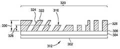
도 2는, 도 3a 내지 도 3f에 도시된 바와 같은, 도파관 구조(300)를 제조하기 위한 방법(200)의 동작들을 예시하는 흐름도이다. 일 실시예에서, 도파관 구조(300)는, 도파관 결합기(100)의 입력 결합 구역(102), 도파관 구역(104), 및 출력 결합 구역(106) 중 적어도 하나에 대응한다. 다른 실시예에서, 도파관 구조(300)는, 도파관 결합기(100)의 입력 결합 구역(102), 도파관 구역(104), 및 출력 결합 구역(106) 중 적어도 하나의 마스터에 대응한다. 동작(201)에서, 음의 도파관 구조(312)를 형성하기 위해, 양의 도파관 패턴(310)을 갖는 스탬프(308)가 기판(304)의 부분(302)의 표면(306) 상에 배치되는 레지스트(326) 상에 임프린팅된다. 기판(304)은 제1 굴절률을 갖는다. 일 실시예에서, 기판(304)은 유리 및 플라스틱 물질들 중 적어도 하나를 포함한다.FIG. 2 is a flow diagram illustrating operations of a
도 3a에 도시된 바와 같이, 양의 도파관 패턴(310)은, 도파관 결합기(100)의 입력 결합 구역(102), 도파관 구역(104), 및 출력 결합 구역(106) 중 적어도 하나의 형성을 초래하는 적어도 하나의 패턴 부분(314)을 포함한다. 도 3a 및 도 3b에 도시된 바와 같이, 음의 도파관 구조(312)는, 종종 최하부 표면으로 지칭되는 잔류 층(318)을 갖는 역의 구역(316)을 포함한다. 일 실시예에서, 역의 구역(316)은, 입력 결합 구역(102)의 복수의 격자들(108), 출력 결합 구역(106)의 복수의 격자들(110), 및 도파관 구역(104) 중 적어도 하나를 형성하기 위한 복수의 역의 격자들(320)을 포함한다. 일 실시예에서, 역의 격자들(320)은, 기판(304)의 표면(306)과 평행한 역의 최상부 표면들(322), 역의 측벽 표면들(324), 및 기판(304)의 표면(306)과 평행한 잔류 층(318)을 갖는다. 일 실시예에서, 역의 격자들(320)의 역의 측벽 표면들(324) 각각은 기판(304)의 표면(306)에 수직으로 배향된다. 다른 실시예에서, 역의 격자들(320)의 역의 측벽 표면들(324) 각각은 기판(304)의 표면(306)에 대해 각진다. 또 다른 실시예에서, 기판(304)의 표면(306)에 대해, 역의 격자들(320)의 역의 측벽 표면들(324)의 일부분은 수직으로 배향되고 역의 측벽 표면들(324)의 일부분은 각진다.As shown in FIG. 3A , the
동작(202)에서, 기판(304)의 표면(306) 상의 레지스트(326)는 레지스트(326)를 안정화시키기 위해 경화된다. 동작(203)에서, 스탬프(308)가 레지스트(326)로부터 해제된다. 일 실시예에서, 스탬프(308)는, 역의 패턴 부분을 포함하는 음의 패턴을 갖는 도파관 마스터로부터 제조된다. 스탬프(308)는 도파관 마스터로부터 성형된다. 스탬프(308)는, 적외선(IR) 방사선 또는 자외선(UV) 방사선과 같은 전자기 방사선에 대한 노출에 의해 레지스트(326)가 경화될 수 있게 하기 위한 반투명한 물질, 이를테면, 용융 실리카 또는 폴리디메틸실록산(PDMS)을 포함한다. 일 실시예에서, 레지스트(326)는, PDMS를 포함하는 스탬프(308)에 의해 나노 임프린팅가능한 UV 경화성 물질(이를테면, 마이크로 레지스트 테크놀로지(Micro Resist Technology)로부터 입수가능한 mr-N210)을 포함한다. 일 실시예에서, 기판(304)의 표면(306)은, UV 오존 처리, 산소(O2) 플라즈마 처리에 의해, 또는 프라이머(이를테면, 마이크로 레지스트 테크놀로지로부터 입수가능한 mr-APS1)의 적용에 의해 UV 경화성 물질의 스핀 코팅을 위한 준비가 된다. 레지스트(326)는 대안적으로 열적으로 경화될 수 있다. 다른 실시예에서, 레지스트(326)는, 열적 가열 또는 적외선 조명 가열을 포함하는 용매 증발 경화 공정에 의해 경화될 수 있는 열 경화성 물질을 포함한다. 레지스트(326)는, 액체 물질 주입 주조 공정, 스핀-온 코팅 공정, 액체 분무 코팅 공정, 건조 분말 코팅 고정, 스크린 인쇄 공정, 닥터 블레이딩 공정, 물리 기상 증착(PVD) 공정, 화학 기상 증착(CVD) 공정, 유동성 CVD(FCVD) 공정, 또는 원자 층 증착(ALD) 공정을 사용하여 표면(306) 상에 배치될 수 있다.In
동작(204)에서, 잔류 층(318)이 제거된다. 일 실시예에서, 잔류 층(318)은, 산소 가스(O2) 함유 플라즈마, 플루오린 가스(F2) 함유 플라즈마, 염소 가스(Cl2) 함유 플라즈마, 및/또는 메탄(CH4) 함유 플라즈마를 사용하는, 종종 플라즈마 디스커밍(descumming)으로 지칭되는 플라즈마 애싱에 의해 제거된다. 다른 실시예에서, 잔류 층(318)이 제거될 때까지 무선 주파수(RF) 전력이 O2 및 불활성 가스, 이를테면, 아르곤(Ar) 또는 질소(N)에 인가된다. 도 3c에 도시된 바와 같이, 역의 격자들(320)은, 역의 최상부 표면들(322)로부터 기판(304)의 표면(306)까지 연장되는 역의 깊이들(328, 330)을 갖는다. 일 실시예에서, 역의 깊이(328) 및 역의 깊이(330)는 실질적으로 동일하다. 다른 실시예에서, 역의 깊이(328) 및 역의 깊이(330)는 상이하다.In
동작(205)에서, 코팅(322)이 기판(304)의 표면(306) 상에 증착된다. 일 실시예에서, 도 3d 및 도 3e에 도시된 바와 같이, 코팅(322)은, 기판(304)의 표면(306), 및 음의 도파관 구조(312)의 나머지 돌출부들 상에 증착된다. 코팅(322)은, 제1 굴절률과 실질적으로 매칭되거나 그보다 큰 제2 굴절률을 갖는다. 코팅(322)은, 스핀 온 글래스(SOG; spin on glass), 유동성 SOG, 졸-겔, 유기 나노 임프린팅가능, 무기 나노 임프린팅가능, 및 혼성(유기와 무기) 나노 임프린팅가능 물질들 중 적어도 하나, 이를테면, 규소 옥시카바이드(SiOC), 이산화티타늄(TiO2), 이산화규소(SiO2), 바나듐(IV) 산화물(VOx), 산화알루미늄(Al2O3), 인듐 주석 산화물(ITO), 산화아연(ZnO), 오산화탄탈럼(Ta2O5), 질화규소(Si3N4), 질화티타늄(TiN), 및/또는 이산화지르코늄(ZrO2) 함유 물질들 중 적어도 하나를 포함한다. 코팅(322)은, 액체 물질 주입 주조 공정, 스핀-온 코팅 공정, 액체 분무 코팅 공정, 건조 분말 코팅 고정, 스크린 인쇄 공정, 닥터 블레이딩 공정, PVD 공정, CVD 공정, FCVD 공정, 또는 ALD 공정을 사용하여 표면(306) 상에 배치될 수 있다. 또한, 코팅(322), 이를테면 SiOC 코팅은, UV 경화 또는 열 경화를 겪을 수 있다. 도 3d에 도시된 바와 같이, 일 실시예에서, 과잉 코팅(322)이 존재할 수 있다. 실시예에서, 과잉 코팅(322)은, 물질 열 리플로우 또는 식각을 사용하여 제거된다. 도 3e에 도시된 바와 같이, 코팅(322)은, 음의 도파관 구조(312)의 나머지 돌출부들과 동일 평면 상에 있거나, 음의 도파관 구조(312)의 나머지 돌출부들과 동일한 높이까지 기판(304) 위로 연장된다. 일 실시예에서, 코팅(322)은 액체 침착되고, 과잉 코팅(322)은 기계적 평탄화에 의해 제거된다.In
코팅(322)의 굴절률은, 기판(304)의 제1 굴절률, 및 격자들, 이를테면, 방법(200)에 의해 형성되는 입력 결합 구역(102)의 결과적인 복수의 격자들(108) 및/또는 출력 결합 구역(106)의 결과적인 복수의 격자들(110)의 강도에 기반하여 조정된다. 코팅(322)의 굴절률은, 광의 포획(in-coupling) 및 축출(out-coupling)을 제어하고 도파관 구조(300)를 통한 광 전파를 용이하게 하도록 기판(304)의 제1 굴절률 및 격자들의 강도에 기반하여 조정된다. 예컨대, 기판(304)의 표면(306)의 물질은 약 1.5 내지 약 2.5의 제1 굴절률을 갖고, 코팅(322)의 물질은 약 1.5 내지 약 2.5의 제2 굴절률을 갖는다. 기판(304)을 제조하는 데 활용되는 물질과 코팅(322)의 물질의 굴절률들을 매칭시킴으로써, 기판(304)의 표면(306)과 코팅(322)의 물질 사이의 계면에서의 실질적인 광 굴절이 없는 기판(304) 및 코팅(322)의 물질 둘 모두를 통한 광 전파가 달성될 수 있다. 기판(304)을 제조하는 데 활용되는 물질들의 굴절률들보다 큰 굴절률을 갖는 코팅(322)의 물질을 활용함으로써, 더 많은 광이 광 수용 각도를 통해 도파관 구조(300)로부터 포획 및 축출될 것이다. 기판(304) 및 코팅(322)의 물질은 총괄적으로 도파관 구조(300)를 포함한다. 기판(304)에 대해 약 1.5 내지 약 2.5의 굴절률을 갖는 물질들을 활용함으로써, 공기의 굴절률(1.0)과 비교하여, 내부 전반사 또는 적어도 높은 수준의 내부 전반사가 달성되어 도파관 구조(300)을 통한 광 전파를 용이하게 한다.The refractive index of the
동작(206)에서, 도파관 구조(300)를 형성하도록 레지스트(326)가 제거된다. 일 실시예에서, 레지스트(326)는, O2 함유 플라즈마, F2 함유 플라즈마, Cl2 함유 플라즈마, 및/또는 CH4 함유 플라즈마를 사용하는 플라즈마 애싱에 의해 제거된다. 다른 실시예에서, 레지스트(326)가 제거될 때까지 RF 전력이 O2 및 불활성 가스, 이를테면, 아르곤(Ar) 또는 질소(N)에 인가된다. 도 3f에 도시된 바와 같이, 도파관 구조(300)는 구역(334)을 포함한다. 일 실시예에서, 구역(334)은, 도파관 결합기(100)의 입력 결합 구역(102), 도파관 구역(104), 및 출력 결합 구역(106) 중 적어도 하나에 대응한다. 구역(334)은 복수의 격자들(336)을 포함한다. 일 실시예에서, 구역(334)은, 입력 결합 구역(102)의 복수의 격자들(108), 출력 결합 구역(106)의 복수의 격자들(110), 및 도파관 구역(104) 중 적어도 하나에 대응하는 복수의 격자들(336)을 포함한다. 일 실시예에서, 격자들(336)은, 기판(304)의 표면(306)과 평행한 최상부 표면들(338), 및 측벽 표면들(340)을 갖는다. 일 실시예에서, 격자들(336)의 측벽 표면들(340) 각각은 기판(304)의 표면(306)에 수직으로 배향된다. 다른 실시예에서, 격자들(336)의 측벽 표면들(340) 각각은 기판(304)의 표면(306)에 대해 각진다. 또 다른 실시예에서, 기판(304)의 표면(306)에 대해, 격자들(336)의 측벽 표면들(340)의 일부분은 수직으로 배향되고 측벽 표면들(340)의 일부분은 각진다. 일 실시예에서, 측벽 표면들(340)은 약 15 도 내지 약 75 도의 각도로 각진다. 격자들(336)은, 기판(304)의 표면(306)으로부터 최상부 표면들(338)까지 연장되는 깊이들(342, 344)을 갖는다. 일 실시예에서, 깊이(342) 및 깊이(344)는 실질적으로 동일하다. 다른 실시예에서, 깊이(342) 및 깊이(344)는 상이하다.In
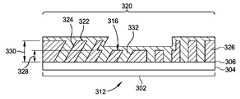
도 4는, 도 5a 내지 도 5d에 도시된 바와 같은, 도파관 구조(500)를 제조하기 위한 방법(400)의 동작들을 예시하는 흐름도이다. 일 실시예에서, 도파관 구조(500)는, 도파관 결합기(100)의 입력 결합 구역(102), 도파관 구역(104), 및/또는 출력 결합 구역(106) 중 적어도 하나에 대응한다. 다른 실시예에서, 도파관 구조(500)는, 도파관 결합기(100)의 입력 결합 구역(102), 도파관 구역(104), 및 출력 결합 구역(106) 중 적어도 하나의 마스터에 대응한다. 동작(401)에서, 스탬프(308)의 음의 도파관 구조(512) 상에 코팅(322)이 증착된다. 도 5a에 도시된 바와 같이, 일 실시예에서, 증착된 코팅(322)은, 스탬프(308)의 음의 도파관 구조(512)에 형상추종적이다. 도 5b에 도시된 바와 같이, 일 실시예에서, 증착된 코팅(322)은, 스탬프(308)의 음의 도파관 구조(512)에 대해 실질적으로 평면이다. 따라서, 임의적 동작(402)에서 코팅(322)을 평탄화할 필요가 없다. 임의적 동작(402)에서, 일 실시예에서는, 코팅(322)을 평탄화하는 것은, 중력, 열 리플로우, 또는 화학적 기계적 연마(CMP)에 의한 기계적 평탄화를 포함한다.4 is a flow diagram illustrating operations of a
스탬프(308)는 도파관 마스터로부터 성형되고, IR 방사선 또는 UV 방사선과 같은 전자기 방사선에 대한 노출에 의해 코팅(322)이 경화될 수 있게 하기 위한 반투명한 물질, 이를테면, 용융 실리카 또는 PDMS로 만들어질 수 있다. 일 실시예에서, 스탬프(308)는, 코팅(322)의 증착 및 평탄화를 용이하게 하기 위한 기계적 강도를 더하기 위해, 유리 시트와 같은 강성 후면 시트를 포함한다.The
코팅(322)은, SOG, 유동성 SOG, 졸-겔, 유기 나노 임프린팅가능, 무기 나노 임프린팅가능, 및 혼성(유기와 무기) 나노 임프린팅가능 물질들 중 적어도 하나, 이를테면, SiOC, TiO2, SiO2, VOx, Al2O3, ITO, ZnO, Ta2O5, Si3N4, TiN, 및 ZrO2 함유 물질들 중 적어도 하나를 포함한다. 코팅(322)은, 액체 물질 주입 주조 공정, 스핀-온 코팅 공정, 액체 분무 코팅 공정, 건조 분말 코팅 고정, 스크린 인쇄 공정, 닥터 블레이딩 공정, PVD 공정, CVD 공정, FCVD 공정, 또는 ALD 공정을 사용하여 증착될 수 있다. 일 실시예에서, 코팅 물질은, 코팅 물질의 용융 온도를 낮추고 평탄화 동안의 코팅 물질의 개선된 유동을 허용하기 위해, 도펀트 물질로 도핑된다. 도펀트 물질은, 더 낮은 온도에서의 열 리플로우를 허용하는 인(P) 함유 물질 및/또는 붕소(B) 함유 물질을 포함할 수 있다.Coating 322 may include at least one of SOG, flowable SOG, sol-gel, organic nanoimprintable, inorganic nanoimprintable, and hybrid (organic and inorganic) nanoimprintable materials, such as SiOC, TiO2 , SiO2 , VOx , Al2 O3 , ITO, ZnO, Ta2 O5 , Si3 N4 , TiN, and at least one of ZrO2 containing materials. The
도 5a 및 도 5b에 도시된 바와 같이, 음의 도파관 구조(512)는 역의 구역(516)을 포함한다. 역의 구역(516)은, 입력 결합 구역(102)의 복수의 격자들(108), 출력 결합 구역(106)의 복수의 격자들(110), 및 도파관 구역(104) 중 적어도 하나를 형성하기 위한 복수의 역의 격자들(520)을 포함한다. 일 실시예에서, 역의 격자들(520)은, 스탬프(308)의 최하부 표면(521)과 평행한 역의 최상부 표면들(522), 역의 측벽 표면들(524), 및 스탬프(308)의 최하부 표면(521)과 평행한 역의 최하부 표면들(523)을 갖는다. 일 실시예에서, 역의 격자들(520)의 역의 측벽 표면들(524) 각각은 스탬프(308)의 최하부 표면(521)에 수직으로 배향된다. 다른 실시예에서, 역의 격자들(520)의 역의 측벽 표면들(524) 각각은 스탬프(308)의 최하부 표면(521)에 대해 각진다. 다른 실시예에서, 역의 격자들(520)은, 스탬프(308)의 최하부 표면(521)에 대해 각진 역의 블레이징된(blazed) 표면들(502) 및 스탬프(308)의 최하부 표면(521)에 수직으로 배향된 역의 측벽 표면들(524)을 포함하는 블레이징된 역의 각진 격자들이다. 또 다른 실시예에서, 역의 구역(516)은, 블레이징된 역의 각진 격자들 및 복수의 역의 격자들(520)을 포함하며, 스탬프(308)의 최하부 표면(521)에 대해, 역의 격자들(520)의 역의 측벽 표면들(524)의 일부분은 수직으로 배향되고 역의 측벽 표면들(524)의 일부분은 각진다. 도 5a 및 도 5b에 도시된 바와 같이, 역의 격자들(520)은, 역의 최상부 표면들(522)로부터 스탬프(308)의 최하부 표면(521)까지 연장되는 역의 깊이들(528, 530)을 갖는다. 일 실시예에서, 역의 깊이(528) 및 역의 깊이(530)는 실질적으로 동일하다. 다른 실시예에서, 역의 깊이(528) 및 역의 깊이(530)는 상이하다.5A and 5B ,
동작(403)에서, 도 5c에 도시된 바와 같이, 코팅(322)은 기판(304)의 부분(302)의 표면(306)에 접합된다. 코팅(322)을 기판(304)의 표면(306)에 접합시키기 위해 광학 접착제(501)가 사용된다. 일 실시예에서, 광학 접착제(501)는, 투명한(transparent) 금속 산화물 물질 또는 투명(clear) 아크릴계 중합체를 함유할 수 있다. 광학 접착제(501)는 제3 굴절률을 갖는다.In
코팅(322)은, 기판(304)의 제1 굴절률과 실질적으로 매칭되거나 그보다 큰 제2 굴절률을 갖는다. 코팅의 제2 굴절률은, 기판(304)의 제1 굴절률, 및 격자들, 이를테면, 방법(400)에 의해 형성되는 입력 결합 구역(102)의 결과적인 복수의 격자들(108) 및/또는 출력 결합 구역(106)의 결과적인 복수의 격자들(110)의 강도에 기반하여 조정된다. 코팅(322)의 굴절률은, 광의 포획 및 축출을 제어하고 도파관 구조(500)를 통한 광 전파를 용이하게 하도록 기판(304)의 제1 굴절률 및 격자들의 강도에 기반하여 조정된다. 또한, 광학 접착제(501)는, 제1 굴절률 및 제2 굴절률과 실질적으로 매칭되는 제3 굴절률을 갖는다. 예컨대, 기판(304)의 표면(306)의 물질은 약 1.5 내지 약 2.5의 제1 굴절률을 갖고, 광학 접착제(501)의 물질은 약 1.5 내지 약 2.5의 제3 굴절률을 갖고, 코팅(322)의 물질은 약 1.5 내지 약 2.5의 제2 굴절률을 갖는다. 기판(304)을 제조하는 데 활용되는 물질, 광학 접착제(501)의 물질, 및 코팅(322)의 물질의 굴절률들을 매칭시킴으로써, 기판(304), 광학 접착제(501)의 물질, 및 코팅(322)의 물질 사이의 계면에서의 실질적인 광 굴절이 없는 기판(304), 광학 접착제(501)의 물질, 및 코팅(322)의 물질을 통한 광 전파가 달성될 수 있다. 기판(304)을 제조하는 데 활용되는 물질들의 굴절률들보다 큰 굴절률을 갖는 코팅(322)의 물질을 활용함으로써, 더 많은 광이 광 수용 각도를 통해 도파관 구조(500)로부터 포획 및 축출될 것이다. 기판(304) 및 광학 접착제(501)의 물질에 대해 약 1.5 내지 약 2.5의 굴절률을 갖는 물질들을 활용함으로써, 공기의 굴절률(1.0)과 비교하여, 내부 전반사 또는 적어도 높은 수준의 내부 전반사가 달성되어 도파관 구조(500)를 통한 광 전파를 용이하게 한다.The
동작(404)에서, 도파관 구조(500)를 형성하기 위해 스탬프(308)가 해제된다. 도 5d에 도시된 바와 같이, 도파관 구조(500)는 구역(534)을 포함한다. 일 실시예에서, 구역(534)은, 도파관 결합기(100)의 입력 결합 구역(102), 도파관 구역(104), 및 출력 결합 구역(106) 중 적어도 하나에 대응한다. 구역(534)은 복수의 격자들(536)을 포함한다. 일 실시예에서, 복수의 격자들(536)은, 입력 결합 구역(102)의 복수의 격자들(108), 출력 결합 구역(106)의 복수의 격자들(110), 및 도파관 구역(104) 중 적어도 하나에 대응한다. 일 실시예에서, 격자들(536)은, 기판(304)의 표면(306)과 평행한 최상부 표면들(538), 및 측벽 표면들(540)을 갖는다. 일 실시예에서, 격자들(536)의 측벽 표면들(540) 각각은 기판(304)의 표면(306)에 수직으로 배향된다. 다른 실시예에서, 격자들(536)의 측벽 표면들(540) 각각은 기판(304)의 표면(306)에 대해 각진다. 다른 실시예에서, 격자들(536)은, 기판(304)의 표면(306)에 대해 각진 블레이징된 표면들(506) 및 기판(304)의 표면(306)에 수직으로 배향된 측벽 표면들(540)을 포함하는 블레이징된 각진 격자들이다. 또 다른 실시예에서, 구역(534)은, 블레이징된 각진 격자들 및 격자들(536)을 포함하며, 기판(304)의 표면(306)에 대해, 격자들(536)의 측벽 표면들(540)의 일부분은 수직으로 배향되고 측벽 표면들(540)의 일부분은 각진다. 격자들(536)은, 광학 접착제(501)로부터 최상부 표면들(538)까지 연장되는 깊이들(542, 544)을 갖는다. 일 실시예에서, 깊이(542) 및 깊이(544)는 실질적으로 동일하다. 다른 실시예에서, 깊이(542) 및 깊이(544)는 상이하다.At
요약하면, 도파관 결합기들을 제조하기 위한 방법들이 본원에 설명된다. 방법들은, 미세 광 격자들을 정의하는 무기 또는 혼성(유기와 무기) 물질들로 형성되는 입력 결합 구역들, 도파관 구역들, 및 출력 결합 구역들을 갖는 도파관 결합기들을 제공한다. 무기 또는 혼성 도파관 구조들은, 도파관들을 통해 광을 전파하기 위한 최적의 굴절률들을 갖는 격자들을 형성하도록 임프린팅가능하지 않은 유기 레지스트들과 비교하여, 안정하고, 낮은 광 흡수 손실을 갖고, 도파관 결합기들을 통해 광을 전파하기 위한 최적의 굴절률들을 갖는다.In summary, methods for fabricating waveguide couplers are described herein. Methods provide waveguide couplers having input coupling regions, waveguide regions, and output coupling regions formed of inorganic or hybrid (organic and inorganic) materials that define fine optical gratings. Inorganic or hybrid waveguide structures are stable compared to organic resists that are not imprintable to form gratings with optimal refractive indices for propagating light through the waveguides, have low light absorption loss, and pass through waveguide couplers. It has optimal refractive indices for propagating light.
전술한 내용이 본 개시내용의 예들에 관한 것이지만, 본 개시내용의 다른 그리고 추가적인 예들이 본 개시내용의 기본적인 범위로부터 벗어나지 않으면서 고안될 수 있으며, 본 개시내용의 범위는 하기의 청구항들에 의해 결정된다.While the foregoing is directed to examples of the present disclosure, other and additional examples of the disclosure may be devised without departing from the basic scope of the disclosure, the scope of which is determined by the following claims. do.
Claims (15)
Translated fromKorean레지스트에 스탬프를 임프린팅하는 단계 ― 상기 스탬프는 적어도 하나의 패턴 부분을 포함하는 양의 도파관 패턴을 갖고, 상기 임프린팅하는 단계는, 잔류 층을 갖는 역의(inverse) 구역을 포함하는 음의 도파관 구조를 형성하고, 상기 레지스트는 기판의 일부분의 표면 상에 배치되고, 상기 기판은 제1 굴절률을 가짐 ―;
상기 기판의 상기 표면 상의 상기 레지스트를 경화시키는 단계;
상기 스탬프를 해제하는 단계;
상기 잔류 층을 제거하는 단계;
상기 기판의 상기 표면의 상기 제1 굴절률과 매칭되거나 상기 제1 굴절률보다 큰 제2 굴절률을 갖는 코팅을 증착하는 단계; 및
상기 레지스트를 제거하여 구역을 포함하는 도파관 구조를 형성하는 단계를 포함하고,
상기 코팅은, 규소 옥시카바이드(SiOC), 이산화티타늄(TiO2), 이산화규소(SiO2), 바나듐(IV) 산화물(VOx), 산화알루미늄(Al2O3), 인듐 주석 산화물(ITO), 산화아연(ZnO), 오산화탄탈럼(Ta2O5), 질화규소(Si3N4), 질화티타늄(TiN), 및 이산화지르코늄(ZrO2) 함유 물질들 중 적어도 하나를 포함하는, 도파관 구조를 제조하는 방법.A method of manufacturing a waveguide structure comprising:
imprinting a stamp into the resist, wherein the stamp has a positive waveguide pattern comprising at least one pattern portion, and wherein the imprinting comprises: a negative waveguide comprising an inverse region having a residual layer forming a structure, wherein the resist is disposed on a surface of a portion of a substrate, the substrate having a first index of refraction;
curing the resist on the surface of the substrate;
releasing the stamp;
removing the residual layer;
depositing a coating having a second index of refraction that matches or is greater than the first index of refraction of the surface of the substrate; and
removing the resist to form a waveguide structure comprising a zone;
The coating is silicon oxycarbide (SiOC), titanium dioxide (TiO2 ), silicon dioxide (SiO2 ), vanadium (IV) oxide (VOx ), aluminum oxide (Al2 O3 ), indium tin oxide (ITO) , zinc oxide (ZnO), tantalum pentoxide (Ta2 O5 ), silicon nitride (Si3 N4 ), titanium nitride (TiN), and zirconium dioxide (ZrO2 ). How to manufacture.
상기 구역은, 도파관 결합기의 입력 결합 구역, 도파관 구역, 및 출력 결합 구역 중 적어도 하나인, 도파관 구조를 제조하는 방법.According to claim 1,
wherein the zone is at least one of an input coupling zone, a waveguide zone, and an output coupling zone of the waveguide coupler.
상기 구역은, 상기 입력 결합 구역 및 상기 출력 결합 구역 중 적어도 하나의 복수의 격자들을 포함하는, 도파관 구조를 제조하는 방법.4. The method of claim 3,
wherein the zone comprises a plurality of gratings of at least one of the input coupling zone and the output coupling zone.
상기 복수의 격자들은, 상기 기판의 상기 표면과 평행한 최상부 표면들, 및 상기 기판의 상기 표면에 대해 일정 양만큼 경사지는 측벽 표면들을 포함하는, 도파관 구조를 제조하는 방법.5. The method of claim 4,
wherein the plurality of gratings include top surfaces parallel to the surface of the substrate and sidewall surfaces that are inclined relative to the surface of the substrate by an amount.
스탬프의 음의 도파관 구조 상에 제2 굴절률을 갖는 코팅을 증착하는 단계 ― 상기 제2 굴절률은 기판의 제1 굴절률과 매칭되거나 상기 제1 굴절률보다 크고, 상기 음의 도파관 구조는 역의 구역을 포함함 ―;
상기 코팅을 평탄화하는 단계;
상기 코팅을 상기 기판의 일부분의 표면에 접합시키는 단계; 및
구역을 포함하는 도파관 구조를 형성하도록 상기 스탬프를 해제하는 단계를 포함하고,
상기 코팅은, 규소 옥시카바이드(SiOC), 이산화티타늄(TiO2), 이산화규소(SiO2), 바나듐(IV) 산화물(VOx), 산화알루미늄(Al2O3), 인듐 주석 산화물(ITO), 산화아연(ZnO), 오산화탄탈럼(Ta2O5), 질화규소(Si3N4), 질화티타늄(TiN), 또는 이산화지르코늄(ZrO2) 함유 물질들을 포함하는, 도파관 구조를 제조하는 방법.A method of manufacturing a waveguide structure comprising:
depositing a coating having a second index of refraction on the negative waveguide structure of the stamp, wherein the second index of refraction matches or is greater than the first index of refraction of the substrate, the negative waveguide structure comprising a region of inverse Ham ―;
planarizing the coating;
bonding the coating to the surface of the portion of the substrate; and
releasing the stamp to form a waveguide structure comprising a zone;
The coating is silicon oxycarbide (SiOC), titanium dioxide (TiO2 ), silicon dioxide (SiO2 ), vanadium (IV) oxide (VOx ), aluminum oxide (Al2 O3 ), indium tin oxide (ITO) , zinc oxide (ZnO), tantalum pentoxide (Ta2 O5 ), silicon nitride (Si3 N4 ), titanium nitride (TiN), or zirconium dioxide (ZrO2 ). .
상기 코팅을 증착하는 단계는, 액체 물질 주입 주조 공정, 스핀-온 코팅 공정, 액체 분무 코팅 공정, 건조 분말 코팅 고정, 스크린 인쇄 공정, 닥터 블레이딩 공정, 물리 기상 증착(PVD) 공정, 화학 기상 증착(CVD) 공정, 유동성 CVD(FCVD) 공정, 또는 원자 층 증착(ALD) 공정을 포함하는, 도파관 구조를 제조하는 방법.7. The method of claim 6,
Depositing the coating may include a liquid material injection casting process, spin-on coating process, liquid spray coating process, dry powder coating fixing, screen printing process, doctor blading process, physical vapor deposition (PVD) process, chemical vapor deposition A method of making a waveguide structure comprising a (CVD) process, a flowable CVD (FCVD) process, or an atomic layer deposition (ALD) process.
상기 구역은, 도파관 결합기의 입력 결합 구역 및 출력 결합 구역 중 적어도 하나의 복수의 격자들을 포함하는, 도파관 구조를 제조하는 방법.7. The method of claim 6,
wherein the zone comprises a plurality of gratings of at least one of an input coupling zone and an output coupling zone of the waveguide coupler.
상기 코팅을 상기 기판의 상기 표면에 접합시키기 위해 광학 접착제가 사용되고, 상기 광학 접착제는, 상기 제1 굴절률 및 상기 제2 굴절률과 매칭되는 제3 굴절률을 갖는, 도파관 구조를 제조하는 방법.7. The method of claim 6,
An optical adhesive is used to bond the coating to the surface of the substrate, the optical adhesive having a third index of refraction matching the first index of refraction and the second index of refraction.
스탬프의 음의 도파관 구조 상에 1.5 내지 2.5의 제2 굴절률을 갖는 코팅을 증착하는 단계 ― 상기 코팅은 상기 음의 도파관 구조에 대해 평면이고, 상기 제2 굴절률은, 기판의 1.5 내지 2.5의 제1 굴절률과 매칭되거나 상기 제1 굴절률보다 크고, 상기 음의 도파관 구조는 역의 입력 결합 구역 및 역의 출력 결합 구역을 포함함 ―;
상기 코팅을 상기 기판의 일부분의 표면에 접합시키는 단계 ― 상기 기판의 상기 표면에는, 상기 제1 굴절률 및 상기 제2 굴절률과 매칭되는 제3 굴절률을 갖는 광학 접착제가 상부에 배치됨 ―; 및
구역을 갖는 도파관 구조를 형성하도록 상기 스탬프를 해제하는 단계를 포함하고,
상기 코팅은, 규소 옥시카바이드(SiOC), 이산화티타늄(TiO2), 이산화규소(SiO2), 바나듐(IV) 산화물(VOx), 산화알루미늄(Al2O3), 인듐 주석 산화물(ITO), 산화아연(ZnO), 오산화탄탈럼(Ta2O5), 질화규소(Si3N4), 질화티타늄(TiN), 또는 이산화지르코늄(ZrO2) 함유 물질들을 포함하는, 도파관 구조를 제조하는 방법.A method of manufacturing a waveguide structure comprising:
depositing a coating having a second index of refraction of 1.5 to 2.5 on the negative waveguide structure of the stamp, the coating being planar with respect to the negative waveguide structure, the second index of refraction being a first index of refraction of 1.5 to 2.5 of the substrate matching or greater than the first index of refraction, the negative waveguide structure comprising an inverse input coupling region and an inverse output coupling region;
bonding the coating to a surface of a portion of the substrate, the surface of the substrate disposed thereon with an optical adhesive having a third index of refraction matching the first index of refraction and the second index of refraction; and
releasing the stamp to form a waveguide structure having a zone;
The coating is silicon oxycarbide (SiOC), titanium dioxide (TiO2 ), silicon dioxide (SiO2 ), vanadium (IV) oxide (VOx ), aluminum oxide (Al2 O3 ), indium tin oxide (ITO) , zinc oxide (ZnO), tantalum pentoxide (Ta2 O5 ), silicon nitride (Si3 N4 ), titanium nitride (TiN), or zirconium dioxide (ZrO2 ). .
상기 광학 접착제는 투명한(transparent) 금속 산화물 물질 또는 투명(clear) 아크릴계 중합체를 포함하며, 상기 제3 굴절률은 1.5 내지 2.5인, 도파관 구조를 제조하는 방법.12. The method of claim 11,
wherein the optical adhesive comprises a transparent metal oxide material or a clear acrylic polymer, and wherein the third refractive index is 1.5 to 2.5.
상기 구역은, 도파관 결합기의 입력 결합 구역 및 출력 결합 구역 중 적어도 하나의 복수의 격자들을 포함하는, 도파관 구조를 제조하는 방법.12. The method of claim 11,
wherein the zone comprises a plurality of gratings of at least one of an input coupling zone and an output coupling zone of the waveguide coupler.
상기 복수의 격자들은, 상기 기판의 상기 표면과 평행한 최상부 표면들, 및 상기 기판의 상기 표면에 대해 일정 양만큼 경사지는 측벽 표면들을 포함하는, 도파관 구조를 제조하는 방법.14. The method of claim 13,
wherein the plurality of gratings include top surfaces parallel to the surface of the substrate and sidewall surfaces that are inclined relative to the surface of the substrate by an amount.
상기 복수의 격자들은, 상기 기판의 상기 표면에 대해 각진 블레이징된(blazed) 표면들 및 상기 기판의 상기 표면에 수직으로 배향된 측벽 표면들을 갖는 블레이징된 각진 격자들인, 도파관 구조를 제조하는 방법.14. The method of claim 13,
wherein the plurality of gratings are blazed angled gratings having blazed surfaces angled relative to the surface of the substrate and sidewall surfaces oriented perpendicular to the surface of the substrate. .
Applications Claiming Priority (5)
| Application Number | Priority Date | Filing Date | Title |
|---|---|---|---|
| US201762589457P | 2017-11-21 | 2017-11-21 | |
| US62/589,457 | 2017-11-21 | ||
| US201762593756P | 2017-12-01 | 2017-12-01 | |
| US62/593,756 | 2017-12-01 | ||
| PCT/US2018/060641WO2019103871A1 (en) | 2017-11-21 | 2018-11-13 | Method of fabrication of waveguide combiners |
Publications (2)
| Publication Number | Publication Date |
|---|---|
| KR20200075893A KR20200075893A (en) | 2020-06-26 |
| KR102444339B1true KR102444339B1 (en) | 2022-09-19 |
Family
ID=66631728
Family Applications (1)
| Application Number | Title | Priority Date | Filing Date |
|---|---|---|---|
| KR1020207017437AActiveKR102444339B1 (en) | 2017-11-21 | 2018-11-13 | Method of making waveguide couplers |
Country Status (4)
| Country | Link |
|---|---|
| JP (2) | JP2021504736A (en) |
| KR (1) | KR102444339B1 (en) |
| CN (2) | CN115663442A (en) |
| WO (1) | WO2019103871A1 (en) |
Families Citing this family (7)
| Publication number | Priority date | Publication date | Assignee | Title |
|---|---|---|---|---|
| CN113448014A (en)* | 2020-03-25 | 2021-09-28 | 苏州苏大维格科技集团股份有限公司 | Relief type waveguide structure and manufacturing method thereof |
| FI130396B (en)* | 2020-09-23 | 2023-08-10 | Dispelix Oy | Optical Waveguide for Augmented Reality Display |
| US20220299677A1 (en)* | 2021-03-17 | 2022-09-22 | Applied Materials, Inc. | Airgap structures for improved eyepiece efficiency |
| WO2023064094A1 (en)* | 2021-10-15 | 2023-04-20 | Applied Materials, Inc. | Multilayer transmission structures for waveguide display |
| WO2023200682A1 (en)* | 2022-04-13 | 2023-10-19 | Applied Materials, Inc. | Optical device improvement |
| CN117930417A (en)* | 2022-10-14 | 2024-04-26 | Oppo广东移动通信有限公司 | Optical waveguide assembly and augmented reality device |
| TW202432449A (en)* | 2022-10-18 | 2024-08-16 | 日商東京威力科創股份有限公司 | Diffraction grating formation method |
Citations (4)
| Publication number | Priority date | Publication date | Assignee | Title |
|---|---|---|---|---|
| JP2008299084A (en)* | 2007-05-31 | 2008-12-11 | Ricoh Opt Ind Co Ltd | Method of manufacturing optical element having fine irregular shape on the surface |
| US20150107885A1 (en)* | 2013-10-18 | 2015-04-23 | Applied Materials, Inc. | Layer stack for a touch panel and method for forming a layer stack |
| US20160266387A1 (en)* | 2013-11-27 | 2016-09-15 | Magic Leap, Inc. | Virtual and augmented reality systems and methods having improved diffractive grating structures |
| WO2016205249A1 (en)* | 2015-06-15 | 2016-12-22 | Magic Leap, Inc. | Virtual and augmented reality systems and methods |
Family Cites Families (32)
| Publication number | Priority date | Publication date | Assignee | Title |
|---|---|---|---|---|
| JPS627002A (en)* | 1985-07-04 | 1987-01-14 | Kokusai Denshin Denwa Co Ltd <Kdd> | Manufacturing method of phase shift diffraction grating |
| US5114513A (en)* | 1988-10-27 | 1992-05-19 | Omron Tateisi Electronics Co. | Optical device and manufacturing method thereof |
| JPH03200106A (en)* | 1989-12-28 | 1991-09-02 | Omron Corp | Optical waveguide lens |
| JP3009986B2 (en)* | 1993-11-10 | 2000-02-14 | シャープ株式会社 | Fabrication method of tapered waveguide |
| EP1186916A1 (en)* | 2000-09-06 | 2002-03-13 | Corning Incorporated | Fabrication of gratings in planar waveguide devices |
| JP4282263B2 (en)* | 2001-12-28 | 2009-06-17 | 株式会社リコー | Optical path switching device and image display device |
| JP4139140B2 (en)* | 2002-05-30 | 2008-08-27 | 株式会社リコー | Polarization hologram element and manufacturing method thereof |
| JP4266732B2 (en)* | 2002-08-30 | 2009-05-20 | キヤノン株式会社 | Multilayer diffractive optical element |
| US7245406B2 (en)* | 2003-09-17 | 2007-07-17 | Dai Nippon Printing Co., Ltd. | Method for forming fine concavo-convex patterns, method for producing optical diffraction structure, and method for copying optical diffraction structure |
| JP2006276195A (en)* | 2005-03-28 | 2006-10-12 | Canon Inc | Ultraviolet curable resin composition, optical element molded thereby, laminated diffractive optical element, and optical system |
| US7864425B2 (en)* | 2005-09-16 | 2011-01-04 | Panasonic Corporation | Composite material and optical component using the same |
| JP4814002B2 (en)* | 2005-09-30 | 2011-11-09 | 株式会社リコー | Phase plate manufacturing method, optical element and image projection apparatus |
| EP1949147B1 (en)* | 2005-11-18 | 2012-03-21 | Nanocomp Oy Ltd. | Method of producing a diffraction grating element |
| JP2008008990A (en)* | 2006-06-27 | 2008-01-17 | Ricoh Co Ltd | Wave plate, image projection device, and optical pickup device |
| JP2008020846A (en)* | 2006-07-14 | 2008-01-31 | Asahi Glass Co Ltd | Method for forming alignment film, liquid crystal optical element, and optical head device |
| JP4842763B2 (en)* | 2006-10-23 | 2011-12-21 | 株式会社リコー | Optical element and optical device |
| JP2010519588A (en)* | 2007-02-23 | 2010-06-03 | ナノコンプ リミテッド | Diffraction grating structure and design method of the diffraction grating structure |
| JP2011202067A (en)* | 2010-03-26 | 2011-10-13 | Panasonic Corp | Nanocomposite material, optical lens or window material having nanocomposite material, and method of manufacturing nanocomposite material |
| US8699842B2 (en)* | 2011-05-27 | 2014-04-15 | Google Inc. | Image relay waveguide and method of producing same |
| JP2013007830A (en)* | 2011-06-23 | 2013-01-10 | Seiko Epson Corp | Transmissive diffraction grating and detecting device |
| CN103091747B (en)* | 2011-10-28 | 2015-11-25 | 清华大学 | A kind of preparation method of grating |
| JP5899867B2 (en)* | 2011-11-25 | 2016-04-06 | ナガセケムテックス株式会社 | Composite metal oxide fine particles for optical materials |
| US9981844B2 (en)* | 2012-03-08 | 2018-05-29 | Infineon Technologies Ag | Method of manufacturing semiconductor device with glass pieces |
| WO2013148208A1 (en)* | 2012-03-30 | 2013-10-03 | Massachusetts Institute Of Technology | Methods and apparatus for vertical coupling from dielectric waveguides |
| US9780335B2 (en)* | 2012-07-20 | 2017-10-03 | 3M Innovative Properties Company | Structured lamination transfer films and methods |
| WO2014132588A1 (en)* | 2013-02-26 | 2014-09-04 | パナソニック株式会社 | Optical lens |
| EP3084508B1 (en)* | 2013-12-19 | 2018-11-28 | BAE Systems PLC | Improvements in and relating to waveguides |
| CN103837919B (en)* | 2014-03-06 | 2016-03-09 | 成都贝思达光电科技有限公司 | A kind of optical grating construction color filter film job operation based on double-layer glue nano impression |
| CN103943715B (en)* | 2014-03-14 | 2016-10-19 | 中国科学院半导体研究所 | Enhanced Graphene Waveguide Detector Integrated with Distributed Bragg Reflection Grating |
| US9910276B2 (en)* | 2015-06-30 | 2018-03-06 | Microsoft Technology Licensing, Llc | Diffractive optical elements with graded edges |
| JP2017062941A (en)* | 2015-09-25 | 2017-03-30 | ソニー株式会社 | Display device and manufacturing method thereof |
| US10197804B2 (en)* | 2016-04-25 | 2019-02-05 | Microsoft Technology Licensing, Llc | Refractive coating for diffractive optical elements |
- 2018
- 2018-11-13KRKR1020207017437Apatent/KR102444339B1/enactiveActive
- 2018-11-13CNCN202211223884.8Apatent/CN115663442A/enactivePending
- 2018-11-13CNCN201880081384.0Apatent/CN111480262B/enactiveActive
- 2018-11-13JPJP2020527764Apatent/JP2021504736A/enactivePending
- 2018-11-13WOPCT/US2018/060641patent/WO2019103871A1/ennot_activeCeased
- 2022
- 2022-07-22JPJP2022117446Apatent/JP7542033B2/enactiveActive
Patent Citations (4)
| Publication number | Priority date | Publication date | Assignee | Title |
|---|---|---|---|---|
| JP2008299084A (en)* | 2007-05-31 | 2008-12-11 | Ricoh Opt Ind Co Ltd | Method of manufacturing optical element having fine irregular shape on the surface |
| US20150107885A1 (en)* | 2013-10-18 | 2015-04-23 | Applied Materials, Inc. | Layer stack for a touch panel and method for forming a layer stack |
| US20160266387A1 (en)* | 2013-11-27 | 2016-09-15 | Magic Leap, Inc. | Virtual and augmented reality systems and methods having improved diffractive grating structures |
| WO2016205249A1 (en)* | 2015-06-15 | 2016-12-22 | Magic Leap, Inc. | Virtual and augmented reality systems and methods |
Also Published As
| Publication number | Publication date |
|---|---|
| CN115663442A (en) | 2023-01-31 |
| JP2021504736A (en) | 2021-02-15 |
| WO2019103871A1 (en) | 2019-05-31 |
| CN111480262A (en) | 2020-07-31 |
| JP7542033B2 (en) | 2024-08-29 |
| JP2022163081A (en) | 2022-10-25 |
| KR20200075893A (en) | 2020-06-26 |
| CN111480262B (en) | 2022-10-25 |
Similar Documents
| Publication | Publication Date | Title |
|---|---|---|
| KR102444339B1 (en) | Method of making waveguide couplers | |
| US10955606B2 (en) | Method of imprinting tilt angle light gratings | |
| US10564332B2 (en) | Controlling grating outcoupling strength for AR waveguide combiners | |
| KR102562250B1 (en) | Method of direct etching fabrication of waveguide combiners | |
| TWI657267B (en) | Transparent diffusers for lightguides and luminaires | |
| US12158612B2 (en) | Evacuated periodic structures and methods of manufacturing | |
| TWI723438B (en) | Gap fill of imprinted structure with spin coated high refractive index material for optical components | |
| US10409001B2 (en) | Waveguide fabrication with sacrificial sidewall spacers | |
| US20220301926A1 (en) | Formation of angled gratings | |
| JP7196295B2 (en) | Controlled hard mask molding for making tapered slanted fins |
Legal Events
| Date | Code | Title | Description |
|---|---|---|---|
| PA0105 | International application | Patent event date:20200617 Patent event code:PA01051R01D Comment text:International Patent Application | |
| PA0201 | Request for examination | ||
| PG1501 | Laying open of application | ||
| E902 | Notification of reason for refusal | ||
| PE0902 | Notice of grounds for rejection | Comment text:Notification of reason for refusal Patent event date:20210525 Patent event code:PE09021S01D | |
| E902 | Notification of reason for refusal | ||
| PE0902 | Notice of grounds for rejection | Comment text:Notification of reason for refusal Patent event date:20211129 Patent event code:PE09021S01D | |
| E701 | Decision to grant or registration of patent right | ||
| PE0701 | Decision of registration | Patent event code:PE07011S01D Comment text:Decision to Grant Registration Patent event date:20220610 | |
| GRNT | Written decision to grant | ||
| PR0701 | Registration of establishment | Comment text:Registration of Establishment Patent event date:20220913 Patent event code:PR07011E01D | |
| PR1002 | Payment of registration fee | Payment date:20220914 End annual number:3 Start annual number:1 | |
| PG1601 | Publication of registration |