KR102443047B1 - Method of processing a substrate and a device manufactured by the same - Google Patents
Method of processing a substrate and a device manufactured by the sameDownload PDFInfo
- Publication number
- KR102443047B1 KR102443047B1KR1020170153314AKR20170153314AKR102443047B1KR 102443047 B1KR102443047 B1KR 102443047B1KR 1020170153314 AKR1020170153314 AKR 1020170153314AKR 20170153314 AKR20170153314 AKR 20170153314AKR 102443047 B1KR102443047 B1KR 102443047B1
- Authority
- KR
- South Korea
- Prior art keywords
- insulating layer
- layer
- etching
- sacrificial
- gas
- Prior art date
- Legal status (The legal status is an assumption and is not a legal conclusion. Google has not performed a legal analysis and makes no representation as to the accuracy of the status listed.)
- Active
Links
- 239000000758substrateSubstances0.000titleclaimsabstractdescription81
- 238000000034methodMethods0.000titleclaimsdescription127
- 238000005530etchingMethods0.000claimsabstractdescription140
- 238000002161passivationMethods0.000claimsabstractdescription60
- 238000003672processing methodMethods0.000claimsabstractdescription58
- 230000001681protective effectEffects0.000claimsabstractdescription53
- 239000010410layerSubstances0.000claimsdescription549
- 239000007789gasSubstances0.000claimsdescription161
- 230000008569processEffects0.000claimsdescription106
- IJGRMHOSHXDMSA-UHFFFAOYSA-NAtomic nitrogenChemical compoundN#NIJGRMHOSHXDMSA-UHFFFAOYSA-N0.000claimsdescription85
- 229910052757nitrogenInorganic materials0.000claimsdescription42
- UFHFLCQGNIYNRP-UHFFFAOYSA-NHydrogenChemical compound[H][H]UFHFLCQGNIYNRP-UHFFFAOYSA-N0.000claimsdescription40
- 239000001257hydrogenSubstances0.000claimsdescription40
- 229910052739hydrogenInorganic materials0.000claimsdescription40
- 239000000463materialSubstances0.000claimsdescription31
- 239000000376reactantSubstances0.000claimsdescription31
- 239000011241protective layerSubstances0.000claimsdescription17
- 239000011229interlayerSubstances0.000claimsdescription7
- 150000004767nitridesChemical class0.000claimsdescription4
- 239000010408filmSubstances0.000description80
- 238000001039wet etchingMethods0.000description40
- QGZKDVFQNNGYKY-UHFFFAOYSA-NAmmoniaChemical compoundNQGZKDVFQNNGYKY-UHFFFAOYSA-N0.000description38
- 229910052581Si3N4Inorganic materials0.000description31
- HQVNEWCFYHHQES-UHFFFAOYSA-Nsilicon nitrideChemical compoundN12[Si]34N5[Si]62N3[Si]51N64HQVNEWCFYHHQES-UHFFFAOYSA-N0.000description30
- 238000000151depositionMethods0.000description23
- 239000004065semiconductorSubstances0.000description19
- 238000010849ion bombardmentMethods0.000description18
- 230000000694effectsEffects0.000description17
- 230000008021depositionEffects0.000description16
- 238000000280densificationMethods0.000description13
- 229910052751metalInorganic materials0.000description11
- 239000002184metalSubstances0.000description11
- 229910007991Si-NInorganic materials0.000description9
- 229910006294Si—NInorganic materials0.000description9
- 239000002243precursorSubstances0.000description9
- 238000010926purgeMethods0.000description9
- XKRFYHLGVUSROY-UHFFFAOYSA-NArgonChemical compound[Ar]XKRFYHLGVUSROY-UHFFFAOYSA-N0.000description8
- NBIIXXVUZAFLBC-UHFFFAOYSA-NPhosphoric acidChemical compoundOP(O)(O)=ONBIIXXVUZAFLBC-UHFFFAOYSA-N0.000description8
- VYPSYNLAJGMNEJ-UHFFFAOYSA-NSilicium dioxideChemical compoundO=[Si]=OVYPSYNLAJGMNEJ-UHFFFAOYSA-N0.000description8
- 230000015572biosynthetic processEffects0.000description8
- 150000002500ionsChemical class0.000description8
- 239000010409thin filmSubstances0.000description8
- 238000006243chemical reactionMethods0.000description7
- 230000001965increasing effectEffects0.000description7
- 229910003828SiH3Inorganic materials0.000description6
- OLRJXMHANKMLTD-UHFFFAOYSA-NsilylChemical compound[SiH3]OLRJXMHANKMLTD-UHFFFAOYSA-N0.000description6
- 238000000231atomic layer depositionMethods0.000description5
- 229910001873dinitrogenInorganic materials0.000description5
- 239000011261inert gasSubstances0.000description5
- 230000007246mechanismEffects0.000description5
- 239000012495reaction gasSubstances0.000description5
- 229910052814silicon oxideInorganic materials0.000description5
- XMIJDTGORVPYLW-UHFFFAOYSA-N[SiH2]Chemical compound[SiH2]XMIJDTGORVPYLW-UHFFFAOYSA-N0.000description4
- 229910000147aluminium phosphateInorganic materials0.000description4
- 229910052786argonInorganic materials0.000description4
- 238000011065in-situ storageMethods0.000description4
- 238000000206photolithographyMethods0.000description4
- 229910052710siliconInorganic materials0.000description4
- 239000000654additiveSubstances0.000description3
- 230000000996additive effectEffects0.000description3
- 229910021529ammoniaInorganic materials0.000description3
- 239000000470constituentSubstances0.000description3
- 238000011066ex-situ storageMethods0.000description3
- 150000002431hydrogenChemical class0.000description3
- 238000009413insulationMethods0.000description3
- 238000004519manufacturing processMethods0.000description3
- 230000000704physical effectEffects0.000description3
- 239000002356single layerSubstances0.000description3
- 239000000126substanceSubstances0.000description3
- WFKWXMTUELFFGS-UHFFFAOYSA-NtungstenChemical compound[W]WFKWXMTUELFFGS-UHFFFAOYSA-N0.000description3
- 229910052721tungstenInorganic materials0.000description3
- 239000010937tungstenSubstances0.000description3
- KRHYYFGTRYWZRS-UHFFFAOYSA-NFluoraneChemical compoundFKRHYYFGTRYWZRS-UHFFFAOYSA-N0.000description2
- XUIMIQQOPSSXEZ-UHFFFAOYSA-NSiliconChemical compound[Si]XUIMIQQOPSSXEZ-UHFFFAOYSA-N0.000description2
- BOTDANWDWHJENH-UHFFFAOYSA-NTetraethyl orthosilicateChemical compoundCCO[Si](OCC)(OCC)OCCBOTDANWDWHJENH-UHFFFAOYSA-N0.000description2
- 229910052782aluminiumInorganic materials0.000description2
- XAGFODPZIPBFFR-UHFFFAOYSA-NaluminiumChemical compound[Al]XAGFODPZIPBFFR-UHFFFAOYSA-N0.000description2
- -1at least one (egSubstances0.000description2
- 230000008859changeEffects0.000description2
- 239000004020conductorSubstances0.000description2
- 239000003085diluting agentSubstances0.000description2
- 238000009826distributionMethods0.000description2
- 239000007788liquidSubstances0.000description2
- 239000012528membraneSubstances0.000description2
- 230000004048modificationEffects0.000description2
- 238000012986modificationMethods0.000description2
- 229910021420polycrystalline siliconInorganic materials0.000description2
- 238000002203pretreatmentMethods0.000description2
- 239000010703siliconSubstances0.000description2
- 239000011800void materialSubstances0.000description2
- NSYDOBYFTHLPFM-UHFFFAOYSA-N2-(2,2-dimethyl-1,3,6,2-dioxazasilocan-6-yl)ethanolChemical compoundC[Si]1(C)OCCN(CCO)CCO1NSYDOBYFTHLPFM-UHFFFAOYSA-N0.000description1
- RYGMFSIKBFXOCR-UHFFFAOYSA-NCopperChemical compound[Cu]RYGMFSIKBFXOCR-UHFFFAOYSA-N0.000description1
- 101000735417Homo sapiens Protein PAPPASProteins0.000description1
- 101000915175Nicotiana tabacum 5-epi-aristolochene synthaseProteins0.000description1
- 102100034919Protein PAPPASHuman genes0.000description1
- 229910007245Si2Cl6Inorganic materials0.000description1
- 229910007261Si2N3Inorganic materials0.000description1
- 229910005096Si3H8Inorganic materials0.000description1
- 229910003910SiCl4Inorganic materials0.000description1
- 230000004888barrier functionEffects0.000description1
- 239000012159carrier gasSubstances0.000description1
- 239000002131composite materialSubstances0.000description1
- 229910052802copperInorganic materials0.000description1
- 239000010949copperSubstances0.000description1
- 230000003247decreasing effectEffects0.000description1
- 238000010586diagramMethods0.000description1
- DVSDDICSXBCMQJ-UHFFFAOYSA-Ndiethyl 2-acetylbutanedioateChemical compoundCCOC(=O)CC(C(C)=O)C(=O)OCCDVSDDICSXBCMQJ-UHFFFAOYSA-N0.000description1
- SDIXRDNYIMOKSG-UHFFFAOYSA-Ldisodium methyl arsenateChemical compound[Na+].[Na+].C[As]([O-])([O-])=OSDIXRDNYIMOKSG-UHFFFAOYSA-L0.000description1
- 238000005516engineering processMethods0.000description1
- 230000002708enhancing effectEffects0.000description1
- 230000006870functionEffects0.000description1
- 125000004435hydrogen atomChemical group[H]*0.000description1
- 239000012212insulatorSubstances0.000description1
- 238000003475laminationMethods0.000description1
- 239000011159matrix materialSubstances0.000description1
- 229910052752metalloidInorganic materials0.000description1
- 150000002738metalloidsChemical class0.000description1
- 239000000203mixtureSubstances0.000description1
- 238000000059patterningMethods0.000description1
- 230000000149penetrating effectEffects0.000description1
- 238000001020plasma etchingMethods0.000description1
- 238000009832plasma treatmentMethods0.000description1
- 229920005591polysiliconPolymers0.000description1
- 238000004886process controlMethods0.000description1
- FZHAPNGMFPVSLP-UHFFFAOYSA-NsilanamineChemical group[SiH3]NFZHAPNGMFPVSLP-UHFFFAOYSA-N0.000description1
- FDNAPBUWERUEDA-UHFFFAOYSA-Nsilicon tetrachlorideChemical compoundCl[Si](Cl)(Cl)ClFDNAPBUWERUEDA-UHFFFAOYSA-N0.000description1
- 229910052709silverInorganic materials0.000description1
- 239000004332silverSubstances0.000description1
- 239000007787solidSubstances0.000description1
- 238000001179sorption measurementMethods0.000description1
- 125000001424substituent groupChemical group0.000description1
- 238000006467substitution reactionMethods0.000description1
- 235000013616teaNutrition0.000description1
- 238000007736thin film deposition techniqueMethods0.000description1
- 238000000427thin-film depositionMethods0.000description1
- LXEXBJXDGVGRAR-UHFFFAOYSA-Ntrichloro(trichlorosilyl)silaneChemical compoundCl[Si](Cl)(Cl)[Si](Cl)(Cl)ClLXEXBJXDGVGRAR-UHFFFAOYSA-N0.000description1
Images


Classifications
- H—ELECTRICITY
- H01—ELECTRIC ELEMENTS
- H01L—SEMICONDUCTOR DEVICES NOT COVERED BY CLASS H10
- H01L21/00—Processes or apparatus adapted for the manufacture or treatment of semiconductor or solid state devices or of parts thereof
- H01L21/02—Manufacture or treatment of semiconductor devices or of parts thereof
- H01L21/04—Manufacture or treatment of semiconductor devices or of parts thereof the devices having potential barriers, e.g. a PN junction, depletion layer or carrier concentration layer
- H01L21/18—Manufacture or treatment of semiconductor devices or of parts thereof the devices having potential barriers, e.g. a PN junction, depletion layer or carrier concentration layer the devices having semiconductor bodies comprising elements of Group IV of the Periodic Table or AIIIBV compounds with or without impurities, e.g. doping materials
- H01L21/30—Treatment of semiconductor bodies using processes or apparatus not provided for in groups H01L21/20 - H01L21/26
- H01L21/31—Treatment of semiconductor bodies using processes or apparatus not provided for in groups H01L21/20 - H01L21/26 to form insulating layers thereon, e.g. for masking or by using photolithographic techniques; After treatment of these layers; Selection of materials for these layers
- H01L21/3105—After-treatment
- H01L21/311—Etching the insulating layers by chemical or physical means
- H01L21/31105—Etching inorganic layers
- H01L21/31111—Etching inorganic layers by chemical means
- H01L21/31116—Etching inorganic layers by chemical means by dry-etching
- H—ELECTRICITY
- H01—ELECTRIC ELEMENTS
- H01L—SEMICONDUCTOR DEVICES NOT COVERED BY CLASS H10
- H01L21/00—Processes or apparatus adapted for the manufacture or treatment of semiconductor or solid state devices or of parts thereof
- H01L21/02—Manufacture or treatment of semiconductor devices or of parts thereof
- H01L21/02104—Forming layers
- H01L21/02107—Forming insulating materials on a substrate
- H01L21/02225—Forming insulating materials on a substrate characterised by the process for the formation of the insulating layer
- H01L21/0226—Forming insulating materials on a substrate characterised by the process for the formation of the insulating layer formation by a deposition process
- H01L21/02263—Forming insulating materials on a substrate characterised by the process for the formation of the insulating layer formation by a deposition process deposition from the gas or vapour phase
- H01L21/02271—Forming insulating materials on a substrate characterised by the process for the formation of the insulating layer formation by a deposition process deposition from the gas or vapour phase deposition by decomposition or reaction of gaseous or vapour phase compounds, i.e. chemical vapour deposition
- H01L21/02274—Forming insulating materials on a substrate characterised by the process for the formation of the insulating layer formation by a deposition process deposition from the gas or vapour phase deposition by decomposition or reaction of gaseous or vapour phase compounds, i.e. chemical vapour deposition in the presence of a plasma [PECVD]
- H—ELECTRICITY
- H01—ELECTRIC ELEMENTS
- H01L—SEMICONDUCTOR DEVICES NOT COVERED BY CLASS H10
- H01L21/00—Processes or apparatus adapted for the manufacture or treatment of semiconductor or solid state devices or of parts thereof
- H01L21/02—Manufacture or treatment of semiconductor devices or of parts thereof
- H01L21/02104—Forming layers
- H01L21/02107—Forming insulating materials on a substrate
- H01L21/02109—Forming insulating materials on a substrate characterised by the type of layer, e.g. type of material, porous/non-porous, pre-cursors, mixtures or laminates
- H01L21/02112—Forming insulating materials on a substrate characterised by the type of layer, e.g. type of material, porous/non-porous, pre-cursors, mixtures or laminates characterised by the material of the layer
- H01L21/02123—Forming insulating materials on a substrate characterised by the type of layer, e.g. type of material, porous/non-porous, pre-cursors, mixtures or laminates characterised by the material of the layer the material containing silicon
- H01L21/0217—Forming insulating materials on a substrate characterised by the type of layer, e.g. type of material, porous/non-porous, pre-cursors, mixtures or laminates characterised by the material of the layer the material containing silicon the material being a silicon nitride not containing oxygen, e.g. SixNy or SixByNz
- H—ELECTRICITY
- H01—ELECTRIC ELEMENTS
- H01L—SEMICONDUCTOR DEVICES NOT COVERED BY CLASS H10
- H01L21/00—Processes or apparatus adapted for the manufacture or treatment of semiconductor or solid state devices or of parts thereof
- H01L21/02—Manufacture or treatment of semiconductor devices or of parts thereof
- H01L21/02104—Forming layers
- H01L21/02107—Forming insulating materials on a substrate
- H01L21/02109—Forming insulating materials on a substrate characterised by the type of layer, e.g. type of material, porous/non-porous, pre-cursors, mixtures or laminates
- H01L21/02205—Forming insulating materials on a substrate characterised by the type of layer, e.g. type of material, porous/non-porous, pre-cursors, mixtures or laminates the layer being characterised by the precursor material for deposition
- H01L21/02208—Forming insulating materials on a substrate characterised by the type of layer, e.g. type of material, porous/non-porous, pre-cursors, mixtures or laminates the layer being characterised by the precursor material for deposition the precursor containing a compound comprising Si
- H01L21/02219—Forming insulating materials on a substrate characterised by the type of layer, e.g. type of material, porous/non-porous, pre-cursors, mixtures or laminates the layer being characterised by the precursor material for deposition the precursor containing a compound comprising Si the compound comprising silicon and nitrogen
- H—ELECTRICITY
- H01—ELECTRIC ELEMENTS
- H01L—SEMICONDUCTOR DEVICES NOT COVERED BY CLASS H10
- H01L21/00—Processes or apparatus adapted for the manufacture or treatment of semiconductor or solid state devices or of parts thereof
- H01L21/02—Manufacture or treatment of semiconductor devices or of parts thereof
- H01L21/02104—Forming layers
- H01L21/02107—Forming insulating materials on a substrate
- H01L21/02225—Forming insulating materials on a substrate characterised by the process for the formation of the insulating layer
- H01L21/0226—Forming insulating materials on a substrate characterised by the process for the formation of the insulating layer formation by a deposition process
- H01L21/02263—Forming insulating materials on a substrate characterised by the process for the formation of the insulating layer formation by a deposition process deposition from the gas or vapour phase
- H01L21/02271—Forming insulating materials on a substrate characterised by the process for the formation of the insulating layer formation by a deposition process deposition from the gas or vapour phase deposition by decomposition or reaction of gaseous or vapour phase compounds, i.e. chemical vapour deposition
- H01L21/0228—Forming insulating materials on a substrate characterised by the process for the formation of the insulating layer formation by a deposition process deposition from the gas or vapour phase deposition by decomposition or reaction of gaseous or vapour phase compounds, i.e. chemical vapour deposition deposition by cyclic CVD, e.g. ALD, ALE, pulsed CVD
- H—ELECTRICITY
- H01—ELECTRIC ELEMENTS
- H01L—SEMICONDUCTOR DEVICES NOT COVERED BY CLASS H10
- H01L21/00—Processes or apparatus adapted for the manufacture or treatment of semiconductor or solid state devices or of parts thereof
- H01L21/02—Manufacture or treatment of semiconductor devices or of parts thereof
- H01L21/02104—Forming layers
- H01L21/02107—Forming insulating materials on a substrate
- H01L21/02296—Forming insulating materials on a substrate characterised by the treatment performed before or after the formation of the layer
- H01L21/02318—Forming insulating materials on a substrate characterised by the treatment performed before or after the formation of the layer post-treatment
- H01L21/02337—Forming insulating materials on a substrate characterised by the treatment performed before or after the formation of the layer post-treatment treatment by exposure to a gas or vapour
- H01L21/0234—Forming insulating materials on a substrate characterised by the treatment performed before or after the formation of the layer post-treatment treatment by exposure to a gas or vapour treatment by exposure to a plasma
- H—ELECTRICITY
- H01—ELECTRIC ELEMENTS
- H01L—SEMICONDUCTOR DEVICES NOT COVERED BY CLASS H10
- H01L21/00—Processes or apparatus adapted for the manufacture or treatment of semiconductor or solid state devices or of parts thereof
- H01L21/02—Manufacture or treatment of semiconductor devices or of parts thereof
- H01L21/04—Manufacture or treatment of semiconductor devices or of parts thereof the devices having potential barriers, e.g. a PN junction, depletion layer or carrier concentration layer
- H01L21/18—Manufacture or treatment of semiconductor devices or of parts thereof the devices having potential barriers, e.g. a PN junction, depletion layer or carrier concentration layer the devices having semiconductor bodies comprising elements of Group IV of the Periodic Table or AIIIBV compounds with or without impurities, e.g. doping materials
- H01L21/30—Treatment of semiconductor bodies using processes or apparatus not provided for in groups H01L21/20 - H01L21/26
- H01L21/31—Treatment of semiconductor bodies using processes or apparatus not provided for in groups H01L21/20 - H01L21/26 to form insulating layers thereon, e.g. for masking or by using photolithographic techniques; After treatment of these layers; Selection of materials for these layers
- H01L21/3105—After-treatment
- H01L21/311—Etching the insulating layers by chemical or physical means
- H01L21/31105—Etching inorganic layers
- H01L21/31111—Etching inorganic layers by chemical means
- H—ELECTRICITY
- H01—ELECTRIC ELEMENTS
- H01L—SEMICONDUCTOR DEVICES NOT COVERED BY CLASS H10
- H01L21/00—Processes or apparatus adapted for the manufacture or treatment of semiconductor or solid state devices or of parts thereof
- H01L21/02—Manufacture or treatment of semiconductor devices or of parts thereof
- H01L21/04—Manufacture or treatment of semiconductor devices or of parts thereof the devices having potential barriers, e.g. a PN junction, depletion layer or carrier concentration layer
- H01L21/18—Manufacture or treatment of semiconductor devices or of parts thereof the devices having potential barriers, e.g. a PN junction, depletion layer or carrier concentration layer the devices having semiconductor bodies comprising elements of Group IV of the Periodic Table or AIIIBV compounds with or without impurities, e.g. doping materials
- H01L21/30—Treatment of semiconductor bodies using processes or apparatus not provided for in groups H01L21/20 - H01L21/26
- H01L21/31—Treatment of semiconductor bodies using processes or apparatus not provided for in groups H01L21/20 - H01L21/26 to form insulating layers thereon, e.g. for masking or by using photolithographic techniques; After treatment of these layers; Selection of materials for these layers
- H01L21/3105—After-treatment
- H01L21/311—Etching the insulating layers by chemical or physical means
- H01L21/31127—Etching organic layers
- H01L27/11524—
- H01L27/11529—
- H01L27/11551—
- H—ELECTRICITY
- H10—SEMICONDUCTOR DEVICES; ELECTRIC SOLID-STATE DEVICES NOT OTHERWISE PROVIDED FOR
- H10B—ELECTRONIC MEMORY DEVICES
- H10B41/00—Electrically erasable-and-programmable ROM [EEPROM] devices comprising floating gates
- H10B41/20—Electrically erasable-and-programmable ROM [EEPROM] devices comprising floating gates characterised by three-dimensional arrangements, e.g. with cells on different height levels
- H10B41/23—Electrically erasable-and-programmable ROM [EEPROM] devices comprising floating gates characterised by three-dimensional arrangements, e.g. with cells on different height levels with source and drain on different levels, e.g. with sloping channels
- H10B41/27—Electrically erasable-and-programmable ROM [EEPROM] devices comprising floating gates characterised by three-dimensional arrangements, e.g. with cells on different height levels with source and drain on different levels, e.g. with sloping channels the channels comprising vertical portions, e.g. U-shaped channels
- H—ELECTRICITY
- H10—SEMICONDUCTOR DEVICES; ELECTRIC SOLID-STATE DEVICES NOT OTHERWISE PROVIDED FOR
- H10B—ELECTRONIC MEMORY DEVICES
- H10B41/00—Electrically erasable-and-programmable ROM [EEPROM] devices comprising floating gates
- H10B41/30—Electrically erasable-and-programmable ROM [EEPROM] devices comprising floating gates characterised by the memory core region
- H10B41/35—Electrically erasable-and-programmable ROM [EEPROM] devices comprising floating gates characterised by the memory core region with a cell select transistor, e.g. NAND
- H—ELECTRICITY
- H10—SEMICONDUCTOR DEVICES; ELECTRIC SOLID-STATE DEVICES NOT OTHERWISE PROVIDED FOR
- H10B—ELECTRONIC MEMORY DEVICES
- H10B41/00—Electrically erasable-and-programmable ROM [EEPROM] devices comprising floating gates
- H10B41/40—Electrically erasable-and-programmable ROM [EEPROM] devices comprising floating gates characterised by the peripheral circuit region
- H10B41/41—Electrically erasable-and-programmable ROM [EEPROM] devices comprising floating gates characterised by the peripheral circuit region of a memory region comprising a cell select transistor, e.g. NAND
- H—ELECTRICITY
- H10—SEMICONDUCTOR DEVICES; ELECTRIC SOLID-STATE DEVICES NOT OTHERWISE PROVIDED FOR
- H10B—ELECTRONIC MEMORY DEVICES
- H10B41/00—Electrically erasable-and-programmable ROM [EEPROM] devices comprising floating gates
- H10B41/50—Electrically erasable-and-programmable ROM [EEPROM] devices comprising floating gates characterised by the boundary region between the core region and the peripheral circuit region
- H—ELECTRICITY
- H10—SEMICONDUCTOR DEVICES; ELECTRIC SOLID-STATE DEVICES NOT OTHERWISE PROVIDED FOR
- H10B—ELECTRONIC MEMORY DEVICES
- H10B43/00—EEPROM devices comprising charge-trapping gate insulators
- H10B43/20—EEPROM devices comprising charge-trapping gate insulators characterised by three-dimensional arrangements, e.g. with cells on different height levels
- H10B43/23—EEPROM devices comprising charge-trapping gate insulators characterised by three-dimensional arrangements, e.g. with cells on different height levels with source and drain on different levels, e.g. with sloping channels
- H10B43/27—EEPROM devices comprising charge-trapping gate insulators characterised by three-dimensional arrangements, e.g. with cells on different height levels with source and drain on different levels, e.g. with sloping channels the channels comprising vertical portions, e.g. U-shaped channels
- H—ELECTRICITY
- H10—SEMICONDUCTOR DEVICES; ELECTRIC SOLID-STATE DEVICES NOT OTHERWISE PROVIDED FOR
- H10B—ELECTRONIC MEMORY DEVICES
- H10B43/00—EEPROM devices comprising charge-trapping gate insulators
- H10B43/50—EEPROM devices comprising charge-trapping gate insulators characterised by the boundary region between the core and peripheral circuit regions
- H—ELECTRICITY
- H10—SEMICONDUCTOR DEVICES; ELECTRIC SOLID-STATE DEVICES NOT OTHERWISE PROVIDED FOR
- H10D—INORGANIC ELECTRIC SEMICONDUCTOR DEVICES
- H10D84/00—Integrated devices formed in or on semiconductor substrates that comprise only semiconducting layers, e.g. on Si wafers or on GaAs-on-Si wafers
- H10D84/01—Manufacture or treatment
- H10D84/02—Manufacture or treatment characterised by using material-based technologies
- H10D84/03—Manufacture or treatment characterised by using material-based technologies using Group IV technology, e.g. silicon technology or silicon-carbide [SiC] technology
- H10D84/038—Manufacture or treatment characterised by using material-based technologies using Group IV technology, e.g. silicon technology or silicon-carbide [SiC] technology using silicon technology, e.g. SiGe
- H—ELECTRICITY
- H10—SEMICONDUCTOR DEVICES; ELECTRIC SOLID-STATE DEVICES NOT OTHERWISE PROVIDED FOR
- H10D—INORGANIC ELECTRIC SEMICONDUCTOR DEVICES
- H10D88/00—Three-dimensional [3D] integrated devices
- H10D88/01—Manufacture or treatment
Landscapes
- Engineering & Computer Science (AREA)
- Physics & Mathematics (AREA)
- Condensed Matter Physics & Semiconductors (AREA)
- General Physics & Mathematics (AREA)
- Manufacturing & Machinery (AREA)
- Computer Hardware Design (AREA)
- Microelectronics & Electronic Packaging (AREA)
- Power Engineering (AREA)
- Chemical & Material Sciences (AREA)
- Chemical Kinetics & Catalysis (AREA)
- Plasma & Fusion (AREA)
- Inorganic Chemistry (AREA)
- General Chemical & Material Sciences (AREA)
- Internal Circuitry In Semiconductor Integrated Circuit Devices (AREA)
- Semiconductor Memories (AREA)
- Non-Volatile Memory (AREA)
- Drying Of Semiconductors (AREA)
- Surface Acoustic Wave Elements And Circuit Networks Thereof (AREA)
Abstract
Translated fromKoreanDescription
Translated fromKorean본 발명은 박막 증착 기술을 이용한 기판 처리 방법 및 그에 의해 제조된 장치에 관련된 것으로, 특히 기판 상에 플라즈마 원자층 증착법(PEALD)으로 절연층(예를 들어, 실리콘 질화층)을 증착함으로써 기판을 처리하는 방법 및 그러한 방법에 의해 제조된 장치(예를 들어, 반도체 장치)에 관한 것이다.The present invention relates to a method of processing a substrate using a thin film deposition technique and an apparatus manufactured thereby, in particular, processing a substrate by depositing an insulating layer (eg, a silicon nitride layer) on the substrate by plasma atomic layer deposition (PEALD). It relates to a method of making and a device (eg, a semiconductor device) manufactured by the method.
최근 들어 3D VNAND(3D vertical NAND) 플래시 소자에 대한 수요가 증가하고 있다. 보다 많은 정보를 처리하기 위해, 적층 게이트의 제1 절연층과 제2 절연층의 적층 횟수는 32, 48, 64 단(pairs) 등으로 증가되고 있다. 절연층들의 적층 구조물은 계단형 구조로 이루어져 있어, 각각의 단차에 금속 배선이 연결될 수 있다. 예를 들어, 제2 절연층의 상부면이 계단 구조의 상부면을 형성하며, 노출된 제2 절연층이 비아 콘택 홀과 연결된다.Recently, the demand for 3D VNAND (3D vertical NAND) flash devices is increasing. In order to process more information, the number of laminations of the first insulating layer and the second insulating layer of the stacked gate is increased to 32, 48, 64 pairs, or the like. Since the stacked structure of the insulating layers has a stepped structure, a metal wire may be connected to each step. For example, the upper surface of the second insulating layer forms the upper surface of the step structure, and the exposed second insulating layer is connected to the via contact hole.
그러나 비아 콘택 홀을 형성할 때, 과도한 식각으로 인하여 상기 비아 콘택 홀이 제2 절연층을 관통하여 계단형 구조의 다른 제2 절연층과 연결될 수 있다. 이는 반도체 소자 구동 시 전기적 합선을 일으키는 원인이 된다.However, when the via contact hole is formed, the via contact hole may pass through the second insulating layer and be connected to the other second insulating layer having a stepped structure due to excessive etching. This causes an electrical short circuit when driving a semiconductor device.
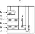
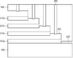
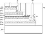
도 1a 및 도 1b는 상기 기존 공정의 문제점을 개략적으로 도시한다. 제1 절연층(2a, 2b, 2c, 이하 2)과 제2 절연층(3a, 3b, 3c, 이하 3)이 교번하여 적층되어 적층 구조(1)를 이룬다. 예를 들어 제1 절연층(2)은 SiO2 막, 제2 절연층(3)은 SiN 막일 수 있다. 상기 제1 절연층(2)은 게이트(미도시) 사이를 절연한다. 상기 제2 절연층(3)은 각 게이트 전극과 연결되며, 후속 공정에서 텅스텐, 알루미늄 등과 같은 금속 또는 기타 도전체 막으로 교체될 수 있다.1a and 1b schematically illustrate the problems of the existing process. The first
도 1a에 도시된 바와 같이, 비아 콘택 홀(11)이 형성될 때, 과도한 식각으로 인해, 상기 비아 콘택 홀(11)은 제2 절연층(3b)을 관통하여 또 다른 제2 절연층(3a)에도 연결된다. 도 2b에 도시된 바와 같이 제2 절연층(3)과 비아 콘택 홀(12)이 금속으로 충진될 경우, 제2 절연층들(3a, 3b)간에 전기적 합선이 발생할 수 있으며, 이로써 정상적인 소자 작동이 불가능하게 된다.As shown in FIG. 1A , when the
본 발명의 일 목적은, 별도의 포토리소그래피 공정을 수행하지 않고서도 단차를 갖는 구조물의 영역 상에 선택적으로 보호막을 증착하는 것이다.It is an object of the present invention to selectively deposit a protective layer on a region of a structure having a step difference without performing a separate photolithography process.
본 발명의 일 목적은 보호막을 형성하는 동안 단차를 갖는 구조물의 일부가 과식각되는 문제를 해결하는 것이다.SUMMARY OF THE INVENTION One object of the present invention is to solve a problem in which a part of a structure having a step is over-etched while a protective layer is formed.
본 발명의 다른 목적은 3차원 반도체 장치의 계단형 구조물 상에서 상부 표면과 하부 표면의 막질의 습식 식각 저항성을 강화시키는 것이다.Another object of the present invention is to enhance the wet etch resistance of the film quality of the upper surface and the lower surface on a stepped structure of a 3D semiconductor device.
본 발명의 또 다른 목적은 계단형 구조를 갖는 VNAND 소자에 선택적으로 보호막을 형성할 때, 계단형 구조물의 일부가 식각액에 의해 과식각되는 문제를 해결하는 것이다.Another object of the present invention is to solve a problem in which a portion of the stepped structure is overetched by an etchant when a passivation layer is selectively formed on a VNAND device having a stepped structure.
본 발명의 기술적 사상에 의한 실시예들의 일 측면에 따르면, 기판 처리 방법은, 제1 절연층 및 제2 절연층을 서로 교번하여 적층하는 단계; 적층된 제1 절연층 및 제2 절연층을 식각하여 상부 표면, 하부 표면, 상기 상부 표면과 상기 하부 표면을 연결하는 측면을 갖는 계단형 구조물을 형성하는 단계; 상기 계단형 구조물을 치밀화하는 단계; 치밀화된 제2 절연층 상에 보호막을 형성하는 단계; 및 상기 제2 절연층 및 상기 보호막을 포함하는 희생 워드라인 구조물의 적어도 일부를 등방성 식각하는 단계를 포함할 수 있다.According to one aspect of the embodiments according to the technical spirit of the present invention, a substrate processing method includes: alternately stacking a first insulating layer and a second insulating layer with each other; etching the stacked first and second insulating layers to form a stepped structure having an upper surface, a lower surface, and a side surface connecting the upper surface and the lower surface; densifying the step-like structure; forming a protective film on the densified second insulating layer; and isotropically etching at least a portion of the sacrificial word line structure including the second insulating layer and the passivation layer.
상기 기판 처리 방법의 일 예에 따르면, 상기 계단형 구조물을 치밀화하는 단계는, 상기 제2 절연층의 상부를 치밀화하는 단계를 포함할 수 있다. 선택적인 실시예에서, 상기 제2 절연층의 상부를 치밀화하는 단계는 : 상기 제2 절연층 중 상기 측면 및 상기 하부 표면의 경계부에 위치한 부분을 선택적으로 치밀화하는 단계를 포함할 수 있다.According to an example of the substrate processing method, the step of densifying the step-like structure may include densifying an upper portion of the second insulating layer. In an optional embodiment, the step of densifying the upper portion of the second insulating layer may include: selectively densifying a portion of the second insulating layer located at a boundary between the side surface and the lower surface.
상기 기판 처리 방법의 다른 예에 따르면, 상기 희생 워드라인 구조물의 적어도 일부를 등방성 식각하는 단계 동안, 상기 제2 절연층 중 상기 측면 및 상기 하부 표면의 경계부에 위치한 부분의 식각 속도와 상기 보호막의 식각 속도의 비율은 미리 정해진 기준 값 이하일 수 있다.According to another example of the substrate processing method, during the isotropic etching of at least a portion of the sacrificial wordline structure, an etching rate of a portion of the second insulating layer located at a boundary between the side surface and the lower surface and the etching rate of the passivation layer The rate of speed may be less than or equal to a predetermined reference value.
상기 기판 처리 방법의 다른 예에 따르면, 상기 희생 워드라인 구조물의 적어도 일부를 등방성 식각하는 단계 동안, 상기 제2 절연층 중 상기 상부 표면 및 하부 표면에서 노출된 부분의 식각 속도는 상기 제2 절연층의 비-노출된 부분의 식각 속도 보다 느릴 수 있다.According to another example of the substrate processing method, during the isotropically etching at least a portion of the sacrificial wordline structure, an etching rate of a portion of the second insulating layer exposed from the upper surface and the lower surface of the second insulating layer is determined by the second insulating layer. may be slower than the etching rate of the non-exposed portion of
상기 기판 처리 방법의 다른 예에 따르면, 상기 희생 워드라인 구조물의 적어도 일부를 등방성 식각하는 동안, 상기 제2 절연층 중 상기 측면 및 상기 하부 표면의 경계부에 위치한 부분은 미리 정해진 두께 이하로 식각될 수 있다.According to another example of the substrate processing method, during isotropic etching of at least a portion of the sacrificial wordline structure, a portion of the second insulating layer located at a boundary between the side surface and the lower surface may be etched to a predetermined thickness or less. have.
상기 기판 처리 방법의 다른 예에 따르면, 상기 제2 절연층은 제1 물질로 형성되며, 상기 계단형 구조물을 치밀화하는 단계는 : 상기 제1 물질을 구성하는 원소 중 어느 하나를 포함하는 제1 기체를 반응 기체로서 이용하여 플라즈마 공정을 수행하는 단계를 포함할 수 있다.According to another example of the substrate processing method, the second insulating layer is formed of a first material, and the step of densifying the step-like structure includes: a first gas including any one of elements constituting the first material It may include performing a plasma process using as a reactant gas.
상기 기판 처리 방법의 다른 예에 따르면, 상기 제2 절연층의 식각 속도는 상기 제1 기체의 종류 및 공급 속도 중 적어도 하나에 의해 제어 될 수 있다.According to another example of the substrate processing method, the etching rate of the second insulating layer may be controlled by at least one of a type and a supply rate of the first gas.
상기 기판 처리 방법의 다른 예에 따르면, 상기 제1 물질은 질화물이며, 상기 제1 기체는 질소를 포함하는 기체일 수 있다.According to another example of the substrate processing method, the first material may be a nitride, and the first gas may be a gas including nitrogen.
상기 기판 처리 방법의 다른 예에 따르면, 상기 제1 기체는 수소-미함유 기체일 수 있다. 선택적인 실시예에서, 상기 계단형 구조물을 치밀화하는 단계는 : 상기 제1 물질을 구성하는 원소 중 적어도 하나를 포함하는 제2 기체를 반응 기체로서 이용하여 플라즈마 공정을 수행하는 단계를 더 포함하며, 상기 제2 기체는 수소-함유 기체일 수 있다. 다른 선택적인 실시예에서, 상기 제2 절연층의 식각 속도는 : 상기 수소-미함유 기체 및 상기 수소-함유 기체의 공급 비율에 따라 제어되며; 그리고 상기 희생 워드라인 구조물의 적어도 일부를 등방성 식각하는 단계 동안, 미리 정해진 기준 식각 속도 보다 느리도록 조정될 수 있다.According to another example of the substrate processing method, the first gas may be a hydrogen-free gas. In an optional embodiment, the step of densifying the step-like structure further comprises: performing a plasma process using a second gas including at least one of the elements constituting the first material as a reactant gas, The second gas may be a hydrogen-containing gas. In another optional embodiment, the etching rate of the second insulating layer is controlled according to a supply ratio of the hydrogen-free gas and the hydrogen-containing gas; In addition, during the isotropically etching at least a portion of the sacrificial wordline structure, the etch rate may be adjusted to be slower than a predetermined reference etch rate.
상기 기판 처리 방법의 다른 예에 따르면, 상기 제2 절연층 상에 보호막을 형성하는 단계 동안 수소-함유 기체가 이용되며, 상기 제2 절연층 중 상기 측면 및 상기 하부 표면의 경계부에 위치한 부분의 식각 속도와 상기 보호막의 식각 속도의 비율이 미리 정해진 기준 값 이하가 되도록, 상기 보호막을 형성하는 단계 동안 사용되는 수소-함유 기체의 공급 속도가 제어될 수 있다.According to another example of the substrate processing method, a hydrogen-containing gas is used during the step of forming a protective film on the second insulating layer, and etching of a portion of the second insulating layer located at a boundary between the side surface and the lower surface The supply rate of the hydrogen-containing gas used during the forming of the passivation layer may be controlled so that a ratio of the rate and the etching rate of the passivation layer is equal to or less than a predetermined reference value.
상기 기판 처리 방법의 다른 예에 따르면, 상기 기판 처리 방법은, 상기 희생 워드라인 구조물 상에 층간 절연층을 형성하는 단계; 상기 희생 워드라인 구조물을 제거하는 단계; 및 상기 희생 워드라인 구조물이 제거된 공간에 상응하는 도전성 워드라인 구조물을 형성하는 단계를 더 포함하며, 상기 도전성 워드라인 구조물은 : 채널을 향하여 연장되는 제1 도전층; 및 상기 제1 도전층 상의 제2 도전층을 포함하며, 상기 계단형 구조물을 치밀화하는 단계는 플라즈마 공정을 통해 수행되며, 상기 제1 도전층 중 상기 제2 도전층과 접촉한 부분의 두께는 상기 제1 도전층의 나머지 부분의 두께보다 얇을 수 있다.According to another example of the substrate processing method, the substrate processing method may include: forming an interlayer insulating layer on the sacrificial wordline structure; removing the sacrificial wordline structure; and forming a conductive wordline structure corresponding to a space in which the sacrificial wordline structure is removed, the conductive wordline structure comprising: a first conductive layer extending toward a channel; and a second conductive layer on the first conductive layer, wherein the step of densifying the step-like structure is performed through a plasma process, and the thickness of a portion of the first conductive layer in contact with the second conductive layer is It may be thinner than the thickness of the remaining portion of the first conductive layer.
본 발명의 기술적 사상에 의한 실시예들의 다른 측면에 따르면, 기판 처리 방법은 : 절연층 및 제1 희생층을 포함하는 적층 구조물을 복수 회 적층하는 단계; 상기 적층 구조물을 식각하여 상부 표면, 하부 표면, 상기 상부 표면과 상기 하부 표면을 연결하는 측면을 갖는 계단형 구조물을 형성하는 단계; 상기 계단형 구조물 상에 제2 희생층을 형성하는 단계; 및 상기 제2 희생층의 적어도 일부에 대해 등방성 식각 공정을 수행하는 단계를 포함하며, 상기 제2 희생층을 형성하는 단계 전에, 상기 제1 희생층 중 상기 상부 표면 및 하부 표면에서 노출된 부분의 치밀도는 상기 제1 희생층의 비-노출된 부분의 치밀도에 비해 미리 정해진 비율 이상 높도록 처리될 수 있다.According to another aspect of the embodiments according to the inventive concept, a substrate processing method includes: stacking a stacked structure including an insulating layer and a first sacrificial layer a plurality of times; etching the stacked structure to form a stepped structure having an upper surface, a lower surface, and a side surface connecting the upper surface and the lower surface; forming a second sacrificial layer on the stepped structure; and performing an isotropic etching process on at least a portion of the second sacrificial layer. The density may be processed to be higher than the density of the non-exposed portion of the first sacrificial layer by at least a predetermined ratio.
상기 기판 처리 방법의 다른 예에 따르면, 상기 제2 희생층의 적어도 일부에 대한 식각 공정을 수행하는 단계 동안, 상기 제1 희생층의 노출된 부분의 식각 속도와 상기 제2 희생층의 식각 속도의 비율은 미리 정해진 기준 값 이하일 수 있다.According to another example of the substrate processing method, during the step of performing an etching process on at least a portion of the second sacrificial layer, the etch rate of the exposed portion of the first sacrificial layer and the etch rate of the second sacrificial layer are The ratio may be less than or equal to a predetermined reference value.
상기 기판 처리 방법의 다른 예에 따르면, 상기 제2 희생층의 적어도 일부에 대해 등방성 식각하는 동안, 상기 제1 희생층 중 상기 상부 표면 및 하부 표면에서 노출된 부분은 미리 정해진 두께 이하로 식각될 수 있다.According to another example of the substrate processing method, during isotropic etching of at least a portion of the second sacrificial layer, portions of the first sacrificial layer exposed on the upper surface and the lower surface may be etched to a predetermined thickness or less. have.
본 발명의 기술적 사상에 의한 실시예들의 또 다른 측면에 따르면, 기판 처리 방법은, 상부 표면, 하부 표면, 상기 상부 표면과 상기 하부 표면을 연결하는 측면을 갖는 단차 구조물을 선택적으로 치밀화하는 단계; 상기 단차 구조물 상에 적어도 하나의 층을 형성하는 단계; 및 상기 적어도 하나의 층에 대한 등방성 식각 공정을 수행하는 단계를 포함하고, 상기 등방성 식각 공정을 수행하기 전에, 상기 적어도 하나의 층을 구성하는 수소와 질소의 비율은 상기 단차 구조물을 구성하는 수소와 질소의 비율보다 클 수 있다.According to another aspect of the embodiments according to the technical spirit of the present invention, a substrate processing method includes the steps of selectively densifying a step structure having an upper surface, a lower surface, and a side connecting the upper surface and the lower surface; forming at least one layer on the step structure; and performing an isotropic etching process on the at least one layer, wherein, before performing the isotropic etching process, the ratio of hydrogen and nitrogen constituting the at least one layer is hydrogen constituting the step structure and It may be greater than the ratio of nitrogen.
도 1a 및 도 1b는 기존 공정의 문제점을 개략적으로 도시한다.
도 2a 내지 도 2f는 3차원 반도체 장치의 계단형 구조물 상에 보호막을 증착하고 선택적으로 식각하는 공정을 개략적으로 도시한다.
도 3a 및 도 3b는 계단 상부면에 노출된 제2 절연층이 과식각되는 문제를 개략적으로 도시한다.
도 4는 본 발명의 기술적 사상에 의한 실시예들에 따른 기판 처리 방법을 개략적으로 나타낸 흐름도이다.
도 5는 본 발명의 기술적 사상에 의한 실시예들에 따른 기판 처리 방법을 개략적으로 나타낸다.
도 6은 본 발명의 기술적 사상에 의한 실시예들에 따른 기판 처리 방법을 개략적으로 나타낸다.
도 7은 본 발명의 기술적 사상에 의한 실시예들에 따른 기판 처리 방법을 개략적으로 나타낸다.
도 8 a 내지 도 8d는 단차 구조의 패턴 상에서 도 5의 실시예에 따른 기판 처리 방법이 적용된 결과를 도시한다.
도 9는 본 발명의 기술적 사상에 의한 실시예들에 따른 기판 처리 방법을 개략적으로 나타낸다.
도 10은 도 9의 플라즈마 전처리 단계(제1 단계 및 제2 단계)에서 사용되는 반응기체들의 공급 비율에 따라 제2 절연층의 습식 식각 속도가 변화하는 모습을 도시한다.
도 11은 도 10의 각 플라즈마 전처리 공정의 조건들의 표를 도시한다.
도 12 내지 도 21은 본 발명의 기술적 사상에 의한 실시예들에 따른 기판 처리 방법을 개략적으로 나타낸다.
도 22는 본 발명의 기술적 사상에 의한 실시예들에 따른 기판 처리 방법에 의해 형성된 반도체 장치를 도시한다.
도 23 및 도 24는 본 발명의 기술적 사상에 의한 실시예들에 따른 기판 처리 방법 및 그에 의해 형성된 반도체 장치를 도시한다.
도 25내지 도 27은 도 16의 기판 처리 방법을 보다 구체적으로 도시한다.1a and 1b schematically illustrate the problems of the existing process.
2A to 2F schematically illustrate a process of depositing and selectively etching a passivation layer on a stepped structure of a 3D semiconductor device.
3A and 3B schematically show a problem in which the second insulating layer exposed on the upper surface of the step is over-etched.
4 is a flowchart schematically illustrating a substrate processing method according to embodiments according to the inventive concept.
5 schematically illustrates a substrate processing method according to embodiments according to the inventive concept.
6 schematically illustrates a substrate processing method according to embodiments according to the inventive concept.
7 schematically shows a substrate processing method according to embodiments according to the inventive concept.
8A to 8D illustrate a result of applying the substrate processing method according to the embodiment of FIG. 5 on a pattern having a stepped structure.
9 schematically illustrates a substrate processing method according to embodiments according to the inventive concept.
FIG. 10 illustrates a change in the wet etch rate of the second insulating layer according to the supply ratio of reactive gases used in the plasma pretreatment step (first step and second step) of FIG. 9 .
11 shows a table of conditions of each plasma pretreatment process of FIG. 10 .
12 to 21 schematically show a substrate processing method according to embodiments according to the inventive concept.
22 illustrates a semiconductor device formed by a substrate processing method according to embodiments of the inventive concept.
23 and 24 illustrate a method for processing a substrate and a semiconductor device formed by the method according to embodiments according to the inventive concept.
25 to 27 illustrate the substrate processing method of FIG. 16 in more detail.
이하, 첨부된 도면을 참조하여 본 발명의 실시예들을 설명하기로 한다.Hereinafter, embodiments of the present invention will be described with reference to the accompanying drawings.
본 발명의 실시예들은 당해 기술 분야에서 통상의 지식을 가진 자에게 본 발명을 더욱 완전하게 설명하기 위하여 제공되는 것이며, 아래의 실시예들은 여러 가지 다른 형태로 변형될 수 있으며, 본 발명의 범위가 아래의 실시예들로 한정되는 것은 아니다. 오히려, 이들 실시예는 본 개시를 더욱 충실하고 완전하게 하며 당업자에게 본 발명의 사상을 완전하게 전달하기 위하여 제공되는 것이다.The embodiments of the present invention are provided to more completely explain the present invention to those of ordinary skill in the art, and the following embodiments can be modified in various other forms, and the scope of the present invention is not limited. It is not limited to the following examples. Rather, these examples are provided so that this disclosure will be more thorough and complete, and will fully convey the spirit of the invention to those skilled in the art.
본 명세서에서 사용된 용어는 특정 실시예를 설명하기 위하여 사용되며, 본 발명을 제한하기 위한 것이 아니다. 본 명세서에서 사용된 바와 같이 단수 형태는 문맥상 다른 경우를 분명히 지적하는 것이 아니라면, 복수의 형태를 포함할 수 있다. 또한, 본 명세서에서 사용되는 경우 "포함한다(comprise)" 및/또는 "포함하는(comprising)"은 언급한 형상들, 숫자, 단계, 동작, 부재, 요소 및/또는 이들 그룹의 존재를 특정하는 것이며, 하나 이상의 다른 형상, 숫자, 동작, 부재, 요소 및/또는 그룹들의 존재 또는 부가를 배제하는 것이 아니다. 본 명세서에서 사용된 바와 같이, 용어 "및/또는"은 해당 열거된 항목 중 어느 하나 및 하나 이상의 모든 조합을 포함한다.The terminology used herein is used to describe specific embodiments, not to limit the present invention. As used herein, the singular form may include the plural form unless the context clearly dictates otherwise. Also, as used herein, “comprise” and/or “comprising” refers to the presence of the recited shapes, numbers, steps, actions, members, elements, and/or groups of those specified. and does not exclude the presence or addition of one or more other shapes, numbers, movements, members, elements and/or groups. As used herein, the term “and/or” includes any one and any combination of one or more of those listed items.
본 명세서에서 제1, 제2 등의 용어가 다양한 부재, 영역 및/또는 부위들을 설명하기 위하여 사용되지만, 이들 부재, 부품, 영역, 층들 및/또는 부위들은 이들 용어에 의해 한정되어서는 안됨은 자명하다. 이들 용어는 특정 순서나 상하, 또는 우열의 의미하지 않으며, 하나의 부재, 영역 또는 부위를 다른 부재, 영역 또는 부위와 구별하기 위하여만 사용된다. 따라서, 이하 상술할 제1 부재, 영역 또는 부위는 본 발명의 가르침으로부터 벗어나지 않고서도 제2 부재, 영역 또는 부위를 지칭할 수 있다.It is to be understood that although the terms first, second, etc. are used herein to describe various members, regions and/or regions, these members, parts, regions, layers, and/or regions should not be limited by these terms. do. These terms do not imply a specific order or superiority or superiority, and are used only to distinguish one member, region or region from another member, region or region. Accordingly, a first member, region, or region described below may refer to a second member, region, or region without departing from the teachings of the present invention.
본 개시서에서, "기체(가스)"는 증발된 고체 및/또는 액체를 포함할 수 있으며, 단일 기체 또는 기체들의 혼합물로 구성될 수 있다. 본 개시서에서, 샤워헤드를 통하여 반응 챔버로 도입된 공정 기체는 전구체 기체 및 부가성 기체를 포함할 수 있다. 상기 전구체 기체 및 상기 부가성 기체는 전형적으로 혼합 기체로서 또는 별도로 반응 공간으로 도입될 수 있다. 상기 전구체 기체는 불활성 기체와 같은 캐리어 기체와 함께 도입될 수 있다. 상기 부가성 기체는 반응물 기체 및 불활성 기체와 같은 희석 기체를 포함할 수 있다. 상기 반응물 기체 및 상기 희석 기체는 혼합하여 또는 별도로 반응 공간으로 도입될 수 있다. 전구체는 둘 이상의 전구체들로 구성될 수 있으며, 그리고 반응물 기체는 둘 이상의 반응물 기체들로 구성될 수 있다. 상기 전구체는 기판 상에 화학흡착된 그리고 유전체 막의 매트릭스의 주요 구조를 구성하는 전형적으로 메탈로이드(metalloid) 또는 금속 원소를 함유하는 기체며, 퇴적을 위한 상기 반응물 기체는 상기 기체가 상기 기판 상에서 원자층 또는 단층(monolayer)을 고정하기 위해 여기될 때 기판 상에 화학흡착된 상기 전구체와 반응하는 기체이다. "화학흡착(chemisorption)"은 화학적 포화 흡착을 지칭한다. 상기 공정 기체 외의 기체, 즉 상기 샤워헤드를 통하여 통과하지 않고 도입된 기체가 상기 반응 공간을 실링(sealing)하기 위해 사용될 수 있으며, 이것은 불활성 기체와 같은 시일 기체(seal gas)를 포함한다. 일부 실시예들에서, "막(film)"은 전체 타겟 또는 관련된 표면을 피복하도록 실질적으로 핀홀들 없이 두께 방향에 수직한 방향으로 연속적으로 연장되는 층, 또는 단순히 타겟 또는 관련된 표면을 피복하는 층을 지칭한다. 일부 실시예들에서 "층(layer)"은 표면 상에 형성된 어떠한 두께를 갖는 구조물, 또는 막의 동의어, 또는 비막(non-film) 구조물을 지칭한다. 막 또는 층은 어떠한 특성들을 갖는 불연속적 단일 막 또는 층, 또는 다중의 막들 또는 층들로 구성될 수 있으며, 그리고 인접한 막들 또는 층들 사이의 경계는 분명하거나 또는 분명하지 않을 수 있으며, 그리고 물리적, 화학적, 및/또는 어떤 다른 특성들, 형성 공정들 또는 시퀀스, 및/또는 인접한 막들 또는 층들의 기능들 또는 목적들에 기초하여 설정될 수 있다.In the present disclosure, "gas (gas)" may include evaporated solids and/or liquids, and may consist of a single gas or a mixture of gases. In the present disclosure, the process gas introduced into the reaction chamber through the showerhead may include a precursor gas and an additive gas. The precursor gas and the additive gas may typically be introduced into the reaction space as a mixed gas or separately. The precursor gas may be introduced together with a carrier gas such as an inert gas. The additive gas may include a reactant gas and a diluent gas such as an inert gas. The reactant gas and the diluent gas may be mixed or introduced into the reaction space separately. A precursor may be composed of two or more precursors, and a reactant gas may be composed of two or more reactant gases. The precursor is a gas chemisorbed onto a substrate and typically containing a metalloid or metal element constituting the main structure of the matrix of a dielectric film, and the reactant gas for deposition is the gas in which the gas is atomic layer on the substrate. or a gas that reacts with the precursor chemisorbed onto the substrate when excited to fix a monolayer. “Chemisorption” refers to chemical saturation adsorption. A gas other than the process gas, that is, a gas introduced without passing through the showerhead may be used to seal the reaction space, including a seal gas such as an inert gas. In some embodiments, a “film” is a layer extending continuously in a direction perpendicular to the thickness direction substantially free of pinholes to cover the entire target or related surface, or simply a layer covering the target or related surface. refers to In some embodiments “layer” refers to a structure having any thickness formed on a surface, or a synonym for a film, or a non-film structure. A film or layer may consist of a single, discontinuous film or layer, or multiple films or layers, having certain properties, and the boundaries between adjacent films or layers may or may not be clear, and physical, chemical, and/or some other characteristics, formation processes or sequence, and/or functions or purposes of adjacent films or layers.
본 개시서에서, "Si-N 결합을 함유하는"이라는 표현은 Si-N 결합 또는 Si-N 결합들에 의해 실질적으로 구성된 주요 골격을 갖는, 및/또는 Si-N 결합 또는 Si-N 결합들에 의해 실질적으로 구성된 치환기를 갖는, Si-N 결합 또는 Si-N 결합들에 의해 특징되는 것으로 지칭할 수 있다. 실리콘 질화층은 Si-N 결합을 함유하는 유전체 층일 수 있으며, 실리콘 질화층(SiN) 및 실리콘 산질화층(SiON)을 포함할 수 있다.In this disclosure, the expression "containing Si-N bonds" means having a main backbone substantially composed of Si-N bonds or Si-N bonds, and/or Si-N bonds or Si-N bonds It can be referred to as characterized by Si-N bonds or Si-N bonds, having a substituent substantially constituted by The silicon nitride layer may be a dielectric layer containing Si-N bonds, and may include a silicon nitride layer (SiN) and a silicon oxynitride layer (SiON).
본 개시서에서, "동일한 물질"이라는 표현은, 주요 구성 성분이 동일함을 의미하는 것으로 해석되어야 한다. 예를 들어, 제1 층과 제2 층은 모두 실리콘 질화층이고 동일한 물질로 형성될 경우, 제1 층은 Si2N, SiN, Si3N4, 및 Si2N3을 포함하는 그룹으로부터 선택될 수 있고, 제2 층 역시 상기 그룹으로부터 선택될 수 있으나 그 구체적인 막질은 제1 층과 상이할 수 있다.In the present disclosure, the expression "the same substance" should be construed to mean that the main constituents are the same. For example, if the first layer and the second layer are both silicon nitride layers and are formed of the same material, the first layer may be selected from the group comprising Si2N, SiN, Si3N4, and Si2N3, and the second layer is also It may be selected from the above group, but the specific film quality may be different from that of the first layer.
부가적으로, 본 개시서에서, 실행 가능한 범위가 정례적인 작업에 기초하여 결정될 수 있다는 것에 따라서 어떠한 두 가지의 변수가 상기 변수의 실행가능한 범위를 구성할 수 있으며, 어떠한 지시된 범위는 종료점들을 포함하거나 배제할 수 있다. 부가적으로, 어떠한 지시된 변수들의 값들은(그것들이 "약(about)"으로 지시되었거나 아니거나 상관없이) 정확한 값들 또는 근사값들을 지칭할 수 있으며, 등가물을 포함할 수 있으며, 그리고 일부 실시예들에서 평균값, 중앙값, 대표값, 다수값 등을 지칭할 수 있다.Additionally, in this disclosure, any two variables may constitute a viable range of the variable, as the feasible range may be determined on the basis of routine work, and any indicated range includes endpoints. or can be excluded. Additionally, values of any indicated variables (whether or not they are indicated as “about”) may refer to exact values or approximations, including equivalents, and in some embodiments. may refer to an average value, a median value, a representative value, a majority value, and the like.
조건들 및/또는 구조들이 특정되지 않은 본 개시서에서, 통상의 기술자는 관례적인 실험의 문제로서, 본 개시서의 견지에서 이러한 조건들 및/또는 구조들을 용이하게 제공할 수 있다. 모든 개시된 실시예들에서, 하나의 실시예에서 사용된 어떠한 구성 요소는 의도된 목적들을 위해, 여기에 명시적으로, 필연적으로 또는 본질적으로 개시된 것들을 포함하여, 그것에 등가적인 어떠한 구성 요소들로 대체될 수 있다, 나아가, 본 발명은 장치들 및 방법들에 동일하게 적용될 수 있다.In this disclosure in which conditions and/or structures are not specified, a person skilled in the art can readily provide such conditions and/or structures in light of the present disclosure as a matter of routine experimentation. In all disclosed embodiments, any component used in one embodiment may be, for its intended purposes, replaced by any component equivalent thereto, including those explicitly, necessarily or essentially disclosed herein. Furthermore, the present invention is equally applicable to devices and methods.
이하, 본 발명의 기술적 사상에 따른 실시예들을 개략적으로 도시하는 도면들을 참조하여 설명한다. 도면들에 있어서, 예를 들면, 제조 기술 및/또는 공차에 따라, 도시된 형상의 변형들이 예상될 수 있다. 따라서, 본 발명의 실시예는 본 명세서에 도시된 영역의 특정 형상에 제한된 것으로 해석되어서는 아니 되며, 예를 들면 제조상 초래되는 형상의 변화를 포함하여야 한다.DETAILED DESCRIPTION OF THE PREFERRED EMBODIMENTS Hereinafter, embodiments according to the technical spirit of the present invention will be described with reference to the drawings schematically showing. In the drawings, variations of the illustrated shape may be expected, for example depending on manufacturing technology and/or tolerances. Accordingly, embodiments of the present invention should not be construed as limited to the specific shape of the region shown herein, but should include, for example, changes in shape caused by manufacturing.
도 2a 내지 도 2f는 3차원 반도체 장치의 계단형 구조물 상에 보호막을 증착하고 선택적으로 식각하는 공정을 개략적으로 도시한다.2A to 2F schematically illustrate a process of depositing and selectively etching a passivation layer on a stepped structure of a 3D semiconductor device.
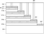
비아 콘택 홀이 제2 절연층을 관통하는 종래 기술의 문제점을 방지하기 위해, 도 2a 및 도 2b 도시된 바와 같이, 계단형 구조물(1) 상부에 보호막(barrier layer)(6)을 증착한다. 플라즈마 원자층 증착 공정(PEALD)을 이용하여 각 단층의 측면(S), 상면(U) 및 하면(L)에 보호막(6)을 증착할 수 있다. 플라즈마 공정은 기판 상에서 생성시키는 직접 플라즈마(in-situ plasma 또는 direct plasma) 공정이다. 상기 플라즈마 공정은 비대칭 플라즈마 공정이다. 라디칼 및 활성종의 직진성에 따라, 상기 계단 상면(U) 및 하면(L)에 증착된 보호막은 이온 충돌 효과(ion-bombardment effect)에 의해 측면(S)에 증착된 보호막 보다 더 치밀해진다.In order to prevent the problem of the prior art in which the via contact hole penetrates the second insulating layer, a
이에 따라, 도 2c에 도시된 바와 같이, 이후 습식 식각 시, 계단 측벽(S)의 보호막은 제거되고 계단형 구조물의 상면(U) 및 하면(L)의 보호막은 잔존하게 된다(선택적 식각(selective etching)).Accordingly, as shown in FIG. 2C , during the subsequent wet etching, the protective film of the step sidewall S is removed and the protective film of the upper surface U and the lower surface L of the stepped structure remains (selective etching). etching)).
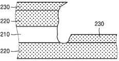
한편, 계단 상면(U)과 측면(S)의 경계면에 있는 보호막과 계단 하면(L)과 측면(S)의 경계면에 있는 보호막은 막의 치밀도가 상면(U)에 증착된 보호막의 치밀도와 측면에 증착된 보호막(8)의 치밀도의 중간 단계에 있어서, 일부가 잔존된(또는 일부가 제거된) 경사진 돌출형태(overhang, 9)로 잔존하게 된다.On the other hand, the protective film on the interface between the upper surface of the step U and the side S and the protective film on the interface between the lower surface of the step L and the side S have the same density of the protective film deposited on the upper surface U and the side surface. In the intermediate stage of the density of the protective film 8 deposited on the ?
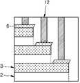
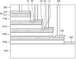
이후, 도 2d에 도시된 바와 같이, 상기 계단 구조물(1)에 절연 후막층(10)을 증착하고, 비아 콘택 홀(11)을 형성한다. 각각의 비아 콘택 홀(11)은 상응하는 제2 절연층(3) 상의 보호막(6)과 연결된다. 증착된 보호막(6) 덕분에, 비아 콘택 홀(11)이 제2 절연층(3)을 관통하는 것을 방지할 수 있다.Thereafter, as shown in FIG. 2D , an insulating
후속 공정에서, 도 2e에 도시된 바와 같이, 상기 비아 콘택 홀(11)은 금속으로 충진되어 금속 배선(12)을 형성한다. 그 후, 도 2f에 도시된 바와 같이, 상기 제2 절연층(3)과 보호막(6)은 텅스텐, 알루미늄 등과 같은 금속, 다결정 실리콘, 또는 도핑된 절연층(doped insulator) 등의 도전체로 교체되어 워드라인(word line)을 형성한다. 이로써, 게이트 전극은 도전층(13)을 통해 금속 배선(12)과 연결될 수 있다.In a subsequent process, as shown in FIG. 2E , the via
그러나 상기 선택적 식각 시, 계단 구조물(1)의 일부분, 가령 계단의 하면(L)와 측면(S)의 경계 부분에서는 상기 보호막(6)의 일부만이 잔존하므로, 보호막 하부에 위치한 제2 절연층(3)의 일부가 노출될 수 있다(도 2c 참고). 따라서 상기 노출된 제2 절연층(3)은 선택적 식각 공정 중에 식각 용액에 의해 식각됨으로써 손상될 수 있으며, 추후 도전체로 교체되었을 때 소자 작동 시 전기적 단락이 발생하는 원인이 된다.However, during the selective etching, since only a part of the
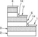
도 3은 계단 상면(U) 및 하면(L)에 노출된 제2 절연층(3)이 과식각(over etching)에 의해 손상되는 것을 도시한다.3 shows that the second insulating
도 3a에서, 보호막(6)에 대한 선택적 식각시, 계단의 측면(S) 및 하면(L)의 경계부분에 있는 보호막의 일부가 제거됨으로써 제2 절연층의 일부(14)가 식각액에 노출되게 된다. 도 3b에서 도시된 바와 같이, 노출된 제2 절연층(14)으로 인해, 제2 절연층에 다양한 형태의 손상이 발생할 수 있다. 가령, 제2 절연층(3)의 일부가 소실되거나(15), 제2 절연층(3)에 침투한 식각액이 보호막(6)과 제2 절연층(3)의 경계를 따라 침투함으로써 공동(void, 16)이 발생하거나, 또는 제2 절연층(3)이 분리될 수 있다(17). 이 경우, 후속 공정에서 상기 제2 절연층(3)과 보호막(6)을 금속막 또는 도전막으로 교체하였을 때 소자의 정상적인 작동이 불가능하게 되며, 이들을 워드라인(word line)으로 사용할 수 없다. 이에 따라, 식각 공정 동안 제2 절연층의 일부가 과식각되는 문제를 해결하는 방법이 요구된다.In FIG. 3A , when the
도 4는 본 발명의 기술적 사상에 의한 실시예들에 따른 기판 처리 방법을 개략적으로 나타낸 흐름도이다.4 is a flowchart schematically illustrating a substrate processing method according to embodiments according to the inventive concept.
도 4를 참조하면, 단차 구조물을 형성한다(단계 S1). 예를 들어, 먼저 제1 절연층 및 제2 절연층을 서로 교번하여 적층한다. 그 다음, 적층된 제1 절연층 및 제2 절연층을 식각하여, 상부 표면, 하부 표면, 상기 상부 표면과 상기 하부 표면을 연결하는 측면을 갖는 계단형 구조물을 형성한다.Referring to FIG. 4 , a stepped structure is formed (step S1 ). For example, first, the first insulating layer and the second insulating layer are alternately stacked with each other. Then, the stacked first insulating layer and the second insulating layer are etched to form a stepped structure having an upper surface, a lower surface, and a side surface connecting the upper surface and the lower surface.
이후, 상기 단차 구조물 상에 플라즈마 전처리(plasma pre-treatment) 단계가 수행될 수 있다(단계 S2). 플라즈마 전처리 단계는 2개의 전극들 중 적어도 하나에 RF 전력을 인가함으로써 여기되는 용량성 결합 플라즈마(CCP)를 이용하여 수행될 수 있다. 선택적인 실시예에서, 플라즈마 전처리 단계는 단차 구조물을 형성하는 공정과 함께 동일한 반응기에서 인-시츄(in-situ)로 수행될 수 있고, 서로 다른 반응기에서 엑스-시츄(ex-situ)로 수행될 수도 있다.Thereafter, a plasma pre-treatment step may be performed on the stepped structure (step S2). The plasma pretreatment step may be performed using a capacitively coupled plasma (CCP) excited by applying RF power to at least one of the two electrodes. In an alternative embodiment, the plasma pretreatment step may be performed in-situ in the same reactor with the process of forming the stepped structure, and may be performed ex-situ in a different reactor. may be
선택적 실시예에서, 플라즈마 전처리 단계는 비대칭 플라즈마 공정을 이용하여 수행될 수 있으며, 상기 비대칭 플라즈마 공정에 의해 상기 계단형 구조의 상부 막질이 선택적으로 치밀화될 수 있다. 비대칭 플라즈마 공정은 방향성을 갖도록 플라즈마를 인가하는 공정을 포함하는 개념으로서, 플라즈마의 방향성으로 인해 단차 구조를 갖는 구조물의 박막에 대한 선택적인 치밀화가 달성될 수 있다.In an alternative embodiment, the plasma pretreatment step may be performed using an asymmetric plasma process, and the upper film quality of the stepped structure may be selectively densified by the asymmetric plasma process. The asymmetric plasma process is a concept including a process of applying plasma to have directionality, and selective densification of a thin film of a structure having a stepped structure may be achieved due to the directionality of the plasma.
예를 들어, 상부 표면, 하부 표면, 상기 상부 표면과 상기 하부 표면을 연결하는 측면을 갖는 단차 구조물에 대해, 상기 측면과 평행한 방향으로 플라즈마가 인가될 수 있다. 이 경우 상기 방향성으로 인해 구조물의 상부 표면과 하부 표면에서 플라즈마의 충돌이 일반적으로 발생하고, 반면에 구조물의 측면에서는 플라즈마의 충돌이 상대적으로 덜 발생하게 된다.For example, plasma may be applied to a stepped structure having an upper surface, a lower surface, and a side surface connecting the upper surface and the lower surface in a direction parallel to the side surface. In this case, the collision of plasma generally occurs on the upper surface and the lower surface of the structure due to the directionality, whereas the collision of the plasma occurs relatively less on the side of the structure.
선택적인 실시예에서, 비대칭 플라즈마 공정 동안, 아르곤을 포함하는 기체가 이용될 수 있다. 비대칭 플라즈마 공정 동안, 아르곤 기체가 활성화되어 활성종이 발생할 수 있다. 상기 활성종의 방향성으로 인해, 플라즈마 활성종의 진행 방향과 직각 방향에 위치한, 단차 구조의 상부 표면이 선택적으로 치밀화될 수 있으며, 이에 따라 단차 구조의 상부의 막질의 습식 식각 저항성이 강화된다. 이러한 치밀화는 활성종에 의한 이온 포격 효과(ion bombardment effect)에 의해 발생할 수 있다.In an alternative embodiment, a gas comprising argon may be used during the asymmetric plasma process. During an asymmetric plasma process, argon gas may be activated to generate active species. Due to the directionality of the active species, the upper surface of the stepped structure located in a direction perpendicular to the propagation direction of the plasma active species may be selectively densified, thereby enhancing the wet etch resistance of the film on the stepped structure. Such densification may be caused by an ion bombardment effect by active species.
다른 선택적인 실시예에서, 비대칭 플라즈마 공정 동안, 단차 구조물의 구성 성분을 포함하는 기체가 이용될 수 있다. 구체적으로, 단차 구조물이 제1 물질로 형성된 경우, 상기 제1 물질을 구성하는 원소 중 어느 하나를 포함하는 제1 기체를 반응 기체로서 이용하여 플라즈마 공정을 수행할 수 있다. 예를 들어, 단차 구조물의 상부 표면 및 하부 표면이 실리콘 질화층으로 구성된다면, 비대칭 플라즈마 공정 동안, 상기 단차 구조물의 상부를 구성하는 원소(Si, N) 중 적어도 하나(예를 들어, 질소)를 포함하는 기체(예를 들어, N2, NH3)가 활성화되어 활성종이 발생할 수 있다. 질소 플라즈마의 방향성으로 인해, 질소 플라즈마가 단차 구조의 상부 표면 및 하부 표면 상에 인가될 수 있다. 따라서 단차 구조물의 구성 성분인 질소 성분이 증가하여 질소가 풍부한 실리콘 질화층이 형성될 수 있다.In another alternative embodiment, during the asymmetric plasma process, a gas comprising the constituents of the stepped structure may be used. Specifically, when the step structure is formed of the first material, the plasma process may be performed using a first gas including any one of the elements constituting the first material as a reaction gas. For example, if the upper surface and the lower surface of the stepped structure are composed of a silicon nitride layer, at least one (eg, nitrogen) of the elements (Si, N) constituting the upper portion of the stepped structure during an asymmetric plasma process A gas containing (eg, N2, NH3) may be activated to generate active species. Due to the directionality of the nitrogen plasma, the nitrogen plasma can be applied on the upper surface and the lower surface of the stepped structure. Accordingly, the nitrogen component, which is a component of the step structure, may increase to form a nitrogen-rich silicon nitride layer.
선택적인 실시예에서, 플라즈마 전처리 단계 동안, 플라즈마 내의 Ar 이온에 의한 이온 포격 효과 및/또는 반응기체(예를 들어, 질소 이온)에 의한 단차 구조의 치밀화 효과가 달성되는데, 이 때, 플라즈마 공급 조건(플라즈마 파워, 플라즈마 주파수, Ar/N2 유량 등)을 달리함으로써, 단차 구조물의 치밀도 및 WER(wet etch rate) 특성이 조절될 수 있다.In an optional embodiment, during the plasma pretreatment step, an ion bombardment effect by Ar ions in the plasma and/or a densification effect of the stepped structure by a reactive gas (eg nitrogen ions) is achieved, wherein the plasma supply conditions By varying (plasma power, plasma frequency, Ar/N2 flow rate, etc.), the density and wet etch rate (WER) characteristics of the stepped structure may be adjusted.
또한, 수소 성분 및 질소 성분이 막의 습식 식각에 대한 저항성에 영향을 주는 주요 인자들 중 하나이므로(도 9 내지 도 11을 참조하여 후술함), 플라즈마 전처리 단계 동안, 반응물의 수소 및/또는 질소 함량을 조절함으로써, 단차 구조물의 WER 특성이 조절될 수도 있다. 예를 들어, 실리콘 질화층의 WER을 감소시키기 위해, 플라즈마 공정 동안, 수소를 포함하지 않는 기체(또는 수소 성분을 포함하지 않는 기체)가 이용될 수 있다. 이 때, 기체 자체에 수소 기체가 포함되지 않을 수도 있고, 기체의 성분 중에 수소가 포함되지 않을 수도 있다. 예를 들어, 실리콘 질화층에 대한 플라즈마 전처리 단계 동안, 암모니아(NH3) 대신에 수소-미함유 질소 기체(예를 들어, 질소(N2) 기체)가 이용될 수 있다.In addition, since a hydrogen component and a nitrogen component are one of the main factors affecting the resistance to wet etching of the film (described later with reference to FIGS. 9 to 11 ), during the plasma pretreatment step, the hydrogen and/or nitrogen content of the reactants By adjusting the WER characteristics of the stepped structure may be adjusted. For example, in order to reduce the WER of the silicon nitride layer, a gas that does not contain hydrogen (or a gas that does not contain a hydrogen component) may be used during the plasma process. At this time, hydrogen gas may not be included in the gas itself, and hydrogen may not be included in the gas component. For example, during the plasma pretreatment step for the silicon nitride layer, a hydrogen-free nitrogen gas (eg, nitrogen (N2) gas) may be used instead of ammonia (NH3).
이후, 단차 구조물 상에 보호막이 형성된다(단계 S3). 보호막은 원자 층 증착(ALD) 공정을 이용하여 형성될 수 있으며, 특히 플라즈마 원자층 증착 공정(PEALD)을 이용하여 형성될 수 있다. 보호막은 절연층일 수 있다. 예를 들어, 보호막은 SiN 막일 수 있다. 일 실시예에서, 보호막은 단일막으로 형성될 수 있다. 선택적 실시예에서, 보호막은 서로 다른 공정 조건으로 형성된 이중막 또는 복합막으로 구성될 수 있다. 단차 구조물과 보호막의 형성 공정은 동일한 반응기에서 인-시츄(in-situ)로 수행될 수도 있고, 서로 다른 반응기에서 엑스-시츄(ex-situ)로 수행될 수도 있다.Thereafter, a protective film is formed on the step structure (step S3). The passivation layer may be formed using an atomic layer deposition (ALD) process, and in particular, may be formed using a plasma atomic layer deposition (PEALD) process. The passivation layer may be an insulating layer. For example, the protective film may be a SiN film. In one embodiment, the passivation layer may be formed as a single layer. In an alternative embodiment, the protective film may be composed of a double film or a composite film formed under different process conditions. The steps of forming the step structure and the protective layer may be performed in-situ in the same reactor or ex-situ in different reactors.
이후, 플라즈마 후처리(plasma post-treatment) 단계가 수행될 수 있다(단계 S4). 플라즈마 후처리 단계는 2개의 전극들 중 적어도 하나에 RF 전력을 인가함으로써 여기되는 용량성 결합 플라즈마(CCP)를 이용하여 수행될 수 있다. 선택적인 실시예에서, 플라즈마 후처리 단계는 단차 구조물 및 보호막의 형성 공정과 함께 동일한 반응기에서 인-시츄(in-situ)로 수행될 수 있고, 서로 다른 반응기에서 엑스-시츄(ex-situ)로 수행될 수도 있다.Thereafter, a plasma post-treatment step may be performed (step S4). The plasma post-treatment step may be performed using a capacitively coupled plasma (CCP) excited by applying RF power to at least one of the two electrodes. In an alternative embodiment, the plasma post-treatment step may be performed in-situ in the same reactor together with the step structure and the formation process of the protective film, and ex-situ in different reactors. may be performed.
플라즈마 후처리 단계는 비대칭 플라즈마 공정을 이용하여 수행될 수 있으며, 상기 비대칭 플라즈마 공정에 의해 보호막이 선택적으로 치밀화될 수 있다. 비대칭 플라즈마 공정은 방향성을 갖도록 플라즈마를 인가하는 공정을 포함하는 개념으로서, 플라즈마의 방향성으로 인해 단차 구조를 갖는 구조물 상에 퇴적된 박막에 대한 선택적인 치밀화가 달성될 수 있다.The plasma post-treatment step may be performed using an asymmetric plasma process, and the protective layer may be selectively densified by the asymmetric plasma process. The asymmetric plasma process is a concept including a process of applying plasma to have directionality, and selective densification of a thin film deposited on a structure having a stepped structure may be achieved due to the directionality of the plasma.
예를 들어, 상부 표면, 하부 표면, 상기 상부 표면과 상기 하부 표면을 연결하는 측면을 갖는 단차 구조물에 대해, 상기 측면과 평행한 방향으로 플라즈마가 인가될 수 있다. 이 경우 플라즈마 활성종의 방향성으로 인해, 플라즈마 활성종의 진행 방향과 직각 방향에 위치한, 단차 구조의 상부 표면 및 하부 표면 상에 형성된 보호막이 선택적으로 치밀화될 수 있다. 이에 따라 단차 구조의 상부 표면 및 하부 표면의 습식 식각 저항성이 단차 구조의 측면의 습식 식각 저항성보다 강화될 수 있다.For example, plasma may be applied to a stepped structure having an upper surface, a lower surface, and a side surface connecting the upper surface and the lower surface in a direction parallel to the side surface. In this case, due to the directionality of the plasma active species, the protective film formed on the upper surface and the lower surface of the stepped structure located in a direction perpendicular to the propagation direction of the plasma active species may be selectively densified. Accordingly, the wet etching resistance of the upper surface and the lower surface of the stepped structure may be stronger than the wet etching resistance of the side surface of the stepped structure.
비대칭 플라즈마 인가를 통해 형성된 층의 위치별 막질의 차이로 인해, 추후 등방성 식각 공정(단계 S5) 동안, 상부 표면 상에 형성된 보호막과 하부 표면 상에 형성된 보호막이 분리될 수 있다.Due to the difference in the film quality for each position of the layer formed through the asymmetric plasma application, the passivation layer formed on the upper surface and the passivation layer formed on the lower surface may be separated during the subsequent isotropic etching process (step S5).
플라즈마 후처리 단계 이후, 습식 식각 단계가 수행될 수 있다(단계 S5). 본 단계에 의해 보호막이 제거될 수 있으며, 그러한 제거는 식각 용액을 이용하여 보호막의 선택적인 영역에서 부분적으로 이루어질 수 있다(선택적 식각(selective etch)). 즉, 단차 구조물 상에 보호막이 형성된 경우, 습식 식각 단계가 수행됨으로써, 측면 상에 형성된 보호막은 제거되는 반면에 상부 표면 및 하부 표면 상에 형성된 보호막은 잔존할 수 있다.After the plasma post-treatment step, a wet etching step may be performed (step S5). The passivation layer may be removed by this step, and the removal may be partially performed in a selective region of the passivation layer using an etching solution (selective etch). That is, when the passivation layer is formed on the step structure, the wet etching step is performed to remove the passivation layer formed on the side surface while the passivation layer formed on the upper surface and the lower surface may remain.
이와 같이, 비대칭 플라즈마 공정을 이용하여 플라즈마 후처리 단계를 수행함으로써, 습식 식각 단계만으로 단차를 갖는 구조물의 상하부에 선택적으로 보호막을 증착할 수 있다. 나아가, 선택적으로 증착된 보호막은 습식 식각 단계 동안 충분히 이격될 수 있다. 따라서, 단차를 갖는 구조물의 상하부에 선택적으로 그리고 소정 간격으로 이격되도록 보호막을 형성하기 위한 포토리소그래피 공정이 생략될 수 있다.As described above, by performing the plasma post-treatment step using the asymmetric plasma process, the protective layer may be selectively deposited on the upper and lower portions of the structure having the step difference only by the wet etching step. Furthermore, the selectively deposited passivation layer may be sufficiently spaced apart during the wet etching step. Accordingly, the photolithography process for forming the protective layer selectively and spaced apart from each other at the upper and lower portions of the structure having a step difference may be omitted.
습식 식각에 의해 보호막 일부가 제거되면, 그에 상응하는 위치에서 단차 구조물이 식각 용액에 노출될 수 있다. 그러나, 도 3b에 도시된 문제점과는 달리, 본 발명에서는, 식각 용액에 의한 단차 구조물의 손상(예를 들어, 과식각)이 발생하지 않는다. 왜냐하면, 보호막 증착 이전에, 단계 S2에서 단차 구조물에 대해 플라즈마 전처리를 진행함으로써, 단차 구조물이 보다 치밀해지고, 이에 따라 식각 용액에 대한 습식 식각 저항성이 강화되었기 때문이다.When a portion of the passivation layer is removed by wet etching, the step structure may be exposed to the etching solution at a position corresponding thereto. However, unlike the problem illustrated in FIG. 3B , in the present invention, damage (eg, over-etching) of the stepped structure by the etching solution does not occur. This is because, by performing plasma pretreatment on the stepped structure in step S2 before deposition of the passivation layer, the stepped structure becomes denser, and thus the wet etching resistance to the etching solution is enhanced.
선택적 실시예에서, 상기 플라즈마 전처리가 비대칭 플라즈마 공정을 이용하여 수행될 수 있다. 예를 들어, 상부 표면, 하부 표면, 상기 상부 표면과 상기 하부 표면을 연결하는 측면을 갖는 단차 구조물에 대해, 상기 측면과 평행한 방향으로 플라즈마가 인가될 수 있다. 이 경우, 습식 식각 단계가 수행됨으로써 측면 상에 형성된 보호막이 제거되면, 식각 용액에 노출된 단차 구조의 측면은 식각될 수 있다. 그러나, 측면 상에 위치한 보호막을 식각하여 소정 간격으로 이격된 보호막을 형성하는 것과는 달리, 단차 구조물의 측면을 식각할 이유가 없으므로, 플라즈마 전처리는 비대칭 플라즈마 공정을 이용하여 수행될 필요가 없다. 이는 도 25 및 도 26를 참조하여 더 자세히 상술한다.In an alternative embodiment, the plasma pretreatment may be performed using an asymmetric plasma process. For example, plasma may be applied to a stepped structure having an upper surface, a lower surface, and a side surface connecting the upper surface and the lower surface in a direction parallel to the side surface. In this case, when the protective layer formed on the side surface is removed by performing the wet etching step, the side surface of the stepped structure exposed to the etching solution may be etched. However, there is no reason to etch the side surface of the stepped structure, unlike the formation of a protective film spaced apart from each other by etching the protective film located on the side surface, so that plasma pretreatment does not need to be performed using an asymmetric plasma process. This will be described in more detail with reference to FIGS. 25 and 26 .
본 명세서에서 언급된 습식 식각은 액상의 식각 용액에 반도체 소자상의 구조물을 침지하여 화학적 반응에 의해 표면을 식각하는 방법이다. 이러한 습식 식각은 등방성 식각이므로, 그러한 등방성 식각 자체는 단차 구조물 및 보호막의 선택적 식각에 큰 영향을 미치지 않을 수 있다. 오히려 본 발명의 기술적 사상에 따르면, 단차 구조물 및 보호막의 형성하는 과정에서, 플라즈마 전처리를 사용하여 단차 구조물의 식각 저항성보다 강화시키고, 비대칭 플라즈마를 수행하여 상부 표면과 하부 표면의 구조물과 그곳에 형성된 보호막과 측벽의 구조물 및 그곳에 형성된 보호막이 서로 상이한 물성을 갖도록 처리함으로써, 후속 식각 공정에서 선택적인 식각이 달성될 수 있도록 함에 유의한다. 다시 말해, 식각 공정 이전에 수행되는 단계들이 후속하는 습식 단계의 공정 조건을 제어하는 요소가 되는 것이다.The wet etching referred to in this specification is a method of etching a surface by a chemical reaction by immersing a structure on a semiconductor device in a liquid etching solution. Since the wet etching is isotropic etching, the isotropic etching itself may not significantly affect the selective etching of the step structure and the passivation layer. Rather, according to the technical idea of the present invention, in the process of forming the stepped structure and the protective film, plasma pretreatment is used to enhance the etching resistance of the stepped structure, and an asymmetric plasma is performed to form the structures on the upper and lower surfaces and the protective film formed thereon. Note that by treating the structure of the sidewall and the protective film formed thereon to have different physical properties, selective etching can be achieved in a subsequent etching process. In other words, the steps performed before the etching process are factors controlling the process conditions of the subsequent wet step.
이러한 공정 조건을 제어하는 요소들은 플라즈마를 인가하는 단계를 포함한다. 단차 구조물 및 보호층의 치밀화, 플라즈마의 방향성, 활성종의 이온 포격 효과, 그리고/또는 절연층 구성 성분을 갖는 기체 플라즈마 인가 등 중 적어도 하나가 후속 식각 공정의 공정 제어 요소로 작용함으로써, 단차 구조물 및 보호막의 선택적 식각이 달성될 수 있다.Elements controlling these process conditions include applying a plasma. At least one of the densification of the step structure and the protective layer, the directionality of the plasma, the ion bombardment effect of active species, and/or the application of gas plasma having an insulating layer constituent, etc. acts as a process control element of the subsequent etching process, so that the step structure and the Selective etching of the protective film can be achieved.
도 5는 본 발명의 기술적 사상에 의한 실시예들에 따른 기판 처리 방법을 개략적으로 나타낸다.5 schematically illustrates a substrate processing method according to embodiments according to the inventive concept.
도 5를 참조하면, 단차 구조물의 습식 식각 저항성을 증가시킬 수 있는 방법이 개시된다. 본 실시예에 따르면, 보호막을 증착하기 전에 플라즈마 전처리(plasma pre-treatment)가 수행된다.Referring to FIG. 5 , a method capable of increasing the wet etch resistance of a stepped structure is disclosed. According to this embodiment, plasma pre-treatment is performed before depositing the protective film.
본 실시예에 따르면, 상기 방법은 제1 단계, 제2 단계 및 제3 단계를 포함한다. 제1 단계는 플라즈마 전처리 단계이며, 제2 단계는 보호막 증착 단계, 제3 단계는 플라즈마 후처리(plasma post-treatment) 단계이다.According to this embodiment, the method includes a first step, a second step and a third step. The first step is a plasma pretreatment step, the second step is a protective film deposition step, and the third step is a plasma post-treatment step.
구체적으로, 제1 단계에서, 반응기안에 기판(단차 구조)을 탑재한 후 기판(단차 구조)에 대해 플라즈마 전처리를 진행한다. 플라즈마 전처리는 소스 기체를 공급하지 않고 반응기체만을 공급하여 반응기체를 플라즈마로 활성화시킨다. 제1 단계의 일 사이클 동안, 반응기체가 공급되고(t0~t2), 이후 반응기체가 공급된 상태에서 플라즈마가 인가될 수 있다(t1~t2). 활성화된 반응기체의 이온 포격 효과(ion bombardment)는 대상 막의 습식 식각 저항성을 증가시킨다. 도 5에 도시된 바와 같이, 반응기체 공급(t0~t2)/플라즈마 인가(t1~t2)/퍼지(t2~t3)의 사이클을 복수 회(예를 들어, m회) 반복하여, 단차 구조물의 치밀도를 조절할 수 있다.Specifically, in the first step, after the substrate (stepped structure) is mounted in the reactor, plasma pretreatment is performed on the substrate (stepped structure). In the plasma pretreatment, only the reactive gas is supplied without supplying the source gas to activate the reactive gas into plasma. During one cycle of the first step, a reactive gas may be supplied (t0 to t2), and then plasma may be applied in a state in which the reactive gas is supplied (t1 to t2). The ion bombardment of the activated reactive gas increases the wet etch resistance of the target film. 5, the cycle of supplying reactive gas (t0 to t2) / plasma application (t1 to t2) / purge (t2 to t3) is repeated a plurality of times (for example, m times), The density can be adjusted.
선택적 실시예에서, 노출되는 하부 기판의 막질을 구성하는 원소 중 적어도 하나를 포함하는 기체가 반응기체로서 사용될 수 있다. 예를 들어, 단차 구조물에서 SiN 절연층이 노출되어 있는 경우, 질소를 포함하는 기체를 반응기체로서 사용할 수 있다. 예를 들어, 반응기체는 N2 또는 NH3일 수 있다. 질소를 포함하는 기체(특히 수소를 포함하지 않고 질소를 포함하는 기체)가 활성화되어 단차 구조에 인가되면, 단차 구조물의 구성 성분인 질소 성분이 증가하여 질소가 풍부한(N-rich) 실리콘 질화층이 형성될 수 있다. 이 경우, 단차 구조물의 치밀도가 증가할 수 있다. 또한, 후술되는 바와 같이, 단차 구조물의 습식 식각 저항성이 증가할 수 있다.In an optional embodiment, a gas including at least one of the elements constituting the film quality of the exposed lower substrate may be used as the reactive gas. For example, when the SiN insulating layer is exposed in the step structure, a gas containing nitrogen may be used as a reactive gas. For example, the reactive gas may be N2 or NH3. When a gas containing nitrogen (especially a gas that does not contain hydrogen but contains nitrogen) is activated and applied to the stepped structure, the nitrogen component, which is a component of the stepped structure, increases, so that a nitrogen-rich (N-rich) silicon nitride layer is formed. can be formed. In this case, the density of the stepped structure may increase. Also, as will be described later, the wet etch resistance of the stepped structure may increase.
선택적 실시예에서, 제1 단계는 반응기체 사전-유동 단계(t0~t1)를 포함할 수 있다. 반응기체의 사전-유동 단계를 수행함으로써, 플라즈마가 반응 공간에 공급되기 전에 반응 공간 내에 반응기체의 분포가 균일하게 될 수 있고, 그에 따라 플라즈마 공급단계에서 활성종의 분포가 균일하게 되어 보다 안정적인 공정이 달성될 수 있다.In an optional embodiment, the first stage may comprise a reactive gas pre-flow stage (t0-t1). By performing the pre-flowing step of the reactive gas, the distribution of the reactive gas in the reaction space before the plasma is supplied to the reaction space can be made uniform, so that the distribution of the active species is uniform in the plasma supplying step, making a more stable process This can be achieved.
또 다른 선택적 실시예에서, 플라즈마 전처리 단계는 비대칭 플라즈마 공정을 이용하여 수행될 수 있다. 예를 들어, 상부 표면, 하부 표면, 상기 상부 표면과 상기 하부 표면을 연결하는 측면을 갖는 단차 구조물에 대해, 상기 측면과 평행한 방향으로 플라즈마가 인가될 수 있다. 이 때 Ar 이온 또는 반응기체 이온은 방향성(직진성)을 갖기 때문에, 단차 구조물(예를 들어, 계단형 구조물)의 상부 및 하부 표면에는 이온 포격 효과가 크고 측면에 대해서는 이온 포격 효과가 적다. 따라서 플라즈마 전처리에 의해 계단형 구조물의 상부 및 하부가 측벽 보다 상대적으로 더 치밀화되며, WER이 상대적으로 더 낮아지게 된다.In another alternative embodiment, the plasma pretreatment step may be performed using an asymmetric plasma process. For example, plasma may be applied to a stepped structure having an upper surface, a lower surface, and a side surface connecting the upper surface and the lower surface in a direction parallel to the side surface. At this time, since the Ar ions or reactive gas ions have directionality (straightness), the ion bombardment effect is large on the upper and lower surfaces of the stepped structure (eg, a stepped structure), and the ion bombardment effect is small on the side surfaces. Therefore, the upper and lower portions of the stepped structure are relatively more densified than the sidewalls by the plasma pretreatment, and the WER is relatively lowered.
이와 같이, 본 발명의 기술적 사상에 의한 실시예들에 따르면, 플라즈마 전처리 단계가 수행됨으로써, 활성화된 Ar의 이온 포격 효과(ion bombardment) 및/또는 질소에 의한 박막의 치밀화 효과가 달성될 수 있고, 그에 의해 박막의 후속 식각에 대한 저항성이 선별적으로 조절될 수 있다.As such, according to embodiments according to the technical idea of the present invention, by performing the plasma pretreatment step, the ion bombardment effect of activated Ar and/or the densification effect of the thin film by nitrogen can be achieved, Thereby, the resistance to subsequent etching of the thin film can be selectively controlled.
제2 단계는 플라즈마 전처리된 기판 상에(즉, 단차 구조물 상에) 보호막을 증착하는 단계이다. 제2 단계는 PEALD 박막 증착 단계이다. 도 5에 도시된 바와 같이, 소스 공급(t3~t4)/퍼지(t4~t5)/반응물 공급(t5~t7)/RF 플라즈마(t6~t7)/퍼지(t7~t8)의 기본 PEALD 사이클을 수회(예를 들어, n회) 반복하여 원하는 두께의 보호막을 형성할 수 있다.The second step is a step of depositing a protective film on the plasma-pretreated substrate (ie, on the stepped structure). The second step is PEALD thin film deposition step. As shown in Figure 5, the basic PEALD cycle of source supply (t3 ~ t4) / purge (t4 ~ t5) / reactant supply (t5 ~ t7) / RF plasma (t6 ~ t7) / purge (t7 ~ t8) It may be repeated several times (for example, n times) to form a protective layer having a desired thickness.
본 실시예에서, 소스 기체는 Si을 포함하는 전구체일 수 있으며, 보다 구체적으로, 아미노 실란기를 포함하는 전구체일 수 있다. 상기 반응물로서는 질소를 포함하는 기체를 반응물로서 사용할 수 있다. 예를 들어, 반응기체는 N2 또는 NH3일 수 있다. 그러나 본 발명에 이용되는 소스 기체 및 반응물은 이에 한정되지 않는다. Si 소스로서 TSA, (SiH3)3N; DSO, (SiH3)2; DSMA, (SiH3)2NMe; DSEA, (SiH3)2NEt; DSIPA, (SiH3)2N(iPr); DSTBA, (SiH3)2N(tBu); DEAS, SiH3NEt2; DIPAS, SiH3N(iPr)2; DTBAS, SiH3N(tBu)2; BDEAS, SiH2(NEt2)2; BDMAS, SiH2(NMe2)2; BTBAS, SiH2(NHtBu)2; BITS, SiH2(NHSiMe3)2; TEOS, Si(OEt)4; SiCl4; HCD, Si2Cl6; 3DMAS, SiH(N(Me)2)3; BEMAS, Si H2[N(Et)(Me)]2; AHEAD, Si2 (NHEt)6; TEAS, Si(NHEt)4; Si3H8 등이 사용될 수 있고, 혹은 상기 Si 소스를 공급할 때 이들 물질들의 조합이 사용될 수 있다. 본 발명에서 반응물은 수소를 함유하는 질소 기체일 수 있고, 전술한 암모니아(NH3) 외에 NH4+ 등이 사용될 수도 있다. 퍼지 기체로서 Ar이 사용되었다.In this embodiment, the source gas may be a precursor including Si, and more specifically, may be a precursor including an amino silane group. As the reactant, a gas containing nitrogen may be used as the reactant. For example, the reactive gas may be N2 or NH3. However, the source gas and reactant used in the present invention are not limited thereto. TSA as Si source, (SiH3)3N; DSO, (SiH3)2; DSMA, (SiH3)2NMe; DSEA, (SiH3)2NEt; DSIPA, (SiH3)2N(iPr); DSTBA, (SiH3)2N(tBu); DEAS, SiH3NEt2; DIPAS, SiH3N(iPr)2; DTBAS, SiH3N(tBu)2; BDEAS, SiH2(NEt2)2; BDMAS, SiH2(NMe2)2; BTBAS, SiH2(NHtBu)2; BITS, SiH2(NHSiMe3)2; TEOS, Si(OEt)4; SiCl4; HCD, Si2Cl6; 3DMAS, SiH(N(Me)2)3; BEMAS, Si H2[N(Et)(Me)]2; AHEAD, Si2(NHEt)6; TEAS, Si(NHEt)4; Si3H8 or the like may be used, or a combination of these materials may be used when supplying the Si source. In the present invention, the reactant may be nitrogen gas containing hydrogen, and NH4+ may be used in addition to the aforementioned ammonia (NH3). Ar was used as purge gas.
제2 단계를 수 회 반복하여 원하는 두께의 보호막을 증착한 후, 제3 단계 동안 Ar 기체를 이용한 플라즈마 후처리가 수행될 수 있다. 제3 단계의 일 사이클 동안, Ar 기체가 공급되고(t8~t10) 이후 Ar 기체가 공급된 상태에서 플라즈마가 인가될 수 있다(t9~t10). 이러한 사이클은 복수 회(예를 들어, x회) 수행될 수 있다. 제3 단계 동안, 플라즈마 내의 Ar 이온에 의한 이온 포격효과가 달성될 수 있다.After the second step is repeated several times to deposit a protective layer having a desired thickness, plasma post-treatment using Ar gas may be performed during the third step. During one cycle of the third step, Ar gas is supplied (t8 to t10), and then plasma may be applied in a state in which Ar gas is supplied (t9 to t10). This cycle may be performed multiple times (eg, x times). During the third step, an ion bombardment effect by Ar ions in the plasma can be achieved.
선택적 실시예에서, 플라즈마 후처리 단계는 비대칭 플라즈마 공정을 이용하여 수행될 수 있다. 예를 들어, 상부 표면, 하부 표면, 상기 상부 표면과 상기 하부 표면을 연결하는 측면을 갖는 단차 구조물에 대해, 상기 측면과 평행한 방향으로 플라즈마가 인가될 수 있다. 이 때 Ar 이온은 방향성(직진성)을 갖기 때문에, 단차 구조물(예를 들어, 계단형 구조물)의 상부 및 하부 표면 상에 형성된 보호막의 이온 포격 효과가 크고 측면에 형성된 보호막에 대해서는 이온 포격 효과가 적다. 따라서 플라즈마 후처리에 의해 측벽에 증착된 보호막이 계단형 구조물의 상부 및 하부에 형성된 보호막 보다 상대적으로 덜 치밀하고, WER이 상대적으로 높아지게 된다.In an alternative embodiment, the plasma post-treatment step may be performed using an asymmetric plasma process. For example, plasma may be applied to a stepped structure having an upper surface, a lower surface, and a side surface connecting the upper surface and the lower surface in a direction parallel to the side surface. At this time, since Ar ions have directionality (straightness), the ion bombardment effect of the protective film formed on the upper and lower surfaces of the stepped structure (for example, a stepped structure) is large, and the ion bombardment effect is small for the protective film formed on the side surface. . Accordingly, the protective film deposited on the sidewall by the plasma post-treatment is relatively less dense than the protective film formed on the upper and lower portions of the stepped structure, and the WER is relatively high.
도 6은 본 발명의 기술적 사상에 의한 실시예들에 따른 기판 처리 방법을 개략적으로 나타낸다. 이 실시예들에 따른 기판 처리 방법은 전술한 실시예들에 따른 기판 처리 방법의 변형예일 수 있다. 이하 실시예들간 중복되는 설명은 생략하기로 한다.6 schematically illustrates a substrate processing method according to embodiments according to the inventive concept. The substrate processing method according to these embodiments may be a modified example of the substrate processing method according to the above-described embodiments. Hereinafter, overlapping descriptions between the embodiments will be omitted.
도 6을 참조하면, 단차 구조물 상의 보호막 형성은 플라즈마 전처리 단계, PEALD 보호막 증착 단계, 플라즈마 후처리 단계 및 후속 습식 식각 단계를 통해 이루어진다. 도 5에 나타난 실시예들의 경우 PEALD 보호막 증착 단계 동안 한 종류의 반응기체가 이용된 반면에, 도 6에 나타난 실시예들의 경우 PEALD 보호막 증착 단계 동안 두 종류의 반응기체가 이용된다.Referring to FIG. 6 , the formation of the passivation layer on the stepped structure is performed through a plasma pretreatment step, a PEALD passivation layer deposition step, a plasma posttreatment step, and a subsequent wet etching step. In the case of the embodiments shown in FIG. 5, one type of reactive gas is used during the PEALD passivation layer deposition step, whereas in the embodiments shown in FIG. 6, two types of reactive gas are used during the PEALD passivation layer deposition step.
제1 단계(플라즈마 전처리 단계)는 반응기체 공급(t0~t2)/플라즈마 인가(t1~t2)/퍼지(t2~t3)의 사이클을 복수 회(예를 들어, m회) 반복함으로써 수행될 수 있다. 이후 제2 단계(보호막 증착 단계)는 소스 공급(t3~t4)/퍼지(t4~t5)/반응기체 공급(t5~t7)/RF 플라즈마(t6~t7)/퍼지(t7~t8) 의 기본 PEALD 사이클을 수회(예를 들어, n회) 반복함으로써 수행될 수 있다.The first step (plasma pretreatment step) may be performed by repeating the cycle of supplying reactive gas (t0 to t2) / applying plasma (t1 to t2) / purge (t2 to t3) a plurality of times (for example, m times). have. After that, the second step (protective film deposition step) is the basis of source supply (t3 to t4)/purge (t4 to t5)/reactive gas supply (t5 to t7)/RF plasma (t6 to t7)/purge (t7 to t8) This can be done by repeating the PEALD cycle several times (eg, n times).
전술한 바와 같이, 플라즈마 전처리 단계에 이용되는 반응물의 종류 및/또는 유량에 따라, 특히 반응물의 질소 및/또는 수소 함량에 따라, 단차 구조물의 후속 습식 식각에 대한 저항성(또는 식각 속도)이 변화될 수 있다. 예를 들어, 플라즈마 전처리 단계에 이용되는 제1 반응물은 N2이거나 NH3일 수 있다. 제1 반응물로서 N2를 사용한 경우, 제1 반응물로서 NH3를 사용한 경우보다 단차 구조물의 WER가 낮을 것이며, 후속 습식 식각 공정 동안, 단차 구조물이 과식각될 가능성이 더 낮을 것이다.As described above, depending on the type and/or flow rate of the reactants used in the plasma pretreatment step, especially the nitrogen and/or hydrogen content of the reactants, the resistance (or etch rate) of the step structure to subsequent wet etching may be changed. can For example, the first reactant used in the plasma pretreatment step may be N2 or NH3. When N2 is used as the first reactant, the WER of the step structure will be lower than when NH3 is used as the first reactant, and during the subsequent wet etch process, the step structure will be less likely to be overetched.
PEALD 보호막 증착 단계에서, 반응기체로서 다양한 물질 또는 그 조합이 이용될 수 있으며, 이들의 질소 및/또는 수소 함량에 의해, 증착된 보호막의 후속 습식 식각에 대한 저항성이 변화할 수 있음은 전술한 바와 같다. 예를 들어, 제1 반응물은 N2이고, 제2 반응물은 NH3일 수 있으며, 이는 제1 반응물이 NH4이고, 제2 반응물이 NH3인 경우보다 습식 식각에 대한 저항성이 높다.In the PEALD passivation layer deposition step, various materials or combinations thereof may be used as reactive gases, and their nitrogen and/or hydrogen content may change the resistance to subsequent wet etching of the deposited passivation layer, as described above. same. For example, the first reactant may be N2 and the second reactant may be NH3, which is more resistant to wet etching than when the first reactant is NH4 and the second reactant is NH3.
도 7은 본 발명의 기술적 사상에 의한 실시예들에 따른 기판 처리 방법을 개략적으로 나타낸다. 이 실시예들에 따른 기판 처리 방법은 전술한 실시예들에 따른 기판 처리 방법의 변형예일 수 있다. 이하 실시예들간 중복되는 설명은 생략하기로 한다.7 schematically shows a substrate processing method according to embodiments according to the inventive concept. The substrate processing method according to these embodiments may be a modified example of the substrate processing method according to the above-described embodiments. Hereinafter, overlapping descriptions between the embodiments will be omitted.
도 7을 참조하면, 단차 구조물 상의 보호막 형성은 플라즈마 전처리 단계, PEALD 보호막 증착 단계 및 후속 습식 식각 단계를 통해 이루어진다. 도 6에 나타난 실시예들의 경우 PEALD 보호막 증착 단계가 수행되고 이후 플라즈마 후처리 단계가 수행되는 반면에, 도 7에 나타난 실시예들의 경우 플라즈마 후처리 단계 없이 후속 습식 식각 단계가 수행된다.Referring to FIG. 7 , the formation of the passivation layer on the stepped structure is performed through a plasma pretreatment step, a PEALD passivation layer deposition step, and a subsequent wet etching step. In the embodiments shown in FIG. 6 , a PEALD passivation layer deposition step is performed and then a plasma post-treatment step is performed, whereas in the embodiments shown in FIG. 7 , a subsequent wet etching step is performed without a plasma post-treatment step.
전술한 바와 같이, 플라즈마 전처리 단계에 이용되는 반응물의 종류 및/또는 유량에 따라 단차 구조물의 후속 습식 식각에 대한 저항성이 변화될 수 있다.As described above, the resistance to subsequent wet etching of the step structure may be changed according to the type and/or flow rate of the reactant used in the plasma pretreatment step.
또한, 보호막 증착 단계(제2 단계)에 이용되는 소스 물질과 반응기체를 달리함으로써, 증착된 보호막의 후속 습식 식각에 대한 저항성이 변화될 수 있다. 또한, 선택적인 실시예에서, 보호막 증착 단계(제2 단계) 동안 수행되는 RF 플라즈마 인가 단계(t6~t7)의 방향성을 조절함으로써, 단차 구조물 상에 형성된 보호막의 막질이 위치에 따라 다르게 조절될 수 있다.In addition, by differentiating the source material and the reactive gas used in the passivation layer deposition step (the second step), the resistance of the deposited passivation layer to subsequent wet etching may be changed. In addition, in an optional embodiment, by adjusting the directionality of the RF plasma application step (t6 to t7) performed during the protective film deposition step (the second step), the film quality of the protective film formed on the step structure can be adjusted differently depending on the location. have.
도 8a 내지 도 8d는 단차 구조물 상에서 도 5의 실시예에 따른 기판 처리 방법이 적용된 결과를 도시한다.8A to 8D show results of applying the substrate processing method according to the embodiment of FIG. 5 on a stepped structure.
도 8a에 도시된 바와 같이, 단차 구조물은 제1 절연층(81a, 81b, 이하 81) 및 제2 절연층(82a, 82b, 이하 82)이 교번하여 적층된 계단형 구조물(80)일 수 있다. 상기 계단형 구조물(80)은 제1 절연층(81) 및 제2 절연층(82)을 서로 교번하여 복수 회 적층한 후, 적층된 제1 절연층(81) 및 제2 절연층(82)을 식각(staircase etching)함으로써 형성될 수 있다. 상기 계단형 구조물(80)은 상부 표면(U), 하부 표면(L), 상기 상부 표면(U)과 상기 하부 표면(L)을 연결하는 측면(S)을 갖는다.As shown in FIG. 8A , the stepped structure may be a stepped
선택적 실시예에서, 상기 제1 절연층(81)은 실리콘 산화층(SiO2)일 수 있고, 상기 제2 절연층(82)은 실리콘 질화층(SiN)일 수 있다.In an optional embodiment, the first insulating layer 81 may be a silicon oxide layer (SiO2), and the second insulating layer 82 may be a silicon nitride layer (SiN).
제1 절연층(81a)의 두께는 h1이며, 제2 절연층(82a)의 두께는 h2이고, 제1 절연층(81b)의 두께는 h3이고, 그리고 제2 절연층(82b)의 두께는 h4이다. 일례에서, 제1 절연층(81a)의 두께 h1와 제1 절연층(81b)의 두께 h3는 동일할 수 있다. 일례에서, 제2 절연층(82a)의 두께 h2와 제2 절연층(82b)의 두께 h4는 동일할 수 있다. 일례에서, h1=h2=h3=h4일 수 있다.The thickness of the first insulating
도 5 및 도 8b를 참조하면, 상기 단차 구조물(계단형 구조물(80)) 상에 플라즈마 전처리 단계(제1 단계)가 수행될 수 있다. 플라즈마 전처리 단계(도 5의 제1 단계)를 통해, 제2 절연층(82)의 노출된 부분은 플라즈마의 이온 포격 효과에 의해 치밀화될 수 있다. 구체적으로, 상기 계단형 구조물(80)의 상부, 즉 상부 표면(U), 하부 표면(L) 및 측면(S)이 치밀화될 수 있다. 이로써, 계단형 구조물(80)의 상부의 습식 식각 저항성이 증가될 수 있다. 이 경우, 후속 식각 공정 동안, 제2 절연층(82)에 대한 손상이 발생하지 않거나 무시할 수 있는 손상이 발생할 것이며, 이후에 제2 절연층(82)이 금속층 또는 도전층으로 교체되었을 때 전기적 단락 등의 문제가 발생하지 않을 수 있다.5 and 8B , a plasma pretreatment step (first step) may be performed on the stepped structure (stepped structure 80 ). Through the plasma pretreatment step (the first step of FIG. 5 ), the exposed portion of the second insulating layer 82 may be densified by the ion bombardment effect of plasma. Specifically, the upper portion of the stepped
플라즈마에 노출된 제2 절연층(82a)의 일부(E)의 치밀도는 플라즈마에 노출되지 않은 제2 절연층(82a)의 일부(NE)의 치밀도 보다 높을 수 있다. 이 경우, 플라즈마에 노출된 제2 절연층(82a)의 일부(E)의 식각 속도 Ve는 플라즈마에 노출되지 않은 제2 절연층(82a)의 일부(NE)의 식각 속도 Vne보다 느릴 수 있다. 또한, 이온 포격 효과로 인해, 플라즈마에 노출된 부분(E)에 위치한 제2 절연층(82a)의 두께 h2'는 플라즈마에 노출되지 않은 부분(NE)에 위치한 제2 절연층(82a)의 두께 h2 보다 작거나 같을 수 있다. 즉, 제2 절연층(82a) 중 제1 절연층(81b)과 접촉한 부분의 두께 h2는 제1 절연층(81b)과 접촉하지 않은 부분의 두께 h2'보다 두껍거나 같을 수 있다. 이에 따라, 제2 절연층(82a)은 상기 하부 표면(L)과 측면(S)의 경계부(도 8d의 85)에서 두께가 달라질 수 있고, 단차부를 가질 수 있다. 따라서, 이후 제2 절연층(82a) 및 보호막(도 8d의 83)이 제거된 공간에 상응하도록 도전성 워드라인 구조물이 형성된 경우, 상기 도전성 워드라인 구조물의 제1 도전층(제2 절연층(82a)에 상응)의 상부는 다른 제1 도전층(제2 절연층(82b)에 상응)의 일단의 수직 방향의 연장선상에 위치한 단차부를 가질 수 있으며, 상기 단차부는 제2 도전층(보호막(83)에 상응)에 이격되어 형성될 수 있다. 도전성 워드라인 구조물은 제1 도전층에 형성된 제1 단차부(도 8d의 85에 상응)를 가질 수 있다.The density of the portion E of the second insulating
마찬가지로, 상부(U)에 위치한 제2 절연층(82b)은 플라즈마에 노출된 후 이온 포격으로 인해 치밀화될 수 있으며, 후속 습식 식각에 대한 저항성이 증가할 수 있다. 또한, 플라즈마에 노출된 상부(U)에 위치한 제2 절연층(82b)의 두께 h4'는 플라즈마에 노출되기 전의 두께 h4 보다 작거나 같을 수 있다.Similarly, the second insulating
선택적 실시예에서, 전술한 바와 같이, 제2 절연층(82)의 습식 식각 저항성을 강화시키기 위해, 플라즈마 전처리 단계 동안, 제2 절연층(82)을 구성하는 원소(Si, N) 중 어느 하나를 포함하는 기체를 반응기체로서 이용할 수 있다. 예를 들어, 질소(N)를 포함하는 기체를 반응기체로서 이용할 수 있다. 이 경우, 이온 포격으로 인해, 제2 절연층(82)의 구성 성분인 질소 성분이 증가하여 질소가 풍부한(N-rich) 실리콘 질화층이 형성될 수 있다. 이 경우, 제2 절연층(82), 구체적으로 계단형 구조물(80)의 상부 표면(U), 하부 표면(L) 에 위치한 제2 절연층(82)의 치밀도가 증가할 수 있다.In an optional embodiment, as described above, in order to enhance the wet etch resistance of the second insulating layer 82 , during the plasma pretreatment step, any one of the elements (Si, N) constituting the second insulating layer 82 . A gas containing can be used as a reactive gas. For example, a gas containing nitrogen (N) may be used as the reactive gas. In this case, due to the ion bombardment, a nitrogen component, which is a component of the second insulating layer 82 , may increase to form a nitrogen-rich (N-rich) silicon nitride layer. In this case, the density of the second insulating layer 82 , specifically, the second insulating layer 82 positioned on the upper surface U and the lower surface L of the stepped
전술한 바와 같이, 플라즈마 전처리 단계(도 5의 제1 단계)에 이용되는 반응기체의 종류 및/또는 유량에 따라, 단차 구조물(특히, 상부 표면(U), 하부 표면(L) 및 측면(S))의 후속 습식 식각에 대한 저항성이 변화될 수 있다. 즉, 상기 제2 절연층(82)의 일부분의 식각 속도는 반응기체의 종류 및 공급 속도 중 적어도 하나에 의해 제어될 수 있다. 반응기체의 종류 및 공급 속도 중 적어도 하나를 조정함으로써 상기 제2 절연층(82)의 노출된 부분의 식각 속도를 제어할 수 있으며, 이로써 후속 습식 식각 단계 동안 제2 절연층(82)의 일부가 과식각되는 것을 방지할 수 있다. 즉, 반응기체의 종류 및 공급 속도 중 적어도 하나를 조정함으로써, 후속 습식 식각 단계 동안 제2 절연층(82)이 미리 정해진 두께 이하로 식각되도록 할 수 있다.As described above, depending on the type and/or flow rate of the reactive gas used in the plasma pretreatment step (the first step in FIG. 5 ), the stepped structure (in particular, the upper surface (U), the lower surface (L) and the side surface (S) )), the resistance to subsequent wet etching may be changed. That is, the etching rate of a portion of the second insulating layer 82 may be controlled by at least one of a type and a supply rate of a reactive gas. The etching rate of the exposed portion of the second insulating layer 82 can be controlled by adjusting at least one of the type and the supply rate of the reactive gas, whereby a portion of the second insulating layer 82 is removed during the subsequent wet etching step. It can prevent over-etching. That is, by adjusting at least one of the type of the reactive gas and the feed rate, the second insulating layer 82 may be etched to a predetermined thickness or less during the subsequent wet etching step.
선택적 실시예에서, 플라즈마 전처리 단계(도 5의 제1 단계)는 비대칭 플라즈마 공정을 이용하여 수행될 수 있다. 예를 들어, 상기 계단형 구조물(80)에 대해, 상기 측면(S)과 평행한 방향으로 플라즈마가 인가될 수 있다. 이 경우, 방향성으로 인해, 일반적으로 상기 계단형 구조물(80)의 상부 표면(U) 및 하부 표면(L)에서 플라즈마 충돌이 발생하고, 측면(S)에서는 플라즈마 충돌이 상대적으로 덜 발생한다. 따라서, 상부 표면(U) 및 하부 표면(L)에 위치한 제2 절연층(82)의 치밀도는 측면(S)에 위치한 제2 절연층(82)의 치밀도보다 높을 수 있다. 이 경우, 후속 습식 식각 단계가 수행됨으로써 측면 상에 형성된 보호막이 제거되면, 식각 용액에 노출된 단차 구조의 측면(S)에 위치한 제2 절연층(82)은 식각될 수 있다. 이는 도 25 및 도 26를 참조하여 더 자세히 상술한다.In an alternative embodiment, the plasma pretreatment step (
다른 선택적 실시예에서, 플라즈마 전처리 단계(도 5의 제1 단계)는 상기 상부 표면 및 하부 표면에 위치한 제2 절연층의 적어도 일부를 선택적으로 치밀화하는 단계를 포함할 수 있다. 특히, 도 8d를 후술되는 바와 같이, 하부 표면(L)과 측면(S)의 경계부(85)에서 제2 절연층(82a)이 식각 용액에 노출되기 때문에, 상기 경계부(85)에 위치한 제2 절연층(82)을 선택적으로 치밀화하여 과식각되는 것을 방지할 수 있다. 예를 들어, 플라즈마 전처리 단계(도 5의 제1 단계)에 사용되는 반응기체의 종류 및/또는 유량을 조정함으로써, 상기 경계부(85)에 위치한 제2 절연층(82)은 후속 습식 식각 공정 동안 미리 정해진 두께 이하로 식각될 수 있다.In another optional embodiment, the plasma pretreatment step (
도 5 및 도 8c를 참조하면, 보호막 증착 단계(도 5의 제2 단계)가 수행됨으로써, 단차 구조물 상에 보호막(83)이 증착된다. 보호막(83)은 제2 절연층(82)과 동일한 층일 수 있다. 예를 들어, 제2 절연층(82)이 실리콘 질화층인 경우, 보호층(83)도 실리콘 질화층일 수 있다.Referring to FIGS. 5 and 8C , the passivation layer deposition step (the second step of FIG. 5 ) is performed, so that the
이후 플라즈마 후처리 단계(도 5의 제3 단계)가 진행된다. 본 실시예에서, 상기 단차 구조물(80)에 대해, 상기 측면(S)과 평행한 방향으로 플라즈마가 인가될 수 있다. 이 때 Ar 이온의 방향성(직진성)으로 인해 상부 표면(U)과 하부 표면(L) 상에 형성된 보호막(83)과 측벽(S) 상에 형성된 보호막(83)의 막질이 다르게 형성될 수 있다. 즉, 이온 포격 효과가 상부 표면(U)와 하부 표면(L)에 집중되고 측면(S)에 형성된 보호막에는 상대적으로 이온 포격 효과가 적기 때문에, 위치별 막질이 상이하게 형성되고, 그에 따라 후속 습식 식각 단계 동안 측면(S) 상의 보호막(83)이 먼저 식각될 수 있다. 결과적으로 상부 표면(U)과 하부 표면(L) 상의 보호막(83)이 잔존하게 되어 선택적 습식 식각이 달성될 수 있다.Thereafter, the plasma post-treatment step (the third step in FIG. 5 ) is performed. In this embodiment, the plasma may be applied to the stepped
보다 구체적으로, 도 8d에 도시된 바와 같이, 습식 식각 동안 측벽(S) 상에 형성된 보호막(83)이 우선적으로 식각될 수 있고, 그에 의해 측벽(S)에 위치한 제1 절연층(81b)과 제2 절연층(82b)이 노출될 수 있다. 이 경우, 상부 표면(U)과 하부 표면(L) 상의 보호막은 잔존할 것이다.More specifically, as shown in FIG. 8D , the
한편, 계단형 구조물(80)의 하부 표면(L)과 측면(S)의 경계부(85)에 있는 보호막(83)은 막의 치밀도가 하부 표면(L)에 증착된 보호막(83)의 치밀도와 측면(S)에 증착된 보호막(83)의 치밀도의 중간 단계에 있어서, 일부가 잔존된(또는 일부가 제거된) 경사진 돌출형태(overhang, 87)로 잔존하게 된다. 즉, 계단형 구조물(80)의 하부 표면(L)과 측면(S)의 경계부(85)에서 보호막(83)의 일부가 식각될 수 있으며, 그에 의해 상기 경계부(85)에 위치한 제2 절연층(82a)이 노출될 수 있다.On the other hand, the
그러나, 상기 경계부(85)에서 제2 절연층(82a)이 식각 용액에 노출되었음에도 불구하고, 제2 절연층(82a)에 대한 손상(예를 들어, 과식각)이 발생하지 않는다. 왜냐하면, 보호막(83) 증착 단계 이전에, 제1 단계에서 제2 절연층(82a)의 노출 부분에 대해 플라즈마 전처리를 진행함으로써 단차 구조물 상부가 보다 치밀해졌고, 이에 따라 식각 용액에 대한 습식 식각 저항성이 강화되었기 때문이다.However, although the second insulating
선택적인 실시예에서, 플라즈마 전처리(도 5의 제1 단계)의 공정 조건을 조정함으로써, 상기 제2 절연층(82)의 식각 속도는 상기 보호막(83)의 식각 속도에 비해 현저히 느리도록 조정될 수 있다. 이 경우, 상기 제2 절연층(82)은 보호막(83)에 대한 습식 식각 공정 동안 사실상 식각되지 않을 것이다.In an optional embodiment, by adjusting the process conditions of the plasma pretreatment (the first step in FIG. 5 ), the etching rate of the second insulating layer 82 may be adjusted to be significantly slower than the etching rate of the
다른 선택적인 실시예에서, 플라즈마 전처리(도 5의 제1 단계)의 공정 조건을 조정함으로써, 상기 제2 절연층(82)의 식각 속도와 상기 보호막(83)의 식각 속도의 비율은 미리 정해진 기준 값 이하가 되도록 조정될 수 있다. 특히, 상기 경계부(85)에 위치한 제2 절연층(82a)의 식각 속도와 상기 보호막(83)의 식각 속도의 비율이 미리 정해진 기준 값 이하가 되도록 조정할 수 있다. 이 경우, 상기 제2 절연층(82)은 습식 식각 공정 동안 미리 정해진 두께 이하로 식각될 것이며, 상기 제2 절연층(82)은 과식각되지 않을 것이다.In another optional embodiment, by adjusting the process conditions of the plasma pretreatment (the first step in FIG. 5 ), the ratio of the etching rate of the second insulating layer 82 and the etching rate of the
도 9는 본 발명의 기술적 사상에 의한 실시예들에 따른 기판 처리 방법을 개략적으로 나타낸다. 이 실시예들에 따른 기판 처리 방법은 전술한 실시예들에 따른 기판 처리 방법의 변형예일 수 있다. 이하 실시예들간 중복되는 설명은 생략하기로 한다.9 schematically illustrates a substrate processing method according to embodiments according to the inventive concept. The substrate processing method according to these embodiments may be a modified example of the substrate processing method according to the above-described embodiments. Hereinafter, overlapping descriptions between the embodiments will be omitted.
도 9를 참조하면, 단차 구조물 상의 보호막 형성은 플라즈마 전처리 단계, PEALD 보호막 증착 단계 및 후속 습식 식각 단계를 통해 이루어진다. 도 7에 나타난 실시예들의 경우 플라즈마 전처리 단계가 한 단계로 이루어져 있지만, 도 9에 나타난 실시예들의 경우 플라즈마 전처리 단계가 두 단계로 나누어져 있다.Referring to FIG. 9 , the formation of the passivation layer on the stepped structure is performed through a plasma pretreatment step, a PEALD passivation layer deposition step, and a subsequent wet etching step. In the case of the embodiments shown in FIG. 7 , the plasma pretreatment step consists of one step, but in the embodiments shown in FIG. 9 , the plasma pretreatment step is divided into two steps.
제1 단계(제1 플라즈마 전처리 단계)는 제2 반응기체 공급(t0~t2)/플라즈마 인가(t1~t2) 의 사이클을 복수 회(예를 들어, m회) 반복함으로써 수행될 수 있다. 예를 들어, 제1 플라즈마 전처리 단계에 이용되는 제2 반응기체는 N2이거나 NH3일 수 있다. 이후 제2 단계(제2 플라즈마 전처리 단계)는 제1 반응기체 공급(t2~t4)/플라즈마 인가(t3~t4)의 사이클을 복수 회(예를 들어, n회) 반복함으로써 수행될 수 있다. 예를 들어, 제2 플라즈마 전처리 단계에 이용되는 제1 반응기체는 NH3이거나 N2일 수 있다. 이후 제3 단계(보호막 증착 단계)는 소스 공급(t5~t6)/퍼지(t6~t7)/제 1 반응기체 및 제2 반응기체 공급(t7~t9)/RF 플라즈마(t8~t9)/퍼지(t9~t10)의 기본 PEALD 사이클을 수회(예를 들어, x회) 반복함으로써 수행될 수 있다.The first step (the first plasma pretreatment step) may be performed by repeating the cycle of the second reactive gas supply (t0 to t2)/plasma application (t1 to t2) a plurality of times (eg, m times). For example, the second reactive gas used in the first plasma pretreatment step may be N2 or NH3. Thereafter, the second step (the second plasma pretreatment step) may be performed by repeating the cycle of the first reactive gas supply (t2 to t4)/plasma application (t3 to t4) a plurality of times (eg, n times). For example, the first reactive gas used in the second plasma pretreatment step may be NH3 or N2. After that, the third step (the protective film deposition step) is source supply (t5 to t6)/purge (t6 to t7)/first reactive gas and second reactive gas supply (t7 to t9)/RF plasma (t8 to t9)/purge It can be performed by repeating the basic PEALD cycle of (t9 to t10) several times (eg, x times).
본 실시예에서는 플라즈마 전처리 단계의 반응기체가 2종류이고, 플라즈마 전처리 단계가 두 단계로 나누어져 있지만, 본 발명은 이에 한정되지 않는다. 예를 들어, 플라즈마 전처리 단계의 반응기체는 a 종류일 수 있고, 플라즈마 전처리 단계는 b 개의 단계들로 이루어질 수 있다(이 때, a와 b는 같을 필요 없음).In this embodiment, there are two types of reactive gas in the plasma pretreatment step, and the plasma pretreatment step is divided into two steps, but the present invention is not limited thereto. For example, the reactive gas of the plasma pretreatment step may be a type, and the plasma pretreatment step may consist of b steps (in this case, a and b need not be the same).
선택적인 실시예에서, 제2 단계에서 사용되는 제1 반응기체는 제1 단계에서 사용되는 제2 반응기체와 상이할 수 있다. 보다 구체적으로, 제2 단계 동안 상대적으로 수소 함유량이 낮은 물질이 이용될 수 있다. 선택적인 실시예에서, 수소 기체는 절연층의 습식 식각 저항성을 약화시킨다는 점을 고려하여, 제1 반응기체 및/또는 제2 반응기체로서 수소를 함유하지 않는 물질이 이용될 수 있다. 또한, 제1 반응기체 및/또는 제2 반응기체로서 수소 함유량이 낮거나 수소를 함유하지 않는 질소 기체가 이용될 수 있다. 나아가, 제2 단계에서 사용되는 제1 반응기체의 질소 함유량은 제1 단계에서 사용되는 제2 반응기체의 질소 함유량보다 높을 수 있다.In an alternative embodiment, the first reactive gas used in the second stage may be different from the second reactive gas used in the first stage. More specifically, a material having a relatively low hydrogen content may be used during the second step. In an alternative embodiment, considering that the hydrogen gas weakens the wet etching resistance of the insulating layer, a material not containing hydrogen may be used as the first reactive gas and/or the second reactive gas. Also, as the first reactive gas and/or the second reactive gas, a nitrogen gas having a low hydrogen content or no hydrogen may be used. Furthermore, the nitrogen content of the first reactive gas used in the second step may be higher than the nitrogen content of the second reactive gas used in the first step.
일 실시예에서, 상기 제2 절연층이 제1 물질로 형성된 경우, 상기 제1 물질을 구성하는 원소 중 어느 하나를 포함하는 제1 기체를 제1 기체로서 이용하여 도 9의 플라즈마 공정을 수행할 수 있다. 이 경우, 상기 제2 절연층의 구성 성분인 상기 원소 성분이 증가하여 상기 제2 절연층의 치밀도가 증가할 수 있다. 예를 들어, 상기 제1 물질이 질화물인 경우, 상기 제1 반응기체는 질소를 포함하는 기체일 수 있으며, 이 경우 제2 절연층은 질소가 풍부한 절연층으로 형성될 수 있다. 상기 제2 절연층의 식각 속도는 상기 제1 기체의 종류 및 공급 속도 중 적어도 하나에 의해 제어될 수 있다. 예를 들어, 반응기체의 수소 성분은 막의 치밀화를 억제하며, 반응기체의 질소 성분은 막의 치밀화를 증가한다는 점을 고려하여, 상기 질소를 포함하는 제1 기체를 반응 기체로서 이용하거나, 수소-미함유 기체인 제1 기체를 반응 기체로서 이용하여, 상기 제2 절연층의 치밀도를 증가시킬 수 있다. 추가 선택적 실시예에서, 상기 제1 물질을 구성하는 원소 중 적어도 하나를 포함하는 제2 기체를 반응 기체로서 이용하여 도 9의 플라즈마 공정을 수행할 수 있다. 일례에서, 상기 제1 기체는 수소-미함유 기체이며, 제2 기체는 수소-함유 기체일 수 있다. 이 경우, 상기 제2 절연층의 식각 속도는 상기 수소-미함유 기체 및 상기 수소-함유 기체의 공 급 비율에 따라 제어될 수 있다. 특히, 상기 제2 절연층(도 8c의 82)과 보호막(도 8c의 83)을 포함하는 희생 워드라인 구조물의 적어도 일부를 등방성 식각하는 동안, 상기 제2 절연층의 식각 속도가 미리 정해진 기준 식각 속도 보다 느리도록 상기 수소-미함유 기체 및 상기 수소-함유 기체의 공급 비율이 조정될 수 있다.In one embodiment, when the second insulating layer is formed of a first material, the plasma process of FIG. 9 may be performed using a first gas including any one of the elements constituting the first material as the first gas. can In this case, the element component, which is a component of the second insulating layer, may increase to increase the density of the second insulating layer. For example, when the first material is nitride, the first reactive gas may be a gas containing nitrogen, and in this case, the second insulating layer may be formed of an insulating layer rich in nitrogen. The etching rate of the second insulating layer may be controlled by at least one of a type and a supply rate of the first gas. For example, considering that the hydrogen component of the reactive gas suppresses densification of the membrane and the nitrogen component of the reactive gas increases the densification of the membrane, the first gas including nitrogen is used as the reaction gas, or hydrogen-mi The density of the second insulating layer may be increased by using the first gas, which is the containing gas, as the reaction gas. In a further optional embodiment, the plasma process of FIG. 9 may be performed using a second gas including at least one of the elements constituting the first material as a reactant gas. In one example, the first gas may be a hydrogen-free gas, and the second gas may be a hydrogen-containing gas. In this case, the etching rate of the second insulating layer may be controlled according to a supply ratio of the hydrogen-free gas and the hydrogen-containing gas. In particular, during isotropic etching of at least a portion of the sacrificial wordline structure including the second insulating layer (82 in FIG. 8C) and the passivation layer (83 in FIG. 8C), the etch rate of the second insulating layer is a predetermined reference etch rate. The feed ratio of the hydrogen-free gas and the hydrogen-containing gas may be adjusted to be slower than the rate.
도 10 및 도 11을 참조하여 후술되는 바와 같이, 플라즈마 전처리 단계들(도 9의 제1 단계 및 제2 단계)의 공정 파라미터 차이로 인해, 단차 구조물(특히, 단차 구조물의 상부)의 치밀도 및 후속 습식 식각에 대한 저항성(또는 식각 속도)이 변화될 수 있다. 예를 들어, 제1 반응기체가 N2이고, 제2 반응기체가 NH3인 경우, 제1 반응기체가 NH4이고, 제2 반응기체가 NH3인 경우보다 낮은 WER을 갖게 된다.As will be described later with reference to FIGS. 10 and 11 , due to the difference in process parameters of the plasma pretreatment steps (the first step and the second step in FIG. 9 ), the density and The resistance (or etch rate) to subsequent wet etching may be varied. For example, when the first reactive gas is N2 and the second reactive gas is NH3, the WER is lower than when the first reactive gas is NH4 and the second reactive gas is NH3.
도 10은 플라즈마 전처리 단계(도 7의 제1 단계 및 도 9의 제1 단계 및 제2 단계)에서 사용되는 반응기체들의 종류 및/또는 공급 비율에 따라, 플라즈마에 노출된 제2 절연층의 습식 식각 속도가 변화하는 모습을 도시한다. 도 11은 도 10의 각 플라즈마 전처리 공정의 조건들의 표를 도시한다. 본 실시예에서, 제1 절연층은 SiO2로 구성되며, 제2 절연층은 SiN으로 구성된다.10 is a view showing the wet type of the second insulating layer exposed to plasma according to the type and/or supply ratio of reactive gases used in the plasma pretreatment step (the first step in FIG. 7 and the first and second steps in FIG. 9 ). It shows how the etching rate changes. 11 shows a table of conditions of each plasma pretreatment process of FIG. 10 . In this embodiment, the first insulating layer is composed of SiO2, and the second insulating layer is composed of SiN.
조건 #1 내지 #3은 도 7의 실시예에 따른 기판 처리 방법에 따라 플라즈마 전처리 단계(제1 단계)에서 N2 기체만을 공급하는 것이다. 조건 #4 내지 #7은 도 9의 실시예에 따른 기판 처리 방법에 따라 제1플라즈마 전처리 단계에서 제2 반응기체로서 NH3를 공급하고, 제2 플라즈마 전처리 단계에서 제1 반응 기체로서 N2 를 공급하는 것이다.
도 10은 상기 조건 #1 내지 #7에 따른 플라즈마 전처리 조건하에서의 제2 절연층 막의 WER을 나타낸다. 도 10에 도시된 바와 같이, 미리 정해진 기준 속도는 1.51 A/sec로, 제2 절연층 막이 1.51 A/sec 보다 높은 WER을 갖는 경우, 보호막에 대한 습식 식각 공정 동안, 노출되는 제2 절연층 막이 손상될 수 있다(과식각될 수 있다). 따라서, 제2 절연층 막의 식각 속도는 미리 정해진 기준 식각 속도(이 경우, 1.51 A/sec) 보다 작거나 같도록 조정되어야 한다.10 shows the WER of the second insulating layer film under the plasma pretreatment conditions according to the
도 10 및 도 11을 참조하면, 조건 #4 내지 #7에 따른 제2 절연층의 WER이 조건 #1 내지 #3에 따른 제2 절연층의 WER 보다 높은 것을 알 수 있다. 즉, 수소 기체는 절연층의 습식 식각 저항성을 약화시킨다는 것을 알 수 있다. 수소를 포함하는 기체를 이용하면, 제2 절연층에 보다 많은 Si-H 결합이 형성될 수 있고, 그에 의해 후속 식각 공정에서 제2 절연층의 WER이 증가하기 때문이다.10 and 11 , it can be seen that the WER of the second insulating layer according to
특히, 조건 #4와 조건 #7의 공정을 비교하면, 조건 #4와 조건 #7은 조건 #7의 경우가 조건 #4보다 많은 량(3 L)의 NH3가 공급된다는 점을 제외하고 다른 조건들은 모두 동일하다. 이 때, 조건 #7의 제2 절연층의 WER이 조건 #4의 경우보다 높은 것을 알 수 있다. 즉 반응물의 수소 함유량이 높을수록 높은 WER을 갖게 된다는 것을 알 수 있다.In particular, when comparing the processes of
조건 #1과 조건 #2의 공정을 비교하면, 제2 절연층의 질소 함유량이 높을수록 낮은 WER을 갖게 된다는 것을 알 수 있다. 조건 #2는 조건 #1에 비해 인가되는 플라즈마 전력이 더 높다는 점을 제외하고 다른 조건들은 모두 동일하다. 이 경우, 조건 #2의 더 높은 플라즈마 전력으로 인해, 조건 #2에 의해 형성된 제2 절연층(SiN)은 조건 #1에 의해 형성된 제2 절연층(SiN) 보다 더 치밀해지며(예를 들어, 상대적으로 더 많은 수의 Si-N 결합들을 갖고), 그에 따라 낮은 값의 WER을 갖게 되는 것이다.Comparing the process of
즉, 도 10 및 도 11로부터, 반응물의 수소 성분은 막의 치밀화를 억제하며, 반응물의 질소 성분은 막의 치밀화를 증가시킨다는 것을 알 수 있다.That is, it can be seen from FIGS. 10 and 11 that the hydrogen component of the reactant suppresses film densification, and the nitrogen component of the reactant increases the film densification.
이로부터, 플라즈마 전처리 단계에서 공급되는 반응물의 종류 및/또는 공급 비율에 따라 하부막, 즉 계단 구조물의 제2 절연층 중 플라즈마에 노출되는 부분의 WER을 제어할 수 있음을 알 수 있다. 예를 들어, 수소 기체가 절연층의 습식 식각 저항성을 약화시킨다는 점을 고려하여, 플라즈마 전처리 단계 동안 수소 또는 수소를 포함하는 기체를 공급하지 않고 Ar과 N2 혼합 기체를 공급하여, 제2 절연층의 WER을 감소시킬 수 있다.From this, it can be seen that the WER of the lower layer, that is, the portion of the second insulating layer of the staircase structure exposed to plasma, can be controlled according to the type and/or supply ratio of the reactant supplied in the plasma pretreatment step. For example, in consideration of the fact that hydrogen gas weakens the wet etching resistance of the insulating layer, during the plasma pretreatment step, a mixed gas of Ar and N2 is supplied without supplying hydrogen or a gas containing hydrogen, so that the second insulating layer is WER can be reduced.
도 12 내지 도 20은 본 발명의 기술적 사상에 의한 실시예들에 따른 기판 처리 방법을 개략적으로 나타낸다. 이 실시예들에 따른 기판 처리 방법은 전술한 실시예들에 따른 기판 처리 방법의 변형예일 수 있다. 이하 실시예들간 중복되는 설명은 생략하기로 한다.12 to 20 schematically show a substrate processing method according to embodiments according to the inventive concept. The substrate processing method according to these embodiments may be a modified example of the substrate processing method according to the above-described embodiments. Hereinafter, overlapping descriptions between the embodiments will be omitted.
도 12를 참조하면, 기판(200) 상에 절연층(210a, 210b, 210c, 210d, 이하 210) 및 제1 희생층(220a, 210b, 210c, 210d, 이하 220)을 포함하는 적층 구조물을 교대로 복수 회 적층한다. 예를 들어, 절연층(210)은 실리콘 산화층일 수 있고, 희생층(220)은 실리콘 질화층일 수 있다. 그러나 본 발명은 이에 한정되지 않으며, 절연층(210) 및 제1 희생층(220)은 서로 다른 식각 선택비를 갖는 임의의 물질로 형성될 수 있다.Referring to FIG. 12 , a stacked structure including insulating
이후, 절연층(210) 및 제1 희생층(220)을 식각하여 채널 홀들을 형성하고, 상기 채널 홀들 내로 메모리 셀 스트링(도 22의 MCS)의 구성요소들 중 적어도 일부를 형성하기 위한 공정을 수행한다. 메모리 셀 스트링은 채널, 게이트 도전층, 및 게이트 절연층과 같은 구성요소들을 포함할 수 있다.Thereafter, the insulating
상기 메모리 셀 스트링의 구성요소들을 형성하기 위한 공정은, 채널, 게이트 도전층, 및 게이트 절연층의 적어도 일부를 직접 형성함으로써 수행될 수도 있고, 후속 공정에서 채널, 게이트 도전층, 및 게이트 절연층이 형성될 수 있도록, 채널 홀 내로 희생층을 형성함으로써 수행될 수도 있으며, 이들의 조합에 의해 수행될 수도 있다.The process for forming the components of the memory cell string may be performed by directly forming at least a portion of the channel, the gate conductive layer, and the gate insulating layer, and in a subsequent process, the channel, the gate conductive layer, and the gate insulating layer are layered. To be formed, it may be performed by forming a sacrificial layer into the channel hole, or it may be performed by a combination thereof.
그 다음, 상기 적층 구조물을 식각하여 상부 표면, 하부 표면, 상기 상부 표면과 상기 하부 표면을 연결하는 측면을 갖는 계단형 구조물을 형성한다. 예를 들어, 도 13에 도시된 바와 같이, 절연층(210) 및 제1 희생층(220)을 포함하는 적층 구조물의 일 단부를 식각하여, 계단 형상의 단차 구조물을 형성한다. 이러한 계단 형상의 단차 구조물은 예를 들어 반응 이온 식각(reactive ion etching) 및 레지스트 슬리밍(resist sliming)에 의해 형성될 수 있다.Then, the stacked structure is etched to form a stepped structure having an upper surface, a lower surface, and a side surface connecting the upper surface and the lower surface. For example, as shown in FIG. 13 , one end of the multilayer structure including the insulating
계단 형상의 단차 구조물이 형성됨으로써, 단차 구조물은 상부 표면, 하부 표면, 상기 상부 표면과 상기 하부 표면을 연결하는 측면을 갖는다. 예를 들어, 단차 구조물은 적어도 하나의 계단(ST)을 포함할 수 있으며, 일 계단(ST)은 제1 희생층(220b)상의 상부 표면(U), 제1 희생층(220a)상의 하부 표면(L), 및 상기 상부 표면(U)과 상기 하부 표면(L)을 연결하는 측면(S)을 가질 수 있다.By forming the step structure in the step shape, the step structure has an upper surface, a lower surface, and a side surface connecting the upper surface and the lower surface. For example, the step structure may include at least one step ST, wherein the step ST includes an upper surface U on the first
도 14를 참조하면, 계단 형상의 단차 구조물을 치밀화하는 단계, 즉 플라즈마 전처리 단계가 수행된다. 플라즈마 전처리 단계는 아르곤과 같은 비활성 기체 및/또는 단차 구조물의 구성 성분(예를 들어, 제1 희생층(220)이 실리콘 질화층인 경우 질소)을 갖는 기체를 이용하여 수행될 수 있다.Referring to FIG. 14 , the step of densifying the stepped structure of the step shape, that is, the plasma pretreatment step is performed. The plasma pretreatment step may be performed using an inert gas such as argon and/or a gas having a component of the stepped structure (eg, nitrogen when the first
플라즈마 전처리 단계(즉, 치밀화하는 단계)는 비대칭 플라즈마 공정을 이용하여 수행될 수 있다. 비대칭 플라즈마 공정이 갖는 플라즈마 이온의 방향성으로 인해, 상기 제1 희생층(220)의 상부(예를 들어, 제1 실리콘 질화층), 즉 상기 계단형 구조물의 상기 상부 표면(U), 하부 표면(L)에 위치한 제1 희생층(220)(예를 들어, 제1 실리콘 질화층)의 일부 만이 치밀화될 수 있다. 따라서, 후속 등방성 식각 동안 단차 구조물 상의 희생층의 선택적 식각이 달성될 수 있다.The plasma pretreatment step (ie, the densification step) may be performed using an asymmetric plasma process. Due to the directionality of plasma ions of the asymmetric plasma process, the upper surface (eg, the first silicon nitride layer) of the first
선택적 실시예에서, 상기 계단형 구조물의 상기 상부 표면(U), 하부 표면(L)에 위치한 제1 희생층(220)의 적어도 일부가 선택적으로 치밀화될 수 있다. 예를 들어, 상기 측면부(S)와 하부 표면(L)의 경계부에 있는 제1 희생층(220)이 선택적으로 치밀화될 수 있다. 추가적 실시예에서, 상기 희생층(220)의 적어도 일부(예를 들어, 상기 측면부(S)와 하부 표면(L)의 경계부에 있는 제1 희생층(220))의 식각 속도와 제2 희생층(도 15의 230)의 식각 속도의 비율이 미리 정해진 기준 값 이하가 되도록 비대칭 플라즈마 공정의 조건을 조정하여(예를 들어, 반응 기체의 종류 및/또는 유량 속도를 조정하여), 상기 희생층(220)의 적어도 일부가 선택적으로 치밀화될 수 있다. 이로써, 제2 희생층(도 15의 230)에 대한 후속 등방성 식각 동안, 상기 제1 희생층(220)의 적어도 일부는 미리 정해진 두께 이하로 식각될 수 있다.In an optional embodiment, at least a portion of the first
대안적 실시예에서, 제2 희생층(도 15의 230)을 형성하는 단계 전에, 상기 제1 희생층(220) 중 상기 상부 표면(U) 및 하부 표면(L)에서 노출된 부분의 치밀도는 상기 제1 희생층(220)의 비-노출된 부분의 치밀도 보다 높도록 처리될 수 있다. 선택적 실시예에서, 상기 제1 희생층(220) 중 상기 상부 표면(U) 및 하부 표면(L)에서 노출된 부분의 치밀도는 상기 제1 희생층(220)의 비-노출된 부분의 치밀도에 비해 미리 정해진 비율 이상 높도록 처리(예를 들어, 비대칭 플라즈마 처리)될 수 있다. 등방성 식각 공정 동안 제1 희생층(220)의 과식각을 방지하기 위해 상기 제1 희생층(220)의 노출된 부분의 치밀도를 조절하여, 상기 제1 희생층(220)의 노출된 부분의 식각 속도와 제2 희생층(230)의 식각 속도의 비율이 미리 정해진 기준 값 이하가 되게 할 수 있다. 이 경우, 후속 등방성 식각 공정에 의해 제2 희생층(230)이 식각되는 동안, 상기 제1 희생층(220) 중 상기 상부 표면(U) 및 하부 표면(L)에서 노출된 부분은 미리 정해진 두께 이하로 식각될 수 있다.In an alternative embodiment, before forming the second sacrificial layer ( 230 in FIG. 15 ), the density of the exposed portion of the first
도 15를 참조하면, 계단 형상의 단차 구조물 상에 적어도 하나의 층을 형성한다. 상기 적어도 하나의 층은 절연층일 수 있고, 상기 절연층은 전술한 실시예들에 따른 PEALD 공정을 통해 형성될 수 있다. 이 경우, 상기 계단형 구조물 상에 제2 희생층(230)이 형성될 수 있다.Referring to FIG. 15 , at least one layer is formed on the stepped structure having a step shape. The at least one layer may be an insulating layer, and the insulating layer may be formed through the PEALD process according to the above-described embodiments. In this case, the second
일 실시예에서 제1 희생층(220) 및 제2 희생층(230)은 서로 동일한 물질의 층일 수 있다. 예를 들어, 제1 희생층(220)이 실리콘 질화층인 경우, 제2 희생층(230) 역시 실리콘 질화층(즉, 제2 실리콘 질화층)일 수 있다.In an embodiment, the first
또 다른 실시예에서 제2 희생층(230)은 제1 희생층(220)과 상이한 물성을 갖도록 형성될 수 있다. 예를 들어, 제1 희생층(220) 및 제2 희생층(230)이 각각 제1 실리콘 질화층 및 제2 실리콘 질화층으로 형성되는 경우, 플라즈마 전처리 단계 동안 수소-미함유 질소 기체가 이용되고, 제2 희생층(230)을 형성하는 동안, 수소-함유 질소 기체가 이용될 수 있다.In another embodiment, the second
선택적인 실시예에서, 후속 등방성 식각에 의해 제2 희생층(230)이 식각되는 동안 제1 희생층(220)이 미리 정해진 두께 이하로 식각될 수 있도록, 즉 제2 희생층(230)의 식각 속도가 제1 희생층(220)의 식각 속도보다 미리 정해진 비율 이상 높도록, 제2 희생층(230)을 형성하는 동안 사용되는 수소-미함유 기체 및 수소-함유 기체의 유량이 조정될 수 있다. 예를 들어, 제2 희생층(230)을 형성하는 단계 동안 질소보다 암모니아가 더 많이 공급될 수 있다. 이로써, 제2 희생층(230)을 구성하는 수소와 질소의 비율은 상기 제1 희생층(220)을 구성하는 수소와 질소의 비율보다 클 것이다. 이는 반응물의 수소 성분은 막의 치밀화를 억제하고, 질소 성분은 막의 치밀화를 증가시킨다는 원리(도 10 참조)를 이용한 것이다. 이로써, 제2 희생층(230)에 대한 후속 등방성 식각 동안, 상기 제1 희생층(220)은 미리 정해진 두께 이하로 식각될 수 있다.In an optional embodiment, the second
이후 제2 희생층(230)을 치밀화하는 단계, 즉 플라즈마 후처리 단계가 수행된다. 플라즈마 후처리 단계는 아르곤 같은 비활성 기체 및/또는 제2 희생층의 구성 성분을 갖는 기체(예를 들어, 제2 희생층(230)이 실리콘 질화층인 경우 질소)를 이용하여 수행될 수 있다.Thereafter, a step of densifying the second
플라즈마 후처리 단계는 비대칭 플라즈마 공정을 이용하여 수행될 수 있다. 비대칭 플라즈마 공정이 갖는 플라즈마 이온의 방향성으로 인해, 제2 희생층(230) 중 계단의 상부 표면(U) 및 하부 표면(L) 상에 형성된 부분만이 치밀화될 수 있다. 따라서 후속 등방성 식각 동안 단차 구조물 상의 제2 희생층의 선택적 식각이 달성될 수 있다.The plasma post-treatment step may be performed using an asymmetric plasma process. Due to the directionality of plasma ions of the asymmetric plasma process, only portions of the second
도 16을 참조하면, 제1 희생층(220) 및 제2 희생층(230)(예를 들어, 제1 실리콘 질화층 및 제2 실리콘 질화층)을 포함하는 희생 워드라인 구조물의 적어도 일부를 식각하는 단계가 수행된다. 이러한 식각은 등방성 식각일 수 있다. 보다 구체적으로, 식각 단계는 습식 식각 공정을 이용하여 수행될 수 있으며, 예를 들어 인산 또는 불산을 이용하여 수행될 수 있다.Referring to FIG. 16 , at least a portion of a sacrificial wordline structure including a first
비대칭 플라즈마 후처리 공정으로 인하여, 식각 단계 동안, 일 계단의 측면(S) 상의 제2 희생층(예를 들어, 제2 실리콘 질화층)에 대한 식각 속도는 상기 계단의 상부 표면(U) 및 하부 표면(L) 상의 제2 희생층에 대한 식각 속도보다 빠를 수 있다. 따라서 측면(S) 상의 희생층만이 제거되고, 상하부(U, L) 상의 희생층은 잔존할 수 있다. 이와 같이, 포토리소그래피 공정 없이, 비대칭 플라즈마 후처리 공정과 습식 식각 단계만으로 단차를 갖는 구조물의 상하부에 선택적으로 박막(이 경우, 제2 희생층)을 증착할 수 있다.Due to the asymmetric plasma post-treatment process, during the etching step, the etch rate for the second sacrificial layer (eg, the second silicon nitride layer) on the side (S) of the step is the upper surface (U) and the bottom of the step. It may be faster than the etching rate for the second sacrificial layer on the surface (L). Accordingly, only the sacrificial layer on the side surface S is removed, and the sacrificial layer on the upper and lower portions U and L may remain. As described above, a thin film (in this case, the second sacrificial layer) may be selectively deposited on the upper and lower portions of the structure having a step difference only through an asymmetric plasma post-treatment process and a wet etching process without a photolithography process.
또한, 식각 단계 동안, 제1 희생층(220)의 노출된 부분의 식각 속도는 제2 희생층(230)의 식각 속도보다 느릴 수 있다. 이는 플라즈마 전처리 단계 동안 제1 희생층(220)이 치밀화되어 제1 희생층(220)의 식각 저항성이 상대적으로 향상되었기 때문일 수 있고, 그리고/또는 제2 희생층(230)을 형성하는 동안 상대적으로 많은 수소 함유 반응물이 공급되어 제2 희생층(230)이 낮은 치밀도를 가지기 때문일 수 있다.Also, during the etching step, the etching rate of the exposed portion of the first
선택적인 실시예에서, 식각 단계는 다음과 같은 메커니즘들 중 하나에 따라 진행될 수 있다.In an alternative embodiment, the etching step may proceed according to one of the following mechanisms.
- 제1 메커니즘(비-대칭 플라즈마 전처리 단계가 수행되어 일 계단의 상부 표면(U) 및 하부 표면(L)만이 치밀화되고 그리고 비-대칭 플라즈마 후처리 단계가 수행된 경우) : 일 계단의 측면(S) 상에 형성된 제2 희생층(230)이 우선적으로 제거된다. 그에 따라 일 계단의 측면(S) 상에 형성된 제1 희생층(220) 및 절연층(210)이 식각 물질에 노출될 수 있다(도 25 참조). 이 때, 식각 물질에 노출된 제1 희생층(220) 및 절연층(210)의 측면(S) 부분이 제거될 수 있다. 비-대칭 플라즈마 전처리 단계가 수행되어, 제1 희생층(220) 및 절연층(210)의 측면(S) 부분이 치밀화되지 않았기 때문이다. 이 때 측면(S) 상에 잔존하는 제2 희생층(230)도 제거될 수 있다. 이에 따라, 일 계단의 측면(S)과 하부 표면(L)의 경계부에 위치한 제1 희생층(220)이 식각 물질에 노출될 수 있다. 그러나, 노출된 제1 희생층(220)은 제거되지 않거나, 소량(예를 들어, 미리 정해진 양만큼) 제거될 수 있다. 이는 비-대칭 플라즈마 전처리 단계가 수행되어, 제1 희생층(220)의 상부가 치밀화되었기 때문이다(도 26 참조).- the first mechanism (when a non-symmetric plasma pretreatment step is performed so that only the upper surface (U) and lower surface (L) of one step is densified and the non-symmetric plasma post treatment step is performed): the side of one step ( The second
따라서, 이후 희생 워드라인 구조물이 제거된 공간에 상응하도록 도전성 워드라인 구조물이 형성된 경우, 도전성 워드라인 구조물의 제1 도전층(도 20의 C1)은 측면(S)과 하부 표면(L)의 경계부에서 내부가 움푹 파인 홈을 포함하지 않을 것이며, 비교적 평평한 상면을 가질 것이다. 반면, 제1 희생층(220)의 측면은 식각되었기 때문에, 제1 도전층(도 20의 C1)의 측면은 편평하지 않을 것이다.Accordingly, when the conductive wordline structure is formed to correspond to the space from which the sacrificial wordline structure is removed, the first conductive layer (C1 of FIG. 20 ) of the conductive wordline structure is formed at the boundary between the side surface S and the lower surface L. will not contain an internal depression in the , and will have a relatively flat top surface. On the other hand, since the side surface of the first
- 제2 메커니즘(플라즈마 전처리 단계가 수행되어 일 계단의 상부 표면(U), 하부 표면(L) 및 측면(S) 모두 치밀화되고 그리고 비-대칭 플라즈마 후처리 단계가 수행된 경우) : 일 계단의 측면(S) 상에 형성된 제2 희생층(230)이 우선적으로 제거된다. 그에 따라 일 계단의 측면(S) 상에 형성된 제1 희생층(220) 및 절연층(210)이 식각 물질에 노출될 수 있다(도 27 참조). 또한, 일 계단의 측면(S)과 하부 표면(L)의 경계부에 위치한 제1 희생층(220)도 식각 물질에 노출될 수 있다. 그러나, 식각 물질에 노출된 제1 희생층(220) 및 절연층(210)은 제거되지 않거나, 소량(예를 들어, 미리 정해진 양만큼) 제거될 수 있다. 이는 플라즈마 전처리 단계가 수행되어, 상부 표면(U), 하부 표면(L) 및 측면(S)에 위치한 제1 희생층(220) 및 절연층(210)이 치밀화되었기 때문이다(도 26 참조).- the second mechanism (when the plasma pretreatment step is performed so that the upper surface (U), lower surface (L) and side (S) of one step are all densified and the non-symmetric plasma post treatment step is performed): The second
따라서, 이후 희생 워드라인 구조물이 제거된 공간에 상응하도록 도전성 워드라인 구조물이 형성된 경우, 도전성 워드라인 구조물의 제1 도전층(도 20의 C1)은 측면(S)과 하부 표면(L)의 경계부에서, 그리고 측면(S)에서 내부가 움푹 파인 홈을 포함하지 않을 것이며, 비교적 평평한 상면 및 측면을 가질 것이다.Accordingly, when the conductive wordline structure is formed to correspond to the space from which the sacrificial wordline structure is removed, the first conductive layer (C1 of FIG. 20 ) of the conductive wordline structure is formed at the boundary between the side surface S and the lower surface L. , and at the side S, it will not contain an internal recess, and will have a relatively flat top and side surfaces.
보다 구체적으로, 비-대칭 플라즈마 후처리 단계로 인해, 상부 표면(U) 및 하부 표면(L) 상에 형성된 제2 희생층(230)과 측면(S) 상에 형성된 제2 희생층(230)은 서로 다른 물성을 갖기 때문에, 상부 표면(U) 및 하부 표면(L) 상에 형성된 제2 희생층(230)은 측면(S) 상에 형성된 제2 희생층(230) 보다 높은 습식 식각 저항성을 갖는다. 따라서, 상부 표면(U)과 측면(S)의 경계부에 있는 제2 희생층(230)은 측면(S)에 비해 돌출될 수 있으며, 하부 표면(L)과 측면(S)의 경계부에 있는 제2 희생층(230)은 측면(S)을 향하여 돌출될 수 있다.More specifically, due to the non-symmetric plasma post-treatment step, the second
또한, 플라즈마 전처리 단계가 수행되어 상부 표면(U) 및 하부 표면(L)에 위치한 제1 희생층(210)이 식각되지 않거나, 소량(예를 들어, 미리 정해진 양만큼) 식각된다면, 제1 희생층(210)은 과식각에 의해 손상되지 않을 것이며, 그로 인해, 제1 희생층(210)은 비교적 평평한 상면을 가질 것이다.In addition, if the plasma pretreatment step is performed so that the first
전술한 제1 메커니즘 및 제2 메커니즘이 단일 식각 공정 동안 진행됨에 유의한다. 즉, 본 발명의 기술적 사상에 의한 실시예들에 따른 기판 처리 방법은, 별도의 추가적인 포토리소그래피 공정 없이도 단차를 갖는 구조물의 영역 상에 선택적으로 박막을 증착하는 것이 가능하다. 또한, 플라즈마 전처리 단계의 공정 파라미터를 조절함으로써, 선택적으로 박막을 증착하는 공정 동안, 단차를 갖는 구조물에 과식각과 같은 다양한 형태의 손상을 야기하지 않을 수 있다는 점에서 기술적 의미를 갖는다.Note that the first mechanism and the second mechanism described above proceed during a single etching process. That is, in the method for processing a substrate according to embodiments according to the inventive concept, it is possible to selectively deposit a thin film on a region of a structure having a step difference without a separate additional photolithography process. In addition, by controlling the process parameters of the plasma pretreatment step, it has a technical significance in that various types of damage, such as over-etching, may not be caused to a structure having a step difference during a process of selectively depositing a thin film.
도 17을 참조하면, 희생 워드라인 구조물 상에 층간 절연층(250)이 형성된다. 층간 절연층(250)은, 계단 구조물의 제1 희생층(220) 사이에 위치된 절연층(210)과 동일한 물질로 형성될 수 있다. 예를 들어, 계단 구조물의 제1 희생층(220)은 실리콘 질화층일 수 있고, 계단 구조물의 절연층(210)은 실리콘 산화층일 수 있으며, 층간 절연층(250)은 실리콘 산화층일 수 있다.Referring to FIG. 17 , an
도 18을 참조하면, 층간 절연층(250)의 상부 표면에서, 패터닝을 통해 제2 희생층(230)의 적어도 일부와 연결된 비아 콘택들(260)을 형성한다. 선택적인 실시예에서, 제1 희생층(220) 및 제2 희생층(230)이 식각되어 도전성 워드라인 구조물이 형성된 이후 비아 콘택들(260)이 형성될 수도 있다.Referring to FIG. 18 , via
도 19를 참조하면, 채널(미도시), 절연층(210), 층간 절연층(250), 및 비아 콘택들(260)이 노출되도록, 제1 희생층(220) 및 제2 희생층(230)을 식각한다. 그에 따라 제1 희생층(도 18의 220) 및 제2 희생층(도 18의 230)을 포함하는 희생 워드라인 구조물이 제거될 수 있다. 선택적인 실시예에서, 희생층 식각 단계 동안, 기판(200) 상에 형성된 제2 희생층(도 18의 230')도 동시에 제거될 수 있고, 그에 따라 기판(200)의 상부 표면 일부가 노출될 수 있다.Referring to FIG. 19 , the first
도 20을 참조하면, 노출된 공간을 통해 도전성 워드라인 구조물(WL)이 형성된다. 도전성 워드라인 구조물(WL)은 희생 워드라인 구조물이 제거된 공간에 상응하도록 형성될 수 있다. 도전성 워드라인 구조물(WL)은 텅스텐일 수 있고, 구리, 폴리실리콘 등 도전성을 갖는 다양한 물질로부터 선택되거나 이들을 조합한 물질을 포함할 수 있다.Referring to FIG. 20 , a conductive word line structure WL is formed through the exposed space. The conductive wordline structure WL may be formed to correspond to a space in which the sacrificial wordline structure is removed. The conductive wordline structure WL may be tungsten, and may include a material selected from various materials having conductivity, such as copper, polysilicon, or a combination thereof.
이렇게 형성된 도전성 워드라인 구조물(WL)은 다음과 같은 구성을 포함할 수 있다.The conductive word line structure WL formed in this way may include the following configuration.
- 채널을 향하여 연장되는 제1 도전층(C1, 제1 희생층(도 18의 220)에 상응함)- a first conductive layer extending toward the channel (C1, corresponding to the first sacrificial layer (220 in FIG. 18))
- 제1 도전층의 일 단부 상에 위치하는 제2 도전층(C2, 제2 희생층(도 18의 230)에 상응함)- a second conductive layer (C2, corresponding to the second
다시 말해, 도전성 워드라인 구조물(WL)에 포함되는 제1 도전층(C1) 및 제2 도전층(C2)은 서로 다른 공정을 통해 형성된 층들(즉, 희생층들)에 기인한 것이다.In other words, the first conductive layer C1 and the second conductive layer C2 included in the conductive wordline structure WL are caused by layers (ie, sacrificial layers) formed through different processes.
도 8b를 참조하여 전술한 바와 같이, 본 발명의 기술적 사상에 의한 실시예들에 따르면, 제2 희생층을 형성하기 전에, 계단 구조물을 치밀화하는 단계, 즉 플라즈마 전처리 단계가 수행된다. 따라서, 이온 포격 효과로 인해, 플라즈마에 노출된 부분(즉, 단차 구조물의 상면(U) 및 하면(L))에 위치한 제1 희생층의 높이는 플라즈마에 노출되지 않은 부분에 위치한 제1 희생층의 높이보다 작거나 같을 수 있다. 그에 따라, 도 21에 도시된 바와 같이,도전성 워드라인 구조물(WL)의 제1 도전층(C1) 중 플라즈마 전처리 단계 동안 플라즈마에 노출되었던 부분의 두께는 플라즈마에 노출되지 않았던 부분의 두께보다 얇거나 같을 수 있다. 이로써 상기 제1 도전층(C1)은 제1 단차부(S1)를 가질 수 있다. 구체적으로, 상기 제1 단차부(S1)는 해당 제1 도전층(C1)의 상부에 위치한 또 다른 제1 도전층(C1)의 일단의 수직방향의 연장선상에 위치할 수 있다. 또한 도전성 워드라인 구조물은 제1 도전층(C1)과 제1 도전층(C1) 상의 제2 도전층(C2)으로 구성된 제2 단차부(S2)를 가질 수 있다. 상기 제2 단차부(S2)는 상기 제2 도전층(C2)의 상면(U1), 상기 제2 도전층(C2)의 일측면(U2), 상기 제1 도전층(C1)의 상면(U3)으로 구성될 수 있다. 일 실시예에서, 상기 제1 단차부(S1)와 상기 제2 단차부(S2)는 서로 이격될 수 있다.As described above with reference to FIG. 8B , according to embodiments of the inventive concept, before forming the second sacrificial layer, the step of densifying the step structure, that is, the plasma pretreatment step is performed. Therefore, due to the ion bombardment effect, the height of the first sacrificial layer located in the portion exposed to plasma (ie, the upper surface (U) and the lower surface (L) of the stepped structure) is that of the first sacrificial layer located in the portion not exposed to plasma. It can be less than or equal to the height. Accordingly, as shown in FIG. 21 , the thickness of a portion of the first conductive layer C1 of the conductive wordline structure WL that was exposed to plasma during the plasma pretreatment step is smaller than the thickness of the portion not exposed to plasma, or can be the same Accordingly, the first conductive layer C1 may have a first stepped portion S1. Specifically, the first step portion S1 may be located on a vertical extension line of one end of another first conductive layer C1 positioned above the first conductive layer C1. In addition, the conductive wordline structure may have a second stepped portion S2 including a first conductive layer C1 and a second conductive layer C2 on the first conductive layer C1. The second step portion S2 includes an upper surface U1 of the second conductive layer C2, one side U2 of the second conductive layer C2, and an upper surface U3 of the first conductive layer C1. ) can be composed of In an embodiment, the first stepped portion S1 and the second stepped portion S2 may be spaced apart from each other.
도 22은 본 발명의 기술적 사상에 의한 실시예에 따른 반도체 장치의 회로도이다. 상기 반도체 장치는 전술한 실시예들에 따른 기판 처리 방법에 의해 형성될 수 있다. 이하 실시예들간 중복되는 설명은 생략하기로 한다.22 is a circuit diagram of a semiconductor device according to an embodiment of the inventive concept. The semiconductor device may be formed by the substrate processing method according to the above-described embodiments. Hereinafter, overlapping descriptions between the embodiments will be omitted.
도 22을 참조하면, 반도체 메모리 장치는 기판(200), 메모리 셀 스트링(MCS), 제1 워드 라인(WL1) 및 제2 워드 라인(WL2)을 포함할 수 있다.Referring to FIG. 22 , the semiconductor memory device may include a
메모리 셀 스트링(MCS)은 기판(200) 상으로 돌출하여 연장되는 구조를 가질 수 있다. 메모리 셀 스트링(MCS)은 복수의 메모리 셀들을 포함할 수 있다. 비록 도 22에는 4개의 메모리 셀들만이 도시되었지만 필요에 따라 더 적거나 많은 메모리 셀들이 하나의 메모리 셀 스트링(MCS) 내에 구현될 수 있다.The memory cell string MCS may have a structure that protrudes and extends on the
제1 워드 라인(WL1)은 제1 메모리 셀(MC1)과 연결될 수 있다. 예를 들어, 제1 워드 라인(WL1)은 제1 메모리 셀(MC1)의 채널을 향하여 연장되도록 형성될 수 있다. 마찬가지로, 제2 워드 라인(WL2)은 제2 메모리 셀(MC2)과 연결될 수 있고, 제2 워드 라인(WL2)은 제2 메모리 셀(MC2)의 채널을 향하여 연장되도록 형성될 수 있다.The first word line WL1 may be connected to the first memory cell MC1 . For example, the first word line WL1 may be formed to extend toward the channel of the first memory cell MC1 . Similarly, the second word line WL2 may be connected to the second memory cell MC2 , and the second word line WL2 may be formed to extend toward the channel of the second memory cell MC2 .
제1 워드 라인(WL1)과 제2 워드 라인(WL2)은 중 적어도 하나는 도 20에 나타난 단계를 통해 형성된 워드라인 구조물을 포함할 수 있다. 따라서, 제1 워드 라인(WL1)과 제2 워드 라인(WL2) 중 적어도 하나는, 채널을 향하여 연장되는 제1 도전층(C1) 및 제1 도전층(C1) 상의 제2 도전층(C2)을 포함할 수 있고, 상기 제1 도전층(C1) 중 제2 도전층(C2)과 접촉한 부분의 두께(도 8b의 h2')는 제2 도전층(C2)과 접촉하지 않은 부분의 두께(도 8b의 h2)보다 얇거나 같을 수 있다.At least one of the first word line WL1 and the second word line WL2 may include a word line structure formed through the steps shown in FIG. 20 . Accordingly, at least one of the first word line WL1 and the second word line WL2 may have a first conductive layer C1 extending toward the channel and a second conductive layer C2 on the first conductive layer C1 . may include, and the thickness of the portion of the first conductive layer C1 in contact with the second conductive layer C2 (h2′ in FIG. 8B ) is the thickness of the portion not in contact with the second conductive layer C2 . (h2 in FIG. 8B) may be thinner or the same.
도 23는 본 발명의 기술적 사상에 의한 실시예들에 따른 기판 처리 방법에 의해 형성된 반도체 장치를 도시한다. 이 실시예들에 따른 반도체 장치는 전술한 실시예들에 따른 반도체 장치의 변형예일 수 있다. 이하 실시예들간 중복되는 설명은 생략하기로 한다.23 illustrates a semiconductor device formed by a substrate processing method according to embodiments of the inventive concept. The semiconductor device according to these embodiments may be a modification of the semiconductor device according to the above-described embodiments. Hereinafter, overlapping descriptions between the embodiments will be omitted.
도 23를 참조하면, 도 20의 반도체 장치에 비하여 기판(200) 상에 제2 희생층(230')이 잔존한다는 점에서 차이가 있다. 이는 도 19의 희생층 식각 단계 동안, 기판(200) 상에 형성된 제2 희생층(230')이 식각액에 노출되지 않았기 때문에 발생할 수 있다. 이 경우 기판(200) 상의 제2 희생층(230')은 반도체 장치의 최종 완성품에 잔존하는 구조물이 될 수 있다.Referring to FIG. 23 , there is a difference from the semiconductor device of FIG. 20 in that the second
도 24은 본 발명의 기술적 사상에 의한 실시예들에 따른 기판 처리 방법 및 그에 의해 형성된 반도체 장치를 도시한다. 이 실시예들에 따른 기판 처리 방법 및 반도체 장치는 전술한 실시예들에 따른 기판 처리 방법 및 반도체 장치의 변형예일 수 있다. 이하 실시예들간 중복되는 설명은 생략하기로 한다.24 illustrates a substrate processing method and a semiconductor device formed by the method according to embodiments according to the inventive concept. The substrate processing method and the semiconductor device according to these embodiments may be modified examples of the substrate processing method and the semiconductor device according to the above-described embodiments. Hereinafter, overlapping descriptions between the embodiments will be omitted.
도 24을 참조하면, 절연층(210)은 실리콘 산화층일 수 있고, 제1 희생층(220) 및 제2 희생층(230)을 포함하는 희생 워드라인 구조물은 실리콘 질화층(즉, 제1 실리콘 질화층 및 제2 실리콘 질화층)으로 형성될 수 있다. 계단 구조물(ST)의 상부에 위치하는 희생 워드라인 구조물과 하부에 위치하는 희생 워드라인 구조물을 분리하기 위해, 실리콘 질화층에 대한 인산 식각 단계가 수행될 수 있다.Referring to FIG. 24 , the insulating
도 24에 나타난 바와 같이, 인산 식각 단계 동안, 제2 희생층은 평행사변형-유사 오버행 구조 (parallelogram-like overhang structure)를 가질 수 있다. 이는, 전술한 바와 같이, 비대칭 플라즈마 후처리 공정으로 인해, 단차 구조물의 상부 표면(U) 및 하부 표면(L) 상에 위치한 제2 희생층의 식각 속도와 측면(S) 상에 위치한 제2 희생층의 식각 속도가 상이하기 때문이다.24 , during the phosphoric acid etching step, the second sacrificial layer may have a parallelogram-like overhang structure. As described above, due to the asymmetric plasma post-treatment process, the etch rate of the second sacrificial layer located on the upper surface (U) and the lower surface (L) of the stepped structure and the second sacrifice located on the side surface (S) This is because the etching rates of the layers are different.
상기 하부 표면(L) 및 측면(S)의 경계부(85)에 위치한 제2 희생층이 식각됨으로 인해 제1 희생층의 일부가 노출될 수 있다. 그러나, 플라즈마 전처리 단계로 인하여, 인산 식각 단계 동안, 상기 노출된 제1 희생층의 일부는 식각되지 않거나 무시할 수 있을 정도로 식각될 수 있다. 이에 따라, 제1 희생층에는 공동이 발생하지 않을 수 있으며, 제1 희생층이 식각으로 인해 분리될 위험도 감소된다.A portion of the first sacrificial layer may be exposed because the second sacrificial layer positioned at the
이와 같이 본 발명의 기술적 사상에 의한 실시예들에 따른 기판 처리 방법은, 단차를 갖는 구조물에 선택적으로 박막을 증착하는 과정에서, 단차를 갖는 구조물이 과도하게 식각되거나, 구조물에 공동이 발생하는 것을 방지할 수 있다. 이로써, 단차를 갖는 구조물의 희생층이 향후 금속막으로 교체되었을 때 전기적 단락이 발생하는 문제점을 감소시킬 수 있다.As such, the substrate processing method according to embodiments according to the technical idea of the present invention prevents excessive etching of a structure having a step or a void in the structure in the process of selectively depositing a thin film on a structure having a step difference can be prevented Accordingly, when the sacrificial layer of the structure having a step difference is replaced with a metal film in the future, it is possible to reduce a problem in which an electrical short occurs.
본 발명을 명확하게 이해시키기 위해 첨부한 도면의 각 부위의 형상은 예시적인 것으로 이해하여야 한다. 도시된 형상 외의 다양한 형상으로 변형될 수 있음에 주의하여야 할 것이다. 도면들에 기재된 동일한 번호는 동일한 요소를 지칭할 수 있다.In order to clearly understand the present invention, it should be understood that the shape of each part in the accompanying drawings is exemplary. It should be noted that it may be deformed into various shapes other than the illustrated shape. Like numbers in the drawings may refer to like elements.
이상에서 설명한 본 발명이 전술한 실시예 및 첨부된 도면에 한정되지 않으며, 본 발명의 기술적 사상을 벗어나지 않는 범위 내에서 여러 가지 치환, 변형 및 변경이 가능하다는 것은, 본 발명이 속하는 기술분야에서 통상의 지식을 가진 자에게 있어 명백할 것이다.It is common in the technical field to which the present invention pertains that the present invention described above is not limited to the above-described embodiments and the accompanying drawings, and various substitutions, modifications and changes are possible within the scope without departing from the technical spirit of the present invention. It will be clear to those who have the knowledge of
Claims (18)
Translated fromKorean적층된 제1 절연층 및 제2 절연층을 식각하여 상부 표면, 하부 표면, 상기 상부 표면과 상기 하부 표면을 연결하는 측면을 갖는 계단형 구조물을 형성하는 단계;
상기 계단형 구조물을 치밀화하는 단계;
치밀화된 제2 절연층 상에 보호막을 형성하는 단계; 및
상기 제2 절연층 및 상기 보호막을 포함하는 희생 워드라인 구조물의 적어도 일부를 등방성 식각하는 단계를 포함하고,
상기 계단형 구조물을 치밀화하는 단계는 :
상기 제2 절연층의 상부를 치밀화하는 단계를 포함하며,
상기 제2 절연층의 상부를 치밀화하는 단계는 :
상기 제2 절연층 중 상기 측면 및 상기 하부 표면의 경계부에 위치한 부분을 선택적으로 치밀화하는 단계를 포함하는 기판 처리 방법.stacking the first insulating layer and the second insulating layer alternately with each other;
etching the stacked first and second insulating layers to form a stepped structure having an upper surface, a lower surface, and a side surface connecting the upper surface and the lower surface;
densifying the step-like structure;
forming a protective film on the densified second insulating layer; and
isotropically etching at least a portion of the sacrificial word line structure including the second insulating layer and the passivation layer;
The step of densifying the step-like structure is:
densifying the upper portion of the second insulating layer,
The step of densifying the upper portion of the second insulating layer is:
and selectively densifying a portion of the second insulating layer located at a boundary between the side surface and the lower surface.
상기 희생 워드라인 구조물의 적어도 일부를 등방성 식각하는 단계 동안, 상기 제2 절연층 중 상기 측면 및 상기 하부 표면의 경계부에 위치한 부분의 식각 속도와 상기 보호막의 식각 속도의 비율은 미리 정해진 기준 값 이하인 것을 특징으로 하는 기판 처리 방법.4. The method of claim 3,
During the isotropic etching of at least a portion of the sacrificial wordline structure, the ratio of the etch rate of the portion of the second insulating layer positioned at the boundary between the side surface and the lower surface to the etch rate of the passivation layer is less than or equal to a predetermined reference value A substrate processing method characterized in that.
적층된 제1 절연층 및 제2 절연층을 식각하여 상부 표면, 하부 표면, 상기 상부 표면과 상기 하부 표면을 연결하는 측면을 갖는 계단형 구조물을 형성하는 단계;
상기 계단형 구조물을 치밀화하는 단계;
치밀화된 제2 절연층 상에 보호막을 형성하는 단계; 및
상기 제2 절연층 및 상기 보호막을 포함하는 희생 워드라인 구조물의 적어도 일부를 등방성 식각하는 단계를 포함하고,
상기 희생 워드라인 구조물의 적어도 일부를 등방성 식각하는 단계 동안, 상기 제2 절연층 중 상기 상부 표면 및 하부 표면에서 노출된 부분의 식각 속도는 상기 제2 절연층의 비-노출된 부분의 식각 속도 보다 느린 것을 특징으로 하는 기판 처리 방법.stacking the first insulating layer and the second insulating layer alternately with each other;
etching the stacked first and second insulating layers to form a stepped structure having an upper surface, a lower surface, and a side surface connecting the upper surface and the lower surface;
densifying the step-like structure;
forming a protective film on the densified second insulating layer; and
isotropically etching at least a portion of the sacrificial word line structure including the second insulating layer and the passivation layer;
During the isotropically etching at least a portion of the sacrificial wordline structure, the etch rate of the exposed portion on the upper surface and the lower surface of the second insulating layer is higher than the etch rate of the non-exposed portion of the second insulating layer. A method of processing a substrate, characterized in that it is slow.
적층된 제1 절연층 및 제2 절연층을 식각하여 상부 표면, 하부 표면, 상기 상부 표면과 상기 하부 표면을 연결하는 측면을 갖는 계단형 구조물을 형성하는 단계;
상기 계단형 구조물을 치밀화하는 단계;
치밀화된 제2 절연층 상에 보호막을 형성하는 단계; 및
상기 제2 절연층 및 상기 보호막을 포함하는 희생 워드라인 구조물의 적어도 일부를 등방성 식각하는 단계를 포함하고,
상기 계단형 구조물을 치밀화하는 단계는 :
상기 제2 절연층의 상부를 치밀화하는 단계를 포함하며,
상기 희생 워드라인 구조물의 적어도 일부를 등방성 식각하는 동안, 상기 제2 절연층 중 상기 측면 및 상기 하부 표면의 경계부에 위치한 부분은 미리 정해진 두께 이하로 식각되는 것을 특징으로 하는 기판 처리 방법.stacking the first insulating layer and the second insulating layer alternately with each other;
etching the stacked first and second insulating layers to form a stepped structure having an upper surface, a lower surface, and a side surface connecting the upper surface and the lower surface;
densifying the step-like structure;
forming a protective film on the densified second insulating layer; and
isotropically etching at least a portion of the sacrificial word line structure including the second insulating layer and the passivation layer;
The step of densifying the step-like structure is:
densifying the upper portion of the second insulating layer,
While the at least a portion of the sacrificial wordline structure is isotropically etched, a portion of the second insulating layer positioned at a boundary between the side surface and the lower surface is etched to a predetermined thickness or less.
적층된 제1 절연층 및 제2 절연층을 식각하여 상부 표면, 하부 표면, 상기 상부 표면과 상기 하부 표면을 연결하는 측면을 갖는 계단형 구조물을 형성하는 단계;
상기 계단형 구조물을 치밀화하는 단계;
치밀화된 제2 절연층 상에 보호막을 형성하는 단계; 및
상기 제2 절연층 및 상기 보호막을 포함하는 희생 워드라인 구조물의 적어도 일부를 등방성 식각하는 단계를 포함하고,
상기 제2 절연층은 제1 물질로 형성되며,
상기 계단형 구조물을 치밀화하는 단계는 :
상기 제1 물질을 구성하는 원소 중 어느 하나를 포함하는 제1 기체를 반응 기체로서 이용하여 플라즈마 공정을 수행하는 단계를 포함하는 것을 특징으로 하는 기판 처리 방법.stacking the first insulating layer and the second insulating layer alternately with each other;
etching the stacked first and second insulating layers to form a stepped structure having an upper surface, a lower surface, and a side surface connecting the upper surface and the lower surface;
densifying the step-like structure;
forming a protective film on the densified second insulating layer; and
isotropically etching at least a portion of the sacrificial word line structure including the second insulating layer and the passivation layer;
The second insulating layer is formed of a first material,
The step of densifying the step-like structure is:
and performing a plasma process using a first gas including any one of the elements constituting the first material as a reactant gas.
상기 제2 절연층의 식각 속도는 상기 제1 기체의 종류 및 공급 속도 중 적어도 하나에 의해 제어되는 것을 특징으로 하는 기판 처리 방법.8. The method of claim 7,
The etching rate of the second insulating layer is controlled by at least one of a type and a supply rate of the first gas.
상기 제1 물질은 질화물이며,
상기 제1 기체는 질소를 포함하는 기체인 것을 특징으로 하는 기판 처리 방법.8. The method of claim 7,
The first material is a nitride,
The first gas is a substrate processing method, characterized in that the gas containing nitrogen.
상기 제1 기체는 수소-미함유 기체인 것을 특징으로 하는 기판 처리 방법.8. The method of claim 7,
The first gas is a substrate processing method, characterized in that the hydrogen-free gas.
상기 계단형 구조물을 치밀화하는 단계는 :
상기 제1 물질을 구성하는 원소 중 적어도 하나를 포함하는 제2 기체를 반응 기체로서 이용하여 플라즈마 공정을 수행하는 단계를 더 포함하며,
상기 제2 기체는 수소-함유 기체인 것을 특징으로 하는 기판 처리 방법.11. The method of claim 10,
The step of densifying the step-like structure is:
Further comprising the step of performing a plasma process using a second gas containing at least one of the elements constituting the first material as a reactive gas,
and the second gas is a hydrogen-containing gas.
상기 제2 절연층의 식각 속도는 :
상기 수소-미함유 기체 및 상기 수소-함유 기체의 공급 비율에 따라 제어되며; 그리고
상기 희생 워드라인 구조물의 적어도 일부를 등방성 식각하는 단계 동안, 미리 정해진 기준 식각 속도 보다 느리도록 조정되는 것을 특징으로 하는 기판 처리 방법.12. The method of claim 11,
The etching rate of the second insulating layer is:
controlled according to the feed ratio of the hydrogen-free gas and the hydrogen-containing gas; and
During the isotropically etching at least a portion of the sacrificial wordline structure, the substrate processing method is adjusted to be slower than a predetermined reference etch rate.
적층된 제1 절연층 및 제2 절연층을 식각하여 상부 표면, 하부 표면, 상기 상부 표면과 상기 하부 표면을 연결하는 측면을 갖는 계단형 구조물을 형성하는 단계;
상기 계단형 구조물을 치밀화하는 단계;
치밀화된 제2 절연층 상에 보호막을 형성하는 단계; 및
상기 제2 절연층 및 상기 보호막을 포함하는 희생 워드라인 구조물의 적어도 일부를 등방성 식각하는 단계를 포함하고,
상기 제2 절연층 상에 보호막을 형성하는 단계 동안 수소-함유 기체가 이용되며,
상기 제2 절연층 중 상기 측면 및 상기 하부 표면의 경계부에 위치한 부분의 식각 속도와 상기 보호막의 식각 속도의 비율이 미리 정해진 기준 값 이하가 되도록, 상기 보호막을 형성하는 단계 동안 사용되는 수소-함유 기체의 공급 속도가 제어되는 것을 특징으로 하는 기판 처리 방법.stacking the first insulating layer and the second insulating layer alternately with each other;
etching the stacked first and second insulating layers to form a stepped structure having an upper surface, a lower surface, and a side surface connecting the upper surface and the lower surface;
densifying the step-like structure;
forming a protective film on the densified second insulating layer; and
isotropically etching at least a portion of the sacrificial word line structure including the second insulating layer and the passivation layer;
A hydrogen-containing gas is used during the step of forming a protective film on the second insulating layer,
The hydrogen-containing gas used during the step of forming the protective layer so that the ratio of the etching rate of the portion of the second insulating layer located at the boundary of the side surface and the lower surface to the etching rate of the protective layer is equal to or less than a predetermined reference value. A substrate processing method, characterized in that the feed rate is controlled.
제1 절연층 및 제2 절연층을 서로 교번하여 적층하는 단계;
적층된 제1 절연층 및 제2 절연층을 식각하여 상부 표면, 하부 표면, 상기 상부 표면과 상기 하부 표면을 연결하는 측면을 갖는 계단형 구조물을 형성하는 단계;
상기 계단형 구조물을 치밀화하는 단계;
치밀화된 제2 절연층 상에 보호막을 형성하는 단계; 및
상기 제2 절연층 및 상기 보호막을 포함하는 희생 워드라인 구조물의 적어도 일부를 등방성 식각하는 단계를 포함하고,
상기 기판 처리 방법은 :
상기 희생 워드라인 구조물 상에 층간 절연층을 형성하는 단계;
상기 희생 워드라인 구조물을 제거하는 단계; 및
상기 희생 워드라인 구조물이 제거된 공간에 상응하는 도전성 워드라인 구조물을 형성하는 단계를 더 포함하며,
상기 도전성 워드라인 구조물은 :
채널을 향하여 연장되는 제1 도전층; 및
상기 제1 도전층 상의 제2 도전층을 포함하며,
상기 계단형 구조물을 치밀화하는 단계는 플라즈마 공정을 통해 수행되며,
상기 제1 도전층 중 상기 제2 도전층과 접촉한 부분의 두께는 상기 제1 도전층의 나머지 부분의 두께보다 얇은 것을 특징으로 하는 기판 처리 방법.A substrate processing method comprising:
stacking the first insulating layer and the second insulating layer alternately with each other;
etching the stacked first and second insulating layers to form a stepped structure having an upper surface, a lower surface, and a side surface connecting the upper surface and the lower surface;
densifying the step-like structure;
forming a protective film on the densified second insulating layer; and
isotropically etching at least a portion of the sacrificial word line structure including the second insulating layer and the passivation layer;
The substrate processing method is:
forming an interlayer insulating layer on the sacrificial wordline structure;
removing the sacrificial wordline structure; and
The method further comprising the step of forming a conductive wordline structure corresponding to the space from which the sacrificial wordline structure is removed;
The conductive wordline structure comprises:
a first conductive layer extending toward the channel; and
a second conductive layer on the first conductive layer;
The step of densifying the stepped structure is performed through a plasma process,
A thickness of a portion of the first conductive layer in contact with the second conductive layer is thinner than a thickness of the remaining portion of the first conductive layer.
상기 적층 구조물을 식각하여 상부 표면, 하부 표면, 상기 상부 표면과 상기 하부 표면을 연결하는 측면을 갖는 계단형 구조물을 형성하는 단계;
상기 계단형 구조물 상에 제2 희생층을 형성하는 단계; 및
상기 제2 희생층의 적어도 일부에 대해 등방성 식각 공정을 수행하는 단계를 포함하며,
상기 제2 희생층을 형성하는 단계 전에, 상기 제1 희생층 중 상기 상부 표면 및 하부 표면에서 노출된 부분의 치밀도는 상기 제1 희생층의 비-노출된 부분의 치밀도에 비해 미리 정해진 비율 이상 높도록 처리되고,
상기 제2 희생층의 적어도 일부에 대한 식각 공정을 수행하는 단계 동안, 상기 제1 희생층의 노출된 부분의 식각 속도와 상기 제2 희생층의 식각 속도의 비율은 미리 정해진 기준 값 이하인 특징으로 하는 기판 처리 방법.stacking a multilayer structure including an insulating layer and a first sacrificial layer a plurality of times;
etching the stacked structure to form a stepped structure having an upper surface, a lower surface, and a side surface connecting the upper surface and the lower surface;
forming a second sacrificial layer on the stepped structure; and
performing an isotropic etching process on at least a portion of the second sacrificial layer,
Before the step of forming the second sacrificial layer, the density of the exposed portion of the upper surface and the lower surface of the first sacrificial layer is a predetermined ratio compared to the density of the non-exposed portion of the first sacrificial layer. processed to a higher level,
During the step of performing an etching process on at least a portion of the second sacrificial layer, the ratio of the etch rate of the exposed portion of the first sacrificial layer to the etch rate of the second sacrificial layer is less than or equal to a predetermined reference value, characterized in that Substrate processing method.
상기 제2 희생층의 적어도 일부에 대해 등방성 식각하는 동안, 상기 제1 희생층 중 상기 상부 표면 및 하부 표면에서 노출된 부분은 미리 정해진 두께 이하로 식각되는 것을 특징으로 하는 기판 처리 방법.16. The method of claim 15,
During isotropic etching of at least a portion of the second sacrificial layer, portions of the first sacrificial layer exposed on the upper surface and the lower surface are etched to a predetermined thickness or less.
상기 단차 구조물 상에 적어도 하나의 층을 형성하는 단계; 및
상기 적어도 하나의 층에 대한 등방성 식각 공정을 수행하는 단계를 포함하고,
상기 등방성 식각 공정을 수행하기 전에, 상기 적어도 하나의 층을 구성하는 수소와 질소의 비율은 상기 단차 구조물을 구성하는 수소와 질소의 비율보다 큰 것을 특징으로 하는 기판 처리 방법.selectively densifying a step structure having an upper surface, a lower surface, and a side surface connecting the upper surface and the lower surface;
forming at least one layer on the step structure; and
performing an isotropic etching process on the at least one layer,
Before performing the isotropic etching process, a ratio of hydrogen and nitrogen constituting the at least one layer is greater than a ratio of hydrogen and nitrogen constituting the step structure.
Priority Applications (4)
| Application Number | Priority Date | Filing Date | Title |
|---|---|---|---|
| KR1020170153314AKR102443047B1 (en) | 2017-11-16 | 2017-11-16 | Method of processing a substrate and a device manufactured by the same |
| TW107123992ATWI682454B (en) | 2017-11-16 | 2018-07-12 | Method of processing a substrate |
| US16/039,867US10734244B2 (en) | 2017-11-16 | 2018-07-19 | Method of processing a substrate and a device manufactured by the same |
| CN201810841057.2ACN109801842B (en) | 2017-11-16 | 2018-07-26 | Substrate processing method |
Applications Claiming Priority (1)
| Application Number | Priority Date | Filing Date | Title |
|---|---|---|---|
| KR1020170153314AKR102443047B1 (en) | 2017-11-16 | 2017-11-16 | Method of processing a substrate and a device manufactured by the same |
Publications (2)
| Publication Number | Publication Date |
|---|---|
| KR20190056158A KR20190056158A (en) | 2019-05-24 |
| KR102443047B1true KR102443047B1 (en) | 2022-09-14 |
Family
ID=66432701
Family Applications (1)
| Application Number | Title | Priority Date | Filing Date |
|---|---|---|---|
| KR1020170153314AActiveKR102443047B1 (en) | 2017-11-16 | 2017-11-16 | Method of processing a substrate and a device manufactured by the same |
Country Status (4)
| Country | Link |
|---|---|
| US (1) | US10734244B2 (en) |
| KR (1) | KR102443047B1 (en) |
| CN (1) | CN109801842B (en) |
| TW (1) | TWI682454B (en) |
Families Citing this family (339)
| Publication number | Priority date | Publication date | Assignee | Title |
|---|---|---|---|---|
| US9394608B2 (en) | 2009-04-06 | 2016-07-19 | Asm America, Inc. | Semiconductor processing reactor and components thereof |
| US8802201B2 (en) | 2009-08-14 | 2014-08-12 | Asm America, Inc. | Systems and methods for thin-film deposition of metal oxides using excited nitrogen-oxygen species |
| US9312155B2 (en) | 2011-06-06 | 2016-04-12 | Asm Japan K.K. | High-throughput semiconductor-processing apparatus equipped with multiple dual-chamber modules |
| US10854498B2 (en) | 2011-07-15 | 2020-12-01 | Asm Ip Holding B.V. | Wafer-supporting device and method for producing same |
| US20130023129A1 (en) | 2011-07-20 | 2013-01-24 | Asm America, Inc. | Pressure transmitter for a semiconductor processing environment |
| US9017481B1 (en) | 2011-10-28 | 2015-04-28 | Asm America, Inc. | Process feed management for semiconductor substrate processing |
| US10714315B2 (en) | 2012-10-12 | 2020-07-14 | Asm Ip Holdings B.V. | Semiconductor reaction chamber showerhead |
| US20160376700A1 (en) | 2013-02-01 | 2016-12-29 | Asm Ip Holding B.V. | System for treatment of deposition reactor |
| US9564309B2 (en) | 2013-03-14 | 2017-02-07 | Asm Ip Holding B.V. | Si precursors for deposition of SiN at low temperatures |
| US10683571B2 (en) | 2014-02-25 | 2020-06-16 | Asm Ip Holding B.V. | Gas supply manifold and method of supplying gases to chamber using same |
| US10167557B2 (en) | 2014-03-18 | 2019-01-01 | Asm Ip Holding B.V. | Gas distribution system, reactor including the system, and methods of using the same |
| US11015245B2 (en) | 2014-03-19 | 2021-05-25 | Asm Ip Holding B.V. | Gas-phase reactor and system having exhaust plenum and components thereof |
| US10858737B2 (en) | 2014-07-28 | 2020-12-08 | Asm Ip Holding B.V. | Showerhead assembly and components thereof |
| US9890456B2 (en) | 2014-08-21 | 2018-02-13 | Asm Ip Holding B.V. | Method and system for in situ formation of gas-phase compounds |
| US9576792B2 (en) | 2014-09-17 | 2017-02-21 | Asm Ip Holding B.V. | Deposition of SiN |
| US10941490B2 (en) | 2014-10-07 | 2021-03-09 | Asm Ip Holding B.V. | Multiple temperature range susceptor, assembly, reactor and system including the susceptor, and methods of using the same |
| US9657845B2 (en) | 2014-10-07 | 2017-05-23 | Asm Ip Holding B.V. | Variable conductance gas distribution apparatus and method |
| US10276355B2 (en) | 2015-03-12 | 2019-04-30 | Asm Ip Holding B.V. | Multi-zone reactor, system including the reactor, and method of using the same |
| US10458018B2 (en) | 2015-06-26 | 2019-10-29 | Asm Ip Holding B.V. | Structures including metal carbide material, devices including the structures, and methods of forming same |
| US10600673B2 (en) | 2015-07-07 | 2020-03-24 | Asm Ip Holding B.V. | Magnetic susceptor to baseplate seal |
| US10410857B2 (en) | 2015-08-24 | 2019-09-10 | Asm Ip Holding B.V. | Formation of SiN thin films |
| US10211308B2 (en) | 2015-10-21 | 2019-02-19 | Asm Ip Holding B.V. | NbMC layers |
| US11139308B2 (en) | 2015-12-29 | 2021-10-05 | Asm Ip Holding B.V. | Atomic layer deposition of III-V compounds to form V-NAND devices |
| US10529554B2 (en) | 2016-02-19 | 2020-01-07 | Asm Ip Holding B.V. | Method for forming silicon nitride film selectively on sidewalls or flat surfaces of trenches |
| US10343920B2 (en) | 2016-03-18 | 2019-07-09 | Asm Ip Holding B.V. | Aligned carbon nanotubes |
| US10865475B2 (en) | 2016-04-21 | 2020-12-15 | Asm Ip Holding B.V. | Deposition of metal borides and silicides |
| US10190213B2 (en) | 2016-04-21 | 2019-01-29 | Asm Ip Holding B.V. | Deposition of metal borides |
| US10032628B2 (en) | 2016-05-02 | 2018-07-24 | Asm Ip Holding B.V. | Source/drain performance through conformal solid state doping |
| US10367080B2 (en) | 2016-05-02 | 2019-07-30 | Asm Ip Holding B.V. | Method of forming a germanium oxynitride film |
| US11453943B2 (en) | 2016-05-25 | 2022-09-27 | Asm Ip Holding B.V. | Method for forming carbon-containing silicon/metal oxide or nitride film by ALD using silicon precursor and hydrocarbon precursor |
| US9859151B1 (en) | 2016-07-08 | 2018-01-02 | Asm Ip Holding B.V. | Selective film deposition method to form air gaps |
| US10612137B2 (en) | 2016-07-08 | 2020-04-07 | Asm Ip Holdings B.V. | Organic reactants for atomic layer deposition |
| US10714385B2 (en) | 2016-07-19 | 2020-07-14 | Asm Ip Holding B.V. | Selective deposition of tungsten |
| KR102532607B1 (en) | 2016-07-28 | 2023-05-15 | 에이에스엠 아이피 홀딩 비.브이. | Substrate processing apparatus and method of operating the same |
| US9887082B1 (en) | 2016-07-28 | 2018-02-06 | Asm Ip Holding B.V. | Method and apparatus for filling a gap |
| US9812320B1 (en) | 2016-07-28 | 2017-11-07 | Asm Ip Holding B.V. | Method and apparatus for filling a gap |
| US10643826B2 (en) | 2016-10-26 | 2020-05-05 | Asm Ip Holdings B.V. | Methods for thermally calibrating reaction chambers |
| US11532757B2 (en) | 2016-10-27 | 2022-12-20 | Asm Ip Holding B.V. | Deposition of charge trapping layers |
| US10643904B2 (en) | 2016-11-01 | 2020-05-05 | Asm Ip Holdings B.V. | Methods for forming a semiconductor device and related semiconductor device structures |
| US10714350B2 (en) | 2016-11-01 | 2020-07-14 | ASM IP Holdings, B.V. | Methods for forming a transition metal niobium nitride film on a substrate by atomic layer deposition and related semiconductor device structures |
| US10229833B2 (en) | 2016-11-01 | 2019-03-12 | Asm Ip Holding B.V. | Methods for forming a transition metal nitride film on a substrate by atomic layer deposition and related semiconductor device structures |
| US10134757B2 (en) | 2016-11-07 | 2018-11-20 | Asm Ip Holding B.V. | Method of processing a substrate and a device manufactured by using the method |
| KR102546317B1 (en) | 2016-11-15 | 2023-06-21 | 에이에스엠 아이피 홀딩 비.브이. | Gas supply unit and substrate processing apparatus including the same |
| KR102762543B1 (en) | 2016-12-14 | 2025-02-05 | 에이에스엠 아이피 홀딩 비.브이. | Substrate processing apparatus |
| US11581186B2 (en) | 2016-12-15 | 2023-02-14 | Asm Ip Holding B.V. | Sequential infiltration synthesis apparatus |
| US11447861B2 (en) | 2016-12-15 | 2022-09-20 | Asm Ip Holding B.V. | Sequential infiltration synthesis apparatus and a method of forming a patterned structure |
| KR102700194B1 (en) | 2016-12-19 | 2024-08-28 | 에이에스엠 아이피 홀딩 비.브이. | Substrate processing apparatus |
| US10269558B2 (en) | 2016-12-22 | 2019-04-23 | Asm Ip Holding B.V. | Method of forming a structure on a substrate |
| US10867788B2 (en) | 2016-12-28 | 2020-12-15 | Asm Ip Holding B.V. | Method of forming a structure on a substrate |
| US11390950B2 (en) | 2017-01-10 | 2022-07-19 | Asm Ip Holding B.V. | Reactor system and method to reduce residue buildup during a film deposition process |
| US10655221B2 (en) | 2017-02-09 | 2020-05-19 | Asm Ip Holding B.V. | Method for depositing oxide film by thermal ALD and PEALD |
| US10468261B2 (en) | 2017-02-15 | 2019-11-05 | Asm Ip Holding B.V. | Methods for forming a metallic film on a substrate by cyclical deposition and related semiconductor device structures |
| US10529563B2 (en) | 2017-03-29 | 2020-01-07 | Asm Ip Holdings B.V. | Method for forming doped metal oxide films on a substrate by cyclical deposition and related semiconductor device structures |
| USD876504S1 (en) | 2017-04-03 | 2020-02-25 | Asm Ip Holding B.V. | Exhaust flow control ring for semiconductor deposition apparatus |
| KR102457289B1 (en) | 2017-04-25 | 2022-10-21 | 에이에스엠 아이피 홀딩 비.브이. | Method for depositing a thin film and manufacturing a semiconductor device |
| US10892156B2 (en) | 2017-05-08 | 2021-01-12 | Asm Ip Holding B.V. | Methods for forming a silicon nitride film on a substrate and related semiconductor device structures |
| US10770286B2 (en) | 2017-05-08 | 2020-09-08 | Asm Ip Holdings B.V. | Methods for selectively forming a silicon nitride film on a substrate and related semiconductor device structures |
| US12040200B2 (en) | 2017-06-20 | 2024-07-16 | Asm Ip Holding B.V. | Semiconductor processing apparatus and methods for calibrating a semiconductor processing apparatus |
| US11306395B2 (en) | 2017-06-28 | 2022-04-19 | Asm Ip Holding B.V. | Methods for depositing a transition metal nitride film on a substrate by atomic layer deposition and related deposition apparatus |
| US10685834B2 (en) | 2017-07-05 | 2020-06-16 | Asm Ip Holdings B.V. | Methods for forming a silicon germanium tin layer and related semiconductor device structures |
| KR20190009245A (en) | 2017-07-18 | 2019-01-28 | 에이에스엠 아이피 홀딩 비.브이. | Methods for forming a semiconductor device structure and related semiconductor device structures |
| US11018002B2 (en) | 2017-07-19 | 2021-05-25 | Asm Ip Holding B.V. | Method for selectively depositing a Group IV semiconductor and related semiconductor device structures |
| US10541333B2 (en) | 2017-07-19 | 2020-01-21 | Asm Ip Holding B.V. | Method for depositing a group IV semiconductor and related semiconductor device structures |
| US11374112B2 (en) | 2017-07-19 | 2022-06-28 | Asm Ip Holding B.V. | Method for depositing a group IV semiconductor and related semiconductor device structures |
| US10590535B2 (en) | 2017-07-26 | 2020-03-17 | Asm Ip Holdings B.V. | Chemical treatment, deposition and/or infiltration apparatus and method for using the same |
| TWI815813B (en) | 2017-08-04 | 2023-09-21 | 荷蘭商Asm智慧財產控股公司 | Showerhead assembly for distributing a gas within a reaction chamber |
| US10770336B2 (en) | 2017-08-08 | 2020-09-08 | Asm Ip Holding B.V. | Substrate lift mechanism and reactor including same |
| US10692741B2 (en) | 2017-08-08 | 2020-06-23 | Asm Ip Holdings B.V. | Radiation shield |
| US10249524B2 (en) | 2017-08-09 | 2019-04-02 | Asm Ip Holding B.V. | Cassette holder assembly for a substrate cassette and holding member for use in such assembly |
| US11139191B2 (en) | 2017-08-09 | 2021-10-05 | Asm Ip Holding B.V. | Storage apparatus for storing cassettes for substrates and processing apparatus equipped therewith |
| US11769682B2 (en) | 2017-08-09 | 2023-09-26 | Asm Ip Holding B.V. | Storage apparatus for storing cassettes for substrates and processing apparatus equipped therewith |
| USD900036S1 (en) | 2017-08-24 | 2020-10-27 | Asm Ip Holding B.V. | Heater electrical connector and adapter |
| US11830730B2 (en) | 2017-08-29 | 2023-11-28 | Asm Ip Holding B.V. | Layer forming method and apparatus |
| US11056344B2 (en) | 2017-08-30 | 2021-07-06 | Asm Ip Holding B.V. | Layer forming method |
| US11295980B2 (en) | 2017-08-30 | 2022-04-05 | Asm Ip Holding B.V. | Methods for depositing a molybdenum metal film over a dielectric surface of a substrate by a cyclical deposition process and related semiconductor device structures |
| KR102491945B1 (en) | 2017-08-30 | 2023-01-26 | 에이에스엠 아이피 홀딩 비.브이. | Substrate processing apparatus |
| KR102401446B1 (en) | 2017-08-31 | 2022-05-24 | 에이에스엠 아이피 홀딩 비.브이. | Substrate processing apparatus |
| KR102630301B1 (en) | 2017-09-21 | 2024-01-29 | 에이에스엠 아이피 홀딩 비.브이. | Method of sequential infiltration synthesis treatment of infiltrateable material and structures and devices formed using same |
| US10844484B2 (en) | 2017-09-22 | 2020-11-24 | Asm Ip Holding B.V. | Apparatus for dispensing a vapor phase reactant to a reaction chamber and related methods |
| US10658205B2 (en) | 2017-09-28 | 2020-05-19 | Asm Ip Holdings B.V. | Chemical dispensing apparatus and methods for dispensing a chemical to a reaction chamber |
| US10403504B2 (en) | 2017-10-05 | 2019-09-03 | Asm Ip Holding B.V. | Method for selectively depositing a metallic film on a substrate |
| US10319588B2 (en) | 2017-10-10 | 2019-06-11 | Asm Ip Holding B.V. | Method for depositing a metal chalcogenide on a substrate by cyclical deposition |
| US10923344B2 (en) | 2017-10-30 | 2021-02-16 | Asm Ip Holding B.V. | Methods for forming a semiconductor structure and related semiconductor structures |
| KR102443047B1 (en) | 2017-11-16 | 2022-09-14 | 에이에스엠 아이피 홀딩 비.브이. | Method of processing a substrate and a device manufactured by the same |
| US10910262B2 (en) | 2017-11-16 | 2021-02-02 | Asm Ip Holding B.V. | Method of selectively depositing a capping layer structure on a semiconductor device structure |
| US11022879B2 (en) | 2017-11-24 | 2021-06-01 | Asm Ip Holding B.V. | Method of forming an enhanced unexposed photoresist layer |
| CN111344522B (en) | 2017-11-27 | 2022-04-12 | 阿斯莫Ip控股公司 | Including clean mini-environment device |
| WO2019103613A1 (en) | 2017-11-27 | 2019-05-31 | Asm Ip Holding B.V. | A storage device for storing wafer cassettes for use with a batch furnace |
| US10872771B2 (en) | 2018-01-16 | 2020-12-22 | Asm Ip Holding B. V. | Method for depositing a material film on a substrate within a reaction chamber by a cyclical deposition process and related device structures |
| TWI799494B (en) | 2018-01-19 | 2023-04-21 | 荷蘭商Asm 智慧財產控股公司 | Deposition method |
| KR102695659B1 (en) | 2018-01-19 | 2024-08-14 | 에이에스엠 아이피 홀딩 비.브이. | Method for depositing a gap filling layer by plasma assisted deposition |
| USD903477S1 (en) | 2018-01-24 | 2020-12-01 | Asm Ip Holdings B.V. | Metal clamp |
| US11018047B2 (en) | 2018-01-25 | 2021-05-25 | Asm Ip Holding B.V. | Hybrid lift pin |
| USD880437S1 (en) | 2018-02-01 | 2020-04-07 | Asm Ip Holding B.V. | Gas supply plate for semiconductor manufacturing apparatus |
| US11081345B2 (en) | 2018-02-06 | 2021-08-03 | Asm Ip Holding B.V. | Method of post-deposition treatment for silicon oxide film |
| US10896820B2 (en) | 2018-02-14 | 2021-01-19 | Asm Ip Holding B.V. | Method for depositing a ruthenium-containing film on a substrate by a cyclical deposition process |
| WO2019158960A1 (en) | 2018-02-14 | 2019-08-22 | Asm Ip Holding B.V. | A method for depositing a ruthenium-containing film on a substrate by a cyclical deposition process |
| US10731249B2 (en) | 2018-02-15 | 2020-08-04 | Asm Ip Holding B.V. | Method of forming a transition metal containing film on a substrate by a cyclical deposition process, a method for supplying a transition metal halide compound to a reaction chamber, and related vapor deposition apparatus |
| US10658181B2 (en) | 2018-02-20 | 2020-05-19 | Asm Ip Holding B.V. | Method of spacer-defined direct patterning in semiconductor fabrication |
| KR102636427B1 (en) | 2018-02-20 | 2024-02-13 | 에이에스엠 아이피 홀딩 비.브이. | Substrate processing method and apparatus |
| US10975470B2 (en) | 2018-02-23 | 2021-04-13 | Asm Ip Holding B.V. | Apparatus for detecting or monitoring for a chemical precursor in a high temperature environment |
| US11473195B2 (en) | 2018-03-01 | 2022-10-18 | Asm Ip Holding B.V. | Semiconductor processing apparatus and a method for processing a substrate |
| US11629406B2 (en) | 2018-03-09 | 2023-04-18 | Asm Ip Holding B.V. | Semiconductor processing apparatus comprising one or more pyrometers for measuring a temperature of a substrate during transfer of the substrate |
| US11114283B2 (en) | 2018-03-16 | 2021-09-07 | Asm Ip Holding B.V. | Reactor, system including the reactor, and methods of manufacturing and using same |
| KR102646467B1 (en) | 2018-03-27 | 2024-03-11 | 에이에스엠 아이피 홀딩 비.브이. | Method of forming an electrode on a substrate and a semiconductor device structure including an electrode |
| US11230766B2 (en) | 2018-03-29 | 2022-01-25 | Asm Ip Holding B.V. | Substrate processing apparatus and method |
| US11088002B2 (en) | 2018-03-29 | 2021-08-10 | Asm Ip Holding B.V. | Substrate rack and a substrate processing system and method |
| KR102501472B1 (en) | 2018-03-30 | 2023-02-20 | 에이에스엠 아이피 홀딩 비.브이. | Substrate processing method |
| KR102600229B1 (en) | 2018-04-09 | 2023-11-10 | 에이에스엠 아이피 홀딩 비.브이. | Substrate supporting device, substrate processing apparatus including the same and substrate processing method |
| US10580645B2 (en)* | 2018-04-30 | 2020-03-03 | Asm Ip Holding B.V. | Plasma enhanced atomic layer deposition (PEALD) of SiN using silicon-hydrohalide precursors |
| TWI811348B (en) | 2018-05-08 | 2023-08-11 | 荷蘭商Asm 智慧財產控股公司 | Methods for depositing an oxide film on a substrate by a cyclical deposition process and related device structures |
| US12025484B2 (en) | 2018-05-08 | 2024-07-02 | Asm Ip Holding B.V. | Thin film forming method |
| US12272527B2 (en) | 2018-05-09 | 2025-04-08 | Asm Ip Holding B.V. | Apparatus for use with hydrogen radicals and method of using same |
| KR20190129718A (en) | 2018-05-11 | 2019-11-20 | 에이에스엠 아이피 홀딩 비.브이. | Methods for forming a doped metal carbide film on a substrate and related semiconductor device structures |
| KR102596988B1 (en) | 2018-05-28 | 2023-10-31 | 에이에스엠 아이피 홀딩 비.브이. | Method of processing a substrate and a device manufactured by the same |
| US11718913B2 (en) | 2018-06-04 | 2023-08-08 | Asm Ip Holding B.V. | Gas distribution system and reactor system including same |
| TWI840362B (en) | 2018-06-04 | 2024-05-01 | 荷蘭商Asm Ip私人控股有限公司 | Wafer handling chamber with moisture reduction |
| US11286562B2 (en) | 2018-06-08 | 2022-03-29 | Asm Ip Holding B.V. | Gas-phase chemical reactor and method of using same |
| US10797133B2 (en) | 2018-06-21 | 2020-10-06 | Asm Ip Holding B.V. | Method for depositing a phosphorus doped silicon arsenide film and related semiconductor device structures |
| KR102568797B1 (en) | 2018-06-21 | 2023-08-21 | 에이에스엠 아이피 홀딩 비.브이. | Substrate processing system |
| KR102854019B1 (en) | 2018-06-27 | 2025-09-02 | 에이에스엠 아이피 홀딩 비.브이. | Periodic deposition method for forming a metal-containing material and films and structures comprising the metal-containing material |
| TWI873894B (en) | 2018-06-27 | 2025-02-21 | 荷蘭商Asm Ip私人控股有限公司 | Cyclic deposition methods for forming metal-containing material and films and structures including the metal-containing material |
| US10612136B2 (en) | 2018-06-29 | 2020-04-07 | ASM IP Holding, B.V. | Temperature-controlled flange and reactor system including same |
| KR102686758B1 (en) | 2018-06-29 | 2024-07-18 | 에이에스엠 아이피 홀딩 비.브이. | Method for depositing a thin film and manufacturing a semiconductor device |
| US10755922B2 (en) | 2018-07-03 | 2020-08-25 | Asm Ip Holding B.V. | Method for depositing silicon-free carbon-containing film as gap-fill layer by pulse plasma-assisted deposition |
| US10388513B1 (en) | 2018-07-03 | 2019-08-20 | Asm Ip Holding B.V. | Method for depositing silicon-free carbon-containing film as gap-fill layer by pulse plasma-assisted deposition |
| US10767789B2 (en) | 2018-07-16 | 2020-09-08 | Asm Ip Holding B.V. | Diaphragm valves, valve components, and methods for forming valve components |
| US11053591B2 (en) | 2018-08-06 | 2021-07-06 | Asm Ip Holding B.V. | Multi-port gas injection system and reactor system including same |
| US10883175B2 (en) | 2018-08-09 | 2021-01-05 | Asm Ip Holding B.V. | Vertical furnace for processing substrates and a liner for use therein |
| US10829852B2 (en) | 2018-08-16 | 2020-11-10 | Asm Ip Holding B.V. | Gas distribution device for a wafer processing apparatus |
| US11430674B2 (en) | 2018-08-22 | 2022-08-30 | Asm Ip Holding B.V. | Sensor array, apparatus for dispensing a vapor phase reactant to a reaction chamber and related methods |
| KR102707956B1 (en) | 2018-09-11 | 2024-09-19 | 에이에스엠 아이피 홀딩 비.브이. | Method for deposition of a thin film |
| US11024523B2 (en) | 2018-09-11 | 2021-06-01 | Asm Ip Holding B.V. | Substrate processing apparatus and method |
| US11049751B2 (en) | 2018-09-14 | 2021-06-29 | Asm Ip Holding B.V. | Cassette supply system to store and handle cassettes and processing apparatus equipped therewith |
| CN110970344B (en) | 2018-10-01 | 2024-10-25 | Asmip控股有限公司 | Substrate holding apparatus, system comprising the same and method of using the same |
| JP2020056104A (en) | 2018-10-02 | 2020-04-09 | エーエスエム アイピー ホールディング ビー.ブイ. | Selective passivation and selective deposition |
| US11232963B2 (en) | 2018-10-03 | 2022-01-25 | Asm Ip Holding B.V. | Substrate processing apparatus and method |
| KR102592699B1 (en) | 2018-10-08 | 2023-10-23 | 에이에스엠 아이피 홀딩 비.브이. | Substrate support unit and apparatuses for depositing thin film and processing the substrate including the same |
| US10847365B2 (en) | 2018-10-11 | 2020-11-24 | Asm Ip Holding B.V. | Method of forming conformal silicon carbide film by cyclic CVD |
| US10811256B2 (en) | 2018-10-16 | 2020-10-20 | Asm Ip Holding B.V. | Method for etching a carbon-containing feature |
| KR102546322B1 (en) | 2018-10-19 | 2023-06-21 | 에이에스엠 아이피 홀딩 비.브이. | Substrate processing apparatus and substrate processing method |
| KR102605121B1 (en) | 2018-10-19 | 2023-11-23 | 에이에스엠 아이피 홀딩 비.브이. | Substrate processing apparatus and substrate processing method |
| USD948463S1 (en) | 2018-10-24 | 2022-04-12 | Asm Ip Holding B.V. | Susceptor for semiconductor substrate supporting apparatus |
| US12378665B2 (en) | 2018-10-26 | 2025-08-05 | Asm Ip Holding B.V. | High temperature coatings for a preclean and etch apparatus and related methods |
| US11087997B2 (en) | 2018-10-31 | 2021-08-10 | Asm Ip Holding B.V. | Substrate processing apparatus for processing substrates |
| KR102748291B1 (en) | 2018-11-02 | 2024-12-31 | 에이에스엠 아이피 홀딩 비.브이. | Substrate support unit and substrate processing apparatus including the same |
| US11572620B2 (en) | 2018-11-06 | 2023-02-07 | Asm Ip Holding B.V. | Methods for selectively depositing an amorphous silicon film on a substrate |
| US11031242B2 (en) | 2018-11-07 | 2021-06-08 | Asm Ip Holding B.V. | Methods for depositing a boron doped silicon germanium film |
| US10847366B2 (en) | 2018-11-16 | 2020-11-24 | Asm Ip Holding B.V. | Methods for depositing a transition metal chalcogenide film on a substrate by a cyclical deposition process |
| US10818758B2 (en) | 2018-11-16 | 2020-10-27 | Asm Ip Holding B.V. | Methods for forming a metal silicate film on a substrate in a reaction chamber and related semiconductor device structures |
| US10559458B1 (en) | 2018-11-26 | 2020-02-11 | Asm Ip Holding B.V. | Method of forming oxynitride film |
| US12040199B2 (en) | 2018-11-28 | 2024-07-16 | Asm Ip Holding B.V. | Substrate processing apparatus for processing substrates |
| US11217444B2 (en) | 2018-11-30 | 2022-01-04 | Asm Ip Holding B.V. | Method for forming an ultraviolet radiation responsive metal oxide-containing film |
| KR102636428B1 (en) | 2018-12-04 | 2024-02-13 | 에이에스엠 아이피 홀딩 비.브이. | A method for cleaning a substrate processing apparatus |
| US11158513B2 (en) | 2018-12-13 | 2021-10-26 | Asm Ip Holding B.V. | Methods for forming a rhenium-containing film on a substrate by a cyclical deposition process and related semiconductor device structures |
| TWI874340B (en) | 2018-12-14 | 2025-03-01 | 荷蘭商Asm Ip私人控股有限公司 | Method of forming device structure, structure formed by the method and system for performing the method |
| TWI866480B (en) | 2019-01-17 | 2024-12-11 | 荷蘭商Asm Ip 私人控股有限公司 | Methods of forming a transition metal containing film on a substrate by a cyclical deposition process |
| KR102727227B1 (en) | 2019-01-22 | 2024-11-07 | 에이에스엠 아이피 홀딩 비.브이. | Semiconductor processing device |
| CN111524788B (en) | 2019-02-01 | 2023-11-24 | Asm Ip私人控股有限公司 | Method for forming topologically selective films of silicon oxide |
| TWI873122B (en) | 2019-02-20 | 2025-02-21 | 荷蘭商Asm Ip私人控股有限公司 | Method of filling a recess formed within a surface of a substrate, semiconductor structure formed according to the method, and semiconductor processing apparatus |
| TWI838458B (en) | 2019-02-20 | 2024-04-11 | 荷蘭商Asm Ip私人控股有限公司 | Apparatus and methods for plug fill deposition in 3-d nand applications |
| KR102626263B1 (en) | 2019-02-20 | 2024-01-16 | 에이에스엠 아이피 홀딩 비.브이. | Cyclical deposition method including treatment step and apparatus for same |
| TWI845607B (en) | 2019-02-20 | 2024-06-21 | 荷蘭商Asm Ip私人控股有限公司 | Cyclical deposition method and apparatus for filling a recess formed within a substrate surface |
| TWI842826B (en) | 2019-02-22 | 2024-05-21 | 荷蘭商Asm Ip私人控股有限公司 | Substrate processing apparatus and method for processing substrate |
| US11742198B2 (en) | 2019-03-08 | 2023-08-29 | Asm Ip Holding B.V. | Structure including SiOCN layer and method of forming same |
| KR102858005B1 (en) | 2019-03-08 | 2025-09-09 | 에이에스엠 아이피 홀딩 비.브이. | Method for Selective Deposition of Silicon Nitride Layer and Structure Including Selectively-Deposited Silicon Nitride Layer |
| KR102782593B1 (en) | 2019-03-08 | 2025-03-14 | 에이에스엠 아이피 홀딩 비.브이. | Structure Including SiOC Layer and Method of Forming Same |
| JP2020167398A (en) | 2019-03-28 | 2020-10-08 | エーエスエム・アイピー・ホールディング・ベー・フェー | Door openers and substrate processing equipment provided with door openers |
| US12087572B2 (en)* | 2019-03-28 | 2024-09-10 | Lam Research Corporation | Etch stop layer |
| KR102809999B1 (en) | 2019-04-01 | 2025-05-19 | 에이에스엠 아이피 홀딩 비.브이. | Method of manufacturing semiconductor device |
| KR20200123380A (en) | 2019-04-19 | 2020-10-29 | 에이에스엠 아이피 홀딩 비.브이. | Layer forming method and apparatus |
| KR20200125453A (en) | 2019-04-24 | 2020-11-04 | 에이에스엠 아이피 홀딩 비.브이. | Gas-phase reactor system and method of using same |
| US10964621B2 (en)* | 2019-05-01 | 2021-03-30 | Micron Technology, Inc. | Memory device with high resistivity thermal barrier |
| US11158561B2 (en) | 2019-05-01 | 2021-10-26 | Micron Technology, Inc. | Memory device with low density thermal barrier |
| KR20200130121A (en) | 2019-05-07 | 2020-11-18 | 에이에스엠 아이피 홀딩 비.브이. | Chemical source vessel with dip tube |
| US11289326B2 (en) | 2019-05-07 | 2022-03-29 | Asm Ip Holding B.V. | Method for reforming amorphous carbon polymer film |
| KR20200130652A (en) | 2019-05-10 | 2020-11-19 | 에이에스엠 아이피 홀딩 비.브이. | Method of depositing material onto a surface and structure formed according to the method |
| JP7598201B2 (en) | 2019-05-16 | 2024-12-11 | エーエスエム・アイピー・ホールディング・ベー・フェー | Wafer boat handling apparatus, vertical batch furnace and method |
| JP7612342B2 (en) | 2019-05-16 | 2025-01-14 | エーエスエム・アイピー・ホールディング・ベー・フェー | Wafer boat handling apparatus, vertical batch furnace and method |
| USD975665S1 (en) | 2019-05-17 | 2023-01-17 | Asm Ip Holding B.V. | Susceptor shaft |
| USD947913S1 (en) | 2019-05-17 | 2022-04-05 | Asm Ip Holding B.V. | Susceptor shaft |
| USD935572S1 (en) | 2019-05-24 | 2021-11-09 | Asm Ip Holding B.V. | Gas channel plate |
| USD922229S1 (en) | 2019-06-05 | 2021-06-15 | Asm Ip Holding B.V. | Device for controlling a temperature of a gas supply unit |
| KR20200141002A (en) | 2019-06-06 | 2020-12-17 | 에이에스엠 아이피 홀딩 비.브이. | Method of using a gas-phase reactor system including analyzing exhausted gas |
| KR20200141931A (en) | 2019-06-10 | 2020-12-21 | 에이에스엠 아이피 홀딩 비.브이. | Method for cleaning quartz epitaxial chambers |
| KR20200143254A (en) | 2019-06-11 | 2020-12-23 | 에이에스엠 아이피 홀딩 비.브이. | Method of forming an electronic structure using an reforming gas, system for performing the method, and structure formed using the method |
| USD944946S1 (en) | 2019-06-14 | 2022-03-01 | Asm Ip Holding B.V. | Shower plate |
| USD931978S1 (en) | 2019-06-27 | 2021-09-28 | Asm Ip Holding B.V. | Showerhead vacuum transport |
| KR20210005515A (en) | 2019-07-03 | 2021-01-14 | 에이에스엠 아이피 홀딩 비.브이. | Temperature control assembly for substrate processing apparatus and method of using same |
| JP7499079B2 (en) | 2019-07-09 | 2024-06-13 | エーエスエム・アイピー・ホールディング・ベー・フェー | Plasma device using coaxial waveguide and substrate processing method |
| CN112216646A (en) | 2019-07-10 | 2021-01-12 | Asm Ip私人控股有限公司 | Substrate supporting assembly and substrate processing device comprising same |
| KR20210010307A (en) | 2019-07-16 | 2021-01-27 | 에이에스엠 아이피 홀딩 비.브이. | Substrate processing apparatus |
| KR102860110B1 (en) | 2019-07-17 | 2025-09-16 | 에이에스엠 아이피 홀딩 비.브이. | Methods of forming silicon germanium structures |
| KR20210010816A (en) | 2019-07-17 | 2021-01-28 | 에이에스엠 아이피 홀딩 비.브이. | Radical assist ignition plasma system and method |
| US11643724B2 (en) | 2019-07-18 | 2023-05-09 | Asm Ip Holding B.V. | Method of forming structures using a neutral beam |
| TWI839544B (en) | 2019-07-19 | 2024-04-21 | 荷蘭商Asm Ip私人控股有限公司 | Method of forming topology-controlled amorphous carbon polymer film |
| KR20210010817A (en) | 2019-07-19 | 2021-01-28 | 에이에스엠 아이피 홀딩 비.브이. | Method of Forming Topology-Controlled Amorphous Carbon Polymer Film |
| TWI851767B (en) | 2019-07-29 | 2024-08-11 | 荷蘭商Asm Ip私人控股有限公司 | Methods for selective deposition utilizing n-type dopants and/or alternative dopants to achieve high dopant incorporation |
| CN112309899A (en) | 2019-07-30 | 2021-02-02 | Asm Ip私人控股有限公司 | Substrate processing apparatus |
| CN112309900A (en) | 2019-07-30 | 2021-02-02 | Asm Ip私人控股有限公司 | Substrate processing apparatus |
| US12169361B2 (en) | 2019-07-30 | 2024-12-17 | Asm Ip Holding B.V. | Substrate processing apparatus and method |
| US11587814B2 (en) | 2019-07-31 | 2023-02-21 | Asm Ip Holding B.V. | Vertical batch furnace assembly |
| US11227782B2 (en) | 2019-07-31 | 2022-01-18 | Asm Ip Holding B.V. | Vertical batch furnace assembly |
| US11587815B2 (en) | 2019-07-31 | 2023-02-21 | Asm Ip Holding B.V. | Vertical batch furnace assembly |
| CN112323048B (en) | 2019-08-05 | 2024-02-09 | Asm Ip私人控股有限公司 | Liquid level sensor for chemical source container |
| CN112342526A (en) | 2019-08-09 | 2021-02-09 | Asm Ip私人控股有限公司 | Heater assembly including cooling device and method of using same |
| USD965524S1 (en) | 2019-08-19 | 2022-10-04 | Asm Ip Holding B.V. | Susceptor support |
| USD965044S1 (en) | 2019-08-19 | 2022-09-27 | Asm Ip Holding B.V. | Susceptor shaft |
| JP2021031769A (en) | 2019-08-21 | 2021-03-01 | エーエスエム アイピー ホールディング ビー.ブイ. | Production apparatus of mixed gas of film deposition raw material and film deposition apparatus |
| USD930782S1 (en) | 2019-08-22 | 2021-09-14 | Asm Ip Holding B.V. | Gas distributor |
| USD979506S1 (en) | 2019-08-22 | 2023-02-28 | Asm Ip Holding B.V. | Insulator |
| USD940837S1 (en) | 2019-08-22 | 2022-01-11 | Asm Ip Holding B.V. | Electrode |
| USD949319S1 (en) | 2019-08-22 | 2022-04-19 | Asm Ip Holding B.V. | Exhaust duct |
| KR20210024423A (en) | 2019-08-22 | 2021-03-05 | 에이에스엠 아이피 홀딩 비.브이. | Method for forming a structure with a hole |
| US11286558B2 (en) | 2019-08-23 | 2022-03-29 | Asm Ip Holding B.V. | Methods for depositing a molybdenum nitride film on a surface of a substrate by a cyclical deposition process and related semiconductor device structures including a molybdenum nitride film |
| KR20210024420A (en) | 2019-08-23 | 2021-03-05 | 에이에스엠 아이피 홀딩 비.브이. | Method for depositing silicon oxide film having improved quality by peald using bis(diethylamino)silane |
| KR102806450B1 (en) | 2019-09-04 | 2025-05-12 | 에이에스엠 아이피 홀딩 비.브이. | Methods for selective deposition using a sacrificial capping layer |
| KR102733104B1 (en) | 2019-09-05 | 2024-11-22 | 에이에스엠 아이피 홀딩 비.브이. | Substrate processing apparatus |
| US11562901B2 (en) | 2019-09-25 | 2023-01-24 | Asm Ip Holding B.V. | Substrate processing method |
| CN112593212B (en) | 2019-10-02 | 2023-12-22 | Asm Ip私人控股有限公司 | Method for forming topologically selective silicon oxide film by cyclic plasma enhanced deposition process |
| KR20210042810A (en) | 2019-10-08 | 2021-04-20 | 에이에스엠 아이피 홀딩 비.브이. | Reactor system including a gas distribution assembly for use with activated species and method of using same |
| TWI846953B (en) | 2019-10-08 | 2024-07-01 | 荷蘭商Asm Ip私人控股有限公司 | Substrate processing device |
| TW202128273A (en) | 2019-10-08 | 2021-08-01 | 荷蘭商Asm Ip私人控股有限公司 | Gas injection system, reactor system, and method of depositing material on surface of substratewithin reaction chamber |
| TWI846966B (en) | 2019-10-10 | 2024-07-01 | 荷蘭商Asm Ip私人控股有限公司 | Method of forming a photoresist underlayer and structure including same |
| US12009241B2 (en) | 2019-10-14 | 2024-06-11 | Asm Ip Holding B.V. | Vertical batch furnace assembly with detector to detect cassette |
| TWI834919B (en) | 2019-10-16 | 2024-03-11 | 荷蘭商Asm Ip私人控股有限公司 | Method of topology-selective film formation of silicon oxide |
| US11637014B2 (en) | 2019-10-17 | 2023-04-25 | Asm Ip Holding B.V. | Methods for selective deposition of doped semiconductor material |
| US11092551B2 (en)* | 2019-10-17 | 2021-08-17 | International Business Machines Corporation | Staircase surface-enhanced raman scattering substrate |
| KR102845724B1 (en) | 2019-10-21 | 2025-08-13 | 에이에스엠 아이피 홀딩 비.브이. | Apparatus and methods for selectively etching films |
| KR20210050453A (en) | 2019-10-25 | 2021-05-07 | 에이에스엠 아이피 홀딩 비.브이. | Methods for filling a gap feature on a substrate surface and related semiconductor structures |
| US11646205B2 (en) | 2019-10-29 | 2023-05-09 | Asm Ip Holding B.V. | Methods of selectively forming n-type doped material on a surface, systems for selectively forming n-type doped material, and structures formed using same |
| KR20210054983A (en) | 2019-11-05 | 2021-05-14 | 에이에스엠 아이피 홀딩 비.브이. | Structures with doped semiconductor layers and methods and systems for forming same |
| US11501968B2 (en) | 2019-11-15 | 2022-11-15 | Asm Ip Holding B.V. | Method for providing a semiconductor device with silicon filled gaps |
| KR102861314B1 (en) | 2019-11-20 | 2025-09-17 | 에이에스엠 아이피 홀딩 비.브이. | Method of depositing carbon-containing material on a surface of a substrate, structure formed using the method, and system for forming the structure |
| US11450529B2 (en) | 2019-11-26 | 2022-09-20 | Asm Ip Holding B.V. | Methods for selectively forming a target film on a substrate comprising a first dielectric surface and a second metallic surface |
| CN112951697B (en) | 2019-11-26 | 2025-07-29 | Asmip私人控股有限公司 | Substrate processing apparatus |
| CN112885692B (en) | 2019-11-29 | 2025-08-15 | Asmip私人控股有限公司 | Substrate processing apparatus |
| CN120432376A (en) | 2019-11-29 | 2025-08-05 | Asm Ip私人控股有限公司 | Substrate processing apparatus |
| JP7527928B2 (en) | 2019-12-02 | 2024-08-05 | エーエスエム・アイピー・ホールディング・ベー・フェー | Substrate processing apparatus and substrate processing method |
| KR20210070898A (en) | 2019-12-04 | 2021-06-15 | 에이에스엠 아이피 홀딩 비.브이. | Substrate processing apparatus |
| KR20210078405A (en) | 2019-12-17 | 2021-06-28 | 에이에스엠 아이피 홀딩 비.브이. | Method of forming vanadium nitride layer and structure including the vanadium nitride layer |
| KR20210080214A (en) | 2019-12-19 | 2021-06-30 | 에이에스엠 아이피 홀딩 비.브이. | Methods for filling a gap feature on a substrate and related semiconductor structures |
| CN111162077B (en)* | 2020-01-02 | 2022-07-22 | 长江存储科技有限责任公司 | Semiconductor structure and forming method thereof |
| JP7730637B2 (en) | 2020-01-06 | 2025-08-28 | エーエスエム・アイピー・ホールディング・ベー・フェー | Gas delivery assembly, components thereof, and reactor system including same |
| JP7636892B2 (en) | 2020-01-06 | 2025-02-27 | エーエスエム・アイピー・ホールディング・ベー・フェー | Channeled Lift Pins |
| US11993847B2 (en) | 2020-01-08 | 2024-05-28 | Asm Ip Holding B.V. | Injector |
| KR20210093163A (en) | 2020-01-16 | 2021-07-27 | 에이에스엠 아이피 홀딩 비.브이. | Method of forming high aspect ratio features |
| KR102675856B1 (en) | 2020-01-20 | 2024-06-17 | 에이에스엠 아이피 홀딩 비.브이. | Method of forming thin film and method of modifying surface of thin film |
| TWI889744B (en) | 2020-01-29 | 2025-07-11 | 荷蘭商Asm Ip私人控股有限公司 | Contaminant trap system, and baffle plate stack |
| TW202513845A (en) | 2020-02-03 | 2025-04-01 | 荷蘭商Asm Ip私人控股有限公司 | Semiconductor structures and methods for forming the same |
| KR20210100010A (en) | 2020-02-04 | 2021-08-13 | 에이에스엠 아이피 홀딩 비.브이. | Method and apparatus for transmittance measurements of large articles |
| US11776846B2 (en) | 2020-02-07 | 2023-10-03 | Asm Ip Holding B.V. | Methods for depositing gap filling fluids and related systems and devices |
| TW202146691A (en) | 2020-02-13 | 2021-12-16 | 荷蘭商Asm Ip私人控股有限公司 | Gas distribution assembly, shower plate assembly, and method of adjusting conductance of gas to reaction chamber |
| KR20210103956A (en) | 2020-02-13 | 2021-08-24 | 에이에스엠 아이피 홀딩 비.브이. | Substrate processing apparatus including light receiving device and calibration method of light receiving device |
| TWI855223B (en) | 2020-02-17 | 2024-09-11 | 荷蘭商Asm Ip私人控股有限公司 | Method for growing phosphorous-doped silicon layer |
| CN113410160A (en) | 2020-02-28 | 2021-09-17 | Asm Ip私人控股有限公司 | System specially used for cleaning parts |
| KR20210113043A (en) | 2020-03-04 | 2021-09-15 | 에이에스엠 아이피 홀딩 비.브이. | Alignment fixture for a reactor system |
| US11876356B2 (en) | 2020-03-11 | 2024-01-16 | Asm Ip Holding B.V. | Lockout tagout assembly and system and method of using same |
| KR20210116240A (en) | 2020-03-11 | 2021-09-27 | 에이에스엠 아이피 홀딩 비.브이. | Substrate handling device with adjustable joints |
| KR102775390B1 (en) | 2020-03-12 | 2025-02-28 | 에이에스엠 아이피 홀딩 비.브이. | Method for Fabricating Layer Structure Having Target Topological Profile |
| US12173404B2 (en) | 2020-03-17 | 2024-12-24 | Asm Ip Holding B.V. | Method of depositing epitaxial material, structure formed using the method, and system for performing the method |
| KR102755229B1 (en) | 2020-04-02 | 2025-01-14 | 에이에스엠 아이피 홀딩 비.브이. | Thin film forming method |
| TWI887376B (en) | 2020-04-03 | 2025-06-21 | 荷蘭商Asm Ip私人控股有限公司 | Method for manufacturing semiconductor device |
| TWI888525B (en) | 2020-04-08 | 2025-07-01 | 荷蘭商Asm Ip私人控股有限公司 | Apparatus and methods for selectively etching silcon oxide films |
| US11821078B2 (en) | 2020-04-15 | 2023-11-21 | Asm Ip Holding B.V. | Method for forming precoat film and method for forming silicon-containing film |
| KR20210128343A (en) | 2020-04-15 | 2021-10-26 | 에이에스엠 아이피 홀딩 비.브이. | Method of forming chromium nitride layer and structure including the chromium nitride layer |
| US11996289B2 (en) | 2020-04-16 | 2024-05-28 | Asm Ip Holding B.V. | Methods of forming structures including silicon germanium and silicon layers, devices formed using the methods, and systems for performing the methods |
| KR20210130646A (en) | 2020-04-21 | 2021-11-01 | 에이에스엠 아이피 홀딩 비.브이. | Method for processing a substrate |
| KR20210132600A (en) | 2020-04-24 | 2021-11-04 | 에이에스엠 아이피 홀딩 비.브이. | Methods and systems for depositing a layer comprising vanadium, nitrogen, and a further element |
| CN113555279A (en) | 2020-04-24 | 2021-10-26 | Asm Ip私人控股有限公司 | Methods of forming vanadium nitride-containing layers and structures comprising the same |
| KR20210132612A (en) | 2020-04-24 | 2021-11-04 | 에이에스엠 아이피 홀딩 비.브이. | Methods and apparatus for stabilizing vanadium compounds |
| KR102866804B1 (en) | 2020-04-24 | 2025-09-30 | 에이에스엠 아이피 홀딩 비.브이. | Vertical batch furnace assembly comprising a cooling gas supply |
| TW202208671A (en) | 2020-04-24 | 2022-03-01 | 荷蘭商Asm Ip私人控股有限公司 | Methods of forming structures including vanadium boride and vanadium phosphide layers |
| KR102783898B1 (en) | 2020-04-29 | 2025-03-18 | 에이에스엠 아이피 홀딩 비.브이. | Solid source precursor vessel |
| KR20210134869A (en) | 2020-05-01 | 2021-11-11 | 에이에스엠 아이피 홀딩 비.브이. | Fast FOUP swapping with a FOUP handler |
| JP7726664B2 (en) | 2020-05-04 | 2025-08-20 | エーエスエム・アイピー・ホールディング・ベー・フェー | Substrate processing system for processing a substrate |
| KR102788543B1 (en) | 2020-05-13 | 2025-03-27 | 에이에스엠 아이피 홀딩 비.브이. | Laser alignment fixture for a reactor system |
| TW202146699A (en) | 2020-05-15 | 2021-12-16 | 荷蘭商Asm Ip私人控股有限公司 | Method of forming a silicon germanium layer, semiconductor structure, semiconductor device, method of forming a deposition layer, and deposition system |
| KR20210143653A (en) | 2020-05-19 | 2021-11-29 | 에이에스엠 아이피 홀딩 비.브이. | Substrate processing apparatus |
| KR20210145079A (en) | 2020-05-21 | 2021-12-01 | 에이에스엠 아이피 홀딩 비.브이. | Flange and apparatus for processing substrates |
| KR102795476B1 (en) | 2020-05-21 | 2025-04-11 | 에이에스엠 아이피 홀딩 비.브이. | Structures including multiple carbon layers and methods of forming and using same |
| TWI873343B (en) | 2020-05-22 | 2025-02-21 | 荷蘭商Asm Ip私人控股有限公司 | Reaction system for forming thin film on substrate |
| KR20210146802A (en) | 2020-05-26 | 2021-12-06 | 에이에스엠 아이피 홀딩 비.브이. | Method for depositing boron and gallium containing silicon germanium layers |
| TWI876048B (en) | 2020-05-29 | 2025-03-11 | 荷蘭商Asm Ip私人控股有限公司 | Substrate processing device |
| TW202212620A (en) | 2020-06-02 | 2022-04-01 | 荷蘭商Asm Ip私人控股有限公司 | Apparatus for processing substrate, method of forming film, and method of controlling apparatus for processing substrate |
| TW202208659A (en) | 2020-06-16 | 2022-03-01 | 荷蘭商Asm Ip私人控股有限公司 | Method for depositing boron containing silicon germanium layers |
| CN115053341A (en) | 2020-06-23 | 2022-09-13 | 铠侠股份有限公司 | Semiconductor memory device with a plurality of memory cells |
| TW202218133A (en) | 2020-06-24 | 2022-05-01 | 荷蘭商Asm Ip私人控股有限公司 | Method for forming a layer provided with silicon |
| TWI873359B (en) | 2020-06-30 | 2025-02-21 | 荷蘭商Asm Ip私人控股有限公司 | Substrate processing method |
| US12431354B2 (en) | 2020-07-01 | 2025-09-30 | Asm Ip Holding B.V. | Silicon nitride and silicon oxide deposition methods using fluorine inhibitor |
| TW202202649A (en) | 2020-07-08 | 2022-01-16 | 荷蘭商Asm Ip私人控股有限公司 | Substrate processing method |
| KR20220010438A (en) | 2020-07-17 | 2022-01-25 | 에이에스엠 아이피 홀딩 비.브이. | Structures and methods for use in photolithography |
| TWI878570B (en) | 2020-07-20 | 2025-04-01 | 荷蘭商Asm Ip私人控股有限公司 | Method and system for depositing molybdenum layers |
| KR20220011092A (en) | 2020-07-20 | 2022-01-27 | 에이에스엠 아이피 홀딩 비.브이. | Method and system for forming structures including transition metal layers |
| US12322591B2 (en) | 2020-07-27 | 2025-06-03 | Asm Ip Holding B.V. | Thin film deposition process |
| KR20220021863A (en) | 2020-08-14 | 2022-02-22 | 에이에스엠 아이피 홀딩 비.브이. | Method for processing a substrate |
| US12040177B2 (en) | 2020-08-18 | 2024-07-16 | Asm Ip Holding B.V. | Methods for forming a laminate film by cyclical plasma-enhanced deposition processes |
| TW202228863A (en) | 2020-08-25 | 2022-08-01 | 荷蘭商Asm Ip私人控股有限公司 | Method for cleaning a substrate, method for selectively depositing, and reaction system |
| US11725280B2 (en) | 2020-08-26 | 2023-08-15 | Asm Ip Holding B.V. | Method for forming metal silicon oxide and metal silicon oxynitride layers |
| TW202229601A (en) | 2020-08-27 | 2022-08-01 | 荷蘭商Asm Ip私人控股有限公司 | Method of forming patterned structures, method of manipulating mechanical property, device structure, and substrate processing system |
| TW202217045A (en) | 2020-09-10 | 2022-05-01 | 荷蘭商Asm Ip私人控股有限公司 | Methods for depositing gap filing fluids and related systems and devices |
| USD990534S1 (en) | 2020-09-11 | 2023-06-27 | Asm Ip Holding B.V. | Weighted lift pin |
| KR20220036866A (en) | 2020-09-16 | 2022-03-23 | 에이에스엠 아이피 홀딩 비.브이. | Silicon oxide deposition method |
| CN112071755B (en)* | 2020-09-17 | 2024-04-23 | 长江存储科技有限责任公司 | Etching method and manufacturing method of three-dimensional memory |
| USD1012873S1 (en) | 2020-09-24 | 2024-01-30 | Asm Ip Holding B.V. | Electrode for semiconductor processing apparatus |
| TWI889903B (en) | 2020-09-25 | 2025-07-11 | 荷蘭商Asm Ip私人控股有限公司 | Semiconductor processing method |
| US12009224B2 (en) | 2020-09-29 | 2024-06-11 | Asm Ip Holding B.V. | Apparatus and method for etching metal nitrides |
| KR20220045900A (en) | 2020-10-06 | 2022-04-13 | 에이에스엠 아이피 홀딩 비.브이. | Deposition method and an apparatus for depositing a silicon-containing material |
| CN114293174A (en) | 2020-10-07 | 2022-04-08 | Asm Ip私人控股有限公司 | Gas supply unit and substrate processing apparatus including the same |
| TW202229613A (en) | 2020-10-14 | 2022-08-01 | 荷蘭商Asm Ip私人控股有限公司 | Method of depositing material on stepped structure |
| TW202232565A (en) | 2020-10-15 | 2022-08-16 | 荷蘭商Asm Ip私人控股有限公司 | Method of manufacturing semiconductor device, and substrate treatment apparatus using ether-cat |
| TW202217037A (en) | 2020-10-22 | 2022-05-01 | 荷蘭商Asm Ip私人控股有限公司 | Method of depositing vanadium metal, structure, device and a deposition assembly |
| TW202223136A (en) | 2020-10-28 | 2022-06-16 | 荷蘭商Asm Ip私人控股有限公司 | Method for forming layer on substrate, and semiconductor processing system |
| TW202229620A (en) | 2020-11-12 | 2022-08-01 | 特文特大學 | Deposition system, method for controlling reaction condition, method for depositing |
| TW202229795A (en) | 2020-11-23 | 2022-08-01 | 荷蘭商Asm Ip私人控股有限公司 | A substrate processing apparatus with an injector |
| TW202235649A (en) | 2020-11-24 | 2022-09-16 | 荷蘭商Asm Ip私人控股有限公司 | Methods for filling a gap and related systems and devices |
| TW202235675A (en) | 2020-11-30 | 2022-09-16 | 荷蘭商Asm Ip私人控股有限公司 | Injector, and substrate processing apparatus |
| KR20220081905A (en) | 2020-12-09 | 2022-06-16 | 에이에스엠 아이피 홀딩 비.브이. | Silicon precursors for silicon silicon nitride deposition |
| US12255053B2 (en) | 2020-12-10 | 2025-03-18 | Asm Ip Holding B.V. | Methods and systems for depositing a layer |
| TW202233884A (en) | 2020-12-14 | 2022-09-01 | 荷蘭商Asm Ip私人控股有限公司 | Method of forming structures for threshold voltage control |
| US11946137B2 (en) | 2020-12-16 | 2024-04-02 | Asm Ip Holding B.V. | Runout and wobble measurement fixtures |
| TW202232639A (en) | 2020-12-18 | 2022-08-16 | 荷蘭商Asm Ip私人控股有限公司 | Wafer processing apparatus with a rotatable table |
| TW202226899A (en) | 2020-12-22 | 2022-07-01 | 荷蘭商Asm Ip私人控股有限公司 | Plasma treatment device having matching box |
| TW202242184A (en) | 2020-12-22 | 2022-11-01 | 荷蘭商Asm Ip私人控股有限公司 | Precursor capsule, precursor vessel, vapor deposition assembly, and method of loading solid precursor into precursor vessel |
| TW202231903A (en) | 2020-12-22 | 2022-08-16 | 荷蘭商Asm Ip私人控股有限公司 | Transition metal deposition method, transition metal layer, and deposition assembly for depositing transition metal on substrate |
| CN114724923A (en)* | 2021-01-06 | 2022-07-08 | 中芯国际集成电路制造(上海)有限公司 | Method for forming semiconductor structure |
| CN117769255A (en)* | 2021-01-13 | 2024-03-26 | 长江存储科技有限责任公司 | Method for forming steps in three-dimensional memory device |
| CN115223863B (en)* | 2021-04-21 | 2024-05-14 | 长鑫存储技术有限公司 | Method for manufacturing semiconductor structure |
| CN113314439B (en)* | 2021-04-27 | 2023-11-28 | 长江存储科技有限责任公司 | Wet etching device and method |
| USD981973S1 (en) | 2021-05-11 | 2023-03-28 | Asm Ip Holding B.V. | Reactor wall for substrate processing apparatus |
| USD980814S1 (en) | 2021-05-11 | 2023-03-14 | Asm Ip Holding B.V. | Gas distributor for substrate processing apparatus |
| USD1023959S1 (en) | 2021-05-11 | 2024-04-23 | Asm Ip Holding B.V. | Electrode for substrate processing apparatus |
| USD980813S1 (en) | 2021-05-11 | 2023-03-14 | Asm Ip Holding B.V. | Gas flow control plate for substrate processing apparatus |
| USD990441S1 (en) | 2021-09-07 | 2023-06-27 | Asm Ip Holding B.V. | Gas flow control plate |
| US11978625B2 (en)* | 2021-10-18 | 2024-05-07 | Applied Materials, Inc. | Methods of forming metal nitride films |
| USD1060598S1 (en) | 2021-12-03 | 2025-02-04 | Asm Ip Holding B.V. | Split showerhead cover |
| CN114678366B (en)* | 2022-03-24 | 2025-03-21 | 福建省晋华集成电路有限公司 | Three-dimensional storage device and method for manufacturing the same |
| JP2025511274A (en)* | 2022-03-29 | 2025-04-15 | エイチピエスピ カンパニー リミテッド | Semiconductor device and method for manufacturing the same |
| US20240222132A1 (en)* | 2022-12-28 | 2024-07-04 | Tokyo Electron Limited | DENSIFICATION AND REDUCTION OF SELECTIVELY DEPOSITED Si PROTECTIVE LAYER FOR MASK SELECTIVITY IMPROVEMENT IN HAR ETCHING |
Family Cites Families (3156)
| Publication number | Priority date | Publication date | Assignee | Title |
|---|---|---|---|---|
| US3089507A (en) | 1963-05-14 | Air eject system control valve | ||
| US2059480A (en) | 1933-09-20 | 1936-11-03 | John A Obermaier | Thermocouple |
| US2161626A (en) | 1937-09-25 | 1939-06-06 | Walworth Patents Inc | Locking device |
| US2266416A (en) | 1939-01-14 | 1941-12-16 | Western Electric Co | Control apparatus |
| US2280778A (en) | 1939-09-29 | 1942-04-28 | John C Andersen | Garden tool |
| US2410420A (en) | 1944-01-01 | 1946-11-05 | Robert B Bennett | Scraper |
| US2563931A (en) | 1946-04-02 | 1951-08-14 | Honeywell Regulator Co | Rate responsive thermocouple |
| US2660061A (en) | 1949-03-05 | 1953-11-24 | Dominion Eng Works Ltd | Immersion type thermocouple temperature measuring device |
| US2745640A (en) | 1953-09-24 | 1956-05-15 | American Viscose Corp | Heat exchanging apparatus |
| GB752277A (en) | 1953-10-28 | 1956-07-11 | Canadian Ind 1954 Ltd | Improved thermocouple unit |
| US3094396A (en) | 1959-07-07 | 1963-06-18 | Continental Can Co | Method of and apparatus for curing internal coatings on can bodies |
| US2990045A (en) | 1959-09-18 | 1961-06-27 | Lipe Rollway Corp | Thermally responsive transmission for automobile fan |
| US6482262B1 (en) | 1959-10-10 | 2002-11-19 | Asm Microchemistry Oy | Deposition of transition metal carbides |
| US3038951A (en) | 1961-01-19 | 1962-06-12 | Leeds & Northrup Co | Fast acting totally expendable immersion thermocouple |
| US3232437A (en) | 1963-03-13 | 1966-02-01 | Champlon Lab Inc | Spin-on filter cartridge |
| US3410349A (en) | 1964-01-02 | 1968-11-12 | Ted R. Troutman | Tubing scraper and method |
| US3263502A (en) | 1964-01-21 | 1966-08-02 | Redwood L Springfield | Multiple thermocouple support |
| FR1408266A (en) | 1964-06-30 | 1965-08-13 | Realisations Electr Et Electro | Connection socket for thermocouples |
| US3588192A (en) | 1969-06-02 | 1971-06-28 | Trw Inc | Hydraulic skid control system |
| US3647387A (en) | 1970-03-19 | 1972-03-07 | Stanford Research Inst | Detection device |
| US3647716A (en) | 1970-04-03 | 1972-03-07 | Westvaco Corp | Transport reactor with a venturi tube connection to a combustion chamber for producing activated carbon |
| US4393013A (en) | 1970-05-20 | 1983-07-12 | J. C. Schumacher Company | Vapor mass flow control system |
| US3713899A (en) | 1970-11-12 | 1973-01-30 | Ford Motor Co | Thermocouple probe |
| US3885504A (en) | 1971-01-09 | 1975-05-27 | Max Baermann | Magnetic stabilizing or suspension system |
| US3718429A (en) | 1971-03-15 | 1973-02-27 | Du Pont | No-no2 analyzer |
| CA1002299A (en) | 1971-06-24 | 1976-12-28 | William H. Trembley | Installation tool |
| US3833492A (en) | 1971-09-22 | 1974-09-03 | Pollution Control Ind Inc | Method of producing ozone |
| US3862397A (en) | 1972-03-24 | 1975-01-21 | Applied Materials Tech | Cool wall radiantly heated reactor |
| FR2181175A5 (en) | 1972-04-20 | 1973-11-30 | Commissariat Energie Atomique | |
| JPS5132766B2 (en) | 1972-07-25 | 1976-09-14 | ||
| JPS5539903B2 (en) | 1972-10-19 | 1980-10-14 | ||
| DE7242602U (en) | 1972-11-20 | 1976-04-29 | Hoogovens Ijmuiden B.V., Ijmuiden (Niederlande) | |
| DE2427992A1 (en) | 1973-06-13 | 1975-03-13 | Thermal Syndicate Ltd | METHOD OF MEASURING HIGH TEMPERATURES WITH THERMOCOUPLES |
| US3854443A (en) | 1973-12-19 | 1974-12-17 | Intel Corp | Gas reactor for depositing thin films |
| DE2407133B2 (en) | 1974-02-15 | 1976-12-09 | Deutsche Forschungs- und Versuchsanstalt für Luft- und Raumfahrt e.V., 5300 Bonn | METHOD AND DEVICE FOR DETERMINING NITROGEN OXIDE |
| US3904371A (en) | 1974-03-04 | 1975-09-09 | Beckman Instruments Inc | Chemiluminescent ammonia detection |
| SU494614A1 (en) | 1974-05-05 | 1975-12-05 | Специальное Проектно-Конструкторское Бюро "Главнефтеснабсбыта" Усср | Remote level measurement device |
| US3997638A (en) | 1974-09-18 | 1976-12-14 | Celanese Corporation | Production of metal ion containing carbon fibers useful in electron shielding applications |
| US3887790A (en) | 1974-10-07 | 1975-06-03 | Vernon H Ferguson | Wrap-around electric resistance heater |
| SE393967B (en) | 1974-11-29 | 1977-05-31 | Sateko Oy | PROCEDURE AND PERFORMANCE OF LAYING BETWEEN THE STORAGE IN A LABOR PACKAGE |
| US4054071A (en) | 1975-06-17 | 1977-10-18 | Aetna-Standard Engineering Company | Flying saw with movable work shifter |
| DE2610556C2 (en) | 1976-03-12 | 1978-02-02 | Siemens AG, 1000 Berlin und 8000 München | Device for distributing flowing media over a flow cross-section |
| USD249341S (en) | 1976-11-11 | 1978-09-12 | Umc Industries, Inc. | Electro-mechanical pulser |
| US4194536A (en) | 1976-12-09 | 1980-03-25 | Eaton Corporation | Composite tubing product |
| US4181330A (en) | 1977-03-22 | 1980-01-01 | Noriatsu Kojima | Horn shaped multi-inlet pipe fitting |
| US4164959A (en) | 1977-04-15 | 1979-08-21 | The Salk Institute For Biological Studies | Metering valve |
| US4176630A (en) | 1977-06-01 | 1979-12-04 | Dynair Limited | Automatic control valves |
| US4126027A (en) | 1977-06-03 | 1978-11-21 | Westinghouse Electric Corp. | Method and apparatus for eccentricity correction in a rolling mill |
| US4145699A (en) | 1977-12-07 | 1979-03-20 | Bell Telephone Laboratories, Incorporated | Superconducting junctions utilizing a binary semiconductor barrier |
| US4217463A (en) | 1978-03-13 | 1980-08-12 | National Distillers And Chemical Corporation | Fast responsive, high pressure thermocouple |
| US4234449A (en) | 1979-05-30 | 1980-11-18 | The United States Of America As Represented By The United States Department Of Energy | Method of handling radioactive alkali metal waste |
| US4389973A (en) | 1980-03-18 | 1983-06-28 | Oy Lohja Ab | Apparatus for performing growth of compound thin films |
| US4322592A (en) | 1980-08-22 | 1982-03-30 | Rca Corporation | Susceptor for heating semiconductor substrates |
| US4355912A (en) | 1980-09-12 | 1982-10-26 | Haak Raymond L | Spring loaded sensor fitting |
| US4479831A (en) | 1980-09-15 | 1984-10-30 | Burroughs Corporation | Method of making low resistance polysilicon gate transistors and low resistance interconnections therefor via gas deposited in-situ doped amorphous layer and heat-treatment |
| US4333735A (en) | 1981-03-16 | 1982-06-08 | Exxon Research & Engineering Co. | Process and apparatus for measuring gaseous fixed nitrogen species |
| US4466766A (en) | 1981-05-20 | 1984-08-21 | Ruska Instrument Corporation | Transfer apparatus |
| USD269850S (en) | 1981-07-22 | 1983-07-26 | Drag Specialties, Inc. | Handlebar grip |
| JPS5819462A (en) | 1981-07-24 | 1983-02-04 | Kawasaki Steel Corp | Electric welded steel pipe |
| US4436674A (en) | 1981-07-30 | 1984-03-13 | J.C. Schumacher Co. | Vapor mass flow control system |
| JPS58107339A (en) | 1981-12-19 | 1983-06-27 | Takanobu Yamamoto | Engraving method for seal by laser beam |
| US4414492A (en) | 1982-02-02 | 1983-11-08 | Intent Patent A.G. | Electronic ballast system |
| FR2529714A1 (en) | 1982-07-01 | 1984-01-06 | Commissariat Energie Atomique | METHOD FOR PRODUCING THE FIELD OXIDE OF AN INTEGRATED CIRCUIT |
| US4401507A (en) | 1982-07-14 | 1983-08-30 | Advanced Semiconductor Materials/Am. | Method and apparatus for achieving spatially uniform externally excited non-thermal chemical reactions |
| US4454370A (en) | 1982-09-07 | 1984-06-12 | Wahl Instruments, Inc. | Thermocouple surface probe |
| US4444990A (en) | 1982-09-08 | 1984-04-24 | Servo Corporation Of America | Heat sensing device |
| JPS5945900U (en) | 1982-09-17 | 1984-03-27 | 住友電気工業株式会社 | Torch for high frequency induced plasma |
| US4512113A (en) | 1982-09-23 | 1985-04-23 | Budinger William D | Workpiece holder for polishing operation |
| US4499354A (en) | 1982-10-06 | 1985-02-12 | General Instrument Corp. | Susceptor for radiant absorption heater system |
| US4570328A (en) | 1983-03-07 | 1986-02-18 | Motorola, Inc. | Method of producing titanium nitride MOS device gate electrode |
| JPS59211779A (en) | 1983-05-14 | 1984-11-30 | Toshiba Corp | Compressor |
| US4537001A (en) | 1983-05-23 | 1985-08-27 | Uppstroem Leif R | Building elements |
| US4548688A (en) | 1983-05-23 | 1985-10-22 | Fusion Semiconductor Systems | Hardening of photoresist |
| USD274122S (en) | 1983-06-20 | 1984-06-05 | Drag Specialties, Inc. | Motorcycle handlebar grip |
| JPS6050923A (en) | 1983-08-31 | 1985-03-22 | Hitachi Ltd | Method of plasma surface treatment and device therefor |
| US4579080A (en) | 1983-12-09 | 1986-04-01 | Applied Materials, Inc. | Induction heated reactor system for chemical vapor deposition |
| USD288556S (en) | 1984-02-21 | 1987-03-03 | Pace, Incorporated | Ornamental design for a frame of circuit elements utilized to replace damaged elements on printed circuit boards |
| US4735259A (en) | 1984-02-21 | 1988-04-05 | Hewlett-Packard Company | Heated transfer line for capillary tubing |
| US5259881A (en) | 1991-05-17 | 1993-11-09 | Materials Research Corporation | Wafer processing cluster tool batch preheating and degassing apparatus |
| US4527005A (en) | 1984-03-13 | 1985-07-02 | The United States Of America As Represented By The United States Department Of Energy | Spring loaded thermocouple module |
| US4724272A (en) | 1984-04-17 | 1988-02-09 | Rockwell International Corporation | Method of controlling pyrolysis temperature |
| US4575636A (en) | 1984-04-30 | 1986-03-11 | Rca Corporation | Deep ultraviolet (DUV) flood exposure system |
| US4611966A (en) | 1984-05-30 | 1986-09-16 | Johnson Lester R | Apparatus for transferring semiconductor wafers |
| US4590326A (en) | 1984-06-14 | 1986-05-20 | Texaco Inc. | Multi-element thermocouple |
| JPS6138863A (en) | 1984-07-30 | 1986-02-24 | Toshiba Corp | polishing equipment |
| US4579378A (en) | 1984-10-31 | 1986-04-01 | Snyders Robert V | Mortar joint pointing guide |
| JPH0752718B2 (en) | 1984-11-26 | 1995-06-05 | 株式会社半導体エネルギー研究所 | Thin film formation method |
| US4620998A (en) | 1985-02-05 | 1986-11-04 | Haresh Lalvani | Crescent-shaped polygonal tiles |
| US4653541A (en) | 1985-06-26 | 1987-03-31 | Parker Hannifin Corporation | Dual wall safety tube |
| US4789294A (en) | 1985-08-30 | 1988-12-06 | Canon Kabushiki Kaisha | Wafer handling apparatus and method |
| US4664769A (en) | 1985-10-28 | 1987-05-12 | International Business Machines Corporation | Photoelectric enhanced plasma glow discharge system and method including radiation means |
| JPH0651909B2 (en) | 1985-12-28 | 1994-07-06 | キヤノン株式会社 | Method of forming thin film multilayer structure |
| KR940000915B1 (en) | 1986-01-31 | 1994-02-04 | 가부시기가이샤 히다찌세이사꾸쇼 | Surface treating method of semiconductor device |
| US4654226A (en) | 1986-03-03 | 1987-03-31 | The University Of Delaware | Apparatus and method for photochemical vapor deposition |
| US4722298A (en) | 1986-05-19 | 1988-02-02 | Machine Technology, Inc. | Modular processing apparatus for processing semiconductor wafers |
| USD309702S (en) | 1986-06-25 | 1990-08-07 | Don Hall | Safety clamp attachment for a hammer |
| US4718637A (en) | 1986-07-02 | 1988-01-12 | Mdc Vacuum Products Corporation | High vacuum gate valve having improved metal vacuum joint |
| US5183511A (en) | 1986-07-23 | 1993-02-02 | Semiconductor Energy Laboratory Co., Ltd. | Photo CVD apparatus with a glow discharge system |
| US4681134A (en) | 1986-07-23 | 1987-07-21 | Paris Sr Raymond L | Valve lock |
| US4812201A (en) | 1986-07-25 | 1989-03-14 | Tokyo Electron Limited | Method of ashing layers, and apparatus for ashing layers |
| US4749416A (en) | 1986-08-01 | 1988-06-07 | System Planning Corporation | Immersion pyrometer with protective structure for sidewall use |
| US4721533A (en) | 1986-08-01 | 1988-01-26 | System Planning Corporation | Protective structure for an immersion pyrometer |
| US4882199A (en) | 1986-08-15 | 1989-11-21 | Massachusetts Institute Of Technology | Method of forming a metal coating on a substrate |
| USD311126S (en) | 1986-12-23 | 1990-10-09 | Joseph Crowley | Shelf extending mounting bracket for additional product display |
| US4753856A (en) | 1987-01-02 | 1988-06-28 | Dow Corning Corporation | Multilayer ceramic coatings from silicate esters and metal oxides |
| SU1408319A1 (en) | 1987-01-06 | 1988-07-07 | Всесоюзный научно-исследовательский институт аналитического приборостроения | Chemoluminescent gas analyzer for nitrogen oxides |
| US4753192A (en) | 1987-01-08 | 1988-06-28 | Btu Engineering Corporation | Movable core fast cool-down furnace |
| US4976996A (en) | 1987-02-17 | 1990-12-11 | Lam Research Corporation | Chemical vapor deposition reactor and method of use thereof |
| US4821674A (en) | 1987-03-31 | 1989-04-18 | Deboer Wiebe B | Rotatable substrate supporting mechanism with temperature sensing device for use in chemical vapor deposition equipment |
| US5198034A (en) | 1987-03-31 | 1993-03-30 | Epsilon Technology, Inc. | Rotatable substrate supporting mechanism with temperature sensing device for use in chemical vapor deposition equipment |
| US4827430A (en) | 1987-05-11 | 1989-05-02 | Baxter International Inc. | Flow measurement system |
| US4780169A (en) | 1987-05-11 | 1988-10-25 | Tegal Corporation | Non-uniform gas inlet for dry etching apparatus |
| US5221556A (en) | 1987-06-24 | 1993-06-22 | Epsilon Technology, Inc. | Gas injectors for reaction chambers in CVD systems |
| US4828224A (en) | 1987-10-15 | 1989-05-09 | Epsilon Technology, Inc. | Chemical vapor deposition system |
| NO161941C (en) | 1987-06-25 | 1991-04-30 | Kvaerner Eng | PROCEDURE AT THE PLANT FOR TRANSPORTING HYDROCARBONS OVER LONG DISTANCE FROM A HYDROCARBON SOURCE TO SEA. |
| US4837113A (en) | 1987-07-16 | 1989-06-06 | Texas Instruments Incorporated | Method for depositing compound from group II-VI |
| US5062386A (en) | 1987-07-27 | 1991-11-05 | Epitaxy Systems, Inc. | Induction heated pancake epitaxial reactor |
| USD327534S (en) | 1987-07-30 | 1992-06-30 | CLM Investments, Inc. | Floor drain strainer |
| US4854263B1 (en) | 1987-08-14 | 1997-06-17 | Applied Materials Inc | Inlet manifold and methods for increasing gas dissociation and for PECVD of dielectric films |
| JPH0777211B2 (en) | 1987-08-19 | 1995-08-16 | 富士通株式会社 | Ashing method |
| US4756794A (en) | 1987-08-31 | 1988-07-12 | The United States Of America As Represented By The Secretary Of The Navy | Atomic layer etching |
| US4854266A (en) | 1987-11-02 | 1989-08-08 | Btu Engineering Corporation | Cross-flow diffusion furnace |
| US4916091A (en) | 1987-11-05 | 1990-04-10 | Texas Instruments Incorporated | Plasma and plasma UV deposition of SiO2 |
| JPH0648217B2 (en) | 1987-12-24 | 1994-06-22 | 川惣電機工業株式会社 | Continuous temperature measuring device for molten metal |
| US4830515A (en) | 1987-12-28 | 1989-05-16 | Omega Engineering, Inc. | Mounting clip for a thermocouple assembly |
| US5028366A (en) | 1988-01-12 | 1991-07-02 | Air Products And Chemicals, Inc. | Water based mold release compositions for making molded polyurethane foam |
| FR2628985B1 (en) | 1988-03-22 | 1990-12-28 | Labo Electronique Physique | EPITAXY REACTOR WITH WALL PROTECTION |
| US5069591A (en) | 1988-03-24 | 1991-12-03 | Tel Sagami Limited | Semiconductor wafer-processing apparatus |
| US4978567A (en) | 1988-03-31 | 1990-12-18 | Materials Technology Corporation, Subsidiary Of The Carbon/Graphite Group, Inc. | Wafer holding fixture for chemical reaction processes in rapid thermal processing equipment and method for making same |
| JP2859632B2 (en) | 1988-04-14 | 1999-02-17 | キヤノン株式会社 | Film forming apparatus and film forming method |
| US4857382A (en) | 1988-04-26 | 1989-08-15 | General Electric Company | Apparatus and method for photoetching of polyimides, polycarbonates and polyetherimides |
| US4949848A (en) | 1988-04-29 | 1990-08-21 | Fluoroware, Inc. | Wafer carrier |
| JPH01296613A (en) | 1988-05-25 | 1989-11-30 | Nec Corp | Method of vapor growth of iii-v compound semiconductor |
| US5178682A (en) | 1988-06-21 | 1993-01-12 | Mitsubishi Denki Kabushiki Kaisha | Method for forming a thin layer on a semiconductor substrate and apparatus therefor |
| IT1227708B (en) | 1988-07-29 | 1991-05-06 | Pomini Farrel Spa | TEMPERATURE DETECTION DEVICE OF THE MATERIAL CONTAINED WITHIN A CLOSED APPLIANCE. |
| US4986215A (en) | 1988-09-01 | 1991-01-22 | Kyushu Electronic Metal Co., Ltd. | Susceptor for vapor-phase growth system |
| US5158128A (en) | 1988-09-01 | 1992-10-27 | Sumitec, Inc. | Thermocouple for a continuous casting machine |
| JPH0293071A (en) | 1988-09-29 | 1990-04-03 | Toshiba Corp | Method of forming thin film |
| JP2918892B2 (en) | 1988-10-14 | 1999-07-12 | 株式会社日立製作所 | Plasma etching method |
| US4837185A (en) | 1988-10-26 | 1989-06-06 | Intel Corporation | Pulsed dual radio frequency CVD process |
| DE3836696C1 (en) | 1988-10-28 | 1989-12-07 | Fraunhofer-Gesellschaft Zur Foerderung Der Angewandten Forschung Ev, 8000 Muenchen, De | Lock for transporting material between clean rooms |
| US5119760A (en) | 1988-12-27 | 1992-06-09 | Symetrix Corporation | Methods and apparatus for material deposition |
| US5084126A (en) | 1988-12-29 | 1992-01-28 | Texas Instruments Incorporated | Method and apparatus for uniform flow distribution in plasma reactors |
| USD320148S (en) | 1988-12-30 | 1991-09-24 | Andrews Edward A | Drill socket |
| JPH02185038A (en) | 1989-01-11 | 1990-07-19 | Nec Corp | Thermal treatment equipment |
| JPH0834187B2 (en) | 1989-01-13 | 1996-03-29 | 東芝セラミックス株式会社 | Susceptor |
| US5053247A (en) | 1989-02-28 | 1991-10-01 | Moore Epitaxial, Inc. | Method for increasing the batch size of a barrel epitaxial reactor and reactor produced thereby |
| US4934831A (en) | 1989-03-20 | 1990-06-19 | Claud S. Gordon Company | Temperature sensing device |
| EP0422243B1 (en) | 1989-03-31 | 1994-09-21 | Canon Kabushiki Kaisha | Method of forming polycrystalline film by chemical vapor deposition |
| US5194401A (en) | 1989-04-18 | 1993-03-16 | Applied Materials, Inc. | Thermally processing semiconductor wafers at non-ambient pressures |
| JP2543224B2 (en) | 1989-04-25 | 1996-10-16 | 松下電子工業株式会社 | Semiconductor device and manufacturing method thereof |
| US5192717A (en) | 1989-04-28 | 1993-03-09 | Canon Kabushiki Kaisha | Process for the formation of a polycrystalline semiconductor film by microwave plasma chemical vapor deposition method |
| US5360269A (en) | 1989-05-10 | 1994-11-01 | Tokyo Kogyo Kabushiki Kaisha | Immersion-type temperature measuring apparatus using thermocouple |
| US4987856A (en) | 1989-05-22 | 1991-01-29 | Advanced Semiconductor Materials America, Inc. | High throughput multi station processor for multiple single wafers |
| US5313061A (en) | 1989-06-06 | 1994-05-17 | Viking Instrument | Miniaturized mass spectrometer system |
| US5061083A (en) | 1989-06-19 | 1991-10-29 | The United States Of America As Represented By The Department Of Energy | Temperature monitoring device and thermocouple assembly therefor |
| JP2890494B2 (en) | 1989-07-11 | 1999-05-17 | セイコーエプソン株式会社 | Method for producing plasma thin film |
| US5060322A (en) | 1989-07-27 | 1991-10-29 | Delepine Jean C | Shower room and ceiling element, especially for a shower room |
| US5013691A (en) | 1989-07-31 | 1991-05-07 | At&T Bell Laboratories | Anisotropic deposition of silicon dioxide |
| US5213650A (en) | 1989-08-25 | 1993-05-25 | Applied Materials, Inc. | Apparatus for removing deposits from backside and end edge of semiconductor wafer while preventing removal of materials from front surface of wafer |
| US5057436A (en) | 1989-10-02 | 1991-10-15 | Agmaster, Inc. | Method and apparatus for detecting toxic gases |
| US5098865A (en) | 1989-11-02 | 1992-03-24 | Machado Jose R | High step coverage silicon oxide thin films |
| JPH03155625A (en) | 1989-11-14 | 1991-07-03 | Seiko Epson Corp | Manufacturing method of plasma CVD film |
| DE68927182T2 (en) | 1989-11-22 | 1997-01-30 | Nippon Steel Corp | THERMOCOUPLE-LIKE TEMPERATURE PROBE AND METHOD FOR TEMPERATURE MEASURING LIQUID STEEL |
| US5002632A (en) | 1989-11-22 | 1991-03-26 | Texas Instruments Incorporated | Method and apparatus for etching semiconductor materials |
| US4987102A (en) | 1989-12-04 | 1991-01-22 | Motorola, Inc. | Process for forming high purity thin films |
| JP2723324B2 (en) | 1990-01-25 | 1998-03-09 | 日本特殊陶業株式会社 | Alumina sintered substrate |
| USD330900S (en) | 1990-02-08 | 1992-11-10 | Wakegijig William M | Drill adapter |
| JP2936623B2 (en) | 1990-02-26 | 1999-08-23 | 日本電気株式会社 | Method for manufacturing semiconductor device |
| LU87693A1 (en) | 1990-03-07 | 1991-10-08 | Wurth Paul Sa | PROBE FOR TAKING GAS SAMPLES AND THERMAL MEASUREMENTS IN A TANK OVEN |
| JPH03257182A (en) | 1990-03-07 | 1991-11-15 | Hitachi Ltd | surface processing equipment |
| JPH03277774A (en) | 1990-03-27 | 1991-12-09 | Semiconductor Energy Lab Co Ltd | Photogas phase reactor |
| DE4011933C2 (en) | 1990-04-12 | 1996-11-21 | Balzers Hochvakuum | Process for the reactive surface treatment of a workpiece and treatment chamber therefor |
| US5243202A (en) | 1990-04-25 | 1993-09-07 | Casio Computer Co., Ltd. | Thin-film transistor and a liquid crystal matrix display device using thin-film transistors of this type |
| US5356672A (en) | 1990-05-09 | 1994-10-18 | Jet Process Corporation | Method for microwave plasma assisted supersonic gas jet deposition of thin films |
| CA2016970A1 (en) | 1990-05-16 | 1991-11-16 | Prasad N. Gadgil | Inverted diffusion stagnation point flow reactor for vapor deposition of thin films |
| JPH0429313A (en) | 1990-05-24 | 1992-01-31 | Fujitsu Ltd | Semiconductor crystal manufacturing equipment |
| US5130003A (en) | 1990-06-14 | 1992-07-14 | Conrad Richard H | method of powering corona discharge in ozone generators |
| US5225366A (en) | 1990-06-22 | 1993-07-06 | The United States Of America As Represented By The Secretary Of The Navy | Apparatus for and a method of growing thin films of elemental semiconductors |
| JPH0464025A (en) | 1990-07-02 | 1992-02-28 | Matsushita Electric Ind Co Ltd | Temperature sensor for cooking apparatus |
| KR0184849B1 (en) | 1990-07-18 | 1999-05-01 | 하지메 히토추야나기 | Diamond manufacturing method and apparatus |
| KR0176715B1 (en) | 1990-07-30 | 1999-04-15 | 오가 노리오 | Dry etching method |
| US5082517A (en) | 1990-08-23 | 1992-01-21 | Texas Instruments Incorporated | Plasma density controller for semiconductor device processing equipment |
| JPH04115531A (en) | 1990-09-05 | 1992-04-16 | Mitsubishi Electric Corp | chemical vapor deposition equipment |
| US5273609A (en) | 1990-09-12 | 1993-12-28 | Texas Instruments Incorporated | Method and apparatus for time-division plasma chopping in a multi-channel plasma processing equipment |
| US5167716A (en) | 1990-09-28 | 1992-12-01 | Gasonics, Inc. | Method and apparatus for batch processing a semiconductor wafer |
| JP2780866B2 (en) | 1990-10-11 | 1998-07-30 | 大日本スクリーン製造 株式会社 | Light irradiation heating substrate temperature measurement device |
| TW214599B (en) | 1990-10-15 | 1993-10-11 | Seiko Epson Corp | |
| JP2714247B2 (en) | 1990-10-29 | 1998-02-16 | キヤノン株式会社 | Method and apparatus for continuously forming large-area functional deposited film by microwave plasma CVD |
| US5228114A (en) | 1990-10-30 | 1993-07-13 | Tokyo Electron Sagami Limited | Heat-treating apparatus with batch scheme having improved heat controlling capability |
| US5071258A (en) | 1991-02-01 | 1991-12-10 | Vesuvius Crucible Company | Thermocouple assembly |
| JPH05136218A (en) | 1991-02-19 | 1993-06-01 | Tokyo Electron Yamanashi Kk | Inspection device |
| JP2740050B2 (en) | 1991-03-19 | 1998-04-15 | 株式会社東芝 | Groove embedded wiring formation method |
| JP3323530B2 (en) | 1991-04-04 | 2002-09-09 | 株式会社日立製作所 | Method for manufacturing semiconductor device |
| US5116018A (en) | 1991-04-12 | 1992-05-26 | Automax, Inc. | Lockout modules |
| US5243195A (en) | 1991-04-25 | 1993-09-07 | Nikon Corporation | Projection exposure apparatus having an off-axis alignment system and method of alignment therefor |
| US5104514A (en) | 1991-05-16 | 1992-04-14 | The United States Of America As Represented By The Secretary Of The Navy | Protective coating system for aluminum |
| US6095083A (en) | 1991-06-27 | 2000-08-01 | Applied Materiels, Inc. | Vacuum processing chamber having multi-mode access |
| JPH0523079A (en) | 1991-07-19 | 1993-02-02 | Shimano Inc | Fishing rod and production thereof |
| US5137286A (en) | 1991-08-23 | 1992-08-11 | General Electric Company | Permanent magnet floating shaft seal |
| JP3040212B2 (en) | 1991-09-05 | 2000-05-15 | 株式会社東芝 | Vapor phase growth equipment |
| US5294778A (en) | 1991-09-11 | 1994-03-15 | Lam Research Corporation | CVD platen heater system utilizing concentric electric heating elements |
| US5154301A (en) | 1991-09-12 | 1992-10-13 | Fluoroware, Inc. | Wafer carrier |
| EP0533568A1 (en) | 1991-09-17 | 1993-03-24 | Sumitomo Electric Industries, Ltd. | Superconducting thin film formed of oxide superconductor material, superconducting device utilizing the superconducting thin film and method for manufacturing thereof |
| JPH05118928A (en) | 1991-10-25 | 1993-05-14 | Tokyo Electron Ltd | Contact type temperature measuring method |
| US5199603A (en) | 1991-11-26 | 1993-04-06 | Prescott Norman F | Delivery system for organometallic compounds |
| JPH05171446A (en) | 1991-12-24 | 1993-07-09 | Furukawa Electric Co Ltd:The | Formation of thin film |
| US5414221A (en) | 1991-12-31 | 1995-05-09 | Intel Corporation | Embedded ground plane and shielding structures using sidewall insulators in high frequency circuits having vias |
| US5215588A (en) | 1992-01-17 | 1993-06-01 | Amtech Systems, Inc. | Photo-CVD system |
| US6379466B1 (en) | 1992-01-17 | 2002-04-30 | Applied Materials, Inc. | Temperature controlled gas distribution plate |
| US5480818A (en) | 1992-02-10 | 1996-01-02 | Fujitsu Limited | Method for forming a film and method for manufacturing a thin film transistor |
| JP2506539B2 (en) | 1992-02-27 | 1996-06-12 | 株式会社ジーティシー | Method of forming insulating film |
| NL9200446A (en) | 1992-03-10 | 1993-10-01 | Tempress B V | Apparatus for handling microcircuit disks (wafers). |
| US5226383A (en) | 1992-03-12 | 1993-07-13 | Bell Communications Research, Inc. | Gas foil rotating substrate holder |
| JPH05267186A (en) | 1992-03-18 | 1993-10-15 | Fujitsu Ltd | Vapor phase growth apparatus and vapor phase growth method using the apparatus |
| JP3191392B2 (en) | 1992-04-07 | 2001-07-23 | 神鋼電機株式会社 | Sealed container for clean room |
| US5455069A (en) | 1992-06-01 | 1995-10-03 | Motorola, Inc. | Method of improving layer uniformity in a CVD reactor |
| DE69320963T2 (en) | 1992-06-22 | 1999-05-12 | Lam Research Corp., Fremont, Calif. | PLASMA CLEANING METHOD FOR REMOVING RESIDUES IN A PLASMA TREATMENT CHAMBER |
| US5534072A (en) | 1992-06-24 | 1996-07-09 | Anelva Corporation | Integrated module multi-chamber CVD processing system and its method for processing subtrates |
| JP3148004B2 (en) | 1992-07-06 | 2001-03-19 | 株式会社東芝 | Optical CVD apparatus and method for manufacturing semiconductor device using the same |
| US5601641A (en) | 1992-07-21 | 1997-02-11 | Tse Industries, Inc. | Mold release composition with polybutadiene and method of coating a mold core |
| US5306666A (en) | 1992-07-24 | 1994-04-26 | Nippon Steel Corporation | Process for forming a thin metal film by chemical vapor deposition |
| JPH0653210A (en) | 1992-07-28 | 1994-02-25 | Nec Corp | Semiconductor device |
| KR100304127B1 (en) | 1992-07-29 | 2001-11-30 | 이노마다 시게오 | Electromagnetic plate processing system using portable sealed container and its device |
| ES2078718T3 (en) | 1992-08-04 | 1995-12-16 | Ibm | MANUFACTURING CHAIN STRUCTURES BASED ON FULLY AUTOMATED AND COMPUTERIZED CONVEYORS ADAPTED TO PRESSURE SEALABLE TRANSPORTABLE CONTAINERS. |
| US5271967A (en) | 1992-08-21 | 1993-12-21 | General Motors Corporation | Method and apparatus for application of thermal spray coatings to engine blocks |
| USD363464S (en) | 1992-08-27 | 1995-10-24 | Tokyo Electron Yamanashi Limited | Electrode for a semiconductor processing apparatus |
| US5338362A (en) | 1992-08-29 | 1994-08-16 | Tokyo Electron Limited | Apparatus for processing semiconductor wafer comprising continuously rotating wafer table and plural chamber compartments |
| US5326427A (en) | 1992-09-11 | 1994-07-05 | Lsi Logic Corporation | Method of selectively etching titanium-containing materials on a semiconductor wafer using remote plasma generation |
| US5246218A (en) | 1992-09-25 | 1993-09-21 | Intel Corporation | Apparatus for securing an automatically loaded wafer cassette on a wafer processing equipment |
| US6438502B1 (en) | 1992-10-07 | 2002-08-20 | Dallas Semiconductor Corporation | Environmental condition sensor device and method |
| USD354898S (en) | 1992-10-13 | 1995-01-31 | Verdel Innovations | Egg holder for use with a stand for decorating eggs |
| JP3190745B2 (en) | 1992-10-27 | 2001-07-23 | 株式会社東芝 | Vapor growth method |
| JP3093487B2 (en) | 1992-10-28 | 2000-10-03 | 松下電子工業株式会社 | Semiconductor device and manufacturing method thereof |
| US6235858B1 (en) | 1992-10-30 | 2001-05-22 | Ppg Industries Ohio, Inc. | Aminoplast curable film-forming compositions providing films having resistance to acid etching |
| JPH06295862A (en) | 1992-11-20 | 1994-10-21 | Mitsubishi Electric Corp | Compound semiconductor fabrication system and organic metal material vessel |
| JPH086181B2 (en) | 1992-11-30 | 1996-01-24 | 日本電気株式会社 | Chemical vapor deposition method and chemical vapor deposition apparatus |
| IT1257434B (en) | 1992-12-04 | 1996-01-17 | Cselt Centro Studi Lab Telecom | STEAM GENERATOR FOR VAPOR PHASE CHEMICAL LAYING PLANTS |
| KR100238629B1 (en) | 1992-12-17 | 2000-01-15 | 히가시 데쓰로 | Stage having eletrostatic chuck and plasma processing apparatus using same |
| DE4244189C2 (en) | 1992-12-24 | 1995-06-01 | Busch Dieter & Co Prueftech | Contact temperature sensor |
| US5453124A (en) | 1992-12-30 | 1995-09-26 | Texas Instruments Incorporated | Programmable multizone gas injector for single-wafer semiconductor processing equipment |
| CA2114294A1 (en) | 1993-01-05 | 1995-07-27 | Thomas Earle Allen | Apparatus and method for continuously mixing fluids |
| US5444217A (en) | 1993-01-21 | 1995-08-22 | Moore Epitaxial Inc. | Rapid thermal processing apparatus for processing semiconductor wafers |
| US5447294A (en) | 1993-01-21 | 1995-09-05 | Tokyo Electron Limited | Vertical type heat treatment system |
| US5709745A (en) | 1993-01-25 | 1998-01-20 | Ohio Aerospace Institute | Compound semi-conductors and controlled doping thereof |
| JPH06319177A (en) | 1993-02-24 | 1994-11-15 | Hewlett Packard Co <Hp> | Adaptive remote control system |
| US5421893A (en) | 1993-02-26 | 1995-06-06 | Applied Materials, Inc. | Susceptor drive and wafer displacement mechanism |
| JP3348936B2 (en) | 1993-10-21 | 2002-11-20 | 東京エレクトロン株式会社 | Vertical heat treatment equipment |
| JP3265042B2 (en) | 1993-03-18 | 2002-03-11 | 東京エレクトロン株式会社 | Film formation method |
| US5305417A (en) | 1993-03-26 | 1994-04-19 | Texas Instruments Incorporated | Apparatus and method for determining wafer temperature using pyrometry |
| DE4311197A1 (en) | 1993-04-05 | 1994-10-06 | Patent Treuhand Ges Fuer Elektrische Gluehlampen Mbh | Method for operating an incoherently radiating light source |
| EP0621051B1 (en) | 1993-04-17 | 2001-08-22 | MESSER GRIESHEIM AUSTRIA Ges.m.b.H. | Apparatus for the controlled dosage of NO to a patient's air supply |
| JPH06310438A (en) | 1993-04-22 | 1994-11-04 | Mitsubishi Electric Corp | Substrate holder and apparatus for vapor growth of compound semiconductor |
| US5404082A (en) | 1993-04-23 | 1995-04-04 | North American Philips Corporation | High frequency inverter with power-line-controlled frequency modulation |
| USD353452S (en) | 1993-04-27 | 1994-12-13 | Groenhoff Larry C | Window adapter for portable box fans |
| JP2508581B2 (en) | 1993-05-28 | 1996-06-19 | 日本電気株式会社 | Chemical vapor deposition |
| US5501740A (en) | 1993-06-04 | 1996-03-26 | Applied Science And Technology, Inc. | Microwave plasma reactor |
| US5354580A (en) | 1993-06-08 | 1994-10-11 | Cvd Incorporated | Triangular deposition chamber for a vapor deposition system |
| US5616264A (en) | 1993-06-15 | 1997-04-01 | Tokyo Electron Limited | Method and apparatus for controlling temperature in rapid heat treatment system |
| JPH0799162A (en) | 1993-06-21 | 1995-04-11 | Hitachi Ltd | CVD reactor device |
| DE69415408T2 (en) | 1993-06-28 | 1999-06-10 | Canon K.K., Tokio/Tokyo | Heat generating resistor containing TaNO.8, substrate with this heat generating resistor for liquid jet head, liquid jet head with this substrate, and device for a liquid jet with this liquid jet head |
| US5997768A (en) | 1993-06-29 | 1999-12-07 | Ciba Specialty Chemicals Corporation | Pelletization of metal soap powders |
| US5484484A (en) | 1993-07-03 | 1996-01-16 | Tokyo Electron Kabushiki | Thermal processing method and apparatus therefor |
| JPH0729836A (en) | 1993-07-14 | 1995-01-31 | Sony Corp | Deposition of plasma silicon nitride |
| JP3667781B2 (en) | 1993-07-16 | 2005-07-06 | 株式会社日立製作所 | Engine system diagnostic device |
| US5415753A (en) | 1993-07-22 | 1995-05-16 | Materials Research Corporation | Stationary aperture plate for reactive sputter deposition |
| US5350480A (en) | 1993-07-23 | 1994-09-27 | Aspect International, Inc. | Surface cleaning and conditioning using hot neutral gas beam array |
| US5348774A (en) | 1993-08-11 | 1994-09-20 | Alliedsignal Inc. | Method of rapidly densifying a porous structure |
| JP3418458B2 (en) | 1993-08-31 | 2003-06-23 | 富士通株式会社 | Method for manufacturing semiconductor device |
| US5418382A (en) | 1993-09-23 | 1995-05-23 | Fsi International, Inc. | Substrate location and detection apparatus |
| JPH07109576A (en) | 1993-10-07 | 1995-04-25 | Shinko Seiki Co Ltd | Formation of film by plasma cvd |
| US6122036A (en) | 1993-10-21 | 2000-09-19 | Nikon Corporation | Projection exposure apparatus and method |
| JP2682403B2 (en) | 1993-10-29 | 1997-11-26 | 日本電気株式会社 | Method for manufacturing semiconductor device |
| US5413813A (en) | 1993-11-23 | 1995-05-09 | Enichem S.P.A. | CVD of silicon-based ceramic materials on internal surface of a reactor |
| US5463176A (en) | 1994-01-03 | 1995-10-31 | Eckert; C. Edward | Liquid waste oxygenation |
| JPH07209093A (en) | 1994-01-20 | 1995-08-11 | Tokyo Electron Ltd | Thermometer |
| US5616947A (en) | 1994-02-01 | 1997-04-01 | Matsushita Electric Industrial Co., Ltd. | Semiconductor device having an MIS structure |
| US5681779A (en) | 1994-02-04 | 1997-10-28 | Lsi Logic Corporation | Method of doping metal layers for electromigration resistance |
| JPH07225214A (en) | 1994-02-14 | 1995-08-22 | Shimadzu Corp | NOx measuring device |
| US5589002A (en) | 1994-03-24 | 1996-12-31 | Applied Materials, Inc. | Gas distribution plate for semiconductor wafer processing apparatus with means for inhibiting arcing |
| US5900103A (en) | 1994-04-20 | 1999-05-04 | Tokyo Electron Limited | Plasma treatment method and apparatus |
| JP3211548B2 (en) | 1994-03-30 | 2001-09-25 | ウシオ電機株式会社 | Dielectric barrier discharge fluorescent lamp |
| JPH07283149A (en) | 1994-04-04 | 1995-10-27 | Nissin Electric Co Ltd | Thin film vapor growth device |
| JPH07297271A (en) | 1994-04-22 | 1995-11-10 | Shinko Electric Co Ltd | Support mechanism for supporting wafer cassettes with different sizes arbitrarily |
| US6447232B1 (en) | 1994-04-28 | 2002-09-10 | Semitool, Inc. | Semiconductor wafer processing apparatus having improved wafer input/output handling system |
| US5431734A (en) | 1994-04-28 | 1995-07-11 | International Business Machines Corporation | Aluminum oxide low pressure chemical vapor deposition (LPCVD) system-fourier transform infrared (FTIR) source chemical control |
| US5531835A (en) | 1994-05-18 | 1996-07-02 | Applied Materials, Inc. | Patterned susceptor to reduce electrostatic force in a CVD chamber |
| JP3181171B2 (en) | 1994-05-20 | 2001-07-03 | シャープ株式会社 | Vapor phase growth apparatus and vapor phase growth method |
| KR0144956B1 (en) | 1994-06-10 | 1998-08-17 | 김광호 | Wiring Structure of Semiconductor Device and Formation Method |
| CN1274009C (en) | 1994-06-15 | 2006-09-06 | 精工爱普生株式会社 | Method for making thin-film semicondcutor device |
| US5423942A (en) | 1994-06-20 | 1995-06-13 | Texas Instruments Incorporated | Method and apparatus for reducing etching erosion in a plasma containment tube |
| US5504042A (en) | 1994-06-23 | 1996-04-02 | Texas Instruments Incorporated | Porous dielectric material with improved pore surface properties for electronics applications |
| US5510277A (en) | 1994-06-29 | 1996-04-23 | At&T Corp. | Surface treatment for silicon substrates |
| JP2709568B2 (en) | 1994-06-30 | 1998-02-04 | 日本プレシジョン・サーキッツ株式会社 | Down flow type spin dryer |
| US6022414A (en) | 1994-07-18 | 2000-02-08 | Semiconductor Equipment Group, Llc | Single body injector and method for delivering gases to a surface |
| US5838029A (en) | 1994-08-22 | 1998-11-17 | Rohm Co., Ltd. | GaN-type light emitting device formed on a silicon substrate |
| US5730801A (en) | 1994-08-23 | 1998-03-24 | Applied Materials, Inc. | Compartnetalized substrate processing chamber |
| US5669713A (en) | 1994-09-27 | 1997-09-23 | Rosemount Inc. | Calibration of process control temperature transmitter |
| JP3632256B2 (en) | 1994-09-30 | 2005-03-23 | 株式会社デンソー | Manufacturing method of semiconductor device having silicon nitride film |
| US5514439A (en) | 1994-10-14 | 1996-05-07 | Sibley; Thomas | Wafer support fixtures for rapid thermal processing |
| US5576629A (en) | 1994-10-24 | 1996-11-19 | Fourth State Technology, Inc. | Plasma monitoring and control method and system |
| JP2845163B2 (en) | 1994-10-27 | 1999-01-13 | 日本電気株式会社 | Plasma processing method and apparatus |
| CA2204736A1 (en) | 1994-11-08 | 1996-05-23 | Charles H. Ferguson | An online service development tool with fee setting capabilities |
| US5562947A (en) | 1994-11-09 | 1996-10-08 | Sony Corporation | Method and apparatus for isolating a susceptor heating element from a chemical vapor deposition environment |
| US6699530B2 (en) | 1995-07-06 | 2004-03-02 | Applied Materials, Inc. | Method for constructing a film on a semiconductor wafer |
| US5583736A (en) | 1994-11-17 | 1996-12-10 | The United States Of America As Represented By The Department Of Energy | Micromachined silicon electrostatic chuck |
| FI97730C (en) | 1994-11-28 | 1997-02-10 | Mikrokemia Oy | Apparatus for making thin films |
| FI100409B (en) | 1994-11-28 | 1997-11-28 | Asm Int | Process and plant for making thin films |
| FI97731C (en) | 1994-11-28 | 1997-02-10 | Mikrokemia Oy | Method and apparatus for making thin films |
| US5558717A (en) | 1994-11-30 | 1996-09-24 | Applied Materials | CVD Processing chamber |
| JPH08181135A (en) | 1994-12-22 | 1996-07-12 | Sharp Corp | Method for manufacturing semiconductor device |
| US5716133A (en) | 1995-01-17 | 1998-02-10 | Applied Komatsu Technology, Inc. | Shielded heat sensor for measuring temperature |
| US5586585A (en) | 1995-02-27 | 1996-12-24 | Asyst Technologies, Inc. | Direct loadlock interface |
| JP3151118B2 (en) | 1995-03-01 | 2001-04-03 | 東京エレクトロン株式会社 | Heat treatment equipment |
| US5518549A (en) | 1995-04-18 | 1996-05-21 | Memc Electronic Materials, Inc. | Susceptor and baffle therefor |
| JP3360098B2 (en) | 1995-04-20 | 2002-12-24 | 東京エレクトロン株式会社 | Shower head structure of processing equipment |
| US5852879A (en) | 1995-04-26 | 1998-12-29 | Schumaier; Daniel R. | Moisture sensitive item drying appliance |
| SE506163C2 (en) | 1995-04-27 | 1997-11-17 | Ericsson Telefon Ab L M | Device at a silicon substrate having a recess for receiving an element and method for making such a device |
| US5761328A (en) | 1995-05-22 | 1998-06-02 | Solberg Creations, Inc. | Computer automated system and method for converting source-documents bearing alphanumeric text relating to survey measurements |
| US5708825A (en) | 1995-05-26 | 1998-01-13 | Iconovex Corporation | Automatic summary page creation and hyperlink generation |
| US5540898A (en) | 1995-05-26 | 1996-07-30 | Vasogen Inc. | Ozone generator with in-line ozone sensor |
| US5663899A (en) | 1995-06-05 | 1997-09-02 | Advanced Micro Devices | Redundant thermocouple |
| US6190634B1 (en) | 1995-06-07 | 2001-02-20 | President And Fellows Of Harvard College | Carbide nanomaterials |
| US5683517A (en) | 1995-06-07 | 1997-11-04 | Applied Materials, Inc. | Plasma reactor with programmable reactant gas distribution |
| US5982931A (en) | 1995-06-07 | 1999-11-09 | Ishimaru; Mikio | Apparatus and method for the manipulation of image containing documents |
| JPH08335558A (en) | 1995-06-08 | 1996-12-17 | Nissin Electric Co Ltd | Thin film vapor phase deposition apparatus |
| JP3380091B2 (en) | 1995-06-09 | 2003-02-24 | 株式会社荏原製作所 | Reactive gas injection head and thin film vapor phase growth apparatus |
| US5685912A (en) | 1995-06-20 | 1997-11-11 | Sony Corporation | Pressure control system for semiconductor manufacturing equipment |
| USD392855S (en) | 1995-06-26 | 1998-03-31 | Pillow Daryl R | Floor protection template for use while spray-painting door frames |
| US20020114886A1 (en) | 1995-07-06 | 2002-08-22 | Applied Materials, Inc. | Method of tisin deposition using a chemical vapor deposition process |
| TW294820B (en) | 1995-07-10 | 1997-01-01 | Watkins Johnson Co | Gas distribution apparatus |
| TW283250B (en) | 1995-07-10 | 1996-08-11 | Watkins Johnson Co | Plasma enhanced chemical processing reactor and method |
| US6093252A (en) | 1995-08-03 | 2000-07-25 | Asm America, Inc. | Process chamber with inner support |
| NO953217L (en) | 1995-08-16 | 1997-02-17 | Aker Eng As | Method and arrangement of pipe bundles |
| JPH0964149A (en) | 1995-08-29 | 1997-03-07 | Hitachi Electron Eng Co Ltd | Semiconductor manufacturing equipment |
| US6113702A (en) | 1995-09-01 | 2000-09-05 | Asm America, Inc. | Wafer support system |
| US6053982A (en) | 1995-09-01 | 2000-04-25 | Asm America, Inc. | Wafer support system |
| JP3504784B2 (en) | 1995-09-07 | 2004-03-08 | 東京エレクトロン株式会社 | Heat treatment method |
| TW371796B (en) | 1995-09-08 | 1999-10-11 | Semiconductor Energy Lab Co Ltd | Method and apparatus for manufacturing a semiconductor device |
| JPH0989676A (en) | 1995-09-21 | 1997-04-04 | Casio Comput Co Ltd | Electronic thermometer |
| US5791782A (en) | 1995-09-21 | 1998-08-11 | Fusion Systems Corporation | Contact temperature probe with unrestrained orientation |
| DE19535178C2 (en) | 1995-09-22 | 2001-07-19 | Jenoptik Jena Gmbh | Device for locking and unlocking a door of a container |
| US5997588A (en) | 1995-10-13 | 1999-12-07 | Advanced Semiconductor Materials America, Inc. | Semiconductor processing system with gas curtain |
| DE29517100U1 (en) | 1995-10-17 | 1997-02-13 | Zimmer, Johannes, Klagenfurt | Flow dividing and reshaping bodies |
| TW356554B (en) | 1995-10-23 | 1999-04-21 | Watkins Johnson Co | Gas injection system for semiconductor processing |
| US5801104A (en) | 1995-10-24 | 1998-09-01 | Micron Technology, Inc. | Uniform dielectric film deposition on textured surfaces |
| US6299404B1 (en) | 1995-10-27 | 2001-10-09 | Brooks Automation Inc. | Substrate transport apparatus with double substrate holders |
| KR100201386B1 (en) | 1995-10-28 | 1999-06-15 | 구본준 | Reaction gas injecting apparatus of chemical vapor deposition apparatus |
| IL115931A0 (en) | 1995-11-09 | 1996-01-31 | Oramir Semiconductor Ltd | Laser stripping improvement by modified gas composition |
| US5736314A (en) | 1995-11-16 | 1998-04-07 | Microfab Technologies, Inc. | Inline thermo-cycler |
| JPH09148322A (en) | 1995-11-22 | 1997-06-06 | Sharp Corp | Silicon oxide film forming method and plasma CVD film forming apparatus |
| US5796074A (en) | 1995-11-28 | 1998-08-18 | Applied Materials, Inc. | Wafer heater assembly |
| JPH09172055A (en) | 1995-12-19 | 1997-06-30 | Fujitsu Ltd | Electrostatic chuck and wafer suction method |
| US5954375A (en) | 1995-12-21 | 1999-09-21 | Edstrom Industries, Inc. | Sanitary fitting having ferrule with grooved undercut |
| US5697706A (en) | 1995-12-26 | 1997-12-16 | Chrysler Corporation | Multi-point temperature probe |
| KR100267418B1 (en) | 1995-12-28 | 2000-10-16 | 엔도 마코토 | Plasma treatment method and plasma treatment device |
| US5679215A (en) | 1996-01-02 | 1997-10-21 | Lam Research Corporation | Method of in situ cleaning a vacuum plasma processing chamber |
| US6017818A (en) | 1996-01-22 | 2000-01-25 | Texas Instruments Incorporated | Process for fabricating conformal Ti-Si-N and Ti-B-N based barrier films with low defect density |
| US5632919A (en) | 1996-01-25 | 1997-05-27 | T.G.M., Inc. | Temperature controlled insulation system |
| JPH09213772A (en) | 1996-01-30 | 1997-08-15 | Dainippon Screen Mfg Co Ltd | Board holder |
| US6054013A (en) | 1996-02-02 | 2000-04-25 | Applied Materials, Inc. | Parallel plate electrode plasma reactor having an inductive antenna and adjustable radial distribution of plasma ion density |
| SE9600705D0 (en) | 1996-02-26 | 1996-02-26 | Abb Research Ltd | A susceptor for a device for epitaxially growing objects and such a device |
| US5837320A (en) | 1996-02-27 | 1998-11-17 | The University Of New Mexico | Chemical vapor deposition of metal sulfide films from metal thiocarboxylate complexes with monodenate or multidentate ligands |
| US5732744A (en) | 1996-03-08 | 1998-03-31 | Control Systems, Inc. | Method and apparatus for aligning and supporting semiconductor process gas delivery and regulation components |
| US5656093A (en) | 1996-03-08 | 1997-08-12 | Applied Materials, Inc. | Wafer spacing mask for a substrate support chuck and method of fabricating same |
| DE19609678C2 (en) | 1996-03-12 | 2003-04-17 | Infineon Technologies Ag | Memory cell arrangement with stripe-shaped, parallel trenches and vertical MOS transistors and method for their production |
| USD411516S (en) | 1996-03-15 | 1999-06-29 | Tokyo Electron Limited | Gas diffusion plate for electrode of semiconductor wafer processing apparatus |
| USD380527S (en) | 1996-03-19 | 1997-07-01 | Cherle Velez | Sink drain shield |
| KR100272752B1 (en) | 1996-03-22 | 2001-05-02 | 쓰치야 히로오 | Vapor phase growth apparatus and vapor phase growth method |
| US6106678A (en) | 1996-03-29 | 2000-08-22 | Lam Research Corporation | Method of high density plasma CVD gap-filling |
| US5667592A (en) | 1996-04-16 | 1997-09-16 | Gasonics International | Process chamber sleeve with ring seals for isolating individual process modules in a common cluster |
| KR100212132B1 (en) | 1996-04-24 | 1999-08-02 | 윤종용 | Profile thermocouple in horizontal diffuser |
| US5819434A (en) | 1996-04-25 | 1998-10-13 | Applied Materials, Inc. | Etch enhancement using an improved gas distribution plate |
| USD386076S (en) | 1996-05-14 | 1997-11-11 | Camco Manufacturing, Inc. | Awning clamp |
| US5844683A (en) | 1996-05-22 | 1998-12-01 | Applied Materials, Inc. | Position sensor system for substrate holders |
| US5920798A (en) | 1996-05-28 | 1999-07-06 | Matsushita Battery Industrial Co., Ltd. | Method of preparing a semiconductor layer for an optical transforming device |
| US6534133B1 (en) | 1996-06-14 | 2003-03-18 | Research Foundation Of State University Of New York | Methodology for in-situ doping of aluminum coatings |
| US6342277B1 (en) | 1996-08-16 | 2002-01-29 | Licensee For Microelectronics: Asm America, Inc. | Sequential chemical vapor deposition |
| US5801945A (en) | 1996-06-28 | 1998-09-01 | Lam Research Corporation | Scheduling method for robotic manufacturing processes |
| US5779203A (en) | 1996-06-28 | 1998-07-14 | Edlinger; Erich | Adjustable wafer cassette stand |
| US5837058A (en) | 1996-07-12 | 1998-11-17 | Applied Materials, Inc. | High temperature susceptor |
| EP0818671A3 (en) | 1996-07-12 | 1998-07-08 | Isuzu Ceramics Research Institute Co., Ltd. | A ceramic sheath type thermocouple |
| US5846332A (en) | 1996-07-12 | 1998-12-08 | Applied Materials, Inc. | Thermally floating pedestal collar in a chemical vapor deposition chamber |
| US5993916A (en) | 1996-07-12 | 1999-11-30 | Applied Materials, Inc. | Method for substrate processing with improved throughput and yield |
| US5915562A (en) | 1996-07-12 | 1999-06-29 | Fluoroware, Inc. | Transport module with latching door |
| US5700729A (en) | 1996-07-15 | 1997-12-23 | Taiwan Semiconductor Manufacturing Company, Ltd. | Masked-gate MOS S/D implantation |
| US5827757A (en) | 1996-07-16 | 1998-10-27 | Direct Radiography Corp. | Fabrication of large area x-ray image capturing element |
| JP3122617B2 (en) | 1996-07-19 | 2001-01-09 | 東京エレクトロン株式会社 | Plasma processing equipment |
| US5879128A (en) | 1996-07-24 | 1999-03-09 | Applied Materials, Inc. | Lift pin and support pin apparatus for a processing chamber |
| US5724748A (en) | 1996-07-24 | 1998-03-10 | Brooks; Ray G. | Apparatus for packaging contaminant-sensitive articles and resulting package |
| US5781693A (en) | 1996-07-24 | 1998-07-14 | Applied Materials, Inc. | Gas introduction showerhead for an RTP chamber with upper and lower transparent plates and gas flow therebetween |
| US5987480A (en) | 1996-07-25 | 1999-11-16 | Donohue; Michael | Method and system for delivering documents customized for a particular user over the internet using imbedded dynamic content |
| KR0183912B1 (en) | 1996-08-08 | 1999-05-01 | 김광호 | Pumping facility connected to the multi-reaction chamber and method thereof |
| US5916365A (en) | 1996-08-16 | 1999-06-29 | Sherman; Arthur | Sequential chemical vapor deposition |
| JP3122618B2 (en) | 1996-08-23 | 2001-01-09 | 東京エレクトロン株式会社 | Plasma processing equipment |
| TW344847B (en) | 1996-08-29 | 1998-11-11 | Tokyo Electron Co Ltd | Substrate treatment system, substrate transfer system, and substrate transfer method |
| US5806980A (en) | 1996-09-11 | 1998-09-15 | Novellus Systems, Inc. | Methods and apparatus for measuring temperatures at high potential |
| US5857777A (en) | 1996-09-25 | 1999-01-12 | Claud S. Gordon Company | Smart temperature sensing device |
| US6048154A (en) | 1996-10-02 | 2000-04-11 | Applied Materials, Inc. | High vacuum dual stage load lock and method for loading and unloading wafers using a high vacuum dual stage load lock |
| KR100492258B1 (en) | 1996-10-11 | 2005-09-02 | 가부시키가이샤 에바라 세이사꾸쇼 | Reaction gas ejection head |
| KR19980026850A (en) | 1996-10-11 | 1998-07-15 | 김광호 | Rapid heat treatment equipment with the function of inspecting warpage of wafer |
| US5928389A (en) | 1996-10-21 | 1999-07-27 | Applied Materials, Inc. | Method and apparatus for priority based scheduling of wafer processing within a multiple chamber semiconductor wafer processing tool |
| US6073973A (en) | 1996-10-31 | 2000-06-13 | Stanley Aviation Corporation | Lightweight positive lock coupling |
| US6444037B1 (en) | 1996-11-13 | 2002-09-03 | Applied Materials, Inc. | Chamber liner for high temperature processing chamber |
| US6347636B1 (en) | 1996-11-13 | 2002-02-19 | Applied Materials, Inc. | Methods and apparatus for gettering fluorine from chamber material surfaces |
| US5855681A (en) | 1996-11-18 | 1999-01-05 | Applied Materials, Inc. | Ultra high throughput wafer vacuum processing system |
| JP3740587B2 (en) | 1996-11-25 | 2006-02-01 | 山里産業株式会社 | thermocouple |
| US5836483A (en) | 1997-02-05 | 1998-11-17 | Aerotech Dental Systems, Inc. | Self-regulating fluid dispensing cap with safety pressure relief valve for dental/medical unit fluid bottles |
| US5753835A (en) | 1996-12-12 | 1998-05-19 | Caterpillar Inc. | Receptacle for holding a sensing device |
| US6367410B1 (en) | 1996-12-16 | 2002-04-09 | Applied Materials, Inc. | Closed-loop dome thermal control apparatus for a semiconductor wafer processing system |
| US5953635A (en) | 1996-12-19 | 1999-09-14 | Intel Corporation | Interlayer dielectric with a composite dielectric stack |
| US5984391A (en) | 1997-02-03 | 1999-11-16 | Novellus Systems, Inc. | Microfeature wafer handling apparatus and methods |
| US5893741A (en) | 1997-02-07 | 1999-04-13 | National Science Council | Method for simultaneously forming local interconnect with silicided elevated source/drain MOSFET's |
| US20020174106A1 (en) | 1997-02-10 | 2002-11-21 | Actioneer, Inc. | Method and apparatus for receiving information in response to a request |
| US6035101A (en) | 1997-02-12 | 2000-03-07 | Applied Materials, Inc. | High temperature multi-layered alloy heater assembly and related methods |
| JP3492135B2 (en) | 1997-02-13 | 2004-02-03 | 三菱重工業株式会社 | Heat flux meter |
| US6461982B2 (en) | 1997-02-27 | 2002-10-08 | Micron Technology, Inc. | Methods for forming a dielectric film |
| JPH10239165A (en) | 1997-02-27 | 1998-09-11 | Sony Corp | Method and apparatus for measuring temperature of substrate, and heating method for substrate |
| US6096267A (en) | 1997-02-28 | 2000-08-01 | Extraction Systems, Inc. | System for detecting base contaminants in air |
| WO1998038508A1 (en) | 1997-02-28 | 1998-09-03 | Extraction Systems, Inc. | System for detecting amine and other basic molecular contamination in a gas |
| US5879459A (en) | 1997-08-29 | 1999-03-09 | Genus, Inc. | Vertically-stacked process reactor and cluster tool system for atomic layer deposition |
| US5947718A (en) | 1997-03-07 | 1999-09-07 | Semitool, Inc. | Semiconductor processing furnace |
| JP3124506B2 (en) | 1997-03-14 | 2001-01-15 | 白光株式会社 | Heater / sensor complex |
| US5866795A (en) | 1997-03-17 | 1999-02-02 | Applied Materials, Inc. | Liquid flow rate estimation and verification by direct liquid measurement |
| US6214122B1 (en) | 1997-03-17 | 2001-04-10 | Motorola, Inc. | Rapid thermal processing susceptor |
| US6287988B1 (en) | 1997-03-18 | 2001-09-11 | Kabushiki Kaisha Toshiba | Semiconductor device manufacturing method, semiconductor device manufacturing apparatus and semiconductor device |
| JPH10261620A (en) | 1997-03-19 | 1998-09-29 | Hitachi Ltd | Surface treatment equipment |
| US5872065A (en) | 1997-04-02 | 1999-02-16 | Applied Materials Inc. | Method for depositing low K SI-O-F films using SIF4 /oxygen chemistry |
| US6891138B2 (en) | 1997-04-04 | 2005-05-10 | Robert C. Dalton | Electromagnetic susceptors with coatings for artificial dielectric systems and devices |
| US5865205A (en) | 1997-04-17 | 1999-02-02 | Applied Materials, Inc. | Dynamic gas flow controller |
| JP3752578B2 (en) | 1997-04-21 | 2006-03-08 | 株式会社フジキン | Heating device for fluid controller |
| US6026762A (en) | 1997-04-23 | 2000-02-22 | Applied Materials, Inc. | Apparatus for improved remote microwave plasma source for use with substrate processing systems |
| US6053983A (en) | 1997-05-08 | 2000-04-25 | Tokyo Electron, Ltd. | Wafer for carrying semiconductor wafers and method detecting wafers on carrier |
| US5904170A (en) | 1997-05-14 | 1999-05-18 | Applied Materials, Inc. | Pressure flow and concentration control of oxygen/ozone gas mixtures |
| JP3230051B2 (en) | 1997-05-16 | 2001-11-19 | 東京エレクトロン株式会社 | Drying method and apparatus |
| US6390754B2 (en) | 1997-05-21 | 2002-05-21 | Tokyo Electron Limited | Wafer processing apparatus, method of operating the same and wafer detecting system |
| JPH1144799A (en) | 1997-05-27 | 1999-02-16 | Ushio Inc | Optical path split type UV irradiation device |
| US5937323A (en) | 1997-06-03 | 1999-08-10 | Applied Materials, Inc. | Sequencing of the recipe steps for the optimal low-k HDP-CVD processing |
| US6201999B1 (en) | 1997-06-09 | 2001-03-13 | Applied Materials, Inc. | Method and apparatus for automatically generating schedules for wafer processing within a multichamber semiconductor wafer processing tool |
| US6104401A (en) | 1997-06-12 | 2000-08-15 | Netscape Communications Corporation | Link filters |
| EP0887632A1 (en) | 1997-06-24 | 1998-12-30 | Isuzu Ceramics Research Institute Co., Ltd. | A ceramic thermocouple for measuring temperature of molten metal |
| US5968275A (en) | 1997-06-25 | 1999-10-19 | Lam Research Corporation | Methods and apparatus for passivating a substrate in a plasma reactor |
| US6531193B2 (en) | 1997-07-07 | 2003-03-11 | The Penn State Research Foundation | Low temperature, high quality silicon dioxide thin films deposited using tetramethylsilane (TMS) for stress control and coverage applications |
| US6576064B2 (en) | 1997-07-10 | 2003-06-10 | Sandia Corporation | Support apparatus for semiconductor wafer processing |
| US6024799A (en) | 1997-07-11 | 2000-02-15 | Applied Materials, Inc. | Chemical vapor deposition manifold |
| US6083321A (en) | 1997-07-11 | 2000-07-04 | Applied Materials, Inc. | Fluid delivery system and method |
| US6312525B1 (en) | 1997-07-11 | 2001-11-06 | Applied Materials, Inc. | Modular architecture for semiconductor wafer fabrication equipment |
| US5975492A (en) | 1997-07-14 | 1999-11-02 | Brenes; Arthur | Bellows driver slot valve |
| US6099596A (en) | 1997-07-23 | 2000-08-08 | Applied Materials, Inc. | Wafer out-of-pocket detection tool |
| US6013553A (en) | 1997-07-24 | 2000-01-11 | Texas Instruments Incorporated | Zirconium and/or hafnium oxynitride gate dielectric |
| US6287965B1 (en) | 1997-07-28 | 2001-09-11 | Samsung Electronics Co, Ltd. | Method of forming metal layer using atomic layer deposition and semiconductor device having the metal layer as barrier metal layer or upper or lower electrode of capacitor |
| KR100385946B1 (en) | 1999-12-08 | 2003-06-02 | 삼성전자주식회사 | Method for forming a metal layer by an atomic layer deposition and a semiconductor device with the metal layer as a barrier metal layer, an upper electrode, or a lower electrode of capacitor |
| US5827420A (en) | 1997-07-29 | 1998-10-27 | World Precision Instruments, Inc. | Method and apparatus for the generation of nitric oxide |
| US5884640A (en) | 1997-08-07 | 1999-03-23 | Applied Materials, Inc. | Method and apparatus for drying substrates |
| US7393561B2 (en) | 1997-08-11 | 2008-07-01 | Applied Materials, Inc. | Method and apparatus for layer by layer deposition of thin films |
| US6321680B2 (en) | 1997-08-11 | 2001-11-27 | Torrex Equipment Corporation | Vertical plasma enhanced process apparatus and method |
| US20030049372A1 (en) | 1997-08-11 | 2003-03-13 | Cook Robert C. | High rate deposition at low pressures in a small batch reactor |
| JP3317209B2 (en) | 1997-08-12 | 2002-08-26 | 東京エレクトロンエイ・ティー株式会社 | Plasma processing apparatus and plasma processing method |
| US6121158A (en) | 1997-08-13 | 2000-09-19 | Sony Corporation | Method for hardening a photoresist material formed on a substrate |
| USD404370S (en) | 1997-08-20 | 1999-01-19 | Tokyo Electron Limited | Cap for use in a semiconductor wafer heat processing apparatus |
| WO1999008805A1 (en) | 1997-08-20 | 1999-02-25 | Air Liquide Electronics Chemicals & Services, Inc. | Plasma cleaning and etching methods using non-global-warming compounds |
| USD404372S (en) | 1997-08-20 | 1999-01-19 | Tokyo Electron Limited | Ring for use in a semiconductor wafer heat processing apparatus |
| KR100253664B1 (en) | 1997-08-22 | 2000-04-15 | 이해광 | Operating system of polyimide dryer |
| US6104011A (en) | 1997-09-04 | 2000-08-15 | Watlow Electric Manufacturing Company | Sheathed thermocouple with internal coiled wires |
| AUPO904597A0 (en) | 1997-09-08 | 1997-10-02 | Canon Information Systems Research Australia Pty Ltd | Method for non-linear document conversion and printing |
| JP3581537B2 (en) | 1997-09-24 | 2004-10-27 | 三菱重工業株式会社 | High frequency heating coil installation gap holding device |
| US6161500A (en) | 1997-09-30 | 2000-12-19 | Tokyo Electron Limited | Apparatus and method for preventing the premature mixture of reactant gases in CVD and PECVD reactions |
| AU1269499A (en) | 1997-10-07 | 1999-04-27 | Electronics Development Corporation | Transducer assembly with smart connector |
| JPH11118615A (en) | 1997-10-09 | 1999-04-30 | Kakunenryo Cycle Kaihatsu Kiko | Temperature sensor for object to be measured having stretchability |
| US6624064B1 (en) | 1997-10-10 | 2003-09-23 | Applied Materials, Inc. | Chamber seasoning method to improve adhesion of F-containing dielectric film to metal for VLSI application |
| US5908672A (en) | 1997-10-15 | 1999-06-01 | Applied Materials, Inc. | Method and apparatus for depositing a planarized passivation layer |
| EP1036406B1 (en) | 1997-11-03 | 2003-04-02 | ASM America, Inc. | Improved low mass wafer support system |
| WO1999023690A1 (en) | 1997-11-03 | 1999-05-14 | Asm America, Inc. | Method of processing wafers with low mass support |
| KR20010031714A (en) | 1997-11-03 | 2001-04-16 | 러셀 엔. 페어뱅크스, 쥬니어 | Long life high temperature process chamber |
| JPH11140648A (en) | 1997-11-07 | 1999-05-25 | Tokyo Electron Ltd | Process chamber device and treating device |
| US6136211A (en) | 1997-11-12 | 2000-10-24 | Applied Materials, Inc. | Self-cleaning etch process |
| JP3050193B2 (en) | 1997-11-12 | 2000-06-12 | 日本電気株式会社 | Semiconductor device and manufacturing method thereof |
| GB9724168D0 (en) | 1997-11-14 | 1998-01-14 | Air Prod & Chem | Gas control device and method of supplying gas |
| KR100252049B1 (en) | 1997-11-18 | 2000-04-15 | 윤종용 | The atomic layer deposition method for fabricating aluminum layer |
| US6068441A (en) | 1997-11-21 | 2000-05-30 | Asm America, Inc. | Substrate transfer system for semiconductor processing equipment |
| US6574644B2 (en) | 1997-11-26 | 2003-06-03 | Siemens Corporate Research, Inc | Automatic capturing of hyperlink specifications for multimedia documents |
| JP2002504744A (en) | 1997-11-28 | 2002-02-12 | マットソン テクノロジイ インコーポレイテッド | System and method for handling non-workpieces subjected to vacuum processing with low contamination and high throughput |
| WO1999028952A2 (en) | 1997-11-28 | 1999-06-10 | Fortrend Engineering Corporation | Wafer-mapping load port interface |
| US6106625A (en) | 1997-12-02 | 2000-08-22 | Applied Materials, Inc. | Reactor useful for chemical vapor deposition of titanium nitride |
| US6079356A (en) | 1997-12-02 | 2000-06-27 | Applied Materials, Inc. | Reactor optimized for chemical vapor deposition of titanium |
| KR100295043B1 (en) | 1997-12-03 | 2001-10-19 | 윤종용 | Method for forming a metal film of a semiconductor device using an insulating film having a low dielectric constant as an interdielectric layer |
| US6248168B1 (en) | 1997-12-15 | 2001-06-19 | Tokyo Electron Limited | Spin coating apparatus including aging unit and solvent replacement unit |
| JPH11319545A (en) | 1997-12-15 | 1999-11-24 | Canon Inc | Plasma processing method and substrate processing method |
| JPH11183265A (en) | 1997-12-16 | 1999-07-09 | Tokyo Yogyo Co Ltd | Temperature measuring instrument with thermocouple |
| JPH11183264A (en) | 1997-12-16 | 1999-07-09 | Tokyo Yogyo Co Ltd | Temperature measuring instrument with thermocouple |
| JPH11195688A (en) | 1997-12-26 | 1999-07-21 | Mc Electronics Kk | Substrate treatment device |
| USD409894S (en) | 1997-12-30 | 1999-05-18 | Mcclurg Ben B | Sheet rock plug |
| KR100249391B1 (en) | 1997-12-30 | 2000-03-15 | 김영환 | Heater |
| KR100269328B1 (en) | 1997-12-31 | 2000-10-16 | 윤종용 | Method for forming conductive layer using atomic layer deposition process |
| JP3314151B2 (en) | 1998-01-05 | 2002-08-12 | 株式会社日立国際電気 | Plasma CVD apparatus and method for manufacturing semiconductor device |
| WO1999036336A1 (en) | 1998-01-16 | 1999-07-22 | Pri Automation, Inc. | Semiconductor wafer cassette positioning and detection mechanism |
| US6091062A (en) | 1998-01-27 | 2000-07-18 | Kinetrix, Inc. | Method and apparatus for temperature control of a semiconductor electrical-test contractor assembly |
| US6125789A (en) | 1998-01-30 | 2000-10-03 | Applied Materials, Inc. | Increasing the sensitivity of an in-situ particle monitor |
| TWI237305B (en) | 1998-02-04 | 2005-08-01 | Nikon Corp | Exposure apparatus and positioning apparatus of substrate receiving cassette |
| TW437017B (en) | 1998-02-05 | 2001-05-28 | Asm Japan Kk | Silicone polymer insulation film on semiconductor substrate and method for formation thereof |
| US7582575B2 (en) | 1998-02-05 | 2009-09-01 | Asm Japan K.K. | Method for forming insulation film |
| US7354873B2 (en) | 1998-02-05 | 2008-04-08 | Asm Japan K.K. | Method for forming insulation film |
| US6383955B1 (en) | 1998-02-05 | 2002-05-07 | Asm Japan K.K. | Silicone polymer insulation film on semiconductor substrate and method for forming the film |
| US6352049B1 (en) | 1998-02-09 | 2002-03-05 | Applied Materials, Inc. | Plasma assisted processing chamber with separate control of species density |
| US6413583B1 (en) | 1998-02-11 | 2002-07-02 | Applied Materials, Inc. | Formation of a liquid-like silica layer by reaction of an organosilicon compound and a hydroxyl forming compound |
| US6303523B2 (en) | 1998-02-11 | 2001-10-16 | Applied Materials, Inc. | Plasma processes for depositing low dielectric constant films |
| US6050506A (en) | 1998-02-13 | 2000-04-18 | Applied Materials, Inc. | Pattern of apertures in a showerhead for chemical vapor deposition |
| US6072163A (en) | 1998-03-05 | 2000-06-06 | Fsi International Inc. | Combination bake/chill apparatus incorporating low thermal mass, thermally conductive bakeplate |
| US7181501B2 (en) | 1998-03-19 | 2007-02-20 | Isochron, Inc. | Remote data acquisition, transmission and analysis system including handheld wireless equipment |
| JP3656701B2 (en) | 1998-03-23 | 2005-06-08 | 東京エレクトロン株式会社 | Processing equipment |
| JPH11287715A (en) | 1998-04-02 | 1999-10-19 | Canon Inc | thermocouple |
| SE9801190D0 (en) | 1998-04-06 | 1998-04-06 | Abb Research Ltd | A method and a device for epitaxial growth of objects by Chemical Vapor Deposition |
| US6015465A (en) | 1998-04-08 | 2000-01-18 | Applied Materials, Inc. | Temperature control system for semiconductor process chamber |
| KR100265287B1 (en) | 1998-04-21 | 2000-10-02 | 윤종용 | Multi-chamber system for etching equipment for manufacturing semiconductor device |
| US6079927A (en) | 1998-04-22 | 2000-06-27 | Varian Semiconductor Equipment Associates, Inc. | Automated wafer buffer for use with wafer processing equipment |
| US6120008A (en) | 1998-04-28 | 2000-09-19 | Life International Products, Inc. | Oxygenating apparatus, method for oxygenating a liquid therewith, and applications thereof |
| KR100376983B1 (en) | 1998-04-30 | 2003-08-02 | 주식회사 하이닉스반도체 | Photoresist polymer and method for forming micropattern by using the same |
| KR100376984B1 (en) | 1998-04-30 | 2003-07-16 | 주식회사 하이닉스반도체 | Photoresist polymer and method for forming micropattern by using the same |
| US6126848A (en) | 1998-05-06 | 2000-10-03 | International Business Machines Corporation | Indirect endpoint detection by chemical reaction and chemiluminescence |
| US6060721A (en) | 1998-05-06 | 2000-05-09 | Taiwan Semiconductor Manufacturing Co., Ltd | Apparatus for detecting correct positioning of a wafer cassette |
| US6287435B1 (en) | 1998-05-06 | 2001-09-11 | Tokyo Electron Limited | Method and apparatus for ionized physical vapor deposition |
| KR20010071235A (en) | 1998-05-11 | 2001-07-28 | 세미툴 인코포레이티드 | Temperature control system for a thermal reactor |
| US6218288B1 (en) | 1998-05-11 | 2001-04-17 | Micron Technology, Inc. | Multiple step methods for forming conformal layers |
| KR100309918B1 (en) | 1998-05-16 | 2001-12-17 | 윤종용 | Liquid crystal display having wide viewing angle and method for manufacturing the same |
| US6284050B1 (en) | 1998-05-18 | 2001-09-04 | Novellus Systems, Inc. | UV exposure for improving properties and adhesion of dielectric polymer films formed by chemical vapor deposition |
| JP3208376B2 (en) | 1998-05-20 | 2001-09-10 | 株式会社半導体プロセス研究所 | Film forming method and semiconductor device manufacturing method |
| JPH11343571A (en) | 1998-05-29 | 1999-12-14 | Ngk Insulators Ltd | Susceptor |
| NL1009327C2 (en) | 1998-06-05 | 1999-12-10 | Asm Int | Method and device for transferring wafers. |
| JPH11354637A (en) | 1998-06-11 | 1999-12-24 | Oki Electric Ind Co Ltd | Connection structure for wiring and formation of connection part of the wiring |
| US6302964B1 (en) | 1998-06-16 | 2001-10-16 | Applied Materials, Inc. | One-piece dual gas faceplate for a showerhead in a semiconductor wafer processing system |
| US6148761A (en) | 1998-06-16 | 2000-11-21 | Applied Materials, Inc. | Dual channel gas distribution plate |
| US6086677A (en) | 1998-06-16 | 2000-07-11 | Applied Materials, Inc. | Dual gas faceplate for a showerhead in a semiconductor wafer processing system |
| JP2963443B1 (en) | 1998-06-19 | 1999-10-18 | キヤノン販売株式会社 | Semiconductor device manufacturing equipment |
| KR20000002833A (en) | 1998-06-23 | 2000-01-15 | 윤종용 | Semiconductor wafer boat |
| USD412512S (en) | 1998-06-24 | 1999-08-03 | Marc H Boisvert | Tool holding device |
| JP3333135B2 (en) | 1998-06-25 | 2002-10-07 | 東京エレクトロン株式会社 | Heat treatment apparatus and heat treatment method |
| US6015459A (en) | 1998-06-26 | 2000-01-18 | Extreme Devices, Inc. | Method for doping semiconductor materials |
| JP3472482B2 (en) | 1998-06-30 | 2003-12-02 | 富士通株式会社 | Semiconductor device manufacturing method and manufacturing apparatus |
| US6232248B1 (en) | 1998-07-03 | 2001-05-15 | Tokyo Electron Limited | Single-substrate-heat-processing method for performing reformation and crystallization |
| US6182603B1 (en) | 1998-07-13 | 2001-02-06 | Applied Komatsu Technology, Inc. | Surface-treated shower head for use in a substrate processing chamber |
| JP2000040728A (en) | 1998-07-22 | 2000-02-08 | Nippon Asm Kk | Wafer carrying mechanism |
| US20010001384A1 (en) | 1998-07-29 | 2001-05-24 | Takeshi Arai | Silicon epitaxial wafer and production method therefor |
| US6344232B1 (en) | 1998-07-30 | 2002-02-05 | The United States Of America As Represented By The Secretary Of The Air Force | Computer controlled temperature and oxygen maintenance for fiber coating CVD |
| USD412270S (en) | 1998-08-10 | 1999-07-27 | David Frank Fredrickson | Article lifter |
| US6569971B2 (en) | 1998-08-27 | 2003-05-27 | Hyundai Electronics Industries Co., Ltd. | Polymers for photoresist and photoresist compositions using the same |
| US6427622B2 (en) | 1998-08-28 | 2002-08-06 | Mv Systems, Inc. | Hot wire chemical vapor deposition method and apparatus using graphite hot rods |
| US6323081B1 (en) | 1998-09-03 | 2001-11-27 | Micron Technology, Inc. | Diffusion barrier layers and methods of forming same |
| US6190732B1 (en) | 1998-09-03 | 2001-02-20 | Cvc Products, Inc. | Method and system for dispensing process gas for fabricating a device on a substrate |
| EP1038996B1 (en) | 1998-09-11 | 2007-09-05 | Japan Science and Technology Agency | Combinatorial molecular layer epitaxy device |
| US6203969B1 (en) | 1998-09-14 | 2001-03-20 | Tokyo Electron Limited | Resist processing apparatus which measures temperature of heat-sensing substrate and measuring method therein |
| KR100646906B1 (en) | 1998-09-22 | 2006-11-17 | 동경 엘렉트론 주식회사 | Substrate processing apparatus and substrate processing method |
| US6187672B1 (en) | 1998-09-22 | 2001-02-13 | Conexant Systems, Inc. | Interconnect with low dielectric constant insulators for semiconductor integrated circuit manufacturing |
| US6800571B2 (en) | 1998-09-29 | 2004-10-05 | Applied Materials Inc. | CVD plasma assisted low dielectric constant films |
| US6143082A (en) | 1998-10-08 | 2000-11-07 | Novellus Systems, Inc. | Isolation of incompatible processes in a multi-station processing chamber |
| US6257758B1 (en) | 1998-10-09 | 2001-07-10 | Claud S. Gordon Company | Surface temperature sensor |
| USD451893S1 (en) | 1998-10-15 | 2001-12-11 | Meto International Gmbh | Arrangement of aluminum foil coils forming an inductor of a resonant frequency identification element |
| US6462671B2 (en) | 1998-10-20 | 2002-10-08 | Brendyl Trent Bushner | Remote securities based data reception and order system |
| US6454860B2 (en) | 1998-10-27 | 2002-09-24 | Applied Materials, Inc. | Deposition reactor having vaporizing, mixing and cleaning capabilities |
| US20030101938A1 (en) | 1998-10-27 | 2003-06-05 | Applied Materials, Inc. | Apparatus for the deposition of high dielectric constant films |
| KR100317238B1 (en) | 1998-11-03 | 2002-02-19 | 윤종용 | Spike Thermocouple Device for Temperature Detection of Furnace_ |
| US6423613B1 (en) | 1998-11-10 | 2002-07-23 | Micron Technology, Inc. | Low temperature silicon wafer bond process with bulk material bond strength |
| JP2000150617A (en) | 1998-11-17 | 2000-05-30 | Tokyo Electron Ltd | Transporter |
| JP3664897B2 (en) | 1998-11-18 | 2005-06-29 | 東京エレクトロン株式会社 | Vertical heat treatment equipment |
| DE19956531A1 (en) | 1998-11-27 | 2000-05-31 | Hyundai Electronics Ind | Crosslinker for a photoresist and a photoresist composition containing the same |
| JP2000174123A (en) | 1998-12-09 | 2000-06-23 | Nec Corp | Semiconductor device and manufacturing method thereof |
| US6310328B1 (en) | 1998-12-10 | 2001-10-30 | Mattson Technologies, Inc. | Rapid thermal processing chamber for processing multiple wafers |
| JP2000183346A (en) | 1998-12-15 | 2000-06-30 | Toshiba Corp | Semiconductor device and manufacturing method thereof |
| US6129954A (en) | 1998-12-22 | 2000-10-10 | General Electric Company | Method for thermally spraying crack-free mullite coatings on ceramic-based substrates |
| US6607948B1 (en) | 1998-12-24 | 2003-08-19 | Kabushiki Kaisha Toshiba | Method of manufacturing a substrate using an SiGe layer |
| US6496819B1 (en) | 1998-12-28 | 2002-12-17 | Oracle Corporation | Rewriting a query in terms of a summary based on functional dependencies and join backs, and based on join derivability |
| KR100281094B1 (en) | 1998-12-30 | 2001-02-01 | 서평원 | Cell navigation method in mobile communication system |
| US6137240A (en) | 1998-12-31 | 2000-10-24 | Lumion Corporation | Universal ballast control circuit |
| US6579805B1 (en) | 1999-01-05 | 2003-06-17 | Ronal Systems Corp. | In situ chemical generator and method |
| KR100331544B1 (en) | 1999-01-18 | 2002-04-06 | 윤종용 | Method for introducing gases into a reactor chamber and a shower head used therein |
| JP3119641B2 (en) | 1999-01-19 | 2000-12-25 | 九州日本電気株式会社 | Vertical heat treatment equipment |
| US7217325B2 (en) | 1999-01-22 | 2007-05-15 | Semitool, Inc. | System for processing a workpiece |
| TW455912B (en) | 1999-01-22 | 2001-09-21 | Sony Corp | Method and apparatus for film deposition |
| JP2987148B1 (en) | 1999-01-26 | 1999-12-06 | 国際電気株式会社 | Substrate processing equipment |
| US6044860A (en) | 1999-02-01 | 2000-04-04 | Spx Corporation | Adjustable lockout device for knife gate valves |
| US6374831B1 (en) | 1999-02-04 | 2002-04-23 | Applied Materials, Inc. | Accelerated plasma clean |
| US6281141B1 (en) | 1999-02-08 | 2001-08-28 | Steag Rtp Systems, Inc. | Process for forming thin dielectric layers in semiconductor devices |
| DE10080457T1 (en) | 1999-02-12 | 2001-04-26 | Gelest Inc | CVD deposition of tungsten nitride |
| IT1308606B1 (en) | 1999-02-12 | 2002-01-08 | Lpe Spa | DEVICE FOR HANDLING SUBSTRATES BY MEANS OF A SELF-LEVELING DEPRESSION SYSTEM IN INDUCTION EPISTAXIAL REACTORS WITH SUCCESSOR |
| US6190037B1 (en) | 1999-02-19 | 2001-02-20 | Applied Materials, Inc. | Non-intrusive, on-the-fly (OTF) temperature measurement and monitoring system |
| US6426125B1 (en) | 1999-03-17 | 2002-07-30 | General Electric Company | Multilayer article and method of making by ARC plasma deposition |
| US6250250B1 (en) | 1999-03-18 | 2001-06-26 | Yuri Maishev | Multiple-cell source of uniform plasma |
| JP3250154B2 (en) | 1999-03-31 | 2002-01-28 | 株式会社スーパーシリコン研究所 | Semiconductor wafer manufacturing equipment |
| JP3398936B2 (en) | 1999-04-09 | 2003-04-21 | 日本エー・エス・エム株式会社 | Semiconductor processing equipment |
| US6264467B1 (en) | 1999-04-14 | 2001-07-24 | Applied Materials, Inc. | Micro grooved support surface for reducing substrate wear and slip formation |
| US6326597B1 (en) | 1999-04-15 | 2001-12-04 | Applied Materials, Inc. | Temperature control system for process chamber |
| JP3965258B2 (en) | 1999-04-30 | 2007-08-29 | 日本碍子株式会社 | Ceramic gas supply structure for semiconductor manufacturing equipment |
| US7588720B2 (en) | 1999-04-30 | 2009-09-15 | Tso3, Inc. | Method and apparatus for ozone sterilization |
| KR100347379B1 (en) | 1999-05-01 | 2002-08-07 | 주식회사 피케이엘 | Atomic layer deposition apparatus for depositing multi substrate |
| JP3072989B1 (en) | 1999-05-14 | 2000-08-07 | 日本エー・エス・エム株式会社 | Film forming method in a film forming apparatus for forming a thin film on a semiconductor substrate |
| JP2000329447A (en) | 1999-05-17 | 2000-11-30 | Matsushita Refrig Co Ltd | Refrigerator and defrost heater |
| JP4294791B2 (en) | 1999-05-17 | 2009-07-15 | アプライド マテリアルズ インコーポレイテッド | Semiconductor manufacturing equipment |
| US6423949B1 (en) | 1999-05-19 | 2002-07-23 | Applied Materials, Inc. | Multi-zone resistive heater |
| US6617553B2 (en) | 1999-05-19 | 2003-09-09 | Applied Materials, Inc. | Multi-zone resistive heater |
| US6119710A (en) | 1999-05-26 | 2000-09-19 | Cyber Instrument Technologies Llc | Method for wide range gas flow system with real time flow measurement and correction |
| US6461801B1 (en) | 1999-05-27 | 2002-10-08 | Matrix Integrated Systems, Inc. | Rapid heating and cooling of workpiece chucks |
| KR100495551B1 (en) | 1999-05-28 | 2005-06-16 | 동경 엘렉트론 주식회사 | Ozone treatment device of semiconductor process system |
| US20020033183A1 (en) | 1999-05-29 | 2002-03-21 | Sheng Sun | Method and apparatus for enhanced chamber cleaning |
| JP3668079B2 (en) | 1999-05-31 | 2005-07-06 | 忠弘 大見 | Plasma process equipment |
| JP3940546B2 (en) | 1999-06-07 | 2007-07-04 | 株式会社東芝 | Pattern forming method and pattern forming material |
| US6656281B1 (en) | 1999-06-09 | 2003-12-02 | Tokyo Electron Limited | Substrate processing apparatus and substrate processing method |
| US6548402B2 (en) | 1999-06-11 | 2003-04-15 | Applied Materials, Inc. | Method of depositing a thick titanium nitride film |
| US6555183B2 (en) | 1999-06-11 | 2003-04-29 | Applied Materials, Inc. | Plasma treatment of a titanium nitride film formed by chemical vapor deposition |
| US6281098B1 (en) | 1999-06-15 | 2001-08-28 | Midwest Research Institute | Process for Polycrystalline film silicon growth |
| US6821571B2 (en) | 1999-06-18 | 2004-11-23 | Applied Materials Inc. | Plasma treatment to enhance adhesion and to minimize oxidation of carbon-containing layers |
| JP4726369B2 (en) | 1999-06-19 | 2011-07-20 | エー・エス・エムジニテックコリア株式会社 | Chemical vapor deposition reactor and thin film forming method using the same |
| US6812157B1 (en) | 1999-06-24 | 2004-11-02 | Prasad Narhar Gadgil | Apparatus for atomic layer chemical vapor deposition |
| FR2795745B1 (en) | 1999-06-30 | 2001-08-03 | Saint Gobain Vitrage | PROCESS FOR DEPOSITING A TUNGSTENE AND / OR MOLYBDENE LAYER ON A GLASS, CERAMIC OR VITROCERAMIC SUBSTRATE, AND SUBSTRATE THUS COATED |
| JP3252835B2 (en) | 1999-07-02 | 2002-02-04 | 松下電器産業株式会社 | Semiconductor device and manufacturing method thereof |
| JP2001023955A (en) | 1999-07-07 | 2001-01-26 | Mitsubishi Electric Corp | Plasma processing equipment |
| US6214121B1 (en) | 1999-07-07 | 2001-04-10 | Applied Materials, Inc. | Pedestal with a thermally controlled platen |
| US6238734B1 (en) | 1999-07-08 | 2001-05-29 | Air Products And Chemicals, Inc. | Liquid precursor mixtures for deposition of multicomponent metal containing materials |
| JP2001023872A (en) | 1999-07-09 | 2001-01-26 | Hitachi Ltd | Semiconductor substrate processing equipment |
| US6375749B1 (en) | 1999-07-14 | 2002-04-23 | Seh America, Inc. | Susceptorless semiconductor wafer support and reactor system for epitaxial layer growth |
| US6368988B1 (en) | 1999-07-16 | 2002-04-09 | Micron Technology, Inc. | Combined gate cap or digit line and spacer deposition using HDP |
| US7381944B2 (en) | 2004-04-28 | 2008-06-03 | Sionex Corporation | Systems and methods for ion species analysis with enhanced condition control and data interpretation |
| JP3701148B2 (en) | 1999-07-28 | 2005-09-28 | 株式会社日立製作所 | Content distribution method |
| US6867859B1 (en) | 1999-08-03 | 2005-03-15 | Lightwind Corporation | Inductively coupled plasma spectrometer for process diagnostics and control |
| KR100557594B1 (en) | 1999-08-17 | 2006-03-10 | 주식회사 하이닉스반도체 | Novel photoresist monomers, copolymers thereof, and photoresist compositions containing the same, having post-exposure delay stability |
| EP1077477B1 (en) | 1999-08-17 | 2008-12-17 | Applied Materials, Inc. | Surface treatment of C-doped SiO2 film to enhance film stability during O2 ashing |
| EP1077274A1 (en) | 1999-08-17 | 2001-02-21 | Applied Materials, Inc. | Lid cooling mechanism and method for optimized deposition of low-k dielectric using tri methylsilane-ozone based processes |
| EP1077479A1 (en) | 1999-08-17 | 2001-02-21 | Applied Materials, Inc. | Post-deposition treatment to enchance properties of Si-O-C low K film |
| US6579833B1 (en) | 1999-09-01 | 2003-06-17 | The Board Of Trustees Of The University Of Illinois | Process for converting a metal carbide to carbon by etching in halogens |
| JP2001077088A (en) | 1999-09-02 | 2001-03-23 | Tokyo Electron Ltd | Plasma processing device |
| US6410459B2 (en) | 1999-09-02 | 2002-06-25 | Micron Technology, Inc. | Wafer planarization using a uniform layer of material and method and apparatus for forming uniform layer of material used in semiconductor processing |
| US6238636B1 (en) | 1999-09-03 | 2001-05-29 | Air Liquide America Corporation | Process and systems for purification of boron trichloride |
| US6511539B1 (en) | 1999-09-08 | 2003-01-28 | Asm America, Inc. | Apparatus and method for growth of a thin film |
| US7894474B1 (en) | 1999-09-10 | 2011-02-22 | Koninklijke Philips Electronics N.V. | Remote control of an electronic device through downloading of a control interface of the electronic device in a mobile station |
| US6355153B1 (en) | 1999-09-17 | 2002-03-12 | Nutool, Inc. | Chip interconnect and packaging deposition methods and structures |
| US6420792B1 (en) | 1999-09-24 | 2002-07-16 | Texas Instruments Incorporated | Semiconductor wafer edge marking |
| US6293700B1 (en) | 1999-09-24 | 2001-09-25 | Fluke Corporation | Calibrated isothermal assembly for a thermocouple thermometer |
| US6740853B1 (en) | 1999-09-29 | 2004-05-25 | Tokyo Electron Limited | Multi-zone resistance heater |
| US6296710B1 (en) | 1999-10-06 | 2001-10-02 | Advanced Micro Devices, Inc. | Multi-port gas injector for a vertical furnace used in semiconductor processing |
| US7010580B1 (en) | 1999-10-08 | 2006-03-07 | Agile Software Corp. | Method and apparatus for exchanging data in a platform independent manner |
| US6503758B1 (en) | 1999-10-12 | 2003-01-07 | President & Fellows Of Harvard College | Systems and methods for measuring nitrate levels |
| JP5331282B2 (en) | 1999-10-13 | 2013-10-30 | ジーイー・エナジー・ユーエスエー・エルエルシー | Sapphire reinforced thermocouple protection tube |
| US6203613B1 (en) | 1999-10-19 | 2001-03-20 | International Business Machines Corporation | Atomic layer deposition with nitrate containing precursors |
| US6287913B1 (en) | 1999-10-26 | 2001-09-11 | International Business Machines Corporation | Double polysilicon process for providing single chip high performance logic and compact embedded memory structure |
| KR100340716B1 (en) | 1999-10-29 | 2002-06-20 | 윤종용 | method for forming silicion nitride |
| KR20010045418A (en) | 1999-11-05 | 2001-06-05 | 박종섭 | Novel photoresist monomer, polymer thereof and photoresist composition containing it |
| JP3551867B2 (en) | 1999-11-09 | 2004-08-11 | 信越化学工業株式会社 | Silicon focus ring and manufacturing method thereof |
| KR100547248B1 (en) | 1999-11-12 | 2006-02-01 | 주식회사 하이닉스반도체 | Method for forming gate insulating film of semiconductor device using alumina |
| JP4209057B2 (en) | 1999-12-01 | 2009-01-14 | 東京エレクトロン株式会社 | Ceramic heater, substrate processing apparatus and substrate processing method using the same |
| KR100369324B1 (en) | 1999-12-02 | 2003-01-24 | 한국전자통신연구원 | Method for fabricating planar type micro cavity |
| FI118804B (en) | 1999-12-03 | 2008-03-31 | Asm Int | Process for making oxide films |
| EP1107512A1 (en) | 1999-12-03 | 2001-06-13 | Sony International (Europe) GmbH | Communication device and software for operating multimedia applications |
| US6589352B1 (en) | 1999-12-10 | 2003-07-08 | Applied Materials, Inc. | Self aligning non contact shadow ring process kit |
| US7838842B2 (en) | 1999-12-13 | 2010-11-23 | Semequip, Inc. | Dual mode ion source for ion implantation |
| US6452338B1 (en) | 1999-12-13 | 2002-09-17 | Semequip, Inc. | Electron beam ion source with integral low-temperature vaporizer |
| WO2001043157A1 (en) | 1999-12-13 | 2001-06-14 | Semequip, Inc. | Ion implantation ion source, system and method |
| JP3810604B2 (en) | 1999-12-21 | 2006-08-16 | Smc株式会社 | Gate valve |
| JP2001176952A (en) | 1999-12-21 | 2001-06-29 | Toshiba Mach Co Ltd | Positional shift detector for wafer |
| US6673198B1 (en) | 1999-12-22 | 2004-01-06 | Lam Research Corporation | Semiconductor processing equipment having improved process drift control |
| WO2001050349A1 (en) | 1999-12-30 | 2001-07-12 | Rutgers, The State University Of New Jersey | Electronic document customization and transformation utilizing user feedback |
| US6335049B1 (en) | 2000-01-03 | 2002-01-01 | Micron Technology, Inc. | Chemical vapor deposition methods of forming a high K dielectric layer and methods of forming a capacitor |
| US6576062B2 (en) | 2000-01-06 | 2003-06-10 | Tokyo Electron Limited | Film forming apparatus and film forming method |
| KR100767762B1 (en) | 2000-01-18 | 2007-10-17 | 에이에스엠 저펜 가부시기가이샤 | A CVD semiconductor-processing device provided with a remote plasma source for self cleaning |
| US6541367B1 (en) | 2000-01-18 | 2003-04-01 | Applied Materials, Inc. | Very low dielectric constant plasma-enhanced CVD films |
| JP2001203211A (en) | 2000-01-20 | 2001-07-27 | Hitachi Kokusai Electric Inc | Hydrogen annealing method and apparatus |
| TW473792B (en) | 2000-01-20 | 2002-01-21 | Ngk Insulators Ltd | Electrostatic chuck |
| JP2001207265A (en) | 2000-01-27 | 2001-07-31 | Kubota Corp | Film forming equipment |
| JP4384770B2 (en) | 2000-01-27 | 2009-12-16 | 株式会社日立国際電気 | Substrate processing equipment |
| JP2001207268A (en) | 2000-01-27 | 2001-07-31 | Kubota Corp | Film forming equipment |
| US6475930B1 (en) | 2000-01-31 | 2002-11-05 | Motorola, Inc. | UV cure process and tool for low k film formation |
| US6436819B1 (en) | 2000-02-01 | 2002-08-20 | Applied Materials, Inc. | Nitrogen treatment of a metal nitride/metal stack |
| US6191399B1 (en) | 2000-02-01 | 2001-02-20 | Asm America, Inc. | System of controlling the temperature of a processing chamber |
| JP4174941B2 (en) | 2000-02-03 | 2008-11-05 | 株式会社デンソー | Thin film manufacturing method and thin film manufacturing apparatus |
| US6521046B2 (en) | 2000-02-04 | 2003-02-18 | Kabushiki Kaisha Kobe Seiko Sho | Chamber material made of Al alloy and heater block |
| US6372583B1 (en) | 2000-02-09 | 2002-04-16 | Intel Corporation | Process for making semiconductor device with epitaxially grown source and drain |
| US20020009119A1 (en) | 2000-02-11 | 2002-01-24 | Matthew William T. | Environmental heat stress monitor |
| US6407435B1 (en) | 2000-02-11 | 2002-06-18 | Sharp Laboratories Of America, Inc. | Multilayer dielectric stack and method |
| US6573030B1 (en) | 2000-02-17 | 2003-06-03 | Applied Materials, Inc. | Method for depositing an amorphous carbon layer |
| KR100520188B1 (en) | 2000-02-18 | 2005-10-10 | 주식회사 하이닉스반도체 | Partially crosslinked polymer for bilayer photoresist |
| TW476996B (en) | 2000-02-28 | 2002-02-21 | Mitsubishi Material Silicon | Semiconductor manufacturing method and semiconductor manufacturing apparatus |
| US6846711B2 (en) | 2000-03-02 | 2005-01-25 | Tokyo Electron Limited | Method of making a metal oxide capacitor, including a barrier film |
| US7419903B2 (en) | 2000-03-07 | 2008-09-02 | Asm International N.V. | Thin films |
| JP5016767B2 (en) | 2000-03-07 | 2012-09-05 | エーエスエム インターナショナル エヌ.ヴェー. | Method for forming gradient thin film |
| JP4054159B2 (en) | 2000-03-08 | 2008-02-27 | 東京エレクトロン株式会社 | Substrate processing method and apparatus |
| TW492054B (en) | 2000-03-09 | 2002-06-21 | Semix Inc | Wafer processing apparatus and method |
| WO2001069329A2 (en) | 2000-03-10 | 2001-09-20 | Cyrano Sciences, Inc. | Control for an industrial process using one or more multidimensional variables |
| JP2001332609A (en) | 2000-03-13 | 2001-11-30 | Nikon Corp | Substrate holding device and exposure device |
| US6506009B1 (en) | 2000-03-16 | 2003-01-14 | Applied Materials, Inc. | Apparatus for storing and moving a cassette |
| US6558755B2 (en) | 2000-03-20 | 2003-05-06 | Dow Corning Corporation | Plasma curing process for porous silica thin film |
| US6576300B1 (en) | 2000-03-20 | 2003-06-10 | Dow Corning Corporation | High modulus, low dielectric constant coatings |
| US6759098B2 (en) | 2000-03-20 | 2004-07-06 | Axcelis Technologies, Inc. | Plasma curing of MSQ-based porous low-k film materials |
| US6913796B2 (en) | 2000-03-20 | 2005-07-05 | Axcelis Technologies, Inc. | Plasma curing process for porous low-k materials |
| US6598559B1 (en) | 2000-03-24 | 2003-07-29 | Applied Materials, Inc. | Temperature controlled chamber |
| AT412302B (en) | 2000-03-28 | 2004-12-27 | Hoerbiger Ventilwerke Gmbh | AUTOMATIC VALVE |
| JP3676983B2 (en) | 2000-03-29 | 2005-07-27 | 株式会社日立国際電気 | Semiconductor manufacturing method, substrate processing method, and semiconductor manufacturing apparatus |
| JP2001342570A (en) | 2000-03-30 | 2001-12-14 | Hitachi Kokusai Electric Inc | Semiconductor device manufacturing method and semiconductor manufacturing apparatus |
| AU2001247685A1 (en) | 2000-03-30 | 2001-10-15 | Tokyo Electron Limited | Method of and apparatus for tunable gas injection in a plasma processing system |
| JP2001345263A (en) | 2000-03-31 | 2001-12-14 | Nikon Corp | Aligner, exposure method, and device-manufacturing method |
| JP4281208B2 (en) | 2000-04-04 | 2009-06-17 | ソニー株式会社 | Robot remote control system |
| WO2001078115A2 (en) | 2000-04-06 | 2001-10-18 | Asm America, Inc. | Barrier coating for vitreous materials |
| FI117979B (en) | 2000-04-14 | 2007-05-15 | Asm Int | Process for making oxide thin films |
| ATE518239T1 (en) | 2000-04-17 | 2011-08-15 | Mattson Tech Inc | METHOD FOR UV PRETREATMENT OF ULTRATHIN OXYNITRIDE FOR PRODUCING SILICON NITRIDE LAYERS |
| US6641350B2 (en) | 2000-04-17 | 2003-11-04 | Hitachi Kokusai Electric Inc. | Dual loading port semiconductor processing equipment |
| US6984591B1 (en) | 2000-04-20 | 2006-01-10 | International Business Machines Corporation | Precursor source mixtures |
| US6329297B1 (en) | 2000-04-21 | 2001-12-11 | Applied Materials, Inc. | Dilute remote plasma clean |
| US6502530B1 (en) | 2000-04-26 | 2003-01-07 | Unaxis Balzers Aktiengesellschaft | Design of gas injection for the electrode in a capacitively coupled RF plasma reactor |
| US6635117B1 (en) | 2000-04-26 | 2003-10-21 | Axcelis Technologies, Inc. | Actively-cooled distribution plate for reducing reactive gas temperature in a plasma processing system |
| US7141768B2 (en) | 2000-04-28 | 2006-11-28 | Nexicor, Llc | Fastening device |
| JP2001313329A (en) | 2000-04-28 | 2001-11-09 | Applied Materials Inc | Wafer support device in semiconductor manufacturing equipment |
| US6952656B1 (en) | 2000-04-28 | 2005-10-04 | Applied Materials, Inc. | Wafer fabrication data acquisition and management systems |
| US6387207B1 (en) | 2000-04-28 | 2002-05-14 | Applied Materials, Inc. | Integration of remote plasma generator with semiconductor processing chamber |
| KR100367662B1 (en) | 2000-05-02 | 2003-01-10 | 주식회사 셈테크놀러지 | Hyperthermal Neutral Particle Beam Source and Neutral Particle Beam Processing Apparatus Employing the Same |
| DE10021871A1 (en) | 2000-05-05 | 2001-11-15 | Infineon Technologies Ag | Method for producing a barrier layer in an electronic component and method for producing an electronic component with a barrier layer |
| JP2001319921A (en) | 2000-05-09 | 2001-11-16 | Canon Inc | Process chamber |
| US20020195056A1 (en) | 2000-05-12 | 2002-12-26 | Gurtej Sandhu | Versatile atomic layer deposition apparatus |
| US6553932B2 (en) | 2000-05-12 | 2003-04-29 | Applied Materials, Inc. | Reduction of plasma edge effect on plasma enhanced CVD processes |
| US20020078893A1 (en) | 2000-05-18 | 2002-06-27 | Applied Materials , Inc. | Plasma enhanced chemical processing reactor and method |
| JP4449226B2 (en) | 2000-05-22 | 2010-04-14 | 東京エレクトロン株式会社 | Metal oxide film modification method, metal oxide film formation method, and heat treatment apparatus |
| US6559026B1 (en) | 2000-05-25 | 2003-05-06 | Applied Materials, Inc | Trench fill with HDP-CVD process including coupled high power density plasma deposition |
| JP3448737B2 (en) | 2000-05-25 | 2003-09-22 | 住友重機械工業株式会社 | Wafer chuck cooling plate and wafer chuck |
| US6558517B2 (en) | 2000-05-26 | 2003-05-06 | Micron Technology, Inc. | Physical vapor deposition methods |
| TW578214B (en) | 2000-05-29 | 2004-03-01 | Tokyo Electron Ltd | Method of forming oxynitride film or the like and system for carrying out the same |
| KR100783841B1 (en) | 2000-05-31 | 2007-12-10 | 동경 엘렉트론 주식회사 | Heat treatment system |
| EP1292970B1 (en) | 2000-06-08 | 2011-09-28 | Genitech Inc. | Thin film forming method |
| USD455024S1 (en) | 2000-06-09 | 2002-04-02 | Levenger Company | Portable writing surface |
| US6863019B2 (en) | 2000-06-13 | 2005-03-08 | Applied Materials, Inc. | Semiconductor device fabrication chamber cleaning method and apparatus with recirculation of cleaning gas |
| KR100406173B1 (en) | 2000-06-13 | 2003-11-19 | 주식회사 하이닉스반도체 | Heater Block Having Catalyst Injection means |
| DE60123366T2 (en) | 2000-06-15 | 2007-08-23 | Koninklijke Philips Electronics N.V. | HOLDER FOR A SUBSTRATE CASSETTE AND DEVICE EQUIPPED WITH THIS HOLDER |
| US6461435B1 (en) | 2000-06-22 | 2002-10-08 | Applied Materials, Inc. | Showerhead with reduced contact area |
| US6346419B1 (en) | 2000-06-26 | 2002-02-12 | The United States Of America As Represented By The Department Of Commerce | Photolysis system for fast-response NO2 measurements and method therefor |
| US6620723B1 (en) | 2000-06-27 | 2003-09-16 | Applied Materials, Inc. | Formation of boride barrier layers using chemisorption techniques |
| US6632322B1 (en) | 2000-06-30 | 2003-10-14 | Lam Research Corporation | Switched uniformity control |
| KR100546138B1 (en) | 2000-06-30 | 2006-01-24 | 주식회사 하이닉스반도체 | Novel photoresist monomers, polymers thereof and photoresist compositions containing them |
| KR100467366B1 (en) | 2000-06-30 | 2005-01-24 | 주식회사 하이닉스반도체 | A method for forming zirconium oxide film using atomic layer deposition |
| US6874480B1 (en) | 2000-07-03 | 2005-04-05 | Combustion Dynamics Corp. | Flow meter |
| JP3497450B2 (en) | 2000-07-06 | 2004-02-16 | 東京エレクトロン株式会社 | Batch heat treatment apparatus and control method thereof |
| US6835278B2 (en) | 2000-07-07 | 2004-12-28 | Mattson Technology Inc. | Systems and methods for remote plasma clean |
| JP2002164342A (en) | 2000-07-21 | 2002-06-07 | Canon Sales Co Inc | Semiconductor device and manufacturing method therefor |
| JP4357715B2 (en) | 2000-07-24 | 2009-11-04 | 東京エレクトロン株式会社 | Temperature calibration method for heat treatment equipment |
| AU2001288225A1 (en) | 2000-07-24 | 2002-02-05 | The University Of Maryland College Park | Spatially programmable microelectronics process equipment using segmented gas injection showerhead with exhaust gas recirculation |
| US6450117B1 (en) | 2000-08-07 | 2002-09-17 | Applied Materials, Inc. | Directing a flow of gas in a substrate processing chamber |
| US6712929B1 (en) | 2000-08-08 | 2004-03-30 | Lam Research Corporation | Deformation reduction at the main chamber |
| US7223676B2 (en) | 2002-06-05 | 2007-05-29 | Applied Materials, Inc. | Very low temperature CVD process with independently variable conformality, stress and composition of the CVD layer |
| US7166524B2 (en) | 2000-08-11 | 2007-01-23 | Applied Materials, Inc. | Method for ion implanting insulator material to reduce dielectric constant |
| US20020136214A1 (en) | 2000-08-14 | 2002-09-26 | Consumer Direct Link | Pervasive computing network architecture |
| US6437290B1 (en) | 2000-08-17 | 2002-08-20 | Tokyo Electron Limited | Heat treatment apparatus having a thin light-transmitting window |
| DE60127973T2 (en) | 2000-08-18 | 2008-01-17 | Tokyo Electron Ltd. | PRODUCTION PROCESS OF SEMICONDUCTOR COMPONENT WITH SILICON NITRIDE INTERMEDIATE WITH LOW DIELECTRIC CONSTANT |
| JP4150493B2 (en) | 2000-08-22 | 2008-09-17 | 株式会社東芝 | Temperature measuring method in pattern drawing apparatus |
| JP4365017B2 (en) | 2000-08-23 | 2009-11-18 | 東京エレクトロン株式会社 | Method for controlling temperature drop rate of heat treatment apparatus and heat treatment apparatus |
| US6566278B1 (en) | 2000-08-24 | 2003-05-20 | Applied Materials Inc. | Method for densification of CVD carbon-doped silicon oxide films through UV irradiation |
| US6878906B2 (en) | 2000-08-30 | 2005-04-12 | Ibiden Co., Ltd. | Ceramic heater for semiconductor manufacturing and inspecting equipment |
| US6494998B1 (en) | 2000-08-30 | 2002-12-17 | Tokyo Electron Limited | Process apparatus and method for improving plasma distribution and performance in an inductively coupled plasma using an internal inductive element |
| US6784108B1 (en) | 2000-08-31 | 2004-08-31 | Micron Technology, Inc. | Gas pulsing for etch profile control |
| KR20020019414A (en) | 2000-09-05 | 2002-03-12 | 엔도 마코토 | Substrate processing apparatus and method for manufacturing a semiconductor device by using the substrate processing apparatus |
| USD449873S1 (en) | 2000-09-22 | 2001-10-30 | James Bronson | Garbage disposal strainer and splash guard |
| JP4232330B2 (en) | 2000-09-22 | 2009-03-04 | 東京エレクトロン株式会社 | Excited gas forming apparatus, processing apparatus and processing method |
| JP3929261B2 (en) | 2000-09-25 | 2007-06-13 | 株式会社日立国際電気 | Substrate processing apparatus and substrate processing method |
| US6494065B2 (en) | 2000-09-26 | 2002-12-17 | Babbitt Steam Specialty Company | Valve lockout/tag out system |
| US6632068B2 (en) | 2000-09-27 | 2003-10-14 | Asm International N.V. | Wafer handling system |
| US6492625B1 (en) | 2000-09-27 | 2002-12-10 | Emcore Corporation | Apparatus and method for controlling temperature uniformity of substrates |
| US6370796B1 (en) | 2000-09-29 | 2002-04-16 | Sony Corporation | Heater block cooling system for wafer processing apparatus |
| AU146327S (en) | 2000-09-29 | 2001-12-18 | American Standard Int Inc | Faucet |
| US6578893B2 (en) | 2000-10-02 | 2003-06-17 | Ajs Automation, Inc. | Apparatus and methods for handling semiconductor wafers |
| JP2002110570A (en) | 2000-10-04 | 2002-04-12 | Asm Japan Kk | Gas line system for semiconductor manufacturing apparatus |
| US6745095B1 (en) | 2000-10-04 | 2004-06-01 | Applied Materials, Inc. | Detection of process endpoint through monitoring fluctuation of output data |
| US6660660B2 (en) | 2000-10-10 | 2003-12-09 | Asm International, Nv. | Methods for making a dielectric stack in an integrated circuit |
| US7204887B2 (en) | 2000-10-16 | 2007-04-17 | Nippon Steel Corporation | Wafer holding, wafer support member, wafer boat and heat treatment furnace |
| US6395650B1 (en) | 2000-10-23 | 2002-05-28 | International Business Machines Corporation | Methods for forming metal oxide layers with enhanced purity |
| JP4156788B2 (en) | 2000-10-23 | 2008-09-24 | 日本碍子株式会社 | Susceptor for semiconductor manufacturing equipment |
| TW548239B (en) | 2000-10-23 | 2003-08-21 | Asm Microchemistry Oy | Process for producing aluminium oxide films at low temperatures |
| US6688784B1 (en) | 2000-10-25 | 2004-02-10 | Advanced Micro Devices, Inc. | Parallel plate development with multiple holes in top plate for control of developer flow and pressure |
| US6824665B2 (en) | 2000-10-25 | 2004-11-30 | Shipley Company, L.L.C. | Seed layer deposition |
| US6445574B1 (en) | 2000-10-30 | 2002-09-03 | Motorola, Inc. | Electronic device |
| US6498091B1 (en) | 2000-11-01 | 2002-12-24 | Applied Materials, Inc. | Method of using a barrier sputter reactor to remove an underlying barrier layer |
| US7032614B2 (en) | 2000-11-03 | 2006-04-25 | Applied Materials, Inc. | Facilities connection box for pre-facilitation of wafer fabrication equipment |
| US6649540B2 (en) | 2000-11-09 | 2003-11-18 | The Boc Group, Inc. | Organosilane CVD precursors and their use for making organosilane polymer low-k dielectric film |
| JP2002158178A (en) | 2000-11-21 | 2002-05-31 | Hitachi Kokusai Electric Inc | Substrate processing apparatus and semiconductor device manufacturing method |
| US6689220B1 (en) | 2000-11-22 | 2004-02-10 | Simplus Systems Corporation | Plasma enhanced pulsed layer deposition |
| US6613695B2 (en) | 2000-11-24 | 2003-09-02 | Asm America, Inc. | Surface preparation prior to deposition |
| US20020064592A1 (en) | 2000-11-29 | 2002-05-30 | Madhav Datta | Electroless method of seed layer depostion, repair, and fabrication of Cu interconnects |
| KR100688484B1 (en) | 2000-11-30 | 2007-02-28 | 삼성전자주식회사 | Apparatus and method for treating substrate using activated oxygen |
| JP3610900B2 (en) | 2000-11-30 | 2005-01-19 | 東京エレクトロン株式会社 | Heat treatment equipment |
| US20020069222A1 (en) | 2000-12-01 | 2002-06-06 | Wiznet, Inc. | System and method for placing active tags in HTML document |
| US6913152B2 (en) | 2000-12-04 | 2005-07-05 | Peter Zuk, Jr. | Disposable vacuum filtration apparatus capable of detecting microorganisms and particulates in liquid samples |
| JP2002237375A (en) | 2000-12-05 | 2002-08-23 | Ibiden Co Ltd | Ceramic plate for semiconductor manufacturing/testing device, and manufacturing method of the same |
| KR100886997B1 (en) | 2000-12-05 | 2009-03-04 | 도쿄엘렉트론가부시키가이샤 | Treatment Method and Processing Apparatus |
| KR100385947B1 (en) | 2000-12-06 | 2003-06-02 | 삼성전자주식회사 | Method of forming thin film by atomic layer deposition |
| US6878402B2 (en) | 2000-12-06 | 2005-04-12 | Novellus Systems, Inc. | Method and apparatus for improved temperature control in atomic layer deposition |
| US6930041B2 (en) | 2000-12-07 | 2005-08-16 | Micron Technology, Inc. | Photo-assisted method for semiconductor fabrication |
| US6576564B2 (en) | 2000-12-07 | 2003-06-10 | Micron Technology, Inc. | Photo-assisted remote plasma apparatus and method |
| US6413321B1 (en) | 2000-12-07 | 2002-07-02 | Applied Materials, Inc. | Method and apparatus for reducing particle contamination on wafer backside during CVD process |
| AU2002221122A1 (en) | 2000-12-12 | 2002-06-24 | Tokyo Electron Limited | Thin film forming method and thin film forming device |
| US6814096B2 (en) | 2000-12-15 | 2004-11-09 | Nor-Cal Products, Inc. | Pressure controller and method |
| US20020076507A1 (en) | 2000-12-15 | 2002-06-20 | Chiang Tony P. | Process sequence for atomic layer deposition |
| US6641673B2 (en) | 2000-12-20 | 2003-11-04 | General Electric Company | Fluid injector for and method of prolonged delivery and distribution of reagents into plasma |
| US7015422B2 (en) | 2000-12-21 | 2006-03-21 | Mattson Technology, Inc. | System and process for heating semiconductor wafers by optimizing absorption of electromagnetic energy |
| US6544906B2 (en) | 2000-12-21 | 2003-04-08 | Texas Instruments Incorporated | Annealing of high-k dielectric materials |
| US20020151327A1 (en) | 2000-12-22 | 2002-10-17 | David Levitt | Program selector and guide system and method |
| US20020152244A1 (en) | 2000-12-22 | 2002-10-17 | International Business Machines Corporation | Method and apparatus to dynamically create a customized user interface based on a document type definition |
| JP5068402B2 (en) | 2000-12-28 | 2012-11-07 | 公益財団法人国際科学振興財団 | Dielectric film and method for forming the same, semiconductor device, nonvolatile semiconductor memory device, and method for manufacturing semiconductor device |
| US6398184B1 (en) | 2000-12-29 | 2002-06-04 | General Signal Corporation | Lock device and lock method for knife gate valves |
| US7172497B2 (en) | 2001-01-05 | 2007-02-06 | Asm Nutool, Inc. | Fabrication of semiconductor interconnect structures |
| US6572923B2 (en) | 2001-01-12 | 2003-06-03 | The Boc Group, Inc. | Asymmetric organocyclosiloxanes and their use for making organosilicon polymer low-k dielectric film |
| JP4633269B2 (en) | 2001-01-15 | 2011-02-16 | 株式会社日立国際電気 | Substrate processing apparatus and semiconductor device manufacturing method |
| US6583048B2 (en) | 2001-01-17 | 2003-06-24 | Air Products And Chemicals, Inc. | Organosilicon precursors for interlayer dielectric films with low dielectric constants |
| US7087482B2 (en) | 2001-01-19 | 2006-08-08 | Samsung Electronics Co., Ltd. | Method of forming material using atomic layer deposition and method of forming capacitor of semiconductor device using the same |
| KR20070116696A (en) | 2001-01-22 | 2007-12-10 | 동경 엘렉트론 주식회사 | Manufacturing Method and Plasma Processing Method of Electronic Device Material |
| JP4644943B2 (en) | 2001-01-23 | 2011-03-09 | 東京エレクトロン株式会社 | Processing equipment |
| JP4429300B2 (en) | 2001-01-25 | 2010-03-10 | 東京エレクトロン株式会社 | Manufacturing method of electronic device material |
| CN101752244B (en) | 2001-01-25 | 2012-02-08 | 东京毅力科创株式会社 | Plasma treatment method |
| US6660662B2 (en) | 2001-01-26 | 2003-12-09 | Applied Materials, Inc. | Method of reducing plasma charge damage for plasma processes |
| KR20020064028A (en) | 2001-01-31 | 2002-08-07 | 한빛 세마텍(주) | Cleaning and surface treatment equipment by pulsed ultra-violet light radiation |
| WO2002063535A2 (en) | 2001-02-07 | 2002-08-15 | Exalt Solutions, Inc. | Intelligent multimedia e-catalog |
| US6589868B2 (en) | 2001-02-08 | 2003-07-08 | Applied Materials, Inc. | Si seasoning to reduce particles, extend clean frequency, block mobile ions and increase chamber throughput |
| JP3626933B2 (en) | 2001-02-08 | 2005-03-09 | 東京エレクトロン株式会社 | Manufacturing method of substrate mounting table |
| JP2005033221A (en) | 2001-02-08 | 2005-02-03 | Tokyo Electron Ltd | Substrate mounting stand and processor |
| AU2002306436A1 (en) | 2001-02-12 | 2002-10-15 | Asm America, Inc. | Improved process for deposition of semiconductor films |
| US20020108670A1 (en) | 2001-02-12 | 2002-08-15 | Baker John Eric | High purity chemical container with external level sensor and removable dip tube |
| US7072061B2 (en) | 2001-02-13 | 2006-07-04 | Ariba, Inc. | Method and system for extracting information from RFQ documents and compressing RFQ files into a common RFQ file type |
| US6613656B2 (en) | 2001-02-13 | 2003-09-02 | Micron Technology, Inc. | Sequential pulse deposition |
| KR100410991B1 (en) | 2001-02-22 | 2003-12-18 | 삼성전자주식회사 | Loadport for semiconductor processing apparatus |
| US6632478B2 (en) | 2001-02-22 | 2003-10-14 | Applied Materials, Inc. | Process for forming a low dielectric constant carbon-containing film |
| TW544775B (en) | 2001-02-28 | 2003-08-01 | Japan Pionics | Chemical vapor deposition apparatus and chemical vapor deposition method |
| US6878206B2 (en) | 2001-07-16 | 2005-04-12 | Applied Materials, Inc. | Lid assembly for a processing system to facilitate sequential deposition techniques |
| JP4487135B2 (en) | 2001-03-05 | 2010-06-23 | 東京エレクトロン株式会社 | Fluid control device |
| US20020123237A1 (en) | 2001-03-05 | 2002-09-05 | Tue Nguyen | Plasma pulse semiconductor processing system and method |
| US7563715B2 (en) | 2005-12-05 | 2009-07-21 | Asm International N.V. | Method of producing thin films |
| US6447651B1 (en) | 2001-03-07 | 2002-09-10 | Applied Materials, Inc. | High-permeability magnetic shield for improved process uniformity in nonmagnetized plasma process chambers |
| US7111232B1 (en) | 2001-03-07 | 2006-09-19 | Thomas Layne Bascom | Method and system for making document objects available to users of a network |
| US7186648B1 (en) | 2001-03-13 | 2007-03-06 | Novellus Systems, Inc. | Barrier first method for single damascene trench applications |
| JP3912993B2 (en) | 2001-03-26 | 2007-05-09 | 株式会社荏原製作所 | Neutral particle beam processing equipment |
| US6716571B2 (en) | 2001-03-28 | 2004-04-06 | Advanced Micro Devices, Inc. | Selective photoresist hardening to facilitate lateral trimming |
| US6723654B2 (en) | 2001-03-30 | 2004-04-20 | Taiwan Semiconductor Manufacturing Co., Ltd | Method and apparatus for in-situ descum/hot bake/dry etch photoresist/polyimide layer |
| TW540093B (en) | 2001-04-05 | 2003-07-01 | Angstron Systems Inc | Atomic layer deposition system and method |
| US6448192B1 (en) | 2001-04-16 | 2002-09-10 | Motorola, Inc. | Method for forming a high dielectric constant material |
| US6521295B1 (en) | 2001-04-17 | 2003-02-18 | Pilkington North America, Inc. | Chemical vapor deposition of antimony-doped metal oxide and the coated article made thereby |
| US6482331B2 (en) | 2001-04-18 | 2002-11-19 | Taiwan Semiconductor Manufacturing Co., Ltd. | Method for preventing contamination in a plasma process chamber |
| TW538327B (en) | 2001-04-24 | 2003-06-21 | Unit Instr Inc | System and method for a mass flow controller |
| US6753507B2 (en) | 2001-04-27 | 2004-06-22 | Kyocera Corporation | Wafer heating apparatus |
| US20030019428A1 (en) | 2001-04-28 | 2003-01-30 | Applied Materials, Inc. | Chemical vapor deposition chamber |
| US6847014B1 (en) | 2001-04-30 | 2005-01-25 | Lam Research Corporation | Method and apparatus for controlling the spatial temperature distribution across the surface of a workpiece support |
| US6528430B2 (en) | 2001-05-01 | 2003-03-04 | Samsung Electronics Co., Ltd. | Method of forming silicon containing thin films by atomic layer deposition utilizing Si2C16 and NH3 |
| US6864041B2 (en) | 2001-05-02 | 2005-03-08 | International Business Machines Corporation | Gate linewidth tailoring and critical dimension control for sub-100 nm devices using plasma etching |
| US6627268B1 (en) | 2001-05-03 | 2003-09-30 | Novellus Systems, Inc. | Sequential ion, UV, and electron induced chemical vapor deposition |
| KR20020086763A (en) | 2001-05-10 | 2002-11-20 | 주식회사 엘지이아이 | Thermocouple for continuous polymerizing system using plasma |
| US6596653B2 (en) | 2001-05-11 | 2003-07-22 | Applied Materials, Inc. | Hydrogen assisted undoped silicon oxide deposition process for HDP-CVD |
| JP2003053688A (en) | 2001-05-15 | 2003-02-26 | Fanuc Robotics North America Inc | Robot system having teach pendant |
| JP2002343790A (en) | 2001-05-21 | 2002-11-29 | Nec Corp | Vapor-phase deposition method of metallic compound thin film and method for manufacturing semiconductor device |
| US6528767B2 (en) | 2001-05-22 | 2003-03-04 | Applied Materials, Inc. | Pre-heating and load lock pedestal material for high temperature CVD liquid crystal and flat panel display applications |
| US7262125B2 (en) | 2001-05-22 | 2007-08-28 | Novellus Systems, Inc. | Method of forming low-resistivity tungsten interconnects |
| US7037574B2 (en) | 2001-05-23 | 2006-05-02 | Veeco Instruments, Inc. | Atomic layer deposition for fabricating thin films |
| US6810886B2 (en) | 2001-05-24 | 2004-11-02 | Applied Materials, Inc. | Chamber cleaning via rapid thermal process during a cleaning period |
| US7159597B2 (en) | 2001-06-01 | 2007-01-09 | Applied Materials, Inc. | Multistep remote plasma clean process |
| US6758909B2 (en) | 2001-06-05 | 2004-07-06 | Honeywell International Inc. | Gas port sealing for CVD/CVI furnace hearth plates |
| GB0113735D0 (en) | 2001-06-05 | 2001-07-25 | Holset Engineering Co | Mixing fluid streams |
| US6472266B1 (en) | 2001-06-18 | 2002-10-29 | Taiwan Semiconductor Manufacturing Company | Method to reduce bit line capacitance in cub drams |
| US6955928B1 (en) | 2001-06-18 | 2005-10-18 | Advanced Micro Devices, Inc. | Closed loop residual gas analyzer process control technique |
| US6391803B1 (en) | 2001-06-20 | 2002-05-21 | Samsung Electronics Co., Ltd. | Method of forming silicon containing thin films by atomic layer deposition utilizing trisdimethylaminosilane |
| US6709989B2 (en) | 2001-06-21 | 2004-03-23 | Motorola, Inc. | Method for fabricating a semiconductor structure including a metal oxide interface with silicon |
| US6514313B1 (en) | 2001-06-22 | 2003-02-04 | Aeronex, Inc. | Gas purification system and method |
| US20030002562A1 (en) | 2001-06-27 | 2003-01-02 | Yerlikaya Y. Denis | Temperature probe adapter |
| KR20030001939A (en) | 2001-06-28 | 2003-01-08 | 동부전자 주식회사 | Method And Apparatus For Manufacturing Barrier Layer Of Semiconductor Device |
| US6420279B1 (en) | 2001-06-28 | 2002-07-16 | Sharp Laboratories Of America, Inc. | Methods of using atomic layer deposition to deposit a high dielectric constant material on a substrate |
| US20030000647A1 (en) | 2001-06-29 | 2003-01-02 | Applied Materials, Inc. | Substrate processing chamber |
| JP3708031B2 (en) | 2001-06-29 | 2005-10-19 | 株式会社日立製作所 | Plasma processing apparatus and processing method |
| US20030003696A1 (en) | 2001-06-29 | 2003-01-02 | Avgerinos Gelatos | Method and apparatus for tuning a plurality of processing chambers |
| TW539822B (en) | 2001-07-03 | 2003-07-01 | Asm Inc | Source chemical container assembly |
| JP4133810B2 (en) | 2001-07-10 | 2008-08-13 | 東京エレクトロン株式会社 | Dry etching method |
| US6746308B1 (en) | 2001-07-11 | 2004-06-08 | Advanced Micro Devices, Inc. | Dynamic lot allocation based upon wafer state characteristics, and system for accomplishing same |
| US20030017266A1 (en) | 2001-07-13 | 2003-01-23 | Cem Basceri | Chemical vapor deposition methods of forming barium strontium titanate comprising dielectric layers, including such layers having a varied concentration of barium and strontium within the layer |
| US6838122B2 (en) | 2001-07-13 | 2005-01-04 | Micron Technology, Inc. | Chemical vapor deposition methods of forming barium strontium titanate comprising dielectric layers |
| US6868856B2 (en) | 2001-07-13 | 2005-03-22 | Applied Materials, Inc. | Enhanced remote plasma cleaning |
| KR100400044B1 (en) | 2001-07-16 | 2003-09-29 | 삼성전자주식회사 | Shower head of wafer treatment apparatus having gap controller |
| US20030017268A1 (en) | 2001-07-18 | 2003-01-23 | Applied Materials, Inc. | .method of cvd titanium nitride film deposition for increased titanium nitride film uniformity |
| JP3926588B2 (en) | 2001-07-19 | 2007-06-06 | キヤノンマーケティングジャパン株式会社 | Manufacturing method of semiconductor device |
| US6677254B2 (en) | 2001-07-23 | 2004-01-13 | Applied Materials, Inc. | Processes for making a barrier between a dielectric and a conductor and products produced therefrom |
| JP2003035574A (en) | 2001-07-23 | 2003-02-07 | Mitsubishi Heavy Ind Ltd | Responsive sensor and application measurement system |
| US20080268635A1 (en) | 2001-07-25 | 2008-10-30 | Sang-Ho Yu | Process for forming cobalt and cobalt silicide materials in copper contact applications |
| US6638839B2 (en) | 2001-07-26 | 2003-10-28 | The University Of Toledo | Hot-filament chemical vapor deposition chamber and process with multiple gas inlets |
| US7085616B2 (en) | 2001-07-27 | 2006-08-01 | Applied Materials, Inc. | Atomic layer deposition apparatus |
| US6435865B1 (en) | 2001-07-30 | 2002-08-20 | Taiwan Semiconductor Manufacturing Co., Ltd. | Apparatus and method for positioning gas injectors in a vertical furnace |
| WO2003012843A1 (en) | 2001-07-31 | 2003-02-13 | L'air Liquide, Societe Anonyme Pour L'etude Et L'exploitation Des Procedes Georges Claude | Method and apparatus for cleaning and method and apparatus for etching |
| JP3958539B2 (en) | 2001-08-02 | 2007-08-15 | 東京エレクトロン株式会社 | Substrate processing apparatus and substrate processing method |
| JP4921652B2 (en) | 2001-08-03 | 2012-04-25 | エイエスエム インターナショナル エヌ.ヴェー. | Method for depositing yttrium oxide and lanthanum oxide thin films |
| US6678583B2 (en) | 2001-08-06 | 2004-01-13 | Seminet, Inc. | Robotic storage buffer system for substrate carrier pods |
| JP3775262B2 (en) | 2001-08-09 | 2006-05-17 | ヤマハ株式会社 | Electronic musical instrument and electronic musical instrument system |
| TW559905B (en) | 2001-08-10 | 2003-11-01 | Toshiba Corp | Vertical chemical vapor deposition system cross-reference to related applications |
| US6531412B2 (en) | 2001-08-10 | 2003-03-11 | International Business Machines Corporation | Method for low temperature chemical vapor deposition of low-k films using selected cyclosiloxane and ozone gases for semiconductor applications |
| JP2003059999A (en) | 2001-08-14 | 2003-02-28 | Tokyo Electron Ltd | Treating system |
| US6820570B2 (en) | 2001-08-15 | 2004-11-23 | Nobel Biocare Services Ag | Atomic layer deposition reactor |
| US20030035002A1 (en) | 2001-08-15 | 2003-02-20 | Samsung Electronics Co., Ltd. | Alternate interpretation of markup language documents |
| USD699816S1 (en) | 2001-08-17 | 2014-02-18 | Neoperl Gmbh | Stream straightener for faucet |
| JP2003060076A (en) | 2001-08-21 | 2003-02-28 | Nec Corp | Semiconductor device and manufacturing method thereof |
| KR100604751B1 (en) | 2001-08-24 | 2006-07-26 | 주식회사 하이닉스반도체 | Acid Resistant Photoresist Copolymer and Photoresist Composition Containing the Same |
| KR20030018134A (en) | 2001-08-27 | 2003-03-06 | 한국전자통신연구원 | Method of forming an insulation layer of a semiconductor device for controlling the composition and the doping concentration |
| JP3886424B2 (en) | 2001-08-28 | 2007-02-28 | 鹿児島日本電気株式会社 | Substrate processing apparatus and method |
| JP2003077782A (en) | 2001-08-31 | 2003-03-14 | Toshiba Corp | Method for manufacturing semiconductor device |
| JP3832294B2 (en) | 2001-08-31 | 2006-10-11 | 株式会社ダイフク | Load storage equipment |
| JP3832293B2 (en) | 2001-08-31 | 2006-10-11 | 株式会社ダイフク | Load storage equipment |
| JP4460803B2 (en) | 2001-09-05 | 2010-05-12 | パナソニック株式会社 | Substrate surface treatment method |
| US6521547B1 (en) | 2001-09-07 | 2003-02-18 | United Microelectronics Corp. | Method of repairing a low dielectric constant material layer |
| JP2003158127A (en) | 2001-09-07 | 2003-05-30 | Arieesu Gijutsu Kenkyu Kk | Method and device for forming film and semiconductor device |
| US9708707B2 (en) | 2001-09-10 | 2017-07-18 | Asm International N.V. | Nanolayer deposition using bias power treatment |
| US6756318B2 (en) | 2001-09-10 | 2004-06-29 | Tegal Corporation | Nanolayer thick film processing system and method |
| JP4094262B2 (en) | 2001-09-13 | 2008-06-04 | 住友大阪セメント株式会社 | Adsorption fixing device and manufacturing method thereof |
| JP4938962B2 (en) | 2001-09-14 | 2012-05-23 | エーエスエム インターナショナル エヌ.ヴェー. | Metal nitride deposition by ALD using gettering reactant |
| US6756085B2 (en) | 2001-09-14 | 2004-06-29 | Axcelis Technologies, Inc. | Ultraviolet curing processes for advanced low-k materials |
| US6541370B1 (en) | 2001-09-17 | 2003-04-01 | Taiwan Semiconductor Manufacturing Co., Ltd. | Composite microelectronic dielectric layer with inhibited crack susceptibility |
| JP2003100717A (en) | 2001-09-21 | 2003-04-04 | Tokyo Electron Ltd | Plasma treatment apparatus |
| US20030059535A1 (en) | 2001-09-25 | 2003-03-27 | Lee Luo | Cycling deposition of low temperature films in a cold wall single wafer process chamber |
| US6607976B2 (en) | 2001-09-25 | 2003-08-19 | Applied Materials, Inc. | Copper interconnect barrier layer structure and formation method |
| US7049226B2 (en) | 2001-09-26 | 2006-05-23 | Applied Materials, Inc. | Integration of ALD tantalum nitride for copper metallization |
| US6782305B2 (en) | 2001-10-01 | 2004-08-24 | Massachusetts Institute Of Technology | Method of geometric information sharing and parametric consistency maintenance in a collaborative design environment |
| US6960537B2 (en) | 2001-10-02 | 2005-11-01 | Asm America, Inc. | Incorporation of nitrogen into high k dielectric film |
| US6720259B2 (en) | 2001-10-02 | 2004-04-13 | Genus, Inc. | Passivation method for improved uniformity and repeatability for atomic layer deposition and chemical vapor deposition |
| KR100431658B1 (en) | 2001-10-05 | 2004-05-17 | 삼성전자주식회사 | Apparatus for heating a substrate and apparatus having the same |
| US6461436B1 (en) | 2001-10-15 | 2002-10-08 | Micron Technology, Inc. | Apparatus and process of improving atomic layer deposition chamber performance |
| US6936183B2 (en) | 2001-10-17 | 2005-08-30 | Applied Materials, Inc. | Etch process for etching microstructures |
| JP4615859B2 (en) | 2001-10-26 | 2011-01-19 | アプライド マテリアルズ インコーポレイテッド | Gas delivery device for atomic layer deposition |
| US20080102208A1 (en) | 2001-10-26 | 2008-05-01 | Dien-Yeh Wu | Vortex chamber lids for atomic layer deposition |
| US7780785B2 (en) | 2001-10-26 | 2010-08-24 | Applied Materials, Inc. | Gas delivery apparatus for atomic layer deposition |
| US6916398B2 (en) | 2001-10-26 | 2005-07-12 | Applied Materials, Inc. | Gas delivery apparatus and method for atomic layer deposition |
| US20080102203A1 (en) | 2001-10-26 | 2008-05-01 | Dien-Yeh Wu | Vortex chamber lids for atomic layer deposition |
| JP2003133300A (en) | 2001-10-26 | 2003-05-09 | Tokyo Electron Ltd | Apparatus and method for forming film |
| US7780789B2 (en) | 2001-10-26 | 2010-08-24 | Applied Materials, Inc. | Vortex chamber lids for atomic layer deposition |
| WO2003038145A2 (en) | 2001-10-29 | 2003-05-08 | Genus, Inc. | Chemical vapor deposition system |
| US20040253867A1 (en) | 2001-11-05 | 2004-12-16 | Shuzo Matsumoto | Circuit part connector structure and gasket |
| KR100782529B1 (en) | 2001-11-08 | 2007-12-06 | 에이에스엠지니텍코리아 주식회사 | Deposition equipment |
| KR100760291B1 (en) | 2001-11-08 | 2007-09-19 | 에이에스엠지니텍코리아 주식회사 | Thin film formation method |
| US6975921B2 (en) | 2001-11-09 | 2005-12-13 | Asm International Nv | Graphical representation of a wafer processing process |
| US7112690B2 (en) | 2001-11-09 | 2006-09-26 | National Research Council Of Canada | Volatile noble metal organometallic complexes |
| KR20030039247A (en) | 2001-11-12 | 2003-05-17 | 주성엔지니어링(주) | Susceptor |
| US20040010772A1 (en) | 2001-11-13 | 2004-01-15 | General Electric Company | Interactive method and system for faciliting the development of computer software applications |
| JP2005510082A (en) | 2001-11-16 | 2005-04-14 | トリコン ホールディングス リミティド | Formation of low-K dielectric layer |
| JP2003153706A (en) | 2001-11-20 | 2003-05-27 | Toyobo Co Ltd | Female material for hook-and-loop fastener and production method thereof |
| US6926774B2 (en) | 2001-11-21 | 2005-08-09 | Applied Materials, Inc. | Piezoelectric vaporizer |
| USD461233S1 (en) | 2001-11-29 | 2002-08-06 | James Michael Whalen | Marine deck drain strainer |
| EP1463121B1 (en) | 2001-11-30 | 2011-04-20 | Panasonic Corporation | Semiconductor device and production method therefor |
| JP4116283B2 (en) | 2001-11-30 | 2008-07-09 | レール・リキード−ソシエテ・アノニム・プール・レテュード・エ・レクスプロワタシオン・デ・プロセデ・ジョルジュ・クロード | Hexakis (monohydrocarbylamino) disilane and process for producing the same |
| US7017514B1 (en) | 2001-12-03 | 2006-03-28 | Novellus Systems, Inc. | Method and apparatus for plasma optimization in water processing |
| US6638879B2 (en) | 2001-12-06 | 2003-10-28 | Macronix International Co., Ltd. | Method for forming nitride spacer by using atomic layer deposition |
| AU2002354103A1 (en) | 2001-12-07 | 2003-06-17 | Tokyo Electron Limited | Nitriding method for insulation film, semiconductor device and production method for semiconductor device, substrate treating device and substrate treating method |
| KR100446619B1 (en) | 2001-12-14 | 2004-09-04 | 삼성전자주식회사 | Inductively coupled plasma system |
| SE0104252D0 (en) | 2001-12-17 | 2001-12-17 | Sintercast Ab | New device |
| US20030111013A1 (en) | 2001-12-19 | 2003-06-19 | Oosterlaken Theodorus Gerardus Maria | Method for the deposition of silicon germanium layers |
| US20030116087A1 (en) | 2001-12-21 | 2003-06-26 | Nguyen Anh N. | Chamber hardware design for titanium nitride atomic layer deposition |
| US6841201B2 (en) | 2001-12-21 | 2005-01-11 | The Procter & Gamble Company | Apparatus and method for treating a workpiece using plasma generated from microwave radiation |
| DE10163394A1 (en) | 2001-12-21 | 2003-07-03 | Aixtron Ag | Method and device for depositing crystalline layers and on crystalline substrates |
| JP3891267B2 (en) | 2001-12-25 | 2007-03-14 | キヤノンアネルバ株式会社 | Silicon oxide film manufacturing method |
| KR100442104B1 (en) | 2001-12-27 | 2004-07-27 | 삼성전자주식회사 | Method of fabricating semiconductor device having a capacitor |
| US6497734B1 (en) | 2002-01-02 | 2002-12-24 | Novellus Systems, Inc. | Apparatus and method for enhanced degassing of semiconductor wafers for increased throughput |
| US6766260B2 (en) | 2002-01-04 | 2004-07-20 | Mks Instruments, Inc. | Mass flow ratio system and method |
| US7125812B2 (en) | 2002-01-15 | 2006-10-24 | Tokyo Electron Limited | CVD method and device for forming silicon-containing insulation film |
| US6580050B1 (en) | 2002-01-16 | 2003-06-17 | Pace, Incorporated | Soldering station with built-in self-calibration function |
| JP4071968B2 (en) | 2002-01-17 | 2008-04-02 | 東芝三菱電機産業システム株式会社 | Gas supply system and gas supply method |
| WO2003062490A2 (en) | 2002-01-17 | 2003-07-31 | Sundew Technologies, Llc | Ald apparatus and method |
| US6760981B2 (en) | 2002-01-18 | 2004-07-13 | Speedline Technologies, Inc. | Compact convection drying chamber for drying printed circuit boards and other electronic assemblies by enhanced evaporation |
| US6793733B2 (en) | 2002-01-25 | 2004-09-21 | Applied Materials Inc. | Gas distribution showerhead |
| US6998014B2 (en) | 2002-01-26 | 2006-02-14 | Applied Materials, Inc. | Apparatus and method for plasma assisted deposition |
| US20030141820A1 (en) | 2002-01-30 | 2003-07-31 | Applied Materials, Inc. | Method and apparatus for substrate processing |
| KR100377095B1 (en) | 2002-02-01 | 2003-03-20 | Nexo Co Ltd | Semiconductor fabrication apparatus using low energy plasma |
| US7115305B2 (en) | 2002-02-01 | 2006-10-03 | California Institute Of Technology | Method of producing regular arrays of nano-scale objects using nano-structured block-copolymeric materials |
| US6732006B2 (en) | 2002-02-06 | 2004-05-04 | Asm International Nv | Method and system to process semiconductor wafers |
| US6899507B2 (en) | 2002-02-08 | 2005-05-31 | Asm Japan K.K. | Semiconductor processing apparatus comprising chamber partitioned into reaction and transfer sections |
| US6777352B2 (en) | 2002-02-11 | 2004-08-17 | Applied Materials, Inc. | Variable flow deposition apparatus and method in semiconductor substrate processing |
| US7479304B2 (en) | 2002-02-14 | 2009-01-20 | Applied Materials, Inc. | Gas distribution plate fabricated from a solid yttrium oxide-comprising substrate |
| US6734090B2 (en) | 2002-02-20 | 2004-05-11 | International Business Machines Corporation | Method of making an edge seal for a semiconductor device |
| DE10207131B4 (en) | 2002-02-20 | 2007-12-20 | Infineon Technologies Ag | Process for forming a hardmask in a layer on a flat disk |
| US6787185B2 (en) | 2002-02-25 | 2004-09-07 | Micron Technology, Inc. | Deposition methods for improved delivery of metastable species |
| NL1020054C2 (en) | 2002-02-25 | 2003-09-05 | Asm Int | Device for treating wafers, provided with a measuring device box. |
| US20030159653A1 (en) | 2002-02-28 | 2003-08-28 | Dando Ross S. | Manifold assembly for feeding reactive precursors to substrate processing chambers |
| US20030170583A1 (en) | 2002-03-01 | 2003-09-11 | Hitachi Kokusai Electric Inc. | Heat treatment apparatus and a method for fabricating substrates |
| KR100449028B1 (en) | 2002-03-05 | 2004-09-16 | 삼성전자주식회사 | Method for forming thin film using ALD |
| KR100997699B1 (en) | 2002-03-05 | 2010-12-02 | 가부시키가이샤 한도오따이 에네루기 켄큐쇼 | Transistor |
| US6596973B1 (en) | 2002-03-07 | 2003-07-22 | Asm America, Inc. | Pyrometer calibrated wafer temperature estimator |
| US7250083B2 (en) | 2002-03-08 | 2007-07-31 | Sundew Technologies, Llc | ALD method and apparatus |
| JP2003264186A (en) | 2002-03-11 | 2003-09-19 | Asm Japan Kk | Cleaning method of treatment chamber in cvd device |
| US6753618B2 (en) | 2002-03-11 | 2004-06-22 | Micron Technology, Inc. | MIM capacitor with metal nitride electrode materials and method of formation |
| US6835039B2 (en) | 2002-03-15 | 2004-12-28 | Asm International N.V. | Method and apparatus for batch processing of wafers in a furnace |
| US20030173346A1 (en) | 2002-03-18 | 2003-09-18 | Renken Wayne Glenn | System and method for heating and cooling wafer at accelerated rates |
| US6962644B2 (en) | 2002-03-18 | 2005-11-08 | Applied Materials, Inc. | Tandem etch chamber plasma processing system |
| JP4157914B2 (en) | 2002-03-20 | 2008-10-01 | 坂野 數仁 | Temperature measuring apparatus and temperature measuring method |
| US6800134B2 (en) | 2002-03-26 | 2004-10-05 | Micron Technology, Inc. | Chemical vapor deposition methods and atomic layer deposition methods |
| US6825134B2 (en) | 2002-03-26 | 2004-11-30 | Applied Materials, Inc. | Deposition of film layers by alternately pulsing a precursor and high frequency power in a continuous gas flow |
| JP4099092B2 (en) | 2002-03-26 | 2008-06-11 | 東京エレクトロン株式会社 | Substrate processing apparatus, substrate processing method, and high-speed rotary valve |
| JP4128383B2 (en) | 2002-03-27 | 2008-07-30 | 東京エレクトロン株式会社 | Processing apparatus and processing method |
| DE10214066B4 (en) | 2002-03-28 | 2007-02-01 | Advanced Micro Devices, Inc., Sunnyvale | Semiconductor device having a retrograde doping profile in a channel region and method of making the same |
| US6883733B1 (en) | 2002-03-28 | 2005-04-26 | Novellus Systems, Inc. | Tapered post, showerhead design to improve mixing on dual plenum showerheads |
| EP1490529A1 (en) | 2002-03-28 | 2004-12-29 | President And Fellows Of Harvard College | Vapor deposition of silicon dioxide nanolaminates |
| JP4106948B2 (en) | 2002-03-29 | 2008-06-25 | 東京エレクトロン株式会社 | Processed object jump detection device, process object jump detection method, plasma processing apparatus, and plasma processing method |
| US6594550B1 (en) | 2002-03-29 | 2003-07-15 | Asm America, Inc. | Method and system for using a buffer to track robotic movement |
| US20030231698A1 (en) | 2002-03-29 | 2003-12-18 | Takatomo Yamaguchi | Apparatus and method for fabricating a semiconductor device and a heat treatment apparatus |
| JP4001498B2 (en) | 2002-03-29 | 2007-10-31 | 東京エレクトロン株式会社 | Insulating film forming method and insulating film forming system |
| US20030188685A1 (en) | 2002-04-08 | 2003-10-09 | Applied Materials, Inc. | Laser drilled surfaces for substrate processing chambers |
| US6875271B2 (en) | 2002-04-09 | 2005-04-05 | Applied Materials, Inc. | Simultaneous cyclical deposition in different processing regions |
| KR20030081144A (en) | 2002-04-11 | 2003-10-17 | 가부시키가이샤 히다치 고쿠사이 덴키 | Vertical semiconductor manufacturing apparatus |
| JP4092937B2 (en) | 2002-04-11 | 2008-05-28 | 松下電工株式会社 | Plasma processing apparatus and plasma processing method |
| US6710312B2 (en) | 2002-04-12 | 2004-03-23 | B H Thermal Corporation | Heating jacket assembly with field replaceable thermostat |
| US7988833B2 (en) | 2002-04-12 | 2011-08-02 | Schneider Electric USA, Inc. | System and method for detecting non-cathode arcing in a plasma generation apparatus |
| US6846515B2 (en) | 2002-04-17 | 2005-01-25 | Air Products And Chemicals, Inc. | Methods for using porogens and/or porogenated precursors to provide porous organosilica glass films with low dielectric constants |
| US8293001B2 (en) | 2002-04-17 | 2012-10-23 | Air Products And Chemicals, Inc. | Porogens, porogenated precursors and methods for using the same to provide porous organosilica glass films with low dielectric constants |
| AU2003224977A1 (en) | 2002-04-19 | 2003-11-03 | Mattson Technology, Inc. | System for depositing a film onto a substrate using a low vapor pressure gas precursor |
| KR100439948B1 (en) | 2002-04-19 | 2004-07-12 | 주식회사 아이피에스 | Apparatus and method for depositing thin film on wafer using remote plasma |
| US6825126B2 (en) | 2002-04-25 | 2004-11-30 | Hitachi Kokusai Electric Inc. | Manufacturing method of semiconductor device and substrate processing apparatus |
| KR100472730B1 (en) | 2002-04-26 | 2005-03-08 | 주식회사 하이닉스반도체 | Method for fabricating metal electrode with Atomic Layer Deposition in semiconductor device |
| US7045430B2 (en) | 2002-05-02 | 2006-05-16 | Micron Technology Inc. | Atomic layer-deposited LaAlO3 films for gate dielectrics |
| US7589029B2 (en) | 2002-05-02 | 2009-09-15 | Micron Technology, Inc. | Atomic layer deposition and conversion |
| JP2003324072A (en) | 2002-05-07 | 2003-11-14 | Nec Electronics Corp | Semiconductor manufacturing equipment |
| KR100437458B1 (en) | 2002-05-07 | 2004-06-23 | 삼성전자주식회사 | Phase change memory cells and methods of fabricating the same |
| US20030209326A1 (en) | 2002-05-07 | 2003-11-13 | Mattson Technology, Inc. | Process and system for heating semiconductor substrates in a processing chamber containing a susceptor |
| US7122844B2 (en) | 2002-05-13 | 2006-10-17 | Cree, Inc. | Susceptor for MOCVD reactor |
| US6682973B1 (en) | 2002-05-16 | 2004-01-27 | Advanced Micro Devices, Inc. | Formation of well-controlled thin SiO, SiN, SiON layer for multilayer high-K dielectric applications |
| US20030213560A1 (en) | 2002-05-16 | 2003-11-20 | Yaxin Wang | Tandem wafer processing system and process |
| KR100466818B1 (en) | 2002-05-17 | 2005-01-24 | 주식회사 하이닉스반도체 | Method of forming a insulating layer in a semiconductor device |
| US6797525B2 (en) | 2002-05-22 | 2004-09-28 | Agere Systems Inc. | Fabrication process for a semiconductor device having a metal oxide dielectric material with a high dielectric constant, annealed with a buffered anneal process |
| US6902656B2 (en) | 2002-05-24 | 2005-06-07 | Dalsa Semiconductor Inc. | Fabrication of microstructures with vacuum-sealed cavity |
| KR20030092305A (en) | 2002-05-29 | 2003-12-06 | 삼성전자주식회사 | A MEAN MEASURING ON A TEMPERATURE OF A CHAMBER's OUTER WALL IN A MACHINE DEPOSITING HTUSG |
| JP4311914B2 (en) | 2002-06-05 | 2009-08-12 | 住友電気工業株式会社 | Heater module for semiconductor manufacturing equipment |
| US20060014384A1 (en) | 2002-06-05 | 2006-01-19 | Jong-Cheol Lee | Method of forming a layer and forming a capacitor of a semiconductor device having the same layer |
| US7195693B2 (en) | 2002-06-05 | 2007-03-27 | Advanced Thermal Sciences | Lateral temperature equalizing system for large area surfaces during processing |
| US7135421B2 (en) | 2002-06-05 | 2006-11-14 | Micron Technology, Inc. | Atomic layer-deposited hafnium aluminum oxide |
| US6849464B2 (en) | 2002-06-10 | 2005-02-01 | Micron Technology, Inc. | Method of fabricating a multilayer dielectric tunnel barrier structure |
| US20050211167A1 (en) | 2002-06-10 | 2005-09-29 | Tokyo Electron Limited | Processing device and processing method |
| JP2004014952A (en) | 2002-06-10 | 2004-01-15 | Tokyo Electron Ltd | Processing system and processing method |
| US7067439B2 (en) | 2002-06-14 | 2006-06-27 | Applied Materials, Inc. | ALD metal oxide deposition process using direct oxidation |
| US6858547B2 (en) | 2002-06-14 | 2005-02-22 | Applied Materials, Inc. | System and method for forming a gate dielectric |
| US7601225B2 (en) | 2002-06-17 | 2009-10-13 | Asm International N.V. | System for controlling the sublimation of reactants |
| JP2004022902A (en) | 2002-06-18 | 2004-01-22 | Fujitsu Ltd | Method for manufacturing semiconductor device |
| WO2004001804A2 (en) | 2002-06-19 | 2003-12-31 | Ziegler Byron J | Device for generation of reactive ions |
| KR100455297B1 (en) | 2002-06-19 | 2004-11-06 | 삼성전자주식회사 | Manufacturing method of inorganic nano tube |
| JP3670628B2 (en) | 2002-06-20 | 2005-07-13 | 株式会社東芝 | Film forming method, film forming apparatus, and semiconductor device manufacturing method |
| TWI278532B (en) | 2002-06-23 | 2007-04-11 | Asml Us Inc | Method for energy-assisted atomic layer deposition and removal |
| US6552209B1 (en) | 2002-06-24 | 2003-04-22 | Air Products And Chemicals, Inc. | Preparation of metal imino/amino complexes for metal oxide and metal nitride thin films |
| JP3999059B2 (en) | 2002-06-26 | 2007-10-31 | 東京エレクトロン株式会社 | Substrate processing system and substrate processing method |
| US7255775B2 (en) | 2002-06-28 | 2007-08-14 | Toshiba Ceramics Co., Ltd. | Semiconductor wafer treatment member |
| US20040018750A1 (en) | 2002-07-02 | 2004-01-29 | Sophie Auguste J.L. | Method for deposition of nitrogen doped silicon carbide films |
| US6821347B2 (en) | 2002-07-08 | 2004-11-23 | Micron Technology, Inc. | Apparatus and method for depositing materials onto microelectronic workpieces |
| US7356762B2 (en) | 2002-07-08 | 2008-04-08 | Asm International Nv | Method for the automatic generation of an interactive electronic equipment documentation package |
| US6838125B2 (en) | 2002-07-10 | 2005-01-04 | Applied Materials, Inc. | Method of film deposition using activated precursor gases |
| WO2004007800A1 (en) | 2002-07-15 | 2004-01-22 | Aviza Technology, Inc. | Thermal processing apparatus and method for evacuating a process chamber |
| US6976822B2 (en) | 2002-07-16 | 2005-12-20 | Semitool, Inc. | End-effectors and transfer devices for handling microelectronic workpieces |
| US7186385B2 (en) | 2002-07-17 | 2007-03-06 | Applied Materials, Inc. | Apparatus for providing gas to a processing chamber |
| US6955211B2 (en) | 2002-07-17 | 2005-10-18 | Applied Materials, Inc. | Method and apparatus for gas temperature control in a semiconductor processing system |
| US7357138B2 (en) | 2002-07-18 | 2008-04-15 | Air Products And Chemicals, Inc. | Method for etching high dielectric constant materials and for cleaning deposition chambers for high dielectric constant materials |
| CN100374768C (en) | 2002-07-19 | 2008-03-12 | 诚实公司 | Liquid flow control apparatus and method |
| JP5005170B2 (en) | 2002-07-19 | 2012-08-22 | エーエスエム アメリカ インコーポレイテッド | Method for forming ultra-high quality silicon-containing compound layer |
| KR100447284B1 (en) | 2002-07-19 | 2004-09-07 | 삼성전자주식회사 | Method of cleaning chemical vapor deposition chamber |
| TW200427858A (en) | 2002-07-19 | 2004-12-16 | Asml Us Inc | Atomic layer deposition of high k dielectric films |
| JP2005534179A (en) | 2002-07-19 | 2005-11-10 | アヴィザ テクノロジー インコーポレイテッド | Low temperature dielectric deposition using aminosilane and ozone. |
| US6772072B2 (en) | 2002-07-22 | 2004-08-03 | Applied Materials, Inc. | Method and apparatus for monitoring solid precursor delivery |
| US6921062B2 (en) | 2002-07-23 | 2005-07-26 | Advanced Technology Materials, Inc. | Vaporizer delivery ampoule |
| US7223323B2 (en) | 2002-07-24 | 2007-05-29 | Applied Materials, Inc. | Multi-chemistry plating system |
| US7018555B2 (en) | 2002-07-26 | 2006-03-28 | Dainippon Screen Mfg. Co., Ltd. | Substrate treatment method and substrate treatment apparatus |
| KR100464855B1 (en) | 2002-07-26 | 2005-01-06 | 삼성전자주식회사 | method for forming a thin film, and method for forming a capacitor and a transistor of a semiconductor device using the same |
| US7122085B2 (en) | 2002-07-30 | 2006-10-17 | Asm America, Inc. | Sublimation bed employing carrier gas guidance structures |
| US7504006B2 (en) | 2002-08-01 | 2009-03-17 | Applied Materials, Inc. | Self-ionized and capacitively-coupled plasma for sputtering and resputtering |
| DE10235427A1 (en) | 2002-08-02 | 2004-02-12 | Eos Gmbh Electro Optical Systems | Device for producing three-dimensional objects under the action of electromagnetic or particle radiation has a switching unit for switching the radiation between the construction regions so that each construction region is irradiated |
| US7153542B2 (en) | 2002-08-06 | 2006-12-26 | Tegal Corporation | Assembly line processing method |
| JP4034145B2 (en) | 2002-08-09 | 2008-01-16 | 住友大阪セメント株式会社 | Susceptor device |
| KR100480610B1 (en) | 2002-08-09 | 2005-03-31 | 삼성전자주식회사 | Forming method for fine patterns using silicon oxide layer |
| US7085623B2 (en) | 2002-08-15 | 2006-08-01 | Asm International Nv | Method and system for using short ranged wireless enabled computers as a service tool |
| TW200408015A (en) | 2002-08-18 | 2004-05-16 | Asml Us Inc | Atomic layer deposition of high K metal silicates |
| TW200408323A (en) | 2002-08-18 | 2004-05-16 | Asml Us Inc | Atomic layer deposition of high k metal oxides |
| US6649921B1 (en) | 2002-08-19 | 2003-11-18 | Fusion Uv Systems, Inc. | Apparatus and method providing substantially two-dimensionally uniform irradiation |
| US6927140B2 (en) | 2002-08-21 | 2005-08-09 | Intel Corporation | Method for fabricating a bipolar transistor base |
| US20040036129A1 (en) | 2002-08-22 | 2004-02-26 | Micron Technology, Inc. | Atomic layer deposition of CMOS gates with variable work functions |
| US6884296B2 (en) | 2002-08-23 | 2005-04-26 | Micron Technology, Inc. | Reactors having gas distributors and methods for depositing materials onto micro-device workpieces |
| US6967154B2 (en) | 2002-08-26 | 2005-11-22 | Micron Technology, Inc. | Enhanced atomic layer deposition |
| US7041609B2 (en) | 2002-08-28 | 2006-05-09 | Micron Technology, Inc. | Systems and methods for forming metal oxides using alcohols |
| US6794284B2 (en) | 2002-08-28 | 2004-09-21 | Micron Technology, Inc. | Systems and methods for forming refractory metal nitride layers using disilazanes |
| JP2004091848A (en) | 2002-08-30 | 2004-03-25 | Tokyo Electron Ltd | Gaseous raw material supply system for thin film forming apparatus and thin film forming apparatus |
| USD511280S1 (en) | 2002-09-04 | 2005-11-08 | Thermal Dynamics Corporation | Plasma arc torch tip |
| WO2004025697A2 (en) | 2002-09-10 | 2004-03-25 | Fsi International, Inc. | Thermal process station with heated lid |
| US6936086B2 (en) | 2002-09-11 | 2005-08-30 | Planar Systems, Inc. | High conductivity particle filter |
| US20040050325A1 (en) | 2002-09-12 | 2004-03-18 | Samoilov Arkadii V. | Apparatus and method for delivering process gas to a substrate processing system |
| JP2004103990A (en) | 2002-09-12 | 2004-04-02 | Hitachi Kokusai Electric Inc | Semiconductor manufacturing apparatus and semiconductor device manufacturing method |
| US7011299B2 (en) | 2002-09-16 | 2006-03-14 | Matheson Tri-Gas, Inc. | Liquid vapor delivery system and method of maintaining a constant level of fluid therein |
| KR100497748B1 (en) | 2002-09-17 | 2005-06-29 | 주식회사 무한 | ALD equament and ALD methode |
| US7411352B2 (en) | 2002-09-19 | 2008-08-12 | Applied Process Technologies, Inc. | Dual plasma beam sources and method |
| US6905940B2 (en) | 2002-09-19 | 2005-06-14 | Applied Materials, Inc. | Method using TEOS ramp-up during TEOS/ozone CVD for improved gap-fill |
| JP3594947B2 (en) | 2002-09-19 | 2004-12-02 | 東京エレクトロン株式会社 | Method for forming insulating film, method for manufacturing semiconductor device, substrate processing apparatus |
| US7252738B2 (en) | 2002-09-20 | 2007-08-07 | Lam Research Corporation | Apparatus for reducing polymer deposition on a substrate and substrate support |
| JP3877157B2 (en) | 2002-09-24 | 2007-02-07 | 東京エレクトロン株式会社 | Substrate processing equipment |
| JP4231953B2 (en) | 2002-09-24 | 2009-03-04 | ペガサスネット株式会社 | Ear hole type SAW thermometer and body temperature management system using the thermometer |
| JP3887291B2 (en) | 2002-09-24 | 2007-02-28 | 東京エレクトロン株式会社 | Substrate processing equipment |
| US6696367B1 (en) | 2002-09-27 | 2004-02-24 | Asm America, Inc. | System for the improved handling of wafers within a process tool |
| JP2004128019A (en) | 2002-09-30 | 2004-04-22 | Applied Materials Inc | Plasma processing method and apparatus |
| JP2004127957A (en) | 2002-09-30 | 2004-04-22 | Fujitsu Ltd | Semiconductor device manufacturing method and semiconductor device |
| US20040065255A1 (en) | 2002-10-02 | 2004-04-08 | Applied Materials, Inc. | Cyclical layer deposition system |
| US8187377B2 (en) | 2002-10-04 | 2012-05-29 | Silicon Genesis Corporation | Non-contact etch annealing of strained layers |
| US7749563B2 (en) | 2002-10-07 | 2010-07-06 | Applied Materials, Inc. | Two-layer film for next generation damascene barrier application with good oxidation resistance |
| JP3671951B2 (en) | 2002-10-08 | 2005-07-13 | 住友電気工業株式会社 | Temperature measuring device and ceramic heater using the same |
| JP4093462B2 (en) | 2002-10-09 | 2008-06-04 | 東京エレクトロン株式会社 | Substrate processing method and substrate processing apparatus |
| JP2004134553A (en) | 2002-10-10 | 2004-04-30 | Sony Corp | Process for forming resist pattern and process for fabricating semiconductor device |
| EP1408140A1 (en) | 2002-10-11 | 2004-04-14 | STMicroelectronics S.r.l. | A high-density plasma process for depositing a layer of Silicon Nitride |
| US6905737B2 (en) | 2002-10-11 | 2005-06-14 | Applied Materials, Inc. | Method of delivering activated species for rapid cyclical deposition |
| US7080545B2 (en) | 2002-10-17 | 2006-07-25 | Advanced Technology Materials, Inc. | Apparatus and process for sensing fluoro species in semiconductor processing systems |
| KR100460841B1 (en) | 2002-10-22 | 2004-12-09 | 한국전자통신연구원 | Method for forming nitrogen containing oxide thin film by plasma enhanced atomic layer deposition |
| US6821909B2 (en) | 2002-10-30 | 2004-11-23 | Applied Materials, Inc. | Post rinse to improve selective deposition of electroless cobalt on copper for ULSI application |
| US6982230B2 (en) | 2002-11-08 | 2006-01-03 | International Business Machines Corporation | Deposition of hafnium oxide and/or zirconium oxide and fabrication of passivated electronic structures |
| JP4009523B2 (en) | 2002-11-14 | 2007-11-14 | 岩谷産業株式会社 | Ozone gas concentration measuring method and ozone gas concentration measuring device |
| EP1420080A3 (en) | 2002-11-14 | 2005-11-09 | Applied Materials, Inc. | Apparatus and method for hybrid chemical deposition processes |
| JP4502590B2 (en) | 2002-11-15 | 2010-07-14 | 株式会社ルネサステクノロジ | Semiconductor manufacturing equipment |
| US6676290B1 (en) | 2002-11-15 | 2004-01-13 | Hsueh-Yu Lu | Electronic clinical thermometer |
| CN102312214B (en) | 2002-11-15 | 2013-10-23 | 哈佛学院院长等 | Atomic layer deposition using metal amidinates |
| KR100520902B1 (en) | 2002-11-20 | 2005-10-12 | 주식회사 아이피에스 | Method for depositing thin film on wafer using Aluminum compound |
| KR100935291B1 (en) | 2002-11-28 | 2010-01-06 | 도쿄엘렉트론가부시키가이샤 | Substrate Processing System and Coating Developer |
| US7062161B2 (en) | 2002-11-28 | 2006-06-13 | Dainippon Screen Mfg. Co., Ltd. | Photoirradiation thermal processing apparatus and thermal processing susceptor employed therefor |
| KR100486690B1 (en) | 2002-11-29 | 2005-05-03 | 삼성전자주식회사 | Substrate processing apparatus and method for controlling contamination in substrate transfer module |
| KR100496265B1 (en) | 2002-11-29 | 2005-06-17 | 한국전자통신연구원 | Method of forming a thin film in a semiconductor device |
| TW200410337A (en) | 2002-12-02 | 2004-06-16 | Au Optronics Corp | Dry cleaning method for plasma reaction chamber |
| US6858524B2 (en) | 2002-12-03 | 2005-02-22 | Asm International, Nv | Method of depositing barrier layer for metal gates |
| US7122414B2 (en) | 2002-12-03 | 2006-10-17 | Asm International, Inc. | Method to fabricate dual metal CMOS devices |
| US6895158B2 (en) | 2002-12-09 | 2005-05-17 | Eastman Kodak Company | Waveguide and method of smoothing optical surfaces |
| USD496008S1 (en) | 2002-12-12 | 2004-09-14 | Tokyo Electron Limited | Exhaust ring for manufacturing semiconductors |
| USD494552S1 (en) | 2002-12-12 | 2004-08-17 | Tokyo Electron Limited | Exhaust ring for manufacturing semiconductors |
| US7092287B2 (en) | 2002-12-18 | 2006-08-15 | Asm International N.V. | Method of fabricating silicon nitride nanodots |
| AU2003301074A1 (en) | 2002-12-20 | 2004-07-22 | Brooks Automation, Inc. | System and method for on-the-fly eccentricity recognition |
| JP2004207564A (en) | 2002-12-26 | 2004-07-22 | Fujitsu Ltd | Semiconductor device manufacturing method and semiconductor device |
| CN2588350Y (en) | 2002-12-26 | 2003-11-26 | 张连合 | Electric thermo-couple |
| DE10261362B8 (en) | 2002-12-30 | 2008-08-28 | Osram Opto Semiconductors Gmbh | Substrate holder |
| KR100506816B1 (en)* | 2003-01-06 | 2005-08-09 | 삼성전자주식회사 | Storage node of a capacitor in a semiconductor device and method for forming the storage node |
| US7270713B2 (en) | 2003-01-07 | 2007-09-18 | Applied Materials, Inc. | Tunable gas distribution plate assembly |
| USD486891S1 (en) | 2003-01-21 | 2004-02-17 | Richard W. Cronce, Jr. | Vent pipe protective cover |
| USD497977S1 (en) | 2003-01-22 | 2004-11-02 | Tour & Andersson Ab | Sealing ring membrane |
| US7122222B2 (en) | 2003-01-23 | 2006-10-17 | Air Products And Chemicals, Inc. | Precursors for depositing silicon containing films and processes thereof |
| US20040144980A1 (en) | 2003-01-27 | 2004-07-29 | Ahn Kie Y. | Atomic layer deposition of metal oxynitride layers as gate dielectrics and semiconductor device structures utilizing metal oxynitride layers |
| USD558021S1 (en) | 2003-01-30 | 2007-12-25 | Roger Lawrence | Metal fabrication clamp |
| US20040152287A1 (en) | 2003-01-31 | 2004-08-05 | Sherrill Adrian B. | Deposition of a silicon film |
| US7713592B2 (en) | 2003-02-04 | 2010-05-11 | Tegal Corporation | Nanolayer deposition process |
| US7129165B2 (en) | 2003-02-04 | 2006-10-31 | Asm Nutool, Inc. | Method and structure to improve reliability of copper interconnects |
| US7163721B2 (en) | 2003-02-04 | 2007-01-16 | Tegal Corporation | Method to plasma deposit on organic polymer dielectric film |
| KR100800639B1 (en) | 2003-02-06 | 2008-02-01 | 동경 엘렉트론 주식회사 | Plasma processing method, semiconductor substrate and plasma processing apparatus |
| US6876017B2 (en) | 2003-02-08 | 2005-04-05 | Intel Corporation | Polymer sacrificial light absorbing structure and method |
| US7374696B2 (en) | 2003-02-14 | 2008-05-20 | Applied Materials, Inc. | Method and apparatus for removing a halogen-containing residue |
| TWI338323B (en) | 2003-02-17 | 2011-03-01 | Nikon Corp | Stage device, exposure device and manufacguring method of devices |
| US6930059B2 (en) | 2003-02-27 | 2005-08-16 | Sharp Laboratories Of America, Inc. | Method for depositing a nanolaminate film by atomic layer deposition |
| US7091453B2 (en) | 2003-02-27 | 2006-08-15 | Dainippon Screen Mfg. Co., Ltd. | Heat treatment apparatus by means of light irradiation |
| US6917755B2 (en) | 2003-02-27 | 2005-07-12 | Applied Materials, Inc. | Substrate support |
| US20040168627A1 (en) | 2003-02-27 | 2004-09-02 | Sharp Laboratories Of America, Inc. | Atomic layer deposition of oxide film |
| US7077911B2 (en) | 2003-03-03 | 2006-07-18 | Seiko Epson Corporation | MOCVD apparatus and MOCVD method |
| US7098149B2 (en) | 2003-03-04 | 2006-08-29 | Air Products And Chemicals, Inc. | Mechanical enhancement of dense and porous organosilicate materials by UV exposure |
| US7192892B2 (en) | 2003-03-04 | 2007-03-20 | Micron Technology, Inc. | Atomic layer deposited dielectric layers |
| JP2004273766A (en) | 2003-03-07 | 2004-09-30 | Watanabe Shoko:Kk | Vaporizing device and film forming device using it, and method for vaporising and film forming |
| US7238653B2 (en) | 2003-03-10 | 2007-07-03 | Hynix Semiconductor Inc. | Cleaning solution for photoresist and method for forming pattern using the same |
| JP4369203B2 (en) | 2003-03-24 | 2009-11-18 | 信越化学工業株式会社 | Antireflection film material, substrate having antireflection film, and pattern forming method |
| JP2004288916A (en) | 2003-03-24 | 2004-10-14 | Renesas Technology Corp | Cvd apparatus |
| JP2004294638A (en) | 2003-03-26 | 2004-10-21 | Tokyo Ohka Kogyo Co Ltd | Negative resist material and method for forming resist pattern |
| US7393207B2 (en) | 2003-03-26 | 2008-07-01 | Shin-Etsu Handotai Co., Ltd. | Wafer support tool for heat treatment and heat treatment apparatus |
| US7223014B2 (en) | 2003-03-28 | 2007-05-29 | Intempco Controls Ltd. | Remotely programmable integrated sensor transmitter |
| US6972055B2 (en) | 2003-03-28 | 2005-12-06 | Finens Corporation | Continuous flow deposition system |
| US7208389B1 (en) | 2003-03-31 | 2007-04-24 | Novellus Systems, Inc. | Method of porogen removal from porous low-k films using UV radiation |
| US20040198069A1 (en) | 2003-04-04 | 2004-10-07 | Applied Materials, Inc. | Method for hafnium nitride deposition |
| KR100500246B1 (en) | 2003-04-09 | 2005-07-11 | 삼성전자주식회사 | Gas supplying apparatus |
| US7037376B2 (en) | 2003-04-11 | 2006-05-02 | Applied Materials Inc. | Backflush chamber clean |
| US6942753B2 (en) | 2003-04-16 | 2005-09-13 | Applied Materials, Inc. | Gas distribution plate assembly for large area plasma enhanced chemical vapor deposition |
| US7077973B2 (en) | 2003-04-18 | 2006-07-18 | Applied Materials, Inc. | Methods for substrate orientation |
| JP4347295B2 (en) | 2003-04-18 | 2009-10-21 | 株式会社日立国際電気 | Semiconductor manufacturing apparatus and semiconductor device manufacturing method |
| JP2004336019A (en) | 2003-04-18 | 2004-11-25 | Advanced Lcd Technologies Development Center Co Ltd | Film forming method, semiconductor element forming method, semiconductor element, display device forming method, and display device |
| TW200506093A (en) | 2003-04-21 | 2005-02-16 | Aviza Tech Inc | System and method for forming multi-component films |
| US7221553B2 (en) | 2003-04-22 | 2007-05-22 | Applied Materials, Inc. | Substrate support having heat transfer system |
| US7183186B2 (en) | 2003-04-22 | 2007-02-27 | Micro Technology, Inc. | Atomic layer deposited ZrTiO4 films |
| US6953608B2 (en) | 2003-04-23 | 2005-10-11 | Taiwan Semiconductor Manufacturing Co., Ltd. | Solution for FSG induced metal corrosion & metal peeling defects with extra bias liner and smooth RF bias ramp up |
| US20040211357A1 (en) | 2003-04-24 | 2004-10-28 | Gadgil Pradad N. | Method of manufacturing a gap-filled structure of a semiconductor device |
| US20040261712A1 (en) | 2003-04-25 | 2004-12-30 | Daisuke Hayashi | Plasma processing apparatus |
| KR200319645Y1 (en) | 2003-04-28 | 2003-07-12 | 이규옥 | Wafer carrier locker device |
| US7601223B2 (en) | 2003-04-29 | 2009-10-13 | Asm International N.V. | Showerhead assembly and ALD methods |
| US7375035B2 (en) | 2003-04-29 | 2008-05-20 | Ronal Systems Corporation | Host and ancillary tool interface methodology for distributed processing |
| US7033113B2 (en) | 2003-05-01 | 2006-04-25 | Shell Oil Company | Mid-line connector and method for pipe-in-pipe electrical heating |
| US20090204403A1 (en) | 2003-05-07 | 2009-08-13 | Omega Engineering, Inc. | Speech generating means for use with signal sensors |
| US6939817B2 (en) | 2003-05-08 | 2005-09-06 | Micron Technology, Inc. | Removal of carbon from an insulative layer using ozone |
| EP1623454A2 (en) | 2003-05-09 | 2006-02-08 | ASM America, Inc. | Reactor surface passivation through chemical deactivation |
| JP3642572B2 (en) | 2003-05-09 | 2005-04-27 | 東芝三菱電機産業システム株式会社 | Ozone generator and ozone generation method |
| US7265061B1 (en) | 2003-05-09 | 2007-09-04 | Novellus Systems, Inc. | Method and apparatus for UV exposure of low dielectric constant materials for porogen removal and improved mechanical properties |
| US20040250600A1 (en) | 2003-05-12 | 2004-12-16 | Bevers William Daniel | Method of mass flow control flow verification and calibration |
| US20050000428A1 (en) | 2003-05-16 | 2005-01-06 | Shero Eric J. | Method and apparatus for vaporizing and delivering reactant |
| USD505590S1 (en) | 2003-05-22 | 2005-05-31 | Kraft Foods Holdings, Inc. | Susceptor tray |
| JP4403824B2 (en) | 2003-05-26 | 2010-01-27 | 東京エレクトロン株式会社 | Method for forming silicon nitride film |
| CN1795290B (en) | 2003-05-27 | 2010-06-16 | 应用材料股份有限公司 | A method and apparatus for producing a precursor usable in a semiconductor processing system |
| US7141500B2 (en) | 2003-06-05 | 2006-11-28 | American Air Liquide, Inc. | Methods for forming aluminum containing films utilizing amino aluminum precursors |
| US8512798B2 (en) | 2003-06-05 | 2013-08-20 | Superpower, Inc. | Plasma assisted metalorganic chemical vapor deposition (MOCVD) system |
| US7598513B2 (en) | 2003-06-13 | 2009-10-06 | Arizona Board Of Regents, Acting For And On Behalf Of Arizona State University, A Corporate Body Organized Under Arizona Law | SixSnyGe1-x-y and related alloy heterostructures based on Si, Ge and Sn |
| WO2005015609A2 (en) | 2003-06-13 | 2005-02-17 | Arizona Board Of Regents, Acting For And On Behalf Of Arizona State University | Sixsnyge1-x-y and related alloy heterostructures based on si, ge and sn |
| US7589003B2 (en) | 2003-06-13 | 2009-09-15 | Arizona Board Of Regents, Acting For And On Behalf Of Arizona State University, A Corporate Body Organized Under Arizona Law | GeSn alloys and ordered phases with direct tunable bandgaps grown directly on silicon |
| WO2004112114A1 (en) | 2003-06-16 | 2004-12-23 | Tokyo Electron Limited | Process for depositing film, process for fabricating semiconductor device, semiconductor device and system for depositing film |
| US7211508B2 (en) | 2003-06-18 | 2007-05-01 | Applied Materials, Inc. | Atomic layer deposition of tantalum based barrier materials |
| US7192824B2 (en) | 2003-06-24 | 2007-03-20 | Micron Technology, Inc. | Lanthanide oxide / hafnium oxide dielectric layers |
| US6955072B2 (en) | 2003-06-25 | 2005-10-18 | Mks Instruments, Inc. | System and method for in-situ flow verification and calibration |
| KR20050001793A (en) | 2003-06-26 | 2005-01-07 | 삼성전자주식회사 | In-situ analysis method for atomic layer deposition process |
| DE10328660B3 (en) | 2003-06-26 | 2004-12-02 | Infineon Technologies Ag | Determining temperature of semiconductor wafer at instant of contact with sensor, records varying sensor output over time, to deduce initial wafer temperature |
| US20100129548A1 (en) | 2003-06-27 | 2010-05-27 | Sundew Technologies, Llc | Ald apparatus and method |
| ATE468421T1 (en) | 2003-06-27 | 2010-06-15 | Sundew Technologies Llc | DEVICE AND METHOD FOR CONTROLLING THE VAPOR PRESSURE OF A CHEMICAL SOURCE |
| KR100471408B1 (en)* | 2003-06-30 | 2005-03-14 | 주식회사 하이닉스반도체 | Method for patterning a metal wire in semiconductor device |
| US7547363B2 (en) | 2003-07-08 | 2009-06-16 | Tosoh Finechem Corporation | Solid organometallic compound-filled container and filling method thereof |
| US20070012402A1 (en) | 2003-07-08 | 2007-01-18 | Sundew Technologies, Llc | Apparatus and method for downstream pressure control and sub-atmospheric reactive gas abatement |
| US7055875B2 (en) | 2003-07-11 | 2006-06-06 | Asyst Technologies, Inc. | Ultra low contact area end effector |
| JP4298421B2 (en) | 2003-07-23 | 2009-07-22 | エスペック株式会社 | Thermal plate and test equipment |
| US6909839B2 (en) | 2003-07-23 | 2005-06-21 | Advanced Technology Materials, Inc. | Delivery systems for efficient vaporization of precursor source material |
| US7399388B2 (en) | 2003-07-25 | 2008-07-15 | Applied Materials, Inc. | Sequential gas flow oxide deposition technique |
| US7122481B2 (en) | 2003-07-25 | 2006-10-17 | Intel Corporation | Sealing porous dielectrics with silane coupling reagents |
| ATE374936T1 (en) | 2003-07-25 | 2007-10-15 | Lightwind Corp | METHOD AND DEVICE FOR MONITORING CHEMICAL PROCESSES |
| US7361447B2 (en) | 2003-07-30 | 2008-04-22 | Hynix Semiconductor Inc. | Photoresist polymer and photoresist composition containing the same |
| WO2005017963A2 (en) | 2003-08-04 | 2005-02-24 | Asm America, Inc. | Surface preparation prior to deposition on germanium |
| WO2005015613A2 (en) | 2003-08-07 | 2005-02-17 | Sundew Technologies, Llc | Perimeter partition-valve with protected seals |
| KR100536604B1 (en) | 2003-08-14 | 2005-12-14 | 삼성전자주식회사 | Method of gap-fill using a high density plasma deposision |
| US20050037578A1 (en) | 2003-08-14 | 2005-02-17 | Wei Wen Chen | [method for forming an oxide/ nitride/oxide stacked layer] |
| JP2005072405A (en) | 2003-08-27 | 2005-03-17 | Sony Corp | Thin film forming method and semiconductor device manufacturing method |
| US7422635B2 (en) | 2003-08-28 | 2008-09-09 | Micron Technology, Inc. | Methods and apparatus for processing microfeature workpieces, e.g., for depositing materials on microfeature workpieces |
| JP3881973B2 (en) | 2003-08-29 | 2007-02-14 | 三菱重工業株式会社 | Method for forming silicon nitride film |
| US8152922B2 (en) | 2003-08-29 | 2012-04-10 | Asm America, Inc. | Gas mixer and manifold assembly for ALD reactor |
| JP4235066B2 (en) | 2003-09-03 | 2009-03-04 | 日本エー・エス・エム株式会社 | Thin film formation method |
| EP1667217A1 (en) | 2003-09-03 | 2006-06-07 | Tokyo Electron Limited | Gas treatment device and heat readiting method |
| US7235482B2 (en) | 2003-09-08 | 2007-06-26 | Taiwan Semiconductor Manufacturing Company, Ltd. | Method of manufacturing a contact interconnection layer containing a metal and nitrogen by atomic layer deposition for deep sub-micron semiconductor technology |
| US7335277B2 (en) | 2003-09-08 | 2008-02-26 | Hitachi High-Technologies Corporation | Vacuum processing apparatus |
| US7414281B1 (en) | 2003-09-09 | 2008-08-19 | Spansion Llc | Flash memory with high-K dielectric material between substrate and gate |
| KR100551138B1 (en) | 2003-09-09 | 2006-02-10 | 어댑티브프라즈마테크놀로지 주식회사 | Adaptive Plasma Source for Uniform Plasma Generation |
| US7132201B2 (en) | 2003-09-12 | 2006-11-07 | Micron Technology, Inc. | Transparent amorphous carbon structure in semiconductor devices |
| US7056806B2 (en) | 2003-09-17 | 2006-06-06 | Micron Technology, Inc. | Microfeature workpiece processing apparatus and methods for controlling deposition of materials on microfeature workpieces |
| EP1668298A4 (en) | 2003-09-17 | 2010-04-14 | Sionex Corp | Solid-state flow generator and related systems, applications, and methods |
| CN1823404B (en) | 2003-09-19 | 2012-08-29 | 株式会社日立国际电气 | Semiconductor device manufacturing method and substrate processing apparatus |
| US6911399B2 (en) | 2003-09-19 | 2005-06-28 | Applied Materials, Inc. | Method of controlling critical dimension microloading of photoresist trimming process by selective sidewall polymer deposition |
| JP4356410B2 (en) | 2003-09-22 | 2009-11-04 | 株式会社日立製作所 | Chemical substance detection apparatus and chemical substance detection method |
| US20070137794A1 (en) | 2003-09-24 | 2007-06-21 | Aviza Technology, Inc. | Thermal processing system with across-flow liner |
| US20050098107A1 (en) | 2003-09-24 | 2005-05-12 | Du Bois Dale R. | Thermal processing system with cross-flow liner |
| JP4524554B2 (en) | 2003-09-25 | 2010-08-18 | 信越化学工業株式会社 | Method for producing γ, δ-unsaturated carboxylic acid and silyl ester thereof, organosilicon compound having carboxyl group and method for producing the same |
| US7156380B2 (en) | 2003-09-29 | 2007-01-02 | Asm International, N.V. | Safe liquid source containers |
| US20050069651A1 (en) | 2003-09-30 | 2005-03-31 | Tokyo Electron Limited | Plasma processing system |
| US6875677B1 (en) | 2003-09-30 | 2005-04-05 | Sharp Laboratories Of America, Inc. | Method to control the interfacial layer for deposition of high dielectric constant films |
| US7205247B2 (en) | 2003-09-30 | 2007-04-17 | Aviza Technology, Inc. | Atomic layer deposition of hafnium-based high-k dielectric |
| US6982046B2 (en) | 2003-10-01 | 2006-01-03 | General Electric Company | Light sources with nanometer-sized VUV radiation-absorbing phosphors |
| US7408225B2 (en) | 2003-10-09 | 2008-08-05 | Asm Japan K.K. | Apparatus and method for forming thin film using upstream and downstream exhaust mechanisms |
| US8501594B2 (en) | 2003-10-10 | 2013-08-06 | Applied Materials, Inc. | Methods for forming silicon germanium layers |
| US6974781B2 (en) | 2003-10-20 | 2005-12-13 | Asm International N.V. | Reactor precoating for reduced stress and uniform CVD |
| JP2007511902A (en) | 2003-10-29 | 2007-05-10 | エーエスエム アメリカ インコーポレイテッド | Reactor for thin film growth |
| US20050095859A1 (en) | 2003-11-03 | 2005-05-05 | Applied Materials, Inc. | Precursor delivery system with rate control |
| US20050101843A1 (en) | 2003-11-06 | 2005-05-12 | Welch Allyn, Inc. | Wireless disposable physiological sensor |
| US7329947B2 (en) | 2003-11-07 | 2008-02-12 | Sumitomo Mitsubishi Silicon Corporation | Heat treatment jig for semiconductor substrate |
| US8313277B2 (en) | 2003-11-10 | 2012-11-20 | Brooks Automation, Inc. | Semiconductor manufacturing process modules |
| US7071118B2 (en) | 2003-11-12 | 2006-07-04 | Veeco Instruments, Inc. | Method and apparatus for fabricating a conformal thin film on a substrate |
| US20050153571A1 (en) | 2003-11-17 | 2005-07-14 | Yoshihide Senzaki | Nitridation of high-k dielectric films |
| JP4320323B2 (en) | 2003-11-20 | 2009-08-26 | 株式会社日立国際電気 | Semiconductor device manufacturing method and substrate processing apparatus |
| KR100550641B1 (en) | 2003-11-22 | 2006-02-09 | 주식회사 하이닉스반도체 | Dielectric layer alloyed hafnium oxide and aluminium oxide and method for fabricating the same |
| KR20050053417A (en) | 2003-12-02 | 2005-06-08 | 한국전자통신연구원 | Radical assisted oxidation apparatus |
| US20050120805A1 (en) | 2003-12-04 | 2005-06-09 | John Lane | Method and apparatus for substrate temperature control |
| KR20050054122A (en) | 2003-12-04 | 2005-06-10 | 성명모 | Method of fabricating thin film using uv-enhanced atomic layer deposition |
| JP4725085B2 (en) | 2003-12-04 | 2011-07-13 | 株式会社豊田中央研究所 | Amorphous carbon, amorphous carbon coating member and amorphous carbon film forming method |
| US7431966B2 (en) | 2003-12-09 | 2008-10-07 | Micron Technology, Inc. | Atomic layer deposition method of depositing an oxide on a substrate |
| JP2005172489A (en) | 2003-12-09 | 2005-06-30 | Tokyo Yogyo Co Ltd | Temperature measuring probe for molten metal |
| US7143897B1 (en) | 2003-12-09 | 2006-12-05 | H20 International, Inc. | Water filter |
| KR100519798B1 (en) | 2003-12-11 | 2005-10-10 | 삼성전자주식회사 | method of forming a thin film having enhanced productavity |
| US7301623B1 (en) | 2003-12-16 | 2007-11-27 | Nanometrics Incorporated | Transferring, buffering and measuring a substrate in a metrology system |
| EP1709214A1 (en) | 2003-12-22 | 2006-10-11 | Seco Tools Ab | Carrier body and method for coating cutting tools. |
| US7645341B2 (en) | 2003-12-23 | 2010-01-12 | Lam Research Corporation | Showerhead electrode assembly for plasma processing apparatuses |
| US20050148162A1 (en) | 2004-01-02 | 2005-07-07 | Huajie Chen | Method of preventing surface roughening during hydrogen pre-bake of SiGe substrates using chlorine containing gases |
| KR100620673B1 (en) | 2004-01-05 | 2006-09-13 | 주식회사 하이닉스반도체 | Photoresist cleaning liquid composition and pattern formation method using the same |
| KR100593960B1 (en) | 2004-01-09 | 2006-06-30 | 병호 최 | Substrate deposition equipment and deposition method |
| KR100549273B1 (en) | 2004-01-15 | 2006-02-03 | 주식회사 테라세미콘 | Substrate Holder of Semiconductor Manufacturing Equipment |
| JP4513329B2 (en) | 2004-01-16 | 2010-07-28 | 東京エレクトロン株式会社 | Processing equipment |
| US7071051B1 (en) | 2004-01-20 | 2006-07-04 | Advanced Micro Devices, Inc. | Method for forming a thin, high quality buffer layer in a field effect transistor and related structure |
| US7005227B2 (en) | 2004-01-21 | 2006-02-28 | Intel Corporation | One component EUV photoresist |
| US7354847B2 (en) | 2004-01-26 | 2008-04-08 | Taiwan Semiconductor Manufacturing Company | Method of trimming technology |
| JP4722501B2 (en) | 2004-01-29 | 2011-07-13 | 三星電子株式会社 | Multilayer dielectric structure for semiconductor device, semiconductor, and manufacturing method thereof |
| KR101118863B1 (en) | 2004-01-30 | 2012-03-19 | 도쿄엘렉트론가부시키가이샤 | Substrate holder having a fluid gap and method of fabricating the substrate holder |
| US7163393B2 (en) | 2004-02-02 | 2007-01-16 | Sumitomo Mitsubishi Silicon Corporation | Heat treatment jig for semiconductor silicon substrate |
| DE102004005385A1 (en) | 2004-02-03 | 2005-10-20 | Infineon Technologies Ag | Use of dissolved hafnium alkoxides or zirconium alkoxides as precursors for hafnium oxide and hafnium oxynitride layers or zirconium oxide and zirconium oxynitride layers |
| US20050229849A1 (en) | 2004-02-13 | 2005-10-20 | Applied Materials, Inc. | High productivity plasma processing chamber |
| TWI263709B (en) | 2004-02-17 | 2006-10-11 | Ind Tech Res Inst | Structure of strain relaxed thin Si/Ge epitaxial layer and fabricating method thereof |
| US20050181535A1 (en) | 2004-02-17 | 2005-08-18 | Yun Sun J. | Method of fabricating passivation layer for organic devices |
| US7088003B2 (en) | 2004-02-19 | 2006-08-08 | International Business Machines Corporation | Structures and methods for integration of ultralow-k dielectrics with improved reliability |
| US20050187647A1 (en) | 2004-02-19 | 2005-08-25 | Kuo-Hua Wang | Intelligent full automation controlled flow for a semiconductor furnace tool |
| JP4698251B2 (en) | 2004-02-24 | 2011-06-08 | アプライド マテリアルズ インコーポレイテッド | Movable or flexible shower head mounting |
| US20100297391A1 (en) | 2004-02-25 | 2010-11-25 | General Nanotechnoloy Llc | Diamond capsules and methods of manufacture |
| US7958842B2 (en) | 2004-02-27 | 2011-06-14 | Hitachi Kokusai Electric Inc. | Substrate processing apparatus |
| US20050214458A1 (en) | 2004-03-01 | 2005-09-29 | Meiere Scott H | Low zirconium hafnium halide compositions |
| US20060062910A1 (en) | 2004-03-01 | 2006-03-23 | Meiere Scott H | Low zirconium, hafnium-containing compositions, processes for the preparation thereof and methods of use thereof |
| WO2005086331A2 (en) | 2004-03-02 | 2005-09-15 | Rosemount, Inc. | Process device with improved power generation |
| CN100373545C (en) | 2004-03-05 | 2008-03-05 | 东京毅力科创株式会社 | Base plate processing device,base plate processing method and progarm |
| US7407893B2 (en) | 2004-03-05 | 2008-08-05 | Applied Materials, Inc. | Liquid precursors for the CVD deposition of amorphous carbon films |
| US20050233477A1 (en) | 2004-03-05 | 2005-10-20 | Tokyo Electron Limited | Substrate processing apparatus, substrate processing method, and program for implementing the method |
| JP4246654B2 (en) | 2004-03-08 | 2009-04-02 | 株式会社日立ハイテクノロジーズ | Vacuum processing equipment |
| US7079740B2 (en) | 2004-03-12 | 2006-07-18 | Applied Materials, Inc. | Use of amorphous carbon film as a hardmask in the fabrication of optical waveguides |
| KR100538096B1 (en) | 2004-03-16 | 2005-12-21 | 삼성전자주식회사 | Method for forming a capacitor using atomic layer deposition method |
| US7053010B2 (en) | 2004-03-22 | 2006-05-30 | Micron Technology, Inc. | Methods of depositing silicon dioxide comprising layers in the fabrication of integrated circuitry, methods of forming trench isolation, and methods of forming arrays of memory cells |
| US7524735B1 (en) | 2004-03-25 | 2009-04-28 | Novellus Systems, Inc | Flowable film dielectric gap fill process |
| US7582555B1 (en) | 2005-12-29 | 2009-09-01 | Novellus Systems, Inc. | CVD flowable gap fill |
| US20050214457A1 (en) | 2004-03-29 | 2005-09-29 | Applied Materials, Inc. | Deposition of low dielectric constant films by N2O addition |
| US20050221021A1 (en) | 2004-03-31 | 2005-10-06 | Tokyo Electron Limited | Method and system for performing atomic layer deposition |
| US20050221618A1 (en) | 2004-03-31 | 2005-10-06 | Amrhein Frederick J | System for controlling a plenum output flow geometry |
| WO2005098922A1 (en) | 2004-03-31 | 2005-10-20 | Hitachi Kokusai Electric Inc. | Semiconductor device manufacturing method |
| CN1292092C (en) | 2004-04-01 | 2006-12-27 | 南昌大学 | Bilayer inlet gas spray nozzle in use for metal-organic chemical vapor deposition device |
| US7585371B2 (en) | 2004-04-08 | 2009-09-08 | Micron Technology, Inc. | Substrate susceptors for receiving semiconductor substrates to be deposited upon |
| US20050227502A1 (en) | 2004-04-12 | 2005-10-13 | Applied Materials, Inc. | Method for forming an ultra low dielectric film by forming an organosilicon matrix and large porogens as a template for increased porosity |
| US7273526B2 (en) | 2004-04-15 | 2007-09-25 | Asm Japan K.K. | Thin-film deposition apparatus |
| US8083853B2 (en) | 2004-05-12 | 2011-12-27 | Applied Materials, Inc. | Plasma uniformity control by gas diffuser hole design |
| US20060019502A1 (en) | 2004-07-23 | 2006-01-26 | Park Beom S | Method of controlling the film properties of a CVD-deposited silicon nitride film |
| US7785672B2 (en) | 2004-04-20 | 2010-08-31 | Applied Materials, Inc. | Method of controlling the film properties of PECVD-deposited thin films |
| KR100840705B1 (en) | 2004-04-21 | 2008-06-24 | 가부시키가이샤 히다치 고쿠사이 덴키 | Heat treatment equipment |
| USD553104S1 (en) | 2004-04-21 | 2007-10-16 | Tokyo Electron Limited | Absorption board for an electric chuck used in semiconductor manufacture |
| US7018941B2 (en) | 2004-04-21 | 2006-03-28 | Applied Materials, Inc. | Post treatment of low k dielectric films |
| US7708859B2 (en) | 2004-04-30 | 2010-05-04 | Lam Research Corporation | Gas distribution system having fast gas switching capabilities |
| DE602005027196D1 (en) | 2004-04-30 | 2011-05-12 | Dichroic Cell S R L | PROCESS FOR PRODUCING VIRTUAL GE SUBSTRATES FOR III / V INTEGRATION ON SI (001) |
| US20070066038A1 (en) | 2004-04-30 | 2007-03-22 | Lam Research Corporation | Fast gas switching plasma processing apparatus |
| US6982208B2 (en) | 2004-05-03 | 2006-01-03 | Taiwan Semiconductor Manufacturing Co., Ltd. | Method for producing high throughput strained-Si channel MOSFETS |
| US7049247B2 (en) | 2004-05-03 | 2006-05-23 | International Business Machines Corporation | Method for fabricating an ultralow dielectric constant material as an intralevel or interlevel dielectric in a semiconductor device and electronic device made |
| JP2005322668A (en) | 2004-05-06 | 2005-11-17 | Renesas Technology Corp | Film deposition equipment and film deposition method |
| US7109114B2 (en) | 2004-05-07 | 2006-09-19 | Applied Materials, Inc. | HDP-CVD seasoning process for high power HDP-CVD gapfil to improve particle performance |
| US20050252447A1 (en) | 2004-05-11 | 2005-11-17 | Applied Materials, Inc. | Gas blocker plate for improved deposition |
| US20050252449A1 (en) | 2004-05-12 | 2005-11-17 | Nguyen Son T | Control of gas flow and delivery to suppress the formation of particles in an MOCVD/ALD system |
| US8328939B2 (en) | 2004-05-12 | 2012-12-11 | Applied Materials, Inc. | Diffuser plate with slit valve compensation |
| WO2005109486A1 (en) | 2004-05-12 | 2005-11-17 | Viatron Technologies Inc. | System for heat treatment of semiconductor device |
| US8074599B2 (en) | 2004-05-12 | 2011-12-13 | Applied Materials, Inc. | Plasma uniformity control by gas diffuser curvature |
| US7748138B2 (en) | 2004-05-13 | 2010-07-06 | Tokyo Electron Limited | Particle removal method for a substrate transfer mechanism and apparatus |
| KR100469132B1 (en) | 2004-05-18 | 2005-01-29 | 주식회사 아이피에스 | Cyclically pulsed two level plasma atomic layer deposition apparatus and method thereof |
| US8119210B2 (en) | 2004-05-21 | 2012-02-21 | Applied Materials, Inc. | Formation of a silicon oxynitride layer on a high-k dielectric material |
| US20060019033A1 (en) | 2004-05-21 | 2006-01-26 | Applied Materials, Inc. | Plasma treatment of hafnium-containing materials |
| JP2005340251A (en) | 2004-05-24 | 2005-12-08 | Shin Etsu Chem Co Ltd | Shower plate for plasma processing apparatus and plasma processing apparatus |
| US7271093B2 (en) | 2004-05-24 | 2007-09-18 | Asm Japan K.K. | Low-carbon-doped silicon oxide film and damascene structure using same |
| US7396746B2 (en) | 2004-05-24 | 2008-07-08 | Varian Semiconductor Equipment Associates, Inc. | Methods for stable and repeatable ion implantation |
| US20050266173A1 (en) | 2004-05-26 | 2005-12-01 | Tokyo Electron Limited | Method and apparatus of distributed plasma processing system for conformal ion stimulated nanoscale deposition process |
| US7622005B2 (en) | 2004-05-26 | 2009-11-24 | Applied Materials, Inc. | Uniformity control for low flow process and chamber to chamber matching |
| US7580388B2 (en) | 2004-06-01 | 2009-08-25 | Lg Electronics Inc. | Method and apparatus for providing enhanced messages on common control channel in wireless communication system |
| US7651583B2 (en) | 2004-06-04 | 2010-01-26 | Tokyo Electron Limited | Processing system and method for treating a substrate |
| US7037794B2 (en) | 2004-06-09 | 2006-05-02 | International Business Machines Corporation | Raised STI process for multiple gate ox and sidewall protection on strained Si/SGOI structure with elevated source/drain |
| US7132360B2 (en) | 2004-06-10 | 2006-11-07 | Freescale Semiconductor, Inc. | Method for treating a semiconductor surface to form a metal-containing layer |
| US7396743B2 (en) | 2004-06-10 | 2008-07-08 | Singh Kaushal K | Low temperature epitaxial growth of silicon-containing films using UV radiation |
| KR100589062B1 (en) | 2004-06-10 | 2006-06-12 | 삼성전자주식회사 | Thin film formation method of atomic layer stacking method and capacitor formation method of semiconductor device using same |
| DE602005017272D1 (en) | 2004-06-10 | 2009-12-03 | Humanscale Corp | MECHANISM FOR THE POSITION ADJUSTMENT OF A DEVICE APPLIED |
| JP4565897B2 (en) | 2004-06-14 | 2010-10-20 | 株式会社Adeka | Thin film forming raw material and thin film manufacturing method |
| US7399570B2 (en) | 2004-06-18 | 2008-07-15 | Hynix Semiconductor Inc. | Water-soluble negative photoresist polymer and composition containing the same |
| TWI574318B (en) | 2004-06-21 | 2017-03-11 | Tokyo Electron Ltd | A plasma processing apparatus, a plasma processing method, and a computer-readable recording medium |
| US7951262B2 (en) | 2004-06-21 | 2011-05-31 | Tokyo Electron Limited | Plasma processing apparatus and method |
| JP4534619B2 (en) | 2004-06-21 | 2010-09-01 | 株式会社Sumco | Heat treatment jig for semiconductor silicon substrate |
| KR20050121426A (en) | 2004-06-22 | 2005-12-27 | 삼성에스디아이 주식회사 | Method for preparing catalyst for manufacturing carbon nano tubes |
| US7244958B2 (en) | 2004-06-24 | 2007-07-17 | International Business Machines Corporation | Integration of strained Ge into advanced CMOS technology |
| US7073834B2 (en) | 2004-06-25 | 2006-07-11 | Applied Materials, Inc. | Multiple section end effector assembly |
| EP1771598B1 (en) | 2004-06-28 | 2009-09-30 | Cambridge Nanotech Inc. | Atomic layer deposition (ald) system and method |
| KR100614801B1 (en) | 2004-07-05 | 2006-08-22 | 삼성전자주식회사 | Film Formation Method of Semiconductor Device |
| US7363195B2 (en) | 2004-07-07 | 2008-04-22 | Sensarray Corporation | Methods of configuring a sensor network |
| WO2006006129A2 (en) | 2004-07-09 | 2006-01-19 | Philips Intellectual Property & Standards Gmbh | Uvc/vuv dielectric barrier discharge lamp with reflector |
| US7094442B2 (en) | 2004-07-13 | 2006-08-22 | Applied Materials, Inc. | Methods for the reduction and elimination of particulate contamination with CVD of amorphous carbon |
| US7422653B2 (en) | 2004-07-13 | 2008-09-09 | Applied Materials, Inc. | Single-sided inflatable vertical slit valve |
| US9111972B2 (en) | 2004-07-13 | 2015-08-18 | Hitachi Kokusai Electric Inc. | Substrate processing apparatus and manufacturing method for a semiconductor device |
| US7409263B2 (en) | 2004-07-14 | 2008-08-05 | Applied Materials, Inc. | Methods and apparatus for repositioning support for a substrate carrier |
| KR100578819B1 (en) | 2004-07-15 | 2006-05-11 | 삼성전자주식회사 | Atomic layer deposition method, method of manufacturing gate structure using same and method of manufacturing capacitor |
| US20060016783A1 (en) | 2004-07-22 | 2006-01-26 | Dingjun Wu | Process for titanium nitride removal |
| US20060021703A1 (en) | 2004-07-29 | 2006-02-02 | Applied Materials, Inc. | Dual gas faceplate for a showerhead in a semiconductor wafer processing system |
| JP4417197B2 (en) | 2004-07-30 | 2010-02-17 | 住友大阪セメント株式会社 | Susceptor device |
| WO2006011169A1 (en) | 2004-07-30 | 2006-02-02 | Lpe Spa | Epitaxial reactor with susceptor controlled positioning |
| US7689687B2 (en) | 2004-07-30 | 2010-03-30 | Fisher-Rosemount Systems, Inc. | Communication controller with automatic time stamping |
| KR100689401B1 (en) | 2004-07-30 | 2007-03-08 | 주식회사 하이닉스반도체 | Photoresist Polymer and Photoresist Composition Containing the Same |
| US20060021572A1 (en) | 2004-07-30 | 2006-02-02 | Colorado School Of Mines | High Vacuum Plasma-Assisted Chemical Vapor Deposition System |
| JP4718141B2 (en) | 2004-08-06 | 2011-07-06 | 東京エレクトロン株式会社 | Thin film forming method and thin film forming apparatus |
| US7504344B2 (en) | 2004-08-09 | 2009-03-17 | Asm Japan K.K. | Method of forming a carbon polymer film using plasma CVD |
| US7470633B2 (en) | 2004-08-09 | 2008-12-30 | Asm Japan K.K. | Method of forming a carbon polymer film using plasma CVD |
| KR101114219B1 (en) | 2004-08-09 | 2012-03-05 | 주성엔지니어링(주) | Apparatus for atomic layer deposition comprising light source, and the method of deposition using the same |
| JP2006059931A (en) | 2004-08-18 | 2006-03-02 | Canon Anelva Corp | Rapid heat treatment equipment |
| US20060040054A1 (en) | 2004-08-18 | 2006-02-23 | Pearlstein Ronald M | Passivating ALD reactor chamber internal surfaces to prevent residue buildup |
| US7119032B2 (en) | 2004-08-23 | 2006-10-10 | Air Products And Chemicals, Inc. | Method to protect internal components of semiconductor processing equipment using layered superlattice materials |
| KR101071136B1 (en) | 2004-08-27 | 2011-10-10 | 엘지디스플레이 주식회사 | apparatus for processing a thin film on substrate for flat panel display device |
| ITMI20041677A1 (en) | 2004-08-30 | 2004-11-30 | E T C Epitaxial Technology Ct | CLEANING PROCESS AND OPERATIONAL PROCESS FOR A CVD REACTOR. |
| US8158488B2 (en) | 2004-08-31 | 2012-04-17 | Micron Technology, Inc. | Method of increasing deposition rate of silicon dioxide on a catalyst |
| DE102004042431B4 (en) | 2004-08-31 | 2008-07-03 | Schott Ag | Method and device for plasma coating of workpieces with spectral evaluation of the process parameters and use of the device |
| US7910288B2 (en) | 2004-09-01 | 2011-03-22 | Micron Technology, Inc. | Mask material conversion |
| US7253084B2 (en) | 2004-09-03 | 2007-08-07 | Asm America, Inc. | Deposition from liquid sources |
| JP2006108629A (en) | 2004-09-10 | 2006-04-20 | Toshiba Corp | Manufacturing method of semiconductor device |
| US20060137609A1 (en) | 2004-09-13 | 2006-06-29 | Puchacz Jerzy P | Multi-single wafer processing apparatus |
| WO2006034025A1 (en) | 2004-09-16 | 2006-03-30 | Arizona Board Of Regents | MATERIALS AND OPTICAL DEVICES BASED ON GROUP IV QUANTUM WELLS GROWN ON Si-Ge-Sn BUFFERED SILICON |
| US20060060930A1 (en) | 2004-09-17 | 2006-03-23 | Metz Matthew V | Atomic layer deposition of high dielectric constant gate dielectrics |
| JP4698190B2 (en) | 2004-09-22 | 2011-06-08 | 川惣電機工業株式会社 | Temperature measuring device |
| JP2006097044A (en) | 2004-09-28 | 2006-04-13 | L'air Liquide Sa Pour L'etude & L'exploitation Des Procede S Georges Claude | Film forming precursor, ruthenium-containing film forming method, ruthenium film forming method, ruthenium oxide film forming method, and ruthenate film forming method |
| JP4572100B2 (en) | 2004-09-28 | 2010-10-27 | 日本エー・エス・エム株式会社 | Plasma processing equipment |
| US7806587B2 (en) | 2004-09-29 | 2010-10-05 | Citizen Holdings Co., Ltd. | Electronic clinical thermometer and method of producing the same |
| DE102005045081B4 (en) | 2004-09-29 | 2011-07-07 | Covalent Materials Corp. | susceptor |
| US7241475B2 (en) | 2004-09-30 | 2007-07-10 | The Aerospace Corporation | Method for producing carbon surface films by plasma exposure of a carbide compound |
| US7361958B2 (en) | 2004-09-30 | 2008-04-22 | Intel Corporation | Nonplanar transistors with metal gate electrodes |
| US6874247B1 (en) | 2004-10-12 | 2005-04-05 | Tsang-Hung Hsu | Toothbrush dryer |
| US20060257563A1 (en) | 2004-10-13 | 2006-11-16 | Seok-Joo Doh | Method of fabricating silicon-doped metal oxide layer using atomic layer deposition technique |
| US20060099782A1 (en) | 2004-10-15 | 2006-05-11 | Massachusetts Institute Of Technology | Method for forming an interface between germanium and other materials |
| US7780440B2 (en) | 2004-10-19 | 2010-08-24 | Canon Anelva Corporation | Substrate supporting/transferring tray |
| JP2006128188A (en) | 2004-10-26 | 2006-05-18 | Nikon Corp | Substrate transport apparatus, substrate transport method, and exposure apparatus |
| US7790633B1 (en) | 2004-10-26 | 2010-09-07 | Novellus Systems, Inc. | Sequential deposition/anneal film densification method |
| US7163900B2 (en) | 2004-11-01 | 2007-01-16 | Infineon Technologies Ag | Using polydentate ligands for sealing pores in low-k dielectrics |
| JP2006135161A (en) | 2004-11-08 | 2006-05-25 | Canon Inc | Method and apparatus for forming insulating film |
| JP4435666B2 (en) | 2004-11-09 | 2010-03-24 | 東京エレクトロン株式会社 | Plasma processing method, film forming method |
| KR100782369B1 (en) | 2004-11-11 | 2007-12-07 | 삼성전자주식회사 | Semiconductor manufacturing device |
| US7678682B2 (en) | 2004-11-12 | 2010-03-16 | Axcelis Technologies, Inc. | Ultraviolet assisted pore sealing of porous low k dielectric films |
| US7428958B2 (en) | 2004-11-15 | 2008-09-30 | Nikon Corporation | Substrate conveyor apparatus, substrate conveyance method and exposure apparatus |
| KR100773755B1 (en) | 2004-11-18 | 2007-11-09 | 주식회사 아이피에스 | Plasma ALD Thin Film Deposition Method |
| TWI588872B (en) | 2004-11-18 | 2017-06-21 | 尼康股份有限公司 | Position measurement method, position control method, measurement method, loading method, exposure method and exposure apparatus, and device manufacturing method |
| US20060107898A1 (en) | 2004-11-19 | 2006-05-25 | Blomberg Tom E | Method and apparatus for measuring consumption of reactants |
| ATE543925T1 (en) | 2004-11-24 | 2012-02-15 | Oerlikon Solar Ag | VACUUM TREATMENT CHAMBER FOR VERY LARGE SUBSTRATES |
| US20060108221A1 (en) | 2004-11-24 | 2006-05-25 | William Goodwin | Method and apparatus for improving measuring accuracy in gas monitoring systems |
| US20060113806A1 (en) | 2004-11-29 | 2006-06-01 | Asm Japan K.K. | Wafer transfer mechanism |
| US7722737B2 (en) | 2004-11-29 | 2010-05-25 | Applied Materials, Inc. | Gas distribution system for improved transient phase deposition |
| JP2006153706A (en) | 2004-11-30 | 2006-06-15 | Taiyo Nippon Sanso Corp | Thermometer and vapor phase growth apparatus |
| US20060113675A1 (en) | 2004-12-01 | 2006-06-01 | Chung-Liang Chang | Barrier material and process for Cu interconnect |
| US7368377B2 (en) | 2004-12-09 | 2008-05-06 | Interuniversitair Microelektronica Centrum (Imec) Vzw | Method for selective deposition of a thin self-assembled monolayer |
| US7271463B2 (en) | 2004-12-10 | 2007-09-18 | Micron Technology, Inc. | Trench insulation structures including an oxide liner that is thinner along the walls of the trench than along the base |
| US7235501B2 (en) | 2004-12-13 | 2007-06-26 | Micron Technology, Inc. | Lanthanum hafnium oxide dielectrics |
| US20060127067A1 (en) | 2004-12-13 | 2006-06-15 | General Electric Company | Fast heating and cooling wafer handling assembly and method of manufacturing thereof |
| KR100558922B1 (en) | 2004-12-16 | 2006-03-10 | (주)퓨전에이드 | Thin film deposition apparatus and method |
| US7290813B2 (en) | 2004-12-16 | 2007-11-06 | Asyst Technologies, Inc. | Active edge grip rest pad |
| US7396732B2 (en) | 2004-12-17 | 2008-07-08 | Interuniversitair Microelektronica Centrum Vzw (Imec) | Formation of deep trench airgaps and related applications |
| US7255747B2 (en) | 2004-12-22 | 2007-08-14 | Sokudo Co., Ltd. | Coat/develop module with independent stations |
| JP4560681B2 (en) | 2004-12-24 | 2010-10-13 | ミネベア株式会社 | Multi-lamp type discharge lamp lighting device |
| US20060137608A1 (en) | 2004-12-28 | 2006-06-29 | Choi Seung W | Atomic layer deposition apparatus |
| JP2006186271A (en) | 2004-12-28 | 2006-07-13 | Sharp Corp | Vapor phase growth apparatus and method of manufacturing film-formed substrate |
| US20090104594A1 (en) | 2004-12-29 | 2009-04-23 | Biogen Idec | Bioreactor Process Control System and Method |
| US7846499B2 (en) | 2004-12-30 | 2010-12-07 | Asm International N.V. | Method of pulsing vapor precursors in an ALD reactor |
| KR20070107017A (en) | 2004-12-30 | 2007-11-06 | 어플라이드 머티어리얼스, 인코포레이티드 | Line edge roughness reduction method compatible with trimming |
| US7482247B1 (en) | 2004-12-30 | 2009-01-27 | Novellus Systems, Inc. | Conformal nanolaminate dielectric deposition and etch bag gap fill process |
| US7560395B2 (en) | 2005-01-05 | 2009-07-14 | Micron Technology, Inc. | Atomic layer deposited hafnium tantalum oxide dielectrics |
| JP2006188729A (en) | 2005-01-05 | 2006-07-20 | Hitachi Kokusai Electric Inc | Substrate processing equipment |
| US7598516B2 (en) | 2005-01-07 | 2009-10-06 | International Business Machines Corporation | Self-aligned process for nanotube/nanowire FETs |
| US7169668B2 (en) | 2005-01-09 | 2007-01-30 | United Microelectronics Corp. | Method of manufacturing a split-gate flash memory device |
| US8211230B2 (en) | 2005-01-18 | 2012-07-03 | Asm America, Inc. | Reaction system for growing a thin film |
| CN101495668A (en) | 2005-01-18 | 2009-07-29 | Asm美国公司 | Wafer support pin assembly |
| US20060156980A1 (en) | 2005-01-19 | 2006-07-20 | Samsung Electronics Co., Ltd. | Apparatus including 4-way valve for fabricating semiconductor device, method of controlling valve, and method of fabricating semiconductor device using the apparatus |
| US7964380B2 (en) | 2005-01-21 | 2011-06-21 | Argylia Technologies | Nanoparticles for manipulation of biopolymers and methods of thereof |
| JP2006203120A (en) | 2005-01-24 | 2006-08-03 | Toshiba Corp | Manufacturing method of semiconductor device |
| KR100640550B1 (en) | 2005-01-26 | 2006-10-31 | 주식회사 아이피에스 | Plasma ALD Thin Film Deposition Method |
| US20060240187A1 (en) | 2005-01-27 | 2006-10-26 | Applied Materials, Inc. | Deposition of an intermediate catalytic layer on a barrier layer for copper metallization |
| US7438949B2 (en) | 2005-01-27 | 2008-10-21 | Applied Materials, Inc. | Ruthenium containing layer deposition method |
| JP5045432B2 (en) | 2005-01-31 | 2012-10-10 | 宇部興産株式会社 | Method for producing red phosphor and red phosphor |
| US7235492B2 (en) | 2005-01-31 | 2007-06-26 | Applied Materials, Inc. | Low temperature etchant for treatment of silicon-containing surfaces |
| US7298009B2 (en) | 2005-02-01 | 2007-11-20 | Infineon Technologies Ag | Semiconductor method and device with mixed orientation substrate |
| US7135402B2 (en) | 2005-02-01 | 2006-11-14 | Taiwan Semiconductor Manufacturing Company, Ltd. | Sealing pores of low-k dielectrics using CxHy |
| US7816236B2 (en) | 2005-02-04 | 2010-10-19 | Asm America Inc. | Selective deposition of silicon-containing films |
| KR100585178B1 (en) | 2005-02-05 | 2006-05-30 | 삼성전자주식회사 | A semiconductor device comprising a metal FET having a metal gate electrode, and a manufacturing method thereof |
| US20060182885A1 (en) | 2005-02-14 | 2006-08-17 | Xinjian Lei | Preparation of metal silicon nitride films via cyclic deposition |
| US20070292974A1 (en) | 2005-02-17 | 2007-12-20 | Hitachi Kokusai Electric Inc | Substrate Processing Method and Substrate Processing Apparatus |
| KR100841866B1 (en) | 2005-02-17 | 2008-06-27 | 가부시키가이샤 히다치 고쿠사이 덴키 | Method for manufacturing semiconductor device and substrate processing apparatus |
| WO2006091510A1 (en) | 2005-02-22 | 2006-08-31 | Asm America, Inc. | Plasma pre-treating surfaces for atomic layer deposition |
| US7410340B2 (en) | 2005-02-24 | 2008-08-12 | Asyst Technologies, Inc. | Direct tool loading |
| KR100667598B1 (en) | 2005-02-25 | 2007-01-12 | 주식회사 아이피에스 | Semiconductor processing equipment |
| JP4764028B2 (en) | 2005-02-28 | 2011-08-31 | 株式会社日立ハイテクノロジーズ | Plasma processing method |
| KR100854995B1 (en) | 2005-03-02 | 2008-08-28 | 삼성전자주식회사 | High Density Plasma Chemical Vapor Deposition Equipment |
| US7629267B2 (en) | 2005-03-07 | 2009-12-08 | Asm International N.V. | High stress nitride film and method for formation thereof |
| US6972478B1 (en) | 2005-03-07 | 2005-12-06 | Advanced Micro Devices, Inc. | Integrated circuit and method for its manufacture |
| JP4258518B2 (en) | 2005-03-09 | 2009-04-30 | 東京エレクトロン株式会社 | Film forming method, film forming apparatus, and storage medium |
| JP4214124B2 (en) | 2005-03-14 | 2009-01-28 | 株式会社バイオエコーネット | Ear thermometer |
| US7376520B2 (en) | 2005-03-16 | 2008-05-20 | Lam Research Corporation | System and method for gas flow verification |
| US7211525B1 (en) | 2005-03-16 | 2007-05-01 | Novellus Systems, Inc. | Hydrogen treatment enhanced gap fill |
| JP2006261434A (en) | 2005-03-17 | 2006-09-28 | L'air Liquide Sa Pour L'etude & L'exploitation Des Procede S Georges Claude | Method for forming silicon oxide film |
| US8974868B2 (en) | 2005-03-21 | 2015-03-10 | Tokyo Electron Limited | Post deposition plasma cleaning system and method |
| US7314835B2 (en) | 2005-03-21 | 2008-01-01 | Tokyo Electron Limited | Plasma enhanced atomic layer deposition system and method |
| US20060211259A1 (en) | 2005-03-21 | 2006-09-21 | Maes Jan W | Silicon oxide cap over high dielectric constant films |
| KR100669828B1 (en) | 2005-03-22 | 2007-01-16 | 성균관대학교산학협력단 | Atomic Layer Deposition Apparatus Using Neutral Beam and Atomic Layer Deposition Method Using Apparatus |
| KR100655431B1 (en) | 2005-03-23 | 2006-12-11 | 삼성전자주식회사 | Wafer carrier capable of minimizing contact area with wafers and wafer cleaning method using the same |
| US7422636B2 (en) | 2005-03-25 | 2008-09-09 | Tokyo Electron Limited | Plasma enhanced atomic layer deposition system having reduced contamination |
| JP2006278058A (en) | 2005-03-28 | 2006-10-12 | Matsushita Electric Works Ltd | Plasma processing device |
| US20060226117A1 (en) | 2005-03-29 | 2006-10-12 | Bertram Ronald T | Phase change based heating element system and method |
| US7282415B2 (en) | 2005-03-29 | 2007-10-16 | Freescale Semiconductor, Inc. | Method for making a semiconductor device with strain enhancement |
| USD559993S1 (en) | 2005-03-30 | 2008-01-15 | Tokyo Electron Limited | Cover ring |
| US20060228898A1 (en) | 2005-03-30 | 2006-10-12 | Cory Wajda | Method and system for forming a high-k dielectric layer |
| TWD121115S1 (en) | 2005-03-30 | 2008-01-21 | 東京威力科創股份有限公司 | Cover ring |
| EP1866963A4 (en) | 2005-04-07 | 2009-07-08 | Aviza Tech Inc | MULTICOMPOSING FILMS, MULTICOMPONENTS WITH A HIGH DIELECTRIC CONSTANT, AND METHODS OF DEPOSITING THESE FILMS |
| US7479198B2 (en) | 2005-04-07 | 2009-01-20 | Timothy D'Annunzio | Methods for forming nanofiber adhesive structures |
| KR100640640B1 (en) | 2005-04-19 | 2006-10-31 | 삼성전자주식회사 | Fine Pattern Forming Method of Semiconductor Device Using Fine Pitch Hard Mask |
| JP4694878B2 (en) | 2005-04-20 | 2011-06-08 | Okiセミコンダクタ株式会社 | Semiconductor manufacturing apparatus and semiconductor device manufacturing method |
| WO2006115476A2 (en) | 2005-04-21 | 2006-11-02 | Honeywell International Inc. | Ruthenium-based materials and ruthenium alloys |
| US7160819B2 (en) | 2005-04-25 | 2007-01-09 | Sharp Laboratories Of America, Inc. | Method to perform selective atomic layer deposition of zinc oxide |
| WO2006114781A2 (en) | 2005-04-26 | 2006-11-02 | University College Cork - National University Of Ireland, Cork | Deposition of materials |
| US8137465B1 (en) | 2005-04-26 | 2012-03-20 | Novellus Systems, Inc. | Single-chamber sequential curing of semiconductor wafers |
| US7544398B1 (en) | 2005-04-26 | 2009-06-09 | The Regents Of The Univesity Of California | Controlled nano-doping of ultra thin films |
| US7351057B2 (en) | 2005-04-27 | 2008-04-01 | Asm International N.V. | Door plate for furnace |
| US7169018B2 (en) | 2005-05-04 | 2007-01-30 | Micrel, Incorporated | Wafer carrier checker and method of using same |
| US7084060B1 (en) | 2005-05-04 | 2006-08-01 | International Business Machines Corporation | Forming capping layer over metal wire structure using selective atomic layer deposition |
| US7915173B2 (en) | 2005-05-05 | 2011-03-29 | Macronix International Co., Ltd. | Shallow trench isolation structure having reduced dislocation density |
| US7214630B1 (en) | 2005-05-06 | 2007-05-08 | Novellus Systems, Inc. | PMOS transistor with compressive dielectric capping layer |
| US20060251827A1 (en) | 2005-05-09 | 2006-11-09 | Applied Materials, Inc. | Tandem uv chamber for curing dielectric materials |
| JP4666473B2 (en) | 2005-05-12 | 2011-04-06 | 大日本スクリーン製造株式会社 | Substrate heat treatment equipment |
| JP2006319261A (en) | 2005-05-16 | 2006-11-24 | Dainippon Screen Mfg Co Ltd | Substrate processing apparatus |
| US7875556B2 (en) | 2005-05-16 | 2011-01-25 | Air Products And Chemicals, Inc. | Precursors for CVD silicon carbo-nitride and silicon nitride films |
| US7109098B1 (en) | 2005-05-17 | 2006-09-19 | Applied Materials, Inc. | Semiconductor junction formation process including low temperature plasma deposition of an optical absorption layer and high speed optical annealing |
| US7101763B1 (en) | 2005-05-17 | 2006-09-05 | International Business Machines Corporation | Low capacitance junction-isolation for bulk FinFET technology |
| US7422775B2 (en) | 2005-05-17 | 2008-09-09 | Applied Materials, Inc. | Process for low temperature plasma deposition of an optical absorption layer and high speed optical annealing |
| US7312162B2 (en) | 2005-05-17 | 2007-12-25 | Applied Materials, Inc. | Low temperature plasma deposition process for carbon layer deposition |
| US20060260545A1 (en) | 2005-05-17 | 2006-11-23 | Kartik Ramaswamy | Low temperature absorption layer deposition and high speed optical annealing system |
| KR100731164B1 (en) | 2005-05-19 | 2007-06-20 | 주식회사 피에조닉스 | Apparatus of chemical vapor deposition with a shower head and method therof |
| US20070155138A1 (en) | 2005-05-24 | 2007-07-05 | Pierre Tomasini | Apparatus and method for depositing silicon germanium films |
| US8129290B2 (en) | 2005-05-26 | 2012-03-06 | Applied Materials, Inc. | Method to increase tensile stress of silicon nitride films using a post PECVD deposition UV cure |
| US8138104B2 (en) | 2005-05-26 | 2012-03-20 | Applied Materials, Inc. | Method to increase silicon nitride tensile stress using nitrogen plasma in-situ treatment and ex-situ UV cure |
| US7732342B2 (en) | 2005-05-26 | 2010-06-08 | Applied Materials, Inc. | Method to increase the compressive stress of PECVD silicon nitride films |
| US20060269690A1 (en) | 2005-05-27 | 2006-11-30 | Asm Japan K.K. | Formation technology for nanoparticle films having low dielectric constant |
| JPWO2006129643A1 (en) | 2005-05-31 | 2009-01-08 | 東京エレクトロン株式会社 | Plasma processing apparatus and plasma processing method |
| US7608490B2 (en) | 2005-06-02 | 2009-10-27 | Semiconductor Energy Laboratory Co., Ltd. | Semiconductor device and manufacturing method thereof |
| US20060275933A1 (en) | 2005-06-02 | 2006-12-07 | Applied Materials, Inc. | Thermally conductive ceramic tipped contact thermocouple |
| EP1889287A1 (en) | 2005-06-09 | 2008-02-20 | Axcelis Technologies, Inc. | Ultraviolet curing process for spin-on dielectric materials used in pre-metal and/or shallow trench isolation applications |
| JP4813480B2 (en) | 2005-06-13 | 2011-11-09 | 株式会社日立国際電気 | Semiconductor device manufacturing method, substrate processing method, and substrate processing apparatus |
| US20060278524A1 (en) | 2005-06-14 | 2006-12-14 | Stowell Michael W | System and method for modulating power signals to control sputtering |
| JP4853857B2 (en) | 2005-06-15 | 2012-01-11 | 東京エレクトロン株式会社 | Substrate processing method, computer-readable recording medium, and substrate processing apparatus |
| JP4728708B2 (en) | 2005-06-17 | 2011-07-20 | 日本電気株式会社 | Wiring board and manufacturing method thereof |
| US7473655B2 (en) | 2005-06-17 | 2009-01-06 | Applied Materials, Inc. | Method for silicon based dielectric chemical vapor deposition |
| JP4753173B2 (en) | 2005-06-17 | 2011-08-24 | 株式会社フジキン | Fluid control device |
| US20060286774A1 (en) | 2005-06-21 | 2006-12-21 | Applied Materials. Inc. | Method for forming silicon-containing materials during a photoexcitation deposition process |
| US20060286819A1 (en) | 2005-06-21 | 2006-12-21 | Applied Materials, Inc. | Method for silicon based dielectric deposition and clean with photoexcitation |
| US7648927B2 (en) | 2005-06-21 | 2010-01-19 | Applied Materials, Inc. | Method for forming silicon-containing materials during a photoexcitation deposition process |
| US7601652B2 (en) | 2005-06-21 | 2009-10-13 | Applied Materials, Inc. | Method for treating substrates and films with photoexcitation |
| US7651955B2 (en) | 2005-06-21 | 2010-01-26 | Applied Materials, Inc. | Method for forming silicon-containing materials during a photoexcitation deposition process |
| JP2007005582A (en) | 2005-06-24 | 2007-01-11 | Asm Japan Kk | Substrate transfer apparatus and semiconductor substrate manufacturing apparatus mounted with the same |
| US7575990B2 (en) | 2005-07-01 | 2009-08-18 | Macronix International Co., Ltd. | Method of forming self-aligned contacts and local interconnects |
| KR20130007667A (en) | 2005-07-07 | 2013-01-18 | 엠케이에스 인스트루먼츠, 인코포레이티드 | Ozone system for multi-chamber tools |
| WO2007008653A2 (en) | 2005-07-08 | 2007-01-18 | Aviza Technology, Inc. | Method for depositing silicon-containing films |
| CN101222983B (en) | 2005-07-09 | 2012-09-05 | 康邦权 | Surface coating method for hydrophobic and superhydrophobic treatment in atmospheric pressure plasma |
| US20070010072A1 (en) | 2005-07-09 | 2007-01-11 | Aviza Technology, Inc. | Uniform batch film deposition process and films so produced |
| US7762755B2 (en) | 2005-07-11 | 2010-07-27 | Brooks Automation, Inc. | Equipment storage for substrate processing apparatus |
| US7579285B2 (en) | 2005-07-11 | 2009-08-25 | Imec | Atomic layer deposition method for depositing a layer |
| US7925378B2 (en) | 2005-07-11 | 2011-04-12 | Brooks Automation, Inc. | Process apparatus with on-the-fly workpiece centering |
| TW200702647A (en) | 2005-07-13 | 2007-01-16 | Actherm Inc | Heat conductive structure of electronic clinical thermometer and clinical thermometer with the same |
| US7271044B2 (en) | 2005-07-21 | 2007-09-18 | International Business Machines Corporation | CMOS (complementary metal oxide semiconductor) technology |
| US7314838B2 (en) | 2005-07-21 | 2008-01-01 | Taiwan Semiconductor Manufacturing Co., Ltd. | Method for forming a high density dielectric film by chemical vapor deposition |
| JP2007035747A (en) | 2005-07-25 | 2007-02-08 | Sumitomo Electric Ind Ltd | Wafer holder and wafer prober equipped with the same |
| JP2007035899A (en) | 2005-07-27 | 2007-02-08 | Sumitomo Electric Ind Ltd | Wafer holder for wafer prober and wafer prober mounted therewith |
| TWI313486B (en) | 2005-07-28 | 2009-08-11 | Nuflare Technology Inc | Position measurement apparatus and method and writing apparatus and method |
| TWI261313B (en) | 2005-07-29 | 2006-09-01 | Ind Tech Res Inst | A method for a large dimension plasma enhanced atomic layer deposition cavity and an apparatus thereof |
| TWI327339B (en) | 2005-07-29 | 2010-07-11 | Nuflare Technology Inc | Vapor phase growing apparatus and vapor phase growing method |
| TWD117939S1 (en) | 2005-07-29 | 2007-07-01 | 東京威力科創股份有限公司 | Top panel for microwave introduction window of plasma processing apparatus |
| TWD117941S1 (en) | 2005-07-29 | 2007-07-01 | 東京威力科創股份有限公司 | Top panel for microwave introduction window of plasma processing apparatus |
| TWD125339S1 (en) | 2005-07-29 | 2008-10-11 | 東京威力科創股份有限公司 | Top panel for microwave introduction window of plasma processing apparatus |
| US20070028842A1 (en) | 2005-08-02 | 2007-02-08 | Makoto Inagawa | Vacuum chamber bottom |
| US20090045829A1 (en) | 2005-08-04 | 2009-02-19 | Sumitomo Electric Industries, Ltd. | Wafer holder for wafer prober and wafer prober equipped with same |
| CN101238095B (en) | 2005-08-04 | 2011-08-10 | 东曹株式会社 | Metal-containing compound, method for producing the compound, metal-containing thin film and method for forming the thin film |
| WO2007018157A1 (en) | 2005-08-05 | 2007-02-15 | Tokyo Electron Limited | Substrate processing apparatus and substrate stage used therein |
| US20070037412A1 (en) | 2005-08-05 | 2007-02-15 | Tokyo Electron Limited | In-situ atomic layer deposition |
| US7335611B2 (en) | 2005-08-08 | 2008-02-26 | Applied Materials, Inc. | Copper conductor annealing process employing high speed optical annealing with a low temperature-deposited optical absorber layer |
| US7429532B2 (en) | 2005-08-08 | 2008-09-30 | Applied Materials, Inc. | Semiconductor substrate process using an optically writable carbon-containing mask |
| US7323401B2 (en) | 2005-08-08 | 2008-01-29 | Applied Materials, Inc. | Semiconductor substrate process using a low temperature deposited carbon-containing hard mask |
| US7312148B2 (en) | 2005-08-08 | 2007-12-25 | Applied Materials, Inc. | Copper barrier reflow process employing high speed optical annealing |
| JP4666215B2 (en) | 2005-08-10 | 2011-04-06 | 株式会社ダイフク | Article conveying device |
| US7229873B2 (en) | 2005-08-10 | 2007-06-12 | Texas Instruments Incorporated | Process for manufacturing dual work function metal gates in a microelectronics device |
| WO2007020874A1 (en) | 2005-08-16 | 2007-02-22 | Hitachi Kokusai Electric Inc. | Thin film forming method and semiconductor device manufacturing method |
| US7718225B2 (en) | 2005-08-17 | 2010-05-18 | Applied Materials, Inc. | Method to control semiconductor film deposition characteristics |
| JP5184357B2 (en) | 2005-08-24 | 2013-04-17 | エレクトロニクス アンド テレコミュニケーションズ リサーチ インスチチュート | Method for producing vanadium oxide thin film |
| US8123968B2 (en) | 2005-08-25 | 2012-02-28 | Round Rock Research, Llc | Multiple deposition for integration of spacers in pitch multiplication process |
| USD556704S1 (en) | 2005-08-25 | 2007-12-04 | Hitachi High-Technologies Corporation | Grounded electrode for a plasma processing apparatus |
| USD557226S1 (en) | 2005-08-25 | 2007-12-11 | Hitachi High-Technologies Corporation | Electrode cover for a plasma processing apparatus |
| US7402534B2 (en) | 2005-08-26 | 2008-07-22 | Applied Materials, Inc. | Pretreatment processes within a batch ALD reactor |
| US7393736B2 (en) | 2005-08-29 | 2008-07-01 | Micron Technology, Inc. | Atomic layer deposition of Zrx Hfy Sn1-x-y O2 films as high k gate dielectrics |
| JP4815600B2 (en) | 2005-09-06 | 2011-11-16 | 株式会社テラセミコン | Polycrystalline silicon thin film manufacturing method and manufacturing apparatus thereof |
| CN101578141A (en) | 2005-09-08 | 2009-11-11 | 应用材料股份有限公司 | Patterned electroless metallization processes for large area electronics |
| US20070056843A1 (en) | 2005-09-13 | 2007-03-15 | Applied Materials, Inc. | Method of processing a substrate using a large-area magnetron sputtering chamber with individually controlled sputtering zones |
| US20070056850A1 (en) | 2005-09-13 | 2007-03-15 | Applied Materials, Inc. | Large-area magnetron sputtering chamber with individually controlled sputtering zones |
| US20070065578A1 (en) | 2005-09-21 | 2007-03-22 | Applied Materials, Inc. | Treatment processes for a batch ALD reactor |
| JP5017950B2 (en) | 2005-09-21 | 2012-09-05 | 株式会社Sumco | Temperature control method for epitaxial growth equipment |
| JP2007088113A (en) | 2005-09-21 | 2007-04-05 | Sony Corp | Manufacturing method of semiconductor device |
| US20070066084A1 (en) | 2005-09-21 | 2007-03-22 | Cory Wajda | Method and system for forming a layer with controllable spstial variation |
| US7578616B2 (en) | 2005-09-22 | 2009-08-25 | Lam Research Corporation | Apparatus for determining a temperature of a substrate and methods therefor |
| WO2007041164A2 (en) | 2005-09-30 | 2007-04-12 | Bognar John A | Measuring nitrogen oxides and other gases by ozone formation |
| US7691204B2 (en) | 2005-09-30 | 2010-04-06 | Applied Materials, Inc. | Film formation apparatus and methods including temperature and emissivity/pattern compensation |
| USD541125S1 (en) | 2005-10-05 | 2007-04-24 | Powers Products Iii, Llc | Fastener slide |
| US7754906B2 (en) | 2005-10-07 | 2010-07-13 | Air Products And Chemicals, Inc. | Ti, Ta, Hf, Zr and related metal silicon amides for ALD/CVD of metal-silicon nitrides, oxides or oxynitrides |
| US7785658B2 (en) | 2005-10-07 | 2010-08-31 | Asm Japan K.K. | Method for forming metal wiring structure |
| WO2007043528A1 (en) | 2005-10-12 | 2007-04-19 | Matsushita Electric Industrial Co., Ltd. | Plasma processing apparatus, plasma processing method and tray |
| US7294581B2 (en) | 2005-10-17 | 2007-11-13 | Applied Materials, Inc. | Method for fabricating silicon nitride spacer structures |
| US7691205B2 (en) | 2005-10-18 | 2010-04-06 | Asm Japan K.K. | Substrate-supporting device |
| KR100725108B1 (en) | 2005-10-18 | 2007-06-04 | 삼성전자주식회사 | Gas supply apparatus and substrate processing apparatus having the same |
| US7727828B2 (en) | 2005-10-20 | 2010-06-01 | Applied Materials, Inc. | Method for fabricating a gate dielectric of a field effect transistor |
| US7994721B2 (en) | 2005-10-27 | 2011-08-09 | Luxim Corporation | Plasma lamp and methods using a waveguide body and protruding bulb |
| US7906910B2 (en) | 2005-10-27 | 2011-03-15 | Luxim Corporation | Plasma lamp with conductive material positioned relative to RF feed |
| US8993055B2 (en) | 2005-10-27 | 2015-03-31 | Asm International N.V. | Enhanced thin film deposition |
| US7638951B2 (en) | 2005-10-27 | 2009-12-29 | Luxim Corporation | Plasma lamp with stable feedback amplification and method therefor |
| DE102005051994B4 (en) | 2005-10-31 | 2011-12-01 | Globalfoundries Inc. | Deformation technique in silicon-based transistors using embedded semiconductor layers with atoms of large covalent radius |
| US20070095283A1 (en) | 2005-10-31 | 2007-05-03 | Galewski Carl J | Pumping System for Atomic Layer Deposition |
| US7399712B1 (en) | 2005-10-31 | 2008-07-15 | Novellus Systems, Inc. | Method for etching organic hardmasks |
| JP5044931B2 (en) | 2005-10-31 | 2012-10-10 | 東京エレクトロン株式会社 | Gas supply apparatus and substrate processing apparatus |
| TWI332532B (en) | 2005-11-04 | 2010-11-01 | Applied Materials Inc | Apparatus and process for plasma-enhanced atomic layer deposition |
| US7695808B2 (en) | 2005-11-07 | 2010-04-13 | 3M Innovative Properties Company | Thermal transfer coating |
| US7622378B2 (en) | 2005-11-09 | 2009-11-24 | Tokyo Electron Limited | Multi-step system and method for curing a dielectric film |
| US7561982B2 (en) | 2005-11-10 | 2009-07-14 | Shake Awake Products, LLC | Physical attribute recording method and system |
| JP4940635B2 (en) | 2005-11-14 | 2012-05-30 | 東京エレクトロン株式会社 | Heating device, heat treatment device and storage medium |
| US7589028B1 (en) | 2005-11-15 | 2009-09-15 | Novellus Systems, Inc. | Hydroxyl bond removal and film densification method for oxide films using microwave post treatment |
| KR100660890B1 (en) | 2005-11-16 | 2006-12-26 | 삼성전자주식회사 | Silicon dioxide film formation method using ALD |
| GB2432363B (en) | 2005-11-16 | 2010-06-23 | Epichem Ltd | Hafnocene and zirconocene precursors, and use thereof in atomic layer deposition |
| US20070116873A1 (en) | 2005-11-18 | 2007-05-24 | Tokyo Electron Limited | Apparatus for thermal and plasma enhanced vapor deposition and method of operating |
| US20070116888A1 (en) | 2005-11-18 | 2007-05-24 | Tokyo Electron Limited | Method and system for performing different deposition processes within a single chamber |
| US7897217B2 (en) | 2005-11-18 | 2011-03-01 | Tokyo Electron Limited | Method and system for performing plasma enhanced atomic layer deposition |
| KR100975268B1 (en) | 2005-11-18 | 2010-08-11 | 가부시키가이샤 히다치 고쿠사이 덴키 | Method of manufacturing semiconductor device and substrate processing apparatus |
| US7629277B2 (en) | 2005-11-23 | 2009-12-08 | Honeywell International Inc. | Frag shield |
| US7912439B2 (en) | 2005-11-25 | 2011-03-22 | Semiconductor Energy Laboratory Co., Ltd. | Semiconductor device and operating method thereof |
| US20070125762A1 (en) | 2005-12-01 | 2007-06-07 | Applied Materials, Inc. | Multi-zone resistive heater |
| US7862683B2 (en) | 2005-12-02 | 2011-01-04 | Tokyo Electron Limited | Chamber dry cleaning |
| US7963917B2 (en) | 2005-12-05 | 2011-06-21 | Echo Therapeutics, Inc. | System and method for continuous non-invasive glucose monitoring |
| US7857506B2 (en) | 2005-12-05 | 2010-12-28 | Sencal Llc | Disposable, pre-calibrated, pre-validated sensors for use in bio-processing applications |
| US8003919B2 (en) | 2005-12-06 | 2011-08-23 | Dainippon Screen Mfg. Co., Ltd. | Substrate heat treatment apparatus |
| WO2007066472A1 (en) | 2005-12-06 | 2007-06-14 | Ulvac, Inc. | Gas head and thin-film production apparatus |
| JP4666496B2 (en) | 2005-12-07 | 2011-04-06 | 大日本スクリーン製造株式会社 | Substrate heat treatment equipment |
| US7592251B2 (en) | 2005-12-08 | 2009-09-22 | Micron Technology, Inc. | Hafnium tantalum titanium oxide films |
| JP4803578B2 (en) | 2005-12-08 | 2011-10-26 | 東京エレクトロン株式会社 | Deposition method |
| US7713584B2 (en) | 2005-12-22 | 2010-05-11 | Asm International N.V. | Process for producing oxide films |
| US7381644B1 (en) | 2005-12-23 | 2008-06-03 | Novellus Systems, Inc. | Pulsed PECVD method for modulating hydrogen content in hard mask |
| JP4629574B2 (en) | 2005-12-27 | 2011-02-09 | 日本発條株式会社 | Substrate support device and manufacturing method thereof |
| KR101296911B1 (en) | 2005-12-28 | 2013-08-14 | 엘지디스플레이 주식회사 | Apparatus For Fabricating Flat Panel Display, Detector Static Electricity Quantity Thereof And Method For Detecting |
| TWM292692U (en) | 2005-12-29 | 2006-06-21 | Powerchip Semiconductor Corp | Thermocouple apparatus |
| TWI284390B (en) | 2006-01-10 | 2007-07-21 | Ind Tech Res Inst | Manufacturing method of charge store device |
| US8088248B2 (en) | 2006-01-11 | 2012-01-03 | Lam Research Corporation | Gas switching section including valves having different flow coefficients for gas distribution system |
| JP5324026B2 (en) | 2006-01-18 | 2013-10-23 | 東京エレクトロン株式会社 | Plasma processing apparatus and plasma processing apparatus control method |
| CN101370963B (en) | 2006-01-19 | 2012-03-28 | Asm美国公司 | High temperature atomic layer deposition intake manifold |
| JP2007191792A (en) | 2006-01-19 | 2007-08-02 | Atto Co Ltd | Gas separation type showerhead |
| US20080254220A1 (en) | 2006-01-20 | 2008-10-16 | Tokyo Electron Limited | Plasma processing apparatus |
| US20070173071A1 (en) | 2006-01-20 | 2007-07-26 | International Business Machines Corporation | SiCOH dielectric |
| US8673413B2 (en) | 2006-01-27 | 2014-03-18 | Tosoh Finechem Corporation | Method for packing solid organometallic compound and packed container |
| JP4854317B2 (en) | 2006-01-31 | 2012-01-18 | 東京エレクトロン株式会社 | Substrate processing method |
| US7736437B2 (en) | 2006-02-03 | 2010-06-15 | Integrated Materials, Incorporated | Baffled liner cover |
| US20070184179A1 (en) | 2006-02-09 | 2007-08-09 | Akshay Waghray | Methods and apparatus to monitor a process of depositing a constituent of a multi-constituent gas during production of a composite brake disc |
| JP2007211326A (en) | 2006-02-13 | 2007-08-23 | Nec Electronics Corp | Film deposition apparatus and film deposition method |
| US8057603B2 (en) | 2006-02-13 | 2011-11-15 | Tokyo Electron Limited | Method of cleaning substrate processing chamber, storage medium, and substrate processing chamber |
| US20070187363A1 (en) | 2006-02-13 | 2007-08-16 | Tokyo Electron Limited | Substrate processing apparatus and substrate processing method |
| KR101379015B1 (en) | 2006-02-15 | 2014-03-28 | 한국에이에스엠지니텍 주식회사 | METHOD OF DEPOSITING Ru FILM USING PEALD AND DENSE Ru FILM |
| KR101186740B1 (en) | 2006-02-17 | 2012-09-28 | 삼성전자주식회사 | Method for Fabricating Bank and Organic Thin Film Transistor Having the Bank |
| KR20070084683A (en) | 2006-02-21 | 2007-08-27 | 국민대학교산학협력단 | Molecular Layer Deposition |
| US20070207275A1 (en) | 2006-02-21 | 2007-09-06 | Applied Materials, Inc. | Enhancement of remote plasma source clean for dielectric films |
| US7354849B2 (en) | 2006-02-28 | 2008-04-08 | Intel Corporation | Catalytically enhanced atomic layer deposition process |
| KR101117749B1 (en) | 2006-03-07 | 2012-03-16 | 씨케이디 가부시키 가이샤 | Gas flow rate verification unit |
| KR101003446B1 (en) | 2006-03-07 | 2010-12-28 | 가부시키가이샤 히다치 고쿠사이 덴키 | Substrate processing apparatus and substrate processing method |
| US7794546B2 (en) | 2006-03-08 | 2010-09-14 | Tokyo Electron Limited | Sealing device and method for a processing system |
| US7740705B2 (en) | 2006-03-08 | 2010-06-22 | Tokyo Electron Limited | Exhaust apparatus configured to reduce particle contamination in a deposition system |
| US7460003B2 (en) | 2006-03-09 | 2008-12-02 | International Business Machines Corporation | Electronic fuse with conformal fuse element formed over a freestanding dielectric spacer |
| US7494882B2 (en) | 2006-03-10 | 2009-02-24 | Texas Instruments Incorporated | Manufacturing a semiconductive device using a controlled atomic layer removal process |
| KR20070093493A (en) | 2006-03-14 | 2007-09-19 | 엘지이노텍 주식회사 | Susceptor and Semiconductor Manufacturing Equipment |
| US8268078B2 (en) | 2006-03-16 | 2012-09-18 | Tokyo Electron Limited | Method and apparatus for reducing particle contamination in a deposition system |
| US20070218200A1 (en) | 2006-03-16 | 2007-09-20 | Kenji Suzuki | Method and apparatus for reducing particle formation in a vapor distribution system |
| US7566891B2 (en) | 2006-03-17 | 2009-07-28 | Applied Materials, Inc. | Apparatus and method for treating a substrate with UV radiation using primary and secondary reflectors |
| US7692171B2 (en) | 2006-03-17 | 2010-04-06 | Andrzei Kaszuba | Apparatus and method for exposing a substrate to UV radiation using asymmetric reflectors |
| US7410915B2 (en) | 2006-03-23 | 2008-08-12 | Asm Japan K.K. | Method of forming carbon polymer film using plasma CVD |
| JP2007266464A (en) | 2006-03-29 | 2007-10-11 | Hitachi Ltd | Manufacturing method of semiconductor integrated circuit device |
| US7456429B2 (en) | 2006-03-29 | 2008-11-25 | Eastman Kodak Company | Apparatus for atomic layer deposition |
| US20070234955A1 (en) | 2006-03-29 | 2007-10-11 | Tokyo Electron Limited | Method and apparatus for reducing carbon monoxide poisoning at the peripheral edge of a substrate in a thin film deposition system |
| US8951478B2 (en) | 2006-03-30 | 2015-02-10 | Applied Materials, Inc. | Ampoule with a thermally conductive coating |
| EP2008068A2 (en) | 2006-03-31 | 2008-12-31 | Mesoscribe Technologies, Inc. | Thermocouples |
| US20070237697A1 (en) | 2006-03-31 | 2007-10-11 | Tokyo Electron Limited | Method of forming mixed rare earth oxide and aluminate films by atomic layer deposition |
| US7645484B2 (en) | 2006-03-31 | 2010-01-12 | Tokyo Electron Limited | Method of forming a metal carbide or metal carbonitride film having improved adhesion |
| US8097300B2 (en) | 2006-03-31 | 2012-01-17 | Tokyo Electron Limited | Method of forming mixed rare earth oxynitride and aluminum oxynitride films by atomic layer deposition |
| US7780865B2 (en) | 2006-03-31 | 2010-08-24 | Applied Materials, Inc. | Method to improve the step coverage and pattern loading for dielectric films |
| US20070287301A1 (en) | 2006-03-31 | 2007-12-13 | Huiwen Xu | Method to minimize wet etch undercuts and provide pore sealing of extreme low k (k<2.5) dielectrics |
| US8012442B2 (en) | 2006-03-31 | 2011-09-06 | Tokyo Electron Limited | Method of forming mixed rare earth nitride and aluminum nitride films by atomic layer deposition |
| US7396491B2 (en) | 2006-04-06 | 2008-07-08 | Osram Sylvania Inc. | UV-emitting phosphor and lamp containing same |
| JP4943047B2 (en) | 2006-04-07 | 2012-05-30 | 東京エレクトロン株式会社 | Processing apparatus and processing method |
| US7902074B2 (en) | 2006-04-07 | 2011-03-08 | Micron Technology, Inc. | Simplified pitch doubling process flow |
| US8399349B2 (en) | 2006-04-18 | 2013-03-19 | Air Products And Chemicals, Inc. | Materials and methods of forming controlled void |
| US20070248767A1 (en) | 2006-04-19 | 2007-10-25 | Asm Japan K.K. | Method of self-cleaning of carbon-based film |
| US7410852B2 (en) | 2006-04-21 | 2008-08-12 | International Business Machines Corporation | Opto-thermal annealing methods for forming metal gate and fully silicided gate field effect transistors |
| FR2900276B1 (en) | 2006-04-25 | 2008-09-12 | St Microelectronics Sa | PEALD DEPOSITION OF A SILICON MATERIAL |
| US20070251456A1 (en) | 2006-04-27 | 2007-11-01 | Applied Materials, Inc., A Delaware Corporation | Composite heater and chill plate |
| US7537804B2 (en) | 2006-04-28 | 2009-05-26 | Micron Technology, Inc. | ALD methods in which two or more different precursors are utilized with one or more reactants to form materials over substrates |
| US20070252233A1 (en) | 2006-04-28 | 2007-11-01 | Semiconductor Energy Laboratory Co., Ltd. | Semiconductor device and method for manufacturing the semiconductor device |
| US8231799B2 (en) | 2006-04-28 | 2012-07-31 | Applied Materials, Inc. | Plasma reactor apparatus with multiple gas injection zones having time-changing separate configurable gas compositions for each zone |
| US7547633B2 (en) | 2006-05-01 | 2009-06-16 | Applied Materials, Inc. | UV assisted thermal processing |
| US7997795B2 (en) | 2006-05-02 | 2011-08-16 | Watlow Electric Manufacturing Company | Temperature sensors and methods of manufacture thereof |
| US7798096B2 (en) | 2006-05-05 | 2010-09-21 | Applied Materials, Inc. | Plasma, UV and ion/neutral assisted ALD or CVD in a batch tool |
| US20070261868A1 (en) | 2006-05-12 | 2007-11-15 | Gross James R | Magnetic torque-limiting device and method |
| US20070266945A1 (en) | 2006-05-16 | 2007-11-22 | Asm Japan K.K. | Plasma cvd apparatus equipped with plasma blocking insulation plate |
| US7875312B2 (en) | 2006-05-23 | 2011-01-25 | Air Products And Chemicals, Inc. | Process for producing silicon oxide films for organoaminosilane precursors |
| US7718732B2 (en) | 2006-05-26 | 2010-05-18 | Ineos Manufacturing Belgium Nv | Loop type reactor for polymerization |
| US7825038B2 (en) | 2006-05-30 | 2010-11-02 | Applied Materials, Inc. | Chemical vapor deposition of high quality flow-like silicon dioxide using a silicon containing precursor and atomic oxygen |
| US7790634B2 (en) | 2006-05-30 | 2010-09-07 | Applied Materials, Inc | Method for depositing and curing low-k films for gapfill and conformal film applications |
| JP2007324350A (en) | 2006-05-31 | 2007-12-13 | Tokyo Electron Ltd | Heat treatment method, heat treatment apparatus, and substrate processing apparatus |
| US20070277735A1 (en) | 2006-06-02 | 2007-12-06 | Nima Mokhlesi | Systems for Atomic Layer Deposition of Oxides Using Krypton as an Ion Generating Feeding Gas |
| EP2029790A1 (en) | 2006-06-02 | 2009-03-04 | L'AIR LIQUIDE, Société Anonyme pour l'Etude et l'Exploitation des Procédés Georges Claude | Method of forming high-k dielectric films based on novel titanium, zirconium, and hafnium precursors and their use for semiconductor manufacturing |
| US7623940B2 (en) | 2006-06-02 | 2009-11-24 | The Boeing Company | Direct-manufactured duct interconnects |
| US20070281082A1 (en) | 2006-06-02 | 2007-12-06 | Nima Mokhlesi | Flash Heating in Atomic Layer Deposition |
| US20070281105A1 (en) | 2006-06-02 | 2007-12-06 | Nima Mokhlesi | Atomic Layer Deposition of Oxides Using Krypton as an Ion Generating Feeding Gas |
| US8278176B2 (en) | 2006-06-07 | 2012-10-02 | Asm America, Inc. | Selective epitaxial formation of semiconductor films |
| US20080018004A1 (en) | 2006-06-09 | 2008-01-24 | Air Products And Chemicals, Inc. | High Flow GaCl3 Delivery |
| US20090324971A1 (en) | 2006-06-16 | 2009-12-31 | Fujifilm Manufacturing Europe B.V. | Method and apparatus for atomic layer deposition using an atmospheric pressure glow discharge plasma |
| JP5045000B2 (en) | 2006-06-20 | 2012-10-10 | 東京エレクトロン株式会社 | Film forming apparatus, gas supply apparatus, film forming method, and storage medium |
| US7625820B1 (en) | 2006-06-21 | 2009-12-01 | Novellus Systems, Inc. | Method of selective coverage of high aspect ratio structures with a conformal film |
| US7691757B2 (en) | 2006-06-22 | 2010-04-06 | Asm International N.V. | Deposition of complex nitride films |
| US7554103B2 (en) | 2006-06-26 | 2009-06-30 | Applied Materials, Inc. | Increased tool utilization/reduction in MWBC for UV curing chamber |
| US7494272B2 (en) | 2006-06-27 | 2009-02-24 | Applied Materials, Inc. | Dynamic surface annealing using addressable laser array with pyrometry feedback |
| US7718045B2 (en) | 2006-06-27 | 2010-05-18 | Applied Materials, Inc. | Ground shield with reentrant feature |
| US20080153311A1 (en) | 2006-06-28 | 2008-06-26 | Deenesh Padhi | Method for depositing an amorphous carbon film with improved density and step coverage |
| US7867578B2 (en) | 2006-06-28 | 2011-01-11 | Applied Materials, Inc. | Method for depositing an amorphous carbon film with improved density and step coverage |
| US7501355B2 (en) | 2006-06-29 | 2009-03-10 | Applied Materials, Inc. | Decreasing the etch rate of silicon nitride by carbon addition |
| US7416989B1 (en) | 2006-06-30 | 2008-08-26 | Novellus Systems, Inc. | Adsorption based material removal process |
| WO2008004278A1 (en) | 2006-07-04 | 2008-01-10 | Toshiba Mitsubishi-Electric Industrial Systems Corporation | Apparatus for concentrating/diluting specific gas and method of concentrating/diluting specific gas |
| JP4193883B2 (en) | 2006-07-05 | 2008-12-10 | 住友電気工業株式会社 | Metalorganic vapor phase epitaxy system |
| JP5027573B2 (en) | 2006-07-06 | 2012-09-19 | 株式会社小松製作所 | Temperature sensor and temperature controller |
| US7597523B2 (en) | 2006-07-10 | 2009-10-06 | Asyst Technologies, Inc. | Variable lot size load port |
| KR100799735B1 (en) | 2006-07-10 | 2008-02-01 | 삼성전자주식회사 | Metal oxide formation method and apparatus for performing the same |
| KR100782484B1 (en) | 2006-07-13 | 2007-12-05 | 삼성전자주식회사 | Heat treatment equipment |
| JP5171625B2 (en) | 2006-07-20 | 2013-03-27 | 株式会社日立国際電気 | Semiconductor device manufacturing method and substrate processing apparatus |
| US7795160B2 (en) | 2006-07-21 | 2010-09-14 | Asm America Inc. | ALD of metal silicate films |
| KR100791334B1 (en) | 2006-07-26 | 2008-01-07 | 삼성전자주식회사 | Metal oxide film formation method using atomic layer deposition |
| FR2904328B1 (en) | 2006-07-27 | 2008-10-24 | St Microelectronics Sa | DEPOSITION BY ADSORPTION UNDER AN ELECTRIC FIELD |
| US8187679B2 (en) | 2006-07-29 | 2012-05-29 | Lotus Applied Technology, Llc | Radical-enhanced atomic layer deposition system and method |
| JP2008041734A (en) | 2006-08-02 | 2008-02-21 | Sony Corp | Semiconductor device and manufacturing method of semiconductor device |
| JP2008039513A (en) | 2006-08-03 | 2008-02-21 | Hitachi Metals Ltd | Flow rate control compensation method for mass flow controller |
| US7749879B2 (en) | 2006-08-03 | 2010-07-06 | Micron Technology, Inc. | ALD of silicon films on germanium |
| US8080282B2 (en) | 2006-08-08 | 2011-12-20 | Asm Japan K.K. | Method for forming silicon carbide film containing oxygen |
| GB0615722D0 (en) | 2006-08-08 | 2006-09-20 | Boc Group Plc | Apparatus for conveying a waste stream |
| US7514375B1 (en) | 2006-08-08 | 2009-04-07 | Novellus Systems, Inc. | Pulsed bias having high pulse frequency for filling gaps with dielectric material |
| TW200814131A (en) | 2006-08-11 | 2008-03-16 | Schott Ag | External electrode fluorescent lamp with optimized operating efficiency |
| US20080045030A1 (en) | 2006-08-15 | 2008-02-21 | Shigeru Tahara | Substrate processing method, substrate processing system and storage medium |
| US7935942B2 (en) | 2006-08-15 | 2011-05-03 | Varian Semiconductor Equipment Associates, Inc. | Technique for low-temperature ion implantation |
| US20110027999A1 (en) | 2006-08-16 | 2011-02-03 | Freescale Semiconductor, Inc. | Etch method in the manufacture of an integrated circuit |
| JP5037510B2 (en) | 2006-08-23 | 2012-09-26 | 株式会社堀場エステック | Integrated gas panel device |
| JP4961895B2 (en) | 2006-08-25 | 2012-06-27 | 東京エレクトロン株式会社 | Wafer transfer device, wafer transfer method, and storage medium |
| JP4904995B2 (en) | 2006-08-28 | 2012-03-28 | シンフォニアテクノロジー株式会社 | Load port device |
| US7690881B2 (en) | 2006-08-30 | 2010-04-06 | Asm Japan K.K. | Substrate-processing apparatus with buffer mechanism and substrate-transferring apparatus |
| US7611980B2 (en) | 2006-08-30 | 2009-11-03 | Micron Technology, Inc. | Single spacer process for multiplying pitch by a factor greater than two and related intermediate IC structures |
| KR100753020B1 (en) | 2006-08-30 | 2007-08-30 | 한국화학연구원 | Fabrication method of nano laminate for nonvolatile floating gate memory device using atomic layer deposition |
| US20080260963A1 (en) | 2007-04-17 | 2008-10-23 | Hyungsuk Alexander Yoon | Apparatus and method for pre and post treatment of atomic layer deposition |
| US20080063798A1 (en) | 2006-08-30 | 2008-03-13 | Kher Shreyas S | Precursors and hardware for cvd and ald |
| US7544604B2 (en) | 2006-08-31 | 2009-06-09 | Micron Technology, Inc. | Tantalum lanthanide oxynitride films |
| US20080057659A1 (en) | 2006-08-31 | 2008-03-06 | Micron Technology, Inc. | Hafnium aluminium oxynitride high-K dielectric and metal gates |
| US7605030B2 (en) | 2006-08-31 | 2009-10-20 | Micron Technology, Inc. | Hafnium tantalum oxynitride high-k dielectric and metal gates |
| JP4943780B2 (en) | 2006-08-31 | 2012-05-30 | 株式会社日立ハイテクノロジーズ | Plasma processing apparatus and plasma processing method |
| US20080241805A1 (en) | 2006-08-31 | 2008-10-02 | Q-Track Corporation | System and method for simulated dosimetry using a real time locating system |
| JP5138253B2 (en) | 2006-09-05 | 2013-02-06 | 東京エレクトロン株式会社 | Annealing equipment |
| DE502007004378D1 (en) | 2006-09-06 | 2010-08-26 | Kistler Holding Ag | Temperature sensor with machinable front |
| JP4762835B2 (en) | 2006-09-07 | 2011-08-31 | 東京エレクトロン株式会社 | Substrate processing method, substrate processing apparatus, program, and program recording medium |
| KR100761857B1 (en) | 2006-09-08 | 2007-09-28 | 삼성전자주식회사 | Method of forming fine pattern of semiconductor device and manufacturing method of semiconductor device using same |
| JP2008066159A (en) | 2006-09-08 | 2008-03-21 | Noritsu Koki Co Ltd | Plasma generating apparatus and work processing apparatus using the same |
| USD613829S1 (en) | 2006-09-13 | 2010-04-13 | Hayward Industries, Inc. | Circular suction outlet assembly cover |
| JP2008072030A (en) | 2006-09-15 | 2008-03-27 | Matsushita Electric Ind Co Ltd | Plasma processing apparatus, abnormality detection method of plasma processing apparatus, and plasma processing method |
| US7789965B2 (en) | 2006-09-19 | 2010-09-07 | Asm Japan K.K. | Method of cleaning UV irradiation chamber |
| US7976898B2 (en) | 2006-09-20 | 2011-07-12 | Asm Genitech Korea Ltd. | Atomic layer deposition apparatus |
| US7718553B2 (en) | 2006-09-21 | 2010-05-18 | Asm Japan K.K. | Method for forming insulation film having high density |
| JP2008074963A (en) | 2006-09-21 | 2008-04-03 | Fujifilm Corp | Composition, membrane, and method for producing the same |
| US7740437B2 (en) | 2006-09-22 | 2010-06-22 | Asm International N.V. | Processing system with increased cassette storage capacity |
| JP4814038B2 (en) | 2006-09-25 | 2011-11-09 | 株式会社日立国際電気 | Substrate processing apparatus and method for attaching / detaching reaction vessel |
| US7723648B2 (en) | 2006-09-25 | 2010-05-25 | Tokyo Electron Limited | Temperature controlled substrate holder with non-uniform insulation layer for a substrate processing system |
| USD634329S1 (en) | 2006-09-26 | 2011-03-15 | Margareta Wastrom | Computer platform with forearm support |
| WO2008039943A2 (en) | 2006-09-27 | 2008-04-03 | Vserv Tech | Wafer processing system with dual wafer robots capable of asynchronous motion |
| TWI462179B (en) | 2006-09-28 | 2014-11-21 | Tokyo Electron Ltd | Film formation method and apparatus for forming silicon oxide film |
| JP2008085129A (en) | 2006-09-28 | 2008-04-10 | Taiheiyo Cement Corp | Substrate mounting apparatus |
| US7476291B2 (en) | 2006-09-28 | 2009-01-13 | Lam Research Corporation | High chamber temperature process and chamber design for photo-resist stripping and post-metal etch passivation |
| DE102006046374B4 (en) | 2006-09-29 | 2010-11-11 | Advanced Micro Devices, Inc., Sunnyvale | A method of reducing paint poisoning during patterning of silicon nitride films in a semiconductor device |
| US7767262B2 (en) | 2006-09-29 | 2010-08-03 | Tokyo Electron Limited | Nitrogen profile engineering in nitrided high dielectric constant films |
| JP2008089320A (en) | 2006-09-29 | 2008-04-17 | Nicom Co Ltd | Flow rate measuring apparatus |
| TW200822253A (en) | 2006-10-02 | 2008-05-16 | Matsushita Electric Industrial Co Ltd | Component crimping apparatus control method, component crimping apparatus, and measuring tool |
| JP5073751B2 (en) | 2006-10-10 | 2012-11-14 | エーエスエム アメリカ インコーポレイテッド | Precursor delivery system |
| TWD122456S1 (en) | 2006-10-10 | 2008-04-11 | 東京威力科創股份有限公司 | Semiconductor manufacturing chamber body |
| US8986456B2 (en) | 2006-10-10 | 2015-03-24 | Asm America, Inc. | Precursor delivery system |
| CN100451163C (en) | 2006-10-18 | 2009-01-14 | 中微半导体设备(上海)有限公司 | Gas distribution device for treating reactor by semiconductor technological element and reactor thereof |
| US8795771B2 (en) | 2006-10-27 | 2014-08-05 | Sean T. Barry | ALD of metal-containing films using cyclopentadienyl compounds |
| JP2008108991A (en) | 2006-10-27 | 2008-05-08 | Daihen Corp | Work holding mechanism |
| US7851232B2 (en) | 2006-10-30 | 2010-12-14 | Novellus Systems, Inc. | UV treatment for carbon-containing low-k dielectric repair in semiconductor processing |
| US7611751B2 (en) | 2006-11-01 | 2009-11-03 | Asm America, Inc. | Vapor deposition of metal carbide films |
| US7888273B1 (en) | 2006-11-01 | 2011-02-15 | Novellus Systems, Inc. | Density gradient-free gap fill |
| US7727864B2 (en) | 2006-11-01 | 2010-06-01 | Asm America, Inc. | Controlled composition using plasma-enhanced atomic layer deposition |
| JP2008117903A (en) | 2006-11-02 | 2008-05-22 | Toshiba Corp | Manufacturing method of semiconductor device |
| US7955516B2 (en) | 2006-11-02 | 2011-06-07 | Applied Materials, Inc. | Etching of nano-imprint templates using an etch reactor |
| KR101064354B1 (en) | 2006-11-09 | 2011-09-14 | 가부시키가이샤 알박 | Barrier Film Formation Method |
| WO2008056295A1 (en) | 2006-11-09 | 2008-05-15 | Nxp B.V. | A semiconductor device and a method of manufacturing thereof |
| US7776395B2 (en) | 2006-11-14 | 2010-08-17 | Applied Materials, Inc. | Method of depositing catalyst assisted silicates of high-k materials |
| US20080179104A1 (en) | 2006-11-14 | 2008-07-31 | Smith International, Inc. | Nano-reinforced wc-co for improved properties |
| US7749574B2 (en) | 2006-11-14 | 2010-07-06 | Applied Materials, Inc. | Low temperature ALD SiO2 |
| US7671134B2 (en) | 2006-11-15 | 2010-03-02 | Brady Worldwide, Inc. | Compositions with improved adhesion to low surface energy substrates |
| US7976634B2 (en) | 2006-11-21 | 2011-07-12 | Applied Materials, Inc. | Independent radiant gas preheating for precursor disassociation control and gas reaction kinetics in low temperature CVD systems |
| WO2008064080A1 (en) | 2006-11-22 | 2008-05-29 | S.O.I.Tec Silicon On Insulator Technologies | High volume delivery system for gallium trichloride |
| US20080118334A1 (en) | 2006-11-22 | 2008-05-22 | Bonora Anthony C | Variable pitch storage shelves |
| US7758698B2 (en) | 2006-11-28 | 2010-07-20 | Applied Materials, Inc. | Dual top gas feed through distributor for high density plasma chamber |
| US20080121177A1 (en) | 2006-11-28 | 2008-05-29 | Applied Materials, Inc. | Dual top gas feed through distributor for high density plasma chamber |
| US20080124946A1 (en) | 2006-11-28 | 2008-05-29 | Air Products And Chemicals, Inc. | Organosilane compounds for modifying dielectrical properties of silicon oxide and silicon nitride films |
| US7807575B2 (en) | 2006-11-29 | 2010-10-05 | Micron Technology, Inc. | Methods to reduce the critical dimension of semiconductor devices |
| US7853364B2 (en) | 2006-11-30 | 2010-12-14 | Veeco Instruments, Inc. | Adaptive controller for ion source |
| US20080132046A1 (en) | 2006-12-04 | 2008-06-05 | Varian Semiconductor Equipment Associates, Inc. | Plasma Doping With Electronically Controllable Implant Angle |
| US20080178805A1 (en) | 2006-12-05 | 2008-07-31 | Applied Materials, Inc. | Mid-chamber gas distribution plate, tuned plasma flow control grid and electrode |
| EP2089897A2 (en) | 2006-12-07 | 2009-08-19 | Innovalight, Inc. | Methods for creating a densified group iv semiconductor nanoparticle thin film |
| US20080142483A1 (en) | 2006-12-07 | 2008-06-19 | Applied Materials, Inc. | Multi-step dep-etch-dep high density plasma chemical vapor deposition processes for dielectric gapfills |
| US7906174B1 (en) | 2006-12-07 | 2011-03-15 | Novellus Systems, Inc. | PECVD methods for producing ultra low-k dielectric films using UV treatment |
| US20080202689A1 (en) | 2006-12-08 | 2008-08-28 | Tes Co., Ltd. | Plasma processing apparatus |
| US7960236B2 (en) | 2006-12-12 | 2011-06-14 | Applied Materials, Inc. | Phosphorus containing Si epitaxial layers in N-type source/drain junctions |
| US20080173238A1 (en) | 2006-12-12 | 2008-07-24 | Hitachi Kokusai Electric Inc. | Substrate processing apparatus, method of manufacturing semiconductor device, and reaction vessel |
| USD583395S1 (en) | 2006-12-15 | 2008-12-23 | Tokyo Electron Limited | Cover for a heater stage of a plasma processing apparatus |
| US8362561B2 (en) | 2006-12-15 | 2013-01-29 | Nxp B.V. | Transistor device and method of manufacturing such a transistor device |
| JP5662022B2 (en) | 2006-12-19 | 2015-01-28 | コーニンクレッカ フィリップス エヌ ヴェ | System and method for heating objects in a production line |
| US8178436B2 (en) | 2006-12-21 | 2012-05-15 | Intel Corporation | Adhesion and electromigration performance at an interface between a dielectric and metal |
| JP2008166360A (en) | 2006-12-27 | 2008-07-17 | Hitachi Ltd | Semiconductor integrated circuit device |
| JP4553891B2 (en) | 2006-12-27 | 2010-09-29 | シャープ株式会社 | Semiconductor layer manufacturing method |
| US8120114B2 (en) | 2006-12-27 | 2012-02-21 | Intel Corporation | Transistor having an etch stop layer including a metal compound that is selectively formed over a metal gate |
| GB2445188B (en) | 2006-12-29 | 2009-07-01 | Thermo Fisher Scientific Inc | Apparatus and method for generating nitrogen oxides |
| JP2008172083A (en) | 2007-01-12 | 2008-07-24 | Sharp Corp | Vapor growth apparatus and vapor growth method |
| US7860379B2 (en) | 2007-01-15 | 2010-12-28 | Applied Materials, Inc. | Temperature measurement and control of wafer support in thermal processing chamber |
| DE102007003416A1 (en) | 2007-01-16 | 2008-07-17 | Hansgrohe Ag | shower |
| JP5108489B2 (en) | 2007-01-16 | 2012-12-26 | 株式会社日立ハイテクノロジーズ | Plasma processing method |
| WO2008089168A2 (en) | 2007-01-19 | 2008-07-24 | Applied Materials, Inc. | Plasma immersion chamber |
| DE102007002962B3 (en) | 2007-01-19 | 2008-07-31 | Qimonda Ag | Method for producing a dielectric layer and for producing a capacitor |
| WO2008143716A2 (en) | 2007-01-22 | 2008-11-27 | Innovalight, Inc. | In situ modification of group iv nanoparticles using gas phase nanoparticle reactors |
| JP5109376B2 (en) | 2007-01-22 | 2012-12-26 | 東京エレクトロン株式会社 | Heating device, heating method and storage medium |
| JP4299863B2 (en) | 2007-01-22 | 2009-07-22 | エルピーダメモリ株式会社 | Manufacturing method of semiconductor device |
| US7550090B2 (en) | 2007-01-23 | 2009-06-23 | Applied Materials, Inc. | Oxygen plasma clean to remove carbon species deposited on a glass dome surface |
| US20080173239A1 (en) | 2007-01-24 | 2008-07-24 | Yuri Makarov | Method, system, and apparatus for the growth of SiC and related or similar material, by chemical vapor deposition, using precursors in modified cold-wall reactor |
| US7833353B2 (en) | 2007-01-24 | 2010-11-16 | Asm Japan K.K. | Liquid material vaporization apparatus for semiconductor processing apparatus |
| CN101589459A (en) | 2007-01-26 | 2009-11-25 | 应用材料股份有限公司 | Uv curing of pecvd-deposited sacrificial polymer films for air-gap ild |
| US7598170B2 (en) | 2007-01-26 | 2009-10-06 | Asm America, Inc. | Plasma-enhanced ALD of tantalum nitride films |
| US20080179715A1 (en) | 2007-01-30 | 2008-07-31 | Micron Technology, Inc. | Shallow trench isolation using atomic layer deposition during fabrication of a semiconductor device |
| JP4270284B2 (en) | 2007-01-30 | 2009-05-27 | トヨタ自動車株式会社 | Wheel state monitoring system and wheel state detection device |
| DE102007004867B4 (en) | 2007-01-31 | 2009-07-30 | Advanced Micro Devices, Inc., Sunnyvale | A method of increasing the reliability of copper-based metallization structures in a microstructure device by using aluminum nitride |
| JP2008192643A (en) | 2007-01-31 | 2008-08-21 | Tokyo Electron Ltd | Substrate treating equipment |
| JP4896899B2 (en) | 2007-01-31 | 2012-03-14 | 東京エレクトロン株式会社 | Substrate processing apparatus and particle adhesion preventing method |
| JP2008198629A (en) | 2007-02-08 | 2008-08-28 | Mitsubishi Electric Corp | Surface treatment method and solar battery cell |
| US8043432B2 (en) | 2007-02-12 | 2011-10-25 | Tokyo Electron Limited | Atomic layer deposition systems and methods |
| US7851360B2 (en) | 2007-02-14 | 2010-12-14 | Intel Corporation | Organometallic precursors for seed/barrier processes and methods thereof |
| US7500397B2 (en) | 2007-02-15 | 2009-03-10 | Air Products And Chemicals, Inc. | Activated chemical process for enhancing material properties of dielectric films |
| USD576001S1 (en) | 2007-02-16 | 2008-09-02 | Brenda Brunderman | Faux brick tool |
| JP2008202107A (en) | 2007-02-21 | 2008-09-04 | Hitachi Kokusai Electric Inc | Substrate processing equipment |
| JP4805862B2 (en) | 2007-02-21 | 2011-11-02 | 富士通セミコンダクター株式会社 | Substrate processing apparatus, substrate processing method, and semiconductor device manufacturing method |
| JP5313171B2 (en) | 2007-02-21 | 2013-10-09 | レール・リキード−ソシエテ・アノニム・プール・レテュード・エ・レクスプロワタシオン・デ・プロセデ・ジョルジュ・クロード | Method for forming a ruthenium-based film on a substrate |
| US7871198B2 (en) | 2007-02-26 | 2011-01-18 | Battelle Energy Alliance, Llc | High-temperature thermocouples and related methods |
| US20080207007A1 (en) | 2007-02-27 | 2008-08-28 | Air Products And Chemicals, Inc. | Plasma Enhanced Cyclic Chemical Vapor Deposition of Silicon-Containing Films |
| DE102007009914B4 (en) | 2007-02-28 | 2010-04-22 | Advanced Micro Devices, Inc., Sunnyvale | Semiconductor device in the form of a field effect transistor with an interlayer dielectric material with increased internal stress and method for producing the same |
| US20080216077A1 (en) | 2007-03-02 | 2008-09-04 | Applied Materials, Inc. | Software sequencer for integrated substrate processing system |
| US8012259B2 (en) | 2007-03-09 | 2011-09-06 | Hitachi Kokusai Electric, Inc. | Substrate processing apparatus |
| US20080220619A1 (en) | 2007-03-09 | 2008-09-11 | Asm Japan K.K. | Method for increasing mechanical strength of dielectric film by using sequential combination of two types of uv irradiation |
| US20080223130A1 (en) | 2007-03-13 | 2008-09-18 | Provina Incorporated | Method and device for measuring density of a liquid |
| US7621672B2 (en) | 2007-03-19 | 2009-11-24 | Babcock & Wilcox Technical Services Y-12, Llc | Thermocouple shield |
| US7833913B2 (en) | 2007-03-20 | 2010-11-16 | Tokyo Electron Limited | Method of forming crystallographically stabilized doped hafnium zirconium based films |
| US8906249B2 (en) | 2007-03-22 | 2014-12-09 | Panasonic Corporation | Plasma processing apparatus and plasma processing method |
| US7763869B2 (en) | 2007-03-23 | 2010-07-27 | Asm Japan K.K. | UV light irradiating apparatus with liquid filter |
| US7435987B1 (en) | 2007-03-27 | 2008-10-14 | Intel Corporation | Forming a type I heterostructure in a group IV semiconductor |
| US7588749B2 (en) | 2007-03-29 | 2009-09-15 | Minimus Spine, Inc. | Apparatus, method and system for delivering oxygen-ozone |
| US20080241387A1 (en) | 2007-03-29 | 2008-10-02 | Asm International N.V. | Atomic layer deposition reactor |
| US7651961B2 (en) | 2007-03-30 | 2010-01-26 | Tokyo Electron Limited | Method for forming strained silicon nitride films and a device containing such films |
| US8235001B2 (en) | 2007-04-02 | 2012-08-07 | Hitachi Kokusai Electric Inc. | Substrate processing apparatus and method for manufacturing semiconductor device |
| ITMI20070671A1 (en) | 2007-04-02 | 2008-10-03 | St Microelectronics Srl | CIRCUIT ARCHITECTURE ON ORGANIC BASIS AND RELATIVE METHOD OF IMPLEMENTATION |
| US20080241384A1 (en) | 2007-04-02 | 2008-10-02 | Asm Genitech Korea Ltd. | Lateral flow deposition apparatus and method of depositing film by using the apparatus |
| US8242028B1 (en) | 2007-04-03 | 2012-08-14 | Novellus Systems, Inc. | UV treatment of etch stop and hard mask films for selectivity and hermeticity enhancement |
| KR100829759B1 (en) | 2007-04-04 | 2008-05-15 | 삼성에스디아이 주식회사 | Carbon nanotube hybrid using carbide-derived carbon, electron emission source including the same, and electron emission device including the electron emission source |
| US7592212B2 (en) | 2007-04-06 | 2009-09-22 | Micron Technology, Inc. | Methods for determining a dose of an impurity implanted in a semiconductor substrate |
| US8362220B2 (en) | 2007-04-13 | 2013-01-29 | The Board Of Trustees Of The University Of Illinois | Metal complex compositions and methods for making metal-containing films |
| CN101641272B (en) | 2007-04-16 | 2011-11-16 | 株式会社爱发科 | Conveyor and film forming device and maintenance method thereof |
| WO2008129977A1 (en) | 2007-04-17 | 2008-10-30 | Ulvac, Inc. | Film forming apparatus |
| US20080257102A1 (en) | 2007-04-20 | 2008-10-23 | William Packer | Mechanically retained motorcycle handlebar grips |
| US8357214B2 (en) | 2007-04-26 | 2013-01-22 | Trulite, Inc. | Apparatus, system, and method for generating a gas from solid reactant pouches |
| JP4853374B2 (en) | 2007-04-27 | 2012-01-11 | 東京エレクトロン株式会社 | Coating and developing apparatus and method, and storage medium |
| US7575968B2 (en) | 2007-04-30 | 2009-08-18 | Freescale Semiconductor, Inc. | Inverse slope isolation and dual surface orientation integration |
| US7713874B2 (en) | 2007-05-02 | 2010-05-11 | Asm America, Inc. | Periodic plasma annealing in an ALD-type process |
| KR100894098B1 (en) | 2007-05-03 | 2009-04-20 | 주식회사 하이닉스반도체 | Nonvolatile memory device having a fast erase speed and improved retention characteristics and method of manufacturing the same |
| US20110067522A1 (en) | 2007-05-08 | 2011-03-24 | Lai Ching-Chuan | Bicycle handlebar grip |
| US8110099B2 (en) | 2007-05-09 | 2012-02-07 | Contech Stormwater Solutions Inc. | Stormwater filter assembly |
| US7750429B2 (en) | 2007-05-15 | 2010-07-06 | International Business Machines Corporation | Self-aligned and extended inter-well isolation structure |
| JP5103056B2 (en) | 2007-05-15 | 2012-12-19 | ルネサスエレクトロニクス株式会社 | Manufacturing method of semiconductor device |
| GB0709723D0 (en) | 2007-05-22 | 2007-06-27 | Goodrich Control Sys Ltd | Temperature sensing |
| US7874726B2 (en) | 2007-05-24 | 2011-01-25 | Asm America, Inc. | Thermocouple |
| US7942969B2 (en) | 2007-05-30 | 2011-05-17 | Applied Materials, Inc. | Substrate cleaning chamber and components |
| US20080299326A1 (en) | 2007-05-30 | 2008-12-04 | Asm Japan K.K. | Plasma cvd apparatus having non-metal susceptor |
| CN101678974A (en) | 2007-05-31 | 2010-03-24 | 应用材料股份有限公司 | Method and apparatus for extending SCARA robot arm connections |
| US20090017631A1 (en) | 2007-06-01 | 2009-01-15 | Bencher Christopher D | Self-aligned pillar patterning using multiple spacer masks |
| US7807578B2 (en) | 2007-06-01 | 2010-10-05 | Applied Materials, Inc. | Frequency doubling using spacer mask |
| US8084352B2 (en) | 2007-06-04 | 2011-12-27 | Panasonic Corporation | Method of manufacturing semiconductor device |
| US7781352B2 (en) | 2007-06-06 | 2010-08-24 | Asm Japan K.K. | Method for forming inorganic silazane-based dielectric film |
| US8142606B2 (en) | 2007-06-07 | 2012-03-27 | Applied Materials, Inc. | Apparatus for depositing a uniform silicon film and methods for manufacturing the same |
| US20080302303A1 (en) | 2007-06-07 | 2008-12-11 | Applied Materials, Inc. | Methods and apparatus for depositing a uniform silicon film with flow gradient designs |
| US7955650B2 (en) | 2007-06-07 | 2011-06-07 | Asm Japan K.K. | Method for forming dielectric film using porogen gas |
| US20080305014A1 (en) | 2007-06-07 | 2008-12-11 | Hitachi Kokusai Electric Inc. | Substrate processing apparatus |
| KR101101785B1 (en) | 2007-06-08 | 2012-01-05 | 도쿄엘렉트론가부시키가이샤 | Patterning method |
| KR101011490B1 (en) | 2007-06-08 | 2011-01-31 | 도쿄엘렉트론가부시키가이샤 | Patterning method |
| JP4427562B2 (en) | 2007-06-11 | 2010-03-10 | 株式会社東芝 | Pattern formation method |
| US8329541B2 (en) | 2007-06-15 | 2012-12-11 | Taiwan Semiconductor Manufacturing Company, Ltd. | InP-based transistor fabrication |
| USD575713S1 (en) | 2007-06-21 | 2008-08-26 | Ratcliffe Peter W | Vehicle accessory |
| US8017182B2 (en) | 2007-06-21 | 2011-09-13 | Asm International N.V. | Method for depositing thin films by mixed pulsed CVD and ALD |
| CN100590804C (en) | 2007-06-22 | 2010-02-17 | 中芯国际集成电路制造(上海)有限公司 | Atomic layer deposition method and formed semiconductor device |
| US20080314892A1 (en) | 2007-06-25 | 2008-12-25 | Graham Robert G | Radiant shield |
| US8905124B2 (en) | 2007-06-27 | 2014-12-09 | Taiwan Semiconductor Manufacturing Company, Ltd. | Temperature controlled loadlock chamber |
| US20090004875A1 (en) | 2007-06-27 | 2009-01-01 | Meihua Shen | Methods of trimming amorphous carbon film for forming ultra thin structures on a substrate |
| KR101593352B1 (en) | 2007-06-28 | 2016-02-15 | 인티그리스, 인코포레이티드 | Precursors for silicon dioxide gap fill |
| US20090000550A1 (en) | 2007-06-29 | 2009-01-01 | Applied Materials, Inc. | Manifold assembly |
| US20090033907A1 (en) | 2007-07-05 | 2009-02-05 | Nikon Corporation | Devices and methods for decreasing residual chucking forces |
| JP2009016672A (en) | 2007-07-06 | 2009-01-22 | Tokyo Electron Ltd | Semiconductor device manufacturing method, semiconductor device, semiconductor manufacturing apparatus, and storage medium. |
| US8021514B2 (en) | 2007-07-11 | 2011-09-20 | Applied Materials, Inc. | Remote plasma source for pre-treatment of substrates prior to deposition |
| US7501292B2 (en) | 2007-07-19 | 2009-03-10 | Asm Japan K.K. | Method for managing UV irradiation for curing semiconductor substrate |
| US7651269B2 (en) | 2007-07-19 | 2010-01-26 | Lam Research Corporation | Temperature probes having a thermally isolated tip |
| JP4900110B2 (en) | 2007-07-20 | 2012-03-21 | 東京エレクトロン株式会社 | Chemical vaporization tank and chemical treatment system |
| US8008166B2 (en) | 2007-07-26 | 2011-08-30 | Applied Materials, Inc. | Method and apparatus for cleaning a substrate surface |
| US7720560B2 (en) | 2007-07-26 | 2010-05-18 | International Business Machines Corporation | Semiconductor manufacturing process monitoring |
| JP5058084B2 (en) | 2007-07-27 | 2012-10-24 | 株式会社半導体エネルギー研究所 | Method for manufacturing photoelectric conversion device and microwave plasma CVD apparatus |
| US8004045B2 (en) | 2007-07-27 | 2011-08-23 | Panasonic Corporation | Semiconductor device and method for producing the same |
| US7910497B2 (en) | 2007-07-30 | 2011-03-22 | Applied Materials, Inc. | Method of forming dielectric layers on a substrate and apparatus therefor |
| WO2009020024A1 (en) | 2007-08-03 | 2009-02-12 | Shin-Etsu Handotai Co., Ltd. | Susceptor and method for manufacturing silicon epitaxial wafer |
| US20090041984A1 (en) | 2007-08-10 | 2009-02-12 | Nano Terra Inc. | Structured Smudge-Resistant Coatings and Methods of Making and Using the Same |
| JP2009044023A (en) | 2007-08-10 | 2009-02-26 | Hitachi Kokusai Electric Inc | Semiconductor device manufacturing method and substrate processing apparatus |
| US20090041952A1 (en) | 2007-08-10 | 2009-02-12 | Asm Genitech Korea Ltd. | Method of depositing silicon oxide films |
| TWI405295B (en) | 2007-08-13 | 2013-08-11 | Advanced Display Proc Eng Co | Substrate processing apparatus and method |
| GB0715854D0 (en) | 2007-08-15 | 2007-09-26 | Enigma Diagnostics Ltd | Apparatus and method for calibration of non-contact thermal sensors |
| US20090052498A1 (en) | 2007-08-24 | 2009-02-26 | Asm America, Inc. | Thermocouple |
| US8084372B2 (en) | 2007-08-24 | 2011-12-27 | Tokyo Electron Limited | Substrate processing method and computer storage medium |
| US7745352B2 (en) | 2007-08-27 | 2010-06-29 | Applied Materials, Inc. | Curing methods for silicon dioxide thin films deposited from alkoxysilane precursor with harp II process |
| JP2009076881A (en) | 2007-08-30 | 2009-04-09 | Tokyo Electron Ltd | Treatment gas supply system and processing device |
| WO2009028619A1 (en) | 2007-08-30 | 2009-03-05 | Tokyo Electron Limited | Treating-gas supply system and treating apparatus |
| US8962101B2 (en) | 2007-08-31 | 2015-02-24 | Novellus Systems, Inc. | Methods and apparatus for plasma-based deposition |
| JP2009060035A (en) | 2007-09-03 | 2009-03-19 | Shinko Electric Ind Co Ltd | Electrostatic chuck member, its manufacturing method, and electrostatic chuck apparatus |
| US7879250B2 (en) | 2007-09-05 | 2011-02-01 | Applied Materials, Inc. | Method of processing a workpiece in a plasma reactor with independent wafer edge process gas injection |
| US8334015B2 (en) | 2007-09-05 | 2012-12-18 | Intermolecular, Inc. | Vapor based combinatorial processing |
| US7832354B2 (en) | 2007-09-05 | 2010-11-16 | Applied Materials, Inc. | Cathode liner with wafer edge gas injection in a plasma reactor chamber |
| EP2188413B1 (en) | 2007-09-07 | 2018-07-11 | Fujifilm Manufacturing Europe B.V. | Method for atomic layer deposition using an atmospheric pressure glow discharge plasma |
| CA122619S (en) | 2007-10-09 | 2010-01-27 | Silvano Breda | Shower strainer |
| JP5347294B2 (en) | 2007-09-12 | 2013-11-20 | 東京エレクトロン株式会社 | Film forming apparatus, film forming method, and storage medium |
| US20090075491A1 (en) | 2007-09-13 | 2009-03-19 | Tokyo Electron Limited | Method for curing a dielectric film |
| JP4986784B2 (en) | 2007-09-18 | 2012-07-25 | 東京エレクトロン株式会社 | Processing system control apparatus, processing system control method, and storage medium storing control program |
| CN101889331A (en) | 2007-09-18 | 2010-11-17 | 乔治洛德方法研究和开发液化空气有限公司 | Method for forming silicon-containing film |
| US20090085156A1 (en) | 2007-09-28 | 2009-04-02 | Gilbert Dewey | Metal surface treatments for uniformly growing dielectric layers |
| JP5236983B2 (en) | 2007-09-28 | 2013-07-17 | 東京エレクトロン株式会社 | Semiconductor device manufacturing method, semiconductor device manufacturing apparatus, control program, and program storage medium |
| US20090084317A1 (en) | 2007-09-28 | 2009-04-02 | Applied Materials, Inc. | Atomic layer deposition chamber and components |
| US7824743B2 (en) | 2007-09-28 | 2010-11-02 | Applied Materials, Inc. | Deposition processes for titanium nitride barrier and aluminum |
| JP2009088421A (en) | 2007-10-03 | 2009-04-23 | Renesas Technology Corp | Semiconductor device manufacturing method |
| US8041450B2 (en) | 2007-10-04 | 2011-10-18 | Asm Japan K.K. | Position sensor system for substrate transfer robot |
| US7776698B2 (en) | 2007-10-05 | 2010-08-17 | Applied Materials, Inc. | Selective formation of silicon carbon epitaxial layer |
| US20090090382A1 (en) | 2007-10-05 | 2009-04-09 | Asm Japan K.K. | Method of self-cleaning of carbon-based film |
| US20090095221A1 (en) | 2007-10-16 | 2009-04-16 | Alexander Tam | Multi-gas concentric injection showerhead |
| US7803722B2 (en) | 2007-10-22 | 2010-09-28 | Applied Materials, Inc | Methods for forming a dielectric layer within trenches |
| US8070880B2 (en) | 2007-10-22 | 2011-12-06 | Hitachi Kokusai Electric, Inc. | Substrate processing apparatus |
| US7867923B2 (en) | 2007-10-22 | 2011-01-11 | Applied Materials, Inc. | High quality silicon oxide films by remote plasma CVD from disilane precursors |
| US7541297B2 (en) | 2007-10-22 | 2009-06-02 | Applied Materials, Inc. | Method and system for improving dielectric film quality for void free gap fill |
| US7939447B2 (en) | 2007-10-26 | 2011-05-10 | Asm America, Inc. | Inhibitors for selective deposition of silicon containing films |
| US7615831B2 (en) | 2007-10-26 | 2009-11-10 | International Business Machines Corporation | Structure and method for fabricating self-aligned metal contacts |
| JP4730369B2 (en) | 2007-10-30 | 2011-07-20 | 株式会社デンソー | Navigation system |
| KR101369907B1 (en) | 2007-10-31 | 2014-03-04 | 주성엔지니어링(주) | Transistor and method of manufacturing the same |
| EP2910624B1 (en) | 2007-10-31 | 2016-11-23 | China Petroleum & Chemical Corporation | Passivation process for a continuous reforming apparatus during the initial reaction |
| US7737039B2 (en) | 2007-11-01 | 2010-06-15 | Micron Technology, Inc. | Spacer process for on pitch contacts and related structures |
| US7772097B2 (en) | 2007-11-05 | 2010-08-10 | Asm America, Inc. | Methods of selectively depositing silicon-containing films |
| US20090124131A1 (en) | 2007-11-09 | 2009-05-14 | Electronic Controls Design | Thermocouple adapter |
| US20090122458A1 (en) | 2007-11-14 | 2009-05-14 | Varian Semiconductor Epuipment Associated, Inc. | Embossed electrostatic chuck |
| CA123272S (en) | 2007-11-19 | 2010-01-27 | Silvano Breda | Shower strainer |
| US8272516B2 (en) | 2007-11-19 | 2012-09-25 | Caterpillar Inc. | Fluid filter system |
| CA123273S (en) | 2007-11-19 | 2010-01-27 | Silvano Breda | Shower strainer |
| KR101412144B1 (en) | 2007-11-26 | 2014-06-26 | 삼성전자 주식회사 | Fabricating method of metal interconnection and fabricating method of image sensor using the same |
| EP2065927B1 (en) | 2007-11-27 | 2013-10-02 | Imec | Integration and manufacturing method of Cu germanide and Cu silicide as Cu capping layer |
| US8021723B2 (en) | 2007-11-27 | 2011-09-20 | Asm Japan K.K. | Method of plasma treatment using amplitude-modulated RF power |
| KR20090055443A (en) | 2007-11-28 | 2009-06-02 | 주식회사 케이씨텍 | Atomic layer deposition apparatus |
| JP5314700B2 (en) | 2007-11-28 | 2013-10-16 | コーニンクレッカ フィリップス エヌ ヴェ | Dielectric barrier discharge lamp |
| US8060252B2 (en) | 2007-11-30 | 2011-11-15 | Novellus Systems, Inc. | High throughput method of in transit wafer position correction in system using multiple robots |
| US7651959B2 (en) | 2007-12-03 | 2010-01-26 | Asm Japan K.K. | Method for forming silazane-based dielectric film |
| JP5464843B2 (en) | 2007-12-03 | 2014-04-09 | 株式会社半導体エネルギー研究所 | Method for manufacturing SOI substrate |
| US20090139657A1 (en) | 2007-12-04 | 2009-06-04 | Applied Materials, Inc. | Etch system |
| US20100282170A1 (en) | 2007-12-06 | 2010-11-11 | Tsuyoshi Nishizawa | Vapor phase growth susceptor and vapor phase growth apparatus |
| US8047706B2 (en) | 2007-12-07 | 2011-11-01 | Asm America, Inc. | Calibration of temperature control system for semiconductor processing chamber |
| US7807566B2 (en) | 2007-12-07 | 2010-10-05 | Asm Japan K.K. | Method for forming dielectric SiOCH film having chemical stability |
| US8440569B2 (en) | 2007-12-07 | 2013-05-14 | Cadence Design Systems, Inc. | Method of eliminating a lithography operation |
| US8628616B2 (en) | 2007-12-11 | 2014-01-14 | Sumitomo Electric Industries, Ltd. | Vapor-phase process apparatus, vapor-phase process method, and substrate |
| KR100956247B1 (en) | 2007-12-13 | 2010-05-06 | 삼성엘이디 주식회사 | Metal Organic Chemical Vapor Deposition System |
| US8003174B2 (en) | 2007-12-13 | 2011-08-23 | Asm Japan K.K. | Method for forming dielectric film using siloxane-silazane mixture |
| US20100259152A1 (en) | 2007-12-17 | 2010-10-14 | Orc Manufacturing Co., Ltd. | Discharge lamp |
| US8092606B2 (en) | 2007-12-18 | 2012-01-10 | Asm Genitech Korea Ltd. | Deposition apparatus |
| US20090155488A1 (en) | 2007-12-18 | 2009-06-18 | Asm Japan K.K. | Shower plate electrode for plasma cvd reactor |
| US7998875B2 (en) | 2007-12-19 | 2011-08-16 | Lam Research Corporation | Vapor phase repair and pore sealing of low-K dielectric materials |
| US8137463B2 (en) | 2007-12-19 | 2012-03-20 | Applied Materials, Inc. | Dual zone gas injection nozzle |
| US20090159002A1 (en) | 2007-12-19 | 2009-06-25 | Kallol Bera | Gas distribution plate with annular plenum having a sloped ceiling for uniform distribution |
| US7993057B2 (en) | 2007-12-20 | 2011-08-09 | Asm America, Inc. | Redundant temperature sensor for semiconductor processing chambers |
| KR101573954B1 (en) | 2007-12-21 | 2015-12-02 | 램 리써치 코포레이션 | Photoresist double patterning |
| US7678715B2 (en) | 2007-12-21 | 2010-03-16 | Applied Materials, Inc. | Low wet etch rate silicon nitride film |
| US8501637B2 (en) | 2007-12-21 | 2013-08-06 | Asm International N.V. | Silicon dioxide thin films by ALD |
| JP3140111U (en) | 2007-12-21 | 2008-03-13 | 日本エー・エス・エム株式会社 | Gas supply equipment for semiconductor manufacturing equipment |
| US7989329B2 (en) | 2007-12-21 | 2011-08-02 | Applied Materials, Inc. | Removal of surface dopants from a substrate |
| US20090197015A1 (en) | 2007-12-25 | 2009-08-06 | Applied Materials, Inc. | Method and apparatus for controlling plasma uniformity |
| JP5291928B2 (en) | 2007-12-26 | 2013-09-18 | 株式会社日立製作所 | Oxide semiconductor device and manufacturing method thereof |
| KR101444873B1 (en) | 2007-12-26 | 2014-09-26 | 주성엔지니어링(주) | System for treatmenting substrate |
| US20090165721A1 (en) | 2007-12-27 | 2009-07-02 | Memc Electronic Materials, Inc. | Susceptor with Support Bosses |
| JP5409649B2 (en) | 2007-12-27 | 2014-02-05 | ラム リサーチ コーポレーション | System and method for determining position and offset |
| US8333839B2 (en) | 2007-12-27 | 2012-12-18 | Synos Technology, Inc. | Vapor deposition reactor |
| US8496377B2 (en) | 2007-12-31 | 2013-07-30 | Covidien Lp | Thermometer having molded probe component |
| KR101013413B1 (en) | 2008-01-07 | 2011-02-14 | 한국과학기술연구원 | Method for manufacturing transparent gas barrier film using plasma surface treatment and transparent gas barrier film prepared therefrom |
| US7935940B1 (en) | 2008-01-08 | 2011-05-03 | Novellus Systems, Inc. | Measuring in-situ UV intensity in UV cure tool |
| US8129288B2 (en) | 2008-05-02 | 2012-03-06 | Intermolecular, Inc. | Combinatorial plasma enhanced deposition techniques |
| US8198567B2 (en) | 2008-01-15 | 2012-06-12 | Applied Materials, Inc. | High temperature vacuum chuck assembly |
| JP5548841B2 (en) | 2008-01-16 | 2014-07-16 | チャーム エンジニアリング シーオー エルティーディー | Substrate processing equipment |
| US20090186571A1 (en) | 2008-01-22 | 2009-07-23 | Asm America, Inc. | Air ventilation system |
| CN101911253B (en) | 2008-01-31 | 2012-08-22 | 应用材料公司 | Closed loop MOCVD deposition control |
| WO2009095898A1 (en) | 2008-02-01 | 2009-08-06 | L'air Liquide-Societe Anonyme Pour L'etude Et L'exploitation Des Procedes Georges Claude | New metal precursors containing beta-diketiminato ligands |
| US20090203197A1 (en) | 2008-02-08 | 2009-08-13 | Hiroji Hanawa | Novel method for conformal plasma immersed ion implantation assisted by atomic layer deposition |
| US20090200494A1 (en) | 2008-02-11 | 2009-08-13 | Varian Semiconductor Equipment Associates, Inc. | Techniques for cold implantation of carbon-containing species |
| KR100988390B1 (en) | 2008-02-11 | 2010-10-18 | 성균관대학교산학협력단 | Substrate Processing Apparatus and Substrate Processing Method |
| GB0802486D0 (en) | 2008-02-12 | 2008-03-19 | Gilbert Patrick C | Warm water economy device |
| KR101043211B1 (en) | 2008-02-12 | 2011-06-22 | 신웅철 | Batch Atomic Layer Deposition Apparatus |
| US7795045B2 (en) | 2008-02-13 | 2010-09-14 | Icemos Technology Ltd. | Trench depth monitor for semiconductor manufacturing |
| US20090206056A1 (en) | 2008-02-14 | 2009-08-20 | Songlin Xu | Method and Apparatus for Plasma Process Performance Matching in Multiple Wafer Chambers |
| JP2009194248A (en) | 2008-02-15 | 2009-08-27 | Tokyo Electron Ltd | Pattern forming method, semiconductor manufacturing apparatus and storage medium |
| WO2009104732A1 (en) | 2008-02-20 | 2009-08-27 | 東京エレクトロン株式会社 | Gas supply device |
| US20090214777A1 (en) | 2008-02-22 | 2009-08-27 | Demetrius Sarigiannis | Multiple ampoule delivery systems |
| WO2009107718A1 (en) | 2008-02-27 | 2009-09-03 | 東京エレクトロン株式会社 | Plasma etching apparatus and plasma etching method |
| KR100968132B1 (en) | 2008-02-29 | 2010-07-06 | (주)얼라이드 테크 파인더즈 | Antenna and semiconductor device having same |
| US7727866B2 (en) | 2008-03-05 | 2010-06-01 | Varian Semiconductor Equipment Associates, Inc. | Use of chained implants in solar cells |
| USD585968S1 (en) | 2008-03-06 | 2009-02-03 | West Coast Washers, Inc. | Pipe flashing |
| US7858533B2 (en) | 2008-03-06 | 2010-12-28 | Tokyo Electron Limited | Method for curing a porous low dielectric constant dielectric film |
| US7977256B2 (en) | 2008-03-06 | 2011-07-12 | Tokyo Electron Limited | Method for removing a pore-generating material from an uncured low-k dielectric film |
| EP2099067A1 (en) | 2008-03-07 | 2009-09-09 | Nederlandse Organisatie voor toegepast- natuurwetenschappelijk onderzoek TNO | Process for adjusting the friction coefficient between surfaces of two solid objects |
| JP5507097B2 (en) | 2008-03-12 | 2014-05-28 | 富士フイルム株式会社 | Perovskite oxide and method for producing the same, piezoelectric body, piezoelectric element, and liquid ejection device |
| GB2458507A (en) | 2008-03-20 | 2009-09-23 | Tecvac Ltd | Oxidation of non ferrous metal components |
| US7695619B2 (en) | 2008-03-21 | 2010-04-13 | Pentair Filtration, Inc. | Modular drinking water filtration system with adapter rings for replaceable cartridges to assure proper fit |
| GB0805328D0 (en) | 2008-03-25 | 2008-04-30 | Aviza Technologies Ltd | Deposition of an amorphous layer |
| JP2009239082A (en) | 2008-03-27 | 2009-10-15 | Tokyo Electron Ltd | Gas feeding device, treating device, and treating method |
| US20090246399A1 (en) | 2008-03-28 | 2009-10-01 | Asm Japan K.K. | Method for activating reactive oxygen species for cleaning carbon-based film deposition |
| US7816278B2 (en) | 2008-03-28 | 2010-10-19 | Tokyo Electron Limited | In-situ hybrid deposition of high dielectric constant films using atomic layer deposition and chemical vapor deposition |
| US8252114B2 (en) | 2008-03-28 | 2012-08-28 | Tokyo Electron Limited | Gas distribution system and method for distributing process gas in a processing system |
| US7659158B2 (en) | 2008-03-31 | 2010-02-09 | Applied Materials, Inc. | Atomic layer deposition processes for non-volatile memory devices |
| USD590933S1 (en) | 2008-03-31 | 2009-04-21 | Mcp Industries, Inc. | Vent cap device |
| JP2009252851A (en) | 2008-04-02 | 2009-10-29 | Nikon Corp | Exposure apparatus, and device manufacturing method |
| US7963736B2 (en) | 2008-04-03 | 2011-06-21 | Asm Japan K.K. | Wafer processing apparatus with wafer alignment device |
| WO2009122751A1 (en) | 2008-04-04 | 2009-10-08 | ダイセル化学工業株式会社 | Polyol compound for photoresist |
| JP5007827B2 (en) | 2008-04-04 | 2012-08-22 | 信越化学工業株式会社 | Double pattern formation method |
| US20090250955A1 (en) | 2008-04-07 | 2009-10-08 | Applied Materials, Inc. | Wafer transfer blade |
| KR101540077B1 (en) | 2008-04-16 | 2015-07-28 | 에이에스엠 아메리카, 인코포레이티드 | Atomic layer deposition of metal carbide films using aluminum hydrocarbon compounds |
| WO2009129391A2 (en) | 2008-04-17 | 2009-10-22 | Applied Materials, Inc. | Low temperature thin film transistor process, device property, and device stability improvement |
| US8741062B2 (en) | 2008-04-22 | 2014-06-03 | Picosun Oy | Apparatus and methods for deposition reactors |
| WO2009131902A2 (en) | 2008-04-23 | 2009-10-29 | Intermolecular, Inc. | Yttrium and titanium high-k dielectric films |
| US20090269506A1 (en) | 2008-04-24 | 2009-10-29 | Seiji Okura | Method and apparatus for cleaning of a CVD reactor |
| US8383525B2 (en) | 2008-04-25 | 2013-02-26 | Asm America, Inc. | Plasma-enhanced deposition process for forming a metal oxide thin film and related structures |
| CN102067281B (en) | 2008-04-25 | 2013-06-12 | 株式会社半导体能源研究所 | Semiconductor device and method for manufacturing the same |
| RU2010148303A (en) | 2008-04-28 | 2012-06-10 | Басф Се (De) | LOW-TO DIELECTRICS OBTAINED BY TWIN POLYMERIZATION METHOD |
| US20090269507A1 (en) | 2008-04-29 | 2009-10-29 | Sang-Ho Yu | Selective cobalt deposition on copper surfaces |
| US8252194B2 (en) | 2008-05-02 | 2012-08-28 | Micron Technology, Inc. | Methods of removing silicon oxide |
| US7632549B2 (en) | 2008-05-05 | 2009-12-15 | Asm Japan K.K. | Method of forming a high transparent carbon film |
| US20090280248A1 (en) | 2008-05-06 | 2009-11-12 | Asm America, Inc. | Porous substrate holder with thinned portions |
| US8076237B2 (en) | 2008-05-09 | 2011-12-13 | Asm America, Inc. | Method and apparatus for 3D interconnect |
| US8277670B2 (en) | 2008-05-13 | 2012-10-02 | Lam Research Corporation | Plasma process with photoresist mask pretreatment |
| US20090286402A1 (en) | 2008-05-13 | 2009-11-19 | Applied Materials, Inc | Method for critical dimension shrink using conformal pecvd films |
| WO2009140371A2 (en) | 2008-05-14 | 2009-11-19 | Applied Materials, Inc. | Method and apparatus for pulsed plasma processing using a time resolved tuning scheme for rf power delivery |
| US8333842B2 (en) | 2008-05-15 | 2012-12-18 | Applied Materials, Inc. | Apparatus for etching semiconductor wafers |
| US7514058B1 (en) | 2008-05-22 | 2009-04-07 | The Lata Group, Inc. | Apparatus for on-site production of nitrate ions |
| US10041169B2 (en) | 2008-05-27 | 2018-08-07 | Picosun Oy | System and method for loading a substrate holder carrying a batch of vertically placed substrates into an atomic layer deposition reactor |
| EP2128299B1 (en) | 2008-05-29 | 2016-12-28 | General Electric Technology GmbH | Multilayer thermal barrier coating |
| US7622369B1 (en) | 2008-05-30 | 2009-11-24 | Asm Japan K.K. | Device isolation technology on semiconductor substrate |
| US8298628B2 (en) | 2008-06-02 | 2012-10-30 | Air Products And Chemicals, Inc. | Low temperature deposition of silicon-containing films |
| US20110056513A1 (en) | 2008-06-05 | 2011-03-10 | Axel Hombach | Method for treating surfaces, lamp for said method, and irradiation system having said lamp |
| US8283201B2 (en) | 2008-06-05 | 2012-10-09 | American Air Liquide, Inc. | Preparation of lanthanide-containing precursors and deposition of lanthanide-containing films |
| JP2009295932A (en) | 2008-06-09 | 2009-12-17 | Canon Inc | Exposure device and device manufacturing method |
| US7915667B2 (en) | 2008-06-11 | 2011-03-29 | Qimonda Ag | Integrated circuits having a contact region and methods for manufacturing the same |
| US20090308315A1 (en) | 2008-06-13 | 2009-12-17 | Asm International N.V. | Semiconductor processing apparatus with improved thermal characteristics and method for providing the same |
| US7946762B2 (en) | 2008-06-17 | 2011-05-24 | Asm America, Inc. | Thermocouple |
| KR20110031466A (en) | 2008-06-20 | 2011-03-28 | 어플라이드 머티어리얼스, 인코포레이티드 | Gas Distribution Showerhead Skirt |
| US8726837B2 (en) | 2008-06-23 | 2014-05-20 | Applied Materials, Inc. | Semiconductor process chamber vision and monitoring system |
| US20090325391A1 (en) | 2008-06-30 | 2009-12-31 | Asm International Nv | Ozone and teos process for silicon oxide deposition |
| KR101036605B1 (en) | 2008-06-30 | 2011-05-24 | 세메스 주식회사 | Substrate support unit and sheet type substrate polishing apparatus using the same |
| US8291857B2 (en) | 2008-07-03 | 2012-10-23 | Applied Materials, Inc. | Apparatuses and methods for atomic layer deposition |
| US8206506B2 (en) | 2008-07-07 | 2012-06-26 | Lam Research Corporation | Showerhead electrode |
| JP2010021204A (en) | 2008-07-08 | 2010-01-28 | Toshiba Corp | Semiconductor device and manufacturing method thereof |
| US8702867B2 (en) | 2008-07-08 | 2014-04-22 | Jusung Engineering Co., Ltd. | Gas distribution plate and substrate treating apparatus including the same |
| US8058138B2 (en) | 2008-07-17 | 2011-11-15 | Micron Technology, Inc. | Gap processing |
| US9997325B2 (en) | 2008-07-17 | 2018-06-12 | Verity Instruments, Inc. | Electron beam exciter for use in chemical analysis in processing systems |
| USD614593S1 (en) | 2008-07-21 | 2010-04-27 | Asm Genitech Korea Ltd | Substrate support for a semiconductor deposition apparatus |
| TWD136587S1 (en) | 2008-07-22 | 2010-08-21 | 東京威力科創股份有限公司 | Wafer attracting plate |
| KR20100015213A (en) | 2008-08-04 | 2010-02-12 | 삼성전기주식회사 | Showerhead and chemical vapor deposition apparatus having the same |
| WO2010017136A1 (en) | 2008-08-04 | 2010-02-11 | Amir Dassoud Dabiran | Microchannel plate photocathode |
| US20100034719A1 (en) | 2008-08-06 | 2010-02-11 | Christian Dussarrat | Novel lanthanide beta-diketonate precursors for lanthanide thin film deposition |
| USD600223S1 (en) | 2008-08-07 | 2009-09-15 | Ravinder Aggarwal | Susceptor ring |
| US8328585B2 (en) | 2008-08-07 | 2012-12-11 | Texas Instruments Incorporated | Modulated deposition process for stress control in thick TiN films |
| WO2010017555A1 (en) | 2008-08-08 | 2010-02-11 | Cornell Research Foundation, Inc. | Inorganic bulk multijunction materials and processes for preparing the same |
| US8129555B2 (en) | 2008-08-12 | 2012-03-06 | Air Products And Chemicals, Inc. | Precursors for depositing silicon-containing films and methods for making and using same |
| JP5338335B2 (en) | 2008-08-13 | 2013-11-13 | 東京エレクトロン株式会社 | Opening / closing device and probe device of transfer container |
| US8263502B2 (en) | 2008-08-13 | 2012-09-11 | Synos Technology, Inc. | Forming substrate structure by filling recesses with deposition material |
| KR101017170B1 (en) | 2008-08-13 | 2011-02-25 | 주식회사 동부하이텍 | Back Metal Process Chamber |
| US8147648B2 (en) | 2008-08-15 | 2012-04-03 | Lam Research Corporation | Composite showerhead electrode assembly for a plasma processing apparatus |
| JP5593472B2 (en) | 2008-08-27 | 2014-09-24 | 株式会社日立国際電気 | Substrate processing apparatus and semiconductor device manufacturing method |
| JP5188326B2 (en) | 2008-08-28 | 2013-04-24 | 株式会社日立国際電気 | Semiconductor device manufacturing method, substrate processing method, and substrate processing apparatus |
| US8084104B2 (en) | 2008-08-29 | 2011-12-27 | Asm Japan K.K. | Atomic composition controlled ruthenium alloy film formed by plasma-enhanced atomic layer deposition |
| US20100055442A1 (en) | 2008-09-03 | 2010-03-04 | International Business Machines Corporation | METHOD OF PE-ALD OF SiNxCy AND INTEGRATION OF LINER MATERIALS ON POROUS LOW K SUBSTRATES |
| JP2010087467A (en) | 2008-09-04 | 2010-04-15 | Tokyo Electron Ltd | Film deposition apparatus, substrate processing apparatus, film deposition method, and recording medium with recorded program for implementing the film deposition method |
| JP5107185B2 (en) | 2008-09-04 | 2012-12-26 | 東京エレクトロン株式会社 | Film forming apparatus, substrate processing apparatus, film forming method, and recording medium recording program for executing this film forming method |
| TW201011861A (en) | 2008-09-04 | 2010-03-16 | Nanya Technology Corp | Method for fabricating integrated circuit |
| JP5276388B2 (en) | 2008-09-04 | 2013-08-28 | 東京エレクトロン株式会社 | Film forming apparatus and substrate processing apparatus |
| DE112009002156T5 (en) | 2008-09-08 | 2012-01-12 | Shibaura Mechatronics Corp. | Substrate holding member, substrate processing apparatus and substrate processing method |
| JP5226438B2 (en) | 2008-09-10 | 2013-07-03 | 株式会社日立国際電気 | Substrate processing apparatus, semiconductor device manufacturing method, and substrate processing method |
| USD643055S1 (en) | 2008-09-11 | 2011-08-09 | Asm Japan K.K. | Heater block for use in a semiconductor processing tool |
| US8731706B2 (en) | 2008-09-12 | 2014-05-20 | Hitachi High-Technologies Corporation | Vacuum processing apparatus |
| US20100065758A1 (en) | 2008-09-16 | 2010-03-18 | Tokyo Electron Limited | Dielectric material treatment system and method of operating |
| US9711373B2 (en) | 2008-09-22 | 2017-07-18 | Taiwan Semiconductor Manufacturing Company, Ltd. | Method of fabricating a gate dielectric for high-k metal gate devices |
| US20100075037A1 (en) | 2008-09-22 | 2010-03-25 | Marsh Eugene P | Deposition Systems, ALD Systems, CVD Systems, Deposition Methods, ALD Methods and CVD Methods |
| JP2010077508A (en) | 2008-09-26 | 2010-04-08 | Tokyo Electron Ltd | Film deposition apparatus and substrate processing apparatus |
| JP4638550B2 (en) | 2008-09-29 | 2011-02-23 | 東京エレクトロン株式会社 | Mask pattern forming method, fine pattern forming method, and film forming apparatus |
| DE102008049353A1 (en) | 2008-09-29 | 2010-04-08 | Vat Holding Ag | vacuum valve |
| US9493875B2 (en) | 2008-09-30 | 2016-11-15 | Eugene Technology Co., Ltd. | Shower head unit and chemical vapor deposition apparatus |
| US20100090149A1 (en) | 2008-10-01 | 2010-04-15 | Compressor Engineering Corp. | Poppet valve assembly, system, and apparatus for use in high speed compressor applications |
| US20100081293A1 (en) | 2008-10-01 | 2010-04-01 | Applied Materials, Inc. | Methods for forming silicon nitride based film or silicon carbon based film |
| TWD135511S1 (en) | 2008-10-03 | 2010-06-21 | 日本碍子股份有限公司 | Electrostatic chuck |
| KR20110079831A (en) | 2008-10-03 | 2011-07-08 | 비코 프로세스 이큅먼트, 아이엔씨. | Weather epitaxy system |
| WO2010042410A2 (en) | 2008-10-07 | 2010-04-15 | Applied Materials, Inc. | Apparatus for efficient removal of halogen residues from etched substrates |
| KR101627297B1 (en) | 2008-10-13 | 2016-06-03 | 한국에이에스엠지니텍 주식회사 | Plasma processing member, deposition apparatus including the same and depositing method using the same |
| US8133555B2 (en) | 2008-10-14 | 2012-03-13 | Asm Japan K.K. | Method for forming metal film by ALD using beta-diketone metal complex |
| WO2010045153A2 (en) | 2008-10-14 | 2010-04-22 | Applied Materials, Inc. | Method for depositing conformal amorphous carbon film by plasma-enhanced chemical vapor deposition (pecvd) |
| WO2010044978A1 (en) | 2008-10-15 | 2010-04-22 | Arizona Board of Regents, a body corporate acting for and on behalf of Arizona State University | Hybrid group iv/iii-v semiconductor structures |
| US7745346B2 (en) | 2008-10-17 | 2010-06-29 | Novellus Systems, Inc. | Method for improving process control and film conformality of PECVD film |
| JP2010097834A (en) | 2008-10-17 | 2010-04-30 | Ushio Inc | Backlight unit |
| US7964858B2 (en) | 2008-10-21 | 2011-06-21 | Applied Materials, Inc. | Ultraviolet reflector with coolant gas holes and method |
| US8114734B2 (en) | 2008-10-21 | 2012-02-14 | United Microelectronics Corp. | Metal capacitor and method of making the same |
| US8697189B2 (en) | 2008-10-21 | 2014-04-15 | Intevac, Inc. | Method and apparatus for precision surface modification in nano-imprint lithography |
| US7967913B2 (en) | 2008-10-22 | 2011-06-28 | Applied Materials, Inc. | Remote plasma clean process with cycled high and low pressure clean steps |
| US20100102417A1 (en) | 2008-10-27 | 2010-04-29 | Applied Materials, Inc. | Vapor deposition method for ternary compounds |
| US8185443B2 (en) | 2008-10-27 | 2012-05-22 | Ebay, Inc. | Method and apparatus for authorizing a payment via a remote device |
| JP5410074B2 (en) | 2008-11-07 | 2014-02-05 | 東京エレクトロン株式会社 | Ozone gas concentration measurement method, ozone gas concentration measurement system, and substrate processing apparatus |
| KR101714660B1 (en) | 2008-11-07 | 2017-03-22 | 에이에스엠 아메리카, 인코포레이티드 | Reaction chamber |
| JP5062143B2 (en) | 2008-11-10 | 2012-10-31 | 東京エレクトロン株式会社 | Deposition equipment |
| US8647722B2 (en) | 2008-11-14 | 2014-02-11 | Asm Japan K.K. | Method of forming insulation film using plasma treatment cycles |
| US10378106B2 (en) | 2008-11-14 | 2019-08-13 | Asm Ip Holding B.V. | Method of forming insulation film by modified PEALD |
| JP2010153769A (en) | 2008-11-19 | 2010-07-08 | Tokyo Electron Ltd | Substrate position sensing device, substrate position sensing method, film forming device, film forming method, program, and computer readable storage medium |
| US20100130017A1 (en) | 2008-11-21 | 2010-05-27 | Axcelis Technologies, Inc. | Front end of line plasma mediated ashing processes and apparatus |
| JP5225041B2 (en) | 2008-11-21 | 2013-07-03 | 京セラ株式会社 | Electrostatic chuck |
| US8714169B2 (en) | 2008-11-26 | 2014-05-06 | Semes Co. Ltd. | Spin head, apparatus for treating substrate, and method for treating substrate |
| KR101004434B1 (en) | 2008-11-26 | 2010-12-28 | 세메스 주식회사 | Substrate support unit, substrate polishing apparatus and method using same |
| US8138676B2 (en) | 2008-12-01 | 2012-03-20 | Mills Robert L | Methods and systems for dimmable fluorescent lighting using multiple frequencies |
| US9714465B2 (en) | 2008-12-01 | 2017-07-25 | Applied Materials, Inc. | Gas distribution blocker apparatus |
| US8252659B2 (en) | 2008-12-02 | 2012-08-28 | Imec | Method for producing interconnect structures for integrated circuits |
| US8262287B2 (en) | 2008-12-08 | 2012-09-11 | Asm America, Inc. | Thermocouple |
| US8765233B2 (en) | 2008-12-09 | 2014-07-01 | Asm Japan K.K. | Method for forming low-carbon CVD film for filling trenches |
| JP5390846B2 (en) | 2008-12-09 | 2014-01-15 | 東京エレクトロン株式会社 | Plasma etching apparatus and plasma cleaning method |
| JP5356005B2 (en) | 2008-12-10 | 2013-12-04 | 株式会社東芝 | Nonvolatile semiconductor memory device and manufacturing method thereof |
| US20100151206A1 (en) | 2008-12-11 | 2010-06-17 | Air Products And Chemicals, Inc. | Method for Removal of Carbon From An Organosilicate Material |
| US8033771B1 (en) | 2008-12-11 | 2011-10-11 | Novellus Systems, Inc. | Minimum contact area wafer clamping with gas flow for rapid wafer cooling |
| US7902009B2 (en) | 2008-12-11 | 2011-03-08 | Intel Corporation | Graded high germanium compound films for strained semiconductor devices |
| CN102246268A (en) | 2008-12-15 | 2011-11-16 | 东京毅力科创株式会社 | System for processing of substrate, method of processing of substrate, and storage medium that stores program |
| US8557712B1 (en) | 2008-12-15 | 2013-10-15 | Novellus Systems, Inc. | PECVD flowable dielectric gap fill |
| US9379011B2 (en) | 2008-12-19 | 2016-06-28 | Asm International N.V. | Methods for depositing nickel films and for making nickel silicide and nickel germanide |
| GB2481144B (en) | 2008-12-23 | 2014-06-18 | Mks Instr Inc | Reactive chemical containment system |
| KR20100075070A (en) | 2008-12-24 | 2010-07-02 | 삼성전자주식회사 | Fabrication method of nonvolatile memory device |
| JP2010157536A (en) | 2008-12-26 | 2010-07-15 | Nuflare Technology Inc | Method for manufacturing susceptor |
| US8816424B2 (en) | 2008-12-26 | 2014-08-26 | SK Hynix Inc. | Nonvolatile memory device |
| JP5295095B2 (en) | 2008-12-29 | 2013-09-18 | ケー.シー.テック カンパニー リミテッド | Atomic layer deposition equipment |
| US7964490B2 (en) | 2008-12-31 | 2011-06-21 | Intel Corporation | Methods of forming nickel sulfide film on a semiconductor device |
| KR101111063B1 (en) | 2008-12-31 | 2012-02-16 | 엘아이지에이디피 주식회사 | Apparatus for joining of substrate |
| US20100183825A1 (en) | 2008-12-31 | 2010-07-22 | Cambridge Nanotech Inc. | Plasma atomic layer deposition system and method |
| US9640396B2 (en) | 2009-01-07 | 2017-05-02 | Brewer Science Inc. | Spin-on spacer materials for double- and triple-patterning lithography |
| US8216380B2 (en) | 2009-01-08 | 2012-07-10 | Asm America, Inc. | Gap maintenance for opening to process chamber |
| US20100176513A1 (en) | 2009-01-09 | 2010-07-15 | International Business Machines Corporation | Structure and method of forming metal interconnect structures in ultra low-k dielectrics |
| US20100178137A1 (en) | 2009-01-11 | 2010-07-15 | Applied Materials, Inc. | Systems, apparatus and methods for moving substrates |
| US8151814B2 (en) | 2009-01-13 | 2012-04-10 | Asm Japan K.K. | Method for controlling flow and concentration of liquid precursor |
| US8591659B1 (en) | 2009-01-16 | 2013-11-26 | Novellus Systems, Inc. | Plasma clean method for deposition chamber |
| USD606952S1 (en) | 2009-01-16 | 2009-12-29 | Asm Genitech Korea Ltd. | Plasma inducing plate for semiconductor deposition apparatus |
| US8142862B2 (en) | 2009-01-21 | 2012-03-27 | Asm Japan K.K. | Method of forming conformal dielectric film having Si-N bonds by PECVD |
| US7919416B2 (en) | 2009-01-21 | 2011-04-05 | Asm Japan K.K. | Method of forming conformal dielectric film having Si-N bonds by PECVD |
| US7972980B2 (en) | 2009-01-21 | 2011-07-05 | Asm Japan K.K. | Method of forming conformal dielectric film having Si-N bonds by PECVD |
| US8680650B2 (en) | 2009-02-03 | 2014-03-25 | Micron Technology, Inc. | Capacitor structures having improved area efficiency |
| US8307472B1 (en) | 2009-02-04 | 2012-11-13 | Thomas Jason Saxon | Light emitting diode system |
| WO2010090948A1 (en) | 2009-02-04 | 2010-08-12 | Mattson Technology, Inc. | Electrostatic chuck system and process for radially tuning the temperature profile across the surface of a substrate |
| US8287648B2 (en) | 2009-02-09 | 2012-10-16 | Asm America, Inc. | Method and apparatus for minimizing contamination in semiconductor processing chamber |
| US8663735B2 (en) | 2009-02-13 | 2014-03-04 | Advanced Technology Materials, Inc. | In situ generation of RuO4 for ALD of Ru and Ru related materials |
| WO2010093041A1 (en) | 2009-02-16 | 2010-08-19 | 三菱樹脂株式会社 | Process for producing multilayered gas-barrier film |
| JP2010205967A (en) | 2009-03-04 | 2010-09-16 | Tokyo Electron Ltd | Plasma etching method, plasma etching device, and computer storage medium |
| WO2010100702A1 (en) | 2009-03-04 | 2010-09-10 | 富士電機ホールディングス株式会社 | Film forming method and film forming apparatus |
| KR101049801B1 (en) | 2009-03-05 | 2011-07-15 | 삼성모바일디스플레이주식회사 | Method for manufacturing polycrystalline silicon layer and atomic layer deposition apparatus used therein |
| USD616394S1 (en) | 2009-03-06 | 2010-05-25 | Tokyo Electron Limited | Support of wafer boat for manufacturing semiconductor wafers |
| JP5221421B2 (en) | 2009-03-10 | 2013-06-26 | 東京エレクトロン株式会社 | Shower head and plasma processing apparatus |
| JP2010239115A (en) | 2009-03-10 | 2010-10-21 | Hitachi Kokusai Electric Inc | Substrate processing equipment |
| JP5337542B2 (en) | 2009-03-12 | 2013-11-06 | 株式会社堀場エステック | Mass flow meter, mass flow controller, mass flow meter system and mass flow controller system including them |
| US8703624B2 (en) | 2009-03-13 | 2014-04-22 | Air Products And Chemicals, Inc. | Dielectric films comprising silicon and methods for making same |
| JP5275094B2 (en) | 2009-03-13 | 2013-08-28 | 東京エレクトロン株式会社 | Substrate processing method |
| EP2230703A3 (en) | 2009-03-18 | 2012-05-02 | Semiconductor Energy Laboratory Co., Ltd. | Manufacturing apparatus and manufacturing method of lighting device |
| KR101583608B1 (en) | 2009-03-24 | 2016-01-08 | 삼성전자 주식회사 | METHOD FOR FORMING SILICON OXIDE MEMBRANE USING INORGANIC SILICON precursor |
| TW201118977A (en) | 2009-03-26 | 2011-06-01 | Panasonic Corp | Plasma processing apparatus and plasma processing method |
| US9004744B1 (en) | 2009-03-30 | 2015-04-14 | Techni-Blend, Inc. | Fluid mixer using countercurrent injection |
| JP5292160B2 (en) | 2009-03-31 | 2013-09-18 | 東京エレクトロン株式会社 | Gas flow path structure and substrate processing apparatus |
| US8118484B2 (en) | 2009-03-31 | 2012-02-21 | Rosemount Inc. | Thermocouple temperature sensor with connection detection circuitry |
| US8284601B2 (en) | 2009-04-01 | 2012-10-09 | Samsung Electronics Co., Ltd. | Semiconductor memory device comprising three-dimensional memory cell array |
| US8197915B2 (en) | 2009-04-01 | 2012-06-12 | Asm Japan K.K. | Method of depositing silicon oxide film by plasma enhanced atomic layer deposition at low temperature |
| JP5647792B2 (en) | 2009-04-01 | 2015-01-07 | ピーエスフォー ルクスコ エスエイアールエルPS4 Luxco S.a.r.l. | Method for manufacturing capacitor insulating film for capacitor |
| US9394608B2 (en) | 2009-04-06 | 2016-07-19 | Asm America, Inc. | Semiconductor processing reactor and components thereof |
| US8402918B2 (en) | 2009-04-07 | 2013-03-26 | Lam Research Corporation | Showerhead electrode with centering feature |
| US8486191B2 (en) | 2009-04-07 | 2013-07-16 | Asm America, Inc. | Substrate reactor with adjustable injectors for mixing gases within reaction chamber |
| JP5338443B2 (en) | 2009-04-14 | 2013-11-13 | 信越半導体株式会社 | Manufacturing method of SOI wafer |
| US9431237B2 (en) | 2009-04-20 | 2016-08-30 | Applied Materials, Inc. | Post treatment methods for oxide layers on semiconductor devices |
| US8404499B2 (en) | 2009-04-20 | 2013-03-26 | Applied Materials, Inc. | LED substrate processing |
| US20100266765A1 (en) | 2009-04-21 | 2010-10-21 | White Carl L | Method and apparatus for growing a thin film onto a substrate |
| SG10201401671SA (en) | 2009-04-21 | 2014-07-30 | Applied Materials Inc | Cvd apparatus for improved film thickness non-uniformity and particle performance |
| JP5204031B2 (en) | 2009-04-22 | 2013-06-05 | Jfe鋼板株式会社 | Mating type folded roof material |
| US8071452B2 (en) | 2009-04-27 | 2011-12-06 | Asm America, Inc. | Atomic layer deposition of hafnium lanthanum oxides |
| JP5136574B2 (en) | 2009-05-01 | 2013-02-06 | 東京エレクトロン株式会社 | Plasma processing apparatus and plasma processing method |
| US9297705B2 (en) | 2009-05-06 | 2016-03-29 | Asm America, Inc. | Smart temperature measuring device |
| US8382370B2 (en) | 2009-05-06 | 2013-02-26 | Asm America, Inc. | Thermocouple assembly with guarded thermocouple junction |
| US8100583B2 (en) | 2009-05-06 | 2012-01-24 | Asm America, Inc. | Thermocouple |
| KR20100032812A (en) | 2009-05-11 | 2010-03-26 | 주식회사 테스 | Cvd apparatus and substrate processing system |
| US7842622B1 (en) | 2009-05-15 | 2010-11-30 | Asm Japan K.K. | Method of forming highly conformal amorphous carbon layer |
| US8962876B2 (en) | 2009-05-15 | 2015-02-24 | Wayne State University | Thermally stable volatile film precursors |
| KR101311621B1 (en) | 2009-05-20 | 2013-09-26 | 가부시끼가이샤 도시바 | Method for forming uneven pattern |
| US8004198B2 (en) | 2009-05-28 | 2011-08-23 | Osram Sylvania Inc. | Resetting an electronic ballast in the event of fault |
| KR101064210B1 (en) | 2009-06-01 | 2011-09-14 | 한국생산기술연구원 | Shower head for membrane deposition vacuum equipment |
| EP2438655A1 (en) | 2009-06-05 | 2012-04-11 | Andrew LLC | Slip ring contact coaxial connector |
| US20100317198A1 (en) | 2009-06-12 | 2010-12-16 | Novellus Systems, Inc. | Remote plasma processing of interface surfaces |
| WO2010143306A1 (en) | 2009-06-12 | 2010-12-16 | 株式会社 東芝 | Nonvolatile semiconductor storage device |
| USD652896S1 (en) | 2009-06-17 | 2012-01-24 | Neoperl Gmbh | Faucet stream former |
| US7825040B1 (en) | 2009-06-22 | 2010-11-02 | Asm Japan K.K. | Method for depositing flowable material using alkoxysilane or aminosilane precursor |
| JP5285519B2 (en) | 2009-07-01 | 2013-09-11 | パナソニック株式会社 | Semiconductor device and manufacturing method thereof |
| KR101110080B1 (en) | 2009-07-08 | 2012-03-13 | 주식회사 유진테크 | Substrate treatment method for selectively inserting diffusion plate |
| US20110006406A1 (en) | 2009-07-08 | 2011-01-13 | Imec | Fabrication of porogen residues free and mechanically robust low-k materials |
| US8546276B2 (en) | 2009-07-14 | 2013-10-01 | L'Air Liquide, Société Anonyme pour l'Etude et l'Exploitation des Procédés Georges Claude | Deposition of group IV metal-containing films at high temperature |
| JP2011023718A (en) | 2009-07-15 | 2011-02-03 | Asm Japan Kk | METHOD FOR FORMING STRESS-TUNED DIELECTRIC FILM HAVING Si-N BOND BY PEALD |
| EP2455220B1 (en) | 2009-07-17 | 2015-11-25 | Mitsui Chemicals, Inc. | Laminate and process for production thereof |
| JP5223804B2 (en) | 2009-07-22 | 2013-06-26 | 東京エレクトロン株式会社 | Film forming method and film forming apparatus |
| KR101245769B1 (en) | 2009-07-28 | 2013-03-20 | 엘아이지에이디피 주식회사 | Chemical vapor deposition device, guide member for the chemical vapor deposition device and method for manufacturing thin film using the chemical vapor deposition device |
| US8071451B2 (en) | 2009-07-29 | 2011-12-06 | Axcelis Technologies, Inc. | Method of doping semiconductors |
| JP5618505B2 (en) | 2009-07-30 | 2014-11-05 | テクノクオーツ株式会社 | Recycling method of quartz glass member |
| CN102498557A (en) | 2009-08-05 | 2012-06-13 | 应用材料公司 | Chemical Vapor Deposition Equipment |
| US8741788B2 (en) | 2009-08-06 | 2014-06-03 | Applied Materials, Inc. | Formation of silicon oxide using non-carbon flowable CVD processes |
| US8258588B2 (en) | 2009-08-07 | 2012-09-04 | Taiwan Semiconductor Manufacturing Company, Ltd. | Sealing layer of a field effect transistor |
| US8802201B2 (en) | 2009-08-14 | 2014-08-12 | Asm America, Inc. | Systems and methods for thin-film deposition of metal oxides using excited nitrogen-oxygen species |
| US8877655B2 (en) | 2010-05-07 | 2014-11-04 | Asm America, Inc. | Systems and methods for thin-film deposition of metal oxides using excited nitrogen-oxygen species |
| US8883270B2 (en) | 2009-08-14 | 2014-11-11 | Asm America, Inc. | Systems and methods for thin-film deposition of metal oxides using excited nitrogen—oxygen species |
| US8563085B2 (en) | 2009-08-18 | 2013-10-22 | Samsung Electronics Co., Ltd. | Precursor composition, methods of forming a layer, methods of forming a gate structure and methods of forming a capacitor |
| KR101031226B1 (en) | 2009-08-21 | 2011-04-29 | 에이피시스템 주식회사 | Heater Block of Rapid Heat Treatment Device |
| US9117773B2 (en) | 2009-08-26 | 2015-08-25 | Asm America, Inc. | High concentration water pulses for atomic layer deposition |
| US9117769B2 (en) | 2009-08-27 | 2015-08-25 | Tokyo Electron Limited | Plasma etching method |
| USD634719S1 (en) | 2009-08-27 | 2011-03-22 | Ebara Corporation | Elastic membrane for semiconductor wafer polishing apparatus |
| US20110117728A1 (en) | 2009-08-27 | 2011-05-19 | Applied Materials, Inc. | Method of decontamination of process chamber after in-situ chamber clean |
| WO2011026064A1 (en) | 2009-08-31 | 2011-03-03 | The Penn State Research Foundation | Improved plasma enhanced atomic layer deposition process |
| JP2011054708A (en) | 2009-09-01 | 2011-03-17 | Elpida Memory Inc | Insulating film, method of manufacturing the same, semiconductor device, and data processing system |
| JP5457109B2 (en) | 2009-09-02 | 2014-04-02 | 東京エレクトロン株式会社 | Plasma processing equipment |
| US9012333B2 (en) | 2009-09-09 | 2015-04-21 | Spansion Llc | Varied silicon richness silicon nitride formation |
| KR200479181Y1 (en) | 2009-09-10 | 2015-12-30 | 램 리써치 코포레이션 | Replaceable upper chamber parts of plasma processing apparatus |
| US20110061810A1 (en) | 2009-09-11 | 2011-03-17 | Applied Materials, Inc. | Apparatus and Methods for Cyclical Oxidation and Etching |
| JP2011082493A (en) | 2009-09-14 | 2011-04-21 | Hitachi Kokusai Electric Inc | Method of manufacturing semiconductor device and substrate processing apparatus |
| SG169960A1 (en) | 2009-09-18 | 2011-04-29 | Lam Res Corp | Clamped monolithic showerhead electrode |
| JP5504793B2 (en) | 2009-09-26 | 2014-05-28 | 東京エレクトロン株式会社 | Heat treatment apparatus and cooling method |
| WO2011040385A1 (en) | 2009-09-29 | 2011-04-07 | 東京エレクトロン株式会社 | PROCESS FOR PRODUCTION OF Ni FILM |
| JP5467007B2 (en) | 2009-09-30 | 2014-04-09 | 株式会社日立国際電気 | Semiconductor device manufacturing method and substrate processing apparatus |
| EP2306497B1 (en) | 2009-10-02 | 2012-06-06 | Imec | Method for manufacturing a low defect interface between a dielectric and a III/V compound |
| TW201131651A (en) | 2009-10-05 | 2011-09-16 | Univ Tohoku | Low dielectric constant insulating film |
| US8544317B2 (en) | 2009-10-09 | 2013-10-01 | Taiwan Semiconductor Manufacturing Co., Ltd. | Semiconductor processing apparatus with simultaneously movable stages |
| US8415259B2 (en) | 2009-10-14 | 2013-04-09 | Asm Japan K.K. | Method of depositing dielectric film by modified PEALD method |
| US8173554B2 (en) | 2009-10-14 | 2012-05-08 | Asm Japan K.K. | Method of depositing dielectric film having Si-N bonds by modified peald method |
| US8465791B2 (en) | 2009-10-16 | 2013-06-18 | Msp Corporation | Method for counting particles in a gas |
| US8637794B2 (en) | 2009-10-21 | 2014-01-28 | Lam Research Corporation | Heating plate with planar heating zones for semiconductor processing |
| US20110097901A1 (en) | 2009-10-26 | 2011-04-28 | Applied Materials, Inc. | Dual mode inductively coupled plasma reactor with adjustable phase coil assembly |
| WO2011056519A2 (en) | 2009-10-26 | 2011-05-12 | Asm International N.V. | Synthesis and use of precursors for ald of group va element containing thin films |
| EP2494187A4 (en) | 2009-10-29 | 2013-07-10 | Oceana Energy Co | Energy conversion systems and methods |
| JP5451324B2 (en) | 2009-11-10 | 2014-03-26 | 株式会社日立ハイテクノロジーズ | Plasma processing equipment |
| US8528224B2 (en) | 2009-11-12 | 2013-09-10 | Novellus Systems, Inc. | Systems and methods for at least partially converting films to silicon oxide and/or improving film quality using ultraviolet curing in steam and densification of films using UV curing in ammonia |
| US8854734B2 (en) | 2009-11-12 | 2014-10-07 | Vela Technologies, Inc. | Integrating optical system and methods |
| KR101829472B1 (en) | 2009-11-13 | 2018-02-14 | 바스프 에스이 | Method for purifying a chlorine supply |
| JP4948587B2 (en) | 2009-11-13 | 2012-06-06 | 東京エレクトロン株式会社 | Photoresist coating and developing device, substrate transport method, interface device |
| US8367528B2 (en) | 2009-11-17 | 2013-02-05 | Asm America, Inc. | Cyclical epitaxial deposition and etch |
| US8329585B2 (en) | 2009-11-17 | 2012-12-11 | Lam Research Corporation | Method for reducing line width roughness with plasma pre-etch treatment on photoresist |
| JP5753351B2 (en) | 2009-11-19 | 2015-07-22 | ローム アンド ハース エレクトロニック マテリアルズ エルエルシーRohm and Haas Electronic Materials LLC | Method for forming an electronic device |
| KR20110055912A (en) | 2009-11-20 | 2011-05-26 | 주식회사 하이닉스반도체 | Contact hole formation method of semiconductor device |
| AU329418S (en) | 2009-11-23 | 2010-01-29 | Pusher tool | |
| US8389977B2 (en) | 2009-12-10 | 2013-03-05 | Transphorm Inc. | Reverse side engineered III-nitride devices |
| US8328494B2 (en) | 2009-12-15 | 2012-12-11 | Varian Semiconductor Equipment Associates, Inc. | In vacuum optical wafer heater for cryogenic processing |
| US20110139748A1 (en) | 2009-12-15 | 2011-06-16 | University Of Houston | Atomic layer etching with pulsed plasmas |
| US20110159202A1 (en) | 2009-12-29 | 2011-06-30 | Asm Japan K.K. | Method for Sealing Pores at Surface of Dielectric Layer by UV Light-Assisted CVD |
| KR20110078326A (en) | 2009-12-31 | 2011-07-07 | 삼성전자주식회사 | Dielectric film forming method and semiconductor device manufacturing method using same |
| USD653734S1 (en) | 2010-01-08 | 2012-02-07 | Bulk Tank, Inc. | Screened gasket |
| JP2011166106A (en) | 2010-01-13 | 2011-08-25 | Renesas Electronics Corp | Semiconductor device manufacturing method and semiconductor device |
| JP2011144412A (en) | 2010-01-13 | 2011-07-28 | Honda Motor Co Ltd | Plasma film-forming apparatus |
| JP5549441B2 (en) | 2010-01-14 | 2014-07-16 | 東京エレクトロン株式会社 | Holder mechanism, load lock device, processing device, and transport mechanism |
| USD651291S1 (en) | 2010-01-24 | 2011-12-27 | Glv International (1995) Ltd. | Duct connector ring |
| US20110183269A1 (en) | 2010-01-25 | 2011-07-28 | Hongbin Zhu | Methods Of Forming Patterns, And Methods For Trimming Photoresist Features |
| US8480942B2 (en) | 2010-01-27 | 2013-07-09 | The Board Of Trustees Of The University Of Illinois | Method of forming a patterned layer of a material on a substrate |
| US20110180233A1 (en) | 2010-01-27 | 2011-07-28 | Applied Materials, Inc. | Apparatus for controlling temperature uniformity of a showerhead |
| JP5107372B2 (en) | 2010-02-04 | 2012-12-26 | 東京エレクトロン株式会社 | Heat treatment apparatus, coating and developing treatment system, heat treatment method, coating and developing treatment method, and recording medium on which program for executing the heat treatment method or coating and developing treatment method is recorded |
| WO2011096208A1 (en) | 2010-02-05 | 2011-08-11 | 東京エレクトロン株式会社 | Substrate holder, substrate transfer apparatus, and substrate processing apparatus |
| KR101080604B1 (en) | 2010-02-09 | 2011-11-04 | 성균관대학교산학협력단 | atomic layer etching apparatus and etching method using the same |
| JP2011162830A (en) | 2010-02-09 | 2011-08-25 | Fuji Electric Co Ltd | Film-forming method with plasma cvd technique, substrate having film formed thereon, and film-forming apparatus |
| WO2011100293A2 (en) | 2010-02-12 | 2011-08-18 | Applied Materials, Inc. | Process chamber gas flow improvements |
| US8562272B2 (en) | 2010-02-16 | 2013-10-22 | Lam Research Corporation | Substrate load and unload mechanisms for high throughput |
| US8293658B2 (en) | 2010-02-17 | 2012-10-23 | Asm America, Inc. | Reactive site deactivation against vapor deposition |
| WO2011106072A2 (en) | 2010-02-23 | 2011-09-01 | L'air Liquide Societe Anonyme Pour L'etude Et L'exploitation Des Procedes Georges Claude | Use of ruthenium tetroxide as a precursor and reactant for thin film depositions |
| WO2011105596A1 (en) | 2010-02-23 | 2011-09-01 | 旭有機材工業株式会社 | In-line fluid mixing device |
| USD625977S1 (en) | 2010-02-25 | 2010-10-26 | Vertex Stone and Chinaware Ltd. | Spacer tool |
| JP2011181681A (en) | 2010-03-01 | 2011-09-15 | Mitsui Eng & Shipbuild Co Ltd | Atomic layer deposition method and atomic layer deposition device |
| US8241991B2 (en) | 2010-03-05 | 2012-08-14 | Asm Japan K.K. | Method for forming interconnect structure having airgap |
| SG183536A1 (en) | 2010-03-12 | 2012-09-27 | Applied Materials Inc | Atomic layer deposition chamber with multi inject |
| FR2957716B1 (en) | 2010-03-18 | 2012-10-05 | Soitec Silicon On Insulator | METHOD FOR FINISHING A SEMICONDUCTOR TYPE SUBSTRATE ON INSULATION |
| US8039388B1 (en) | 2010-03-24 | 2011-10-18 | Taiwam Semiconductor Manufacturing Company, Ltd. | Main spacer trim-back method for replacement gate process |
| US8709551B2 (en) | 2010-03-25 | 2014-04-29 | Novellus Systems, Inc. | Smooth silicon-containing films |
| US8242460B2 (en) | 2010-03-29 | 2012-08-14 | Tokyo Electron Limited | Ultraviolet treatment apparatus |
| US20130078376A1 (en) | 2010-04-01 | 2013-03-28 | L'air Liquide, Societe Anonyme Pour L'etude Et L'exploitation Des Procedes Georges Claude | Metal nitride containing film deposition using combination of amino-metal and halogenated metal precursors |
| JP4733214B1 (en) | 2010-04-02 | 2011-07-27 | 東京エレクトロン株式会社 | Mask pattern forming method and semiconductor device manufacturing method |
| EP2378543B1 (en) | 2010-04-14 | 2015-05-20 | ASM Genitech Korea Ltd. | Method of forming semiconductor patterns |
| US20110256692A1 (en) | 2010-04-14 | 2011-10-20 | Applied Materials, Inc. | Multiple precursor concentric delivery showerhead |
| US20110256734A1 (en) | 2010-04-15 | 2011-10-20 | Hausmann Dennis M | Silicon nitride films and methods |
| US9076646B2 (en) | 2010-04-15 | 2015-07-07 | Lam Research Corporation | Plasma enhanced atomic layer deposition with pulsed plasma exposure |
| US9611544B2 (en) | 2010-04-15 | 2017-04-04 | Novellus Systems, Inc. | Plasma activated conformal dielectric film deposition |
| US9257274B2 (en) | 2010-04-15 | 2016-02-09 | Lam Research Corporation | Gapfill of variable aspect ratio features with a composite PEALD and PECVD method |
| US9997357B2 (en) | 2010-04-15 | 2018-06-12 | Lam Research Corporation | Capped ALD films for doping fin-shaped channel regions of 3-D IC transistors |
| US8956983B2 (en) | 2010-04-15 | 2015-02-17 | Novellus Systems, Inc. | Conformal doping via plasma activated atomic layer deposition and conformal film deposition |
| US9390909B2 (en) | 2013-11-07 | 2016-07-12 | Novellus Systems, Inc. | Soft landing nanolaminates for advanced patterning |
| US8993460B2 (en) | 2013-01-10 | 2015-03-31 | Novellus Systems, Inc. | Apparatuses and methods for depositing SiC/SiCN films via cross-metathesis reactions with organometallic co-reactants |
| US8637411B2 (en) | 2010-04-15 | 2014-01-28 | Novellus Systems, Inc. | Plasma activated conformal dielectric film deposition |
| CZ303655B6 (en) | 2010-04-16 | 2013-01-30 | Skutchanová@Zuzana | Process for preparing grinding surface of glass cosmetic tool |
| KR101121858B1 (en) | 2010-04-27 | 2012-03-21 | 주식회사 하이닉스반도체 | Method of manufacturing a semiconductor device |
| CH702999A1 (en) | 2010-04-29 | 2011-10-31 | Amt Ag | A device for coating substrates by high-speed flame spraying. |
| KR101796656B1 (en) | 2010-04-30 | 2017-11-13 | 어플라이드 머티어리얼스, 인코포레이티드 | Vertical inline cvd system |
| US20110265951A1 (en) | 2010-04-30 | 2011-11-03 | Applied Materials, Inc. | Twin chamber processing system |
| US8707754B2 (en) | 2010-04-30 | 2014-04-29 | Applied Materials, Inc. | Methods and apparatus for calibrating flow controllers in substrate processing systems |
| US8496756B2 (en) | 2010-04-30 | 2013-07-30 | Applied Materials, Inc. | Methods for processing substrates in process systems having shared resources |
| US8241992B2 (en) | 2010-05-10 | 2012-08-14 | International Business Machines Corporation | Method for air gap interconnect integration using photo-patternable low k material |
| US9441295B2 (en) | 2010-05-14 | 2016-09-13 | Solarcity Corporation | Multi-channel gas-delivery system |
| US20110294075A1 (en) | 2010-05-25 | 2011-12-01 | United Microelectronics Corp. | Patterning method |
| MY162263A (en) | 2010-05-28 | 2017-05-31 | Exxonmobil Upstream Res Co | Integrated adsorber head and valve design and swing adsorption methods related thereto |
| US8513129B2 (en) | 2010-05-28 | 2013-08-20 | Applied Materials, Inc. | Planarizing etch hardmask to increase pattern density and aspect ratio |
| WO2011151996A1 (en) | 2010-06-01 | 2011-12-08 | パナソニック株式会社 | Plasma processing device and plasma processing method |
| US8912353B2 (en) | 2010-06-02 | 2014-12-16 | Air Products And Chemicals, Inc. | Organoaminosilane precursors and methods for depositing films comprising same |
| US8637390B2 (en) | 2010-06-04 | 2014-01-28 | Applied Materials, Inc. | Metal gate structures and methods for forming thereof |
| WO2011156576A1 (en) | 2010-06-09 | 2011-12-15 | The Procter & Gamble Company | Semi-continuous feed production of liquid personal care compositions |
| JP5525339B2 (en) | 2010-06-10 | 2014-06-18 | ナブテスコ株式会社 | Robot arm |
| TWI529808B (en) | 2010-06-10 | 2016-04-11 | Asm國際股份有限公司 | Method for selectively depositing film on substrate |
| JP2012004401A (en) | 2010-06-18 | 2012-01-05 | Fujitsu Semiconductor Ltd | Method of manufacturing semiconductor device |
| US8778745B2 (en) | 2010-06-29 | 2014-07-15 | Semiconductor Energy Laboratory Co., Ltd. | Method for manufacturing semiconductor device |
| EP2589071A4 (en) | 2010-07-02 | 2014-04-09 | Matheson Tri Gas Inc | FINE FILMS AND METHODS OF MAKING SAME USING CYCLOHEXASILANE |
| KR20120003677A (en)* | 2010-07-05 | 2012-01-11 | 삼성전자주식회사 | Semiconductor device and formation method thereof |
| US9373677B2 (en) | 2010-07-07 | 2016-06-21 | Entegris, Inc. | Doping of ZrO2 for DRAM applications |
| JP5405667B2 (en) | 2010-07-22 | 2014-02-05 | 株式会社日立国際電気 | Substrate processing apparatus and semiconductor device manufacturing method |
| US8721791B2 (en) | 2010-07-28 | 2014-05-13 | Applied Materials, Inc. | Showerhead support structure for improved gas flow |
| JP5490753B2 (en) | 2010-07-29 | 2014-05-14 | 東京エレクトロン株式会社 | Trench filling method and film forming system |
| US9443753B2 (en) | 2010-07-30 | 2016-09-13 | Applied Materials, Inc. | Apparatus for controlling the flow of a gas in a process chamber |
| US8669185B2 (en) | 2010-07-30 | 2014-03-11 | Asm Japan K.K. | Method of tailoring conformality of Si-containing film |
| JP2012038819A (en) | 2010-08-04 | 2012-02-23 | Sanyo Electric Co Ltd | Semiconductor laser device and optical apparatus |
| US9449793B2 (en) | 2010-08-06 | 2016-09-20 | Lam Research Corporation | Systems, methods and apparatus for choked flow element extraction |
| US9449858B2 (en) | 2010-08-09 | 2016-09-20 | Applied Materials, Inc. | Transparent reflector plate for rapid thermal processing chamber |
| US8357608B2 (en) | 2010-08-09 | 2013-01-22 | International Business Machines Corporation | Multi component dielectric layer |
| US9783885B2 (en) | 2010-08-11 | 2017-10-10 | Unit Cell Diamond Llc | Methods for producing diamond mass and apparatus therefor |
| KR101249999B1 (en) | 2010-08-12 | 2013-04-03 | 주식회사 디엠에스 | Apparatus for chemical vapor deposition |
| KR101658492B1 (en) | 2010-08-13 | 2016-09-21 | 삼성전자주식회사 | Method for forming fine patterns and method for manufacturing a semiconductor device by using the same |
| USD649986S1 (en) | 2010-08-17 | 2011-12-06 | Ebara Corporation | Sealing ring |
| US9487600B2 (en) | 2010-08-17 | 2016-11-08 | Uchicago Argonne, Llc | Ordered nanoscale domains by infiltration of block copolymers |
| US8685845B2 (en) | 2010-08-20 | 2014-04-01 | International Business Machines Corporation | Epitaxial growth of silicon doped with carbon and phosphorus using hydrogen carrier gas |
| KR101153642B1 (en)* | 2010-08-27 | 2012-06-18 | 에스케이하이닉스 주식회사 | Semiconductor substrate and method of manufacturing the same |
| US8945305B2 (en) | 2010-08-31 | 2015-02-03 | Micron Technology, Inc. | Methods of selectively forming a material using parylene coating |
| EP2426233B1 (en) | 2010-09-03 | 2013-05-01 | L'air Liquide, Societe Anonyme Pour L'etude Et L'exploitation Des Procedes Georges Claude | Use of dialkyl monoalkoxy aluminum for the growth of Al2O3 thin films for photovoltaic applications |
| US8573152B2 (en) | 2010-09-03 | 2013-11-05 | Lam Research Corporation | Showerhead electrode |
| US8394466B2 (en) | 2010-09-03 | 2013-03-12 | Asm Japan K.K. | Method of forming conformal film having si-N bonds on high-aspect ratio pattern |
| CN102383106B (en) | 2010-09-03 | 2013-12-25 | 甘志银 | Metal organic chemical vapour deposition reaction chamber for fast removing residual reaction gas |
| US20120058630A1 (en) | 2010-09-08 | 2012-03-08 | Veeco Instruments Inc. | Linear Cluster Deposition System |
| JP2012080095A (en) | 2010-09-10 | 2012-04-19 | Elpida Memory Inc | Semiconductor device and manufacturing method therefor |
| JP5560147B2 (en) | 2010-09-13 | 2014-07-23 | 東京エレクトロン株式会社 | Film-forming method and semiconductor device manufacturing method |
| KR20120029291A (en) | 2010-09-16 | 2012-03-26 | 삼성전자주식회사 | Semiconductor devices and methods of fabricating the same |
| US8524612B2 (en) | 2010-09-23 | 2013-09-03 | Novellus Systems, Inc. | Plasma-activated deposition of conformal films |
| US9685320B2 (en) | 2010-09-23 | 2017-06-20 | Lam Research Corporation | Methods for depositing silicon oxide |
| US8722548B2 (en) | 2010-09-24 | 2014-05-13 | International Business Machines Corporation | Structures and techniques for atomic layer deposition |
| US20120073400A1 (en) | 2010-09-29 | 2012-03-29 | John Wang | Handlebar grip assembly |
| US7994070B1 (en) | 2010-09-30 | 2011-08-09 | Tokyo Electron Limited | Low-temperature dielectric film formation by chemical vapor deposition |
| TW201224190A (en) | 2010-10-06 | 2012-06-16 | Applied Materials Inc | Atomic layer deposition of photoresist materials and hard mask precursors |
| US8076250B1 (en) | 2010-10-06 | 2011-12-13 | Applied Materials, Inc. | PECVD oxide-nitride and oxide-silicon stacks for 3D memory application |
| JP5638405B2 (en) | 2010-10-08 | 2014-12-10 | パナソニック株式会社 | Substrate plasma processing method |
| FR2965888B1 (en) | 2010-10-08 | 2012-12-28 | Alcatel Lucent | GAS DRAIN PIPING AND ASSOCIATED DRAINAGE METHOD |
| US8664127B2 (en) | 2010-10-15 | 2014-03-04 | Applied Materials, Inc. | Two silicon-containing precursors for gapfill enhancing dielectric liner |
| JP5636867B2 (en) | 2010-10-19 | 2014-12-10 | 富士通株式会社 | Semiconductor device and manufacturing method of semiconductor device |
| WO2012054206A2 (en) | 2010-10-19 | 2012-04-26 | Applied Materials, Inc. | Quartz showerhead for nanocure uv chamber |
| US11675269B2 (en) | 2010-10-21 | 2023-06-13 | Nissan Chemical Industries, Ltd. | Composition for forming resist overlayer film for EUV lithography |
| USD654882S1 (en) | 2010-10-21 | 2012-02-28 | Tokyo Electron Limited | Gas-separating plate for reactor for manufacturing semiconductor |
| USD655260S1 (en) | 2010-10-21 | 2012-03-06 | Tokyo Electron Limited | Gas-separating plate for reactor for manufacturing semiconductor |
| USD654884S1 (en) | 2010-10-21 | 2012-02-28 | Tokyo Electron Limited | Top plate for reactor for manufacturing semiconductor |
| USD655261S1 (en) | 2010-10-21 | 2012-03-06 | Tokyo Electron Limited | Gas-separating plate for reactor for manufacturing semiconductor |
| US8192901B2 (en) | 2010-10-21 | 2012-06-05 | Asahi Glass Company, Limited | Glass substrate-holding tool |
| US8845806B2 (en) | 2010-10-22 | 2014-09-30 | Asm Japan K.K. | Shower plate having different aperture dimensions and/or distributions |
| US8926788B2 (en) | 2010-10-27 | 2015-01-06 | Lam Research Ag | Closed chamber for wafer wet processing |
| KR20130141550A (en) | 2010-10-27 | 2013-12-26 | 어플라이드 머티어리얼스, 인코포레이티드 | Methods and apparatus for adjusting photoresist linewidth roughness |
| JP5544343B2 (en) | 2010-10-29 | 2014-07-09 | 東京エレクトロン株式会社 | Deposition equipment |
| KR20120047325A (en) | 2010-11-01 | 2012-05-11 | 삼성전자주식회사 | Three dimensional semiconductor device and method for manufacturing the same |
| US8440571B2 (en) | 2010-11-03 | 2013-05-14 | Applied Materials, Inc. | Methods for deposition of silicon carbide and silicon carbonitride films |
| KR20130086620A (en) | 2010-11-05 | 2013-08-02 | 시너스 테크놀리지, 인코포레이티드 | Radical reactor with multiple plasma chambers |
| US8470187B2 (en) | 2010-11-05 | 2013-06-25 | Asm Japan K.K. | Method of depositing film with tailored comformality |
| JP5722595B2 (en) | 2010-11-11 | 2015-05-20 | 株式会社日立国際電気 | Substrate processing apparatus and semiconductor device manufacturing method |
| US20120121823A1 (en) | 2010-11-12 | 2012-05-17 | Applied Materials, Inc. | Process for lowering adhesion layer thickness and improving damage resistance for thin ultra low-k dielectric film |
| US20140144500A1 (en) | 2010-11-22 | 2014-05-29 | E I Du Pont De Nemours And Company | Semiconductor inks films, coated substrates and methods of preparation |
| KR20120055363A (en) | 2010-11-23 | 2012-05-31 | 삼성전자주식회사 | Capacitor and semiconductor device including the same |
| KR20130055694A (en) | 2010-11-29 | 2013-05-28 | 가부시키가이샤 히다치 고쿠사이 덴키 | Method for manufacturing semiconductor device, method for processing substrate, and apparatus for processing substrate |
| US8288758B2 (en) | 2010-12-02 | 2012-10-16 | International Business Machines Corporation | SOI SiGe-base lateral bipolar junction transistor |
| US20120149213A1 (en) | 2010-12-09 | 2012-06-14 | Lakshminarayana Nittala | Bottom up fill in high aspect ratio trenches |
| CN103249858B (en) | 2010-12-09 | 2015-06-10 | 株式会社爱发科 | Apparatus for forming organic thin film |
| US9719169B2 (en) | 2010-12-20 | 2017-08-01 | Novellus Systems, Inc. | System and apparatus for flowable deposition in semiconductor fabrication |
| KR101801409B1 (en) | 2010-12-20 | 2017-12-20 | 에베 그룹 에. 탈너 게엠베하 | Receiving means for mounting of wafers |
| WO2012087493A2 (en) | 2010-12-20 | 2012-06-28 | Applied Materials, Inc. | In-situ low-k capping to improve integration damage resistance |
| JP5735304B2 (en) | 2010-12-21 | 2015-06-17 | 株式会社日立国際電気 | Substrate processing apparatus, substrate manufacturing method, semiconductor device manufacturing method, and gas supply pipe |
| US8314034B2 (en) | 2010-12-23 | 2012-11-20 | Intel Corporation | Feature size reduction |
| JP2012138500A (en) | 2010-12-27 | 2012-07-19 | Tokyo Electron Ltd | Method for forming silicon oxide film on tungsten film or tungsten oxide film and film forming device |
| JP5675331B2 (en) | 2010-12-27 | 2015-02-25 | 東京エレクトロン株式会社 | How to fill trench |
| JP5573666B2 (en) | 2010-12-28 | 2014-08-20 | 東京エレクトロン株式会社 | Raw material supply apparatus and film forming apparatus |
| US8901016B2 (en) | 2010-12-28 | 2014-12-02 | Asm Japan K.K. | Method of forming metal oxide hardmask |
| FR2970110B1 (en) | 2010-12-29 | 2013-09-06 | St Microelectronics Crolles 2 | PROCESS FOR PRODUCING A POLYCRYSTALLINE DIELECTRIC LAYER |
| US8883269B2 (en) | 2010-12-30 | 2014-11-11 | Applied Materials, Inc. | Thin film deposition using microwave plasma |
| US8698107B2 (en) | 2011-01-10 | 2014-04-15 | Varian Semiconductor Equipment Associates, Inc. | Technique and apparatus for monitoring ion mass, energy, and angle in processing systems |
| KR101306315B1 (en) | 2011-01-11 | 2013-09-09 | 주식회사 디엠에스 | Apparatus for chemical vapor deposition |
| JP5236755B2 (en) | 2011-01-14 | 2013-07-17 | 東京エレクトロン株式会社 | Film forming apparatus and film forming method |
| JP5609663B2 (en) | 2011-01-18 | 2014-10-22 | 旭硝子株式会社 | Glass substrate holding means and EUV mask blank manufacturing method using the same |
| US20120180954A1 (en) | 2011-01-18 | 2012-07-19 | Applied Materials, Inc. | Semiconductor processing system and methods using capacitively coupled plasma |
| JP5782279B2 (en) | 2011-01-20 | 2015-09-24 | 株式会社Screenホールディングス | Substrate processing method and substrate processing apparatus |
| US8398773B2 (en) | 2011-01-21 | 2013-03-19 | Asm International N.V. | Thermal processing furnace and liner for the same |
| US8969823B2 (en) | 2011-01-21 | 2015-03-03 | Uchicago Argonne, Llc | Microchannel plate detector and methods for their fabrication |
| US8450191B2 (en) | 2011-01-24 | 2013-05-28 | Applied Materials, Inc. | Polysilicon films by HDP-CVD |
| KR20130118963A (en) | 2011-01-26 | 2013-10-30 | 어플라이드 머티어리얼스, 인코포레이티드 | Plasma treatment of silicon nitride and silicon oxynitride |
| US8465811B2 (en) | 2011-01-28 | 2013-06-18 | Asm Japan K.K. | Method of depositing film by atomic layer deposition with pulse-time-modulated plasma |
| JP2012164736A (en) | 2011-02-04 | 2012-08-30 | Hitachi Kokusai Electric Inc | Substrate processing apparatus and semiconductor device manufacturing method |
| US20120263876A1 (en) | 2011-02-14 | 2012-10-18 | Asm Ip Holding B.V. | Deposition of silicon dioxide on hydrophobic surfaces |
| US8329599B2 (en) | 2011-02-18 | 2012-12-11 | Asm Japan K.K. | Method of depositing dielectric film by ALD using precursor containing silicon, hydrocarbon, and halogen |
| US8563443B2 (en) | 2011-02-18 | 2013-10-22 | Asm Japan K.K. | Method of depositing dielectric film by ALD using precursor containing silicon, hydrocarbon, and halogen |
| CN202259160U (en) | 2011-02-21 | 2012-05-30 | 盛陶盟(香港)有限公司 | Ceramic glass composite electrode and fluorescent lamp thereof |
| US20120219824A1 (en) | 2011-02-28 | 2012-08-30 | Uchicago Argonne Llc | Atomic layer deposition of super-conducting niobium silicide |
| JP2012195562A (en) | 2011-02-28 | 2012-10-11 | Hitachi Kokusai Electric Inc | Attachment for substrate of different diameter, substrate processing apparatus, and method of manufacturing substrate or semiconductor device |
| US9017457B2 (en) | 2011-03-01 | 2015-04-28 | Exxonmobil Upstream Research Company | Apparatus and systems having a reciprocating valve head assembly and swing adsorption processes related thereto |
| US8735299B2 (en) | 2011-03-03 | 2014-05-27 | Tokyo Electron Limited | Semiconductor device manufacturing method and computer-readable storage medium |
| US8466411B2 (en) | 2011-03-03 | 2013-06-18 | Asm Japan K.K. | Calibration method of UV sensor for UV curing |
| US8501605B2 (en) | 2011-03-14 | 2013-08-06 | Applied Materials, Inc. | Methods and apparatus for conformal doping |
| JP2012195513A (en) | 2011-03-17 | 2012-10-11 | Tokyo Electron Ltd | Plasma processing apparatus |
| JP5820731B2 (en) | 2011-03-22 | 2015-11-24 | 株式会社日立国際電気 | Substrate processing apparatus and solid material replenishment method |
| US9684234B2 (en) | 2011-03-24 | 2017-06-20 | Uchicago Argonne, Llc | Sequential infiltration synthesis for enhancing multiple-patterning lithography |
| US8980418B2 (en) | 2011-03-24 | 2015-03-17 | Uchicago Argonne, Llc | Sequential infiltration synthesis for advanced lithography |
| JP5203482B2 (en) | 2011-03-28 | 2013-06-05 | 株式会社小松製作所 | Heating device |
| JP5922219B2 (en) | 2011-03-31 | 2016-05-24 | アイメックImec | Method for growing single crystal tin-containing semiconductor material |
| KR102111702B1 (en) | 2011-04-07 | 2020-05-15 | 피코순 오와이 | Atomic layer deposition with plasma source |
| US8647993B2 (en) | 2011-04-11 | 2014-02-11 | Novellus Systems, Inc. | Methods for UV-assisted conformal film deposition |
| US8900402B2 (en) | 2011-05-10 | 2014-12-02 | Lam Research Corporation | Semiconductor processing system having multiple decoupled plasma sources |
| WO2012142230A2 (en) | 2011-04-12 | 2012-10-18 | Smith James S | Air gap control systems and methods |
| US8298951B1 (en) | 2011-04-13 | 2012-10-30 | Asm Japan K.K. | Footing reduction using etch-selective layer |
| US8371567B2 (en) | 2011-04-13 | 2013-02-12 | Novellus Systems, Inc. | Pedestal covers |
| KR20130137043A (en) | 2011-04-15 | 2013-12-13 | 다즈모 가부시키가이샤 | Wafer exchange device and hand for wafer support |
| US8871617B2 (en) | 2011-04-22 | 2014-10-28 | Asm Ip Holding B.V. | Deposition and reduction of mixed metal oxide thin films |
| US8492170B2 (en) | 2011-04-25 | 2013-07-23 | Applied Materials, Inc. | UV assisted silylation for recovery and pore sealing of damaged low K films |
| US8592005B2 (en) | 2011-04-26 | 2013-11-26 | Asm Japan K.K. | Atomic layer deposition for controlling vertical film growth |
| USD655055S1 (en) | 2011-04-28 | 2012-02-28 | Carolyn Grace Toll | Pet outfit |
| US8746284B2 (en) | 2011-05-11 | 2014-06-10 | Intermolecular, Inc. | Apparatus and method for multiple symmetrical divisional gas distribution |
| US8809170B2 (en) | 2011-05-19 | 2014-08-19 | Asm America Inc. | High throughput cyclical epitaxial deposition and etch process |
| JP2012244180A (en)* | 2011-05-24 | 2012-12-10 | Macronix Internatl Co Ltd | Multi-layer structure and manufacturing method for the same |
| US8771807B2 (en) | 2011-05-24 | 2014-07-08 | Air Products And Chemicals, Inc. | Organoaminosilane precursors and methods for making and using same |
| JP5730670B2 (en) | 2011-05-27 | 2015-06-10 | 株式会社Adeka | Method for producing thin film containing molybdenum oxide, and raw material for forming thin film containing molybdenum oxide |
| US20120304935A1 (en) | 2011-05-31 | 2012-12-06 | Oosterlaken Theodorus G M | Bubbler assembly and method for vapor flow control |
| JP2013012719A (en) | 2011-05-31 | 2013-01-17 | Hitachi Kokusai Electric Inc | Substrate processing apparatus and substrate processing method |
| US9136180B2 (en) | 2011-06-01 | 2015-09-15 | Asm Ip Holding B.V. | Process for depositing electrode with high effective work function |
| US8692319B2 (en) | 2011-06-03 | 2014-04-08 | Infineon Technologies Austria Ag | Lateral trench MESFET |
| US8753978B2 (en) | 2011-06-03 | 2014-06-17 | Novellus Systems, Inc. | Metal and silicon containing capping layers for interconnects |
| US9312155B2 (en) | 2011-06-06 | 2016-04-12 | Asm Japan K.K. | High-throughput semiconductor-processing apparatus equipped with multiple dual-chamber modules |
| US8927318B2 (en) | 2011-06-14 | 2015-01-06 | International Business Machines Corporation | Spalling methods to form multi-junction photovoltaic structure |
| TW201308021A (en) | 2011-06-15 | 2013-02-16 | Applied Materials Inc | Methods and apparatus for controlling photoresist line width roughness with enhanced electron spin control |
| US9175392B2 (en) | 2011-06-17 | 2015-11-03 | Intermolecular, Inc. | System for multi-region processing |
| US9793148B2 (en) | 2011-06-22 | 2017-10-17 | Asm Japan K.K. | Method for positioning wafers in multiple wafer transport |
| US10364496B2 (en) | 2011-06-27 | 2019-07-30 | Asm Ip Holding B.V. | Dual section module having shared and unshared mass flow controllers |
| US8450212B2 (en) | 2011-06-28 | 2013-05-28 | International Business Machines Corporation | Method of reducing critical dimension process bias differences between narrow and wide damascene wires |
| US10707082B2 (en) | 2011-07-06 | 2020-07-07 | Asm International N.V. | Methods for depositing thin films comprising indium nitride by atomic layer deposition |
| DE112012002871T5 (en) | 2011-07-06 | 2014-03-20 | Wayne State University | Atomic layer deposition of thin films on transition metal |
| US8962400B2 (en) | 2011-07-07 | 2015-02-24 | Taiwan Semiconductor Manufacturing Company, Ltd. | In-situ doping of arsenic for source and drain epitaxy |
| US20130014697A1 (en) | 2011-07-12 | 2013-01-17 | Asm Japan K.K. | Container Having Multiple Compartments Containing Liquid Material for Multiple Wafer-Processing Chambers |
| CN103620751B (en) | 2011-07-12 | 2017-08-01 | 松下知识产权经营株式会社 | Nitride semiconductor device and manufacturing method thereof |
| US9018567B2 (en) | 2011-07-13 | 2015-04-28 | Asm International N.V. | Wafer processing apparatus with heated, rotating substrate support |
| JP5940342B2 (en) | 2011-07-15 | 2016-06-29 | 東京エレクトロン株式会社 | Substrate transport apparatus, substrate processing system, substrate transport method, and storage medium |
| US10854498B2 (en) | 2011-07-15 | 2020-12-01 | Asm Ip Holding B.V. | Wafer-supporting device and method for producing same |
| US9630127B2 (en) | 2011-07-19 | 2017-04-25 | Hayward Industries, Inc. | Filter vessel assembly and related methods of use |
| US8617411B2 (en) | 2011-07-20 | 2013-12-31 | Lam Research Corporation | Methods and apparatus for atomic layer etching |
| US20130023129A1 (en) | 2011-07-20 | 2013-01-24 | Asm America, Inc. | Pressure transmitter for a semiconductor processing environment |
| JP5789149B2 (en) | 2011-07-21 | 2015-10-07 | Jswアフティ株式会社 | Atomic layer growth method and atomic layer growth apparatus |
| US8778448B2 (en) | 2011-07-21 | 2014-07-15 | International Business Machines Corporation | Method of stabilizing hydrogenated amorphous silicon and amorphous hydrogenated silicon alloys |
| WO2013016208A2 (en) | 2011-07-22 | 2013-01-31 | Applied Materials, Inc. | Reactant delivery system for ald/cvd processes |
| US8716072B2 (en) | 2011-07-25 | 2014-05-06 | International Business Machines Corporation | Hybrid CMOS technology with nanowire devices and double gated planar devices |
| US8551892B2 (en) | 2011-07-27 | 2013-10-08 | Asm Japan K.K. | Method for reducing dielectric constant of film using direct plasma of hydrogen |
| US20130025538A1 (en) | 2011-07-27 | 2013-01-31 | Applied Materials, Inc. | Methods and apparatus for deposition processes |
| US20130025786A1 (en) | 2011-07-28 | 2013-01-31 | Vladislav Davidkovich | Systems for and methods of controlling time-multiplexed deep reactive-ion etching processes |
| US9184100B2 (en) | 2011-08-10 | 2015-11-10 | United Microelectronics Corp. | Semiconductor device having strained fin structure and method of making the same |
| CN102931083B (en) | 2011-08-10 | 2015-07-29 | 中芯国际集成电路制造(北京)有限公司 | Semiconductor device and manufacture method thereof |
| US20130040481A1 (en) | 2011-08-12 | 2013-02-14 | Genesis Technology Usa, Inc. | U-Channel Coaxial F-Connector |
| WO2013027682A1 (en) | 2011-08-19 | 2013-02-28 | 東京エレクトロン株式会社 | Method for forming ge-sb-te film, method for forming ge-te film, method for forming sb-te film, and program |
| TWI492298B (en) | 2011-08-26 | 2015-07-11 | Applied Materials Inc | Double patterning etching process |
| US8614047B2 (en) | 2011-08-26 | 2013-12-24 | International Business Machines Corporation | Photodecomposable bases and photoresist compositions |
| US20130048606A1 (en) | 2011-08-31 | 2013-02-28 | Zhigang Mao | Methods for in-situ chamber dry clean in photomask plasma etching processing chamber |
| US20130064973A1 (en) | 2011-09-09 | 2013-03-14 | Taiwan Semiconductor Manufacturing Company, Ltd. | Chamber Conditioning Method |
| US20130217240A1 (en) | 2011-09-09 | 2013-08-22 | Applied Materials, Inc. | Flowable silicon-carbon-nitrogen layers for semiconductor processing |
| US20130217239A1 (en) | 2011-09-09 | 2013-08-22 | Applied Materials, Inc. | Flowable silicon-and-carbon-containing layers for semiconductor processing |
| US20130217241A1 (en) | 2011-09-09 | 2013-08-22 | Applied Materials, Inc. | Treatments for decreasing etch rates after flowable deposition of silicon-carbon-and-nitrogen-containing layers |
| US20130217243A1 (en) | 2011-09-09 | 2013-08-22 | Applied Materials, Inc. | Doping of dielectric layers |
| JP2013062361A (en) | 2011-09-13 | 2013-04-04 | Tokyo Electron Ltd | Heat treatment apparatus, temperature control system, heat treatment method, temperature control method, and record medium recording program for executing heat treatment method or temperature control method |
| US9177872B2 (en) | 2011-09-16 | 2015-11-03 | Micron Technology, Inc. | Memory cells, semiconductor devices, systems including such cells, and methods of fabrication |
| JP1438319S (en) | 2011-09-20 | 2015-04-06 | ||
| JP1438745S (en) | 2011-09-20 | 2015-04-06 | ||
| US20130068970A1 (en) | 2011-09-21 | 2013-03-21 | Asm Japan K.K. | UV Irradiation Apparatus Having UV Lamp-Shared Multiple Process Stations |
| JP5549655B2 (en) | 2011-09-26 | 2014-07-16 | 株式会社安川電機 | Hand and robot |
| US8993072B2 (en) | 2011-09-27 | 2015-03-31 | Air Products And Chemicals, Inc. | Halogenated organoaminosilane precursors and methods for depositing films comprising same |
| US9048178B2 (en) | 2011-09-27 | 2015-06-02 | Tokyo Electron Limited | Plasma etching method and semiconductor device manufacturing method |
| US9644796B2 (en) | 2011-09-29 | 2017-05-09 | Applied Materials, Inc. | Methods for in-situ calibration of a flow controller |
| US20130082274A1 (en) | 2011-09-29 | 2013-04-04 | Bridgelux, Inc. | Light emitting devices having dislocation density maintaining buffer layers |
| USD709537S1 (en) | 2011-09-30 | 2014-07-22 | Tokyo Electron Limited | Focusing ring |
| JP6042656B2 (en) | 2011-09-30 | 2016-12-14 | 株式会社日立国際電気 | Semiconductor device manufacturing method, substrate processing method, substrate processing apparatus, and program |
| US8569184B2 (en) | 2011-09-30 | 2013-10-29 | Asm Japan K.K. | Method for forming single-phase multi-element film by PEALD |
| USD709536S1 (en) | 2011-09-30 | 2014-07-22 | Tokyo Electron Limited | Focusing ring |
| NL2009555A (en) | 2011-10-03 | 2013-04-08 | Asml Netherlands Bv | Method to provide a patterned orientation template for a self-assemblable polymer. |
| WO2013055798A1 (en) | 2011-10-10 | 2013-04-18 | Brewer Science Inc. | Spin-on carbon compositions for lithographic processing |
| US9281231B2 (en) | 2011-10-12 | 2016-03-08 | Ferrotec (Usa) Corporation | Non-contact magnetic drive assembly with mechanical stop elements |
| JP6202798B2 (en) | 2011-10-12 | 2017-09-27 | エーエスエム インターナショナル エヌ.ヴェー.Asm International N.V. | Atomic layer deposition of antimony oxide films. |
| US8759234B2 (en) | 2011-10-17 | 2014-06-24 | Taiwan Semiconductor Manufacturing Company, Ltd. | Deposited material and method of formation |
| USD695240S1 (en) | 2011-10-20 | 2013-12-10 | Tokyo Electron Limited | Arm for wafer transportation for manufacturing semiconductor |
| US9341296B2 (en) | 2011-10-27 | 2016-05-17 | Asm America, Inc. | Heater jacket for a fluid line |
| US9096931B2 (en) | 2011-10-27 | 2015-08-04 | Asm America, Inc | Deposition valve assembly and method of heating the same |
| US9017481B1 (en) | 2011-10-28 | 2015-04-28 | Asm America, Inc. | Process feed management for semiconductor substrate processing |
| US9574268B1 (en) | 2011-10-28 | 2017-02-21 | Asm America, Inc. | Pulsed valve manifold for atomic layer deposition |
| US8927428B2 (en) | 2011-11-04 | 2015-01-06 | E I Du Pont De Nemours And Company | Process of forming an aluminum p-doped surface region of an n-doped semiconductor substrate |
| TWI541377B (en) | 2011-11-04 | 2016-07-11 | Asm國際股份有限公司 | Method of forming doped cerium oxide film |
| US8927059B2 (en) | 2011-11-08 | 2015-01-06 | Applied Materials, Inc. | Deposition of metal films using alane-based precursors |
| US20130122712A1 (en) | 2011-11-14 | 2013-05-16 | Jong Mun Kim | Method of etching high aspect ratio features in a dielectric layer |
| US20130119018A1 (en) | 2011-11-15 | 2013-05-16 | Keren Jacobs Kanarik | Hybrid pulsing plasma processing systems |
| US9005539B2 (en) | 2011-11-23 | 2015-04-14 | Asm Ip Holding B.V. | Chamber sealing member |
| US9167625B2 (en) | 2011-11-23 | 2015-10-20 | Asm Ip Holding B.V. | Radiation shielding for a substrate holder |
| US10276410B2 (en) | 2011-11-25 | 2019-04-30 | Nhk Spring Co., Ltd. | Substrate support device |
| JP5694129B2 (en) | 2011-11-29 | 2015-04-01 | 株式会社東芝 | Semiconductor device and manufacturing method thereof |
| US8633115B2 (en) | 2011-11-30 | 2014-01-21 | Applied Materials, Inc. | Methods for atomic layer etching |
| US9112003B2 (en) | 2011-12-09 | 2015-08-18 | Asm International N.V. | Selective formation of metallic films on metallic surfaces |
| CN104115270B (en) | 2011-12-14 | 2017-12-08 | 英特尔公司 | Metal-insulator-metal (MIM) capacitor with insulator stack comprising multiple metal oxide layers |
| US20130157409A1 (en) | 2011-12-16 | 2013-06-20 | Kaushik Vaidya | Selective atomic layer deposition of passivation layers for silicon-based photovoltaic devices |
| KR101891458B1 (en) | 2011-12-20 | 2018-08-24 | 인텔 코포레이션 | Semiconductor device having iii-v semiconductor material layer |
| USD691974S1 (en) | 2011-12-22 | 2013-10-22 | Tokyo Electron Limited | Holding pad for transferring a wafer |
| WO2013095651A1 (en) | 2011-12-23 | 2013-06-27 | Intel Corporation | Non-planar gate all-around device and method of fabrication thereof |
| US9388492B2 (en) | 2011-12-27 | 2016-07-12 | Asm America, Inc. | Vapor flow control apparatus for atomic layer deposition |
| US20130161629A1 (en) | 2011-12-27 | 2013-06-27 | Applied Materials, Inc. | Zero shrinkage smooth interface oxy-nitride and oxy-amorphous-silicon stacks for 3d memory vertical gate application |
| JP5679581B2 (en) | 2011-12-27 | 2015-03-04 | 東京エレクトロン株式会社 | Deposition method |
| US8883028B2 (en) | 2011-12-28 | 2014-11-11 | Lam Research Corporation | Mixed mode pulsing etching in plasma processing systems |
| KR20130076979A (en) | 2011-12-29 | 2013-07-09 | 삼성전자주식회사 | Semiconductor device and method of manufacturing the same |
| CN102505114A (en) | 2012-01-03 | 2012-06-20 | 西安电子科技大学 | Preparation method of graphene on SiC substrate based on Ni film-aided annealing |
| TW201330086A (en) | 2012-01-05 | 2013-07-16 | Duan-Ren Yu | Etching apparatus |
| US8659066B2 (en) | 2012-01-06 | 2014-02-25 | International Business Machines Corporation | Integrated circuit with a thin body field effect transistor and capacitor |
| USD676943S1 (en) | 2012-01-11 | 2013-02-26 | Bill Kluss | Pipe end cap |
| US20130183814A1 (en) | 2012-01-13 | 2013-07-18 | Applied Materials, Inc. | Method of depositing a silicon germanium tin layer on a substrate |
| US10838123B2 (en) | 2012-01-19 | 2020-11-17 | Supriya Jaiswal | Materials, components, and methods for use with extreme ultraviolet radiation in lithography and other applications |
| US8592328B2 (en) | 2012-01-20 | 2013-11-26 | Novellus Systems, Inc. | Method for depositing a chlorine-free conformal sin film |
| USD665055S1 (en) | 2012-01-24 | 2012-08-07 | Asm Ip Holding B.V. | Shower plate |
| JP5601331B2 (en) | 2012-01-26 | 2014-10-08 | 株式会社安川電機 | Robot hand and robot |
| WO2013112702A1 (en) | 2012-01-26 | 2013-08-01 | Applied Materials, Inc. | Devices including metal-silicon contacts using indium arsenide films and apparatus and methods |
| US9466524B2 (en) | 2012-01-31 | 2016-10-11 | Applied Materials, Inc. | Method of depositing metals using high frequency plasma |
| US9177826B2 (en) | 2012-02-02 | 2015-11-03 | Globalfoundries Inc. | Methods of forming metal nitride materials |
| US9238865B2 (en) | 2012-02-06 | 2016-01-19 | Asm Ip Holding B.V. | Multiple vapor sources for vapor deposition |
| USD698904S1 (en) | 2012-02-08 | 2014-02-04 | Asm Ip Holding B.V. | Vacuum flange ring |
| US8728955B2 (en) | 2012-02-14 | 2014-05-20 | Novellus Systems, Inc. | Method of plasma activated deposition of a conformal film on a substrate surface |
| US8686386B2 (en) | 2012-02-17 | 2014-04-01 | Sandisk 3D Llc | Nonvolatile memory device using a varistor as a current limiter element |
| JP5912637B2 (en) | 2012-02-17 | 2016-04-27 | 東京エレクトロン株式会社 | Manufacturing method of semiconductor device |
| US20130224964A1 (en) | 2012-02-28 | 2013-08-29 | Asm Ip Holding B.V. | Method for Forming Dielectric Film Containing Si-C bonds by Atomic Layer Deposition Using Precursor Containing Si-C-Si bond |
| US9162209B2 (en) | 2012-03-01 | 2015-10-20 | Novellus Systems, Inc. | Sequential cascading of reaction volumes as a chemical reuse strategy |
| US9202727B2 (en) | 2012-03-02 | 2015-12-01 | ASM IP Holding | Susceptor heater shim |
| US8785285B2 (en) | 2012-03-08 | 2014-07-22 | Taiwan Semiconductor Manufacturing Company, Ltd. | Semiconductor devices and methods of manufacture thereof |
| JP6092902B2 (en) | 2012-03-09 | 2017-03-08 | エア プロダクツ アンド ケミカルズ インコーポレイテッドAir Products And Chemicals Incorporated | Method for producing a silicon-containing film on a thin film transistor device |
| WO2013134661A1 (en) | 2012-03-09 | 2013-09-12 | Air Products And Chemicals, Inc. | Barrier materials for display devices |
| WO2013137115A1 (en) | 2012-03-15 | 2013-09-19 | 東京エレクトロン株式会社 | Film forming process and film forming apparatus |
| US8912101B2 (en) | 2012-03-15 | 2014-12-16 | Asm Ip Holding B.V. | Method for forming Si-containing film using two precursors by ALD |
| US8902428B2 (en) | 2012-03-15 | 2014-12-02 | Applied Materials, Inc. | Process and apparatus for measuring the crystal fraction of crystalline silicon casted mono wafers |
| USD715410S1 (en) | 2012-03-21 | 2014-10-14 | Blucher Metal A/S | Roof drain |
| US9682398B2 (en) | 2012-03-30 | 2017-06-20 | Applied Materials, Inc. | Substrate processing system having susceptorless substrate support with enhanced substrate heating control |
| US9082684B2 (en) | 2012-04-02 | 2015-07-14 | Applied Materials, Inc. | Method of epitaxial doped germanium tin alloy formation |
| US8946830B2 (en) | 2012-04-04 | 2015-02-03 | Asm Ip Holdings B.V. | Metal oxide protective layer for a semiconductor device |
| GB201206096D0 (en) | 2012-04-05 | 2012-05-16 | Dyson Technology Ltd | Atomic layer deposition |
| US9460912B2 (en) | 2012-04-12 | 2016-10-04 | Air Products And Chemicals, Inc. | High temperature atomic layer deposition of silicon oxide thin films |
| US20130269612A1 (en) | 2012-04-16 | 2013-10-17 | Hermes-Epitek Corporation | Gas Treatment Apparatus with Surrounding Spray Curtains |
| US8535767B1 (en) | 2012-04-18 | 2013-09-17 | Asm Ip Holding B.V. | Method for repairing damage of dielectric film by hydrocarbon restoration and hydrocarbon depletion using UV irradiation |
| KR102104688B1 (en) | 2012-04-19 | 2020-05-29 | 인테벡, 인코포레이티드 | Dual-mask arrangement for solar cell fabrication |
| US10679883B2 (en) | 2012-04-19 | 2020-06-09 | Intevac, Inc. | Wafer plate and mask arrangement for substrate fabrication |
| US20130280891A1 (en) | 2012-04-20 | 2013-10-24 | Yihwan Kim | Method and apparatus for germanium tin alloy formation by thermal cvd |
| TWI554636B (en) | 2012-04-25 | 2016-10-21 | 應用材料股份有限公司 | Method for producing dielectric film from metal bismuth salt precursor |
| US10062600B2 (en) | 2012-04-26 | 2018-08-28 | Intevac, Inc. | System and method for bi-facial processing of substrates |
| US8647439B2 (en) | 2012-04-26 | 2014-02-11 | Applied Materials, Inc. | Method of epitaxial germanium tin alloy surface preparation |
| CN104582863B (en) | 2012-04-26 | 2016-09-21 | 因特瓦克公司 | System structure for vacuum processing |
| US20130288485A1 (en) | 2012-04-30 | 2013-10-31 | Applied Materials, Inc. | Densification for flowable films |
| TWI622664B (en) | 2012-05-02 | 2018-05-01 | Asm智慧財產控股公司 | Phase stable film, structure and device comprising the same, and method of forming same |
| US8728832B2 (en) | 2012-05-07 | 2014-05-20 | Asm Ip Holdings B.V. | Semiconductor device dielectric interface layer |
| JP2013235912A (en) | 2012-05-08 | 2013-11-21 | Tokyo Electron Ltd | Method for etching substrate to be processed and plasma etching device |
| TWI522490B (en) | 2012-05-10 | 2016-02-21 | 應用材料股份有限公司 | Method of depositing a film on a substrate using microwave plasma chemical vapor deposition |
| US20130302520A1 (en) | 2012-05-11 | 2013-11-14 | Kai-An Wang | Co-evaporation system comprising vapor pre-mixer |
| US8853826B2 (en) | 2012-05-14 | 2014-10-07 | Taiwan Semiconductor Manufacturing Company, Ltd. | Methods and apparatus for bipolar junction transistors and resistors |
| US20130312663A1 (en) | 2012-05-22 | 2013-11-28 | Applied Microstructures, Inc. | Vapor Delivery Apparatus |
| US8828884B2 (en)* | 2012-05-23 | 2014-09-09 | Sandisk Technologies Inc. | Multi-level contact to a 3D memory array and method of making |
| US8846543B2 (en) | 2012-05-24 | 2014-09-30 | Jinhong Tong | Methods of atomic layer deposition of hafnium oxide / erbium oxide bi-layer as advanced gate dielectrics |
| US8785215B2 (en) | 2012-05-31 | 2014-07-22 | Asm Ip Holding B.V. | Method for repairing damage of dielectric film by cyclic processes |
| US20130320429A1 (en) | 2012-05-31 | 2013-12-05 | Asm Ip Holding B.V. | Processes and structures for dopant profile control in epitaxial trench fill |
| US9337018B2 (en) | 2012-06-01 | 2016-05-10 | Air Products And Chemicals, Inc. | Methods for depositing films with organoaminodisilane precursors |
| US8900886B2 (en) | 2012-06-01 | 2014-12-02 | Taiwan Semiconductor Manufacturing Co., Ltd. | System and method of monitoring and controlling atomic layer deposition of tungsten |
| US9978585B2 (en) | 2012-06-01 | 2018-05-22 | Versum Materials Us, Llc | Organoaminodisilane precursors and methods for depositing films comprising same |
| DE112013002823T5 (en) | 2012-06-07 | 2015-03-19 | Soitec | Gas injection components for deposition systems, deposition systems with such components and associated methods |
| US20130330911A1 (en) | 2012-06-08 | 2013-12-12 | Yi-Chiau Huang | Method of semiconductor film stabilization |
| USD723330S1 (en) | 2012-06-11 | 2015-03-03 | Barry Dean York | Debris mask and basin |
| US8722546B2 (en) | 2012-06-11 | 2014-05-13 | Asm Ip Holding B.V. | Method for forming silicon-containing dielectric film by cyclic deposition with side wall coverage control |
| US10325773B2 (en) | 2012-06-12 | 2019-06-18 | Novellus Systems, Inc. | Conformal deposition of silicon carbide films |
| US9984866B2 (en) | 2012-06-12 | 2018-05-29 | Component Re-Engineering Company, Inc. | Multiple zone heater |
| US8728938B2 (en) | 2012-06-13 | 2014-05-20 | Ostendo Technologies, Inc. | Method for substrate pretreatment to achieve high-quality III-nitride epitaxy |
| CN104379808A (en) | 2012-06-15 | 2015-02-25 | 皮考逊公司 | Coating a substrate web by atomic layer deposition |
| US20130337653A1 (en) | 2012-06-15 | 2013-12-19 | Asm Ip Holding B.V. | Semiconductor processing apparatus with compact free radical source |
| US8962078B2 (en) | 2012-06-22 | 2015-02-24 | Tokyo Electron Limited | Method for depositing dielectric films |
| US8933375B2 (en) | 2012-06-27 | 2015-01-13 | Asm Ip Holding B.V. | Susceptor heater and method of heating a substrate |
| US10233541B2 (en) | 2012-06-29 | 2019-03-19 | Applied Materials, Inc. | Deposition of films containing alkaline earth metals |
| US10535735B2 (en) | 2012-06-29 | 2020-01-14 | Intel Corporation | Contact resistance reduced P-MOS transistors employing Ge-rich contact layer |
| TWD157605S (en) | 2012-07-04 | 2013-12-01 | 中磊電子股份有限公司 | Communication device having multi-module assembly used as femtocell |
| US9023737B2 (en) | 2012-07-11 | 2015-05-05 | Asm Ip Holding B.V. | Method for forming conformal, homogeneous dielectric film by cyclic deposition and heat treatment |
| US9630284B2 (en) | 2012-07-12 | 2017-04-25 | Lincoln Global, Inc. | Configurable welding table and force indicating clamp |
| SG11201407907XA (en) | 2012-07-13 | 2015-01-29 | Gallium Entpr Pty Ltd | Apparatus and method for film formation |
| US8784950B2 (en) | 2012-07-16 | 2014-07-22 | Asm Ip Holding B.V. | Method for forming aluminum oxide film using Al compound containing alkyl group and alkoxy or alkylamine group |
| JP6242026B2 (en) | 2012-07-20 | 2017-12-06 | レール・リキード−ソシエテ・アノニム・プール・レテュード・エ・レクスプロワタシオン・デ・プロセデ・ジョルジュ・クロード | Organosilane precursor for ALD / CVD silicon-containing films |
| US20140023794A1 (en) | 2012-07-23 | 2014-01-23 | Maitreyee Mahajani | Method And Apparatus For Low Temperature ALD Deposition |
| US9558931B2 (en) | 2012-07-27 | 2017-01-31 | Asm Ip Holding B.V. | System and method for gas-phase sulfur passivation of a semiconductor surface |
| US9911676B2 (en) | 2012-07-27 | 2018-03-06 | Asm Ip Holding B.V. | System and method for gas-phase passivation of a semiconductor surface |
| US9117866B2 (en) | 2012-07-31 | 2015-08-25 | Asm Ip Holding B.V. | Apparatus and method for calculating a wafer position in a processing chamber under process conditions |
| US20140034632A1 (en) | 2012-08-01 | 2014-02-06 | Heng Pan | Apparatus and method for selective oxidation at lower temperature using remote plasma source |
| US8911826B2 (en) | 2012-08-02 | 2014-12-16 | Asm Ip Holding B.V. | Method of parallel shift operation of multiple reactors |
| US8664627B1 (en) | 2012-08-08 | 2014-03-04 | Asm Ip Holding B.V. | Method for supplying gas with flow rate gradient over substrate |
| US9514932B2 (en) | 2012-08-08 | 2016-12-06 | Applied Materials, Inc. | Flowable carbon for semiconductor processing |
| US8912070B2 (en) | 2012-08-16 | 2014-12-16 | The Institute of Microelectronics Chinese Academy of Science | Method for manufacturing semiconductor device |
| US9707530B2 (en) | 2012-08-21 | 2017-07-18 | Uop Llc | Methane conversion apparatus and process using a supersonic flow reactor |
| US9370757B2 (en) | 2012-08-21 | 2016-06-21 | Uop Llc | Pyrolytic reactor |
| KR101881857B1 (en)* | 2012-08-27 | 2018-08-24 | 삼성전자주식회사 | Method of forming a step shape pattern |
| US9169975B2 (en) | 2012-08-28 | 2015-10-27 | Asm Ip Holding B.V. | Systems and methods for mass flow controller verification |
| USD693200S1 (en) | 2012-08-28 | 2013-11-12 | Lee Valley Tools, Ltd. | Bench stop |
| US9659799B2 (en) | 2012-08-28 | 2017-05-23 | Asm Ip Holding B.V. | Systems and methods for dynamic semiconductor process scheduling |
| US8859368B2 (en) | 2012-09-04 | 2014-10-14 | Globalfoundries Inc. | Semiconductor device incorporating a multi-function layer into gate stacks |
| US8742668B2 (en) | 2012-09-05 | 2014-06-03 | Asm Ip Holdings B.V. | Method for stabilizing plasma ignition |
| US9171715B2 (en) | 2012-09-05 | 2015-10-27 | Asm Ip Holding B.V. | Atomic layer deposition of GeO2 |
| SG11201501144TA (en) | 2012-09-07 | 2015-04-29 | Applied Materials Inc | Integrated processing of porous dielectric, polymer-coated substrates and epoxy within a multi-chamber vacuum system confirmation |
| US9021985B2 (en) | 2012-09-12 | 2015-05-05 | Asm Ip Holdings B.V. | Process gas management for an inductively-coupled plasma deposition reactor |
| JP5882167B2 (en) | 2012-09-13 | 2016-03-09 | 東京エレクトロン株式会社 | Heat treatment equipment |
| US20140077240A1 (en) | 2012-09-17 | 2014-03-20 | Radek Roucka | Iv material photonic device on dbr |
| WO2014046729A1 (en) | 2012-09-19 | 2014-03-27 | Apjet, Inc. | Atmospheric-pressure plasma processing apparatus and method |
| US8921207B2 (en) | 2012-09-24 | 2014-12-30 | Asm Ip Holding B.V., Inc. | Tin precursors for vapor deposition and deposition processes |
| US9324811B2 (en) | 2012-09-26 | 2016-04-26 | Asm Ip Holding B.V. | Structures and devices including a tensile-stressed silicon arsenic layer and methods of forming same |
| JP6042160B2 (en) | 2012-10-03 | 2016-12-14 | 東京エレクトロン株式会社 | Film forming method and film forming apparatus |
| US9353441B2 (en) | 2012-10-05 | 2016-05-31 | Asm Ip Holding B.V. | Heating/cooling pedestal for semiconductor-processing apparatus |
| US20140099798A1 (en) | 2012-10-05 | 2014-04-10 | Asm Ip Holding B.V. | UV-Curing Apparatus Provided With Wavelength-Tuned Excimer Lamp and Method of Processing Semiconductor Substrate Using Same |
| US10714315B2 (en) | 2012-10-12 | 2020-07-14 | Asm Ip Holdings B.V. | Semiconductor reaction chamber showerhead |
| JP2014086472A (en) | 2012-10-19 | 2014-05-12 | Sinfonia Technology Co Ltd | Clamp device and workpiece conveyer robot |
| US9064948B2 (en) | 2012-10-22 | 2015-06-23 | Globalfoundries Inc. | Methods of forming a semiconductor device with low-k spacers and the resulting device |
| US9018639B2 (en) | 2012-10-26 | 2015-04-28 | Dow Corning Corporation | Flat SiC semiconductor substrate |
| US9230815B2 (en) | 2012-10-26 | 2016-01-05 | Appled Materials, Inc. | Methods for depositing fluorine/carbon-free conformal tungsten |
| US20140120678A1 (en) | 2012-10-29 | 2014-05-01 | Matheson Tri-Gas | Methods for Selective and Conformal Epitaxy of Highly Doped Si-containing Materials for Three Dimensional Structures |
| JP5960028B2 (en) | 2012-10-31 | 2016-08-02 | 東京エレクトロン株式会社 | Heat treatment equipment |
| US20140116335A1 (en) | 2012-10-31 | 2014-05-01 | Asm Ip Holding B.V. | UV Irradiation Apparatus with Cleaning Mechanism and Method for Cleaning UV Irradiation Apparatus |
| US9330899B2 (en) | 2012-11-01 | 2016-05-03 | Asm Ip Holding B.V. | Method of depositing thin film |
| US9105587B2 (en) | 2012-11-08 | 2015-08-11 | Micron Technology, Inc. | Methods of forming semiconductor structures with sulfur dioxide etch chemistries |
| US8784951B2 (en) | 2012-11-16 | 2014-07-22 | Asm Ip Holding B.V. | Method for forming insulation film using non-halide precursor having four or more silicons |
| US9190486B2 (en) | 2012-11-20 | 2015-11-17 | Globalfoundries Inc. | Integrated circuits and methods for fabricating integrated circuits with reduced parasitic capacitance |
| US20150292088A1 (en) | 2012-11-27 | 2015-10-15 | Claudio Canizares | Deposition systems having interchangeable gas injectors and related methods |
| KR102046976B1 (en) | 2012-12-04 | 2019-12-02 | 삼성전자주식회사 | Semiconductor memory device and method for fabricating the same |
| US9362092B2 (en) | 2012-12-07 | 2016-06-07 | LGS Innovations LLC | Gas dispersion disc assembly |
| US9123577B2 (en) | 2012-12-12 | 2015-09-01 | Sandisk Technologies Inc. | Air gap isolation in non-volatile memory using sacrificial films |
| WO2014094103A1 (en) | 2012-12-18 | 2014-06-26 | Seastar Chemicals Inc. | Process and method for in-situ dry cleaning of thin film deposition reactors and thin film layers |
| US9064857B2 (en) | 2012-12-19 | 2015-06-23 | Taiwan Semiconductor Manufacturing Company, Ltd. | N metal for FinFET |
| US9640416B2 (en) | 2012-12-26 | 2017-05-02 | Asm Ip Holding B.V. | Single-and dual-chamber module-attachable wafer-handling chamber |
| WO2014103850A1 (en) | 2012-12-27 | 2014-07-03 | 住友化学株式会社 | Method for producing oxime |
| US20140182053A1 (en) | 2012-12-29 | 2014-07-03 | Alexander Yeh Industry Co., Ltd. | Pullable drain plug |
| EP2750167A1 (en) | 2012-12-31 | 2014-07-02 | Imec | Method for tuning the effective work function of a gate structure in a semiconductor device |
| US20140186544A1 (en) | 2013-01-02 | 2014-07-03 | Applied Materials, Inc. | Metal processing using high density plasma |
| KR20140089793A (en) | 2013-01-07 | 2014-07-16 | 에스케이하이닉스 주식회사 | Semiconductor device and method of manufacturing the same |
| KR102007274B1 (en)* | 2013-01-15 | 2019-08-05 | 삼성전자주식회사 | Vertical memory devices and methods of manufacturing the same |
| US10358718B2 (en) | 2013-01-16 | 2019-07-23 | Universiteit Gent | Methods for obtaining hydrophilic fluoropolymers |
| CN103972132B (en) | 2013-01-24 | 2017-07-11 | 东京毅力科创株式会社 | Substrate board treatment and mounting table |
| KR20140095738A (en) | 2013-01-25 | 2014-08-04 | 삼성전자주식회사 | Transistors and methods of manufacturing the same |
| US9018093B2 (en) | 2013-01-25 | 2015-04-28 | Asm Ip Holding B.V. | Method for forming layer constituted by repeated stacked layers |
| US8894870B2 (en) | 2013-02-01 | 2014-11-25 | Asm Ip Holding B.V. | Multi-step method and apparatus for etching compounds containing a metal |
| US20160376700A1 (en) | 2013-02-01 | 2016-12-29 | Asm Ip Holding B.V. | System for treatment of deposition reactor |
| US9399228B2 (en) | 2013-02-06 | 2016-07-26 | Novellus Systems, Inc. | Method and apparatus for purging and plasma suppression in a process chamber |
| EP2765218A1 (en) | 2013-02-07 | 2014-08-13 | Nederlandse Organisatie voor toegepast-natuurwetenschappelijk Onderzoek TNO | Method and apparatus for depositing atomic layers on a substrate |
| US10256079B2 (en) | 2013-02-08 | 2019-04-09 | Applied Materials, Inc. | Semiconductor processing systems having multiple plasma configurations |
| US9184045B2 (en) | 2013-02-08 | 2015-11-10 | Taiwan Semiconductor Manufacturing Co., Ltd. | Bottom-up PEALD process |
| US9758866B2 (en) | 2013-02-13 | 2017-09-12 | Wayne State University | Synthesis and characterization of first row transition metal complexes containing α-imino alkoxides as precursors for deposition of metal films |
| KR20140102782A (en) | 2013-02-14 | 2014-08-25 | 삼성전자주식회사 | Blade for transferring wafer and wafer transferring apparatus having the same |
| US8932923B2 (en) | 2013-02-19 | 2015-01-13 | Globalfoundries Inc. | Semiconductor gate structure for threshold voltage modulation and method of making same |
| FR3002241B1 (en) | 2013-02-21 | 2015-11-20 | Altatech Semiconductor | CHEMICAL VAPOR DEPOSITION DEVICE |
| US20140234466A1 (en) | 2013-02-21 | 2014-08-21 | HGST Netherlands B.V. | Imprint mold and method for making using sidewall spacer line doubling |
| JP5934665B2 (en) | 2013-02-22 | 2016-06-15 | 東京エレクトロン株式会社 | Film forming method, program, computer storage medium, and film forming system |
| USD743357S1 (en) | 2013-03-01 | 2015-11-17 | Asm Ip Holding B.V. | Susceptor |
| US8790743B1 (en) | 2013-03-04 | 2014-07-29 | Asm Ip Holding B.V. | Method for controlling cyclic plasma-assisted process |
| US9484191B2 (en) | 2013-03-08 | 2016-11-01 | Asm Ip Holding B.V. | Pulsed remote plasma method and system |
| US10170282B2 (en) | 2013-03-08 | 2019-01-01 | Applied Materials, Inc. | Insulated semiconductor faceplate designs |
| US9589770B2 (en) | 2013-03-08 | 2017-03-07 | Asm Ip Holding B.V. | Method and systems for in-situ formation of intermediate reactive species |
| USD702188S1 (en) | 2013-03-08 | 2014-04-08 | Asm Ip Holding B.V. | Thermocouple |
| USD723153S1 (en) | 2013-03-08 | 2015-02-24 | Olen Borkholder | Recess ceiling fan bezel |
| US8933528B2 (en) | 2013-03-11 | 2015-01-13 | International Business Machines Corporation | Semiconductor fin isolation by a well trapping fin portion |
| US9312222B2 (en) | 2013-03-12 | 2016-04-12 | Taiwan Semiconductor Manufacturing Co., Ltd. | Patterning approach for improved via landing profile |
| US9543147B2 (en) | 2013-03-12 | 2017-01-10 | Taiwan Semiconductor Manufacturing Company, Ltd. | Photoresist and method of manufacture |
| KR101317942B1 (en) | 2013-03-13 | 2013-10-16 | (주)테키스트 | Edge ring cooling module for semi-conductor manufacture chuck |
| US9309978B2 (en) | 2013-03-14 | 2016-04-12 | Dresser-Rand Company | Low head to stem ratio poppet valve |
| US8841182B1 (en) | 2013-03-14 | 2014-09-23 | Asm Ip Holding B.V. | Silane and borane treatments for titanium carbide films |
| US9824881B2 (en) | 2013-03-14 | 2017-11-21 | Asm Ip Holding B.V. | Si precursors for deposition of SiN at low temperatures |
| US20140273531A1 (en) | 2013-03-14 | 2014-09-18 | Asm Ip Holding B.V. | Si PRECURSORS FOR DEPOSITION OF SiN AT LOW TEMPERATURES |
| US9564309B2 (en) | 2013-03-14 | 2017-02-07 | Asm Ip Holding B.V. | Si precursors for deposition of SiN at low temperatures |
| US8846550B1 (en) | 2013-03-14 | 2014-09-30 | Asm Ip Holding B.V. | Silane or borane treatment of metal thin films |
| CN105027316B (en) | 2013-03-14 | 2018-07-17 | 应用材料公司 | Thin-film package-is used for the thin superelevation barrier layer of OLED applications |
| US20140273534A1 (en) | 2013-03-14 | 2014-09-18 | Tokyo Electron Limited | Integration of absorption based heating bake methods into a photolithography track system |
| US9666702B2 (en) | 2013-03-15 | 2017-05-30 | Matthew H. Kim | Advanced heterojunction devices and methods of manufacturing advanced heterojunction devices |
| US8984962B2 (en) | 2013-03-15 | 2015-03-24 | H. Aaron Christmann | Rotatable torque-measuring apparatus and method |
| US20140273530A1 (en) | 2013-03-15 | 2014-09-18 | Victor Nguyen | Post-Deposition Treatment Methods For Silicon Nitride |
| TWI627305B (en) | 2013-03-15 | 2018-06-21 | 應用材料股份有限公司 | Atmospheric lid with rigid plate for carousel processing chambers |
| WO2014140672A1 (en) | 2013-03-15 | 2014-09-18 | L'air Liquide, Societe Anonyme Pour I'etude Et I'exploitation Des Procedes Georges Claude | Bis(alkylimido)-bis(alkylamido)molybdenum molecules for deposition of molybdenum-containing films |
| KR102146501B1 (en) | 2013-03-15 | 2020-08-20 | 어플라이드 머티어리얼스, 인코포레이티드 | Apparatus and method for tuning a plasma profile using a tuning electrode in a processing chamber |
| US9355876B2 (en) | 2013-03-15 | 2016-05-31 | Applied Materials, Inc. | Process load lock apparatus, lift assemblies, electronic device processing systems, and methods of processing substrates in load lock locations |
| MX2015013113A (en) | 2013-03-15 | 2016-08-03 | Prime Group Alliance Llc | Opposed piston internal combustion engine with inviscid layer sealing. |
| JP6096547B2 (en) | 2013-03-21 | 2017-03-15 | 東京エレクトロン株式会社 | Plasma processing apparatus and shower plate |
| USD734377S1 (en) | 2013-03-28 | 2015-07-14 | Hirata Corporation | Top cover of a load lock chamber |
| JP6134191B2 (en) | 2013-04-07 | 2017-05-24 | 村川 惠美 | Rotary semi-batch ALD equipment |
| US9142437B2 (en) | 2013-04-10 | 2015-09-22 | Globalfoundries Inc. | System for separately handling different size FOUPs |
| US8864202B1 (en) | 2013-04-12 | 2014-10-21 | Varian Semiconductor Equipment Associates, Inc. | Spring retained end effector contact pad |
| JP2014216647A (en) | 2013-04-29 | 2014-11-17 | エーエスエムアイピー ホールディング ビー.ブイ. | Method for manufacturing resistive random access memory having metal-doped resistive switching layer |
| US8956939B2 (en) | 2013-04-29 | 2015-02-17 | Asm Ip Holding B.V. | Method of making a resistive random access memory device |
| USD766849S1 (en) | 2013-05-15 | 2016-09-20 | Ebara Corporation | Substrate retaining ring |
| US9252024B2 (en) | 2013-05-17 | 2016-02-02 | Applied Materials, Inc. | Deposition chambers with UV treatment and methods of use |
| US9142393B2 (en) | 2013-05-23 | 2015-09-22 | Asm Ip Holding B.V. | Method for cleaning reaction chamber using pre-cleaning process |
| US9365924B2 (en) | 2013-05-23 | 2016-06-14 | Asm Ip Holding B.V. | Method for forming film by plasma-assisted deposition using two-frequency combined pulsed RF power |
| US8900467B1 (en) | 2013-05-25 | 2014-12-02 | HGST Netherlands B.V. | Method for making a chemical contrast pattern using block copolymers and sequential infiltration synthesis |
| USD726365S1 (en) | 2013-05-29 | 2015-04-07 | Sis Resources Ltd. | Mouthpiece plug for electronic cigarette |
| US9117657B2 (en) | 2013-06-07 | 2015-08-25 | Asm Ip Holding B.V. | Method for filling recesses using pre-treatment with hydrocarbon-containing gas |
| US9245740B2 (en) | 2013-06-07 | 2016-01-26 | Dnf Co., Ltd. | Amino-silyl amine compound, method for preparing the same and silicon-containing thin-film using the same |
| US9123510B2 (en) | 2013-06-12 | 2015-09-01 | ASM IP Holding, B.V. | Method for controlling in-plane uniformity of substrate processed by plasma-assisted process |
| US20140367043A1 (en) | 2013-06-17 | 2014-12-18 | Applied Materials, Inc. | Method for fast and repeatable plasma ignition and tuning in plasma chambers |
| USD794185S1 (en) | 2013-06-17 | 2017-08-08 | Q-Med Ab | Syringe part |
| CN105164791A (en) | 2013-06-26 | 2015-12-16 | 应用材料公司 | Method for depositing metal alloy films |
| US20150004798A1 (en) | 2013-06-28 | 2015-01-01 | Lam Research Corporation | Chemical deposition chamber having gas seal |
| CN105518838B (en) | 2013-07-02 | 2019-11-26 | 雅达公司 | Heteroepitaxial layer formation using rapid thermal processing to remove lattice dislocations |
| US9677176B2 (en) | 2013-07-03 | 2017-06-13 | Novellus Systems, Inc. | Multi-plenum, dual-temperature showerhead |
| JP5861676B2 (en) | 2013-07-08 | 2016-02-16 | 株式会社安川電機 | Adsorption structure, robot hand and robot |
| USD705745S1 (en) | 2013-07-08 | 2014-05-27 | Witricity Corporation | Printed resonator coil |
| US20150010381A1 (en) | 2013-07-08 | 2015-01-08 | United Microelectronics Corp. | Wafer processing chamber and method for transferring wafer in the same |
| US8993054B2 (en) | 2013-07-12 | 2015-03-31 | Asm Ip Holding B.V. | Method and system to reduce outgassing in a reaction chamber |
| US9099423B2 (en) | 2013-07-12 | 2015-08-04 | Asm Ip Holding B.V. | Doped semiconductor films and processing |
| US8940646B1 (en) | 2013-07-12 | 2015-01-27 | Lam Research Corporation | Sequential precursor dosing in an ALD multi-station/batch reactor |
| US9018111B2 (en) | 2013-07-22 | 2015-04-28 | Asm Ip Holding B.V. | Semiconductor reaction chamber with plasma capabilities |
| US9099393B2 (en) | 2013-08-05 | 2015-08-04 | International Business Machines Corporation | Enabling enhanced reliability and mobility for replacement gate planar and FinFET structures |
| US8986562B2 (en) | 2013-08-07 | 2015-03-24 | Ultratech, Inc. | Methods of laser processing photoresist in a gaseous environment |
| US9793115B2 (en) | 2013-08-14 | 2017-10-17 | Asm Ip Holding B.V. | Structures and devices including germanium-tin films and methods of forming same |
| US9396934B2 (en) | 2013-08-14 | 2016-07-19 | Asm Ip Holding B.V. | Methods of forming films including germanium tin and structures and devices including the films |
| US8900999B1 (en) | 2013-08-16 | 2014-12-02 | Applied Materials, Inc. | Low temperature high pressure high H2/WF6 ratio W process for 3D NAND application |
| WO2015026230A1 (en) | 2013-08-19 | 2015-02-26 | Asm Ip Holding B.V. | Twin-assembly of diverging semiconductor processing systems |
| US9209033B2 (en) | 2013-08-21 | 2015-12-08 | Tel Epion Inc. | GCIB etching method for adjusting fin height of finFET devices |
| US9190263B2 (en) | 2013-08-22 | 2015-11-17 | Asm Ip Holding B.V. | Method for forming SiOCH film using organoaminosilane annealing |
| US9136108B2 (en) | 2013-09-04 | 2015-09-15 | Asm Ip Holding B.V. | Method for restoring porous surface of dielectric layer by UV light-assisted ALD |
| US9484199B2 (en) | 2013-09-06 | 2016-11-01 | Applied Materials, Inc. | PECVD microcrystalline silicon germanium (SiGe) |
| USD724553S1 (en) | 2013-09-13 | 2015-03-17 | Asm Ip Holding B.V. | Substrate supporter for semiconductor deposition apparatus |
| USD716742S1 (en) | 2013-09-13 | 2014-11-04 | Asm Ip Holding B.V. | Substrate supporter for semiconductor deposition apparatus |
| US10312127B2 (en) | 2013-09-16 | 2019-06-04 | Applied Materials, Inc. | Compliant robot blade for defect reduction |
| US9284642B2 (en) | 2013-09-19 | 2016-03-15 | Asm Ip Holding B.V. | Method for forming oxide film by plasma-assisted processing |
| US9378971B1 (en) | 2014-12-04 | 2016-06-28 | Lam Research Corporation | Technique to deposit sidewall passivation for high aspect ratio cylinder etch |
| US9202738B2 (en) | 2013-09-26 | 2015-12-01 | Applied Materials, Inc. | Pneumatic end effector apparatus and substrate transportation systems with annular flow channel |
| US9018103B2 (en) | 2013-09-26 | 2015-04-28 | Lam Research Corporation | High aspect ratio etch with combination mask |
| US9240412B2 (en) | 2013-09-27 | 2016-01-19 | Asm Ip Holding B.V. | Semiconductor structure and device and methods of forming same using selective epitaxial process |
| CN105493248B (en) | 2013-09-30 | 2018-04-10 | 株式会社日立国际电气 | Manufacturing method of semiconductor device, substrate processing apparatus, substrate processing system, and recording medium |
| US9396986B2 (en) | 2013-10-04 | 2016-07-19 | Taiwan Semiconductor Manufacturing Company, Ltd. | Mechanism of forming a trench structure |
| US9556516B2 (en) | 2013-10-09 | 2017-01-31 | ASM IP Holding B.V | Method for forming Ti-containing film by PEALD using TDMAT or TDEAT |
| US9576790B2 (en) | 2013-10-16 | 2017-02-21 | Asm Ip Holding B.V. | Deposition of boron and carbon containing materials |
| US9034717B2 (en) | 2013-10-16 | 2015-05-19 | Taiwan Semiconductor Manufacturing Company Limited | Semiconductor-on-insulator structure and method of fabricating the same |
| US20150111374A1 (en) | 2013-10-18 | 2015-04-23 | International Business Machines Corporation | Surface treatment in a dep-etch-dep process |
| JP5847783B2 (en) | 2013-10-21 | 2016-01-27 | 株式会社日立国際電気 | Semiconductor device manufacturing method, substrate processing apparatus, program, and recording medium |
| US9343308B2 (en) | 2013-10-28 | 2016-05-17 | Asm Ip Holding B.V. | Method for trimming carbon-containing film at reduced trimming rate |
| KR102134200B1 (en) | 2013-10-28 | 2020-07-15 | 메르크 파텐트 게엠베하 | Metal complexes containing amidoimine ligands |
| US9029272B1 (en) | 2013-10-31 | 2015-05-12 | Asm Ip Holding B.V. | Method for treating SiOCH film with hydrogen plasma |
| KR20150052996A (en) | 2013-11-07 | 2015-05-15 | 삼성디스플레이 주식회사 | Substrate transferring apparatus and thin film deposition apparatus having the same |
| US9605343B2 (en) | 2013-11-13 | 2017-03-28 | Asm Ip Holding B.V. | Method for forming conformal carbon films, structures conformal carbon film, and system of forming same |
| USD739222S1 (en) | 2013-11-13 | 2015-09-22 | Jeff Chadbourne | Two-piece magnetic clamp |
| KR20150061179A (en) | 2013-11-26 | 2015-06-04 | 에스케이하이닉스 주식회사 | Deposition using plasma enhanced vapor phase method |
| TWI588286B (en) | 2013-11-26 | 2017-06-21 | 烏翠泰克股份有限公司 | Improved plasma enhanced atomic layer deposition method, cycle and device |
| US10179947B2 (en) | 2013-11-26 | 2019-01-15 | Asm Ip Holding B.V. | Method for forming conformal nitrided, oxidized, or carbonized dielectric film by atomic layer deposition |
| US9620382B2 (en) | 2013-12-06 | 2017-04-11 | University Of Maryland, College Park | Reactor for plasma-based atomic layer etching of materials |
| TW201525173A (en) | 2013-12-09 | 2015-07-01 | Applied Materials Inc | Methods of selective layer deposition |
| US9401273B2 (en) | 2013-12-11 | 2016-07-26 | Asm Ip Holding B.V. | Atomic layer deposition of silicon carbon nitride based materials |
| KR102102787B1 (en) | 2013-12-17 | 2020-04-22 | 삼성전자주식회사 | Substrate treating apparatus and blocker plate assembly |
| US10431489B2 (en) | 2013-12-17 | 2019-10-01 | Applied Materials, Inc. | Substrate support apparatus having reduced substrate particle generation |
| WO2015095394A1 (en) | 2013-12-17 | 2015-06-25 | Texas Instruments Incorporated | Elongated contacts using litho-freeze-litho-etch process |
| US9478419B2 (en) | 2013-12-18 | 2016-10-25 | Asm Ip Holding B.V. | Sulfur-containing thin films |
| US9362385B2 (en) | 2013-12-18 | 2016-06-07 | Taiwan Semiconductor Manufacturing Company Ltd. | Method for tuning threshold voltage of semiconductor device with metal gate structure |
| US9984874B2 (en) | 2013-12-18 | 2018-05-29 | Imec Vzw | Method of producing transition metal dichalcogenide layer |
| US9245742B2 (en) | 2013-12-18 | 2016-01-26 | Asm Ip Holding B.V. | Sulfur-containing thin films |
| US20150179640A1 (en) | 2013-12-19 | 2015-06-25 | Globalfoundries Inc. | Common fabrication of different semiconductor devices with different threshold voltages |
| KR20150073251A (en) | 2013-12-20 | 2015-07-01 | 에스케이하이닉스 주식회사 | Semiconductor device and method of manufacturing the same |
| US9698035B2 (en) | 2013-12-23 | 2017-07-04 | Lam Research Corporation | Microstructures for improved wafer handling |
| KR102146705B1 (en) | 2013-12-23 | 2020-08-21 | 삼성전자주식회사 | Wiring structure in a semiconductor device and method for forming the same |
| US9406547B2 (en) | 2013-12-24 | 2016-08-02 | Intel Corporation | Techniques for trench isolation using flowable dielectric materials |
| US9159561B2 (en) | 2013-12-26 | 2015-10-13 | Taiwan Semiconductor Manufacturing Company, Ltd. | Method for overcoming broken line and photoresist scum issues in tri-layer photoresist patterning |
| JP6247095B2 (en) | 2013-12-27 | 2017-12-13 | 株式会社日立国際電気 | Semiconductor device manufacturing method, substrate processing apparatus, and program |
| CN106415810B (en) | 2014-01-17 | 2020-03-20 | 皇家飞利浦有限公司 | Heating system comprising semiconductor light source |
| US9677172B2 (en) | 2014-01-21 | 2017-06-13 | Applied Materials, Inc. | Methods for forming a cobalt-ruthenium liner layer for interconnect structures |
| SG11201605901QA (en) | 2014-01-23 | 2016-08-30 | Ultratech Inc | Vapor delivery system |
| JP6324739B2 (en) | 2014-01-27 | 2018-05-16 | 株式会社Kelk | Semiconductor wafer temperature control device and semiconductor wafer temperature control method |
| WO2015115202A1 (en) | 2014-01-28 | 2015-08-06 | 三菱電機株式会社 | Silicon carbide semiconductor device and silicon carbide semiconductor device manufacturing method |
| US9370863B2 (en) | 2014-02-04 | 2016-06-21 | Asm Ip Holding B.V. | Anti-slip end-effector for transporting workpiece |
| USD726884S1 (en) | 2014-02-04 | 2015-04-14 | Asm Ip Holding B.V. | Heater block |
| USD724701S1 (en) | 2014-02-04 | 2015-03-17 | ASM IP Holding, B.V. | Shower plate |
| TWI661072B (en) | 2014-02-04 | 2019-06-01 | 荷蘭商Asm Ip控股公司 | Selective deposition of metals, metal oxides, and dielectrics |
| USD732145S1 (en) | 2014-02-04 | 2015-06-16 | Asm Ip Holding B.V. | Shower plate |
| USD732644S1 (en) | 2014-02-04 | 2015-06-23 | Asm Ip Holding B.V. | Top plate |
| USD725168S1 (en) | 2014-02-04 | 2015-03-24 | Asm Ip Holding B.V. | Heater block |
| USD720838S1 (en) | 2014-02-04 | 2015-01-06 | Asm Ip Holding B.V. | Shower plate |
| US8993457B1 (en) | 2014-02-06 | 2015-03-31 | Cypress Semiconductor Corporation | Method of fabricating a charge-trapping gate stack using a CMOS process flow |
| US9416447B2 (en) | 2014-02-07 | 2016-08-16 | HGST Netherlands B.V. | Method for line density multiplication using block copolymers and sequential infiltration synthesis |
| US9281211B2 (en) | 2014-02-10 | 2016-03-08 | International Business Machines Corporation | Nanoscale interconnect structure |
| USD733257S1 (en) | 2014-02-14 | 2015-06-30 | Hansgrohe Se | Overhead shower |
| JP6303592B2 (en) | 2014-02-25 | 2018-04-04 | 東京エレクトロン株式会社 | Substrate processing equipment |
| US9362180B2 (en) | 2014-02-25 | 2016-06-07 | Globalfoundries Inc. | Integrated circuit having multiple threshold voltages |
| US10683571B2 (en) | 2014-02-25 | 2020-06-16 | Asm Ip Holding B.V. | Gas supply manifold and method of supplying gases to chamber using same |
| US9576952B2 (en) | 2014-02-25 | 2017-02-21 | Globalfoundries Inc. | Integrated circuits with varying gate structures and fabrication methods |
| US9425078B2 (en) | 2014-02-26 | 2016-08-23 | Lam Research Corporation | Inhibitor plasma mediated atomic layer deposition for seamless feature fill |
| TWI626701B (en) | 2014-02-27 | 2018-06-11 | 斯克林集團公司 | Substrate processing apparatus and substrate processing method |
| KR20150104817A (en) | 2014-03-06 | 2015-09-16 | 에스케이하이닉스 주식회사 | Semiconductor device and method of manufacturing the same |
| JP6204231B2 (en) | 2014-03-11 | 2017-09-27 | 大陽日酸株式会社 | Air liquefaction separation apparatus and method |
| JP2015173230A (en) | 2014-03-12 | 2015-10-01 | 株式会社東芝 | Semiconductor device and manufacturing method of semiconductor device |
| US10109534B2 (en) | 2014-03-14 | 2018-10-23 | Applied Materials, Inc. | Multi-threshold voltage (Vt) workfunction metal by selective atomic layer deposition (ALD) |
| JP6379550B2 (en) | 2014-03-18 | 2018-08-29 | 東京エレクトロン株式会社 | Deposition equipment |
| US9447498B2 (en) | 2014-03-18 | 2016-09-20 | Asm Ip Holding B.V. | Method for performing uniform processing in gas system-sharing multiple reaction chambers |
| US10167557B2 (en) | 2014-03-18 | 2019-01-01 | Asm Ip Holding B.V. | Gas distribution system, reactor including the system, and methods of using the same |
| US20150267295A1 (en) | 2014-03-19 | 2015-09-24 | Asm Ip Holding B.V. | Removable substrate tray and assembly and reactor including same |
| US9299557B2 (en) | 2014-03-19 | 2016-03-29 | Asm Ip Holding B.V. | Plasma pre-clean module and process |
| US11015245B2 (en) | 2014-03-19 | 2021-05-25 | Asm Ip Holding B.V. | Gas-phase reactor and system having exhaust plenum and components thereof |
| KR102308587B1 (en) | 2014-03-19 | 2021-10-01 | 가부시키가이샤 스크린 홀딩스 | Substrate processing apparatus and substrate processing method |
| JP6275822B2 (en) | 2014-03-20 | 2018-02-07 | 株式会社東芝 | Non-aqueous electrolyte battery active material, non-aqueous electrolyte battery electrode, non-aqueous electrolyte secondary battery, battery pack, and method for producing non-aqueous electrolyte battery active material |
| JP6270575B2 (en) | 2014-03-24 | 2018-01-31 | 株式会社日立国際電気 | Reaction tube, substrate processing apparatus, and semiconductor device manufacturing method |
| JP6304592B2 (en) | 2014-03-25 | 2018-04-04 | 株式会社Screenホールディングス | Substrate processing method and substrate processing apparatus |
| US9637823B2 (en) | 2014-03-31 | 2017-05-02 | Asm Ip Holding B.V. | Plasma atomic layer deposition |
| JP6254036B2 (en) | 2014-03-31 | 2017-12-27 | 三菱重工業株式会社 | Three-dimensional laminating apparatus and three-dimensional laminating method |
| US9343350B2 (en) | 2014-04-03 | 2016-05-17 | Asm Ip Holding B.V. | Anti-slip end effector for transporting workpiece using van der waals force |
| US9663857B2 (en) | 2014-04-07 | 2017-05-30 | Asm Ip Holding B.V. | Method for stabilizing reaction chamber pressure |
| US9269590B2 (en) | 2014-04-07 | 2016-02-23 | Applied Materials, Inc. | Spacer formation |
| KR102094470B1 (en) | 2014-04-08 | 2020-03-27 | 삼성전자주식회사 | Semiconductor Device and Method of Fabricating the Same |
| US10047435B2 (en) | 2014-04-16 | 2018-08-14 | Asm Ip Holding B.V. | Dual selective deposition |
| US9404587B2 (en) | 2014-04-24 | 2016-08-02 | ASM IP Holding B.V | Lockout tagout for semiconductor vacuum valve |
| US9184054B1 (en) | 2014-04-25 | 2015-11-10 | Taiwan Semiconductor Manufacturing Company, Ltd. | Method for integrated circuit patterning |
| US9343294B2 (en) | 2014-04-28 | 2016-05-17 | Taiwan Semiconductor Manufacturing Company, Ltd. | Interconnect structure having air gap and method of forming the same |
| US9464352B2 (en) | 2014-05-02 | 2016-10-11 | Asm Ip Holding B.V. | Low-oxidation plasma-assisted process |
| KR102168792B1 (en) | 2014-05-08 | 2020-10-23 | 스트라타시스 엘티디. | Method and apparatus for 3d printing by selective sintering |
| TWI518751B (en) | 2014-05-14 | 2016-01-21 | 國立清華大學 | Carrier channel with gradient concentration of component elements and manufacturing method thereof |
| US9343343B2 (en) | 2014-05-19 | 2016-05-17 | Asm Ip Holding B.V. | Method for reducing particle generation at bevel portion of substrate |
| US9257557B2 (en) | 2014-05-20 | 2016-02-09 | Globalfoundries Inc. | Semiconductor structure with self-aligned wells and multiple channel materials |
| US9577192B2 (en) | 2014-05-21 | 2017-02-21 | Sony Semiconductor Solutions Corporation | Method for forming a metal cap in a semiconductor memory device |
| USD733262S1 (en) | 2014-05-22 | 2015-06-30 | Young Boung Kang | Disposer of connection member for kitchen sink bowl |
| JP2016005900A (en) | 2014-05-27 | 2016-01-14 | パナソニックIpマネジメント株式会社 | A gas barrier film, a film substrate with a gas barrier film, and an electronic device including the same. |
| US9309598B2 (en) | 2014-05-28 | 2016-04-12 | Applied Materials, Inc. | Oxide and metal removal |
| US20150348755A1 (en) | 2014-05-29 | 2015-12-03 | Charm Engineering Co., Ltd. | Gas distribution apparatus and substrate processing apparatus including same |
| WO2015182699A1 (en) | 2014-05-30 | 2015-12-03 | 株式会社 荏原製作所 | Gas-evacuation system |
| EP2953162A1 (en) | 2014-06-06 | 2015-12-09 | IMEC vzw | Method for manufacturing a semiconductor device comprising transistors each having a different effective work function |
| US9773683B2 (en) | 2014-06-09 | 2017-09-26 | American Air Liquide, Inc. | Atomic layer or cyclic plasma etching chemistries and processes |
| US10998228B2 (en) | 2014-06-12 | 2021-05-04 | Taiwan Semiconductor Manufacturing Company, Ltd. | Self-aligned interconnect with protection layer |
| USD743513S1 (en) | 2014-06-13 | 2015-11-17 | Asm Ip Holding B.V. | Seal ring |
| KR102195003B1 (en) | 2014-06-18 | 2020-12-24 | 삼성전자주식회사 | Semiconductor diodes, variable resistance memory devices and methods of manufacturing variable resistance memory devices |
| USD753629S1 (en) | 2014-06-19 | 2016-04-12 | Yamaha Corporation | Speaker |
| US20150367253A1 (en) | 2014-06-24 | 2015-12-24 | Us Synthetic Corporation | Photoluminescent thin-layer chromatography plate and methods for making same |
| US20150380296A1 (en) | 2014-06-25 | 2015-12-31 | Lam Research Corporation | Cleaning of carbon-based contaminants in metal interconnects for interconnect capping applications |
| US9825191B2 (en) | 2014-06-27 | 2017-11-21 | Sunpower Corporation | Passivation of light-receiving surfaces of solar cells with high energy gap (EG) materials |
| USD736348S1 (en) | 2014-07-07 | 2015-08-11 | Jiangmen Triumph Rain Showers Co., LTD | Spray head for a shower |
| US9349620B2 (en) | 2014-07-09 | 2016-05-24 | Asm Ip Holdings B.V. | Apparatus and method for pre-baking substrate upstream of process chamber |
| KR102262887B1 (en) | 2014-07-21 | 2021-06-08 | 삼성전자주식회사 | Semiconductor device and method for fabricating the same |
| US10858737B2 (en) | 2014-07-28 | 2020-12-08 | Asm Ip Holding B.V. | Showerhead assembly and components thereof |
| US9617638B2 (en) | 2014-07-30 | 2017-04-11 | Lam Research Corporation | Methods and apparatuses for showerhead backside parasitic plasma suppression in a secondary purge enabled ALD system |
| US9543180B2 (en) | 2014-08-01 | 2017-01-10 | Asm Ip Holding B.V. | Apparatus and method for transporting wafers between wafer carrier and process tool under vacuum |
| US10176996B2 (en) | 2014-08-06 | 2019-01-08 | Globalfoundries Inc. | Replacement metal gate and fabrication process with reduced lithography steps |
| USD751176S1 (en) | 2014-08-07 | 2016-03-08 | Hansgrohe Se | Overhead shower |
| US9252238B1 (en) | 2014-08-18 | 2016-02-02 | Lam Research Corporation | Semiconductor structures with coplanar recessed gate layers and fabrication methods |
| KR20160021958A (en) | 2014-08-18 | 2016-02-29 | 삼성전자주식회사 | Plasma treating apparatus and substrate treating apparatus |
| US9349637B2 (en) | 2014-08-21 | 2016-05-24 | Lam Research Corporation | Method for void-free cobalt gap fill |
| US9890456B2 (en) | 2014-08-21 | 2018-02-13 | Asm Ip Holding B.V. | Method and system for in situ formation of gas-phase compounds |
| US10224222B2 (en) | 2014-09-09 | 2019-03-05 | Asm Ip Holding B.V. | Assembly of liner and flange for vertical furnace as well as a vertical process furnace |
| USD742202S1 (en) | 2014-09-11 | 2015-11-03 | Thomas Jason Cyphers | Sign frame key |
| US9576792B2 (en) | 2014-09-17 | 2017-02-21 | Asm Ip Holding B.V. | Deposition of SiN |
| US9214333B1 (en) | 2014-09-24 | 2015-12-15 | Lam Research Corporation | Methods and apparatuses for uniform reduction of the in-feature wet etch rate of a silicon nitride film formed by ALD |
| WO2016048306A1 (en) | 2014-09-24 | 2016-03-31 | Intel Corporation | Scaled tfet transistor formed using nanowire with surface termination |
| US9478414B2 (en) | 2014-09-26 | 2016-10-25 | Asm Ip Holding B.V. | Method for hydrophobization of surface of silicon-containing film by ALD |
| WO2015041376A1 (en) | 2014-09-30 | 2015-03-26 | 株式会社日立国際電気 | Substrate processing device, manufacturing method for semiconductor device, and reaction tube |
| US9331093B2 (en) | 2014-10-03 | 2016-05-03 | Sandisk Technologies Inc. | Three dimensional NAND device with silicon germanium heterostructure channel |
| US9558946B2 (en) | 2014-10-03 | 2017-01-31 | Taiwan Semiconductor Manufacturing Company, Ltd. | FinFETs and methods of forming FinFETs |
| US10941490B2 (en) | 2014-10-07 | 2021-03-09 | Asm Ip Holding B.V. | Multiple temperature range susceptor, assembly, reactor and system including the susceptor, and methods of using the same |
| US9657845B2 (en) | 2014-10-07 | 2017-05-23 | Asm Ip Holding B.V. | Variable conductance gas distribution apparatus and method |
| ES2703911T3 (en) | 2014-10-13 | 2019-03-13 | Heraeus Deutschland Gmbh & Co Kg | Copper-colored paint |
| US9530787B2 (en) | 2014-10-20 | 2016-12-27 | Sandisk Technologies Llc | Batch contacts for multiple electrically conductive layers |
| KR101535573B1 (en) | 2014-11-04 | 2015-07-13 | 연세대학교 산학협력단 | Method for synthesis of transition metal chalcogenide |
| KR102268187B1 (en) | 2014-11-10 | 2021-06-24 | 삼성전자주식회사 | Magnetic memory device and method of manufacturing the same |
| US9305836B1 (en) | 2014-11-10 | 2016-04-05 | International Business Machines Corporation | Air gap semiconductor structure with selective cap bilayer |
| KR102300403B1 (en) | 2014-11-19 | 2021-09-09 | 에이에스엠 아이피 홀딩 비.브이. | Method of depositing thin film |
| JP2016098406A (en) | 2014-11-21 | 2016-05-30 | 東京エレクトロン株式会社 | Film deposition method of molybdenum film |
| KR102493327B1 (en) | 2014-11-21 | 2023-01-27 | 어플라이드 머티어리얼스, 인코포레이티드 | Alcohol assisted ald film deposition |
| US9589790B2 (en) | 2014-11-24 | 2017-03-07 | Lam Research Corporation | Method of depositing ammonia free and chlorine free conformal silicon nitride film |
| US9564312B2 (en) | 2014-11-24 | 2017-02-07 | Lam Research Corporation | Selective inhibition in atomic layer deposition of silicon-containing films |
| JP6086892B2 (en) | 2014-11-25 | 2017-03-01 | 株式会社日立国際電気 | Semiconductor device manufacturing method, substrate processing apparatus, and program |
| US9837281B2 (en) | 2014-11-26 | 2017-12-05 | Asm Ip Holding B.V. | Cyclic doped aluminum nitride deposition |
| US11637002B2 (en) | 2014-11-26 | 2023-04-25 | Applied Materials, Inc. | Methods and systems to enhance process uniformity |
| US9406683B2 (en) | 2014-12-04 | 2016-08-02 | International Business Machines Corporation | Wet bottling process for small diameter deep trench capacitors |
| US9620377B2 (en) | 2014-12-04 | 2017-04-11 | Lab Research Corporation | Technique to deposit metal-containing sidewall passivation for high aspect ratio cylinder etch |
| US9384998B2 (en) | 2014-12-04 | 2016-07-05 | Lam Research Corporation | Technique to deposit sidewall passivation for high aspect ratio cylinder etch |
| US9997373B2 (en) | 2014-12-04 | 2018-06-12 | Lam Research Corporation | Technique to deposit sidewall passivation for high aspect ratio cylinder etch |
| US9951421B2 (en) | 2014-12-10 | 2018-04-24 | Lam Research Corporation | Inlet for effective mixing and purging |
| US20160168699A1 (en) | 2014-12-12 | 2016-06-16 | Asm Ip Holding B.V. | Method for depositing metal-containing film using particle-reduction step |
| US10062564B2 (en) | 2014-12-15 | 2018-08-28 | Tokyo Electron Limited | Method of selective gas phase film deposition on a substrate by modifying the surface using hydrogen plasma |
| US9820289B1 (en) | 2014-12-18 | 2017-11-14 | Sprint Spectrum L.P. | Method and system for managing quantity of carriers in air interface connection based on type of content |
| KR102263121B1 (en) | 2014-12-22 | 2021-06-09 | 에이에스엠 아이피 홀딩 비.브이. | Semiconductor device and manufacuring method thereof |
| US9515072B2 (en) | 2014-12-26 | 2016-12-06 | Taiwan Semiconductor Manufacturing Company Ltd. | FinFET structure and method for manufacturing thereof |
| US9474163B2 (en) | 2014-12-30 | 2016-10-18 | Asm Ip Holding B.V. | Germanium oxide pre-clean module and process |
| US9324846B1 (en) | 2015-01-08 | 2016-04-26 | Globalfoundries Inc. | Field plate in heterojunction bipolar transistor with improved break-down voltage |
| USD753269S1 (en) | 2015-01-09 | 2016-04-05 | Asm Ip Holding B.V. | Top plate |
| US9396956B1 (en) | 2015-01-16 | 2016-07-19 | Asm Ip Holding B.V. | Method of plasma-enhanced atomic layer etching |
| US9496040B2 (en) | 2015-01-22 | 2016-11-15 | Sandisk Technologies Llc | Adaptive multi-page programming methods and apparatus for non-volatile memory |
| JP6470057B2 (en) | 2015-01-29 | 2019-02-13 | 株式会社Kokusai Electric | Semiconductor device manufacturing method, substrate processing apparatus, and program |
| US9816180B2 (en) | 2015-02-03 | 2017-11-14 | Asm Ip Holding B.V. | Selective deposition |
| US9478415B2 (en) | 2015-02-13 | 2016-10-25 | Asm Ip Holding B.V. | Method for forming film having low resistance and shallow junction depth |
| US10228291B2 (en) | 2015-02-25 | 2019-03-12 | Kokusai Electric Corporation | Substrate processing apparatus, and thermocouple |
| US10548504B2 (en) | 2015-03-06 | 2020-02-04 | Ethicon Llc | Overlaid multi sensor radio frequency (RF) electrode system to measure tissue compression |
| US9808246B2 (en) | 2015-03-06 | 2017-11-07 | Ethicon Endo-Surgery, Llc | Method of operating a powered surgical instrument |
| KR102339740B1 (en)* | 2015-03-10 | 2021-12-15 | 삼성전자주식회사 | Vertical memory devices |
| US10529542B2 (en) | 2015-03-11 | 2020-01-07 | Asm Ip Holdings B.V. | Cross-flow reactor and method |
| US10276355B2 (en) | 2015-03-12 | 2019-04-30 | Asm Ip Holding B.V. | Multi-zone reactor, system including the reactor, and method of using the same |
| IL237775B (en) | 2015-03-16 | 2019-03-31 | Redler Tech Ltd | Automatic, highly reliable, fully redundant electornic circuit breaker that includes means for preventing short-circuit overcurrent |
| US10566187B2 (en) | 2015-03-20 | 2020-02-18 | Lam Research Corporation | Ultrathin atomic layer deposition film accuracy thickness control |
| JP2016178223A (en) | 2015-03-20 | 2016-10-06 | ルネサスエレクトロニクス株式会社 | Manufacturing method of semiconductor device |
| JP6484478B2 (en) | 2015-03-25 | 2019-03-13 | 株式会社Kokusai Electric | Semiconductor device manufacturing method, substrate processing apparatus, and program |
| JP6458595B2 (en) | 2015-03-27 | 2019-01-30 | 東京エレクトロン株式会社 | Film forming apparatus, film forming method, and storage medium |
| US9777025B2 (en) | 2015-03-30 | 2017-10-03 | L'Air Liquide, Société pour l'Etude et l'Exploitation des Procédés Georges Claude | Si-containing film forming precursors and methods of using the same |
| US9502238B2 (en) | 2015-04-03 | 2016-11-22 | Lam Research Corporation | Deposition of conformal films by atomic layer deposition and atomic layer etch |
| US20160307708A1 (en) | 2015-04-16 | 2016-10-20 | L'Air Liquide, Société Anonyme pour l'Etude et l'Exploitation des Procédés Georges Claude | Tantalum-containing film forming compositions and vapor deposition of tantalum-containing films |
| US20160314964A1 (en) | 2015-04-21 | 2016-10-27 | Lam Research Corporation | Gap fill using carbon-based films |
| US9343297B1 (en) | 2015-04-22 | 2016-05-17 | Asm Ip Holding B.V. | Method for forming multi-element thin film constituted by at least five elements by PEALD |
| US11384432B2 (en) | 2015-04-22 | 2022-07-12 | Applied Materials, Inc. | Atomic layer deposition chamber with funnel-shaped gas dispersion channel and gas distribution plate |
| JP2016213475A (en) | 2015-05-13 | 2016-12-15 | 東京エレクトロン株式会社 | Extreme ultraviolet sensitivity reduction using shrink and growth method |
| JP1544542S (en) | 2015-05-14 | 2019-02-18 | ||
| JP1547057S (en) | 2015-05-28 | 2016-04-04 | ||
| US9711350B2 (en) | 2015-06-03 | 2017-07-18 | Asm Ip Holding B.V. | Methods for semiconductor passivation by nitridation |
| JP1545222S (en) | 2015-06-10 | 2016-03-07 | ||
| US9646883B2 (en) | 2015-06-12 | 2017-05-09 | International Business Machines Corporation | Chemoepitaxy etch trim using a self aligned hard mask for metal line to via |
| KR102696320B1 (en) | 2015-06-12 | 2024-08-20 | 어플라이드 머티어리얼스, 인코포레이티드 | Injector for semiconductor epitaxy growth |
| US10053774B2 (en) | 2015-06-12 | 2018-08-21 | Asm Ip Holding B.V. | Reactor system for sublimation of pre-clean byproducts and method thereof |
| US9647071B2 (en) | 2015-06-15 | 2017-05-09 | Taiwan Semiconductor Manufacturing Company, Ltd. | FINFET structures and methods of forming the same |
| US9711396B2 (en) | 2015-06-16 | 2017-07-18 | Asm Ip Holding B.V. | Method for forming metal chalcogenide thin films on a semiconductor device |
| US10438795B2 (en) | 2015-06-22 | 2019-10-08 | Veeco Instruments, Inc. | Self-centering wafer carrier system for chemical vapor deposition |
| US10458018B2 (en) | 2015-06-26 | 2019-10-29 | Asm Ip Holding B.V. | Structures including metal carbide material, devices including the structures, and methods of forming same |
| US20160379851A1 (en) | 2015-06-29 | 2016-12-29 | Bharath Swaminathan | Temperature controlled substrate processing |
| US10600673B2 (en) | 2015-07-07 | 2020-03-24 | Asm Ip Holding B.V. | Magnetic susceptor to baseplate seal |
| US10174437B2 (en) | 2015-07-09 | 2019-01-08 | Applied Materials, Inc. | Wafer electroplating chuck assembly |
| US9899291B2 (en) | 2015-07-13 | 2018-02-20 | Asm Ip Holding B.V. | Method for protecting layer by forming hydrocarbon-based extremely thin film |
| US10043661B2 (en) | 2015-07-13 | 2018-08-07 | Asm Ip Holding B.V. | Method for protecting layer by forming hydrocarbon-based extremely thin film |
| JP6578243B2 (en) | 2015-07-17 | 2019-09-18 | 株式会社Kokusai Electric | Gas supply nozzle, substrate processing apparatus, semiconductor device manufacturing method and program |
| US20170025291A1 (en) | 2015-07-22 | 2017-01-26 | Taiwan Semiconductor Manufacturing Co., Ltd. | Multi-chamber furnace for batch processing |
| US10083836B2 (en) | 2015-07-24 | 2018-09-25 | Asm Ip Holding B.V. | Formation of boron-doped titanium metal films with high work function |
| JP6502779B2 (en) | 2015-07-29 | 2019-04-17 | 東京エレクトロン株式会社 | Method of inspecting leak of valve of gas supply system |
| JP6560924B2 (en) | 2015-07-29 | 2019-08-14 | 株式会社Kokusai Electric | Substrate processing apparatus, semiconductor device manufacturing method, and program |
| JP6688949B2 (en) | 2015-07-29 | 2020-04-28 | コリア リサーチ インスティチュート オブ スタンダーズ アンド サイエンス | Method for producing two-dimensional transition metal dichalcogenide thin film |
| KR102420087B1 (en) | 2015-07-31 | 2022-07-12 | 삼성전자주식회사 | Method of fabricating a semiconductor device |
| US10428421B2 (en) | 2015-08-03 | 2019-10-01 | Asm Ip Holding B.V. | Selective deposition on metal or metallic surfaces relative to dielectric surfaces |
| US10087525B2 (en) | 2015-08-04 | 2018-10-02 | Asm Ip Holding B.V. | Variable gap hard stop design |
| US10566185B2 (en) | 2015-08-05 | 2020-02-18 | Asm Ip Holding B.V. | Selective deposition of aluminum and nitrogen containing material |
| US9647114B2 (en) | 2015-08-14 | 2017-05-09 | Asm Ip Holding B.V. | Methods of forming highly p-type doped germanium tin films and structures and devices including the films |
| US20170051402A1 (en) | 2015-08-17 | 2017-02-23 | Asm Ip Holding B.V. | Susceptor and substrate processing apparatus |
| US20170051405A1 (en) | 2015-08-18 | 2017-02-23 | Asm Ip Holding B.V. | Method for forming sin or sicn film in trenches by peald |
| JP1549882S (en) | 2015-08-18 | 2016-05-23 | ||
| US9978610B2 (en) | 2015-08-21 | 2018-05-22 | Lam Research Corporation | Pulsing RF power in etch process to enhance tungsten gapfill performance |
| US10410857B2 (en) | 2015-08-24 | 2019-09-10 | Asm Ip Holding B.V. | Formation of SiN thin films |
| US9711345B2 (en) | 2015-08-25 | 2017-07-18 | Asm Ip Holding B.V. | Method for forming aluminum nitride-based film by PEALD |
| US9523148B1 (en) | 2015-08-25 | 2016-12-20 | Asm Ip Holdings B.V. | Process for deposition of titanium oxynitride for use in integrated circuit fabrication |
| US10121671B2 (en) | 2015-08-28 | 2018-11-06 | Applied Materials, Inc. | Methods of depositing metal films using metal oxyhalide precursors |
| US9455177B1 (en) | 2015-08-31 | 2016-09-27 | Dow Global Technologies Llc | Contact hole formation methods |
| US11514096B2 (en) | 2015-09-01 | 2022-11-29 | Panjiva, Inc. | Natural language processing for entity resolution |
| JP1546345S (en) | 2015-09-04 | 2016-03-22 | ||
| JP6448502B2 (en) | 2015-09-09 | 2019-01-09 | 株式会社Kokusai Electric | Semiconductor device manufacturing method, substrate processing apparatus, and program |
| US9601693B1 (en) | 2015-09-24 | 2017-03-21 | Lam Research Corporation | Method for encapsulating a chalcogenide material |
| US10373809B2 (en) | 2015-09-25 | 2019-08-06 | Applied Materials Inc. | Grooved backing plate for standing wave compensation |
| US9960072B2 (en) | 2015-09-29 | 2018-05-01 | Asm Ip Holding B.V. | Variable adjustment for precise matching of multiple chamber cavity housings |
| JP2017069313A (en) | 2015-09-29 | 2017-04-06 | 株式会社日立国際電気 | Method for manufacturing semiconductor device, apparatus for processing substrate, gas-supply system and program |
| KR102395997B1 (en) | 2015-09-30 | 2022-05-10 | 삼성전자주식회사 | Magnetoresistive random access device and method of manufacturing the same |
| US9853101B2 (en) | 2015-10-07 | 2017-12-26 | Taiwan Semiconductor Manufacturing Company, Ltd. | Strained nanowire CMOS device and method of forming |
| EP4138121A1 (en) | 2015-10-09 | 2023-02-22 | Applied Materials, Inc. | Diode laser for wafer heating for epi processes |
| US10695794B2 (en) | 2015-10-09 | 2020-06-30 | Asm Ip Holding B.V. | Vapor phase deposition of organic films |
| USD810705S1 (en) | 2016-04-01 | 2018-02-20 | Veeco Instruments Inc. | Self-centering wafer carrier for chemical vapor deposition |
| USD819580S1 (en) | 2016-04-01 | 2018-06-05 | Veeco Instruments, Inc. | Self-centering wafer carrier for chemical vapor deposition |
| US9909214B2 (en) | 2015-10-15 | 2018-03-06 | Asm Ip Holding B.V. | Method for depositing dielectric film in trenches by PEALD |
| US9941425B2 (en) | 2015-10-16 | 2018-04-10 | Asm Ip Holdings B.V. | Photoactive devices and materials |
| TWI740848B (en) | 2015-10-16 | 2021-10-01 | 荷蘭商Asm智慧財產控股公司 | Implementing atomic layer deposition for gate dielectrics |
| US10211308B2 (en) | 2015-10-21 | 2019-02-19 | Asm Ip Holding B.V. | NbMC layers |
| JP6464990B2 (en) | 2015-10-21 | 2019-02-06 | 東京エレクトロン株式会社 | Vertical heat treatment equipment |
| KR102424720B1 (en) | 2015-10-22 | 2022-07-25 | 삼성전자주식회사 | Vertical memory devices and methods of manufacturing the same |
| US10322384B2 (en) | 2015-11-09 | 2019-06-18 | Asm Ip Holding B.V. | Counter flow mixer for process chamber |
| US9455138B1 (en) | 2015-11-10 | 2016-09-27 | Asm Ip Holding B.V. | Method for forming dielectric film in trenches by PEALD using H-containing gas |
| US9786491B2 (en) | 2015-11-12 | 2017-10-10 | Asm Ip Holding B.V. | Formation of SiOCN thin films |
| US9786492B2 (en) | 2015-11-12 | 2017-10-10 | Asm Ip Holding B.V. | Formation of SiOCN thin films |
| TWD177995S (en) | 2015-11-18 | 2016-09-01 | Asm Ip Holding Bv | Gas supply plate for semiconductor manufacturing apparatus |
| WO2017091345A1 (en) | 2015-11-25 | 2017-06-01 | Applied Materials, Inc. | New materials for tensile stress and low contact resistance and method of forming |
| US9905420B2 (en) | 2015-12-01 | 2018-02-27 | Asm Ip Holding B.V. | Methods of forming silicon germanium tin films and structures and devices including the films |
| WO2017105515A1 (en) | 2015-12-18 | 2017-06-22 | Intel Corporation | Stacked transistors |
| US20170178899A1 (en) | 2015-12-18 | 2017-06-22 | Lam Research Corporation | Directional deposition on patterned structures |
| US9607837B1 (en) | 2015-12-21 | 2017-03-28 | Asm Ip Holding B.V. | Method for forming silicon oxide cap layer for solid state diffusion process |
| CH711990A2 (en) | 2015-12-22 | 2017-06-30 | Interglass Tech Ag | Vacuum coating system for coating lenses. |
| AT518081B1 (en) | 2015-12-22 | 2017-07-15 | Sico Tech Gmbh | Injector made of silicon for the semiconductor industry |
| US9633838B2 (en) | 2015-12-28 | 2017-04-25 | L'Air Liquide, Société Anonyme pour l'Etude et l'Exploitation des Procédés Georges Claude | Vapor deposition of silicon-containing films using penta-substituted disilanes |
| US9627221B1 (en) | 2015-12-28 | 2017-04-18 | Asm Ip Holding B.V. | Continuous process incorporating atomic layer etching |
| US9735024B2 (en) | 2015-12-28 | 2017-08-15 | Asm Ip Holding B.V. | Method of atomic layer etching using functional group-containing fluorocarbon |
| US11139308B2 (en) | 2015-12-29 | 2021-10-05 | Asm Ip Holding B.V. | Atomic layer deposition of III-V compounds to form V-NAND devices |
| KR102497116B1 (en)* | 2015-12-30 | 2023-02-07 | 에스케이하이닉스 주식회사 | Electronic device and method for fabricating the same |
| TWD178425S (en) | 2016-01-08 | 2016-09-21 | Asm Ip Holding Bv | Electrode plate for semiconductor manufacturing apparatus |
| TWD178424S (en) | 2016-01-08 | 2016-09-21 | Asm Ip Holding Bv | Gas flow control plate for semiconductor manufacturing apparatus |
| TWD178698S (en) | 2016-01-08 | 2016-10-01 | Asm Ip Holding Bv | Outer wall of reactor for semiconductor manufacturing apparatus |
| US9412648B1 (en) | 2016-01-11 | 2016-08-09 | Taiwan Semiconductor Manufacturing Company, Ltd. | Via patterning using multiple photo multiple etch |
| US10865477B2 (en) | 2016-02-08 | 2020-12-15 | Illinois Tool Works Inc. | Method and system for the localized deposit of metal on a surface |
| US9570302B1 (en) | 2016-02-10 | 2017-02-14 | Taiwan Semiconductor Manufacturing Co., Ltd. | Method of patterning a material layer |
| JP6538582B2 (en) | 2016-02-15 | 2019-07-03 | 株式会社Kokusai Electric | Substrate processing apparatus, method of manufacturing semiconductor device, and program |
| US10468251B2 (en) | 2016-02-19 | 2019-11-05 | Asm Ip Holding B.V. | Method for forming spacers using silicon nitride film for spacer-defined multiple patterning |
| US10529554B2 (en) | 2016-02-19 | 2020-01-07 | Asm Ip Holding B.V. | Method for forming silicon nitride film selectively on sidewalls or flat surfaces of trenches |
| US9754779B1 (en) | 2016-02-19 | 2017-09-05 | Asm Ip Holding B.V. | Method for forming silicon nitride film selectively on sidewalls or flat surfaces of trenches |
| SG11201806624XA (en) | 2016-02-19 | 2018-09-27 | Merck Patent Gmbh | Deposition of molybdenum thin films using a molybdenum carbonyl precursor |
| US9666528B1 (en) | 2016-02-23 | 2017-05-30 | International Business Machines Corporation | BEOL vertical fuse formed over air gap |
| US9748145B1 (en) | 2016-02-29 | 2017-08-29 | Globalfoundries Inc. | Semiconductor devices with varying threshold voltage and fabrication methods thereof |
| USD855089S1 (en) | 2016-02-29 | 2019-07-30 | Moldman Systems Llc | Mixer assembly |
| US10073342B2 (en) | 2016-03-04 | 2018-09-11 | Micron Technology, Inc. | Method of forming patterns |
| US10018920B2 (en) | 2016-03-04 | 2018-07-10 | Taiwan Semiconductor Manufacturing Co., Ltd. | Lithography patterning with a gas phase resist |
| US10501866B2 (en) | 2016-03-09 | 2019-12-10 | Asm Ip Holding B.V. | Gas distribution apparatus for improved film uniformity in an epitaxial system |
| TWI722132B (en) | 2016-03-13 | 2021-03-21 | 美商應用材料股份有限公司 | Selective deposition of silicon nitride films for spacer applications |
| US10134672B2 (en) | 2016-03-15 | 2018-11-20 | Toshiba Memory Corporation | Semiconductor memory device having a stepped structure and contact wirings formed thereon |
| KR20170107323A (en) | 2016-03-15 | 2017-09-25 | 연세대학교 산학협력단 | Transition metal dichalcogenides alloy and manufacturing the same |
| US10343920B2 (en) | 2016-03-18 | 2019-07-09 | Asm Ip Holding B.V. | Aligned carbon nanotubes |
| JP6576277B2 (en) | 2016-03-23 | 2019-09-18 | 東京エレクトロン株式会社 | Formation method of nitride film |
| US9892913B2 (en) | 2016-03-24 | 2018-02-13 | Asm Ip Holding B.V. | Radial and thickness control via biased multi-port injection settings |
| CN111627807B (en) | 2016-03-28 | 2023-08-29 | 株式会社日立高新技术 | Plasma processing method and plasma processing device |
| JP6566904B2 (en) | 2016-03-29 | 2019-08-28 | 東京エレクトロン株式会社 | Substrate processing equipment |
| JP6608753B2 (en) | 2016-03-31 | 2019-11-20 | 株式会社ノリタケカンパニーリミテド | PdRu alloy electrode material and manufacturing method thereof |
| JP6095825B2 (en) | 2016-04-08 | 2017-03-15 | 株式会社日立国際電気 | Substrate processing apparatus and semiconductor device manufacturing method |
| US10049913B2 (en)* | 2016-04-12 | 2018-08-14 | Tokyo Electron Limited | Methods for SiO2 filling of fine recessed features and selective SiO2 deposition on catalytic surfaces |
| US10087522B2 (en) | 2016-04-21 | 2018-10-02 | Asm Ip Holding B.V. | Deposition of metal borides |
| US10865475B2 (en) | 2016-04-21 | 2020-12-15 | Asm Ip Holding B.V. | Deposition of metal borides and silicides |
| US10190213B2 (en) | 2016-04-21 | 2019-01-29 | Asm Ip Holding B.V. | Deposition of metal borides |
| US10367080B2 (en) | 2016-05-02 | 2019-07-30 | Asm Ip Holding B.V. | Method of forming a germanium oxynitride film |
| US10032628B2 (en) | 2016-05-02 | 2018-07-24 | Asm Ip Holding B.V. | Source/drain performance through conformal solid state doping |
| KR102592471B1 (en) | 2016-05-17 | 2023-10-20 | 에이에스엠 아이피 홀딩 비.브이. | Method of forming metal interconnection and method of fabricating semiconductor device using the same |
| US10504754B2 (en) | 2016-05-19 | 2019-12-10 | Applied Materials, Inc. | Systems and methods for improved semiconductor etching and component protection |
| US10522371B2 (en) | 2016-05-19 | 2019-12-31 | Applied Materials, Inc. | Systems and methods for improved semiconductor etching and component protection |
| USD849662S1 (en) | 2016-05-21 | 2019-05-28 | Worthington Industries, Inc. | Cylinder support system |
| US9987747B2 (en) | 2016-05-24 | 2018-06-05 | Semes Co., Ltd. | Stocker for receiving cassettes and method of teaching a stocker robot disposed therein |
| US11453943B2 (en) | 2016-05-25 | 2022-09-27 | Asm Ip Holding B.V. | Method for forming carbon-containing silicon/metal oxide or nitride film by ALD using silicon precursor and hydrocarbon precursor |
| KR102326377B1 (en) | 2016-06-07 | 2021-11-15 | 가부시키가이샤 코쿠사이 엘렉트릭 | Substrate processing apparatus, method of manufacturing semiconductor device and program |
| US10014212B2 (en) | 2016-06-08 | 2018-07-03 | Asm Ip Holding B.V. | Selective deposition of metallic films |
| US10002958B2 (en) | 2016-06-08 | 2018-06-19 | The United States Of America, As Represented By The Secretary Of The Navy | Diamond on III-nitride device |
| JP6585551B2 (en) | 2016-06-15 | 2019-10-02 | 株式会社Kokusai Electric | Semiconductor device manufacturing method, substrate processing apparatus, and program |
| USD785766S1 (en) | 2016-06-15 | 2017-05-02 | Asm Ip Holding B.V. | Shower plate |
| US9824893B1 (en) | 2016-06-28 | 2017-11-21 | Lam Research Corporation | Tin oxide thin film spacers in semiconductor device manufacturing |
| US10388509B2 (en) | 2016-06-28 | 2019-08-20 | Asm Ip Holding B.V. | Formation of epitaxial layers via dislocation filtering |
| US10217863B2 (en) | 2016-06-28 | 2019-02-26 | International Business Machines Corporation | Fabrication of a vertical fin field effect transistor with an asymmetric gate structure |
| CN110265322B (en) | 2016-06-30 | 2020-10-30 | 株式会社国际电气 | Substrate processing apparatus, method of manufacturing semiconductor device, and recording medium |
| US20160314962A1 (en) | 2016-06-30 | 2016-10-27 | American Air Liquide, Inc. | Cyclic organoaminosilane precursors for forming silicon-containing films and methods of using the same |
| US20180344956A1 (en) | 2016-07-01 | 2018-12-06 | Cai Gu Huang | Inhaler Device for Administering Powered Pharmaceutical Compositions via Inhalation |
| US10062563B2 (en) | 2016-07-01 | 2018-08-28 | Lam Research Corporation | Selective atomic layer deposition with post-dose treatment |
| WO2018008088A1 (en) | 2016-07-05 | 2018-01-11 | 株式会社日立国際電気 | Substrate treatment apparatus, gas nozzle, and semiconductor device manufacturing method |
| US9812319B1 (en) | 2016-07-06 | 2017-11-07 | Asm Ip Holding B.V. | Method for forming film filled in trench without seam or void |
| US10612137B2 (en) | 2016-07-08 | 2020-04-07 | Asm Ip Holdings B.V. | Organic reactants for atomic layer deposition |
| US9859151B1 (en) | 2016-07-08 | 2018-01-02 | Asm Ip Holding B.V. | Selective film deposition method to form air gaps |
| USD793352S1 (en) | 2016-07-11 | 2017-08-01 | Asm Ip Holding B.V. | Getter plate |
| JP6793243B2 (en) | 2016-07-14 | 2020-12-02 | インテグリス・インコーポレーテッド | CVD Mo deposition by using MoOCl4 |
| US9793135B1 (en) | 2016-07-14 | 2017-10-17 | ASM IP Holding B.V | Method of cyclic dry etching using etchant film |
| US10714385B2 (en) | 2016-07-19 | 2020-07-14 | Asm Ip Holding B.V. | Selective deposition of tungsten |
| US9799736B1 (en) | 2016-07-20 | 2017-10-24 | International Business Machines Corporation | High acceptor level doping in silicon germanium |
| JP6616258B2 (en) | 2016-07-26 | 2019-12-04 | 株式会社Kokusai Electric | Substrate processing apparatus, lid cover, and semiconductor device manufacturing method |
| KR102354490B1 (en) | 2016-07-27 | 2022-01-21 | 에이에스엠 아이피 홀딩 비.브이. | Method of processing a substrate |
| KR102532607B1 (en) | 2016-07-28 | 2023-05-15 | 에이에스엠 아이피 홀딩 비.브이. | Substrate processing apparatus and method of operating the same |
| US9812320B1 (en) | 2016-07-28 | 2017-11-07 | Asm Ip Holding B.V. | Method and apparatus for filling a gap |
| US9887082B1 (en) | 2016-07-28 | 2018-02-06 | Asm Ip Holding B.V. | Method and apparatus for filling a gap |
| US10395919B2 (en) | 2016-07-28 | 2019-08-27 | Asm Ip Holding B.V. | Method and apparatus for filling a gap |
| US10177025B2 (en) | 2016-07-28 | 2019-01-08 | Asm Ip Holding B.V. | Method and apparatus for filling a gap |
| US10347547B2 (en) | 2016-08-09 | 2019-07-09 | Lam Research Corporation | Suppressing interfacial reactions by varying the wafer temperature throughout deposition |
| US10573522B2 (en) | 2016-08-16 | 2020-02-25 | Lam Research Corporation | Method for preventing line bending during metal fill process |
| KR102429608B1 (en) | 2016-08-17 | 2022-08-04 | 삼성전자주식회사 | Semiconductor device and method for fabricating the same |
| KR102613349B1 (en) | 2016-08-25 | 2023-12-14 | 에이에스엠 아이피 홀딩 비.브이. | Exhaust apparatus and substrate processing apparatus and thin film fabricating method using the same |
| US10037884B2 (en) | 2016-08-31 | 2018-07-31 | Lam Research Corporation | Selective atomic layer deposition for gapfill using sacrificial underlayer |
| US10090316B2 (en) | 2016-09-01 | 2018-10-02 | Asm Ip Holding B.V. | 3D stacked multilayer semiconductor memory using doped select transistor channel |
| US10269714B2 (en) | 2016-09-06 | 2019-04-23 | International Business Machines Corporation | Low resistance contacts including intermetallic alloy of nickel, platinum, titanium, aluminum and type IV semiconductor elements |
| US9865455B1 (en) | 2016-09-07 | 2018-01-09 | Lam Research Corporation | Nitride film formed by plasma-enhanced and thermal atomic layer deposition process |
| JP6710130B2 (en) | 2016-09-13 | 2020-06-17 | 東京エレクトロン株式会社 | Substrate processing equipment |
| JP6710134B2 (en) | 2016-09-27 | 2020-06-17 | 東京エレクトロン株式会社 | Gas introduction mechanism and processing device |
| JP6550029B2 (en) | 2016-09-28 | 2019-07-24 | 株式会社Kokusai Electric | Substrate processing apparatus, nozzle base and method of manufacturing semiconductor device |
| JP6270952B1 (en) | 2016-09-28 | 2018-01-31 | 株式会社日立国際電気 | Substrate processing apparatus, semiconductor device manufacturing method, and recording medium. |
| KR102600998B1 (en) | 2016-09-28 | 2023-11-13 | 삼성전자주식회사 | Semiconductor devices |
| US11926894B2 (en) | 2016-09-30 | 2024-03-12 | Asm Ip Holding B.V. | Reactant vaporizer and related systems and methods |
| US9997606B2 (en) | 2016-09-30 | 2018-06-12 | International Business Machines Corporation | Fully depleted SOI device for reducing parasitic back gate capacitance |
| US10573549B2 (en) | 2016-12-01 | 2020-02-25 | Lam Research Corporation | Pad raising mechanism in wafer positioning pedestal for semiconductor processing |
| US10410943B2 (en) | 2016-10-13 | 2019-09-10 | Asm Ip Holding B.V. | Method for passivating a surface of a semiconductor and related systems |
| US10643826B2 (en) | 2016-10-26 | 2020-05-05 | Asm Ip Holdings B.V. | Methods for thermally calibrating reaction chambers |
| US11532757B2 (en) | 2016-10-27 | 2022-12-20 | Asm Ip Holding B.V. | Deposition of charge trapping layers |
| US20170044664A1 (en) | 2016-10-28 | 2017-02-16 | L'Air Liquide, Société Anonyme pour l'Etude et l'Exploitation des Procédés Georges Claude | Hafnium-containing film forming compositions for vapor deposition of hafnium-containing films |
| US10643904B2 (en) | 2016-11-01 | 2020-05-05 | Asm Ip Holdings B.V. | Methods for forming a semiconductor device and related semiconductor device structures |
| US10714350B2 (en) | 2016-11-01 | 2020-07-14 | ASM IP Holdings, B.V. | Methods for forming a transition metal niobium nitride film on a substrate by atomic layer deposition and related semiconductor device structures |
| US10435790B2 (en) | 2016-11-01 | 2019-10-08 | Asm Ip Holding B.V. | Method of subatmospheric plasma-enhanced ALD using capacitively coupled electrodes with narrow gap |
| US10229833B2 (en) | 2016-11-01 | 2019-03-12 | Asm Ip Holding B.V. | Methods for forming a transition metal nitride film on a substrate by atomic layer deposition and related semiconductor device structures |
| US10134757B2 (en) | 2016-11-07 | 2018-11-20 | Asm Ip Holding B.V. | Method of processing a substrate and a device manufactured by using the method |
| JP6737139B2 (en) | 2016-11-14 | 2020-08-05 | 東京エレクトロン株式会社 | Gas injector and vertical heat treatment equipment |
| KR102546317B1 (en) | 2016-11-15 | 2023-06-21 | 에이에스엠 아이피 홀딩 비.브이. | Gas supply unit and substrate processing apparatus including the same |
| KR102147174B1 (en) | 2016-11-18 | 2020-08-28 | 가부시키가이샤 코쿠사이 엘렉트릭 | Substrate processing apparatus, reaction tube structure and method of manufacturing semiconductor device |
| JP6804270B2 (en) | 2016-11-21 | 2020-12-23 | 東京エレクトロン株式会社 | Substrate processing equipment and substrate processing method |
| US10340135B2 (en) | 2016-11-28 | 2019-07-02 | Asm Ip Holding B.V. | Method of topologically restricted plasma-enhanced cyclic deposition of silicon or metal nitride |
| US9991277B1 (en) | 2016-11-28 | 2018-06-05 | Sandisk Technologies Llc | Three-dimensional memory device with discrete self-aligned charge storage elements and method of making thereof |
| US10186420B2 (en) | 2016-11-29 | 2019-01-22 | Asm Ip Holding B.V. | Formation of silicon-containing thin films |
| US11761084B2 (en) | 2016-12-02 | 2023-09-19 | Asm Ip Holding B.V. | Substrate processing apparatus and method of processing substrate |
| KR102762543B1 (en) | 2016-12-14 | 2025-02-05 | 에이에스엠 아이피 홀딩 비.브이. | Substrate processing apparatus |
| US10604841B2 (en) | 2016-12-14 | 2020-03-31 | Lam Research Corporation | Integrated showerhead with thermal control for delivering radical and precursor gas to a downstream chamber to enable remote plasma film deposition |
| US9916980B1 (en) | 2016-12-15 | 2018-03-13 | Asm Ip Holding B.V. | Method of forming a structure on a substrate |
| JP2020502790A (en) | 2016-12-15 | 2020-01-23 | アーエスエム・イーぺー・ホールディング・ベスローテン・フェンノートシャップ | Semiconductor processing equipment |
| US11581186B2 (en) | 2016-12-15 | 2023-02-14 | Asm Ip Holding B.V. | Sequential infiltration synthesis apparatus |
| US11447861B2 (en) | 2016-12-15 | 2022-09-20 | Asm Ip Holding B.V. | Sequential infiltration synthesis apparatus and a method of forming a patterned structure |
| KR102700194B1 (en) | 2016-12-19 | 2024-08-28 | 에이에스엠 아이피 홀딩 비.브이. | Substrate processing apparatus |
| US20180174801A1 (en) | 2016-12-21 | 2018-06-21 | Ulvac Technologies, Inc. | Apparatuses and methods for surface treatment |
| US10269558B2 (en) | 2016-12-22 | 2019-04-23 | Asm Ip Holding B.V. | Method of forming a structure on a substrate |
| US10867788B2 (en) | 2016-12-28 | 2020-12-15 | Asm Ip Holding B.V. | Method of forming a structure on a substrate |
| US10049426B2 (en) | 2017-01-03 | 2018-08-14 | Qualcomm Incorporated | Draw call visibility stream |
| US11390950B2 (en) | 2017-01-10 | 2022-07-19 | Asm Ip Holding B.V. | Reactor system and method to reduce residue buildup during a film deposition process |
| JP1584906S (en) | 2017-01-31 | 2017-08-28 | ||
| JP1584241S (en) | 2017-01-31 | 2017-08-21 | ||
| US10655221B2 (en) | 2017-02-09 | 2020-05-19 | Asm Ip Holding B.V. | Method for depositing oxide film by thermal ALD and PEALD |
| US10468261B2 (en) | 2017-02-15 | 2019-11-05 | Asm Ip Holding B.V. | Methods for forming a metallic film on a substrate by cyclical deposition and related semiconductor device structures |
| JP2018148143A (en) | 2017-03-08 | 2018-09-20 | 株式会社東芝 | Shower plate, processing apparatus, and discharge method |
| US11081337B2 (en) | 2017-03-15 | 2021-08-03 | Versum Materials U.S., LLC | Formulation for deposition of silicon doped hafnium oxide as ferroelectric materials |
| US10629415B2 (en) | 2017-03-28 | 2020-04-21 | Asm Ip Holding B.V. | Substrate processing apparatus and method for processing substrate |
| US10283353B2 (en) | 2017-03-29 | 2019-05-07 | Asm Ip Holding B.V. | Method of reforming insulating film deposited on substrate with recess pattern |
| US10529563B2 (en) | 2017-03-29 | 2020-01-07 | Asm Ip Holdings B.V. | Method for forming doped metal oxide films on a substrate by cyclical deposition and related semiconductor device structures |
| US10460932B2 (en) | 2017-03-31 | 2019-10-29 | Asm Ip Holding B.V. | Semiconductor device with amorphous silicon filled gaps and methods for forming |
| US10103040B1 (en) | 2017-03-31 | 2018-10-16 | Asm Ip Holding B.V. | Apparatus and method for manufacturing a semiconductor device |
| USD830981S1 (en) | 2017-04-07 | 2018-10-16 | Asm Ip Holding B.V. | Susceptor for semiconductor substrate processing apparatus |
| CN110731003B (en) | 2017-04-10 | 2024-03-26 | 朗姆研究公司 | Low resistivity film containing molybdenum |
| US9984869B1 (en) | 2017-04-17 | 2018-05-29 | Asm Ip Holding B.V. | Method of plasma-assisted cyclic deposition using ramp-down flow of reactant gas |
| US10242879B2 (en) | 2017-04-20 | 2019-03-26 | Lam Research Corporation | Methods and apparatus for forming smooth and conformal cobalt film by atomic layer deposition |
| KR102457289B1 (en) | 2017-04-25 | 2022-10-21 | 에이에스엠 아이피 홀딩 비.브이. | Method for depositing a thin film and manufacturing a semiconductor device |
| US11501965B2 (en) | 2017-05-05 | 2022-11-15 | Asm Ip Holding B.V. | Plasma enhanced deposition processes for controlled formation of metal oxide thin films |
| US10892156B2 (en) | 2017-05-08 | 2021-01-12 | Asm Ip Holding B.V. | Methods for forming a silicon nitride film on a substrate and related semiconductor device structures |
| US10446393B2 (en) | 2017-05-08 | 2019-10-15 | Asm Ip Holding B.V. | Methods for forming silicon-containing epitaxial layers and related semiconductor device structures |
| US10770286B2 (en) | 2017-05-08 | 2020-09-08 | Asm Ip Holdings B.V. | Methods for selectively forming a silicon nitride film on a substrate and related semiconductor device structures |
| US20180331117A1 (en)* | 2017-05-12 | 2018-11-15 | Sandisk Technologies Llc | Multilevel memory stack structure with tapered inter-tier joint region and methods of making thereof |
| US20180325414A1 (en) | 2017-05-12 | 2018-11-15 | Tech4Imaging Llc | Electro-magneto volume tomography system and methodology for non-invasive volume tomography |
| KR102417931B1 (en) | 2017-05-30 | 2022-07-06 | 에이에스엠 아이피 홀딩 비.브이. | Substrate supporting device and substrate processing apparatus including the same |
| US10504742B2 (en) | 2017-05-31 | 2019-12-10 | Asm Ip Holding B.V. | Method of atomic layer etching using hydrogen plasma |
| US10886123B2 (en) | 2017-06-02 | 2021-01-05 | Asm Ip Holding B.V. | Methods for forming low temperature semiconductor layers and related semiconductor device structures |
| US10246777B2 (en) | 2017-06-12 | 2019-04-02 | Asm Ip Holding B.V. | Heater block having continuous concavity |
| KR102474876B1 (en) | 2017-06-15 | 2022-12-07 | 삼성전자주식회사 | Tungsten precursor and Method of forming a tungsten-containing layer using the same |
| US12040200B2 (en) | 2017-06-20 | 2024-07-16 | Asm Ip Holding B.V. | Semiconductor processing apparatus and methods for calibrating a semiconductor processing apparatus |
| US11306395B2 (en) | 2017-06-28 | 2022-04-19 | Asm Ip Holding B.V. | Methods for depositing a transition metal nitride film on a substrate by atomic layer deposition and related deposition apparatus |
| US10361522B2 (en) | 2017-06-29 | 2019-07-23 | Commscope Technologies Llc | Inner contact for coaxial cable |
| US10685834B2 (en) | 2017-07-05 | 2020-06-16 | Asm Ip Holdings B.V. | Methods for forming a silicon germanium tin layer and related semiconductor device structures |
| TWI794238B (en) | 2017-07-13 | 2023-03-01 | 荷蘭商Asm智慧財產控股公司 | Apparatus and method for removal of oxide and carbon from semiconductor films in a single processing chamber |
| KR20190009245A (en) | 2017-07-18 | 2019-01-28 | 에이에스엠 아이피 홀딩 비.브이. | Methods for forming a semiconductor device structure and related semiconductor device structures |
| US10541333B2 (en) | 2017-07-19 | 2020-01-21 | Asm Ip Holding B.V. | Method for depositing a group IV semiconductor and related semiconductor device structures |
| US11018002B2 (en) | 2017-07-19 | 2021-05-25 | Asm Ip Holding B.V. | Method for selectively depositing a Group IV semiconductor and related semiconductor device structures |
| US11374112B2 (en) | 2017-07-19 | 2022-06-28 | Asm Ip Holding B.V. | Method for depositing a group IV semiconductor and related semiconductor device structures |
| US10605530B2 (en) | 2017-07-26 | 2020-03-31 | Asm Ip Holding B.V. | Assembly of a liner and a flange for a vertical furnace as well as the liner and the vertical furnace |
| US10312055B2 (en) | 2017-07-26 | 2019-06-04 | Asm Ip Holding B.V. | Method of depositing film by PEALD using negative bias |
| US10590535B2 (en) | 2017-07-26 | 2020-03-17 | Asm Ip Holdings B.V. | Chemical treatment, deposition and/or infiltration apparatus and method for using the same |
| KR102481410B1 (en) | 2017-07-31 | 2022-12-26 | 에이에스엠 아이피 홀딩 비.브이. | Substrate processing apparatus |
| TWI815813B (en) | 2017-08-04 | 2023-09-21 | 荷蘭商Asm智慧財產控股公司 | Showerhead assembly for distributing a gas within a reaction chamber |
| US10692741B2 (en) | 2017-08-08 | 2020-06-23 | Asm Ip Holdings B.V. | Radiation shield |
| US10770336B2 (en) | 2017-08-08 | 2020-09-08 | Asm Ip Holding B.V. | Substrate lift mechanism and reactor including same |
| US10249524B2 (en) | 2017-08-09 | 2019-04-02 | Asm Ip Holding B.V. | Cassette holder assembly for a substrate cassette and holding member for use in such assembly |
| TWI778102B (en) | 2017-08-09 | 2022-09-21 | 荷蘭商Asm智慧財產控股公司 | Storage apparatus for storing cassettes for substrates and processing apparatus equipped therewith |
| US10763108B2 (en) | 2017-08-18 | 2020-09-01 | Lam Research Corporation | Geometrically selective deposition of a dielectric film |
| US10236177B1 (en) | 2017-08-22 | 2019-03-19 | ASM IP Holding B.V.. | Methods for depositing a doped germanium tin semiconductor and related semiconductor device structures |
| US11830730B2 (en) | 2017-08-29 | 2023-11-28 | Asm Ip Holding B.V. | Layer forming method and apparatus |
| KR102491945B1 (en) | 2017-08-30 | 2023-01-26 | 에이에스엠 아이피 홀딩 비.브이. | Substrate processing apparatus |
| US11295980B2 (en) | 2017-08-30 | 2022-04-05 | Asm Ip Holding B.V. | Methods for depositing a molybdenum metal film over a dielectric surface of a substrate by a cyclical deposition process and related semiconductor device structures |
| US11056344B2 (en) | 2017-08-30 | 2021-07-06 | Asm Ip Holding B.V. | Layer forming method |
| US20190067003A1 (en) | 2017-08-30 | 2019-02-28 | Asm Ip Holding B.V. | Methods for depositing a molybdenum metal film on a dielectric surface of a substrate and related semiconductor device structures |
| US20190067095A1 (en) | 2017-08-30 | 2019-02-28 | Asm Ip Holding B.V. | Layer forming method |
| US20190067014A1 (en) | 2017-08-30 | 2019-02-28 | Asm Ip Holding B.V. | Methods for filling a gap feature on a substrate surface and related semiconductor device structures |
| KR102401446B1 (en) | 2017-08-31 | 2022-05-24 | 에이에스엠 아이피 홀딩 비.브이. | Substrate processing apparatus |
| US10106892B1 (en) | 2017-08-31 | 2018-10-23 | Globalfoundries Inc. | Thermal oxide equivalent low temperature ALD oxide for dual purpose gate oxide and method for producing the same |
| US10269559B2 (en) | 2017-09-13 | 2019-04-23 | Lam Research Corporation | Dielectric gapfill of high aspect ratio features utilizing a sacrificial etch cap layer |
| US10607895B2 (en) | 2017-09-18 | 2020-03-31 | Asm Ip Holdings B.V. | Method for forming a semiconductor device structure comprising a gate fill metal |
| KR102630301B1 (en) | 2017-09-21 | 2024-01-29 | 에이에스엠 아이피 홀딩 비.브이. | Method of sequential infiltration synthesis treatment of infiltrateable material and structures and devices formed using same |
| US10530143B2 (en) | 2017-09-21 | 2020-01-07 | Accessesp Uk Limited | Stress control cones for downhole electrical power system tubing encapsulated power cables |
| US10844484B2 (en) | 2017-09-22 | 2020-11-24 | Asm Ip Holding B.V. | Apparatus for dispensing a vapor phase reactant to a reaction chamber and related methods |
| US10658205B2 (en) | 2017-09-28 | 2020-05-19 | Asm Ip Holdings B.V. | Chemical dispensing apparatus and methods for dispensing a chemical to a reaction chamber |
| US10403504B2 (en) | 2017-10-05 | 2019-09-03 | Asm Ip Holding B.V. | Method for selectively depositing a metallic film on a substrate |
| US10319588B2 (en) | 2017-10-10 | 2019-06-11 | Asm Ip Holding B.V. | Method for depositing a metal chalcogenide on a substrate by cyclical deposition |
| US10923344B2 (en) | 2017-10-30 | 2021-02-16 | Asm Ip Holding B.V. | Methods for forming a semiconductor structure and related semiconductor structures |
| US10910262B2 (en) | 2017-11-16 | 2021-02-02 | Asm Ip Holding B.V. | Method of selectively depositing a capping layer structure on a semiconductor device structure |
| KR102443047B1 (en) | 2017-11-16 | 2022-09-14 | 에이에스엠 아이피 홀딩 비.브이. | Method of processing a substrate and a device manufactured by the same |
| CN111356785A (en) | 2017-11-19 | 2020-06-30 | 应用材料公司 | Method for ALD of metal oxides on metal surfaces |
| US11022879B2 (en) | 2017-11-24 | 2021-06-01 | Asm Ip Holding B.V. | Method of forming an enhanced unexposed photoresist layer |
| US10290508B1 (en) | 2017-12-05 | 2019-05-14 | Asm Ip Holding B.V. | Method for forming vertical spacers for spacer-defined patterning |
| US10872771B2 (en) | 2018-01-16 | 2020-12-22 | Asm Ip Holding B. V. | Method for depositing a material film on a substrate within a reaction chamber by a cyclical deposition process and related device structures |
| KR102695659B1 (en) | 2018-01-19 | 2024-08-14 | 에이에스엠 아이피 홀딩 비.브이. | Method for depositing a gap filling layer by plasma assisted deposition |
| US11018047B2 (en) | 2018-01-25 | 2021-05-25 | Asm Ip Holding B.V. | Hybrid lift pin |
| US11081345B2 (en) | 2018-02-06 | 2021-08-03 | Asm Ip Holding B.V. | Method of post-deposition treatment for silicon oxide film |
| US20190249303A1 (en) | 2018-02-09 | 2019-08-15 | Asm Ip Holding B.V. | Chemical precursors and methods for depositing a silicon oxide film on a substrate utilizing chemical precursors |
| US10896820B2 (en) | 2018-02-14 | 2021-01-19 | Asm Ip Holding B.V. | Method for depositing a ruthenium-containing film on a substrate by a cyclical deposition process |
| WO2019158960A1 (en) | 2018-02-14 | 2019-08-22 | Asm Ip Holding B.V. | A method for depositing a ruthenium-containing film on a substrate by a cyclical deposition process |
| US10731249B2 (en) | 2018-02-15 | 2020-08-04 | Asm Ip Holding B.V. | Method of forming a transition metal containing film on a substrate by a cyclical deposition process, a method for supplying a transition metal halide compound to a reaction chamber, and related vapor deposition apparatus |
| US11629406B2 (en) | 2018-03-09 | 2023-04-18 | Asm Ip Holding B.V. | Semiconductor processing apparatus comprising one or more pyrometers for measuring a temperature of a substrate during transfer of the substrate |
| US11114283B2 (en) | 2018-03-16 | 2021-09-07 | Asm Ip Holding B.V. | Reactor, system including the reactor, and methods of manufacturing and using same |
| KR102646467B1 (en) | 2018-03-27 | 2024-03-11 | 에이에스엠 아이피 홀딩 비.브이. | Method of forming an electrode on a substrate and a semiconductor device structure including an electrode |
| US11088002B2 (en) | 2018-03-29 | 2021-08-10 | Asm Ip Holding B.V. | Substrate rack and a substrate processing system and method |
| US10510536B2 (en) | 2018-03-29 | 2019-12-17 | Asm Ip Holding B.V. | Method of depositing a co-doped polysilicon film on a surface of a substrate within a reaction chamber |
| KR102501472B1 (en) | 2018-03-30 | 2023-02-20 | 에이에스엠 아이피 홀딩 비.브이. | Substrate processing method |
| KR102600229B1 (en) | 2018-04-09 | 2023-11-10 | 에이에스엠 아이피 홀딩 비.브이. | Substrate supporting device, substrate processing apparatus including the same and substrate processing method |
| US20190330740A1 (en) | 2018-04-30 | 2019-10-31 | Asm Ip Holding B.V. | Substrate processing apparatus and method |
| TWI811348B (en) | 2018-05-08 | 2023-08-11 | 荷蘭商Asm 智慧財產控股公司 | Methods for depositing an oxide film on a substrate by a cyclical deposition process and related device structures |
| US12025484B2 (en) | 2018-05-08 | 2024-07-02 | Asm Ip Holding B.V. | Thin film forming method |
| US12272527B2 (en) | 2018-05-09 | 2025-04-08 | Asm Ip Holding B.V. | Apparatus for use with hydrogen radicals and method of using same |
| KR20190129718A (en) | 2018-05-11 | 2019-11-20 | 에이에스엠 아이피 홀딩 비.브이. | Methods for forming a doped metal carbide film on a substrate and related semiconductor device structures |
| KR102596988B1 (en) | 2018-05-28 | 2023-10-31 | 에이에스엠 아이피 홀딩 비.브이. | Method of processing a substrate and a device manufactured by the same |
| US20190368040A1 (en) | 2018-06-01 | 2019-12-05 | Asm Ip Holding B.V. | Infiltration apparatus and methods of infiltrating an infiltrateable material |
| TWI840362B (en) | 2018-06-04 | 2024-05-01 | 荷蘭商Asm Ip私人控股有限公司 | Wafer handling chamber with moisture reduction |
| US11718913B2 (en) | 2018-06-04 | 2023-08-08 | Asm Ip Holding B.V. | Gas distribution system and reactor system including same |
- 2017
- 2017-11-16KRKR1020170153314Apatent/KR102443047B1/enactiveActive
- 2018
- 2018-07-12TWTW107123992Apatent/TWI682454B/enactive
- 2018-07-19USUS16/039,867patent/US10734244B2/enactiveActive
- 2018-07-26CNCN201810841057.2Apatent/CN109801842B/enactiveActive
Also Published As
| Publication number | Publication date |
|---|---|
| US10734244B2 (en) | 2020-08-04 |
| CN109801842A (en) | 2019-05-24 |
| CN109801842B (en) | 2023-04-25 |
| TWI682454B (en) | 2020-01-11 |
| KR20190056158A (en) | 2019-05-24 |
| TW201923886A (en) | 2019-06-16 |
| US20190148398A1 (en) | 2019-05-16 |
Similar Documents
| Publication | Publication Date | Title |
|---|---|---|
| KR102443047B1 (en) | Method of processing a substrate and a device manufactured by the same | |
| US11195845B2 (en) | Substrate processing method and device manufactured by the same | |
| KR102424336B1 (en) | Method of processing a substrate and a device manufactured by the same | |
| US11908733B2 (en) | Substrate processing method and device manufactured by using the same | |
| US11562901B2 (en) | Substrate processing method | |
| KR102354490B1 (en) | Method of processing a substrate | |
| US10504901B2 (en) | Substrate processing method and device manufactured using the same | |
| WO2013070436A1 (en) | Methods of reducing substrate dislocation during gapfill processing | |
| KR20220041751A (en) | Semiconductor processing method | |
| US20250157811A1 (en) | Substrate processing method | |
| KR20200008755A (en) | Method of Depositing thin film |
Legal Events
| Date | Code | Title | Description |
|---|---|---|---|
| PA0109 | Patent application | Patent event code:PA01091R01D Comment text:Patent Application Patent event date:20171116 | |
| PG1501 | Laying open of application | ||
| A201 | Request for examination | ||
| PA0201 | Request for examination | Patent event code:PA02012R01D Patent event date:20201110 Comment text:Request for Examination of Application Patent event code:PA02011R01I Patent event date:20171116 Comment text:Patent Application | |
| E902 | Notification of reason for refusal | ||
| PE0902 | Notice of grounds for rejection | Comment text:Notification of reason for refusal Patent event date:20211215 Patent event code:PE09021S01D | |
| E701 | Decision to grant or registration of patent right | ||
| PE0701 | Decision of registration | Patent event code:PE07011S01D Comment text:Decision to Grant Registration Patent event date:20220608 | |
| GRNT | Written decision to grant | ||
| PR0701 | Registration of establishment | Comment text:Registration of Establishment Patent event date:20220907 Patent event code:PR07011E01D | |
| PR1002 | Payment of registration fee | Payment date:20220908 End annual number:3 Start annual number:1 | |
| PG1601 | Publication of registration |