KR102442921B1 - Electronic device capable of increasing the task management efficiency of the digital signal processor - Google Patents
Electronic device capable of increasing the task management efficiency of the digital signal processorDownload PDFInfo
- Publication number
- KR102442921B1 KR102442921B1KR1020170169551AKR20170169551AKR102442921B1KR 102442921 B1KR102442921 B1KR 102442921B1KR 1020170169551 AKR1020170169551 AKR 1020170169551AKR 20170169551 AKR20170169551 AKR 20170169551AKR 102442921 B1KR102442921 B1KR 102442921B1
- Authority
- KR
- South Korea
- Prior art keywords
- task
- cores
- control circuit
- instructions
- core
- Prior art date
- Legal status (The legal status is an assumption and is not a legal conclusion. Google has not performed a legal analysis and makes no representation as to the accuracy of the status listed.)
- Active
Links
Images


Classifications
- G—PHYSICS
- G06—COMPUTING OR CALCULATING; COUNTING
- G06F—ELECTRIC DIGITAL DATA PROCESSING
- G06F9/00—Arrangements for program control, e.g. control units
- G06F9/06—Arrangements for program control, e.g. control units using stored programs, i.e. using an internal store of processing equipment to receive or retain programs
- G06F9/46—Multiprogramming arrangements
- G06F9/48—Program initiating; Program switching, e.g. by interrupt
- G06F9/4806—Task transfer initiation or dispatching
- G06F9/4843—Task transfer initiation or dispatching by program, e.g. task dispatcher, supervisor, operating system
- G06F9/4881—Scheduling strategies for dispatcher, e.g. round robin, multi-level priority queues
- G—PHYSICS
- G06—COMPUTING OR CALCULATING; COUNTING
- G06F—ELECTRIC DIGITAL DATA PROCESSING
- G06F9/00—Arrangements for program control, e.g. control units
- G06F9/06—Arrangements for program control, e.g. control units using stored programs, i.e. using an internal store of processing equipment to receive or retain programs
- G06F9/46—Multiprogramming arrangements
- G06F9/50—Allocation of resources, e.g. of the central processing unit [CPU]
- G06F9/5005—Allocation of resources, e.g. of the central processing unit [CPU] to service a request
- G06F9/5027—Allocation of resources, e.g. of the central processing unit [CPU] to service a request the resource being a machine, e.g. CPUs, Servers, Terminals
- G—PHYSICS
- G06—COMPUTING OR CALCULATING; COUNTING
- G06F—ELECTRIC DIGITAL DATA PROCESSING
- G06F9/00—Arrangements for program control, e.g. control units
- G06F9/06—Arrangements for program control, e.g. control units using stored programs, i.e. using an internal store of processing equipment to receive or retain programs
- G06F9/46—Multiprogramming arrangements
- G06F9/48—Program initiating; Program switching, e.g. by interrupt
- G06F9/4806—Task transfer initiation or dispatching
- G06F9/4812—Task transfer initiation or dispatching by interrupt, e.g. masked
- G—PHYSICS
- G06—COMPUTING OR CALCULATING; COUNTING
- G06F—ELECTRIC DIGITAL DATA PROCESSING
- G06F9/00—Arrangements for program control, e.g. control units
- G06F9/06—Arrangements for program control, e.g. control units using stored programs, i.e. using an internal store of processing equipment to receive or retain programs
- G06F9/46—Multiprogramming arrangements
- G06F9/50—Allocation of resources, e.g. of the central processing unit [CPU]
- G06F9/5005—Allocation of resources, e.g. of the central processing unit [CPU] to service a request
- G06F9/5027—Allocation of resources, e.g. of the central processing unit [CPU] to service a request the resource being a machine, e.g. CPUs, Servers, Terminals
- G06F9/5038—Allocation of resources, e.g. of the central processing unit [CPU] to service a request the resource being a machine, e.g. CPUs, Servers, Terminals considering the execution order of a plurality of tasks, e.g. taking priority or time dependency constraints into consideration
Landscapes
- Engineering & Computer Science (AREA)
- Software Systems (AREA)
- Theoretical Computer Science (AREA)
- Physics & Mathematics (AREA)
- General Engineering & Computer Science (AREA)
- General Physics & Mathematics (AREA)
- Advance Control (AREA)
- Microcomputers (AREA)
- Mobile Radio Communication Systems (AREA)
Abstract
Translated fromKoreanDescription
Translated fromKorean본 발명의 다양한 실시예들은, 복수의 디지털 시그널 프로세서(digital signal processor, 이하 DSP)에서 태스크들을 보다 빠르게 처리할 수 있도록 하기 위한 태스크의 전달 방법 및 상기 방법이 구현된 복수의 DSP를 포함하는 전자 장치에 관한 것이다.Various embodiments of the present invention provide a method for delivering a task for faster processing of tasks in a plurality of digital signal processors (DSP), and an electronic device including a plurality of DSPs in which the method is implemented is about
전자 기술의 발달에 힘입어 스마트폰, 태블릿 PC 등과 같이 다양한 기능을 가지는 전자 장치의 보급이 확대되고 있다.BACKGROUND ART With the development of electronic technology, the spread of electronic devices having various functions, such as smart phones and tablet PCs, is expanding.
최근의 전자 장치는 메인 프로세서가 복수의 DSP(digital signal processor)를 포함하는 추세이다. 복수의 DSP는 메인 프로세서의 역할을 대신하여 다른 내부 장치들로부터의 신호로부터 정보를 추출하는 기능, 정보의 내용이나 특성을 변경하는 기능, 음성 신호를 디지털화하는 음성 코딩 기능, 디지털 필터 기능, 또는 음향이나 영상을 처리하는 기능 등의 신호 처리 기능을 수행하도록 구성된다.In recent electronic devices, a main processor tends to include a plurality of digital signal processors (DSPs). A plurality of DSPs take the place of the main processor and have a function of extracting information from signals from other internal devices, a function of changing the content or characteristics of information, a voice coding function of digitizing a voice signal, a digital filter function, or a sound It is configured to perform a signal processing function such as a function of processing an image or an image.
종래의 DSP기술에 따르면, 마스터 DSP 코어는 커맨드 패킷 또는 데이터 메시지 패킷이 큐에 도착한 순서에 따라 실행 커맨드를 결정하고, 나머지 슬레이브 DSP들의 동작 상태를 모니터링한 결과에 기반하여 실행 커맨드를 전달받을 슬레이브 DSP를 결정하는 스케줄링을 수행할 수 있다.According to the conventional DSP technology, the master DSP core determines the execution command according to the order in which the command packet or the data message packet arrives at the queue, and the slave DSP to which the execution command is delivered based on the monitoring result of the operation status of the remaining slave DSPs. Scheduling can be performed to determine
그러나, 상기와 같은 종래의 DSP들 간의 태스크 전달 방법은 모든 태스크 정보가 마스터 DSP 코어에게 수집된 다음, 마스터 DSP 코어에 의해 스케줄링 및 태스크 전달이 이루어진다. 따라서, 태스크의 갯수가 증가하면, 마스터 DSP 코어의 부담이 증가하여 DSP의 태스크 처리 속도가 느려지는 문제점이 있을 수 있다.However, in the conventional task transfer method between DSPs as described above, all task information is collected by the master DSP core, and then scheduling and task transfer are performed by the master DSP core. Therefore, when the number of tasks increases, the load on the master DSP core increases, and thus there may be a problem in that the task processing speed of the DSP is slowed down.
본 발명의 다양한 실시예들은, 복수의 DSP에서 태스크들을 보다 빠르게 처리할 수 있도록 하기 위한 태스크의 전달 방법 및 상기 방법이 구현된 복수의 DSP를 포함하는 전자 장치를 제공할 수 있다.Various embodiments of the present disclosure may provide a method of delivering a task for enabling a plurality of DSPs to process tasks faster, and an electronic device including a plurality of DSPs in which the method is implemented.
본 발명의 다양한 실시예에 따른 프로세서에 있어서, 서로 독립적으로 연산을 수행할 수 있는 복수의 코어들(cores); 메모리; 상기 복수의 코어들 및 메모리와 전기적으로 연결된 제어 회로를 포함하고, 상기 제어 회로는, 상기 복수의 코어들 중 적어도 일부 코어들을 이용하여 처리할 태스크와 관련된 하나 이상의 명령어들을 획득하고, 상기 하나 이상의 명령어들에 적어도 기반하여, 상기 태스크에 대응하는 데이터를 상기 메모리에 저장하고, 상기 하나 이상의 명령들의 적어도 일부 명령어를 상기 적어도 일부 코어들로 전달하고, 상기 적어도 일부 코어들 중 상기 적어도 일부 명령어에 응답한 하나 이상의 코어들을 확인하고, 상기 태스크가 상기 하나 이상의 코어들 중 하나의 코어에 할당된 경우, 상기 하나 이상의 코어들 중 상기 하나의 코어와 다른 나머지 코어에 상기 태스크를 할당하지 않고, 및 상기 태스크가 상기 하나 이상의 코어들에 할당되지 않은 경우, 상기 하나 이상의 코어들 중 하나의 코어에 상기 태스크를 할당하고, 상기 할당하는 동작은 상기 태스크의 할당과 관련된 상태 정보를 변경하는 동작 및 상기 하나의 코어와 다른 나머지 코어가 상기 태스크에 대응하는 데이터에 접근할 수 없도록 설정하는 동작을 포함하도록 설정될 수 있다.In a processor according to various embodiments of the present invention, a plurality of cores capable of performing operations independently of each other; Memory; a control circuit electrically connected to the plurality of cores and a memory, wherein the control circuit is configured to obtain one or more instructions related to a task to be processed using at least some of the plurality of cores, the one or more instructions store data corresponding to the task in the memory, transmit at least some instructions of the one or more instructions to the at least some cores, and respond to the at least some instructions of the at least some cores check one or more cores, and if the task is assigned to one of the one or more cores, do not assign the task to the other core different from the one of the one or more cores, and if the task is When the task is not allocated to the one or more cores, allocating the task to one of the one or more cores, and the allocating operation includes changing state information related to the allocation of the task and the one or more cores; It may be configured to include an operation of setting that other remaining cores cannot access data corresponding to the task.
본 발명의 다양한 실시예에 따른 프로세서의 태스크 처리 방법에 있어서, 상기 프로세서는 서로 독립적으로 연산을 수행할 수 있는 복수의 코어들(cores), 메모리, 및 상기 복수의 코어들 및 메모리와 전기적으로 연결된 제어 회로를 포함하고, 상기 방법은, 상기 복수의 코어들 중 적어도 일부 코어들을 이용하여 처리할 태스크와 관련된 하나 이상의 명령어들을 획득하는 동작, 상기 하나 이상의 명령어들에 적어도 기반하여, 상기 태스크에 대응하는 데이터를 상기 메모리에 저장하는 동작, 상기 하나 이상의 명령들의 적어도 일부 명령어를 상기 적어도 일부 코어들로 전달하는 동작, 상기 적어도 일부 코어들 중 상기 적어도 일부 명령어에 응답한 하나 이상의 코어들을 확인하는 동작, 상기 태스크가 상기 하나 이상의 코어들 중 하나의 코어에 할당된 경우, 상기 하나 이상의 코어들 중 상기 하나의 코어와 다른 나머지 코어에 상기 태스크를 할당하지 않는 동작, 및 상기 태스크가 상기 하나 이상의 코어들에 할당되지 않은 경우, 상기 하나 이상의 코어들 중 하나의 코어에 상기 태스크를 할당하는 동작을 포함하고, 상기 할당하는 동작은 상기 태스크의 할당과 관련된 상태 정보를 변경하는 동작 및 상기 하나의 코어와 다른 나머지 코어가 상기 태스크에 대응하는 데이터에 접근할 수 없도록 설정하는 동작을 포함할 수 있다.In the task processing method of a processor according to various embodiments of the present disclosure, the processor includes a plurality of cores capable of performing operations independently of each other, a memory, and electrically connected to the plurality of cores and the memory A control circuit, comprising: obtaining one or more instructions related to a task to be processed using at least some of the plurality of cores; based at least on the one or more instructions, the method corresponding to the task storing data in the memory, transferring at least some of the one or more commands to the at least some cores, identifying one or more of the at least some cores that respond to the at least some commands, the not assigning the task to the other core different from the one of the one or more cores when the task is assigned to one of the one or more cores, and the task is assigned to the one or more cores if not, allocating the task to one of the one or more cores, wherein the allocating includes changing state information related to assignment of the task and other cores different from the one core. may include an operation of setting so that data corresponding to the task cannot be accessed.
본 발명의 다양한 실시예에 따른 아키텍처(architecture)에 있어서, 서로 다른 복수의 디지털 시그널 프로세서(digital signal processor) 또는 적어도 하나의 하드웨어 가속기(hardware accelerator)로 구성된 복수의 코어, 및 상기 복수의 코어와 전기적으로 연결된 제어 회로를 포함하고, 상기 제어 회로는, 상기 복수의 코어 중 적어도 일부로부터 태스크의 처리 요청을 수신하고, 상기 태스크에 관련한 명령어 및 정보를 내부 메모리에 저장하고, 상기 태스크에 관련한 명령어의 적어도 일부 명령어를 이벤트 형식으로 상기 복수의 코어에게 전달하고, 상기 복수의 코어 중에서 상기 적어도 일부 명령어에 가장 먼저 응답한 코어에게 상기 태스크를 할당하도록 설정될 수 있다.In the architecture according to various embodiments of the present invention, a plurality of cores composed of a plurality of different digital signal processors or at least one hardware accelerator, and the plurality of cores and electrical and a control circuit connected to It may be configured to transmit some commands to the plurality of cores in the form of an event, and to allocate the task to a core that first responds to the at least some commands among the plurality of cores.
본 발명의 다양한 실시예에 따르면 다음과 같은 효과가 있을 수 있다.According to various embodiments of the present invention, the following effects may be obtained.
복수의 DSP로부터의 태스크를 관리 및 공유하는 SCQ 회로를 구비함으로써, 태스크 처리 속도를 높이고 태스크 관리 효율을 높일 수 있다.By providing the SCQ circuit for managing and sharing tasks from a plurality of DSPs, it is possible to increase the task processing speed and increase the task management efficiency.
SCQ 회로가 태스크를 전달함에 있어서, 별도의 Lock 알고리즘을 적용하지 않아도 되므로 동작이 빠르다.When the SCQ circuit transmits a task, it is not necessary to apply a separate lock algorithm, so the operation is fast.
SCQ 회로는 태스크 데이터를 저장하는 SRAM을 이용하므로, 태스크 전달시 메인 메모리를 사용하지 않아도 되므로 처리 속도가 빠르다.Since the SCQ circuit uses SRAM for storing task data, it is not necessary to use the main memory for task delivery, so the processing speed is fast.
마스터 및 슬레이브 구조가 아니므로, 모든 DSP 코어가 태스크를 할당할 수 있다.Because there is no master and slave structure, any DSP core can assign tasks.
도 1은, 다양한 실시예들에 따른, 네트워크 환경 내의 전자 장치의 블록도이다.
도 2는 본 발명의 다양한 실시예에 따른 아키텍처(architecture)의 구성 블록도이다.
도 3은 본 발명의 다양한 실시예에 따른 제어 회로의 구성 블록도이다.
도 4는 본 발명의 다양한 실시예에 따른 아키텍처의 동작 흐름도이다.
도 5는 본 발명의 다양한 실시예에 따른 아키텍처의 태스크 처리 과정을 설명한 동작 흐름도이다.
도 6은 SCQ 회로가 적어도 일부 코어로부터 요청된 태스크를 다른 코어에게 할당하는 과정을 설명하기 위한 예시도이다.
도 7은 SCQ 회로가 태스크의 의존성을 고려하여 태스크를 할당하는 방법을 설명하기 위한 예시도이다.
도 8은 SCQ 회로가 wait task를 설정하는 방법을 설명한 예시이다.
도 9는, 다양한 실시예들에 따른, 카메라 모듈의 블록도이다.1 is a block diagram of an electronic device in a network environment, according to various embodiments of the present disclosure;
2 is a block diagram of an architecture according to various embodiments of the present invention.
3 is a block diagram of a control circuit according to various embodiments of the present invention.
4 is an operational flow diagram of an architecture according to various embodiments of the present invention.
5 is an operation flowchart illustrating a task processing process of an architecture according to various embodiments of the present invention.
6 is an exemplary diagram for explaining a process in which the SCQ circuit allocates tasks requested from at least some cores to other cores.
7 is an exemplary diagram for explaining a method in which the SCQ circuit allocates tasks in consideration of task dependency.
8 is an example illustrating a method in which the SCQ circuit sets a wait task.
9 is a block diagram of a camera module, according to various embodiments.
도 1은, 다양한 실시예들에 따른, 네트워크 환경(100) 내의 전자 장치(101)의 블록도이다. 도 1을 참조하면, 네트워크 환경(100)에서 전자 장치(101)는 제 1 네트워크(198)(예: 근거리 무선 통신)를 통하여 전자 장치(102)와 통신하거나, 또는 제 2 네트워크(199)(예: 원거리 무선 통신)를 통하여 전자 장치(104) 또는 서버(108)와 통신할 수 있다. 일 실시예에 따르면, 전자 장치(101)는 서버(108)를 통하여 전자 장치(104)와 통신할 수 있다. 일 실시예에 따르면, 전자 장치(101)는 프로세서(120), 메모리(130), 입력 장치(150), 음향 출력 장치(155), 표시 장치(160), 오디오 모듈(170), 센서 모듈(176), 인터페이스(177), 햅틱 모듈(179), 카메라 모듈(180), 전력 관리 모듈(188), 배터리(189), 통신 모듈(190), 가입자 식별 모듈(196), 및 안테나 모듈(197)을 포함할 수 있다. 어떤 실시예에서는, 전자 장치(101)에는, 이 구성요소들 중 적어도 하나(예: 표시 장치(160) 또는 카메라 모듈(180))가 생략되거나 다른 구성 요소가 추가될 수 있다. 어떤 실시예에서는, 예를 들면, 표시 장치(160)(예: 디스플레이)에 임베디드된 센서 모듈(176)(예: 지문 센서, 홍채 센서, 또는 조도 센서)의 경우와 같이, 일부의 구성요소들이 통합되어 구현될 수 있다.1 is a block diagram of an
프로세서(120)는, 예를 들면, 소프트웨어(예: 프로그램(140))를 구동하여 프로세서(120)에 연결된 전자 장치(101)의 적어도 하나의 다른 구성요소(예: 하드웨어 또는 소프트웨어 구성요소)을 제어할 수 있고, 다양한 데이터 처리 및 연산을 수행할 수 있다. 프로세서(120)는 다른 구성요소(예: 센서 모듈(176) 또는 통신 모듈(190))로부터 수신된 명령 또는 데이터를 휘발성 메모리(132)에 로드하여 처리하고, 결과 데이터를 비휘발성 메모리(134)에 저장할 수 있다. 일 실시예에 따르면, 프로세서(120)는 메인 프로세서(121)(예: 중앙 처리 장치 또는 어플리케이션 프로세서), 및 이와는 독립적으로 운영되고, 추가적으로 또는 대체적으로, 메인 프로세서(121)보다 저전력을 사용하거나, 또는 지정된 기능에 특화된 보조 프로세서(123)(예: 그래픽 처리 장치, 이미지 시그널 프로세서, 센서 허브 프로세서, 또는 커뮤니케이션 프로세서)를 포함할 수 있다. 여기서, 보조 프로세서(123)는 메인 프로세서(121)와 별개로 또는 임베디드되어 운영될 수 있다.The
이런 경우, 보조 프로세서(123)는, 예를 들면, 메인 프로세서(121)가 인액티브(예: 슬립) 상태에 있는 동안 메인 프로세서(121)를 대신하여, 또는 메인 프로세서(121)가 액티브(예: 어플리케이션 수행) 상태에 있는 동안 메인 프로세서(121)와 함께, 전자 장치(101)의 구성요소들 중 적어도 하나의 구성요소(예: 표시 장치(160), 센서 모듈(176), 또는 통신 모듈(190))와 관련된 기능 또는 상태들의 적어도 일부를 제어할 수 있다. 일 실시예에 따르면, 보조 프로세서(123)(예: 이미지 시그널 프로세서 또는 커뮤니케이션 프로세서)는 기능적으로 관련 있는 다른 구성 요소(예: 카메라 모듈(180) 또는 통신 모듈(190))의 일부 구성 요소로서 구현될 수 있다. 메모리(130)는, 전자 장치(101)의 적어도 하나의 구성요소(예: 프로세서(120) 또는 센서모듈(176))에 의해 사용되는 다양한 데이터, 예를 들어, 소프트웨어(예: 프로그램(140)) 및, 이와 관련된 명령에 대한 입력 데이터 또는 출력 데이터를 저장할 수 있다. 메모리(130)는, 휘발성 메모리(132) 또는 비휘발성 메모리(134)를 포함할 수 있다.In this case, the
프로그램(140)은 메모리(130)에 저장되는 소프트웨어로서, 예를 들면, 운영 체제(142), 미들 웨어(144) 또는 어플리케이션(146)을 포함할 수 있다.The
입력 장치(150)는, 전자 장치(101)의 구성요소(예: 프로세서(120))에 사용될 명령 또는 데이터를 전자 장치(101)의 외부(예: 사용자)로부터 수신하기 위한 장치로서, 예를 들면, 마이크, 마우스, 또는 키보드를 포함할 수 있다.The
음향 출력 장치(155)는 음향 신호를 전자 장치(101)의 외부로 출력하기 위한 장치로서, 예를 들면, 멀티미디어 재생 또는 녹음 재생과 같이 일반적인 용도로 사용되는 스피커와 전화 수신 전용으로 사용되는 리시버를 포함할 수 있다. 일 실시예에 따르면, 리시버는 스피커와 일체 또는 별도로 형성될 수 있다.The
표시 장치(160)는 전자 장치(101)의 사용자에게 정보를 시각적으로 제공하기 위한 장치로서, 예를 들면, 디스플레이, 홀로그램 장치, 또는 프로젝터 및 해당 장치를 제어하기 위한 제어 회로를 포함할 수 있다. 일 실시예에 따르면, 표시 장치(160)는 터치 회로(touch circuitry) 또는 터치에 대한 압력의 세기를 측정할 수 있는 압력 센서를 포함할 수 있다.The
오디오 모듈(170)은 소리와 전기 신호를 쌍방향으로 변환시킬 수 있다. 일 실시예에 따르면, 오디오 모듈(170)은, 입력 장치(150)를 통해 소리를 획득하거나, 음향 출력 장치(155), 또는 전자 장치(101)와 유선 또는 무선으로 연결된 외부 전자 장치(예: 전자 장치(102)(예: 스피커 또는 헤드폰))를 통해 소리를 출력할 수 있다.The
센서 모듈(176)은 전자 장치(101)의 내부의 작동 상태(예: 전력 또는 온도), 또는 외부의 환경 상태에 대응하는 전기 신호 또는 데이터 값을 생성할 수 있다. 센서 모듈(176)은, 예를 들면, 제스처 센서, 자이로 센서, 기압 센서, 마그네틱 센서, 가속도 센서, 그립 센서, 근접 센서, 컬러 센서, IR(infrared) 센서, 생체 센서, 온도 센서, 습도 센서, 또는 조도 센서를 포함할 수 있다.The
인터페이스(177)는 외부 전자 장치(예: 전자 장치(102))와 유선 또는 무선으로 연결할 수 있는 지정된 프로토콜을 지원할 수 있다. 일 실시예에 따르면, 인터페이스(177)는 HDMI(high definition multimedia interface), USB(universal serial bus) 인터페이스, SD카드 인터페이스, 또는 오디오 인터페이스를 포함할 수 있다.The
연결 단자(178)는 전자 장치(101)와 외부 전자 장치(예: 전자 장치(102))를 물리적으로 연결시킬 수 있는 커넥터, 예를 들면, HDMI 커넥터, USB 커넥터, SD 카드 커넥터, 또는 오디오 커넥터(예: 헤드폰 커넥터)를 포함할 수 있다.The
햅틱 모듈(179)은 전기적 신호를 사용자가 촉각 또는 운동 감각을 통해서 인지할 수 있는 기계적인 자극(예: 진동 또는 움직임) 또는 전기적인 자극으로 변환할 수 있다. 햅틱 모듈(179)은, 예를 들면, 모터, 압전 소자, 또는 전기 자극 장치를 포함할 수 있다.The
카메라 모듈(180)은 정지 영상 및 동영상을 촬영할 수 있다. 일 실시예에 따르면, 카메라 모듈(180)은 하나 이상의 렌즈, 이미지 센서, 이미지 시그널 프로세서, 또는 플래시를 포함할 수 있다.The
전력 관리 모듈(188)은 전자 장치(101)에 공급되는 전력을 관리하기 위한 모듈로서, 예를 들면, PMIC(power management integrated circuit)의 적어도 일부로서 구성될 수 있다.The
배터리(189)는 전자 장치(101)의 적어도 하나의 구성 요소에 전력을 공급하기 위한 장치로서, 예를 들면, 재충전 불가능한 1차 전지, 재충전 가능한 2차 전지 또는 연료 전지를 포함할 수 있다.The
통신 모듈(190)은 전자 장치(101)와 외부 전자 장치(예: 전자 장치(102), 전자 장치(104), 또는 서버(108))간의 유선 또는 무선 통신 채널의 수립, 및 수립된 통신 채널을 통한 통신 수행을 지원할 수 있다. 통신 모듈(190)은 프로세서(120)(예: 어플리케이션 프로세서)와 독립적으로 운영되는, 유선 통신 또는 무선 통신을 지원하는 하나 이상의 커뮤니케이션 프로세서를 포함할 수 있다. 일 실시예에 따르면, 통신 모듈(190)은 무선 통신 모듈(192)(예: 셀룰러 통신 모듈, 근거리 무선 통신 모듈, 또는 GNSS(global navigation satellite system) 통신 모듈) 또는 유선 통신 모듈(194)(예: LAN(local area network) 통신 모듈, 또는 전력선 통신 모듈)을 포함하고, 그 중 해당하는 통신 모듈을 이용하여 제 1 네트워크(198)(예: 블루투스, WiFi direct 또는 IrDA(infrared data association) 같은 근거리 통신 네트워크) 또는 제 2 네트워크(199)(예: 셀룰러 네트워크, 인터넷, 또는 컴퓨터 네트워크(예: LAN 또는 WAN)와 같은 원거리 통신 네트워크)를 통하여 외부 전자 장치와 통신할 수 있다. 상술한 여러 종류의 통신 모듈(190)은 하나의 칩으로 구현되거나 또는 각각 별도의 칩으로 구현될 수 있다.The
일 실시예에 따르면, 무선 통신 모듈(192)은 가입자 식별 모듈(196)에 저장된 사용자 정보를 이용하여 통신 네트워크 내에서 전자 장치(101)를 구별 및 인증할 수 있다.According to an embodiment, the
안테나 모듈(197)은 신호 또는 전력을 외부로 송신하거나 외부로부터 수신하기 위한 하나 이상의 안테나들을 포함할 수 있다. 일시예에 따르면, 통신 모듈(190)(예: 무선 통신 모듈(192))은 통신 방식에 적합한 안테나를 통하여 신호를 외부 전자 장치로 송신하거나, 외부 전자 장치로부터 수신할 수 있다.The
상기 구성요소들 중 일부 구성요소들은 주변 기기들간 통신 방식(예: 버스, GPIO(general purpose input/output), SPI(serial peripheral interface), 또는 MIPI(mobile industry processor interface))를 통해 서로 연결되어 신호(예: 명령 또는 데이터)를 상호간에 교환할 수 있다.Some of the components are connected to each other through a communication method between peripheral devices (eg, a bus, general purpose input/output (GPIO), serial peripheral interface (SPI), or mobile industry processor interface (MIPI)) to signal (eg commands or data) can be exchanged with each other.
일 실시예에 따르면, 명령 또는 데이터는 제 2 네트워크(199)에 연결된 서버(108)를 통해서 전자 장치(101)와 외부의 전자 장치(104)간에 송신 또는 수신될 수 있다. 전자 장치(102, 104) 각각은 전자 장치(101)와 동일한 또는 다른 종류의 장치일 수 있다. 일 실시예에 따르면, 전자 장치(101)에서 실행되는 동작들의 전부 또는 일부는 다른 하나 또는 복수의 외부 전자 장치에서 실행될 수 있다. 일 실시예에 따르면, 전자 장치(101)가 어떤 기능이나 서비스를 자동으로 또는 요청에 의하여 수행해야 할 경우에, 전자 장치(101)는 기능 또는 서비스를 자체적으로 실행시키는 대신에 또는 추가적으로, 그와 연관된 적어도 일부 기능을 외부 전자 장치에게 요청할 수 있다. 상기 요청을 수신한 외부 전자 장치는 요청된 기능 또는 추가 기능을 실행하고, 그 결과를 전자 장치(101)로 전달할 수 있다. 전자 장치(101)는 수신된 결과를 그대로 또는 추가적으로 처리하여 요청된 기능이나 서비스를 제공할 수 있다. 이를 위하여, 예를 들면, 클라우드 컴퓨팅, 분산 컴퓨팅, 또는 클라이언트-서버 컴퓨팅 기술이 이용될 수 있다.According to an embodiment, the command or data may be transmitted or received between the
본 발명의 다양한 실시예에 따른 프로세서에 있어서, 서로 독립적으로 연산을 수행할 수 있는 복수의 코어들(cores)(예: 도 2의 230); 메모리(예: 도 3의 350); 상기 복수의 코어들(230) 및 메모리(350)와 전기적으로 연결된 제어 회로(예: 도 3의 300)를 포함하고, 상기 제어 회로(300)는, 상기 복수의 코어들(230) 중 적어도 일부 코어들(230)을 이용하여 처리할 태스크와 관련된 하나 이상의 명령어들을 획득하고, 상기 하나 이상의 명령어들에 적어도 기반하여, 상기 태스크에 대응하는 데이터를 상기 메모리(350)에 저장하고, 상기 하나 이상의 명령들의 적어도 일부 명령어를 상기 적어도 일부 코어들(230)로 전달하고, 상기 적어도 일부 코어들(230) 중 상기 적어도 일부 명령어에 응답한 하나 이상의 코어들(230)을 확인하고, 상기 태스크가 상기 하나 이상의 코어들(230) 중 하나의 코어에 할당된 경우, 상기 하나 이상의 코어들(230) 중 상기 하나의 코어와 다른 나머지 코어에 상기 태스크를 할당하지 않고, 및 상기 태스크가 상기 하나 이상의 코어들(230)에 할당되지 않은 경우, 상기 하나 이상의 코어들(230) 중 하나의 코어에 상기 태스크를 할당하고, 상기 할당하는 동작은 상기 태스크의 할당과 관련된 상태 정보를 변경하는 동작 및 상기 하나의 코어와 다른 나머지 코어가 상기 태스크에 대응하는 데이터에 접근할 수 없도록 설정하는 동작을 포함하도록 설정될 수 있다. 상기 제어 회로(300)는, 상기 적어도 일부 코어들(230) 중 상기 적어도 일부 명령어에 가장 먼저 응답한 코어에게 상기 태스크를 할당하도록 설정될 수 있다. 상기 제어 회로(300)는, FIFO(first in first out) 구조로 태스크 명령어를 저장 및 관리하는 큐 저장 장치(예: 도 3의 314)를 포함할 수 있다. 상기 제어 회로(300)는 이벤트 기반으로 인터럽트를 생성하여 상기 태스크를 상기 적어도 일부 명령어에 응답한 하나 이상의 코어에게 전달하는 인터럽트 요청(IRQ)(interrupt request) 제어 회로(300)를 포함할 수 있다. 상기 메모리(350)는 SRAM(static random access memory)으로 구성되어 상기 제어 회로(300)에 내장될 수 있다. 상기 제어 회로(300)는 상기 처리할 태스크와 관련된 하나 이상의 명령어들을 획득한 것에 응답하여, 상기 태스크에 대응하는 데이터를 저장할 주소를 자동으로 할당하고, 상기 메모리(350)의 상기 할당된 주소에 상기 태스크에 대응하는 데이터를 저장하도록 구성된SRAM 주소 제어기(예: 도 3의 317)를 포함할 수 있다. 상기 제어 회로(300)는 사용자가 설정한 우선순위에 기반하여 지정된 하나 이상의 코어에게 태스크를 우선적으로 할당하도록 설정될 수 있다. 상기 복수의 코어는 서로 다른 복수의 디지털 시그널 프로세서(digital signal processor)로 구성될 수 있다.In a processor according to various embodiments of the present invention, a plurality of cores (eg, 230 in FIG. 2 ) capable of performing operations independently of each other; memory (eg, 350 in FIG. 3 ); and a control circuit (eg, 300 of FIG. 3 ) electrically connected to the plurality of
본 발명의 다양한 실시예에 따른 아키텍처(architecture)(예: 도 2의 200)에 있어서, 서로 다른 복수의 디지털 시그널 프로세서(digital signal processor) 또는 적어도 하나의 하드웨어 가속기(hardware accelerator)로 구성된 복수의 코어(예: 도 2의 230), 및 상기 복수의 코어와 전기적으로 연결된 제어 회로(예: 도 3의 300)를 포함하고, 상기 제어 회로(300)는, 상기 복수의 코어(230) 중 적어도 일부로부터 태스크의 처리 요청을 수신하고, 상기 태스크에 관련한 명령어 및 정보를 내부 메모리(350)에 저장하고, 상기 태스크에 관련한 명령어의 적어도 일부 명령어를 이벤트 형식으로 상기 복수의 코어에게 전달하고, 상기 복수의 코어 중에서 상기 적어도 일부 명령어에 가장 먼저 응답한 코어에게 상기 태스크를 할당하도록 설정될 수 있다. 상기 제어 회로(300)는, 상기 태스크가 상기 복수의 코어들(230) 중 어느 하나에 할당된 경우, 상기 태스크를 상기 하나의 코어와 다른 나머지 코어들(230)에게 할당하지 않도록 설정될 수 있다. 상기 제어 회로(300)가 상기 태스크를 상기 할당하는 동작은 상기 태스크의 할당과 관련된 상태 정보를 변경하는 동작, 및 상기 하나의 코어와 다른 나머지 코어가 상기 태스크에 대응하는 데이터에 접근할 수 없도록 설정하는 동작을 포함하도록 설정될 수 있다. 상기 제어 회로(300)는, FIFO(first in first out) 구조로 태스크 명령어를 저장 및 관리하는 큐 저장 장치(예: 도 3의 314)를 포함할 수 있다.In an architecture (eg, 200 in FIG. 2 ) according to various embodiments of the present invention, a plurality of cores configured with a plurality of different digital signal processors or at least one hardware accelerator (eg, 230 of FIG. 2 ), and a control circuit electrically connected to the plurality of cores (eg, 300 of FIG. 3 ), wherein the
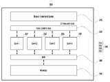
도 2는 본 발명의 다양한 실시예에 따른 아키텍처(architecture)(200)의 구성 블록도이다. 일 실시예에 따르면, 도 2에 도시된 아키텍처(200)는 도 1에 도시된 도 1에 도시된 프로세서(120)와 동일 또는 유사한 것일 수 있다. 어떤 실시 예에 따르면, 도 2에 도시된 아키텍처(200)는 도 1에 도시된 프로세서(120)의 내부에 구성된 적어도 일부 구성요소일 수 있다.2 is a block diagram of an
도 2를 참조하면, 아키텍처(200)는 서로 독립적으로 연산을 수행할 수 있는 복수의 코어들(cores)(230), 메모리(250), 또는 복수의 코어들(230) 및 메모리(250)와 전기적으로 연결된 제어 회로(210)를 포함할 수 있다. 일 실시예에 따르면, DSP(200)는 제어 회로(210)와 복수의 코어들(230) 사이를 연결하는 코어 컨트롤 허브(core control hub)(220), 또는 복수의 코어들(230)과 메모리(240) 사이를 연결하는 버스(bus)(250)를 더 포함할 수 있다.Referring to FIG. 2 , the
일 실시예에 따르면, 복수의 코어들(230)은 서로 다른 복수의 DSP(digital signal processor) 또는 적어도 하나의 하드웨어 가속기(hardware accelerator)로 구성될 수 있다. 일 실시예에 따르면, 복수의 코어들(230)은 전자 장치(예: 도 1의 전자 장치(101))를 구성하는 다른 장치들(예: 도 1의 오디오 모듈(170), 센서 모듈(176), 햅틱 모듈(179), 또는 카메라 모듈(180) 등)로부터 제공된 신호 또는 정보를 처리하도록 구성될 수 있다. 예를 들면, 복수의 코어(230)가 처리하는 태스크는 전자 장치(예: 도 1의 전자 장치(101))를 구성하는 다른 장치들(예: 도 1의 오디오 모듈(170), 센서 모듈(176), 햅틱 모듈(179), 또는 카메라 모듈(180) 등)로부터 제공된 신호로부터 정보를 추출하는 기능, 정보의 내용이나 특성을 변경하는 기능, 음성 신호를 디지털화하는 음성 코딩 기능, 디지털 필터 기능, 또는 음향이나 영상을 처리하는 기능 등을 포함할 수 있다.According to an embodiment, the plurality of
일 실시예에 따르면, 복수의 코어들(230)은 상기 기능들을 수행하도록 서로 독립적으로 연산을 수행할 수 있다. 예를 들면, 복수의 코어들(230)은 서로 다른 복수의 DSP(digital signal processor)이거나, 또는 적어도 하나의 하드웨어 가속기(hardware accelerator)일 수 있다. 도 2에서는, 복수의 코어들(230)은 서로 독립적으로 연산을 수행하는 4개의 코어로서, 제 1 코어(231), 제 2 코어(233), 제 3 코어(235), 및 제 4 코어(237)를 예시적으로 나타내고 있지만, 본 발명에서 코어의 갯수는 국한되지 않을 수 있다.According to an embodiment, the plurality of
일 실시예에 따르면, 메모리(250)는 태스크에 대응하는 데이터를 저장하는 구성일 수 있다. 일 실시예에 따르면, 메모리(250)는 제어 회로(210)의 내부에 구성될 수 있다. 일 실시예에 따르면, 메모리(250)는 SRAM(static random access memory)으로 구성될 수 있다.According to an embodiment, the
일 실시예에 따르면, 제어 회로(210)는 복수의 코어(230)로부터 태스크 처리 요청을 수신하고, 수신된 태스크를 복수의 코어들(230)에게 분배하는 구성일 수 있다. 일 실시예에 따르면, 제어 회로는 복수의 코어들(230)로부터 요청된 태스크를 관리하는 회로일 수 있다.According to an embodiment, the
일 실시예에 따르면, 제어 회로(210)는 특정 코어로부터 요청된 태스크를 복수의 코어(230)에게 인터럽트 이벤트 형식으로 전달하고, 복수의 코어(230) 중에서 적어도 일부의 코어로부터 인터럽트 이벤트에 대한 응답을 수신할 수 있다. 일 실시예에 따르면, 제어 회로(210)는, 복수의 코어(230) 중에서 가장 먼저 응답한 코어에게 요청된 태스크를 할당할 수 있다. 예를 들면, 제어 회로(210)는 제 1 코어(231)로부터 태스크 처리 요청을 수신한 것에 응답하여, 제 1 코어 내지 제 4 코어(231, 233, 235, 237) 각각에게 태스크에 관련한 인터럽트 이벤트를 전송할 수 있다. 제어 회로(210)는, 만약 제 1 코어 내지 제 4 코어(231, 233, 235, 237) 중에서 제 3 코어(235)로부터 가장 먼저 응답을 수신한 경우, 제 3 코어(235)에게 태스크를 할당할 수 있다. 일 실시예에 따르면, 제어 회로(210)가 태스크를 할당하는 동작은 복수의 코어(230) 중에서 가장 먼저 응답한 코어에게 태스크에 관련한 명령어, 또는 해당 태스크에 대응하는 데이터를 전송하는 동작을 포함할 수 있다. 일 실시예에 따르면, 제어 회로(210)로부터 태스크를 할당받은 코어, 예컨대 제 3 코어(235)는 할당된 태스크에 관련한 기능을 수행할 수 있다.According to an embodiment, the
일 실시예에 따르면, 제어 회로(210)는 사용자의 설정에 기반하여 태스크의 우선 순위를 결정할 수 있다. 예를 들면, 복수의 태스크들 중에서 지정된 태스크는 다른 태스크보다 우선적으로 처리되어야 할 수 있다. 예를 들면, 제어 회로(210)가 복수의 코어(230)로부터 수신된 제 1 태스크, 제 2 태스크, 및 제 3 태스크를 순차적으로 저장하고 있는 상태에서, 우선 순위를 갖고 있는 제 4 태스크의 처리 요청을 수신할 수 있다. 이 경우, 제어 회로(210)는 제 4 태스크의 처리가 제 1 태스크 내지 제 3 태스크의 처리보다 우선적으로 처리되도록 큐의 순서를 조정할 수 있다.According to an embodiment, the
일 실시예에 따르면, 제어 회로(210)는 특정 태스크와 특정 코어를 매칭할 수 있다. 예를 들면, 제어 회로(210)는 복수의 태스크 중에서 적어도 일부 태스크는 지정된 코어가 처리하도록 설정할 수 있다.According to an embodiment, the
일 실시예에 따르면, 제어 회로(210)는 태스크들 간의 의존성을 고려하여 태스크의 할당 시점을 조정할 수 있다. 예를 들면, 복수의 태스크들 간에는 의존성이 존재할 수 있다. 예를 들면, 제 2 태스크의 처리는 제 1 태스크의 처리가 완료된 이후에 수행되어야 할 수 있다. 이 경우, 제어 회로(210)는 제 1 태스크의 처리 이후에 wait task를 지정함으로써, 제 1 태스크의 처리가 완료된 후에 제 2 태스크가 처리되도록 할 수 있다.According to an embodiment, the
본 발명의 다양한 실시예에 따른 제어 회로(210)는 태스크와 관련한 큐(queue)들을 복수의 코어들(230)에게 공유하고, 상기 큐들을 관리하는 역할을 수행하는 바, 이하 본 문서에서는, 제어 회로를 "SCQ(shared command queue) 회로"라고 정의한다.The
도 3은 본 발명의 다양한 실시예에 따른 제어 회로의 구성 블록도이다.3 is a block diagram of a control circuit according to various embodiments of the present invention.
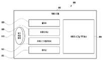
도 3을 참조하면, 본 발명의 다양한 실시예에 따른 SCQ 회로(300)(예: 도 2의 SCQ 회로(210))는 메인 회로(310), 메인 회로(310) 및 복수의 코어(예: 도 2의 복수의 코어들(230))를 서로 연결하는 버스(320)(예: 도 2의 코어 컨트롤 허브(core control hub)(220)), 또는 SRAM(static random access memory)으로 구성된 내부 메모리(350)를 포함할 수 있다.Referring to FIG. 3 , the SCQ circuit 300 (eg, the
일 실시예에 따르면, 메인 회로(310)는 복수의 코어들(230)을 제어하기 위해 버스(320)와 연결되는 SFR(special function register) 설정 회로(311), 복수의 코어들(230)에게 인터럽트 요청(IRQ)(interrupt request)을 전송하는 IRQ 제어 회로(312), SRAM 주소 제어기(SRAM address controller)(317), SRAM 인터페이스(318), 및 큐 제어(queue control) 회로(313)를 포함할 수 있다. 일 실시예에 따르면, 큐 제어 회로(313)는 큐 저장 장치(314), 큐 스케쥴 회로(315), 및 큐 메모리 유효성 검사기(316)를 포함할 수 있다.According to an embodiment, the
일 실시예에 따르면, 복수의 코어(230)는 SCQ 회로(300)를 통해 태스크를 서로 공유할 수 있다. 일 실시예에 따르면, SCQ 회로(300)는 복수의 코어(230)로부터 수신한 태스크를 저장하고 관리한다. 예를 들면, SCQ 회로(300)는 태스크를 저장하고 관리하는 구성일 수 있다. 일 실시예에 따르면, SCQ 회로(300)는 태스크 명령어와 태스크에 관련한 데이터(태스크 정보)를 저장할 수 있다. 예를 들면, SCQ 회로(300)는 큐 저장 장치(314)를 통해 최대 32개의 태스크를 저장하도록 구성될 수 있다. 다양한 실시예에 따르면, 큐 저장 장치(314)가 저장하는 태스크의 갯수는 최대 32개보다 많을 수 있다.According to an embodiment, the plurality of
일 실시예에 따르면, 1 개의 태스크는 1개의 명령어를 포함할 수 있고, 또는 1개의 태스크는 복수개의 명령어를 포함할 수 있다. 예를 들면, 1개의 태스크는 1개의 태스크 정보를 포함할 수 있고, 또는 1개의 태스크는 10개의 태스크 정보를 포함할 수 있다.According to an embodiment, one task may include one instruction, or one task may include a plurality of instructions. For example, one task may include one task information, or one task may include ten task information.
일 실시예에 따르면, 큐 저장 장치(314)는 FIFO(first in first out) 구조로 태스크 명령어를 저장할 수 있다.According to an embodiment, the
일 실시예에 따르면, SCQ 회로(300)는 태스크 정보를 저장하도록 최대 8Kbyte 의 내부 메모리(350)을 포함할 수 있다. 예를 들면, SCQ 회로(300)는 복수의 코어(230) 중에서 적어도 하나로부터 수신한 태스크 명령어를 큐 저장 장치(314)에 저장하고, 태스크에 관련한 데이터(태스크 정보)를 내부 메모리(350)인 SRAM에 저장할 수 있다.According to an embodiment, the
일 실시예에 따르면, SCQ 회로(300)는 수신한 태스크 명령어를 순차적으로 저장하고, 태스크 명령어를 저장된 순서대로 복수의 코어(230)에게 할당할 수 있다. 다른 실시예에 따르면, SCQ 회로(300)는 사용자가 설정한 우선순위에 기반하여 태스크를 복수의 코어(230)에 할당하도록 설정될 수 있다.According to an embodiment, the
일 실시예에 따르면, SRAM 주소 제어기(317)는 큐 제어 회로(313)의 제어에 기반하여 태스크 정보를 내부 메모리(350)에 저장하는 구성일 수 있다. 예를 들면, SRAM 주소 제어기(317)는 큐 제어 회로(313)의 제어에 기반하여 자동으로 주소를 생성하고, 생성된 주소에 대응하도록 태스크 정보를 내부 메모리(350)에 저장할 수 있다. 일 실시예에 따르면, SRAM 주소 제어기(317)는 태스크 정보를 저장하기 위해, 내부 메모리(350)에서 데이터가 저장되지 않는 메모리 공간을 검색하고, 검색된 메모리 공간을 할당 및 저장 주소를 생성하여 큐 제어 회로(313)에게 저장 주소를 전달할 수 있다.According to an embodiment, the
일 실시예에 따르면, IRQ 제어 회로(312)는 이벤트 기반으로 인터럽트를 생성하여 SCQ 회로(300)에 저장된 태스크 명령어 및 태스크 정보를 복수의 코어(230)에게 전달하는 구성일 수 있다.According to an embodiment, the
일 실시예에 따르면, SFR 설정 회로(311)는 사용자 요청에 기반하여 복수의 코어(230)에게 인터럽트 요청을 전송하거나, 또는 복수의 코어(230) 중에서 지정된 일부 코어에게만 인터럽트 요청을 전송하도록 구성될 수 있다.According to an embodiment, the
본 발명의 다양한 실시예에 따른 프로세서의 태스크 처리 방법에 있어서, 상기 프로세서는 서로 독립적으로 연산을 수행할 수 있는 복수의 코어들(예: 도 2의 230)(cores), 메모리(예: 도 3의 350), 및 상기 복수의 코어들(230) 및 메모리(350)와 전기적으로 연결된 제어 회로(예: 도 3의 300)를 포함하고, 상기 방법은, 상기 복수의 코어들(230) 중 적어도 일부 코어들(230)을 이용하여 처리할 태스크와 관련된 하나 이상의 명령어들을 획득하는 동작, 상기 하나 이상의 명령어들에 적어도 기반하여, 상기 태스크에 대응하는 데이터를 상기 메모리(350)에 저장하는 동작, 상기 하나 이상의 명령들의 적어도 일부 명령어를 상기 적어도 일부 코어들(230)로 전달하는 동작, 상기 적어도 일부 코어들(230) 중 상기 적어도 일부 명령어에 응답한 하나 이상의 코어들(230)을 확인하는 동작, 상기 태스크가 상기 하나 이상의 코어들(230) 중 하나의 코어에 할당된 경우, 상기 하나 이상의 코어들(230) 중 상기 하나의 코어와 다른 나머지 코어에 상기 태스크를 할당하지 않는 동작, 및 상기 태스크가 상기 하나 이상의 코어들(230)에 할당되지 않은 경우, 상기 하나 이상의 코어들(230) 중 하나의 코어에 상기 태스크를 할당하는 동작을 포함하고, 상기 할당하는 동작은 상기 태스크의 할당과 관련된 상태 정보를 변경하는 동작 및 상기 하나의 코어와 다른 나머지 코어가 상기 태스크에 대응하는 데이터에 접근할 수 없도록 설정하는 동작을 포함할 수 있다. 상기 적어도 일부 코어들(230) 중 상기 적어도 일부 명령어에 가장 먼저 응답한 코어에게 상기 태스크를 할당하는 동작을 더 포함할 수 있다. 상기 태스크에 대응하는 데이터를 상기 메모리(350)에 저장하는 동작은 FIFO(first in first out) 구조인 큐 저장 장치(314)에 태스크 명령어를 저장하는 동작을 포함할 수 있다. 상기 제어 회로(300)가, 인터럽트 요청(IRQ)(interrupt request) 제어 회로(300)를 이용해, 이벤트 기반으로 인터럽트를 생성하여 상기 태스크를 상기 적어도 일부 명령어에 응답한 하나 이상의 코어에게 전달하는 동작을 포함할 수 있다. 상기 메모리(350)는 SRAM(static random access memory)으로 구성되어 상기 제어 회로(300)에 내장될 수 있다. 상기 제어 회로(300)가, SRAM 주소 제어기(317)를 이용해, 상기 처리할 태스크와 관련된 하나 이상의 명령어들을 획득한 것에 응답하여, 상기 태스크에 대응하는 데이터를 저장할 주소를 자동으로 할당하고, 상기 메모리(350)의 상기 할당된 주소에 상기 태스크에 대응하는 데이터를 저장하는 동작을 포함할 수 있다. 사용자가 설정한 우선순위에 기반하여 지정된 하나 이상의 코어에게 태스크를 우선적으로 할당하는 동작을 포함할 수 있다. 상기 복수의 코어는 서로 다른 복수의 디지털 시그널 프로세서(digital signal processor)로 구성될 수 있다.In the task processing method of a processor according to various embodiments of the present disclosure, the processor includes a plurality of cores (eg, 230 in FIG. 2 ) (cores) capable of performing operations independently of each other, and a memory (eg, FIG. 3 ). 350 ), and a control circuit (eg, 300 in FIG. 3 ) electrically connected to the plurality of
도 4는 본 발명의 다양한 실시예에 따른 아키텍처(architecture)(예: 도 2의 200)의 동작 흐름도이다.4 is an operation flowchart of an architecture (eg, 200 of FIG. 2 ) according to various embodiments of the present disclosure.
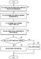
도 4를 참조하면, 일 실시예에 따른 SCQ 회로(예: 도 3의 300)는, 동작 401에서, 복수의 코어(예: 도 2의 230)들 중 적어도 일부 코어들을 이용하여 처리할 태스크와 관련된 하나 이상의 명령어들을 획득할 수 있다. 예를 들면, SCQ 회로(300)는 상기 복수의 코어(230) 중 적어도 일부로부터 태스크의 처리 요청을 수신할 수 있다.Referring to FIG. 4 , the SCQ circuit (eg, 300 of FIG. 3 ) according to an embodiment performs a task to be processed using at least some of the plurality of cores (eg, 230 of FIG. 2 ) in
동작 402에서, 일 실시예에 따른 SCQ 회로(300)는, 수신한 태스크에 포함된 하나 이상의 명령어들에 적어도 기반하여, 태스크에 대응하는 데이터를 메모리(예: 도 3의 350)에 저장할 수 있다.In
동작 403에서, 일 실시예에 따른 SCQ 회로(300)는, 수신한 태스크에 관련한 하나 이상의 명령들의 적어도 일부 명령어를 적어도 일부 코어들로 전달할 수 있다.In
동작 404에서, 일 실시예에 따른 SCQ 회로(300)는, 적어도 일부 코어들 중 적어도 일부 명령어에 응답한 하나 이상의 코어들을 확인할 수 있다.In
동작 405 내지 동작 406에서, 일 실시예에 따른 SCQ 회로(300)는, 상기 태스크가 상기 하나 이상의 코어들 중 하나의 코어에 할당된 경우, 상기 하나 이상의 코어들 중 상기 하나의 코어와 다른 나머지 코어에 상기 태스크를 할당하지 않을 수 있다.In
동작 407에서, 일 실시예에 따른 SCQ 회로(300)는, 태스크가 상기 하나 이상의 코어들에 할당되지 않은 경우, 상기 하나 이상의 코어들 중 하나의 코어에 상기 태스크를 할당할 수 있다. 일 실시예에 따르면, SCQ 회로(300)가 태스크를 할당하는 동작은 상기 태스크의 할당과 관련된 상태 정보를 변경하는 동작 및 상기 하나의 코어와 다른 나머지 코어가 상기 태스크에 대응하는 데이터에 접근할 수 없도록 설정하는 동작을 포함할 수 있다.In
도 5는 본 발명의 다양한 실시예에 따른 아키텍처(architecture)(예: 도 2의 200)의 태스크 처리 과정을 설명한 동작 흐름도이다.5 is an operation flowchart illustrating a task processing process of an architecture (eg, 200 of FIG. 2 ) according to various embodiments of the present disclosure.
도 5를 참조하면, 일 실시예에 따른 복수의 코어(예: 도 2의 230)들 중 적어도 일부는 태스크를 생성하고, 생성된 태스크를 SCQ 회로(예: 도 3의 300)로 전송할 수 있다. 예를 들면, SCQ 회로(300)는 상기 복수의 코어(230) 중 적어도 일부로부터 태스크의 처리 요청을 수신할 수 있다.Referring to FIG. 5 , at least some of a plurality of cores (eg, 230 in FIG. 2 ) according to an embodiment may generate a task and transmit the generated task to an SCQ circuit (eg, 300 in FIG. 3 ). . For example, the
동작 502 및 동작 503에서, 일 실시예에 따른 SCQ 회로(300)는 상기 복수의 코어(230) 중 적어도 일부로부터 태스크의 처리 요청을 수신한 것에 응답하여, 해당 태스크를 수용할 수 있는지 여부를 확인(결정)하고, 확인 결과를 복수의 코어(230)에게 전달할 수 있다. 예를 들면, SCQ 회로(300)는 큐 저장 장치(314)를 통해 최대 32개의 태스크를 저장하고, 최대 최대 8Kbyte 의 태스크 데이터를 저장할 수 있도록 구성될 수 있다. 일 실시예에 따르면, SCQ 회로(300)는, 상기 예시한 바와 같은, 지정된 수용 가능한 태스크의 갯수를 초과하거나, 또는 지정된 메모리의 저장 공간이 꽉 차면 태스크 데이터를 더 이상 수용할 수 없는 것으로 결정할 수 있다. 일 실시예에 따르면, SCQ 회로(300)는, 태스크를 수용할 수 없는 것으로 결정한 경우 해당 정보를 복수의 코어(230)들에게 전달할 수 있다. 일 실시예에 따르면, 복수의 코어(230)는 SCQ 회로(300)로부터 태스크를 수용할 수 없다는 이벤트를 수신하고서, 지정 시간이 경과하면 다시 태스크 처리 요청을 SCQ 회로(300)로 전송하도록 설정될 수 있다. 일 실시예에 따르면, 복수의 코어(230)는 SCQ 회로(300)로부터 태스크를 수용할 수 있다는 이벤트를 수신하면, 태스크 명령어 및 태스크 데이터를 SCQ 회로(300)로 전달할 수 있다.In
동작 504에서, 일 실시예에 따른 SCQ 회로(300)는, 수신한 태스크 명령어를 순차적으로 저장할 수 있다. 예를 들면, SCQ 회로(300)는 FIFO(first in first out) 구조인 큐 저장 장치(예: 도 3의 314)에 태스크 명령어를 저장하고, SRAM 주소 제어기(예: 도 3의 317)를 이용해 태스크 데이터를 내부 메모리(예: 도 3의 350)에 저장할 수 있다.In
동작 505 및 도 506에서, 일 실시예에 따른 SCQ 회로(300)는, 모든 복수의 코어(230)에게 태스크 명령어의 적어도 일부 명령어를 전달하고, 명령어를 수신한 복수의 코어(230) 각각은 태스크의 처리 가능 여부를 알리는 이벤트를 SCQ 회로(300)에게 전송할 수 있다.In
동작 507에서, 일 실시예에 따른 SCQ 회로(300)는, 모든 복수의 코어(230) 중 적어도 일부 명령어에 응답한 하나 이상의 코어들을 확인하고, 하나 이상의 코어에게 태스크를 할당할 수 있다. 일 실시예에 따르면, SCQ 회로(300)는 수신한 태스크 명령어를 순차적으로 저장하고, 태스크 명령어를 저장된 순서대로 복수의 코어(230)에게 할당할 수 있다. 다른 실시예에 따르면, SCQ 회로(300)는 사용자가 설정한 우선순위에 기반하여 태스크를 복수의 코어(230)에 할당하도록 설정될 수 있다.In
동작 508 및 동작 509에서, 일 실시예에 따르면, 태스크가 할당된 코어는 SCQ 회로(300)로부터 태스크 데이터를 수신하고, 수신된 태스크를 처리할 수 있다.In
도 6은 SCQ 회로가 적어도 일부 코어로부터 요청된 태스크를 다른 코어에게 할당하는 과정을 설명하기 위한 예시도이다.6 is an exemplary diagram for explaining a process in which the SCQ circuit allocates tasks requested from at least some cores to other cores.
도 6을 참조하면, 본 발명의 일 실시예에 따른 아키텍처(architecture)(예: 도 2의 200)는 서로 독립적으로 연산을 수행할 수 있는 복수의 코어들(cores)(630)(예: 도 2의 230), 및 SCQ 회로(620)(예: 도 3의 300)를 포함할 수 있다. 일 실시예에 따르면, 복수의 코어(630)는 서로 다른 복수의 DSP(digital signal processor) 또는 적어도 하나의 하드웨어 가속기(hardware accelerator)로 구성된 제 1 코어 내지 제 4 코어(631, 633, 635, 637)를 포함할 수 있다.Referring to FIG. 6 , an architecture (eg, 200 of FIG. 2 ) according to an embodiment of the present invention includes a plurality of cores 630 (eg, FIG. 2 ) capable of performing operations independently of each other. 230 of 2), and an SCQ circuit 620 (eg, 300 of FIG. 3). According to an embodiment, the plurality of
일 실시예에 따르면, SCQ 회로(620)는 특정 코어로부터 요청된 태스크를 복수의 코어에게 인터럽트 이벤트 형식으로 전달하고, 복수의 코어 중에서 적어도 일부의 코어로부터 인터럽트 이벤트에 대한 응답을 수신할 수 있다. 일 실시예에 따르면, SCQ 회로(620)는, 복수의 코어 중에서 가장 먼저 응답한 코어에게 요청된 태스크를 할당할 수 있다. 예를 들면, SCQ 회로(620)가 적어도 일부 코어로부터 요청된 태스크를 다른 코어에게 할당하는 과정은 도 6의 화살표 610과 같을 수 있다. SCQ 회로(620)의 아비터(arbiter) 회로(621)(예: 도 3의 큐 제어 회로(313))는 제 3 코어(635)로부터 태스크 처리 요청을 수신하면, 수신된 태스크를 큐 저장 장치(622)(예: 도 3의 314)에 순차적으로 저장하고, 제 1 코어 내지 제 4 코어(631, 633, 635, 637) 각각에게 태스크에 관련한 인터럽트 이벤트를 전송할 수 있다. SCQ 회로(620)는, 만약 제 1 코어 내지 제 4 코어(631, 633, 635, 637) 중에서 제 1 코어(631)로부터 가장 먼저 응답을 수신한 경우, 제 1 코어(631)에게 태스크를 할당할 수 있다. SCQ 회로(620)로부터 태스크를 할당받은 코어, 예컨대 제 1 코어(631)는 할당된 태스크에 관련한 기능을 수행할 수 있다.According to an embodiment, the
도 7은 SCQ 회로가 태스크의 의존성을 고려하여 태스크를 할당하는 방법을 설명하기 위한 예시도이다. 도 8은 SCQ 회로가 wait task를 설정하는 방법을 설명한 예시이다.7 is an exemplary diagram for explaining a method in which the SCQ circuit allocates tasks in consideration of task dependency. 8 is an example illustrating a method in which the SCQ circuit sets a wait task.
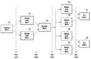
일 실시예에 따르면, 도 7은 2D-DFT(discrete fourier transform) 알고리즘을 나타낸 예시일 수 있다. 본 발명의 다양한 실시예에 따른 아키텍처(예: 도 2의 200)가 수행하는 태스크는 도 7에 도시된 바와 같이 태스크들 간에 의존성이 존재할 수 있다. 예를 들면, 블록 721 및 블록 722에 해당하는 태스크들은 블록 711에 해당하는 태스크가 먼저 처리된 후에 처리되어야 할 수 있다. 또는, 블록 731에 해당하는 태스크는 블록 721 및 블록 722에 해당하는 태스크들이 먼저 처리된 후에 처리되어야 할 수 있다. 또는, 블록 741, 블록 742, 블록 743, 및 블록 744에 해당하는 태스크들은 블록 731에 해당하는 태스크가 먼저 처리된 후에 처리되어야 할 수 있다. 또는, 블록 751 및 블록 752에 해당하는 태스크들은 블록 741, 블록 742, 블록 743, 및 블록 744에 해당하는 태스크들이 먼저 처리된 후에 처리되어야 할 수 있다.According to an embodiment, FIG. 7 may be an example illustrating a 2D-DFT (discrete fourier transform) algorithm. Tasks performed by the architecture (eg, 200 in FIG. 2 ) according to various embodiments of the present disclosure may have dependencies among the tasks as illustrated in FIG. 7 . For example, tasks corresponding to
도 7 및 도 8을 참조하면, 본 발명의 다양한 실시예에 따른 SCQ 회로(800)(예: 도 3의 300)는 상기와 같은 태스크들 간의 의존성을 고려하여 wait task를 설정할 수 있다. 예를 들면, SCQ 회로(800)의 아비터(arbiter) 회로(821)(예: 도 3의 큐 제어 회로(313))는 도 7의 블록 711에 해당하는 태스크가 먼저 처리될 때까지 다른 태스크의 처리가 진행되지 않도록 wait task 1(832)를 큐 저장 장치(822)(예: 도 3의 314)에 지정할 수 있다.Referring to FIGS. 7 and 8 , the SCQ circuit 800 (eg, 300 of FIG. 3 ) according to various embodiments of the present invention may set a wait task in consideration of the dependency between tasks as described above. For example, the
또는, SCQ 회로(800)의 아비터 회로(821)는 도 7의 블록 721 및 블록 722에 해당하는 태스크들이 먼저 처리될 때까지 다른 태스크의 처리가 진행되지 않도록 wait task 2(835)을 큐 저장 장치(822)에 지정할 수 있다.Alternatively, the
또는, SCQ 회로(800)의 아비터 회로(821)는 블록 731에 해당하는 태스크가 먼저 처리될 때까지 다른 태스크의 처리가 진행되지 않도록 wait task3을 큐 저장 장치(822)에 지정할 수 있다.Alternatively, the
또는, SCQ 회로(800)의 아비터 회로(821)는 블록 741, 블록 742, 블록 743, 및 블록 744에 해당하는 태스크들이 먼저 처리될 때까지 다른 태스크의 처리가 진행되지 않도록 wait task 4를 큐 저장 장치(822)에 지정할 수 있다.Alternatively, the
도 9는, 다양한 실시예들에 따른, 카메라 모듈(980)(예: 도 1의 980)의 블럭도(900)이다. 도 9를 참조하면, 카메라 모듈(980)은 렌즈 어셈블리(910), 플래쉬(920), 이미지 센서(930), 이미지 스태빌라이저(940), 메모리(950)(예: 버퍼 메모리), 또는 이미지 시그널 프로세서(960)를 포함할 수 있다. 렌즈 어셈블리(910)는 이미지 촬영의 대상인 피사체로부터 방출되는 빛을 수집할 수 있다. 렌즈 어셈블리(910)는 하나 또는 그 이상의 렌즈들을 포함할 수 있다. 일 실시예에 따르면, 카메라 모듈(980)은 복수의 렌즈 어셈블리(910)들을 포함할 수 있다. 이런 경우, 카메라 모듈(980)은, 예를 들면, 듀얼 카메라, 360도 카메라, 또는 구형 카메라(spherical camera)일 수 있다. 복수의 렌즈 어셈블리(910)들은 동일한 렌즈 속성(예: 화각, 초점 거리, 자동 초점, f 넘버(f number), 또는 광학 줌)을 갖거나, 또는 적어도 하나의 렌즈 어셈블리는 다른 렌즈 렌즈 어셈블리와 적어도 하나의 다른 렌즈 속성을 가질 수 있다. 렌즈 어셈블리(910)는, 예를 들면, 광각 렌즈 또는 망원 렌즈를 포함할 수 있다. 플래쉬(920)는 피사체로부터 방출되는 빛을 강화하기 위하여 사용되는 광원을 방출할 수 있다. 플래쉬(920)는 하나 이상의 발광 다이오드들(예: RGB(red-green-blue) LED, white LED, infrared LED, 또는 ultraviolet LED), 또는 xenon lamp를 포함할 수 있다.9 is a block diagram 900 of a camera module 980 (eg, 980 of FIG. 1 ), according to various embodiments. Referring to FIG. 9 , the
이미지 센서(930)는 피사체로부터 렌즈 어셈블리(910)를 통해 전달된 빛을 전기적인 신호로 변환함으로써, 상기 피사체에 대응하는 이미지를 획득할 수 있다. 일 실시예에 따르면, 이미지 센서(930)는, 예를 들면, RGB 센서, BW(black and white) 센서, IR 센서, 또는 UV 센서와 같이 속성이 다른 이미지 센서들 중 선택된 하나의 이미지 센서, 동일한 속성을 갖는 복수의 이미지 센서들, 또는 다른 속성을 갖는 복수의 이미지 센서들을 포함할 수 있다. 이미지 센서(930)에 포함된 각각의 이미지 센서는, 예를 들면, CCD(charged coupled device) 센서 또는 CMOS(complementary metal oxide semiconductor) 센서로 구현될 수 있다.The
이미지 스태빌라이저(940)는 카메라 모듈(980) 또는 이를 포함하는 전자 장치(101)의 움직임에 반응하여, 촬영되는 이미지에 대한 상기 움직임에 의한 부정적인 영향(예: 이미지 흔들림)을 적어도 일부 보상하기 위하여 렌즈 어셈블리(910)에 포함된 적어도 하나의 렌즈 또는 이미지 센서(930)를 특정한 방향으로 움직이거나 제어(예: 리드 아웃(read-out) 타이밍을 조정 등)할 수 있다. 일 실시예에 따르면, 이미지 스태빌라이저(940)는, 예를 들면, 광학식 이미지 스태빌라이저로 구현될 수 있으며, 카메라 모듈(980)의 내부 또는 외부에 배치된 자이로 센서(미도시) 또는 가속도 센서(미도시)를 이용하여 상기 움직임을 감지할 수 있다.The
메모리(950)는 이미지 센서(930)을 통하여 획득된 이미지의 적어도 일부를 다음 이미지 처리 작업을 위하여 적어도 일시 저장할 수 있다. 예를 들어, 셔터에 따른 이미지 획득이 지연되거나, 또는 복수의 이미지들이 고속으로 획득되는 경우, 획득된 원본 이미지(예: 높은 해상도의 이미지)는 메모리(950)에 저장이 되고, 그에 대응하는 사본 이미지(예: 낮은 해상도의 이미지)는 표시 장치(160)을 통하여 프리뷰될 수 있다. 이후, 지정된 조건이 만족되면(예: 사용자 입력 또는 시스템 명령) 메모리(950)에 저장되었던 원본 이미지의 적어도 일부가, 예를 들면, 이미지 시그널 프로세서(960)에 의해 획득되어 처리될 수 있다. 일 실시예에 따르면, 메모리(950)는 메모리(130)의 적어도 일부로, 또는 이와는 독립적으로 운영되는 별도의 메모리로 구성될 수 있다.The
이미지 시그널 프로세서(960)는 이미지 센서(930)을 통하여 획득된 이미지 또는 메모리(950)에 저장된 이미지에 대하여 이미지 처리(예: 깊이 지도(depth map) 생성, 3차원 모델링, 파노라마 생성, 특징점 추출, 이미지 합성, 또는 이미지 보상(예: 노이즈 감소, 해상도 조정, 밝기 조정, 블러링(blurring), 샤프닝(sharpening), 또는 소프트닝(softening))을 수행할 수 있다. 추가적으로 또는 대체적으로, 이미지 시그널 프로세서(960)는 카메라 모듈(980)에 포함된 구성 요소들 중 적어도 하나(예: 이미지 센서(930))에 대한 제어(예: 노출 시간 제어, 또는 리드 아웃 타이밍 제어 등)를 수행할 수 있다. 이미지 시그널 프로세서(960)에 의해 처리된 이미지는 추가 처리를 위하여 메모리(950)에 다시 저장 되거나 카메라 모듈(980)의 외부 구성 요소(예: 도 1의 메모리(130), 표시 장치(160), 전자 장치(102), 전자 장치(104), 또는 서버(108))로 전달될 수 있다. 일 실시예에 따르면, 이미지 시그널 프로세서(960)는 프로세서(예: 도 1의 120)의 적어도 일부로 구성되거나, 프로세서(120)와 독립적으로 운영되는 별도의 프로세서로 구성될 수 있다. 별도의 프로세서로 구성된 경우, 이미지 시그널 프로세서(960)에 의해 처리된 이미지들은 프로세서(120)에 의하여 그대로 또는 추가의 이미지 처리를 거친 후 표시 장치(예: 도 1의 160)를 통해 표시될 수 있다.The
일 실시예에 따르면, 전자 장치(예: 도 1의 101)는 각각 다른 속성 또는 기능을 가진 둘 이상의 카메라 모듈(980)들을 포함할 수 있다. 이런 경우, 예를 들면, 적어도 하나의 카메라 모듈(980)은 광각 카메라 또는 전면 카메라이고, 적어도 하나의 다른 카메라 모듈은 망원 카메라 또는 후면 카메라일 수 있다.According to an embodiment, the electronic device (eg, 101 of FIG. 1 ) may include two or
본 발명의 다양한 실시예에 따르면 다음과 같은 효과가 있을 수 있다.According to various embodiments of the present invention, the following effects may be obtained.
SCQ 회로가 복수의 DSP로부터의 태스크를 관리 및 공유함으로써 태스크 처리 속도를 높이고 태스크 관리 효율을 높일 수 있다.The SCQ circuit can manage and share tasks from a plurality of DSPs to speed up task processing and increase task management efficiency.
SCQ 회로가 태스크를 전달함에 있어서, 별도의 Lock 알고리즘을 적용하지 않아도 되므로 동작이 빠르다. Lock 알고리즘은 태스크가 할당된 특정 DSP 코어 이외에는 태스크 데이터에 대한 접근을 하지 못하도록 하는 알고리즘으로, 성능 하락의 원인이다.When the SCQ circuit transmits a task, it is not necessary to apply a separate lock algorithm, so the operation is fast. The lock algorithm is an algorithm that prevents access to task data except for the specific DSP core to which the task is assigned, and is the cause of performance degradation.
SCQ 회로는 태스크 데이터를 저장하는 SRAM을 이용하므로, 태스크 전달시 메인 메모리를 사용하지 않아도 되므로 처리 속도가 빠르다.Since the SCQ circuit uses SRAM for storing task data, it is not necessary to use the main memory for task delivery, so the processing speed is fast.
마스터 및 슬레이브 구조가 아니므로, 모든 DSP 코어가 태스크를 할당할 수 있다.Because there is no master and slave structure, any DSP core can assign tasks.
본 문서에 개시된 다양한 실시예들에 따른 전자 장치는 다양한 형태의 장치가 될 수 있다. 전자 장치는, 예를 들면, 휴대용 통신 장치 (예: 스마트폰), 컴퓨터 장치, 휴대용 멀티미디어 장치, 휴대용 의료 기기, 카메라, 웨어러블 장치, 또는 가전 장치 중 적어도 하나를 포함할 수 있다. 본 문서의 실시예에 따른 전자 장치는 전술한 기기들에 한정되지 않는다.The electronic device according to various embodiments disclosed in this document may have various types of devices. The electronic device may include, for example, at least one of a portable communication device (eg, a smart phone), a computer device, a portable multimedia device, a portable medical device, a camera, a wearable device, and a home appliance device. The electronic device according to the embodiment of the present document is not limited to the above-described devices.
본 문서의 다양한 실시예들 및 이에 사용된 용어들은 본 문서에 기재된 기술을 특정한 실시 형태에 대해 한정하려는 것이 아니며, 해당 실시예의 다양한 변경, 균등물, 및/또는 대체물을 포함하는 것으로 이해되어야 한다. 도면의 설명과 관련하여, 유사한 구성요소에 대해서는 유사한 참조 부호가 사용될 수 있다. 단수의 표현은 문맥상 명백하게 다르게 뜻하지 않는 한, 복수의 표현을 포함할 수 있다. 본 문서에서, "A 또는 B", "A 및/또는 B 중 적어도 하나", "A, B 또는 C" 또는 "A, B 및/또는 C 중 적어도 하나" 등의 표현은 함께 나열된 항목들의 모든 가능한 조합을 포함할 수 있다. "제 1", "제 2", "첫째" 또는 "둘째" 등의 표현들은 해당 구성요소들을, 순서 또는 중요도에 상관없이 수식할 수 있고, 한 구성요소를 다른 구성요소와 구분하기 위해 사용될 뿐 해당 구성요소들을 한정하지 않는다. 어떤(예: 제 1) 구성요소가 다른(예: 제 2) 구성요소에 "(기능적으로 또는 통신적으로) 연결되어" 있다거나 "접속되어" 있다고 언급된 때에는, 상기 어떤 구성요소가 상기 다른 구성요소에 직접적으로 연결되거나, 다른 구성요소(예: 제 3 구성요소)를 통하여 연결될 수 있다.It should be understood that the various embodiments of this document and the terms used therein are not intended to limit the technology described in this document to the specific embodiments, and include various modifications, equivalents, and/or substitutions of the embodiments. In connection with the description of the drawings, like reference numerals may be used for like components. The singular expression may include the plural expression unless the context clearly dictates otherwise. In this document, expressions such as “A or B”, “at least one of A and/or B”, “A, B or C” or “at least one of A, B and/or C” refer to all of the items listed together. Possible combinations may be included. Expressions such as “first”, “second”, “first” or “second” can modify the corresponding components regardless of order or importance, and are only used to distinguish one component from another. The components are not limited. When an (eg, first) component is referred to as being “connected (functionally or communicatively)” or “connected” to another (eg, second) component, that component is It may be directly connected to the component or may be connected through another component (eg, a third component).
본 문서에서 사용된 용어 "모듈"은 하드웨어, 소프트웨어 또는 펌웨어로 구성된 유닛을 포함하며, 예를 들면, 로직, 논리 블록, 부품, 또는 회로 등의 용어와 상호 호환적으로 사용될 수 있다. 모듈은, 일체로 구성된 부품 또는 하나 또는 그 이상의 기능을 수행하는 최소 단위 또는 그 일부가 될 수 있다. 예를 들면, 모듈은 ASIC(application-specific integrated circuit)으로 구성될 수 있다.As used herein, the term “module” includes a unit composed of hardware, software, or firmware, and may be used interchangeably with terms such as, for example, logic, logic block, component, or circuit. A module may be an integrally formed part or a minimum unit or a part of one or more functions. For example, the module may be configured as an application-specific integrated circuit (ASIC).
본 문서의 다양한 실시예들은 기기(machine)(예: 컴퓨터)로 읽을 수 있는 저장 매체(machine-readable storage media)(예: 내장 메모리(136) 또는 외장 메모리(138))에 저장된 명령어를 포함하는 소프트웨어(예: 프로그램(140))로 구현될 수 있다. 기기는, 저장 매체로부터 저장된 명령어를 호출하고, 호출된 명령어에 따라 동작이 가능한 장치로서, 개시된 실시예들에 따른 전자 장치(예: 전자 장치(101))를 포함할 수 있다. 상기 명령이 프로세서(예: 프로세서(120))에 의해 실행될 경우, 프로세서가 직접, 또는 상기 프로세서의 제어하에 다른 구성요소들을 이용하여 상기 명령에 해당하는 기능을 수행할 수 있다. 명령은 컴파일러 또는 인터프리터에 의해 생성 또는 실행되는 코드를 포함할 수 있다. 기기로 읽을 수 있는 저장매체는, 비일시적(non-transitory) 저장매체의 형태로 제공될 수 있다. 여기서, ‘비일시적’은 저장매체가 신호(signal)를 포함하지 않으며 실재(tangible)한다는 것을 의미할 뿐 데이터가 저장매체에 반영구적 또는 임시적으로 저장됨을 구분하지 않는다.Various embodiments of the present document include instructions stored in a machine-readable storage media (eg,
일시예에 따르면, 본 문서에 개시된 다양한 실시예들에 따른 방법은 컴퓨터 프로그램 제품(computer program product)에 포함되어 제공될 수 있다. 컴퓨터 프로그램 제품은 상품으로서 판매자 및 구매자 간에 거래될 수 있다. 컴퓨터 프로그램 제품은 기기로 읽을 수 있는 저장 매체(예: compact disc read only memory (CD-ROM))의 형태로, 또는 어플리케이션 스토어(예: 플레이 스토어TM)를 통해 온라인으로 배포될 수 있다. 온라인 배포의 경우에, 컴퓨터 프로그램 제품의 적어도 일부는 제조사의 서버, 어플리케이션 스토어의 서버, 또는 중계 서버의 메모리와 같은 저장 매체에 적어도 일시 저장되거나, 임시적으로 생성될 수 있다.According to an exemplary embodiment, the method according to various embodiments disclosed in this document may be included and provided in a computer program product. Computer program products may be traded between sellers and buyers as commodities. The computer program product may be distributed in the form of a machine-readable storage medium (eg, compact disc read only memory (CD-ROM)) or online through an application store (eg, Play Store™). In the case of online distribution, at least a part of the computer program product may be temporarily stored or temporarily generated in a storage medium such as a memory of a server of a manufacturer, a server of an application store, or a relay server.
다양한 실시예들에 따른 구성 요소(예: 모듈 또는 프로그램) 각각은 단수 또는 복수의 개체로 구성될 수 있으며, 전술한 해당 서브 구성 요소들 중 일부 서브 구성 요소가 생략되거나, 또는 다른 서브 구성 요소가 다양한 실시예에 더 포함될 수 있다. 대체적으로 또는 추가적으로, 일부 구성 요소들(예: 모듈 또는 프로그램)은 하나의 개체로 통합되어, 통합되기 이전의 각각의 해당 구성 요소에 의해 수행되는 기능을 동일 또는 유사하게 수행할 수 있다. 다양한 실시예들에 따른, 모듈, 프로그램 또는 다른 구성 요소에 의해 수행되는 동작들은 순차적, 병렬적, 반복적 또는 휴리스틱하게 실행되거나, 적어도 일부 동작이 다른 순서로 실행되거나, 생략되거나, 또는 다른 동작이 추가될 수 있다.Each of the components (eg, a module or a program) according to various embodiments may be composed of a singular or a plurality of entities, and some sub-components of the aforementioned sub-components may be omitted, or other sub-components may be It may be further included in various embodiments. Alternatively or additionally, some components (eg, a module or a program) may be integrated into a single entity to perform the same or similar functions performed by each corresponding component prior to integration. According to various embodiments, operations performed by a module, program, or other component are executed sequentially, parallel, iteratively, or heuristically, or at least some operations are executed in a different order, are omitted, or other operations are added. can be
100: 전자 장치
120: 프로세서
130: 메모리
160: 표시 장치100: electronic device
120: processor
130: memory
160: display device
Claims (20)
Translated fromKorean서로 독립적으로 연산을 수행할 수 있는 복수의 코어들(cores);
메모리;
상기 복수의 코어들 및 메모리와 전기적으로 연결된 제어 회로를 포함하고,
상기 제어 회로는,
상기 복수의 코어들 중 적어도 하나의 코어를 이용하여 처리할 제1 태스크와 관련된 하나 이상의 제1 명령어들을 획득하고,
상기 하나 이상의 제1 명령어들에 기반하여, 상기 제1 태스크에 대응하는 데이터를 상기 메모리에 저장하고,
획득한 상기 하나 이상의 제1 명령어들 중 적어도 하나의 제1 명령어를 포함하는 인터럽트 이벤트를 상기 복수의 코어들 각각에 모두 전달하고,
상기 복수의 코어들 중 하나 이상의 코어로부터 상기 인터럽트 이벤트에 대한 응답을 수신한 것에 응답하여, 상기 인터럽트 이벤트에 응답한 상기 하나 이상의 코어가 상기 전달된 적어도 하나의 제1 명령어를 처리할 수 있는지 여부를 확인하고,
상기 제1 태스크가 상기 복수의 코어들에 할당되지 않은 경우, 상기 제1 태스크를, 상기 이벤트에 대해 응답하고 상기 전달된 하나 이상의 제1 명령어들을 처리할 수 있는 상기 하나 이상의 코어 중 하나의 코어에 할당하고,
상기 제1 태스크가 상기 하나의 코어에 할당된 경우, 상기 복수의 코어들 중 상기 하나의 코어와 다른 나머지 코어에 상기 제1 태스크를 할당하지 않되,
상기 제1 태스크를 할당하는 동작은 상기 제1 태스크의 할당과 관련된 상태 정보를 변경하는 동작 및 상기 하나의 코어와 다른 나머지 코어가 상기 제1 태스크에 대응하는 데이터에 접근할 수 없도록 설정하는 동작을 포함하도록 설정된, 프로세서.In the processor,
a plurality of cores capable of performing operations independently of each other;
Memory;
a control circuit electrically connected to the plurality of cores and the memory;
The control circuit is
obtaining one or more first instructions related to a first task to be processed by using at least one of the plurality of cores;
based on the one or more first instructions, store data corresponding to the first task in the memory;
Transmitting an interrupt event including at least one first instruction among the obtained one or more first instructions to each of the plurality of cores,
In response to receiving a response to the interrupt event from one or more of the plurality of cores, determine whether the one or more cores responsive to the interrupt event are capable of processing the delivered at least one first instruction. check,
If the first task is not assigned to the plurality of cores, assign the first task to one of the one or more cores capable of responding to the event and processing the forwarded one or more first instructions. assign,
When the first task is allocated to the one core, the first task is not allocated to the other cores different from the one core among the plurality of cores;
The operation of allocating the first task includes an operation of changing state information related to the allocation of the first task and an operation of setting so that the one core and other cores cannot access data corresponding to the first task. set to include, the processor.
상기 제어 회로는,
상기 하나 이상의 코어들 중 상기 적어도 하나의 제1 명령어에 가장 먼저 응답한 코어에게 상기 제1 태스크를 할당하도록 설정된, 프로세서.The method of claim 1,
The control circuit is
and assign the first task to a core that responds first to the at least one first instruction among the one or more cores.
상기 제어 회로는,
FIFO(first in first out) 구조로 태스크 명령어를 저장 및 관리하는 큐 저장 장치를 포함하는, 프로세서.The method of claim 1,
The control circuit is
A processor, comprising: a queue storage device for storing and managing task instructions in a first in first out (FIFO) structure.
상기 제어 회로는
이벤트 인터럽트를 이용하여 상기 제1 태스크를 상기 적어도 하나의 제1 명령어에 응답한 상기 하나 이상의 코어에게 전달하는 인터럽트 요청(IRQ)(interrupt request) 제어 회로를 포함하는, 프로세서.The method of claim 1,
The control circuit is
and an interrupt request (IRQ) control circuit that uses an event interrupt to deliver the first task to the one or more cores in response to the at least one first instruction.
상기 복수의 코어들 중 적어도 하나의 코어를 이용하여 처리할 제1 태스크와 관련된 하나 이상의 제1 명령어들을 획득하는 동작,
상기 하나 이상의 제1 명령어들에 기반하여, 상기 제1 태스크에 대응하는 데이터를 상기 메모리에 저장하는 동작,
획득한 상기 하나 이상의 제1 명령어들 중 적어도 하나의 제1 명령어를 포함하는 인터럽트 이벤트를 상기 복수의 코어들 각각에 모두 전달하는 동작,
상기 복수의 코어들 중 하나 이상의 코어로부터 상기 인터럽트 이벤트에 대한 응답을 수신한 것에 응답하여, 상기 인터럽트 이벤트에 응답한 상기 하나 이상의 코어가 상기 전달된 적어도 하나의 제1 명령어를 처리할 수 있는지 여부를 확인하는 동작,
상기 제1 태스크가 상기 복수의 코어들에 할당되지 않은 경우, 상기 제1 태스크를, 상기 이벤트에 대해 응답하고 상기 전달된 하나 이상의 제1 명령어들을 처리할 수 있는 상기 하나 이상의 코어 중 하나의 코어에 할당하는 동작,
상기 제1 태스크가 상기 하나의 코어에 할당된 경우, 상기 복수의 코어들 중 상기 하나의 코어와 다른 나머지 코어에 상기 제1 태스크를 할당하지 않는 동작을 포함하되,
상기 제1 태스크를 할당하는 동작은 상기 제1 태스크의 할당과 관련된 상태 정보를 변경하는 동작 및 상기 하나의 코어와 다른 나머지 코어가 상기 제1 태스크에 대응하는 데이터에 접근할 수 없도록 설정하는 동작을 포함하는, 프로세서의 태스크 처리 방법.In the task processing method of a processor comprising a plurality of cores (cores) capable of performing operations independently of each other, a memory, and a control circuit electrically connected to the plurality of cores and the memory,
obtaining one or more first instructions related to a first task to be processed by using at least one of the plurality of cores;
storing data corresponding to the first task in the memory based on the one or more first instructions;
An operation of delivering an interrupt event including at least one first instruction among the one or more first instructions obtained to each of the plurality of cores;
In response to receiving a response to the interrupt event from one or more of the plurality of cores, determine whether the one or more cores responsive to the interrupt event are capable of processing the forwarded at least one first instruction. check action,
If the first task is not assigned to the plurality of cores, assign the first task to one of the one or more cores capable of responding to the event and processing the forwarded one or more first instructions. allocating action,
when the first task is assigned to the one core, not assigning the first task to the remaining cores different from the one core among the plurality of cores;
The operation of allocating the first task includes an operation of changing state information related to the allocation of the first task and an operation of setting so that the one core and other cores cannot access data corresponding to the first task. Including, a method of processing a task of a processor.
상기 하나 이상의 코어들 중 상기 적어도 하나의 제1 명령어에 가장 먼저 응답한 코어에게 상기 제1 태스크를 할당하는 동작을 더 포함하는, 프로세서의 태스크 처리 방법.10. The method of claim 9,
The method further comprising assigning the first task to a core that first responds to the at least one first instruction among the one or more cores.
상기 태스크에 대응하는 데이터를 상기 메모리에 저장하는 동작은 FIFO(first in first out) 구조인 큐 저장 장치에 태스크 명령어를 저장하는 동작을 포함하는, 프로세서의 태스크 처리 방법.10. The method of claim 9,
Storing data corresponding to the task in the memory includes storing a task instruction in a queue storage device having a first in first out (FIFO) structure.
상기 제어 회로가, 인터럽트 요청(IRQ)(interrupt request) 제어 회로를 이용해, 이벤트 인터럽트를 이용하여 상기 제1 태스크를 상기 적어도 하나의 제1 명령어에 응답한 상기 하나 이상의 코어에게 전달하는 동작을 포함하는, 프로세서의 태스크 처리 방법.10. The method of claim 9,
and transferring, by the control circuit, the first task to the one or more cores in response to the at least one first instruction using an event interrupt using an interrupt request (IRQ) control circuit. , how the processor handles the task.
서로 다른 복수의 디지털 시그널 프로세서(digital signal processor) 또는 적어도 하나의 하드웨어 가속기(hardware accelerator)로 구성된 복수의 코어, 및
상기 복수의 코어와 전기적으로 연결된 제어 회로를 포함하고,
상기 제어 회로는,
상기 복수의 코어 중 적어도 하나로부터 제1 태스크에 대응되는 태스크의 처리 요청을 수신하고,
상기 제1 태스크에 관련한 명령어 및 정보를 내부 메모리에 저장하고,
상기 제1 태스크에 관련한 명령어의 적어도 일부 명령어를 인터럽트 이벤트 형식으로 상기 복수의 코어 모두에게 전달하고,
상기 복수의 코어 중에서 상기 인터럽트 이벤트에 응답하고 상기 전달된 명령어를 처리할 수 있는 하나의 코어에게 상기 제1 태스크를 할당하도록 설정된, 아키텍처.In an architecture that is a device,
A plurality of cores composed of a plurality of different digital signal processors or at least one hardware accelerator, and
a control circuit electrically connected to the plurality of cores;
The control circuit is
receiving a processing request of a task corresponding to a first task from at least one of the plurality of cores,
Storing instructions and information related to the first task in an internal memory,
Delivers at least some instructions of instructions related to the first task to all of the plurality of cores in the form of an interrupt event,
and assign the first task to one of the plurality of cores capable of responding to the interrupt event and processing the forwarded instruction.
상기 제어 회로는,
상기 제1 태스크가 상기 복수의 코어들 중 어느 하나에 할당된 경우, 상기 제1 태스크를 상기 하나의 코어와 다른 나머지 코어들에게 할당하지 않도록 설정된. 아키텍처.18. The method of claim 17,
The control circuit is
and when the first task is allocated to any one of the plurality of cores, not to allocate the first task to other cores other than the one core. architecture.
Priority Applications (4)
| Application Number | Priority Date | Filing Date | Title |
|---|---|---|---|
| KR1020170169551AKR102442921B1 (en) | 2017-12-11 | 2017-12-11 | Electronic device capable of increasing the task management efficiency of the digital signal processor |
| US16/205,727US11422852B2 (en) | 2017-12-11 | 2018-11-30 | Electronic device capable of increasing task management efficiency of digital signal processor |
| CN201811509925.3ACN110032443B (en) | 2017-12-11 | 2018-12-11 | Processor, task processing method thereof and architecture for processing tasks |
| TW107144473ATW201928662A (en) | 2017-12-11 | 2018-12-11 | Processor, task processing method thereof and architecture |
Applications Claiming Priority (1)
| Application Number | Priority Date | Filing Date | Title |
|---|---|---|---|
| KR1020170169551AKR102442921B1 (en) | 2017-12-11 | 2017-12-11 | Electronic device capable of increasing the task management efficiency of the digital signal processor |
Publications (2)
| Publication Number | Publication Date |
|---|---|
| KR20190069139A KR20190069139A (en) | 2019-06-19 |
| KR102442921B1true KR102442921B1 (en) | 2022-09-13 |
Family
ID=66696832
Family Applications (1)
| Application Number | Title | Priority Date | Filing Date |
|---|---|---|---|
| KR1020170169551AActiveKR102442921B1 (en) | 2017-12-11 | 2017-12-11 | Electronic device capable of increasing the task management efficiency of the digital signal processor |
Country Status (4)
| Country | Link |
|---|---|
| US (1) | US11422852B2 (en) |
| KR (1) | KR102442921B1 (en) |
| CN (1) | CN110032443B (en) |
| TW (1) | TW201928662A (en) |
Families Citing this family (4)
| Publication number | Priority date | Publication date | Assignee | Title |
|---|---|---|---|---|
| CN112395234A (en)* | 2019-08-16 | 2021-02-23 | 阿里巴巴集团控股有限公司 | Request processing method and device |
| CN111081198B (en)* | 2019-11-29 | 2022-12-06 | Tcl移动通信科技(宁波)有限公司 | Data control method, data control device, storage medium and terminal equipment |
| KR102863856B1 (en) | 2020-10-29 | 2025-09-25 | 삼성전자주식회사 | Memory expander, heterogeneous computing device, and operation method of heterogeneous computing device |
| KR20220168742A (en)* | 2021-06-17 | 2022-12-26 | 삼성전자주식회사 | Image signal processor and image processing system performing interrupt control |
Citations (3)
| Publication number | Priority date | Publication date | Assignee | Title |
|---|---|---|---|---|
| US20070074207A1 (en)* | 2005-09-27 | 2007-03-29 | Sony Computer Entertainment Inc. | SPU task manager for cell processor |
| US20090144742A1 (en)* | 2007-11-30 | 2009-06-04 | International Business Machines Corporation | Method, system and computer program to optimize deterministic event record and replay |
| US20150301854A1 (en)* | 2014-04-21 | 2015-10-22 | Samsung Electronics Co., Ltd. | Apparatus and method for hardware-based task scheduling |
Family Cites Families (24)
| Publication number | Priority date | Publication date | Assignee | Title |
|---|---|---|---|---|
| US7035852B2 (en)* | 2000-07-21 | 2006-04-25 | International Business Machines Corporation | Implementing a message queuing interface (MQI) indexed queue support that adds a key to the index on put commit |
| JP3914230B2 (en)* | 2004-11-04 | 2007-05-16 | 株式会社東芝 | Processor system and control method thereof |
| JP3942617B2 (en)* | 2005-02-10 | 2007-07-11 | 株式会社日立製作所 | Computer resource management method for distributed processing system |
| KR100791296B1 (en) | 2006-03-03 | 2008-01-04 | 삼성전자주식회사 | Apparatus and method for providing cooperative scheduling in multi-core systems |
| US8055886B2 (en)* | 2007-07-12 | 2011-11-08 | Texas Instruments Incorporated | Processor micro-architecture for compute, save or restore multiple registers and responsive to first instruction for repeated issue of second instruction |
| TWI386814B (en)* | 2007-12-31 | 2013-02-21 | Ind Tech Res Inst | Multicore interface with dynamic task management capability and task loading/offloading method thereof |
| US8656145B2 (en) | 2008-09-19 | 2014-02-18 | Qualcomm Incorporated | Methods and systems for allocating interrupts in a multithreaded processor |
| EP2282265A1 (en) | 2009-07-27 | 2011-02-09 | Nxp B.V. | A hardware task scheduler |
| US9098335B2 (en)* | 2009-12-23 | 2015-08-04 | Citrix Systems, Inc. | Systems and methods for managing spillover limits in a multi-core system |
| KR101651871B1 (en) | 2009-12-28 | 2016-09-09 | 삼성전자주식회사 | Job Allocation Method on Multi-core System and Apparatus thereof |
| US9348587B2 (en)* | 2010-07-09 | 2016-05-24 | Hyperion Core, Inc. | Providing code sections for matrix of arithmetic logic units in a processor |
| US9645866B2 (en) | 2010-09-20 | 2017-05-09 | Qualcomm Incorporated | Inter-processor communication techniques in a multiple-processor computing platform |
| US8868748B2 (en)* | 2010-10-11 | 2014-10-21 | International Business Machines Corporation | Two-level management of locks on shared resources |
| KR101738641B1 (en) | 2010-12-17 | 2017-05-23 | 삼성전자주식회사 | Apparatus and method for compilation of program on multi core system |
| US8842122B2 (en) | 2011-12-15 | 2014-09-23 | Qualcomm Incorporated | Graphics processing unit with command processor |
| KR101655137B1 (en) | 2012-02-04 | 2016-09-07 | 엠파이어 테크놀로지 디벨롭먼트 엘엘씨 | Core-level dynamic voltage and frequency scaling in a chip multiporcessor |
| US9195506B2 (en)* | 2012-12-21 | 2015-11-24 | International Business Machines Corporation | Processor provisioning by a middleware processing system for a plurality of logical processor partitions |
| US20140208072A1 (en)* | 2013-01-18 | 2014-07-24 | Nec Laboratories America, Inc. | User-level manager to handle multi-processing on many-core coprocessor-based systems |
| US9692820B2 (en)* | 2013-04-06 | 2017-06-27 | Citrix Systems, Inc. | Systems and methods for cluster parameter limit |
| KR20140145748A (en)* | 2013-06-14 | 2014-12-24 | 한국전자통신연구원 | Method for allocating process in multi core environment and apparatus therefor |
| KR101694310B1 (en) | 2013-06-14 | 2017-01-10 | 한국전자통신연구원 | Apparatus and method for monitoring based on a multi-core processor |
| US9823673B2 (en) | 2014-04-08 | 2017-11-21 | Qualcomm Incorporated | Energy efficiency aware thermal management in a multi-processor system on a chip based on monitored processing component current draw |
| US9880857B2 (en)* | 2015-12-01 | 2018-01-30 | Seagate Technology Llc | System file management on a storage device |
| US10013392B2 (en)* | 2016-01-26 | 2018-07-03 | Intel Corporation | Providing access from outside a multicore processor SoC to individually configure voltages |
- 2017
- 2017-12-11KRKR1020170169551Apatent/KR102442921B1/enactiveActive
- 2018
- 2018-11-30USUS16/205,727patent/US11422852B2/enactiveActive
- 2018-12-11CNCN201811509925.3Apatent/CN110032443B/enactiveActive
- 2018-12-11TWTW107144473Apatent/TW201928662A/enunknown
Patent Citations (3)
| Publication number | Priority date | Publication date | Assignee | Title |
|---|---|---|---|---|
| US20070074207A1 (en)* | 2005-09-27 | 2007-03-29 | Sony Computer Entertainment Inc. | SPU task manager for cell processor |
| US20090144742A1 (en)* | 2007-11-30 | 2009-06-04 | International Business Machines Corporation | Method, system and computer program to optimize deterministic event record and replay |
| US20150301854A1 (en)* | 2014-04-21 | 2015-10-22 | Samsung Electronics Co., Ltd. | Apparatus and method for hardware-based task scheduling |
Also Published As
| Publication number | Publication date |
|---|---|
| US20190179670A1 (en) | 2019-06-13 |
| TW201928662A (en) | 2019-07-16 |
| KR20190069139A (en) | 2019-06-19 |
| US11422852B2 (en) | 2022-08-23 |
| CN110032443B (en) | 2024-10-25 |
| CN110032443A (en) | 2019-07-19 |
Similar Documents
| Publication | Publication Date | Title |
|---|---|---|
| US10812768B2 (en) | Electronic device for recording image by using multiple cameras and operating method thereof | |
| KR102495763B1 (en) | Electronic device and method for correcting images corrected by a first image processing mode in external electronic device using a second image processing mode | |
| US11563887B2 (en) | Method for controlling synchronization of plurality of image sensors and electronic device for implementing same | |
| KR102442921B1 (en) | Electronic device capable of increasing the task management efficiency of the digital signal processor | |
| KR102552923B1 (en) | Electronic device for acquiring depth information using at least one of cameras or depth sensor | |
| US12035053B2 (en) | Method for processing photographed image and electronic device therefor | |
| US11297266B2 (en) | Electronic device and method for obtaining data from second image sensor by means of signal provided from first image sensor | |
| KR102418852B1 (en) | Electronic device and method for controlling an image display | |
| KR102512839B1 (en) | Electronic device and method obtaining image using cameras through adjustment of position of external device | |
| US11601590B2 (en) | Interface connected to image sensor and electronic device comprising interfaces connected among plurality of processors | |
| US11126322B2 (en) | Electronic device and method for sharing image with external device using image link information | |
| US11082612B2 (en) | Electronic device and image acquisition method thereof | |
| US11115605B2 (en) | Electronic device for selectively compressing image data according to read out speed of image sensor, and method for operating same | |
| KR102553150B1 (en) | Electronic device for processing image with external electronic device acquired and method for operating thefeof | |
| KR102390798B1 (en) | An electronic device providing graphical content and control method | |
| KR20210101768A (en) | An electronic device for proccesing an image and a method thereof | |
| KR102518167B1 (en) | Method for processing image and electornic device thereof | |
| US12120432B2 (en) | Electronic device and method for improving quality of image by using multiple cameras | |
| US11184538B2 (en) | Electronic device for selectively generating video by using image data acquired at frame rate changed according to distance between subject and reference region, and operation method therefor | |
| KR102494412B1 (en) | Electronic device for performing frequency conversion of image data using single instruction multiple data and method for the same |
Legal Events
| Date | Code | Title | Description |
|---|---|---|---|
| PA0109 | Patent application | St.27 status event code:A-0-1-A10-A12-nap-PA0109 | |
| R17-X000 | Change to representative recorded | St.27 status event code:A-3-3-R10-R17-oth-X000 | |
| PG1501 | Laying open of application | St.27 status event code:A-1-1-Q10-Q12-nap-PG1501 | |
| A201 | Request for examination | ||
| E13-X000 | Pre-grant limitation requested | St.27 status event code:A-2-3-E10-E13-lim-X000 | |
| P11-X000 | Amendment of application requested | St.27 status event code:A-2-2-P10-P11-nap-X000 | |
| P13-X000 | Application amended | St.27 status event code:A-2-2-P10-P13-nap-X000 | |
| PA0201 | Request for examination | St.27 status event code:A-1-2-D10-D11-exm-PA0201 | |
| E902 | Notification of reason for refusal | ||
| PE0902 | Notice of grounds for rejection | St.27 status event code:A-1-2-D10-D21-exm-PE0902 | |
| P11-X000 | Amendment of application requested | St.27 status event code:A-2-2-P10-P11-nap-X000 | |
| P13-X000 | Application amended | St.27 status event code:A-2-2-P10-P13-nap-X000 | |
| E701 | Decision to grant or registration of patent right | ||
| PE0701 | Decision of registration | St.27 status event code:A-1-2-D10-D22-exm-PE0701 | |
| GRNT | Written decision to grant | ||
| PR0701 | Registration of establishment | St.27 status event code:A-2-4-F10-F11-exm-PR0701 | |
| PR1002 | Payment of registration fee | St.27 status event code:A-2-2-U10-U11-oth-PR1002 Fee payment year number:1 | |
| PG1601 | Publication of registration | St.27 status event code:A-4-4-Q10-Q13-nap-PG1601 | |
| PR1001 | Payment of annual fee | St.27 status event code:A-4-4-U10-U11-oth-PR1001 Fee payment year number:4 |