KR102442838B1 - Flexible printed circuit board having three dielectric substance layer and four ground layer - Google Patents
Flexible printed circuit board having three dielectric substance layer and four ground layerDownload PDFInfo
- Publication number
- KR102442838B1 KR102442838B1KR1020150135435AKR20150135435AKR102442838B1KR 102442838 B1KR102442838 B1KR 102442838B1KR 1020150135435 AKR1020150135435 AKR 1020150135435AKR 20150135435 AKR20150135435 AKR 20150135435AKR 102442838 B1KR102442838 B1KR 102442838B1
- Authority
- KR
- South Korea
- Prior art keywords
- dielectric
- ground layer
- signal line
- layer
- ground
- Prior art date
- Legal status (The legal status is an assumption and is not a legal conclusion. Google has not performed a legal analysis and makes no representation as to the accuracy of the status listed.)
- Active
Links
Images


Classifications
- H—ELECTRICITY
- H05—ELECTRIC TECHNIQUES NOT OTHERWISE PROVIDED FOR
- H05K—PRINTED CIRCUITS; CASINGS OR CONSTRUCTIONAL DETAILS OF ELECTRIC APPARATUS; MANUFACTURE OF ASSEMBLAGES OF ELECTRICAL COMPONENTS
- H05K1/00—Printed circuits
- H05K1/02—Details
- H05K1/0277—Bendability or stretchability details
- H05K1/028—Bending or folding regions of flexible printed circuits
- H05K1/0281—Reinforcement details thereof
- H—ELECTRICITY
- H05—ELECTRIC TECHNIQUES NOT OTHERWISE PROVIDED FOR
- H05K—PRINTED CIRCUITS; CASINGS OR CONSTRUCTIONAL DETAILS OF ELECTRIC APPARATUS; MANUFACTURE OF ASSEMBLAGES OF ELECTRICAL COMPONENTS
- H05K1/00—Printed circuits
- H05K1/02—Details
- H05K1/11—Printed elements for providing electric connections to or between printed circuits
- H05K1/115—Via connections; Lands around holes or via connections
- H—ELECTRICITY
- H05—ELECTRIC TECHNIQUES NOT OTHERWISE PROVIDED FOR
- H05K—PRINTED CIRCUITS; CASINGS OR CONSTRUCTIONAL DETAILS OF ELECTRIC APPARATUS; MANUFACTURE OF ASSEMBLAGES OF ELECTRICAL COMPONENTS
- H05K1/00—Printed circuits
- H05K1/02—Details
- H05K1/0213—Electrical arrangements not otherwise provided for
- H05K1/0215—Grounding of printed circuits by connection to external grounding means
- H—ELECTRICITY
- H05—ELECTRIC TECHNIQUES NOT OTHERWISE PROVIDED FOR
- H05K—PRINTED CIRCUITS; CASINGS OR CONSTRUCTIONAL DETAILS OF ELECTRIC APPARATUS; MANUFACTURE OF ASSEMBLAGES OF ELECTRICAL COMPONENTS
- H05K1/00—Printed circuits
- H05K1/02—Details
- H05K1/0213—Electrical arrangements not otherwise provided for
- H05K1/0216—Reduction of cross-talk, noise or electromagnetic interference
- H05K1/0218—Reduction of cross-talk, noise or electromagnetic interference by printed shielding conductors, ground planes or power plane
- H05K1/0224—Patterned shielding planes, ground planes or power planes
- H05K1/0225—Single or multiple openings in a shielding, ground or power plane
- H—ELECTRICITY
- H05—ELECTRIC TECHNIQUES NOT OTHERWISE PROVIDED FOR
- H05K—PRINTED CIRCUITS; CASINGS OR CONSTRUCTIONAL DETAILS OF ELECTRIC APPARATUS; MANUFACTURE OF ASSEMBLAGES OF ELECTRICAL COMPONENTS
- H05K1/00—Printed circuits
- H05K1/02—Details
- H05K1/0277—Bendability or stretchability details
- H05K1/028—Bending or folding regions of flexible printed circuits
- H—ELECTRICITY
- H05—ELECTRIC TECHNIQUES NOT OTHERWISE PROVIDED FOR
- H05K—PRINTED CIRCUITS; CASINGS OR CONSTRUCTIONAL DETAILS OF ELECTRIC APPARATUS; MANUFACTURE OF ASSEMBLAGES OF ELECTRICAL COMPONENTS
- H05K1/00—Printed circuits
- H05K1/02—Details
- H05K1/03—Use of materials for the substrate
- H05K1/0393—Flexible materials
- H—ELECTRICITY
- H05—ELECTRIC TECHNIQUES NOT OTHERWISE PROVIDED FOR
- H05K—PRINTED CIRCUITS; CASINGS OR CONSTRUCTIONAL DETAILS OF ELECTRIC APPARATUS; MANUFACTURE OF ASSEMBLAGES OF ELECTRICAL COMPONENTS
- H05K3/00—Apparatus or processes for manufacturing printed circuits
- H05K3/0011—Working of insulating substrates or insulating layers
- H05K3/0044—Mechanical working of the substrate, e.g. drilling or punching
- H—ELECTRICITY
- H05—ELECTRIC TECHNIQUES NOT OTHERWISE PROVIDED FOR
- H05K—PRINTED CIRCUITS; CASINGS OR CONSTRUCTIONAL DETAILS OF ELECTRIC APPARATUS; MANUFACTURE OF ASSEMBLAGES OF ELECTRICAL COMPONENTS
- H05K3/00—Apparatus or processes for manufacturing printed circuits
- H05K3/40—Forming printed elements for providing electric connections to or between printed circuits
- H05K3/42—Plated through-holes or plated via connections
- H05K3/429—Plated through-holes specially for multilayer circuits, e.g. having connections to inner circuit layers
- H—ELECTRICITY
- H05—ELECTRIC TECHNIQUES NOT OTHERWISE PROVIDED FOR
- H05K—PRINTED CIRCUITS; CASINGS OR CONSTRUCTIONAL DETAILS OF ELECTRIC APPARATUS; MANUFACTURE OF ASSEMBLAGES OF ELECTRICAL COMPONENTS
- H05K3/00—Apparatus or processes for manufacturing printed circuits
- H05K3/46—Manufacturing multilayer circuits
- H05K3/4611—Manufacturing multilayer circuits by laminating two or more circuit boards
- H—ELECTRICITY
- H05—ELECTRIC TECHNIQUES NOT OTHERWISE PROVIDED FOR
- H05K—PRINTED CIRCUITS; CASINGS OR CONSTRUCTIONAL DETAILS OF ELECTRIC APPARATUS; MANUFACTURE OF ASSEMBLAGES OF ELECTRICAL COMPONENTS
- H05K3/00—Apparatus or processes for manufacturing printed circuits
- H05K3/46—Manufacturing multilayer circuits
- H05K3/4688—Composite multilayer circuits, i.e. comprising insulating layers having different properties
- H05K3/4694—Partitioned multilayer circuits having adjacent regions with different properties, e.g. by adding or inserting locally circuit layers having a higher circuit density
- H—ELECTRICITY
- H05—ELECTRIC TECHNIQUES NOT OTHERWISE PROVIDED FOR
- H05K—PRINTED CIRCUITS; CASINGS OR CONSTRUCTIONAL DETAILS OF ELECTRIC APPARATUS; MANUFACTURE OF ASSEMBLAGES OF ELECTRICAL COMPONENTS
- H05K2201/00—Indexing scheme relating to printed circuits covered by H05K1/00
- H05K2201/09—Shape and layout
- H05K2201/09209—Shape and layout details of conductors
- H05K2201/09218—Conductive traces
- H05K2201/09236—Parallel layout
- H—ELECTRICITY
- H05—ELECTRIC TECHNIQUES NOT OTHERWISE PROVIDED FOR
- H05K—PRINTED CIRCUITS; CASINGS OR CONSTRUCTIONAL DETAILS OF ELECTRIC APPARATUS; MANUFACTURE OF ASSEMBLAGES OF ELECTRICAL COMPONENTS
- H05K2201/00—Indexing scheme relating to printed circuits covered by H05K1/00
- H05K2201/09—Shape and layout
- H05K2201/09209—Shape and layout details of conductors
- H05K2201/0929—Conductive planes
- H05K2201/093—Layout of power planes, ground planes or power supply conductors, e.g. having special clearance holes therein
- H—ELECTRICITY
- H05—ELECTRIC TECHNIQUES NOT OTHERWISE PROVIDED FOR
- H05K—PRINTED CIRCUITS; CASINGS OR CONSTRUCTIONAL DETAILS OF ELECTRIC APPARATUS; MANUFACTURE OF ASSEMBLAGES OF ELECTRICAL COMPONENTS
- H05K2201/00—Indexing scheme relating to printed circuits covered by H05K1/00
- H05K2201/09—Shape and layout
- H05K2201/09209—Shape and layout details of conductors
- H05K2201/0929—Conductive planes
- H05K2201/09327—Special sequence of power, ground and signal layers in multilayer PCB
- H—ELECTRICITY
- H05—ELECTRIC TECHNIQUES NOT OTHERWISE PROVIDED FOR
- H05K—PRINTED CIRCUITS; CASINGS OR CONSTRUCTIONAL DETAILS OF ELECTRIC APPARATUS; MANUFACTURE OF ASSEMBLAGES OF ELECTRICAL COMPONENTS
- H05K3/00—Apparatus or processes for manufacturing printed circuits
- H05K3/46—Manufacturing multilayer circuits
- H05K3/4697—Manufacturing multilayer circuits having cavities, e.g. for mounting components
Landscapes
- Engineering & Computer Science (AREA)
- Microelectronics & Electronic Packaging (AREA)
- Manufacturing & Machinery (AREA)
- Physics & Mathematics (AREA)
- Electromagnetism (AREA)
- Structure Of Printed Boards (AREA)
Abstract
Translated fromKoreanDescription
Translated fromKorean본 발명은 3층의 유전체와 4층 그라운드 레이어 구조를 갖는 연성회로기판에 관한 것이다.The present invention relates to a flexible circuit board having a three-layer dielectric and a four-layer ground layer structure.
핸드폰 등 무선단말기기에는 RF(Radio Frequency) 신호선로가 구비되는데, 종래 RF 신호선로는 동축 케이블 형태로 장착되었는바, 동축 케이블 형태로 장착되는 경우 무선단말기기 내에서 공간 활용성이 저하되기 때문에 근래 들어 연성회로기판이 사용되는 것이 일반적이다.Wireless terminal devices such as mobile phones are equipped with RF (Radio Frequency) signal lines. Conventionally, RF signal lines are installed in the form of a coaxial cable. For example, it is common to use a flexible circuit board.
통상 연성회로기판은 신호라인의 면적을 증가시키거나, 두께를 증가시켜 신호 전송 시 발생하는 선로 손실을 감소시키고, 외부로부터 유입되는 외부신호를 차폐함으로써 신호의 반사 손실을 감소시킴으로써 필요한 신호양을 확보한다.
In general, flexible circuit boards increase the area or thickness of the signal line to reduce line loss that occurs during signal transmission, and shield the external signal from the outside to reduce the signal reflection loss, thereby securing the required amount of signal. .
한편, 연성회로기판의 신호 송신단 최적 임피던스는 약 33Ω, 신호 수신단 최적 임피던스는 약 75Ω이므로, 신호 송수신단 모두를 고려하여 연성회로기판의 특성 임피던스는 약 50Ω으로 설계되는 것이 일반적이다.On the other hand, since the optimal impedance of the signal transmitting end of the flexible circuit board is about 33Ω and the optimal impedance of the signal receiving end is about 75Ω, it is common that the characteristic impedance of the flexible circuit board is designed to be about 50Ω in consideration of both the signal transmitting and receiving terminals.
주변 부품에 의한 외부 신호가 유입되면, 상술한 특성 임피던스가 기준치인 50Ω을 벗어나게 되어 신호 전송 효율에 악 영향을 미치게 되는데, 그라운드의 면적이 감소된 부분에 메인보드, 서브보드, 배터리 등 전도체인 타 부품이 접촉되거나, 근접하여 배치되면 외부로부터 신호가 유입되면서 특성 임피던스가 50Ω을 벗어나게 된다.When an external signal is introduced by peripheral components, the above-described characteristic impedance deviates from the reference value of 50Ω, which adversely affects signal transmission efficiency. When components are brought into contact or placed close to each other, a signal from the outside flows in and the characteristic impedance deviates from 50Ω.
따라서, 연성회로기판은 임피던스 변화 발생을 방지하기 위해 타 부품과 적절히 이격된 위치에 장착되어야 하는바, 이로 인해 연성회로기판 적용 시 최대 장점으로 꼽히는 공간활용성이 저하되는 문제점이 존재한다.Therefore, the flexible printed circuit board must be mounted at a location properly spaced apart from other components in order to prevent an impedance change from occurring, and thus there is a problem in that space utilization, which is considered the greatest advantage when applying the flexible printed circuit board, is reduced.
물론, 임피던스 매칭을 통하여 타 부품과 근접한 위치에 배치할 수도 있지만, 이러한 경우라 하더라도 메인보드, 서브보드, 배터리 등 다수의 타 부품 중 어느 하나의 형상 또는 위치가 변경되는 경우, 임피던스 매칭을 위해 연성회로기판의 형상 또한 변경되어야 하는 단점이 존재하게 되므로, 무선단말기기 부품의 영향을 받지 않으면서 무선단말기기 내에서 자유롭게 설치될 수 있는 연성회로기판이 필요한 실정이다.Of course, it can be placed in a position close to other components through impedance matching, but even in this case, if the shape or position of any one of a number of other components such as the main board, sub-board, and battery is changed, flexible for impedance matching Since there is a disadvantage that the shape of the circuit board must also be changed, there is a need for a flexible circuit board that can be freely installed in the wireless terminal device without being affected by the wireless terminal device parts.
상기한 배경기술로서 설명된 사항들은 본 발명의 배경에 대한 이해 증진을 위한 것일 뿐, 이 기술분야에서 통상의 지식을 가진 자에게 이미 알려진 종래기술에 해당함을 인정하는 것으로 받아들여져서는 안 될 것이다.The matters described as the above background art are only for improving the understanding of the background of the present invention, and should not be accepted as acknowledging that they correspond to the prior art already known to those of ordinary skill in the art.
본 발명은 무선단말기기 내에서의 설치 위치에 제약을 받지 않는 연성회로기판을 제공하는데 그 목적이 있다.An object of the present invention is to provide a flexible circuit board that is not restricted by an installation position in a wireless terminal device.
이러한 목적을 달성하기 위한 본 발명의 3층 유전체 및 4층 그라운드 레이어 구조를 갖는 연성회로기판은 제1유전체; 상기 제1유전체의 평면과 마주보는 제2유전체; 상기 제1유전체 저면과 마주보는 제3유전체; 상기 제1유전체 상에 형성된 신호라인; 상기 신호라인을 사이에 두고 상기 제1유전체 평면에 적층되는 한 쌍의 제1그라운드 레이어; 상기 제1그라운드 레이어와 대응될 수 있도록 상기 제1그라운드 레이어 저면에 적층된 제2그라운드 레이어; 상기 제2유전체 상에 적층된 제3그라운드 레이어; 및 상기 제3유전체 저면에 적층된 제4그라운드 레이어를 포함한다.A flexible circuit board having a three-layer dielectric and a four-layer ground layer structure of the present invention for achieving this object includes: a first dielectric; a second dielectric facing the plane of the first dielectric; a third dielectric facing the bottom surface of the first dielectric; a signal line formed on the first dielectric; a pair of first ground layers stacked on the first dielectric plane with the signal line interposed therebetween; a second ground layer stacked on a bottom surface of the first ground layer to correspond to the first ground layer; a third ground layer stacked on the second dielectric; and a fourth ground layer stacked on a bottom surface of the third dielectric.
상기 제3그라운드 레이어에는 그라운드 홀이 상기 신호라인의 길이 방향으로 일정 간격 이격되어 복수 개 형성되고, 상기 제4그라운드 레이어는 상기 제3유전체와 대응되는 형상으로 면 접착된 것을 특징으로 한다.A plurality of ground holes are formed in the third ground layer at regular intervals in the longitudinal direction of the signal line, and the fourth ground layer is surface-bonded in a shape corresponding to the third dielectric.
상기 제3유전체는 상기 제2유전체보다 더 두꺼운 것을 특징으로 한다.The third dielectric is thicker than the second dielectric.
상기 제1그라운드 레이어와 상기 제2유전체는 제1본딩시트를 매개로 접착되고, 상기 제2그라운드 레이어와 상기 제3유전체는 제2본딩시트를 매개로 접착된 것을 특징으로 한다.The first ground layer and the second dielectric are bonded through a first bonding sheet, and the second ground layer and the third dielectric are bonded through a second bonding sheet.
상기 제1본딩시트는 상기 신호라인을 사이에 두고 한 쌍이 설치되어 상기 한 쌍의 제1그라운드 레이어와 상기 제2유전체를 매개함으로써, 상기 제2유전체, 상기 제1본딩시트, 상기 제1그라운드 레이어, 상기 제1유전체로 구획되는 내부 공간을 형성하는 것을 특징으로 한다.A pair of the first bonding sheet is provided with the signal line interposed therebetween to interpose the pair of first ground layer and the second dielectric, so that the second dielectric, the first bonding sheet, and the first ground layer are interposed. , characterized in that to form an internal space partitioned by the first dielectric.
상기 제1유전체와, 상기 제2유전체와, 상기 제3유전체와, 상기 신호라인과, 상기 제1그라운드 레이어와, 상기 제2그라운드 레이어와, 상기 제3그라운드 레이어와, 상기 제4그라운드 레이어를 포함하는 제1기판부; 상기 제1기판부에서 연장 형성된 제2유전체와, 상기 신호라인과, 상기 제1그라운드 레이어와, 상기 제1유전체와, 상기 제2그라운드 레이어와, 상기 제3유전체를 포함하는, 제2기판부; 및 상기 제2기판부에서 연장 형성된 제1그라운드 레이어와, 상기 신호라인과, 상기 제1유전체와, 상기 제2그라운드 레이어를 포함하는 제3기판부를 포함한다.the first dielectric, the second dielectric, the third dielectric, the signal line, the first ground layer, the second ground layer, the third ground layer, and the fourth ground layer. a first substrate including; a second substrate portion including a second dielectric extending from the first substrate portion, the signal line, the first ground layer, the first dielectric, the second ground layer, and the third dielectric ; and a third substrate portion including a first ground layer extending from the second substrate portion, the signal line, the first dielectric, and the second ground layer.
상기 신호라인은 제1신호라인 및 상기 제1신호라인에서 분기되어 서로 평행하게 위치하는 한 쌍의 제2신호라인을 포함한다.The signal line includes a first signal line and a pair of second signal lines branched from the first signal line and positioned parallel to each other.
상기 제1유전체와, 상기 제2유전체와, 상기 제3유전체와, 상기 신호라인과, 상기 제1그라운드 레이어와, 상기 제2그라운드 레이어와, 상기 제3그라운드 레이어와, 상기 제4그라운드 레이어를 포함하는 제1기판부; 상기 제1기판부에서 연장 형성된 제2유전체와, 상기 신호라인과, 상기 제1그라운드 레이어와, 상기 제1유전체와, 상기 제2그라운드 레이어와, 상기 제3유전체를 포함하는, 제2기판부; 및 상기 제2기판부에서 연장 형성된 상기 신호라인과, 상기 제1유전체와, 상기 제2그라운드 레이어를 포함하는 제3기판부를 포함하고, 상기 신호라인은 제1신호라인 및 상기 제1신호라인에서 분기되어 서로 평행하게 위치하는 한 쌍의 제2신호라인을 포함한다.the first dielectric, the second dielectric, the third dielectric, the signal line, the first ground layer, the second ground layer, the third ground layer, and the fourth ground layer. a first substrate including; a second substrate portion including a second dielectric extending from the first substrate portion, the signal line, the first ground layer, the first dielectric, the second ground layer, and the third dielectric ; and a third substrate portion including the signal line extending from the second substrate portion, the first dielectric, and the second ground layer, wherein the signal line is formed from the first signal line and the first signal line. It includes a pair of second signal lines that are branched and positioned parallel to each other.
상기 제1유전체와, 상기 제2유전체와, 상기 제3유전체와, 상기 신호라인과, 상기 제1그라운드 레이어와, 상기 제2그라운드 레이어와, 상기 제3그라운드 레이어와, 상기 제4그라운드 레이어를 포함하는 제1기판부; 상기 제1기판부에서 연장 형성된 제2유전체와, 상기 신호라인과, 상기 제1그라운드 레이어와, 상기 제1유전체와, 상기 제2그라운드 레이어와, 상기 제3유전체를 포함하는, 제2기판부; 및 상기 제2기판부에서 연장 형성된 상기 신호라인과, 상기 제1유전체와, 상기 제1그라운드 레이어를 포함하는 제3기판부를 포함하고, 상기 신호라인은 제1신호라인 및 상기 제1신호라인에서 분기되어 서로 평행하게 위치하는 한 쌍의 제2신호라인을 포함한다.the first dielectric, the second dielectric, the third dielectric, the signal line, the first ground layer, the second ground layer, the third ground layer, and the fourth ground layer. a first substrate including; a second substrate portion including a second dielectric extending from the first substrate portion, the signal line, the first ground layer, the first dielectric, the second ground layer, and the third dielectric ; and a third substrate portion including the signal line extending from the second substrate portion, the first dielectric, and the first ground layer, wherein the signal line is formed between the first signal line and the first signal line. It includes a pair of second signal lines that are branched and positioned parallel to each other.
상기 제2신호라인과 상기 제1그라운드 레이어 사이에 형성된 간격은 상기 제1신호라인과 상기 제1그라운드 레이어 사이에 형성된 간격보다 작은 것을 특징으로 한다.A gap formed between the second signal line and the first ground layer may be smaller than a gap formed between the first signal line and the first ground layer.
본 발명의 특징 및 이점들은 첨부도면에 의거한 다음의 상세한 설명으로부터 더욱 명백해질 것이다.The features and advantages of the present invention will become more apparent from the following detailed description taken in conjunction with the accompanying drawings.
이에 앞서, 본 명세서 및 청구범위에 사용된 용어나 단어는 통상적이고 사전적인 의미로 해석되어서는 아니되며, 발명자가 그 자신의 발명을 가장 최선의 방법으로 설명하기 위해 용어의 개념을 적절하게 정의할 수 있다는 원칙에 입각하여 본 발명의 기술적 사상에 부합되는 의미와 개념으로 해석되어야만 한다.Prior to this, the terms or words used in the present specification and claims should not be construed in their ordinary and dictionary meanings, and the inventor may properly define the concept of the term in order to best describe his invention. It should be interpreted as meaning and concept consistent with the technical idea of the present invention based on the principle that it is possible.
본 발명에 따르면 아래와 같은 다양한 효과를 구현할 수 있게 된다.According to the present invention, it is possible to implement various effects as follows.
첫째, 무선단말기기 내에서 설치 위치에 제약을 받지 않는 이점이 있다.First, there is an advantage that is not restricted by the installation location in the wireless terminal device.
둘째, 벤딩 내구성이 개선되는 이점이 있다.Second, there is an advantage in that bending durability is improved.
셋째, 제조 과정에서 신호라인 및 그라운드 손상을 방지할 수 있는 이점이 있다.Third, there is an advantage in that it is possible to prevent damage to the signal line and the ground during the manufacturing process.
도 1은 본 발명의 3층 유전체 및 4층 그라운드 레이어 구조를 갖는 연성회로기판의 일 실시예의 사시도,
도 2는 본 발명의 3층 유전체 및 4층 그라운드 레이어 구조를 갖는 연성회로기판의 일 실시예의 단면도,
도 3은 본 발명의 3층 유전체 및 4층 그라운드 레이어 구조를 갖는 연성회로기판의 다른 실시예의 개략도,
도 4는 본 발명의 3층 유전체 및 4층 그라운드 레이어 구조를 갖는 연성회로기판의 다른 실시예의 구성도,
도 5는 본 발명의 3층 유전체 및 4층 그라운드 레이어 구조를 갖는 연성회로기판의 다른 실시예의 단면도,
도 6은 본 발명의 3층 유전체 및 4층 그라운드 레이어 구조를 갖는 연성회로기판의 다른 실시예의 일요부인 제3기판부의 제1실시예를 나타낸 도면,
도 7은 본 발명의 3층 유전체 및 4층 그라운드 레이어 구조를 갖는 연성회로기판의 다른 실시예의 일요부인 제3기판부의 제2실시예를 나타낸 도면,
도 8은 본 발명의 3층 유전체 및 4층 그라운드 레이어 구조를 갖는 연성회로기판의 다른 실시예의 일요부인 제3기판부의 제3실시예를 나타낸 도면,
도 9는 본 발명의 3층 유전체 및 4층 그라운드 레이어 구조를 갖는 연성회로기판의 다른 실시예의 일요부인 제3기판부의 제1실시예 및 제3실시예의 평면 구조를 나타낸 도면,
도 10은 본 발명의 3층 유전체 및 4층 그라운드 레이어 구조를 갖는 연성회로기판의 다른 실시예의 일요부인 제3기판부의 제4실시예 및 제5실시예를 나타낸 도면,
도 11은 본 발명의 3층 유전체 및 4층 그라운드 레이어 구조를 갖는 연성회로기판의 다른 실시예의 일요부인 제3기판부의 제4실시예 중 제2그라운드 레이어의 구조를 나타낸 도면이다.1 is a perspective view of an embodiment of a flexible circuit board having a three-layer dielectric and four-layer ground layer structure of the present invention;
2 is a cross-sectional view of an embodiment of a flexible circuit board having a three-layer dielectric and four-layer ground layer structure of the present invention;
3 is a schematic diagram of another embodiment of a flexible circuit board having a three-layer dielectric and four-layer ground layer structure of the present invention;
4 is a block diagram of another embodiment of a flexible circuit board having a three-layer dielectric and four-layer ground layer structure of the present invention;
5 is a cross-sectional view of another embodiment of a flexible printed circuit board having a three-layer dielectric and four-layer ground layer structure of the present invention;
6 is a view showing a first embodiment of a third substrate part, which is an essential part of another embodiment of a flexible circuit board having a three-layer dielectric and four-layer ground layer structure of the present invention;
7 is a view showing a second embodiment of a third substrate part, which is an essential part of another embodiment of a flexible circuit board having a three-layer dielectric and four-layer ground layer structure of the present invention;
8 is a view showing a third embodiment of a third substrate part, which is an essential part of another embodiment of a flexible circuit board having a three-layer dielectric and four-layer ground layer structure of the present invention;
9 is a view showing the planar structure of the first embodiment and the third embodiment of a third substrate part, which is an essential part of another embodiment of a flexible circuit board having a three-layer dielectric and four-layer ground layer structure of the present invention;
10 is a view showing a fourth embodiment and a fifth embodiment of a third substrate part, which is an essential part of another embodiment of a flexible circuit board having a three-layer dielectric and a four-layer ground layer structure of the present invention;
11 is a view showing a structure of a second ground layer among a fourth embodiment of a third substrate part, which is an essential part of another embodiment of a flexible circuit board having a three-layer dielectric and four-layer ground layer structure according to the present invention.
본 발명의 목적, 특정한 장점들 및 신규한 특징들은 첨부된 도면들과 연관되는 이하의 상세한 설명과 실시예로부터 더욱 명백해질 것이다. 본 명세서에서 각 도면의 구성요소들에 참조번호를 부가함에 있어서, 동일한 구성 요소들에 한해서는 비록 다른 도면상에 표시되더라도 가능한 한 동일한 번호를 가지도록 하고 있음에 유의하여야 한다. 또한, 제1, 제2 등의 용어는 다양한 구성요소들을 설명하는데 사용될 수 있지만, 상기 구성요소들은 상기 용어들에 의해 한정되어서는 안 된다. 상기 용어들은 하나의 구성요소를 다른 구성요소로부터 구별하는 목적으로만 사용된다. 또한, 본 발명을 설명함에 있어서, 관련된 공지 기술에 대한 구체적인 설명이 본 발명의 요지를 불필요하게 흐릴 수 있다고 판단되는 경우 그 상세한 설명은 생략한다.The objects, specific advantages and novel features of the present invention will become more apparent from the following detailed description and examples taken in conjunction with the accompanying drawings. In the present specification, in adding reference numbers to the components of each drawing, it should be noted that only the same components are given the same number as possible even though they are indicated on different drawings. Also, terms such as first, second, etc. may be used to describe various elements, but the elements should not be limited by the terms. The above terms are used only for the purpose of distinguishing one component from another. In addition, in describing the present invention, if it is determined that a detailed description of a related known technology may unnecessarily obscure the subject matter of the present invention, the detailed description thereof will be omitted.
이하, 첨부된 도면을 참조하여 본 발명의 실시예를 상세히 설명하기로 한다.Hereinafter, embodiments of the present invention will be described in detail with reference to the accompanying drawings.
본 발명의 3층 유전체 및 4층 그라운드 레이어 구조를 갖는 연성회로기판은 메인보드, 서브보드, 배터리 등 타 부품의 영향을 받아 임피던스가 변화하는 것을 방지하는 것은 물론, 반복적으로 절곡되는 위치에서 전송선로가 손상되는 것을 방지한다.
The flexible circuit board having a three-layer dielectric and four-layer ground layer structure of the present invention prevents impedance changes under the influence of other components such as a main board, a sub-board, and a battery, as well as a transmission line at a repeatedly bent position. to prevent damage to
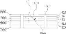
도 1 및 도 2에 도시된 바와 같이, 본 발명의 3층 유전체 및 4층 그라운드 레이어 구조를 갖는 연성회로기판은 제1유전체(E1), 제2유전체(E2), 제3유전체(E3), 제1그라운드 레이어(400), 제2그라운드 레이어(500), 제3그라운드 레이어(600), 제4그라운드 레이어(700), 비아홀(VH) 및 신호라인(800)을 포함하여 3층의 유전체 구조 및 4층의 그라운드 레이어 구조로 이루어진다.1 and 2, the flexible circuit board having a three-layer dielectric and a four-layer ground layer structure of the present invention includes a first dielectric E1, a second dielectric E2, a third dielectric E3, A three-layer dielectric structure including a
3층 유전체 구조는 제1유전체(E1)와, 제1유전체(E1)와 평행하고, 제1유전체(E1)의 평면과 마주보며, 제1유전체(E1) 평면과 일정 간격 이격되어 위치하는 제2유전체(E2)와, 제1유전체(E1)와 평행하고, 제1유전체(E1)의 저면과 마주보며, 제1유전체(E1) 저면과 일정 간격 이격되어 위치하는 제3유전체(E3)로 이루어진다.The three-layer dielectric structure has a first dielectric (E1), a first dielectric (E1) parallel to the first dielectric (E1), facing the plane of the first dielectric (E1), and a first dielectric (E1) spaced apart from the first dielectric (E1) plane by a predetermined distance 2nd dielectric (E2), parallel to the first dielectric (E1), facing the bottom of the first dielectric (E1), and a third dielectric (E3) located at a predetermined distance from the bottom of the first dielectric (E1) is done
4층 그라운드 레이어 구조는 제1유전체(E1) 평면 상에 적층된 제1그라운드 레이어(400)와, 제1유전체(E1) 저면 상에 적층된 제2그라운드 레이어(500), 제2유전체(E2) 상에 적층된 제3그라운드 레이어(600) 및 제3유전체(E3) 저면 상에 적층된 제4그라운드 레이어(700)로 이루어진다.The four-layer ground layer structure includes a
제1그라운드 레이어(400)와 제2유전체(E2) 저면은 제1본딩시트(B1)를 매개로 접착되고, 제2그라운드 레이어(500)와 제3유전체(E3) 평면은 제2본딩시트(B2)를 매개로 접착된다.The bottom surface of the
또한, 본 발명의 3층 유전체 및 4층 그라운드 레이어 구조를 갖는 연성회로기판은 제1그라운드 레이어(400) 내지 상기 제4그라운드 레이어(700)가 도통할 수 있도록 제1유전체(E1) 내지 제3유전체(E3) 및 제1그라운드 레이어(400) 내지 제4그라운드 레이어(700), 제1본딩시트(B1) 및 제2본딩시트(B2)를 관통하는 홀에 전도체가 충진된 비아홀(VH)을 포함한다.In addition, in the flexible circuit board having a three-layer dielectric and four-layer ground layer structure according to the present invention, the first dielectrics E1 to third A via hole (VH) in which a conductor is filled in a hole passing through the dielectric (E3), the first ground layer (400) to the fourth ground layer (700), the first bonding sheet (B1), and the second bonding sheet (B2) is formed. include
제1유전체(E1) 상에는 신호라인(800)이 설치되고, 제1본딩시트(B1)는 신호라인(800)을 사이에 두고 한 쌍이 일정 간격 이격되어 위치하여, 제2유전체(E2) 및 제1본딩시트(B1)로 구획되는 내부공간을 형성할 수 있는바, 신호라인(800)은 이러한 내부공간에 위치하는 것이 바람직하다. 즉, 신호라인(800)이 내부공간에 위치하여 유전율(ε=1.0005)이 낮은 공기층에 노출되는바, 신호라인(800)에서 발생하는 선로 손실이 저감된다. 상술한 바와 같이, 제1본딩시트(B1) 형상은 양단으로부터 이물질이 유입되는 것을 방지하기 위해 "ㅁ' 형상인 것이 바람직하다.A
제3그라운드 레이어(600)에는 복수 개의 그라운드 홀(GH)이 서로 일정 간격 이격되어 형성되는 것이 바람직하고, 제2그라운드 레이어(500)와 제4그라운드 레이어(700) 사이의 간격은 제1그라운드 레이어(400)와 제3그라운드 레이어(600) 사이의 간격보다 큰 것이 바람직하다.Preferably, a plurality of ground holes GH are formed to be spaced apart from each other by a predetermined distance in the
본 발명에서는 제4그라운드 레이어(700)를 이용하여 외부신호가 유입되는 것을 방지함과 동시에, 제4그라운드 레이어(700) 및 복수 개의 그라운드 홀(GH)이 형성된 제3그라운드 레이어(600)를 이용하여 약 50Ω에 맞추어져 있는 신호선로(800)의 특성 임피던스를 충족시킬 수 있으며, 선로 손실을 저감하고, 연성회로기판을 박형화할 수 있었다.In the present invention, the
제2그라운드 레이어(500)와 제4그라운드 레이어(700) 사이의 간격과, 제1그라운드 레이어(400)와 제3그라운드 레이어(600) 사이의 간격은 제2유전체(E2) 및 제3유전체(E3)의 두께를 조절함으로써 조절 가능한데, 제3유전체(E3)의 두께는 제2유전체(E2) 두께보다 1.5배 이상으로 형성하는 것이 바람직하다.The gap between the
제3유전체(E3)의 두께를 두껍게 형성하게 되면, 신호선로(800)의 두께를 더 두껍게 형성할 수 있게 되는바, 선로 손실을 저감할 수 있게 된다.When the thickness of the third dielectric E3 is formed to be thick, the thickness of the
또한, 제3그라운드 레이어(600)에 그라운드 홀(GH)을 형성함으로써 제2유전체(E2)의 두께를 얇게 형성할 수 있게 되는바, 연성회로기판을 박형화할 수 있게 된다.
In addition, by forming the ground hole GH in the
한편, 도 3 내지 도 5에 도시된 바와 같이, 본 발명의 3층 유전체 및 4층 그라운드 레이어 구조를 갖는 연성회로기판은 제1기판부(100), 제2기판부(200) 및 제3기판부(300)를 포함할 수 있다.Meanwhile, as shown in FIGS. 3 to 5 , the flexible circuit board having a three-layer dielectric and four-layer ground layer structure according to the present invention includes a
제1기판부(100), 제2기판부(200) 및 제3기판부(300)의 두께는 순차적으로 감소한다.The thicknesses of the
제2기판부(200)는 제1기판부(100) 일측에서 연장 형성되어 제1기판부(100)의 두께보다 얇게 형성되고, 제3기판부(300)는 제2기판부(200) 일측에서 연장 형성되어 제2기판부(200) 두께보다 얇게 형성된다.The
제3기판부(300)는 무선단말기기에서 벤딩이 반복적으로 일어나는 구간에 해당된다. 제1기판부(100)에서 제3기판부(300)를 바로 연장 형성하는 경우 급작스러운 두께 변화로 인하여 제1기판부(100)와 제3기판부(300)의 연결 부위에 응력이 집중되어 파손 가능성이 증가되므로, 본 발명자는 "순차적 두께 변화"라는 기술사상을 도입하였다. 즉, 제1기판부(100)의 두께보다 얇으면서 제3기판부(300)의 두께보다는 두꺼운 제2기판부(200)를 매개로 제1기판부(100)와 제3기판부(300)를 연결한 것이다.The
제2기판부(200)는 제1기판부(100)를 구성하는 제3그라운드 레이어(600) 및 제4그라운드 레이어(700) 중 어느 하나 이상이 생략되어 형성될 수 있다.The
즉, 제2기판부(200)는 제1유전체(E1), 제2유전체(E2), 제3유전체(E3), 제1그라운드 레이어(400), 제2그라운드 레이어(500)를 구비하고, 제3그라운드 레이어(600) 및 제4그라운드 레이어(700)를 선택적으로 적용하거나, 미적용함으로써 제1기판부(100)보다 그 두께를 얇게 형성한 것이다.That is, the
제3기판부(300)는 제1기판부(100)에서 제2유전체(E2), 제3유전체(E3), 제3그라운드 레이어(600), 제4그라운드 레이어(700) 중에서 선택된 어느 두 개 이상을 생략하여 제2기판부(200)보다 그 두께를 얇게 형성한 것이다.The
이와 같이, 제1기판부(100), 제2기판부(200), 제3기판부(300)의 두께가 순차적으로 얇아짐에 따라 급작스러운 두께 변화에 따른 특정 부분에서의 응력 집중을 방지함으로써 연성회로기판의 절곡 내구성이 개선되는 것이다.As described above, as the thicknesses of the
본 발명의 3층 유전체 및 4층 그라운드 레이어 구조를 갖는 연성회로기판은 제1보호시트(C1) 및 제2보호시트(C2)를 포함한다. 제1보호시트(C1) 및 제2보호시트(C2)는 폴리 이미드 등 폴리계열 또는 에폭시 계열의 수지로 제1유전체(E1)와 제2유전체(E2), 제1유전체(E1)와 제3유전체(E3) 사이에 각각 개재되며, 제1본딩시트(B1) 및 제2본딩시트(B2)와 각각 연결되거나 겹치도록 위치한다.The flexible printed circuit board having a three-layer dielectric and four-layer ground layer structure according to the present invention includes a first protective sheet C1 and a second protective sheet C2. The first protective sheet (C1) and the second protective sheet (C2) are poly- or epoxy-based resins such as polyimide, and the first dielectric (E1) and the second dielectric (E2), the first dielectric (E1) and the second dielectric (E1) They are respectively interposed between the three dielectrics E3, and are respectively connected to or overlapped with the first bonding sheet B1 and the second bonding sheet B2.
제3기판부(300)는 제1유전체(E1)의 평면 상에 위치하는 제2유전체(E2), 제1유전체(E1) 저면 상에 위치하는 제3유전체(E3)를 칼날, 레이저 등으로 커팅하여 제조되는바, 제1보호시트(C1)는 제1본딩시트(B1) 일단에 연결되거나 겹치도록 제2유전체(E2) 및 상기 제1그라운드 레이어(400) 사이에 개재되고, 그 타단은 제2유전체(E2) 일단보다 신호라인 방향으로 더 돌출되어 형성된다. 제2보호시트(C2)는 제2본딩시트(B2) 일단에 연결되거나 겹치도록 제3유전체(E3) 및 제2그라운드 레이어(500) 사이에 개재되고, 그 타단은 제3유전체(E3) 일단보다 신호라인 방향으로 더 돌출되어 형성됨으로써, 제1보호시트(C1) 및 제2보호시트(C2) 커팅에 이용되는 칼날, 레이저 등으로부터 신호라인(800), 제1그라운드 레이어(400), 제2그라운드 레이어(500)를 보호하므로, 커팅 시 신호라인(800), 제1그라운드 레이어(400), 제2그라운드 레이어(500)가 손상되는 것을 방지하고, 불필요한 탄화물 생성을 방지한다.The
제1보호시트(C1)는 제2유전체(E2) 및 제1그라운드 레이어(400) 사이에서 고정되도록 저면에는 열경화접착제를 도포하고, 평면에는 제2유전체(E2)가 커팅되어 외부로 노출되는 면을 제외한 면에만 열경화접착제를 도포하거나 열경화접착제를 도포하지 않고 제1본딩시트(B1)를 연장하여 제1보호시트(C1)와 겹치도록 할 수 있다.A thermosetting adhesive is applied to the bottom surface of the first protective sheet C1 to be fixed between the second dielectric E2 and the
제2보호시트(C2)는 제3유전체(E3) 및 제2그라운드 레이어(500) 사이에서 고정되도록 평면에는 열경화접착제를 도포하고, 저면에는 제3유전체(E3)가 커팅되어 외부로 노출되는 면을 제외한 면에만 열경화접착제를 도포하거나 열경화접착제를 도포하지 않고 제2본딩시트(B2)를 연장하여 제2보호시트(C2)와 겹치도록 할 수 있다.A thermosetting adhesive is applied to the second protective sheet C2 to be fixed between the third dielectric E3 and the
한편, 제1본딩시트(B1)는 신호라인(800)을 사이에 두고 한 쌍이 서로 일정 간격 이격되어 위치하여 제1유전체(E1), 제2유전체(E2) 및 제1본딩시트(B1)로 구획되는 내부공간을 형성하는바, 이를 위해 제1본딩시트(B1)에는 내부공간 형성홈(H)이 마련된다.
On the other hand, the first bonding sheet (B1) is positioned with a predetermined distance from each other with the
이하에서는 상술한 제3기판부(300)의 다양한 실시예에 대하여 설명한다.Hereinafter, various embodiments of the above-described
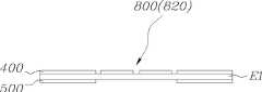
도 6은 본 발명의 일요부인 제3기판부(300)의 제1실시예를 나타낸 도면이다.6 is a view showing a first embodiment of the
도 6에 도시된 바와 같이, 제3기판부(300)는 제1유전체(E1)와, 제1유전체(E1) 상에 적층된 신호라인(800)과, 제1유전체(E1) 상에 적층되되, 신호라인(800)을 사이에 두고 일정 간격 이격된 한 쌍의 제1그라운드 레이어(400)와, 제1유전체(E1) 저면에 적층되되, 일정 간격 이격된 한 쌍의 제2그라운드 레이어(500)를 포함할 수 있고, 신호라인(800)은 제1신호라인(810)과, 제1신호라인(810)에서 분기되며 서로 평행한 한 쌍의 제2신호라인(820)을 포함할 수 있다.As shown in FIG. 6 , the
도 7은 본 발명의 제3기판부(300)의 제2실시예를 나타낸 도면이다.7 is a view showing a second embodiment of the
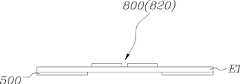
도 7에 도시된 바와 같이, 제3기판부(300)는 제1유전체(E1)와, 제1유전체(E1) 상에 적층된 신호라인(800)과, 제1유전체(E1) 저면에 적층되되, 일정 간격 이격된 한 쌍의 제2그라운드 레이어(500)를 포함하고, 신호라인(800)은 제1신호라인(810) 및 제1신호라인(810)에서 분기되어 서로 평행하게 위치하는 한 쌍의 제2신호라인(820)을 포함할 수 있다.As shown in FIG. 7 , the
도 8은 본 발명의 제3기판부(300)의 제3실시예를 나타낸 도면이다.8 is a view showing a third embodiment of the
도 8에 도시된 바와 같이, 제3기판부(300)는 제1유전체(E1)와, 제1유전체(E1) 상에 적층된 신호라인(800)과, 제1유전체(E1) 상에 적층되되, 신호라인(800)을 사이에 두고 일정 간격 이격된 한 쌍의 제1그라운드 레이어(400)를 포함하고, 신호라인(800)은 제1신호라인(810) 및 제1신호라인(810)에서 분기되어 서로 평행하게 위치하는 한 쌍의 제2신호라인(820)을 포함할 수 있다.As shown in FIG. 8 , the
도 9에 도시된 바와 같이, 본 발명의 제3기판부(300)의 제1실시예 및 제3실시예의 경우, 제2신호라인(820) 외측과 제1그라운드 레이어(400) 내측 사이의 간격은 제1신호라인(810)의 일측과 제1그라운드 레이어(400) 내측 사이의 간격보다 좁게 형성할 수 있다.As shown in FIG. 9 , in the case of the first and third embodiments of the
도 10은 본 발명의 제3기판부(300)의 제4실시예 및 제5실시예를 나타낸 도면이고, 도 11은 본 발명의 제3기판부(300)의 제4실시예의 제2그라운드 레이어(500)를 나타낸 도면이다.10 is a view showing a fourth embodiment and a fifth embodiment of the
도 10 및 도 11에 도시된 바와 같이, 본 발명의 제3기판부(300)의 제4실시예는 제1유전체(E1)와, 제1유전체(E1) 상에 적층된 신호라인(800)과, 제1유전체(E1) 상에 적층되되, 신호라인(800)을 사이에 두고 일정 간격 이격된 한 쌍의 제1그라운드 레이어(400)와, 제1유전체(E1) 저면에 적층된 제2그라운드 레이어(500)를 포함하고, 제2그라운드 레이어(500)는, 신호라인(800)을 사이에 두고 일정 간격 이격되어 적층된 한 쌍의 라인 그라운드(510)와, 한 쌍의 라인 그라운드(510)를 연결하는 메쉬 그라운드(520)를 포함할 수도 있다.10 and 11, the fourth embodiment of the
한편, 본 발명의 제3기판부(300)의 제5실시예는 제2그라운드 레이어(500)를 실버 페이스트로 형성한 것이다.Meanwhile, in the fifth embodiment of the
이상 본 발명을 구체적인 실시예를 통하여 상세히 설명하였으나, 이는 본 발명을 구체적으로 설명하기 위한 것으로, 본 발명에 따른 연성회로기판에 한정되지 않으며, 본 발명의 기술적 사상 내에서 당해 분야의 통상의 지식을 가진 자에 의해 그 변형이나 개량이 가능함은 명백하다고 할 것이다.Although the present invention has been described in detail through specific examples, this is for describing the present invention in detail, and is not limited to the flexible circuit board according to the present invention, and common knowledge in the field is provided within the technical spirit of the present invention. It will be clear that the transformation or improvement is possible by those who have it.
본 발명의 단순한 변형 내지 변경은 모두 본 발명의 영역에 속하는 것으로 본 발명의 구체적인 보호 범위는 첨부된 특허청구범위에 의하여 명확해질 것이다.All simple modifications or changes of the present invention fall within the scope of the present invention, and the specific scope of protection of the present invention will be made clear by the appended claims.
100 : 제1기판부200 : 제2기판부
300 : 제3기판부400 : 제1그라운드 레이어
500 : 제2그라운드 레이어510 : 라인 그라운드
520 : 메쉬 그라운드600 : 제3그라운드 레이어
700 : 제4그라운드 레이어800 : 신호라인
810 : 제1신호라인820 : 제2신호라인
B1 : 제1본딩시트B2 : 제2본딩시트
C1 : 제1보호시트C2 : 제2보호시트
E1 : 제1유전체E2 : 제2유전체
E3 : 제3유전체H : 내부공간 형성홈
GH : 그라운드 홀VH : 비아홀100: first substrate unit 200: second substrate unit
300: third substrate unit 400: first ground layer
500: second ground layer 510: line ground
520: mesh ground 600: third ground layer
700: fourth ground layer 800: signal line
810: first signal line 820: second signal line
B1: first bonding sheet B2: second bonding sheet
C1: first protective sheet C2: second protective sheet
E1: first dielectric E2: second dielectric
E3: third dielectric H: groove for forming internal space
GH : Ground hole VH : Via hole
Claims (10)
Translated fromKorean상기 제1유전체의 평면과 마주보며 이격되어 제공되는 제2유전체;
상기 제1유전체 저면과 마주보며 이격되어 제공되는 제3유전체;
상기 제1유전체 상에 형성된 신호라인;
상기 신호라인을 사이에 두고 상기 제1유전체 평면에 적층되는 한 쌍의 제1그라운드 레이어;
상기 제1그라운드 레이어와 대응될 수 있도록 상기 제1그라운드 레이어 저면에 적층된 제2그라운드 레이어;
상기 제2유전체 상에 적층된 제3그라운드 레이어; 및
상기 제3유전체 저면에 적층된 제4그라운드 레이어를 포함하는, 3층 유전체 및 4층 그라운드 레이어 구조를 갖는 연성회로기판.
a first dielectric;
a second dielectric provided to face the plane of the first dielectric and spaced apart;
a third dielectric provided to face the bottom of the first dielectric and spaced apart;
a signal line formed on the first dielectric;
a pair of first ground layers stacked on the first dielectric plane with the signal line interposed therebetween;
a second ground layer stacked on a bottom surface of the first ground layer to correspond to the first ground layer;
a third ground layer stacked on the second dielectric; and
A flexible circuit board having a three-layer dielectric and a four-layered ground layer structure, including a fourth ground layer stacked on a bottom surface of the third dielectric.
상기 제3그라운드 레이어에는 그라운드 홀이 상기 신호라인의 길이 방향으로 일정 간격 이격되어 복수 개 형성되고,
상기 제4그라운드 레이어는 상기 제3유전체와 대응되는 형상으로 면 접착된 것을 특징으로 하는, 3층 유전체 및 4층 그라운드 레이어 구조를 갖는 연성회로기판.
The method according to claim 1,
A plurality of ground holes are formed in the third ground layer at regular intervals in the length direction of the signal line,
The flexible circuit board having a three-layer dielectric and a four-layer ground layer structure, wherein the fourth ground layer is surface-bonded in a shape corresponding to the third dielectric.
상기 제3유전체는 상기 제2유전체보다 더 두꺼운 것을 특징으로 하는, 3층 유전체 및 4층 그라운드 레이어 구조를 갖는 연성회로기판.
3. The method according to claim 2,
The third dielectric is thicker than the second dielectric, the flexible circuit board having a three-layer dielectric and a four-layer ground layer structure.
상기 제1그라운드 레이어와 상기 제2유전체는 제1본딩시트를 매개로 접착되고, 상기 제2그라운드 레이어와 상기 제3유전체는 제2본딩시트를 매개로 접착된 것을 특징으로 하는, 3층 유전체 및 4층 그라운드 레이어 구조를 갖는 연성회로기판.
4. The method of claim 3,
wherein the first ground layer and the second dielectric are bonded through a first bonding sheet, and the second ground layer and the third dielectric are bonded through a second bonding sheet. A flexible circuit board having a four-layer ground layer structure.
상기 제1본딩시트는 상기 신호라인을 사이에 두고 한 쌍이 설치되어 상기 한 쌍의 제1그라운드 레이어와 상기 제2유전체를 매개함으로써, 상기 제2유전체, 상기 제1본딩시트, 상기 제1그라운드 레이어, 상기 제1유전체로 구획되는 내부 공간을 형성하는 것을 특징으로 하는, 3층 유전체 및 4층 그라운드 레이어 구조를 갖는 연성회로기판.
5. The method according to claim 4,
A pair of the first bonding sheet is provided with the signal line interposed therebetween to interpose the pair of first ground layer and the second dielectric, so that the second dielectric, the first bonding sheet, and the first ground layer are interposed. , a flexible circuit board having a three-layer dielectric and a four-layer ground layer structure, characterized in that it forms an internal space partitioned by the first dielectric.
상기 제1유전체와, 상기 제2유전체와, 상기 제3유전체와, 상기 신호라인과, 상기 제1그라운드 레이어와, 상기 제2그라운드 레이어와, 상기 제3그라운드 레이어와, 상기 제4그라운드 레이어를 포함하는 제1기판부;
상기 제1기판부에서 연장 형성된 제2유전체와, 상기 신호라인과, 상기 제1그라운드 레이어와, 상기 제1유전체와, 상기 제2그라운드 레이어와, 상기 제3유전체를 포함하는, 제2기판부; 및
상기 제2기판부에서 연장 형성된 제1그라운드 레이어와, 상기 신호라인과, 상기 제1유전체와, 상기 제2그라운드 레이어를 포함하는 제3기판부를 포함하는, 3층 유전체 및 4층 그라운드 레이어 구조를 갖는 연성회로기판.
The method according to claim 1,
the first dielectric, the second dielectric, the third dielectric, the signal line, the first ground layer, the second ground layer, the third ground layer, and the fourth ground layer. a first substrate including;
a second substrate portion including a second dielectric extending from the first substrate portion, the signal line, the first ground layer, the first dielectric, the second ground layer, and the third dielectric ; and
a three-layer dielectric and four-layered ground layer structure including a first ground layer extending from the second substrate portion, a third substrate portion including the signal line, the first dielectric, and the second ground layer; with a flexible circuit board.
상기 신호라인은 제1신호라인 및 상기 제1신호라인에서 분기되어 서로 평행하게 위치하는 한 쌍의 제2신호라인을 포함하는, 3층 유전체 및 4층 그라운드 레이어 구조를 갖는 연성회로기판.
7. The method of claim 6,
wherein the signal line includes a first signal line and a pair of second signal lines branched from the first signal line and positioned parallel to each other.
상기 제1유전체와, 상기 제2유전체와, 상기 제3유전체와, 상기 신호라인과, 상기 제1그라운드 레이어와, 상기 제2그라운드 레이어와, 상기 제3그라운드 레이어와, 상기 제4그라운드 레이어를 포함하는 제1기판부;
상기 제1기판부에서 연장 형성된 제2유전체와, 상기 신호라인과, 상기 제1그라운드 레이어와, 상기 제1유전체와, 상기 제2그라운드 레이어와, 상기 제3유전체를 포함하는, 제2기판부; 및
상기 제2기판부에서 연장 형성된 상기 신호라인과, 상기 제1유전체와, 상기 제2그라운드 레이어를 포함하는 제3기판부를 포함하고,
상기 신호라인은 제1신호라인 및 상기 제1신호라인에서 분기되어 서로 평행하게 위치하는 한 쌍의 제2신호라인을 포함하는, 3층 유전체 및 4층 그라운드 레이어 구조를 갖는 연성회로기판.
The method according to claim 1,
the first dielectric, the second dielectric, the third dielectric, the signal line, the first ground layer, the second ground layer, the third ground layer, and the fourth ground layer. a first substrate including;
a second substrate portion including a second dielectric extending from the first substrate portion, the signal line, the first ground layer, the first dielectric, the second ground layer, and the third dielectric ; and
a third substrate portion including the signal line extending from the second substrate portion, the first dielectric, and the second ground layer;
wherein the signal line includes a first signal line and a pair of second signal lines branched from the first signal line and positioned parallel to each other.
상기 제1유전체와, 상기 제2유전체와, 상기 제3유전체와, 상기 신호라인과, 상기 제1그라운드 레이어와, 상기 제2그라운드 레이어와, 상기 제3그라운드 레이어와, 상기 제4그라운드 레이어를 포함하는 제1기판부;
상기 제1기판부에서 연장 형성된 제2유전체와, 상기 신호라인과, 상기 제1그라운드 레이어와, 상기 제1유전체와, 상기 제2그라운드 레이어와, 상기 제3유전체를 포함하는, 제2기판부; 및
상기 제2기판부에서 연장 형성된 상기 신호라인과, 상기 제1유전체와, 상기 제1그라운드 레이어를 포함하는 제3기판부를 포함하고,
상기 신호라인은 제1신호라인 및 상기 제1신호라인에서 분기되어 서로 평행하게 위치하는 한 쌍의 제2신호라인을 포함하는, 3층 유전체 및 4층 그라운드 레이어 구조를 갖는 연성회로기판.
The method according to claim 1,
the first dielectric, the second dielectric, the third dielectric, the signal line, the first ground layer, the second ground layer, the third ground layer, and the fourth ground layer. a first substrate including;
a second substrate portion including a second dielectric extending from the first substrate portion, the signal line, the first ground layer, the first dielectric, the second ground layer, and the third dielectric ; and
a third substrate including the signal line extending from the second substrate, the first dielectric, and the first ground layer;
wherein the signal line includes a first signal line and a pair of second signal lines branched from the first signal line and positioned parallel to each other.
상기 제2신호라인과 상기 제1그라운드 레이어 사이에 형성된 간격은 상기 제1신호라인과 상기 제1그라운드 레이어 사이에 형성된 간격보다 작은 것을 특징으로 하는, 3층 유전체 및 4층 그라운드 레이어 구조를 갖는 연성회로기판.
10. The method according to claim 7 or 9,
A flexible structure having a three-layer dielectric and four-layer ground layer structure, characterized in that the gap formed between the second signal line and the first ground layer is smaller than the gap formed between the first signal line and the first ground layer. circuit board.
Priority Applications (4)
| Application Number | Priority Date | Filing Date | Title |
|---|---|---|---|
| KR1020150135435AKR102442838B1 (en) | 2015-09-24 | 2015-09-24 | Flexible printed circuit board having three dielectric substance layer and four ground layer |
| PCT/KR2016/010673WO2017052274A1 (en) | 2015-09-24 | 2016-09-23 | Flexible circuit board having three-layer dielectric body and four-layer ground layer structure |
| CN201680054578.2ACN108029191B (en) | 2015-09-24 | 2016-09-23 | Flexible circuit board with three-layer dielectric and four-layer ground plane structure |
| US15/923,048US10362675B2 (en) | 2015-09-24 | 2018-03-16 | Flexible circuit board having three-layer dielectric body and four-layer ground layer structure |
Applications Claiming Priority (1)
| Application Number | Priority Date | Filing Date | Title |
|---|---|---|---|
| KR1020150135435AKR102442838B1 (en) | 2015-09-24 | 2015-09-24 | Flexible printed circuit board having three dielectric substance layer and four ground layer |
Publications (2)
| Publication Number | Publication Date |
|---|---|
| KR20170036364A KR20170036364A (en) | 2017-04-03 |
| KR102442838B1true KR102442838B1 (en) | 2022-09-15 |
Family
ID=58386621
Family Applications (1)
| Application Number | Title | Priority Date | Filing Date |
|---|---|---|---|
| KR1020150135435AActiveKR102442838B1 (en) | 2015-09-24 | 2015-09-24 | Flexible printed circuit board having three dielectric substance layer and four ground layer |
Country Status (4)
| Country | Link |
|---|---|
| US (1) | US10362675B2 (en) |
| KR (1) | KR102442838B1 (en) |
| CN (1) | CN108029191B (en) |
| WO (1) | WO2017052274A1 (en) |
Families Citing this family (10)
| Publication number | Priority date | Publication date | Assignee | Title |
|---|---|---|---|---|
| KR102622767B1 (en)* | 2016-02-11 | 2024-01-09 | 주식회사 기가레인 | Flexible printed circuit board |
| KR102552614B1 (en)* | 2016-02-26 | 2023-07-06 | 주식회사 기가레인 | Flexible printed circuit board |
| EP3383146B8 (en)* | 2017-03-31 | 2023-08-30 | Inventronics GmbH | Lighting device with ip protection and multidirectional bending capability, and method for manufacturing the same |
| KR101824644B1 (en)* | 2017-05-08 | 2018-02-01 | 주식회사 기가레인 | Flexible printed circuit board with narrower width and manufacturing method thereof |
| KR101938106B1 (en)* | 2018-01-25 | 2019-01-14 | 주식회사 기가레인 | Flexible printed circuit board with narrower |
| KR101938105B1 (en)* | 2018-01-25 | 2019-01-14 | 주식회사 기가레인 | Flexible circuit board with improved bonding position accuracy |
| KR102575550B1 (en)* | 2018-08-20 | 2023-09-07 | 삼성전자주식회사 | Printed circuit board including bending portion, and electronic device with the same |
| KR102059279B1 (en)* | 2018-12-19 | 2019-12-24 | 주식회사 기가레인 | Flexible circuit board including bending portion with improved shielding property and manufacturing method thereof |
| KR102831948B1 (en)* | 2019-04-12 | 2025-07-09 | 주식회사 기가레인 | A flexible circuit board on which a vertical section and a horizontal section are formed |
| KR102611072B1 (en)* | 2019-10-10 | 2023-12-07 | 엘지전자 주식회사 | Dual antenna |
Citations (6)
| Publication number | Priority date | Publication date | Assignee | Title |
|---|---|---|---|---|
| WO1996038026A1 (en) | 1995-05-22 | 1996-11-28 | Dynaco Corporation | Rigid-flex printed circuit boards |
| JP2002093526A (en) | 2000-09-11 | 2002-03-29 | Yazaki Corp | Flexible conductor and its connector |
| US20090133906A1 (en) | 2007-11-27 | 2009-05-28 | Baek Jae Myung | Flexible printed circuit board and manufacturing method thereof |
| US20140017940A1 (en) | 2012-07-11 | 2014-01-16 | Tyco Electronics Corporation | Layered connector and method of manufacturing a layered connector |
| US20140102763A1 (en)* | 2012-10-16 | 2014-04-17 | Advanced Flexible Circuits Co., Ltd. | Rigid flexible circuit board with impedance control |
| JP2014082455A (en) | 2012-09-27 | 2014-05-08 | Mitsubishi Electric Corp | Flexible board and board connection structure |
Family Cites Families (13)
| Publication number | Priority date | Publication date | Assignee | Title |
|---|---|---|---|---|
| US5024896A (en)* | 1989-07-06 | 1991-06-18 | International Business Machines Corporation | Collimated metal deposition |
| US5262594A (en)* | 1990-10-12 | 1993-11-16 | Compaq Computer Corporation | Multilayer rigid-flex printed circuit boards for use in infrared reflow oven and method for assembling same |
| US5418504A (en)* | 1993-12-09 | 1995-05-23 | Nottenburg; Richard N. | Transmission line |
| US5499444A (en)* | 1994-08-02 | 1996-03-19 | Coesen, Inc. | Method of manufacturing a rigid flex printed circuit board |
| FI106585B (en)* | 1997-10-22 | 2001-02-28 | Nokia Mobile Phones Ltd | Coaxial line, method of manufacturing a coaxial line and wireless telephony |
| US5982249A (en)* | 1998-03-18 | 1999-11-09 | Tektronix, Inc. | Reduced crosstalk microstrip transmission-line |
| US6590466B2 (en)* | 1998-08-31 | 2003-07-08 | Advanced Flexible Circuit Co., Ltd. | Circuit board having shielding planes with varied void opening patterns for controlling the impedance and the transmission time of differential transmission lines |
| US6535088B1 (en)* | 2000-04-13 | 2003-03-18 | Raytheon Company | Suspended transmission line and method |
| KR100958268B1 (en)* | 2008-02-15 | 2010-05-19 | (주)기가레인 | Printed circuit board to widen signal transmission line without impedance mismatch |
| KR101065279B1 (en)* | 2008-04-04 | 2011-09-16 | (주)기가레인 | Printed circuit board having a slot pattern formed in the signal transmission line |
| WO2012073591A1 (en) | 2010-12-03 | 2012-06-07 | 株式会社村田製作所 | High-frequency signal line |
| JP5477422B2 (en)* | 2012-01-06 | 2014-04-23 | 株式会社村田製作所 | High frequency signal line |
| US8912581B2 (en)* | 2012-03-09 | 2014-12-16 | Taiwan Semiconductor Manufacturing Co., Ltd. | 3D transmission lines for semiconductors |
- 2015
- 2015-09-24KRKR1020150135435Apatent/KR102442838B1/enactiveActive
- 2016
- 2016-09-23WOPCT/KR2016/010673patent/WO2017052274A1/ennot_activeCeased
- 2016-09-23CNCN201680054578.2Apatent/CN108029191B/enactiveActive
- 2018
- 2018-03-16USUS15/923,048patent/US10362675B2/enactiveActive
Patent Citations (6)
| Publication number | Priority date | Publication date | Assignee | Title |
|---|---|---|---|---|
| WO1996038026A1 (en) | 1995-05-22 | 1996-11-28 | Dynaco Corporation | Rigid-flex printed circuit boards |
| JP2002093526A (en) | 2000-09-11 | 2002-03-29 | Yazaki Corp | Flexible conductor and its connector |
| US20090133906A1 (en) | 2007-11-27 | 2009-05-28 | Baek Jae Myung | Flexible printed circuit board and manufacturing method thereof |
| US20140017940A1 (en) | 2012-07-11 | 2014-01-16 | Tyco Electronics Corporation | Layered connector and method of manufacturing a layered connector |
| JP2014082455A (en) | 2012-09-27 | 2014-05-08 | Mitsubishi Electric Corp | Flexible board and board connection structure |
| US20140102763A1 (en)* | 2012-10-16 | 2014-04-17 | Advanced Flexible Circuits Co., Ltd. | Rigid flexible circuit board with impedance control |
Also Published As
| Publication number | Publication date |
|---|---|
| WO2017052274A1 (en) | 2017-03-30 |
| US20180206332A1 (en) | 2018-07-19 |
| KR20170036364A (en) | 2017-04-03 |
| US10362675B2 (en) | 2019-07-23 |
| CN108029191A (en) | 2018-05-11 |
| CN108029191B (en) | 2020-06-16 |
Similar Documents
| Publication | Publication Date | Title |
|---|---|---|
| KR102442838B1 (en) | Flexible printed circuit board having three dielectric substance layer and four ground layer | |
| KR102497358B1 (en) | Flexible printed circuit board having improved bending durabiliy | |
| KR102432541B1 (en) | Flexible printed circuit board having improved bending durabiliy and manufacturing method thereof | |
| US10424432B2 (en) | Inductor bridge and electronic device | |
| TWI632731B (en) | Antenna substrate | |
| US20150364823A1 (en) | Antenna device and wireless device | |
| JP5696819B2 (en) | Transmission line and electronic equipment | |
| KR102234067B1 (en) | Antenna integrated Flexible printed circuit board | |
| WO2016121629A1 (en) | High frequency module | |
| JP5673898B2 (en) | High frequency signal line and electronic device equipped with the same | |
| KR20170094702A (en) | Flexible printed circuit board | |
| WO2018135475A1 (en) | Transmission line | |
| US20160205768A1 (en) | Printed board and method for mounting on printed board | |
| US9935601B2 (en) | LC parallel resonant element | |
| KR20160125307A (en) | Antenna substrate | |
| TWI616024B (en) | Antenna substrate | |
| WO2018150926A1 (en) | Multilayer board | |
| US8847699B2 (en) | Composite component | |
| KR102455653B1 (en) | High frequency transmission line | |
| KR102364151B1 (en) | Flexible printed circuit board | |
| JP5929557B2 (en) | Flat cable |
Legal Events
| Date | Code | Title | Description |
|---|---|---|---|
| PA0109 | Patent application | Patent event code:PA01091R01D Comment text:Patent Application Patent event date:20150924 | |
| PG1501 | Laying open of application | ||
| A201 | Request for examination | ||
| PA0201 | Request for examination | Patent event code:PA02012R01D Patent event date:20200810 Comment text:Request for Examination of Application Patent event code:PA02011R01I Patent event date:20150924 Comment text:Patent Application | |
| E902 | Notification of reason for refusal | ||
| PE0902 | Notice of grounds for rejection | Comment text:Notification of reason for refusal Patent event date:20211207 Patent event code:PE09021S01D | |
| E701 | Decision to grant or registration of patent right | ||
| PE0701 | Decision of registration | Patent event code:PE07011S01D Comment text:Decision to Grant Registration Patent event date:20220621 | |
| PR0701 | Registration of establishment | Comment text:Registration of Establishment Patent event date:20220907 Patent event code:PR07011E01D | |
| PR1002 | Payment of registration fee | Payment date:20220908 End annual number:3 Start annual number:1 | |
| PG1601 | Publication of registration | ||
| PR1001 | Payment of annual fee | Payment date:20250610 Start annual number:4 End annual number:4 |