KR102440078B1 - Polarizing plate and display device including same - Google Patents
Polarizing plate and display device including sameDownload PDFInfo
- Publication number
- KR102440078B1 KR102440078B1KR1020150033329AKR20150033329AKR102440078B1KR 102440078 B1KR102440078 B1KR 102440078B1KR 1020150033329 AKR1020150033329 AKR 1020150033329AKR 20150033329 AKR20150033329 AKR 20150033329AKR 102440078 B1KR102440078 B1KR 102440078B1
- Authority
- KR
- South Korea
- Prior art keywords
- layer
- disposed
- refractive index
- polarizing plate
- retarder
- Prior art date
- Legal status (The legal status is an assumption and is not a legal conclusion. Google has not performed a legal analysis and makes no representation as to the accuracy of the status listed.)
- Active
Links
Images


Classifications
- G—PHYSICS
- G02—OPTICS
- G02B—OPTICAL ELEMENTS, SYSTEMS OR APPARATUS
- G02B5/00—Optical elements other than lenses
- G02B5/30—Polarising elements
- G02B5/3083—Birefringent or phase retarding elements
- G—PHYSICS
- G02—OPTICS
- G02B—OPTICAL ELEMENTS, SYSTEMS OR APPARATUS
- G02B27/00—Optical systems or apparatus not provided for by any of the groups G02B1/00 - G02B26/00, G02B30/00
- G02B27/28—Optical systems or apparatus not provided for by any of the groups G02B1/00 - G02B26/00, G02B30/00 for polarising
- G02B27/286—Optical systems or apparatus not provided for by any of the groups G02B1/00 - G02B26/00, G02B30/00 for polarising for controlling or changing the state of polarisation, e.g. transforming one polarisation state into another
- G—PHYSICS
- G02—OPTICS
- G02B—OPTICAL ELEMENTS, SYSTEMS OR APPARATUS
- G02B5/00—Optical elements other than lenses
- G02B5/30—Polarising elements
- G02B5/3016—Polarising elements involving passive liquid crystal elements
- G—PHYSICS
- G02—OPTICS
- G02B—OPTICAL ELEMENTS, SYSTEMS OR APPARATUS
- G02B5/00—Optical elements other than lenses
- G02B5/30—Polarising elements
- G02B5/3025—Polarisers, i.e. arrangements capable of producing a definite output polarisation state from an unpolarised input state
- G—PHYSICS
- G02—OPTICS
- G02F—OPTICAL DEVICES OR ARRANGEMENTS FOR THE CONTROL OF LIGHT BY MODIFICATION OF THE OPTICAL PROPERTIES OF THE MEDIA OF THE ELEMENTS INVOLVED THEREIN; NON-LINEAR OPTICS; FREQUENCY-CHANGING OF LIGHT; OPTICAL LOGIC ELEMENTS; OPTICAL ANALOGUE/DIGITAL CONVERTERS
- G02F1/00—Devices or arrangements for the control of the intensity, colour, phase, polarisation or direction of light arriving from an independent light source, e.g. switching, gating or modulating; Non-linear optics
- G02F1/01—Devices or arrangements for the control of the intensity, colour, phase, polarisation or direction of light arriving from an independent light source, e.g. switching, gating or modulating; Non-linear optics for the control of the intensity, phase, polarisation or colour
- G02F1/13—Devices or arrangements for the control of the intensity, colour, phase, polarisation or direction of light arriving from an independent light source, e.g. switching, gating or modulating; Non-linear optics for the control of the intensity, phase, polarisation or colour based on liquid crystals, e.g. single liquid crystal display cells
- G02F1/133—Constructional arrangements; Operation of liquid crystal cells; Circuit arrangements
- G02F1/1333—Constructional arrangements; Manufacturing methods
- G02F1/1335—Structural association of cells with optical devices, e.g. polarisers or reflectors
- G02F1/133528—Polarisers
- G—PHYSICS
- G02—OPTICS
- G02F—OPTICAL DEVICES OR ARRANGEMENTS FOR THE CONTROL OF LIGHT BY MODIFICATION OF THE OPTICAL PROPERTIES OF THE MEDIA OF THE ELEMENTS INVOLVED THEREIN; NON-LINEAR OPTICS; FREQUENCY-CHANGING OF LIGHT; OPTICAL LOGIC ELEMENTS; OPTICAL ANALOGUE/DIGITAL CONVERTERS
- G02F1/00—Devices or arrangements for the control of the intensity, colour, phase, polarisation or direction of light arriving from an independent light source, e.g. switching, gating or modulating; Non-linear optics
- G02F1/01—Devices or arrangements for the control of the intensity, colour, phase, polarisation or direction of light arriving from an independent light source, e.g. switching, gating or modulating; Non-linear optics for the control of the intensity, phase, polarisation or colour
- G02F1/13—Devices or arrangements for the control of the intensity, colour, phase, polarisation or direction of light arriving from an independent light source, e.g. switching, gating or modulating; Non-linear optics for the control of the intensity, phase, polarisation or colour based on liquid crystals, e.g. single liquid crystal display cells
- G02F1/133—Constructional arrangements; Operation of liquid crystal cells; Circuit arrangements
- G02F1/1333—Constructional arrangements; Manufacturing methods
- G02F1/1335—Structural association of cells with optical devices, e.g. polarisers or reflectors
- G02F1/13363—Birefringent elements, e.g. for optical compensation
- G02F1/133634—Birefringent elements, e.g. for optical compensation the refractive index Nz perpendicular to the element surface being different from in-plane refractive indices Nx and Ny, e.g. biaxial or with normal optical axis
- H—ELECTRICITY
- H10—SEMICONDUCTOR DEVICES; ELECTRIC SOLID-STATE DEVICES NOT OTHERWISE PROVIDED FOR
- H10K—ORGANIC ELECTRIC SOLID-STATE DEVICES
- H10K50/00—Organic light-emitting devices
- H10K50/80—Constructional details
- H10K50/84—Passivation; Containers; Encapsulations
- H—ELECTRICITY
- H10—SEMICONDUCTOR DEVICES; ELECTRIC SOLID-STATE DEVICES NOT OTHERWISE PROVIDED FOR
- H10K—ORGANIC ELECTRIC SOLID-STATE DEVICES
- H10K50/00—Organic light-emitting devices
- H10K50/80—Constructional details
- H10K50/85—Arrangements for extracting light from the devices
- H10K50/858—Arrangements for extracting light from the devices comprising refractive means, e.g. lenses
- H—ELECTRICITY
- H10—SEMICONDUCTOR DEVICES; ELECTRIC SOLID-STATE DEVICES NOT OTHERWISE PROVIDED FOR
- H10K—ORGANIC ELECTRIC SOLID-STATE DEVICES
- H10K50/00—Organic light-emitting devices
- H10K50/80—Constructional details
- H10K50/86—Arrangements for improving contrast, e.g. preventing reflection of ambient light
- H—ELECTRICITY
- H10—SEMICONDUCTOR DEVICES; ELECTRIC SOLID-STATE DEVICES NOT OTHERWISE PROVIDED FOR
- H10K—ORGANIC ELECTRIC SOLID-STATE DEVICES
- H10K59/00—Integrated devices, or assemblies of multiple devices, comprising at least one organic light-emitting element covered by group H10K50/00
- H10K59/80—Constructional details
- H10K59/875—Arrangements for extracting light from the devices
- H10K59/879—Arrangements for extracting light from the devices comprising refractive means, e.g. lenses
- H—ELECTRICITY
- H10—SEMICONDUCTOR DEVICES; ELECTRIC SOLID-STATE DEVICES NOT OTHERWISE PROVIDED FOR
- H10K—ORGANIC ELECTRIC SOLID-STATE DEVICES
- H10K59/00—Integrated devices, or assemblies of multiple devices, comprising at least one organic light-emitting element covered by group H10K50/00
- H10K59/80—Constructional details
- H10K59/8791—Arrangements for improving contrast, e.g. preventing reflection of ambient light
- H—ELECTRICITY
- H10—SEMICONDUCTOR DEVICES; ELECTRIC SOLID-STATE DEVICES NOT OTHERWISE PROVIDED FOR
- H10K—ORGANIC ELECTRIC SOLID-STATE DEVICES
- H10K85/00—Organic materials used in the body or electrodes of devices covered by this subclass
- H10K85/10—Organic polymers or oligomers
- H10K85/141—Organic polymers or oligomers comprising aliphatic or olefinic chains, e.g. poly N-vinylcarbazol, PVC or PTFE
- H—ELECTRICITY
- H10—SEMICONDUCTOR DEVICES; ELECTRIC SOLID-STATE DEVICES NOT OTHERWISE PROVIDED FOR
- H10K—ORGANIC ELECTRIC SOLID-STATE DEVICES
- H10K85/00—Organic materials used in the body or electrodes of devices covered by this subclass
- H10K85/731—Liquid crystalline materials
- G—PHYSICS
- G02—OPTICS
- G02F—OPTICAL DEVICES OR ARRANGEMENTS FOR THE CONTROL OF LIGHT BY MODIFICATION OF THE OPTICAL PROPERTIES OF THE MEDIA OF THE ELEMENTS INVOLVED THEREIN; NON-LINEAR OPTICS; FREQUENCY-CHANGING OF LIGHT; OPTICAL LOGIC ELEMENTS; OPTICAL ANALOGUE/DIGITAL CONVERTERS
- G02F1/00—Devices or arrangements for the control of the intensity, colour, phase, polarisation or direction of light arriving from an independent light source, e.g. switching, gating or modulating; Non-linear optics
- G02F1/01—Devices or arrangements for the control of the intensity, colour, phase, polarisation or direction of light arriving from an independent light source, e.g. switching, gating or modulating; Non-linear optics for the control of the intensity, phase, polarisation or colour
- G02F1/13—Devices or arrangements for the control of the intensity, colour, phase, polarisation or direction of light arriving from an independent light source, e.g. switching, gating or modulating; Non-linear optics for the control of the intensity, phase, polarisation or colour based on liquid crystals, e.g. single liquid crystal display cells
- G02F1/133—Constructional arrangements; Operation of liquid crystal cells; Circuit arrangements
- G02F1/1333—Constructional arrangements; Manufacturing methods
- G02F1/1335—Structural association of cells with optical devices, e.g. polarisers or reflectors
- G02F1/13363—Birefringent elements, e.g. for optical compensation
- G02F1/133638—Waveplates, i.e. plates with a retardation value of lambda/n
- H—ELECTRICITY
- H10—SEMICONDUCTOR DEVICES; ELECTRIC SOLID-STATE DEVICES NOT OTHERWISE PROVIDED FOR
- H10K—ORGANIC ELECTRIC SOLID-STATE DEVICES
- H10K2102/00—Constructional details relating to the organic devices covered by this subclass
- H10K2102/301—Details of OLEDs
- H10K2102/302—Details of OLEDs of OLED structures
- H10K2102/3023—Direction of light emission
- H10K2102/3026—Top emission
- H—ELECTRICITY
- H10—SEMICONDUCTOR DEVICES; ELECTRIC SOLID-STATE DEVICES NOT OTHERWISE PROVIDED FOR
- H10K—ORGANIC ELECTRIC SOLID-STATE DEVICES
- H10K2102/00—Constructional details relating to the organic devices covered by this subclass
- H10K2102/301—Details of OLEDs
- H10K2102/351—Thickness
- H—ELECTRICITY
- H10—SEMICONDUCTOR DEVICES; ELECTRIC SOLID-STATE DEVICES NOT OTHERWISE PROVIDED FOR
- H10K—ORGANIC ELECTRIC SOLID-STATE DEVICES
- H10K50/00—Organic light-emitting devices
- H10K50/80—Constructional details
- H10K50/84—Passivation; Containers; Encapsulations
- H10K50/844—Encapsulations
- H10K50/8445—Encapsulations multilayered coatings having a repetitive structure, e.g. having multiple organic-inorganic bilayers
- H—ELECTRICITY
- H10—SEMICONDUCTOR DEVICES; ELECTRIC SOLID-STATE DEVICES NOT OTHERWISE PROVIDED FOR
- H10K—ORGANIC ELECTRIC SOLID-STATE DEVICES
- H10K59/00—Integrated devices, or assemblies of multiple devices, comprising at least one organic light-emitting element covered by group H10K50/00
- H10K59/10—OLED displays
- H10K59/12—Active-matrix OLED [AMOLED] displays
- H—ELECTRICITY
- H10—SEMICONDUCTOR DEVICES; ELECTRIC SOLID-STATE DEVICES NOT OTHERWISE PROVIDED FOR
- H10K—ORGANIC ELECTRIC SOLID-STATE DEVICES
- H10K59/00—Integrated devices, or assemblies of multiple devices, comprising at least one organic light-emitting element covered by group H10K50/00
- H10K59/80—Constructional details
- H10K59/87—Passivation; Containers; Encapsulations
- H10K59/873—Encapsulations
- H10K59/8731—Encapsulations multilayered coatings having a repetitive structure, e.g. having multiple organic-inorganic bilayers
Landscapes
- Physics & Mathematics (AREA)
- Optics & Photonics (AREA)
- General Physics & Mathematics (AREA)
- Chemical & Material Sciences (AREA)
- Crystallography & Structural Chemistry (AREA)
- Nonlinear Science (AREA)
- Mathematical Physics (AREA)
- Materials Engineering (AREA)
- Engineering & Computer Science (AREA)
- Polarising Elements (AREA)
- Electroluminescent Light Sources (AREA)
- Liquid Crystal (AREA)
- Fittings On The Vehicle Exterior For Carrying Loads, And Devices For Holding Or Mounting Articles (AREA)
Abstract
Translated fromKoreanDescription
Translated fromKorean본 발명은 편광판 및 이를 포함하는 표시장치에 대한 것이다.The present invention relates to a polarizing plate and a display device including the same.
유기발광 표시장치(organic light emitting diode display)는 빛을 방출하는 유기 발광 소자(organic light emitting diode)를 가지고 화상을 표시하는 자발광형 표시 장치이다. 유기발광 표시장치는 액정표시장치(liquid crystal display)와 달리 별도의 광원을 필요로 하지 않으므로 상대적으로 얇고 가볍다. 또한 유기발광 표시장치는 낮은 소비 전력, 높은 휘도 및 높은 반응 속도 등의 고품위 특성을 가지기 때문에 차세대 표시 장치로 주목받고 있다.2. Description of the Related Art An organic light emitting diode display is a self-luminous display device that displays an image with an organic light emitting diode that emits light. Unlike a liquid crystal display, an organic light emitting display device is relatively thin and light because it does not require a separate light source. In addition, since the organic light emitting diode display has high quality characteristics such as low power consumption, high luminance, and high response speed, it is attracting attention as a next-generation display device.
유기발광 표시장치는 여러 종류의 전극 및 배선들을 포함하는데, 이러한 전극과 배선들은 외부에서 유입된 빛(외광)을 반사한다. 외광 반사로 인하여, 유기발광 표시장치는 밝은 환경에서 검은색 표현이 어렵고 낮은 콘트라스트비를 나타낸다.The organic light emitting diode display includes various types of electrodes and wires, and these electrodes and wires reflect light (external light) introduced from the outside. Due to external light reflection, the organic light emitting diode display has difficulty in expressing black in a bright environment and exhibits a low contrast ratio.
이러한 외광 반사를 방지하기 위해, 외광 반사 방지용 편광판이 유기발광 표시장치의 유기 발광 소자 상에 배치된다.In order to prevent such external light reflection, a polarizing plate for preventing external light reflection is disposed on the organic light emitting element of the organic light emitting display device.
본 발명의 일 실시예는 우수한 외광 반사방지 능력을 갖는 편광판 및 이를 포함하는 표시장치를 제공하고자 한다.SUMMARY One embodiment of the present invention is to provide a polarizing plate having excellent anti-reflection ability of external light and a display device including the same.
본 발명의 일 실시예는, 편광자; 및 상기 편광자상에 배치되고, λ/4 위상차판 및 λ/2 위상차판을 포함하는 위상지연층;을 포함하며, 상기 λ/2 위상차판은 굴절률 이방성층을 포함하고, 상기 굴절률 이방성층은 x축 방향 굴절률 Nx, y방향 굴절률 Ny 및 z축 방향 굴절률 Nz를 가지며, Nx = Nz > Ny 인 편광판을 제공한다.One embodiment of the present invention is a polarizer; and a retardation layer disposed on the polarizer and including a λ/4 retarder and a λ/2 retarder, wherein the λ/2 retarder comprises a refractive index anisotropic layer, and the refractive index anisotropic layer is x Provided is a polarizing plate having an axial refractive index Nx, a y-direction refractive index Ny, and a z-direction refractive index Nz, and Nx = Nz > Ny.
상기 굴절률 이방성층은 액정층을 포함한다.The refractive index anisotropic layer includes a liquid crystal layer.
상기 액정층은 디스코틱 화합물을 포함한다.The liquid crystal layer includes a discotic compound.
상기 디스코틱 화합물은 디스크 면을 가지며, 상기 디스크 면은 λ/2 위상차판의 표면에 대하여 60 내지 90˚의 경사각을 갖는다.The discotic compound has a disk surface, and the disk surface has an inclination angle of 60 to 90° with respect to the surface of the λ/2 retarder.
상기 Nx 및 상기 Nz는 각각 1.6 내지 1.8이다.Each of Nx and Nz is 1.6 to 1.8.
상기 Ny는 1.5 내지 1.7이다.The Ny is 1.5 to 1.7.
상기 Nx와 상기 Ny의 차는 0.05 내지 0.2이다.The difference between Nx and Ny is 0.05 to 0.2.
상기 굴절률 이방성층은 1 내지 5㎛의 두께를 갖는다.The refractive index anisotropic layer has a thickness of 1 to 5㎛.
상기 굴절률 이방성층은 "a"㎛의 두께를 가지며, Nx-Ny = "b" 라고 할 때, 0.1 < a x b < 0.5 이다.The refractive index anisotropic layer has a thickness of “a” μm, and when Nx-Ny = “b”, 0.1 < a x b < 0.5.
상기 λ/2 위상차판은 배향막을 포함하며, 상기 굴절률 이방성층은 상기 배향막상에 배치된다.The λ/2 retardation plate includes an alignment layer, and the refractive index anisotropic layer is disposed on the alignment layer.
상기 λ/4 위상차판은 COP(Cyclic Olefin Polymer)를 포함한다.The λ/4 retarder includes COP (Cyclic Olefin Polymer).
상기 편광자상에 상기 λ/4 위상차판이 배치되며, 상기 λ/4 위상차판상에 상기 λ/2 위상차판이 배치될 수 있다.The λ/4 retarder may be disposed on the polarizer, and the λ/2 retarder may be disposed on the λ/4 retarder.
상기 편광자상에 상기 λ/2 위상차판이 배치되며, 상기 λ/2 위상차판상에 상기 λ/4 위상차판이 배치될 수 있다.The λ/2 retarder may be disposed on the polarizer, and the λ/4 retarder may be disposed on the λ/2 retarder.
본 발명의 다른 일 실시예는, 표시패널; 및 상기 표시패널상에 배치된 편광판을 포함하며, 상기 편광판은 편광자; 및 상기 편광자상에 배치되고, λ/4 위상차판 및 λ/2 위상차판을 포함하는 위상지연층;을 포함하며, 상기 λ/2 위상차판은 굴절률 이방성층을 포함하고, 상기 굴절률 이방성층은 x축 방향 굴절률 Nx, y방향 굴절률 Ny 및 z축 방향 굴절률 Nz를 가지며, Nx = Nz > Ny인 표시장치를 제공한다.Another embodiment of the present invention provides a display panel; and a polarizing plate disposed on the display panel, wherein the polarizing plate comprises: a polarizer; and a retardation layer disposed on the polarizer and including a λ/4 retarder and a λ/2 retarder, wherein the λ/2 retarder comprises a refractive index anisotropic layer, and the refractive index anisotropic layer is x Provided is a display device having an axial refractive index Nx, a y-direction refractive index Ny, and a z-direction refractive index Nz, wherein Nx = Nz > Ny.
상기 굴절률 이방성층은 액정층을 포함한다.The refractive index anisotropic layer includes a liquid crystal layer.
상기 액정층은 디스코틱 화합물을 포함한다.The liquid crystal layer includes a discotic compound.
상기 디스코틱 화합물은 디스크 면을 가지며, 상기 디스크 면은 λ/2 위상차판의 표면에 대하여 60 내지 90˚의 경사각을 갖는다.The discotic compound has a disk surface, and the disk surface has an inclination angle of 60 to 90° with respect to the surface of the λ/2 retarder.
상기 Nx 및 상기 Nz는 1.6 내지 1.8이다.The Nx and the Nz are 1.6 to 1.8.
상기 Ny는 1.5 내지 1.7이다.The Ny is 1.5 to 1.7.
상기 Nx와 상기 Ny의 차는 0.05 내지 0.2이다.The difference between Nx and Ny is 0.05 to 0.2.
상기 굴절률 이방성층은 1 내지 5㎛의 두께를 갖는다.The refractive index anisotropic layer has a thickness of 1 to 5㎛.
상기 굴절률 이방성층은 "a"㎛의 두께를 가지며, Nx-Ny = "b" 라고 할 때, 0.1 < a x b < 0.5이다.The refractive index anisotropic layer has a thickness of “a” μm, and when Nx-Ny = “b”, 0.1 < a x b < 0.5.
λ/2 위상차판은 배향막을 더 포함하며, 상기 굴절률 이방성층은 상기 배향막상에 배치된다.The λ/2 retardation plate further includes an alignment layer, and the refractive index anisotropic layer is disposed on the alignment layer.
상기 λ/4 위상차판은 COP(Cyclic Olefin Polymer)를 포함한다.The λ/4 retarder includes COP (Cyclic Olefin Polymer).
상기 편광자상에 상기 λ/4 위상차판이 배치되며, 상기 λ/4 위상차판상에 상기 λ/2 위상차판이 배치될 수 있다.The λ/4 retarder may be disposed on the polarizer, and the λ/2 retarder may be disposed on the λ/4 retarder.
상기 편광자상에 상기 λ/2 위상차판이 배치되며, 상기 λ/2 위상차판상에 상기 λ/4 위상차판이 배치될 수 있다.The λ/2 retarder may be disposed on the polarizer, and the λ/4 retarder may be disposed on the λ/2 retarder.
상기 표시패널은 제1 기판; 상기 제1 기판상에 배치된 유기발광층; 및 상기 유기 발광층 상에 배치된 제2 전극;을 포함한다.The display panel may include a first substrate; an organic light emitting layer disposed on the first substrate; and a second electrode disposed on the organic light emitting layer.
상기 표시장치는 상기 제2 전극상에 배치된 제2 기판을 더 포함하며, 상기 편광판은 상기 제2 기판상에 배치된다.The display device further includes a second substrate disposed on the second electrode, and the polarizing plate is disposed on the second substrate.
상기 표시장치는 상기 제2 전극상에 배치된 박막 봉지층을 더 포함하며, 상기 편광판은 상기 박막 봉지층상에 배치된다.The display device further includes a thin film encapsulation layer disposed on the second electrode, and the polarizing plate is disposed on the thin film encapsulation layer.
본 발명의 일 실시예에 따른 편광판은 굴절률 이방성을 갖는 위상차판을 포함하며, 외광의 입사각에 상관없이 우수한 외광의 반사 방지 능력을 갖는다. 또한, 본 발명의 일 실시예에 따른 표시장치는 우수한 외광 반사 방지 능력을 갖는 편광판은 포함하며, 우수한 검은색 표현 능력 및 높은 콘트라스트 비를 갖는다.A polarizing plate according to an embodiment of the present invention includes a retardation plate having refractive index anisotropy, and has excellent antireflection ability of external light regardless of an incident angle of external light. In addition, the display device according to an embodiment of the present invention includes a polarizing plate having excellent external light reflection prevention ability, and has excellent black expression ability and high contrast ratio.
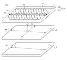
도 1은 본 발명의 제1 실시예에 따른 편광판의 단면도이다.
도 2는 도 1의 분해 사시도이다.
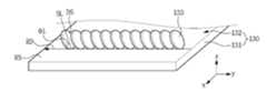
도 3은 λ/2 위상차판의 구조도이다.
도 4는 본 발명의 제2 실시예에 따른 편광판의 분해 사시도이다.
도 5는 본 발명의 제3 실시예에 따른 편광판의 단면도이다.
도 6은 본 발명의 제4 실시예에 따른 유기발광 표시장치의 평면도이다.
도 7은 도 6의 I-I'을 따라 절단한 단면도이다.
도 8은 본 발명의 제5 실시예에 따른 유기발광 표시장치의 단면도이다.
도 9a 및 9b는 편광판의 반사율 실험 결과이다.1 is a cross-sectional view of a polarizing plate according to a first embodiment of the present invention.
FIG. 2 is an exploded perspective view of FIG. 1 ;
3 is a structural diagram of a λ/2 retarder.
4 is an exploded perspective view of a polarizing plate according to a second embodiment of the present invention.
5 is a cross-sectional view of a polarizing plate according to a third embodiment of the present invention.
6 is a plan view of an organic light emitting display device according to a fourth exemplary embodiment of the present invention.
7 is a cross-sectional view taken along line I-I' of FIG. 6 .
8 is a cross-sectional view of an organic light emitting display device according to a fifth exemplary embodiment of the present invention.
9A and 9B are results of a reflectance test of a polarizing plate.
이하, 도면을 참조하여 본 발명을 보다 상세히 설명한다. 그러나, 본 발명의 범위가 하기 설명하는 실시예나 도면들로 한정되는 것은 아니다.Hereinafter, the present invention will be described in more detail with reference to the drawings. However, the scope of the present invention is not limited to the examples or drawings described below.
본 명세서에서 사용되는 용어(terminology)들은 본 발명의 실시예를 표현하기 위해 사용된 용어들로, 이는 사용자, 운용자의 의도 또는 본 발명이 속하는 분야의 관례 등에 따라 해석되어야 한다. 용어의 정의는 본 명세서 전반에 걸친 내용을 토대로 내려져야 할 것이다.Terms used in this specification are terms used to express embodiments of the present invention, which should be interpreted according to the intention of the user or operator or the customs of the field to which the present invention belongs. Definitions of terms should be made based on the content throughout this specification.
도면에서, 이해를 돕기 위하여 각 구성요소와 그 형상 등이 간략하게 그려지거나 또는 과장되어 그려지기도 하며, 실제 제품에 있는 구성요소가 표현되지 않고 생략되기도 한다. 따라서 도면은 발명의 이해를 돕기 위한 것으로 해석되어야 한다. 또한 동일한 기능을 하는 구성요소는 동일한 부호로 표시된다.In the drawings, each component and its shape may be drawn briefly or exaggerated to help understanding, and components in the actual product may be omitted without being expressed. Accordingly, the drawings should be interpreted as helping the understanding of the invention. Also, components having the same function are denoted by the same reference numerals.
어떤 층이나 구성요소가 다른 층이나 구성요소의 '상'에 있다 라고 기재되는 경우, 어떤 층이나 구성요소가 다른 층이나 구성요소와 직접 접촉하여 배치된 경우뿐만 아니라, 그 사이에 제3의 층이 개재되어 배치된 경우까지 모두 포함하는 의미이다.
When a layer or component is described as being 'on' another layer or component, the layer or component is placed in direct contact with another layer or component, as well as a third layer in between. It is meant to include all the cases in which they are interposed.
이하, 도 1 내지 도 3을 참조하여 본 발명의 제1 실시예를 설명한다.Hereinafter, a first embodiment of the present invention will be described with reference to FIGS. 1 to 3 .
도 1은 본 발명의 제1 실시예에 따른 편광판(101)의 단면도이고, 도 2는 도 1의 분해 사시도이다.1 is a cross-sectional view of a polarizing
본 발명의 제1 실시예에 따른 편광판(101)은 편광자(linear polarizer) (110), 편광자(110)상에 배치된 위상지연층(140)을 포함한다. 이러한 편광판(101)은 외광반사를 방지하는 역할을 한다.The polarizing
편광자(110)는 편광판(101)으로 입사된 외광을 선편광시키는 역할을 한다.The
편광자(110)로 폴리비닐알코올(PVA)계 수지에 이색성 색소가 흡착 배향되어 만들어진 필름이 사용될 수 있다. 폴리비닐알콜(PVA)계 수지의 예로, 아세트산 비닐의 단독 중합체 또는 아세트산 비닐과 다른 단량체의 공중합체 등이 있다.As the
편광자(110)는, 예를 들어, 폴리비닐알콜계 수지 필름을 일축 연신하는 공정, 폴리비닐알콜계 수지 필름을 2색성 색소로 염색하여 2색성 색소가 폴리비닐알콜계 수지 필름에 흡착되도록 하는 공정, 2색성 색소가 흡착된 폴리비닐알콜계 수지 필름을 붕산 수용액으로 처리하는 공정, 및 수세공정을 포함하는 방법에 의하여 제조될 수 있다. 그러나, 본 발명의 제1 실시예에 따른 편광자(110)의 제조방법이 이에 한정되는 것은 아니다.
2색성 색소로, 예를 들어, 요오드가 사용될 수 있으며, 당업계에서 사용되는 다른 2색성 염료가 사용될 수도 있다. 2색성 색소로 요오드가 사용되는 경우, 요오드 및 요오드화칼륨을 함유하는 수용액에 폴리비닐알콜계 수지 필름을 침지하여 염색하는 과정을 거쳐 편광자(110)가 제조될 수 있다.As the dichroic dye, for example, iodine may be used, and other dichroic dyes used in the art may also be used. When iodine is used as the dichroic dye, the
요오드는 폴리비닐알콜(PVA)계 수지 필름의 연신방향과 평행한 방향으로 배열될 수 있다. 이러한 요오드의 배열에 의하여 편광자(110)의 투과축(A1)이 결정되는데, 편광자(110)의 투과축(A1)은 요오드의 배열방향과 실질적으로 평행하다.The iodine may be arranged in a direction parallel to the stretching direction of the polyvinyl alcohol (PVA)-based resin film. The transmission axis A1 of the
편광자(110)의 두께는 적용대상 제품에 따라 달라질 수 있다. 예를 들어 편광자(110)는 5~50㎛의 두께를 갖는다. 편광자(110)로 상업적으로 시판되는 제품이 사용될 수 있다.The thickness of the
위상지연층(140)은 편광자(110)의 일면에 배치된다.The
위상지연층(140)은 광의 위상을 지연시킨다. 이러한 위상지연층(140)은 선편광을 원편광으로 바꾸기도 하도 원평광을 선편광으로 바꾸기도 한다. 예를 들어, 편광판(101)으로 입사된 외광은 편광자(110)에 의하여 선편광되고, 위상지연층(140)에 의하여 원편광된다. 원편광된 외광은 편광판(101)이 부착된 장치(예를 들어, 표시장치)의 내부에서 반사되어 반사광이 되는데, 반사과정에서 위상과 편광축이 달라진다. 위상이 변화된 반사광은 편광판(101)을 통과하지 못하게 되어, 편광판(101)에 의해 외광반사가 방지된다.The
위상지연층(140)으로 필름 형태의 위상차판이 사용될 수 있는데, 단일의 위상차판이 사용될 수도 있고, 복수개의 위상차판이 적층되어 사용될 수도 있다.A retardation plate in a film form may be used as the
본 발명의 제1 실시예에 따른 위상지연층(140)은 λ/4 위상차판(quarter wave plate; QWP)(120) 및 λ/2 위상차판(half wave plate; QWP)(130)을 포함한다.The
예를 들어, 위상지연층(140)은 편광자(110)상에 배치된 λ/4 위상차판 (120) 및 λ/4 위상차판(120)상에 배치된 λ/2 위상차판 (130)을 포함한다. 그러나 본 발명의 제1 실시예가 이에 한정되는 것은 아니며, λ/2 위상차판(130)이 편광자(110)상에 배치되고, λ/4 위상차판(120)이 λ/2 위상차판(130)상에 배치될 수도 있다.For example, the
λ/4 위상차판(120)은 필름의 연신에 의하여 제조될 수 있다. 예를 들어, 폴리카보네이트, 폴리비닐알콜, 폴리스티렌, 폴리메틸메타크릴레이트, 폴리프로필렌, 폴리올레핀, 폴리아릴레이트 또는 폴리아미드로 만들어진 필름의 연신에 의하여 λ/4 위상차판(120)이 만들어질 수 있다.The λ/4
λ/4 위상차판(120)은 COP(Cyclic Olefin Polymer)로 된 필름을 포함할 수 있다. COP 필름의 제조를 위해, 예를 들어, 노보넨(Norbornene) 계열의 COP가 사용될 수 있다. COP 필름은 광 투과율, 내열성 및 강도가 높고, 수분 흡수성이 낮고 가격이 저렴하여 경제적이다. COP 필름으로 된 위상차판은 입사광의 파장에 관계없이 비교적 일정한 위상지연값을 나타낸다.The λ/4
또한, λ/4 위상차판(120)은 광경화성 액정 화합물로 만들어질 수도 있다. 예를 들어, 기재 필름 상에 배향막이 형성되고, 배향막상에 액정 화합물이 배열되어 패턴화됨으로써 λ/4 위상차판(120)이 만들어질 수 있다. 이 때, 배향막 및 액정 화합물의 배열에 따라 λ/4 위상차판이 만들어질 수도 있고, λ/2 위상차판이 만들어질 수도 있다.In addition, the λ/4
λ/4 위상차판(120)의 종류나 제조방법에 특별한 제한이 있는 것은 아니다. λ/4 위상차판(120)으로 상업적으로 시판되는 제품이 사용될 수도 있다.There is no particular limitation on the type or manufacturing method of the λ/4
λ/4 위상차판(120)은 투과축(A2)을 갖는다. λ/4 위상차판(120)의 투과축(A2)은 필름의 연신축 또는 액정 화합물의 배향방향에 의해 결정될 수 있다.The λ/4
본 발명의 제1 실시예에 따른 λ/4 위상차판(120)은 COP 필름의 연신에 의하여 만들어질 수 있으며, λ/4 위상차판(120) 투과축(A2)은 COP 필름의 연신축과 실질적으로 평행하다.The λ/4
본 발명의 제1 실시예에 따른 λ/4 위상차판(120)은 정면으로 입사되는 외광, 즉, 편광판(101)의 표면에 대하여 수직으로 입사되는 외광의 반사 방지에 최적화 되도록 설계된다. 따라서, 위상지연층(140)으로 λ/4 위상차판(120)만이 사용된 편광판의 경우, 편광판에 대하여 소정의 입사각으로 입사되는 외광의 반사는 편광판에 의하여 제대로 방지되지 않는다. 즉, 위상지연층(140)으로 λ/4 위상차판(120)만이 사용되는 경우, 외광의 입사각에 따라 외광의 경로가 달라져 위상지연 효과가 달라지고, 외광 반사방지 효과 역시 입사각에 따라 달라질 수 있다.The λ/4
이 경우 외광의 입사각이 커지면 편광판의 반사율이 증가되어, 사용자의 시야각이 커지면 사용자에게 시인되는 반사광의 양이 많아진다.In this case, when the incident angle of external light increases, the reflectance of the polarizing plate increases, and when the user's viewing angle increases, the amount of reflected light visually recognized by the user increases.
외광의 입사각 증가에 따른 편광판의 반사율이 증가를 방지하기 위해, λ/4 위상차판(120)과 함께 λ/2 위상차판(130)이 사용된다.In order to prevent an increase in reflectivity of the polarizing plate according to an increase in the incident angle of external light, the λ/2
본 발명의 제1 실시예에 따른 λ/2 위상차판(130)은 굴절률 이방성층을 가진다.The λ/2
굴절률 이방성층은 x축 방향 굴절률 Nx, y방향 굴절률 Ny 및 z축 방향 굴절률 Nz를 가지며, "Nx = Nz > Ny"의 관계를 만족한다. Nx = Nz > Ny"의 관계를 만족하는 위상차판을 (-)A 플레이트 라고도 불려진다.The refractive index anisotropic layer has a refractive index Nx in the x-axis direction, a refractive index Ny in the y-direction, and a refractive index Nz in the z-axis direction, and satisfies the relationship of "Nx = Nz > Ny". A retardation plate satisfying the relationship of "Nx = Nz > Ny" is also called a (-)A plate.
도 3은 λ/2 위상차판(130)에 대한 구조도이다. 도 3의 λ/2 위상차판(130)은 굴절률 이방성층으로 액정층(132)을 포함한다.3 is a structural diagram of the λ/2
구체적으로, 본 발명의 제1 실시예에 따른 λ/2 위상차판(130)은 지지부재(131) 및 지지부재(131)상에 배치된 액정층(132)을 포함한다. 액정층(132)은 굴절률 이방성을 갖는다.Specifically, the λ/2
지지부재(131)는 액정층(132)을 지지하는 역할을 한다. 지지부재(131)는 투명 플라스틱 필름으로 만들어질 수 있는데, 예를 들어, 트리 아세틸 셀룰로오즈(Tri-Acetyl Cellulose, TAC), 폴리에틸렌 테레프탈레이트(polyethylene terephthalate, PET), 폴리이미드(polyimide, PI) 및 폴리카보네이트(Polycarbonate, PC) 중 적어도 하나를 포함할 수 있다.The
또한, 배향막이 지지부재(131)로 사용될 수도 있다. 배향막은 후술된다.Also, an alignment layer may be used as the
액정층(132)은 디스코틱 화합물(133)을 포함한다. 예를 들어, 액정층(132)은 바인더 화합물을 포함하며, 디스코틱 화합물(133)은 바인더 화합물에 분산되어 배열될 수 있다. 디스코틱 화합물(133)을 포함하는 액정층(132)은 디스코틱 액정층이라고도 불려진다.The
도 3의 디스코틱 화합물(133)은 λ/2 위상차판(130)의 표면에 대하여 소정의 경사각(θ1)을 갖는다. 구체적으로, 도 3의 디스코틱 화합물(133)은 디스크 면(DS)을 가지며, 디스크 면(DS)은 지지부재(131)의 표면에 대하여 60 내지 90˚의 경사각(θ1)을 가진다.The
디스코틱 화합물(133)의 경사각(θ1)은 일반적으로 디스코틱 화합물(133)의 종류, 디스코틱 화합물(133)의 배향 방법, 디스코틱 화합물(133)의 배향에 사용된 물질의 종류 및 배향막의 종류에 따라 달라질 수 있다.The inclination angle θ1 of the
액정층(132)은, 배향막을 이용하여 디스코틱 화합물(133)을 배향시키고 배향된 상태의 디스코틱 화합물(133)을 고정시켜 만들어 질 수 있다.The
액정층(132) 형성을 위해 공지의 디스코틱 화합물(133)이 사용될 수 있고, 디스코틱 화합물(133)의 고정을 위해 공지의 중합 방법이 사용될 수 있다.A known
예를 들어, 디스코틱 화합물(133)을 중합에 의해 고정시키기 위하여, 중합기를 갖는 화합물이 사용될 수 있다. 중합기를 갖는 화합물의 예로, 모노머 또는 올리고머가 있다. 이 때, 디스코틱 화합물(133)과 중합기 사이에 연결기가 도입될 수 있다. 예를 들어, 액정층(132)은 식 1로 표현되는 화합물을 포함할 수 있다.For example, in order to fix the
[식 1][Equation 1]

여기서, "D"는 디스코틱 화합물(133)을 나타내고, "L"은 연결기를 나타내고, "P"는 중합기를 나타낸다. n은 4 내지 12의 정수이다.Here, "D" represents the
액정층(132)은, 배향막상에 디스코틱 화합물(133)을 포함하는 액정층 형성용 조성물을 코팅하고, 건조하고, 디스코틱 네마틱상이 형성되는 온도로 가열하고, 액정층 형성용 조성물을 중합한 후 냉각시킴으로써 만들어질 수 있다. 디스코틱 네마틱상 형성 온도는 배향막의 열 변형 온도보다 낮은 70 내지 300℃ 범위이며, 보다 구체적으로 70 내지 170℃ 범위일 수 있다.The
액정층 형성용 조성물은 전체 중량에 대하여 1 내지 70 중량%의 디스코틱 화합물(133)을 포함한다.The composition for forming the liquid crystal layer includes 1 to 70 wt% of the
또한, 액정층 형성용 조성물은 디스코틱 화합물(133)외에 중합성 모노머, 중합 개시제 및 첨가제를 더 포함한다.In addition, the composition for forming a liquid crystal layer further includes a polymerizable monomer, a polymerization initiator, and an additive in addition to the
중합성 모노머로 비닐기, 비닐록시기, 아크릴기, 메타크릴기를 갖는 모노머가 사용될 수 있다. 액정층 형성용 조성물은 전체 중량에 대하여 1 내지 50 중량%의 중합성 모노머를 포함할 수 있다.As the polymerizable monomer, a monomer having a vinyl group, a vinyloxy group, an acryl group, or a methacryl group may be used. The composition for forming a liquid crystal layer may include 1 to 50 wt% of a polymerizable monomer based on the total weight.
첨가제로 폴리머, 가소제 및 계면활성제가 사용될 수 있다.Polymers, plasticizers and surfactants can be used as additives.
폴리머로, 디스코틱 화합물(133)과 충분한 호환성을 가진 폴리머가 사용된다. 이러한 폴리머의 예로, 셀룰로오스 에스테르계 폴리머가 있다. 셀룰로오스 에스테르계 폴리머의 구체적인 예로, 셀룰로오스 아세테이트, 셀룰로오스 아세테이트 프로피온네이트, 히드록시프로필 셀룰로오스, 셀룰로오스 아세테이트 부티레이트 등이 있다. 액정층 형성용 조성물은 전체 중량에 대하여 1 내지 30 중량%의 폴리머를 포함할 수 있다.As the polymer, a polymer having sufficient compatibility with the
가소제와 계면활성제로 중합성 조성물의 제조에 통상적으로 사용되는 가소제와 계면활성제가 사용될 수 있다.As plasticizers and surfactants, plasticizers and surfactants commonly used in the preparation of polymerizable compositions may be used.
중합 개시제로 광중합 개시제 또는 열중합 개시제가 사용될 수 있다.A photopolymerization initiator or a thermal polymerization initiator may be used as the polymerization initiator.
액정층 형성용 조성물의 중합 방법으로 열 중합 개시제를 이용한 열 중합 방법과 광중합 개시제를 이용한 광중합 방법이 있다. 디스코틱 화합물(133)의 배향 상태가 유지되면서 액정층 형성용 조성물이 중합되도록 하기 위해, 특히 광중합 방법이 적용될 수 있다.As a polymerization method of the composition for forming a liquid crystal layer, there are a thermal polymerization method using a thermal polymerization initiator and a photopolymerization method using a photopolymerization initiator. In order to polymerize the composition for forming the liquid crystal layer while maintaining the alignment state of the
광중합을 위해, 액정층 형성용 조성물은 광중합 개시제를 포함한다. 광중합 개시제로, 예를 들어, α-카르보닐 화합물, 아실로인 에테르, α-하이드로카본 치환된 아로마틱 아실로인 화합물, 다핵 퀴논 화합물, 트리아릴이미다졸 이량체와 P-아미노페닐케톤의 결합물, 아크리딘 화합물, 페나진 화합물 및 옥사디아졸 화합물 중 적어도 1종이 사용될 수 있다. 액정층 형성용 조성물은 전체 중량에 대하여 0.01 내지 20 중량%의 광중합 개시제를 포함한다.For photopolymerization, the composition for forming a liquid crystal layer includes a photopolymerization initiator. As a photoinitiator, for example, an α-carbonyl compound, an acyl ether, an α-hydrocarbon substituted aromatic acyl compound, a polynuclear quinone compound, a triarylimidazole dimer and P-aminophenyl ketone are combined At least one of water, an acridine compound, a phenazine compound, and an oxadiazole compound may be used. The composition for forming a liquid crystal layer includes 0.01 to 20 wt% of a photopolymerization initiator based on the total weight.
액정층 형성용 조성물의 광중합을 위해 액정층 형성용 조성물에 광이 조사된다. 이러한 광으로 20 내지 5000 mJ/㎠의 에너지를 갖는 UV가 사용될 수 있다. 광조사는 광중합 반응을 가속하기 위해 가열 중에 수행될 수도 있다.Light is irradiated to the composition for forming a liquid crystal layer for photopolymerization of the composition for forming a liquid crystal layer. As such light, UV having an energy of 20 to 5000 mJ/cm 2 may be used. Light irradiation may be performed during heating to accelerate the photopolymerization reaction.
액정층 형성용 조성물이 경화되어 액정층(132)이 형성되고 디스코틱 화합물(133)이 고정된다.The composition for forming the liquid crystal layer is cured to form the
이와 같이 디스코틱 화합물(133)이 소정 60 내지 90˚의 경삭각(θ1)으로 배열됨에 따라, 액정층(132)은 1.6 내지 1.8의 x축 방향 굴절률(Nx) 및 z축 방향 굴절률(Nz)를 가지고, 1.5 내지 1.7의 y축 굴절률(Ny)를 가진다. 또한, Nx와 Ny의 차는 0.05 내지 0.2 범위의 값을 가질 수 있다.As described above, as the
그러나, 본 발명의 제1 실시예가 이에 한정되는 것은 아니며, 액정층(132)을 구성하는 재료들 및 그 재료들의 배열에 따라 x축 방향 굴절률 Nx, y방향 굴절률 Ny 및 z축 방향 굴절률 Nz이 달라질 수 있다.However, the first embodiment of the present invention is not limited thereto, and the refractive index in the x-axis direction Nx, the refractive index in the y-direction, and the refractive index Nz in the z-axis direction may vary depending on the materials constituting the
액정층(132)의 두께는 원평광을 위해 필요한 위상지연이 이루어질 수 있도록 조정된다. 액정층(132)의 두께는 액정층(132)의 굴절률에 따라 달라질 수 있다. 본 발명의 제1 실시예에 따른 액정층(132)은 1 내지 5㎛의 두께를 가질 수 있다.The thickness of the
또한, 외광의 입사각에 따른 위상지연 편차를 보상하기 위해, 액정층(132)의 두께와 굴절률은 다음 관계를 만족하도록 조정될 수 있다. 즉, 액정층(132)이 "a"㎛의 두께를 가지고, 굴절률의 차 "Nx-Ny = b"라고 할 때, "0.1 ≤ a x b ≤ 0.5"의 관계를 만족하도록 액정층(132)의 두께와 굴절률이 조정된다.In addition, in order to compensate for the phase delay deviation according to the incident angle of external light, the thickness and refractive index of the
"a x b"의 값이 0.1 내지 0.5인 경우, 100nm 내지 500nm 범위의 위상지연 편차가 보상될 수 있다. 즉, 측면으로 입사되는 외광이 정면으로 입사되는 외광과 비교하여 100nm 내지 500nm 정도의 위상지연 편차를 가지더라도, 편광판(101)에 의하여 측면으로 입사되는 외광이 원편광된다.When the value of "a x b" is 0.1 to 0.5, a phase delay deviation in the range of 100 nm to 500 nm may be compensated. That is, even if the external light incident to the side has a phase delay deviation of about 100 nm to 500 nm compared to the external light incident to the front, the external light incident to the side by the
보다 구체적으로, "a x b"의 값은 0.2 내지 0.3이다. 이 경우, 200nm 내지 300nm 범위의 위상지연 편차가 보상될 수 있다.More specifically, the value of "a x b" is 0.2 to 0.3. In this case, the phase delay deviation in the range of 200 nm to 300 nm may be compensated.
이러한 액정층(132)이 λ/2 위상차판(130)의 굴절률 이방성층으로 사용되는 경우, 외광의 입사각 달라지더라도 편광판(101)에 의하여 외광의 원편광이 이루어진다. 그에 따라, 이러한 λ/2 위상차판(130)을 포함하는 편광판(101)은 외광의 입사각에 상관없이 외광 반사를 효과적으로 방지할 수 있다.When the
본 발명의 제1 실시예에 따른 λ/2 위상차판(130)은 배향막을 포함하며, 배향막은 지지부재(131) 역할을 한다. 따라서, 배향막상에 액정층(132)이 배치된다.The λ/2
배향막은 디스코틱 화합물(133)의 배향 방향를 결정하는 기능을 한다.The alignment layer functions to determine the alignment direction of the
배향막은 폴리머의 러빙 처리, 사방(rhombic) 진공 증착법, 랭뮤어-브로젯(Langmuir-Brojet, LB)법 등에 의해 만들어질 수 있다. 이 때, 배향막 형성을 위한 폴리머로 ω-트리코사노익 산, 디옥타데클메틸암모늄 클로라이드, 메틸 스테아르산염 등이 있다.The alignment layer may be formed by a polymer rubbing treatment, a rhombic vacuum deposition method, a Langmuir-Brojet (LB) method, or the like. At this time, examples of the polymer for forming the alignment layer include ω-tricosanoic acid, dioctadeclemethylammonium chloride, methyl stearate, and the like.
구체적으로, 배향막은 폴리머의 러빙 처리에 의해 만들어질 수 있다. 배향막 형성을 위한 폴리머로 폴리비닐 알코올이 있다. 또한, 배향막 형성을 위해 소수성기가 결합되어 변성된 폴리머가 사용될 수도 있는데, 예를 들어, 폴리비닐 알코올에 소수성기가 도입된 폴리머가 사용될 수 있다. 소수성기는 디스코틱 화합물(133)에 대한 친화력을 가지므로, 디스코틱 화합물(133)을 균일하게 배향시키는 데 유리하다.Specifically, the alignment layer may be made by rubbing the polymer. Polyvinyl alcohol is a polymer for forming the alignment layer. In addition, a polymer modified with a hydrophobic group bonded thereto may be used to form the alignment layer, for example, a polymer having a hydrophobic group introduced into polyvinyl alcohol may be used. Since the hydrophobic group has an affinity for the
소수성기는 폴리비닐 알콜의 주쇄의 말단 또는 측쇄에 결합된다.The hydrophobic group is bonded to the end or side chain of the main chain of polyvinyl alcohol.
소수성기로, 6 이상의 탄소 원자를 갖는 지방족기 또는 방향족기가 있다. 예를 들어, 6 이상의 탄소 원자를 갖는 알킬기 또는 알케닐기가 소수성기로 사용될 수 있다.As the hydrophobic group, there is an aliphatic group or an aromatic group having 6 or more carbon atoms. For example, an alkyl group or an alkenyl group having 6 or more carbon atoms may be used as the hydrophobic group.
소수성기를 폴리비닐 알콜의 주쇄의 말단에 결합시키는 경우, 소수성기와 주쇄 말단 사이에 연결기가 도입될 수 있다. 연결기의 예로, -S-, -C(CN)R1 -, -NR2- 등이 있다. 여기서, R1 및 R2는 각각 수소 원자 또는 1 내지 6 개의 탄소 원자를 갖는 알킬기를 나타낸다.When the hydrophobic group is bonded to the end of the main chain of polyvinyl alcohol, a linking group may be introduced between the hydrophobic group and the end of the main chain. Examples of the linking group include -S-, -C(CN)R1 -, -NR2 - and the like. Here, R1 and R2 each represent a hydrogen atom or an alkyl group having 1 to 6 carbon atoms.
배향막 제조를 위해 상업적으로 이용 가능한 폴리비닐 알코올 필름이 사용될 수 있다.A commercially available polyvinyl alcohol film may be used for preparing the alignment layer.
배향막의 재료가 되는 필름의 표면을 일정한 방향으로 수회 러빙시킴으로써 러빙 공정이 수행된다. 러빙을 위해 균일한 길이와 균일한 두께를 가지며 균일하게 배열된 섬유를 갖는 직물이 사용될 수 있다.The rubbing process is performed by rubbing the surface of the film, which is the material of the alignment layer, several times in a predetermined direction. For rubbing, a fabric having uniform length and uniform thickness and uniformly arranged fibers may be used.
배향막은 배향방향(RD)을 가지는데, 러빙에 의하여 배향막이 형성되는 경우 배향방향(RD)은 러빙 방향과 평행하다. 디스코틱 화합물(133)은 배향막의 배향방향에 따라 배향된다.The alignment layer has an alignment direction RD. When the alignment layer is formed by rubbing, the alignment direction RD is parallel to the rubbing direction. The
디스코틱 화합물(133)의 배향방향에 따라 액정층(132)의 투과축이 결정되며, 액정층(132)의 투과축은 λ/2 위상차판(130)의 투과축이 된다.The transmission axis of the
편광판(101)에 배향막이 반드시 필요한 것은 아니며 생략될 수 있다. 예를 들어, 디스코틱 화합물(133)을 배향시키기 위하여 배향막이 사용된 후, 편광판(101) 제조 과정에서 배향막이 제거될 수 있다. 이 경우, 디스코틱 화합물(133)을 지지하기 위한 지재부재(131)로 배향막 대신 투명한 기재 필름이 사용될 수 있다.An alignment layer is not necessarily required for the
또한 지지부재(131)가 생략될 수도 있다. 즉, 배향막에 의해 배향된 액정층(132)이 직접 λ/4 위상차판(140)상에 배치될 수 있다.Also, the
도면에 도시되지 않았지만, 본 발명에 제1 실시예에 따른 편광판(101)은 편광(110)자와 λ/4 위상차판(120) 사이에 배치된 점착층을 더 포함할 수 있으며, λ/4 위상차판(120)과 λ/2 위상차판(130) 사이에 배치된 점착층을 더 포함할 수 있다.Although not shown in the drawings, the
또한, 효율적인 외광 반사를 위해 편광자(110), λ/4 위상차판(120) 및 λ/2 위상차판(130)이 소정이 각도로 엇갈려 배치될 수 있다.In addition, the
예를 들어, λ/4 위상차판(120)은 투과축 기준으로 편광자(110)와 θ2의 각도로 엇갈려 배치될 수 있고, λ/2 위상차판(130)은 투과축을 기준으로 편광자(110)와 θ3의 각도로 엇갈려 배치될 수 있다. 여기서, θ2는 편광자(110)의 투과축(A1)과 λ/4 위상차판(120)의 투과축(A2)의 사잇각이며, 70˚ 내지 80˚ 이다. 또한, θ3는 편광자(110)의 투과축(A1)과 λ/2 위상차판(120)의 투과축(RD)의 사잇각이며 12 내지 17˚이다.For example, the λ/4
표시장치 등에 편광판(101)이 배치될 때, y축은 사용자 기준으로 외광의 입사가 차이가 큰 방향과 평행한 방향이 될 수 있다. 예를 들어, 가로방향의 길이가 세로방향의 길이보다 긴 표시장치에 편광판(101)이 사용되는 경우, y축은 표시장치의 가로방향과 평행한 방향이다.When the
도 9a 및 도 9b는 편광판의 반사율에 대한 실험 결과이다. 도 9a는 굴절률 이방성을 갖지 않는 λ/2 위상차판을 포함하는 편광판의 반사율에 대한 시뮬레이션 실험 결과이고, 도 9b는 본 발명의 제1 실시예에 따른 편광판(101)의 반사율에 대한 시뮬레이션 실험 결과가 도시되어 있다.9A and 9B are experimental results for reflectance of a polarizing plate. 9A is a simulation test result for the reflectance of a polarizing plate including a λ/2 retarder having no refractive index anisotropy, and FIG. 9B is a simulation test result for the reflectance of the
구체적으로, 도 9a의 실험에 적용된 λ/2 위상차판은 Nx=Ny=Nz=1.6의 굴절률을 가지며, 도 9b의 실험에 적용된 λ/2 위상차판은 Nx=Nz=1.77 및 Ny=1.6의 굴절률을 가진다. 도 9a 및 9b에서 어두운 부분은 효율적인 외광 반사 방지가 이루어진 부분이고, 밝은 부분은 외광 반사 방지가 효율적으로 이루어지지 않은 부분이다. 도 9a 및 도 9b에 도시된 바와 같이, 본 발명의 제1 실시예에 따른 편광판(101)은 외광의 입사각에 관계없이 모든 방향에 대하여 우수한 외광 반사 방지 능력을 가지며, 우수한 검은색 표현 능력을 가진다.Specifically, the λ/2 retarder applied to the experiment of FIG. 9A has a refractive index of Nx=Ny=Nz=1.6, and the λ/2 retarder applied to the experiment of FIG. 9B has a refractive index of Nx=Nz=1.77 and Ny=1.6 have In FIGS. 9A and 9B , a dark part is a part where external light reflection is effectively prevented, and a bright part is a part where external light reflection is not effectively prevented. 9A and 9B, the
이와 같이 본 발명의 제1 실시예에 따른 편광판(101)은 (-)A 플레이트 특성을 갖는 λ/2 위상차판(130)을 가지며, 외광의 입사각에 관계없이 외광의 반사를 방지할 수 있다. 그에 따라, 본 발명의 제1 실시예에 따른 편광판(101)이 사용된 제품은 검은색 표현 능력 및 콘트라스트 특성이 우수하다.
As described above, the
다음, 도 4를 참조하여 본 발명의 제2 실시예를 설명한다. 이하, 중복을 피하기 위하여, 이미 설명된 구성요소에 대한 설명은 생략된다.Next, a second embodiment of the present invention will be described with reference to FIG. 4 . Hereinafter, in order to avoid duplication, descriptions of the already described components will be omitted.
도 4는 본 발명의 제2 실시예에 따른 편광판(102)의 단면도이다.4 is a cross-sectional view of the polarizing plate 102 according to the second embodiment of the present invention.
본 발명의 제2 실시예에 따른 편광판(102)은 편광자(110), 편광자(110)상에 배치된 λ/2 위상차판(130) 및 λ/2 위상차판(130)상에 배치된 λ/4 위상차판(120)을 포함한다. λ/2 위상차판(130)과 λ/4 위상차판(120) 각각의 구성은 제1 실시예와 동일하다.
The polarizing plate 102 according to the second embodiment of the present invention includes a
이하, 도 5를 참조하여 본 발명의 제3 실시예를 설명한다.Hereinafter, a third embodiment of the present invention will be described with reference to FIG. 5 .
도 5는 본 발명의 제3 실시예에 따른 편광판(103)의 단면도이다.5 is a cross-sectional view of a
본 발명의 제3 실시예에 따른 편광판(102)은 편광자(110), λ/4 위상차판(120) 및 λ/2 위상차판(130)을 포함하며, 편광자(110)와 λ/4 위상차판(120) 사이에 배치된 지지층(150)을 포함한다.The polarizing plate 102 according to the third embodiment of the present invention includes a
지지층(150) 편광판(103)을 지지하고 보호하는 역할을 한다. 이러한 지지층(150)으로, 예를 들어, TAC(Tri-Acetyl Cellulose: 트리 아세틸 셀룰로오즈) 필름이 사용될 수 있다. TAC 필름은 우수한 내구성 및 기계적 강도를 가진다.The
또한, 본 발명의 제3 실시예에 따른 편광판(103)은 λ/2 위상차판(130)상에 배치된 점착층(160)을 더 포함한다. 점착층(160)은 점착성 수지로 만들어질 수 있다.
In addition, the
이하, 도 6 및 7을 참조하여 본 발명의 제4 실시예를 설명한다.Hereinafter, a fourth embodiment of the present invention will be described with reference to FIGS. 6 and 7 .
도 6은 본 발명의 제4 실시예에 따른 유기발광 표시장치(104)의 평면도이고, 도 7은 도 6의 I-I'를 따라 자른 단면도이다.6 is a plan view of an organic light emitting
도 6 및 도 7에 도시된 바와 같이, 본 발명의 제4 실시예에 따른 유기발광 표시장치(104)는 표시패널(301) 및 편광판(101)을 포함한다.6 and 7 , the organic light emitting
표시패널(301)은 제1기판(311), 배선부(330), 유기발광소자(210) 및 제2기판(312)을 포함한다.The
제1기판(311)은 유리, 석영, 세라믹, 및 플라스틱 등으로 이루어진 군에서 선택된 절연성 재료로 만들어질 수 있다. 그러나, 본 발명의 제4 실시예가 이에 한정되는 것은 아니며, 제1기판(311)이 스테인리스강 등의 금속성 재료로 만들어질 수도 있다.The
제1기판(311)상에 버퍼층(321)이 배치된다. 버퍼층(321)은 다양한 무기막들 및 유기막들 중에서 선택된 하나 이상의 막을 포함할 수 있다. 버퍼층(321)은 수분과 같은 불순물이 배선부(330)나 유기발광소자(210)로 침투하는 것을 방지하면서 동시에 표면을 평탄화하는 역할을 한다. 하지만, 버퍼층(321)은 반드시 필요한 것은 아니며, 생략될 수도 있다.A
배선부(330)는 버퍼층(321) 상에 배치된다. 배선부(330)는 스위칭 박막 트랜지스터(10), 구동 박막 트랜지스터(20) 및 축전 소자(80)를 포함하는 부분으로, 유기발광소자(210)를 구동한다. 유기발광소자(210)는 배선부(330)로부터 전달받은 구동 신호에 따라 광을 방출하여 화상을 표시한다.The
도 6 및 7에, 하나의 화소에 두개의 박막 트랜지스터(thin film transistor, TFT)(10, 20)와 하나의 축전 소자(capacitor)(80)가 구비된 2Tr-1Cap 구조의 능동 구동(active matrix, AM)형 유기발광 표시장치(104)가 도시되어 있다. 그러나, 본 발명의 제4 실시예가 이러한 구조로 한정되는 것은 아니다. 예컨대, 유기발광 표시장치(104)는 하나의 화소에 셋 이상의 박막 트랜지스터와 둘 이상의 축전 소자를 포함할 수 있으며, 별도의 배선을 더 포함하는 다양한 구조를 가질 수 있다. 여기서, 화소는 화상을 표시하는 최소 단위를 말하며, 유기발광 표시장치(104)는 복수의 화소들을 통해 화상을 표시한다.6 and 7, an active matrix of a 2Tr-1Cap structure in which two thin film transistors (TFTs) 10 and 20 and one
하나의 화소마다 각각 스위칭 박막 트랜지스터(10), 구동 박막 트랜지스터(20), 축전 소자(80), 및 유기발광소자(organic light emitting diode, OLED)(210)가 구비된다. 또한 일 방향을 따라 배치되는 게이트 라인(351)과, 상기 게이트 라인(351)과 절연 교차되는 데이터 라인(371) 및 공통 전원 라인(372)이 배선부(330)에 배치된다. 하나의 화소는 게이트 라인(351), 데이터 라인(371) 및 공통 전원 라인(372)을 경계로 정의될 수 있으나, 반드시 이에 한정되는 것은 아니다. 화소정의막(PDL)(391) 또는 블랙 매트릭스에 의하여 화소가 정의될 수도 있다.Each pixel includes a switching
유기발광소자(210)는 제1전극(211), 제1전극(211)상에 배치된 유기 발광층(212) 및 유기 발광층(212)상에 배치된 제2전극(213)을 포함한다. 제1전극(211) 및 제2전극(213)으로부터 각각 정공과 전자가 유기 발광층(212) 내부로 주입된다. 이렇게 주입된 정공과 전자가 결합되어 형성된 엑시톤(exiton)이 여기상태로부터 기저상태로 떨어질 때 발광이 이루어진다.The organic
축전 소자(80)는 층간 절연막(345)을 사이에 두고 배치된 한 쌍의 축전판(358, 378)을 포함한다. 여기서, 층간 절연막(345)은 유전체가 된다. 축전 소자(80)에서 축전된 전하와 양 축전판(358, 378) 사이의 전압에 의해 축전용량이 결정된다.The
스위칭 박막 트랜지스터(10)는 스위칭 반도체층(331), 스위칭 게이트 전극(352), 스위칭 소스 전극(373), 및 스위칭 드레인 전극(374)을 포함한다. 구동 박막 트랜지스터(20)는 구동 반도체층(332), 구동 게이트 전극(355), 구동 소스 전극(376), 및 구동 드레인 전극(377)을 포함한다. 반도체층(331, 332)과 게이트 전극(352, 355)은 게이트 절연막(341)에 의하여 절연된다.The switching
스위칭 박막 트랜지스터(10)는 발광시키고자 하는 화소를 선택하는 스위칭 소자로 사용된다. 스위칭 게이트 전극(352)은 게이트 라인(351)에 연결된다. 스위칭 소스 전극(373)은 데이터 라인(371)에 연결된다. 스위칭 드레인 전극(374)은 스위칭 소스 전극(373)으로부터 이격 배치되며 어느 한 축전판(358)과 연결된다.The switching
구동 박막 트랜지스터(20)는 선택된 화소 내의 유기발광소자(210)의 유기 발광층(212)을 발광시키기 위한 구동 전원을 화소 전극인 제1전극(211)에 인가한다. 구동 게이트 전극(355)은 스위칭 드레인 전극(374)과 연결된 축전판(358)과 연결된다. 구동 소스 전극(376) 및 다른 한 축전판(378)은 각각 공통 전원 라인(372)과 연결된다. 구동 드레인 전극(377)은 컨택홀(contact hole)을 통해 유기발광소자(210)의 제1전극(211)과 연결된다.The driving
이와 같은 구조에 의하여, 스위칭 박막 트랜지스터(10)는 게이트 라인(351)에 인가되는 게이트 전압에 의해 작동되어 데이터 라인(371)에 인가되는 데이터 전압을 구동 박막 트랜지스터(20)로 전달하는 역할을 한다. 공통 전원 라인(372)으로부터 구동 박막 트랜지스터(20)에 인가되는 공통 전압과 스위칭 박막 트랜지스터(10)로부터 전달된 데이터 전압의 차에 해당하는 전압이 축전 소자(80)에 저장되고, 축전 소자(80)에 저장된 전압에 대응하는 전류가 구동 박막 트랜지스터(20)를 통해 유기발광소자(210)로 흘러 유기발광소자(210)가 발광하게 된다.With this structure, the switching
본 발명의 제4 실시예에서 제1전극(211)이 정공을 주입하는 애노드(anode)이며, 제2전극(213)이 전자를 주입하는 캐소드(cathode)이다. 하지만, 본 발명의 제4 실시예가 이에 한정되는 것은 아니며, 제1전극(211)이 캐소드가 되고, 제2전극(213)이 애노드가 될 수도 있다.In the fourth embodiment of the present invention, the
평탄화막(346)은 층간절연막(345)상에 배치된다. 평탄화막(346)은 절연 재료로 만들어질 수 있으며, 배선부(330)를 보호한다. 평탄화막(346)과 층간절연막(345)은 동일한 재료로 만들어질 수 있다.A
구동 박막트랜지스터(20)의 드레인 전극(377)은 평탄화막(146)에 형성된 컨택홀(contact hole)을 통해 유기 발광 소자(210)의 제1전극(211)과 연결된다.The
본 발명의 제4 실시예에서, 제1전극(211)은 반사전극이고, 제2전극(213)은 반투과 전극이다. 따라서, 유기 발광층(212)에서 발생된 광은 제2전극(213)을 투과하여 발광된다. 즉, 본 발명의 제4 실시예에 따른 유기발광 표시장치(104)는 전면 발광형(top emission type)의 구조를 갖는다.In the fourth embodiment of the present invention, the
반사전극 및 반투과 전극의 형성에 마그네슘(Mg), 은(Ag), 금(Au), 칼슘(Ca), 리튬(Li), 크롬(Cr), 알루미늄(Al) 및 구리(Cu) 중 하나 이상의 금속 또는 이들의 합금이 사용될 수 있다. 이때, 반사전극과 반투과 전극은 두께로 결정된다. 일반적으로, 반투과 전극은 약 200nm 이하의 두께를 갖는다. 반투과 전극의 두께가 얇아질수록 광의 투과율이 높아지고, 두께가 두꺼워질수록 광의 투과율이 낮아진다.One of magnesium (Mg), silver (Ag), gold (Au), calcium (Ca), lithium (Li), chromium (Cr), aluminum (Al) and copper (Cu) to form a reflective electrode and a transflective electrode The above metals or alloys thereof may be used. In this case, the thickness of the reflective electrode and the transflective electrode is determined. Generally, the transflective electrode has a thickness of about 200 nm or less. As the thickness of the transflective electrode decreases, the transmittance of light increases, and as the thickness increases, the transmittance of light decreases.
구체적으로 제1전극(211)은 마그네슘(Mg), 은(Ag), 금(Au), 칼슘(Ca), 리튬(Li), 크롬(Cr), 알루미늄(Al) 및 구리(Cu) 중 하나 이상의 금속을 포함하는 반사막 및 반사막상에 배치된 투명 도전막을 포함할 수 있다. 여기서, 투명 도전막은 투명전도성산화물(Transparent Conductive Oxide; TCO)을 포함할 수 있는데, 예를 들어, ITO(Indium Tin Oxide), IZO(Indium Zinc Oxide), ZnO(Zinc Oxide), AZO(Aluminum Zinc Oxide) 및 In2O3(Indium Oxide) 중 적어도 하나를 포함할 수 있다. 이러한 투명 도전막은 높은 일함수를 갖기 때문에 제1전극(211)을 통한 정공 주입이 원활해진다.Specifically, the
또한, 제1전극(211)은 투명 도전막, 반사막 및 투명 도전막이 차례로 적층된 3중막 구조를 가질 수도 있다.Also, the
제2전극(213)은 마그네슘(Mg), 은(Ag), 금(Au), 칼슘(Ca), 리튬(Li), 크롬(Cr), 알루미늄(Al) 및 구리(Cu) 중 하나 이상의 금속을 포함하는 반투과막으로 만들어질 수 있다.The
도면에 도시되지 않았지만, 제1전극(211)과 유기 발광층(212) 사이에 정공 주입층(hole injection layer; HIL) 및 정공 수송층(hole transporting layer; HTL) 중 적어도 하나가 더 배치될 수도 있다. 또한, 유기 발광층(212)과 제2전극(213) 사이에 전자 수송층(electron transport layer; ETL) 및 전자 주입층(electron injection layer, EIL) 중 적어도 하나가 더 배치될 수 있다.Although not shown in the drawings, at least one of a hole injection layer (HIL) and a hole transport layer (HTL) may be further disposed between the
유기 발광층(212), 정공주입층, 정공수송층, 전자수송층 및 전자주입층을 유기층이라고도 한다. 유기층은 저분자 유기물 또는 고분자 유기물로 형성될 수 있다.The organic
화소 정의막(391)은 개구부를 갖는다. 화소 정의막(391)의 개구부는 제1전극(211)의 일부를 드러낸다. 화소 정의막(191)의 개구부에 제1전극(211), 유기 발광층(212) 및 제2전극(213)이 차례로 적층된다. 제2전극(213)은 유기 발광층(212)뿐만 아니라 화소 정의막(191) 위에도 배치된다. 화소 정의막(191)은 발광 영역을 정의할 수 있다.The
도면에 도시되지 않았지만, 제2전극(213)상에 캡핑층이 배치될 수 있다. 캡핑층는 유기발광소자(210)를 보호한다.Although not shown in the drawings, a capping layer may be disposed on the
유기발광소자(210)를 보호하기 위해, 제1기판(311)과 대향되도록 유기발광소자(210)상에 제2기판(312)이 배치된다. 제2기판(312)은 제1기판(311)과 동일한 재료로 만들어질 수 있다.In order to protect the organic
표시패널(301)상에 편광판(101)이 배치된다. 본 발명의 제4 실시예에 따른 편광판(101)은 제1 실시예의 편광판과 동일한 구성을 가진다. 구체적으로, 편광판(101)은 표시패널(301)의 표시면에 해당되는 제2기판(312)상에 배치된다. 이때, 점착층(160)에 의해 편광판(101)이 제2기판(312)에 접착된다. 편광판(101)의 구성은 제1 실시예에서 설명되었으므로 이에 대한 상세한 설명은 생략된다.
A
이하, 도 8을 참조하여 본 발명의 제5 실시예를 설명한다. 도 8은 본 발명의 제5 실시예에 따른 유기발광 표시장치(105)의 단면도이다.Hereinafter, a fifth embodiment of the present invention will be described with reference to FIG. 8 . 8 is a cross-sectional view of an organic light emitting
본 발명의 제5 실시예에 따른 유기발광 표시장치(105)는 유기발광소자(210)상에 배치된 박막 봉지층(250)을 포함한다.The organic light emitting
박막 봉지층(250)은 하나 이상의 무기막(251, 253, 255) 및 하나 이상의 유기막(252, 254)을 포함한다. 박막 봉지층(250)은 무기막(251, 253, 255)과 유기막(252, 254)이 교호적으로 적층된 구조를 갖는다. 이때, 무기막(251)이 최하부에 배치된다. 즉, 무기막(251)이 유기발광소자(210)와 가장 가깝게 배치된다. 도 8에서 박막 봉지층(250)이 3개의 무기막(251, 253, 255)과 2개의 유기막(252, 254)을 포함하고 있으나, 본 발명의 제5 실시예가 이에 한정되는 것은 아니다.The thin
무기막(251, 253, 255)은 Al2O3, TiO2, ZrO, SiO2, AlON, AlN, SiON, Si3N4, ZnO, 및 Ta2O5 중 하나 이상의 무기물을 포함한다. 무기막(251, 253, 255)은 화학증착(chemical vapor deposition, CVD)법 또는 원자층 증착(atomic layer depostion, ALD)법을 통해 형성된다. 하지만, 본 발명의 제5 실시예가 이에 한정되는 것은 아니며, 무기막(251, 253, 255)은 해당 기술 분야에서 공지된 다양한 방법에 의해 형성될 수 있다.The
유기막(252, 254)은 고분자(polymer) 계열의 소재로 만들어진다. 여기서, 고분자 계열의 소재는 아크릴계 수지, 에폭시계 수지, 폴리이미드, 및 폴리에틸렌 등을 포함한다. 유기막(252, 254)은 열증착 공정을 통해 형성될 수 있다. 유기막(252, 254)을 형성하기 위한 열증착 공정은 유기발광소자(210)를 손상시키지 않는 온도 범위 내에서 진행된다. 하지만, 본 발명의 제5 실시예가 이에 한정되는 것은 아니며, 유기막(252, 254)은 해당 기술 분야에서 공지된 다양한 방법을 통해 형성될 수 있다.The
박막의 밀도가 치밀하게 형성된 무기막(251, 253, 255)이 주로 수분 또는 산소의 침투를 억제한다. 대부분의 수분 및 산소는 무기막(251, 253, 255)에 의해 유기 발광 소자(210)로의 침투가 차단된다.The
무기막(251, 253, 255)을 통과한 수분 및 산소는 유기막(252, 254)에 의해 다시 차단된다. 유기막(252, 254)은 무기막(251, 253, 255)에 비해 상대적으로 투습 방지 효과는 적다. 하지만, 유기막(252, 254)은 투습 억제 외에 무기막(251, 253, 255)과 무기막(251, 253, 255) 사이에서, 각층들 간의 응력을 줄여주는 완충층의 역할도 함께 수행한다. 또한, 유기막(252, 254)은 평탄화 특성을 가지므로, 박막 봉지층(250)의 최상부면이 평탄해질 수 있다.Moisture and oxygen passing through the
박막 봉지층(250)은 10㎛ 이하의 두께로 형성될 수 있다. 따라서, 유기발광 표시장치(102)의 전체적인 두께가 매우 얇게 형성될 수 있다.The thin
편광판(101)은 박막 봉지층(250)상에 배치된다. 편광판(101)으로, 제1 실시예의 편광판이 적용될 수 있다.
The
이상 실시예와 도면을 참고하여 본 발명의 설명하였다. 상기 실시예와 도면은 본 발명의 이해를 돕기 위한 예시일 뿐, 본 발명의 범위가 상기 실시예나 도면에 의하여 한정되지 않는다.The present invention has been described with reference to the above examples and drawings. The above embodiments and drawings are only examples for helping understanding of the present invention, and the scope of the present invention is not limited by the above embodiments or drawings.
110: 편광자120: λ/4 위상차판
130: λ/2 위상차판131: 지지부재
132: 액정층133: 디스코틱 화합물
140: 위상지연층160: 점착층
201: 표시패널210: 유기발광소자
211: 제1전극212: 유기 발광층
213: 제2전극250: 박막봉지층
311: 제1기판312: 제2기판
330: 배선부110: polarizer 120: λ/4 retardation plate
130: λ/2 retardation plate 131: support member
132: liquid crystal layer 133: discotic compound
140: phase delay layer 160: adhesive layer
201: display panel 210: organic light emitting device
211: first electrode 212: organic light emitting layer
213: second electrode 250: thin film encapsulation layer
311: first substrate 312: second substrate
330: wiring unit
Claims (30)
Translated fromKorean상기 편광자상에 배치되고, λ/4 위상차판 및 λ/2 위상차판을 포함하는 위상지연층;을 포함하며,
상기 λ/2 위상차판은 굴절률 이방성층을 포함하고,
상기 굴절률 이방성층은 x축 방향 굴절률 Nx, y방향 굴절률 Ny 및 z축 방향 굴절률 Nz를 가지며,
Nx = Nz > Ny 이며,
상기 편광자, λ/4 위상차판 및 λ/2 위상차판은 상기 z축을 따라 배열되며,
상기 굴절률 이방성층은 "a"㎛의 두께를 가지며,
Nx-Ny = "b" 라고 할 때, 0.1 < a x b < 0.5인 편광판.polarizer; and
and a phase delay layer disposed on the polarizer and comprising a λ/4 retardation plate and a λ/2 retardation plate;
The λ/2 retarder includes a refractive index anisotropic layer,
The refractive index anisotropic layer has an x-axis refractive index Nx, a y-direction refractive index Ny, and a z-axis direction refractive index Nz,
Nx = Nz > Ny,
The polarizer, λ/4 retarder and λ/2 retarder are arranged along the z-axis,
The refractive index anisotropic layer has a thickness of "a" ㎛,
A polarizing plate with 0.1 < axb < 0.5 when Nx-Ny = "b".
상기 디스크 면은 λ/2 위상차판의 표면에 대하여 60 내지 90˚의 경사각을 갖는 편광판.4. The method of claim 3, wherein the discotic compound has a disk surface,
The disk surface is a polarizing plate having an inclination angle of 60 to 90 degrees with respect to the surface of the λ/2 retardation plate.
상기 λ/2 위상차판은 배향막을 포함하며,
상기 굴절률 이방성층은 상기 배향막상에 배치된 편광판.According to claim 1,
The λ/2 retarder includes an alignment layer,
The refractive index anisotropic layer is a polarizing plate disposed on the alignment layer.
상기 편광자상에 상기 λ/4 위상차판이 배치되며,
상기 λ/4 위상차판상에 상기 λ/2 위상차판이 배치된 편광판.According to claim 1,
The λ/4 retardation plate is disposed on the polarizer,
A polarizing plate in which the λ/2 retarder is disposed on the λ/4 retarder.
상기 편광자상에 상기 λ/2 위상차판이 배치되며,
상기 λ/2 위상차판상에 상기 λ/4 위상차판이 배치된 편광판.According to claim 1,
The λ/2 retardation plate is disposed on the polarizer,
A polarizing plate in which the λ/4 retarder is disposed on the λ/2 retarder.
상기 표시패널상에 배치된 편광판을 포함하며,
상기 편광판은,
편광자; 및
상기 편광자상에 배치되고, λ/4 위상차판 및 λ/2 위상차판을 포함하는 위상지연층;을 포함하며,
상기 λ/2 위상차판은 굴절률 이방성층을 포함하고,
상기 굴절률 이방성층은 x축 방향 굴절률 Nx, y방향 굴절률 Ny 및 z축 방향 굴절률 Nz를 가지며, Nx = Nz > Ny이며,
상기 편광자, λ/4 위상차판 및 λ/2 위상차판은 상기 z축을 따라 배열되며,
상기 굴절률 이방성층은 "a"㎛의 두께를 가지며,
Nx-Ny = "b" 라고 할 때, 0.1 < a x b < 0.5인 표시장치.display panel; and
a polarizing plate disposed on the display panel;
The polarizing plate is
polarizer; and
and a phase delay layer disposed on the polarizer and comprising a λ/4 retardation plate and a λ/2 retardation plate;
The λ/2 retarder includes a refractive index anisotropic layer,
The refractive index anisotropic layer has an x-axis refractive index Nx, a y-direction refractive index Ny, and a z-axis direction refractive index Nz, Nx = Nz > Ny,
The polarizer, λ/4 retarder and λ/2 retarder are arranged along the z-axis,
The refractive index anisotropic layer has a thickness of "a" ㎛,
When Nx-Ny = "b", the display device is 0.1 < axb < 0.5.
상기 디스크 면은 λ/2 위상차판의 표면에 대하여 60 내지 90˚의 경사각을 갖는 표시장치.17. The method of claim 16, wherein the discotic compound has a disk surface,
The disk surface has an inclination angle of 60 to 90° with respect to the surface of the λ/2 retarder.
λ/2 위상차판은 배향막을 더 포함하며,
상기 굴절률 이방성층은 상기 배향막상에 배치된 표시장치.15. The method of claim 14,
The λ/2 retarder further includes an alignment layer,
The refractive index anisotropic layer is disposed on the alignment layer.
상기 편광자상에 상기 λ/4 위상차판이 배치되며,
상기 λ/4 위상차판상에 상기 λ/2 위상차판이 배치된 표시장치.15. The method of claim 14,
The λ/4 retardation plate is disposed on the polarizer,
A display device in which the λ/2 retarder is disposed on the λ/4 retarder.
상기 편광자상에 상기 λ/2 위상차판이 배치되며,
상기 λ/2 위상차판상에 상기 λ/4 위상차판이 배치된 표시장치.15. The method of claim 14,
The λ/2 retardation plate is disposed on the polarizer,
A display device in which the λ/4 retarder is disposed on the λ/2 retarder.
제1 기판;
상기 제1 기판상에 배치된 유기발광층; 및
상기 유기 발광층 상에 배치된 제2 전극;
을 포함하는 표시장치.15. The method of claim 14, wherein the display panel comprises:
a first substrate;
an organic light emitting layer disposed on the first substrate; and
a second electrode disposed on the organic light emitting layer;
display device comprising
상기 제2 전극상에 배치된 제2 기판을 더 포함하며,
상기 편광판은 상기 제2 기판상에 배치된 표시장치.28. The method of claim 27,
Further comprising a second substrate disposed on the second electrode,
and the polarizing plate is disposed on the second substrate.
상기 제2 전극상에 배치된 박막 봉지층을 더 포함하며,
상기 편광판은 상기 박막 봉지층상에 배치된 표시장치.28. The method of claim 27,
It further comprises a thin film encapsulation layer disposed on the second electrode,
The polarizing plate is disposed on the thin film encapsulation layer.
0.3 < a x b < 0.5인 편광판.According to claim 1,
Polarizer with 0.3 < axb < 0.5.
Priority Applications (5)
| Application Number | Priority Date | Filing Date | Title |
|---|---|---|---|
| KR1020150033329AKR102440078B1 (en) | 2015-03-10 | 2015-03-10 | Polarizing plate and display device including same |
| US14/958,795US9952369B2 (en) | 2015-03-10 | 2015-12-03 | Polarizer and display device comprising the same |
| EP16158811.6AEP3067722B1 (en) | 2015-03-10 | 2016-03-04 | Polarizer and display device comprising the same |
| CN201610130217.3ACN105974507B (en) | 2015-03-10 | 2016-03-08 | Polarizer and display device including polarizer |
| US15/935,842US10330842B2 (en) | 2015-03-10 | 2018-03-26 | Polarizer and display device comprising the same |
Applications Claiming Priority (1)
| Application Number | Priority Date | Filing Date | Title |
|---|---|---|---|
| KR1020150033329AKR102440078B1 (en) | 2015-03-10 | 2015-03-10 | Polarizing plate and display device including same |
Publications (2)
| Publication Number | Publication Date |
|---|---|
| KR20160110672A KR20160110672A (en) | 2016-09-22 |
| KR102440078B1true KR102440078B1 (en) | 2022-09-06 |
Family
ID=55524157
Family Applications (1)
| Application Number | Title | Priority Date | Filing Date |
|---|---|---|---|
| KR1020150033329AActiveKR102440078B1 (en) | 2015-03-10 | 2015-03-10 | Polarizing plate and display device including same |
Country Status (4)
| Country | Link |
|---|---|
| US (2) | US9952369B2 (en) |
| EP (1) | EP3067722B1 (en) |
| KR (1) | KR102440078B1 (en) |
| CN (1) | CN105974507B (en) |
Families Citing this family (12)
| Publication number | Priority date | Publication date | Assignee | Title |
|---|---|---|---|---|
| CN105510999B (en)* | 2016-01-28 | 2019-05-28 | 京东方科技集团股份有限公司 | Anti-reflection structure and its manufacturing method, display and its manufacturing method |
| JPWO2018123725A1 (en)* | 2016-12-26 | 2019-10-31 | 富士フイルム株式会社 | Circular polarizing plate, organic electroluminescence display device |
| CN106856229B (en)* | 2016-12-28 | 2019-11-26 | 京东方科技集团股份有限公司 | Organic Light Emitting Diode and the display device for applying it |
| JP7055425B2 (en)* | 2017-01-25 | 2022-04-18 | エルジー・ケム・リミテッド | Anti-reflection optical filter and organic light emitting device |
| JP6925588B2 (en) | 2017-04-20 | 2021-08-25 | エルジー・ケム・リミテッド | Anti-reflection optical filter and organic light emitting device |
| CN108565356A (en)* | 2018-04-26 | 2018-09-21 | 武汉华星光电技术有限公司 | OLED display |
| US20190334127A1 (en)* | 2018-04-26 | 2019-10-31 | Wuhan China Star Optoelectronics Technology Co., Ltd. | Oled display device |
| US11693165B2 (en)* | 2018-06-11 | 2023-07-04 | Lockheed Martin Corporation | Thin film optics |
| CN110208957A (en)* | 2019-05-31 | 2019-09-06 | 京东方科技集团股份有限公司 | Organic light emitting display panel and electronic equipment |
| KR20210028775A (en)* | 2019-09-04 | 2021-03-15 | 삼성디스플레이 주식회사 | Display device |
| KR102686387B1 (en)* | 2019-11-01 | 2024-07-22 | 삼성디스플레이 주식회사 | Display device and method for manufacturing of the same |
| CN111415975A (en)* | 2020-04-30 | 2020-07-14 | 武汉华星光电半导体显示技术有限公司 | Display panel |
Citations (2)
| Publication number | Priority date | Publication date | Assignee | Title |
|---|---|---|---|---|
| WO2007063629A1 (en)* | 2005-12-02 | 2007-06-07 | Sharp Kabushiki Kaisha | Liquid crystal display device |
| KR100832760B1 (en)* | 2004-12-22 | 2008-05-27 | 닛토덴코 가부시키가이샤 | Image display apparatus using elliptical polarizing plate and elliptical polarizing plate |
Family Cites Families (23)
| Publication number | Priority date | Publication date | Assignee | Title |
|---|---|---|---|---|
| JP3854659B2 (en)* | 1996-04-26 | 2006-12-06 | キヤノン株式会社 | Liquid crystal device |
| KR19980070467A (en)* | 1997-01-17 | 1998-10-26 | 오오자와 슈지로 | Optical film |
| TW528895B (en) | 2001-05-29 | 2003-04-21 | Sumitomo Chemical Co | Polarizing conversion plate and projection type liquid crystal display device using the same |
| CN100399075C (en)* | 2002-04-23 | 2008-07-02 | 日东电工株式会社 | Polarization member, polarized light source and image display device using the same |
| KR100977427B1 (en) | 2002-08-07 | 2010-08-24 | 후지필름 가부시키가이샤 | Retardation Plate and Circular Polarizing Plate |
| JP2004184809A (en)* | 2002-12-05 | 2004-07-02 | Nitto Denko Corp | Manufacturing method of polarizing plate, polarizing plate and image display device using the same |
| JP4485184B2 (en) | 2003-12-15 | 2010-06-16 | 株式会社半導体エネルギー研究所 | LIGHT EMITTING DEVICE AND ELECTRONIC DEVICE |
| WO2006067916A1 (en)* | 2004-12-22 | 2006-06-29 | Nitto Denko Corporation | Elliptic polarizing plate and image display employing it |
| CN100410774C (en)* | 2005-03-07 | 2008-08-13 | 日东电工株式会社 | Liquid crystal panel, liquid crystal television and liquid crystal display device |
| KR101157963B1 (en) | 2005-09-28 | 2012-06-25 | 엘지디스플레이 주식회사 | Liquid Crystal Display Device |
| JP2007156085A (en)* | 2005-12-05 | 2007-06-21 | Toshiba Matsushita Display Technology Co Ltd | Liquid crystal display apparatus |
| WO2007097596A1 (en) | 2006-02-27 | 2007-08-30 | Lg Chem, Ltd | Very thin achromatic quater wave film laminate for transflective lcd and method for producing the same |
| JP2008122851A (en)* | 2006-11-15 | 2008-05-29 | Nitto Denko Corp | Optical laminate, method for producing optical laminate, and use of optical laminate |
| US20080309854A1 (en)* | 2007-06-15 | 2008-12-18 | Zhibing Ge | Wide Viewing Angle and Broadband Circular Polarizers for Transflective Liquid Crystal Displays |
| JP2009053684A (en)* | 2007-07-30 | 2009-03-12 | Fujifilm Corp | Retardation film, polarizing plate, and liquid crystal display device using the same |
| KR20090101620A (en)* | 2008-03-24 | 2009-09-29 | 주식회사 엘지화학 | Polarizer intergally containing view angle compensating film and in plane switching liquid crystal display |
| US7948592B2 (en)* | 2008-06-23 | 2011-05-24 | Samsung Electronics Co., Ltd. | Display device for increasing viewing angle |
| CN202067049U (en)* | 2010-08-06 | 2011-12-07 | 信利半导体有限公司 | Novel liquid crystal three-dimensional (3D) spectacles and display system for universal type 3D spectacles |
| KR101943378B1 (en) | 2011-06-29 | 2019-01-30 | 삼성디스플레이 주식회사 | Organic light emitting display apparatus |
| KR101361722B1 (en) | 2012-06-05 | 2014-02-13 | 주식회사 엘엠에스 | Wave retardation film and 3d display device having the same |
| KR101542618B1 (en) | 2012-12-14 | 2015-08-06 | 제일모직주식회사 | Polarizing plate and optical display apparatus comprising the same |
| CN103207426B (en)* | 2013-03-28 | 2015-09-16 | 京东方科技集团股份有限公司 | A kind of polaroid and display device |
| CN105761623B (en)* | 2014-12-29 | 2019-03-08 | 乐金显示有限公司 | display device |
- 2015
- 2015-03-10KRKR1020150033329Apatent/KR102440078B1/enactiveActive
- 2015-12-03USUS14/958,795patent/US9952369B2/enactiveActive
- 2016
- 2016-03-04EPEP16158811.6Apatent/EP3067722B1/enactiveActive
- 2016-03-08CNCN201610130217.3Apatent/CN105974507B/enactiveActive
- 2018
- 2018-03-26USUS15/935,842patent/US10330842B2/enactiveActive
Patent Citations (2)
| Publication number | Priority date | Publication date | Assignee | Title |
|---|---|---|---|---|
| KR100832760B1 (en)* | 2004-12-22 | 2008-05-27 | 닛토덴코 가부시키가이샤 | Image display apparatus using elliptical polarizing plate and elliptical polarizing plate |
| WO2007063629A1 (en)* | 2005-12-02 | 2007-06-07 | Sharp Kabushiki Kaisha | Liquid crystal display device |
Also Published As
| Publication number | Publication date |
|---|---|
| EP3067722B1 (en) | 2024-10-16 |
| CN105974507B (en) | 2021-08-17 |
| US20180217310A1 (en) | 2018-08-02 |
| EP3067722A1 (en) | 2016-09-14 |
| US9952369B2 (en) | 2018-04-24 |
| US20160266296A1 (en) | 2016-09-15 |
| KR20160110672A (en) | 2016-09-22 |
| CN105974507A (en) | 2016-09-28 |
| US10330842B2 (en) | 2019-06-25 |
Similar Documents
| Publication | Publication Date | Title |
|---|---|---|
| KR102440078B1 (en) | Polarizing plate and display device including same | |
| KR102442909B1 (en) | Polarizer and display device compring the same | |
| US9444076B2 (en) | Display device comprising polarizing layer | |
| KR102643461B1 (en) | Optical film, manufacturing method thereof and display device | |
| TWI468793B (en) | Organic light emitting display device | |
| JP6929586B2 (en) | Anti-reflection optical filter and organic light emitting device | |
| US10705385B2 (en) | Optical laminate, circularly polarizing plate, touch panel, and image display device | |
| US10935708B2 (en) | Retardation film and a display apparatus including the same | |
| KR102103497B1 (en) | Retardation film and optical film and display device | |
| CN110050210A (en) | Display device | |
| US10139534B2 (en) | Optical film, manufacturing method thereof, and display device | |
| CN110045451B (en) | Polarizing film, method of preparing the same, and display device including the same | |
| KR20190098876A (en) | Polarizing unit, method of manufacturing the same and display device comprising the polarizing unit | |
| KR102503218B1 (en) | Organic light emitting display device | |
| KR20130078727A (en) | Coatable phase retardation film and electroluminescence display device having thereof | |
| KR20180119588A (en) | Polarizer with optical compensation layer and organic EL panel using the same | |
| KR102715321B1 (en) | Display device | |
| KR102577329B1 (en) | Polarizing plates and uses thereof | |
| KR101830612B1 (en) | Organic light emitting display device | |
| KR20230159145A (en) | A display device capable of controlling light transmittance | |
| KR20210037875A (en) | Polarizing plate |
Legal Events
| Date | Code | Title | Description |
|---|---|---|---|
| PA0109 | Patent application | Patent event code:PA01091R01D Comment text:Patent Application Patent event date:20150310 | |
| PG1501 | Laying open of application | ||
| A201 | Request for examination | ||
| PA0201 | Request for examination | Patent event code:PA02012R01D Patent event date:20200310 Comment text:Request for Examination of Application Patent event code:PA02011R01I Patent event date:20150310 Comment text:Patent Application | |
| E902 | Notification of reason for refusal | ||
| PE0902 | Notice of grounds for rejection | Comment text:Notification of reason for refusal Patent event date:20210803 Patent event code:PE09021S01D | |
| AMND | Amendment | ||
| E601 | Decision to refuse application | ||
| PE0601 | Decision on rejection of patent | Patent event date:20220118 Comment text:Decision to Refuse Application Patent event code:PE06012S01D Patent event date:20210803 Comment text:Notification of reason for refusal Patent event code:PE06011S01I | |
| AMND | Amendment | ||
| PX0901 | Re-examination | Patent event code:PX09011S01I Patent event date:20220118 Comment text:Decision to Refuse Application Patent event code:PX09012R01I Patent event date:20210927 Comment text:Amendment to Specification, etc. | |
| E902 | Notification of reason for refusal | ||
| PE0902 | Notice of grounds for rejection | Comment text:Notification of reason for refusal Patent event date:20220314 Patent event code:PE09021S01D | |
| AMND | Amendment | ||
| PX0701 | Decision of registration after re-examination | Patent event date:20220607 Comment text:Decision to Grant Registration Patent event code:PX07013S01D Patent event date:20220516 Comment text:Amendment to Specification, etc. Patent event code:PX07012R01I Patent event date:20220218 Comment text:Amendment to Specification, etc. Patent event code:PX07012R01I Patent event date:20220118 Comment text:Decision to Refuse Application Patent event code:PX07011S01I Patent event date:20210927 Comment text:Amendment to Specification, etc. Patent event code:PX07012R01I | |
| X701 | Decision to grant (after re-examination) | ||
| GRNT | Written decision to grant | ||
| PR0701 | Registration of establishment | Comment text:Registration of Establishment Patent event date:20220831 Patent event code:PR07011E01D | |
| PR1002 | Payment of registration fee | Payment date:20220901 End annual number:3 Start annual number:1 | |
| PG1601 | Publication of registration |