KR102439455B1 - Electron beam processing apparatus and processing method - Google Patents
Electron beam processing apparatus and processing methodDownload PDFInfo
- Publication number
- KR102439455B1 KR102439455B1KR1020200152029AKR20200152029AKR102439455B1KR 102439455 B1KR102439455 B1KR 102439455B1KR 1020200152029 AKR1020200152029 AKR 1020200152029AKR 20200152029 AKR20200152029 AKR 20200152029AKR 102439455 B1KR102439455 B1KR 102439455B1
- Authority
- KR
- South Korea
- Prior art keywords
- electron beam
- workpiece
- preheating
- coating layer
- delete delete
- Prior art date
- Legal status (The legal status is an assumption and is not a legal conclusion. Google has not performed a legal analysis and makes no representation as to the accuracy of the status listed.)
- Active
Links
Images


Classifications
- B—PERFORMING OPERATIONS; TRANSPORTING
- B23—MACHINE TOOLS; METAL-WORKING NOT OTHERWISE PROVIDED FOR
- B23K—SOLDERING OR UNSOLDERING; WELDING; CLADDING OR PLATING BY SOLDERING OR WELDING; CUTTING BY APPLYING HEAT LOCALLY, e.g. FLAME CUTTING; WORKING BY LASER BEAM
- B23K15/00—Electron-beam welding or cutting
- B23K15/08—Removing material, e.g. by cutting, by hole drilling
- B—PERFORMING OPERATIONS; TRANSPORTING
- B23—MACHINE TOOLS; METAL-WORKING NOT OTHERWISE PROVIDED FOR
- B23K—SOLDERING OR UNSOLDERING; WELDING; CLADDING OR PLATING BY SOLDERING OR WELDING; CUTTING BY APPLYING HEAT LOCALLY, e.g. FLAME CUTTING; WORKING BY LASER BEAM
- B23K15/00—Electron-beam welding or cutting
- B23K15/0033—Preliminary treatment
- B—PERFORMING OPERATIONS; TRANSPORTING
- B23—MACHINE TOOLS; METAL-WORKING NOT OTHERWISE PROVIDED FOR
- B23K—SOLDERING OR UNSOLDERING; WELDING; CLADDING OR PLATING BY SOLDERING OR WELDING; CUTTING BY APPLYING HEAT LOCALLY, e.g. FLAME CUTTING; WORKING BY LASER BEAM
- B23K15/00—Electron-beam welding or cutting
- B23K15/02—Control circuits therefor
- B—PERFORMING OPERATIONS; TRANSPORTING
- B23—MACHINE TOOLS; METAL-WORKING NOT OTHERWISE PROVIDED FOR
- B23K—SOLDERING OR UNSOLDERING; WELDING; CLADDING OR PLATING BY SOLDERING OR WELDING; CUTTING BY APPLYING HEAT LOCALLY, e.g. FLAME CUTTING; WORKING BY LASER BEAM
- B23K2101/00—Articles made by soldering, welding or cutting
- B23K2101/36—Electric or electronic devices
- Y—GENERAL TAGGING OF NEW TECHNOLOGICAL DEVELOPMENTS; GENERAL TAGGING OF CROSS-SECTIONAL TECHNOLOGIES SPANNING OVER SEVERAL SECTIONS OF THE IPC; TECHNICAL SUBJECTS COVERED BY FORMER USPC CROSS-REFERENCE ART COLLECTIONS [XRACs] AND DIGESTS
- Y02—TECHNOLOGIES OR APPLICATIONS FOR MITIGATION OR ADAPTATION AGAINST CLIMATE CHANGE
- Y02P—CLIMATE CHANGE MITIGATION TECHNOLOGIES IN THE PRODUCTION OR PROCESSING OF GOODS
- Y02P10/00—Technologies related to metal processing
- Y02P10/20—Recycling
Landscapes
- Engineering & Computer Science (AREA)
- Mechanical Engineering (AREA)
- Internal Circuitry In Semiconductor Integrated Circuit Devices (AREA)
- Recrystallisation Techniques (AREA)
- Drying Of Semiconductors (AREA)
- Welding Or Cutting Using Electron Beams (AREA)
Abstract
Translated fromKoreanDescription
Translated fromKorean본 발명은 전자빔 가공장치에 관한 것으로서, 보다 상세하게는, 전자빔 건 및 피가공물의 청정도를 유지시킬 수 있으며, 금속뿐만 아니라 유리나 세라믹 등의 비전도체도 가공할 수 있는 전자빔을 이용한 가공장치 및 가공방법에 관한 것이다.The present invention relates to an electron beam processing apparatus, and more particularly, a processing apparatus and processing method using an electron beam that can maintain the cleanliness of an electron beam gun and a workpiece, and can process not only metals but also non-conductors such as glass and ceramics. is about
일반적으로 마이크로 드릴링 머신(Micro Drilling Mashine)은 전자산업 분야에서 주로 많이 이용된다. 예컨대, 기판의 배선상에 각종 전자 부품이 삽입될 수 있도록 홀을 형성하거나 초소형 정밀부품 등에 홀을 가공하는 데 사용되는 경우가 많다.In general, a micro drilling machine (Micro Drilling Mashine) is mainly used in the field of electronics industry. For example, it is often used to form a hole so that various electronic components can be inserted on the wiring of a substrate, or to process a hole in a micro-precision component or the like.
이러한 부품이 삽입되는 홀은 각종 부품의 소형화에 따라 아주 미세하게 형성되어야 하므로, 상기와 같은 마이크로 드릴링 머신의 사용이 거의 필연적이다.Since the hole into which these parts are inserted must be very finely formed according to the miniaturization of various parts, the use of a micro-drilling machine as described above is almost inevitable.
종래의 경우, 모터 등을 이용하여 드릴을 회전시켜 직접 홀을 가공하는 방식이 사용되어 왔으나, 보다 마이크로화되는 첨단 제품의 추세에 따라 종래의 드릴 방식은 전자빔을 이용하여 드릴링을 수행하는 방식으로 대체되고 있다.In the conventional case, a method of directly processing a hole by rotating a drill using a motor or the like has been used. However, in accordance with the trend of microscopic high-tech products, the conventional drilling method is replaced by a method of performing drilling using an electron beam. is becoming
이와 같은 전자빔을 이용한 드릴링장치는 종래에 비해 보다 미세한 마이크로 단위의 홀을 가공할 수 있으며, 또한 홀 가공에 따른 분진 발생이 적다는 장점이 있다.The drilling apparatus using such an electron beam has the advantage of being able to process a finer micro-sized hole compared to the prior art, and less dust generation due to hole processing.
다만, 전자빔을 이용한 드릴링장치는 전자빔에 의해 용융된 용융물이 홀 내부에 잔류하게 되므로 이와 같은 잔류물을 배출시키는 후처리 과정이 필수적으로 수행되어야 하며, 미세한 홀의 특성 상 잔류물을 깨끗하게 배출시키기가 어려워 홀 내주면이 불규칙한 형태를 가지게 되는 문제가 있다.However, since the molten material melted by the electron beam remains inside the hole in the drilling apparatus using the electron beam, a post-processing process for discharging such residue is essential, and it is difficult to cleanly discharge the residue due to the characteristics of the fine hole. There is a problem that the inner peripheral surface of the hole has an irregular shape.
이러한 문제를 개선하기 위하여 도 1에 도시된 바와 같은 전자빔 드릴링 장치가 연구 중에 있다.In order to improve this problem, an electron beam drilling apparatus as shown in FIG. 1 is under study.
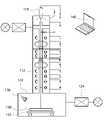
도 1에 도시된 바와 같이, 전자빔 건(10)이 상측에 구비되며, 하측에는 피가공물(40)이 위치되는 챔버(20)가 구비된다. 그리고, 상기 전자빔 건(10) 측에서 방출되는 전자빔을 챔버(20)까지 안내하는 전자빔 방출관(60)이 구비된다.As shown in FIG. 1 , the
그리고, 전자빔이 방출되는 끝단에는 전자빔 가공시 비산하는 이물질이 전자빔 건(10) 측으로 유입되지 않도록 차단하는 데브리 모듈(30)이 구비된다.In addition, a
또한, 상기 피가공물(40)의 하측에는 전자빔 조사시 급격하게 기화되는 백킹제(50)가 구비된다.In addition, a
즉, 도 2에 도시된 바와 같이, 전자빔이 피가공물(40)에 조사되어 용융되며, 더 진행되어 전자빔이 백킹제(50)에 조사되는 순간 백킹제(50)가 급격하게 기화되면서 그 압력으로 상부의 피가공물(40)이 용융된 부분을 불어내어 버리도록 구비된다.That is, as shown in FIG. 2 , the electron beam is irradiated to the
그러나, 이러한 구조는 불어내어지는 용융물이 상부측에 구비된 전자빔 건(10) 측으로 비산되므로, 비산물이 전자빔 건(10) 측으로 유입될 위험이 커지게 되며, 이 때문에 데브리 모듈(30)의 간소화 또는 삭제가 불가능해진다.However, in this structure, since the blown melt is scattered toward the
따라서, 데브리 모듈(30)의 부피(높이)를 줄이기 어려우므로 전자빔의 집속이 조절되는 렌즈부와 피가공물(40) 사이의 거리인 워킹 디스턴스(working distance)를 축소시키는데 한계가 있으며, 그에 따라 전자빔 폭의 축소에 한계점이 있으며, 이는 전자빔의 에너지 밀도에도 연관되어 가공정밀도 및 가공효율에도 영향을 미칠 수 있다.Therefore, since it is difficult to reduce the volume (height) of the
한편, 비산물이 전자빔 건(10) 측으로 유입될 위험을 줄이고자 피가공물(40)을 다소 경사지게 위치시켜 비산물이 비산되는 방향이 전자빔 건(10) 측이 아닌 다른 측을 향하게 할 수도 있으나, 이러한 경우에도 비산물이 발생되는 것은 여전하며, 전자빔 또한 피가공물(40)이 경사에 따라 같이 경사되어야 하므로 전자빔의 트렉킹 설정에 어려움이 있으며, 전자빔을 경사(편향)시키기 위한 편향기(deflector)등의 설치도 필요하여 워킹 디스턴스가 더 길게 형성되는 원인이 될 수 있고, 전자빔의 편향에 따라 데브리 모듈(30)의 전자빔 방출구의 크기도 그만큼 커져야 하는데, 그에 따라 데브리 유입 가능성이 증가하는 문제도 있다.On the other hand, in order to reduce the risk of scattering products entering the
또한, 백킹제(50)의 사용으로 인해 백킹제(50)가 기화되는 압력이 이미 형성된 홀(2)을 통해 배출되므로, 연속적인 홀 형성이 어려워 단순 홀(2) 형성 외에 절단 같은 연속적인 가공이 불가능한 문제점이 있다.In addition, since the pressure at which the
또한, 백킹제(50)로 인해 비산되는 용융물이 홀의 입구에서 버어를 형성하게 되어 정밀하고 깨끗한 홀의 형성이 어려우며, 이렇게 생성된 버어는 피가공물 소재와 일체로 굳어지게 되어 고난도의 후가공이 필요한 문제점이 있다.In addition, the melt scattered due to the
또한, 종래의 전자빔 가공장치의 경우에는 피가공물(40)의 소재가 메탈 등의 전도성 소재로 한정되는 문제가 있었다.In addition, in the case of the conventional electron beam processing apparatus, there was a problem in that the material of the
이는, 유리나 세라믹, 실리콘 등의 비전도체인 경우, 조사된 전자빔의 전자가 표면에 쌓여 전기장이 형성되어 전자빔의 조사를 간섭하게 되는 문제점이 있으며, 또한, 유리나 세라믹, 실리콘 등의 부도체들은 메탈 류에 비하여 열전도율이 무척 낮아 전자빔 조사지점에만 열이 급격히 상승하여 열충격이 발생하게되어 결국 크랙이 발생되는 것이 이유이다.This is a problem in that, in the case of a non-conductor such as glass, ceramic, or silicon, electrons of the irradiated electron beam are accumulated on the surface and an electric field is formed to interfere with the irradiation of the electron beam. Compared to that, the thermal conductivity is very low, and the heat rapidly rises only at the point where the electron beam is irradiated, resulting in thermal shock and eventually cracking.
그러나, 최근에는 유리나 세라믹 등의 비전도체의 경우에도 정밀한 가공이 요구되는 경우도 많아 비전도체에도 전자빔으로 가공할 수 있는 장치나 방법 등이 요구되고 있다.However, in recent years, even in the case of a non-conductor such as glass or ceramic, precise processing is often required, so an apparatus or method capable of processing the non-conductor with an electron beam is required.
본 발명은 상기와 같은 문제점을 해결하기 위한 것으로서, 메탈 등의 전도체뿐만 아니라 유리나 세라믹 등의 비전도체도 가공이 가능하며, 전자빔 장치의 오염도를 낮출 수 있으며, 전자빔 장치의 크기를 줄일 수 있고, 홀뿐만 아니라 절단가공도 가능한 전자빔을 이용한 가공장치 및 가공방법을 제공하는 것이 과제이다.The present invention is intended to solve the above problems, and it is possible to process not only conductors such as metal but also non-conductors such as glass or ceramics, can lower the degree of contamination of the electron beam device, reduce the size of the electron beam device, and the hole In addition, it is an object to provide a processing apparatus and processing method using an electron beam capable of cutting processing.
본 발명의 과제들은 이상에서 언급한 과제들로 제한되지 않으며, 언급되지 않는 또 다른 과제들은 아래의 기재로부터 당업자에게 명확하게 이해될 수 있을 것이다.The problems of the present invention are not limited to the problems mentioned above, and other problems not mentioned will be clearly understood by those skilled in the art from the following description.
상기한 과제를 해결하기 위하여, 본 발명의 일 형태에 따르면, 피가공물이 위치되는 챔버, 상기 챔버에 위치된 피가공물에 전자빔을 조사하는 전자빔 건, 상기 챔버에 위치된 피가공물을 전자빔 조사전에 예열온도로 예열하는 예열수단, 상기 전자빔 건 및 예열수단을 제어하는 제어부를 포함하는 전자빔을 이용한 가공장치가 개시된다.In order to solve the above problems, according to one aspect of the present invention, a chamber in which a workpiece is positioned, an electron beam gun irradiating an electron beam to the workpiece positioned in the chamber, and a workpiece positioned in the chamber are preheated before electron beam irradiation Disclosed is a processing apparatus using an electron beam including a preheating means for preheating to a temperature, and a control unit for controlling the electron beam gun and the preheating means.
상기 피가공물은 부도체일 수 있다.The workpiece may be an insulator.
상기 피가공물은, 유리, 쿼츠, 세라믹, 실리콘 중 어느 하나의 재질일 수 있다.The workpiece may be made of any one of glass, quartz, ceramic, and silicon.
상기 제어부는 상기 피가공물을 소재의 유리전이온도의 30% 이상 100%이하로 예열하도록 상기예열수단을 제어할 수 있다.The control unit may control the preheating means to preheat the workpiece to 30% or more and 100% or less of the glass transition temperature of the material.
상기 피가공물은 메탈일 수 있다.The workpiece may be a metal.
상기 제어부는 상기 피가공물을 소재의 용융온도의 30% 이상 80%이하로 예열하도록 상기 예열수단을 제어할 수 있다.The control unit may control the preheating means to preheat the workpiece to 30% or more and 80% or less of the melting temperature of the material.
상기 피가공물의 전자빔 입사면에 코팅되며, 접지가 이루어지는 전도코팅층을 더 포함할 수 있다.It may further include a conductive coating layer that is coated on the electron beam incident surface of the workpiece and is grounded.
상기 전도코팅층은, 전기가 통하는 전도체이고, 비자성체 재질로 형성될 수 있다.The conductive coating layer is a conductor through which electricity passes, and may be formed of a non-magnetic material.
상기 전도코팅층은, 구리 또는 스테인레스 재질일 수 있다.The conductive coating layer may be made of copper or stainless steel.
한편, 본 발명의 다른 형태에 따르면, 피가공물을 예열온도까지 예열하는 예열단계, 상기 예열온도까지 가열된 피가공물의 표면에 전자빔을 조사하여 조사된 지점의 피가공물의 소재가 승화되도록 가열하는 전자빔 조사단계를 포함할 수 있다.Meanwhile, according to another aspect of the present invention, in a preheating step of preheating the workpiece to a preheating temperature, an electron beam is irradiated to the surface of the workpiece heated to the preheating temperature to sublimate the material of the workpiece at the irradiated point. It may include an investigation step.
상기 피가공물이 부도체인 경우, 상기 예열온도는 피가공물 소재의 유리전이온도의 30% 이상 100% 이하일 수 있다.When the workpiece is a non-conductor, the preheating temperature may be 30% or more and 100% or less of the glass transition temperature of the workpiece material.
상기 피가공물이 메탈인 경우, 상기 예열온도는 피가공물 소재의 용융온도의 30% 이상 80% 이하일 수 있다.When the workpiece is a metal, the preheating temperature may be 30% or more and 80% or less of the melting temperature of the workpiece material.
피가공물의 전자빔 입사면에 전도코팅층을 형성하는 코팅층 형성단계를 더 포함할 수 있다.The method may further include a coating layer forming step of forming a conductive coating layer on the electron beam incident surface of the workpiece.
전자빔 조사 후, 전도코팅층을 제거하는 코팅층 제거단계를 더 포함할 수 있다.After the electron beam irradiation, it may further include a coating layer removal step of removing the conductive coating layer.
상기 코팅층 제거단계는, 전해연마방법으로 이루어질 수 있다.The coating layer removing step may be performed by an electrolytic polishing method.
본 발명의 전자빔을 이용한 가공장치 및 가공방법에 따르면 다음과 같은 효과가 있다.According to the processing apparatus and processing method using the electron beam of the present invention, there are the following effects.
첫째, 메탈 등의 전도체뿐만 아니라 유리나 세라믹 등의 비전도체 또한 전자빔으로 가공할 수 있어 적용소재를 다양화 할 수 있는 효과가 있다.First, not only conductors such as metals, but also non-conductors such as glass or ceramics can be processed with an electron beam, which has the effect of diversifying application materials.
둘째, 예열 후 전자빔 조사가 이루어짐으로써, 피가공물의 전자빔이 조사된 부분이 용융되기 전에 순간적인 승화 또는 기화가 가능하여 백킹제를 적용할 필요가 없어지는 장점이 있다.Second, since electron beam irradiation is performed after preheating, instantaneous sublimation or vaporization is possible before the portion irradiated with the electron beam of the workpiece is melted, thereby eliminating the need to apply a backing agent.
셋째, 백킹제를 적용할 필요가 없으므로, 백킹제에 의해 비산되는 오염물질 및 버어의 형성을 배제할 수 있어, 전자빔 장치의 오염 및 버어의 형성의 문제를 해결할 수 있다.Third, since there is no need to apply a backing agent, it is possible to exclude the formation of burrs and contaminants scattered by the backing agent, thereby solving the problems of contamination of the electron beam device and the formation of burrs.
넷째, 백킹제를 적용하지 않아도, 홀의 형성이 가능하므로, 연속적인 홀 형성을 통한 절단가공 등의 연속가공이 가능한 장점이 있다.Fourth, since the formation of a hole is possible without applying a backing agent, there is an advantage that continuous processing such as cutting processing through continuous hole formation is possible.
다섯째, 데브리 모듈의 삭제가 가능하여, 전자빔 장치를 간소화 시키며 크기를 축소시킬 수 있는 장점이 있다.Fifth, since the debris module can be deleted, there is an advantage of simplifying the electron beam device and reducing the size.
본 발명의 효과들은 이상에서 언급한 효과들로 제한되지 않으며, 언급되지 않은 또 다른 효과들은 청구범위의 기재로부터 당업자에게 명확하게 이해될 수 있을 것이다.The effects of the present invention are not limited to the above-mentioned effects, and other effects not mentioned will be clearly understood by those skilled in the art from the description of the claims.
아래에서 설명하는 본 출원의 바람직한 실시예의 상세한 설명뿐만 아니라 위에서 설명한 요약은 첨부된 도면과 관련해서 읽을 때에 더 잘 이해될 수 있을 것이다. 본 발명을 예시하기 위한 목적으로 도면에는 바람직한 실시예들이 도시되어 있다. 그러나, 본 출원은 도시된 정확한 배치와 수단에 한정되는 것이 아님을 이해해야 한다.
도 1은 종래의 전자빔 가공장치를 도시한 도면;
도 2는 종래의 전자빔 가공장치에서, 백킹제에 의해 용융물이 비산되는 모습을 도시한 도면;
도 3은 본 발명의 일 실시예에 따른 전자빔 가공장치를 도시한 도면;
도 4는 피가공물이 예열된 상태와 그렇지 않은 상태에서 전자빔이 조사량과 온도상승의 그래프;
도 5는 전도코팅층이 형성된 피가공물에 홀이 형성된 모습을 도시한 도면;
도 6은 전도코팅층이 제거된 후의 피가공물을 도시한 도면;
도 7은 본 발명의 전자빔을 이용한 가공방법을 도시한 순서도 이다.The summary set forth above as well as the detailed description of the preferred embodiments of the present application set forth below may be better understood when read in conjunction with the accompanying drawings. For the purpose of illustrating the invention, there are shown in the drawings preferred embodiments. It should be understood, however, that the present application is not limited to the precise arrangements and instrumentalities shown.
1 is a view showing a conventional electron beam processing apparatus;
Figure 2 is a view showing a state in which the melt is scattered by the backing agent in the conventional electron beam processing apparatus;
Figure 3 is a view showing an electron beam processing apparatus according to an embodiment of the present invention;
4 is a graph of the amount of irradiation and the temperature rise of the electron beam in a state in which the workpiece is preheated and in a state in which it is not;
5 is a view showing a state in which a hole is formed in a workpiece on which a conductive coating layer is formed;
6 is a view showing a workpiece after the conductive coating layer is removed;
7 is a flowchart illustrating a processing method using an electron beam of the present invention.
이하 본 발명의 목적이 구체적으로 실현될 수 있는 본 발명의 바람직한 실시예를 첨부된 도면을 참조하여 설명한다. 본 실시예를 설명함에 있어서, 동일 구성에 대해서는 동일 명칭 및 동일 부호가 사용되며 이에 따른 부가적인 설명은 생략하기로 한다.Hereinafter, preferred embodiments of the present invention in which the object of the present invention can be specifically realized will be described with reference to the accompanying drawings. In describing the present embodiment, the same names and the same reference numerals are used for the same components, and an additional description thereof will be omitted.
이하, 본 발명의 전자빔 가공장치의 일 실시예에 대해서 설명하기로 한다.Hereinafter, an embodiment of the electron beam processing apparatus of the present invention will be described.
본 발명의 일 실시예에 따른 전자빔을 이용한 가공장치는 도 3에 도시된 바와 같이, 챔버(120), 전자빔 건(110), 예열수단(130) 및 제어부(140)를 포함할 수 있다.As shown in FIG. 3 , the processing apparatus using an electron beam according to an embodiment of the present invention may include a
상기 챔버(120)는 피가공물(150)이 위치되는 공간이다. 상기 챔버(120)는 피가공물(150)이 놓여지기 위한 척 또는 스테이지(122) 등이 구비될 수 있으며, 상기 챔버(120) 내에 진공을 형성하기 위한 진공펌프()124 등이 구비될 수 있다.The
상기 전자빔 건(110)은 전자빔을 생성하여 방출하는 구성요소로서, 열전자빔 방식이거나 또는 플라즈마를 이용한 콜드 타입 전자빔 방식일 수도 있는 등 다양한 방식의 전자빔 건(110)이 적용될 수 있다. 상기 전자빔 건(110)은 생성된 전자빔을 상기 챔버(120) 내의 피가공물(150)로 조사시킬 수 있다. 이를 위하여, 조사되는 전자빔을 편향시키거나 확산 또는 집속하기 위한 코일 등이 전자빔 조사 경로상에 위치될 수 있다.The
즉, 상기 전자빔 건(110)에서 조사된 전자빔은 코일 등에 의해 집속 및 편향 된 뒤에 챔버(120)에 위치된 피가공물(150)의 임의의 위치에 조사되어 조사된 지점을 가공할 수 있다.That is, after the electron beam irradiated from the
이 때, 상기 피가공물(150)은 설치면과 상기 피가공물(150)을 지지하는 스테이지(122)의 수평이송방향에 수평하며, 상기 전자빔의 광축에 수직하도록 놓여질 수 있다. 게 놓여질 수 있다. 그러나, 반드시 이에 한정되는 것은 아니다.At this time, the
한편, 상기 예열수단(130)은 상기 챔버(120)에 위치된 피가공물(150)을 전자빔 조사를 이용한 가공 전에 예열온도로 가열하는 수단으로서, 예를 들어 챔버(120)를 균일하게 가열할 수 있는 버너나 피가공물(150)만을 가열할 수 있는 할로겐 램프 또는 열선 등 다양한 수단으로 구현될 수 있다. 또한, 전자빔 건(110)의 전자빔으로서 피가공물(150)을 예열시키는 것 또한 가능할 것이다. 이러한 경우, 전자빔 건(110)이 가공의 목적으로 전자빔을 조사하는 것과는 구분되어야 할 것이다.On the other hand, the preheating means 130 is a means for heating the
또한, 상기 제어부(140)는, 상기 전자빔 건(110) 및 예열수단(130)을 제어하는 구성요소로서, 통합 설치된 마이컴 등으로 구비되거나, 또는 외부에 구비되어 유선 또는 무선 통신으로 전자빔 건(110) 또는 예열수단(130)과 연결된 컴퓨터 일 수 있다.In addition, the
본 실시예에서 상기 피가공물(150)은 전도체 또는 비전도체 일 수 있다.In this embodiment, the
전통적으로, 전자빔을 이용한 가공은 대부분 메탈 등의 전도체 소재에 국한되어 있었다. 이는 전도체 소재의 경우, 조사되는 전자들의 피가공물(150) 내 이동이 자유로워 피가공물(150) 외부로 전자들이 배출되므로 피가공물(150)에 전자가 축적되지 아니하여 전자빔의 조사를 방해하는 전기장이 형성되지 아니하므로 전자빔이 정밀하게 조사될 수 있다.Traditionally, processing using electron beams has been mostly limited to conductive materials such as metals. This is because, in the case of a conductive material, electrons to be irradiated are free to move within the
또한, 일반적으로 메탈은 열전도율이 높기도 하고, 연성(ductility)을 가지고 있어, 조사된 열이 주변으로 퍼져나가 조사지점과 주변의 열팽창량의 차이 및 온도차이가 작아 상대적으로 열 충격이 작으므로 전자빔으로 가공이 가능하였다.In addition, in general, metal has high thermal conductivity and ductility, so that the irradiated heat spreads to the surroundings and the difference in the amount of thermal expansion and temperature difference between the irradiation point and the surroundings is small, so the thermal shock is relatively small. processing was possible.
그러나, 유리나 세라믹 등의 비전도체 소재의 경우, 조사된 전자빔에 의해 전자가 이동되지 아니하고 소재 내부에 축적됨으로써 충전현상이 일어나며, 이는 피가공물(150)에 전기장을 형성함으로써 정밀한 전자빔 조사를 방해할 수 있다.However, in the case of a non-conductive material such as glass or ceramic, the electrons are not moved by the irradiated electron beam and are accumulated inside the material, thereby causing a charging phenomenon, which can prevent precise electron beam irradiation by forming an electric field in the
또한, 유리나 세라믹, 실리콘 등의 비전도체는 열전도율이 상대적으로 낮거나 취성이 강하여, 조사된 열이 주변으로 퍼져나가지 않아 조사지점과 그 주변의 열팽창량의 차이 및 온도차이가 매우 커서 상대적으로 열 충격이 크게 작용하여 전자빔 조사시 크랙이 발생되어 깨지거나 하는 일이 많았다.In addition, non-conductors such as glass, ceramic, and silicon have relatively low thermal conductivity or strong brittleness, so that the irradiated heat does not spread to the surroundings. Due to this large effect, cracks were generated during electron beam irradiation, and cracks often occurred.
그러나, 본 실시예에서는 상기 전자빔으로 가공하는 피가공물(150)의 소재가 메탈 등의 전도체뿐만 아니라 비전도체를 포함할 수 있다.However, in the present embodiment, the material of the
상기 비전도체는 예를 들어 유리나, 쿼츠(석영), 세라믹 또는 실리콘 등의 소재일 수 있다.The non-conductor may be, for example, a material such as glass, quartz (quartz), ceramic, or silicon.
상기 예열수단(130)은 상기 피가공물(150)에 가공목적의 전자빔 조사 전에 상기 피가공물(150)을 예열 할 수 있다. 이 때, 상기 피가공물(150)이 비전도체 소재인 경우, 소재의 유리전이온도 근처까지 예열할 수 있다.The preheating means 130 may preheat the
유리나 쿼츠, 실리콘이나 세라믹 등의 소재는 유리전이온도(glass transition temperature)를 가지고 있는데, 이러한 유리전이온도는 유리전이가 일어나는 온도로서, 소재의 물리적 성질이 유리상의 딱딱한 상태에서 고무와 같이 물렁해지는 상태로 변화될 수 있다.Materials such as glass, quartz, silicon, or ceramics have a glass transition temperature, which is the temperature at which the glass transition occurs. can be changed to
즉, 소재가 유리전이온도 근방으로 가열될수록 연성(ductility)이 증가할 수 있다. 이렇게 연성이 증가된 경우, 열팽창량이 다소 상이하여도 변형량의 차이에 따른 열 충격의 크기를 다소 줄일 수 있다.That is, as the material is heated near the glass transition temperature, ductility may increase. When the ductility is increased in this way, even if the amount of thermal expansion is slightly different, the magnitude of the thermal shock according to the difference in the amount of deformation may be somewhat reduced.
한편, 도 4에 도시된 바와 같이, 전자빔 조사 에너지에 따른 소재의 온도 증가는 전자빔 조사의 초기에는 온도상승이 미미하다가 어느 정도 이후부터는 2차 함수적으로 급격하게 증가하는 경향을 알 수 있다.On the other hand, as shown in FIG. 4 , it can be seen that the temperature increase of the material according to the electron beam irradiation energy has a slight increase in the temperature at the initial stage of the electron beam irradiation, and then rapidly increases as a quadratic function after a certain point.
이 때, 예열되어 소재의 온도가 미리 상승되어 있는 경우에는 소재의 온도가 증가하는 구간이 그래프 상 좌측으로 이동되어 있어, 동일한 에너지의 전자빔 조사에 의해서도 예열되지 아니한 경우에 비하여 비교적 온도가 급격히 상승할 수 있음을 알 수 있다. 즉, 예를 들어, 섭씨 200도씨로 예열된 상태의 피가공물과 예열이 되지 않은 상온(섭씨 20도씨)의 피가공물에 동일한 에너지의 전자빔을 조사하였을 때, 예열된 피가공물의 온도가 더 급격하게 상승됨을 알 수 있다.At this time, when the temperature of the material is increased by preheating, the section in which the temperature of the material increases is shifted to the left on the graph, so that the temperature rises relatively rapidly compared to the case where the temperature is not preheated even by irradiation with an electron beam of the same energy. It can be seen that That is, for example, when an electron beam of the same energy is irradiated to a workpiece preheated to 200 degrees Celsius and a workpiece at room temperature (20 degrees Celsius) that has not been preheated, the temperature of the preheated workpiece is higher. It can be seen that there is a sharp rise.
그리고, 온도가 급격히 상승함으로써, 소재가 액체상태로 용융되지 아니하고 고체상태에서 전자빔을 조사받아 바로 승화되거나 또는, 용융된다고 하더라도 극히 짧은 시간만에 바로 기화될 수 있음을 알 수 있다.And, it can be seen that by rapidly increasing the temperature, the material does not melt into a liquid state, but sublimes immediately upon irradiation with an electron beam in a solid state, or even if melted, it can be immediately vaporized in a very short time.
즉, 상기 예열수단(130)에 따라 피가공물(150)이 해당 소재의 유리전이온도 근방까지 예열되어, 형태는 유지하면서도 전자빔 조사에 따른 열충격을 완화하여 크랙발생을 방지하며, 단시간의 전자빔 조사로도 급격한 온도상승을 이룰 수 있어 피가공물(150)의 전자빔 조사지점을 바로 기화시켜 홀(152)의 형성이 가능할 수 있다. That is, according to the preheating means 130, the
또한, 상기 챔버(120)의 내부는 진공분위기로 형성되므로, 전자빔이 조사된 피가공물(150) 소재의 승화가 더욱 용이하게 일어날 수 있다.In addition, since the inside of the
이에 따라, 백킹제의 사용을 배제할 수 있어, 백킹제의 사용에 따른 데브리 비산 문제라던가 표면 버어 형성문제 및 연속홀 가공 불가 문제를 해결할 수 있다.Accordingly, the use of the backing agent can be excluded, and the problem of debris scattering due to the use of the backing agent, the problem of surface burrs formation, and the problem of continuous hole processing can be solved.
이 때, 상기 예열수단(130)에 의해 가열되는 예열온도는, 상기 피가공물(150)이 유리, 쿼츠, 세라믹, 실리콘 등의 부도체인 경우, 소재의 유리전이온도의 30% 이상 100%이하의 온도까지 예열할 수 있다.At this time, the preheating temperature heated by the preheating means 130 is 30% or more and 100% or less of the glass transition temperature of the material when the
또한, 상기 피가공물(150)이 메탈 등의 전도체일 경우, 소재의 용융온도의 30%이상 80%이하로 예열할 수 있다. 이는 소재의 용융온도까지 예열할 경우 피가공물(150)이 자기 형태를 유지하지 못하기 때문이다.In addition, when the
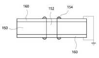
한편, 도 5에 도시된 바와 같이, 상기 피가공물(150)이 부도체인 경우, 상기 피가공물(150)의 전자빔 입사면(가공면)의 표면에 전도코팅층(160)이 형성될 수 있다.Meanwhile, as shown in FIG. 5 , when the
상기 전도코팅층(160)은 전도체이고, 비성체이며, 가공 후 전기분해연마 등의 후작업으로서 용이하게 제거가 가능한 재질로 형성될 수 있다. 예를 들어 구리나 스테인레스 금속일 수 있다.The
이러한 전도코팅층(160)이 피가공물(150)의 전자빔 입사면에 얇게 형성되며, 또한 접지가 이루어질 수 있다. 그리고, 상기 피가공물(150)의 전자빔 입사면에 대향되는 면에도 상기 전도코팅층(160)이 접지가 이루어지도록 형성될 수 있다.The
전자의 이동이 가능한 전도코팅층(160)이 전자빔 입사면에 형성되므로, 피가공물(150)에 조사된 전자는 전도코팅층(160)을 타고 외부로 배출되어 전하축적현상이 발생되지 아니하여 정밀한 전자빔 조사가 가능해질 수 있다.Since the
또한, 상기 소재가 승화될 때, 일부는 도 5에 도시된 바와 같이, 기화된 상기 피가공물(150)의 소재가 홀(152) 입구에 다시 재응축되어 미세한 돌기(154)를 형성할 수 있는데, 이러한 재응축되는 부분이 전도코팅층(160) 표면에 형성될 것이므로, 도 6에 도시된 바와 같이, 상기 전도코팅층(160)을 제거하면서 같이 제거될 수 있다.In addition, when the material is sublimed, as shown in FIG. 5, the vaporized material of the
이하, 본 발명의 전자빔을 이용한 가공방법의 일 실시예를 설명하기로 한다.Hereinafter, an embodiment of the processing method using the electron beam of the present invention will be described.
본 실시예에 따른 전자빔을 이용한 가공방법은 도 7에 도시된 바와 같이, 예열단계(S120) 및 전자빔 조사단계(S130)를 포함할 수 있다.The processing method using the electron beam according to the present embodiment may include a preheating step (S120) and an electron beam irradiation step (S130) as shown in FIG. 7 .
그리고, 상기 예열단계(S120)가 수행되기 전에 피가공물(150)의 전자빔 입사면에 전도코팅층(160)을 형성하는 코팅층 형성단계(S110)가 수행될 수 있다. 상기 코팅층 형성단계(S110)는, 피가공물(150)의 전자빔 입사면 및 그에 대향하는 면에 전도체이고 비자성체 소재의 재질을 코팅하는 단계일 수 있다. 일 예를 들어 구리 또는 스테인레스 소재를 코팅할 수도 있다. 물론, 반드시 코팅될 필요는 없으며, 구리 또는 스테인레스 소재의 판재가 피가공물(150)의 표면에 금속박 형태로 입혀지거나 부착될 수도 있을 것이다.And, before the preheating step (S120) is performed, the coating layer forming step (S110) of forming the
상기 코팅층 형성단계(S110)는, 피가공물(150)이 비전도체 소재일 경우 수행될 수 있으며, 상기 피가공물(150)이 전도체 소재일 경우 수행되지 아니할 수도 있다. 물론, 상기 피가공물(150)이 전도체 소재라고 하여도 필요할 경우 상기 코팅층 형성단계(S110)가 수행될 수 있다.The coating layer forming step (S110) may be performed when the
그리고, 이렇게 전도코팅층(160)이 형성된 피가공물(150)이 챔버(120) 내부에 위치되며, 챔버(120) 내부는 진공상태가 형성될 수 있다. 이 때, 상기 피가공물(150)에 형성된 전도코팅층(160)은 접지가 이루어질 수 있다.Then, the
그리고, 예열단계(S120)가 수행될 수 있다. 상기 예열단계(S120)에서는 상기 피가공물(150)을 예열온도까지 예열하는 단계이다.Then, a preheating step ( S120 ) may be performed. The preheating step (S120) is a step of preheating the
상기 피가공물(150)이 비전도체 소재일 경우, 상기 예열온도는 피가공물(150)의 형태가 유지되면서, 소재의 연성(ductility)이 증가하여 전자빔이 조사되었을 때 열충격으로 크랙이 발생하지 않을 온도이며, 또한 전자빔이 조사되었을 때, 피가공물(150)의 조사된 지점의 온도가 급격히 상승되어 고체상태로부터 용융단계를 거치지 않고 바로 기화가 가능한 정도의 온도일 수 있다. 또는, 극히 짧은 시간내에 순간적으로 용융상태로부터 기화가 가능한 온도일 수도 있다.When the
예를 들어, 상기 예열온도는 상기 피가공물(150) 소재의 유리전이온도의 30% 이상 100%이하의 온도일 수 있다. 이러한 예열온도는 소재별로 상이할 수 있으며, 또한, 피가공물(150)에 조사되는 전자빔의 출력이나 세기, 조사시간 등에 의해 달라질 수 있는 온도이다.For example, the preheating temperature may be a temperature of 30% or more and 100% or less of the glass transition temperature of the material of the
또는 상기 피가공물(150)이 전도체 소재일 경우, 상기 예열온도는, 피가공물(150)의 형태는 유지되면서, 전자빔이 조사되었을 때, 피가공물(150)의 조사된 지점의 온도가 급격히 상승되어 고체상태로부터 용융단계를 거치지 않고 바로 기화가 가능한 정도의 온도일 수 있다. 또는, 극히 짧은 시간내에 순간적으로 용융상태로부터 기화가 가능한 온도일 수도 있다.Alternatively, when the
상기 예열단계(S120)에서 피가공물(150)의 예열이 완료된 후에는 전자빔 조사단계(S130)가 수행될 수 있다. 상기 전자빔 조사단계(S130)는, 상기 예열온도까지 가열된 피가공물(150)의 표면에 전자빔을 조사하여 조사된 지점의 피가공물(150)의 소재가 승화 또는 기화 되도록 가열하는 단계이다.After the preheating of the
상기 예열단계(S120)에서, 피가공물(150)이 예열온도로 이미 가열되었으므로, 상기 전자빔 조사단계(S130)에서 전자빔이 피가공물(150)에 조사되면, 전자빔이 조사된 지점의 온도가 급격하게 상승하여, 피가공물(150)의 전자빔이 조사된 지점이 용융상태를 거치지 않고 곧바로 기화될 수 있다. 또는, 피가공물(150)의 전자빔이 조사된 지점이 용융상태를 거치는 시간이 극히 짧아질 수 있을 것이다.In the preheating step (S120), since the
따라서, 전자빔이 조사된 지점에 홀(152)이 형성되는 등의 가공이 이루어질 수 있다. 그리고, 이러한 홀(152)을 연속적으로 형성한다면 절단가공 또한 가능할 수 있다.Accordingly, processing such as forming the
그리고, 코팅층 제거단계(S140)가 수행될 수 있다. 상기 코팅층 제거단계(S140)는, 도 5 및 도 6에 도시된 바와 같이, 전자빔의 조사가 완료된 후에 상기 전도코팅층(160)을 제거하는 단계이다. 상기 코팅층 제거단계(S140)는 작업이 용이하고 단시간에 이루어지며, 피가공물(150)의 큰 영향을 끼치지 않는 전해연마방법으로 이루어질 수 있다. 물론, 이에 한정되는 것은 아니며, 물리적 연마나 박피 등의 방법으로서 제거할 수도 있을 것이다.Then, the coating layer removing step (S140) may be performed. The coating layer removing step (S140), as shown in FIGS. 5 and 6, is a step of removing the
한편, 도 5에 도시된 바와 같이, 소재가 승화 또는 기화될 때, 상기 피가공물(150)이 홀(152) 입구에 재응축되거나, 또는 미량의 액상의 용융된 소재가 홀(152) 입구에서 굳어져 버어형태의 돌기(154)를 형성할 수 있는데, 이러한 버어는 상기 전도코팅층(160) 표면에 형성되므로, 상기 코팅층 제거단계(S140)가 수행되면서 돌기(154) 또한 제거될 수 있어, 보다 정밀하고 미려한 홀(152) 형성이 가능할 수 있다.On the other hand, as shown in FIG. 5, when the material is sublimed or vaporized, the
이상과 같이 본 발명에 따른 바람직한 실시예를 살펴보았으며, 앞서 설명된 실시예 이외에도 본 발명이 그 취지나 범주에서 벗어남이 없이 다른 특정 형태로 구체화 될 수 있다는 사실은 해당 기술에 통상의 지식을 가진 이들에게는 자명한 것이다. 그러므로, 상술된 실시예는 제한적인 것이 아니라 예시적인 것으로 여겨져야 하고, 이에 따라 본 발명은 상술한 설명에 한정되지 않고 첨부된 청구항의 범주 및 그 동등 범위 내에서 변경될 수도 있다.As described above, preferred embodiments according to the present invention have been reviewed, and the fact that the present invention can be embodied in other specific forms without departing from the spirit or scope of the present invention in addition to the above-described embodiments is one of ordinary skill in the art. It is obvious to them. Therefore, the above-described embodiments are to be regarded as illustrative rather than restrictive, and accordingly, the present invention is not limited to the above description, but may be modified within the scope of the appended claims and their equivalents.
110: 전자빔 건 120: 챔버
122: 스테이지 124: 진공펌프
130: 예열수단 140: 제어부
150: 피가공물 152: 홀
154: 돌기 160: 전도코팅층
S110: 코팅층 형성단계 S120: 예열단계
S130: 전자빔 조사단계 S140: 코팅층 제거단계110: electron beam gun 120: chamber
122: stage 124: vacuum pump
130: preheating means 140: control unit
150: workpiece 152: hole
154: projection 160: conductive coating layer
S110: coating layer forming step S120: preheating step
S130: electron beam irradiation step S140: coating layer removal step
Claims (15)
Translated fromKorean상기 챔버에 위치된 피가공물에 전자빔을 조사하는 전자빔 건;
상기 챔버에 위치된 피가공물을 전자빔 조사전에 예열온도로 예열하는 예열수단;
상기 전자빔 건 및 예열수단을 제어하는 제어부;
상기 피가공물의 전자빔 입사면에 코팅되며, 접지가 이루어지고, 전기가 통하는 전도체이며, 비자성체 재질이며, 전해연마로 제거될 수 있는 재질인 스테인레스로 형성되는 전도코팅층;을 포함하며,
상기 제어부는,
상기 피가공물이 유리, 쿼츠, 세라믹, 실리콘 중 어느 하나의 재질인 경우, 상기 피가공물을 상기 예열수단을 통해 피가공물 소재의 유리전이온도의 30%이상 100%이하로 예열한 후, 상기 전자빔 건을 통해 상기 피가공물에 전자빔을 조사하도록 제어하는 전자빔을 이용한 가공장치.
a chamber in which the workpiece is located;
an electron beam gun for irradiating an electron beam to the workpiece positioned in the chamber;
preheating means for preheating the workpiece positioned in the chamber to a preheating temperature before electron beam irradiation;
a control unit for controlling the electron beam gun and the preheating means;
A conductive coating layer is coated on the electron beam incident surface of the workpiece, is grounded, is an electrically conductive conductor, is a non-magnetic material, and is made of stainless steel, a material that can be removed by electrolytic polishing;
The control unit is
When the workpiece is made of any one of glass, quartz, ceramic, and silicon, the workpiece is preheated to 30% or more and 100% or less of the glass transition temperature of the workpiece material through the preheating means, and then the electron beam gun A processing apparatus using an electron beam for controlling to irradiate the electron beam on the workpiece through the
피가공물의 전자빔 입사면에 전기가 통하는 전도체 이면서 비자성체 재질인 스테인레스로 이루어지는 전도코팅층을 형성하는 코팅층 형성단계;
상기 전도코팅층이 형성된 피가공물을 예열온도까지 예열하는 예열단계;
상기 예열온도까지 가열된 피가공물의 표면에 전자빔을 조사하여 조사된 지점의 피가공물의 소재가 승화되도록 가열하는 전자빔 조사단계;
전해연마 방법으로서 상기 전도코팅층을 제거하는 코팅층 제거단계;
를 포함하며,
상기 예열단계에서,
상기 피가공물이 유리, 쿼츠, 세라믹, 실리콘 중 어느 하나의 재질인 경우,
상기 예열온도는 피가공물 소재의 유리전이온도의 30% 이상 100% 이하인 전자빔을 이용한 가공방법.
In the processing method using the electron beam of the processing apparatus using the electron beam of claim 1,
A coating layer forming step of forming a conductive coating layer made of stainless steel, which is a conductive and non-magnetic material, on the electron beam incident surface of the workpiece;
a preheating step of preheating the workpiece on which the conductive coating layer is formed to a preheating temperature;
an electron beam irradiation step of irradiating an electron beam on the surface of the workpiece heated to the preheating temperature to heat the material of the workpiece at the irradiated point to sublimate;
A coating layer removal step of removing the conductive coating layer as an electrolytic polishing method;
includes,
In the preheating step,
When the workpiece is made of any one of glass, quartz, ceramic, and silicon,
The preheating temperature is a processing method using an electron beam that is 30% or more and 100% or less of the glass transition temperature of the workpiece material.
Priority Applications (1)
| Application Number | Priority Date | Filing Date | Title |
|---|---|---|---|
| KR1020200152029AKR102439455B1 (en) | 2020-11-13 | 2020-11-13 | Electron beam processing apparatus and processing method |
Applications Claiming Priority (1)
| Application Number | Priority Date | Filing Date | Title |
|---|---|---|---|
| KR1020200152029AKR102439455B1 (en) | 2020-11-13 | 2020-11-13 | Electron beam processing apparatus and processing method |
Publications (2)
| Publication Number | Publication Date |
|---|---|
| KR20220065466A KR20220065466A (en) | 2022-05-20 |
| KR102439455B1true KR102439455B1 (en) | 2022-09-02 |
Family
ID=81801542
Family Applications (1)
| Application Number | Title | Priority Date | Filing Date |
|---|---|---|---|
| KR1020200152029AActiveKR102439455B1 (en) | 2020-11-13 | 2020-11-13 | Electron beam processing apparatus and processing method |
Country Status (1)
| Country | Link |
|---|---|
| KR (1) | KR102439455B1 (en) |
Family Cites Families (4)
| Publication number | Priority date | Publication date | Assignee | Title |
|---|---|---|---|---|
| JPS6352781A (en)* | 1986-08-20 | 1988-03-05 | Mitsubishi Heavy Ind Ltd | Electron beam machining method for nonconductor material |
| TWI342582B (en)* | 2003-07-17 | 2011-05-21 | Applied Materials Inc | Method of surface texturizing |
| JP2015080800A (en) | 2013-10-23 | 2015-04-27 | 旭硝子株式会社 | Method for forming a through hole in a glass substrate using laser light |
| KR101871857B1 (en)* | 2016-10-27 | 2018-08-03 | 한국생산기술연구원 | Device for Brazing using Electron Beam and Method for Brazing using Electron Beam |
- 2020
- 2020-11-13KRKR1020200152029Apatent/KR102439455B1/enactiveActive
Also Published As
| Publication number | Publication date |
|---|---|
| KR20220065466A (en) | 2022-05-20 |
Similar Documents
| Publication | Publication Date | Title |
|---|---|---|
| US7427766B2 (en) | Method and apparatus for producing extreme ultraviolet radiation or soft X-ray radiation | |
| KR101433415B1 (en) | A fused furnace comprising a wire discharge ion plasma electron emitter | |
| EP2308629A1 (en) | Apparatus for generating a negatively charged ionic reducing gas | |
| JP5086409B2 (en) | Method for removing surface oxides by electron attachment | |
| US10994371B2 (en) | System and method for depositing a metal to form a three-dimensional part | |
| JPH0514416B2 (en) | ||
| CN104889570B (en) | Rapid forming equipment and method based on femtosecond laser and ion beam complex technique | |
| JP4846987B2 (en) | Apparatus and method for removing surface oxides by fluxless technology with electron deposition and remote ion generation | |
| KR102439455B1 (en) | Electron beam processing apparatus and processing method | |
| US4831230A (en) | Surface shaping and finishing apparatus and method | |
| KR102287256B1 (en) | Subzero Electron Beam Processing Device and Method for Processing using the same | |
| US9758858B2 (en) | Methods of manufacturing a coated structure on a substrate | |
| US6607613B2 (en) | Solder ball with chemically and mechanically enhanced surface properties | |
| TWI566284B (en) | Lavacoat pre-clean and pre-heat | |
| JP5294816B2 (en) | Suction-type local microplasma etching apparatus with microscope and local microplasma etching method | |
| Buetje | Excimer laser processing of metals considering the effects of pulse duration and geometrical aspects | |
| US3894208A (en) | Method of abrasive machining of material by means of an energy beam | |
| RU2384911C1 (en) | Method for treatment of electrodes in insulating gaps of high-voltage electric vacuum instruments | |
| KR102060222B1 (en) | Method for forming fine wiring | |
| KR100392709B1 (en) | low melting metal mount method and manufacture device of specimens for micro-surface analysis of radioactive materials | |
| Martinez-Calderon et al. | Performance of laser patterned copper plasmonic photocathodes | |
| US20240375132A1 (en) | Droplet applicator and method for generating molten metal droplets | |
| JP7384366B2 (en) | Powder bed preheating | |
| Eaton | Electron beam fusion and its applications | |
| US11148945B2 (en) | Method assisted by a laser and high-intensity electric fields for the synthesis and collection of nanoparticles and the generation of coatings |
Legal Events
| Date | Code | Title | Description |
|---|---|---|---|
| PA0109 | Patent application | Patent event code:PA01091R01D Comment text:Patent Application Patent event date:20201113 | |
| PA0201 | Request for examination | ||
| PE0902 | Notice of grounds for rejection | Comment text:Notification of reason for refusal Patent event date:20211019 Patent event code:PE09021S01D | |
| AMND | Amendment | ||
| E601 | Decision to refuse application | ||
| PE0601 | Decision on rejection of patent | Patent event date:20220428 Comment text:Decision to Refuse Application Patent event code:PE06012S01D Patent event date:20211019 Comment text:Notification of reason for refusal Patent event code:PE06011S01I | |
| PG1501 | Laying open of application | ||
| AMND | Amendment | ||
| PX0901 | Re-examination | Patent event code:PX09011S01I Patent event date:20220428 Comment text:Decision to Refuse Application Patent event code:PX09012R01I Patent event date:20211220 Comment text:Amendment to Specification, etc. | |
| PX0701 | Decision of registration after re-examination | Patent event date:20220826 Comment text:Decision to Grant Registration Patent event code:PX07013S01D Patent event date:20220729 Comment text:Amendment to Specification, etc. Patent event code:PX07012R01I Patent event date:20220428 Comment text:Decision to Refuse Application Patent event code:PX07011S01I Patent event date:20211220 Comment text:Amendment to Specification, etc. Patent event code:PX07012R01I | |
| X701 | Decision to grant (after re-examination) | ||
| GRNT | Written decision to grant | ||
| PR0701 | Registration of establishment | Comment text:Registration of Establishment Patent event date:20220830 Patent event code:PR07011E01D | |
| PR1002 | Payment of registration fee | Payment date:20220830 End annual number:3 Start annual number:1 | |
| PG1601 | Publication of registration |