KR102437591B1 - Operation method of nonvolatile memory system and method operation of memory controller - Google Patents
Operation method of nonvolatile memory system and method operation of memory controllerDownload PDFInfo
- Publication number
- KR102437591B1 KR102437591B1KR1020150171644AKR20150171644AKR102437591B1KR 102437591 B1KR102437591 B1KR 102437591B1KR 1020150171644 AKR1020150171644 AKR 1020150171644AKR 20150171644 AKR20150171644 AKR 20150171644AKR 102437591 B1KR102437591 B1KR 102437591B1
- Authority
- KR
- South Korea
- Prior art keywords
- reclaim
- read
- sub
- nonvolatile memory
- source block
- Prior art date
- Legal status (The legal status is an assumption and is not a legal conclusion. Google has not performed a legal analysis and makes no representation as to the accuracy of the status listed.)
- Active
Links
Images


Classifications
- G—PHYSICS
- G06—COMPUTING OR CALCULATING; COUNTING
- G06F—ELECTRIC DIGITAL DATA PROCESSING
- G06F3/00—Input arrangements for transferring data to be processed into a form capable of being handled by the computer; Output arrangements for transferring data from processing unit to output unit, e.g. interface arrangements
- G06F3/06—Digital input from, or digital output to, record carriers, e.g. RAID, emulated record carriers or networked record carriers
- G06F3/0601—Interfaces specially adapted for storage systems
- G06F3/0602—Interfaces specially adapted for storage systems specifically adapted to achieve a particular effect
- G06F3/061—Improving I/O performance
- G—PHYSICS
- G11—INFORMATION STORAGE
- G11C—STATIC STORES
- G11C16/00—Erasable programmable read-only memories
- G11C16/02—Erasable programmable read-only memories electrically programmable
- G11C16/06—Auxiliary circuits, e.g. for writing into memory
- G11C16/10—Programming or data input circuits
- G11C16/14—Circuits for erasing electrically, e.g. erase voltage switching circuits
- G11C16/16—Circuits for erasing electrically, e.g. erase voltage switching circuits for erasing blocks, e.g. arrays, words, groups
- G—PHYSICS
- G06—COMPUTING OR CALCULATING; COUNTING
- G06F—ELECTRIC DIGITAL DATA PROCESSING
- G06F11/00—Error detection; Error correction; Monitoring
- G06F11/07—Responding to the occurrence of a fault, e.g. fault tolerance
- G06F11/08—Error detection or correction by redundancy in data representation, e.g. by using checking codes
- G06F11/10—Adding special bits or symbols to the coded information, e.g. parity check, casting out 9's or 11's
- G06F11/1008—Adding special bits or symbols to the coded information, e.g. parity check, casting out 9's or 11's in individual solid state devices
- G06F11/1068—Adding special bits or symbols to the coded information, e.g. parity check, casting out 9's or 11's in individual solid state devices in sector programmable memories, e.g. flash disk
- G—PHYSICS
- G06—COMPUTING OR CALCULATING; COUNTING
- G06F—ELECTRIC DIGITAL DATA PROCESSING
- G06F12/00—Accessing, addressing or allocating within memory systems or architectures
- G06F12/02—Addressing or allocation; Relocation
- G06F12/0223—User address space allocation, e.g. contiguous or non contiguous base addressing
- G06F12/023—Free address space management
- G06F12/0238—Memory management in non-volatile memory, e.g. resistive RAM or ferroelectric memory
- G06F12/0246—Memory management in non-volatile memory, e.g. resistive RAM or ferroelectric memory in block erasable memory, e.g. flash memory
- G—PHYSICS
- G06—COMPUTING OR CALCULATING; COUNTING
- G06F—ELECTRIC DIGITAL DATA PROCESSING
- G06F3/00—Input arrangements for transferring data to be processed into a form capable of being handled by the computer; Output arrangements for transferring data from processing unit to output unit, e.g. interface arrangements
- G06F3/06—Digital input from, or digital output to, record carriers, e.g. RAID, emulated record carriers or networked record carriers
- G06F3/0601—Interfaces specially adapted for storage systems
- G06F3/0602—Interfaces specially adapted for storage systems specifically adapted to achieve a particular effect
- G06F3/0614—Improving the reliability of storage systems
- G06F3/0619—Improving the reliability of storage systems in relation to data integrity, e.g. data losses, bit errors
- G—PHYSICS
- G06—COMPUTING OR CALCULATING; COUNTING
- G06F—ELECTRIC DIGITAL DATA PROCESSING
- G06F3/00—Input arrangements for transferring data to be processed into a form capable of being handled by the computer; Output arrangements for transferring data from processing unit to output unit, e.g. interface arrangements
- G06F3/06—Digital input from, or digital output to, record carriers, e.g. RAID, emulated record carriers or networked record carriers
- G06F3/0601—Interfaces specially adapted for storage systems
- G06F3/0628—Interfaces specially adapted for storage systems making use of a particular technique
- G06F3/0638—Organizing or formatting or addressing of data
- G06F3/064—Management of blocks
- G—PHYSICS
- G06—COMPUTING OR CALCULATING; COUNTING
- G06F—ELECTRIC DIGITAL DATA PROCESSING
- G06F3/00—Input arrangements for transferring data to be processed into a form capable of being handled by the computer; Output arrangements for transferring data from processing unit to output unit, e.g. interface arrangements
- G06F3/06—Digital input from, or digital output to, record carriers, e.g. RAID, emulated record carriers or networked record carriers
- G06F3/0601—Interfaces specially adapted for storage systems
- G06F3/0628—Interfaces specially adapted for storage systems making use of a particular technique
- G06F3/0655—Vertical data movement, i.e. input-output transfer; data movement between one or more hosts and one or more storage devices
- G06F3/0659—Command handling arrangements, e.g. command buffers, queues, command scheduling
- G—PHYSICS
- G06—COMPUTING OR CALCULATING; COUNTING
- G06F—ELECTRIC DIGITAL DATA PROCESSING
- G06F3/00—Input arrangements for transferring data to be processed into a form capable of being handled by the computer; Output arrangements for transferring data from processing unit to output unit, e.g. interface arrangements
- G06F3/06—Digital input from, or digital output to, record carriers, e.g. RAID, emulated record carriers or networked record carriers
- G06F3/0601—Interfaces specially adapted for storage systems
- G06F3/0668—Interfaces specially adapted for storage systems adopting a particular infrastructure
- G06F3/0671—In-line storage system
- G06F3/0673—Single storage device
- G06F3/0679—Non-volatile semiconductor memory device, e.g. flash memory, one time programmable memory [OTP]
- G—PHYSICS
- G11—INFORMATION STORAGE
- G11C—STATIC STORES
- G11C16/00—Erasable programmable read-only memories
- G11C16/02—Erasable programmable read-only memories electrically programmable
- G11C16/06—Auxiliary circuits, e.g. for writing into memory
- G11C16/10—Programming or data input circuits
- G—PHYSICS
- G11—INFORMATION STORAGE
- G11C—STATIC STORES
- G11C16/00—Erasable programmable read-only memories
- G11C16/02—Erasable programmable read-only memories electrically programmable
- G11C16/06—Auxiliary circuits, e.g. for writing into memory
- G11C16/26—Sensing or reading circuits; Data output circuits
- G—PHYSICS
- G11—INFORMATION STORAGE
- G11C—STATIC STORES
- G11C16/00—Erasable programmable read-only memories
- G11C16/02—Erasable programmable read-only memories electrically programmable
- G11C16/06—Auxiliary circuits, e.g. for writing into memory
- G11C16/34—Determination of programming status, e.g. threshold voltage, overprogramming or underprogramming, retention
- G11C16/3418—Disturbance prevention or evaluation; Refreshing of disturbed memory data
- G11C16/3431—Circuits or methods to detect disturbed nonvolatile memory cells, e.g. which still read as programmed but with threshold less than the program verify threshold or read as erased but with threshold greater than the erase verify threshold, and to reverse the disturbance via a refreshing programming or erasing step
- G—PHYSICS
- G11—INFORMATION STORAGE
- G11C—STATIC STORES
- G11C16/00—Erasable programmable read-only memories
- G11C16/02—Erasable programmable read-only memories electrically programmable
- G11C16/06—Auxiliary circuits, e.g. for writing into memory
- G11C16/34—Determination of programming status, e.g. threshold voltage, overprogramming or underprogramming, retention
- G11C16/349—Arrangements for evaluating degradation, retention or wearout, e.g. by counting erase cycles
- G11C16/3495—Circuits or methods to detect or delay wearout of nonvolatile EPROM or EEPROM memory devices, e.g. by counting numbers of erase or reprogram cycles, by using multiple memory areas serially or cyclically
- G—PHYSICS
- G11—INFORMATION STORAGE
- G11C—STATIC STORES
- G11C29/00—Checking stores for correct operation ; Subsequent repair; Testing stores during standby or offline operation
- G11C29/04—Detection or location of defective memory elements, e.g. cell constructio details, timing of test signals
- G11C29/08—Functional testing, e.g. testing during refresh, power-on self testing [POST] or distributed testing
- G11C29/12—Built-in arrangements for testing, e.g. built-in self testing [BIST] or interconnection details
- G11C29/38—Response verification devices
- G11C29/42—Response verification devices using error correcting codes [ECC] or parity check
- G—PHYSICS
- G11—INFORMATION STORAGE
- G11C—STATIC STORES
- G11C29/00—Checking stores for correct operation ; Subsequent repair; Testing stores during standby or offline operation
- G11C29/52—Protection of memory contents; Detection of errors in memory contents
- G—PHYSICS
- G11—INFORMATION STORAGE
- G11C—STATIC STORES
- G11C16/00—Erasable programmable read-only memories
- G11C16/02—Erasable programmable read-only memories electrically programmable
- G11C16/04—Erasable programmable read-only memories electrically programmable using variable threshold transistors, e.g. FAMOS
- G11C16/0483—Erasable programmable read-only memories electrically programmable using variable threshold transistors, e.g. FAMOS comprising cells having several storage transistors connected in series
- G—PHYSICS
- G11—INFORMATION STORAGE
- G11C—STATIC STORES
- G11C29/00—Checking stores for correct operation ; Subsequent repair; Testing stores during standby or offline operation
- G11C29/04—Detection or location of defective memory elements, e.g. cell constructio details, timing of test signals
- G11C2029/0409—Online test
- G—PHYSICS
- G11—INFORMATION STORAGE
- G11C—STATIC STORES
- G11C29/00—Checking stores for correct operation ; Subsequent repair; Testing stores during standby or offline operation
- G11C29/04—Detection or location of defective memory elements, e.g. cell constructio details, timing of test signals
- G11C2029/0411—Online error correction
- G—PHYSICS
- G11—INFORMATION STORAGE
- G11C—STATIC STORES
- G11C2213/00—Indexing scheme relating to G11C13/00 for features not covered by this group
- G11C2213/70—Resistive array aspects
- G11C2213/75—Array having a NAND structure comprising, for example, memory cells in series or memory elements in series, a memory element being a memory cell in parallel with an access transistor
Landscapes
- Engineering & Computer Science (AREA)
- Theoretical Computer Science (AREA)
- Physics & Mathematics (AREA)
- General Engineering & Computer Science (AREA)
- General Physics & Mathematics (AREA)
- Human Computer Interaction (AREA)
- Quality & Reliability (AREA)
- Computer Security & Cryptography (AREA)
- Techniques For Improving Reliability Of Storages (AREA)
- Read Only Memory (AREA)
Abstract
Translated fromKoreanDescription
Translated fromKorean본 발명은 반도체 메모리에 관한 것으로, 더욱 상세하게는 저장 장치의 동작 방법에 관한 것이다.The present invention relates to a semiconductor memory, and more particularly, to a method of operating a storage device.
반도체 메모리 장치(semiconductor memory device)는 실리콘(Si, silicon), 게르마늄(Ge, Germanium), 비화 갈륨(GaAs, gallium arsenide), 인화인듐(InP, indium phosphide) 등과 같은 반도체를 이용하여 구현되는 기억장치이다. 반도체 메모리 장치는 크게 휘발성 메모리 장치(Volatile memory device)와 불휘발성 메모리 장치(Nonvolatile memory device)로 구분된다.A semiconductor memory device is a memory device implemented using semiconductors such as silicon (Si, silicon), germanium (Ge, Germanium), gallium arsenide (GaAs, gallium arsenide), and indium phosphide (InP). to be. A semiconductor memory device is largely divided into a volatile memory device and a nonvolatile memory device.
휘발성 메모리 장치는 전원 공급이 차단되면 저장하고 있던 데이터가 소멸되는 메모리 장치이다. 휘발성 메모리 장치에는 SRAM (Static RAM), DRAM (Dynamic RAM), SDRAM (Synchronous DRAM) 등이 있다. 불휘발성 메모리 장치는 전원 공급이 차단되어도 저장하고 있던 데이터를 유지하는 메모리 장치이다. 불 휘발성 메모리 장치에는 ROM (Read Only Memory), PROM (Programmable ROM), EPROM (Electrically Programmable ROM), EEPROM (Electrically Erasable and Programmable ROM), 플래시 메모리 장치, PRAM (Phase-change RAM), MRAM (Magnetic RAM), RRAM (Resistive RAM), FRAM (Ferroelectric RAM) 등이 있다.A volatile memory device is a memory device in which stored data is destroyed when power supply is cut off. Volatile memory devices include static RAM (SRAM), dynamic RAM (DRAM), and synchronous DRAM (SDRAM). The nonvolatile memory device is a memory device that retains stored data even when power supply is cut off. Non-volatile memory devices include ROM (Read Only Memory), PROM (Programmable ROM), EPROM (Electrically Programmable ROM), EEPROM (Electrically Erasable and Programmable ROM), Flash memory devices, PRAM (Phase-change RAM), MRAM (Magnetic RAM) ), RRAM (Resistive RAM), and FRAM (Ferroelectric RAM).
특히, 플래시 메모리 장치는 대용량 저장 장치로써 다양한 분야에서 널리 사용된다. 플래시 메모리 장치는 불휘발성 메모리 장치이나, 온도, 읽기 교란, 프로그램 교란, 또는 전하 손실 등과 같은 다양한 요인들로 인하여 저장된 데이터가 소실될 수 있다. 이에 따라, 플래시 메모리 장치에 저장된 데이터의 신뢰성을 보장하기 위한 다양한 기법들이 개발되고 있다.In particular, a flash memory device is widely used in various fields as a mass storage device. Although the flash memory device is a nonvolatile memory device, stored data may be lost due to various factors such as temperature, read disturbance, program disturbance, or charge loss. Accordingly, various techniques have been developed to ensure reliability of data stored in the flash memory device.
본 발명의 목적은 향상된 성능 및 향상된 신뢰성을 갖는 불휘발성 메모리 시스템의 동작 방법을 제공하는데 있다.SUMMARY OF THE INVENTION It is an object of the present invention to provide a method of operating a nonvolatile memory system having improved performance and improved reliability.
본 발명의 일 실시 예에 따른 불휘발성 메모리 시스템의 동작 방법은 상기 불휘발성 메모리 시스템의 복수의 메모리 블록들 중 소스 블록을 선택하는 단계; 및 상기 소스 블록의 프로그램 및 소거 사이클을 기반으로 상기 소스 블록에 대한 리클레임 동작을 수행하는 단계를 포함한다.According to an embodiment of the present invention, a method of operating a nonvolatile memory system includes: selecting a source block from among a plurality of memory blocks of the nonvolatile memory system; and performing a reclaim operation on the source block based on the program and erase cycles of the source block.
실시 예로서, 상기 리클레임 동작은 복수의 서브 동작들을 포함하고, 상기 소스 블록의 프로그램 및 소거 사이클을 기반으로 상기 소스 블록에 대한 리클레임 동작을 수행하는 단계는, 상기 소스 블록의 프로그램 소거 사이클이 제1 값인 경우 상기 복수의 서브 동작들 각각을 제1 읽기 카운트마다 수행하고, 상기 소스 블록의 소거 사이클이 제1 값보다 작은 제2 값인 경우 상기 복수의 서브 동작들 각각을 상기 제1 읽기 카운트보다 큰 제2 읽기 카운트마다 수행하는 단계를 포함한다.In an embodiment, the reclaim operation includes a plurality of sub operations, and the performing of the reclaim operation on the source block based on the program and erase cycles of the source block may include: In the case of a first value, each of the plurality of sub-operations is performed for each first read count, and when the erase cycle of the source block is a second value smaller than the first value, each of the plurality of sub-operations is performed less than the first read count and performing every second large read count.
실시 예로서, 상기 복수의 서브 동작들 각각은 상기 서브 블록에 포함된 복수의 페이지 데이터 중 적어도 하나의 페이지 데이터를 읽는 동작, 상기 읽은 적어도 하나의 페이지 데이터의 에러를 정정하는 동작, 또는 상기 정정된 적어도 하나의 페이지 데이터를 목표 블록에 프로그램하는 동작을 포함한다.In an embodiment, each of the plurality of sub-operations includes an operation of reading at least one page data among a plurality of page data included in the sub-block, an operation of correcting an error of the read at least one page data, or the corrected and programming at least one page data into the target block.
실시 예로서, 상기 소스 블록의 프로그램 및 소거 사이클을 기반으로 상기 소스 블록에 대한 리클레임 동작을 수행하는 단계는 상기 소스 블록의 상기 프로그램 및 소거 사이클이 제1 값인 경우, 상기 리클레임 동작을 제1 리클레임 실행 구간동안 수행하고, 상기 소스 블록의 상기 프로그램 및 소거 사이클이 상기 제1 값보다 작은 제2 값인 경우, 상기 리클레임 동작을 상기 제1 리클레임 구간보다 큰 제2 리클레임 실행 구간 동안 수행하는 단계를 포함한다.In an embodiment, the performing of the reclaim operation on the source block based on the program and erase cycles of the source block may include performing the reclaim operation on the first value when the program and erase cycles of the source block are a first value. Performed during the reclaim execution period, and when the program and erase cycles of the source block have a second value smaller than the first value, the reclaim operation is performed during a second reclaim execution period greater than the first reclaim period including the steps of
본 발명의 일 실시 예에 따른 불휘발성 메모리 시스템의 동작 방법은 상기 불휘발성 메모리 시스템의 복수의 메모리 블록들 중 소스 블록을 선택하는 단계; 상기 선택된 소스 블록의 프로그램 및 소거 사이클을 기반으로 상기 소스 블록에 대한 리클레임 정책을 조절하는 단계; 및 상기 조절된 리클레임 정책을 기반으로 상기 소스 블록에 대한 리클레임 동작을 수행하는 단계를 포함한다.According to an embodiment of the present invention, a method of operating a nonvolatile memory system includes: selecting a source block from among a plurality of memory blocks of the nonvolatile memory system; adjusting a reclaim policy for the source block based on the program and erase cycles of the selected source block; and performing a reclaim operation on the source block based on the adjusted reclaim policy.
본 발명의 일 실시 예에 따른 불휘발성 메모리 장치를 제어하는 메모리 컨트롤러의 동작 방법은 상기 불휘발성 메모리 장치에 포함된 복수의 메모리 블록들 중 소스 블록을 선택하는 단계; 및 상기 선택된 소스 블록의 프로그램 및 소거 사이클을 기반으로 상기 소스 블록에 대한 리클레임 동작을 수행하는 단계를 포함하되, 상기 소스 블록의 프로그램 및 소거 사이클이 증가할수록 상기 리클레임 동작이 수행되는 구간이 감소되는 것을 특징으로 한다.According to an embodiment of the present invention, a method of operating a memory controller for controlling a nonvolatile memory device includes: selecting a source block from among a plurality of memory blocks included in the nonvolatile memory device; and performing a reclaim operation on the source block based on the program and erase cycles of the selected source block, wherein as the program and erase cycles of the source block increase, the period during which the reclaim operation is performed decreases. characterized by being
본 발명에 따르면, 소스 블록의 프로그램 및 소거 사이클에 따라 소스 블록에 대한 리클레임 정책을 조절함으로써 향상된 성능을 갖는 불휘발성 메모리 시스템의 동작 방법이 제공된다.According to the present invention, there is provided a method of operating a nonvolatile memory system having improved performance by adjusting a reclaim policy for a source block according to program and erase cycles of the source block.
도 1은 본 발명의 실시 예에 따른 불휘발성 메모리 시스템을 보여주는 블록도이다.
도 2는 도 1의 불휘발성 메모리 시스템의 소프트웨어 계층을 예시적으로 보여주는 도면이다.
도 3은 도 1의 메모리 컨트롤러를 상세하게 보여주는 블록도이다.
도 4는 도 1의 불휘발성 메모리 장치를 상세하게 보여주는 블록도이다.
도 5는 도 1의 불휘발성 메모리 시스템의 리클레임 동작을 예시적으로 보여주는 블록도이다.
도 6 은 메모리 블록의 P/E 사이클에 대한 에러 비트 비율을 보여주는 그래프들이다.
도 7은 메모리 블록의 읽기 카운트에 대한 에러 비트 개수를 보여주는 그래프이다.
도 8은 도 1의 불휘발성 메모리 시스템의 동작을 보여주는 순서도이다.
도 9 및 도 10은 도 8의 동작 방법을 설명하기 위한 그래프들이다.
도 11은 도 1의 불휘발성 메모리 시스템의 다른 동작을 보여주는 순서도이다.
도 12는 도 11의 S210 단계를 좀 더 상세하게 보여주는 순서도이다.
도 13 및 도 14는 도 11의 동작 방법을 상세하게 설명하기 위한 그래프이다.
도 15는 도 1의 불휘발성 메모리 시스템의 다른 동작을 보여주는 순서도이다.
도 16은 도 1의 불휘발성 메모리 시스템의 다른 동작을 보여주는 순서도이다.
도 17은 본 발명의 일 실시 예에 따른 불휘발성 메모리 시스템(200)을 보여주는 블록도이다.
도 18은 도 17의 불휘발성 메모리 시스템의 동작을 설명하기 위한 그래프이다.
도 19는 본 발명에 따른 불휘발성 메모리 장치에 포함된 메모리 블록들 중 제1 메모리 블록을 예시적으로 보여주는 회로도이다.
도 20은 본 발명의 실시 예들에 따른 불휘발성 메모리 시스템이 적용된 메모리 카드 시스템을 보여주는 블록도이다.
도 21은 본 발명에 따른 불휘발성 메모리 시스템이 적용된 SSD(Solid State Drive) 시스템을 예시적으로 보여주는 블록도이다.
도 22는 본 발명의 실시 예에 따른 불휘발성 메모리 시스템을 포함하는 전자 시스템의 구성을 보여주는 블록도이다.1 is a block diagram illustrating a nonvolatile memory system according to an embodiment of the present invention.
FIG. 2 is a diagram exemplarily showing a software layer of the nonvolatile memory system of FIG. 1 .
3 is a block diagram illustrating the memory controller of FIG. 1 in detail.
4 is a detailed block diagram illustrating the nonvolatile memory device of FIG. 1 .
FIG. 5 is a block diagram exemplarily illustrating a reclaim operation of the nonvolatile memory system of FIG. 1 .
6 is a graph showing an error bit rate with respect to a P/E cycle of a memory block.
7 is a graph showing the number of error bits with respect to a read count of a memory block.
8 is a flowchart illustrating an operation of the nonvolatile memory system of FIG. 1 .
9 and 10 are graphs for explaining the operation method of FIG. 8 .
11 is a flowchart illustrating another operation of the nonvolatile memory system of FIG. 1 .
12 is a flowchart illustrating step S210 of FIG. 11 in more detail.
13 and 14 are graphs for explaining the operation method of FIG. 11 in detail.
15 is a flowchart illustrating another operation of the nonvolatile memory system of FIG. 1 .
16 is a flowchart illustrating another operation of the nonvolatile memory system of FIG. 1 .
17 is a block diagram illustrating a
18 is a graph for explaining an operation of the nonvolatile memory system of FIG. 17 .
19 is a circuit diagram exemplarily illustrating a first memory block among memory blocks included in a nonvolatile memory device according to the present invention.
20 is a block diagram illustrating a memory card system to which a nonvolatile memory system according to embodiments of the present invention is applied.
21 is a block diagram exemplarily illustrating a solid state drive (SSD) system to which a nonvolatile memory system according to the present invention is applied.
22 is a block diagram illustrating a configuration of an electronic system including a nonvolatile memory system according to an embodiment of the present invention.
이하에서, 첨부된 도면들을 참조하여 본 발명의 실시 예들이 상세하게 설명된다. 이하의 설명에서, 상세한 구성들 및 구조들과 같은 세부적인 사항들은 단순히 본 발명의 실시 예들의 전반적인 이해를 돕기 위하여 제공된다. 그러므로 본 발명의 기술적 사상 및 범위로부터의 벗어남 없이 본문에 기재된 실시 예들의 변형들은 당업자에 의해 수행될 수 있다. 또한, 잘 알려진 기능들 및 구조들에 대한 설명들은 명확성 및 간결성을 위하여 생략된다. 상세한 설명에서 사용된 용어들은 본 발명의 기능들을 고려하여 정의된 용어들이며, 특정 기능에 한정되지 않는다. 상세한 설명에서 사용되는 용어들의 정의는 상세한 설명에 기재된 사항을 기반으로 결정될 수 있다.Hereinafter, embodiments of the present invention will be described in detail with reference to the accompanying drawings. In the following description, details such as detailed configurations and structures are simply provided to help the general understanding of the embodiments of the present invention. Therefore, variations of the embodiments described herein can be made by those skilled in the art without departing from the spirit and scope of the present invention. Also, descriptions of well-known functions and structures are omitted for clarity and brevity. Terms used in the detailed description are terms defined in consideration of the functions of the present invention, and are not limited to specific functions. Definitions of terms used in the detailed description may be determined based on the details described in the detailed description.
상세한 설명에서 사용되는 부(unit), 모듈(module), 계층(layer) 등의 용어를 참조하여 설명되는 구성 요소들은 소프트웨어, 또는 하드웨어, 또는 그것들의 조합의 형태로 구현될 수 있다. 예시적으로, 소프트웨어는 기계 코드, 펌웨어, 임베디드 코드, 및 애플리케이션 소프트웨어일 수 있다. 예를 들어, 하드웨어는 회로, 프로세서, 컴퓨터, 집적회로, 집적 회로 코어들, 압력 센서, 관성 센서, 멤즈(MEMS; microelectromechanical system), 수동 소자, 또는 그것들의 조합을 포함할 수 있다.Components described with reference to terms such as unit, module, layer, etc. used in the detailed description may be implemented in the form of software, hardware, or a combination thereof. Illustratively, the software may be machine code, firmware, embedded code, and application software. For example, the hardware may include a circuit, a processor, a computer, an integrated circuit, integrated circuit cores, a pressure sensor, an inertial sensor, a microelectromechanical system (MEMS), a passive element, or a combination thereof.
상세한 설명 또는 도면에서 사용되는 부(unit), 모듈(module), 계층(layer) 등의 용어 또는 기능 블록들 사이의 연결은 각각 직접적 또는 비직접적일 수 있다. 모듈들 또는 구성 요소들 사이의 연결은 각각 통신에 의한 연결이거나 또는 물리적인 접속일 수 있다.Terms such as unit, module, layer, or the like used in the detailed description or drawings, or the connection between functional blocks, may be direct or non-direct, respectively. A connection between modules or components may be a communication connection or a physical connection, respectively.
다르게 정의되지 않는 한, 본문에서 사용되는 기술적 또는 과학적인 의미를 포함하는 모든 용어들은 본 발명이 속하는 기술 분야에서의 당업자에 의해 이해될 수 있는 의미를 갖는다. 일반적으로 사전에서 정의된 용어들은 관련된 기술 분야에서의 맥락적 의미와 동등한 의미를 갖도록 해석되며, 본문에서 명확하게 정의되지 않는 한, 이상적 또는 과도하게 형식적인 의미를 갖도록 해석되지 않는다.Unless defined otherwise, all terms including technical or scientific meanings used herein have the meanings understood by one of ordinary skill in the art to which this invention belongs. In general, terms defined in the dictionary are interpreted to have the same meaning as the contextual meaning in the related technical field, and unless clearly defined in the text, they are not interpreted to have an ideal or excessively formal meaning.
또한, 이하에서, 설명의 편의를 위하여 특정 실시 예들을 기반으로 본 발명이 설명되나, 본 발명의 범위가 이에 한정되는 것은 아니며, 다양한 실시 예들 각각이 구현되거나 또는 다양한 실시 예들의 조합이 구현될 수 있다.In addition, in the following, the present invention is described based on specific embodiments for convenience of description, but the scope of the present invention is not limited thereto, and each of various embodiments may be implemented or a combination of various embodiments may be implemented. have.
본 발명에 따른 불휘발성 메모리 시스템은 데이터 신뢰성을 향상시키기 위하여 읽기 리클레임 동작(또는 리클레임 동작)을 수행할 수 있다. 이 때, 불휘발성 메모리 시스템은 리클레임 동작의 대상인 소스 블록(source block)의 프로그램 및 소거 사이클(이하에서, 'P/E 사이클'라 칭함)를 기반으로 리클레임 정책을 조절함으로써 전체적인 성능을 향상시킬 수 있다. 따라서, 향상된 성능을 갖는 불휘발성 메모리 시스템 및 그것의 동작 방법이 제공된다.The nonvolatile memory system according to the present invention may perform a read reclaim operation (or a reclaim operation) to improve data reliability. In this case, the nonvolatile memory system improves overall performance by adjusting the reclaim policy based on the program and erase cycles (hereinafter, referred to as 'P/E cycle') of the source block that is the target of the reclaim operation. can do it Accordingly, a nonvolatile memory system having improved performance and an operating method thereof are provided.
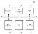
도 1은 본 발명의 실시 예에 따른 불휘발성 메모리 시스템(100)을 보여주는 블록도이다. 도 1을 참조하면, 불휘발성 메모리 시스템(100)은 메모리 컨트롤러(110) 및 불휘발성 메모리 장치(120)를 포함한다. 메모리 컨트롤러(110) 및 불휘발성 메모리 장치(120)는 각각 별도의 칩, 별도의 패키지, 또는 별도의 모듈로 제공될 수 있다. 예시적으로, 불휘발성 메모리 시스템(100)은 솔리드 스테이트 드라이브(SSD; Solid State Drive), 메모리 카드, 메모리 스틱 등과 같은 대용량 저장 매체 또는 저장 장치일 수 있다.1 is a block diagram illustrating a
메모리 컨트롤러(110)는 외부 장치(예를 들어, 호스트, CPU, AP 등)의 요청에 따라, 불휘발성 메모리 장치(120)를 제어할 수 있다. 예를 들어, 메모리 컨트롤러(110)는 외부 장치의 요청에 따라 어드레스(ADDR), 커맨드(CMD), 및 제어 신호(CTRL)를 불휘발성 메모리 장치(120)로 전송할 수 있다. 메모리 컨트롤러(110)는 외부 장치의 요청에 따라 불휘발성 메모리 장치(120)와 데이터(DATA)를 주고 받을 수 있다.The
불휘발성 메모리 장치(120)는 메모리 컨트롤러(110)의 제어에 따라 데이터(DATA)를 저장하거나 또는 저장된 데이터(DATA)를 출력할 수 있다. 불휘발성 메모리 장치(120)는 복수의 메모리 블록들을 포함하는 낸드 플래시 메모리를 기반으로 제공될 수 있다. 그러나, 본 발명의 범위가 이에 한정되는 것은 아니며, 불휘발성 메모리 장치(120)는 노어 플래시 메모리, MRAM, PRAM, ReRAM, FRAM 등과 같은 불휘발성 메모리 소자들을 포함할 수 있다.The
불휘발성 메모리 장치(120)는 복수의 메모리 블록들을 포함한다. 복수의 메모리 블록들 각각은 복수의 메모리 셀들을 포함하고, 복수의 메모리 셀들 각각은 1-비트 데이터를 저장하는 싱글 레벨 셀(SLC)이거나 또는 적어도 2-비트 데이터를 저장하는 멀티 레벨 셀(MLC)일 수 있다.The
예시적으로, 메모리 컨트롤러(110)는 불휘발성 메모리 장치(120)에 저장된 데이터의 신뢰성을 보장하기 위한 다양한 동작을 수행할 수 있다. 예를 들어, 메모리 컨트롤러(110)는 에러 정정 코드 회로(111)(ECC Circuit; error correction code circuit) 및 리클레임 관리자(112)를 포함한다. ECC 회로(111)는 불휘발성 메모리 장치(120)에 저장될 데이터에 대한 에러 정정 코드를 생성하거나 또는 에러 정정 코드를 기반으로 불휘발성 메모리 장치(111)로부터 읽은 데이터(DATA)의 에러를 검출 및 정정할 수 있다.For example, the
예시적으로, ECC 회로(111)는 일정 수준의 에러 정정 능력을 갖는다. 예를 들어, ECC 회로(111)는 에러 정정 능력 이하의 에러를 검출 및 정정할 수 있다. ECC 회로(111)는 에러 정정 능력을 초과하는 에러를 검출 또는 정정할 수 없다. ECC 회로(111)에 의해 에러가 정정되지 않는 데이터는 'UECC 데이터(Uncorrectable Error Correction Code Data)'라 불린다. 불휘발성 메모리 장치(120)로부터 읽은 데이터가 UECC 데이터인 경우, 불휘발성 메모리 장치(120)로부터 읽은 데이터의 신뢰성을 보장할 수 없다.Exemplarily, the
리클레임 관리자(112)는 UECC 데이터의 발생을 방지하기 위하여, 기준 개수 이상의 에러 비트를 포함하는 데이터가 저장된 메모리 블록 또는 페이지에 대한 리클레임 동작을 수행할 수 있다. 예를 들어, 불휘발성 메모리 장치(120)에 대한 프로그램, 읽기, 또는 소거 동작이 수행되거나 또는 시간이 경과함에 따라, 불휘발성 메모리 장치(120)의 복수의 메모리 셀들의 문턱 전압이 변화할 수 있다. 이는 불휘발성 메모리 장치(120)로부터 읽은 데이터에서 에러가 발생할 수 있음을 의미한다. ECC 회로(111)는 불휘발성 메모리 장치(120)로부터 읽은 데이터(DATA)의 에러 비트를 검출할 수 있다. 리클레임 관리자(112)는 검출된 에러 비트의 개수 및 기준 개수를 비교함으로써, 읽은 데이터(DATA)가 저장된 메모리 블록에 대한 리클레임 여부를 판별할 수 있다. 검출된 에러 비트의 개수가 기준 개수 이상인 경우, 리클레임 관리자(112)는 읽은 데이터(DATA)가 저장된 메모리 블록을 소스 블록(Source Block)으로서 선택할 수 있다. 리클레임 관리자(112)는 소스 블록에 대한 리클레임 동작을 수행함으로써, 소스 블록에 저장된 데이터의 신뢰성을 보장할 수 있다. 예시적으로, 기준 값은 ECC 회로(111)의 에러 정정 능력보다 낮은 에러 비트의 개수를 가리킬 수 있다.In order to prevent the generation of UECC data, the reclaim
본 발명에 따른 리클레임 관리자(112)는 소스 블록의 프로그램 소거 사이클(이하에서, 'P/E 사이클'이라 칭함)에 따라, 리클레임 정책(reclaim policy)을 조절할 수 있다. 예를 들어, 소스 블록의 P/E 사이클이 제1 값인 경우, 리클레임 관리자(112)는 소스 블록에 대한 리클레임 동작의 속도가 제1 속도가 되도록 리클레임 정책을 조절할 수 있다. 소스 블록의 P/E 사이클이 제1 값보다 큰 제2 값인 경우, 리클레임 관리자(112)는 소스 블록에 대한 리클레임 동작의 속도가 제1 속도보다 빠른 제2 속도가 되도록 리클레임 정책을 조절할 수 있다.The reclaim
좀 더 상세한 예로서, 리클레임 관리자(112)는 소스 블록의 P/E 사이클이 클수록 리클레임 속도를 증가시킬 수 있다. 또는, 리클레임 관리자(112)는 소스 블록의 P/E 사이클이 작을수록 리클레임 속도를 감소시킬 수 있다. 예시적으로, 리클레임 동작의 속도 또는 리클레임 속도는 소스 블록으로 선택된 시점(또는 읽기 카운트)로부터 리클레임 동작이 완료되는 시점(또는 읽기 카운트)까지의 시간 동안 수행된 리클레임 동작 카운트의 비율을 가리킨다. 예시적으로, 읽기 카운트는 외부 장치(예를 들어, 호스트, CPU, AP 등)의 요청에 따라 불휘발성 메모리 시스템(100)에서 수행되는 읽기 동작의 횟수를 가리킨다.As a more detailed example, the reclaim
예시적으로, 리클레임 정책은 리클레임 속도, 리클레임 실행 구간, 리클레임의 서브 동작 간격, 리클레임의 서브 동작 단위 등과 같은 인자들을 포함할 수 있다. 예시적으로, 리클레임 속도는 리클레임 실행 구간, 리클레임 서브 동작 간격, 리클레임 서브 동작 단위 등을 조절함으로써 조절될 수 있다.Exemplarily, the reclaim policy may include factors such as a reclaim rate, a reclaim execution interval, a sub operation interval of a reclaim, a sub operation unit of a reclaim, and the like. Illustratively, the reclaim speed may be adjusted by adjusting the reclaim execution period, the reclaim sub operation interval, the re claim sub operation unit, and the like.
도 2는 도 1의 불휘발성 메모리 시스템(100)의 소프트웨어 계층을 예시적으로 보여주는 도면이다. 도 1 및 도 2를 참조하면, 불휘발성 메모리 시스템(100)의 소프트웨어 계층은 애플리케이션(101), 파일 시스템(102), 및 플래시 변환 계층(130)을 포함할 수 있다. 예시적으로, 애플리케이션(101) 및 파일 시스템(102)은 외부 장치(예를 들어, 호스트, CPU, AP, 등)에 포함되거나 또는 외부 장치에 의해 구동될 수 있다.FIG. 2 is a diagram exemplarily showing a software layer of the
애플리케이션(101)은 외부 장치의 운영 체제(OS; Operating System) 상에서 구동되는 다양한 프로그램들을 포함할 수 있다. 예를 들어, 애플리케이션(101)은 문서 편집기, 영상 재생기, 웹 브라우저 등과 같은 다양한 프로그램들을 포함할 수 있다.The
파일 시스템(102)은 애플리케이션(101)에 의해 사용되는 파일 또는 데이터를 조직화하는 역할을 수행한다. 예를 들어, 파일 시스템(102)은 파일 또는 데이터의 어드레스를 제공할 수 있다. 예시적으로, 어드레스는 외부 장치에 의해 조직화된 또는 관리되는 논리적 어드레스(Logical Address)일 수 있다. 파일 시스템(102)은 운영 체제에 따라 다양한 형태로 제공될 수 있다. 예를 들어, 파일 시스템(102)은 FAT(File Allocation Table), FAT32, NTFS(NT File System), HFS(Hierarchical File System), JSF2(Journaled File System2), XFS, ODS-5(On-Disk Structure-5), UDF, ZFS, UFS(Unix File System), ext2, ext3, ext4, ReiserFS, Reiser4, ISO 9660, Gnome VFS, BFS, 또는 WinFS 등을 포함할 수 있다.
플래시 변환 계층(130)(FTL; Flash Translation Layer)은 불휘발성 메모리 장치(120)가 효율적으로 사용될 수 있도록, 외부 장치 및 불휘발성 메모리 장치 사이의 인터페이스를 제공한다. 예를 들어, FTL(130)은 외부 장치로부터 제공되는 논리적 어드레스를 불휘발성 메모리 장치(120)에서 사용 가능한 물리적 어드레스로 변환하는 동작을 수행할 수 있다. FTL(130)은 맵핑 테이블(미도시)을 통해 상술된 어드레스 변환 동작을 수행할 수 있다.The flash translation layer 130 (FTL) provides an interface between an external device and the nonvolatile memory device so that the
예시적으로, FTL(130)은 가비지 콜렉션, 웨어 레벨링, 리클레임 등과 같은 동작들을 수행할 수 있다. 예를 들어, FTL(130)은 불휘발성 메모리 장치(120)의 자유 블록을 확보하기 위하여 가비지 콜렉션을 수행할 수 있다. FTL(130)은 불휘발성 메모리 장치(120)의 복수의 메모리 블록들 각각의 P/E 사이클이 평준화되도록 웨어 레벨링을 수행할 수 있다. 예시적으로, 앞서 설명된 리클레임 관리자(112)는 FTL(130) 내에 포함될 수 있다. FTL(130)은 불휘발성 메모리 장치(120)에 저장된 데이터의 신뢰성을 보장하기 위하여 리클레임 동작을 수행할 수 있다.For example, the FTL 130 may perform operations such as garbage collection, wear leveling, and reclaim. For example, the FTL 130 may perform garbage collection to secure a free block of the
도 3은 도 1의 메모리 컨트롤러(110)를 상세하게 보여주는 블록도이다. 도 1 및 도 3을 참조하면, 메모리 컨트롤러(110)는 ECC 회로(111), 프로세서(113), SRAM(114), ROM(115), 호스트 인터페이스(116), 및 플래시 인터페이스(117)를 포함한다.FIG. 3 is a detailed block diagram illustrating the
프로세서(113)는 메모리 컨트롤러(110)의 제반 동작을 제어할 수 있다. SRAM(114)은 메모리 컨트롤러(110)의 버퍼 메모리, 캐시 메모리, 동작 메모리 등으로써 사용될 수 있다. ROM(115)은 메모리 컨트롤러(110)가 동작하는데 요구되는 다양한 정보를 펌웨어 형태로 저장할 수 있다. 예시적으로, 도 1의 리클레임 관리자(112) 또는 도 2의 FTL(130)은 소프트웨어 형태로 제공될 수 있고, 리클레임 관리자(112) 또는 FTL(130)은 SRAM(114)에 저장되고, 프로세서(113)에 의해 구동될 수 있다.The
메모리 컨트롤러(110)는 호스트 인터페이스(116)를 통해 외부 장치와 통신할 수 있다. 예시적으로, 호스트 인터페이스(116)는 USB (Universal Serial Bus), MMC (multimedia card), embedded MMC, PCI (peripheral component interconnection), PCI-express, ATA (Advanced Technology Attachment), Serial-ATA, Parallel-ATA, SCSI (small computer small interface), ESDI (enhanced small disk interface), IDE (Integrated Drive Electronics), 파이어와이어(Firewire), UFS(Universal Flash Storage), NVMe (Nonvolatile Memory express) 중 적어도 하나의 통신 규격을 기반으로 제공될 수 있다. 메모리 컨트롤러(110)는 플래시 인터페이스(117)를 통해 불휘발성 메모리 장치(120)와 통신할 수 있다.The
도 4는 도 1의 불휘발성 메모리 장치(120)를 상세하게 보여주는 블록도이다. 도 1 및 도 4를 참조하면, 불휘발성 메모리 장치(120)는 메모리 셀 어레이(121), 어드레스 디코더(122), 제어 로직 및 전압 발생 회로(123), 페이지 버퍼(124), 및 입출력 회로(125)를 포함한다.4 is a detailed block diagram illustrating the
메모리 셀 어레이(121)는 복수의 메모리 블록들을 포함한다. 복수의 메모리 블록들 각각은 복수의 셀 스트링들을 포함한다. 셀 스트링들 각각은 복수의 메모리 셀들을 포함하고, 복수의 메모리 셀들 각각은 복수의 워드라인들(WL)과 각각 연결된다.The
어드레스 디코더(122)는 복수의 워드라인들(WL), 스트링 선택 라인들(SSL), 접지 선택 라인들(GSL)을 통해 메모리 셀 어레이(121)와 연결된다. 어드레스 디코더(122)는 메모리 컨트롤러(110)로부터 어드레스(ADDR)를 수신하고, 수신된 어드레스(ADDR)를 디코딩할 수 있다. 어드레스 디코더(122)는 디코딩된 어드레스(ADDR)를 기반으로 복수의 워드라인들(WL) 중 적어도 하나를 선택하고, 선택된 워드라인의 전압을 제어할 수 있다.The
제어 로직 및 전압 발생 회로(123)는 메모리 컨트롤러(110)로부터 커맨드(CMD) 및 제어 신호(CTRL)를 수신하고, 수신된 신호들에 응답하여 어드레스 디코더(122), 페이지 버퍼(124), 및 입출력 회로(125)를 제어할 수 있다.The control logic and
제어 로직 및 전압 발생 회로(123)는 불휘발성 메모리 장치(120)가 동작하는데 요구되는 다양한 전압들을 생성할 수 있다. 예를 들어, 제어 로직 및 전압 발생 회로(123)는 프로그램 전압들, 패스 전압들, 선택 읽기 전압들, 비선택 읽기 전압들, 검증 전압들, 소거 전압들, 소거 검증 전압들 등과 같은 다양한 전압들을 생성할 수 있다. 예시적으로, 프로그램 전압들, 패스 전압들, 선택 읽기 전압들, 비선택 읽기 전압들, 검증 전압들, 소거 전압들, 소거 검증 전압들 등과 같은 다양한 전압들 각각은 메모리 셀 어레이(121)에 포함된 복수의 메모리 셀들 각각의 크기, 동작 속도, 물리적 위치에 따라 가변될 수 있다.The control logic and
페이지 버퍼(124)는 복수의 비트라인들(BL)을 통해 메모리 셀 어레이(121)와 연결된다. 페이지 버퍼(124)는 복수의 데이터 라인들(DL)을 통해 입출력 회로(125)와 연결된다. 페이지 버퍼(124)는 복수의 데이터 라인들(DL)을 통해 수신된 데이터(DATA)가 메모리 셀 어레이(121)에 기입되도록 복수의 비트 라인들(BL)을 제어할 수 있다. 페이지 버퍼(124)는 복수의 비트 라인들(BL)의 전압 변화를 감지함으로써, 메모리 셀 어레이(121)에 저장된 데이터를 읽을 수 있다. 페이지 버퍼(124)는 복수의 데이터 라인들(DL)을 통해 읽은 데이터(DATA)를 입출력 회로(125)로 제공할 수 있다.The
입출력 회로(125)는 메모리 컨트롤러(110)와 데이터(DATA)를 주고 받을 수 있다. 입출력 회로(125)는 제어 로직 및 전압 발생 회로(123)의 제어에 따라 메모리 컨트롤러(125)로부터 데이터(DATA)를 수신하거나 또는 제어 신호(CTRL)에 동기하여 데이터(DATA)를 출력할 수 있다.The input/
도 5는 도 1의 불휘발성 메모리 시스템(100)의 리클레임 동작을 예시적으로 보여주는 블록도이다. 도면의 간결성 및 설명의 편의를 위하여, 메모리 블록으로부터 읽은 데이터의 에러 비트는 "메모리 블록의 에러 비트"라 칭한다.FIG. 5 is a block diagram exemplarily illustrating a reclaim operation of the
도 1 및 도 5를 참조하면, 불휘발성 메모리 시스템(100)은 제1 메모리 블록(BLK1)을 소스 블록(Source Block)으로써 선택될 수 있다. 앞서 설명된 바와 같이, 예를 들어, 메모리 컨트롤러(110)는 제1 메모리 블록(BLK1)에 포함된 제1 페이지 데이터(PD1)를 읽을 수 있다. 제1 메모리 블록(BLK1)으로부터 읽어진 제1 페이지 데이터(PD1)의 에러는 ECC 회로(111)에 의해 검출 및 정정될 수 있다. 이 때, 읽어진 페이지 데이터로부터 검출된 에러 비트의 수가 기준 개수보다 클 경우, 메모리 컨트롤러(110)는 제1 페이지 데이터(PD1)가 저장된 제1 메모리 블록(BLK1)을 소스 블록(Source Block)으로써 선택할 수 있다. 예시적으로, 소스 블록은 읽기 리클레임 동작의 대상이 되는 메모리 블록을 가리킨다.1 and 5 , the
메모리 컨트롤러(110)는 소스 블록인 제1 메모리 블록(BLK1)으로부터 페이지 데이터를 순차적으로 읽고, 읽은 페이지 데이터를 목표 블록(Destination Block)인 제2 메모리 블록(BLK2)에 프로그램할 수 있다. 예시적으로, 제1 메모리 블록(BLK1)으로부터 읽어진 페이지 데이터는 ECC 회로(111)에 의해 에러가 정정되고, 에러가 정정된 페이지 데이터가 제2 메모리 블록(BLK2)에 프로그램될 수 있다. 즉, 에러가 정정된 데이터가 제2 메모리 블록(BLK2)에 프로그램됨으로써 데이터의 신뢰성을 보장할 수 있다. 예시적으로, 에러가 정정된 데이터가 제2 메모리 블록(BLK2)에 프로그램됨에 따라, FTL(130, 도 2 참조)은 에러가 정정된 데이터에 대한 맵핑 테이블을 갱신할 수 있다.The
이하에서, 설명의 편의를 위하여, 소스 블록인 제1 메모리 블록(BLK1)에 대한 리클레임 동작은 복수의 서브 동작들(sub-operation)을 포함하는 것으로 가정한다. 하나의 서브 동작은 소스 블록으로부터 적어도 하나의 페이지 데이터를 읽는 동작, 적어도 하나의 읽은 페이지 데이터의 에러를 정정하는 동작, 또는 적어도 하나의 에러가 정정된 페이지 데이터를 목표 블록에 프로그램하는 동작 중 적어도 하나를 포함하는 것으로 가정한다. 즉, 메모리 컨트롤러(110)는 복수의 서브 동작들을 반복 수행함으로써 하나의 소스 블록에 대한 리클레임 동작을 완료할 수 있다.Hereinafter, for convenience of description, it is assumed that the reclaim operation on the first memory block BLK1 as the source block includes a plurality of sub-operations. The one sub-operation is at least one of an operation of reading at least one page data from a source block, an operation of correcting an error of the at least one read page data, and an operation of programming the at least one error-corrected page data into a target block It is assumed to include That is, the
예시적으로, 메모리 컨트롤러(110)는 복수의 서브 동작들 각각을 연속적으로 수행하거나 또는 불연속적으로 수행할 수 있다. 예시적으로, 메모리 컨트롤러(110)는 제1 서브 동작을 수행한 이후, 소정의 시간(또는 소정의 읽기 카운트)이 경과한 이후에, 제2 서브 동작을 수행할 수 있다. 그러나, 본 발명의 범위가 이에 한정되는 것은 아니다.For example, the
도 6 은 메모리 블록의 P/E 사이클에 대한 에러 비트 비율을 보여주는 그래프들이다. 도 1 및 도 6을 참조하면, 도 6의 X축은 메모리 블록의 P/E 사이클을 가리키고, Y축은 읽기 카운트 대 에러 비트의 비율을 가리킨다. 예시적으로, 읽기 카운트는 메모리 블록이 소거된 이후에 메모리 블록으로부터 데이터가 읽어지는 횟수를 가리킨다.6 is a graph showing an error bit rate with respect to a P/E cycle of a memory block. 1 and 6 , the X axis of FIG. 6 indicates a P/E cycle of the memory block, and the Y axis indicates a ratio of read count to error bits. For example, the read count indicates the number of times data is read from the memory block after the memory block is erased.
도 6에 도시된 바와 같이, 제1 P/E 사이클(PE1)을 갖는 메모리 블록에 대한 읽기 카운트 대 에러 비트의 비율은 제1 값(V1)이고, 제1 P/E 사이클(PE1)보다 큰 제2 P/E 사이클(PE2)을 갖는 메모리 블록에 대한 읽기 카운트 대 에러 비트의 비율은 제1 값(V1)보다 큰 제2 값(V2)이다. 즉, 메모리 블록의 P/E 사이클이 증가할수록 읽기 카운트 대 에러 비트의 비율이 증가한다. 다시 말해서, 메모리 블록의 P/E 사이클이 증가할수록 메모리 블록의 열화 정도가 증가하기 때문에, 에러 비트가 발생할 가능성이 높아진다.As shown in FIG. 6 , the ratio of the read count to the error bit for the memory block having the first P/E cycle PE1 is a first value V1 and is greater than the first P/E cycle PE1 . A ratio of a read count to an error bit for the memory block having the second P/E cycle PE2 is a second value V2 greater than the first value V1 . That is, as the P/E cycle of the memory block increases, the ratio of the read count to the error bit increases. In other words, since the degree of deterioration of the memory block increases as the P/E cycle of the memory block increases, the possibility of generating an error bit increases.
도 7은 메모리 블록의 읽기 카운트에 대한 에러 비트 개수를 보여주는 그래프이다. 도 7의 X축은 읽기 카운트를 가리키고, Y축은 에러 비트의 개수를 가리킨다.7 is a graph showing the number of error bits with respect to a read count of a memory block. The X-axis of FIG. 7 indicates the read count, and the Y-axis indicates the number of error bits.
도 1, 도 6, 및 도 7을 참조하면, 제1 라인(L01)은 제1 P/E 사이클(PE1)을 갖는 메모리 블록의 읽기 카운트에 대한 에러 비트 개수를 보여주는 그래프이다. 제2 라인(L02)은 제1 P/E 사이클(PE1)보다 큰 제2 P/E 사이클(PE2)을 갖는 메모리 블록의 읽기 카운트에 대한 에러 비트 개수를 보여주는 그래프이다. 예시적으로, 제1 및 제2 라인들(L01, L02)의 기울기들은 도 6의 Y축의 값(읽기 카운트 대 에러 비트의 비율)과 대응될 수 있다.1, 6, and 7 , the first line L01 is a graph showing the number of error bits with respect to the read count of the memory block having the first P/E cycle PE1. The second line L02 is a graph showing the number of error bits with respect to the read count of the memory block having the second P/E cycle PE2 greater than the first P/E cycle PE1 . For example, slopes of the first and second lines L01 and L02 may correspond to a Y-axis value (ratio of read count to error bit) of FIG. 6 .
이하에서, 간결한 설명을 위하여, 제1 P/E 사이클(PE1)을 갖는 메모리 블록은 "일반 블록(Normal Block)"이라 칭하고, 제1 P/E 사이클(PE1)보다 큰 제2 P/E 사이클(PE2)을 갖는 메모리 블록은 "열화된 블록(Depleted Block)"이라 칭한다. 즉, 열화된 블록(Depleted Block)은 정상 블록(Normal Block)과 비교하여 큰 P/E 사이클을 갖고, 열화 정도가 크며, 동일한 읽기 카운트에서 더 많은 에러 비트를 갖는다. 예를 들어, 도 7에 도시된 바와 같이, 동일한 읽기 카운트에서, 제1 라인(L01)은 제2 라인(LO2)보다 큰 값을 갖는다. 즉, 읽기 카운트가 동일한 경우, 일반 블록은 열화된 블록보다 더 적은 에러 비트를 가질 것이다. 예시적으로, 상술된 가정은 본 발명의 실시 예를 간결하게 설명하기 위한 가정이며, 본 발명의 범위가 이에 한정되는 것은 아니다. 열화된 블록 및 정상 블록은 서로 상대적인 것이며, P/E 사이클에 따라 다양하게 가변될 수 있다.Hereinafter, for concise description, the memory block having the first P/E cycle PE1 is referred to as a “Normal Block”, and a second P/E cycle greater than the first P/E cycle PE1 is referred to. A memory block with (PE2) is referred to as a "Depleted Block". That is, compared to a normal block, a depleted block has a large P/E cycle, a high degree of degradation, and has more error bits at the same read count. For example, as shown in FIG. 7 , at the same read count, the first line L01 has a larger value than the second line LO2 . That is, if the read counts are the same, the normal block will have fewer error bits than the degraded block. Illustratively, the above-mentioned assumptions are assumptions for concisely explaining the embodiments of the present invention, and the scope of the present invention is not limited thereto. The deteriorated block and the normal block are relative to each other and may be variously changed according to the P/E cycle.
앞서 설명된 바와 같이, 불휘발성 메모리 시스템(100)은 메모리 블록의 에러 비트가 기준값(REF)이상인 경우, 불휘발성 메모리 시스템(100)은 기준 값 이상의 에러 비트를 포함하는 메모리 블록을 소스 블록으로서 선택하고, 소스 블록에 대한 리클레임 동작을 수행한다.As described above, when the error bit of the memory block is greater than or equal to the reference value REF, the
예를 들어, 제1 읽기 카운트(c1)에서, 열화된 블록의 에러 비트가 기준 값(REF) 이상일 수 있다. 이 경우, 불휘발성 메모리 시스템(100)은, 제1 읽기 카운트(c1)에서, 열화된 블록을 소스 블록으로서 선택하고, 리클레임 실행 구간(RP)동안 소스 블록에 대한 리클레임 동작을 시작한다.For example, in the first read count c1 , the error bit of the deteriorated block may be greater than or equal to the reference value REF. In this case, the
예시적으로, 제2 읽기 카운트(c2)에서, 열화된 블록의 에러 비트가 ECC 회로(111)의 에러 정정 능력을 초과할 수 있다. 즉, 제2 읽기 카운트(c2)에서 열화된 블록으로부터 데이터가 읽어진 경우, 읽어진 데이터는 UECC 데이터일 것이다. 이 경우, 열화된 블록으로부터 읽어진 데이터의 신뢰성을 보장할 수 없기 때문에, 불휘발성 메모리 시스템(100)은 제2 읽기 카운트(c2) 이전에 소스 블록에 대한 리클레임 동작을 완료할 것이다.For example, in the second read count c2 , the error bit of the degraded block may exceed the error correction capability of the
예시적으로, 제1 읽기 카운트(c1)로부터 제2 읽기 카운트(c2) 사이의 차이는 리클레임 마진(RM; Reclaim Margin)이라 칭한다. 다시 말해서, 메모리 블록이 소스 블록으로써 선택된 읽기 카운트부터 소스 블록에서 UECC 데이터가 발생되는 읽기 카운트까지의 읽기 카운트 (또는 시간)는 "리클레임 마진"이라 칭한다. 즉, 리클레임 마진 이내에 소스 블록에 대한 리클레임 동작이 완료될 경우, 소스 블록에 대한 신뢰성이 보장될 수 있다.Exemplarily, a difference between the first read count c1 and the second read count c2 is referred to as a reclaim margin (RM). In other words, the read count (or time) from the read count in which the memory block is selected as the source block to the read count in which UECC data is generated in the source block is referred to as a "reclaim margin". That is, when the reclaim operation on the source block is completed within the reclaim margin, the reliability of the source block can be guaranteed.
예시적으로, 실제 리클레임 동작이 수행되는 읽기 카운트 구간은 리클레임 실행 구간(RP; Reclaim Period)이라 칭한다. 즉, 소스 블록의 데이터에 대한 신뢰성을 보장하기 위해서는 리클레임 실행 구간(RP)은 리클레임 마진(RM)보다 작은 값을 가져야 할 것이다. 열화된 블록에 대한 리클레임 실행 구간(RP) 및 제2 리클레임 마진(RM2)은 서로 동일하거나 또는 근사한 값을 가질 수 있다.Exemplarily, a read count period in which an actual reclaim operation is performed is referred to as a reclaim execution period (RP). That is, in order to ensure the reliability of the data of the source block, the reclaim execution period (RP) should have a smaller value than the reclaim margin (RM). The reclaim execution period RP for the degraded block and the second reclaim margin RM2 may have the same or approximate values.
제3 읽기 카운트(c3)에서, 정상 블록(즉, 제1 P/E 사이클(PE1)을 갖는 메모리 블록)의 에러 비트가 기준 값(REF)보다 크므로, 정상 블록이 소스 블록으로써 선택될 수 있다. 불휘발성 메모리 시스템(100)은 제3 읽기 카운트(c3)에서 선택된 소스 블록에 대한 리클레임 동작을 리클레임 실행 구간(RP)동안 수행할 수 있다.In the third read count c3, since the error bit of the normal block (ie, the memory block having the first P/E cycle PE1) is greater than the reference value REF, the normal block can be selected as the source block. have. The
예시적으로, 불휘발성 메모리 시스템은 복수의 메모리 블록들을 포함하고, 복수의 메모리 블록들 각각은 서로 다른 P/E 사이클을 가질 수 있다. 종래의 불휘발성 메모리 시스템은 복수의 메모리 블록들 전체에 대한 신뢰성을 보장하기 위하여, 최악의 상태(worst case)(즉, 높은 P/E 사이클을 갖는 열화된 블록과 같은 상태)가 반영된 리클레임 마진을 모든 메모리 블록들에 일괄적으로 적용하여 리클레임 동작을 수행한다.For example, the nonvolatile memory system may include a plurality of memory blocks, and each of the plurality of memory blocks may have different P/E cycles. In the conventional nonvolatile memory system, a reclaim margin in which a worst case (ie, a state such as a deteriorated block having a high P/E cycle) is reflected in order to guarantee reliability of all of the plurality of memory blocks. is collectively applied to all memory blocks to perform a reclaim operation.
예를 들어, 도 7의 제1 라인(LO1)과 같이 일반 블록의 리클레임 마진은 제1 리클레임 마진(RM1)이나, 실제 리클레임 동작이 수행되는 리클레임 실행 구간(RP)은 제1 리클레임 마진(RM1)보다 짧거나 혹은 작을 수 있다. 이 경우, 메모리 블록의 특성이 고려되지 않고, 리클레임 동작이 빠른 시간 내에 수행되기 때문에, 리클레임 동작으로 인한 오버 헤드가 발생하고, 이로 인하여 전체적인 성능이 하락하게 된다.For example, as in the first line LO1 of FIG. 7 , the reclaim margin of the general block is the first reclaim margin RM1, but the reclaim execution period RP in which the actual reclaim operation is performed is the first reclaim margin. It may be shorter or smaller than the claim margin (RM1). In this case, since the characteristics of the memory block are not taken into account and the reclaim operation is performed within a short time, an overhead due to the reclaim operation occurs, thereby deteriorating overall performance.
본 발명에 따른 불휘발성 메모리 시스템은 소스 블록의 P/E 사이클에 따라 리클레임 정책을 조절할 수 있다. 예시적으로 리클레임 정책은 리클레임 속도, 리클레임 실행 구간, 리클레임의 서브 동작 간격, 서브 동작 단위 등과 같은 인자들을 포함할 수 있다. 소스 블록의 P/E 사이클에 따라 리클레임 정책이 가변되기 때문에, 일반 블록에 대한 리클레임 동작시, 리클레임 동작으로 인한 오버 헤드가 감소될 수 있다. 좀 더 상세하게는, 불휘발성 메모리 시스템(100)은 전체적인 성능 저하를 최소화하여 낮은 P/E 사이클을 갖는 메모리 블록들에 대한 리클레임 동작이 수행될 수 있다.The nonvolatile memory system according to the present invention may adjust the reclaim policy according to the P/E cycle of the source block. Exemplarily, the reclaim policy may include factors such as a reclaim rate, a reclaim execution interval, a sub operation interval of reclaim, a sub operation unit, and the like. Since the reclaim policy is changed according to the P/E cycle of the source block, the overhead due to the reclaim operation can be reduced during the reclaim operation for the normal block. In more detail, the
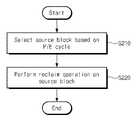
도 8은 도 1의 불휘발성 메모리 시스템(100)의 동작을 보여주는 순서도이다. 도 1 및 도 6을 참조하면, S110 단계에서, 불휘발성 메모리 시스템(100)은 소스 블록을 선택한다. 좀 더 상세한 예로서, 메모리 컨트롤러(110)는 외부 장치의 요청에 따라 읽기 동작을 수행할 수 있다. 읽기 동작 도중에, 불휘발성 메모리 장치(120)로부터 읽은 데이터의 에러 비트 개수가 기준 값을 초과하는 경우, 읽은 데이터가 저장된 메모리 블록을 소스 블록으로서 선택할 수 있다.8 is a flowchart illustrating an operation of the
S120 단계에서, 불휘발성 메모리 시스템(100)은 소스 블록의 P/E 사이클을 기반으로 리클레임 정책을 조절할 수 있다. 예시적으로, 리클레임 정책은 소스 블록에 대한 리클레임 동작을 수행하기 위한 동작 조건들을 포함할 수 있다. 리클레임 정책은 리클레임 속도, 리클레임 실행 구간, 리클레임의 서브 동작 간격, 서브 동작 단위 등과 같은 인자들을 포함할 수 있다.In operation S120 , the
예를 들어, 불휘발성 메모리 시스템(100)은 소스 블록의 P/E 사이클이 제1 값인 경우, 불휘발성 메모리 시스템(100)은 선택된 소스 블록에 대한 리클레임 속도를 제1 속도로 조절할 수 있다. 불휘발성 메모리 시스템(100)은 소스 블록의 P/E 사이클이 제1 값보다 큰 제2 값인 경우, 불휘발성 메모리 시스템(100)은 선택된 소스 블록에 대한 리클레임 속도를 제1 속도보다 빠른 제2 속도로 조절할 수 있다. 즉, 불휘발성 메모리 시스템(100)은 소스 블록의 P/E 사이클에 따라 소스 블록에 대한 리클레임 속도를 조절할 수 있다.For example, when the P/E cycle of the source block is the first value, the
마찬가지로, 불휘발성 메모리 시스템(100)은 소스 블록의 P/E 사이클에 따라 소스 블록의 리클레임 동작에 대한 리클레임 실행 구간, 리클레임의 서브 동작 간격, 서브 동작 단위 등과 같은 리클레임 정책을 조절할 수 있다.Similarly, the
S130 단계에서, 불휘발성 메모리 시스템(100)은 조절된 리클레임 정책을 기반으로 소스 블록에 대한 리클레임 동작을 수행할 수 있다. S130 단계에 따른 동작은 이하의 도면들을 참조하여 더욱 상세하게 설명된다.In step S130 , the
도 9 및 도 10은 도 8의 동작 방법을 설명하기 위한 그래프들이다. 간결한 설명을 위하여, 앞서 설명된 내용과 중복되는 내용은 생략된다. 또한, 간결한 설명을 위하여, 제1 P/E 사이클(PE1)을 갖는 일반 블록 및 제2 P/E 사이클(PE2)를 갖는 열화된 블록을 참조하여 본 발명에 따른 동작 방법이 설명된다. 또한, 제1 및 제2 라인들(L01, L02) 각각은 일반 블록 및 열화된 블록 각각에 대응되는 그래프들이다.9 and 10 are graphs for explaining the operation method of FIG. 8 . For concise description, content overlapping with the previously described content is omitted. Further, for concise description, an operating method according to the present invention is described with reference to a normal block having a first P/E cycle PE1 and a degraded block having a second P/E cycle PE2. Also, each of the first and second lines L01 and L02 is a graph corresponding to a normal block and a degraded block, respectively.
상술된 사항들은 본 발명의 실시 예를 명확하게 설명하기 위한 예시적인 것이며, 본 발명의 범위가 이에 한정되는 것은 아니다. 도 9의 X축은 불휘발성 메모리 장치(120)에 대한 읽기 카운트를 가리키고, Y축은 에러 비트의 개수를 가리킨다.The above-mentioned matters are illustrative for clearly explaining the embodiments of the present invention, and the scope of the present invention is not limited thereto. In FIG. 9 , the X axis indicates a read count for the
먼저, 도 1, 도 8, 및 도 9를 참조하면, 제1 읽기 카운트(c1)에서, 열화된 블록의 에러 비트가 기준 값(REF) 이상일 수 있다. 이 경우, 열화된 블록은 소스 블록으로써 선택되고, 불휘발성 메모리 시스템(100)은 제2 리클레임 실행 구간(RP2)동안 소스 블록으로써 선택된 열화된 블록에 대한 리클레임 동작을 수행할 수 있다. 이 때, 제2 리클레임 실행 구간(RP2)은 열화된 블록의 리클레임 마진인 제2 리클레임 마진(RM2)과 동일할 수 있다. 즉, 불휘발성 메모리 시스템(100)은 제2 리클레임 마진(RM2) 동안 열화된 블록에 대한 리클레임 동작을 수행할 수 있다.First, referring to FIGS. 1, 8, and 9 , in the first read count c1 , the error bit of the deteriorated block may be greater than or equal to the reference value REF. In this case, the degraded block is selected as the source block, and the
반면에, 제3 읽기 카운트(c3)에서, 일반 블록의 에러 비트가 기준 값(REF) 이상일 수 있다. 이 경우, 일반 블록은 소스 블록으로써 선택되고, 불휘발성 메모리 시스템(100)은 제1 리클레임 실행 구간(RP1)동안 소스 블록으로써 선택된 일반 블록에 대한 리클레임 동작을 수행할 수 있다. 이 때, 제1 리클레임 실행 구간(RP1)은 일반 블록의 리클레임 마진인 제1 리클레임 마진(RM1)과 동일할 수 있다.On the other hand, in the third read count c3 , the error bit of the general block may be greater than or equal to the reference value REF. In this case, the general block is selected as the source block, and the
예시적으로, 도 7에 도시된 바와 달리, 도 9에 도시된 본 발명의 실시 예에서는, 제1 리클레임 마진(RM1)은 제2 리클레임 마진(RM2)보다 클 수 있다. 즉, 불휘발성 메모리 시스템(100)은 일반 블록에 대한 리클레임 실행 구간(RP)을 증가시킴으로써, 단위 읽기 카운트(또는 단위 시간) 당 발생하는 리클레임 동작을 감소시킬 수 있다. 뿐만 아니라, UECC 데이터가 발생하기 이전에 소스 블록에 대한 리클레임 동작이 완료된다. 다시 말해서, 소스 블록의 P/E 사이클에 따라 리클레임 실행 구간(즉, 실제 리클레임 동작이 수행되는 구간 또는 읽기 카운트)을 조절함으로써 향상된 신뢰성 및 향상된 성능을 갖는 불휘발성 메모리 시스템이 제공된다.Exemplarily, unlike shown in FIG. 7 , in the embodiment of the present invention shown in FIG. 9 , the first reclaim margin RM1 may be greater than the second reclaim margin RM2 . That is, the
다음으로, 도 1 및 도 10을 참조하여, 열화된 블록 및 일반 블록 각각에 대한 리클레임 동작이 더욱 상세하게 설명된다. 간결한 설명을 위하여, 불휘발성 메모리 시스템(100)은 읽기 동작이 집중된 상황(read intensive case)인 것으로 가정한다. 읽기 동작은 외부 장치의 요청에 의한 읽기 동작이며, 정해진 시간 간격에 따라 수행되는 것으로 가정한다.Next, with reference to FIGS. 1 and 10 , a reclaim operation for each of the degraded block and the normal block will be described in more detail. For concise description, it is assumed that the
또한, 열화된 블록 및 일반 블록들의 리클레임 동작들 각각은 제1 내지 제4 서브 동작들(SO1~SO4)로 구성되는 것으로 가정한다. 즉, 제1 내지 제4 서브 동작들(SO1~SO4)이 완료된 경우, 하나의 소스 블록에 대한 리클레임 동작이 완료될 것이다. 앞서 설명된 바와 같이, 제1 내지 제4 서브 동작들(SO1~SO4) 각각은 소스 블록으로부터 적어도 하나의 페이지 데이터를 읽는 동작, 읽은 페이지 데이터의 에러를 정정하는 동작, 또는 에러가 정정된 페이지 데이터를 목표 블록에 프로그램 하는 동작 중 적어도 하나를 포함하는 것으로 가정한다. 그러나, 본 발명의 범위가 이에 한정되는 것은 아니다.In addition, it is assumed that each of the reclaim operations of the degraded block and the normal blocks consists of first to fourth sub-operations SO1 to SO4 . That is, when the first to fourth sub-operations SO1 to SO4 are completed, the reclaim operation for one source block will be completed. As described above, each of the first to fourth sub-operations SO1 to SO4 includes an operation of reading at least one page data from a source block, an operation of correcting an error of the read page data, or an operation of error-corrected page data. It is assumed that at least one of the operations of programming in the target block is included. However, the scope of the present invention is not limited thereto.
도 1 및 도 8 내지 도 10을 참조하면, 제1 내지 제4 서브 동작(SO1~SO4) 각각은 리클레임 정책에 따라 소정의 간격으로 수행될 수 있다. 예를 들어, 불휘발성 메모리 시스템(100)은 열화된 블록을 소스 블록으로써 선택할 수 있다. 이 경우, 불휘발성 메모리 시스템(100)은 열화된 블록의 제2 P/E 사이클(PE2)에 따라 리클레임 정책을 조절할 수 있다.1 and 8 to 10 , each of the first to fourth sub-operations SO1 to SO4 may be performed at predetermined intervals according to a reclaim policy. For example, the
좀 더 상세한 예로서, 제1 섹션(1st Section)에 도시된 바와 같이, 불휘발성 메모리 시스템(100)은 열화된 블록에 대한 리클레임 동작의 읽기 카운트 간격(Read Count Interval)을 제2 읽기 카운트 간격(RCI2)으로 조절할 수 있다. 예시적으로, 읽기 카운트 간격(RCI; Read Count Interval)은 리클레임 동작에 포함된 복수의 서브 동작들 각각이 수행되는 시점들 사이의 읽기 카운트 간격(또는 시간 각격)을 가리킬 수 있다. 즉, 읽기 카운트 간격(RCI)을 짧게 혹은 작게할수록, 리클레임 동작이 빠르게 완료된다. (즉, 리클레임 속도가 증가한다.) 예시적으로, 제1 읽기 카운트 간격(RCI1) 동안 특정 횟수의 읽기 동작이 수행될 것이다.As a more detailed example, as shown in the first section, the
이와 달리, 불휘발성 메모리 시스템(100)은 일반 블록을 소스 블록으로써 선택할 수 있다. 이 경우, 불휘발성 메모리 시스템(100)은 일반 블록의 제1 P/E 사이클(PE1)에 따라 리클레임 정책을 조절할 수 있다. 좀 더 상세한 예로서, 제2 섹션(2nd Section)에 도시된 바와 같이, 불휘발성 메모리 시스템(100)은 일반 블록에 대한 리클레임 동작의 읽기 카운트 간격(Read Count Interval)을 제1 읽기 카운트 간격(RCI1)으로 조절할 수 있다. 예시적으로, 제1 읽기 카운트 간격(RCI1)은 제2 읽기 카운트 간격(RCI2)보다 클 수 있다.Alternatively, the
다시 말해서, 일반 블록이 소스 블록으로써 선택된 경우, 제1 내지 제4 서브 동작들(SO1~SO4) 각각의 사이의 간격이 길어지기 때문에, 열화된 블록과 비교하여 더 많은 읽기 카운트들(또는 더 긴 시간) 동안 리클레임 동작을 수행한다.In other words, when the normal block is selected as the source block, since the interval between each of the first to fourth sub-operations SO1 to SO4 becomes longer, more read counts (or longer read counts) compared to the deteriorated block time) during the reclaim operation.
예시적으로, 제1 내지 제4 서브 동작들(SO1~SO4) 각각이 수행되는 시점 또는 구간은 리클레임 동작에 따른 오버헤드로 작용한다. 즉, 동일한 시간 구간 내에 서브 동작이 수행되는 횟수가 많을수록 불휘발성 메모리 시스템(100)의 성능이 저하된다.Exemplarily, a time point or section at which each of the first to fourth sub-operations SO1 to SO4 is performed acts as an overhead according to the reclaim operation. That is, as the number of times that a sub-operation is performed within the same time period increases, the performance of the
앞서 설명된 바와 같이, 낮은 P/E 사이클을 갖는 일반 블록에 대한 리클레임 동작시, 본 발명에 따른 불휘발성 메모리 시스템(100)은 읽기 카운트 간격(RCI)을 증가시킴으로써, 리클레임 동작으로 인한 성능 저하를 방지할 수 있다. 예를 들어, 제2 읽기 카운트 간격(RCI2)보다 큰 제1 읽기 카운트 간격(RCI1)마다 서브 동작을 수행하는 경우는 제2 읽기 카운트 간격(RCI2)마다 서브 동작을 수행하는 경우와 비교하여 단위 시간당 수행되는 서브 동작의 횟수가 작을 것이다. 이는 동일한 시간 동안 수행되는 서브 동작의 횟수가 작음을 의미하며, 이로 인하여 동일한 시간 동안 서브 동작(또는 리클레임 동작)으로 인한 오버 헤드가 감소됨을 의미한다.As described above, during a reclaim operation for a general block having a low P/E cycle, the
따라서, 상술된 본 발명의 실시 예에 따르면, 불휘발성 메모리 시스템(100)은 성능 저하를 방지함과 동시에 리클레임 동작을 통해 데이터의 신뢰성을 보장할 수 있다.Accordingly, according to the above-described embodiment of the present invention, the
예시적으로, 비록 도면에 도시되지는 않았으나, 불휘발성 메모리 시스템(100)은 소스 블록의 P/E 사이클이 클수록 서브 동작 단위를 증가시킬 수 있다. 서브 동작 단위는 서브 동작시 처리되는 데이터 단위를 가리킨다. 즉, P/E 사이클이 클수록 읽기 카운트 간격 사이에 수행되는 서브 동작 단위를 증가시킴으로써, 리클레임 실행 구간(RP)을 단축시킬 수 있다.For example, although not illustrated in the drawings, the
도 11은 도 1의 불휘발성 메모리 시스템(100)의 다른 동작을 보여주는 순서도이다. 도 1 및 도 11을 참조하면, S110 단계에서, 불휘발성 메모리 시스템(100)은 P/E 사이클을 기반으로 소스 블록을 선택한다. 예를 들어, 앞서 설명된 바와 같이, 메모리 컨트롤러(110)는 불휘발성 메모리 장치(120)로부터 읽은 데이터의 에러를 검출하고 정정할 수 있다. 메모리 컨트롤러(110)는 읽은 데이터가 저장된 메모리 블록의 P/E 사이클에 따라 기준 값을 조절할 수 있다. 메모리 컨트롤러(110)는 검출된 에러가 조절된 기준 값 이상인지 판별하고, 조절된 기준 값 이상인 경우, 메모리 컨트롤러(110)는 기준 값 이상의 에러 비트가 포함된 메모리 블록을 소스 블록으로써 선택한다.11 is a flowchart illustrating another operation of the
S220 단계에서, 불휘발성 메모리 시스템(100)은 선택된 소스 블록에 대한 리클레임 동작을 수행할 수 있다. 예를 들어, 불휘발성 메모리 시스템(100)은 미리 정해진 리클레임 정책에 따라 선택된 소스 블록에 대한 리클레임 동작을 수행할 수 있다.In operation S220 , the
도 12는 도 11의 S210 단계를 좀 더 상세하게 보여주는 순서도이다. 도 1, 도 11, 및 도 12를 참조하면, S211 단계에서, 불휘발성 메모리 시스템(100)은 어드레스(ADDR)에 대응되는 페이지 데이터(PD)를 읽는다. 예를 들어, 불휘발성 메모리 시스템(100)은 외부 장치의 요청에 따라 어드레스(ADDR)에 대응되는 페이지 데이터(PD)를 읽을 수 있다. 예시적으로, 어드레스(ADDR)는 외부 장치의 요청에 따른 논리적 어드레스가 변환된 물리적 어드레스일 수 있다.12 is a flowchart illustrating step S210 of FIG. 11 in more detail. 1, 11, and 12 , in step S211 , the
S212 단계에서, 불휘발성 메모리 시스템(100)은 읽은 페이지 데이터(PD)의 에러를 검출 및 정정할 수 있다. 예를 들어, ECC 회로(111)는 읽은 페이지 데이터(PD)에 대응하는 에러 정정 코드를 기반으로 읽은 페이지 데이터(PD)의 에러를 검출 및 정정할 수 있다.In operation S212 , the
S213 단계에서, 불휘발성 메모리 시스템(100)은 기준 값(REF)을 조절할 수 있다. 예를 들어, 불휘발성 메모리 시스템(100)은 읽은 페이지 데이터(PD)가 저장된 메모리 블록의 P/E 사이클을 기반으로 소스 블록 선택을 위한 기준 값(REF)을 조절할 수 있다. 예시적으로, P/E 사이클이 클수록 기준 값(REF)은 작아질 수 있다.In operation S213 , the
S214 단계에서, 불휘발성 메모리 시스템(100)은 조절된 기준 값(REF) 및 검출된 에러 비트의 개수를 비교할 수 있다.In operation S214 , the
검출된 에러 비트 개수가 조절된 기준 값(REF)보다 큰 경우, S215 단계에서, 불휘발성 메모리 시스템(100)은 읽은 페이지 데이터(PD)가 저장된 메모리 블록을 소스 블록으로써 선택한다. 검출된 에러 비트 개수가 조절된 기준 값(REF)보다 크지 않은 경우, 불휘발성 메모리 시스템(100)은 별도의 추가 동작을 수행하지 않거나 또는 다른 동작을 수행한다.When the detected number of error bits is greater than the adjusted reference value REF, in step S215 , the
도 13 및 도 14는 도 11의 동작 방법을 상세하게 설명하기 위한 그래프이다. 도 13 및 도 14의 X축들은 읽기 카운트를 가리키고, Y축들은 에러 비트의 개수를 가리킨다. 간결한 설명을 위하여, 앞서 설명된 내용과 유사하거나 또는 중복되는 내용에 대한 설명은 생략된다.13 and 14 are graphs for explaining the operation method of FIG. 11 in detail. In FIGS. 13 and 14 , X axes indicate read counts, and Y axes indicate the number of error bits. For the sake of concise description, descriptions of contents similar to or overlapping with those described above will be omitted.
먼저, 도 1, 도 11, 및 도 13을 참조하면, 일반 블록 및 열화된 블록 각각에 대한 리클레임 실행 구간(RP)은 서로 동일할 수 있다. 단, 불휘발성 메모리 시스템(100)은 제1 기준 값(REF1) 및 일반 블록의 에러 비트 개수를 비교함으로써, 일반 블록을 소스 블록으로써 선택한다. 불휘발성 메모리 시스템(100)은 제2 기준 값(REF2) 및 열화된 블록의 에러 비트 개수를 비교함으로써 열화된 블록을 소스 블록으로써 선택한다. 이 때, 제2 기준 값(REF2)은 제1 기준 값(REF1)보다 낮다. 즉, 불휘발성 메모리 시스템(100)은 메모리 블록의 P/E 사이클이 증가할수록 소스 블록 선택을 위한 기준 값을 낮춤으로써 충분한 리클레임 마진(RM)을 확보할 수 있다. 확보된 리클레임 마진(RM)에 따라 리클레임 실행 구간(RP)이 확보될 수 있기 때문에, 단위 시간당 리클레임 동작 횟수 (또는 서브 동작 횟수)가 감소됨으로써 불휘발성 메모리 시스템(100)의 성능이 향상된다.First, referring to FIGS. 1, 11, and 13 , the reclaim execution period RP for each of a normal block and a degraded block may be the same. However, the
도 1, 도 11, 및 도 14를 참조하면, 도 13의 실시 예와 유사하게, 일반 블록 및 열화된 블록 각각에 대한 리클레임 실행 구간(RP')은 서로 동일할 수 있고, 일반 블록을 소스 블록으로써 선택하기 위한 제1 기준 값(REF1')은 열화된 블록을 소스 블록으로써 선택하기 위한 제2 기준 값(REF2')보다 클 수 있다. 단, 도 13의 실시 예와 달리, 도 14의 리클레임 실행 구간(RP')은 도 13의 리클레임 실행 구간(RP)보다 작을 수 있다. 도 13의 실시 예는 일반 블록을 기준으로 하여 P/E 사이클이 증가할수록 기준 값을 감소시키는 구성인 반면에, 도 14의 실시 예는 열화된 블록을 기준으로 하여 P/E 사이클이 작을수록 기준 값을 증가시키는 구성이다.Referring to FIGS. 1, 11, and 14 , similar to the embodiment of FIG. 13 , the reclaim execution period RP′ for each of the normal block and the degraded block may be the same, and the normal block is the source The first reference value REF1' for selecting the block as a block may be greater than the second reference value REF2' for selecting the deteriorated block as the source block. However, unlike the embodiment of FIG. 13 , the reclaim execution period RP' of FIG. 14 may be smaller than the reclaim execution period RP of FIG. 13 . The embodiment of FIG. 13 is a configuration in which the reference value is decreased as the P/E cycle increases with respect to the general block, whereas the embodiment of FIG. 14 is the reference value as the P/E cycle decreases based on the deteriorated block. It is a configuration that increases the value.
예시적으로, 도 13의 실시 예에 따를 경우, 리클레임 실행 구간(RP)이 증가함에 따라 단위 읽기 카운트당 수행되는 리클레임 동작(또는 서브 동작)이 작기 때문에, 향상된 성능을 갖는 불휘발성 메모리 시스템이 제공된다. 도 14의 실시 예에 따를 경우, 일반 블록이 소스 블록으로 선택되는 시점(또는 읽기 카운트)을 늦춤으로써 리클레임 동작의 전체적인 횟수를 감소시킬 수 있다. 이로 인하여, 불휘발성 메모리 시스템(100)의 전체적인 수명이 향상된다.For example, according to the embodiment of FIG. 13 , as the reclaim execution period (RP) increases, the reclaim operation (or sub operation) performed per unit read count is small, so the nonvolatile memory system having improved performance this is provided According to the embodiment of FIG. 14 , the total number of reclaim operations may be reduced by delaying the time when a normal block is selected as a source block (or read count). Accordingly, the overall lifespan of the
도 15는 도 1의 불휘발성 메모리 시스템(100)의 다른 동작을 보여주는 순서도이다. 도 1 및 도 15를 참조하면, S310 단계에서, 불휘발성 메모리 시스템(100)은 메모리 블록의 P/E 사이클을 기반으로 신뢰성 동작을 수행할 수 있다. 예를 들어, 신뢰성 동작은 적어도 1회의 읽기 동작을 통해 불휘발성 메모리 장치(120)로부터 데이터를 읽고, 읽은 데이터의 에러를 검출하고, 검출된 에러를 기준 값과 비교하는 동작을 가리킨다. 이 때, 불휘발성 메모리 시스템은 읽은 데이터가 저장된 메모리 블록의 P/E 사이클을 기반으로 기준 값을 조절할 수 있다. P/E 사이클을 기반으로 기준 값을 조절하는 방법은 도 11 내지 도 14를 참조하여 설명되었으므로 이에 대한 상세한 설명은 생략된다. 예시적으로, 불휘발성 메모리 시스템(100)은 다양한 방식을 기반으로 신뢰성 동작을 수행하고, 신뢰성 읽기 동작의 결과를 기반으로 소스 블록을 선택할 수 있다. 일 예로써, 불휘발성 메모리 시스템(100)은 특정 읽기 카운트 또는 임의의 읽기 카운트마다 임의의 메모리 블록, 임의의 워드라인, 또는 임의의 페이지에 저장된 데이터를 읽고, 읽은 데이터의 에러 개수를 검출할 수 있다. 불휘발성 메모리 시스템(100)은 검출된 에러 개수 및 기준 값을 비교함으로써 소스 블록을 선택할 수 있다.15 is a flowchart illustrating another operation of the
S320 단계에서, 불휘발성 메모리 시스템(100)은 신뢰성 동작의 결과를 기반으로 소스 블록을 선택할 수 있다. 예를 들어, 앞서 설명된 바와 같이, 읽은 데이터의 에러 비트의 개수가 기준 값보다 큰 경우, 불휘발성 메모리 시스템(100)은 읽은 데이터가 저장된 메모리 블록을 소스 블록으로써 선택할 수 있다.In operation S320 , the
비록 도면에 도시되지는 않았으나, 불휘발성 메모리 시스템(100)은 선택된 소스 블록에 대한 리클레임 동작을 수행할 수 있다.Although not shown in the drawings, the
도 16은 도 1의 불휘발성 메모리 시스템(100)의 다른 동작을 보여주는 순서도이다. 도 1 및 도 16을 참조하면, S410 단계에서, 불휘발성 메모리 시스템(100)은 P/E 사이클을 기반으로 소스 블록을 선택한다. 예를 들어, 불휘발성 메모리 시스템(100)은 도 11 내지 도 15를 참조하여 설명된 동작 방법을 기반으로 소스 블록을 선택할 수 있다.16 is a flowchart illustrating another operation of the
S420 단계에서, 불휘발성 메모리 시스템(100)은 선택된 소스 블록의 P/E 사이클을 기반으로 리클레임 정책을 조절할 수 있다. 예를 들어, 불휘발성 메모리 시스템(100)은 도 1 내지 도 10을 참조하여 설명된 방법을 기반으로 리클레임 정책을 조절할 수 있다.In operation S420 , the
S430 단계에서, 불휘발성 메모리 시스템(100)은 조절된 리클레임 정책을 기반으로 리클레임 동작을 수행할 수 있다.In step S430 , the
상술된 바와 같이, 본 발명에 따른 불휘발성 메모리 시스템(100)은 각 메모리 블록의 P/E 사이클을 기반으로 소스 블록을 선택하고, 선택된 소스 블록의 P/E 사이클을 기반으로 리클레임 정책을 조절할 수 있다. 따라서, 향상된 신뢰성 및 향상된 성능을 갖는 불휘발성 메모리 시스템이 제공된다.As described above, the
도 17은 본 발명의 일 실시 예에 따른 불휘발성 메모리 시스템(200)을 보여주는 블록도이다. 도 17을 참조하면, 불휘발성 메모리 시스템(200)은 메모리 컨트롤러(210) 및 불휘발성 메모리 장치(220)를 포함한다. 메모리 컨트롤러(210)는 ECC 회로(211), 리클레임 관리자(212), 및 룩-업 테이블(LUT)을 포함한다. 메모리 컨트롤러(210), 불휘발성 메모리 장치(220), ECC 회로(211), 및 리클레임 관리자(212)는 도 1을 참조하여 설명되었으므로 이에 대한 상세한 설명은 생략된다.17 is a block diagram illustrating a
예시적으로, 특정 P/E 사이클을 갖는 메모리 블록들(예를 들어, 일반 블록 및 열화된 블록)을 기준으로 도 1 내지 도 16의 실시 예들이 설명되었으나, 본 발명의 범위가 이에 한정되는 것은 아니다. 도 17에 도시된 바와 같이, 메모리 컨트롤러(210)는 룩-업 테이블(LUT)을 포함할 수 있다.For example, although the embodiments of FIGS. 1 to 16 have been described with reference to memory blocks (eg, normal blocks and degraded blocks) having specific P/E cycles, the scope of the present invention is not limited thereto. not. 17 , the
룩-업 테이블(LUT)은 P/E 사이클에 대한 리클레임 정책의 정보를 포함할 수 있다. 메모리 컨트롤러(110)는 룩-업 테이블(LUT)을 참조하여 소스 블록에 대한 리클레임 정책을 조절할 수 있다. 예를 들어, 메모리 컨트롤러(110)는 룩-업 테이블(LUT)을 참조하여, 제0 내지 제1 P/E 사이클(PE0 ~ PE1) 사이의 메모리 블록들에 대하여, 제1 기준 값(REF1), 또는 제1 리클레임 실행 구간(RP1), 또는 제1 읽기 카운트 간격(RCI1)을 기반으로, 리클레임 동작이 수행되도록 리클레임 정책을 조절할 수 있다. 또는 메모리 컨트롤러(110)는 제1 내지 제2 P/E 사이클(PE1~PE2) 사이의 메모리 블록들에 대하여, 제2 기준 값(REF2), 또는 제2 리클레임 실행 구간(RP2), 또는 제2 읽기 카운트 간격(RCI2)을 기반으로, 리클레임 동작이 수행되도록 리클레임 정책을 조절할 수 있다. 이 때, P/E 사이클이 증가할수록 리클레임 실행 구간(RP)은 감소하고, 읽기 카운트 간격(RCI)은 감소하고, 기준 값은 감소할 것이다.The look-up table (LUT) may include information of a reclaim policy for a P/E cycle. The
상술된 바와 같이, 메모리 컨트롤러(210)는 불휘발성 메모리 장치(220)에 포함된 복수의 메모리 블록들을 P/E 사이클에 따라 소정의 그룹들로 분류하고, 분류된 그룹에 따라 서로 다른 리클레임 정책을 적용할 수 있다.As described above, the
도 18은 도 17의 불휘발성 메모리 시스템(200)의 동작을 설명하기 위한 그래프이다. 도 18의 X축은 읽기 카운트를 가리키고, Y축은 읽기 카운트 대 에러 비트의 비율을 가리킨다. 도 17 및 도 18을 참조하면, 도 6을 참조하여 설명된 바와 유사하게, 불휘발성 메모리 장치(220)에 포함된 복수의 메모리 블록들은 P/E 사이클이 증가함에 따라 읽기 카운트 대 에러 비트의 비율이 증가한다.18 is a graph for explaining the operation of the
앞서 설명된 바와 같이, 메모리 컨트롤러(210)는 메모리 블록의 P/E 사이클에 따라 서로 다른 리클레임 정책을 적용할 수 있다. 예를 들어, 메모리 컨트롤러(210)는 P/E 사이클이 제1 구간(1st Period)에 포함되는 메모리 블록들에 대하여 제1 리클레임 정책(1st policy)을 기반으로 리클레임 동작을 수행할 수 있다. 메모리 컨트롤러(210)는 P/E 사이클이 제2 구간(2nd Period)에 포함되는 메모리 블록들에 대하여 제2 리클레임 정책(2nd policy)을 기반으로 리클레임 동작을 수행할 수 있다. 이 때, 제2 리클레임 정책은 제1 리클레임 정책과 비교하여, 제1 리클레임 정책보다 낮은 기준 값, 큰 리클레임 실행 구간, 큰 서브 동작 간격, 큰 서브 동작 단위를 가질 수 있다. 마찬가지로, 메모리 컨트롤러(210)는 P/E 사이클이 제3 구간(3rd Period)에 포함되는 메모리 블록들에 대하여 제3 리클레임 정책(3rd Policy)을 적용하고, P/E 사이클이 제4 구간(4th Period)에 포함되는 메모리 블록들에 대하여 제4 리클레임 정책(4th Policy)을 적용할 수 있다.As described above, the
상술된 바와 같이, 메모리 컨트롤러(210)는 메모리 블록의 P/E 사이클에 따라 서로 다른 리클레임 정책을 적용하여 리클레임 동작으로 인한 오버헤드를 분산시킴으로써, 전체적인 성능을 향상시킬 수 있다. 또한, UECC 데이터가 발생하기 이전에 소스 블록에 대한 리클레임 동작을 완료함으로써, 불휘발성 메모리 시스템의 신뢰성이 향상된다.As described above, the
예시적으로, 상술된 본 발명에 따른 실시 예들에 따르면, 불휘발성 메모리 시스템은 소스 블록의 P/E 사이클을 참조하여 리클레임 정책을 조절한다. 그러나, 본 발명의 범위가 이에 한정되는 것은 아니며, 불휘발성 메모리 시스템(100)은 온도, 시간 등과 같이 에러 발생 확률과 관련된 요소들을 기반으로 리클레임 정책을 조절할 수 있다. 예를 들어, 불휘발성 메모리 시스템의 온도가 낮을수록 읽기 카운트 대 에러 비트 비율이 감소할 수 있다. 즉, 불휘발성 메모리 시스템은 온도가 낮을수록 리클레임 구간을 증가시킴으로써, 리클레임 동작에 따른 오버헤드를 감소시킬 수 있다.Illustratively, according to the above-described embodiments of the present invention, the nonvolatile memory system adjusts the reclaim policy with reference to the P/E cycle of the source block. However, the scope of the present invention is not limited thereto, and the
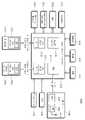
도 19는 본 발명에 따른 불휘발성 메모리 장치에 포함된 메모리 블록들 중 제1 메모리 블록을 예시적으로 보여주는 회로도이다. 예시적으로, 도 19를 참조하여 3차원 구조의 제1 메모리 블록(BLK1)이 설명된다. 그러나, 본 발명의 범위가 이에 한정되는 것은 아니며, 다른 메모리 블록들 또한 제1 메모리 블록(BLK1)과 유사한 구조를 가질 수 있다.19 is a circuit diagram exemplarily illustrating a first memory block among memory blocks included in a nonvolatile memory device according to the present invention. For example, a first memory block BLK1 having a three-dimensional structure will be described with reference to FIG. 19 . However, the scope of the present invention is not limited thereto, and other memory blocks may also have a structure similar to that of the first memory block BLK1 .
도 19를 참조하면, 제1 메모리 블록(BLK1)은 복수의 셀 스트링들(CS11, CS12, CS21, CS22)을 포함한다. 복수의 셀 스트링들(CS11, CS12, CS21, CS22)은 행 방향(row direction) 및 열 방향(column direction)을 따라 배치되어 행들 및 열들을 형성할 수 있다.Referring to FIG. 19 , the first memory block BLK1 includes a plurality of cell strings CS11 , CS12 , CS21 , and CS22 . The plurality of cell strings CS11 , CS12 , CS21 , and CS22 may be disposed along a row direction and a column direction to form rows and columns.
복수의 셀 스트링들(CS11, CS12, CS21, CS22) 각각은 복수의 셀 트랜지스터들을 포함한다. 예를 들어, 복수의 셀 스트링들(CS11, CS12, CS21, CS22) 각각은 스트링 선택 트랜지스터들(SSTa, SSTb), 복수의 메모리 셀들(MC1~MC8), 접지 선택 트랜지스터들(GSTa, GSTb), 및 더미 메모리 셀들(DMC1, DMC2)을 포함할 수 있다. 예시적으로, 복수의 셀 스트링들(CS11, CS12, CS21, CS22)에 포함된 복수의 셀 트랜지스터들 각각은 전하 트랩형 플래시(CTF; charge trap flash) 메모리 셀일 수 있다.Each of the plurality of cell strings CS11 , CS12 , CS21 , and CS22 includes a plurality of cell transistors. For example, each of the plurality of cell strings CS11, CS12, CS21, and CS22 includes string select transistors SSTa and SSTb, a plurality of memory cells MC1 to MC8, ground select transistors GSTa and GSTb, and dummy memory cells DMC1 and DMC2. For example, each of the plurality of cell transistors included in the plurality of cell strings CS11, CS12, CS21, and CS22 may be a charge trap flash (CTF) memory cell.
복수의 메모리 셀들(MC1~MC8)은 직렬 연결되며, 행 방향 및 열 방향에 의해 형성된 평명과 수직한 방향인 높이 방향(height direction)으로 적층된다. 스트링 선택 트랜지스터들(SSTa, SSTb)은 직렬 연결되고, 직렬 연결된 스트링 선택 트랜지스터들(SSTa, SSTb)은 복수의 메모리 셀들(MC1~MC8) 및 비트라인(BL) 사이에 제공된다. 접지 선택 트랜지스터들(GSTa, GSTb)은 직렬 연결되고, 직렬 연결된 접지 선택 트랜지스터들(GSTa, GSTb)은 복수의 메모리 셀들(MC1~MC8) 및 공통 소스 라인(CSL) 사이에 제공된다.The plurality of memory cells MC1 to MC8 are connected in series and are stacked in a height direction that is perpendicular to a plane formed by a row direction and a column direction. The string select transistors SSTa and SSTb are connected in series, and the series connected string select transistors SSTa and SSTb are provided between the plurality of memory cells MC1 to MC8 and the bit line BL. The ground select transistors GSTa and GSTb are connected in series, and the series connected ground select transistors GSTa and GSTb are provided between the plurality of memory cells MC1 to MC8 and the common source line CSL.
예시적으로, 복수의 메모리 셀들(MC1~MC8) 및 접지 선택 트랜지스터들(GSTa, GSTb) 사이에 제1 더미 메모리 셀(DMC1)이 제공될 수 있다. 예시적으로, 복수의 메모리 셀들(MC1~MC8) 및 스트링 선택 트랜지스터들(SSTa, SSTb) 사이에 제2 더미 메모리 셀(DMC2)이 제공될 수 있다.For example, a first dummy memory cell DMC1 may be provided between the plurality of memory cells MC1 to MC8 and the ground selection transistors GSTa and GSTb. For example, the second dummy memory cell DMC2 may be provided between the plurality of memory cells MC1 to MC8 and the string select transistors SSTa and SSTb.
셀 스트링들(CS11, CS12, CS21, CS22)의 접지 선택 트랜지스터들(GSTa, GSTb)은 접지 선택 라인(GSL)에 공통으로 연결될 수 있다. 예시적으로, 동일한 행의 접지 선택 트랜지스터들은 동일한 접지 선택 라인에 연결될 수 있고, 다른 행의 접지 선택 트랜지스터들은 다른 접지 선택 라인에 연결될 수 있다. 예를 들어, 제1 행의 셀 스트링들(CS11, CS12)의 제1 접지 선택 트랜지스터들(GSTa)은 제1 접지 선택 라인에 연결될 수 있고, 제2 행의 셀 스트링들(CS21, CS22)의 제1 접지 선택 트랜지스터들(GSTa)은 제2 접지 선택 라인에 연결될 수 있다.The ground selection transistors GSTa and GSTb of the cell strings CS11 , CS12 , CS21 , and CS22 may be commonly connected to the ground selection line GSL. For example, ground select transistors in the same row may be connected to the same ground select line, and ground select transistors in different rows may be connected to different ground select lines. For example, the first ground select transistors GSTa of the cell strings CS11 and CS12 in the first row may be connected to the first ground select line, and The first ground select transistors GSTa may be connected to the second ground select line.
예시적으로, 도면에 도시되지는 않았으나, 기판(미도시)으로부터 동일한 높이에 제공되는 접지 선택 트랜지스터들은 동일한 접지 선택 라인에 연결될 수 있고, 다른 높이에 제공되는 접지 선택 트랜지스터들은 다른 접지 선택 라인에 연결될 수 있다. 예를 들어, 셀 스트링들(CS11, CS12, CS21, CS22)의 제1 접지 선택 트랜지스터들(GSTa)은 제1 접지 선택 라인에 연결되고, 제2 접지 선택 트랜지스터들(GSTb)은 제2 접지 선택 라인에 연결될 수 있다.Exemplarily, although not shown in the drawings, ground selection transistors provided at the same height from the substrate (not shown) may be connected to the same ground selection line, and ground selection transistors provided at different heights may be connected to different ground selection lines. can For example, the first ground selection transistors GSTa of the cell strings CS11 , CS12 , CS21 , and CS22 are connected to the first ground selection line, and the second ground selection transistors GSTb are connected to the second ground selection line. can be connected to the line.
기판 또는 접지 선택 트랜지스터(GSTa, GSTb)으로부터 동일한 높이의 메모리 셀들은 동일한 워드라인에 공통으로 연결되고, 서로 다른 높이의 메모리 셀들은 서로 다른 워드라인에 연결된다. 예를 들어, 셀 스트링들(CS11, CS12, CS21, CS22)의 제1 내지 제8 메모리 셀들(MC8)은 제1 내지 제8 워드라인들(WL1~WL8)에 각각 공통으로 연결된다.Memory cells of the same height from the substrate or ground selection transistors GSTa and GSTb are commonly connected to the same word line, and memory cells of different heights are connected to different word lines. For example, the first to eighth memory cells MC8 of the cell strings CS11, CS12, CS21, and CS22 are commonly connected to the first to eighth word lines WL1 to WL8, respectively.
동일한 높이의 제1 스트링 선택 트랜지스터들(SSTa) 중 동일한 행의 스트링 선택 트랜지스터들은 동일한 스트링 선택 라인과 연결되고, 다른 행의 스트링 선택 트랜지스터들은 다른 스트링 선택 라인과 연결된다. 예를 들어, 제1 행의 셀 스트링들(CS11, CS12)의 제1 스트링 선택 트랜지스터들(SSTa)은 스트링 선택 라인(SSL1a)과 공통으로 연결되고, 제2 행의 셀 스트링들(CS21, CS22)의 제1 스트링 선택 트랜지스터들(SSTa)은 스트링 선택 라인(SSL1a)과 공통으로 연결된다.Among the first string select transistors SSTa having the same height, string select transistors in the same row are connected to the same string select line, and string select transistors in different rows are connected to different string select lines. For example, the first string select transistors SSTa of the cell strings CS11 and CS12 of the first row are commonly connected to the string select line SSL1a, and the cell strings CS21 and CS22 of the second row are connected in common. ) of the first string select transistors SSTa are commonly connected to the string select line SSL1a.
마찬가지로, 동일한 높이의 제2 스트링 선택 트랜지스터들(SSTb) 중 동일한 행의 스트링 선택 트랜지스터들은 동일한 스트링 선택 라인과 연결되고, 다른 행의 스트링 선택 트랜지스터들은 다른 스트링 선택 라인과 연결된다. 예를 들어, 제1 행의 셀 스트링들(CS11, CS12)의 제2 스트링 선택 트랜지스터들(SSTb)은 스트링 선택 라인(SSL1b)과 공통으로 연결되고, 제2 행의 셀 스트링들(CS21, CS22)의 제2 스트링 선택 트랜지스터들(SSTb)은 스트링 선택 라인(SSL2b)과 공통으로 연결된다.Similarly, of the second string select transistors SSTb having the same height, string select transistors in the same row are connected to the same string select line, and string select transistors in different rows are connected to different string select lines. For example, the second string select transistors SSTb of the cell strings CS11 and CS12 of the first row are commonly connected to the string select line SSL1b, and the cell strings CS21 and CS22 of the second row are connected in common. ) of the second string select transistors SSTb are commonly connected to the string select line SSL2b.
비록 도면에 도시되지는 않았으나, 동일한 행의 셀 스트링들의 스트링 선택 트랜지스터들은 동일한 스트링 선택 라인에 공통으로 연결될 수 있다. 예를 들어, 제1 행의 셀 스트링들(CS11, CS12)의 제1 및 제2 스트링 선택 트랜지스터들(SSTa, SSTb)은 동일한 스트링 선택 라인에 공통으로 연결될 수 있다. 제2 행의 셀 스트링들(CS21, CS22)의 제1 및 제2 스트링 선택 트랜지스터들(SSTa, SSTb)은 동일한 스트링 선택 라인에 공통으로 연결될 수 있다.Although not shown in the drawings, string select transistors of cell strings in the same row may be commonly connected to the same string select line. For example, the first and second string select transistors SSTa and SSTb of the cell strings CS11 and CS12 of the first row may be commonly connected to the same string select line. The first and second string select transistors SSTa and SSTb of the cell strings CS21 and CS22 of the second row may be commonly connected to the same string select line.
예시적으로, 동일한 높이의 더미 메모리 셀들은 동일한 더미 워드라인과 연결되고, 다른 높이의 더미 메모리 셀들은 다른 더미 워드라인과 연결된다. 예를 들어, 제1 더미 메모리 셀들(DMC1)은 제1 더미 워드라인(DWL1)과 연결되고, 제2 더미 메모리 셀들(DMC2)은 제2 더미 워드라인(DWL2)과 연결된다.For example, dummy memory cells having the same height are connected to the same dummy word line, and dummy memory cells having different heights are connected to different dummy word lines. For example, the first dummy memory cells DMC1 are connected to the first dummy word line DWL1 , and the second dummy memory cells DMC2 are connected to the second dummy word line DWL2 .
예시적으로, 도 19에 도시된 제1 메모리 블록(BLK1)은 예시적인 것이며, 셀 스트링들의 개수는 증가 또는 감소할 수 있으며, 셀 스트링들의 개수에 따라 셀 스트링들이 구성하는 행들 및 열들의 개수는 증가 또는 감소할 수 있다. 또한, 제1 메모리 블록(BLK1)의 셀 트랜지스터들(GST, MC, DMC, SST 등)의 개수들은 각각 증가 또는 감소될 수 있으며, 셀 트랜지스터들의 개수들에 따라 제1 메모리 블록(BLK1)의 높이가 증가 또는 감소할 수 있다. 또한, 셀 트랜지스터들의 개수들에 따라 셀 트랜지스터들과 연결된 라인들(GSL, WL, DWL, SSL 등)의 개수들이 증가 또는 감소될 수 있다.For example, the first memory block BLK1 illustrated in FIG. 19 is exemplary, and the number of cell strings may increase or decrease, and the number of rows and columns constituting the cell strings may vary according to the number of cell strings. may increase or decrease. Also, the number of cell transistors GST, MC, DMC, SST, etc. of the first memory block BLK1 may be increased or decreased, respectively, and the height of the first memory block BLK1 may be increased according to the number of cell transistors. may increase or decrease. Also, the number of lines (GSL, WL, DWL, SSL, etc.) connected to the cell transistors may be increased or decreased according to the number of cell transistors.
도 20은 본 발명의 실시 예들에 따른 불휘발성 메모리 시스템이 적용된 메모리 카드 시스템을 보여주는 블록도이다. 예시적으로, 도 20의 메모리 카드 시스템(1000)은 도 1 내지 도 18을 참조하여 설명된 불휘발성 메모리 시스템의 동작 방법을 기반으로 동작할 수 있다.20 is a block diagram illustrating a memory card system to which a nonvolatile memory system according to embodiments of the present invention is applied. For example, the
도 20을 참조하면, 메모리 카드 시스템(1000)은 컨트롤러(1100), 불휘발성 메모리(1200), 및 커넥터(1300)를 포함한다.Referring to FIG. 20 , the
컨트롤러(1100)는 불휘발성 메모리(1200)와 연결된다. 컨트롤러(1100)는 불휘발성 메모리(1200)를 액세스하도록 구성된다. 예를 들어, 컨트롤러(1100)는 불휘발성 메모리(1100)의 읽기, 쓰기, 소거, 그리고 배경(background) 동작을 제어하도록 구성된다. 배경(background) 동작은 마모도 관리, 가비지 콜렉션 등과 같은 동작들을 포함한다.The
컨트롤러(1100)는 불휘발성 메모리(1200) 및 호스트(Host) 사이에 인터페이스를 제공하도록 구성된다. 컨트롤러(1100)는 불휘발성 메모리(1200)를 제어하기 위한 펌웨어(firmware)를 구동하도록 구성된다.The
예시적으로, 컨트롤러(1100)는 램(RAM, Random Access Memory), 프로세싱 유닛(processing unit), 호스트 인터페이스(host interface), 메모리 인터페이스(memory interface), 에러 정정부와 같은 구성 요소들을 포함할 수 있다.For example, the
컨트롤러(1100)는 커넥터(1300)를 통해 외부 장치와 통신할 수 있다. 컨트롤러(1100)는 미리 정해진 통신 규격에 따라 외부 장치(예를 들어, 호스트)와 통신할 수 있다. 예시적으로, 컨트롤러(1100)는 USB (Universal Serial Bus), MMC (multimedia card), eMMC(embedded MMC), PCI (peripheral component interconnection), PCI-E (PCI-express), ATA (Advanced Technology Attachment), Serial-ATA, Parallel-ATA, SCSI (small computer small interface), ESDI (enhanced small disk interface), IDE (Integrated Drive Electronics), 파이어와이어(Firewire), UFS(Universal Flash Storage), NVMe (Nonvolatile Memory express) 등과 같은 다양한 통신 규격들 중 적어도 하나를 통해 외부 장치와 통신하도록 구성된다.The
불휘발성 메모리(1200)는 EPROM (Electrically Erasable and Programmable ROM), 낸드 플래시 메모리, 노어 플래시 메모리, PRAM (Phase-change RAM), ReRAM (Resistive RAM), FRAM (Ferroelectric RAM), STT-MRAM(Spin-Torque Magnetic RAM) 등과 같은 다양한 불휘발성 메모리 소자들로 구현될 수 있다.The
예시적으로, 컨트롤러(1100) 및 불휘발성 메모리(1200)는 하나의 반도체 장치로 집적될 수 있다. 예시적으로, 컨트롤러(1100) 및 불휘발성 메모리(1200)는 하나의 반도체 장치로 집적되어 솔리드 스테이트 드라이브(SSD, Solid State Drive)를 구성할 수 있다. 컨트롤러(1100) 및 불휘발성 메모리(1100)는 하나의 반도체 장치로 집적되어, 메모리 카드를 구성할 수 있다. 예를 들면, 컨트롤러(1100) 및 불휘발성 메모리(1200)는 하나의 반도체 장치로 집적되어 PC 카드(PCMCIA, personal computer memory card international association), 컴팩트 플래시 카드(CF), 스마트 미디어 카드(SM, SMC), 메모리 스틱, 멀티``미디어 카드(MMC, RS-MMC, MMCmicro, eMMC), SD 카드(SD, miniSD, microSD, SDHC), 유니버설 플래시 기억장치(UFS) 등과 같은 메모리 카드를 구성할 수 있다.For example, the
불휘발성 메모리(1200) 또는 메모리 카드 시스템(1000)은 다양한 형태의 패키지로 실장될 수 있다. 예를 들면, 불휘발성 메모리(1200) 또는 메모리 카드 시스템(1000)은 PoP(Package on Package), Ball grid arrays(BGAs), Chip scale packages(CSPs), Plastic Leaded Chip Carrier(PLCC), Plastic Dual In Line Package(PDIP), Die in Waffle Pack, Die in Wafer Form, Chip On Board(COB), Ceramic Dual In Line Package(CERDIP), Plastic Metric Quad Flat Pack(MQFP), Thin Quad Flatpack(TQFP), Small Outline(SOIC), Shrink Small Outline Package(SSOP), Thin Small Outline(TSOP), Thin Quad Flatpack(TQFP), System In Package(SIP), Multi-Chip Package(MCP), Wafer-level Fabricated Package(WFP), Wafer-Level Processed Stack Package(WSP) 등과 같은 방식으로 패키지화되어 실장될 수 있다.The
도 21은 본 발명에 따른 불휘발성 메모리 시스템이 적용된 SSD(Solid State Drive) 시스템을 예시적으로 보여주는 블록도이다. 예시적으로, 도 21의 SSD 시스템(2000)은 도 1 내지 도 17을 참조하여 설명된 불휘발성 메모리 시스템의 동작 방법을 기반으로 동작할 수 있다.21 is a block diagram exemplarily illustrating a solid state drive (SSD) system to which a nonvolatile memory system according to the present invention is applied. For example, the
도 21을 참조하면, SSD 시스템(2000)은 호스트(2100) 및 SSD(2200)를 포함한다. SSD(2200)는 신호 커넥터(2001)를 통해 호스트(2100)와 신호(SIG)를 주고 받고, 전원 커넥터(2002)를 통해 전원(PWR)을 입력 받는다. SSD(2200)는 SSD 컨트롤러(2210), 복수의 플래시 메모리들(2221~222n), 보조 전원 장치(2230), 및 버퍼 메모리(2240)를 포함한다.Referring to FIG. 21 , the
SSD 컨트롤러(2210)는 호스트(2100)로부터 수신된 신호(SIG)에 응답하여 복수의 플래시 메모리들(2221~222n)을 제어할 수 있다. 복수의 플래시 메모리들(2221~222n)은 SSD 컨트롤러(2210)의 제어에 따라 프로그램 동작을 수행할 수 있다. 예시적으로, SSD 컨트롤러(2210)는 도 1 내지 도 14를 참조하여 설명된 동작 방법에 따라, 유휴 시간을 기반으로 쓰기 커맨드의 연속성을 판별하고, 판별 결과를 기반으로 동작 모드를 제어할 수 있다.The
보조 전원 장치(2230)는 전원 커넥터(2002)를 통해 호스트(2100)와 연결된다. 보조 전원 장치(2230)는 호스트(2100)로부터 전원(PWR)을 입력 받고, 충전할 수 있다. 보조 전원 장치(2230)는 호스트(2100)로부터의 전원 공급이 원활하지 않을 경우, SSD 시스템(2000)의 보조 전원을 제공할 수 있다. 예시적으로, 보조 전원 장치(2230)는 SSD(2200) 내에 위치할 수도 있고, SSD(2200) 밖에 위치할 수도 있다. 예를 들면, 보조 전원 장치(2230)는 메인 보드 또는 별도의 인쇄 회로 기판 상에 위치하며, SSD(2200)에 보조 전원을 제공할 수도 있다.The auxiliary power supply 2230 is connected to the
버퍼 메모리(2240)는 SSD(2200)의 버퍼 메모리로 동작한다. 예를 들어, 버퍼 메모리(2240)는 호스트(2100)로부터 수신된 데이터 또는 복수의 플래시 메모리들(2221~222n)로부터 수신된 데이터를 임시 저장하거나, 플래시 메모리들(2221~222n)의 메타 데이터(예를 들어, 매핑 테이블)를 임시 저장할 수 있다. 버퍼 메모리(2240)는 DRAM, SDRAM, DDR SDRAM, LPDDR SDRAM, SRAM 등과 같은 휘발성 메모리 또는 FRAM ReRAM, STT-MRAM, PRAM 등과 같은 불휘발성 메모리들을 포함할 수 있다.The
도 22는 본 발명의 실시 예에 따른 불휘발성 메모리 시스템을 포함하는 전자 시스템의 구성을 보여주는 블록도이다. 예시적으로, 전자 시스템(3000)은 MIPI 연합에 의해 제안된 인터페이스를 이용하거나 지원할 수 있는 데이터 처리 장치로 구현될 수 있다. 예시적으로, 전자 시스템(3000)은 휴대용 통신 단말기, PDA(Personal Digital Assistant), PMP(Portable Media Player), 스마트폰, 또는 웨어러블(Wearable) 장치 형태로 구현될 수 있다.22 is a block diagram illustrating a configuration of an electronic system including a nonvolatile memory system according to an embodiment of the present invention. For example, the
도 22를 참조하면, 전자 시스템(3000)은 애플리케이션 프로세서(3100), 디스플레이(3220), 및 이미지 센서(3230)를 포함할 수 있다. 애플리케이션 프로세서(3100)는 DigRF 마스터(3110), DSI(Display Serial Interface) 호스트(3120), CSI(Camera Serial Interface) 호스트(3130), 및 물리 계층(3140)을 포함할 수 있다.Referring to FIG. 22 , the
DSI 호스트(3120)는 DSI를 통해 디스플레이(3220)의 DSI 장치(3225)와 통신할 수 있다. 예시적으로, DSI 호스트(3120)에는 광 시리얼라이저(SER)가 구현될 수 있다. 예로서, DSI 장치(3225)에는 광 디시리얼라이저(DES)가 구현될 수 있다.The
CSI 호스트(3130)는 CSI를 통해 이미지 센서(3230)의 CSI 장치(3235)와 통신할 수 있다. 예시적으로, CSI 호스트(3130)에는 광 디시리얼라이저(DES)가 구현될 수 있다. 예로서, CSI 장치(3235)에는 광 시리얼라이저(SER)가 구현될 수 있다.The
전자 시스템(3000)은 애플리케이션 프로세서(3100)와 통신하는 RF(Radio Frequency) 칩(3240)을 더 포함할 수 있다. RF 칩(3240)은 물리 계층(3242), DigRF 슬레이브(3244), 및 안테나(3246)를 포함할 수 있다. 예시적으로, RF 칩(3240)의 물리 계층(3242)과 애플리케이션 프로세서(3100)의 물리 계층(3140)은 MIPI DigRF 인터페이스에 의해 서로 데이터를 교환할 수 있다.The
전자 시스템(3000)은 워킹 메모리(Working Memory; 3250) 및 임베디드/카드 스토리지(3255)를 더 포함할 수 있다. 워킹 메모리(3250) 및 임베디드/카드 스토리지(3255)는 애플리케이션 프로세서(3100)로부터 제공받은 데이터를 저장할 수 있다. 워킹 메모리(3250) 및 임베디드/카드 스토리지(3255)는 저장된 데이터를 어플리케이션 프로세서(3100)로 제공할 수 있다.The
워킹 메모리(3250)는 애플리케이션 프로세서(3100)에 의해 처리된 또는 처리될 데이터를 일시적으로 저장할 수 있다. 워킹 메모리(3250)는 SRAM, DRAM, SDRAM 등과 같은 휘발성 메모리, 또는 플래시 메모리, PRAM, MRAM, ReRAM, FRAM 등과 같은 불휘발성 메모리를 포함할 수 있다.The working
임베디드/카드 스토리지(3255)는 전원 공급 여부와 관계없이 데이터를 저장할 수 있다. 실시 예로서, 임베디드/카드 스토리지(3255)는 UFS 인터페이스 규약에 따라 작동할 수 있으나, 본 발명은 이 실시 예로 한정되지 않는다. 예시적으로, 임베디드/카드 스토리지(3255)는 도 1 내지 도 17을 참조하여 설명된 불휘발성 메모리 시스템을 포함할 수 있다. 임베디드/카드 스토리지(3255)는 도 1 내지 도 17을 참조하여 설명된 불휘발성 메모리 시스템의 동작 방법을 기반으로 동작할 수 있다.The embedded/
전자 시스템(3000)은 Wimax(World Interoperability for Microwave Access; 3260), WLAN(Wireless Local Area Network; 3262), UWB(Ultra Wideband; 3264) 등을 통해 외부 시스템과 통신할 수 있다.The
전자 시스템(3000)은 음성 정보를 처리하기 위한 스피커(3270) 및 마이크(3275)를 더 포함할 수 있다. 예시적으로, 전자 시스템(3000)은 위치 정보를 처리하기 위한 GPS(Global Positioning System) 장치(3280)를 더 포함할 수 있다. 전자 시스템(3000)은 주변 장치들과의 연결을 관리하기 위한 브릿지(Bridge) 칩(3290)을 더 포함할 수 있다.The
본 발명의 기술적 사상에 따른 예시적인 실시 예로서, 불휘발성 메모리 장치는 3차원 메모리 어레이를 포함할 수 있다. 3차원 메모리 어레이는, 실리콘 기판 및 메모리 셀들의 동작에 연관된 회로의 위에 배치되는 활성 영역을 갖는 메모리 셀들의 어레이들의 하나 또는 그 이상의 물리 레벨들에 모놀리식으로(monolithically) 형성될 수 있다. 메모리 셀들의 동작에 연관된 회로는 기판 내에 또는 기판 위에 위치할 수 있다. 모놀리식(monolithically)이란 용어는, 3차원 어레이의 각 레벨의 층들이 3차원 어레이의 하위 레벨의 층들 위에 직접 증착됨을 의미한다.As an exemplary embodiment according to the inventive concept, the nonvolatile memory device may include a 3D memory array. A three-dimensional memory array may be formed monolithically on one or more physical levels of an array of memory cells having an active area disposed over a silicon substrate and circuitry associated with the operation of the memory cells. The circuitry involved in the operation of the memory cells may be located in or on the substrate. The term monolithically means that the layers of each level of the three-dimensional array are deposited directly over the layers of the lower level of the three-dimensional array.
본 발명의 기술적 사상에 따른 예시적인 실시 예로서, 3차원 메모리 어레이는 수직의 방향성을 가지며, 적어도 하나의 메모리 셀이 다른 하나의 메모리 셀 위에 위치하는 수직 NAND 스트링들을 포함한다. 적어도 하나의 메모리 셀은 전하 트랩 층을 포함한다. 각각의 수직 NAND 스트링은 메모리 셀들 위에 위치하는 적어도 하나의 선택 트랜지스터를 포함할 수 있다. 적어도 하나의 선택 트랜지스터는 메모리 셀들과 동일한 구조를 갖고, 메모리 셀들과 함께 모놀리식으로 형성될 수 있다.As an exemplary embodiment according to the inventive concept, a 3D memory array has vertical directionality and includes vertical NAND strings in which at least one memory cell is positioned on another memory cell. At least one memory cell includes a charge trap layer. Each vertical NAND string may include at least one select transistor positioned over memory cells. The at least one selection transistor may have the same structure as the memory cells, and may be monolithically formed together with the memory cells.
3차원 메모리 어레이가 복수의 레벨들로 구성되고, 레벨들 사이에 공유된 워드 라인들 또는 비트 라인들을 갖고, 3차원 메모리 어레이에 적합한 구성은 미국등록특허공보 제7,679,133호, 미국등록특허공보 제8,553,466호, 미국등록특허공보 제8,654,587호, 미국등록특허공보 제8,559,235호, 그리고 미국공개특허공보 제2011/0233648호에 개시되어 있으며, 본 발명의 레퍼런스로 포함된다.A configuration in which a three-dimensional memory array is composed of a plurality of levels, with word lines or bit lines shared between the levels, and suitable for a three-dimensional memory array is disclosed in U.S. Patent No. 7,679,133, U.S. Patent No. 8,553,466 No. 8,654,587, U.S. Patent No. 8,559,235, and U.S. Patent Publication No. 2011/0233648, which are incorporated herein by reference.
상술된 본 발명의 실시 예들에 따르면, 불휘발성 메모리 시스템은 소스 블록의 P/E 사이클을 기반으로 리클레임 동작을 제어할 수 있다. 따라서, 향상된 성능 및 향상된 신뢰성을 갖는 불휘발성 메모리 시스템 및 그것의 동작 방법이 제공된다.According to the above-described embodiments of the present invention, the nonvolatile memory system may control the reclaim operation based on the P/E cycle of the source block. Accordingly, a nonvolatile memory system having improved performance and improved reliability and a method of operating the same are provided.
본 발명의 상세한 설명에서는 구체적인 실시 예들에 관하여 설명하였으나, 본 발명의 범위에서 벗어나지 않는 한도 내에서 여러 가지 변형이 가능하다. 그러므로 본 발명의 범위는 상술된 실시 예들에 국한되어 정해져서는 안되며 후술하는 특허청구범위뿐만 아니라 이 발명의 특허청구범위와 균등한 것들에 의해 정해져야 할 것이다.In the detailed description of the present invention, specific embodiments have been described, but various modifications are possible without departing from the scope of the present invention. Therefore, the scope of the present invention should not be limited to the above-described embodiments, but should be defined by the following claims as well as the claims and equivalents of the present invention.
100 : 불휘발성 메모리 시스템
110 : 메모리 컨트롤러
111 : ECC 회로
112 : 리클레임 관리자
120 : 불휘발성 메모리 장치
PE : 프로그램 및 소거 사이클(P/E 사이클)
RP : 리클레임 실행 구간
RM : 리클레임 마진
RCI : 읽기 카운트 간격
SO : 서브 동작100: non-volatile memory system
110: memory controller
111: ECC circuit
112: reclaim manager
120: nonvolatile memory device
PE : Program and Erase Cycles (P/E Cycles)
RP: Reclaim execution section
RM: Reclaim Margin
RCI: read count interval
SO: sub-action
Claims (20)
Translated fromKorean상기 복수의 메모리 블록들 중 소스 블록에 대한 읽기 동작 동안 기준 값보다 큰 에러 비트들이 검출된 경우, 상기 소스 블록을 선택하는 단계;
상기 소스 블록의 프로그램/소거(P/E) 사이클을 검출하고, 상기 P/E 사이클이 제1 값보다 큰 경우, 상기 소스 블록에 대한 제1 리클레임 동작을 제1 읽기 카운트에서 시작하고, 상기 P/E 사이클이 제1 값보다 작거나 같은 경우, 상기 소스 블록에 대한 제2 리클레임 동작을 제2 읽기 카운트에서 시작하는 단계를 포함하고,
상기 제1 읽기 카운트 및 상기 제2 읽기 카운트는 상기 불휘발성 메모리 장치에서 수행되는 읽기 동작들의 횟수를 가리키고, 상기 제1 읽기 카운트는 상기 제2 읽기 카운트보다 작은 동작 방법.A method of operating a nonvolatile memory device including a plurality of memory blocks, the method comprising:
selecting the source block when error bits greater than a reference value are detected during a read operation on the source block among the plurality of memory blocks;
detecting a program/erase (P/E) cycle of the source block, and when the P/E cycle is greater than a first value, starting a first reclaim operation on the source block at a first read count, and If the P/E cycle is less than or equal to the first value, starting a second reclaim operation on the source block at a second read count,
The first read count and the second read count indicate the number of read operations performed in the nonvolatile memory device, and the first read count is smaller than the second read count.
상기 제1 읽기 카운트 및 상기 제2 읽기 카운트는 상기 소스 블록의 상기 P/E 사이클 및 상기 소스 블록에서 수행된 상기 읽기 동작 도중에 발생한 상기 에러 비트들의 개수를 기반으로 설정되는 동작 방법.The method of claim 1,
The first read count and the second read count are set based on the P/E cycle of the source block and the number of error bits generated during the read operation performed in the source block.
상기 제1 읽기 카운트에서 수행된 제1 읽기 동작 동안 발생한 제1 에러 비트들의 개수는 상기 제2 읽기 카운트에서 수행된 제2 읽기 동작 동안 발생한 제2 에러 비트들의 개수와 동일한 동작 방법.
3. The method of claim 2,
The number of first error bits generated during the first read operation performed in the first read count is the same as the number of second error bits generated during the second read operation performed in the second read count.
상기 제1 리클레임 동작은 제1 리클레임 실행 구간에서 완료되고, 상기 제2 리클레임 동작은 상기 제1 리클레임 실행 구간과 다른 제2 리클레임 실행 구간에서 완료되고, 상기 제1 리클레임 실행 구간 및 상기 제2 리클레임 실행 구간은 상기 제1 읽기 카운트 및 상기 제2 읽기 카운트로부터 추가적인 읽기 카운트들을 각각 가리키는 동작 방법.The method of claim 1,
The first reclaim operation is completed in a first reclaim execution period, the second reclaim operation is completed in a second reclaim execution period different from the first reclaim execution period, and the first reclaim execution period and the second reclaim execution period indicates additional read counts from the first read count and the second read count, respectively.
상기 제1 리클레임 실행 구간은 상기 제2 리클레임 실행 구간보다 짧은 동작 방법.5. The method of claim 4,
The first reclaim execution period is shorter than the second reclaim execution period.
상기 제1 리클레임 실행 구간 및 상기 제2 리클레임 실행 구간은 리클레임 마진 내에서 설정되고, 상기 리클레임 마진은 UECC 데이터(Uncorrectable Error Correction Code Data)가 발생하지 않는 추가적인 읽기 카운트들을 가리키는 동작 방법.6. The method of claim 5,
The first reclaim execution period and the second reclaim execution period are set within a reclaim margin, and the reclaim margin indicates additional read counts in which Uncorrectable Error Correction Code Data (UECC data) does not occur.
상기 제1 리클레임 동작은 복수의 제1 서브 동작들을 포함하고,
상기 복수의 제1 서브 동작들 각각은 제1 서브-동작 구간을 갖고,
상기 제2 리클레임 동작은 복수의 제2 서브 동작들을 포함하고,
상기 복수의 제2 서브 동작들 각각은 제2 서브-동작 구간을 갖고,
상기 제1 서브-동작 구간은 상기 제2 서브-동작 구간보다 긴 동작 방법.
7. The method of claim 6,
The first reclaim operation includes a plurality of first sub operations,
each of the plurality of first sub-operations has a first sub-operation period,
The second reclaim operation includes a plurality of second sub operations,
each of the plurality of second sub-operations has a second sub-operation period,
wherein the first sub-operation period is longer than the second sub-operation period.
상기 제1 서브 동작들 및 상기 제2 서브 동작들 각각은:
상기 소스 블록에 포함된 복수의 페이지들 중 적어도 하나의 페이지를 읽는 단계;
상기 읽은 데이터에서 하나 또는 그 이상의 에러들을 정정하는 단계; 및
상기 정정된 데이터를 목표 블록에 프로그램하는 단계를 포함하는 동작 방법.8. The method of claim 7,
Each of the first sub-operations and the second sub-operations includes:
reading at least one page among a plurality of pages included in the source block;
correcting one or more errors in the read data; and
and programming the corrected data into a target block.
상기 제1 서브 동작들 각각은 제1 단위로 수행되고, 상기 제2 서브 동작들 각각은 제2 단위로 수행되고, 상기 제1 단위는 상기 제2 단위보다 큰 동작 방법.9. The method of claim 8,
Each of the first sub-operations is performed in a first unit, each of the second sub-operations is performed in a second unit, and the first unit is greater than the second unit.
복수의 메모리 블록들을 포함하는 불휘발성 메모리 장치; 및
상기 불휘발성 메모리 장치를 제어하도록 구성된 메모리 컨트롤러를 포함하고,
상기 메모리 컨트롤러는:
상기 복수의 메모리 블록들 중 소스 블록에 대한 읽기 동작 동안 기준 값보다 큰 에러 비트들이 검출된 경우, 상기 소스 블록을 선택하는 단계;
상기 소스 블록의 프로그램/소거(P/E) 사이클을 검출하고, 상기 P/E 사이클이 제1 값보다 큰 경우, 상기 소스 블록에 대한 제1 리클레임 동작을 제1 읽기 카운트에서 시작하고, 상기 P/E 사이클이 제1 값보다 작거나 같은 경우, 상기 소스 블록에 대한 제2 리클레임 동작을 제2 읽기 카운트에서 시작하는 단계를 포함하고,
상기 제1 읽기 카운트 및 상기 제2 읽기 카운트는 상기 불휘발성 메모리 장치에서 수행되는 읽기 동작들의 횟수를 가리키고, 상기 제1 읽기 카운트는 상기 제2 읽기 카운트보다 작은 불휘발성 메모리 시스템.A nonvolatile memory system comprising:
a nonvolatile memory device including a plurality of memory blocks; and
a memory controller configured to control the nonvolatile memory device;
The memory controller includes:
selecting the source block when error bits greater than a reference value are detected during a read operation on the source block among the plurality of memory blocks;
detecting a program/erase (P/E) cycle of the source block, and when the P/E cycle is greater than a first value, starting a first reclaim operation on the source block at a first read count, and If the P/E cycle is less than or equal to the first value, starting a second reclaim operation on the source block at a second read count,
The first read count and the second read count indicate the number of read operations performed in the nonvolatile memory device, and the first read count is less than the second read count.
상기 메모리 컨트롤러는 상기 불휘발성 메모리 장치에 저장될 데이터에 대한 에러 정정 코드를 생성하고, 상기 에러 정정 코드를 기반으로 상기 읽기 동작 동안 발생한 하나 또는 그 이상의 에러 비트들을 검출하고 정정하도록 구성된 ECC(error correction code) 회로를 포함하는 불휘발성 메모리 시스템.11. The method of claim 10,
The memory controller is configured to generate an error correction code for data to be stored in the nonvolatile memory device, and to detect and correct one or more error bits generated during the read operation based on the error correction code. code) a nonvolatile memory system including a circuit.
상기 메모리 컨트롤러는 상기 기준 값 및 상기 검출된 에러 비트들을 비교하여 상기 제1 및 제2 리클레임 동작들을 시작하는 것을 판별하도록 구성된 리클레임 관리자를 포함하는 불휘발성 메모리 시스템.11. The method of claim 10,
and the memory controller comprises a reclaim manager configured to compare the reference value and the detected error bits to determine starting the first and second reclaim operations.
상기 제1 읽기 카운트 및 상기 제2 읽기 카운트는 상기 소스 블록의 상기 P/E 사이클 및 상기 소스 블록에서 수행된 상기 읽기 동작 도중에 발생한 상기 에러 비트들의 개수 모두를 기반으로 설정되는 불휘발성 메모리 시스템.11. The method of claim 10,
The first read count and the second read count are set based on both the P/E cycle of the source block and the number of error bits generated during the read operation performed in the source block.
상기 제1 읽기 카운트에서 수행된 제1 읽기 동작 동안 발생한 제1 에러 비트들의 개수는 상기 제2 읽기 카운트에서 수행된 제2 읽기 동작 동안 발생한 제2 에러 비트들의 개수와 동일한 불휘발성 메모리 시스템.14. The method of claim 13,
The number of first error bits generated during the first read operation performed in the first read count is the same as the number of second error bits generated during the second read operation performed in the second read count.
상기 제1 리클레임 동작은 제1 리클레임 실행 구간에서 완료되고, 상기 제2 리클레임 동작은 상기 제1 리클레임 실행 구간과 다른 제2 리클레임 실행 구간에서 완료되고, 상기 제1 리클레임 실행 구간 및 상기 제2 리클레임 실행 구간은 상기 제1 읽기 카운트 및 상기 제2 읽기 카운트로부터 추가적인 읽기 카운트들을 각각 가리키는 불휘발성 메모리 시스템.15. The method of claim 14,
The first reclaim operation is completed in a first reclaim execution period, the second reclaim operation is completed in a second reclaim execution period different from the first reclaim execution period, and the first reclaim execution period and the second reclaim execution period indicates additional read counts from the first read count and the second read count, respectively.
상기 제1 리클레임 실행 구간은 상기 제2 리클레임 실행 구간보다 짧은 불휘발성 메모리 시스템.16. The method of claim 15,
The first reclaim execution period is shorter than the second reclaim execution period.
상기 제1 리클레임 실행 구간 및 상기 제2 리클레임 실행 구간은 리클레임 마진 내에서 설정되고, 상기 리클레임 마진은 UECC 데이터(Uncorrectable Error Correction Code Data)가 발생하지 않는 추가적인 읽기 카운트들을 가리키는 불휘발성 메모리 시스템.17. The method of claim 16,
The first reclaim execution period and the second reclaim execution period are set within a reclaim margin, and the reclaim margin indicates additional read counts in which uncorrectable error correction code data (UECC data) does not occur. system.
상기 제1 리클레임 동작은 복수의 제1 서브 동작들을 포함하고,
상기 복수의 제1 서브 동작들 각각은 제1 서브-동작 구간을 갖고,
상기 제2 리클레임 동작은 복수의 제2 서브 동작들을 포함하고,
상기 복수의 제2 서브 동작들 각각은 제2 서브-동작 구간을 갖고,
상기 제1 서브-동작 구간은 상기 제2 서브-동작 구간보다 긴 동작 방법.18. The method of claim 17,
The first reclaim operation includes a plurality of first sub operations,
each of the plurality of first sub-operations has a first sub-operation period,
The second reclaim operation includes a plurality of second sub operations,
each of the plurality of second sub-operations has a second sub-operation period,
wherein the first sub-operation period is longer than the second sub-operation period.
상기 제1 서브 동작들 및 상기 제2 서브 동작들 각각은:
상기 소스 블록에 포함된 복수의 페이지들 중 적어도 하나의 페이지를 읽는 것;
상기 읽은 데이터에서 하나 또는 그 이상의 에러들을 정정하는 것; 및
상기 정정된 데이터를 목표 블록에 프로그램하는 것을 포함하는 불휘발성 메모리 시스템.19. The method of claim 18,
Each of the first sub-operations and the second sub-operations includes:
reading at least one page among a plurality of pages included in the source block;
correcting one or more errors in the read data; and
and programming the corrected data into a target block.
상기 제1 서브 동작들 각각은 제1 단위로 수행되고, 상기 제2 서브 동작들 각각은 제2 단위로 수행되고, 상기 제1 단위는 상기 제2 단위보다 큰 불휘발성 메모리 시스템.
20. The method of claim 19,
Each of the first sub-operations is performed in a first unit, each of the second sub-operations is performed in a second unit, and the first unit is larger than the second unit.
Priority Applications (4)
| Application Number | Priority Date | Filing Date | Title |
|---|---|---|---|
| KR1020150171644AKR102437591B1 (en) | 2015-12-03 | 2015-12-03 | Operation method of nonvolatile memory system and method operation of memory controller |
| US15/352,121US9778851B2 (en) | 2015-12-03 | 2016-11-15 | Method of operation for a nonvolatile memory system and method of operating a memory controller |
| CN201611099993.8ACN106847340B (en) | 2015-12-03 | 2016-12-02 | Method for operation of a non-volatile memory system and memory controller |
| US15/688,939US10089016B2 (en) | 2015-12-03 | 2017-08-29 | Method of operation for a nonvolatile memory system and method of operating a memory controller |
Applications Claiming Priority (1)
| Application Number | Priority Date | Filing Date | Title |
|---|---|---|---|
| KR1020150171644AKR102437591B1 (en) | 2015-12-03 | 2015-12-03 | Operation method of nonvolatile memory system and method operation of memory controller |
Publications (2)
| Publication Number | Publication Date |
|---|---|
| KR20170065726A KR20170065726A (en) | 2017-06-14 |
| KR102437591B1true KR102437591B1 (en) | 2022-08-30 |
Family
ID=58800301
Family Applications (1)
| Application Number | Title | Priority Date | Filing Date |
|---|---|---|---|
| KR1020150171644AActiveKR102437591B1 (en) | 2015-12-03 | 2015-12-03 | Operation method of nonvolatile memory system and method operation of memory controller |
Country Status (3)
| Country | Link |
|---|---|
| US (2) | US9778851B2 (en) |
| KR (1) | KR102437591B1 (en) |
| CN (1) | CN106847340B (en) |
Families Citing this family (25)
| Publication number | Priority date | Publication date | Assignee | Title |
|---|---|---|---|---|
| US10049757B2 (en)* | 2016-08-11 | 2018-08-14 | SK Hynix Inc. | Techniques for dynamically determining performance of read reclaim operations |
| KR102683257B1 (en)* | 2017-01-17 | 2024-07-11 | 에스케이하이닉스 주식회사 | Memory system and operation method thereof |
| US10657014B2 (en)* | 2017-02-27 | 2020-05-19 | Everspin Technologies, Inc. | Methods for monitoring and managing memory devices |
| US10229749B2 (en)* | 2017-03-31 | 2019-03-12 | Samsung Electronics Co., Ltd. | Nonvolatile memory storage system |
| US10381090B2 (en)* | 2017-03-31 | 2019-08-13 | Samsung Electronics Co., Ltd. | Operation method of nonvolatile memory device and storage device |
| US10621117B2 (en) | 2017-06-15 | 2020-04-14 | Micron Technology, Inc. | Controlling memory devices using a shared channel |
| KR102244921B1 (en) | 2017-09-07 | 2021-04-27 | 삼성전자주식회사 | Storage device and Method for refreshing thereof |
| US10140042B1 (en) | 2017-09-13 | 2018-11-27 | Toshiba Memory Corporation | Deterministic read disturb counter-based data checking for NAND flash |
| CN110554970B (en)* | 2018-05-31 | 2024-10-01 | 北京忆恒创源科技股份有限公司 | Garbage collection method and storage device capable of remarkably reducing write amplification |
| KR102457662B1 (en)* | 2017-10-31 | 2022-10-25 | 삼성전자주식회사 | Operation method of memory controller and operation method of storage device |
| KR102467075B1 (en)* | 2017-11-13 | 2022-11-11 | 삼성전자주식회사 | Memory Device and method of reclaiming the same |
| KR20190083862A (en)* | 2018-01-05 | 2019-07-15 | 에스케이하이닉스 주식회사 | Memory system and operation method thereof |
| KR102513691B1 (en)* | 2018-02-06 | 2023-03-27 | 에스케이하이닉스 주식회사 | Storage device and operating method thereof |
| KR102470726B1 (en)* | 2018-03-14 | 2022-11-25 | 삼성전자주식회사 | Non-volatile memory device |
| KR102549548B1 (en) | 2018-05-08 | 2023-06-30 | 에스케이하이닉스 주식회사 | Memory system, operating method thereof and electronic device |
| KR102387960B1 (en)* | 2018-07-23 | 2022-04-19 | 삼성전자주식회사 | Controller and method of operating the same |
| US11366597B2 (en)* | 2020-01-27 | 2022-06-21 | Western Digital Technologies, Inc. | Storage system and method for maintaining uniform hot count distribution using smart stream block exchange |
| US11106532B1 (en)* | 2020-04-29 | 2021-08-31 | Micron Technology, Inc. | Selective sampling of a data unit during a program erase cycle based on error rate change patterns |
| US11409446B2 (en)* | 2020-11-11 | 2022-08-09 | Micro Technology, Inc. | Media management on power-up |
| KR20220099845A (en) | 2021-01-07 | 2022-07-14 | 에스케이하이닉스 주식회사 | Memory system and operating method of the memory system |
| KR102344380B1 (en) | 2021-06-02 | 2021-12-28 | 삼성전자주식회사 | Nonvolatile memory device, controller for controlling the same, storage device having the same, and operating method thereof |
| KR20230056333A (en)* | 2021-10-20 | 2023-04-27 | 에스케이하이닉스 주식회사 | Memory controller, memory system including the same and operating method thereof |
| CN114327265B (en)* | 2021-12-23 | 2023-05-30 | 群联电子股份有限公司 | Read interference checking method, memory storage device and control circuit unit |
| KR20230138142A (en) | 2022-03-23 | 2023-10-05 | 에스케이하이닉스 주식회사 | Memory system and operating method thereof |
| US12118222B2 (en)* | 2023-02-23 | 2024-10-15 | Sk Hynix Nand Product Solutions Corp. | Controlling memory overhead for storing integrity data in solid state drives |
Citations (3)
| Publication number | Priority date | Publication date | Assignee | Title |
|---|---|---|---|---|
| US20130031443A1 (en) | 2011-07-28 | 2013-01-31 | Samsung Electronics Co., Ltd. | Method of operating memory controller, and memory system, memory card and portable electronic device including the memory controller |
| US20140310448A1 (en) | 2013-04-12 | 2014-10-16 | Sang-Wan Nam | Method of operating memory controller and data storage device including memory controller |
| US20160203047A1 (en) | 2015-01-13 | 2016-07-14 | Hyery No | Operation method of nonvolatile memory system |
Family Cites Families (22)
| Publication number | Priority date | Publication date | Assignee | Title |
|---|---|---|---|---|
| US6643177B1 (en) | 2003-01-21 | 2003-11-04 | Advanced Micro Devices, Inc. | Method for improving read margin in a flash memory device |
| US6888758B1 (en) | 2004-01-21 | 2005-05-03 | Sandisk Corporation | Programming non-volatile memory |
| KR100525004B1 (en) | 2004-02-26 | 2005-10-31 | 삼성전자주식회사 | Multi-level cell flash memory device and program method thereof |
| KR101226685B1 (en) | 2007-11-08 | 2013-01-25 | 삼성전자주식회사 | Vertical type semiconductor device and Method of manufacturing the same |
| US7613045B2 (en) | 2007-11-26 | 2009-11-03 | Sandisk Il, Ltd. | Operation sequence and commands for measuring threshold voltage distribution in memory |
| CN101339808B (en)* | 2008-07-28 | 2011-02-09 | 华中科技大学 | Method and device for erasing memory block |
| KR20100102925A (en) | 2009-03-12 | 2010-09-27 | 삼성전자주식회사 | Non-volatile memory device and memory system generating read reclaim signal |
| US8464106B2 (en)* | 2009-08-24 | 2013-06-11 | Ocz Technology Group, Inc. | Computer system with backup function and method therefor |
| KR101691092B1 (en) | 2010-08-26 | 2016-12-30 | 삼성전자주식회사 | Nonvolatile memory device, operating method thereof and memory system including the same |
| US8553466B2 (en) | 2010-03-04 | 2013-10-08 | Samsung Electronics Co., Ltd. | Non-volatile memory device, erasing method thereof, and memory system including the same |
| US9536970B2 (en) | 2010-03-26 | 2017-01-03 | Samsung Electronics Co., Ltd. | Three-dimensional semiconductor memory devices and methods of fabricating the same |
| US8819503B2 (en) | 2010-07-02 | 2014-08-26 | Stec, Inc. | Apparatus and method for determining an operating condition of a memory cell based on cycle information |
| US20120023144A1 (en)* | 2010-07-21 | 2012-01-26 | Seagate Technology Llc | Managing Wear in Flash Memory |
| KR101682666B1 (en) | 2010-08-11 | 2016-12-07 | 삼성전자주식회사 | Nonvolatile memory devicwe, channel boosting method thereof, programming method thereof, and memory system having the same |
| CN102222047B (en)* | 2011-06-16 | 2013-04-17 | 西安交通大学 | Improved BET static loss equalization method |
| US20130185612A1 (en) | 2012-01-18 | 2013-07-18 | Samsung Electronics Co., Ltd. | Flash memory system and read method of flash memory system |
| US9195586B2 (en) | 2012-02-23 | 2015-11-24 | Hgst Technologies Santa Ana, Inc. | Determining bias information for offsetting operating variations in memory cells based on wordline address |
| KR102025263B1 (en) | 2012-10-05 | 2019-09-25 | 삼성전자주식회사 | Memory system and read reclaim method thereof |
| KR102025193B1 (en) | 2013-02-19 | 2019-09-25 | 삼성전자주식회사 | Memory controller and operating method the same, memory system comprising the memory controller |
| CN104103318B (en)* | 2013-04-12 | 2019-11-05 | 三星电子株式会社 | Operate the method for storage control and the data storage device including storage control |
| US9298608B2 (en)* | 2013-10-18 | 2016-03-29 | Sandisk Enterprise Ip Llc | Biasing for wear leveling in storage systems |
| US9916237B2 (en)* | 2014-12-12 | 2018-03-13 | Sandisk Technologies Llc | Model based configuration parameter management |
- 2015
- 2015-12-03KRKR1020150171644Apatent/KR102437591B1/enactiveActive
- 2016
- 2016-11-15USUS15/352,121patent/US9778851B2/enactiveActive
- 2016-12-02CNCN201611099993.8Apatent/CN106847340B/enactiveActive
- 2017
- 2017-08-29USUS15/688,939patent/US10089016B2/enactiveActive
Patent Citations (3)
| Publication number | Priority date | Publication date | Assignee | Title |
|---|---|---|---|---|
| US20130031443A1 (en) | 2011-07-28 | 2013-01-31 | Samsung Electronics Co., Ltd. | Method of operating memory controller, and memory system, memory card and portable electronic device including the memory controller |
| US20140310448A1 (en) | 2013-04-12 | 2014-10-16 | Sang-Wan Nam | Method of operating memory controller and data storage device including memory controller |
| US20160203047A1 (en) | 2015-01-13 | 2016-07-14 | Hyery No | Operation method of nonvolatile memory system |
Also Published As
| Publication number | Publication date |
|---|---|
| CN106847340B (en) | 2022-02-11 |
| US10089016B2 (en) | 2018-10-02 |
| KR20170065726A (en) | 2017-06-14 |
| US9778851B2 (en) | 2017-10-03 |
| CN106847340A (en) | 2017-06-13 |
| US20170160934A1 (en) | 2017-06-08 |
| US20180004417A1 (en) | 2018-01-04 |
Similar Documents
| Publication | Publication Date | Title |
|---|---|---|
| KR102437591B1 (en) | Operation method of nonvolatile memory system and method operation of memory controller | |
| KR102449337B1 (en) | Operation method of nonvolatile memory system | |
| KR102333220B1 (en) | Operation method of nonvolatile memory system | |
| US10073643B2 (en) | Method of initializing storage device including one or more interface chips and nonvolatile memory devices connected to the one or more interface chips | |
| US9529705B2 (en) | Nonvolatile memory system including nonvolatile memory device and memory controller that loads a mapping table on a sub-bitmap and method of operating the memory controller | |
| US9696911B2 (en) | Operation method of nonvolatile memory system and operation method of user system including the same | |
| US9760308B2 (en) | Nonvolatile memory system and operation method of the same | |
| KR102609177B1 (en) | Operation method of nonvolatile memory system and operation method of nonvolatile memory device | |
| US10497452B2 (en) | Semiconductor memory device and method of operating the same | |
| KR20140145254A (en) | User device including nonvolatile memory device and write method thereof | |
| US10061695B2 (en) | Memory system and operating method thereof | |
| US10409718B2 (en) | Memory system and operating method thereof | |
| KR102591011B1 (en) | Memory system and operating method of memory system | |
| US9798478B2 (en) | Nonvolatile memory system for creating and updating program time stamp and operating method thereof | |
| KR20200001310A (en) | Memory system and operation method thereof | |
| KR102579824B1 (en) | Memory system and operation method thereof | |
| KR20190133331A (en) | Memory system and operaiton method for thereof | |
| KR20240115798A (en) | Memory system and operation method thereof | |
| US9256494B2 (en) | Memory system and operating method thereof | |
| US20250087282A1 (en) | Memory device, operation method thereof, and readable storage medium | |
| KR20230018873A (en) | Memory system and operating method thereof |
Legal Events
| Date | Code | Title | Description |
|---|---|---|---|
| PA0109 | Patent application | St.27 status event code:A-0-1-A10-A12-nap-PA0109 | |
| P11-X000 | Amendment of application requested | St.27 status event code:A-2-2-P10-P11-nap-X000 | |
| P13-X000 | Application amended | St.27 status event code:A-2-2-P10-P13-nap-X000 | |
| PG1501 | Laying open of application | St.27 status event code:A-1-1-Q10-Q12-nap-PG1501 | |
| P22-X000 | Classification modified | St.27 status event code:A-2-2-P10-P22-nap-X000 | |
| A201 | Request for examination | ||
| P11-X000 | Amendment of application requested | St.27 status event code:A-2-2-P10-P11-nap-X000 | |
| P13-X000 | Application amended | St.27 status event code:A-2-2-P10-P13-nap-X000 | |
| PA0201 | Request for examination | St.27 status event code:A-1-2-D10-D11-exm-PA0201 | |
| E902 | Notification of reason for refusal | ||
| PE0902 | Notice of grounds for rejection | St.27 status event code:A-1-2-D10-D21-exm-PE0902 | |
| P11-X000 | Amendment of application requested | St.27 status event code:A-2-2-P10-P11-nap-X000 | |
| P13-X000 | Application amended | St.27 status event code:A-2-2-P10-P13-nap-X000 | |
| E701 | Decision to grant or registration of patent right | ||
| PE0701 | Decision of registration | St.27 status event code:A-1-2-D10-D22-exm-PE0701 | |
| GRNT | Written decision to grant | ||
| PR0701 | Registration of establishment | St.27 status event code:A-2-4-F10-F11-exm-PR0701 | |
| PR1002 | Payment of registration fee | St.27 status event code:A-2-2-U10-U11-oth-PR1002 Fee payment year number:1 | |
| PG1601 | Publication of registration | St.27 status event code:A-4-4-Q10-Q13-nap-PG1601 | |
| PR1001 | Payment of annual fee | St.27 status event code:A-4-4-U10-U11-oth-PR1001 Fee payment year number:4 |