KR102437444B1 - Display device - Google Patents
Display deviceDownload PDFInfo
- Publication number
- KR102437444B1 KR102437444B1KR1020227003687AKR20227003687AKR102437444B1KR 102437444 B1KR102437444 B1KR 102437444B1KR 1020227003687 AKR1020227003687 AKR 1020227003687AKR 20227003687 AKR20227003687 AKR 20227003687AKR 102437444 B1KR102437444 B1KR 102437444B1
- Authority
- KR
- South Korea
- Prior art keywords
- thin film
- film transistor
- layer
- gate
- conductive layer
- Prior art date
- Legal status (The legal status is an assumption and is not a legal conclusion. Google has not performed a legal analysis and makes no representation as to the accuracy of the status listed.)
- Active
Links
- 239000010409thin filmSubstances0.000claimsdescription256
- 239000004065semiconductorSubstances0.000claimsdescription221
- 238000000034methodMethods0.000claimsdescription70
- 239000010410layerSubstances0.000description397
- 239000010408filmSubstances0.000description258
- 239000000758substrateSubstances0.000description92
- 239000000463materialSubstances0.000description63
- 239000004973liquid crystal related substanceSubstances0.000description49
- 239000013078crystalSubstances0.000description48
- 229910007541Zn OInorganic materials0.000description38
- 238000004544sputter depositionMethods0.000description38
- 239000011241protective layerSubstances0.000description36
- 239000003990capacitorSubstances0.000description35
- 238000004519manufacturing processMethods0.000description35
- 230000001681protective effectEffects0.000description31
- 229910052581Si3N4Inorganic materials0.000description25
- 230000006870functionEffects0.000description25
- HQVNEWCFYHHQES-UHFFFAOYSA-Nsilicon nitrideChemical compoundN12[Si]34N5[Si]62N3[Si]51N64HQVNEWCFYHHQES-UHFFFAOYSA-N0.000description25
- 230000008569processEffects0.000description23
- XKRFYHLGVUSROY-UHFFFAOYSA-NArgonChemical compound[Ar]XKRFYHLGVUSROY-UHFFFAOYSA-N0.000description22
- 229910052782aluminiumInorganic materials0.000description22
- 238000005530etchingMethods0.000description22
- XAGFODPZIPBFFR-UHFFFAOYSA-NaluminiumChemical compound[Al]XAGFODPZIPBFFR-UHFFFAOYSA-N0.000description21
- 239000010936titaniumSubstances0.000description21
- 230000015572biosynthetic processEffects0.000description19
- VYPSYNLAJGMNEJ-UHFFFAOYSA-NSilicium dioxideChemical compoundO=[Si]=OVYPSYNLAJGMNEJ-UHFFFAOYSA-N0.000description18
- 229910052814silicon oxideInorganic materials0.000description18
- 239000011159matrix materialSubstances0.000description16
- 238000000206photolithographyMethods0.000description16
- 239000010949copperSubstances0.000description15
- 238000010586diagramMethods0.000description15
- 102100040862Dual specificity protein kinase CLK1Human genes0.000description14
- XLOMVQKBTHCTTD-UHFFFAOYSA-NZinc monoxideChemical compound[Zn]=OXLOMVQKBTHCTTD-UHFFFAOYSA-N0.000description14
- 239000000956alloySubstances0.000description14
- 239000011651chromiumSubstances0.000description14
- 239000002356single layerSubstances0.000description14
- 229910045601alloyInorganic materials0.000description13
- 239000004020conductorSubstances0.000description12
- 239000003566sealing materialSubstances0.000description12
- 229910052719titaniumInorganic materials0.000description12
- 229910052786argonInorganic materials0.000description11
- 239000011521glassSubstances0.000description11
- 229910052750molybdenumInorganic materials0.000description11
- RYGMFSIKBFXOCR-UHFFFAOYSA-NCopperChemical compound[Cu]RYGMFSIKBFXOCR-UHFFFAOYSA-N0.000description10
- ZOKXTWBITQBERF-UHFFFAOYSA-NMolybdenumChemical compound[Mo]ZOKXTWBITQBERF-UHFFFAOYSA-N0.000description10
- XUIMIQQOPSSXEZ-UHFFFAOYSA-NSiliconChemical compound[Si]XUIMIQQOPSSXEZ-UHFFFAOYSA-N0.000description10
- RTAQQCXQSZGOHL-UHFFFAOYSA-NTitaniumChemical compound[Ti]RTAQQCXQSZGOHL-UHFFFAOYSA-N0.000description10
- 238000004891communicationMethods0.000description10
- 229910052802copperInorganic materials0.000description10
- 239000007789gasSubstances0.000description10
- 239000011733molybdenumSubstances0.000description10
- 229920005989resinPolymers0.000description10
- 239000011347resinSubstances0.000description10
- 229910052710siliconInorganic materials0.000description10
- 239000010703siliconSubstances0.000description10
- 238000003860storageMethods0.000description10
- 229910052721tungstenInorganic materials0.000description10
- 239000012298atmosphereSubstances0.000description9
- 238000003475laminationMethods0.000description9
- 229910052751metalInorganic materials0.000description9
- 239000010937tungstenSubstances0.000description9
- 101000749294Homo sapiens Dual specificity protein kinase CLK1Proteins0.000description8
- 229910052804chromiumInorganic materials0.000description8
- 238000010438heat treatmentMethods0.000description8
- 239000000203mixtureSubstances0.000description8
- 239000012071phaseSubstances0.000description8
- 238000005268plasma chemical vapour depositionMethods0.000description8
- 229910052715tantalumInorganic materials0.000description8
- WFKWXMTUELFFGS-UHFFFAOYSA-NtungstenChemical compound[W]WFKWXMTUELFFGS-UHFFFAOYSA-N0.000description8
- VYZAMTAEIAYCRO-UHFFFAOYSA-NChromiumChemical compound[Cr]VYZAMTAEIAYCRO-UHFFFAOYSA-N0.000description7
- 229910052779NeodymiumInorganic materials0.000description7
- 239000012300argon atmosphereSubstances0.000description7
- 230000009977dual effectEffects0.000description7
- AMGQUBHHOARCQH-UHFFFAOYSA-Nindium;oxotinChemical compound[In].[Sn]=OAMGQUBHHOARCQH-UHFFFAOYSA-N0.000description7
- 239000002184metalSubstances0.000description7
- QEFYFXOXNSNQGX-UHFFFAOYSA-Nneodymium atomChemical compound[Nd]QEFYFXOXNSNQGX-UHFFFAOYSA-N0.000description7
- 230000003287optical effectEffects0.000description7
- 239000002245particleSubstances0.000description7
- 238000002161passivationMethods0.000description7
- 229910052706scandiumInorganic materials0.000description7
- SIXSYDAISGFNSX-UHFFFAOYSA-Nscandium atomChemical compound[Sc]SIXSYDAISGFNSX-UHFFFAOYSA-N0.000description7
- GUVRBAGPIYLISA-UHFFFAOYSA-Ntantalum atomChemical compound[Ta]GUVRBAGPIYLISA-UHFFFAOYSA-N0.000description7
- 238000001039wet etchingMethods0.000description7
- 239000011787zinc oxideSubstances0.000description7
- IJGRMHOSHXDMSA-UHFFFAOYSA-NAtomic nitrogenChemical compoundN#NIJGRMHOSHXDMSA-UHFFFAOYSA-N0.000description6
- QVGXLLKOCUKJST-UHFFFAOYSA-Natomic oxygenChemical compound[O]QVGXLLKOCUKJST-UHFFFAOYSA-N0.000description6
- 230000004888barrier functionEffects0.000description6
- 229910003437indium oxideInorganic materials0.000description6
- PJXISJQVUVHSOJ-UHFFFAOYSA-Nindium(iii) oxideChemical compound[O-2].[O-2].[O-2].[In+3].[In+3]PJXISJQVUVHSOJ-UHFFFAOYSA-N0.000description6
- 239000001301oxygenSubstances0.000description6
- 229910052760oxygenInorganic materials0.000description6
- 238000009832plasma treatmentMethods0.000description6
- -1sodiumChemical class0.000description6
- 102100040844Dual specificity protein kinase CLK2Human genes0.000description5
- 102100040858Dual specificity protein kinase CLK4Human genes0.000description5
- 101000749291Homo sapiens Dual specificity protein kinase CLK2Proteins0.000description5
- 101000749298Homo sapiens Dual specificity protein kinase CLK4Proteins0.000description5
- 229920001940conductive polymerPolymers0.000description5
- 238000000151depositionMethods0.000description5
- 230000008021depositionEffects0.000description5
- 230000007246mechanismEffects0.000description5
- 239000007769metal materialSubstances0.000description5
- 230000009467reductionEffects0.000description5
- 230000002441reversible effectEffects0.000description5
- 239000000243solutionSubstances0.000description5
- 239000012798spherical particleSubstances0.000description5
- 238000012360testing methodMethods0.000description5
- YVTHLONGBIQYBO-UHFFFAOYSA-Nzinc indium(3+) oxygen(2-)Chemical compound[O--].[Zn++].[In+3]YVTHLONGBIQYBO-UHFFFAOYSA-N0.000description5
- MYMOFIZGZYHOMD-UHFFFAOYSA-NDioxygenChemical compoundO=OMYMOFIZGZYHOMD-UHFFFAOYSA-N0.000description4
- 102100040856Dual specificity protein kinase CLK3Human genes0.000description4
- 229910005191Ga 2 O 3Inorganic materials0.000description4
- 101000749304Homo sapiens Dual specificity protein kinase CLK3Proteins0.000description4
- GWEVSGVZZGPLCZ-UHFFFAOYSA-NTitan oxideChemical compoundO=[Ti]=OGWEVSGVZZGPLCZ-UHFFFAOYSA-N0.000description4
- 238000000137annealingMethods0.000description4
- 230000008859changeEffects0.000description4
- PMHQVHHXPFUNSP-UHFFFAOYSA-Mcopper(1+);methylsulfanylmethane;bromideChemical compoundBr[Cu].CSCPMHQVHHXPFUNSP-UHFFFAOYSA-M0.000description4
- 229910001882dioxygenInorganic materials0.000description4
- KPUWHANPEXNPJT-UHFFFAOYSA-NdisiloxaneChemical class[SiH3]O[SiH3]KPUWHANPEXNPJT-UHFFFAOYSA-N0.000description4
- 239000000428dustSubstances0.000description4
- 239000012535impuritySubstances0.000description4
- 229910010272inorganic materialInorganic materials0.000description4
- 229910052742ironInorganic materials0.000description4
- 229910052759nickelInorganic materials0.000description4
- QGLKJKCYBOYXKC-UHFFFAOYSA-NnonaoxidotritungstenChemical compoundO=[W]1(=O)O[W](=O)(=O)O[W](=O)(=O)O1QGLKJKCYBOYXKC-UHFFFAOYSA-N0.000description4
- 150000002894organic compoundsChemical class0.000description4
- TWNQGVIAIRXVLR-UHFFFAOYSA-Noxo(oxoalumanyloxy)alumaneChemical compoundO=[Al]O[Al]=OTWNQGVIAIRXVLR-UHFFFAOYSA-N0.000description4
- 230000003071parasitic effectEffects0.000description4
- 229920003023plasticPolymers0.000description4
- 239000004033plasticSubstances0.000description4
- 238000004528spin coatingMethods0.000description4
- OGIDPMRJRNCKJF-UHFFFAOYSA-Ntitanium oxideInorganic materials[Ti]=OOGIDPMRJRNCKJF-UHFFFAOYSA-N0.000description4
- 229910001930tungsten oxideInorganic materials0.000description4
- QTBSBXVTEAMEQO-UHFFFAOYSA-NAcetic acidChemical compoundCC(O)=OQTBSBXVTEAMEQO-UHFFFAOYSA-N0.000description3
- DGAQECJNVWCQMB-PUAWFVPOSA-MIlexoside XXIXChemical compoundC[C@@H]1CC[C@@]2(CC[C@@]3(C(=CC[C@H]4[C@]3(CC[C@@H]5[C@@]4(CC[C@@H](C5(C)C)OS(=O)(=O)[O-])C)C)[C@@H]2[C@]1(C)O)C)C(=O)O[C@H]6[C@@H]([C@H]([C@@H]([C@H](O6)CO)O)O)O.[Na+]DGAQECJNVWCQMB-PUAWFVPOSA-M0.000description3
- NRTOMJZYCJJWKI-UHFFFAOYSA-NTitanium nitrideChemical compound[Ti]#NNRTOMJZYCJJWKI-UHFFFAOYSA-N0.000description3
- 229910021417amorphous siliconInorganic materials0.000description3
- 230000001413cellular effectEffects0.000description3
- 230000000593degrading effectEffects0.000description3
- 238000007599dischargingMethods0.000description3
- 230000005684electric fieldEffects0.000description3
- 239000005262ferroelectric liquid crystals (FLCs)Substances0.000description3
- 230000005669field effectEffects0.000description3
- 239000000945fillerSubstances0.000description3
- 229910052733galliumInorganic materials0.000description3
- 229910052734heliumInorganic materials0.000description3
- 239000001307heliumSubstances0.000description3
- SWQJXJOGLNCZEY-UHFFFAOYSA-Nhelium atomChemical compound[He]SWQJXJOGLNCZEY-UHFFFAOYSA-N0.000description3
- 239000001257hydrogenSubstances0.000description3
- 229910052739hydrogenInorganic materials0.000description3
- 125000004435hydrogen atomChemical class[H]*0.000description3
- 239000011147inorganic materialSubstances0.000description3
- 150000002500ionsChemical class0.000description3
- 229910052757nitrogenInorganic materials0.000description3
- BPUBBGLMJRNUCC-UHFFFAOYSA-Noxygen(2-);tantalum(5+)Chemical compound[O-2].[O-2].[O-2].[O-2].[O-2].[Ta+5].[Ta+5]BPUBBGLMJRNUCC-UHFFFAOYSA-N0.000description3
- 229910021420polycrystalline siliconInorganic materials0.000description3
- 229920006267polyester filmPolymers0.000description3
- 229920002620polyvinyl fluoridePolymers0.000description3
- 230000004044responseEffects0.000description3
- 229910052708sodiumInorganic materials0.000description3
- 239000011734sodiumSubstances0.000description3
- 125000006850spacer groupChemical group0.000description3
- 229910001936tantalum oxideInorganic materials0.000description3
- 238000002230thermal chemical vapour depositionMethods0.000description3
- 238000001947vapour-phase growthMethods0.000description3
- UWCWUCKPEYNDNV-LBPRGKRZSA-N2,6-dimethyl-n-[[(2s)-pyrrolidin-2-yl]methyl]anilineChemical compoundCC1=CC=CC(C)=C1NC[C@H]1NCCC1UWCWUCKPEYNDNV-LBPRGKRZSA-N0.000description2
- QGZKDVFQNNGYKY-UHFFFAOYSA-NAmmoniaChemical compoundNQGZKDVFQNNGYKY-UHFFFAOYSA-N0.000description2
- CURLTUGMZLYLDI-UHFFFAOYSA-NCarbon dioxideChemical compoundO=C=OCURLTUGMZLYLDI-UHFFFAOYSA-N0.000description2
- QPLDLSVMHZLSFG-UHFFFAOYSA-NCopper oxideChemical compound[Cu]=OQPLDLSVMHZLSFG-UHFFFAOYSA-N0.000description2
- 239000005751Copper oxideSubstances0.000description2
- 206010052128GlareDiseases0.000description2
- VEXZGXHMUGYJMC-UHFFFAOYSA-NHydrochloric acidChemical compoundClVEXZGXHMUGYJMC-UHFFFAOYSA-N0.000description2
- MHAJPDPJQMAIIY-UHFFFAOYSA-NHydrogen peroxideChemical compoundOOMHAJPDPJQMAIIY-UHFFFAOYSA-N0.000description2
- NBIIXXVUZAFLBC-UHFFFAOYSA-NPhosphoric acidChemical compoundOP(O)(O)=ONBIIXXVUZAFLBC-UHFFFAOYSA-N0.000description2
- 239000004642PolyimideSubstances0.000description2
- NIXOWILDQLNWCW-UHFFFAOYSA-Nacrylic acid groupChemical groupC(C=C)(=O)ONIXOWILDQLNWCW-UHFFFAOYSA-N0.000description2
- SWXQKHHHCFXQJF-UHFFFAOYSA-Nazane;hydrogen peroxideChemical compound[NH4+].[O-]OSWXQKHHHCFXQJF-UHFFFAOYSA-N0.000description2
- DQXBYHZEEUGOBF-UHFFFAOYSA-Nbut-3-enoic acid;etheneChemical compoundC=C.OC(=O)CC=CDQXBYHZEEUGOBF-UHFFFAOYSA-N0.000description2
- 229910000431copper oxideInorganic materials0.000description2
- 230000007797corrosionEffects0.000description2
- 238000005260corrosionMethods0.000description2
- 239000003989dielectric materialSubstances0.000description2
- 238000009792diffusion processMethods0.000description2
- 238000001312dry etchingMethods0.000description2
- 230000000694effectsEffects0.000description2
- 230000005611electricityEffects0.000description2
- 238000005401electroluminescenceMethods0.000description2
- 239000005038ethylene vinyl acetateSubstances0.000description2
- 239000011152fibreglassSubstances0.000description2
- 238000010304firingMethods0.000description2
- 125000001153fluoro groupChemical groupF*0.000description2
- 238000002347injectionMethods0.000description2
- 239000007924injectionSubstances0.000description2
- 238000003780insertionMethods0.000description2
- 230000037431insertionEffects0.000description2
- 238000010030laminatingMethods0.000description2
- 239000007788liquidSubstances0.000description2
- 239000012528membraneSubstances0.000description2
- 239000003094microcapsuleSubstances0.000description2
- 239000002159nanocrystalSubstances0.000description2
- 150000004767nitridesChemical class0.000description2
- 125000000962organic groupChemical group0.000description2
- 239000011368organic materialSubstances0.000description2
- 230000002093peripheral effectEffects0.000description2
- 229920001200poly(ethylene-vinyl acetate)Polymers0.000description2
- 229920002037poly(vinyl butyral) polymerPolymers0.000description2
- 229920001721polyimidePolymers0.000description2
- 229920000915polyvinyl chloridePolymers0.000description2
- 239000004800polyvinyl chlorideSubstances0.000description2
- 238000001552radio frequency sputter depositionMethods0.000description2
- 238000005546reactive sputteringMethods0.000description2
- 238000007650screen-printingMethods0.000description2
- 238000009751slip formingMethods0.000description2
- 230000003068static effectEffects0.000description2
- 230000007704transitionEffects0.000description2
- 229910052723transition metalInorganic materials0.000description2
- 238000001771vacuum depositionMethods0.000description2
- 210000003462veinAnatomy0.000description2
- XLYOFNOQVPJJNP-UHFFFAOYSA-NwaterSubstancesOXLYOFNOQVPJJNP-UHFFFAOYSA-N0.000description2
- 239000004925Acrylic resinSubstances0.000description1
- 229920000178Acrylic resinPolymers0.000description1
- 229910000838Al alloyInorganic materials0.000description1
- 229910017073AlLiInorganic materials0.000description1
- 239000004986Cholesteric liquid crystals (ChLC)Substances0.000description1
- 239000004593EpoxySubstances0.000description1
- GRYLNZFGIOXLOG-UHFFFAOYSA-NNitric acidChemical compoundO[N+]([O-])=OGRYLNZFGIOXLOG-UHFFFAOYSA-N0.000description1
- OAICVXFJPJFONN-UHFFFAOYSA-NPhosphorusChemical compound[P]OAICVXFJPJFONN-UHFFFAOYSA-N0.000description1
- 239000004952PolyamideSubstances0.000description1
- 229910002808Si–O–SiInorganic materials0.000description1
- 229910006404SnO 2Inorganic materials0.000description1
- 238000003848UV Light-CuringMethods0.000description1
- 206010047571Visual impairmentDiseases0.000description1
- 230000001133accelerationEffects0.000description1
- 230000009471actionEffects0.000description1
- 230000004913activationEffects0.000description1
- 125000000217alkyl groupChemical group0.000description1
- 229910000147aluminium phosphateInorganic materials0.000description1
- 239000005407aluminoborosilicate glassSubstances0.000description1
- 229910021529ammoniaInorganic materials0.000description1
- 238000004458analytical methodMethods0.000description1
- 125000003118aryl groupChemical group0.000description1
- 229910052788bariumInorganic materials0.000description1
- DSAJWYNOEDNPEQ-UHFFFAOYSA-Nbarium atomChemical compound[Ba]DSAJWYNOEDNPEQ-UHFFFAOYSA-N0.000description1
- 230000008901benefitEffects0.000description1
- UMIVXZPTRXBADB-UHFFFAOYSA-NbenzocyclobuteneChemical compoundC1=CC=C2CCC2=C1UMIVXZPTRXBADB-UHFFFAOYSA-N0.000description1
- 239000011230binding agentSubstances0.000description1
- 239000005380borophosphosilicate glassSubstances0.000description1
- 239000005388borosilicate glassSubstances0.000description1
- 239000001569carbon dioxideSubstances0.000description1
- 229910002092carbon dioxideInorganic materials0.000description1
- 239000000969carrierSubstances0.000description1
- 239000000919ceramicSubstances0.000description1
- 239000003795chemical substances by applicationSubstances0.000description1
- 230000003098cholesteric effectEffects0.000description1
- 238000004040coloringMethods0.000description1
- 150000001875compoundsChemical class0.000description1
- 239000000356contaminantSubstances0.000description1
- 239000002872contrast mediaSubstances0.000description1
- 229920001577copolymerPolymers0.000description1
- 238000002425crystallisationMethods0.000description1
- 230000008025crystallizationEffects0.000description1
- 238000013461designMethods0.000description1
- 238000001514detection methodMethods0.000description1
- AJNVQOSZGJRYEI-UHFFFAOYSA-Ndigallium;oxygen(2-)Chemical compound[O-2].[O-2].[O-2].[Ga+3].[Ga+3]AJNVQOSZGJRYEI-UHFFFAOYSA-N0.000description1
- 238000007598dipping methodMethods0.000description1
- 239000006185dispersionSubstances0.000description1
- 238000009826distributionMethods0.000description1
- 239000003822epoxy resinSubstances0.000description1
- 230000005281excited stateEffects0.000description1
- 230000001747exhibiting effectEffects0.000description1
- 238000000605extractionMethods0.000description1
- 238000007667floatingMethods0.000description1
- 239000011888foilSubstances0.000description1
- 230000004313glareEffects0.000description1
- 230000005283ground stateEffects0.000description1
- 229910052735hafniumInorganic materials0.000description1
- VBJZVLUMGGDVMO-UHFFFAOYSA-Nhafnium atomChemical compound[Hf]VBJZVLUMGGDVMO-UHFFFAOYSA-N0.000description1
- 229910000449hafnium oxideInorganic materials0.000description1
- WIHZLLGSGQNAGK-UHFFFAOYSA-Nhafnium(4+);oxygen(2-)Chemical compound[O-2].[O-2].[Hf+4]WIHZLLGSGQNAGK-UHFFFAOYSA-N0.000description1
- 230000005525hole transportEffects0.000description1
- 230000006872improvementEffects0.000description1
- 239000011261inert gasSubstances0.000description1
- 239000003999initiatorSubstances0.000description1
- 150000002484inorganic compoundsChemical class0.000description1
- 238000009434installationMethods0.000description1
- 238000009413insulationMethods0.000description1
- 239000005001laminate filmSubstances0.000description1
- 238000005224laser annealingMethods0.000description1
- 238000001755magnetron sputter depositionMethods0.000description1
- 229910052748manganeseInorganic materials0.000description1
- 229910021645metal ionInorganic materials0.000description1
- 238000012986modificationMethods0.000description1
- 230000004048modificationEffects0.000description1
- 229910017604nitric acidInorganic materials0.000description1
- 239000012299nitrogen atmosphereSubstances0.000description1
- 238000010943off-gassingMethods0.000description1
- 238000007645offset printingMethods0.000description1
- 239000012788optical filmSubstances0.000description1
- 239000005416organic matterSubstances0.000description1
- AHLBNYSZXLDEJQ-FWEHEUNISA-NorlistatChemical compoundCCCCCCCCCCC[C@H](OC(=O)[C@H](CC(C)C)NC=O)C[C@@H]1OC(=O)[C@H]1CCCCCCAHLBNYSZXLDEJQ-FWEHEUNISA-N0.000description1
- 230000003647oxidationEffects0.000description1
- 238000007254oxidation reactionMethods0.000description1
- 238000005192partitionMethods0.000description1
- 230000035515penetrationEffects0.000description1
- 229910052698phosphorusInorganic materials0.000description1
- 239000011574phosphorusSubstances0.000description1
- 239000000049pigmentSubstances0.000description1
- 229920002647polyamidePolymers0.000description1
- 229920000767polyanilinePolymers0.000description1
- 229920000647polyepoxidePolymers0.000description1
- 229920000128polypyrrolePolymers0.000description1
- 229920001296polysiloxanePolymers0.000description1
- 229920000123polythiophenePolymers0.000description1
- 230000002265preventionEffects0.000description1
- 238000012545processingMethods0.000description1
- 230000008707rearrangementEffects0.000description1
- 230000006798recombinationEffects0.000description1
- 238000005215recombinationMethods0.000description1
- 229920002050silicone resinPolymers0.000description1
- 238000005507sprayingMethods0.000description1
- 239000010935stainless steelSubstances0.000description1
- 229910001220stainless steelInorganic materials0.000description1
- 125000001424substituent groupChemical group0.000description1
- 230000001360synchronised effectEffects0.000description1
- MZLGASXMSKOWSE-UHFFFAOYSA-Ntantalum nitrideChemical compound[Ta]#NMZLGASXMSKOWSE-UHFFFAOYSA-N0.000description1
- 239000013077target materialSubstances0.000description1
- 229920001187thermosetting polymerPolymers0.000description1
- 150000003608titaniumChemical class0.000description1
- 229910000314transition metal oxideInorganic materials0.000description1
- 150000003624transition metalsChemical class0.000description1
- 238000002834transmittanceMethods0.000description1
- 239000002699waste materialSubstances0.000description1
- 239000011701zincSubstances0.000description1
Images


Classifications
- H01L27/1225—
- H—ELECTRICITY
- H10—SEMICONDUCTOR DEVICES; ELECTRIC SOLID-STATE DEVICES NOT OTHERWISE PROVIDED FOR
- H10D—INORGANIC ELECTRIC SEMICONDUCTOR DEVICES
- H10D86/00—Integrated devices formed in or on insulating or conducting substrates, e.g. formed in silicon-on-insulator [SOI] substrates or on stainless steel or glass substrates
- H10D86/40—Integrated devices formed in or on insulating or conducting substrates, e.g. formed in silicon-on-insulator [SOI] substrates or on stainless steel or glass substrates characterised by multiple TFTs
- H10D86/60—Integrated devices formed in or on insulating or conducting substrates, e.g. formed in silicon-on-insulator [SOI] substrates or on stainless steel or glass substrates characterised by multiple TFTs wherein the TFTs are in active matrices
- G—PHYSICS
- G02—OPTICS
- G02F—OPTICAL DEVICES OR ARRANGEMENTS FOR THE CONTROL OF LIGHT BY MODIFICATION OF THE OPTICAL PROPERTIES OF THE MEDIA OF THE ELEMENTS INVOLVED THEREIN; NON-LINEAR OPTICS; FREQUENCY-CHANGING OF LIGHT; OPTICAL LOGIC ELEMENTS; OPTICAL ANALOGUE/DIGITAL CONVERTERS
- G02F1/00—Devices or arrangements for the control of the intensity, colour, phase, polarisation or direction of light arriving from an independent light source, e.g. switching, gating or modulating; Non-linear optics
- G02F1/01—Devices or arrangements for the control of the intensity, colour, phase, polarisation or direction of light arriving from an independent light source, e.g. switching, gating or modulating; Non-linear optics for the control of the intensity, phase, polarisation or colour
- G02F1/13—Devices or arrangements for the control of the intensity, colour, phase, polarisation or direction of light arriving from an independent light source, e.g. switching, gating or modulating; Non-linear optics for the control of the intensity, phase, polarisation or colour based on liquid crystals, e.g. single liquid crystal display cells
- G02F1/133—Constructional arrangements; Operation of liquid crystal cells; Circuit arrangements
- G02F1/136—Liquid crystal cells structurally associated with a semi-conducting layer or substrate, e.g. cells forming part of an integrated circuit
- G02F1/1362—Active matrix addressed cells
- H01L27/124—
- H01L27/1251—
- H01L29/78606—
- H01L29/7869—
- H—ELECTRICITY
- H10—SEMICONDUCTOR DEVICES; ELECTRIC SOLID-STATE DEVICES NOT OTHERWISE PROVIDED FOR
- H10D—INORGANIC ELECTRIC SEMICONDUCTOR DEVICES
- H10D30/00—Field-effect transistors [FET]
- H10D30/60—Insulated-gate field-effect transistors [IGFET]
- H10D30/67—Thin-film transistors [TFT]
- H10D30/6704—Thin-film transistors [TFT] having supplementary regions or layers in the thin films or in the insulated bulk substrates for controlling properties of the device
- H—ELECTRICITY
- H10—SEMICONDUCTOR DEVICES; ELECTRIC SOLID-STATE DEVICES NOT OTHERWISE PROVIDED FOR
- H10D—INORGANIC ELECTRIC SEMICONDUCTOR DEVICES
- H10D30/00—Field-effect transistors [FET]
- H10D30/60—Insulated-gate field-effect transistors [IGFET]
- H10D30/67—Thin-film transistors [TFT]
- H10D30/6729—Thin-film transistors [TFT] characterised by the electrodes
- H10D30/673—Thin-film transistors [TFT] characterised by the electrodes characterised by the shapes, relative sizes or dispositions of the gate electrodes
- H10D30/6733—Multi-gate TFTs
- H10D30/6734—Multi-gate TFTs having gate electrodes arranged on both top and bottom sides of the channel, e.g. dual-gate TFTs
- H—ELECTRICITY
- H10—SEMICONDUCTOR DEVICES; ELECTRIC SOLID-STATE DEVICES NOT OTHERWISE PROVIDED FOR
- H10D—INORGANIC ELECTRIC SEMICONDUCTOR DEVICES
- H10D30/00—Field-effect transistors [FET]
- H10D30/60—Insulated-gate field-effect transistors [IGFET]
- H10D30/67—Thin-film transistors [TFT]
- H10D30/6729—Thin-film transistors [TFT] characterised by the electrodes
- H10D30/6737—Thin-film transistors [TFT] characterised by the electrodes characterised by the electrode materials
- H10D30/6739—Conductor-insulator-semiconductor electrodes
- H—ELECTRICITY
- H10—SEMICONDUCTOR DEVICES; ELECTRIC SOLID-STATE DEVICES NOT OTHERWISE PROVIDED FOR
- H10D—INORGANIC ELECTRIC SEMICONDUCTOR DEVICES
- H10D30/00—Field-effect transistors [FET]
- H10D30/60—Insulated-gate field-effect transistors [IGFET]
- H10D30/67—Thin-film transistors [TFT]
- H10D30/674—Thin-film transistors [TFT] characterised by the active materials
- H10D30/6755—Oxide semiconductors, e.g. zinc oxide, copper aluminium oxide or cadmium stannate
- H—ELECTRICITY
- H10—SEMICONDUCTOR DEVICES; ELECTRIC SOLID-STATE DEVICES NOT OTHERWISE PROVIDED FOR
- H10D—INORGANIC ELECTRIC SEMICONDUCTOR DEVICES
- H10D86/00—Integrated devices formed in or on insulating or conducting substrates, e.g. formed in silicon-on-insulator [SOI] substrates or on stainless steel or glass substrates
- H10D86/40—Integrated devices formed in or on insulating or conducting substrates, e.g. formed in silicon-on-insulator [SOI] substrates or on stainless steel or glass substrates characterised by multiple TFTs
- H10D86/421—Integrated devices formed in or on insulating or conducting substrates, e.g. formed in silicon-on-insulator [SOI] substrates or on stainless steel or glass substrates characterised by multiple TFTs having a particular composition, shape or crystalline structure of the active layer
- H10D86/423—Integrated devices formed in or on insulating or conducting substrates, e.g. formed in silicon-on-insulator [SOI] substrates or on stainless steel or glass substrates characterised by multiple TFTs having a particular composition, shape or crystalline structure of the active layer comprising semiconductor materials not belonging to the Group IV, e.g. InGaZnO
- H—ELECTRICITY
- H10—SEMICONDUCTOR DEVICES; ELECTRIC SOLID-STATE DEVICES NOT OTHERWISE PROVIDED FOR
- H10D—INORGANIC ELECTRIC SEMICONDUCTOR DEVICES
- H10D86/00—Integrated devices formed in or on insulating or conducting substrates, e.g. formed in silicon-on-insulator [SOI] substrates or on stainless steel or glass substrates
- H10D86/40—Integrated devices formed in or on insulating or conducting substrates, e.g. formed in silicon-on-insulator [SOI] substrates or on stainless steel or glass substrates characterised by multiple TFTs
- H10D86/441—Interconnections, e.g. scanning lines
- H—ELECTRICITY
- H10—SEMICONDUCTOR DEVICES; ELECTRIC SOLID-STATE DEVICES NOT OTHERWISE PROVIDED FOR
- H10D—INORGANIC ELECTRIC SEMICONDUCTOR DEVICES
- H10D86/00—Integrated devices formed in or on insulating or conducting substrates, e.g. formed in silicon-on-insulator [SOI] substrates or on stainless steel or glass substrates
- H10D86/40—Integrated devices formed in or on insulating or conducting substrates, e.g. formed in silicon-on-insulator [SOI] substrates or on stainless steel or glass substrates characterised by multiple TFTs
- H10D86/471—Integrated devices formed in or on insulating or conducting substrates, e.g. formed in silicon-on-insulator [SOI] substrates or on stainless steel or glass substrates characterised by multiple TFTs having different architectures, e.g. having both top-gate and bottom-gate TFTs
- H—ELECTRICITY
- H10—SEMICONDUCTOR DEVICES; ELECTRIC SOLID-STATE DEVICES NOT OTHERWISE PROVIDED FOR
- H10D—INORGANIC ELECTRIC SEMICONDUCTOR DEVICES
- H10D86/00—Integrated devices formed in or on insulating or conducting substrates, e.g. formed in silicon-on-insulator [SOI] substrates or on stainless steel or glass substrates
- H10D86/40—Integrated devices formed in or on insulating or conducting substrates, e.g. formed in silicon-on-insulator [SOI] substrates or on stainless steel or glass substrates characterised by multiple TFTs
- H10D86/481—Integrated devices formed in or on insulating or conducting substrates, e.g. formed in silicon-on-insulator [SOI] substrates or on stainless steel or glass substrates characterised by multiple TFTs integrated with passive devices, e.g. auxiliary capacitors
- H—ELECTRICITY
- H10—SEMICONDUCTOR DEVICES; ELECTRIC SOLID-STATE DEVICES NOT OTHERWISE PROVIDED FOR
- H10K—ORGANIC ELECTRIC SOLID-STATE DEVICES
- H10K59/00—Integrated devices, or assemblies of multiple devices, comprising at least one organic light-emitting element covered by group H10K50/00
- H10K59/10—OLED displays
- H10K59/12—Active-matrix OLED [AMOLED] displays
- H10K59/121—Active-matrix OLED [AMOLED] displays characterised by the geometry or disposition of pixel elements
- H10K59/1213—Active-matrix OLED [AMOLED] displays characterised by the geometry or disposition of pixel elements the pixel elements being TFTs
- H—ELECTRICITY
- H10—SEMICONDUCTOR DEVICES; ELECTRIC SOLID-STATE DEVICES NOT OTHERWISE PROVIDED FOR
- H10K—ORGANIC ELECTRIC SOLID-STATE DEVICES
- H10K59/00—Integrated devices, or assemblies of multiple devices, comprising at least one organic light-emitting element covered by group H10K50/00
- H10K59/10—OLED displays
- H10K59/12—Active-matrix OLED [AMOLED] displays
- H10K59/131—Interconnections, e.g. wiring lines or terminals
Landscapes
- Physics & Mathematics (AREA)
- Nonlinear Science (AREA)
- Engineering & Computer Science (AREA)
- Microelectronics & Electronic Packaging (AREA)
- Mathematical Physics (AREA)
- Chemical & Material Sciences (AREA)
- Crystallography & Structural Chemistry (AREA)
- General Physics & Mathematics (AREA)
- Optics & Photonics (AREA)
- Geometry (AREA)
- Thin Film Transistor (AREA)
- Metal-Oxide And Bipolar Metal-Oxide Semiconductor Integrated Circuits (AREA)
- Electrodes Of Semiconductors (AREA)
- Devices For Indicating Variable Information By Combining Individual Elements (AREA)
- Liquid Crystal (AREA)
- Electroluminescent Light Sources (AREA)
- Shift Register Type Memory (AREA)
- Encapsulation Of And Coatings For Semiconductor Or Solid State Devices (AREA)
- Vehicle Body Suspensions (AREA)
- Diaphragms For Electromechanical Transducers (AREA)
- Measuring Pulse, Heart Rate, Blood Pressure Or Blood Flow (AREA)
Abstract
Translated fromKoreanDescription
Translated fromKorean본 발명은 산화물 반도체를 이용하는 반도체 장치 및 반도체 장치의 제조 방법에 관한 것이다.The present invention relates to a semiconductor device using an oxide semiconductor and a method for manufacturing the semiconductor device.
액정 표시 장치에서 대표적으로 보여지듯이, 유리 기판 등의 평판에 형성되는 박막 트랜지스터는, 비정질 실리콘 또는 다결정 실리콘을 사용하여 제조된다. 비정질 실리콘을 이용한 박막 트랜지스터는, 전계 효과 이동도가 낮지만 유리 기판의 큰 면적화에 대응하여 이러한 트랜지스터가 형성될 수 있다. 한편, 다결정 실리콘을 이용한 박막 트랜지스터는 전계 효과 이동도가 높지만, 레이저 어닐링 등의 결정화 공정이 필요하고, 유리 기판의 큰 면적화에 이러한 트랜지스터가 반드시 적당한지는 않는다.As typically seen in liquid crystal display devices, a thin film transistor formed on a flat plate such as a glass substrate is manufactured using amorphous silicon or polycrystalline silicon. A thin film transistor using amorphous silicon has low field effect mobility, but such a transistor can be formed in response to a large area of a glass substrate. On the other hand, thin film transistors using polycrystalline silicon have high field effect mobility, but require a crystallization process such as laser annealing, and such transistors are not necessarily suitable for increasing the area of a glass substrate.
상술한 점에서, 산화물 반도체를 이용하여 박막 트랜지스터를 제조하여, 이러한 트랜지스터를 전자 디바이스나 광 디바이스에 응용하는 기술이 주목받고 있다. 예를 들면, 산화물 반도체막으로서 산화아연 또는 In-Ga-Zn-O계 산화물 반도체를 이용하여 박막 트랜지스터를 제조하여, 이러한 트랜지스터를 화상 표시 장치의 스위칭 소자 등에 이용하는 기술이 특허문헌1 및 특허문헌2에 개시된다.In view of the above, a technique for manufacturing a thin film transistor using an oxide semiconductor and applying such a transistor to an electronic device or an optical device is attracting attention. For example,
[참고 문헌][references]
[특허문헌1] 일본 특허 공개 제2007-123861호 공보[Patent Document 1] Japanese Patent Laid-Open No. 2007-123861
[특허문헌2] 일본 특허 공개 제2007-096055호 공보[Patent Document 2] Japanese Patent Laid-Open No. 2007-096055
산화물 반도체에 채널 형성 영역을 구비하는 박막 트랜지스터의 전계 효과 이동도는 비정질 실리콘을 이용한 박막 트랜지스터의 전계 효과 이동도보다도 높다. 산화물 반도체막은 스퍼터링법 등에 의해서 300℃ 이하의 온도에서 형성될 수 있다. 다결정 실리콘을 이용한 박막 트랜지스터보다도 제조 공정이 간단하다.The field effect mobility of a thin film transistor having a channel formation region in an oxide semiconductor is higher than that of a thin film transistor using amorphous silicon. The oxide semiconductor film may be formed at a temperature of 300° C. or less by sputtering or the like. The manufacturing process is simpler than that of a thin film transistor using polycrystalline silicon.
이러한 산화물 반도체를 이용하여 유리 기판, 플라스틱 기판 등에 박막 트랜지스터를 형성하고, 액정 디스플레이 장치, 전계 발광 디스플레이 장치 또는 전자 페이퍼 등의 표시 장치에 응용이 기대된다.A thin film transistor is formed on a glass substrate, a plastic substrate, etc. using such an oxide semiconductor, and application is expected to a display device such as a liquid crystal display device, an electroluminescent display device, or electronic paper.
또한, 표시 장치의 표시 영역을 대형화 하면, 화소수가 증가하여, 게이트선 수 및 신호선 수가 증가한다. 더욱이, 표시 장치의 고정밀화에 따라서, 화소수가 증가하여, 게이트선 수 및 신호선 수가 증가한다. 게이트선 수 및 신호선 수가 증가하면, 게이트선 및 신호선을 구동하기 위한 구동 회로를 갖는 IC 칩을 본딩 등에 의해 실장하는 것이 곤란해서, 제조 비용이 증대한다.Further, if the display area of the display device is enlarged, the number of pixels increases, and the number of gate lines and the number of signal lines increase. Moreover, along with the high definition of the display device, the number of pixels increases, so that the number of gate lines and the number of signal lines increase. When the number of gate lines and the number of signal lines increases, it is difficult to mount an IC chip having a driving circuit for driving the gate lines and signal lines by bonding or the like, and the manufacturing cost increases.
따라서, 화소부를 구동하는 구동 회로의 적어도 일부에 산화물 반도체를 이용하는 박막 트랜지스터를 이용하여, 제조 비용을 감소시키는 것을 목적으로 한다.Accordingly, it is an object to reduce the manufacturing cost by using a thin film transistor using an oxide semiconductor for at least a part of a driving circuit for driving a pixel portion.
화소부를 구동하는 구동 회로의 적어도 일부에 산화물 반도체를 이용하는 박막 트랜지스터를 이용하는 경우, 그 박막 트랜지스터에는, 높은 동적 특성(dynamic characteristics)(온 특성이나 주파수 특성(f 특성이라고 불림))이 요구된다. 높은 동적 특성(온 특성)을 갖는 박막 트랜지스터를 제공하여, 고속 구동할 수 있는 구동 회로를 제공하는 것을 다른 목적으로 한다.When a thin film transistor using an oxide semiconductor is used for at least a part of a driving circuit for driving the pixel portion, the thin film transistor is required to have high dynamic characteristics (on characteristics or frequency characteristics (referred to as f characteristics)). Another object is to provide a thin film transistor having high dynamic characteristics (on characteristics) and to provide a driving circuit capable of high-speed driving.
또한, 본 발명의 일 실시형태는, 채널 형성 영역에 산화물 반도체층을 이용하는, 신뢰성이 높은 박막 트랜지스터를 구비한 반도체 장치를 제공하는 것을 목적으로 한다.Another object of one embodiment of the present invention is to provide a semiconductor device including a highly reliable thin film transistor in which an oxide semiconductor layer is used in a channel formation region.
산화물 반도체층의 상하에 게이트 전극을 구비하여, 박막 트랜지스터의 온 특성 및 신뢰성의 향상을 실현한다.By providing the gate electrode above and below the oxide semiconductor layer, the on characteristic and reliability of the thin film transistor are improved.
또한, 상하의 게이트 전극에 인가되는 게이트 전압을 제어함으로써, 임계 전압(threshold voltage)을 제어할 수 있다. 상하의 게이트 전극을 서로 전기적으로 접속시켜 동일 전위를 갖게 하고, 또는 상하의 게이트 전극을 상이한 배선에 접속시키고 다른 전위를 갖도록 해도 좋다. 예를 들면, 상하의 게이트 전극의 한쪽에 임계 전압을 제어하도록 전압을 인가함으로써 임계 전압을 제로 또는 제로에 가까이 설정하여 구동 전압을 감소시키면, 소비 전력의 저하를 도모할 수 있다. 또한, 임계 전압을 플러스로 설정하면, 박막 트랜지스터는 인핸스먼트형 트랜지스터로서 기능할 수 있다. 또한, 임계 전압을 마이너스로 설정하면, 디플레션형 트랜지스터로서 기능할 수 있다.Also, a threshold voltage may be controlled by controlling the gate voltage applied to the upper and lower gate electrodes. The upper and lower gate electrodes may be electrically connected to each other to have the same potential, or the upper and lower gate electrodes may be connected to different wirings to have different potentials. For example, if the driving voltage is reduced by setting the threshold voltage to zero or close to zero by applying a voltage to one of the upper and lower gate electrodes to control the threshold voltage, power consumption can be reduced. In addition, when the threshold voltage is set to positive, the thin film transistor can function as an enhancement transistor. In addition, if the threshold voltage is set to a negative value, it can function as a deflation type transistor.
예를 들면, 인핸스먼트형 트랜지스터와 디플레션형 트랜지스터를 조합하여 인버터 회로(이하, 이러한 회로를 EDMOS 회로라 함)를 구성하여, 구동 회로용으로 사용할 수 있다. 구동 회로는, 논리 회로부와, 스위치부 또는 버퍼부 중 적어도 하나를 갖는다. 논리 회로부는 상기 EDMOS 회로를 포함하는 회로 구성을 갖는다. 또한, 스위치부 또는 버퍼부에는, 온 전류가 많이 흐를 수 있는 박막 트랜지스터를 이용하는 것이 바람직하다. 디플레션형 트랜지스터 또는 산화물 반도체층의 상하에 게이트 전극을 갖는 박막 트랜지스터를 이용한다.For example, an inverter circuit (hereinafter, such a circuit is referred to as an EDMOS circuit) can be formed by combining an enhancement type transistor and a depression type transistor to be used for a driving circuit. The driving circuit includes a logic circuit portion and at least one of a switch portion and a buffer portion. The logic circuit portion has a circuit configuration including the EDMOS circuit. In addition, it is preferable to use a thin film transistor through which a large amount of on-current can flow for the switch unit or the buffer unit. A deflation type transistor or a thin film transistor having gate electrodes above and below the oxide semiconductor layer is used.
공정수를 대폭 늘리지 않고, 동일 기판 위에 다른 구조의 박막 트랜지스터를 형성할 수 있다. 예를 들면, 고속 구동을 위한 구동 회로에는, 산화물 반도체층의 상하에 게이트 전극을 갖는 박막 트랜지스터를 이용하여 EDMOS 회로를 구성하고, 화소부에는, 산화물 반도체층의 아래에만 게이트 전극을 갖는 박막 트랜지스터를 이용하여도 좋다.Thin film transistors having different structures can be formed on the same substrate without significantly increasing the number of steps. For example, in the driving circuit for high-speed driving, an EDMOS circuit is formed using thin film transistors having gate electrodes above and below the oxide semiconductor layer, and in the pixel portion, thin film transistors having gate electrodes only under the oxide semiconductor layer are used. may be used.
또한, 본 명세서 전체에 걸쳐 n 채널형 TFT의 임계 전압이 플러스의 경우는, 인핸스먼트형 트랜지스터로 언급되고, n 채널형 TFT의 임계 전압이 마이너스의 경우는, 디플레션형 트랜지스터로 언급된다.Further, throughout this specification, when the threshold voltage of the n-channel type TFT is positive, it is referred to as an enhancement transistor, and when the threshold voltage of the n-channel type TFT is negative, it is referred to as a deflation type transistor.
또한, 산화물 반도체층의 위에 구비되는 게이트 전극의 재료로서는, 특별히 한정되지 않고 임의의 도전막을 사용할 수 있고, 예를 들어 알루미늄(Al), 구리(Cu), 티타늄(Ti), 탄탈륨(Ta), 텅스텐(W), 몰리브덴(Mo), 크롬(Cr), 네오디뮴(Nd), 스칸듐(Sc)으로부터 선택된 원소, 또는 상술한 원소 중 어느 것을 성분으로 포함하는 합금을 포함한다. 또한, 게이트 전극은, 상술한 원소를 포함하는 단층 구조에 한정되지 않고, 2층 이상의 적층 구조를 사용할 수 있다.In addition, as a material of the gate electrode provided on the oxide semiconductor layer, it does not specifically limit, Any conductive film can be used, For example, aluminum (Al), copper (Cu), titanium (Ti), tantalum (Ta), an element selected from tungsten (W), molybdenum (Mo), chromium (Cr), neodymium (Nd), and scandium (Sc), or an alloy containing any of the above elements as a component. In addition, the gate electrode is not limited to the single-layer structure containing the above-mentioned element, A laminated structure of two or more layers can be used.
또한, 산화물 반도체층의 위에 구비되는 게이트 전극의 재료로서, 화소 전극과 동일 재료(투과형 표시 장치이면, 투명 도전막 등이 사용될 수 있음)를 사용할 수 있다. 예를 들면, 화소부에서, 박막 트랜지스터와 전기적으로 접속하는 화소 전극을 형성하는 공정과 동일 공정에서, 산화물 반도체층의 위에 구비되는 게이트 전극을 형성할 수 있다. 결국, 공정수를 대폭 늘리지 않고, 산화물 반도체층의 상하에 게이트 전극을 구비한 박막 트랜지스터를 형성할 수 있다. 또한, 산화물 반도체층의 위에 게이트 전극을 구비함으로써, 박막 트랜지스터의 신뢰성을 검사하기 위한 바이어스-열 스트레스 시험(이하, BT 시험이라고 함)에서, BT 스트레스 전후 사이의 박막 트랜지스터의 임계 전압의 변화량을 감소시킬 수 있다. 즉, 산화물 반도체층의 위에 게이트 전극을 구비하는 것은 신뢰성을 향상시킬 수 있다.In addition, as a material of the gate electrode provided on the oxide semiconductor layer, the same material as the pixel electrode (a transparent conductive film or the like may be used in the case of a transmissive display device) can be used. For example, in the pixel portion, the gate electrode provided on the oxide semiconductor layer can be formed in the same step as the step of forming the pixel electrode electrically connected to the thin film transistor. As a result, it is possible to form a thin film transistor including gate electrodes above and below the oxide semiconductor layer without significantly increasing the number of steps. In addition, by providing the gate electrode on the oxide semiconductor layer, the amount of change in the threshold voltage of the thin film transistor between before and after BT stress is reduced in a bias-thermal stress test (hereinafter referred to as BT test) for examining the reliability of the thin film transistor. can do it That is, providing the gate electrode on the oxide semiconductor layer can improve reliability.
본 명세서에 개시된 발명의 구성의 하나는, 절연면 위에 제1 게이트 전극과, 제1 게이트 전극 위에 제1 절연층과, 제1 절연층 위에 산화물 반도체층과, 산화물 반도체층 위에 접하는 채널 보호층과, 산화물 반도체층 위에 소스 전극 또는 드레인 전극과, 소스 전극 또는 드레인 전극을 덮는 제2 절연층과, 제2 절연층 위에 제2 게이트 전극을 갖고, 제2 절연층은, 채널 보호층과 접하는 반도체 장치이다.One of the configurations of the invention disclosed herein includes a first gate electrode on an insulating surface, a first insulating layer on the first gate electrode, an oxide semiconductor layer on the first insulating layer, and a channel protective layer in contact with the oxide semiconductor layer; , A semiconductor device having a source electrode or a drain electrode on the oxide semiconductor layer, a second insulating layer covering the source electrode or the drain electrode, and a second gate electrode on the second insulating layer, wherein the second insulating layer is in contact with the channel protective layer to be.
상기 구성은, 상기 목적 중 적어도 하나를 달성할 수 있다.The above configuration may achieve at least one of the above objects.
상기 구성에서, 제2 게이트 전극의 폭은, 산화물 반도체층의 폭보다도 넓게 형성함으로써, 산화물 반도체층 전체에 제2 게이트 전극으로부터 게이트 전압을 인가할 수 있다.In the above configuration, by forming the width of the second gate electrode wider than the width of the oxide semiconductor layer, the gate voltage can be applied from the second gate electrode to the entire oxide semiconductor layer.
또는, 상기 구성에서, 제1 게이트 전극의 폭은, 제2 게이트 전극의 폭보다도 좁게 하는 경우, 소스 전극 및 드레인 전극과 중첩되는 제1 게이트 전극의 면적을 축소하여 기생 용량을 작게 할 수 있다. 또한, 제1 게이트 전극의 폭은, 채널 보호층의 폭보다도 넓게 설정하고, 제2 게이트 전극의 폭은, 채널 보호층의 폭보다도 좁게 설정하여, 제2 게이트 전극이 소스 전극 및 드레인 전극과 (가능한 많이) 중첩되지 않도록 함으로써, 기생 용량을 더욱 감소시킬 수 있다.Alternatively, in the above configuration, when the width of the first gate electrode is made narrower than the width of the second gate electrode, the area of the first gate electrode overlapping the source electrode and the drain electrode can be reduced to reduce the parasitic capacitance. In addition, the width of the first gate electrode is set to be wider than the width of the channel protective layer, and the width of the second gate electrode is set to be narrower than the width of the channel protective layer, so that the second gate electrode is connected to the source electrode and the drain electrode ( By avoiding overlapping as much as possible), the parasitic capacity can be further reduced.
또한, 상기 구성은, 소스 전극 또는 드레인 전극과, 산화물 반도체층 사이에 버퍼층을 갖는다. 버퍼층을 구비하는 것에 의해, 소스 전극(또는 드레인 전극)과 산화물 반도체층 사이에 형성되는 접촉 저항을 감소시킬 수 있다.Moreover, the said structure has a buffer layer between a source electrode or a drain electrode, and an oxide semiconductor layer. By providing the buffer layer, the contact resistance formed between the source electrode (or drain electrode) and the oxide semiconductor layer can be reduced.
또한, 본 발명의 다른 구성은, 화소부와 구동 회로를 갖는 반도체 장치이다. 화소부는, 적어도 제1 산화물 반도체층을 갖는 제1 박막 트랜지스터를 포함한다. 구동 회로는, 적어도 제2 산화물 반도체층을 갖는 제2 박막 트랜지스터와, 제3 산화물 반도체층을 갖는 제3 박막 트랜지스터를 갖는 EDMOS 회로를 포함한다. 제3 박막 트랜지스터는, 제3 산화물 반도체층의 아래쪽으로 제1 게이트 전극과, 제3 산화물 반도체층 위에 소스 전극 또는 드레인 전극과, 제3 산화물 반도체층의 위에 제2 게이트 전극을 포함한다. 제3 산화물 반도체층과 제2 게이트 전극 사이에 채널 보호층을 구비하고, 제3 산화물 반도체층은 채널 보호층과 접한다.Another configuration of the present invention is a semiconductor device having a pixel portion and a driving circuit. The pixel portion includes at least a first thin film transistor having a first oxide semiconductor layer. The driving circuit includes an EDMOS circuit including at least a second thin film transistor having a second oxide semiconductor layer and a third thin film transistor having a third oxide semiconductor layer. The third thin film transistor includes a first gate electrode under the third oxide semiconductor layer, a source electrode or drain electrode on the third oxide semiconductor layer, and a second gate electrode on the third oxide semiconductor layer. A channel passivation layer is provided between the third oxide semiconductor layer and the second gate electrode, and the third oxide semiconductor layer is in contact with the channel passivation layer.
상기 구성에서, 화소부의 제1 박막 트랜지스터는 화소 전극에 전기적으로 접속하고, 화소 전극이 구동 회로의 제2 게이트 전극과 동일 재료인 경우, 반도체 장치는 공정수를 늘리지 않고 제조할 수 있다.In the above configuration, when the first thin film transistor of the pixel portion is electrically connected to the pixel electrode, and the pixel electrode is made of the same material as the second gate electrode of the driving circuit, the semiconductor device can be manufactured without increasing the number of steps.
상기 구성에서, 화소부의 제1 박막 트랜지스터가 화소 전극에 전기적으로 접속하고, 화소 전극이 구동 회로의 제2 게이트 전극과 다른 재료로 형성되는 경우, 예를 들면, 화소 전극을 투명 도전막으로 하고, 제2 게이트 전극을 알루미늄막으로 형성하면, 구동 회로의 제2 게이트 전극의 저저항화를 도모할 수 있다.In the above configuration, when the first thin film transistor of the pixel portion is electrically connected to the pixel electrode, and the pixel electrode is formed of a material different from that of the second gate electrode of the driving circuit, for example, the pixel electrode is a transparent conductive film, When the second gate electrode is formed of an aluminum film, the resistance of the second gate electrode of the driving circuit can be reduced.
또한, 상기 구성은 소스 전극 또는 드레인 전극과, 제3 산화물 반도체층 사이에 버퍼층을 갖는다. 버퍼층을 구비하는 것에 의해, 소스 전극(또는 드레인 전극)과 산화물 반도체층 사이에 형성되는 접촉 저항을 감소시킬 수 있다.In addition, the above configuration has a buffer layer between the source electrode or the drain electrode and the third oxide semiconductor layer. By providing the buffer layer, the contact resistance formed between the source electrode (or drain electrode) and the oxide semiconductor layer can be reduced.
또한, 제3 박막 트랜지스터는, 구동 회로의 제3 산화물 반도체층이 제1 절연층을 통해 제1 게이트 전극과 중첩되어, 또한, 제2 절연층을 통해 제2 게이트 전극과 중첩되는 소위, 듀얼 게이트 구조이다.Further, in the third thin film transistor, a so-called dual gate in which the third oxide semiconductor layer of the driving circuit overlaps the first gate electrode through the first insulating layer and overlaps the second gate electrode through the second insulating layer is the structure
또한, 제1 게이트 전극과 제2 게이트 전극을 전기적으로 접속하여, 동일 전위로 설정함으로써, 제1 게이트 전극과 제2 게이트 전극의 사이에 구비된 산화물 반도체층의 상하로부터 게이트 전압을 인가할 수 있다.In addition, by electrically connecting the first gate electrode and the second gate electrode and setting the same potential, the gate voltage can be applied from the top and bottom of the oxide semiconductor layer provided between the first gate electrode and the second gate electrode. .
또한, 제1 게이트 전극과 제2 게이트 전극을 다른 전위로 설정하는 경우에는, TFT의 전기 특성, 예를 들면 임계 전압 등을 제어할 수 있다.Further, when the first gate electrode and the second gate electrode are set to different potentials, it is possible to control the electrical characteristics of the TFT, for example, the threshold voltage.
또한, 구동 회로를 갖는 반도체 장치에서는, 액정 표시 장치 외에, 발광 소자를 이용한 발광 표시 장치 및 전기 영동 표시 소자를 이용한 전자 페이퍼로도 언급되는 표시 장치를 들 수 있다.Further, in the semiconductor device having a driving circuit, in addition to the liquid crystal display device, a light emitting display device using a light emitting element and a display device also referred to as an electronic paper using an electrophoretic display device are mentioned.
또한, 본 명세서에서의 "표시 장치"라는 용어는, 화상 표시 디바이스, 발광 디바이스, 또는 광원(조명 장치를 포함함)을 가리킨다. 또한, "표시 장치"는 그 카테고리에서 다음의 모듈, 즉, 커넥터, 예를 들면 FPC(Flexible Printed Circuit)또는 TAB(Tape Automated Bonding) 테이프 또는 TCP(Tape Carrier Package)가 부착된 모듈, TAB 테이프나 TCP의 단부에 인쇄 배선판이 구비된 모듈, 및 표시 소자에 COG(Chip On Glass) 방식에 의해 IC(집적 회로)가 직접 실장된 모듈을 포함한다.In addition, the term "display apparatus" in this specification refers to an image display device, a light emitting device, or a light source (including a lighting apparatus). In addition, "display device" refers to the following modules in its category, that is, a connector, for example, a module to which FPC (Flexible Printed Circuit) or TAB (Tape Automated Bonding) tape or TCP (Tape Carrier Package) is attached, TAB tape or It includes a module in which a printed wiring board is provided at the end of the TCP, and a module in which an IC (integrated circuit) is directly mounted on a display element by a COG (Chip On Glass) method.
발광 소자를 이용한 발광 표시 장치에서는, 화소부에 복수의 박막 트랜지스터가 포함되고, 박막 트랜지스터의 게이트 전극과 다른 트랜지스터의 소스 배선 또는 드레인 배선을 전기적으로 접속시키는 개소는 화소부에도 포함된다.In a light emitting display device using a light emitting element, a plurality of thin film transistors are included in a pixel portion, and a portion for electrically connecting a gate electrode of the thin film transistor to a source wiring or drain wiring of another transistor is also included in the pixel portion.
또한, 박막 트랜지스터가 정전기 등에 의해 파괴되기 쉽기 때문에, 게이트선 또는 소스선에 대하여, 구동 회로 보호용의 보호 회로를 동일 기판 위에 구비되는 것이 바람직하다. 보호 회로는, 산화물 반도체를 포함하는 비선형 소자로 형성하는 것이 바람직하다.Further, since the thin film transistor is easily destroyed by static electricity or the like, it is preferable to provide a protection circuit for protecting the drive circuit on the same substrate for the gate line or the source line. It is preferable to form a protection circuit with the nonlinear element containing an oxide semiconductor.
본 명세서에서 이용되는 산화물 반도체는, InMO3(ZnO)m(m>0)으로 표기되는 박막이고, 그 박막을 반도체층으로서 이용한 박막 트랜지스터를 형성한다. 또한, M은, Ga, Fe, Ni, Mn 및 Co에서 선택된 하나의 금속원소 또는 복수의 금속원소를 나타낸다. 예를 들면 M은 Ga의 경우가 있는 반면, 다른 경우 M은 Ga 이외의 Ni 또는 Fe와 같은 상기 금속원소(Ga와 Ni 또는 Ga와 Fe)를 나타낸다. 또한, 상기 산화물 반도체에서, M으로서 포함되는 금속원소 외에, 불순물원소로서 Fe 또는 Ni, 그 밖의 전이 금속원소, 또는 전이 금속의 산화물이 포함될 수 있다. 본 명세서에서는, 이 박막은 M이 Ga를 포함하는 경우 In-Ga-Zn-O계 비 단결정막이라고도 칭한다.The oxide semiconductor used in this specification is a thin film represented by InMO3 (ZnO)m (m>0), and a thin film transistor is formed using the thin film as a semiconductor layer. In addition, M represents one metal element or a plurality of metal elements selected from Ga, Fe, Ni, Mn and Co. For example, M may be Ga, whereas M in other cases represents the above metal elements (Ga and Ni or Ga and Fe) other than Ga, such as Ni or Fe. Further, in the oxide semiconductor, in addition to the metal element included as M, Fe or Ni, other transition metal elements, or oxides of transition metals may be included as impurity elements. In this specification, this thin film is also referred to as an In-Ga-Zn-O-based non-single crystal film when M contains Ga.
In-Ga-Zn-O계 비 단결정막의 결정 구조는, 스퍼터링법으로 성막한 후, 200℃ 내지 500℃, 대표적으로는 300℃ 내지 400℃로 10분 내지 100분 동안 행하여도, 비정질 구조가 XRD 분석으로 관찰될 수 있다.The crystal structure of the In-Ga-Zn-O-based non-single-crystal film is XRD, even after being formed by sputtering, at 200°C to 500°C, typically 300°C to 400°C, for 10 minutes to 100 minutes. analysis can be observed.
In-Ga-Zn-O계 비 단결정막으로 대표되는 산화물 반도체는, 에너지갭(Eg)이 넓은 재료이기 때문에, 산화물 반도체층의 상하에 2개의 게이트 전극을 구비하여도 오프 전류의 증대를 억제할 수 있다.Since the oxide semiconductor represented by the In-Ga-Zn-O-based non-single-crystal film is a material with a wide energy gap (Eg), it is possible to suppress an increase in the off current even if two gate electrodes are provided above and below the oxide semiconductor layer. can
또한, 본 명세서의 "제1" 및 "제2"와 같은 서수사는 편의상 이용되는 것으로, 공정순 또는 적층순을 나타내는 것은 아니다. 또한, 본 명세서의 서수사는 발명을 특정하는 고유의 명칭을 나타내는 것은 아니다.In addition, ordinal numbers such as "first" and "second" in the present specification are used for convenience, and do not indicate a process order or a stacking order. In addition, the ordinal number in the present specification does not indicate a unique name for specifying the invention.
또한, 본 명세서에서 사용되는 정도를 나타내는 용어, 예를 들면 "대략", "거의" 등은, 최종 결과가 현저하게 변화되지 않을 정도로 변경된 용어의 합리적인 일탈의 정도를 의미한다. 이들 용어는, 약간 변경된 용어의 적어도 ±5%의 일탈을 포함하는 것으로 하고 해석되야 되지만, 이 일탈이 약간 변경되는 용어의 의미를 부정하지 않는 것을 조건으로 한다.Also, as used herein, terms indicating the degree, for example, "approximately", "almost", etc. mean the degree of reasonable deviation of the modified term to such an extent that the final result is not significantly changed. These terms are to be construed as including deviations of at least ±5% of the slightly modified terms, provided that these deviations do not negate the meaning of the slightly modified terms.
게이트선 구동 회로 또는 소스선 구동 회로 등의 주변 회로, 또는 화소부에, 산화물 반도체 상하에 구비되는 2개의 게이트 전극 사이에 개재된 산화물 반도체를 이용한 박막 트랜지스터로 형성함으로써, 제조 비용을 감소시킨다.By forming a thin film transistor using an oxide semiconductor interposed between two gate electrodes provided above and below the oxide semiconductor in a peripheral circuit such as a gate line driver circuit or a source line driver circuit, or in a pixel portion, a manufacturing cost is reduced.
또한, 산화물 반도체 상하에 구비되는 2개의 게이트 전극 사이에 개재된 산화물 반도체를 이용한 박막 트랜지스터에 의해서, BT 시험에서, BT 스트레스 전후 사이의 박막 트랜지스터의 임계 전압의 변화량을 감소시킬 수 있다. 즉, 산화물 반도체 상하에 구비되는 2개의 게이트 전극 사이에 개재된 산화물 반도체를 이용한 박막 트랜지스터에 의해서, 박막 트랜지스터의 신뢰성을 향상시킬 수 있다.In addition, in the BT test, the amount of change in the threshold voltage of the thin film transistor between before and after BT stress can be reduced by the thin film transistor using the oxide semiconductor interposed between two gate electrodes provided above and below the oxide semiconductor. That is, the reliability of the thin film transistor can be improved by the thin film transistor using the oxide semiconductor interposed between the two gate electrodes provided above and below the oxide semiconductor.
첨부된 도면에서,
도 1a는 실시 형태 1의 표시 장치의 일례를 나타내는 단면도, 도 1b는 실시 형태 1의 표시 장치의 다른 일례를 나타내는 단면도, 도 1c는 실시 형태 1의 표시 장치의 다른 일례를 나타내는 단면도.
도 2a, 도 2b 및 도 2c는 실시 형태 2의 반도체 장치의 단면도, 등이 회로도 및 상면도.
도 3a 및 도 3b는 실시 형태 3의 표시 장치를 설명하는 블럭도.
도 4는 실시 형태 3의 배선, 입력 단자 등의 배치를 설명하는 도면.
도 5는 시프트 레지스터 회로의 구성을 설명하는 블럭도.
도 6은 플립-플롭 회로의 일례를 도시한 도면.
도 7은 플립-플롭 회로의 레이아웃도(상면도).
도 8은 시프트 레지스터 회로의 동작을 설명하는 타이밍 차트.
도 9a 내지 도 9c는 실시 형태 4의 반도체 장치의 제조 방법을 설명하는 도면.
도 10a 내지 도 10c는 실시 형태 4의 반도체 장치의 제조 방법을 설명하는 도면.
도 11은 실시 형태 4의 반도체 장치의 제조 방법을 설명하는 도면.
도 12는 실시 형태 4의 반도체 장치의 제조 방법을 설명하는 도면.
도 13은 실시 형태 4의 반도체 장치의 제조 방법을 설명하는 도면.
도 14는 실시 형태 4의 반도체 장치를 설명하는 도면.
도 15a의 (1), 도 15a의 (2) 및 도 15b의 (1) 및 도 15b의 (2)는 실시 형태 4의 반도체 장치를 설명하는 도면.
도 16은 실시 형태 4의 반도체 장치를 설명하는 도면.
도 17은 실시 형태 5의 반도체 장치를 설명하는 단면도.
도 18은 실시 형태 6의 반도체 장치의 화소 등가 회로를 설명하는 도면.
도 19a 내지 도 19c는 실시 형태 6의 반도체 장치를 설명하는 단면도.
도 20a의 (1), 도 20a의 (2) 및 도 20b는 실시 형태 7의 반도체 장치를 설명하는 상면도 및 단면도.
도 21a 및 도 21b는 실시 형태 6의 반도체 장치를 설명하는 상면도 및 단면도.
도 22는 실시 형태 7의 반도체 장치를 설명하는 단면도.
도 23a 내지 도 23d는 전자 기기의 일례를 각각 나타내는 외관도.
도 24a는 텔레비전 장치의 예를 도시하는 외관도이고, 도 24b는 디지털 포토 프레임의 예를 도시하는 외관도.
도 25a 및 도 25b는 휴대 전화기의 일례를 각각 나타내는 외관도.
도 26은 실시 형태 9의 반도체 장치를 설명하는 단면도.In the attached drawing,
Fig. 1A is a cross-sectional view showing an example of the display device according to the first embodiment, Fig. 1B is a cross-sectional view showing another example of the display device according to the first embodiment, and Fig. 1C is a cross-sectional view showing another example of the display device according to the first embodiment.
2A, 2B and 2C are a cross-sectional view, a circuit diagram, and a top view of a semiconductor device according to
3A and 3B are block diagrams for explaining a display device according to a third embodiment;
It is a figure explaining arrangement|positioning of wiring, input terminals, etc. of Embodiment 3. FIG.
Fig. 5 is a block diagram for explaining the configuration of a shift register circuit;
Fig. 6 is a diagram showing an example of a flip-flop circuit;
Fig. 7 is a layout diagram (top view) of a flip-flop circuit;
Fig. 8 is a timing chart for explaining the operation of the shift register circuit;
9A to 9C are views for explaining a method of manufacturing a semiconductor device according to a fourth embodiment;
10A to 10C are views for explaining a method of manufacturing a semiconductor device according to a fourth embodiment;
Fig. 11 is a view for explaining a method of manufacturing a semiconductor device according to a fourth embodiment;
Fig. 12 is a view for explaining a method of manufacturing the semiconductor device according to the fourth embodiment;
Fig. 13 is a view for explaining a method of manufacturing a semiconductor device according to a fourth embodiment;
Fig. 14 is a diagram for explaining a semiconductor device according to a fourth embodiment;
15A (1), 15A (2), 15B (1), and 15B (2) are views for explaining a semiconductor device according to the fourth embodiment;
Fig. 16 is a diagram for explaining a semiconductor device according to a fourth embodiment;
Fig. 17 is a cross-sectional view for explaining a semiconductor device according to a fifth embodiment;
Fig. 18 is a diagram for explaining a pixel equivalent circuit of the semiconductor device according to the sixth embodiment;
19A to 19C are cross-sectional views for explaining a semiconductor device according to a sixth embodiment;
20A (1), 20A (2), and 20B are a top view and a cross-sectional view for explaining a semiconductor device according to a seventh embodiment;
21A and 21B are a top view and a cross-sectional view for explaining a semiconductor device according to a sixth embodiment;
Fig. 22 is a cross-sectional view for explaining a semiconductor device according to a seventh embodiment;
23A to 23D are external views each showing an example of an electronic device.
Fig. 24A is an external view showing an example of a television device, and Fig. 24B is an external view showing an example of a digital photo frame.
25A and 25B are external views each showing an example of a mobile phone.
26 is a cross-sectional view for explaining a semiconductor device according to a ninth embodiment;
실시 형태에 관해서, 이하에 설명한다.Embodiments are described below.
(실시 형태 1)(Embodiment 1)
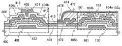
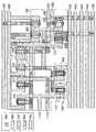
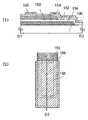
도 1a에 구동 회로에 이용하는 박막 트랜지스터(430)와, 화소부에 이용하는 박막 트랜지스터(170)를 동일 기판 위에 구비되는 예를 도시한다. 또한, 도 1a는 표시 장치의 단면도의 일례이다.1A shows an example in which a
화소부와 구동 회로는, 동일 기판 위에 형성된다. 화소부에서는, 매트릭스형으로 배치한 인핸스먼트형 트랜지스터인 박막 트랜지스터(170)를 이용하여 화소 전극(110)으로의 전압 인가의 온오프를 전환한다. 이 화소부에 배치하는 박막 트랜지스터(170)는, 산화물 반도체층(103)을 이용하여 형성된다. 온오프비가 109 이상이기 때문에, 표시 콘트라스트를 향상시키는 수 있고, 또한 누설 전류가 적기 때문에, 저소비 전력 구동을 실현할 수 있다. 온오프비는, 오프 전류와 온 전류의 비율(ION/IOFF)이고, ION/IOFF의 값이 클수록 스위칭 특성이 우수하다. 따라서, 온오프비는, 표시 콘트라스트의 향상에 기여한다. 또한, 온 전류는, 트랜지스터가 온상태일 때, 소스 전극과 드레인 전극의 사이에 흐르는 전류를 말한다. 한편, 오프 전류는, 트랜지스터가 오프 상태일 때, 소스 전극과 드레인 전극의 사이에 흐르는 전류를 말한다. 예를 들면, n형의 트랜지스터에서, 오프 전류는 게이트 전압이 트랜지스터의 임계 전압보다도 낮을 때, 소스 전극과 드레인 전극 사이에 흐르는 전류이다. 이와 같이, 고콘트라스트 및 저소비 전력 구동을 실현하기 위해서는, 화소부에 인핸스먼트형 트랜지스터를 이용하는 것이 바람직하다. 또한, 부호 101은 게이트 전극, 부호 104a와 104b는 소스 영역 및 드레인 영역, 부호 105a는 제1 전극, 부호 105b는 제2 전극, 부호 107은 보호 절연층을 나타낸다.The pixel portion and the driving circuit are formed on the same substrate. In the pixel section, the on/off of voltage application to the
구동 회로에서는, 산화물 반도체층(405)의 아래쪽으로 제1 게이트 전극(401)과, 산화물 반도체층(405)의 위에 박막 트랜지스터(430)의 제2 게이트 전극으로서 기능하는 전극(470)을 갖는 박막 트랜지스터(430)를 적어도 하나 이용한다. 박막 트랜지스터(430)의 제2 게이트 전극으로서 기능하는 전극(470)은 백게이트 전극이라고도 부를 수 있다. 백게이트 전극을 형성할 때, 박막 트랜지스터의 신뢰성을 검사하기 위한 바이어스-열스트레스시험(이하, BT 시험이라 함)에서, BT 스트레스 전후 사이의 박막 트랜지스터의 임계 전압의 변화량을 감소시킬 수 있다.In the driving circuit, a thin film having a
이 박막 트랜지스터(430)의 구조를 도 1a를 이용하여 설명한다. 절연 표면을 갖는 기판(400) 위에 구비된 제1 게이트 전극(401)은, 제1 게이트 절연층(403)으로 덮힌다. 제1 게이트 전극(401)과 중첩되는 제1 게이트 절연층(403) 위에는 산화물 반도체층(405)이 구비된다. 산화물 반도체층(405) 위에는, 채널 보호층(418)이 구비되고, 채널 보호층(418) 위에 제1 배선(409) 및 제2 배선(410)이 구비된다. 그리고, 제1 배선(409) 및 제2 배선(410) 위에 접하여 절연층(412)이 구비된다. 또한, 절연층(412) 위에 박막 트랜지스터(430)의 제2 게이트 전극으로서 기능하는 전극(470)이 구비된다.The structure of the
제1 게이트 절연층(403)의 재료로서는, 무기 재료(산화 실리콘, 질화 실리콘, 산화질화 실리콘, 질화 산화 실리콘 등)를 사용할 수 있고, 제1 게이트 절연층(403)은 이들 재료로 이루어지는 단층 또는 적층 구조를 갖는다. 제조법에서는, 플라즈마 CVD법이나 열 CVD법 등의 기상 성장법이나 스퍼터링법을 사용할 수 있다. 본 실시 형태에서, 제1 게이트 절연층은, 제1 층으로 플라즈마 CVD법에 의한 질화 실리콘막, 제 2층으로 플라즈마 CVD법에 의한 산화 실리콘막의 적층 구조로 형성된다. 제1 층의 질화 실리콘막은, 제1 게이트 전극(401)의 재료에 힐록이 발생할 가능성이 있는 재료를 이용한 경우, 힐록 발생을 방지하는 효과를 갖는다. 또한, 플라즈마 CVD법으로 성막된 질화 실리콘막은 치밀하고, 따라서 제1 층의 게이트 절연막으로서 질화 실리콘막을 이용함으로써 핀홀 등의 발생을 억제할 수 있다. 또한, 제1 게이트 절연층으로서 질화 실리콘막을 이용하는 경우, 유리 기판으로부터의 불순물, 예를 들면 나트륨 등의 가동 이온이 확산하여, 후에 형성되는 산화물 반도체에 침입하는 것을 방지할 수 있다. 또한, 적층 구조 또는 단층 구조를 사용한 경우, 제1 게이트 절연층(403)의 두께는 50nm 이상 500nm이다.As the material of the first
산화물 반도체층(405)은, 예를 들면, In2O3:Ga2O3:ZnO=1:1:1인 타겟(In:Ga:Zn=1:1:0.5)을 이용하여, 스퍼터링법에서의 아르곤 가스 유량을 10sccm, 산소 유량을 5sccm에서 성막한다. 청정한 계면을 실현하기 위해서, 제1 게이트 절연층(403)의 성막과 산화물 반도체층(405)의 성막은, 대기에 노출되지 않고 적층하는 것이 바람직하다. 또한, 산화물 반도체막(405)을 성막하기 전에 제1 게이트 절연층(403)이 대기에 노출되는 경우에는, 산화물 반도체막(405)을 성막하기 전에 아르곤 가스를 도입하여 플라즈마를 발생시키는 역스퍼터링을 행하여, 제1 게이트 절연층(403)의 표면에 부착된 먼지를 제거하여도 좋다.The
또한, 산화물 반도체층(405)과 제1 배선(409) 사이에는 소스 영역 또는 드레인 영역(406a)을 구비한다. 산화물 반도체층(405)과 제2 배선(410) 사이에는 소스 영역 또는 드레인 영역(406b)을 구비한다. 소스 영역 또는 드레인 영역(406a, 406b)은, 채널 보호층(418) 위에도 형성된다. 예를 들면 채널 보호층(418)과 제1 배선(409) 사이에는 소스 영역 또는 드레인 영역(406a)이 구비된다. 이 소스 영역 또는 드레인 영역은, 배선과 산화물 반도체층의 사이에 구비되는 버퍼층으로도 언급될 수 있다.In addition, a source region or a
본 실시 형태에서는, 소스 영역 또는 드레인 영역(406a, 406b)은, In-Ga-Zn-O계 비 단결정막으로 형성되고, 이는 산화물 반도체층(405)의 성막 조건과는 다른 성막 조건으로 형성되고, 보다 저저항인 산화물 반도체층이다. 예를 들면, 스퍼터링법에서의 아르곤 가스 유량을 40sccm로 한 증착 조건으로 얻어지는 산화물 반도체막으로 형성한 소스 영역 또는 드레인 영역(406a, 406b)은, n형의 도전성을 갖고, 활성화 에너지(ΔE)가 0.01eV 내지 0.1eV 이다. 또한, 본 실시 형태에서는, 소스 영역 또는 드레인 영역(406a, 406b)은, In-Ga-Zn-O계 비 단결정막으로 형성되고, 적어도 비정질 성분을 포함한다. 소스 영역 또는 드레인 영역(406a, 406b)은 비정질 성분에 결정립(나노 크리스탈)을 포함하는 경우가 있다. 이 소스 영역 또는 드레인 영역(406a, 406b) 중의 결정립(나노 크리스탈)은 대략 직경 1nm 내지 10nm, 대표적으로는 2nm 내지 4nm 정도이다.In this embodiment, the source regions or
박막 트랜지스터(430)에서, 채널 보호층(418)과 절연층(412)의 적층이 제2 게이트 절연층으로서 기능한다. 채널 보호층(418)의 재료로서는, 무기 재료(산화 실리콘, 질화 실리콘, 산화질화 실리콘, 질화 산화 실리콘 등)를 사용할 수 있다. 제조법에서는, 플라즈마 CVD법이나 열 CVD법 등의 기상 성장법이나 스퍼터링법을 사용할 수 있다. 본 실시 형태에서는, 채널 보호층(418)으로서 스퍼터링법으로 얻어지는 산화 실리콘막을 이용한다.In the
또한, 절연층(412)은, 산화 실리콘막, 산화질화 실리콘막, 질화 실리콘막, 산화 알루미늄, 질화 알루미늄, 산화 탄탈막, 산화 하프늄막, 산화질화 하프늄막 등의 절연막의 단층 또는 적층 구조를 가질 수 있다. 본 실시 형태에서는, 절연층(412)으로서 플라즈마 CVD법으로 얻어지는 질화 실리콘막을 이용한다. 채널 보호층(418)과 절연층(412)의 적층이 제2 게이트 절연층으로서 기능하기 때문에, 각각의 재료와 막 두께는 박막 트랜지스터(430)의 전기 특성에서 중요하다. 예를 들면, 산화물 반도체층(405)의 상하에 게이트 전압을 인가하여 거의 동일 전계를 산화물 반도체층(405)에 제공하는 경우에는, 질화 실리콘막과 산화 실리콘막의 적층인 제1 게이트 절연층과, 산화 실리콘막(채널 보호층(418))과 질화 실리콘막(절연층(412))을 포함하는 제2 게이트 절연층의 막 두께를 거의 동일하게 하는 것이 바람직하다. 또한, 소정의 임계 전압 등의 전기 특성을 얻기 위해서 산화물 반도체층(405)의 상하에 다른 게이트 전압 값을 인가하여 다른 전계를 산화물 반도체층(405)에 제공하는 경우에는, 제1 게이트 절연층과 제2 게이트 절연층의 재료나 막 두께를 적절하게 조절함으로써, 원하는 박막 트랜지스터(430)의 전기 특성을 얻을 수 있다.In addition, the insulating
또한, 제1 게이트 전극(401)과 박막 트랜지스터(430)의 제2 게이트 전극으로서 기능하는 전극(470)을 전기적으로 접속시켜 동일 전위를 가질 수 있다. 제1 게이트 전극(401)과 박막 트랜지스터(430)의 제2 게이트 전극으로서 기능하는 전극(470)을 동일 전위로 하면, 산화물 반도체층의 상하로부터 게이트 전압을 인가할 수 있어서, 온상태에서 흐르는 전류량을 크게 할 수 있다.In addition, the
또한, 임계 전압을 마이너스로 시프트하기 위한 제어 신호선을 제1 게이트 전극(401) 또는 박막 트랜지스터(430)의 제2 게이트 전극으로서 기능하는 전극(470) 중 어느 한쪽에 전기적으로 접속시킴으로써 디플레션형의 TFT를 형성할 수 있다.Further, by electrically connecting a control signal line for shifting the threshold voltage to minus either the
또한, 임계 전압을 플러스로 시프트하기 위한 제어 신호선을 제1 게이트 전극(401) 또는 박막 트랜지스터(430)의 제2 게이트 전극으로서 기능하는 전극(470)중 어느 한쪽에 전기적으로 접속시킴으로써 인핸스먼트형의 TFT를 형성할 수 있다.Further, by electrically connecting a control signal line for shifting the threshold voltage to positive to either the
또한, 구동 회로에 이용하는 2개의 박막 트랜지스터의 조합은 특별히 한정되지 않으며, 디플레션형 TFT로서 1개만의 게이트 전극을 갖는 박막 트랜지스터와 인핸스먼트형 TFT로서 2개의 게이트 전극을 갖는 박막 트랜지스터의 조합을 이용하여도 좋다. 그 경우에는, 화소부의 박막 트랜지스터로서, 게이트 전극을 산화물 반도체층의 상하에 갖는 구조를 갖는다.In addition, the combination of the two thin film transistors used in the driving circuit is not particularly limited, and a combination of a thin film transistor having only one gate electrode as a deflation type TFT and a thin film transistor having two gate electrodes as an enhancement type TFT is used. also good In that case, it has a structure which has a gate electrode above and below an oxide semiconductor layer as a thin film transistor of a pixel part.
또한, 화소부의 박막 트랜지스터로서, 게이트 전극을 산화물 반도체층의 상하에 갖는 구조로 하고, 구동 회로의 인핸스먼트형 TFT 및 디플레션형 TFT으로서 게이트 전극을 산화물 반도체층의 상하에 각각 갖는 구조로서도 좋다. 그 경우에는, 임계 전압을 제어하기 위한 제어 신호선을 게이트 전극 상하 중 한 쪽에 전기적으로 접속시켜, 그 접속한 게이트 전극이 임계 전압을 제어하는 구성으로 한다.Further, the thin film transistor of the pixel portion may have a structure in which a gate electrode is provided above and below an oxide semiconductor layer, and a gate electrode is provided above and below the oxide semiconductor layer as an enhancement type TFT and a depression type TFT of the driving circuit, respectively. In this case, a control signal line for controlling the threshold voltage is electrically connected to one of the upper and lower sides of the gate electrode, and the connected gate electrode controls the threshold voltage.
또한, 도 1a에서는, 박막 트랜지스터(430)의 제2 게이트 전극으로서 기능하는 전극(470)은, 화소부의 화소 전극(110)과 동일 재료, 예를 들면 투과형의 액정 표시 장치에서의 투명 도전막을 이용하여 형성되어 공정수를 감소시킨다. 그러나, 전극(470)의 재료에 대해서는 특별히 한정되지 않는다. 또한, 전극(470)의 폭은, 제1 게이트 전극(401)의 폭보다도 넓고, 또한 산화물 반도체층(405)의 폭보다도 넓은 예를 도시하고 있지만 전극(470)의 폭에 대해서는 특별히 한정되지 않는다. 또한, 제1 게이트 전극(401)의 폭은, 채널 보호층(418)의 폭(채널방향으로의 폭)보다도 넓다.1A, the
제2 게이트 전극의 재료 및 폭이 도 1a와 다른 예를 도 1b에 나타낸다. 또한, 도 1b는 유기 발광 소자 또는 무기 발광 소자와 접속하는 박막 트랜지스터(170)를 화소부에 갖는 표시 장치의 예이다.An example in which the material and width of the second gate electrode are different from those of FIG. 1A is shown in FIG. 1B . 1B is an example of a display device including a
도 1b에서는, 박막 트랜지스터(432)의 제2 게이트 전극으로서 기능하는 전극(471)의 재료는 금속 재료(알루미늄(Al)이나 구리(Cu), 티타늄(Ti), 탄탈(Ta), 텅스텐(W), 몰리브덴(Mo), 크롬(Cr), 네오디뮴(Nd), 스칸듐(Sc)으로부터 선택된 원소, 또는 상술한 원소를 성분으로 하는 합금)를 이용한다. 단면에서의 전극(471)의 폭은 도 1a의 전극(470)의 폭보다도 좁다. 또한, 전극(471)의 폭은 산화물 반도체층(405)의 폭보다도 좁다. 전극(471)의 폭을 좁게 함으로써 전극(471)이 제1 배선(409) 및 제2 배선(410)과 절연층(412)을 통해 중첩되는 면적을 감소할 수 있어서, 기생 용량을 작게 할 수 있다. 또한, 도 1b에서는, 전극(471)의 폭은, 채널 보호층(418)의 폭보다도 넓다.In FIG. 1B, the material of the
발광 소자는, 적어도 제1 전극(472)과 발광층(475)과 제2 전극(474)을 갖는다. 도 1b에서는, 전극(471)은, 화소부의 제1 전극(472)과 동일 재료, 예를 들면, 알루미늄 등을 이용하여 형성되어 공정수를 감소하고 있지만, 전극(471)에 대해서 특별히 한정되지 않는다. 또한, 도 1b에서 절연층(473)은, 인접하는 화소의 제1 전극과의 절연을 위한 격벽으로서 기능한다.The light emitting element has at least a
또한, 제2 게이트 전극의 재료 및 폭이 도 1a와 다른 예를 도 1c에 나타낸다. 도 1c에서는, 박막 트랜지스터(433)의 제2 게이트 전극으로서 기능하는 전극(476)의 재료는 금속 재료(알루미늄(Al)이나 구리(Cu), 티타늄(Ti), 탄탈(Ta), 텅스텐(W), 몰리브덴(Mo), 크롬(Cr), 네오디뮴(Nd), 스칸듐(Sc)으로부터 선택된 원소, 또는 상술한 원소를 성분으로 하는 합금)를 이용한다. 단면에서의 제2 게이트 전극의 폭은 도 1b에서 보다도 좁다. 도 1b에서 보다도 또한 폭을 좁게 함으로써 제1 배선(409) 및 제2 배선(410)과 절연층(412)을 통해 중첩되지 않도록 제2 게이트 전극을 형성할 수 있어서, 기생 용량을 더 작게 할 수 있다. 도 1c에 나타내는 전극(476)의 폭은, 채널 보호층(418)의 폭보다도 좁다. 이와 같이 좁은 폭의 전극(476)을 형성하는 경우에는, 습식 에칭 등을 이용하여 레지스트 마스크의 단부보다도 내측에 전극(476)의 양단부가 위치하는 공정으로 하는 것이 바람직하다. 다만, 도 1c에서는 화소 전극(110)과 다른 금속 재료를 이용하기 때문에, 전극(476)의 형성을 위한 하나 이상의 포토리소그래피 공정이 추가되고, 하나 이상의 마스크가 필요하다.In addition, an example in which the material and width of the second gate electrode are different from those of FIG. 1A is shown in FIG. 1C. In FIG. 1C , the material of the
액정 표시 장치나 발광 표시 장치나 전자 페이퍼에 이용하는 게이트선 구동 회로 또는 소스선 구동 회로 등의 주변 회로, 또는 화소부에 대하여, 산화물 반도체 상하의 2개의 게이트 전극 사이에 개재된 산화물 반도체를 포함하는 박막 트랜지스터를 이용하여, 고속 구동이나 저소비 전력화를 도모할 수 있다. 또한, 공정수를 대폭 증가시키는 일없이, 동일 기판 위에 화소부와 구동 회로 양쪽을 구비할 수 있다. 동일 기판 위에 화소부 이외의 여러가지 회로를 구비하는 것에 의해, 표시 장치의 제조 비용을 감소시킬 수 있다.A thin film transistor comprising an oxide semiconductor interposed between two gate electrodes above and below the oxide semiconductor for peripheral circuits such as a gate line driving circuit or a source line driving circuit used in a liquid crystal display device, a light emitting display device, or electronic paper, or a pixel portion can be used to achieve high-speed driving and low power consumption. Further, both the pixel portion and the driving circuit can be provided on the same substrate without significantly increasing the number of steps. By providing various circuits other than the pixel portion on the same substrate, it is possible to reduce the manufacturing cost of the display device.
(실시 형태 2)(Embodiment 2)
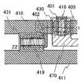
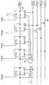
실시 형태 1에서는 구동 회로의 박막 트랜지스터로서 하나의 박막 트랜지스터를 설명했지만, 실시 형태 2에서는, 2개의 n 채널형의 박막 트랜지스터를 이용하여 구동 회로의 인버터 회로를 구성하는 예를 이하에 설명한다. 도 2a에 나타내는 박막 트랜지스터는, 실시 형태 1의 도 1a에 나타낸 박막 트랜지스터(430)와 동일하기 때문에, 동일 부분에는 동일 부호를 이용하여 설명한다.In
화소부를 구동하기 위한 구동 회로는, 인버터 회로, 용량, 저항 등을 이용하여 형성된다. 2개의 n 채널형 TFT를 조합하여 인버터 회로를 형성하는 경우, 인핸스먼트형 트랜지스터와 디플레션형 트랜지스터를 조합한 인버터 회로(이하, EDMOS 회로라 함)와, 2개의 인핸스먼트형 트랜지스터끼리의 조합한 인버터 회로(이하, EEMOS 회로라 함)가 있다.A driving circuit for driving the pixel portion is formed using an inverter circuit, a capacitor, a resistor, and the like. When an inverter circuit is formed by combining two n-channel TFTs, an inverter circuit combining an enhancement transistor and a depression transistor (hereinafter referred to as an EDMOS circuit) and an inverter combining two enhancement transistors There is a circuit (hereinafter referred to as an EEMOS circuit).
구동 회로의 인버터 회로의 단면 구조를 도 2a에 나타낸다. 또한, 도 2a 내지 도 2c에 나타내는 박막 트랜지스터(430)는 듀얼 게이트형 박막 트랜지스터이고, 제2 박막 트랜지스터(431)는, 바텀 게이트형 박막 트랜지스터이고, 박막 트랜지스터(430) 및 제2 박막 트랜지스터(431)는 반도체층 위에 소스 영역 또는 드레인 영역을 통해 배선이 구비되어 있는 박막 트랜지스터의 예이다.The cross-sectional structure of the inverter circuit of the driving circuit is shown in Fig. 2A. The
도 2a에서, 기판(400) 위에 제1 게이트 전극(401) 및 게이트 전극(402)을 구비한다. 제1 게이트 전극(401) 및 게이트 전극(402)의 재료는, 몰리브덴, 티타늄, 크롬, 탄탈, 텅스텐, 알루미늄, 구리, 네오디뮴, 스칸듐 등의 금속 재료 또는 이들을 주성분으로 하는 합금 재료를 이용하여, 단층으로 또는 적층하여 형성할 수 있다.In FIG. 2A , a
예를 들면, 제1 게이트 전극(401) 및 게이트 전극(402)의 2층의 적층 구조에서는, 알루미늄층 위에 몰리브덴층이 적층된 2층의 적층 구조, 또는 구리층 위에 몰리브덴층을 적층한 2층 구조, 또는 구리층 위에 질화 티타늄층 또는 질화 탄탈층을 적층한 2층 구조, 질화 티타늄층과 몰리브덴층을 적층한 2층 구조로 하는 것이 바람직하다. 또한, Mg를 포함하는 구리층 위에 배리어층으로 기능하는 Ca를 포함하는 산화 구리층의 적층이나, Mg를 포함하는 구리층 위에 배리어층으로 기능하는 Mg를 포함하는 산화 구리층의 적층도 있다. 또한, 3층의 적층 구조에서는, 텅스텐층 또는 질화 텅스텐층과, 알루미늄과 실리콘의 합금 또는 알루미늄과 티타늄의 합금층과, 질화 티타늄층 또는 티타늄층을 적층한 적층으로 하는 것이 바람직하다.For example, in the two-layer stacked structure of the
또한, 제1 게이트 전극(401) 및 게이트 전극(402)을 덮는 제1 게이트 절연층(403) 위에는, 산화물 반도체층(405)과, 제2 산화물 반도체층(407)을 구비한다.In addition, an
산화물 반도체층(405) 위에는 채널 보호층(418)을 구비하고, 또한 제1 배선(409) 및 제2 배선(410)을 구비한다. 제2 배선(410)은, 제1 게이트 절연층(403)에 형성된 컨택트 홀(404)을 통해 게이트 전극(402)과 직접 접속한다. 본 실시 형태에서는, 제1 게이트 절연층(403)을 형성한 후 또는 채널 보호층(418), 제2 채널 보호층(419)을 형성한 후에 컨택트 홀(404)을 형성하여도 좋다. 또한, 제2 산화물 반도체층(407) 위에는 제3 배선(411)을 구비한다.A channel
박막 트랜지스터(430)는, 제1 게이트 전극(401)과, 제1 게이트 절연층(403)을 통해 제1 게이트 전극(401)과 중첩되는 산화물 반도체층(405)을 포함한다. 제1 배선(409)은, 부의 전압 VDL이 인가되는 전원선(마이너스 전원선)이다. 이 전원선은, 접지 전위를 갖는 전원선(접지 전원선)일 수도 있다.The
또한, 제2 박막 트랜지스터(431)는, 게이트 전극(402)과, 제1 게이트 절연층(403)을 통해 게이트 전극(402)과 중첩되는 제2 산화물 반도체층(407)을 포함한다. 3 배선(411)은, 플러스의 전압 VDH가 인가되는 전원선(플러스 전원선)이다.In addition, the second
또한, 제2 산화물 반도체층(407)과 제2 배선(410) 사이에는 n+ 층(408a)을 구비하고, 제2 산화물 반도체층(407)과 제3 배선(411) 사이에는 n+ 층(408b)을 구비한다. 또한, 채널 보호층(418)과 제2 배선(410) 사이에는 소스 영역 또는 드레인 영역(406b)이 구비된다. 또한, 채널 보호층(418)과 제1 배선(409) 사이에는 소스 영역 또는 드레인 영역(406a)이 구비된다.In addition, an
또한, 구동 회로의 인버터 회로의 상면도를 도 2c에 나타낸다. 도 2c에서, 쇄선 Z1-Z2로 절단한 단면이 도 2a에 상당한다.Also, a top view of the inverter circuit of the driving circuit is shown in Fig. 2C. In Fig. 2C, a cross section taken along the chain line Z1-Z2 corresponds to Fig. 2A.
또한, EDMOS 회로의 등가 회로를 도 2b에 나타낸다. 도 2a에 나타내는 접속 구조는, 도 2b에 상당하고, 박막 트랜지스터(430)를 인핸스먼트형의 n 채널형 트랜지스터로 하고, 제2 박막 트랜지스터(431)를 디플레션형의 n 채널형 트랜지스터로 하는 예이다.Also, an equivalent circuit of the EDMOS circuit is shown in Fig. 2B. The connection structure shown in FIG. 2A corresponds to FIG. 2B, and is an example in which the
박막 트랜지스터(430)를 인핸스먼트형의 n 채널형 트랜지스터로 하기 위해, 본 실시 형태에서는, 산화물 반도체층(405) 위에 채널 보호층(418) 및 게이트 절연층(412)과, 상기 절연층(412) 위에 박막 트랜지스터(430)의 제2 게이트 전극으로서 기능하는 전극(470)을 구비하여, 박막 트랜지스터(430)의 제2 게이트 전극으로서 기능하는 전극(470)에 인가하는 전압에 의해서 박막 트랜지스터(430)의 임계값 제어를 행한다.In order to make the
또한, 도 2a 및 도 2c에서, 제2 배선(410)은, 제1 게이트 절연층(403)에 형성된 컨택트 홀(404)을 통해 게이트 전극(402)과 직접 접속하는 예를 도시했지만, 특별히 한정되지 않으며, 접속 전극을 별도 구비하여 제2 배선(410)과 게이트 전극(402)을 전기적으로 접속시켜도 좋다.Also, in FIGS. 2A and 2C , an example in which the
또한, 본 실시 형태는, 실시 형태 1과 자유롭게 조합할 수 있다.Note that this embodiment can be freely combined with the first embodiment.
(실시 형태 3)(Embodiment 3)
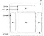
실시 형태 3에서는, 표시 장치에 관해서, 블럭도 등을 참조하여 설명한다.In the third embodiment, a display device will be described with reference to block diagrams and the like.
도 3a는, 액티브 매트릭스형 액정 표시 장치의 블럭도의 일례를 나타낸다. 도 3a에 나타내는 액정 표시 장치는, 기판(300) 위에 표시 소자를 구비한 화소를 복수 갖는 화소부(301)와, 각 화소의 게이트 전극에 접속된 주사선을 제어하는 주사선 구동 회로(302)와, 선택된 화소에의 비디오 신호의 입력을 제어하는 신호선 구동 회로(303)를 갖는다.Fig. 3A shows an example of a block diagram of an active matrix liquid crystal display device. The liquid crystal display device shown in FIG. 3A includes a
도 3b는, 액티브 매트릭스형 발광 표시 장치의 블럭도의 일례를 나타낸다. 도 3b에 나타내는 발광 표시 장치는, 기판(310) 위에 표시 소자를 구비한 화소를 복수 갖는 화소부(311)와, 각 화소의 게이트 전극에 접속된 주사선을 제어하는 제1 주사선 구동 회로(312) 및 제2 주사선 구동 회로(313)와, 선택된 화소에의 비디오 신호의 입력을 제어하는 신호선 구동 회로(314)를 갖는다. 하나의 화소에 스위칭용 TFT(Thin Film Transistor)와 전류 제어용 TFT의 2개를 배치하는 경우, 도 3b에 나타내는 발광 표시 장치에서는, 스위칭용 TFT의 게이트 전극에 접속된 제1 주사선에 입력되는 신호를 제1 주사선 구동 회로(312)로 생성하여, 전류 제어용 TFT의 게이트 전극에 접속된 제2 주사선에 입력되는 신호를 제2 주사선 구동 회로(313)로 생성한다. 또한, 제1 주사선에 입력되는 신호와, 제2 주사선에 입력되는 신호를, 하나의 주사선 구동 회로에서 생성하는 구성으로서도 좋다. 또한, 예를 들면, 스위칭 소자에 포함되는 TFT의 수에 따라서, 스위칭 소자의 동작을 제어하는 데 이용되는 제1 주사선이, 각 화소에 복수 구비되어 있어도 좋다. 이 경우, 복수의 제1 주사선에 입력되는 신호를, 전부 1개의 주사선 구동 회로로 생성하여도 좋고, 복수의 주사선 구동 회로에 의해 이들을 각각으로 생성하여도 좋다.3B shows an example of a block diagram of an active matrix type light emitting display device. The light emitting display device shown in FIG. 3B includes a
또한, 여기서 설명된 표시 장치에는, 주사선 구동 회로(302), 제1 주사선 구동 회로(312), 제2 주사선 구동 회로(313) 및 신호선 구동 회로(303, 314)를 표시 장치에 제조하는 형태를 나타내었지만, 주사선 구동 회로(302), 제1 주사선 구동 회로(312), 또는 제2 주사선 구동 회로(313)의 일부를 IC 등의 반도체 장치로 실장하여도 좋다. 또한, 신호선 구동 회로(303, 314)의 일부를 IC 등의 반도체 장치로 실장하여도 좋다.Further, in the display device described herein, a form in which the scan
도 4는, 표시 장치를 구성하는, 신호 입력 단자(321), 주사선(323), 신호선(324), 비선형 소자를 포함하는 보호 회로(334 내지 336) 및 화소부(327)의 위치 관계를 설명하는 도면이다. 절연 표면을 갖는 기판(320) 위에는 주사선(323)과 신호선(324)이 교차하여 배치되어, 화소부(327)가 구성된다. 또한, 화소부(327)는, 도 3a 또는 도 3b에 나타내는 화소부(301) 또는 화소부(311)에 상당한다.4 illustrates the positional relationship between the
화소부(301)는, 신호선 구동 회로(303)로부터 열방향으로 신장하여 배치된 복수의 신호선 S1 내지 Sm(도시하지 않음)에 의해 신호선 구동 회로(303)와 접속되고 주사선 구동 회로(302)로부터 행방향으로 신장하여 배치된 복수의 주사선 G1 내지 Gn(도시하지 않음)에 의해 주사선 구동 회로(302)와 접속된다. 화소부(301)는 신호선 S1 내지 Sm 및 주사선 G1 내지 Gn에 의해 매트릭스형으로 배치된 복수의 화소(도시하지 않음)를 갖는다. 그리고, 각 화소는, 신호선 Sj(신호선 S1 내지 Sm 중 어느 하나), 주사선 Gi(주사선 G1 내지 Gn 중 어느 하나)에 접속된다.The
화소부(327)는 복수의 화소(328)가 매트릭스형으로 배열하여 구성된다. 화소(328)는, 주사선(323)과 신호선(324)에 접속하는 화소 TFT329, 유지 용량부(330), 화소 전극(331)을 포함한다.The
여기의 화소 구성에서, 유지 용량부(330)에서는, 한 쪽의 전극과 화소 TFT329가 접속되고, 다른 쪽의 전극과 용량선(332)이 접속되는 경우를 도시한다. 또한, 화소 전극(331)은 표시 소자(액정 소자, 발광 소자, 콘트라스트 매체(전자 잉크) 등)를 구동하는 한 쪽의 전극으로 기능한다. 이 표시 소자의 다른 쪽의 전극은 공통 단자(333)에 접속된다.In the pixel configuration here, in the
보호 회로(335)는, 화소부(327)와 신호선 입력 단자(322) 사이에 배치된다. 또한, 보호 회로(334)는, 주사선 구동 회로와 화소부(327)의 사이에 배치된다. 본 실시 형태에서는, 복수의 보호 회로를 구비하여, 주사선(323), 신호선(324) 또는 용량 버스선(337)에 정전기 등에 의해 서지 전압이 인가될 때 화소 TFT329 등이 파괴되지 않는다. 그 때문에, 보호 회로에는 서지 전압이 인가되었을 때에, 공통 배선에 전하를 방출하도록 형성된다.The
본 실시 형태에서는, 주사선(323)측에 보호 회로(334), 신호선(324)측에 보호 회로(335), 용량 버스선(337)측에 보호 회로(336)를 배치하는 예를 도시한다. 또한, 보호 회로의 배치 위치는 이것에 한정되지 않는다. 또한, 주사선 구동 회로를 IC 등의 반도체 장치를 사용하여 실장하지 않는 경우는, 주사선(323)측에 보호 회로(334)를 구비하지 않아도 좋다.In this embodiment, an example is shown in which the
이들 회로의 실시 형태 1 또는 실시 형태 2에 나타낸 TFT를 이용하는 것으로, 이하의 이점이 달성된다.By using the TFTs shown in
구동 회로는, 크게 논리 회로부와, 스위치부 또는 버퍼부로 분류된다. 논리 회로부에 구비되는 TFT는 임계 전압을 제어하는 것이 가능한 구성을 갖는 것이 바람직하다. 한편, 스위치부 또는 버퍼부에 구비되는 TFT는 온 전류가 큰 것이 바람직하다. 실시 형태 1 또는 실시 형태 2에 나타낸 TFT를 갖는 구동 회로를 구비함으로써, 논리 회로부에 구비되는 TFT의 임계 전압의 제어가 가능해져, 스위치부 또는 버퍼부에 구비되는 TFT의 온 전류를 크게 하는 것이 가능해진다. 또한, 실시 형태 1 또는 실시 형태 2에 나타낸 TFT는 구동 회로가 점유하는 면적을 작게 하여, 프레임을 좁게 하는 것에 기여한다.The driving circuit is broadly classified into a logic circuit section and a switch section or a buffer section. The TFT provided in the logic circuit portion preferably has a configuration capable of controlling the threshold voltage. On the other hand, the TFT provided in the switch unit or the buffer unit preferably has a large on-state current. By providing the driving circuit having the TFTs shown in the first or second embodiment, it is possible to control the threshold voltage of the TFTs provided in the logic circuit section, and it is possible to increase the on-current of the TFTs provided in the switch section or the buffer section. becomes Further, the TFT shown in the first or second embodiment contributes to narrowing the frame by reducing the area occupied by the driving circuit.
주사선 구동 회로에 포함되는 시프트 레지스터 회로에 관해서 이하에 설명한다.The shift register circuit included in the scan line driver circuit will be described below.
도 5에 나타내는 시프트 레지스터 회로는, 플립-플롭 회로(351)를 복수 갖고, 제어 신호선(352), 제어 신호선(353), 제어 신호선(354), 제어 신호선(355), 제어 신호선(356) 및 리셋트선(357)을 갖는다.The shift register circuit shown in FIG. 5 has a plurality of flip-
도 5의 시프트 레지스터 회로에 나타낸 바와 같이, 플립-플롭 회로(351)에서는, 1단의 입력 단자 IN에, 제어 신호선(352)을 통해, 스타트 펄스 SSP가 입력되고, 다음단의 입력 단자 IN에 전단의 플립-플롭 회로(351)의 출력 신호 단자 SOUT가 접속된다. 또한, N 단째(N은 자연수이다)의 리셋트 단자 RES는, (N+3)단째의 플립-플롭 회로의 출력 신호 단자 Sout와 리셋트선(357)을 통해 접속된다. N 단째의 플립-플롭 회로(351)의 클록 단자 CLK에는, 제어 신호선(353)을 통해, 제1 클록 신호 CLK1이 입력되면, (N+1)단째의 플립-플롭 회로(351)의 클록 단자 CLK에는, 제어 신호선(354)을 통해, 제2 클록 신호 CLK2가 입력된다. 또한, (N+2)단째의 플립-플롭 회로(351)의 클록 단자 CLK에는, 제어 신호선(355)을 통해, 제3 클록 신호 CLK3이 입력된다. 또한, (N+3)단째의 플립-플롭 회로(351)의 클록 단자 CLK에는, 제어 신호선(356)을 통해, 제4 클록 신호 CLK4가 입력된다. 그리고, (N+4)단째의 플립-플롭 회로(351)의 클록 단자 CLK에는, 제어 신호선(353)을 통해, 제1 클록 신호 CLK1이 입력된다. 또한, N 단째의 플립-플롭 회로(351)는, 게이트 출력 단자 Gout로부터 N 단째의 플립-플롭 회로의 출력 SRoutN을 출력한다.As shown in the shift register circuit in Fig. 5, in the flip-
또한, 플립-플롭 회로(351)와, 전원 및 전원선과의 접속을 도시하지 않지만, 각 플립-플롭 회로(351)에는 전원선을 통해 전원 전위 Vdd 및 전원 전위 GND가 공급된다.Further, although the connection between the flip-
또한, 본 명세서에서 설명하는 전원 전위는, 기준 전위를 0V로 한 경우의, 전위차에 상당한다. 그 때문에, 전원 전위를 전원 전압, 또는 전원 전압을 전원 전위로 언급하는 경우가 있다.In addition, the power supply potential described in this specification corresponds to a potential difference when the reference potential is set to 0V. Therefore, the power supply potential is sometimes referred to as a power supply voltage or the power supply voltage is referred to as a power supply potential.
또한, 본 명세서에서, "A와 B가 서로 접속된다"라는 설명은, A와 B가 직접 접속되어 있는 경우 이외에 전기적으로 서로 접속되어 있는 것을 포함한다. 여기서, "A와 B가 서로 전기적으로 접속된다"라는 설명은, A와 B 사이에 어떠한 전기적 작용을 갖는 대상물이 존재할 때, 대상물을 통해 A와 B가 대략적으로 동일 전위를 갖는 경우를 나타낸다. 구체적으로는, "A와 B가 서로 전기적으로 접속된다"라는 설명은 예를 들어, TFT같은 스위칭 소자를 통해 A와 B가 접속되어, 상기 스위칭 소자의 도통에 의해서 A와 B가 대략적으로 동일 전위가 되는 경우나, 저항 소자를 통해 A와 B가 접속되어, 상기 저항 소자의 양끝에 발생하는 전위차가 A와 B를 포함하는 회로의 동작에 영향을 주지 않은 정도로 되어 있는 경우 등, 회로 동작면에서 A와 B가 동일 전위를 갖는 것으로 여겨지는 경우를 나타낸다.In addition, in this specification, the description that "A and B are connected to each other" includes electrically connected to each other other than the case where A and B are directly connected. Here, the description "A and B are electrically connected to each other" indicates a case where, when an object having a certain electrical action exists between A and B, A and B have approximately the same potential through the object. Specifically, the description "A and B are electrically connected to each other" means, for example, that A and B are connected through a switching element such as a TFT, so that A and B are approximately at the same potential by conduction of the switching element. In terms of circuit operation, such as a case where A and B are connected through a resistor A case where A and B are considered to have the same potential is shown.
다음에, 도 6은, 도 5에 나타낸 시프트 레지스터 회로에 포함되는 플립-플롭 회로(351)의 일 실시 형태를 나타낸다. 도 6에 나타내는 플립-플롭 회로(351)는, 논리 회로부(361)와, 스위치부(362)를 갖는다. 논리 회로부(361)는, TFT363 내지 TFT368을 갖는다. 또한, 스위치부(362)는, TFT369 내지 TFT372를 갖고 있다. 또 논리 회로부는, 외부로부터 입력되는 신호에 따라서 후단의 회로인 스위치부에 출력하는 신호를 전환하기 위한 회로이다. 또한, 스위치부는, 외부 및 제어 회로부로부터 입력되는 신호에 따라서 스위치로 기능하는 TFT의 온 또는 오프 전환하여, 해당 TFT의 크기 및 구조에 따른 전류를 출력하기 위한 회로이다.Next, FIG. 6 shows an embodiment of a flip-
플립-플롭 회로(351)에서, 입력 단자 IN은 TFT364의 게이트 단자 및 TFT367의 게이트 단자에 접속된다. 리셋트 단자 RES는, TFT363의 게이트 단자에 접속된다. 클록 단자 CLK는, TFT369의 제1 단자 및 TFT371의 제1 단자에 접속된다. 전원 전위 Vdd가 공급되는 전원선은, TFT364의 제1 단자 및 TFT366의 게이트 단자 및 제2 단자에 접속된다. 전원 전위 GND가 공급되는 전원선은, TFT363의 제2 단자, TFT365의 제2 단자, TFT367의 제2 단자, TFT368의 제2 단자, TFT370의 제2 단자 및 TFT372의 제2 단자에 접속된다. 또한, TFT363의 제1 단자, TFT364의 제2 단자, TFT365의 제1 단자, TFT368의 게이트 단자, TFT369의 게이트 단자 및 TFT371의 게이트 단자는 서로 접속된다. 또한, TFT366의 제1 단자는, TFT365의 게이트 단자, TFT367의 제1 단자, TFT368의 제1 단자, TFT370의 게이트 단자 및 TFT372의 게이트 단자에 접속된다. 또한, 게이트 출력 단자 Gout는, TFT369의 제2 단자 및 TFT370의 제1 단자에 접속된다. 출력 신호 단자 Sout는, TFT371의 제2 단자 및 TFT372의 제1 단자에 접속된다.In the flip-
또한, 여기서는, TFT363 내지 TFT372가, 전부 N형 TFT인 경우에 관해서 설명한다.Incidentally, the case where all of the TFT363 to TFT372 are N-type TFTs will be described here.
또한, TFT는, 게이트와, 드레인과, 소스를 포함하는 적어도 3개의 단자를 갖는 소자이고, 드레인 영역과 소스 영역의 사이에 채널 형성 영역을 갖는다. 드레인 영역과 채널 형성 영역과 소스 영역을 통해 전류가 흐르게 할 수 있다. 여기서, 소스와 드레인은, TFT의 구조나 동작 조건 등에 의해서 교체할 수 있기 때문에, 어느 것이 소스이고, 어느 적이 드레인인 가를 특정하는 것은 곤란하다. 따라서, 소스 및 드레인으로서 기능하는 영역을 소스 또는 드레인이라고 언급하지 않고, 예를 들면, 각각을 제1 단자 및 제2 단자로 표기한다. 또한, 이 경우에, 게이트로서 기능하는 단자에 대해서는, 게이트 단자로 표기한다.Further, the TFT is an element having at least three terminals including a gate, a drain, and a source, and has a channel formation region between the drain region and the source region. A current may flow through the drain region, the channel formation region, and the source region. Here, since the source and the drain can be replaced depending on the structure and operating conditions of the TFT, it is difficult to specify which one is the source and which one is the drain. Accordingly, regions serving as the source and drain are not referred to as a source or a drain, but are denoted, for example, as a first terminal and a second terminal, respectively. Incidentally, in this case, a terminal functioning as a gate is denoted as a gate terminal.
다음에, 도 6에 나타낸 플립-플롭 회로(351)의 레이아웃도의 일례를 도 7에 나타낸다.Next, an example of the layout diagram of the flip-
도 7의 플립-플롭 회로는, 전원 전위 Vdd가 공급되는 전원선(381), 리셋트선(382), 제어 신호선(353), 제어 신호선(354), 제어 신호선(355), 제어 신호선(356), 제어 신호선(383), 전원 전위 GND가 공급되는 전원선(384), 논리 회로부(361) 및 스위치부(362)를 갖는다. 논리 회로부(361)는, TFT363 내지 TFT368을 갖는다. 또한, 스위치부(362)는, TFT369 내지 TFT372를 갖고 있다. 또한, 도 7에서는, 게이트 출력 단자 Gout에 접속되는 배선, 출력 신호 단자 Sout에 접속되는 배선에 관해서도 도시한다.The flip-flop circuit of FIG. 7 includes a
도 7에는, 반도체층(385), 제1 배선층(386), 제2 배선층(387), 제3 배선층(388), 컨택트 홀(389)에 관해서 도시한다. 또한, 제1 배선층(386)은, 게이트 전극을 형성하는 층에 의해 형성되고, 제2 배선층(387)은, TFT의 소스 전극 또는 드레인 전극을 형성하는 층에 의해 형성되고, 제3 배선층(388)은, 화소부에서의 화소 전극을 형성하는 층에 의해 형성되면 좋다. 다만, 이 예에 한정되지 않고, 예를 들어 제3 배선층(388)은, 화소 전극을 형성하는 층과는 별도의 배선층으로 형성하여도 좋다.7 shows the
또한, 도 7의 각 회로 소자 사이의 접속 관계는, 도 6으로 설명한 바와 같다. 또한, 도 7에서는, 제1 클록 신호가 입력되는 플립-플롭 회로에 관해서 도시하고 있기 때문에, 제어 신호선(354) 내지 제어 신호선(356)과의 접속에 관하여는 도시되어 있지 않다.In addition, the connection relationship between each circuit element of FIG. 7 is as having demonstrated with FIG. In addition, since Fig. 7 shows the flip-flop circuit to which the first clock signal is input, the connection with the
도 7의 플립-플롭 회로의 레이아웃도면에서, 논리 회로부(361)에 포함되는 TFT366또는 TFT367의 임계 전압을 제어함으로써, EDMOS 회로(373)를 구성할 수 있다. 대표적으로는, TFT366을 디플레션형으로 하고, TFT367을 인핸스먼트형으로 한 EDMOS 회로(373)를 형성하고, 스위치부(362)에 포함되는 TFT369 내지 TFT372를 듀얼 게이트형의 TFT 또는 디플레션형의 TFT로 한다. 또한, 도 6에서, EDMOS 회로(373)에서의 TFT366과 TFT367은 도 2a 내지 도 2c에 나타낸 EDMOS 회로에서의 TFT와 디플레션형의 TFT의 게이트 전극의 접속 위치가 다르다.In the layout diagram of the flip-flop circuit of FIG. 7, by controlling the threshold voltage of the TFT366 or TFT367 included in the
TFT366 또는 TFT367을 듀얼 게이트형의 TFT로 형성하여, 백게이트 전극의 전위를 제어하는 것으로, 디플레션형의 TFT 또는 인핸스먼트형의 TFT를 형성할 수 있다.By forming the TFT366 or TFT367 as a dual-gate TFT and controlling the potential of the back gate electrode, a deflation-type TFT or an enhancement-type TFT can be formed.
도 7에서는, TFT366의 임계 전압을 제어하기 위한 백게이트 전극과 동일 전위의 제어 신호선(390)을 별도 구비하여, 디플레션형을 형성한다. TFT366은 듀얼 게이트형의 TFT이고, 백게이트 전극의 전위는, 게이트 전극에 인가되는 전원 전위 Vdd가 공급되는 전원선(381)과는 다른 전위이다.In Fig. 7, a
도 7에서는, TFT369 내지 372는, 듀얼 게이트형의 TFT이고, 백게이트 전극과 TFT의 각각의 게이트 전극이 동일 전위를 갖고, 백게이트 전극의 각각의 전위는, 게이트 전극에 인가되는 전원 전위 Vdd가 공급되는 전원선과 동일 전위이다.In Fig. 7,
이러한 방식으로, 표시 장치의 화소부 및 구동 회로에 배치하는 TFT를 산화물 반도체층을 이용한 n 채널형 TFT만을 이용하여 형성할 수 있다.In this way, the TFTs arranged in the pixel portion and the driving circuit of the display device can be formed using only the n-channel type TFT using the oxide semiconductor layer.
또한, 논리 회로부(361)에서의 TFT366은 전원 전위 Vdd에 따라서 전류를 공급하기 위한 TFT이다. 듀얼 게이트형 TFT 또는 디플레션형 TFT를 TFT로서 이용함으로써 TFT366에 흐르는 전류량은 크게 하는 것에 의해, TFT의 성능을 저하시키지 않고, TFT의 소형화를 도모할 수 있다.Further, the TFT366 in the
또한, 스위치부(362)를 구성하는 TFT에서, TFT에 흐르는 전류량을 크게 하여, 또한 온과 오프의 전환을 고속으로 행할 수 있기 때문에, 성능을 저하시키지 않고 TFT가 차지하는 면적을 축소할 수 있다. 따라서, 상기 TFT에 의해 구성되는 회로가 차지하는 면적을 축소할 수도 있다. 또한, 스위치부(362)에서의 TFT369 내지 TFT372는, 도면에 도시된 바와 같이 반도체층(385)을 제1 배선층(386)과 제3 배선층(388) 사이에 개재하여 듀얼 게이트형 TFT를 형성하면 좋다.In addition, in the TFT constituting the
또한, 도 7에서는, 듀얼 게이트형 TFT이, 반도체층(385)을 제1 배선층(386)과, 컨택트 홀(389)을 통해 서로 접속되어 동일 전위가 되는 제3 배선층(388) 사이에 개재하여 구성되는 예를 도시했다. 그러나, 이 구성에 한정되지 않고, 예를 들면, 제3 배선층(388)에 대하여, 별도 제어 신호선을 구비하여, 제3 배선층(388)의 전위를 제1 배선층(386)으로부터 독립적으로 제어하는 구성으로 하여도 좋다.In Fig. 7, the dual-gate TFT has the
또한, 도 7에 나타내는 플립-플롭 회로의 레이아웃도면에서, TFT363 내지 TFT372의 채널 형성 영역의 형상을 U 자형(회전된 C형 또는 말굽형)일 수 있다. 또한, 도 7에서는, 모든 TFT가 동일한 크기를 갖고 있지만, 후단의 부하량에 따라서 출력 신호 단자 Sout 또는 게이트 출력 단자 Gout에 접속되는 각 TFT의 크기를 적절하게 변경하여도 좋다.Further, in the layout diagram of the flip-flop circuit shown in Fig. 7, the shape of the channel forming regions of the TFT363 to TFT372 may be U-shaped (rotated C-shaped or horseshoe-shaped). Further, in Fig. 7, all TFTs have the same size, but the size of each TFT connected to the output signal terminal Sout or the gate output terminal Gout may be appropriately changed according to the load amount of the subsequent stage.
다음에, 도 8에 나타내는 타이밍 차트를 참조하여, 도 5에 나타내는 시프트 레지스터 회로의 동작에 관해서 설명한다. 도 8은, 도 5에 나타낸 제어 신호선(352) 내지 제어 신호선(356)에 각각 공급되는 스타트 펄스 SSP, 제1 클록 신호 CLK1 내지 제4 클록 신호 CLK4 및 1단째 내지 5단째의 플립-플롭 회로의 출력 신호 단자 Sout에서 출력되는 Sout1 내지 Sout5에 관해서 도시한다. 또한, 도 8의 설명에서는, 도 6 및 도 7에서 각 소자에 붙인 부호를 이용한다.Next, with reference to the timing chart shown in FIG. 8, the operation of the shift register circuit shown in FIG. 5 will be described. Fig. 8 shows the start pulse SSP, the first clock signal CLK1 to the fourth clock signal CLK4, and the first to fifth stages of flip-flop circuits respectively supplied to the
또한, 도 8은, 플립-플롭 회로에 포함되는 TFT의 각각이, N 채널형 TFT의 경우의 타이밍 차트이다. 또한 제1 클록 신호 CLK1 내지 제4 클록 신호 CLK4는 도시한 바와 같이 1/4파장(점선으로써 구분한 섹션)씩 이전 단의 클록 신호로부터 시프트된다.8 is a timing chart in the case where each of the TFTs included in the flip-flop circuit is an N-channel TFT. Also, the first clock signal CLK1 to the fourth clock signal CLK4 are shifted from the clock signal of the previous stage by 1/4 wavelength (section separated by a dotted line) as shown.
우선, 기간 T1에서, 1단째의 플립-플롭 회로에는, 스타트 펄스 SSP가 H 레벨로 입력되고, 논리 회로부(361)는 스위치부의 TFT369 및 TFT371을 온으로 하고, TFT370 및 TFT372를 오프로 한다. 이 때, 제1 클록 신호 CLK1은 L 레벨이기 때문에, Sout1은 L 레벨이다.First, in the period T1, a start pulse SSP is input to the first-stage flip-flop circuit at H level, and the
또한, 기간 T1에서, 2단째 및 그 이후의 플립-플롭 회로에는, IN 단자에 신호가 입력되지 않기 때문에, 플립-플롭 회로는 동작없이 L 레벨을 출력한다. 또한, 초기 상태에서는, 시프트 레지스터 회로의 각 플립-플롭 회로는, L 레벨을 출력하는 것으로서 설명한다.Further, in the period T1, since no signal is input to the IN terminal to the flip-flop circuits in the second stage and thereafter, the flip-flop circuit outputs the L level without operation. Incidentally, in the initial state, each flip-flop circuit of the shift register circuit will be described as outputting an L level.
다음에, 기간 T2에서, 1단째의 플립-플롭 회로에서는, 기간 T1과 마찬가지로, 논리 회로부(361)가 스위치부(362)의 제어를 행한다. 기간 T2에서는, 제1 클록 신호 CLK1은 H 레벨에 있기 때문에, Sout1은 H 레벨이 된다. 또한, 기간 T2에서는, 2단째의 플립-플롭 회로에는, Sout1이 H 레벨로 IN 단자에 입력되고, 논리 회로부(361)가 스위치부의 TFT369 및 TFT371을 온으로 하고, TFT370 및 TFT372를 오프로 한다. 이 때, 제2 클록 신호 CLK2는 L 레벨이기 때문에,Sout2는 L 레벨이다.Next, in the period T2, in the flip-flop circuit of the first stage, the
또한, 기간 T2에서, 3단째 및 그 이후의 플립-플롭 회로에는, IN 단자에 신호가 입력되지 않기 때문에, 플립-플롭 회로는 동작없이 L 레벨을 출력한다.Further, in the period T2, since no signal is input to the IN terminal to the flip-flop circuits in the third stage and thereafter, the flip-flop circuit outputs L level without operation.
다음에, 기간 T3에서, 1단째의 플립-플롭 회로에서는, 기간 T2의 상태를 유지하도록 논리 회로부(361)가 스위치부(362)의 제어를 행한다. 그 때문에, 기간 T3에서는, 제1 클록 신호 CLK1은 H 레벨이고, Sout1은 H 레벨이 된다. 또한, 기간 T3에서, 2단째의 플립-플롭 회로에서는, 기간 T2와 마찬가지로, 논리 회로부(361)가 스위치부(362)의 제어를 행한다. 기간 T3에서는, 제2 클록 신호 CLK2는 H 레벨이기 때문에, Sout2는 H 레벨이다. 또한, 기간 T3의 3단째의 플립-플롭 회로에는, Sout2가 H 레벨로 IN 단자에 입력되고, 논리 회로부(361)가 스위치부의 TFT369 및 371을 온으로 하고, TFT370 및(372)을 오프로 한다. 이 때, 제3 클록 신호 CLK3은 L 레벨이기 때문에, Sout3은 L 레벨이다.Next, in the period T3, in the flip-flop circuit of the first stage, the
또한, 기간 T3에서, 4단째 및 그 이후의 플립-플롭 회로에는, IN 단자에 신호가 입력되지 않기 때문에, 플립-플롭 회로는 동작없이 L 레벨을 출력한다.Further, in the period T3, since no signal is input to the IN terminal to the flip-flop circuits in the fourth stage and thereafter, the flip-flop circuit outputs the L level without operation.
다음에, 기간 T4에서, 1단째의 플립-플롭 회로에서는, 기간 T3의 상태를 유지하도록 논리 회로부(361)가 스위치부(362)의 제어를 행한다. 그 때문에, 기간 T4에서, 제1 클록 신호 CLK1은 L 레벨이고, Sout1은 L 레벨이 된다. 또한, 기간 T4에서, 2단째의 플립-플롭 회로에서는, 기간 T3의 상태를 유지하도록 논리 회로부(361)가 스위치부(362)의 제어를 행한다. 그 때문에, 기간 T4에서, 제2 클록 신호 CLK2는 H 레벨이고, Sout2는 H 레벨이 된다. 또한, 기간 T4에서, 3단째의 플립-플롭 회로에서는, 기간 T3과 마찬가지로, 논리 회로부(361)가 스위치부(362)의 제어를 행한다. 기간 T4에서는, 제3 클록 신호 CLK3은 H 레벨이기 때문에, Sout3은 H 레벨이다. 또한, 기간 T4의 4단째의 플립-플롭 회로에는, Sout3이 H 레벨로 IN 단자에 입력되고, 논리 회로부(361)가 스위치부(362)의 TFT369 및 TFT371을 온으로 하고, TFT370 및 TFT372를 오프로 한다. 이 때, 제4 클록 신호 CLK4는 L 레벨이기 때문에, Sout4는 L 레벨이다.Next, in the period T4, in the flip-flop circuit of the first stage, the
또한, 기간 T4에서, 5단째 및 그 이후의 플립-플롭 회로에는, IN 단자에 신호가 입력되지 않기 때문에, 플립-플롭 회로는 동작없이 L 레벨을 출력한다.Further, in the period T4, since no signal is input to the IN terminal to the flip-flop circuits in the fifth stage and thereafter, the flip-flop circuit outputs the L level without operation.
다음에, 기간 T5에서, 2단째의 플립-플롭 회로에서는, 기간 T3의 상태를 유지하도록 논리 회로부(361)가 스위치부(362)의 제어를 행한다. 그 때문에, 기간 T5에서, 제2 클록 신호 CLK2는 L 레벨이고, Sout2는 L 레벨이 된다. 또한, 기간 T5에서, 3단째의 플립-플롭 회로에서는, 기간 T4의 상태를 유지하도록 논리 회로부(361)가 스위치부(362)의 제어를 행한다. 그 때문에, 기간 T5에서, 제3 클록 신호 CLK3은 H 레벨이고, Sout3은 H 레벨이 된다. 또한, 기간 T5에서 4단째의 플립-플롭 회로에는, 기간 T4와 마찬가지로, 논리 회로부(361)가 스위치부(362)의 제어를 행한다. 기간 T5에서는, 제4 클록 신호 CLK4는 H 레벨이기 때문에, Sout4는 H 레벨이다. 또한, 5단째 및 그 이후의 플립-플롭 회로는, 1단째 내지 4단째의 플립-플롭 회로와 마찬가지의 배선 관계이고, 입력되는 신호의 타이밍도 동일하기 때문에, 설명은 생략한다.Next, in the period T5, in the flip-flop circuit of the second stage, the
도 5의 시프트 레지스터 회로로 도시한 바와 같이, Sout4는 1단째의 플립-플롭 회로의 리셋트 신호로도 기능한다. 기간 T5에서는, Sout4가 H 레벨이 되고, 이 신호가 1단째의 플립-플롭 회로의 리셋트 단자 RES에 입력된다. 리셋트 신호가 입력됨으로써, 스위치부(362)의 TFT369 및 TFT371을 오프로 하고, TFT370 및 TFT372를 온으로 한다. 그리고, 1단째의 플립-플롭 회로의 Sout1은, 다음 스타트 펄스 SSP가 입력될 때까지, L 레벨을 출력한다.As shown by the shift register circuit in Fig. 5, Sout4 also functions as a reset signal of the flip-flop circuit of the first stage. In the period T5, Sout4 becomes H level, and this signal is input to the reset terminal RES of the flip-flop circuit of the first stage. When the reset signal is input, the TFT369 and TFT371 of the
이상 설명한 동작에 의해, 2단째 및 그 이후의 플립-플롭 회로에, 후단의 플립-플롭 회로로부터 출력되는 리셋트 신호에 기초하여 논리 회로부의 리셋트가 행하여 진다. Sout1 내지 Sout5에 나타낸 바와 같이, 클록 신호의 1/4파장만큼 시프트한 파형의 신호를 출력하는 시프트 레지스터 회로를 형성할 수 있다.By the operation described above, the logic circuit portion is reset to the second stage and subsequent flip-flop circuits based on the reset signal output from the flip-flop circuit in the subsequent stage. As shown in Sout1 to Sout5 , it is possible to form a shift register circuit that outputs a signal of a waveform shifted by a quarter wavelength of the clock signal.
또한, 플립-플롭 회로로서, 논리 회로부에 인핸스먼트형 TFT와 디플레션형 TFT를 조합한 EDMOS 회로, 스위치부에 듀얼 게이트형 TFT를 구비하는 구성으로 함으로써, 논리 회로부(361)에 포함되는 TFT에 흐르는 전류량을 크게 할 수 있고, 성능을 저하시키지 않고, TFT가 차지하는 면적, 및 상기 TFT를 포함하는 회로가 차지하는 면적을 축소할 수 있다. 또한, 스위치부(362)를 구성하는 TFT에서는, TFT를 흐르는 전류량을 크게 하고, 온과 오프의 전환을 고속으로 행할 수 있기 때문에, 성능을 저하시키지 않고 TFT가 차지하는 면적, 및 상기 TFT에 의해 구성되는 회로가 차지하는 면적을 축소할 수 있다. 따라서, 표시 장치의 좁은 프레임화, 소형화, 고 성능화를 도모할 수 있다.Further, as a flip-flop circuit, by configuring an EDMOS circuit in which an enhancement type TFT and a deflation type TFT are combined in the logic circuit portion and a dual gate type TFT in the switch portion, the flow to the TFT included in the
또한, 도 3a 및 도 3b에 나타내는 신호선 구동 회로에, 래치 회로, 레벨 시프터 회로 등을 구비할 수 있다. 신호선 구동 회로로부터 화소부에 신호를 보내는 최종단에 버퍼부를 구비하여, 증폭한 신호를 신호선 구동 회로로부터 화소부에 보낸다. 이 때문에, 버퍼부에 온 전류가 큰 TFT, 대표적으로는 듀얼 게이트형의 TFT 또는 디플레션형의 TFT를 구비함으로써, TFT의 면적을 축소하는 것이 가능하고, 신호선 구동 회로가 차지하는 면적을 축소할 수 있다. 따라서, 표시 장치의 좁은 프레임화, 소형화, 고 성능화를 도모할 수 있다. 또한, 신호선 구동 회로의 일부인 시프트 레지스터는, 고속 동작을 필요로 하기 때문에, 시프트 레지스터는 IC 등을 이용하여 표시 장치에 실장하는 것이 바람직하다.Further, the signal line driving circuit shown in Figs. 3A and 3B may include a latch circuit, a level shifter circuit, and the like. A buffer section is provided at the final stage for sending a signal from the signal line driver circuit to the pixel section, and the amplified signal is sent from the signal line driver circuit to the pixel section. For this reason, by providing a TFT with a large on-current, typically a dual-gate TFT or a deflation-type TFT, in the buffer portion, it is possible to reduce the area of the TFT and the area occupied by the signal line driving circuit can be reduced. . Accordingly, it is possible to achieve narrow frame reduction, miniaturization, and high performance of the display device. Further, since the shift register, which is a part of the signal line driver circuit, requires high-speed operation, it is preferable to mount the shift register on the display device using an IC or the like.
또한, 본 실시 형태는, 실시 형태 1 또는 실시 형태 2와 자유롭게 조합할 수 있다.In addition, this embodiment can be freely combined with
(실시 형태 4)(Embodiment 4)
실시 형태 4에서는, 실시 형태 1에서 나타내는 박막 트랜지스터를 포함하는 표시 장치의 제조 공정에 관해서, 도9a 내지 도 9c, 도 10a 내지 도 10c, 도 11, 도 12, 도 13, 도 14, 도 15a의 (1) 및 도 15a의 (2), 도 15b의 (1) 및 도 15b의 (2) 및 도 16을 참조하여 설명한다.In the fourth embodiment, the manufacturing process of the display device including the thin film transistor shown in the first embodiment is shown in Figs. 9A to 9C, 10A to 10C, 11, 12, 13, 14, and 15A. (1) and (2) of Fig. 15A, (1) of Fig. 15B, (2) of Fig. 15B, and Fig. 16 will be described.
도 9a에서, 투광성을 갖는 기판(100)에는 바륨 붕규산 유리나 알루미노 붕규산 유리등의 유리 기판을 사용할 수 있다.In FIG. 9A , a glass substrate such as barium borosilicate glass or alumino borosilicate glass may be used as the
이어서, 도전층을 기판(100) 전체면에 형성한 후, 제1 포토리소그래피 공정을 행하여, 레지스트 마스크를 형성한다. 다음에, 에칭에 의해 불필요한 부분을 제거하여 배선 및 전극(게이트 전극층(101)을 포함하는 게이트 배선, 용량 배선(108) 및 제1 단자(121))을 형성한다. 이 때 적어도 게이트 전극층(101)의 단부에 테이퍼 형상이 형성되도록 에칭한다. 이 단계에서의 단면도를 도 9a에 나타내었다. 또한, 이 단계에서의 상면도가 도 11에 상당한다. 도 11에서, 후에 형성되는 산화막 반도체막, 채널 보호층, 소스 전극 및 드레인 전극, 컨택트 홀, 화소 전극은 파선으로 나타낸다. 또한, 레지스트 마스크의 형성에 스핀 코팅법을 이용하는 경우, 레지스트막의 균일성의 향상을 위해, 대량의 레지스트 재료나, 대량의 현상액이 사용되어, 여분의 재료의 소비량이 많다. 특히 기판이 대형화되면서, 스핀 코팅법을 이용하는 성막 방법에서는, 대형의 기판을 회전시키는 기구가 대형화되고, 재료액의 손실 및 폐액량이 많아지기 때문에 대량 생산에서 불리하다. 또한, 직사각형의 기판을 스핀 코팅에 의해 성막하면 회전축을 중심으로 하는 원형의 불균일이 막에 생기기 쉽다. 따라서, 잉크 젯트법 등의 액적 토출법이나 스크린 인쇄법 등을 이용하여 선택적으로 레지스트 재료막을 형성하여, 노광을 행하고 레지스트 마스크를 형성하는 것이 바람직하다. 선택적으로 레지스트 재료막을 형성함으로써, 레지스트 재료의 사용량의 감소가 도모될 수 있기 때문에 대폭적인 비용 절감이 실현될 수 있고, 예를 들어 1000mm×1200mm, 1100mm×1250mm, 1150mm×1300mm 같은 큰 면적 기판에도 대응할 수 있다.Next, after a conductive layer is formed on the entire surface of the
게이트 전극층(101)을 포함하는 게이트 배선과 용량 배선(108), 단자부의 제1 단자(121)는, 알루미늄(Al), 구리(Cu), 티타늄(Ti), 탄탈(Ta), 텅스텐(W), 몰리브덴(Mo), 크롬(Cr), 네오디뮴(Nd), 스칸듐(Sc)으로부터 선택된 원소, 또는 상술한 원소를 성분으로 하는 합금이나, 상술한 원소를 조합한 합금막, 또는 상술한 원소를 성분으로 하는 질화물로 형성한다. 특히, 알루미늄(Al)이나 구리(Cu) 등의 저저항 도전성 재료로 형성하는 것이 바람직하다. Al 단체에서는 내열성이 떨어지고 부식되기 쉬운 등의 문제점이 있기 때문에 내열성을 가진 도전성 재료와 조합하여 사용한다. 내열성을 가진 도전성 재료로서는, 티타늄(Ti), 탄탈(Ta), 텅스텐(W), 몰리브덴(Mo), 크롬(Cr), Nd(네오디뮴), 스칸듐(Sc)으로부터 선택된 원소를 이용한다.The gate wiring including the
이어서, 게이트 전극층(101) 위에 게이트 절연층(102)을 전체면에 성막한다. 게이트 절연층(102)은 스퍼터링법 등을 이용하여, 막 두께를 50nm 내지 250nm로 한다.Next, the
예를 들면, 게이트 절연층(102)으로서 스퍼터링법에 의해 산화 실리콘막을 이용하여, 100nm의 두께로 형성한다. 물론, 게이트 절연층(102)은 이러한 산화 실리콘막에 한정되는 것이 아니고, 산화질화 실리콘막, 질화 실리콘막, 산화 알루미늄막, 산화 탄탈막 등의 다른 절연막을 이용하여, 단층 또는 적층 구조로서 형성하여도 좋다.For example, a silicon oxide film is used as the
또한, 산화물 반도체막을 성막하기 전에, 아르곤 가스를 도입하여 플라즈마를 발생시키는 역스퍼터링을 행하여, 게이트 절연층의 표면에 부착되어 있는 먼지를 제거하는 것이 바람직하다. 또한, 아르곤 분위기 대신 질소, 헬륨 등을 이용하여도 좋다. 또한, 산소, 수소, N2O 등을 가한 아르곤 분위기에서 역스퍼터링을 행하여도 좋다. 또한, Cl2, CF4등을 가한 아르곤 분위기에서 행하여도 좋다.In addition, before forming the oxide semiconductor film, it is preferable to perform reverse sputtering in which plasma is generated by introducing argon gas to remove dust adhering to the surface of the gate insulating layer. In addition, nitrogen, helium, etc. may be used instead of an argon atmosphere. Alternatively, reverse sputtering may be performed in an argon atmosphere to which oxygen, hydrogen, N2 O, or the like is added. Moreover, you may carry outin argon atmosphere to which Cl2,CF4 , etc. were added.
다음에, 게이트 절연층(102) 위에, 제1 산화물 반도체막(본 실시 형태에서는 제1 In-Ga-Zn-O계 비 단결정막)을 성막한다. 플라즈마 처리후, 대기에 노출시키는 일없이 제1 In-Ga-Zn-O계 비 단결정막을 성막하는 것은, 게이트 절연층과 반도체막의 계면에 먼지나 수분을 부착시키지 않는 점에서 유용하다. 여기서는, In-Ga-Zn-O계 비 단결정막을 직경 8인치의 In(indium), Ga(gallium) 및 Zn(zinc)을 포함하는 산화물 반도체 타겟(In2O3:Ga2O3:ZnO=1:1:1)을 이용하고, 기판과 타겟 사이의 거리를 170mm, 압력0.4Pa, 직류(DC) 전원 0.5kW, 아르곤 또는 산소 분위기하에서 성막한다. 또한, 펄스 직류(DC) 전원을 이용하면, 먼지가 감소될 수 있고, 막 두께 분포도 균일해기기 때문에 바람직하다. 제1 In-Ga-Zn-O계 비 단결정막의 막 두께는, 5nm 내지 200nm로 한다. 본 실시 형태에서는 제1 In-Ga-Zn-O계 비 단결정막의 막 두께는, 100nm로 한다.Next, a first oxide semiconductor film (a first In-Ga-Zn-O-based non-single crystal film in this embodiment) is formed over the
스퍼터링법에는 스퍼터링용 전원에 고주파 전원을 이용하는 RF 스퍼터링법과, DC 스퍼터링법과, 펄스적으로 바이어스를 인가하는 펄스 DC 스퍼터링법도 있다. RF 스퍼터링법은 주로 절연막을 성막하는 경우에 이용되고, DC 스퍼터링법은 주로 금속막을 성막하는 경우에 이용된다.The sputtering method also includes an RF sputtering method using a high-frequency power supply as a power source for sputtering, a DC sputtering method, and a pulsed DC sputtering method in which a bias is applied in a pulse manner. The RF sputtering method is mainly used for forming an insulating film, and the DC sputtering method is mainly used for forming a metal film.
또한, 재료가 다른 타겟을 복수 구비할 수 있는 다원 스퍼터링 장치도 있다. 다원 스퍼터링 장치는, 동일 챔버로 다른 재료막을 적층 성막할 수 있고, 동일 챔버로 복수 종류의 재료를 동시에 방전시켜 성막할 수도 있다.Moreover, there is also a multi-component sputtering apparatus which can be provided with a plurality of targets having different materials. The multiple sputtering apparatus can laminate film|membrane film of different material in the same chamber, and can also discharge and form into a film by simultaneously discharging multiple types of materials in the same chamber.
또한, 챔버 내부에 자석 기구를 구비한 마그네트론 스퍼터링법을 이용하는 스퍼터링 장치나, 글로 방전(glow discharge)을 사용하지 않고 마이크로파를 이용하여 발생시킨 플라즈마를 이용하는 ECR 스퍼터링법을 이용하는 스퍼터링 장치가 있다.Also, there is a sputtering apparatus using a magnetron sputtering method having a magnetic mechanism in the chamber, and a sputtering apparatus using an ECR sputtering method using plasma generated using microwaves without using glow discharge.
또한, 스퍼터링법을 이용하는 성막 방법으로서, 성막에 타겟 물질과 스퍼터링 가스 성분을 화학 반응시켜 이들의 화합물 박막을 형성하는 리액티브 스퍼터링법이나, 성막에 기판에도 전압을 인가하는 바이어스 스퍼터링법도 있다.In addition, as a film formation method using the sputtering method, there is a reactive sputtering method in which a target material and a sputtering gas component are chemically reacted to form a thin film of these compounds in film formation, and a bias sputtering method in which a voltage is also applied to a substrate during film formation.
다음에 제1 In-Ga-Zn-O계 비 단결정막의 채널 형성 영역과 중첩하는 영역에 채널 보호층(133)을 형성한다. 채널 보호층(133)도 대기에 노출되지 않고 제1 In-Ga-Zn-O계 비 단결정막을 성막한 후 연속하여 성막할 수도 있다. 적층된 박막을 연속적으로 성막하면 생산성이 향상한다.Next, a channel
채널 보호층(133)에서는, 무기 재료(산화 실리콘, 질화 실리콘, 산화질화 실리콘, 질화 산화 실리콘 등)를 사용할 수 있다. 제조법으로는, 플라즈마 CVD법이나 열 CVD법 등의 기상성장법이나 스퍼터링법을 사용할 수 있다. 채널 보호층(133)은 성막후에 에칭에 의해 형상을 가공한다. 여기서는, 스퍼터링법에 의해 산화 실리콘막을 형성하여, 포토리소그래피에 의한 마스크를 이용하여 에칭 가공하는 것으로 채널 보호층(133)을 형성한다. 채널 보호층(133)을 에칭 가공할 때, 제1 In-Ga-Zn-O계 비 단결정막이 에칭 스토퍼로서 기능하기 때문에, 게이트 절연막의 막감소를 방지할 수 있다.In the channel
이어서, 제1 In-Ga-Zn-O계 비 단결정막 및 채널 보호층(133) 위에, 제2 산화물 반도체막(본 실시 형태에서는 제2 In-Ga-Zn-O계 비 단결정막)을 스퍼터링법으로 성막한다. 여기서는, In2O3:Ga2O3:ZnO=1:1:1의 비율로 산화 인듐(In2O3), 산화 갈륨(Ga2O3) 및 산화 아연(ZnO)을 포함하는 타겟을 이용하고, 성막 조건은, 압력을 0.4Pa로 하고, 전력을 500W로 하고, 성막 온도를 실온으로 하여, 아르곤 가스 유량 40sccm을 도입하여 스퍼터링 성막을 행한다. In2O3:Ga2O3:ZnO=1:1:1의 타겟을 의도적으로 이용하고 있어도, 성막 직후에 크기 1nm 내지 10nm의 결정립을 포함하는 In-Ga-Zn-O계 비 단결정막이 형성되는 경우가 있다. 또한, 타겟의 성분비, 성막 압력(0.1Pa 내지 2.0Pa), 전력(250W 내지 3000W:8인치φ), 온도(실온 내지 100℃), 반응성 스퍼터링의 성막 조건 등을 적절하게 조절하는 것으로 결정립의 유무나, 결정립의 밀도나, 직경 크기는, 1nm 내지 10nm의 범위에서 조절될 수 있다고 말할 수 있다. 제2 In-Ga-Zn-O계 비 단결정막의 막 두께는, 5nm 내지 20nm로 한다. 물론, 막에 포함되는 결정립의 크기가 막 두께를 초과하지는 않는다. 본 실시 형태에서는 제2 In-Ga-Zn-O계 비 단결정막의 막 두께는, 5nm로 한다.Next, on the first In-Ga-Zn-O-based non-single crystal film and the channel
제1 In-Ga-Zn-O계 비 단결정막은, 제2 In-Ga-Zn-O계 비 단결정막의 성막 조건과 다르게 하다. 예를 들면, 제2 In-Ga-Zn-O계 비 단결정막의 성막 조건에서의 산소 가스 유량과 아르곤 가스 유량의 비보다도 제1 In-Ga-Zn-O계 비 단결정막의 성막 조건에서의 산소 가스 유량이 차지하는 비율이 많은 조건으로 한다. 구체적으로는, 제2 In-Ga-Zn-O계 비 단결정막의 성막은, 희가스(아르곤, 또는 헬륨 등) 분위기(또는 산소 가스 10%이하, 아르곤 가스 90% 이상)에서 하지만, 제1 In-Ga-Zn-O계 비 단결정막의 성막은, 산소 분위기(또는 산소 가스 유량을 아르곤 가스 유량 이상으로 설정함)에서 한다.The conditions for forming the first In-Ga-Zn-O-based non-single crystal film are different from those of the second In-Ga-Zn-O-based non-single crystal film. For example, rather than the ratio of the oxygen gas flow rate and the argon gas flow rate under the deposition conditions of the second In-Ga-Zn-O-based non-single crystal film, oxygen gas under the deposition conditions of the first In-Ga-Zn-O-based non-single crystal film Let it be the condition that the ratio occupied by the flow rate is large. Specifically, the second In-Ga-Zn-O-based non-single crystal film is formed in a rare gas (argon or helium, etc.) atmosphere (or 10% or less of oxygen gas, 90% or more of argon gas), but the first In- The Ga-Zn-O-based non-single crystal film is formed in an oxygen atmosphere (or the oxygen gas flow rate is set to be equal to or higher than the argon gas flow rate).
제2 In-Ga-Zn-O계 비 단결정막의 성막은, 먼저 역스퍼터링을 행한 챔버와 동일 챔버를 이용하여도 좋고, 먼저 역스퍼터링을 행한 챔버와 다른 챔버로 성막하여도 좋다.The second In-Ga-Zn-O-based non-single crystal film may be formed in the same chamber as the chamber in which reverse sputtering was first performed, or may be formed in a chamber different from the chamber in which reverse sputtering was first performed.
다음에, 제3 포토리소그래피 공정을 행하여, 레지스트 마스크를 형성하여, 제1 In-Ga-Zn-O계 비 단결정막 및 제2 In-Ga-Zn-O계 비 단결정막을 에칭한다. 여기서는 ITO07N(간토 가가꾸사 제조)을 이용한 습식 에칭에 의해, 불필요한 부분을 제거하여 제1 In-Ga-Zn-O계 비 단결정막인 산화물 반도체막(103), 제2 In-Ga-Zn-O계 비 단결정막인 산화물 반도체막(111)을 형성한다. 또한, 여기서의 에칭 공정은, 습식 에칭에 한정되지 않고 드라이 에칭을 이용하여도 좋다. 이 단계에서의 상면도를 도 9b에 나타내었다. 또한, 이 단계에서의 상면도가 도 12에 상당한다. 도 12에서, 후에 형성되는 소스 전극 및 드레인 전극, 컨택트 홀, 화소 전극은 파선으로 나타낸다.Next, a third photolithography step is performed to form a resist mask, and the first In-Ga-Zn-O-based non-single crystal film and the second In-Ga-Zn-O-based non-single crystal film are etched. Here, by wet etching using ITO07N (manufactured by Kanto Chemical Co., Ltd.), unnecessary portions are removed to form the first In-Ga-Zn-O-based non-single crystal film
이어서, 제4 포토리소그래피 공정을 행하여, 레지스트 마스크를 형성하여, 에칭에 의해 게이트 절연층(102)의 불필요한 부분을 제거하여 게이트 전극층과 동일 재료의 배선이나 전극층에 도달하는 컨택트 홀을 형성한다. 이 컨택트 홀은 후에 형성하는 도전막과 직접 접속하기 위해서 구비된다. 예를 들면, 구동 회로부에서, 게이트 전극층과 소스 전극층 또는 드레인 전극층과 직접 접하는 박막 트랜지스터나, 단자부의 게이트 배선에 전기적으로 접속하는 단자를 형성하는 경우에 컨택트 홀을 형성한다.Next, a fourth photolithography step is performed to form a resist mask, and an unnecessary portion of the
다음에, 산화물 반도체막(103) 및 산화물 반도체막(111) 위에 금속 재료로 이루어지는 도전막(132)을 스퍼터링법이나 진공 증착법으로 형성한다. 이 단계에서의 상면도를 도 9c에 나타내었다.Next, a
도전막(132)의 재료로서는, Al, Cr, Ta, Ti, Mo, W에서 선택된 원소, 또는 상술한 원소를 성분으로 하는 합금이나, 상술한 원소를 조합한 합금막 등을 들 수 있다. 또한, 200℃ 내지 600℃의 열처리를 행하는 경우에는, 이 열처리에 견디는 내열성을 도전막에 갖게 하는 것이 바람직하다. Al 단체에서는 내열성이 떨어지고 부식되기 쉬운 등의 문제점이 있기 때문에 내열성을 가진 도전성 재료와 조합하여 형성한다. Al과 조합하는 내열성을 가진 도전성 재료로서는, 티타늄(Ti), 탄탈(Ta), 텅스텐(W), 몰리브덴(Mo), 크롬(Cr), Nd(네오디뮴), Sc(스칸듐)으로부터 선택된 원소, 또는 상술한 원소를 성분으로 하는 합금이나, 상술한 원소를 조합한 합금막, 또는 상술한 원소를 성분으로 하는 질화물로 형성한다.Examples of the material of the
여기서는, 도전막(132)으로서 티타늄막의 단층 구조를 갖는다. 또한, 도전막(132)은, 알루미늄막상에 티타늄막을 적층한 2층 구조로도 좋다. 또한, 도전막(132)으로서 Ti 막과, Nd를 포함하는 알루미늄(Al-Nd)막과, Ti 막을 순서대로 적층한 3층 구조로서 좋다. 도전막(132)은, 실리콘을 포함하는 알루미늄막의 단층 구조로도 좋다.Here, the
다음에, 제5 포토리소그래피 공정을 행하여, 레지스트 마스크(131)를 형성하고 에칭에 의해 불필요한 부분을 제거하여 제1 전극(105a), 제2 전극(105b) 및 소스 영역 또는 드레인 영역(104a, 104b)을 형성한다. 이 때의 에칭 방법으로서 습식 에칭 또는 드라이 에칭을 이용한다. 예를 들면 도전막(132)으로서 알루미늄막, 또는 알루미늄 합금막을 이용하는 경우, 인산과 아세트산과 질산을 섞은 용액을 이용한 습식 에칭을 행할 수 있다. 여기서는, 암모니아 과산화수소 혼합물(과산화수소: 암모니아: 물=5:2:2)을 이용한 습식 에칭에 의해, Ti 막의 도전막(132)을 에칭하여 제1 전극(105a), 제2 전극(105b)을 형성하고, 산화물 반도체막(111)을 에칭하여 소스 영역 또는 드레인 영역(104a, 104b)을 형성한다. 이 에칭 공정에서, 채널 보호층(133)은 산화물 반도체층(103)의 에칭을 방지하는 막으로서 기능하기 때문에, 산화물 반도체층(103)은 에칭되지 않다. 도 10a에서는, 제1 전극(105a), 제2 전극(105b), 소스 영역 또는 드레인 영역(104a, 104b)의 에칭을 암모니아 과산화수소 혼합물의 에칭재에 의해서 한번에 행하기 때문에, 제1 전극(105a), 제2 전극(105b) 및 소스 영역 또는 드레인 영역(104a, 104b)의 단부는 일치하여, 연속적인 구조를 갖는다. 또한 습식 에칭을 이용하기 때문에, 에칭이 등방적으로 행해져, 제1 전극(105a), 제2 전극(105b)의 단부는 레지스트 마스크(131)보다 후퇴한다. 이상의 공정에서 산화물 반도체층(103)을 채널 형성 영역으로 하고, 또한 상기 채널 형성 영역 위에 채널 보호층(133)을 갖는 박막 트랜지스터(170)가 제조될 수 있다. 이 단계에서의 단면도를 도 10a에 나타내었다. 또한, 이 단계에서의 레지스트 마스크(131)가 없는 상면도가 도 13에 상당한다. 도 13에서, 후에 형성되는 화소 전극은 파선으로 나타낸다.Next, a fifth photolithography process is performed to form a resist
산화물 반도체층(103)의 채널 형성 영역 위에 채널 보호층(133)을 구비하는 구조이기 때문에, 산화물 반도체층(103)의 채널 형성 영역에 대한 제조 공정시의 손상(에칭시의 플라즈마나 에칭재에 의한 막감소, 또는 산화 등)을 막을 수 있다. 따라서 박막 트랜지스터(170)의 신뢰성을 향상시킬 수 있다.Because of the structure in which the channel
이어서, 200℃ 내지 600℃, 대표적으로는 300℃ 내지 500℃의 열처리를 행하는 것이 바람직하다. 여기서는 로에서, 질소 분위기하에서 350℃, 1 시간의 열처리를 행한다. 이 열처리에 의해 In-Ga-Zn-O계 비 단결정막의 원자 레벨의 재배열이 행하여진다. 이 열처리에 의해 캐리어의 이동을 저해하는 왜곡이 해제되기 때문에, 여기서의 열처리(광어닐링을 포함)는 중요하다. 또한, 열처리를 행하는 타이밍은, 제2 In-Ga-Zn-O계 비 단결정막의 성막후면 임의의 시간에 행해질 수 있고, 예를 들면 화소 전극 형성후에 행하여도 좋다.Subsequently, it is preferable to perform heat treatment at 200°C to 600°C, typically 300°C to 500°C. Here, in a furnace, heat treatment is performed at 350° C. for 1 hour in a nitrogen atmosphere. By this heat treatment, the atomic level rearrangement of the In-Ga-Zn-O-based non-single crystal film is performed. The heat treatment (including optical annealing) here is important because distortion that inhibits carrier movement is released by this heat treatment. Further, the timing for performing the heat treatment may be any time after the formation of the second In-Ga-Zn-O-based non-single crystal film, for example, it may be performed after the pixel electrode is formed.
또한, 이 제5 포토리소그래피 공정에서, 제1 전극(105a), 제2 전극(105b)과 동일 재료인 제2 단자(122)를 단자부에 남긴다. 또한, 제2 단자(122)는 소스 배선(제1 전극(105a), 제2 전극(105b)을 포함하는 소스 배선)에 전기적으로 접속된다.Further, in this fifth photolithography step, the
또한, 단자부에서, 접속 전극(120)은, 게이트 절연막에 형성된 컨택트 홀을 통해 단자부의 제1 단자(121)와 직접 접속된다. 또한, 여기서는 도시하지 않지만, 상술한 공정과 동일 공정을 거쳐 구동 회로의 박막 트랜지스터의 소스 배선 또는 드레인 배선과 게이트 전극이 직접 접속된다.Further, in the terminal portion, the
또한, 다계조 마스크에 의해 형성한 복수의 두께(대표적으로는 두 개의 상이한 두께)의 영역을 갖는 레지스트 마스크를 이용하면, 포토마스크의 수를 저감할 수 있기 때문에, 공정 간략화, 저 비용화가 도모할 수 있다.In addition, if a resist mask having regions of a plurality of thicknesses (typically, two different thicknesses) formed by a multi-gradation mask is used, the number of photomasks can be reduced, thereby simplifying the process and reducing the cost. can
이어서, 레지스트 마스크(131)를 제거하여, 박막 트랜지스터(170)를 덮는 보호 절연층(107)을 형성한다. 보호 절연층(107)은 스퍼터링법 등을 이용하여 얻어지는 질화 실리콘막, 산화 실리콘막, 산화질화 실리콘막, 산화 알루미늄막, 질화 알루미늄막, 산화질화 알루미늄막, 또는 산화 탄탈막 등의 단층 또는 이들의 적층을 사용할 수 있다. 구동 회로의 일부의 박막 트랜지스터에서, 이 보호 절연층(107)은 제2 게이트 절연층의 한층으로서 기능하고, 그 위에 제2 게이트 전극을 형성한다. 보호 절연층(107)은, 막 두께를 50 내지 400nm로 한다. 제2 게이트 절연층을 형성하는 보호 절연층(107)과 채널 보호층의 합계 막 두께는, 제1 게이트 절연막의 막 두께와 대략 동일이 되어 상하의 게이트 전극으로부터 대략 동일한 게이트 전압을 인가할 수 있다. 또한, 보호 절연층(107)으로서 산화질화 실리콘막, 또는 질화 실리콘막 등을 이용하는 경우, 보호 절연층(107) 형성후에 어떠한 원인으로 부착되는 불순물, 예를 들면 나트륨 등의 가동 이온이 확산하여, 산화물 반도체에 침입하는 것을 방지할 수 있다.Next, the resist
다음에, 제6 포토리소그래피 공정을 행하여, 레지스트 마스크를 형성하여, 보호 절연층(107)의 에칭에 의해 제2 전극(105b)에 도달하는 컨택트 홀(125)을 형성하다. 또한, 여기서의 에칭에 의해 제2 단자(122)에 도달하는 컨택트 홀(127), 접속 전극(120)에 도달하는 컨택트 홀(126)도 동일 레지스트 마스크로 형성하는 것이 바람직하다. 이 단계에서의 단면도를 도 10b에 나타낸다.Next, a sixth photolithography step is performed, a resist mask is formed, and a
이어서, 레지스트 마스크를 제거한 후, 투명 도전막을 성막한다. 투명 도전막의 재료로서는, 산화 인듐(In2O3)이나 산화 인듐 산화주석 합금(In2O3-SnO2, ITO로 약기함)등을 스퍼터링법이나 진공 증착법 등을 이용하여 형성한다. 이러한 재료의 에칭 처리는 염산계의 용액에 의해 행한다. 그러나, 특히 ITO의 에칭은 잔사가 발생하기 쉽기 때문에, 에칭 가공성을 개선하기 위해서 산화 인듐 산화아연 합금(In2O3-ZnO)을 사용할 수도 있다.Next, after removing the resist mask, a transparent conductive film is formed into a film. As a material of the transparent conductive film, indium oxide (In2 O3 ), an indium tin oxide alloy (In2 O3 -SnO2 , abbreviated as ITO), etc. are formed using a sputtering method, a vacuum deposition method, or the like. The etching treatment of these materials is performed with a hydrochloric acid-based solution. However, in particular, since the etching of ITO tends to generate residues, indium zinc oxide alloy (In2 O3 -ZnO) may be used in order to improve etching workability.
다음에, 제7 포토리소그래피 공정을 행하여, 레지스트 마스크를 형성하고, 에칭에 의해 불필요한 부분을 제거하여 화소 전극(110)을 형성한다. 이 제7 포토리소그래피 공정에서, 구동 회로에서는, 회로의 일부에 화소 전극(110)과 동일 재료를 이용하여, 산화물 반도체층 위에 임계 전압을 제어하는 전극층(백게이트 전극)을 형성한다. 또한, 백게이트 전극을 갖는 박막 트랜지스터는, 도 1a를 참조하여 실시 형태 1에 도시하고 있기 때문에, 여기서는 상세한 설명은 생략한다.Next, a seventh photolithography process is performed to form a resist mask, and unnecessary portions are removed by etching to form the
또한, 이 제7 포토리소그래피 공정에서, 용량부에서의 게이트 절연층(102) 및 보호 절연층(107)을 유전체로서 이용하여, 용량 배선(108)과 화소 전극(110)으로부터 유지 용량이 형성된다. 또한, 여기서는, 게이트 절연층(102) 및 보호 절연층(107)을 유전체로서 이용하여, 용량 배선(108)과 화소 전극(110)으로부터 유지 용량을 형성하는 예를 도시했다. 그러나, 특별히 한정되지 않으며, 소스 전극 또는 드레인 전극과 동일 재료로 구성되는 전극을 용량 배선 위에 구비하여, 그 전극과, 용량 배선과, 이들 사이에 게이트 절연층(102)을 유전체로서 이용하여 유지 용량을 형성하고, 그 전극과 화소 전극을 전기적으로 접속하는 구성으로 하여도 좋다.Further, in this seventh photolithography process, a storage capacitor is formed from the
또한, 이 제7 포토리소그래피 공정에서, 제1 단자 및 제2 단자를 레지스트 마스크로 덮어 단자부에 투명 도전막(128, 129)을 남긴다. 투명 도전막(128, 129)은 FPC에 접속되는 전극 또는 배선으로 기능한다. 제1 단자(121)에 직접 접속된 접속 전극(120) 위에 형성된 투명 도전막(128)은, 게이트 배선의 입력 단자로서 기능하는 접속용의 단자 전극이다. 제2 단자(122) 위에 형성된 투명 도전막(129)은, 소스 배선의 입력 단자로서 기능하는 접속용의 단자 전극이다.Further, in this seventh photolithography process, the first terminal and the second terminal are covered with a resist mask to leave the transparent
이어서, 레지스트 마스크를 제거한다. 이 단계에서의 단면도를 도 10c에 나타낸다. 또한, 이 단계에서의 상면도가 도 14에 상당한다.Then, the resist mask is removed. A cross-sectional view at this stage is shown in Fig. 10C. In addition, the top view at this stage corresponds to FIG.
또한, 도 15a의 (1), 도 15a의 (2)는, 이 단계에서의 게이트 배선 단자부의 상면도 및 단면도를 각각 도시한다. 도 15a의 (1)은 도 15a의 (2)의 C1-C2선에 따른 단면도에 상당한다. 도 15a의 (1)에서, 보호 절연막(154) 위에 형성되는 투명 도전막(155)은, 입력 단자로서 기능하는 접속용의 단자 전극이다. 또한, 도 15a의 (1)의 단자부에서는, 게이트 배선과 동일 재료로 형성되는 제1 단자(151)와, 소스 배선과 동일 재료로 형성되는 접속 전극(153)이 게이트 절연층(152)을 통해 중첩되어 직접 접하여 도통한다. 또한, 접속 전극(153)과 투명 도전막(155)이 보호 절연막(154)에 구비된 컨택트 홀을 통해 직접 접하여 도통한다.15A (1) and 15A (2) respectively show a top view and a cross-sectional view of the gate wiring terminal portion at this stage. Fig. 15A (1) corresponds to a cross-sectional view taken along the line C1-C2 in Fig. 15A (2). In Fig. 15A (1), the transparent
또한, 도 15b의 (1) 및 도 15b의 (2)는, 소스 배선 단자부의 상면도 및 단면도를 각각 도시한다. 또한, 도 15b의 (1)은 도 15b의 (2)의 D1-D2선에 따른 단면도에 상당한다. 도 15b의 (1)에서, 보호 절연막(154) 위에 형성되는 투명 도전막(155)은, 입력 단자로서 기능하는 접속용의 단자 전극이다. 또한, 도 15b의 (1)의 단자부에서는, 게이트 배선과 동일 재료로 형성되는 전극(156)이, 소스 배선에 전기적으로 접속되는 제2 단자(150)의 아래쪽에서 게이트 절연층(152)을 통해 중첩된다. 전극(156)은 제2 단자(150)에 전기적으로 접속하지 않고, 전극(156)을 제2 단자(150)와 다른 전위, 예를 들면 부유, GND 또는 0V 등으로 설정하면, 노이즈 방지를 위한 용량 또는 정전기 방지를 위한 용량을 형성할 수 있다. 또한, 제2 단자(150)는, 보호 절연막(154)을 통해 투명 도전막(155)에 전기적으로 접속한다.15B (1) and 15B (2) respectively show a top view and a cross-sectional view of the source wiring terminal portion. In addition, (1) of FIG. 15B corresponds to sectional drawing taken along the line D1-D2 of FIG. 15B (2). In (1) of FIG. 15B, the transparent
게이트 배선, 소스 배선 및 용량 배선은 화소 밀도에 따라서 복수 구비된다. 또한, 단자부에서는, 게이트 배선과 동일 전위의 제1 단자, 소스 배선과 동일 전위의 제2 단자, 용량 배선과 동일 전위의 제3 단자 등이 복수 배치된다. 각각의 단자의 수는, 각각 임의의 수로 구비하면 좋고, 단자의 수는 실시자가 적절히 결정할 수 있다.A plurality of gate wirings, source wirings and capacitor wirings are provided according to the pixel density. In the terminal portion, a plurality of first terminals at the same potential as the gate wiring, a second terminal at the same potential as the source wiring, and a third terminal at the same potential as the capacitor wiring are arranged. The number of each terminal may be provided in an arbitrary number, respectively, and the number of terminals may be appropriately determined by the operator.
이러한 7회의 포토리소그래피 공정에 의해, 7매의 포토마스크를 사용하여, 바텀 게이트형의 n 채널형 박막 트랜지스터인 박막 트랜지스터(170)를 갖는 화소 박막 트랜지스터부, 및 유지 용량을 완성시킬 수 있다. 이들 화소 박막 트랜지스터부, 및 유지 용량을 화소에 대응하여 매트릭스형으로 배치하여 화소부를 구성함으로써 액티브 매트릭스형의 표시 장치를 제조하기 위한 한 쪽의 기판을 얻을 수 있다. 본 명세서에서는 편의상 이러한 기판을 액티브 매트릭스 기판이라고 부른다.Through these seven photolithography processes, the pixel thin film transistor section including the
또한, 화소 전극과 동일 재료를 이용하여 접속 전극을 형성하여, 게이트 배선과 소스 배선 또는 드레인 배선에 전기적으로 접속하는 구성으로 하는 경우에는, 제3 포토리소그래피 공정을 생략할 수 있다. 따라서, 6회의 포토리소그래피 공정에 의해, 6매의 포토마스크를 사용하여, 바텀 게이트형의 n 채널형 박막 트랜지스터인 제2 박막 트랜지스터 및 유지 용량을 완성시킬 수 있다.In addition, when the connection electrode is formed using the same material as the pixel electrode and electrically connected to the gate wiring and the source wiring or the drain wiring, the third photolithography step can be omitted. Accordingly, the second thin film transistor and the storage capacitor, which are the bottom gate type n-channel type thin film transistor, can be completed by using 6 photomasks through 6 photolithography steps.
또한, 도 1b에 나타낸 바와 같이 제2 게이트 전극의 재료를 화소 전극의 재료와 다르게 한 경우에는 1회의 포토리소그래피 공정이 증가하여, 1매의 포토마스크가 증가한다.In addition, as shown in FIG. 1B , when the material of the second gate electrode is different from that of the pixel electrode, one photolithography process is increased, so that one photomask is increased.
액티브 매트릭스형의 액정 표시 장치를 제조하는 경우에는, 액티브 매트릭스 기판과, 대향 전극이 구비된 대향 기판 사이에 액정층을 개재하여, 액티브 매트릭스 기판과 대향 기판을 고정한다. 또한, 대향 기판에 구비된 대향 전극에 전기적으로 접속하는 공통 전극을 액티브 매트릭스 기판 위에 구비하여, 공통 전극에 전기적으로 접속하는 제4 단자를 단자부에 구비한다. 제4 단자는, 공통 전극을 고정전위, 예를 들면 GND 또는 0V 등으로 설정하기 위해 구비된다.In the case of manufacturing an active matrix liquid crystal display device, a liquid crystal layer is interposed between the active matrix substrate and the counter substrate provided with the counter electrode to fix the active matrix substrate and the counter substrate. In addition, a common electrode electrically connected to the counter electrode provided on the counter substrate is provided on the active matrix substrate, and a fourth terminal electrically connected to the common electrode is provided in the terminal portion. The fourth terminal is provided to set the common electrode to a fixed potential, for example, GND or 0V.
또한, 본 실시 형태는, 도 14의 화소 구성에 한정되지 않고, 도 14와 다른 상면도의 예를 도 16에 나타낸다. 도 16에서는 용량 배선을 구비하지 않고, 보호 절연막 및 게이트 절연층을 통해 화소 전극에 인접하는 화소의 게이트 배선과 겹쳐 유지 용량을 형성하는 예이다. 이 경우, 용량 배선 및 용량 배선에 접속하는 제3 단자는 생략할 수 있다. 또한, 도 16에서, 도 14와 동일 부분에는 동일 부호를 이용하여 설명한다.In addition, this embodiment is not limited to the pixel structure of FIG. 14, The example of the top view different from FIG. 14 is shown in FIG. 16 shows an example in which the storage capacitor is formed by overlapping with the gate wiring of a pixel adjacent to the pixel electrode through the protective insulating film and the gate insulating layer without the capacitor wiring. In this case, the capacitor wiring and the third terminal connected to the capacitor wiring can be omitted. In addition, in FIG. 16, the same code|symbol is used for the same part as FIG. 14, and it demonstrates.
액티브 매트릭스형의 액정 표시 장치에서는, 매트릭스형으로 배치된 화소 전극을 구동함으로써, 화면 위에 표시 패턴이 형성된다. 상세하게는 선택된 화소 전극과 상기 화소 전극에 대응하는 대향 전극 사이에 전압이 인가됨으로써, 화소 전극과 대향 전극 사이에 배치된 액정층의 광학 변조가 행해져, 이 광학 변조가 표시 패턴으로서 관찰자에게 인식된다.In an active matrix liquid crystal display device, a display pattern is formed on a screen by driving pixel electrodes arranged in a matrix. Specifically, when a voltage is applied between a selected pixel electrode and a counter electrode corresponding to the pixel electrode, optical modulation of the liquid crystal layer disposed between the pixel electrode and the counter electrode is performed, and this optical modulation is recognized by an observer as a display pattern. .
액정 표시 장치의 동화상 표시에서, 액정 분자 자체의 응답이 느리기 때문에, 잔상이나 동화상의 블러링이 생기는 문제가 있다. 액정 표시 장치의 동화상 특성을 개선하기 위해서, 전체면에 흑 표시를 1 프레임 걸러서 행하는 소위, 흑 삽입이라고 불리는 구동 기술이 사용된다.In the moving image display of the liquid crystal display device, since the response of the liquid crystal molecules itself is slow, there is a problem that an afterimage or blurring of the moving image occurs. In order to improve the moving image characteristics of the liquid crystal display device, a driving technique called black interpolation in which black display is performed every other frame on the entire surface is used.
또한, 통상의 수직 동기 주파수를 1.5배 이상, 바람직하게는 2배 이상으로 하는 것으로 동화상 특성을 개선하는, 소위, 배속 구동(double-frame rate driving)이라고 불리는 구동 기술을 사용할 수도 있다.Further, it is also possible to use a driving technique called double-frame rate driving, which improves the moving picture characteristics by making the normal vertical synchronization frequency 1.5 times or more, preferably 2 times or more.
또한, 액정 표시 장치의 동화상 특성을 개선하기 위해서, 백라이트로서 복수의 LED(발광 다이오드) 광원 또는 복수의 EL 광원 등을 이용하여 면광원을 구성하여, 면광원을 구성하고 있는 각 광원을 독립적으로 1 프레임 기간 내에 간헐적으로 구동하는 구동 방법을 사용할 수도 있다. 면광원으로서, 3종류 이상의 LED를 이용하여도 좋고, 백색 발광의 LED를 이용하여도 좋다. 독립적으로 복수의 LED를 제어할 수 있기 때문에, 액정층의 광학 변조의 전환 타이밍으로 LED의 발광 타이밍을 동기화할 수 있다. 이 구동 방법은, LED를 부분적으로 소등할 수 있기 때문에, 특히 검은 표시 영역의 비율이 많은 영상 표시의 경우에는, 소비 전력의 감소 효과가 도모될 수 있다.In addition, in order to improve the moving image characteristics of the liquid crystal display device, a surface light source is constituted by using a plurality of LED (light emitting diode) light sources or a plurality of EL light sources as a backlight, and each light source constituting the surface light source is independently set to 1 A driving method of intermittently driving within a frame period may be used. As the surface light source, three or more types of LEDs may be used, or a white light-emitting LED may be used. Since a plurality of LEDs can be controlled independently, the light emission timing of the LEDs can be synchronized with the switching timing of the optical modulation of the liquid crystal layer. In this driving method, since the LED can be partially turned off, an effect of reducing power consumption can be achieved, particularly in the case of video display with a large ratio of black display areas.
이들 구동 방법을 조합함으로써, 액정 표시 장치의 동화상 특성 등의 표시 특성을 종래에 비해 개선할 수 있다.By combining these driving methods, display characteristics such as moving image characteristics of the liquid crystal display device can be improved compared to the prior art.
본 실시 형태로 얻어지는 n 채널형의 트랜지스터는, In-Ga-Zn-O계 비 단결정막을 채널 형성 영역에 이용하고, 양호한 동적 특성을 갖는다. 이에 따라, 이들 구동 방법을 적용할 수 있다.The n-channel transistor obtained in this embodiment uses an In-Ga-Zn-O-based non-single crystal film for the channel formation region, and has good dynamic characteristics. Accordingly, these driving methods can be applied.
또한, 발광 표시 장치를 제조하는 경우, 유기 발광 소자의 한 쪽의 전극(캐소드라고도 부름)은, 저전원 전위, 예를 들면 GND 또는 0V 등으로 설정하기 때문에, 단자부에, 캐소드를 저전원 전위, 예를 들면 GND 또는 0V 등으로 설정하기 위한 제4 단자가 구비된다. 또한, 발광 표시 장치를 제조하는 경우에는, 소스 배선 및 게이트 배선에 더하여 전원 공급선을 구비한다. 따라서, 단자부에는, 전원 공급선에 전기적으로 접속하는 제5 단자를 구비한다.In the case of manufacturing a light emitting display device, one electrode (also called a cathode) of the organic light emitting element is set to a low power supply potential, for example, GND or 0 V. For example, a fourth terminal for setting to GND or 0V is provided. In the case of manufacturing a light emitting display device, a power supply line is provided in addition to the source wiring and the gate wiring. Accordingly, the terminal portion is provided with a fifth terminal electrically connected to the power supply line.
게이트선 구동 회로 또는 소스선 구동 회로에서 산화물 반도체를 이용한 박막 트랜지스터를 이용하여, 제조 비용을 감소시킨다. 그리고 구동 회로에 이용하는 박막 트랜지스터의 게이트 전극과 소스 배선, 또는 드레인 배선을 직접 접속시킴으로써 컨택트 홀의 수를 적게 하여, 구동 회로의 점유 면적을 축소화할 수 있는 표시 장치를 제공할 수 있다.By using a thin film transistor using an oxide semiconductor in the gate line driving circuit or the source line driving circuit, the manufacturing cost is reduced. In addition, it is possible to provide a display device capable of reducing the area occupied by the driving circuit by reducing the number of contact holes by directly connecting the gate electrode and the source wiring or the drain wiring of the thin film transistor used in the driving circuit.
따라서, 본 실시 형태에 의해, 전기 특성이 높고 신뢰성이 좋은 표시 장치를 저 비용으로 제공할 수 있다.Therefore, according to the present embodiment, a display device having high electrical characteristics and good reliability can be provided at low cost.
또한, 본 실시 형태는, 실시 형태 1, 실시 형태 2, 또는 실시 형태 3과 자유롭게 조합할 수 있다.In addition, this embodiment can be freely combined with
(실시 형태 5)(Embodiment 5)
실시 형태 5에서는, 반도체 장치로서 전자 페이퍼가 예를 도시한다.In Embodiment 5, an example is shown in which electronic paper is a semiconductor device.
도 17은, 액정 표시 장치와 다른 반도체 장치의 예로서 액티브 매트릭스형의 전자 페이퍼를 나타낸다. 반도체 장치의 화소부에 이용되는 박막 트랜지스터(581)에서는, 실시 형태 4로 나타내는 화소부의 박막 트랜지스터와 같이 제조할 수 있고, In-Ga-Zn-O계 비 단결정막을 반도체층으로서 포함하는 박막 트랜지스터이다. 또한, 실시 형태 1에 도시한 바와 같이, 동일 기판 위에 화소부와 구동 회로를 형성할 수 있어서, 제조 비용을 감소시킨 전자 페이퍼를 실현할 수 있다.Fig. 17 shows an active matrix type electronic paper as an example of a semiconductor device different from a liquid crystal display device. The
도 17의 전자 페이퍼는, 트위스트볼 표시 방식을 이용한 표시 장치의 예이다. 트위스트볼 표시 방식은, 백과 흑으로 착색된 구형 입자를 표시 소자에 이용하는 전극층인 제1 전극층 및 제2 전극층 사이에 배치하여, 제1 전극층 및 제2 전극층 사이에 전위차가 생기게 하여 구형 입자의 방향을 제어함으로써, 표시를 행하는 방법이다.The electronic paper of FIG. 17 is an example of a display device using the twist ball display method. In the twist ball display method, spherical particles colored in white and black are disposed between the first electrode layer and the second electrode layer, which are electrode layers used in the display element, and a potential difference is generated between the first electrode layer and the second electrode layer to change the direction of the spherical particles. It is a method of performing display by controlling.
박막 트랜지스터(581)는 바텀 게이트 구조의 박막 트랜지스터이고, 소스 전극층 또는 드레인 전극층은 절연층(583, 584, 585)에 형성되는 개구에서 제1 전극층(587)과 접하고 있어, 박막 트랜지스터(581)는 제1 전극층(587)에 전기적으로 접속한다. 제1 전극층(587)과 제2 전극층(588) 사이에는 흑색 영역(590a) 및 백색 영역(590b)을 갖고, 주위에 액체로 충전되어 있는 캐비티(594)를 포함하는 구형 입자(589)가 한 쌍의 기판(580, 596) 사이에 구비되어 있다. 구형 입자(589)의 주위 공간은 수지 등의 충전재(595)로 충전되어 있다(도 17참조).The
또한, 트위스트볼 대신에, 전기 영동 소자를 이용하는 것도 가능하다. 투명한 액체와, 플러스로 대전된 흰 미립자와 마이너스로 대전된 검은 미립자를 봉입한 직경 10μm 내지 200μm 정도의 마이크로 캡슐을 이용한다. 제1 전극층과 제2 전극층 사이에 구비되는 마이크로 캡슐은, 제1 전극층과 제2 전극층에 의해서, 전계가 주어지면, 흰 미립자와 검은 미립자가 역방향으로 이동하여, 백 또는 흑을 표시할 수 있다. 이 원리를 응용한 표시 소자가 전기 영동 표시 소자이고, 전자 페이퍼라고 불리고 있다. 전기 영동 표시 소자는, 액정 표시 소자에 비해 반사율이 높기 때문에, 보조라이트는 불필요하고, 또한 소비 전력이 작고, 어두운 장소에서도 표시부를 인식하는 것이 가능하다. 또한, 표시부에 전원이 공급되지 않은 경우에도, 한번 표시한 상을 유지할 수 있다. 따라서, 표시 기능부를 가진 반도체 장치(간단히 표시 장치를 구비한 표시 장치 또는 반도체 장치로 언급됨)가 전파 발신원에서 멀리 있어도 표시된 화상을 기억할 수 있다.It is also possible to use an electrophoretic element instead of the twist ball. Microcapsules with a diameter of about 10 µm to 200 µm in which a transparent liquid and positively charged white particles and negatively charged black particles are enclosed are used. In the microcapsule provided between the first electrode layer and the second electrode layer, when an electric field is applied by the first electrode layer and the second electrode layer, the white particles and the black particles move in opposite directions to display white or black. A display element to which this principle is applied is an electrophoretic display element and is called electronic paper. Since the electrophoretic display element has a higher reflectance than the liquid crystal display element, an auxiliary light is unnecessary, and the power consumption is small, and the display unit can be recognized even in a dark place. In addition, even when power is not supplied to the display unit, the image displayed once can be maintained. Accordingly, the displayed image can be stored even when a semiconductor device having a display function section (referred to simply as a display device or semiconductor device having a display device) is far from the radio wave source.
실시 형태 1등에 나타낸 박막 트랜지스터를 이용함으로써, 반도체 장치로서 제조 비용이 감소된 전자 페이퍼를 제조할 수 있다.By using the thin film transistor shown in
본 실시 형태는, 실시 형태 1, 또는 실시 형태 2에 기재한 구성과 적절하게 조합하여 실시하는 것이 가능하다.This embodiment can be implemented in appropriate combination with the structure described in
(실시 형태 6)(Embodiment 6)
실시 형태 6에서는, 반도체 장치로서 발광 표시 장치의 예를 도시한다. 표시 장치에 포함되는 표시 소자에서, 여기서는 전계 발광을 이용하는 발광 소자를 이용하여 나타낸다. 전계 발광을 이용하는 발광 소자는, 발광 재료가 유기 화합물인지, 무기 화합물인지에 따라 분류된다. 일반적으로, 전자는 유기 EL소자, 후자는 무기 EL 소자라고 불린다.Embodiment 6 shows an example of a light emitting display device as a semiconductor device. In the display element included in the display device, here, a light emitting element using electroluminescence is used and shown. Light-emitting devices using electroluminescence are classified according to whether the light-emitting material is an organic compound or an inorganic compound. Generally, the former is called an organic EL element, and the latter is called an inorganic EL element.
유기 EL 소자는, 발광 소자에 전압을 인가함으로써, 한 쌍의 전극으로부터 전자 및 정공이 각각 발광성의 유기 화합물을 포함하는 층에 주입되어, 전류가 흐른다. 그리고, 캐리어(전자 및 정공)가 재결합함으로써, 발광성의 유기 화합물이 여기된다. 발광성의 유기 화합물은, 이 여기 상태로부터 기저 상태로 되돌아갈 때 발광한다. 이러한 메커니즘으로 인해, 이러한 발광 소자는, 전류 여기형의 발광 소자라고 불린다.In the organic EL element, by applying a voltage to the light emitting element, electrons and holes are respectively injected from a pair of electrodes into a layer containing a light emitting organic compound, and an electric current flows. And when carriers (electrons and holes) recombine, the luminescent organic compound is excited. The luminescent organic compound emits light when returning from this excited state to the ground state. Due to this mechanism, such a light-emitting element is called a current-excited light-emitting element.
무기 EL 소자는, 그 소자 구성에 따라, 분산형 무기 EL 소자와 박막형 무기 EL 소자로 분류된다. 분산형 무기 EL 소자는, 발광 재료의 입자를 바인더중에 분산시킨 발광층을 갖는 것이고, 발광 메커니즘은 도너 준위와 억셉터 준위를 이용하는 도너-억셉터 재결합형 발광이다. 박막형 무기 EL 소자는, 발광층을 유전체층 사이에 끼워, 그것을 전극 사이에 끼운 구조이고, 발광 메커니즘은 금속 이온의 안각(inner-shell) 전자 천이를 이용하는 국재형 발광(localized type light emission)이다. 또한, 여기서는, 발광 소자로서 유기 EL소자를 이용하여 설명한다.Inorganic EL elements are classified into dispersion type inorganic EL elements and thin film type inorganic EL elements according to the element structure. A dispersed inorganic EL device has a light emitting layer in which particles of a light emitting material are dispersed in a binder, and the light emission mechanism is a donor-acceptor recombination type light emission using a donor level and an acceptor level. The thin film type inorganic EL device has a structure in which a light emitting layer is sandwiched between dielectric layers and sandwiched between electrodes, and the light emission mechanism is localized type light emission using inner-shell electron transition of metal ions. In addition, here, an organic electroluminescent element is used as a light emitting element, and it demonstrates.
도 18은, 반도체 장치의 예로서 디지털 시간 계조 구동(grayscale driving)을 적용할 수 있는 화소 구성의 일례를 도시한 도면이다.18 is a diagram showing an example of a pixel configuration to which digital time grayscale driving can be applied as an example of a semiconductor device.
디지털 시간 계조 구동을 적용할 수 있는 화소의 구성 및 화소의 동작에 관해서 설명한다. 본 실시 형태에서는, 산화물 반도체층(In-Ga-Zn-O계 비 단결정막)을 채널 형성 영역에 이용하는 n 채널형의 트랜지스터를 1개의 화소에 2개 이용하는 예를 도시한다.A configuration of a pixel to which digital time grayscale driving can be applied and an operation of the pixel will be described. In this embodiment, an example is shown in which two n-channel transistors using an oxide semiconductor layer (In-Ga-Zn-O-based non-single crystal film) for a channel formation region are used in one pixel.
화소(6400)는, 스위칭 트랜지스터(6401), 구동용 트랜지스터(6402), 발광 소자(6404) 및 용량 소자(6403)를 갖고 있다. 스위칭 트랜지스터(6401)는 게이트가 주사선(6406)에 접속되고, 스위칭 트랜지스터(6401)의 제1 전극(소스 전극 및 드레인 전극의 한 쪽)이 신호선(6405)에 접속되고, 스위칭 트랜지스터(6401)의 제2 전극(소스 전극 및 드레인 전극의 다른 쪽)이 구동용 트랜지스터(6402)의 게이트에 접속된다. 구동용 트랜지스터(6402)는, 게이트가 용량 소자(6403)를 통해 전원선(6407)에 접속되고, 구동용 트랜지스터(6402)의 제1 전극이 전원선(6407)에 접속되고, 구동용 트랜지스터(6402)의 제2 전극이 발광 소자(6404)의 제1 전극(화소 전극)에 접속된다. 발광 소자(6404)의 제2 전극은 공통 전극(6408)에 상당한다.The
또한, 발광 소자(6404)의 제2 전극(공통 전극(6408))에는 저전원 전위가 설정된다. 또한, 저전원 전위는, 전원선(6407)으로 설정되는 고전원 전위를 기준으로 하여 "저전원 전위<고전원 전위"를 만족시키는 전위이다. 저전원 전위로서는 예를 들면 GND 또는 0V 등이 사용될 수 있다. 이 고전원 전위와 저전원 전위 사이의 전위차를 발광 소자(6404)에 인가하여, 발광 소자(6404)에 공급하여 발광 소자(6404)를 발광시킨다. 여기서, 발광 소자(6404)를 발광시키기 위해, 고전원 전위와 저전원 전위 사이의 전위차가 발광 소자(6404)의 순방향 임계 전압 이상이 되도록 각각의 전위를 설정한다.In addition, a low power supply potential is set to the second electrode (common electrode 6408) of the
또한, 용량 소자(6403)는, 구동용 트랜지스터(6402)의 게이트 용량을 용량 소자(6403)로서 대용할 수 있어서, 생략하는 것도 가능하다. 구동용 트랜지스터(6402)의 게이트 용량은, 채널 영역과 게이트 전극 사이에 형성되어 있어도 좋다.In addition, the
여기서, 전압 입력 전압 구동 방식의 경우에는, 구동용 트랜지스터(6402)의 게이트에는, 구동용 트랜지스터(6402)가 충분히 온이거나 오프의 두 개의 상태 중 하나에 있도록 비디오 신호를 입력한다. 즉, 구동용 트랜지스터(6402)는 온상태에서는 선형 영역에서 동작한다. 구동용 트랜지스터(6402)가 온 상태 중에 선형 영역에서 동작되기 때문에, 온상태 중에 전원선(6407)의 전압보다도 높은 전압을 구동용 트랜지스터(6402)의 게이트에 인가한다. 또한, 신호선(6405)에는, 구동용 트랜지스터(6402)가 온상태일 때 "전원선 전압+스위칭 트랜지스터(6401)의 Vth" 이상의 전압을 인가한다.Here, in the case of the voltage input voltage driving method, a video signal is input to the gate of the driving
또한, 디지털 시간 계조 구동 대신에 아날로그 계조 구동을 행하는 경우, 신호의 입력을 변경하여, 도 18과 동일 화소 구성을 사용할 수 있다.Further, when analog grayscale driving is performed instead of digital time grayscale driving, the same pixel configuration as in Fig. 18 can be used by changing the signal input.
아날로그 계조 구동을 행하는 경우, 구동용 트랜지스터(6402)의 게이트에 (발광 소자(6404)의 순방향 전압 + 구동용 트랜지스터(6402)의 Vth) 이상의 전압을 인가한다. 발광 소자(6404)의 순방향 전압은, 원하는 휘도가 얻어지는 전압을 나타내고, 적어도 순방향 임계 전압보다 크다. 또한, 구동용 트랜지스터(6402)가 포화 영역에서 동작하는 비디오 신호를 입력하여, 발광 소자(6404)에 전류를 흐르게 할 수 있다. 구동용 트랜지스터(6402)를 포화 영역에서 동작시키기 위해, 전원선(6407)의 전위는, 구동용 트랜지스터(6402)의 게이트 전위보다도 높게 한다. 아날로그 신호를 사용하는 경우, 발광 소자(6404)에 비디오 신호에 따른 전류를 흘려, 아날로그 계조 구동을 행할 수 있다.When analog grayscale driving is performed, a voltage equal to or greater than (forward voltage of the
또한, 도 18에 나타내는 화소 구성은, 이것에 한정되지 않는다. 예를 들면, 도 18에 나타내는 화소에 스위치, 저항 소자, 용량 소자, 트랜지스터 또는 논리 회로 등을 추가하여도 좋다.In addition, the pixel structure shown in FIG. 18 is not limited to this. For example, a switch, a resistance element, a capacitor element, a transistor, a logic circuit, or the like may be added to the pixel shown in FIG. 18 .
다음에, 발광 소자의 구성에 관해서, 도 19a, 도 19b, 도 19c를 이용하여 설명한다. 여기서는, 구동용 TFT가 도 1b에 나타내는 박막 트랜지스터(170)의 경우를 예로서 예를 들어, 화소의 단면 구조에 관해서 설명한다. 도 19a, 도 19b, 도 19c의 반도체 장치에 이용되는 구동용 TFT7001, 7011, 7021은, 실시 형태 1로 나타내는 박막 트랜지스터(170)와 같이 제조할 수 있고, In-Ga-Zn-O계 비 단결정막을 반도체층으로서 포함하는 높은 전기 특성을 갖는 박막 트랜지스터이다.Next, the structure of the light emitting element will be described with reference to Figs. 19A, 19B, and 19C. Here, the cross-sectional structure of the pixel will be described taking the case where the driving TFT is the
발광 소자로부터 발광을 취출하기 위해서 적어도 양극 또는 음극의 한쪽이 투명하는 것이 요구된다. 기판 위에 박막 트랜지스터 및 발광 소자를 형성한다. 기판과 반대측의 면에서 발광을 취출하는 상면 발광, 기판측의 면에서 발광을 취출하는 하면 발광, 기판측 및 기판과 반대측의 면에서 발광을 취출하는 양면 발광 구조의 발광 소자가 있다. 도 18에 나타내는 화소 구성은 이러한 발광 구조 중 어떤 발광 구조의 발광 소자에도 적용할 수 있다.In order to take out light emission from a light emitting element, it is calculated|required that at least one of an anode or a cathode is transparent. A thin film transistor and a light emitting device are formed on a substrate. There is a light emitting element having a double-sided light emitting structure in which light is emitted from a surface opposite to the substrate, light emission is emitted from a bottom surface, light is emitted from a surface opposite to the substrate, and light is emitted from a surface opposite to the substrate. The pixel configuration shown in Fig. 18 can be applied to a light emitting element having any of these light emitting structures.
상면 발광 구조의 발광 소자에 관해서 도 19a를 이용하여 설명한다.A light emitting element having a top light emitting structure will be described with reference to Fig. 19A.
도 19a에, 구동용 TFT7001이 도 1b에 나타내는 박막 트랜지스터(170)이고, 발광 소자(7002)로부터 발생하는 광이 양극(7005)측으로 방출되는 경우의, 화소의 단면도를 나타낸다. 도 19a에서는, 발광 소자(7002)의 음극(7003)과 구동용 TFT7001이 전기적으로 접속되어 있고, 음극(7003) 위에 발광층(7004), 양극(7005)이 이 순서대로 적층된다. 음극(7003)은 일함수가 작고, 광을 반사하는 도전막이면 여러가지의 도전성 재료를 사용하여 형성될 수 있다. 예를 들면, Ca, Al, CaF, MgAg, AlLi 등이 바람직하다. 그리고 발광층(7004)은, 단일 층 또는 복수의 층이 적층되어 구성되어 있어도 좋다. 발광층(7004)이 복수의 층으로 구성되어 있는 경우, 발광층(7004)은 음극(7003) 위에 전자 주입층, 전자 수송층, 발광층, 홀수송층, 홀주입층의 이 순서대로 적층된다. 또 이들 층을 전부 형성할 필요는 없다. 양극(7005)은 광을 투과하는 투광성을 갖는 도전성 재료를 이용하여 형성하여, 예를 들면 산화 텅스텐을 포함하는 인듐 산화물, 산화 텅스텐을 포함하는 인듐 아연 산화물, 산화 티타늄을 포함하는 인듐 산화물, 산화 티타늄을 포함하는 인듐 주석 산화물, 인듐 주석 산화물(이하, ITO와 나타냄), 인듐 아연 산화물, 산화 실리콘을 첨가한 인듐 주석 산화물 등의 투광성을 갖는 도전막을 사용할 수도 있다.Fig. 19A is a cross-sectional view of a pixel when the driving
음극(7003)과 양극(7005) 사이에 발광층(7004)을 끼우고 있는 영역이 발광 소자(7002)에 상당한다. 도 19a에 나타낸 화소의 경우, 광은 발광 소자(7002)로부터 화살표로 나타낸 바와 같이 양극(7005)측으로 발광한다.A region sandwiching the
또한, 구동 회로에서 산화물 반도체층 위에 구비되는 제2 게이트 전극은, 음극(7003)과 동일 재료로 형성하면 공정을 간략화할 수 있기 때문에 바람직하다.Further, in the driving circuit, the second gate electrode provided on the oxide semiconductor layer is preferably formed of the same material as the
다음에, 하면 발광 구조를 가진 발광 소자에 관해서 도 19b를 이용하여 설명한다. 도 19b는 구동용 TFT7011이 도 1a에 나타내는 박막 트랜지스터(170)이고, 광이 발광 소자(7012)로부터 음극(7013)측으로 발광하는 경우의, 화소의 단면도를 나타낸다. 도 19b에서는, 구동용 TFT7011에 전기적으로 접속된 투광성을 갖는 도전막(7017) 위에, 발광 소자(7012)의 음극(7013)이 성막되어 있고, 음극(7013) 위에 발광층(7014), 양극(7015)이 이 순서대로 적층된다. 또한, 양극(7015)이 투광성을 갖는 경우, 양극 위를 덮도록 광을 반사 또는 차폐하기 위한 차폐막(7016)이 성막되어 있어도 좋다. 음극(7013)은, 도 19a의 경우와 같이, 일함수가 작은 도전성 재료이면 여러가지 재료를 사용할 수 있다. 음극(7013)은 광을 투과할 수 있는 막 두께(바람직하게는, 5nm 내지 30nm 정도)를 갖도록 형성된다. 예를 들면 20nm의 막 두께를 갖는 알루미늄막을, 음극(7013)으로서 사용할 수 있다. 발광층(7014)은, 도 19a와 같이, 단일 층으로 구성되어 있어도, 복수의 층이 적층되도록 구성되어 있어도 좋다. 양극(7015)은 광을 투과할 필요는 없지만, 도 19a의 경우와 같이, 투광성을 갖는 도전성 재료를 이용하여 형성할 수 있다. 차폐막(7016)은, 예를 들면 광을 반사하는 금속 등을 사용할 수 있지만, 금속막에 한정되지 않는다. 예를 들면 흑색 안료를 첨가한 수지 등을 이용할 수 있다.Next, a light emitting element having a bottom light emitting structure will be described with reference to Fig. 19B. Fig. 19B is a cross-sectional view of a pixel when the driving
음극(7013)과 양극(7015) 사이에 발광층(7014)이 끼워지는 영역이 발광 소자(7012)에 상당한다. 도 19b에 나타낸 화소의 경우, 광은 발광 소자(7012)로부터 화살표로 나타낸 바와 같이 음극(7013)측으로 발광한다.The region where the
또한, 구동 회로에서 산화물 반도체층 위에 구비되는 제2 게이트 전극은, 음극(7013)과 동일 재료로 형성하면 공정을 간략화할 수 있기 때문에 바람직하다.Further, in the driving circuit, the second gate electrode provided on the oxide semiconductor layer is preferably formed of the same material as the
다음에, 양면 발광 구조의 발광 소자에 관해서, 도 19c를 이용하여 설명한다. 도 19c에서는, 구동용 TFT7021에 전기적으로 접속된 투광성을 갖는 도전막(7027) 위에, 발광 소자(7022)의 음극(7023)이 성막되어 있고, 음극(7023) 위에 발광층(7024), 양극(7025)이 이 순서대로 적층된다. 음극(7023)은, 도 19a의 경우와 같이, 일함수가 작은 도전성 재료이면 여러가지 재료를 사용할 수 있다. 음극(7023)은 광을 투과할 수 있는 두께를 갖도록 형성된다. 예를 들면 20nm의 막 두께를 갖는 Al을, 음극(7023)으로서 사용할 수 있다. 그리고 발광층(7024)은, 도 19a와 같이, 단일 층으로 구성되어 있어도, 복수의 층이 적층되도록 구성되어 있어도 좋다. 양극(7025)은, 도 19a와 같이, 광을 투과하는 투광성을 갖는 도전성 재료를 이용하여 형성할 수 있다.Next, a light emitting element having a double-sided light emitting structure will be described with reference to Fig. 19C. In Fig. 19C, the
음극(7023)과, 발광층(7024)과, 양극(7025)이 중첩되어 있는 부분이 발광 소자(7022)에 상당한다. 도 19c에 나타낸 화소의 경우, 광은 발광 소자(7022)로부터 화살표로 나타낸 바와 같이 양극(7025)측과 음극(7023)측의 양쪽으로 발광한다.A portion where the
또한, 구동 회로에서 산화물 반도체층 위에 구비되는 제2 게이트 전극은, 도전막(7027)과 동일 재료로 형성하면 공정을 간략화할 수 있기 때문에 바람직하다. 또한, 구동 회로에서 산화물 반도체층 위에 구비되는 제2 게이트 전극은, 도전막(7027) 및 음극(7023)과 동일 재료를 이용하여 적층시키면, 공정을 간략화할 수 있을 뿐 아니라 배선 저항을 저하시킬 수 있어, 바람직하다.Further, in the driving circuit, the second gate electrode provided on the oxide semiconductor layer is preferably formed of the same material as the
또한, 여기서는, 발광 소자로서 유기 EL소자에 관해서 설명했지만, 발광 소자로서 무기 EL 소자를 구비하는 것도 가능하다.In addition, although the organic EL element was demonstrated as a light emitting element here, it is also possible to provide an inorganic EL element as a light emitting element.
또한, 본 실시 형태에서는, 발광 소자의 구동을 제어하는 박막 트랜지스터(구동용 TFT)와 발광 소자가 접속되어 있는 예를 도시했지만, 구동용 TFT과 발광 소자 사이에 전류 제어용 TFT이 접속되어 있는 구성일 수도 있다.In addition, although the example in which the thin film transistor (drive TFT) which controls the driving of a light emitting element and the light emitting element is connected in this embodiment is shown, it is a structure in which the TFT for current control is connected between the driving TFT and a light emitting element. may be
또 본 실시 형태로 나타내는 반도체 장치는, 도 19a, 도 19b, 도 19c에 나타낸 구성에 한정되는 것이 아니고, 개시한 기술 사상에 기초하는 각종 변형이 가능하다.In addition, the semiconductor device shown in this embodiment is not limited to the structure shown in FIGS. 19A, 19B, and 19C, Various modifications based on the disclosed technical idea are possible.
다음에, 반도체 장치의 일 실시 형태인 발광 표시 패널(발광 패널이라고도 함)의 상면 및 단면에 관해서, 도 21a, 도 21b를 참조하여 설명한다. 도 21a는, 제1 기판 위에 형성된 박막 트랜지스터 및 발광 소자를, 제1 기판과 제2 기판 사이에서 밀봉재로 밀봉한 패널의 상면도이다. 도 21b는, 도 21a의 H-I에서의 단면도이다.Next, the top surface and cross section of a light emitting display panel (also referred to as a light emitting panel) as an embodiment of the semiconductor device will be described with reference to FIGS. 21A and 21B . 21A is a top view of a panel in which a thin film transistor and a light emitting element formed on a first substrate are sealed with a sealing material between the first substrate and the second substrate. Fig. 21B is a cross-sectional view taken along line H-I in Fig. 21A.
제1 기판(4501) 위에 구비된 화소부(4502), 신호선 구동 회로(4503a, 4503b) 및 주사선 구동 회로(4504a, 4504b)를 둘러싸도록, 밀봉재(4505)가 구비된다. 또한 화소부(4502), 신호선 구동 회로(4503a, 4503b) 및 주사선 구동 회로(4504a, 4504b)의 위에 제2 기판(4506)이 구비된다. 따라서 화소부(4502), 신호선 구동 회로(4503a, 4503b) 및 주사선 구동 회로(4504a, 4504b)는, 제1 기판(4501)과 밀봉재(4505)와 제2 기판(4506)에 의해, 충전재(4507)와 함께 밀봉된다. 이와 같이 패널을 외부 공기에 노출시키지 않도록 기밀성이 높고, 탈 가스가 적은 보호막(적층막 또는 자외선 경화 수지막 등)이나 커버재로 패키징(봉입)하는 것이 바람직하다.A sealing
또한 제1 기판(4501) 위에 구비된 화소부(4502), 신호선 구동 회로(4503a, 4503b) 및 주사선 구동 회로(4504a, 4504b)는, 박막 트랜지스터를 복수 갖는다. 도 21b에서는, 화소부(4502)에 포함되는 박막 트랜지스터(4510)와, 신호선 구동 회로(4503a)에 포함되는 박막 트랜지스터(4509)를 예시한다.Further, the
박막 트랜지스터(4509, 4510)는, In-Ga-Zn-O계 비 단결정막을 반도체층으로서 포함하는 신뢰성이 높은 실시 형태 1에 나타내는 박막 트랜지스터를 적용할 수 있다. 또한, 박막 트랜지스터(4509)는, 도 1b를 참조하여 실시 형태 1에서 설명한 바와 같이 반도체층의 상하에 게이트 전극을 갖고 있다.As the
또한 참조번호 4511은 발광 소자를 나타낸다. 발광 소자(4511)에 포함되는 화소 전극인 제1 전극층(4517)은, 박막 트랜지스터(4510)의 소스 전극층 또는 드레인 전극층에 전기적으로 접속된다. 또 발광 소자(4511)의 구성은, 제1 전극층(4517), 전계 발광층(4512), 제2 전극층(4513)의 적층 구조이지만, 본 실시 형태에 나타낸 구성에 한정되지 않는다. 발광 소자(4511)로부터 취출하는 광의 방향 등에 따라서, 발광 소자(4511)의 구성은 적절하게 바꿀 수 있다.Also,
격벽(4520)은, 유기 수지막, 무기 절연막 또는 유기 폴리실록산을 이용하여 형성된다. 특히 격벽(4520)은 감광성 재료를 이용하여, 제1 전극층(4517) 위에 개구부를 형성하여, 그 개구부의 측벽이 연속한 곡율을 갖는 경사면으로 형성되는 것이 바람직하다.The
전계 발광층(4512)은, 단일 층 또는 복수의 층이 적층되어 형성될 수 있다.The
발광 소자(4511)에 산소, 수소, 수분, 이산화탄소 등이 침입하지 않도록, 제2 전극층(4513) 및 격벽(4520) 위에 보호막을 형성할 수도 있다. 보호막으로는, 질화 실리콘막, 질화 산화 실리콘막, DLC 막 등을 형성할 수 있다.A passivation layer may be formed on the
또한, 신호선 구동 회로(4503a, 4503b), 주사선 구동 회로(4504a, 4504b), 및 화소부(4502)에 공급되는 각종 신호 및 전위는, FPC 4518a, 4518b로부터 공급된다.In addition, various signals and potentials supplied to the signal
본 실시 형태에서, 접속 단자 전극(4515)은, 발광 소자(4511)에 포함되는 제1 전극층(4517)과 동일 도전막으로부터 형성되어, 단자 전극(4516)은, 박막 트랜지스터(4509, 4510)에 포함되는 소스 전극층 및 드레인 전극층과 동일 도전막으로부터 형성된다.In the present embodiment, the
접속 단자 전극(4515)은, 이방성 도전막(4519)을 통해 FPC 4518a에 포함되는 단자와 전기적으로 접속된다.The
발광 소자(4511)로부터의 광의 취출 방향에 위치하는 제2 기판은 투광성을 갖는 것이 요구된다. 이 경우에, 유리판, 플라스틱판, 폴리에스테르막 또는 아크릴막같은 투광성을 갖는 재료를 이용한다.The second substrate positioned in the light extraction direction from the light-emitting
또한, 충전재(4507)로서는 질소나 아르곤 등의 불활성인 기체 외에, 자외선 경화 수지 또는 열 경화 수지를 사용할 수 있다. 예를 들어, PVC(폴리 비닐 클로라이드), 아크릴, 폴리이미드, 에폭시 수지, 실리콘 수지, PVB(폴리 비닐 브티랄)또는 EVA(에틸렌 비닐 아세테이트)를 사용할 수 있다.In addition, as the
또한, 필요시, 발광 소자의 발광면에 편광판, 또는 원편광판(타원 편광판을 포함한다), 위상차판(λ/4판, λ/2판) 또는 컬러 필터 등의 광학막을 적절하게구비하여도 좋다. 또한, 편광판 또는 원편광판에 반사 방지막을 구비하여도 좋다. 예를 들면, 표면의 요철에 의해 반사광을 확산시켜, 눈부심을 감소시킬 수 있는 앤티-글레어처리를 실시할 수 있다.In addition, if necessary, a polarizing plate or an optical film such as a circularly polarizing plate (including an elliptically polarizing plate), a retardation plate (λ/4 plate, λ/2 plate) or a color filter may be provided on the light emitting surface of the light emitting element as appropriate . Further, an antireflection film may be provided on the polarizing plate or the circularly polarizing plate. For example, an anti-glare treatment capable of reducing glare by diffusing reflected light by the unevenness of the surface can be applied.
신호선 구동 회로(4503a, 4503b) 및 주사선 구동 회로(4504a, 4504b)는, 별도 준비된 단결정 반도체 기판, 또는 절연 기판 위에 단결정 반도체막 또는 다결정 반도체막에 의해 형성된 구동 회로를 실장함으로써 구비될 수 있다. 또한, 신호선 구동 회로만, 또는 일부, 또는 주사선 구동 회로만, 또는 일부만을 별도 형성하여 실장하여도 좋다. 본 실시 형태는 도 21a 및 도 21b의 구성에 한정되지 않는다.The signal
실시 형태 1 등에 나타낸 TFT를 이용함으로써, 제조 비용을 감소시킨 발광 표시 장치(표시 패널)를 제조할 수 있다.By using the TFT shown in
본 실시 형태는, 실시 형태 1, 또는 실시 형태 2에 기재한 구성과 적절하게 조합하여 실시하는 것이 가능하다.This embodiment can be implemented in appropriate combination with the structure described in
(실시 형태 7)(Embodiment 7)
본 실시 형태에서는, 반도체 장치의 일 실시 형태에 상당하는 액정 표시 패널의 상면 및 단면에 관해서, 도 20a, 도 20b를 이용하여 설명한다. 도 20a는, 제1 기판(4001) 위에 형성된 실시 형태 1로 나타낸 In-Ga-Zn-O계 비 단결정막을 반도체층으로서 포함하는 박막 트랜지스터(4010, 4011) 및 액정 소자(4013)를, 제1 기판(4001)과 제2 기판(4006) 사이에서 밀봉재(4005)로 밀봉한 패널의 상면도이고, 도 20b는, 도 20a의 M-N에서의 단면도이다.In this embodiment, an upper surface and a cross section of a liquid crystal display panel corresponding to an embodiment of a semiconductor device will be described with reference to Figs. 20A and 20B. FIG. 20A shows
제1 기판(4001) 위에 구비된 화소부(4002)와, 주사선 구동 회로(4004)를 둘러싸도록, 밀봉재(4005)가 구비된다. 또한 화소부(4002)와, 주사선 구동 회로(4004) 위에 제2 기판(4006)이 구비된다. 따라서 화소부(4002)와, 주사선 구동 회로(4004)는, 제1 기판(4001)과 밀봉재(4005)와 제2 기판(4006)에 의해, 액정층(4008)과 함께 밀봉된다. 또한 제1 기판(4001) 위의 밀봉재(4005)에 의해서 둘러싸여 있는 영역과는 다른 영역에, 별도 준비된 기판 위의 단결정 반도체막 또는 다결정 반도체막을 이용하여 형성된 신호선 구동 회로(4003)가 실장된다.A sealing
또한, 별도 형성된 구동 회로의 접속 방법은, 특별히 한정되는 것이 아니고, COG 방법, 와이어 본딩 방법, 또는 TAB 방법 등을 사용할 수 있다. 도 20a의 (1)은, COG 방법에 의해 신호선 구동 회로(4003)를 실장하는 예이고, 도 20a의 (2)는, TAB 방법에 의해 신호선 구동 회로(4003)를 실장하는 예이다.In addition, the connection method of the separately formed drive circuit is not specifically limited, A COG method, a wire bonding method, a TAB method, etc. can be used. Fig. 20A (1) shows an example in which the signal
또한 제1 기판(4001) 위에 구비된 화소부(4002)와 주사선 구동 회로(4004)는, 박막 트랜지스터를 복수 갖는다. 도 20b에서는, 화소부(4002)에 포함되는 박막 트랜지스터(4010)와, 주사선 구동 회로(4004)에 포함되는 박막 트랜지스터(4011)를 예시한다. 박막 트랜지스터(4010, 4011) 위에는 절연층(4020, 4021)이 구비된다.Further, the
각각의 박막 트랜지스터(4010, 4011)는, In-Ga-Zn-O계 비 단결정막을 반도체층으로서 포함하는 실시 형태 1에 나타내는 박막 트랜지스터일 수 있다. 박막 트랜지스터(4011)는, 실시 형태 2의 도 2a에 나타낸 백게이트 전극을 갖는 박막 트랜지스터에 상당한다.Each of the
또한, 액정 소자(4013)에 포함되는 화소 전극(4030)은, 박막 트랜지스터(4010)와 전기적으로 접속된다. 그리고 액정 소자(4013)의 대향 전극층(4031)은 제2 기판(4006) 위에 형성된다. 화소 전극(4030)과 대향 전극층(4031)과 액정층(4008)이 중첩되는 부분이, 액정 소자(4013)에 상당한다. 또한, 화소 전극(4030), 대향 전극층(4031)은 각각 배향막으로서 기능하는 절연층(4032, 4033)이 구비되고, 절연층(4032, 4033)을 통해 화소 전극(4030)과 대향 전극층(4031) 사이에 액정층(4008)이 끼워진다.In addition, the
또한, 제1 기판(4001), 제2 기판(4006)으로서는, 유리, 금속(대표적으로는 스테인리스 스틸), 세라믹, 플라스틱을 사용할 수 있다. 플라스틱으로서는, FRP(Fiberglass-Reinforced Plastics)판, PVF(폴리비닐 플루오라이드)막, 폴리에스테르막 또는 아크릴 수지막을 사용할 수 있다. 또한, 알루미늄 호일을 PVF막이나 폴리에스테르막 사이에 끼운 구조의 시트를 이용할 수 있다.As the
또한 참조번호 4035는 절연막을 선택적으로 에칭함으로써 얻어지는 기둥형의 스페이서이고, 화소 전극(4030)과 대향 전극층(4031) 사이의 거리(셀 간격)를 제어하기 위해서 구비된다. 또 구형의 스페이서를 이용하고 있어도 좋다. 또한, 대향 전극층(4031)은, 박막 트랜지스터(4010)와 동일 기판 위에 구비되는 공통 전위선에 전기적으로 접속된다. 공통 접속부를 이용하여, 한 쌍의 기판 사이에 배치되는 도전성 입자를 통해 대향 전극층(4031)과 공통 전위선을 전기적으로 접속시킬 수 있다. 또한, 도전성 입자는 밀봉재(4005)에 포함된다.Further,
또한, 배향막이 불필요한 블루상(blue phase)을 나타내는 액정을 이용하여도 좋다. 블루상은 액정상의 하나이고, 콜레스테릭 액정의 온도를 증가시키면서, 콜레스테릭상으로부터 등방상으로 전이하는 직전에 발생하는 상이다. 블루상은 좁은 온도 범위에서만 발생되기 때문에, 온도 범위를 개선하기 위해서 5 중량% 이상의 키랄제(chiral agent)를 혼합시킨 액정 조성물을 이용하여 액정층(4008)에 이용한다. 블루상을 나타내는 액정과 키랄제를 포함하는 액정 조성물은, 응답 속도가 10μs 내지 100μs로 짧고, 광학적 등방성이기 때문에 배향 처리가 불필요하고, 시야각 의존성이 작다.Moreover, you may use the liquid crystal which shows a blue phase which an alignment film is unnecessary. The blue phase is one of the liquid crystal phases, and while increasing the temperature of the cholesteric liquid crystal, it is a phase that occurs just before the transition from the cholesteric phase to the isotropic phase. Since the blue phase is generated only in a narrow temperature range, a liquid crystal composition in which 5 wt% or more of a chiral agent is mixed is used for the
또 본 실시 형태는 투과형 액정 표시 장치의 예이지만, 반사형 액정 표시 장치 및 반 투과형 액정 표시 장치에도 적용할 수 있다.In addition, although this embodiment is an example of a transmissive liquid crystal display device, it is applicable also to a reflection type liquid crystal display device and a semitransmissive liquid crystal display device.
또한, 본 실시 형태의 액정 표시 장치로는, 기판의 외측(뷰어측)에 편광판을 구비하고, 내측에 착색층 및 표시 소자에 이용하는 전극층을 이 순서대로 구비하지만, 편광판은 기판의 내측에 구비하여도 좋다. 또한, 편광판과 착색층의 적층 구조도 본 실시 형태에 한정되지 않고, 편광판 및 착색층의 재료나 제조 공정 조건에 따라 적절하게 설정하면 좋다. 또한, 블랙 매트릭스로서 기능하는 차광막을 구비하여도 좋다.Further, in the liquid crystal display device of the present embodiment, a polarizing plate is provided on the outside (viewer side) of the substrate, and a colored layer and an electrode layer used for a display element are provided on the inside in this order, but the polarizing plate is provided on the inside of the substrate, also good In addition, the laminated structure of a polarizing plate and a colored layer is also not limited to this embodiment, What is necessary is just to set suitably according to the material of a polarizing plate and a colored layer, and manufacturing process conditions. Moreover, you may provide the light shielding film which functions as a black matrix.
또한, 본 실시 형태에서는, 박막 트랜지스터의 표면 불균일성을 감소시키고 박막 트랜지스터의 신뢰성을 향상시키기 위해, 실시 형태 1에서 얻어진 박막 트랜지스터를 보호막이나 평탄화 절연막으로서 기능하는 절연층(절연층(4020), 절연층(4021))으로 덮는다. 또한, 보호막은, 대기중에 존재하는 유기물이나 금속물, 수증기 등의 오염 불순물의 침입을 막기 위한 것으로, 치밀한 막이 바람직하다. 보호막은, 스퍼터링법을 이용하여, 산화 실리콘막, 질화 실리콘막, 산화질화 실리콘막, 질화 산화 실리콘막, 산화 알루미늄막, 질화 알루미늄막, 산화질화 알루미늄막, 또는 질화 산화 알루미늄막의 단층 또는 적층하여 형성하면 좋다. 본 실시 형태에서는 보호막을 스퍼터링법으로 형성하는 예를 도시하지만, 특별히 한정되지 않으며 플라즈마 CVD법 등의 여러가지의 방법으로 형성하면 좋다. 구동 회로의 일부에서는, 이 보호막이 제2 게이트 절연층으로서 기능하고, 제2 게이트 절연층 위에 백게이트를 갖는 박막 트랜지스터를 구비한다.In addition, in this embodiment, in order to reduce the surface non-uniformity of the thin film transistor and improve the reliability of the thin film transistor, the thin film transistor obtained in the first embodiment is used as an insulating layer (insulating
본 실시 형태에서, 보호막으로서 적층 구조의 절연층(4020)을 형성한다. 여기서는, 절연층(4020)의 제1 층으로서, 스퍼터링법을 이용하여 산화 실리콘막을 형성한다. 보호막으로서 산화 실리콘막을 이용하면, 알루미늄막의 힐록 방지에 효과가 있다.In the present embodiment, an insulating
또한, 보호막의 제2 층으로서 절연층을 형성한다. 본 실시 형태에서는, 절연층(4020)의 제2 층으로서, 스퍼터링법을 이용하여 질화 실리콘막을 형성한다. 보호막으로서 질화 실리콘막을 이용하면, 나트륨 등의 가동 이온이 반도체 영역에 침입하여, TFT의 전기 특성을 변화시키는 것을 방지할 수 있다. 절연층의 제2 층도 구동 회로의 일부에서 제2 게이트 절연층으로서 기능한다.Further, an insulating layer is formed as the second layer of the protective film. In this embodiment, as the second layer of the insulating
따라서, 산화물 반도체층 상하로부터 대략 동일한 게이트 전압을 인가하고, 제2 게이트 절연층이 다른 재료층의 적층으로 형성되는 경우, 제1 게이트 절연층도 다른 재료층의 적층으로 형성되고, 제1 및 제2 게이트 절연층은 대략 동일한 막 두께를 갖는 것이 바람직하다. 본 실시 형태에서는, 구동 회로에서, 백게이트를 갖는 박막 트랜지스터의 제1 게이트 전극 위에 구비되는 제1 게이트 절연층은, 질화 실리콘막과 산화 실리콘막의 적층으로 형성되어, 두께의 합이 절연층(4020)과 대략 동일이 되도록 설정된다.Therefore, when substantially the same gate voltage is applied from the top and bottom of the oxide semiconductor layer and the second gate insulating layer is formed by lamination of different material layers, the first gate insulating layer is also formed by lamination of different material layers, and the first and second gate insulating layers are also formed by lamination of different material layers. The two gate insulating layers preferably have approximately the same film thickness. In the present embodiment, in the driving circuit, the first gate insulating layer provided on the first gate electrode of the thin film transistor having a back gate is formed by laminating a silicon nitride film and a silicon oxide film, and the sum of the thicknesses is the insulating layer 4020 ) is set to be approximately equal to
또한, 보호막을 형성한 후에, 반도체층은 어닐링(300℃ 내지 400℃) 처리될 수 있다. 또한, 보호막을 형성한 후에 백게이트를 형성한다.Also, after forming the protective film, the semiconductor layer may be subjected to annealing (300° C. to 400° C.) treatment. In addition, after the protective film is formed, a backgate is formed.
또한, 평탄화 절연막으로서 절연층(4021)을 형성한다. 절연층(4021)으로는, 폴리이미드, 아크릴, 벤조시클로부텐, 폴리아미드 또는 에폭시 등의, 내열성을 갖는 유기 재료를 사용할 수 있다. 또한 이러한 유기 재료 외에, 저유전율 재료(낮은-k 재료), 실록산계 수지, PSG(인 유리), BPSG(인보론 유리) 등을 사용할 수 있다. 또한, 이들 재료로 형성되는 절연막을 복수 적층시킴으로써, 절연층(4021)을 형성할 수도 있다.Further, an insulating
또 실록산계 수지는, 실록산계 재료를 개시재로서 형성되고 Si-O-Si 결합을 포함하는 수지이다. 실록산계 수지는 치환기에서는 유기기(예를 들면 알킬기나 아릴기)나 플루오로기를 포함할 수도 있다. 또한, 유기기는 플루오로기를 갖고 있어도 좋다.Further, the siloxane-based resin is a resin formed by using a siloxane-based material as an initiator and containing a Si-O-Si bond. The siloxane-based resin may include an organic group (eg, an alkyl group or an aryl group) or a fluoro group in the substituent. Moreover, the organic group may have a fluoro group.
절연층(4021)의 형성법은, 특별히 한정되지 않으며, 그 재료에 따라서 스퍼터링법, SOG법, 스핀 코팅법, 디핑법, 스프레이 도포법, 액적 토출법(잉크 젯트법, 스크린 인쇄, 오프셋 인쇄 등), 닥터 나이프, 롤코터, 커튼 코터, 나이프 코터 등을 사용할 수 있다. 절연층(4021)을 재료액을 이용하여 형성하는 경우, 소성 공정과 동시에, 반도체층의 어닐링(300℃ 내지 400℃)을 행하여도 좋다. 절연층(4021)의 소성 공정이 반도체층의 어닐링을 겸하는 것으로, 효율적으로 반도체 장치를 제조하는 것이 가능해진다.The method for forming the insulating
화소 전극(4030), 대향 전극층(4031)은, 산화 텅스텐을 포함하는 인듐 산화물, 산화 텅스텐을 포함하는 인듐 아연 산화물, 산화 티타늄을 포함하는 인듐 산화물, 산화 티타늄을 포함하는 인듐 주석 산화물, 인듐 주석 산화물(이하, ITO로 나타냄), 인듐 아연 산화물, 산화 실리콘을 첨가한 인듐 주석 산화물 등의 투광성을 갖는 도전성 재료를 사용할 수 있다.The
또한, 화소 전극(4030), 대향 전극층(4031)으로서, 도전성 고분자(도전성 중합체라고도 함)를 포함하는 도전성 조성물을 이용하여 형성할 수 있다. 도전성 조성물을 이용하여 형성한 화소 전극은, 시트 저항이 10000Ω/□(ohms per square) 이하, 파장 550nm의 투광율이 70% 이상을 갖는다. 또한, 도전성 조성물에 포함되는 도전성 고분자의 저항률이 0.1Ω·cm 이하인 것이 바람직하다.In addition, the
도전성 고분자에서는, 이른바 π 전자 공액계 도전성 고분자가 사용될 수 있다. 예를 들면, 폴리아닐린 또는 그의 유도체, 폴리피롤 또는 그의 유도체, 폴리티오펜 또는 그의 유도체, 또는 이들 2종 이상의 공중합체 등을 들 수 있다.In the conductive polymer, a so-called π-electron conjugated conductive polymer can be used. For example, polyaniline or a derivative thereof, polypyrrole or a derivative thereof, polythiophene or a derivative thereof, or a copolymer of two or more of these may be mentioned.
또한 별도 형성된 신호선 구동 회로(4003)와, 주사선 구동 회로(4004) 및 화소부(4002)에 공급되는 각종 신호 및 전위는, FPC 4018로부터 공급된다.In addition, various signals and potentials supplied to the separately formed signal
본 실시 형태에서는, 접속 단자 전극(4015)이, 액정 소자(4013)에 포함되는 화소 전극(4030)과 동일 도전막으로부터 형성되고, 단자 전극(4016)은, 박막 트랜지스터(4010, 4011)의 소스 전극층 및 드레인 전극층과 동일 도전막으로 형성된다.In this embodiment, the
접속 단자 전극(4015)은, 이방성 도전막(4019)을 통해 FPC 4018에 포함되는 단자와 전기적으로 접속된다.The
또한 도 20a의 (1), 도 20a의 (2)에서는, 신호선 구동 회로(4003)를 별도 형성하여, 제1 기판(4001) 위에 실장하고 있는 예를 도시하고 있지만, 본 실시 형태는 이 구성에 한정되지 않는다. 주사선 구동 회로를 별도 형성하여 실장하여도 좋고, 신호선 구동 회로의 일부만 또는 주사선 구동 회로의 일부만을 별도 형성하여 실장하여도 좋다.20A (1) and 20A (2) show an example in which the signal
도 22는, TFT 기판(2600)을 이용하여 반도체 장치로서 액정 표시 모듈을 구성하는 일례를 도시한다.22 shows an example of configuring a liquid crystal display module as a semiconductor device using the
도 22는 액정 표시 모듈의 일례이고, TFT 기판(2600)과 대향 기판(2601)이 밀봉재(2602)에 의해 고착되어, 기판들 사이에 TFT 등을 포함하는 화소부(2603), 액정층을 포함하는 표시 소자(2604), 착색층(2605), 편광판(2606)이 구비되어 표시 영역을 형성한다. 착색층(2605)은 컬러 표시를 행하는 경우에 필요하다. RGB 방식의 경우는, 적색, 녹색, 청색의 각 색에 대응한 착색층이 각 화소에 대응하여 구비된다. TFT 기판(2600)과 대향 기판(2601)의 외측에는 편광판(2606), 편광판(2607), 확산판(2613)이 구비된다. 광원은 냉음극관(2610)과 반사판(2611)을 포함하고, 회로 기판(2612)은, 플렉시블 배선 기판(2609)에 의해 TFT 기판(2600)의 배선 회로부(2608)에 접속되고, 컨트롤 회로나 전원 회로 등의 외부 회로를 포함한다. 또한 편광판과 액정층 사이에 위상차판을 갖는 상태에서 편광판과 액정층을 적층하여도 좋다.22 is an example of a liquid crystal display module, in which a
액정 표시 모듈에는, TN(Twisted Nematic) 모드, IPS(In-Plane-Switching) 모드, FFS(Fringe Field Switching) 모드, MVA(Multi-domain Vertical Alignment) 모드, PVA(Patterned Vertical Alignment), ASM(Axially Symmetric Aligned Micro-cell) 모드, OCB(Optical Compensated Birefringence) 모드, FLC(Ferroelectric Liquid Crystal) 모드, AFLC(Anti Ferroelectric Liquid Crystal) 등의 액정을 사용할 수 있다.In the liquid crystal display module, TN (Twisted Nematic) mode, IPS (In-Plane-Switching) mode, FFS (Fringe Field Switching) mode, MVA (Multi-domain Vertical Alignment) mode, PVA (Patterned Vertical Alignment), ASM (Axially) mode A liquid crystal such as a Symmetric Aligned Micro-cell) mode, an Optical Compensated Birefringence (OCB) mode, a Ferroelectric Liquid Crystal (FLC) mode, and an Anti Ferroelectric Liquid Crystal (AFLC) mode may be used.
실시 형태 1 등에 나타낸 박막 트랜지스터를 이용함으로써, 반도체 장치로서 제조 비용을 감소시킨 액정 표시 패널을 제조할 수 있다.By using the thin film transistor shown in
본 실시 형태는, 실시 형태 1, 실시 형태 2, 또는 실시 형태 3에 기재한 구성과 적절하게 조합할 수 있다.This embodiment can be suitably combined with the structure described in
(실시 형태 8)(Embodiment 8)
본 발명의 실시 형태에 따른 반도체 장치는, 여러가지의 전자 기기(오락기도 포함)에 적용할 수 있다. 전자 기기에서는, 예를 들면, 텔레비전 장치(텔레비전, 또는 텔레비전 수신기라고도 함), 컴퓨터용 등의 모니터, 디지털 카메라, 디지털 비디오 카메라, 디지털 포토 프레임, 휴대 전화기(휴대 전화, 휴대 전화 장치라고도 함), 휴대형 게임기, 휴대 정보 단말, 음향 재생 장치, 파칭코기 등의 대형 게임기 등을 들 수 있다.The semiconductor device according to the embodiment of the present invention can be applied to various electronic devices (including entertainment equipment). In electronic equipment, for example, a television device (also referred to as a television or television receiver), a monitor for a computer, etc., a digital camera, a digital video camera, a digital photo frame, a cellular phone (also referred to as a mobile phone or a mobile phone device); Large game machines, such as a portable game machine, a portable information terminal, a sound reproducing apparatus, and a pachinko machine, etc. are mentioned.
도 23a는, 휴대 정보 단말 기기(9200)의 일례를 도시한다. 휴대 정보 단말 기기(9200)는, 컴퓨터를 내장하고 있어, 여러가지 데이터 처리를 행하는 것이 가능하다. 이러한 휴대 정보 단말 기기(9200)의 예는, PDA(Personal Digital Assistant)를 들 수 있다.23A shows an example of the portable
휴대 정보 단말 기기(9200)는, 케이스(9201) 및 케이스(9203)의 2개의 케이스로 구성된다. 케이스(9201)와 케이스(9203)는, 연결부(9207)로 연결되어 휴대 정보 단말 기기(9200)가 접힐 수 있다. 케이스(9201)에는 표시부(9202)가 합체되고, 케이스(9203)는 키보드(9205)를 구비한다. 물론, 휴대 정보 단말 기기(9200)의 구성은 전술의 것에 한정되지 않고, 이 구성은 적어도 백게이트 전극을 갖는 박막 트랜지스터를 구비할 수 있고, 기타 부속설비가 적절하게 구비될 수 있다. 동일 기판 위에 구동 회로와 화소부를 형성함으로써 제조 비용이 감소된다. 따라서, 전기 특성이 향상된 박막 트랜지스터를 갖는 휴대 정보 단말 기기를 실현할 수 있다.The portable
도 23b는, 디지털 비디오 카메라(9500)의 일례를 도시한다. 디지털 비디오 카메라(9500)는, 케이스(9501)에 합체된 표시부(9503)와, 각종 조작부를 포함한다. 또한, 디지털 비디오 카메라(9500)의 구성은 특별히 한정되지 않으며, 적어도 백게이트 전극을 갖는 박막 트랜지스터를 구비할 수 있고, 기타 부속설비가 적절하게구비될 수 있다. 동일 기판 위에 구동 회로와 화소부를 형성함으로써 제조 비용이 감소된다. 따라서, 전기 특성이 향상된 박막 트랜지스터를 갖는 디지털 비디오 카메라를 실현할 수 있다.23B shows an example of a
도 23c는, 휴대 전화기(9100)의 일례를 도시한다. 휴대 전화기(9100)는, 케이스(9102) 및 케이스(9101)의 2개의 케이스를 갖는다. 케이스(9102) 및 케이스(9101)는 연결부(9103)에 의해 연결되어 접힐 수 있다. 케이스(9102)에는 표시부(9104)가 합체되고, 케이스(9101)에는 조작키(9106)가 구비된다. 또한, 휴대 전화기(9100)의 구성은 특별히 한정되지 않으며, 이 구성은 적어도 백게이트 전극을 갖는 박막 트랜지스터를 구비할 수 있고, 기타 부속설비가 적절하게 구비될 수 있다. 동일 기판 위에 구동 회로와 화소부를 형성함으로써 제조 비용이 감소된다. 따라서, 전기 특성이 향상된 박막 트랜지스터를 갖는 휴대 전화기를 실현할 수 있다.23C shows an example of a
도 23d는, 휴대 가능한 컴퓨터(9400)의 일례를 도시한다. 컴퓨터(9400)는, 2개의 케이스, 즉, 케이스(9401)와 케이스(9404)를 구비한다. 케이스(9401)와 케이스(9404)는 컴퓨터가 개폐 가능하도록 연결되어 있다. 케이스(9401)에는 표시부(9402)가 합체되고, 케이스(9404)는 키보드(9403) 등을 구비한다. 또한, 컴퓨터(9400)의 구성은 특별히 한정되지 않으며, 이 구성은 적어도 백게이트 전극을 갖는 박막 트랜지스터를 구비할 수 있고, 기타 부속설비가 적절하게 구비될 수 있다. 동일 기판 위에 구동 회로와 화소부를 형성함으로써 제조 비용이 감소된다. 따라서, 전기 특성이 향상된 박막 트랜지스터를 갖는 컴퓨터를 실현할 수 있다.23D shows an example of a
도 24a는, 텔레비전 세트(9600)의 일례를 도시한다. 텔레비전 세트(9600)는, 케이스(9601)에 표시부(9603)가 합체된다. 표시부(9603)에 의해, 영상을 표시하는 것이 가능하다. 또한, 도 24a에서는 스탠드(9605)에 의해 케이스(9601)가 지지된다.24A shows an example of a
텔레비전 세트(9600)의 조작은, 케이스(9601)의 조작 스위치나, 별개의 부재의 리모콘 조작기(9610)에 의해 행할 수 있다. 리모콘 조작기(9610)의 조작키(9609)에 의해, 채널이나 음량의 조작을 행하는 수 있어, 표시부(9603)에 표시되는 영상을 조작할 수 있다. 또한, 리모콘 조작기(9610)에, 해당 리모콘 조작기(9610)로부터 출력하는 정보를 표시하는 표시부(9607)를 구비하는 구성으로 하여도 좋다.The
또한, 텔레비전 세트(9600)는, 수신기나 모뎀 등을 구비한 구성으로 한다. 수신기에 의해 일반의 텔레비전 방송의 수신을 행할 수 있다. 또한 텔레비전 세트(9600)가 모뎀을 통해 유선 또는 무선에 의한 통신 네트워크에 접속하는 경우, 일방향(송신자로부터 수신자) 또는 양방향(송신자와 수신자 사이, 또는 수신자 사이끼리)의 데이터 통신을 행하는 것도 가능하다.Further, the
도 24b는, 디지털 포토 프레임(9700)의 일례를 도시한다. 예를 들면, 디지털 포토 프레임(9700)에서, 케이스(9701)에 표시부(9703)가 합체된다. 표시부(9703)는, 각종 화상을 표시하는 것이 가능하다. 예를 들면, 표시부(9703)는 디지털 카메라 등으로 촬영한 화상 데이터를 표시할 수 있고, 통상의 사진 프레임으로 기능할 수 있다.24B shows an example of a
또한, 디지털 포토 프레임(9700)은, 조작부, 외부 접속용 단자(USB 단자, USB 케이블 등의 각종 케이블에 접속 가능한 단자 등), 기록 매체 삽입부 등을 구비한다. 이들 구성은, 표시부가 구비되는 면에 구비될 수 있고, 측면이나 이면에 구비하면 디지털 포토 프레임(9700)의 디자인성이 향상하기 때문에 바람직하다. 예를 들면, 디지털 포토 프레임의 기록 매체 삽입부에, 디지털 카메라로 촬영한 화상 데이터를 기억한 메모리를 삽입함으로써, 화상 데이터를 전송하여 표시부(9703)에 표시할 수 있다.Further, the
또한, 디지털 포토 프레임(9700)은, 무선으로 데이터를 송수신하도록 구성될 수 있다. 무선에 의해, 원하는 화상 데이터를 전송하여 표시하는 구성할 수도 있다.Also, the
도 25a는, 도 23c의 휴대 전화와는 다른 휴대 전화기(1000)의 일례를 도시한다. 휴대 전화기(1000)는, 케이스(1001)에 합체된 표시부(1002), 조작 버튼(1003), 외부 접속 포트(1004), 스피커(1005), 마이크폰(1006) 등을 구비한다.Fig. 25A shows an example of a
도 25a에 나타내는 휴대 전화기(1000)는, 표시부(1002)를 손가락 등으로 표시부를 터치하는 경우 데이터를 입력할 수 있다. 또한, 전화를 걸거나 또는 메일을 쓰는 등의 조작은, 표시부(1002)를 손가락 등으로 터치하는 것에 의해 행할 수 있다.The
표시부(1002)의 화면은 주로 3개의 모드가 있고, 제1 모드는, 화상의 표시를 주로 하는 표시 모드이고, 제2 모드는, 문자 등의 정보의 입력을 주로 하는 입력 모드이고, 제3 모드는 표시 모드와 입력 모드의 2개의 모드가 결합된 표시 및 입력 모드이다.The screen of the
예를 들면, 전화를 걸거나 메일을 쓰는 경우는, 표시부(1002)를 문자의 입력을 주로 하는 문자 입력 모드로 선택하여, 화면에 표시되는 문자를 입력시킬 수 있다. 이 경우, 표시부(1002)의 화면의 거의 모든 영역에 키보드 또는 번호 버튼을 표시하는 것이 바람직하다.For example, when making a phone call or writing an e-mail, the
또한, 휴대 전화기(1000) 내부에, 나침반, 가속도 센서 등의 기울기를 검출하는 센서를 갖는 검출 장치를 구비하는 경우, 휴대 전화기(1000)의 설치 방향(휴대 전화기(1000)가 풍경 모드나 인물 모드에 대해 세로 또는 수직인가)을 판단하여, 표시부(1002)의 화면 표시를 자동적으로 전환하도록 할 수 있다.In addition, when a detection device having a sensor for detecting inclination, such as a compass or an acceleration sensor, is provided inside the
또한, 화면 모드의 전환은, 표시부(1002)를 터치하거나, 또는 케이스(1001)의 조작 버튼(1003)의 조작에 의해 행해진다. 또한, 표시부(1002)에 표시되는 화상의 종류에 따라 화면 모드가 전환되도록 할 수 있다. 예를 들면, 표시부에 표시되는 화상 신호가 동화상 데이터의 화상이면, 화면 모드는 표시 모드로 전환된다. 이 신호가 문자 데이터의 신호이면, 화면 모드는 입력 모드로 전환된다.Note that the screen mode is switched by touching the
또한, 입력 모드에서, 표시부(1002)의 광 센서에 의해 검출되는 신호를 검지하여, 표시부(1002)의 터치 조작에 의한 입력이 일정 기간동안 행해지지 않는 경우에는, 화면의 모드를 입력 모드로부터 표시 모드로 전환하도록 제어하여도 좋다.Further, in the input mode, a signal detected by the optical sensor of the
표시부(1002)는, 이미지 센서로서 기능할 수 있다. 예를 들면, 표시부(1002)를 손바닥이나 손가락으로 터치하는 경우, 손바닥 무늬, 지문 등을 촬상하는 것으로, 본인 인증을 행할 수 있다. 또한, 표시부에 근적외광을 발광하는 백라이트 또는 근적외광을 발광하는 센싱용 광원을 이용하면, 손가락 정맥, 손바닥 정맥 등을 촬상하는 것도 할 수 있다.The
도 25b는 휴대 전화기의 다른 일례이다. 도 25b의 휴대 전화기는, 케이스(9411)에, 표시부(9412) 및 조작 버튼(9413)을 포함하는 표시 장치(9410)와, 케이스(9421)에 조작 버튼(9422), 외부 입력 단자(9423), 마이크(9424), 스피커(9405) 및 착신시에 발광하는 발광부(9406)를 포함하는 통신 장치(9420)를 갖는다. 표시 기능을 갖는 표시 장치(9410)는 전화 기능을 갖는 통신 장치(9420)와 화살표로 표시된 2방향으로 탈착 가능하다. 따라서, 표시 장치(9410)와 통신 장치(9420)의 단축끼리 또는 장축끼리를 부착하는 것도 할 수 있다. 또한, 표시 기능만을 필요로 하는 경우, 통신 장치(9420)로부터 표시 장치(9410)를 제거하여, 단독으로 이용할 수 있다. 통신 장치(9420)와 표시 장치(9410) 사이의 무선 통신 또는 유선 통신에 의해 화상 또는 입력 정보를 송수신할 수 있고, 각각은 충전 가능한 배터리를 갖는다.25B is another example of a mobile phone. The mobile phone of FIG. 25B includes a
(실시 형태 9)(Embodiment 9)
본 실시 형태에서는, 배선과 산화물 반도체층이 접하는 구성의 박막 트랜지스터를 갖는 표시 장치의 예를 도 26에 나타낸다. 또한, 도 26에서, 도 2a와 동일한 개소에는 동일 부호를 이용하여 설명한다.In the present embodiment, an example of a display device having a thin film transistor configured to be in contact with wiring and an oxide semiconductor layer is shown in FIG. 26 . In addition, in FIG. 26, it demonstrates using the same code|symbol to the same location as FIG. 2A.
도 26에 나타내는 제1 박막 트랜지스터(480)는, 구동 회로에 이용되는 박막 트랜지스터이고, 제1 산화물 반도체층(405)에 접하여 제1 배선(409), 제2 배선(410)이 구비되어 있다. 제1 박막 트랜지스터(480)는, 산화물 반도체층(405)의 아래쪽으로 제1 게이트 전극(401)과, 제1 산화물 반도체층(405) 위에 접하도록 구비된 채널 보호층(418)과, 제1 산화물 반도체층(405) 위에 제1 박막 트랜지스터(480)의 제2 게이트 전극으로서 기능하는 전극(470)을 갖는다.The first
제2 박막 트랜지스터(481)는, 채널 보호층을 갖는 바텀 게이트형 박막 트랜지스터이고, 제2 산화물 반도체층(407)에 접하여 제2 채널 보호층(419), 제2 배선(410), 제3 배선(411)이 구비되어 있는 예이다.The second
제1 박막 트랜지스터(480), 제2 박막 트랜지스터(481)에서, 제1 산화물 반도체층(405)과 제1 배선(409)의 접촉 영역, 제1 산화물 반도체층(405)과 제2 배선(410)의 접촉 영역 및 제2 산화물 반도체층(407)과 제2 배선(410)의 접촉 영역, 제2 산화물 반도체층(407)과 제3 배선(411)의 접촉 영역은 플라즈마 처리에 의해서 개질되는 것이 바람직하다. 본 실시 형태에서는, 배선으로 기능하는 도전막을 형성하기 전에, 산화물 반도체층(본 실시 형태에서는 In-Ga-Zn-O계 비 단결정막)에 아르곤 분위기에서 플라즈마 처리를 행한다.In the first
플라즈마 처리는, 아르곤 분위기 대신 질소, 헬륨 등을 이용하여도 좋다. 또한, 아르곤 분위기에 산소, 수소, N2O 등을 추가한 분위기에서 플라즈마 처리를 행하여도 좋다. 또한, 아르곤 분위기에 Cl2, CF4등을 추가한 분위기에서 행하여도 좋다.In the plasma treatment, nitrogen, helium, or the like may be used instead of an argon atmosphere. Alternatively, the plasma treatment may be performed in an atmosphere in which oxygen, hydrogen, N2 O, or the like is added to an argon atmosphere. Moreover, you may carry out in the atmosphere which added Cl2,CF4 , etc. tothe argon atmosphere.
플라즈마 처리에 의해 개질된 제1 산화물 반도체층(405), 제2 산화물 반도체층(407)에 접하여 도전막을 형성하여, 제1 배선(409), 제2 배선(410), 제3 배선(411)을 형성한다. 이에 따라, 제1 산화물 반도체층(405)과 제1 배선(409) 사이의 접촉 저항, 제1 산화물 반도체층(405)과 제2 배선(410) 사이의 접촉 저항, 제2 산화물 반도체층(407)과 제2 배선(410) 사이의 접촉 저항, 제2 산화물 반도체층(407)과 제3 배선(411) 사이의 접촉 저항을 감소시킬 수 있다.A conductive film is formed in contact with the first
본 실시 형태의 반도체 장치는, 배선과 산화물 반도체층이 접하는 구성이기 때문에, 실시 형태 1에 비해 공정수를 감소시킬 수 있다.Since the semiconductor device of the present embodiment has a configuration in which the wiring and the oxide semiconductor layer are in contact with each other, the number of steps can be reduced compared to that of the first embodiment.
본 실시 형태는, 다른 실시 형태의 구성과 조합될 수 있다.This embodiment can be combined with configurations of other embodiments.
본 출원은 2008년 11월 21일 일본 특허청에 출원된 일본 특허 출원 일련번호 제2008-298000호를 기초로 하며, 그 전체 내용은 본 명세서에서 참조로 원용된다.This application is based on Japanese Patent Application Serial No. 2008-298000, filed with the Japan Patent Office on November 21, 2008, the entire contents of which are incorporated herein by reference.
100 기판, 101 게이트 전극층, 102 게이트 절연층, 103 산화물 반도체층, 104a, 104b 소스 영역 및 드레인 영역, 105a 제1 전극, 105b 제2 전극, 107 보호 절연층, 108 용량 배선, 111 제2 산화물 반도체막, 110 화소 전극, 120 접속 전극, 121 제1 단자, 122 제2 단자, 125, 126, 127 컨택트 홀, 128, 129 투명 도전막, 131 레지스트 마스크, 132 도전막, 133 채널 보호층, 150 제2 단자, 151 제1 단자, 152 게이트 절연층, 153 접속 전극, 154 보호 절연막, 155 투명 도전막, 156 전극, 170 박막 트랜지스터, 300 기판, 301 화소부, 302, 312 제1 주사선 구동 회로, 313 제2 주사선 구동 회로, 303, 314 신호선 구동 회로, 310 기판, 311 화소부, 320 기판, 321 신호 입력 단자, 322 신호선 입력 단자, 323 주사선, 324 신호선, 327 화소부, 328 화소, 329 화소 TFT, 330 기억 용량부, 331 화소 전극, 332 용량선, 333 공통 단자, 334, 335, 336 보호 회로, 337 용량 버스선, 351 플립-플롭 회로, 352 내지 356 제어 신호선, 357 리셋선, 361 논리 회로부, 362 스위치부, 363 내지 372 TFT, 373 EDMOS 회로, 381 전원선, 382 리셋선, 383 제어 신호선, 384 전원선, 385 반도체층, 386 제1 배선층, 387 제2 배선층, 388 제3 배선층, 389 콘택트 홀, 390 제어 신호선, 400 기판, 401 제1 게이트 전극, 402 게이트 전극, 403 제1 게이트 절연층, 404 컨택트 홀, 405 산화물 반도체층, 407 제2 산화물 반도체층, 406a, 406b 소스 영역 또는 드레인 영역, 408a, 408b n+ 층, 409 제1 배선, 410 제2 배선, 411 제3 배선, 412 절연층, 418, 419 채널 보호층 419 제2 채널 보호층, 430, 432, 433 박막 트랜지스터, 431 제2 박막 트랜지스터, 470 전극, 471 전극, 472 제1 전극, 473 절연층, 474 제2 전극, 475 발광층, 476 전극, 480 제1 박막 트랜지스터, 481 제2 박막 트랜지스터, 581 박막 트랜지스터, 580 기판, 583 절연층, 584 절연층, 585 절연층, 587 제1 전극층, 588 제2 전극층, 589 구형 입자, 590a 흑색 영역, 590b 백색 영역, 594 캐비티, 595 필러, 1000 휴대 전화기, 1001 케이스, 1002 표시부, 1003 조작 버튼, 1004 외부 접속 포트, 1005 스피커, 1006 마이크폰, 2600 TFT 기판, 2601 대향 기판, 2602 밀봉재, 2603 화소부, 2604 표시 소자, 2605 착색층, 2606, 2607 편광판, 2608 배선 회로부, 2609 플렉시블 배선 기판, 2610 냉음극관, 2611 반사판, 2612 회로 기판, 2613 확산판, 4001 제1 기판, 4002 화소부, 4003 신호선 구동 회로, 4004 주사선 구동 회로, 4005 밀봉재, 4006 제2 기판, 4008 액정층, 4010, 4011 박막 트랜지스터, 4013 액정 소자, 4015 접속 단자 전극, 4016 단자 전극, 4018 FPC, 4019 이방성 도전막, 4020, 4021 절연층, 4030 화소 전극, 4031 대향 전극층, 4032 절연층, 4035 기둥형의 스페이서, 4501 제1 기판, 4502 화소부, 4503a, 4503b 신호선 구동 회로, 4504a, 4504b 주사선 구동 회로, 4505 밀봉재, 4506 제2 기판, 4507 필러, 4509, 4510 박막 트랜지스터, 4511 발광 소자, 4512 전계 발광층, 4513 제2 전극층, 4515 접속 단자 전극, 4516 단자 전극, 4517 제1 전극층, 4518a, 4518b FPC, 4519 이방성 도전막, 4520 격벽, 6400 화소, 6401 스위칭 트랜지스터, 6402 구동용 트랜지스터, 6403 용량 소자, 6404 발광 소자, 6405 신호선, 6406 주사선, 6407 전원선, 6408 공통 전극, 7001 구동용 TFT, 7002, 7012, 7022 발광층, 7005, 7015, 7025 양극, 7011, 7021 구동용 TFT, 7016 차폐막, 7017, 7027 도전막, 9100 휴대 전화기, 9101, 9102 케이스, 9103 연결부, 9104 표시부, 9106 조작키, 9200 휴대 정보 단말 기기, 9201, 9203 케이스, 9202 표시부, 9205 키보드, 9207 연결부, 9400 컴퓨터, 9401, 9404 케이스, 9402, 9412 표시부, 9403 키보드, 9405 스피커, 9406 발광부, 9410 표시 장치, 9411 케이스, 9413, 9422 조작 버튼, 9420 통신 장치, 9421 케이스, 9423 외부 입력 단자, 9424 마이크폰, 9500 디지털 비디오 카메라, 9501 케이스, 9503 표시부, 9600 텔레비전 세트, 9601 케이스, 9603, 9607 표시부, 9605 스탠드, 9609 조작키, 9610 리모콘 조작기, 9700 디지털 포토 프레임, 9701 케이스, 9703 표시부100 substrate, 101 gate electrode layer, 102 gate insulating layer, 103 oxide semiconductor layer, 104a, 104b source region and drain region, 105a first electrode, 105b second electrode, 107 protective insulating layer, 108 capacitor wiring, 111 second oxide semiconductor Film, 110 pixel electrode, 120 connection electrode, 121 first terminal, 122 second terminal, 125, 126, 127 contact hole, 128, 129 transparent conductive film, 131 resist mask, 132 conductive film, 133 channel protective layer, 150 agent 2 terminals, 151 first terminal, 152 gate insulating layer, 153 connection electrode, 154 protective insulating film, 155 transparent conductive film, 156 electrode, 170 thin film transistor, 300 substrate, 301 pixel portion, 302, 312 first scan line driving circuit, 313 second scan line driver circuit, 303, 314 signal line driver circuit, 310 substrate, 311 pixel portion, 320 substrate, 321 signal input terminal, 322 signal line input terminal, 323 scan line, 324 signal line, 327 pixel portion, 328 pixel, 329 pixel TFT, 330 storage capacitors, 331 pixel electrodes, 332 capacitor lines, 333 common terminals, 334, 335, 336 protection circuits, 337 capacitor bus lines, 351 flip-flop circuits, 352 to 356 control signal lines, 357 reset lines, 361 logic circuits, 362 switch section, 363 to 372 TFT, 373 EDMOS circuit, 381 power line, 382 reset line, 383 control signal line, 384 power line, 385 semiconductor layer, 386 first wiring layer, 387 second wiring layer, 388 third wiring layer, 389 contact hole, 390 control signal line, 400 substrate, 401 first gate electrode, 402 gate electrode, 403 first gate insulating layer, 404 contact hole, 405 oxide semiconductor layer, 407 second oxide semiconductor layer, 406a, 406b source region or drain region , 408a, 408b n+ layer, 409 first wiring, 410 second wiring, 411 third wiring, 412 insulating layer, 418, 419 channel protective layer 419 second channel protective layer, 430, 432, 433 thin film transistor, 431 second thin film transistor, 470 electrode, 471 electrode, 472 first electrode, 473 insulating layer, 474 second electrode, 475 light emitting layer, 476 electrode, 480 first thin film transistor, 481 second thin film transistor, 581 thin film transistor, 580 substrate, 583 insulating layer, 584 insulating layer, 585 insulating layer, 587 first electrode layer, 588 second electrode layer, 589 spherical particles, 590a black region, 590b white region, 594 cavity, 595 pillars, 1000 mobile phone, 1001 case, 1002 display unit, 1003 operation buttons, 1004 external connection port, 1005 speaker, 1006 microphone, 2600 TFT substrate, 2601 counter substrate, 2602 sealing material, 2603 pixel unit, 2604 display element , 2605 colored layer, 2606, 2607 polarizing plate, 2608 wiring circuit part, 2609 flexible wiring board, 2610 cold cathode tube, 2611 reflecting plate, 2612 circuit board, 2613 diffusion plate, 4001 first substrate, 4002 pixel part, 4003 signal line driving circuit, 4004 scanning line Driving circuit, 4005 sealing material, 4006 second substrate, 4008 liquid crystal layer, 4010, 4011 thin film transistor, 4013 liquid crystal element, 4015 connection terminal electrode, 4016 terminal electrode, 4018 FPC, 4019 anisotropic conductive film, 4020, 4021 insulating layer, 4030 pixels electrode, 4031 counter electrode layer, 4032 insulating layer, 4035 columnar spacer, 4501 first substrate, 4502 pixel portion, 4503a, 4503b signal line driver circuit, 4504a, 4504b scan line driver circuit, 4505 sealing material, 4506 second substrate, 4507 pillar; 4509, 4510 thin film transistor, 4511 light emitting element, 4512 electroluminescent layer, 4513 second electrode layer, 4515 connection terminal electrode, 4516 terminal electrode, 4517 first electrode layer, 4518a, 4518b FPC, 4519 anisotropic conductive film, 4520 barrier rib, 6400 Pixel, 6401 switching transistor, 6402 driver transistor, 6403 capacitor, 6404 light emitting element, 6405 signal line, 6406 scan line, 6407 power line, 6408 common electrode, 7001 driver TFT, 7002, 7012, 7022 light emitting layer, 7005, 7015, 7025 Anode, 7011, 7021 driving TFT, 7016 shielding film, 7017, 7027 conductive film, 9100 mobile phone, 9101, 9102 case, 9103 connection part, 9104 display part, 9106 operation key, 9200 portable information terminal device, 9201, 9203 case, 9202 display part , 9205 keyboard, 9207 connector, 9400 computer, 9401, 9404 case, 9402, 9412 display, 9403 keyboard, 9405 speaker, 9406 emitter, 9410 display, 9411 case, 9413, 9422 control button, 9420 communication device, 9421 case, 9423 external input terminal, 9424 microphone, 9500 digital video camera, 9501 case, 9503 display unit, 9600 television set, 9601 case, 9603, 9607 display unit, 9605 stand, 9609 operation keys, 9610 remote control operator, 9700 digital photo frame, 9701 case , 9703 display
Claims (6)
Translated fromKorean복수의 회로를 포함하고,
상기 회로는, 주사선에 신호를 공급하는 기능을 갖고,
상기 회로는, 제1 박막 트랜지스터 내지 제5 박막 트랜지스터를 포함하고,
상기 제1 박막 트랜지스터 내지 상기 제5 박막 트랜지스터는, n채널형을 갖고,
상기 제1 박막 트랜지스터의 소스 또는 드레인 중 한쪽은, 상기 주사선과 전기적으로 접속되고,
상기 제1 박막 트랜지스터의 게이트로서의 기능을 갖는 제1 도전층은, 상기 제2 박막 트랜지스터의 소스 또는 드레인 중 한쪽으로서의 기능과 상기 제3 박막 트랜지스터의 소스 또는 드레인 중 한쪽으로서의 기능을 갖는 제2 도전층을 통하여, 상기 제4 박막 트랜지스터의 게이트로서의 기능을 갖는 제3 도전층과 전기적으로 접속되고,
상기 제2 박막 트랜지스터의 게이트로서의 기능을 갖는 제4 도전층은, 상기 제5 박막 트랜지스터의 게이트로서의 기능을 갖고,
평면에서 보아, 상기 제2 도전층은, 상기 제1 도전층과 상기 제3 도전층 사이에 위치하는 영역을 포함하고,
평면에서 보아, 상기 제4 도전층은, 상기 제1 도전층과 상기 제3 도전층 사이에 위치하는 영역을 포함하고,
평면에서 보아, 상기 제2 도전층은, 상기 제4 도전층과 겹치는 영역을 포함하고,
상기 제2 박막 트랜지스터의 채널 형성 영역은, 상기 제4 박막 트랜지스터의 채널 형성 영역보다 상기 제1 박막 트랜지스터의 채널 형성 영역에 가깝고,
상기 제5 박막 트랜지스터의 게이트는, 상기 제2 박막 트랜지스터의 게이트와 전기적으로 접속되고,
상기 제4 박막 트랜지스터의 소스 또는 드레인 중 한쪽은, 상기 제5 박막 트랜지스터의 게이트와 전기적으로 접속되고,
상기 제2 박막 트랜지스터 및 상기 제3 박막 트랜지스터가 각각 포함하는 반도체층은, 제1 반도체층과, 상기 제1 반도체층 상의 제2 반도체층을 포함하고,
상기 제2 반도체층은, n형을 갖고 또한 상기 제2 도전층에 접하는 영역을 포함하는, 반도체 장치.A semiconductor device comprising:
comprising a plurality of circuits,
The circuit has a function of supplying a signal to a scan line,
The circuit includes first to fifth thin film transistors,
The first to fifth thin film transistors have an n-channel type,
one of the source and drain of the first thin film transistor is electrically connected to the scan line;
The first conductive layer having a function as a gate of the first thin film transistor is a second conductive layer having a function as one of a source or a drain of the second thin film transistor and a function as one of a source or a drain of the third thin film transistor is electrically connected to the third conductive layer having a function as a gate of the fourth thin film transistor,
The fourth conductive layer having a function as a gate of the second thin film transistor has a function as a gate of the fifth thin film transistor,
In plan view, the second conductive layer includes a region located between the first conductive layer and the third conductive layer,
In plan view, the fourth conductive layer includes a region positioned between the first conductive layer and the third conductive layer,
In a plan view, the second conductive layer includes a region overlapping the fourth conductive layer,
The channel forming region of the second thin film transistor is closer to the channel forming region of the first thin film transistor than the channel forming region of the fourth thin film transistor,
a gate of the fifth thin film transistor is electrically connected to a gate of the second thin film transistor;
One of the source or the drain of the fourth thin film transistor is electrically connected to the gate of the fifth thin film transistor,
The semiconductor layers included in each of the second thin film transistor and the third thin film transistor include a first semiconductor layer and a second semiconductor layer on the first semiconductor layer,
The second semiconductor layer has an n-type and includes a region in contact with the second conductive layer.
복수의 회로를 포함하고,
상기 회로는, 주사선에 신호를 공급하는 기능을 갖고,
상기 회로는, 제1 박막 트랜지스터 내지 제5 박막 트랜지스터를 포함하고,
상기 제1 박막 트랜지스터 내지 상기 제5 박막 트랜지스터는, n채널형을 갖고,
상기 제1 박막 트랜지스터의 소스 또는 드레인 중 한쪽은, 상기 주사선과 전기적으로 접속되고,
상기 제1 박막 트랜지스터의 게이트로서의 기능을 갖는 제1 도전층은, 상기 제2 박막 트랜지스터의 소스 또는 드레인 중 한쪽으로서의 기능과 상기 제3 박막 트랜지스터의 소스 또는 드레인 중 한쪽으로서의 기능을 갖는 제2 도전층을 통하여, 상기 제4 박막 트랜지스터의 게이트로서의 기능을 갖는 제3 도전층과 전기적으로 접속되고,
상기 제2 박막 트랜지스터의 게이트로서의 기능을 갖는 제4 도전층은, 상기 제5 박막 트랜지스터의 게이트로서의 기능을 갖고,
평면에서 보아, 상기 제2 도전층은, 상기 제1 도전층과 상기 제3 도전층 사이에 위치하는 영역을 포함하고,
평면에서 보아, 상기 제4 도전층은, 상기 제1 도전층과 상기 제3 도전층 사이에 위치하는 영역을 포함하고,
평면에서 보아, 상기 제2 도전층은, 상기 제4 도전층과 겹치는 영역을 포함하고,
상기 제2 박막 트랜지스터의 채널 형성 영역은, 상기 제4 박막 트랜지스터의 채널 형성 영역보다 상기 제1 박막 트랜지스터의 채널 형성 영역에 가깝고,
상기 제5 박막 트랜지스터의 게이트는, 상기 제2 박막 트랜지스터의 게이트와 전기적으로 접속되고,
상기 제4 박막 트랜지스터의 소스 또는 드레인 중 한쪽은, 상기 제5 박막 트랜지스터의 게이트와 전기적으로 접속되고,
상기 제2 박막 트랜지스터의 소스 또는 드레인의 다른 쪽은, 배선과 전기적으로 접속되고,
상기 제3 박막 트랜지스터의 소스 또는 드레인의 다른 쪽은, 상기 배선과 전기적으로 접속되고,
상기 제4 박막 트랜지스터의 소스 또는 드레인의 다른 쪽은, 상기 배선과 전기적으로 접속되고,
상기 배선은, 복수의 상기 회로에 공급되는 전위를 전달하는 기능을 갖고,
상기 제2 박막 트랜지스터 및 상기 제3 박막 트랜지스터가 각각 포함하는 반도체층은, 제1 반도체층과, 상기 제1 반도체층 상의 제2 반도체층을 포함하고,
상기 제2 반도체층은, n형을 갖고 또한 상기 제2 도전층에 접하는 영역을 포함하는, 반도체 장치.A semiconductor device comprising:
comprising a plurality of circuits,
The circuit has a function of supplying a signal to a scan line,
The circuit includes first to fifth thin film transistors,
The first to fifth thin film transistors have an n-channel type,
one of the source and drain of the first thin film transistor is electrically connected to the scan line;
The first conductive layer having a function as a gate of the first thin film transistor is a second conductive layer having a function as one of a source or a drain of the second thin film transistor and a function as one of a source or a drain of the third thin film transistor is electrically connected to the third conductive layer having a function as a gate of the fourth thin film transistor,
The fourth conductive layer having a function as a gate of the second thin film transistor has a function as a gate of the fifth thin film transistor,
In plan view, the second conductive layer includes a region located between the first conductive layer and the third conductive layer,
In plan view, the fourth conductive layer includes a region positioned between the first conductive layer and the third conductive layer,
In a plan view, the second conductive layer includes a region overlapping the fourth conductive layer,
The channel forming region of the second thin film transistor is closer to the channel forming region of the first thin film transistor than the channel forming region of the fourth thin film transistor,
a gate of the fifth thin film transistor is electrically connected to a gate of the second thin film transistor;
One of the source or the drain of the fourth thin film transistor is electrically connected to the gate of the fifth thin film transistor,
The other of the source or drain of the second thin film transistor is electrically connected to a wiring,
The other side of the source or drain of the third thin film transistor is electrically connected to the wiring,
The other side of the source or drain of the fourth thin film transistor is electrically connected to the wiring,
the wiring has a function of transmitting a potential supplied to the plurality of circuits;
The semiconductor layers included in each of the second thin film transistor and the third thin film transistor include a first semiconductor layer and a second semiconductor layer on the first semiconductor layer,
The second semiconductor layer has an n-type and includes a region in contact with the second conductive layer.
상기 제2 도전층은, 상기 제1 도전층과 다른 층에 제공되어 있고,
상기 제2 도전층은, 상기 제3 도전층과 다른 층에 제공되어 있는, 반도체 장치.3. The method of claim 1 or 2,
The second conductive layer is provided in a layer different from the first conductive layer,
The second conductive layer is provided in a layer different from the third conductive layer.
복수의 회로 및 화소를 포함하고,
상기 회로는, 주사선에 신호를 공급하는 기능을 갖고,
상기 주사선은, 상기 화소에 전기적으로 접속되고,
상기 회로는, 제1 박막 트랜지스터 내지 제5 박막 트랜지스터를 포함하고,
상기 제1 박막 트랜지스터의 소스 또는 드레인 중 한쪽은, 상기 주사선과 전기적으로 접속되고,
상기 제1 박막 트랜지스터의 게이트로서의 기능을 갖는 제1 도전층은, 상기 제2 박막 트랜지스터의 소스 또는 드레인 중 한쪽으로서의 기능과 상기 제3 박막 트랜지스터의 소스 또는 드레인 중 한쪽으로서의 기능을 갖는 제2 도전층을 통하여, 상기 제4 박막 트랜지스터의 게이트로서의 기능을 갖는 제3 도전층과 전기적으로 접속되고,
상기 제2 박막 트랜지스터의 게이트로서의 기능을 갖는 제4 도전층은, 상기 제5 박막 트랜지스터의 게이트로서의 기능을 갖고,
평면에서 보아, 상기 제2 도전층은, 상기 제1 도전층과 상기 제3 도전층 사이에 위치하는 영역을 포함하고,
평면에서 보아, 상기 제4 도전층은, 상기 제1 도전층과 상기 제3 도전층 사이에 위치하는 영역을 포함하고,
평면에서 보아, 상기 제2 도전층은, 상기 제4 도전층과 겹치는 영역을 포함하고,
상기 제2 박막 트랜지스터의 채널 형성 영역은, 상기 제4 박막 트랜지스터의 채널 형성 영역보다 상기 제1 박막 트랜지스터의 채널 형성 영역에 가깝고,
상기 제5 박막 트랜지스터의 게이트는, 상기 제2 박막 트랜지스터의 게이트와 전기적으로 접속되고,
상기 제4 박막 트랜지스터의 소스 또는 드레인 중 한쪽은, 상기 제5 박막 트랜지스터의 게이트와 전기적으로 접속되고,
상기 제2 박막 트랜지스터 및 상기 제3 박막 트랜지스터가 각각 포함하는 반도체층은, 제1 반도체층과, 상기 제1 반도체층 상의 제2 반도체층을 포함하고,
상기 제2 반도체층은, n형을 갖고 또한 상기 제2 도전층에 접하는 영역을 포함하는, 표시 장치.A display device comprising:
comprising a plurality of circuits and pixels;
The circuit has a function of supplying a signal to a scan line,
the scanning line is electrically connected to the pixel;
The circuit includes first to fifth thin film transistors,
one of the source and drain of the first thin film transistor is electrically connected to the scan line;
The first conductive layer having a function as a gate of the first thin film transistor is a second conductive layer having a function as one of a source or a drain of the second thin film transistor and a function as one of a source or a drain of the third thin film transistor is electrically connected to the third conductive layer having a function as a gate of the fourth thin film transistor,
The fourth conductive layer having a function as a gate of the second thin film transistor has a function as a gate of the fifth thin film transistor,
In plan view, the second conductive layer includes a region located between the first conductive layer and the third conductive layer,
In plan view, the fourth conductive layer includes a region positioned between the first conductive layer and the third conductive layer,
In a plan view, the second conductive layer includes a region overlapping the fourth conductive layer,
The channel forming region of the second thin film transistor is closer to the channel forming region of the first thin film transistor than the channel forming region of the fourth thin film transistor,
a gate of the fifth thin film transistor is electrically connected to a gate of the second thin film transistor;
One of the source or the drain of the fourth thin film transistor is electrically connected to the gate of the fifth thin film transistor,
The semiconductor layers included in each of the second thin film transistor and the third thin film transistor include a first semiconductor layer and a second semiconductor layer on the first semiconductor layer,
The second semiconductor layer has an n-type and includes a region in contact with the second conductive layer.
복수의 회로 및 화소를 포함하고,
상기 회로는, 주사선에 신호를 공급하는 기능을 갖고,
상기 주사선은, 상기 화소에 전기적으로 접속되고,
상기 회로는, 제1 박막 트랜지스터 내지 제5 박막 트랜지스터를 포함하고,
상기 제1 박막 트랜지스터의 소스 또는 드레인 중 한쪽은, 상기 주사선과 전기적으로 접속되고,
상기 제1 박막 트랜지스터의 게이트로서의 기능을 갖는 제1 도전층은, 상기 제2 박막 트랜지스터의 소스 또는 드레인 중 한쪽으로서의 기능과 상기 제3 박막 트랜지스터의 소스 또는 드레인 중 한쪽으로서의 기능을 갖는 제2 도전층을 통하여, 상기 제4 박막 트랜지스터의 게이트로서의 기능을 갖는 제3 도전층과 전기적으로 접속되고,
상기 제2 박막 트랜지스터의 게이트로서의 기능을 갖는 제4 도전층은, 상기 제5 박막 트랜지스터의 게이트로서의 기능을 갖고,
평면에서 보아, 상기 제2 도전층은, 상기 제1 도전층과 상기 제3 도전층 사이에 위치하는 영역을 포함하고,
평면에서 보아, 상기 제4 도전층은, 상기 제1 도전층과 상기 제3 도전층 사이에 위치하는 영역을 포함하고,
평면에서 보아, 상기 제2 도전층은, 상기 제4 도전층과 겹치는 영역을 포함하고,
상기 제2 박막 트랜지스터의 채널 형성 영역은, 상기 제4 박막 트랜지스터의 채널 형성 영역보다 상기 제1 박막 트랜지스터의 채널 형성 영역에 가깝고,
상기 제5 박막 트랜지스터의 게이트는, 상기 제2 박막 트랜지스터의 게이트와 전기적으로 접속되고,
상기 제4 박막 트랜지스터의 소스 또는 드레인 중 한쪽은, 상기 제5 박막 트랜지스터의 게이트와 전기적으로 접속되고,
상기 제2 박막 트랜지스터의 소스 또는 드레인의 다른 쪽은, 배선과 전기적으로 접속되고,
상기 제3 박막 트랜지스터의 소스 또는 드레인의 다른 쪽은, 상기 배선과 전기적으로 접속되고,
상기 제4 박막 트랜지스터의 소스 또는 드레인의 다른 쪽은, 상기 배선과 전기적으로 접속되고,
상기 배선은, 복수의 상기 회로에 공급되는 전위를 전달하는 기능을 갖고,
상기 제2 박막 트랜지스터 및 상기 제3 박막 트랜지스터가 각각 포함하는 반도체층은, 제1 반도체층과, 상기 제1 반도체층 상의 제2 반도체층을 포함하고,
상기 제2 반도체층은, n형을 갖고 또한 상기 제2 도전층에 접하는 영역을 포함하는, 표시 장치.A display device comprising:
comprising a plurality of circuits and pixels;
The circuit has a function of supplying a signal to a scan line,
the scanning line is electrically connected to the pixel;
The circuit includes first to fifth thin film transistors,
one of the source and drain of the first thin film transistor is electrically connected to the scan line;
The first conductive layer having a function as a gate of the first thin film transistor is a second conductive layer having a function as one of a source or a drain of the second thin film transistor and a function as one of a source or a drain of the third thin film transistor is electrically connected to the third conductive layer having a function as a gate of the fourth thin film transistor,
The fourth conductive layer having a function as a gate of the second thin film transistor has a function as a gate of the fifth thin film transistor,
In plan view, the second conductive layer includes a region located between the first conductive layer and the third conductive layer,
In plan view, the fourth conductive layer includes a region positioned between the first conductive layer and the third conductive layer,
In a plan view, the second conductive layer includes a region overlapping the fourth conductive layer,
The channel forming region of the second thin film transistor is closer to the channel forming region of the first thin film transistor than the channel forming region of the fourth thin film transistor,
a gate of the fifth thin film transistor is electrically connected to a gate of the second thin film transistor;
One of the source or the drain of the fourth thin film transistor is electrically connected to the gate of the fifth thin film transistor,
The other of the source or drain of the second thin film transistor is electrically connected to a wiring,
The other side of the source or drain of the third thin film transistor is electrically connected to the wiring,
The other side of the source or drain of the fourth thin film transistor is electrically connected to the wiring,
the wiring has a function of transmitting a potential supplied to the plurality of circuits;
The semiconductor layers included in each of the second thin film transistor and the third thin film transistor include a first semiconductor layer and a second semiconductor layer on the first semiconductor layer,
The second semiconductor layer has an n-type and includes a region in contact with the second conductive layer.
상기 제2 도전층은, 상기 제1 도전층과 다른 층에 제공되어 있고,
상기 제2 도전층은, 상기 제3 도전층과 다른 층에 제공되어 있는, 표시 장치.6. The method according to claim 4 or 5,
The second conductive layer is provided in a layer different from the first conductive layer,
The second conductive layer is provided in a layer different from the third conductive layer.
Priority Applications (1)
| Application Number | Priority Date | Filing Date | Title |
|---|---|---|---|
| KR1020227029266AKR102556313B1 (en) | 2008-11-21 | 2009-11-09 | Display device |
Applications Claiming Priority (4)
| Application Number | Priority Date | Filing Date | Title |
|---|---|---|---|
| JP2008298000 | 2008-11-21 | ||
| JPJP-P-2008-298000 | 2008-11-21 | ||
| KR1020207028320AKR102359831B1 (en) | 2008-11-21 | 2009-11-09 | Display device |
| PCT/JP2009/069407WO2010058746A1 (en) | 2008-11-21 | 2009-11-09 | Semiconductor device and manufacturing method thereof |
Related Parent Applications (1)
| Application Number | Title | Priority Date | Filing Date |
|---|---|---|---|
| KR1020207028320ADivisionKR102359831B1 (en) | 2008-11-21 | 2009-11-09 | Display device |
Related Child Applications (1)
| Application Number | Title | Priority Date | Filing Date |
|---|---|---|---|
| KR1020227029266ADivisionKR102556313B1 (en) | 2008-11-21 | 2009-11-09 | Display device |
Publications (2)
| Publication Number | Publication Date |
|---|---|
| KR20220025086A KR20220025086A (en) | 2022-03-03 |
| KR102437444B1true KR102437444B1 (en) | 2022-08-30 |
Family
ID=42198186
Family Applications (10)
| Application Number | Title | Priority Date | Filing Date |
|---|---|---|---|
| KR1020177027919AActiveKR101914404B1 (en) | 2008-11-21 | 2009-11-09 | Semiconductor device |
| KR1020117014161AActiveKR101671544B1 (en) | 2008-11-21 | 2009-11-09 | Semiconductor device, display device, and electronic device |
| KR1020197027248AActiveKR102163686B1 (en) | 2008-11-21 | 2009-11-09 | Semiconductor device |
| KR1020187031014AActiveKR102025505B1 (en) | 2008-11-21 | 2009-11-09 | Semiconductor device |
| KR1020227003687AActiveKR102437444B1 (en) | 2008-11-21 | 2009-11-09 | Display device |
| KR1020127011237AExpired - Fee RelatedKR101291384B1 (en) | 2008-11-21 | 2009-11-09 | Semiconductor device |
| KR1020157034149AActiveKR101671660B1 (en) | 2008-11-21 | 2009-11-09 | Semiconductor device, display device, and electronic device |
| KR1020207028320AActiveKR102359831B1 (en) | 2008-11-21 | 2009-11-09 | Display device |
| KR1020167029696AActiveKR101785887B1 (en) | 2008-11-21 | 2009-11-09 | Semiconductor device, and display device |
| KR1020227029266AActiveKR102556313B1 (en) | 2008-11-21 | 2009-11-09 | Display device |
Family Applications Before (4)
| Application Number | Title | Priority Date | Filing Date |
|---|---|---|---|
| KR1020177027919AActiveKR101914404B1 (en) | 2008-11-21 | 2009-11-09 | Semiconductor device |
| KR1020117014161AActiveKR101671544B1 (en) | 2008-11-21 | 2009-11-09 | Semiconductor device, display device, and electronic device |
| KR1020197027248AActiveKR102163686B1 (en) | 2008-11-21 | 2009-11-09 | Semiconductor device |
| KR1020187031014AActiveKR102025505B1 (en) | 2008-11-21 | 2009-11-09 | Semiconductor device |
Family Applications After (5)
| Application Number | Title | Priority Date | Filing Date |
|---|---|---|---|
| KR1020127011237AExpired - Fee RelatedKR101291384B1 (en) | 2008-11-21 | 2009-11-09 | Semiconductor device |
| KR1020157034149AActiveKR101671660B1 (en) | 2008-11-21 | 2009-11-09 | Semiconductor device, display device, and electronic device |
| KR1020207028320AActiveKR102359831B1 (en) | 2008-11-21 | 2009-11-09 | Display device |
| KR1020167029696AActiveKR101785887B1 (en) | 2008-11-21 | 2009-11-09 | Semiconductor device, and display device |
| KR1020227029266AActiveKR102556313B1 (en) | 2008-11-21 | 2009-11-09 | Display device |
Country Status (5)
| Country | Link |
|---|---|
| US (9) | US8188477B2 (en) |
| JP (9) | JP5602417B2 (en) |
| KR (10) | KR101914404B1 (en) |
| TW (13) | TWI833613B (en) |
| WO (1) | WO2010058746A1 (en) |
Families Citing this family (120)
| Publication number | Priority date | Publication date | Assignee | Title |
|---|---|---|---|---|
| EP2172977A1 (en) | 2008-10-03 | 2010-04-07 | Semiconductor Energy Laboratory Co., Ltd. | Display device |
| KR101435501B1 (en) | 2008-10-03 | 2014-08-29 | 가부시키가이샤 한도오따이 에네루기 켄큐쇼 | Display device |
| CN101714546B (en) | 2008-10-03 | 2014-05-14 | 株式会社半导体能源研究所 | Display device and manufacturing method thereof |
| KR20160072845A (en) | 2008-10-24 | 2016-06-23 | 가부시키가이샤 한도오따이 에네루기 켄큐쇼 | Semiconductor device and method for manufacturing the same |
| US8106400B2 (en) | 2008-10-24 | 2012-01-31 | Semiconductor Energy Laboratory Co., Ltd. | Semiconductor device and method for manufacturing the same |
| KR101432764B1 (en) | 2008-11-13 | 2014-08-21 | 가부시키가이샤 한도오따이 에네루기 켄큐쇼 | Method for manufacturing semiconductor device |
| KR101914404B1 (en)* | 2008-11-21 | 2018-11-01 | 가부시키가이샤 한도오따이 에네루기 켄큐쇼 | Semiconductor device |
| US8247276B2 (en)* | 2009-02-20 | 2012-08-21 | Semiconductor Energy Laboratory Co., Ltd. | Thin film transistor, method for manufacturing the same, and semiconductor device |
| KR101681884B1 (en)* | 2009-03-27 | 2016-12-05 | 가부시키가이샤 한도오따이 에네루기 켄큐쇼 | Semiconductor device, display device, and electronic appliance |
| US8338226B2 (en)* | 2009-04-02 | 2012-12-25 | Semiconductor Energy Laboratory Co., Ltd. | Method for manufacturing semiconductor device |
| KR101476817B1 (en)* | 2009-07-03 | 2014-12-26 | 가부시키가이샤 한도오따이 에네루기 켄큐쇼 | Display device including transistor and manufacturing method thereof |
| KR101791370B1 (en) | 2009-07-10 | 2017-10-27 | 가부시키가이샤 한도오따이 에네루기 켄큐쇼 | Semiconductor device |
| CN102498570B (en) | 2009-09-04 | 2016-02-10 | 株式会社半导体能源研究所 | Light emitting device and manufacturing method thereof |
| WO2011034012A1 (en) | 2009-09-16 | 2011-03-24 | Semiconductor Energy Laboratory Co., Ltd. | Logic circuit, light emitting device, semiconductor device, and electronic device |
| KR20120084751A (en) | 2009-10-05 | 2012-07-30 | 가부시키가이샤 한도오따이 에네루기 켄큐쇼 | Semiconductor device and manufacturing method thereof |
| KR101396096B1 (en) | 2009-10-09 | 2014-05-15 | 가부시키가이샤 한도오따이 에네루기 켄큐쇼 | Semiconductor device and manufacturing method thereof |
| KR101759504B1 (en) | 2009-10-09 | 2017-07-19 | 가부시키가이샤 한도오따이 에네루기 켄큐쇼 | Light-emitting display device and electronic device including the same |
| CN107731931B (en) | 2009-10-21 | 2021-03-23 | 株式会社半导体能源研究所 | Display device and electronic equipment including display device |
| KR101812683B1 (en)* | 2009-10-21 | 2017-12-27 | 가부시키가이샤 한도오따이 에네루기 켄큐쇼 | Method for manufacturing semiconductor device |
| WO2011052384A1 (en) | 2009-10-30 | 2011-05-05 | Semiconductor Energy Laboratory Co., Ltd. | Semiconductor device and method for manufacturing the same |
| KR101849321B1 (en) | 2009-11-06 | 2018-04-16 | 가부시키가이샤 한도오따이 에네루기 켄큐쇼 | Semiconductor device and manufacturing method thereof |
| KR101681234B1 (en)* | 2009-11-09 | 2016-12-01 | 삼성디스플레이 주식회사 | Display device and manufacturing method thereof |
| KR20130004238A (en)* | 2009-11-27 | 2013-01-09 | 가부시키가이샤 한도오따이 에네루기 켄큐쇼 | Liquid crystal display device |
| KR101523358B1 (en) | 2009-12-04 | 2015-05-27 | 가부시키가이샤 한도오따이 에네루기 켄큐쇼 | Display device |
| CN102652330B (en)* | 2009-12-09 | 2014-09-17 | 夏普株式会社 | Semiconductor device and method for producing same |
| JP5744366B2 (en) | 2010-04-12 | 2015-07-08 | 株式会社半導体エネルギー研究所 | Liquid crystal display |
| CN102906881B (en)* | 2010-05-21 | 2016-02-10 | 株式会社半导体能源研究所 | Semiconductor device |
| WO2011155295A1 (en)* | 2010-06-10 | 2011-12-15 | Semiconductor Energy Laboratory Co., Ltd. | Dc/dc converter, power supply circuit, and semiconductor device |
| DE112011102837B4 (en) | 2010-08-27 | 2021-03-11 | Semiconductor Energy Laboratory Co., Ltd. | Memory device and semiconductor device with double gate and oxide semiconductor |
| JP5839896B2 (en)* | 2010-09-09 | 2016-01-06 | 株式会社半導体エネルギー研究所 | Display device |
| US8835917B2 (en)* | 2010-09-13 | 2014-09-16 | Semiconductor Energy Laboratory Co., Ltd. | Semiconductor device, power diode, and rectifier |
| KR20140054465A (en) | 2010-09-15 | 2014-05-08 | 가부시키가이샤 한도오따이 에네루기 켄큐쇼 | Semiconductor device and display device |
| JP5782695B2 (en)* | 2010-09-29 | 2015-09-24 | 凸版印刷株式会社 | Thin film transistor, image display device including thin film transistor, method for manufacturing thin film transistor, and method for manufacturing image display device |
| CN103155153B (en)* | 2010-10-07 | 2016-03-30 | 夏普株式会社 | The manufacture method of semiconductor device, display unit and semiconductor device and display unit |
| JP5666616B2 (en)* | 2010-10-25 | 2015-02-12 | 株式会社日立製作所 | Manufacturing method of oxide semiconductor device |
| KR101774256B1 (en)* | 2010-11-15 | 2017-09-05 | 삼성디스플레이 주식회사 | Oxide semiconductor thin film transistor and method of manufacturing the same |
| KR20120063809A (en)* | 2010-12-08 | 2012-06-18 | 삼성전자주식회사 | Thin film transistor array panel |
| JP5993141B2 (en)* | 2010-12-28 | 2016-09-14 | 株式会社半導体エネルギー研究所 | Storage device |
| JP2012146805A (en)* | 2011-01-12 | 2012-08-02 | Sony Corp | Radiation imaging apparatus, radiation imaging display system and transistor |
| DE112012000766T5 (en) | 2011-02-10 | 2014-02-06 | Semiconductor Energy Laboratory Co., Ltd | Light-emitting device and method for producing the same, lighting device and display device |
| KR102004305B1 (en)* | 2011-02-11 | 2019-07-26 | 가부시키가이샤 한도오따이 에네루기 켄큐쇼 | Light-emitting device and manufacturing method thereof, lighting device, and display device |
| TWI562423B (en) | 2011-03-02 | 2016-12-11 | Semiconductor Energy Lab Co Ltd | Light-emitting device and lighting device |
| KR101844953B1 (en)* | 2011-03-02 | 2018-04-04 | 삼성디스플레이 주식회사 | Thin film transistor display panel and the method thereof |
| JP6116149B2 (en) | 2011-08-24 | 2017-04-19 | 株式会社半導体エネルギー研究所 | Semiconductor device |
| US8698137B2 (en) | 2011-09-14 | 2014-04-15 | Semiconductor Energy Laboratory Co., Ltd. | Semiconductor device |
| JP5832399B2 (en) | 2011-09-16 | 2015-12-16 | 株式会社半導体エネルギー研究所 | Light emitting device |
| JP2013084333A (en) | 2011-09-28 | 2013-05-09 | Semiconductor Energy Lab Co Ltd | Shift register circuit |
| TWI613822B (en) | 2011-09-29 | 2018-02-01 | 半導體能源研究所股份有限公司 | Semiconductor device and method of manufacturing same |
| JP2013093565A (en) | 2011-10-07 | 2013-05-16 | Semiconductor Energy Lab Co Ltd | Semiconductor device |
| US8829528B2 (en)* | 2011-11-25 | 2014-09-09 | Semiconductor Energy Laboratory Co., Ltd. | Semiconductor device including groove portion extending beyond pixel electrode |
| JP2013236068A (en) | 2012-04-12 | 2013-11-21 | Semiconductor Energy Lab Co Ltd | Semiconductor device and manufacturing method therefor |
| CN103474467B (en) | 2012-06-05 | 2016-04-13 | 元太科技工业股份有限公司 | Thin film transistor structure and array substrate thereof |
| KR102113160B1 (en) | 2012-06-15 | 2020-05-20 | 가부시키가이샤 한도오따이 에네루기 켄큐쇼 | Semiconductor device |
| US9083327B2 (en)* | 2012-07-06 | 2015-07-14 | Semiconductor Energy Laboratory Co., Ltd. | Semiconductor device and method of driving semiconductor device |
| JP2014045175A (en) | 2012-08-02 | 2014-03-13 | Semiconductor Energy Lab Co Ltd | Semiconductor device |
| JP6013084B2 (en)* | 2012-08-24 | 2016-10-25 | ルネサスエレクトロニクス株式会社 | Semiconductor device and manufacturing method of semiconductor device |
| KR101483026B1 (en)* | 2012-08-31 | 2015-01-15 | 엘지디스플레이 주식회사 | Substrate inculding oxide thin-film transistor and method for fabbicating the same, dirving circuit for liquid crystal display device using thereof |
| KR101896377B1 (en)* | 2012-10-12 | 2018-09-07 | 엘지디스플레이 주식회사 | Liquid crystal display device having minimized bezzel |
| KR101965256B1 (en) | 2012-10-17 | 2019-04-04 | 삼성디스플레이 주식회사 | Organic light emitting display device and the manufacturing method thereof |
| CN102981335A (en)* | 2012-11-15 | 2013-03-20 | 京东方科技集团股份有限公司 | Pixel unit structure, array substrate and display device |
| JP6083089B2 (en)* | 2013-03-27 | 2017-02-22 | 株式会社Joled | Semiconductor device, display device and electronic apparatus |
| KR102196949B1 (en)* | 2013-03-29 | 2020-12-30 | 엘지디스플레이 주식회사 | Thin film transistor, method for manufacturing the same and display device comprising the same |
| JP6300589B2 (en) | 2013-04-04 | 2018-03-28 | 株式会社半導体エネルギー研究所 | Method for manufacturing semiconductor device |
| JP6151070B2 (en)* | 2013-04-11 | 2017-06-21 | 株式会社ジャパンディスプレイ | THIN FILM TRANSISTOR AND DISPLAY DEVICE USING THE SAME |
| KR102053410B1 (en)* | 2013-04-24 | 2019-12-09 | 삼성디스플레이 주식회사 | Thin film transistor and organic light emitting diode display |
| JP6475424B2 (en)* | 2013-06-05 | 2019-02-27 | 株式会社半導体エネルギー研究所 | Semiconductor device |
| CN105324848A (en) | 2013-06-11 | 2016-02-10 | 庆熙大学校产学协力团 | Oxide semiconductor transistor as pixel element of display device and manufacturing method thereof |
| KR101506098B1 (en)* | 2013-12-10 | 2015-03-26 | 경희대학교 산학협력단 | Oxide semiconductor transistor without threshold voltage change in nbis method for manufacturing the same |
| KR102522133B1 (en)* | 2013-06-27 | 2023-04-17 | 가부시키가이샤 한도오따이 에네루기 켄큐쇼 | Semiconductor device |
| JP6357663B2 (en)* | 2013-09-06 | 2018-07-18 | 株式会社Joled | Display device |
| US20150069510A1 (en)* | 2013-09-10 | 2015-03-12 | Shenzhen China Star Optoelectronics Technology Co., Ltd. | Thin film transistor, array substrate, and display panel |
| CN103474473B (en)* | 2013-09-10 | 2016-02-03 | 深圳市华星光电技术有限公司 | A kind of thin film transistor switch and manufacture method thereof |
| US9887297B2 (en)* | 2013-09-17 | 2018-02-06 | Semiconductor Energy Laboratory Co., Ltd. | Semiconductor device comprising oxide semiconductor layer in which thickness of the oxide semiconductor layer is greater than or equal to width of the oxide semiconductor layer |
| US10269831B2 (en)* | 2013-11-26 | 2019-04-23 | Sharp Kabushiki Kaisha | Semiconductor device including a plurality of thin-film transistors with one thin-film transistor including two gate electrodes |
| KR102264987B1 (en)* | 2013-12-02 | 2021-06-16 | 가부시키가이샤 한도오따이 에네루기 켄큐쇼 | Display device |
| US9431725B2 (en)* | 2013-12-13 | 2016-08-30 | Asia Connection LLC | Water bonding fixture |
| US9472678B2 (en) | 2013-12-27 | 2016-10-18 | Semiconductor Energy Laboratory Co., Ltd. | Semiconductor device |
| JP6506545B2 (en) | 2013-12-27 | 2019-04-24 | 株式会社半導体エネルギー研究所 | Semiconductor device |
| KR102159684B1 (en)* | 2014-02-17 | 2020-09-25 | 삼성디스플레이 주식회사 | Thin film transistor |
| TWI672804B (en)* | 2014-05-23 | 2019-09-21 | 日商半導體能源研究所股份有限公司 | Manufacturing method of semiconductor device |
| JP6615490B2 (en) | 2014-05-29 | 2019-12-04 | 株式会社半導体エネルギー研究所 | Semiconductor device and electronic equipment |
| KR102344782B1 (en) | 2014-06-13 | 2021-12-28 | 가부시키가이샤 한도오따이 에네루기 켄큐쇼 | Input device and input/output device |
| CN104319279B (en)* | 2014-11-10 | 2017-11-14 | 京东方科技集团股份有限公司 | Array base palte and its manufacture method, display device |
| TWI691088B (en) | 2014-11-21 | 2020-04-11 | 日商半導體能源研究所股份有限公司 | Semiconductor device |
| WO2016084778A1 (en)* | 2014-11-28 | 2016-06-02 | シャープ株式会社 | Liquid crystal display device |
| CN104393053B (en)* | 2014-12-19 | 2018-10-23 | 合肥京东方光电科技有限公司 | Thin film transistor and its manufacturing method, thin-film transistor component, array substrate and display device |
| JP2016134293A (en)* | 2015-01-20 | 2016-07-25 | 株式会社ジャパンディスプレイ | Display device |
| US10186618B2 (en)* | 2015-03-18 | 2019-01-22 | Semiconductor Energy Laboratory Co., Ltd. | Semiconductor device and manufacturing method thereof |
| US10147823B2 (en)* | 2015-03-19 | 2018-12-04 | Semiconductor Energy Laboratory Co., Ltd. | Semiconductor device |
| CN104867959B (en)* | 2015-04-14 | 2017-09-26 | 深圳市华星光电技术有限公司 | The preparation method and its structure of dual gate oxide semiconductor TFT substrate |
| CN104752343B (en)* | 2015-04-14 | 2017-07-28 | 深圳市华星光电技术有限公司 | The preparation method and its structure of dual gate oxide semiconductor TFT substrate |
| CN104779203B (en)* | 2015-04-23 | 2017-11-28 | 京东方科技集团股份有限公司 | A kind of array base palte and its manufacture method, display device |
| US10032921B2 (en) | 2015-07-31 | 2018-07-24 | Semiconductor Energy Laboratory Co., Ltd. | Semiconductor device, display module, and electronic device |
| US9666606B2 (en)* | 2015-08-21 | 2017-05-30 | Semiconductor Energy Laboratory Co., Ltd. | Semiconductor device and electronic device |
| US10297331B2 (en) | 2015-10-30 | 2019-05-21 | Semiconductor Energy Laboratory Co., Ltd. | Semiconductor device and electronic device |
| CN105655408A (en)* | 2016-03-14 | 2016-06-08 | 京东方科技集团股份有限公司 | Thin film transistor, array substrate and manufacture and driving method of array substrate and display device |
| SG10201701689UA (en) | 2016-03-18 | 2017-10-30 | Semiconductor Energy Lab | Semiconductor device, semiconductor wafer, and electronic device |
| US10242617B2 (en) | 2016-06-03 | 2019-03-26 | Semiconductor Energy Laboratory Co., Ltd. | Display device, display module, electronic device, and driving method |
| JP2017224676A (en)* | 2016-06-14 | 2017-12-21 | 株式会社ジャパンディスプレイ | Semiconductor device and display device |
| KR102583770B1 (en)* | 2016-09-12 | 2023-10-06 | 삼성디스플레이 주식회사 | Memory transistor and display apparatus having the same |
| KR102343573B1 (en)* | 2017-05-26 | 2021-12-28 | 삼성디스플레이 주식회사 | Flexible display device |
| US11990502B2 (en)* | 2017-08-31 | 2024-05-21 | Semiconductor Energy Laboratory Co., Ltd. | Display device and electronic device |
| WO2019048966A1 (en) | 2017-09-05 | 2019-03-14 | 株式会社半導体エネルギー研究所 | Display system |
| WO2019053549A1 (en) | 2017-09-15 | 2019-03-21 | Semiconductor Energy Laboratory Co., Ltd. | Display device and electronic device |
| CN108376695B (en)* | 2018-02-05 | 2021-01-08 | 惠科股份有限公司 | A display panel and display device |
| JP7209692B2 (en)* | 2018-03-06 | 2023-01-20 | 株式会社半導体エネルギー研究所 | semiconductor equipment |
| JP7345497B2 (en) | 2018-11-22 | 2023-09-15 | 株式会社半導体エネルギー研究所 | battery pack |
| CN113196546A (en) | 2018-12-20 | 2021-07-30 | 株式会社半导体能源研究所 | Semiconductor device and battery pack |
| JP7327940B2 (en)* | 2019-01-10 | 2023-08-16 | 株式会社ジャパンディスプレイ | Semiconductor device and display device |
| KR102819170B1 (en)* | 2019-02-18 | 2025-06-12 | 삼성디스플레이 주식회사 | Display device and method of manufacturing the display device |
| KR102599124B1 (en)* | 2019-09-03 | 2023-11-07 | 한국전자통신연구원 | Memory device |
| JP7427945B2 (en)* | 2019-12-09 | 2024-02-06 | 株式会社大林組 | Wall-like structure and method for constructing wall-like structure |
| US11729989B2 (en)* | 2020-01-06 | 2023-08-15 | Iu-Meng Tom Ho | Depletion mode ferroelectric transistors |
| US11462608B2 (en) | 2020-03-25 | 2022-10-04 | Apple Inc. | Large panel displays with reduced routing line resistance |
| KR20230131872A (en)* | 2021-01-28 | 2023-09-14 | 가부시키가이샤 한도오따이 에네루기 켄큐쇼 | display device |
| CN114242745A (en)* | 2021-09-30 | 2022-03-25 | 上海天马微电子有限公司 | A display panel and display device |
| CN114171537A (en)* | 2021-12-02 | 2022-03-11 | 武汉华星光电技术有限公司 | Display panel and display device |
| TWI798987B (en) | 2021-12-09 | 2023-04-11 | 虹彩光電股份有限公司 | Cholesterol liquid crystal display device and control method for reducing surge current when clearing picture |
| TWI819717B (en)* | 2022-07-25 | 2023-10-21 | 國立陽明交通大學 | Semiconductor device and method of manufacturing the same |
| CN116133478B (en)* | 2022-12-26 | 2025-09-26 | 京东方科技集团股份有限公司 | OLED display panel and display device |
Citations (3)
| Publication number | Priority date | Publication date | Assignee | Title |
|---|---|---|---|---|
| JP2007123861A (en) | 2005-09-29 | 2007-05-17 | Semiconductor Energy Lab Co Ltd | Semiconductor device and manufacturing method thereof |
| JP2008009396A (en) | 2006-06-02 | 2008-01-17 | Semiconductor Energy Lab Co Ltd | Liquid crystal display device, driving method thereof, and electronic apparatus using them |
| JP2008070838A (en) | 2006-09-15 | 2008-03-27 | Semiconductor Energy Lab Co Ltd | Display device and driving method thereof |
Family Cites Families (199)
| Publication number | Priority date | Publication date | Assignee | Title |
|---|---|---|---|---|
| JPS60198861A (en) | 1984-03-23 | 1985-10-08 | Fujitsu Ltd | Thin film transistor |
| JPH0244256B2 (en) | 1987-01-28 | 1990-10-03 | Kagaku Gijutsucho Mukizaishitsu Kenkyushocho | INGAZN2O5DESHIMESARERUROTSUHOSHOKEINOSOJOKOZOOJUSURUKAGOBUTSUOYOBISONOSEIZOHO |
| JPH0244258B2 (en) | 1987-02-24 | 1990-10-03 | Kagaku Gijutsucho Mukizaishitsu Kenkyushocho | INGAZN3O6DESHIMESARERUROTSUHOSHOKEINOSOJOKOZOOJUSURUKAGOBUTSUOYOBISONOSEIZOHO |
| JPS63210023A (en) | 1987-02-24 | 1988-08-31 | Natl Inst For Res In Inorg Mater | Compound having a hexagonal layered structure represented by InGaZn↓4O↓7 and its manufacturing method |
| JPH0244260B2 (en) | 1987-02-24 | 1990-10-03 | Kagaku Gijutsucho Mukizaishitsu Kenkyushocho | INGAZN5O8DESHIMESARERUROTSUHOSHOKEINOSOJOKOZOOJUSURUKAGOBUTSUOYOBISONOSEIZOHO |
| JPH0244262B2 (en) | 1987-02-27 | 1990-10-03 | Kagaku Gijutsucho Mukizaishitsu Kenkyushocho | INGAZN6O9DESHIMESARERUROTSUHOSHOKEINOSOJOKOZOOJUSURUKAGOBUTSUOYOBISONOSEIZOHO |
| JPH0244263B2 (en) | 1987-04-22 | 1990-10-03 | Kagaku Gijutsucho Mukizaishitsu Kenkyushocho | INGAZN7O10DESHIMESARERUROTSUHOSHOKEINOSOJOKOZOOJUSURUKAGOBUTSUOYOBISONOSEIZOHO |
| JPS63301565A (en) | 1987-05-30 | 1988-12-08 | Matsushita Electric Ind Co Ltd | thin film integrated circuit |
| JPH02156676A (en)* | 1988-12-09 | 1990-06-15 | Fuji Xerox Co Ltd | Thin film semiconductor device |
| JPH02297971A (en) | 1989-05-12 | 1990-12-10 | Casio Comput Co Ltd | Manufacturing method of thin film transistor |
| US5079606A (en) | 1989-01-26 | 1992-01-07 | Casio Computer Co., Ltd. | Thin-film memory element |
| KR0133536B1 (en) | 1989-03-24 | 1998-04-22 | Lg Electronics Inc | Amorphous silicon thin film transistor with dual gates and |
| EP0445535B1 (en) | 1990-02-06 | 1995-02-01 | Sel Semiconductor Energy Laboratory Co., Ltd. | Method of forming an oxide film |
| JP2585118B2 (en) | 1990-02-06 | 1997-02-26 | 株式会社半導体エネルギー研究所 | Method for manufacturing thin film transistor |
| JPH06342929A (en)* | 1991-05-31 | 1994-12-13 | Ind Technol Res Inst | Thin-film transistor photoelectric detector array and its manufacture |
| JP3566616B2 (en)* | 1991-06-07 | 2004-09-15 | 株式会社半導体エネルギー研究所 | Active matrix display |
| JPH05251705A (en) | 1992-03-04 | 1993-09-28 | Fuji Xerox Co Ltd | Thin-film transistor |
| JP2572003B2 (en) | 1992-03-30 | 1997-01-16 | 三星電子株式会社 | Method of manufacturing thin film transistor having three-dimensional multi-channel structure |
| JPH06202156A (en)* | 1992-12-28 | 1994-07-22 | Sharp Corp | Driver monolithic drive element |
| KR950001433A (en)* | 1993-06-30 | 1995-01-03 | 김주용 | Fixing device for electrophotographic developing equipment |
| JP3479375B2 (en) | 1995-03-27 | 2003-12-15 | 科学技術振興事業団 | Metal oxide semiconductor device in which a pn junction is formed with a thin film transistor made of a metal oxide semiconductor such as cuprous oxide, and methods for manufacturing the same |
| KR100394896B1 (en) | 1995-08-03 | 2003-11-28 | 코닌클리케 필립스 일렉트로닉스 엔.브이. | A semiconductor device including a transparent switching element |
| US5847410A (en) | 1995-11-24 | 1998-12-08 | Semiconductor Energy Laboratory Co. | Semiconductor electro-optical device |
| JP3625598B2 (en) | 1995-12-30 | 2005-03-02 | 三星電子株式会社 | Manufacturing method of liquid crystal display device |
| JPH1065177A (en) | 1996-08-23 | 1998-03-06 | Toshiba Corp | Thin film transistor device, method of manufacturing thin film transistor device, and liquid crystal display device |
| JP3145931B2 (en) | 1996-08-26 | 2001-03-12 | 日本電気株式会社 | Thin film transistor |
| JPH10229195A (en) | 1997-02-12 | 1998-08-25 | Internatl Business Mach Corp <Ibm> | Non-photosensitive vertical redundant two channel thin film transistor and manufacture thereof |
| JPH10290012A (en) | 1997-04-14 | 1998-10-27 | Nec Corp | Active matrix liquid crystal display unit and its manufacture |
| JPH10293321A (en) | 1997-04-17 | 1998-11-04 | Mitsubishi Electric Corp | Liquid crystal display device and manufacturing method thereof |
| JPH11203871A (en)* | 1998-01-09 | 1999-07-30 | Nec Corp | Semiconductor memory circuit |
| JPH11261101A (en)* | 1998-03-12 | 1999-09-24 | Casio Comput Co Ltd | Method for manufacturing photosensor element |
| JP2001051292A (en)* | 1998-06-12 | 2001-02-23 | Semiconductor Energy Lab Co Ltd | Semiconductor device and semiconductor display device |
| JP4170454B2 (en) | 1998-07-24 | 2008-10-22 | Hoya株式会社 | Article having transparent conductive oxide thin film and method for producing the same |
| JP4070896B2 (en) | 1998-10-07 | 2008-04-02 | 三菱電機株式会社 | ELECTRO-OPTICAL ELEMENT AND METHOD FOR PRODUCING THE ELECTRO-OPTICAL ELEMENT |
| JP2000150861A (en) | 1998-11-16 | 2000-05-30 | Tdk Corp | Oxide thin film |
| JP3276930B2 (en) | 1998-11-17 | 2002-04-22 | 科学技術振興事業団 | Transistor and semiconductor device |
| JP2001053283A (en) | 1999-08-12 | 2001-02-23 | Semiconductor Energy Lab Co Ltd | Semiconductor device and manufacturing method thereof |
| TW460731B (en) | 1999-09-03 | 2001-10-21 | Ind Tech Res Inst | Electrode structure and production method of wide viewing angle LCD |
| JP3394483B2 (en) | 1999-11-16 | 2003-04-07 | 鹿児島日本電気株式会社 | Thin film transistor substrate and manufacturing method thereof |
| JP2001284592A (en) | 2000-03-29 | 2001-10-12 | Sony Corp | Thin film semiconductor device and driving method thereof |
| US6566685B2 (en) | 2000-04-12 | 2003-05-20 | Casio Computer Co., Ltd. | Double gate photo sensor array |
| JP3587131B2 (en) | 2000-05-24 | 2004-11-10 | カシオ計算機株式会社 | Photosensor array and method of manufacturing the same |
| US7633471B2 (en) | 2000-05-12 | 2009-12-15 | Semiconductor Energy Laboratory Co., Ltd. | Light-emitting device and electric appliance |
| JP5183838B2 (en) | 2000-05-12 | 2013-04-17 | 株式会社半導体エネルギー研究所 | Light emitting device |
| US6828587B2 (en) | 2000-06-19 | 2004-12-07 | Semiconductor Energy Laboratory Co., Ltd. | Semiconductor device |
| JP3765466B2 (en) | 2000-08-22 | 2006-04-12 | カシオ計算機株式会社 | Photoelectric conversion element and photosensor array |
| JP4089858B2 (en) | 2000-09-01 | 2008-05-28 | 国立大学法人東北大学 | Semiconductor device |
| US6549071B1 (en) | 2000-09-12 | 2003-04-15 | Silicon Laboratories, Inc. | Power amplifier circuitry and method using an inductance coupled to power amplifier switching devices |
| JP2002162644A (en) | 2000-11-27 | 2002-06-07 | Hitachi Ltd | Liquid crystal display device |
| KR20020038482A (en) | 2000-11-15 | 2002-05-23 | 모리시타 요이찌 | Thin film transistor array, method for producing the same, and display panel using the same |
| US7061451B2 (en)* | 2001-02-21 | 2006-06-13 | Semiconductor Energy Laboratory Co., Ltd, | Light emitting device and electronic device |
| US6650158B2 (en) | 2001-02-21 | 2003-11-18 | Ramtron International Corporation | Ferroelectric non-volatile logic elements |
| JP2002269859A (en) | 2001-03-13 | 2002-09-20 | Ricoh Co Ltd | Phase change optical information recording medium and method for manufacturing the phase change optical information recording medium |
| JP3997731B2 (en) | 2001-03-19 | 2007-10-24 | 富士ゼロックス株式会社 | Method for forming a crystalline semiconductor thin film on a substrate |
| JP2002289859A (en) | 2001-03-23 | 2002-10-04 | Minolta Co Ltd | Thin film transistor |
| US6740938B2 (en)* | 2001-04-16 | 2004-05-25 | Semiconductor Energy Laboratory Co., Ltd. | Transistor provided with first and second gate electrodes with channel region therebetween |
| US6906344B2 (en)* | 2001-05-24 | 2005-06-14 | Semiconductor Energy Laboratory Co., Ltd. | Thin film transistor with plural channels and corresponding plural overlapping electrodes |
| JP3638926B2 (en)* | 2001-09-10 | 2005-04-13 | 株式会社半導体エネルギー研究所 | Light emitting device and method for manufacturing semiconductor device |
| US7317205B2 (en) | 2001-09-10 | 2008-01-08 | Semiconductor Energy Laboratory Co., Ltd. | Light emitting device and method of manufacturing a semiconductor device |
| JP3925839B2 (en) | 2001-09-10 | 2007-06-06 | シャープ株式会社 | Semiconductor memory device and test method thereof |
| JP4090716B2 (en) | 2001-09-10 | 2008-05-28 | 雅司 川崎 | Thin film transistor and matrix display device |
| JP4164562B2 (en) | 2002-09-11 | 2008-10-15 | 独立行政法人科学技術振興機構 | Transparent thin film field effect transistor using homologous thin film as active layer |
| WO2003040441A1 (en) | 2001-11-05 | 2003-05-15 | Japan Science And Technology Agency | Natural superlattice homologous single crystal thin film, method for preparation thereof, and device using said single crystal thin film |
| JP2003309268A (en) | 2002-02-15 | 2003-10-31 | Konica Minolta Holdings Inc | Organic transistor element and manufacturing method thereof |
| JP4083486B2 (en) | 2002-02-21 | 2008-04-30 | 独立行政法人科学技術振興機構 | Method for producing LnCuO (S, Se, Te) single crystal thin film |
| CN1445821A (en) | 2002-03-15 | 2003-10-01 | 三洋电机株式会社 | Forming method of ZnO film and ZnO semiconductor layer, semiconductor element and manufacturing method thereof |
| JP2003273361A (en)* | 2002-03-15 | 2003-09-26 | Sharp Corp | Semiconductor device and method of manufacturing the same |
| JP4069648B2 (en)* | 2002-03-15 | 2008-04-02 | カシオ計算機株式会社 | Semiconductor device and display driving device |
| JP2003280034A (en)* | 2002-03-20 | 2003-10-02 | Sharp Corp | TFT substrate and liquid crystal display device using the same |
| JP3933591B2 (en) | 2002-03-26 | 2007-06-20 | 淳二 城戸 | Organic electroluminescent device |
| JP2003309266A (en) | 2002-04-17 | 2003-10-31 | Konica Minolta Holdings Inc | Method for manufacturing organic thin film transistor element |
| US7339187B2 (en) | 2002-05-21 | 2008-03-04 | State Of Oregon Acting By And Through The Oregon State Board Of Higher Education On Behalf Of Oregon State University | Transistor structures |
| JP2004022625A (en) | 2002-06-13 | 2004-01-22 | Murata Mfg Co Ltd | Semiconductor device and method of manufacturing the semiconductor device |
| JP4310969B2 (en) | 2002-06-13 | 2009-08-12 | カシオ計算機株式会社 | Wiring structure of active substrate and fingerprint reader |
| US7105868B2 (en) | 2002-06-24 | 2006-09-12 | Cermet, Inc. | High-electron mobility transistor with zinc oxide |
| US6977483B2 (en) | 2002-08-23 | 2005-12-20 | Nissan Motor Co., Ltd. | Battery pack malfunction detection apparatus and method for detecting a disconnection at a connecting line between a given cell and a corresponding detection terminal |
| JP2004103857A (en) | 2002-09-10 | 2004-04-02 | Tokyo Electron Ltd | Apparatus and method of dicing |
| KR100870522B1 (en) | 2002-09-17 | 2008-11-26 | 엘지디스플레이 주식회사 | LCD and its manufacturing method |
| US7067843B2 (en) | 2002-10-11 | 2006-06-27 | E. I. Du Pont De Nemours And Company | Transparent oxide semiconductor thin film transistors |
| JP4266656B2 (en)* | 2003-02-14 | 2009-05-20 | キヤノン株式会社 | Solid-state imaging device and radiation imaging device |
| JP4314843B2 (en) | 2003-03-05 | 2009-08-19 | カシオ計算機株式会社 | Image reading apparatus and personal authentication system |
| JP4166105B2 (en) | 2003-03-06 | 2008-10-15 | シャープ株式会社 | Semiconductor device and manufacturing method thereof |
| JP2004273732A (en) | 2003-03-07 | 2004-09-30 | Sharp Corp | Active matrix substrate and manufacturing method thereof |
| DE10319089B4 (en)* | 2003-04-28 | 2008-05-29 | Austriamicrosystems Ag | Flip-flop circuit arrangement |
| JP4108633B2 (en) | 2003-06-20 | 2008-06-25 | シャープ株式会社 | THIN FILM TRANSISTOR, MANUFACTURING METHOD THEREOF, AND ELECTRONIC DEVICE |
| US7262463B2 (en) | 2003-07-25 | 2007-08-28 | Hewlett-Packard Development Company, L.P. | Transistor including a deposited channel region having a doped portion |
| WO2005050597A1 (en) | 2003-11-14 | 2005-06-02 | Semiconductor Energy Laboratory Co., Ltd. | Light-emitting device and method for manufacturing the same |
| KR101019045B1 (en) | 2003-11-25 | 2011-03-04 | 엘지디스플레이 주식회사 | Array substrate for liquid crystal display device and manufacturing method |
| US7297977B2 (en) | 2004-03-12 | 2007-11-20 | Hewlett-Packard Development Company, L.P. | Semiconductor device |
| CN1998087B (en) | 2004-03-12 | 2014-12-31 | 独立行政法人科学技术振兴机构 | Amorphous oxide and thin film transistor |
| US7145174B2 (en) | 2004-03-12 | 2006-12-05 | Hewlett-Packard Development Company, Lp. | Semiconductor device |
| US7282782B2 (en) | 2004-03-12 | 2007-10-16 | Hewlett-Packard Development Company, L.P. | Combined binary oxide semiconductor device |
| JP4628004B2 (en) | 2004-03-26 | 2011-02-09 | 株式会社半導体エネルギー研究所 | Method for manufacturing thin film transistor |
| US20060166415A1 (en) | 2004-06-07 | 2006-07-27 | Sharp Laboratories Of America, Inc. | Two-transistor tri-state inverter |
| US7211825B2 (en)* | 2004-06-14 | 2007-05-01 | Yi-Chi Shih | Indium oxide-based thin film transistors and circuits |
| JP4854994B2 (en) | 2004-06-28 | 2012-01-18 | 株式会社半導体エネルギー研究所 | Wiring substrate manufacturing method and thin film transistor manufacturing method |
| US8158517B2 (en) | 2004-06-28 | 2012-04-17 | Semiconductor Energy Laboratory Co., Ltd. | Method for manufacturing wiring substrate, thin film transistor, display device and television device |
| JP2006100760A (en) | 2004-09-02 | 2006-04-13 | Casio Comput Co Ltd | Thin film transistor and manufacturing method thereof |
| US7285501B2 (en) | 2004-09-17 | 2007-10-23 | Hewlett-Packard Development Company, L.P. | Method of forming a solution processed device |
| US7298084B2 (en) | 2004-11-02 | 2007-11-20 | 3M Innovative Properties Company | Methods and displays utilizing integrated zinc oxide row and column drivers in conjunction with organic light emitting diodes |
| US7863611B2 (en) | 2004-11-10 | 2011-01-04 | Canon Kabushiki Kaisha | Integrated circuits utilizing amorphous oxides |
| AU2005302964B2 (en) | 2004-11-10 | 2010-11-04 | Canon Kabushiki Kaisha | Field effect transistor employing an amorphous oxide |
| US7829444B2 (en) | 2004-11-10 | 2010-11-09 | Canon Kabushiki Kaisha | Field effect transistor manufacturing method |
| EP2453481B1 (en) | 2004-11-10 | 2017-01-11 | Canon Kabushiki Kaisha | Field effect transistor with amorphous oxide |
| US7791072B2 (en) | 2004-11-10 | 2010-09-07 | Canon Kabushiki Kaisha | Display |
| US7453065B2 (en) | 2004-11-10 | 2008-11-18 | Canon Kabushiki Kaisha | Sensor and image pickup device |
| KR100953596B1 (en) | 2004-11-10 | 2010-04-21 | 캐논 가부시끼가이샤 | Light emitting device |
| US8003449B2 (en) | 2004-11-26 | 2011-08-23 | Semiconductor Energy Laboratory Co., Ltd. | Method of manufacturing a semiconductor device having a reverse staggered thin film transistor |
| US20060118869A1 (en) | 2004-12-03 | 2006-06-08 | Je-Hsiung Lan | Thin-film transistors and processes for forming the same |
| US7579224B2 (en) | 2005-01-21 | 2009-08-25 | Semiconductor Energy Laboratory Co., Ltd. | Method for manufacturing a thin film semiconductor device |
| TWI505473B (en) | 2005-01-28 | 2015-10-21 | Semiconductor Energy Lab | Semiconductor device, electronic device, and method of manufacturing semiconductor device |
| TWI445178B (en) | 2005-01-28 | 2014-07-11 | Semiconductor Energy Lab | Semiconductor device, electronic device, and method of manufacturing semiconductor device |
| US7858451B2 (en) | 2005-02-03 | 2010-12-28 | Semiconductor Energy Laboratory Co., Ltd. | Electronic device, semiconductor device and manufacturing method thereof |
| US7948171B2 (en) | 2005-02-18 | 2011-05-24 | Semiconductor Energy Laboratory Co., Ltd. | Light emitting device |
| US20060197092A1 (en) | 2005-03-03 | 2006-09-07 | Randy Hoffman | System and method for forming conductive material on a substrate |
| US8681077B2 (en) | 2005-03-18 | 2014-03-25 | Semiconductor Energy Laboratory Co., Ltd. | Semiconductor device, and display device, driving method and electronic apparatus thereof |
| US7544967B2 (en) | 2005-03-28 | 2009-06-09 | Massachusetts Institute Of Technology | Low voltage flexible organic/transparent transistor for selective gas sensing, photodetecting and CMOS device applications |
| US7645478B2 (en) | 2005-03-31 | 2010-01-12 | 3M Innovative Properties Company | Methods of making displays |
| US8300031B2 (en) | 2005-04-20 | 2012-10-30 | Semiconductor Energy Laboratory Co., Ltd. | Semiconductor device comprising transistor having gate and drain connected through a current-voltage conversion element |
| JP2006344849A (en) | 2005-06-10 | 2006-12-21 | Casio Comput Co Ltd | Thin film transistor |
| US7691666B2 (en) | 2005-06-16 | 2010-04-06 | Eastman Kodak Company | Methods of making thin film transistors comprising zinc-oxide-based semiconductor materials and transistors made thereby |
| US7402506B2 (en) | 2005-06-16 | 2008-07-22 | Eastman Kodak Company | Methods of making thin film transistors comprising zinc-oxide-based semiconductor materials and transistors made thereby |
| US7507618B2 (en) | 2005-06-27 | 2009-03-24 | 3M Innovative Properties Company | Method for making electronic devices using metal oxide nanoparticles |
| KR100711890B1 (en) | 2005-07-28 | 2007-04-25 | 삼성에스디아이 주식회사 | OLED display and manufacturing method thereof |
| JP2007059128A (en) | 2005-08-23 | 2007-03-08 | Canon Inc | Organic EL display device and manufacturing method thereof |
| JP2007073614A (en) | 2005-09-05 | 2007-03-22 | Canon Inc | Method for manufacturing thin film transistor using oxide semiconductor |
| JP2007073705A (en) | 2005-09-06 | 2007-03-22 | Canon Inc | Oxide semiconductor channel thin film transistor and method for manufacturing the same |
| JP4280736B2 (en) | 2005-09-06 | 2009-06-17 | キヤノン株式会社 | Semiconductor element |
| JP4850457B2 (en) | 2005-09-06 | 2012-01-11 | キヤノン株式会社 | Thin film transistor and thin film diode |
| JP5116225B2 (en) | 2005-09-06 | 2013-01-09 | キヤノン株式会社 | Manufacturing method of oxide semiconductor device |
| EP1770788A3 (en) | 2005-09-29 | 2011-09-21 | Semiconductor Energy Laboratory Co., Ltd. | Semiconductor device having oxide semiconductor layer and manufacturing method thereof |
| JP5078246B2 (en) | 2005-09-29 | 2012-11-21 | 株式会社半導体エネルギー研究所 | Semiconductor device and manufacturing method of semiconductor device |
| JP5037808B2 (en) | 2005-10-20 | 2012-10-03 | キヤノン株式会社 | Field effect transistor using amorphous oxide, and display device using the transistor |
| CN101577231B (en) | 2005-11-15 | 2013-01-02 | 株式会社半导体能源研究所 | Semiconductor device and method of manufacturing the same |
| JP5250929B2 (en) | 2005-11-30 | 2013-07-31 | 凸版印刷株式会社 | Transistor and manufacturing method thereof |
| TWI286899B (en) | 2005-12-07 | 2007-09-11 | Transystem Inc | GPS receiving apparatus and signal transmitting method thereof |
| TWI292281B (en) | 2005-12-29 | 2008-01-01 | Ind Tech Res Inst | Pixel structure of active organic light emitting diode and method of fabricating the same |
| US7867636B2 (en) | 2006-01-11 | 2011-01-11 | Murata Manufacturing Co., Ltd. | Transparent conductive film and method for manufacturing the same |
| JP4977478B2 (en) | 2006-01-21 | 2012-07-18 | 三星電子株式会社 | ZnO film and method of manufacturing TFT using the same |
| US20070170846A1 (en)* | 2006-01-23 | 2007-07-26 | Choi Dong-Soo | Organic light emitting display and method of fabricating the same |
| US7576394B2 (en) | 2006-02-02 | 2009-08-18 | Kochi Industrial Promotion Center | Thin film transistor including low resistance conductive thin films and manufacturing method thereof |
| US20070176538A1 (en)* | 2006-02-02 | 2007-08-02 | Eastman Kodak Company | Continuous conductor for OLED electrical drive circuitry |
| US7977169B2 (en) | 2006-02-15 | 2011-07-12 | Kochi Industrial Promotion Center | Semiconductor device including active layer made of zinc oxide with controlled orientations and manufacturing method thereof |
| JP2007227595A (en)* | 2006-02-23 | 2007-09-06 | Konica Minolta Holdings Inc | Method for producing organic thin film transistor |
| WO2007119366A1 (en) | 2006-03-17 | 2007-10-25 | Fuji Oil Company, Limited | Process for production of pectin, and gelling agent and gelatinous food using the same |
| JP5110803B2 (en) | 2006-03-17 | 2012-12-26 | キヤノン株式会社 | FIELD EFFECT TRANSISTOR USING OXIDE FILM FOR CHANNEL AND METHOD FOR MANUFACTURING THE SAME |
| KR20070101595A (en) | 2006-04-11 | 2007-10-17 | 삼성전자주식회사 | ZnO TFT |
| US20070252928A1 (en) | 2006-04-28 | 2007-11-01 | Toppan Printing Co., Ltd. | Structure, transmission type liquid crystal display, reflection type display and manufacturing method thereof |
| TWI316760B (en)* | 2006-05-03 | 2009-11-01 | Ind Tech Res Inst | Circuit structure with doubl-gate organic thin film transistors and application thereof |
| KR100801961B1 (en)* | 2006-05-26 | 2008-02-12 | 한국전자통신연구원 | Inverter Using Dual Gate Organic Transistor |
| US8154493B2 (en) | 2006-06-02 | 2012-04-10 | Semiconductor Energy Laboratory Co., Ltd. | Liquid crystal display device, driving method of the same, and electronic device using the same |
| JP5028033B2 (en) | 2006-06-13 | 2012-09-19 | キヤノン株式会社 | Oxide semiconductor film dry etching method |
| KR101217555B1 (en) | 2006-06-28 | 2013-01-02 | 삼성전자주식회사 | Junction field effect thin film transistor |
| JP5028900B2 (en) | 2006-08-01 | 2012-09-19 | カシオ計算機株式会社 | Display panel manufacturing method using light emitting element |
| JP4609797B2 (en) | 2006-08-09 | 2011-01-12 | Nec液晶テクノロジー株式会社 | Thin film device and manufacturing method thereof |
| JP4999400B2 (en) | 2006-08-09 | 2012-08-15 | キヤノン株式会社 | Oxide semiconductor film dry etching method |
| EP1895545B1 (en)* | 2006-08-31 | 2014-04-23 | Semiconductor Energy Laboratory Co., Ltd. | Liquid crystal display device |
| JP4332545B2 (en) | 2006-09-15 | 2009-09-16 | キヤノン株式会社 | Field effect transistor and manufacturing method thereof |
| JP4748456B2 (en) | 2006-09-26 | 2011-08-17 | カシオ計算機株式会社 | Pixel drive circuit and image display device |
| JP4274219B2 (en) | 2006-09-27 | 2009-06-03 | セイコーエプソン株式会社 | Electronic devices, organic electroluminescence devices, organic thin film semiconductor devices |
| JP5164357B2 (en) | 2006-09-27 | 2013-03-21 | キヤノン株式会社 | Semiconductor device and manufacturing method of semiconductor device |
| TWI514347B (en) | 2006-09-29 | 2015-12-21 | Semiconductor Energy Lab | Display device and electronic device |
| JP5468196B2 (en) | 2006-09-29 | 2014-04-09 | 株式会社半導体エネルギー研究所 | Semiconductor device, display device, and liquid crystal display device |
| JP5116277B2 (en) | 2006-09-29 | 2013-01-09 | 株式会社半導体エネルギー研究所 | Semiconductor device, display device, liquid crystal display device, display module, and electronic apparatus |
| JP4932415B2 (en) | 2006-09-29 | 2012-05-16 | 株式会社半導体エネルギー研究所 | Semiconductor device |
| US7622371B2 (en) | 2006-10-10 | 2009-11-24 | Hewlett-Packard Development Company, L.P. | Fused nanocrystal thin film semiconductor and method |
| JP2008117863A (en) | 2006-11-01 | 2008-05-22 | Sharp Corp | Semiconductor element and display device |
| US7772021B2 (en) | 2006-11-29 | 2010-08-10 | Samsung Electronics Co., Ltd. | Flat panel displays comprising a thin-film transistor having a semiconductive oxide in its channel and methods of fabricating the same for use in flat panel displays |
| JP2008140684A (en) | 2006-12-04 | 2008-06-19 | Toppan Printing Co Ltd | Color EL display and manufacturing method thereof |
| KR101303578B1 (en) | 2007-01-05 | 2013-09-09 | 삼성전자주식회사 | Etching method of thin film |
| US8207063B2 (en) | 2007-01-26 | 2012-06-26 | Eastman Kodak Company | Process for atomic layer deposition |
| JP4420032B2 (en)* | 2007-01-31 | 2010-02-24 | ソニー株式会社 | Method for manufacturing thin film semiconductor device |
| US8138583B2 (en) | 2007-02-16 | 2012-03-20 | Cree, Inc. | Diode having reduced on-resistance and associated method of manufacture |
| KR101410926B1 (en) | 2007-02-16 | 2014-06-24 | 삼성전자주식회사 | Thin film transistor and manufacturing method thereof |
| US7994000B2 (en) | 2007-02-27 | 2011-08-09 | Semiconductor Energy Laboratory Co., Ltd. | Semiconductor device and method of manufacturing the same |
| KR100858088B1 (en) | 2007-02-28 | 2008-09-10 | 삼성전자주식회사 | Thin film transistor and method of manufacturing the same |
| KR100851215B1 (en) | 2007-03-14 | 2008-08-07 | 삼성에스디아이 주식회사 | Thin film transistor and organic light emitting display device using same |
| JP5466940B2 (en)* | 2007-04-05 | 2014-04-09 | 出光興産株式会社 | FIELD EFFECT TRANSISTOR AND METHOD FOR MANUFACTURING FIELD EFFECT TRANSISTOR |
| US7795613B2 (en) | 2007-04-17 | 2010-09-14 | Toppan Printing Co., Ltd. | Structure with transistor |
| KR101325053B1 (en) | 2007-04-18 | 2013-11-05 | 삼성디스플레이 주식회사 | Thin film transistor substrate and manufacturing method thereof |
| KR20080094300A (en) | 2007-04-19 | 2008-10-23 | 삼성전자주식회사 | Thin film transistors and methods of manufacturing the same and flat panel displays comprising thin film transistors |
| KR101334181B1 (en) | 2007-04-20 | 2013-11-28 | 삼성전자주식회사 | Thin Film Transistor having selectively crystallized channel layer and method of manufacturing the same |
| CN101663762B (en) | 2007-04-25 | 2011-09-21 | 佳能株式会社 | Oxynitride semiconductor |
| JP5294651B2 (en)* | 2007-05-18 | 2013-09-18 | キヤノン株式会社 | Inverter manufacturing method and inverter |
| KR101345376B1 (en) | 2007-05-29 | 2013-12-24 | 삼성전자주식회사 | Fabrication method of ZnO family Thin film transistor |
| KR100907400B1 (en)* | 2007-08-28 | 2009-07-10 | 삼성모바일디스플레이주식회사 | Thin film transistor and light emitting display device using same |
| US8202365B2 (en) | 2007-12-17 | 2012-06-19 | Fujifilm Corporation | Process for producing oriented inorganic crystalline film, and semiconductor device using the oriented inorganic crystalline film |
| TWI469354B (en) | 2008-07-31 | 2015-01-11 | Semiconductor Energy Lab | Semiconductor device and method of manufacturing same |
| TW201009954A (en)* | 2008-08-19 | 2010-03-01 | Chunghwa Picture Tubes Ltd | Thin film transistor, pixel structure and fabrication methods thereof |
| JP4623179B2 (en) | 2008-09-18 | 2011-02-02 | ソニー株式会社 | Thin film transistor and manufacturing method thereof |
| KR101435501B1 (en) | 2008-10-03 | 2014-08-29 | 가부시키가이샤 한도오따이 에네루기 켄큐쇼 | Display device |
| CN101714546B (en) | 2008-10-03 | 2014-05-14 | 株式会社半导体能源研究所 | Display device and manufacturing method thereof |
| EP2172977A1 (en) | 2008-10-03 | 2010-04-07 | Semiconductor Energy Laboratory Co., Ltd. | Display device |
| JP5451280B2 (en) | 2008-10-09 | 2014-03-26 | キヤノン株式会社 | Wurtzite crystal growth substrate, manufacturing method thereof, and semiconductor device |
| US8106400B2 (en) | 2008-10-24 | 2012-01-31 | Semiconductor Energy Laboratory Co., Ltd. | Semiconductor device and method for manufacturing the same |
| KR20160072845A (en) | 2008-10-24 | 2016-06-23 | 가부시키가이샤 한도오따이 에네루기 켄큐쇼 | Semiconductor device and method for manufacturing the same |
| KR101432764B1 (en) | 2008-11-13 | 2014-08-21 | 가부시키가이샤 한도오따이 에네루기 켄큐쇼 | Method for manufacturing semiconductor device |
| KR101914404B1 (en)* | 2008-11-21 | 2018-11-01 | 가부시키가이샤 한도오따이 에네루기 켄큐쇼 | Semiconductor device |
| KR101544051B1 (en)* | 2009-02-17 | 2015-08-13 | 삼성디스플레이 주식회사 | Gate line driving method, gate line driving circuit performing the same, and display device including the same |
- 2009
- 2009-11-09KRKR1020177027919Apatent/KR101914404B1/enactiveActive
- 2009-11-09WOPCT/JP2009/069407patent/WO2010058746A1/enactiveApplication Filing
- 2009-11-09KRKR1020117014161Apatent/KR101671544B1/enactiveActive
- 2009-11-09KRKR1020197027248Apatent/KR102163686B1/enactiveActive
- 2009-11-09KRKR1020187031014Apatent/KR102025505B1/enactiveActive
- 2009-11-09KRKR1020227003687Apatent/KR102437444B1/enactiveActive
- 2009-11-09KRKR1020127011237Apatent/KR101291384B1/ennot_activeExpired - Fee Related
- 2009-11-09KRKR1020157034149Apatent/KR101671660B1/enactiveActive
- 2009-11-09KRKR1020207028320Apatent/KR102359831B1/enactiveActive
- 2009-11-09KRKR1020167029696Apatent/KR101785887B1/enactiveActive
- 2009-11-09KRKR1020227029266Apatent/KR102556313B1/enactiveActive
- 2009-11-17USUS12/620,009patent/US8188477B2/enactiveActive
- 2009-11-19TWTW112110749Apatent/TWI833613B/enactive
- 2009-11-19TWTW108142776Apatent/TWI707186B/enactive
- 2009-11-19TWTW110120347Apatent/TWI760243B/enactive
- 2009-11-19TWTW103144503Apatent/TWI544264B/enactive
- 2009-11-19TWTW113100790Apatent/TWI860227B/enactive
- 2009-11-19TWTW106113953Apatent/TWI646380B/ennot_activeIP Right Cessation
- 2009-11-19JPJP2009263800Apatent/JP5602417B2/enactiveActive
- 2009-11-19TWTW113120523Apatent/TWI871975B/enactive
- 2009-11-19TWTW098139318Apatent/TWI475535B/enactive
- 2009-11-19TWTW107137036Apatent/TWI662346B/enactive
- 2009-11-19TWTW111109676Apatent/TWI799194B/enactive
- 2009-11-19TWTW108109838Apatent/TWI679482B/enactive
- 2009-11-19TWTW105114567Apatent/TWI591410B/enactive
- 2009-11-19TWTW109130979Apatent/TWI730899B/enactive
- 2012
- 2012-05-23USUS13/478,490patent/US8907348B2/enactiveActive
- 2014
- 2014-05-12USUS14/275,522patent/US9570619B2/enactiveActive
- 2014-08-20JPJP2014167279Apatent/JP5796117B2/enactiveActive
- 2015
- 2015-08-17JPJP2015160483Apatent/JP6122917B2/enactiveActive
- 2017
- 2017-01-19USUS15/410,028patent/US9893089B2/enactiveActive
- 2017-04-03JPJP2017073466Apatent/JP2017135402A/ennot_activeWithdrawn
- 2017-12-18USUS15/845,079patent/US10243006B2/enactiveActive
- 2018
- 2018-12-27USUS16/233,335patent/US10622381B2/enactiveActive
- 2019
- 2019-03-08JPJP2019042754Apatent/JP6776388B2/ennot_activeExpired - Fee Related
- 2020
- 2020-03-02USUS16/806,248patent/US11374028B2/enactiveActive
- 2020-10-07JPJP2020170063Apatent/JP7159255B2/enactiveActive
- 2021
- 2021-12-08JPJP2021199349Apatent/JP7224427B2/enactiveActive
- 2022
- 2022-06-27USUS17/849,808patent/US11776967B2/enactiveActive
- 2022-10-12JPJP2022163649Apatent/JP7547434B2/enactiveActive
- 2023
- 2023-08-10USUS18/232,409patent/US12062663B2/enactiveActive
- 2024
- 2024-08-28JPJP2024146611Apatent/JP7721758B2/enactiveActive
Patent Citations (3)
| Publication number | Priority date | Publication date | Assignee | Title |
|---|---|---|---|---|
| JP2007123861A (en) | 2005-09-29 | 2007-05-17 | Semiconductor Energy Lab Co Ltd | Semiconductor device and manufacturing method thereof |
| JP2008009396A (en) | 2006-06-02 | 2008-01-17 | Semiconductor Energy Lab Co Ltd | Liquid crystal display device, driving method thereof, and electronic apparatus using them |
| JP2008070838A (en) | 2006-09-15 | 2008-03-27 | Semiconductor Energy Lab Co Ltd | Display device and driving method thereof |
Also Published As
Similar Documents
| Publication | Publication Date | Title |
|---|---|---|
| KR102437444B1 (en) | Display device | |
| KR101684853B1 (en) | Semiconductor device, gate line driver circuit, display device and electronic device | |
| KR102251817B1 (en) | Semiconductor device and method for manufacturing the same |
Legal Events
| Date | Code | Title | Description |
|---|---|---|---|
| A107 | Divisional application of patent | ||
| PA0104 | Divisional application for international application | Comment text:Divisional Application for International Patent Patent event code:PA01041R01D Patent event date:20220203 Application number text:1020207028320 Filing date:20200929 | |
| PG1501 | Laying open of application | ||
| A201 | Request for examination | ||
| PA0201 | Request for examination | Patent event code:PA02012R01D Patent event date:20220307 Comment text:Request for Examination of Application | |
| E701 | Decision to grant or registration of patent right | ||
| PE0701 | Decision of registration | Patent event code:PE07011S01D Comment text:Decision to Grant Registration Patent event date:20220607 | |
| A107 | Divisional application of patent | ||
| GRNT | Written decision to grant | ||
| PA0104 | Divisional application for international application | Comment text:Divisional Application for International Patent Patent event code:PA01041R01D Patent event date:20220824 Application number text:1020207028320 Filing date:20200929 | |
| PR0701 | Registration of establishment | Comment text:Registration of Establishment Patent event date:20220824 Patent event code:PR07011E01D | |
| PR1002 | Payment of registration fee | Payment date:20220825 End annual number:3 Start annual number:1 | |
| PG1601 | Publication of registration |