KR102435932B1 - Organic light emitting display device and method of driving the same - Google Patents
Organic light emitting display device and method of driving the sameDownload PDFInfo
- Publication number
- KR102435932B1 KR102435932B1KR1020150132984AKR20150132984AKR102435932B1KR 102435932 B1KR102435932 B1KR 102435932B1KR 1020150132984 AKR1020150132984 AKR 1020150132984AKR 20150132984 AKR20150132984 AKR 20150132984AKR 102435932 B1KR102435932 B1KR 102435932B1
- Authority
- KR
- South Korea
- Prior art keywords
- modeling
- data
- sensing
- current variation
- pixels
- Prior art date
- Legal status (The legal status is an assumption and is not a legal conclusion. Google has not performed a legal analysis and makes no representation as to the accuracy of the status listed.)
- Active
Links
- 238000000034methodMethods0.000titleclaimsdescription26
- 230000006866deteriorationEffects0.000claimsdescription21
- 238000003860storageMethods0.000description15
- 238000010586diagramMethods0.000description12
- 238000013500data storageMethods0.000description10
- 239000003990capacitorSubstances0.000description9
- 230000000694effectsEffects0.000description4
- 238000004519manufacturing processMethods0.000description4
- 238000004364calculation methodMethods0.000description3
- 238000005259measurementMethods0.000description3
- 230000004044responseEffects0.000description3
- 102100031699Choline transporter-like protein 1Human genes0.000description2
- 102100039497Choline transporter-like protein 3Human genes0.000description2
- 101000940912Homo sapiens Choline transporter-like protein 1Proteins0.000description2
- 101000889279Homo sapiens Choline transporter-like protein 3Proteins0.000description2
- 102100035954Choline transporter-like protein 2Human genes0.000description1
- 101000948115Homo sapiens Choline transporter-like protein 2Proteins0.000description1
- 206010047571Visual impairmentDiseases0.000description1
- 238000009826distributionMethods0.000description1
- 239000011159matrix materialSubstances0.000description1
- 229920000642polymerPolymers0.000description1
Images


Classifications
- G—PHYSICS
- G09—EDUCATION; CRYPTOGRAPHY; DISPLAY; ADVERTISING; SEALS
- G09G—ARRANGEMENTS OR CIRCUITS FOR CONTROL OF INDICATING DEVICES USING STATIC MEANS TO PRESENT VARIABLE INFORMATION
- G09G3/00—Control arrangements or circuits, of interest only in connection with visual indicators other than cathode-ray tubes
- G09G3/20—Control arrangements or circuits, of interest only in connection with visual indicators other than cathode-ray tubes for presentation of an assembly of a number of characters, e.g. a page, by composing the assembly by combination of individual elements arranged in a matrix no fixed position being assigned to or needed to be assigned to the individual characters or partial characters
- G09G3/22—Control arrangements or circuits, of interest only in connection with visual indicators other than cathode-ray tubes for presentation of an assembly of a number of characters, e.g. a page, by composing the assembly by combination of individual elements arranged in a matrix no fixed position being assigned to or needed to be assigned to the individual characters or partial characters using controlled light sources
- G09G3/30—Control arrangements or circuits, of interest only in connection with visual indicators other than cathode-ray tubes for presentation of an assembly of a number of characters, e.g. a page, by composing the assembly by combination of individual elements arranged in a matrix no fixed position being assigned to or needed to be assigned to the individual characters or partial characters using controlled light sources using electroluminescent panels
- G09G3/32—Control arrangements or circuits, of interest only in connection with visual indicators other than cathode-ray tubes for presentation of an assembly of a number of characters, e.g. a page, by composing the assembly by combination of individual elements arranged in a matrix no fixed position being assigned to or needed to be assigned to the individual characters or partial characters using controlled light sources using electroluminescent panels semiconductive, e.g. using light-emitting diodes [LED]
- G09G3/3208—Control arrangements or circuits, of interest only in connection with visual indicators other than cathode-ray tubes for presentation of an assembly of a number of characters, e.g. a page, by composing the assembly by combination of individual elements arranged in a matrix no fixed position being assigned to or needed to be assigned to the individual characters or partial characters using controlled light sources using electroluminescent panels semiconductive, e.g. using light-emitting diodes [LED] organic, e.g. using organic light-emitting diodes [OLED]
- G09G3/3275—Details of drivers for data electrodes
- G—PHYSICS
- G09—EDUCATION; CRYPTOGRAPHY; DISPLAY; ADVERTISING; SEALS
- G09G—ARRANGEMENTS OR CIRCUITS FOR CONTROL OF INDICATING DEVICES USING STATIC MEANS TO PRESENT VARIABLE INFORMATION
- G09G3/00—Control arrangements or circuits, of interest only in connection with visual indicators other than cathode-ray tubes
- G09G3/20—Control arrangements or circuits, of interest only in connection with visual indicators other than cathode-ray tubes for presentation of an assembly of a number of characters, e.g. a page, by composing the assembly by combination of individual elements arranged in a matrix no fixed position being assigned to or needed to be assigned to the individual characters or partial characters
- G09G3/22—Control arrangements or circuits, of interest only in connection with visual indicators other than cathode-ray tubes for presentation of an assembly of a number of characters, e.g. a page, by composing the assembly by combination of individual elements arranged in a matrix no fixed position being assigned to or needed to be assigned to the individual characters or partial characters using controlled light sources
- G09G3/30—Control arrangements or circuits, of interest only in connection with visual indicators other than cathode-ray tubes for presentation of an assembly of a number of characters, e.g. a page, by composing the assembly by combination of individual elements arranged in a matrix no fixed position being assigned to or needed to be assigned to the individual characters or partial characters using controlled light sources using electroluminescent panels
- G09G3/32—Control arrangements or circuits, of interest only in connection with visual indicators other than cathode-ray tubes for presentation of an assembly of a number of characters, e.g. a page, by composing the assembly by combination of individual elements arranged in a matrix no fixed position being assigned to or needed to be assigned to the individual characters or partial characters using controlled light sources using electroluminescent panels semiconductive, e.g. using light-emitting diodes [LED]
- G09G3/3208—Control arrangements or circuits, of interest only in connection with visual indicators other than cathode-ray tubes for presentation of an assembly of a number of characters, e.g. a page, by composing the assembly by combination of individual elements arranged in a matrix no fixed position being assigned to or needed to be assigned to the individual characters or partial characters using controlled light sources using electroluminescent panels semiconductive, e.g. using light-emitting diodes [LED] organic, e.g. using organic light-emitting diodes [OLED]
- G09G3/3225—Control arrangements or circuits, of interest only in connection with visual indicators other than cathode-ray tubes for presentation of an assembly of a number of characters, e.g. a page, by composing the assembly by combination of individual elements arranged in a matrix no fixed position being assigned to or needed to be assigned to the individual characters or partial characters using controlled light sources using electroluminescent panels semiconductive, e.g. using light-emitting diodes [LED] organic, e.g. using organic light-emitting diodes [OLED] using an active matrix
- G09G3/3233—Control arrangements or circuits, of interest only in connection with visual indicators other than cathode-ray tubes for presentation of an assembly of a number of characters, e.g. a page, by composing the assembly by combination of individual elements arranged in a matrix no fixed position being assigned to or needed to be assigned to the individual characters or partial characters using controlled light sources using electroluminescent panels semiconductive, e.g. using light-emitting diodes [LED] organic, e.g. using organic light-emitting diodes [OLED] using an active matrix with pixel circuitry controlling the current through the light-emitting element
- G—PHYSICS
- G09—EDUCATION; CRYPTOGRAPHY; DISPLAY; ADVERTISING; SEALS
- G09G—ARRANGEMENTS OR CIRCUITS FOR CONTROL OF INDICATING DEVICES USING STATIC MEANS TO PRESENT VARIABLE INFORMATION
- G09G3/00—Control arrangements or circuits, of interest only in connection with visual indicators other than cathode-ray tubes
- G09G3/20—Control arrangements or circuits, of interest only in connection with visual indicators other than cathode-ray tubes for presentation of an assembly of a number of characters, e.g. a page, by composing the assembly by combination of individual elements arranged in a matrix no fixed position being assigned to or needed to be assigned to the individual characters or partial characters
- G09G3/2007—Display of intermediate tones
- G—PHYSICS
- G09—EDUCATION; CRYPTOGRAPHY; DISPLAY; ADVERTISING; SEALS
- G09G—ARRANGEMENTS OR CIRCUITS FOR CONTROL OF INDICATING DEVICES USING STATIC MEANS TO PRESENT VARIABLE INFORMATION
- G09G3/00—Control arrangements or circuits, of interest only in connection with visual indicators other than cathode-ray tubes
- G09G3/20—Control arrangements or circuits, of interest only in connection with visual indicators other than cathode-ray tubes for presentation of an assembly of a number of characters, e.g. a page, by composing the assembly by combination of individual elements arranged in a matrix no fixed position being assigned to or needed to be assigned to the individual characters or partial characters
- G09G3/22—Control arrangements or circuits, of interest only in connection with visual indicators other than cathode-ray tubes for presentation of an assembly of a number of characters, e.g. a page, by composing the assembly by combination of individual elements arranged in a matrix no fixed position being assigned to or needed to be assigned to the individual characters or partial characters using controlled light sources
- G09G3/30—Control arrangements or circuits, of interest only in connection with visual indicators other than cathode-ray tubes for presentation of an assembly of a number of characters, e.g. a page, by composing the assembly by combination of individual elements arranged in a matrix no fixed position being assigned to or needed to be assigned to the individual characters or partial characters using controlled light sources using electroluminescent panels
- G09G3/32—Control arrangements or circuits, of interest only in connection with visual indicators other than cathode-ray tubes for presentation of an assembly of a number of characters, e.g. a page, by composing the assembly by combination of individual elements arranged in a matrix no fixed position being assigned to or needed to be assigned to the individual characters or partial characters using controlled light sources using electroluminescent panels semiconductive, e.g. using light-emitting diodes [LED]
- G09G3/3208—Control arrangements or circuits, of interest only in connection with visual indicators other than cathode-ray tubes for presentation of an assembly of a number of characters, e.g. a page, by composing the assembly by combination of individual elements arranged in a matrix no fixed position being assigned to or needed to be assigned to the individual characters or partial characters using controlled light sources using electroluminescent panels semiconductive, e.g. using light-emitting diodes [LED] organic, e.g. using organic light-emitting diodes [OLED]
- G09G3/3225—Control arrangements or circuits, of interest only in connection with visual indicators other than cathode-ray tubes for presentation of an assembly of a number of characters, e.g. a page, by composing the assembly by combination of individual elements arranged in a matrix no fixed position being assigned to or needed to be assigned to the individual characters or partial characters using controlled light sources using electroluminescent panels semiconductive, e.g. using light-emitting diodes [LED] organic, e.g. using organic light-emitting diodes [OLED] using an active matrix
- G—PHYSICS
- G09—EDUCATION; CRYPTOGRAPHY; DISPLAY; ADVERTISING; SEALS
- G09G—ARRANGEMENTS OR CIRCUITS FOR CONTROL OF INDICATING DEVICES USING STATIC MEANS TO PRESENT VARIABLE INFORMATION
- G09G2300/00—Aspects of the constitution of display devices
- G09G2300/08—Active matrix structure, i.e. with use of active elements, inclusive of non-linear two terminal elements, in the pixels together with light emitting or modulating elements
- G09G2300/0809—Several active elements per pixel in active matrix panels
- G09G2300/0819—Several active elements per pixel in active matrix panels used for counteracting undesired variations, e.g. feedback or autozeroing
- G—PHYSICS
- G09—EDUCATION; CRYPTOGRAPHY; DISPLAY; ADVERTISING; SEALS
- G09G—ARRANGEMENTS OR CIRCUITS FOR CONTROL OF INDICATING DEVICES USING STATIC MEANS TO PRESENT VARIABLE INFORMATION
- G09G2300/00—Aspects of the constitution of display devices
- G09G2300/08—Active matrix structure, i.e. with use of active elements, inclusive of non-linear two terminal elements, in the pixels together with light emitting or modulating elements
- G09G2300/0809—Several active elements per pixel in active matrix panels
- G09G2300/0842—Several active elements per pixel in active matrix panels forming a memory circuit, e.g. a dynamic memory with one capacitor
- G09G2300/0861—Several active elements per pixel in active matrix panels forming a memory circuit, e.g. a dynamic memory with one capacitor with additional control of the display period without amending the charge stored in a pixel memory, e.g. by means of additional select electrodes
- G—PHYSICS
- G09—EDUCATION; CRYPTOGRAPHY; DISPLAY; ADVERTISING; SEALS
- G09G—ARRANGEMENTS OR CIRCUITS FOR CONTROL OF INDICATING DEVICES USING STATIC MEANS TO PRESENT VARIABLE INFORMATION
- G09G2320/00—Control of display operating conditions
- G09G2320/02—Improving the quality of display appearance
- G09G2320/0233—Improving the luminance or brightness uniformity across the screen
- G—PHYSICS
- G09—EDUCATION; CRYPTOGRAPHY; DISPLAY; ADVERTISING; SEALS
- G09G—ARRANGEMENTS OR CIRCUITS FOR CONTROL OF INDICATING DEVICES USING STATIC MEANS TO PRESENT VARIABLE INFORMATION
- G09G2320/00—Control of display operating conditions
- G09G2320/02—Improving the quality of display appearance
- G09G2320/029—Improving the quality of display appearance by monitoring one or more pixels in the display panel, e.g. by monitoring a fixed reference pixel
- G09G2320/0295—Improving the quality of display appearance by monitoring one or more pixels in the display panel, e.g. by monitoring a fixed reference pixel by monitoring each display pixel
- G—PHYSICS
- G09—EDUCATION; CRYPTOGRAPHY; DISPLAY; ADVERTISING; SEALS
- G09G—ARRANGEMENTS OR CIRCUITS FOR CONTROL OF INDICATING DEVICES USING STATIC MEANS TO PRESENT VARIABLE INFORMATION
- G09G2320/00—Control of display operating conditions
- G09G2320/04—Maintaining the quality of display appearance
- G09G2320/043—Preventing or counteracting the effects of ageing
- G09G2320/045—Compensation of drifts in the characteristics of light emitting or modulating elements
- G—PHYSICS
- G09—EDUCATION; CRYPTOGRAPHY; DISPLAY; ADVERTISING; SEALS
- G09G—ARRANGEMENTS OR CIRCUITS FOR CONTROL OF INDICATING DEVICES USING STATIC MEANS TO PRESENT VARIABLE INFORMATION
- G09G2320/00—Control of display operating conditions
- G09G2320/06—Adjustment of display parameters
- G09G2320/0693—Calibration of display systems
Landscapes
- Engineering & Computer Science (AREA)
- Physics & Mathematics (AREA)
- Computer Hardware Design (AREA)
- General Physics & Mathematics (AREA)
- Theoretical Computer Science (AREA)
- Control Of El Displays (AREA)
- Control Of Indicators Other Than Cathode Ray Tubes (AREA)
- Electroluminescent Light Sources (AREA)
Abstract
Translated fromKoreanDescription
Translated fromKorean본 발명은 표시 장치에 관한 것으로, 보다 상세하게는 유기 발광 표시 장치 및 이의 구동 방법에 관한 것이다.The present invention relates to a display device, and more particularly, to an organic light emitting display device and a driving method thereof.
유기 발광 다이오드는 양극으로부터 제공되는 정공들과 음극으로부터 제공되는 전자들이 양극 및 음극 사이의 발광층에서 결합하여 발광한다. 유기 발광 다이오드를 사용하면, 시야각이 넓고, 응답속도가 빠르며, 두께가 얇고, 전력소모가 낮은 표시 장치를 구현할 수 있다.The organic light emitting diode emits light by combining holes provided from an anode and electrons provided from a cathode in a light emitting layer between the anode and the cathode. If the organic light emitting diode is used, a display device having a wide viewing angle, a fast response speed, a thin thickness, and low power consumption can be realized.
일반적으로, 유기 발광 다이오드를 포함하는 유기 발광 표시 장치는 시간이 경과함에 따라 구동 시간 및 구동 전류량에 상응하여 유기 발광 다이오드 또는 구동 트랜지스터의 열화(이하, 화소의 열화) 현상이 발생한다. 화소들이 열화되는 경우, 화소들의 휘도가 저하되어 표시 품질이 낮아지거나 화면 잔상이 발생할 수 있다.In general, in an organic light emitting diode display including an organic light emitting diode, deterioration of the organic light emitting diode or a driving transistor (hereinafter, referred to as pixel deterioration) occurs according to a driving time and an amount of driving current as time elapses. When the pixels are deteriorated, the luminance of the pixels may be lowered, and thus display quality may be lowered or a screen afterimage may be generated.
유기 발광 표시 장치는 화소들에 센싱 기준 전압을 인가하고, 센싱 기준 전압에 따라 화소들 각각에 흐르는 센싱 전류를 센싱하며, 전류 변화량을 산출하여 화소의 열화를 보상한다. 그러나, 고정된 센싱 기준 전압을 이용하여 화소들에 대한 센싱 전류를 센싱하는 경우, 화소들의 특성 산포에 의해 전류 변화량은 오차가 발생한다. 따라서, 유기 발광 표시 장치는 화소의 열화를 정확히 보상할 수 없다.The organic light emitting diode display applies a sensing reference voltage to pixels, senses a sensing current flowing through each of the pixels according to the sensing reference voltage, and calculates a current variation to compensate for deterioration of the pixel. However, when sensing current for pixels using a fixed sensing reference voltage, an error occurs in the amount of current change due to characteristic distribution of the pixels. Accordingly, the organic light emitting diode display cannot accurately compensate for deterioration of pixels.
본 발명의 일 목적은 표시 품질을 향상시킬 수 있는 유기 발광 표시 장치를 제공하는 것이다.SUMMARY OF THE INVENTION One object of the present invention is to provide an organic light emitting diode display capable of improving display quality.
본 발명의 다른 목적은 상기 유기 발광 표시 장치의 구동 방법을 제공하는 것이다.Another object of the present invention is to provide a method of driving the organic light emitting diode display.
다만, 본 발명의 목적은 상기 목적들로 한정되는 것이 아니며, 본 발명의 사상 및 영역으로부터 벗어나지 않는 범위에서 다양하게 확장될 수 있을 것이다.However, the object of the present invention is not limited to the above objects, and may be variously expanded without departing from the spirit and scope of the present invention.
본 발명의 일 목적을 달성하기 위하여, 본 발명의 실시예들에 따른 유기 발광 표시 장치는 복수의 화소들을 포함하는 표시 패널, 상기 화소들에 스캔 신호를 제공하는 스캔 구동부, 상기 화소들에 데이터 신호를 제공하는 데이터 구동부, 상기 화소들에 인가되는 센싱 기준 전압에 따라 상기 화소들에 흐르는 센싱 전류를 센싱하는 센싱부, 및 상기 센싱 전류로부터 센싱 전류 변화량을 산출하고, 입력 영상 데이터를 보상하기 위해 상기 화소들의 편차 데이터를 이용하여 상기 센싱 전류 변화량을 조정하는 제어부를 포함할 수 있다.In order to achieve one aspect of the present invention, an organic light emitting diode display according to embodiments of the present invention includes a display panel including a plurality of pixels, a scan driver providing a scan signal to the pixels, and a data signal to the pixels. a data driver providing The control unit may include a control unit that adjusts the amount of change in the sensing current by using the deviation data of the pixels.
일 실시예에 의하면, 상기 편차 데이터는 상기 화소들에 기 지정된 모델링 기준 전류가 흐르기 위한 모델링 전압들을 포함하는 모델링 전압 맵(map) 및 상기 모델링 전압들과 전류 변화량 조정값의 관계를 나타내는 모델링 데이터를 포함할 수 있다.According to an embodiment, the deviation data includes a modeling voltage map including modeling voltages for a predetermined modeling reference current to flow in the pixels and modeling data representing a relationship between the modeling voltages and a current change amount adjustment value. may include
일 실시예에 의하면, 상기 제어부는 상기 센싱 전류로부터 상기 센싱 전류 변화량을 산출하는 전류 변화량 산출부, 상기 모델링 전압 맵 및 상기 모델링 데이터에 기초하여 상기 센싱 전류 변화량을 조정 전류 변화량으로 변환하는 전류 변화량 조정부, 및 상기 조정 전류 변화량에 기초하여 상기 입력 영상 데이터를 보상하는 데이터 보상부를 포함할 수 있다.According to an embodiment, the control unit is a current variation calculator for calculating the sensing current variation from the sensing current, and a current variation adjusting unit for converting the sensing current variation into an adjusted current variation based on the modeling voltage map and the modeling data. , and a data compensator configured to compensate the input image data based on the amount of change in the adjusted current.
일 실시예에 의하면, 상기 전류 변화량 조정부는 상기 모델링 전압 맵으로부터 상기 화소들에 상응하는 제1 모델링 전압을 도출하고, 상기 모델링 데이터를 이용하여 상기 제1 모델링 전압에 대한 제1 전류 변화량 조정값 및 상기 센싱 기준 전압에 대한 제2 전류 변화량 조정값을 산출하며, 상기 제1 모델링 전류 조정값과 상기 제2 전류 변화량 조정값의 차이만큼 상기 센싱 전류 변화량을 조정할 수 있다.According to an embodiment, the current variation adjustment unit derives a first modeling voltage corresponding to the pixels from the modeling voltage map, and uses the modeling data to determine a first current variation adjustment value for the first modeling voltage and A second current variation adjustment value for the sensing reference voltage may be calculated, and the sensing current variation may be adjusted by a difference between the first modeling current adjustment value and the second current variation adjustment value.
일 실시예에 의하면, 상기 제어부는 상기 입력 영상 데이터를 누적하여 저장함으로써 스트레스 데이터를 생성하는 스트레스 데이터 생성부를 더 포함할 수 있다.According to an embodiment, the controller may further include a stress data generator configured to generate stress data by accumulating and storing the input image data.
일 실시예에 의하면, 상기 데이터 보상부는 상기 조정 전류 변화량에 기초하여 생성된 제1 보상 데이터 및 상기 스트레스 데이터에 기초하여 생성된 제2 보상 데이터의 평균값으로 상기 입력 영상 데이터를 보상할 수 있다.In an exemplary embodiment, the data compensator may compensate the input image data with an average value of first compensation data generated based on the adjustment current variation and second compensation data generated based on the stress data.
일 실시예에 의하면, 상기 데이터 보상부는 상기 조정 전류 변화량에 기초하여 생성된 제1 보상 데이터와 상기 스트레스 데이터에 기초하여 생성된 제2 보상 데이터 중 하나로 상기 입력 영상 데이터를 보상할 수 있다.According to an embodiment, the data compensator may compensate the input image data with one of first compensation data generated based on the adjustment current variation and second compensation data generated based on the stress data.
일 실시예에 의하면, 상기 데이터 보상부는 상기 입력 영상 데이터의 계조값이 기 지정된 임계 계조값보다 큰 경우 상기 제1 보상 데이터로 상기 입력 영상 데이터를 보상하고, 상기 입력 영상 데이터의 계조값이 상기 임계 계조값 이하인 경우 상기 제2 보상 데이터로 상기 입력 영상 데이터를 보상할 수 있다.In an embodiment, the data compensator compensates the input image data with the first compensation data when the grayscale value of the input image data is greater than a predetermined threshold grayscale value, and the grayscale value of the input image data is set to the threshold value. When the grayscale value is less than the gradation value, the input image data may be compensated with the second compensation data.
일 실시예에 의하면, 상기 모델링 전압 맵은 상기 화소들 각각에 대한 상기 모델링 전압들을 포함할 수 있다.According to an embodiment, the modeling voltage map may include the modeling voltages for each of the pixels.
일 실시예에 의하면, 상기 모델링 전압 맵은 화소 그룹에 대한 상기 모델링 전압들을 포함할 수 있다.According to an embodiment, the modeling voltage map may include the modeling voltages for the pixel group.
일 실시예에 의하면, 상기 모델링 전압들은 상기 센싱 기준 전압에 대한 오프셋(offset) 값으로 저장될 수 있다.According to an embodiment, the modeling voltages may be stored as an offset value with respect to the sensing reference voltage.
본 발명의 다른 목적을 달성하기 위하여, 발명의 실시예들에 따른 유기 발광 표시 장치의 구동 방법은 상기 화소들에 모델링 기준 전류가 흐르기 위한 모델링 전압들을 포함하는 모델링 전압 맵을 도출하는 단계, 상기 모델링 전압들과 전류 변화량 조정값의 관계를 나타내는 모델링 데이터를 도출하는 단계, 상기 화소들에 인가되는 센싱 기준 전압에 따라 상기 화소들에 흐르는 상기 센싱 전류를 센싱하는 단계, 상기 센싱 전류로부터 센싱 전류 변화량을 산출하는 단계, 상기 모델링 전압 맵 및 상기 모델링 데이터에 기초하여 상기 센싱 전류 변화량을 조정 전류 변화량으로 변환하는 단계, 및 상기 조정 전류 변화량에 기초하여 입력 영상 데이터를 보상하는 단계를 포함할 수 있다.In order to achieve another object of the present invention, a method of driving an organic light emitting display device according to embodiments of the present invention includes deriving a modeling voltage map including modeling voltages for a modeling reference current to flow in the pixels, the modeling Deriving modeling data representing a relationship between voltages and a current change amount adjustment value, sensing the sensing current flowing through the pixels according to a sensing reference voltage applied to the pixels, a sensing current change amount from the sensing current The method may include calculating, converting the sensing current variation into an adjusted current variation based on the modeling voltage map and the modeling data, and compensating for input image data based on the adjusted current variation.
일 실시예에 의하면, 상기 센싱 전류 변화량을 상기 조정 전류 변화량으로 변환하는 단계는 상기 모델링 전압 맵으로부터 상기 화소들에 상응하는 제1 모델링 전압을 도출하는 단계, 상기 모델링 데이터를 이용하여 상기 제1 모델링 전압에 대한 제1 전류 변화량 조정값 및 상기 센싱 기준 전압에 대한 제2 전류 변화량 조정값을 산출하는 단계, 및 상기 조정 전류 변화량을 산출하기 위해 상기 제1 전류 변화량 조정값 및 상기 제2 전류 변화량 조정값의 차이만큼 상기 센싱 전류 변화량을 조정하는 단계를 포함할 수 있다.According to an embodiment, converting the sensing current variation into the adjustment current variation includes deriving a first modeling voltage corresponding to the pixels from the modeling voltage map, and using the modeling data to model the first Calculating a first current variation adjustment value for voltage and a second current variation adjustment value for the sensing reference voltage, and adjusting the first current variation adjustment value and the second current variation adjustment value to calculate the adjusted current variation It may include adjusting the amount of change in the sensing current by the difference in values.
일 실시예에 의하면, 상기 모델링 전압 맵은 상기 화소들 각각에 대한 상기 모델링 전압들을 포함할 수 있다.According to an embodiment, the modeling voltage map may include the modeling voltages for each of the pixels.
일 실시예에 의하면, 상기 모델링 전압 맵은 화소 그룹에 대한 상기 모델링 전압들을 포함할 수 있다.According to an embodiment, the modeling voltage map may include the modeling voltages for the pixel group.
일 실시예에 의하면, 상기 모델링 전압들은 상기 센싱 기준 전압에 대한 오프셋(offset) 값으로 저장될 수 있다.According to an embodiment, the modeling voltages may be stored as an offset value with respect to the sensing reference voltage.
일 실시예에 의하면, 상기 입력 영상 데이터를 누적하여 저장함으로써 스트레스 데이터를 생성하는 단계를 더 포함할 수 있다.According to an embodiment, the method may further include generating stress data by accumulating and storing the input image data.
일 실시예에 의하면, 상기 입력 영상 데이터는 상기 조정 전류 변화량에 기초하여 생성된 제1 보상 데이터 및 상기 스트레스 데이터에 기초하여 생성된 제2 보상 데이터의 평균값으로 보상될 수 있다.According to an embodiment, the input image data may be compensated with an average value of the first compensation data generated based on the adjustment current variation and the second compensation data generated based on the stress data.
일 실시예에 의하면, 상기 입력 영상 데이터는 상기 조정 전류 변화량에 기초하여 생성된 제1 보상 데이터와 상기 스트레스 데이터에 기초하여 생성된 제2 보상 데이터 중 하나로 보상될 수 있다.According to an embodiment, the input image data may be compensated with one of first compensation data generated based on the adjustment current variation and second compensation data generated based on the stress data.
일 실시예에 의하면, 상기 입력 영상 데이터는 상기 입력 영상 데이터의 계조값이 임계 계조값보다 큰 경우 상기 제1 보상 데이터로 보상되고, 상기 입력 영상 데이터의 계조값이 상기 임계 계조값 이하인 경우 상기 제2 보상 데이터로 보상될 수 있다.According to an embodiment, the input image data is compensated with the first compensation data when the grayscale value of the input image data is greater than a threshold grayscale value, and when the grayscale value of the input image data is less than or equal to the threshold grayscale value, the first compensation data 2 can be compensated with compensation data.
본 발명의 실시예들에 따른 유기 발광 표시 장치는 동일한 모델링 기준 전류가 화소들에 흐르기 위한 모델링 전압 맵(map)과 모델링 데이터를 이용하여 측정된 센싱 전류 변화량을 조정할 수 있다. 따라서, 상기 유기 발광 표시 장치는 화소 열화를 정확히 보상할 수 있다.The organic light emitting diode display according to embodiments of the present invention may adjust the amount of change in sensing current measured by using a modeling voltage map and modeling data for the same modeling reference current to flow to pixels. Accordingly, the organic light emitting diode display can accurately compensate for pixel deterioration.
본 발명의 실시예들에 따른 유기 발광 표시 장치의 구동 방법은 상기 유기 발광 표시 장치의 표시 품질을 높일 수 있다.The method of driving an organic light emitting diode display according to embodiments of the present invention may improve display quality of the organic light emitting display device.
다만, 본 발명의 효과는 상기 효과들로 한정되는 것이 아니며, 본 발명의 사상 및 영역으로부터 벗어나지 않는 범위에서 다양하게 확장될 수 있을 것이다.However, the effects of the present invention are not limited to the above effects, and may be variously expanded without departing from the spirit and scope of the present invention.
도 1은 본 발명의 실시예들에 따른 유기 발광 표시 장치를 나타내는 블록도이다.
도 2는 도 1의 유기 발광 표시 장치에 포함된 화소 및 센싱부의 일 예를 나타내는 회로도이다.
도 3은 도 1의 유기 발광 표시 장치에 포함된 제어부의 일 예를 나타내는 블록도이다.
도 4는 화소가 열화됨에 따른 센싱 기준 전압과 센싱 전류의 관계를 나타내는 그래프이다.
도 5는 모델링 전압들 및 모델링 전압 맵을 도출하는 방법을 설명하기 위한 그래프이다.
도 6은 모델링 전압 맵의 일 예를 나타내는 도면이다.
도 7은 도 6의 모델링 전압 맵이 화소 그룹에 대한 모델링 전압들을 포함하는 일 예를 나타내는 도면이다.
도 8은 모델링 전압들과 전류 변화량 조정값의 관계를 나타내는 모델링 데이터의 일 예를 나타내는 그래프이다.
도 9a 및 도 9b는 본 발명의 효과를 설명하기 위한 그래프들이다.
도 10은 도 1의 유기 발광 표시 장치에 포함된 제어부의 다른 예를 나타내는 블록도이다.
도 11은 본 발명의 실시예들에 따른 유기 발광 표시 장치의 구동 방법을 나타내는 순서도이다.1 is a block diagram illustrating an organic light emitting diode display according to example embodiments.
FIG. 2 is a circuit diagram illustrating an example of a pixel and a sensing unit included in the organic light emitting diode display of FIG. 1 .
3 is a block diagram illustrating an example of a control unit included in the organic light emitting diode display of FIG. 1 .
4 is a graph illustrating a relationship between a sensing reference voltage and a sensing current according to deterioration of a pixel.
5 is a graph for explaining a method of deriving modeling voltages and a modeling voltage map.
6 is a diagram illustrating an example of a modeling voltage map.
7 is a diagram illustrating an example in which the modeling voltage map of FIG. 6 includes modeling voltages for a pixel group.
8 is a graph illustrating an example of modeling data indicating a relationship between modeling voltages and a current variation adjustment value.
9A and 9B are graphs for explaining the effect of the present invention.
10 is a block diagram illustrating another example of a controller included in the organic light emitting diode display of FIG. 1 .
11 is a flowchart illustrating a method of driving an organic light emitting diode display according to example embodiments.
이하, 첨부한 도면들을 참조하여, 본 발명의 실시예들을 보다 상세하게 설명하고자 한다. 도면상의 동일한 구성 요소에 대해서는 동일하거나 유사한 참조 부호를 사용한다.Hereinafter, embodiments of the present invention will be described in more detail with reference to the accompanying drawings. The same or similar reference numerals are used for the same components in the drawings.
도 1은 본 발명의 실시예들에 따른 유기 발광 표시 장치를 나타내는 블록도이다.1 is a block diagram illustrating an organic light emitting diode display according to example embodiments.
도 1을 참조하면, 유기 발광 표시 장치(1000)는 표시 패널(100), 스캔 구동부(200), 센싱 구동부(300), 데이터 구동부(400), 및 센싱부(500), 및 제어부(700)를 포함할 수 있다.Referring to FIG. 1 , the organic light
표시 패널(100)은 복수의 화소(PX)들을 포함할 수 있다. 예를 들어, 표시 패널(100)은 스캔 라인들(SL1 내지 SLn) 및 데이터 라인들(DL1 내지 DLm)의 교차부마다 위치되는 n*m 개의 화소(PX)들을 포함할 수 있다.The
스캔 구동부(200)는 제1 제어 신호(CTL1)에 기초하여 스캔 라인들(SL1 내지 SLn)을 통해 화소(PX)들에 스캔 신호를 제공할 수 있다.The
센싱 구동부(300)는 제2 제어 신호(CTL2)에 기초하여 센싱 제어 라인들(SC1 내지 SCn)을 통해 화소(PX)들에 스캔 신호를 제공할 수 있다.The
데이터 구동부(400)는 제3 제어 신호(CTL3)에 기초하여 데이터 라인들(DL1 내지 DLm)을 통해 화소(PX)들에 데이터 신호를 제공할 수 있다.The
센싱부(500)는 복수의 센싱 라인들(SE1 내지 SEm)을 통해 화소(PX)들에 연결될 수 있다. 센싱부(500)는 화소(PX)의 열화를 측정하기 위해 화소(PX)들에 인가되는 센싱 기준 전압에 따라 화소(PX)들에 흐르는 센싱 전류를 센싱할 수 있다. 센싱부(500)는 센싱 전류에 대한 센싱 데이터(SD)를 제어부(700)에 제공할 수 있다.The
제어부(700)는 센싱 전류에 대한 센싱 데이터(SD)를 수신할 수 있다. 제어부(700)는 센싱 전류로부터 센싱 전류 변화량을 산출하고, 입력 영상 데이터(IDATA)를 보상하기 위해 화소(PX)들의 편차 데이터를 이용하여 센싱 전류 변화량을 조정할 수 있다. 일 실시예에서, 편차 데이터는 화소(PX)들에 기 지정된 모델링 기준 전류가 흐르기 위한 모델링 전압들을 포함하는 모델링 전압 맵(map) 및 모델링 전압들과 전류 변화량 조정값의 관계를 나타내는 모델링 데이터를 포함할 수 있다. 즉, 모델링 전압들이 화소(PX)들 각각에 인가될 때 화소(PX)에 동일한 크기의 전류(즉, 모델링 기준 전류)가 흐르도록, 모델링 전압들이 측정되고 모델링 전압 맵에 저장될 수 있다. 또한, 모델링 데이터는 모델링 전압들과 전류 변화량 조정값의 관계에 대해 1차원 모델링을 통해 생성될 수 있다. 따라서, 제어부(700)는 모델링 전압 맵과 모델링 데이터를 이용하여 측정된 센싱 전류 변화량을 조정함으로써 화소(PX)의 열화를 정확히 보상할 수 있다. 화소(PX)의 열화를 보상하기 위한 제어부(700)에 대해서는 도 3을 참조하여 자세히 설명하기로 한다.The
또한, 제어부(700)는 스캔 구동부(200), 센싱 제어 구동부(300), 및 데이터 구동부(400)를 제어하기 위해 제1 내지 제3 제어 신호들(CTL1 내지 CTL3)를 생성할 수 있다.Also, the
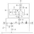
도 2는 도 1의 유기 발광 표시 장치에 포함된 화소 및 센싱부의 일 예를 나타내는 회로도이다.FIG. 2 is a circuit diagram illustrating an example of a pixel and a sensing unit included in the organic light emitting diode display of FIG. 1 .
도 2를 참조하면, 화소(PXij)는 스위칭 트랜지스터(M1), 저장 커패시터(Cst), 구동 트랜지스터(M2), 유기 발광 다이오드(OLED) 및 센싱 트랜지스터(M3)를 포함할 수 있다. 화소(PXij)는 제i(단, i는 양의 정수) 데이터 라인(DLi) 및 제i 센싱 라인(SEi)에 연결될 수 있다.Referring to FIG. 2 , the pixel PXij may include a switching transistor M1 , a storage capacitor Cst, a driving transistor M2 , an organic light emitting diode OLED, and a sensing transistor M3 . The pixel PXij may be connected to an ith (where i is a positive integer) data line DLi and an ith sensing line SEi.
스위칭 트랜지스터(M1)는 제i 데이터 라인(DLi)과 제2 노드(ND2) 사이에 연결되고, 제j(단, j는 양의 정수) 스캔 신호에 응답하여 턴-온될 수 있다. 저장 커패시터(Cst)는 제1 전원(ELVDD)과 제2 노드(ND2) 사이에 연결될 수 있다. 스위칭 트랜지스터(M1)가 턴-온될 때, 저장 커패시터(Cst)는 제i 데이터선(DLi)을 통해 공급되는 데이터 신호에 대응하는 전압을 충전할 수 있다. 구동 트랜지스터(M2)는 저장 커패시터(Cst)에 충전된 전압에 대응하는 구동 전류를 유기 발광 다이오드(OLED)에 제공할 수 있다. 유기 발광 다이오드(OLED)는 제1 노드(ND1)와 제2 전원(ELVSS) 사이에 연결되고, 제1 노드(ND1)와 제2 전원(ELVSS) 사이에 흐르는 구동 전류에 대응하는 휘도로 발광할 수 있다. 센싱 트랜지스터(M3)는 제i 센싱 라인(SEi)과 제1 노드(ND1) 사이에 연결되고, 센싱 제어 신호에 응답하여 턴-온될 수 있다.The switching transistor M1 is connected between the i-th data line DLi and the second node ND2 and may be turned on in response to a j-th (where j is a positive integer) scan signal. The storage capacitor Cst may be connected between the first power source ELVDD and the second node ND2 . When the switching transistor M1 is turned on, the storage capacitor Cst may be charged with a voltage corresponding to the data signal supplied through the ith data line DLi. The driving transistor M2 may provide a driving current corresponding to the voltage charged in the storage capacitor Cst to the organic light emitting diode OLED. The organic light emitting diode OLED is connected between the first node ND1 and the second power source ELVSS, and emits light with a luminance corresponding to the driving current flowing between the first node ND1 and the second power source ELVSS. can The sensing transistor M3 may be connected between the i-th sensing line SEi and the first node ND1 and may be turned on in response to a sensing control signal.
일 실시예에서, 화소(PXij)는 제2 스위치(SW2)와 제3 스위치(SW3)를 더 포함할 수 있다. 제2 스위치(SW2)는 구동 트랜지스터(M2)와 제1 노드(ND1) 사이에 연결되고, 제1 센싱 구간 동안 턴-오프 될 수 있다. 여기서, 제1 센싱 구간은 유기 발광 다이오드(OLED)의 열화 정보를 센싱하는 기간일 수 있다. 제1 센싱 구간에서, 제2 스위치(SW2)는 턴-오프 되고, 제3 스위치(SW3)는 턴-온될 수 있다. 이 경우, 센싱부(500)와 제2 전원(ELVSS) 사이에 전류 이동 경로가 형성되고, 제i 센싱 라인(SEi)에는 제1 센싱 전류(I1)가 흐를 수 있다. 즉, 센싱부(500)로부터 제1 노드(ND1)를 통해 제2 전원(ELVSS)으로 제1 센싱 전류(I1)가 흐를 수 있다.In an embodiment, the pixel PXij may further include a second switch SW2 and a third switch SW3 . The second switch SW2 is connected between the driving transistor M2 and the first node ND1 and may be turned off during the first sensing period. Here, the first sensing period may be a period for sensing deterioration information of the organic light emitting diode (OLED). In the first sensing period, the second switch SW2 may be turned off, and the third switch SW3 may be turned on. In this case, a current movement path is formed between the
제3 스위치(SW3)는 제1 노드(ND1)와 유기 발광 다이오드(OLED) 사이에 연결되고, 제2 센싱 구간 동안 턴-오프 될 수 있다. 여기서, 제2 센싱 구간은 구동 트랜지스터(M2)의 문턱전압/이동도 변화를 센싱하는 기간일 수 있다. 제2 센싱 구간에서, 제2 스위치(SW2)는 턴-온 되고, 제3 스위치(SW3)는 턴-오프될 수 있다. 이 경우, 제1 전원(ELVDD)과 센싱부(500) 사이에 전류 이동 경로가 형성되고, 제i 센싱 라인(SEi)에는 제2 센싱 전류(I2)가 흐를 수 있다. 즉, 제1 전원(ELVDD)으로부터 제1 노드(ND1)를 통해 센싱부(500)로 제2 센싱 전류(I2)가 흐를 수 있다.The third switch SW3 is connected between the first node ND1 and the organic light emitting diode OLED, and may be turned off during the second sensing period. Here, the second sensing period may be a period in which a change in threshold voltage/mobility of the driving transistor M2 is sensed. In the second sensing period, the second switch SW2 may be turned on, and the third switch SW3 may be turned off. In this case, a current movement path is formed between the first power source ELVDD and the
도 2에 도시된 화소(PXij)는 예시적인 것으로, 이에 한정되는 것은 아니다. 예를 들어, 화소는 데이터 라인과 구분되는 센싱 라인을 구비하는 것으로 도 2에 도시되어 있으나, 화소는 데이터 라인만을 포함하고, 기 설정된 시간들에 따라 데이터 라인을 센싱 라인으로 이용할 수 있다.The pixel PXij illustrated in FIG. 2 is exemplary and is not limited thereto. For example, although the pixel is illustrated in FIG. 2 as having a sensing line separated from the data line, the pixel includes only the data line, and the data line may be used as the sensing line according to preset times.
센싱부(500)는 적분기(510), 변환기(520) 및 메모리(미도시)를 포함할 수 있다.The
적분기(510)는 센싱 기준 전압(VSET)에 따라 제i 센싱 라인(SEi)에 흐르는 센싱 전류(즉, 제1 센싱 전류(I1) 또는 제2 센싱 전류(I2))를 적분하고, 적분에 의해 생성된 출력 전압(VOUT)을 출력할 수 있다. 적분기(510)는 증폭기(AMP) 및 제2 커패시터(C2)를 포함할 수 있다. 증폭기(AMP)는 제i 센싱 라인(SEi)에 연결되는 제1 입력 단자, 센싱 기준 전압(VSET)을 수신하는 제2 입력 단자, 및 변환기(520)에 연결되는 출력 단자를 포함할 수 있다. 제2 커패시터(C2)는 증폭기(AMP)의 제1 입력 단자와 증폭기(AMP)의 출력 단자 사이에 연결될 수 있다.The
적분기(510)는 제1 센싱 구간 동안 제i 센싱 라인(SEi)을 통해 화소(PXij)로 공급되는 제1 센싱 전류(I1)를 적분할 수 있다. 이 경우, 적분기(510)는 전류원으로서 동작할 수 있다. 적분기(510)는 제2 센싱 구간 동안 제i 센싱 라인(SEi)을 통해 화소(PXij)로부터 공급되는 제2 센싱 전류(I2)를 적분할 수 있다.The
일 실시예에서, 적분기(510)는 증폭기(AMP)의 제1 입력 단자와 증폭기(AMP)의 출력 단자 사이에 연결되는 제1 스위치(SW1)를 더 포함할 수 있다. 제1 스위치(SW1)는 리셋 구간동안 턴-온될 수 있다. 제1 스위치(SW1)는 리셋 구간동안 적분기(510)를 리셋할 수 있다. 즉, 제1 스위치(SW1)는 리셋 구간동안 제2 커패시터(C2)에 충전된 전압을 방전시킬 수 있다.In an embodiment, the
일 실시예에서, 센싱부(500)는 적분기(510)의 출력 전압(VOUT)을 일시적으로 저장하는 제1 커패시터(C1)를 더 포함할 수 있다. 제1 커패시터(C1)는 증폭기(AMP)의 출력 단자와 접지 전원 사이에 연결되고, 제1 센싱 구간 또는 제2 센싱 구간 동안 출력 전압(VOUT)을 일시적으로 저장할 수 있다.In an embodiment, the
변환기(520)는 적분기(510)의 출력 전압(VOUT)에 기초하여 센싱 데이터(SD)를 생성할 수 있다. 예를 들어, 변환기(520)는 적분기(510)의 출력 전압(VOUT)을 설정 전압(또는, 센싱 기준 전압(VSET))과 비교하는 비교기를 포함할 수 있다.The
도 2에 도시된 센싱부(500)는 예시적인 것으로, 센싱부(500)는 이에 한정되는 것은 아니다.The
도 3은 도 1의 유기 발광 표시 장치에 포함된 제어부의 일 예를 나타내는 블록도이다.3 is a block diagram illustrating an example of a control unit included in the organic light emitting diode display of FIG. 1 .
도 3을 참조하면, 제어부(700A)는 맵 저장부(710), 모델링 데이터 저장부(720), 전류 변화량 산출부(730), 전류 변화량 조정부(750), 및 데이터 보상부(770A)를 포함할 수 있다.Referring to FIG. 3 , the
맵 저장부(710)에는 화소들에 기 지정된 모델링 기준 전류가 흐르기 위한 모델링 전압들을 포함하는 모델링 전압 맵(MP)이 저장될 수 있다. 예를 들어, 유기 발광 표시 장치의 제조 단계에서, 모델링 전압이 화소에 인가될 때 화소에 모델링 기준 전류가 흐르도록 모델링 전압들이 측정되고, 측정된 모델링 전압들은 모델링 전압 맵(MP)으로서 맵 저장부(710)에 저장될 수 있다. 맵 저장부(710)는 비휘발성 메모리를 포함할 수 있다. 비휘발성 메모리는 전원이 공급되지 않는 상태에서 데이터를 보존할 수 있으며, 가격이 비교적 저렴하고 대용량을 저장할 수 있는 특징이 있다. 일 실시예에서, 맵 저장부(710)는 플래시 메모리(Flash Memory), EPROM(Erasable Programmable Read-Only Memory), EEPROM(Electrically Erasable Programmable Read-Only Memory), PRAM(Phase Change Random Access Memory), RRAM(Resistance Random Access Memory), NFGM(Nano Floating Gate Memory), PoRAM(Polymer Random Access Memory), MRAM(Magnetic Random Access Memory), FRAM(Ferroelectric Random Access Memory) 등을 포함할 수 있다.The
모델링 데이터 저장부(720)에는 모델링 전압과 전류 변화량 조정값의 관계를 나타내는 모델링 데이터(MD)가 저장될 수 있다. 예를 들어, 유기 발광 표시 장치의 제조 단계에서, 모델링 데이터(MD)는 모델링 전압들과 전류 변화량 조정값의 관계에 대해 1차원 모델링을 통해 생성되고, 모델링 데이터 저장부(720)에 저장될 수 있다. 일 실시예에서, 모델링 데이터(MD)는 모델링 전압과 전류 변화량 조정값의 관계로서 [수학식 1]을 포함할 수 있다.The modeling
[수학식 1][Equation 1]
IA = Ka * VMSET + KbIA = Ka * VMSET + Kb
여기서, IA는 전류 변화량 조정값, VMSET은 모델링 전압, Ka는 상수값(예를 들어, -0.1363), Kb는 상수값(예를 들어, 0.7367)을 나타낸다.Here, IA is a current change amount adjustment value, VMSET is a modeling voltage, Ka is a constant value (eg, -0.1363), and Kb is a constant value (eg, 0.7367).
모델링 데이터 저장부(720)는 비휘발성 메모리를 포함할 수 있다. 일 실시예에서, 모델링 데이터 저장부(720)는 플래시 메모리, EPROM, EEPROM, PRAM, RRAM, NFGM, PoRAM, MRAM, FRAM 등을 포함할 수 있다.The modeling
전류 변화량 산출부(730)는 센싱 전류(SD)로부터 센싱 전류 변화량(△I)을 산출할 수 있다. 여기서, 센싱 전류 변화량(△I)은 화소의 열화에 따른 휘도 변화량에 상응하고, 화소의 열화 정도를 나타낸다. 일 실시예에서, 전류 변화량 산출부(730)는 인접한 화소들에 대한 센싱 전류를 비교함으로써 센싱 전류 변화량(△I)을 산출할 수 있다. 예를 들어, 열화가 발생한 영역 내 화소들 중 첫번째 화소의 센싱 전류값과 마지막 화소의 센싱 전류값을 연결하여 기준선을 설정하고, 기준선과 열화된 화소의 센싱 전류값의 차이로 센싱 전류 변화량(△I)을 산출할 수 있다. 다른 실시예에서, 전류 변화량 산출부(730)는 센싱 전류값을 초기 구동 시에 측정된 센싱 전류값과 비교함으로써 센싱 전류 변화량(△I)을 산출할 수 있다.The
전류 변화량 조정부(750)는 모델링 전압 맵(MP) 및 모델링 데이터(MD)에 기초하여 센싱 전류 변화량(△I)을 조정 전류 변화량(△I')으로 변환할 수 있다. 전류 변화량 조정부(750)는 모델링 전압 맵(MP)으로부터 화소들에 상응하는 제1 모델링 전압을 도출할 수 있다. 전류 변화량 조정부(750)는 모델링 데이터(MD)를 이용하여 제1 모델링 전압에 대한 제1 전류 변화량 조정값 및 센싱 기준 전압에 대한 제2 전류 변화량 조정값을 산출할 수 있다. 전류 변화량 조정부(750)는 제1 모델링 전류 조정값과 제2 전류 변화량 조정값의 차이만큼 센싱 전류 변화량(△I)을 조정할 수 있다.The current
[실시예 1][Example 1]
센싱 기준 전압은 4V, 센싱 전류 변화량(△I)은 10%이고, 모델링 전압 맵(MP)으로부터 측정 화소의 제1 모델링 전압은 4.1V일 수 있다. 이 경우, 모델링 데이터(MD)를 이용하여 산출된 제1 전류 변화량 조정값은 약 0.177% (즉, 0.177 = -0.1363 * 4.1 + 0.7367)일 수 있다. 제2 전류 변화량 조정값은 약 0.191%(즉, 0.191 = -0.1363 * 4 + 0.7367)일 수 있다. 따라서, 조정 전류 변화량(△I')은 약 9.986% (즉, 9.986 = 10 + (0.177 - 0.191))일 수 있다.The sensing reference voltage may be 4V, the sensing current variation ΔI may be 10%, and the first modeling voltage of the measurement pixel from the modeling voltage map MP may be 4.1V. In this case, the first current variation adjustment value calculated using the modeling data MD may be about 0.177% (ie, 0.177 = -0.1363 * 4.1 + 0.7367). The second current variation adjustment value may be about 0.191% (ie, 0.191 = -0.1363 * 4 + 0.7367). Accordingly, the adjustment current variation ΔI′ may be about 9.986% (ie, 9.986 = 10 + (0.177 - 0.191)).
[실시예 2][Example 2]
센싱 기준 전압은 4V, 센싱 전류 변화량(△I)은 10%이고, 모델링 전압 맵(MP)으로부터 측정 화소의 제1 모델링 전압은 3.9V일 수 있다. 이 경우, 모델링 데이터(MD)를 이용하여 산출된 제1 전류 변화량 조정값은 약 0.205% (즉, 0.205 = -0.1363 * 3.9 + 0.7367)일 수 있다. 제2 전류 변화량 조정값은 약 0.191%(즉, 0.191 = -0.1363 * 4 + 0.7367)일 수 있다. 따라서, 조정 전류 변화량(△I')은 약 10.014% (즉, 10.014 = 10 + (0.205 - 0.191))일 수 있다.The sensing reference voltage may be 4V, the sensing current variation ΔI may be 10%, and the first modeling voltage of the measurement pixel from the modeling voltage map MP may be 3.9V. In this case, the first current variation adjustment value calculated using the modeling data MD may be about 0.205% (ie, 0.205 = -0.1363 * 3.9 + 0.7367). The second current variation adjustment value may be about 0.191% (ie, 0.191 = -0.1363 * 4 + 0.7367). Accordingly, the adjustment current change amount ΔI′ may be about 10.014% (ie, 10.014 = 10 + (0.205 - 0.191)).
[실시예 3][Example 3]
센싱 기준 전압은 4V, 센싱 전류 변화량(△I)은 10%이고, 모델링 전압 맵(MP)으로부터 측정 화소의 제1 모델링 전압은 4V일 수 있다. 이 경우, 센싱 기준 전압과 제1 모델링 전압이 동일하므로, 센싱 전류 변화량(△I)은 조정될 필요가 없다.The sensing reference voltage may be 4V, the sensing current variation ΔI may be 10%, and the first modeling voltage of the measurement pixel from the modeling voltage map MP may be 4V. In this case, since the sensing reference voltage and the first modeling voltage are the same, the sensing current variation ΔI does not need to be adjusted.
데이터 보상부(770A)는 조정 전류 변화량(△I')에 기초하여 입력 영상 데이터(IDATA)를 보상할 수 있다. 예를 들어, 데이터 보상부(770A)는 조정 전류 변화량(△I')에 기초하여 화소의 열화에 따른 휘도 변화량을 산출할 수 있다. 일 실시예에서, 데이터 보상부(770A)는 [수학식 2]를 이용하여 휘도 변화량을 산출할 수 있다.The data compensator 770A may compensate the input image data IDATA based on the adjustment current variation ΔI′. For example, the data compensator 770A may calculate a luminance change amount according to deterioration of a pixel based on the adjustment current change amount ΔI'. In an embodiment, the data compensator 770A may calculate the luminance change amount using [Equation 2].
[수학식 2][Equation 2]
△L = a * △I' + bΔL = a * ΔI' + b
여기서, △L는 휘도 변화량, a는 상수, △I'는 조정 전류 변화량, b는 상수를 나타낸다.Here, ΔL is a luminance change amount, a is a constant, ΔI' is an adjustment current change amount, and b is a constant.
데이터 보상부(770A)는 휘도 변화량에 상응하는 보상 데이터를 도출하고, 입력 영상 데이터(IDATA)에 보상 데이터를 반영함으로써 출력 영상 데이터(ODATA)를 생성할 수 있다.The data compensator 770A may generate the output image data ODATA by deriving compensation data corresponding to the luminance change amount and reflecting the compensation data in the input image data IDATA.
도 4는 화소가 열화됨에 따른 센싱 기준 전압과 센싱 전류의 관계를 나타내는 그래프이다.4 is a graph illustrating a relationship between a sensing reference voltage and a sensing current according to deterioration of a pixel.
도 4를 참조하면, 화소가 열화됨에 따라 전압-전류 특성 곡선이 변화될 수 있다. 예를 들어, 제1 화소 및 제2 화소가 열화되지 않은 상태에서, 제1 화소 및 제2 화소는 각각 제1 전압-전류 특성 곡선(P1)과 제2 전압-전류 특성 곡선(P2)을 가질 수 있다. 제1 화소와 제2 화소가 동일한 정도로 열화된 경우, 제1 화소 및 제2 화소는 각각 제1' 전압-전류 특성 곡선(P1')과 제2' 전압-전류 특성 곡선(P2')을 가질 수 있다.Referring to FIG. 4 , as the pixel deteriorates, the voltage-current characteristic curve may change. For example, in a state in which the first pixel and the second pixel are not deteriorated, the first pixel and the second pixel may have a first voltage-current characteristic curve P1 and a second voltage-current characteristic curve P2, respectively. can When the first pixel and the second pixel are degraded to the same extent, the first pixel and the second pixel may have a first 'voltage-current characteristic curve P1' and a second' voltage-current characteristic curve P2', respectively. can
제1 화소가 열화됨에 따라, 센싱 기준 전압(VSET)이 제1 화소에 인가될 때 측정되는 센싱 전류는 제1 전류값(I1)에서 제1' 전류값(I1')로 변경될 수 있다. 또한, 제2 화소가 열화됨에 따라, 센싱 기준 전압(VSET)이 제2 화소에 인가될 때 측정되는 센싱 전류는 제2 전류값(I2)에서 제2' 전류값(I2')로 변경될 수 있다.As the first pixel deteriorates, the sensing current measured when the sensing reference voltage VSET is applied to the first pixel may be changed from the first current value I1 to the first 'current value I1'. Also, as the second pixel deteriorates, the sensing current measured when the sensing reference voltage VSET is applied to the second pixel may change from the second current value I2 to the second 'current value I2'. have.
제1 전압-전류 특성 곡선(P1)과 제2 전압-전류 특성 곡선(P2)이 서로 다름에도 동일한 센싱 기준 전압(VSET)을 이용하여 화소들의 열화가 측정되므로, 동일한 정도로 열화된 경우에도 제1 측정 전류 변화량(즉, I1-I1')과 제2 측정 전류 변화량(즉, I2-I2')이 서로 다를 수 있다. 따라서, 동일한 크기의 전류(즉, 모델링 기준 전류)를 기준으로 측정 전류 변화량을 조정할 필요가 있다.Although the first voltage-current characteristic curve P1 and the second voltage-current characteristic curve P2 are different from each other, since deterioration of the pixels is measured using the same sensing reference voltage VSET, even when the first voltage-current characteristic curve P2 is deteriorated to the same degree, the first The measured current variation (ie, I1-I1') and the second measured current variation (ie, I2-I2') may be different from each other. Therefore, it is necessary to adjust the amount of change in the measured current based on the current of the same magnitude (ie, the modeling reference current).
도 5는 모델링 전압들 및 모델링 전압 맵을 도출하는 방법을 설명하기 위한 그래프이다.5 is a graph for explaining a method of deriving modeling voltages and a modeling voltage map.
도 5를 참조하면, 모델링 전압이 화소에 인가될 때 화소에 모델링 기준 전류가 흐르기 위한 모델링 전압이 측정될 수 있다. 예를 들어, 제1 화소에 제1 모델링 전압(VMSET1)이 인가될 때, 모델링 기준 전류(IM)가 센싱될 수 있다. 제2 화소에 제2 모델링 전압(VMSET2)이 인가될 때, 모델링 기준 전류(IM)가 센싱될 수 있다. 측정된 화소들에 대한 모델링 전압들은 모델링 전압 맵에 포함되어 맵 저장부에 저장될 수 있다.Referring to FIG. 5 , when a modeling voltage is applied to a pixel, a modeling voltage for flowing a modeling reference current to the pixel may be measured. For example, when the first modeling voltage VMSET1 is applied to the first pixel, the modeling reference current IM may be sensed. When the second modeling voltage VMSET2 is applied to the second pixel, the modeling reference current IM may be sensed. Modeling voltages for the measured pixels may be included in the modeling voltage map and stored in the map storage unit.
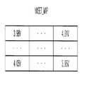
도 6은 모델링 전압 맵의 일 예를 나타내는 도면이다. 도 7을 도 6의 모델링 전압 맵이 화소 그룹에 대한 모델링 전압들을 포함하는 일 예를 나타내는 도면이다.6 is a diagram illustrating an example of a modeling voltage map. 7 is a diagram illustrating an example in which the modeling voltage map of FIG. 6 includes modeling voltages for a pixel group.
도 6 및 7을 참조하면, 모델링 전압 맵(VMSET_MAP)은 화소들 각각에 대한 모델링 전압 또는 화소 그룹에 대한 모델링 전압들을 포함할 수 있다.6 and 7 , the modeling voltage map VMSET_MAP may include a modeling voltage for each pixel or modeling voltages for a pixel group.
도 6에 도시된 바와 같이, 기 지정된 모델링 기준 전류가 흐르기 위한 모델링 전압들은 화소 단위 또는 화소 그룹 단위로 저장될 수 있다.As shown in FIG. 6 , modeling voltages for flowing a predetermined modeling reference current may be stored in units of pixels or groups of pixels.
일 실시예에서, 모델링 전압 맵(VMSET_MAP)은 화소들 각각에 대한 모델링 전압들을 포함할 수 있다. 모델링 전압 맵(VMSET_MAP)은 화소들 각각에 대한 모델링 전압을 저장함으로써 센싱 전류 변화량을 정확하게 조정할 수 있다.In an embodiment, the modeling voltage map VMSET_MAP may include modeling voltages for each of the pixels. The modeling voltage map VMSET_MAP may accurately adjust the amount of change in the sensing current by storing the modeling voltage for each pixel.
다른 실시예에서, 모델링 전압 맵(VMSET_MAP)은 화소 그룹에 대한 모델링 전압들을 포함할 수 있다. 도 7에 도시된 바와 같이, 4*4 매트릭스에 포함된 서로 인접한 화소들이 하나의 화소 그룹으로 설정되고, 모델링 전압 맵(VMSET_MAP)은 화소 그룹에 대한 모델링 전압들을 포함할 수 있다. 예를 들어, 제1 화소 그룹(PG(1,1))은 제1-1 화소(PX(1,1)) 내지 제4-4 화소(PX(4,4))를 포함할 수 있다. 제1 화소 그룹(PG(1,1))에 대한 모델링 전압은 제1-1 화소(PX(1,1)) 내지 제4-4 화소(PX(4,4))에 대한 모델링 전압들의 평균값으로 설정되거나, 대표 화소의 모델링 전압으로 설정될 수 있다. 화소 그룹은 서로 인접한 화소들로 구성되므로 열화 정도가 서로 비슷할 수 있다. 따라서, 높은 해상도를 지원하는 유기 발광 표시 장치에서 화소 그룹 단위로 모델링 전압들을 저장함으로써 맵 저장부의 용량을 줄일 수 있다.In another embodiment, the modeling voltage map VMSET_MAP may include modeling voltages for a pixel group. 7 , adjacent pixels included in a 4*4 matrix are set as one pixel group, and the modeling voltage map VMSET_MAP may include modeling voltages for the pixel group. For example, the first pixel group PG(1,1) may include a 1-1 pixel PX(1,1) to a 4-4th pixel PX(4,4). The modeling voltage for the first pixel group PG(1,1) is an average value of the modeling voltages for the 1-1 pixels PX(1,1) to 4-4 pixels PX(4,4). or may be set as the modeling voltage of the representative pixel. Since the pixel group is composed of pixels adjacent to each other, the degree of deterioration may be similar to each other. Accordingly, in the organic light emitting diode display supporting high resolution, the capacity of the map storage unit may be reduced by storing modeling voltages in units of pixel groups.
비록, 도 6에서는 모델링 전압들은 전압값으로 저장된 것으로 도시하였지만, 모델링 전압들은 다양한 형태로 저장될 수 있다. 예를 들어, 모델링 전압들은 센싱 기준 전압에 대한 오프셋(offset) 값으로 저장될 수 있다.Although it is shown in FIG. 6 that the modeling voltages are stored as voltage values, the modeling voltages may be stored in various forms. For example, the modeling voltages may be stored as an offset value with respect to a sensing reference voltage.
도 8은 모델링 전압들과 전류 변화량 조정값의 관계를 나타내는 모델링 데이터의 일 예를 나타내는 그래프이다.8 is a graph illustrating an example of modeling data indicating a relationship between modeling voltages and a current variation adjustment value.
도 8을 참조하면, 모델링 데이터는 모델링 전압(VMSET)과 전류 변화량 조정값(IA)의 관계에 대해 1차원 모델링을 통해 생성되고, 모델링 데이터 저장부에 저장될 수 있다. 예를 들어, 모델링 데이터는 모델링 전압과 전류 변화량 조정값의 관계로서 [수학식 3]을 포함할 수 있다.Referring to FIG. 8 , modeling data may be generated through one-dimensional modeling with respect to the relationship between the modeling voltage VMSET and the current variation adjustment value IA, and stored in the modeling data storage unit. For example, the modeling data may include [Equation 3] as the relationship between the modeling voltage and the current variation adjustment value.
[수학식 3][Equation 3]
IA = -0.1363 * VMSET + 0.7367IA = -0.1363 * VMSET + 0.7367
여기서, IA는 전류 변화량 조정값, VMSET은 모델링 전압을 나타낸다.Here, IA is a current change amount adjustment value, and VMSET is a modeling voltage.
도 9a 및 도 9b는 본 발명의 효과를 설명하기 위한 그래프들이다.9A and 9B are graphs for explaining the effect of the present invention.
도 9a 및 도 9b를 참조하면, 유기 발광 표시 장치는 모델링 전압 맵과 모델링 데이터를 이용하여 측정된 센싱 전류 변화량(△I)을 조정하고, 조정 전류 변화량(△I')에 기초하여 화소의 열화를 정확히 보상할 수 있다.Referring to FIGS. 9A and 9B , the organic light emitting diode display adjusts a sensing current variation ΔI measured using a modeling voltage map and modeling data, and deterioration of a pixel based on the adjusted current variation ΔI′ can be accurately compensated for.
도 9a에 도시된 바와 같이, 하나의 센싱 기준 전압을 화소에 인가함으로써 센싱된 센싱 전류 변화량(△I)을 이용하여 도출된 휘도 변화량(△L)은 상대적으로 오차가 클 수 있다. 예를 들어, 제1 센싱 전류 변화량(△I1)에서 화소들의 휘도 변화량(△L) 편차는 제1 편차값(D1)일 수 있다.As shown in FIG. 9A , the luminance change ΔL derived using the sensing current change ΔI sensed by applying one sensing reference voltage to the pixel may have a relatively large error. For example, the deviation of the luminance change ΔL of the pixels from the first sensing current change ΔI1 may be the first deviation value D1.
도 9b에 도시된 바와 같이, 모델링 기준 전류를 기준으로 조정된 조정 전류 변화량(△I')을 이용하여 도출된 휘도 변화량(△L)은 상대적으로 오차가 작을 수 있다. 예를 들어, 제1 센싱 전류 변화량(△I1')에서 화소들의 휘도 변화량(△L) 편차는 제1 편차값(D1) 보다 작은 제2 편차값(D2)일 수 있다.As shown in FIG. 9B , the luminance change amount ΔL derived using the adjustment current change amount △I′ adjusted based on the modeling reference current may have a relatively small error. For example, the deviation of the luminance change amount ΔL of the pixels from the first sensing current change amount ΔI1 ′ may be a second deviation value D2 smaller than the first deviation value D1 .
따라서, 유기 발광 표시 장치는 조정 전류 변화량(△I')을 이용하여 휘도 변화량(△L)을 도출하고, 영상 데이터를 보상함으로써 화소의 열화를 정확히 보상할 수 있다.Accordingly, the organic light emitting diode display may accurately compensate for pixel deterioration by deriving a luminance variation ΔL using the adjustment current variation ΔI′ and compensating for image data.
도 10은 도 1의 유기 발광 표시 장치에 포함된 제어부의 다른 예를 나타내는 블록도이다.10 is a block diagram illustrating another example of a controller included in the organic light emitting diode display of FIG. 1 .
도 10을 참조하면, 제어부(700B)는 맵 저장부(710), 모델링 데이터 저장부(720), 전류 변화량 산출부(730), 전류 변화량 조정부(750), 스트레스 데이터 생성부(760) 및 데이터 보상부(770B)를 포함할 수 있다. 다만, 본 실시예에 따른 제어부(700B)는 스트레스 데이터 생성부(760)가 추가된 것을 제외하면, 도 2의 제어부와 실질적으로 동일하므로, 동일 또는 유사한 구성 요소에 대해서는 동일한 참조 번호를 사용하고, 중복되는 설명은 생략하기로 한다.Referring to FIG. 10 , the
맵 저장부(710)에는 화소들에 기 지정된 모델링 기준 전류가 흐르기 위한 모델링 전압들을 포함하는 모델링 전압 맵(MP)이 저장될 수 있다.The
모델링 데이터 저장부(720)에는 모델링 전압과 전류 변화량 조정값의 관계를 나타내는 모델링 데이터(MD)가 저장될 수 있다.The modeling
전류 변화량 산출부(730)는 센싱 전류(SD)로부터 센싱 전류 변화량(△I)을 산출할 수 있다.The
전류 변화량 조정부(750)는 모델링 전압 맵(MP) 및 모델링 데이터(MD)에 기초하여 센싱 전류 변화량(△I)을 조정 전류 변화량(△I')으로 변환할 수 있다.The current
스트레스 데이터 생성부(760)는 입력 영상 데이터(IDATA)를 누적하여 저장함으로써 스트레스 데이터(ST)를 생성할 수 있다. 여기서, 스트레스 데이터(ST)는 누적 구동량, 누적 구동 시간 등을 포함할 수 있다. 스트레스 데이터 생성부(760)는 표시 패널이 구동되는 동안 스트레스 데이터(ST)를 누적하여 저장하는 휘발성 메모리 및 전원이 공급되지 않는 상태에서 스트레스 데이터를 유지하기 위한 비휘발성 메모리를 포함할 수 있다.The
데이터 보상부(770B)는 조정 전류 변화량(△I')에 기초하여 입력 영상 데이터(IDATA)를 보상할 수 있다. 데이터 보상부(770B)는 조정 전류 변화량(△I')에 기초하여 화소의 열화에 따른 휘도 변화량을 산출하고, 휘도 변화량에 따른 제1 보상 데이터를 도출할 수 있다. 또한, 데이터 보상부(770B)는 룩업 테이블(look-up table)을 이용하여 스트레스 데이터에 상응하는 제2 보상 데이터를 도출할 수 있다.The data compensator 770B may compensate the input image data IDATA based on the adjustment current variation ΔI′. The data compensator 770B may calculate a luminance change according to the deterioration of a pixel based on the adjustment current change amount ΔI' and derive first compensation data according to the luminance change amount. Also, the data compensator 770B may derive second compensation data corresponding to the stress data using a look-up table.
일 실시예에서, 데이터 보상부(770B)는 조정 전류 변화량(△I')에 기초하여 생성된 제1 보상 데이터 및 스트레스 데이터(ST)에 기초하여 생성된 제2 보상 데이터의 평균값으로 입력 영상 데이터(IDATA)를 보상할 수 있다. 즉, 데이터 보상부(770B)는 제1 보상 데이터 및 제2 보상 데이터의 평균값으로 입력 영상 데이터(IDATA)를 보상함으로써, 센싱 전류에 의한 보상 방식에서 발생할 수 있는 오차를 완화시키고 표시 품질을 높일 수 있다.In an exemplary embodiment, the data compensator 770B uses the input image data as an average value of the first compensation data generated based on the adjustment current variation ΔI′ and the second compensation data generated based on the stress data ST. (IDATA) can be compensated. That is, the
다른 실시예에서, 데이터 보상부(770B)는 조정 전류 변화량(△I')에 기초하여 생성된 제1 보상 데이터와 스트레스 데이터(ST)에 기초하여 생성된 제2 보상 데이터 중 하나로 입력 영상 데이터(IDATA)를 보상할 수 있다. 데이터 보상부(770B)는 입력 영상 데이터(IDATA)를 보상하기 위해 입력 영상 데이터(IDATA)의 계조값에 기초하여 제1 보상 데이터와 제2 보상 데이터 중 하나를 선택할 수 있다. 예를 들어, 입력 영상 데이터(IDATA)가 저계조 영역에 해당하는 경우, 센싱 전류의 크기에 따라 휘도가 크게 변화될 수 있다. 따라서, 데이터 보상부(770B)는 입력 영상 데이터(IDATA)의 계조값이 기 지정된 임계 계조값보다 큰 경우 제1 보상 데이터로 입력 영상 데이터(IDATA)를 보상하고, 입력 영상 데이터(IDATA)의 계조값이 임계 계조값 이하인 경우 제2 보상 데이터로 입력 영상 데이터(IDATA)를 보상할 수 있다.In another embodiment, the data compensator 770B may use input image data ( IDATA) can be compensated. The data compensator 770B may select one of the first compensation data and the second compensation data based on the grayscale value of the input image data IDATA in order to compensate the input image data IDATA. For example, when the input image data IDATA corresponds to the low grayscale region, the luminance may be greatly changed according to the magnitude of the sensing current. Accordingly, the
도 11은 본 발명의 실시예들에 따른 유기 발광 표시 장치의 구동 방법을 나타내는 순서도이다.11 is a flowchart illustrating a method of driving an organic light emitting diode display according to example embodiments.
도 11을 참조하면, 화소들에 모델링 기준 전류가 흐르기 위한 모델링 전압들을 포함하는 모델링 전압 맵이 도출(S110)될 수 있다. 예를 들어, 유기 발광 표시 장치의 제조 단계에서, 모델링 전압이 화소에 인가될 때 화소에 모델링 기준 전류가 흐르도록 모델링 전압이 측정되고, 측정된 모델링 전압들은 모델링 전압 맵으로서 맵 저장부에 저장될 수 있다. 일 실시예에서, 모델링 전압 맵은 화소들 각각에 대한 모델링 전압들을 포함할 수 있다. 다른 실시예에서, 모델링 전압 맵은 화소 그룹에 대한 모델링 전압들을 포함할 수 있다. 일 실시예에서, 모델링 전압들은 센싱 기준 전압에 대한 오프셋 값으로 저장될 수 있다.Referring to FIG. 11 , a modeling voltage map including modeling voltages for a modeling reference current to flow in the pixels may be derived ( S110 ). For example, in the manufacturing stage of the organic light emitting diode display, when the modeling voltage is applied to the pixel, the modeling voltage is measured so that a modeling reference current flows in the pixel, and the measured modeling voltages are stored in the map storage unit as a modeling voltage map. can In an embodiment, the modeling voltage map may include modeling voltages for each of the pixels. In another embodiment, the modeling voltage map may include modeling voltages for a group of pixels. In an embodiment, the modeling voltages may be stored as an offset value with respect to the sensing reference voltage.
모델링 전압들과 전류 변화량 조정값의 관계를 나타내는 모델링 데이터가 도출(S120)될 수 있다. 예를 들어, 유기 발광 표시 장치의 제조 단계에서, 모델링 데이터는 모델링 전압들과 전류 변화량 조정값의 관계에 대해 1차원 모델링을 통해 생성되고, 모델링 데이터 저장부에 저장될 수 있다.Modeling data representing the relationship between the modeling voltages and the current change amount adjustment value may be derived ( S120 ). For example, in the manufacturing stage of the organic light emitting diode display, modeling data may be generated through one-dimensional modeling with respect to the relationship between the modeling voltages and the current variation adjustment value, and stored in the modeling data storage unit.
화소들에 인가되는 센싱 기준 전압에 따라 화소들에 흐르는 센싱 전류가 센싱(S130)될 수 있다.The sensing current flowing through the pixels may be sensed ( S130 ) according to the sensing reference voltage applied to the pixels.
센싱 전류로부터 센싱 전류 변화량이 산출(S140)될 수 있다. 일 실시예에서, 인접한 화소들에 대한 센싱 전류를 비교함으로써 센싱 전류 변화량이 산출될 수 있다. 다른 실시예에서, 센싱 전류값을 초기 구동 시에 측정된 센싱 전류값과 비교함으로써 센싱 전류 변화량이 산출될 수 있다.A sensing current variation may be calculated from the sensing current ( S140 ). In an embodiment, the amount of change in sensing current may be calculated by comparing sensing currents with respect to adjacent pixels. In another embodiment, the sensing current variation may be calculated by comparing the sensing current value with the sensing current value measured during initial driving.
모델링 전압 맵 및 모델링 데이터에 기초하여 센싱 전류 변화량을 조정 전류 변화량으로 변환(S150)될 수 있다. 일 실시예에서, 센싱 전류 변화량을 조정 전류 변화량으로 변환하기 위해 모델링 전압 맵으로부터 화소들에 상응하는 제1 모델링 전압이 도출되고, 모델링 데이터를 이용하여 제1 모델링 전압에 대한 제1 전류 변화량 조정값 및 센싱 기준 전압에 대한 제2 전류 변화량 조정값이 산출되며, 전류 변화량을 산출하기 위해 제1 전류 변화량 조정값 및 제2 전류 변화량 조정값의 차이만큼 센싱 전류 변화량이 조정될 수 있다. 다만, 센싱 전류 변화량을 조정 전류 변화량으로 변환하는 방법에 대해서는 상술한 바 있으므로, 그에 대한 중복되는 설명은 생략하기로 한다.Based on the modeling voltage map and modeling data, the sensing current variation may be converted into an adjustment current variation ( S150 ). In an embodiment, a first modeling voltage corresponding to pixels is derived from a modeling voltage map to convert a sensing current variation into an adjustment current variation, and a first current variation adjustment value for the first modeling voltage using the modeling data and a second current variation adjustment value for the sensing reference voltage may be calculated, and the sensing current variation may be adjusted by the difference between the first current variation adjustment value and the second current variation adjustment value to calculate the current variation. However, since the method for converting the sensing current variation into the adjustment current variation has been described above, a redundant description thereof will be omitted.
조정 전류 변화량에 기초하여 입력 영상 데이터가 보상(S160)될 수 있다. 휘도 변화량에 상응하는 보상 데이터가 도출하고, 입력 영상 데이터에 보상 데이터가 반영됨으로써 출력 영상 데이터가 생성될 수 있다. 일 실시예에서, 입력 영상 데이터는 조정 전류 변화량에 기초하여 생성된 제1 보상 데이터 및 스트레스 데이터에 기초하여 생성된 제2 보상 데이터의 평균값으로 보상될 수 있다. 일 실시예에서, 입력 영상 데이터는 조정 전류 변화량에 기초하여 생성된 제1 보상 데이터와 스트레스 데이터에 기초하여 생성된 제2 보상 데이터 중 하나로 보상될 수 있다. 일 실시예에서, 입력 영상 데이터는 입력 영상 데이터의 계조값이 임계 계조값보다 큰 경우 제1 보상 데이터로 보상되고, 입력 영상 데이터의 계조값이 임계 계조값 이하인 경우 제2 보상 데이터로 보상될 수 있다.The input image data may be compensated ( S160 ) based on the amount of change in the adjustment current. Compensation data corresponding to the amount of luminance change may be derived, and the compensation data may be reflected in the input image data to generate output image data. In an embodiment, the input image data may be compensated with an average value of the first compensation data generated based on the adjustment current variation and the second compensation data generated based on the stress data. In an embodiment, the input image data may be compensated with one of the first compensation data generated based on the adjustment current variation and the second compensation data generated based on the stress data. In an embodiment, the input image data may be compensated with the first compensation data when the grayscale value of the input image data is greater than the threshold grayscale value, and compensated with the second compensation data when the grayscale value of the input image data is less than or equal to the threshold grayscale value. have.
따라서, 유기 발광 표시 장치의 구동 방법은 화소 열화를 정확히 보상하고, 유기 발광 표시 장치의 표시 품질을 높일 수 있다.Accordingly, the driving method of the organic light emitting diode display can accurately compensate for pixel deterioration and improve the display quality of the organic light emitting display apparatus.
이상, 본 발명의 실시예들에 따른 유기 발광 표시 장치 및 유기 발광 표시 장치의 구동 방법에 대하여 도면을 참조하여 설명하였지만, 상기 설명은 예시적인 것으로서 본 발명의 기술적 사상을 벗어나지 않는 범위에서 해당 기술 분야에서 통상의 지식을 가진 자에 의하여 수정 및 변경될 수 있을 것이다. 예를 들어, 상기에서는 센싱부 및 데이터 구동부가 분리된 것으로 설명하였으나, 이에 한정되는 것이 아니다. 예를 들어, 센싱부와 데이터 구동부는 하나의 IC에 형성될 수 있다.In the above, although the organic light emitting display device and the method of driving the organic light emitting display device according to the embodiments of the present invention have been described with reference to the drawings, the above description is illustrative and does not depart from the technical spirit of the present invention. It may be modified and changed by those of ordinary skill in the art. For example, although it has been described above that the sensing unit and the data driving unit are separated, the present invention is not limited thereto. For example, the sensing unit and the data driving unit may be formed in one IC.
본 발명은 유기 발광 표시 장치를 구비한 전자 기기에 다양하게 적용될 수 있다. 예를 들어, 본 발명은 컴퓨터, 노트북, 휴대폰, 스마트폰, 스마트패드, 피엠피(PMP), 피디에이(PDA), MP3 플레이어, 디지털 카메라, 비디오 캠코더 등에 적용될 수 있다.The present invention can be variously applied to an electronic device having an organic light emitting diode display. For example, the present invention can be applied to a computer, a notebook computer, a mobile phone, a smart phone, a smart pad, a PMP, a PDA, an MP3 player, a digital camera, a video camcorder, and the like.
상기에서는 본 발명의 실시예들을 참조하여 설명하였지만, 해당 기술분야에서 통상의 지식을 가진 자는 하기의 특허청구범위에 기재된 본 발명의 사상 및 영역으로부터 벗어나지 않는 범위 내에서 본 발명을 다양하게 수정 및 변경시킬 수 있음을 이해할 것이다.Although the above has been described with reference to the embodiments of the present invention, those of ordinary skill in the art can variously modify and change the present invention within the scope without departing from the spirit and scope of the present invention described in the claims below. You will understand that you can
100: 표시 패널200: 스캔 구동부
300: 센싱 구동부400: 데이터 구동부
500: 센싱부700, 700A, 700B: 제어부
710: 맵 저장부720: 모델링 데이터 저장부
730: 전류 변화량 산출부750: 전류 변화량 조정부
770: 데이터 보상부1000: 유기 발광 표시 장치100: display panel 200: scan driver
300: sensing driver 400: data driver
500: sensing
710: map storage 720: modeling data storage
730: current change amount calculation unit 750: current change amount adjustment unit
770: data compensator 1000: organic light emitting display device
Claims (20)
Translated fromKorean상기 화소들에 스캔 신호를 제공하는 스캔 구동부;
상기 화소들에 데이터 신호를 제공하는 데이터 구동부;
상기 화소들에 인가되는 센싱 기준 전압에 따라 상기 화소들에 흐르는 센싱 전류를 센싱하는 센싱부; 및
상기 센싱 전류로부터 센싱 전류 변화량을 산출하고, 입력 영상 데이터를 보상하기 위해 상기 화소들의 편차 데이터를 이용하여 상기 센싱 전류 변화량을 조정하는 제어부를 포함하고,
상기 편차 데이터는 상기 화소들에 기 지정된 모델링 기준 전류가 흐르기 위한 모델링 전압들을 포함하는 모델링 전압 맵(map) 및 상기 모델링 전압들과 전류 변화량 조정값의 관계를 나타내는 모델링 데이터를 포함하며,
상기 모델링 전압들은 상기 센싱 기준 전압에 대한 오프셋(offset) 값으로 저장되는 유기 발광 표시 장치.a display panel including a plurality of pixels;
a scan driver providing a scan signal to the pixels;
a data driver providing a data signal to the pixels;
a sensing unit sensing a sensing current flowing through the pixels according to a sensing reference voltage applied to the pixels; and
a control unit that calculates a sensing current variation from the sensing current and adjusts the sensing current variation by using the deviation data of the pixels to compensate for input image data,
The deviation data includes a modeling voltage map including modeling voltages for a predetermined modeling reference current to flow in the pixels, and modeling data indicating a relationship between the modeling voltages and a current change amount adjustment value,
The modeling voltages are stored as offset values with respect to the sensing reference voltage.
상기 센싱 전류로부터 상기 센싱 전류 변화량을 산출하는 전류 변화량 산출부;
상기 모델링 전압 맵 및 상기 모델링 데이터에 기초하여 상기 센싱 전류 변화량을 조정 전류 변화량으로 변환하는 전류 변화량 조정부; 및
상기 조정 전류 변화량에 기초하여 상기 입력 영상 데이터를 보상하는 데이터 보상부를 포함하는 것을 특징으로 하는 유기 발광 표시 장치.According to claim 1, wherein the control unit
a current variation calculating unit for calculating the sensing current variation from the sensing current;
a current variation adjusting unit converting the sensing current variation into an adjusted current variation based on the modeling voltage map and the modeling data; and
and a data compensator compensating for the input image data based on the change amount of the adjusted current.
상기 입력 영상 데이터를 누적하여 저장함으로써 스트레스 데이터를 생성하는 스트레스 데이터 생성부를 더 포함하는 것을 특징으로 하는 유기 발광 표시 장치.According to claim 3, wherein the control unit
and a stress data generator configured to generate stress data by accumulating and storing the input image data.
상기 화소들에 모델링 기준 전류가 흐르기 위한 모델링 전압들을 포함하는 모델링 전압 맵을 도출하는 단계;
상기 모델링 전압들과 전류 변화량 조정값의 관계를 나타내는 모델링 데이터를 도출하는 단계;
상기 화소들에 인가되는 센싱 기준 전압에 따라 상기 화소들에 흐르는 상기 센싱 전류를 센싱하는 단계;
상기 센싱 전류로부터 센싱 전류 변화량을 산출하는 단계;
상기 모델링 전압 맵 및 상기 모델링 데이터에 기초하여 상기 센싱 전류 변화량을 조정 전류 변화량으로 변환하는 단계; 및
상기 조정 전류 변화량에 기초하여 입력 영상 데이터를 보상하는 단계를 포함하고,
상기 모델링 전압들은 상기 센싱 기준 전압에 대한 오프셋(offset) 값으로 저장되는 유기 발광 표시 장치의 구동 방법.A method of driving an organic light emitting diode display for compensating for deterioration of the pixels by sensing a sensing current flowing through the pixels, the method comprising:
deriving a modeling voltage map including modeling voltages for a modeling reference current to flow in the pixels;
deriving modeling data representing a relationship between the modeling voltages and a current variation adjustment value;
sensing the sensing current flowing through the pixels according to a sensing reference voltage applied to the pixels;
calculating a sensing current variation from the sensing current;
converting the sensing current variation into an adjustment current variation based on the modeling voltage map and the modeling data; and
Compensating the input image data based on the adjustment current change amount,
The modeling voltages are stored as offset values with respect to the sensing reference voltage.
상기 모델링 전압 맵으로부터 상기 화소들에 상응하는 제1 모델링 전압을 도출하는 단계;
상기 모델링 데이터를 이용하여 상기 제1 모델링 전압에 대한 제1 전류 변화량 조정값 및 상기 센싱 기준 전압에 대한 제2 전류 변화량 조정값을 산출하는 단계; 및
상기 조정 전류 변화량을 산출하기 위해 상기 제1 전류 변화량 조정값 및 상기 제2 전류 변화량 조정값의 차이만큼 상기 센싱 전류 변화량을 조정하는 단계를 포함하는 것을 특징으로 하는 유기 발광 표시 장치의 구동 방법.The method of claim 12, wherein converting the sensing current variation into the adjustment current variation comprises:
deriving a first modeling voltage corresponding to the pixels from the modeling voltage map;
calculating a first current variation adjustment value with respect to the first modeling voltage and a second current variation adjustment value with respect to the sensing reference voltage by using the modeling data; and
and adjusting the sensing current variation by a difference between the first current variation control value and the second current variation control value to calculate the adjusted current variation.
상기 입력 영상 데이터를 누적하여 저장함으로써 스트레스 데이터를 생성하는 단계를 더 포함하는 것을 특징으로 하는 유기 발광 표시 장치의 구동 방법.13. The method of claim 12,
and generating stress data by accumulating and storing the input image data.
Priority Applications (2)
| Application Number | Priority Date | Filing Date | Title |
|---|---|---|---|
| KR1020150132984AKR102435932B1 (en) | 2015-09-21 | 2015-09-21 | Organic light emitting display device and method of driving the same |
| US15/087,588US9984628B2 (en) | 2015-09-21 | 2016-03-31 | Organic light emitting display device for compensating deterioration of a pixel and method of driving the same |
Applications Claiming Priority (1)
| Application Number | Priority Date | Filing Date | Title |
|---|---|---|---|
| KR1020150132984AKR102435932B1 (en) | 2015-09-21 | 2015-09-21 | Organic light emitting display device and method of driving the same |
Publications (2)
| Publication Number | Publication Date |
|---|---|
| KR20170034977A KR20170034977A (en) | 2017-03-30 |
| KR102435932B1true KR102435932B1 (en) | 2022-08-25 |
Family
ID=58282921
Family Applications (1)
| Application Number | Title | Priority Date | Filing Date |
|---|---|---|---|
| KR1020150132984AActiveKR102435932B1 (en) | 2015-09-21 | 2015-09-21 | Organic light emitting display device and method of driving the same |
Country Status (2)
| Country | Link |
|---|---|
| US (1) | US9984628B2 (en) |
| KR (1) | KR102435932B1 (en) |
Families Citing this family (12)
| Publication number | Priority date | Publication date | Assignee | Title |
|---|---|---|---|---|
| KR102546774B1 (en)* | 2016-07-22 | 2023-06-23 | 삼성디스플레이 주식회사 | Display apparatus and method of operating the same |
| KR102595281B1 (en)* | 2016-10-31 | 2023-10-31 | 엘지디스플레이 주식회사 | Data Driver and Display Device using the same |
| KR102490238B1 (en)* | 2017-12-27 | 2023-01-18 | 엘지디스플레이 주식회사 | Display device and method of driving the same |
| CN109935182B (en)* | 2018-07-27 | 2020-07-17 | 京东方科技集团股份有限公司 | Pixel current detection circuit, method, and display device |
| KR102730941B1 (en)* | 2019-10-30 | 2024-11-19 | 삼성디스플레이 주식회사 | Display device and method of driving display device |
| KR102709912B1 (en) | 2019-11-14 | 2024-09-27 | 삼성디스플레이 주식회사 | Display device and driving method thereof |
| KR102738966B1 (en) | 2019-12-18 | 2024-12-06 | 주식회사 엘엑스세미콘 | Source driver and display device including the same |
| KR102733640B1 (en)* | 2019-12-26 | 2024-11-27 | 삼성디스플레이 주식회사 | Compensation method of display device |
| KR102793697B1 (en)* | 2020-08-24 | 2025-04-10 | 삼성디스플레이 주식회사 | Display apparatus and method of compensating image of display panel using the same |
| CN113763882A (en)* | 2021-10-11 | 2021-12-07 | 合肥维信诺科技有限公司 | Control circuit, display screen, terminal device, control method and device |
| KR102813519B1 (en)* | 2021-12-23 | 2025-05-27 | 엘지디스플레이 주식회사 | Display device and driving method thereof |
| KR20240042330A (en)* | 2022-09-23 | 2024-04-02 | 삼성디스플레이 주식회사 | Display apparatus and method of compensating deterioration of display panel using the same |
Family Cites Families (5)
| Publication number | Priority date | Publication date | Assignee | Title |
|---|---|---|---|---|
| JP3767877B2 (en)* | 1997-09-29 | 2006-04-19 | 三菱化学株式会社 | Active matrix light emitting diode pixel structure and method thereof |
| US6911781B2 (en)* | 2002-04-23 | 2005-06-28 | Semiconductor Energy Laboratory Co., Ltd. | Light emitting device and production system of the same |
| KR101073226B1 (en)* | 2010-03-17 | 2011-10-12 | 삼성모바일디스플레이주식회사 | Organic Light Emitting Display Device |
| KR101865586B1 (en)* | 2011-04-08 | 2018-06-11 | 삼성디스플레이 주식회사 | Organic Light Emitting Display Device and Driving Method Thereof |
| KR20150054124A (en) | 2013-11-11 | 2015-05-20 | 삼성디스플레이 주식회사 | Organic light emitting display device and method for driving the same |
- 2015
- 2015-09-21KRKR1020150132984Apatent/KR102435932B1/enactiveActive
- 2016
- 2016-03-31USUS15/087,588patent/US9984628B2/enactiveActive
Also Published As
| Publication number | Publication date |
|---|---|
| US20170084227A1 (en) | 2017-03-23 |
| KR20170034977A (en) | 2017-03-30 |
| US9984628B2 (en) | 2018-05-29 |
Similar Documents
| Publication | Publication Date | Title |
|---|---|---|
| KR102435932B1 (en) | Organic light emitting display device and method of driving the same | |
| CN105788526B (en) | Organic light emitting display | |
| US10283043B2 (en) | Organic light emitting display device and method of driving the same | |
| US10629118B2 (en) | Organic light emitting display device and method for driving the same | |
| US11017727B2 (en) | Driving voltage setting device, method of setting driving voltage for display device, and display device | |
| US9520084B2 (en) | Image quality compensation device and method for organic light emitting display | |
| US11514847B2 (en) | Display device and method of driving the same | |
| CN104700772B (en) | Organic light-emitting display device and its quality compensation method | |
| KR102411075B1 (en) | Pixel and organic light emitting display device having the same | |
| KR20190056478A (en) | Organic light emitting display device and method of drving the same | |
| KR20160072886A (en) | Orgainic light emitting display and driving method for the same | |
| KR20200008087A (en) | Display device and method for improving image quality thereof | |
| KR102686300B1 (en) | Method for compensating degradation of display device | |
| KR102423587B1 (en) | Organic light emitting diode display device | |
| KR102412677B1 (en) | Display device and electronic device having the same | |
| US11830405B2 (en) | Display device | |
| KR102445128B1 (en) | organic light emitting display device | |
| KR102106558B1 (en) | Organic light emitting display device and method for driving thereof | |
| KR102626493B1 (en) | Degradation compensating apparatus and method for compensating image data of organic light emitting display device | |
| CN110853582B (en) | Pixel, control method thereof and organic light emitting diode display | |
| KR20210092863A (en) | Electrostatic discharge protection circuit and organic light emitting display device including the same | |
| KR20160061483A (en) | Power supply device and display device having the same | |
| US20230162670A1 (en) | Display device | |
| KR20220046464A (en) | Data compensating circuit, display device including the same, method of compensating data using the same | |
| KR102203059B1 (en) | Organic light emitting display device and method for driving the same |
Legal Events
| Date | Code | Title | Description |
|---|---|---|---|
| PA0109 | Patent application | Patent event code:PA01091R01D Comment text:Patent Application Patent event date:20150921 | |
| PG1501 | Laying open of application | ||
| A201 | Request for examination | ||
| PA0201 | Request for examination | Patent event code:PA02012R01D Patent event date:20200915 Comment text:Request for Examination of Application Patent event code:PA02011R01I Patent event date:20150921 Comment text:Patent Application | |
| E902 | Notification of reason for refusal | ||
| PE0902 | Notice of grounds for rejection | Comment text:Notification of reason for refusal Patent event date:20220112 Patent event code:PE09021S01D | |
| E701 | Decision to grant or registration of patent right | ||
| PE0701 | Decision of registration | Patent event code:PE07011S01D Comment text:Decision to Grant Registration Patent event date:20220629 | |
| PR0701 | Registration of establishment | Comment text:Registration of Establishment Patent event date:20220819 Patent event code:PR07011E01D | |
| PR1002 | Payment of registration fee | Payment date:20220822 End annual number:3 Start annual number:1 | |
| PG1601 | Publication of registration |