KR102435888B1 - Electro-static chuck, apparatus for processing substrate and manufacturing method of semiconductor device using the same - Google Patents
Electro-static chuck, apparatus for processing substrate and manufacturing method of semiconductor device using the sameDownload PDFInfo
- Publication number
- KR102435888B1 KR102435888B1KR1020170085015AKR20170085015AKR102435888B1KR 102435888 B1KR102435888 B1KR 102435888B1KR 1020170085015 AKR1020170085015 AKR 1020170085015AKR 20170085015 AKR20170085015 AKR 20170085015AKR 102435888 B1KR102435888 B1KR 102435888B1
- Authority
- KR
- South Korea
- Prior art keywords
- heaters
- heater
- cell
- disposed
- control unit
- Prior art date
- Legal status (The legal status is an assumption and is not a legal conclusion. Google has not performed a legal analysis and makes no representation as to the accuracy of the status listed.)
- Active
Links
Images


Classifications
- H—ELECTRICITY
- H01—ELECTRIC ELEMENTS
- H01L—SEMICONDUCTOR DEVICES NOT COVERED BY CLASS H10
- H01L21/00—Processes or apparatus adapted for the manufacture or treatment of semiconductor or solid state devices or of parts thereof
- H01L21/67—Apparatus specially adapted for handling semiconductor or electric solid state devices during manufacture or treatment thereof; Apparatus specially adapted for handling wafers during manufacture or treatment of semiconductor or electric solid state devices or components ; Apparatus not specifically provided for elsewhere
- H01L21/683—Apparatus specially adapted for handling semiconductor or electric solid state devices during manufacture or treatment thereof; Apparatus specially adapted for handling wafers during manufacture or treatment of semiconductor or electric solid state devices or components ; Apparatus not specifically provided for elsewhere for supporting or gripping
- H01L21/6831—Apparatus specially adapted for handling semiconductor or electric solid state devices during manufacture or treatment thereof; Apparatus specially adapted for handling wafers during manufacture or treatment of semiconductor or electric solid state devices or components ; Apparatus not specifically provided for elsewhere for supporting or gripping using electrostatic chucks
- H01L21/6833—Details of electrostatic chucks
- H—ELECTRICITY
- H01—ELECTRIC ELEMENTS
- H01J—ELECTRIC DISCHARGE TUBES OR DISCHARGE LAMPS
- H01J37/00—Discharge tubes with provision for introducing objects or material to be exposed to the discharge, e.g. for the purpose of examination or processing thereof
- H01J37/32—Gas-filled discharge tubes
- H01J37/32009—Arrangements for generation of plasma specially adapted for examination or treatment of objects, e.g. plasma sources
- H01J37/32082—Radio frequency generated discharge
- H01J37/321—Radio frequency generated discharge the radio frequency energy being inductively coupled to the plasma
- H—ELECTRICITY
- H01—ELECTRIC ELEMENTS
- H01J—ELECTRIC DISCHARGE TUBES OR DISCHARGE LAMPS
- H01J37/00—Discharge tubes with provision for introducing objects or material to be exposed to the discharge, e.g. for the purpose of examination or processing thereof
- H01J37/32—Gas-filled discharge tubes
- H01J37/32431—Constructional details of the reactor
- H01J37/32715—Workpiece holder
- H01J37/32724—Temperature
- H—ELECTRICITY
- H01—ELECTRIC ELEMENTS
- H01J—ELECTRIC DISCHARGE TUBES OR DISCHARGE LAMPS
- H01J37/00—Discharge tubes with provision for introducing objects or material to be exposed to the discharge, e.g. for the purpose of examination or processing thereof
- H01J37/32—Gas-filled discharge tubes
- H01J37/32431—Constructional details of the reactor
- H01J37/32733—Means for moving the material to be treated
- H—ELECTRICITY
- H01—ELECTRIC ELEMENTS
- H01L—SEMICONDUCTOR DEVICES NOT COVERED BY CLASS H10
- H01L21/00—Processes or apparatus adapted for the manufacture or treatment of semiconductor or solid state devices or of parts thereof
- H01L21/02—Manufacture or treatment of semiconductor devices or of parts thereof
- H01L21/04—Manufacture or treatment of semiconductor devices or of parts thereof the devices having potential barriers, e.g. a PN junction, depletion layer or carrier concentration layer
- H01L21/18—Manufacture or treatment of semiconductor devices or of parts thereof the devices having potential barriers, e.g. a PN junction, depletion layer or carrier concentration layer the devices having semiconductor bodies comprising elements of Group IV of the Periodic Table or AIIIBV compounds with or without impurities, e.g. doping materials
- H01L21/30—Treatment of semiconductor bodies using processes or apparatus not provided for in groups H01L21/20 - H01L21/26
- H01L21/302—Treatment of semiconductor bodies using processes or apparatus not provided for in groups H01L21/20 - H01L21/26 to change their surface-physical characteristics or shape, e.g. etching, polishing, cutting
- H01L21/306—Chemical or electrical treatment, e.g. electrolytic etching
- H01L21/3065—Plasma etching; Reactive-ion etching
- H—ELECTRICITY
- H01—ELECTRIC ELEMENTS
- H01L—SEMICONDUCTOR DEVICES NOT COVERED BY CLASS H10
- H01L21/00—Processes or apparatus adapted for the manufacture or treatment of semiconductor or solid state devices or of parts thereof
- H01L21/02—Manufacture or treatment of semiconductor devices or of parts thereof
- H01L21/04—Manufacture or treatment of semiconductor devices or of parts thereof the devices having potential barriers, e.g. a PN junction, depletion layer or carrier concentration layer
- H01L21/18—Manufacture or treatment of semiconductor devices or of parts thereof the devices having potential barriers, e.g. a PN junction, depletion layer or carrier concentration layer the devices having semiconductor bodies comprising elements of Group IV of the Periodic Table or AIIIBV compounds with or without impurities, e.g. doping materials
- H01L21/30—Treatment of semiconductor bodies using processes or apparatus not provided for in groups H01L21/20 - H01L21/26
- H01L21/324—Thermal treatment for modifying the properties of semiconductor bodies, e.g. annealing, sintering
- H—ELECTRICITY
- H01—ELECTRIC ELEMENTS
- H01L—SEMICONDUCTOR DEVICES NOT COVERED BY CLASS H10
- H01L21/00—Processes or apparatus adapted for the manufacture or treatment of semiconductor or solid state devices or of parts thereof
- H01L21/67—Apparatus specially adapted for handling semiconductor or electric solid state devices during manufacture or treatment thereof; Apparatus specially adapted for handling wafers during manufacture or treatment of semiconductor or electric solid state devices or components ; Apparatus not specifically provided for elsewhere
- H01L21/67005—Apparatus not specifically provided for elsewhere
- H01L21/67011—Apparatus for manufacture or treatment
- H01L21/67017—Apparatus for fluid treatment
- H01L21/67063—Apparatus for fluid treatment for etching
- H01L21/67069—Apparatus for fluid treatment for etching for drying etching
- H—ELECTRICITY
- H01—ELECTRIC ELEMENTS
- H01L—SEMICONDUCTOR DEVICES NOT COVERED BY CLASS H10
- H01L21/00—Processes or apparatus adapted for the manufacture or treatment of semiconductor or solid state devices or of parts thereof
- H01L21/67—Apparatus specially adapted for handling semiconductor or electric solid state devices during manufacture or treatment thereof; Apparatus specially adapted for handling wafers during manufacture or treatment of semiconductor or electric solid state devices or components ; Apparatus not specifically provided for elsewhere
- H01L21/67005—Apparatus not specifically provided for elsewhere
- H01L21/67011—Apparatus for manufacture or treatment
- H01L21/67098—Apparatus for thermal treatment
- H01L21/67103—Apparatus for thermal treatment mainly by conduction
- H—ELECTRICITY
- H01—ELECTRIC ELEMENTS
- H01L—SEMICONDUCTOR DEVICES NOT COVERED BY CLASS H10
- H01L21/00—Processes or apparatus adapted for the manufacture or treatment of semiconductor or solid state devices or of parts thereof
- H01L21/67—Apparatus specially adapted for handling semiconductor or electric solid state devices during manufacture or treatment thereof; Apparatus specially adapted for handling wafers during manufacture or treatment of semiconductor or electric solid state devices or components ; Apparatus not specifically provided for elsewhere
- H01L21/67005—Apparatus not specifically provided for elsewhere
- H01L21/67242—Apparatus for monitoring, sorting or marking
- H01L21/67248—Temperature monitoring
- H—ELECTRICITY
- H01—ELECTRIC ELEMENTS
- H01L—SEMICONDUCTOR DEVICES NOT COVERED BY CLASS H10
- H01L21/00—Processes or apparatus adapted for the manufacture or treatment of semiconductor or solid state devices or of parts thereof
- H01L21/67—Apparatus specially adapted for handling semiconductor or electric solid state devices during manufacture or treatment thereof; Apparatus specially adapted for handling wafers during manufacture or treatment of semiconductor or electric solid state devices or components ; Apparatus not specifically provided for elsewhere
- H01L21/683—Apparatus specially adapted for handling semiconductor or electric solid state devices during manufacture or treatment thereof; Apparatus specially adapted for handling wafers during manufacture or treatment of semiconductor or electric solid state devices or components ; Apparatus not specifically provided for elsewhere for supporting or gripping
- H01L21/6831—Apparatus specially adapted for handling semiconductor or electric solid state devices during manufacture or treatment thereof; Apparatus specially adapted for handling wafers during manufacture or treatment of semiconductor or electric solid state devices or components ; Apparatus not specifically provided for elsewhere for supporting or gripping using electrostatic chucks
- H—ELECTRICITY
- H02—GENERATION; CONVERSION OR DISTRIBUTION OF ELECTRIC POWER
- H02N—ELECTRIC MACHINES NOT OTHERWISE PROVIDED FOR
- H02N13/00—Clutches or holding devices using electrostatic attraction, e.g. using Johnson-Rahbek effect
- H—ELECTRICITY
- H01—ELECTRIC ELEMENTS
- H01J—ELECTRIC DISCHARGE TUBES OR DISCHARGE LAMPS
- H01J2237/00—Discharge tubes exposing object to beam, e.g. for analysis treatment, etching, imaging
- H01J2237/32—Processing objects by plasma generation
- H01J2237/33—Processing objects by plasma generation characterised by the type of processing
- H01J2237/334—Etching
- H—ELECTRICITY
- H01—ELECTRIC ELEMENTS
- H01L—SEMICONDUCTOR DEVICES NOT COVERED BY CLASS H10
- H01L21/00—Processes or apparatus adapted for the manufacture or treatment of semiconductor or solid state devices or of parts thereof
- H01L21/02—Manufacture or treatment of semiconductor devices or of parts thereof
- H01L21/04—Manufacture or treatment of semiconductor devices or of parts thereof the devices having potential barriers, e.g. a PN junction, depletion layer or carrier concentration layer
- H01L21/18—Manufacture or treatment of semiconductor devices or of parts thereof the devices having potential barriers, e.g. a PN junction, depletion layer or carrier concentration layer the devices having semiconductor bodies comprising elements of Group IV of the Periodic Table or AIIIBV compounds with or without impurities, e.g. doping materials
- H01L21/30—Treatment of semiconductor bodies using processes or apparatus not provided for in groups H01L21/20 - H01L21/26
- H01L21/31—Treatment of semiconductor bodies using processes or apparatus not provided for in groups H01L21/20 - H01L21/26 to form insulating layers thereon, e.g. for masking or by using photolithographic techniques; After treatment of these layers; Selection of materials for these layers
- H01L21/3105—After-treatment
- H01L21/311—Etching the insulating layers by chemical or physical means
- H01L21/31105—Etching inorganic layers
- H01L21/31111—Etching inorganic layers by chemical means
- H01L21/31116—Etching inorganic layers by chemical means by dry-etching
- H—ELECTRICITY
- H01—ELECTRIC ELEMENTS
- H01L—SEMICONDUCTOR DEVICES NOT COVERED BY CLASS H10
- H01L21/00—Processes or apparatus adapted for the manufacture or treatment of semiconductor or solid state devices or of parts thereof
- H01L21/02—Manufacture or treatment of semiconductor devices or of parts thereof
- H01L21/04—Manufacture or treatment of semiconductor devices or of parts thereof the devices having potential barriers, e.g. a PN junction, depletion layer or carrier concentration layer
- H01L21/18—Manufacture or treatment of semiconductor devices or of parts thereof the devices having potential barriers, e.g. a PN junction, depletion layer or carrier concentration layer the devices having semiconductor bodies comprising elements of Group IV of the Periodic Table or AIIIBV compounds with or without impurities, e.g. doping materials
- H01L21/30—Treatment of semiconductor bodies using processes or apparatus not provided for in groups H01L21/20 - H01L21/26
- H01L21/31—Treatment of semiconductor bodies using processes or apparatus not provided for in groups H01L21/20 - H01L21/26 to form insulating layers thereon, e.g. for masking or by using photolithographic techniques; After treatment of these layers; Selection of materials for these layers
- H01L21/3205—Deposition of non-insulating-, e.g. conductive- or resistive-, layers on insulating layers; After-treatment of these layers
- H01L21/321—After treatment
- H01L21/3213—Physical or chemical etching of the layers, e.g. to produce a patterned layer from a pre-deposited extensive layer
- H01L21/32133—Physical or chemical etching of the layers, e.g. to produce a patterned layer from a pre-deposited extensive layer by chemical means only
- H01L21/32135—Physical or chemical etching of the layers, e.g. to produce a patterned layer from a pre-deposited extensive layer by chemical means only by vapour etching only
- H01L21/32136—Physical or chemical etching of the layers, e.g. to produce a patterned layer from a pre-deposited extensive layer by chemical means only by vapour etching only using plasmas
- H01L21/32137—Physical or chemical etching of the layers, e.g. to produce a patterned layer from a pre-deposited extensive layer by chemical means only by vapour etching only using plasmas of silicon-containing layers
Landscapes
- Engineering & Computer Science (AREA)
- Physics & Mathematics (AREA)
- Microelectronics & Electronic Packaging (AREA)
- General Physics & Mathematics (AREA)
- Manufacturing & Machinery (AREA)
- Computer Hardware Design (AREA)
- Condensed Matter Physics & Semiconductors (AREA)
- Power Engineering (AREA)
- Plasma & Fusion (AREA)
- Chemical & Material Sciences (AREA)
- Analytical Chemistry (AREA)
- Drying Of Semiconductors (AREA)
- Container, Conveyance, Adherence, Positioning, Of Wafer (AREA)
- Control Of Resistance Heating (AREA)
Abstract
Translated fromKorean
Description
Translated fromKorean본 발명은 기판 처리 장치에 관한 것으로, 보다 상세하게는 기판을 고정하는 정전 척, 기판 처리 장치 및 그를 이용한 반도체 소자의 제조방법 관한 것이다.The present invention relates to a substrate processing apparatus, and more particularly, to an electrostatic chuck for fixing a substrate, a substrate processing apparatus, and a method of manufacturing a semiconductor device using the same.
일반적으로 반도체 소자는 다수의 단위 공정들에 의해 제조될 수 있다. 단위 공정들은 박막 증착 공정, 리소그래피 공정, 및 식각 공정을 포함할 수 있다. 박막 증착 공정과 식각 공정은 주로 플라즈마에 의해 수행될 수 있다. 플라즈마는 기판을 고온으로 처리(treat)할 수 있다. 정전 척은 고온의 기판을 정 전압으로 고정시킬 수 있다.In general, a semiconductor device may be manufactured by a plurality of unit processes. The unit processes may include a thin film deposition process, a lithography process, and an etching process. The thin film deposition process and the etching process may be mainly performed by plasma. The plasma can treat the substrate to high temperatures. The electrostatic chuck can hold a high-temperature substrate with a constant voltage.
본 발명이 해결하고자 하는 과제는 정전 척 내의 히터들의 온도를 전기적으로 검출할 수 있는 정전 척 및 그를 포함한 기판 처리 장치를 제공하는 데 있다.An object of the present invention is to provide an electrostatic chuck capable of electrically detecting temperatures of heaters in the electrostatic chuck and a substrate processing apparatus including the same.
본 발명의 다른 과제는 기판의 온도 균일성(temperature uniformity)을 개선시킬 수 있는 기판 처리 장치 및 그를 이용한 반도체 소자의 제조방법을 제공하는 데 있다.Another object of the present invention is to provide a substrate processing apparatus capable of improving the temperature uniformity of a substrate and a method of manufacturing a semiconductor device using the same.
본 발명은 정전 척을 개시한다. 상기 정전 척은, 척 베이스; 상기 척 베이스 상의 절연 플레이트; 상기 절연 플레이트 내에 배치된 셀 히터를 갖는 제 1 히터 부; 및 상기 셀 히터를 제어하는 히터 제어 부를 포함한다. 여기서, 상기 히터 제어 부는 상기 셀 히터의 저항을 측정하고, 상기 저항을 문턱 값과 비교하여 상기 셀 히터에 제공되는 히팅 파워를 제어할 수 있다.The present invention discloses an electrostatic chuck. The electrostatic chuck may include a chuck base; an insulating plate on the chuck base; a first heater unit having a cell heater disposed in the insulating plate; and a heater control unit controlling the cell heater. Here, the heater control unit may measure the resistance of the cell heater and compare the resistance with a threshold value to control the heating power provided to the cell heater.
본 발명의 일 예에 따른 기판 처리 장치는, 챔버; 및 상기 챔버 내에 배치되어 기판을 수납하는 정전 척을 포함한다. 여기서, 상기 정전 척은: 척 베이스; 상기 척 베이스 상의 절연 플레이트; 상기 절연 플레이트 내에 배치된 셀 히터를 갖는 제 1 히터 부; 및 상기 셀 히터를 제어하는 히터 제어 부를 포함할 수 있다. 상기 히터 제어 부는 상기 셀 히터의 저항을 측정하고, 상기 저항을 문턱 값과 비교하여 상기 셀 히터에 제공되는 히팅 파워를 제어할 수 있다.A substrate processing apparatus according to an embodiment of the present invention includes: a chamber; and an electrostatic chuck disposed in the chamber to receive a substrate. Here, the electrostatic chuck includes: a chuck base; an insulating plate on the chuck base; a first heater unit having a cell heater disposed in the insulating plate; and a heater control unit for controlling the cell heater. The heater control unit may measure the resistance of the cell heater, compare the resistance with a threshold value, and control the heating power provided to the cell heater.
본 발명의 일 예에 따른 반도체 소자의 제조방법은, 셀 히터의 문턱 값을 획득하는 단계; 기판을 가열하는 단계; 및 상기 기판을 식각하는 단계를 포함한다. 여기서, 상기 기판을 가열하는 단계는: 상기 셀 히터에 히팅 파워를 제공하는 단계; 상기 셀 히터의 저항을 측정하는 단계; 및 상기 저항을 상기 문턱 값과 비교하여 상기 히팅 파워를 제어하는 단계를 포함할 수 있다.A method of manufacturing a semiconductor device according to an embodiment of the present invention includes: obtaining a threshold value of a cell heater; heating the substrate; and etching the substrate. Here, heating the substrate may include: providing heating power to the cell heater; measuring the resistance of the cell heater; and comparing the resistance with the threshold value to control the heating power.
본 발명의 개념에 따른 정전 척은 히터들의 저항을 측정하여 상기 히터들의 온도를 전기적으로 검출할 수 있다. 상기 히터들은 상기 측정된 저항에 근거하여 기판의 식각률의 차이를 제거하기 위한 문턱 값으로 가열될 수 있다. 식각률의 차이는 온도 균일성 및 온도 산포와 반비례할 수 있다. 식각률의 차이가 제거되면, 상기 기판의 온도 균일성은 증가될 수 있다.The electrostatic chuck according to the inventive concept may electrically detect the temperature of the heaters by measuring the resistance of the heaters. The heaters may be heated to a threshold value for removing a difference in the etch rate of the substrate based on the measured resistance. The difference in the etch rate may be inversely proportional to the temperature uniformity and temperature distribution. When the difference in etch rate is removed, the temperature uniformity of the substrate may be increased.
도 1은 본 발명의 개념에 따른 기판 처리 장치를 보여주는 도면이다.
도 2는 도 1의 정전 척의 일 예를 보여주는 단면도이다.
도 3은 도 1의 정전 척의 일 예를 보여주는 분해 사시도이다.
도 4는 도 3의 상부 히터 부의 일 예를 보여주는 평면도이다.
도 5는 도 4의 상부 히터 부의 연결 관계를 도면이다.
도 6은 도 1의 히터 파워 공급 부와 히터 제어 부의 일 예를 보여주는 회로도이다.
도 7은 본 발명의 반도체 소자의 제조방법을 보여주는 플로우 챠트이다.
도 8은 도 7의 문턱 값들을 획득하는 단계의 일 예를 보여주는 플로우 챠트이다.
도 9는 도 8의 테스트 기판을 보여주는 평면도이다.
도 10은 도 9의 테스트 기판의 온도에 따른 제 1 및 제 2 식각률들을 보여주는 그래프이다.
도 11은 도 7의 기판을 가열하는 단계의 일 예를 보여주는 플로우 챠트이다.
도 12는 도 11의 저항을 측정하는 단계의 일 예를 보여주는 플로우 챠트이다.
도 13은 도 10의 셀 히터들의 저항들을 보여주는 그래프이다.1 is a view showing a substrate processing apparatus according to the concept of the present invention.
FIG. 2 is a cross-sectional view illustrating an example of the electrostatic chuck of FIG. 1 .
3 is an exploded perspective view illustrating an example of the electrostatic chuck of FIG. 1 .
4 is a plan view illustrating an example of the upper heater unit of FIG. 3 .
5 is a diagram illustrating a connection relationship of the upper heater unit of FIG. 4 .
6 is a circuit diagram illustrating an example of the heater power supply unit and the heater control unit of FIG. 1 .
7 is a flowchart illustrating a method of manufacturing a semiconductor device according to the present invention.
8 is a flowchart illustrating an example of a step of obtaining the threshold values of FIG. 7 .
FIG. 9 is a plan view showing the test board of FIG. 8 .
FIG. 10 is a graph showing first and second etch rates according to the temperature of the test substrate of FIG. 9 .
11 is a flowchart illustrating an example of a step of heating the substrate of FIG. 7 .
12 is a flowchart illustrating an example of a step of measuring the resistance of FIG. 11 .
13 is a graph showing resistances of cell heaters of FIG. 10 .
도 1은 본 발명의 개념에 따른 기판 처리 장치(100)를 보여준다.1 shows a
도 1을 참조하면, 본 발명의 개념에 따른 기판 처리 장치(100)는 ICP(Inductively Coupled Plasma) 식각 장치를 포함할 수 있다. 이와 달리, 예를 들어 기판 처리 장치(100)는 CCP(Capacitively Coupled Plasma) 식각 장치, 마이크로웨이브 플라즈마 식각 장치, 또는 화학기상증착장치를 포함할 수 있다. 일 예에 따르면, 기판 처리 장치(100)는 챔버(10), 리프트 부(20), 가스 공급 부(30), 안테나(40), 고주파 파워 공급 부(50), 정전 척(60), 정 전압 공급 부(70) 및 히터 파워 공급 부(80)를 포함할 수 있다. 기판(W)은 상기 챔버(10) 내에 제공될 수 있다. 상기 리프트 부(20)는 상기 챔버(10) 및 상기 챔버(10) 내의 기판(W)을 이동시킬 수 있다. 상기 가스 공급 부(30)는 상기 챔버(10) 내에 반응 가스(16)를 제공할 수 있다. 상기 안테나(40)는 고주파 파워를 사용하여 상기 반응 가스(16)를 플라즈마로 여기시킬 수 있다. 상기 고주파 파워 공급 부(50)는 상기 안테나(40) 및/또는 상기 정전 척(60)으로 고주파 파워를 제공할 수 있다. 상기 정전 척(60)은 상기 기판(W)을 정 전압으로 고정할 수 있다. 상기 정 전압 공급 부(70)는 상기 정 전압을 상기 정전 척(60)에 제공할 수 있다. 상기 히터 파워 공급 부(80)는 정전 척(60)으로 히팅 파워 및/또는 센싱 파워를 제공할 수 있다. 상기 정전 척(60)은 상기 히팅 파워를 이용하여 상기 기판(W)을 가열하고, 상기 센싱 파워를 이용하여 상기 기판(W)의 온도를 전기적으로 측정할 수 있다.Referring to FIG. 1 , a
상기 챔버(10)는 기판(W)에 대해 외부로부터 독립된 공간을 제공할 수 있다. 예를 들어, 챔버(10)는 약10-3Torr의 압력을 가질 수 있다. 일 예에 따르면, 챔버(10)는 하부 하우징(12) 및 상부 하우징(14)을 포함할 수 있다. 상기 기판(W)은 상기 하부 하우징(12) 내에 제공될 수 있다. 상기 상부 하우징(14)은 상기 하부 하우징(12) 상에 배치될 수 있다.The
상기 리프트 부(20)는 상기 하부 하우징(12)의 아래에 배치될 수 있다. 상기 리프트 부(20)는 상기 하부 하우징(12)을 이동시킬 수 있다. 상기 상부 하우징(14)은 상기 하부 하우징(12)에 대해 상대적으로 고정될 수 있다. 이와 달리, 상기 하부 하우징(12)은 고정되고, 상기 상부 하우징(14)은 상기 리프트 부(20)에 의해 이동될 수 있다. 일 예에 따르면, 상기 리프트 부(20)는 리프트 실린더(22), 및 리프트 핀들(24)을 포함할 수 있다. 상기 리프트 실린더(22)는 상기 하부 하우징(12)을 위 아래로 이동시킬 수 있다. 상기 하부 하우징(12)이 하강하여 상부 하우징(14)으로부터 분리되면, 상기 기판(W)은 로봇 암(미도시)에 의해 상기 하부 하우징(12) 내의 상기 리프트 핀들(24) 상에 제공(loaded)될 수 있다. 상기 리프트 핀들(24)은 상기 하부 하우징(12) 내의 상기 기판(W)을 위 아래로 이동시킬 수 있다 상기 리프트 핀들(24)은 기판(W)을 정전 척(60) 상에 안착시킬 수 있다. 상기 하부 하우징(12)이 승강하여 상기 상부 하우징(14)에 결합되면, 상기 기판(W)의 식각 공정은 수행될 수 있다. 상기 기판(W)의 식각 공정이 완료되면, 상기 하부 하우징(12)은 하강하고, 상기 리프트 핀들(24)은 기판(W)을 승강시킬 수 있다. 이후, 상기 기판(W)은 상기 챔버(10)의 외부로 반출(unloaded)될 수 있다.The
상기 가스 공급 부(30)는 상부 하우징(14)에 연결될 수 있다. 예를 들어, 상기 가스 공급 부(30)는 상기 챔버(10) 내에 SF6, HF, CH3, CH4, 또는 N2의 상기 반응 가스(16)를 제공할 수 있다.The
상기 안테나(40)는 상기 상부 하우징(14) 상에 배치될 수 있다. 상기 안테나(40)는 상기 기판(W)의 중심 영역과 가장자리 영역 상에 배치될 수 있다. 상기 안테나(40)는 고주파 파워를 이용하여 상기 챔버(10) 내에 반응 가스(16)의 플라즈마를 유도할 수 있다.The
상기 고주파 파워 공급 부(50)는 챔버(10)의 외부에 배치될 수 있다. 일 예에 따르면, 상기 고주파 파워 공급 부(50)는 소스 파워 공급 부(52)와 바이어스 파워 공급 부(54)를 포함할 수 있다. 상기 소스 파워 공급 부(52)는 안테나(40)에 소스 고주파 파워를 제공할 수 있다. 상기 소스 고주파 파워는 상기 반응 가스(16)를 플라즈마로 여기시킬 수 있다. 상기 바이어스 파워 공급 부(54)는 상기 정전 척(60)에 바이어스 파워를 제공할 수 있다. 상기 바이어스 파워는 플라즈마의 반응 가스(16)를 상기 기판(W)으로 집중시킬 수 있다. 상기 반응 가스(16)는 상기 기판(W)을 식각할 수 있다.The high frequency
상기 정전 척(60)은 상기 하부 하우징(12) 내에 배치될 수 있다. 상기 리프트 핀들(24)은 상기 하부 하우징(12)의 바닥과, 상기 정전 척(60)에 통과될 수 있다. 상기 리프트 핀들(24)이 하강할 때, 상기 정전 척(60)은 상기 기판(W)을 수납할 수 있다. 상기 리프트 핀들(24)이 승강할 때, 상기 기판(W)은 상기 정전 척(60)으로부터 분리될 수 있다.The
도 2 및 도 3은 도 1의 정전 척(60)의 일 예를 보여준다.2 and 3 show an example of the
도 2 및 도 3을 참조하면, 상기 정전 척(60)은 척 베이스(610), 절연 플레이트(620), 척 전극(630), 접지 플레이트(640), 하부 히터 부(650), 상부 히터 부(660) 및 히터 제어 부(670)를 포함할 수 있다.2 and 3 , the
상기 척 베이스(610)는 알루미늄 및/또는 알루미늄 합금의 디스크 플레이트를 포함할 수 있다. 상기 척 베이스(610)는 하부 베이스(612)와 상부 베이스(614)를 포함할 수 있다. 상기 상부 베이스(614)는 상기 하부 베이스(612) 상에 결합될 수 있다.The
상기 절연 플레이트(620)는 상부 베이스(614) 상에 배치될 수 있다. 상기 기판(W)은 상기 절연 플레이트(620) 상에 제공될 수 있다. 상기 절연 플레이트(620)는 상기 기판(W)을 상기 상부 베이스(614)로부터 절연시킬 수 있다. 예를 들어, 상기 절연 플레이트(620)는 알루미늄 산화막(Al2O3)의 세라믹 플레이트를 포함할 수 있다. 상기 절연 플레이트(620)는 상부 베이스(614)의 직경과 동일하거나 작은 직경을 갖고, 약 5mm의 두께를 가질 수 있다. 도시되지는 않았지만, 상기 절연 플레이트(620)는 세라믹 접착제에 의해 상기 상부 베이스(614) 상에 접착될 수 있다.The insulating
상기 척 전극(630)은 상기 절연 플레이트(620) 내에 배치될 수 있다. 상기 척 전극(630)은 박막의 금속 격자(grid)를 포함할 수 있다.The
상기 척 전극(630)은 상기 정 전압 공급 부(70)에 연결될 수 있다. 상기 척 전극(630)은 상기 정 전압으로 상기 절연 플레이트(620) 상에 상기 기판(W)을 고정시킬 수 있다. 예를 들어, 정 전압 공급 부(70)는 약 2500V 정도의 상기 정 전압을 상기 척 전극(630)에 제공할 수 있다. 상기 척 전극(630)은 상기 정 전압의 존슨 라벡 힘 및/또는 쿨롱 힘으로 상기 기판(W)을 상기 절연 플레이트(620) 상에 고정시킬 수 있다. 상기 척 전극(630)은 상기 접지 플레이트(640) 및 상기 히터 제어 부(670)에 전기적으로 연결될 수 있다.The
상기 히터 제어 부(670)는 상기 하부 베이스(612)와 상기 상부 베이스(614) 사이에 배치될 수 있다. 이와 달리, 상기 히터 제어 부(670)는 상기 하부 베이스(612) 아래의 상기 챔버(10) 외부에 배치될 수 있다. 상기 히터 제어 부(670)는 비어 전극들(622)을 통해 상기 척 전극(630), 상기 접지 플레이트(640), 상기 하부 히터 부(650) 및 상기 상부 히터 부(660)에 전기적으로 연결될 수 있다. 상기 히터 제어 부(670)는 상기 하부 히터 부(650) 및 상기 상부 히터 부(660)에 히팅 파워를 제공할 수 있다. 상기 히터 제어 부(670)는 상기 하부 히터 부(650) 및/또는 상기 상부 히터 부(660)의 저항을 측정하여 상기 히팅 파워를 제어할 수 있다. 이하, 상기 접지 플레이트(640), 상기 하부 히터 부(650) 및 상기 상부 히터 부(660)의 배치 구조 및 그들의 연결 관계를 살펴본 다음 상기 히터 제어 부(670)의 상기 히팅 파워의 제어방법에 대해 설명하기로 한다.The
상기 접지 플레이트(640)는 상기 척 전극(630)과 상기 상부 베이스(614) 사이의 상기 절연 플레이트(620) 내에 배치될 수 있다. 상기 접지 플레이트(640)는 금속 디스크를 포함할 수 있다. 상기 척 전극(630), 상기 하부 히터 부(650) 및 상기 상부 히터 부(660)는 상기 접지 플레이트(640)에 접지될 수 있다.The
상기 하부 히터 부(650)는 상기 접지 플레이트(640)와 상기 척 전극(630) 사이의 상기 절연 플레이트(620) 내에 배치될 수 있다. 일 예에 따르면, 상기 하부 히터 부(650)는 링 히터들(652)과 하부 섹터 전극들(654)을 포함할 수 있다. 상기 링 히터들(652)은 상기 절연 플레이트(620)의 중심 영역 내에 배치될 수 있다. 상기 링 히터들(652)은 상기 히터 제어 부(670)로부터 상기 히터 파워를 수신할 수 있다. 상기 링 히터들(652)은 상기 기판(W)의 중심 영역을 가열하는 매크로 히터들로 사용될 수 있다. 상기 링 히터들(652)은 니켈 크롬 합금을 포함할 수 있다. 상기 링 히터들(652)의 각각은 접지 플레이트(640)로 전기적으로 연결될 수 있다. 상기 링 히터들(652)은 상기 하부 섹터 전극들(654)에 각각 전기적으로 연결될 수 있다. 상기 하부 섹터 전극들(654)은 상기 링 히터들(652)과 상기 접지 플레이트(640) 사이의 상기 절연 플레이트(620) 내에 배치될 수 있다. 상기 하부 섹터 전극들(654)은 방위각(θ) 방향으로 배열될 수 있다. 상기 하부 섹터 전극들(654)은 상기 비어 전극들(622)을 통해 상기 히터 제어 부(670)로 전기적으로 연결될 수 있다. 상기 하부 섹터 전극들(654)과 상기 접지 플레이트(640)는 상기 링 히터들(652)과 상기 히터 제어 부(670) 사이의 비어 전극들(622)의 개수를 감소시킬 수 있다. 또한, 상기 하부 섹터 전극들(654)과 상기 접지 플레이트(640)는 상기 링 히터들(652)의 히팅 파워에 대한 상기 고주파 파워의 간섭을 감소시킬 수 있다. 상기 히터 제어 부(670)는 링 히터들(652)의 저항을 측정하여 상기 링 히터들(652)의 온도에 따른 저항 변화에 근거하여 상기 링 히터들(652)의 온도를 판정할 수 있다.The
상기 상부 히터 부(660)는 상기 링 히터들(652)과 상기 척 전극(630) 사이에 배치될 수 있다. 상기 상부 히터 부(660)는 상부 베이스(614) 및/또는 접지 플레이트(640)의 가장자리 상에 배치될 수 있다. 일 예에 따르면, 상기 상부 히터 부(660)는 셀 히터들(662)과 상부 섹터 전극들(664)을 포함할 수 있다. 상기 셀 히터들(662)은 상기 링 히터들(652)보다 작은 면적 및/또는 길이를 가질 수 있다. 상기 셀 히터들(662)은 절연 플레이트(620)의 가장자리 내에 배치될 수 있다. 상기 셀 히터들(662)은 상기 기판(W)의 가장자리를 국부적으로 가열하는 마이크로 히터들로 사용될 수 있다. 상기 셀 히터들(662)은 니켈 크롬 합금을 포함할 수 있다. 상기 셀 히터들(662)은 상기 상부 섹터 전극들(664)에 전기적으로 연결될 수 있다. 상기 상부 섹터 전극들(664)은 상기 셀 히터들(662)과 상기 링 히터들(652) 사이의 절연 플레이트(620) 내에 배치될 수 있다. 상기 상부 섹터 전극들(664)의 각각은 상기 비어 전극들(622)을 통해 상기 접지 플레이트(640) 및 상기 히터 제어 부(670)으로 전기적으로 연결될 수 있다. 상기 상부 섹터 전극들(664)은 상기 셀 히터들(662)과 상기 접지 플레이트(640) 사이를 연결하는 상기 비어 전극들(622)의 배열 마진을 증가시킬 수 있다. 또한, 상기 상부 섹터 전극들(664)은 상기 셀 히터들(662)과 히터 제어 부(670) 사이를 연결하는 상기 비어 전극들(622)의 배열 마진을 증가시킬 수 있다. 즉, 상기 셀 히터들(662)의 면적 및/또는 크기가 감소하더라도 상기 상부 섹터 전극들(664)은 상기 비어 전극들(622) 사이의 간격(distance)을 증가시킬 수 있다. 또한, 상기 상부 섹터 전극들(664)은 상기 셀 히터들(662)의 히팅 파워에 대한 상기 고주파 파워의 간섭을 감소시킬 수 있다.The
도 4는 도 3의 상부 히터 부(660)의 일 예를 보여준다.FIG. 4 shows an example of the
도 4를 참조하면, 상기 셀 히터들(662)의 각각은 제 1 외부 히터(661), 제 2 외부 히터(663), 제 1 내부 히터(665), 및 제 2 내부 히터(667)를 포함할 수 있다. 상기 제 1 외부 히터(661)와 상기 제 2 외부 히터(663)는 상기 절연 플레이트(620)의 가장자리에 배치될 수 있다. 상기 제 1 내부 히터(665) 및 상기 제 2 내부 히터(667)는 상기 절연 플레이트(620)의 중심 방향으로 상기 제 1 외부 히터(661)와 상기 제 2 외부 히터(663)의 내측에 각각 배치될 수 있다. 상기 셀 히터들(662)의 각각은 방위각(θ) 방향으로 상기 상부 섹터 전극들(664)과 정렬될 수 있다.Referring to FIG. 4 , each of the
일 예에 따르면, 상기 상부 섹터 전극들(664)의 각각은 접지 전극(681), 제 1 외부 전극(683), 제 2 외부 전극(685), 제 1 내부 전극(687) 및 제 2 내부 전극(689)을 포함할 수 있다. 상기 접지 전극(681)은 상기 제 1 외부 히터(661), 상기 제 2 외부 히터(663), 상기 제 1 내부 히터(665), 및 상기 제 2 내부 히터(667) 각각의 일부와 중첩될 수 있다. 제 1 외부 전극(683), 제 2 외부 전극(685), 제 1 내부 전극(687) 및 제 2 내부 전극(689)은 제 1 외부 히터(661), 제 2 외부 히터(663), 제 1 내부 히터(665), 및 제 2 내부 히터(667) 아래에 각각 배치될 수 있다.According to an example, each of the
도 5는 도 4의 상부 히터 부(660)의 연결 관계를 보여준다.FIG. 5 shows a connection relationship between the
도 5를 참조하면, 상기 접지 전극(681)은 상기 제 1 외부 히터(661), 상기 제 2 외부 히터(663), 상기 제 1 내부 히터(665), 및 상기 제 2 내부 히터(667)와 공통으로 전기적으로 연결될 수 있다. 또한, 제 1 외부 전극(683), 제 2 외부 전극(685), 제 1 내부 전극(687) 및 제 2 내부 전극(689)은 제 1 외부 히터(661), 제 2 외부 히터(663), 제 1 내부 히터(665), 및 제 2 내부 히터(667)로 각각 전기적으로 연결될 수 있다. 상기 접지 전극(681), 상기 제 1 외부 히터(661), 상기 제 2 외부 히터(663), 상기 제 1 내부 히터(665), 및 상기 제 2 내부 히터(667)은 상기 히터 제어 부(670) 및 상기 히터 파워 공급 부(80)에 전기적으로 연결될 수 있다. 상기 히터 제어 부(670) 및 상기 히터 파워 공급 부(80)는 상기 제 1 및 제 2 외부 히터들(661, 663)과, 상기 제 1 및 제 2 내부 히터들(665, 667)로 상기 히팅 파워를 제공할 수 있다.Referring to FIG. 5 , the
도 6은 도 1의 히터 파워 공급 부(80)와 히터 제어 부(670)의 일 예를 보여준다.6 shows an example of the heater
도 6을 참조하면, 히터 파워 공급 부(80)는 제 1 파워 소스(82)와 제 2 파워 소스(84)를 포함할 수 있다. 상기 제 1 파워 소스(82)는 상기 제 1 및 제 2 외부 히터들(661, 663)과, 상기 제 1 및 제 2 내부 히터들(665, 667)로 상기 히팅 파워를 공급할 수 있다. 제 2 파워 소스(84)는 상기 제 1 및 제 2 외부 히터들(661, 663)과, 상기 제 1 및 제 2 내부 히터들(665, 667)로 센싱 파워를 공급할 수 있다. 상기 센싱 파워는 상기 히팅 파워와 다를 수 있다. 상기 센싱 파워는 상기 히팅 파워보다 작을 수 있다.Referring to FIG. 6 , the heater
상기 히터 제어 부(670)는 상기 히팅 파워와 상기 센싱 파워를 스위칭하고, 상기 센싱 파워의 전압을 검출하여 상기 셀 히터들(662)의 저항들을 측정할 수 있다. 일 예에 따르면, 상기 히터 제어 부(670)는 제 1 스위치들(672), 제 2 스위치들(674), 전압계들(676) 및 온도 조절 부(678)를 포함할 수 있다.The
제 1 스위치들(672)은 상기 제 1 파워 소스(82)와 상기 제 1 및 제 2 외부 히터들(661, 663) 사이 및 상기 제 1 파워 소스(82)와 상기 제 1 및 제 2 내부 히터들(665, 667) 사이에 연결될 수 있다. 제 1 스위치들(672)은 상기 제 1 및 제 2 외부 히터들(661, 663)과 상기 제 1 및 제 2 내부 히터들(665, 667)에 제공되는 히팅 파워를 개별적으로 제어할 수 있다. 상기 제 1 스위치들(672)은 상기 온도 조절 부(678)의 제어 신호에 따라 개별적으로 스위칭될 수 있다. 상기 제 1 스위치들(672)이 턴온되면, 상기 제 1 및 제 2 외부 히터들(661, 663)과, 상기 제 1 및 제 2 내부 히터들(665, 667)은 상기 히팅 파워에 의해 발열될 수 있다. 상기 제 1 및 제 2 외부 히터들(661, 663)과, 상기 제 1 및 제 2 내부 히터들(665, 667)은 제 1 내지 제 4 저항들(R1, R2, R3, R4)을 갖고, 상기 제 1 내지 제 4 저항들(R1, R2, R3, R4)은 온도에 따라 변화할 수 있다. 예를 들어, 상기 제 1 및 제 2 외부 히터들(661, 663)과, 상기 제 1 및 제 2 내부 히터들(665, 667)의 온도가 상승하면, 제 1 내지 제 4 저항들(R1, R2, R3, R4)은 증가할 수 있다.
제 2 스위치들(674)은 상기 제 1 및 제 2 외부 히터들(661, 663)과 상기 제 2 파워 소스(84) 사이 및 상기 제 1 및 제 2 내부 히터들(665, 667)과 상기 제 2 파워 소스(84) 사이에 연결될 수 있다. 상기 제 2 스위치들(674)은 상기 제 1 및 제 2 외부 히터들(661, 663)과 상기 제 2 파워 소스(84) 사이 및 상기 제 1 및 제 2 내부 히터들(665, 667)과 상기 제 2 파워 소스(84) 사이의 상기 센싱 파워를 단속할 수 있다. 상기 제 2 스위치들(674)은 상기 제 1 스위치들(672)와 반대로 턴온될 수 있다.
상기 전압계들(676)은 접지와 상기 제 1 및 제 2 스위치들(672, 674) 사이의 상기 제 1 및 제 2 외부 히터들(661, 663)과 상기 제 1 및 제 2 내부 히터들(665, 667) 각각의 양측 단자들(both side terminals)에 연결될 수 있다. 상기 센싱 파워가 상기 제 1 및 제 2 외부 히터들(661, 663)과, 제 1 및 제 2 내부 히터들(665, 667)로 제공되면, 상기 전압계들(676)은 상기 제 1 및 제 2 외부 히터들(661, 663)과, 제 1 및 제 2 내부 히터들(665, 667) 각각의 센싱 파워의 전압를 감지할 수 있다.The
상기 온도 조절 부(678)는 상기 제 1 및 제 2 스위치들(672, 674) 및 상기 전압계들(676)에 전기적으로 연결될 수 있다. 상기 온도 조절 부(678)는 상기 제 1 및 제 2 스위치들(672, 674) 를 제어할 수 있다. 상기 온도 조절 부(678)는 상기 제 1 및 제 2 외부 히터들(661, 663)과 상기 제 1 및 제 2 내부 히터들(665, 667) 의 히팅 파워를 개별적으로 제어할 수 있다. 또한, 상기 온도 조절 부(678)는 상기 전압계들(676)의 감지 신호를 이용하여 상기 제 1 내지 제 4 저항들(R1, R2, R3, R4)을 검출할 수 있다. 예를 들어, 상기 온도 조절 부(678)는 상기 제 1 전압(V1)을 센싱 파워의 제 1 전류(I1)으로 나누어 상기 제 1 저항(R1)을 계산할 수 있다. 같은 방법으로, 상기 온도 조절 부(678)는 상기 제 2 내지 제 4 전압들(V2, V3, V4)을 제 2 내지 제 4 전류들(I1, I2, I3, I4)로 각각 나누어, 상기 제 2 내지 제 4 저항들(R2, R3, R4)을 각각 계산할 수 있다. 일 예에 따르면, 상기 온도 조절 부(678)는 상기 제 1 내지 제 4 저항들(R1, R2, R3, R4)에 각각 대응되는 미리 계산된 제 1 내지 제 4 문턱 값들에 따라 상기 제 1 및 제 2 외부 히터들(661, 663)과, 상기 제 1 및 제 2 내부 히터들(665, 667)을 제어할 수 있다. 제 1 내지 제 4 문턱 값들은 서로 다를 수 있다. 상기 제 1 내지 제 4 저항들(R1, R2, R3, R4)이 온도에 따라 증가되기 때문에, 상기 온도 조절 부(678)는 상기 제 1 내지 제 4 저항들(R1, R2, R3, R4)을 상기 제 1 내지 제 4 문턱 값들과 각각 비교할 수 있다. 가령, 제 1 저항(R1)이 제 1 문턱 값보다 작을 경우, 상기 온도 조절 부(678)는 상기 히팅 파워를 상기 제 1 외부 히터(661)에 제공할 수 있다. 제 1 저항(R1)이 제 1 문턱 값보다 클 경우, 상기 온도 조절 부(678)는 상기 제 1 외부 히터(661)의 가열을 일정 시간동안 지연시켜 상기 제 1 외부 히터(661)을 냉각시킬 수 있다. 상기 제 1 저항(R1)이 제 1 문턱 값에 도달하면, 상기 제 1 외부 히터(661)는 미리 정해진 온도로 가열될 수 있다. 이와 유사하게, 온도 조절 부(678)는 상기 제 2 저항(R2)을 제 2 문턱 전압으로 조절하여 상기 제 2 외부 히터(663)을 정해진 온도로 가열시킬 수 있다. 온도 조절 부(678)는 상기 제 3 저항(R3)을 제 3 문턱 전압으로 조절하여 제 1 내부 히터(665)를 정해진 온도로 가열시킬 수 있다. 온도 조절 부(678)는 제 4 저항(R4)을 제 4 문턱 전압으로 조절하여 제 2 내부 히터(667)를 정해진 온도로 가열시킬 수 있다. 상기 제 1 및 제 2 외부 히터들(661, 663)과 상기 제 1 및 제 2 내부 히터들(665, 667)의 온도는 동일할 수 있다. 따라서, 상기 기판(W)의 온도 균일성(temperature uniformity) 및 온도 산포는 증가 및/또는 개선될 수 있다.The
이와 같이 구성된 본 발명의 기판 처리 장치(100)를 이용한 반도체 소자의 제조방법을 설명하면 다음과 같다.A method of manufacturing a semiconductor device using the
도 7은 본 발명의 반도체 소자의 제조방법을 보여준다. 이하, 반도체 소자의 제조방법은 기판(W)의 식각 방법을 포함하고 있으나, 박막 증착 방법을 포함할 수 있다.7 shows a method of manufacturing a semiconductor device of the present invention. Hereinafter, a method of manufacturing a semiconductor device includes a method of etching the substrate W, but may include a method of depositing a thin film.
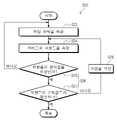
도 7을 참조하면, 반도체 소자의 제조방법은, 상기 셀 히터들(662)의 상기 문턱 값들을 획득하는 단계(S10), 상기 기판(W)을 가열하는 단계(S20), 상기 기판(W)을 식각하는 단계(S30) 및 상기 기판(W)의 식각을 종료할지를 판별하는 단계(S40)를 포함할 수 있다.Referring to FIG. 7 , the method of manufacturing a semiconductor device includes obtaining the threshold values of the cell heaters 662 ( S10 ), heating the substrate W ( S20 ), and the substrate W It may include an etching step (S30) and a step (S40) of determining whether to end the etching of the substrate (W).
도 8은 도 7의 문턱 값들을 획득하는 단계(S10)의 일 예를 보여준다. 도 9는 도 8의 테스트 기판(WT)의 일 예를 보여준다.FIG. 8 shows an example of the step S10 of obtaining the threshold values of FIG. 7 . FIG. 9 shows an example of the test board WT of FIG. 8 .
도 8 및 도 9를 참조하면, 상기 셀 히터들(662)의 상기 문턱 값들을 획득하는 단계(S10)는 테스트 기판(WT)의 식각률의 차이를 계산하여 상기 식각률의 차이를 제거할 수 있는 상기 셀 히터들(662)의 저항을 계산하는 단계일 수 있다. 일 예에 따르면, 상기 문턱 값들을 획득하는 단계(S10)는 테스트 기판(WT)을 가열하는 단계(S12), 상기 셀 히터들(662)의 저항들을 측정하는 단계(S14), 상기 테스트 기판(WT)을 식각하는 단계(S16), 상기 테스트 기판(WT)의 식각률 차이를 계산하는 단계(S18) 및 상기 식각률 차이를 제거할 수 있는 상기 셀 히터들(662)의 문턱 값들을 각각 계산하는 단계(S19)를 포함할 수 있다.8 and 9 , in the step S10 of obtaining the threshold values of the
먼저, 상기 테스트 기판(WT)이 상기 정전 척(60) 상에 제공되면, 상기 링 히터들(652)과 상기 셀 히터들(662)은 상기 테스트 기판(WT)을 가열한다(S12). 상기 테스트 기판(WT)은 약 80℃ 내재 약 120℃로 가열될 수 있다.First, when the test substrate WT is provided on the
다음, 상기 온도 조절 부(678)는 상기 셀 히터들(662)의 저항들을 측정한다(S14). 상기 셀 히터들(662)의 저항들은 서로 다르게 측정될 수 있다.Next, the
그 다음, 상기 안테나(40) 및 상기 고주파 파워 공급 부(50)는 고주파 파워를 이용하여 상기 테스트 기판(WT)을 식각한다(S16). 상기 테스트 기판(WT)은 실리콘 산화물 또는 폴리 실리콘의 박막을 포함할 수 있다. 상기 플라즈마는 상기 테스트 기판(WT)을 식각할 수 있다.Next, the
그리고, 장치 제어 부(미도시)는 상기 테스트 기판(WT)의 식각률의 차이를 계산한다(S18). 상기 테스트 기판(WT)의 식각률은 측정 장치(ex, 전자 현미경(SEM: Scanning Electron Microscopy) 또는 원자 현미경(AFM: Atomic Force Microscopy))로부터 획득될 수 있다. 예를 들어, 상기 테스트 기판(WT)은 제 1 영역(102)과 제 2 영역(104)을 가질 수 있다. 상기 제 1 및 제 2 영역(102, 104)의 식각률은 그들의 온도에 따라 서로 다를 수 있다. 상기 플라즈마는 상기 테스트 기판(WT)의 상기 제 1 및 제 2 영역(102, 104) 상에 다른 밀도로 집중되기 때문일 수 있다. 예를 들어 상기 제 2 영역(104)의 식각률은 상기 제 1 영역(102)의 식각률보다 클 수 있다. 이와 달리, 상기 제 2 영역(104)의 식각률은 상기 제 1 영역(102)의 식각률보다 작을 수 있다. 상기 제 1 영역(102)은 상기 테스트 기판(WT)의 중심과, 가장자리의 일 부분들을 포함할 수 있다. 상기 제 2 영역(104)은 상기 테스트 기판(WT)의 가장자리의 나머지(another) 부분들을 포함할 수 있다. 상기 제 2 영역(104)은 상기 테스트 기판(WT) 가장자리의 식각률의 차이를 증가시킬 수 있다. 장치 제어 부는 제 1 영역(102)의 식각률에 대한 제 2 영역(104)의 식각률의 차이를 계산할 수 있다. 상기 식각률의 차이는 온도 균일성과 반비례할 수 있다. 상기 식각률의 차이가 감소하면, 온도 균일성은 증가할 수 있다. 반대로, 식각률의 차이가 증가하면, 온도 균일성은 감소할 수 있다.Then, the device controller (not shown) calculates the difference in the etch rate of the test substrate WT ( S18 ). The etch rate of the test substrate WT may be obtained from a measuring device (eg, scanning electron microscopy (SEM) or atomic force microscopy (AFM)). For example, the test substrate WT may have a
도 8을 참조하면, 상기 온도 조절 부(678)는 상기 셀 히터들(662)의 문턱 값을 계산한다(S19). 셀 히터들(662)의 문턱 값들은 서로 다를 수 있다.Referring to FIG. 8 , the
예를 들어, 셀 히터들(662)의 저항들(ex, R=R0 + aR0Δt)은 상기 니켈 크롬 합금의 온도 계수(a), 상온(ex, 20℃)에서의 초기 저항(R0), 및 온도 변화(ΔT)의 곱과 상기 초기 저항(R0)의 합으로 계산될 수 있다. 상기 온도 변화(ΔT= T-20℃)는 상기 셀 히터들(662)의 히팅 온도(T)와 상온의 차이일 수 있다. 상기 셀 히터들(662)의 히팅 온도(T)는 그들의 저항들으로 계산될 수 있다. 그러나, 상기 셀 히터들(662)의 상기 저항들은 상기 셀 히터들(662)의 면적 및/또는 길이에 따라 달라질 수 있다. 마찬가지로, 상기 저항들의 문턱 값들은 상기 셀 히터들(662)의 면적 및/또는 길이에 따라 달라질 수 있다. 실제로, 상기 셀 히터들(662)의 상기 저항들은 서로 다를 수 있다.For example, the resistances (ex, R=R0 + aR0 Δt) of the
상기 문턱 값들은 상기 테스트 기판(WT) 가장자리의 상기 제 2 영역(104)을 상기 제 1 영역(102)으로 만들 수 있는 상기 셀 히터들(662)의 저항들일 수 있다. 즉, 상기 문턱 값들은 상기 테스트 기판(WT)의 식각률의 차이를 제거할 수 있는 상기 셀 히터들(662)의 저항들일 수 있다. 가령, 상기 문턱 값들은 상기 제 1 및 제 2 영역(102, 104)의 식각률의 차이에 따라 상기 셀 히터들(662)마다 개별적으로 계산될 수 있다.The threshold values may be resistances of the
도 10은 도 9의 테스트 기판(WT)의 온도에 따른 제 1 및 제 2 식각률들(106, 108)을 보여준다.FIG. 10 shows first and
도 10을 참조하면, 테스트 기판(WT)은 그들의 종류에 따라, 제 1 식각률(106)과 제 2 식각률(108)을 가질 수 있다. 상기 제 1 식각률(106) 또는 상기 제 2 식각률(108)을 바탕으로, 상기 온도 조절 부(678)는 상기 셀 히터들(662)의 상기 문턱 값들을 계산할 수 있다.Referring to FIG. 10 , the test substrate WT may have a
예를 들어, 실리콘 산화물의 테스트 기판(WT)은 제 1 식각률(106)을 가질 수 있다. 상기 제 1 식각률(106)은 온도에 반비례할 수 있다. 상기 제 2 영역(104)이 상기 제 1 영역(102)의 온도보다 높은 온도를 가질 때, 상기 테스트 기판(WT)의 상기 제 1 영역(102)은 상기 제 2 영역(104)보다 깊게 식각될 수 있다. 상기 온도 조절 부(678)는 상기 제 2 영역(104)을 상기 제 1 영역(102)과 동일한 깊이로 식각하기 위한 상기 제 2 영역(104)의 온도를 상기 제 1 식각률(106)에 근거하여 계산할 수 있다. 예를 들어, 상기 제 2 영역(104)의 온도는 줄어들 수 있다. 상기 제 2 영역(104)의 온도는 상기 제 2 영역(104)에 대응하는 상기 셀 히터들(662)의 저항들, 예컨대 상기 문턱 값들로 계산될 수 있다.For example, the test substrate WT of silicon oxide may have a
폴리 실리콘의 테스트 기판(WT)은 제 2 식각률(108)을 가질 수 있다. 상기 제 2 식각률(108)은 온도에 비례할 수 있다. 상기 제 2 영역(104)이 상기 제 1 영역(102)의 온도보다 높은 온도를 가질 때, 상기 제 2 영역(104)은 상기 제 1 영역(102)보다 깊게 식각될 수 있다. 상기 온도 조절 부(678)는 상기 제 2 영역(104)을 상기 제 1 영역(102)과 동일한 깊이로 식각하기 위한 상기 제 2 영역(104)의 온도를 상기 제 2 식각률(108)에 근거하여 계산할 수 있다. 상기 제 2 영역(104)의 온도는 줄어들 수 있다. 상기 제 2 영역(104)의 온도는 상기 제 2 영역(104)에 대응하는 상기 셀 히터들(662)의 문턱 값들로 계산될 수 있다. 이하, 상기 문턱 값들을 이용하여 상기 기판(W)의 식각률의 차이를 제거하여 온도 균일성 및/또는 온도 산포를 증가 및/또는 개선할 수 있다.The polysilicon test substrate WT may have a
다시 도 7을 참조하면, 기판(W)이 정전 척(60) 상에 제공되면, 상기 링 히터들(652) 및 상기 셀 히터들(662)은 상기 기판(W)을 가열한다(S20). 예를 들어, 상기 기판(W)은 약 80℃ 내지 약 120℃의 온도로 가열될 수 있다. 상기 셀 히터들(662)은 그들의 저항들의 상기 문턱 값들에 따라 상기 기판(W)의 가장자리를 가열할 수 있다.Referring back to FIG. 7 , when the substrate W is provided on the
도 11은 도 7의 기판(W)을 가열하는 단계(S20)의 일 예를 보여준다.FIG. 11 shows an example of the step S20 of heating the substrate W of FIG. 7 .
도 11를 참조하면, 상기 기판(W)을 가열하는 단계(S20)는 상기 히팅 파워를 제공하는 단계(S22), 상기 셀 히터들(662)의 저항을 측정하는 단계(S24), 상기 셀 히터들(662)의 저항들을 문턱 값들과 비교하는 단계(S26), 및 상기 셀 히터들(662)의 가열을 지연하는 단계(S28)를 포함할 수 있다.Referring to FIG. 11 , the heating of the substrate W ( S20 ) includes providing the heating power ( S22 ), measuring the resistance of the cell heaters 662 ( S24 ), and the cell heater It may include comparing the resistances of the
상기 제 1 스위치들(672)이 턴온되면, 상기 제 1 파워 소스(82)는 상기 셀 히터들(662)에 히팅 파워를 개별적으로 제공한다(S22). 상기 온도 조절 부(678)는 상기 셀 히터들(662)에 제공되는 히팅 파워를 독립적으로 제어할 수 있으며, 상기 셀 히터들(662)의 제 1 및 제 2 외부 히터들(661, 663) 그리고 제 1 및 제 2 내부 히터들(665, 667)에 제공되는 히팅 파워를 독립적으로 제어할 수 있다. 상기 셀 히터들(662)은 상기 기판(W)의 가장자리 부분을 가열할 수 있다. 상기 링 히터들(652)은 상기 기판(W)의 중심 부분을 가열할 수 있다.When the
다음, 상기 제 1 스위치들(672)이 턴오프되고 상기 제 2 스위치들(674)이 턴온되면, 상기 온도 조절 부(678)는 상기 전압계들(676)을 통해 상기 셀 히터들(662)의 저항들(R1, R2, R3, R4)을 개별적으로 측정한다(S24).Next, when the
도 12는 도 11의 저항들(R1, R2, R3, R4)을 측정하는 단계(S24)의 일 예를 보여준다.12 shows an example of a step S24 of measuring the resistors R1 , R2 , R3 , and R4 of FIG. 11 .
도 12를 참조하면, 상기 저항들(R1, R2, R3, R4)을 측정하는 단계(S24)는 센싱 파워를 제공하는 단계(S21) 및 셀 히터들(662) 각각의 양측 단자들 사이의 전압을 측정하는 단계(S23)를 포함할 수 있다. 셀 히터들(662) 각각의 양측 단자들 사이의 전압은 상기 센싱 파워의 전압으로 설명될 수 있다.Referring to FIG. 12 , the step of measuring the resistors R1 , R2 , R3 , and R4 ( S24 ) includes the step of providing sensing power ( S21 ) and both terminals of each of the
상기 제 2 스위치들(674)이 턴온되면, 상기 제 2 파워 소스(84)는 상기 셀 히터들(662)에 센싱 파워를 개별적으로 제공한다(S21). 상기 셀 히터들(662) 내의 상기 센싱 파워의 전압은 강하될 수 있다.When the
그 후, 상기 온도 조절 부(678)은 상기 셀 히터들(662)의 전압들(V1, V2, V3, V4)을 측정한다(S23). 상기 온도 조절 부(678)는 상기 셀 히터들(662)의 저항들(R1, R2, R3, R4)을 개별적으로 계산할 수 있다.Thereafter, the
도 11을 다시 참조하면, 상기 온도 조절 부(678)는 상기 셀 히터들(662)의 저항들(R1, R2, R3, R4)을 그들의 문턱 값들과 각각 비교한다(S26). 상기 셀 히터들(662)의 저항들(R1, R2, R3, R4)을 상기 문턱 값들과 비교하는 단계(S26)는 상기 저항들(R1, R2, R3, R4)이 상기 문턱 값들 이상인지를 판별하는 단계(S25)와, 상기 저항들(R1, R2, R3, R4)이 상기 문턱 값들과 동일한지를 판별하는 단계(S27)를 포함할 수 있다.Referring back to FIG. 11 , the
먼저, 상기 온도 조절 부(678)는 상기 저항들(R1, R2, R3, R4)이 상기 문턱 값들 이상인지를 판별한다(S25). 상기 셀 히터들(662)의 저항들(R1, R2, R3, R4)이 문턱 값들보다 작을 경우, 상기 온도 조절 부(678)는 상기 히팅 파워를 제공하는 단계(S22), 상기 셀 히터들(662)의 저항들(R1, R2, R3, R4)을 측정하는 단계(S24) 및 상기 셀 히터들(662)의 저항들(R1, R2, R3, R4)이 문턱 값들인지를 판별하는 단계(S26)를 반복하여 수행할 수 있다. 예를 들어, 제 1 저항(R1)이 제 1 문턱 값보다 작을 경우, 상기 온도 조절 부(678)는 상기 히팅 파워를 상기 제 1 외부 히터(661)에 제공할 수 있다. 제 2 저항(R2)이 제 2 문턱 값보다 작을 경우, 상기 온도 조절 부(678)는 상기 히팅 파워를 상기 제 2 외부 히터(663)에 제공할 수 있다. 제 3 저항(R3)이 제 3 문턱 값보다 작을 경우, 상기 온도 조절 부(678)는 상기 히팅 파워를 상기 제 1 내부 히터(665)에 제공할 수 있다. 제 4 저항(R4)이 제 3 문턱 값보다 작을 경우, 상기 온도 조절 부(678)는 상기 히팅 파워를 상기 제 2 내부 히터(667)에 제공할 수 있다.First, the
그리고, 상기 셀 히터들(662)의 저항들(R1, R2, R3, R4)이 문턱 값들 이상일 경우, 상기 온도 조절 부(678)는 상기 저항들(R1, R2, R3, R4)이 상기 문턱 값들과 동일한지를 판별한다(S27).And, when the resistances R1 , R2 , R3 , and R4 of the
상기 저항들(R1, R2, R3, R4)이 상기 문턱 값들보다 클 경우, 상기 온도 조절 부(678)는 상기 셀 히터들(662)의 가열을 지연한다(S28), 제 1 저항(R1)이 제 1 문턱 값보다 클 경우, 상기 온도 조절 부(678)는 상기 제 1 외부 히터(661)의 가열을 일정 시간동안 지연시켜 상기 제 1 외부 히터(661)을 냉각시킬 수 있다. 제 2 저항(R2)이 제 2 문턱 값보다 클 경우, 상기 온도 조절 부(678)는 상기 제 2 외부 히터(663)의 가열을 일정 시간동안 지연시켜 상기 제 2 외부 히터(663)을 냉각시킬 수 있다. 제 3 저항(R3)이 제 3 문턱 값보다 클 경우, 상기 온도 조절 부(678)는 상기 제 1 내부 히터(665)의 가열을 일정 시간동안 지연시킬 수 있다. 제 4 저항(R4)이 제 4 문턱 값보다 클 경우, 상기 온도 조절 부(678)는 상기 제 2 내부 히터(667)의 가열을 일정 시간동안 지연시킬 수 있다. 이후, 상기 온도 조절 부(678)는 상기 셀 히터들(662)의 저항들을 측정하는 단계(S24) 및 상기 셀 히터들(662)의 저항들이 문턱 값들인지를 판별하는 단계(S26)를 다시 수행할 수 있다.When the resistors R1 , R2 , R3 , and R4 are greater than the threshold values, the
상기 저항들(R1, R2, R3, R4)이 상기 문턱 값들과 모두 동일할 경우, 상기 온도 조절 부(678)는 기판(W)의 온도 균일성 및/온도 산포가 개선될 것으로 판단하여 상기 기판(W)을 식각시킬 수 있다.When the resistors R1 , R2 , R3 , R4 are all equal to the threshold values, the
도 13은 도 10의 셀 히터들(662)의 제 1 내지 제 4 저항들(R1, R2, R3, R4)을 보여준다.13 shows first to fourth resistors R1 , R2 , R3 , and R4 of the
도 13을 참조하면, 상기 셀 히터들(662)의 제 1 내지 제 4 저항들(R1, R2, R3, R4)은 서로 다를 수 있다. 상기 제 1 내지 제 4 저항들(R1, R2, R3, R4)이 상온에서 서로 다를 경우, 상기 셀 히터들(662)의 상기 문턱 값들은 서로 다를 수 있다. 상기 셀 히터들(662) 각각에 인가되는 히팅 파워가 다를 수 있다. 그럼에도 불구하고, 상기 기판(W)은 상기 문턱 값들과 일치하는 상기 제 1 내지 제 4 저항들(R1, R2, R3, R4)에 따라 동일한 온도로 가열될 수 있다. 상기 기판(W) 가장자리의 온도 균일성 및/또는 온도 산포는 증가될 수 있다.Referring to FIG. 13 , the first to fourth resistors R1 , R2 , R3 , and R4 of the
다시 도 7을 참조하면, 상기 안테나(40) 및 상기 고주파 파워 공급 부(50)는 상기 플라즈마를 이용하여 상기 기판(W)을 식각한다(S30). 상기 기판(W)의 식각률이 동일하기 때문에, 상기 기판(W)은 동일한 깊이로 식각될 수 있다. 온도 균일성 및/또는 온도 산포는 증가될 수 있다.Referring back to FIG. 7 , the
상기 장치 제어 부는 상기 기판(W)의 식각을 종료할지를 판별한다(S40). 상기 기판(W)의 식각을 종료하지 않을 경우, 상기 기판(W)을 가열하는 단계(S20), 상기 기판(W)을 식각하는 단계(S30) 및 상기 기판(W)의 식각을 종료할지를 판별하는 단계(S40)는 반복적으로 수행될 수 있다. 상기 기판(W)의 식각을 종료할 경우, 상기 기판(W)과 다른 새로운 기판(미도시)에 대한 반도체 소자의 제조방법이 진행될 수 있다.The apparatus control unit determines whether to end the etching of the substrate W (S40). If the etching of the substrate W is not finished, heating the substrate W (S20), etching the substrate W (S30), and determining whether to end the etching of the substrate W The step S40 may be repeatedly performed. When the etching of the substrate W is finished, a method of manufacturing a semiconductor device for a new substrate (not shown) different from the substrate W may be performed.
이상에서와 같이 도면과 명세서에서 실시 예가 개시되었다. 여기서 특정한 용어들이 사용되었으나, 이는 단지 본 발명을 설명하기 위한 목적에서 사용된 것이지 의미 한정이나 특허 청구범위에 기재된 본 발명의 범위를 제한하기 위하여 사용된 것은 아니다. 그러므로 본 기술분야의 통상의 지식을 가진 자라면 이로부터 다양한 변형 및 균등한 타 실시 예가 가능하다는 점을 이해할 것이다. 따라서 본 발명의 진정한 기술적 보호 범위는 첨부된 특허 청구범위의 기술적 사상에 의해 정해져야 할 것이다.As described above, the embodiments have been disclosed in the drawings and the specification. Although specific terms are used herein, they are used only for the purpose of describing the present invention and are not used to limit the meaning or the scope of the present invention described in the claims. Therefore, those skilled in the art will understand that various modifications and equivalent other embodiments are possible therefrom. Therefore, the true technical protection scope of the present invention should be determined by the technical spirit of the appended claims.
Claims (10)
Translated fromKorean상기 척 베이스 상의 절연 플레이트;
상기 절연 플레이트 내에 배치된 셀 히터들을 갖는 제 1 히터 부; 및
상기 절연 플레이트 아래에 제공되어 상기 셀 히터들의 저항을 측정하고, 상기 저항을 문턱 값과 비교하여 상기 셀 히터들에 제공되는 히팅 파워를 제어하는 히터 제어부를 포함하되,
상기 제 1 히터 부는 상기 셀 히터들과 상기 히터 제어부 사이의 상기 절연 플레이트 내에 배치되고, 상기 셀 히터들에 정렬되는 제 1 섹터 전극들을 더 포함하되,
상기 제 1 섹터 전극들의 각각은:
상기 셀 히터들에 상기 히팅 파워를 제공하는 파워 전극들; 및
상기 파워 전극들 사이에 배치되고, 상기 셀 히터들을 접지하는 접지 전극을 포함하되,
상기 파워 전극들은:
상기 접지 전극의 일측에 배치되는 제 1 외부 전극;
상기 절연 플레이트의 중심 방향으로 상기 제 1 외부 전극 내에 배치되는 제 1 내부 전극;
상기 접지 전극의 타측에 배치되는 제 2 외부 전극; 및
상기 절연 플레이트의 중심 방향으로 상기 제 2 외부 전극 내에 제공되는 제 2 내부 전극을 포함하되,
상기 접지 전극은 상기 제 1 내부 전극과 상기 제 2 내부 전극 사이 및 상기 제 1 외부 전극과 상기 제 2 외부 전극 사이에 배치되는 정전 척.
chuck base;
an insulating plate on the chuck base;
a first heater unit having cell heaters disposed in the insulating plate; and
a heater control unit provided under the insulating plate to measure resistance of the cell heaters, and comparing the resistance with a threshold value to control the heating power provided to the cell heaters,
The first heater unit further includes first sector electrodes disposed in the insulating plate between the cell heaters and the heater control unit and aligned with the cell heaters,
Each of the first sector electrodes comprises:
power electrodes providing the heating power to the cell heaters; and
a ground electrode disposed between the power electrodes and grounding the cell heaters;
The power electrodes are:
a first external electrode disposed on one side of the ground electrode;
a first internal electrode disposed within the first external electrode in a central direction of the insulating plate;
a second external electrode disposed on the other side of the ground electrode; and
a second inner electrode provided in the second outer electrode in a central direction of the insulating plate;
and the ground electrode is disposed between the first internal electrode and the second internal electrode and between the first external electrode and the second external electrode.
상기 히터 제어 부는, 상기 셀 히터에 센싱 파워가 제공될 때, 상기 셀 히터 양측의 전압을 감지하는 전압계를 포함하는 정전 척.
The method of claim 1,
wherein the heater control unit includes a voltmeter configured to sense voltages at both sides of the cell heater when sensing power is provided to the cell heater.
상기 히터 제어 부는:
상기 히팅 파워를 스위칭하는 제 1 스위치; 및
상기 제 1 스위치와 반대로 턴온되고, 상기 센싱 파워를 스위칭하는 제 2 스위치를 더 포함하는 정전 척.
3. The method of claim 2,
The heater control unit is:
a first switch for switching the heating power; and
and a second switch turned on opposite to the first switch and configured to switch the sensing power.
상기 히터 제어 부는 상기 전압계로부터 감지된 전압을 이용하여 상기 셀히터들의 저항을 계산하고, 상기 저항이 상기 문턱 값보다 작을 경우 상기 셀 히터에 상기 히팅 파워를 제공하는 온도 조절 부를 더 포함하는 정전 척.
3. The method of claim 2,
The heater control unit calculates resistances of the cell heaters using the voltage sensed by the voltmeter, and when the resistance is less than the threshold value, the electrostatic chuck further includes a temperature control unit that provides the heating power to the cell heater.
상기 온도 조절 부는 상기 저항이 상기 문턱 값보다 클 경우, 상기 셀 히터의 가열을 지연시키는 정전 척.
5. The method of claim 4,
The temperature controller delays heating of the cell heater when the resistance is greater than the threshold value.
상기 셀 히터들의 각각은:
상기 제 1 및 제 2 외부 전극들의 일측들에 각각 연결되는 제 1 및 제 2 외부 히터들; 및
상기 제 1 및 제 2 내부 전극들의 일측들에 각각연결되는 제 1 및 제 2 내부 히터들을 포함하되,
상기 접지 전극은 상기 제 1 및 제 2 외부 히터들의 타측들과, 상기 제 1 및 제 2 내부 히터들의 타측들에 연결되는 정전 척.
The method of claim 1,
Each of the cell heaters is:
first and second external heaters respectively connected to one side of the first and second external electrodes; and
Including first and second internal heaters respectively connected to one side of the first and second internal electrodes,
The ground electrode is connected to other ends of the first and second external heaters and other ends of the first and second internal heaters.
상기 셀 히터는 복수개이고, 상기 셀 히터들은 상기 절연 플레이트의 가장자리 영역에 방위각 방향으로 배치되되,
상기 정전 척은:
상기 제 1 히터 부와 상기 척 베이스 사이에 배치되어 상기 절연 플레이트의 중심 영역에 배치된 링 히터들, 그리고 상기 링 히터들과 상기 척 베이스 사이에 배치되는 제 2 섹터 전극을 포함하는 제 2 히터 부; 및
상기 제 2 섹터 전극들의 직경과 동일한 직경을 갖고, 상기 제 2 히터 부와 상기 척 베이스 사이에 배치되어 상기 접지 전극으로 연결되는 접지 플레이트를 더 포함하는 정전 척.The method of claim 1,
The cell heaters are in plurality, and the cell heaters are disposed in an azimuth direction on an edge region of the insulating plate,
The electrostatic chuck comprises:
a second heater unit including ring heaters disposed between the first heater unit and the chuck base and disposed in a central region of the insulating plate, and a second sector electrode disposed between the ring heaters and the chuck base; ; and
and a ground plate having the same diameter as the second sector electrodes and disposed between the second heater unit and the chuck base and connected to the ground electrode.
Priority Applications (4)
| Application Number | Priority Date | Filing Date | Title |
|---|---|---|---|
| KR1020170085015AKR102435888B1 (en) | 2017-07-04 | 2017-07-04 | Electro-static chuck, apparatus for processing substrate and manufacturing method of semiconductor device using the same |
| US15/857,047US10522374B2 (en) | 2017-07-04 | 2017-12-28 | Electrostatic chuck, substrate processing apparatus, and method of manufacturing semiconductor device using the same |
| CN201810620351.0ACN109216251B (en) | 2017-07-04 | 2018-06-15 | Electrostatic chuck, substrate processing apparatus, and method of manufacturing semiconductor device |
| US16/703,270US10854485B2 (en) | 2017-07-04 | 2019-12-04 | Electrostatic chuck, substrate processing apparatus, and method of manufacturing semiconductor device using the same |
Applications Claiming Priority (1)
| Application Number | Priority Date | Filing Date | Title |
|---|---|---|---|
| KR1020170085015AKR102435888B1 (en) | 2017-07-04 | 2017-07-04 | Electro-static chuck, apparatus for processing substrate and manufacturing method of semiconductor device using the same |
Publications (2)
| Publication Number | Publication Date |
|---|---|
| KR20190004867A KR20190004867A (en) | 2019-01-15 |
| KR102435888B1true KR102435888B1 (en) | 2022-08-25 |
Family
ID=64902892
Family Applications (1)
| Application Number | Title | Priority Date | Filing Date |
|---|---|---|---|
| KR1020170085015AActiveKR102435888B1 (en) | 2017-07-04 | 2017-07-04 | Electro-static chuck, apparatus for processing substrate and manufacturing method of semiconductor device using the same |
Country Status (3)
| Country | Link |
|---|---|
| US (2) | US10522374B2 (en) |
| KR (1) | KR102435888B1 (en) |
| CN (1) | CN109216251B (en) |
Families Citing this family (20)
| Publication number | Priority date | Publication date | Assignee | Title |
|---|---|---|---|---|
| KR102513443B1 (en)* | 2016-03-15 | 2023-03-24 | 삼성전자주식회사 | electrostatic chuck and substrate processing apparatus including the same |
| KR102450476B1 (en)* | 2018-02-28 | 2022-10-05 | 주식회사 미코세라믹스 | Electrostatic chucking Heater And Manufacturing Method Thereof |
| US11367645B2 (en) | 2019-03-13 | 2022-06-21 | Applied Materials, Inc. | Temperature tunable multi-zone electrostatic chuck |
| US11562913B2 (en)* | 2019-04-25 | 2023-01-24 | Watlow Electric Manufacturing Company | Multi-zone azimuthal heater |
| WO2021016223A1 (en)* | 2019-07-25 | 2021-01-28 | Lam Research Corporation | In situ real-time sensing and compensation of non-uniformities in substrate processing systems |
| JP7458156B2 (en)* | 2019-08-22 | 2024-03-29 | 東京エレクトロン株式会社 | Mounting table and plasma processing equipment |
| US20210159102A1 (en)* | 2019-11-26 | 2021-05-27 | Tokyo Electron Limited | THERMAL TREATMENTS USING A PLURALITY OF EMBEDDED RESISTANCE TEMPERATURE DETECTORS (RTDs) |
| JP7522837B2 (en) | 2020-01-22 | 2024-07-25 | アプライド マテリアルズ インコーポレイテッド | In-line monitoring of OLED layer thickness and dopant concentration |
| EP4094307A4 (en)* | 2020-01-22 | 2024-02-28 | Applied Materials, Inc. | INLINE MONITORING OF OLED LAYER THICKNESS AND DOPANT CONCENTRATION |
| US20230052543A1 (en)* | 2020-02-10 | 2023-02-16 | Lam Research Corporation | Decoupling radiofrequency (rf) signals from input signal conductors of a process chamber |
| JP7539236B2 (en)* | 2020-02-21 | 2024-08-23 | 東京エレクトロン株式会社 | Substrate Processing Equipment |
| CN111446198B (en)* | 2020-03-23 | 2023-05-16 | 北京北方华创微电子装备有限公司 | Electrostatic chuck and control method thereof |
| KR102776505B1 (en) | 2020-07-09 | 2025-03-07 | 삼성전자주식회사 | Plasma processing apparatus and method of fabricating semiconductor device using the same |
| JP7361005B2 (en)* | 2020-09-18 | 2023-10-13 | 株式会社Kokusai Electric | Substrate processing equipment, substrate holder, semiconductor device manufacturing method, and program |
| KR102695408B1 (en)* | 2021-02-26 | 2024-08-16 | 세메스 주식회사 | Support unit and substrate treating apparatus including the same |
| JP7677862B2 (en)* | 2021-09-17 | 2025-05-15 | 東京エレクトロン株式会社 | Plasma Processing Equipment |
| CN114496889B (en)* | 2022-01-21 | 2025-09-16 | 北京北方华创微电子装备有限公司 | Electrostatic chuck device and temperature control method |
| JP7675051B2 (en)* | 2022-06-29 | 2025-05-12 | 東京エレクトロン株式会社 | Plasma processing apparatus and plasma processing method |
| CN118147615A (en)* | 2022-12-06 | 2024-06-07 | 中微半导体设备(上海)股份有限公司 | Gas distribution transfer ring, tray rotating mechanism and semiconductor processing equipment |
| US20240234108A1 (en)* | 2023-01-10 | 2024-07-11 | Applied Materials, Inc. | Biasable electrostatic chuck |
Citations (4)
| Publication number | Priority date | Publication date | Assignee | Title |
|---|---|---|---|---|
| JP2000012195A (en) | 1998-06-29 | 2000-01-14 | Ibiden Co Ltd | Ceramic heater |
| JP2015191837A (en) | 2014-03-28 | 2015-11-02 | 日本特殊陶業株式会社 | Laminate heating element |
| JP2016136611A (en)* | 2015-01-16 | 2016-07-28 | Toto株式会社 | Electrostatic chuck |
| JP2017228360A (en) | 2016-06-20 | 2017-12-28 | 日本特殊陶業株式会社 | Heating member and electrostatic chuck |
Family Cites Families (29)
| Publication number | Priority date | Publication date | Assignee | Title |
|---|---|---|---|---|
| EP1132956A4 (en)* | 1998-10-29 | 2005-04-27 | Tokyo Electron Ltd | Vacuum processor apparatus |
| US6740853B1 (en)* | 1999-09-29 | 2004-05-25 | Tokyo Electron Limited | Multi-zone resistance heater |
| JP2002076102A (en)* | 2000-08-31 | 2002-03-15 | Ibiden Co Ltd | Ceramic substrate |
| JP4129855B2 (en)* | 2001-12-13 | 2008-08-06 | 東京エレクトロン株式会社 | Plasma processing equipment |
| JP4596883B2 (en)* | 2004-10-28 | 2010-12-15 | 京セラ株式会社 | Annular heater |
| CN101278385B (en)* | 2004-11-04 | 2011-10-12 | 株式会社爱发科 | Electrostatic chuck device |
| US7030624B1 (en)* | 2005-02-17 | 2006-04-18 | Sandia Corporation | Electrical circuit tester |
| WO2007018157A1 (en)* | 2005-08-05 | 2007-02-15 | Tokyo Electron Limited | Substrate processing apparatus and substrate stage used therein |
| JP5183058B2 (en)* | 2006-07-20 | 2013-04-17 | アプライド マテリアルズ インコーポレイテッド | Substrate processing with rapid temperature gradient control |
| JP2008115440A (en)* | 2006-11-06 | 2008-05-22 | Shinko Electric Ind Co Ltd | Substrate heating apparatus |
| JP2009054871A (en)* | 2007-08-28 | 2009-03-12 | Tokyo Electron Ltd | Placing stand structure and treatment apparatus |
| US8981265B2 (en)* | 2008-12-30 | 2015-03-17 | Ppg Industries Ohio, Inc. | Electric circuit and sensor for detecting arcing and a transparency having the circuit and sensor |
| US8791392B2 (en)* | 2010-10-22 | 2014-07-29 | Lam Research Corporation | Methods of fault detection for multiplexed heater array |
| US20120196242A1 (en) | 2011-01-27 | 2012-08-02 | Applied Materials, Inc. | Substrate support with heater and rapid temperature change |
| WO2013033350A1 (en)* | 2011-08-30 | 2013-03-07 | Watlow Electric Manufacturing Company | Thermal array system |
| US9324589B2 (en) | 2012-02-28 | 2016-04-26 | Lam Research Corporation | Multiplexed heater array using AC drive for semiconductor processing |
| US10049948B2 (en)* | 2012-11-30 | 2018-08-14 | Lam Research Corporation | Power switching system for ESC with array of thermal control elements |
| JP6441927B2 (en)* | 2013-08-06 | 2018-12-19 | アプライド マテリアルズ インコーポレイテッドApplied Materials,Incorporated | Multi-zone substrate support heated locally |
| US10217615B2 (en) | 2013-12-16 | 2019-02-26 | Lam Research Corporation | Plasma processing apparatus and component thereof including an optical fiber for determining a temperature thereof |
| JP6317138B2 (en)* | 2014-02-27 | 2018-04-25 | 東京エレクトロン株式会社 | High frequency plasma processing apparatus and high frequency plasma processing method |
| JP6399435B2 (en) | 2014-05-26 | 2018-10-03 | パナソニックIpマネジメント株式会社 | Plasma processing method and apparatus |
| KR101758087B1 (en)* | 2014-07-23 | 2017-07-14 | 어플라이드 머티어리얼스, 인코포레이티드 | Tunable temperature controlled substrate support assembly |
| JP6463938B2 (en) | 2014-10-08 | 2019-02-06 | 日本特殊陶業株式会社 | Electrostatic chuck |
| JP6804828B2 (en) | 2015-04-20 | 2020-12-23 | 日本特殊陶業株式会社 | Ceramic heater and electrostatic chuck |
| CN107636817B (en)* | 2015-05-22 | 2021-08-27 | 应用材料公司 | Azimuth adjustable multi-zone electrostatic chuck |
| US10690414B2 (en)* | 2015-12-11 | 2020-06-23 | Lam Research Corporation | Multi-plane heater for semiconductor substrate support |
| KR102513443B1 (en)* | 2016-03-15 | 2023-03-24 | 삼성전자주식회사 | electrostatic chuck and substrate processing apparatus including the same |
| US10029328B2 (en)* | 2016-03-29 | 2018-07-24 | Ngk Insulators, Ltd. | Metal wiring bonding structure and production method therefor |
| JP6397588B2 (en)* | 2016-07-19 | 2018-09-26 | 日本碍子株式会社 | Electrostatic chuck heater |
- 2017
- 2017-07-04KRKR1020170085015Apatent/KR102435888B1/enactiveActive
- 2017-12-28USUS15/857,047patent/US10522374B2/enactiveActive
- 2018
- 2018-06-15CNCN201810620351.0Apatent/CN109216251B/enactiveActive
- 2019
- 2019-12-04USUS16/703,270patent/US10854485B2/enactiveActive
Patent Citations (4)
| Publication number | Priority date | Publication date | Assignee | Title |
|---|---|---|---|---|
| JP2000012195A (en) | 1998-06-29 | 2000-01-14 | Ibiden Co Ltd | Ceramic heater |
| JP2015191837A (en) | 2014-03-28 | 2015-11-02 | 日本特殊陶業株式会社 | Laminate heating element |
| JP2016136611A (en)* | 2015-01-16 | 2016-07-28 | Toto株式会社 | Electrostatic chuck |
| JP2017228360A (en) | 2016-06-20 | 2017-12-28 | 日本特殊陶業株式会社 | Heating member and electrostatic chuck |
Also Published As
| Publication number | Publication date |
|---|---|
| US10854485B2 (en) | 2020-12-01 |
| US20190013222A1 (en) | 2019-01-10 |
| CN109216251A (en) | 2019-01-15 |
| CN109216251B (en) | 2023-07-21 |
| US20200126827A1 (en) | 2020-04-23 |
| KR20190004867A (en) | 2019-01-15 |
| US10522374B2 (en) | 2019-12-31 |
Similar Documents
| Publication | Publication Date | Title |
|---|---|---|
| KR102435888B1 (en) | Electro-static chuck, apparatus for processing substrate and manufacturing method of semiconductor device using the same | |
| TWI747837B (en) | Edge ring assembly for plasma processing chamber and system for plasma processing | |
| US12402208B2 (en) | Substrate processing system and substrate processing method | |
| KR102468738B1 (en) | Multi-electrode substrate support assembly and phase control system | |
| JP4632548B2 (en) | Method and apparatus for correcting non-uniform wafer processing in a plasma processing chamber | |
| CN111430207A (en) | Plasma processing method and plasma processing apparatus | |
| JP5274918B2 (en) | Method for controlling temperature of chamber inner member of plasma processing apparatus, chamber inner member and substrate mounting table, and plasma processing apparatus including the same | |
| KR100938635B1 (en) | Plasma-limited baffle and flow ratio equalizers for improved magnetic control of radial plasma distribution | |
| US9021984B2 (en) | Plasma processing apparatus and semiconductor device manufacturing method | |
| US9011637B2 (en) | Plasma processing apparatus and method of manufacturing semiconductor device | |
| US7199327B2 (en) | Method and system for arc suppression in a plasma processing system | |
| CN112997270A (en) | Edge ring control circuit for shaped DC pulsed plasma processing apparatus | |
| US7824519B2 (en) | Variable volume plasma processing chamber and associated methods | |
| US11862438B2 (en) | Plasma processing apparatus, calculation method, and calculation program | |
| US20130270250A1 (en) | Current peak spreading schemes for multiplexed heated array | |
| JP2018037662A (en) | Method of controlling/adjusting magnetic field pattern in plasma treatment | |
| CN109698110B (en) | Hollow cathode and apparatus and method for manufacturing semiconductor device | |
| KR20140114817A (en) | Plasma processing apparatus and heater temperature control method | |
| US9991100B2 (en) | Plasma processing apparatus and control method | |
| US10896832B2 (en) | Substrate processing method and substrate processing apparatus | |
| TW201732922A (en) | Plasma processing method and plasma processing device | |
| KR20240093943A (en) | Method and apparatus for real-time wafer potential measurement in a plasma processing chamber | |
| US20210343503A1 (en) | Etching apparatus and etching method | |
| JP2021132190A (en) | Substrate processing apparatus and mounting table | |
| JP2023027754A (en) | Plasma processing apparatus and etching method |
Legal Events
| Date | Code | Title | Description |
|---|---|---|---|
| PA0109 | Patent application | St.27 status event code:A-0-1-A10-A12-nap-PA0109 | |
| PG1501 | Laying open of application | St.27 status event code:A-1-1-Q10-Q12-nap-PG1501 | |
| A201 | Request for examination | ||
| PA0201 | Request for examination | St.27 status event code:A-1-2-D10-D11-exm-PA0201 | |
| E902 | Notification of reason for refusal | ||
| PE0902 | Notice of grounds for rejection | St.27 status event code:A-1-2-D10-D21-exm-PE0902 | |
| E13-X000 | Pre-grant limitation requested | St.27 status event code:A-2-3-E10-E13-lim-X000 | |
| P11-X000 | Amendment of application requested | St.27 status event code:A-2-2-P10-P11-nap-X000 | |
| P13-X000 | Application amended | St.27 status event code:A-2-2-P10-P13-nap-X000 | |
| E701 | Decision to grant or registration of patent right | ||
| PE0701 | Decision of registration | St.27 status event code:A-1-2-D10-D22-exm-PE0701 | |
| PR0701 | Registration of establishment | St.27 status event code:A-2-4-F10-F11-exm-PR0701 | |
| PR1002 | Payment of registration fee | St.27 status event code:A-2-2-U10-U11-oth-PR1002 Fee payment year number:1 | |
| PG1601 | Publication of registration | St.27 status event code:A-4-4-Q10-Q13-nap-PG1601 | |
| PR1001 | Payment of annual fee | St.27 status event code:A-4-4-U10-U11-oth-PR1001 Fee payment year number:4 |