KR102435604B1 - Multi-electrode structures for molecular sensing devices and methods of making them - Google Patents
Multi-electrode structures for molecular sensing devices and methods of making themDownload PDFInfo
- Publication number
- KR102435604B1 KR102435604B1KR1020197005767AKR20197005767AKR102435604B1KR 102435604 B1KR102435604 B1KR 102435604B1KR 1020197005767 AKR1020197005767 AKR 1020197005767AKR 20197005767 AKR20197005767 AKR 20197005767AKR 102435604 B1KR102435604 B1KR 102435604B1
- Authority
- KR
- South Korea
- Prior art keywords
- electrode
- sheet
- sheets
- layer
- dielectric
- Prior art date
- Legal status (The legal status is an assumption and is not a legal conclusion. Google has not performed a legal analysis and makes no representation as to the accuracy of the status listed.)
- Active
Links
Images


Classifications
- G—PHYSICS
- G01—MEASURING; TESTING
- G01N—INVESTIGATING OR ANALYSING MATERIALS BY DETERMINING THEIR CHEMICAL OR PHYSICAL PROPERTIES
- G01N27/00—Investigating or analysing materials by the use of electric, electrochemical, or magnetic means
- G01N27/26—Investigating or analysing materials by the use of electric, electrochemical, or magnetic means by investigating electrochemical variables; by using electrolysis or electrophoresis
- G01N27/403—Cells and electrode assemblies
- G01N27/414—Ion-sensitive or chemical field-effect transistors, i.e. ISFETS or CHEMFETS
- G01N27/4145—Ion-sensitive or chemical field-effect transistors, i.e. ISFETS or CHEMFETS specially adapted for biomolecules, e.g. gate electrode with immobilised receptors
- B—PERFORMING OPERATIONS; TRANSPORTING
- B81—MICROSTRUCTURAL TECHNOLOGY
- B81C—PROCESSES OR APPARATUS SPECIALLY ADAPTED FOR THE MANUFACTURE OR TREATMENT OF MICROSTRUCTURAL DEVICES OR SYSTEMS
- B81C1/00—Manufacture or treatment of devices or systems in or on a substrate
- B81C1/00015—Manufacture or treatment of devices or systems in or on a substrate for manufacturing microsystems
- B81C1/00023—Manufacture or treatment of devices or systems in or on a substrate for manufacturing microsystems without movable or flexible elements
- B81C1/00126—Static structures not provided for in groups B81C1/00031 - B81C1/00119
- C—CHEMISTRY; METALLURGY
- C23—COATING METALLIC MATERIAL; COATING MATERIAL WITH METALLIC MATERIAL; CHEMICAL SURFACE TREATMENT; DIFFUSION TREATMENT OF METALLIC MATERIAL; COATING BY VACUUM EVAPORATION, BY SPUTTERING, BY ION IMPLANTATION OR BY CHEMICAL VAPOUR DEPOSITION, IN GENERAL; INHIBITING CORROSION OF METALLIC MATERIAL OR INCRUSTATION IN GENERAL
- C23C—COATING METALLIC MATERIAL; COATING MATERIAL WITH METALLIC MATERIAL; SURFACE TREATMENT OF METALLIC MATERIAL BY DIFFUSION INTO THE SURFACE, BY CHEMICAL CONVERSION OR SUBSTITUTION; COATING BY VACUUM EVAPORATION, BY SPUTTERING, BY ION IMPLANTATION OR BY CHEMICAL VAPOUR DEPOSITION, IN GENERAL
- C23C16/00—Chemical coating by decomposition of gaseous compounds, without leaving reaction products of surface material in the coating, i.e. chemical vapour deposition [CVD] processes
- C23C16/01—Chemical coating by decomposition of gaseous compounds, without leaving reaction products of surface material in the coating, i.e. chemical vapour deposition [CVD] processes on temporary substrates, e.g. substrates subsequently removed by etching
- G—PHYSICS
- G01—MEASURING; TESTING
- G01N—INVESTIGATING OR ANALYSING MATERIALS BY DETERMINING THEIR CHEMICAL OR PHYSICAL PROPERTIES
- G01N27/00—Investigating or analysing materials by the use of electric, electrochemical, or magnetic means
- G01N27/02—Investigating or analysing materials by the use of electric, electrochemical, or magnetic means by investigating impedance
- G01N27/04—Investigating or analysing materials by the use of electric, electrochemical, or magnetic means by investigating impedance by investigating resistance
- G—PHYSICS
- G01—MEASURING; TESTING
- G01N—INVESTIGATING OR ANALYSING MATERIALS BY DETERMINING THEIR CHEMICAL OR PHYSICAL PROPERTIES
- G01N27/00—Investigating or analysing materials by the use of electric, electrochemical, or magnetic means
- G01N27/02—Investigating or analysing materials by the use of electric, electrochemical, or magnetic means by investigating impedance
- G01N27/22—Investigating or analysing materials by the use of electric, electrochemical, or magnetic means by investigating impedance by investigating capacitance
- G01N27/221—Investigating or analysing materials by the use of electric, electrochemical, or magnetic means by investigating impedance by investigating capacitance by investigating the dielectric properties
- G—PHYSICS
- G01—MEASURING; TESTING
- G01N—INVESTIGATING OR ANALYSING MATERIALS BY DETERMINING THEIR CHEMICAL OR PHYSICAL PROPERTIES
- G01N27/00—Investigating or analysing materials by the use of electric, electrochemical, or magnetic means
- G01N27/26—Investigating or analysing materials by the use of electric, electrochemical, or magnetic means by investigating electrochemical variables; by using electrolysis or electrophoresis
- G01N27/28—Electrolytic cell components
- G01N27/30—Electrodes, e.g. test electrodes; Half-cells
- G01N27/327—Biochemical electrodes, e.g. electrical or mechanical details for in vitro measurements
- G01N27/3275—Sensing specific biomolecules, e.g. nucleic acid strands, based on an electrode surface reaction
- G01N27/3278—Sensing specific biomolecules, e.g. nucleic acid strands, based on an electrode surface reaction involving nanosized elements, e.g. nanogaps or nanoparticles
- B—PERFORMING OPERATIONS; TRANSPORTING
- B81—MICROSTRUCTURAL TECHNOLOGY
- B81B—MICROSTRUCTURAL DEVICES OR SYSTEMS, e.g. MICROMECHANICAL DEVICES
- B81B2201/00—Specific applications of microelectromechanical systems
- B81B2201/02—Sensors
- B81B2201/0214—Biosensors; Chemical sensors
- B—PERFORMING OPERATIONS; TRANSPORTING
- B81—MICROSTRUCTURAL TECHNOLOGY
- B81B—MICROSTRUCTURAL DEVICES OR SYSTEMS, e.g. MICROMECHANICAL DEVICES
- B81B2201/00—Specific applications of microelectromechanical systems
- B81B2201/05—Microfluidics
- B81B2201/058—Microfluidics not provided for in B81B2201/051 - B81B2201/054
- B—PERFORMING OPERATIONS; TRANSPORTING
- B81—MICROSTRUCTURAL TECHNOLOGY
- B81B—MICROSTRUCTURAL DEVICES OR SYSTEMS, e.g. MICROMECHANICAL DEVICES
- B81B2203/00—Basic microelectromechanical structures
- B81B2203/04—Electrodes
- C—CHEMISTRY; METALLURGY
- C12—BIOCHEMISTRY; BEER; SPIRITS; WINE; VINEGAR; MICROBIOLOGY; ENZYMOLOGY; MUTATION OR GENETIC ENGINEERING
- C12Q—MEASURING OR TESTING PROCESSES INVOLVING ENZYMES, NUCLEIC ACIDS OR MICROORGANISMS; COMPOSITIONS OR TEST PAPERS THEREFOR; PROCESSES OF PREPARING SUCH COMPOSITIONS; CONDITION-RESPONSIVE CONTROL IN MICROBIOLOGICAL OR ENZYMOLOGICAL PROCESSES
- C12Q1/00—Measuring or testing processes involving enzymes, nucleic acids or microorganisms; Compositions therefor; Processes of preparing such compositions
- C12Q1/68—Measuring or testing processes involving enzymes, nucleic acids or microorganisms; Compositions therefor; Processes of preparing such compositions involving nucleic acids
- C12Q1/6869—Methods for sequencing
- C—CHEMISTRY; METALLURGY
- C12—BIOCHEMISTRY; BEER; SPIRITS; WINE; VINEGAR; MICROBIOLOGY; ENZYMOLOGY; MUTATION OR GENETIC ENGINEERING
- C12Q—MEASURING OR TESTING PROCESSES INVOLVING ENZYMES, NUCLEIC ACIDS OR MICROORGANISMS; COMPOSITIONS OR TEST PAPERS THEREFOR; PROCESSES OF PREPARING SUCH COMPOSITIONS; CONDITION-RESPONSIVE CONTROL IN MICROBIOLOGICAL OR ENZYMOLOGICAL PROCESSES
- C12Q2565/00—Nucleic acid analysis characterised by mode or means of detection
- C12Q2565/60—Detection means characterised by use of a special device
- C12Q2565/607—Detection means characterised by use of a special device being a sensor, e.g. electrode
Landscapes
- Chemical & Material Sciences (AREA)
- Life Sciences & Earth Sciences (AREA)
- Health & Medical Sciences (AREA)
- Physics & Mathematics (AREA)
- Chemical Kinetics & Catalysis (AREA)
- Engineering & Computer Science (AREA)
- Analytical Chemistry (AREA)
- Biochemistry (AREA)
- General Health & Medical Sciences (AREA)
- Immunology (AREA)
- Molecular Biology (AREA)
- Electrochemistry (AREA)
- General Physics & Mathematics (AREA)
- Pathology (AREA)
- Organic Chemistry (AREA)
- Spectroscopy & Molecular Physics (AREA)
- Microelectronics & Electronic Packaging (AREA)
- Proteomics, Peptides & Aminoacids (AREA)
- Metallurgy (AREA)
- Mechanical Engineering (AREA)
- Materials Engineering (AREA)
- General Chemical & Material Sciences (AREA)
- Wood Science & Technology (AREA)
- Zoology (AREA)
- Manufacturing & Machinery (AREA)
- General Engineering & Computer Science (AREA)
- Bioinformatics & Cheminformatics (AREA)
- Genetics & Genomics (AREA)
- Microbiology (AREA)
- Biotechnology (AREA)
- Biophysics (AREA)
- Nanotechnology (AREA)
- Investigating Or Analyzing Materials By The Use Of Electric Means (AREA)
- Apparatus Associated With Microorganisms And Enzymes (AREA)
- Measuring Or Testing Involving Enzymes Or Micro-Organisms (AREA)
- Micromachines (AREA)
Abstract
Translated fromKorean
Description
Translated fromKorean관련 출원들의 상호 참조CROSS-REFERENCE TO RELATED APPLICATIONS
본 출원은 2016년 7월 26일 출원되고 발명의 명칭이 "Multi-Electrode Molecular Sensing Devices and Methods of Making the Same" 인 미국 비-가특허 출원 일련번호 제15/220,307호를 우선권으로 주장하며, 그 전체 내용을 여기서는 참조로서 포함한다.This application claims priority to U.S. Non-Provisional Patent Application Serial No. 15/220,307, filed July 26, 2016, entitled "Multi-Electrode Molecular Sensing Devices and Methods of Making the Same," and The entire contents are incorporated herein by reference.
기술분야technical field
본 발명은 나노제조 및 나노전극들에 관한 것이다. 보다 구체적으로, 본 개시는 디바이스 스택들과 같은 구조체들, 및 게놈 시퀀싱 및 DNA 시퀀싱을 포함한, 분자들을 감지하고 분석하기 위한 디바이스들에 이용가능한 구조체들의 제조에 관한 것이다.The present invention relates to nanofabrication and nanoelectrodes. More specifically, the present disclosure relates to constructs such as device stacks, and fabrication of constructs usable in devices for sensing and analyzing molecules, including genomic sequencing and DNA sequencing.
분자 분석은 여러 분야들, 이를 테면, 정밀 의료 또는 나노기술에서 점점더 많은 관심을 받고 있다. 일 예가 게놈들을 시퀀싱하기 위한 분자들의 분석을 포함한다. 1946년의 Avery 의 주요 작업에서, DNA 가 조직의 특성을 결정하는 물질이였음이 논의되었다. 그 후, DNA 의 분자 구조는 1962년에 노벨 의학상을 받은 Watson 및 Crick 에 의해 1953년에 처음 기술되었다. 이 작업은 DNA 분자들의 화학적 문자들 (염기들) 의 시퀀스가 기본적인 생물학적 정보를 암호화하고 있음을 분명히 하였다. 이러한 발견 이래, 이 시퀀스를 실험적으로 실제적으로 측정하는 수단을 개발하기 위한 제휴된 노력이 있어 왔다. DNA 를 체계적으로 시퀀싱하는 첫번째 방법은 1980년 노벨 화학상을 받았던 Sanger 에 의해 1978년에 도입되었다.Molecular analysis is of increasing interest in several fields, such as precision medicine or nanotechnology. One example involves analysis of molecules to sequence genomes. In Avery's main work in 1946, it was discussed that DNA was the determinant of tissue properties. Then, the molecular structure of DNA was first described in 1953 by Watson and Crick, who received the Nobel Prize in Medicine in 1962. This work made it clear that the sequence of chemical letters (bases) in DNA molecules encodes basic biological information. Since this discovery, there has been a concerted effort to develop a means to experimentally and practically measure this sequence. The first method for systematically sequencing DNA was introduced in 1978 by Sanger, who was awarded the 1980 Nobel Prize in Chemistry.
게놈을 시퀀싱하기 위한 기본 방법은 1980년대 후반에 상업용 기구 플랫폼에서 자동화되었고, 이는 궁극적으로 2001년에 첫번째 인간 게놈의 시퀀싱을 가능하게 하였다. 이는 10년에 걸쳐 수 십억 달러의 비용을 들이고 수 천 개의 전용 DNA 시퀀싱 기구의 출력에 의존한 대규모 공공 및 개인의 노력의 결과물이였다. 이 노력의 성공은 인간 게놈을 시퀀싱하는데 요구되는 비용 및 시간을 극적으로 감소시키는 목표를 갖는 많은 수의 "초병렬" 시퀀싱 플랫폼의 개발에 동기를 부여하였다. 이러한 초병렬 시퀀싱 플랫폼들은 일반적으로 매우 소형화된 미세유체 포맷들로 동시에 수 백만 내지 수 억 개의 시퀀싱 반응들을 프로세싱하는 것에 의존한다. 이들 중 첫번째가 2005년에 Rothberg 에 의해 454 플랫폼으로서 발명되어 상용화되었으며, 이는 비용 및 실행 시간에서 수 천 배의 감소를 실현하였다. 그러나, 454 플랫폼은 여전히 게놈을 시퀀싱하기 위해 대략 수 백만 달러를 요구하고 수 개월에 걸쳐 시간이 소요된다.The primary method for sequencing the genome was automated on commercial instrument platforms in the late 1980s, which ultimately enabled the sequencing of the first human genome in 2001. It was the result of a large public and private effort over a decade that cost billions of dollars and relied on the output of thousands of dedicated DNA sequencing instruments. The success of this effort has motivated the development of a large number of “superparallel” sequencing platforms with the goal of dramatically reducing the cost and time required to sequence the human genome. These hyperparallel sequencing platforms typically rely on processing millions to hundreds of millions of sequencing reactions simultaneously in very miniaturized microfluidic formats. The first of these was invented and commercialized as a 454 platform by Rothberg in 2005, which realized a thousands of fold reduction in cost and execution time. However, the 454 platform still requires approximately millions of dollars to sequence the genome and takes months and months.
시퀀싱의 정확도 및 품질에서의 추가의 개선들 및 비용 및 시간에서의 감소가 여전히 요구된다. 이는 임상학적 품질 등급으로 수 백만의 개인들의 게놈들을 시퀀싱하는 것이 바람직한 경우, 정밀 의료에 폭넓게 이용하기 위하여 실제적인 게놈 시퀀싱을 행하기 위해 특히 그러하다.Further improvements in the accuracy and quality of sequencing and reductions in cost and time are still desired. This is especially true for practical genome sequencing for widespread use in precision medicine, where it is desirable to sequence the genomes of millions of individuals to a clinical quality grade.
많은 DNA 시퀀싱 기술들이 형광성 리포터들을 갖는 광학 수단을 이용하고 있지만, 이러한 방법은 번거롭고 검출 속도가 느리고 추가로 비용을 감소시키기도록 대량 생산을 하는 것이 곤란하다. 라벨-프리 DNA 또는 게놈 시퀀싱 접근방식들은 고속으로 그리고 저렴한 방식으로 실현될 수 있는 전자 신호검출과 결합할 때 특히, 형광성 유형 라벨링 프로세스 및 연관된 광학 시스템들을 이용할 필요가 없는 이점을 제공한다.Although many DNA sequencing techniques use optical means with fluorescent reporters, this method is cumbersome, slow detection rate, and difficult to mass-produce to further reduce cost. Label-free DNA or genome sequencing approaches offer the advantage of eliminating the need to use a fluorescent type labeling process and associated optical systems, especially when combined with electronic signal detection, which can be realized in a fast and inexpensive manner.
이러한 점에서, 특정 유형들의 분자 전자 디바이스들은 피분석물 분자가 회로에 부착될 때 전자 신호 변화들을 측정하는 것에 의해, 단일 분자, 생체 분자 피분석물, 이를 테면, DNA들, RNA들, 단백질, 및 뉴클레오티드들을 검출할 수 있다. 이러한 방법들은 라벨-프리이기 때문에 복잡하고, 부피가 크고 고가의 형광성 유형 라벨링 장치를 이용하는 것을 방지한다.In this regard, certain types of molecular electronic devices can be used for single molecule, biomolecule analytes, such as DNAs, RNAs, proteins, and nucleotides. Because these methods are label-free, they avoid using complex, bulky and expensive fluorescent type labeling devices.
현재 분자 전자 디바이스들은 여러 애플리케이션들을 위하여 분자들을 전자적으로 측정할 수 있지만, 이들은 실제 방식으로 수 백만까지의 스케일로 많은 피분석물들을 고속으로 감지하기 위해 요구되는 스케일러빌리티 및 제조능력을 결여한다. 이러한 매우 스케일러블한 방법들은 수 백만 내지 수 십억의 독립적 DNA 분자들을 분석하는데 종종 필요한 DNA 시퀀싱 애플리케이션들에 대해 특히 중요하다. 추가로, 현재 분자 전자 디바이스들의 제조는 요구되는 높은 레벨의 정밀도에 기인하여 일반적으로 고가의 것이 된다.Although current molecular electronic devices can measure molecules electronically for many applications, they lack the scalability and manufacturability required to rapidly sense many analytes at scales up to millions in a practical way. These highly scalable methods are particularly important for DNA sequencing applications where it is often necessary to analyze millions to billions of independent DNA molecules. Additionally, the fabrication of current molecular electronic devices is generally expensive due to the high level of precision required.
본 개시의 여러 실시형태들에서, 분자 센서 디바이스에 이용가능한 구조체를 제조하는 방법이 설명된다. 본 방법은: 기판 평면에 대해 일정 각도로 기판으로부터 돌출한 돌출부를 갖는 기판 평면을 정의하는 기판을 제공하는 단계; 기판 평면에 대해 일정 각도로 제 1 전극 시트를 형성하기 위해 돌출부의 측을 따라 일정 배향으로 제 1 전극 층을 성막하는 단계; 기판 평면에 대해 일정 각도로 내부 유전체 시트를 형성하기 위해 제 1 전극 층 상에 내부 유전체 층을 성막하는 단계; 기판 평면에 대해 일정 각도로 제 2 전극 시트를 형성하기 위해 내부 유전체 층 상에 제 2 전극 층을 성막하는 단계로서, 제 1 전극 시트와 제 2 전극 시트는 제 1 전극 시트와 제 2 전극 시트 사이에서 내부 유전체 시트에 의해 이격되는 전극 시트들의 페어를 형성하는, 상기 제 2 전극 층을 성막하는 단계; 기판 평면에 대해 일정 각도로 외부 유전체 시트를 형성하기 위해 제 2 전극 층 상에 외부 유전체 층을 성막하는 단계; 전극 시트들의 이격된 페어들을 형성하기 위해 제 1 전극 층, 내부 유전체 층, 제 2 전극 층 및 외부 유전체 층의 성막을 적어도 한번 반복하는 단계로서, 내부 유전체 시트는 전극 시트들의 페어에서의 각각의 전극 시트 사이에 있고 외부 유전체 시트는 전극 시트들의 각각의 페어 사이에 있는, 상기 성막을 적어도 한번 반복하는 단계; 전극 시트들의 페어들, 내부 유전체 시트들, 및 외부 유전체 시트들을 평탄화하는 단계; 및 각각의 내부 유전체 시트의 노출된 종단부를 제거하여, 각각의 내부 유전체 시트에서, 평탄화된 에지로부터 기판을 향하여 하강한 그루브들을 형성하는 단계를 포함한다.In various embodiments of the present disclosure, a method of making a structure usable in a molecular sensor device is described. The method comprises the steps of: providing a substrate defining a substrate plane having a projection that protrudes from the substrate at an angle to the substrate plane; depositing a first electrode layer in a constant orientation along a side of the protrusion to form a first electrode sheet at an angle with respect to the substrate plane; depositing an inner dielectric layer on the first electrode layer to form an inner dielectric sheet at an angle to the substrate plane; depositing a second electrode layer on the inner dielectric layer to form a second electrode sheet at an angle to the substrate plane, wherein the first electrode sheet and the second electrode sheet are disposed between the first electrode sheet and the second electrode sheet depositing the second electrode layer, forming a pair of electrode sheets spaced apart by an inner dielectric sheet; depositing an outer dielectric layer on the second electrode layer to form an outer dielectric sheet at an angle to the substrate plane; repeating the deposition of the first electrode layer, the inner dielectric layer, the second electrode layer, and the outer dielectric layer at least once to form spaced-apart pairs of electrode sheets, wherein the inner dielectric sheet comprises each electrode in the pair of electrode sheets. repeating said deposition at least once, between the sheets and an outer dielectric sheet between each pair of electrode sheets; planarizing the pairs of electrode sheets, the inner dielectric sheets, and the outer dielectric sheets; and removing the exposed terminus of each inner dielectric sheet to form, in each inner dielectric sheet, grooves descending from the planarized edge toward the substrate.
특정 예들에서, 각각의 내부 유전체 시트는 제 1 두께로 성막되고, 각각의 외부 유전체 시트는 제 1 두께보다 적어도 한 자리수 더 큰 크기의 제 2 두께로 성막된다.In certain examples, each inner dielectric sheet is deposited to a first thickness, and each outer dielectric sheet is deposited to a second thickness that is at least an order of magnitude greater than the first thickness.
일부 양태들에서, 본 방법은 평탄화하는 단계 이전에, 성막된 제 1 전극 층들, 내부 유전체 층들, 제 2 전극 층들 및 외부 유전체 층들에 의해 형성된 스택에 인접하여 기계적 지지 블록 재료를 부착하는 단계를 더 포함할 수도 있다. 블록 재료는 평탄화 동안에 구조체에 지지부를 제공할 수도 있다.In some aspects, the method further comprises, prior to the planarizing step, attaching a mechanical support block material adjacent the stack formed by the deposited first electrode layers, inner dielectric layers, second electrode layers and outer dielectric layers. may include The block material may provide support to the structure during planarization.
여러 예들에서, 내부 유전체 시트들 및 외부 유전체 시트들은 상이한 유전체 재료들을 포함한다. 일부 사례들에서, 상이한 재료들은 이를 테면, 그루브들을 형성하기 위해, 외부 유전체 시트들의 노출된 외부 에지들의 존재 하에서 내부 유전체 시트의 노출된 에지들의 선택적 에칭을 허용한다.In various examples, the inner dielectric sheets and the outer dielectric sheets include different dielectric materials. In some instances, the different materials allow for selective etching of the exposed edges of the inner dielectric sheet in the presence of the exposed outer edges of the outer dielectric sheets, such as to form grooves.
여러 실시형태들에서, 각각의 내부 유전체 시트에서의 그루브의 형성은: 내부 유전체 시트의 부분들을 제거하는 단계; 및 전극 시트들의 페어 사이에서의 전기적, 용량 또는 광학 측정에 기초하여 내부 유전체 시트의 추가적인 제거를 정지하는 단계를 포함한다.In various embodiments, the formation of the groove in each inner dielectric sheet comprises: removing portions of the inner dielectric sheet; and stopping further removal of the inner dielectric sheet based on an electrical, capacitive or optical measurement between the pair of electrode sheets.
일부 양태들에서, 제조하는 방법은 전극 시트들의 이격된 페어들의 일부분을 노출시키는 갭을 정의하기 위해 기판의 맞은 편의 전극 시트들의 복수의 페어들에 직교하거나 또는 일정 각도로 유전체 커버 층을 성막하는 단계를 더 포함할 수도 있다. 추가로, 본 방법은 이를 테면, 노출된 에지들 상에 금속들 또는 분자들의 부착을 용이하기 위해 각각의 전극 시트의 노출된 에지를 조화처리하는 단계를 포함할 수도 있다.In some aspects, a method of manufacturing includes depositing a dielectric cover layer orthogonal to or at an angle to a plurality of pairs of electrode sheets opposite a substrate to define a gap exposing a portion of the spaced apart pairs of electrode sheets. may further include. Additionally, the method may include roughening the exposed edge of each electrode sheet, such as to facilitate attachment of metals or molecules on the exposed edges.
센서 디바이스들에서의 이용을 위하여 구조체를 적응시킴에 있어서, 본 방법은 전극 시트들의 이격된 페어들에 복수의 리드 컨덕터들을 접속하는 단계를 더 포함할 수도 있고, 각각의 리드 컨덕터는 개별적인 전극 시트에 접속되고, 각각의 리드 컨덕터는 리드 컨덕터가 전극 시트의 에지로부터 멀리 연장될 때 그 폭이 확산한다. 특정 예들에서, 본 방법은 전극 시트들의 이격된 페어들에서의 전극 시트에 의해 정의된 전극 평면에 직교하고 그리고 기판 평면에 평행한 게이트 전극을 성막하는 단계를 더 포함할 수도 있다. 또한 특정 실시형태들에서, 본 방법은 복수의 채널들을 형성하는 단계를 더 포함할 수도 있고, 각각의 채널은 전극 시트들의 적어도 2 개의 페어들의 노출된 부분들에 유체를 도입하도록 배열된다.In adapting the structure for use in sensor devices, the method may further comprise connecting a plurality of lead conductors to spaced apart pairs of electrode sheets, each lead conductor to a respective electrode sheet. connected, and each lead conductor spreads in width as the lead conductor extends away from the edge of the electrode sheet. In certain examples, the method may further include depositing a gate electrode perpendicular to the electrode plane defined by the electrode sheet in the spaced-apart pairs of electrode sheets and parallel to the substrate plane. Also in certain embodiments, the method may further comprise forming a plurality of channels, each channel arranged to introduce a fluid to the exposed portions of the at least two pairs of electrode sheets.
본 개시의 다른 실시형태들에서, 분자 센서에 이용가능한 디바이스 스택을 제조하는 방법이 개시된다. 본 방법은: 제 1 외부 유전체 층을 제공하는 단계; 제 1 외부 유전체 층 상에 제 1 전극 층을 성막하는 단계; 제 1 전극 층 상에 내부 유전체 층을 성막하는 단계; 내부 유전체 층 상에 제 2 전극 층을 성막하는 단계; 제 2 전극 층 상에 제 2 외부 유전체 층을 성막하는 단계; 스택의 슬라이스된 부분들로부터 적어도 2 개의 칩들을 형성하기 위해 스택에서의 층들에 대해 일정 각도로 적어도 한번 스택을 관통하여 슬라이스하는 단계; 및 제 1 전극 층 및 제 2 전극 층의 슬라이스된 부분들이 기판에 의해 정의된 기판 평면에 대해 일정 각도로 전극 시트들의 복수의 페어들을 형성하도록 그리고 내부 유전체 층의 슬라이스된 부분들이 복수의 내부 유전체 시트들을 형성하도록, 기판에 칩들을 부착하는 단계로서, 각각의 내부 유전체 시트는 전극 시트들의 각각의 페어에서의 각각의 전극 시트 사이에 있는, 칩들을 부착하는 단계를 포함한다. 특정 양태들에서, 디바이스 스택을 형성하는 단계는 복수의 칩들 중 각각의 칩이 전극 시트들의 다수의 페어들을 포함하도록, 제 1 전극 층, 내부 유전체 층, 제 2 전극 층 및 제 2 외부 유전체 층의 성막을 적어도 한번 반복하는 단계를 더 포함한다.In other embodiments of the present disclosure, a method of making a device stack usable for a molecular sensor is disclosed. The method comprises: providing a first outer dielectric layer; depositing a first electrode layer on the first outer dielectric layer; depositing an inner dielectric layer on the first electrode layer; depositing a second electrode layer on the inner dielectric layer; depositing a second outer dielectric layer on the second electrode layer; slicing through the stack at least once at an angle to the layers in the stack to form at least two chips from the sliced portions of the stack; and the sliced portions of the first electrode layer and the second electrode layer form a plurality of pairs of electrode sheets at an angle with respect to a substrate plane defined by the substrate and the sliced portions of the inner dielectric layer are disposed on the plurality of inner dielectric sheets. attaching the chips to the substrate, wherein each inner dielectric sheet is between each electrode sheet in each pair of electrode sheets. In certain aspects, forming the device stack comprises: a first electrode layer, an inner dielectric layer, a second electrode layer, and a second outer dielectric layer such that each chip of the plurality of chips includes a plurality of pairs of electrode sheets. The method further includes repeating the film formation at least once.
여러 예들에서, 내부 유전체 층은 제 1 두께를 갖고, 제 2 외부 유전체 층은 제 1 두께보다 적어도 한 자리수 더 큰 크기의 제 2 두께를 갖는다. 또한, 내부 유전체 층들 및 외부 유전체 층들은 상이한 유전체 재료들을 포함할 수도 있다.In various examples, the inner dielectric layer has a first thickness and the second outer dielectric layer has a second thickness that is at least an order of magnitude greater than the first thickness. Further, the inner dielectric layers and the outer dielectric layers may include different dielectric materials.
여러 실시형태들에서, 본 방법은 각각의 내부 유전체 시트의 노출된 종단부 상에 위치된 그루브를 형성하는 단계를 더 포함할 수도 있다. 추가적으로, 본 방법은 전극 시트들의 복수의 페어들의 일부분을 노출시키는 갭을 정의하기 위해 기판의 맞은 편의 전극 시트들의 복수의 페어들에 직교하거나 또는 일정 각도로 유전체 커버 층을 성막하는 단계를 더 포함할 수도 있다. 일부 예들에서, 본 방법은 각각의 전극 시트의 노출된 에지를 조화처리하는 단계를 포함할 수도 있다.In various embodiments, the method may further include forming a groove positioned on the exposed end of each inner dielectric sheet. Additionally, the method may further comprise depositing a dielectric cover layer orthogonal to or at an angle to the plurality of pairs of electrode sheets opposite the substrate to define a gap exposing a portion of the plurality of pairs of electrode sheets. may be In some examples, the method may include roughening the exposed edge of each electrode sheet.
여러 양태들에서, 본 방법은 전극 시트들의 복수의 페어들에서의 전극 시트에 의해 정의된 전극 평면에 직교하고 그리고 기판 평면에 평행한 게이트 전극을 성막하는 단계를 더 포함할 수도 있다. 일부 예들에서, 본 방법은 복수의 채널들을 형성하는 단계를 더 포함할 수도 있고, 각각의 채널은 전극 시트들의 복수의 페어들 중 전극 시트들의 적어도 2 개의 페어들의 노출된 부분들에 유체를 도입하도록 배열된다.In various aspects, the method may further include depositing a gate electrode perpendicular to the electrode plane defined by the electrode sheet in the plurality of pairs of electrode sheets and parallel to the substrate plane. In some examples, the method may further include forming a plurality of channels, each channel to introduce a fluid to exposed portions of at least two pairs of electrode sheets of the plurality of pairs of electrode sheets. are arranged
본 개시의 여러 실시형태들에서, 분자 센서 디바이스에 이용가능한 구조체가 설명된다. 이러한 구조체는 본원에 설명된 제조 방법으로 제조될 수 있다. 여러 예들에서, 분자 센서 디바이스에 이용가능한 구조체는: 기판 평면을 정의하는 기판; 기판 평면에 대해 일정 각도로 기판에 대한 전극 시트의 에지 상에 부착된 전극 시트들의 이격된 페어들; 전극 시트들의 각각의 페어에서의 전극 시트들 사이에 배치되는 내부 유전체 시트; 및 전극 시트들의 이격된 페어들 사이에 배치된 외부 유전체 시트를 포함하고, 기판의 맞은 편의 각각의 전극 시트의 에지, 내부 유전체 시트, 외부 유전체 시트는 동일 평면 상에 있고 기판 평면에 대해 실질적으로 평행하다.In various embodiments of the present disclosure, a structure usable in a molecular sensor device is described. Such constructs can be made by the manufacturing methods described herein. In various examples, a structure usable for a molecular sensor device may include: a substrate defining a substrate plane; spaced pairs of electrode sheets attached on an edge of the electrode sheet relative to the substrate at an angle to the substrate plane; an inner dielectric sheet disposed between the electrode sheets in each pair of electrode sheets; and an outer dielectric sheet disposed between the spaced apart pairs of electrode sheets, wherein an edge of each electrode sheet opposite the substrate, the inner dielectric sheet, the outer dielectric sheet are coplanar and substantially parallel to the substrate plane. do.
여러 예들에서, 각각의 내부 유전체 시트는 제 1 두께를 갖고, 각각의 외부 유전체 시트는 제 1 두께보다 적어도 한 자리수 더 큰 크기의 제 2 두께를 갖는다.In various examples, each inner dielectric sheet has a first thickness and each outer dielectric sheet has a second thickness that is at least an order of magnitude greater than the first thickness.
여러 예들에서, 구조체는 기판의 맞은 편의 각각의 내부 유전체 시트의 노출된 종단부 상에 위치된 그루브를 포함한다. 추가로 일부 예들에서, 내부 유전체 시트들 및 외부 유전체 시트들은 상이한 유전체 재료들을 포함한다. 예를 들어, SiO2 를 포함하는 내부 유전체 시트들은 이를 테면, 내부 유전체 시트들의 노출된 종단부들에 그루브를 형성하기 위해, Al2O3 를 포함하는 외부 유전체 시트들의 존재 하에서 선택적으로 에칭될 수도 있다.In various examples, the structure includes a groove positioned on the exposed end of each inner dielectric sheet opposite the substrate. Further in some examples, the inner dielectric sheets and the outer dielectric sheets include different dielectric materials. For example, inner dielectric sheets comprising SiO2 may be selectively etched in the presence of outer dielectric sheets comprising Al2 O3 , such as to form grooves in exposed ends of the inner dielectric sheets. .
일부 예들에서, 구조체는 기판의 맞은 편의 전극들의 이격된 페어들의 에지들의 부분들을 커버하는 유전체 커버 층들을 더 포함할 수도 있고, 유전체 커버 층들은 전극들의 이격된 페어들의 일부분이 노출되어 있는 갭에 의해 이격된다. 특정 양태들에서의 갭은 폭이 약 2 nm 내지 약 40 nm 일 수도 있다.In some examples, the structure may further include dielectric cover layers that cover portions of the edges of the spaced apart pairs of electrodes opposite the substrate, the dielectric cover layers being separated by a gap in which a portion of the spaced apart pairs of electrodes is exposed. are spaced apart The gap in certain aspects may be from about 2 nm to about 40 nm wide.
특정 양태들에서, 기판의 맞은 편의 각각의 전극의 노출된 에지는 이를 테면, 전극 시트들의 노출된 에지들 상에 다른 금속 성막물들 또는 분자들의 본딩을 개선하기 위해 조화처리될 수도 있다.In certain aspects, the exposed edge of each electrode opposite the substrate may be roughened, such as to improve bonding of other metal deposits or molecules onto the exposed edges of electrode sheets.
여러 실시형태들에서, 구조체는: 복수의 리드 컨덕터들로서, 복수의 리드 컨덕터들의 각각의 리드 컨덕터는 복수의 페어들의 전극 시트로부터 연장되는, 상기 복수의 리드 컨덕터들; 및 복수의 컨택들로서, 복수의 컨택들 중 각각의 컨택은 복수의 리드 컨덕터들 중 한 리드 컨덕터와 전기 통신하고, 복수의 리드 컨덕터들 중 각각의 리드 컨덕터는 전극 시트의 에지로부터 컨택으로 폭이 확산되는, 복수의 컨택들을 더 포함할 수도 있다. 구조체는 또한 이격된 페어들에서의 전극 시트에 의해 정의된 전극 평면에 직교하고 기판 평면에 평행한 게이트 전극을 포함할 수도 있다.In various embodiments, a structure comprises: a plurality of lead conductors, each lead conductor of the plurality of lead conductors extending from a plurality of pairs of electrode sheets; and a plurality of contacts, wherein each contact of the plurality of contacts is in electrical communication with a lead conductor of the plurality of lead conductors, each lead conductor of the plurality of lead conductors spreading in width from an edge of the electrode sheet to the contact It may further include a plurality of contacts. The structure may also include a gate electrode orthogonal to the electrode plane defined by the electrode sheet in spaced pairs and parallel to the substrate plane.
여러 예들에서, 구조체는 복수의 채널들을 더 포함하고, 복수의 채널들의 각각의 채널은 복수의 페어들의 전극 시트들의 적어도 2 개의 페어들의 노출된 부분들에 유체를 도입하도록 배열된다. 일부 예들에서, 구조체는 분자 센서에서 전자 신호를 측정하는 것에 의해 DNA 분자, 뉴클레오티드, 항체 분자, 및 단백질 분자 중 적어도 하나를 검출하기 위해 이용되는 분자 센서의 일부분을 포함한다. 이러한 분자 센서는 게놈 시퀀싱에 이용될 수도 있다.In various examples, the structure further includes a plurality of channels, each channel of the plurality of channels arranged to introduce a fluid to exposed portions of at least two pairs of the plurality of pairs of electrode sheets. In some examples, the construct comprises a portion of a molecular sensor used to detect at least one of a DNA molecule, a nucleotide, an antibody molecule, and a protein molecule by measuring an electronic signal at the molecular sensor. Such molecular sensors may also be used for genome sequencing.
본 개시의 특징들 및 이점들은 도면들과 연계하여 취해질 때 하기에 제시된 상세한 설명으로부터 보다 명백해질 것이다. 도면들 및 연관된 설명들은 본 개시의 실시형태들을 예시하도록 제공되며, 무엇을 청구하는지의 그 범위를 제한하지 않는다.
도 1a 는 일 실시형태에 따라 하부 성막 각도 및 희생 상부 층을 이용하여 삼중층 박막 디바이스 스택들을 순차적으로 성막하는 것에 의해 분자 센서의 제조를 도시하는 단면도이다.
도 1b 는 도 1a 의 분자 센서의 추가 제조를 도시하는 단면도이다.
도 1c 는 제조 후에 도 1a 및 도 1b 의 분자 센서의 단면도이다.
도 2a 는 일 실시형태에 따라 하부 성막 각도 및 탈착가능 쉐이드들을 이용하여 삼중층 박막 디바이스 스택들을 순차적으로 성막하는 것에 의해 분자 센서의 제조를 도시하는 단면도이다.
도 2b 는 도 2a 의 분자 센서의 추가 제조를 도시하는 단면도이다.
도 2c 는 제조 후에 도 2a 및 도 2b 의 분자 센서의 단면도이다.
도 3 은 낮은 입사 각도의 빗각 성막을 이용하는 실시형태에 따른 도 1c 또는 도 2c 의 분자 센서의 제조 프로세스에 대한 흐름도이다.
도 4a 는 일 실시형태에 따라 높은 성막 각도를 이용하여 삼중층 박막 디바이스 스택들을 순차적으로 성막하는 것에 의해 분자 센서의 제조를 도시하는 단면도이다.
도 4b 는 제조 후에 도 4a 의 분자 센서의 단면도이다.
도 5 는 높은 입사 각도 빗각 성막을 이용하는 실시형태에 따른 도 4b 의 분자 센서의 제조 프로세스에 대한 흐름도이다.
도 6 은 일 실시형태에 따른 추가적인 제조 프로세스에 대한 흐름도이다.
도 7a 는 도 6 의 제조 프로세스 동안 마스크 라인의 성막을 도시하는 분자 센서의 단면도이다.
도 7b 는 유전체 커버 층을 성막하고 도 7a 의 마스크 라인을 제거한 후에 도 7a 의 분자 센서의 단면도이다.
도 8 은 일 실시형태에 따른 전극 시트들의 노출된 부분의 조화처리를 예시하는 도 7b 의 분자 센서의 단면도이다.
도 9 는 일 실시형태에 따른 확산형 리드 컨덕터들을 갖는 분자 센서의 평면도이다.
도 10 은 일 실시형태에 따른 게이트 전극을 갖는 도 9 의 분자 센서의 평면도이다.
도 11 은 일 실시형태에 따라 전극 시트들의 페어들에 유체를 도입하기 위한 채널들을 갖는 분자 센서의 평면도이다.
도 12 는 일 실시형태에 따라 층들의 스택을 형성하고 스택을 관통하여 슬라이스하는 것에 의해 제조된 분자 센서를 묘사한다.
도 13 은 일 실시형태에 따른 도 12 의 분자 센서의 제조 프로세스에 대한 흐름도이다.
도 14a 는 도 13 의 제조 프로세스 동안 층들의 스택의 단면도이다.
도 14b 는 도 13 의 제조 프로세스 동안 칩들을 형성하기 위해 도 14a 의 스택을 슬라이싱하는 것을 예시한다.
도 14c 는 도 13 의 제조 프로세스 동안 기판 상에 도 14b 로부터의 칩의 배치를 도시하는 단면도이다.
도 15 는 일 실시형태에 따른 기판 상의 다수의 칩들의 배치를 예시한다.
도 16 은 일 실시형태에 따라 도 15 의 다수의 칩들 상에 유전체 커버 층을 배치하는 것을 예시한다.
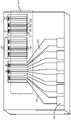
도 17 은 일 실시형태에 따른 확산형 리드 컨덕터들을 갖는 분자 센서의 평면도이다.
도 18 은 일 실시형태에 따라 전극 시트들의 페어들에 유체를 도입하기 위한 채널들을 갖는 분자 센서의 평면도이다.
도 19a 내지 도 19c 는 OAD 및 평탄화 단계들에 의해 이용가능한 구조체들의 실시형태들을 예시한다.
도 20a 및 도 20b 는 본 개시에 따른 구조체의 TEM 및 STEM 이미지들을 제공한다.Features and advantages of the present disclosure will become more apparent from the detailed description presented below when taken in conjunction with the drawings. The drawings and associated description are provided to illustrate embodiments of the present disclosure and do not limit the scope of what is claimed.
1A is a cross-sectional view illustrating fabrication of a molecular sensor by sequentially depositing trilayer thin film device stacks using a lower deposition angle and a sacrificial top layer in accordance with one embodiment.
FIG. 1B is a cross-sectional view illustrating further fabrication of the molecular sensor of FIG. 1A .
1C is a cross-sectional view of the molecular sensor of FIGS. 1A and 1B after fabrication.
2A is a cross-sectional view illustrating fabrication of a molecular sensor by sequentially depositing trilayer thin film device stacks using a lower deposition angle and removable shades in accordance with one embodiment.
FIG. 2B is a cross-sectional view illustrating further fabrication of the molecular sensor of FIG. 2A .
2C is a cross-sectional view of the molecular sensor of FIGS. 2A and 2B after fabrication.
3 is a flow chart for a manufacturing process of the molecular sensor of FIG. 1C or 2C according to an embodiment using low incidence angle oblique deposition.
4A is a cross-sectional view illustrating fabrication of a molecular sensor by sequentially depositing triple-layer thin film device stacks using a high deposition angle in accordance with one embodiment.
4B is a cross-sectional view of the molecular sensor of FIG. 4A after fabrication.
FIG. 5 is a flow diagram for a manufacturing process of the molecular sensor of FIG. 4B in accordance with an embodiment using high incidence angle oblique film deposition.
6 is a flow diagram for an additional manufacturing process according to an embodiment.
7A is a cross-sectional view of a molecular sensor illustrating deposition of a mask line during the fabrication process of FIG. 6 ;
7B is a cross-sectional view of the molecular sensor of FIG. 7A after depositing a dielectric cover layer and removing the mask line of FIG. 7A.
Fig. 8 is a cross-sectional view of the molecular sensor of Fig. 7B illustrating a roughening treatment of an exposed portion of electrode sheets according to an embodiment;
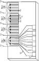
9 is a plan view of a molecular sensor having diffusion type lead conductors according to an embodiment.
10 is a top view of the molecular sensor of FIG. 9 with a gate electrode according to one embodiment.
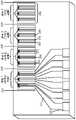
11 is a top view of a molecular sensor with channels for introducing a fluid to pairs of electrode sheets in accordance with one embodiment.
12 depicts a molecular sensor fabricated by forming a stack of layers and slicing through the stack in accordance with one embodiment.
13 is a flow diagram for a manufacturing process of the molecular sensor of FIG. 12 in accordance with one embodiment.
14A is a cross-sectional view of a stack of layers during the fabrication process of FIG. 13 ;
14B illustrates slicing the stack of FIG. 14A to form chips during the manufacturing process of FIG. 13 .
14C is a cross-sectional view illustrating the placement of the chip from FIG. 14B on a substrate during the manufacturing process of FIG. 13 ;
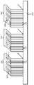
15 illustrates placement of multiple chips on a substrate according to one embodiment.
16 illustrates disposing a dielectric cover layer on multiple chips of FIG. 15 in accordance with one embodiment.
17 is a plan view of a molecular sensor with diffusion type lead conductors according to an embodiment.
18 is a top view of a molecular sensor with channels for introducing a fluid to pairs of electrode sheets in accordance with one embodiment.
19A-19C illustrate embodiments of structures usable by OAD and planarization steps.
20A and 20B provide TEM and STEM images of a structure according to the present disclosure.
다음의 상세한 설명에서, 본 개시의 완전한 이해를 제공하기 위해 다수의 특정 세부사항들이 제시된다. 그러나, 개시된 여러 실시형태들이 이러한 특정 세부사항들 중 일부 세부사항들 없이도 실시될 수도 있음은 당업자에게 자명할 것이다. 다른 사례들에서, 잘 알려진 구조체들 및 기술들은 여러 실시형태들을 불필요하게 모호하게 하는 것을 방지하기 위해 자세히 도시하지 않는다.In the detailed description that follows, numerous specific details are set forth in order to provide a thorough understanding of the present disclosure. It will be apparent, however, to one skilled in the art, that the various embodiments disclosed may be practiced without some of these specific details. In other instances, well-known structures and techniques have not been shown in detail in order to avoid unnecessarily obscuring the various embodiments.
본원에 이용된 용어 "구조체"는 일반적으로 기판 상에 금속 및/또는 유전체 층들을 성막하는 것에 의해 형성되는 것과 같이, 기판 층, 전극 층 또는 유전체 층 중 적어도 하나를 임의의 조합으로 포함하는 물리적 구성물들을 일반적으로 지칭한다. 본원에서 "구조체" 는 분자 전자 컴포넌트 또는 임의의 다른 디바이스의 부분 또는 분자 센서의 부분일 수도 있다. 일부 사례들에서, 본원에서 "구조체"는 다른 프로세서들 중에서도 구조체에 전극들의 페어를 따라 생체분자 또는 다른 분자를 배치하는 것에 의해 동작하는 분자 센서로 변환될 수도 있다. 일부 사례들에서, 구조체, 예를 들어, 기판 상의 교번하는 전극들 및 유전체 층들을 포함하는 구조체는 분자 센서 내에 이용가능한 또는 분자 센서를 위해 이용가능한 구조체로서 또한 지칭될 수도 있다.As used herein, the term “structure” refers to a physical construction comprising at least one of a substrate layer, an electrode layer, or a dielectric layer, in any combination, generally as formed by depositing metal and/or dielectric layers on a substrate. are generally referred to as A “structure” herein may be part of a molecular electronic component or any other device or part of a molecular sensor. In some instances, a “structure” herein may be converted into a molecular sensor that operates by placing a biomolecule or other molecule along a pair of electrodes on the structure, among other processors. In some instances, a structure, eg, a structure comprising alternating electrodes and dielectric layers on a substrate, may also be referred to as a structure usable in or for a molecular sensor.
본원에 이용된 용어 "디바이스 스택"은 "구조체" 의 일 실시형태이며, 일반적으로 금속 및 유전체 층들을 포함하는 재료의 다수의 층들을 갖는 구조체를 지칭한다. 비제한적 예에서, 디바이스 스택은 2 개의 전극 층들 사이에 샌드위치된 유전체 층을 더 포함하는 3층 (또는 삼중층) 배열체를 포함한다.As used herein, the term “device stack” is one embodiment of a “structure” and generally refers to a structure having multiple layers of material including metal and dielectric layers. In a non-limiting example, the device stack includes a three-layer (or triple-layer) arrangement further comprising a dielectric layer sandwiched between two electrode layers.
본원에 이용된 빗각 성막 (oblique angle deposition) 또는 "OAD"는 성막을 수용하는 평면 기판에 대해 90° 미만의 입사 각도로 금속과 같은 재료를 성막하는 프로세스를 지칭한다. 법선방향 성막은 일반적으로, 기판 평면에 대해 직교하는 (90°) 재료들의 성막을 지칭하며, 이는 기판의 상부 표면과 동일 평면에 있는 층들을 필수적으로 생성한다. 한편, OAD 는 90° 미만의 각도 (0° 에서 또는 "수평으로" 를 포함함) 로의 기판 상에의 성막을 포함하고, 이에 의해 기판 평면으로 돌출하는 수직 표면들이 재료의 성막을 또한 수용할 수 있다. OAD 의 정의는 0° (또한 "수평으로" 또는 "측방향으로 (sideways)" 를 지칭함) 성막을 포함하도록 확장되며, 이는 기판 시트의 상부 표면 상에 어떠한 재료도 성막되지 않게 하고, 성막 스트림에 대면하는 기판의 에지 상에서의 성막 그리고 성막 스트림에 대면하는 기판으로부터 나오는 임의의 돌출부들의 표면 상에서의 성막 만을 가져온다.As used herein, oblique angle deposition or “OAD” refers to a process of depositing a material, such as a metal, at an angle of incidence of less than 90° with respect to a planar substrate receiving the deposition. Normal deposition generally refers to deposition of materials that are orthogonal to the substrate plane (90°), which creates essentially coplanar layers with the top surface of the substrate. OAD, on the other hand, involves deposition on a substrate at an angle less than 90° (including at 0° or “horizontally”), whereby vertical surfaces protruding into the substrate plane can also accommodate deposition of material. have. The definition of OAD is extended to include deposition of 0° (also referred to as “horizontally” or “sideways”) deposition, which results in deposition of no material on the top surface of the substrate sheet, and in the deposition stream It only results in deposition on the edge of the facing substrate and on the surface of any protrusions coming out of the substrate facing the deposition stream.
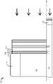
낮은 각도low angle성막tabernacle
도 1a 내지 도 1c 의 단면도들은 본 개시의 제조 프로세스의 여러 단계들을 수행하는 것에 의해, 이를 테면 기판 평면 (103) 에 대해 박막들과 후막들을 교번하는 낮은 각도 (약 0°내지 약 20°) 또는 0°(수평 방향) 입사 막 성막을 이용하는 것에 의해 획득된 중간 구조체 (100) 의 실시형태들을 예시한다. 도 1a 에 예를 들어, 예시된 바와 같이, 삼중층 박막 구조체 또는 디바이스 스택 (111) 은 제 1 전극 시트 (107), 내부 유전체 시트 (108) 및 제 2 전극 시트 (115) 의 순차적 성막에 의해 형성될 수도 있다. 도 1a 에서의 구조체 (100) 는 비제한적 실시형태에 따라, 세퍼레이터로서 더 두꺼운 외부 유전체 시트들 (112) 과 함께 다수의 인접하는 삼중층 디바이스 스택들 (111) 을 형성하기 위해, 더 두꺼운 외부 유전체 시트 (112) 의 성막에 의해 그리고 이후, 3 개의 층들, 제 1 전극 시트 (107), 내부 유전체 시트 (108) 및 제 2 전극 시트 (115) 의 성막의 반복에 의해 제조된다.The cross-sectional views of FIGS. 1A-1C are by performing various steps of the manufacturing process of the present disclosure, such as at a low angle (about 0° to about 20°) or alternating thin and thick films relative to the
도 1a 내지 도 1c 에 도시된 바와 같이, 구조체 (100) 는 기판 (102) 에 의해 정의된 기판 평면 (103) 에 대해 일정 각도로 기판 (102) 으로부터 돌출한 돌출부 (104) 를 갖는 지지 기판 (102) 을 포함한다. 돌출부 (104) 는 기판 평면 (103) 에 실질적으로 직교하거나 또는 다른 각도로 약 90° 내지 약 45° 로 배치될 수도 있다. 여러 실시형태들에서, 돌출부 (104) 는 기판 (102) 상에 재료의 블록으로서 나타날 수도 있다. 지지 기판 (102) 은 예를 들어, SiO2 또는 SiO2 코팅을 갖는 Si 를 포함할 수도 있다. 도 1a 내지 도 1c 에 도시된 바와 같이, 돌출부 (104) 는 기판 평면 (103) 에 직교하여 기판 (102) 으로부터 연장되는 블록을 포함한다. 다른 구현들에서, 돌출부 (104) 는 상이한 각도로 이를 테면 예를 들어, 기판 평면 (103) 에 대해 45° 또는 60° 로 기판 (102) 으로부터 돌출될 수도 있다.1A-1C , the
돌출부 (104) 는 예를 들어, 유전체 재료, 이를 테면, SiO2, Al2O3, 또는 MgO 를 포함할 수도 있다. 여러 예에서, 기판 (102) 및 돌출부 (104) 의 결합은 기판 (102) 상에 돌출부 (104)(예를 들어, 유전체 재료의 블록) 를 부착하거나, 또는 단차부 형상 피처를 생성하도록 기판 재료의 더 큰 블록의 일부분을 제거 (예를 들어, 애블레이션) 하는 것에 의해 형성될 수도 있다. 돌출부 (104) 는 기판 평면 (103) 에 대해 일정 각도로 유전체 및/또는 전극 층들의 배치를 위한 구조적 지지체를 제공할 수 있다.The
도 1a 는 박막 및 후막 성막 프로세스 단계들로부터 초래된 구조체 (100) 의 일 실시형태를 예시한다. 돌출부 (104) 와 기판 (102) 의 단차부-형상 결합부 상에 성막물이 형성된다. 이 실시형태에서, 희생 상부 및 측부 층들 (119) 은 다수의 삼중층 디바이스 스택들 (111) 의 측방향으로의 성막을 가능하게 하기 위해 포함된다. 도 1a 의 예에서, 성막 각도는 도 1a 의 우측의 큰 화살표로 도시된 바와 같이 수평방향일 수도 있거나 또는 수평 평면 (103) 으로부터 플러스 또는 마이너스 약 20° 내에 있을 수도 있다. OAD 에 의해 성막되는 제 1 전도성 전극 시트 (107) 는 측방향으로 또는 낮은 성막 각도로 성막되는 박막을 포함한다. 프로세스는 내부 유전체 시트 (108) 의 성막 그리고 나서 제 2 전극 시트 (115) 의 성막으로 계속된다. 이 프로세스는 많은 디바이스 스택들 (111) 을 형성하기 위해 반복될 수 있으며, 각각의 스택은 전극 시트들의 페어들을 포함하고, 내부 유전체 시트 (108) 는 전극 시트들의 페어 (106) 사이에 있고, 각각의 디바이스 스택 (111) 은 디바이스 스택 층들의 성막의 반복 사이클들 사이에 성막되는 더 두꺼운 외부 유전체 시트 (112) 에 의해 분리된다.1A illustrates one embodiment of a
더 두꺼운 유전체 시트 (112) 는 각각의 삼중층 디바이스 스택 사이에 성막된다. 도 1a 내지 도 1c 는 구조체들을 묘사하는 본원의 다른 모든 도면부들과 함께, 여러 엘리먼트들의 사이즈로서 그대로 해석되지 않아야 한다. 예를 들어, 삼중층 디바이스 스택 (111) 및 세퍼레이터 외부 유전체 시트들 (112) 에 대하여 도시된 상대 사이즈는 삼중층 디바이스 스택들 (111) 의 피처들을 보다 잘 예시하기 위해 다소 과장될 수도 있다. 이와 관련하여, 일부 실시형태들에서 삼중층 디바이스의 단면 폭은 약 50 nm 미만일 수도 있다.A thicker
도 1b 는 상부로부터의 재료의 폴리싱 및 평면 (117) 을 따라 구조체를 평탄화하는 것을 용이하게 하기 위해 추가된 기계적 지지 블록 재료 (123) 를 더 포함하는 구조체 (100) 의 실시형태를 예시한다. 블록 재료 (123) 는 예를 들어, 산화물 또는 산화물의 전구체 (예를 들어, 하이드로겐실세스퀴옥산 또는 "HSQ") 를 포함할 수 있다.1B illustrates an embodiment of the
도 1c 는 구조체 (100) 의 일 실시형태의 단면도를 나타낸다. 이러한 구조체 (100) 는 평면 (117) 을 따라 도 1b 에서의 구조체를 평탄화하는 것에 의해 획득될 수도 있다. 도 1b 에서의 평면 (117) 에 따른 평탄화는 돌출부 (104) 및 희생 재료 (119) 의 교차부보다 더 높거나 더 낮은 레벨에 있을 수도 있다. 여러 예들에서, 평면 (117) 에 따른 평탄화는 희생 재료 (119) 를 전체적으로 제거한다.1C shows a cross-sectional view of one embodiment of a
도 2a 는 다수의 삼중층 박막 디바이스 스택들 (111) 의 측방향 또는 낮은 각도 성막을 가능하게 하는 것을 돕는 탈착가능 상부 및 측부 쉐이드들 (121) 의 이용을 논의한다. 이들 쉐이드들 (121) 은 예시된 바와 같이 입사 성막 스트림에 대한 배리어들 또는 차폐부들로서 작용하고, 연속하는 성막들에 의해 그들의 단부들 상에 층형성된다. 여러 예들에서, 쉐이드 (121) 는 희생 재료 (119)(도 1a 및 도 1b 를 참조) 에 대한 필요를 대체한다. 도 2b 에 도시된 바와 같이, 돌출부 (104) 의 일부분은 쉐이드 (121) 에 의해 낮은 각도 또는 수평 OAD 로부터 효과적으로 차단된다. 구조체 (100) 는 낮은 성막 각도 OAD 에 의한 박막으로서 제 1 전도성 전극 시트 (107), 이어서 내부 유전체 박막 시트 (108) 그리고 나서 제 2 유전체 전극 시트 (115) 를 층형성하는 것에 의해 형성된다. 이 프로세스는 다수의 디바이스 스택들 (111) 을 형성하도록 반복되고, 더 두꺼운 유전체 세퍼레이터 시트 (112) 가 인접하는 삼중층 스택 (111) 사이에 성막된다.2A discusses the use of removable top and
도 2b 는 쉐이드들 (121) 의 제거 후에 도 2a 의 구조체에, 산화물 또는 산화물의 전구체 (예를 들어, HSQ) 를 포함할 수 있는 기계적 지지 블록 재료 (123) 의 추가 후의 구조체 (100) 의 일 실시형태를 예시한다. 에시된 바와 같이, 지지 블록 재료 (123) 는 기판 (102) 에 부착될 수도 있고 여러 층들의 성막으로부터 이전에 차폐되었던 기판 위의 영역들을 점유할 수도 있다. 일부 예들에서, 지지 블록 재료 (123) 는 다수의 디바이스 스택들 아래의 영역에 그리고 최종 성막 층에 인접하는 영역에 배치될 수도 있다. 지지 블록 재료 (123) 는 평면 (117) 을 따라 상부로부터의 구조체의 평탄화 및 폴리싱을 용이하게 할 수 있다. 도 2c 는 평면 (117) 을 따라 도 2b 의 구조체를 평탄화하는 것에 의해 획득된 구조체 (100) 의 단면도를 예시한다.FIG. 2B is an illustration of
도 1c 및 도 2c 의 예들에서 도시된 바와 같이 분자 센서들에서 이용가능한 구조체 (100) 는 수직으로 정렬되거나 또는 거의 수직으로 정렬된 삼중층 시트 구성에서 전극들의 고유 기하구조를 이용한다. 도 1c 의 구조체와 도 2c 의 구조체 사이의 하나의 주목할만한 차이는 도 1c 에서 전극 층들 및 내부 및 외부 유전체 층들이 기판 (102) 에 대해 모든 방향으로 연장되어 있다는 점이다. 도 2c 의 구조체 (100) 에서, 이들은 중간 블록 재료 (123) 때문에 그러하지 않다.The
여러 센서들에 이용될 때, 이들 구조체들에 도시된 바와 같이 전기 전도성 전극들의 시트 기하구조는 센서 전극들의 낮은 전기 저항을 통상적으로 허용하여 높은 신호-대-잡음 비들을 가능하게 하고 비교적 낮은 비용으로 스케일업 제조의 용이성 및 정확한 치수 제어를 가능하게 한다. 이 구성은 비교적 작은 디바이스 표면적들로 고밀도 디바이스 어레이들을 팩킹하는 것을 용이하게 하여, 콤팩트한 다중 디바이스 어셈블리의 제조를 허용할 수 있다. 제 1 컨덕터 층, 내부 절연체 층, 및 제 2 컨덕터 층의 순차적 성막이 여러번 반복될 수도 있어, 디바이스 스택 층들의 다음 반복 이전에, 외부 유전체 층을 각각의 제 2 컨덕터 층 상에 성막한다. 이러한 점에서, 성막들의 이 시퀀스는 2 내지 10,000 배 이상 반복하여 적어도 2 내지 수 만 개의 병렬 디바이스들의 어레이를 형성할 수도 있다.When used in several sensors, the sheet geometry of electrically conductive electrodes as shown in these structures typically allows for low electrical resistance of the sensor electrodes, enabling high signal-to-noise ratios and at relatively low cost. It allows for ease of scale-up manufacturing and precise dimensional control. This configuration may facilitate packing of high density device arrays with relatively small device surface areas, allowing for the fabrication of compact multi-device assemblies. The sequential deposition of the first conductor layer, the inner insulator layer, and the second conductor layer may be repeated multiple times, depositing an outer dielectric layer on each second conductor layer prior to the next iteration of the device stack layers. In this regard, this sequence of depositions may be repeated 2 to 10,000 times or more to form an array of at least 20,000 to tens of thousands of parallel devices.
본원에서의 구조체들의 여러 실시형태들에서 삼중층 디바이스 스택 (111) 은 매우 전기 전도성인 금속성 전극 시트들을 수직 또는 거의 수직의 구성으로 포함할 수 있다. 다른 구현들은 수직으로부터 약 60° 까지의 디바이스 스택의 층들의 경사진 각도 배향을 포함할 수 있다. 일부 예들에서, 디바이스 스택의 층들은 약 20° 이하로 수직 방향으로부터 경사진다. 전극 시트들의 각각의 페어 (106) 는 산화물들 (예를 들어, SiO2, Al2O3, MgO, CaO, 내열성 산화물, 희토류 산화물, 또는 산화물들의 혼합물), 질화물들 (예를 들어, AlN, Si3N4, 내열성 질화물, 희토류 질화물 또는 질화물들의 혼합물), 플루오르화물, 옥시플루오르화물, 또는 산질화물 (oxynitride) 로부터 선택될 수 있는 유전체 시트 층 재료 (108) 에 의해 디바이스 스택 (111) 에서 분리된다.In various embodiments of structures herein the
각각의 디바이스 스택 (111) 에서의 전극 시트들 (107 및 115) 에 대한 재료는 Au, Pt, Pd, Ag, Os, Ir, Rh, Ru 및 이들의 합금들을 포함하지만 이들에 제한되지 않는 높은 전도성 금속들 또는 합금들로부터 선택될 수도 있다. 평탄화 후의 구조체 상부 표면 상의 노출된 전극 시트 에지들의 치수는 예를 들어, 약 1 내지 약 100 nm 의 두께 (또는 폭) 을 가질 수 있다. 여러 실시형태들에서, (예를 들어, 도 1a 및 도 2a 에서) 전극 시트들 (107 및 115) 은 약 1 내지 약 40 nm, 또는 약 5 내지 약 15 nm 의 두께로 성막될 수 있고, 수직 또는 거의 수직 전극 시트의 높이는 (기판 (102) 상부 표면으로부터 평탄화 레벨까지 측정될 때) 적어도 약 100 ㎛ 길이이다. 다른 예들에서, 전극 시트들의 높이는 적어도 약 1,000 ㎛ 길이이거나 또는 적어도 약 10,000 ㎛ 길이이다. 따라서, 전극 시트에 대한 애스펙트 비는 (두께에 대한 높이의 관점에서) 적어도 약 10,000 또는 적어도 약 100,000 이다. 이 애스펙트 비에 의해, 기판 평면 (103) 에 대하여 수직으로 또는 거의 수직으로 기립하는 본원에서의 전극 시트는 기판 (102) 의 맞은 편에 있는 상부 에지를 필수적으로 가질 것이다. 수직으로 배치된 전극 시트가 기판 평면 (103) 에 대해 실질적으로 평행한 평면을 따라 평탄화될 때, 전극 시트의 상부 표면은 필수적으로 기판 평면 (103) 과 실질적으로 평행하게 될 것이다. 평탄화 후에, 전극 시트들의 노출된 상부 에지들, 내부 유전체 시트들 및 외부 유전체 시트들은 구조체의 평탄화된 상부 표면 상에 평행한 스트립들로서 나타난다.The material for the
다른 실시형태들에서, 얇은 부착 촉진 층은 계면에서의 부착을 개선하기 위해 전극 시트들과 내부 유전체 시트 사이의 계면에 성막될 수도 있다. 예를 들어, 약 1 내지 약 5 nm 두께의 막이 계면에 성막될 수도 있고 이 막은 Ti, Cr, Al, Zr, Mo, Nb, Ta, 또는 Hf 와 같은 재료를 포함할 수도 있다.In other embodiments, a thin adhesion promoting layer may be deposited at the interface between the electrode sheets and the inner dielectric sheet to improve adhesion at the interface. For example, a film about 1 to about 5 nm thick may be deposited at the interface and the film may include a material such as Ti, Cr, Al, Zr, Mo, Nb, Ta, or Hf.
평탄화 후에 구조체의 상부 표면 상의 2 개의 전극 시트들 사이에 성막된 내부 유전체 시트 (108) 의 노출된 종단부의 두께는 약 1 내지 약 40 nm 일 수도 있다. 일부 예들에서, 평탄화 후에 내부 유전체 층의 노출된 종단부의 두께는 약 5 내지 약 15 nm 일 수도 있다. 일부 실시형태들에서, 내부 유전체 시트들 (108) 의 두께는 약 10 nm 미만일 수도 있다. 수직 또는 거의 수직 유전체 시트 (108) 의 높이는 적어도 약 100 ㎛ 길이일 수도 있다. 다른 예들에서, 높이는 적어도 약 1,000 ㎛ 길이 또는 적어도 약 10,000 ㎛ 길이이다. 따라서, 내부 유전체 층 시트의 애스펙트 비는 (두께에 대한 높이의 관점에서) 적어도 약 10,000 또는 적어도 약 100,000 이다.The thickness of the exposed end of the
인접하는 삼중층 디바이스 스택들 (111) 을 분리하는 각각의 외부 유전체 층 (112) 의 치수는 적어도 약 500 내지 적어도 약 20,000 nm 의 폭을 가질 수도 있거나, 또는 디바이스 스택에서의 제 1 전극 및 제 2 전극을 분리하는 어느 하나의 내부 유전체 시트의 두께보다 약 한 자리수 더 큰 크기의 폭을 가질 수도 있다. 여러 예들에서, 외부 유전체 층 (112) 에 대한 두께는 예를 들어, 약 500 내지 약 5,000 nm 의 범위에 있을 수도 있다. 인접하는 삼중층 디바이스 스택들 (111) 사이의 약 500 내지 약 5,000 nm 의 분리는 전기적, 유도적, 용량적, 또는 다른 간섭들을 감소시킨다.The dimension of each
구조체 (100) 의 여러 실시형태들은 이를 테면, 기판 평면으로부터 0° 내지 약 20° 미만의 성막 각도로 층들의 낮은 입사 각도 OAD 를 이용하여 제조될 수 있다 (예를 들어, 도 1a 에서의 기판 평면 (103) 을 참조). 도 3 의 예시의 프로세스에서, 낮은 입사 각도 OAD 는 하나 이상의 희생 층들 (예를 들어, 도 1a 에서의 희생 층들 (119)) 및/또는 탈착가능 쉐이드들 (예를 들어, 도 2a 에서의 탈착가능 쉐이드들 (121)) 에 이용되어, 특정 표면들에서의 전극과 유전체 층들의 성막을 방지하는 것을 돕는다. 희생 층들 및/또는 탈착가능 쉐이트들은 이후, 전극 및 유전체 시트들이 기판 평면 (103) 에 대해 원하는 각도로 형성된 후에 제거된다.Various embodiments of
도 1a 의 예에서, 일련의 막 성막은 기판 평면 (103) 으로부터 0° 내지 약 20° 미만의 성막 각도로 수행된다. 기판 (102) 의 맞은 편의 돌출부 (104) 의 표면 상의 희생 층 (119) 은 평탄화시에 처분가능하다. 일부 예들에서, 희생 층 (119) 은 돌출부 (104) 의 에지를 약간 확장하는 것을 포함하여, 돌출부 (104) 의 상부 표면 위의 성막을 방지하는 것을 도울 수 있다.In the example of FIG. 1A , a series of film depositions are performed at a deposition angle from 0° to less than about 20° from the
아래 논의된 도 5 는 평탄화 이전에 더 높은 빗각 입사 각도로 다층 성막을 수행하는 것을 포함하는 프로세스의 대안의 실시형태를 제공한다. 다층 OAD 에 대한 더 높은 빗각 입사 각도가 예를 들어, 기판 평면 (103) 으로부터 약 20° 내지 약 70° 의 범위의 임의의 각도로, 이를 테면 약 30° 내지 약 60° 로 수행될 수 있다. 도 5 의 프로세스에서와 같이 희생층 없는 OAD 를 이용하여, 기판 (102) 맞은 편의 돌출부 (104) 의 표면은 또한 (예를 들어, 도 4a 에 예시된 바와 같이) 다층 박막들로 또한 커버된다. 그럼에도 불구하고, 평탄화 폴리싱 프로세스는 도 4b 에서와 같은 구조체를 실현하기 위해 돌출부 (104) 의 표면에 이들 필름 성막들을 제거한다. 일부 사례들에서, 돌출부 (104) 의 최상부 층은 돌출부 (104) 상에 이전에 성막된 층들의 모두를 제거하는 평탄화에서 희생된다.5, discussed below, provides an alternative embodiment of a process that includes performing multilayer deposition at a higher oblique incidence angle prior to planarization. Higher oblique incidence angles for multilayer OAD can be performed, for example, at any angle ranging from about 20° to about 70° from the
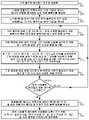
도 3 은 본 개시에 따라 예시적인 제조 프로세스의 흐름도를 예시한다. 도 3 의 흐름도에 예시된 바와 같이, 단계 302 는 기판 (이를 테면, 여러 실시형태들 전반에 걸쳐 묘사된 기판 (102)) 을 제공하는 것을 포함한다. 논의된 바와 같이, 기판 (102) 은 기판 평면 (103) 을 정의하는 주요 표면을 더 포함한다. 기판 평면은 유전체 및/또는 전극 층들을 지지하기 위하여 이용되는 상부 표면 또는 하부 표면과 같은 기판의 주요 표면과 평행하게 하는 것에 의해 정의될 수 있다.3 illustrates a flow diagram of an exemplary manufacturing process in accordance with the present disclosure. As illustrated in the flowchart of FIG. 3 ,
단계 304 에서, 돌출부 (예를 들어, 여러 실시형태들 전반에 걸쳐 묘사된 돌출부 (104)) 가 기판 (102) 에 부착되거나 또는 대안의 실시형태들에서, 돌출부는 더 큰 기판의 하나 이상의 부분들을 제거하여, 초기에 더 두꺼운 지지 기판에서 컷-아웃 "단차부"를 생성하는 것에 의해 형성된다. 여러 예들에서, 블록 또는 다른 형상의 유전체 재료가 기판에 부착되어 기판 평면에 대해 원하는 각도로 돌출부를 형성할 수도 있다. 위에 주지된 바와 같이, 돌출부는 (더 두꺼운 기판에서 단차부를 컷아웃하는 것에 의해 형성되든 또는 재료를 부착하든 간에) 약 90° 와 같은 각도로 기판 평면으로부터 돌출한다.At
도 3 을 계속 참조하여 보면, 단계 305 는 OAD 에 대해 타겟으로 되는 기판의 일측에 하나 이상의 희생 층들 및/또는 탈착가능 쉐이드들 (예를 들어, 도 2a 에서 탈착가능 쉐이드들 (121)) 및/또는 기판의 맞은 편의 돌출부의 표면 상에 하나 이상의 희생 층들 및/또는 탈착가능 쉐이드들 (예를 들어, 도 1a 에서 상부 희생 층 (119)) 의 배치를 포함한다. 위에 주지된 바와 같이, 희생 층은 돌출부 (104) 의 에지를 너머 연장될 수도 있다. 희생 층은 반도체 제조에 있어서 리프트 오프 프로세싱에 일반적인, 예를 들어, 물리적으로 제거가능한 플레이트, 또는 용해가능한 폴리머 층, 이를 테면, 아세톤 용해가능 (폴리)메틸 메타크릴레이트 ((poly)methyl methacrylate; PMMA) 를 포함할 수 있다. 탈착가능 쉐이드는 예를 들어, 탈착가능 금속성, 세라믹, 또는 폴리머 재료를 포함할 수 있다.With continued reference to FIG. 3 ,
단계 306 에서, 제 1 전극 층은 기판 상에 성막된다. 여러 실시형태들에서, 제 1 전극 층의 적어도 일부분은 기판으로부터 돌출부의 노출된 측에 반대되어 성막되고, 이에 의해 기판과 돌출부 사이의 각도와 동일하게 되는 기판에 대해 일정 각도로 된 제 1 전극 시트 (예를 들어, 도 1a 또는 도 2a 에서의 제 1 전극 시트 (107)) 를 가져온다. 다른 구현들에서, 유전체 층 (예를 들어, 본원에 설명된 같이 외부 유전체 층) 은 제 1 전극 층 및 후속하는 층들의의 성막 전에, 먼저 돌출부에 반대되어 성막될 수도 있다.In
도 3 의 흐름도에 묘사된 실시형태에서, 단계 308 에서, 내부 유전체 층은 단계 306 에서 이전에 성막된 제 1 전극 층 상에서 성막된다. 도 1a 및 도 2a 의 예들에서 도시된 바와 같이, 내부 유전체 층의 적어도 일부분은 기판 평면 (103) 에 대한 돌출부의 동일 배향으로 내부 유전체 시트 (108) 를 형성하기 위해 돌출부 (104) 에 반대되어 성막된다. 단계 306 에서 성막된 제 1 전극 층에서와 같이, OAD 는 기판 평면에 대하여 일정 각도로 내부 유전체 층을 성막하기 위해 이용될 수 있다. 상보성 금속 산화물 반도체 (Complementary metal-oxide semiconductor; CMOS) 프로세스들, 이를 테면 OAD 는 통상적으로 내부 유전체 층이 정확하고 반복가능한 두께로 성막될 수 있게 한다.In the embodiment depicted in the flow chart of FIG. 3 , in
일부 실시형태들에서, 얇은 부착 강화 층은 층들의 부착을 개선하기 위해 내부 유전체 층을 성막한 전 및/또는 후에 제 1 전극 층 상에 성막될 수도 있다. 여러 예들에서, 약 1 내지 약 5 nm 두께의 막 재료가 일 재료를 이용하여 계면에서 성막된다. 이러한 막 재료는 예를 들어, Ti, Cr, Al, Zr, Mo, Nb, Ta, 또는 Hf 를 포함할 수도 있다.In some embodiments, a thin adhesion enhancing layer may be deposited on the first electrode layer before and/or after depositing the inner dielectric layer to improve adhesion of the layers. In various examples, a film material about 1 to about 5 nm thick is deposited at the interface using one material. Such a film material may include, for example, Ti, Cr, Al, Zr, Mo, Nb, Ta, or Hf.
도 3 에 묘사된 프로세스의 단계 310 에서, 제 2 전극 층은 예를 들어, OAD 를 이용하여 이전 층들과 동일한 기판 평면에 대한 각도로 제 2 전극 시트 (예를 들어, 도 1a 및 도 2a 에서의 제 2 전극 시트 (115)) 를 형성하기 위해 내부 유전체 층 상에 성막된다. 단계 310 의 완료시, 디바이스 스택이 형성되고, 이 스택은 전극 시트들의 페어로서 배열된 제 1 전극 시트 및 제 2 전극 시트를 포함하고, 내부 유전체 시트는 전극 시트들의 페어들 사이에 배치된다.In
단계 312 에서, 외부 유전체 층은 기판 평면에 대해 일정 각도로 외부 유전체 시트를 형성하기 위해 제 2 전극 층 상에 성막된다. 도 1a 및 도 2a 에서의 예들을 참조하여 보면, 외부 유전체 층은 제 2 전극 층 상에 성막되어, 이전 층들에 대한 것과 동일한 기판 평면 (103) 에 대한 각도로 외부 유전체 시트 (112) 를 형성한다. 일부 구현들에서, 외부 유전체 층은 예를 들어 이것이 최종의 외부 유전체 층을 포함하면 이전에 성막된 다른 외부 유전체 층들과는 상이한 두께를 가질 수도 있다. 이러한 더 두꺼운 터미널 외부 유전체 층은 전체적인 어레이에 대한 더 큰 외부 절연을 제공하고/하거나 디바이스 스택들의 더 큰 어레이 내에서 구조체를 패키징하는 것을 용이하게 한다.In
단계 314 에서, 전극 시트들의 페어들의 최종 개수에 도달되었는지의 여부를 결정한다. 일부 구현들에서, 전극 시트들의 페어들의 최종 개수는 전극 시트들의 하나의 페어 (예를 들어, 하나의 디바이스 스택) 만큼 적을 수도 있다. 전극 시트들의 2 개 이상의 페어들에 대해, 단계들 306 내지 312 을 포함하는 서브 프로세스는 전극 시트들의 적어도 2 개의 페어들을 제공하기 위해 적어도 한번 반복된다. 일부 구현들에서, 전극 시트들의 페어들의 최종 개수는 예를 들어, 전극 시트들의 수 천 개의 페어들만큼 클 수도 있다. 원하는 시트들의 페어들의 최종 개수는 제조된 구조체들로부터 제조되고 있는 센서에 대한 설계 고려사항들, 이를 테면, 원하는 테스팅 속도, 분석될 분자 유형, 또는 센서에 대한 원하는 풋프린트 및 다른 고려 사항들에 의존할 수도 있다.In
단계 314 에서 전극 시트들의 페어들의 최종 개수가 도달되지 않으면, 프로세스는 단계 306 으로 리턴하여, 기판 평면에 대해 일정 각도로 다른 제 1 전극 시트를 형성하기 위해 돌출부의 측에 대해 반대되어 다른 제 1 전극 층을 성막한다. 한편, 전극 시트들의 페어들의 최종 개수가 단계 314 에서 도달되었다면, 프로세스는 단계 315 로 진행하며, 이는 위에 논의된 바와 같이 단계 305 에서 추가되었던 희생 층들 또는 탈착가능 쉐이드들의 제거를 포함한다. 희생 층은 예를 들어, 용해에 의해 제거되거나 또는 물리적으로 제거될 수 있다. 탈착가능 쉐이드는 물리적으로 제거될 수 있다. 일 예에서, 희생 층은 액체를 이용하여 리프트-오프 프로세싱에서처럼 용해된다.If the final number of pairs of electrode sheets is not reached in
적어도 하나의 기계적 지지 블록 재료가 또한 단계 315 에서 이를 테면, 갭 충전 경화가능 폴리머가 추가된다. 기계적 지지 블록 재료는 성막된 다층 스택에 인접하여 부착될 수도 있다 (예를 들어, 도 1b 및 도 2b 에서 도시된 성막된 층들의 오른쪽에 추가된 블록 (123)). 일부 구현들에서, 이는 세라믹 재료 또는 폴리머 재료의 블록을 부착하는 것에 의해, 또는 폴리머 재료를 성막하고 후속하여 폴리머를 경화하는 것에 의해 실현된다. 추가된 지지 블록 및 이전에 성막된 다층들 사이의 공간은 UV-경화가능, 전자 빔 경화가능 또는 열 경화가능 폴리머, 이를 테면, PMMA 또는 하이드로젠 실세스퀴옥산 (HSQ) 레지스트로 충전될 수 있다. 성막된 HSQ 레지스트 층은 SiO2 유형 재료의 경도와 가깝게 되도록 추가적인 열 경화에 의해 경화될 수 있다. 기계적 지지 블록 재료는 구조체 (100) 의 후속하는 패키징 프로세스 동안과 같은 처리를 위하여 지지부를 제공하도록 또는 선택적 단계 316 에서와 같이 후속 평탄화를 용이하게 하도록 추가될 수 있다.At least one mechanical support block material is also added in
선택적 단계 316 는 필요에 따라 서브프로세스 단계들 306 내지 312 의 이전 반복 단계들로부터 형성된, 전극 시트들의 페어들, 내부 유전체 시트들 및 하나 이상의 외부 유전체 시트들을 평탄화하는 것을 포함한다. 평탄화하는 단계는 예를 들어, 화학 기계적 평탄화 (chemical-mechanical planarization; CMP) 폴리싱, 포커싱된 이온 빔 (focused ion beam; FIB) 에칭, 또는 (폴리)메틸메타크릴레이트 (PMMA) 또는 HSQ 충전 및 리액티브 이온 에치 (reactive ion etch; RIE) 에 의한 후속 "에칭 백"을 포함할 수도 있다. 박막 및 후막 그리고 유전체 층들의 반복되는 성막 이후, 단계 315 에서 추가되어 경화된 기계적 지지 블록 재료, 이를 테면, SiO2 재료 또는 SiO2 의 전구체 (예를 들어, HSQ) 가 평탄화 동안에 구조체의 기계적 지지부를 제공할 수 있다. 구조체 상의 평탄화의 위치는 예를 들어, 도 1b 또는 도 2b 에 도시된 평면 (117) 을 따라 돌출부 (104) 의 상부 표면 아래일 수도 있다. 다른 구현들에서, 이를 테면, 돌출부의 상부 상으로의 성막이 차폐될 때, 평탄화는 돌출부의 상부 표면, 전극 시트들 및 다양한 내부 및 외부 유전체 시트들을 제거하도록 돌출부 (104) 의 상부 표면 바로 아래에서 발생하여, 층들의 에지들을 노출시켜 이들 모두를 돌출부 (104) 의 상부 표면과 실질적으로 평면을 이루도록 레벨링한다. 여러 실시형태들에서, 평탄화는 기판 평면 (103) 에 대해 실질적으로 평행한 상부 표면을 갖는 구조체를 가져온다.
특정 예들에서, 도 3 에서의 단계 316 는 쉐이드가 돌출부의 에지 상에서 돌출부의 상부 상의 원하지 않는 성막을 방지하기에 충분히 멀리 연장될 때 생략될 수도 있다. 이러한 예에서, 단계 315 에서의 쉐이드의 제거는 평탄화를 필요로 함이 없이 실질적으로 평행한 전극 시트들의 페어들의 노출된 상부 표면들을 가져올 수도 있다.In certain examples,
높은 각도high angle성막tabernacle
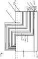
도 4a 를 참조하여 보면, 제조 방법의 여러 실시형태들에 의해 형성된 구조체 (100) 의 단면도가 예시된다. 구조체 (100) 는 내부 유전체 시트 (108) 에 의해 분리된 전극 페어 시트들 (107 및 115) 을 더 포함하는 디바이스 택들을 포함한다. 이 실시형태에서, 구조체 (100) 는 높은 각도 OAD 를 이용하여 삼중층 박막 디바이스 스택들을 순차적으로 성막하는 것에 의해 제조된다. 높은 각도의 성막은 기판 표면 상에 (또는 기판 표면 상에 성막된 이전 층 상에) 그리고 또한 돌출부 (104) 의 표면들 상에 (또는 돌출부 (104) 상에 이전에 성막된 층들 상에) 양쪽 모두에 각각의 박막 층의 성막을 가져온다. 수직 또는 거의 수직 성막물들이 제 1 전극 시트 (107), 내부 유전체 시트 (108), 제 2 전극 시트 (115), 및 외부 유전체 시트 (112) 로서 라벨링되는 한편, 수평 또는 거의 수평 성막물들은 제 1 전극 층 (105), 내부 유전체 층 (109), 제 2 전극 층 (113), 및 외부 유전체 층 (118) 으로서 라벨링된다. 각각의 층의 수직 또는 거의 수직 부분 및 수평 또는 거의 수평 부분이 필수적으로 접속하는데 그 이유는 각각의 층이 각각 OAD 단계에서 돌출부 표면 및 기판 표면 양쪽 모두에 성막되기 때문이다.Referring to FIG. 4A , a cross-sectional view of a
도 4a 에서의 수평 또는 거의 수평 유전체 층들은 내부 유전체 층들 (109) 및 외부 유전체 층들 (118) 을 포함한다. 돌출부 (104) 에서와 같이, 내부 유전체 층들 (109) 및 외부 유전체 층들 (118) 은 예를 들어, 유전체 재료, 이를 테면 SiO2, Al2O3, 또는 MgO 를 포함할 수도 있다. 도 4a 에 도시된 바와 같이, 내부 유전체 층 (109) 의 제 1 부분 및 외부 유전체 층 (118) 은 기판 평면 (103) 을 따라 일정 배향으로 (즉 도 4a 의 예에서 수평방향으로) 성막된다. 내부 유전체 층 (109) 의 제 2 부분 및 외부 유전체 층 (118) 은 돌출부 (104) 를 따르는 배향으로 (예를 들어, 도 4a 의 예에서 돌출부 (104) 의 오른쪽 상에 수직방향으로) 성막되어 내부 유전체 시트들 (108) 및 외부 유전체 시트들 (112) 을 각각 형성한다. 내부 유전체 시트들 (108) 및 외부 유전체 시트들 (112) 은 기판 평면 (103) 에 대해 일정 각도로 형성된다.The horizontal or near-horizontal dielectric layers in FIG. 4A include inner
도 4a 에서의 수평 또는 거의 수평 전극 층들은 제 1 전극 층들 (105) 및 제 2 전극 층들 (113) 을 포함한다. 전극 층들은 예를 들어, 전도성 금속, 이를 테면, Au, Pt, Pd, Ag, 또는 Rh 를 포함할 수도 있다.The horizontal or near-horizontal electrode layers in FIG. 4A include first electrode layers 105 and second electrode layers 113 . The electrode layers may include, for example, a conductive metal, such as Au, Pt, Pd, Ag, or Rh.
도 4a 에 도시된 바와 같이, 제 1 전극 층들 (105) 및 제 2 전극 층들 (113) 은 기판 평면 (103) 을 따르는 배향으로 (즉, 도 1a 내지 도 1c 의 예에서와 같이 수평으로 또는 거의 수평으로) 성막된다. 제 1 전극 층들 (105) 의 제 2 부분 및 제 2 전극 층들 (113) 은 돌출부 (104) 에 반대되어 (예를 들어, 도 1a 내지 도 1c 의 예에서 돌출부 (104) 의 오른쪽 상에 수직으로 또는 거의 수직으로) 성막되어 제 1 전극 시트들 (107) 및 제 2 전극 시트들 (115) 을 각각 형성한다. 제 1 전극 시트들 (107) 및 제 2 전극 시트들 (115) 은 기판 평면 (103) 에 대해 일정 각도로, 이를 테면, 돌출부가 기판에 대해 배향되는 각도로 형성된다.As shown in FIG. 4A , the first electrode layers 105 and the second electrode layers 113 are in an orientation along the substrate plane 103 (ie, horizontally or nearly as in the example of FIGS. 1A-1C ). horizontally). The second portion of the first electrode layers 105 and the second electrode layers 113 are opposite the protrusion 104 (eg, vertically on the right side of the
전극 층들 및 유전체 층들을 기판 평면 (103) 에 대해 일정 각도로 성막하는 것은 전극 시트들의 다수의 페어들을 노출시킬 수 있게 한다. 이는 많은 전극 및 유전체 층들을 성막하는 것에 의해 많은 수의 전극 페어들을 제조함에 있어서 스케일러빌리티를 허용할 수 있다.Depositing the electrode layers and dielectric layers at an angle relative to the
예를 들어, 필름 성막들의 시퀀스는 제 1 컨덕터 층 (105), 이어서 내부 유전체 층 (109) 을 성막하고 나서 제 2 컨덕터 층 (113) 의 성막으로 이어져, 제 1 컨덕터 층 (105) 과 페어링되고, 내부 유전체 층 (109) 은 제 1 컨덕터 층 (105) 과 제 2 컨덕터 층 (113) 에 의해 샌드위치된다. 외부 유전체 층 (118) 은 그후, 후속하는 컨덕터 페어로부터 조기 성막되는 컨덕터 페어를 분리하기에 충분한 두께를 갖고 성막된다. 컨덕터 층, 유전체 층 및 제 2 컨덕터 층의 성막은 여러 회 반복될 수 있다.For example, the sequence of film depositions deposits a
스케일러빌리티에 더하여, 내부 유전체 시트들 (108/109) 의 두께는 위에 논의된 도 1c 및 도 2c 의 예들에 따라 CMOS 유형 박막 성막 제조 프로세스들을 이용하여 정확하게 제어될 수 있다. 이는 고정된 그리고 정확하게 제어된 2 개의 전극 시트들 사이의 간극이 전극들의 페어에서 전극들을 따라 특정 분자들, 이를 테면, 특정 단백질, DNA, 뉴클레오티드, 지질, 항체, 호르몬, 카르보하이드레이트들, 신진대사 산물, 제약물, 비타민들, 신경 전달 물질, 효소들, 또는 분석될 다른 분자들의 신뢰성있고 재현성있는 부착을 용이하게 하도록 허용할 수 있다. 다중 전극 분자 감지 디바이스들에서의 이용가능한 구조체들을 형성하기 위한 표준 CMOS 프로세스들의 이용은 또한 분자 센서를 제조하는 것과 통상적으로 연관된 비용을 감소시킨다.In addition to scalability, the thickness of the
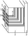
도 4b 는 (아래 논의된 바와 같이) 117 을 따르는 평탄화 및 내부 유전체 시트들 각각의 일부분의 제거 후에 도 4a 의 구조체 (100) 의 단면도를 예시한다. 이 실시형태에서, 평탄화는 또한 높은 입사 각도 OAD 프로세스로부터 야기되었던 돌출부 (104) 의 상부 표면에 성막되었던 박층막 성막물들을 제거함을 주지한다.4B illustrates a cross-sectional view of the
도 4b 에서의 각각의 전극 시트는 예를 들어, 약 1 내지 약 100 nm 의 두께를 가질 수 있다. 설계 고려 사항들, 이를 테면, 분석될 분자에 따라, 전극 시트들 및 층들 (107/105 및 115/113) 은 약 1 내지 약 40 nm, 또는 약 5 내지 약 15 nm 의 두께로 성막될 수 있다. 이러한 구현들에서, 내부 유전체 시트들 및 층들 (108/109) 은 약 1 내지 약 40 nm, 또는 약 2 내지 약 15 nm 의 유사한 두께로 성막될 수 있다. 외부 유전체 시트들 및 층들 (112/118) 은 약 50 내지 약 2,000 nm, 또는 내부 유전체 시트들 및 층들 (108/109) 보다 적어도 약 한 자리수 더 큰 크기의 두께로 성막될 수 있다.Each electrode sheet in FIG. 4B may have a thickness of, for example, about 1 to about 100 nm. Depending on design considerations, such as the molecule to be analyzed, the electrode sheets and layers 107/105 and 115/113 may be deposited to a thickness of from about 1 to about 40 nm, or from about 5 to about 15 nm. . In such implementations, the inner dielectric sheets and layers 108 / 109 may be deposited to a similar thickness of from about 1 to about 40 nm, or from about 2 to about 15 nm. The outer dielectric sheets and layers 112 / 118 may be deposited to a thickness of about 50 to about 2,000 nm, or at least about an order of magnitude greater than the inner dielectric sheets and layers 108 / 109 .
도 4b 에서의 평탄화된 구조체를 계속 참조하여 보면, 노출된 제 1 전극 시트 (107) 및 노출된 제 2 전극 시트 (115) 는 전극 시트들의 페어들 (106) 을 형성하고, 페어에서의 각각의 전극은 내부 전극 시트에 의해 분리된다. 구조체 (100) 의 이 실시형태에서, 각각의 내부 유전체 시트의 노출된 단부들은 내부 유전체 시트에서 평탄화된 평면으로부터 아래로 연장되는 오목부 (110) 를 형성하기 위해 제거되었던 것으로 도시된다. 이 오목부는 또한 각각의 내부 유전체 시트에서 평탄화된 표면 아래로 연장되는 그루브 (110) 로서 본원에서 지칭된다. 2 개의 전극 시트들 사이의 그루브 (110) 내에서 그리고 유전체 재료가 없는 자유 공간은 도 4b 에 도시된 바와 같이 각각의 전극 페어에 브리지 분자들 (10) 이 보다 편리하게 부착되도록 허용할 수 있다. 분자들 (10) 은 예를 들어, 단백질, DNA, 뉴클레오티드, 지질, 항체, 호르몬, 카르보하이드레이트들, 신진대사 산물, 제약물, 비타민들, 신경 전달 물질, 효소들, 또는 분석되거나 식별될 다른 유형의 분자들을 포함할 수도 있다.With continued reference to the planarized structure in FIG. 4B , the exposed
구조체 (100) 의 일 실시형태를 이용하는 분자 센서에서, 전극 시트들의 페어 (106) 에서의 한 전극 시트는 소스 전극으로서 역할을 할 수 있고 페어에서의 다른 전극 시트는 드레인 전극으로서 역할을 할 수 있다. 동작시, 분자 (10) 는 각각의 페어에서 제 1 전극 시트와 제 2 전극 시트 사이에 분자 브리지를 형성하도록 도 4b 에서 도시된 바와 같은 전극 시트들에서의 페어에서 각각의 전극 시트에 부착된다. 분자들 (10) 은 예를 들어, 단백질, DNA, 항체, 뉴클레오티드, 지질, 호르몬, 카르보하이드레이트들, 신진대사 산물, 제약물, 비타민들, 신경 전달 물질, 효소들, 또는 분석되거나 식별될 다른 유형의 분자들을 포함할 수도 있다. 그 후 분자 (10) 는 분자 (10) 와 상호작용하는 피분석물들을 검출하기 위해 이용되거나 전자 신호를 측정하는 것에 의해 검출 또는 분석될 수 있다. 일부 구현들에서, 제 1 전극 시트 (107), 제 2 전극 시트 (115), 및 분자 (10) 를 포함하는 회로에서 전류가 분자 (10) 를 통과한다. 이 회로를 통과하는 측정된 전류에 기초하여, 분자 (10) 는 식별되고, 정량화되고, 및/또는 분석될 있거나 또는 분자 (10) 와 상호작용가능한 여러 피분석물들이 식별되고, 정량화되고, 및/또는 분석될 수 있다. 이러한 구현은 구조체 (100) 의 일 실시형태를 포함하는 분자 센서가 게놈 시퀀싱을 위해 이용될 수 있게 할 수 있다.In a molecular sensor using one embodiment of
일부 구현들에서, 분자 센서 디바이스에서의 포함을 위하여 구성된 단일 구조체 (100) 는 전극 시트들의 천 개 이상의 페어들 (106) 까지를 포함할 수 있다. 이러한 구조체는 센서 제조에서 스케일러빌리티를 제공하고, 다수의 구조체들 (100) 은 전극 시트들의 페어들의 훨씬 더 큰 수를 획득하기 위해 센서 디바이스에서 결합된다. 결과적인 센서 디바이스는 보다 단시간에 더 많은 분자들을 동시에 테스팅가능하다.In some implementations, a
도 4b 를 계속 참조하여 보면, 전극 시트들의 각각의 페어 (106) 는 외부 유전체 시트 (112) 에 의해 분리된다. 내부 유전체 시트 (108) 는 전극 시트들의 페어 (106) 에서의 제 1 전극 시트 (107) 및 제 2 전극 시트 (115) 를 분리한다. 일부 구현들에서, 내부 유전체 시트들 (108) 은 대략 제 1 두께 (예를 들어, 5% 허용 오차 등 내에서) 를 가질 수 있는 한편, 모든 외부 유전체 시트들 (112) 은 대략 제 2 두께 (예를 들어, 또한 5% 허용 오차 등 내에서) 를 가질 수 있고, 제 2 두께는 제 1 두께보다 적어도 한 자리수 더 크다. 더 두꺼운 외부 유전체 시트 (112) 는 전극 시트들의 인접하는 페어들 (106) 사이의 분리를 제공하여, 전극들의 인접하는 페어들 사이의 전기적 또는 용량 간섭을 감소시키고, 다른 이점들 중에서, (내부 유전체 층 상에서) 각각의 페어에서의 2 개의 전극들을 따르기 보다 (외부 유전체 층 상에서) 전극들의 인접하는 페어들 사이의 분자 브리지를 브리징하는 확률을 최소화한다.With continued reference to FIG. 4B , each
예를 들어, 외부 유전체 시트들 (112) 의 원하는 두께는 적어도 약 1 ㎛ 또는 적어도 약 10 ㎛ 일 수 있는 한편, 내부 유전체 시트들 (112) 에 대한 원하는 두께는 최대 약 50 nm 또는 최대 약 20 nm 일 수 있다. 일부 구현들에서, 내부 유전체 시트 (112) 의 두께는 최대 약 10 nm 일 수 있다. 정확하게 제어된 내부 유전체 층 두께를 갖는 것은, 전극 시트들의 페어들 (106) 에 특정 분자들의 신뢰성있고 재현성있는 부착에 대한 기회를 개선시킬 수 있고, 이는 다른 유형의 분자들이 분자들의 사이즈와 협업하도록 비교적 정밀한 간극이 주어지면, 전극 시트들에 불가역적으로 부착할 경향이 거의 없기 때문에, 구조체 (100) 중에서 구성된 분자 센서로부터 보다 정확한 판독값들을 가져온다.For example, the desired thickness for the
내부 유전체 시트 (108) 에서 생성된 그루브 (110) 는 마무리된 센서의 동작을 개선하고 분자 센서의 구성에서 분자 (10) 의 부착을 용이하게 할 수 있다. 일부 구현들에서, 각각의 그루브를 형성하기 위한 내부 유전체 재료의 일부분의 제거는 로컬 마스킹으로 내부 유전체 시트의 성막에 의해 또는 로컬화된 에칭에 의해 실현될 수 있다. 이들 방식으로, 그루브 (110) 가 내부 유전체 시트들 (108) 의 각각에 형성된다. 여러 실시형태들에서, 내부 유전체 시트들에서의 각각의 그루브는 평탄화 표면으로부터 약 5 내지 약 15 nm 깊이로 측정된다. 즉, 내부 유전체 시트 재료의 제거의 범위는 평탄화에 의해 생성된 내부 유전체 시트 (108) 의 노출된 종단부로부터 약 5 내지 약 15 nm 이다. 내부 유전체 시트들 각각의 노출된 종단부들의 제거는 유전체 재료에서 에칭된 이들 그루브들 상에서 브리징하는, 전극들의 페어에서의 전극들을 따르는 특정 생체분자들의 이동 및 부착을 실현하기 위한 자유 공간을 제공한다.The grooves 110 created in the
각각의 내부 유전체 시트의 노출된 종단부들을 제거하기 위해 이용된 방법에 따라, 이렇게 생성된 그루브는 직사각 직육면체 이외의 다른 형상을 가질 수도 있다. 예를 들어, 각각의 전극에 인접하는 내부 유전체 시트의 부분들은 그루브의 단면도가 포물선형 (예를 들어, 도 12 의 실시형태에서의 그루브 (210) 의 형상을 참조) 을 나타낼 수도 있도록, 부분 제거 후에 남겨질 수도 있다. 전극들의 각각의 페어를 따르는 각각의 브리지 분자의 부착 및 이동을 돕는 에어 공간을 제공하기 위해 모든 유전체 재료 중에서 그루브들이 완전하게 클리닝될 필요는 없다.Depending on the method used to remove the exposed ends of each inner dielectric sheet, the groove so created may have a shape other than a rectangular cuboid. For example, portions of the inner dielectric sheet adjacent to each electrode may be removed such that the cross-sectional view of the groove may exhibit a parabolic shape (eg, see the shape of the
도 5 는 도 4b 의 구조체를 제조하는 예시적인 제조 프로세스를 요약하는 흐름도를 예시한다. 논의된 바와 같이, 제조 프로세스는 비교적 높은 입사 각도 OAD 를 포함한다. 또한 본원에 논의된 바와 같이 도 1a 내지 도 1c 의 구조체를 생성하기 위해 도 3 의 일 예의 프로세스에 이용된 OAD 각도 보다 더 높은 각도를 갖는 더 높은 입사 각도 OAD 에 의해, 전극 및 유전체 박막 층들은 또한 기판 (102) 의 맞은 편의 돌출부 (104) 의 표면 (즉, 도 4a 에서의 돌출부 (104) 의 상부 표면) 상에 성막된다. 돌출부의 상부 표면 상에 성막된 층들은 기판 평면 (103) 에 대해 일정 각도로 형성되었던 전극 시트들 및 유전체 시트들의 에지들을 노출시키기 위한 후속의 평탄화 단계에서 희생된다.5 illustrates a flow diagram summarizing an exemplary manufacturing process for manufacturing the structure of FIG. 4B . As discussed, the manufacturing process involves a relatively high angle of incidence OAD. Also with a higher angle of incidence OAD with a higher angle than the OAD angle used in the example process of FIG. 3 to create the structure of FIGS. 1A-1C as discussed herein, the electrode and dielectric thin film layers are also It is deposited on the surface of the
도 3 의 프로세스에 비해, 도 5 의 프로세스는 일반적으로 도 3 의 단계 305 에서와 같은 희생 층들 또는 탈착가능 쉐이드들의 배치 또는 도 3 의 단계 315 에서와 같은 이러한 희생 층들 또는 탈착가능 쉐이드들의 제거를 포함하지 않는다. 더 높은 성막 각도의 OAD 는 희생 층들 또는 탈착가능 쉐이드들을 이용함이 없이 층들의 원하지 않는 성막을 일반적으로 방지할 수 있다.Compared to the process of FIG. 3 , the process of FIG. 5 generally includes the placement of sacrificial layers or removable shades as in
도 5 의 단계 502 에서, 기판, 이를 테면, 기판 (102) 이 제공된다. 기판은 평면형일 수도 있고, 따라서 기판 평면을 정의한다. 기판 평면은 여러 유전체 및 전극 층들을 지지하는 상부 또는 하부 표면과 같은 기판의 주요 표면과 평행한 것으로서 정의된다.In
단계 504 에서, 돌출부 (예를 들어, 돌출부 (104)) 는 기판 상에 부착되거나 또는 대안의 실시형태들에서, 돌출부는 더 큰 기판의 하나 이상의 부분들을 제거하는 것에 의해 형성될 수도 있다. 위에 주지된 바와 같이, 돌출부는 일정 각도, 이를 테면, 90° 로 기판으로부터 연장되거나 또는 돌출한다. 일 예에서, 돌출부는 초기에 더 두꺼운 지지 기판의 단차부 형상 컷-아웃일 수도 있다. 다른 예들에서, 유전체 재료의 다른 형상 또는 재료의 유전체 블록은 기판 평면 상에 돌출부를 형성하기 위해 임의의 각도로 지지 기판에 부착될 수도 있다.At
단계 506 에서, 제 1 전극 층은 비교적 높은 각도 OAD 이를 테면, 기판 평면으로부터 약 20° 내지 70° 를 이용하여 기판 상에 성막된다. 제 1 전극 층의 적어도 일부분은 기판 평면에 대해 일정 각도로 제 1 전극 시트 (예를 들어, 도 4a 에서의 제 1 전극 시트 (107)) 를 형성하기 위해 돌출부의 일 측을 따라 일정 배향으로 성막된다. 다른 구현들에서, 제 1 전극 층이 단계 506 에서 성막되기 전에 초기 유전체 층이 성막될 수도 있다.In
도 5 의 예시 프로세스의 단계 508 에서, 내부 유전체 층은 그 후, 단계 506 에서 이전에 성막된 제 1 전극 층 상에서 성막된다. 도 4a 의 예에서 도시된 바와 같이, 내부 유전체 층의 적어도 일부분은 기판 평면 (103) 에 대해 일정 각도로 내부 유전체 시트 (108) 를 형성하기 위해 돌출부 (104) 를 따라 일정 배향으로 성막된다. 단계 506 에서 성막된 제 1 전극 층에서와 같이, OAD 는 기판 평면에 대하여 일정 각도로 내부 유전체 층을 성막하기 위해 이용될 수 있다. 표준 CMOS 프로세스들, 이를 테면 OAD 는 통상적으로 내부 유전체 층이 정확하고 반복가능한 두께로 성막될 수 있게 한다.At
일부 실시형태들에서, 얇은 부착 강화 층은 층들의 부착을 개선하기 위해 내부 유전체 층을 성막한 전 및/또는 후에 제 1 전극 층 상에 성막될 수도 있다. 일 예에서, 대략 1 내지 대략 5 nm 두께의 막 재료는 Ti, Cr, Al, Zr, Mo, Nb, Ta, 또는 Hf 와 같은 재료를 이용하여 계면에서 성막된다.In some embodiments, a thin adhesion enhancing layer may be deposited on the first electrode layer before and/or after depositing the inner dielectric layer to improve adhesion of the layers. In one example, a film material approximately 1 to approximately 5 nm thick is deposited at the interface using a material such as Ti, Cr, Al, Zr, Mo, Nb, Ta, or Hf.
단계 510 에서, 제 2 전극 층은 예를 들어, OAD 를 이용하여 기판 평면에 대해 일정 각도로 제 2 전극 시트 (예를 들어, 도 4a 에서의 제 2 전극 시트 (115)) 를 형성하기 위해 내부 유전체 층 상에 성막된다. 제 1 전극 시트 및 제 2 전극 시트는 전극 시트들의 페어를 형성하고, 내부 유전체 시트는 제 1 및 제 2 전극 시트들 사이에 있고 이들을 분리한다.In
단계 512 에서, 외부 유전체 층은 그 후, 기판 평면에 대해 일정 각도로 외부 유전체 시트를 형성하기 위해 제 2 전극 층 상에 성막된다. 도 4b 에서의 예를 참조하여 보면, 외부 유전체 층은 기판 평면 (103) 에 대해 일정 각도로 외부 유전체 시트 (112) 를 형성하기 위해 제 2 전극 층 상에 성막된다. 일부 구현들에서, 외부 유전체 층은 이것이 최종의 외부 유전체 층을 포함하면 임의의 이전의 외부 유전체 층들과는 상이한 두께에서 성막될 수도 있다. 더 두꺼운 최종 외부 유전체 층은 예를 들어, 센서 디바이스에서의 다수의 구조체들의 패키징을 용이하게 할 수 있고, 이에 의해 하나의 구조체의 더 두꺼운 최종 외부 유전체 층이 인접하는 구조체에서의 제 1 전극 시트 층에 반대되어 패키징된다. 특정 실시형태들에서, 더 두꺼운 최종 외부 유전체 층들을 가진 구조체들이 센서 디바이스들 내에 패키징될 수 있어, 더 두꺼운 최종 외부 유전체 층들이 이를 테면, 센서에 더 큰 외부 절연성을 제공하기 위해 센서 디바이스에 대해 외주연부를 형성하게 된다.At
단계 514 에서, 전극 시트들의 페어들의 최종 개수에 도달되었는지의 여부를 결정한다. 일부 구현들에서, 전극 시트들의 페어들의 최종 개수는 예를 들어, 전극 시트들의 2 개의 페어들만큼 작을 수도 있다. 이와 관련하여, 단계들 506 내지 512 의 서브프로세스는 전극 시트들의 적어도 2 개의 페어들을 제공하도록 적어도 한번 반복된다. 일부 예들에서, 전극 시트들의 페어들의 최종 개수는 예를 들어, 전극 시트들의 수 천 개의 페어들만큼 클 수도 있다. 디바이스 스택에 대한 전극 스택들의 페어들의 최종 개수는 디바이스 스택을 포함하는 센서에 대한 설계 고려사항들에 의존할 수도 있다. 설계 고려사향들은 센서에 대한 원하는 테스팅 속력, 센서에 의해 분석될 분자의 유형, 및 센서에 대한 원하는 풋프린트를 포함하지만 이들에 제한되지 않는다.In
단계 514 에서 전극 시트들의 페어들의 최종 개수가 도달되지 않으면, 프로세스는 단계 506 으로 리턴하여, 기판 평면에 대해 일정 각도로 다른 제 1 전극 시트를 형성하기 위해 돌출부의 측을 따라 일 배향으로 다른 제 1 전극 층을 성막한다.If the final number of pairs of electrode sheets is not reached in
한편, 단계 514 에서 전극 시트들의 페어들의 최종 개수가 도달되었다면, 프로세스는 단계 515 로 진행하여, 갭 충전 경화가능 폴리머로 적어도 하나의 기계적 지지 블록 재료를 추가한다. 기계적 지지 블록 재료는 성막된 다층 스택에 인접하여 부착될 수도 있다 (예를 들어, 도 4a 에서 도시된 성막된 층들의 오른쪽에 추가된 블록 (123)). 일부 구현들에서, 이는 세라믹 재료 또는 폴리머 재료의 블록을 부착하는 것에 의해, 또는 폴리머 재료를 성막하고 경화하는 것에 의해 실현된다. 추가된 지지 블록 및 이전에 성막된 다층들 사이의 갭은 UV-경화가능, 전자 빔 경화가능 또는 열 경화가능 폴리머, 이를 테면, PMMA 또는 HSQ 레지스트로 충전될 수 있다. 성막된 HSQ 레지스트 층은 SiO2 유형의 또는 더 경성의 재료의 경도와 가깝게 되도록 추가적인 열 경화에 의해 경화될 수 있다. 기계적 지지 블록 재료는 구조체 (100) 를 포함하는 센서의 후속하는 패키징 프로세스 동안과 같은 처리를 위하여 지지부를 제공하도록 또는 단계 516 에서와 같이 후속 평탄화를 위해 추가된다.On the other hand, if at
단계 516 는 서브-프로세스 단계들 506 내지 512 를 반복하는 것에 의해 형성된, 전극 시트들의 페어들, 내부 유전체 시트들 및 하나 이상의 외부 유전체 시트들을 평탄화하는 것을 포함한다. 평탄화는 예를 들어, CMP 폴리싱, FIB 에칭, 또는 PMMA 또는 HSQ 충전 및 RIE 에 의한 에칭 백을 포함할 수도 있다. 박막 및 후막 그리고 유전체 층들의 반복되는 성막 이후, 단계 515 에서 추가되어 경화된 기계적 지지 블록 재료, 이를 테면, SiO2 재료 또는 SiO2 의 전구체 (예를 들어, HSQ) 가 평탄화 동안에 지지부를 제공할 수 있다.Step 516 includes planarizing the pairs of electrode sheets, inner dielectric sheets, and one or more outer dielectric sheets, formed by repeating sub-process steps 506 - 512 . Planarization may include, for example, CMP polishing, FIB etching, or etch back by PMMA or HSQ fill and RIE. After repeated deposition of the thin and thick film and dielectric layers, a hardened mechanical support block material, such as a SiO2 material or a precursor of SiO2 (eg, HSQ) may be added in
도 4a 를 참조하여 보면, 평탄화는 돌출부 (104) 의 상부 표면을 따르는 평탄화 라인 (117) 을 따라 발생할 수 있어, 전극 시트들의 노출된 상부 표면 및 유전체 시트들이 기판 평면 (103) 에 평행하거나 또는 돌출부 (104) 의 상부 표면과 실질적으로 평면을 이루게 된다. 다른 구현들에서, 평탄화는 이를 테면 평탄화 라인 (117') 을 따르는 것과 같이 전극 시트들의 페어들을 노출시키도록 평탄화 (104) 의 상부 표면 아래에서 발생할 수 있다.Referring to FIG. 4A , planarization may occur along a
추가적인 제조 방법들Additional manufacturing methods
도 6 은 도 3 또는 도 5 의 제조 프로세스를 따를 수 있는 제조 프로세스의 일 실시형태에 대한 흐름도를 예시한다. 단계 602 에서, 그루브는 유전체 재료의 제거에 의해 각각의 내부 유전체 시트의 노출된 종단부 상에 형성된다. 위에 주지된 바와 같이, 그루브는 RIE, 스퍼터 에칭, 또는 화학적 에칭, 이를 테면, HF 를 이용한 에칭과 같은 에칭 프로세스를 이용하여 내부 유전체 시트를 에칭하는 것에 의해 형성될 수 있다. 여러 구현들에서, 전기적, 용량, 또는 광학 측정, 이를 테면, 전압, 전기 저항, 또는 광학적 침투 또는 간섭은 전극들 사이의 유전체 시트의 노출된 종단부 내에 그루브를 형성하면서, 이에 따라 그루브의 깊이의 표시자가 형성될 때 제 1 및 제 2 전극 시트 사이에서 측정될 수 있다. 예를 들어, 전극들 사이의 유전체 시트에서의 그루브의 원하는 깊이에 대응하는 임계값에 측정값이 도달할 때까지 에칭이 수행될 수 있다. 그 후, 내부 유전체 시트로부터의 유전체 재료의 제거는 측정 (전압, 전기, 광학, 간섭 등) 이 임계값에 도달하는 것에 기초하여 정지된다.6 illustrates a flow diagram for one embodiment of a manufacturing process that may follow the manufacturing process of FIG. 3 or FIG. 5 . In
단계 604 에서, 유전체 커버 층은 광학적으로 전극 시트들의 복수의 페어들의 일부분을 노출하는 갭을 정의하기 위해 선택적으로 성막된다. 일부 구현들에서, 마스크 라인은 전극 시트들의 페어들의 종단부를 따라 성막되고, 유전체 커버 층은 마스크 라인에 의해 커버되지 않는 전극 시트들의 페어들의 나머지 노출된 부분을 커버하기 위해 마스크 라인의 적어도 일측에 성막된다. 마스크 라인은 그 후, 유전체 커버 층이 전극 시트들의 페어들의 종단부를 노출시키는 갭을 정의하도록 제거된다. 특정 예들에서, 2 개의 유전체 커버 층들은 서로 인접하여 그리고 전극 시트들의 노출된 종단부를 따라 성막되어 전극 에지들이 노출된 상태로 되는 2 개의 유전체 부분들 사이의 갭이 정의된다. 다른 실시형태들에서, 단계 604 는 광학 마스크 라인 및 하나 이상의 유전체 커버 층들의 성막이 수행되지 않도록 생략될 수도 있다.At
전극 시트들의 페어들의 노출된 영역을 유전체 커버 층들 사이의 갭으로만 제한하는 것에 의해, 전극 시트들의 각각의 페어에서 하나 보다 많은 분자들이 전극 시트들의 노출된 에지들에 부착하는 것을 통상적으로 방지하는 것이 가능하다. 하나 보다 많은 분자가 전극 페어에 부착할 때, 전극 시트들의 페어들에 대한 판독값들이 영향을 받는다. 회로에서 브리징 분자를 통하여 전극들의 페어에서의 전극들 사이에서 전류가 측정되는 경우에, 전극들 사이의 다수의 분자들의 부착은 전극들을 따라 측정된 전류를 낮추고 인식할 수 없는 전류 측정들을 초래할 수 있다. 전극 페어 당 단일의 분자만을 갖는 것은 이들 구조체들에 기초하여 센서 디바이스의 정확도를 개선한다.Preventing more than one molecule in each pair of electrode sheets from adhering to the exposed edges of the electrode sheets is typically prevented by limiting the exposed area of the pairs of electrode sheets only to the gap between the dielectric cover layers. It is possible. When more than one molecule attaches to an electrode pair, the readings for the pairs of electrode sheets are affected. In the case where current is measured between electrodes in a pair of electrodes via a bridging molecule in the circuit, the attachment of multiple molecules between the electrodes lowers the measured current along the electrodes and can result in unrecognized current measurements. . Having only a single molecule per electrode pair improves the accuracy of the sensor device based on these structures.
일부 구현들에서, 유전체 커버 층들에 의해 정의된 갭은 부착될 분자의 유형에 의존하여 약 2 내지 약 40 나노미터들이다. 일부 구현들에서, 갭의 폭은 약 5 내지 약 15 nm 폭일 수도 있다.In some implementations, the gap defined by the dielectric cover layers is from about 2 to about 40 nanometers depending on the type of molecule to be attached. In some implementations, the width of the gap may be between about 5 and about 15 nm wide.
도 7a 는 전극 시트들의 페어들 (106) 의 노출된 에지들 및 내부 및 외부 유전체 층들을 따르는 마스크 라인 (114) 의 배치를 도시한다. 도시된 바와 같이, 마스크 라인 (114) 은 평탄화된 표면 상의 스트립들로서 나타나는 전극들의 노출된 에지들 및 유전체 층들에 직교하여, 구조체의 평탄화된 상부 표면 상에 성막될 수도 있다. 마스크 라인 (114) 은 예를 들어, HSQ 레지스트를 이용하여 구조체의 상부 표면 상에 성막될 수 있다. 도 7b 에 도시된 바와 같이, 유전체 커버 층 (116) 의 2 개의 부분들은 마스크 라인 (114) 의 양방 측에 성막된다. 유전체 커버 층들 (116) 은 예를 들어, SiO2 층들을 포함할 수도 있다. 마스크 라인 (114) 의 제거 후, 유전체 층 부분들 사이의 갭 (118) 에서의 전극 시트 페어들의 종단부만이 단일의 브리지 분자 (10) 를 전극 시트들의 각각의 노출된 페어에 부착하기 위하여 노출된다. 다른 구현들에서, 갭 (118) 은 갭 (118) 을 형성하기 위한 e-빔 리소그래피 또는 나노-임프린팅 및 마스크되지 않은 영역의 에칭과 같은 패터닝 프로세스를 이용하는 것에 의해 형성될 수도 있다. 일부 예들에서, 갭 (118) 은 이를 테면, 전극 시트들의 각각의 페어 (106) 에서 단일의 분자의 부착을 용이하게 하기 위해 약 2 내지 약 40 nm, 또는 약 5 내지 약 15 nm 의 폭을 가질 수 있다.7A shows the placement of the
도 6 의 제조 프로세스로 돌아가서, 각각의 전극 시트의 노출된 에지는 단계 606 에서 조화처리되어 전극 시트의 에지에 대한 부착을 개선할 수도 있다. 도 8 은 여러 실시형태들에 따라 제 1 전극 시트들 (107) 과 제 2 전극 시트들 (115) 의 노출된 부분의 조화 처리를 예시한다. 갭 (118) 에서의 전극 시트들의 노출된 부분들은 예를 들어, 기본 합금의 탈성분 부식 (예를 들어, Au-Ag 합금의 탈성분 부식), 기계적 샌드 블라스팅, 이온 충격 (ion bombardment), 전자 충격 (electron bombardment), 이온 주입, 화학적 에칭, 또는 전기화학적 에칭에 의해 조화처리될 수도 있다. 표면 조화처리는 약 0.5 내지 약 20 nm 의 최소 배선폭을 포함할 수도 있다. 일부 예들에서, 표면 조화처리 최소 배선폭은 약 1 내지 약 10 nm, 또는 약 1 내지 약 5 nm 일 수 있다.Returning to the manufacturing process of FIG. 6 , the exposed edge of each electrode sheet may be roughened in
전극 시트들의 노출된 에지들의 조화처리는 조화된 표면의 더 높은 표면적에 기인하여 보다 쉽고 보다 확고한 분자 부착을 제공한다. 피분석물 분자의 부착을 개선하기 위해 다른 프로세스들이 전극 시트들의 노출된 에지들 상에 수행될 수도 있다. 이러한 프로세스들의 예들은 PCT 출원번호 제 PCT/US17/15437 호에 개시된 나노-팁 또는 나노-필라 전도성 아일랜드들을 포함하지만 이에 제한되지 않으며, 이 출원번호의 전체 내용들을 본원에서는 참조로서 포함한다. 전극 시트들의 노출된 에지들에 대한 피분석물 분자의 부착을 개선하는 다른 예들은 PCT 출원번호 제 PCT/US17/17231 호에 개시된 감소된 콘택 저항을 갖는 전도성 아일랜드들을 이용하는 것을 포함하며, 이 출원번호의 전체 내용들을 본원에서는 참조로서 포함한다.The roughening of the exposed edges of the electrode sheets provides easier and more secure molecular attachment due to the higher surface area of the roughened surface. Other processes may be performed on the exposed edges of the electrode sheets to improve the attachment of the analyte molecule. Examples of such processes include, but are not limited to, nano-tip or nano-pillar conductive islands disclosed in PCT Application No. PCT/US17/15437, the entire contents of which are incorporated herein by reference. Other examples of improving the attachment of an analyte molecule to the exposed edges of electrode sheets include using conductive islands with reduced contact resistance disclosed in PCT Application No. PCT/US17/17231, which The entire contents of which are incorporated herein by reference.
도 6 의 프로세스로 돌아가면, 복수의 리드 컨덕터들은 단계 608 에서 복수의 전극 시트들에 접속되며, 각각의 리드 컨덕터는 개별적인 전극 시트에 접속된다. 도 9 에 도시된 바와 같이, 리드 컨덕터들 (120) 은 리드 컨덕터가 전극 시트의 에지로부터 컨택 (122) 을 향하여 멀리 연장될수록 그 폭이 넓어진다 (diverge). 리드 컨덕터들은 전극 시트들로부터 테스트 신호를 반송하기 위한 금과 같은 전도성 재료로 이루어질 수 있다. 일부 구현들에서, 전극 시트들의 두께는 약 10 nm 만큼 작을 수 있다. 리드 컨덕터들은 그 후, 컨택들 (122) 에서 솔더링하는 것을 허용하기 위해 대략 10 nm 의 폭으로부터 마이크로미터의 스케일로 펼쳐질 수도 있다. 컨택들 (122) 은 회로 패키징, 솔더 본딩, 또는 와이어 본딩에 대한 컨택 패드 어레이를 포함할 수 있다.Returning to the process of FIG. 6 , a plurality of lead conductors are connected to a plurality of electrode sheets in
도 9 에 도시된 바와 같이, 유전체 커버 층 (124)(그 경계들이 점선들로 표현된다) 은 전극 시트들의 페어들 (106) 의 일부분만이 노출되도록 또한 적용될 수도 있다. 유전체 커버 층 (124) 은 또한, 도시된 바와 같이 리드 컨덕터들 (120) 의 일부분을 커버할 수도 있다. 일부 구현들에서, 유전체 커버 층 (124) 은 약 1 내지 약 20 nm 또는 약 1 내지 약 10 nm 의 두께를 가질 수 있고, 유전체 재료, 이를 테면 SiO2, Al2O3, MgO, PMMA, 또는 폴리디메틸실록산 (polydimethylsiloxane; PDMS) 을 포함할 수 있다. 단계 604 에 대하여 위에 논의된 유전체 커버 층들과 유사하게, 도 9 에서의 유전체 커버 층 (124) 은 도 9 에 대하여 도시된 바와 같이, 전극 시트들의 페어 (106)마다 하나만의 분자 (10) 의 부착을 용이하게 할 수 있다. 도 9 의 구조체를 포함하는 센서 디바이스는 전극 페어 당 하나의 분자 (10) 만을 갖는 것에 의해 보다 정확한 판독값들을 가질 수도 있다. 도 9 의 삼각형 형상부들은 구조체에서 브리지 분자들 (10) 과 상호작용하는 피분석물 분자들의 일반적 표현이다. 전그 페어 당 하나의 브리지 분자 (10) 는 또한 피분석물 분자들이 단일의 브리지 분자 (10) 및 전극 페어를 포함하는 하나의 회로와만 상호작용한다.As shown in FIG. 9 , the dielectric cover layer 124 (the boundaries of which are represented by dashed lines) may also be applied such that only a portion of the
일부 구현들에서, 다수의 구조체들, 이를 테면, 도 9 에 도시된 블록은 분자 센서들의 스케일러빌러티에 대해 함께 결합될 수도 있다. 예를 들어, 1 내지 1,000 개의 블록들이 함께 결합될 수도 있고, 각각의 블록은 전극 시트들의 100 내지 5,000 개의 페어들 (106) 을 포함한다. 결합된 블록들은 그 후, 예를 들어, CMP 폴리싱, FIB 에칭, 또는 PMMA 또는 HSQ 충전 및 RIE 에 의한 에칭 백을 이용하여 동일한 높이로 평탄화될 수도 있다. 이는 또한 결합된 블록들에 대한 전기 회로들 또는 컴포넌트들의 배치를 고려할 수 있다.In some implementations, multiple structures, such as the block shown in FIG. 9 , may be coupled together for scalability of molecular sensors. For example, 1 to 1,000 blocks may be joined together, each block including 100 to 5,000
도 6 의 단계 610 에서, 게이트 전극은 전극 시트에 의해 정의된 전극 평면에 직교하게 그리고 기판 평면에 평행하게 선택적으로 성막된다. 게이트 전극은 예를 들어, 전극 시트들과 동일한 기판의 측에서 전극 시트들의 전방부 근방에 또는 전극 시트들 반대편의 기판의 측에 배치된 Si 또는 금속성 전극을 포함할 수도 있다. 아래 논의된 도 10 은 이들 위치들에서 전극 게이트들의 배치를 도시하는 예들을 제공한다.In
도 10 에 도시된 바와 같이, 전극 게이트 (126) 는 전극 시트들의 전방부 근방에 위치되고, 전극 시트들 중 하나의 시트에 의해 정의된 전극 시트 평면 (125) 에 직교하는 방향으로 전극 시트들의 길이를 따라 연장된다. 다른 전극 게이트 (127) 는 기판 (102) 의 후방측에 위치되어, 전극 시트 평면 (125) 에 직교하는 방향으로 기판 (102) 을 따라 연장된다.As shown in Fig. 10, the
전극 게이트의 추가는 통상적으로 전극들의 페어에서 소스 및 드레인 전극들로서 역활을 하는 제 1 시트 전극과 제 2 시트 전극 사이에 전하 캐리어들을 조절하기 위해 전기장을 부여하는 것에 의해 전극 시트들의 페어들로부터의 판독값들의 정확도들을 개선시킬 수 있다. 전극 게이트는 전극 시트가 반도체를 포함하는 구현들에서 특히 유용할 수도 있다. 한편, 일부 구현들이 전극 게이트를 포함하지 않을 수도 있고 이 경우에 단계 608 은 도 6 의 프로세스로부터 생략될 수도 있다.The addition of an electrode gate is typically read out from pairs of electrode sheets by imparting an electric field to modulate charge carriers between a first sheet electrode and a second sheet electrode that serve as source and drain electrodes in the pair of electrodes. It is possible to improve the accuracy of the values. An electrode gate may be particularly useful in implementations where the electrode sheet includes a semiconductor. On the other hand, some implementations may not include an electrode gate, in which
일부 구현들에서, 도 10 의 구조체는 위에 논의된 도 9 에서의 유전체 커버 층 (124) 과 유사한 하나 이상의 유전체 커버 층들을 더 포함할 수도 있다. 유전체 커버 층 또는 층들은 분자 감지를 위하여 전극 시트들의 좁은 갭 부분만을 노출시키도록 평탄화된 구조체의 표면 상에 전극 시트들에 직교하게 또는 전극 시트들에 대해 일정 각도로 성막될 수 있다.In some implementations, the structure of FIG. 10 may further include one or more dielectric cover layers similar to
도 6 의 단계 612 에서, 복수의 채널들이 선택적으로 형성되고 각각의 채널은 전극 시트들의 노출된 부분들에 유체를 도입하도록 배열된다. 각각의 채널은 전극 시트들의 적어도 2 개의 페어들을 포함한다. 도 11 의 예에 도시된 바와 같이, 각각의 채널은 전극 시트들의 페어들의 그룹들 사이에서 벽부 (128) 를 추가하는 것에 의해 형성될 수 있다. 유체, 이를 테면, 테스트될 분자들의 기체 또는 액체는 그후, 전극들의 다수의 페어들이 유체에서의 분자들을 테스트하기 위해 이용될 수 있도록 채널에 도입될 수 있다. 도 11 의 예에서, 각각의 채널은, 채널에서 전극 시트들의 페어들 (106) 을 통한 검출을 위하여 상이한 DNA 핵염기를 포함하는 유체로 채워진다.In
도 11 에서 도시된 배열체는 통상적으로, 임계값보다 더 큰 값으로 이탈한 측정값을 제거하고/하거나 임의의 에러를 평균절삭하기 위해, 테스트될 동일한 유체 (예를 들어, 도 11 에서의 분자들 (10, 12, 14, 또는 16) 을 가진 유체) 를 채우는 것에 의해 그리고 전극 시트의 다수의 페어들 (106) 을 따라 그리고 전극 시트들의 상이한 페어들에 대한 상이한 측정들을 이용하여 에러 수정 또는 보상을 허용할 수 있다. 채널마다 전극 시트들의 3 개의 페어들이 도 11 의 예에 도시되어 있지만, 다른 구현들에서, 상이한 수의 페어들, 이를 테면, 채널마다 10 개 또는 20 개의 페어들 이상의 전극 시트들이 이용될 수 있다.The arrangement shown in FIG. 11 typically uses the same fluid to be tested (e.g., the molecules in FIG. 11 ) to eliminate measurements that deviate by values greater than a threshold and/or to average out any errors. error correction or compensation by filling in the fluid with
일부 구현들에서, 도 11 의 구조체는 위에 논의된 도 9 에서의 유전체 커버 층 (124) 과 유사한 하나 이상의 유전체 커버 층들을 더 포함할 수도 있다. 유전체 커버 층 또는 층들은 분자 감지를 위하여 전극 시트들의 좁은 부분만을 노출시키도록 평탄화된 구조체의 표면 상에 전극 시트들에 직교하게 또는 전극 시트들에 대해 일정 각도로 성막될 수 있다.In some implementations, the structure of FIG. 11 may further include one or more dielectric cover layers similar to
도 12 는 전극 및 유전체 층들의 스택을 형성하고 스택을 관통하여 슬라이스하는 것에 의해 센서를 위한 구조체가 제조되는 경우인 일 실시형태에 따른 분자 센서에서 이용가능한 구조체 (200) 의 측면도를 제공한다. 도 12 에 도시된 바와 같이, 구조체 (200) 는 예를 들어, SiO2 또는 SiO2 를 가진 Si 를 포함할 수도 있는 지지 기판 (202) 을 포함한다. 도 12 의 예에서, 전극 시트들의 페어들 (206), 내부 유전체 시트들 (208) 및 외부 유전체 시트들 (212) 은 전극 시트들이 수직 또는 거의 수직 구성에 있도록 기판 (202) 에 대해 직교하는 각도에 있다. 다른 구현들은 수직 정렬로부터 전극 시트들의 최대 약 60° 경사, 바람직하게는 약 20° 경사 미만의 경사진 각도 배향을 포함할 수 있다. 이러한 구현들에서, 시트들은 일정 각도 이를 테면, 약 45° 또는 약 60° 각도로 기판 (202) 으로부터 연장될 수도 있다.12 provides a side view of a
내부 유전체 시트들 (208) 및 외부 유전체 시트들 (212) 은 예를 들어, 유전체, 이를 테면, SiO2, Al2O3, 또는 MgO 를 포함할 수도 있다. 여러 실시형태들에서, 내부 유전체 시트들 (208) 은 외부 유전체 시트들 (212) 과는 상이한 재료를 포함한다. 예를 들어, 내부 유전체 시트들 (208) 은 SiO2 를 포함할 수도 있는 한편, 외부 유전체 시트들 (212) 은 Al2O3, 또는 MgO 를 포함할 수도 있다. 이러한 실시형태들에서, SiO2 내부 유전체 시트들은 Al2O3 또는 MgO 외부 유전체 시트들의 인과적으로 수반되는 에칭 없이도, (예를 들어, CF4 플라즈마 에칭에 의해) 선택적으로 에칭되어 그루브들 (210) 이 형성될 수도 있다. 전극 시트들 (207 및 215) 은 예를 들어, 전도성 금속, 이를 테면, Au, Pt, Pd, Ag, 또는 Rh 를 포함할 수도 있다.The
도 14a 내지 도 14c 를 참조하여 아래 보다 자세히 논의될 바와 같이, 분자 센서에 이용가능한 구조체 (200) 는 유전체 및 전극 층들의 스택을 복수의 칩들로 슬라이스하고 그리고 기판, 이를 테면 기판 (202) 에 대해 복수의 칩들을 부착하는 것에 의해 형성되어, 전극 페어들 및 유전체 스페이서들의 바람직하게 정렬된 구조체가 획득된다. 이는 통상적으로 스택을 형성함에 있어서 다수의 층들을 이용하고/하거나 다수의 칩들을 부착하는 것에 의해 많은 수의 전극 시트 페어들 (206) 을 제조하는 것을 허용할 수 있다.As will be discussed in greater detail below with reference to FIGS. 14A-14C , a
기판 (202) 에 평행한 것에 반하여, 기판 (202) 에 대해 일정 각도로 층들을 배열하는 것은 그루브들을 형성하기 위한 내부 유전체 시트들 (208) 의 에칭 정도의 제어를 개선시킨다. 이는 DNA, 핵산 또는 다른 피분석물이 부착될 때 분석을 위한 단일의 분자의 보다 용이한 부착을 제공하기 위해 보다 정확하고 재현성있는 캐비티 구조체 또는 그루브 (210) 를 허용할 수 있다. 추가로, 그리고 위에 논의된 구조체 (100) 와 같이, 내부 유전체 층들 (208) 의 두께는 특히 분자들, 이를 테면, 단백질들, DNA들, 효소들, 뉴클레오티드들, 또는 다른 분석될 분자들의 부착을 용이하게 하기 위해 표준의 CMOS 제조 프로세스들을 이용하여 정확하게 제조될 수 있다. 다중 전극 분자 감지 디바이스들에 대한 표준 CMOS 프로세스들의 이용은 또한 분자 센서를 제조하는 것과 통상적으로 연관된 비용을 감소시킨다.Arranging the layers at an angle to the
노출된 제 1 전극 시트들 (207) 및 노출된 제 2 전극 시트들 (215) 은 분자들 (10) 을 부착시키기 위한 전극 시트들의 페어들 (206) 을 형성한다. 전극 시트들의 페어 (206) 에서의 한 전극 시트는 소스 전극으로서 역할을 할 수 있고 다른 전극 시트는 드레인 전극으로서 역할을 할 수 있다. 분자 (10) 는 분자 브리지를 형성하도록 도 12 에서 도시된 바와 같은 전극 시트들에서의 페어에서 각각의 전극 시트에 부착된다. 분자들 (10) 은 예를 들어, 단백질, DNA, 항체, 뉴클레오티드, 지질, 호르몬, 카르보하이드레이트들, 신진대사 산물, 제약물, 비타민들, 신경 전달 물질, 효소들, 또는 분석되거나 식별될 다른 유형의 분자들을 포함할 수도 있다. 분자 (10) 는 그 후, 내부에 구조체들을 통합하는 완성된 분자 센서에서 전자 신호를 측정하는 것에 의해 검출 또는 분석될 수 있다. 일부 구현들에서, 제 1 전극 시트 (207), 제 2 전극 시트 (215), 및 분자 (10) 를 포함하는 회로를 형성하는 것에 의해 전류가 분자 (10) 를 관통할 수 있다. 특정된 전류에 기초하여, 분자 (10) 는 식별되거나 또는 분석될 수 있다. 이러한 구현은 게놈 시퀀싱에 대해 이용될 구조체 (100) 와 같은 구조체들을 통합하는 분자 센서를 허용할 수 있다.The exposed
일부 구현들에서, 구조체 (200) 는 전극 시트들의 최대 천 개의 페어들 (206) 을 포함할 수 있다. 구조체 (200) 는 또한 더 많은 분자들을 동시에 테스트하기 위해 전극들의 페어들의 훨씬 더 많은 수의 페어들을 획득하도록 구조체 (200) 와 같은 다수의 구조체들을 함께 결합하는 것에 의해 완성된 센서에서 스케일러빌리티를 제공할 수 있다. 스케일러빌리티는 동시에 많은 수의 분자들을 분석하기 위한 시간을 통상적으로 단축시킬 수 있다.In some implementations, the
도 12 에 도시된 바와 같이, 전극 시트들의 각각의 페어 (206) 는 외부 유전체 시트 (212) 에 의해 분리된다. 내부 유전체 시트 (208) 는 제 1 전극 시트 (207) 및 제 2 전극 시트 (215) 를 전극 시트들의 페어 (206) 에서 분리한다. 일부 구현들에서, 내부 유전체 시트들 (208) 은 대략 제 1 두께 (예를 들어, 5% 허용 오차 내에서) 를 가질 수 있는 한편, 모든 외부 유전체 시트들 (212) 은 대략 제 2 두께 (예를 들어, 또한 5% 허용 오차 내에서) 를 가질 수 있고, 제 2 두께는 제 1 두께보다 적어도 한 자리수 더 크다. 더 두꺼운 외부 유전체 시트 (212) 는 전기적, 유도적, 또는 용량 간섭을 감소시키기 위해 전극 시트들의 인접하는 페어들 (206) 사이에 분리를 제공한다.As shown in FIG. 12 , each
일부 구현들에서, 외부 유전체 시트들의 원하는 두께는 적어도 약 0.5 ㎛ 이고, 일부 사례들에서, 적어도 약 1 ㎛ 또는 적어도 약 10 ㎛ 인 한편, 내부 유전체 시트들은 최대 약 50 nm, 약 20 nm, 또는 약 10 nm 두께에 있다. 위에 주지된 바와 같이, 정확하게 제어된 내부 유전체 시트 두께는 통상적으로 전극 시트들의 페어들 (206) 에 대해 특정 분자들의 신뢰성있고 재현성있는 부착을 개선시킬 수 있다. 이는 결국, 다른 유형들의 분자들이 전극 시트들에 부적절하게 부착하게 하는 가능성을 없게 하기 때문에 구조체 (200) 를 포함하는 센서로부터 보다 정확한 판독값들을 가져올 수 있다.In some implementations, the desired thickness of the outer dielectric sheets is at least about 0.5 μm, and in some instances, at least about 1 μm or at least about 10 μm, while the inner dielectric sheets are at most about 50 nm, about 20 nm, or about It is 10 nm thick. As noted above, precisely controlled inner dielectric sheet thickness can typically improve reliable and reproducible adhesion of specific molecules to
내부 유전체 시트 (208) 에서의 그루브 (210) 는 동작 동안 분석을 위한 분자 (10) 의 부착을 용이하게 할 수 있다. 일부 구현들에서, 유전체 재료에서의 그루브 (210) 는 내부 유전체 시트 (208) 에서 그루브 (210) 를 형성하기 위한 로컬 마스킹에 의한 성막에 의해 또는 각각의 내부 유전체 시트의 종단부의 로컬화된 에칭에 의해 도입될 수 있다. 예를 들어, 약 5 내지 약 15 nm 의 깊이를 갖는 공간이 특정 생체분자들의 부착을 용이하게 하도록 에칭될 수 있다. 본원에 도시된 바와 같이 그루브 (210) 는 정사각형 또는 직사각형과 같은 것 외에, 단면화될 때 포물선으로서 나타날 수도 있다. 그루브 (210) 를 형성하기 위해 이용된 프로세스들은 그루브에 대해 아래로 원하는 깊이까지 전극 시트들에 대해 인접하는 유전체 재료의 모두를 제거할 필요가 있는 것은 아니다.The
도 13 은 다른 실시형태에 따른 도 12 의 분자 센서 (200) 의 제조 프로세스에 대한 흐름도이다. 도 13 에 도시된 바와 같이, 단계들 1302 내지 1312 는 단계 1316 에서 기판에 부착되는 다수의 칩들을 형성하기 위해 단계 1314 에서 이후 슬라이스되는 디바이스 스택을 형성하도록 총괄적으로 수행된다.13 is a flow diagram for a manufacturing process of the
단계 1302 에서, 제 1 외부 유전체 층이 제공되고 제 1 전극 층은 단계 1304 에서 제 1 외부 유전체 층 상에 성막된다. 제 1 전극 층은 표준 CMOS 성막 기법을 이용하여 성막될 수 있다. 일부 구현들에서, 외부 유전체 층은 예를 들어, 센서들의 더 큰 어레이에 이러한 구조체를 통합하는 센서의 패키징을 용이하게 하거나 또는 더 큰 외부 절연성을 제공하기 위해 다른 외부 유전체 층과는 상이한 두께를 가질 수 있다. 다른 구현들에서, 제 1 외부 유전체 층의 두께는 전극 시트들의 페어들에서의 전극 시트들 사이에 위치된 다른 외부 유전체 층들과 동일할 수도 있다.In
단계 1306 에서, 내부 유전체 층은 제 1 전극 층 상에 성막된다. 제 2 전극 층은 전극 층들의 페어를 형성하도록 단계 1308 에서 내부 유전체 층 상에 성막되고 내부 전극 층은 제 1 전극 층과 제 2 전극 층 사이에 있다. 단계 1310 에서, 제 2 외부 유전체 층이 단계 1308 에서 성막되었던 제 2 전극 층 상에 성막된다. 제 2 외부 유전체 층의 두께는 단계 1302 에서 제공된 제 1 외부 유전체 층의 두께와 동일할 수도 있거나 상이할 수도 있다.At
단계 1312 에서, 스택에 대해 전극 층들의 최종 개수에 도달했는지의 여부가 결정된다. 도달하였다면 프로세서는 단계 1314 로 진행하고, 스택은 스택의 슬라이스된 부분들로부터 복수의 칩들을 형성하기 위해 스택에서의 층들에 대해 일정 각도로 적어도 한번 관통하여 슬라이스된다. 슬라이싱의 평면은 스택에서의 층들에 대해 실질적으로 직교할 수도 있는데 이는 슬라이싱이 스택에서의 층들에 대해 약 90° 의 각도로 이루어짐을 의미한다. 단계 1312 에서 전극 페어들의 최종 개수에 도달하지 않았다고 결정되면, 프로세스는 단계 1304 로 리턴하여, 단계 1310 에서 성막된 제 2 외부 유전체 층 상에 다른 제 1 전극 층을 성막한다. 단계 1304 내지 1310 에서의 제 1 전극 층, 내부 유전체 층, 제 2 전극 층 및 제 2 외부 유전체 층의 성막은 단계 1312 에서 전극 층들의 페어들의 최종 개수에 도달할 때까지 반복한다.At
도 14a 는 도 13 의 제조 프로세스에서 단계들 1302 내지 1312 를 수행하는 것에 의해 형성된 스택 (230) 의 일 예를 제공한다. 도 14a 에 도시된 바와 같이, 제 1 전극 층 (205) 은 제 1 외부 유전체 층 (227) 상에 성막된다. 내부 유전체 층 (209) 은 제 1 전극 층 (205) 상에 성막되고 제 2 전극 층 (219) 은 내부 유전체 층 (209) 상에 성막된다. 제 2 외부 유전체 층 (223) 은 제 2 전극 층 (219) 상에 성막된다. 제 1 전극 층 (205), 내부 유전체 층 (209), 제 2 전극 층 (219) 및 제 2 외부 유전체 층 (223) 을 성막하는 이 패턴은 도 14a 의 예에서 2번 이상 반복되어 전극 층들의 3 개의 페어들을 포함하는 스택 (230) 을 가져온다.14A provides an example of a
일부 실시형태들에서, 얇은 부착 강화 층은 층들의 부착을 개선하기 위해 전극 층들과 내부 유전체 층들 사이에 계면들에 성막될 수도 있다. 일 예에서, 약 1 내지 약 5 nm 두께의 막 재료는 Ti, Cr, Al, Zr, Mo, Nb, Ta, 또는 Hf 와 같은 재료를 이용하여 계면에서 성막된다.In some embodiments, a thin adhesion enhancing layer may be deposited at the interfaces between the electrode layers and the inner dielectric layers to improve adhesion of the layers. In one example, a film material of about 1 to about 5 nm thick is deposited at the interface using a material such as Ti, Cr, Al, Zr, Mo, Nb, Ta, or Hf.
일부 구현들에서, 전극 층들 (205 및 219) 은 약 1 내지 약 40 nm 의 두께로 성막되거나 또는 일부 구현들에서 약 5 내지 약 15 nm 의 두께로 성막된다. 이러한 구현들에서, 내부 유전체 층들 (209) 은 약 1 내지 약 40 nm 또는 약 2 내지 약 15 nm 의 유사한 두께로 성막될 수 있다. 외부 유전체 층들 (223) 은 약 50 내지 약 2,000 nm, 또는 내부 유전체 층들 (209) 보다 적어도 약 한 자리수 더 큰 크기의 두께로 성막된다.In some implementations, electrode layers 205 and 219 are deposited to a thickness of about 1 to about 40 nm, or in some implementations to a thickness of about 5 to about 15 nm. In such implementations, the inner
도 13 의 프로세스로 돌아가면, 단계들 1302 내지 1312 에서 형성된 스택은 스택의 슬라이스된 부분들로부터 복수의 칩들을 형성하기 위해 단계 1314 에서 적어도 한번 관통하여 슬라이스된다. 스택은 스택에 이전에 성막된 층들의 단면을 노출시키기 위해 스택에서 층들에 대해 일정 각도로 슬라이스된다. 일부 구현들에서, 스택은 스택에서의 층들에 대해 90° 각도로 슬라이스된다. 다른 구현들에서, 스택은 스택에서의 층들에 대해 상이한 각도로 슬라이스될 수도 있다. 스택에서의 층들에 대한 슬라이싱 각도를 보다 잘 이해하기 위해, 도 14b 에서의 평면들 (225) 은 본질적으로 도시된 바와 같이 개별적인 칩들 (232) 을 생성하는 스택에서의 층들에 대해 약 90° 의 각도에서의 슬라이스임을 표현한다.Returning to the process of FIG. 13 , the stack formed in steps 1302 - 1312 is sliced through at least once in step 1314 to form a plurality of chips from sliced portions of the stack. The stack is sliced at an angle with respect to the layers in the stack to expose a cross-section of the layers previously deposited in the stack. In some implementations, the stack is sliced at a 90° angle to the layers in the stack. In other implementations, the stack may be sliced at different angles relative to the layers in the stack. To better understand the slicing angle for the layers in the stack, the
도 14b 는 전극 시트들의 적어도 하나의 페어를 포함하는 복수의 칩들 (232) 을 형성하기 위해 도 14a 의 스택 (230) 을 슬라이싱하는 것을 예시한다. 도 14b 에 도시된 바와 같이, 스택 (230) 은 평면들 (225) 을 따라 슬라이싱되어 3 개의 칩들 (232) 을 형성하고, 이는 동일한 두께/높이 또는 상이한 두께/높이를 가질 수도 있다.14B illustrates slicing the
도 13 의 단계 1316 에서, 복수의 칩들이 기판에 부착되어, 제 1 전극 층 또는 층들 및 제 2 전극 층 또는 층들의 슬라이싱된 부분들이 기판에 의해 정의된 기판 평면에 대해 일정 각도로 전극 시트들의 복수의 페어들을 형성하게 된다. 추가로, 내부 유전체 층 또는 층들의 슬라이싱된 부분들은 복수의 내부 유전체 시트들을 형성하고, 각각의 내부 유전체 시트는 전극 시트들의 각각의 페어에서의 각각의 전극 시트 사이에 있다.In step 1316 of FIG. 13 , a plurality of chips are attached to a substrate such that the sliced portions of the first electrode layer or layers and the second electrode layer or layers are at an angle to the substrate plane defined by the substrate. to form pairs of Additionally, the sliced portions of the inner dielectric layer or layers form a plurality of inner dielectric sheets, each inner dielectric sheet between each electrode sheet in each pair of electrode sheets.
도 13 의 제조 프로세스는 하나 이상의 추가적인 프로세스들, 이를 테면, 위에 논의된 도 6 에서의 단계들 중 어느 것이 이어질 수도 있다. 이러한 추가적인 프로세스들은 예를 들어, 각각의 내부 유전체 시트의 노출된 종단부 상에 그루브를 형성하는 것 (예를 들어, 도 6 에서의 단계 602), 커버 층에 갭을 정의하는 것 (예를 들어, 단계 604), 전극 시트의 노출된 에지를 조화처리하는 것 (예를 들어, 단계 606), 게이트 전극을 성막하는 것 (예를 들어, 단계 608), 복수의 채널들을 형성하는 것 (예를 들어, 단계 610), 및 리드 컨덕터들을 접속하는 것 (예를 들어, 단계 612) 을 포함할 수 있다.The manufacturing process of FIG. 13 may be followed by one or more additional processes, such as any of the steps in FIG. 6 discussed above. These additional processes include, for example, forming a groove on the exposed end of each inner dielectric sheet (eg,
도 14c 는 도 13 의 제조 프로세스 동안 기판 (202) 상에 도 14b 로부터의 칩 (232) 의 배치를 도시하는 단면도이다. 도 14c 에 도시된 바와 같이, 칩 (232) 은 다수의 노출된 전극 시트 페어들 (206) 을 드러내도록 90° 회전되고 기판 (202) 에 부착된다. 전극 시트들의 각각의 페어 (206) 는 제 1 전극 시트 (207) 및 제 2 전극 시트 (215) 를 포함하고, 내부 유전체 시트 (208) 는 전극 시트들 사이에 샌드위치된다. 외부 유전체 시트들 (212) 은 칩 (232) 의 단부들 상에 그리고 전극 시트들의 각각의 페어 (206) 사이에 제공된다. 일부 구현들에서, 제 1 또는 마지막 외부 유전체 시트들 (212) 은 다른 외부 유전체 시트들과 상이한 두께를 가질 수도 있다.14C is a cross-sectional view illustrating the placement of the
도 15 는 일 실시형태에 따른 기판 (202) 상의 다수의 칩들 (232) 의 배치를 예시한다. 기판 (202) 에 더 많은 칩들 (232) 을 추가하는 것은 전극 시트들의 페어들의 수를 증가시키고 이는 결국 전극 시트들의 노출된 단부들에 분자들을 부착하기 위한 더 많은 사이트들을 제공한다. 도 15 의 예에서, 칩들 (232) 은 칩들 (232) 사이의 공간을 갖고 기판 (202) 상에 탑재된다. 일부 구현들에서 칩들 (232) 사이의 공간은 재료, 이를 테면, SiO2 플레이트 또는 SiO2 에 대한 전구체, 이를 테면, HSQ 레지스트로 충전될 수 있고, 이는 이후 전극 시트들의 상부 에지들을 드러내도록 평탄화될 수도 있다. 평탄화는 예를 들어, CMP 폴리싱, FIB 에칭, 또는 PMMA 또는 HSQ 충전 및 RIE 에 의한 에칭 백을 포함할 수도 있다.15 illustrates the placement of
도 15 의 예는 칩들이 전극 시트들의 3 개의 페어들 (206) 을 각각 갖는 것을 도시하고 있지만, 다른 구현들은 전극 시트들의 페어들의 상이한 수들을 포함할 수 있다, 이를 테면 칩들은 2 내지 2,000 개 이상의 전극 시트들의 페어들을 갖는다. 각각의 전극 시트는 약 2 내지 약 100 nm 의 두께를 가질 수 있다. 이와 관련하여, 일부 구현들은 완성된 센서에 의해 분석될 분자와 같은 설계 고려사항들에 의존하여, 약 1 내지 약 40 nm, 또는 약 5 내지 약 15 nm 의 두께를 갖는 전극 시트들을 포함할 수도 있다.Although the example of FIG. 15 shows the chips each having three
도 16 은 일 실시형태에 따라 도 15 의 다수의 칩들 (232) 상에 유전체 커버 층 (216) 을 배치하는 것을 예시한다. 도 16 에 도시된 바와 같이, 유전체 커버 층 (216) 은 갭 (218) 에서 전극 시트 페어 (206) 에서의 전극 시트들의 노출된 부분들에 대해 단일의 분자만을 부착하는 것을 용이하게 할 수 있다. 도 7a 및 도 7b 의 예를 참조하여 위에 논의된 바와 같이, 마스크 라인은 유전체 커버 층이 갭 (218) 을 형성하도록 성막된 후에 성막된 다음 제거될 수 있다. 다른 구현들에서, 갭 (218) 은 갭 (218) 을 형성하기 위한 e-빔 리소그래피 또는 나노-임프린팅 및 마스크되지 않은 영역의 에칭과 같은 패터닝 프로세스를 이용하는 것에 의해 형성될 수도 있다. 일부 예들에서, 갭은 이를 테면, 전극 시트들의 각각의 페어 (206) 에서 단일의 분자의 부착을 용이하게 하기 위해 약 2 내지 약 40 nm, 또는 약 5 내지 약 15 nm 의 폭을 가질 수 있다.16 illustrates disposing a
추가로, 그리고 도 6 의 단계 602 및 도 12 의 그루브 (210) 에 대해 위에서 논의된 바와 같이, 내부 유전체 시트들 (208) 의 비마스킹 영역은 예를 들어, RIE, 스퍼터 에칭, 또는 화학적 에칭, 이를 테면, HF 를 이용한 에칭에 의해 에칭되어, 전극 시트 페어들 (206) 에서의 전극 시트들 사이에 그루브들 (210) 을 형성할 수 있다.Additionally, and as discussed above with respect to step 602 of FIG. 6 and groove 210 of FIG. 12 , the unmasked region of the
도 17 은 분자 센서에 이용하기 위한 구조체의 일 실시형태의 평면도이고, 스택은 다수의 칩들 (232) 및 확산형 리드 컨덕터들 (220) 을 포함한다. 도 17 에 도시된 바와 같이, 리드 컨덕터들 (220) 은 리드 컨덕터가 전극 시트의 에지로부터 컨택 (222) 을 향하여 멀리 연장될수록 그 폭이 넓어진다. 리드 컨덕터들은 전극 시트들로부터 테스트 신호를 반송하기 위한 금과 같은 전도성 재료로 이루어질 수 있다. 일부 구현들에서, 전극 시트들의 두께는 약 10 nm 만큼 작을 수 있다.17 is a plan view of one embodiment of a structure for use in a molecular sensor, the stack including
리드 컨덕터들은 그 후, 컨택들 (222) 에서 솔더링하는 것을 허용하기 위해 대략 10 nm 의 폭으로부터 마이크로미터의 스케일로 펼쳐질 수도 있다. 컨택들 (222) 은 회로 패키징, 솔더 본딩, 또는 와이어 본딩에 대한 컨택 패드 어레이를 포함할 수 있다. 추가로, 유전체 커버 층 (224) 은 전극 시트들의 각각의 페어 (206) 에 단일의 분자를 부착하기 위하여 전극 시트들의 종단부만이 노출되도록 성막된다.The lead conductors may then be spread out on a micrometer scale from a width of approximately 10 nm to allow soldering to the
일부 구현들에서, 위에 논의된 도 10 에 도시된 게이트 전극들 (126 또는 127) 과 같은 게이트 전극이 또한 구조체에 적용되어, 소스 및 드레인 전극들로서 역활을 하는 제 1 시트 전극 (207) 과 제 2 시트 전극 (215) 사이에 전하 캐리어들을 조절하기 위해 전기장을 부여하는 것에 의해 센서에서의 전극 시트들의 페어들 (206)로부터의 판독값들의 정확도들을 개선시킬 수 있다.In some implementations, a gate electrode, such as
도 18 은 일 실시형태에 따라 전극 시트들의 페어들에 유체를 도입하기 위한 채널들이 제공되는 분자 센서에 이용가능한 구조체의 평면도이다. 도 18 의 예에서, 각각의 칩 (232) 은 벽부 (228) 에 의해 분리된 전극 시트들의 페어들 (206) 의 그룹을 별개의 채널에 제공한다. 유체, 이를 테면, 테스트될 분자들의 기체 또는 액체는 그후, 전극 시트들의 다수의 페어들이 유체에서의 분자들을 테스트하기 위해 이용될 수 있도록 채널에 도입될 수 있다. 도 18 의 예에서, 각각의 채널은, 채널에서 전극 시트들의 페어들 (206)을 통한 검출을 위하여 상이한 DNA 핵염기를 포함하는 유체로 채워진다.18 is a top view of a structure usable in a molecular sensor provided with channels for introducing a fluid to pairs of electrode sheets in accordance with one embodiment; In the example of FIG. 18 , each
도 18 에서 도시된 배열체는 통상적으로, 임계값보다 더 큰 값으로 이탈한 측정값을 제거하고/하거나 임의의 에러를 평균절삭하기 위해, 테스트될 동일한 유체 (예를 들어, 도 18 에서의 분자들 (12, 14, 16, 또는 18) 을 가진 유체) 를 채우는 것에 의해 그리고 전극 시트의 다수의 폐어들 (206) 을 따라 그리고 전극 시트들의 상이한 페어들에 대한 상이한 측정들을 이용하여 에러 수정 또는 보상을 허용할 수 있다. 채널마다 전극 시트들의 3 개의 페어들이 도 18 의 예에 도시되어 있지만, 다른 구현들에서, 상이한 수의 페어들, 이를 테면, 채널마다 10 개 또는 20 개의 페어들 이상의 전극 시트들이 이용될 수 있다.The arrangement shown in FIG. 18 is typically the same fluid to be tested (e.g., the molecules in error correction or compensation by filling in the fluid with
일부 구현들에서, 도 18 의 구조체는 위에 논의된 도 17 에서의 유전체 커버 층 (124) 과 유사한 하나 이상의 유전체 커버 층들을 더 포함할 수도 있다. 유전체 커버 층 또는 층들은 분자 감지를 위하여 전극 시트들의 좁은 갭 부분만을 노출시키도록 칩들 (232) 의 표면 상에 전극 시트들에 직교하게 또는 전극 시트들에 대해 일정 각도로 성막될 수 있다.In some implementations, the structure of FIG. 18 may further include one or more dielectric cover layers similar to
분자 센서 디바이스들에 대해 이용가능한 구조체들 및 이들 구조체들에 대해 위에 논의된 제조 방법들은 이전의 분자 센서들 및 이들을 제조하는데 이용되는 제조 방법들 내에서 구조체에 의해 제공되지 못하는 여러 이점들을 제공한다. 예를 들어, 위에 논의된 구조체들은 전도성 아일랜드들의 나노제조, 위치결정, 및 부착을 필요로 하지 않는다. 통상의 분자 센서들은 통상적으로, 각각의 전극 상에 제조된 나노패턴 또는 각각의 전극 상의 특정 위치에 전사되고 배치된 전도성 아일랜드 (예를 들어, 3 내지 10 nm 의 금 아일랜드) 를 갖고 수평으로 선형인 구성으로 서로 대면하는 박막 전극들의 페어를 포함하는 구조체들을 포함한다. 이러한 전도성 아일랜드의 사이즈, 부착 강도 및 위치결정은 이러한 통상의 분자 센서들의 성능, 신뢰성, 및 수율에 중대한 영향을 줄 수 있고 게놈 시퀀싱의 경우에 특히 그러하다. 일부 경우들에서, 전도성 아일랜드는 심지어 전극들의 품질을 낮출 수도 있다.The structures available for molecular sensor devices and the fabrication methods discussed above for these structures provide several advantages not provided by the structure in previous molecular sensors and fabrication methods used to fabricate them. For example, the structures discussed above do not require nanofabrication, positioning, and attachment of conductive islands. Conventional molecular sensors are typically horizontally linear with a nanopattern fabricated on each electrode or conductive islands transferred and disposed at specific locations on each electrode (eg, gold islands of 3-10 nm). and structures comprising a pair of thin film electrodes facing each other in configuration. The size, adhesion strength and positioning of these conductive islands can have a significant impact on the performance, reliability, and yield of these conventional molecular sensors, especially in the case of genomic sequencing. In some cases, the conductive island may even degrade the electrodes.
이와 대조적으로, 본원에 개시된 구조체들은 전도성 아일랜드들의 나노제조, 부착 또는 정밀한 위치결정을 필요로 하지 않는다. 그 결과, 전도성 아일랜드 사이즈, 위치결정 및 부착강도의 가변성과 연관된 문제들이 일반적으로 회피된다.In contrast, the structures disclosed herein do not require nanofabrication, attachment, or precise positioning of conductive islands. As a result, problems associated with variability in conductive island size, positioning and adhesion strength are generally avoided.
다른 이점으로서, 위에 논의된 전극 시트들의 배열체는 통상적으로 이전의 박막 센서 디바이스들에 비해 훨씬 더 높은 전기 전도도를 허용한다. 더 높은 전기 전도도는 개선된 신호 대 잡음 비를 제공할 수 있다.As another advantage, the arrangement of electrode sheets discussed above typically allows for much higher electrical conductivity compared to previous thin film sensor devices. Higher electrical conductivity can provide an improved signal-to-noise ratio.
또 다른 이점으로서, 센서들에 대한 개시된 프로세스들 및 결과적인 구조체들은 전극들 자체에 대한 분자의 부착의 노출된 영역의 사이즈의 보다 양호한 제어를 제공한다. 위에 논의된 바와 같이, 커버 층들의 이용은 분자 부착에 대한 위치의 사이즈를 정확하게 제어할 수 있고 이는 단일의 분자만이 노출된 영역에 대해 부착하는 것을 보장하도록 도울 수 있다. 상술한 프로세스들은 또한 전극들 사이의 유전체 층 두께의 더 정확한 제어를 제공하여 더 높은 디바이스 수율을 용이하게 할 수 있다.As another advantage, the disclosed processes and resulting structures for sensors provide better control of the size of the exposed area of attachment of the molecule to the electrodes themselves. As discussed above, the use of cover layers can precisely control the size of the site for molecular attachment, which can help ensure that only a single molecule attaches to the exposed area. The processes described above may also provide more precise control of the thickness of the dielectric layer between the electrodes, facilitating higher device yields.
또한, 본원에 설명된 제조 프로세스들은 분자 센서들에서의 구조체들에 대한 통상의 제조 프로세스들에 비해 단순하고 더 낮은 비용을 제공한다. 위에 논의된 다층 성막 및 평탄화 프로세스들은 또한 수 천 개 이상의 초병렬 디바이스 어레이들의 제조를 허용할 수 있다.In addition, the manufacturing processes described herein provide simplicity and lower cost compared to conventional manufacturing processes for structures in molecular sensors. The multilayer deposition and planarization processes discussed above may also allow for the fabrication of thousands or more of superparallel device arrays.
실시예들Examples
도 19a 내지 도 19c 및 도 20a 및 도 20b 는 본 개시에 따른 제조 프로세스에 의해 생성된 구조체들을 예시한다. 제조 프로세스는 층형성된 전극 구조체의 일 실시형태를 실시하기 위해 이용된다. 전자 현미경 이미지들은 본원에 방법들의 가시성을 보여주도록 초기 기판 및 최종 평탄화된 구조체의 전자 현미경 이미지들이 제공된다.19A-19C and 20A-20B illustrate structures produced by a manufacturing process in accordance with the present disclosure. A manufacturing process is used to practice one embodiment of the layered electrode structure. Electron Microscopy Images Provided herein are electron microscopy images of the initial substrate and the final planarized structure to show visibility of the methods.
도 19a 의 상위 부분은 평편한 기판 상의 병렬 Si 리지들을 포함하는 구조체의 개략적 예시를 제공한다. 이 예시에서 리지들은 다른 도면들 중에서 예를 들어 도 1a 내지 도 1c 및 도 2a 내지 도 2c 에 예시된 "돌출부"(104) 에 상당한다. 본원에 논의된 바와 같이, 분자 센서에 이용가능한 구조체를 생산하는 제조 프로세스들은 나노 스케일 플랫 기판, 이를 테면, SiO2 층으로 선택적으로 코팅된 Si 웨이퍼로 시작한다. 도 19a 에 상위 부분에 예시된 리지들을 갖는 구조체들은 나노임프린트 리소그래피를 이용하는 것에 의해 제작되었다. PMMA 레지스트는 나노임프린트 몰드에 의해 스핀 코칭에 의해 패턴화되어, 병렬 시리즈들의 로우들이 레지스트에 의해 보호되었다. 그 후, 리액티브 이온 에칭 (RIE) 이 이용되어, 레지스트에 의해 보호되지 않은 대략 300 nm 의 재료 하방으로 에칭되었고, 대략 100 nm 의 폭으로 측정되고 약 100 nm 피치로 이격된 일련의 상승된 Si 리지들을 남겨둔다. 따라서 형성된 구조체의 확인은 도 19a 의 하위 부분에 마무리된 Si 기판의 SEM 이미지에 의해 제공된다.The upper portion of FIG. 19A provides a schematic illustration of a structure comprising parallel Si ridges on a flat substrate. The ridges in this example correspond to the “projection” 104 illustrated in, for example, FIGS. 1A-1C and 2A-2C, among other figures. As discussed herein, fabrication processes for producing structures usable for molecular sensors begin with nano-scale flat substrates, such as Si wafers selectively coated with a SiO2 layer. The structures with ridges illustrated in the upper part in FIG. 19A were fabricated by using nanoimprint lithography. The PMMA resist was patterned by spin coaching with a nanoimprint mold, so that rows of parallel series were protected by the resist. Reactive ion etching (RIE) was then used to etch down approximately 300 nm of material unprotected by resist, and a series of raised Si measurements approximately 100 nm wide and spaced approximately 100 nm pitch apart. leave the ridges The confirmation of the structure thus formed is provided by the SEM image of the finished Si substrate in the lower part of Fig. 19a.
기판으로서, 도 19a 의 구조체를 이용하여, OAD 가 도 19b 에 예시된 바와 같이 45° 의 각도로 수행되었고 SiO2 및 금 (Au) 의 층들을 교번시키고, 제 1 SiO2 층은 약 50 nm 두께로 측정되고 후속 층들은 약 10 nm 두께로 측정되었다. 성막된 10 nm SiO2 및 Au 의 20 개의 교번 층들이 있었다.As a substrate, using the structure of FIG. 19A , OAD was performed at an angle of 45° as illustrated in FIG. 19B and alternating layers of SiO2 and gold (Au), the first SiO2 layer being about 50 nm thick and subsequent layers were measured to be about 10 nm thick. There were 20 alternating layers of 10 nm SiO2 and Au deposited.
그 후, 도 19b 의 결과적인 다층 구조체는 평탄화되어 도 19c 의 상위 부분에 개략적으로 예시된 구조체를 가져왔다. 약 10 nm-폭으로 측정된 교번 스트립들을 상부 표면 상에서 노출시키도록 TEM 현미경에 대한 폴리싱 화합물을 이용하여 상위 표면을 미세하게 폴리싱하는 것에 의해 평탄화가 수행되었다. 평탄화로부터 초래된 구조체는 10 nm-폭 SiO2 절연 스페이서들에 의해 분리된 금 (Au) 전극들을 포함한다. 따라서 형성된 구조체의 확인은 도 19c 의 하위 부분에 평탄화된 구조체의 SEM 이미지에 의해 제공된다.The resulting multilayer structure of FIG. 19B is then planarized to result in the structure schematically illustrated in the upper portion of FIG. 19C . Planarization was performed by fine polishing the upper surface using a polishing compound for a TEM microscope to expose alternating strips, measured about 10 nm-wide, on the upper surface. The structure resulting from planarization includes gold (Au) electrodes separated by 10 nm-wide SiO2 insulating spacers. The confirmation of the structure thus formed is provided by the SEM image of the planarized structure in the lower part of FIG. 19c .
도 20a 는 도 20c 로부터의 구조체의 단차부 에지 상을 아래로 내려보아 이미징하는 것에 의해 획득된 SEM 이미지를 기술한다. 상부 표면 상을 아래로 내려본 투사 전자 현미경 (Transmission Electron Microscopy; TEM) 및 스캐닝 투사 전자 현미경 (Scanning Transmission Electron Microscopy; STEM) 이미지들은 도 20b 에 제공되며, 이는 이 결과적인 층형성된 전극 구조체에서의 Au 및 SiO2 의 교번하는 표면 노출된 스트립들을 선명하게 도시한다.FIG. 20A describes an SEM image obtained by looking down imaging on the stepped edge of the structure from FIG. 20C . Transmission Electron Microscopy (TEM) and Scanning Transmission Electron Microscopy (STEM) images looking down on the upper surface are provided in FIG. 20B , which shows the Au in this resulting layered electrode structure. and alternating surface exposed strips of SiO2 .
본 개시의 예의 실시형태들의 상술한 설명은 당업자가 본 개시의 실시형태들을 행하거나 이용하도록 하게 위해 제공된다. 이러한 예들에 대한 다양한 수정예들이 당업자들에게는 자명할 것이고, 본원에서 개시된 원리들은 본 개시의 범위를 벗어나지 않으면서 다른 예들에 적용될 수도 있다. 상술한 실시형태들은 단지 예시에 불과하며 제한을 두기 위한 것이 아니고, 본 개시의 범위는 상술한 설명에 의해서라기 보다는 다음의 청구항들에 의해 나타내어진다. 청구항의 등가성의 의미 및 범위 내에 오는 모든 수정들이 본 발명의 범위 내에서 포함되는 것으로 한다.The previous description of example embodiments of the present disclosure is provided to enable any person skilled in the art to make or use the embodiments of the present disclosure. Various modifications to these examples will be readily apparent to those skilled in the art, and the principles disclosed herein may be applied to other examples without departing from the scope of the disclosure. The above-described embodiments are illustrative only and not intended to be limiting, and the scope of the present disclosure is indicated by the following claims rather than by the foregoing description. All modifications that come within the meaning and scope of equivalence of the claims are intended to be included within the scope of the present invention.
Claims (20)
Translated fromKorean기판 평면에 대해 일정 각도로 기판으로부터 돌출한 돌출부를 갖는 상기 기판 평면을 정의하는 기판을 제공하는 단계;
상기 기판 평면에 대해 상기 일정 각도로 제 1 전극 시트를 형성하기 위해 상기 돌출부의 측을 따라 일정 배향으로 제 1 전극 층을 성막하는 단계;
상기 기판 평면에 대해 상기 일정 각도로 내부 유전체 시트를 형성하기 위해 상기 제 1 전극 층 상에 내부 유전체 층을 성막하는 단계;
상기 기판 평면에 대해 상기 일정 각도로 제 2 전극 시트를 형성하기 위해 상기 내부 유전체 층 상에 제 2 전극 층을 성막하는 단계로서, 상기 제 1 전극 시트와 상기 제 2 전극 시트는 상기 제 1 전극 시트와 상기 제 2 전극 시트 사이에서 상기 내부 유전체 시트에 의해 이격되는 전극 시트들의 페어를 형성하는, 상기 제 2 전극 층을 성막하는 단계;
상기 기판 평면에 대해 일정 각도로 외부 유전체 시트를 형성하기 위해 상기 제 2 전극 층 상에 외부 유전체 층을 성막하는 단계;
전극 시트들의 이격된 페어들을 형성하기 위해 상기 제 1 전극 층, 상기 내부 유전체 층, 상기 제 2 전극 층 및 상기 외부 유전체 층의 성막을 적어도 한번 반복하는 단계로서, 내부 유전체 시트가 상기 전극 시트들의 페어에서의 각각의 전극 시트 사이에 있고 외부 유전체 시트가 전극 시트들의 각각의 페어 사이에 있는, 상기 제 1 전극 층, 상기 내부 유전체 층, 상기 제 2 전극 층 및 상기 외부 유전체 층의 성막을 적어도 한번 반복하는 단계;
상기 전극 시트들의 페어들, 상기 내부 유전체 시트들, 및 상기 외부 유전체 시트들을 평탄화하는 단계; 및
각각의 내부 유전체 시트의 노출된 종단부를 제거하여, 각각의 내부 유전체 시트에서, 평탄화된 에지로부터 상기 기판을 향하여 하강한 그루브들을 형성하는 단계를 포함하는, 분자 센서 디바이스에 이용가능한 구조체를 제조하는 방법.A method of making a structure usable in a molecular sensor device, comprising:
providing a substrate defining the substrate plane having a projection protruding from the substrate at an angle to the substrate plane;
depositing a first electrode layer in a predetermined orientation along a side of the protrusion to form a first electrode sheet at the predetermined angle with respect to the substrate plane;
depositing an inner dielectric layer on the first electrode layer to form an inner dielectric sheet at the angle with respect to the substrate plane;
depositing a second electrode layer on the inner dielectric layer to form a second electrode sheet at the predetermined angle with respect to the substrate plane, wherein the first electrode sheet and the second electrode sheet are the first electrode sheet and forming a pair of electrode sheets spaced apart by the inner dielectric sheet between the second electrode sheet, the second electrode layer forming a film;
depositing an outer dielectric layer on the second electrode layer to form an outer dielectric sheet at an angle to the substrate plane;
repeating the deposition of the first electrode layer, the inner dielectric layer, the second electrode layer and the outer dielectric layer at least once to form spaced-apart pairs of electrode sheets, wherein the inner dielectric sheet is the pair of electrode sheets. Repeat the deposition of the first electrode layer, the inner dielectric layer, the second electrode layer and the outer dielectric layer at least once between each electrode sheet in and an outer dielectric sheet is between each pair of electrode sheets. to do;
planarizing the pairs of electrode sheets, the inner dielectric sheets, and the outer dielectric sheets; and
A method of manufacturing a structure usable in a molecular sensor device comprising removing an exposed end of each inner dielectric sheet to form, in each inner dielectric sheet, grooves that descend from the planarized edge towards the substrate. .
각각의 내부 유전체 층은 제 1 두께로 성막되고, 각각의 외부 유전체 시트는 상기 제 1 두께보다 적어도 한 자리수 더 큰 크기의 제 2 두께로 성막되는, 분자 센서 디바이스에 이용가능한 구조체를 제조하는 방법.The method of claim 1,
wherein each inner dielectric layer is deposited to a first thickness and each outer dielectric sheet is deposited to a second thickness that is at least an order of magnitude greater than the first thickness.
평탄화하는 단계 이전에, 성막된 상기 제 1 전극 층들, 내부 유전체 층들, 제 2 전극 층들 및 외부 유전체 층들에 의해 형성된 스택에 인접하여 기계적 지지 블록 재료를 부착하는 단계를 더 포함하는, 분자 센서 디바이스에 이용가능한 구조체를 제조하는 방법.The method of claim 1,
prior to the planarizing step, further comprising attaching a mechanical support block material adjacent the stack formed by the deposited first electrode layers, inner dielectric layers, second electrode layers and outer dielectric layers. A method of making a usable construct.
상기 내부 유전체 시트들 및 상기 외부 유전체 시트들은 상이한 유전체 재료들을 포함하는, 분자 센서 디바이스에 이용가능한 구조체를 제조하는 방법.The method of claim 1,
wherein the inner dielectric sheets and the outer dielectric sheets comprise different dielectric materials.
각각의 내부 유전체 시트에서 상기 그루브를 형성하는 단계는:
상기 내부 유전체 시트의 부분들을 제거하는 단계; 및
전극 시트들의 상기 페어 사이에서의 전기적, 용량 또는 광학 측정에 기초하여 상기 내부 유전체 시트의 추가적인 제거를 정지하는 단계를 포함하는, 분자 센서 디바이스에 이용가능한 구조체를 제조하는 방법.The method of claim 1,
The step of forming the groove in each inner dielectric sheet comprises:
removing portions of the inner dielectric sheet; and
ceasing further removal of the inner dielectric sheet based on an electrical, capacitive or optical measurement between the pair of electrode sheets.
전극 시트들의 상기 이격된 페어들에 복수의 리드 컨덕터들을 접속하는 단계를 더 포함하고, 각각의 리드 컨덕터는 개별적인 전극 시트에 접속되고, 각각의 리드 컨덕터는 리드 컨덕터가 상기 전극 시트의 에지로부터 멀리 연장될 때 폭이 넓어지는 (diverge), 분자 센서 디바이스에 이용가능한 구조체를 제조하는 방법.The method of claim 1,
connecting a plurality of lead conductors to the spaced apart pairs of electrode sheets, each lead conductor connected to a respective electrode sheet, each lead conductor having a lead conductor extending away from an edge of the electrode sheet A method of making a structure usable for a molecular sensor device that diverges when made.
전극 시트들의 상기 이격된 페어들에서의 전극 시트에 의해 정의된 전극 평면에 직교하고 그리고 상기 기판 평면에 평행한 게이트 전극을 성막하는 단계를 더 포함하는, 분자 센서 디바이스에 이용가능한 구조체를 제조하는 방법.The method of claim 1,
and depositing a gate electrode perpendicular to an electrode plane defined by an electrode sheet in the spaced-apart pairs of electrode sheets and parallel to the substrate plane. .
제 1 외부 유전체 층을 제공하는 단계;
상기 제 1 외부 유전체 층 상에 제 1 전극 층을 성막하는 단계;
상기 제 1 전극 층 상에 제 1 두께를 가지는 내부 유전체 층을 성막하는 단계;
상기 내부 유전체 층 상에 제 2 전극 층을 성막하는 단계;
상기 제 2 전극 층 상에 제 2 두께를 가지는 제 2 외부 유전체 층을 성막하는 단계로서, 상기 제 2 외부 유전체 층의 상기 제 2 두께는 상기 내부 유전체 층의 상기 제 1 두께보다 적어도 한 자리수 더 큰 크기인, 상기 제 2 외부 유전체 층을 성막하는 단계;
상기 스택의 슬라이스된 부분들로부터 적어도 2 개의 칩들을 형성하기 위해 상기 스택에서의 층들에 대해 일정 각도로 적어도 한번 상기 스택을 관통하여 슬라이스하는 단계;
상기 제 1 전극 층 및 상기 제 2 전극 층의 슬라이스된 부분들이 기판에 의해 정의된 기판 평면에 대해 일정 각도로 전극 시트들의 복수의 페어들을 형성하도록 그리고 상기 내부 유전체 층의 슬라이스된 부분들이 복수의 내부 유전체 시트들을 형성하도록, 상기 기판에 칩들을 부착하는 단계로서, 각각의 내부 유전체 시트는 전극 시트들의 각각의 페어에서의 각각의 전극 시트 사이에 있는, 상기 칩들을 부착하는 단계; 및
각각의 내부 유전체 시트의 노출된 종단부 상에 위치된 그루브를 형성하는 단계를 포함하는, 분자 센서에서 이용가능한 디바이스 스택을 제조하는 방법.A method of making a device stack usable in a molecular sensor, comprising:
providing a first outer dielectric layer;
depositing a first electrode layer on the first outer dielectric layer;
depositing an inner dielectric layer having a first thickness on the first electrode layer;
depositing a second electrode layer on the inner dielectric layer;
depositing a second outer dielectric layer having a second thickness on the second electrode layer, wherein the second thickness of the second outer dielectric layer is at least one order of magnitude greater than the first thickness of the inner dielectric layer depositing the second outer dielectric layer, which is sized;
slicing through the stack at least once at an angle to the layers in the stack to form at least two chips from sliced portions of the stack;
so that the sliced portions of the first electrode layer and the second electrode layer form a plurality of pairs of electrode sheets at an angle to a substrate plane defined by a substrate and wherein the sliced portions of the inner dielectric layer are formed into a plurality of inner attaching the chips to the substrate to form dielectric sheets, each inner dielectric sheet being between each electrode sheet in each pair of electrode sheets; and
A method of making a device stack usable in a molecular sensor comprising the step of forming a groove positioned on the exposed end of each inner dielectric sheet.
상기 디바이스 스택을 형성하는 것은, 복수의 칩들 중 각각의 칩이 전극 시트들의 다수의 페어들을 포함하도록, 상기 제 1 전극 층, 상기 내부 유전체 층, 상기 제 2 전극 층 및 상기 제 2 외부 유전체 층의 성막을 적어도 한번 반복하는 단계를 더 포함하는, 분자 센서에서 이용가능한 디바이스 스택을 제조하는 방법.9. The method of claim 8,
Forming the device stack comprises: the first electrode layer, the inner dielectric layer, the second electrode layer and the second outer dielectric layer such that each chip of the plurality of chips includes a plurality of pairs of electrode sheets. The method of making a device stack usable in a molecular sensor further comprising repeating the deposition at least once.
전극 시트들의 상기 복수의 페어들에서의 전극 시트에 의해 정의된 전극 평면에 직교하고 그리고 상기 기판 평면에 평행한 게이트 전극을 성막하는 단계를 더 포함하는, 분자 센서에서 이용가능한 디바이스 스택을 제조하는 방법.9. The method of claim 8,
and depositing a gate electrode perpendicular to an electrode plane defined by an electrode sheet in the plurality of pairs of electrode sheets and parallel to the substrate plane. .
기판 평면을 정의하는 기판;
상기 기판 평면에 대해 일정 각도로 상기 기판에 대한 전극 시트의 에지 상에 부착된 전극 시트들의 이격된 페어들;
전극 시트들의 각각의 페어에서의 상기 전극 시트들 사이에 배치되는 제 1 두께를 가지는 내부 유전체 시트; 및
전극 시트들의 이격된 페어들 사이에 배치된 제 2 두께를 가지는 외부 유전체 시트로서, 상기 외부 유전체 시트의 상기 제 2 두께는 상기 내부 유전체 시트의 상기 제 1 두께보다 적어도 한 자리수 더 큰 크기인, 상기 외부 유전체 시트를 포함하고,
상기 기판의 맞은 편의 각각의 전극 시트의 에지, 내부 유전체 시트 및 외부 유전체 시트는 동일 평면에 있는, 분자 센서 디바이스에서 이용가능한 구조체.A structure usable in a molecular sensor device, comprising:
a substrate defining a substrate plane;
spaced pairs of electrode sheets attached on an edge of the electrode sheet relative to the substrate at an angle to the substrate plane;
an inner dielectric sheet having a first thickness disposed between the electrode sheets in each pair of electrode sheets; and
an outer dielectric sheet having a second thickness disposed between spaced apart pairs of electrode sheets, wherein the second thickness of the outer dielectric sheet is at least an order of magnitude greater than the first thickness of the inner dielectric sheet an outer dielectric sheet;
wherein the edge of each electrode sheet opposite the substrate, the inner dielectric sheet and the outer dielectric sheet are coplanar.
상기 내부 유전체 시트들 및 상기 외부 유전체 시트들은 상이한 유전체 재료들을 포함하는, 분자 센서 디바이스에서 이용가능한 구조체.13. The method of claim 12,
wherein the inner dielectric sheets and the outer dielectric sheets comprise different dielectric materials.
상기 기판의 맞은 편의 각각의 내부 유전체 시트의 노출된 종단부 상에 위치된 그루브를 더 포함하는, 분자 센서 디바이스에서 이용가능한 구조체.13. The method of claim 12,
and a groove positioned on the exposed terminus of each inner dielectric sheet opposite the substrate.
상기 기판의 맞은 편의 전극 시트들의 상기 이격된 페어들의 에지들의 부분들을 커버하는 유전체 커버 층들을 더 포함하고, 상기 유전체 커버 층들은 전극 시트들의 상기 이격된 페어들의 일부분이 노출되는 갭에 의해 이격되어 있는, 분자 센서 디바이스에서 이용가능한 구조체.13. The method of claim 12,
and dielectric cover layers covering portions of the edges of the spaced apart pairs of electrode sheets opposite the substrate, the dielectric cover layers being spaced apart by a gap through which a portion of the spaced apart pairs of electrode sheets is exposed. , a structure usable in a molecular sensor device.
유전체 커버 층들 사이의 상기 갭은 폭이 2 nm 내지 40 nm 인, 분자 센서 디바이스에서 이용가능한 구조체.17. The method of claim 16,
wherein the gap between the dielectric cover layers is between 2 nm and 40 nm in width.
복수의 리드 컨덕터들로서, 상기 복수의 리드 컨덕터들의 각각의 리드 컨덕터는 복수의 페어들의 전극 시트로부터 연장되는, 상기 복수의 리드 컨덕터들; 및
복수의 컨택들로서, 상기 복수의 컨택들의 각각의 컨택은 상기 복수의 리드 컨덕터들 중 한 리드 컨덕터와 전기 통신하는, 상기 복수의 컨택들을 더 포함하고,
상기 복수의 리드 컨덕터들 중 각각의 리드 컨덕터는 상기 전극 시트의 에지로부터 상기 컨택으로 폭이 넓어지는, 분자 센서 디바이스에서 이용가능한 구조체.13. The method of claim 12,
a plurality of lead conductors, each lead conductor of the plurality of lead conductors extending from a plurality of pairs of electrode sheets; and
a plurality of contacts, wherein each contact of the plurality of contacts is in electrical communication with a lead conductor of the plurality of lead conductors;
wherein each lead conductor of the plurality of lead conductors widens from an edge of the electrode sheet to the contact.
상기 이격된 페어들에서의 전극 시트에 의해 정의된 전극 평면에 직교하고 그리고 상기 기판 평면에 평행한 게이트 전극을 더 포함하는, 분자 센서 디바이스에서 이용가능한 구조체.13. The method of claim 12,
and a gate electrode perpendicular to the electrode plane defined by the electrode sheet in the spaced-apart pairs and parallel to the substrate plane.
상기 구조체는 분자 센서에서 전자 신호를 측정하는 것에 의해 DNA 분자, 항체 분자, 뉴클레오티드, 및 단백질 분자 중 적어도 하나를 검출하기 위해 이용되는 상기 분자 센서의 일부분을 포함하는, 분자 센서 디바이스에서 이용가능한 구조체.13. The method of claim 12,
wherein the construct comprises a portion of the molecular sensor used to detect at least one of a DNA molecule, an antibody molecule, a nucleotide, and a protein molecule by measuring an electronic signal at the molecular sensor.
Applications Claiming Priority (3)
| Application Number | Priority Date | Filing Date | Title |
|---|---|---|---|
| US15/220,307 | 2016-07-26 | ||
| US15/220,307US9829456B1 (en) | 2016-07-26 | 2016-07-26 | Method of making a multi-electrode structure usable in molecular sensing devices |
| PCT/US2017/044023WO2018022799A1 (en) | 2016-07-26 | 2017-07-26 | Multi-electrode structures for molecular sensing devices and methods of making same |
Publications (2)
| Publication Number | Publication Date |
|---|---|
| KR20190034605A KR20190034605A (en) | 2019-04-02 |
| KR102435604B1true KR102435604B1 (en) | 2022-08-23 |
Family
ID=60408592
Family Applications (1)
| Application Number | Title | Priority Date | Filing Date |
|---|---|---|---|
| KR1020197005767AActiveKR102435604B1 (en) | 2016-07-26 | 2017-07-26 | Multi-electrode structures for molecular sensing devices and methods of making them |
Country Status (7)
| Country | Link |
|---|---|
| US (8) | US9829456B1 (en) |
| EP (1) | EP3491148A4 (en) |
| JP (1) | JP7045722B2 (en) |
| KR (1) | KR102435604B1 (en) |
| CN (1) | CN109791120B (en) |
| CA (1) | CA3057068A1 (en) |
| WO (1) | WO2018022799A1 (en) |
Families Citing this family (49)
| Publication number | Priority date | Publication date | Assignee | Title |
|---|---|---|---|---|
| KR102713216B1 (en) | 2015-06-25 | 2024-10-02 | 로스웰 엠이 아이엔씨. | Biomolecular sensors and methods |
| WO2017132567A1 (en) | 2016-01-28 | 2017-08-03 | Roswell Biotechnologies, Inc. | Massively parallel dna sequencing apparatus |
| CN109071212A (en) | 2016-01-28 | 2018-12-21 | 罗斯韦尔生物技术股份有限公司 | Use the method and apparatus of large-scale molecular electronic sensor array measurement analyte |
| JP6854532B2 (en) | 2016-02-09 | 2021-04-07 | ロズウェル バイオテクノロジーズ,インコーポレイテッド | Electronic, label-free DNA and genome sequencing |
| US10597767B2 (en) | 2016-02-22 | 2020-03-24 | Roswell Biotechnologies, Inc. | Nanoparticle fabrication |
| US9829456B1 (en) | 2016-07-26 | 2017-11-28 | Roswell Biotechnologies, Inc. | Method of making a multi-electrode structure usable in molecular sensing devices |
| KR102622275B1 (en) | 2017-01-10 | 2024-01-05 | 로스웰 바이오테크놀로지스 인코포레이티드 | Methods and systems for DNA data storage |
| US11656197B2 (en) | 2017-01-19 | 2023-05-23 | Roswell ME Inc. | Solid state sequencing devices comprising two dimensional layer materials |
| KR102692957B1 (en) | 2017-04-25 | 2024-08-06 | 로스웰 엠이 아이엔씨. | Enzyme circuits for molecular sensors |
| US10508296B2 (en) | 2017-04-25 | 2019-12-17 | Roswell Biotechnologies, Inc. | Enzymatic circuits for molecular sensors |
| CA3057155A1 (en) | 2017-05-09 | 2018-11-15 | Roswell Biotechnologies, Inc. | Binding probe circuits for molecular sensors |
| KR102737316B1 (en) | 2017-08-30 | 2024-12-02 | 로스웰 엠이 아이엔씨. | Progressive Enzyme Molecular Electronic Sensors for DNA Data Storage |
| WO2019075100A1 (en) | 2017-10-10 | 2019-04-18 | Roswell Biotechnologies, Inc. | Methods, apparatus and systems for amplification-free dna data storage |
| CN111316072B (en)* | 2017-11-17 | 2021-12-07 | 美国西门子医学诊断股份有限公司 | Sensor assembly and method of using the same |
| CA3135743A1 (en) | 2018-05-09 | 2019-11-14 | Arizona Board Of Regents On Behalf Of Arizona State University | Method for electronic detection and quantification of antibodies |
| US20240011086A1 (en) | 2018-11-15 | 2024-01-11 | Omniome, Inc. | Electronic detection of nucleic acid structure |
| CN113166805B (en) | 2018-12-04 | 2024-07-16 | 加利福尼亚太平洋生物科学股份有限公司 | Mixed-phase fluids for nucleic acid sequencing and other analytical assays |
| CA3137395A1 (en) | 2019-01-10 | 2020-07-16 | Roswell Biotechnologies Inc. | Conductive synthetic peptides for molecular electronics |
| US12351855B2 (en) | 2019-01-30 | 2025-07-08 | Arizona Board Of Regents On Behalf Of Arizona State University | Bioelectronic circuits, systems and methods for preparing and using them |
| US11499189B2 (en) | 2019-02-14 | 2022-11-15 | Pacific Biosciences Of California, Inc. | Mitigating adverse impacts of detection systems on nucleic acids and other biological analytes |
| US12146852B2 (en) | 2019-09-06 | 2024-11-19 | Roswell Biotechnologies, Inc. | Methods of fabricating nanoscale structures usable in molecular sensors and other devices |
| EP4265628A3 (en) | 2019-09-10 | 2024-01-03 | Pacific Biosciences of California, Inc. | Reversible modification of nucleotides |
| USD929133S1 (en)* | 2019-11-12 | 2021-08-31 | Shenzhen Golden Wish Personal Care Co., Ltd | Facial brush |
| DE202019106694U1 (en) | 2019-12-02 | 2020-03-19 | Omniome, Inc. | System for sequencing nucleic acids in fluid foam |
| CN115243792A (en) | 2020-02-04 | 2022-10-25 | 加利福尼亚太平洋生物科学股份有限公司 | Flow cell and methods of making and using the same |
| EP4136256A4 (en) | 2020-04-17 | 2024-05-22 | Arizona Board of Regents on behalf of Arizona State University | ELECTRONIC SINGLE MOLECULE SEQUENCE DETECTOR AND METHOD OF USE |
| US12276653B2 (en) | 2020-05-29 | 2025-04-15 | Arizona Board Of Regents On Behalf Of Arizona State University | Bioelectronic devices with programmable adaptors |
| WO2021252800A1 (en) | 2020-06-11 | 2021-12-16 | Nautilus Biotechnology, Inc. | Methods and systems for computational decoding of biological, chemical, and physical entities |
| AU2021378290A1 (en) | 2020-11-11 | 2023-06-29 | Nautilus Subsidiary, Inc. | Affinity reagents having enhanced binding and detection characteristics |
| AU2022209365A1 (en) | 2021-01-21 | 2023-07-20 | Nautilus Subsidiary, Inc. | Systems and methods for biomolecule preparation |
| US11505796B2 (en) | 2021-03-11 | 2022-11-22 | Nautilus Biotechnology, Inc. | Systems and methods for biomolecule retention |
| WO2023039307A2 (en)* | 2021-05-28 | 2023-03-16 | University Of Florida Research Foundation, Inc. | Self-amplified resonators with embedded piezoresistive elements for high performance, ultra-low swap microwave and millimeter-wave applications |
| US20230070896A1 (en) | 2021-09-09 | 2023-03-09 | Nautilus Biotechnology, Inc. | Characterization and localization of protein modifications |
| CZ2022446A3 (en)* | 2021-09-16 | 2023-03-15 | Vysoká škola báňská – Technická univerzita Ostrava | A method of obtaining ferric concentrate from metallurgical slag |
| AU2022352593A1 (en) | 2021-09-22 | 2024-02-15 | Nautilus Subsidiary, Inc. | Methods and systems for determining polypeptide interactions |
| US20230149883A1 (en) | 2021-11-03 | 2023-05-18 | Nautilus Biotechnology, Inc. | Systems and methods for surface structuring |
| US12092578B2 (en) | 2022-03-29 | 2024-09-17 | Nautilus Subsidiary, Inc. | Integrated arrays for single-analyte processes |
| CN114876935B (en)* | 2022-04-27 | 2024-04-26 | 中国舰船研究设计中心 | Internal and external balance type hydraulic nut for installing ship propeller and installation method thereof |
| EP4544077A1 (en) | 2022-06-21 | 2025-04-30 | Nautilus Subsidiary, Inc. | Method for detecting analytes at sites of optically non-resolvable distances |
| WO2024073599A1 (en) | 2022-09-29 | 2024-04-04 | Nautilus Subsidiary, Inc. | Preparation of array surfaces for single-analyte processes |
| US20240192202A1 (en) | 2022-12-09 | 2024-06-13 | Nautilus Subsidiary, Inc. | Fluidic media for single-analtye arrays |
| WO2024130000A1 (en) | 2022-12-15 | 2024-06-20 | Nautilus Subsidiary, Inc. | Inhibition of photon phenomena on single molecule arrays |
| CN115963161B (en)* | 2023-02-13 | 2024-11-01 | 湘潭大学 | Carbon nano tube field effect transistor biosensor with wavy sensing interface, preparation method and application |
| US20240344116A1 (en) | 2023-03-24 | 2024-10-17 | Nautilus Subsidiary, Inc. | Transfer of nanoparticles to array surfaces |
| WO2024243237A1 (en) | 2023-05-24 | 2024-11-28 | Nautilus Subsidiary, Inc. | Systems and methods for machine vision |
| US20250066841A1 (en) | 2023-08-24 | 2025-02-27 | Nautilus Subsidiary, Inc. | Compositions and methods for detecting binding interactions under equilibrium or non-equilibrium conditions |
| US20250189519A1 (en) | 2023-12-11 | 2025-06-12 | Nautilus Subsidiary, Inc. | Methods and compositions of particle-based arrays |
| WO2025137166A1 (en) | 2023-12-20 | 2025-06-26 | Nautilus Subsidiary, Inc. | Fluidic devices for single-analyte assays |
| WO2025199236A1 (en) | 2024-03-22 | 2025-09-25 | Nautilus Subsidiary, Inc. | Plasmonic particle systems for single-analyte assays |
Citations (6)
| Publication number | Priority date | Publication date | Assignee | Title |
|---|---|---|---|---|
| US20030025133A1 (en)* | 2001-07-13 | 2003-02-06 | Brousseau Louis C. | Methods of fabricating single electron transistors in which the thickness of an insulating layer defines spacing between electrodes |
| US20040023253A1 (en) | 2001-06-11 | 2004-02-05 | Sandeep Kunwar | Device structure for closely spaced electrodes |
| US20040248282A1 (en) | 2001-06-11 | 2004-12-09 | Pisharody Sobha M. | Electronic detection of biological molecules using thin layers |
| US20050074911A1 (en)* | 2003-10-07 | 2005-04-07 | Pavel Kornilovich | Fabricationof nano-object array |
| US20090306578A1 (en) | 2004-03-24 | 2009-12-10 | Technion Research & Development Foundation Ltd. | Artificial receptors |
| US20140367749A1 (en) | 2013-06-18 | 2014-12-18 | International Business Machines Corporation | Nanochannel process and structure for bio-detection |
Family Cites Families (236)
| Publication number | Priority date | Publication date | Assignee | Title |
|---|---|---|---|---|
| US5082627A (en)* | 1987-05-01 | 1992-01-21 | Biotronic Systems Corporation | Three dimensional binding site array for interfering with an electrical field |
| US5486449A (en) | 1989-02-07 | 1996-01-23 | Rohm Co., Ltd. | Photomask, photoresist and photolithography for a monolithic IC |
| GB2244135B (en)* | 1990-05-04 | 1994-07-13 | Gen Electric Co Plc | Sensor devices |
| US6051380A (en)* | 1993-11-01 | 2000-04-18 | Nanogen, Inc. | Methods and procedures for molecular biological analysis and diagnostics |
| IL103674A0 (en)* | 1991-11-19 | 1993-04-04 | Houston Advanced Res Center | Method and apparatus for molecule detection |
| US5414588A (en) | 1993-09-20 | 1995-05-09 | The Regents Of The University Of California | High performance capacitors using nano-structure multilayer materials fabrication |
| US5366140A (en) | 1993-09-30 | 1994-11-22 | Minnesota Mining And Manufacturing Company | Patterned array of uniform metal microbeads |
| US5871918A (en)* | 1996-06-20 | 1999-02-16 | The University Of North Carolina At Chapel Hill | Electrochemical detection of nucleic acid hybridization |
| US5583359A (en)* | 1995-03-03 | 1996-12-10 | Northern Telecom Limited | Capacitor structure for an integrated circuit |
| US6673533B1 (en) | 1995-03-10 | 2004-01-06 | Meso Scale Technologies, Llc. | Multi-array multi-specific electrochemiluminescence testing |
| US5639507A (en)* | 1995-05-03 | 1997-06-17 | Avx Corporation | Method of making a planar multi-layer capacitor |
| AU719454B2 (en)* | 1995-12-01 | 2000-05-11 | Innogenetics N.V. | Impedimetric detection system and method of production thereof |
| US6033582A (en) | 1996-01-22 | 2000-03-07 | Etex Corporation | Surface modification of medical implants |
| US5881184A (en) | 1996-05-22 | 1999-03-09 | Eastman Kodak Company | Active pixel sensor with single pixel reset |
| US6506564B1 (en) | 1996-07-29 | 2003-01-14 | Nanosphere, Inc. | Nanoparticles having oligonucleotides attached thereto and uses therefor |
| EP0855132B1 (en)* | 1996-08-14 | 2002-06-19 | Koninklijke Philips Electronics N.V. | Circuit arrangement |
| US6202471B1 (en)* | 1997-10-10 | 2001-03-20 | Nanomaterials Research Corporation | Low-cost multilaminate sensors |
| US6110354A (en)* | 1996-11-01 | 2000-08-29 | University Of Washington | Microband electrode arrays |
| US5767687A (en)* | 1996-11-29 | 1998-06-16 | Geist; Jon | Surface-capacitor type condensable-vapor sensor |
| US6706473B1 (en) | 1996-12-06 | 2004-03-16 | Nanogen, Inc. | Systems and devices for photoelectrophoretic transport and hybridization of oligonucleotides |
| US7169272B2 (en)* | 1997-04-30 | 2007-01-30 | Board Of Trustees Of The University Of Arkansas | Microfabricated recessed disk microelectrodes: characterization in static and convective solutions |
| US5982018A (en)* | 1997-05-23 | 1999-11-09 | Micron Technology, Inc. | Thin film capacitor coupons for memory modules and multi-chip modules |
| FR2764386B1 (en)* | 1997-06-06 | 1999-07-16 | Commissariat Energie Atomique | ELECTRODES HOLDER COMPRISING AT LEAST ONE ELECTRODE COVERED BY A DEPOSIT AND READING SYSTEM THEREOF |
| JP2000033712A (en) | 1997-09-30 | 2000-02-02 | Seiko Epson Corp | Microsensor device manufacturing method and liquid function evaluation method using the same |
| US6123819A (en)* | 1997-11-12 | 2000-09-26 | Protiveris, Inc. | Nanoelectrode arrays |
| US6537747B1 (en) | 1998-02-03 | 2003-03-25 | Lucent Technologies Inc. | Data transmission using DNA oligomers |
| US6060023A (en) | 1998-03-31 | 2000-05-09 | Motorola, Inc. | Molecular sensing apparatus |
| JP2002517300A (en) | 1998-06-10 | 2002-06-18 | ジョージア テック リサーチ コーポレイション | Microneedle devices and methods of manufacture and uses thereof |
| TW457736B (en) | 1998-09-17 | 2001-10-01 | Ibm | Self assembled nano-devices using DNA |
| AU6412799A (en) | 1998-10-05 | 2000-04-26 | Mosaic Technologies | Reverse displacement assay for detection of nucleic acid sequences |
| US6094335A (en)* | 1998-10-09 | 2000-07-25 | Advanced Micro Devices, Inc. | Vertical parallel plate capacitor |
| WO2000050232A1 (en) | 1999-02-25 | 2000-08-31 | Seiko Epson Corporation | Structure member excellent in water-repellency and manufacturing method thereof |
| US6517669B2 (en)* | 1999-02-26 | 2003-02-11 | Micron Technology, Inc. | Apparatus and method of detecting endpoint of a dielectric etch |
| AU773978B2 (en) | 1999-04-07 | 2004-06-10 | Dennis Michael Connolly | High resolution DNA detection methods and devices |
| DE19916921A1 (en) | 1999-04-14 | 2000-10-19 | Fraunhofer Ges Forschung | Electrical sensor array |
| US7122152B2 (en)* | 1999-05-10 | 2006-10-17 | University Of Florida | Spatiotemporal and geometric optimization of sensor arrays for detecting analytes fluids |
| CN1223851C (en)* | 1999-10-20 | 2005-10-19 | 内田和彦 | Gene detection chip, detection device and detection method |
| DE19960076C2 (en) | 1999-12-13 | 2002-12-05 | November Ag Molekulare Medizin | Method and device for the detection and quantification of biomolecules |
| US20020090649A1 (en)* | 1999-12-15 | 2002-07-11 | Tony Chan | High density column and row addressable electrode arrays |
| DE10015818A1 (en)* | 2000-03-30 | 2001-10-18 | Infineon Technologies Ag | Biosensor and method for determining macromolecular biopolymers using a biosensor |
| WO2001079529A1 (en)* | 2000-04-17 | 2001-10-25 | Purdue Research Foundation | Biosensor and related method |
| WO2001083674A1 (en) | 2000-05-03 | 2001-11-08 | Gau Jen Jr | Biological identification system with integrated sensor chip |
| FR2811316B1 (en) | 2000-07-06 | 2003-01-10 | Saint Gobain | TRANSPARENT TEXTURE SUBSTRATE AND METHODS OF OBTAINING SAME |
| US6670131B2 (en)* | 2000-11-30 | 2003-12-30 | Kabushiki Kaisha Toshiba | Nucleic acid detection method and apparatus, and vessel for detecting nucleic acid |
| NL1016779C2 (en) | 2000-12-02 | 2002-06-04 | Cornelis Johannes Maria V Rijn | Mold, method for manufacturing precision products with the aid of a mold, as well as precision products, in particular microsieves and membrane filters, manufactured with such a mold. |
| DE10063739B4 (en) | 2000-12-21 | 2009-04-02 | Ferro Gmbh | Substrates with self-cleaning surface, process for their preparation and their use |
| US6958216B2 (en)* | 2001-01-10 | 2005-10-25 | The Trustees Of Boston College | DNA-bridged carbon nanotube arrays |
| US6749731B2 (en)* | 2001-01-31 | 2004-06-15 | Kyocera Corporation | Gene detection chip and detection device |
| JP2004527905A (en)* | 2001-03-14 | 2004-09-09 | ユニバーシティー オブ マサチューセッツ | Nano manufacturing |
| DE10113550A1 (en) | 2001-03-20 | 2002-10-02 | Infineon Technologies Ag | Method for detecting macromolecular biopolymers using an electrode arrangement |
| US6824974B2 (en)* | 2001-06-11 | 2004-11-30 | Genorx, Inc. | Electronic detection of biological molecules using thin layers |
| JP2005514909A (en)* | 2001-07-12 | 2005-05-26 | メルク エンド カムパニー インコーポレーテッド | Stimulation of eukaryotic cells by electric fields |
| US20030040000A1 (en) | 2001-08-08 | 2003-02-27 | Connolly Dennis M. | Methods for attaching nucleic acid molecules to electrically conductive surfaces |
| US6861224B2 (en)* | 2001-11-02 | 2005-03-01 | Fujitsu Limited | Protein detecting device |
| EP1511862A4 (en)* | 2002-05-14 | 2006-01-18 | Nanosphere Inc | Electrical detection of dna hybridization and specific binding events |
| US20030224387A1 (en)* | 2002-05-22 | 2003-12-04 | Sandeep Kunwar | Association of molecules with electrodes of an array of electrodes |
| US7377948B2 (en)* | 2002-06-05 | 2008-05-27 | Reveo, Inc. | Layered electrochemical cell and manufacturing method therefor |
| EP1376111A1 (en)* | 2002-06-24 | 2004-01-02 | Universite Catholique De Louvain | Method and device for high sensitivity detection of the presence of DNA and other probes |
| DE10397003B4 (en) | 2002-07-02 | 2015-04-30 | Panasonic Healthcare Holdings Co., Ltd. | Biosensor, biosensor chip and biosensor device |
| US6755423B2 (en) | 2002-07-17 | 2004-06-29 | Li Jiun Chiu | Tool coupling device for changeable tool members |
| US7470533B2 (en) | 2002-12-20 | 2008-12-30 | Acea Biosciences | Impedance based devices and methods for use in assays |
| DE10242560A1 (en) | 2002-09-13 | 2004-03-25 | Creavis Gesellschaft Für Technologie Und Innovation Mbh | Process for preparation of self-cleaning surfaces on coated flat textile structures useful for cladding technical textiles and structures obtained from these and production of raincoats and safety clothing with signaling effect |
| US20040063100A1 (en) | 2002-09-30 | 2004-04-01 | Wang Chung Lin | Nanoneedle chips and the production thereof |
| DE10247679A1 (en) | 2002-10-12 | 2004-04-22 | Fujitsu Ltd., Kawasaki | Semiconductor body structure, as a biosensor, has two thick layers of one material separated by a thin different intermediate layer forming a nano gap, with organic wire structures as the contacts |
| US7183055B2 (en)* | 2002-11-01 | 2007-02-27 | Wisconsin Alumni Research Foundation | Direct radio-frequency detection of nucleotide hybridization at microelectrodes |
| WO2004099307A2 (en) | 2003-02-07 | 2004-11-18 | Wisconsin Alumni Research Foundation | Nanocylinder-modified surfaces |
| US7172917B2 (en)* | 2003-04-17 | 2007-02-06 | Robert Bosch Gmbh | Method of making a nanogap for variable capacitive elements, and device having a nanogap |
| WO2005005679A2 (en) | 2003-04-28 | 2005-01-20 | Nanosys, Inc. | Super-hydrophobic surfaces, methods of their construction and uses therefor |
| WO2004096986A2 (en) | 2003-04-29 | 2004-11-11 | Integrated Nano-Technologies, Llc | Method for quantitative detection of nucleic acid molecules |
| JP4059181B2 (en)* | 2003-09-29 | 2008-03-12 | 株式会社村田製作所 | Manufacturing method of multi-terminal type multilayer ceramic electronic components |
| JP2005109269A (en)* | 2003-09-30 | 2005-04-21 | Hitachi Ltd | Semiconductor radiation detector and semiconductor radiation imaging apparatus |
| MXPA06005558A (en) | 2003-11-20 | 2006-12-15 | Biowarn Llc | Methodology and apparatus for the detection of biological substances. |
| WO2005108612A2 (en) | 2003-11-28 | 2005-11-17 | Genorx, Inc. | Nanoscale biosensor device, system and technique |
| ATE458194T1 (en) | 2003-12-16 | 2010-03-15 | Dynabyte Informationssysteme G | CONNECTOR MODULE FOR BLOOD ANALYSIS |
| DE10359173B4 (en)* | 2003-12-17 | 2006-11-09 | Robert Bosch Gmbh | Measuring device with a plurality of potentiometric electrode pairs arranged on a substrate |
| US7451381B2 (en) | 2004-02-03 | 2008-11-11 | Phonex Broadband Corporation | Reliable method and system for efficiently transporting dynamic data across a network |
| US20050247573A1 (en)* | 2004-03-23 | 2005-11-10 | Hideaki Nakamura | Biosensors |
| US20050221473A1 (en) | 2004-03-30 | 2005-10-06 | Intel Corporation | Sensor array integrated circuits |
| US20060019273A1 (en) | 2004-05-12 | 2006-01-26 | Connolly Dennis M | Detection card for analyzing a sample for a target nucleic acid molecule, and uses thereof |
| US7385295B2 (en) | 2004-06-24 | 2008-06-10 | California Institute Of Technology | Fabrication of nano-gap electrode arrays by the construction and selective chemical etching of nano-crosswire stacks |
| US7265019B2 (en)* | 2004-06-30 | 2007-09-04 | International Business Machines Corporation | Elastomeric CMOS based micro electromechanical varactor |
| US7258731B2 (en) | 2004-07-27 | 2007-08-21 | Ut Battelle, Llc | Composite, nanostructured, super-hydrophobic material |
| US7150904B2 (en) | 2004-07-27 | 2006-12-19 | Ut-Battelle, Llc | Composite, ordered material having sharp surface features |
| US7655275B2 (en) | 2004-08-02 | 2010-02-02 | Hewlett-Packard Delopment Company, L.P. | Methods of controlling flow |
| US20060029808A1 (en) | 2004-08-06 | 2006-02-09 | Lei Zhai | Superhydrophobic coatings |
| EP1630882B1 (en) | 2004-08-31 | 2012-05-02 | STMicroelectronics S.r.l. | Nanometric structure and corresponding manufacturing method |
| EP1630127B1 (en)* | 2004-08-31 | 2008-09-10 | STMicroelectronics S.r.l. | Method for realising a hosting structure of nanometric elements |
| DE102004042729B4 (en)* | 2004-09-03 | 2018-02-01 | Robert Bosch Gmbh | Bio-chip with an electrode array on a substrate |
| US20070048748A1 (en) | 2004-09-24 | 2007-03-01 | Li-Cor, Inc. | Mutant polymerases for sequencing and genotyping |
| US7507320B2 (en) | 2004-10-09 | 2009-03-24 | Academia Sinica | Single-atom tip and preparation method thereof |
| EP1810015A1 (en) | 2004-10-14 | 2007-07-25 | Kabushiki Kaisha Toshiba | Fet-based nucleic acid detecting sensor |
| US7541004B2 (en) | 2004-11-12 | 2009-06-02 | Predict, Inc. | MEMS-based sensor for lubricant analysis |
| WO2007008246A2 (en) | 2004-11-12 | 2007-01-18 | The Board Of Trustees Of The Leland Stanford Junior University | Charge perturbation detection system for dna and other molecules |
| DE102004060738B4 (en) | 2004-12-15 | 2008-07-03 | Forschungszentrum Jülich GmbH | Process for the structured application of molecules to a conductor track |
| US8039368B2 (en) | 2005-03-21 | 2011-10-18 | The Trustees Of The University Of Pennsylvania | Nanogaps: methods and devices containing same |
| EP1890598A1 (en)* | 2005-03-31 | 2008-02-27 | Gregersen Enterprises 2005 Aps | Apparatus and method for a global model of hollow internal organs including the determination of cross-sectional areas and volume in internal hollow organs and wall properties |
| WO2006132694A2 (en) | 2005-04-01 | 2006-12-14 | Clemson University | Ultrahydrophobic substrates |
| WO2006130535A2 (en)* | 2005-06-02 | 2006-12-07 | Michigan State University | Methods to increase dynamic range and improve quantitative analysis in rapid biosensors |
| US7417418B1 (en)* | 2005-06-14 | 2008-08-26 | Ayliffe Harold E | Thin film sensor |
| WO2007053242A2 (en) | 2005-09-19 | 2007-05-10 | Wayne State University | Transparent hydrophobic article having self-cleaning and liquid repellant features and method of fabricating same |
| FR2893266B1 (en) | 2005-11-14 | 2007-12-21 | Commissariat Energie Atomique | SUPERHYDROPHIL OR SUPERHYDROPHOBIC PRODUCT, PROCESS FOR PRODUCING THE SAME AND USE THEREOF |
| KR100757389B1 (en)* | 2005-12-06 | 2007-09-11 | 한국전자통신연구원 | Sensors having nano-gap electrode and their manufacturing method |
| WO2007120312A2 (en) | 2005-12-15 | 2007-10-25 | The Trustees Of Columbia University In The City Of New York | Sensing devices from molecular electronic devices |
| US8706219B2 (en)* | 2005-12-22 | 2014-04-22 | Board Of Regents, The University Of Texas System | Method and apparatus for monitoring an organ of a patient |
| US7649198B2 (en) | 2005-12-28 | 2010-01-19 | Industrial Technology Research Institute | Nano-array and fabrication method thereof |
| WO2007087377A2 (en) | 2006-01-25 | 2007-08-02 | Massachusetts Institute Of Technology | Photoelectrochemical synthesis of high density combinatorial polymer arrays |
| US20090018249A1 (en) | 2006-01-30 | 2009-01-15 | Subbareddy Kanagasabapathy | Hydrophobic self-cleaning coating compositions |
| US20070184247A1 (en) | 2006-02-03 | 2007-08-09 | Simpson John T | Transparent, super-hydrophobic, disordered composite material |
| WO2007107844A1 (en) | 2006-03-17 | 2007-09-27 | Element Six Limited | Microelectrode array |
| US20090011222A1 (en) | 2006-03-27 | 2009-01-08 | Georgia Tech Research Corporation | Superhydrophobic surface and method for forming same |
| US20070227300A1 (en) | 2006-03-31 | 2007-10-04 | Quantumsphere, Inc. | Compositions of nanometal particles containing a metal or alloy and platinum particles for use in fuel cells |
| US20070231542A1 (en) | 2006-04-03 | 2007-10-04 | General Electric Company | Articles having low wettability and high light transmission |
| GB2437328A (en) | 2006-04-10 | 2007-10-24 | Cambridge Display Tech Ltd | Electric devices and methods of manufacture |
| GB0607205D0 (en)* | 2006-04-10 | 2006-05-17 | Diagnoswiss Sa | Miniaturised biosensor with optimized anperimetric detection |
| JP2008026109A (en) | 2006-07-20 | 2008-02-07 | Fujifilm Corp | MICROSTRUCTURE, MANUFACTURING METHOD THEREOF, SENSOR DEVICE, AND RAMAN SPECTROSCOPY DEVICE |
| US8394590B2 (en) | 2006-08-02 | 2013-03-12 | California Institute Of Technology | Capture agents and related methods and systems for detecting and/or sorting targets |
| US20100194409A1 (en)* | 2006-08-16 | 2010-08-05 | Agency For Science, Technology And Research | Method of electrically detecting a biological analyte molecule |
| ITTO20060774A1 (en)* | 2006-10-27 | 2008-04-28 | St Microelectronics Srl | MICROELETTROMECHANICAL SENSOR WITH MULTIPLE SCALES VALUES AND SENSITIVITY |
| JP4986138B2 (en) | 2006-11-15 | 2012-07-25 | 独立行政法人産業技術総合研究所 | Method for manufacturing mold for optical element having antireflection structure |
| CA2672315A1 (en) | 2006-12-14 | 2008-06-26 | Ion Torrent Systems Incorporated | Methods and apparatus for measuring analytes using large scale fet arrays |
| GB0625070D0 (en) | 2006-12-15 | 2007-01-24 | Imp Innovations Ltd | Characterization of molecules |
| KR100854486B1 (en) | 2007-04-05 | 2008-08-26 | 한국기계연구원 | Super water-repellent surface manufacturing method |
| AT505495A1 (en) | 2007-07-04 | 2009-01-15 | Arc Austrian Res Centers Gmbh | METHOD FOR IDENTIFYING AND QUANTIFYING ORGANIC AND BIOCHEMICAL SUBSTANCES |
| US8278188B2 (en) | 2007-07-19 | 2012-10-02 | University of Pittsburgh—of the Commonwealth System of Higher Education | Manipulation, detection, and assay of small scale biological particles |
| US20100285601A1 (en)* | 2007-09-28 | 2010-11-11 | Agency For Science, Technology And Research | Method of electrically detecting a nucleic acid molecule |
| US8927464B2 (en) | 2007-11-29 | 2015-01-06 | President And Fellows Of Harvard College | Assembly and deposition of materials using a superhydrophobic surface structure |
| WO2009082706A1 (en) | 2007-12-21 | 2009-07-02 | The Trustees Of Columbia University In The City Of New York | Active cmos sensor array for electrochemical biomolecular detection |
| US8372585B2 (en) | 2007-12-31 | 2013-02-12 | Intel Corporation | Electronic sensing for nucleic acid sequencing |
| US8304273B2 (en) | 2008-01-24 | 2012-11-06 | Massachusetts Institute Of Technology | Insulated nanogap devices and methods of use thereof |
| US8183648B2 (en) | 2008-01-25 | 2012-05-22 | Ut-Battelle, Llc | Nanoscopic electrode molecular probes |
| US20090297913A1 (en)* | 2008-03-25 | 2009-12-03 | The University Of Georgia Research Foundation, Inc. | Nanostructure-Enhanced stereo-electrodes for fuel cells and biosensors |
| CN102066929B (en)* | 2008-06-19 | 2016-03-23 | 普乐喜金生物技术股份有限公司 | Multidimensional fluid sensor and relevant detecting device and method |
| US7970332B2 (en) | 2008-06-30 | 2011-06-28 | Xerox Corporation | Oil less fusing using nano/micro textured fusing surfaces |
| CN102150037B (en) | 2008-07-11 | 2014-06-04 | 康奈尔大学 | Nanofluidic channel with integrated charge sensor and method based on the nanofluidic channel |
| WO2010022107A2 (en) | 2008-08-18 | 2010-02-25 | The Regents Of The University Of California | Nanostructured superhydrophobic, superoleophobic and/or superomniphobic coatings, methods for fabrication, and applications thereof |
| US20100044212A1 (en)* | 2008-08-21 | 2010-02-25 | Snu R&Db Foundation | Vertically standing ionic polymer-metal composite |
| EP2803988B1 (en) | 2008-09-02 | 2017-04-12 | The Governing Council Of The University Of Toronto | Nanostructured microelectrodes and biosensing devices incorporating the same |
| US20100132771A1 (en)* | 2008-10-06 | 2010-06-03 | The Regents Of The University Of California | 3D Carbon Nanotubes Membrane as a Solar Energy Absorbing Layer |
| CN101383256B (en)* | 2008-10-23 | 2011-09-28 | 上海交通大学 | Side wall electrode of large length to diameter ratio and manufacturing method thereof |
| WO2010059687A2 (en) | 2008-11-18 | 2010-05-27 | The United States Of America, As Represented By The Secretary, Department Of Health And Human Services | A semiconductor for measuring biological interactions |
| US20100206367A1 (en) | 2009-02-18 | 2010-08-19 | Korea Institute Of Industrial Technology | Method for fabricating silicon nano wire, solar cell including silicon nano wire and method for fabricating solar cell |
| AU2010236563A1 (en) | 2009-04-14 | 2011-09-22 | Nanoink, Inc. | Conducting lines, nanoparticles, inks, and patterning |
| US20110291673A1 (en) | 2009-04-27 | 2011-12-01 | Sharp Kabushiki Kaisha | Chemical sensor |
| US20100285272A1 (en) | 2009-05-06 | 2010-11-11 | Shari Elizabeth Koval | Multi-length scale textured glass substrates for anti-fingerprinting |
| US8911972B2 (en) | 2009-12-16 | 2014-12-16 | Pacific Biosciences Of California, Inc. | Sequencing methods using enzyme conformation |
| KR20110104245A (en) | 2010-03-16 | 2011-09-22 | 주식회사 나노플랫폼 | FET-based biosensor, preparation method thereof, and target material detection method using same |
| US8940663B2 (en)* | 2010-04-07 | 2015-01-27 | Board Of Regents, The University Of Texas System | Nano-scale biosensors |
| US20110311853A1 (en) | 2010-06-17 | 2011-12-22 | Lsi Corporation | Electrochemical cell system and apparatus to provide energy to a portable electronic device |
| US9353412B2 (en) | 2010-06-18 | 2016-05-31 | Illumina, Inc. | Conformational probes and methods for sequencing nucleic acids |
| KR101136534B1 (en)* | 2010-09-07 | 2012-04-17 | 한국기계연구원 | Probe card and manufacturing method thereof |
| US9231133B2 (en) | 2010-09-10 | 2016-01-05 | International Business Machines Corporation | Nanowires formed by employing solder nanodots |
| WO2012037118A2 (en) | 2010-09-14 | 2012-03-22 | The General Hospital Corporation | Nanoporous metal multiple electrode array and method of making same |
| WO2012047889A2 (en)* | 2010-10-04 | 2012-04-12 | Genapsys Inc. | Systems and methods for automated reusable parallel biological reactions |
| US10024819B2 (en)* | 2010-10-21 | 2018-07-17 | The Regents Of The University Of California | Microfluidics with wirelessly powered electronic circuits |
| US20130184184A1 (en) | 2010-11-22 | 2013-07-18 | The University Of Chicago | Methods and/or Use of Oligonucleotide Conjugates Having Varied Degrees of Labeling for Assays and Detections |
| WO2012087352A2 (en) | 2010-12-20 | 2012-06-28 | The Regents Of The University Of California | Superhydrophobic and superoleophobic nanosurfaces |
| US9632054B2 (en) | 2010-12-31 | 2017-04-25 | Cilag Gmbh International | Systems and methods for high accuracy analyte measurement |
| WO2012093360A1 (en) | 2011-01-04 | 2012-07-12 | Ecole Polytechnique Federale De Lausanne (Epfl) | Semiconductor device |
| TW201231948A (en) | 2011-01-26 | 2012-08-01 | zhi-yu Zhao | Method for forming frozen biological test strip for electron microscope and device thereof |
| US8652768B1 (en) | 2011-01-31 | 2014-02-18 | Sandia Corporation | Nanopatterns by phase separation of patterned mixed polymer monolayers |
| EP2492673A1 (en) | 2011-02-28 | 2012-08-29 | Lexogen GmbH | Biosensor array formed by junctions of functionalized electrodes |
| EP2492674A1 (en) | 2011-02-28 | 2012-08-29 | Lexogen GmbH | Biosensor array formed by junctions of functionalized electrodes |
| CN103597094B (en) | 2011-04-19 | 2015-12-23 | 香港科技大学 | Methods and devices for monitoring real-time polymerase chain reaction (PCR) using electroactive hydrolysis probes (E-TAG probes) |
| KR101548771B1 (en) | 2011-06-23 | 2015-09-01 | 삼성전기주식회사 | Chip type laminated capacitor |
| KR102023754B1 (en) | 2011-07-27 | 2019-09-20 | 더 보오드 오브 트러스티스 오브 더 유니버시티 오브 일리노이즈 | Nanopore sensors for biomolecular characterization |
| JP6137483B2 (en) | 2011-08-04 | 2017-05-31 | 日産化学工業株式会社 | Resist underlayer film forming composition for EUV lithography having a condensation polymer |
| US8685858B2 (en) | 2011-08-30 | 2014-04-01 | International Business Machines Corporation | Formation of metal nanospheres and microspheres |
| CN103975237A (en)* | 2011-09-19 | 2014-08-06 | 犹他大学研究基金会 | Multimode platform for detection of compounds |
| US9347900B2 (en) | 2011-10-14 | 2016-05-24 | Pacific Biosciences Of California, Inc. | Real-time redox sequencing |
| US20130108956A1 (en) | 2011-11-01 | 2013-05-02 | Az Electronic Materials Usa Corp. | Nanocomposite positive photosensitive composition and use thereof |
| WO2013089742A1 (en) | 2011-12-15 | 2013-06-20 | Intel Corporation | Diamond electrode nanogap transducers |
| EP4249605B1 (en) | 2011-12-22 | 2024-08-28 | President And Fellows Of Harvard College | Methods for analyte detection |
| US20130183492A1 (en) | 2012-01-17 | 2013-07-18 | Snu R&Db Foundation | Metal nanoparticles on substrate and method of forming the same |
| US20130214875A1 (en) | 2012-02-16 | 2013-08-22 | Elwha Llc | Graphene sheet and nanomechanical resonator |
| US20130239349A1 (en)* | 2012-03-14 | 2013-09-19 | Palo Alto Research Center Incorporated | Self-powered manual toothbrush with sensors |
| KR102048946B1 (en) | 2012-04-09 | 2019-11-27 | 엔바이로로직스 인크. | Compositions and methods for quantifying a nucleic acid sequence in a sample |
| US9393590B2 (en) | 2012-04-16 | 2016-07-19 | Temple University—Of the Commonwealth System of Higher Education | Self-assembly of small structures |
| WO2013165588A1 (en)* | 2012-05-01 | 2013-11-07 | Life Technologies Corporation | Methods for analysis of dna fragments |
| US9551682B2 (en) | 2012-06-29 | 2017-01-24 | Intel Corporation | High throughput biochemical detection using single molecule fingerprinting arrays |
| AU2013291763B2 (en) | 2012-07-19 | 2019-06-20 | Oxford Nanopore Technologies Limited | Modified helicases |
| US8741688B2 (en) | 2012-07-24 | 2014-06-03 | Micron Technology, Inc. | Methods of forming a metal chalcogenide material |
| HK1211260A1 (en) | 2012-08-06 | 2016-05-20 | Quantumdx Group Limited | Method and kit for nucleic acid sequencing |
| TWI492384B (en) | 2012-08-17 | 2015-07-11 | Univ Nat Chiao Tung | Protein crystal device |
| TWI514566B (en) | 2012-09-19 | 2015-12-21 | Univ Nat Chiao Tung | Semiconductor biological nanowire device and manufacturing method thereof |
| EP2909601B1 (en) | 2012-10-16 | 2019-09-11 | Abbott Laboratories | Method of increasing the debye length on a sensor surface within a sample solution and corresponding computer readable strorage medium |
| WO2014066770A1 (en) | 2012-10-26 | 2014-05-01 | Research Triangle Institute, International | Intermediate band semiconductors, heterojunctions, and optoelectronic devices utilizing solution processed quantum dots, and related methods |
| WO2014097943A1 (en) | 2012-12-18 | 2014-06-26 | 東レ株式会社 | Metal dot substrate and method for manufacturing metal dot substrate |
| CN102995620B (en)* | 2012-12-27 | 2015-01-28 | 大连理工大学 | Vacuum/electroosmosis/magnetic field/stack joint preloading consolidation method of soft foundation |
| US20140218637A1 (en)* | 2013-02-06 | 2014-08-07 | Nanchang O-Film Tech. Co., Ltd. | Conductive film, manufacturing method thereof, and touch screen including the conducting film |
| CN103187119B (en)* | 2013-02-06 | 2014-08-06 | 南昌欧菲光科技有限公司 | Conductive film, preparation method for conductive film and touch screen comprising conductive film |
| US9040363B2 (en)* | 2013-03-20 | 2015-05-26 | International Business Machines Corporation | FinFET with reduced capacitance |
| FR3003751A1 (en)* | 2013-03-27 | 2014-10-03 | Jacques Geloen | SATURATION VISUALIZATION DEVICE FOR PROTECTION OF UROFECAL INCONTINENCE. |
| US9708656B2 (en) | 2013-05-06 | 2017-07-18 | Pacific Biosciences Of California, Inc. | Real-time electronic sequencing |
| TW201502276A (en) | 2013-07-09 | 2015-01-16 | Univ Nat Chiao Tung | Sequencing method for label-free single molecular nucleic acid |
| DE102013012145A1 (en) | 2013-07-20 | 2015-01-22 | Borros Arneth | Protein transistor based on anti-silicon antibody |
| US20150049332A1 (en) | 2013-07-30 | 2015-02-19 | The Curators Of The University Of Missouri | Gold nanoisland arrays |
| CN106104274B (en) | 2013-09-18 | 2018-05-22 | 量子生物有限公司 | biomolecule sequencing device, system and method |
| WO2015102746A2 (en) | 2013-11-04 | 2015-07-09 | Massachusetts Institute Of Technology | Electronics including graphene-based hybrid structures |
| CA2930836A1 (en) | 2013-11-17 | 2015-05-21 | Quantum-Si Incorporated | Active-source-pixel, integrated device for rapid analysis of biological and chemical specimens |
| CN105980581B (en) | 2013-12-12 | 2021-03-26 | 阿尔查技术有限公司 | Capacitive sensor and method of use |
| US9683967B2 (en)* | 2014-01-27 | 2017-06-20 | Cornell University | Integrated circuits based biosensors |
| US9472396B2 (en) | 2014-04-15 | 2016-10-18 | University Of Central Florida Research Foundation, Inc. | Plasma treated semiconductor dichalcogenide materials and devices therefrom |
| CN106471359A (en) | 2014-04-28 | 2017-03-01 | 量子生物有限公司 | Nano-gap electrode device and system and forming method thereof |
| EP2947779A1 (en) | 2014-05-23 | 2015-11-25 | Thomson Licensing | Method and apparatus for storing information units in nucleic acid molecules and nucleic acid storage system |
| ES2846746T3 (en) | 2014-06-03 | 2021-07-29 | Illumina Inc | Compositions, systems and methods for detecting events using anchors anchored or adjacent to nanopores |
| AU2015269053A1 (en) | 2014-06-06 | 2016-12-22 | Solstice Biologics, Ltd. | Polynucleotide constructs having bioreversible and non-bioreversible groups |
| JP6510029B2 (en) | 2014-07-15 | 2019-05-08 | イラミーナ インコーポレーテッド | Biochemically operated electronic devices |
| GB2528682A (en)* | 2014-07-28 | 2016-02-03 | Isis Innovation | Plasmonic filter |
| US9859513B2 (en) | 2014-11-25 | 2018-01-02 | University Of Kentucky Research Foundation | Integrated multi-terminal devices consisting of carbon nanotube, few-layer graphene nanogaps and few-layer graphene nanoribbons having crystallographically controlled interfaces |
| US20180051316A1 (en) | 2014-12-18 | 2018-02-22 | The Regents Of The University Of California | Detection of nucleic acid polymerase conformational changes using a nanotube |
| US20160187282A1 (en) | 2014-12-26 | 2016-06-30 | Intel Corporation | Device for single molecule detection and fabrication methods thereof |
| US9306164B1 (en)* | 2015-01-30 | 2016-04-05 | International Business Machines Corporation | Electrode pair fabrication using directed self assembly of diblock copolymers |
| FR3035220A1 (en)* | 2015-04-20 | 2016-10-21 | Commissariat Energie Atomique | "ELECTRONIC DEVICE FOR MEASURING AT LEAST ONE ELECTRICAL CHARACTERISTIC OF AN OBJECT" |
| JP2016210986A (en) | 2015-05-07 | 2016-12-15 | 学校法人日本大学 | Rare earth-free phosphor manufacturing method and rare earth-free phosphor |
| WO2016196755A1 (en) | 2015-06-03 | 2016-12-08 | Illumina, Inc. | Compositions, systems, and methods for sequencing polynucleotides using tethers anchored to polymerases adjacent to nanopores |
| KR102713216B1 (en) | 2015-06-25 | 2024-10-02 | 로스웰 엠이 아이엔씨. | Biomolecular sensors and methods |
| EP3332032B1 (en) | 2015-08-06 | 2023-12-27 | Pacific Biosciences Of California, Inc. | Integrated circuits for selectively addressing sparsely arranged electronic measurement devices |
| EP4303314A3 (en) | 2015-09-10 | 2024-04-17 | F. Hoffmann-La Roche AG | Polypeptide tagged nucleotides and use thereof in nucleic acid sequencing by nanopore detection |
| JP2018533935A (en) | 2015-10-08 | 2018-11-22 | クオンタムバイオシステムズ株式会社 | Nucleic acid sequencing apparatus, system and method |
| CA3050062A1 (en) | 2016-01-14 | 2017-07-20 | Roswell Biotechnologies, Inc. | Molecular sensors and related methods |
| CN109071212A (en) | 2016-01-28 | 2018-12-21 | 罗斯韦尔生物技术股份有限公司 | Use the method and apparatus of large-scale molecular electronic sensor array measurement analyte |
| WO2017132567A1 (en) | 2016-01-28 | 2017-08-03 | Roswell Biotechnologies, Inc. | Massively parallel dna sequencing apparatus |
| JP6854532B2 (en) | 2016-02-09 | 2021-04-07 | ロズウェル バイオテクノロジーズ,インコーポレイテッド | Electronic, label-free DNA and genome sequencing |
| US10597767B2 (en) | 2016-02-22 | 2020-03-24 | Roswell Biotechnologies, Inc. | Nanoparticle fabrication |
| SG11201807334SA (en) | 2016-02-29 | 2018-09-27 | Dodo Omnidata Inc | Methods, compositions, and devices for information storage |
| US10883140B2 (en) | 2016-04-21 | 2021-01-05 | President And Fellows Of Harvard College | Method and system of nanopore-based information encoding |
| AU2017267505A1 (en)* | 2016-05-19 | 2019-01-17 | Dragon Medical Development Limited | Guidewire apparatus and method for multiple parameter analysis of Coronary stenosis |
| US20180014786A1 (en)* | 2016-07-15 | 2018-01-18 | Dragon Medical Development Limited | Multi-spline, multi-electrode catheter and method of use for mapping of internal organs |
| US9829456B1 (en) | 2016-07-26 | 2017-11-28 | Roswell Biotechnologies, Inc. | Method of making a multi-electrode structure usable in molecular sensing devices |
| KR102526825B1 (en) | 2016-08-01 | 2023-04-27 | 로스웰 바이오테크놀로지스 인코포레이티드 | Modified Nucleotide Triphosphates for Molecular Electronic Sensors |
| US20190376925A1 (en) | 2016-11-22 | 2019-12-12 | Roswell Biotechnologies, Inc. | Nucleic acid sequencing device containing graphene |
| KR102622275B1 (en) | 2017-01-10 | 2024-01-05 | 로스웰 바이오테크놀로지스 인코포레이티드 | Methods and systems for DNA data storage |
| US11656197B2 (en) | 2017-01-19 | 2023-05-23 | Roswell ME Inc. | Solid state sequencing devices comprising two dimensional layer materials |
| KR102692957B1 (en) | 2017-04-25 | 2024-08-06 | 로스웰 엠이 아이엔씨. | Enzyme circuits for molecular sensors |
| US10508296B2 (en) | 2017-04-25 | 2019-12-17 | Roswell Biotechnologies, Inc. | Enzymatic circuits for molecular sensors |
| CA3057155A1 (en) | 2017-05-09 | 2018-11-15 | Roswell Biotechnologies, Inc. | Binding probe circuits for molecular sensors |
- 2016
- 2016-07-26USUS15/220,307patent/US9829456B1/enactiveActive - Reinstated
- 2017
- 2017-07-26CACA3057068Apatent/CA3057068A1/enactivePending
- 2017-07-26CNCN201780058921.5Apatent/CN109791120B/ennot_activeExpired - Fee Related
- 2017-07-26JPJP2019503699Apatent/JP7045722B2/enactiveActive
- 2017-07-26WOPCT/US2017/044023patent/WO2018022799A1/ennot_activeCeased
- 2017-07-26EPEP17835231.6Apatent/EP3491148A4/ennot_activeWithdrawn
- 2017-07-26KRKR1020197005767Apatent/KR102435604B1/enactiveActive
- 2017-10-09USUS15/728,412patent/US10125420B2/enactiveActive
- 2017-10-09USUS15/728,400patent/US10227694B2/enactiveActive
- 2017-10-27USUS15/796,080patent/US10151722B2/enactiveActive
- 2018
- 2018-05-14USUS15/979,135patent/US10584410B2/enactiveActive
- 2018-10-04USUS16/152,190patent/US10378103B2/ennot_activeExpired - Fee Related
- 2019
- 2019-01-17USUS16/250,929patent/US10526696B2/ennot_activeExpired - Fee Related
- 2019-12-31USUS16/731,749patent/US20200385855A1/ennot_activeAbandoned
Patent Citations (6)
| Publication number | Priority date | Publication date | Assignee | Title |
|---|---|---|---|---|
| US20040023253A1 (en) | 2001-06-11 | 2004-02-05 | Sandeep Kunwar | Device structure for closely spaced electrodes |
| US20040248282A1 (en) | 2001-06-11 | 2004-12-09 | Pisharody Sobha M. | Electronic detection of biological molecules using thin layers |
| US20030025133A1 (en)* | 2001-07-13 | 2003-02-06 | Brousseau Louis C. | Methods of fabricating single electron transistors in which the thickness of an insulating layer defines spacing between electrodes |
| US20050074911A1 (en)* | 2003-10-07 | 2005-04-07 | Pavel Kornilovich | Fabricationof nano-object array |
| US20090306578A1 (en) | 2004-03-24 | 2009-12-10 | Technion Research & Development Foundation Ltd. | Artificial receptors |
| US20140367749A1 (en) | 2013-06-18 | 2014-12-18 | International Business Machines Corporation | Nanochannel process and structure for bio-detection |
Also Published As
| Publication number | Publication date |
|---|---|
| EP3491148A4 (en) | 2020-04-08 |
| US20190194801A1 (en) | 2019-06-27 |
| US20180259474A1 (en) | 2018-09-13 |
| US20180045665A1 (en) | 2018-02-15 |
| US10151722B2 (en) | 2018-12-11 |
| US10584410B2 (en) | 2020-03-10 |
| US9829456B1 (en) | 2017-11-28 |
| CA3057068A1 (en) | 2018-02-01 |
| JP7045722B2 (en) | 2022-04-01 |
| US10227694B2 (en) | 2019-03-12 |
| US20200385855A1 (en) | 2020-12-10 |
| JP2019523411A (en) | 2019-08-22 |
| US20180031508A1 (en) | 2018-02-01 |
| US10125420B2 (en) | 2018-11-13 |
| CN109791120B (en) | 2022-06-03 |
| KR20190034605A (en) | 2019-04-02 |
| CN109791120A (en) | 2019-05-21 |
| WO2018022799A1 (en) | 2018-02-01 |
| US10526696B2 (en) | 2020-01-07 |
| US20180031509A1 (en) | 2018-02-01 |
| EP3491148A1 (en) | 2019-06-05 |
| US20190033244A1 (en) | 2019-01-31 |
| US10378103B2 (en) | 2019-08-13 |
Similar Documents
| Publication | Publication Date | Title |
|---|---|---|
| KR102435604B1 (en) | Multi-electrode structures for molecular sensing devices and methods of making them | |
| EP3540436B1 (en) | High-resolution molecular sensor | |
| US20090215156A1 (en) | Method for Fabricating Nanogap and Nanogap Sensor | |
| US20100273166A1 (en) | biosensor device and method of sequencing biological particles | |
| ES2742515T3 (en) | Design and procedures for measuring analytes using a nanofabricated device | |
| US10213144B2 (en) | Nanopatterned biosensor electrode for enhanced sensor signal and sensitivity | |
| CN109791137B (en) | Tunnel Junctions in Microfluidic Arrays for Molecular Recognition | |
| US9768162B2 (en) | Imprinted semiconductor multiplex detection array | |
| WO2008132656A2 (en) | A biosensor chip and a method of manufacturing the same | |
| EP2492675A1 (en) | A biosensor chip and a method of manufacturing the same | |
| JP2000241343A (en) | Measuring device and method of manufacturing the measuring device | |
| US7955883B2 (en) | Polymer replicated interdigitated electrode array for (bio) sensing applications | |
| US20080230389A1 (en) | Electrochemical Detector Integrated on Microfabricated Capillary Electrophoresis Chip and Method of Manufacturing the Same | |
| CN114910538B (en) | Biosensor system and method for analyzing a test sample using the biosensor system | |
| KR100532812B1 (en) | Method for fabricating a nano-biochip using the nanopattern of block copolymers | |
| US8323955B1 (en) | Micromachined patch-clamp apparatus | |
| KR20130020402A (en) | Biochip using the insulated membrane of metal oxide | |
| US20250060331A1 (en) | Methods of fabricating nanoscale structures usable in molecular sensors and other devices | |
| EP1938364A1 (en) | A method for fabricating nanogap and nanogap sensor |
Legal Events
| Date | Code | Title | Description |
|---|---|---|---|
| PA0105 | International application | St.27 status event code:A-0-1-A10-A15-nap-PA0105 | |
| P11-X000 | Amendment of application requested | St.27 status event code:A-2-2-P10-P11-nap-X000 | |
| P13-X000 | Application amended | St.27 status event code:A-2-2-P10-P13-nap-X000 | |
| PG1501 | Laying open of application | St.27 status event code:A-1-1-Q10-Q12-nap-PG1501 | |
| PA0201 | Request for examination | St.27 status event code:A-1-2-D10-D11-exm-PA0201 | |
| E902 | Notification of reason for refusal | ||
| PE0902 | Notice of grounds for rejection | St.27 status event code:A-1-2-D10-D21-exm-PE0902 | |
| T11-X000 | Administrative time limit extension requested | St.27 status event code:U-3-3-T10-T11-oth-X000 | |
| E13-X000 | Pre-grant limitation requested | St.27 status event code:A-2-3-E10-E13-lim-X000 | |
| P11-X000 | Amendment of application requested | St.27 status event code:A-2-2-P10-P11-nap-X000 | |
| P13-X000 | Application amended | St.27 status event code:A-2-2-P10-P13-nap-X000 | |
| E701 | Decision to grant or registration of patent right | ||
| PE0701 | Decision of registration | St.27 status event code:A-1-2-D10-D22-exm-PE0701 | |
| GRNT | Written decision to grant | ||
| PR0701 | Registration of establishment | St.27 status event code:A-2-4-F10-F11-exm-PR0701 | |
| PR1002 | Payment of registration fee | St.27 status event code:A-2-2-U10-U12-oth-PR1002 Fee payment year number:1 | |
| PG1601 | Publication of registration | St.27 status event code:A-4-4-Q10-Q13-nap-PG1601 | |
| R18-X000 | Changes to party contact information recorded | St.27 status event code:A-5-5-R10-R18-oth-X000 | |
| PN2301 | Change of applicant | St.27 status event code:A-5-5-R10-R11-asn-PN2301 | |
| PN2301 | Change of applicant | St.27 status event code:A-5-5-R10-R14-asn-PN2301 | |
| PR1001 | Payment of annual fee | St.27 status event code:A-4-4-U10-U11-oth-PR1001 Fee payment year number:4 |