KR102429283B1 - Display device - Google Patents
Display deviceDownload PDFInfo
- Publication number
- KR102429283B1 KR102429283B1KR1020150142227AKR20150142227AKR102429283B1KR 102429283 B1KR102429283 B1KR 102429283B1KR 1020150142227 AKR1020150142227 AKR 1020150142227AKR 20150142227 AKR20150142227 AKR 20150142227AKR 102429283 B1KR102429283 B1KR 102429283B1
- Authority
- KR
- South Korea
- Prior art keywords
- display device
- pixels
- disposed
- antenna radiator
- various embodiments
- Prior art date
- Legal status (The legal status is an assumption and is not a legal conclusion. Google has not performed a legal analysis and makes no representation as to the accuracy of the status listed.)
- Active
Links
Images


Classifications
- H—ELECTRICITY
- H01—ELECTRIC ELEMENTS
- H01L—SEMICONDUCTOR DEVICES NOT COVERED BY CLASS H10
- H01L23/00—Details of semiconductor or other solid state devices
- H01L23/58—Structural electrical arrangements for semiconductor devices not otherwise provided for, e.g. in combination with batteries
- H01L23/64—Impedance arrangements
- H01L23/66—High-frequency adaptations
- H—ELECTRICITY
- H01—ELECTRIC ELEMENTS
- H01Q—ANTENNAS, i.e. RADIO AERIALS
- H01Q1/00—Details of, or arrangements associated with, antennas
- H01Q1/12—Supports; Mounting means
- H01Q1/22—Supports; Mounting means by structural association with other equipment or articles
- H01Q1/24—Supports; Mounting means by structural association with other equipment or articles with receiving set
- H01Q1/241—Supports; Mounting means by structural association with other equipment or articles with receiving set used in mobile communications, e.g. GSM
- H01Q1/242—Supports; Mounting means by structural association with other equipment or articles with receiving set used in mobile communications, e.g. GSM specially adapted for hand-held use
- H01Q1/243—Supports; Mounting means by structural association with other equipment or articles with receiving set used in mobile communications, e.g. GSM specially adapted for hand-held use with built-in antennas
- H—ELECTRICITY
- H04—ELECTRIC COMMUNICATION TECHNIQUE
- H04M—TELEPHONIC COMMUNICATION
- H04M1/00—Substation equipment, e.g. for use by subscribers
- H04M1/02—Constructional features of telephone sets
- H04M1/0202—Portable telephone sets, e.g. cordless phones, mobile phones or bar type handsets
- G—PHYSICS
- G02—OPTICS
- G02F—OPTICAL DEVICES OR ARRANGEMENTS FOR THE CONTROL OF LIGHT BY MODIFICATION OF THE OPTICAL PROPERTIES OF THE MEDIA OF THE ELEMENTS INVOLVED THEREIN; NON-LINEAR OPTICS; FREQUENCY-CHANGING OF LIGHT; OPTICAL LOGIC ELEMENTS; OPTICAL ANALOGUE/DIGITAL CONVERTERS
- G02F1/00—Devices or arrangements for the control of the intensity, colour, phase, polarisation or direction of light arriving from an independent light source, e.g. switching, gating or modulating; Non-linear optics
- G02F1/01—Devices or arrangements for the control of the intensity, colour, phase, polarisation or direction of light arriving from an independent light source, e.g. switching, gating or modulating; Non-linear optics for the control of the intensity, phase, polarisation or colour
- G02F1/13—Devices or arrangements for the control of the intensity, colour, phase, polarisation or direction of light arriving from an independent light source, e.g. switching, gating or modulating; Non-linear optics for the control of the intensity, phase, polarisation or colour based on liquid crystals, e.g. single liquid crystal display cells
- G02F1/133—Constructional arrangements; Operation of liquid crystal cells; Circuit arrangements
- G02F1/1333—Constructional arrangements; Manufacturing methods
- G02F1/13338—Input devices, e.g. touch panels
- G—PHYSICS
- G02—OPTICS
- G02F—OPTICAL DEVICES OR ARRANGEMENTS FOR THE CONTROL OF LIGHT BY MODIFICATION OF THE OPTICAL PROPERTIES OF THE MEDIA OF THE ELEMENTS INVOLVED THEREIN; NON-LINEAR OPTICS; FREQUENCY-CHANGING OF LIGHT; OPTICAL LOGIC ELEMENTS; OPTICAL ANALOGUE/DIGITAL CONVERTERS
- G02F1/00—Devices or arrangements for the control of the intensity, colour, phase, polarisation or direction of light arriving from an independent light source, e.g. switching, gating or modulating; Non-linear optics
- G02F1/01—Devices or arrangements for the control of the intensity, colour, phase, polarisation or direction of light arriving from an independent light source, e.g. switching, gating or modulating; Non-linear optics for the control of the intensity, phase, polarisation or colour
- G02F1/13—Devices or arrangements for the control of the intensity, colour, phase, polarisation or direction of light arriving from an independent light source, e.g. switching, gating or modulating; Non-linear optics for the control of the intensity, phase, polarisation or colour based on liquid crystals, e.g. single liquid crystal display cells
- G02F1/133—Constructional arrangements; Operation of liquid crystal cells; Circuit arrangements
- G02F1/1333—Constructional arrangements; Manufacturing methods
- G02F1/1335—Structural association of cells with optical devices, e.g. polarisers or reflectors
- G02F1/1336—Illuminating devices
- G—PHYSICS
- G02—OPTICS
- G02F—OPTICAL DEVICES OR ARRANGEMENTS FOR THE CONTROL OF LIGHT BY MODIFICATION OF THE OPTICAL PROPERTIES OF THE MEDIA OF THE ELEMENTS INVOLVED THEREIN; NON-LINEAR OPTICS; FREQUENCY-CHANGING OF LIGHT; OPTICAL LOGIC ELEMENTS; OPTICAL ANALOGUE/DIGITAL CONVERTERS
- G02F1/00—Devices or arrangements for the control of the intensity, colour, phase, polarisation or direction of light arriving from an independent light source, e.g. switching, gating or modulating; Non-linear optics
- G02F1/01—Devices or arrangements for the control of the intensity, colour, phase, polarisation or direction of light arriving from an independent light source, e.g. switching, gating or modulating; Non-linear optics for the control of the intensity, phase, polarisation or colour
- G02F1/13—Devices or arrangements for the control of the intensity, colour, phase, polarisation or direction of light arriving from an independent light source, e.g. switching, gating or modulating; Non-linear optics for the control of the intensity, phase, polarisation or colour based on liquid crystals, e.g. single liquid crystal display cells
- G02F1/133—Constructional arrangements; Operation of liquid crystal cells; Circuit arrangements
- G02F1/136—Liquid crystal cells structurally associated with a semi-conducting layer or substrate, e.g. cells forming part of an integrated circuit
- G02F1/1362—Active matrix addressed cells
- G02F1/1368—Active matrix addressed cells in which the switching element is a three-electrode device
- G—PHYSICS
- G06—COMPUTING OR CALCULATING; COUNTING
- G06F—ELECTRIC DIGITAL DATA PROCESSING
- G06F1/00—Details not covered by groups G06F3/00 - G06F13/00 and G06F21/00
- G06F1/16—Constructional details or arrangements
- G06F1/1613—Constructional details or arrangements for portable computers
- G06F1/1633—Constructional details or arrangements of portable computers not specific to the type of enclosures covered by groups G06F1/1615 - G06F1/1626
- G06F1/1684—Constructional details or arrangements related to integrated I/O peripherals not covered by groups G06F1/1635 - G06F1/1675
- G06F1/1698—Constructional details or arrangements related to integrated I/O peripherals not covered by groups G06F1/1635 - G06F1/1675 the I/O peripheral being a sending/receiving arrangement to establish a cordless communication link, e.g. radio or infrared link, integrated cellular phone
- G—PHYSICS
- G06—COMPUTING OR CALCULATING; COUNTING
- G06F—ELECTRIC DIGITAL DATA PROCESSING
- G06F3/00—Input arrangements for transferring data to be processed into a form capable of being handled by the computer; Output arrangements for transferring data from processing unit to output unit, e.g. interface arrangements
- G06F3/01—Input arrangements or combined input and output arrangements for interaction between user and computer
- G06F3/03—Arrangements for converting the position or the displacement of a member into a coded form
- G06F3/041—Digitisers, e.g. for touch screens or touch pads, characterised by the transducing means
- H—ELECTRICITY
- H01—ELECTRIC ELEMENTS
- H01Q—ANTENNAS, i.e. RADIO AERIALS
- H01Q1/00—Details of, or arrangements associated with, antennas
- H—ELECTRICITY
- H10—SEMICONDUCTOR DEVICES; ELECTRIC SOLID-STATE DEVICES NOT OTHERWISE PROVIDED FOR
- H10K—ORGANIC ELECTRIC SOLID-STATE DEVICES
- H10K59/00—Integrated devices, or assemblies of multiple devices, comprising at least one organic light-emitting element covered by group H10K50/00
- H—ELECTRICITY
- H10—SEMICONDUCTOR DEVICES; ELECTRIC SOLID-STATE DEVICES NOT OTHERWISE PROVIDED FOR
- H10K—ORGANIC ELECTRIC SOLID-STATE DEVICES
- H10K59/00—Integrated devices, or assemblies of multiple devices, comprising at least one organic light-emitting element covered by group H10K50/00
- H10K59/10—OLED displays
- H10K59/12—Active-matrix OLED [AMOLED] displays
- H10K59/122—Pixel-defining structures or layers, e.g. banks
- G—PHYSICS
- G02—OPTICS
- G02F—OPTICAL DEVICES OR ARRANGEMENTS FOR THE CONTROL OF LIGHT BY MODIFICATION OF THE OPTICAL PROPERTIES OF THE MEDIA OF THE ELEMENTS INVOLVED THEREIN; NON-LINEAR OPTICS; FREQUENCY-CHANGING OF LIGHT; OPTICAL LOGIC ELEMENTS; OPTICAL ANALOGUE/DIGITAL CONVERTERS
- G02F1/00—Devices or arrangements for the control of the intensity, colour, phase, polarisation or direction of light arriving from an independent light source, e.g. switching, gating or modulating; Non-linear optics
- G02F1/01—Devices or arrangements for the control of the intensity, colour, phase, polarisation or direction of light arriving from an independent light source, e.g. switching, gating or modulating; Non-linear optics for the control of the intensity, phase, polarisation or colour
- G02F1/13—Devices or arrangements for the control of the intensity, colour, phase, polarisation or direction of light arriving from an independent light source, e.g. switching, gating or modulating; Non-linear optics for the control of the intensity, phase, polarisation or colour based on liquid crystals, e.g. single liquid crystal display cells
- G02F1/133—Constructional arrangements; Operation of liquid crystal cells; Circuit arrangements
- G02F1/1333—Constructional arrangements; Manufacturing methods
- G02F1/1343—Electrodes
- G02F1/134309—Electrodes characterised by their geometrical arrangement
- H—ELECTRICITY
- H01—ELECTRIC ELEMENTS
- H01L—SEMICONDUCTOR DEVICES NOT COVERED BY CLASS H10
- H01L2223/00—Details relating to semiconductor or other solid state devices covered by the group H01L23/00
- H01L2223/58—Structural electrical arrangements for semiconductor devices not otherwise provided for
- H01L2223/64—Impedance arrangements
- H01L2223/66—High-frequency adaptations
- H01L2223/6605—High-frequency electrical connections
- H01L2223/6627—Waveguides, e.g. microstrip line, strip line, coplanar line
- H—ELECTRICITY
- H01—ELECTRIC ELEMENTS
- H01L—SEMICONDUCTOR DEVICES NOT COVERED BY CLASS H10
- H01L2223/00—Details relating to semiconductor or other solid state devices covered by the group H01L23/00
- H01L2223/58—Structural electrical arrangements for semiconductor devices not otherwise provided for
- H01L2223/64—Impedance arrangements
- H01L2223/66—High-frequency adaptations
- H01L2223/6661—High-frequency adaptations for passive devices
- H01L2223/6677—High-frequency adaptations for passive devices for antenna, e.g. antenna included within housing of semiconductor device
- H—ELECTRICITY
- H04—ELECTRIC COMMUNICATION TECHNIQUE
- H04M—TELEPHONIC COMMUNICATION
- H04M1/00—Substation equipment, e.g. for use by subscribers
- H04M1/02—Constructional features of telephone sets
- H04M1/0202—Portable telephone sets, e.g. cordless phones, mobile phones or bar type handsets
- H04M1/026—Details of the structure or mounting of specific components
- H04M1/0266—Details of the structure or mounting of specific components for a display module assembly
- H—ELECTRICITY
- H10—SEMICONDUCTOR DEVICES; ELECTRIC SOLID-STATE DEVICES NOT OTHERWISE PROVIDED FOR
- H10K—ORGANIC ELECTRIC SOLID-STATE DEVICES
- H10K59/00—Integrated devices, or assemblies of multiple devices, comprising at least one organic light-emitting element covered by group H10K50/00
- H10K59/10—OLED displays
- H10K59/12—Active-matrix OLED [AMOLED] displays
- H10K59/131—Interconnections, e.g. wiring lines or terminals
- H—ELECTRICITY
- H10—SEMICONDUCTOR DEVICES; ELECTRIC SOLID-STATE DEVICES NOT OTHERWISE PROVIDED FOR
- H10K—ORGANIC ELECTRIC SOLID-STATE DEVICES
- H10K59/00—Integrated devices, or assemblies of multiple devices, comprising at least one organic light-emitting element covered by group H10K50/00
- H10K59/80—Constructional details
- H10K59/8791—Arrangements for improving contrast, e.g. preventing reflection of ambient light
- H10K59/8792—Arrangements for improving contrast, e.g. preventing reflection of ambient light comprising light absorbing layers, e.g. black layers
Landscapes
- Engineering & Computer Science (AREA)
- Computer Hardware Design (AREA)
- Physics & Mathematics (AREA)
- Theoretical Computer Science (AREA)
- General Engineering & Computer Science (AREA)
- General Physics & Mathematics (AREA)
- Computer Networks & Wireless Communication (AREA)
- Human Computer Interaction (AREA)
- Microelectronics & Electronic Packaging (AREA)
- Nonlinear Science (AREA)
- Condensed Matter Physics & Semiconductors (AREA)
- Power Engineering (AREA)
- Devices For Indicating Variable Information By Combining Individual Elements (AREA)
- Mathematical Physics (AREA)
- Chemical & Material Sciences (AREA)
- Crystallography & Structural Chemistry (AREA)
- Optics & Photonics (AREA)
- Signal Processing (AREA)
Abstract
Translated fromKoreanDescription
Translated fromKorean본 발명의 다양한 실시예들은 디스플레이 장치에 관한 것으로서, 예를 들면, 무선 통신 기능을 구현하는 안테나 장치가 내장되는 디스플레이 장치에 관한 것이다.Various embodiments of the present invention relate to a display device, for example, to a display device in which an antenna device for implementing a wireless communication function is built-in.
무선 통신 기술은 상용화된 이동통신망 접속뿐만 아니라, 최근에는 와이파이(Wi-Fi) 기술로 대표되는 근거리 무선통신(wireless local area network; w-LAN), 블루투스(Bluetooth), 근접무선통신(near field communication; NFC) 등 다양한 방식으로 구현되고 있다. 이동통신 서비스는 음성 통화 중심의 1세대 이동통신 서비스로부터 4세대 이동통신망으로 진화하면서 인터넷, 멀티미디어 서비스가 가능하게 되었다. 향후에 상용화될 차세대 이동통신 서비스는 수십 GHz 이상의 초고주파 대역을 통해 제공될 것으로 전망된다. 예컨대, 제 4 세대 이동통신(4G)의 대표 주자로서 전세계적으로 보편화되고 있는 3GGP 표준에 의한 LTE(Long Term Evolution) 기술을 준수하는 이동통신 단말기의 경우 대부분 기본적으로 700MHz~960MHz, 2.5GHz~2.7GHz대역을 지원하여야 한다.Wireless communication technologies include not only commercialized mobile communication network access, but also wireless local area network (w-LAN), Bluetooth, and near field communication, which are recently represented by Wi-Fi technology. ; NFC), etc., are implemented in various ways. The mobile communication service has evolved from the first-generation mobile communication service centered on voice calls to the fourth-generation mobile communication network, enabling Internet and multimedia services. It is expected that next-generation mobile communication services to be commercialized in the future will be provided through ultra-high frequency bands of several tens of GHz or more. For example, most mobile communication terminals complying with LTE (Long Term Evolution) technology according to the 3GGP standard, which are universal as a representative player of the 4th generation mobile communication (4G), are basically 700 MHz to 960 MHz, 2.5 GHz to 2.7 It must support the GHz band.
또한, 근거리 무선통신이나 블루투스 등의 통신 규격이 활성화하면서, 전자 기기, 예컨대, 이동통신 단말기는 서로 다른 다양한 주파수 대역에서 동작하는 안테나 장치를 될 수 있다. 예컨대, 4세대 이동통신 서비스는 700MHz, 1.8GHz, 2.1GHz 등의 주파수 대역에서, 와이파이는 규약에 따라 다소 차이는 있으나, 2.4GHz, 5GHz의 주파수 대역에서, 블루투스는 2.45GHz의 주파수 대역에서 운용될 수 있다.In addition, as communication standards such as short-range wireless communication and Bluetooth are activated, electronic devices, for example, mobile communication terminals, may become antenna devices operating in various different frequency bands. For example, the 4th generation mobile communication service is operated in frequency bands such as 700 MHz, 1.8 GHz, 2.1 GHz, etc., Wi-Fi is slightly different depending on the protocol, but in the frequency band of 2.4 GHz and 5 GHz, Bluetooth is operated in the frequency band of 2.45 GHz. can
또한, 전자 장치는 무선통신을 가능하게 하기 위해서는 안테나 장치를 필요로 한다. 안테나 장치는 다른 회로 장치들과 충분한 거리를 두고 설치됨으로써, 고주파 신호를 송수신하는 과정에서 다른 회로 장치들과 간섭을 억제할 수 있다.In addition, the electronic device requires an antenna device to enable wireless communication. Since the antenna device is installed at a sufficient distance from other circuit devices, interference with other circuit devices can be suppressed in the process of transmitting and receiving a high-frequency signal.
이러한 안테나 장치의 경우에는 슬림화되고 소형화되는 전자 장치의 디자인 추세에 부합되도록 작은 부피 내에서도 우수한 방사 성능과 넓은 대역폭을 가져야 하는 요구가 뒤따른다. 특히, 내장형 안테나 장치의 경우에는 전자 장치 내에서 실장될 수 있는 안테나 영역이 점점 더 협소화되고 있는 추세에 있기 때문에 전체 안테나 장치의 크기를 변화시키지 않는 범위 내에서 우수한 방사 성능을 얻어내야만 한다는 점이 안테나 설계에 있어서 큰 관건이다.In the case of such an antenna device, there is a demand to have excellent radiation performance and a wide bandwidth even in a small volume to meet the design trend of slimmer and miniaturized electronic devices. In particular, in the case of a built-in antenna device, since the area of an antenna that can be mounted within an electronic device tends to become narrower, excellent radiation performance must be obtained within a range that does not change the size of the entire antenna device. This is a big factor in design.
이러한 안테나 장치를 전자 장치의 터치 패널에 내장할 경우, 전자 장치 내에 안테나 장치가 실장되는 공간을 줄어 전자 장치의 소형화를 이룰 수 있으나, 터치 패널의 터치 기능 및 안테나 장치의 방사 성능이 저하될 우려가 있다.When such an antenna device is built into the touch panel of the electronic device, it is possible to achieve miniaturization of the electronic device by reducing the space in which the antenna device is mounted in the electronic device. have.
또한, 안테나 장치를 전자 장치의 디스플레이 장치에 내장할 경우, 안테나 장치가 디스플레이 장치 내에서 광의 이동을 간섭하게 되어 디스플레이 장치의 품질이 저하될 우려가 있다.In addition, when the antenna device is built into the display device of the electronic device, the antenna device interferes with the movement of light in the display device, so that the quality of the display device may be deteriorated.
따라서, 본 발명의 다양한 실시예는 안테나 장치를 디스플레이 장치에 내장하여 전자 장치를 소형화하면서 안테나 장치가 디스플레이 장치의 품질 저하를 방지하는 디스플레이 장치가 제공하고자 한다.Accordingly, various embodiments of the present invention are to provide a display device in which an antenna device is built into a display device to miniaturize an electronic device and the antenna device prevents deterioration of the display device quality.
본 발명의 다양한 실시예에 따른 디스플레이 장치는,A display device according to various embodiments of the present invention,
서로에 대하여 간격을 두고 배열되는 복수의 픽셀들; 및a plurality of pixels arranged at intervals with respect to each other; and
상기 픽셀들 사이에 배열되는 적어도 하나의 도체로 이루어진 안테나 방사체를 포함할 수 있다.An antenna radiator made of at least one conductor arranged between the pixels may be included.
본 발명의 다양한 실시예에 따른 디스플레이 장치는 픽셀들 사이에 도체가 배열됨으로써, 도체가 픽셀을 통해 이동되는 광의 간섭을 방지할 수 있다. 또한, 도체가 픽셀들 사이에 배열됨으로써, 전자 장치 내에 도체로 이루어진 안테나 방사체를 실장하기 위한 별도의 공간을 줄일 수 있게 되어, 전자 장치가 소형화될 수 있다. 또한, 도체가 픽셀들 사이에 배열됨으로써, 터치 패널을 구비하는 디스플레이 장치의 터치 기능이 감소되는 것을 방지할 수 있다.In the display device according to various embodiments of the present disclosure, since conductors are arranged between pixels, the conductors may prevent interference of light moving through the pixels. In addition, since the conductors are arranged between the pixels, it is possible to reduce a separate space for mounting the antenna radiator made of the conductor in the electronic device, thereby reducing the size of the electronic device. In addition, by arranging the conductors between the pixels, it is possible to prevent a decrease in the touch function of the display device including the touch panel.
도 1은 본 발명의 다양한 실시예에 따른 전자 장치를 나타내는 분리 사시도이다.
도 2는 본 발명의 다양한 실시예 중 하나에 따른 디스플레이 장치를 나타내는 분리 사시도이다.
도 3은 본 발명의 다양한 실시예 중 하나에 따른 디스플레이 장치의 픽셀들을 나타내는 사시도이다.
도 4는 본 발명의 다양한 실시예 중 하나에 따른 디스플레이 장치의 안테나 방사체 및 급전 기판을 나타내는 도면이다.
도 5은 본 발명의 다양한 실시예 중 다른 하나에 따른 디스플레이 장치의 픽셀들을 나타내는 평면도이다.
도 6은 본 발명의 다양한 실시예 중 다른 하나에 따른 디스플레이 장치의 안테나 방사체를 나타내는 평면도이다.
도 7은 본 발명의 다양한 실시예 중 다른 하나에 따른 디스플레이 장치의 도체에 차광부가 덮어진 모습을 나타내는 도면이다.
도 8은 본 발명의 다양한 실시예 중 또 다른 하나에 따른 디스플레이 장치의 안테나 방사체를 나타내는 평면도이다.
도 9는 본 발명의 다양한 실시예 중 또 다른 하나에 따른 디스플레이 장치의 도체에 차광부가 덮어진 모습을 나타내는 도면이다.
도 10은 본 발명의 다양한 실시예 중 또 다른 하나에 따른 디스플레이 장치의 일부분을 나타내는 단면도이다.
도 11은 본 발명의 다양한 실시예 중 또 다른 하나에 따른 디스플레이 장치의 일부분을 나타내는 단면도이다.
도 12는 본 발명의 다양한 실시예 중 다른 하나에 따른 전자 장치를 나타내는 분리 사시도이다.
도 13은 본 발명의 다양한 실시예 중 또 다른 하나에 따른 디스플레이 장치를 나타내는 단면도이다.
도 14는 본 발명의 다양한 실시예 중 또 다른 하나에 따른 디스플레이 장치의 안테나 방사체 및 급전 기판을 나타내는 도면이다.
도 15는 본 발명의 다양한 실시예 중 또 다른 하나에 따른 디스플레이 장치의 트랜지스터 기판이 분절된 모습을 나타내는 도면이다.
도 16는 본 발명의 다양한 실시예 중 또 다른 하나에 따른 디스플레이 장치를 나타내는 단면도이다.
도 17은 본 발명의 다양한 실시예 중 또 다른 하나에 따른 디스플레이 장치를 나타내는 단면도이다.
도 18은 본 발명의 다양한 실시예 중 또 다른 하나에 따른 디스플레이 장치를 나타내는 단면도이다.
도 19는 본 발명의 다양한 실시예 중 또 다른 하나에 따른 디스플레이 장치와 제2의 안테나부를 나타내는 도면이다.
도 20은 본 발명의 다양한 실시예 중 또 다른 하나에 따른 디스플레이 장치와 제2의 안테나부를 나타내는 단면도이다.
도 21은 본 발명의 다양한 실시예 중 또 다른 하나에 따른 디스플레이 장치를 나타내는 단면도이다.
도 22는 본 발명의 다양한 실시예 중 또 다른 하나에 따른 디스플레이 장치를 나타내는 단면도이다.
도 23은 본 발명의 다양한 실시예 중 또 다른 하나에 따른 디스플레이 장치를 나타내는 단면도이다.
도 24는 본 발명의 다양한 실시예 중 또 다른 하나에 따른 디스플레이 장치를 나타내는 단면도이다.
도 25는 본 발명의 다양한 실시예 중 또 다른 하나에 따른 디스플레이 장치를 나타내는 단면도이다.
도 26은 본 발명의 다양한 실시예 중 또 다른 하나에 따른 디스플레이 장치를 나타내는 단면도이다.
도 27은 본 발명의 다양한 실시예 중 또 다른 하나에 따른 전자 장치의 안테나 방사체를 나타내는 전면도이다.
도 28은 본 발명의 다양한 실시예 중 또 다른 하나에 따른 전자 장치의 안테나 방사체를 나타내는 전면도이다.
도 29는 본 발명의 다양한 실시예 중 또 다른 하나에 따른 전자 장치의 안테나 방사체를 나타내는 전면도이다.
도 30은 본 발명의 다양한 실시예 중 또 다른 하나에 따른 전자 장치의 안테나 방사체를 나타내는 전면도이다.1 is an exploded perspective view illustrating an electronic device according to various embodiments of the present disclosure;
2 is an exploded perspective view illustrating a display device according to one of various embodiments of the present invention.
3 is a perspective view illustrating pixels of a display device according to one of various embodiments of the present invention.
4 is a view illustrating an antenna radiator and a power supply substrate of a display device according to one of various embodiments of the present invention.
5 is a plan view illustrating pixels of a display device according to another one of various embodiments of the present invention.
6 is a plan view illustrating an antenna radiator of a display apparatus according to another one of various embodiments of the present invention.
7 is a view illustrating a state in which a light blocking unit is covered on a conductor of a display device according to another one of various embodiments of the present invention.
8 is a plan view illustrating an antenna radiator of a display device according to another one of various embodiments of the present invention.
9 is a diagram illustrating a state in which a light blocking unit is covered on a conductor of a display device according to still another one of various embodiments of the present invention.
10 is a cross-sectional view illustrating a portion of a display device according to still another one of various embodiments of the present invention.
11 is a cross-sectional view illustrating a portion of a display device according to still another one of various embodiments of the present invention.
12 is an exploded perspective view illustrating an electronic device according to another one of various embodiments of the present disclosure;
13 is a cross-sectional view illustrating a display device according to still another one of various embodiments of the present invention.
14 is a view showing an antenna radiator and a power supply substrate of a display device according to another one of various embodiments of the present invention.
15 is a diagram illustrating a segmented state of a transistor substrate of a display device according to another one of various embodiments of the present invention.
16 is a cross-sectional view illustrating a display device according to still another one of various embodiments of the present invention.
17 is a cross-sectional view illustrating a display device according to still another one of various embodiments of the present invention.
18 is a cross-sectional view illustrating a display device according to still another one of various embodiments of the present invention.
19 is a diagram illustrating a display device and a second antenna unit according to still another one of various embodiments of the present invention.
20 is a cross-sectional view illustrating a display device and a second antenna unit according to still another one of various embodiments of the present invention.
21 is a cross-sectional view illustrating a display device according to still another one of various embodiments of the present invention.
22 is a cross-sectional view illustrating a display device according to still another one of various embodiments of the present invention.
23 is a cross-sectional view illustrating a display device according to still another one of various embodiments of the present invention.
24 is a cross-sectional view illustrating a display device according to still another one of various embodiments of the present invention.
25 is a cross-sectional view illustrating a display device according to still another one of various embodiments of the present invention.
26 is a cross-sectional view illustrating a display device according to still another one of various embodiments of the present invention.
27 is a front view illustrating an antenna radiator of an electronic device according to still another one of various embodiments of the present disclosure.
28 is a front view illustrating an antenna radiator of an electronic device according to still another one of various embodiments of the present disclosure.
29 is a front view illustrating an antenna radiator of an electronic device according to still another one of various embodiments of the present invention.
30 is a front view illustrating an antenna radiator of an electronic device according to still another one of various embodiments of the present invention.
이하, 본 발명의 다양한 실시예가 첨부된 도면을 참조하여 기재된다. 그러나, 이는 본 발명에 기재된 기술을 특정한 실시 형태에 대해 한정하려는 것이 아니며, 본 발명의 실시예의 다양한 변경(modifications), 균등물(equivalents), 및/또는 대체물(alternatives)을 포함하는 것으로 이해되어야 한다. 도면의 설명과 관련하여, 유사한 구성요소에 대해서는 유사한 참조 부호가 사용될 수 있다.Hereinafter, various embodiments of the present invention will be described with reference to the accompanying drawings. However, it is not intended to limit the technology described in the present invention to specific embodiments, and it should be understood that the present invention includes various modifications, equivalents, and/or alternatives of the embodiments of the present invention. . In connection with the description of the drawings, like reference numerals may be used for like components.
본 발명의 다양한 실시예에서, "가진다", "가질 수 있다", "포함한다" 또는 "포함할 수 있다" 등의 표현은 해당 특징(예: 수치, 기능, 동작, 또는 부품 등의 구성요소)의 존재를 가리키며, 추가적인 특징의 존재를 배제하지 않는다.In various embodiments of the present disclosure, expressions such as “have”, “may have”, “include” or “may include” refer to a corresponding characteristic (eg, a numerical value, function, operation, or component such as a part). ), and does not exclude the presence of additional features.
본 발명의 다양한 실시예에서, "A 또는 B", "A 또는/및 B 중 적어도 하나" 또는 "A 또는/및 B 중 하나 또는 그 이상"등의 표현은 함께 나열된 항목들의 모든 가능한 조합을 포함할 수 있다. 예를 들면, "A 또는 B," "A 및 B 중 적어도 하나," 또는 "A 또는 B 중 적어도 하나"는, (1) 적어도 하나의 A를 포함, (2) 적어도 하나의 B를 포함, 또는 (3) 적어도 하나의 A 및 적어도 하나의 B 모두를 포함하는 경우를 모두 지칭할 수 있다.In various embodiments of the present invention, expressions such as "A or B", "at least one of A or/and B" or "one or more of A or/and B" include all possible combinations of the items listed together. can do. For example, "A or B," "at least one of A and B," or "at least one of A or B" means (1) includes at least one A, (2) includes at least one B; Or (3) it may refer to all cases including both at least one A and at least one B.
본 발명에서 사용된 "제 1", "제 2", "첫째" 또는 "둘째"등의 표현들은 다양한 구성요소들을, 순서 및/또는 중요도에 상관없이 수식할 수 있고, 한 구성요소를 다른 구성요소와 구분하기 위해 사용될 뿐 해당 구성요소들을 한정하지 않는다. 예를 들면, 제 1 사용자 기기와 제 2 사용자 기기는, 순서 또는 중요도와 무관하게, 서로 다른 사용자 기기를 나타낼 수 있다. 예를 들면, 본 발명에 기재된 권리 범위를 벗어나지 않으면서 제 1 구성요소는 제 2 구성요소로 명명될 수 있고, 유사하게 제 2 구성요소도 제 1 구성요소로 바꾸어 명명될 수 있다.Expressions such as "first", "second", "first" or "second" used in the present invention may modify various elements, regardless of order and/or importance, and convert one element to another. It is used only to distinguish it from an element, and does not limit the corresponding elements. For example, the first user equipment and the second user equipment may represent different user equipment regardless of order or importance. For example, without departing from the scope of the rights described in the present invention, the first component may be named as the second component, and similarly, the second component may also be renamed as the first component.
어떤 구성요소(예: 제 1 구성요소)가 다른 구성요소(예: 제 2 구성요소)에 "(기능적으로 또는 통신적으로) 연결되어((operatively or communicatively) coupled with/to)" 있다거나 "접속되어(connected to)" 있다고 언급된 때에는, 상기 어떤 구성요소가 상기 다른 구성요소에 직접적으로 연결되거나, 다른 구성요소(예: 제 3 구성요소)를 통하여 연결될 수 있다고 이해되어야 할 것이다. 반면에, 어떤 구성요소(예: 제 1 구성요소)가 다른 구성요소(예: 제 2 구성요소)에 "직접 연결되어" 있다거나 "직접 접속되어" 있다고 언급된 때에는, 상기 어떤 구성요소와 상기 다른 구성요소 사이에 다른 구성요소(예: 제 3 구성요소)가 존재하지 않는 것으로 이해될 수 있다.A component (eg, a first component) is "coupled with/to (operatively or communicatively)" to another component (eg, a second component) When referring to "connected to", it will be understood that the certain element may be directly connected to the other element or may be connected through another element (eg, a third element). On the other hand, when it is said that a component (eg, a first component) is "directly connected" or "directly connected" to another component (eg, a second component), the component and the It may be understood that other components (eg, a third component) do not exist between other components.
본 발명에서 사용된 용어들은 단지 특정한 실시예를 설명하기 위해 사용된 것으로, 다른 실시예의 범위를 한정하려는 의도가 아닐 수 있다. 단수의 표현은 문맥상 명백하게 다르게 뜻하지 않는 한, 복수의 표현을 포함할 수 있다. 기술적이거나 과학적인 용어를 포함해서 여기서 사용되는 용어들은 본 발명에 기재된 기술 분야에서 통상의 지식을 가진 자에 의해 일반적으로 이해되는 것과 동일한 의미를 가질 수 있다. 본 발명에 사용된 용어들 중 일반적인 사전에 정의된 용어들은, 관련 기술의 문맥상 가지는 의미와 동일 또는 유사한 의미로 해석될 수 있으며, 본 발명에서 명백하게 정의되지 않는 한, 이상적이거나 과도하게 형식적인 의미로 해석되지 않는다. 경우에 따라서, 본 발명에서 정의된 용어일지라도 본 발명의 실시예들을 배제하도록 해석될 수 없다.Terms used in the present invention are only used to describe specific embodiments, and may not be intended to limit the scope of other embodiments. The singular expression may include the plural expression unless the context clearly dictates otherwise. Terms used herein, including technical or scientific terms, may have the same meaning as commonly understood by one of ordinary skill in the art described in the present invention. Among the terms used in the present invention, terms defined in a general dictionary may be interpreted with the same or similar meaning as the meaning in the context of the related art, and unless explicitly defined in the present invention, ideal or excessively formal meanings is not interpreted as In some cases, even terms defined in the present invention cannot be construed to exclude embodiments of the present invention.
본 발명의 다양한 실시예에 따른 전자 장치는 터치 패널을 구비할 수 있으며, 전자 장치는 단말, 휴대 단말, 이동 단말, 통신 단말, 휴대용 통신 단말, 휴대용 이동 단말, 디스플레이 장치 등으로 칭할 수 있다.An electronic device according to various embodiments of the present disclosure may include a touch panel, and the electronic device may be referred to as a terminal, a portable terminal, a mobile terminal, a communication terminal, a portable communication terminal, a portable mobile terminal, a display device, and the like.
예를 들어, 상기 전자 장치는 스마트폰, 휴대폰, 내비게이션 장치, 게임기, TV, 차량용 헤드 유닛, 노트북 컴퓨터, 랩탑 컴퓨터, 태블릿(Tablet) 컴퓨터, PMP(Personal Media Player), PDA(Personal Digital Assistants) 등일 수 있다. 전자 장치는 무선통신 기능을 갖는 포켓 사이즈의 휴대용 통신 단말로서 구현될 수도 있다. 또한, 상기 전자 장치는 플렉서블 장치 또는 플렉서블 디스플레이 장치일 수 있다.For example, the electronic device may be a smartphone, a mobile phone, a navigation device, a game machine, a TV, a vehicle head unit, a notebook computer, a laptop computer, a tablet computer, a Personal Media Player (PMP), a Personal Digital Assistants (PDA), etc. can The electronic device may be implemented as a pocket-sized portable communication terminal having a wireless communication function. Also, the electronic device may be a flexible device or a flexible display device.
상기 전자 장치는 서버 등의 외부 전자 장치와 통신하거나, 외부 전자 장치와의 연동을 통해 작업을 수행할 수 있다. 예를 들어, 상기 전자 장치는 카메라에 의해 촬영된 영상 및/또는 센서부에 의해 검출된 위치 정보를 네트워크를 통해 서버로 전송할 수 있다. 네트워크는, 이에 한정되지 않지만, 이동 또는 셀룰러 통신망, 근거리 통신망(Local Area Network: LAN), 무선 근거리 통신망(Wireless Local Area Network: WLAN), 광역 통신망(Wide Area Network: WAN), 인터넷, 소지역 통신망(Small Area Network: SAN) 등일 수 있다.The electronic device may communicate with an external electronic device such as a server or may perform a task through interworking with the external electronic device. For example, the electronic device may transmit an image captured by a camera and/or location information detected by a sensor unit to a server through a network. A network may include, but is not limited to, a mobile or cellular network, a local area network (LAN), a wireless local area network (WLAN), a wide area network (WAN), the Internet, a small area network (Small Area Network: SAN) or the like.
도 1은 본 발명의 다양한 실시예에 따른 전자 장치를 나타내는 분리 사시도이다.1 is an exploded perspective view illustrating an electronic device according to various embodiments of the present disclosure;
도 1을 참조하면, 본 발명의 다양한 실시예에 따른 전자 장치(100)는 전면 커버(11), 터치 패널(13), 디스플레이 장치(100), 프레임(15), 배터리(17) 및 후면 커버(18)를 포함할 수 있다. 본 실시예에 따른 전자 장치(100)는 스마트폰을 예를 들어 설명하기로 한다. 상기 전면 커버(11)은 상기 전자 장치(10)의 전면을 형성하면서 상기 전자 장치(10)의 내부를 보호할 수 있다. 상기 전면 커버(11)는 유리(glass) 재질로 이루어질 수 있다. 다만, 상기 전면 커버(11)는 유리 재질로 이루어지는 것에 한정되지 않고, 강화 플라스틱 등 다양한 재질로 이루어질 수 있다. 그리고, 본 실시예에서는, 상기 전면 커버(11)는 평판 형상인 것을 예시하고 있으나, 양측면이 곡면을 이루어지는 입체적인 형상을 가질 수 있다.Referring to FIG. 1 , an
상기 터치 패널(13)은 상기 전면 커버(11)의 후면에 배치되어 입력 장치의 기능을 제공할 수 있다. 상기 터치 패널(13)은 상기 전면 커버(11)와 일체로 제작될 수 있다.The
상기 디스플레이 장치(100)는 전기적인 신호를 받아 이미지 또는 영상을 전면 커버에 출력할 수 있다. 상기 디스플레이 장치(100)는 상기 전면 커버(11)뿐만 아니라 상기 터치 패널(13)과 일체로 제작될 수 있다. 즉, 상기 전면 커버(11), 상기 터치 패널(13) 및 상기 디스플레이 장치(100)는 순차적으로 적층되는 구조로 이루어질 수 있다. 다만, 상기 전자 장치(10)는 상기 전면 커버(11), 상기 터치 패널(13) 및 상기 디스플레이 장치(100)가 순차적으로 적층되는 것에 한정되지 않는다.The
상기 프레임(15)는 상기 디스플레이 장치(100)의 후면에 구비되어 상기 디스플레이 장치(100)뿐만 아니라 상기 전자 장치(10)를 지지할 수 있다. 상기 프레임(15)는 금속 재질로 이루어질 수 있으나, 이에 한정되지 않고, 강성을 가지는 다양한 재질로 이루어질 수 있다.The
상기 배터리(17)는 상기 프레임(15)의 후면에 배치되며, 상기 전자 장치(10)의 전력을 공급할 수 있다.The
상기 후면 커버(18)는 상기 배터리(17)의 후면에 배치되어 상기 전자 장치(10)의 후면을 보호할 수 있다. 그리고, 후면 커버(15)에는 상기 전자 장치(100)의 메인 칩셋, 통신 모듈, 저장 모듈 등 각종 전자 부품이 탑재되는 회로 기판이 구비될 수 있다.The
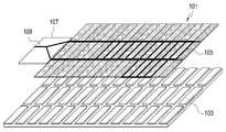
도 2는 본 발명의 다양한 실시예 중 하나에 따른 디스플레이 장치를 나타내는 분리 사시도이다. 도 3은 본 발명의 다양한 실시예 중 하나에 따른 디스플레이 장치의 픽셀들을 나타내는 사시도이다. 도 4는 본 발명의 다양한 실시예 중 하나에 따른 디스플레이 장치의 안테나 방사체 및 급전 기판을 나타내는 도면이다.2 is an exploded perspective view illustrating a display device according to one of various embodiments of the present invention. 3 is a perspective view illustrating pixels of a display device according to one of various embodiments of the present invention. 4 is a view illustrating an antenna radiator and a power supply substrate of a display device according to one of various embodiments of the present invention.
먼저, 본 발명의 일 실시예에 따른 디스플레이 장치(100, 도 1)는 전술한 스마트폰에 구비될 수 있다. 다만, 상기 디스플레이 장치는 스마트폰에 구비되는 것에 한정되지 않고, 스마트 시계 등 웨어러블 디바이스(wearable device)에 구비될 수 있다.First, the display apparatus 100 ( FIG. 1 ) according to an embodiment of the present invention may be provided in the aforementioned smart phone. However, the display apparatus is not limited to being provided in a smart phone, and may be provided in a wearable device such as a smart watch.
도 2 내지 도 4를 참조하면, 본 발명의 다양한 실시예 중 하나에 따른 디스플레이 장치는 복수의 픽셀(111a, 111b, 111c)들, 액정층(102), 트랜지스터(131)들, 백라이트(104), 안테나 방사체(105) 및 급전 기판(107)을 포함할 수 있다.2 to 4 , a display device according to one of various embodiments of the present invention includes a plurality of
상기 복수의 픽셀(111a, 111b, 111c)들은 서로에 대하여 간격을 두고 제1 기판(113)에 배열되어 출력층(output layer)을 이룰 수 있다. 상기 픽셀(111a, 111b, 111c)들은 각각 레드(red), 그린(green) 및 블루(blue) 중 하나의 색을 출력할 수 있다. 예를 들면, 상기 픽셀(111a, 111b, 111c)들은 상기 백라이트(104)에서 출력된 광을 상기 액정층(102)으로부터 전달받아 레드, 그린 및 블루 중 하나의 색을 출력할 수 있다. 상기 픽셀들은 레드의 색을 출력하는 제1 픽셀(111a)들, 그린의 색을 출력하는 제2 픽셀(111b)들 및 블루의 색을 출력하는 제3 픽셀(111c)들을 구비할 수 있다. 그리고, 상기 제1 픽셀(111a)은 상기 제2 픽셀(111b)과 제1 간격(113a)을 두고 배열될 수 있다. 상기 제2 픽셀(111b)은 상기 제3 픽셀(111c)과 제2 간격(113b)을 두고 배열될 수 있다. 상기 제1 간격(113a)은 상기 제2 간격(113b)과 대응될 수 있으나, 이에 한정되지 않고, 서로 다른 간격을 가질 수 있다.The plurality of
상기 액정층(102)은 상기 픽셀(111a, 111b, 111c)들의 일면에 배치될 수 있다. 상기 액정층(102)은 일정한 방향으로 배열된 액정(Liquid crystal)을 구비되어 전기 신호에 의해 상기 액정이 다른 방향으로 배열될 수 있다. 상기 액정층(102)은 이러한 액정 물질의 배열 변화에 따라, 상기 액정층(102)에 전달된 광의 진행 방향을 변경할 수 있다.The
상기 트랜지스터(131)들은 상기 액정층(102)의 일면에 배치될 수 있다. 상기 트랜지스터(131)들은 상기 픽셀(111a, 111b, 111c)들 각각에 대응하여 제2 기판(103)에 배열될 수 있다. 상기 트랜지스터(131)들은 상기 액정층(102)에 전기 신호를 가하여 상기 액정층(102)의 액정의 배열을 변화시킬 수 있다.The
상기 백라이트(104)는 상기 제2 기판(103)의 일면에 배치되며, 상기 액정층(102)을 향하여 광을 출력할 수 있다. 상기 백라이트(104)는 냉음극 형광램프(Cold Cathode Fluorescent Lamp: CCFL), 외부전극 형광램프(External Electrode Fluorescent Lamp: EEFL), 발광 다이오드(Light Emitting Diode) 및 평판형 형광 램프(Flat Fluorescent Lamp: FFL) 중 하나일 수 있다. 다만, 상기 백라이트(104)는 이에 한정되지 않고, 광을 출력하는 다양한 광원 장치일 수 있다. 상기 백라이트(104)에서 출력된 광은 상기 액정층(102)을 경유하여 상기 픽셀(111a, 111b, 111c)들에게 전달될 수 있다.The
상기 안테나 방사체(105)는 상기 픽셀(111a, 111b, 111c)들 사이에 배열되는 적어도 하나의 도체로 이루어질 수 있다. 상기 안테나 방사체(105)는 상기 픽셀(111a, 111b, 111c)들이 이루는 층 내에 위치할 수 있다. 상기 안테나 방사체(105)는 급전을 받아 적어도 하나의 공진 주파수를 형성할 수 있다. 그리고, 상기 안테나 방사체(105)는 상기 픽셀(111a, 111b, 111c)들 사이에 배열됨에 따라, 상기 픽셀(111a, 111b, 111c)들이 출력하는 색에 영향을 주는 것을 방지할 수 있다. 또한, 상기 안테나 방사체(105)는 상기 픽셀들(111a, 111b, 111c)들 사이에 배열됨에 따라, 상기 디스플레이 장치를 구비하는 전자 장치의 내부에 별도로 장착될 필요가 없게 되어 상기 전자 장치를 소형화할 수 있다.The
상기 급전 기판(109)은 상기 출력층(101)의 일단에 연결되며, 상기 안테나 방사체(105)의 도체와 연결되는 급전 라인(109)를 구비할 수 있다. 상기 급전 라인(109)은 상기 안테나 방사체(105)에 전기적 신호를 공급하여, 상기 안테나 방사체(105)가 공진 주파수를 형성할 수 있다.The feeding
도 5은 본 발명의 다양한 실시예 중 다른 하나에 따른 디스플레이 장치의 픽셀들을 나타내는 평면도이다.5 is a plan view illustrating pixels of a display device according to another one of various embodiments of the present invention.
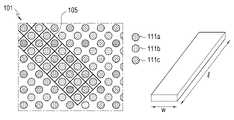
도 5를 참조하면, 본 발명의 다양한 실시예 중 다른 하나에 따른 디스플레이 장치의 픽셀(111a, 111b, 111c)들은 원형 형태를 가질 수 있다. 다만, 상기 픽셀(111a, 111b, 111c)들은 원형 형태를 가지는 것에 한정되지 않고, 마름모, 직사각형 등 다양한 형태를 가질 수 있다. 또한, 상기 픽셀(111a, 111b, 111c)들은 서로 동일한 크기를 가질 수 있으나, 이에 한정되지 않는다. 예를 들면, 상기 픽셀들은 레드의 색을 출력하는 제1 픽셀(111a)들, 그린의 색을 출력하는 제2 픽셀(111b)들 및 블루의 색을 출력하는 제3 픽셀(111c)들을 구비하고, 상기 제2 픽셀(111b)의 크기는 상기 제3 픽셀(111c) 및 상기 제1 픽셀(111a)보다 작고, 상기 제3 픽셀(111c)의 크기는 상기 제1 픽셀(111a)보다 작을 수 있다.Referring to FIG. 5 ,
그리고, 상기 픽셀(111a, 111b, 111c)들 사이에는 차광부(106)가 구비될 수 있다. 상기 차광부(106)는 상기 픽셀(111a, 111b, 111c)들 사이에서 상기 백라이트(104, 도 2)로 광이 투과하는 것을 차단할 수 있다. 상기 차광부(106)는 카본 블랙(carbon black)으로 이루어질 수 있다. 다만, 상기 차광부(106)는 상기 카본 블랙에 한정되지 않고, 광을 흡수할 수 있는 재질로 이루어지거나 광을 선택적으로 반사하는 재질로 이루어질 수 있다. 상기 차광부(106)는 상기 픽셀(111a, 111b, 111c)들 각각 출력되는 색이 서로 간섭이 일어나는 것을 방지할 수 있다. 또한, 상기 차광부(106)는 디스플레이 장치의 외부에서 들어오는 광을 흡수할 수 있다.In addition, a
도 6은 본 발명의 다양한 실시예 중 다른 하나에 따른 디스플레이 장치의 안테나 방사체를 나타내는 평면도이다.6 is a plan view illustrating an antenna radiator of a display apparatus according to another one of various embodiments of the present invention.
도 6을 참조하면, 상기 안테나 방사체(105)는 복수 개의 상기 도체들이 상기 픽셀(111a, 111b, 111c)들 사이로 교차하게 연장되어 메쉬(mesh) 형태로 형성될 수 있다. 상기 안테나 방사체(105)는 상기 메쉬 형태의 안테나 방사체(105)는 신호 전류가 분포되기 때문에, 상기 도체의 저항 성분에 의한 손실을 줄일 수 있다.Referring to FIG. 6 , the
그리고, 상기 안테나 방사체(105)는 도체의 비저항(resisitivity), 길이(l), 선폭(w)에 따라 공진 주파수 대역이 결정될 수 있다. 예를 들면, 상기 도체의 저항은 비저항과 길이에 비례하면서 선폭에 반비례할 수 있다.In addition, the
그리고, 상기 안테나 방사체(105)는 상기 도체의 저항에 반비례하는 공진 주파수 대역을 형성할 수 있다. 예를 들면, 상기 안테나 방사체(105)는 상기 도체의 저항이 큰 경우, 고주파 대역의 공진 주파수를 형성할 수 있다. 이러한 도체의 저항을 조정하여, 상기 디스플레이 장치 내에 안테나 방사체(105)의 주파수 대역을 설정할 수 있다.In addition, the
도 7은 본 발명의 다양한 실시예 중 다른 하나에 따른 디스플레이 장치의 도체에 차광부가 덮어진 모습을 나타내는 도면이다.7 is a view illustrating a state in which a light blocking unit is covered on a conductor of a display device according to another one of various embodiments of the present invention.
도 7을 참조하면, 상기 안테나 방사체(105)는 상기 차광부(106)에 의해 덮어질 수 있다. 상기 차광부(106)는 상기 안테나 방사체(105)를 덮어 상기 안테나 방사체(105)가 상기 픽셀(111a, 111b, 111c)들에서 출력되는 색에 영향을 주는 것을 방지할 수 있다.Referring to FIG. 7 , the
도 8은 본 발명의 다양한 실시예 중 또 다른 하나에 따른 디스플레이 장치의 안테나 방사체를 나타내는 평면도이다.8 is a plan view illustrating an antenna radiator of a display device according to another one of various embodiments of the present invention.
도 8을 참조하면, 본 발명의 다양한 실시예 중 또 다른 하나에 따른 디스플레이 장치에 적용되는 안테나 방사체(105)는 상기 도체의 일부분이 제거된 분절 부분(151a)을 포함할 수 있다. 이러한 분절 부분(151a)을 이루는 안테나 방사체(105)는 전체적인 도체의 길이를 변경하거나 도체들의 전기적인 연결 상태가 변경될 수 있다. 즉, 상기 분절 부분(151a)의 개수 및 분절 부분(151a)의 위치에 따라, 상기 안테나 방사체(105)는 다양한 주파수 대역을 형성할 수 있다.Referring to FIG. 8 , an
도 9는 본 발명의 다양한 실시예 중 또 다른 하나에 따른 디스플레이 장치의 도체에 차광부가 덮어진 모습을 나타내는 도면이다.9 is a diagram illustrating a state in which a light blocking unit is covered on a conductor of a display device according to still another one of various embodiments of the present invention.
도 9를 참조하면, 상기 안테나 방사체(105)는 상기 차광부(106)에 의해 덮어질 수 있다. 상기 차광부(106)는 상기 안테나 방사체(105)의 분절 부분(151a)에 충전될 수 있다.Referring to FIG. 9 , the
도 10은 본 발명의 다양한 실시예 중 또 다른 하나에 따른 디스플레이 장치의 일부분을 나타내는 단면도이다.10 is a cross-sectional view illustrating a portion of a display device according to still another one of various embodiments of the present invention.
도 10을 참조하면, 본 발명의 다양한 실시예 중 또 다른 하나에 따른 디스플레이 장치는 유리 기판(112), 픽셀(111a, 111b, 111c)들, 도체(109b)들, 차광부(109b), 코팅층(115) 및 공통 전극(114)을 포함할 수 있다.Referring to FIG. 10 , a display device according to another one of various embodiments of the present invention includes a
상기 유리 기판(112)는 상기 (111a, 111b, 111c)들의 일면에 배치되어 상기 픽셀(111a, 111b, 111c)들을 보호할 수 있다. 또한, 상기 유리 기판(112)는 편광 유리로 이루어질 수 있다.The
상기 도체(109b)들은 상기 픽셀(111a, 111b, 111c)들 사이에 배치되며, 상기 차광부(109b)에 감싸질 수 있다. 즉, 상기 도체(109b)들은 상기 차광부(109b)에 의해 은폐되어 인접하는 픽셀(111a, 111b, 111c)에서 출력되는 색과 간섭이 일어나는 것을 방지할 수 있다.The
상기 차광부(109b)는 상기 픽셀(111a, 111b, 111c)의 타면, 예를 들면, 상기 픽셀(111a, 111b, 111c)들에서 색이 출력되는 면의 일부분을 은폐할 수 있다. 이에 따라, 상기 디스플레이 장치의 외부에서 들어오는 광을 흡수할 수 있다.The
상기 코팅층(115)은 상기 픽셀(111a, 111b, 111c)의 일면에 형성될 수 있다. 또한, 상기 코팅층(115)은 상기 픽셀(111a, 111b, 111c)들 사이에 충전될 수 있다.The
상기 공통 전극(114)은 상기 트랜지스터(131, 도 2)들에 연결되어 상기 액정층(102, 도 2)에 전압을 인가할 수 있다.The
도 11은 본 발명의 다양한 실시예 중 또 다른 하나에 따른 디스플레이 장치의 일부분을 나타내는 단면도이다. 본 실시예에서는, 전술한 실시예와 유사한 구성요소에 대한 자세한 설명은 생략하기로 한다.11 is a cross-sectional view illustrating a portion of a display device according to still another one of various embodiments of the present invention. In this embodiment, detailed descriptions of components similar to those of the above-described embodiment will be omitted.
도 11을 참조하면, 본 발명의 다양한 실시예 중 또 다른 하나에 따른 디스플레이 장치에 적용되는 도체(101c)는 차광부(109c)의 일면에 배치될 수 있다. 즉, 상기 도체(101c)는 상기 차광부(109c) 상에 적층될 수 있다. 이러한 적층 구조를 가지는 디스플레이 장치를 제작함에 있어서, 상기 도체(101c)는 먼저 상기 픽셀(111a, 111b, 111c)들 사이에 배열된 후, 상기 차광부(109c)를 상기 픽셀(111a, 111b, 111c) 상에 적층할 수 있다.Referring to FIG. 11 , a
도 12는 본 발명의 다양한 실시예 중 다른 하나에 따른 전자 장치를 나타내는 분리 사시도이다.12 is an exploded perspective view illustrating an electronic device according to another one of various embodiments of the present disclosure;
상기 전자 장치는 이동통신 단말기 등의 휴대용 전자 장치나 사용자의 신체에 착용 가능한 다양한 전자 장치일 수 있다. 본 실시예에서는 상기 전자 장치를 스마트 시계(smart watch)로 예를 들어 설명하기로 한다.The electronic device may be a portable electronic device such as a mobile communication terminal or various electronic devices that can be worn on a user's body. In this embodiment, the electronic device will be described as an example of a smart watch.
도 12를 참조하면, 상기 전자 장치(20)는, 하우징(21)의 양측(또는, 양단)에서 각각 서로 멀어지는 방향으로 연장된 착용부(25, 26)들을 포함할 수 있다. 상기 착용부(25, 26)들은 일부분이 서로 중첩한 상태로 결속되어 상기 전자 장치(20)를 사용자의 신체(예: 손목)에 착용 가능하게 할 수 있다. 상기 하우징(20)은 금속 재질로 이루어지거나, 상기 하우징(20)의 테두리가 금속 재질로 이루어질 수 있다. 상기 하우징(20)은, 프로세서(예: 어플리케이션 프로세서(application processor: AP)), 통신 모듈, 메모리, 배터리 등 각종 회로 장치들을 내장할 수 있으며, 일면에 장착된 디스플레이 장치(22)를 포함할 수 있다. 상기 디스플레이 장치(22)는, 액정 디스플레이(LCD), 발광 다이오드(LED) 디스플레이, 유기 발광 다이오드(OLED) 디스플레이, 또는 마이크로 전자기계 시스템(microelectromechanical system: MEMS) 디스플레이, 또는 전자 종이(electronic paper) 디스플레이를 포함할 수 있다. 상기 디스플레이 장치(22)는 각종 콘텐츠(예: 사진, 동영상)를 출력할 수 있고, 사용자의 조작에 따라 다양한 어플리케이션(예: 게임, 인터넷 뱅킹, 일정 관리 등)의 실행 화면을 출력할 수 있다. 또한, 본 발명의 다양한 실시예에 따른 디스플레이 장치(22)에는 전술한 안테나 방사체가 내장될 수 있다. 또한, 상기 전자 장치(20)가 터치 스크린 기능을 가지고 있다면, 상기 디스플레이 장치(22) 상에는 터치 스크린 패널이 설치될 수 있다.Referring to FIG. 12 , the
상기 하우징(21)의 전면에는 윈도우 부재(23)가 장착되어 상기 디스플레이 장치(22)를 보호할 수 있다. 상기 윈도우 부재(23)는 투명한 소재, 예컨대, 유리(glass)나 합성수지(예: 아크릴, 폴리카보네이트)로 제작되어, 상기 디스플레이 장치(21)로부터 출력되는 화면을 투과시키면서 외부 환경으로부터 상기 디스플레이 장치(22)를 보호할 수 있다. 상기 윈도우 부재(23)의 테두리에는 베젤(24)이 형성될 수 있다. 상기 베젤(24)은 금속 재질로 이루어져 외관을 미려하게 할 수 있다.A
도 13은 본 발명의 다양한 실시예 중 또 다른 하나에 따른 디스플레이 장치를 나타내는 단면도이다.13 is a cross-sectional view illustrating a display device according to still another one of various embodiments of the present invention.
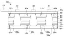
도 13을 참조하면, 본 발명의 다양한 실시예 중 또 다른 하나에 따른 디스플레이 장치(200)는 발광층(206), 격벽(212)들, 도체(201)들, 정공 이송층(207, 208), 양극(209), 전자 이송층(203, 204), 음극(202) 및 트랜지스터 기판(210)을 포함할 수 있다.Referring to FIG. 13 , a
상기 발광층(206)은 전술한 실시예와 달리, 광을 자체적으로 출력할 수 있다. 또한, 상기 발광층(206)은 레드, 그린 및 블루 중 하나의 색을 출력할 수 있다.Unlike the above-described embodiment, the
상기 정공 이송층(207, 208)은 상기 발광층(206)의 일면에 배치되어 상기 발광층(206)으로 정공(hole)이 이송되는 경로를 제공할 수 있다.The
상기 양극(210)은 상기 정공 이송층(207, 208)의 일면에 배치되어 상기 정공 이송층(207, 208)에 정공을 공급할 수 있다.The
상기 전자 이송층(204, 205)은 상기 발광층(206)의 타면에 배치되어 상기 발광층(206)으로 전자가 이송되는 경로를 제공할 수 있다.The
상기 음극(202)은 상기 전자 이송층(204, 205)의 타면에 배치되며, 상기 전자를 발생시켜 상기 전자 이송층(204, 205)에 상기 전자를 공급할 수 있다.The
픽셀들은 상기 음극(202), 상기 전자 이송층(204, 205), 상기 발광층(206), 상기 정공 이송층(207, 208)이 순차적으로 적층되어 이루어질 수 있다. 상기 격벽(212)들은 상기 픽셀들 사이에 배치되어 상기 픽셀들을 서로 분리시킬 수 있다. 또한, 상기 발광층(206)은 상기 격벽(212)들에 의해 서로에 대하여 간격을 두고 배열되는 복수의 발광부들을 구비할 수 있다.The pixels may be formed by sequentially stacking the
상기 도체(201)들은 상기 픽셀들 사이에 배열되면서 상기 격벽(212)들의 일면에 배치될 수 있다. 상기 도체(201)들은 알루미늄(Aluminum) 재질로 이루어질 수 있다. 다만, 상기 도체(201)들은 알루미늄 재질로 이루어진 것에 한정되지 않고, 전파를 송수신할 수 있는 다양한 소재로 이루어질 수 있다.The
그리고, 상기 격벽(212)의 일면은 상기 음극(202)과 다른 평면에 위치하게 되어 상기 도체(201)들이 상기 음극(202)과 연결되는 것을 차단할 수 있다. 또한, 본 발명의 다양한 실시예에 따른 디스플레이 장치(200)는 상기 도체(201)들과 상기 음극(202) 사이에 구비되는 절연부(213)를 더 포함할 수 있다. 상기 절연부(213)는 무기물 재질로 이루어져 상기 도체(201)들과 상기 음극(202) 사이를 전기적으로 절연시킬 수 있다. 다만, 상기 절연부(213)는 고무 재질에 한정되지 않고, 전기적 연결을 차단하는 다양한 재질일 수 있다.In addition, one surface of the
상기 트랜지스터 기판(210)은 상기 양극(209)의 일면에 배치되어 상기 양극(209)에 공급되는 전기적 신호를 조절할 수 있다. 상기 트랜지스터 기판(210)은 복수의 트랜지스터들을 포함하고, 상기 각각의 트랜지스터는 상기 각각의 발광부에 대응되어 배열될 수 있다.The
상기 발광층(206)은 상기 정공 이송층(207, 208)에서 이송된 정공과 상기 전자 이송층(207, 208)에서 이송된 전자들에 의해 광을 출력할 수 있다. 이때, 상기 발광층(206)은 상기 음극(202)을 향하여 광을 출력할 수 있다. 그리고, 상기 도체(201)들은 상기 격벽(212) 상에 배치되어 상기 광의 진행 경로에서 벗어날 수 있다. 따라서, 상기 도체(201)들은 상기 발광층(206)에서 출력된 광에 간섭되는 것을 방지할 수 있다.The
또한, 본 발명의 다양한 실시예에 따르면, 상기 발광층(206)에서 출력되는 광은 트랜지스터 기판(210) 및 유리 기판(211)을 통과할 수 있다. 상기 도체(201)들은 상기 광이 출력되는 방향과 반대 방향에 위치하게 되어 상기 도체(201)가 상기 광을 간섭하는 것을 방지할 수 있다.In addition, according to various embodiments of the present disclosure, light output from the
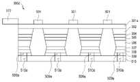
도 14는 본 발명의 다양한 실시예 중 또 다른 하나에 따른 디스플레이 장치의 안테나 방사체 및 급전 기판을 나타내는 도면이다. 본 실시예를 설명함에 있어, 선행 실시예와 유사한 및/또는 선행 실시예를 통해 용이하게 이해될 수 있는 구성요소들에 대해서는 도면의 참조번호를 동일하게 부여하거나 생략하고, 그 상세한 설명 또한 생략될 수 있다.14 is a view showing an antenna radiator and a power supply substrate of a display device according to another one of various embodiments of the present invention. In describing the present embodiment, the same reference numerals in the drawings are given or omitted for components similar to and/or easily understood through the preceding embodiments, and detailed descriptions thereof will also be omitted. can
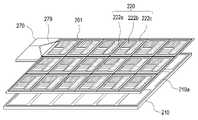
도 14를 참조하면, 본 발명의 다양한 실시예 중 또 다른 하나에 따른 디스플레이 장치는 상기 음극(202)의 일단에 연결되는 급전 기판(270)을 더 포함할 수 있다.Referring to FIG. 14 , the display device according to another one of various embodiments of the present invention may further include a
상기 급전 기판(270)은 상기 도체(201)들과 전기적으로 연결되는 급전 라인(279)를 구비할 수 있다. 상기 급전 라인(279)은 상기 도체(201)에 전기적 신호를 공급하여, 상기 도체(201)들로 이루어진 안테나 방사체가 전파를 송수신할 수 있다.The feeding
그리고, 상기 픽셀(220)들은 상기 격벽(212, 도 13)들에 의해 서로 분리되는 제1 픽셀(222a), 제2 픽셀(222b) 및 제3 픽셀(222c)를 구비할 수 있다. 상기 제1 픽셀(222a)은 레드의 색의 광을 출력하고, 상기 제2 픽셀(222b)은 그린의 색의 광을 출력하고, 상기 제3 픽셀(222c)은 블루의 색의 광을 출력할 수 있다. 예컨대, 서로 인접하는 어느 하나의 제1 픽셀(222a), 어느 하나의 제2 픽셀(222b)과 어느 하나의 제3 픽셀(222c)이 조합되어 레드의 색, 그린의 색, 블루의 색의 광을 각각 출력할 수 있는 픽셀(220)을 형성할 수 있다.In addition, the
상기 도체(201)들은 상기 픽셀(220)들 사이에 배치되어 메쉬(mesh) 형태의 안테나 방사체를 형성할 수 있다. 상기 안테나 방사체는 전파를 송수신할 수 있다. 또한, 본 발명의 다양한 실시예에 따르면, 상기 도체(201)들 중 일부분은 상기 제1 픽셀(222a)과 상기 제2 픽셀(222b) 사이에 배치되거나, 상기 제1 픽셀(222a)과 상기 제3 픽셀(222c) 사이에 배치되거나, 상기 제2 픽셀(222b)과 상기 제3 픽셀(222c) 사이에 배치될 수 있다.The
도 15는 본 발명의 다양한 실시예 중 또 다른 하나에 따른 디스플레이 장치의 트랜지스터 기판이 분절된 모습을 나타내는 도면이다. 도 16는 본 발명의 다양한 실시예 중 또 다른 하나에 따른 디스플레이 장치를 나타내는 단면도이다. 본 실시예를 설명함에 있어, 선행 실시예와 유사한 및/또는 선행 실시예를 통해 용이하게 이해될 수 있는 구성요소들에 대해서는 도면의 참조번호를 동일하게 부여하거나 생략하고, 그 상세한 설명 또한 생략될 수 있다.15 is a diagram illustrating a segmented state of a transistor substrate of a display device according to another one of various embodiments of the present invention. 16 is a cross-sectional view illustrating a display device according to still another one of various embodiments of the present invention. In describing the present embodiment, the same reference numerals in the drawings are given or omitted for components similar to and/or easily understood through the preceding embodiments, and detailed descriptions thereof will also be omitted. can
도 15 및 도 16을 참조하면, 상기 트랜지스터 기판(210)에는 트랜지스터 슬롯(210a)들이 형성될 수 있다. 상기 트랜지스터 슬롯(210a)들은 제1 방향을 따라 형성되거나 상기 제1 방향과 수직한 방향으로 형성될 수 있다. 상기 도체(201)들에 의해 형성된 전파는 상기 트랜지스터 슬롯(210a)들을 통해 상기 트랜지스터 기판(210)을 통과하여 진행될 수 있다.15 and 16 ,
도 17은 본 발명의 다양한 실시예 중 또 다른 하나에 따른 디스플레이 장치를 나타내는 단면도이다.17 is a cross-sectional view illustrating a display device according to still another one of various embodiments of the present invention.
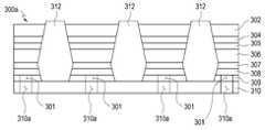
도 17을 참조하면, 본 발명의 다양한 실시예 중 또 다른 하나에 따른 디스플레이 장치(300)는 발광층(306), 격벽(312)들, 도체(301)들, 정공 이송층(307, 308), 양극(309), 전자 이송층(303, 304), 음극(302) 및 트랜지스터 기판(310)을 포함할 수 있다. 본 실시예를 설명함에 있어, 선행 실시예와 유사한 및/또는 선행 실시예를 통해 용이하게 이해될 수 있는 구성요소들에 대해서는 도면의 참조번호를 동일하게 부여하거나 생략하고, 그 상세한 설명 또한 생략될 수 있다. 그리고, 본 실시예에서는 도체(301)들의 배치를 중점적으로 살펴보기로 한다.Referring to FIG. 17 , a
상기 도체(301)들은 상기 양극(309)에 구비될 수 있다. 그리고, 상기 도체(301)들은 양극 절연부(309a)에 의해 감싸져 상기 양극(309)과 전기적으로 절연될 수 있다. 그리고, 상기 도체(301)들은 은(Ag) 재질로 이루어질 수 있다. 다만, 상기 도체(301)들은 은(Ag) 재질에 한정되지 않고, 전파를 방사할 수 있는 다양한 재질로 이루어질 수 있다. 그리고, 상기 양근 절연부(309a)은 공기층을 형성하거나 무기물 재질로 이루어져 상기 양극(309)과 상기 도체(301)들을 전기적으로 절연시킬 수 있다.The
이에 따라, 상기 발광층(306)이 광을 상기 음극(302) 방향으로 출력하는 경우, 상기 안테나(301)가 상기 광이 출력되는 방향(예를 들면, 상기 디스플레이 장치에서 이미지가 표시되는 방향)과 반대 방향에 위치하게 되어 출력되는 광을 간섭하는 것을 방지할 수 있다.Accordingly, when the
도 18은 본 발명의 다양한 실시예 중 또 다른 하나에 따른 디스플레이 장치를 나타내는 단면도이다. 본 실시예를 설명함에 있어, 선행 실시예와 유사한 및/또는 선행 실시예를 통해 용이하게 이해될 수 있는 구성요소들에 대해서는 도면의 참조번호를 동일하게 부여하거나 생략하고, 그 상세한 설명 또한 생략될 수 있다.18 is a cross-sectional view illustrating a display device according to still another one of various embodiments of the present invention. In describing the present embodiment, the same reference numerals in the drawings are given or omitted for components similar to and/or easily understood through the preceding embodiments, and detailed descriptions thereof will also be omitted. can
도 18를 참조하면, 본 발명의 다양한 실시예 중 또 다른 하나에 따른 디스플레이 장치(300a)는 상기 도체(301)들을 구비한 상기 양극(309) 및 트랜지스터 슬롯(310a)를 형성하는 트랜지스터 기판(310)을 포함할 수 있다.Referring to FIG. 18 , in a
상기 트랜지스터 슬롯(310a)은 상기 도체(301) 각각과 대응되는 위치에 형성될 수 있다. 다만, 상기 트랜지스터 슬롯(310a)은 상기 도체(301)들과 대응되는 위치에 형성되는 것에 한정되지 않고, 다양한 패턴으로 상기 트랜지스터 기판(310)에 형성될 수 있다. 상기 도체(301)들에 의해 형성된 전파는 상기 트랜지스터 슬롯(310a)들을 통해 트랜지스터 기판(310)을 통과하여 진행될 수 있다.The
도 19는 본 발명의 다양한 실시예 중 또 다른 하나에 따른 디스플레이 장치와 제2의 안테나부를 나타내는 도면이다. 도 20은 본 발명의 다양한 실시예 중 또 다른 하나에 따른 디스플레이 장치와 제2의 안테나부를 나타내는 단면도이다.19 is a diagram illustrating a display device and a second antenna unit according to still another one of various embodiments of the present invention. 20 is a cross-sectional view illustrating a display device and a second antenna unit according to still another one of various embodiments of the present invention.
도 19 및 도 20을 참조하면, 본 발명의 다양한 실시예 중 또 다른 하나에 따른 디스플레이 장치(400)는 발광층(406), 격벽(412)들, 회로 기판(420), 정공 이송층(407, 408), 양극(409), 전자 이송층(403, 404), 음극(402) 및 트랜지스터 기판(410)을 포함할 수 있다. 본 실시예를 설명함에 있어, 선행 실시예와 유사한 및/또는 선행 실시예를 통해 용이하게 이해될 수 있는 구성요소들에 대해서는 도면의 참조번호를 동일하게 부여하거나 생략하고, 그 상세한 설명 또한 생략될 수 있다. 그리고, 본 실시예에서는 회로 기판(420)에 배치되는 안테나 방사체를 중점적으로 살펴보기로 한다.19 and 20 , a
상기 회로 기판(420)은 상기 트랜지스터 기판(410)의 하면(예를 들면, 상기 트랜지스터 기판(410)이 상기 양극(409)과 접하는 면의 반대면)에 구비될 수 있다. 상기 회로 기판(420)에는 안테나 방사체(421)가 구비될 수 있다. 그리고, 상기 회로 기판(420)에는 상기 안테나 방사체(421)에 전기적 신호를 급전하는 급전라인(479)이 구비될 수 있다. 상기 안테나 방사체(421)는 메쉬(mesh) 형태 등 다양한 패턴으로 상기 회로 기판(420)에 형성될 수 있다. 상기 안테나 방사체(421)는 상기 발광층(406)이 광을 출력하는 방향과 반대 방향에 배치됨에 따라, 광의 출력을 간섭하는 것을 방지할 수 있다.The
그리고, 상기 트랜지스터 기판(410)에는 트랜지스터 슬롯(410a)이 형성될 수 있다. 상기 안테나 방사체(421)들에 의해 형성된 전파는 상기 트랜지스터 슬롯(410a)들을 통해 상기 트랜지스터 기판(410)을 통과하여 진행함에 따라, 상기 트랜지스터 기판(410)을 직접 관통하는 것에 비해 전파의 손실을 억제할 수 있다.In addition, a
도 21은 본 발명의 다양한 실시예 중 또 다른 하나에 따른 디스플레이 장치를 나타내는 단면도이다.21 is a cross-sectional view illustrating a display device according to still another one of various embodiments of the present invention.
도 21을 참조하면, 본 발명의 다양한 실시예 중 또 다른 하나에 따른 디스플레이 장치(500)는 발광층(506), 격벽(512)들, 도체(501)들, 정공 이송층(507, 508), 양극(509), 전자 이송층(503, 504), 음극(502) 및 트랜지스터 기판(510)을 포함할 수 있다. 본 실시예를 설명함에 있어, 선행 실시예와 유사한 및/또는 선행 실시예를 통해 용이하게 이해될 수 있는 구성요소들에 대해서는 도면의 참조번호를 동일하게 부여하거나 생략하고, 그 상세한 설명 또한 생략될 수 있다.Referring to FIG. 21 , a
상기 도체(501)들은 상기 음극(502)과 다른 층에 배치될 수 있다. 그리고, 상기 도체(501)들과 상기 음극(502) 사이에는 절연부(501a)가 구비되어, 상기 도체(501)들과 상기 음극(502)의 전기적인 연결을 차단할 수 있다.The
그리고, 상기 도체(501)들과 동일한 층에는 급전 기판(570)이 구비될 수 있다. 상기 급전 기판(570)은 상기 도체(501)와 전기적으로 연결되는 급전 라인(미도시)을 구비하여, 상기 급전 라인을 통해 상기 도체(501)에 전기적 신호를 급전할 수 있다.In addition, a
그리고, 상기 음극(502)에는 음극 슬롯(502a)이 형성될 수 있다. 상기 도체(501)들에 의해 형성된 전파는 상기 음극 슬롯(502a)을 통해 상기 트랜지스터 기판(510) 방향으로 방사됨에 따라, 상기 음극(502)에 의해 전파가 간섭되는 것을 방지할 수 있다.In addition, a
도 22는 본 발명의 다양한 실시예 중 또 다른 하나에 따른 디스플레이 장치를 나타내는 단면도이다. 본 실시예를 설명함에 있어, 선행 실시예와 유사한 및/또는 선행 실시예를 통해 용이하게 이해될 수 있는 구성요소들에 대해서는 도면의 참조번호를 동일하게 부여하거나 생략하고, 그 상세한 설명 또한 생략될 수 있다.22 is a cross-sectional view illustrating a display device according to still another one of various embodiments of the present invention. In describing the present embodiment, the same reference numerals in the drawings are given or omitted for components similar to and/or easily understood through the preceding embodiments, and detailed descriptions thereof will also be omitted. can
도 22를 참조하면, 본 발명의 다양한 실시예 중 또 다른 하나에 따른 디스플레이 장치(500a)는 선행 실시예의 음극 슬롯(502a)과 더불어 양극 슬롯(509a)을 포함할 수 있다.Referring to FIG. 22 , a
상기 양극 슬롯(509a)은 상기 양극(509)에 형성되어, 상기 도체(501)들에 의해 형성된 전파를 통과시킬 수 있다. 또한, 양극 슬롯(509a)은 상기 음극 슬롯(502a)과 대응되는 위치에 배치될 수 있으나, 이에 한정되지 않고, 다양한 패턴으로 상기 양극(509)에 형성될 수 있다.The
도 23은 본 발명의 다양한 실시예 중 또 다른 하나에 따른 디스플레이 장치를 나타내는 단면도이다. 본 실시예를 설명함에 있어, 선행 실시예와 유사한 및/또는 선행 실시예를 통해 용이하게 이해될 수 있는 구성요소들에 대해서는 도면의 참조번호를 동일하게 부여하거나 생략하고, 그 상세한 설명 또한 생략될 수 있다.23 is a cross-sectional view illustrating a display device according to still another one of various embodiments of the present invention. In describing the present embodiment, the same reference numerals in the drawings are given or omitted for components similar to and/or easily understood through the preceding embodiments, and detailed descriptions thereof will also be omitted. can
도 23을 참조하면, 본 발명의 다양한 실시예 중 또 다른 하나에 따른 디스플레이 장치(500b)는 선행 실시예의 음극 슬롯(502a) 및 양극 슬롯(509a)을 포함함과 더불어 트랜지스터 슬롯(510a)을 포함할 수 있다.Referring to FIG. 23 , a
상기 트랜지스터 슬롯(510a)은 상기 트랜지스터 기판(510)에 형성되어, 전파를 통과시킬 수 있다. 또한, 트랜지스터 슬롯(510a)은 상기 양극 슬롯(509a)과 대응되는 위치에 배치될 수 있으나, 이에 한정되지 않고, 다양한 패턴으로 상기 트랜지스터 기판(510)에 형성될 수 있다.The
도 24는 본 발명의 다양한 실시예 중 또 다른 하나에 따른 디스플레이 장치를 나타내는 단면도이다. 본 실시예를 설명함에 있어, 선행 실시예와 유사한 및/또는 선행 실시예를 통해 용이하게 이해될 수 있는 구성요소들에 대해서는 도면의 참조번호를 동일하게 부여하거나 생략하고, 그 상세한 설명 또한 생략될 수 있다.24 is a cross-sectional view illustrating a display device according to still another one of various embodiments of the present invention. In describing the present embodiment, the same reference numerals in the drawings are given or omitted for components similar to and/or easily understood through the preceding embodiments, and detailed descriptions thereof will also be omitted. can
도 24를 참조하면, 본 발명의 다양한 실시예 중 또 다른 하나에 따른 디스플레이 장치(500c)는 상기 음극 슬롯(502a)과 상기 트랜지스터 슬롯(510a)의 조합으로 이루어질 수 있다.Referring to FIG. 24 , a
도 25는 본 발명의 다양한 실시예 중 또 다른 하나에 따른 디스플레이 장치를 나타내는 단면도이다. 본 실시예를 설명함에 있어, 선행 실시예와 유사한 및/또는 선행 실시예를 통해 용이하게 이해될 수 있는 구성요소들에 대해서는 도면의 참조번호를 동일하게 부여하거나 생략하고, 그 상세한 설명 또한 생략될 수 있다.25 is a cross-sectional view illustrating a display device according to still another one of various embodiments of the present invention. In describing the present embodiment, the same reference numerals in the drawings are given or omitted for components similar to and/or easily understood through the preceding embodiments, and detailed descriptions thereof will also be omitted. can
도 25를 참조하면, 본 발명의 다양한 실시예 중 또 다른 하나에 따른 디스플레이 장치(500d)는 상기 양극 슬롯(509a)과 상기 트랜지스터 슬롯(510a)의 조합으로 이루어질 수 있다.Referring to FIG. 25 , a
도 26은 본 발명의 다양한 실시예 중 또 다른 하나에 따른 디스플레이 장치를 나타내는 단면도이다. 본 실시예를 설명함에 있어, 선행 실시예와 유사한 및/또는 선행 실시예를 통해 용이하게 이해될 수 있는 구성요소들에 대해서는 도면의 참조번호를 동일하게 부여하거나 생략하고, 그 상세한 설명 또한 생략될 수 있다.26 is a cross-sectional view illustrating a display device according to still another one of various embodiments of the present invention. In describing the present embodiment, the same reference numerals in the drawings are given or omitted for components similar to and/or easily understood through the preceding embodiments, and detailed descriptions thereof will also be omitted. can
도 26을 참조하면, 본 발명의 다양한 실시예 중 또 다른 하나에 따른 디스플레이 장치(500e)는 회로 기판(521) 및 연결 기판(571)을 포함할 수 있다.Referring to FIG. 26 , a
상기 회로 기판(521)은 제2의 안테나 방사체(미도시)를 구비하면서 연결 기판(571)을 통해 상기 급전 기판(570)과 연결될 수 있다. 제2의 안테나 방사체는 상기 급전 기판(571)과 상기 연결 기판(571)을 통해 전기적 신호를 급전 받아 전파를 방사할 수 있다. 또한, 상기 제2의 안테나 방사체는 상기 급전 기판(571)을 통해 상기 도체(501)들과 전기적으로 연결되어 상기 도체(501)들과 함께 안테나 방사체의 기능을 수행할 수 있다.The
도 27은 본 발명의 다양한 실시예 중 또 다른 하나에 따른 전자 장치의 안테나 방사체를 나타내는 전면도이다.27 is a front view illustrating an antenna radiator of an electronic device according to still another one of various embodiments of the present disclosure.
도 27을 참조하면, 본 발명의 다양한 실시예 중 또 다른 하나에 따른 전자 장치(30)는 선행 실시예의 도체들로 이루어진 안테나 방사체 또는 제2의 안테나 방사체에 의해 형성된 싱글 안테나(31, single antenna)를 포함할 수 있다.Referring to FIG. 27 , an
도 28은 본 발명의 다양한 실시예 중 또 다른 하나에 따른 전자 장치의 안테나 방사체를 나타내는 전면도이다.28 is a front view illustrating an antenna radiator of an electronic device according to still another one of various embodiments of the present disclosure.
도 28을 참조하면, 본 발명의 다양한 실시예 중 또 다른 하나에 따른 전자 장치(30a)는 선행 실시예의 도체들로 이루어진 안테나 방사체 또는 제2의 안테나 방사체에 의해 형성된 배열 안테나(32)를 포함할 수 있다.Referring to FIG. 28 , an
도 29는 본 발명의 다양한 실시예 중 또 다른 하나에 따른 전자 장치의 안테나 방사체를 나타내는 전면도이다.29 is a front view illustrating an antenna radiator of an electronic device according to still another one of various embodiments of the present invention.
도 29를 참조하면, 본 발명의 다양한 실시예 중 또 다른 하나에 따른 전자 장치(30b)는 선행 실시예의 도체들로 이루어진 안테나 방사체 또는 제2의 안테나 방사체에 의해 형성된 미모 안테나(33, multiple-input multiple-output antenna)를 포함할 수 있다.Referring to FIG. 29 , an
도 30은 본 발명의 다양한 실시예 중 또 다른 하나에 따른 전자 장치의 안테나 방사체를 나타내는 전면도이다.30 is a front view illustrating an antenna radiator of an electronic device according to still another one of various embodiments of the present invention.
도 30을 참조하면, 본 발명의 다양한 실시예 중 또 다른 하나에 따른 전자 장치(30c)는 선행 실시예의 도체들로 이루어진 안테나 방사체 또는 제2의 안테나 방사체에 의해 형성된 엔드-파이어 안테나(33, end-fire antenna)를 포함할 수 있다.Referring to FIG. 30 , an
상술한 바와 같이, 본 발명의 다양한 실시예에 따른 디스플레이 장치는, 서로에 대하여 간격을 두고 배열되는 복수의 픽셀들; 및 상기 픽셀들 사이에 배열되는 적어도 하나의 도체로 이루어진 안테나 방사체를 포함할 수 있다.As described above, a display apparatus according to various embodiments of the present disclosure may include: a plurality of pixels arranged at intervals with respect to each other; and an antenna radiator including at least one conductor arranged between the pixels.
또한, 본 발명의 다양한 실시예에 따르면, 상기 안테나 방사체는 상기 픽셀들이 이루는 층 내에 위치할 수 있다.Also, according to various embodiments of the present disclosure, the antenna radiator may be located in a layer formed by the pixels.
또한, 본 발명의 다양한 실시예에 따르면, 상기 픽셀들은 각각 레드(red), 그린(green) 및 블루(blue) 중 하나의 색을 출력할 수 있다.Also, according to various embodiments of the present disclosure, each of the pixels may output one color among red, green, and blue.
또한, 본 발명의 다양한 실시예에 따른 디스플레이 장치는, 상기 픽셀들 사이에 배치되는 차광부를 더 포함하고, 상기 차광부는 상기 픽셀들 사이에서 광이 투과하는 것을 차단할 수 있다.In addition, the display device according to various embodiments of the present disclosure may further include a light blocking unit disposed between the pixels, and the light blocking unit may block light from being transmitted between the pixels.
또한, 본 발명의 다양한 실시예에 따르면, 상기 차광부는 상기 도체를 감쌀 수 있다.Also, according to various embodiments of the present disclosure, the light blocking unit may surround the conductor.
또한, 본 발명의 다양한 실시예에 따르면, 상기 도체는 상기 차광부의 일면에 구비될 수 있다.Also, according to various embodiments of the present disclosure, the conductor may be provided on one surface of the light blocking unit.
또한, 본 발명의 다양한 실시예에 따르면, 복수의 상기 도체들이 상기 픽셀들 사이로 교차하게 연장되어 메쉬(mesh) 형태로 상기 안테나 방사체를 형성할 수 있다.In addition, according to various embodiments of the present disclosure, a plurality of the conductors may crossly extend between the pixels to form the antenna radiator in the form of a mesh.
또한, 본 발명의 다양한 실시예에 따르면, 상기 안테나 방사체는 상기 도체의 일부분이 제거된 분절 부분을 포함할 수 있다.Also, according to various embodiments of the present disclosure, the antenna radiator may include a segmented portion from which a portion of the conductor is removed.
또한, 본 발명의 다양한 실시예에 따른 디스플레이 장치는, 상기 픽셀들이 배치되는 출력층(output layer); 및 상기 출력층에 연결되어 상기 도체에 전류를 급전하는 경로를 제공하는 급전 기판을 더 포함할 수 있다.In addition, a display device according to various embodiments of the present disclosure may include an output layer in which the pixels are disposed; and a feeding substrate connected to the output layer to provide a path for feeding a current to the conductor.
또한, 본 발명의 다양한 실시예에 따른 디스플레이 장치는, 상기 출력층의 일면에 배치되는 액정층; 상기 액정층의 일면에 배치되어 상기 액정층에 인가하는 전압을 조절하는 트랜지스터들; 및 상기 트랜지스터들의 일면에 배치되어 상기 액정층에 광을 출력하는 백라이트를 더 포함할 수 있다.In addition, a display device according to various embodiments of the present disclosure may include a liquid crystal layer disposed on one surface of the output layer; transistors disposed on one surface of the liquid crystal layer to control a voltage applied to the liquid crystal layer; and a backlight disposed on one surface of the transistors to output light to the liquid crystal layer.
또한, 본 발명의 다양한 실시예에 따른 디스플레이 장치는, 상기 픽셀들 사이에 배치되는 격벽들을 더 포함하고, 상기 도체들은 상기 격벽들의 일면에 배치될 수 있다.In addition, the display apparatus according to various embodiments of the present disclosure may further include barrier ribs disposed between the pixels, and the conductors may be disposed on one surface of the barrier ribs.
또한, 본 발명의 다양한 실시예에 따른 디스플레이 장치는, 상기 픽셀들은, 광을 출력하는 발광층; 상기 발광층의 일면에 배치되어 상기 발광층으로 정공(hole)이 이송되는 경로를 제공하는 정공 이송층; 상기 정공 이송층의 일면에 배치되며, 상기 정공을 발생시켜 상기 정공 이송층에 상기 정공을 공급하는 양극; 상기 발광층의 타면에 배치되어 상기 발광층으로 전자가 이송되는 경로를 제공하는 전자 이송층; 및 상기 전자 이송층의 타면에 배치되며, 상기 전자를 발생시켜 상기 전자 이송층에 상기 전자를 공급하는 음극을 포함하고, 상기 발광층은 상기 정공 이송층에서 이송된 정공과 상기 전자 이송층에서 이송된 전자들에 의해 광을 출력할 수 있다.In addition, a display device according to various embodiments of the present disclosure may include: a light emitting layer for outputting light; a hole transport layer disposed on one surface of the light emitting layer to provide a path through which holes are transported to the light emitting layer; an anode disposed on one surface of the hole transport layer and supplying the holes to the hole transport layer by generating the holes; an electron transport layer disposed on the other surface of the light emitting layer to provide a path through which electrons are transported to the light emitting layer; and a cathode disposed on the other surface of the electron transport layer to generate the electrons and supply the electrons to the electron transport layer, wherein the light emitting layer includes holes transported from the hole transport layer and the electron transport layer. Light can be emitted by electrons.
또한, 본 발명의 다양한 실시예에 따른 디스플레이 장치는, 상기 양극의 일면에 배치되는 트랜지스터 기판을 더 포함할 수 있다.In addition, the display device according to various embodiments of the present disclosure may further include a transistor substrate disposed on one surface of the anode.
또한, 본 발명의 다양한 실시예에 따른 디스플레이 장치는, 상기 양극, 상기 음극, 상기 트랜지스터 기판 중 적어도 하나에 형성되는 적어도 하나의 슬롯을 더 포함하고, 상기 도체들을 통해 송수신되는 전파의 적어도 일부가 상기 슬롯을 통과하여 진행할 수 있다.In addition, the display device according to various embodiments of the present disclosure further includes at least one slot formed in at least one of the anode, the cathode, and the transistor substrate, wherein at least a portion of the radio wave transmitted and received through the conductors is You can proceed through the slots.
또한, 본 발명의 다양한 실시예에 따른 디스플레이 장치는, 상기 트랜지스터 기판의 일면에 구비되는 제2의 안테나 방사체를 더 포함하고, 상기 제2의 안테나 방사체는 상기 도체들과 전기적으로 연결될 수 있다.In addition, the display apparatus according to various embodiments of the present disclosure may further include a second antenna radiator provided on one surface of the transistor substrate, and the second antenna radiator may be electrically connected to the conductors.
또한, 본 발명의 다양한 실시예에 따른 디스플레이 장치는, 상기 양극, 상기 음극, 상기 트랜지스터 기판 중 적어도 하나에 형성되는 적어도 하나의 슬롯을 더 포함하고, 상기 도체들을 통해 송수신되는 전파의 적어도 일부가 상기 슬롯을 통과하여 진행할 수 있다.In addition, the display device according to various embodiments of the present disclosure further includes at least one slot formed in at least one of the anode, the cathode, and the transistor substrate, wherein at least a portion of the radio wave transmitted and received through the conductors is You can proceed through the slots.
또한, 본 발명의 다양한 실시예에 따른 디스플레이 장치는, 상기 도체들은 상기 픽셀들이 출력하는 광의 방향과 반대방향에 배치된 상기 양극에 구비될 수 있다.In addition, in the display device according to various embodiments of the present disclosure, the conductors may be provided on the anode disposed in a direction opposite to the direction of the light output by the pixels.
또한, 본 발명의 다양한 실시예에 따른 디스플레이 장치는, 상기 도체들과 상기 양극 사이에 절연부를 더 포함할 수 있다.In addition, the display device according to various embodiments of the present disclosure may further include an insulating part between the conductors and the anode.
또한, 본 발명의 다양한 실시예에 따르면, 상기 절연부는 무기질 재질로 이루어질 수 있다.In addition, according to various embodiments of the present invention, the insulating part may be made of an inorganic material.
또한, 본 발명의 다양한 실시예에 따른 디스플레이 장치는, 기판; 상기 기판 상에 서로에 대하여 간격을 두고 배열되는 복수의 발광부들; 및 상기 기판과 상기 발광부들 사이에 배열되는 적어도 하나의 도체로 이루어진 안테나 방사체를 포함할 수 있다.In addition, a display device according to various embodiments of the present invention includes: a substrate; a plurality of light emitting units arranged at a distance from each other on the substrate; and an antenna radiator including at least one conductor arranged between the substrate and the light emitting units.
또한, 본 발명의 다양한 실시예에 따르면, 상기 기판은 복수의 트랜지스터들을 포함하며, 상기 각각의 트랜지스터는 상기 각각의 발광부에 대응되도록 배열될 수 있다.Also, according to various embodiments of the present disclosure, the substrate may include a plurality of transistors, and each transistor may be arranged to correspond to each of the light emitting units.
이상, 본 발명의 상세한 설명에서는 구체적인 실시예에 관해서 설명하였으나, 본 발명의 범위에서 벗어나지 않는 한도 내에서 여러 가지 변형이 가능함은 당해 분야에서 통상의 지식을 가진 자에게 있어서 자명하다 할 것이다.As mentioned above, although specific embodiments have been described in the detailed description of the present invention, it will be apparent to those of ordinary skill in the art that various modifications are possible without departing from the scope of the present invention.
10: 전자 장치 111a, 111b, 111c: 픽셀들
102: 액정층 131: 트랜지스터들
104: 백라이트 105: 안테나 방사체
106: 차광부10:
102: liquid crystal layer 131: transistors
104: backlight 105: antenna radiator
106: light blocking unit
Claims (21)
Translated fromKorean서로에 대하여 간격을 두고 배열되는 복수의 픽셀들; 및
상기 픽셀들 사이에 배열되는 적어도 하나의 도체로 이루어진 안테나 방사체를 포함하며,
상기 안테나 방사체는 상기 픽셀들이 이루는 층 내에 위치하고
복수의 상기 도체들이 상기 픽셀들 사이로 교차하게 연장되어 메쉬(mesh) 형태로 상기 안테나 방사체를 형성하는 디스플레이 장치.
In the display device,
a plurality of pixels arranged at intervals with respect to each other; and
An antenna radiator comprising at least one conductor arranged between the pixels,
The antenna radiator is located in the layer formed by the pixels.
A plurality of the conductors extend to cross between the pixels to form the antenna radiator in the form of a mesh.
The display device of claim 1 , wherein each of the pixels outputs one color of red, green, and blue.
상기 픽셀들 사이에 배치되는 차광부를 더 포함하고,
상기 차광부는 상기 픽셀들 사이에서 광이 투과하는 것을 차단하는 디스플레이 장치.
The method of claim 1,
Further comprising a light blocking unit disposed between the pixels,
The light blocking unit blocks light from being transmitted between the pixels.
The display device of claim 4 , wherein the light blocking part surrounds the conductor.
The display device of claim 4 , wherein the conductor is provided on one surface of the light blocking part.
The display apparatus of claim 1 , wherein the antenna radiator includes a segmented portion from which a portion of the conductor is removed.
상기 픽셀들이 배치되는 출력층(output layer); 및
상기 출력층에 연결되어 상기 도체에 전류를 급전하는 경로를 제공하는 급전 기판을 더 포함하는 디스플레이 장치.
The method of claim 1,
an output layer in which the pixels are disposed; and
and a power supply substrate connected to the output layer to provide a path for supplying current to the conductor.
상기 출력층의 일면에 배치되는 액정층;
상기 액정층의 일면에 배치되어 상기 액정층에 인가하는 전압을 조절하는 트랜지스터들; 및
상기 트랜지스터들의 일면에 배치되어 상기 액정층에 광을 출력하는 백라이트를 더 포함하는 디스플레이 장치.
10. The method of claim 9,
a liquid crystal layer disposed on one surface of the output layer;
transistors disposed on one surface of the liquid crystal layer to control a voltage applied to the liquid crystal layer; and
and a backlight disposed on one surface of the transistors to output light to the liquid crystal layer.
상기 픽셀들 사이에 배치되는 격벽들을 더 포함하고,
상기 도체들은 상기 격벽들의 일면에 배치되는 디스플레이 장치.
The method of claim 1,
Further comprising barrier ribs disposed between the pixels,
The conductors are disposed on one surface of the barrier ribs.
광을 출력하는 발광층;
상기 발광층의 일면에 배치되어 상기 발광층으로 정공(hole)이 이송되는 경로를 제공하는 정공 이송층;
상기 정공 이송층의 일면에 배치되며, 상기 정공을 발생시켜 상기 정공 이송층에 상기 정공을 공급하는 양극;
상기 발광층의 타면에 배치되어 상기 발광층으로 전자가 이송되는 경로를 제공하는 전자 이송층; 및
상기 전자 이송층의 타면에 배치되며, 상기 전자를 발생시켜 상기 전자 이송층에 상기 전자를 공급하는 음극을 포함하고,
상기 발광층은 상기 정공 이송층에서 이송된 정공과 상기 전자 이송층에서 이송된 전자들에 의해 광을 출력하는 디스플레이 장치.
12. The method of claim 11, wherein the pixels,
a light emitting layer for outputting light;
a hole transport layer disposed on one surface of the light emitting layer to provide a path through which holes are transported to the light emitting layer;
an anode disposed on one surface of the hole transport layer and supplying the holes to the hole transport layer by generating the holes;
an electron transport layer disposed on the other surface of the light emitting layer to provide a path through which electrons are transported to the light emitting layer; and
a cathode disposed on the other surface of the electron transport layer to generate the electrons and supply the electrons to the electron transport layer;
The light emitting layer may output light by the holes transported from the hole transport layer and electrons transported from the electron transport layer.
상기 양극의 일면에 배치되는 트랜지스터 기판을 더 포함하는 디스플레이 장치.
13. The method of claim 12,
The display device further comprising a transistor substrate disposed on one surface of the anode.
상기 양극, 상기 음극, 상기 트랜지스터 기판 중 적어도 하나에 형성되는 적어도 하나의 슬롯을 더 포함하고,
상기 도체들을 통해 송수신되는 전파의 적어도 일부가 상기 슬롯을 통과하여 진행하는 디스플레이 장치.
14. The method of claim 13,
At least one slot formed in at least one of the anode, the cathode, and the transistor substrate,
A display device in which at least a portion of radio waves transmitted and received through the conductors pass through the slot.
상기 트랜지스터 기판의 일면에 구비되는 제2의 안테나 방사체를 더 포함하고,
상기 제2의 안테나 방사체는 상기 도체들과 전기적으로 연결되는 디스플레이 장치.
14. The method of claim 13,
Further comprising a second antenna radiator provided on one surface of the transistor substrate,
The second antenna radiator is electrically connected to the conductors.
상기 양극, 상기 음극, 상기 트랜지스터 기판 중 적어도 하나에 형성되는 적어도 하나의 슬롯을 더 포함하고,
상기 도체들을 통해 송수신되는 전파의 적어도 일부가 상기 슬롯을 통과하여 진행하는 디스플레이 장치.
16. The method of claim 15,
At least one slot formed in at least one of the anode, the cathode, and the transistor substrate,
A display device in which at least a portion of radio waves transmitted and received through the conductors pass through the slot.
상기 도체들은 상기 픽셀들이 출력하는 광의 방향과 반대방향에 배치된 상기 양극에 구비되는 디스플레이 장치.
13. The method of claim 12,
The conductors are provided at the anode disposed in a direction opposite to the direction of the light output by the pixels.
상기 도체들과 상기 양극 사이에 절연부를 더 포함하는 디스플레이 장치.
18. The method of claim 17,
The display device further comprising an insulating portion between the conductors and the anode.
The display device of claim 18 , wherein the insulating part is made of an inorganic material.
기판;
상기 기판 상에 서로에 대하여 간격을 두고 배열되는 복수의 발광부들; 및
상기 기판과 상기 발광부들 사이에 배열되는 적어도 하나의 도체로 이루어진 안테나 방사체를 포함하며,
상기 안테나 방사체는 상기 발광부들이 이루는 층 내에 위치하며,
복수의 상기 도체들이 상기 발광부들 사이로 교차하게 연장되어 메쉬(mesh) 형태로 상기 안테나 방사체를 형성하는 디스플레이 장치.
In the display device,
Board;
a plurality of light emitting units arranged at a distance from each other on the substrate; and
and an antenna radiator made of at least one conductor arranged between the substrate and the light emitting units,
The antenna radiator is located in the layer formed by the light emitting units,
A plurality of the conductors extend to cross between the light emitting units to form the antenna radiator in the form of a mesh.
Priority Applications (7)
| Application Number | Priority Date | Filing Date | Title |
|---|---|---|---|
| EP20204914.4AEP3806437B1 (en) | 2015-05-27 | 2016-05-24 | Display device |
| CN202011357017.4ACN112436045B (en) | 2015-05-27 | 2016-05-24 | display device |
| EP16800287.1AEP3304872B1 (en) | 2015-05-27 | 2016-05-24 | Display device |
| CN201680030582.5ACN107667428B (en) | 2015-05-27 | 2016-05-24 | display device |
| PCT/KR2016/005480WO2016190648A1 (en) | 2015-05-27 | 2016-05-24 | Display device |
| US15/165,698US10324327B2 (en) | 2015-05-27 | 2016-05-26 | Display device |
| US16/423,633US10838266B2 (en) | 2015-05-27 | 2019-05-28 | Display device |
Applications Claiming Priority (2)
| Application Number | Priority Date | Filing Date | Title |
|---|---|---|---|
| KR1020150074001 | 2015-05-27 | ||
| KR20150074001 | 2015-05-27 |
Publications (2)
| Publication Number | Publication Date |
|---|---|
| KR20160140306A KR20160140306A (en) | 2016-12-07 |
| KR102429283B1true KR102429283B1 (en) | 2022-08-05 |
Family
ID=57573395
Family Applications (1)
| Application Number | Title | Priority Date | Filing Date |
|---|---|---|---|
| KR1020150142227AActiveKR102429283B1 (en) | 2015-05-27 | 2015-10-12 | Display device |
Country Status (3)
| Country | Link |
|---|---|
| EP (2) | EP3806437B1 (en) |
| KR (1) | KR102429283B1 (en) |
| CN (1) | CN107667428B (en) |
Families Citing this family (8)
| Publication number | Priority date | Publication date | Assignee | Title |
|---|---|---|---|---|
| KR102671154B1 (en) | 2018-12-31 | 2024-05-30 | 엘지디스플레이 주식회사 | Display apparatus with integrated antenna |
| US11804660B2 (en) | 2019-02-25 | 2023-10-31 | Huawei Technologies Co., Ltd. | Antenna for integration with a display |
| US12278245B2 (en) | 2019-07-19 | 2025-04-15 | Semiconductor Energy Laboratory Co., Ltd. | Display device |
| US11557825B2 (en)* | 2019-10-15 | 2023-01-17 | Huawei Technologies Co., Ltd. | Antenna integrated display screen |
| CN110737308B (en)* | 2019-10-16 | 2021-10-15 | Oppo广东移动通信有限公司 | Screen assemblies for electronic equipment and electronic equipment |
| CN113745810B (en)* | 2020-05-28 | 2024-07-23 | 北京小米移动软件有限公司 | Functional module, terminal device and method for manufacturing functional module |
| WO2021261630A1 (en)* | 2020-06-26 | 2021-12-30 | 엘지전자 주식회사 | Electronic device having transparent antenna |
| CN112054049A (en)* | 2020-09-23 | 2020-12-08 | 福州京东方光电科技有限公司 | OLED display panel and display device |
Citations (2)
| Publication number | Priority date | Publication date | Assignee | Title |
|---|---|---|---|---|
| US20110320295A1 (en)* | 2008-04-04 | 2011-12-29 | Johnson Jr William S | Radio frequency identification (rfid) payment terminal with display-embedded rfid antenna |
| US20140253613A1 (en)* | 2011-10-11 | 2014-09-11 | Sunpartner Technologies | Display device including a multifunctional and communicating surface |
Family Cites Families (12)
| Publication number | Priority date | Publication date | Assignee | Title |
|---|---|---|---|---|
| JP3490304B2 (en)* | 1997-10-17 | 2004-01-26 | シャープ株式会社 | Wireless communication device |
| JP4415971B2 (en)* | 2006-05-10 | 2010-02-17 | カシオ計算機株式会社 | Display device and manufacturing method thereof |
| US8213757B2 (en)* | 2007-12-06 | 2012-07-03 | Telefonaktiebolaget L M Ericsson (Publ) | Combined display and antenna arrangement |
| KR101015347B1 (en)* | 2009-02-16 | 2011-02-16 | 삼성모바일디스플레이주식회사 | OLED display equipped with RF ID |
| CN102347527B (en)* | 2010-03-25 | 2014-05-14 | 索尼移动通信日本株式会社 | Antenna device and mobile device |
| JP5682464B2 (en)* | 2011-06-13 | 2015-03-11 | 大日本印刷株式会社 | Transparent antenna and image display device |
| KR101240781B1 (en)* | 2011-06-30 | 2013-03-11 | 주식회사 탑 엔지니어링 | Organic light emitting device |
| US20140080411A1 (en)* | 2012-09-14 | 2014-03-20 | Anand S. Konanur | Integration of a near field communication coil antenna behind a screen display for near field coupling |
| JP6216125B2 (en)* | 2013-02-12 | 2017-10-18 | 株式会社半導体エネルギー研究所 | Light emitting device |
| JP5991490B2 (en)* | 2013-03-22 | 2016-09-14 | 株式会社ジャパンディスプレイ | Organic electroluminescence display device |
| KR20140148150A (en)* | 2013-06-21 | 2014-12-31 | 삼성전자주식회사 | Antenna device and display apparatus having the same |
| JP6560610B2 (en)* | 2015-12-18 | 2019-08-14 | 株式会社ジャパンディスプレイ | Display device |
- 2015
- 2015-10-12KRKR1020150142227Apatent/KR102429283B1/enactiveActive
- 2016
- 2016-05-24EPEP20204914.4Apatent/EP3806437B1/enactiveActive
- 2016-05-24EPEP16800287.1Apatent/EP3304872B1/enactiveActive
- 2016-05-24CNCN201680030582.5Apatent/CN107667428B/enactiveActive
Patent Citations (2)
| Publication number | Priority date | Publication date | Assignee | Title |
|---|---|---|---|---|
| US20110320295A1 (en)* | 2008-04-04 | 2011-12-29 | Johnson Jr William S | Radio frequency identification (rfid) payment terminal with display-embedded rfid antenna |
| US20140253613A1 (en)* | 2011-10-11 | 2014-09-11 | Sunpartner Technologies | Display device including a multifunctional and communicating surface |
Also Published As
| Publication number | Publication date |
|---|---|
| EP3304872B1 (en) | 2020-12-30 |
| KR20160140306A (en) | 2016-12-07 |
| CN107667428A (en) | 2018-02-06 |
| EP3806437B1 (en) | 2025-04-23 |
| CN107667428B (en) | 2020-12-18 |
| EP3806437A2 (en) | 2021-04-14 |
| EP3304872A4 (en) | 2018-06-27 |
| EP3806437A3 (en) | 2021-07-14 |
| EP3304872A1 (en) | 2018-04-11 |
Similar Documents
| Publication | Publication Date | Title |
|---|---|---|
| CN112436045B (en) | display device | |
| KR102429283B1 (en) | Display device | |
| CN104428945B (en) | Antenna integrated with loudspeaker and method for suppressing cavity modes | |
| CN102881985B (en) | With the electronic equipment that magnetic antenna is installed | |
| US10511079B2 (en) | Electronic device and antenna structure thereof | |
| CN109494452A (en) | Electronic device antennas with separate return paths | |
| CN109494447A (en) | Electronic equipment with isolated antennas structure | |
| CN112448162A (en) | Antenna assembly and electronic equipment | |
| CN106104915A (en) | Antenna equipment and the electronic equipment with antenna equipment | |
| CN104064865A (en) | Tunable Antenna With Slot-based Parasitic Element | |
| TWI769878B (en) | Antenna structure and electronc device with same | |
| US10931001B2 (en) | Electronic apparatus and smartphone | |
| CN114389005B (en) | an electronic device | |
| US12341264B2 (en) | Antenna apparatus and electronic device | |
| CN112736454A (en) | Antenna assembly and electronic equipment | |
| US20240079784A1 (en) | Electronic Device Having Compact Grounding Structure | |
| CN112542692B (en) | Electronic device | |
| CN108417980B (en) | Electronic equipment | |
| CN113067147A (en) | Antenna assembly and electronic equipment | |
| US20150145732A1 (en) | Display apparatus provided with antennas | |
| CN218448435U (en) | Antenna assembly and electronic equipment | |
| CN112635968B (en) | Electronic equipment | |
| US20240079779A1 (en) | Electronic Device with Antenna Grounding Through Sensor Module | |
| US11271285B2 (en) | Antenna structure |
Legal Events
| Date | Code | Title | Description |
|---|---|---|---|
| PA0109 | Patent application | Patent event code:PA01091R01D Comment text:Patent Application Patent event date:20151012 | |
| PG1501 | Laying open of application | ||
| PA0201 | Request for examination | Patent event code:PA02012R01D Patent event date:20200917 Comment text:Request for Examination of Application Patent event code:PA02011R01I Patent event date:20151012 Comment text:Patent Application | |
| E902 | Notification of reason for refusal | ||
| PE0902 | Notice of grounds for rejection | Comment text:Notification of reason for refusal Patent event date:20210719 Patent event code:PE09021S01D | |
| E90F | Notification of reason for final refusal | ||
| PE0902 | Notice of grounds for rejection | Comment text:Final Notice of Reason for Refusal Patent event date:20220124 Patent event code:PE09021S02D | |
| E701 | Decision to grant or registration of patent right | ||
| PE0701 | Decision of registration | Patent event code:PE07011S01D Comment text:Decision to Grant Registration Patent event date:20220728 | |
| GRNT | Written decision to grant | ||
| PR0701 | Registration of establishment | Comment text:Registration of Establishment Patent event date:20220801 Patent event code:PR07011E01D | |
| PR1002 | Payment of registration fee | Payment date:20220802 End annual number:3 Start annual number:1 | |
| PG1601 | Publication of registration |