KR102428534B1 - Backlight unit and liquid crystal display device including the same - Google Patents
Backlight unit and liquid crystal display device including the sameDownload PDFInfo
- Publication number
- KR102428534B1 KR102428534B1KR1020170175652AKR20170175652AKR102428534B1KR 102428534 B1KR102428534 B1KR 102428534B1KR 1020170175652 AKR1020170175652 AKR 1020170175652AKR 20170175652 AKR20170175652 AKR 20170175652AKR 102428534 B1KR102428534 B1KR 102428534B1
- Authority
- KR
- South Korea
- Prior art keywords
- backlight unit
- diffusion plate
- region
- liquid crystal
- area
- Prior art date
- Legal status (The legal status is an assumption and is not a legal conclusion. Google has not performed a legal analysis and makes no representation as to the accuracy of the status listed.)
- Active
Links
Images


Classifications
- G—PHYSICS
- G02—OPTICS
- G02F—OPTICAL DEVICES OR ARRANGEMENTS FOR THE CONTROL OF LIGHT BY MODIFICATION OF THE OPTICAL PROPERTIES OF THE MEDIA OF THE ELEMENTS INVOLVED THEREIN; NON-LINEAR OPTICS; FREQUENCY-CHANGING OF LIGHT; OPTICAL LOGIC ELEMENTS; OPTICAL ANALOGUE/DIGITAL CONVERTERS
- G02F1/00—Devices or arrangements for the control of the intensity, colour, phase, polarisation or direction of light arriving from an independent light source, e.g. switching, gating or modulating; Non-linear optics
- G02F1/01—Devices or arrangements for the control of the intensity, colour, phase, polarisation or direction of light arriving from an independent light source, e.g. switching, gating or modulating; Non-linear optics for the control of the intensity, phase, polarisation or colour
- G02F1/13—Devices or arrangements for the control of the intensity, colour, phase, polarisation or direction of light arriving from an independent light source, e.g. switching, gating or modulating; Non-linear optics for the control of the intensity, phase, polarisation or colour based on liquid crystals, e.g. single liquid crystal display cells
- G02F1/133—Constructional arrangements; Operation of liquid crystal cells; Circuit arrangements
- G02F1/1333—Constructional arrangements; Manufacturing methods
- G02F1/1335—Structural association of cells with optical devices, e.g. polarisers or reflectors
- G02F1/1336—Illuminating devices
- G02F1/133602—Direct backlight
- G02F1/133606—Direct backlight including a specially adapted diffusing, scattering or light controlling members
- G—PHYSICS
- G02—OPTICS
- G02F—OPTICAL DEVICES OR ARRANGEMENTS FOR THE CONTROL OF LIGHT BY MODIFICATION OF THE OPTICAL PROPERTIES OF THE MEDIA OF THE ELEMENTS INVOLVED THEREIN; NON-LINEAR OPTICS; FREQUENCY-CHANGING OF LIGHT; OPTICAL LOGIC ELEMENTS; OPTICAL ANALOGUE/DIGITAL CONVERTERS
- G02F1/00—Devices or arrangements for the control of the intensity, colour, phase, polarisation or direction of light arriving from an independent light source, e.g. switching, gating or modulating; Non-linear optics
- G02F1/01—Devices or arrangements for the control of the intensity, colour, phase, polarisation or direction of light arriving from an independent light source, e.g. switching, gating or modulating; Non-linear optics for the control of the intensity, phase, polarisation or colour
- G02F1/13—Devices or arrangements for the control of the intensity, colour, phase, polarisation or direction of light arriving from an independent light source, e.g. switching, gating or modulating; Non-linear optics for the control of the intensity, phase, polarisation or colour based on liquid crystals, e.g. single liquid crystal display cells
- G02F1/133—Constructional arrangements; Operation of liquid crystal cells; Circuit arrangements
- G02F1/1333—Constructional arrangements; Manufacturing methods
- G02F1/1335—Structural association of cells with optical devices, e.g. polarisers or reflectors
- G02F1/1336—Illuminating devices
- G02F1/133602—Direct backlight
- G02F1/133611—Direct backlight including means for improving the brightness uniformity
- G—PHYSICS
- G02—OPTICS
- G02B—OPTICAL ELEMENTS, SYSTEMS OR APPARATUS
- G02B6/00—Light guides; Structural details of arrangements comprising light guides and other optical elements, e.g. couplings
- G02B6/0001—Light guides; Structural details of arrangements comprising light guides and other optical elements, e.g. couplings specially adapted for lighting devices or systems
- G02B6/0011—Light guides; Structural details of arrangements comprising light guides and other optical elements, e.g. couplings specially adapted for lighting devices or systems the light guides being planar or of plate-like form
- G02B6/0033—Means for improving the coupling-out of light from the light guide
- G02B6/0035—Means for improving the coupling-out of light from the light guide provided on the surface of the light guide or in the bulk of it
- G02B6/0036—2-D arrangement of prisms, protrusions, indentations or roughened surfaces
- G—PHYSICS
- G02—OPTICS
- G02B—OPTICAL ELEMENTS, SYSTEMS OR APPARATUS
- G02B6/00—Light guides; Structural details of arrangements comprising light guides and other optical elements, e.g. couplings
- G02B6/0001—Light guides; Structural details of arrangements comprising light guides and other optical elements, e.g. couplings specially adapted for lighting devices or systems
- G02B6/0011—Light guides; Structural details of arrangements comprising light guides and other optical elements, e.g. couplings specially adapted for lighting devices or systems the light guides being planar or of plate-like form
- G02B6/0033—Means for improving the coupling-out of light from the light guide
- G02B6/0035—Means for improving the coupling-out of light from the light guide provided on the surface of the light guide or in the bulk of it
- G02B6/0045—Means for improving the coupling-out of light from the light guide provided on the surface of the light guide or in the bulk of it by shaping at least a portion of the light guide
- G—PHYSICS
- G02—OPTICS
- G02F—OPTICAL DEVICES OR ARRANGEMENTS FOR THE CONTROL OF LIGHT BY MODIFICATION OF THE OPTICAL PROPERTIES OF THE MEDIA OF THE ELEMENTS INVOLVED THEREIN; NON-LINEAR OPTICS; FREQUENCY-CHANGING OF LIGHT; OPTICAL LOGIC ELEMENTS; OPTICAL ANALOGUE/DIGITAL CONVERTERS
- G02F1/00—Devices or arrangements for the control of the intensity, colour, phase, polarisation or direction of light arriving from an independent light source, e.g. switching, gating or modulating; Non-linear optics
- G02F1/01—Devices or arrangements for the control of the intensity, colour, phase, polarisation or direction of light arriving from an independent light source, e.g. switching, gating or modulating; Non-linear optics for the control of the intensity, phase, polarisation or colour
- G02F1/13—Devices or arrangements for the control of the intensity, colour, phase, polarisation or direction of light arriving from an independent light source, e.g. switching, gating or modulating; Non-linear optics for the control of the intensity, phase, polarisation or colour based on liquid crystals, e.g. single liquid crystal display cells
- G02F1/133—Constructional arrangements; Operation of liquid crystal cells; Circuit arrangements
- G02F1/1333—Constructional arrangements; Manufacturing methods
- G02F1/1335—Structural association of cells with optical devices, e.g. polarisers or reflectors
- G02F1/133524—Light-guides, e.g. fibre-optic bundles, louvered or jalousie light-guides
- G—PHYSICS
- G02—OPTICS
- G02F—OPTICAL DEVICES OR ARRANGEMENTS FOR THE CONTROL OF LIGHT BY MODIFICATION OF THE OPTICAL PROPERTIES OF THE MEDIA OF THE ELEMENTS INVOLVED THEREIN; NON-LINEAR OPTICS; FREQUENCY-CHANGING OF LIGHT; OPTICAL LOGIC ELEMENTS; OPTICAL ANALOGUE/DIGITAL CONVERTERS
- G02F1/00—Devices or arrangements for the control of the intensity, colour, phase, polarisation or direction of light arriving from an independent light source, e.g. switching, gating or modulating; Non-linear optics
- G02F1/01—Devices or arrangements for the control of the intensity, colour, phase, polarisation or direction of light arriving from an independent light source, e.g. switching, gating or modulating; Non-linear optics for the control of the intensity, phase, polarisation or colour
- G02F1/13—Devices or arrangements for the control of the intensity, colour, phase, polarisation or direction of light arriving from an independent light source, e.g. switching, gating or modulating; Non-linear optics for the control of the intensity, phase, polarisation or colour based on liquid crystals, e.g. single liquid crystal display cells
- G02F1/133—Constructional arrangements; Operation of liquid crystal cells; Circuit arrangements
- G02F1/1333—Constructional arrangements; Manufacturing methods
- G02F1/1335—Structural association of cells with optical devices, e.g. polarisers or reflectors
- G02F1/1336—Illuminating devices
- G02F1/133602—Direct backlight
- G02F1/133603—Direct backlight with LEDs
- G—PHYSICS
- G02—OPTICS
- G02F—OPTICAL DEVICES OR ARRANGEMENTS FOR THE CONTROL OF LIGHT BY MODIFICATION OF THE OPTICAL PROPERTIES OF THE MEDIA OF THE ELEMENTS INVOLVED THEREIN; NON-LINEAR OPTICS; FREQUENCY-CHANGING OF LIGHT; OPTICAL LOGIC ELEMENTS; OPTICAL ANALOGUE/DIGITAL CONVERTERS
- G02F1/00—Devices or arrangements for the control of the intensity, colour, phase, polarisation or direction of light arriving from an independent light source, e.g. switching, gating or modulating; Non-linear optics
- G02F1/01—Devices or arrangements for the control of the intensity, colour, phase, polarisation or direction of light arriving from an independent light source, e.g. switching, gating or modulating; Non-linear optics for the control of the intensity, phase, polarisation or colour
- G02F1/13—Devices or arrangements for the control of the intensity, colour, phase, polarisation or direction of light arriving from an independent light source, e.g. switching, gating or modulating; Non-linear optics for the control of the intensity, phase, polarisation or colour based on liquid crystals, e.g. single liquid crystal display cells
- G02F1/133—Constructional arrangements; Operation of liquid crystal cells; Circuit arrangements
- G02F1/1333—Constructional arrangements; Manufacturing methods
- G02F1/1335—Structural association of cells with optical devices, e.g. polarisers or reflectors
- G02F1/1336—Illuminating devices
- G02F1/133602—Direct backlight
- G02F1/133605—Direct backlight including specially adapted reflectors
- G—PHYSICS
- G02—OPTICS
- G02F—OPTICAL DEVICES OR ARRANGEMENTS FOR THE CONTROL OF LIGHT BY MODIFICATION OF THE OPTICAL PROPERTIES OF THE MEDIA OF THE ELEMENTS INVOLVED THEREIN; NON-LINEAR OPTICS; FREQUENCY-CHANGING OF LIGHT; OPTICAL LOGIC ELEMENTS; OPTICAL ANALOGUE/DIGITAL CONVERTERS
- G02F1/00—Devices or arrangements for the control of the intensity, colour, phase, polarisation or direction of light arriving from an independent light source, e.g. switching, gating or modulating; Non-linear optics
- G02F1/01—Devices or arrangements for the control of the intensity, colour, phase, polarisation or direction of light arriving from an independent light source, e.g. switching, gating or modulating; Non-linear optics for the control of the intensity, phase, polarisation or colour
- G02F1/13—Devices or arrangements for the control of the intensity, colour, phase, polarisation or direction of light arriving from an independent light source, e.g. switching, gating or modulating; Non-linear optics for the control of the intensity, phase, polarisation or colour based on liquid crystals, e.g. single liquid crystal display cells
- G02F1/133—Constructional arrangements; Operation of liquid crystal cells; Circuit arrangements
- G02F1/1333—Constructional arrangements; Manufacturing methods
- G02F1/1335—Structural association of cells with optical devices, e.g. polarisers or reflectors
- G02F1/1336—Illuminating devices
- G02F1/133614—Illuminating devices using photoluminescence, e.g. phosphors illuminated by UV or blue light
Landscapes
- Physics & Mathematics (AREA)
- Nonlinear Science (AREA)
- General Physics & Mathematics (AREA)
- Optics & Photonics (AREA)
- Mathematical Physics (AREA)
- Chemical & Material Sciences (AREA)
- Crystallography & Structural Chemistry (AREA)
- Planar Illumination Modules (AREA)
- Liquid Crystal (AREA)
Abstract
Translated fromKoreanDescription
Translated fromKorean본 발명은 백라이트유닛 및 이를 포함한 액정표시장치에 관한 것이다.The present invention relates to a backlight unit and a liquid crystal display including the same.
정보화 사회가 발전함에 따라 화상을 표시하기 위한 표시장치에 대한 요구가 다양한 형태로 증가하고 있으며, 근래에는 액정표시장치(LCD : liquid crystal display device), 플라즈마표시장치(PDP : plasma display panel), 유기발광소자(OLED : organic light emitting diode)와 같은 여러가지 평판표시장치(flat display device)가 활용되고 있다.As the information society develops, the demand for display devices for displaying images is increasing in various forms, and in recent years, liquid crystal display devices (LCDs), plasma display devices (PDPs), organic Various flat display devices such as an organic light emitting diode (OLED) are being used.
이들 평판표시장치 중에서, 액정표시장치는 소형화, 경량화, 박형화, 저전력 구동의 장점을 가지고 있어 널리 사용되고 있다. 액정표시장치는 영상을 표시하는 액정패널과, 액정패널 하부에 위치하여 광을 공급하는 백라이트유닛을 포함하여 구성된다.Among these flat panel display devices, the liquid crystal display device is widely used because it has the advantages of miniaturization, weight reduction, thinness, and low power driving. The liquid crystal display device includes a liquid crystal panel for displaying an image, and a backlight unit positioned below the liquid crystal panel to supply light.
백라이트유닛은 광원의 배열 방법에 따라 측면형(side edge type)과 직하형(direct light type)으로 구분될 수 있다.The backlight unit may be classified into a side edge type and a direct light type according to an arrangement method of the light source.
직하형 백라이트유닛은 액정패널 하부에 다수의 광원을 배치하여 액정 패널의 전면에 광을 직접적으로 조사하는 방식으로서, 액정패널에 조사되는 광의 균일도 및 휘도를 향상시킬 수 있고, 또한 로컬 디밍(local dimming) 구동을 구현할 수 있어 명암비가 개선되고 소비전력 절감의 효과를 얻을 수 있다.The direct backlight unit is a method of irradiating light directly to the front surface of the liquid crystal panel by arranging a plurality of light sources under the liquid crystal panel, and can improve the uniformity and luminance of the light irradiated to the liquid crystal panel, and also local dimming (local dimming). ) can be implemented, improving the contrast ratio and reducing power consumption.
그런데, 액정표시장치의 두께가 감소함에 따라 백라이트유닛의 두께 또한 감소되어 광학거리(optical gap)가 작아지기 때문에, 액정표시장치의 가장자리 부분까지 광이 충분하게 확산되지 않게 된다.However, as the thickness of the liquid crystal display decreases, the thickness of the backlight unit also decreases, thereby reducing an optical gap, so that light is not sufficiently diffused to the edge of the liquid crystal display.
이에 따라, 가장자리 부분에서 암부가 발생되어 휘도 균일도가 저하되는 문제가 발생하게 된다.Accordingly, there is a problem in that the dark portion is generated at the edge portion and the luminance uniformity is lowered.
본 발명은 액정표시장치에서 가장자리 부분의 암부 발생을 방지하여 휘도 균일도를 개선할 수 있는 방안을 제공하는 것에 과제가 있다.An object of the present invention is to provide a method for improving luminance uniformity by preventing the occurrence of dark portions at edges in a liquid crystal display device.
전술한 바와 같은 과제를 달성하기 위해, 본 발명은 가장자리를 따라 위치하는 제1영역과 상기 제1영역에 둘러싸인 제2영역이 정의되고, 상기 제1영역은 외측 방향으로 갈수록 두께가 감소하는 확산플레이트를 포함하는 백라이트유닛을 제공한다.In order to achieve the above object, in the present invention, a diffusion plate in which a first region positioned along an edge and a second region surrounded by the first region are defined, and the thickness of the first region decreases toward the outside. It provides a backlight unit comprising a.
상기 제1영역은, 상기 제2영역의 상면으로부터 연장되고 하방으로 경사진 경사면을 포함하고, 상기 제1 및 제2영역의 하면과 상기 제2영역의 상면은 서로 평행한 평면일 수 있다.The first region may include an inclined surface extending from an upper surface of the second region and inclined downward, and the lower surfaces of the first and second regions and the upper surface of the second region may be parallel to each other.
상기 경사면은 직선형이거나 곡선형일 수 있다.The inclined surface may be straight or curved.
회로기판 상면에 실장된 다수의 LED패키지와; 상기 회로기판 상에, 상기 다수의 LED패키지를 덮는 봉지층과; 상기 봉지층과 상기 확산플레이트 사이에, 상기 다수의 LED패키지 각각에 대응하여 배치된 다수의 반사패턴을 포함한 반사패턴시트와; 상기 확산플레이트 상에 형광체시트와; 상기 형광체시트 상에 광학시트를 포함할 수 있다.a plurality of LED packages mounted on the upper surface of the circuit board; an encapsulation layer covering the plurality of LED packages on the circuit board; a reflective pattern sheet including a plurality of reflective patterns disposed between the encapsulation layer and the diffusion plate to correspond to each of the plurality of LED packages; a phosphor sheet on the diffusion plate; An optical sheet may be included on the phosphor sheet.
다른 측면에서, 본 발명은 가장자리를 따라 위치하는 제1영역과 상기 제1영역에 둘러싸인 제2영역이 정의되고, 상기 제1영역은 외측 방향으로 갈수록 밀도가 증가하는 다수의 투과홀을 갖는 확산플레이트를 포함하는 백라이트유닛을 제공한다.In another aspect, in the present invention, a diffusion plate having a plurality of penetration holes in which a density increases toward the outside is defined in which a first region positioned along an edge and a second region surrounded by the first region are defined. It provides a backlight unit comprising a.
상기 투과홀은 외측 방향으로 갈수록 개수가 증가하도록 구성될 수 있다.The through hole may be configured to increase in number toward the outside.
상기 투과홀은 외측 방향으로 갈수록 크기가 증가하도록 구성될 수 있다.The through hole may be configured to increase in size toward the outside.
회로기판 상면에 실장된 다수의 LED패키지와; 상기 회로기판 상에, 상기 다수의 LED패키지를 덮는 봉지층과; 상기 봉지층과 상기 확산플레이트 사이에, 상기 다수의 LED패키지 각각에 대응하여 배치된 다수의 반사패턴을 포함한 반사패턴시트와; 상기 확산플레이트 상에 형광체시트와; 상기 형광체시트 상에 광학시트를 포함할 수 있다.a plurality of LED packages mounted on the upper surface of the circuit board; an encapsulation layer covering the plurality of LED packages on the circuit board; a reflective pattern sheet including a plurality of reflective patterns disposed between the encapsulation layer and the diffusion plate to correspond to each of the plurality of LED packages; a phosphor sheet on the diffusion plate; An optical sheet may be included on the phosphor sheet.
또 다른 측면에서, 본 발명은 전술한 백라이트유닛과; 상기 백라이트유닛 상에 액정패널을 포함하는 액정표시장치를 제공한다.In another aspect, the present invention includes the above-described backlight unit; Provided is a liquid crystal display including a liquid crystal panel on the backlight unit.
본 발명에서는, 확산플레이트에 대해 가장자리 영역을 경사 구조나 투과홀 구조로 구성하게 된다.In the present invention, the edge region with respect to the diffusion plate is configured to have an inclined structure or a through hole structure.
이에 따라, 가장자리 영역에서 광투과율을 상승시켜 출광량이 감소되는 현상을 보상할 수 있게 된다. 따라서, 가장자리 영역에서의 암부 발생을 개선할 수 있게 되고, 전체적으로 균일한 휘도를 확보할 수 있게 된다.Accordingly, it is possible to compensate for the decrease in the amount of emitted light by increasing the light transmittance in the edge region. Accordingly, it is possible to improve the occurrence of dark portions in the edge region and to ensure uniform luminance as a whole.
또한, 위 구조에 따라, 암부 개선을 위해 LED패키지의 수량을 증가시키지 않아도 되고, 가장자리 부분의 LED패키지의 구동전류를 높여 소비전력을 증가시키지 않아도 된다.In addition, according to the above structure, it is not necessary to increase the number of LED packages to improve the dark part, and it is not necessary to increase the power consumption by increasing the driving current of the LED package at the edge.
도 1 및 2는 각각 본 발명의 제1실시예에 따른 백라이트유닛 및 이를 포함한 액정표시장치를 개략적으로 도시한 분해 사시도 및 단면도.
도 3 및 4는 각각 본 발명의 제1실시예에 따른 확산플레이트를 도시한 사시도 및 단면도.
도 5는 종래와 본 발명의 제1실시예의 확산플레이트의 가장자리 영역에서의 광투과량을 개략적으로 설명한 도면.
도 6은 본 발명의 제1실시예의 확산플레이트의 다른 예를 도시한 단면도.
도 7은 종래 및 본 발명의 실시예에 따른 정면 휘도프로파일의 시뮬레이션 결과를 도시한 도면.
도 8은 도 7의 x-x' 방향에서의 단면 휘도프로파일을 도시한 도면.
도 9는 도 7의 y-y' 방향에서의 단면 휘도프로파일을 도시한 도면.
도 10은 본 발명의 제2실시예에 따른 액정표시장치의 백라이트유닛을 개략적으로 도시한 단면도.
도 11 및 12는 각각 본 발명의 제2실시예에 따른 확산플레이트를 도시한 사시도 및 단면도.
도 13은 본 발명의 제2실시예의 확산플레이트의 다른 예를 도시한 단면도.1 and 2 are an exploded perspective view and a cross-sectional view schematically illustrating a backlight unit and a liquid crystal display including the same according to a first embodiment of the present invention, respectively;
3 and 4 are a perspective view and a cross-sectional view showing a diffusion plate according to a first embodiment of the present invention, respectively.
5 is a view schematically explaining the amount of light transmittance in the edge region of the diffusion plate in the prior art and in the first embodiment of the present invention;
6 is a cross-sectional view showing another example of the diffusion plate according to the first embodiment of the present invention.
7 is a view showing simulation results of a front luminance profile according to an embodiment of the present invention and the related art.
FIG. 8 is a diagram illustrating a cross-sectional luminance profile in the xx' direction of FIG. 7;
FIG. 9 is a view showing a cross-sectional luminance profile in the yy' direction of FIG. 7;
10 is a cross-sectional view schematically illustrating a backlight unit of a liquid crystal display according to a second embodiment of the present invention.
11 and 12 are a perspective view and a cross-sectional view of a diffusion plate according to a second embodiment of the present invention, respectively.
13 is a cross-sectional view showing another example of a diffusion plate according to a second embodiment of the present invention.
이하, 도면을 참조하여 본 발명의 실시예들을 설명한다. 한편, 이하의 실시예들에서는 동일 유사한 구성에 대해서는 동일 유사한 도면번호를 부여하고 중복되는 설명을 생략할 수 있다.Hereinafter, embodiments of the present invention will be described with reference to the drawings. Meanwhile, in the following embodiments, the same and similar reference numerals may be assigned to the same and similar components, and overlapping descriptions may be omitted.
<제1실시예><First embodiment>
도 1 및 2는 각각 본 발명의 제1실시예에 따른 백라이트유닛 및 이를 포함한 액정표시장치를 개략적으로 도시한 분해 사시도 및 단면도이다.1 and 2 are exploded perspective and cross-sectional views schematically illustrating a backlight unit and a liquid crystal display including the same according to a first embodiment of the present invention, respectively.
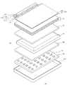
도 1 및 2를 참조하면, 본 발명의 제1실시예에 따른 액정표시장치(10)는 백라이트유닛(200)과, 액정패널(300)과, 패널구동회로(310)와, 보텀커버(또는 하부커버)(100)를 포함할 수 있다.1 and 2 , the
보텀커버(100)는 백라이트유닛(200)의 하부에 배치되어 이를 지지할 수 있다. 여기서, 보텀커버(100)는 경우에 따라 백라이트유닛(200)에 포함되는 구성으로 볼 수도 있다.The
보텀커버(100)는 상부가 개방된 박스 형상으로 형성되어 백라이트유닛(200)을 내부에 수용하도록 형성될 수 있는데, 이에 한정되지는 않는다. 일예로, 보텀커버(100)는 플레이트 형태(또는 평판 형태)로 형성될 수도 있다.The
한편, 구체적으로 도시하지는 않았지만, 액정표시장치(10)는 백라이트유닛(200) 및 액정패널(300)의 측면을 감싸고 지지하는 가이드패널을 구비할 수 있고, 액정패널(300)의 상면 가장자리를 둘러싸는 탑커버를 구비할 수도 있다.Meanwhile, although not specifically illustrated, the
본 실시예의 백라이트유닛(200)은 직하형 백라이트유닛으로서, 서로 일정 간격 이격된 다수의 광원 예를 들어 발광다이오드(light emitting diode: LED)가 액정패널(300) 하부에 위치하여 액정패널(300)과 대면하도록 배치된다.The
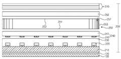
이와 같은 백라이트유닛(200)은 회로기판(210)과, 다수의 LED패키지(220)와, 봉지층(230)과, 반사패턴시트(240)와, 확산플레이트(250)와, 형광체시트(260)와, 광학시트(270)를 포함할 수 있다.Such a
회로기판(210)은 보텀커버(100) 상면에 배치된다. 회로기판(210)은 양면 접착제와 같은 접착부재(120)를 통해 보텀커버(100)에 부착될 수 있다.The
이 회로기판(210)의 상면에는 서로 일정 간격 이격된 다수의 LED패키지(220)가 실장된다. 한편, 회로기판(210)의 상면은 반사특성을 갖도록 형성될 수 있는데, 일예로 반사막이 상면에 형성될 수 있다. 이처럼, 회로기판(210)이 반사특성을 갖게 됨으로써, 회로기판(210) 방향으로 진행하는 광은 액정패널(300) 방향으로 반사될 수 있다.A plurality of
회로기판(210)에 실장된 LED패키지(220)는, 백라이트 구동부로부터 공급된 구동신호에 의해 발광하여 광을 방출한다.The
LED패키지(220)는 다양한 구조로 구성될 수 있는데, 예를 들면, 래터럴 칩(lateral chip) 구조, 플립 칩(flip chip) 구조, 버티컬 칩(vertical chip) 구조, 칩 스케일 패키지(chip scale package: CSP) 구조 등이 사용될 수 있다.The
이때, 칩 스케일 패키지 구조는 LED칩과 LED칩을 감싸는 몰드로 구성된 구조로서, 이 구조에 따르면 LED패키지(220)의 크기가 최소화 될 수 있고, 이에 따라 백라이트유닛의 두께를 감소시킬 수 있다.At this time, the chip scale package structure is a structure composed of an LED chip and a mold surrounding the LED chip. According to this structure, the size of the
한편, 다수의 LED패키지(220)가 실장된 상태의 회로기판(210)의 상면 전체를 덮는 봉지층(또는 봉지몰드)(230)이 형성될 수 있다. 봉지층(230)은 LED패키지(220) 보다 두꺼운 두께로 회로기판(210)에 도포되어, 회로기판(210)에 실장된 모든 LED패키지(220)를 덮도록 구성될 수 있다. 이와 같은 봉지층(230)은 LED패키지(220)를 회로기판(210)에 안정적으로 고정시키면서 외부로부터 보호하는 기능을 수행할 수 있다.Meanwhile, an encapsulation layer (or encapsulation mold) 230 covering the entire upper surface of the
봉지층(230)은, 예를 들면, Si, UV 레진, PC, PMMA를 포함하는 수지 계열 물질 중 하나 또는 이들의 조합으로 형성될 수 있는데, 이에 한정되지는 않는다.The
봉지층(230) 상에는 확산플레이트(250)가 배치될 수 있다.A
확산플레이트(250)는 다수의 LED패키지(220)에서 출사된 광을 확산시켜 균일한 면광원을 액정패널(300)에 제공하는 기능을 수행할 수 있다.The
특히, 본 실시예에서는, 확산플레이트(250)의 가장자리 부분(즉, 가장자리 영역)이 이의 내측에 위치하는 내부 부분(즉, 내부 영역) 보다 작은 두께(또는 높이)를 갖도록 구성하게 된다.In particular, in this embodiment, the edge portion (ie, the edge region) of the
이에 따라 가장자리 부분에서의 투과율을 향상시키게 된다. 이로 인해, 가장자리 부분을 따라 암부가 발생하는 현상을 방지할 수 있게 되어, 암부 발생에 의해 휘도 균일도가 저하되는 문제를 개선할 수 있게 된다.Accordingly, the transmittance at the edge portion is improved. For this reason, it is possible to prevent the occurrence of dark portions along the edge portion, and thus it is possible to improve the problem of a decrease in luminance uniformity due to the occurrence of dark portions.
이와 같은 확산플레이트(250)의 구조 및 작용에 대해서는 아래에서 보다 상세하게 설명한다.The structure and operation of the
한편, 확산플레이트(250)의 하면에는 필름 형태의 반사패턴시트(240)가 구비될 수 있다. 반사패턴시트(240)는 기재(241)와, 기재(241) 하면에 형성되고 하부의 LED패키지(220) 각각에 대응하여 배치된 다수의 반사패턴(242)으로 구성될 수 있다.Meanwhile, a
여기서, 반사패턴(242)은 이 하부에 위치하는 해당 LED패키지(220)로부터 상부 방향으로 출사되는 광의 일부를 반사하여 측면 방향으로 분산시키는 기능을 하고 나머지 일부는 투과하여 상부 방향으로 진행하게 된다.Here, the
이에 따라, 대부분의 광이 수직한 상부 방향으로 진행하여 액정패널(300)에 입사되는 것을 방지하게 된다. 따라서, 수직한 상부 방향으로의 광 입사에 의한 핫스팟(hot spot) 발생을 방지하게 되어, 핫스팟에 의한 화질 저하를 개선할 수 있게 된다.Accordingly, it is prevented that most of the light travels in the vertical upward direction and is incident on the
확산플레이트(250) 상에는 형광체시트(260)가 배치될 수 있다. 형광체시트(260)는 LED패키지(220)에서 발생된 제1컬러의 광의 일부를 흡수하여, 제1컬러와 다른 적어도 하나의 컬러의 광을 각각 발생시키는 적어도 하나의 형광체를 포함할 수 있다.A
이처럼, 형광체시트(260)를 사용하는 경우에, LED패키지(220)에서 발생된 제1컬러의 광과, 형광체시트(260)에 의해 발생된 컬러의 광이 혼합되어 최종적으로 백색 광이 생성되고 액정패널(300)에 제공될 수 있다.As such, when the
이와 관련하여 예를 들면, LED패키지(220)가 제1컬러 광으로서 청색 광을 발생시키는 경우에, 형광체시트(260)는 청색 광의 일부를 흡수하여 제2컬러 광으로서 황색 광을 발생시킬 수 있다.In this regard, for example, when the
한편, LED패키지(220)가 백색 광을 발생하는 경우에는, 형광체시트(260)는 삭제될 수도 있다.On the other hand, when the
형광체시트(260) 상에는, 집광시트를 포함하여 적어도 하나의 광학시트(270)가 배치될 수 있다. 본 실시예에서는, 일예로 3장의 광학시트(270)가 사용된 경우를 도시하였다.At least one
위와 같이 구성된 백라이트유닛(200) 상에는 액정패널(300)이 배치된다.The
액정패널(300)은 액정층의 광투과율을 조절하여 영상을 표시하는 표시패널로서, 액정층을 사이에 두고 대향 합착된 제1기판(또는 하부기판)(301)과 제2기판(또는 상부기판)(302)을 포함할 수 있다. 한편, 구체적으로 도시하지는 않았지만, 제1기판(301) 및 제2기판(302) 각각의 외면(또는 바깥면)에는 해당 제1편광판과 제2편광판이 부착될 수 있다.The
이러한, 액정패널(300)은 각 화소별로 인가되는 데이터전압과 공통전압에 의해 화소마다 형성되는 전계에 따라 액정층의 액정분자를 구동함으로써 액정층의 광 투과율에 따라 컬러 영상을 표시할 수 있다.The
패널구동회로(310)는 하부 기판(301)에 마련된 패드부에 연결되어 액정패널(300)의 각 화소를 구동할 수 있다.The
예를 들면, 패널구동회로(310)는 액정패널(300)의 패드부에 연결된 다수의 회로필름(311)과, 각 회로필름(311)에 실장된 데이터IC(313)와, 다수의 회로필름(311)에 연결된 디스플레이용 인쇄회로기판(312)과, 디스플레이용 인쇄회로기판(312)에 실장된 타이밍제어회로(314)를 포함하여 구성될 수 있다.For example, the
타이밍제어회로(314)는 외부의 구동 시스템으로부터 공급되는 타이밍 동기 신호에 응답해 구동 시스템으로부터 입력되는 디지털 영상데이터를 액정패널(300)의 화소 배치 구조에 부합하게 정렬하여 화소별 화소데이터를 생성하고, 생성된 화소별 화소데이터를 데이터IC(313)에 제공할 수 있다.The
또한, 타이밍제어회로(314)는 타이밍 동기 신호에 기초해 데이터 제어 신호와 게이트 제어 신호 각각을 생성하여 데이터IC(313) 및 게이트IC 각각의 구동 타이밍을 제어할 수 있다.Also, the
더욱이, 타이밍제어회로(314)는 로컬 디밍 기술을 통해 백라이트유닛(200)의 발광 동작을 제어함으로써 액정패널(300)의 영역별 휘도를 개별적으로 제어할 수 있다.Furthermore, the
위와 같이, 백라이트유닛(200)은 직하형 백라이트유닛으로서 액정패널(300)의 영역별 로컬 디밍(local dimming)을 구현할 수 있어 명암비가 개선되고 소비전력 절감의 효과를 얻을 수 있다.As described above, the
그리고, 다수의 LED패키지(220) 각각에 대응하여 반사패턴(241)이 형성된 반사패턴시트(240)를 구비함에 따라, 수직한 상부 방향으로의 출광을 감소시켜 핫스팟 현상을 방지하게 되고, 이로 인해 화질이 개선될 수 있다.In addition, as the plurality of
또한, 반사패턴시트(240)에 의해 광이 반사되어 측면 방향으로 진행될 수 있게 되어, 직하형 백라이트유닛(200)의 광학거리를 실질적으로 감소시키는 작용을 하게 됨으로써, 광이 주변 로컬 디밍 영역을 넘게 되어 헤일로(halo) 현상이 발생하는 것을 방지할 수 있게 된다.In addition, the light is reflected by the
특히, 본 실시예에서는, 확산플레이트(250)의 가장자리 영역에 대해 외측 방향으로 두께(또는 높이)가 감소하도록 구성하게 된다.In particular, in this embodiment, the thickness (or height) of the
이에 따라, 가장자리 영역에서의 확산플레이트(250)의 투과율은 외측 방향으로 증가하게 되어, 이 영역에서의 암부 발생이 개선될 수 있게 된다.Accordingly, the transmittance of the
이에 대해, 도 3 및 4를 함께 참조하여 보다 상세하게 설명한다. 도 3 및 4는 각각 본 발명의 제1실시예에 따른 확산플레이트를 도시한 사시도 및 단면도이다.This will be described in more detail with reference to FIGS. 3 and 4 . 3 and 4 are perspective and cross-sectional views, respectively, of a diffusion plate according to a first embodiment of the present invention.
본 실시예의 확산플레이트(250)에는, 평면적으로 볼 때, 이의 외곽 또는 가장자리(즉, 모서리들과 모서리들 사이의 코너들)를 따라 배치된 가장자리 영역(A1)인 제1영역(A1)과, 제1영역(A1)으로 둘러싸여져 이의 내측에 위치하는 내부 영역(A2)인 제2영역(A2)이 정의될 수 있다.The
그리고, 확산플레이트(250)는, LED패키지(220)를 바라보는 하면(251)과, 하면(251)과 반대편에 위치하여 액정패널(300)을 바라보는 상면(252)과, 하면(251)의 각 모서리에서 상부로 수직하게 연장된 측면(253)을 포함할 수 있다.In addition, the
여기서, 하면(251) 및 상면(252) 각각은 실질적으로 전체가 평탄한 평면 형태로서, 액정패널(300)의 기판면에 평행하게 형성될 수 있다.Here, each of the
더욱이, 확산플레이트(250)는, 제2영역(A2)의 상면(252)의 가장자리로부터 연장되고 하방으로 경사져 측면(253)과 연결되는 경사면(254)으로서, 제1영역(A1)에 형성된 경사면(254)을 포함할 수 있다. 보다 상세하게는, 경사면(254)은 상면(252)의 모서리 및 코너로부터 하방으로 경사진 형태로 제1영역(A1)에 형성될 수 있다.Furthermore, the
여기서, 경사면(254)은 직선형의 형태로 구성될 수 있는데, 즉 경사면(254)의 기울기가 일정한 직선형의 형태로 형성될 수 있다.Here, the
이처럼, 확산플레이트(250)의 가장자리 영역인 제1영역(A1)에 경사면(254)을 형성함에 따라, 이 제1영역(A1)은 측면(253) 방향으로 갈수록 두께(h) 즉 높이(h)가 감소하는 형태를 갖게 된다.As described above, as the
다시 말하면, 평탄한 하면(251)을 기준으로 하여, 제1영역(A1)의 경사면(254)은 높이(h)가 감소하는 형태로 외측 방향으로 경사지도록 구성될 수 있게 된다.In other words, based on the flat
이와 같이, 제1영역(A1)은 외측 방향에 가까워질수록 두께(h)가 작아지도록 구성됨에 따라, 제1영역(A1)에서의 광투과율(또는 광투과량)은 증가할 수 있게 된다.As described above, as the thickness h of the first area A1 becomes smaller as it approaches the outside direction, the light transmittance (or the amount of light transmittance) in the first area A1 may increase.
이와 관련하여 도 5를 참조할 수 있는데, 도 5는 종래와 본 발명의 제1실시예의 확산플레이트의 가장자리 영역에서의 광투과량을 개략적으로 설명한 도면이다.In this regard, reference may be made to FIG. 5, which is a diagram schematically explaining the amount of light transmission in the edge region of the diffusion plate according to the first embodiment of the present invention and the related art.
도 5를 참조하면, 종래의 확산플레이트(50)(점선으로 도시됨)는 상면(51)이 전체적으로 평탄한 평면 형태를 갖게 되는데, 즉 상면(51)은 내부 영역(A2)인 제2영역(A2) 뿐만 아니라 가장자리 영역인 제1영역(A1) 또한 평탄한 평면 형태를 갖게 되어, 종래의 확산플레이트(50)는 제2영역(A2)과 제1영역(A1)이 실질적으로 동일한 두께 즉 높이를 갖게 된다.5, the conventional diffusion plate 50 (shown by a dotted line) has a flat
이에 따라, 종래의 확산플레이트(50)에서는 제1영역(A1)의 광투과율이 제2영역(A2)의 광투과율과 실질적으로 동일한데, 상대적으로 외측에 위치하는 제1영역(A1)은 내측에 위치하는 제2영역(A2)에 비해 출광량(Lp)이 작고 또한 외측 방향으로 갈수록 출광량(Lp)이 감소되므로, 외측 방향으로 갈수록 밝기가 어두워지는 암부가 발생하게 된다.Accordingly, in the
반면에, 본 실시예의 확산플레이트(250)는 가장자리 영역(A1)인 제1영역(A1)이 하방으로 경사진 형태를 갖게 되어 실질적으로 제1영역(A1)에서의 상면에 해당되는 경사면(254)이 형성된다.On the other hand, in the
이에 따라, 제1영역(A1)에서는 외측 방향으로 갈수록 두께가 작아지게 되고, 이로 인해 제1영역(A1)에서는 외측 방향으로 갈수록 광투과율이 상승할 수 있게 된다.Accordingly, in the first area A1, the thickness decreases in the outer direction, and thus, the light transmittance increases in the outer direction in the first area A1.
이와 관련하여, 확산플레이트(250)는 그 특성상 두께가 두꺼워질수록 투과율이 감소하게 되는데, 제1영역(A1)에서는 외측 방향으로 갈수록 확산플레이트(250)가 제거되는 부분이 많아지게 되어 두께가 감소하게 되므로, 외측 방향으로 갈수록 광투과율이 상승할 수 있게 된다.In this regard, as the thickness of the
따라서, 경사진 구조의 제1영역(A1)은 외측 방향으로 갈수록 광투과율이 높아지게 되므로, 평탄한 구조의 종래와 비교하여 제1영역(A1)에서의 출광량(L)이 증가하게 된다.Accordingly, since the light transmittance of the first area A1 having the inclined structure increases toward the outside, the amount of light L emitted from the first area A1 is increased compared to the conventional structure having the flat structure.
이처럼, 가장자리 영역(A1)을 경사진 구조로 구성하여 광투과율을 상승시킴으로써, 가장자리 영역(A1)에서 출광량이 감소되는 현상을 보상할 수 있게 된다.As such, by configuring the edge area A1 in a inclined structure to increase the light transmittance, it is possible to compensate for a decrease in the amount of light emitted from the edge area A1.
이에 따라, 가장자리 영역(A1)에서의 암부 발생을 개선할 수 있게 되고, 전체적으로 균일한 휘도를 확보할 수 있게 된다.Accordingly, it is possible to improve the occurrence of dark portions in the edge area A1 and to ensure uniform luminance as a whole.
한편, 제1영역(A1)의 경사면(254)은 전술한 직선형의 형태와 다른 형태를 갖도록 구성될 수도 있다.Meanwhile, the
이와 관련하여 일예를 들면, 도 6에 도시한 바와 같이, 경사면(254)은 곡선 형태를 갖도록 구성될 수도 있다.In this regard, for example, as shown in FIG. 6 , the
이와 같은 곡선형 경사 구조의 경사면(254)이 구성되면, 제1영역(A1)의 두께 감소율이 외측 방향을 향해 증가하게 된다. 이 곡선형 구조의 경우에는, 광투과율의 증가율이 외측 방향을 향해 일정하지 않고 점차적으로 증가하는 작용을 하게 되어, 암부 정도가 높은 모델에 보다 효과적으로 적용될 수 있을 것이다.When the
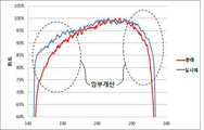
도 7은 종래 및 본 발명의 실시예에 따른 정면 휘도프로파일의 시뮬레이션 결과를 도시한 도면이다. 그리고, 도 8은 도 7의 x-x' 방향에서의 단면 휘도프로파일을 도시한 도면이고, 도 9는 도 7의 y-y' 방향에서의 단면 휘도프로파일을 도시한 도면이다.7 is a diagram illustrating simulation results of a front luminance profile according to an embodiment of the present invention. Also, FIG. 8 is a diagram illustrating a cross-sectional luminance profile in the x-x' direction of FIG. 7 , and FIG. 9 is a diagram illustrating a cross-sectional luminance profile in the y-y' direction of FIG. 7 .
도 7 내지 9를 살펴보면, 가장자리 영역이 평탄한 구조를 갖는 종래와 비교하여 가장자리 영역에 경사진 구조를 적용한 본 실시예에 따르면, 가장자리 영역에서의 휘도가 향상되어 암부 현상이 개선됨을 확인할 수 있다.7 to 9 , it can be seen that according to the present embodiment in which the inclined structure is applied to the edge region compared to the prior art in which the edge region has a flat structure, the luminance in the edge region is improved and the dark part phenomenon is improved.
전술한 바와 같이, 본 실시예에 따르면, 확산플레이트에 대해 가장자리 영역을 경사진 구조로 구성하게 된다.As described above, according to this embodiment, the edge region with respect to the diffusion plate is configured to have an inclined structure.
이에 따라, 가장자리 영역에서 광투과율을 상승시켜 출광량이 감소되는 현상을 보상할 수 있게 된다. 따라서, 가장자리 영역에서의 암부 발생을 개선할 수 있게 되고, 전체적으로 균일한 휘도를 확보할 수 있게 된다.Accordingly, it is possible to compensate for the decrease in the amount of emitted light by increasing the light transmittance in the edge region. Accordingly, it is possible to improve the occurrence of dark portions in the edge region and to ensure uniform luminance as a whole.
또한, 위 구조에 따라, 암부 개선을 위해 LED패키지의 수량을 증가시키지 않아도 되고, 가장자리 부분의 LED패키지의 구동전류를 높여 소비전력을 증가시키지 않아도 된다.In addition, according to the above structure, it is not necessary to increase the number of LED packages to improve the dark part, and it is not necessary to increase the power consumption by increasing the driving current of the LED package at the edge.
<제2실시예><Second embodiment>
도 10은 본 발명의 제2실시예에 따른 액정표시장치의 백라이트유닛을 개략적으로 도시한 단면도이다.10 is a cross-sectional view schematically illustrating a backlight unit of a liquid crystal display according to a second exemplary embodiment of the present invention.
아래에서는, 제1실시예와 동일 유사한 구성에 대한 구체적인 설명을 생략할 수 있다.Hereinafter, a detailed description of a configuration similar to that of the first embodiment may be omitted.
도 10을 참조하면, 본 발명의 제2실시예에 따른 액정표시장치는 백라이트유닛(200)과, 액정패널(도 1의 300 참조)과, 패널구동회로(도 1의 310 참조)와, 보텀커버(100)를 포함할 수 있다.Referring to FIG. 10 , the liquid crystal display according to the second embodiment of the present invention includes a
보텀커버(100)는 백라이트유닛(200)의 하부에 배치되어 이를 지지할 수 있다. 여기서, 보텀커버(100)는 경우에 따라 백라이트유닛(200)에 포함되는 구성으로 볼 수도 있다.The
백라이트유닛(200)은 회로기판(210)과, 다수의 LED패키지(220)와, 봉지층(230)과, 반사패턴시트(240)와, 확산플레이트(250)와, 형광체시트(260)와, 광학시트(270)를 포함할 수 있다.The
회로기판(210)은 보텀커버(100) 상면에 배치된다. 회로기판(210)은 양면 접착제와 같은 접착부재(120)를 통해 보텀커버(100)에 부착될 수 있다.The
이 회로기판(210)의 상면에는 서로 일정 간격 이격된 다수의 LED패키지(220)가 실장된다.A plurality of
회로기판(210)에 실장된 LED패키지(220)는, 백라이트 구동부로부터 공급된 구동신호에 의해 발광하여 광을 방출한다.The
LED패키지(220)는 다양한 구조로 구성될 수 있는데, 예를 들면, 래터럴 칩(lateral chip) 구조, 플립 칩(flip chip) 구조, 버티컬 칩(vertical chip) 구조, 칩 스케일 패키지(chip scale package: CSP) 구조 등이 사용될 수 있다.The
다수의 LED패키지(220)가 실장된 상태의 회로기판(210)의 상면 전체를 덮는 봉지층(또는 봉지몰드)(230)이 형성될 수 있다. 봉지층(230)은 LED패키지(220) 보다 두꺼운 두께로 회로기판(210)에 도포되어, 회로기판(210)에 실장된 모든 LED패키지(220)를 덮도록 구성될 수 있다.An encapsulation layer (or encapsulation mold) 230 covering the entire upper surface of the
봉지층(230) 상에는 확산플레이트(250)가 배치될 수 있다.A
확산플레이트(250)는 다수의 LED패키지(220)에서 출사된 광을 확산시켜 균일한 면광원을 액정패널에 제공하는 기능을 수행할 수 있다.The
특히, 본 실시예에서는, 확산플레이트(250)의 가장자리 부분(즉, 가장자리 영역)에 다수의 투과홀(257)을 형성하게 된다. 이로 인해, 가장자리 부분을 따라 암부가 발생하는 현상을 방지할 수 있게 되어, 암부 발생에 의한 휘도 균일도가 저하되는 문제를 개선할 수 있게 된다.In particular, in the present embodiment, a plurality of through
이와 같은 확산플레이트(250)의 구조 및 작용에 대해서는 아래에서 보다 상세하게 설명한다.The structure and operation of the
한편, 확산플레이트(250)의 하면에는 필름 형태의 반사패턴시트(240)가 구비될 수 있다. 반사패턴시트(240)는 기재(241)와, 기재(241) 하면에 형성되고 하부의 LED패키지(220) 각각에 대응하여 배치된 다수의 반사패턴(242)으로 구성될 수 있다.Meanwhile, a
확산플레이트(250) 상에는 형광체시트(260)가 배치될 수 있다. 형광체시트(260)는 LED패키지(220)에서 발생된 제1컬러의 광의 일부를 흡수하여, 제1컬러와 다른 적어도 하나의 컬러의 광을 각각 발생시키는 적어도 하나의 형광체를 포함할 수 있다.A
이처럼, 형광체시트(260)를 사용하는 경우에, LED패키지(220)에서 발생된 제1컬러의 광과, 형광체시트(260)에 의해 발생된 컬러의 광이 혼합되어 최종적으로 백색 광이 생성되고 액정패널에 제공될 수 있다.In this way, when the
이와 관련하여 예를 들면, LED패키지(220)가 제1컬러 광으로서 청색 광을 발생시키는 경우에, 형광체시트(260)는 청색 광의 일부를 흡수하여 제2컬러 광으로서 황색 광을 발생시킬 수 있다.In this regard, for example, when the
한편, LED패키지(220)가 백색 광을 발생하는 경우에는, 형광체시트(260)는 삭제될 수도 있다.On the other hand, when the
형광체시트(260) 상에는, 집광시트를 포함하여 적어도 하나의 광학시트(270)가 배치될 수 있다. 본 실시예에서는, 일예로 3장의 광학시트(270)가 사용된 경우를 도시하였다.At least one
위와 같이 구성된 백라이트유닛(200) 상에는 액정패널이 배치된다.A liquid crystal panel is disposed on the
한편, 본 실시예에서는, 확산플레이트(250)의 가장자리 영역인 제1영역에 투과홀(257)을 형성하게 되고, 이때 외측 방향으로 갈수록 투과홀(257)의 밀도(즉, 단위 면적당 투과홀(257)이 차지하는 면적 밀도)가 증가하도록 구성할 수 있다.On the other hand, in the present embodiment, the
이에 따라, 가장자리 영역(A1)에서의 투과율은 외측 방향으로 증가하게 되어, 이 영역에서의 암부 발생이 개선될 수 있게 된다.Accordingly, the transmittance in the edge region A1 increases in the outward direction, so that the occurrence of dark portions in this region can be improved.
이에 대해, 도 11 및 12를 함께 참조하여 보다 상세하게 설명한다. 도 11 및 12는 각각 본 발명의 제2실시예에 따른 확산플레이트를 도시한 사시도 및 단면도이다. 한편, 도 12에서는, 설명의 편의를 위해, 가장자리 영역을 위주로 도시하였다.This will be described in more detail with reference to FIGS. 11 and 12 . 11 and 12 are perspective and cross-sectional views, respectively, of a diffusion plate according to a second embodiment of the present invention. Meanwhile, in FIG. 12 , the edge region is mainly illustrated for convenience of explanation.
본 실시예의 확산플레이트(250)에는, 평면적으로 볼 때, 이의 외곽을 따라 배치된 가장자리 영역(A1)인 제1영역(A1)과, 제1영역(A1)으로 둘러싸여져 이의 내측에 위치하는 내부 영역(A2)인 제2영역(A2)이 정의될 수 있다.In the
그리고, 확산플레이트(250)는, LED패키지(220)를 바라보는 하면(251)과, 하면(251)과 반대편에 위치하여 액정패널(도 1의 300 참조)을 바라보는 상면(252)과, 하면(251)의 각 모서리에서 상부로 수직하게 연장되어 상면(252)에 연결되는 측면(253)을 포함할 수 있다.And, the
여기서, 하면(251) 및 상면(252) 각각은 실질적으로 전체가 평탄한 평면 형태로서, 액정패널의 기판면에 평행하게 형성될 수 있다.Here, each of the
이처럼, 확산플레이트(250)는 전체적으로 균일한(또는 동일한) 두께를 갖도록 형성될 수 있다.As such, the
그리고, 가장자리 영역(A1)인 제1영역(A1)에는, 두께 방향을 따라 확산플레이트(250)를 관통하는 형태의 다수의 투과홀(257)이 배치될 수 있다.In addition, in the first area A1, which is the edge area A1, a plurality of penetration holes 257 penetrating through the
한편, 내부 영역(A2)인 제2영역(A2)에는 별도의 투과홀(257)이 형성되지 않고, 전체적으로 균일한 광특성을 갖도록 구성될 수 있다.Meanwhile, a
이때, 투과홀(257)은, 측면(253) 방향으로 갈수록 밀도가 높아지도록 구성될 수 있다.In this case, the through
이와 관련하여 예를 들면, 제1영역(A1)에 배치된 투과홀들(257)은 서로 동일한 크기(또는 폭)(d)를 갖고, 측면(253) 방향으로 갈수록 단위면적 당 개수가 커지도록 구성될 수 있다.In this regard, for example, the through
이와 같이, 제1영역(A1)은 외측 방향에 가까워질수록 투과홀(257)의 밀도가 높아지도록 구성됨에 따라, 제1영역(A1)에서의 광투과율(또는 광투과량)은 증가할 수 있게 된다.As such, as the first area A1 is configured such that the density of the transmission holes 257 increases as it approaches the outside direction, the light transmittance (or light transmittance) in the first area A1 can be increased. do.
이와 관련하여 종래의 확산플레이트에는 내부 영역과 마찬가지로 가장자리 영역에 별도의 투과홀이 형성되지 않게 되고, 이 확산플레이트에서는 상대적으로 외측에 위치하는 가장자리 영역은 내측에 위치하는 내부 영역에 비해 출광량이 작고 또한 외측 방향으로 갈수록 출광량이 감소되므로, 외측 방향으로 갈수록 밝기가 어두워지는 암부가 발생하게 된다.In this regard, in the conventional diffusion plate, a separate transmission hole is not formed in the edge region as in the inner region. In addition, since the amount of emitted light decreases toward the outside, a dark portion whose brightness becomes darker toward the outside is generated.
반면에, 본 실시예의 확산플레이트(250)는 가장자리 영역(A1)인 제1영역(A1)에는 투과홀(257)이 외측 방향으로 밀도가 증가하도록 형성된다.On the other hand, in the
이에 따라, 제1영역(A1)에서는 외측 방향으로 갈수록 투과홀(257)이 차지하는 면적이 증가하게 되고, 이로 인해 제1영역(A1)에서는 외측 방향으로 갈수록 광투과율이 상승할 수 있게 된다.Accordingly, in the first area A1, the area occupied by the
이와 관련하여, 제1영역(A1)에서는 외측 방향으로 갈수록 확산플레이트(250)가 제거되는 부분이 많아지게 되어 확산플레이트(250)가 차지하는 면적이 감소하게 되므로, 외측 방향으로 갈수록 광투과율이 상승할 수 있게 된다.In this regard, in the first area A1, the portion from which the
따라서, 투과홀 구조의 제1영역(A1)은 외측 방향으로 갈수록 광투과율이 높아지게 되므로, 비투과홀 구조의 종래와 비교하여 제1영역(A1)에서의 출광량이 증가하게 된다.Accordingly, since the light transmittance of the first area A1 of the through hole structure increases toward the outside, the amount of light emitted from the first area A1 increases as compared with the conventional structure of the non-transmissive hole structure.
이처럼, 가장자리 영역(A1)을 투과홀 구조로 구성하여 광투과율을 상승시킴으로써, 가장자리 영역(A1)에서 출광량이 감소되는 현상을 보상할 수 있게 된다.In this way, by configuring the edge area A1 as a transmission hole structure to increase the light transmittance, it is possible to compensate for a decrease in the amount of light emitted from the edge area A1.
이에 따라, 가장자리 영역(A1)에서의 암부 발생을 개선할 수 있게 되고, 전체적으로 균일한 휘도를 확보할 수 있게 된다.Accordingly, it is possible to improve the occurrence of dark portions in the edge area A1 and to ensure uniform luminance as a whole.
한편, 제1영역(A1)의 투과홀(257)의 밀도 변화는, 전술한 투과홀(257)의 개수 변화와는 다른 방식으로 구현될 수 있다.Meanwhile, the change in the density of the through
이와 관련하여 일예를 들면, 도 13에 도시한 바와 같이, 투과홀(257)은 외측 방향으로 갈수록 그 폭(d)이 커지도록 구성될 수 있다.In this regard, for example, as shown in FIG. 13 , the through
또 다른 예로서, 투과홀(257)은 외측 방향으로 갈수록 개수 및/또는 폭이 커지도록 구성될 수 있다.As another example, the through
전술한 바와 같이, 본 실시예에 따르면, 확산플레이트에 대해 가장자리 영역을 투과홀 구조로 구성하게 된다.As described above, according to the present embodiment, the edge region of the diffusion plate is configured as a through hole structure.
이에 따라, 가장자리 영역에서 광투과율을 상승시켜 출광량이 감소되는 현상을 보상할 수 있게 된다. 따라서, 가장자리 영역에서의 암부 발생을 개선할 수 있게 되고, 전체적으로 균일한 휘도를 확보할 수 있게 된다.Accordingly, it is possible to compensate for the decrease in the amount of emitted light by increasing the light transmittance in the edge region. Accordingly, it is possible to improve the occurrence of dark portions in the edge region and to ensure uniform luminance as a whole.
또한, 위 구조에 따라, 암부 개선을 위해 LED패키지의 수량을 증가시키지 않아도 되고, 가장자리 부분의 LED패키지의 구동전류를 높여 소비전력을 증가시키지 않아도 된다.In addition, according to the above structure, it is not necessary to increase the number of LED packages to improve the dark part, and it is not necessary to increase the power consumption by increasing the driving current of the LED package at the edge.
위와 같이, 본 발명의 실시예들에 따르면, 확산플레이트에 대해 가장자리 영역을 경사 구조나 투과홀 구조로 구성하게 된다.As described above, according to the embodiments of the present invention, the edge region with respect to the diffusion plate is configured as an inclined structure or a through hole structure.
이에 따라, 가장자리 영역에서 광투과율을 상승시켜 출광량이 감소되는 현상을 보상할 수 있게 된다. 따라서, 가장자리 영역에서의 암부 발생을 개선할 수 있게 되고, 전체적으로 균일한 휘도를 확보할 수 있게 된다.Accordingly, it is possible to compensate for the decrease in the amount of emitted light by increasing the light transmittance in the edge region. Accordingly, it is possible to improve the occurrence of dark portions in the edge region and to ensure uniform luminance as a whole.
또한, 위 구조에 따라, 암부 개선을 위해 LED패키지의 수량을 증가시키지 않아도 되고, 가장자리 부분의 LED패키지의 구동전류를 높여 소비전력을 증가시키지 않아도 된다.In addition, according to the above structure, it is not necessary to increase the number of LED packages to improve the dark part, and it is not necessary to increase the power consumption by increasing the driving current of the LED package at the edge.
전술한 본 발명의 실시예는 본 발명의 일예로서, 본 발명의 정신에 포함되는 범위 내에서 자유로운 변형이 가능하다. 따라서, 본 발명은, 첨부된 특허청구범위 및 이와 등가되는 범위 내에서의 본 발명의 변형을 포함한다.The above-described embodiment of the present invention is an example of the present invention, and free modifications are possible within the scope included in the spirit of the present invention. Accordingly, the present invention includes modifications of the present invention provided they come within the scope of the appended claims and their equivalents.
10: 액정표시장치100: 보텀커버
120: 접착부재200: 백라이트유닛
210: 회로기판220: LED패키지
230: 봉지층240: 반사패턴시트
241: 기재242: 반사패턴
250: 확산플레이트251: 하면
252: 상면253: 측면
254: 경사면257: 투과홀
260: 형광체시트270: 광학시트
300: 액정패널301: 제1기판
302: 제2기판310: 패널구동회로
311: 회로필름312: 디스플레이용 인쇄회로기판
313: 데이터IC314: 타이밍제어회로
A1: 제1영역(가장자리 영역)
A2: 제2영역(내부 영역)10: liquid crystal display device 100: bottom cover
120: adhesive member 200: backlight unit
210: circuit board 220: LED package
230: encapsulation layer 240: reflective pattern sheet
241: substrate 242: reflection pattern
250: diffusion plate 251: bottom
252: top surface 253: side
254: inclined surface 257: through hole
260: phosphor sheet 270: optical sheet
300: liquid crystal panel 301: first substrate
302: second substrate 310: panel driving circuit
311: circuit film 312: printed circuit board for display
313: data IC 314: timing control circuit
A1: 1st area (edge area)
A2: second area (inner area)
Claims (10)
Translated fromKorean를 포함하고,
상기 제1영역은, 상기 제2영역의 상면으로부터 연장되고 하방으로 경사진 경사면을 포함하고,
상기 제1 및 제2영역의 하면과 상기 제2영역의 상면은 서로 평행한 평면인
백라이트유닛.
A diffusion plate in which a first region positioned along an edge and a second region surrounded by the first region are defined, and the thickness of the first region decreases toward the outside.
including,
The first area includes an inclined surface extending from the upper surface of the second area and inclined downward,
The lower surfaces of the first and second regions and the upper surfaces of the second region are planes parallel to each other.
backlight unit.
상기 경사면은 직선형이거나 곡선형인
백라이트유닛.
The method of claim 1,
The inclined surface is straight or curved
backlight unit.
회로기판 상면에 실장된 다수의 LED패키지와;
상기 회로기판 상에, 상기 다수의 LED패키지를 덮는 봉지층과;
상기 봉지층과 상기 확산플레이트 사이에, 상기 다수의 LED패키지 각각에 대응하여 배치된 다수의 반사패턴을 포함한 반사패턴시트와;
상기 확산플레이트 상에 형광체시트와;
상기 형광체시트 상에 광학시트
를 포함하는 백라이트유닛.
The method of claim 1,
a plurality of LED packages mounted on the upper surface of the circuit board;
an encapsulation layer covering the plurality of LED packages on the circuit board;
a reflective pattern sheet including a plurality of reflective patterns disposed between the encapsulation layer and the diffusion plate to correspond to each of the plurality of LED packages;
a phosphor sheet on the diffusion plate;
an optical sheet on the phosphor sheet
A backlight unit comprising a.
상기 다수의 LED패키지 상에 위치하고, 가장자리를 따라 위치하는 제1영역과 상기 제1영역에 둘러싸인 제2영역이 정의되고, 상기 제1영역은 외측 방향으로 갈수록 밀도가 증가하는 다수의 투과홀을 갖고, 전체적으로 광투과 특성을 갖는 확산플레이트와;
상기 다수의 LED패키지와 상기 확산플레이트 사이에 위치하는 반사패턴시트
를 포함하는 백라이트유닛.
a plurality of LED packages;
Located on the plurality of LED packages, a first region positioned along an edge and a second region surrounded by the first region are defined, and the first region has a plurality of penetration holes whose density increases toward the outside. , A diffusion plate having a light transmission characteristic as a whole;
A reflective pattern sheet positioned between the plurality of LED packages and the diffusion plate
A backlight unit comprising a.
상기 투과홀은 외측 방향으로 갈수록 개수가 증가하도록 구성된
백라이트유닛.
6. The method of claim 5,
The through holes are configured to increase in number toward the outside.
backlight unit.
상기 투과홀은 외측 방향으로 갈수록 크기가 증가하도록 구성된
백라이트유닛.
6. The method of claim 5,
The through hole is configured to increase in size toward the outside.
backlight unit.
회로기판 상면에 실장된 상기 다수의 LED패키지와;
상기 회로기판 상에, 상기 다수의 LED패키지를 덮는 봉지층과;
상기 봉지층과 상기 확산플레이트 사이에, 상기 다수의 LED패키지 각각에 대응하여 배치된 다수의 반사패턴을 포함한 상기 반사패턴시트와;
상기 확산플레이트 상에 형광체시트와;
상기 형광체시트 상에 광학시트
를 포함하는 백라이트유닛.
6. The method of claim 5,
the plurality of LED packages mounted on the upper surface of the circuit board;
an encapsulation layer covering the plurality of LED packages on the circuit board;
the reflective pattern sheet including a plurality of reflective patterns disposed between the encapsulation layer and the diffusion plate to correspond to each of the plurality of LED packages;
a phosphor sheet on the diffusion plate;
an optical sheet on the phosphor sheet
A backlight unit comprising a.
상기 백라이트유닛 상에 액정패널
을 포함하는 액정표시장치.
The backlight unit of any one of claims 1, 3 to 8;
a liquid crystal panel on the backlight unit
A liquid crystal display comprising a.
상기 제2영역에는 투과홀이 존재하지 않는
백라이트유닛.6. The method of claim 5,
There is no through hole in the second region
backlight unit.
Priority Applications (3)
| Application Number | Priority Date | Filing Date | Title |
|---|---|---|---|
| KR1020170175652AKR102428534B1 (en) | 2017-12-20 | 2017-12-20 | Backlight unit and liquid crystal display device including the same |
| CN201811538841.2ACN109946876B (en) | 2017-12-20 | 2018-12-14 | Backlight unit and liquid crystal display device including the same |
| US16/223,715US10816854B2 (en) | 2017-12-20 | 2018-12-18 | Backlight unit and liquid crystal display device including the same |
Applications Claiming Priority (1)
| Application Number | Priority Date | Filing Date | Title |
|---|---|---|---|
| KR1020170175652AKR102428534B1 (en) | 2017-12-20 | 2017-12-20 | Backlight unit and liquid crystal display device including the same |
Publications (2)
| Publication Number | Publication Date |
|---|---|
| KR20190074368A KR20190074368A (en) | 2019-06-28 |
| KR102428534B1true KR102428534B1 (en) | 2022-08-02 |
Family
ID=66815953
Family Applications (1)
| Application Number | Title | Priority Date | Filing Date |
|---|---|---|---|
| KR1020170175652AActiveKR102428534B1 (en) | 2017-12-20 | 2017-12-20 | Backlight unit and liquid crystal display device including the same |
Country Status (3)
| Country | Link |
|---|---|
| US (1) | US10816854B2 (en) |
| KR (1) | KR102428534B1 (en) |
| CN (1) | CN109946876B (en) |
Families Citing this family (4)
| Publication number | Priority date | Publication date | Assignee | Title |
|---|---|---|---|---|
| JP7560730B2 (en)* | 2020-05-29 | 2024-10-03 | 日亜化学工業株式会社 | Planar light source, liquid crystal display device |
| US11428984B2 (en) | 2020-05-29 | 2022-08-30 | Nichia Corporation | Planar light source and liquid crystal display device |
| CN114842741A (en)* | 2021-02-01 | 2022-08-02 | 北京京东方显示技术有限公司 | Light-emitting module and display device |
| CN116300198A (en)* | 2023-01-16 | 2023-06-23 | 上海天马微电子有限公司 | Backlight module, display module and display device |
Citations (3)
| Publication number | Priority date | Publication date | Assignee | Title |
|---|---|---|---|---|
| US20110050735A1 (en)* | 2009-08-27 | 2011-03-03 | Seung Choon Bae | Optical assembly, backlight unit and display apparatus thereof |
| US20140029238A1 (en)* | 2011-07-05 | 2014-01-30 | Dexerials Corporation | Illumination apparatus |
| US20160259209A1 (en)* | 2013-11-01 | 2016-09-08 | Denso Corporation | Backlight unit |
Family Cites Families (8)
| Publication number | Priority date | Publication date | Assignee | Title |
|---|---|---|---|---|
| KR20080048335A (en)* | 2006-11-28 | 2008-06-02 | 엘지디스플레이 주식회사 | White LED Package and Direct Backlight Assembly Including the Same |
| CN101295036A (en)* | 2007-04-27 | 2008-10-29 | 鸿富锦精密工业(深圳)有限公司 | Back light module and optical plate |
| KR101343390B1 (en)* | 2007-06-12 | 2013-12-19 | 엘지디스플레이 주식회사 | Backlight Unit Including Diffusing Plate and Liquid Crystal Display Device Using The Same |
| KR101418119B1 (en)* | 2007-11-23 | 2014-07-11 | 엘지디스플레이 주식회사 | Backlight unit and liquid crystal display device having the same |
| CN100594326C (en)* | 2008-09-27 | 2010-03-17 | 上海广电光电子有限公司 | Direct down type back light module |
| KR102237160B1 (en)* | 2014-06-30 | 2021-04-07 | 엘지디스플레이 주식회사 | Backlight unit and display apparatus having the same |
| TWM514022U (en)* | 2015-07-29 | 2015-12-11 | Innolux Corp | Display module |
| CN206282061U (en)* | 2016-10-14 | 2017-06-27 | 合肥惠科金扬科技有限公司 | Backlight display module structure and display |
- 2017
- 2017-12-20KRKR1020170175652Apatent/KR102428534B1/enactiveActive
- 2018
- 2018-12-14CNCN201811538841.2Apatent/CN109946876B/enactiveActive
- 2018-12-18USUS16/223,715patent/US10816854B2/enactiveActive
Patent Citations (3)
| Publication number | Priority date | Publication date | Assignee | Title |
|---|---|---|---|---|
| US20110050735A1 (en)* | 2009-08-27 | 2011-03-03 | Seung Choon Bae | Optical assembly, backlight unit and display apparatus thereof |
| US20140029238A1 (en)* | 2011-07-05 | 2014-01-30 | Dexerials Corporation | Illumination apparatus |
| US20160259209A1 (en)* | 2013-11-01 | 2016-09-08 | Denso Corporation | Backlight unit |
Also Published As
| Publication number | Publication date |
|---|---|
| CN109946876B (en) | 2022-05-10 |
| CN109946876A (en) | 2019-06-28 |
| KR20190074368A (en) | 2019-06-28 |
| US10816854B2 (en) | 2020-10-27 |
| US20190187519A1 (en) | 2019-06-20 |
Similar Documents
| Publication | Publication Date | Title |
|---|---|---|
| KR102297644B1 (en) | Backlight unit and liquid crystal display device including the same | |
| KR102377175B1 (en) | Backlight unit and liquid crystal display device including the same | |
| KR102383302B1 (en) | Backlight unit and liquid crystal display device including the same | |
| US8643804B2 (en) | Backlight unit and display device | |
| US20190129249A1 (en) | Backlight unit and liquid crystal display device including the same | |
| US11003020B2 (en) | Light source package, backlight unit including light source package, and display device using the same | |
| KR102428534B1 (en) | Backlight unit and liquid crystal display device including the same | |
| US10948645B2 (en) | Backlight unit with light-modifying portion and display including the same | |
| KR102585534B1 (en) | Liquid crystal display device | |
| KR102767767B1 (en) | Backlight unit and display device including the same | |
| KR102855928B1 (en) | Back light unit and display device using the same | |
| KR20150014194A (en) | Back light assembly and Liquid crystal display apparatus having the same | |
| US20150023053A1 (en) | Backlight unit including color-compensating diffuser and display device including the same | |
| KR20210004019A (en) | Color conversion sheet, backlight unit and display device | |
| KR102616215B1 (en) | Back light unit and liquid crystal display device using the same | |
| KR20110073210A (en) | Backlight unit | |
| KR20130025765A (en) | Liquid crystal display device | |
| KR101654373B1 (en) | Backlight unit and display apparatus thereof | |
| KR20130053568A (en) | Backlight unit and display apparatus thereof | |
| KR101654372B1 (en) | Backlight unit and display apparatus thereof | |
| KR20100094159A (en) | Liquid crystal display device | |
| KR20110087106A (en) | Optical assembly, backlight unit and display device having same |
Legal Events
| Date | Code | Title | Description |
|---|---|---|---|
| PA0109 | Patent application | Patent event code:PA01091R01D Comment text:Patent Application Patent event date:20171220 | |
| PG1501 | Laying open of application | ||
| A201 | Request for examination | ||
| PA0201 | Request for examination | Patent event code:PA02012R01D Patent event date:20201214 Comment text:Request for Examination of Application Patent event code:PA02011R01I Patent event date:20171220 Comment text:Patent Application | |
| E902 | Notification of reason for refusal | ||
| PE0902 | Notice of grounds for rejection | Comment text:Notification of reason for refusal Patent event date:20220127 Patent event code:PE09021S01D | |
| E701 | Decision to grant or registration of patent right | ||
| PE0701 | Decision of registration | Patent event code:PE07011S01D Comment text:Decision to Grant Registration Patent event date:20220727 | |
| GRNT | Written decision to grant | ||
| PR0701 | Registration of establishment | Comment text:Registration of Establishment Patent event date:20220729 Patent event code:PR07011E01D | |
| PR1002 | Payment of registration fee | Payment date:20220729 End annual number:3 Start annual number:1 | |
| PG1601 | Publication of registration |