KR102427637B1 - Semiconductor light emitting device - Google Patents
Semiconductor light emitting deviceDownload PDFInfo
- Publication number
- KR102427637B1 KR102427637B1KR1020170127984AKR20170127984AKR102427637B1KR 102427637 B1KR102427637 B1KR 102427637B1KR 1020170127984 AKR1020170127984 AKR 1020170127984AKR 20170127984 AKR20170127984 AKR 20170127984AKR 102427637 B1KR102427637 B1KR 102427637B1
- Authority
- KR
- South Korea
- Prior art keywords
- light emitting
- region
- electrode
- type semiconductor
- disposed
- Prior art date
- Legal status (The legal status is an assumption and is not a legal conclusion. Google has not performed a legal analysis and makes no representation as to the accuracy of the status listed.)
- Active
Links
Images


Classifications
- H01L33/38—
- H—ELECTRICITY
- H10—SEMICONDUCTOR DEVICES; ELECTRIC SOLID-STATE DEVICES NOT OTHERWISE PROVIDED FOR
- H10H—INORGANIC LIGHT-EMITTING SEMICONDUCTOR DEVICES HAVING POTENTIAL BARRIERS
- H10H20/00—Individual inorganic light-emitting semiconductor devices having potential barriers, e.g. light-emitting diodes [LED]
- H10H20/80—Constructional details
- H10H20/83—Electrodes
- H10H20/831—Electrodes characterised by their shape
- H—ELECTRICITY
- H01—ELECTRIC ELEMENTS
- H01L—SEMICONDUCTOR DEVICES NOT COVERED BY CLASS H10
- H01L21/00—Processes or apparatus adapted for the manufacture or treatment of semiconductor or solid state devices or of parts thereof
- H01L21/70—Manufacture or treatment of devices consisting of a plurality of solid state components formed in or on a common substrate or of parts thereof; Manufacture of integrated circuit devices or of parts thereof
- H01L21/77—Manufacture or treatment of devices consisting of a plurality of solid state components or integrated circuits formed in, or on, a common substrate
- H01L21/78—Manufacture or treatment of devices consisting of a plurality of solid state components or integrated circuits formed in, or on, a common substrate with subsequent division of the substrate into plural individual devices
- H01L21/7806—Manufacture or treatment of devices consisting of a plurality of solid state components or integrated circuits formed in, or on, a common substrate with subsequent division of the substrate into plural individual devices involving the separation of the active layers from a substrate
- H—ELECTRICITY
- H01—ELECTRIC ELEMENTS
- H01L—SEMICONDUCTOR DEVICES NOT COVERED BY CLASS H10
- H01L23/00—Details of semiconductor or other solid state devices
- H01L23/544—Marks applied to semiconductor devices or parts, e.g. registration marks, alignment structures, wafer maps
- H—ELECTRICITY
- H01—ELECTRIC ELEMENTS
- H01L—SEMICONDUCTOR DEVICES NOT COVERED BY CLASS H10
- H01L25/00—Assemblies consisting of a plurality of semiconductor or other solid state devices
- H01L25/03—Assemblies consisting of a plurality of semiconductor or other solid state devices all the devices being of a type provided for in a single subclass of subclasses H10B, H10D, H10F, H10H, H10K or H10N, e.g. assemblies of rectifier diodes
- H01L25/04—Assemblies consisting of a plurality of semiconductor or other solid state devices all the devices being of a type provided for in a single subclass of subclasses H10B, H10D, H10F, H10H, H10K or H10N, e.g. assemblies of rectifier diodes the devices not having separate containers
- H01L25/075—Assemblies consisting of a plurality of semiconductor or other solid state devices all the devices being of a type provided for in a single subclass of subclasses H10B, H10D, H10F, H10H, H10K or H10N, e.g. assemblies of rectifier diodes the devices not having separate containers the devices being of a type provided for in group H10H20/00
- H01L33/62—
- H—ELECTRICITY
- H10—SEMICONDUCTOR DEVICES; ELECTRIC SOLID-STATE DEVICES NOT OTHERWISE PROVIDED FOR
- H10D—INORGANIC ELECTRIC SEMICONDUCTOR DEVICES
- H10D89/00—Aspects of integrated devices not covered by groups H10D84/00 - H10D88/00
- H10D89/011—Division of wafers or substrates to produce devices, each consisting of a single electric circuit element
- H10D89/013—Division of wafers or substrates to produce devices, each consisting of a single electric circuit element the wafers or substrates being semiconductor bodies
- H—ELECTRICITY
- H10—SEMICONDUCTOR DEVICES; ELECTRIC SOLID-STATE DEVICES NOT OTHERWISE PROVIDED FOR
- H10H—INORGANIC LIGHT-EMITTING SEMICONDUCTOR DEVICES HAVING POTENTIAL BARRIERS
- H10H20/00—Individual inorganic light-emitting semiconductor devices having potential barriers, e.g. light-emitting diodes [LED]
- H10H20/80—Constructional details
- H10H20/83—Electrodes
- H10H20/831—Electrodes characterised by their shape
- H10H20/8312—Electrodes characterised by their shape extending at least partially through the bodies
- H—ELECTRICITY
- H10—SEMICONDUCTOR DEVICES; ELECTRIC SOLID-STATE DEVICES NOT OTHERWISE PROVIDED FOR
- H10H—INORGANIC LIGHT-EMITTING SEMICONDUCTOR DEVICES HAVING POTENTIAL BARRIERS
- H10H20/00—Individual inorganic light-emitting semiconductor devices having potential barriers, e.g. light-emitting diodes [LED]
- H10H20/80—Constructional details
- H10H20/83—Electrodes
- H10H20/831—Electrodes characterised by their shape
- H10H20/8314—Electrodes characterised by their shape extending at least partially onto an outer side surface of the bodies
- H—ELECTRICITY
- H10—SEMICONDUCTOR DEVICES; ELECTRIC SOLID-STATE DEVICES NOT OTHERWISE PROVIDED FOR
- H10H—INORGANIC LIGHT-EMITTING SEMICONDUCTOR DEVICES HAVING POTENTIAL BARRIERS
- H10H20/00—Individual inorganic light-emitting semiconductor devices having potential barriers, e.g. light-emitting diodes [LED]
- H10H20/80—Constructional details
- H10H20/85—Packages
- H10H20/857—Interconnections, e.g. lead-frames, bond wires or solder balls
- H—ELECTRICITY
- H10—SEMICONDUCTOR DEVICES; ELECTRIC SOLID-STATE DEVICES NOT OTHERWISE PROVIDED FOR
- H10H—INORGANIC LIGHT-EMITTING SEMICONDUCTOR DEVICES HAVING POTENTIAL BARRIERS
- H10H29/00—Integrated devices, or assemblies of multiple devices, comprising at least one light-emitting semiconductor element covered by group H10H20/00
- H10H29/10—Integrated devices comprising at least one light-emitting semiconductor component covered by group H10H20/00
- H10H29/14—Integrated devices comprising at least one light-emitting semiconductor component covered by group H10H20/00 comprising multiple light-emitting semiconductor components
- H10H29/142—Two-dimensional arrangements, e.g. asymmetric LED layout
- H—ELECTRICITY
- H01—ELECTRIC ELEMENTS
- H01L—SEMICONDUCTOR DEVICES NOT COVERED BY CLASS H10
- H01L2223/00—Details relating to semiconductor or other solid state devices covered by the group H01L23/00
- H01L2223/544—Marks applied to semiconductor devices or parts
- H01L2223/5442—Marks applied to semiconductor devices or parts comprising non digital, non alphanumeric information, e.g. symbols
- H—ELECTRICITY
- H01—ELECTRIC ELEMENTS
- H01L—SEMICONDUCTOR DEVICES NOT COVERED BY CLASS H10
- H01L2223/00—Details relating to semiconductor or other solid state devices covered by the group H01L23/00
- H01L2223/544—Marks applied to semiconductor devices or parts
- H01L2223/54426—Marks applied to semiconductor devices or parts for alignment
- H—ELECTRICITY
- H01—ELECTRIC ELEMENTS
- H01L—SEMICONDUCTOR DEVICES NOT COVERED BY CLASS H10
- H01L2223/00—Details relating to semiconductor or other solid state devices covered by the group H01L23/00
- H01L2223/544—Marks applied to semiconductor devices or parts
- H01L2223/54453—Marks applied to semiconductor devices or parts for use prior to dicing
- H01L2223/5446—Located in scribe lines
- H—ELECTRICITY
- H10—SEMICONDUCTOR DEVICES; ELECTRIC SOLID-STATE DEVICES NOT OTHERWISE PROVIDED FOR
- H10H—INORGANIC LIGHT-EMITTING SEMICONDUCTOR DEVICES HAVING POTENTIAL BARRIERS
- H10H20/00—Individual inorganic light-emitting semiconductor devices having potential barriers, e.g. light-emitting diodes [LED]
- H10H20/01—Manufacture or treatment
- H—ELECTRICITY
- H10—SEMICONDUCTOR DEVICES; ELECTRIC SOLID-STATE DEVICES NOT OTHERWISE PROVIDED FOR
- H10H—INORGANIC LIGHT-EMITTING SEMICONDUCTOR DEVICES HAVING POTENTIAL BARRIERS
- H10H20/00—Individual inorganic light-emitting semiconductor devices having potential barriers, e.g. light-emitting diodes [LED]
- H10H20/80—Constructional details
- H10H20/81—Bodies
- H10H20/819—Bodies characterised by their shape, e.g. curved or truncated substrates
- H10H20/82—Roughened surfaces, e.g. at the interface between epitaxial layers
- H—ELECTRICITY
- H10—SEMICONDUCTOR DEVICES; ELECTRIC SOLID-STATE DEVICES NOT OTHERWISE PROVIDED FOR
- H10H—INORGANIC LIGHT-EMITTING SEMICONDUCTOR DEVICES HAVING POTENTIAL BARRIERS
- H10H20/00—Individual inorganic light-emitting semiconductor devices having potential barriers, e.g. light-emitting diodes [LED]
- H10H20/80—Constructional details
- H10H20/84—Coatings, e.g. passivation layers or antireflective coatings
Landscapes
- Engineering & Computer Science (AREA)
- Microelectronics & Electronic Packaging (AREA)
- Power Engineering (AREA)
- Physics & Mathematics (AREA)
- Condensed Matter Physics & Semiconductors (AREA)
- General Physics & Mathematics (AREA)
- Computer Hardware Design (AREA)
- Manufacturing & Machinery (AREA)
- Led Devices (AREA)
Abstract
Translated fromKoreanDescription
Translated fromKorean본 발명은 반도체 발광소자에 관한 것이다.
The present invention relates to a semiconductor light emitting device.
반도체 발광소자는 전류가 가해지면 전자와 정공의 재결합 원리를 이용하여 광을 방출하며, 낮은 소비전력, 고휘도, 소형화 등의 여러 장점 때문에 광원으로서 널리 사용되고 있다. 특히, 질화물계 발광소자가 개발된 후에는 활용범위가 더욱 확대되어 광원모듈, 가정용 조명장치, 자동차 조명 등으로 채용되고 있다.A semiconductor light emitting device emits light using the principle of recombination of electrons and holes when an electric current is applied, and is widely used as a light source due to various advantages such as low power consumption, high brightness, and miniaturization. In particular, after the development of the nitride-based light emitting device, the application range has been further expanded and is being used as a light source module, a home lighting device, and a vehicle lighting.
반도체 발광소자의 활용범위가 넓어짐에 따라 고전류/고출력 분야의 광원 분야로 그 활용범위가 확대되고 있다. 이와 같이 반도체 발광소자가 고전류/고출력 분야에서 요구됨에 따라 당 기술 분야에서는 반도체 발광소자 패키지의 외부 광추출 효율을 향상시키기 위한 연구가 계속되어 왔다.
As the application range of the semiconductor light emitting device is widened, the application range is expanding to the light source field in the high current/high output field. As such, as the semiconductor light emitting device is required in the high current/high output field, research has been continued in the art to improve the external light extraction efficiency of the semiconductor light emitting device package.
본 발명이 해결하고자 하는 과제 중 하나는, 외부 광추출 효율이 향상된 반도체 발광소자를 제공하는 것이다.
One of the problems to be solved by the present invention is to provide a semiconductor light emitting device having improved external light extraction efficiency.
본 발명의 일 실시예는, 기판 상에 제1 도전형 반도체층, 활성층 및 제2 도전형 반도체층이 순차적으로 적층되며, 상기 제2 도전형 반도체층과 상기 활성층이 부분적으로 제거된 영역을 갖는 발광 구조물; 상기 영역 상에 배치된 제1 콘택 전극; 상기 제2 도전형 반도체층 상에 배치된 제2 콘택 전극; 상기 발광 구조물을 덮는 절연층; 상기 절연층을 관통하여 상기 제1 콘택 전극과 전기적으로 연결되며 적어도 일부 영역이 상기 제2 콘택 전극 상에 배치되는 제1 전극 패드; 및 상기 절연층을 관통하여 상기 제2 콘택 전극에 전기적으로 연결되는 제2 전극 패드;를 포함하며, 상기 제1 및 제2 전극 패드 중 적어도 하나의 측면은 상기 기판의 측면과 공면(co-plannar)을 갖도록 연장된 반도체 발광소자를 제공한다.
In one embodiment of the present invention, a first conductivity-type semiconductor layer, an active layer, and a second conductivity-type semiconductor layer are sequentially stacked on a substrate, and the second conductivity-type semiconductor layer and the active layer have a region partially removed. light emitting structures; a first contact electrode disposed on the region; a second contact electrode disposed on the second conductivity type semiconductor layer; an insulating layer covering the light emitting structure; a first electrode pad passing through the insulating layer to be electrically connected to the first contact electrode and having at least a partial region disposed on the second contact electrode; and a second electrode pad passing through the insulating layer and electrically connected to the second contact electrode, wherein at least one side surface of the first and second electrode pads is coplanar with a side surface of the substrate. ) to provide an extended semiconductor light emitting device.
본 발명의 일 실시예는, 기판 상에 제1 도전형 반도체층, 활성층 및 제2 도전형 반도체층이 순차적으로 적층되며, 상기 제2 도전형 반도체층과 상기 활성층이 부분적으로 제거된 영역을 갖는 복수의 발광 구조물; 상기 복수의 발광 구조물의 상기 제1 도전형 반도체층에 공통적으로 접속되는 적어도 하나의 제1 전극 패드; 및 상기 복수의 발광 구조물의 상기 제2 도전형 반도체층에 각각 접속되는 복수의 제2 전극 패드;를 포함하며, 상기 제1 및 제2 전극 패드 중 적어도 하나는, 상기 복수의 발광 구조물을 개별 반도체 발광소자로 분리하는 소자분리영역 상에 배치된 반도체 발광소자를 제공한다.
In one embodiment of the present invention, a first conductivity-type semiconductor layer, an active layer, and a second conductivity-type semiconductor layer are sequentially stacked on a substrate, and the second conductivity-type semiconductor layer and the active layer have a region partially removed. a plurality of light emitting structures; at least one first electrode pad commonly connected to the first conductivity-type semiconductor layer of the plurality of light emitting structures; and a plurality of second electrode pads respectively connected to the second conductivity-type semiconductor layers of the plurality of light emitting structures, wherein at least one of the first and second electrode pads comprises the plurality of light emitting structures as individual semiconductors. Provided is a semiconductor light emitting device disposed on a device isolation region separated into a light emitting device.
본 발명의 기술적 사상에 따른 반도체 발광소자는 외부 광추출 효율이 향상된 반도체 발광소자를 제공할 수 있다.The semiconductor light emitting device according to the technical idea of the present invention can provide a semiconductor light emitting device with improved external light extraction efficiency.
다만, 본 발명의 다양하면서도 유익한 장점과 효과는 상술한 내용에 한정되지 않으며, 본 발명의 구체적인 실시 형태를 설명하는 과정에서 보다 쉽게 이해될 수 있을 것이다.
However, the various and beneficial advantages and effects of the present invention are not limited to the above, and will be more easily understood in the course of describing specific embodiments of the present invention.
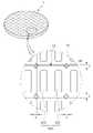
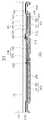
도 1은 본 발명의 일 실시예에 의한 반도체 발광소자가 배치된 반도체 웨이퍼의 개략적인 사시도이다.
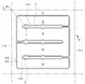
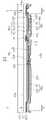
도 2는 도 1 중 하나의 반도체 발광소자를 확대한 평면도이다.
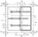
도 3은 도 2의 I-I'선을 따라 절개하여 본 측 단면도이다.
도 4(a) 및 도 4(b)는 도 3의 A 및 B부분의 확대도이다.
도 5 및 도 6은 도 2의 제1 및 제2 전극 패드의 다양한 변형예이다.
도 7a 내지 도 14b는 도 2의 반도체 발광소자의 제조공정을 나타내는 주요 단계별 도면들이다.1 is a schematic perspective view of a semiconductor wafer on which a semiconductor light emitting device according to an embodiment of the present invention is disposed.
FIG. 2 is an enlarged plan view of one semiconductor light emitting device of FIG. 1 .
3 is a side cross-sectional view taken along line I-I' of FIG. 2 .
4(a) and 4(b) are enlarged views of parts A and B of FIG. 3 .
5 and 6 are various modifications of the first and second electrode pads of FIG. 2 .
7A to 14B are main step-by-step views illustrating a manufacturing process of the semiconductor light emitting device of FIG. 2 .
이하, 첨부된 도면을 참조하여 본 발명의 다양한 실시예를 상세히 설명한다.
Hereinafter, various embodiments of the present invention will be described in detail with reference to the accompanying drawings.
도 1 내지 도 4를 참조하여, 본 발명의 일 실시예에 의한 반도체 발광소자에 대해 설명한다. 도 1은 본 발명의 일 실시예에 의한 반도체 발광소자가 배치된 반도체 웨이퍼의 개략적인 사시도이고, 도 2는 도 1 중 하나의 반도체 발광소자를 확대한 평면도이다. 도 3은 도 2의 I-I'선을 따라 절개하여 본 측 단면도이고, 도 4는 도 3의 A부분의 확대도이다.
A semiconductor light emitting device according to an embodiment of the present invention will be described with reference to FIGS. 1 to 4 . 1 is a schematic perspective view of a semiconductor wafer on which a semiconductor light emitting device is disposed according to an embodiment of the present invention, and FIG. 2 is an enlarged plan view of one of the semiconductor light emitting devices of FIG. 1 . FIG. 3 is a side cross-sectional view taken along line I-I' of FIG. 2 , and FIG. 4 is an enlarged view of part A of FIG. 3 .
도 1을 참조하면, 본 발명의 일 실시예에 의한 반도체 웨이퍼(1)는 일면에 개별소자로 분리되지 않은 복수의 반도체 발광소자(10)가 행과 열을 맞추어 배열된다. 상기 복수의 반도체 발광소자(10)는 각각 반도체 발광소자(10)를 개별소자로 분리하기 위한 소자분리영역(S)을 가지며, 상기 소자분리영역(S)에는 상기 복수의 반도체 발광소자(10)를 개별소자로 분리하기 위하여 사용되는 얼라인 키 영역(align key, AK)이 배치된다. 도면부호 BL은 복수의 반도체 발광소자(10)를 개별소자로 분리기 위해 절단(breaking)되는 지점을 표시한 것이다. 상기 절단되는 지점(BL)은 상기 소자분리영역(S) 내에 배치된다. 일 실시예의 경우, 복수의 반도체 발광소자(10)의 상부에는 반도체 발광소자(10)를 실장하기 위한 제1 및 제2 솔더 패드(610, 620)가 배치될 수 있다.
Referring to FIG. 1 , on one surface of a semiconductor wafer 1 according to an embodiment of the present invention, a plurality of semiconductor
도 2 내지 도 4는 도 1의 반도체 웨이퍼(1)를 절단된 개별 반도체 발광소자(10)를 도시한다. 도 2 내지 도 4를 참조하여, 반도체 발광소자(10)에 대해 구체적으로 설명한다. 본 발명의 일 실시예에 의한 반도체 발광소자(10)는 발광 구조물(100), 제1 및 제2 콘택 전극(140, 150), 절연층(300) 및 전극 패드(400)를 포함할 수 있다. 일 실시예의 반도체 발광소자(10)는 칩 스케일 패키지(Chip Scale Package, CSP)일 수 있으며, 웨이퍼 레벨 패키지(Wafer Level Package, WLP)일 수 있다.
2 to 4 show individual semiconductor
발광 구조물(100)은 기판(101) 상에 복수의 반도체층이 적층된 구조를 가지며, 상기 기판(101) 상에 순차적으로 적층된 제1 도전형 반도체층(110), 활성층(120) 및 제2 도전형 반도체층(130)을 포함할 수 있다.
The
기판(101)은 제1 면(102) 및 이에 대향하는 제2 면(103)을 가질 수 있으며, 상기 제1 면(102) 및 제2 면(103)을 연결하는 측면(104)을 가질 수 있다. 기판(101)은 반도체 성장용 기판으로 제공될 수 있으며, 사파이어, Si, SiC, MgAl2O4, MgO, LiAlO2, LiGaO2, GaN, AlN, 금속기판 등과 같이 절연성, 도전성, 반도체 물질을 이용할 수 있다. 질화물 반도체 성장용 기판으로 널리 이용되는 사파이어는, 전기 절연성을 가지며 육각-롬보형(Hexa-Rhombo R3c) 대칭성을 갖는 결정체로서 c축 및 a측 방향의 격자상수가 각각 13.001Å과 4.758Å이며, C(0001)면, A(11-20)면, R(1-102)면 등을 갖는다. 이 경우, 상기 C면은 비교적 질화물 박막의 성장이 용이하며, 고온에서 안정하기 때문에 질화물 성장용 기판으로 주로 사용된다.The
그리고, 도면에서 도시하는 것과 같이, 반도체층이 성장하는 제1 면(102)에는 다수의 요철 구조(U)가 형성될 수 있으며, 이러한 요철 구조(U)에 의하여 반도체층들의 결정성과 광 방출 효율 등이 향상될 수 있다. 본 실시예에서는 상기 요철 구조(U)가 돔 형상의 볼록한 형태를 가지는 것으로 예시하고 있으나, 이에 한정하는 것은 아니다. 예를 들어, 상기 요철 구조(U)는 사각형, 삼각형 등의 다양한 형태로 형성될 수 있다. 또한, 상기 요철 구조(U)는 선택적으로 형성 및 구비될 수 있으며, 실시예에 따라서 생략될 수도 있다.
And, as shown in the drawing, a plurality of concave-convex structures U may be formed on the
또한, 실시예에 따라서는, 제1 도전형 반도체층(110)을 성장시키기 전에 기판(101)의 제1 면(102)에 버퍼층을 성장시킬 수 있다. 버퍼층은 기판(101) 상에 성장되는 반도체층의 격자 결함 완화를 위한 것으로, 질화물 등으로 이루어진 언도프 반도체층으로 이루어질 수 있다. 버퍼층은, 예를 들어, 사파이어로 이루어진 기판(101)과 기판(101) 상면에 적층되는 GaN으로 이루어진 제1 도전형 반도체층(110) 사이의 격자상수 차이를 완화하여, GaN층의 결정성을 증대시킬 수 있다. 버퍼층은 언도프 GaN, AlN, InGaN 등이 적용될 수 있으며, 500℃ 내지 600℃의 저온에서 수십 내지 수백 Å의 두께로 성장시켜 형성할 수 있다. 여기서, 언도프라 함은 반도체층에 불순물 도핑 공정을 따로 거치지 않은 것을 의미하며, 반도체층에 본래 존재하던 수준의 불순물 농도, 예컨대, 질화갈륨 반도체를 유기 금속 화학 증착(Metal Organic Chemical Vapor Deposition, MOCVD)를 이용하여 성장시킬 경우, 도펀트로 사용되는 Si 등이 의도하지 않더라도 약 1014~ 1018/㎤의 수준으로 포함될 수 있다. 다만, 이러한 버퍼층은 본 실시예에서 필수적인 요소는 아니며 실시예에 따라 생략될 수도 있다.
Also, in some embodiments, a buffer layer may be grown on the
상기 기판(101) 상에 적층되는 제1 도전형 반도체층(110)은 n형 불순물이 도핑된 반도체로 이루어질 수 있으며, n형 질화물 반도체층일 수 있다. 그리고, 제2 도전형 반도체층(130)은 p형 불순물이 도핑된 반도체로 이루어질 수 있으며, p형 질화물 반도체층일 수 있다. 다만, 실시예에 따라서 제1 및 제2 도전형 반도체층(110, 130)은 위치가 바뀌어 적층될 수도 있다. 이러한 제1 및 제2 도전형 반도체층(110, 130)은 AlxInyGa(1-x-y)N 조성식(여기서, 0≤x<1, 0≤y<1, 0≤x+y<1임)을 가지며, 예컨대, GaN, AlGaN, InGaN, AlInGaN 등의 물질이 이에 해당될 수 있다.
The first conductivity-
제1 및 제2 도전형 반도체층(110, 130) 사이에 배치되는 활성층(120)은 전자와 정공의 재결합에 의해 소정의 에너지를 갖는 광을 방출한다. 활성층(120)은 제1 및 제2 도전형 반도체층(110, 130)의 에너지 밴드 갭보다 작은 에너지 밴드 갭을 갖는 물질을 포함할 수 있다. 예를 들어, 제1 및 제2 도전형 반도체층(110, 130)이 GaN계 화합물 반도체인 경우, 활성층(120)은 GaN의 에너지 밴드 갭보다 작은 에너지 밴드 갭을 갖는 InGaN계 화합물 반도체를 포함할 수 있다. 또한, 활성층(120)은 양자우물층과 양자장벽층이 서로 교대로 적층된 다중 양자우물(Multiple Quantum Wells, MQW) 구조, 예컨대, InGaN/GaN 구조가 사용될 수 있다. 다만, 이에 제한되는 것은 아니므로 상기 활성층(120)은 단일 양자우물 구조(Single Quantum Well, SQW)가 사용될 수도 있다.
The
상기 발광 구조물(100)은, 상기 제2 도전형 반도체층(130), 상기 활성층(120) 및 상기 제1 도전형 반도체층(110)의 일부가 식각된 식각 영역(E)과, 상기 식각 영역(E)에 의해 부분적으로 구획된 복수의 메사 영역(M)을 포함할 수 있다.The
상기 식각 영역(E)은 상부에서 바라보았을 때 사각 형태를 갖는 상기 발광 구조물(100)의 일측면에서 이와 대향하는 타측면을 향해 소정 두께 및 길이로 절개된 틈새 구조를 가질 수 있다. 그리고, 상기 발광 구조물(100)의 사각 형태의 영역 안쪽에서 복수개가 서로 평행하게 배열되어 구비될 수 있다. 따라서, 상기 복수의 식각 영역(E)은 상기 메사 영역(M)에 의해 둘러싸이는 구조로 구비될 수 있다.The etched region E may have a gap structure cut to a predetermined thickness and length from one side of the
또한, 도 4(a) 및 도 4(b)에 도시된 바와 같이, 식각 영역(E) 중 기판(101)의 측면(104)과 접하는 영역에 배열된 식각 영역(E)의 일부는 반도체 발광소자(10)를 개별소자로 분리하는 데에 사용되는 소자분리영역(S)으로 제공될 수 있다. 이러한 소자분리영역(S)은 반도체 발광소자(10)를 개별소자로 분리하는 과정에서 기판(101)에 레이저가 조사되어 결정구조가 변형된 영역이 형성되는 영역으로 제공될 수 있다. 도 4(b)를 참조하면, 상기 기판(101)의 측면(104)은 반도체 발광소자(10)를 개별소자로 분리하는 과정에서 절단된 절단면으로서, 반도체 발광소자(10)의 측면은 후술하는 전극 패드(400)의 측면(400b)과 공면(co-plannar)을 갖는다. 따라서, 상기 전극 패드(400)의 측면(400b)이 반도체 발광소자(10)의 측면에 노출될 수 있다.
In addition, as shown in FIGS. 4A and 4B , a part of the etch region E arranged in the region in contact with the
도 3에 도시된 바와 같이, 상기 식각 영역(E)으로 노출되는 상기 제1 도전형 반도체층(110)의 상부면에는 제1 콘택 전극(140)이 배치되어 상기 제1 도전형 반도체층(110)과 접속되고, 상기 복수의 메사 영역(M)의 상부면에는 제2 콘택 전극(150)이 배치되어 상기 제2 도전형 반도체층(130)과 접속될 수 있다. 상기 제1 및 제2 콘택 전극(140, 150)은 상기 발광 구조물(100)이 위치한 상기 반도체 발광소자(10)의 일 면에 배치될 수 있다. 따라서, 상기 제1 및 제2 콘택 전극(140, 150)은 반도체 발광소자(10)의 동일한 면에 배치되어, 상기 반도체 발광소자(10)를 실장하려는 회로기판에 플립 칩(flip-chip) 방식으로 실장되도록 할 수 있다. 상기 제1 및 제2 콘택 전극(140, 150)은 Au, Al 및 Ag 등과 같은 전기 전도도가 높은 물질을 포함할 수 있으며, 다층 구조를 이룰 수도 있다.
As shown in FIG. 3 , a
상기 제1 콘택 전극(140)은, 도 2에 도시된 것과 같이 복수의 패드부(141) 및 이보다 폭이 좁은 형태로 상기 복수의 패드부(141)로부터 각각 연장되는 복수의 핑거부(142)를 포함하며, 상기 식각 영역(E)을 따라 연장될 수 있다. 그리고, 상기 제1 콘택 전극(140)은 복수개가 상기 제1 도전형 반도체층(110) 상에 전체적으로 균일하게 분포될 수 있도록 간격을 두고 배열될 수 있다. 따라서, 상기 복수의 제1 콘택 전극(140)을 통해 상기 제1 도전형 반도체층(110)으로 주입되는 전류는 상기 제1 도전형 반도체층(110) 전체에 걸쳐 균일하게 주입될 수 있다.As shown in FIG. 2 , the
상기 복수의 패드부(141)는 서로 이격되어 배치될 수 있으며, 상기 복수의 핑거부(142)는 각각 상기 복수의 패드부(141)를 연결할 수 있다. 상기 복수의 핑거부(142)는 서로 상이한 크기의 폭을 가질 수 있다. 예를 들어, 본 실시예에서와 같이 제1 콘택 전극(140)이 3개의 핑거부(142)를 가지는 경우, 어느 하나의 핑거부(142)의 폭이 상대적으로 다른 핑거부(142)의 폭 보다 클 수 있다. 이러한 어느 하나의 핑거부(142)의 폭은 상기 제1 콘택 전극(140)을 통해 주입되는 전류의 저항을 고려하여 폭의 크기를 조절할 수 있다.
The plurality of
도 3에 도시된 바와 같이, 상기 제2 콘택 전극(150)은 반사 금속층(151)을 포함할 수 있다. 그리고, 상기 반사 금속층(151)을 덮는 피복 금속층(152)을 더 포함할 수 있다. 다만, 이러한 피복 금속층(152)은 선택적으로 구비될 수 있으며, 실시예에 따라서 생략될 수도 있다. 상기 제2 콘택 전극(150)은 상기 메사 영역(M)의 상부면을 정의하는 상기 제2 도전형 반도체층(130)의 상면을 덮는 형태로 구비될 수 있다.
3 , the
한편, 상기 식각 영역(E)으로 노출되는 상기 활성층(120)을 덮도록 상기 메사 영역(M)의 측면을 포함하는 발광 구조물(100) 상에는 절연 물질로 이루어지는 제1 절연층(200)이 구비될 수 있다. 예를 들어, 상기 제1 절연층(200)은 SiO2, SiOxNy, TiO2, Al2O3, ZrO2 등의 물질을 포함하는 절연성 물질로 이루어질 수 있다. 또한, 상기 제1 절연층(200)은 상기 제1 및 제2 콘택 전극(140, 150)을 노출시키는 제1 및 제2 콘택 영역(210, 220)을 제공하는 형태로 구비될 수 있다. 다만, 상기 제1 절연층(200)은 선택적으로 구비되는 것으로, 실시예에 따라서 생략될 수도 있다.
Meanwhile, a first insulating
제2 절연층(300)은 상기 발광 구조물(100)을 전체적으로 덮는 구조로 상기 발광 구조물(100)의 식각 영역(E)과 메사 영역(M) 상에 구비될 수 있다. 상기 제2 절연층(300)은 기본적으로 절연 특성을 지닌 재료로 이루어질 수 있으며, 무기질 또는 유기질 물질을 사용하여 형성될 수 있다. 예를 들어, 상기 제2 절연층(300)은 에폭시계 절연 수지로 형성될 수 있다. 또한, 상기 제2 절연층(300)은 실리콘 산화물 또는 실리콘 질화물을 포함하여 이루어질 수 있으며, 예를 들어, SiO2, SiOxNy, TiO2, Al2O3, ZrO2 등으로 이루어질 수 있다.
The second
상기 제2 절연층(300)은 상기 제1 콘택 전극(140)과 제2 콘택 전극(150) 상에 각각 배치되는 복수의 개구(310, 320)를 구비할 수 있다. 상기 복수의 개구(310, 320)는 각각 상기 제1 콘택 전극(140)과 제2 콘택 전극(150)과 대응되는 위치에 구비되는 제1 개구(310)와 제2 개구(320)를 포함할 수 있다. 상기 제1 개구(310)와 제2 개구(320)는 각각 제1 콘택 전극(140)과 제2 콘택 전극(150)을 부분적으로 노출시킬 수 있다.The second
특히, 제1 개구(310)는 상기 제1 콘택 전극(140)의 패드부(141)만을 외부로 노출시키도록 형성될 수 있다. 따라서, 상기 제1 개구(310)는 상기 제1 콘택 전극(140) 상에서는 상기 패드부(141)와 대응하는 위치에 배치될 수 있다.
In particular, the
실시예에 따라서는, 상기 절연층(200)의 표면에 플라즈마(plasma)를 이용한 표면처리 의해 형성된 요철을 구비할 수 있다. 이러한 요철은 후술할 전극 패드(400)가 접하는 계면의 면적을 증가시켜 상기 전극 패드(400)의 부착력을 향상시킬 수 있다. 또한 전극 패드(400)의 부착력이 향상됨에 따라, 전극 패드(400)를 증착할 때에 별도의 접착층이 필요 없으므로, 접착층에 빛이 흡수되는 문제점이 근본적으로 해소될 수 있다. 따라서, 반도체 발광소자의 외부 광추출 효율이 향상되는 효과를 기대할 수 있다.
In some embodiments, the surface of the insulating
전극 패드(400)는 상기 제2 절연층(300) 상에 구비되며, 상기 복수의 개구(310, 320)를 통해 상기 제1 도전형 반도체층(110) 및 상기 제2 도전형 반도체층(130)과 각각 전기적으로 접속될 수 있다.The
도 2에서 도시하는 바와 같이, 상기 전극 패드(400)는 상기 발광 구조물(100)의 상부면을 전체적으로 덮는 상기 제2 절연층(300)에 의해 상기 제1 및 제2 도전형 반도체층(110, 130)과 절연될 수 있다. 그리고, 상기 제1 및 제2 개구(310, 320)를 통해 부분적으로 노출되는 상기 제1 콘택 전극(140) 및 제2 콘택 전극(150)과 연결되어 상기 제1 및 제2 도전형 반도체층(110, 130)과 전기적으로 접속될 수 있다.As shown in FIG. 2 , the
상기 전극 패드(400)와 상기 제1 및 제2 도전형 반도체층(110, 130)의 전기적 연결은 상기 제2 절연층(300)에 구비되는 상기 제1 및 제2 개구(310, 320)에 의해 다양하게 조절될 수 있다. 예를 들어, 상기 제1 및 제2 개구(310, 320)의 개수 및 배치 위치에 따라서 상기 전극 패드(400)와 상기 제1 및 제2 도전형 반도체층(110, 130)과의 전기적 연결은 다양하게 변경될 수 있다.
The
상기 전극 패드(400)는 제1 전극 패드(410) 및 제2 전극 패드(420)를 포함하여 적어도 한 쌍으로 구비될 수 있다. 즉, 상기 제1 전극 패드(410)는 상기 제1 콘택 전극(140)을 통해 상기 제1 도전형 반도체층(110)과 전기적으로 접속하고, 상기 제2 전극 패드(420)는 상기 제2 콘택 전극(150)을 통해 제2 도전형 반도체층(130)과 전기적으로 접속할 수 있다. 이 경우, 상기 제1 콘택 전극(140)을 노출시키는 제1 개구(310)는 상기 제1 전극 패드(410)와 중첩되는 위치에 배치되고, 상기 제2 콘택 전극(150)을 노출시키는 제2 개구(320)는 상기 제2 전극 패드(420)와 중첩되는 위치에 배치될 필요가 있다. 그리고, 상기 제1 및 제2 전극 패드(410, 420)는 서로 분리되어 전기적으로 절연될 수 있다.
The
상기 전극 패드(400)는, 반사도가 높은 물질로 이루어질 수 있다. 예를 들어, Au, Al, W, Pt, Si, Ir, Ag, Cu, Ni, Ti, Cr 등의 물질 및 그 합금 중 하나 이상을 포함한 물질로 이루어질 수 있으며, 다층 구조를 이룰 수도 있다.
The
일 실시예의 상기 전극 패드(400)는 각 변(400a~400d)이 기판(101)의 각 측면(104)에 접하도록 연장되어 활성층(120)에서 방출된 광의 외부 광추출 효율을 향상시킬 수 있다. 전극 패드(400)는 높은 반사도를 가지므로, 활성층(120)에서 방출된 광을 반사하여 외부 광추출 효율을 향상시킬 수 있다. 따라서, 전극 패드(400)의 면적이 넓어질수록 외부 광추출 향상에는 유리하다. 그러나, 반도체 발광소자(10)를 분리하기 위한 소자분리영역(S)에 전극 패드(400)가 배치되면, 전극 패드(400)의 높은 반사도로 인해, 개별소자로 분리하기 위해 기판에 레이저를 조사한 영역을 광학적으로 인식할 수 없게 되어, 개별 반도체 발광소자로 절단(breaking)할 수 없는 문제가 발생한다. 이러한 문제로 인해, 종래에는 소자분리영역(S)에는 전극 패드(400)를 배치할 수 없었다. 일 실시예는 전극 패드(400)를 소자분리영역(S)까지 확장시키되, 일 영역에 전극 패드(400)가 제거된 얼라인 키(align key) 영역을 배치하였다. 따라서, 반도체 발광소자를 개별소자로 분리하는 단계에서 얼라인 키 영역을 통해 기판에 레이저를 조사한 영역을 광학적으로 인식할 수 있도록 하였다. 따라서, 전극 패드(400)의 면적을 소자분리영역(S)까지 확장시켜 반도체 발광소자의 외부 광추출효율을 향상시키면서도, 반도체 발광소자를 개별적으로 분리하기 위한 공정성을 확보할 수 있다. 소자분리영역(S)은 반도체 발광소자(10)의 전체 면적 중 약 7~9%의 면적을 차지하므로, 일 실시예의 전극 패드(400)는 종래의 반도체 발광소자의 전극 패드에 비해 약 7~9%의 면적이 확대될 수 있으며, 외부 광추출 효율은 약 1% 이상 상승하는 것으로 조사되었다.
The
일 실시예의 경우, 얼라인 키 영역(AKa~AKd)이 반도체 발광소자(10)의 각 모서리에 배치된 경우를 예로 들어 설명하였으나, 이에 한정하는 것은 아니며, 반도체 발광소자(10)를 개별소자 단위로 절단하기 위한 레이저 조사 영역을 광학적으로 인식할 수 있는 형상으로 다양하게 변형할 수 있다. 일 실시예의 경우, 얼라인 키 영역(Aka~Akd)이 제1 전극 패드(410)의 모서리에 'L'자 형상으로 형성된 경우를 예로 들어 설명하였으나, 이에 한정하는 것은 아니며, 반도체 발광소자(10)의 제1 및 제2 전극 패드(410, 420)의 배치에 따라서는 제1 및 제2 전극 패드(410, 420)에 모두 형성되거나, 제 1 및 제2 전극 패드(410, 420) 중 어느 하나에만 형성될 수도 있다. 복수의 얼라인 키 영역(Aka~Akd)은 모두 실질적으로 동일한 형상을 갖도록 형성될 수 있으나, 공정상에서 허용하는 범위 내에서의 형상의 차이를 가질 수도 있다.
In the case of an embodiment, the case where the alignment key regions AKa to AKd are disposed at each corner of the semiconductor
도 5 및 도 6은 얼라인 키 영역의 변형예이다. 이해의 편의를 위해, 반도체 발광소자 상에 전극 패드 만을 도시하였다. 도 5는 얼라인 키 영역(AK1a~AK1d)이 전극 패드(400)의 각 변(410a~410d)에 선형으로 형성된 경우이다.5 and 6 are modified examples of the alignment key area. For convenience of understanding, only the electrode pad is shown on the semiconductor light emitting device. 5 illustrates a case in which the alignment key regions AK1a to AK1d are formed linearly on each
앞서 설명한 일 실시예는 제1 전극 패드(410)가 제2 전극 패드(420)의 가장자리를 둘러싸도록 배치된 반면에, 도 6은 이웃하는 제2 전극 패드(1420)가 서로 연결된 차이점이 있다. 제1 전극 패드(1410)의 일 영역(1411)은 이웃하는 반도체 발광소자의 제2 전극 패드(1420)와 얼라인 키 영역(AK2c)을 사이에 두고 배치될 수 있다. 따라서, 반도체 발광소자가 개별소자 단위로 분리되면, 제1 전극 패드(1410)의 일 영역(1411)은 제2 전극 패드(1420)와 이웃하도록 배치되되 전기적으로는 분리되도록 소자분리영역 상에 배치될 수 있다. 따라서, 일 영역(1411)은, 반도체 발광소자의 외부 광추출 효율을 향상시킬 수 있다. 또한, 얼라인 키 영역(AK2c)에 의해 제2 전극 패드(1420)와 이웃하는 반도체 발광소자의 제1 전극 패드(1410)가 서로 이격되게 되므로, 반도체 발광소자를 개별소자 단위로 절단하지 않고도, 제1 및 제2 전극 패드(1410, 1420)에 전원을 인가하여, 점등함으로써, 반도체 발광소자의 불량여부를 확인할 수 있다.
In the exemplary embodiment described above, the
패시베이션층(500)은 상기 전극 패드(400) 상에 구비되며, 상기 전극 패드(400)를 전체적으로 덮어 보호한다. 그리고, 상기 패시베이션층(500)은 상기 전극 패드(400)를 부분적으로 노출시키는 본딩 영역(510, 520)을 구비할 수 있다. 상기 패시베이션층(500)은 상기 제2 절연층(300)과 동일한 재질로 이루어질 수 있다.The
상기 본딩 영역(510, 520)은 상기 제1 전극 패드(410) 및 제2 전극 패드(420)를 각각 부분적으로 노출시킬 수 있도록 복수개로 구비될 수 있다. 이 경우, 상기 복수의 본딩 영역(510, 520) 중 일부는 상기 제2 절연층(300)의 제2 개구(320)와 서로 중첩되지 않는 구조로 배치될 수 있다. 예를 들어, 도 3에 도시된 바와 같이, 상기 제2 전극 패드(420)를 부분적으로 노출시키는 본딩 영역(520)은 상기 제2 콘택 전극(150)을 부분적으로 노출시키는 개구(320)와 서로 중첩되지 않을 수 있다. 즉, 수직 방향으로 상기 개구(320)의 상부에는 상기 본딩 영역(520)이 위치하지 않는다. 그리고, 상기 제1 전극 패드(410)를 부분 노출시키는 본딩 영역(510)은 상기 제1 콘택 전극(140)을 부분 노출시키는 개구(310)와 부분적으로 중첩될 수 있다.A plurality of
본 실시예에서는 상기 본딩 영역(510, 520)이 2개 구비되는 것으로 예시하고 있으나, 이에 한정하는 것은 아니다. 상기 본딩 영역(510, 520)의 개수 및 배치 형태는 다양하게 변형될 수 있다.
In the present embodiment, it is illustrated that two
상기 솔더 패드(600)는 상기 본딩 영역(510, 520)에 각각 배치될 수 있다. 따라서, 상기 솔더 패드(600)의 면적은 상기 제1 및 제2 전극 패드(410, 420)의 면적보다 작을 수 있다. 솔더 패드(600)는 제1 솔더 패드(610) 및 제2 솔더 패드(620)를 포함할 수 있으며, 상기 본딩 영역(510, 520)을 통해 부분적으로 노출되는 상기 제1 및 제2 전극 패드(410, 420)와 각각 연결될 수 있다. 이 경우, 상기 제1 및 제2 솔더 패드(610, 620)의 각각의 면적은 상기 제1 및 제2 전극 패드(410, 420)의 각각의 면적보다 작을 수 있다.The
그리고, 상기 전극 패드(400)를 통해 상기 제1 도전형 반도체층(110) 및 제2 도전형 반도체층(130)과 각각 전기적으로 접속할 수 있다. 이러한 솔더 패드(600)는 Ni, Au, Cu 등의 물질 및 그 합금 중 하나 이상을 포함한 물질로 이루어질 수 있다.
In addition, the first
상기 제1 솔더 패드(610) 및 제2 솔더 패드(620)는, 예를 들어, UBM(Under Bump Metallurgy) 층일 수 있다. 본 실시예에서는 제1 솔더 패드(610)와 제2 솔더 패드(620)가 각각 1개로 구비되는 것으로 예시하고 있으나 이에 한정하는 것은 아니다. 상기 제1 솔더 패드(610)와 제2 솔더 패드(620)의 개수와 배치 구조는 상기 본딩 영역(510, 520)의 개수와 배치에 따라 조절될 수 있다.
The
다음으로, 도 2의 반도체 발광소자의 제조공정에 대해 설명한다. 도 7a 내지 도 14b는 도 2의 반도체 발광소자의 제조공정을 나타내는 주요 단계별 도면들이다. 여기서, 도 7a 내지 도 13b는 개별소자로 분리하기 전의 웨이퍼 상태의 도면으로, 도면부호 BLa는 후속공정에서 개별소자로 분리기 위해 절단되는 지점을 표시한 것이다. 도 7a 내지 도 14b에서, 도 1 내지 도 4와 동일한 참조 부호는 동일한 부재를 나타내며, 따라서 중복되는 설명은 생략한다.Next, a manufacturing process of the semiconductor light emitting device of FIG. 2 will be described. 7A to 14B are main step-by-step views illustrating a manufacturing process of the semiconductor light emitting device of FIG. 2 . 7A to 13B are views of a wafer state before separation into individual devices, and reference numeral BLa denotes a cutting point to separate into individual devices in a subsequent process. In FIGS. 7A to 14B , the same reference numerals as those of FIGS. 1 to 4 denote the same members, and thus overlapping descriptions are omitted.
도 7a 및 도 7b를 참조하면, 도 7a는 기판(101) 상에 형성된 발광 구조물(100)의 평면도를 도시하며, 도 7b는 도 7a의 I-I'선에 대응하는 단면도가 도시된다. 이하의 도 8a 내지 도 14b도 동일한 방식으로 도시된다.
Referring to FIGS. 7A and 7B , FIG. 7A is a plan view of the
먼저 기판(101) 상에 요철 구조(U)를 형성할 수 있다. 다만, 실시예에 따라 요철 구조(U)는 생략될 수 있다. 기판(101)은, 앞서 설명한 바와 같이, 사파이어, Si, SiC, MgAl2O4, MgO, LiAlO2, LiGaO2, GaN 등의 물질로 이루어진 기판을 사용할 수 있다.First, the uneven structure U may be formed on the
다음으로, 유기 금속 화학 증착(Metal Organic Chemical Vapor Deposition, MOCVD), 수소화 기상 에피택시(Hydride Vapor Phase Epitaxy, HVPE), 분자선 에피택시(Molecular Beam Epitaxy, MBE) 등과 같은 공정을 이용하여, 기판(101) 상에 순차적으로 제1 도전형 반도체층(110), 활성층(120) 및 제2 도전형 반도체층(130)을 성장시켜 복수의 반도체층의 적층구조를 갖는 발광 구조물(100)을 형성한다. 여기서, 제1 도전형 반도체층(110)과 제2 도전형 반도체층(130)은 각각 n형 반도체층 및 p형 반도체층일 수 있다. 발광 구조물(100)에서 제1 도전형 반도체층(110)과 제2 도전형 반도체층(130)의 위치는 서로 바뀔 수 있으며, 제2 도전형 반도체층(130)이 기판(101) 상에 먼저 형성될 수 있다.
Next, using a process such as Metal Organic Chemical Vapor Deposition (MOCVD), Hydrogen Vapor Phase Epitaxy (HVPE), Molecular Beam Epitaxy (MBE), etc., the substrate 101 ) on the first conductivity
도 8a 및 도 8b를 참조하면, 제1 도전형 반도체층(110)의 적어도 일부가 노출되도록 제2 도전형 반도체층(130), 활성층(120) 및 제1 도전형 반도체층(110)의 일부를 식각할 수 있다. 이에 의해 식각 영역(E)에 의해 부분적으로 구획된 복수의 메사 영역(M)을 형성할 수 있다.8A and 8B , the second conductivity
식각 공정은 제1 도전형 반도체층(110)이 노출되는 영역을 제외한 영역에 마스크층을 형성한 후, 습식 또는 건식을 통해 메사 영역(M)을 형성할 수 있다. 실시예에 따라, 제1 도전형 반도체층(110)은 식각되지 않고 상면만 일부 노출되도록 식각 공정이 수행될 수도 있다.
In the etching process, after forming a mask layer in a region except for the region where the first conductivity-
식각 공정에 의해 식각 영역(E)으로 노출되는 메사 영역(M)의 측면에는 활성층(120)을 커버하고 제1 및 제2 콘택 영역(210, 220)을 제공하는 제1 절연층(200)이 형성될 수 있다. 상기 제1 절연층(200)은 상기 메사 영역(M)의 상면 가장자리와 상기 식각 영역(E)의 바닥면을 일부 포함하여 상기 메사 영역(M)의 측면을 덮는 구조로 형성될 수 있다. 따라서, 상기 식각 영역(E)으로 노출되는 상기 활성층(120)은 상기 제1 절연층(200)에 의해 외부로 노출되지 않도록 커버될 수 있다. 다만, 이러한 제1 절연층(200)은 선택적으로 형성되는 것으로 실시예에 따라서 생략될 수도 있다.
A first insulating
도 9a 및 도 9b를 참조하면, 제1 및 제2 콘택 영역(210, 220) 상에 각각 제1 콘택 전극(140)과 제2 콘택 전극(150)이 형성될 수 있다. 상기 제1 콘택 전극(140)은 상기 제1 콘택 영역(210)을 따라서 연장되며, 식각 영역(E)의 바닥면을 정의하는 제1 도전형 반도체층(110)과 접속할 수 있다. 그리고, 상기 제2 콘택 전극(150)은 상기 제2 도전형 반도체층(130)과 접속할 수 있다.9A and 9B , a
상기 제1 콘택 전극(140)은 복수의 패드부(141) 및 상기 패드부(141)로부터 연장되는 복수의 핑거부(142)를 포함하여 구성될 수 있다. 상기 제2 콘택 전극(150)은 반사 금속층(151)을 포함할 수 있다. 그리고, 상기 반사 금속층(151)을 덮는 피복 금속층(152)을 더 포함할 수 있다. 이와 같이, 제1 콘택 전극(140)과 제2 콘택 전극(150)을 형성하면 반도체 발광소자(10)가 준비된다.
The
도 10a 및 도 10b를 참조하면, 제2 절연층(300)이 발광 구조물(100)의 표면을 덮는 구조로 구비될 수 있다. 예를 들어, 상기 제2 절연층(300)은 에폭시계 절연 수지로 형성될 수 있다. 또한, 상기 제2 절연층(300)은 실리콘 산화물 또는 실리콘 질화물을 포함하여 이루어질 수 있으며, 예를 들어, SiO2, SiOxNy, TiO2, Al2O3, ZrO2 등으로 이루어질 수 있다.10A and 10B , the second insulating
그리고, 제1 및 제2 개구(310, 320)를 통해 상기 제1 및 제2 도전형 반도체층(110, 130) 상에서 상기 제1 콘택 전극(140)과 제2 콘택 전극(150)이 부분적으로 노출될 수 있다. 상기 복수의 개구(310, 320)는 (ICP-RIE)과 같은 건식 식각에 의해 형성될 수 있다.
In addition, the
도 11a 및 도 11b를 참조하면, 전극 패드(400)가 상기 제2 절연층(300) 상에 형성될 수 있다. 그리고, 상기 전극 패드(400)는 제1 및 제2 전극 패드(410, 420)을 포함하며, 제1 및 제2 전극 패드(410, 420)는 제1 및 제2 개구(310, 320)를 통해 상기 노출된 상기 제1 및 제2 콘택 전극(140, 150)과 연결되어, 상기 제1 도전형 반도체층(110) 및 상기 제2 도전형 반도체층(130)과 각각 전기적으로 접속될 수 있다. 상기 전극 패드(400)는 상기 제1 도전형 반도체층(110) 및 제2 도전형 반도체층(130) 사이의 전기적 절연을 위해 적어도 한 쌍으로 구비될 수 있다. 즉, 제1 전극 패드(410)는 상기 제1 콘택 전극(140)을 통해 상기 제1 도전형 반도체층(110)과 전기적으로 접속하고, 제2 전극 패드(420)는 상기 제2 콘택 전극(150)을 통해 상기 제2 도전형 반도체층(130)과 전기적으로 접속하며, 상기 제1 및 제2 전극 패드(410, 420)은 서로 분리되어 전기적으로 절연될 수 있다.11A and 11B , an
상기 전극 패드(400)는 제2 절연층(300)의 표면을 전체적으로 덮도록 형성될 수 있다. 상기 제1 전극 패드(410)는 제2 전극 패드(420)의 둘레를 둘러싸도록 형성되되, 이웃하는 반도체 발광소자의 제1 전극 패드와 일체를 이루도록 형성될 수 있다. 따라서, 제2 전극 패드(410)는 복수의 발광 구조물(100)의 각각의 제1 도전형 반도체층(110)에 공통적으로 접속될 수 있다.The
상기 제1 전극 패드(410) 중 후속 공정에서 절단되는 지점을 표시한 직선(BLa)이 만나는 영역에는, 상기 제1 전극 패드(410)의 일부분이 제거된 얼라인 키 영역(Aka~AKd)이 형성될 수 있다. 상기 얼라인 키 영역(Aka~AKd)은 복수의 반도체 발광소자를 개별소자로 분리하기 위한 소자분리영역(S) 내에 배치되되, 각각의 반도체 발광소자의 가장자리에 매트릭스(matrix)형으로 배열될 수 있다. 상기 얼라인 키 영역(Aka~AKd)의 폭은 후술하는 레이저 조사 영역의 폭보다 크게 형성될 수 있다. 다만, 얼라인 키 영역의 형상과 배치는 반도체 발광소자의 배치에 따라 다양하게 변형될 수 있다.
Align key regions Aka to AKd from which a portion of the
도 12a 및 도 12b를 참조하면, 패시베이션층(500)이 상기 전극 패드(400) 상에 형성될 수 있다. 그리고, 상기 패시베이션층(500)은 본딩 영역(510, 520)을 통해 상기 전극 패드(400)를 부분적으로 노출시킬 수 있다.12A and 12B , a
상기 본딩 영역(510, 520)은 상기 제1 전극 패드(410) 및 제2 전극 패드(420)를 각각 부분적으로 노출시킬 수 있도록 복수개로 구비될 수 있다. 상기 패시베이션층(500)은 상기 제2 절연층(300)과 동일한 재질로 이루어질 수 있다.
A plurality of
상기 본딩 영역(510, 520)을 통해 부분적으로 노출되는 상기 제1 및 제2 전극 패드(410, 420) 상에 각각 제1 솔더 패드(610) 및 제2 솔더 패드(620)를 포함하는 솔더 패드(600)가 형성될 수 있다. 상기 제1 솔더 패드(610) 및 제2 솔더 패드(620)는, 예를 들어, UBM(Under Bump Metallurgy) 층일 수 있다. 상기 제1 솔더 패드(610)와 제2 솔더 패드(620)의 개수와 배치 구조는 도면에 한정하지 않고 앞서 설명한 바와 같이, 다양하게 변경될 수 있다.
Solder pads including a
도 13a 및 도 13b를 참조하면, 기판(101)의 제2 면(103) 방향에서, 기판(101)의 내부에 레이저(L)를 조사하여, 소자분리영역(S) 내에 레이저 조사 영역(CL)을 형성할 수 있다. 레이저 조사 영역(CL)은 상기 기판(101)에 레이저가 조사되어, 레이저의 열 에너지에 의해 상기 기판(101)의 결정구조가 변형된 부분이다. 상기 레이저 조사 영역(CL)은 연속된 레이저를 조사하여 연속된 직선의 형태로 형성될 수 있으며, 간헐적인 레이저를 조사하여 단속적인 점의 형태로 형성될 수 있다.
13A and 13B , in the direction of the
이때, 상기 레이저는 상대적으로 장 파장을 갖는 레이저가 사용될 수 있으며, 예를 들어, 약 800 ~ 1200㎚의 파장을 갖는 스텔스 레이저(stealth laser)가 사용될 수 있다. 이와 같은 스텔스 레이저를 상기 기판(101)의 내부에 초점을 맞추어 조사하여, 상기 레이저 조사 영역(CL)을 형성할 수 있다. 상기 레이저 조사 영역(CL)은 상기 기판(101)이 레이저에 의해 가열되어 용융됨으로써 형성되는 영역으로, 이 용융된 부분이 냉각되는 과정에서 결정구조가 아몰퍼스(amorphous) 구조로 변형된 영역이다. 이와 같은 아몰퍼스 구조는 충격에 쉽게 파손되므로, 상기 레이저 조사 영역(CL)은 상기 복수의 반도체 발광소자를 개별 반도체 발광소자(10)로 분할하기 위한 기점으로 사용될 수 있다. 따라서, 개별 반도체 발광소자로 분할하고자 하는 영역에 상기 레이저 조사 영역(CL)을 형성하고 충격을 가하면, 레이저 조사 영역(CL)이 파괴되면서 발생한 크랙이 발광 구조물(100)로 전달되어 상기 기판(101 및 발광 구조물(100)을 절단하여 개별 반도체 발광소자를 제조할 수 있다.In this case, a laser having a relatively long wavelength may be used as the laser, for example, a stealth laser having a wavelength of about 800 to 1200 nm may be used. By focusing and irradiating such a stealth laser into the interior of the
다만, 후속 공정에서 레이저 조사 영역(CL)에 충격을 가하기 위해서는, 반도체 발광소자의 상부에서 레이저 조사 영역(CL)의 위치를 광학적으로 정확하게 인식하여야 한다. 레이저 조사 영역(CL)에 정확하게 충격을 가하지 못하게 되면, 크랙이 의도하지 않은 방향으로 전달되어 발광 구조물을 손상시켜 불량을 발생시킬 수 있다. 그러나, 소자분리영역(S)에 전극 패드(400)가 배치되면, 반도체 발광소자의 상부에서 레이저 조사 영역(CL)을 인식할 수 없는 문제점이 있다. 본 실시예는 전극 패드(400)의 얼라인 키 영역(AK)을 형성하고, 이 부분을 통해 투영되는 기판(101)의 레이저 조사 영역(CL)을 광학적으로 인식함으로써 이러한 문제점을 해소하였다.
However, in order to apply an impact to the laser irradiation area CL in a subsequent process, the position of the laser irradiation area CL above the semiconductor light emitting device must be accurately recognized optically. If it is not possible to accurately apply an impact to the laser irradiation area CL, cracks may be transmitted in an unintended direction to damage the light emitting structure and cause defects. However, when the
도 14a 및 도 14b를 참조하면, 기판(101)에 테이프(T)를 부착하여 임시로 고정하고, 광학장치(CM)를 이용하여 도 13a의 레이저 조사 영역(CL)에 충격을 가함으로써, 반도체 발광소자(10)를 개별 소자 단위로 절단할 수 있다. 도 14a은 충격에 의해 상기 레이저 조사 영역(CL)이 파손되어, 소자분리영역(S) 내에 실제 소자가 제거된 영역(DA)을 형성함으로써, 개별 반도체 발광소자(10)로 분리할 수 있다.
14A and 14B , by attaching a tape T to the
본 발명은 상술한 실시형태 및 첨부된 도면에 의해 한정되는 것이 아니며 첨부된 청구범위에 의해 한정하고자 한다. 따라서, 청구범위에 기재된 본 발명의 기술적 사상을 벗어나지 않는 범위 내에서 당 기술분야의 통상의 지식을 가진 자에 의해 다양한 형태의 치환, 변형 및 변경이 가능할 것이며, 이 또한 본 발명의 범위에 속한다고 할 것이다.
The present invention is not limited by the above-described embodiments and the accompanying drawings, but is intended to be limited by the appended claims. Therefore, various types of substitution, modification and change will be possible by those skilled in the art within the scope not departing from the technical spirit of the present invention described in the claims, and it is also said that it falls within the scope of the present invention. something to do.
1: 반도체 웨이퍼10: 반도체 발광소자
100: 발광 구조물101: 기판
102: 요철 구조110: 제1 도전형 반도체층
120: 활성층130: 제2 도전형 반도체층
140: 제1 콘택 전극141: 패드부
150: 제2 콘택 전극151: 반사 금속층
152: 피복 금속층160: 제2 콘택 전극
200: 제1 절연층300: 제2 절연층
400: 전극 패드410: 제1 전극 패드
420: 제2 전극 패드500: 패시베이션
510: 본딩영역600: 솔더패드
610: 제1 솔더패드 620: 제2 솔더패드1: semiconductor wafer 10: semiconductor light emitting device
100: light emitting structure 101: substrate
102: concave-convex structure 110: first conductivity type semiconductor layer
120: active layer 130: second conductivity type semiconductor layer
140: first contact electrode 141: pad part
150: second contact electrode 151: reflective metal layer
152: covering metal layer 160: second contact electrode
200: first insulating layer 300: second insulating layer
400: electrode pad 410: first electrode pad
420: second electrode pad 500: passivation
510: bonding area 600: solder pad
610: first solder pad 620: second solder pad
Claims (20)
Translated fromKorean상기 영역 상에 배치된 제1 콘택 전극;
상기 제2 도전형 반도체층 상에 배치된 제2 콘택 전극;
상기 발광 구조물을 덮는 절연층;
상기 절연층을 관통하여 상기 제1 콘택 전극과 전기적으로 연결되며 적어도 일부 영역이 상기 제2 콘택 전극 상에 배치되는 제1 전극 패드; 및
상기 절연층을 관통하여 상기 제2 콘택 전극에 전기적으로 연결되는 제2 전극 패드;를 포함하며,
상기 제1 및 제2 전극 패드 중 적어도 하나의 측면은 상기 기판의 측면과 공면(co-plannar)을 갖도록 연장된 반도체 발광소자.
a light emitting structure in which a first conductivity type semiconductor layer, an active layer, and a second conductivity type semiconductor layer are sequentially stacked on a substrate, the light emitting structure having a region in which the second conductivity type semiconductor layer and the active layer are partially removed;
a first contact electrode disposed on the region;
a second contact electrode disposed on the second conductivity type semiconductor layer;
an insulating layer covering the light emitting structure;
a first electrode pad passing through the insulating layer to be electrically connected to the first contact electrode and having at least a partial region disposed on the second contact electrode; and
a second electrode pad passing through the insulating layer and electrically connected to the second contact electrode;
At least one side surface of the first and second electrode pads extends to have a co-planar surface with a side surface of the substrate.
상기 제1 전극 패드는 상기 기판의 각 측면과 공면을 갖는 것을 특징으로 하는 반도체 발광소자.
According to claim 1,
The first electrode pad is a semiconductor light emitting device, characterized in that it has a coplanar surface with each side surface of the substrate.
상기 제1 및 제2 전극 패드 중 적어도 하나는 상기 기판의 측면에 접한 영역 중 일부분이 제거된, 적어도 하나의 얼라인 키(align key) 영역을 갖는 것을 특징으로 하는 반도체 발광소자.
According to claim 1,
At least one of the first and second electrode pads has at least one align key region in which a portion of a region in contact with a side surface of the substrate is removed.
상기 얼라인 키 영역 중 상기 기판의 마주보는 측면에 배치되는 얼라인 키 영역은 서로 대칭적인 형상을 갖는 것을 특징으로 하는 반도체 발광소자.
4. The method of claim 3,
Among the alignment key regions, the alignment key regions disposed on opposite sides of the substrate have symmetrical shapes.
상기 제1 및 2 전극 패드 중 적어도 하나는 분리된 복수개의 영역으로 이루어진 것을 특징으로 하는 반도체 발광소자.
According to claim 1,
At least one of the first and second electrode pads comprises a plurality of separated regions.
상기 얼라인 키 영역은 상기 영역에 배치되는 것을 특징으로 하는 반도체 발광소자.
4. The method of claim 3,
The align key region is a semiconductor light emitting device, characterized in that it is disposed in the region.
상기 얼라인 키 영역은 상기 기판의 각 측면에 접하는 제1 내지 제4 얼라인 키 영역을 포함하며,
상기 제1 내지 제4 얼라인 키 영역은 동일한 형상을 갖는 것을 특징으로 하는 반도체 발광소자.
4. The method of claim 3,
The alignment key region includes first to fourth alignment key regions in contact with each side surface of the substrate;
The first to fourth alignment key regions have the same shape.
상기 얼라인 키 영역은 상기 기판의 각 모서리에 접하는 제1 내지 제4 얼라인 키 영역을 포함하며,
상기 제1 내지 제4 얼라인 키 영역은 동일한 형상을 갖는 것을 특징으로 하는 반도체 발광소자.
4. The method of claim 3,
The alignment key region includes first to fourth alignment key regions in contact with each corner of the substrate;
The first to fourth alignment key regions have the same shape.
상기 제1 및 제2 전극 패드는 각각 다층 구조를 이루는 것을 특징으로 하는 반도체 발광소자.
According to claim 1,
The first and second electrode pads each have a multilayer structure.
상기 얼라인 키 영역은 상기 발광 구조물이 배치된 영역과 중첩하지 않는 것을 특징으로 하는 반도체 발광소자.
4. The method of claim 3,
The align key region does not overlap a region in which the light emitting structure is disposed.
상기 제1 및 제2 전극 패드를 덮는 패시베이션층; 및
상기 패시베이션층을 관통하여 상기 제1 및 제2 전극 패드에 각각 전기적으로 연결되는 제1 및 제2 솔더 패드를 더 포함하며,
상기 제1 및 제2 솔더 패드의 면적은 상기 제1 및 제2 전극 패드의 면적보다 작은 것을 특징으로 하는 반도체 발광소자.
According to claim 1,
a passivation layer covering the first and second electrode pads; and
Further comprising first and second solder pads electrically connected to the first and second electrode pads through the passivation layer, respectively,
An area of the first and second solder pads is smaller than an area of the first and second electrode pads.
상기 제1 도전형 반도체층의 제1 영역 상에 배치되는 제1 콘택 전극;
상기 제2 도전형 반도체층 상에 배치되는 제2 콘택 전극;
상기 발광 구조물을 덮는 절연층;
상기 절연층을 관통하여 상기 제1 콘택 전극과 전기적으로 연결되며 적어도 일부 영역이 상기 제2 콘택 전극 상에 배치되는 제1 전극 패드;
상기 절연층을 관통하여 상기 제2 콘택 전극에 전기적으로 연결되는 제2 전극 패드;
상기 제1 및 제2 전극 패드를 덮는 패시베이션층; 및
상기 패시베이션층을 관통하여 상기 제1 및 제2 전극 패드에 각각 전기적으로 연결되는 제1 및 제2 솔더 패드;를 포함하며,
상기 제1 및 제2 전극 패드 중 적어도 하나는 상기 기판의 각 변까지 연장된 반도체 발광소자.
A first conductivity type semiconductor layer disposed on a substrate and having an upper surface divided into first and second regions, an active layer and a second conductivity type semiconductor sequentially disposed on a second region of the first conductivity type semiconductor layer a light emitting structure having a layer;
a first contact electrode disposed on a first region of the first conductivity type semiconductor layer;
a second contact electrode disposed on the second conductivity-type semiconductor layer;
an insulating layer covering the light emitting structure;
a first electrode pad passing through the insulating layer to be electrically connected to the first contact electrode and having at least a partial region disposed on the second contact electrode;
a second electrode pad passing through the insulating layer and electrically connected to the second contact electrode;
a passivation layer covering the first and second electrode pads; and
first and second solder pads passing through the passivation layer and electrically connected to the first and second electrode pads, respectively;
At least one of the first and second electrode pads extends to each side of the substrate.
상기 복수의 발광 구조물의 상기 제1 도전형 반도체층에 공통적으로 접속되는 적어도 하나의 제1 전극 패드; 및
상기 복수의 발광 구조물의 상기 제2 도전형 반도체층에 각각 접속되는 복수의 제2 전극 패드;를 포함하며,
상기 제1 및 제2 전극 패드 중 적어도 하나는, 상기 복수의 발광 구조물을 개별 반도체 발광소자로 분리하는 소자분리영역 상에 배치되며, 상기 기판의 측면과 동일 선상까지 연장된 반도체 발광소자.
a plurality of light emitting structures in which a first conductivity type semiconductor layer, an active layer, and a second conductivity type semiconductor layer are sequentially stacked on a substrate, the light emitting structure having a region in which the second conductivity type semiconductor layer and the active layer are partially removed;
at least one first electrode pad commonly connected to the first conductivity-type semiconductor layer of the plurality of light emitting structures; and
a plurality of second electrode pads respectively connected to the second conductivity-type semiconductor layers of the plurality of light emitting structures;
At least one of the first and second electrode pads is disposed on a device isolation region that separates the plurality of light emitting structures into individual semiconductor light emitting devices, and extends to the same line as a side surface of the substrate.
상기 제1 및 제2 전극 패드 중 적어도 하나는 상기 소자분리영역 상에 배치된 얼라인 키(align key)영역을 갖는 것을 특징으로 하는 반도체 발광소자.
14. The method of claim 13,
At least one of the first and second electrode pads has an align key region disposed on the device isolation region.
상기 얼라인 키 영역은 상기 복수의 발광 구조물 중 적어도 두개의 발광 구조물이 마주하는 영역에 배열된 것을 특징으로 하는 반도체 발광소자.
15. The method of claim 14,
The align key region is a semiconductor light emitting device, wherein at least two of the plurality of light emitting structures face each other.
상기 얼라인 키 영역은 상기 복수의 발광 구조물과 중첩되지 않는 영역에 배치된 것을 특징으로 하는 반도체 발광소자.
15. The method of claim 14,
The align key region is a semiconductor light emitting device, characterized in that it is disposed in a region that does not overlap the plurality of light emitting structures.
상기 제1 전극 패드는 상기 제2 전극 패드의 가장자리를 둘러싸도록 배치된 것을 특징으로 하는 반도체 발광소자.
14. The method of claim 13,
The first electrode pad is a semiconductor light emitting device, characterized in that disposed to surround the edge of the second electrode pad.
상기 제1 전극 패드는 각각의 상기 복수의 발광 구조물에 공통적으로 접속되는 것을 특징으로 하는 반도체 발광소자.
14. The method of claim 13,
The first electrode pad is a semiconductor light emitting device, characterized in that it is commonly connected to each of the plurality of light emitting structures.
상기 기판은 상기 소자분리영역 내에 레이저 조사에 의해 결정구조가 변형된 영역을 가지며, 상기 결정구조가 변형된 영역은 상기 얼라인 키 영역을 통하여 투영되는 것을 특징으로 하는 반도체 발광소자.
15. The method of claim 14,
The substrate has a region in which the crystal structure is deformed by laser irradiation in the device isolation region, and the region in which the crystal structure is deformed is projected through the alignment key region.
상기 얼라인 키 영역의 폭은 상기 변형된 영역의 폭보다 큰 것을 특징으로 하는 반도체 발광소자.
20. The method of claim 19,
A width of the alignment key region is greater than a width of the deformed region.
Priority Applications (3)
| Application Number | Priority Date | Filing Date | Title |
|---|---|---|---|
| KR1020170127984AKR102427637B1 (en) | 2017-09-29 | 2017-09-29 | Semiconductor light emitting device |
| US15/939,909US10211372B1 (en) | 2017-09-29 | 2018-03-29 | Semiconductor light emitting device |
| CN201810834091.7ACN109585634B (en) | 2017-09-29 | 2018-07-26 | Semiconductor light emitting device |
Applications Claiming Priority (1)
| Application Number | Priority Date | Filing Date | Title |
|---|---|---|---|
| KR1020170127984AKR102427637B1 (en) | 2017-09-29 | 2017-09-29 | Semiconductor light emitting device |
Publications (2)
| Publication Number | Publication Date |
|---|---|
| KR20190038030A KR20190038030A (en) | 2019-04-08 |
| KR102427637B1true KR102427637B1 (en) | 2022-08-01 |
Family
ID=65322766
Family Applications (1)
| Application Number | Title | Priority Date | Filing Date |
|---|---|---|---|
| KR1020170127984AActiveKR102427637B1 (en) | 2017-09-29 | 2017-09-29 | Semiconductor light emitting device |
Country Status (3)
| Country | Link |
|---|---|
| US (1) | US10211372B1 (en) |
| KR (1) | KR102427637B1 (en) |
| CN (1) | CN109585634B (en) |
Families Citing this family (2)
| Publication number | Priority date | Publication date | Assignee | Title |
|---|---|---|---|---|
| USD894850S1 (en)* | 2018-12-12 | 2020-09-01 | Epistar Corporation | Light-emitting device |
| CN115911239B (en)* | 2022-11-30 | 2025-03-07 | 华引芯(武汉)科技有限公司 | A light emitting element and a method for preparing the same |
Family Cites Families (46)
| Publication number | Priority date | Publication date | Assignee | Title |
|---|---|---|---|---|
| CN1143394C (en) | 1996-08-27 | 2004-03-24 | 精工爱普生株式会社 | Peeling method, thin film device transfer method and thin film device |
| USRE38466E1 (en) | 1996-11-12 | 2004-03-16 | Seiko Epson Corporation | Manufacturing method of active matrix substrate, active matrix substrate and liquid crystal display device |
| US7208725B2 (en) | 1998-11-25 | 2007-04-24 | Rohm And Haas Electronic Materials Llc | Optoelectronic component with encapsulant |
| JP3906654B2 (en) | 2000-07-18 | 2007-04-18 | ソニー株式会社 | Semiconductor light emitting device and semiconductor light emitting device |
| US6528861B1 (en)* | 2001-06-15 | 2003-03-04 | National Semiconductor Corporation | High performance bipolar transistor architecture |
| US6818465B2 (en) | 2001-08-22 | 2004-11-16 | Sony Corporation | Nitride semiconductor element and production method for nitride semiconductor element |
| JP2003218034A (en) | 2002-01-17 | 2003-07-31 | Sony Corp | Selective growth method, semiconductor light emitting device and method of manufacturing the same |
| JP3815335B2 (en) | 2002-01-18 | 2006-08-30 | ソニー株式会社 | Semiconductor light emitting device and manufacturing method thereof |
| KR100499129B1 (en) | 2002-09-02 | 2005-07-04 | 삼성전기주식회사 | Light emitting laser diode and fabricatin method thereof |
| US7002182B2 (en) | 2002-09-06 | 2006-02-21 | Sony Corporation | Semiconductor light emitting device integral type semiconductor light emitting unit image display unit and illuminating unit |
| KR100714639B1 (en) | 2003-10-21 | 2007-05-07 | 삼성전기주식회사 | Light emitting element |
| KR100506740B1 (en) | 2003-12-23 | 2005-08-08 | 삼성전기주식회사 | Nitride semiconductor light emitting device and method of manufacturing the same |
| JP4632690B2 (en)* | 2004-05-11 | 2011-02-16 | スタンレー電気株式会社 | Semiconductor light emitting device and manufacturing method thereof |
| CN100388517C (en) | 2004-07-08 | 2008-05-14 | 夏普株式会社 | Nitride-based compound semiconductor light-emitting element and manufacturing method thereof |
| JP2006073619A (en) | 2004-08-31 | 2006-03-16 | Sharp Corp | Nitride compound semiconductor light emitting device |
| KR100664985B1 (en) | 2004-10-26 | 2007-01-09 | 삼성전기주식회사 | Nitride-based semiconductor device |
| KR100665222B1 (en) | 2005-07-26 | 2007-01-09 | 삼성전기주식회사 | LED package using diffusion material and manufacturing method thereof |
| KR100661614B1 (en) | 2005-10-07 | 2006-12-26 | 삼성전기주식회사 | Nitride-based semiconductor light emitting device and its manufacturing method |
| KR100723247B1 (en) | 2006-01-10 | 2007-05-29 | 삼성전기주식회사 | Chip coated LED package and manufacturing method thereof |
| KR100735325B1 (en) | 2006-04-17 | 2007-07-04 | 삼성전기주식회사 | Light emitting diode package and its manufacturing method |
| KR100930171B1 (en) | 2006-12-05 | 2009-12-07 | 삼성전기주식회사 | White light emitting device and white light source module using same |
| KR100855065B1 (en) | 2007-04-24 | 2008-08-29 | 삼성전기주식회사 | Light emitting diode package |
| KR100982980B1 (en) | 2007-05-15 | 2010-09-17 | 삼성엘이디 주식회사 | Surface light source device and LCD backlight unit having same |
| KR101164026B1 (en) | 2007-07-12 | 2012-07-18 | 삼성전자주식회사 | Nitride semiconductor light emitting device and fabrication method thereof |
| KR100891761B1 (en) | 2007-10-19 | 2009-04-07 | 삼성전기주식회사 | Semiconductor light emitting device, manufacturing method thereof and semiconductor light emitting device package using same |
| US7910451B2 (en)* | 2008-04-04 | 2011-03-22 | International Business Machines Corporation | Simultaneous buried strap and buried contact via formation for SOI deep trench capacitor |
| KR101332794B1 (en) | 2008-08-05 | 2013-11-25 | 삼성전자주식회사 | Light emitting device, light emitting system comprising the same, and fabricating method of the light emitting device and the light emitting system |
| KR20100030470A (en) | 2008-09-10 | 2010-03-18 | 삼성전자주식회사 | Light emitting device and system providing white light with various color temperatures |
| KR101530876B1 (en) | 2008-09-16 | 2015-06-23 | 삼성전자 주식회사 | Light emitting device with increased light emitting amount, light emitting device including same, method of manufacturing light emitting device and light emitting device |
| JP5123269B2 (en)* | 2008-09-30 | 2013-01-23 | ソウル オプト デバイス カンパニー リミテッド | Light emitting device and manufacturing method thereof |
| US8008683B2 (en) | 2008-10-22 | 2011-08-30 | Samsung Led Co., Ltd. | Semiconductor light emitting device |
| KR101009653B1 (en)* | 2008-10-24 | 2011-01-19 | 주식회사 에피밸리 | Group III nitride semiconductor light emitting device |
| KR101564342B1 (en) | 2009-03-31 | 2015-10-29 | 서울바이오시스 주식회사 | Method of manufacturing light emitting diode |
| KR100996446B1 (en) | 2010-05-24 | 2010-11-25 | 엘지이노텍 주식회사 | Light emitting device, method for fabricating the light emitting device and light emitting device package |
| US9520536B2 (en)* | 2010-11-18 | 2016-12-13 | Seoul Viosys Co., Ltd. | Light emitting diode chip having electrode pad |
| KR101762173B1 (en)* | 2011-01-13 | 2017-08-04 | 삼성전자 주식회사 | Wafer level light emitting device package and method of manufacturing the same |
| JP5644669B2 (en)* | 2011-05-19 | 2014-12-24 | 日亜化学工業株式会社 | Manufacturing method of nitride semiconductor light emitting device |
| KR20140006485A (en)* | 2012-07-05 | 2014-01-16 | 삼성전자주식회사 | Semiconductor light emitting device having a multi-cell array and method for manufacturing the same |
| KR20140049275A (en) | 2012-10-17 | 2014-04-25 | 엘지이노텍 주식회사 | Light emitting device, fabrication method of light emitting device, and lighting system |
| KR101532917B1 (en)* | 2012-12-03 | 2015-07-01 | 일진엘이디(주) | Semiconductor Light Emitting Diode with Improved Current Spreading Performance and High Brightness Comprising Seperation Region |
| KR102108325B1 (en)* | 2013-10-14 | 2020-05-08 | 삼성전자주식회사 | Semiconductor package |
| KR102127975B1 (en) | 2013-12-27 | 2020-06-29 | 엘지디스플레이 주식회사 | Organic light emitting display panel and method of fabricating the same |
| KR102282137B1 (en)* | 2014-11-25 | 2021-07-28 | 삼성전자주식회사 | Semiconductor light emitting device and semiconductor light emitting apparatus having the same |
| JP5985782B1 (en)* | 2015-04-03 | 2016-09-06 | 創光科学株式会社 | Nitride semiconductor ultraviolet light emitting device and nitride semiconductor ultraviolet light emitting device |
| KR102323250B1 (en)* | 2015-05-27 | 2021-11-09 | 삼성전자주식회사 | Fabrication method of semiconductor light emitting device |
| KR102427641B1 (en)* | 2015-09-16 | 2022-08-02 | 삼성전자주식회사 | Semiconductor light emitting device |
- 2017
- 2017-09-29KRKR1020170127984Apatent/KR102427637B1/enactiveActive
- 2018
- 2018-03-29USUS15/939,909patent/US10211372B1/enactiveActive
- 2018-07-26CNCN201810834091.7Apatent/CN109585634B/enactiveActive
Also Published As
| Publication number | Publication date |
|---|---|
| CN109585634B (en) | 2023-11-03 |
| US10211372B1 (en) | 2019-02-19 |
| KR20190038030A (en) | 2019-04-08 |
| CN109585634A (en) | 2019-04-05 |
Similar Documents
| Publication | Publication Date | Title |
|---|---|---|
| US11563152B2 (en) | Light emitting diode package and method of manufacturing the same | |
| KR102476139B1 (en) | Semiconductor light emitting device | |
| KR101978968B1 (en) | Semiconductor light emitting device and light emitting apparatus | |
| KR102427642B1 (en) | Semiconductor light emitting device | |
| US9059149B2 (en) | Electronic device package and packaging substrate for the same | |
| KR102624111B1 (en) | UV Light Emitting Device | |
| TWI559573B (en) | Light-emitting diode | |
| KR102223038B1 (en) | Semiconductor light emitting device and semiconductor light emitting apparatus having the same | |
| JP2009541989A (en) | Vertical light emitting device and manufacturing method thereof | |
| KR102598043B1 (en) | Semiconductor light emitting device including a floating conductive pattern | |
| KR102724660B1 (en) | Light emitting device | |
| KR102212559B1 (en) | Semiconductor light emitting diode and semiconductor light emitting diode package using the same | |
| KR102427637B1 (en) | Semiconductor light emitting device | |
| KR102256590B1 (en) | Light emitting diode | |
| KR101040140B1 (en) | Semiconductor light emitting device array and manufacturing method thereof | |
| US20050127374A1 (en) | Light-emitting device and forming method thereof | |
| KR20140047871A (en) | Semiconductor device and method of fabricating the same | |
| EP4343864A1 (en) | Ultraviolet light-emitting diode | |
| KR102001663B1 (en) | Light emitting diode package | |
| US11069845B2 (en) | Light emitting device | |
| KR102432224B1 (en) | Light emitting device and light emitting device package | |
| KR20230026248A (en) | Light-emitting device | |
| KR20150041957A (en) | Bump comprising barrier layer and light emitting device comprising the same | |
| KR20110085727A (en) | Semiconductor light emitting device and method for manufacturing same | |
| KR20170072687A (en) | UV Light Emitting Device |
Legal Events
| Date | Code | Title | Description |
|---|---|---|---|
| PA0109 | Patent application | Patent event code:PA01091R01D Comment text:Patent Application Patent event date:20170929 | |
| PG1501 | Laying open of application | ||
| A201 | Request for examination | ||
| PA0201 | Request for examination | Patent event code:PA02012R01D Patent event date:20200915 Comment text:Request for Examination of Application Patent event code:PA02011R01I Patent event date:20170929 Comment text:Patent Application | |
| E902 | Notification of reason for refusal | ||
| PE0902 | Notice of grounds for rejection | Comment text:Notification of reason for refusal Patent event date:20211101 Patent event code:PE09021S01D | |
| E701 | Decision to grant or registration of patent right | ||
| PE0701 | Decision of registration | Patent event code:PE07011S01D Comment text:Decision to Grant Registration Patent event date:20220503 | |
| GRNT | Written decision to grant | ||
| PR0701 | Registration of establishment | Comment text:Registration of Establishment Patent event date:20220727 Patent event code:PR07011E01D | |
| PR1002 | Payment of registration fee | Payment date:20220728 End annual number:3 Start annual number:1 | |
| PG1601 | Publication of registration |