KR102424963B1 - Integrated circuit device and method of manufacturing the same - Google Patents
Integrated circuit device and method of manufacturing the sameDownload PDFInfo
- Publication number
- KR102424963B1 KR102424963B1KR1020150108149AKR20150108149AKR102424963B1KR 102424963 B1KR102424963 B1KR 102424963B1KR 1020150108149 AKR1020150108149 AKR 1020150108149AKR 20150108149 AKR20150108149 AKR 20150108149AKR 102424963 B1KR102424963 B1KR 102424963B1
- Authority
- KR
- South Korea
- Prior art keywords
- fin
- type active
- active region
- region
- gate insulating
- Prior art date
- Legal status (The legal status is an assumption and is not a legal conclusion. Google has not performed a legal analysis and makes no representation as to the accuracy of the status listed.)
- Active
Links
Images


Classifications
- H—ELECTRICITY
- H10—SEMICONDUCTOR DEVICES; ELECTRIC SOLID-STATE DEVICES NOT OTHERWISE PROVIDED FOR
- H10D—INORGANIC ELECTRIC SEMICONDUCTOR DEVICES
- H10D30/00—Field-effect transistors [FET]
- H10D30/60—Insulated-gate field-effect transistors [IGFET]
- H10D30/62—Fin field-effect transistors [FinFET]
- H01L29/785—
- H—ELECTRICITY
- H01—ELECTRIC ELEMENTS
- H01L—SEMICONDUCTOR DEVICES NOT COVERED BY CLASS H10
- H01L21/00—Processes or apparatus adapted for the manufacture or treatment of semiconductor or solid state devices or of parts thereof
- H01L21/02—Manufacture or treatment of semiconductor devices or of parts thereof
- H01L21/02041—Cleaning
- H01L21/02057—Cleaning during device manufacture
- H—ELECTRICITY
- H01—ELECTRIC ELEMENTS
- H01L—SEMICONDUCTOR DEVICES NOT COVERED BY CLASS H10
- H01L21/00—Processes or apparatus adapted for the manufacture or treatment of semiconductor or solid state devices or of parts thereof
- H01L21/02—Manufacture or treatment of semiconductor devices or of parts thereof
- H01L21/02104—Forming layers
- H01L21/02107—Forming insulating materials on a substrate
- H01L21/02109—Forming insulating materials on a substrate characterised by the type of layer, e.g. type of material, porous/non-porous, pre-cursors, mixtures or laminates
- H01L21/02112—Forming insulating materials on a substrate characterised by the type of layer, e.g. type of material, porous/non-porous, pre-cursors, mixtures or laminates characterised by the material of the layer
- H01L21/02123—Forming insulating materials on a substrate characterised by the type of layer, e.g. type of material, porous/non-porous, pre-cursors, mixtures or laminates characterised by the material of the layer the material containing silicon
- H01L21/02126—Forming insulating materials on a substrate characterised by the type of layer, e.g. type of material, porous/non-porous, pre-cursors, mixtures or laminates characterised by the material of the layer the material containing silicon the material containing Si, O, and at least one of H, N, C, F, or other non-metal elements, e.g. SiOC, SiOC:H or SiONC
- H01L21/0214—Forming insulating materials on a substrate characterised by the type of layer, e.g. type of material, porous/non-porous, pre-cursors, mixtures or laminates characterised by the material of the layer the material containing silicon the material containing Si, O, and at least one of H, N, C, F, or other non-metal elements, e.g. SiOC, SiOC:H or SiONC the material being a silicon oxynitride, e.g. SiON or SiON:H
- H—ELECTRICITY
- H01—ELECTRIC ELEMENTS
- H01L—SEMICONDUCTOR DEVICES NOT COVERED BY CLASS H10
- H01L21/00—Processes or apparatus adapted for the manufacture or treatment of semiconductor or solid state devices or of parts thereof
- H01L21/02—Manufacture or treatment of semiconductor devices or of parts thereof
- H01L21/02104—Forming layers
- H01L21/02107—Forming insulating materials on a substrate
- H01L21/02225—Forming insulating materials on a substrate characterised by the process for the formation of the insulating layer
- H01L21/02227—Forming insulating materials on a substrate characterised by the process for the formation of the insulating layer formation by a process other than a deposition process
- H01L21/0223—Forming insulating materials on a substrate characterised by the process for the formation of the insulating layer formation by a process other than a deposition process formation by oxidation, e.g. oxidation of the substrate
- H—ELECTRICITY
- H01—ELECTRIC ELEMENTS
- H01L—SEMICONDUCTOR DEVICES NOT COVERED BY CLASS H10
- H01L21/00—Processes or apparatus adapted for the manufacture or treatment of semiconductor or solid state devices or of parts thereof
- H01L21/02—Manufacture or treatment of semiconductor devices or of parts thereof
- H01L21/02104—Forming layers
- H01L21/02107—Forming insulating materials on a substrate
- H01L21/02225—Forming insulating materials on a substrate characterised by the process for the formation of the insulating layer
- H01L21/02227—Forming insulating materials on a substrate characterised by the process for the formation of the insulating layer formation by a process other than a deposition process
- H01L21/02247—Forming insulating materials on a substrate characterised by the process for the formation of the insulating layer formation by a process other than a deposition process formation by nitridation, e.g. nitridation of the substrate
- H—ELECTRICITY
- H01—ELECTRIC ELEMENTS
- H01L—SEMICONDUCTOR DEVICES NOT COVERED BY CLASS H10
- H01L21/00—Processes or apparatus adapted for the manufacture or treatment of semiconductor or solid state devices or of parts thereof
- H01L21/02—Manufacture or treatment of semiconductor devices or of parts thereof
- H01L21/02104—Forming layers
- H01L21/02107—Forming insulating materials on a substrate
- H01L21/02296—Forming insulating materials on a substrate characterised by the treatment performed before or after the formation of the layer
- H01L21/02318—Forming insulating materials on a substrate characterised by the treatment performed before or after the formation of the layer post-treatment
- H01L21/02321—Forming insulating materials on a substrate characterised by the treatment performed before or after the formation of the layer post-treatment introduction of substances into an already existing insulating layer
- H01L21/02329—Forming insulating materials on a substrate characterised by the treatment performed before or after the formation of the layer post-treatment introduction of substances into an already existing insulating layer introduction of nitrogen
- H01L21/02332—Forming insulating materials on a substrate characterised by the treatment performed before or after the formation of the layer post-treatment introduction of substances into an already existing insulating layer introduction of nitrogen into an oxide layer, e.g. changing SiO to SiON
- H—ELECTRICITY
- H01—ELECTRIC ELEMENTS
- H01L—SEMICONDUCTOR DEVICES NOT COVERED BY CLASS H10
- H01L21/00—Processes or apparatus adapted for the manufacture or treatment of semiconductor or solid state devices or of parts thereof
- H01L21/02—Manufacture or treatment of semiconductor devices or of parts thereof
- H01L21/04—Manufacture or treatment of semiconductor devices or of parts thereof the devices having potential barriers, e.g. a PN junction, depletion layer or carrier concentration layer
- H01L21/18—Manufacture or treatment of semiconductor devices or of parts thereof the devices having potential barriers, e.g. a PN junction, depletion layer or carrier concentration layer the devices having semiconductor bodies comprising elements of Group IV of the Periodic Table or AIIIBV compounds with or without impurities, e.g. doping materials
- H01L21/28—Manufacture of electrodes on semiconductor bodies using processes or apparatus not provided for in groups H01L21/20 - H01L21/268
- H01L21/28008—Making conductor-insulator-semiconductor electrodes
- H01L21/28017—Making conductor-insulator-semiconductor electrodes the insulator being formed after the semiconductor body, the semiconductor being silicon
- H01L21/28158—Making the insulator
- H—ELECTRICITY
- H01—ELECTRIC ELEMENTS
- H01L—SEMICONDUCTOR DEVICES NOT COVERED BY CLASS H10
- H01L21/00—Processes or apparatus adapted for the manufacture or treatment of semiconductor or solid state devices or of parts thereof
- H01L21/02—Manufacture or treatment of semiconductor devices or of parts thereof
- H01L21/04—Manufacture or treatment of semiconductor devices or of parts thereof the devices having potential barriers, e.g. a PN junction, depletion layer or carrier concentration layer
- H01L21/18—Manufacture or treatment of semiconductor devices or of parts thereof the devices having potential barriers, e.g. a PN junction, depletion layer or carrier concentration layer the devices having semiconductor bodies comprising elements of Group IV of the Periodic Table or AIIIBV compounds with or without impurities, e.g. doping materials
- H01L21/30—Treatment of semiconductor bodies using processes or apparatus not provided for in groups H01L21/20 - H01L21/26
- H01L21/3003—Hydrogenation or deuterisation, e.g. using atomic hydrogen from a plasma
- H—ELECTRICITY
- H01—ELECTRIC ELEMENTS
- H01L—SEMICONDUCTOR DEVICES NOT COVERED BY CLASS H10
- H01L21/00—Processes or apparatus adapted for the manufacture or treatment of semiconductor or solid state devices or of parts thereof
- H01L21/02—Manufacture or treatment of semiconductor devices or of parts thereof
- H01L21/04—Manufacture or treatment of semiconductor devices or of parts thereof the devices having potential barriers, e.g. a PN junction, depletion layer or carrier concentration layer
- H01L21/18—Manufacture or treatment of semiconductor devices or of parts thereof the devices having potential barriers, e.g. a PN junction, depletion layer or carrier concentration layer the devices having semiconductor bodies comprising elements of Group IV of the Periodic Table or AIIIBV compounds with or without impurities, e.g. doping materials
- H01L21/30—Treatment of semiconductor bodies using processes or apparatus not provided for in groups H01L21/20 - H01L21/26
- H01L21/302—Treatment of semiconductor bodies using processes or apparatus not provided for in groups H01L21/20 - H01L21/26 to change their surface-physical characteristics or shape, e.g. etching, polishing, cutting
- H01L21/306—Chemical or electrical treatment, e.g. electrolytic etching
- H01L21/30604—Chemical etching
- H—ELECTRICITY
- H01—ELECTRIC ELEMENTS
- H01L—SEMICONDUCTOR DEVICES NOT COVERED BY CLASS H10
- H01L21/00—Processes or apparatus adapted for the manufacture or treatment of semiconductor or solid state devices or of parts thereof
- H01L21/02—Manufacture or treatment of semiconductor devices or of parts thereof
- H01L21/04—Manufacture or treatment of semiconductor devices or of parts thereof the devices having potential barriers, e.g. a PN junction, depletion layer or carrier concentration layer
- H01L21/18—Manufacture or treatment of semiconductor devices or of parts thereof the devices having potential barriers, e.g. a PN junction, depletion layer or carrier concentration layer the devices having semiconductor bodies comprising elements of Group IV of the Periodic Table or AIIIBV compounds with or without impurities, e.g. doping materials
- H01L21/30—Treatment of semiconductor bodies using processes or apparatus not provided for in groups H01L21/20 - H01L21/26
- H01L21/31—Treatment of semiconductor bodies using processes or apparatus not provided for in groups H01L21/20 - H01L21/26 to form insulating layers thereon, e.g. for masking or by using photolithographic techniques; After treatment of these layers; Selection of materials for these layers
- H01L21/3105—After-treatment
- H01L21/311—Etching the insulating layers by chemical or physical means
- H01L21/31105—Etching inorganic layers
- H01L21/31111—Etching inorganic layers by chemical means
- H—ELECTRICITY
- H01—ELECTRIC ELEMENTS
- H01L—SEMICONDUCTOR DEVICES NOT COVERED BY CLASS H10
- H01L21/00—Processes or apparatus adapted for the manufacture or treatment of semiconductor or solid state devices or of parts thereof
- H01L21/02—Manufacture or treatment of semiconductor devices or of parts thereof
- H01L21/04—Manufacture or treatment of semiconductor devices or of parts thereof the devices having potential barriers, e.g. a PN junction, depletion layer or carrier concentration layer
- H01L21/18—Manufacture or treatment of semiconductor devices or of parts thereof the devices having potential barriers, e.g. a PN junction, depletion layer or carrier concentration layer the devices having semiconductor bodies comprising elements of Group IV of the Periodic Table or AIIIBV compounds with or without impurities, e.g. doping materials
- H01L21/30—Treatment of semiconductor bodies using processes or apparatus not provided for in groups H01L21/20 - H01L21/26
- H01L21/322—Treatment of semiconductor bodies using processes or apparatus not provided for in groups H01L21/20 - H01L21/26 to modify their internal properties, e.g. to produce internal imperfections
- H01L21/3221—Treatment of semiconductor bodies using processes or apparatus not provided for in groups H01L21/20 - H01L21/26 to modify their internal properties, e.g. to produce internal imperfections of silicon bodies, e.g. for gettering
- H—ELECTRICITY
- H01—ELECTRIC ELEMENTS
- H01L—SEMICONDUCTOR DEVICES NOT COVERED BY CLASS H10
- H01L21/00—Processes or apparatus adapted for the manufacture or treatment of semiconductor or solid state devices or of parts thereof
- H01L21/02—Manufacture or treatment of semiconductor devices or of parts thereof
- H01L21/04—Manufacture or treatment of semiconductor devices or of parts thereof the devices having potential barriers, e.g. a PN junction, depletion layer or carrier concentration layer
- H01L21/18—Manufacture or treatment of semiconductor devices or of parts thereof the devices having potential barriers, e.g. a PN junction, depletion layer or carrier concentration layer the devices having semiconductor bodies comprising elements of Group IV of the Periodic Table or AIIIBV compounds with or without impurities, e.g. doping materials
- H01L21/30—Treatment of semiconductor bodies using processes or apparatus not provided for in groups H01L21/20 - H01L21/26
- H01L21/324—Thermal treatment for modifying the properties of semiconductor bodies, e.g. annealing, sintering
- H01L21/3247—Thermal treatment for modifying the properties of semiconductor bodies, e.g. annealing, sintering for altering the shape, e.g. smoothing the surface
- H—ELECTRICITY
- H01—ELECTRIC ELEMENTS
- H01L—SEMICONDUCTOR DEVICES NOT COVERED BY CLASS H10
- H01L21/00—Processes or apparatus adapted for the manufacture or treatment of semiconductor or solid state devices or of parts thereof
- H01L21/70—Manufacture or treatment of devices consisting of a plurality of solid state components formed in or on a common substrate or of parts thereof; Manufacture of integrated circuit devices or of parts thereof
- H01L21/71—Manufacture of specific parts of devices defined in group H01L21/70
- H01L21/76—Making of isolation regions between components
- H01L29/365—
- H01L29/6684—
- H—ELECTRICITY
- H10—SEMICONDUCTOR DEVICES; ELECTRIC SOLID-STATE DEVICES NOT OTHERWISE PROVIDED FOR
- H10D—INORGANIC ELECTRIC SEMICONDUCTOR DEVICES
- H10D30/00—Field-effect transistors [FET]
- H10D30/01—Manufacture or treatment
- H10D30/021—Manufacture or treatment of FETs having insulated gates [IGFET]
- H10D30/024—Manufacture or treatment of FETs having insulated gates [IGFET] of fin field-effect transistors [FinFET]
- H—ELECTRICITY
- H10—SEMICONDUCTOR DEVICES; ELECTRIC SOLID-STATE DEVICES NOT OTHERWISE PROVIDED FOR
- H10D—INORGANIC ELECTRIC SEMICONDUCTOR DEVICES
- H10D30/00—Field-effect transistors [FET]
- H10D30/60—Insulated-gate field-effect transistors [IGFET]
- H10D30/62—Fin field-effect transistors [FinFET]
- H10D30/6212—Fin field-effect transistors [FinFET] having fin-shaped semiconductor bodies having non-rectangular cross-sections
- H10D30/6213—Fin field-effect transistors [FinFET] having fin-shaped semiconductor bodies having non-rectangular cross-sections having rounded corners
- H—ELECTRICITY
- H10—SEMICONDUCTOR DEVICES; ELECTRIC SOLID-STATE DEVICES NOT OTHERWISE PROVIDED FOR
- H10D—INORGANIC ELECTRIC SEMICONDUCTOR DEVICES
- H10D62/00—Semiconductor bodies, or regions thereof, of devices having potential barriers
- H10D62/10—Shapes, relative sizes or dispositions of the regions of the semiconductor bodies; Shapes of the semiconductor bodies
- H10D62/113—Isolations within a component, i.e. internal isolations
- H10D62/115—Dielectric isolations, e.g. air gaps
- H—ELECTRICITY
- H10—SEMICONDUCTOR DEVICES; ELECTRIC SOLID-STATE DEVICES NOT OTHERWISE PROVIDED FOR
- H10D—INORGANIC ELECTRIC SEMICONDUCTOR DEVICES
- H10D84/00—Integrated devices formed in or on semiconductor substrates that comprise only semiconducting layers, e.g. on Si wafers or on GaAs-on-Si wafers
- H10D84/01—Manufacture or treatment
- H10D84/0123—Integrating together multiple components covered by H10D12/00 or H10D30/00, e.g. integrating multiple IGBTs
- H10D84/0126—Integrating together multiple components covered by H10D12/00 or H10D30/00, e.g. integrating multiple IGBTs the components including insulated gates, e.g. IGFETs
- H10D84/0144—Manufacturing their gate insulating layers
- H—ELECTRICITY
- H10—SEMICONDUCTOR DEVICES; ELECTRIC SOLID-STATE DEVICES NOT OTHERWISE PROVIDED FOR
- H10D—INORGANIC ELECTRIC SEMICONDUCTOR DEVICES
- H10D84/00—Integrated devices formed in or on semiconductor substrates that comprise only semiconducting layers, e.g. on Si wafers or on GaAs-on-Si wafers
- H10D84/01—Manufacture or treatment
- H10D84/0123—Integrating together multiple components covered by H10D12/00 or H10D30/00, e.g. integrating multiple IGBTs
- H10D84/0126—Integrating together multiple components covered by H10D12/00 or H10D30/00, e.g. integrating multiple IGBTs the components including insulated gates, e.g. IGFETs
- H10D84/0151—Manufacturing their isolation regions
- H—ELECTRICITY
- H10—SEMICONDUCTOR DEVICES; ELECTRIC SOLID-STATE DEVICES NOT OTHERWISE PROVIDED FOR
- H10D—INORGANIC ELECTRIC SEMICONDUCTOR DEVICES
- H10D84/00—Integrated devices formed in or on semiconductor substrates that comprise only semiconducting layers, e.g. on Si wafers or on GaAs-on-Si wafers
- H10D84/01—Manufacture or treatment
- H10D84/0123—Integrating together multiple components covered by H10D12/00 or H10D30/00, e.g. integrating multiple IGBTs
- H10D84/0126—Integrating together multiple components covered by H10D12/00 or H10D30/00, e.g. integrating multiple IGBTs the components including insulated gates, e.g. IGFETs
- H10D84/0158—Integrating together multiple components covered by H10D12/00 or H10D30/00, e.g. integrating multiple IGBTs the components including insulated gates, e.g. IGFETs the components including FinFETs
- H—ELECTRICITY
- H10—SEMICONDUCTOR DEVICES; ELECTRIC SOLID-STATE DEVICES NOT OTHERWISE PROVIDED FOR
- H10D—INORGANIC ELECTRIC SEMICONDUCTOR DEVICES
- H10D84/00—Integrated devices formed in or on semiconductor substrates that comprise only semiconducting layers, e.g. on Si wafers or on GaAs-on-Si wafers
- H10D84/01—Manufacture or treatment
- H10D84/02—Manufacture or treatment characterised by using material-based technologies
- H10D84/03—Manufacture or treatment characterised by using material-based technologies using Group IV technology, e.g. silicon technology or silicon-carbide [SiC] technology
- H10D84/038—Manufacture or treatment characterised by using material-based technologies using Group IV technology, e.g. silicon technology or silicon-carbide [SiC] technology using silicon technology, e.g. SiGe
- H—ELECTRICITY
- H10—SEMICONDUCTOR DEVICES; ELECTRIC SOLID-STATE DEVICES NOT OTHERWISE PROVIDED FOR
- H10D—INORGANIC ELECTRIC SEMICONDUCTOR DEVICES
- H10D84/00—Integrated devices formed in or on semiconductor substrates that comprise only semiconducting layers, e.g. on Si wafers or on GaAs-on-Si wafers
- H10D84/80—Integrated devices formed in or on semiconductor substrates that comprise only semiconducting layers, e.g. on Si wafers or on GaAs-on-Si wafers characterised by the integration of at least one component covered by groups H10D12/00 or H10D30/00, e.g. integration of IGFETs
- H10D84/82—Integrated devices formed in or on semiconductor substrates that comprise only semiconducting layers, e.g. on Si wafers or on GaAs-on-Si wafers characterised by the integration of at least one component covered by groups H10D12/00 or H10D30/00, e.g. integration of IGFETs of only field-effect components
- H10D84/83—Integrated devices formed in or on semiconductor substrates that comprise only semiconducting layers, e.g. on Si wafers or on GaAs-on-Si wafers characterised by the integration of at least one component covered by groups H10D12/00 or H10D30/00, e.g. integration of IGFETs of only field-effect components of only insulated-gate FETs [IGFET]
- H10D84/834—Integrated devices formed in or on semiconductor substrates that comprise only semiconducting layers, e.g. on Si wafers or on GaAs-on-Si wafers characterised by the integration of at least one component covered by groups H10D12/00 or H10D30/00, e.g. integration of IGFETs of only field-effect components of only insulated-gate FETs [IGFET] comprising FinFETs
- H—ELECTRICITY
- H01—ELECTRIC ELEMENTS
- H01L—SEMICONDUCTOR DEVICES NOT COVERED BY CLASS H10
- H01L21/00—Processes or apparatus adapted for the manufacture or treatment of semiconductor or solid state devices or of parts thereof
- H01L21/02—Manufacture or treatment of semiconductor devices or of parts thereof
- H01L21/02104—Forming layers
- H01L21/02107—Forming insulating materials on a substrate
- H01L21/02225—Forming insulating materials on a substrate characterised by the process for the formation of the insulating layer
- H01L21/02227—Forming insulating materials on a substrate characterised by the process for the formation of the insulating layer formation by a process other than a deposition process
- H01L21/0223—Forming insulating materials on a substrate characterised by the process for the formation of the insulating layer formation by a process other than a deposition process formation by oxidation, e.g. oxidation of the substrate
- H01L21/02233—Forming insulating materials on a substrate characterised by the process for the formation of the insulating layer formation by a process other than a deposition process formation by oxidation, e.g. oxidation of the substrate of the semiconductor substrate or a semiconductor layer
- H01L21/02236—Forming insulating materials on a substrate characterised by the process for the formation of the insulating layer formation by a process other than a deposition process formation by oxidation, e.g. oxidation of the substrate of the semiconductor substrate or a semiconductor layer group IV semiconductor
- H01L21/02238—Forming insulating materials on a substrate characterised by the process for the formation of the insulating layer formation by a process other than a deposition process formation by oxidation, e.g. oxidation of the substrate of the semiconductor substrate or a semiconductor layer group IV semiconductor silicon in uncombined form, i.e. pure silicon
- H—ELECTRICITY
- H01—ELECTRIC ELEMENTS
- H01L—SEMICONDUCTOR DEVICES NOT COVERED BY CLASS H10
- H01L21/00—Processes or apparatus adapted for the manufacture or treatment of semiconductor or solid state devices or of parts thereof
- H01L21/02—Manufacture or treatment of semiconductor devices or of parts thereof
- H01L21/02104—Forming layers
- H01L21/02107—Forming insulating materials on a substrate
- H01L21/02225—Forming insulating materials on a substrate characterised by the process for the formation of the insulating layer
- H01L21/02227—Forming insulating materials on a substrate characterised by the process for the formation of the insulating layer formation by a process other than a deposition process
- H01L21/02252—Forming insulating materials on a substrate characterised by the process for the formation of the insulating layer formation by a process other than a deposition process formation by plasma treatment, e.g. plasma oxidation of the substrate
- H—ELECTRICITY
- H01—ELECTRIC ELEMENTS
- H01L—SEMICONDUCTOR DEVICES NOT COVERED BY CLASS H10
- H01L21/00—Processes or apparatus adapted for the manufacture or treatment of semiconductor or solid state devices or of parts thereof
- H01L21/02—Manufacture or treatment of semiconductor devices or of parts thereof
- H01L21/02104—Forming layers
- H01L21/02107—Forming insulating materials on a substrate
- H01L21/02225—Forming insulating materials on a substrate characterised by the process for the formation of the insulating layer
- H01L21/02227—Forming insulating materials on a substrate characterised by the process for the formation of the insulating layer formation by a process other than a deposition process
- H01L21/02255—Forming insulating materials on a substrate characterised by the process for the formation of the insulating layer formation by a process other than a deposition process formation by thermal treatment
- H—ELECTRICITY
- H01—ELECTRIC ELEMENTS
- H01L—SEMICONDUCTOR DEVICES NOT COVERED BY CLASS H10
- H01L2924/00—Indexing scheme for arrangements or methods for connecting or disconnecting semiconductor or solid-state bodies as covered by H01L24/00
- H01L2924/10—Details of semiconductor or other solid state devices to be connected
- H01L2924/11—Device type
- H01L2924/13—Discrete devices, e.g. 3 terminal devices
- H01L2924/1304—Transistor
- H01L2924/1306—Field-effect transistor [FET]
- H01L2924/13067—FinFET, source/drain region shapes fins on the silicon surface
Landscapes
- Engineering & Computer Science (AREA)
- Physics & Mathematics (AREA)
- Condensed Matter Physics & Semiconductors (AREA)
- General Physics & Mathematics (AREA)
- Manufacturing & Machinery (AREA)
- Computer Hardware Design (AREA)
- Microelectronics & Electronic Packaging (AREA)
- Power Engineering (AREA)
- Chemical & Material Sciences (AREA)
- Chemical Kinetics & Catalysis (AREA)
- General Chemical & Material Sciences (AREA)
- Inorganic Chemistry (AREA)
- Plasma & Fusion (AREA)
- Metal-Oxide And Bipolar Metal-Oxide Semiconductor Integrated Circuits (AREA)
- Design And Manufacture Of Integrated Circuits (AREA)
- Insulated Gate Type Field-Effect Transistor (AREA)
- Thin Film Transistor (AREA)
Abstract
Translated fromKoreanDescription
Translated fromKorean본 발명의 기술적 사상은 집적회로 소자 및 그 제조 방법에 관한 것으로, 특히 핀형 활성 영역을 포함하는 집적회로 소자 및 그 제조 방법에 관한 것이다.The technical idea of the present invention relates to an integrated circuit device and a method for manufacturing the same, and more particularly, to an integrated circuit device including a fin-type active region and a method for manufacturing the same.
전자 기술의 발달로 인해, 최근 반도체 소자의 다운-스케일링(down-scaling)이 급속도로 진행되고 있다. 최근, 반도체 소자는 빠른 동작 속도뿐만 아니라, 동작에 관한 정확성도 요구되기 때문에, 반도체 소자에 포함되는 트랜지스터의 구조 최적화를 위한 다양한 연구가 진행되고 있다.Due to the development of electronic technology, down-scaling of semiconductor devices is rapidly progressing in recent years. Recently, since a semiconductor device requires not only a fast operation speed but also an operation accuracy, various studies for optimizing the structure of a transistor included in the semiconductor device are being conducted.
본 발명의 기술적 사상이 이루고자 하는 기술적 과제는 트랜지스터의 퍼포먼스를 향상시키기 위한 최적의 형상을 가지는 핀형 활성 영역을 가지는 집적회로 소자의 제조 방법을 제공하는 것이다.An object of the present invention is to provide a method of manufacturing an integrated circuit device having a fin-type active region having an optimal shape for improving the performance of a transistor.
본 발명의 기술적 사상이 이루고자 하는 다른 기술적 과제는 트랜지스터의 퍼포먼스를 향상시킬 수 있도록 핀형 활성 영역을 최적의 형상으로 제어할 수 있는 집적회로 소자의 제조 방법을 제공하는 것이다.Another technical problem to be achieved by the technical idea of the present invention is to provide a method of manufacturing an integrated circuit device capable of controlling the fin-type active region to have an optimal shape so as to improve the performance of the transistor.
본 발명의 기술적 사상에 의한 일 양태에 따른 집적회로 소자는 핀형 활성 영역과, 상기 핀형 활성 영역의 상면 및 양 측벽을 덮는 게이트 절연막과, 상기 핀형 활성 영역의 상기 상면 및 상기 양 측벽 위에서 상기 게이트 절연막을 덮는 게이트 전극과, 상기 핀형 활성 영역과 상기 게이트 절연막과의 사이의 계면을 따라 형성된 수소 원자층을 포함한다.An integrated circuit device according to an aspect of the inventive concept includes a fin-type active region, a gate insulating film covering an upper surface and both sidewalls of the fin-type active region, and the gate insulating film on the upper surface and both sidewalls of the fin-type active region and a gate electrode covering
상기 수소 원자층에 포함된 수소 원자는 상기 핀형 활성 영역을 구성하는 반도체 원소와 결합되어 있을 수 있다.A hydrogen atom included in the hydrogen atomic layer may be bonded to a semiconductor element constituting the fin-type active region.
상기 수소 원자층은1H 원자 또는2H (중수소 D) 원자를 포함할 수 있다.The hydrogen atom layer may include1 H atoms or2 H (deuterium D) atoms.
상기 핀형 활성 영역은 Si로 이루어지고, 상기 수소 원자층은 상기 핀형 활성 영역의 표면에서 Si-H 결합 형태 또는 Si-D 결합 형태로 형성될 수 있다.The fin-type active region may be made of Si, and the hydrogen atomic layer may be formed in the form of a Si-H bond or a Si-D bond on the surface of the fin-type active region.
상기 게이트 절연막은 상기 수소 원자층에 접하는 하부 게이트 절연막과, 상기 하부 게이트 절연막 위에 형성된 인터페이스막과, 상기 인터페이스막 위에 형성되고 상기 하부 게이트 절연막 및 상기 인터페이스막보다 더 큰 유전 상수를 가지는 고유전막을 포함할 수 있다. 일부 실시예들에서, 상기 하부 게이트 절연막은 실리콘 산화막, 실리콘 산질화막, 또는 이들의 조합으로 이루어질 수 있다. 일부 실시예들에서, 상기 인터페이스막은 실리콘 산화막, 실리콘 산질화막, 또는 이들의 조합으로 이루어질 수 있다. 상기 고유전막은 상기 게이트 전극의 저면 및 양 측벽을 덮도록 형성될 수 있다.The gate insulating layer includes a lower gate insulating layer in contact with the hydrogen atomic layer, an interface layer formed on the lower gate insulating layer, and a high-k dielectric layer formed over the interface layer and having a higher dielectric constant than the lower gate insulating layer and the interface layer. can do. In some embodiments, the lower gate insulating layer may be formed of a silicon oxide layer, a silicon oxynitride layer, or a combination thereof. In some embodiments, the interface layer may be formed of a silicon oxide layer, a silicon oxynitride layer, or a combination thereof. The high-k layer may be formed to cover a bottom surface and both sidewalls of the gate electrode.
본 발명의 기술적 사상에 의한 다른 양태에 따른 집적회로 소자는 기판의 제1 영역에서 상기 기판으로부터 돌출된 제1 핀형 활성 영역, 제1 두께를 가지고 상기 제1 핀형 활성 영역의 상면 및 양 측벽을 덮는 제1 게이트 절연막, 상기 제1 핀형 활성 영역의 상기 상면 및 상기 양 측벽 위에서 상기 제1 게이트 절연막을 덮는 제1 게이트 전극, 및 상기 핀형 활성 영역과 상기 제1 게이트 절연막과의 사이의 계면을 따라 형성된 수소 원자층을 가지는 제1 트랜지스터와, 상기 기판의 제2 영역에서 상기 기판으로부터 돌출된 제2 핀형 활성 영역, 상기 제1 두께보다 작은 제2 두께를 가지고 상기 제2 핀형 활성 영역의 상면 및 양 측벽을 덮는 제2 게이트 절연막, 상기 제2 핀형 활성 영역의 상기 상면 및 상기 양 측벽 위에서 상기 제2 게이트 절연막을 덮는 제2 게이트 전극을 가지는 제2 트랜지스터를 포함한다.An integrated circuit device according to another aspect of the inventive concept has a first fin-type active region protruding from the substrate in a first region of a substrate, a first thickness, and covering an upper surface and both sidewalls of the first fin-type active region a first gate insulating layer, a first gate electrode covering the first gate insulating layer on the upper surface and both sidewalls of the first fin-type active region, and formed along an interface between the fin-type active region and the first gate insulating layer A first transistor having an atomic layer of hydrogen, a second fin-type active region protruding from the substrate in a second region of the substrate, an upper surface and both sidewalls of the second fin-type active region having a second thickness smaller than the first thickness and a second transistor having a second gate insulating layer covering the second gate insulating layer, and a second gate electrode covering the second gate insulating layer on the upper surface and both sidewalls of the second fin-type active region.
본 발명의 기술적 사상에 의한 다른 양태에 따른 집적회로 소자에서, 상기 수소 원자층은1H 원자 또는2H (중수소 D) 원자를 포함할 수 있다.In an integrated circuit device according to another aspect of the inventive concept, the hydrogen atomic layer may include1 H atom or2 H (deuterium D) atom.
본 발명의 기술적 사상에 의한 다른 양태에 따른 집적회로 소자에서, 상기 수소 원자층은 상기 제1 핀형 활성 영역의 표면에서 Si-H 결합 형태 또는 Si-D 결합 형태로 형성될 수 있다.In the integrated circuit device according to another aspect of the inventive concept, the hydrogen atomic layer may be formed in a Si-H bond form or a Si-D bond form on the surface of the first fin-type active region.
상기 제1 핀형 활성 영역의 길이 방향에 따르는 상기 제1 게이트 전극의 폭은 상기 제2 핀형 활성 영역의 길이 방향에 따르는 상기 제2 게이트 전극의 폭보다 더 클 수 있다.A width of the first gate electrode in a longitudinal direction of the first fin-type active region may be greater than a width of the second gate electrode in a longitudinal direction of the second fin-type active region.
상기 제1 게이트 절연막은 상기 수소 원자층에 접하는 하부 게이트 절연막과, 상기 하부 게이트 절연막 위에 형성된 제1 인터페이스막과, 상기 제1 인터페이스막 위에 형성되고 상기 하부 게이트 절연막 및 상기 제1 인터페이스막보다 더 큰 유전 상수를 가지는 제1 고유전막을 포함할 수 있다. 상기 제2 게이트 절연막은 상기 제2 핀형 활성 영역에 접하는 제2 인터페이스막과, 상기 제2 인터페이스막 위에 형성되고 상기 제2 인터페이스막보다 더 큰 유전 상수를 가지는 제2 고유전막을 포함할 수 있다.The first gate insulating layer includes a lower gate insulating layer in contact with the hydrogen atomic layer, a first interface layer formed on the lower gate insulating layer, and a larger size than the lower gate insulating layer and the first interface layer formed on the first interface layer. A first high-k film having a dielectric constant may be included. The second gate insulating layer may include a second interface layer in contact with the second fin-type active region, and a second high-k dielectric layer formed on the second interface layer and having a higher dielectric constant than that of the second interface layer.
본 발명의 기술적 사상에 의한 다른 양태에 따른 집적회로 소자에서, 상기 하부 게이트 절연막은 실리콘 산화막, 실리콘 산질화막, 또는 이들의 조합으로 이루어질 수 있다.In an integrated circuit device according to another aspect of the inventive concept, the lower gate insulating layer may be formed of a silicon oxide layer, a silicon oxynitride layer, or a combination thereof.
상기 제1 고유전막은 상기 제1 게이트 전극의 저면 및 양 측벽을 덮도록 형성되고, 상기 제2 고유전막은 상기 제2 게이트 전극의 저면 및 양 측벽을 덮도록 형성될 수 있다.The first high-k layer may be formed to cover a bottom surface and both sidewalls of the first gate electrode, and the second high-k layer may be formed to cover the bottom surface and both sidewalls of the second gate electrode.
본 발명의 기술적 사상에 의한 일 양태에 따른 집적회로 소자의 제조 방법에서는 기판을 일부 식각하여 예비 핀형 활성 영역을 형성한다. 상기 예비 핀형 활성 영역의 양 측벽 하부를 덮는 절연막을 형성하여 상기 절연막 위로 상기 예비 핀형 활성 영역의 상부를 돌출시킨다. 상기 예비 핀형 활성 영역의 노출된 부분을 수소 분위기에서 어닐링하여 상기 예비 핀형 활성 영역보다 평활도가 증가된 외측 표면을 가지는 핀형 활성 영역과, 상기 핀형 활성 영역의 외측 표면을 덮는 수소 원자층을 형성한다. 상기 수소 원자층 위에서 핀형 활성 영역의 상면 및 양 측벽을 덮는 게이트 절연막을 형성한다. 상기 게이트 절연막 위에서 상기 핀형 활성 영역의 상면 및 양 측벽을 덮는 게이트 전극을 형성한다.In the method of manufacturing an integrated circuit device according to an aspect according to the inventive concept, a preliminary fin-type active region is formed by partially etching the substrate. An insulating layer covering lower portions of both sidewalls of the preliminary fin-type active region is formed to protrude an upper portion of the preliminary fin-type active region over the insulating layer. The exposed portion of the preliminary fin-type active region is annealed in a hydrogen atmosphere to form a fin-type active region having an outer surface having an increased smoothness than that of the preliminary fin-type active region, and a hydrogen atom layer covering the outer surface of the fin-type active region. A gate insulating layer is formed on the hydrogen atomic layer to cover the top surface and both sidewalls of the fin-type active region. A gate electrode is formed on the gate insulating layer to cover an upper surface and both sidewalls of the fin-type active region.
상기 핀형 활성 영역 및 상기 수소 원자층을 형성하는 단계는 상기 핀형 활성 영역이 상기 수소 원자층을 구성하는 수소 원자들로 종결된 표면을 가지도록 형성될 수 있다.The forming of the fin-type active region and the hydrogen atomic layer may include forming the fin-type active region to have a surface terminated with hydrogen atoms constituting the hydrogen atomic layer.
상기 핀형 활성 영역을 형성하는 단계는 상기 수소 분위기에서의 어닐링이 수행되는 동안 상기 예비 핀형 활성 영역의 노출 표면의 모폴로지(morphology)를 변화시키는 단계를 포함할 수 있다.The forming of the fin-type active region may include changing a morphology of an exposed surface of the preliminary fin-type active region while the annealing in the hydrogen atmosphere is performed.
상기 핀형 활성 영역을 형성하는 단계는 상기 수소 분위기에서의 어닐링이 수행되는 동안 상기 예비 핀형 활성 영역의 노출 표면에서 수소 원자에 의해 유도되는 표면 원자 마이그레이션 (hydrogen-enhanced surface atom migration)을 유도하여 상기 예비 핀형 활성 영역의 노출 표면의 거칠기(roughness)를 감소시키는 단계를 포함할 수 있다.The forming of the fin-type active region may include inducing hydrogen-enhanced surface atom migration induced by hydrogen atoms on the exposed surface of the preliminary fin-type active region while the annealing in the hydrogen atmosphere is performed. reducing the roughness of the exposed surface of the fin-type active region.
상기 핀형 활성 영역을 형성하는 단계는 상기 수소 분위기에서의 어닐링을 이용하여 상기 예비 핀형 활성 영역의 노출 표면으로부터 오염물을 제거하는 단계를 더 포함할 수 있다.The forming of the fin-type active region may further include removing contaminants from the exposed surface of the preliminary fin-type active region by using the annealing in the hydrogen atmosphere.
상기 게이트 절연막을 형성하는 단계는 상기 수소 원자층에 접하는 하부 게이트 절연막을 형성하는 단계를 포함하고, 상기 하부 게이트 절연막을 형성하는 단계는 플라즈마를 이용하는 제1 산화 처리에 의해 상기 수소 원자층 위에 산화막을 형성하는 단계와, 상기 수소 원자층이 상기 산화막으로 덮인 상태에서, 플라즈마를 이용하지 않는 제2 산화 처리에 의해 상기 산화막의 두께를 증가시키는 단계를 포함할 수 있다.The forming of the gate insulating film includes forming a lower gate insulating film in contact with the hydrogen atomic layer, and the forming of the lower gate insulating film includes forming an oxide film on the hydrogen atomic layer by a first oxidation treatment using plasma. forming, and increasing the thickness of the oxide film by a second oxidation treatment without using plasma in a state in which the hydrogen atomic layer is covered with the oxide film.
일부 실시예들에서, 상기 산화막을 형성하는 단계는 O2 가스 및 불활성 가스를 이용하여 플라즈마 분위기에서 수행될 수 있다. 다른 일부 실시예들에서, 상기 산화막을 형성하는 단계는 O2 가스, 불활성 가스, 및 H2 가스를 이용하여 플라즈마 분위기에서 수행될 수 있다.In some embodiments, the forming of the oxide layer may be performed in a plasma atmosphere using an O2 gas and an inert gas. In some other embodiments, the forming of the oxide layer may be performed in a plasma atmosphere using an O2 gas, an inert gas, and a H2 gas.
상기 산화막의 두께를 증가시키는 단계는 수증기, 또는 H2 가스 및 O2 가스의 조합을 이용하는 ISSG (in-situ steam generation) 공정을 수행하는 단계를 포함할 수 있다.Increasing the thickness of the oxide layer may include performing an in-situ steam generation (ISSG) process using water vapor or a combination of H2 gas and O2 gas.
본 발명의 기술적 사상에 의한 일 양태에 따른 집적회로 소자의 제조 방법에서, 상기 산화막을 형성하는 단계 후, 상기 산화막의 두께를 증가시키는 단계 전에, 상기 핀형 활성 영역이 노출되지 않을 정도로 상기 산화막의 노출 표면으로부터 상기 산화막을 일부 두께만큼 제거하여 두께가 감소된 산화막을 형성하는 단계를 더 포함할 수 있다. 상기 산화막의 노출 표면으로부터 상기 산화막을 일부 두께만큼 제거하기 위하여 습식 식각 공정을 이용할 수 있다.In the method of manufacturing an integrated circuit device according to an aspect according to the inventive concept, after forming the oxide film and before increasing the thickness of the oxide film, the oxide film is exposed to such an extent that the fin-type active region is not exposed. The method may further include removing the oxide film by a partial thickness from the surface to form an oxide film having a reduced thickness. A wet etching process may be used to remove the oxide layer by a partial thickness from the exposed surface of the oxide layer.
본 발명의 기술적 사상에 의한 일 양태에 따른 집적회로 소자의 제조 방법에서, 상기 하부 게이트 절연막을 형성하는 단계는 상기 산화막의 적어도 일부를 질화하여 실리콘 산질화막을 형성하는 단계를 포함할 수 있다. 상기 산화막의 적어도 일부를 질화하는 단계는 상기 산화막의 두께를 증가시키는 단계 후 수행될 수 있다. 상기 산화막의 적어도 일부를 질화하는 단계는 DPN (decoupled plasma nitridation) 공정을 이용하여 수행될 수 있다.In the method of manufacturing an integrated circuit device according to an aspect of the inventive concept, the forming of the lower gate insulating layer may include forming a silicon oxynitride layer by nitriding at least a portion of the oxide layer. The step of nitriding at least a portion of the oxide layer may be performed after the step of increasing the thickness of the oxide layer. The nitriding of at least a portion of the oxide layer may be performed using a decoupled plasma nitridation (DPN) process.
본 발명의 기술적 사상에 의한 일 양태에 따른 집적회로 소자의 제조 방법에서, 상기 게이트 절연막을 형성하는 단계는 상기 하부 게이트 절연막을 덮는 인터페이스막을 형성하는 단계와, 상기 인터페이스막 위에 상기 하부 게이트 절연막 및 상기 인터페이스막보다 더 큰 유전 상수를 가지는 고유전막을 형성하는 단계를 더 포함할 수 있다.In the method of manufacturing an integrated circuit device according to an aspect of the inventive concept, the forming of the gate insulating layer includes forming an interface layer covering the lower gate insulating layer, the lower gate insulating layer and the lower gate insulating layer on the interface layer. The method may further include forming a high-k film having a dielectric constant greater than that of the interface film.
본 발명의 기술적 사상에 의한 다른 양태에 따른 집적회로 소자의 제조 방법에서는 기판을 일부 식각하여 상기 기판의 제1 영역에서 돌출된 제1 예비 핀형 활성 영역과 상기 기판의 제2 영역에서 돌출된 제1 예비 핀형 활성 영역을 형성한다. 상기 제1 예비 핀형 활성 영역 및 상기 제2 예비 핀형 활성 영역 각각의 양 측벽 하부를 덮는 절연막을 형성하여 상기 절연막 위로 상기 제1 예비 핀형 활성 영역 및 제2 예비 핀형 활성 영역 각각의 상부를 돌출시킨다. 상기 제1 예비 핀형 활성 영역 및 상기 제2 예비 핀형 활성 영역 각각의 노출된 부분을 수소 분위기에서 어닐링하여 상기 제1 영역에는 상기 제1 예비 핀형 활성 영역보다 평활도가 증가된 외측 표면을 가지는 제1 핀형 활성 영역을 형성하고, 상기 제2 영역에는 상기 제2 예비 핀형 활성 영역보다 평활도가 증가된 외측 표면을 가지는 제2 핀형 활성 영역을 형성한다. 상기 수소 분위기에서의 어닐링 후 습식 공정 없이 상기 제1 영역에서 상기 제1 핀형 활성 영역의 상면 및 양 측벽을 덮는 제1 하부 게이트 절연막과, 상기 제2 영역에서 상기 제2 핀형 활성 영역의 상면 및 양 측벽을 덮는 제2 하부 게이트 절연막을 형성한다. 상기 제2 영역에서 상기 제2 하부 게이트 절연막을 제거하여, 상기 제2 핀형 활성 영역의 상부를 노출시킨다. 상기 제1 영역에서 상기 제1 하부 게이트 절연막 위에 배치되는 제1 고유전막과, 상기 제2 영역에서 상기 제2 핀형 활성 영역 위에 배치되는 제2 고유전막을 형성한다.In a method of manufacturing an integrated circuit device according to another aspect of the inventive concept, a first preliminary fin-type active region protruding from the first region of the substrate and a first protruding from the second region of the substrate by partially etching the substrate A preliminary fin-type active region is formed. An insulating layer covering lower portions of both sidewalls of each of the first preliminary fin-type active region and the second preliminary fin-type active region is formed to protrude upper portions of each of the first preliminary fin-type active region and the second preliminary fin-type active region over the insulating layer. Exposed portions of each of the first preliminary fin-type active region and the second preliminary fin-type active region are annealed in a hydrogen atmosphere so that the first region has an outer surface having an increased smoothness than that of the first preliminary fin-type active region. An active region is formed, and a second fin-type active region having an outer surface having an increased smoothness compared to the second preliminary fin-type active region is formed in the second region. A first lower gate insulating layer covering a top surface and both sidewalls of the first fin-type active region in the first region without a wet process after annealing in the hydrogen atmosphere, and an upper surface and amount of the second fin-type active region in the second region A second lower gate insulating layer covering the sidewall is formed. The second lower gate insulating layer is removed from the second region to expose an upper portion of the second fin-type active region. A first high-k layer disposed on the first lower gate insulating layer in the first region and a second high-k layer disposed on the second fin-type active region in the second region are formed.
상기 제1 핀형 활성 영역 및 상기 제2 핀형 활성 영역을 형성하는 단계에서, 상기 수소 분위기에서 어닐링하는 동안 상기 제1 핀형 활성 영역의 표면 및 상기 제2 핀형 활성 영역의 표면을 덮는 수소 원자층을 형성할 수 있다. 상기 제1 핀형 활성 영역 및 상기 제2 핀형 활성 영역은 각각 상기 수소 원자층을 구성하는 수소 원자들로 종결된 표면을 가지도록 형성될 수 있다.In the forming of the first fin-type active region and the second fin-type active region, a hydrogen atomic layer is formed that covers the surface of the first fin-type active region and the surface of the second fin-type active region during annealing in the hydrogen atmosphere can do. Each of the first fin-type active region and the second fin-type active region may be formed to have a surface terminated with hydrogen atoms constituting the hydrogen atom layer.
본 발명의 기술적 사상에 의한 다른 양태에 따른 집적회로 소자의 제조 방법에서, 상기 수소 분위기에서의 어닐링이 수행되는 동안 상기 제1 예비 핀형 활성 영역 및 상기 제2 예비 핀형 활성 영역의 노출 표면에서 수소 원자에 의해 유도되는 표면 원자 마이그레이션을 유도하여 상기 제1 예비 핀형 활성 영역 및 상기 제2 예비 핀형 활성 영역의 노출 표면의 거칠기를 감소시키는 단계를 포함할 수 있다.In the method of manufacturing an integrated circuit device according to another aspect according to the inventive concept, hydrogen atoms on the exposed surfaces of the first preliminary fin-type active region and the second preliminary fin-type active region while the annealing in the hydrogen atmosphere is performed and reducing the roughness of the exposed surfaces of the first preliminary fin-type active region and the second preliminary fin-type active region by inducing surface atom migration induced by .
상기 제1 하부 게이트 절연막과 상기 제2 하부 게이트 절연막을 형성하는 단계는 상기 제1 영역 및 상기 제2 영역에서 플라즈마를 이용하는 제1 산화 처리에 의해 상기 제1 핀형 활성 영역 및 상기 제2 핀형 활성 영역 위에 산화막을 형성하는 단계와, 상기 제1 영역 및 상기 제2 영역에서 플라즈마를 이용하지 않는 제2 산화 처리에 의해 상기 산화막의 두께를 증가시키는 단계를 포함할 수 있다. 상기 산화막을 형성하는 단계 후, 상기 산화막의 두께를 증가시키는 단계 전에, 상기 제1 영역 및 상기 제2 영역에서 상기 산화막을 습식 식각하여 두께가 감소된 산화막을 형성하는 단계를 더 포함할 수 있으며, 상기 산화막의 두께를 증가시키는 단계에서는 상기 두께가 감소된 산화막의 두께를 증가시킬 수 있다. 상기 산화막의 두께를 증가시키는 단계 후, 상기 제1 영역 및 상기 제2 영역에서 DPN 공정에 의해 상기 산화막의 적어도 일부를 질화하여 실리콘 산질화막을 형성할 수 있다.In the forming of the first lower gate insulating layer and the second lower gate insulating layer, the first fin-type active region and the second fin-type active region are performed by a first oxidation treatment using plasma in the first region and the second region. It may include forming an oxide film thereon, and increasing the thickness of the oxide film in the first region and the second region by a second oxidation treatment without using plasma. After forming the oxide film, before increasing the thickness of the oxide film, the method may further include wet etching the oxide film in the first region and the second region to form an oxide film having a reduced thickness, In the step of increasing the thickness of the oxide film, the thickness of the reduced oxide film may be increased. After increasing the thickness of the oxide layer, at least a portion of the oxide layer may be nitrided by a DPN process in the first region and the second region to form a silicon oxynitride layer.
본 발명의 기술적 사상에 의한 집적회로 소자 및 그 제조 방법에 따르면, 고도로 스케일링 다운(scaling down)된 핀형 활성 영역의 탑(top) 부분의 폭과 바텀(bottom) 부분의 폭과의 차이를 최소화하고 표면 러프니스를 최소화하여 평활한 표면을 가지는 핀형 활성 영역을 제공함으로써 고도로 스케일링된 핀 전계효과 트랜지스터의 퍼포먼스(performance)를 향상시킬 수 있다.According to the integrated circuit device and the method for manufacturing the same according to the technical concept of the present invention, the difference between the width of the top portion and the width of the bottom portion of the highly scaled down fin-type active region is minimized and By providing a fin-type active region having a smooth surface by minimizing surface roughness, the performance of a highly scaled fin field effect transistor can be improved.
도 1은 본 발명의 기술적 사상에 의한 실시예들에 따른 집적회로 소자의 주요 구성을 도시한 단면도이다.
도 2a 및 도 2b는 각각 본 발명의 기술적 사상에 의한 실시예들에 따른 집적회로 소자 중 수소 원자층을 포함하는 일부 구성을 확대하여 도시한 도면이다.
도 3a 내지 도 3c는 본 발명의 기술적 사상에 의한 실시예들에 따른 집적회로 소자를 설명하기 위한 도면들로서, 도 3a는 FinFET 구조를 가지는 트랜지스터를 포함하는 집적회로 소자의 주요 구성들의 사시도이고, 도 3b는 도 3a의 B - B' 선 단면도이고, 도 3c는 도 3a의 C - C' 선 단면도이다.
도 4는 본 발명의 기술적 사상에 의한 실시예들에 따른 집적회로 소자의 블록 다이어그램이다.
도 5는 본 발명의 기술적 사상에 의한 실시예들에 따른 집적회로 소자의 주요 구성을 도시한 단면도이다.
도 6a는 본 발명의 기술적 사상에 의한 실시예들에 따른 집적회로 소자의 주요 구성을 도시한 평면 레이아웃 다이어그램이고, 도 6b는 도 6a의 B1 - B1' 선 단면 구성 및 B2 - B2' 선 단면 구성을 보여주는 단면도이고, 도 6c는 도 6a의 C1 - C1' 선 단면 구성 및 C2 - C2' 선 단면 구성을 보여주는 단면도이다.
도 7a 내지 도 7l은 본 발명의 기술적 사상에 의한 실시예들에 따른 집적회로 소자의 제조 방법을 설명하기 위하여 공정 순서에 따라 도시한 단면도들이다.
도 8은 본 발명의 기술적 사상에 의한 실시예들에 따른 집적회로 소자의 주요 구성을 도시한 단면도이다.
도 9는 본 발명의 기술적 사상에 의한 실시예들에 따른 집적회로 소자의 주요 구성을 도시한 단면도이다.
도 10은 본 발명의 기술적 사상에 의한 실시예들에 따른 전자 시스템의 블록 다이어그램이다.1 is a cross-sectional view illustrating a main configuration of an integrated circuit device according to embodiments of the inventive concept.
2A and 2B are enlarged views of some components including a hydrogen atomic layer among integrated circuit devices according to embodiments according to the technical idea of the present invention, respectively.
3A to 3C are views for explaining an integrated circuit device according to embodiments according to the inventive concept, and FIG. 3A is a perspective view of main components of an integrated circuit device including a transistor having a FinFET structure, and FIG. 3B is a cross-sectional view taken along line B - B' of FIG. 3A, and FIG. 3C is a cross-sectional view taken along line C - C' of FIG. 3A.
4 is a block diagram of an integrated circuit device according to embodiments according to the inventive concept.
5 is a cross-sectional view illustrating a main configuration of an integrated circuit device according to embodiments of the inventive concept.
6A is a plan layout diagram illustrating a main configuration of an integrated circuit device according to embodiments of the inventive concept, and FIG. 6B is a cross-sectional configuration along line B1 - B1' and cross-section along line B2 - B2' of FIG. 6A. 6C is a cross-sectional view showing a cross-sectional configuration along the line C1 - C1' and a cross-sectional configuration along the line C2 - C2' of FIG. 6A.
7A to 7L are cross-sectional views illustrating a process sequence in order to explain a method of manufacturing an integrated circuit device according to embodiments according to the inventive concept.
8 is a cross-sectional view illustrating a main configuration of an integrated circuit device according to embodiments of the inventive concept.
9 is a cross-sectional view illustrating a main configuration of an integrated circuit device according to embodiments of the inventive concept.
10 is a block diagram of an electronic system according to embodiments of the inventive concept.
이하, 첨부 도면을 참조하여 본 발명의 실시예들을 상세히 설명한다. 도면상의 동일한 구성요소에 대해서는 동일한 참조부호를 사용하고, 이들에 대한 중복된 설명은 생략한다.Hereinafter, embodiments of the present invention will be described in detail with reference to the accompanying drawings. The same reference numerals are used for the same components in the drawings, and duplicate descriptions thereof are omitted.
본 발명의 실시예들은 당해 기술 분야에서 통상의 지식을 가진 자에게 본 발명을 더욱 완전하게 설명하기 위하여 제공되는 것으로, 아래의 실시예들은 여러 가지 다른 형태로 변형될 수 있으며, 본 발명의 범위가 아래의 실시예들로 한정되는 것은 아니다. 오히려, 이들 실시예는 본 개시를 더욱 충실하고 완전하게 하며 당업자에게 본 발명의 사상을 완전하게 전달하기 위하여 제공되는 것이다.The embodiments of the present invention are provided to more completely explain the present invention to those of ordinary skill in the art, and the following embodiments can be modified in various other forms, and the scope of the present invention is not limited. It is not limited to the following examples. Rather, these examples are provided so that this disclosure will be more thorough and complete, and will fully convey the spirit of the invention to those skilled in the art.
본 명세서에서 제1, 제2 등의 용어가 다양한 부재, 영역, 층들, 부위 및/또는 구성 요소들을 설명하기 위하여 사용되지만, 이들 부재, 부품, 영역, 층들, 부위 및/또는 구성 요소들은 이들 용어에 의해 한정되어서는 안 됨은 자명하다. 이들 용어는 특정 순서나 상하, 또는 우열을 의미하지 않으며, 하나의 부재, 영역, 부위, 또는 구성 요소를 다른 부재, 영역, 부위 또는 구성 요소와 구별하기 위하여만 사용된다. 따라서, 이하 상술할 제1 부재, 영역, 부위 또는 구성 요소는 본 발명의 가르침으로부터 벗어나지 않고서도 제2 부재, 영역, 부위 또는 구성 요소를 지칭할 수 있다. 예를 들어, 본 발명의 권리 범위로부터 이탈되지 않은 채 제1 구성 요소는 제2 구성 요소로 명명될 수 있고, 유사하게 제2 구성 요소도 제1 구성 요소로 명명될 수 있다.Although the terms first, second, etc. are used herein to describe various members, regions, layers, regions, and/or components, these members, parts, regions, layers, regions, and/or components refer to these terms. It is obvious that it should not be limited by These terms do not imply a specific order, upper and lower, or superiority, and are used only to distinguish one member, region, region, or component from another member, region, region, or component. Accordingly, a first member, region, region, or component described below may refer to a second member, region, region, or component without departing from the teachings of the present invention. For example, without departing from the scope of the present invention, a first component may be referred to as a second component, and similarly, the second component may also be referred to as a first component.
달리 정의되지 않는 한, 여기에 사용되는 모든 용어들은 기술 용어와 과학 용어를 포함하여 본 발명 개념이 속하는 기술 분야에서 통상의 지식을 가진 자가 공통적으로 이해하고 있는 바와 동일한 의미를 지닌다. 또한, 통상적으로 사용되는, 사전에 정의된 바와 같은 용어들은 관련되는 기술의 맥락에서 이들이 의미하는 바와 일관되는 의미를 갖는 것으로 해석되어야 하며, 여기에 명시적으로 정의하지 않는 한 과도하게 형식적인 의미로 해석되어서는 아니 될 것임은 이해될 것이다.Unless defined otherwise, all terms used herein have the same meaning as commonly understood by one of ordinary skill in the art to which the inventive concept belongs, including technical and scientific terms. In addition, commonly used terms as defined in the dictionary should be construed as having a meaning consistent with their meaning in the context of the relevant technology, and unless explicitly defined herein, in an overly formal sense. It will be understood that they shall not be construed.
어떤 실시예가 달리 구현 가능한 경우에 특정한 공정 순서는 설명되는 순서와 다르게 수행될 수도 있다. 예를 들어, 연속하여 설명되는 두 공정이 실질적으로 동시에 수행될 수도 있고, 설명되는 순서와 반대의 순서로 수행될 수도 있다.In cases where certain embodiments are otherwise practicable, a specific process sequence may be performed different from the described sequence. For example, two processes described in succession may be performed substantially simultaneously, or may be performed in an order opposite to the described order.
첨부 도면에 있어서, 예를 들면, 제조 기술 및/또는 공차에 따라, 도시된 형상의 변형들이 예상될 수 있다. 따라서, 본 발명의 실시예들은 본 명세서에 도시된 영역의 특정 형상에 제한된 것으로 해석되어서는 아니 되며, 예를 들면 제조 과정에서 초래되는 형상의 변화를 포함하여야 한다. 여기에 사용되는 모든 용어 "및/또는"은 언급된 구성 요소들의 각각 및 하나 이상의 모든 조합을 포함한다. 또한, 본 명세서에서 사용되는 용어 "기판"은 기판 그 자체, 또는 기판과 그 표면에 형성된 소정의 층 또는 막 등을 포함하는 적층 구조체를 의미할 수 있다. 또한, 본 명세서에서 "기판의 표면"이라 함은 기판 그 자체의 노출 표면, 또는 기판 위에 형성된 소정의 층 또는 막 등의 외측 표면을 의미할 수 있다. 용어 "수소 분자"는 경수소 분자(H2) 및 중수소 분자(D2)을 통칭하는 의미로 사용될 수 있으며, 용어 "수소"는 경수소(H) 및 중수소(D)를 통칭하는 의미로 사용될 수 있다.In the accompanying drawings, variations of the illustrated shapes can be expected, for example depending on manufacturing technology and/or tolerances. Accordingly, the embodiments of the present invention should not be construed as limited to the specific shape of the region shown in the present specification, but should include, for example, changes in shape resulting from the manufacturing process. As used herein, all terms “and/or” include each and every combination of one or more of the recited elements. In addition, the term "substrate" as used herein may mean a laminate structure including a substrate itself or a substrate and a predetermined layer or film formed on the surface thereof. Also, in this specification, the term "surface of a substrate" may mean an exposed surface of the substrate itself, or an outer surface of a predetermined layer or film formed on the substrate. The term "hydrogen molecule" may be used in the generic sense of a light hydrogen molecule (H2 ) and a deuterium molecule (D2 ), and the term "hydrogen" may be used in the generic sense to refer to light hydrogen (H) and deuterium (D). .
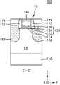
도 1은 본 발명의 기술적 사상에 의한 실시예들에 따른 집적회로 소자(100)의 주요 구성을 도시한 단면도이다.1 is a cross-sectional view illustrating a main configuration of an
도 1을 참조하면, 집적회로 소자(100)는 활성 영역(AC)을 가지는 기판(110)과, 상기 활성 영역(AC) 위에 형성된 게이트 절연막(120)과, 상기 게이트 절연막(120) 위에 형성된 게이트 전극(140)과, 상기 활성 영역(AC)과 상기 게이트 절연막(120)과의 사이의 계면을 따라 형성된 수소 원자층(114)을 포함한다.Referring to FIG. 1 , the
상기 게이트 절연막(120)은 상기 수소 원자층(114)에 접하는 하부 게이트 절연막(122)과, 상기 하부 게이트 절연막(122) 위에 형성된 인터페이스막(124)과, 상기 인터페이스막(124) 위에 형성되고 상기 하부 게이트 절연막(122) 및 상기 인터페이스막(124)보다 더 큰 유전 상수를 가지는 고유전막(126)을 포함할 수 있다.The
상기 기판(110)은 Si 또는 Ge와 같은 반도체, 또는 SiGe, SiC, GaAs, InAs, 또는 InP와 같은 화합물 반도체를 포함할 수 있다. 일부 실시예들에서, 상기 기판(110)은 III-V 족 물질 및 IV 족 물질 중 적어도 하나로 이루어질 수 있다. 상기 III-V 족 물질은 적어도 하나의 III 족 원소와 적어도 하나의 V족 원소를 포함하는 2 원계, 3 원계, 또는 4 원계 화합물일 수 있다. 상기 III-V 족 물질은 III 족 원소로서 In, Ga 및 Al 중 적어도 하나의 원소와, V 족 원소로서 As, P 및 Sb 중 적어도 하나의 원소를 포함하는 화합물일 수 있다. 예를 들면, 상기 III-V 족 물질은 InP, InzGa1-zAs (0 ≤ z ≤ 1), 및 AlzGa1-zAs (0 ≤ z ≤ 1)로부터 선택될 수 있다. 상기 2 원계 화합물은, 예를 들면 InP, GaAs, InAs, InSb 및 GaSb 중 어느 하나일 수 있다. 상기 3 원계 화합물은 InGaP, InGaAs, AlInAs, InGaSb, GaAsSb 및 GaAsP 중 어느 하나일 수 있다. 상기 IV 족 물질은 Si 또는 Ge일 수 있다. 그러나, 본 발명의 기술적 사상에 의한 집적회로 소자에서 사용 가능한 III-V 족 물질 및 IV 족 물질이 상기 예시한 바에 한정되는 것은 아니다. 상기 III-V 족 물질과 Ge과 같은 IV 족 물질은 저전력, 고속 트랜지스터를 만들 수 있는 채널 재료로 이용될 수 있다. Si 기판에 비해 전자의 이동도가 높은 III-V 족 물질, 예를 들면 GaAs로 이루어지는 반도체 기판과, Si 기판에 비해 정공의 이동도가 높은 반도체 물질, 예를 들면 Ge로 이루어지는 반도체 기판을 이용하여 고성능 CMOS를 형성할 수 있다. 일부 실시예들에서, 상기 기판(110) 상에 MMOS 트랜지스터를 형성하는 경우, 상기 기판(110)은 위에서 예시한 III-V 족 물질들 중 어느 하나로 이루어질 수 있다. 다른 일부 실시예들에서, 상기 기판(110) 상에 PMOS 트랜지스터를 형성하는 경우, 상기 기판(110)의 적어도 일부는 Ge로 이루어질 수 있다. 다른 예에서, 상기 기판(110)은 SOI (silicon on insulator) 구조를 가질 수 있다. 상기 기판(110)은 도전 영역, 예를 들면 불순물이 도핑된 웰 (well), 또는 불순물이 도핑된 구조물을 포함할 수 있다.The
상기 수소 원자층(114)에 포함된 수소 원자는 상기 활성 영역(AC)을 구성하는 반도체 원소와 결합된 상태로 존재할 수 있다. 일부 실시예들에서, 상기 수소 원자층(114)은1H (H)원자 또는2H (D) 원자를 포함할 수 있다.The hydrogen atoms included in the hydrogen
일부 실시예들에서, 상기 활성 영역(AC)은 Si로 이루어지고, 상기 수소 원자층(114)을 구성하는 수소 원자들은 상기 활성 영역(AC)의 표면에서 Si-H 결합 형태 또는 Si-D 결합 형태로 형성될 수 있다.In some embodiments, the active region AC is made of Si, and hydrogen atoms constituting the hydrogen
도 2a 및 도 2b는 각각 도 1에 예시한 집적회로 소자(100)의 일부 구성을 확대하여 도시한 도면으로서, Si로 이루어지는 기판(110)의 활성 영역(AC)의 표면에서 상기 활성 영역(AC)과 하부 게이트 절연막(122)과의 사이의 계면(110F)을 따라 형성된 수소 원자층(114A, 114B)을 설명하기 위한 도면이다.2A and 2B are enlarged views showing a partial configuration of the
도 2a는 수소 원자층(114A)이1H (H)원자를 포함하는 경우를 예시한다. 도 2b는 수소 원자층(114B)이2H (D) 원자를 포함하는 경우를 예시한다. 도 2a 및 도 2b에 예시한 수소 원자층(114A, 114B) 중 어느 하나는 도 1에 예시한 수소 원자층(114)을 구성할 수 있다.2A illustrates a case in which the hydrogen
도 2a 및 도 2b에 예시한 수소 원자층(114A, 114B) 내에 포함된 H 원자 또는 D 원자는 기판(110)의 활성 영역(AC)과 하부 게이트 절연막(122)과의 사이의 계면에서 댕글링 본드 (dangling bonds)를 감소시키도록 Si-H 결합 또는 Si-D 결합의 형태로 존재한다. 상기 수소 원자층(114A, 114B)은 활성 영역(AC)의 표면을 패시베이션(passivation)하는 역할을 할 수 있다.H atoms or D atoms included in the hydrogen
상기 수소 원자층(114A, 114B)은 상기 기판(110)의 활성 영역(AC)의 표면을 수소 또는 중수소 분위기 하에서 어닐링함으로써 형성될 수 있다. 상기 수소 원자층(114A, 114B)의 형성 공정에 대한 보다 상세한 사항은 도 7를 참조하여 수소 원자층(114)의 형성 공정에 대하여 설명하는 바를 참조한다.The hydrogen
다시 도 1을 참조하면, 상기 하부 게이트 절연막(122)은 실리콘 산화막, 실리콘 산질화막, 또는 이들의 조합으로 이루어질 수 있다. 상기 하부 게이트 절연막(122)은 약 10 ∼ 40 Å의 두께를 가질 수 있으나, 이에 한정되는 것은 아니다.Referring back to FIG. 1 , the lower
상기 인터페이스막(124)은 유전율이 약 9 이하인 저유전 물질층, 예를 들면 실리콘 산화막, 실리콘 산질화막, 또는 이들의 조합으로 이루어질 수 있다. 상기 인터페이스막(124)은 약 5 ∼ 20 Å의 두께를 가질 수 있으나, 이에 한정되는 것은 아니다.The
상기 고유전막(126)은 하부 게이트 절연막(122) 및 인터페이스막(124)보다 유전 상수가 더 큰 물질로 이루어질 수 있다. 예를 들면, 상기 고유전막(126)은 약 10 내지 25의 유전 상수를 가질 수 있다. 상기 고유전막(126) 하프늄 산화물 (hafnium oxide), 하프늄 산질화물 (hafnium oxynitride), 하프늄 실리콘 산화물 (hafnium silicon oxide), 란타늄 산화물 (lanthanum oxide), 란타늄 알루미늄 산화물 (lanthanum aluminum oxide), 지르코늄 산화물 (zirconium oxide), 지르코늄 실리콘 산화물 (zirconium silicon oxide), 탄탈륨 산화물 (tantalum oxide), 티타늄 산화물 (titanium oxide), 바륨 스트론튬 티타늄 산화물 (barium strontium titanium oxide), 바륨 티타늄 산화물 (barium titanium oxide), 스트론튬 티타늄 산화물 (strontium titanium oxide), 이트륨 산화물 (yttrium oxide), 알루미늄 산화물 (aluminum oxide), 납 스칸듐 탄탈륨 산화물 (lead scandium tantalum oxide), 및 납 아연 니오브산염 (lead zinc niobate), 및 이들의 조합 중에서 선택되는 물질로 이루어질 수 있으나, 상기 고유전막을 구성하는 물질이 상기 예시된 바에 한정되는 것은 아니다. 상기 고유전막(126)은 ALD (atomic layer deposition), CVD (chemical vapor deposition), 또는 PVD (physical vapor deposition) 공정에 의해 형성될 수 있다. 상기 고유전막(126)은 약 10 ∼ 40 Å의 두께를 가질 수 있으나, 이에 한정되는 것은 아니다.The high-
상기 게이트 전극(140)은 일함수 조절용 금속 함유층과, 상기 일함수 조절용 금속 함유층의 상부에 형성된 공간을 채우는 갭필용 금속 함유층을 포함할 수 있다. 일부 실시예들에서, 상기 게이트 전극(140)은 금속 질화물층, 금속층, 도전성 캡핑층, 및 갭필 (gap-fill) 금속막이 차례로 적층된 구조를 가질 수 있다. 상기 금속 질화물층 및 금속층은 각각 Ti, W, Ru, Nb, Mo, Hf, Ni, Co, Pt, Yb, Tb, Dy, Er, 및 Pd 중에서 선택되는 적어도 하나의 금속을 포함할 수 있다. 상기 금속 질화물층 및 금속층은 각각 ALD, MOALD (metal organic ALD), 또는 MOCVD (metal organic CVD) 공정에 의해 형성될 수 있다. 상기 도전성 캡핑층은 상기 금속층의 표면이 산화되는 것을 방지하는 보호막 역할을 할 수 있다. 또한, 상기 도전성 캡핑층은 상기 금속층 위에 다른 도전층이 증착될 때 증착을 용이하게 하기 위한 접착층 (wetting layer) 역할을 할 수 있다. 상기 도전성 캡핑층은 금속 질화물, 예를 들면 TiN, TaN, 또는 이들의 조합으로 이루어질 수 있으나, 이에 한정되는 것은 아니다. 상기 갭필 금속막은 상기 도전성 캡핑층 위에 연장될 수 있다. 상기 갭필 금속막은 W 막으로 이루어질 수 있다. 상기 갭필 금속막은 ALD, CVD, 또는 PVD 공정에 의해 형성될 수 있다. 상기 갭필 금속막은 상기 도전성 캡핑층의 상면에서의 영역간 단차부에 의해 형성되는 리세스 공간을 보이드 (void) 없이 매립할 수 있다. 일부 실시예들에서, 상기 게이트 전극(140)은 TiAlC/TiN/W의 적층 구조 또는 TiN/TaN/TiAlC/TiN/W의 적층 구조, 또는 TiN/TaN/TiN/TiAlC/TiN/W의 적층 구조를 포함할 수 있다. 상기 적층 구조들에서, TiAlC 층 또는 TiN 층이 일함수 조절용 금속 함유층의 역할을 할 수 있다.The
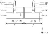
도 3a 내지 도 3c는 본 발명의 기술적 사상에 의한 실시예들에 따른 집적회로 소자(200)를 설명하기 위한 도면들로서, 도 3a는 FinFET 구조를 가지는 트랜지스터(TR)를 포함하는 집적회로 소자(200)의 주요 구성들의 사시도이고, 도 3b는 도 3a의 B - B' 선 단면도이고, 도 3c는 도 3a의 C - C' 선 단면도이다. 도 3a 내지 도 3c에 있어서, 도 1에서와 동일한 참조 부호는 동일 부재를 나타내며, 여기서는 이들에 대한 상세한 설명을 생략한다.3A to 3C are views for explaining an
집적회로 소자(200)는 기판(110)으로부터 상기 기판(110)의 주면에 수직인 방향 (Z 방향)으로 돌출된 핀형 활성 영역(FA)을 포함한다. 상기 핀형 활성 영역(FA)은 일 방향 (도 3a 내지 도 3c에서 Y 방향)을 따라 연장될 수 있다. 상기 기판(110) 상에는 상기 핀형 활성 영역(FA)의 하부 측벽을 덮는 소자분리막(112)이 형성되어 있다. 상기 핀형 활성 영역(FA)은 상기 소자분리막(112) 위로 핀 형상으로 돌출되어 있다.The
상기 핀형 활성 영역(FA)은 상부에 있는 채널 영역(CH)과, 상기 채널 영역(CH)의 하부에서 양 측벽이 소자분리막(112)으로 덮여 있는 베이스 영역(BA)을 가질 수 있다.The fin-type active region FA may include a channel region CH disposed thereon, and a base region BA in which both sidewalls are covered with the
일부 실시예들에서, 상기 핀형 활성 영역(FA)의 채널 영역(CH)은 단일 물질로 이루어질 수 있다. 예를 들면, 상기 핀형 활성 영역(FA)은 상기 채널 영역(CH)을 포함한 모든 영역이 Si으로 이루어질 수 있다. 다른 일부 실시예들에서, 상기 핀형 활성 영역(FA) 중 일부는 Ge로 이루어지고, 상기 핀형 활성 영역(FA) 중 다른 일부는 Si로 이루어질 수 있다.In some embodiments, the channel region CH of the fin-type active region FA may be formed of a single material. For example, in the fin-type active region FA, all regions including the channel region CH may be made of Si. In some other embodiments, a portion of the fin-type active area FA may be formed of Ge, and another portion of the fin-type active area FA may be formed of Si.
상기 게이트 절연막(120)은 상기 핀형 활성 영역(FA)의 상면 및 양 측벽을 덮도록 형성될 수 있다. 수소 원자층(114)은 상기 핀형 활성 영역(FA)의 상면 및 양 측벽과 하부 게이트 절연막(122)과의 사이의 계면을 따라 형성되어 있다. 게이트 전극(140)은 상기 핀형 활성 영역(FA)의 상면 및 양 측벽 위에서 상기 게이트 절연막(120)을 덮도록 형성될 수 있다.The
상기 수소 원자층(114)을 구성하는 수소 원자들은, 도 2a 및 도 2b를 참조하여 설명한 수소 원자층(114A, 114B)에서와 유사하게, 상기 핀형 활성 영역(FA)을 구성하는 반도체 원소와 결합된 형태로 존재할 수 있다. 예를 들면, 상기 핀형 활성 영역(FA)은 Si로 이루어지고, 상기 수소 원자층(114)을 구성하는 H 또는 D는 상기 핀형 활성 영역(FA)의 표면에서 Si-H 결합 형태 또는 Si-D 결합 형태로 존재할 수 있다.Hydrogen atoms constituting the hydrogen
도 3c에 예시한 바와 같이, 상기 집적회로 소자(200)에서 수소 원자층(114), 하부 게이트 절연막(122), 및 인터페이스막(124)은 핀형 활성 영역(FA)의 상면 및 양 측벽과 게이트 전극(140)의 저면과의 사이에 형성되어, 상기 게이트 전극(140)의 저면에 대면하도록 형성되고, 상기 고유전막(126)은 상기 게이트 전극(140)의 저면 및 양 측벽에 대면하도록 형성될 수 있다.As illustrated in FIG. 3C , in the
상기 소자분리막(112)은 실리콘 산화막, 실리콘 질화막, 실리콘 산화질화막, 실리콘 탄화질화막 등과 같은 실리콘 함유 절연막, 폴리실리콘, 또는 이들의 조합으로 이루어질 수 있다.The
상기 핀형 활성 영역(FA) 중 상기 게이트 전극(140)의 양 측에는 한 쌍의 소스/드레인 영역(162)이 형성될 수 있다. 상기 한 쌍의 소스/드레인 영역(162)은 상기 핀형 활성 영역(FA)으로부터 에피택셜 성장된 반도체층을 포함할 수 있다. 상기 소스/드레인 영역(162)은 에피택셜 성장된 복수의 SiGe층을 포함하는 임베디드 SiGe 구조, 에피택셜 성장된 Si 층, 또는 에피택셜 성장된 SiC 층으로 이루어질 수 있다.A pair of source/
도 3a 및 도 3c에서, 상기 한 쌍의 소스/드레인 영역(162)이 특정한 형상을 가지는 경우를 예시하였으나, 본 발명의 기술적 사상에 따르면 상기 한 쌍의 소스/드레인 영역(162)의 단면 형상이 도 3a 및 도 3c에 예시한 바에 한정되지 않으며, 다양한 형상을 가질 수 있다.3A and 3C , the case where the pair of source/
상기 핀형 활성 영역(FA)과 상기 게이트 전극(140)이 교차하는 부분에서 트랜지스터(TR)가 형성될 수 있다. 상기 트랜지스터(TR)는 핀형 활성 영역(FA)의 상면 및 양 측면에서 채널이 형성되는 3 차원 구조의 MOS 트랜지스터로 이루어진다. 상기 MOS 트랜지스터(TR)는 NMOS 트랜지스터 또는 PMOS 트랜지스터를 구성할 수 있다.A transistor TR may be formed in a portion where the fin-type active region FA and the
상기 핀형 활성 영역(FA)의 표면으로부터 차례로 형성된 수소 원자층(114), 게이트 절연막(120), 및 게이트 전극(140)을 포함하는 게이트 구조체(114, 120, 140)의 양 측에는 절연 스페이서(172)가 형성될 수 있다. 도 3c에 예시한 바와 같이, 상기 절연 스페이서(172)를 중심으로 게이트 구조체(114, 120, 140)의 반대측에서 상기 절연 스페이서(172)를 덮는 절연막(174)이 형성될 수 있다. 상기 절연 스페이서(172)는 실리콘 질화막으로 이루어지고, 상기 절연막(174)은 실리콘 산화막으로 이루어질 수 있으나, 본 발명의 기술적 사상이 이에 한정되는 것은 아니다.
도 4는 본 발명의 기술적 사상에 의한 실시예들에 따른 집적회로 소자(300)의 블록 다이어그램이다. 도 4에 있어서, 도 1에서와 동일한 참조 부호는 동일 부재를 나타내며, 여기서는 이들에 대한 상세한 설명은 생략한다.4 is a block diagram of an
도 4를 참조하면, 집적회로 소자(300)는 제1 영역(I) 및 제2 영역(II)을 포함한다.Referring to FIG. 4 , the
상기 제1 영역(I) 및 제2 영역(II)은 동일 기판(110) 상에서 서로 다른 기능을 수행하는 영역일 수 있다. 상기 제1 영역(I) 및 제2 영역(II)은 서로 이격된 영역일 수도 있고, 서로 연결된 영역일 수도 있다.The first region I and the second region II may be regions performing different functions on the
일부 실시예들에서, 상기 제1 영역(Ⅰ)은 비교적 높은 동작 전압이 인가되는 고전압 트랜지스터가 형성되는 고전압 영역이고, 상기 제 2 영역(II)은 비교적 낮은 동작 전압이 인가되는 저전압 트랜지스터가 형성되는 저전압 영역일 수 있다. 본 명세서에서, 고전압 트랜지스터는 동작 전압이 1 V 이상인 트랜지스터를 의미하고, 저전압 트랜지스터는 동작 전압이 1 V 미만인 트랜지스터를 의미할 수 있다.In some embodiments, the first region (I) is a high voltage region in which a high voltage transistor to which a relatively high operating voltage is applied is formed, and the second region (II) is a low voltage transistor to which a relatively low operating voltage is applied. It may be a low voltage region. In this specification, a high voltage transistor may mean a transistor having an operating voltage of 1 V or more, and a low voltage transistor may mean a transistor having an operating voltage of less than 1 V.
상기 제1 영역(Ⅰ)은 문턱 전압이 비교적 높고, 스위칭 속도가 빠르지 않더라도 신뢰성이 높은 트랜지스터가 형성되는 영역일 수 있다. 일부 실시예들에서, 상기 제1 영역(I)은 외부의 데이터를 집적회로 소자(200)의 내부 회로에 입력하거나, 집적회로 소자(200)의 내부 회로로부터 데이터를 외부로 출력하는 기능을 수행하는 주변 회로들이 형성된 주변회로 영역일 수 있다. 일부 실시예들에서, 상기 제1 영역(I)은 입출력(I/O) 회로 장치의 일부를 구성할 수 있다.The first region (I) may be a region in which a transistor with high reliability is formed even though the threshold voltage is relatively high and the switching speed is not fast. In some embodiments, the first region I performs a function of inputting external data into an internal circuit of the
상기 제2 영역(II)은 문턱 전압이 비교적 낮고 스위칭 속도가 빠른 트랜지스터가 형성되는 영역일 수 있다. 일부 실시예들에서, 상기 제2 영역(II)은 단위 메모리 셀이 매트릭스 형태로 배열되어 있는 셀 어레이 영역일 수 있다. 일부 실시예들에서, 상기 제2 영역(II)은 로직 셀 영역 또는 메모리 셀 영역일 수 있다. 상기 로직 셀 영역은 카운터(counter), 버퍼 (buffer) 등과 같은 원하는 논리적 기능을 수행하는 표준 셀 (standard cells)로서, 트랜지스터, 레지스터 등과 같은 복수의 회로 소자들(circuit elements)을 포함하는 다양한 종류의 논리 셀을 포함할 수 있다. 상기 논리 셀은 예를 들면, AND, NAND, OR, NOR, XOR (exclusive OR), XNOR (exclusive NOR), INV (inverter), ADD (adder), BUF (buffer), DLY (delay), FILL (filter), 멀티플렉서 (MXT/MXIT). OAI (OR/AND/INVERTER), AO (AND/OR), AOI (AND/OR/INVERTER), D 플립플롭, 리셋 플립플롭, 마스터-슬레이브 플립플롭(master-slaver flip-flop), 래치(latch) 등을 구성할 수 있다. 그러나, 상기 셀들은 단지 예시에 불과하며, 본 발명의 기술적 사상에 따른 집적회로 소자를 구성하는 논리 셀이 위에서 예시한 셀들에만 한정되는 것은 아니다. 상기 메모리 셀 영역은 SRAM, DRAM, MRAM, RRAM, 및 PRAM 중 적어도 하나의 메모리 셀 영역일 수 있다.The second region II may be a region in which a transistor having a relatively low threshold voltage and a high switching speed is formed. In some embodiments, the second region II may be a cell array region in which unit memory cells are arranged in a matrix form. In some embodiments, the second region II may be a logic cell region or a memory cell region. The logic cell region is a standard cell that performs a desired logical function such as a counter and a buffer, and includes various types of circuit elements such as transistors and resistors. It may contain logic cells. The logic cell is, for example, AND, NAND, OR, NOR, XOR (exclusive OR), XNOR (exclusive NOR), INV (inverter), ADD (adder), BUF (buffer), DLY (delay), FILL ( filter), multiplexers (MXT/MXIT). OAI (OR/AND/INVERTER), AO (AND/OR), AOI (AND/OR/INVERTER), D flip-flop, reset flip-flop, master-slave flip-flop, latch ) can be configured. However, the above cells are merely examples, and the logic cells constituting the integrated circuit device according to the inventive concept are not limited to the cells exemplified above. The memory cell region may be at least one memory cell region of SRAM, DRAM, MRAM, RRAM, and PRAM.
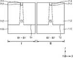
도 5는 본 발명의 기술적 사상에 의한 실시예들에 따른 집적회로 소자(400)의 주요 구성을 도시한 단면도이다. 도 5에 있어서, 도 1 내지 도 4에서와 동일한 참조 부호는 동일 부재를 나타내며, 여기서는 이들에 대한 중복 설명은 생략한다.5 is a cross-sectional view illustrating a main configuration of an
도 5를 참조하면, 집적회로 소자(400)는 제1 영역(I) 및 제2 영역(II)을 가지는 기판(110)과, 제1 영역(I)에 형성된 제1 트랜지스터(TR11)와, 제2 영역(II)에 형성된 제2 트랜지스터(TR12)를 포함한다.Referring to FIG. 5 , the
제1 영역(I)에 형성된 제1 트랜지스터(TR11)는 상기 기판(110)의 제1 활성 영역(AC1) 상에 차례로 형성된 하부 게이트 절연막(122A), 제1 인터페이스막(124A), 및 제1 고유전막(126A)을 포함하는 제1 게이트 절연막(120A)과, 제1 게이트 전극(140A)을 포함한다. 또한, 상기 제1 활성 영역(AC1)과 상기 제1 게이트 절연막(120A)과의 사이의 계면을 따라 수소 원자층(114)이 형성되어 있다. 상기 수소 원자층(114)에 포함된 수소 원자들은 도 2a를 참조하여 설명한 수소 원자층(114A)에서와 유사하게 상기 제1 활성 영역(AC1)의 표면에서 Si-H 결합 형태로 존재하거나, 도 2b를 참조하여 설명한 수소 원자층(114B)에서와 유사하게 Si-D 결합 형태로 존재할 수 있다.The first transistor TR11 formed in the first region I includes a lower
상기 제1 게이트 절연막(120A)은 제1 두께(TH11)를 가질 수 있다. 상기 제1 게이트 절연막(120A)을 구성하는 제1 인터페이스막(124A) 및 제1 고유전막(126A)과, 제1 게이트 전극(140A)에 대한 상세한 사항은 도 1을 참조하여 게이트 절연막(120)을 구성하는 인터페이스막(124) 및 고유전막(126)과, 게이트 전극(140)에 대하여 설명한 바와 대체로 동일한 구성을 가질 수 있다. The first
제2 영역(II)에 형성된 제2 트랜지스터(TR12)는 상기 기판(110)의 제2 활성 영역(AC2) 상에 차례로 형성된 제2 인터페이스막(124B) 및 제2 고유전막(126B)을 포함하는 제2 게이트 절연막(120B)과, 상기 제2 게이트 절연막(120B)을 덮는 제2 게이트 전극(140B)을 포함한다.The second transistor TR12 formed in the second region II includes a
상기 제2 인터페이스막(124B), 제2 고유전막(126B), 및 제2 게이트 전극(140B)은 도 1을 참조하여 인터페이스막(124), 고유전막(126), 및 게이트 전극(140)에 대하여 설명한 바와 대체로 동일한 구성을 가질 수 있다. 상기 제2 게이트 절연막(120B)은 수소 원자층(114) 및 하부 게이트 절연막(122A)을 포함하지 않는 것을 제외하고 상기 제1 게이트 절연막(120A)과 대체로 동일한 구성을 가질 수 있다. 상기 제2 게이트 절연막(120B)은 상기 제1 두께(TH11)보다 작은 제2 두께(TH12)를 가질 수 있다.The
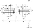
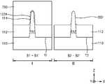
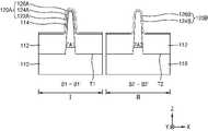
도 6a는 본 발명의 기술적 사상에 의한 실시예들에 따른 집적회로 소자(500)의 주요 구성을 도시한 평면 레이아웃 다이어그램이다. 도 6b는 도 6a의 B1 - B1' 선 단면 구성 및 B2 - B2' 선 단면 구성을 보여주는 단면도이고, 도 6c는 도 6a의 C1 - C1' 선 단면 구성 및 C2 - C2' 선 단면 구성을 보여주는 단면도이다. 도 6a 내지 도 6c에 있어서, 도 1 내지 도 5에서와 동일한 참조 부호는 동일 부재를 나타내며, 여기서는 이들에 대한 상세한 설명을 생략한다.6A is a plan layout diagram illustrating a main configuration of an
도 6a 내지 도 6c를 참조하면, 집적회로 소자(500)는 기판(110)의 제1 영역(I) 및 제2 영역(II)에서 각각 FinFET 구조를 가지는 제1 트랜지스터(TR21) 및 제2 트랜지스터(TR22)를 포함한다.6A to 6C , the
일부 실시예들에서, 제1 영역(I) 및 제2 영역(II)은 서로 다른 기능을 수행하는 영역일 수 있다. 일부 실시예들에서, 제1 영역(I)은 고전력 모드로 동작하는 소자들이 형성되는 영역이고, 제2 영역(II)은 저전력 모드로 동작하는 소자들이 형성되는 영역일 수 있다. 일부 실시예들에서, 제1 영역(I)은 입출력 회로 장치와 같은 주변 회로가 형성되는 영역이고, 제2 영역(II)은 메모리 소자 또는 로직 회로가 형성되는 영역일 수 있다.In some embodiments, the first region I and the second region II may be regions that perform different functions. In some embodiments, the first region I may be a region in which devices operating in a high power mode are formed, and the second region II may be a region in which devices operating in a low power mode are formed. In some embodiments, the first region I may be a region in which a peripheral circuit such as an input/output circuit device is formed, and the second region II may be a region in which a memory device or a logic circuit is formed.
제1 영역(I)에서 제1 핀형 활성 영역(FA1) 위에 제1 게이트 전극(140A)이 교차하도록 연장되어 있고, 상기 제1 핀형 활성 영역(FA1) 및 제1 게이트 전극(140A)이 교차하는 지점에서 상기 제1 트랜지스터(TR21)가 형성될 수 있다.In the first region I, the
제2 영역(II)에서 제2 핀형 활성 영역(FA2) 위에 제2 게이트 전극(140B)이 교차하도록 연장되어 있고, 상기 제2 핀형 활성 영역(FA2) 및 제2 게이트 전극(140B)이 교차하는 지점에서 상기 제2 트랜지스터(TR22)가 형성될 수 있다.In the second region II, the
상기 제1 및 제2 트랜지스터(TR21, TR22)는 각각 NMOS 트랜지스터 또는 PMOS 트랜지스터를 구성할 수 있다.The first and second transistors TR21 and TR22 may constitute an NMOS transistor or a PMOS transistor, respectively.
도 6a에는 제1 영역(I) 및 제2 영역(II)에서 각각 1 개의 제1 및 제2 핀형 활성 영역(FA1, FA2) 및 1 개의 제1 및 제2 게이트 전극(140A, 140B)이 예시되어 있으나, 이들 각각의 개수가 특별히 제한되는 것은 아니며, 제1 영역(I) 및 제2 영역(II)에서 복수의 핀형 활성 영역 및 복수의 게이트 전극이 상호 교차하도록 형성될 수 있다.6A illustrates one first and second fin-type active regions FA1 and FA2 and one first and
제1 영역(I)에 형성된 상기 제1 트랜지스터(TR21)는 기판(110)의 제1 영역(I)에서 상기 기판(110)으로부터 돌출된 제1 핀형 활성 영역(FA1)과, 상기 제1 핀형 활성 영역(FA1) 중 제1 채널 영역(CH1)의 상면 및 양 측벽을 제1 두께(TH21)로 덮는 제1 게이트 절연막(120A)과, 상기 제1 핀형 활성 영역(FA1)의 상면 및 양 측벽 위에서 상기 제1 게이트 절연막(120A)을 덮는 제1 게이트 전극(140A)과, 상기 제1 핀형 활성 영역(FA1)과 상기 게이트 절연막(120A)과의 사이의 계면을 따라 형성된 수소 원자층(114)을 포함한다. 상기 제1 게이트 절연막(120A)은 상기 하부 게이트 절연막(122A), 제1 인터페이스막(124A), 및 제1 고유전막(126A)을 포함할 수 있다. 상기 제1 핀형 활성 영역(FA1)의 제1 베이스 영역(BA1)에서 양 측벽은 소자분리막(112)에 의해 덮여 있다.The first transistor TR21 formed in the first region I includes a first fin-type active region FA1 protruding from the
제2 영역(II)에 형성된 제2 트랜지스터(TR22)는 상기 기판(110)의 제2 영역(II)에서 상기 기판(110)으로부터 돌출된 제2 핀형 활성 영역(FA2)과, 상기 제2 핀형 활성 영역(FA2) 중 제2 채널 영역(CH2)의 상면 및 양 측벽을 상기 제1 두께(TH21)보다 작은 제2 두께(TH22)로 덮는 제2 게이트 절연막(120B)과, 상기 제2 핀형 활성 영역(FA2)의 상면 및 양 측벽 위에서 상기 제2 게이트 절연막(120B)을 덮는 제2 게이트 전극(140B)을 포함한다. 상기 제2 게이트 절연막(120B)은 제2 인터페이스막(124B) 및 제2 고유전막(126B)을 포함할 수 있다. 상기 제2 핀형 활성 영역(FA2)의 제2 베이스 영역(BA2)에서 양 측벽은 소자분리막(112)에 의해 덮여 있다.The second transistor TR22 formed in the second region II includes a second fin-type active region FA2 protruding from the
상기 제1 핀형 활성 영역(FA1) 및 제2 핀형 활성 영역(FA2)에 대한 상세한 사항은 도 3a 내지 도 3c를 참조하여 핀형 활성 영역(FA)에 대하여 설명한 바와 대체로 동일하다.Details of the first fin-type active region FA1 and the second fin-type active region FA2 are substantially the same as those described for the fin-type active region FA with reference to FIGS. 3A to 3C .
도 6a 및 도 6c에 예시한 바와 같이, 제1 핀형 활성 영역(FA1)의 길이 방향 (Y 방향)에 따르는 제1 게이트 전극(140A)의 제1 폭(W1)은 제2 핀형 활성 영역(FA2)의 길이 방향(Y 방향)에 따르는 제2 게이트 전극(140B)의 제2 폭(W2)보다 더 크다.As illustrated in FIGS. 6A and 6C , the first width W1 of the
도 6c에 예시한 바와 같이, 제1 영역(I)에서, 수소 원자층(114), 하부 게이트 절연막(122A), 및 제1 인터페이스막(124A)은 제1 핀형 활성 영역(FA1)의 상면 및 양 측벽과 제1 게이트 전극(140A)의 저면과의 사이에 형성되어, 상기 제1 게이트 전극(140A) 중 저면에 대면하도록 형성되고, 상기 제1 고유전막(126A)은 상기 제1 게이트 전극(140A)의 저면 및 양 측벽에 대면하도록 형성될 수 있다. 또한, 제2 영역(II)에서, 제2 인터페이스막(124B)은 제2 핀형 활성 영역(FA2)의 상면 및 양 측벽과 제2 게이트 전극(140B)의 저면과의 사이에 형성되어, 상기 제2 게이트 전극(140B) 중 저면에 대면하도록 형성되고, 상기 제2 고유전막(126B)은 상기 제2 게이트 전극(140B)의 저면 및 양 측벽에 대면하도록 형성될 수 있다.As illustrated in FIG. 6C , in the first region I, the hydrogen
상기 하부 게이트 절연막(122A), 제1 및 제2 인터페이스막(124A, 124B), 제1 및 제2 고유전막(126A, 126B), 및 제1 및 제2 게이트 전극(140A, 140B)에 대한 상세한 사항은 도 1을 참조하여 하부 게이트 절연막(122), 인터페이스막(124), 고유전막(126), 및 게이트 전극(140)에 대하여 설명한 바와 대체로 동일한 구성을 가질 수 있다.Details of the lower
제1 영역(I)에서 제1 핀형 활성 영역(FA1) 중 제1 게이트 전극(140A)의 양 측에는 한 쌍의 제1 소스/드레인 영역(162A)이 형성될 수 있다. 또한, 제2 영역(II)에서 제2 핀형 활성 영역(FA2) 중 제2 게이트 전극(140B)의 양 측에는 한 쌍의 제2 소스/드레인 영역(162B)이 형성될 수 있다.A pair of first source/drain regions 162A may be formed on both sides of the
상기 제1 및 제2 소스/드레인 영역(162A, 162B)은 도 3a 내지 도 3c를 참조하여 소스/드레인 영역(162)에 대하여 설명한 바와 대체로 동일한 구성을 가질 수 있다.The first and second source/
도 7a 내지 도 7l은 본 발명의 기술적 사상에 의한 실시예들에 따른 집적회로 소자의 제조 방법을 설명하기 위하여 공정 순서에 따라 도시한 단면도들이다. 도 7a 내지 도 7l을 참조하여, 도 6a 내지 도 6c에 예시한 집적회로 소자(500)의 예시적인 제조 방법을 설명한다. 도 7a 내지 도 7l에 있어서, 도 1 내지 도 6c에서와 동일한 참조 부호는 동일 부재를 나타내며, 여기서는 이들에 대한 상세한 설명을 생략한다.7A to 7L are cross-sectional views illustrating a process sequence in order to explain a method of manufacturing an integrated circuit device according to embodiments according to the inventive concept. An exemplary method of manufacturing the
도 7a를 참조하면, 제1 영역(I) 및 제2 영역(II)을 포함하는 기판(110)을 준비한다. 상기 기판(110)의 제1 영역(I) 및 제2 영역(II) 위에 복수의 패드산화막 패턴(712) 및 복수의 마스크 패턴(714)을 형성한다.Referring to FIG. 7A , a
상기 복수의 패드산화막 패턴(712) 및 복수의 마스크 패턴(714)은 기판(110) 상에서 일 방향 (Y 방향)을 따라 상호 평행하게 연장될 수 있다.The plurality of pad
일부 실시예들에서, 상기 복수의 패드산화막 패턴(712)은 상기 기판(110)의 표면을 열산화시켜 얻어진 산화막으로 이루어질 수 있다. 상기 복수의 마스크 패턴(714)은 실리콘 질화막, 실리콘 산화질화막, SOG (spin on glass) 막, SOH (spin on hardmask) 막, 포토레지스트막, 또는 이들의 조합으로 이루어질 수 있으나, 상기 예시한 바에 한정되는 것은 아니다.In some embodiments, the plurality of pad
도 7b를 참조하면, 복수의 마스크 패턴(714)을 식각 마스크로 이용하여 기판(110)의 일부 영역을 식각하여, 상기 기판(110)의 제1 영역(I)에 복수의 제1 트렌치(T1)를 형성하고 기판(110)의 제2 영역에 복수의 제2 트렌치(T2)를 형성한다. 상기 복수의 제1 및 제2 트렌치(T1, T2)가 형성됨에 따라, 상기 기판(110)으로부터 상기 기판(110)의 주면에 수직인 방향 (Z 방향)을 따라 상부로 돌출되고 일 방향 (Y 방향)으로 연장되는 복수의 제1 및 제2 예비 핀형 활성 영역(P1, P2)이 얻어질 수 있다.Referring to FIG. 7B , a partial region of the
도 7c를 참조하면, 제1 영역(I) 및 제2 영역(II)에서 복수의 제1 및 제2 예비 핀형 활성 영역(P1, P2)의 노출 표면을 덮도록 복수의 제1 및 제2 트렌치(T1, T2)를 채우는 소자분리막(112)을 형성한다.Referring to FIG. 7C , a plurality of first and second trenches to cover the exposed surfaces of the plurality of first and second preliminary fin-type active regions P1 and P2 in the first region I and the second region II. A
상기 소자분리막(112)을 형성하기 위하여, PECVD (plasma enhanced chemical vapor deposition), HDP CVD (high density plasma CVD), ICP CVD (inductively coupled plasma CVD), CCP CVD (capacitor coupled plasma CVD), FCVD (flowable chemical vapor deposition), 및/또는 스핀 코팅 (spin coating) 공정 공정을 이용할 수 있으나, 상기 예시한 방법들에만 한정되는 것은 아니다.In order to form the
상기 소자분리막(112)이 형성된 후, 복수의 마스크 패턴(714)이 노출되도록 상면을 평탄화할 수 있다. 이 때, 상기 복수의 마스크 패턴(714)의 일부가 소모되어 이들의 높이가 낮아질 수 있다.After the
도 7d를 참조하면, 복수의 제1 및 제2 예비 핀형 활성 영역(P1, P2) 각각의 상면과 상부 측벽들이 노출되도록 복수의 마스크 패턴(714) 및 복수의 패드산화막 패턴(712)(도 7c 참조)을 제거하고 소자분리막(112)의 일부를 제거하기 위한 리세스(recess) 공정을 수행한다.Referring to FIG. 7D , a plurality of
그 결과, 제1 영역(I) 및 제2 영역(II)에서 소자분리막(112)의 상면의 높이가 낮아지고, 제1 및 제2 예비 핀형 활성 영역(P1, P2)의 상부가 상기 소자분리막(112) 위로 돌출된 상태로 노출될 수 있다.As a result, the height of the upper surface of the
상기 리세스 공정을 수행하기 위하여, 건식 식각, 습식 식각, 또는 건식 및 습식을 조합한 식각 공정을 이용할 수 있다.In order to perform the recess process, dry etching, wet etching, or a combination of dry etching and wet etching may be used.
상기 복수의 마스크 패턴(714)이 실리콘 질화막으로 이루어진 경우, 상기 복수의 마스크 패턴(714)을 제거하기 위하여, 예를 들면 H3PO4를 사용하는 습식 식각 공정을 수행할 수 있다. 상기 복수의 패드산화막 패턴(712)을 제거하기 위하여, 예를 들면 DHF (diluted HF)를 사용하는 습식 식각 공정을 수행할 수 있다. 상기 소자분리막(112)의 리세스 공정을 위하여, 에천트로서 NH4OH, TMAH (tetramethyl ammonium hydroxide), KOH (potassium hydroxide) 용액 등을 이용하는 습식 식각 공정, 또는 ICP (inductively coupled plasma), TCP (transformer coupled plasma), ECR (electron cyclotron resonance), RIE (reactive ion etch) 등과 같은 건식 식각 공정을 이용할 수 있다. 건식 식각에 의해 상기 소자분리막(112)의 리세스 공정을 수행하는 경우, CF4 등과 같은 불소 함유 가스, Cl2와 같은 염소 함유 가스, HBr 등을 이용할 수 있으나, 상기 예시한 바에 한정되는 것은 아니다.When the plurality of
상기 리세스 공정을 수행하는 동안, 제1 영역(I)과 제2 영역(II)에서 노출되는 제1 및 제2 예비 핀형 활성 영역(P1, P2) 각각의 상부가 플라즈마 등의 식각 분위기에 노출될 수 있으며, 상기 식각 분위기에 의해 제1 및 제2 예비 핀형 활성 영역(P1, P2)의 노출 표면(RSF)이 손상되거나, 제1 및 제2 예비 핀형 활성 영역(P1, P2) 각각의 노출 표면(RSF)의 러프니스(roughness)(이하, "핀 에지 러프니스" 또는 "FER"이라 함)가 열화될 수 있다. 또한, 경우에 따라, 식각 마스크 패턴으로 사용되는 막들의 라인 에지 러프니스로 인해 상기 제1 및 제2 예비 핀형 활성 영역(P1, P2)의 노출 표면(RSF)에서의 FER이 커질 수 있다.During the recess process, upper portions of each of the first and second preliminary fin-type active regions P1 and P2 exposed in the first region I and the second region II are exposed to an etching atmosphere such as plasma. The etching atmosphere may damage the exposed surfaces RSF of the first and second preliminary fin-type active regions P1 and P2, or expose each of the first and second preliminary fin-type active regions P1 and P2. The roughness of the surface RSF (hereinafter referred to as "fin edge roughness" or "FER") may deteriorate. In addition, in some cases, the FER at the exposed surface RSF of the first and second preliminary fin-type active regions P1 and P2 may increase due to line edge roughness of the layers used as the etch mask pattern.
고도로 다운스케일링된 트랜지스터의 핀형 활성 영역, 예를 들면 10 nm 또는 그 미만의 게이트 길이를 가지는 트랜지스터의 핀형 활성 영역에서 FER은 핀형 활성 영역의 비대칭 형상을 야기할 수 있으며, 핀형 활성 영역에서의 캐리어 이동도 (carrier mobility)를 열화시키고, 전류 밀도(current density) 감소, 누설 전류 증가 등 불량을 초래하는 원인이 될 수 있다.In highly downscaled finned active regions of transistors, e.g., finned active regions of transistors with gate lengths of 10 nm or less, FER can cause an asymmetric shape of the finned active region, and carrier migration in the finned active region. It may deteriorate carrier mobility and cause defects such as a decrease in current density and an increase in leakage current.
도 7e를 참조하면, 도 7d를 참조하여 설명한 리세스 공정 후, 제1 영역(I) 및 제2 영역(II)에 형성된 제1 및 제2 예비 핀형 활성 영역(P1, P2)에서의 표면 손상을 치유하고 FER을 개선하기 위하여, 상기 제1 및 제2 예비 핀형 활성 영역(P1, P2)의 노출된 부분을 수소 분위기(720)에서 어닐링한다.Referring to FIG. 7E , after the recess process described with reference to FIG. 7D , the surface damage in the first and second preliminary fin-type active regions P1 and P2 formed in the first region I and the second region II In order to heal the fins and improve the FER, the exposed portions of the first and second preliminary fin-type active regions P1 and P2 are annealed in a
일부 실시예들에서, 상기 수소 분위기(720)는 H2 가스 또는 D2 가스로 이루어질 수 있다. 다른 일부 실시예들에서, 상기 수소 분위기(720)는 H2 가스 및 D2 가스 중 적어도 하나의 수소 가스와, Ar, He, Ne, N2 등의 불활성 가스와의 혼합 가스 분위기로 이루어질 수 있다. 예를 들면, 상기 혼합 가스 분위기 내에서 수소 가스는 약 5 ∼ 30 부피 %의 양으로 포함될 수 있으나, 본 발명의 기술적 사상이 상기 예시한 범위에 한정되는 것은 아니다.In some embodiments, the
일부 실시예들에서, 상기 수소 분위기(720)에서의 어닐링은 약 600 ∼ 900 ℃의 온도 및 약 1 ∼ 20 torr의 압력 하에서 약 5 초 ∼ 약 1 분 동안 수행될 수 있다. 그러나, 이들 조건은 예시에 불과한 것으로, 본 발명의 기술적 사상이 상기 예시한 조건들에 한정되는 것은 아니다.In some embodiments, the annealing in the
상기 수소 분위기(720)에서의 어닐링이 수행되는 동안 제1 및 제2 예비 핀형 활성 영역(P1, P2)(도 7d 참조)의 노출 표면(RSF)에서 수소 원자에 의해 유도되는 표면 원자 마이그레이션 (hydrogen-enhanced surface atom migration)이 유도되어, 상기 제1 및 제2 예비 핀형 활성 영역(P1, P2)을 구성하는 반도체 원자들, 예를 들면 Si 원자들은 상기 제1 및 제2 예비 핀형 활성 영역(P1, P2)의 노출 표면(RSF) 중 볼록한 부분들로부터 이동하여 오목한 부분들에 축적될 수 있다. 그 결과, 상기 제1 및 제2 예비 핀형 활성 영역(P1, P2)의 노출 표면(RSF)의 거칠기(roughness)가 감소되고, 상기 제1 및 제2 예비 핀형 활성 영역(P1, P2)의 노출 표면(RSF)의 모폴로지(morphology)가 변화되어 평활한 외측 표면을 가지는 제1 및 제2 핀형 활성 영역(FA1, FA2)이 얻어질 수 있다.Surface atom migration (hydrogen) induced by hydrogen atoms on the exposed surface RSF of the first and second preliminary fin-type active regions P1 and P2 (see FIG. 7D ) while the annealing in the
또한, 상기 수소 분위기(720)에서의 어닐링이 수행되는 동안 상기 제1 및 제2 예비 핀형 활성 영역(P1, P2)의 노출 표면에 남아 있는 반응 부산물, 예를 들면 HFx, CHx 등의 오염물들이 제거될 수 있다.In addition, while the annealing in the
상기 수소 분위기(720)에서의 어닐링 공정은, 도 7d를 참조하여 설명한 바와 같이 소자분리막(112)의 리세스 공정을 수행하여 제1 및 제2 예비 핀형 활성 영역(P1, P2)의 표면(RSF)이 노출된 후, 습식 식각 공정을 거치지 않고 바로 수행될 수 있다. 이와 같이 제1 및 제2 예비 핀형 활성 영역(P1, P2)이 형성된 후, 그 표면(RSF)에 대하여 습식 식각 공정을 거치지 않고 바로 수소 분위기(720)에서의 어닐링 공정을 수행함으로써, 상기 제1 및 제2 예비 핀형 활성 영역(P1, P2)이 습식 식각에 의하여 소모되는 현상을 방지할 수 있으며, 이에 따라 상기 제1 및 제2 예비 핀형 활성 영역(P1, P2) 중 노출된 부분들의 폭 및 높이가 감소되는 문제를 방지할 수 있다. 따라서, 그 결과 얻어지는 제1 및 제2 핀형 활성 영역(FA1, FA2)에서 하부 폭과 상부 폭의 차이를 줄일 수 있다.In the annealing process in the
상기 수소 분위기(720)에서의 어닐링을 수행하는 동안 상기 제1 및 제2 핀형 활성 영역(FA1, FA2)의 표면에 수소 분자들, 예를 들면 H2 분자들 또는 D2 분자들이 흡착될 수 있으며, 상기 제1 및 제2 핀형 활성 영역(FA1, FA2)의 표면에 있는 댕글링 본드 사이트들(dangling bond sites)에 수소 원자들이 결합될 수 있다. 이에 따라, 상기 수소 분위기(720)에서의 어닐링을 수행함으로써, 상기 제1 및 제2 예비 핀형 활성 영역(P1, P2)의 노출 표면(RSF)(도 7d 참조)에서의 평활도가 증가되어 평활한 외측 표면을 가지는 제1 및 제2 핀형 활성 영역(FA1, FA2)이 형성되고, 이와 동시에 상기 제1 및 제2 핀형 활성 영역(FA1, FA2)의 평활한 표면을 덮는 수소 원자층(114)이 형성될 수 있다.During the annealing in the
상기 제1 및 제2 핀형 활성 영역(FA1, FA2)을 덮는 수소 원자층(114)에 의해, 상기 제1 및 제2 핀형 활성 영역(FA1, FA2)은 상기 수소 원자층(114)을 구성하는 수소 원자들로 종결된(terminated by hydrogen atoms) 표면을 가지게 될 수 있다.By the hydrogen
일부 실시예들에서, 제1 영역(I) 및 제2 영역(II)에서 제1 및 제2 핀형 활성 영역(FA1, FA2) 각각의 상부에 문턱 전압 조절용 불순물 이온 주입 공정이 수행될 수 있다. 상기 문턱 전압 조절용 불순물 이온 주입 공정시, 상기 제1 영역(I) 및 제2 영역(II) 중 NMOS 트랜지스터가 형성되는 영역에는 불순물로서 붕소(B) 이온을 주입하고, PMOS 트랜지스터가 형성되는 영역에는 불순물로서 인(P) 또는 비소(As)를 이온주입할 수 있다. 상기 문턱 전압 조절용 불순물 이온 주입 공정은 도 7e를 참조하여 설명한 수소 원자층(114) 형성 공정이 수행되기 전, 또는 상기 수소 원자층(114) 형성 공정이 수행된 후에 행해질 수 있다.In some embodiments, an impurity ion implantation process for adjusting a threshold voltage may be performed on each of the first and second fin-type active regions FA1 and FA2 in the first region I and the second region II. In the impurity ion implantation process for regulating the threshold voltage, boron (B) ions as impurities are implanted into the region where the NMOS transistor is formed among the first region (I) and the second region (II), and into the region where the PMOS transistor is formed. As an impurity, phosphorus (P) or arsenic (As) may be ion-implanted. The impurity ion implantation process for controlling the threshold voltage may be performed before the hydrogen
도 7f 내지 도 7h는 제1 영역(I) 및 제2 영역(II)에서 수소 원자층(114)으로 덮인 제1 및 제2 핀형 활성 영역(FA1, FA2) 위에 하부 게이트 절연막(122A)(도 7h 참조)을 형성하는 예시적인 과정을 설명하기 위한 단면도들이다.7F to 7H show a lower
먼저 도 7f를 참조하면, 제1 영역(I) 및 제2 영역(II)에서 수소 원자층(114) 위에 산화막(122P)을 형성한다.First, referring to FIG. 7F , an
상기 산화막(122P)은 하부 게이트 절연막(122A)(도 7h 참조)을 형성하기 위한 예비 막으로서, 플라즈마를 이용하는 제1 산화 처리에 의해 형성될 수 있다.The
일부 실시예들에서, 상기 제1 산화 처리에 의해 상기 산화막(122P)을 형성하기 위하여, 플라즈마 처리 장치 내에서 플라즈마 분위기를 이용하여 상기 제1 및 제2 핀형 활성 영역(FA1, FA2)의 라디칼 산화 공정을 수행할 수 있다. 일부 실시예들에서, 상기 산화막(122P)은 O2 가스 및 불활성 가스를 이용하여 얻어지는 플라즈마 분위기에서 형성될 수 있다. 다른 일부 실시예들에서, 상기 산화막(122P)은 O2 가스, 불활성 가스, 및 H2 가스를 이용하여 얻어지는 플라즈마 분위기에서 형성될 수 있다. 예를 들면, 상기 플라즈마 분위기를 형성하기 위하여, 상기 플라즈마 처리 장치 내에 O2 가스 및 Ar 가스를 공급할 수 있다. 또는, 상기 플라즈마 분위기를 형성하기 위하여 상기 플라즈마 처리 장치 내에 O2 가스, Ar 가스, 및 H2 가스를 공급할 수 있다. 이 때, 상기 플라즈마 분위기 내에서의 산소 이온 또는 산소 라디칼의 양을 제어하여, 상기 수소 원자층(114)으로 덮인 제1 및 제2 핀형 활성 영역(FA1, FA2)의 FER을 열화시키지 않고 제1 및 제2 핀형 활성 영역(FA1, FA2)의 외측 표면이 평활한 상태를 유지하면서, 상기 수소 원자층(114) 위에 균일한 막 두께를 가지는 산화막(122P)이 형성될 수 있다.In some embodiments, radical oxidation of the first and second fin-type active regions FA1 and FA2 using a plasma atmosphere in a plasma processing apparatus to form the
상기 제1 산화 처리는 다양한 방식의 플라즈마 처리 장치를 이용하여 수행될 수 있다. 예를 들면, 상기 제1 산화 처리는 복수의 슬롯을 가지는 평면 안테나, 특히 RLSA (radial line slot antenna)에서 반응 챔버 내에 마이크로파를 도입해 플라스마를 발생시킴으로써, 고밀도 및 저전자 온도의 마이크로파 플라스마를 발생시킬 수 있는 RLSA 마이크로파 플라즈마 처리 장치, 리모트 플라스마 방식의 플라즈마 처리 장치, ICP (inductively coupled plasma) 플라스마 방식의 플라즈마 처리 장치, ECR (electron cyclotron resonance) 플라스마 방식의 플라즈마 처리 장치, 표면 반사파 플라스마 방식의 플라즈마 처리 장치, 마그네트론 플라스마 방식의 플라즈마 처리 장치 등을 이용하여 수행될 수 있다.The first oxidation treatment may be performed using various types of plasma processing apparatuses. For example, the first oxidation treatment is a planar antenna having a plurality of slots, in particular, a microwave plasma of high density and low electron temperature by introducing microwaves into a reaction chamber in a RLSA (radial line slot antenna) to generate plasma. RLSA microwave plasma processing apparatus, remote plasma type plasma processing apparatus, ICP (inductively coupled plasma) plasma type plasma processing apparatus, ECR (electron cyclotron resonance) plasma type plasma processing apparatus, surface reflection wave plasma type plasma processing apparatus , may be performed using a plasma processing apparatus of a magnetron plasma method, or the like.
상기 산화막(122P)은 약 10 ∼ 40 Å의 두께를 가지도록 형성될 수 있으나, 이에 한정되는 것은 아니다.The
도 7g를 참조하면, 제1 영역(I) 및 제2 영역(II)에서 식각 분위기(730)를 이용하여 제1 및 제2 핀형 활성 영역(FA1, FA2)이 노출되지 않을 정도로 상기 산화막(122P)(도 7f 참조)의 노출 표면으로부터 상기 산화막(122P)을 일부 두께만큼 제거하여 두께가 감소된 산화막(122Q)을 형성한다.Referring to FIG. 7G , the
일부 실시예들에서, 상기 식각 분위기(730)는 습식 식각 분위기일 수 있다. 예를 들면, HF 용액을 사용하여 상기 산화막(122P)을 일부 두께만큼 제거할 수 있다. 이와 같이 습식 식각 분위기를 이용하여 산화막(122P)을 일부 두께만큼 제거하는 동안 제1 및 제2 핀형 활성 영역(FA1, FA2)이 노출되지 않으므로, 제1 및 제2 핀형 활성 영역(FA1, FA2)이 습식 식각에 의하여 소모되는 것을 방지하여 제1 및 제2 핀형 활성 영역(FA1, FA2)의 FER을 열화시키지 않고 평활한 표면을 유지하도록 할 수 있다. 또한, 제1 및 제2 핀형 활성 영역(FA1, FA2)의 폭 및 높이가 감소되는 문제를 방지하여 제1 및 제2 핀형 활성 영역(FA1, FA2)에서 하부 폭과 상부 폭의 차이를 줄일 수 있다.In some embodiments, the
도 7h를 참조하면, 수소 원자층(114)이 상기 두께가 감소된 산화막(122Q)으로 덮인 상태에서, 플라즈마를 이용하지 않는 제2 산화 처리에 의해 상기 두께가 감소된 산화막(122Q)의 두께를 증가시켜 하부 게이트 절연막(122A)을 형성한다.Referring to FIG. 7H , in a state in which the hydrogen
상기 제2 산화 처리를 위하여, 예를 들면 수증기, 또는 H2 가스 및 O2 가스의 조합을 이용하는 ISSG (in-situ steam generation) 공정을 수행할 수 있다. ISSG 공정에 의해 상기 산화막(122Q)의 두께를 증가시킴으로써, 막질이 우수한 하부 게이트 절연막(122A)이 얻어질 수 있다.For the second oxidation treatment, for example, an in-situ steam generation (ISSG) process using water vapor or a combination of H2 gas and O2 gas may be performed. By increasing the thickness of the
제1 영역(I) 및 제2 영역(II)에서 상기 하부 게이트 절연막(122A)은 상기 제1 및 제2 핀형 활성 영역(FA1, FA2) 각각의 상면 및 양 측벽을 덮도록 형성된다.In the first region I and the second region II, the lower
일부 실시예들에서, 상기 하부 게이트 절연막(122A)은 약 10 ∼ 50 Å의 두께를 가질 수 있으나, 상기 예시한 바에 한정되는 것은 아니다.In some embodiments, the lower
일부 실시예들에서, 상기 하부 게이트 절연막(122A)을 형성하기 위하여, 두께가 감소된 산화막(122Q)이 형성된 결과물에 대하여 ISSG 공정에 의해 상기 산화막(122Q)의 두께를 증가시킨 후, 상기 두께가 증가된 산화막의 적어도 일부를 질화 처리하는 공정을 더 수행하여, 실리콘 산질화막으로 이루어지는 상기 하부 게이트 절연막(122A)을 형성할 수 있다. 상기 질화 처리를 위하여 DPN (decoupled plasma nitridation) 공정을 이용할 수 있다. 상기 질화 처리 후 얻어진 하부 게이트 절연막(122A)에서는 상기 하부 게이트 절연막(122A)의 전체 두께 범위 중 외측 표면에 인접한 에지 부분에서의 질소 농도가 가장 높을 수 있다. 예를 들면, 상기 하부 게이트 절연막(122A) 내에서 상기 하부 게이트 절연막(122A)의 외측 표면으로부터 약 0.5 nm의 깊이인 부분을 따라 상기 하부 게이트 절연막(122A) 내에서 질소 원자의 농도가 가장 높은 질소 농도 피크 영역이 존재할 수 있다.In some embodiments, in order to form the lower
도 7i를 참조하면, 제2 영역(II)이 노출되도록 제1 영역(I)을 덮는 마스크 패턴(750)을 형성하고, 수소 원자층(114) 및 하부 게이트 절연막(122A) 중 제2 영역(II)에 있는 부분들을 제거하여, 제2 영역(II)에서 제2 핀형 활성 영역(FA2)의 평활한 표면(SSF)을 노출시킨다.Referring to FIG. 7I , a
제2 영역(II)에서 수소 원자층(114) 및 하부 게이트 절연막(122A)이 제거되는 동안 상기 마스크 패턴(750)은 제1 영역(I)에 있는 제1 핀형 활성 영역(FA1)과 그 위에 형성된 수소 원자층(114) 및 하부 게이트 절연막(122A)을 보호하는 역할을 할 수 있다. 상기 마스크 패턴(750)은 포토레지스트 패턴으로 이루어질 수 있다.While the hydrogen
제2 영역(II)에서 수소 원자층(114) 및 하부 게이트 절연막(122A)이 제거된 후 노출되는 제2 핀형 활성 영역(FA2)의 평활한 표면(SSF)에는 수소 원자층(114)을 구성하였던 수소 원자들의 일부가 남아 있을 수 있다.A hydrogen
도 7j를 참조하면, 제1 영역(I)을 덮는 마스크 패턴(750)(도 7i 참조)을 제거한 후, 제1 영역(I)에서 하부 게이트 절연막(122A)에 접하는 제1 인터페이스막(124A)과, 제2 영역(II)에서 제2 핀형 활성 영역(FA2)의 평활한 표면(SSF)에 접하는 제2 인터페이스막(124B)을 형성한다.Referring to FIG. 7J , after removing the mask pattern 750 (see FIG. 7I ) covering the first region I, the
일부 실시예들에서, 제2 영역(II)에 형성되는 상기 제2 인터페이스막(124B)은 제2 핀형 활성 영역(FA2)의 표면을 산화시켜 얻어질 수 있다. 제2 영역(II)에서 상기 제2 인터페이스막(124B)은 제2 핀형 활성 영역(FA2)과 도 7k를 참조하여 후술하는 제2 고유전막(126B)과의 사이의 계면 결함을 치유하는 역할을 할 수 있다.In some embodiments, the
일부 실시예들에서, 상기 제1 인터페이스막(124A) 및 제2 인터페이스막(124B)은 유전율이 약 9 이하인 저유전 물질층, 예를 들면 실리콘 산화막, 실리콘 산질화막, 또는 이들의 조합으로 이루어질 수 있다. 다른 일부 실시예들에서, 상기 제1 인터페이스막(124A) 및 제2 인터페이스막(124B)은 실리케이트, 실리케이트와 실리콘 산화막과의 조합, 또는 실리케이트와 실리콘 산질화막과의 조합으로 이루어질 수 있다. 일부 실시예들에서, 상기 제1 인터페이스막(124A) 및 제2 인터페이스막(124B)은 각각 약 5 ∼ 20 Å의 두께를 가질 수 있으나, 이에 한정되는 것은 아니다.In some embodiments, the
일부 실시예들에서, 상기 제1 인터페이스막(124A) 및 제2 인터페이스막(124B)은 생략될 수 있다.In some embodiments, the
도 7k를 참조하면, 제1 영역(I)에서 제1 인터페이스막(124A) 위에 배치되는 제1 고유전막(126A)과, 제2 영역(II)에서 제2 인터페이스막(124B) 위에 배치되는 제2 고유전막(126B)을 형성한다.Referring to FIG. 7K , the first high-
일부 실시예들에서, 상기 제1 및 제2 고유전막(126A, 126B)은 ALD, CVD, 또는 PVD 공정에 의해 형성될 수 있다. 상기 제1 및 제2 고유전막(126A, 126B)은 약 10 ∼ 40 Å의 두께를 가질 수 있으나, 이에 한정되는 것은 아니다.In some embodiments, the first and second high-
도 7l을 참조하면, 제1 영역(I)에서 제1 고유전막(126A) 위에 배치되는 제1 게이트 전극(140A)과, 제2 영역(II)에서 제2 고유전막(126B) 위에 배치되는 제2 게이트 전극(140B)을 형성한다.Referring to FIG. 7L , in the first region (I), the
제1 영역(I) 및 제2 영역(II)에서 상기 제1 게이트 전극(140A) 및 제2 게이트 전극(140B)을 형성하기 전 또는 후에, 제1 및 제2 핀형 활성 영역(FA1, FA2)에 각각 제1 및 제2 소스/드레인 영역(162A, 162B)(도 6c 참조)을 형성할 수 있다.Before or after forming the
일부 실시예들에서, 상기 제1 및 제2 게이트 전극(140A, 140B) 중 적어도 하나는 RPG (replacement poly-gate) 공정에 의해 형성될 수 있다. 상기 제1 및 제2 게이트 전극(140A, 140B)을 RPG 공정에 의해 형성하기 위한 예시적인 공정에서, 도 7f 내지 도 7h를 참조하여 설명한 바와 같이 하부 게이트 절연막(122A)을 형성한 후, 상기 하부 게이트 절연막(122A) 위에 폴리실리콘으로 이루어지는 희생 게이트막(도시 생략)을 형성할 수 있다. 그 후, 상기 희생 게이트막 및 하부 게이트 절연막(122A)을 포함하는 적층 구조를 패터닝하여 희생 패턴(도시 생략)을 형성하고, 상기 희생 패턴의 양 측벽을 덮는 절연 스페이서(172)(도 6c 참조)를 형성할 수 있다. 그 후, 제1 영역(I)에서는 상기 희생 패턴 중 상기 희생 게이트막을 제거하여 상기 절연 스페이서(172)에 의해 한정되는 게이트 공간을 통해 상기 하부 게이트 절연막(122A)을 노출시키고, 제2 영역(II)에서는 상기 희생 패턴 중 상기 희생 게이트막을 제거한 후, 도 7i를 참조하여 설명한 바와 같은 방법으로 수소 원자층(114) 및 하부 게이트 절연막(122A)을 제거하여, 상기 절연 스페이서(172)에 의해 한정되는 게이트 공간을 통해 제1 핀형 활성 영역(FA1)의 평활한 표면(SSF)을 노출시킬 수 있다. 그 후, 도 7j 내지 도 7l을 참조하여 설명한 바와 같은 방법으로 제1 영역(I) 및 제2 영역(II)에서 제1 및 제2 인터페이스막(124A, 124B), 제1 및 제2 고유전막(126A, 126B), 제1 및 제2 게이트 전극(140A, 140B)을 차례로 형성할 수 있다.In some embodiments, at least one of the first and
도 7a 내지 도 7l을 참조하여 설명한 집적회로 소자(500)의 제조 방법에 따르면, 제1 영역(I) 및 제2 영역(II)에서 고도로 스케일링 다운된 제1 및 제2 핀형 활성 영역(FA1, FA2)의 탑 부분의 폭과 바텀 부분의 폭과의 차이를 최소화하고 표면 러프니스를 최소화하여 평활한 표면을 가지는 핀형 활성 영역을 제공함으로써 고도로 스케일링된 핀 전계효과 트랜지스터의 퍼포먼스를 향상시킬 수 있다.According to the method of manufacturing the
도 7a 내지 도 7l을 참조하여 도 6a 내지 도 6c에 예시한 집적회로 소자(500)의 예시적인 제조 방법에 대하여 설명하였으나, 본 발명의 기술적 사상의 범위 내에서 이로부터 변형 및 변경된 다양한 방법을 이용하여 본 명세서에서 예시하는 다양한 구조를 가지는 집적회로 소자들, 예를 들면, 도 1에 예시한 집적회로 소자(100), 도 3a 내지 도 3c에 예시한 집적회로 소자(200), 및 도 5에 예시한 집적회로 소자(400)를 용이하게 구현할 수 있다.Although an exemplary method of manufacturing the
또한, 도 7a 내지 도 7l을 참조하여 3 차원 구조의 채널을 구비하는 FinFET을 포함하는 집적회로 소자의 제조 방법에 대하여 설명하였으나, 본 발명의 기술적 사상은 상기 설명한 바에 한정되는 것은 아니다. 예를 들면, 본 발명의 기술적 사상의 범위 내에서 본 발명의 기술적 사상의 다양한 변형 및 변경을 통하여 본 발명의 기술적 사상에 의한 특징들을 가지는 수평형 (planar) MOSFET을 포함하는 집적회로 소자들 및 그 제조 방법들을 제공할 수 있음은 당 업자들이면 잘 알 수 있을 것이다.In addition, although a method of manufacturing an integrated circuit device including a FinFET having a channel having a three-dimensional structure has been described with reference to FIGS. 7A to 7L , the technical spirit of the present invention is not limited thereto. For example, integrated circuit devices including a planar MOSFET having features according to the technical spirit of the present invention through various modifications and changes of the technical spirit of the present invention within the scope of the technical spirit of the present invention, and It will be appreciated by those skilled in the art that manufacturing methods can be provided.
도 8은 본 발명의 기술적 사상에 의한 실시예들에 따른 집적회로 소자(600)의 주요 구성을 도시한 단면도이다. 도 8에 있어서, 도 1 내지 도 6에서와 동일한 참조 부호는 동일 부재를 나타내며, 여기서는 이들에 대한 상세한 설명을 생략한다.8 is a cross-sectional view illustrating a main configuration of an
도 8을 참조하면, 집적회로 소자(600)의 기판(110)은 제1 영역(I) 중에서 선택되는 서로 다른 영역인 제1 국부 영역(IA) 및 제2 국부 영역(IB)을 포함한다.Referring to FIG. 8 , the
제1 국부 영역(IA) 및 제2 국부 영역(IB)은 서로 이격된 영역일 수도 있고, 서로 연결된 영역일 수도 있다. 제1 국부 영역(IA) 및 제2 국부 영역(IB)은 각각 문턱 전압이 비교적 높고, 스위칭 속도가 빠르지 않더라도 신뢰성이 높은 트랜지스터가 형성되는 영역일 수 있다. 일부 실시예들에서, 제1 국부 영역(IA) 및 제2 국부 영역(IB)은 각각 입출력(I/O) 회로 장치의 일부를 구성할 수 있다.The first local area IA and the second local area IB may be spaced apart from each other or may be connected to each other. Each of the first local area IA and the second local area IB may be a region in which a transistor with high reliability is formed even though the threshold voltage is relatively high and the switching speed is not fast. In some embodiments, the first local area IA and the second local area IB may each form a part of an input/output (I/O) circuit device.
상기 집적회로 소자(600)는 제1 국부 영역(IA) 및 제2 국부 영역(IB)에서 각각 FinFET 구조를 가지는 제1 트랜지스터(TR21) 및 제3 트랜지스터(TR3)를 포함한다. 상기 제1 트랜지스터(TR21)에 대한 상세한 구성은 도 6a 내지 도 6c를 참조하여 설명한 바와 같다. 상기 제3 트랜지스터(TR3)는 제1 트랜지스터(TR21)의 제1 채널 영역(CH1)보다 더 좁은 폭을 가지는 제3 채널 영역(CH3)을 포함하는 제3 핀형 활성 영역(FA3)을 포함할 수 있다.The
상기 제3 핀형 활성 영역(FA3)은 제1 핀형 활성 영역(FA1)의 형성 공정과 유사한 공정에 의해 형성될 수 있다. 단, 상기 제3 핀형 활성 영역(FA3)을 형성하는 공정은 도 7e를 참조하여 설명한 바와 같은 수소 분위기(720)에서의 어닐링 공정을 생략할 수 있다. 이에 따라, 상기 제3 트랜지스터(TR3)의 상부 표면에는 수소 원자층(114)이 형성되지 않고, 상기 하부 게이트 절연막(122A)이 상기 제3 트랜지스터(TR3)의 상부 표면에 직접 접하도록 형성될 수 있다.The third fin-type active region FA3 may be formed by a process similar to that of the first fin-type active region FA1 . However, in the process of forming the third fin-type active region FA3 , the annealing process in the
도 9는 본 발명의 기술적 사상에 의한 실시예들에 따른 집적회로 소자(700)의 주요 구성을 도시한 단면도이다. 도 9에 있어서, 도 1 내지 도 6에서와 동일한 참조 부호는 동일 부재를 나타내며, 여기서는 이들에 대한 상세한 설명을 생략한다.9 is a cross-sectional view illustrating a main configuration of an
도 9를 참조하면, 집적회로 소자(700)의 기판(110)은 제2 영역(II) 중에서 선택되는 서로 다른 영역인 제3 국부 영역(IIA) 및 제4 국부 영역(IIB)을 포함한다.Referring to FIG. 9 , the
제3 국부 영역(IIA) 및 제4 국부 영역(IIB)은 서로 이격된 영역일 수도 있고, 서로 연결된 영역일 수도 있다. 제3 국부 영역(IIA) 및 제4 국부 영역(IIB)은 각각 비교적 낮은 동작 전압이 인가되는 저전압 트랜지스터가 형성되는 저전압 영역일 수 있다. 일부 실시예들에서, 제3 국부 영역(IIA) 및 제4 국부 영역(IIB)은 단위 메모리 셀이 매트릭스 형태로 배열되어 있는 셀 어레이 영역일 수 있다. 다른 일부 실시예들에서, 제3 국부 영역(IIA) 및 제4 국부 영역(IIB)은 로직 셀 영역 또는 메모리 셀 영역일 수 있다.The third local area IIA and the fourth local area IIB may be spaced apart from each other or may be connected to each other. Each of the third local region IIA and the fourth local region IIB may be a low voltage region in which a low voltage transistor to which a relatively low operating voltage is applied is formed. In some embodiments, the third local area IIA and the fourth local area IIB may be a cell array area in which unit memory cells are arranged in a matrix form. In some other embodiments, the third local area IIA and the fourth local area IIB may be a logic cell area or a memory cell area.
상기 집적회로 소자(700)는 제3 국부 영역(IIA) 및 제4 국부 영역(IIB)에서 각각 FinFET 구조를 가지는 제2 트랜지스터(TR22) 및 제4 트랜지스터(TR4)를 포함한다. 상기 제2 트랜지스터(TR22)에 대한 상세한 구성은 도 6a 내지 도 6c를 참조하여 설명한 바와 같다. 상기 제4 트랜지스터(TR4)는 제2 트랜지스터(TR22)의 제2 채널 영역(CH2)보다 더 좁은 폭을 가지는 제4 채널 영역(CH4)을 포함하는 제4 핀형 활성 영역(FA4)을 포함할 수 있다.The
상기 제4 핀형 활성 영역(FA4)은 제2 핀형 활성 영역(FA2)의 형성 공정과 유사한 공정에 의해 형성될 수 있다. 단, 상기 제4 핀형 활성 영역(FA4)을 형성하는 공정은 도 7e를 참조하여 설명한 바와 같은 수소 분위기(720)에서의 어닐링 공정을 생략할 수 있다. 상기 제4 트랜지스터(TR4)의 상부 표면에 제2 인터페이스막(124B)이 직접 접하도록 형성될 수 있다.The fourth fin-type active region FA4 may be formed by a process similar to that of the second fin-type active region FA2 . However, in the process of forming the fourth fin-type active region FA4 , the annealing process in the
도 10은 본 발명의 기술적 사상에 의한 실시예들에 따른 전자 시스템(2000)의 블록 다이어그램이다.10 is a block diagram of an
상기 전자 시스템(2000)은 콘트롤러(2010), 입출력 장치 (I/O)(2020), 메모리(2030), 및 인터페이스(2040)를 포함하며, 이들은 각각 버스(2050)를 통해 상호 연결되어 있다.The
상기 콘트롤러(2010)는 마이크로프로세서 (microprocessor), 디지탈 신호 프로세서, 또는 이들과 유사한 처리 장치 중 적어도 하나를 포함할 수 있다. 상기 입출력 장치(2020)는 키패드 (keypad), 키보드 (keyboard), 또는 디스플레이 (display) 중 적어도 하나를 포함할 수 있다. 상기 메모리(2030)는 콘트롤러(2010)에 의해 실행된 명령을 저장하는 데 사용될 수 있다. 예를 들면, 상기 메모리(2030)는 유저 데이타 (user data)를 저장하는 데 사용될 수 있다.The
상기 전자 시스템(2000)은 무선 통신 장치, 또는 무선 환경 하에서 정보를 전송 및/또는 수신할 수 있는 장치를 구성할 수 있다. 상기 전자 시스템(2000)에서 무선 커뮤니케이션 네트워크를 통해 데이타를 전송/수신하기 위하여 상기 인터페이스(2040)는 무선 인터페이스로 구성될 수 있다. 상기 인터페이스(2040)는 안테나 및/또는 무선 트랜시버 (wireless transceiver)를 포함할 수 있다. 일부 실시예에서, 상기 전자 시스템(2000)은 제3 세대 통신 시스템, 예를 들면, CDMA(code division multiple access), GSM (global system for mobile communications), NADC (north American digital cellular), E-TDMA (extended-time division multiple access), 및/또는 WCDMA (wide band code division multiple access)와 같은 제3 세대 통신 시스템의 통신 인터페이스 프로토콜에 사용될 수 있다. 상기 전자 시스템(2000)은 도 1 내지 도 8에 예시한 집적회로 소자(100, 200, 300, 400, 500, 600, 700) 및 이들로부터 본 발명의 기술적 사상의 범위 내에서 변형 및 변경된 다양한 구조를 가지는 집적회로 소자들 중 적어도 하나를 포함한다.The
이상, 본 발명을 바람직한 실시예를 들어 상세하게 설명하였으나, 본 발명은 상기 실시예에 한정되지 않고, 본 발명의 기술적 사상 및 범위 내에서 당 분야에서 통상의 지식을 가진 자에 의하여 여러가지 변형 및 변경이 가능하다.In the above, the present invention has been described in detail with reference to preferred embodiments, but the present invention is not limited to the above embodiments, and various modifications and changes are made by those skilled in the art within the technical spirit and scope of the present invention. This is possible.
110: 기판, 114: 수소 원자층, 120: 게이트 절연막, 122: 하부 게이트 절연막, 124: 인터페이스막, 126: 고유전막, 140: 게이트 전극, AC: 활성 영역.110: substrate, 114: hydrogen atomic layer, 120: gate insulating film, 122: lower gate insulating film, 124: interface film, 126: high-k film, 140: gate electrode, AC: active region.
Claims (20)
Translated fromKorean상기 핀형 활성 영역의 상면 및 양 측벽을 덮는 게이트 절연막과,
상기 핀형 활성 영역의 상기 상면 및 상기 양 측벽 위에서 상기 게이트 절연막을 덮는 게이트 전극과,
상기 핀형 활성 영역과 상기 게이트 절연막과의 사이의 계면을 따라 형성된 수소 원자층을 포함하고,
상기 게이트 절연막은
상기 수소 원자층에 접하는 하부 게이트 절연막과,
상기 하부 게이트 절연막 위에 형성된 인터페이스막과,
상기 인터페이스막 위에 형성되고 상기 하부 게이트 절연막 및 상기 인터페이스막보다 더 큰 유전 상수를 가지는 고유전막을 포함하는 것을 특징으로 하는 집적회로 소자.a fin-type active region;
a gate insulating film covering an upper surface and both sidewalls of the fin-type active region;
a gate electrode covering the gate insulating layer on the upper surface and both sidewalls of the fin-type active region;
a hydrogen atom layer formed along an interface between the fin-type active region and the gate insulating layer;
The gate insulating film is
a lower gate insulating film in contact with the hydrogen atomic layer;
an interface film formed on the lower gate insulating film;
and a high dielectric layer formed on the interface layer and having a dielectric constant greater than that of the lower gate insulating layer and the interface layer.
상기 수소 원자층에 포함된 수소 원자는 상기 핀형 활성 영역을 구성하는 반도체 원소와 결합되어 있는 것을 특징으로 하는 집적회로 소자.According to claim 1,
The integrated circuit device, characterized in that the hydrogen atoms included in the hydrogen atomic layer are combined with semiconductor elements constituting the fin-type active region.
상기 수소 원자층은1H 원자 또는2H (중수소 D) 원자를 포함하는 것을 특징으로 하는 집적회로 소자.According to claim 1,
The atomic layer of hydrogen comprises1 H atom or2 H (deuterium D) atom.
상기 핀형 활성 영역은 Si로 이루어지고,
상기 수소 원자층은 상기 핀형 활성 영역의 표면에서 Si-H 결합 형태 또는 Si-D 결합 형태로 형성된 것을 특징으로 하는 집적회로 소자.According to claim 1,
The fin-type active region is made of Si,
The hydrogen atomic layer is an integrated circuit device, characterized in that formed in a Si-H bond form or Si-D bond form on the surface of the fin-type active region.
상기 기판의 제2 영역에서 상기 기판으로부터 돌출된 제2 핀형 활성 영역, 상기 제1 두께보다 작은 제2 두께를 가지고 상기 제2 핀형 활성 영역의 상면 및 양 측벽을 덮는 제2 게이트 절연막, 상기 제2 핀형 활성 영역의 상기 상면 및 상기 양 측벽 위에서 상기 제2 게이트 절연막을 덮는 제2 게이트 전극을 가지는 제2 트랜지스터를 포함하고,
상기 게이트 절연막은
상기 수소 원자층에 접하는 하부 게이트 절연막과,
상기 하부 게이트 절연막 위에 형성된 인터페이스막과,
상기 인터페이스막 위에 형성되고 상기 하부 게이트 절연막 및 상기 인터페이스막보다 더 큰 유전 상수를 가지는 고유전막을 포함하는 것을 특징으로 하는 집적회로 소자.A first fin-type active region protruding from the substrate in a first region of a substrate, a first gate insulating film having a first thickness and covering an upper surface and both sidewalls of the first fin-type active region, the upper surface of the first fin-type active region, and a first transistor having a first gate electrode covering the first gate insulating film on both sidewalls, and a hydrogen atomic layer formed along an interface between the fin-type active region and the first gate insulating film;
a second fin-type active region protruding from the substrate in the second region of the substrate, a second gate insulating film having a second thickness smaller than the first thickness and covering an upper surface and both sidewalls of the second fin-type active region, the second a second transistor having a second gate electrode covering the second gate insulating film on the upper surface and both sidewalls of the fin-type active region;
The gate insulating film is
a lower gate insulating film in contact with the hydrogen atomic layer;
an interface film formed on the lower gate insulating film;
and a high dielectric layer formed on the interface layer and having a dielectric constant greater than that of the lower gate insulating layer and the interface layer.
상기 제1 핀형 활성 영역의 길이 방향에 따르는 상기 제1 게이트 전극의 폭은 상기 제2 핀형 활성 영역의 길이 방향에 따르는 상기 제2 게이트 전극의 폭보다 더 큰 것을 특징으로 하는 집적회로 소자.7. The method of claim 6,
A width of the first gate electrode in a longitudinal direction of the first fin-type active region is greater than a width of the second gate electrode in a longitudinal direction of the second fin-type active region.
상기 예비 핀형 활성 영역의 양 측벽 하부를 덮는 절연막을 형성하여 상기 절연막 위로 상기 예비 핀형 활성 영역의 상부를 돌출시키는 단계와,
상기 예비 핀형 활성 영역의 노출된 부분을 수소 분위기에서 어닐링하여 상기 예비 핀형 활성 영역보다 평활도가 증가된 외측 표면을 가지는 핀형 활성 영역과, 상기 핀형 활성 영역의 외측 표면을 덮는 수소 원자층을 형성하는 단계와,
상기 수소 원자층 위에서 핀형 활성 영역의 상면 및 양 측벽을 덮는 게이트 절연막을 형성하는 단계와,
상기 게이트 절연막 위에서 상기 핀형 활성 영역의 상면 및 양 측벽을 덮는 게이트 전극을 형성하는 단계를 포함하고,
상기 게이트 절연막을 형성하는 단계는 상기 수소 원자층에 접하는 하부 게이트 절연막을 형성하는 단계를 포함하고,
상기 하부 게이트 절연막을 형성하는 단계는
플라즈마를 이용하는 제1 산화 처리에 의해 상기 수소 원자층 위에 산화막을 형성하는 단계와,
상기 수소 원자층이 상기 산화막으로 덮인 상태에서, 플라즈마를 이용하지 않는 제2 산화 처리에 의해 상기 산화막의 두께를 증가시키는 단계를 포함하는 것을 특징으로 하는 집적회로 소자의 제조 방법.forming a preliminary fin-type active region by partially etching the substrate;
forming an insulating film covering lower portions of both sidewalls of the preliminary fin-type active region to protrude an upper portion of the preliminary fin-type active region above the insulating film;
annealing the exposed portion of the preliminary fin-type active region in a hydrogen atmosphere to form a fin-type active region having an outer surface having an increased smoothness than that of the preliminary fin-type active region, and a hydrogen atom layer covering the outer surface of the fin-type active region Wow,
forming a gate insulating film covering the upper surface and both sidewalls of the fin-type active region on the hydrogen atomic layer;
forming a gate electrode covering an upper surface and both sidewalls of the fin-type active region on the gate insulating layer;
The forming of the gate insulating film includes forming a lower gate insulating film in contact with the hydrogen atomic layer,
The step of forming the lower gate insulating layer is
forming an oxide film on the hydrogen atomic layer by a first oxidation treatment using plasma;
and increasing the thickness of the oxide film by a second oxidation treatment without using plasma in a state in which the hydrogen atomic layer is covered with the oxide film.
상기 핀형 활성 영역 및 상기 수소 원자층을 형성하는 단계는 상기 핀형 활성 영역이 상기 수소 원자층을 구성하는 수소 원자들로 종결된 표면을 가지도록 형성되는 것을 특징으로 하는 집적회로 소자의 제조 방법.9. The method of claim 8,
The method of claim 1 , wherein the forming of the fin-type active region and the hydrogen atomic layer includes forming the fin-type active region to have a surface terminated with hydrogen atoms constituting the hydrogen atomic layer.
상기 핀형 활성 영역을 형성하는 단계는
상기 수소 분위기에서의 어닐링이 수행되는 동안 상기 예비 핀형 활성 영역의 노출 표면의 모폴로지(morphology)를 변화시키는 단계를 포함하는 것을 특징으로 하는 집적회로 소자의 제조 방법.9. The method of claim 8,
The step of forming the fin-type active region includes:
and changing a morphology of an exposed surface of the preliminary fin-type active region while the annealing in the hydrogen atmosphere is performed.
상기 핀형 활성 영역을 형성하는 단계는
상기 수소 분위기에서의 어닐링을 이용하여 상기 예비 핀형 활성 영역의 노출 표면으로부터 오염물을 제거하는 단계를 더 포함하는 것을 특징으로 하는 집적회로 소자의 제조 방법.9. The method of claim 8,
The step of forming the fin-type active region includes:
and removing contaminants from the exposed surface of the preliminary fin-type active region by using the annealing in the hydrogen atmosphere.
상기 산화막을 형성하는 단계는 O2 가스 및 불활성 가스를 이용하여 플라즈마 분위기에서 수행되는 것을 특징으로 하는 집적회로 소자의 제조 방법.9. The method of claim 8,
The forming of the oxide film is performed in a plasma atmosphere using an O2 gas and an inert gas.
상기 산화막을 형성하는 단계는 O2 가스, 불활성 가스, 및 H2 가스를 이용하여 플라즈마 분위기에서 수행되는 것을 특징으로 하는 집적회로 소자의 제조 방법.9. The method of claim 8,
The forming of the oxide film is performed in a plasma atmosphere using an O2 gas, an inert gas, and a H2 gas.
상기 산화막의 두께를 증가시키는 단계는 수증기, 또는 H2 가스 및 O2 가스의 조합을 이용하는 ISSG (in-situ steam generation) 공정을 수행하는 단계를 포함하는 것을 특징으로 하는 집적회로 소자의 제조 방법.9. The method of claim 8,
The increasing the thickness of the oxide layer comprises performing an in-situ steam generation (ISSG) process using water vapor or a combination of H2 gas and O2 gas.
상기 산화막을 형성하는 단계 후, 상기 산화막의 두께를 증가시키는 단계 전에,
상기 핀형 활성 영역이 노출되지 않을 정도로 상기 산화막의 노출 표면으로부터 상기 산화막을 일부 두께만큼 제거하여 두께가 감소된 산화막을 형성하는 단계를 더 포함하는 것을 특징으로 하는 집적회로 소자의 제조 방법.9. The method of claim 8,
After forming the oxide film, before increasing the thickness of the oxide film,
and forming an oxide film having a reduced thickness by removing the oxide film by a partial thickness from the exposed surface of the oxide film to such an extent that the fin-type active region is not exposed.
상기 하부 게이트 절연막을 형성하는 단계는
상기 산화막의 적어도 일부를 질화하여 실리콘 산질화막을 형성하는 단계를 포함하는 것을 특징으로 하는 집적회로 소자의 제조 방법.9. The method of claim 8,
The step of forming the lower gate insulating layer is
and forming a silicon oxynitride film by nitriding at least a portion of the oxide film.
상기 제1 예비 핀형 활성 영역 및 상기 제2 예비 핀형 활성 영역 각각의 양 측벽 하부를 덮는 절연막을 형성하여 상기 절연막 위로 상기 제1 예비 핀형 활성 영역 및 상기 제2 예비 핀형 활성 영역 각각의 상부를 돌출시키는 단계와,
상기 제1 예비 핀형 활성 영역 및 상기 제2 예비 핀형 활성 영역 각각의 노출된 부분을 수소 분위기에서 어닐링하여 상기 제1 영역에는 상기 제1 예비 핀형 활성 영역보다 평활도가 증가된 외측 표면을 가지는 제1 핀형 활성 영역을 형성하고, 상기 제2 영역에는 상기 제2 예비 핀형 활성 영역보다 평활도가 증가된 외측 표면을 가지는 제2 핀형 활성 영역을 형성하는 단계와,
상기 수소 분위기에서의 어닐링 후 습식 공정 없이 상기 제1 영역에서 상기 제1 핀형 활성 영역의 상면 및 양 측벽을 덮는 제1 하부 게이트 절연막과, 상기 제2 영역에서 상기 제2 핀형 활성 영역의 상면 및 양 측벽을 덮는 제2 하부 게이트 절연막을 형성하는 단계와,
상기 제2 영역에서 상기 제2 하부 게이트 절연막을 제거하여, 상기 제2 핀형 활성 영역의 상부를 노출시키는 단계와,
상기 제1 영역에서 상기 제1 하부 게이트 절연막 위에 배치되는 제1 고유전막과, 상기 제2 영역에서 상기 제2 핀형 활성 영역 위에 배치되는 제2 고유전막을 형성하는 단계를 포함하는 것을 특징으로 하는 집적회로 소자의 제조 방법.forming a first preliminary fin-type active region protruding from the first region of the substrate and a second preliminary fin-type active region protruding from the second region of the substrate by partially etching the substrate;
forming an insulating film covering lower portions of both sidewalls of the first preliminary fin-type active region and the second preliminary fin-type active region to protrude upper portions of each of the first preliminary fin-type active region and the second preliminary fin-type active region above the insulating film step and
Exposed portions of each of the first preliminary fin-type active region and the second preliminary fin-type active region are annealed in a hydrogen atmosphere so that the first region has an outer surface having an increased smoothness than that of the first preliminary fin-type active region. forming an active region, and forming a second fin-type active region in the second region, the second fin-type active region having an outer surface having an increased smoothness than that of the second preliminary fin-type active region;
A first lower gate insulating layer covering a top surface and both sidewalls of the first fin-type active region in the first region without a wet process after annealing in the hydrogen atmosphere, and an upper surface and amount of the second fin-type active region in the second region forming a second lower gate insulating film covering the sidewall;
removing the second lower gate insulating layer from the second region to expose an upper portion of the second fin-type active region;
and forming a first high-k film on the first lower gate insulating film in the first region and a second high-k film on the second fin-type active region in the second region. A method of manufacturing a circuit element.
상기 제1 핀형 활성 영역 및 상기 제2 핀형 활성 영역을 형성하는 단계에서, 상기 수소 분위기에서 어닐링하는 동안 상기 제1 핀형 활성 영역의 표면 및 상기 제2 핀형 활성 영역의 표면을 덮는 수소 원자층을 형성하는 것을 특징으로 하는 집적회로 소자의 제조 방법.19. The method of claim 18,
In the forming of the first fin-type active region and the second fin-type active region, a hydrogen atomic layer is formed that covers the surface of the first fin-type active region and the surface of the second fin-type active region during annealing in the hydrogen atmosphere A method of manufacturing an integrated circuit device, characterized in that
상기 제1 하부 게이트 절연막과 상기 제2 하부 게이트 절연막을 형성하는 단계는
상기 제1 영역 및 상기 제2 영역에서 플라즈마를 이용하는 제1 산화 처리에 의해 상기 제1 핀형 활성 영역 및 상기 제2 핀형 활성 영역 위에 산화막을 형성하는 단계와,
상기 제1 영역 및 상기 제2 영역에서 플라즈마를 이용하지 않는 제2 산화 처리에 의해 상기 산화막의 두께를 증가시키는 단계를 포함하는 것을 특징으로 하는 집적회로 소자의 제조 방법.19. The method of claim 18,
The forming of the first lower gate insulating layer and the second lower gate insulating layer may include:
forming an oxide film on the first fin-type active region and the second fin-type active region by a first oxidation treatment using plasma in the first region and the second region;
and increasing the thickness of the oxide film in the first region and the second region by a second oxidation treatment without using plasma.
Priority Applications (4)
| Application Number | Priority Date | Filing Date | Title |
|---|---|---|---|
| KR1020150108149AKR102424963B1 (en) | 2015-07-30 | 2015-07-30 | Integrated circuit device and method of manufacturing the same |
| US15/152,815US9779996B2 (en) | 2015-07-30 | 2016-05-12 | Integrated circuit devices and methods of manufacturing the same |
| CN201610617613.9ACN106409909B (en) | 2015-07-30 | 2016-07-29 | Methods of manufacturing integrated circuit devices |
| US15/698,751US9922879B2 (en) | 2015-07-30 | 2017-09-08 | Integrated circuit devices |
Applications Claiming Priority (1)
| Application Number | Priority Date | Filing Date | Title |
|---|---|---|---|
| KR1020150108149AKR102424963B1 (en) | 2015-07-30 | 2015-07-30 | Integrated circuit device and method of manufacturing the same |
Publications (2)
| Publication Number | Publication Date |
|---|---|
| KR20170014559A KR20170014559A (en) | 2017-02-08 |
| KR102424963B1true KR102424963B1 (en) | 2022-07-25 |
Family
ID=57882856
Family Applications (1)
| Application Number | Title | Priority Date | Filing Date |
|---|---|---|---|
| KR1020150108149AActiveKR102424963B1 (en) | 2015-07-30 | 2015-07-30 | Integrated circuit device and method of manufacturing the same |
Country Status (3)
| Country | Link |
|---|---|
| US (2) | US9779996B2 (en) |
| KR (1) | KR102424963B1 (en) |
| CN (1) | CN106409909B (en) |
Families Citing this family (25)
| Publication number | Priority date | Publication date | Assignee | Title |
|---|---|---|---|---|
| US9209185B2 (en)* | 2014-04-16 | 2015-12-08 | Taiwan Semiconductor Manufacturing Company, Ltd. | Method and structure for FinFET device |
| US10008414B2 (en) | 2016-06-28 | 2018-06-26 | Taiwan Semiconductor Manufacturing Co., Ltd. | System and method for widening Fin widths for small pitch FinFET devices |
| US11715639B2 (en)* | 2016-11-29 | 2023-08-01 | Taiwan Semiconductor Manufacturing Company, Ltd. | Semiconductor device and fabrication method therefor |
| CN108807532B (en)* | 2017-04-28 | 2021-07-06 | 中芯国际集成电路制造(上海)有限公司 | Semiconductor device and method of manufacturing the same |
| CN109148295A (en)* | 2017-06-15 | 2019-01-04 | 中芯国际集成电路制造(上海)有限公司 | Semiconductor structure and forming method thereof |
| US10811507B2 (en)* | 2017-09-20 | 2020-10-20 | International Business Machines Corporation | Vertical transistors having multiple gate thicknesses for optimizing performance and device density |
| CN109599338B (en)* | 2017-09-30 | 2022-04-15 | 中芯国际集成电路制造(上海)有限公司 | Semiconductor structure and forming method thereof |
| US10671360B1 (en)* | 2017-11-03 | 2020-06-02 | EMC IP Holding Company LLC | Resource-aware compiler for multi-cloud function-as-a-service environment |
| US10685886B2 (en)* | 2017-12-15 | 2020-06-16 | International Business Machines Corporation | Fabrication of logic devices and power devices on the same substrate |
| CN115332346A (en)* | 2018-01-05 | 2022-11-11 | 联华电子股份有限公司 | Semiconductor device and method of making the same |
| US10727323B2 (en)* | 2018-01-08 | 2020-07-28 | International Business Machines Corporation | Three-dimensional (3D) tunneling field-effect transistor (FET) |
| US10515954B2 (en)* | 2018-03-18 | 2019-12-24 | Taiwan Semiconductor Manufacturing Co., Ltd. | Semiconductor device having fin structures of varying dimensions |
| US10468428B1 (en)* | 2018-04-19 | 2019-11-05 | Silicon Storage Technology, Inc. | Split gate non-volatile memory cells and logic devices with FinFET structure, and method of making same |
| KR102482368B1 (en)* | 2018-06-18 | 2022-12-29 | 삼성전자주식회사 | Method of detecting failure of a semiconductor device |
| US11355339B2 (en)* | 2018-06-29 | 2022-06-07 | Taiwan Semiconductor Manufacturing Company, Ltd. | Forming nitrogen-containing layers as oxidation blocking layers |
| US10930768B2 (en) | 2018-10-18 | 2021-02-23 | Samsung Electronics Co., Ltd. | Low current leakage finFET and methods of making the same |
| US10957786B2 (en) | 2018-10-18 | 2021-03-23 | Samsung Electronics Co., Ltd. | FinFET with reduced extension resistance and methods of manufacturing the same |
| WO2020141850A1 (en)* | 2018-12-31 | 2020-07-09 | 충남대학교산학협력단 | Hydrocarbon thin film, method of preparing hydrocarbon thin film, and semiconductor device comprising hydrocarbon thin film |
| US11508584B2 (en) | 2019-06-17 | 2022-11-22 | Applied Materials, Inc. | Deuterium-containing films |
| US11424165B2 (en)* | 2019-10-16 | 2022-08-23 | Taiwan Semiconductor Manufacturing Co., Ltd. | Method of manufacturing semiconductor devices having different gate dielectric thickness within one transistor |
| US12369358B2 (en)* | 2019-12-13 | 2025-07-22 | Intel Corporation | Co-integrated high performance nanoribbon transistors with high voltage thick gate finFET devices |
| US11948972B2 (en) | 2020-06-30 | 2024-04-02 | Taiwan Semiconductor Manufacturing Co., Ltd. | High-voltage nano-sheet transistor |
| US11521971B2 (en)* | 2020-11-13 | 2022-12-06 | Taiwan Semiconductor Manufacturing Company, Ltd. | Gate dielectric having a non-uniform thickness profile |
| US11854960B2 (en)* | 2021-01-27 | 2023-12-26 | Taiwan Semiconductor Manufacturing Company, Ltd. | Semiconductor devices including decoupling capacitors and methods of manufacturing thereof |
| US12272689B2 (en)* | 2021-07-30 | 2025-04-08 | Taiwan Semiconductor Manufacturing Company, Ltd. | Semiconductor structure with composite oxide layer |
Citations (2)
| Publication number | Priority date | Publication date | Assignee | Title |
|---|---|---|---|---|
| US20070054467A1 (en) | 2005-09-07 | 2007-03-08 | Amberwave Systems Corporation | Methods for integrating lattice-mismatched semiconductor structure on insulators |
| US20110027957A1 (en)* | 2009-07-29 | 2011-02-03 | Axcelis Technologies, Inc. | Method of doping semiconductors |
Family Cites Families (34)
| Publication number | Priority date | Publication date | Assignee | Title |
|---|---|---|---|---|
| JP3432367B2 (en)* | 1995-11-17 | 2003-08-04 | 東京瓦斯株式会社 | Hydrogen terminated diamond depletion type MESFET and method of manufacturing the depletion type MESFET |
| JPH1168061A (en) | 1997-08-11 | 1999-03-09 | Mitsubishi Electric Corp | Method for forming roughened conductive film and semiconductor device |
| FR2797713B1 (en) | 1999-08-20 | 2002-08-02 | Soitec Silicon On Insulator | PROCESS FOR PROCESSING SUBSTRATES FOR MICROELECTRONICS AND SUBSTRATES OBTAINED BY THIS PROCESS |
| US7749910B2 (en) | 2001-07-04 | 2010-07-06 | S.O.I.Tec Silicon On Insulator Technologies | Method of reducing the surface roughness of a semiconductor wafer |
| US7883628B2 (en) | 2001-07-04 | 2011-02-08 | S.O.I.Tec Silicon On Insulator Technologies | Method of reducing the surface roughness of a semiconductor wafer |
| US20030227057A1 (en) | 2002-06-07 | 2003-12-11 | Lochtefeld Anthony J. | Strained-semiconductor-on-insulator device structures |
| US8187377B2 (en) | 2002-10-04 | 2012-05-29 | Silicon Genesis Corporation | Non-contact etch annealing of strained layers |
| US7074656B2 (en) | 2003-04-29 | 2006-07-11 | Taiwan Semiconductor Manufacturing Company, Ltd. | Doping of semiconductor fin devices |
| US7005700B2 (en)* | 2004-01-06 | 2006-02-28 | Jong Ho Lee | Double-gate flash memory device |
| WO2005079182A2 (en) | 2004-01-22 | 2005-09-01 | International Business Machines Corporation | Vertical fin-fet mos devices |
| US7282449B2 (en) | 2004-03-05 | 2007-10-16 | S.O.I.Tec Silicon On Insulator Technologies | Thermal treatment of a semiconductor layer |
| KR100585161B1 (en)* | 2004-10-02 | 2006-05-30 | 삼성전자주식회사 | Multichannel transistor device manufacturing method and device |
| US20060157732A1 (en) | 2004-11-09 | 2006-07-20 | Epispeed Sa | Fabrication of MOS-gated strained-Si and SiGe buried channel field effect transistors |
| US8921193B2 (en) | 2006-01-17 | 2014-12-30 | Taiwan Semiconductor Manufacturing Company, Ltd. | Pre-gate dielectric process using hydrogen annealing |
| KR20070090293A (en)* | 2006-03-02 | 2007-09-06 | 삼성전자주식회사 | Oxide film formation method |
| JP4282691B2 (en) | 2006-06-07 | 2009-06-24 | 株式会社東芝 | Semiconductor device |
| US7494902B2 (en) | 2006-06-23 | 2009-02-24 | Interuniversitair Microelektronica Centrum Vzw (Imec) | Method of fabricating a strained multi-gate transistor |
| US20080087890A1 (en) | 2006-10-16 | 2008-04-17 | Micron Technology, Inc. | Methods to form dielectric structures in semiconductor devices and resulting devices |
| US20080188011A1 (en) | 2007-01-26 | 2008-08-07 | Silicon Genesis Corporation | Apparatus and method of temperature conrol during cleaving processes of thick film materials |
| US8987092B2 (en) | 2008-04-28 | 2015-03-24 | Spansion Llc | Methods for fabricating memory cells having fin structures with semicircular top surfaces and rounded top corners and edges |
| WO2010025218A2 (en) | 2008-08-28 | 2010-03-04 | The Regents Of The University Of California | Composite semiconductor substrates for thin-film device layer transfer |
| CN103733746B (en) | 2011-05-27 | 2017-05-03 | 阿威德热合金有限公司 | Thermal transfer device with reduced vertical profile |
| CN103000524B (en)* | 2011-09-13 | 2016-03-23 | 中芯国际集成电路制造(上海)有限公司 | Fin FET and manufacture method thereof |
| US8629038B2 (en) | 2012-01-05 | 2014-01-14 | Taiwan Semiconductor Manufacturing Company, Ltd. | FinFETs with vertical fins and methods for forming the same |
| CN103295901B (en)* | 2012-03-02 | 2016-08-03 | 中芯国际集成电路制造(上海)有限公司 | The forming method of fin field effect pipe |
| KR102115156B1 (en)* | 2012-07-01 | 2020-05-27 | 사이프레스 세미컨덕터 코포레이션 | Nonvolatile charge trap memory device having a deuterated layer in a multy-layer charge-trapping region |
| US9362406B2 (en)* | 2012-12-12 | 2016-06-07 | Taiwan Semiconductor Manufacturing Company Limited | Faceted finFET |
| JP6271235B2 (en) | 2013-01-24 | 2018-01-31 | キヤノンアネルバ株式会社 | Fin FET manufacturing method and device manufacturing method |
| US9202711B2 (en) | 2013-03-14 | 2015-12-01 | Sunedison Semiconductor Limited (Uen201334164H) | Semiconductor-on-insulator wafer manufacturing method for reducing light point defects and surface roughness |
| US9263554B2 (en) | 2013-06-04 | 2016-02-16 | International Business Machines Corporation | Localized fin width scaling using a hydrogen anneal |
| US8981487B2 (en) | 2013-07-31 | 2015-03-17 | United Microelectronics Corp. | Fin-shaped field-effect transistor (FinFET) |
| KR102055379B1 (en)* | 2013-08-08 | 2019-12-13 | 삼성전자 주식회사 | Semiconductor device having tri-gate and manufacturing method thereof |
| US9548213B2 (en)* | 2014-02-25 | 2017-01-17 | International Business Machines Corporation | Dielectric isolated fin with improved fin profile |
| US10818558B2 (en)* | 2015-04-24 | 2020-10-27 | Taiwan Semiconductor Manufacturing Co., Ltd. | Semiconductor structure having trench and manufacturing method thereof |
- 2015
- 2015-07-30KRKR1020150108149Apatent/KR102424963B1/enactiveActive
- 2016
- 2016-05-12USUS15/152,815patent/US9779996B2/enactiveActive
- 2016-07-29CNCN201610617613.9Apatent/CN106409909B/enactiveActive
- 2017
- 2017-09-08USUS15/698,751patent/US9922879B2/enactiveActive
Patent Citations (2)
| Publication number | Priority date | Publication date | Assignee | Title |
|---|---|---|---|---|
| US20070054467A1 (en) | 2005-09-07 | 2007-03-08 | Amberwave Systems Corporation | Methods for integrating lattice-mismatched semiconductor structure on insulators |
| US20110027957A1 (en)* | 2009-07-29 | 2011-02-03 | Axcelis Technologies, Inc. | Method of doping semiconductors |
Also Published As
| Publication number | Publication date |
|---|---|
| KR20170014559A (en) | 2017-02-08 |
| US9779996B2 (en) | 2017-10-03 |
| US20170372971A1 (en) | 2017-12-28 |
| CN106409909A (en) | 2017-02-15 |
| CN106409909B (en) | 2021-05-18 |
| US20170033013A1 (en) | 2017-02-02 |
| US9922879B2 (en) | 2018-03-20 |
Similar Documents
| Publication | Publication Date | Title |
|---|---|---|
| KR102424963B1 (en) | Integrated circuit device and method of manufacturing the same | |
| US10707348B2 (en) | Fin field effect transistors having liners between device isolation layers and active areas of the device | |
| US10096688B2 (en) | Integrated circuit device and method of manufacturing the same | |
| US10014300B2 (en) | Integrated circuit devices having inter-device isolation regions and methods of manufacturing the same | |
| US10312341B2 (en) | Integrated circuit device and method of manufacturing the same | |
| US9899388B2 (en) | Integrated circuit device and method of manufacturing the same | |
| KR102443695B1 (en) | Method of manufacturing semiconductor device | |
| US9312188B2 (en) | Method for fabricating semiconductor device | |
| KR20170101729A (en) | Semiconductor devices | |
| US20160181428A1 (en) | Fin Field Effect Transistors Having Conformal Oxide Layers and Methods of Forming Same | |
| US20190245057A1 (en) | Fin Field Effect Transistors having Conformal Oxide Layers and Methods of Forming Same | |
| CN105990113B (en) | Transistor and forming method thereof | |
| KR20160033865A (en) | Semiconductor device and method for manufacturing semiconductor device | |
| TW202207468A (en) | Semiconductor device and method | |
| KR100642754B1 (en) | Semiconductor device having etch resistant L shape spacer and fabrication method thereof | |
| CN118099097B (en) | Method for manufacturing a semiconductor device | |
| KR102356701B1 (en) | Integrated circuit device and method of manufacturing the same | |
| CN118248740B (en) | Semiconductor device and method for manufacturing the same | |
| CN115911038A (en) | Semiconductor structure and forming method thereof |
Legal Events
| Date | Code | Title | Description |
|---|---|---|---|
| PA0109 | Patent application | Patent event code:PA01091R01D Comment text:Patent Application Patent event date:20150730 | |
| PG1501 | Laying open of application | ||
| A201 | Request for examination | ||
| PA0201 | Request for examination | Patent event code:PA02012R01D Patent event date:20200608 Comment text:Request for Examination of Application Patent event code:PA02011R01I Patent event date:20150730 Comment text:Patent Application | |
| E902 | Notification of reason for refusal | ||
| PE0902 | Notice of grounds for rejection | Comment text:Notification of reason for refusal Patent event date:20211213 Patent event code:PE09021S01D | |
| E701 | Decision to grant or registration of patent right | ||
| PE0701 | Decision of registration | Patent event code:PE07011S01D Comment text:Decision to Grant Registration Patent event date:20220608 | |
| GRNT | Written decision to grant | ||
| PR0701 | Registration of establishment | Comment text:Registration of Establishment Patent event date:20220720 Patent event code:PR07011E01D | |
| PR1002 | Payment of registration fee | Payment date:20220721 End annual number:3 Start annual number:1 | |
| PG1601 | Publication of registration | ||
| PR1001 | Payment of annual fee | Payment date:20250624 Start annual number:4 End annual number:4 |