KR102423818B1 - A electrostatic chuck assembly, a semiconductor manufacturing apparatus having the same, and a temperature mesuring method for electrostatic chuck - Google Patents
A electrostatic chuck assembly, a semiconductor manufacturing apparatus having the same, and a temperature mesuring method for electrostatic chuckDownload PDFInfo
- Publication number
- KR102423818B1 KR102423818B1KR1020150182154AKR20150182154AKR102423818B1KR 102423818 B1KR102423818 B1KR 102423818B1KR 1020150182154 AKR1020150182154 AKR 1020150182154AKR 20150182154 AKR20150182154 AKR 20150182154AKR 102423818 B1KR102423818 B1KR 102423818B1
- Authority
- KR
- South Korea
- Prior art keywords
- electrostatic chuck
- temperature
- measurement
- measurement zone
- temperature sensor
- Prior art date
- Legal status (The legal status is an assumption and is not a legal conclusion. Google has not performed a legal analysis and makes no representation as to the accuracy of the status listed.)
- Active
Links
Images


Classifications
- H—ELECTRICITY
- H01—ELECTRIC ELEMENTS
- H01L—SEMICONDUCTOR DEVICES NOT COVERED BY CLASS H10
- H01L22/00—Testing or measuring during manufacture or treatment; Reliability measurements, i.e. testing of parts without further processing to modify the parts as such; Structural arrangements therefor
- H01L22/10—Measuring as part of the manufacturing process
- H01L22/12—Measuring as part of the manufacturing process for structural parameters, e.g. thickness, line width, refractive index, temperature, warp, bond strength, defects, optical inspection, electrical measurement of structural dimensions, metallurgic measurement of diffusions
- H—ELECTRICITY
- H01—ELECTRIC ELEMENTS
- H01L—SEMICONDUCTOR DEVICES NOT COVERED BY CLASS H10
- H01L21/00—Processes or apparatus adapted for the manufacture or treatment of semiconductor or solid state devices or of parts thereof
- H01L21/67—Apparatus specially adapted for handling semiconductor or electric solid state devices during manufacture or treatment thereof; Apparatus specially adapted for handling wafers during manufacture or treatment of semiconductor or electric solid state devices or components ; Apparatus not specifically provided for elsewhere
- H01L21/67005—Apparatus not specifically provided for elsewhere
- H01L21/67011—Apparatus for manufacture or treatment
- H01L21/67098—Apparatus for thermal treatment
- H01L21/67103—Apparatus for thermal treatment mainly by conduction
- H—ELECTRICITY
- H01—ELECTRIC ELEMENTS
- H01L—SEMICONDUCTOR DEVICES NOT COVERED BY CLASS H10
- H01L21/00—Processes or apparatus adapted for the manufacture or treatment of semiconductor or solid state devices or of parts thereof
- H01L21/67—Apparatus specially adapted for handling semiconductor or electric solid state devices during manufacture or treatment thereof; Apparatus specially adapted for handling wafers during manufacture or treatment of semiconductor or electric solid state devices or components ; Apparatus not specifically provided for elsewhere
- H01L21/67005—Apparatus not specifically provided for elsewhere
- H01L21/67011—Apparatus for manufacture or treatment
- H01L21/67098—Apparatus for thermal treatment
- H01L21/67109—Apparatus for thermal treatment mainly by convection
- H—ELECTRICITY
- H01—ELECTRIC ELEMENTS
- H01L—SEMICONDUCTOR DEVICES NOT COVERED BY CLASS H10
- H01L21/00—Processes or apparatus adapted for the manufacture or treatment of semiconductor or solid state devices or of parts thereof
- H01L21/67—Apparatus specially adapted for handling semiconductor or electric solid state devices during manufacture or treatment thereof; Apparatus specially adapted for handling wafers during manufacture or treatment of semiconductor or electric solid state devices or components ; Apparatus not specifically provided for elsewhere
- H01L21/67005—Apparatus not specifically provided for elsewhere
- H01L21/67242—Apparatus for monitoring, sorting or marking
- H01L21/67248—Temperature monitoring
- H—ELECTRICITY
- H01—ELECTRIC ELEMENTS
- H01L—SEMICONDUCTOR DEVICES NOT COVERED BY CLASS H10
- H01L21/00—Processes or apparatus adapted for the manufacture or treatment of semiconductor or solid state devices or of parts thereof
- H01L21/67—Apparatus specially adapted for handling semiconductor or electric solid state devices during manufacture or treatment thereof; Apparatus specially adapted for handling wafers during manufacture or treatment of semiconductor or electric solid state devices or components ; Apparatus not specifically provided for elsewhere
- H01L21/683—Apparatus specially adapted for handling semiconductor or electric solid state devices during manufacture or treatment thereof; Apparatus specially adapted for handling wafers during manufacture or treatment of semiconductor or electric solid state devices or components ; Apparatus not specifically provided for elsewhere for supporting or gripping
- H01L21/6831—Apparatus specially adapted for handling semiconductor or electric solid state devices during manufacture or treatment thereof; Apparatus specially adapted for handling wafers during manufacture or treatment of semiconductor or electric solid state devices or components ; Apparatus not specifically provided for elsewhere for supporting or gripping using electrostatic chucks
- H01L21/6833—Details of electrostatic chucks
- H01L27/304—
Landscapes
- Engineering & Computer Science (AREA)
- Manufacturing & Machinery (AREA)
- Computer Hardware Design (AREA)
- Microelectronics & Electronic Packaging (AREA)
- Power Engineering (AREA)
- Physics & Mathematics (AREA)
- Condensed Matter Physics & Semiconductors (AREA)
- General Physics & Mathematics (AREA)
- Container, Conveyance, Adherence, Positioning, Of Wafer (AREA)
- Drying Of Semiconductors (AREA)
- Measuring Temperature Or Quantity Of Heat (AREA)
Abstract
Translated fromKoreanDescription
Translated fromKorean본 발명은, 정전척 어셈블리 및 그를 포함하는 반도체 제조장치, 그리고 정전척 온도 측정방법에 관한 것으로서, 보다 상세하게는, 온도 측정이 필요한 복수 개의 존(zone)을 갖는 정전척의 온도를 종래보다 효율적으로 측정할 수 있는 정전척 어셈블리 및 그를 포함하는 반도체 제조장치, 그리고 정전척 온도 측정방법에 관한 것이다.The present invention relates to an electrostatic chuck assembly, a semiconductor manufacturing apparatus including the same, and a method for measuring the temperature of the electrostatic chuck, and more particularly, to more efficiently control the temperature of the electrostatic chuck having a plurality of zones requiring temperature measurement than in the prior art. The present invention relates to an electrostatic chuck assembly capable of measuring, a semiconductor manufacturing apparatus including the same, and a method for measuring a temperature of the electrostatic chuck.
일반적으로, 집적 회로 소자는 기판 또는 유리기판 등을 대상으로 하여 증착 공정, 식각 공정, 포토리소그래피 공정, 이온 주입 공정 등을 수행하여 제조되며, 그 예로는 반도체 소자 또는 디스플레이 소자를 들 수 있다.In general, an integrated circuit device is manufactured by performing a deposition process, an etching process, a photolithography process, an ion implantation process, etc. on a substrate or a glass substrate, for example, a semiconductor device or a display device.
이와 같은 공정들 중 예를 들어 반도체 식각 공정은 그 수행을 위한 공간을 제공하는 공정 챔버, 외부로부터 공정 챔버 내로 연결되어 식각 공정에 필요한 공정 가스를 공정 챔버의 내부로 제공하는 가스제공유닛 및 공정 챔버의 내부에 배치되어 기판을 지지하면서 정전기력을 이용해 고정하는 정전척(ESC, Electrostatic Chuck)을 포함하는 반도체 식각 장치에 의해 진행된다.Among these processes, for example, a semiconductor etching process includes a process chamber that provides a space for performing the process chamber, a gas supply unit that is connected from the outside into the process chamber and supplies a process gas necessary for the etching process to the inside of the process chamber, and a process chamber It is carried out by a semiconductor etching apparatus including an electrostatic chuck (ESC) that is disposed inside the substrate and fixed using an electrostatic force while supporting the substrate.
여기서 정전척(ESC, Electrostatic Chuck)은, 직류전압을 인가하여 정전장을 형성하고 이러한 정전장과 기판과의 정전 상호 작용으로 기판을 고정한다.Here, an electrostatic chuck (ESC) applies a DC voltage to form an electrostatic field and fixes the substrate by electrostatic interaction between the electrostatic field and the substrate.
한편, 공정 중 기판의 중심과 테두리 사이에는 온도차가 발생될 수 있고, 이러한 경우에는 품질이 저하되고 공정 불량이 발생할 수 있다. 따라서 이를 개선하기 위하여 온도센서를 정전척에 설치하여 정전척의 온도를 측정하고 정전척 또는 기판의 온도를 제어하여 기판의 중심과 테두리 사이의 온도를 가능한 한 일정하게 유지하도록 하고 있다.On the other hand, a temperature difference may occur between the center and the edge of the substrate during the process, and in this case, the quality may deteriorate and process defects may occur. Therefore, in order to improve this, a temperature sensor is installed in the electrostatic chuck to measure the temperature of the electrostatic chuck, and the temperature between the center and the edge of the substrate is maintained as constant as possible by controlling the temperature of the electrostatic chuck or the substrate.
그런데, 온도센서를 정전척의 어느 한 위치 또는 소수 몇 위치에만 측정하는 경우에는 정전척의 영역 간의 온도 차이를 정확히 측정하였다고 할 수 없으므로, 즉 정전척의 온도를 측정하기 위한 온도센서가 적은 경우 측정된 온도가 정전척 또는 기판의 온도를 대표하지 못하여 정전척 온도 산포 불량을 검출할 수 없고 따라서 정전척 또는 기판의 보다 정확한 온도 제어가 곤란하다.However, when the temperature sensor is measured at only one position or a few positions of the electrostatic chuck, it cannot be said that the temperature difference between regions of the electrostatic chuck is accurately measured, that is, when there are few temperature sensors for measuring the temperature of the electrostatic chuck, the measured temperature Since the temperature of the electrostatic chuck or the substrate is not representative, a defect in temperature distribution of the electrostatic chuck cannot be detected, and thus it is difficult to more accurately control the temperature of the electrostatic chuck or the substrate.
이러한 문제점을 고려하여 최근 정전척의 멀티 존(multi-zone)에 대한 온도 측정과 이에 기초한 개별 존의 온도 제어에 대한 연구 개발이 진행 중이다.In consideration of these problems, research and development on temperature measurement for multi-zones of an electrostatic chuck and temperature control of individual zones based on the temperature measurement is in progress.
정전척의 멀티 존(multi-zone)의 각 개별 존의 온도 제어를 위해서는 개별 존의 온도 측정이 필요한데, 개별 존의 개수가 증가함에 따라 선형적으로 필요한 온도센서의 개수도 증가하는 문제가 있다.In order to control the temperature of each individual zone of the multi-zone of the electrostatic chuck, it is necessary to measure the temperature of each zone. As the number of individual zones increases, there is a problem in that the number of temperature sensors required linearly increases.
그리고 온도센서의 개수가 증가하면 이에 따라 정전척의 구조도 복잡해지고 구조가 복잡해지면 결국 정전척의 신뢰성도 저하될 수 있는 문제가 있다.In addition, as the number of temperature sensors increases, the structure of the electrostatic chuck becomes more complicated.
이러한 문제점을 해결하기 위하여, 하나의 광섬유에 여러 위치에서 온도측정이 가능한 온도센서 예를 들어 광섬유 브래그 격자(FBG, Fiber Bragg Grating) 온도센서를 적용하는 방안이 고려될 수 있으나, 광섬유 브래그 격자(FBG, Fiber Bragg Grating) 온도센서의 경우에도 계측 온도 범위가 넓을수록 계측을 위해 더 넓은 파장대역을 확보하여야 하며 또한 넓은 파장대역으로 인한 근접 파장간의 간섭을 없애기 위해 계측 파장간 거리를 충분히 확보하여야 한다. 계측 파장간 거리가 충분히 확보되지 못하면 근접 파장 간의 간섭이 생기고 이 경우 어느 파장이 측정하고자 하는 해당 위치에서의 온도신호인지 확인이 어렵게 된다.In order to solve this problem, a method of applying a temperature sensor that can measure temperature at various positions in one optical fiber, for example, a Fiber Bragg Grating (FBG) temperature sensor, may be considered, but the optical fiber Bragg grating (FBG) may be considered. In the case of a fiber bragg grating) temperature sensor, as the measurement temperature range is wide, a wider wavelength band must be secured for measurement, and a sufficient distance between measurement wavelengths must be secured to eliminate interference between adjacent wavelengths due to the wide wavelength band. If the distance between measurement wavelengths is not sufficiently secured, interference between adjacent wavelengths occurs.
그리고 이와 같이 계측 온도 범위가 넓어 계측 파장간 거리를 충분히 확보하여야 하는 경우에는 단일의 광섬유에 상대적으로 적은 수의 섬유 브래그 격자(fiber bragg grating, FGB)를 마련할 수밖에 없고 이는 결과적으로 필요한 위치에서의 온도 측정을 위해서 많은 개수의 광섬유를 사용해야 한다. In addition, when the measurement temperature range is wide and it is necessary to secure a sufficient distance between measurement wavelengths, a relatively small number of fiber bragg gratings (FGB) must be provided in a single optical fiber. A large number of optical fibers must be used for temperature measurement.
만약 많은 개수의 광섬유를 사용하게 되면 광섬유 브래그 격자(FBG, Fiber Bragg Grating) 온도센서를 사용하더라도 정전척의 구조도 복잡해지고 구조가 복잡해지면 신뢰성도 저하되는 문제점은 여전히 남게 된다.If a large number of optical fibers are used, even if a Fiber Bragg Grating (FBG) temperature sensor is used, the structure of the electrostatic chuck becomes complicated, and as the structure becomes complicated, the problem of reliability deterioration still remains.
따라서 본 발명이 이루고자 하는 기술적 과제는, 온도 측정이 필요한 복수 개의 존(zone)을 갖는 정전척의 온도를 종래보다 효율적으로 측정할 수 있어 정전척의 구조를 종래보다 크게 복잡하게 하지 않으면서도 정전척의 온도 산포를 계측할 수 있는, 정전척 어셈블리 및 그를 포함하는 반도체 제조장치, 그리고 정전척 온도 측정방법을 제공하는 것이다.Accordingly, the technical object of the present invention is to measure the temperature of the electrostatic chuck having a plurality of zones requiring temperature measurement more efficiently than in the prior art, so that the temperature distribution of the electrostatic chuck is not significantly complicated than the conventional structure of the electrostatic chuck. To provide an electrostatic chuck assembly capable of measuring
본 발명의 일 측면에 따르면, 정전기력에 의해 기판을 흡착하며, 복수의 구획으로 구분된 복수의 측정존을 구비하는 정전척; 및 상기 정전척에 결합되어 상기 정전척의 기준 온도를 측정하는 기준 온도 센서유닛; 상기 기준 온도 센서유닛에 이격되게 상기 정전척에 결합되어 상기 복수의 측정존의 측정존 온도신호를 감지하는 측정존 온도 센서유닛; 및 상기 기준 온도 센서유닛에서 측정된 상기 기준 온도를 기초로 미리 결정된 온도 범위 내로 계측 범위를 설정하고 상기 계측 범위 내에서 상기 측정존 온도 센서유닛에서 감지한 상기 측정존 온도신호를 계측하여 측정존 온도를 산출하는 측정존 온도 계측유닛을 포함하는 정전척 어셈블리가 제공될 수 있다.According to an aspect of the present invention, there is provided an electrostatic chuck for adsorbing a substrate by electrostatic force, the electrostatic chuck having a plurality of measurement zones divided into a plurality of sections; and a reference temperature sensor unit coupled to the electrostatic chuck to measure a reference temperature of the electrostatic chuck. a measurement zone temperature sensor unit coupled to the electrostatic chuck to be spaced apart from the reference temperature sensor unit to sense measurement zone temperature signals of the plurality of measurement zones; and setting a measurement range within a predetermined temperature range based on the reference temperature measured by the reference temperature sensor unit, and measuring the measurement zone temperature signal detected by the measurement zone temperature sensor unit within the measurement range to measure the measurement zone temperature An electrostatic chuck assembly including a measurement zone temperature measuring unit that calculates
상기 측정존 온도 센서유닛은, 광섬유에 들어가서 나온 광의 파라미터들에 기초하여 상기 광섬유를 따르는 상이한 위치들에서의 온도를 결정할 수 있는 측정존 온도센서를 포함할 수 있다.The measurement zone temperature sensor unit may include a measurement zone temperature sensor capable of determining a temperature at different locations along the optical fiber based on parameters of light entering and exiting the optical fiber.
상기 미리 결정된 온도 범위 내는 상기 기준 온도에 미리 마련된 상기 정전척의 온도 편차를 부가한 온도 범위 내일 수 있다.The predetermined temperature range may be within a temperature range obtained by adding a temperature deviation of the electrostatic chuck provided in advance to the reference temperature.
상기 측정존 온도센서는, 상기 광섬유의 길이를 따르는 복수의 광섬유 브래그 격자(FBG, Fiber Bragg Grating)을 포함하는 광섬유 브래그 격자(FBG, Fiber Bragg Grating) 온도센서이며, 상기 측정존 온도 계측유닛은 상기 기준 온도에 상기 정전척의 온도 편차를 부가한 온도 범위 내에 해당하는 파장 범위를 산출하고 상기 파장 범위 내에서 상기 측정존의 반향 파장을 계측하여 상기 측정존 온도를 산출할 수 있다.The measurement zone temperature sensor is a Fiber Bragg grating (FBG) temperature sensor including a plurality of Fiber Bragg gratings (FBG) along the length of the optical fiber, and the measurement zone temperature measuring unit is the A wavelength range corresponding to a temperature range obtained by adding a temperature deviation of the electrostatic chuck to a reference temperature may be calculated, and a reflection wavelength of the measurement zone may be measured within the wavelength range to calculate the temperature of the measurement zone.
상기 복수의 광섬유 브래그 격자(FBG, Fiber Bragg Grating)들은 상기 복수의 측정존에 각각 대응되게 배치될 수 있다.The plurality of Fiber Bragg gratings (FBG) may be disposed to correspond to the plurality of measurement zones, respectively.
상기 복수의 광섬유 브래그 격자(FBG, Fiber Bragg Grating)들은 상기 정전척의 원주 방향 및 반지름 방향으로 배치될 수 있다.The plurality of Fiber Bragg gratings (FBGs) may be disposed in a circumferential direction and a radial direction of the electrostatic chuck.
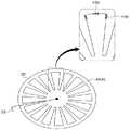
상기 복수의 측정존은, 상기 정전척의 중앙에서 방사선으로 배치되는 복수의 선과 상기 방사선을 따라 외측으로 갈수록 지름이 증가하는 방향으로 상호 이격된 복수의 원에 의해 구획되되 외측의 구획 수가 내측의 구획 수보다 많도록 마련될 수 있다.The plurality of measurement zones are partitioned by a plurality of lines disposed as radiation from the center of the electrostatic chuck and a plurality of circles spaced apart from each other in a direction in which a diameter increases toward the outside along the radiation. More may be provided.
상기 기준 온도 센서유닛은, 상기 측정존 온도 센서유닛과 이격되되 상기 정전척의 평면에서 상기 정전척의 중앙 영역에 배치될 수 있으며, 상기 기준 온도 센서유닛은, 열전대(Thermocouple) 온도센서, 측온저항체(RTD, Resistance Temperature Detector) 온도센서, 광섬유 온도센서 중 어느 하나일 수 있다.The reference temperature sensor unit may be spaced apart from the measurement zone temperature sensor unit and disposed in a central region of the electrostatic chuck in a plane of the electrostatic chuck, and the reference temperature sensor unit may include a thermocouple temperature sensor and a RTD. , Resistance Temperature Detector) may be any one of a temperature sensor and an optical fiber temperature sensor.
상기 정전척은, 유전층인 상부 세라믹; 상부 세리믹이 결합되는 금속바디; 및 상기 상부 세라믹을 상기 금속바디에 결합시키는 본딩층을 포함하며, 상기 측정존 온도 센서유닛은, 상부 세라믹 및 본딩층 중 적어도 어느 한 곳에 적어도 일부분이 삽입 설치될 수 있다.The electrostatic chuck may include an upper ceramic which is a dielectric layer; a metal body to which the upper ceramic is coupled; and a bonding layer for bonding the upper ceramic to the metal body, wherein at least a portion of the measurement zone temperature sensor unit may be inserted into at least one of the upper ceramic and the bonding layer.
본 발명의 다른 측면에 따르면, 반도체 제조 공정 수행을 위한 공간을 제공하는 공정 챔버; 및 정전기력에 의해 상기 기판을 흡착하는 정전척 어셈블리를 포함하며, 상기 정전척 어셈블리는, 정전기력에 의해 기판을 흡착하며, 복수의 구획으로 구분된 복수의 측정존을 구비하는 정전척; 및 상기 정전척에 결합되어 상기 정전척의 기준 온도를 측정하는 기준 온도 센서유닛; 상기 기준 온도 센서유닛에 이격되게 상기 정전척에 결합되어 상기 복수의 측정존의 측정존 온도신호를 감지하는 측정존 온도 센서유닛; 및 상기 기준 온도 센서유닛에서 측정된 상기 기준 온도를 기초로 미리 결정된 온도 범위 내로 계측 범위를 설정하고 상기 계측 범위 내에서 상기 측정존 온도 센서유닛에서 감지한 상기 측정존 온도신호를 계측하여 측정존 온도를 산출하는 측정존 온도 계측유닛을 포함하는 반도체 제조장치가 제공될 수 있다.According to another aspect of the present invention, a process chamber providing a space for performing a semiconductor manufacturing process; and an electrostatic chuck assembly for adsorbing the substrate by an electrostatic force, the electrostatic chuck assembly comprising: an electrostatic chuck for adsorbing the substrate by an electrostatic force, the electrostatic chuck having a plurality of measurement zones divided into a plurality of compartments; and a reference temperature sensor unit coupled to the electrostatic chuck to measure a reference temperature of the electrostatic chuck. a measurement zone temperature sensor unit coupled to the electrostatic chuck to be spaced apart from the reference temperature sensor unit to sense measurement zone temperature signals of the plurality of measurement zones; and setting a measurement range within a predetermined temperature range based on the reference temperature measured by the reference temperature sensor unit, and measuring the measurement zone temperature signal detected by the measurement zone temperature sensor unit within the measurement range to measure the measurement zone temperature There may be provided a semiconductor manufacturing apparatus including a measurement zone temperature measuring unit for calculating .
상기 측정존 온도 센서유닛은, 광섬유에 들어가서 나온 광의 파라미터들에 기초하여 상기 광섬유를 따르는 상이한 위치들에서의 온도를 결정할 수 있는 측정존 온도센서를 포함할 수 있다.The measurement zone temperature sensor unit may include a measurement zone temperature sensor capable of determining a temperature at different locations along the optical fiber based on parameters of light entering and exiting the optical fiber.
상기 미리 결정된 온도 범위 내는 상기 기준 온도에 미리 마련된 상기 정전척의 온도 편차를 부가한 온도 범위 내일 수 있다.The predetermined temperature range may be within a temperature range obtained by adding a temperature deviation of the electrostatic chuck provided in advance to the reference temperature.
상기 측정존 온도센서는, 상기 광섬유의 길이를 따르는 복수의 광섬유 브래그 격자(FBG, Fiber Bragg Grating)을 포함하는 광섬유 브래그 격자(FBG, Fiber Bragg Grating) 온도센서이며, 상기 측정존 온도 계측유닛은 상기 기준 온도에 상기 정전척의 온도 편차를 부가한 온도 범위 내에 해당하는 파장 범위를 산출하고 상기 파장 범위 내에서 상기 측정존의 반향 파장을 계측하여 상기 측정존 온도를 산출할 수 있다.The measurement zone temperature sensor is a Fiber Bragg grating (FBG) temperature sensor including a plurality of Fiber Bragg gratings (FBG) along the length of the optical fiber, and the measurement zone temperature measuring unit is the A wavelength range corresponding to a temperature range obtained by adding a temperature deviation of the electrostatic chuck to a reference temperature may be calculated, and a reflection wavelength of the measurement zone may be measured within the wavelength range to calculate the temperature of the measurement zone.
본 발명의 또 다른 측면에 따르면, 정전기력에 의해 기판을 흡착하는 정전척에 결합되는 기준 온도 센서유닛으로 상기 정전척의 기준 온도를 측정하는 단계; 상기 기준 온도 센서유닛에 이격되게 상기 정전척에 결합되는 측정존 온도 센서유닛으로 상기 정전척에 복수의 구획으로 구분된 복수의 측정존의 측정존 온도신호를 감지하는 단계; 및 상기 기준 온도를 기초로 미리 결정된 온도 범위 내로 계측 범위를 설정하고 상기 계측 범위 내에서 상기 측정존 온도 센서유닛에서 감지한 상기 측정존 온도신호를 계측하여 측정존 온도를 산출하는 단계를 포함하는 정전척 온도 측정방법이 제공될 수 있다.According to another aspect of the present invention, there is provided a method for manufacturing the electrostatic chuck comprising: measuring a reference temperature of the electrostatic chuck with a reference temperature sensor unit coupled to an electrostatic chuck for adsorbing a substrate by electrostatic force; sensing a measurement zone temperature signal of a plurality of measurement zones divided into a plurality of compartments in the electrostatic chuck with a measurement zone temperature sensor unit coupled to the electrostatic chuck to be spaced apart from the reference temperature sensor unit; and setting a measurement range within a predetermined temperature range based on the reference temperature and calculating the measurement zone temperature by measuring the measurement zone temperature signal sensed by the measurement zone temperature sensor unit within the measurement range A chuck temperature measurement method may be provided.
상기 측정존 온도 센서유닛은, 광섬유에 들어가서 나온 광의 파라미터들에 기초하여 상기 광섬유를 따르는 상이한 위치들에서의 온도를 결정할 수 있는 측정존 온도센서를 포함할 수 있다.The measurement zone temperature sensor unit may include a measurement zone temperature sensor capable of determining a temperature at different locations along the optical fiber based on parameters of light entering and exiting the optical fiber.
상기 미리 결정된 온도 범위 내는 상기 기준 온도에 미리 마련된 상기 정전척의 온도 편차를 부가한 온도 범위 내일 수 있다.The predetermined temperature range may be within a temperature range obtained by adding a temperature deviation of the electrostatic chuck provided in advance to the reference temperature.
상기 측정존 온도센서는, 상기 광섬유의 길이를 따르는 복수의 광섬유 브래그 격자(FBG, Fiber Bragg Grating)을 포함하는 광섬유 브래그 격자(FBG, Fiber Bragg Grating) 온도센서이며, 상기 측정존 온도 계측유닛은 상기 기준 온도에 상기 정전척의 온도 편차를 부가한 온도 범위 내에 해당하는 파장 범위를 산출하고 상기 파장 범위 내에서 상기 측정존의 반향 파장을 계측하여 상기 측정존 온도를 산출할 수 있다.The measurement zone temperature sensor is a Fiber Bragg grating (FBG) temperature sensor including a plurality of Fiber Bragg gratings (FBG) along the length of the optical fiber, and the measurement zone temperature measuring unit is the A wavelength range corresponding to a temperature range obtained by adding a temperature deviation of the electrostatic chuck to a reference temperature may be calculated, and a reflection wavelength of the measurement zone may be measured within the wavelength range to calculate the temperature of the measurement zone.
상기 복수의 광섬유 브래그 격자(FBG, Fiber Bragg Grating)들은 상기 복수의 측정존에 각각 대응되게 배치될 수 있다.The plurality of Fiber Bragg gratings (FBG) may be disposed to correspond to the plurality of measurement zones, respectively.
상기 복수의 측정존은, 상기 정전척의 중앙에서 방사선으로 배치되는 복수의 선과 상기 방사선을 따라 외측으로 갈수록 지름이 증가하는 방향으로 상호 이격된 복수의 원에 의해 구획되되 외측의 구획 수가 내측의 구획 수보다 많도록 마련될 수 있다.The plurality of measurement zones are partitioned by a plurality of lines disposed as radiation from the center of the electrostatic chuck and a plurality of circles spaced apart from each other in a direction in which a diameter increases toward the outside along the radiation. More may be provided.
상기 기준 온도 센서유닛은, 상기 측정존 온도 센서유닛과 이격되되 상기 정전척의 평면에서 상기 정전척의 중앙 영역에 배치될 수 있다.The reference temperature sensor unit may be spaced apart from the measurement zone temperature sensor unit and disposed in a central region of the electrostatic chuck in a plane of the electrostatic chuck.
본 발명에 따르면, 도 측정이 필요한 복수 개의 존(zone)을 갖는 정전척의 온도를 종래보다 효율적으로 측정할 수 있어 정전척의 구조를 종래보다 크게 복잡하게 하지 않으면서도 정전척의 온도 산포를 계측할 수 있다.According to the present invention, since the temperature of the electrostatic chuck having a plurality of zones requiring degree measurement can be measured more efficiently than before, the temperature distribution of the electrostatic chuck can be measured without significantly complicating the structure of the electrostatic chuck compared to the prior art. .
도 1은 본 발명의 일 실시 예에 따른 정전척 어셈블리를 포함하는 반도체 건식 식각 장치의 개략적인 단면도이다.
도 2는 도 1의 정전척 어셈블리의 개략적인 단면도이다.
도 3은 도 2의 정전척 어셈블리의 정전척의 개략적인 요부 부분 단면도이다.
도 4는 도 2의 정전척 어셈블리의 정전척의 개략적인 평단면도이다.
도 5는 광섬유 브래그 격자(FBG, Fiber Bragg Grating)를 포함하는 광섬유를 설명하기 위한 도면이다.
도 6은 광섬유 브래그 격자(FBG, Fiber Bragg Grating) 온도센서에 의한 온도측정의 원리를 설명하기 위한 도면이다.
도 7은 본 발명의 일 실시예에 따른 정전척의 온도 측정방법의 순서도이다.
도 8은 본 발명의 다른 실시 예에 따른 정전척 어셈블리의 정전척의 개략적인 평단면도이다.
도 9는 본 발명의 또 다른 실시 예에 따른 정전척 어셈블리의 정전척의 개략적인 평단면도이다.1 is a schematic cross-sectional view of a semiconductor dry etching apparatus including an electrostatic chuck assembly according to an embodiment of the present invention.
FIG. 2 is a schematic cross-sectional view of the electrostatic chuck assembly of FIG. 1 ;
3 is a schematic partial cross-sectional view of an electrostatic chuck of the electrostatic chuck assembly of FIG. 2 .
4 is a schematic plan cross-sectional view of an electrostatic chuck of the electrostatic chuck assembly of FIG. 2 ;
5 is a view for explaining an optical fiber including a Fiber Bragg grating (FBG).
6 is a view for explaining the principle of temperature measurement by a fiber Bragg grating (FBG) temperature sensor.
7 is a flowchart of a method for measuring a temperature of an electrostatic chuck according to an embodiment of the present invention.
8 is a schematic plan cross-sectional view of an electrostatic chuck of an electrostatic chuck assembly according to another embodiment of the present invention.
9 is a schematic plan cross-sectional view of an electrostatic chuck of an electrostatic chuck assembly according to another embodiment of the present invention.
본 명세서 또는 출원에 개시되어 있는 본 발명의 실시 예들에 대해서 특정한 구조적 내지 기능적 설명들은 단지 본 발명에 따른 실시 예를 설명하기 위한 목적으로 예시된 것으로, 본 발명에 따른 실시 예들은 다양한 형태로 실시될 수 있으며 본 명세서 또는 출원에 설명된 실시 예들에 한정되는 것으로 해석되어서는 아니 된다.Specific structural or functional descriptions of the embodiments of the present invention disclosed in this specification or application are only exemplified for the purpose of describing the embodiments according to the present invention, and the embodiments according to the present invention may be implemented in various forms. and should not be construed as being limited to the embodiments described in the present specification or application.
본 발명에 따른 실시 예는 다양한 변경을 가할 수 있고 여러 가지 형태를 가질 수 있으므로 특정실시 예들을 도면에 예시하고 본 명세서 또는 출원에 상세하게 설명하고자 한다. 그러나, 이는 본 발명의 개념에 따른 실시 예를 특정한 개시 형태에 대해 한정하려는 것이 아니며, 본 발명의 사상 및 기술 범위에 포함되는 모든 변경, 균등물 내지 대체물을 포함하는 것으로 이해되어야 한다.Since the embodiment according to the present invention may have various changes and may have various forms, specific embodiments will be illustrated in the drawings and described in detail in the present specification or application. However, this is not intended to limit the embodiment according to the concept of the present invention with respect to a specific disclosed form, and should be understood to include all changes, equivalents or substitutes included in the spirit and scope of the present invention.
제1 및/또는 제2 등의 용어는 다양한 구성 요소들을 설명하는데 사용될 수 있지만, 상기 구성 요소들은 상기 용어들에 의해 한정되어서는 안 된다. 상기 용어들은 하나의 구성 요소를 다른 구성 요소로부터 구별하는 목적으로만, 예컨대 본 발명의 개념에 따른 권리 범위로부터 이탈되지 않은 채, 제1 구성요소는 제2 구성요소로 명명될 수 있고, 유사하게 제2 구성요소는 제1 구성요소로도 명명될 수 있다.Terms such as first and/or second may be used to describe various elements, but the elements should not be limited by the terms. The above terms are used only for the purpose of distinguishing one element from another element, for example, without departing from the scope of the present invention, a first element may be called a second element, and similarly The second component may also be referred to as the first component.
어떤 구성요소가 다른 구성요소에 "연결되어" 있다거나 "접속되어" 있다고 언급된 때에는, 그 다른 구성요소에 직접적으로 연결되어 있거나 또는 접속되어 있을 수도 있지만, 중간에 다른 구성요소가 존재할 수도 있다고 이해되어야 할 것이다. 반면에, 어떤 구성요소가 다른 구성요소에 "직접 연결되어" 있다거나 "직접 접속되어" 있다고 언급된 때에는, 중간에 다른 구성요소가 존재하지 않는 것으로 이해되어야 할 것이다. 구성요소들 간의 관계를 설명하는 다른 표현들, 즉 "~사이에"와 "바로 ~사이에" 또는 "~에 이웃하는"과 "~에 직접 이웃하는" 등도 마찬가지로 해석되어야 한다.When a component is referred to as being “connected” or “connected” to another component, it may be directly connected or connected to the other component, but it is understood that other components may exist in between. it should be On the other hand, when it is said that a certain element is "directly connected" or "directly connected" to another element, it should be understood that the other element does not exist in the middle. Other expressions describing the relationship between elements, such as "between" and "immediately between" or "neighboring to" and "directly adjacent to", etc., should be interpreted similarly.
본 명세서에서 사용한 용어는 단지 특정한 실시 예를 설명하기 위해 사용된 것으로, 본 발명을 한정하려는 의도가 아니다. 단수의 표현은 문맥상 명백하게 다르게 뜻하지 않는 한, 복수의 표현을 포함한다. 본 명세서에서, "포함하다" 또는 "가지다" 등의 용어는 설시된 특징, 숫자, 단계, 동작, 구성요소, 부분품 또는 이들을 조합한 것이 존재함을 지정하려는 것이지, 하나 또는 그 이상의 다른 특징들이나 숫자, 단계, 동작, 구성요소, 부분품 또는 이들을 조합한 것들의 존재 또는 부가가능성을 미리 배제하지 않는 것으로 이해되어야 한다.The terms used herein are used only to describe specific embodiments, and are not intended to limit the present invention. The singular expression includes the plural expression unless the context clearly dictates otherwise. In the present specification, terms such as “comprise” or “have” are intended to designate that the described feature, number, step, operation, component, part, or combination thereof exists, and includes one or more other features or numbers. , it should be understood that it does not preclude the existence or addition of steps, operations, components, parts, or combinations thereof.
다르게 정의되지 않는 한, 기술적이거나 과학적인 용어를 포함해서 여기서 사용되는 모든 용어들은 본 발명이 속하는 기술 분야에서 통상의 지식을 가진 자에 의해 일반적으로 이해되는 것과 동일한 의미이다. 일반적으로 사용되는 사전에 정의되어 있는 것과 같은 용어들은 관련 기술의 문맥상 가지는 의미와 일치하는 의미인 것으로 해석되어야 하며, 본 명세서에서 명백하게 정의하지 않는 한, 이상적이거나 과도하게 형식적인 의미로 해석되지 않는다.Unless defined otherwise, all terms used herein, including technical and scientific terms, have the same meaning as commonly understood by one of ordinary skill in the art to which this invention belongs. Terms such as those defined in commonly used dictionaries should be interpreted as meanings consistent with the context of the related art, and unless explicitly defined in the present specification, they are not to be interpreted in an ideal or excessively formal meaning. .
이하, 첨부한 도면을 참조하여 본 발명의 바람직한 실시 예를 설명함으로써, 본 발명을 상세히 설명한다. 각 도면에 제시된 동일한 참조부호는 동일한 부재를 나타낸다.Hereinafter, the present invention will be described in detail by describing preferred embodiments of the present invention with reference to the accompanying drawings. Like reference numerals in each figure indicate like elements.
본 발명에 따른 정전척 어셈블리 및 정전척 온도 측정방법은 다양한 반도체 제조 장치에 적용될 수 있을 것이나, 설명의 편의를 위하여 이하 반도체 제조장치 중 반도체 건식 식각 장치에 적용된 경우에 대하여 설명하기로 한다.The electrostatic chuck assembly and the electrostatic chuck temperature measuring method according to the present invention can be applied to various semiconductor manufacturing apparatuses, but for convenience of description, a case where it is applied to a semiconductor dry etching apparatus among semiconductor manufacturing apparatuses will be described below.
도 1은 본 발명의 일 실시 예에 따른 정전척 어셈블리를 포함하는 반도체 건식 식각 장치의 개략적인 단면도이다.1 is a schematic cross-sectional view of a semiconductor dry etching apparatus including an electrostatic chuck assembly according to an embodiment of the present invention.
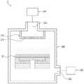
이에 도시된 바와 같이, 본 발명의 일 실시 예에 따른 정전척 어셈블리(10, Electrostatic Chuck Assembly)를 포함하는 반도체 건식 식각 장치(1)는, 공정 챔버(100), 가스공급유닛(110), 노즐(120), 상부전극(미도시), 정전척 어셈블리(10) 및 가스배기유닛(140)을 포함한다.As shown here, the semiconductor dry etching apparatus 1 including the
공정 챔버(100)는 가스유입구(112)와 가스배기구(142)를 갖는다. 가스유입구(112)는 공정 챔버(100)의 상부에 형성된다. 가스배기구(142)는 공정 챔버(100)의 측부에 형성된다.The
가스공급유닛(110)은 공정 챔버(100)의 가스유입구(112)에 연결된다. 가스공급유닛(110)은 공정 가스인 식각 가스를 가스유입구(112)를 통해서 공정 챔버(100) 내부로 제공한다.The
노즐(120)은 가스유입구(112)에 연결된다. 노즐(120)은 식각 가스를 분사하기 위한 복수개의 노즐공(122)들을 갖는다.The
상부전극(미도시)은 공정 챔버(100)의 내부 상부에 배치된다. 상부전극은 노즐(120)을 둘러싸도록 배치된다. 상부전극에는 플라즈마 형성을 위한 RF 파워가 인가될 수 있다.An upper electrode (not shown) is disposed on the inside of the
가스배기유닛(140)은 가스배기구(142)에 연결되어, 미 반응 식각 가스와 식각 부산물들이 가스배기유닛(140)을 통해서 공정 챔버(100)의 외부로 배출된다.The
정전척 어셈블리(10)는 공정 챔버(100)의 내부 하부에 배치된다. 이러한 정전척 어셈블리(10)는 상부전극과 함께 식각 가스로부터 플라즈마를 형성한다.The
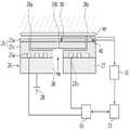
도 2는 도 1의 정전척 어셈블리의 개략적인 단면도이고, 도 3은 도 2의 정전척 어셈블리의 정전척의 개략적인 요부 부분 단면도이며, 도 4는 도 2의 정전척 어셈블리의 정전척의 개략적인 평단면도이며, 도 5는 광섬유 브래그 격자(FBG, Fiber Bragg Grating)를 포함하는 광섬유를 설명하기 위한 도면이고, 도 6은 광섬유 브래그 격자(FBG, Fiber Bragg Grating) 온도센서에 의한 온도측정의 원리를 설명하기 위한 도면이다.FIG. 2 is a schematic cross-sectional view of the electrostatic chuck assembly of FIG. 1 , FIG. 3 is a schematic partial cross-sectional view of the electrostatic chuck of the electrostatic chuck assembly of FIG. 2 , and FIG. 4 is a schematic plan cross-sectional view of the electrostatic chuck of the electrostatic chuck assembly of FIG. 2 5 is a view for explaining an optical fiber including a fiber Bragg grating (FBG), and FIG. 6 is a fiber Bragg grating (FBG, Fiber Bragg Grating) to explain the principle of temperature measurement by a temperature sensor. is a drawing for
이들 도면에 도시된 바와 같이, 본 발명의 일 실시 예에 따른 정전척 어셈블리(10)는, 정전척(20)과, 기준 온도 센서유닛(30)과, 측정존 온도 센서유닛(40)과, 측정존 온도 계측유닛(50)과, 온도조절유닛(60)과, 메인 콘트롤러(70)를 포함한다.As shown in these drawings, the
정전척(20)은, 전극캡(25)과 전극(27)을 포함한다. 전극캡(25)은 유전층(11)인 상부 세라믹(25a)과 본딩층(25b), 그리고 금속바디(25c)를 포함한다. 그리고 전극(27)은 전원(28)으로부터 직류전압을 인가받는다. 기판(W)의 전면 상에 플라즈마(plasma)가 형성되면 기판(W)의 온도가 고온으로 상승하게 되어 공정 불량으로 이어질 수 있으므로 기판(W)의 온도를 낮추기 위해 기판(W)의 배면으로 헬륨(He)을 제공하는 채널(26,26a,26b,26c)이 제공된다. 헬륨은 중심채널(26)을 통해 공급되어 각 채널(26,26a,26b,26c)을 통해 기판 배면으로 제공된다.The
정전척(20)에는 전극캡(25)을 냉각시키는 냉매의 순환경로를 제공하는 채널(29a,29b)이 마련된다. 채널(29a)을 통해 유입된 냉매는 전극캡(25) 내부를 순환한 후 채널(29b)을 통해 유출된다. 채널(29b)로부터 유출된 냉매는 가령 칠러(chiller)와 같은 온도조절유닛(60)에서 그 온도가 조절된 후 채널(29a)로 제공된다. 온도조절유닛(60)의 냉매 온도 조절은 메인 컨트롤러(17)에 의해 좌우되며, 메인 컨트롤러(17)는 정전척(20)의 복수의 측정존(21)의 온도를 산출하는 측정존 온도 계측유닛(50)으로부터 복수의 측정존(21)의 온도 정보를 제공받는다.
또한 정전척(20)은, 도 4에 자세히 도시된 바와 같이, 복수의 구획으로 구분된 복수의 측정존(21)을 구비한다. 본 실시 예에서 복수의 측정존(21)은, 정전척(20)의 중앙에서 방사선으로 배치되는 복수의 선(21a)과, 방사선을 따라 외측으로 갈수록 지름이 증가하는 방향으로 상호 이격된 복수의 원(21b)에 의해 구획된다. 그리고 본 실시 예에서는 외측의 구획 수가 내측의 구획 수보다 많도록 마련되고, 이에 따라 동일 원주 방향의 측정존(21)의 수는 중앙에서 외부로 갈수록 많아지도록 배치된다.In addition, as shown in detail in FIG. 4 , the
본 실시 예에서 이러한 정전척(20)의 중앙 영역에는 기준 온도 센서유닛(30)이 마련된다. 즉 기준 온도 센서유닛(30)은, 측정존 온도 센서유닛(40)과 이격되되 정전척(20)의 평면에서 정전척(20)의 중앙 영역에 배치된다. 본 실시 예에서는 기준 온도 센서유닛(30)이 정전척(20)의 평면 중앙 영역에 배치되고 정전척(20)의 한 위치에서의 온도를 측정하나, 본 발명의 권리범위가 이에 한정되지 않으며, 필요에 따라 정전척(20)의 적절한 곳에 하나 설치될 수도 있고 필요에 따라 복수의 위치에 설치될 수도 있을 것이다.In the present embodiment, the reference
이러한 기준 온도 센서유닛(30)은, 열전대(Thermocouple) 온도센서, 측온저항체(RTD, Resistance Temperature Detector) 온도센서, 광섬유 온도센서 중 어느 하나일 수 있다.The reference
열전대(Thermocouple) 온도센서는 두 종류의 금속도체 양단을 전기적으로 접속시키고 이 양단에 온도차를 주면 회로 중에 전류가 흐르는데(Zeeback 효과) 이와 같이 한쪽(기준접점)의 온도를 일정온도(원칙적으로 0)로 유지하고 열기전력의 수치를 측정함으로써 다른 끝단(온도 접점)의 온도를 알 수 있는 원리를 이용한 온도센서이며, 측온저항체(RTD, Resistance Temperature Detector) 온도센서는, 온도에 따라 저항값이 달라지는 것을 이용한 온도센서이며, 광섬유 온도센서는 광의 위상, 세기, 편극, 산란, 흡수 성질을 이용하여 외부 대상물의 온도 변화를 감지할 수 있는 온도센서이다.Thermocouple temperature sensor electrically connects both ends of two types of metal conductors, and if a temperature difference is applied to both ends, current flows in the circuit (Zeeback effect). It is a temperature sensor that uses the principle to know the temperature of the other end (temperature junction) by maintaining This is a temperature sensor used, and the optical fiber temperature sensor is a temperature sensor that can detect the temperature change of an external object by using the phase, intensity, polarization, scattering, and absorption properties of light.
한편, 측정존 온도 센서유닛(40)은 정전척(20)에 결합되어 복수의 측정존(21)의 측정존 온도신호를 감지한다. 이러한 측정존 온도 센서유닛(40)은, 광섬유에 들어가서 나온 광의 파라미터들에 기초하여 광섬유를 따르는 상이한 위치들에서의 온도를 결정할 수 있는 측정존 온도센서(41)와, 소정 대역범위의 파장을 광섬유를 통해 각 측정존(21)으로로 전송하는 광 소스(미도시)와, 광 파장을 수신하는 광 검출기(미도시)를 포함한다.Meanwhile, the measurement zone
보다 상세하게 본 실시 예에서 측정존 온도센서(41)는, 광섬유의 길이를 따르는 복수의 광섬유 브래그 격자들(43, FBG, Fiber Bragg Gratings)을 포함하는 광섬유 브래그 격자(FBG, Fiber Bragg Grating) 온도센서(41)이다.In more detail, in this embodiment, the measurement zone temperature sensor 41 has a fiber Bragg grating (FBG) temperature including a plurality of fiber Bragg gratings 43 (FBG, Fiber Bragg Gratings) along the length of the optical fiber. sensor 41 .
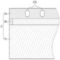
도 5에 자세히 도시된 바와 같이, 광섬유 브래그 격자(FBG, Fiber Bragg Grating) 온도센서(41)의 광섬유는 클래딩(45)과, 코어(47)와, 코어(47) 내의 광섬유 브래그 격자(43, FBG, Fiber Bragg Grating)를 포함한다.5, the optical fiber of the Fiber Bragg Grating (FBG) temperature sensor 41 has a cladding 45, a core 47, and an optical fiber Bragg grating 43 in the core 47, FBG, Fiber Bragg Grating).
본 실시 예에서 광섬유 브래그 격자(FBG, Fiber Bragg Grating) 온도센서(41)의 광섬유는 정전척(20)의 유전층인 상부 세라믹(25a), 그리고 본딩층(25b) 중 적어도 어느 한 곳에 삽입 설치될 수 있다. 본 실시 예에서 광섬유 브래그 격자(FBG, Fiber Bragg Grating) 온도센서(41)가 정전척(20)의 유전층인 상부 세라믹(25a)에 삽입 설치되어 있으나 본 발명의 권리범위가 이에 한정되지 않으며, 본딩층(25b)에만 삽입 설치될 수 있거나 상부 세라믹(25a) 및 본딩층(25b) 모두에 설치될 수도 있을 것이다.In this embodiment, the optical fiber of the Fiber Bragg Grating (FBG) temperature sensor 41 is inserted into at least one of the dielectric layer of the
또한 본 실시 예에서 복수의 광섬유 브래그 격자들(43, FBG, Fiber Bragg Gratings)은 복수의 측정존(21)에 대응되게 배치된다. 즉 복수의 광섬유 브래그 격자들(43, FBG, Fiber Bragg Gratings)이 각 측정존(21)에 하나씩 배치된다.Also, in this embodiment, a plurality of
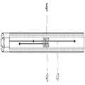
이러한 광섬유 브래그 격자(FBG, Fiber Bragg Grating) 온도센서(41)에 의한 온도측정의 원리를 도 6을 참조하여 설명하면 다음과 같다.The principle of temperature measurement by the fiber Bragg grating (FBG) temperature sensor 41 will be described with reference to FIG. 6 as follows.
광섬유 브래그 격자(FBG, Fiber Bragg Grating) 온도센서(41)는 광섬유에 브래그 격자를 일정한 길이에 따라 새긴 후 온도나 강도 등의 외부의 조건변화에 따라 각 격자에서 반사되는 빛의 파장이 달라지는 특성을 이용한 온도센서이다. 즉, 이 격자는 브래그 조건을 만족하는 파장만을 반사하고, 그 외의 파장은 그대로 투과시키는 특징을 갖는다. 이때 격자의 주변 온도가 바뀌거나 격자에 인장이 가해지면, 광섬유의 굴절률이나 길이가 변화되며 이에 따라 반사되는 빛의 파장의 이동이 발생한다.The Fiber Bragg Grating (FBG) temperature sensor 41 is a Bragg grating in which a Bragg grating is engraved on an optical fiber according to a certain length, and then the wavelength of light reflected from each grating varies according to external conditions such as temperature or intensity. temperature sensor used. That is, this grating has a characteristic of reflecting only wavelengths that satisfy the Bragg condition, and transmitting other wavelengths as it is. At this time, if the ambient temperature of the grating is changed or tension is applied to the grating, the refractive index or length of the optical fiber changes, and accordingly, the wavelength of the reflected light is shifted.
따라서 광섬유 브래그 격자에서 반사되는 빛의 파장의 이동량을 측정함으로써 온도나 인장, 또는 압력, 구부림 등을 감지할 수 있다. 보다 구체적으로, 도 6의 위측 도면과 같이 광섬유 브래그 격자(FBG, Fiber Bragg Grating) 온도 센서에 광폭의 파장 대역을 갖는 광원(λ1, λ2, λ3, λ4)이 입사되면, 광섬유 브래그 격자(FBG, Fiber Bragg Grating) 온도센서(41)에 이미 형성된 격자에 따라 입사된 파장 대역 중 특정 파장(λ3)의 빛만 반사하게 되고 나머지 파장(λ1, λ2, λ4)은 투과된다. 이때 반사된 빛의 파장은 광섬유 브래그 격자(FBG, Fiber Bragg Grating) 온도센서(41)에 형성된 격자의 간격이 변화됨에 따라 이동하게 되며(도 6의 아래측 도면), 따라서 이렇게 파장의 이동으로부터 격자 간격의 변화, 즉 변형율을 도출하게 된다. 이때 변형율은 온도의 함수이므로 반사된 파장의 이동으로부터 계산된 변형율로부터 광섬유 브래그 격자(43, FBG, Fiber Bragg Grating) 위치에서의 온도를 계산할 수 있다.Therefore, temperature, tension, pressure, bending, etc. can be detected by measuring the amount of movement of the wavelength of light reflected from the optical fiber Bragg grating. More specifically, when light sources (λ1, λ2, λ3, λ4) having a wide wavelength band are incident on a Fiber Bragg Grating (FBG) temperature sensor as shown in the upper diagram of FIG. 6, the optical fiber Bragg grating (FBG, Fiber Bragg Grating) According to the grating already formed in the temperature sensor 41, only light of a specific wavelength (λ3) among the incident wavelength bands is reflected, and the remaining wavelengths (λ1, λ2, λ4) are transmitted. At this time, the wavelength of the reflected light moves as the distance between the gratings formed in the Fiber Bragg Grating (FBG) temperature sensor 41 is changed (bottom view of FIG. 6), and thus the grating from the movement of the wavelength in this way The change in spacing, that is, the strain rate, is derived. At this time, since the strain is a function of temperature, the temperature at the location of the fiber Bragg grating 43 (FBG, Fiber Bragg Grating) can be calculated from the strain calculated from the movement of the reflected wavelength.
따라서, 특정 대역의 파장만을 반사시킬 수 있는 광섬유 브래그 격자(43, FBG, Fiber Bragg Grating)를 하나의 광섬유에 직렬로 연결시키고, 광섬유 브래그 격자(43, FBG, Fiber Bragg Grating)마다 반사되는 빛의 파장을 모두 다르게 함으로써 각 광섬유 브래그 격자(43, FBG, Fiber Bragg Grating)가 위치하는 영역에서의 온도측정이 동시에 가능하게 된다.Therefore, an optical fiber Bragg grating (43, FBG, Fiber Bragg Grating) capable of reflecting only a wavelength of a specific band is connected in series to one optical fiber, and each fiber Bragg grating (43, FBG, Fiber Bragg Grating) of the reflected light By making all wavelengths different, it is possible to simultaneously measure the temperature in the region where each fiber Bragg grating 43, FBG, and Fiber Bragg grating are located.
전술한 바와 같이 본 실시예에서 복수의 광섬유 브래그 격자들(Fiber Bragg Gratings)이 복수의 측정존(21)에 대응되게 배치되어 있으므로 각 측정존(21)의 광섬유 브래그 격자(43, FBG, Fiber Bragg Grating)에서 반사된 파장의 이동을 알 수 있다. 즉 각 측정존(21)의 광섬유 브래그 격자(43, FBG, Fiber Bragg Grating)로부터의 온도신호 즉 본 실시 예에서 반향 파장을 감지할 수 있게 된다.As described above, in this embodiment, since a plurality of Fiber Bragg gratings are arranged to correspond to the plurality of
본 실시예에서 복수의 광섬유 브래그 격자(43, FBG, Fiber Bragg Grating)은 하나의 광섬유(23)에 직렬로 연결 시 상대적으로 조밀하게 연결할 수 있다. 이는 본 실시 예에서 하나의 광섬유에 광섬유 브래그 격자(43, FBG, Fiber Bragg Grating)들을 조밀하게 직렬로 연결하더라도 각 측정존(21)의 광섬유 브래그 격자(43, FBG, Fiber Bragg Grating)에서 반사된 파장을 본 실시 예의 측정존 온도 계측유닛(50)이 기준 온도 센서유닛(30)에서 측정된 기준 온도를 기준으로 하여 측정 및 계산할 수 있기 때문이다. 이에 대해서는 측정존 온도 계측유닛(50)의 설명에서 자세히 후술하기로 한다.In this embodiment, a plurality of fiber Bragg gratings 43 (FBG, Fiber Bragg grating) can be connected relatively densely when connected in series to one optical fiber 23 . In this embodiment, even if the
한편 광 소스(미도시)는 소정 대역범위의 파장을 광섬유를 통해 각 측정존(21)의 광섬유 브래그 격자(43, FBG, Fiber Bragg Grating)로 전송하며, 광 검출기(미도시)는 반사된 광 파장을 수신한다. 이때 각 광섬유 브래그 격자(43, FBG, Fiber Bragg Grating)에 대하여 상이한 광 신호를 구별하기 위하여 시분할 멀티플렉싱 (TDM, Time Division Multiplexing) 등이 사용될 수 있다.Meanwhile, the light source (not shown) transmits a wavelength of a predetermined band range to the
그리고 감지된 측정존(21)의 온도신호 즉 본 실시 예에서 반향 파장은 측정존 온도 계측유닛(50)에서 온도로 산출된다. 전술한 바와 같이 광 소스에서 소정 대역범위의 파장을 광섬유를 통해 직렬로 이격 배치된 복수의 각 광섬유 브래그 격자(43, FBG, Fiber Bragg Grating)로 전송하면, 각 광섬유 브래그 격자(43, FBG, Fiber Bragg Grating) 각각은 기 설정된 특정파장에 대해서만 반사하고 그 외의 파장들은 모두 투과시킨다.And the detected temperature signal of the
이때 각 각 광섬유 브래그 격자(43, FBG, Fiber Bragg Grating)는 측정존(21)의 자신이 놓여있는 영역의 온도에 반응하여 브래그 격자의 변형을 유발하게 되며, 이로 인해 각 광섬유 브래그 격자(43, FBG, Fiber Bragg Grating)에서 반사되는 파장은 변형률에 대응하는 값만큼 이동하게 된다.At this time, each fiber Bragg grating (43, FBG, Fiber Bragg Grating) causes deformation of the Bragg grating in response to the temperature of the region in which it is placed in the
측정존 온도 계측유닛(50)은 각 광섬유 브래그 격자(43, FBG, Fiber Bragg Grating)에서 반사되는 파장의 이동량을 측정 및 계산하여 이를 온도로 산출하되, 이때 기준 온도 센서유닛(30)으로부터 정전척(20)의 기준 온도에 대한 신호를 입력받고 이 기준 온도를 활용한다.The measurement zone
이를 보다 자세히 설명하면, 측정존 온도 계측유닛(50)은, 기준 온도 센서유닛(30)에서 측정된 기준 온도를 기준으로 미리 결정된 온도 범위 내로 계측 범위를 설정하고 그 계측 범위 내에서 측정존 온도 센서유닛(40)에서 감지한 파장의 이동량을 측정 및 계산하여 각 광섬유 브래그 격자(43, FBG, Fiber Bragg Grating)가 위치한 측정존(21)의 각 측정존 온도를 산출하게 된다.To explain this in more detail, the measurement zone
보다 상세하게는, 본 실시 예에서는 기준 온도 센서유닛(30)에서 측정된 기준 온도에 미리 마련된 정전척(20)의 온도 편차를 부가한 온도 범위 내에 해당하는 파장 범위를 산출하고 그 파장 범위 내에 있는 신호를 계측하여 각 광섬유 브래그 격자(43, FBG, Fiber Bragg Grating)가 위치한 측정존(21)의 측정존 온도를 산출한다.More specifically, in the present embodiment, a wavelength range corresponding to a temperature range obtained by adding the temperature deviation of the
이에 대하여 보다 상세히 설명하면, 기준 온도가 80도이고 편차가 10도이라면 70도 내지 90도에 해당하는 온도 범위를 계측 범위로 하되 그 온도 범위 내에 해당하는 파장 범위 내에 있는 신호를 측정 및 계산함으로써 측정존 온도를 계측할 수 있게 된다.To describe this in more detail, if the reference temperature is 80 degrees and the deviation is 10 degrees, the measurement range is the temperature range corresponding to 70 degrees to 90 degrees, but the measurement is performed by measuring and calculating the signal within the wavelength range corresponding to the temperature range. Zone temperature can be measured.
종래 기술에서 전술한 바와 같이 계측 온도범위가 넓을수록 계측을 위해 더 넓은 파장대역을 확보하여야 하는데, 넓은 파장대역을 확보하된 계측 파장 간 거리를 충분히 확보하지 않으면 근접 파장간의 간섭이 발생될 수 있기 때문에 복수의 광섬유 브래그 격자(43, FBG, Fiber Bragg Grating)를 하나의 광섬유에 직렬로 연결시킬 때 일정한 거리를 확보하여야 하고 이 경우 하나의 광섬유에 직렬로 연결시킬 수 있는 광섬유 브래그 격자(43, FBG, Fiber Bragg Grating)의 개수가 제한될 수 있다.As described above in the prior art, the wider the measurement temperature range, the wider the wavelength band must be secured for measurement. Therefore, when connecting a plurality of fiber Bragg gratings (43, FBG, Fiber Bragg grating) in series to one optical fiber, a certain distance must be secured, and in this case,
이러한 제한을 보다 감소시켜 하나의 광섬유에 많은 광섬유 브래그 격자(43, FBG, Fiber Bragg Grating)를 직렬로 연결시킬 수 있도록, 본 실시 예에서는 기준 온도 센서유닛을 사용하여 기준 온도를 측정하고 이 기준 온도에 정전척(20)의 온도 편차를 부가한 온도범위를 파장범위로 역산하고 역산된 파장범위로 감지된 반향 파장을 검출, 예를 들어 피크(peak)치를 검출하여 각 광섬유 브래그 격자(43, FBG, Fiber Bragg Grating)가 위치한 측정존(21)의 각 측정존 온도를 산출함으로써, 하나의 광섬유에 광섬유 브래그 격자(43, FBG, Fiber Bragg Grating)가 상대적으로 조밀하게 직렬로 연결되어 있더라도, 즉 근접 파장 간의 간섭이 발생하더라도 각 측정존(21)의 온도를 측정할 수 있도록 하고 있다.In order to further reduce this limitation and connect many
이와 같이 하나의 광섬유에 광섬유 브래그 격자(43, FBG, Fiber Bragg Grating)를 상대적으로 조밀하게 직렬로 연결하여도 각 측정존(21)의 온도를 측정할 수 있고, 그 경우 정전척(20)의 온도 측정에 필요한 광섬유의 개수를 줄일 수 있으며 이에 의하여 정전척(20)의 구조를 단순화할 수 있게 되고 정전척(20)의 구조가 단순화되면 정전척(20)의 신뢰성도 향상될 수 있다.Even if the
이하에서는 도 1 내지 도 6 외에 도 7을 참조하여 본 발명의 일 실시 예에 따른 정전척 온도 측정 방법에 대하여 상세히 설명한다.Hereinafter, an electrostatic chuck temperature measuring method according to an embodiment of the present invention will be described in detail with reference to FIG. 7 in addition to FIGS. 1 to 6 .
본 실시 예에 따른 정전척 온도 측정방법은, 정전기력에 의해 기판(W)을 흡착하는 정전척(20)에 결합되는 기준 온도 센서유닛(30)으로 정전척(20)의 기준 온도를 측정하는 단계(S100)와, 정전척(20)에 결합되는 측정존 온도 센서유닛(40)으로 정전척(20)에 복수의 구획으로 구분된 복수의 측정존(21)의 각 측정존 반향 파장을 감지하는 단계(S200)와, 기준 온도를 기준으로 미리 결정된 온도 범위 내로 계측 범위를 설정하고(S300) 그 계측 범위 내에서 측정존 온도 센서유닛(40)에서 감지한 반향 파장을 계측하여 측정존 온도를 산출하는 단계(S400)를 포함한다.The method for measuring the temperature of the electrostatic chuck according to the present embodiment includes measuring the reference temperature of the
우선 광섬유에 광섬유 브래그 격자(43, FBG, Fiber Bragg Grating)를 직렬로 연결된 광섬유 브래그 격자(FBG, Fiber Bragg Grating) 온도센서(41)가 정전척(20)에 설치된다. 이 광섬유 브래그 격자(FBG, Fiber Bragg Grating) 온도센서(41)에 대해서는 캘리브레이션(Calibration)을 통하여 온도와 광섬유 브래그 격자(43, FBG, Fiber Bragg Grating) 반사 신호의 관계 데이터가 마련된다.First, a fiber Bragg grating (FBG, Fiber Bragg grating) temperature sensor 41 connected in series with a fiber Bragg grating 43, FBG, is installed in the
다음으로 본 실시 예에서 정전척(20)의 중앙 영역에 설치된 기준 온도 센서유닛(30)으로 정전척(20)의 기준 온도를 측정한다(S100).Next, in the present embodiment, the reference temperature of the
그런 다음에 복수의 측정존(21)에 설치된 광섬유 브래그 격자(43, FBG, Fiber Bragg Grating)들을 통하여 각 복수의 측정존(21)의 반향 파장을 감지한다(S200).Then, the echo wavelength of each of the plurality of
즉 광 소스에서 소정 대역범위의 파장을 광섬유를 통해 직렬로 이격 배치된 복수의 각 광섬유 브래그 격자(43, FBG, Fiber Bragg Grating)로 전송하면, 각 광섬유 브래그 격자(43, FBG, Fiber Bragg Grating) 각각은 기 설정된 특정파장에 대해서만 반사하고 그 외의 파장들은 모두 투과시킨다.That is, when a wavelength of a predetermined band range is transmitted from the light source to a plurality of each fiber Bragg grating (43, FBG, Fiber Bragg Grating) spaced in series through an optical fiber, each fiber Bragg grating (43, FBG, Fiber Bragg Grating) Each reflects only a predetermined specific wavelength and transmits all other wavelengths.
이때 각 광섬유 브래그 격자(43, FBG, Fiber Bragg Grating)는 측정존(21)의 자신이 놓여있는 영역의 온도에 반응하여 브래그 격자의 변형을 유발하게 되며, 이로 인해 각 광섬유 브래그 격자(43, FBG, Fiber Bragg Grating)에서 반사되는 파장은 변형률에 대응하는 값만큼 이동하게 된다.At this time, each fiber Bragg grating (43, FBG, Fiber Bragg grating) reacts to the temperature of the region in which it is placed in the
측정존 온도 계측유닛(50)은 각 광섬유 브래그 격자(43, FBG, Fiber Bragg Grating)에서 반사되는 파장의 이동량을 측정 및 계산하여 이를 각 측정존(21)의 온도로 산출하게 된다.The measurement zone
이때 측정존 온도 계측유닛(50)은, 기준 온도 센서유닛(30)에서 측정된 기준 온도에 정전척(20)의 온도 편차를 부가한 온도범위를 파장범위로 역산하고(S300) 역산된 파장범위로 감지된 측정존 반향 파장을 검출, 예를 들어 피크(peak)치를 검출하여 각 광섬유 브래그 격자(43, FBG, Fiber Bragg Grating)가 위치한 측정존(21)의 각 측정존 온도를 산출하게 된다.At this time, the measurement zone
이와 같은 방법에 의하면, 광섬유 브래그 격자(43, FBG, Fiber Bragg Grating)를 조밀하게 하여도 측정존(21)의 온도를 측정할 수 있게 되며, 정전척(20)의 복수의 측정존(21)의 측정존 온도를 측정하는 데 필요한 광섬유의 개수를 줄일 수 있으며 이에 의하여 정전척(20)의 구조를 단순화할 수 있게 된다.According to this method, the temperature of the
한편 측정존 온도 계측유닛(50)에 측정된 측정존 온도는 메인 콘트롤러(70)로 제공되고 메인 콘트롤러(70)는 이에 기초하여 온도조절유닛(60)을 제어하여 정전척(20)의 온도 또는 기판(W)의 온도의 개별 존 제어가 수행된다.Meanwhile, the measurement zone temperature measured by the measurement zone
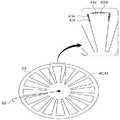
도 8은 본 발명의 다른 실시 예에 따른 정전척 어셈블리의 정전척의 개략적인 평단면도이다. 이에 도시된 바와 같이 본 발명의 다른 실시 예에 따른 정전척 어셈블리는 전술한 일 실시 예에 비하여 광섬유 브래그 격자(FBG, Fiber Bragg Grating) 온도센서의 정전척에서의 평면 배치가 다르다. 이하 전술한 일 실시예와 동일한 부분은 설명의 편의를 위하여 생략하고 다른 부분만 설명하기로 한다.8 is a schematic plan cross-sectional view of an electrostatic chuck of an electrostatic chuck assembly according to another embodiment of the present invention. As shown, the electrostatic chuck assembly according to another embodiment of the present invention has a different planar arrangement of the fiber Bragg grating (FBG) temperature sensor in the electrostatic chuck compared to the above-described embodiment. Hereinafter, the same parts as those of the above-described embodiment will be omitted for convenience of description and only different parts will be described.
본 실시 예에서는 광섬유 브래그 격자(43a, 43b, FBG, Fiber Bragg Grating)가 원주 방향과 반지름 방향으로 각각 배치된다. 이와 같이 아주 인접한 곳에 광섬유 브래그 격자(43a, 43b, FBG, Fiber Bragg Grating)를 원주 방향과 반지름 방향으로 설치하면 온도와 스트레인(strain)의 영향을 분리할 수 있다.In this embodiment, the
보다 상세히 설명하면, 정전척의 외곽의 아주 인접한 곳에 광섬유 브래그 격자(43a, 43b, FBG, Fiber Bragg Grating)를 원주 방향과 반지름 방향으로 설치하면 온도는 거의 일정하다고 가정할 수 있고 정전척의 외곽이 구속되어 있으므로 원주 방향의 스트레인은 없다고 가정할 수 있으므로 원주 방향과 반지름 방향으로 각각 배치된 광섬유 브래그 격자(43a, 43b,, FBG, Fiber Bragg Grating)의 반향 파장을 분석함으로써 반지름 방향의 스트레인을 확인할 수 있다. 그리고 이와 같이 확인된 반지름 방향의 스트레인을 보정하게 되면 스트레인의 영향을 분리할 수 있다.More specifically, if
도 9는 본 발명의 또 다른 실시 예에 따른 정전척 어셈블리의 정전척의 개략적인 평단면도이다. 평단면도이다. 이에 도시된 바와 같이 본 발명의 또 다른 실시 예에 따른 정전척 어셈블리는 전술한 일 실시예에 비하여 광섬유 브래그 격자(FBG, Fiber Bragg Grating) 온도센서의 정전척에서의 평면 배치가 다르고 전술한 다른 실시 예에 비하여 응답 특성이 다른 두 광섬유 브래그 격자(FBG, Fiber Bragg Grating)를 인접하게 배치하고 있다. 이하 전술한 일 실시예와 동일한 부분은 설명의 편의를 위하여 생략하고 다른 부분만 설명하기로 한다.9 is a schematic plan cross-sectional view of an electrostatic chuck of an electrostatic chuck assembly according to another embodiment of the present invention. It is a flat section. As shown, the electrostatic chuck assembly according to another embodiment of the present invention has a different planar arrangement in the electrostatic chuck of a Fiber Bragg grating (FBG) temperature sensor compared to the above-described embodiment, and the electrostatic chuck assembly according to the above-described other embodiment Two Fiber Bragg gratings (FBGs) having different response characteristics are disposed adjacent to each other compared to the example. Hereinafter, the same parts as those of the above-described embodiment will be omitted for convenience of description and only different parts will be described.
본 실시 예에서는 광섬유 브래그 격자(43c, 43d, 43e 43f, FBG, Fiber Bragg Grating)가 원주 방향과 반지름 방향으로 각각 배치되되 응답 특성이 다른 두 광섬유 브래그 격자(43c, 43d, 43e 43f, FBG, Fiber Bragg Grating)를 원주 방향과 반지름 방향 각각으로 인접하게 배치하고 있다. 이와 같이 원주 방향과 반지름 방향 각각으로 상호 아주 인접하게 배치된 같은 방향의 두 광섬유 브래그 격자(43c 및 43d, 43e 및 43f, FBG, Fiber Bragg Grating)의 반향 파장을 각각 분석하면 온도와 스트레인(strain)의 영향을 분리할 수 있다. 한편 전술한 실시 예에서는 측정존 온도센서(41)가 광섬유의 길이를 따르는 복수의 광섬유 브래그 격자(43, FBG, Fiber Bragg Grating)을 포함하는 광섬유 브래그 격자(FBG, Fiber Bragg Grating) 온도센서(41)인 것에 대하여 상술하였으나 광섬유에 들어가서 나온 광의 파라미터들에 기초하여 광섬유를 따르는 상이한 위치들에서의 온도를 결정할 수 있는 다른 종류의 센서들도 적용될 수 있을 것이다.In this embodiment, the
또한 전술한 실시 예에서는 측정존 온도 센서유닛(40)과 측정존 온도 계측유닛(50)이 물리적으로 분리된 것에 대하여 상술하였으나, 측정존 온도 센서유닛(40)과 측정존 온도 계측유닛(50)이 하나의 장치로 구현될 수도 있을 것이며, 측정존 온도 계측유닛(50)이 물리적으로 메인 콘트롤러(70) 내에 구현될 수도 있을 것이다.In addition, in the above-described embodiment, the measurement zone
이와 같이 본 발명은 기재된 실시 예에 한정되는 것이 아니고, 본 발명의 사상 및 범위를 벗어나지 않고 다양하게 수정 및 변형할 수 있음은 이 기술의 분야에서 통상의 지식을 가진 자에게 자명하다. 따라서 그러한 수정 예 또는 변형 예들은 본 발명의 특허청구범위에 속한다 하여야 할 것이다.As such, the present invention is not limited to the described embodiments, and it is apparent to those skilled in the art that various modifications and variations can be made without departing from the spirit and scope of the present invention. Accordingly, it should be said that such modifications or variations are included in the claims of the present invention.
10 : 정전척 에셈블리 20 : 정전척
30 : 기준 온도 센서유닛 40 : 측정존 온도 센서유닛
50 : 측정존 온도 계측유닛 60 : 온도조절유닛
70 : 메인 콘트롤러10: electrostatic chuck assembly 20: electrostatic chuck
30: reference temperature sensor unit 40: measurement zone temperature sensor unit
50: measurement zone temperature measurement unit 60: temperature control unit
70: main controller
Claims (10)
Translated fromKorean상기 정전척에 결합되어 상기 정전척의 기준 온도를 측정하는 기준 온도 센서유닛;
상기 기준 온도 센서유닛에 이격되게 상기 정전척에 결합되어 상기 복수의 측정존의 측정존 온도신호를 감지하는 측정존 온도 센서유닛; 및
상기 기준 온도 센서유닛에서 측정된 상기 기준 온도를 기초로 미리 결정된 온도 범위 내로 계측 범위를 설정하고 상기 계측 범위 내에서 상기 측정존 온도 센서유닛에서 감지한 상기 측정존 온도신호를 계측하여 측정존 온도를 산출하는 측정존 온도 계측유닛을 포함하되,
상기 측정존 온도 센서유닛은, 광섬유에 들어가서 나온 광의 파라미터들에 기초하여 상기 광섬유를 따르는 상이한 위치들에서의 온도를 결정할 수 있는 측정존 온도센서를 포함하는 정전척 어셈블리.an electrostatic chuck adsorbing a substrate by electrostatic force and having a plurality of measurement zones divided into a plurality of sections; and
a reference temperature sensor unit coupled to the electrostatic chuck to measure a reference temperature of the electrostatic chuck;
a measurement zone temperature sensor unit coupled to the electrostatic chuck to be spaced apart from the reference temperature sensor unit to sense measurement zone temperature signals of the plurality of measurement zones; and
The measurement zone temperature is determined by setting a measurement range within a predetermined temperature range based on the reference temperature measured by the reference temperature sensor unit and measuring the measurement zone temperature signal detected by the measurement zone temperature sensor unit within the measurement range. Including a measurement zone temperature measuring unit that calculates,
wherein the measurement zone temperature sensor unit includes a measurement zone temperature sensor capable of determining a temperature at different locations along the optical fiber based on parameters of light entering and exiting the optical fiber.
상기 측정존 온도센서는, 상기 광섬유의 길이를 따르는 복수의 광섬유 브래그 격자(FBG, Fiber Bragg Grating)을 포함하는 광섬유 브래그 격자(FBG, Fiber Bragg Grating) 온도센서이며,
상기 측정존 온도 계측유닛은 상기 기준 온도에 상기 정전척의 온도 편차를 부가한 온도 범위 내에 해당하는 파장 범위를 산출하고 상기 파장 범위 내에서 상기 측정존의 반향 파장을 계측하여 상기 측정존 온도를 산출하는 정전척 어셈블리.According to claim 1,
The measurement zone temperature sensor is a fiber Bragg grating (FBG) temperature sensor including a plurality of fiber Bragg gratings (FBG) along the length of the optical fiber,
The measurement zone temperature measurement unit calculates a wavelength range corresponding to a temperature range in which the temperature deviation of the electrostatic chuck is added to the reference temperature, and calculates the measurement zone temperature by measuring the echo wavelength of the measurement zone within the wavelength range electrostatic chuck assembly.
상기 복수의 광섬유 브래그 격자(FBG, Fiber Bragg Grating)들은 상기 정전척의 원주 방향 및 반지름 방향으로 배치되는 정전척 어셈블리.4. The method of claim 3,
The plurality of Fiber Bragg gratings (FBGs) are disposed in a circumferential direction and a radial direction of the electrostatic chuck.
정전기력에 의해 기판을 흡착하는 정전척 어셈블리를 포함하며,
상기 정전척 어셈블리는,
정전기력에 의해 기판을 흡착하며, 복수의 구획으로 구분된 복수의 측정존을 구비하는 정전척; 및
상기 정전척에 결합되어 상기 정전척의 기준 온도를 측정하는 기준 온도 센서유닛;
상기 기준 온도 센서유닛에 이격되게 상기 정전척에 결합되어 상기 복수의 측정존의 측정존 온도신호를 감지하는 측정존 온도 센서유닛; 및
상기 기준 온도 센서유닛에서 측정된 상기 기준 온도를 기초로 미리 결정된 온도 범위 내로 계측 범위를 설정하고 상기 계측 범위 내에서 상기 측정존 온도 센서유닛에서 감지한 상기 측정존 온도신호를 계측하여 측정존 온도를 산출하는 측정존 온도 계측유닛을 포함하되,
상기 측정존 온도 센서유닛은, 광섬유에 들어가서 나온 광의 파라미터들에 기초하여 상기 광섬유를 따르는 상이한 위치들에서의 온도를 결정할 수 있는 측정존 온도센서를 포함하는 반도체 제조장치.a process chamber providing a space for performing a semiconductor manufacturing process; and
An electrostatic chuck assembly for adsorbing the substrate by electrostatic force,
The electrostatic chuck assembly,
an electrostatic chuck adsorbing a substrate by electrostatic force and having a plurality of measurement zones divided into a plurality of sections; and
a reference temperature sensor unit coupled to the electrostatic chuck to measure a reference temperature of the electrostatic chuck;
a measurement zone temperature sensor unit coupled to the electrostatic chuck to be spaced apart from the reference temperature sensor unit to sense measurement zone temperature signals of the plurality of measurement zones; and
The measurement zone temperature is determined by setting a measurement range within a predetermined temperature range based on the reference temperature measured by the reference temperature sensor unit and measuring the measurement zone temperature signal detected by the measurement zone temperature sensor unit within the measurement range. Including a measurement zone temperature measuring unit that calculates,
The measurement zone temperature sensor unit includes a measurement zone temperature sensor capable of determining temperatures at different positions along the optical fiber based on parameters of light entering and exiting the optical fiber.
상기 측정존 온도센서는, 상기 광섬유의 길이를 따르는 복수의 광섬유 브래그 격자(FBG, Fiber Bragg Grating)을 포함하는 광섬유 브래그 격자(FBG, Fiber Bragg Grating) 온도센서이며,
상기 측정존 온도 계측유닛은 상기 기준 온도에 상기 정전척의 온도 편차를 부가한 온도 범위 내에 해당하는 파장 범위를 산출하고 상기 파장 범위 내에서 상기 측정존의 반향 파장을 계측하여 상기 측정존 온도를 산출하는 반도체 제조장치.6. The method of claim 5,
The measurement zone temperature sensor is a fiber Bragg grating (FBG) temperature sensor including a plurality of fiber Bragg gratings (FBG) along the length of the optical fiber,
The measurement zone temperature measurement unit calculates a wavelength range corresponding to a temperature range in which the temperature deviation of the electrostatic chuck is added to the reference temperature, and calculates the measurement zone temperature by measuring the echo wavelength of the measurement zone within the wavelength range semiconductor manufacturing equipment.
상기 기준 온도 센서유닛에 이격되게 상기 정전척에 결합되는 측정존 온도 센서유닛으로 상기 정전척에 복수의 구획으로 구분된 복수의 측정존의 측정존 온도신호를 감지하는 단계; 및
측정존 온도 계측유닛이 상기 기준 온도를 기초로 미리 결정된 온도 범위 내로 계측 범위를 설정하고 상기 계측 범위 내에서 상기 측정존 온도 센서유닛에서 감지한 상기 측정존 온도신호를 계측하여 측정존 온도를 산출하는 단계를 포함하되,
상기 측정존 온도센서는, 광섬유의 길이를 따르는 복수의 광섬유 브래그 격자(FBG, Fiber Bragg Grating)을 포함하는 광섬유 브래그 격자(FBG, Fiber Bragg Grating) 온도센서인 정전척 온도 측정방법.measuring a reference temperature of the electrostatic chuck with a reference temperature sensor unit coupled to an electrostatic chuck for adsorbing a substrate by electrostatic force;
detecting a measurement zone temperature signal of a plurality of measurement zones divided into a plurality of sections on the electrostatic chuck by a measurement zone temperature sensor unit coupled to the electrostatic chuck to be spaced apart from the reference temperature sensor unit; and
The measurement zone temperature measurement unit sets the measurement range within a predetermined temperature range based on the reference temperature, and calculates the measurement zone temperature by measuring the measurement zone temperature signal detected by the measurement zone temperature sensor unit within the measurement range comprising steps,
The measurement zone temperature sensor is an electrostatic chuck temperature measuring method that is a fiber Bragg grating (FBG) temperature sensor including a plurality of fiber Bragg gratings (FBG) along the length of the optical fiber.
상기 측정존 온도 계측유닛은 상기 기준 온도에 상기 정전척의 온도 편차를 부가한 온도 범위 내에 해당하는 파장 범위를 산출하고 상기 파장 범위 내에서 측정존 반향 파장을 계측하여 상기 측정존 온도를 산출하는 정전척 온도 측정방법.9. The method of claim 8,
The measurement zone temperature measuring unit calculates a wavelength range corresponding to a temperature range in which a temperature deviation of the electrostatic chuck is added to the reference temperature, and measures a reflection wavelength of the measurement zone within the wavelength range to calculate the measurement zone temperature. How to measure temperature.
상기 복수의 광섬유 브래그 격자(FBG, Fiber Bragg Grating)들은 상기 복수의 측정존에 각각 대응되게 배치되는 정전척 온도 측정방법.10. The method of claim 9,
The plurality of fiber Bragg gratings (FBG) are respectively disposed to correspond to the plurality of measurement zones.
Priority Applications (2)
| Application Number | Priority Date | Filing Date | Title |
|---|---|---|---|
| KR1020150182154AKR102423818B1 (en) | 2015-12-18 | 2015-12-18 | A electrostatic chuck assembly, a semiconductor manufacturing apparatus having the same, and a temperature mesuring method for electrostatic chuck |
| US15/232,151US9812372B2 (en) | 2015-12-18 | 2016-08-09 | Electrostatic chuck assembly, semiconductor manufacturing apparatus having the same, and method of measuring temperature of electrostatic chuck |
Applications Claiming Priority (1)
| Application Number | Priority Date | Filing Date | Title |
|---|---|---|---|
| KR1020150182154AKR102423818B1 (en) | 2015-12-18 | 2015-12-18 | A electrostatic chuck assembly, a semiconductor manufacturing apparatus having the same, and a temperature mesuring method for electrostatic chuck |
Publications (2)
| Publication Number | Publication Date |
|---|---|
| KR20170073352A KR20170073352A (en) | 2017-06-28 |
| KR102423818B1true KR102423818B1 (en) | 2022-07-21 |
Family
ID=59064644
Family Applications (1)
| Application Number | Title | Priority Date | Filing Date |
|---|---|---|---|
| KR1020150182154AActiveKR102423818B1 (en) | 2015-12-18 | 2015-12-18 | A electrostatic chuck assembly, a semiconductor manufacturing apparatus having the same, and a temperature mesuring method for electrostatic chuck |
Country Status (2)
| Country | Link |
|---|---|
| US (1) | US9812372B2 (en) |
| KR (1) | KR102423818B1 (en) |
Families Citing this family (266)
| Publication number | Priority date | Publication date | Assignee | Title |
|---|---|---|---|---|
| WO2002046372A1 (en) | 2000-12-08 | 2002-06-13 | Invitrogen Corporation | Methods and compositions for synthesis of nucleic acid molecules using multiple recognition sites |
| US20050069929A1 (en) | 2003-08-08 | 2005-03-31 | Invitrogen Corporation | Methods and compositions for seamless cloning of nucleic acid molecules |
| ATE469984T1 (en) | 2003-12-01 | 2010-06-15 | Life Technologies Corp | NUCLEIC ACID MOLECULES CONTAINING RECOMBINATION SITE AND METHOD FOR USE THEREOF |
| US20120184007A1 (en) | 2009-07-09 | 2012-07-19 | Stephen Picataggio | Engineered microorganisms with enhanced fermentation activity |
| US20140228587A1 (en) | 2011-07-06 | 2014-08-14 | Tom Beardslee | Biological methods for preparing a fatty dicarboxylic acid |
| US20130023129A1 (en) | 2011-07-20 | 2013-01-24 | Asm America, Inc. | Pressure transmitter for a semiconductor processing environment |
| US9465519B2 (en) | 2011-12-21 | 2016-10-11 | Life Technologies Corporation | Methods and systems for in silico experimental designing and performing a biological workflow |
| US10714315B2 (en) | 2012-10-12 | 2020-07-14 | Asm Ip Holdings B.V. | Semiconductor reaction chamber showerhead |
| US20160376700A1 (en) | 2013-02-01 | 2016-12-29 | Asm Ip Holding B.V. | System for treatment of deposition reactor |
| US10861682B2 (en) | 2014-07-31 | 2020-12-08 | iSenseCloud, Inc. | Test wafer with optical fiber with Bragg Grating sensors |
| US10941490B2 (en) | 2014-10-07 | 2021-03-09 | Asm Ip Holding B.V. | Multiple temperature range susceptor, assembly, reactor and system including the susceptor, and methods of using the same |
| US10276355B2 (en) | 2015-03-12 | 2019-04-30 | Asm Ip Holding B.V. | Multi-zone reactor, system including the reactor, and method of using the same |
| US10458018B2 (en) | 2015-06-26 | 2019-10-29 | Asm Ip Holding B.V. | Structures including metal carbide material, devices including the structures, and methods of forming same |
| US10211308B2 (en) | 2015-10-21 | 2019-02-19 | Asm Ip Holding B.V. | NbMC layers |
| US11139308B2 (en) | 2015-12-29 | 2021-10-05 | Asm Ip Holding B.V. | Atomic layer deposition of III-V compounds to form V-NAND devices |
| US10529554B2 (en) | 2016-02-19 | 2020-01-07 | Asm Ip Holding B.V. | Method for forming silicon nitride film selectively on sidewalls or flat surfaces of trenches |
| US10343920B2 (en) | 2016-03-18 | 2019-07-09 | Asm Ip Holding B.V. | Aligned carbon nanotubes |
| US11453943B2 (en) | 2016-05-25 | 2022-09-27 | Asm Ip Holding B.V. | Method for forming carbon-containing silicon/metal oxide or nitride film by ALD using silicon precursor and hydrocarbon precursor |
| US9859151B1 (en) | 2016-07-08 | 2018-01-02 | Asm Ip Holding B.V. | Selective film deposition method to form air gaps |
| US10612137B2 (en) | 2016-07-08 | 2020-04-07 | Asm Ip Holdings B.V. | Organic reactants for atomic layer deposition |
| US9887082B1 (en) | 2016-07-28 | 2018-02-06 | Asm Ip Holding B.V. | Method and apparatus for filling a gap |
| US9812320B1 (en) | 2016-07-28 | 2017-11-07 | Asm Ip Holding B.V. | Method and apparatus for filling a gap |
| US11532757B2 (en) | 2016-10-27 | 2022-12-20 | Asm Ip Holding B.V. | Deposition of charge trapping layers |
| US10714350B2 (en) | 2016-11-01 | 2020-07-14 | ASM IP Holdings, B.V. | Methods for forming a transition metal niobium nitride film on a substrate by atomic layer deposition and related semiconductor device structures |
| KR102546317B1 (en) | 2016-11-15 | 2023-06-21 | 에이에스엠 아이피 홀딩 비.브이. | Gas supply unit and substrate processing apparatus including the same |
| KR102762543B1 (en) | 2016-12-14 | 2025-02-05 | 에이에스엠 아이피 홀딩 비.브이. | Substrate processing apparatus |
| US11447861B2 (en) | 2016-12-15 | 2022-09-20 | Asm Ip Holding B.V. | Sequential infiltration synthesis apparatus and a method of forming a patterned structure |
| US11581186B2 (en) | 2016-12-15 | 2023-02-14 | Asm Ip Holding B.V. | Sequential infiltration synthesis apparatus |
| US10269558B2 (en) | 2016-12-22 | 2019-04-23 | Asm Ip Holding B.V. | Method of forming a structure on a substrate |
| US11390950B2 (en) | 2017-01-10 | 2022-07-19 | Asm Ip Holding B.V. | Reactor system and method to reduce residue buildup during a film deposition process |
| US10468261B2 (en) | 2017-02-15 | 2019-11-05 | Asm Ip Holding B.V. | Methods for forming a metallic film on a substrate by cyclical deposition and related semiconductor device structures |
| US10770286B2 (en) | 2017-05-08 | 2020-09-08 | Asm Ip Holdings B.V. | Methods for selectively forming a silicon nitride film on a substrate and related semiconductor device structures |
| US12040200B2 (en) | 2017-06-20 | 2024-07-16 | Asm Ip Holding B.V. | Semiconductor processing apparatus and methods for calibrating a semiconductor processing apparatus |
| US11306395B2 (en) | 2017-06-28 | 2022-04-19 | Asm Ip Holding B.V. | Methods for depositing a transition metal nitride film on a substrate by atomic layer deposition and related deposition apparatus |
| EP3652300A4 (en) | 2017-07-13 | 2021-06-23 | Radici Chimica S.p.A. | Biological methods for modifying cellular carbon flux |
| KR20190009245A (en) | 2017-07-18 | 2019-01-28 | 에이에스엠 아이피 홀딩 비.브이. | Methods for forming a semiconductor device structure and related semiconductor device structures |
| US11374112B2 (en) | 2017-07-19 | 2022-06-28 | Asm Ip Holding B.V. | Method for depositing a group IV semiconductor and related semiconductor device structures |
| US10590535B2 (en) | 2017-07-26 | 2020-03-17 | Asm Ip Holdings B.V. | Chemical treatment, deposition and/or infiltration apparatus and method for using the same |
| TWI815813B (en) | 2017-08-04 | 2023-09-21 | 荷蘭商Asm智慧財產控股公司 | Showerhead assembly for distributing a gas within a reaction chamber |
| US10770336B2 (en) | 2017-08-08 | 2020-09-08 | Asm Ip Holding B.V. | Substrate lift mechanism and reactor including same |
| US10692741B2 (en) | 2017-08-08 | 2020-06-23 | Asm Ip Holdings B.V. | Radiation shield |
| US11769682B2 (en) | 2017-08-09 | 2023-09-26 | Asm Ip Holding B.V. | Storage apparatus for storing cassettes for substrates and processing apparatus equipped therewith |
| US11830730B2 (en) | 2017-08-29 | 2023-11-28 | Asm Ip Holding B.V. | Layer forming method and apparatus |
| US11295980B2 (en) | 2017-08-30 | 2022-04-05 | Asm Ip Holding B.V. | Methods for depositing a molybdenum metal film over a dielectric surface of a substrate by a cyclical deposition process and related semiconductor device structures |
| US10658205B2 (en) | 2017-09-28 | 2020-05-19 | Asm Ip Holdings B.V. | Chemical dispensing apparatus and methods for dispensing a chemical to a reaction chamber |
| US10403504B2 (en) | 2017-10-05 | 2019-09-03 | Asm Ip Holding B.V. | Method for selectively depositing a metallic film on a substrate |
| US10923344B2 (en) | 2017-10-30 | 2021-02-16 | Asm Ip Holding B.V. | Methods for forming a semiconductor structure and related semiconductor structures |
| CN111344522B (en) | 2017-11-27 | 2022-04-12 | 阿斯莫Ip控股公司 | Including clean mini-environment device |
| WO2019103613A1 (en) | 2017-11-27 | 2019-05-31 | Asm Ip Holding B.V. | A storage device for storing wafer cassettes for use with a batch furnace |
| US10872771B2 (en) | 2018-01-16 | 2020-12-22 | Asm Ip Holding B. V. | Method for depositing a material film on a substrate within a reaction chamber by a cyclical deposition process and related device structures |
| TWI799494B (en) | 2018-01-19 | 2023-04-21 | 荷蘭商Asm 智慧財產控股公司 | Deposition method |
| KR102695659B1 (en) | 2018-01-19 | 2024-08-14 | 에이에스엠 아이피 홀딩 비.브이. | Method for depositing a gap filling layer by plasma assisted deposition |
| US11081345B2 (en) | 2018-02-06 | 2021-08-03 | Asm Ip Holding B.V. | Method of post-deposition treatment for silicon oxide film |
| WO2019158960A1 (en) | 2018-02-14 | 2019-08-22 | Asm Ip Holding B.V. | A method for depositing a ruthenium-containing film on a substrate by a cyclical deposition process |
| US10896820B2 (en) | 2018-02-14 | 2021-01-19 | Asm Ip Holding B.V. | Method for depositing a ruthenium-containing film on a substrate by a cyclical deposition process |
| US10731249B2 (en) | 2018-02-15 | 2020-08-04 | Asm Ip Holding B.V. | Method of forming a transition metal containing film on a substrate by a cyclical deposition process, a method for supplying a transition metal halide compound to a reaction chamber, and related vapor deposition apparatus |
| KR102636427B1 (en) | 2018-02-20 | 2024-02-13 | 에이에스엠 아이피 홀딩 비.브이. | Substrate processing method and apparatus |
| JP6578391B2 (en)* | 2018-02-23 | 2019-09-18 | 日本特殊陶業株式会社 | Semiconductor manufacturing equipment component, semiconductor manufacturing equipment component temperature distribution measuring method, and semiconductor manufacturing equipment temperature distribution measuring device |
| US10975470B2 (en) | 2018-02-23 | 2021-04-13 | Asm Ip Holding B.V. | Apparatus for detecting or monitoring for a chemical precursor in a high temperature environment |
| US11473195B2 (en) | 2018-03-01 | 2022-10-18 | Asm Ip Holding B.V. | Semiconductor processing apparatus and a method for processing a substrate |
| US11629406B2 (en) | 2018-03-09 | 2023-04-18 | Asm Ip Holding B.V. | Semiconductor processing apparatus comprising one or more pyrometers for measuring a temperature of a substrate during transfer of the substrate |
| KR102646467B1 (en) | 2018-03-27 | 2024-03-11 | 에이에스엠 아이피 홀딩 비.브이. | Method of forming an electrode on a substrate and a semiconductor device structure including an electrode |
| US11230766B2 (en) | 2018-03-29 | 2022-01-25 | Asm Ip Holding B.V. | Substrate processing apparatus and method |
| KR102600229B1 (en) | 2018-04-09 | 2023-11-10 | 에이에스엠 아이피 홀딩 비.브이. | Substrate supporting device, substrate processing apparatus including the same and substrate processing method |
| US12025484B2 (en) | 2018-05-08 | 2024-07-02 | Asm Ip Holding B.V. | Thin film forming method |
| TWI811348B (en) | 2018-05-08 | 2023-08-11 | 荷蘭商Asm 智慧財產控股公司 | Methods for depositing an oxide film on a substrate by a cyclical deposition process and related device structures |
| US12272527B2 (en) | 2018-05-09 | 2025-04-08 | Asm Ip Holding B.V. | Apparatus for use with hydrogen radicals and method of using same |
| KR102596988B1 (en) | 2018-05-28 | 2023-10-31 | 에이에스엠 아이피 홀딩 비.브이. | Method of processing a substrate and a device manufactured by the same |
| US11718913B2 (en) | 2018-06-04 | 2023-08-08 | Asm Ip Holding B.V. | Gas distribution system and reactor system including same |
| TWI840362B (en) | 2018-06-04 | 2024-05-01 | 荷蘭商Asm Ip私人控股有限公司 | Wafer handling chamber with moisture reduction |
| US11286562B2 (en) | 2018-06-08 | 2022-03-29 | Asm Ip Holding B.V. | Gas-phase chemical reactor and method of using same |
| KR102568797B1 (en) | 2018-06-21 | 2023-08-21 | 에이에스엠 아이피 홀딩 비.브이. | Substrate processing system |
| US10797133B2 (en) | 2018-06-21 | 2020-10-06 | Asm Ip Holding B.V. | Method for depositing a phosphorus doped silicon arsenide film and related semiconductor device structures |
| KR102854019B1 (en) | 2018-06-27 | 2025-09-02 | 에이에스엠 아이피 홀딩 비.브이. | Periodic deposition method for forming a metal-containing material and films and structures comprising the metal-containing material |
| TWI873894B (en) | 2018-06-27 | 2025-02-21 | 荷蘭商Asm Ip私人控股有限公司 | Cyclic deposition methods for forming metal-containing material and films and structures including the metal-containing material |
| US10612136B2 (en) | 2018-06-29 | 2020-04-07 | ASM IP Holding, B.V. | Temperature-controlled flange and reactor system including same |
| US10755922B2 (en) | 2018-07-03 | 2020-08-25 | Asm Ip Holding B.V. | Method for depositing silicon-free carbon-containing film as gap-fill layer by pulse plasma-assisted deposition |
| US10388513B1 (en) | 2018-07-03 | 2019-08-20 | Asm Ip Holding B.V. | Method for depositing silicon-free carbon-containing film as gap-fill layer by pulse plasma-assisted deposition |
| WO2020023295A1 (en)* | 2018-07-25 | 2020-01-30 | Lam Research Corporation | Substrate support temperature sensing systems and methods |
| US11430674B2 (en) | 2018-08-22 | 2022-08-30 | Asm Ip Holding B.V. | Sensor array, apparatus for dispensing a vapor phase reactant to a reaction chamber and related methods |
| US11024523B2 (en) | 2018-09-11 | 2021-06-01 | Asm Ip Holding B.V. | Substrate processing apparatus and method |
| KR102707956B1 (en) | 2018-09-11 | 2024-09-19 | 에이에스엠 아이피 홀딩 비.브이. | Method for deposition of a thin film |
| CN110970344B (en) | 2018-10-01 | 2024-10-25 | Asmip控股有限公司 | Substrate holding apparatus, system comprising the same and method of using the same |
| US11232963B2 (en) | 2018-10-03 | 2022-01-25 | Asm Ip Holding B.V. | Substrate processing apparatus and method |
| KR102592699B1 (en) | 2018-10-08 | 2023-10-23 | 에이에스엠 아이피 홀딩 비.브이. | Substrate support unit and apparatuses for depositing thin film and processing the substrate including the same |
| KR102605121B1 (en) | 2018-10-19 | 2023-11-23 | 에이에스엠 아이피 홀딩 비.브이. | Substrate processing apparatus and substrate processing method |
| KR102546322B1 (en) | 2018-10-19 | 2023-06-21 | 에이에스엠 아이피 홀딩 비.브이. | Substrate processing apparatus and substrate processing method |
| US12378665B2 (en) | 2018-10-26 | 2025-08-05 | Asm Ip Holding B.V. | High temperature coatings for a preclean and etch apparatus and related methods |
| US11087997B2 (en) | 2018-10-31 | 2021-08-10 | Asm Ip Holding B.V. | Substrate processing apparatus for processing substrates |
| KR102748291B1 (en) | 2018-11-02 | 2024-12-31 | 에이에스엠 아이피 홀딩 비.브이. | Substrate support unit and substrate processing apparatus including the same |
| US11572620B2 (en) | 2018-11-06 | 2023-02-07 | Asm Ip Holding B.V. | Methods for selectively depositing an amorphous silicon film on a substrate |
| US10818758B2 (en) | 2018-11-16 | 2020-10-27 | Asm Ip Holding B.V. | Methods for forming a metal silicate film on a substrate in a reaction chamber and related semiconductor device structures |
| US12040199B2 (en) | 2018-11-28 | 2024-07-16 | Asm Ip Holding B.V. | Substrate processing apparatus for processing substrates |
| US11217444B2 (en) | 2018-11-30 | 2022-01-04 | Asm Ip Holding B.V. | Method for forming an ultraviolet radiation responsive metal oxide-containing film |
| KR102636428B1 (en) | 2018-12-04 | 2024-02-13 | 에이에스엠 아이피 홀딩 비.브이. | A method for cleaning a substrate processing apparatus |
| US11158513B2 (en) | 2018-12-13 | 2021-10-26 | Asm Ip Holding B.V. | Methods for forming a rhenium-containing film on a substrate by a cyclical deposition process and related semiconductor device structures |
| TWI874340B (en) | 2018-12-14 | 2025-03-01 | 荷蘭商Asm Ip私人控股有限公司 | Method of forming device structure, structure formed by the method and system for performing the method |
| TWI866480B (en) | 2019-01-17 | 2024-12-11 | 荷蘭商Asm Ip 私人控股有限公司 | Methods of forming a transition metal containing film on a substrate by a cyclical deposition process |
| KR102727227B1 (en) | 2019-01-22 | 2024-11-07 | 에이에스엠 아이피 홀딩 비.브이. | Semiconductor processing device |
| KR102626263B1 (en) | 2019-02-20 | 2024-01-16 | 에이에스엠 아이피 홀딩 비.브이. | Cyclical deposition method including treatment step and apparatus for same |
| TWI838458B (en) | 2019-02-20 | 2024-04-11 | 荷蘭商Asm Ip私人控股有限公司 | Apparatus and methods for plug fill deposition in 3-d nand applications |
| TWI845607B (en) | 2019-02-20 | 2024-06-21 | 荷蘭商Asm Ip私人控股有限公司 | Cyclical deposition method and apparatus for filling a recess formed within a substrate surface |
| TWI873122B (en) | 2019-02-20 | 2025-02-21 | 荷蘭商Asm Ip私人控股有限公司 | Method of filling a recess formed within a surface of a substrate, semiconductor structure formed according to the method, and semiconductor processing apparatus |
| TWI842826B (en) | 2019-02-22 | 2024-05-21 | 荷蘭商Asm Ip私人控股有限公司 | Substrate processing apparatus and method for processing substrate |
| US11742198B2 (en) | 2019-03-08 | 2023-08-29 | Asm Ip Holding B.V. | Structure including SiOCN layer and method of forming same |
| KR102858005B1 (en) | 2019-03-08 | 2025-09-09 | 에이에스엠 아이피 홀딩 비.브이. | Method for Selective Deposition of Silicon Nitride Layer and Structure Including Selectively-Deposited Silicon Nitride Layer |
| JP2020167398A (en) | 2019-03-28 | 2020-10-08 | エーエスエム・アイピー・ホールディング・ベー・フェー | Door openers and substrate processing equipment provided with door openers |
| KR102809999B1 (en) | 2019-04-01 | 2025-05-19 | 에이에스엠 아이피 홀딩 비.브이. | Method of manufacturing semiconductor device |
| KR20200123380A (en) | 2019-04-19 | 2020-10-29 | 에이에스엠 아이피 홀딩 비.브이. | Layer forming method and apparatus |
| KR20200125453A (en) | 2019-04-24 | 2020-11-04 | 에이에스엠 아이피 홀딩 비.브이. | Gas-phase reactor system and method of using same |
| US11289326B2 (en) | 2019-05-07 | 2022-03-29 | Asm Ip Holding B.V. | Method for reforming amorphous carbon polymer film |
| KR20200130121A (en) | 2019-05-07 | 2020-11-18 | 에이에스엠 아이피 홀딩 비.브이. | Chemical source vessel with dip tube |
| KR20200130652A (en) | 2019-05-10 | 2020-11-19 | 에이에스엠 아이피 홀딩 비.브이. | Method of depositing material onto a surface and structure formed according to the method |
| JP7612342B2 (en) | 2019-05-16 | 2025-01-14 | エーエスエム・アイピー・ホールディング・ベー・フェー | Wafer boat handling apparatus, vertical batch furnace and method |
| JP7598201B2 (en) | 2019-05-16 | 2024-12-11 | エーエスエム・アイピー・ホールディング・ベー・フェー | Wafer boat handling apparatus, vertical batch furnace and method |
| USD975665S1 (en) | 2019-05-17 | 2023-01-17 | Asm Ip Holding B.V. | Susceptor shaft |
| USD947913S1 (en) | 2019-05-17 | 2022-04-05 | Asm Ip Holding B.V. | Susceptor shaft |
| KR20200141002A (en) | 2019-06-06 | 2020-12-17 | 에이에스엠 아이피 홀딩 비.브이. | Method of using a gas-phase reactor system including analyzing exhausted gas |
| KR20200141931A (en) | 2019-06-10 | 2020-12-21 | 에이에스엠 아이피 홀딩 비.브이. | Method for cleaning quartz epitaxial chambers |
| KR20200143254A (en) | 2019-06-11 | 2020-12-23 | 에이에스엠 아이피 홀딩 비.브이. | Method of forming an electronic structure using an reforming gas, system for performing the method, and structure formed using the method |
| USD944946S1 (en) | 2019-06-14 | 2022-03-01 | Asm Ip Holding B.V. | Shower plate |
| KR20210005515A (en) | 2019-07-03 | 2021-01-14 | 에이에스엠 아이피 홀딩 비.브이. | Temperature control assembly for substrate processing apparatus and method of using same |
| JP7499079B2 (en) | 2019-07-09 | 2024-06-13 | エーエスエム・アイピー・ホールディング・ベー・フェー | Plasma device using coaxial waveguide and substrate processing method |
| CN112216646A (en) | 2019-07-10 | 2021-01-12 | Asm Ip私人控股有限公司 | Substrate supporting assembly and substrate processing device comprising same |
| KR20210010307A (en) | 2019-07-16 | 2021-01-27 | 에이에스엠 아이피 홀딩 비.브이. | Substrate processing apparatus |
| KR102860110B1 (en) | 2019-07-17 | 2025-09-16 | 에이에스엠 아이피 홀딩 비.브이. | Methods of forming silicon germanium structures |
| KR20210010816A (en) | 2019-07-17 | 2021-01-28 | 에이에스엠 아이피 홀딩 비.브이. | Radical assist ignition plasma system and method |
| US11643724B2 (en) | 2019-07-18 | 2023-05-09 | Asm Ip Holding B.V. | Method of forming structures using a neutral beam |
| TWI839544B (en) | 2019-07-19 | 2024-04-21 | 荷蘭商Asm Ip私人控股有限公司 | Method of forming topology-controlled amorphous carbon polymer film |
| KR20210010817A (en) | 2019-07-19 | 2021-01-28 | 에이에스엠 아이피 홀딩 비.브이. | Method of Forming Topology-Controlled Amorphous Carbon Polymer Film |
| TWI851767B (en) | 2019-07-29 | 2024-08-11 | 荷蘭商Asm Ip私人控股有限公司 | Methods for selective deposition utilizing n-type dopants and/or alternative dopants to achieve high dopant incorporation |
| CN112309900A (en) | 2019-07-30 | 2021-02-02 | Asm Ip私人控股有限公司 | Substrate processing apparatus |
| CN112309899A (en) | 2019-07-30 | 2021-02-02 | Asm Ip私人控股有限公司 | Substrate processing apparatus |
| US12169361B2 (en) | 2019-07-30 | 2024-12-17 | Asm Ip Holding B.V. | Substrate processing apparatus and method |
| US11587814B2 (en) | 2019-07-31 | 2023-02-21 | Asm Ip Holding B.V. | Vertical batch furnace assembly |
| US11587815B2 (en) | 2019-07-31 | 2023-02-21 | Asm Ip Holding B.V. | Vertical batch furnace assembly |
| US11227782B2 (en) | 2019-07-31 | 2022-01-18 | Asm Ip Holding B.V. | Vertical batch furnace assembly |
| CN112323048B (en) | 2019-08-05 | 2024-02-09 | Asm Ip私人控股有限公司 | Liquid level sensor for chemical source container |
| CN112342526A (en) | 2019-08-09 | 2021-02-09 | Asm Ip私人控股有限公司 | Heater assembly including cooling device and method of using same |
| USD965524S1 (en) | 2019-08-19 | 2022-10-04 | Asm Ip Holding B.V. | Susceptor support |
| USD965044S1 (en) | 2019-08-19 | 2022-09-27 | Asm Ip Holding B.V. | Susceptor shaft |
| JP2021031769A (en) | 2019-08-21 | 2021-03-01 | エーエスエム アイピー ホールディング ビー.ブイ. | Production apparatus of mixed gas of film deposition raw material and film deposition apparatus |
| USD940837S1 (en) | 2019-08-22 | 2022-01-11 | Asm Ip Holding B.V. | Electrode |
| USD949319S1 (en) | 2019-08-22 | 2022-04-19 | Asm Ip Holding B.V. | Exhaust duct |
| KR20210024423A (en) | 2019-08-22 | 2021-03-05 | 에이에스엠 아이피 홀딩 비.브이. | Method for forming a structure with a hole |
| USD979506S1 (en) | 2019-08-22 | 2023-02-28 | Asm Ip Holding B.V. | Insulator |
| US11286558B2 (en) | 2019-08-23 | 2022-03-29 | Asm Ip Holding B.V. | Methods for depositing a molybdenum nitride film on a surface of a substrate by a cyclical deposition process and related semiconductor device structures including a molybdenum nitride film |
| KR20210024420A (en) | 2019-08-23 | 2021-03-05 | 에이에스엠 아이피 홀딩 비.브이. | Method for depositing silicon oxide film having improved quality by peald using bis(diethylamino)silane |
| KR102806450B1 (en) | 2019-09-04 | 2025-05-12 | 에이에스엠 아이피 홀딩 비.브이. | Methods for selective deposition using a sacrificial capping layer |
| KR102733104B1 (en) | 2019-09-05 | 2024-11-22 | 에이에스엠 아이피 홀딩 비.브이. | Substrate processing apparatus |
| US11562901B2 (en) | 2019-09-25 | 2023-01-24 | Asm Ip Holding B.V. | Substrate processing method |
| CN112593212B (en) | 2019-10-02 | 2023-12-22 | Asm Ip私人控股有限公司 | Method for forming topologically selective silicon oxide film by cyclic plasma enhanced deposition process |
| TW202128273A (en) | 2019-10-08 | 2021-08-01 | 荷蘭商Asm Ip私人控股有限公司 | Gas injection system, reactor system, and method of depositing material on surface of substratewithin reaction chamber |
| TWI846953B (en) | 2019-10-08 | 2024-07-01 | 荷蘭商Asm Ip私人控股有限公司 | Substrate processing device |
| KR20210042810A (en) | 2019-10-08 | 2021-04-20 | 에이에스엠 아이피 홀딩 비.브이. | Reactor system including a gas distribution assembly for use with activated species and method of using same |
| TWI846966B (en) | 2019-10-10 | 2024-07-01 | 荷蘭商Asm Ip私人控股有限公司 | Method of forming a photoresist underlayer and structure including same |
| US12009241B2 (en) | 2019-10-14 | 2024-06-11 | Asm Ip Holding B.V. | Vertical batch furnace assembly with detector to detect cassette |
| TWI834919B (en) | 2019-10-16 | 2024-03-11 | 荷蘭商Asm Ip私人控股有限公司 | Method of topology-selective film formation of silicon oxide |
| US11637014B2 (en) | 2019-10-17 | 2023-04-25 | Asm Ip Holding B.V. | Methods for selective deposition of doped semiconductor material |
| KR102845724B1 (en) | 2019-10-21 | 2025-08-13 | 에이에스엠 아이피 홀딩 비.브이. | Apparatus and methods for selectively etching films |
| KR20210050453A (en) | 2019-10-25 | 2021-05-07 | 에이에스엠 아이피 홀딩 비.브이. | Methods for filling a gap feature on a substrate surface and related semiconductor structures |
| US11646205B2 (en) | 2019-10-29 | 2023-05-09 | Asm Ip Holding B.V. | Methods of selectively forming n-type doped material on a surface, systems for selectively forming n-type doped material, and structures formed using same |
| KR20210054983A (en) | 2019-11-05 | 2021-05-14 | 에이에스엠 아이피 홀딩 비.브이. | Structures with doped semiconductor layers and methods and systems for forming same |
| US11501968B2 (en) | 2019-11-15 | 2022-11-15 | Asm Ip Holding B.V. | Method for providing a semiconductor device with silicon filled gaps |
| KR102861314B1 (en) | 2019-11-20 | 2025-09-17 | 에이에스엠 아이피 홀딩 비.브이. | Method of depositing carbon-containing material on a surface of a substrate, structure formed using the method, and system for forming the structure |
| US11450529B2 (en) | 2019-11-26 | 2022-09-20 | Asm Ip Holding B.V. | Methods for selectively forming a target film on a substrate comprising a first dielectric surface and a second metallic surface |
| CN112951697B (en) | 2019-11-26 | 2025-07-29 | Asmip私人控股有限公司 | Substrate processing apparatus |
| CN112885692B (en) | 2019-11-29 | 2025-08-15 | Asmip私人控股有限公司 | Substrate processing apparatus |
| CN120432376A (en) | 2019-11-29 | 2025-08-05 | Asm Ip私人控股有限公司 | Substrate processing apparatus |
| JP7527928B2 (en) | 2019-12-02 | 2024-08-05 | エーエスエム・アイピー・ホールディング・ベー・フェー | Substrate processing apparatus and substrate processing method |
| KR20210070898A (en) | 2019-12-04 | 2021-06-15 | 에이에스엠 아이피 홀딩 비.브이. | Substrate processing apparatus |
| KR20210078405A (en) | 2019-12-17 | 2021-06-28 | 에이에스엠 아이피 홀딩 비.브이. | Method of forming vanadium nitride layer and structure including the vanadium nitride layer |
| KR20210080214A (en) | 2019-12-19 | 2021-06-30 | 에이에스엠 아이피 홀딩 비.브이. | Methods for filling a gap feature on a substrate and related semiconductor structures |
| JP7636892B2 (en) | 2020-01-06 | 2025-02-27 | エーエスエム・アイピー・ホールディング・ベー・フェー | Channeled Lift Pins |
| JP7730637B2 (en) | 2020-01-06 | 2025-08-28 | エーエスエム・アイピー・ホールディング・ベー・フェー | Gas delivery assembly, components thereof, and reactor system including same |
| US11993847B2 (en) | 2020-01-08 | 2024-05-28 | Asm Ip Holding B.V. | Injector |
| KR20210093163A (en) | 2020-01-16 | 2021-07-27 | 에이에스엠 아이피 홀딩 비.브이. | Method of forming high aspect ratio features |
| KR102675856B1 (en) | 2020-01-20 | 2024-06-17 | 에이에스엠 아이피 홀딩 비.브이. | Method of forming thin film and method of modifying surface of thin film |
| TWI889744B (en) | 2020-01-29 | 2025-07-11 | 荷蘭商Asm Ip私人控股有限公司 | Contaminant trap system, and baffle plate stack |
| TW202513845A (en) | 2020-02-03 | 2025-04-01 | 荷蘭商Asm Ip私人控股有限公司 | Semiconductor structures and methods for forming the same |
| KR20210100010A (en) | 2020-02-04 | 2021-08-13 | 에이에스엠 아이피 홀딩 비.브이. | Method and apparatus for transmittance measurements of large articles |
| US11776846B2 (en) | 2020-02-07 | 2023-10-03 | Asm Ip Holding B.V. | Methods for depositing gap filling fluids and related systems and devices |
| KR20210103956A (en) | 2020-02-13 | 2021-08-24 | 에이에스엠 아이피 홀딩 비.브이. | Substrate processing apparatus including light receiving device and calibration method of light receiving device |
| TW202146691A (en) | 2020-02-13 | 2021-12-16 | 荷蘭商Asm Ip私人控股有限公司 | Gas distribution assembly, shower plate assembly, and method of adjusting conductance of gas to reaction chamber |
| TWI855223B (en) | 2020-02-17 | 2024-09-11 | 荷蘭商Asm Ip私人控股有限公司 | Method for growing phosphorous-doped silicon layer |
| CN113410160A (en) | 2020-02-28 | 2021-09-17 | Asm Ip私人控股有限公司 | System specially used for cleaning parts |
| KR20210113043A (en) | 2020-03-04 | 2021-09-15 | 에이에스엠 아이피 홀딩 비.브이. | Alignment fixture for a reactor system |
| KR20210116240A (en) | 2020-03-11 | 2021-09-27 | 에이에스엠 아이피 홀딩 비.브이. | Substrate handling device with adjustable joints |
| US11876356B2 (en) | 2020-03-11 | 2024-01-16 | Asm Ip Holding B.V. | Lockout tagout assembly and system and method of using same |
| KR102775390B1 (en) | 2020-03-12 | 2025-02-28 | 에이에스엠 아이피 홀딩 비.브이. | Method for Fabricating Layer Structure Having Target Topological Profile |
| US12173404B2 (en) | 2020-03-17 | 2024-12-24 | Asm Ip Holding B.V. | Method of depositing epitaxial material, structure formed using the method, and system for performing the method |
| CN113432737A (en)* | 2020-03-19 | 2021-09-24 | 长鑫存储技术有限公司 | Method for measuring and calibrating temperature of wafer chuck and temperature measuring system |
| JP7707188B2 (en)* | 2020-03-27 | 2025-07-14 | ラム リサーチ コーポレーション | Board Support Temperature Probe Diagnostics and Management |
| TWI868119B (en)* | 2020-03-30 | 2025-01-01 | 美商蘭姆研究公司 | Substrate processing system and method of controlling substrate support temperature |
| KR102755229B1 (en) | 2020-04-02 | 2025-01-14 | 에이에스엠 아이피 홀딩 비.브이. | Thin film forming method |
| TWI887376B (en) | 2020-04-03 | 2025-06-21 | 荷蘭商Asm Ip私人控股有限公司 | Method for manufacturing semiconductor device |
| TWI888525B (en) | 2020-04-08 | 2025-07-01 | 荷蘭商Asm Ip私人控股有限公司 | Apparatus and methods for selectively etching silcon oxide films |
| KR20210127620A (en) | 2020-04-13 | 2021-10-22 | 에이에스엠 아이피 홀딩 비.브이. | method of forming a nitrogen-containing carbon film and system for performing the method |
| US11821078B2 (en) | 2020-04-15 | 2023-11-21 | Asm Ip Holding B.V. | Method for forming precoat film and method for forming silicon-containing film |
| KR20210128343A (en) | 2020-04-15 | 2021-10-26 | 에이에스엠 아이피 홀딩 비.브이. | Method of forming chromium nitride layer and structure including the chromium nitride layer |
| US11996289B2 (en) | 2020-04-16 | 2024-05-28 | Asm Ip Holding B.V. | Methods of forming structures including silicon germanium and silicon layers, devices formed using the methods, and systems for performing the methods |
| KR20210130646A (en) | 2020-04-21 | 2021-11-01 | 에이에스엠 아이피 홀딩 비.브이. | Method for processing a substrate |
| CN113555279A (en) | 2020-04-24 | 2021-10-26 | Asm Ip私人控股有限公司 | Methods of forming vanadium nitride-containing layers and structures comprising the same |
| KR102866804B1 (en) | 2020-04-24 | 2025-09-30 | 에이에스엠 아이피 홀딩 비.브이. | Vertical batch furnace assembly comprising a cooling gas supply |
| TW202208671A (en) | 2020-04-24 | 2022-03-01 | 荷蘭商Asm Ip私人控股有限公司 | Methods of forming structures including vanadium boride and vanadium phosphide layers |
| KR20210132600A (en) | 2020-04-24 | 2021-11-04 | 에이에스엠 아이피 홀딩 비.브이. | Methods and systems for depositing a layer comprising vanadium, nitrogen, and a further element |
| KR20210132612A (en) | 2020-04-24 | 2021-11-04 | 에이에스엠 아이피 홀딩 비.브이. | Methods and apparatus for stabilizing vanadium compounds |
| KR102783898B1 (en) | 2020-04-29 | 2025-03-18 | 에이에스엠 아이피 홀딩 비.브이. | Solid source precursor vessel |
| KR20210134869A (en) | 2020-05-01 | 2021-11-11 | 에이에스엠 아이피 홀딩 비.브이. | Fast FOUP swapping with a FOUP handler |
| JP7726664B2 (en) | 2020-05-04 | 2025-08-20 | エーエスエム・アイピー・ホールディング・ベー・フェー | Substrate processing system for processing a substrate |
| KR20210137395A (en) | 2020-05-07 | 2021-11-17 | 에이에스엠 아이피 홀딩 비.브이. | Apparatus and methods for performing an in-situ etch of reaction chambers with fluorine-based radicals |
| KR102788543B1 (en) | 2020-05-13 | 2025-03-27 | 에이에스엠 아이피 홀딩 비.브이. | Laser alignment fixture for a reactor system |
| TW202146699A (en) | 2020-05-15 | 2021-12-16 | 荷蘭商Asm Ip私人控股有限公司 | Method of forming a silicon germanium layer, semiconductor structure, semiconductor device, method of forming a deposition layer, and deposition system |
| KR20210143653A (en) | 2020-05-19 | 2021-11-29 | 에이에스엠 아이피 홀딩 비.브이. | Substrate processing apparatus |
| KR102795476B1 (en) | 2020-05-21 | 2025-04-11 | 에이에스엠 아이피 홀딩 비.브이. | Structures including multiple carbon layers and methods of forming and using same |
| KR20210145079A (en) | 2020-05-21 | 2021-12-01 | 에이에스엠 아이피 홀딩 비.브이. | Flange and apparatus for processing substrates |
| TWI873343B (en) | 2020-05-22 | 2025-02-21 | 荷蘭商Asm Ip私人控股有限公司 | Reaction system for forming thin film on substrate |
| KR20210146802A (en) | 2020-05-26 | 2021-12-06 | 에이에스엠 아이피 홀딩 비.브이. | Method for depositing boron and gallium containing silicon germanium layers |
| TWI876048B (en) | 2020-05-29 | 2025-03-11 | 荷蘭商Asm Ip私人控股有限公司 | Substrate processing device |
| TW202212620A (en) | 2020-06-02 | 2022-04-01 | 荷蘭商Asm Ip私人控股有限公司 | Apparatus for processing substrate, method of forming film, and method of controlling apparatus for processing substrate |
| TW202208659A (en) | 2020-06-16 | 2022-03-01 | 荷蘭商Asm Ip私人控股有限公司 | Method for depositing boron containing silicon germanium layers |
| TW202218133A (en) | 2020-06-24 | 2022-05-01 | 荷蘭商Asm Ip私人控股有限公司 | Method for forming a layer provided with silicon |
| TWI873359B (en) | 2020-06-30 | 2025-02-21 | 荷蘭商Asm Ip私人控股有限公司 | Substrate processing method |
| US12431354B2 (en) | 2020-07-01 | 2025-09-30 | Asm Ip Holding B.V. | Silicon nitride and silicon oxide deposition methods using fluorine inhibitor |
| TW202202649A (en) | 2020-07-08 | 2022-01-16 | 荷蘭商Asm Ip私人控股有限公司 | Substrate processing method |
| KR20220010438A (en) | 2020-07-17 | 2022-01-25 | 에이에스엠 아이피 홀딩 비.브이. | Structures and methods for use in photolithography |
| TWI878570B (en) | 2020-07-20 | 2025-04-01 | 荷蘭商Asm Ip私人控股有限公司 | Method and system for depositing molybdenum layers |
| KR20220011092A (en) | 2020-07-20 | 2022-01-27 | 에이에스엠 아이피 홀딩 비.브이. | Method and system for forming structures including transition metal layers |
| US12322591B2 (en) | 2020-07-27 | 2025-06-03 | Asm Ip Holding B.V. | Thin film deposition process |
| KR20220021863A (en) | 2020-08-14 | 2022-02-22 | 에이에스엠 아이피 홀딩 비.브이. | Method for processing a substrate |
| US12040177B2 (en) | 2020-08-18 | 2024-07-16 | Asm Ip Holding B.V. | Methods for forming a laminate film by cyclical plasma-enhanced deposition processes |
| TW202228863A (en) | 2020-08-25 | 2022-08-01 | 荷蘭商Asm Ip私人控股有限公司 | Method for cleaning a substrate, method for selectively depositing, and reaction system |
| US11725280B2 (en) | 2020-08-26 | 2023-08-15 | Asm Ip Holding B.V. | Method for forming metal silicon oxide and metal silicon oxynitride layers |
| TW202229601A (en) | 2020-08-27 | 2022-08-01 | 荷蘭商Asm Ip私人控股有限公司 | Method of forming patterned structures, method of manipulating mechanical property, device structure, and substrate processing system |
| TW202217045A (en) | 2020-09-10 | 2022-05-01 | 荷蘭商Asm Ip私人控股有限公司 | Methods for depositing gap filing fluids and related systems and devices |
| USD990534S1 (en) | 2020-09-11 | 2023-06-27 | Asm Ip Holding B.V. | Weighted lift pin |
| KR20220036866A (en) | 2020-09-16 | 2022-03-23 | 에이에스엠 아이피 홀딩 비.브이. | Silicon oxide deposition method |
| USD1012873S1 (en) | 2020-09-24 | 2024-01-30 | Asm Ip Holding B.V. | Electrode for semiconductor processing apparatus |
| TWI889903B (en) | 2020-09-25 | 2025-07-11 | 荷蘭商Asm Ip私人控股有限公司 | Semiconductor processing method |
| US12009224B2 (en) | 2020-09-29 | 2024-06-11 | Asm Ip Holding B.V. | Apparatus and method for etching metal nitrides |
| KR20220045900A (en) | 2020-10-06 | 2022-04-13 | 에이에스엠 아이피 홀딩 비.브이. | Deposition method and an apparatus for depositing a silicon-containing material |
| CN114293174A (en) | 2020-10-07 | 2022-04-08 | Asm Ip私人控股有限公司 | Gas supply unit and substrate processing apparatus including the same |
| TW202229613A (en) | 2020-10-14 | 2022-08-01 | 荷蘭商Asm Ip私人控股有限公司 | Method of depositing material on stepped structure |
| TW202232565A (en) | 2020-10-15 | 2022-08-16 | 荷蘭商Asm Ip私人控股有限公司 | Method of manufacturing semiconductor device, and substrate treatment apparatus using ether-cat |
| TW202217037A (en) | 2020-10-22 | 2022-05-01 | 荷蘭商Asm Ip私人控股有限公司 | Method of depositing vanadium metal, structure, device and a deposition assembly |
| TW202223136A (en) | 2020-10-28 | 2022-06-16 | 荷蘭商Asm Ip私人控股有限公司 | Method for forming layer on substrate, and semiconductor processing system |
| TW202229620A (en) | 2020-11-12 | 2022-08-01 | 特文特大學 | Deposition system, method for controlling reaction condition, method for depositing |
| TW202229795A (en) | 2020-11-23 | 2022-08-01 | 荷蘭商Asm Ip私人控股有限公司 | A substrate processing apparatus with an injector |
| TW202235649A (en) | 2020-11-24 | 2022-09-16 | 荷蘭商Asm Ip私人控股有限公司 | Methods for filling a gap and related systems and devices |
| TW202235675A (en) | 2020-11-30 | 2022-09-16 | 荷蘭商Asm Ip私人控股有限公司 | Injector, and substrate processing apparatus |
| US12255053B2 (en) | 2020-12-10 | 2025-03-18 | Asm Ip Holding B.V. | Methods and systems for depositing a layer |
| TW202233884A (en) | 2020-12-14 | 2022-09-01 | 荷蘭商Asm Ip私人控股有限公司 | Method of forming structures for threshold voltage control |
| US11946137B2 (en) | 2020-12-16 | 2024-04-02 | Asm Ip Holding B.V. | Runout and wobble measurement fixtures |
| TW202232639A (en) | 2020-12-18 | 2022-08-16 | 荷蘭商Asm Ip私人控股有限公司 | Wafer processing apparatus with a rotatable table |
| TW202242184A (en) | 2020-12-22 | 2022-11-01 | 荷蘭商Asm Ip私人控股有限公司 | Precursor capsule, precursor vessel, vapor deposition assembly, and method of loading solid precursor into precursor vessel |
| TW202231903A (en) | 2020-12-22 | 2022-08-16 | 荷蘭商Asm Ip私人控股有限公司 | Transition metal deposition method, transition metal layer, and deposition assembly for depositing transition metal on substrate |
| TW202226899A (en) | 2020-12-22 | 2022-07-01 | 荷蘭商Asm Ip私人控股有限公司 | Plasma treatment device having matching box |
| KR102299002B1 (en)* | 2021-03-16 | 2021-09-07 | 주식회사 엘케이엔지니어링 | Apparatus for testing electrostatic chucks |
| USD980813S1 (en) | 2021-05-11 | 2023-03-14 | Asm Ip Holding B.V. | Gas flow control plate for substrate processing apparatus |
| USD981973S1 (en) | 2021-05-11 | 2023-03-28 | Asm Ip Holding B.V. | Reactor wall for substrate processing apparatus |
| USD980814S1 (en) | 2021-05-11 | 2023-03-14 | Asm Ip Holding B.V. | Gas distributor for substrate processing apparatus |
| USD1023959S1 (en) | 2021-05-11 | 2024-04-23 | Asm Ip Holding B.V. | Electrode for substrate processing apparatus |
| US12062565B2 (en) | 2021-06-29 | 2024-08-13 | Asm Ip Holding B.V. | Electrostatic chuck, assembly including the electrostatic chuck, and method of controlling temperature of the electrostatic chuck |
| USD990441S1 (en) | 2021-09-07 | 2023-06-27 | Asm Ip Holding B.V. | Gas flow control plate |
| USD1060598S1 (en) | 2021-12-03 | 2025-02-04 | Asm Ip Holding B.V. | Split showerhead cover |
| WO2024055100A1 (en)* | 2022-09-12 | 2024-03-21 | Photon Control Inc. | Temperature measurement system using fiber bragg grating |
Family Cites Families (13)
| Publication number | Priority date | Publication date | Assignee | Title |
|---|---|---|---|---|
| US5667622A (en)* | 1995-08-25 | 1997-09-16 | Siemens Aktiengesellschaft | In-situ wafer temperature control apparatus for single wafer tools |
| US5996353A (en)* | 1998-05-21 | 1999-12-07 | Applied Materials, Inc. | Semiconductor processing system with a thermoelectric cooling/heating device |
| JP2001228027A (en) | 2000-02-16 | 2001-08-24 | Tokyo Electron Ltd | Method for measuring radiation temperature |
| JP2002071323A (en) | 2000-08-29 | 2002-03-08 | Mitsubishi Cable Ind Ltd | Planar sensor |
| US6495802B1 (en) | 2001-05-31 | 2002-12-17 | Motorola, Inc. | Temperature-controlled chuck and method for controlling the temperature of a substantially flat object |
| CN100565786C (en) | 2002-12-09 | 2009-12-02 | Nxp股份有限公司 | The system and method that in the cold wall CVD system, suppresses the chip temperature skew |
| JP2004219263A (en) | 2003-01-15 | 2004-08-05 | Tokyo Electron Ltd | Radiation thermometer and semiconductor manufacturing apparatus equipped with radiation thermometer |
| US7297894B1 (en)* | 2006-09-25 | 2007-11-20 | Tokyo Electron Limited | Method for multi-step temperature control of a substrate |
| JP2009236631A (en) | 2008-03-26 | 2009-10-15 | Tokyo Electron Ltd | Temperature measurement apparatus, mounting platform structure having the same, and heat treatment apparatus |
| JP5038220B2 (en) | 2008-04-18 | 2012-10-03 | 日鐵住金溶接工業株式会社 | FBG temperature sensor |
| KR101514098B1 (en) | 2009-02-02 | 2015-04-21 | 도쿄엘렉트론가부시키가이샤 | Plasma processing apparatus and temperature measuring method and apparatus used therein |
| US8791392B2 (en) | 2010-10-22 | 2014-07-29 | Lam Research Corporation | Methods of fault detection for multiplexed heater array |
| US10217615B2 (en) | 2013-12-16 | 2019-02-26 | Lam Research Corporation | Plasma processing apparatus and component thereof including an optical fiber for determining a temperature thereof |
- 2015
- 2015-12-18KRKR1020150182154Apatent/KR102423818B1/enactiveActive
- 2016
- 2016-08-09USUS15/232,151patent/US9812372B2/enactiveActive
Also Published As
| Publication number | Publication date |
|---|---|
| KR20170073352A (en) | 2017-06-28 |
| US9812372B2 (en) | 2017-11-07 |
| US20170178978A1 (en) | 2017-06-22 |
Similar Documents
| Publication | Publication Date | Title |
|---|---|---|
| KR102423818B1 (en) | A electrostatic chuck assembly, a semiconductor manufacturing apparatus having the same, and a temperature mesuring method for electrostatic chuck | |
| CA2692804C (en) | Dual source auto-correction in distributed temperature systems | |
| JP4930034B2 (en) | Physical quantity measurement system | |
| TWI649823B (en) | Plasma processing apparatus and component thereof including an optical fiber for determining a temperature thereof | |
| US11490460B2 (en) | Emitter structure and production method | |
| US12196629B2 (en) | Measuring device and optical fiber strain measuring jig thereof | |
| US12018984B2 (en) | On-chip temperature-insensitive read-out | |
| US20150069996A1 (en) | Optical fiber for a sensor and a power device monitoring system | |
| CN107850495B (en) | Substrate for temperature measurement and temperature measurement system | |
| US20160265898A1 (en) | Multi-path Interferometeric Sensor | |
| JP7011214B2 (en) | Fiber optic sensor measurement unit | |
| US20110222581A1 (en) | Probe for temperature measurement, temperature measuring system and temperature measuring method using the same | |
| US10119868B2 (en) | High speed distributed temperature sensing with auto correction | |
| US20030231694A1 (en) | Temperature-measuring device | |
| CN113302464B (en) | Interferometer arrangement and method for determining a first distance between a first mirror arrangement and a second mirror arrangement in an interferometer arrangement | |
| KR102870851B1 (en) | Semiconductor device manufacturing apparatus and temperature control method of manufacturing apparatus thereof | |
| US20230102821A1 (en) | Etalon thermometry for plasma environments | |
| CN119714593A (en) | Temperature detection system and method for heating surface of boiler |
Legal Events
| Date | Code | Title | Description |
|---|---|---|---|
| PA0109 | Patent application | Patent event code:PA01091R01D Comment text:Patent Application Patent event date:20151218 | |
| PG1501 | Laying open of application | ||
| A201 | Request for examination | ||
| PA0201 | Request for examination | Patent event code:PA02012R01D Patent event date:20201020 Comment text:Request for Examination of Application Patent event code:PA02011R01I Patent event date:20151218 Comment text:Patent Application | |
| E902 | Notification of reason for refusal | ||
| PE0902 | Notice of grounds for rejection | Comment text:Notification of reason for refusal Patent event date:20211222 Patent event code:PE09021S01D | |
| E701 | Decision to grant or registration of patent right | ||
| PE0701 | Decision of registration | Patent event code:PE07011S01D Comment text:Decision to Grant Registration Patent event date:20220419 | |
| GRNT | Written decision to grant | ||
| PR0701 | Registration of establishment | Comment text:Registration of Establishment Patent event date:20220718 Patent event code:PR07011E01D | |
| PR1002 | Payment of registration fee | Payment date:20220719 End annual number:3 Start annual number:1 | |
| PG1601 | Publication of registration | ||
| PR1001 | Payment of annual fee | Payment date:20250624 Start annual number:4 End annual number:4 |