KR102423476B1 - Display apparatus - Google Patents
Display apparatusDownload PDFInfo
- Publication number
- KR102423476B1 KR102423476B1KR1020170138601AKR20170138601AKR102423476B1KR 102423476 B1KR102423476 B1KR 102423476B1KR 1020170138601 AKR1020170138601 AKR 1020170138601AKR 20170138601 AKR20170138601 AKR 20170138601AKR 102423476 B1KR102423476 B1KR 102423476B1
- Authority
- KR
- South Korea
- Prior art keywords
- disposed
- black matrix
- touch
- touch sensor
- sensor units
- Prior art date
- Legal status (The legal status is an assumption and is not a legal conclusion. Google has not performed a legal analysis and makes no representation as to the accuracy of the status listed.)
- Active
Links
Images


Classifications
- G—PHYSICS
- G06—COMPUTING OR CALCULATING; COUNTING
- G06F—ELECTRIC DIGITAL DATA PROCESSING
- G06F3/00—Input arrangements for transferring data to be processed into a form capable of being handled by the computer; Output arrangements for transferring data from processing unit to output unit, e.g. interface arrangements
- G06F3/01—Input arrangements or combined input and output arrangements for interaction between user and computer
- G06F3/03—Arrangements for converting the position or the displacement of a member into a coded form
- G06F3/041—Digitisers, e.g. for touch screens or touch pads, characterised by the transducing means
- G06F3/0412—Digitisers structurally integrated in a display
- H01L51/5284—
- G—PHYSICS
- G06—COMPUTING OR CALCULATING; COUNTING
- G06F—ELECTRIC DIGITAL DATA PROCESSING
- G06F3/00—Input arrangements for transferring data to be processed into a form capable of being handled by the computer; Output arrangements for transferring data from processing unit to output unit, e.g. interface arrangements
- G06F3/01—Input arrangements or combined input and output arrangements for interaction between user and computer
- G06F3/03—Arrangements for converting the position or the displacement of a member into a coded form
- G06F3/041—Digitisers, e.g. for touch screens or touch pads, characterised by the transducing means
- G06F3/044—Digitisers, e.g. for touch screens or touch pads, characterised by the transducing means by capacitive means
- G06F3/0443—Digitisers, e.g. for touch screens or touch pads, characterised by the transducing means by capacitive means using a single layer of sensing electrodes
- G—PHYSICS
- G06—COMPUTING OR CALCULATING; COUNTING
- G06F—ELECTRIC DIGITAL DATA PROCESSING
- G06F3/00—Input arrangements for transferring data to be processed into a form capable of being handled by the computer; Output arrangements for transferring data from processing unit to output unit, e.g. interface arrangements
- G06F3/01—Input arrangements or combined input and output arrangements for interaction between user and computer
- G06F3/03—Arrangements for converting the position or the displacement of a member into a coded form
- G06F3/041—Digitisers, e.g. for touch screens or touch pads, characterised by the transducing means
- G06F3/044—Digitisers, e.g. for touch screens or touch pads, characterised by the transducing means by capacitive means
- G06F3/0445—Digitisers, e.g. for touch screens or touch pads, characterised by the transducing means by capacitive means using two or more layers of sensing electrodes, e.g. using two layers of electrodes separated by a dielectric layer
- G—PHYSICS
- G06—COMPUTING OR CALCULATING; COUNTING
- G06F—ELECTRIC DIGITAL DATA PROCESSING
- G06F3/00—Input arrangements for transferring data to be processed into a form capable of being handled by the computer; Output arrangements for transferring data from processing unit to output unit, e.g. interface arrangements
- G06F3/01—Input arrangements or combined input and output arrangements for interaction between user and computer
- G06F3/03—Arrangements for converting the position or the displacement of a member into a coded form
- G06F3/041—Digitisers, e.g. for touch screens or touch pads, characterised by the transducing means
- G06F3/044—Digitisers, e.g. for touch screens or touch pads, characterised by the transducing means by capacitive means
- G06F3/0446—Digitisers, e.g. for touch screens or touch pads, characterised by the transducing means by capacitive means using a grid-like structure of electrodes in at least two directions, e.g. using row and column electrodes
- H01L27/323—
- H01L27/3246—
- H01L27/3258—
- H01L51/5237—
- H01L51/5293—
- H—ELECTRICITY
- H10—SEMICONDUCTOR DEVICES; ELECTRIC SOLID-STATE DEVICES NOT OTHERWISE PROVIDED FOR
- H10K—ORGANIC ELECTRIC SOLID-STATE DEVICES
- H10K50/00—Organic light-emitting devices
- H10K50/80—Constructional details
- H10K50/84—Passivation; Containers; Encapsulations
- H—ELECTRICITY
- H10—SEMICONDUCTOR DEVICES; ELECTRIC SOLID-STATE DEVICES NOT OTHERWISE PROVIDED FOR
- H10K—ORGANIC ELECTRIC SOLID-STATE DEVICES
- H10K50/00—Organic light-emitting devices
- H10K50/80—Constructional details
- H10K50/86—Arrangements for improving contrast, e.g. preventing reflection of ambient light
- H10K50/865—Arrangements for improving contrast, e.g. preventing reflection of ambient light comprising light absorbing layers, e.g. light-blocking layers
- H—ELECTRICITY
- H10—SEMICONDUCTOR DEVICES; ELECTRIC SOLID-STATE DEVICES NOT OTHERWISE PROVIDED FOR
- H10K—ORGANIC ELECTRIC SOLID-STATE DEVICES
- H10K59/00—Integrated devices, or assemblies of multiple devices, comprising at least one organic light-emitting element covered by group H10K50/00
- H10K59/10—OLED displays
- H10K59/12—Active-matrix OLED [AMOLED] displays
- H10K59/124—Insulating layers formed between TFT elements and OLED elements
- H—ELECTRICITY
- H10—SEMICONDUCTOR DEVICES; ELECTRIC SOLID-STATE DEVICES NOT OTHERWISE PROVIDED FOR
- H10K—ORGANIC ELECTRIC SOLID-STATE DEVICES
- H10K59/00—Integrated devices, or assemblies of multiple devices, comprising at least one organic light-emitting element covered by group H10K50/00
- H10K59/10—OLED displays
- H10K59/12—Active-matrix OLED [AMOLED] displays
- H10K59/126—Shielding, e.g. light-blocking means over the TFTs
- H—ELECTRICITY
- H10—SEMICONDUCTOR DEVICES; ELECTRIC SOLID-STATE DEVICES NOT OTHERWISE PROVIDED FOR
- H10K—ORGANIC ELECTRIC SOLID-STATE DEVICES
- H10K59/00—Integrated devices, or assemblies of multiple devices, comprising at least one organic light-emitting element covered by group H10K50/00
- H10K59/40—OLEDs integrated with touch screens
- H—ELECTRICITY
- H10—SEMICONDUCTOR DEVICES; ELECTRIC SOLID-STATE DEVICES NOT OTHERWISE PROVIDED FOR
- H10K—ORGANIC ELECTRIC SOLID-STATE DEVICES
- H10K59/00—Integrated devices, or assemblies of multiple devices, comprising at least one organic light-emitting element covered by group H10K50/00
- H10K59/80—Constructional details
- H10K59/8791—Arrangements for improving contrast, e.g. preventing reflection of ambient light
- H10K59/8792—Arrangements for improving contrast, e.g. preventing reflection of ambient light comprising light absorbing layers, e.g. black layers
- H—ELECTRICITY
- H10—SEMICONDUCTOR DEVICES; ELECTRIC SOLID-STATE DEVICES NOT OTHERWISE PROVIDED FOR
- H10K—ORGANIC ELECTRIC SOLID-STATE DEVICES
- H10K77/00—Constructional details of devices covered by this subclass and not covered by groups H10K10/80, H10K30/80, H10K50/80 or H10K59/80
- H10K77/10—Substrates, e.g. flexible substrates
- H10K77/111—Flexible substrates
- G—PHYSICS
- G06—COMPUTING OR CALCULATING; COUNTING
- G06F—ELECTRIC DIGITAL DATA PROCESSING
- G06F2203/00—Indexing scheme relating to G06F3/00 - G06F3/048
- G06F2203/041—Indexing scheme relating to G06F3/041 - G06F3/045
- G06F2203/04111—Cross over in capacitive digitiser, i.e. details of structures for connecting electrodes of the sensing pattern where the connections cross each other, e.g. bridge structures comprising an insulating layer, or vias through substrate
- G—PHYSICS
- G06—COMPUTING OR CALCULATING; COUNTING
- G06F—ELECTRIC DIGITAL DATA PROCESSING
- G06F2203/00—Indexing scheme relating to G06F3/00 - G06F3/048
- G06F2203/041—Indexing scheme relating to G06F3/041 - G06F3/045
- G06F2203/04112—Electrode mesh in capacitive digitiser: electrode for touch sensing is formed of a mesh of very fine, normally metallic, interconnected lines that are almost invisible to see. This provides a quite large but transparent electrode surface, without need for ITO or similar transparent conductive material
- H—ELECTRICITY
- H10—SEMICONDUCTOR DEVICES; ELECTRIC SOLID-STATE DEVICES NOT OTHERWISE PROVIDED FOR
- H10K—ORGANIC ELECTRIC SOLID-STATE DEVICES
- H10K2102/00—Constructional details relating to the organic devices covered by this subclass
- H10K2102/301—Details of OLEDs
- H10K2102/311—Flexible OLED
- H—ELECTRICITY
- H10—SEMICONDUCTOR DEVICES; ELECTRIC SOLID-STATE DEVICES NOT OTHERWISE PROVIDED FOR
- H10K—ORGANIC ELECTRIC SOLID-STATE DEVICES
- H10K59/00—Integrated devices, or assemblies of multiple devices, comprising at least one organic light-emitting element covered by group H10K50/00
- H10K59/10—OLED displays
- H10K59/12—Active-matrix OLED [AMOLED] displays
- H10K59/122—Pixel-defining structures or layers, e.g. banks
- H—ELECTRICITY
- H10—SEMICONDUCTOR DEVICES; ELECTRIC SOLID-STATE DEVICES NOT OTHERWISE PROVIDED FOR
- H10K—ORGANIC ELECTRIC SOLID-STATE DEVICES
- H10K59/00—Integrated devices, or assemblies of multiple devices, comprising at least one organic light-emitting element covered by group H10K50/00
- H10K59/80—Constructional details
- H10K59/87—Passivation; Containers; Encapsulations
- Y—GENERAL TAGGING OF NEW TECHNOLOGICAL DEVELOPMENTS; GENERAL TAGGING OF CROSS-SECTIONAL TECHNOLOGIES SPANNING OVER SEVERAL SECTIONS OF THE IPC; TECHNICAL SUBJECTS COVERED BY FORMER USPC CROSS-REFERENCE ART COLLECTIONS [XRACs] AND DIGESTS
- Y02—TECHNOLOGIES OR APPLICATIONS FOR MITIGATION OR ADAPTATION AGAINST CLIMATE CHANGE
- Y02E—REDUCTION OF GREENHOUSE GAS [GHG] EMISSIONS, RELATED TO ENERGY GENERATION, TRANSMISSION OR DISTRIBUTION
- Y02E10/00—Energy generation through renewable energy sources
- Y02E10/50—Photovoltaic [PV] energy
- Y02E10/549—Organic PV cells
- Y—GENERAL TAGGING OF NEW TECHNOLOGICAL DEVELOPMENTS; GENERAL TAGGING OF CROSS-SECTIONAL TECHNOLOGIES SPANNING OVER SEVERAL SECTIONS OF THE IPC; TECHNICAL SUBJECTS COVERED BY FORMER USPC CROSS-REFERENCE ART COLLECTIONS [XRACs] AND DIGESTS
- Y02—TECHNOLOGIES OR APPLICATIONS FOR MITIGATION OR ADAPTATION AGAINST CLIMATE CHANGE
- Y02P—CLIMATE CHANGE MITIGATION TECHNOLOGIES IN THE PRODUCTION OR PROCESSING OF GOODS
- Y02P70/00—Climate change mitigation technologies in the production process for final industrial or consumer products
- Y02P70/50—Manufacturing or production processes characterised by the final manufactured product
Landscapes
- Engineering & Computer Science (AREA)
- General Engineering & Computer Science (AREA)
- Theoretical Computer Science (AREA)
- Physics & Mathematics (AREA)
- Human Computer Interaction (AREA)
- General Physics & Mathematics (AREA)
- Microelectronics & Electronic Packaging (AREA)
- Optics & Photonics (AREA)
- Electroluminescent Light Sources (AREA)
- Devices For Indicating Variable Information By Combining Individual Elements (AREA)
- Preparation Of Compounds By Using Micro-Organisms (AREA)
- Measuring Pulse, Heart Rate, Blood Pressure Or Blood Flow (AREA)
- Compounds Of Unknown Constitution (AREA)
Abstract
Translated fromKorean
Description
Translated fromKorean본 발명은 표시 장치에 관한 것으로 더욱 상세하게는 반사율을 감소시키고 영상의 선명도를 개선할 수 있는 표시 장치에 관한 것이다.The present invention relates to a display device, and more particularly, to a display device capable of reducing reflectance and improving image clarity.
사용자에게 영상을 제공하는 스마트 폰, 디지털 카메라, 노트북 컴퓨터, 네비게이션, 및 스마트 텔레비젼 등의 전자기기는 영상을 표시하기 위한 표시 장치를 포함한다. 표시 장치는 영상을 생성하여 표시하기 위한 복수 개의 화소들을 포함하는 표시 패널 및 입력 장치로서 키보드, 마우스, 또는 터치 패널을 포함할 수 있다.Electronic devices such as smart phones, digital cameras, notebook computers, navigation systems, and smart TVs that provide images to users include display devices for displaying images. The display device may include a display panel including a plurality of pixels for generating and displaying an image, and a keyboard, a mouse, or a touch panel as an input device.
터치 패널은 표시 패널의 상부에 배치되며, 사용자가 터치 패널을 터치할 경우, 입력 신호가 발생한다. 터치 패널에서 발생된 입력 신호는 표시 패널에 제공되고, 표시 패널은 터치 패널로부터 제공받은 입력 신호에 응답하여 입력 신호에 대응하는 영상을 사용자에게 제공한다.The touch panel is disposed on the display panel, and when a user touches the touch panel, an input signal is generated. The input signal generated by the touch panel is provided to the display panel, and the display panel provides an image corresponding to the input signal to the user in response to the input signal provided from the touch panel.
외부광이 터치 패널 및 표시 패널로 제공될 수 있고, 터치 패널 및 표시 패널로 제공된 외부광은 터치 패널 내부의 소자들 및 표시 패널 내부의 소자들에서 반사되어 표시 장치 외부로 출광될 수 있다. 터치 패널 내부의 소자들 및 표시 패널 내부의 소자들에서 반사된 외부광에 위해 영상의 선명도가 저하될 수 있다.External light may be provided to the touch panel and the display panel, and the external light provided to the touch panel and the display panel may be reflected from elements inside the touch panel and elements inside the display panel to be emitted to the outside of the display device. Sharpness of an image may be deteriorated due to external light reflected from elements inside the touch panel and elements inside the display panel.
본 발명의 목적은 반사율을 감소시키고 영상의 선명도를 개선할 수 있는 표시 장치를 제공하는데 있다.SUMMARY OF THE INVENTION An object of the present invention is to provide a display device capable of reducing reflectance and improving image sharpness.
본 발명의 실시 예에 따른 표시 장치는 기판, 상기 기판 상에 배치되고 복수 개의 오픈부들을 정의하는 화소 정의막, 상기 오픈부들에 배치된 복수 개의 유기 발광 소자들, 상기 화소 정의막 상에 배치된 제1 블랙 매트릭스, 상기 유기 발광 소자들 및 상기 제1 블랙 매트릭스 상에 배치된 박막 봉지층, 메쉬 구조을 갖고 상기 화소 정의막과 오버랩하며, 상기 박막 봉지층 상에 배치된 복수 개의 터치 센서부들, 상기 터치 센서부들 상에 배치된 제2 블랙 매트릭스, 및 상기 제2 블랙 매트릭스 상에 배치된 편광 필름을 포함한다.A display device according to an embodiment of the present invention includes a substrate, a pixel defining layer disposed on the substrate and defining a plurality of open portions, a plurality of organic light emitting devices disposed in the open portions, and a pixel defining layer disposed on the pixel defining layer. a first black matrix, the organic light emitting devices and a thin film encapsulation layer disposed on the first black matrix, a plurality of touch sensor units having a mesh structure and overlapping the pixel defining layer and disposed on the thin film encapsulation layer, the a second black matrix disposed on the touch sensor units, and a polarizing film disposed on the second black matrix.
상기 제1 블랙 매트릭스의 폭은 상기 제2 블랙 매트릭스의 폭보다 크다.A width of the first black matrix is greater than a width of the second black matrix.
상기 제2 블랙 매트릭스는 상기 터치 센서부들 각각의 상기 메쉬 구조의 가지부들보다 큰 폭을 갖는다.The second black matrix has a greater width than branches of the mesh structure of each of the touch sensor units.
상기 제1 블랙 매트릭스의 폭은 상기 화소 정의막의 폭과 같다.The width of the first black matrix is the same as the width of the pixel defining layer.
상기 표시 장치는 상기 터치 센서부들을 덮도록 상기 박막 봉지층 상에 배치되는 제1 터치 절연층 및 상기 제1 터치 절연층 상에 배치된 제2 터치 절연층을 더 포함하고, 상기 제2 블랙 매트릭스는 상기 제1 터치 절연층 상에 배치되고, 상기 제2 터치 절연층은 상기 제2 블랙 매트릭스를 덮도록 상기 제1 터치 절연층 상에 배치되고, 상기 편광 필름은 상기 제2 터치 절연층 상에 배치된다.The display device further includes a first touch insulating layer disposed on the thin film encapsulation layer to cover the touch sensor units and a second touch insulating layer disposed on the first touch insulating layer, and the second black matrix is disposed on the first touch insulating layer, the second touch insulating layer is disposed on the first touch insulating layer to cover the second black matrix, and the polarizing film is disposed on the second touch insulating layer are placed
상기 터치 센서부들은, 제1 방향으로 배열되고 상기 박막 봉지층 상에 배치된 복수 개의 제1 터치 센서부들, 상기 제1 터치 절연층 상에 배치되고, 서로 인접한 제1 터치 센서부들을 연결하는 복수 개의 제1 연결부들, 상기 제1 방향과 교차하는 제2 방향으로 배열되고 상기 박막 봉지층 상에 배치된 복수 개의 제2 터치 센서부들, 및 상기 박막 봉지층 상에 배치되고, 서로 인접한 제2 터치 센서부들을 연결하는 복수 개의 제2 연결부들을 포함하고, 상기 제1 연결부들은 상기 제1 터치 절연층을 관통하여 정의된 제1 컨택홀들을 통해 상기 서로 인접한 제1 터치 센서부들을 연결한다.The touch sensor units include a plurality of first touch sensor units arranged in a first direction and disposed on the thin film encapsulation layer, a plurality of first touch sensor units disposed on the first touch insulating layer, and connecting first touch sensor units adjacent to each other. first connection parts, a plurality of second touch sensor parts arranged in a second direction intersecting the first direction and disposed on the thin film encapsulation layer, and a second touch disposed on the thin film encapsulation layer and adjacent to each other It includes a plurality of second connection parts connecting the sensor parts, wherein the first connection parts connect the adjacent first touch sensor parts to each other through first contact holes defined through the first touch insulating layer.
상기 제2 블랙 매트릭스는 상기 제1 및 제2 터치 센서부들 및 상기 제1 및 제2 연결부와 오버랩하도록 상기 제1 터치 절연층 상에 배치된다.The second black matrix is disposed on the first touch insulating layer to overlap the first and second touch sensor units and the first and second connection units.
상기 제2 블랙 매트릭스는 상기 제1 연결부를 덮도록 상기 제1 터치 절연층 상에 배치된다.The second black matrix is disposed on the first touch insulating layer to cover the first connection part.
상기 제1 및 제2 터치 센서부들 각각은, 상기 제1 및 제2 방향들에 평행한 평면상에서 상기 제1 및 제2 방향들과 교차하는 제1 대각 방향으로 연장된 복수 개의 제1 가지부들 및 상기 평면상에서 상기 제1 대각 방향과 교차하는 제2 대각 방향으로 연장되어 상기 제1 가지부들과 교차하고 상기 제1 가지부들에 연결된 복수 개의 제2 가지부들을 포함한다.Each of the first and second touch sensor units includes a plurality of first branches extending in a first diagonal direction intersecting the first and second directions on a plane parallel to the first and second directions; and a plurality of second branch portions extending in a second diagonal direction crossing the first diagonal direction on the plane to intersect the first branch portions and connected to the first branch portions.
상기 화소 정의막은 상기 제1 대각 방향 및 상기 제2 대각 방향으로 연장하고, 상기 제1 및 제2 가지부들은 상기 화소 정의막에 오버랩한다.The pixel defining layer extends in the first and second diagonal directions, and the first and second branch portions overlap the pixel defining layer.
상기 기판은 상기 유기 발광 소자들에 연결된 복수 개의 트랜지스터들을 포함하고, 상기 유기 발광 소자들은, 상기 기판 상에 배치되고, 상기 오픈부들에 의해 노출되며, 상기 트랜지스터들에 연결된 복수 개의 제1 전극들, 상기 오픈부들에서 상기 제1 전극들 상에 배치된 복수 개의 유기 발광층들, 및 상기 유기 발광층들 및 상기 화소 정의막 상에 배치된 제2 전극을 포함한다.the substrate includes a plurality of transistors connected to the organic light emitting devices, the organic light emitting devices are disposed on the substrate, exposed by the open portions, a plurality of first electrodes connected to the transistors; and a plurality of organic emission layers disposed on the first electrodes in the open portions, and a second electrode disposed on the organic emission layers and the pixel defining layer.
상기 제1 블랙 매트릭스는 상기 제2 전극 중 상기 화소 정의막과 오버랩하는 제2 전극 상에 배치된다.The first black matrix is disposed on a second electrode overlapping the pixel defining layer among the second electrodes.
본 발명의 실시 예에 따른 표시 장치는 기판, 상기 기판 상에 배치되고 복수 개의 오픈부들을 정의하는 화소 정의막, 상기 오픈부들에 배치된 복수 개의 유기 발광 소자들, 상기 화소 정의막 상에 배치된 제1 블랙 매트릭스, 상기 유기 발광 소자들 및 상기 제1 블랙 매트릭스 상에 배치된 박막 봉지층, 메쉬 구조을 갖고 상기 화소 정의막과 오버랩하며, 상기 박막 봉지층 상에 배치된 복수 개의 터치 센서부들, 및 상기 터치 센서부들 상에 배치된 제2 블랙 매트릭스를 포함하고, 상기 제1 블랙 매트릭스의 폭은 상기 제2 블랙 매트릭스의 폭보다 크고, 상기 제2 블랙 매트릭스는 상기 터치 센서부들 각각의 상기 메쉬 구조의 가지부들보다 큰 폭을 갖는다.A display device according to an embodiment of the present invention includes a substrate, a pixel defining layer disposed on the substrate and defining a plurality of open portions, a plurality of organic light emitting devices disposed in the open portions, and a pixel defining layer disposed on the pixel defining layer. a first black matrix, the organic light emitting devices and a thin film encapsulation layer disposed on the first black matrix, a plurality of touch sensor units having a mesh structure and overlapping the pixel defining layer and disposed on the thin film encapsulation layer, and a second black matrix disposed on the touch sensor units, wherein a width of the first black matrix is greater than a width of the second black matrix, and the second black matrix is the mesh structure of each of the touch sensor units. It has a greater width than the branches.
본 발명의 실시 예에 따른 표시 장치는 복수 개의 화소 영역들에 배치된 복수 개의 유기 발광 소자들 및 상기 화소 영역들 주변의 비화소 영역에 배치된 제1 블랙 매트릭스를 포함하는 표시 패널, 상기 표시 패널 상에 배치된 터치 감지 유닛, 및 상기 터치 감지 유닛 상에 배치된 편광 필름을 포함하고, 상기 터치 감지 유닛은, 상기 제1 블랙 매트릭스에 오버랩하고, 메쉬 구조를 갖는 복수 개의 터치 센서부들 및 상기 터치 센서부들 상에 배치되고, 상기 터치 센서부들 각각의 상기 메쉬 구조의 가지부들보다 크고 상기 제1 블랙 매트릭스보다 작은 폭을 갖는 제2 블랙 매트릭스를 포함한다.A display device according to an embodiment of the present invention includes a display panel including a plurality of organic light emitting devices disposed in a plurality of pixel areas and a first black matrix disposed in a non-pixel area around the pixel areas, the display panel a touch sensing unit disposed on the touch sensing unit, and a polarizing film disposed on the touch sensing unit, wherein the touch sensing unit overlaps the first black matrix and includes a plurality of touch sensor units having a mesh structure and the touch and a second black matrix disposed on the sensor units and having a width larger than the branch portions of the mesh structure of each of the touch sensor units and smaller than the first black matrix.
본 발명의 실시 예에 따른 표시 장치는 화소 정의막과 오버랩하는 제2 전극 상에 제1 블랙 매트릭스를 배치하고, 터치 센서부들 상에 제2 블랙 매트릭스를 배치하여, 제2 전극 및 터치 센서부들에 제공되는 광을 흡수함으로서, 광 반사율을 감소시키고, 영상의 선명도를 개선할 수 있다.In a display device according to an embodiment of the present invention, the first black matrix is disposed on the second electrode overlapping the pixel defining layer, and the second black matrix is disposed on the touch sensor units, so that the second electrode and the touch sensor units are disposed. By absorbing the provided light, it is possible to reduce the light reflectance and improve the clarity of the image.
도 1은 본 발명의 실시 예에 따른 표시 장치의 분해 사시도이다.
도 2는 도 1에 도시된 표시 패널의 평면도이다.
도 3은 도 2에 도시된 화소의 등가 회로도이다.
도 4는 도 3에 도시된 화소의 단면 구성을 개략적으로 보여주는 도면이다.
도 5는 도 1에 도시된 터치 감지 유닛의 평면도이다.
도 6은 도 5에 도시된 제1 영역(A1)의 확대도이다.
도 7은 도 6에 도시된 I-I' 선의 단면도이다.
도 8은 도 6에 도시된 Ⅱ-Ⅱ' 선의 단면도이다.
도 9는 도 5에 도시된 제2 영역(A2)의 확대도이며, 제2 영역에 해당하는 터치 감지 유닛과 표시 패널의 평면 구성을 함께 도시한 도면이다.
도 10은 도 9에 도시된 Ⅲ-Ⅲ'선의 단면도이다.1 is an exploded perspective view of a display device according to an exemplary embodiment.
FIG. 2 is a plan view of the display panel shown in FIG. 1 .
FIG. 3 is an equivalent circuit diagram of the pixel shown in FIG. 2 .
FIG. 4 is a diagram schematically illustrating a cross-sectional configuration of the pixel illustrated in FIG. 3 .
FIG. 5 is a plan view of the touch sensing unit shown in FIG. 1 .
6 is an enlarged view of the first area A1 illustrated in FIG. 5 .
FIG. 7 is a cross-sectional view taken along line II' shown in FIG. 6 .
FIG. 8 is a cross-sectional view taken along line II-II' shown in FIG. 6 .
FIG. 9 is an enlarged view of the second area A2 shown in FIG. 5 , and is a view illustrating a planar configuration of a touch sensing unit and a display panel corresponding to the second area.
FIG. 10 is a cross-sectional view taken along line III-III' shown in FIG. 9 .
본 발명의 이점 및 특징, 그리고 그것들을 달성하는 방법은 첨부되는 도면과 함께 상세하게 후술되어 있는 실시 예들을 참조하면 명확해질 것이다. 그러나 본 발명은 이하에서 개시되는 실시 예들에 한정되는 것이 아니라 서로 다른 다양한 형태로 구현될 것이며, 단지 본 실시 예들은 본 발명의 개시가 완전하도록 하며, 본 발명이 속하는 기술분야에서 통상의 지식을 가진 자에게 발명의 범주를 완전하게 알려주기 위해 제공되는 것이며, 본 발명은 청구항의 범주에 의해 정의될 뿐이다. 명세서 전체에 걸쳐 동일 참조 부호는 동일 구성 요소를 지칭한다.Advantages and features of the present invention, and a method of achieving them will become apparent with reference to the embodiments described below in detail in conjunction with the accompanying drawings. However, the present invention is not limited to the embodiments disclosed below, but will be implemented in a variety of different forms, and only these embodiments allow the disclosure of the present invention to be complete, and those of ordinary skill in the art to which the present invention pertains. It is provided to fully inform the person of the scope of the invention, and the present invention is only defined by the scope of the claims. Like reference numerals refer to like elements throughout.
소자(elements) 또는 층이 다른 소자 또는 층의 "위(on)" 또는 "상(on)"으로 지칭되는 것은 다른 소자 또는 층의 바로 위뿐만 아니라 중간에 다른 층 또는 다른 소자를 개재한 경우를 모두 포함한다. 반면, 소자가 "직접 위(directly on)" 또는 "바로 위"로 지칭되는 것은 중간에 다른 소자 또는 층을 개재하지 않은 것을 나타낸다. "및/또는"은 언급된 아이템들의 각각 및 하나 이상의 모든 조합을 포함한다.Reference to an element or layer “on” or “on” another element or layer includes not only directly on the other element or layer, but also with intervening other layers or other elements. include all On the other hand, reference to an element "directly on" or "directly on" indicates that no intervening element or layer is interposed. “And/or” includes each and every combination of one or more of the recited items.
공간적으로 상대적인 용어인 "아래(below)", "아래(beneath)", "하부(lower)", "위(above)", "상부(upper)" 등은 도면에 도시되어 있는 바와 같이 하나의 소자 또는 구성 요소들과 다른 소자 또는 구성 요소들과의 상관관계를 용이하게 기술하기 위해 사용될 수 있다. 공간적으로 상대적인 용어는 도면에 도시되어 있는 방향에 더하여 사용시 또는 동작 시 소자의 서로 다른 방향을 포함하는 용어로 이해되어야 한다. 명세서 전체에 걸쳐 동일 참조 부호는 동일 구성 요소를 지칭한다.Spatially relative terms "below", "beneath", "lower", "above", "upper", etc. It can be used to easily describe a correlation between an element or components and other elements or components. Spatially relative terms should be understood as terms including different orientations of the device during use or operation in addition to the orientation shown in the drawings. Like reference numerals refer to like elements throughout.
비록 제1, 제2 등이 다양한 소자, 구성요소 및/또는 섹션들을 서술하기 위해서 사용되나, 이들 소자, 구성요소 및/또는 섹션들은 이들 용어에 의해 제한되지 않음은 물론이다. 이들 용어들은 단지 하나의 소자, 구성요소 또는 섹션들을 다른 소자, 구성요소 또는 섹션들과 구별하기 위하여 사용하는 것이다. 따라서, 이하에서 언급되는 제1 소자, 제1 구성요소 또는 제1 섹션은 본 발명의 기술적 사상 내에서 제2 소자, 제2 구성요소 또는 제2 섹션일 수도 있음은 물론이다.Although first, second, etc. are used to describe various elements, components, and/or sections, it should be understood that these elements, components, and/or sections are not limited by these terms. These terms are only used to distinguish one element, component, or sections from another. Accordingly, it goes without saying that the first element, the first element, or the first section mentioned below may be the second element, the second element, or the second section within the spirit of the present invention.
본 명세서에서 기술하는 실시 예들은 본 발명의 이상적인 개략도인 평면도 및 단면도를 참고하여 설명될 것이다. 따라서, 제조 기술 및/또는 허용 오차 등에 의해 예시도의 형태가 변형될 수 있다. 따라서, 본 발명의 실시 예들은 도시된 특정 형태로 제한되는 것이 아니라 제조 공정에 따라 생성되는 형태의 변화도 포함하는 것이다. 따라서, 도면에서 예시된 영역들은 개략적인 속성을 가지며, 도면에서 예시된 영역들의 모양은 소자의 영역의 특정 형태를 예시하기 위한 것이고, 발명의 범주를 제한하기 위한 것은 아니다.Embodiments described herein will be described with reference to a plan view and a cross-sectional view, which are ideal schematic views of the present invention. Accordingly, the shape of the illustrative drawing may be modified due to manufacturing technology and/or tolerance. Accordingly, embodiments of the present invention are not limited to the specific form shown, but also include changes in the form generated according to the manufacturing process. Accordingly, the regions illustrated in the drawings have schematic properties, and the shapes of the illustrated regions in the drawings are intended to illustrate specific shapes of regions of the device, and not to limit the scope of the invention.
이하, 첨부된 도면들을 참조하여 본 발명의 바람직한 실시 예를 보다 상세하게 설명한다.Hereinafter, preferred embodiments of the present invention will be described in more detail with reference to the accompanying drawings.
도 1은 본 발명의 실시 예에 따른 표시 장치의 분해 사시도이다.1 is an exploded perspective view of a display device according to an exemplary embodiment.
도 1을 참조하면, 본 발명의 실시 예에 따른 표시 장치(100)는 표시 패널(DP), 표시 패널(DP) 상에 배치된 터치 감지 유닛(TS), 터치 감지 유닛(TS) 상에 배치된 편광 필름(POL), 및 편광 필름(POL) 상에 배치된 윈도우(WIN)를 포함할 수 있다.Referring to FIG. 1 , a
표시 패널(DP), 터치 감지 유닛(TS), 편광 필름(POL), 및 윈도우(WIN)는 가요성을 가질 수 있다. 표시 패널(DP), 터치 감지 유닛(TS), 편광 필름(POL), 및 윈도우(WIN)는 각각 제1 방향(DR1)으로 장변들을 갖고, 제1 방향(DR1)과 교차하는 제2 방향(DR2)으로 단변들을 갖는 직사각형의 형상을 가질 수 있다.The display panel DP, the touch sensing unit TS, the polarizing film POL, and the window WIN may have flexibility. The display panel DP, the touch sensing unit TS, the polarizing film POL, and the window WIN each have long sides in a first direction DR1 and a second direction intersecting the first direction DR1 ( DR2) may have a rectangular shape having short sides.
표시 패널(DP)은 영상을 생성하여 사용자에게 제공할 수 있다. 표시 패널(DP)은 액정 표시 패널, 유기 발광 표시 패널, 전기 영동 표시 패널, 또는 전기 습윤 표시 패널이거나, 그 외 영상을 표시할 수 있는 다양한 표시 패널들 중 어느 하나일 수 있다. 예시적으로 표시 패널(DP)은 유기 발광 표시 패널일 수 있다.The display panel DP may generate an image and provide it to the user. The display panel DP may be a liquid crystal display panel, an organic light emitting display panel, an electrophoretic display panel, an electrowetting display panel, or any one of other various display panels capable of displaying an image. For example, the display panel DP may be an organic light emitting display panel.
터치 감지 유닛(TS)은 외부의 입력(사용자의 손 또는 터치 펜 등)을 감지하여 소정의 입력 신호로 변경하고, 입력 신호를 표시 패널(DP)에 제공할 수 있다. 터치 감지 유닛(TS)은 정전 용량 방식으로 외부의 입력을 감지할 수 있다. 표시 패널(DP)은 터치 감지 유닛(TS)으로부터 입력 신호를 제공받고, 입력 신호에 대응하는 영상을 생성할 수 있다.The touch sensing unit TS may sense an external input (eg, a user's hand or a touch pen), change it into a predetermined input signal, and provide the input signal to the display panel DP. The touch sensing unit TS may sense an external input in a capacitive manner. The display panel DP may receive an input signal from the touch sensing unit TS and generate an image corresponding to the input signal.
표시 패널(DP)에서 생성된 영상은 터치 감지 유닛(TS)을 투과하여 편광 필름(POL)에서 편광된 후 윈도우(WIN)를 투과하여 사용자에게 제공된다. 윈도우(WIN)는 표시 장치(100)의 상면을 정의하며, 표시 패널(DP), 터치 감지 유닛(TS), 및 편광 필름(POL)을 외력으로부터 보호하는 역할을 할 수 있다.The image generated by the display panel DP passes through the touch sensing unit TS, is polarized on the polarizing film POL, and then passes through the window WIN and is provided to the user. The window WIN defines an upper surface of the
도 2는 도 1에 도시된 표시 패널의 평면도이다.FIG. 2 is a plan view of the display panel shown in FIG. 1 .
도 2를 참조하면, 표시 패널(DP)은 주사 구동부(SD)(scan driver), 데이터 구동부(DD)(data driver), 발광 구동부(ED)(emission driver), 복수 개의 화소들(PX), 복수 개의 주사 라인들(SL1~SLm), 복수 개의 데이터 라인들(DL1~DLn), 및 복수 개의 발광 라인들(EL1~ELm)을 포함한다. m 및 n은 자연수이다.2 , the display panel DP includes a scan driver SD (scan driver), a data driver DD (data driver), an emission driver ED (emission driver), a plurality of pixels PX, It includes a plurality of scan lines SL1 to SLm, a plurality of data lines DL1 to DLn, and a plurality of light emitting lines EL1 to ELm. m and n are natural numbers.
예시적으로, 도 2에는 하나의 화소(PX)가 도시되었으나, 매트릭스 형태로 배열된 복수 개의 화소들(PX)이 표시 패널(DP)에 배치될 수 있다. 화소들(PX)은 주사 라인들(SL1~SLm), 데이터 라인들(DL1~DLn), 및 발광 라인들(EL1~ELm)에 연결된다.For example, although one pixel PX is illustrated in FIG. 2 , a plurality of pixels PX arranged in a matrix form may be disposed on the display panel DP. The pixels PX are connected to the scan lines SL1 to SLm, the data lines DL1 to DLn, and the emission lines EL1 to ELm.
주사 구동부(SD), 데이터 구동부(DD), 및 발광 구동부(ED)는 화소들(PX)을 구동하기 위한 구동부로 정의될 수 있다. 주사 구동부(SD), 데이터 구동부(DD), 및 발광 구동부(ED)는 화소들(PX)을 구동하기 위한 구동 신호들을 화소들(PX)에 제공하고, 화소들(PX)은 구동 신호들에 응답하여 영상을 생성할 수 있다.The scan driver SD, the data driver DD, and the light emission driver ED may be defined as drivers for driving the pixels PX. The scan driver SD, the data driver DD, and the light emission driver ED provide driving signals for driving the pixels PX to the pixels PX, and the pixels PX receive the driving signals. In response, an image can be generated.
표시 패널(DP)은 제1 방향(DR1) 및 제2 방향(DR2)에 평행한 평면을 갖고, 표시 패널(DP)의 평면은 표시 영역(DA) 및 표시 영역(DA)을 둘러싸는 비표시 영역(NDA)을 포함할 수 있다. 표시 영역(DA)은 영상을 표시하는 영역이고, 비표시 영역(NDA)은 영상을 표시하지 않는 영역일 수 있다.The display panel DP has a plane parallel to the first direction DR1 and the second direction DR2 , and the plane of the display panel DP is a non-display area surrounding the display area DA and the display area DA. It may include an area NDA. The display area DA may be an area that displays an image, and the non-display area NDA may be an area that does not display an image.
화소들(PX)은 표시 영역(DA)에 배치되고, 주사 구동부(SD), 데이터 구동부(DD), 및 발광 구동부(ED)는 비표시 영역(NDA)에 배치된다. 주사 구동부(SD)는 표시 패널(DP)의 장변들 중 한 장변에 인접한 비표시 영역(NDA)에 배치될 수 있다. 발광 구동부(ED)는 표시 패널(DP)의 장변들 중 다른 장변에 인접한 비표시 영역(NDA)에 배치될 수 있다. 데이터 구동부(DD)는 집적 회로 칩 형태로 제작되어 표시 패널(DP)의 단변들 중 한 단변에 인접한 비표시 영역(NDA)에 배치될 수 있다.The pixels PX are disposed in the display area DA, and the scan driver SD, the data driver DD, and the light emission driver ED are disposed in the non-display area NDA. The scan driver SD may be disposed in the non-display area NDA adjacent to one of the long sides of the display panel DP. The light emission driver ED may be disposed in the non-display area NDA adjacent to another long side of the long sides of the display panel DP. The data driver DD may be manufactured in the form of an integrated circuit chip and disposed in the non-display area NDA adjacent to one of the short sides of the display panel DP.
주사 라인들(SL1~SLm)은 제2 방향(DR2)으로 연장되어 주사 구동부(SD)에 연결되고, 주사 구동부(SD)로부터 주사 신호들을 수신한다. 데이터 라인들(DL1~DLn)은 제1 방향(DR1)으로 연장되어 데이터 구동부(DD)에 연결되고, 데이터 구동부(DD)로부터 데이터 전압들을 수신한다. 발광 라인들(EL1~ELm)은 제2 방향(DR2)으로 연장되어 발광 구동부(ED)에 연결되고, 발광 구동부(ED)로부터 발광 신호들을 수신한다.The scan lines SL1 to SLm extend in the second direction DR2 , are connected to the scan driver SD, and receive scan signals from the scan driver SD. The data lines DL1 to DLn extend in the first direction DR1 to be connected to the data driver DD, and receive data voltages from the data driver DD. The light emitting lines EL1 to ELm extend in the second direction DR2 to be connected to the light emission driver ED, and receive light emission signals from the light emission driver ED.
주사 구동부(SD)는 복수 개의 주사 신호들을 생성하고, 주사 신호들은 주사 라인들(SL1~SLm)을 통해 화소들(PX)에 인가된다. 주사 신호들은 순차적으로 화소들(PX)에 인가될 수 있다. 데이터 구동부(DD)는 복수 개의 데이터 전압들을 생성하고, 데이터 전압들은 데이터 라인들(DL1~DLn)을 통해 화소들(PX)에 인가된다. 발광 구동부(ED)는 복수 개의 발광 신호들을 생성하고, 발광 신호들은 발광 라인들(EL1~ELm)을 통해 화소들(PX)에 인가된다.The scan driver SD generates a plurality of scan signals, and the scan signals are applied to the pixels PX through the scan lines SL1 to SLm. The scan signals may be sequentially applied to the pixels PX. The data driver DD generates a plurality of data voltages, and the data voltages are applied to the pixels PX through the data lines DL1 to DLn. The emission driver ED generates a plurality of emission signals, and the emission signals are applied to the pixels PX through the emission lines EL1 to ELm.
도시하지 않았으나, 표시 장치(100)는 주사 구동부(SD), 데이터 구동부(DD), 및 발광 구동부(ED)의 동작을 제어하기 위한 타이밍 컨트롤러를 포함할 수 있다. 타이밍 컨트롤러는 외부로부터 수신된 제어 신호들에 응답하여 주사 제어 신호, 데이터 제어 신호, 및 발광 제어 신호를 생성한다. 또한, 타이밍 컨트롤러는 외부로부터 영상 신호들을 수신하고, 데이터 구동부(DD)와의 인터페이스 사양에 맞도록 영상 신호들의 데이터 포맷을 변환하여 데이터 구동부(DD)에 제공한다.Although not shown, the
주사 구동부(SD)는 주사 제어 신호에 응답하여 주사 신호들을 생성하고, 발광 구동부(ED)는 발광 제어 신호에 응답하여 발광 신호들을 생성한다. 데이터 구동부(DD)는 데이터 포맷이 변환된 영상 신호들을 제공받고, 데이터 제어 신호에 응답하여 영상 신호들에 대응하는 데이터 전압들을 생성한다.The scan driver SD generates scan signals in response to the scan control signal, and the light emission driver ED generates light emission signals in response to the emission control signal. The data driver DD receives the image signals having the data format converted, and generates data voltages corresponding to the image signals in response to the data control signal.
화소들(PX)은 주사 신호들에 응답하여 데이터 전압들을 제공받는다. 화소들(PX)은 발광 신호들에 응답하여 데이터 전압들에 대응하는 휘도의 광을 발광함으로써 영상을 표시할 수 있다. 화소들(PX)의 발광 시간은 발광 신호들에 의해 제어될 수 있다.The pixels PX receive data voltages in response to scan signals. The pixels PX may display an image by emitting light having a luminance corresponding to the data voltages in response to the emission signals. The emission time of the pixels PX may be controlled by the emission signals.
도 3은 도 2에 도시된 화소의 등가 회로도이다.FIG. 3 is an equivalent circuit diagram of the pixel shown in FIG. 2 .
도 3에는 하나의 화소(PX)의 구성만 도시되었으나, 표시 패널(DP)에 배치된 나머지 화소들(PX)도 도 3에 도시된 화소(PX)와 동일한 구성을 가질 수 있다.Although only the configuration of one pixel PX is illustrated in FIG. 3 , the remaining pixels PX disposed on the display panel DP may have the same configuration as the pixel PX illustrated in FIG. 3 .
도 3을 참조하면, 화소(PX)는 주사 라인들(SL1~SLm) 중 대응하는 주사 라인(SLi), 데이터 라인들(DL1~DLn) 중 대응하는 데이터 라인(DLj), 및 발광 라인들(EL1~ELm) 중 대응하는 발광 라인(ELi)에 연결된다. i는 m보다 작거나 같은 자연수이고, j는 n보다 작거나 같은 자연수 이다.Referring to FIG. 3 , the pixel PX includes a corresponding scan line SLi among the scan lines SL1 to SLm, a corresponding data line DLj among the data lines DL1 to DLn, and the emission lines SL1 to SLm. It is connected to the corresponding light emitting line ELi among EL1 to ELm). i is a natural number less than or equal to m, and j is a natural number less than or equal to n.
화소(PX)는 유기 발광 소자(OLED), 구동 트랜지스터(T1), 용량 소자(Cst), 스위칭 트랜지스터(T2), 및 발광 제어 트랜지스터(T3)를 포함한다. 유기 발광 소자(OLED)는 유기 발광 다이오드로 정의될 수 있다.The pixel PX includes an organic light emitting diode OLED, a driving transistor T1 , a capacitor Cst, a switching transistor T2 , and a light emission control transistor T3 . The organic light emitting diode (OLED) may be defined as an organic light emitting diode.
구동 트랜지스터(T1)의 소스 단자는 제1 전압(ELVDD)을 제공받고, 구동 트랜지스터(T1)의 드레인 단자는 발광 제어 트랜지스터(T3)의 소스 단자에 연결된다. 구동 트랜지스터(T1)의 게이트 단자는 스위칭 트랜지스터(T2)의 드레인 단자에 연결된다.The source terminal of the driving transistor T1 receives the first voltage ELVDD, and the drain terminal of the driving transistor T1 is connected to the source terminal of the emission control transistor T3 . The gate terminal of the driving transistor T1 is connected to the drain terminal of the switching transistor T2.
스위칭 트랜지스터(T2)의 게이트 단자는 주사 라인(SLi)에 연결되고, 스위칭 트랜지스터(T2)의 소스 단자는 데이터 라인(DLj)에 연결된다. 용량 소자(Cst)의 제1 전극은 구동 트랜지스터(T1)의 소스 단자에 연결되고, 용량 소자(Cst)의 제2 전극은 구동 트랜지스터(T1)의 게이트 단자에 연결된다.The gate terminal of the switching transistor T2 is connected to the scan line SLi, and the source terminal of the switching transistor T2 is connected to the data line DLj. A first electrode of the capacitor Cst is connected to a source terminal of the driving transistor T1 , and a second electrode of the capacitor Cst is connected to a gate terminal of the driving transistor T1 .
발광 제어 트랜지스터(T3)의 게이트 단자는 발광 라인(ELi)에 연결되고, 발광 제어 트랜지스터(T3)의 드레인 단자는 유기 발광 소자(OLED)의 애노드 전극에 연결된다. 유기 발광 소자(OLED)의 캐소드 전극은 제2 전압(ELVSS)을 인가받는다. 제2 전압(ELVSS)은 제1 전압(ELVDD)보다 낮은 레벨을 가질 수 있다.The gate terminal of the emission control transistor T3 is connected to the emission line ELi, and the drain terminal of the emission control transistor T3 is connected to the anode electrode of the organic light emitting diode OLED. The cathode electrode of the organic light emitting diode OLED receives the second voltage ELVSS. The second voltage ELVSS may have a lower level than the first voltage ELVDD.
스위칭 트랜지스터(T2)는 주사 라인(SLi)을 통해 제공받은 주사 신호(SCAN)에 응답하여 턴 온 된다. 턴 온된 스위칭 트랜지스터(T2)는 데이터 라인(DLj)을 통해 제공받은 데이터 전압(VD)을 구동 트랜지스터(T1)의 게이트 단자에 제공한다. 용량 소자(Cst)는 구동 트랜지스터(T1)의 게이트 단자에 인가되는 데이터 전압(VD)을 충전하고, 스위칭 트랜지스터(T2)가 턴 오프된 뒤에도 이를 유지한다.The switching transistor T2 is turned on in response to the scan signal SCAN provided through the scan line SLi. The turned-on switching transistor T2 provides the data voltage VD provided through the data line DLj to the gate terminal of the driving transistor T1 . The capacitor Cst charges the data voltage VD applied to the gate terminal of the driving transistor T1 and maintains it even after the switching transistor T2 is turned off.
발광 제어 트랜지스터(T3)의 게이트 단자는 발광 라인(ELi)을 통해 제공받은 발광 신호(EM)에 응답하여 턴 온된다. 턴 온된 발광 제어 트랜지스터(T3)는 구동 트랜지스터(T1)에 흐르는 전류(Ioled)를 유기 발광 소자(OLED)에 제공하는 역할을 한다. 화소(PX)는 발광 신호(EM)의 인가 시간동안 발광할 수 있다. 유기 발광 소자(OLED)는 제공받은 전류(Ioled) 량에 따라 세기를 달리하여 발광한다.The gate terminal of the emission control transistor T3 is turned on in response to the emission signal EM provided through the emission line ELi. The turned-on emission control transistor T3 serves to provide the current Ioled flowing through the driving transistor T1 to the organic light emitting diode OLED. The pixel PX may emit light during an application time of the emission signal EM. The organic light emitting diode (OLED) emits light by varying the intensity according to the amount of the received current (Ioled).
예시적으로 화소(PX)의 트랜지스터들(T1~T3)은 PMOS 트랜지스터들이나 이에 한정되지 않고, 화소(PX)의 트랜지스터들(T1~T3)은 NMOS 트랜지스터들일 수 있다.For example, the transistors T1 to T3 of the pixel PX may be PMOS transistors, but the present invention is not limited thereto, and the transistors T1 to T3 of the pixel PX may be NMOS transistors.
도 4는 도 3에 도시된 화소의 단면 구성을 개략적으로 보여주는 도면이다.FIG. 4 is a diagram schematically illustrating a cross-sectional configuration of the pixel illustrated in FIG. 3 .
도 4를 참조하면, 화소(PX)는 기판(SUB) 상에 배치된 유기 발광 소자(OLED) 및 유기 발광 소자(OLED)에 연결된 트랜지스터(TR)를 포함한다. 트랜지스터(TR)는 발광 제어 트랜지스터(T3)일 수 있다. 기판(SUB)은 베이스 기판(BS) 및 베이스 기판(BS) 상에 배치된 트랜지스터(TR)를 포함한다. 베이스 기판(BS)은 가요성을 갖고 투명한 플렉서블 기판일 수 있다. 예를 들어, 베이스 기판(BS)은 폴리 이미드(PI:Polyimide)로 형성될 수 있다.Referring to FIG. 4 , the pixel PX includes an organic light emitting device OLED disposed on a substrate SUB and a transistor TR connected to the organic light emitting device OLED. The transistor TR may be a light emission control transistor T3 . The substrate SUB includes a base substrate BS and a transistor TR disposed on the base substrate BS. The base substrate BS may be a flexible and transparent substrate. For example, the base substrate BS may be formed of polyimide (PI).
베이스 기판(BS) 상에 버퍼층(BFL)이 배치되며, 버퍼층(BFL)은 무기 물질을 포함하는 무기 절연층일 수 있다. 버퍼층(BFL) 상에 트랜지스터(TR)의 반도체 층(SM)이 배치된다. 반도체 층(SM)은 아모포스 실리콘 또는 폴리 실리콘과 같은 무기 재료의 반도체나 유기 반도체를 포함할 수 있다. 또한, 반도체 층(SM)은 산화물 반도체(oxide semiconductor)를 포함할 수 있다. 도 4에 도시되지 않았으나, 반도체 층(SM)은 소스 영역, 드레인 영역, 및 소스 영역과 드레인 영역 사이의 채널 영역을 포함할 수 있다.A buffer layer BFL is disposed on the base substrate BS, and the buffer layer BFL may be an inorganic insulating layer including an inorganic material. The semiconductor layer SM of the transistor TR is disposed on the buffer layer BFL. The semiconductor layer SM may include an organic semiconductor or a semiconductor made of an inorganic material such as amorphous silicon or polysilicon. Also, the semiconductor layer SM may include an oxide semiconductor. Although not shown in FIG. 4 , the semiconductor layer SM may include a source region, a drain region, and a channel region between the source region and the drain region.
반도체 층(SM)을 덮도록 버퍼층(BFL) 상에 제1 절연층(INS1)이 배치된다. 제1 절연층(INS1) 상에 반도체 층(SM)과 오버랩하는 트랜지스터(TR)의 게이트 전극(GE)이 배치된다. 게이트 전극(GE)은 반도체 층(SM)의 채널 영역과 오버랩되도록 배치될 수 있다. 게이트 전극(GE)을 덮도록 제1 절연층(INS1) 상에 제2 절연층(INS2)이 배치된다. 제2 절연층(INS2)은 층간 절연막으로 정의될 수 있다. 제1 및 제2 절연층들(INS1,INS2)은 무기 물질을 포함하는 무기 절연층일 수 있다.A first insulating layer INS1 is disposed on the buffer layer BFL to cover the semiconductor layer SM. The gate electrode GE of the transistor TR overlapping the semiconductor layer SM is disposed on the first insulating layer INS1 . The gate electrode GE may be disposed to overlap the channel region of the semiconductor layer SM. A second insulating layer INS2 is disposed on the first insulating layer INS1 to cover the gate electrode GE. The second insulating layer INS2 may be defined as an interlayer insulating layer. The first and second insulating layers INS1 and INS2 may be inorganic insulating layers including an inorganic material.
제2 절연층(INS2) 상에 트랜지스터(TR)의 소스 전극(SE) 및 드레인 전극(DE)이 서로 이격되어 배치된다. 소스 전극(SE)은 제1 절연층(INS1) 및 제2 절연층(INS2)을 관통하여 정의된 제1 컨택 홀(H1)을 통해 반도체층(SM)의 소스 영역에 연결될 수 있다. 드레인 전극(DE)은 제1 절연층(INS1) 및 제2 절연층(INS2)을 관통하여 정의된 제2 컨택 홀(H2)을 통해 반도체층(SM)의 드레인 영역에 연결될 수 있다.The source electrode SE and the drain electrode DE of the transistor TR are disposed on the second insulating layer INS2 to be spaced apart from each other. The source electrode SE may be connected to the source region of the semiconductor layer SM through a first contact hole H1 defined through the first insulating layer INS1 and the second insulating layer INS2 . The drain electrode DE may be connected to the drain region of the semiconductor layer SM through a second contact hole H2 defined through the first insulating layer INS1 and the second insulating layer INS2 .
트랜지스터(TR)의 소스 전극(SE) 및 드레인 전극(DE)을 덮도록 제2 절연층(INS2) 상에 제3 절연층(INS3)이 배치된다. 제3 절연층(INS3)은 평평한 상면을 제공하는 평탄화막으로 정의될 수 있다. 제3 절연층(INS3)은 유기 물질을 포함하는 유기 절연막일 수 있다.A third insulating layer INS3 is disposed on the second insulating layer INS2 to cover the source electrode SE and the drain electrode DE of the transistor TR. The third insulating layer INS3 may be defined as a planarization layer providing a flat top surface. The third insulating layer INS3 may be an organic insulating layer including an organic material.
제3 절연층(INS3) 상에 유기 발광 소자(OLED)의 제1 전극(E1)이 배치된다. 제1 전극(E1)은 제3 절연층(INS3)을 관통하여 정의된 제3 컨택 홀(H3)을 통해 트랜지스터(TR)의 드레인 전극(DE)에 연결될 수 있다. 제1 전극(E1)은 화소 전극 또는 애노드 전극으로 정의될 수 있다. 제1 전극(E1)은 투명 전극 또는 반사형 전극을 포함할 수 있다.The first electrode E1 of the organic light emitting diode OLED is disposed on the third insulating layer INS3 . The first electrode E1 may be connected to the drain electrode DE of the transistor TR through a third contact hole H3 defined through the third insulating layer INS3 . The first electrode E1 may be defined as a pixel electrode or an anode electrode. The first electrode E1 may include a transparent electrode or a reflective electrode.
제1 전극(E1) 및 제3 절연층(INS3) 상에 제1 전극(E1)의 소정의 부분을 노출시키는 화소 정의막(PDL)이 배치된다. 화소 정의막(PDL)에는 제1 전극(E1)의 소정의 부분을 노출시키는 오픈부(OP)가 정의되며, 오픈부(OP)가 배치된 영역은 화소 영역(PA)으로 정의될 수 있다. 화소 영역(PA) 주변은 비화소 영역(NPA)으로 정의될 수 있다.A pixel defining layer PDL exposing a predetermined portion of the first electrode E1 is disposed on the first electrode E1 and the third insulating layer INS3 . An open portion OP exposing a predetermined portion of the first electrode E1 may be defined in the pixel defining layer PDL, and an area in which the open portion OP is disposed may be defined as a pixel area PA. A periphery of the pixel area PA may be defined as a non-pixel area NPA.
오픈부(OP) 내에서 제1 전극(E1) 상에 유기 발광층(OEL)이 배치된다. 유기 발광층(OEL)은 적색, 녹색, 및 청색 중 어느 하나의 광을 생성할 수 있는 유기 물질을 포함할 수 있다. 유기 발광층(OEL)은 적색, 녹색, 및 청색 중 어느 하나의 광을 생성할 수다. 그러나 이에 한정되지 않고, 유기 발광층(OEL)은 적색, 녹색, 및 청색을 생성하는 유기 물질들의 조합에 의해 백색광을 생성할 수도 있다.An organic light emitting layer OEL is disposed on the first electrode E1 in the open portion OP. The organic light emitting layer OEL may include an organic material capable of generating any one of red, green, and blue light. The organic light emitting layer OEL may generate any one of red, green, and blue light. However, the present invention is not limited thereto, and the organic light emitting layer OEL may generate white light by a combination of organic materials that generate red, green, and blue colors.
유기 발광층(OEL)은 각각 저분자 유기물 또는 고분자 유기물을 포함할 수 있다. 도시하지 않았으나, 유기 발광층(OEL)은 정공 주입층(Hole Injection Layer, HIL), 정공 수송층(Hole Transpoting Layer, HTL), 발광층(Emission Layer:EML), 전자 수송층(Electron Transporting Layer, ETL) 및 전자 주입층(Electron Injection Layer, EIL)을 포함하는 다중막으로 형성될 수 있다. 정공 주입층이 제1 전극(E1) 상에 배치되고, 정공 주입층 상에 정공 수송층, 발광층, 전자 수송층, 및 전자 주입층이 차례로 적층될 수 있다.Each of the organic light emitting layers OEL may include a low molecular weight organic material or a high molecular weight organic material. Although not shown, the organic light emitting layer (OEL) includes a hole injection layer (HIL), a hole transport layer (HTL), an emission layer (EML), an electron transport layer (ETL), and electrons. It may be formed as a multilayer including an Electron Injection Layer (EIL). A hole injection layer may be disposed on the first electrode E1 , and a hole transport layer, a light emitting layer, an electron transport layer, and an electron injection layer may be sequentially stacked on the hole injection layer.
화소 정의막(PDL) 및 유기 발광층(OEL) 상에 제2 전극(E2)이 배치된다. 제2 전극(E2)은 공통 전극 또는 캐소드 전극으로 정의될 수 있다. 제2 전극(E2)은 투명 전극 또는 반사형 전극을 포함할 수 있다. 표시 패널(DP)이 전면 발광형 유기 발광 표시 패널일 경우, 제1 전극(E1)은 반사형 전극으로 형성되고, 제2 전극(E2)은 투명 전극으로 형성될 수 있다. 표시 패널(DP)이 후면 발광형 유기 발광 표시 패널일 경우 제1 전극(E1)은 투명 전극으로 형성되고, 제2 전극(E2)은 반사형 전극으로 형성될 수 있다.A second electrode E2 is disposed on the pixel defining layer PDL and the organic emission layer OEL. The second electrode E2 may be defined as a common electrode or a cathode electrode. The second electrode E2 may include a transparent electrode or a reflective electrode. When the display panel DP is a top emission type organic light emitting display panel, the first electrode E1 may be formed as a reflective electrode, and the second electrode E2 may be formed as a transparent electrode. When the display panel DP is a bottom emission type organic light emitting display panel, the first electrode E1 may be formed as a transparent electrode, and the second electrode E2 may be formed as a reflective type electrode.
화소 정의막(PDL) 상에 광을 차단하기 위한 제1 블랙 매트릭스(BM1)가 배치된다. 구체적으로 제1 블랙 매트릭스(BM1)는 제2 전극(E2) 중 화소 정의막(PDL)과 오버랩하는 제2 전극(E2) 상에 배치될 수 있다. 실질적으로 제1 블랙 매트릭스(BM1)는 비화소 영역(NPA)에 배치되어 화소 정의막(PDL)과 같은 폭을 가질 수 있다. 그러나 이에 한정되지 않고, 제1 블랙 매트릭스(BM1)는 화소 정의막(PDL)보다 작은 폭을 가질 수도 있다.A first black matrix BM1 for blocking light is disposed on the pixel defining layer PDL. In detail, the first black matrix BM1 may be disposed on the second electrode E2 overlapping the pixel defining layer PDL among the second electrodes E2 . Substantially, the first black matrix BM1 may be disposed in the non-pixel area NPA and may have the same width as the pixel defining layer PDL. However, the present invention is not limited thereto, and the first black matrix BM1 may have a width smaller than that of the pixel defining layer PDL.
유기 발광 소자(OLED)는 화소 영역(PA)에 형성되고, 화소 영역(PA)에서 제1 전극(E1), 유기 발광층(OEL), 및 제2 전극(E2)을 포함한다. 유기 발광 소자(OLED) 및 제1 블랙 매트릭스(BM1) 상에 박막 봉지층(TFE)이 배치된다.The organic light emitting diode OLED is formed in the pixel area PA, and includes a first electrode E1 , an organic light emitting layer OEL, and a second electrode E2 in the pixel area PA. A thin film encapsulation layer TFE is disposed on the organic light emitting diode OLED and the first black matrix BM1 .
제1 전극(E1)은 정공 주입 전극인 양극이며, 제2 전극(E2)은 전자 주입 전극인 음극일 수 있다. 트랜지스터(TR)에 의해 유기 발광층(OEL)을 발광시키기 위한 제1 전압(ELVDD)이 제1 전극(E1)에 인가되고, 제1 전압(ELVDD)과 반대 극성의 제2 전압(ELVSS)이 제2 전극(E2)에 인가된다.The first electrode E1 may be an anode that is a hole injection electrode, and the second electrode E2 may be a cathode that is an electron injection electrode. A first voltage ELVDD for emitting light from the organic light emitting layer OEL is applied to the first electrode E1 by the transistor TR, and a second voltage ELVSS having a polarity opposite to that of the first voltage ELVDD is applied to the first electrode E1. 2 is applied to the electrode E2.
유기 발광층(OEL)에 주입된 정공과 전자가 결합하여 여기자(exciton)가 형성되고, 여기자가 바닥 상태로 전이하면서 유기 발광 소자(OLED)가 발광 된다. 유기 발광 소자(OLED)는 전류의 흐름에 따라 적색, 녹색, 청색, 또는 백색의 빛을 발광하여 소정의 화상 정보를 표시할 수 있다.Holes and electrons injected into the organic light emitting layer OEL combine to form excitons, and as the excitons transition to a ground state, the organic light emitting diode OLED emits light. The organic light emitting diode OLED may display predetermined image information by emitting red, green, blue, or white light according to the flow of current.
도 5는 도 1에 도시된 터치 감지 유닛의 평면도이다. 도 6은 도 5에 도시된 제1 영역(A1)의 확대도이다.FIG. 5 is a plan view of the touch sensing unit shown in FIG. 1 . 6 is an enlarged view of the first area A1 illustrated in FIG. 5 .
도 5 및 도 6을 참조하면, 터치 감지 유닛(TS)은 복수 개의 제1 터치 전극들(TE1), 제1 터치 전극들(TE1)에 연결된 복수 개의 제1 터치 신호라인들(TSL1), 복수 개의 제2 터치 전극들(TE2), 제2 터치 전극들(TE2)에 연결된 복수 개의 제2 터치 신호라인들(TSL2), 및 제1 및 제2 터치 신호 라인들(TSL1,TSL2)에 연결된 복수 개의 터치 패드부들(TPD)을 포함한다.5 and 6 , the touch sensing unit TS includes a plurality of first touch electrodes TE1 , a plurality of first touch signal lines TSL1 connected to the first touch electrodes TE1 , and a plurality of second touch electrodes TE2 , a plurality of second touch signal lines TSL2 connected to the second touch electrodes TE2 , and a plurality of second touch signal lines TSL1 and TSL2 connected to the first and second touch signal lines TSL1 and TSL2 . and touch pad parts TPD.
터치 감지 유닛(TS)의 평면 상의 영역은 활성 영역(AA) 및 활성 영역(AA)을 둘러싸는 비 활성 영역(NAA)을 포함한다. 제1 터치 전극들(TE1), 제2 터치 전극들(TE2), 및 제1 및 제2 터치 신호 라인들(TSL1,TSL2)은 활성 영역(AA)에 배치되고, 터치 패드부들(TPD)은 비활성 영역(NAA)에 배치된다. 활성 영역(AA)은 표시 영역(DA)과 오버랩할 수 있다.An area on a plane of the touch sensing unit TS includes an active area AA and a non-active area NAA surrounding the active area AA. The first touch electrodes TE1 , the second touch electrodes TE2 , and the first and second touch signal lines TSL1 and TSL2 are disposed in the active area AA, and the touch pad parts TPD are It is disposed in the non-active area NAA. The active area AA may overlap the display area DA.
제1 터치 전극들(TE1) 각각은 복수 개의 터치 개구부들(TOP)이 정의된 메쉬 형상을 가질 수 있다. 제1 터치 전극들(TE1)은 제1 방향(DR1)으로 연장되어 제2 방향(DR2)으로 배열된다. 제2 터치 전극들(TE2)은 제1 터치 전극들(TE1)과 절연하여 교차한다. 제2 터치 전극들(TE2) 각각은 복수 개의 터치 개구부들(TOP)이 정의된 메쉬 형상을 가질 수 있다. 제2 터치 전극들(TE2)은 제2 방향(DR2)으로 연장되어 제1 방향(DR1)으로 배열된다.Each of the first touch electrodes TE1 may have a mesh shape in which a plurality of touch openings TOP is defined. The first touch electrodes TE1 extend in the first direction DR1 and are arranged in the second direction DR2 . The second touch electrodes TE2 are insulated from and cross the first touch electrodes TE1 . Each of the second touch electrodes TE2 may have a mesh shape in which a plurality of touch openings TOP is defined. The second touch electrodes TE2 extend in the second direction DR2 and are arranged in the first direction DR1 .
제1 및 제2 터치 전극들(TE1,TE2)은 복수 개의 터치 센서부들(SP1,SP2)을 포함한다. 구체적으로, 제1 터치 전극들(TE1) 각각은 복수 개의 제1 터치 센서부들(SP1) 및 제1 터치 센서부들(SP1)을 연결하기 위한 복수 개의 제1 연결부들(CP1)를 포함한다. 제1 터치 센서부들(SP1)은 제1 방향(DR1)으로 나열되며, 제1 연결부들(CP1) 각각은 제1 터치 센서부들(SP1) 중 서로 인접하는 2개의 제1 터치 센서부들(SP1)을 연결한다.The first and second touch electrodes TE1 and TE2 include a plurality of touch sensor units SP1 and SP2. Specifically, each of the first touch electrodes TE1 includes a plurality of first touch sensor units SP1 and a plurality of first connection units CP1 for connecting the first touch sensor units SP1. The first touch sensor parts SP1 are arranged in a first direction DR1 , and each of the first connection parts CP1 is two first touch sensor parts SP1 adjacent to each other among the first touch sensor parts SP1 . connect
제2 터치 전극들(TE2) 각각은 복수 개의 제2 터치 센서부들(SP2) 및 제2 터치 센서부들(SP2)을 연결하기 위한 복수 개의 제2 연결부들(CP2)을 포함한다. 제2 터치 센서부들(SP2)은 제2 방향(DR2)으로 나열되며, 제2 연결부들(CP2) 각각은 제2 터치 센서부들(SP2) 중 서로 인접하는 2개의 제2 터치 센서부들(SP2)을 연결한다. Each of the second touch electrodes TE2 includes a plurality of second touch sensor units SP2 and a plurality of second connection units CP2 for connecting the second touch sensor units SP2. The second touch sensor parts SP2 are arranged in the second direction DR2 , and each of the second connection parts CP2 is two second touch sensor parts SP2 adjacent to each other among the second touch sensor parts SP2 . connect
도 6에 도시된 바와 같이 제1 및 제2 터치 센서부들(SP1,SP2) 각각은 복수 개의 가지부들(BP1,BP2)을 포함한다. 가지부들(BP1,BP2)에 의해 터치 개구부들(TOP)이 정의되어 제1 및 제2 터치 센서부들(SP1,SP2)은 메쉬 구조를 가질 수 있다.6 , each of the first and second touch sensor units SP1 and SP2 includes a plurality of branch portions BP1 and BP2. Since touch openings TOP are defined by the branches BP1 and BP2, the first and second touch sensor parts SP1 and SP2 may have a mesh structure.
가지부들(BP1,BP2)은 복수 개의 제1 가지부들(BP1) 및 제1 가지부들(BP1)과 교차하고 제1 가지부들(BP1)에 연결된 복수 개의 제2 가지부들(BP2)을 포함한다. 제1 가지부들(BP1)은 제1 및 제2 방향들(DR1,DR2)에 평행한 평면 상에서 제1 및 제2 방향들(DR1,DR2)과 교차하는 제1 대각 방향(DDR1)으로 연장한다. 제2 가지부들(BP2)은 제1 및 제2 방향들(DR1,DR2)에 평행한 평면 상에서 제1 대각 방향(DDR1)과 교차하는 제2 대각 방향(DDR2)으로 연장한다. 제1 및 제2 터치 센서부들(SP1,SP2) 각각의 제1 및 제2 가지부들(BP1,BP2)은 일체로 형성될 수 있다.The branch portions BP1 and BP2 include a plurality of first branch portions BP1 and a plurality of second branch portions BP2 intersecting the first branch portions BP1 and connected to the first branch portions BP1 . The first branch portions BP1 extend in a first diagonal direction DDR1 intersecting the first and second directions DR1 and DR2 on a plane parallel to the first and second directions DR1 and DR2 . . The second branch portions BP2 extend in a second diagonal direction DDR2 crossing the first diagonal direction DDR1 on a plane parallel to the first and second directions DR1 and DR2 . The first and second branch parts BP1 and BP2 of each of the first and second touch sensor parts SP1 and SP2 may be integrally formed.
제1 연결부들(CP1)은 제2 연결부들(CP2)과 다른 층에 배치되며, 제2 연결부들(CP2)과 절연된다. 제1 및 제2 터치 센서부들(SP1,SP2)과 제2 연결부들(CP2)은 같은 층에 배치될 수 있다. 제2 터치 센서부들(SP2)과 제2 연결부들(CP2)은 일체로 형성될 수 있다. 제1 연결부들(CP1)은 절연층에 정의된 컨택홀들(CH)을 통해 서로 인접한 제1 터치 센서부들(SP1)에 연결된다. 도시하지 않았으나, 제1 터치 신호라인들(TSL1) 및 제2 터치 신호라인들(TSL2)도 메쉬 형상을 가질 수 있다.The first connection parts CP1 are disposed on a different layer from the second connection parts CP2 and are insulated from the second connection parts CP2 . The first and second touch sensor units SP1 and SP2 and the second connection units CP2 may be disposed on the same layer. The second touch sensor units SP2 and the second connection units CP2 may be integrally formed. The first connection parts CP1 are connected to the first touch sensor parts SP1 adjacent to each other through contact holes CH defined in the insulating layer. Although not shown, the first touch signal lines TSL1 and the second touch signal lines TSL2 may also have a mesh shape.
제1 터치 전극들(TE1)과 제2 터치 전극들(TE2)은 서로 중첩되지 않고 서로 교호적으로 배치되고, 제1 터치 전극들(TE1)과 제2 터치 전극들(TE2) 사이에 커패시터들이 형성된다. 사람의 손 또는 터치펜 등이 터치 감지 유닛(TS)에 접촉되면, 제1 및 제2 터치 전극들(TE1,TE2)에 의해 형성된 커패시터의 용량이 변화될 수 있다.The first touch electrodes TE1 and the second touch electrodes TE2 do not overlap each other and are alternately disposed, and capacitors are formed between the first touch electrodes TE1 and the second touch electrodes TE2 . is formed When a human hand or a touch pen comes into contact with the touch sensing unit TS, the capacitance of the capacitor formed by the first and second touch electrodes TE1 and TE2 may be changed.
접촉 위치에 따른 커패시터의 용량의 변화는 제1 및 제2 터치 신호 라인들(TSL1,TSL2) 및 터치 패드부들(TPD)를 경유하여 구동 회로(미 도시됨)에 전달될 수 있다. 구동 회로의 X 및 Y 입력처리회로들(미 도시됨)에 의해 커패시터의 용량의 변화가 전기적 신호로 변환됨으로써 접촉 위치가 파악될 수 있다.The change in capacitance of the capacitor according to the contact position may be transmitted to a driving circuit (not shown) via the first and second touch signal lines TSL1 and TSL2 and the touch pad units TPD. The change in capacitance of the capacitor is converted into an electric signal by the X and Y input processing circuits (not shown) of the driving circuit, so that the contact position may be recognized.
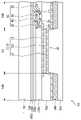
도 7은 도 6에 도시된 I-I' 선의 단면도이다. 도 8은 도 6에 도시된 Ⅱ-Ⅱ' 선의 단면도이다.7 is a cross-sectional view taken along line I-I' shown in FIG. 6 . FIG. 8 is a cross-sectional view taken along line II-II' shown in FIG. 6 .
도 7 및 도 8을 참조하면, 제1 터치 센서부들(SP1)과 제2 연결부들(CP2)은 박막 봉지층(TFE) 상에 배치된다. 도 7 및 도 8에 도시되지 않았으나, 제2 연결부들(CP2)과 일체로 형성된 제2 터치 센서부들(SP2)도 박막 봉지층(TFE) 상에 배치된다.7 and 8 , the first touch sensor parts SP1 and the second connection parts CP2 are disposed on the thin film encapsulation layer TFE. Although not shown in FIGS. 7 and 8 , the second touch sensor parts SP2 integrally formed with the second connection parts CP2 are also disposed on the thin film encapsulation layer TFE.
제1 및 제2 터치 센서부들(SP1,SP2)과 제2 연결부들(CP2)을 덮도록 박막 봉지층(TFE) 상에 제1 터치 절연층(T-INS1)이 배치된다. 제1 터치 절연층(T-INS1) 상에 제2 블랙 매트릭스(BM2)가 배치된다. 제2 블랙 매트릭스(BM2)는 제1 및 제2 터치 센서부들(SP1,SP2) 및 제1 및 제2 연결부들(CP1,CP2) 상에 배치될 수 있다.A first touch insulating layer T-INS1 is disposed on the thin film encapsulation layer TFE to cover the first and second touch sensor parts SP1 and SP2 and the second connection parts CP2 . A second black matrix BM2 is disposed on the first touch insulating layer T-INS1 . The second black matrix BM2 may be disposed on the first and second touch sensor parts SP1 and SP2 and the first and second connection parts CP1 and CP2 .
제1 연결부(CP1)는 제1 터치 절연층(T-INS1) 상에 배치되고, 제1 터치 절연층(T-INS1)에 정의된 컨택홀들(CH)을 통해 서로 인접한 제1 터치 센서부들(SP1)에 연결된다. 제2 블랙 매트릭스(BM2)는 제1 및 제2 터치 센서부들(SP1,SP2) 및 제1 및 제2 연결부들(CP1,CP2)과 오버랩하도록 제1 터치 절연층(T-INS1) 상에 배치된다. 제2 블랙 매트릭스(BM2)는 제1 연결부(CP1)를 덮도록 제1 터치 절연층(T-INS1) 상에 배치될 수 있다. 제2 블랙 매트릭스(BM2)는 제1 및 제2 터치 센서부들(SP2) 각각의 메쉬 구조의 가지부들(BP1,BP2)보다 큰 폭을 갖는다.The first connection part CP1 is disposed on the first touch insulating layer T-INS1 , and the first touch sensor parts are adjacent to each other through the contact holes CH defined in the first touch insulating layer T-INS1 . (SP1) is connected. The second black matrix BM2 is disposed on the first touch insulating layer T-INS1 to overlap the first and second touch sensor parts SP1 and SP2 and the first and second connection parts CP1 and CP2. do. The second black matrix BM2 may be disposed on the first touch insulating layer T-INS1 to cover the first connection part CP1 . The second black matrix BM2 has a greater width than the branch portions BP1 and BP2 of the mesh structure of the first and second touch sensor units SP2 , respectively.
제2 블랙 매트릭스(BM2)를 덮도록 제1 터치 절연층(T-INS1) 상에 제2 터치 절연층(T-INS2)이 배치된다. 제1 및 제2 터치 절연층들(T-INS1,T-INS2)은 무기 물질 또는 유기 물질을 포함하는 절연층들일 수 있다.A second touch insulating layer T-INS2 is disposed on the first touch insulating layer T-INS1 to cover the second black matrix BM2 . The first and second touch insulating layers T-INS1 and T-INS2 may be insulating layers including an inorganic material or an organic material.
도 9는 도 5에 도시된 제2 영역(A2)의 확대도이며, 제2 영역에 해당하는 터치 감지 유닛과 표시 패널의 평면 구성을 함께 도시한 도면이다.FIG. 9 is an enlarged view of the second area A2 shown in FIG. 5 , and is a view illustrating a planar configuration of a touch sensing unit and a display panel corresponding to the second area.
도 9는 실질적으로 본 발명의 실시 예에 따른 화소들(PX)과 제1 및 제2 터치 센서부들(SP1,SP2)의 평면 구성을 설명하기 위한 도면이다.9 is a diagram for explaining a planar configuration of the pixels PX and the first and second touch sensor units SP1 and SP2 according to an embodiment of the present invention.
도 9를 참조하면, 화소들(PX) 각각은 화소 영역들(PA) 및 화소 영역들 주변의 비화소 영역(NPA)을 포함한다. 화소 영역들(PA) 각각은 도 4에 도시된 화소 영역(PA)일 수 있으며, 비화소 영역(NPA)은 도 4에 도시된 비화소 영역(NPA)일 수 있다. 화소 영역들(PA)은 레드 색, 그린 색, 블루 색, 또는 화이트 색을 표시할 수 있다.Referring to FIG. 9 , each of the pixels PX includes pixel areas PA and a non-pixel area NPA around the pixel areas. Each of the pixel areas PA may be a pixel area PA illustrated in FIG. 4 , and the non-pixel area NPA may be a non-pixel area NPA illustrated in FIG. 4 . The pixel areas PA may display a red color, a green color, a blue color, or a white color.
화소 영역들(PA)은 표시하는 색에 따라서 서로 다른 크기를 가질 수 있다. 예를 들어, 블루 색을 표시하는 화소 영역(B)은 레드 색을 표시하는 화소 영역(R)보다 크고, 레드 색을 표시하는 화소 영역(R)은 그린 색을 표시하는 화소 영역(G)보다 클 수 있다.The pixel areas PA may have different sizes according to a color to be displayed. For example, the pixel region B displaying the blue color is larger than the pixel region R displaying the red color, and the pixel region R displaying the red color is larger than the pixel region G displaying the green color. can be large
화소 영역들(PA)은 마름모 형상을 가질 수 있으며, 제1 대각 방향(DDR1) 및 제2 대각 방향(DDR2)으로 배열될 수 있다. 예를 들어, 제1 및 제2 대각 방향들(DDR1,DDR2)로 블루 색을 표시하는 화소 영역들(B) 각각의 주변에 4개의 그린 색을 표시하는 화소 영역들(G)이 배치될 수 있다. 제1 및 제2 대각 방향들(DDR1,DDR2)로 레드 색을 표시하는 화소 영역들(R) 각각의 주변에 4개의 그린 색을 표시하는 화소 영역들(G)이 배치될 수 있다.The pixel areas PA may have a diamond shape and may be arranged in a first diagonal direction DDR1 and a second diagonal direction DDR2 . For example, pixel areas G displaying four green colors may be disposed around each of the pixel areas B displaying a blue color in the first and second diagonal directions DDR1 and DDR2 . have. Pixel regions G displaying four green colors may be disposed around each of the pixel regions R displaying red color in the first and second diagonal directions DDR1 and DDR2 .
비화소 영역(NPA)에 배치되는 화소 정의막(PDL)은 제1 대각 방향(DDR1) 및 제2 대각 방향(DDR2)으로 연장한다. 따라서, 화소 영역들(PA)에 배치된 유기 발광 소자들(OLED)은 마름모 형상을 가질 수 있다. 제1 및 제2 가지부들(BP1,BP2)은 화소 정의막(PDL)에 오버랩한다.The pixel defining layer PDL disposed in the non-pixel area NPA extends in the first diagonal direction DDR1 and the second diagonal direction DDR2 . Accordingly, the organic light emitting diodes OLED disposed in the pixel areas PA may have a rhombus shape. The first and second branch portions BP1 and BP2 overlap the pixel defining layer PDL.
제1 및 제2 터치 센서부들(SP1,SP2)은 비화소 영역(NPA)에 오버랩하여 메쉬 구조를 가질 수 있다. 제1 및 제2 터치 센서부들(SP1,SP2)의 터치 개구부들(TOP)은 화소 영역들(PA)의 형상에 대응하는 마름모 형상을 가지고, 화소 영역들(PA)에 대응하는 크기를 가질 수 있다.The first and second touch sensor units SP1 and SP2 may overlap the non-pixel area NPA to have a mesh structure. The touch openings TOP of the first and second touch sensor units SP1 and SP2 may have a rhombus shape corresponding to the shape of the pixel areas PA and may have a size corresponding to the pixel areas PA. have.
화소 영역들(PA)은 터치 개구부들(TOP)에 오버랩하며 터치 개구부들(TOP)보다 작은 크기를 가질 수 있다. 제2 블랙 매트릭스(BM2)는 제1 및 제2 터치 센서부들(SP1,SP2) 상에 배치된다. 제2 블랙 매트릭스(BM2)는 제1 및 제2 터치 센서부들(SP1,SP2)의 가지부들(BP1,BP2)보다 큰 폭을 갖고 화소 정의막(PDL)보다 작은 폭을 가질 수 있다.The pixel areas PA overlap the touch openings TOP and may have a smaller size than the touch openings TOP. The second black matrix BM2 is disposed on the first and second touch sensor units SP1 and SP2. The second black matrix BM2 may have a width greater than that of the branch portions BP1 and BP2 of the first and second touch sensor units SP1 and SP2 and a width smaller than that of the pixel defining layer PDL.
도 10은 도 9에 도시된 Ⅲ-Ⅲ'선의 단면도이다.FIG. 10 is a cross-sectional view taken along line III-III' shown in FIG. 9 .
도 10은 표시 장치의 단면 구성을 설명하기 위해 표시 패널(DP), 터치 감지 유닛(TS), 편광 필름(POL), 및 윈도우(WIN)의 단면을 함께 도시하였다. 설명의 편의를 위해 기판(SUB)의 상세 구성은 생략되었다.10 illustrates cross-sections of the display panel DP, the touch sensing unit TS, the polarizing film POL, and the window WIN to explain the cross-sectional configuration of the display device. For convenience of description, the detailed configuration of the substrate SUB is omitted.
도 10을 참조하면, 제1 블랙 매트릭스(BM1)는 화소 정의막(PDL) 상에 배치되고, 제2 블랙 매트릭스(BM2)는 제1 및 제2 터치 센서부들(SP1,SP2) 상에 배치된다. 편광 필름(POL)은 제2 터치 절연층(T-INS2) 상에 배치되고, 윈도우(WIN)는 편광 필름(POL) 상에 배치된다.Referring to FIG. 10 , the first black matrix BM1 is disposed on the pixel defining layer PDL, and the second black matrix BM2 is disposed on the first and second touch sensor units SP1 and SP2. . The polarizing film POL is disposed on the second touch insulating layer T-INS2 , and the window WIN is disposed on the polarizing film POL.
제1 블랙 매트릭스(BM1)는 화소 정의막(PDL)과 같은 폭을 가지며, 제1 블랙 매트릭스(BM1)의 폭은 제2 블랙 매트릭스(BM2)의 폭보다 크다. 또한, 앞서 설명한 바와 같이, 제2 블랙 매트릭스(BM2)는 제1 및 제2 터치 센서부들(SP1,SP2) 각각의 메쉬 구조의 가지부들(BP1,BP2)보다 큰 폭을 갖는다.The first black matrix BM1 has the same width as the pixel defining layer PDL, and the width of the first black matrix BM1 is greater than the width of the second black matrix BM2 . Also, as described above, the second black matrix BM2 has a width greater than the branch portions BP1 and BP2 of the mesh structure of the first and second touch sensor units SP1 and SP2, respectively.
유기 발광 소자(OLED)에서 생성된 광들(L1,L2)은 편광 필름(POL) 및 윈도우(WIN)를 통해 사용자에게 제공될 수 있다. 광들(L1,L2)은 수직하게 진행하는 제1 광(L1) 및 제1 광(L1)과 소정의 각도를 이루고 진행하는 제2 광(L2)을 포함할 수 있다.The lights L1 and L2 generated by the organic light emitting diode OLED may be provided to the user through the polarizing film POL and the window WIN. The lights L1 and L2 may include a first light L1 traveling vertically and a second light L2 traveling at a predetermined angle with the first light L1.
외부광들(E_L1,E_L2)은 윈도우(WIN) 및 편광 필름(POL)을 투과하여 표시 패널(DP)에 제공될 수 있다. 외부광들(E_L1,E_L2) 중 제1 및 제2 터치 센서부들(SP1,SP2)을 향해 진행하는 제1 외부광(E_L1)은 제2 블랙 매트릭스(BM2)에 흡수된다. 외부광들(E_L1,E_L2) 중 화소 정의막(PDL)을 향해 진행하는 제2 외부광(E_L2)은 제1 블랙 매트릭스(BM1)에 흡수된다.The external lights E_L1 and E_L2 may pass through the window WIN and the polarizing film POL to be provided to the display panel DP. Among the external lights E_L1 and E_L2 , the first external light E_L1 propagating toward the first and second touch sensor units SP1 and SP2 is absorbed by the second black matrix BM2 . Among the external lights E_L1 and E_L2 , the second external light E_L2 traveling toward the pixel defining layer PDL is absorbed by the first black matrix BM1 .
제1 및 제2 블랙 매트릭스들(BM1,BM2)이 표시 장치(100)에 배치되지 않는다면, 제1 외부광(E_L1)은 제1 및 제2 터치 센서부들(SP1,SP2)에서 반사되어 표시 장치(100)의 외부로 진행할 수 있다. 또한, 제2 외부광(E_L2)은 화소 정의막(PDL)을 투과하여 트랜지스터(TR)에 제공되고, 트랜지스터(TR)의 게이트 전극(GE), 소스 전극(SE), 및 드레인 전극(DE)에서 반사되어 표시 장치(100)의 외부로 진행할 수 있다. 따라서, 표시 장치(100)의 광 반사율이 증가한다.If the first and second black matrices BM1 and BM2 are not disposed on the
이러한 경우, 표시 장치(100) 내부에서 반사되는 제1 및 제2 외부 광들(E_L1,E_L2)에 의해 영상의 선명도가 감소될 수 있다. 특히 블랙 영상이 표시 될때 표시 장치(100) 내부에서 반사되는 제1 및 제2 외부 광들(E_L1,E_L2)에 의해 블랙 영상이 선명하게 표시되지 않을 수 있다.In this case, the sharpness of an image may be reduced by the first and second external lights E_L1 and E_L2 reflected from the inside of the
본 발명의 실시 예에서, 제1 및 제2 블랙 매트릭스들(BM1,BM2)이 제1 및 제2 외부 광들(E_L1,E_L2)을 흡수하여 차단하므로, 제1 및 제2 외부 광들(E_L1,E_L2)이 반사되어 다시 외부로 제공되지 않을 수 있다. 따라서, 표시 장치(100)의 광 반사율이 감소되어 영상의 선명도가 향상될 수 있다.In an embodiment of the present invention, since the first and second black matrices BM1 and BM2 absorb and block the first and second external lights E_L1 and E_L2, the first and second external lights E_L1 and E_L2 ) is reflected and may not be provided to the outside again. Accordingly, the light reflectance of the
제2 블랙 매트릭스(BM2)가 제1 블랙 매트릭스(BM1)와 같은 폭을 갖는다면, 제2 광(L2)은 제2 블랙 매트릭스(BM2)에 의해 차단되어 사용자에게 제공되지 않을 수 있다. 그러나, 제2 블랙 매트릭스(BM2)가 제1 블랙 매트릭스(BM1)보다 작은 폭을 가지므로, 제2 광(L2)은 외부의 사용자에게 제공될 수 있다. 따라서, 표시 장치(100)의 시야각이 커질 수 있다.If the second black matrix BM2 has the same width as the first black matrix BM1 , the second light L2 may be blocked by the second black matrix BM2 and may not be provided to the user. However, since the second black matrix BM2 has a smaller width than the first black matrix BM1 , the second light L2 may be provided to an external user. Accordingly, the viewing angle of the
결과적으로 본 발명의 실시 예에 따른 표시 장치(100)는 광 반사율을 감소시켜 영상의 선명도를 향상시키고, 시야각을 확대시킬 수 있다.As a result, the
이상 실시 예를 참조하여 설명하였지만, 해당 기술 분야의 숙련된 당업자는 하기의 특허 청구의 범위에 기재된 본 발명의 사상 및 영역으로부터 벗어나지 않는 범위 내에서 본 발명을 다양하게 수정 및 변경시킬 수 있음을 이해할 수 있을 것이다. 또한 본 발명에 개시된 실시 예는 본 발명의 기술 사상을 한정하기 위한 것이 아니고, 하기의 특허 청구의 범위 및 그와 동등한 범위 내에 있는 모든 기술 사상은 본 발명의 권리범위에 포함되는 것으로 해석되어야 할 것이다.Although described with reference to the above embodiments, those skilled in the art will understand that various modifications and changes can be made to the present invention without departing from the spirit and scope of the present invention as set forth in the claims below. will be able In addition, the embodiments disclosed in the present invention are not intended to limit the technical spirit of the present invention, and all technical ideas within the scope of the following claims and their equivalents should be construed as being included in the scope of the present invention. .
100: 표시 장치 DP: 표시 패널
TS: 터치 감지 유닛POL: 편광 필름
WIN: 윈도우OLED: 유기 발광 소자
SUB: 기판PDL: 화소 정의막
TFE: 박막 봉지층SP1,SP2: 제1 및 제2 터치 센서부
CP1,CP2: 제1 및 제2 연결부BM1,BM2: 제1 및 제2 블랙 매트릭스100: display device DP: display panel
TS: Touch sensing unit POL: Polarizing film
WIN: Window OLED: Organic light emitting device
SUB: substrate PDL: pixel defining film
TFE: thin film encapsulation layer SP1, SP2: first and second touch sensor units
CP1, CP2: first and second connection parts BM1, BM2: first and second black matrix
Claims (20)
Translated fromKorean상기 기판 상에 배치되고 복수 개의 오픈부들을 정의하는 화소 정의막;
상기 오픈부들에 배치된 복수 개의 유기 발광 소자들;
상기 화소 정의막 상에 배치된 제1 블랙 매트릭스;
상기 유기 발광 소자들 및 상기 제1 블랙 매트릭스 상에 배치된 박막 봉지층;
메쉬 구조을 갖고 상기 화소 정의막과 오버랩하며, 상기 박막 봉지층 상에 배치된 복수 개의 터치 센서부들;
상기 터치 센서부들 상에 배치된 제2 블랙 매트릭스; 및
상기 제2 블랙 매트릭스 상에 배치된 편광 필름을 포함하고,
상기 터치 센서부들은 상기 제1 블랙 매트릭스와 상기 제2 블랙 매트릭스 사이에 배치되어 상기 제2 블랙 매트릭스에 직접 접촉하지 않는 표시 장치.Board;
a pixel defining layer disposed on the substrate and defining a plurality of open portions;
a plurality of organic light emitting devices disposed in the open portions;
a first black matrix disposed on the pixel defining layer;
a thin film encapsulation layer disposed on the organic light emitting devices and the first black matrix;
a plurality of touch sensor units having a mesh structure, overlapping the pixel defining layer, and disposed on the thin film encapsulation layer;
a second black matrix disposed on the touch sensor units; and
a polarizing film disposed on the second black matrix;
The touch sensor units are disposed between the first black matrix and the second black matrix and do not directly contact the second black matrix.
상기 제1 블랙 매트릭스의 폭은 상기 제2 블랙 매트릭스의 폭보다 큰 표시 장치.The method of claim 1,
A width of the first black matrix is greater than a width of the second black matrix.
상기 제2 블랙 매트릭스는 상기 터치 센서부들 각각의 상기 메쉬 구조의 가지부들보다 큰 폭을 갖는 표시 장치.The method of claim 1,
The second black matrix has a width greater than that of branches of the mesh structure of each of the touch sensor units.
상기 제1 블랙 매트릭스의 폭은 상기 화소 정의막의 폭과 같은 표시 장치.The method of claim 1,
A width of the first black matrix is the same as a width of the pixel defining layer.
상기 터치 센서부들을 덮도록 상기 박막 봉지층 상에 배치되는 제1 터치 절연층; 및
상기 제1 터치 절연층 상에 배치된 제2 터치 절연층을 더 포함하고,
상기 제2 블랙 매트릭스는 상기 제1 터치 절연층 상에 배치되고, 상기 제2 터치 절연층은 상기 제2 블랙 매트릭스를 덮도록 상기 제1 터치 절연층 상에 배치되고, 상기 편광 필름은 상기 제2 터치 절연층 상에 배치되는 표시 장치.The method of claim 1,
a first touch insulating layer disposed on the thin film encapsulation layer to cover the touch sensor units; and
Further comprising a second touch insulating layer disposed on the first touch insulating layer,
The second black matrix is disposed on the first touch insulating layer, the second touch insulating layer is disposed on the first touch insulating layer to cover the second black matrix, and the polarizing film is the second A display device disposed on a touch insulating layer.
상기 터치 센서부들은,
제1 방향으로 배열되고 상기 박막 봉지층 상에 배치된 복수 개의 제1 터치 센서부들;
상기 제1 터치 절연층 상에 배치되고, 서로 인접한 제1 터치 센서부들을 연결하는 복수 개의 제1 연결부들;
상기 제1 방향과 교차하는 제2 방향으로 배열되고 상기 박막 봉지층 상에 배치된 복수 개의 제2 터치 센서부들; 및
상기 박막 봉지층 상에 배치되고, 서로 인접한 제2 터치 센서부들을 연결하는 복수 개의 제2 연결부들을 포함하고,
상기 제1 연결부들은 상기 제1 터치 절연층을 관통하여 정의된 제1 컨택홀들을 통해 상기 서로 인접한 제1 터치 센서부들을 연결하는 표시 장치.6. The method of claim 5,
The touch sensor units are
a plurality of first touch sensor units arranged in a first direction and disposed on the thin film encapsulation layer;
a plurality of first connection parts disposed on the first touch insulating layer and connecting first touch sensor parts adjacent to each other;
a plurality of second touch sensor units arranged in a second direction intersecting the first direction and disposed on the thin film encapsulation layer; and
It is disposed on the thin film encapsulation layer and includes a plurality of second connection parts for connecting second touch sensor parts adjacent to each other,
The first connection parts connect the adjacent first touch sensor parts to each other through first contact holes defined through the first touch insulating layer.
상기 제2 블랙 매트릭스는 상기 제1 및 제2 터치 센서부들 및 상기 제1 및 제2 연결부와 오버랩하도록 상기 제1 터치 절연층 상에 배치되는 표시 장치.7. The method of claim 6,
The second black matrix is disposed on the first touch insulating layer to overlap the first and second touch sensor units and the first and second connection units.
상기 제2 블랙 매트릭스는 상기 제1 연결부를 덮도록 상기 제1 터치 절연층 상에 배치되는 표시 장치.8. The method of claim 7,
The second black matrix is disposed on the first touch insulating layer to cover the first connection part.
상기 제1 및 제2 터치 센서부들 각각은,
상기 제1 및 제2 방향들에 평행한 평면상에서 상기 제1 및 제2 방향들과 교차하는 제1 대각 방향으로 연장된 복수 개의 제1 가지부들; 및
상기 평면상에서 상기 제1 대각 방향과 교차하는 제2 대각 방향으로 연장되어 상기 제1 가지부들과 교차하고 상기 제1 가지부들에 연결된 복수 개의 제2 가지부들을 포함하는 표시 장치.7. The method of claim 6,
Each of the first and second touch sensor units,
a plurality of first branch portions extending in a first diagonal direction intersecting the first and second directions on a plane parallel to the first and second directions; and
and a plurality of second branches extending in a second diagonal direction intersecting the first diagonal direction on the plane to intersect the first branches and connected to the first branches.
상기 화소 정의막은 상기 제1 대각 방향 및 상기 제2 대각 방향으로 연장하고, 상기 제1 및 제2 가지부들은 상기 화소 정의막에 오버랩하는 표시 장치.10. The method of claim 9,
The pixel defining layer extends in the first diagonal direction and the second diagonal direction, and the first and second branch portions overlap the pixel defining layer.
상기 기판은 상기 유기 발광 소자들에 연결된 복수 개의 트랜지스터들을 포함하는 표시 장치.The method of claim 1,
The substrate includes a plurality of transistors connected to the organic light emitting diodes.
상기 유기 발광 소자들은,
상기 기판 상에 배치되고, 상기 오픈부들에 의해 노출되며, 상기 트랜지스터들에 연결된 복수 개의 제1 전극들;
상기 오픈부들에서 상기 제1 전극들 상에 배치된 복수 개의 유기 발광층들; 및
상기 유기 발광층들 및 상기 화소 정의막 상에 배치된 제2 전극을 포함하는 표시 장치.12. The method of claim 11,
The organic light emitting devices are
a plurality of first electrodes disposed on the substrate, exposed by the open portions, and connected to the transistors;
a plurality of organic light emitting layers disposed on the first electrodes in the open portions; and
and a second electrode disposed on the organic emission layers and the pixel defining layer.
상기 제1 블랙 매트릭스는 상기 제2 전극 중 상기 화소 정의막과 오버랩하는 제2 전극 상에 배치되는 표시 장치.13. The method of claim 12,
The first black matrix is disposed on a second electrode of the second electrode overlapping the pixel defining layer.
상기 기판 상에 배치되고 복수 개의 오픈부들을 정의하는 화소 정의막;
상기 오픈부들에 배치된 복수 개의 유기 발광 소자들;
상기 화소 정의막 상에 배치된 제1 블랙 매트릭스;
상기 유기 발광 소자들 및 상기 제1 블랙 매트릭스 상에 배치된 박막 봉지층;
메쉬 구조을 갖고 상기 화소 정의막과 오버랩하며, 상기 박막 봉지층 상에 배치된 복수 개의 터치 센서부들; 및
상기 터치 센서부들 상에 배치된 제2 블랙 매트릭스를 포함하고,
상기 제1 블랙 매트릭스의 폭은 상기 제2 블랙 매트릭스의 폭보다 크고, 상기 제2 블랙 매트릭스는 상기 터치 센서부들 각각의 상기 메쉬 구조의 가지부들보다 큰 폭을 갖고,
상기 터치 센서부들은 상기 제1 블랙 매트릭스와 상기 제2 블랙 매트릭스 사이에 배치되어 상기 제2 블랙 매트릭스에 직접 접촉하지 않는 표시 장치.Board;
a pixel defining layer disposed on the substrate and defining a plurality of open portions;
a plurality of organic light emitting devices disposed in the open portions;
a first black matrix disposed on the pixel defining layer;
a thin film encapsulation layer disposed on the organic light emitting devices and the first black matrix;
a plurality of touch sensor units having a mesh structure, overlapping the pixel defining layer, and disposed on the thin film encapsulation layer; and
a second black matrix disposed on the touch sensor units;
a width of the first black matrix is greater than a width of the second black matrix, and the second black matrix has a greater width than branches of the mesh structure of each of the touch sensor units;
The touch sensor units are disposed between the first black matrix and the second black matrix and do not directly contact the second black matrix.
상기 제1 블랙 매트릭스의 상기 폭은 상기 화소 정의막의 폭과 같은 표시 장치.15. The method of claim 14,
The width of the first black matrix is equal to the width of the pixel defining layer.
상기 터치 센서부들을 덮도록 상기 박막 봉지층 상에 배치되는 제1 터치 절연층; 및
상기 제1 터치 절연층 상에 배치된 제2 터치 절연층을 더 포함하고,
상기 제2 블랙 매트릭스는 상기 제1 터치 절연층 상에 배치되고, 상기 제2 터치 절연층은 상기 제2 블랙 매트릭스를 덮도록 상기 제1 터치 절연층 상에 배치되는 표시 장치.15. The method of claim 14,
a first touch insulating layer disposed on the thin film encapsulation layer to cover the touch sensor units; and
Further comprising a second touch insulating layer disposed on the first touch insulating layer,
The second black matrix is disposed on the first touch insulating layer, and the second touch insulating layer is disposed on the first touch insulating layer to cover the second black matrix.
상기 제2 터치 절연층 상에 배치된 편광 필름; 및
상기 편광 필름 상에 배치된 윈도우를 더 포함하는 표시 장치.17. The method of claim 16,
a polarizing film disposed on the second touch insulating layer; and
The display device further comprising a window disposed on the polarizing film.
상기 터치 센서부들은,
제1 방향으로 배열되고 상기 박막 봉지층 상에 배치된 복수 개의 제1 터치 센서부들;
상기 제1 터치 절연층 상에 배치되고, 서로 인접한 제1 터치 센서부들을 연결하는 복수 개의 제1 연결부들;
상기 제1 방향과 교차하는 제2 방향으로 배열되고 상기 박막 봉지층 상에 배치된 복수 개의 제2 터치 센서부들; 및
상기 박막 봉지층 상에 배치되고, 서로 인접한 제2 터치 센서부들을 연결하는 복수 개의 제2 연결부들을 포함하고,
상기 제1 연결부들은 상기 제1 터치 절연층을 관통하여 정의된 제1 컨택홀들을 통해 상기 서로 인접한 제1 터치 센서부들을 연결하고,
상기 제2 블랙 매트릭스는 상기 제1 및 제2 터치 센서부들 및 상기 제1 및 제2 연결부와 오버랩하도록 상기 제1 터치 절연층 상에 배치되는 표시 장치.17. The method of claim 16,
The touch sensor units are
a plurality of first touch sensor units arranged in a first direction and disposed on the thin film encapsulation layer;
a plurality of first connection parts disposed on the first touch insulating layer and connecting first touch sensor parts adjacent to each other;
a plurality of second touch sensor units arranged in a second direction intersecting the first direction and disposed on the thin film encapsulation layer; and
It is disposed on the thin film encapsulation layer and includes a plurality of second connection parts for connecting second touch sensor parts adjacent to each other,
The first connection parts connect the first touch sensor parts adjacent to each other through first contact holes defined through the first touch insulating layer,
The second black matrix is disposed on the first touch insulating layer to overlap the first and second touch sensor units and the first and second connection units.
상기 기판은 상기 유기 발광 소자들에 연결된 복수 개의 트랜지스터들을 포함하고,
상기 유기 발광 소자들은,
상기 기판 상에 배치되고, 상기 오픈부들에 의해 노출되며, 상기 트랜지스터들에 연결된 복수 개의 제1 전극들;
상기 오픈부들에서 상기 제1 전극들 상에 배치된 복수 개의 유기 발광층들; 및
상기 유기 발광층들 및 상기 화소 정의막 상에 배치된 제2 전극을 포함하고,
상기 제1 블랙 매트릭스는 상기 제2 전극 중 상기 화소 정의막과 오버랩하는 제2 전극 상에 배치되는 표시 장치.15. The method of claim 14,
The substrate includes a plurality of transistors connected to the organic light emitting devices,
The organic light emitting devices are
a plurality of first electrodes disposed on the substrate, exposed by the open portions, and connected to the transistors;
a plurality of organic light emitting layers disposed on the first electrodes in the open portions; and
a second electrode disposed on the organic light emitting layers and the pixel defining layer;
The first black matrix is disposed on a second electrode of the second electrode overlapping the pixel defining layer.
상기 표시 패널 상에 배치된 터치 감지 유닛; 및
상기 터치 감지 유닛 상에 배치된 편광 필름을 포함하고,
상기 터치 감지 유닛은,
상기 제1 블랙 매트릭스에 오버랩하고, 메쉬 구조를 갖는 복수 개의 터치 센서부들; 및
상기 터치 센서부들 상에 배치되고, 상기 터치 센서부들 각각의 상기 메쉬 구조의 가지부들보다 크고 상기 제1 블랙 매트릭스보다 작은 폭을 갖는 제2 블랙 매트릭스를 포함하고,
상기 터치 센서부들은 상기 제1 블랙 매트릭스와 상기 제2 블랙 매트릭스 사이에 배치되어 상기 제2 블랙 매트릭스에 직접 접촉하지 않는 표시 장치.
a display panel comprising: a display panel including a plurality of organic light emitting devices disposed in a plurality of pixel areas and a first black matrix disposed in a non-pixel area around the pixel areas;
a touch sensing unit disposed on the display panel; and
A polarizing film disposed on the touch sensing unit,
The touch sensing unit,
a plurality of touch sensor units overlapping the first black matrix and having a mesh structure; and
a second black matrix disposed on the touch sensor units and having a width larger than branch portions of the mesh structure of each of the touch sensor units and smaller than the first black matrix,
The touch sensor units are disposed between the first black matrix and the second black matrix and do not directly contact the second black matrix.
Priority Applications (3)
| Application Number | Priority Date | Filing Date | Title |
|---|---|---|---|
| KR1020170138601AKR102423476B1 (en) | 2017-10-24 | 2017-10-24 | Display apparatus |
| US16/035,477US10777621B2 (en) | 2017-10-24 | 2018-07-13 | Display device having black matrix |
| CN201811188513.4ACN109696986B (en) | 2017-10-24 | 2018-10-12 | Display device |
Applications Claiming Priority (1)
| Application Number | Priority Date | Filing Date | Title |
|---|---|---|---|
| KR1020170138601AKR102423476B1 (en) | 2017-10-24 | 2017-10-24 | Display apparatus |
Publications (2)
| Publication Number | Publication Date |
|---|---|
| KR20190045964A KR20190045964A (en) | 2019-05-07 |
| KR102423476B1true KR102423476B1 (en) | 2022-07-22 |
Family
ID=66170067
Family Applications (1)
| Application Number | Title | Priority Date | Filing Date |
|---|---|---|---|
| KR1020170138601AActiveKR102423476B1 (en) | 2017-10-24 | 2017-10-24 | Display apparatus |
Country Status (3)
| Country | Link |
|---|---|
| US (1) | US10777621B2 (en) |
| KR (1) | KR102423476B1 (en) |
| CN (1) | CN109696986B (en) |
Cited By (1)
| Publication number | Priority date | Publication date | Assignee | Title |
|---|---|---|---|---|
| WO2024225726A1 (en)* | 2023-04-24 | 2024-10-31 | Corning Precision Materials Co., Ltd | Display device and method of making |
Families Citing this family (32)
| Publication number | Priority date | Publication date | Assignee | Title |
|---|---|---|---|---|
| JP6685675B2 (en)* | 2015-09-07 | 2020-04-22 | 株式会社Joled | Organic EL device, organic EL display panel using the same, and method for manufacturing organic EL display panel |
| KR101750428B1 (en)* | 2015-09-24 | 2017-06-23 | 엘지디스플레이 주식회사 | Display device including touch screen function |
| US11177329B2 (en)* | 2018-09-04 | 2021-11-16 | Apple Inc. | Viewing angle color shift control |
| US10872939B2 (en) | 2018-09-04 | 2020-12-22 | Apple Inc. | Viewing angle color shift control |
| KR102819368B1 (en)* | 2018-11-19 | 2025-06-11 | 엘지디스플레이 주식회사 | Display device |
| CN111526226B (en)* | 2019-02-01 | 2021-08-24 | Oppo广东移动通信有限公司 | Electronic equipment and display devices |
| CN109904342B (en)* | 2019-02-19 | 2021-04-09 | 京东方科技集团股份有限公司 | Array substrate, manufacturing method thereof and display device |
| CN110246877B (en)* | 2019-06-10 | 2021-08-06 | 武汉华星光电半导体显示技术有限公司 | Flexible touch display and display device thereof |
| CN110165085B (en)* | 2019-06-27 | 2020-09-11 | 昆山工研院新型平板显示技术中心有限公司 | Display panel and preparation method thereof |
| KR102698107B1 (en)* | 2019-07-29 | 2024-08-26 | 삼성디스플레이 주식회사 | Display apparatus and method of driving the same |
| CN110504385B (en)* | 2019-08-29 | 2022-04-15 | 京东方科技集团股份有限公司 | Display panel, manufacturing method thereof and display device |
| US11462718B2 (en) | 2019-10-23 | 2022-10-04 | Samsung Display Co., Ltd. | Display device |
| KR20210054654A (en)* | 2019-11-05 | 2021-05-14 | 삼성디스플레이 주식회사 | Display device |
| CN112909040B (en)* | 2019-11-19 | 2023-07-04 | Oppo广东移动通信有限公司 | Display module, manufacturing method thereof, display screen assembly and electronic equipment |
| CN111048691A (en)* | 2019-12-02 | 2020-04-21 | 云谷(固安)科技有限公司 | Display panel |
| KR102721988B1 (en)* | 2019-12-17 | 2024-10-28 | 삼성디스플레이 주식회사 | Display panel |
| KR102765793B1 (en)* | 2019-12-19 | 2025-02-07 | 엘지디스플레이 주식회사 | Touch display device |
| KR102764290B1 (en)* | 2019-12-27 | 2025-02-07 | 엘지디스플레이 주식회사 | Display Device |
| KR20210086907A (en)* | 2019-12-31 | 2021-07-09 | 삼성디스플레이 주식회사 | Display device |
| KR20210095267A (en) | 2020-01-22 | 2021-08-02 | 삼성디스플레이 주식회사 | Display device |
| EP4163980A4 (en)* | 2020-06-09 | 2024-06-26 | Wuhan China Star Optoelectronics Semiconductor Display Technology Co., Ltd. | OLED SCREENBOARD |
| CN113934316B (en)* | 2020-07-13 | 2024-01-23 | 重庆康佳光电科技有限公司 | Display panel and preparation method thereof |
| KR102850903B1 (en)* | 2020-08-12 | 2025-08-28 | 삼성디스플레이 주식회사 | Input sensing unit and electronic apparatus including the same |
| CN115996612A (en) | 2020-09-01 | 2023-04-21 | 京东方科技集团股份有限公司 | Display panel and display device |
| KR20220060626A (en) | 2020-11-04 | 2022-05-12 | 삼성디스플레이 주식회사 | Display Device |
| KR102809170B1 (en)* | 2020-12-17 | 2025-05-19 | 삼성디스플레이 주식회사 | Display device |
| CN115696999A (en) | 2020-12-22 | 2023-02-03 | 湖北长江新型显示产业创新中心有限公司 | Display panel, manufacturing method thereof, and display device |
| KR20220097681A (en) | 2020-12-30 | 2022-07-08 | 삼성디스플레이 주식회사 | Display device |
| CN114914270B (en)* | 2021-02-07 | 2024-09-17 | 上海和辉光电股份有限公司 | Display panel and display device |
| US11184595B2 (en) | 2021-03-12 | 2021-11-23 | Google Llc | Color correction using a sensor to reduce color distortions of a camera under a display |
| US12353246B2 (en) | 2023-08-29 | 2025-07-08 | Google Llc | Narrow display borders using a display-to-frame interposer |
| CN118338731A (en)* | 2023-08-30 | 2024-07-12 | 京东方科技集团股份有限公司 | Display substrate, manufacturing method thereof and display device |
Family Cites Families (13)
| Publication number | Priority date | Publication date | Assignee | Title |
|---|---|---|---|---|
| KR100964225B1 (en)* | 2008-03-19 | 2010-06-17 | 삼성모바일디스플레이주식회사 | Organic light emitting display device |
| KR101995729B1 (en)* | 2012-11-29 | 2019-07-04 | 삼성디스플레이 주식회사 | Organic Electroluminescence Device |
| KR102087704B1 (en)* | 2012-12-27 | 2020-03-11 | 도판 인사츠 가부시키가이샤 | Liquid crystal display device, liquid display device substrate, and production method for liquid crystal display device substrate |
| KR102096622B1 (en)* | 2013-08-19 | 2020-04-03 | 삼성디스플레이 주식회사 | Organic light emitting display device |
| JP2015128003A (en)* | 2013-12-27 | 2015-07-09 | ソニー株式会社 | Display device and electronic apparatus |
| KR102376035B1 (en) | 2014-12-31 | 2022-03-17 | 엘지디스플레이 주식회사 | Flexible organic light emitting display device |
| KR102373329B1 (en) | 2015-04-30 | 2022-03-11 | 삼성디스플레이 주식회사 | Organic light emitting diode display |
| KR20170088473A (en)* | 2016-01-22 | 2017-08-02 | 삼성디스플레이 주식회사 | Flexible display device |
| US10168844B2 (en)* | 2015-06-26 | 2019-01-01 | Samsung Display Co., Ltd. | Flexible display device |
| KR101750428B1 (en)* | 2015-09-24 | 2017-06-23 | 엘지디스플레이 주식회사 | Display device including touch screen function |
| KR102560325B1 (en) | 2016-01-08 | 2023-07-28 | 삼성디스플레이 주식회사 | Flexible touch screen panel and flexible display device including flexible touch screen panel |
| KR102629580B1 (en) | 2016-01-08 | 2024-01-26 | 삼성디스플레이 주식회사 | Flexible touch screen panel and method of manufacturing a flexible touch screen panel |
| KR102508750B1 (en)* | 2017-11-30 | 2023-03-13 | 삼성디스플레이 주식회사 | Light emitting display device |
- 2017
- 2017-10-24KRKR1020170138601Apatent/KR102423476B1/enactiveActive
- 2018
- 2018-07-13USUS16/035,477patent/US10777621B2/enactiveActive
- 2018-10-12CNCN201811188513.4Apatent/CN109696986B/enactiveActive
Cited By (1)
| Publication number | Priority date | Publication date | Assignee | Title |
|---|---|---|---|---|
| WO2024225726A1 (en)* | 2023-04-24 | 2024-10-31 | Corning Precision Materials Co., Ltd | Display device and method of making |
Also Published As
| Publication number | Publication date |
|---|---|
| KR20190045964A (en) | 2019-05-07 |
| US20190123112A1 (en) | 2019-04-25 |
| CN109696986B (en) | 2024-12-06 |
| US10777621B2 (en) | 2020-09-15 |
| CN109696986A (en) | 2019-04-30 |
Similar Documents
| Publication | Publication Date | Title |
|---|---|---|
| KR102423476B1 (en) | Display apparatus | |
| KR102733803B1 (en) | Display apparatus | |
| KR102421143B1 (en) | Display apparatus | |
| KR102601818B1 (en) | Display apparatus with touch sensor | |
| US20160132148A1 (en) | Organic light-emitting diode (oled) display | |
| WO2022057527A1 (en) | Display substrate and display device | |
| KR102430429B1 (en) | Display apparatus | |
| US11538893B2 (en) | Display device | |
| KR20200009176A (en) | Display apparatus | |
| WO2022057528A1 (en) | Display substrate and display device | |
| TWI843129B (en) | Display device | |
| CN108735784A (en) | Display module | |
| KR20150039933A (en) | Touch screen display device | |
| KR102597309B1 (en) | Flexible display device | |
| CN109521904B (en) | input sensing device | |
| KR20230049190A (en) | Display apparatus | |
| KR20150002290A (en) | Thin film transistor array substrate and organic light emitting display including the substrate | |
| US11751444B2 (en) | Display device | |
| CN114388578A (en) | Display panel and display device including the same | |
| KR20230103186A (en) | Display device | |
| KR102855936B1 (en) | Display device for improving displaying quality and display panel thereof | |
| KR20250131455A (en) | Display device | |
| KR20240144730A (en) | Display device | |
| KR20240113024A (en) | Display Apparatus | |
| CN117953820A (en) | Electronic device and method of driving the same |
Legal Events
| Date | Code | Title | Description |
|---|---|---|---|
| PA0109 | Patent application | Patent event code:PA01091R01D Comment text:Patent Application Patent event date:20171024 | |
| PG1501 | Laying open of application | ||
| PA0201 | Request for examination | Patent event code:PA02012R01D Patent event date:20201007 Comment text:Request for Examination of Application Patent event code:PA02011R01I Patent event date:20171024 Comment text:Patent Application | |
| E902 | Notification of reason for refusal | ||
| PE0902 | Notice of grounds for rejection | Comment text:Notification of reason for refusal Patent event date:20211025 Patent event code:PE09021S01D | |
| E701 | Decision to grant or registration of patent right | ||
| PE0701 | Decision of registration | Patent event code:PE07011S01D Comment text:Decision to Grant Registration Patent event date:20220426 | |
| GRNT | Written decision to grant | ||
| PR0701 | Registration of establishment | Comment text:Registration of Establishment Patent event date:20220718 Patent event code:PR07011E01D | |
| PR1002 | Payment of registration fee | Payment date:20220719 End annual number:3 Start annual number:1 | |
| PG1601 | Publication of registration | ||
| PR1001 | Payment of annual fee | Payment date:20250625 Start annual number:4 End annual number:4 |