KR102420589B1 - Semiconductor packages having a heat sink - Google Patents
Semiconductor packages having a heat sinkDownload PDFInfo
- Publication number
- KR102420589B1 KR102420589B1KR1020170165226AKR20170165226AKR102420589B1KR 102420589 B1KR102420589 B1KR 102420589B1KR 1020170165226 AKR1020170165226 AKR 1020170165226AKR 20170165226 AKR20170165226 AKR 20170165226AKR 102420589 B1KR102420589 B1KR 102420589B1
- Authority
- KR
- South Korea
- Prior art keywords
- heat sink
- semiconductor chip
- base substrate
- package
- package base
- Prior art date
- Legal status (The legal status is an assumption and is not a legal conclusion. Google has not performed a legal analysis and makes no representation as to the accuracy of the status listed.)
- Active
Links
Images


Classifications
- H—ELECTRICITY
- H01—ELECTRIC ELEMENTS
- H01L—SEMICONDUCTOR DEVICES NOT COVERED BY CLASS H10
- H01L25/00—Assemblies consisting of a plurality of semiconductor or other solid state devices
- H01L25/03—Assemblies consisting of a plurality of semiconductor or other solid state devices all the devices being of a type provided for in a single subclass of subclasses H10B, H10D, H10F, H10H, H10K or H10N, e.g. assemblies of rectifier diodes
- H01L25/04—Assemblies consisting of a plurality of semiconductor or other solid state devices all the devices being of a type provided for in a single subclass of subclasses H10B, H10D, H10F, H10H, H10K or H10N, e.g. assemblies of rectifier diodes the devices not having separate containers
- H01L25/065—Assemblies consisting of a plurality of semiconductor or other solid state devices all the devices being of a type provided for in a single subclass of subclasses H10B, H10D, H10F, H10H, H10K or H10N, e.g. assemblies of rectifier diodes the devices not having separate containers the devices being of a type provided for in group H10D89/00
- H01L25/0657—Stacked arrangements of devices
- H—ELECTRICITY
- H01—ELECTRIC ELEMENTS
- H01L—SEMICONDUCTOR DEVICES NOT COVERED BY CLASS H10
- H01L23/00—Details of semiconductor or other solid state devices
- H01L23/34—Arrangements for cooling, heating, ventilating or temperature compensation ; Temperature sensing arrangements
- H01L23/36—Selection of materials, or shaping, to facilitate cooling or heating, e.g. heatsinks
- H01L23/367—Cooling facilitated by shape of device
- H01L23/3672—Foil-like cooling fins or heat sinks
- H—ELECTRICITY
- H01—ELECTRIC ELEMENTS
- H01L—SEMICONDUCTOR DEVICES NOT COVERED BY CLASS H10
- H01L21/00—Processes or apparatus adapted for the manufacture or treatment of semiconductor or solid state devices or of parts thereof
- H01L21/02—Manufacture or treatment of semiconductor devices or of parts thereof
- H01L21/04—Manufacture or treatment of semiconductor devices or of parts thereof the devices having potential barriers, e.g. a PN junction, depletion layer or carrier concentration layer
- H01L21/50—Assembly of semiconductor devices using processes or apparatus not provided for in a single one of the groups H01L21/18 - H01L21/326 or H10D48/04 - H10D48/07 e.g. sealing of a cap to a base of a container
- H01L21/56—Encapsulations, e.g. encapsulation layers, coatings
- H—ELECTRICITY
- H01—ELECTRIC ELEMENTS
- H01L—SEMICONDUCTOR DEVICES NOT COVERED BY CLASS H10
- H01L23/00—Details of semiconductor or other solid state devices
- H01L23/28—Encapsulations, e.g. encapsulating layers, coatings, e.g. for protection
- H—ELECTRICITY
- H01—ELECTRIC ELEMENTS
- H01L—SEMICONDUCTOR DEVICES NOT COVERED BY CLASS H10
- H01L23/00—Details of semiconductor or other solid state devices
- H01L23/28—Encapsulations, e.g. encapsulating layers, coatings, e.g. for protection
- H01L23/29—Encapsulations, e.g. encapsulating layers, coatings, e.g. for protection characterised by the material, e.g. carbon
- H01L23/293—Organic, e.g. plastic
- H01L23/295—Organic, e.g. plastic containing a filler
- H—ELECTRICITY
- H01—ELECTRIC ELEMENTS
- H01L—SEMICONDUCTOR DEVICES NOT COVERED BY CLASS H10
- H01L23/00—Details of semiconductor or other solid state devices
- H01L23/34—Arrangements for cooling, heating, ventilating or temperature compensation ; Temperature sensing arrangements
- H01L23/36—Selection of materials, or shaping, to facilitate cooling or heating, e.g. heatsinks
- H01L23/367—Cooling facilitated by shape of device
- H01L23/3675—Cooling facilitated by shape of device characterised by the shape of the housing
- H—ELECTRICITY
- H01—ELECTRIC ELEMENTS
- H01L—SEMICONDUCTOR DEVICES NOT COVERED BY CLASS H10
- H01L23/00—Details of semiconductor or other solid state devices
- H01L23/34—Arrangements for cooling, heating, ventilating or temperature compensation ; Temperature sensing arrangements
- H01L23/36—Selection of materials, or shaping, to facilitate cooling or heating, e.g. heatsinks
- H01L23/367—Cooling facilitated by shape of device
- H01L23/3677—Wire-like or pin-like cooling fins or heat sinks
- H—ELECTRICITY
- H01—ELECTRIC ELEMENTS
- H01L—SEMICONDUCTOR DEVICES NOT COVERED BY CLASS H10
- H01L23/00—Details of semiconductor or other solid state devices
- H01L23/34—Arrangements for cooling, heating, ventilating or temperature compensation ; Temperature sensing arrangements
- H01L23/36—Selection of materials, or shaping, to facilitate cooling or heating, e.g. heatsinks
- H01L23/373—Cooling facilitated by selection of materials for the device or materials for thermal expansion adaptation, e.g. carbon
- H01L23/3737—Organic materials with or without a thermoconductive filler
- H—ELECTRICITY
- H01—ELECTRIC ELEMENTS
- H01L—SEMICONDUCTOR DEVICES NOT COVERED BY CLASS H10
- H01L23/00—Details of semiconductor or other solid state devices
- H01L23/552—Protection against radiation, e.g. light or electromagnetic waves
- H—ELECTRICITY
- H01—ELECTRIC ELEMENTS
- H01L—SEMICONDUCTOR DEVICES NOT COVERED BY CLASS H10
- H01L24/00—Arrangements for connecting or disconnecting semiconductor or solid-state bodies; Methods or apparatus related thereto
- H01L24/73—Means for bonding being of different types provided for in two or more of groups H01L24/10, H01L24/18, H01L24/26, H01L24/34, H01L24/42, H01L24/50, H01L24/63, H01L24/71
- H—ELECTRICITY
- H01—ELECTRIC ELEMENTS
- H01L—SEMICONDUCTOR DEVICES NOT COVERED BY CLASS H10
- H01L25/00—Assemblies consisting of a plurality of semiconductor or other solid state devices
- H01L25/50—Multistep manufacturing processes of assemblies consisting of devices, the devices being individual devices of subclass H10D or integrated devices of class H10
- H—ELECTRICITY
- H01—ELECTRIC ELEMENTS
- H01L—SEMICONDUCTOR DEVICES NOT COVERED BY CLASS H10
- H01L23/00—Details of semiconductor or other solid state devices
- H01L23/34—Arrangements for cooling, heating, ventilating or temperature compensation ; Temperature sensing arrangements
- H01L23/40—Mountings or securing means for detachable cooling or heating arrangements ; fixed by friction, plugs or springs
- H01L23/4006—Mountings or securing means for detachable cooling or heating arrangements ; fixed by friction, plugs or springs with bolts or screws
- H01L2023/4037—Mountings or securing means for detachable cooling or heating arrangements ; fixed by friction, plugs or springs with bolts or screws characterised by thermal path or place of attachment of heatsink
- H01L2023/4062—Mountings or securing means for detachable cooling or heating arrangements ; fixed by friction, plugs or springs with bolts or screws characterised by thermal path or place of attachment of heatsink heatsink to or through board or cabinet
- H—ELECTRICITY
- H01—ELECTRIC ELEMENTS
- H01L—SEMICONDUCTOR DEVICES NOT COVERED BY CLASS H10
- H01L21/00—Processes or apparatus adapted for the manufacture or treatment of semiconductor or solid state devices or of parts thereof
- H01L21/02—Manufacture or treatment of semiconductor devices or of parts thereof
- H01L21/04—Manufacture or treatment of semiconductor devices or of parts thereof the devices having potential barriers, e.g. a PN junction, depletion layer or carrier concentration layer
- H01L21/48—Manufacture or treatment of parts, e.g. containers, prior to assembly of the devices, using processes not provided for in a single one of the groups H01L21/18 - H01L21/326 or H10D48/04 - H10D48/07
- H01L21/4814—Conductive parts
- H01L21/4871—Bases, plates or heatsinks
- H01L21/4882—Assembly of heatsink parts
- H—ELECTRICITY
- H01—ELECTRIC ELEMENTS
- H01L—SEMICONDUCTOR DEVICES NOT COVERED BY CLASS H10
- H01L2224/00—Indexing scheme for arrangements for connecting or disconnecting semiconductor or solid-state bodies and methods related thereto as covered by H01L24/00
- H01L2224/01—Means for bonding being attached to, or being formed on, the surface to be connected, e.g. chip-to-package, die-attach, "first-level" interconnects; Manufacturing methods related thereto
- H01L2224/02—Bonding areas; Manufacturing methods related thereto
- H01L2224/04—Structure, shape, material or disposition of the bonding areas prior to the connecting process
- H01L2224/0401—Bonding areas specifically adapted for bump connectors, e.g. under bump metallisation [UBM]
- H—ELECTRICITY
- H01—ELECTRIC ELEMENTS
- H01L—SEMICONDUCTOR DEVICES NOT COVERED BY CLASS H10
- H01L2224/00—Indexing scheme for arrangements for connecting or disconnecting semiconductor or solid-state bodies and methods related thereto as covered by H01L24/00
- H01L2224/01—Means for bonding being attached to, or being formed on, the surface to be connected, e.g. chip-to-package, die-attach, "first-level" interconnects; Manufacturing methods related thereto
- H01L2224/02—Bonding areas; Manufacturing methods related thereto
- H01L2224/04—Structure, shape, material or disposition of the bonding areas prior to the connecting process
- H01L2224/04042—Bonding areas specifically adapted for wire connectors, e.g. wirebond pads
- H—ELECTRICITY
- H01—ELECTRIC ELEMENTS
- H01L—SEMICONDUCTOR DEVICES NOT COVERED BY CLASS H10
- H01L2224/00—Indexing scheme for arrangements for connecting or disconnecting semiconductor or solid-state bodies and methods related thereto as covered by H01L24/00
- H01L2224/01—Means for bonding being attached to, or being formed on, the surface to be connected, e.g. chip-to-package, die-attach, "first-level" interconnects; Manufacturing methods related thereto
- H01L2224/10—Bump connectors; Manufacturing methods related thereto
- H01L2224/15—Structure, shape, material or disposition of the bump connectors after the connecting process
- H01L2224/16—Structure, shape, material or disposition of the bump connectors after the connecting process of an individual bump connector
- H01L2224/161—Disposition
- H01L2224/16151—Disposition the bump connector connecting between a semiconductor or solid-state body and an item not being a semiconductor or solid-state body, e.g. chip-to-substrate, chip-to-passive
- H01L2224/16221—Disposition the bump connector connecting between a semiconductor or solid-state body and an item not being a semiconductor or solid-state body, e.g. chip-to-substrate, chip-to-passive the body and the item being stacked
- H01L2224/16225—Disposition the bump connector connecting between a semiconductor or solid-state body and an item not being a semiconductor or solid-state body, e.g. chip-to-substrate, chip-to-passive the body and the item being stacked the item being non-metallic, e.g. insulating substrate with or without metallisation
- H01L2224/16227—Disposition the bump connector connecting between a semiconductor or solid-state body and an item not being a semiconductor or solid-state body, e.g. chip-to-substrate, chip-to-passive the body and the item being stacked the item being non-metallic, e.g. insulating substrate with or without metallisation the bump connector connecting to a bond pad of the item
- H—ELECTRICITY
- H01—ELECTRIC ELEMENTS
- H01L—SEMICONDUCTOR DEVICES NOT COVERED BY CLASS H10
- H01L2224/00—Indexing scheme for arrangements for connecting or disconnecting semiconductor or solid-state bodies and methods related thereto as covered by H01L24/00
- H01L2224/01—Means for bonding being attached to, or being formed on, the surface to be connected, e.g. chip-to-package, die-attach, "first-level" interconnects; Manufacturing methods related thereto
- H01L2224/10—Bump connectors; Manufacturing methods related thereto
- H01L2224/15—Structure, shape, material or disposition of the bump connectors after the connecting process
- H01L2224/16—Structure, shape, material or disposition of the bump connectors after the connecting process of an individual bump connector
- H01L2224/161—Disposition
- H01L2224/16151—Disposition the bump connector connecting between a semiconductor or solid-state body and an item not being a semiconductor or solid-state body, e.g. chip-to-substrate, chip-to-passive
- H01L2224/16221—Disposition the bump connector connecting between a semiconductor or solid-state body and an item not being a semiconductor or solid-state body, e.g. chip-to-substrate, chip-to-passive the body and the item being stacked
- H01L2224/16245—Disposition the bump connector connecting between a semiconductor or solid-state body and an item not being a semiconductor or solid-state body, e.g. chip-to-substrate, chip-to-passive the body and the item being stacked the item being metallic
- H—ELECTRICITY
- H01—ELECTRIC ELEMENTS
- H01L—SEMICONDUCTOR DEVICES NOT COVERED BY CLASS H10
- H01L2224/00—Indexing scheme for arrangements for connecting or disconnecting semiconductor or solid-state bodies and methods related thereto as covered by H01L24/00
- H01L2224/01—Means for bonding being attached to, or being formed on, the surface to be connected, e.g. chip-to-package, die-attach, "first-level" interconnects; Manufacturing methods related thereto
- H01L2224/26—Layer connectors, e.g. plate connectors, solder or adhesive layers; Manufacturing methods related thereto
- H01L2224/27—Manufacturing methods
- H01L2224/274—Manufacturing methods by blanket deposition of the material of the layer connector
- H01L2224/2743—Manufacturing methods by blanket deposition of the material of the layer connector in solid form
- H01L2224/27436—Lamination of a preform, e.g. foil, sheet or layer
- H—ELECTRICITY
- H01—ELECTRIC ELEMENTS
- H01L—SEMICONDUCTOR DEVICES NOT COVERED BY CLASS H10
- H01L2224/00—Indexing scheme for arrangements for connecting or disconnecting semiconductor or solid-state bodies and methods related thereto as covered by H01L24/00
- H01L2224/01—Means for bonding being attached to, or being formed on, the surface to be connected, e.g. chip-to-package, die-attach, "first-level" interconnects; Manufacturing methods related thereto
- H01L2224/26—Layer connectors, e.g. plate connectors, solder or adhesive layers; Manufacturing methods related thereto
- H01L2224/28—Structure, shape, material or disposition of the layer connectors prior to the connecting process
- H01L2224/29—Structure, shape, material or disposition of the layer connectors prior to the connecting process of an individual layer connector
- H01L2224/29001—Core members of the layer connector
- H01L2224/29099—Material
- H01L2224/2919—Material with a principal constituent of the material being a polymer, e.g. polyester, phenolic based polymer, epoxy
- H—ELECTRICITY
- H01—ELECTRIC ELEMENTS
- H01L—SEMICONDUCTOR DEVICES NOT COVERED BY CLASS H10
- H01L2224/00—Indexing scheme for arrangements for connecting or disconnecting semiconductor or solid-state bodies and methods related thereto as covered by H01L24/00
- H01L2224/01—Means for bonding being attached to, or being formed on, the surface to be connected, e.g. chip-to-package, die-attach, "first-level" interconnects; Manufacturing methods related thereto
- H01L2224/26—Layer connectors, e.g. plate connectors, solder or adhesive layers; Manufacturing methods related thereto
- H01L2224/28—Structure, shape, material or disposition of the layer connectors prior to the connecting process
- H01L2224/29—Structure, shape, material or disposition of the layer connectors prior to the connecting process of an individual layer connector
- H01L2224/29001—Core members of the layer connector
- H01L2224/29099—Material
- H01L2224/29198—Material with a principal constituent of the material being a combination of two or more materials in the form of a matrix with a filler, i.e. being a hybrid material, e.g. segmented structures, foams
- H01L2224/29199—Material of the matrix
- H01L2224/2929—Material of the matrix with a principal constituent of the material being a polymer, e.g. polyester, phenolic based polymer, epoxy
- H—ELECTRICITY
- H01—ELECTRIC ELEMENTS
- H01L—SEMICONDUCTOR DEVICES NOT COVERED BY CLASS H10
- H01L2224/00—Indexing scheme for arrangements for connecting or disconnecting semiconductor or solid-state bodies and methods related thereto as covered by H01L24/00
- H01L2224/01—Means for bonding being attached to, or being formed on, the surface to be connected, e.g. chip-to-package, die-attach, "first-level" interconnects; Manufacturing methods related thereto
- H01L2224/26—Layer connectors, e.g. plate connectors, solder or adhesive layers; Manufacturing methods related thereto
- H01L2224/28—Structure, shape, material or disposition of the layer connectors prior to the connecting process
- H01L2224/29—Structure, shape, material or disposition of the layer connectors prior to the connecting process of an individual layer connector
- H01L2224/29001—Core members of the layer connector
- H01L2224/29099—Material
- H01L2224/29198—Material with a principal constituent of the material being a combination of two or more materials in the form of a matrix with a filler, i.e. being a hybrid material, e.g. segmented structures, foams
- H01L2224/29298—Fillers
- H01L2224/29299—Base material
- H—ELECTRICITY
- H01—ELECTRIC ELEMENTS
- H01L—SEMICONDUCTOR DEVICES NOT COVERED BY CLASS H10
- H01L2224/00—Indexing scheme for arrangements for connecting or disconnecting semiconductor or solid-state bodies and methods related thereto as covered by H01L24/00
- H01L2224/01—Means for bonding being attached to, or being formed on, the surface to be connected, e.g. chip-to-package, die-attach, "first-level" interconnects; Manufacturing methods related thereto
- H01L2224/26—Layer connectors, e.g. plate connectors, solder or adhesive layers; Manufacturing methods related thereto
- H01L2224/31—Structure, shape, material or disposition of the layer connectors after the connecting process
- H01L2224/32—Structure, shape, material or disposition of the layer connectors after the connecting process of an individual layer connector
- H01L2224/321—Disposition
- H01L2224/32135—Disposition the layer connector connecting between different semiconductor or solid-state bodies, i.e. chip-to-chip
- H01L2224/32145—Disposition the layer connector connecting between different semiconductor or solid-state bodies, i.e. chip-to-chip the bodies being stacked
- H—ELECTRICITY
- H01—ELECTRIC ELEMENTS
- H01L—SEMICONDUCTOR DEVICES NOT COVERED BY CLASS H10
- H01L2224/00—Indexing scheme for arrangements for connecting or disconnecting semiconductor or solid-state bodies and methods related thereto as covered by H01L24/00
- H01L2224/01—Means for bonding being attached to, or being formed on, the surface to be connected, e.g. chip-to-package, die-attach, "first-level" interconnects; Manufacturing methods related thereto
- H01L2224/26—Layer connectors, e.g. plate connectors, solder or adhesive layers; Manufacturing methods related thereto
- H01L2224/31—Structure, shape, material or disposition of the layer connectors after the connecting process
- H01L2224/32—Structure, shape, material or disposition of the layer connectors after the connecting process of an individual layer connector
- H01L2224/321—Disposition
- H01L2224/32151—Disposition the layer connector connecting between a semiconductor or solid-state body and an item not being a semiconductor or solid-state body, e.g. chip-to-substrate, chip-to-passive
- H01L2224/32221—Disposition the layer connector connecting between a semiconductor or solid-state body and an item not being a semiconductor or solid-state body, e.g. chip-to-substrate, chip-to-passive the body and the item being stacked
- H01L2224/32225—Disposition the layer connector connecting between a semiconductor or solid-state body and an item not being a semiconductor or solid-state body, e.g. chip-to-substrate, chip-to-passive the body and the item being stacked the item being non-metallic, e.g. insulating substrate with or without metallisation
- H—ELECTRICITY
- H01—ELECTRIC ELEMENTS
- H01L—SEMICONDUCTOR DEVICES NOT COVERED BY CLASS H10
- H01L2224/00—Indexing scheme for arrangements for connecting or disconnecting semiconductor or solid-state bodies and methods related thereto as covered by H01L24/00
- H01L2224/01—Means for bonding being attached to, or being formed on, the surface to be connected, e.g. chip-to-package, die-attach, "first-level" interconnects; Manufacturing methods related thereto
- H01L2224/26—Layer connectors, e.g. plate connectors, solder or adhesive layers; Manufacturing methods related thereto
- H01L2224/31—Structure, shape, material or disposition of the layer connectors after the connecting process
- H01L2224/32—Structure, shape, material or disposition of the layer connectors after the connecting process of an individual layer connector
- H01L2224/321—Disposition
- H01L2224/32151—Disposition the layer connector connecting between a semiconductor or solid-state body and an item not being a semiconductor or solid-state body, e.g. chip-to-substrate, chip-to-passive
- H01L2224/32221—Disposition the layer connector connecting between a semiconductor or solid-state body and an item not being a semiconductor or solid-state body, e.g. chip-to-substrate, chip-to-passive the body and the item being stacked
- H01L2224/32245—Disposition the layer connector connecting between a semiconductor or solid-state body and an item not being a semiconductor or solid-state body, e.g. chip-to-substrate, chip-to-passive the body and the item being stacked the item being metallic
- H—ELECTRICITY
- H01—ELECTRIC ELEMENTS
- H01L—SEMICONDUCTOR DEVICES NOT COVERED BY CLASS H10
- H01L2224/00—Indexing scheme for arrangements for connecting or disconnecting semiconductor or solid-state bodies and methods related thereto as covered by H01L24/00
- H01L2224/01—Means for bonding being attached to, or being formed on, the surface to be connected, e.g. chip-to-package, die-attach, "first-level" interconnects; Manufacturing methods related thereto
- H01L2224/26—Layer connectors, e.g. plate connectors, solder or adhesive layers; Manufacturing methods related thereto
- H01L2224/31—Structure, shape, material or disposition of the layer connectors after the connecting process
- H01L2224/33—Structure, shape, material or disposition of the layer connectors after the connecting process of a plurality of layer connectors
- H01L2224/331—Disposition
- H01L2224/3318—Disposition being disposed on at least two different sides of the body, e.g. dual array
- H01L2224/33181—On opposite sides of the body
- H—ELECTRICITY
- H01—ELECTRIC ELEMENTS
- H01L—SEMICONDUCTOR DEVICES NOT COVERED BY CLASS H10
- H01L2224/00—Indexing scheme for arrangements for connecting or disconnecting semiconductor or solid-state bodies and methods related thereto as covered by H01L24/00
- H01L2224/01—Means for bonding being attached to, or being formed on, the surface to be connected, e.g. chip-to-package, die-attach, "first-level" interconnects; Manufacturing methods related thereto
- H01L2224/42—Wire connectors; Manufacturing methods related thereto
- H01L2224/47—Structure, shape, material or disposition of the wire connectors after the connecting process
- H01L2224/48—Structure, shape, material or disposition of the wire connectors after the connecting process of an individual wire connector
- H01L2224/481—Disposition
- H01L2224/48135—Connecting between different semiconductor or solid-state bodies, i.e. chip-to-chip
- H01L2224/48145—Connecting between different semiconductor or solid-state bodies, i.e. chip-to-chip the bodies being stacked
- H01L2224/48147—Connecting between different semiconductor or solid-state bodies, i.e. chip-to-chip the bodies being stacked with an intermediate bond, e.g. continuous wire daisy chain
- H—ELECTRICITY
- H01—ELECTRIC ELEMENTS
- H01L—SEMICONDUCTOR DEVICES NOT COVERED BY CLASS H10
- H01L2224/00—Indexing scheme for arrangements for connecting or disconnecting semiconductor or solid-state bodies and methods related thereto as covered by H01L24/00
- H01L2224/01—Means for bonding being attached to, or being formed on, the surface to be connected, e.g. chip-to-package, die-attach, "first-level" interconnects; Manufacturing methods related thereto
- H01L2224/42—Wire connectors; Manufacturing methods related thereto
- H01L2224/47—Structure, shape, material or disposition of the wire connectors after the connecting process
- H01L2224/48—Structure, shape, material or disposition of the wire connectors after the connecting process of an individual wire connector
- H01L2224/481—Disposition
- H01L2224/48151—Connecting between a semiconductor or solid-state body and an item not being a semiconductor or solid-state body, e.g. chip-to-substrate, chip-to-passive
- H01L2224/48221—Connecting between a semiconductor or solid-state body and an item not being a semiconductor or solid-state body, e.g. chip-to-substrate, chip-to-passive the body and the item being stacked
- H01L2224/48225—Connecting between a semiconductor or solid-state body and an item not being a semiconductor or solid-state body, e.g. chip-to-substrate, chip-to-passive the body and the item being stacked the item being non-metallic, e.g. insulating substrate with or without metallisation
- H01L2224/48227—Connecting between a semiconductor or solid-state body and an item not being a semiconductor or solid-state body, e.g. chip-to-substrate, chip-to-passive the body and the item being stacked the item being non-metallic, e.g. insulating substrate with or without metallisation connecting the wire to a bond pad of the item
- H—ELECTRICITY
- H01—ELECTRIC ELEMENTS
- H01L—SEMICONDUCTOR DEVICES NOT COVERED BY CLASS H10
- H01L2224/00—Indexing scheme for arrangements for connecting or disconnecting semiconductor or solid-state bodies and methods related thereto as covered by H01L24/00
- H01L2224/73—Means for bonding being of different types provided for in two or more of groups H01L2224/10, H01L2224/18, H01L2224/26, H01L2224/34, H01L2224/42, H01L2224/50, H01L2224/63, H01L2224/71
- H01L2224/732—Location after the connecting process
- H01L2224/73201—Location after the connecting process on the same surface
- H01L2224/73203—Bump and layer connectors
- H01L2224/73204—Bump and layer connectors the bump connector being embedded into the layer connector
- H—ELECTRICITY
- H01—ELECTRIC ELEMENTS
- H01L—SEMICONDUCTOR DEVICES NOT COVERED BY CLASS H10
- H01L2224/00—Indexing scheme for arrangements for connecting or disconnecting semiconductor or solid-state bodies and methods related thereto as covered by H01L24/00
- H01L2224/73—Means for bonding being of different types provided for in two or more of groups H01L2224/10, H01L2224/18, H01L2224/26, H01L2224/34, H01L2224/42, H01L2224/50, H01L2224/63, H01L2224/71
- H01L2224/732—Location after the connecting process
- H01L2224/73201—Location after the connecting process on the same surface
- H01L2224/73207—Bump and wire connectors
- H—ELECTRICITY
- H01—ELECTRIC ELEMENTS
- H01L—SEMICONDUCTOR DEVICES NOT COVERED BY CLASS H10
- H01L2224/00—Indexing scheme for arrangements for connecting or disconnecting semiconductor or solid-state bodies and methods related thereto as covered by H01L24/00
- H01L2224/73—Means for bonding being of different types provided for in two or more of groups H01L2224/10, H01L2224/18, H01L2224/26, H01L2224/34, H01L2224/42, H01L2224/50, H01L2224/63, H01L2224/71
- H01L2224/732—Location after the connecting process
- H01L2224/73201—Location after the connecting process on the same surface
- H01L2224/73215—Layer and wire connectors
- H—ELECTRICITY
- H01—ELECTRIC ELEMENTS
- H01L—SEMICONDUCTOR DEVICES NOT COVERED BY CLASS H10
- H01L2224/00—Indexing scheme for arrangements for connecting or disconnecting semiconductor or solid-state bodies and methods related thereto as covered by H01L24/00
- H01L2224/73—Means for bonding being of different types provided for in two or more of groups H01L2224/10, H01L2224/18, H01L2224/26, H01L2224/34, H01L2224/42, H01L2224/50, H01L2224/63, H01L2224/71
- H01L2224/732—Location after the connecting process
- H01L2224/73251—Location after the connecting process on different surfaces
- H01L2224/73253—Bump and layer connectors
- H—ELECTRICITY
- H01—ELECTRIC ELEMENTS
- H01L—SEMICONDUCTOR DEVICES NOT COVERED BY CLASS H10
- H01L2224/00—Indexing scheme for arrangements for connecting or disconnecting semiconductor or solid-state bodies and methods related thereto as covered by H01L24/00
- H01L2224/73—Means for bonding being of different types provided for in two or more of groups H01L2224/10, H01L2224/18, H01L2224/26, H01L2224/34, H01L2224/42, H01L2224/50, H01L2224/63, H01L2224/71
- H01L2224/732—Location after the connecting process
- H01L2224/73251—Location after the connecting process on different surfaces
- H01L2224/73265—Layer and wire connectors
- H—ELECTRICITY
- H01—ELECTRIC ELEMENTS
- H01L—SEMICONDUCTOR DEVICES NOT COVERED BY CLASS H10
- H01L2224/00—Indexing scheme for arrangements for connecting or disconnecting semiconductor or solid-state bodies and methods related thereto as covered by H01L24/00
- H01L2224/80—Methods for connecting semiconductor or other solid state bodies using means for bonding being attached to, or being formed on, the surface to be connected
- H01L2224/81—Methods for connecting semiconductor or other solid state bodies using means for bonding being attached to, or being formed on, the surface to be connected using a bump connector
- H01L2224/8119—Arrangement of the bump connectors prior to mounting
- H01L2224/81191—Arrangement of the bump connectors prior to mounting wherein the bump connectors are disposed only on the semiconductor or solid-state body
- H—ELECTRICITY
- H01—ELECTRIC ELEMENTS
- H01L—SEMICONDUCTOR DEVICES NOT COVERED BY CLASS H10
- H01L2224/00—Indexing scheme for arrangements for connecting or disconnecting semiconductor or solid-state bodies and methods related thereto as covered by H01L24/00
- H01L2224/80—Methods for connecting semiconductor or other solid state bodies using means for bonding being attached to, or being formed on, the surface to be connected
- H01L2224/83—Methods for connecting semiconductor or other solid state bodies using means for bonding being attached to, or being formed on, the surface to be connected using a layer connector
- H01L2224/8319—Arrangement of the layer connectors prior to mounting
- H01L2224/83191—Arrangement of the layer connectors prior to mounting wherein the layer connectors are disposed only on the semiconductor or solid-state body
- H—ELECTRICITY
- H01—ELECTRIC ELEMENTS
- H01L—SEMICONDUCTOR DEVICES NOT COVERED BY CLASS H10
- H01L2224/00—Indexing scheme for arrangements for connecting or disconnecting semiconductor or solid-state bodies and methods related thereto as covered by H01L24/00
- H01L2224/80—Methods for connecting semiconductor or other solid state bodies using means for bonding being attached to, or being formed on, the surface to be connected
- H01L2224/83—Methods for connecting semiconductor or other solid state bodies using means for bonding being attached to, or being formed on, the surface to be connected using a layer connector
- H01L2224/8319—Arrangement of the layer connectors prior to mounting
- H01L2224/83192—Arrangement of the layer connectors prior to mounting wherein the layer connectors are disposed only on another item or body to be connected to the semiconductor or solid-state body
- H—ELECTRICITY
- H01—ELECTRIC ELEMENTS
- H01L—SEMICONDUCTOR DEVICES NOT COVERED BY CLASS H10
- H01L2224/00—Indexing scheme for arrangements for connecting or disconnecting semiconductor or solid-state bodies and methods related thereto as covered by H01L24/00
- H01L2224/91—Methods for connecting semiconductor or solid state bodies including different methods provided for in two or more of groups H01L2224/80 - H01L2224/90
- H01L2224/92—Specific sequence of method steps
- H01L2224/921—Connecting a surface with connectors of different types
- H01L2224/9212—Sequential connecting processes
- H01L2224/92142—Sequential connecting processes the first connecting process involving a layer connector
- H01L2224/92147—Sequential connecting processes the first connecting process involving a layer connector the second connecting process involving a wire connector
- H—ELECTRICITY
- H01—ELECTRIC ELEMENTS
- H01L—SEMICONDUCTOR DEVICES NOT COVERED BY CLASS H10
- H01L2224/00—Indexing scheme for arrangements for connecting or disconnecting semiconductor or solid-state bodies and methods related thereto as covered by H01L24/00
- H01L2224/91—Methods for connecting semiconductor or solid state bodies including different methods provided for in two or more of groups H01L2224/80 - H01L2224/90
- H01L2224/92—Specific sequence of method steps
- H01L2224/921—Connecting a surface with connectors of different types
- H01L2224/9212—Sequential connecting processes
- H01L2224/92162—Sequential connecting processes the first connecting process involving a wire connector
- H01L2224/92163—Sequential connecting processes the first connecting process involving a wire connector the second connecting process involving a bump connector
- H—ELECTRICITY
- H01—ELECTRIC ELEMENTS
- H01L—SEMICONDUCTOR DEVICES NOT COVERED BY CLASS H10
- H01L2224/00—Indexing scheme for arrangements for connecting or disconnecting semiconductor or solid-state bodies and methods related thereto as covered by H01L24/00
- H01L2224/91—Methods for connecting semiconductor or solid state bodies including different methods provided for in two or more of groups H01L2224/80 - H01L2224/90
- H01L2224/92—Specific sequence of method steps
- H01L2224/921—Connecting a surface with connectors of different types
- H01L2224/9212—Sequential connecting processes
- H01L2224/92162—Sequential connecting processes the first connecting process involving a wire connector
- H01L2224/92165—Sequential connecting processes the first connecting process involving a wire connector the second connecting process involving a layer connector
- H—ELECTRICITY
- H01—ELECTRIC ELEMENTS
- H01L—SEMICONDUCTOR DEVICES NOT COVERED BY CLASS H10
- H01L2224/00—Indexing scheme for arrangements for connecting or disconnecting semiconductor or solid-state bodies and methods related thereto as covered by H01L24/00
- H01L2224/91—Methods for connecting semiconductor or solid state bodies including different methods provided for in two or more of groups H01L2224/80 - H01L2224/90
- H01L2224/92—Specific sequence of method steps
- H01L2224/922—Connecting different surfaces of the semiconductor or solid-state body with connectors of different types
- H01L2224/9222—Sequential connecting processes
- H01L2224/92242—Sequential connecting processes the first connecting process involving a layer connector
- H01L2224/92247—Sequential connecting processes the first connecting process involving a layer connector the second connecting process involving a wire connector
- H—ELECTRICITY
- H01—ELECTRIC ELEMENTS
- H01L—SEMICONDUCTOR DEVICES NOT COVERED BY CLASS H10
- H01L2225/00—Details relating to assemblies covered by the group H01L25/00 but not provided for in its subgroups
- H01L2225/03—All the devices being of a type provided for in the same main group of the same subclass of class H10, e.g. assemblies of rectifier diodes
- H01L2225/04—All the devices being of a type provided for in the same main group of the same subclass of class H10, e.g. assemblies of rectifier diodes the devices not having separate containers
- H01L2225/065—All the devices being of a type provided for in the same main group of the same subclass of class H10
- H01L2225/06503—Stacked arrangements of devices
- H01L2225/06506—Wire or wire-like electrical connections between devices
- H—ELECTRICITY
- H01—ELECTRIC ELEMENTS
- H01L—SEMICONDUCTOR DEVICES NOT COVERED BY CLASS H10
- H01L2225/00—Details relating to assemblies covered by the group H01L25/00 but not provided for in its subgroups
- H01L2225/03—All the devices being of a type provided for in the same main group of the same subclass of class H10, e.g. assemblies of rectifier diodes
- H01L2225/04—All the devices being of a type provided for in the same main group of the same subclass of class H10, e.g. assemblies of rectifier diodes the devices not having separate containers
- H01L2225/065—All the devices being of a type provided for in the same main group of the same subclass of class H10
- H01L2225/06503—Stacked arrangements of devices
- H01L2225/0651—Wire or wire-like electrical connections from device to substrate
- H—ELECTRICITY
- H01—ELECTRIC ELEMENTS
- H01L—SEMICONDUCTOR DEVICES NOT COVERED BY CLASS H10
- H01L2225/00—Details relating to assemblies covered by the group H01L25/00 but not provided for in its subgroups
- H01L2225/03—All the devices being of a type provided for in the same main group of the same subclass of class H10, e.g. assemblies of rectifier diodes
- H01L2225/04—All the devices being of a type provided for in the same main group of the same subclass of class H10, e.g. assemblies of rectifier diodes the devices not having separate containers
- H01L2225/065—All the devices being of a type provided for in the same main group of the same subclass of class H10
- H01L2225/06503—Stacked arrangements of devices
- H01L2225/06527—Special adaptation of electrical connections, e.g. rewiring, engineering changes, pressure contacts, layout
- H01L2225/06537—Electromagnetic shielding
- H—ELECTRICITY
- H01—ELECTRIC ELEMENTS
- H01L—SEMICONDUCTOR DEVICES NOT COVERED BY CLASS H10
- H01L2225/00—Details relating to assemblies covered by the group H01L25/00 but not provided for in its subgroups
- H01L2225/03—All the devices being of a type provided for in the same main group of the same subclass of class H10, e.g. assemblies of rectifier diodes
- H01L2225/04—All the devices being of a type provided for in the same main group of the same subclass of class H10, e.g. assemblies of rectifier diodes the devices not having separate containers
- H01L2225/065—All the devices being of a type provided for in the same main group of the same subclass of class H10
- H01L2225/06503—Stacked arrangements of devices
- H01L2225/06555—Geometry of the stack, e.g. form of the devices, geometry to facilitate stacking
- H01L2225/06562—Geometry of the stack, e.g. form of the devices, geometry to facilitate stacking at least one device in the stack being rotated or offset
- H—ELECTRICITY
- H01—ELECTRIC ELEMENTS
- H01L—SEMICONDUCTOR DEVICES NOT COVERED BY CLASS H10
- H01L2225/00—Details relating to assemblies covered by the group H01L25/00 but not provided for in its subgroups
- H01L2225/03—All the devices being of a type provided for in the same main group of the same subclass of class H10, e.g. assemblies of rectifier diodes
- H01L2225/04—All the devices being of a type provided for in the same main group of the same subclass of class H10, e.g. assemblies of rectifier diodes the devices not having separate containers
- H01L2225/065—All the devices being of a type provided for in the same main group of the same subclass of class H10
- H01L2225/06503—Stacked arrangements of devices
- H01L2225/06582—Housing for the assembly, e.g. chip scale package [CSP]
- H01L2225/06586—Housing with external bump or bump-like connectors
- H—ELECTRICITY
- H01—ELECTRIC ELEMENTS
- H01L—SEMICONDUCTOR DEVICES NOT COVERED BY CLASS H10
- H01L2225/00—Details relating to assemblies covered by the group H01L25/00 but not provided for in its subgroups
- H01L2225/03—All the devices being of a type provided for in the same main group of the same subclass of class H10, e.g. assemblies of rectifier diodes
- H01L2225/04—All the devices being of a type provided for in the same main group of the same subclass of class H10, e.g. assemblies of rectifier diodes the devices not having separate containers
- H01L2225/065—All the devices being of a type provided for in the same main group of the same subclass of class H10
- H01L2225/06503—Stacked arrangements of devices
- H01L2225/06589—Thermal management, e.g. cooling
- H—ELECTRICITY
- H01—ELECTRIC ELEMENTS
- H01L—SEMICONDUCTOR DEVICES NOT COVERED BY CLASS H10
- H01L23/00—Details of semiconductor or other solid state devices
- H01L23/28—Encapsulations, e.g. encapsulating layers, coatings, e.g. for protection
- H01L23/31—Encapsulations, e.g. encapsulating layers, coatings, e.g. for protection characterised by the arrangement or shape
- H01L23/3107—Encapsulations, e.g. encapsulating layers, coatings, e.g. for protection characterised by the arrangement or shape the device being completely enclosed
- H01L23/3121—Encapsulations, e.g. encapsulating layers, coatings, e.g. for protection characterised by the arrangement or shape the device being completely enclosed a substrate forming part of the encapsulation
- H01L23/3128—Encapsulations, e.g. encapsulating layers, coatings, e.g. for protection characterised by the arrangement or shape the device being completely enclosed a substrate forming part of the encapsulation the substrate having spherical bumps for external connection
- H—ELECTRICITY
- H01—ELECTRIC ELEMENTS
- H01L—SEMICONDUCTOR DEVICES NOT COVERED BY CLASS H10
- H01L23/00—Details of semiconductor or other solid state devices
- H01L23/34—Arrangements for cooling, heating, ventilating or temperature compensation ; Temperature sensing arrangements
- H01L23/36—Selection of materials, or shaping, to facilitate cooling or heating, e.g. heatsinks
- H01L23/367—Cooling facilitated by shape of device
- H—ELECTRICITY
- H01—ELECTRIC ELEMENTS
- H01L—SEMICONDUCTOR DEVICES NOT COVERED BY CLASS H10
- H01L23/00—Details of semiconductor or other solid state devices
- H01L23/48—Arrangements for conducting electric current to or from the solid state body in operation, e.g. leads, terminal arrangements ; Selection of materials therefor
- H01L23/488—Arrangements for conducting electric current to or from the solid state body in operation, e.g. leads, terminal arrangements ; Selection of materials therefor consisting of soldered or bonded constructions
- H01L23/498—Leads, i.e. metallisations or lead-frames on insulating substrates, e.g. chip carriers
- H01L23/49811—Additional leads joined to the metallisation on the insulating substrate, e.g. pins, bumps, wires, flat leads
- H01L23/49816—Spherical bumps on the substrate for external connection, e.g. ball grid arrays [BGA]
- H—ELECTRICITY
- H01—ELECTRIC ELEMENTS
- H01L—SEMICONDUCTOR DEVICES NOT COVERED BY CLASS H10
- H01L24/00—Arrangements for connecting or disconnecting semiconductor or solid-state bodies; Methods or apparatus related thereto
- H01L24/01—Means for bonding being attached to, or being formed on, the surface to be connected, e.g. chip-to-package, die-attach, "first-level" interconnects; Manufacturing methods related thereto
- H01L24/10—Bump connectors ; Manufacturing methods related thereto
- H01L24/15—Structure, shape, material or disposition of the bump connectors after the connecting process
- H01L24/16—Structure, shape, material or disposition of the bump connectors after the connecting process of an individual bump connector
- H—ELECTRICITY
- H01—ELECTRIC ELEMENTS
- H01L—SEMICONDUCTOR DEVICES NOT COVERED BY CLASS H10
- H01L24/00—Arrangements for connecting or disconnecting semiconductor or solid-state bodies; Methods or apparatus related thereto
- H01L24/01—Means for bonding being attached to, or being formed on, the surface to be connected, e.g. chip-to-package, die-attach, "first-level" interconnects; Manufacturing methods related thereto
- H01L24/26—Layer connectors, e.g. plate connectors, solder or adhesive layers; Manufacturing methods related thereto
- H01L24/27—Manufacturing methods
- H—ELECTRICITY
- H01—ELECTRIC ELEMENTS
- H01L—SEMICONDUCTOR DEVICES NOT COVERED BY CLASS H10
- H01L24/00—Arrangements for connecting or disconnecting semiconductor or solid-state bodies; Methods or apparatus related thereto
- H01L24/01—Means for bonding being attached to, or being formed on, the surface to be connected, e.g. chip-to-package, die-attach, "first-level" interconnects; Manufacturing methods related thereto
- H01L24/26—Layer connectors, e.g. plate connectors, solder or adhesive layers; Manufacturing methods related thereto
- H01L24/28—Structure, shape, material or disposition of the layer connectors prior to the connecting process
- H01L24/29—Structure, shape, material or disposition of the layer connectors prior to the connecting process of an individual layer connector
- H—ELECTRICITY
- H01—ELECTRIC ELEMENTS
- H01L—SEMICONDUCTOR DEVICES NOT COVERED BY CLASS H10
- H01L24/00—Arrangements for connecting or disconnecting semiconductor or solid-state bodies; Methods or apparatus related thereto
- H01L24/01—Means for bonding being attached to, or being formed on, the surface to be connected, e.g. chip-to-package, die-attach, "first-level" interconnects; Manufacturing methods related thereto
- H01L24/26—Layer connectors, e.g. plate connectors, solder or adhesive layers; Manufacturing methods related thereto
- H01L24/31—Structure, shape, material or disposition of the layer connectors after the connecting process
- H01L24/32—Structure, shape, material or disposition of the layer connectors after the connecting process of an individual layer connector
- H—ELECTRICITY
- H01—ELECTRIC ELEMENTS
- H01L—SEMICONDUCTOR DEVICES NOT COVERED BY CLASS H10
- H01L24/00—Arrangements for connecting or disconnecting semiconductor or solid-state bodies; Methods or apparatus related thereto
- H01L24/01—Means for bonding being attached to, or being formed on, the surface to be connected, e.g. chip-to-package, die-attach, "first-level" interconnects; Manufacturing methods related thereto
- H01L24/26—Layer connectors, e.g. plate connectors, solder or adhesive layers; Manufacturing methods related thereto
- H01L24/31—Structure, shape, material or disposition of the layer connectors after the connecting process
- H01L24/33—Structure, shape, material or disposition of the layer connectors after the connecting process of a plurality of layer connectors
- H—ELECTRICITY
- H01—ELECTRIC ELEMENTS
- H01L—SEMICONDUCTOR DEVICES NOT COVERED BY CLASS H10
- H01L24/00—Arrangements for connecting or disconnecting semiconductor or solid-state bodies; Methods or apparatus related thereto
- H01L24/01—Means for bonding being attached to, or being formed on, the surface to be connected, e.g. chip-to-package, die-attach, "first-level" interconnects; Manufacturing methods related thereto
- H01L24/42—Wire connectors; Manufacturing methods related thereto
- H01L24/47—Structure, shape, material or disposition of the wire connectors after the connecting process
- H01L24/48—Structure, shape, material or disposition of the wire connectors after the connecting process of an individual wire connector
- H—ELECTRICITY
- H01—ELECTRIC ELEMENTS
- H01L—SEMICONDUCTOR DEVICES NOT COVERED BY CLASS H10
- H01L24/00—Arrangements for connecting or disconnecting semiconductor or solid-state bodies; Methods or apparatus related thereto
- H01L24/80—Methods for connecting semiconductor or other solid state bodies using means for bonding being attached to, or being formed on, the surface to be connected
- H01L24/81—Methods for connecting semiconductor or other solid state bodies using means for bonding being attached to, or being formed on, the surface to be connected using a bump connector
- H—ELECTRICITY
- H01—ELECTRIC ELEMENTS
- H01L—SEMICONDUCTOR DEVICES NOT COVERED BY CLASS H10
- H01L24/00—Arrangements for connecting or disconnecting semiconductor or solid-state bodies; Methods or apparatus related thereto
- H01L24/80—Methods for connecting semiconductor or other solid state bodies using means for bonding being attached to, or being formed on, the surface to be connected
- H01L24/83—Methods for connecting semiconductor or other solid state bodies using means for bonding being attached to, or being formed on, the surface to be connected using a layer connector
- H—ELECTRICITY
- H01—ELECTRIC ELEMENTS
- H01L—SEMICONDUCTOR DEVICES NOT COVERED BY CLASS H10
- H01L24/00—Arrangements for connecting or disconnecting semiconductor or solid-state bodies; Methods or apparatus related thereto
- H01L24/80—Methods for connecting semiconductor or other solid state bodies using means for bonding being attached to, or being formed on, the surface to be connected
- H01L24/85—Methods for connecting semiconductor or other solid state bodies using means for bonding being attached to, or being formed on, the surface to be connected using a wire connector
- H—ELECTRICITY
- H01—ELECTRIC ELEMENTS
- H01L—SEMICONDUCTOR DEVICES NOT COVERED BY CLASS H10
- H01L24/00—Arrangements for connecting or disconnecting semiconductor or solid-state bodies; Methods or apparatus related thereto
- H01L24/91—Methods for connecting semiconductor or solid state bodies including different methods provided for in two or more of groups H01L24/80 - H01L24/90
- H01L24/92—Specific sequence of method steps
- H—ELECTRICITY
- H01—ELECTRIC ELEMENTS
- H01L—SEMICONDUCTOR DEVICES NOT COVERED BY CLASS H10
- H01L2924/00—Indexing scheme for arrangements or methods for connecting or disconnecting semiconductor or solid-state bodies as covered by H01L24/00
- H01L2924/0001—Technical content checked by a classifier
- H01L2924/00014—Technical content checked by a classifier the subject-matter covered by the group, the symbol of which is combined with the symbol of this group, being disclosed without further technical details
- H—ELECTRICITY
- H01—ELECTRIC ELEMENTS
- H01L—SEMICONDUCTOR DEVICES NOT COVERED BY CLASS H10
- H01L2924/00—Indexing scheme for arrangements or methods for connecting or disconnecting semiconductor or solid-state bodies as covered by H01L24/00
- H01L2924/15—Details of package parts other than the semiconductor or other solid state devices to be connected
- H01L2924/151—Die mounting substrate
- H01L2924/153—Connection portion
- H01L2924/1531—Connection portion the connection portion being formed only on the surface of the substrate opposite to the die mounting surface
- H01L2924/15311—Connection portion the connection portion being formed only on the surface of the substrate opposite to the die mounting surface being a ball array, e.g. BGA
- H—ELECTRICITY
- H01—ELECTRIC ELEMENTS
- H01L—SEMICONDUCTOR DEVICES NOT COVERED BY CLASS H10
- H01L2924/00—Indexing scheme for arrangements or methods for connecting or disconnecting semiconductor or solid-state bodies as covered by H01L24/00
- H01L2924/15—Details of package parts other than the semiconductor or other solid state devices to be connected
- H01L2924/181—Encapsulation
- H01L2924/1815—Shape
- H—ELECTRICITY
- H01—ELECTRIC ELEMENTS
- H01L—SEMICONDUCTOR DEVICES NOT COVERED BY CLASS H10
- H01L2924/00—Indexing scheme for arrangements or methods for connecting or disconnecting semiconductor or solid-state bodies as covered by H01L24/00
- H01L2924/15—Details of package parts other than the semiconductor or other solid state devices to be connected
- H01L2924/181—Encapsulation
- H01L2924/186—Material
- H—ELECTRICITY
- H01—ELECTRIC ELEMENTS
- H01L—SEMICONDUCTOR DEVICES NOT COVERED BY CLASS H10
- H01L2924/00—Indexing scheme for arrangements or methods for connecting or disconnecting semiconductor or solid-state bodies as covered by H01L24/00
- H01L2924/30—Technical effects
- H01L2924/301—Electrical effects
- H01L2924/3025—Electromagnetic shielding
Landscapes
- Engineering & Computer Science (AREA)
- Microelectronics & Electronic Packaging (AREA)
- Physics & Mathematics (AREA)
- Power Engineering (AREA)
- Computer Hardware Design (AREA)
- General Physics & Mathematics (AREA)
- Condensed Matter Physics & Semiconductors (AREA)
- Chemical & Material Sciences (AREA)
- Materials Engineering (AREA)
- Manufacturing & Machinery (AREA)
- Health & Medical Sciences (AREA)
- Electromagnetism (AREA)
- Toxicology (AREA)
- Cooling Or The Like Of Semiconductors Or Solid State Devices (AREA)
- Structures Or Materials For Encapsulating Or Coating Semiconductor Devices Or Solid State Devices (AREA)
Abstract
Translated fromKorean
Description
Translated fromKorean본 발명은 반도체 패키지에 관한 것으로, 구체적으로는 히트 싱크를 가지는 반도체 패키지에 관한 것이다.The present invention relates to a semiconductor package, and more particularly, to a semiconductor package having a heat sink.
전자 산업의 비약적인 발전 및 사용자의 요구에 따라 반도체 패키지는 더욱 더 고성능화와 함께 소형화가 이루어지고 있으며, 이에 따라 반도체 패키지가 가지는 반도체 칩에서 발열이 증가하여 반도체 패키지의 성능이 저하되는 문제가 발생하고 있다. 이에 따라 열 방출을 효과적으로 할 수 있도록 히트 싱크를 가지는 반도체 패키지가 개발되고 있다.In accordance with the rapid development of the electronics industry and the needs of users, semiconductor packages are being miniaturized with higher performance. As a result, heat generated in the semiconductor chip of the semiconductor package increases, resulting in a problem in that the performance of the semiconductor package is deteriorated. . Accordingly, a semiconductor package having a heat sink to effectively dissipate heat has been developed.
본 발명의 기술적 과제는, 열 방출을 효과적으로 할 수 있는 히트 싱크를 가지는 반도체 패키지를 제공하는 데에 있다.An object of the present invention is to provide a semiconductor package having a heat sink capable of effectively dissipating heat.
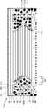
상기 기술적 과제를 달성하기 위하여, 본 발명은 다음과 같은 반도체 패키지를 제공한다. 본 발명에 따른 반도체 패키지는 패키지 베이스 기판; 상기 패키지 베이스 기판 상에 배치되는 적어도 하나의 반도체 칩; 상기 적어도 하나의 반도체 칩 상에 부착되며, 기저부 및 상기 기저부의 상면에 배치되는 복수의 돌출 패턴으로 이루어지는 히트 싱크; 및 상기 패키지 베이스 기판 상에서, 상기 패키지 베이스 기판의 상면, 상기 적어도 하나의 반도체 칩의 측면, 및 상기 히트 싱크의 측면을 덮되, 상기 히트 싱크의 상면을 덮지 않는 몰딩 부재;를 포함한다.In order to achieve the above technical problem, the present invention provides a semiconductor package as follows. A semiconductor package according to the present invention includes a package base substrate; at least one semiconductor chip disposed on the package base substrate; a heat sink attached to the at least one semiconductor chip and having a base and a plurality of protruding patterns disposed on an upper surface of the base; and a molding member on the package base substrate that covers an upper surface of the package base substrate, a side surface of the at least one semiconductor chip, and a side surface of the heat sink, but does not cover the upper surface of the heat sink.
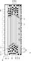
본 발명에 따른 반도체 패키지는, 패키지 베이스 기판; 상기 패키지 베이스 기판 상에 배치되는 적어도 하나의 반도체 칩; 상기 적어도 하나의 반도체 칩 상에 부착되며, 기저부 및 상기 기저부의 상면에 배치되는 복수의 돌출 패턴으로 이루어지는 히트 싱크; 상기 히트 싱크와 상기 적어도 하나의 반도체 칩 사이에서, 상기 히트 싱크의 하면을 덮는 히트 싱크 접착 필름; 상기 히트 싱크 접착 필름을 관통하여 상기 히트 싱크와 접하는 도전성 열 방출 단자; 상기 패키지 베이스 기판 상에서, 상기 패키지 베이스 기판의 상면, 상기 적어도 하나의 반도체 칩의 측면, 및 상기 히트 싱크의 측면을 덮는 몰딩 부재; 및 상기 패키지 베이스 기판의 측면, 상기 몰딩 부재의 측면과 상면, 및 상기 히트 싱크의 상면을 덮는 전자파 차폐 부재;를 포함한다.A semiconductor package according to the present invention includes a package base substrate; at least one semiconductor chip disposed on the package base substrate; a heat sink attached to the at least one semiconductor chip and having a base and a plurality of protruding patterns disposed on an upper surface of the base; a heat sink adhesive film covering a lower surface of the heat sink between the heat sink and the at least one semiconductor chip; a conductive heat dissipation terminal penetrating the heat sink adhesive film and contacting the heat sink; a molding member covering an upper surface of the package base substrate, a side surface of the at least one semiconductor chip, and a side surface of the heat sink on the package base substrate; and an electromagnetic wave shielding member covering a side surface of the package base substrate, a side surface and an upper surface of the molding member, and an upper surface of the heat sink.
본 발명에 따른 반도체 패키지는 패키지 베이스 기판; 상기 패키지 베이스 기판 상에 배치되는 반도체 칩; 상기 반도체 칩 상에 부착되며, 기저부 및 상기 기저부의 상면에 배치되는 복수의 돌출 패턴으로 이루어지는 히트 싱크; 상기 히트 싱크와 상기 반도체 칩 사이에서, 상기 히트 싱크의 하면을 덮는 히트 싱크 접착 필름; 상기 반도체 칩과 상기 패키지 베이스 기판을 전기적으로 연결하며, 일부분이 상기 히트 싱크 접착 필름 내에 매립되는 본딩 와이어; 상기 패키지 베이스 기판 상에서, 상기 패키지 베이스 기판의 상면, 상기 반도체 칩의 측면, 및 상기 히트 싱크의 측면을 덮는 몰딩 부재; 및 상기 패키지 베이스 기판의 측면, 상기 몰딩 부재의 측면과 상면, 및 상기 히트 싱크의 상면과 접하는 전자파 차폐 부재;를 포함한다.A semiconductor package according to the present invention includes a package base substrate; a semiconductor chip disposed on the package base substrate; a heat sink attached to the semiconductor chip and having a base portion and a plurality of protruding patterns disposed on an upper surface of the base portion; a heat sink adhesive film covering a lower surface of the heat sink between the heat sink and the semiconductor chip; a bonding wire electrically connecting the semiconductor chip and the package base substrate, a portion of which is embedded in the heat sink adhesive film; a molding member covering an upper surface of the package base substrate, a side surface of the semiconductor chip, and a side surface of the heat sink on the package base substrate; and an electromagnetic wave shielding member in contact with a side surface of the package base substrate, a side surface and an upper surface of the molding member, and an upper surface of the heat sink.
본 발명에 따른 반도체 패키지는, 몰딩 부재에 의하여 상면이 덮이지 않고 노출되며, 상면에 양극 산화된 알루미늄 산화물층이 가지는 관통 홀에 금속 물질을 채워 형성한 복수의 돌출 패턴이 배치되어 표면적이 증가된 히트 싱크에 의하여 반도체 패키지에서의 발열을 효과적으로 외부로 방출할 수 있다. 따라서 반도체 패키지의 부피, 또는 반도체 패키지 상면의 면적을 증가시키지 않아도 열 방출 효율을 증가시킬 수 있다.In the semiconductor package according to the present invention, the upper surface is exposed without being covered by the molding member, and a plurality of protruding patterns formed by filling a metal material in the through-holes of the anodized aluminum oxide layer on the upper surface are disposed to increase the surface area. The heat sink may effectively dissipate heat from the semiconductor package to the outside. Accordingly, heat dissipation efficiency may be increased without increasing the volume of the semiconductor package or the area of the upper surface of the semiconductor package.
히트 싱크가 가지는 복수의 돌출 패턴은 몰딩 부재의 상면보다 높은 레벨로 돌출되지 않으므로, 복수의 돌출 패턴이 손상되는 것을 방지할 수 있다.Since the plurality of protrusion patterns of the heat sink do not protrude at a level higher than the upper surface of the molding member, damage to the plurality of protrusion patterns may be prevented.
또한 본 발명에 따른 반도체 패키지는 전자파 차폐 부재는 복수의 돌출 패턴이 배치된 히트 싱크 상에서 엠보싱 패턴을 이룰 수 있으므로, 히트 싱크가 차폐재로의 역할을 할 수 있으며, 엠보싱 패턴 효과로 인해 반도체 패키지의 내부로부터 방출되는 전자파를 효율적으로 반사 및 흡수하여, 전자파가 반도체 패키지의 외부로 방출되지 않도록 차폐할 수 있다.In addition, in the semiconductor package according to the present invention, since the electromagnetic wave shielding member can form an embossing pattern on the heat sink on which the plurality of protruding patterns are disposed, the heat sink can serve as a shielding material, and the inside of the semiconductor package due to the embossing pattern effect By efficiently reflecting and absorbing electromagnetic waves emitted from the semiconductor package, it is possible to shield the electromagnetic waves from being emitted to the outside of the semiconductor package.
도 1은 본 발명의 일 실시 예에 따른 반도체 패키지를 나타내는 단면도이다.
도 2는 본 발명의 일 실시 예에 따른 반도체 패키지를 나타내는 단면도이다.
도 3은 본 발명의 일 실시 예에 따른 반도체 패키지를 나타내는 단면도이다.
도 4는 본 발명의 일 실시 예에 따른 반도체 패키지를 나타내는 단면도이다.
도 5는 본 발명의 일 실시 예에 따른 반도체 패키지를 나타내는 단면도이다.
도 6 내지 도 10a, 및 도 11은 본 발명의 일 실시 예에 따른 히트 싱크를 제조하는 과정을 단계적으로 나타내는 단면도들이고, 도 10b는 도 10a에 대한 사시도들이다.
도 12a 및 도 12b는 본 발명의 일 실시 예에 따른 히트 싱크를 나타내는 단면도 및 사시도이다.
도 13 내지 도 16은 본 발명의 일 실시 예에 따른 반도체 패키지를 제조하는 과정을 단계적으로 나타내는 단면도들이다.
도 17 내지 도 20은 본 발명의 일 실시 예에 따른 반도체 패키지를 제조하는 과정을 단계적으로 나타내는 단면도들이다.
도 21 내지 도 23은 본 발명의 일 실시 예에 따른 반도체 패키지를 제조하는 과정을 단계적으로 나타내는 단면도들이다.
도 24 및 도 25는 본 발명의 일 실시 예에 따른 반도체 패키지를 제조하는 과정을 단계적으로 나타내는 단면도들이다.
도 26은 본 발명의 일 실시 예에 따른 반도체 패키지를 나타내는 단면도이다.1 is a cross-sectional view illustrating a semiconductor package according to an embodiment of the present invention.
2 is a cross-sectional view illustrating a semiconductor package according to an embodiment of the present invention.
3 is a cross-sectional view illustrating a semiconductor package according to an embodiment of the present invention.
4 is a cross-sectional view illustrating a semiconductor package according to an embodiment of the present invention.
5 is a cross-sectional view illustrating a semiconductor package according to an embodiment of the present invention.
6 to 10A and 11 are cross-sectional views showing step by step a process of manufacturing a heat sink according to an embodiment of the present invention, and FIG. 10B is a perspective view of FIG. 10A .
12A and 12B are cross-sectional and perspective views illustrating a heat sink according to an exemplary embodiment of the present invention.
13 to 16 are cross-sectional views illustrating a process of manufacturing a semiconductor package according to an embodiment of the present invention in stages.
17 to 20 are cross-sectional views illustrating a process of manufacturing a semiconductor package according to an embodiment of the present invention in stages.
21 to 23 are cross-sectional views illustrating a process of manufacturing a semiconductor package according to an embodiment of the present invention in stages.
24 and 25 are cross-sectional views illustrating a process of manufacturing a semiconductor package according to an embodiment of the present invention in stages.
26 is a cross-sectional view illustrating a semiconductor package according to an embodiment of the present invention.
도 1은 본 발명의 일 실시 예에 따른 반도체 패키지를 나타내는 단면도이다.1 is a cross-sectional view illustrating a semiconductor package according to an embodiment of the present invention.
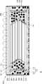
도 1을 참조하면, 반도체 패키지(1)는 패키지 베이스 기판(100), 반도체 칩(210), 및 히트 싱크(310)를 포함한다.Referring to FIG. 1 , a semiconductor package 1 includes a
일부 실시 예에서, 패키지 베이스 기판(100)은 인쇄회로기판(Printed circuit Board)일 수 있다. 예를 들면, 패키지 베이스 기판(100)은 양면 인쇄 회로 기판(double-sided Printed Circuit Board) 또는 멀티 레이어 인쇄 회로 기판(multi-layer Printed Circuit Board)일 수 있다. 패키지 베이스 기판(100)은 적어도 하나의 베이스층(110), 패키지 베이스 기판(100)의 상면에 배치되는 복수의 제1 연결 패드(122), 및 패키지 베이스 기판(100)의 하면에 배치되는 복수의 제2 연결 패드(124)를 포함할 수 있다. 베이스층(110)의 상면 및 하면 상에는 솔더 레지스트층(130)이 배치될 수 있다. 복수의 제1 연결 패드(122) 및 복수의 제2 연결 패드(124)는 각각 솔더 레지스트층(130)에 의하여 덮이지 않고 패키지 베이스 기판(100)의 상면과 하면에 노출될 수 있다. 일부 실시 예에서, 솔더 레지스트층(130)은 베이스층(110)의 상면 상에 배치되지 않고 생략될 수 있다. 일부 실시 예에서, 패키지 베이스 기판(100)은 적층된 복수의 베이스층(110)을 포함할 수 있다. 예를 들면, 패키지 베이스 기판(100)은 멀티 레이어 인쇄 회로 기판(multi-layer Printed Circuit Board)일 수 있다.In some embodiments, the
일부 실시 예에서, 적어도 하나의 베이스층(110)은 페놀 수지, 에폭시 수지, 폴리이미드 중에서 선택되는 적어도 하나의 물질로 이루어질 수 있다. 예를 들면, 적어도 하나의 베이스층(110)은 FR4(Flame Retardant 4), 사관능성 에폭시(Tetrafunctional epoxy), 폴리페닐렌 에테르(Polyphenylene ether), 에폭시/폴리페닐렌 옥사이드(Epoxy/polyphenylene oxide), BT(Bismaleimide triazine), 써마운트(Thermount), 시아네이트 에스터(Cyanate ester), 폴리이미드(Polyimide) 및 액정 고분자(Liquid crystal polymer) 중에서 선택되는 적어도 하나의 물질을 포함할 수 있다.In some embodiments, the at least one
패키지 베이스 기판(100)은 적어도 하나의 전자파 차폐 단자(126)를 더 포함할 수 있다. 도 1에서, 적어도 하나의 전자파 차폐 단자(126)는 베이스층(110)의 측면 및 하면에 걸쳐서 형성된 것으로 도시되었으나, 이에 한정되지 않는다. 적어도 하나의 전자파 차폐 단자(126)는 후술할 전자파 차폐 부재(500)와 접할 수 있는 한, 베이스층(110)에서의 형성 위치는 제한되지 않는다. 일부 실시 예에서, 적어도 하나의 전자파 차폐 단자(126)는 베이스층(110)의 측면의 일부분을 덮도록 형성될 수 있다. 일부 실시 예에서, 적어도 하나의 전자파 차폐 단자(126)는 베이스층(110)의 측면에서 노출되도록 베이스층(110)의 상면 또는 하면에 배치될 수 있다. 일부 실시 예에서, 적어도 하나의 전자파 차폐 단자(126)는 베이스층(110)의 측면에서 노출되도록 적층된 복수의 베이스층(110)의 사이에 배치될 수 있다.The
복수의 제1 연결 패드(122), 복수의 제2 연결 패드(124), 및 적어도 하나의 전자파 차폐 단자(126)는 구리, 니켈, 스테인리스 스틸 또는 베릴륨구리(beryllium copper)로 이루어질 수 있다.The plurality of
패키지 베이스 기판(100) 내에는 복수의 제1 연결 패드(122)와 복수의 제2 연결 패드(124)를 전기적으로 연결하기 위한 배선 패턴 및 도전 비아가 배치될 수 있으나, 도시의 간략화를 위하여 생략되어 있다. 상기 배선 패턴 및 상기 도전 비아는 예를 들면, 구리를 포함하는 금속으로 이루어질 수 있다. 상기 배선 패턴 및 상기 도전 비아 중 일부는 복수의 제2 연결 패드(124) 중 접지가 제공되는 일부와, 적어도 하나의 전자파 차폐 단자(126)를 전기적으로 연결할 수 있다.A wiring pattern and conductive vias for electrically connecting the plurality of
패키지 베이스 기판(100) 상에는 적어도 하나의 반도체 칩(210)이 실장된다. 반도체 칩(210)은 반도체 기판을 포함할 수 있다. 상기 반도체 기판은 예를 들면, 실리콘(Si, silicon)을 포함할 수 있다. 또는 상기 반도체 기판은 저머늄(Ge, germanium)과 같은 반도체 원소, 또는 SiC (silicon carbide), GaAs(gallium arsenide), InAs (indium arsenide), 및 InP (indium phosphide)와 같은 화합물 반도체를 포함할 수 있다. 상기 반도체 기판은 활성면과 상기 활성면에 반대되는 비활성면을 가질 수 있다. 반도체 칩(210)은 상기 활성면에 다양한 종류의 복수의 개별 소자 (individual devices)를 포함하는 반도체 소자가 형성될 수 있다.At least one
일부 실시 예에서, 반도체 칩(210)은 CPU(Central Processor Unit), MPU(Micro Processor Unit), GPU(Graphic Processor Unit) 또는 AP(Application Processor)일 수 있다. 일부 실시 예에서, 반도체 칩(210)은 플래시 메모리(Flash Memory), PRAM(Phase-change Random Access Memory), MRAM(Magnetoresistive Random Access Memory), FeRAM(Ferroelectric Random Access Memory) 또는 RRAM(Resistive Random Access Memory)과 같은 비휘발성 메모리 반도체 칩일 수 있다. 상기 플래시 메모리는, 예를 들면 브이낸드(V-NAND) 플래시 메모리일 수 있다. 일부 실시 예에서, 반도체 칩(210)은 DRAM(Dynamic Random Access Memory) 또는 SRAM(Static Random Access Memory)과 같은 휘발성 메모리 반도체 칩일 수 있다. 일부 실시 예에서, 반도체 칩(210)은 상기 비휘발성 메모리 반도체 칩을 제어하기 위한 컨트롤러 반도체 칩일 수 있다. 일부 실시 예에서, 반도체 칩(210)은 복수 개이고, 복수 개의 반도체 칩(210) 중 적어도 하나는, 나머지를 지지 하기 위한 더미 실리콘 스페이서(dummy silicon spacer) 칩일 수 있다.In some embodiments, the
반도체 칩(210)은 상기 활성면 상에 배치되는 적어도 하나의 반도체 칩 패드(212)를 포함할 수 있다. 적어도 하나의 반도체 칩 패드(212)는 복수의 제1 연결 패드(122)와 전기적으로 연결되고, 상기 배선 패턴 및/또는 도전 비아를 통하여 하면 복수의 제2 연결 패드(124)와 전기적으로 연결될 수 있다.The
일부 실시 예에서, 반도체 칩(210)은 적어도 하나의 반도체 칩 패드(212)와 복수의 제1 연결 패드(122) 사이를 연결하는 본딩 와이어(230)를 통하여 패키지 베이스 기판(100)과 전기적으로 연결될 수 있다. 별도로 도시하지는 않았으나, 일부 실시 예에서, 반도체 칩(210)은 플립 칩 방식으로 칩 연결 단자를 통하여 복수의 제1 연결 패드와 전기적으로 연결될 수 있다.In some embodiments, the
반도체 패키지(1)는 복수의 반도체 칩(210)을 포함할 수 있다. 복수의 반도체 칩(210) 각각은 하면에 부착된 다이 접착 필름(220)을 이용하여, 계단 형상을 이루며 순차적으로 적층될 수 있으나, 이에 한정되지 않는다. 예를 들면, 일부 실시 예에서 복수의 반도체 칩(210)은 패키지 베이스 기판(100) 상에 수평 방향으로 서로 이격되며 배치되거나, 패키지 베이스 기판(100) 상에 수직 방향으로 적층되도록 배치되거나, 복수의 반도체 칩(210) 중 일부는 패키지 베이스 기판(100) 상에 수평 방향으로 서로 이격되며 배치되고, 다른 일부는 수직 방향으로 적층되도록 배치될 수 있다.The semiconductor package 1 may include a plurality of
반도체 칩(210) 상에는 히트 싱크(310)가 부착될 수 있다. 히트 싱크(310)는 히트 싱크 접착 필름(320)을 사이에 두고 반도체 칩(210) 상에 부착될 수 있다. 히트 싱크 접착 필름(320)은 다이 접착 필름(220)과 유사한 물질로 이루어질 수 있다. 히트 싱크 접착 필름(320)은 히트 싱크(310)의 하면을 모두 덮을 수 있도록, 히트 싱크(310)와 대략 동일한 수평 면적을 가질 수 있다. 일부 실시 예에서, 히트 싱크 접착 필름(320)의 두께는 다이 접착 필름(220)의 두께보다 큰 값을 가질 수 있다. 반도체 칩(210)의 반도체 칩 패드(212)와 연결된 본딩 와이어(230)의 일부분은 히트 싱크 접착 필름(320) 내에 매립될 수 있다. 본딩 와이어(230)의 최상단은 히트 싱크(310)의 하면, 즉 기저부(312)의 하면보다 낮은 레벨에 위치할 수 있다. 따라서 본딩 와이어(230)와 히트 싱크(310)는 접하지 않도록 이격될 수 있다.A
히트 싱크(310)의 수평 면적은 패키지 베이스 기판(100)의 수평 면적보다 작은 값을 가질 수 있다.The horizontal area of the
일부 실시 예에서, 히트 싱크(310)의 수평 면적은 반도체 칩(210)의 수평 면적보다 큰 값을 가질 수 있다. 예를 들어, 반도체 패키지(1)가 계단 형상을 이루며 순차적으로 적층된 복수의 반도체 칩(210)을 포함하는 경우, 히트 싱크(310)는 수직 방향으로 복수의 반도체 칩(210)과 모두 중첩(overlap)되기에 충분한 수평 면적을 가질 수 있다. 일부 실시 예에서, 히트 싱크(310)의 수평 면적은 반도체 칩(210)의 수평 면적과 대략 동일한 값을 가질 수 있다. 일부 실시 예에서, 반도체 패키지(1)가 서로 다른 면적을 가지는 복수의 반도체 칩(210)을 포함하는 경우, 히트 싱크(310)의 수평 면적은, 복수의 반도체 칩(210) 중 최상단 반도체 칩(210)의 수평 면적과 대략 동일한 값을 가질 수 있다.In some embodiments, a horizontal area of the
히트 싱크(310)는 기저부(312) 및 기저부(312) 상면에 배치되는 복수의 돌출 패턴(314)으로 이루어질 수 있다. 복수의 돌출 패턴(314)은 기저부(312)의 상면 상에서 육각 배열(honeycomb) 구조를 가지며 배치될 수 있다. 복수의 돌출 패턴(314) 각각은 원형의 수평 단면 형상을 가질 수 있다. 일부 실시 예에서, 복수의 돌출 패턴(314) 각각의 수평 폭과 수직 높이는 각각 수㎚ 내지 수십㎚일 수 있다. 일부 실시 예에서, 복수의 돌출 패턴(314)은 인접하는 2개의 돌출 패턴(314)이 수㎚ 내지 수㎛의 간격을 가지며 기저부(312) 상면에 배치될 수 있다. The
기저부(312) 및 복수의 돌출 패턴(314)은 각각 금속으로 이루어질 수 있다. 예를 들면, 기저부(312)는 알루미늄으로 이루어질 수 있다. 예를 들면, 복수의 돌출 패턴(314)은 알루미늄, 또는 구리로 이루어질 수 있다.Each of the
반도체 패키지(1)는 몰딩 부재(400)를 더 포함할 수 있다. 몰딩 부재(400)는 필러(filler)(410)를 함유할 수 있다. 예를 들면, 몰딩 부재(400)는 필러(410)를 함유한 에폭시 계열 물질로 이루어질 수 있다. 일부 실시 예에서, 몰딩 부재(400)에 포함된 필러(410)의 비율은 약 55wt% 내지 85wt%일 수 있다. 필러(410)는 예를 들면 실리카 필러일 수 있다. 필러(410)의 평균 직경은 0.1㎛ 내지 수십㎛일 수 있다.The semiconductor package 1 may further include a
본 명세서의 도면에서 필러(410)는 돌출 패턴(314)의 크기와의 상대적인 비교를 위하여, 과장되어 크게 도시되었다. 따라서 돌출 패턴(314) 이외의 구성 요소와 필러(410)의 상대적인 크기는 본 명세서의 도면에 도시된 것과는 무관할 수 있다.In the drawings of the present specification, the
몰딩 부재(400)는 패키지 베이스 기판(100) 상에서 반도체 칩(210) 및 히트 싱크(310)를 감쌀 수 있다. 몰딩 부재(400)는 예를 들면, 패키지 베이스 기판(100)의 상면, 반도체 칩(210)의 측면, 및 히트 싱크(310)의 측면을 덮을 수 있다. 몰딩 부재(400)는 히트 싱크(310)의 상면을 덮지 않는 노출형 몰드(exposed type mold)로 형성될 수 있다.The
몰딩 부재(400)의 최상단과 히트 싱크(310)의 최상단은 대략 동일 레벨에 위치할 수 있다. 예를 들면, 몰딩 부재(400)의 최상단과 히트 싱크(310)의 복수의 돌출 패턴(314)의 상면은 대략 동일 레벨에 위치할 수 있다.The uppermost end of the
몰딩 부재(400)가 가지는 필러(410)의 직경은 복수의 돌출 패턴(314) 사이의 간격보다 큰 값을 가질 수 있다. 예를 들면, 복수의 돌출 패턴(314) 사이의 간격은 수㎚ 내지 수십㎚이고, 필러(410)의 직경은 0.1㎛ 내지 수십㎛일 수 있다.The diameter of the
몰딩 부재(400)가 포함하는 필러(410)의 직경이 복수의 돌출 패턴(314) 사이의 간격보다 크므로, 몰딩 부재(400)를 형성하는 과정에서, 필러(410)가 히트 싱크(310) 상면의 가장자리에 인접하여 배치되는 복수의 돌출 패턴(314)의 사이를 막을 수 있어, 몰딩 부재(400)는 히트 싱크(310)의 상면을 덮지 않을 수 있다.Since the diameter of the
몰딩 부재(400)가 히트 싱크(310)의 상면을 덮지 않는다는 것은, 몰딩 부재(400)가 히트 싱크(310)의 상면을 완전히 덮지 않는다는 의미는 아니고, 히트 싱크(310)의 상면의 대부분을 덮지 않고 노출시킨다는 것을 의미한다. 예를 들면, 몰딩 부재(400)는 히트 싱크(310)의 상면의 가장자리에 인접하는 상대적으로 적은 일부분을 덮을 수 있으나, 히트 싱크(310)의 상면의 내측 부분의 대부분을 덮지 않을 수 있다.The fact that the
반도체 패키지(1)의 표면에는 전자파 차폐 부재(500)가 형성될 수 있다. 전자파 차폐 부재(500)는 반도체 패키지(1)의 하면을 제외한 표면을 모두 덮을 수 있다. 구체적으로, 전자파 차폐 부재(500)는 패키지 베이스 기판(100)의 측면, 몰딩 부재(400)의 측면 및 상면, 그리고 히트 싱크(310)의 상면을 덮을 수 있다. 전자파 차폐 부재(500)는 패키지 베이스 기판(100)의 측면, 및 몰딩 부재(400)의 측면 및 상면과 직접 접할 수 있다. 몰딩 부재(400)는 히트 싱크(310)의 상면을 덮지 않는 노출형 몰드로 형성되므로, 전자파 차폐 부재(500)는 히트 싱크(310)의 상면과 직접 접할 수 있다.An electromagnetic
별도로 도시하지는 않았으나, 일부 실시 예에서, 전자파 차폐 부재(500)는 반도체 패키지(1)의 하면의 일부분을 함께 덮을 수 있다.Although not shown separately, in some embodiments, the electromagnetic
전자파 차폐 부재(500)는 반도체 패키지(1)의 표면 상에 컨포멀 쉴딩(Conformal Shielding) 방식으로 형성될 수 있다. 전자파 차폐 부재(500)는 복수의 돌출 패턴(314)이 배치된 히트 싱크(310) 상에서 복수의 돌출 패턴(314)의 측면, 상면, 및 복수의 돌출 패턴(314) 사이의 기저부(312)의 표면을 따라서 컨포멀하게 형성된 엠보싱(embossing) 패턴을 이룰 수 있다. 일부 실시 예에서, 전자파 차폐 부재(500)는 복수의 돌출 패턴(314)이 배치된 히트 싱크(310) 상에 복수의 돌출 패턴(314) 사이의 공간을 채우고, 복수의 돌출 패턴(314)의 형상이 전사된 엠보싱 패턴을 이룰 수 있다. 즉, 전자파 차폐 부재(500)의 상면은 히트 싱크(310) 상에서 요철 구조를 가질 수 있다.The electromagnetic
전자파 차폐 부재(500)는 도전성 물질로 이루어질 수 있다. 전자파 차폐 부재(500)는 예를 들면, Ag, Cu, Ni, Al, Sn, 스테인리스 스틸 등의 금속 물질, 카본블랙(carbon black), 탄소나노튜브(CNT: Carbon Nanotube), 그라파이트(graphite) 등의 전도성 카본 물질, Ag/Cu, Ag/Glass fiber, Ni/Graphite 등의 금속 코팅 물질(Metal coated materials), 또는 폴리피롤(Polypyrrole), 폴리아닐린(Polyaniline) 등의 전도성 고분자 물질로 이루어질 수 있다.The electromagnetic
전자파 차폐 부재(500)는 적어도 하나의 전자파 차폐 단자(126)와 접할 수 있다. 예를 들면, 전자파 차폐 부재(500)는 패키지 베이스 기판(100)의 측면에서 적어도 하나의 전자파 차폐 단자(126)와 접할 수 있다.The electromagnetic
반도체 패키지(1)는 복수의 외부 연결 단자(600)를 더 포함할 수 있다. 외부 연결 단자(600)는 예를 들면, 솔더 볼 또는 범프일 수 있다. 복수의 외부 연결 단자(600)는 패키지 베이스 기판(100)의 하면에 배치되는 복수의 제2 연결 패드(124)에 부착될 수 있다.The semiconductor package 1 may further include a plurality of
본 발명에 따른 반도체 패키지(1)는 몰딩 부재(400)에 의하여 상면이 덮이지 않고 노출되는 히트 싱크(310)에 의하여 반도체 패키지(1) 내, 예를 들면 반도체 칩(210)에서의 발열을 효과적으로 외부로 방출할 수 있다. 히트 싱크(310)는 상면에 양극 산화된 알루미늄 산화물층이 가지는 관통 홀에 금속 물질을 채워 형성한 복수의 돌출 패턴(314)이 배치되므로, 히트 싱크(310)의 표면적이 증가될 수 있다. 따라서 반도체 패키지(1)의 부피, 또는 반도체 패키지(1) 상면의 면적을 증가시키지 않아도 열 방출 효율을 증가시킬 수 있다.In the semiconductor package 1 according to the present invention, heat in the semiconductor package 1, for example, in the
히트 싱크(310)가 가지는 복수의 돌출 패턴(314)은 몰딩 부재(400)의 최상단과 대략 동일 레벨에 위치할 수 있다. 따라서 복수의 돌출 패턴(314)은 몰딩 부재(400)의 상면보다 높은 레벨로 돌출되지 않으므로, 복수의 돌출 패턴(314)이 손상되는 것을 방지할 수 있다.The plurality of
또한 본 발명에 따른 반도체 패키지(1)는 전자파 차폐 부재(500)는 복수의 돌출 패턴(314)이 배치된 히트 싱크(310) 상에서 엠보싱 패턴을 이루므로, 히트 싱크가 차폐재로의 역할을 할 수 있으며, 엠보싱 패턴 효과로 인해 반도체 패키지(1)의 내부로부터 반도체 패키지(1)의 상면을 향하여 방출되는 전자파를 효율적으로 반사 및 흡수하여, 전자파가 반도체 패키지(1)의 외부로 방출되지 않도록 차폐할 수 있다.In addition, in the semiconductor package 1 according to the present invention, the electromagnetic
도 2는 본 발명의 일 실시 예에 따른 반도체 패키지를 나타내는 단면도이다.2 is a cross-sectional view illustrating a semiconductor package according to an embodiment of the present invention.
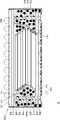
도 2를 참조하면, 반도체 패키지(1a)는 패키지 베이스 기판(100a), 반도체 칩(210), 및 히트 싱크(310)를 포함한다.Referring to FIG. 2 , a
패키지 베이스 기판(100a)은 적어도 하나의 베이스층(110), 패키지 베이스 기판(100a)의 상면에 배치되는 복수의 제1 연결 패드(122), 패키지 베이스 기판(100a)의 하면에 배치되는 복수의 제2 연결 패드(124), 베이스층(110)의 측면에 노출되는 하나의 전자파 차폐 단자(126), 및 패키지 베이스 기판(100a)의 상면에 배치되는 열 전달 패드(128)를 포함한다. The
패키지 베이스 기판(100a) 상에는 적어도 하나의 반도체 칩(210)이 실장된다. 반도체 칩(210)은 적어도 하나의 반도체 칩 패드(212)를 포함할 수 있다. 적어도 하나의 반도체 칩 패드(212)는 복수의 제1 연결 패드(122)와 전기적으로 연결될 수 있다. 일부 실시 예에서, 반도체 칩(210)은 적어도 하나의 반도체 칩 패드(212)와 복수의 제1 연결 패드(122) 사이를 연결하는 본딩 와이어(230)를 통하여 패키지 베이스 기판(100a)과 전기적으로 연결될 수 있다.At least one
반도체 패키지(1a)는 복수의 반도체 칩(210)을 포함할 수 있다. 복수의 반도체 칩(210) 각각은 하면에 부착된 다이 접착 필름(220)을 이용하여, 계단 형상을 이루며 순차적으로 적층될 수 있으나, 이에 한정되지 않는다.The
반도체 칩(210) 상에는 히트 싱크(310)가 부착될 수 있다. 히트 싱크(310)는 히트 싱크 접착 필름(320)을 사이에 두고 반도체 칩(210) 상에 부착될 수 있다. 히트 싱크(310)는 기저부(312) 및 기저부(312) 상면에 배치되는 복수의 돌출 패턴(314)으로 이루어질 수 있다. 복수의 돌출 패턴(314)은 기저부(312)의 상면 상에서 육각 배열 구조를 가지며 배치될 수 있다. 복수의 돌출 패턴(314) 각각은 원형의 수평 단면 형상을 가질 수 있다.A
반도체 패키지(1a)는 몰딩 부재(400)를 더 포함할 수 있다. 몰딩 부재(400)는 필러(410)를 함유할 수 있다.The
몰딩 부재(400)는 패키지 베이스 기판(100a) 상에서 반도체 칩(210) 및 히트 싱크(310)를 감쌀 수 있다. 몰딩 부재(400)는 예를 들면, 패키지 베이스 기판(100a)의 상면, 반도체 칩(210)의 측면, 및 히트 싱크(310)의 측면을 덮을 수 있다. 몰딩 부재(400)는 히트 싱크(310)의 상면을 덮지 않는 노출형 몰드로 형성될 수 있다. 몰딩 부재(400)의 최상단과 히트 싱크(310)의 최상단은 대략 동일 레벨에 위치할 수 있다. 예를 들면, 몰딩 부재(400)의 최상단과 히트 싱크(310)의 복수의 돌출 패턴(314)의 상면은 동일 레벨에 위치할 수 있다. 몰딩 부재(400)가 가지는 필러(410)의 직경은 복수의 돌출 패턴(314) 사이의 간격보다 큰 값을 가질 수 있다. 몰딩 부재(400)는 히트 싱크(310)의 상면을 덮지 않을 수 있다.The
반도체 패키지(1a)는, 패키지 베이스 기판(100a)의 상면 상에 배치되는 도전성 볼 기둥(250)을 더 포함할 수 있다. 도전성 볼 기둥(250)은 예를 들면, 복수의 솔더 볼을 수직 적층하여 형성할 수 있다. 도전성 볼 기둥(250)은 패키지 베이스 기판(100a)의 상면에 배치되는 열 전달 패드(128) 상에 부착될 수 있다. 도전성 볼 기둥(250)은 몰딩 부재(400) 및 히트 싱크 접착 필름(320)을 관통하여 히트 싱크(310)의 기저부(312)의 하면과 접할 수 있다.The
도전성 볼 기둥(250)은 패키지 베이스 기판(100a)에서의 발열, 및/또는 반도체 칩(210)으로부터 패키지 베이스 기판(100a)으로 전달된 열을 히트 싱크(310)로 전달할 수 있다.The
반도체 패키지(1a)의 표면에는 전자파 차폐 부재(500)가 형성될 수 있다. 전자파 차폐 부재(500)는 반도체 패키지(1a)의 하면을 제외한 표면을 모두 덮을 수 있다. 구체적으로, 전자파 차폐 부재(500)는 패키지 베이스 기판(100a)의 측면, 몰딩 부재(400)의 측면 및 상면, 그리고 히트 싱크(310)의 표면을 덮을 수 있다.An electromagnetic
전자파 차폐 부재(500)는 적어도 하나의 전자파 차폐 단자(126)와 접할 수 있다. 예를 들면, 전자파 차폐 부재(500)는 패키지 베이스 기판(100a)의 측면에서 적어도 하나의 전자파 차폐 단자(126)와 접할 수 있다.The electromagnetic
반도체 패키지(1a)는 복수의 외부 연결 단자(600)를 더 포함할 수 있다. 패키지 베이스 기판(100a)의 하면에 배치되는 복수의 제2 연결 패드(124)에 부착될 수 있다.The
본 발명에 따른 반도체 패키지(1a)는 몰딩 부재(400)에 의하여 상면이 덮이지 않고 노출되는 히트 싱크(310)에 의하여 반도체 패키지(1a) 내, 예를 들면 반도체 칩(210)에서의 발열을 효과적으로 외부로 방출할 수 있다. 히트 싱크(310)는 상면에 양극 산화된 알루미늄 산화물층이 가지는 관통 홀에 금속 물질을 채워 형성한 복수의 돌출 패턴(314)이 배치되므로, 히트 싱크(310)의 표면적이 증가될 수 있다. 따라서 반도체 패키지(1a)의 부피, 또는 반도체 패키지(1a) 상면의 면적을 증가시키지 않아도 열 방출 효율을 증가시킬 수 있다.In the
또한 본 발명에 따른 반도체 패키지(1a)는 패키지 베이스 기판(100a)과 히트 싱크(310) 사이를 연결하는 도전성 볼 기둥(250)을 더 포함하므로, 패키지 베이스 기판(100a)에서의 발열, 및/또는 반도체 칩(210)으로부터 패키지 베이스 기판(100a)으로 전달된 열을 히트 싱크(310)로 전달하여, 효과적으로 외부로 방출할 수 있다.In addition, since the
히트 싱크(310)가 가지는 복수의 돌출 패턴(314)은 몰딩 부재(400)의 최상단과 대략 동일 레벨에 위치할 수 있다. 따라서 복수의 돌출 패턴(314)은 몰딩 부재(400)의 상면보다 높은 레벨로 돌출되지 않으므로, 복수의 돌출 패턴(314)이 손상되는 것을 방지할 수 있다.The plurality of
또한 본 발명에 따른 반도체 패키지(1a)는 전자파 차폐 부재(500)는 복수의 돌출 패턴(314)이 배치된 히트 싱크(310) 상에서 엠보싱 패턴을 이루므로, 반도체 패키지(1a)의 내부로부터 반도체 패키지(1a)의 상면을 향하여 방출되는 전자파를 효율적으로 흡수하여, 전자파가 반도체 패키지(1a)의 외부로 방출되지 않도록 차폐할 수 있다.In addition, in the
도 3은 본 발명의 일 실시 예에 따른 반도체 패키지를 나타내는 단면도이다.3 is a cross-sectional view illustrating a semiconductor package according to an embodiment of the present invention.
도 3을 참조하면, 반도체 패키지(1b)는 패키지 베이스 기판(100a), 반도체 칩(210), 및 히트 싱크(310)를 포함한다.Referring to FIG. 3 , a
패키지 베이스 기판(100a)은 적어도 하나의 베이스층(110), 패키지 베이스 기판(100a)의 상면에 배치되는 복수의 제1 연결 패드(122), 패키지 베이스 기판(100a)의 하면에 배치되는 복수의 제2 연결 패드(124), 베이스층(110)의 측면에 노출되는 하나의 전자파 차폐 단자(126), 및 패키지 베이스 기판(100a)의 상면에 배치되는 열 전달 패드(128)를 포함한다. The
패키지 베이스 기판(100a) 상에는 적어도 하나의 반도체 칩(210)이 실장된다. 반도체 칩(210)은 적어도 하나의 반도체 칩 패드(212)를 포함할 수 있다. 적어도 하나의 반도체 칩 패드(212)는 복수의 제1 연결 패드(122)와 전기적으로 연결될 수 있다. 일부 실시 예에서, 반도체 칩(210)은 적어도 하나의 반도체 칩 패드(212)와 복수의 제1 연결 패드(122) 사이를 연결하는 본딩 와이어(230)를 통하여 패키지 베이스 기판(100a)과 전기적으로 연결될 수 있다.At least one
반도체 패키지(1b)는 복수의 반도체 칩(210)을 포함할 수 있다. 복수의 반도체 칩(210) 각각은 하면에 부착된 다이 접착 필름(220)을 이용하여, 계단 형상을 이루며 순차적으로 적층될 수 있으나, 이에 한정되지 않는다.The
반도체 칩(210) 상에는 히트 싱크(310)가 부착될 수 있다. 히트 싱크(310)는 히트 싱크 접착 필름(320)을 사이에 두고 반도체 칩(210) 상에 부착될 수 있다. 히트 싱크(310)는 기저부(312) 및 기저부(312) 상면에 배치되는 복수의 돌출 패턴(314)으로 이루어질 수 있다. 복수의 돌출 패턴(314)은 기저부(312)의 상면 상에서 육각 배열 구조를 가지며 배치될 수 있다. 복수의 돌출 패턴(314) 각각은 원형의 수평 단면 형상을 가질 수 있다.A
반도체 패키지(1b)는 몰딩 부재(400)를 더 포함할 수 있다. 몰딩 부재(400)는 필러(410)를 함유할 수 있다.The
몰딩 부재(400)는 패키지 베이스 기판(100a) 상에서 반도체 칩(210) 및 히트 싱크(310)를 감쌀 수 있다. 몰딩 부재(400)는 예를 들면, 패키지 베이스 기판(100a)의 상면, 반도체 칩(210)의 측면, 및 히트 싱크(310)의 측면을 덮을 수 있다. 몰딩 부재(400)는 히트 싱크(310)의 상면을 덮지 않는 노출형 몰드로 형성될 수 있다. 몰딩 부재(400)의 최상단과 히트 싱크(310)의 최상단은 대략 동일 레벨에 위치할 수 있다. 예를 들면, 몰딩 부재(400)의 최상단과 히트 싱크(310)의 복수의 돌출 패턴(314)의 상면은 동일 레벨에 위치할 수 있다. 몰딩 부재(400)가 가지는 필러(410)의 직경은 복수의 돌출 패턴(314) 사이의 간격보다 큰 값을 가질 수 있다. 몰딩 부재(400)는 히트 싱크(310)의 상면을 덮지 않을 수 있다.The
반도체 패키지(1b)는, 히트 싱크(310), 히트 싱크 접착 필름(320), 및 몰딩 부재(400)를 관통하여, 저면에 패키지 베이스 기판(100a)의 상면 일부분을 노출하는 관통 비아홀(260H), 및 관통 비아홀(260H)을 채우는 도전성 관통 비아(260)를 더 포함한다. 도전성 관통 비아(260)는 금속으로 이루어질 수 있다. 도전성 관통 비아(260)는 예를 들면 Al, Cu, Au, Ag, 또는 Ti 등의 금속으로 이루어질 수 있다.The
관통 비아홀(260H)의 저면에는 열 전달 패드(128)가 노출될 수 있다. 따라서 도전성 관통 비아(260)는 히트 싱크(310), 히트 싱크 접착 필름(320), 및 몰딩 부재(400)를 관통하여 열 전달 패드(128)와 접할 수 있다. 도전성 관통 비아(260)의 상측 측면은 히트 싱크(310)의 기저부(312)와 접할 수 있다.The
도전성 관통 비아(260)의 상면은 히트 싱크(310)의 기저부(312)의 상면과 대략 동일 레벨에 위치할 수 있다. 도전성 관통 비아(260)는 하면에서 상면으로 가면서 직경이 증가하는 테이퍼된(tapered) 형상을 가질 수 있다.A top surface of the conductive through-via 260 may be positioned at approximately the same level as a top surface of the
따라서 도전성 관통 비아(260)는 패키지 베이스 기판(100a)에서의 발열, 및/또는 반도체 칩(210)으로부터 패키지 베이스 기판(100a)으로 전달된 열을 히트 싱크(310)로 전달할 수 있다.Accordingly, the conductive through via 260 may transfer heat from the
반도체 패키지(1b)의 표면에는 전자파 차폐 부재(500)가 형성될 수 있다. 전자파 차폐 부재(500)는 반도체 패키지(1b)의 하면을 제외한 표면을 모두 덮을 수 있다. 구체적으로, 전자파 차폐 부재(500)는 패키지 베이스 기판(100a)의 측면, 몰딩 부재(400)의 측면 및 상면, 히트 싱크(310)의 표면, 및 도전성 관통 비아(260)의 상면을 덮을 수 있다.An electromagnetic
전자파 차폐 부재(500)는 적어도 하나의 전자파 차폐 단자(126)와 접할 수 있다. 예를 들면, 전자파 차폐 부재(500)는 패키지 베이스 기판(100a)의 측면에서 적어도 하나의 전자파 차폐 단자(126)와 접할 수 있다.The electromagnetic
반도체 패키지(1b)는 복수의 외부 연결 단자(600)를 더 포함할 수 있다. 패키지 베이스 기판(100a)의 하면에 배치되는 복수의 제2 연결 패드(124)에 부착될 수 있다.The
본 발명에 따른 반도체 패키지(1b)는 몰딩 부재(400)에 의하여 상면이 덮이지 않고 노출되는 히트 싱크(310)에 의하여 반도체 패키지(1b) 내, 예를 들면 반도체 칩(210)에서의 발열을 효과적으로 외부로 방출할 수 있다. 히트 싱크(310)는 상면에 양극 산화된 알루미늄 산화물층이 가지는 관통 홀에 금속 물질을 채워 형성한 복수의 돌출 패턴(314)이 배치되므로, 히트 싱크(310)의 표면적이 증가될 수 있다. 따라서 반도체 패키지(1b)의 부피, 또는 반도체 패키지(1b) 상면의 면적을 증가시키지 않아도 열 방출 효율을 증가시킬 수 있다.In the
히트 싱크(310)가 가지는 복수의 돌출 패턴(314)은 몰딩 부재(400)의 최상단과 대략 동일 레벨에 위치할 수 있다. 따라서 복수의 돌출 패턴(314)은 몰딩 부재(400)의 상면보다 높은 레벨로 돌출되지 않으므로, 복수의 돌출 패턴(314)이 손상되는 것을 방지할 수 있다.The plurality of
또한 본 발명에 따른 반도체 패키지(1b)는 패키지 베이스 기판(100a)과 히트 싱크(310) 사이를 연결하는 도전성 관통 비아(260)를 더 포함하므로, 패키지 베이스 기판(100a)에서의 발열, 또는 반도체 칩(210)으로부터 패키지 베이스 기판(100a)으로 전달된 열을 히트 싱크(310)로 전달하여, 효과적으로 외부로 방출할 수 있다.In addition, since the
또한 본 발명에 따른 반도체 패키지(1b)는 전자파 차폐 부재(500)는 복수의 돌출 패턴(314)이 배치된 히트 싱크(310) 상에서 엠보싱 패턴을 이루므로, 반도체 패키지(1b)의 내부로부터 반도체 패키지(1b)의 상면을 향하여 방출되는 전자파를 효율적으로 흡수하여, 전자파가 반도체 패키지(1b)의 외부로 방출되지 않도록 차폐할 수 있다.In addition, in the
도 4는 본 발명의 일 실시 예에 따른 반도체 패키지를 나타내는 단면도이다. 도 4에 대한 설명 중 도 1과 중복되는 내용은 생략될 수 있다.4 is a cross-sectional view illustrating a semiconductor package according to an embodiment of the present invention. In the description of FIG. 4 , content overlapping with FIG. 1 may be omitted.
도 4를 참조하면, 반도체 패키지(1c)는 패키지 베이스 기판(100), 반도체 칩(210), 및 히트 싱크(310)를 포함한다. 패키지 베이스 기판(100) 상에는 적어도 하나의 반도체 칩(210)이 실장된다. 반도체 칩(210) 상에는 히트 싱크(310)가 부착될 수 있다. 히트 싱크(310)는 히트 싱크 접착 필름(320)을 사이에 두고 반도체 칩(210) 상에 부착될 수 있다. 히트 싱크(310)는 기저부(312) 및 기저부(312) 상면에 배치되는 복수의 돌출 패턴(314)으로 이루어질 수 있다. 복수의 돌출 패턴(314)은 기저부(312)의 상면 상에서 육각 배열 구조를 가지며 배치될 수 있다. 복수의 돌출 패턴(314) 각각은 원형의 수평 단면 형상을 가질 수 있다.Referring to FIG. 4 , a
반도체 패키지(1c)는 몰딩 부재(400)를 더 포함할 수 있다. 몰딩 부재(400)는 필러(410)를 함유할 수 있다.The
반도체 패키지(1c)의 표면에는 전자파 차폐 부재(500a)가 형성될 수 있다. 전자파 차폐 부재(500a)는 반도체 패키지(1c)의 하면을 제외한 표면을 모두 덮을 수 있다. 구체적으로, 전자파 차폐 부재(500a)는 패키지 베이스 기판(100c)의 측면, 몰딩 부재(400)의 측면 및 상면, 그리고 히트 싱크(310)의 표면을 덮을 수 있다. 전자파 차폐 부재(500a)는 적어도 하나의 전자파 차폐 단자(126)와 접할 수 있다.An electromagnetic
전자파 차폐 부재(500a)는 복수의 돌출 패턴(314)이 배치된 히트 싱크(310) 상에서 복수의 돌출 패턴(314) 사이의 공간을 채우고, 반도체 패키지(1c)의 상면 상에서 실질적으로 평탄한(flat) 상면을 가질 수 있다. 복수의 돌출 패턴(314)의 수직 높이 및 복수의 돌출 패턴(314) 사이의 간격에 비하여 상대적으로 큰 두께를 가지도록 전자파 차폐 부재(500a)를 형성하는 경우, 전자파 차폐 부재(500a)는 히트 싱크(310) 상에서 평탄한 상면을 가질 수 있다.The electromagnetic
반도체 패키지(1c)는 복수의 외부 연결 단자(600)를 더 포함할 수 있다.The
본 발명에 따른 반도체 패키지(1c)는 몰딩 부재(400)에 의하여 상면이 덮이지 않고 노출되는 히트 싱크(310)에 의하여 반도체 패키지(1c) 내, 예를 들면 반도체 칩(210)에서의 발열을 효과적으로 외부로 방출할 수 있다. 히트 싱크(310)는 상면에 양극 산화된 알루미늄 산화물층이 가지는 관통 홀에 금속 물질을 채워 형성한 복수의 돌출 패턴(314)이 배치되므로, 히트 싱크(310)의 표면적이 증가될 수 있다. 따라서 반도체 패키지(1c)의 부피, 또는 반도체 패키지(1c) 상면의 면적을 증가시키지 않아도 열 방출 효율을 증가시킬 수 있다.The
히트 싱크(310)가 가지는 복수의 돌출 패턴(314)은 몰딩 부재(400)의 최상단과 대략 동일 레벨에 위치할 수 있고, 평탄화된 상면을 가지는 전자파 차폐 부재(500a)에 의하여 덮이게 된다. 따라서 본 발명에 따른 반도체 패키지(1c)는 평탄화된 상면을 가지므로, 복수의 돌출 패턴(314)이 손상되는 것을 방지할 수 있다.The plurality of protruding
또한 본 발명에 따른 반도체 패키지(1c)는 전자파 차폐 부재(500a)가 반도체 패키지(1c)의 내부로부터 방출되는 전자파를 효율적으로 흡수하여, 전자파가 반도체 패키지(1c)의 외부로 방출되지 않도록 차폐할 수 있다.In addition, in the
도 5는 본 발명의 일 실시 예에 따른 반도체 패키지를 나타내는 단면도이다. 도 5에 대한 설명 중 도 1과 중복되는 내용은 생략될 수 있다.5 is a cross-sectional view illustrating a semiconductor package according to an embodiment of the present invention. In the description of FIG. 5 , contents overlapping those of FIG. 1 may be omitted.
도 5를 참조하면, 반도체 패키지(1d)는 패키지 베이스 기판(100), 반도체 칩(210), 및 히트 싱크(310)를 포함한다. 패키지 베이스 기판(100) 상에는 적어도 하나의 반도체 칩(210)이 실장된다. 반도체 칩(210) 상에는 복수의 도전성 범프(270)가 배치될 수 있다. 반도체 패키지(1d)가 복수의 반도체 칩(210)을 포함하는 경우, 복수의 도전성 범프(270)는 복수의 반도체 칩(210) 중 최상단의 반도체 칩(210) 상에 배치될 수 있다. 복수의 도전성 범프(270) 각각의 두께는 후술할 히트 싱크 접착 필름(320)의 두께와 대략 동일할 수 있다.Referring to FIG. 5 , a
반도체 칩(210) 상에는 히트 싱크(310)가 부착될 수 있다. 히트 싱크(310)는 히트 싱크 접착 필름(320)을 사이에 두고 반도체 칩(210) 상에 부착될 수 있다. 복수의 도전성 범프(270)는 히트 싱크 접착 필름(320)을 관통하여, 반도체 칩(210)의 상면과 히트 싱크(310)의 하면 사이를 연결할 수 있다.A
히트 싱크(310)는 기저부(312) 및 기저부(312) 상면에 배치되는 복수의 돌출 패턴(314)으로 이루어질 수 있다. 복수의 돌출 패턴(314)은 기저부(312)의 상면 상에서 육각 배열 구조를 가지며 배치될 수 있다. 복수의 돌출 패턴(314) 각각은 원형의 수평 단면 형상을 가질 수 있다.The
반도체 패키지(1d)는 몰딩 부재(400)를 더 포함할 수 있다. 몰딩 부재(400)는 필러(410)를 함유할 수 있다.The
반도체 패키지(1d)의 표면에는 전자파 차폐 부재(500)가 형성될 수 있다. 전자파 차폐 부재(500)는 반도체 패키지(1d)의 하면을 제외한 표면을 모두 덮을 수 있다. 구체적으로, 전자파 차폐 부재(500)는 패키지 베이스 기판(100)의 측면, 몰딩 부재(400)의 측면 및 상면, 그리고 히트 싱크(310)의 표면을 덮을 수 있다. 전자파 차폐 부재(500)는 적어도 하나의 전자파 차폐 단자(126)와 접할 수 있다.An electromagnetic
반도체 패키지(1d)는 복수의 외부 연결 단자(600)를 더 포함할 수 있다.The
본 발명에 따른 반도체 패키지(1d)는 몰딩 부재(400)에 의하여 상면이 덮이지 않고 노출되는 히트 싱크(310)에 의하여 반도체 패키지(1d) 내, 예를 들면 반도체 칩(210)에서의 발열을 효과적으로 외부로 방출할 수 있다. 히트 싱크(310)는 상면에 양극 산화된 알루미늄 산화물층이 가지는 관통 홀에 금속 물질을 채워 형성한 복수의 돌출 패턴(314)이 배치되므로, 히트 싱크(310)의 표면적이 증가될 수 있다. 따라서 반도체 패키지(1d)의 부피, 또는 반도체 패키지(1d) 상면의 면적을 증가시키지 않아도 열 방출 효율을 증가시킬 수 있다.In the
히트 싱크(310)가 가지는 복수의 돌출 패턴(314)은 몰딩 부재(400)의 최상단과 대략 동일 레벨에 위치할 수 있다. 따라서 복수의 돌출 패턴(314)은 몰딩 부재(400)의 상면보다 높은 레벨로 돌출되지 않으므로, 복수의 돌출 패턴(314)이 손상되는 것을 방지할 수 있다.The plurality of
또한 본 발명에 따른 반도체 패키지(1d)는 반도체 칩(210)과 히트 싱크(310) 사이를 연결하는 도전성 범프(270)를 더 포함하므로, 반도체 칩(210)에서 발생한 열을 히트 싱크(310)로 빠르게 전달하여, 효과적으로 외부로 방출할 수 있다.In addition, since the
또한 본 발명에 따른 반도체 패키지(1d)는 전자파 차폐 부재(500)가 반도체 패키지(1d)의 내부로부터 방출되는 전자파를 효율적으로 흡수하여, 전자파가 반도체 패키지(1d)의 외부로 방출되지 않도록 차폐할 수 있다.In addition, in the
본 명세서에서, 히트 싱크(310)와 접하는 도 2의 도전성 볼 기둥(250), 도 3의 도전성 관통 비아(260), 및 도 5의 도전성 범프(270)를 함께, 도전성 열 방출 단자라 호칭할 수 있다.In this specification, the conductive ball post 250 of FIG. 2 , the conductive through-via 260 of FIG. 3 , and the
도 6 내지 도 10a, 및 도 11은 본 발명의 일 실시 예에 따른 히트 싱크를 제조하는 과정을 단계적으로 나타내는 단면도들이고, 도 10b는 도 10a에 대한 사시도들이다. 도 6 내지 도 11에서는 히트 싱크의 일부분을 확대하여 도시한다.6 to 10A and 11 are cross-sectional views showing step by step a process of manufacturing a heat sink according to an embodiment of the present invention, and FIG. 10B is a perspective view of FIG. 10A . 6 to 11 are enlarged views of a portion of the heat sink.
도 6을 참조하면, 금속 베이스(300)를 준비한다. 금속 베이스(300)는 예를 들면 수십 ㎛의 두께를 가질 수 있다. 금속 베이스(300)는 예를 들면, 알루미늄으로 이루어질 수 있다. 또는 금속 베이스(300)는 열전도성이 우수한 금속 기판 상에 알루미늄층이 형성된 것일 수 있다.Referring to FIG. 6 , a
도 7을 참조하면, 금속 베이스(300)에 대하여 1차 양극 산화(anodic oxidation)를 수행한다. 상기 1차 양극 산화는 금속 베이스(300)를 애노다이징 용액(anodizing solution)에 담근 후 소정의 전압을 인가하여 수행할 수 있다. 상기 1차 양극 산화는 예를 들면, 11℃인 약 0.3M의 황산 용액 내에서 5분 동안 40V 전압을 인가하는 양극 산화를 통하여 수행할 수 있다.Referring to FIG. 7 , primary anodic oxidation is performed on the
상기 1차 양극 산화에 의하여 금속 베이스(300)의 상측 일부분은 예비 양극 산화 알루미늄 산화물층(302)으로 형성될 수 있다. 잔류된 금속 베이스(300)의 표면 상에는 복수의 나노 포어(nano pore, 300p)가 형성될 수 있다. 복수의 나노 포어(300p)는 상기 1차 양극 산화 과정에서 금속 베이스(300)의 상면에 발생할 수 있는 결함(flaw)이나 경로(path)로 애노다이징 용액이 상대적으로 많이 공급되면서 형성될 수 있으며, 일정한 전압을 인가하는 양극 산화에 의하여 자기 조직화(self-organizing)되어 상대적으로 높은 규칙성을 가질 수 있다. 예를 들면, 복수의 나노 포어(300p)는 육각 배열 구조로 형성될 수 있다.An upper portion of the
일부 실시 예에서, 복수의 나노 포어(300p)의 규칙성을 더 높이기 위하여 상기 1차 양극 산화를 수행하기 이전에 금속 베이스(300)의 상면에 대한 표면 처리를 수행하여, 나노 포어(300p)가 높은 규칙성을 가지고 배치되도록 할 수 있다. 상기 표면 처리는, 예를 들어, 규칙성을 가지고 배열되는 관통 홀을 가지는 마스크를 이용한 식각 공정을 수행하여, 금속 베이스(300)의 상면에 규칙성을 가지고 배열되는 홈을 형성하는 것일 수 있다.In some embodiments, by performing a surface treatment on the upper surface of the
도 8을 참조하면, 금속 베이스(300) 상의 예비 양극 산화 알루미늄 산화물층(도 7의 302)을 제거한다. 예비 양극 산화 알루미늄 산화물층(302)은 예를 들면, 크롬산과 인산의 혼합 용액을 통하여 제거할 수 있다.Referring to FIG. 8 , the preliminary anodized aluminum oxide layer ( 302 in FIG. 7 ) on the
도 9를 참조하면, 금속 베이스(300)에 대하여 2차 양극 산화를 수행하여 금속 베이스(300) 상에 복수의 블라인드 홀(304H)을 가지는 양극 산화 알루미늄 산화물층(304)을 형성한다. 상기 2차 양극 산화는 금속 베이스(300)를 애노다이징 용액에 담근 후 소정의 전압을 인가하여 수행할 수 있다. 상기 2차 양극 산화는 예를 들면, 11℃인 약 0.3M의 황산 용액 내에서 20분 동안 40V 전압을 인가하는 양극 산화를 통하여 수행할 수 있다.Referring to FIG. 9 , secondary anodization is performed on the
도 7 및 도 9에서 설명한 1차 양극 산화 및 2차 양극 산화 조건, 즉, 애노다이징 용액의 온도, 인가 전압, 전압 인가 시간, 애노다이징 용액은 예시적인 것으로 이에 한정되지 않는다. 다만, 2차 양극 산화는 1차 양극 산화보다 전압 인가 시간을 더 길게 할 수 있다.The primary anodic oxidation and secondary anodic oxidation conditions described in FIGS. 7 and 9 , that is, the temperature of the anodizing solution, the applied voltage, the voltage application time, and the anodizing solution are exemplary and are not limited thereto. However, the secondary anodization may take a longer voltage application time than the primary anodization.
복수의 블라인드 홀(304H)은 양극 산화 알루미늄 산화물층(304)의 상면으로부터 내부로 연장될 수 있다. 복수의 블라인드 홀(304H)은 복수의 나노 포어(도 8의 300p)에 대응되는 위치에 형성될 수 있다. 복수의 블라인드 홀(304H)은 약 수㎚ 내지 수십㎚의 직경을 가지며 규칙적으로 배열될 수 있다. 복수의 블라인드 홀(304H)은 약 수㎚ 내지 수십㎚의 깊이를 가지도록 형성될 수 있다. 복수의 블라인드 홀(304H)은 육각 배열 구조를 가지며 배열될 수 있다.The plurality of
복수의 블라인드 홀(304H)의 직경은 양극 산화 공정 시 애노다이징 용액의 온도, 인가 전압, 애노다이징 용액(전해질 산)의 종류를 선택하여 제어할 수 있다. 복수의 블라인드 홀(304H)은 예를 들면, 약 수㎚ 내지 수십㎚의 직경을 가질 수 있다.The diameters of the plurality of
복수의 블라인드 홀(304H)들의 사이에 금속 베이스(300)의 상면에는 돌출부(300t)가 형성될 수 있다. 돌출부(300t)는 복수의 블라인드 홀(304H) 주변의 금속 베이스(300)의 상측 부분에서, 상대적으로 상기 2차 양극 산화가 덜 진행되는 경우에 형성될 수 있다.A
도 10a 및 도 10b를 함께 참조하면, 양극 산화 알루미늄 산화물층(304)의 일부분을 제거하여, 복수의 블라인드 홀(도 9의 304H)이 확장되어, 양극 산화 알루미늄 산화물층(304)의 상면으로부터 하면까지 연장되는 복수의 관통 홀(304Ha)을 형성한다. 복수의 관통 홀(304Ha)의 저면에는 금속 베이스(300)가 노출될 수 있다. 복수의 관통 홀(304Ha)은 예를 들면, 육각 배열 구조를 가지며 배치될 수 있다.10A and 10B together, by removing a portion of the anodized
복수의 관통 홀(304Ha)을 형성하기 위하여, 양극 산화 알루미늄 산화물층(304)의 일부분을 제거하는 과정에서, 양극 산화 알루미늄 산화물층(304)의 높이 또한 다소 감소될 수 있다.In the process of removing a portion of the anodized
도 11을 참조하면, 복수의 관통 홀(304Ha) 내에 금속 물질을 채워 복수의 돌출 패턴(314)을 형성한다. 복수의 돌출 패턴(314)은 예를 들면, 알루미늄, 또는 구리로 이루어질 수 있다. 복수의 돌출 패턴(314)은 예를 들면, 복수의 관통 홀(304Ha)의 저면에 노출되는 금속 베이스의 상면 부분을 시드로 하여, 도금 방법으로 형성할 수 있다. 예를 들면, 복수의 돌출 패턴(314)은 이머젼 도금(immersion plating), 무전해 도금(electroless plating), 전기도금(electroplating) 또는 이들의 조합에 의하여 형성될 수 있다. 일부 실시 예에서, 복수의 돌출 패턴(314)은 금속 페이스트를 복수의 관통 홀(304Ha)에 채운 후에 경화시키는 방법에 의하여 형성할 수 있다.Referring to FIG. 11 , a plurality of
도 12a 및 도 12b는 본 발명의 일 실시 예에 따른 히트 싱크를 나타내는 단면도 및 사시도이다.12A and 12B are cross-sectional and perspective views illustrating a heat sink according to an embodiment of the present invention.
도 12a 및 도 12b를 함께 참조하면, 도 11의 결과물에서, 양극 산화 알루미늄 산화물층(도 11의 304)을 제거하여, 기저부(312) 및 기저부(312) 상면에 배치되는 복수의 돌출 패턴(314)으로 이루어지는 히트 싱크(310)를 형성한다.12A and 12B together, in the result of FIG. 11 , by removing the anodized aluminum oxide layer (304 in FIG. 11 ), the
양극 산화 알루미늄 산화물층(304)은 습식 식각을 통하여 제거할 수 있다. 예를 들면, 양극 산화 알루미늄 산화물층(304)은 CuCl2 및 H3PO4의 혼합액과 같은 산성 용액을 이용한 습식 식각에 의하여 제거할 수 있다.The anodized
기저부(312)는 도 11에 보인 금속 베이스층(300)일 수 있다. 일부 실시 예에서, 기저부(312)는 도 11에 보인 금속 베이스층(300) 상의 양극 산화 알루미늄 산화물층(304)을 제거하는 과정에서, 금속 베이스층(300)의 상측 일부분도 일부 제거되고 잔류한 금속 베이스층(300)의 나머지 부분일 수 있다.The
도 13 내지 도 16은 본 발명의 일 실시 예에 따른 반도체 패키지를 제조하는 과정을 단계적으로 나타내는 단면도들이다. 구체적으로, 도 13 내지 도 16은 도 1에 보인 반도체 패키지(1)를 제조하는 과정을 단계적으로 나타내는 단면도들이다.13 to 16 are cross-sectional views illustrating a process of manufacturing a semiconductor package according to an embodiment of the present invention in stages. Specifically, FIGS. 13 to 16 are cross-sectional views illustrating a process of manufacturing the semiconductor package 1 shown in FIG. 1 in stages.
도 13을 참조하면, 패키지 베이스 기판(100)을 준비한 후, 패키지 베이스 기판(100) 상에 반도체 칩(210)을 부착한다. 일부 실시 예에서, 반도체 칩(210)은 하면, 즉 비활성면에 부착된 다이 접착 필름(220)을 이용하여 패키지 베이스 기판(100) 상에 부착할 수 있다. 일부 실시 예에서, 반도체 칩(210)은 상면, 즉 활성면에, 적어도 하나의 반도체 칩 패드(212)가 배치될 수 있다.Referring to FIG. 13 , after the
일부 실시 예에서, 패키지 베이스 기판(100) 상에 하면에 다이 접착 필름(220)이 각각 부착된 복수의 반도체 칩(210)을 계단 형상을 이루도록 순차적으로 적층할 수 있다. 이 경우, 복수의 반도체 칩(210) 각각은 하측의 반도체 칩(210)이 가지는 반도체 칩 패드(212)를 덮지 않도록 적층될 수 있다. 이후, 반도체 칩(210)의 반도체 칩 패드(212)와 패키지 베이스 기판(100)의 제1 연결 패드(122) 사이를 연결하는 본딩 와이어(230)를 형성한다.In some embodiments, a plurality of
도 14를 참조하면, 하면에 히트 싱크 접착 필름(320)이 부착된 히트 싱크(310)를 반도체 칩(210) 상에 부착한다. 반도체 칩(210)의 반도체 칩 패드(212)와 연결된 본딩 와이어(230)의 일부분은 히트 싱크 접착 필름(320) 내에 매립될 수 있다.Referring to FIG. 14 , a
패키지 베이스 기판(100) 상에 복수의 반도체 칩(210)이 적층된 경우, 히트 싱크(310)는 복수의 반도체 칩(210) 중 최상단의 반도체 칩(210) 상에 부착될 수 있고, 최상단의 반도체 칩(210)의 반도체 칩 패드(212)와 연결된 본딩 와이어(230)의 일부분은 히트 싱크 접착 필름(320) 내에 매립될 수 있다.When the plurality of
히트 싱크(310)는 일체로 형성된 복수개의 히트 싱크(310)의 하면에 히트 싱크 접착 필름(320)을 부착한 후, 복수개의 히트 싱크(310)를 각각 개별 히트 싱크(310)로 분리하여 형성할 수 있다. 따라서 히트 싱크 접착 필름(320)은 히트 싱크(310)의 하면을 모두 덮을 수 있도록, 히트 싱크(310)와 대략 동일한 수평 면적을 가질 수 있다.The
히트 싱크(310)의 수평 면적은 패키지 베이스 기판(100)의 수평 면적보다 작은 값을 가질 수 있으며, 히트 싱크(310)의 수평 면적은 반도체 칩(210)의 수평 면적보다 큰 값을 가질 수 있다.The horizontal area of the
도 15를 참조하면, 패키지 베이스 기판(100) 상에, 반도체 칩(210), 본딩 와이어(230) 및 히트 싱크(310)를 감싸도록 몰딩 부재(400)를 형성한다. 몰딩 부재(400)는 예를 들면, 패키지 베이스 기판(100)의 상면, 반도체 칩(210)의 측면, 및 히트 싱크(310)의 측면을 덮을 수 있다. 몰딩 부재(400)는 히트 싱크(310)의 상면을 덮지 않는 노출형 몰드로 형성될 수 있다.Referring to FIG. 15 , a
몰딩 부재(400)는, 몰딩 부재(400)의 최상단과 히트 싱크(310)의 최상단이 대략 동일 레벨에 위치하도록 형성할 수 있다. 예를 들면, 몰딩 부재(400)는, 몰딩 부재(400)의 최상단이 히트 싱크(310)의 복수의 돌출 패턴(314)의 상면과 동일 레벨에 위치하도록 형성될 수 있다.The
몰딩 부재(400)가 가지는 필러(410)의 직경은 복수의 돌출 패턴(314) 사이의 간격보다 큰 값을 가질 수 있으며, 몰딩 부재(400)를 형성하는 과정에서, 필러(410)는 히트 싱크(310) 상면의 가장자리에 인접하여 배치되는 복수의 돌출 패턴(314)의 사이를 막을 수 있다. 따라서 몰딩 부재(400)는 히트 싱크(310)의 상면을 덮지 않을 수 있다.The diameter of the
도 16을 참조하면, 패키지 베이스 기판(100)의 측면, 몰딩 부재(400)의 측면 및 상면, 그리고 히트 싱크(310)의 표면을 덮는 전자파 차폐 부재(500)를 형성한다. 전자파 차폐 부재(500)는 컨포멀 쉴딩 방식으로 형성될 수 있다. 전자파 차폐 부재(500)는 예를 들면, PVD 방법, 필름 부착 방법, 또는 무전해 도금 방법에 의하여 형성될 수 있다.Referring to FIG. 16 , the electromagnetic
전자파 차폐 부재(500)는 적어도 하나의 전자파 차폐 단자(126)와 접할 수 있다. 전자파 차폐 부재(500)는 패키지 베이스 기판(100)의 하면을 제외한 표면을 모두 덮을 수 있다.The electromagnetic
일부 실시 예에서, 전자파 차폐 부재(500)는 복수의 돌출 패턴(314)이 배치된 히트 싱크(310) 상에서 복수의 돌출 패턴(314)의 측면, 상면, 및 복수의 돌출 패턴(314) 사이의 기저부(312)의 표면을 따라서 컨포멀하게 형성된 엠보싱 패턴을 이룰 수 있다. 일부 실시 예에서, 전자파 차폐 부재(500)는 복수의 돌출 패턴(314)이 배치된 히트 싱크(310) 상에 복수의 돌출 패턴(314) 사이의 공간을 채우고, 복수의 돌출 패턴(314)의 형상이 전사된 엠보싱 패턴을 이룰 수 있다.In some embodiments, the electromagnetic
이후 도 1에 보인 것과 같이 패키지 베이스 기판(100)의 하면에 배치되는 복수의 제2 연결 패드(124) 상에 복수의 외부 연결 단자(600)를 부착하여, 반도체 패키지(1)를 형성할 수 있다.Thereafter, as shown in FIG. 1 , the semiconductor package 1 may be formed by attaching a plurality of
도 17 내지 도 20은 본 발명의 일 실시 예에 따른 반도체 패키지를 제조하는 과정을 단계적으로 나타내는 단면도들이다. 구체적으로, 도 17 내지 도 20은 도 2에 보인 반도체 패키지(1a)를 제조하는 과정을 단계적으로 나타내는 단면도들이다.17 to 20 are cross-sectional views illustrating a process of manufacturing a semiconductor package according to an embodiment of the present invention in stages. Specifically, FIGS. 17 to 20 are cross-sectional views illustrating a process of manufacturing the
도 17을 참조하면, 도 13에서 설명한 것과 동일하게, 패키지 베이스 기판(100a) 상에 반도체 칩(210)을 부착하고, 반도체 칩(210)의 반도체 칩 패드(212)와 패키지 베이스 기판(100a)의 제1 연결 패드(122) 사이를 연결하는 본딩 와이어(230)를 형성한다.Referring to FIG. 17 , the
이후, 패키지 베이스 기판(100a)의 상면 상에 도전성 볼 기둥(250)을 형성한다. 도전성 볼 기둥(250)은 예를 들면, 복수의 솔더 볼을 수직 적층하여 형성할 수 있다. 도전성 볼 기둥(250)은 패키지 베이스 기판(100a)의 상면에 배치되는 열 전달 패드(128) 상에 부착되도록 형성할 수 있다. 도전성 볼 기둥(250)은 최상단이 복수의 반도체 칩(210)의 최상단 및 본딩 와이어(230)의 최상단보다 높은 레벨에 위치하도록 형성할 수 있다.Thereafter, a
도 18을 참조하면, 하면에 히트 싱크 접착 필름(320)이 부착된 히트 싱크(310)를 반도체 칩(210) 상에 부착한다. 반도체 칩(210)의 반도체 칩 패드(212)와 연결된 본딩 와이어(230)의 일부분은 히트 싱크 접착 필름(320) 내에 매립될 수 있다.Referring to FIG. 18 , a
히트 싱크(310)는 도전성 볼 기둥(250)의 상측 부분이 히트 싱크 접착 필름(320)을 관통하여 히트 싱크(310)의 기저부(312)의 하면과 접하도록, 반도체 칩(210) 상에 부착할 수 있다. 이를 위하여, 도전성 볼 기둥(250)은, 도전성 볼 기둥(250)의 최상단이 복수의 반도체 칩(210)의 최상단보다 대략 히트 싱크 접착 필름(320)의 두께만큼 높은 레벨에 위치하도록 형성될 수 있다.The
도 19를 참조하면, 패키지 베이스 기판(100a) 상에, 반도체 칩(210), 본딩 와이어(230), 도전성 볼 기둥(250) 및 히트 싱크(310)를 감싸도록 몰딩 부재(400)를 형성한다. 몰딩 부재(400)는 예를 들면, 패키지 베이스 기판(100a)의 상면, 반도체 칩(210)의 측면, 도전성 볼 기둥(250)의 측면, 및 히트 싱크(310)의 측면을 덮을 수 있다. 몰딩 부재(400)는 히트 싱크(310)의 상면을 덮지 않는 노출형 몰드로 형성될 수 있다.Referring to FIG. 19 , a
몰딩 부재(400)는, 몰딩 부재(400)의 최상단과 히트 싱크(310)의 최상단이 대략 동일 레벨에 위치하도록 형성할 수 있다.The
도 20을 참조하면, 패키지 베이스 기판(100a)의 측면, 몰딩 부재(400)의 측면 및 상면, 그리고 히트 싱크(310)의 표면을 덮는 전자파 차폐 부재(500)를 형성한다. 전자파 차폐 부재(500)는 적어도 하나의 전자파 차폐 단자(126)와 접할 수 있다. 전자파 차폐 부재(500)는 패키지 베이스 기판(100a)의 하면을 제외한 표면을 모두 덮을 수 있다.Referring to FIG. 20 , the electromagnetic
이후 도 2에 보인 것과 같이 패키지 베이스 기판(100a)의 하면에 배치되는 복수의 제2 연결 패드(124) 상에 복수의 외부 연결 단자(600)를 부착하여, 반도체 패키지(1a)를 형성할 수 있다.Thereafter, as shown in FIG. 2 , the
도 21 내지 도 23은 본 발명의 일 실시 예에 따른 반도체 패키지를 제조하는 과정을 단계적으로 나타내는 단면도들이다. 구체적으로, 도 21 내지 도 23은 도 3에 보인 반도체 패키지(1b)를 제조하는 과정을 단계적으로 나타내는 단면도들이다.21 to 23 are cross-sectional views illustrating a process of manufacturing a semiconductor package according to an embodiment of the present invention in stages. Specifically, FIGS. 21 to 23 are cross-sectional views illustrating a process of manufacturing the
도 21을 참조하면, 도 13 내지 도 15에서 설명한 것과 동일하게, 패키지 베이스 기판(100a) 상에 반도체 칩(210)을 부착하고, 반도체 칩(210)의 반도체 칩 패드(212)와 패키지 베이스 기판(100a)의 제1 연결 패드(122) 사이를 연결하는 본딩 와이어(230)를 형성하고, 하면에 히트 싱크 접착 필름(320)이 부착된 히트 싱크(310)를 반도체 칩(210) 상에 부착하고, 패키지 베이스 기판(100) 상에, 반도체 칩(210), 본딩 와이어(230) 및 히트 싱크(310)를 감싸도록 몰딩 부재(400)를 형성한다.Referring to FIG. 21 , the
이후, 히트 싱크(310), 히트 싱크 접착 필름(320), 및 몰딩 부재(400)를 관통하여 패키지 베이스 기판(100a)의 상면 일부분을 노출하는 관통 비아홀(260H)을 형성한다. 관통 비아홀(260H)은 예를 들면, 식각 공정, 또는 레이저 드릴링 공정에 의하여 형성할 수 있다.Thereafter, a through-via
도 22를 참조하면, 관통 비아홀(260H)을 금속 물질로 채워 도전성 관통 비아(260)를 형성한다. 도전성 관통 비아(260)의 측면은 히트 싱크(310), 히트 싱크 접착 필름(320), 및 몰딩 부재(400)와 접할 수 있으며, 도전성 관통 비아(260)의 하면은 열 전달 패드(128)와 접할 수 있다. 도전성 관통 비아(260)의 상면은 히트 싱크(310)의 기저부(312)의 상면에 노출될 수 있다. 일부 실시 예에서, 도전성 관통 비아(260)의 상면과 히트 싱크(310)의 기저부(312)의 상면은 대략 동일 레벨에 위치할 수 있다.Referring to FIG. 22 , the conductive through-via 260 is formed by filling the through-via
도전성 관통 비아(260)는 히트 싱크(310)를 관통하도록 히트 싱크(310)의 일부분을 제거한 관통 비아홀(260H) 내에 금속 물질을 채워 형성하므로, 도전성 관통 비아(260)의 상면 상에는 돌출 패턴(314)이 배치되지 않는다.Since the conductive through-via 260 is formed by filling a metal material in the through-via
도 23을 참조하면, 패키지 베이스 기판(100a)의 측면, 도전성 관통 비아(260)의 상면, 몰딩 부재(400)의 측면 및 상면, 그리고 히트 싱크(310)의 표면을 덮는 전자파 차폐 부재(500)를 형성한다. 전자파 차폐 부재(500)는 적어도 하나의 전자파 차폐 단자(126)와 접할 수 있다. 전자파 차폐 부재(500)는 패키지 베이스 기판(100a)의 하면을 제외한 표면을 모두 덮을 수 있다.Referring to FIG. 23 , an electromagnetic
이후 도 3에 보인 것과 같이 패키지 베이스 기판(100a)의 하면에 배치되는 복수의 제2 연결 패드(124) 상에 복수의 외부 연결 단자(600)를 부착하여, 반도체 패키지(1b)를 형성할 수 있다.Thereafter, as shown in FIG. 3 , the
도 24 및 도 25는 본 발명의 일 실시 예에 따른 반도체 패키지를 제조하는 과정을 단계적으로 나타내는 단면도들이다. 구체적으로, 도 24 및 도 25는 도 5에 보인 반도체 패키지(1d)를 제조하는 과정을 단계적으로 나타내는 단면도들이다.24 and 25 are cross-sectional views illustrating a process of manufacturing a semiconductor package according to an embodiment of the present invention in stages. Specifically, FIGS. 24 and 25 are cross-sectional views illustrating a process of manufacturing the
도 24를 참조하면, 도 13에서 설명한 것과 유사하게, 패키지 베이스 기판(100) 상에 반도체 칩(210)을 부착하고, 반도체 칩(210)의 반도체 칩 패드(212)와 패키지 베이스 기판(100)의 제1 연결 패드(122) 사이를 연결하는 본딩 와이어(230)를 형성한다.Referring to FIG. 24 , similarly to that described with reference to FIG. 13 , a
이때, 반도체 칩(210)의 상면에는 복수의 도전성 범프(270)가 배치될 수 있다. 일부 실시 예에서, 패키지 베이스 기판(100) 상에 복수의 반도체 칩(210)을 적층하는 경우에는, 도전성 범프(270)는 복수의 반도체 칩(210) 중 최상단의 반도체 칩(210) 상에만 배치될 수 있다.In this case, a plurality of
도 25를 참조하면, 하면에 히트 싱크 접착 필름(320)이 부착된 히트 싱크(310)를 반도체 칩(210) 상에 부착한다. 반도체 칩(210)의 반도체 칩 패드(212)와 연결된 본딩 와이어(230)의 일부분은 히트 싱크 접착 필름(320) 내에 매립될 수 있다.Referring to FIG. 25 , a
하면에 히트 싱크 접착 필름(320)이 부착된 히트 싱크(310)는, 복수의 도전성 범프(270)가 히트 싱크 접착 필름(320)을 관통하여 히트 싱크(310)의 하면과 접하고, 히트 싱크 접착 필름(320)의 하면이 반도체 칩(210)의 상면과 접하도록, 반도체 칩(210) 상에 부착할 수 있다. 이를 위하여, 복수의 도전성 범프(270)는 히트 싱크 접착 필름(320)의 두께와 대략 동일한 두께를 가지도록 형성할 수 있다.The
이후, 도 15 내지 도 16에서 설명한 것과 동일하게 몰딩 부재(400), 및 전자파 차폐 부재(500)를 형성하고, 도 5에 보인 것과 같이, 패키지 베이스 기판(100)의 하면에 배치되는 복수의 제2 연결 패드(124) 상에 복수의 외부 연결 단자(600)를 부착하여, 반도체 패키지(1d)를 형성할 수 있다.Thereafter, the
도 26은 본 발명의 일 실시 예에 따른 반도체 패키지를 나타내는 단면도이다.26 is a cross-sectional view illustrating a semiconductor package according to an embodiment of the present invention.
도 26을 참조하면, 반도체 패키지(2)는 패키지 베이스 기판(100b), 반도체 칩(210a), 및 히트 싱크(310a)를 포함한다.Referring to FIG. 26 , the
패키지 베이스 기판(100b)은 적어도 하나의 베이스층(110), 패키지 베이스 기판(100b)의 상면에 배치되는 복수의 제1 연결 패드(122a), 패키지 베이스 기판(100b)의 하면에 배치되는 복수의 제2 연결 패드(124), 및 베이스층(110)의 측면에 노출되는 하나의 전자파 차폐 단자(126)를 포함할 수 있다. 베이스층(110)의 상면 및 하면 상에는 솔더 레지스트층(130)이 배치될 수 있다.The
패키지 베이스 기판(100b) 상에는 적어도 하나의 반도체 칩(210a)이 실장된다. 반도체 칩(210a)은 활성면 상에 배치되는 복수의 반도체 칩 패드(212a)를 포함할 수 있다. 적어도 하나의 반도체 칩 패드(212a)는 복수의 제1 연결 패드(122a)와 전기적으로 연결될 수 있다. 반도체 칩(210a)은 플립 칩 방식으로 복수의 반도체 칩 패드(212a)에 부착된 칩 연결 단자(232)를 통하여 복수의 제1 연결 패드(122a)와 전기적으로 연결될 수 있다.At least one
별도로 도시하지는 않았으나, 반도체 패키지(2)는 패키지 베이스 기판(100b) 상에 수직 방향으로 적층된 복수의 반도체 칩(212)을 포함할 수 있다. 복수의 반도체 칩(212) 각각은 하측의 반도체 칩(212) 내를 관통하는 관통 전극을 통하여 패키지 베이스 기판(100b)과 전기적으로 연결될 수 있다.Although not shown separately, the
반도체 칩(210a) 상에는 히트 싱크(310a)가 부착될 수 있다. 히트 싱크(310a)는 열 전도 물질(TIM, Thermal Interface Material)층(330)을 사이에 두고 반도체 칩(210a) 상에 부착될 수 있다. 열 전도 물질층(330)은 절연 물질로 이루어지거나, 절연 물질을 포함하여 전기적 절연성을 유지할 수 있는 물질로 이루어질 수 있다. 열 전도 물질층(330)은 예를 들면, 에폭시 수지를 포함할 수 있다. 열 전도 물질층(330)은 예를 들면, 미네랄 오일(mineral oil), 그리스(grease), 갭 필러 퍼티(gap filler putty), 상변화 겔(phase change gel), 상변화물질 패드(phase change material pads) 또는 분말 충전 에폭시(particle filled epoxy)일 수 있다.A
히트 싱크(310a)의 수평 면적은 패키지 베이스 기판(100b)의 수평 면적보다 작은 값을 가질 수 있다. 히트 싱크(310a)의 수평 면적은 반도체 칩(210a)의 수평 면적과 대략 동일한 값을 가질 수 있다. 히트 싱크(310a)와 반도체 칩(210a)은 수직 방향으로 서로 중첩될 수 있다.The horizontal area of the
히트 싱크(310a)는 기저부(312a) 및 기저부(312a) 상면에 배치되는 복수의 돌출 패턴(314a)으로 이루어질 수 있다. 히트 싱크(310a)에 대한 구성은 도 1에서 설명한 히트 싱크(310)의 구성과 유사하므로, 자세한 설명은 생략한다. The
반도체 패키지(2)는 몰딩 부재(400)를 더 포함할 수 있다. 몰딩 부재(400)는 필러(410)를 함유할 수 있다.The
몰딩 부재(400)는 패키지 베이스 기판(100b) 상에서 반도체 칩(210a) 및 히트 싱크(310a)를 감쌀 수 있다. 몰딩 부재(400)는 예를 들면, 패키지 베이스 기판(100a)의 상면, 반도체 칩(210a)의 측면, 및 히트 싱크(310a)의 측면을 덮을 수 있다. 몰딩 부재(400)는 히트 싱크(310a)의 상면을 덮지 않는 노출형 몰드로 형성될 수 있다.The
반도체 패키지(2)의 표면에는 전자파 차폐 부재(500)가 형성될 수 있다. 전자파 차폐 부재(500)는 반도체 패키지(2)의 하면을 제외한 표면을 모두 덮을 수 있다. 구체적으로, 전자파 차폐 부재(500)는 패키지 베이스 기판(100b)의 측면, 몰딩 부재(400)의 측면 및 상면, 그리고 히트 싱크(310a)의 표면을 덮을 수 있다.An electromagnetic
전자파 차폐 부재(500)는 적어도 하나의 전자파 차폐 단자(126)와 접할 수 있다. 예를 들면, 전자파 차폐 부재(500)는 패키지 베이스 기판(100b)의 측면에서 적어도 하나의 전자파 차폐 단자(126)와 접할 수 있다.The electromagnetic
반도체 패키지(2)는 복수의 외부 연결 단자(600)를 더 포함할 수 있다. 복수의 외부 연결 단자(600)는 패키지 베이스 기판(100b)의 하면에 배치되는 복수의 제2 연결 패드(124)에 부착될 수 있다.The
본 발명에 따른 반도체 패키지(2)는 몰딩 부재(400)에 의하여 상면이 덮이지 않고 노출되는 히트 싱크(310a)에 의하여 반도체 패키지(2) 내, 예를 들면 반도체 칩(210a)에서의 발열을 효과적으로 외부로 방출할 수 있다. 히트 싱크(310a)는 상면에 양극 산화된 알루미늄 산화물층이 가지는 관통 홀에 금속 물질을 채워 형성한 복수의 돌출 패턴(314a)이 배치되므로, 히트 싱크(310a)의 표면적이 증가될 수 있다. 따라서 반도체 패키지(2)의 부피, 또는 반도체 패키지(2) 상면의 면적을 증가시키지 않아도 열 방출 효율을 증가시킬 수 있다.In the
또한 본 발명에 따른 반도체 패키지(2)는 전자파 차폐 부재(500)는 복수의 돌출 패턴(314a)이 배치된 히트 싱크(310a) 상에서 엠보싱 패턴을 이루므로, 반도체 패키지(2)의 내부로부터 반도체 패키지(2)의 상면을 향하여 방출되는 전자파를 효율적으로 흡수하여, 전자파가 반도체 패키지(2)의 외부로 방출되지 않도록 차폐할 수 있다.In addition, in the
이상, 본 발명을 바람직한 실시예를 들어 상세하게 설명하였으나, 본 발명은 상기 실시예에 한정되지 않고, 본 발명의 기술적 사상 및 범위 내에서 당 분야에서 통상의 지식을 가진 자에 의하여 여러가지 변형 및 변경이 가능하다.In the above, the present invention has been described in detail with reference to preferred embodiments, but the present invention is not limited to the above embodiments, and various modifications and changes are made by those skilled in the art within the technical spirit and scope of the present invention. This is possible.
1, 1a, 1b, 1c, 1d, 2 : 반도체 패키지, 100, 100a, 100b : 패키지 베이스 기판, 210, 210a : 반도체 칩, 230 : 본딩 와이어, 310, 310a : 히트 싱크, 312, 312a : 기저부, 314, 314a : 돌출 패턴, 320 : 히트 싱크 접착 필름, 400 : 몰딩 부재, 410 : 필러, 500, 500a : 전자파 차폐 부재, 600 : 외부 연결 단자1, 1a, 1b, 1c, 1d, 2: semiconductor package, 100, 100a, 100b: package base substrate, 210, 210a: semiconductor chip, 230: bonding wire, 310, 310a: heat sink, 312, 312a: base; 314, 314a: protrusion pattern, 320: heat sink adhesive film, 400: molding member, 410: filler, 500, 500a: electromagnetic wave shielding member, 600: external connection terminal
Claims (20)
Translated fromKorean상기 패키지 베이스 기판 상에 배치되는 적어도 하나의 반도체 칩;
상기 적어도 하나의 반도체 칩 상에 부착되며, 기저부 및 상기 기저부의 상면에 배치되는 복수의 돌출 패턴으로 이루어지는 히트 싱크; 및
상기 패키지 베이스 기판 상에서, 상기 패키지 베이스 기판의 상면, 상기 적어도 하나의 반도체 칩의 측면, 및 상기 히트 싱크의 측면을 덮되, 상기 히트 싱크의 상면을 덮지 않는 몰딩 부재;를 포함하고,
상기 몰딩 부재는 필러를 함유하며,
상기 필러의 직경은 상기 복수의 돌출 패턴 사이의 간격보다 큰 반도체 패키지.package base substrate;
at least one semiconductor chip disposed on the package base substrate;
a heat sink attached to the at least one semiconductor chip and having a base and a plurality of protruding patterns disposed on an upper surface of the base; and
a molding member covering an upper surface of the package base substrate, a side surface of the at least one semiconductor chip, and a side surface of the heat sink on the package base substrate, but not covering the upper surface of the heat sink;
The molding member contains a filler,
A diameter of the pillar is greater than a distance between the plurality of protrusion patterns.
상기 몰딩 부재는 필러를 함유하며,
상기 필러의 직경은 상기 복수의 돌출 패턴 사이의 간격보다 큰 것을 특징으로 하는 반도체 패키지.The method of claim 1,
The molding member contains a filler,
The diameter of the pillars is a semiconductor package, characterized in that greater than the spacing between the plurality of protrusion patterns.
상기 몰딩 부재의 최상단과 상기 히트 싱크의 복수의 돌출 패턴의 상면은 동일 레벨에 위치하는 것을 특징으로 하는 반도체 패키지.The method of claim 1,
An uppermost end of the molding member and a top surface of the plurality of protrusion patterns of the heat sink are positioned at the same level.
상기 히트 싱크에서, 상기 복수의 돌출 패턴은 상기 기저부의 상면 상에 육각 배열 구조를 가지며 배치되는 것을 특징으로 하는 반도체 패키지.The method of claim 1,
In the heat sink, the plurality of protrusion patterns is a semiconductor package, characterized in that it is disposed on the top surface of the base portion having a hexagonal arrangement structure.
상기 복수의 돌출 패턴 각각은 원형의 수평 단면 형상을 가지는 것을 특징으로 하는 반도체 패키지.The method of claim 1,
Each of the plurality of protrusion patterns has a circular horizontal cross-sectional shape.
상기 적어도 하나의 반도체 칩과 상기 패키지 베이스 기판을 전기적으로 연결하는 본딩 와이어; 및
상기 적어도 하나의 반도체 칩과 상기 히트 싱크 사이에 배치되며, 상기 히트 싱크와 동일한 수평 면적을 가지는 히트 싱크 접착 필름;을 더 포함하며,
상기 본딩 와이어의 일부분은 상기 히트 싱크 접착 필름 내에 매립되되, 상기 본딩 와이어는 상기 히트 싱크와 접하지 않도록 이격되는 것을 특징으로 하는 반도체 패키지.The method of claim 1,
a bonding wire electrically connecting the at least one semiconductor chip and the package base substrate; and
a heat sink adhesive film disposed between the at least one semiconductor chip and the heat sink and having the same horizontal area as the heat sink;
A portion of the bonding wire is embedded in the heat sink adhesive film, and the bonding wire is spaced apart so as not to contact the heat sink.
상기 히트 싱크의 수평 면적은, 상기 적어도 하나의 반도체 칩의 수평 면적보다 큰 값을 가지며,
상기 히트 싱크는, 수직 방향으로 상기 적어도 하나의 반도체 칩과 모두 중첩되는 것을 특징으로 하는 반도체 패키지.The method of claim 1,
A horizontal area of the heat sink has a value greater than a horizontal area of the at least one semiconductor chip,
and the heat sink overlaps the at least one semiconductor chip in a vertical direction.
상기 히트 싱크의 수평 면적은, 상기 적어도 하나의 반도체 칩의 수평 면적과 동일한 값을 가지는 것을 특징으로 하는 반도체 패키지.The method of claim 1,
A horizontal area of the heat sink has the same value as a horizontal area of the at least one semiconductor chip.
상기 패키지 베이스 기판의 측면, 상기 몰딩 부재의 측면과 상면, 및 상기 히트 싱크의 상면을 덮는 전자파 차폐 부재;를 더 포함하는 것을 특징으로 하는 반도체 패키지.The method of claim 1,
and an electromagnetic wave shielding member covering a side surface of the package base substrate, a side surface and an upper surface of the molding member, and an upper surface of the heat sink.
상기 히트 싱크 상에서의 상기 전자파 차폐 부재의 부분은, 상면이 요철 구조를 가지는 엠보싱 패턴을 이루는 것을 특징으로 하는 반도체 패키지.10. The method of claim 9,
A portion of the electromagnetic wave shielding member on the heat sink, the semiconductor package, characterized in that the upper surface forms an embossing pattern having a concave-convex structure.
상기 전자파 차폐 부재는 상기 복수의 돌출 패턴 사이의 공간을 채우며, 상기 히트 싱크 상에서, 평탄한 상면을 가지는 것을 특징으로 하는 반도체 패키지.10. The method of claim 9,
The electromagnetic wave shielding member fills a space between the plurality of protruding patterns and has a flat top surface on the heat sink.
상기 패키지 베이스 기판 상에 배치되는 적어도 하나의 반도체 칩;
상기 적어도 하나의 반도체 칩 상에 부착되며, 기저부 및 상기 기저부의 상면에 배치되는 복수의 돌출 패턴으로 이루어지는 히트 싱크;
상기 히트 싱크와 상기 적어도 하나의 반도체 칩 사이에서, 상기 히트 싱크의 하면을 덮는 히트 싱크 접착 필름;
상기 히트 싱크 접착 필름을 관통하여 상기 히트 싱크와 접하는 도전성 열 방출 단자;
상기 패키지 베이스 기판 상에서, 상기 패키지 베이스 기판의 상면, 상기 적어도 하나의 반도체 칩의 측면, 및 상기 히트 싱크의 측면을 덮는 몰딩 부재; 및
상기 패키지 베이스 기판의 측면, 상기 몰딩 부재의 측면과 상면, 및 상기 히트 싱크의 상면을 덮는 전자파 차폐 부재;를 포함하며,
상기 도전성 열 방출 단자는, 상기 히트 싱크 접착 필름 및 상기 몰딩 부재를 관통하여 상기 패키지 베이스 기판의 상면의 일부를 노출시키거나, 상기 히트 싱크 접착 필름을 관통하여 상기 적어도 하나의 반도체 칩의 상면의 일부를 노출시키는 저면을 가지는 관통 비아홀을 채우는 반도체 패키지.package base substrate;
at least one semiconductor chip disposed on the package base substrate;
a heat sink attached to the at least one semiconductor chip and having a base and a plurality of protruding patterns disposed on an upper surface of the base;
a heat sink adhesive film covering a lower surface of the heat sink between the heat sink and the at least one semiconductor chip;
a conductive heat dissipation terminal penetrating the heat sink adhesive film and contacting the heat sink;
a molding member covering an upper surface of the package base substrate, a side surface of the at least one semiconductor chip, and a side surface of the heat sink on the package base substrate; and
an electromagnetic wave shielding member covering a side surface of the package base substrate, a side surface and an upper surface of the molding member, and an upper surface of the heat sink;
The conductive heat dissipation terminal may penetrate through the heat sink adhesive film and the molding member to expose a portion of an upper surface of the package base substrate, or penetrate the heat sink adhesive film to penetrate a portion of an upper surface of the at least one semiconductor chip. A semiconductor package that fills a through-via hole having a bottom surface that exposes the semiconductor package.
상기 도전성 열 방출 단자는, 상기 히트 싱크의 기저부의 하면과 상기 패키지 베이스 기판의 상면 사이를 연결하는 것을 특징으로 하는 반도체 패키지.13. The method of claim 12,
The conductive heat dissipation terminal connects between the lower surface of the base of the heat sink and the upper surface of the package base substrate.
상기 관통 비아홀은, 상기 히트 싱크, 상기 히트 싱크 접착 필름, 및 상기 몰딩 부재를 관통하여 상기 패키지 베이스 기판의 상면의 일부를 노출시키는 저면을 가지고,
상기 전자파 차폐 부재는, 상기 도전성 열 방출 단자의 상면을 덮는 것을 특징으로 하는 반도체 패키지.13. The method of claim 12,
The through-via hole has a bottom surface that penetrates the heat sink, the heat sink adhesive film, and the molding member to expose a portion of the top surface of the package base substrate,
wherein the electromagnetic wave shielding member covers an upper surface of the conductive heat dissipation terminal.
상기 도전성 열 방출 단자는, 상기 히트 싱크의 기저부의 하면과 상기 적어도 하나의 반도체 칩의 상면 사이를 연결하는 것을 특징으로 하는 반도체 패키지.13. The method of claim 12,
The conductive heat dissipation terminal connects between a lower surface of the base of the heat sink and an upper surface of the at least one semiconductor chip.
상기 적어도 하나의 반도체 칩과 상기 패키지 베이스 기판을 전기적으로 연결하는 본딩 와이어;를 더 포함하며,
상기 본딩 와이어의 일부분은 상기 히트 싱크 접착 필름 내에 매립되며, 상기 본딩 와이어의 최상단은 상기 기저부의 하면보다 낮은 레벨에 위치하는 것을 특징으로 하는 반도체 패키지.13. The method of claim 12,
A bonding wire electrically connecting the at least one semiconductor chip and the package base substrate;
A portion of the bonding wire is embedded in the heat sink adhesive film, and an uppermost end of the bonding wire is positioned at a level lower than a lower surface of the base.
상기 복수의 돌출 패턴은 원형의 수평 단면 형상을 가지고, 상기 기저부의 상면 상에 육각 배열 구조를 가지며 배치되며,
상기 몰딩 부재가 함유하는 필러의 직경은, 상기 복수의 돌출 패턴 사이의 간격보다 큰 것을 특징으로 하는 반도체 패키지.13. The method of claim 12,
The plurality of protrusion patterns have a circular horizontal cross-sectional shape, and are arranged in a hexagonal arrangement on the upper surface of the base,
A diameter of the filler included in the molding member is larger than an interval between the plurality of protrusion patterns.
상기 패키지 베이스 기판 상에 배치되는 반도체 칩;
상기 반도체 칩 상에 부착되며, 기저부 및 상기 기저부의 상면에 배치되는 복수의 돌출 패턴으로 이루어지는 히트 싱크;
상기 히트 싱크와 상기 반도체 칩 사이에서, 상기 히트 싱크의 하면을 덮는 히트 싱크 접착 필름;
상기 반도체 칩과 상기 패키지 베이스 기판을 전기적으로 연결하며, 일부분이 상기 히트 싱크 접착 필름 내에 매립되는 본딩 와이어;
상기 패키지 베이스 기판 상에서, 상기 패키지 베이스 기판의 상면, 상기 반도체 칩의 측면, 및 상기 히트 싱크의 측면을 덮는 몰딩 부재; 및
상기 패키지 베이스 기판의 측면, 상기 몰딩 부재의 측면과 상면, 및 상기 히트 싱크의 상면과 접하는 전자파 차폐 부재;를 포함하고,
상기 전자파 차폐 부재의 두께는 상기 복수의 돌출 패턴 각각의 수직 높이보다 큰 값을 가지는 반도체 패키지.package base substrate;
a semiconductor chip disposed on the package base substrate;
a heat sink attached to the semiconductor chip and having a base portion and a plurality of protruding patterns disposed on an upper surface of the base portion;
a heat sink adhesive film covering a lower surface of the heat sink between the heat sink and the semiconductor chip;
a bonding wire electrically connecting the semiconductor chip and the package base substrate, a portion of which is embedded in the heat sink adhesive film;
a molding member covering an upper surface of the package base substrate, a side surface of the semiconductor chip, and a side surface of the heat sink on the package base substrate; and
and an electromagnetic wave shielding member in contact with a side surface of the package base substrate, a side surface and an upper surface of the molding member, and an upper surface of the heat sink;
A thickness of the electromagnetic shielding member is greater than a vertical height of each of the plurality of protrusion patterns.
상기 몰딩 부재의 최상단과 상기 히트 싱크의 최상단은 동일 레벨에 위치하는 것을 특징으로 하는 반도체 패키지.19. The method of claim 18,
An uppermost end of the molding member and an uppermost end of the heat sink are positioned at the same level.
상기 히트 싱크 접착 필름을 관통하여 상기 히트 싱크와 접하며, 상기 패키지 베이스 기판의 상면 및 상기 반도체 칩의 상면 중 하나와 접하는 도전성 열 방출 단자;를 더 포함하는 것을 특징으로 하는 반도체 패키지.19. The method of claim 18,
and a conductive heat dissipation terminal passing through the heat sink adhesive film to contact the heat sink and contacting one of a top surface of the package base substrate and a top surface of the semiconductor chip.
Priority Applications (3)
| Application Number | Priority Date | Filing Date | Title |
|---|---|---|---|
| KR1020170165226AKR102420589B1 (en) | 2017-12-04 | 2017-12-04 | Semiconductor packages having a heat sink |
| US16/005,749US10453822B2 (en) | 2017-12-04 | 2018-06-12 | Semiconductor package including heat sink |
| US16/572,866US10825800B2 (en) | 2017-12-04 | 2019-09-17 | Semiconductor package including heat sink |
Applications Claiming Priority (1)
| Application Number | Priority Date | Filing Date | Title |
|---|---|---|---|
| KR1020170165226AKR102420589B1 (en) | 2017-12-04 | 2017-12-04 | Semiconductor packages having a heat sink |
Publications (2)
| Publication Number | Publication Date |
|---|---|
| KR20190065749A KR20190065749A (en) | 2019-06-12 |
| KR102420589B1true KR102420589B1 (en) | 2022-07-13 |
Family
ID=66658513
Family Applications (1)
| Application Number | Title | Priority Date | Filing Date |
|---|---|---|---|
| KR1020170165226AActiveKR102420589B1 (en) | 2017-12-04 | 2017-12-04 | Semiconductor packages having a heat sink |
Country Status (2)
| Country | Link |
|---|---|
| US (2) | US10453822B2 (en) |
| KR (1) | KR102420589B1 (en) |
Families Citing this family (16)
| Publication number | Priority date | Publication date | Assignee | Title |
|---|---|---|---|---|
| JP6676191B2 (en)* | 2016-12-21 | 2020-04-08 | 三菱電機株式会社 | Semiconductor device |
| US12249553B2 (en)* | 2018-06-22 | 2025-03-11 | Intel Corporation | Thermal contacts at periphery of integrated circuit packages |
| US11177192B2 (en)* | 2018-09-27 | 2021-11-16 | Taiwan Semiconductor Manufacturing Company, Ltd. | Semiconductor device including heat dissipation structure and fabricating method of the same |
| CN111211059B (en)* | 2018-11-22 | 2023-07-04 | 矽品精密工业股份有限公司 | Electronic package and its manufacturing method and heat sink |
| US11769752B2 (en)* | 2020-07-24 | 2023-09-26 | Micron Technology, Inc. | Stacked semiconductor die assemblies with substrate heat sinks and associated systems and methods |
| CN115917885A (en) | 2020-08-21 | 2023-04-04 | 伊顿智能动力有限公司 | Electrical connector system with high ampacity |
| KR20220045684A (en) | 2020-10-06 | 2022-04-13 | 에스케이하이닉스 주식회사 | Semiconductor Package Including a Wire Having a Zigzag Shape |
| CN113451232B (en)* | 2021-05-14 | 2024-06-18 | 武汉驿天诺科技有限公司 | Hole-eliminating heat-conducting embedded integrated circuit package |
| US11670563B2 (en) | 2021-06-24 | 2023-06-06 | STATS ChipPAC Pte. Ltd. | Thermally enhanced FCBGA package |
| KR20230023877A (en) | 2021-08-10 | 2023-02-20 | 삼성전자주식회사 | Semiconductor package and electronic device including the same |
| CN113755007B (en)* | 2021-09-03 | 2023-12-19 | 惠州市良化新材料有限公司 | Nylon 6 composite material with electromagnetic shielding effect |
| JP2023088006A (en)* | 2021-12-14 | 2023-06-26 | キオクシア株式会社 | Semiconductor device and method for manufacturing semiconductor device |
| US12334412B2 (en)* | 2022-01-05 | 2025-06-17 | Advanced Semiconductor Engineering, Inc. | Electronic package and method of forming the same |
| US12300570B2 (en)* | 2022-01-24 | 2025-05-13 | Micron Technology, Inc. | Grindable heat sink for multiple die packaging |
| CN116072629B (en)* | 2023-03-06 | 2023-06-30 | 广东气派科技有限公司 | Packaging structure for enhancing heat dissipation of high-power radio frequency device and preparation method |
| US20250223151A1 (en)* | 2024-01-08 | 2025-07-10 | xMEMS Labs, Inc. | Semiconductor device and airflow generating package |
Citations (6)
| Publication number | Priority date | Publication date | Assignee | Title |
|---|---|---|---|---|
| US20080169552A1 (en)* | 2006-01-17 | 2008-07-17 | Koji Taya | Semiconductor device and programming method |
| US20120326339A1 (en)* | 2011-06-24 | 2012-12-27 | Kabushiki Kaisha Toshiba | Semiconductor device, and method and apparatus for manufacturing the same |
| US20130133859A1 (en)* | 2011-11-30 | 2013-05-30 | International Business Machines Corporation | Heat sink with heat bus and fin structure |
| US20130139524A1 (en)* | 2011-12-01 | 2013-06-06 | Jae Choon Kim | Thermoelectric cooling packages and thermal management methods thereof |
| US20150255429A1 (en)* | 2014-03-07 | 2015-09-10 | Invensas Corporation | Thermal Vias Disposed in a Substrate Proximate to a Well Thereof |
| US20170309540A1 (en)* | 2014-10-29 | 2017-10-26 | Hitachi Automotive Systems, Ltd. | Electronic device and method of manufacturing the electronic device |
Family Cites Families (16)
| Publication number | Priority date | Publication date | Assignee | Title |
|---|---|---|---|---|
| JPH08116012A (en) | 1994-10-18 | 1996-05-07 | Dainippon Printing Co Ltd | Heat sink, lead frame member using the same, resin-sealed semiconductor device, and method for manufacturing heat sink |
| JPH104260A (en) | 1996-06-14 | 1998-01-06 | Chichibu Onoda Cement Corp | Method of manufacturing aluminum radiation substrate |
| US5847929A (en) | 1996-06-28 | 1998-12-08 | International Business Machines Corporation | Attaching heat sinks directly to flip chips and ceramic chip carriers |
| US6206997B1 (en) | 1999-02-11 | 2001-03-27 | International Business Machines Corporation | Method for bonding heat sinks to overmolds and device formed thereby |
| KR100333384B1 (en)* | 1999-06-28 | 2002-04-18 | 박종섭 | chip size stack package and method of fabricating the same |
| US6770513B1 (en) | 1999-12-16 | 2004-08-03 | National Semiconductor Corporation | Thermally enhanced flip chip packaging arrangement |
| US7112472B2 (en) | 2003-06-25 | 2006-09-26 | Intel Corporation | Methods of fabricating a composite carbon nanotube thermal interface device |
| JP2006114826A (en) | 2004-10-18 | 2006-04-27 | Yamaha Corp | Thermally conductive substrate, thermoelectric module, and method for producing thermally conductive substrate |
| US8008133B2 (en) | 2008-02-11 | 2011-08-30 | Globalfoundries Inc. | Chip package with channel stiffener frame |
| US8304291B2 (en) | 2009-06-29 | 2012-11-06 | Advanced Micro Devices, Inc. | Semiconductor chip thermal interface structures |
| US9431316B2 (en)* | 2010-05-04 | 2016-08-30 | STATS ChipPAC Pte. Ltd. | Semiconductor device and method of forming channels in back surface of FO-WLCSP for heat dissipation |
| JP5782741B2 (en)* | 2010-07-15 | 2015-09-24 | 富士通株式会社 | Electronics |
| US20120299173A1 (en) | 2011-05-26 | 2012-11-29 | Futurewei Technologies, Inc. | Thermally Enhanced Stacked Package and Method |
| JP5752741B2 (en) | 2012-09-26 | 2015-07-22 | 富士フイルム株式会社 | Multilayer substrate and semiconductor package |
| US9842794B2 (en) | 2015-11-18 | 2017-12-12 | Stmicroelectronics, Inc. | Semiconductor package with integrated heatsink |
| JP2017224686A (en)* | 2016-06-14 | 2017-12-21 | ルネサスエレクトロニクス株式会社 | Semiconductor device and manufacturing method of semiconductor device |
- 2017
- 2017-12-04KRKR1020170165226Apatent/KR102420589B1/enactiveActive
- 2018
- 2018-06-12USUS16/005,749patent/US10453822B2/enactiveActive
- 2019
- 2019-09-17USUS16/572,866patent/US10825800B2/enactiveActive
Patent Citations (6)
| Publication number | Priority date | Publication date | Assignee | Title |
|---|---|---|---|---|
| US20080169552A1 (en)* | 2006-01-17 | 2008-07-17 | Koji Taya | Semiconductor device and programming method |
| US20120326339A1 (en)* | 2011-06-24 | 2012-12-27 | Kabushiki Kaisha Toshiba | Semiconductor device, and method and apparatus for manufacturing the same |
| US20130133859A1 (en)* | 2011-11-30 | 2013-05-30 | International Business Machines Corporation | Heat sink with heat bus and fin structure |
| US20130139524A1 (en)* | 2011-12-01 | 2013-06-06 | Jae Choon Kim | Thermoelectric cooling packages and thermal management methods thereof |
| US20150255429A1 (en)* | 2014-03-07 | 2015-09-10 | Invensas Corporation | Thermal Vias Disposed in a Substrate Proximate to a Well Thereof |
| US20170309540A1 (en)* | 2014-10-29 | 2017-10-26 | Hitachi Automotive Systems, Ltd. | Electronic device and method of manufacturing the electronic device |
Also Published As
| Publication number | Publication date |
|---|---|
| US10825800B2 (en) | 2020-11-03 |
| US10453822B2 (en) | 2019-10-22 |
| KR20190065749A (en) | 2019-06-12 |
| US20190172816A1 (en) | 2019-06-06 |
| US20200013757A1 (en) | 2020-01-09 |
Similar Documents
| Publication | Publication Date | Title |
|---|---|---|
| KR102420589B1 (en) | Semiconductor packages having a heat sink | |
| US11205604B2 (en) | Semiconductor package including a thermal conductive layer and method of manufacturing the same | |
| US20140251658A1 (en) | Thermally enhanced wiring board with built-in heat sink and build-up circuitry | |
| US9922902B2 (en) | Semiconductor device and semiconductor package | |
| US9093459B2 (en) | Package structure having a semiconductor component embedded therein and method of fabricating the same | |
| JP5838065B2 (en) | Heat conducting member and joining structure using heat conducting member | |
| JP5081578B2 (en) | Resin-sealed semiconductor device | |
| JP4571679B2 (en) | Semiconductor device | |
| KR101069499B1 (en) | Semiconductor device and manufacturing method thereof | |
| TW201740529A (en) | Integrated fan-out package and method of fabricating the same | |
| KR20110139265A (en) | Multi-die semiconductor package with heat spreader | |
| US11488911B2 (en) | Flip-chip package substrate | |
| US9087847B2 (en) | Thermally enhanced interconnect substrate with embedded semiconductor device and built-in stopper and method of making the same | |
| TWI542263B (en) | Interposer substrate and a method for fabricating the same | |
| JP2013004576A (en) | Semiconductor device | |
| US9899303B2 (en) | Electronic package and fabrication method thereof | |
| US11482507B2 (en) | Semiconductor package having molding member and heat dissipation member | |
| TW201507556A (en) | Thermally enhanced wiring board with thermal pad and electrical post | |
| US12300625B2 (en) | Semiconductor package including outer conductive plate | |
| TWI545997B (en) | Interposer substrate and method of manufacture | |
| CN110556354A (en) | Package substrate and method of manufacturing the same | |
| KR102800191B1 (en) | Semiconductor package | |
| US8786108B2 (en) | Package structure | |
| JP2007059486A (en) | Semiconductor device and substrate for manufacturing semiconductor device | |
| JP2012199283A (en) | Semiconductor device |
Legal Events
| Date | Code | Title | Description |
|---|---|---|---|
| PA0109 | Patent application | Patent event code:PA01091R01D Comment text:Patent Application Patent event date:20171204 | |
| PG1501 | Laying open of application | ||
| A201 | Request for examination | ||
| PA0201 | Request for examination | Patent event code:PA02012R01D Patent event date:20201021 Comment text:Request for Examination of Application Patent event code:PA02011R01I Patent event date:20171204 Comment text:Patent Application | |
| E902 | Notification of reason for refusal | ||
| PE0902 | Notice of grounds for rejection | Comment text:Notification of reason for refusal Patent event date:20211117 Patent event code:PE09021S01D | |
| E701 | Decision to grant or registration of patent right | ||
| PE0701 | Decision of registration | Patent event code:PE07011S01D Comment text:Decision to Grant Registration Patent event date:20220502 | |
| PR0701 | Registration of establishment | Comment text:Registration of Establishment Patent event date:20220708 Patent event code:PR07011E01D | |
| PR1002 | Payment of registration fee | Payment date:20220711 End annual number:3 Start annual number:1 | |
| PG1601 | Publication of registration | ||
| PR1001 | Payment of annual fee | Payment date:20250624 Start annual number:4 End annual number:4 |