KR102418671B1 - 2d and 3d rf lumped element devices for rf system in a package photoactive glass substrates - Google Patents
2d and 3d rf lumped element devices for rf system in a package photoactive glass substratesDownload PDFInfo
- Publication number
- KR102418671B1 KR102418671B1KR1020227012035AKR20227012035AKR102418671B1KR 102418671 B1KR102418671 B1KR 102418671B1KR 1020227012035 AKR1020227012035 AKR 1020227012035AKR 20227012035 AKR20227012035 AKR 20227012035AKR 102418671 B1KR102418671 B1KR 102418671B1
- Authority
- KR
- South Korea
- Prior art keywords
- glass
- package
- photosensitive glass
- glass substrate
- integrated
- Prior art date
- Legal status (The legal status is an assumption and is not a legal conclusion. Google has not performed a legal analysis and makes no representation as to the accuracy of the status listed.)
- Active
Links
Images


Classifications
- H—ELECTRICITY
- H01—ELECTRIC ELEMENTS
- H01L—SEMICONDUCTOR DEVICES NOT COVERED BY CLASS H10
- H01L25/00—Assemblies consisting of a plurality of semiconductor or other solid state devices
- H01L25/03—Assemblies consisting of a plurality of semiconductor or other solid state devices all the devices being of a type provided for in a single subclass of subclasses H10B, H10D, H10F, H10H, H10K or H10N, e.g. assemblies of rectifier diodes
- H01L25/04—Assemblies consisting of a plurality of semiconductor or other solid state devices all the devices being of a type provided for in a single subclass of subclasses H10B, H10D, H10F, H10H, H10K or H10N, e.g. assemblies of rectifier diodes the devices not having separate containers
- H01L25/065—Assemblies consisting of a plurality of semiconductor or other solid state devices all the devices being of a type provided for in a single subclass of subclasses H10B, H10D, H10F, H10H, H10K or H10N, e.g. assemblies of rectifier diodes the devices not having separate containers the devices being of a type provided for in group H10D89/00
- H01L25/0655—Assemblies consisting of a plurality of semiconductor or other solid state devices all the devices being of a type provided for in a single subclass of subclasses H10B, H10D, H10F, H10H, H10K or H10N, e.g. assemblies of rectifier diodes the devices not having separate containers the devices being of a type provided for in group H10D89/00 the devices being arranged next to each other
- H—ELECTRICITY
- H03—ELECTRONIC CIRCUITRY
- H03H—IMPEDANCE NETWORKS, e.g. RESONANT CIRCUITS; RESONATORS
- H03H3/00—Apparatus or processes specially adapted for the manufacture of impedance networks, resonating circuits, resonators
- C—CHEMISTRY; METALLURGY
- C03—GLASS; MINERAL OR SLAG WOOL
- C03C—CHEMICAL COMPOSITION OF GLASSES, GLAZES OR VITREOUS ENAMELS; SURFACE TREATMENT OF GLASS; SURFACE TREATMENT OF FIBRES OR FILAMENTS MADE FROM GLASS, MINERALS OR SLAGS; JOINING GLASS TO GLASS OR OTHER MATERIALS
- C03C15/00—Surface treatment of glass, not in the form of fibres or filaments, by etching
- C—CHEMISTRY; METALLURGY
- C03—GLASS; MINERAL OR SLAG WOOL
- C03C—CHEMICAL COMPOSITION OF GLASSES, GLAZES OR VITREOUS ENAMELS; SURFACE TREATMENT OF GLASS; SURFACE TREATMENT OF FIBRES OR FILAMENTS MADE FROM GLASS, MINERALS OR SLAGS; JOINING GLASS TO GLASS OR OTHER MATERIALS
- C03C17/00—Surface treatment of glass, not in the form of fibres or filaments, by coating
- C03C17/06—Surface treatment of glass, not in the form of fibres or filaments, by coating with metals
- C03C17/10—Surface treatment of glass, not in the form of fibres or filaments, by coating with metals by deposition from the liquid phase
- C—CHEMISTRY; METALLURGY
- C03—GLASS; MINERAL OR SLAG WOOL
- C03C—CHEMICAL COMPOSITION OF GLASSES, GLAZES OR VITREOUS ENAMELS; SURFACE TREATMENT OF GLASS; SURFACE TREATMENT OF FIBRES OR FILAMENTS MADE FROM GLASS, MINERALS OR SLAGS; JOINING GLASS TO GLASS OR OTHER MATERIALS
- C03C23/00—Other surface treatment of glass not in the form of fibres or filaments
- C03C23/0005—Other surface treatment of glass not in the form of fibres or filaments by irradiation
- C03C23/002—Other surface treatment of glass not in the form of fibres or filaments by irradiation by ultraviolet light
- C—CHEMISTRY; METALLURGY
- C03—GLASS; MINERAL OR SLAG WOOL
- C03C—CHEMICAL COMPOSITION OF GLASSES, GLAZES OR VITREOUS ENAMELS; SURFACE TREATMENT OF GLASS; SURFACE TREATMENT OF FIBRES OR FILAMENTS MADE FROM GLASS, MINERALS OR SLAGS; JOINING GLASS TO GLASS OR OTHER MATERIALS
- C03C23/00—Other surface treatment of glass not in the form of fibres or filaments
- C03C23/0005—Other surface treatment of glass not in the form of fibres or filaments by irradiation
- C03C23/0025—Other surface treatment of glass not in the form of fibres or filaments by irradiation by a laser beam
- C—CHEMISTRY; METALLURGY
- C03—GLASS; MINERAL OR SLAG WOOL
- C03C—CHEMICAL COMPOSITION OF GLASSES, GLAZES OR VITREOUS ENAMELS; SURFACE TREATMENT OF GLASS; SURFACE TREATMENT OF FIBRES OR FILAMENTS MADE FROM GLASS, MINERALS OR SLAGS; JOINING GLASS TO GLASS OR OTHER MATERIALS
- C03C23/00—Other surface treatment of glass not in the form of fibres or filaments
- C03C23/007—Other surface treatment of glass not in the form of fibres or filaments by thermal treatment
- C—CHEMISTRY; METALLURGY
- C03—GLASS; MINERAL OR SLAG WOOL
- C03C—CHEMICAL COMPOSITION OF GLASSES, GLAZES OR VITREOUS ENAMELS; SURFACE TREATMENT OF GLASS; SURFACE TREATMENT OF FIBRES OR FILAMENTS MADE FROM GLASS, MINERALS OR SLAGS; JOINING GLASS TO GLASS OR OTHER MATERIALS
- C03C3/00—Glass compositions
- C03C3/04—Glass compositions containing silica
- C03C3/076—Glass compositions containing silica with 40% to 90% silica, by weight
- C03C3/095—Glass compositions containing silica with 40% to 90% silica, by weight containing rare earths
- C—CHEMISTRY; METALLURGY
- C03—GLASS; MINERAL OR SLAG WOOL
- C03C—CHEMICAL COMPOSITION OF GLASSES, GLAZES OR VITREOUS ENAMELS; SURFACE TREATMENT OF GLASS; SURFACE TREATMENT OF FIBRES OR FILAMENTS MADE FROM GLASS, MINERALS OR SLAGS; JOINING GLASS TO GLASS OR OTHER MATERIALS
- C03C4/00—Compositions for glass with special properties
- C03C4/04—Compositions for glass with special properties for photosensitive glass
- H—ELECTRICITY
- H01—ELECTRIC ELEMENTS
- H01F—MAGNETS; INDUCTANCES; TRANSFORMERS; SELECTION OF MATERIALS FOR THEIR MAGNETIC PROPERTIES
- H01F17/00—Fixed inductances of the signal type
- H01F17/0006—Printed inductances
- H—ELECTRICITY
- H01—ELECTRIC ELEMENTS
- H01F—MAGNETS; INDUCTANCES; TRANSFORMERS; SELECTION OF MATERIALS FOR THEIR MAGNETIC PROPERTIES
- H01F41/00—Apparatus or processes specially adapted for manufacturing or assembling magnets, inductances or transformers; Apparatus or processes specially adapted for manufacturing materials characterised by their magnetic properties
- H01F41/02—Apparatus or processes specially adapted for manufacturing or assembling magnets, inductances or transformers; Apparatus or processes specially adapted for manufacturing materials characterised by their magnetic properties for manufacturing cores, coils, or magnets
- H01F41/04—Apparatus or processes specially adapted for manufacturing or assembling magnets, inductances or transformers; Apparatus or processes specially adapted for manufacturing materials characterised by their magnetic properties for manufacturing cores, coils, or magnets for manufacturing coils
- H01F41/041—Printed circuit coils
- H01F41/046—Printed circuit coils structurally combined with ferromagnetic material
- H—ELECTRICITY
- H01—ELECTRIC ELEMENTS
- H01L—SEMICONDUCTOR DEVICES NOT COVERED BY CLASS H10
- H01L23/00—Details of semiconductor or other solid state devices
- H01L23/12—Mountings, e.g. non-detachable insulating substrates
- H01L23/13—Mountings, e.g. non-detachable insulating substrates characterised by the shape
- H—ELECTRICITY
- H01—ELECTRIC ELEMENTS
- H01L—SEMICONDUCTOR DEVICES NOT COVERED BY CLASS H10
- H01L23/00—Details of semiconductor or other solid state devices
- H01L23/12—Mountings, e.g. non-detachable insulating substrates
- H01L23/14—Mountings, e.g. non-detachable insulating substrates characterised by the material or its electrical properties
- H01L23/15—Ceramic or glass substrates
- H—ELECTRICITY
- H01—ELECTRIC ELEMENTS
- H01L—SEMICONDUCTOR DEVICES NOT COVERED BY CLASS H10
- H01L23/00—Details of semiconductor or other solid state devices
- H01L23/48—Arrangements for conducting electric current to or from the solid state body in operation, e.g. leads, terminal arrangements ; Selection of materials therefor
- H01L23/488—Arrangements for conducting electric current to or from the solid state body in operation, e.g. leads, terminal arrangements ; Selection of materials therefor consisting of soldered or bonded constructions
- H01L23/498—Leads, i.e. metallisations or lead-frames on insulating substrates, e.g. chip carriers
- H—ELECTRICITY
- H01—ELECTRIC ELEMENTS
- H01L—SEMICONDUCTOR DEVICES NOT COVERED BY CLASS H10
- H01L23/00—Details of semiconductor or other solid state devices
- H01L23/58—Structural electrical arrangements for semiconductor devices not otherwise provided for, e.g. in combination with batteries
- H01L23/64—Impedance arrangements
- H01L23/66—High-frequency adaptations
- H—ELECTRICITY
- H01—ELECTRIC ELEMENTS
- H01L—SEMICONDUCTOR DEVICES NOT COVERED BY CLASS H10
- H01L25/00—Assemblies consisting of a plurality of semiconductor or other solid state devices
- H01L25/50—Multistep manufacturing processes of assemblies consisting of devices, the devices being individual devices of subclass H10D or integrated devices of class H10
- H—ELECTRICITY
- H01—ELECTRIC ELEMENTS
- H01P—WAVEGUIDES; RESONATORS, LINES, OR OTHER DEVICES OF THE WAVEGUIDE TYPE
- H01P11/00—Apparatus or processes specially adapted for manufacturing waveguides or resonators, lines, or other devices of the waveguide type
- H01P11/001—Manufacturing waveguides or transmission lines of the waveguide type
- H01P11/003—Manufacturing lines with conductors on a substrate, e.g. strip lines, slot lines
- H—ELECTRICITY
- H03—ELECTRONIC CIRCUITRY
- H03H—IMPEDANCE NETWORKS, e.g. RESONANT CIRCUITS; RESONATORS
- H03H1/00—Constructional details of impedance networks whose electrical mode of operation is not specified or applicable to more than one type of network
- H—ELECTRICITY
- H03—ELECTRONIC CIRCUITRY
- H03H—IMPEDANCE NETWORKS, e.g. RESONANT CIRCUITS; RESONATORS
- H03H7/00—Multiple-port networks comprising only passive electrical elements as network components
- H03H7/01—Frequency selective two-port networks
- H03H7/17—Structural details of sub-circuits of frequency selective networks
- H03H7/1741—Comprising typical LC combinations, irrespective of presence and location of additional resistors
- C—CHEMISTRY; METALLURGY
- C03—GLASS; MINERAL OR SLAG WOOL
- C03C—CHEMICAL COMPOSITION OF GLASSES, GLAZES OR VITREOUS ENAMELS; SURFACE TREATMENT OF GLASS; SURFACE TREATMENT OF FIBRES OR FILAMENTS MADE FROM GLASS, MINERALS OR SLAGS; JOINING GLASS TO GLASS OR OTHER MATERIALS
- C03C2217/00—Coatings on glass
- C03C2217/20—Materials for coating a single layer on glass
- C03C2217/25—Metals
- C03C2217/251—Al, Cu, Mg or noble metals
- C03C2217/253—Cu
- C—CHEMISTRY; METALLURGY
- C03—GLASS; MINERAL OR SLAG WOOL
- C03C—CHEMICAL COMPOSITION OF GLASSES, GLAZES OR VITREOUS ENAMELS; SURFACE TREATMENT OF GLASS; SURFACE TREATMENT OF FIBRES OR FILAMENTS MADE FROM GLASS, MINERALS OR SLAGS; JOINING GLASS TO GLASS OR OTHER MATERIALS
- C03C2218/00—Methods for coating glass
- C03C2218/30—Aspects of methods for coating glass not covered above
- C03C2218/34—Masking
- H—ELECTRICITY
- H01—ELECTRIC ELEMENTS
- H01L—SEMICONDUCTOR DEVICES NOT COVERED BY CLASS H10
- H01L2223/00—Details relating to semiconductor or other solid state devices covered by the group H01L23/00
- H01L2223/58—Structural electrical arrangements for semiconductor devices not otherwise provided for
- H01L2223/64—Impedance arrangements
- H01L2223/66—High-frequency adaptations
- H01L2223/6605—High-frequency electrical connections
- H01L2223/6611—Wire connections
- H—ELECTRICITY
- H01—ELECTRIC ELEMENTS
- H01L—SEMICONDUCTOR DEVICES NOT COVERED BY CLASS H10
- H01L2223/00—Details relating to semiconductor or other solid state devices covered by the group H01L23/00
- H01L2223/58—Structural electrical arrangements for semiconductor devices not otherwise provided for
- H01L2223/64—Impedance arrangements
- H01L2223/66—High-frequency adaptations
- H01L2223/6644—Packaging aspects of high-frequency amplifiers
- H01L2223/6655—Matching arrangements, e.g. arrangement of inductive and capacitive components
- H—ELECTRICITY
- H01—ELECTRIC ELEMENTS
- H01L—SEMICONDUCTOR DEVICES NOT COVERED BY CLASS H10
- H01L2223/00—Details relating to semiconductor or other solid state devices covered by the group H01L23/00
- H01L2223/58—Structural electrical arrangements for semiconductor devices not otherwise provided for
- H01L2223/64—Impedance arrangements
- H01L2223/66—High-frequency adaptations
- H01L2223/6661—High-frequency adaptations for passive devices
- H01L2223/6672—High-frequency adaptations for passive devices for integrated passive components, e.g. semiconductor device with passive components only
- H—ELECTRICITY
- H01—ELECTRIC ELEMENTS
- H01L—SEMICONDUCTOR DEVICES NOT COVERED BY CLASS H10
- H01L2223/00—Details relating to semiconductor or other solid state devices covered by the group H01L23/00
- H01L2223/58—Structural electrical arrangements for semiconductor devices not otherwise provided for
- H01L2223/64—Impedance arrangements
- H01L2223/66—High-frequency adaptations
- H01L2223/6661—High-frequency adaptations for passive devices
- H01L2223/6677—High-frequency adaptations for passive devices for antenna, e.g. antenna included within housing of semiconductor device
- H—ELECTRICITY
- H01—ELECTRIC ELEMENTS
- H01P—WAVEGUIDES; RESONATORS, LINES, OR OTHER DEVICES OF THE WAVEGUIDE TYPE
- H01P1/00—Auxiliary devices
- H01P1/20—Frequency-selective devices, e.g. filters
- H01P1/201—Filters for transverse electromagnetic waves
- H01P1/203—Strip line filters
- H01P1/20327—Electromagnetic interstage coupling
- H01P1/20354—Non-comb or non-interdigital filters
- H01P1/20363—Linear resonators
- H—ELECTRICITY
- H01—ELECTRIC ELEMENTS
- H01P—WAVEGUIDES; RESONATORS, LINES, OR OTHER DEVICES OF THE WAVEGUIDE TYPE
- H01P1/00—Auxiliary devices
- H01P1/20—Frequency-selective devices, e.g. filters
- H01P1/201—Filters for transverse electromagnetic waves
- H01P1/203—Strip line filters
- H01P1/20327—Electromagnetic interstage coupling
- H01P1/20354—Non-comb or non-interdigital filters
- H01P1/20372—Hairpin resonators
- H—ELECTRICITY
- H01—ELECTRIC ELEMENTS
- H01P—WAVEGUIDES; RESONATORS, LINES, OR OTHER DEVICES OF THE WAVEGUIDE TYPE
- H01P1/00—Auxiliary devices
- H01P1/20—Frequency-selective devices, e.g. filters
- H01P1/201—Filters for transverse electromagnetic waves
- H01P1/203—Strip line filters
- H01P1/2039—Galvanic coupling between Input/Output
- H—ELECTRICITY
- H03—ELECTRONIC CIRCUITRY
- H03H—IMPEDANCE NETWORKS, e.g. RESONANT CIRCUITS; RESONATORS
- H03H1/00—Constructional details of impedance networks whose electrical mode of operation is not specified or applicable to more than one type of network
- H03H2001/0021—Constructional details
- H—ELECTRICITY
- H03—ELECTRONIC CIRCUITRY
- H03H—IMPEDANCE NETWORKS, e.g. RESONANT CIRCUITS; RESONATORS
- H03H7/00—Multiple-port networks comprising only passive electrical elements as network components
- H03H7/01—Frequency selective two-port networks
- H03H2007/013—Notch or bandstop filters
- H—ELECTRICITY
- H03—ELECTRONIC CIRCUITRY
- H03H—IMPEDANCE NETWORKS, e.g. RESONANT CIRCUITS; RESONATORS
- H03H7/00—Multiple-port networks comprising only passive electrical elements as network components
- H03H7/01—Frequency selective two-port networks
- H03H7/0115—Frequency selective two-port networks comprising only inductors and capacitors
- H—ELECTRICITY
- H03—ELECTRONIC CIRCUITRY
- H03H—IMPEDANCE NETWORKS, e.g. RESONANT CIRCUITS; RESONATORS
- H03H7/00—Multiple-port networks comprising only passive electrical elements as network components
- H03H7/48—Networks for connecting several sources or loads, working on the same frequency or frequency band, to a common load or source
- H—ELECTRICITY
- H03—ELECTRONIC CIRCUITRY
- H03H—IMPEDANCE NETWORKS, e.g. RESONANT CIRCUITS; RESONATORS
- H03H7/00—Multiple-port networks comprising only passive electrical elements as network components
- H03H7/52—One-way transmission networks, i.e. unilines
Landscapes
- Engineering & Computer Science (AREA)
- Chemical & Material Sciences (AREA)
- Power Engineering (AREA)
- Life Sciences & Earth Sciences (AREA)
- Chemical Kinetics & Catalysis (AREA)
- General Chemical & Material Sciences (AREA)
- Geochemistry & Mineralogy (AREA)
- Materials Engineering (AREA)
- Organic Chemistry (AREA)
- Physics & Mathematics (AREA)
- Microelectronics & Electronic Packaging (AREA)
- General Physics & Mathematics (AREA)
- Condensed Matter Physics & Semiconductors (AREA)
- Computer Hardware Design (AREA)
- Manufacturing & Machinery (AREA)
- Health & Medical Sciences (AREA)
- Toxicology (AREA)
- Ceramic Engineering (AREA)
- Thermal Sciences (AREA)
- Optics & Photonics (AREA)
- Semiconductor Integrated Circuits (AREA)
- Filters And Equalizers (AREA)
- Re-Forming, After-Treatment, Cutting And Transporting Of Glass Products (AREA)
- Surface Treatment Of Glass (AREA)
- Shielding Devices Or Components To Electric Or Magnetic Fields (AREA)
Abstract
Translated fromKoreanDescription
Translated fromKorean본 발명은 일반적으로 패키지 광활성 유리 기판들(package photoactive glass substrates)에서 RF 시스템을 위한 RF 집중 소자 디바이스들(RF lumped element devices)의 분야에 관한 것이다.FIELD OF THE INVENTION The present invention relates generally to the field of RF lumped element devices for RF systems in package photoactive glass substrates.
본 발명의 범위를 제한하지 않고, 그 배경은 RF 집중 소자 디바이스들과 관련되어 설명된다.Without limiting the scope of the invention, the background is set forth in the context of RF concentrating element devices.
감광성 유리 구조들은 다른 소자 시스템들 또는 서브시스템들과 함께 통합된 전자 소자들과 같은 다수의 미세 기계 가공 및 미세 제작 프로세스들을 위해 제안되어 왔다. 종래의 유리의 실리콘 미세 제작은 값비싸고 낮은 수율인 반면 사출 성형 또는 엠보싱 프로세스들은 일관되지 않은 형태들을 생성한다. 실리콘 미세 제작 프로세스들은 값비싼 자본 설비; 일반적으로 각각 백만 달러를 초과하는 비용이 들며 수백만 내지 수십억 이상의 비용이 드는 초-청정, 고-생산 실리콘 제작 설비를 요구하는 포토리소그래피 및 반응성 이온 에칭 또는 이온 빔 밀링 툴들에 의존한다. 사출 성형 및 엠보싱은 3차원 형태들을 생성하는 덜 비싼 방법들이지만 이송 시 결함들을 생성하거나 또는 스토캐스틱 경화 프로세스(stochastic curing process)로 인한 차이들을 갖는다. 이상적인 인덕터들은 0 저항 및 0 정전용량을 가질 것이다. 그러나, 실제 인덕터들은 "기생" 저항, 인덕터들 및 정전용량을 가진다.Photosensitive glass structures have been proposed for a number of micromachining and microfabrication processes, such as electronic devices integrated with other device systems or subsystems. Conventional silicon microfabrication of glass is expensive and low yield, whereas injection molding or embossing processes produce inconsistent shapes. Silicon microfabrication processes involve expensive capital equipment; Rely on photolithography and reactive ion etching or ion beam milling tools that typically cost in excess of a million dollars each and require ultra-clean, high-production silicon fabrication facilities costing millions to billions or more. Injection molding and embossing are less expensive methods of creating three-dimensional shapes but produce defects in transport or have differences due to the stochastic curing process. Ideal inductors would have zero resistance and zero capacitance. However, real inductors have “parasitic” resistance, inductors and capacitance.
이력적으로, 인덕터 정전용량은 그것이 절연된 코일 권선들 간의 전하 분리의 결과라는 가정에 기초하여 "권선-간 정전용량"으로 불리운다. 그러나, 인덕터가 전도 접지 평면 위에서 측정되면, 코일과 접지 평면 사이에서의 정전용량이 또한 측정치의 부분이다. 측정 접지 평면으로부터의 코일의 거리 및 측정 기판의 유효 유전율은 접지로의 정전용량에 영향을 준다. 이것은 시험 고정부가 어떻게 SRF 측정에 영향을 주는지를 부분적으로 설명한다. 다음의 식은 SRF가 어떻게 LC 회로에서 인덕턴스 및 정전용량에 관련되는지를 보여준다:Historically, inductor capacitance is referred to as "interwinding capacitance" based on the assumption that it is the result of charge separation between insulated coil windings. However, if the inductor is measured above the conducting ground plane, the capacitance between the coil and the ground plane is also part of the measurement. The distance of the coil from the measurement ground plane and the effective permittivity of the measurement substrate affect the capacitance to ground. This partially explains how the test fixture affects the SRF measurement. The following equation shows how SRF relates to inductance and capacitance in an LC circuit:

여기에서: L은 헨리 단위의 인덕턴스이며, C는 패럿 단위의 정전용량이다.where: L is the inductance in Henry units and C is the capacitance in farads.
부가적인 인덕턴스 외에, 정전용량 및 저항은: (1) PCB 상호 연결부들; (2) 긴 금속 재분배 라인 길이들; (3) 접합 패드들; (4) 솔더 볼들; (5) 기판 손실들 및 유전율/손실 탄젠트; 및/또는 (6) 일관되지 않은 어셈블리로부터의 손실들을 제거한다.Besides the additional inductance, capacitance and resistance are: (1) PCB interconnects; (2) long metal redistribution line lengths; (3) bonding pads; (4) solder balls; (5) substrate losses and permittivity/loss tangent; and/or (6) eliminate losses from inconsistent assembly.
이러한 식으로부터, 일반적으로, RF 및/또는 마이크로파 필터들은 하나 이상의 결합된 공진기들로 이루어지며, 여러 개의 상이한 기술들이 공진기들/필터들을 만들기 위해 사용될 수 있다는 것이 분명하다. 다수의 공진기들/필터들은 3개의 일반적인 카테고리들 중 하나에 속한다: 집중-소자, 마이크로스트립 송신 라인들, 동축 도파관.From this equation, it is clear that, in general, RF and/or microwave filters consist of one or more coupled resonators, and several different techniques may be used to make the resonators/filters. Many resonators/filters fall into one of three general categories: lumped-element, microstrip transmission lines, and coaxial waveguide.
집중-소자 또는 인덕터 커패시터(LC) 필터들은 RF 및 마이크로파 필터들 및 다른 디바이스들에서 사용된 가장 간단한 공진기 구조이다. 집중-소자 회로는 병렬 또는 직렬 인덕터들 및 커패시터들로 이루어진다. 집중-소자 필터들/디바이스들의 이점은 그것들이 매우 소형일 수 있다는 것이지만 단점들은 그것들이 저 품질 인자, 큰 레벨의 왜곡/잡음 및 비교적 열악한 성능을 갖는다는 것이다. 이와 같이 집중-소자 디바이스들은 RF/마이크로파 애플리케이션들에서 실행 가능한 옵션으로 고려되지 않는다.lumped-element or inductor capacitor (LC) filters are the simplest resonator structure used in RF and microwave filters and other devices. A lumped-element circuit consists of parallel or series inductors and capacitors. The advantage of lumped-element filters/devices is that they can be very compact, but the disadvantages are that they have a low quality factor, a large level of distortion/noise and relatively poor performance. As such, centralized-element devices are not considered a viable option in RF/microwave applications.
2003년 출판된 Inder Bahl에 의한 서적 RF 및 마이크로파 회로들을 위한 집중 소자들에서, "이상적인 집중 소자는 프린징 자장들로 인한 연관된 기생 리앤턴스들 때문에 더 낮은 마이크로파 주파수들에서도 실현 가능하지 않다"라고 서술하였다. RF 및 마이크로파 주파수들에서, 각각의 구성요소는 연관된 전기 및 자기장들 및 한정된 소산 손실을 갖는다. 따라서, 이러한 구성요소들은 그것들에 걸쳐 전기 및 자기 에너지들을 저장하거나 또는 방출하며 그것들의 저항은 소산된 전력을 감안한다. 이들 소자들에서 C, L, 및 R 구성요소들의 상대적인 값들은 LE의 의도된 사용에 의존한다. 그것들의 전기적 거동을 설명하기 위해, 이러한 구성요소들을 위한 등가 회로 모델들이 일반적으로 사용된다. 집중 소자 등가 회로(EC) 모델들은 첨자들로 표시된 연관된 기생들을 가진 기본 회로 소자들(L, C, 또는 R)로 이루어진다. MIC들 및 MMIC들의 정확한 컴퓨터-보조 설계는 이들 구성요소들의 완전하고 정확한 특성화를 요구한다. 이것은 접지 평면, 프린징 자장들, 근접 효과들, 기판 재료 및 두께, 도체 두께, 및 연관된 장착 기술들 및 애플리케이션들의 효과를 포함한 포괄적 모델들을 요구한다. 따라서, 그것의 기생들 및 그것들의 주파수-의존 특성들을 가진 집중 소자의 EC 표현은 정확한 소자 모델링을 위해 필수적이다. EC 모델은 만약에 있다면, 공진들을 포함한, 그것의 응답을 완전히 기술하기 위해 필요한 회로 소자들로 이루어진다. 모델들은 분석, 전자기 시뮬레이션, 및 측정 기반 방법들을 사용하여 개발될 수 있다. 집중 소자들의 초기 모델들은 분석 반경험적 식들을 사용하여 개발되었다. 1943년에, Terman은 금속화 두께의 효과를 부가한, Caulton 외에 의해 나중에 개선된 얇은 금속 직선의 인덕턴스에 대한 표현을 공개하였다. Wheeler는 보다 낮은 마이크로파 주파수들에서 적정하게 양호한 정확성을 가진 원형 나선형 인덕터의 인덕턴스에 대한 근사 공식을 보여주었다. 이러한 공식은 마이크로파 집중 회로들의 설계에서 광대하게 사용되어 왔다. 다른 것들은 여러 개의 기하학적 구조들에 대한 인덕턴스 산출들을 논의하여 왔다. MIC들을 위한 마이크로스트립 인덕터들의 이론적 모델링은 보통 두 개의 방법들에 기초하여 왔다: 집중-소자 접근법 및 결합-라인 접근법. 집중-소자 접근법은 접지 평면 효과들을 가진 자유-공간 인덕턴스에 대한 공식들을 사용한다. 이들 주파수-독립적 공식들은 단지 인덕턴스의 총 길이가 동작 파장의 작은 부분일 때 및 턴 간 정전용량이 무시될 수 있을 때에만 유용하다. 결합-라인 접근법에서, 인덕터는 다중도체 결합 마이크로스트립 라인들을 사용하여 분석된다. RF 및 마이크로파 회로 기술을 위한 이러한 10개의 집중 소자들은 나선형 인덕터의 성능이 두 개의 턴들 동안 및 약 18GHz까지 꽤 적절하다는 것을 예측한다. 지간 커패시터에 대한 초기 이론은 Alley에 의해 공개되었으며, Joshi 외는 이들 커패시터들에 대한 수정된 공식들을 제공하였다. Mondal은 결합-라인 접근법에 기초하여 MIM 커패시터의 분배 모델을 보고하였다. Pengelly 외는 Q-인자를 특히 강조하여, 인덕터들 및 지간 커패시터들을 포함한, GaAs 상에서 상이한 집중 소자들에 대한 제 1 광대한 결과들을 제공하였다. Pettenpaul 외는 기본 마이크로스트립 이론 및 네트워크 분석과 함께 수치 해법들을 사용한 집중-소자 모델들을 보고하였다. 일반적으로, 분석 모델들은 집중 소자들의 전기적 성능을 추정하는데 양호하다. 마이크로파 주파수들에서 집중 L, C, R 소자들의 실현은 구성요소 크기를 동작 파장보다 훨씬 더 작게 유지함으로써 가능하다. 그러나, 구성요소 크기가 1/10보다 커질 때, 이들 구성요소들은 저항, 정전용량, 및 인덕턴스와 같은 바람직하지 않은 연관된 기생들을 갖는다. RF 및 더 높은 주파수들에서, 기생들의 리액턴스들은 더 중요해지며, 증가하는 주파수는 보다 높은 손실 및 스퓨리어스 공진들을 야기한다. 따라서, 경험적 표현들은 LE 성능을 정확하게 예측하는데 충분히 정확하지 않다. 일단 집중 소자들이 전자기(EM) 시뮬레이션 또는 측정들에 의해 정확하게 특성화된다면, 기생 리액턴스들은 구성요소들의 일체형 부분이 되며 그것들의 효과들은 설계 시 포함될 수 있다.In the book Concentrators for RF and Microwave Circuits by Inder Bahl published in 2003, he states that "an ideal concentrator is not feasible even at lower microwave frequencies because of the associated parasitic reentances due to fringing magnetic fields" did. At RF and microwave frequencies, each component has associated electric and magnetic fields and finite dissipation losses. Accordingly, these components store or release electrical and magnetic energies across them and their resistance allows for dissipated power. The relative values of the C, L, and R components in these devices depend on the intended use of the LE. To describe their electrical behavior, equivalent circuit models for these components are commonly used. Concentrated element equivalent circuit (EC) models consist of basic circuit elements (L, C, or R) with associated parasitics indicated by subscripts. Accurate computer-aided design of MICs and MMICs requires complete and accurate characterization of these components. This requires comprehensive models including the effects of ground plane, fringing magnetic fields, proximity effects, substrate material and thickness, conductor thickness, and associated mounting techniques and applications. Therefore, an EC representation of a lumped device with its parasitics and their frequency-dependent properties is essential for accurate device modeling. The EC model consists of the circuit elements necessary to fully describe its response, including resonances, if any. Models can be developed using analysis, electromagnetic simulation, and measurement-based methods. Early models of lumped elements were developed using analytical semi-empirical equations. In 1943, Terman published an expression for the inductance of a thin metal straight line, later improved by Caulton et al., adding the effect of metallization thickness. Wheeler showed an approximate formula for the inductance of a circular spiral inductor with reasonably good accuracy at lower microwave frequencies. This formula has been used extensively in the design of microwave concentrator circuits. Others have discussed inductance calculations for several geometries. Theoretical modeling of microstrip inductors for MICs has usually been based on two methods: a lumped-device approach and a coupled-line approach. The lumped-device approach uses formulas for free-space inductance with ground plane effects. These frequency-independent formulas are useful only when the total length of the inductance is a small fraction of the operating wavelength and when the turn-to-turn capacitance is negligible. In the bond-line approach, the inductor is analyzed using multiconductor coupled microstrip lines. These 10 lumped elements for RF and microwave circuit technology predict that the performance of the spiral inductor is quite adequate for two turns and up to about 18 GHz. The initial theory of interspace capacitors was published by Alley, and Joshi et al. provided modified formulas for these capacitors. Mondal reported a distribution model of MIM capacitors based on a coupled-line approach. Pengelly et al, with particular emphasis on the Q-factor, gave first extensive results for different lumped devices on GaAs, including inductors and inter-capacitors. Pettenpaul et al. reported lumped-element models using numerical solutions with basic microstrip theory and network analysis. In general, analytical models are good for estimating the electrical performance of lumped elements. The realization of concentrated L, C, R elements at microwave frequencies is possible by keeping the component size much smaller than the operating wavelength. However, when component size is greater than 1/10, these components have undesirable associated parasitics such as resistance, capacitance, and inductance. At RF and higher frequencies, the reactances of parasitics become more significant, and increasing frequency results in higher loss and spurious resonances. Thus, empirical representations are not accurate enough to accurately predict LE performance. Once the lumped elements are accurately characterized by electromagnetic (EM) simulations or measurements, the parasitic reactances become an integral part of the components and their effects can be included in the design.
워크스테이션 컴퓨팅 전력 및 사용자-친화적 소프트웨어에서의 최근의 진전들은 EM 장 시뮬레이터들을 개발하는 것을 가능하게 한다. 이들 시뮬레이터들은 송신 라인들 및 그것들의 비연속성들; 패치들; 다층 구성요소들, 즉 인덕터들, 커패시터들, 저항기들, 비아 홀들, 에어브리지들, 인덕터 변압기들, 패키지들 등과 같은 단일 및 다층 수동형 회로 소자들; 및 다양한 회로 소자들 간의 수동형 결합의 시뮬레이션 시 중요한 역할을 한다. 밀집하게 패킹된 모놀리식 마이크로파 집적 회로들(MMIC들)의 성능에 대한 구성요소들 간의 복사, 표면파들 및 상호 작용의 효과들에 대한 정확한 평가는 단지 3-차원(3-D) EM 시뮬레이터들을 사용하여 산출될 수 있다. 집중 소자들을 위한 정확한 모델들을 개발하는 가장 일반적으로 사용된 방법은 dc 저항 및 S-파라미터 데이터를 측정하는 것에 의한다. 이러한 모델링 접근법은 빠르고 정확한 결과들을 제공하지만, 결과들은 일반적으로 단지 측정된 디바이스들에만 제한된다. EC 모델 파라미터들은 컴퓨터 최적화에 의해 추출되며, 이것은 애플리케이션에 의존하여 26 또는 40GHz까지 측정된 dc 및 S-파라미터 데이터(1- 또는 2-포트 데이터)를 상관시킨다. 모델 파라미터 값들의 정확성은 최근 개발된 온-웨이퍼 교정 표준들 및 기술들을 사용함으로써 측정 정확성만큼 양호할 수 있다. 등가 회로 모델들은 대개 제 1 병렬 공진 주파수(fres)까지 유효하다. 그러나, 설계가 고조파들, 예를 들어, 출력에서 제 2 및 제 3 고조파 종단들을 가진 전력 증폭기와 연관될 때, 그것은 최고 설계 주파수까지 작동하는 EM 시뮬레션된 데이터 또는 더 높은 차수의 공진들을 고려한 더 복잡한 모델을 요구한다. 동작 주파수가 fres/3보다 낮다면, 상기 논의된 모델들은 적절하다. RF 및 마이크로파 주파수들에서, LE들의 저항은 스킨 효과로 인해 그것들의 dc 값들과 매우 상이하다. RF 신호가 LE에 걸쳐 인가될 때, 도체 재료의 한정된 전도율로 인해, EM 장들은 그것의 단면을 따라 단지 제한된 깊이로 도체를 관통한다. 장들이 표면에서 값들의 1/e(약 36.9%)로 감소하는 도체에서의 거리는 관통 깊이, 또는 스킨 깊이로 불리운다. 이러한 효과는 증가하는 주파수에 따라 감소하는 관통 깊이를 가진 주파수의 함수이다. RF 전류의 흐름은 단지 표면에 제한되어, dc 값보다 높은 RF 표면 저항을 야기한다. 이러한 효과는 구성요소에서의 저항성 손실의 정확한 모델링 동안 고려된다.Recent advances in workstation computing power and user-friendly software make it possible to develop EM field simulators. These simulators include transmission lines and their discontinuities; patches; multilayer components, i.e. single and multilayer passive circuit elements such as inductors, capacitors, resistors, via holes, airbridges, inductor transformers, packages, and the like; and the simulation of passive coupling between various circuit elements. Accurate evaluation of the effects of radiation, surface waves, and interaction between components on the performance of tightly packed monolithic microwave integrated circuits (MMICs) is only possible with three-dimensional (3-D) EM simulators. can be calculated using The most commonly used method for developing accurate models for lumped devices is by measuring dc resistance and S-parameter data. Although this modeling approach provides fast and accurate results, the results are generally limited to only measured devices. EC model parameters are extracted by computer optimization, which correlates measured dc and S-parameter data (1- or 2-port data) up to 26 or 40 GHz depending on the application. The accuracy of the model parameter values can be as good as the measurement accuracy by using recently developed on-wafer calibration standards and techniques. Equivalent circuit models are usually valid up to the first parallel resonant frequency fres . However, when the design is associated with a power amplifier with harmonics, eg, second and third harmonic terminations at the output, it may be more difficult to account for higher order resonances or EM simulated data operating up to the highest design frequency. It requires complex models. If the operating frequency is lower than fres /3, the models discussed above are suitable. At RF and microwave frequencies, the resistance of LEs is very different from their dc values due to the skin effect. When an RF signal is applied across the LE, due to the finite conductivity of the conductor material, the EM fields penetrate the conductor only to a limited depth along its cross-section. The distance in the conductor at which the fields decrease to 1/e (about 36.9%) of the values at the surface is called the penetration depth, or skin depth. This effect is a function of frequency with decreasing penetration depth with increasing frequency. The flow of RF current is limited only to the surface, resulting in RF surface resistance higher than the dc value. These effects are taken into account during accurate modeling of resistive losses in the component.
스트립라인으로 또한 알려진, 마이크로스트립 송신 라인들은 양호한 공진기들/필터들을 만들며 집중 소자 필터들보다 크기 및 성능에 대하여 양호한 절충을 제공한다. 마이크로스트립 회로들을 제조하기 위해 사용된 프로세스들은 정밀 박막 프로세스를 사용하여 인쇄 회로 보드들을 제조하기 위해 사용된 프로세스들과 매우 유사하지만, 저 전력/손실 RF 애플리케이션들을 위해 요구된 성능을 획득하기 위해 석영, 세라믹, 사파이어 기판들 및 금과 같은 낮은 저항 금속들을 사용하는 것을 요구한다.Microstrip transmission lines, also known as striplines, make good resonators/filters and offer a better compromise in size and performance than lumped element filters. The processes used to fabricate the microstrip circuits are very similar to those used to fabricate printed circuit boards using a precision thin film process, but use quartz, It requires the use of ceramic, sapphire substrates and low resistance metals such as gold.
동축 도파관(CW) 필터들은 평면 송신 라인들보다 높은 Q 인자를 제공하며, 고성능 RF 애플리케이션들에서 사용된다. 동축 공진기들은 그것들의 크기를 감소시키기 위해 고-유전율 재료들을 사용할 수 있다. CW 필터의 크기는 크기가 세라믹 기판 상에서 30GHz가 넘는 주파수들에서 2㎠ 미만에 이를 수 있는 주파수로 반대로 스케일링한다. 세라믹 기판 및 물리적 크기의 조합은 필터가 이들 필터들을 일반적으로 이와 같이 상업적인 휴대용, 소형 RF 제품들에서 사용되지 않는 다른 RF 필터들에 대하여 비싸고 크게 만드는 것을 방지한다.Coaxial waveguide (CW) filters provide a higher Q factor than planar transmission lines and are used in high performance RF applications. Coaxial resonators can use high-permittivity materials to reduce their size. The size of the CW filter scales inversely to frequencies that can reach less than 2 cm2 at frequencies above 30 GHz on a ceramic substrate in size. The combination of ceramic substrate and physical size prevents the filter from making these filters expensive and bulky compared to other RF filters that are not typically used in such commercial portable, small RF products.
가장 일반적인 RF 필터들 중 하나는 표면 탄성파(SAW) 및/또는 벌크 탄성파(BAW)이다. SAW 및 BAW 양쪽 모두는 동작의 주파수가 압전 재료에서 사운드의 속도를 초과함에 따라 감소된 신호 대 잡음 비들을 보인다. 단일 결정 BAW 디바이스들은 더 높은 성능을 갖는 것으로 도시되지만 또한 주파수들이 압전 재료의 사운드의 속도를 초과할 때 신호 대 잡음의 극적인 붕괴를 겪는다. SAW 및 BAW 필터들에서 사용된 압전 재료의 사운드의 속도는 그것들의 애플리케이션을 3GHz 미만의 주파수들로 제한한다.One of the most common RF filters is surface acoustic wave (SAW) and/or bulk acoustic wave (BAW). Both SAW and BAW show reduced signal-to-noise ratios as the frequency of operation exceeds the speed of sound in the piezoelectric material. Single crystal BAW devices are shown to have higher performance but also suffer from a dramatic signal-to-noise decay when frequencies exceed the speed of sound of the piezoelectric material. The speed of sound of the piezoelectric material used in SAW and BAW filters limits their application to frequencies below 3 GHz.
이들 진전들의 모두에도 불구하고, 증가된 신호 대 잡음비를 갖고, 구축하기 용이하고 저렴하며, (1) PCB 상호 연결부들; (2) 긴 금속 재분배 라인 길이들; (3) 접합 패드들; (4) 솔더 볼들; (5) 기판 손실들 및 유전율/손실 탄젠트; 및/또는 (6) 일관되지 않은 어셈블리로부터의 손실들을 제거하는 기존의 디바이스들에 대한 개선들에 대한 요구가 남아있다.Notwithstanding all of these advances, it has an increased signal-to-noise ratio, is easy and inexpensive to build, and includes (1) PCB interconnects; (2) long metal redistribution line lengths; (3) bonding pads; (4) solder balls; (5) substrate losses and permittivity/loss tangent; and/or (6) there remains a need for improvements to existing devices that eliminate losses from inconsistent assembly.
일 실시예에서, 본 발명은 광-한정가능 유리(photo-definable glass)에서 또는 그것 상에서 시스템-인-패키지(SiP)로서 형성된 통합 집중 소자 디바이스들과 패키지로 시스템을 생성하기 위한 방법을 포함하며, 상기 방법은: 감광성 유리 기판상에 또는 그것에 하나 이상의 전기 구성요소들을 형성하기 위해 하나 이상의 구조들을 포함한 설계 레이아웃을 마스킹하는 단계; 상기 감광성 유리 기판의 적어도 일 부분을 활성화 에너지 소스에 노출시키는 단계; 적어도 10분 동안 상기 감광성 유리 기판을 그것의 유리 전이 온도를 초과하여 가열하는 단계; 유리-결정성 기판을 형성하기 위해 상기 노출된 유리의 적어도 일 부분을 결정성 재료로 변형시키기 위해 상기 감광성 유리 기판을 냉각시키는 단계; 상기 디바이스에서 하나 이상의 채널들을 형성하기 위해 에천트 용액으로 상기 유리-결정성 기판을 에칭시키는 단계로서, 상기 유리-결정성 기판은 세라믹 상으로 선택적으로 변환될 수 있는, 트렌치들에 인접하는, 상기 에칭 단계; 및 구리의 전기도금이 트렌치들을 채우고 상기 광 한정가능 유리의 표면상에 증착(deposit)할 수 있게 하기 위해 상기 에칭 단계 동안 노출된 유리-결정성 기판의 표면상에 시드 층을 증착시키고, 성장시키거나, 또는 선택적으로 에칭하는 단계를 포함하며, 상기 통합 집중 소자 디바이스들은 등가 표면 장착 디바이스에 비교될 때 광-한정가능 유리에서 또는 그것 상에서 시스템-인-패키지(SiP)에 장착된 패키지 집중 소자 디바이스로부터 적어도 25%만큼 기생 잡음 및 손실들을 감소시킨다. 일 양상에서, 상기 방법은 SiP에 있는 통합 집중 소자 디바이스들을 갖고 아이솔레이터를 형성하는 단계를 추가로 포함한다. 또 다른 양상에서, 상기 방법은 SiP에서 통합 집중 소자 디바이스들을 갖고 서큘레이터를 형성하는 단계를 추가로 포함한다. 또 다른 양상에서, 상기 방법은 SiP에서 통합 집중 소자 디바이스들을 갖고 RF 필터를 형성하는 단계를 추가로 포함한다. 또 다른 양상에서, 상기 방법은 SiP에서 통합 집중 소자 디바이스들을 갖고, 저역 통과, 고역 통과 필터, 노치 필터, 대역 통과 필터, 변압기, 서큘레이터, 아이솔레이터 중 적어도 하나를 형성하는 단계를 추가로 포함한다. 또 다른 양상에서, 상기 방법은 광-한정가능 유리 기판에서 또는 그것 상에서 전력 결합기, 전력 스플리터 RF 회로를 형성하는 단계를 추가로 포함한다. 또 다른 양상에서, 상기 방법은 등가 표면 장착 디바이스에 비교될 때 RF 기생 신호 손실의 적어도 30%를 제거하는 SiP RF 회로를 형성하는 단계를 추가로 포함한다. 또 다른 양상에서, 상기 방법은 등가 표면 장착 디바이스에 비교될 때 RF 기생 신호 손실(기판에 장착 소자들을 패키징하는 것과 연관된 손실)의 적어도 35%를 제거하는 SiP RF 회로를 형성하는 단계를 추가로 포함한다. 또 다른 양상에서, 상기 방법은 등가 표면 장착 디바이스에 비교될 때 RF 기생 신호 손실의 적어도 50%를 제거하는 SiP RF 회로를 형성하는 단계를 추가로 포함한다. 또 다른 양상에서, 상기 방법은 하나 이상의 RF 필터들, RF 서큘레이터들, RF 아이솔레이터들, 안테나, 임피던스 정합 소자들, 50옴 종단 소자들, 통합 접지 평면들, RF 차폐 소자들, EMI 차폐 소자들, RF 결합기들, RF 스플리터들, 변압기들, 스위치들, 전력 스플리터들, 전력 결합기들, 및/또는 다이플렉서들을 형성하는 단계를 추가로 포함한다.In one embodiment, the present invention includes a method for creating a system with integrated concentrator devices and packages formed as a system-in-package (SiP) on or on photo-definable glass, , the method comprising: masking a design layout including one or more structures to form one or more electrical components on or in a photosensitive glass substrate; exposing at least a portion of the photosensitive glass substrate to an activation energy source; heating the photosensitive glass substrate above its glass transition temperature for at least 10 minutes; cooling the photosensitive glass substrate to transform at least a portion of the exposed glass into a crystalline material to form a glass-crystalline substrate; etching the glass-crystalline substrate with an etchant solution to form one or more channels in the device, the glass-crystalline substrate adjacent to trenches, wherein the substrate can be selectively converted into a ceramic etching step; and depositing and growing a seed layer on the surface of the glass-crystalline substrate exposed during the etching step to allow electroplating of copper to fill the trenches and deposit on the surface of the light confiningable glass. or, selectively etching, wherein the integrated concentrator devices are system-in-package (SiP) mounted in or on light-definable glass when compared to an equivalent surface mounted device. Reduces parasitic noise and losses by at least 25% from In an aspect, the method further includes forming an isolator with the integrated lumped element devices in the SiP. In another aspect, the method further includes forming a circulator with integrated lumped element devices in SiP. In another aspect, the method further includes forming an RF filter with integrated lumped element devices in SiP. In another aspect, the method further includes forming at least one of a low pass, a high pass filter, a notch filter, a band pass filter, a transformer, a circulator, an isolator with integrated lumped element devices in a SiP. In another aspect, the method further comprises forming a power combiner, power splitter RF circuit at or on a light-definable glass substrate. In another aspect, the method further includes forming a SiP RF circuit that eliminates at least 30% of RF parasitic signal loss when compared to an equivalent surface mount device. In another aspect, the method further comprises forming a SiP RF circuit that eliminates at least 35% of RF parasitic signal loss (loss associated with packaging mounting elements to a substrate) when compared to an equivalent surface mount device do. In another aspect, the method further comprises forming a SiP RF circuit that eliminates at least 50% of RF parasitic signal loss when compared to an equivalent surface mount device. In another aspect, the method includes one or more RF filters, RF circulators, RF isolators, antenna, impedance matching elements, 50 ohm termination elements, integrated ground planes, RF shielding elements, EMI shielding elements , forming RF couplers, RF splitters, transformers, switches, power splitters, power combiners, and/or diplexers.
본 발명의 또 다른 실시예는 상기 설명된 방법에 의해 만들어진 광-한정가능 유리에서 또는 그것 상에서 시스템-인-패키지(SiP)에 장착된 패키지 집중 소자 디바이스를 포함한다. 일 양상에서, 상기 디바이스는 통합 집중 소자 디바이스들을 가진 아이솔레이터이며 SiP에 있다. 또 다른 양상에서, 디바이스는 통합 집중 소자 디바이스들을 가진 서큘레이터이며 SiP에 있다. 또 다른 양상에서, 디바이스는 통합 집중 소자 디바이스를 가진 RF 필터이며 SiP에 있다. 또 다른 양상에서, 디바이스는 통합 집중 소자 디바이스들을 갖고 저역 통과, 고역 통과 필터, 노치 필터, 대역 통과 필터, 변압기, 서큘레이터, 아이솔레이터 중 적어도 하나이며 SiP에 있다. 또 다른 양상에서, 디바이스는 광-한정가능 유리 기판에서 또는 그것 상에서의 전력 결합기, 전력 스플리터 RF 회로이다. 또 다른 양상에서, 디바이스는 등가 표면 장착 디바이스에 비교될 때 RF 기생 신호 손실의 적어도 30%를 제거하는 SiP RF 회로이다. 또 다른 양상에서, 디바이스는 등가 표면 장착 디바이스에 비교될 때 RF 기생 신호 손실의 적어도 35%를 제거하는 SiP RF 회로이다. 또 다른 양상에서, 방법은 등가 표면 장착 디바이스에 비교될 때 RF 기생 신호 손실의 적어도 50%를 제거하는 SiP RF 회로를 형성하는 단계를 추가로 포함한다. 또 다른 양상에서, 디바이스는 하나 이상의 RF 필터들, RF 서큘레이터들, RF 아이솔레이터들, 안테나, 임피던스 정합 소자들, 50옴 종단 소자들, 통합 접지 평면들, RF 차폐 소자들, EMI 차폐 소자들, RF 결합기들, RF 스플리터들, 변압기들, 스위치들, 전력 스플리터들, 전력 결합기들, 및/또는 다이플렉서들이다.Another embodiment of the present invention includes a package concentrator device mounted in a system-in-package (SiP) on or on a light-definable glass made by the method described above. In one aspect, the device is an isolator with integrated lumped element devices and is in a SiP. In another aspect, the device is a circulator with integrated lumped element devices and is in a SiP. In another aspect, the device is an RF filter with an integrated concentrator device and is in a SiP. In another aspect, the device has integrated lumped element devices and is at least one of a low pass, a high pass filter, a notch filter, a band pass filter, a transformer, a circulator, an isolator and is in a SiP. In another aspect, the device is a power combiner, power splitter RF circuit at or on a light-definable glass substrate. In another aspect, the device is a SiP RF circuit that eliminates at least 30% of RF parasitic signal loss when compared to an equivalent surface mount device. In another aspect, the device is a SiP RF circuit that eliminates at least 35% of RF parasitic signal loss when compared to an equivalent surface mount device. In another aspect, the method further includes forming a SiP RF circuit that eliminates at least 50% of RF parasitic signal loss when compared to an equivalent surface mount device. In another aspect, a device comprises one or more RF filters, RF circulators, RF isolators, antenna, impedance matching elements, 50 ohm termination elements, integrated ground planes, RF shielding elements, EMI shielding elements, RF combiners, RF splitters, transformers, switches, power splitters, power combiners, and/or diplexers.
또 다른 실시예에서, 본 발명은 광-한정가능 유리에서 또는 그것 상에서 시스템-인-패키지(SiP)로서 형성된 통합 집중 소자 디바이스들과 패키지로 시스템을 생성하기 위한 방법을 포함하며, 상기 방법은: 감광성 유리 기판상에 또는 그것에 하나 이상의 전기 구성요소들을 형성하기 위해 하나 이상의 구조들을 포함한 설계 레이아웃을 마스킹하는 단계; 유리-결정성 기판을 형성하기 위해 노출된 유리의 적어도 일 부분을 결정성 재료로 변형시키는 단계; 디바이스에 하나 이상의 채널들을 형성하기 위해 에천트 용액으로 상기 유리-결정성 기판을 에칭하는 단계로서, 상기 유리-결정성 기판은, 선택적으로 세라믹 상으로 변환될 수 있는, 트렌치들에 인접하는, 상기 에칭 단계; 및 구리의 전기도금이 트렌치들을 채우고 광 한정가능 유리의 표면상에 증착할 수 있게 하기 위해 상기 에칭 단계 동안 노출된 상기 유리-결정성 기판의 표면상에 시드 층을 증착시키고, 성장시키거나, 또는 선택적으로 에칭하는 단계를 포함하며, 상기 통합 집중 소자 디바이스들은 등가 표면 장착 디바이스에 비교될 때 광-한정가능 유리에서 또는 그것 상에서 시스템-인-패키지(SiP)에 장착된 패키지 집중 소자 디바이스로부터 적어도 25%만큼 기생 잡음 및 손실들을 감소시킨다. 일 양상에서, 상기 방법은 SiP에 있는 통합 집중 소자 디바이스들을 갖고 아이솔레이터를 형성하는 단계를 추가로 포함한다. 또 다른 양상에서, 상기 방법은 SiP에서 통합 집중 소자 디바이스들을 갖고 서큘레이터를 형성하는 단계를 추가로 포함한다. 또 다른 양상에서, 상기 방법은 SiP에서 통합 집중 소자 디바이스드를 갖고 RF 필터를 형성하는 단계를 추가로 포함한다. 또 다른 양상에서, 상기 방법은 SiP에서 통합 집중 소자 디바이스들을 갖고, 저역 통과, 고역 통과 필터, 노치 필터, 대역 통과 필터, 변압기, 서큘레이터, 아이솔레이터 중 적어도 하나를 형성하는 단계를 추가로 포함한다. 또 다른 양상에서, 상기 방법은 광-한정가능 유리 기판에서 또는 그것 상에서 전력 결합기, 전력 스플리터 RF 회로를 형성하는 단계를 추가로 포함한다. 또 다른 양상에서, 상기 방법은 등가 표면 장착 디바이스에 비교될 때 RF 기생 신호 손실의 적어도 30%를 제거하는 SiP RF 회로를 형성하는 단계를 추가로 포함한다. 또 다른 양상에서, 상기 방법은 등가 표면 장착 디바이스에 비교될 때 RF 기생 신호 손실의 적어도 35%를 제거하는 SiP RF 회로를 형성하는 단계를 추가로 포함한다. 또 다른 양상에서, 상기 방법은 등가 표면 장착 디바이스에 비교될 때 RF 기생 신호 손실의 적어도 50%를 제거하는 SiP RF 회로를 형성하는 단계를 추가로 포함한다. 또 다른 양상에서, 상기 방법은 하나 이상의 RF 필터들, RF 서큘레이터들, RF 아이솔레이터들, 안테나, 임피던스 정합 소자들, 50옴 종단 소자들, 통합 접지 평면들, RF 차폐 소자들, EMI 차폐 소자들, RF 결합기들, RF 스플리터들, 변압기들, 스위치들, 전력 스플리터들, 전력 결합기들, 및/또는 다이플렉서들을 형성하는 단계를 추가로 포함한다.In yet another embodiment, the present invention includes a method for creating a system with integrated concentrator devices and packages formed as a system-in-package (SiP) on or on light-definable glass, the method comprising: masking a design layout including one or more structures to form one or more electrical components on or in the photosensitive glass substrate; transforming at least a portion of the exposed glass into a crystalline material to form a glass-crystalline substrate; etching the glass-crystalline substrate with an etchant solution to form one or more channels in a device, the glass-crystalline substrate adjacent to trenches, optionally convertible into a ceramic phase etching step; and depositing and growing a seed layer on the surface of the glass-crystalline substrate exposed during the etching step to enable electroplating of copper to fill the trenches and deposit on the surface of the light confiningable glass, or selectively etching, wherein the integrated concentrator devices are at least 25 from a package concentrator device mounted in a system-in-package (SiP) on or on a light-definable glass when compared to an equivalent surface mount device. Reduces parasitic noise and losses by %. In an aspect, the method further includes forming an isolator with the integrated lumped element devices in the SiP. In another aspect, the method further includes forming a circulator with integrated lumped element devices in SiP. In another aspect, the method further includes forming an RF filter with an integrated lumped element device in SiP. In another aspect, the method further includes forming at least one of a low pass, a high pass filter, a notch filter, a band pass filter, a transformer, a circulator, an isolator with integrated lumped element devices in a SiP. In another aspect, the method further comprises forming a power combiner, power splitter RF circuit at or on a light-definable glass substrate. In another aspect, the method further includes forming a SiP RF circuit that eliminates at least 30% of RF parasitic signal loss when compared to an equivalent surface mount device. In another aspect, the method further includes forming a SiP RF circuit that eliminates at least 35% of RF parasitic signal loss when compared to an equivalent surface mount device. In another aspect, the method further comprises forming a SiP RF circuit that eliminates at least 50% of RF parasitic signal loss when compared to an equivalent surface mount device. In another aspect, the method includes one or more RF filters, RF circulators, RF isolators, antenna, impedance matching elements, 50 ohm termination elements, integrated ground planes, RF shielding elements, EMI shielding elements , forming RF couplers, RF splitters, transformers, switches, power splitters, power combiners, and/or diplexers.
본 발명의 또 다른 실시예는 상기 설명된 방법에 의해 만들어진 광-한정가능 유리에서 또는 그것 상에서 시스템-인-패키지(SiP)에 장착된 패키지 집중 소자 디바이스를 포함한다. 일 양상에서, 상기 디바이스는 통합 집중 소자 디바이스들을 가진 아이솔레이터이며 SiP에 있다. 또 다른 양상에서, 디바이스는 통합 집중 소자 디바이스들을 가진 서큘레이터이며 SiP에 있다. 또 다른 양상에서, 디바이스는 통합 집중 소자 디바이스들을 가진 RF 필터이며 SiP에 있다. 또 다른 양상에서, 디바이스는 통합 집중 소자 디바이스들을 갖고, 저역 통과, 고역 통과 필터, 노치 필터, 대역 통과 필터, 변압기, 서큘레이터, 아이솔레이터 중 적어도 하나이며 SiP에 있다. 또 다른 양상에서, 디바이스는 광-한정가능 유리 기판에서 또는 그것 상에서의 전력 결합기, 전력 스플리터 RF 회로이다. 또 다른 양상에서, 디바이스는 기판으로 장착 소자들을 패키징하는 것과 연관된 RF 기생 신호의 적어도 30%를 제거하는 SiP RF 회로이다. 또 다른 양상에서, 디바이스는 기판에 장착 소자들을 패키징하는 것과 연관된 RF 기생 신호의 적어도 35%를 제거하는 SiP RF 회로이다. 또 다른 양상에서, 디바이스는 하나 이상의 RF 필터들, RF 서큘레이터들, RF 아이솔레이터들, 안테나, 임피던스 정합 소자들, 50옴 종단 소자들, 통합 접지 평면들, RF 차폐 소자들, EMI 차폐 소자들, RF 결합기들, RF 스플리터들, 변압기들, 스위치들, 전력 스플리터들, 전력 결합기들, 및/또는 다이플렉서들이다.Another embodiment of the present invention includes a package concentrator device mounted in a system-in-package (SiP) on or on a light-definable glass made by the method described above. In one aspect, the device is an isolator with integrated lumped element devices and is in a SiP. In another aspect, the device is a circulator with integrated lumped element devices and is in a SiP. In another aspect, the device is an RF filter with integrated lumped element devices and is in a SiP. In another aspect, the device has integrated lumped element devices and is at least one of a low pass, a high pass filter, a notch filter, a band pass filter, a transformer, a circulator, an isolator and is in a SiP. In another aspect, the device is a power combiner, power splitter RF circuit at or on a light-definable glass substrate. In another aspect, the device is a SiP RF circuit that rejects at least 30% of RF parasitic signals associated with packaging mounting elements into a substrate. In another aspect, the device is a SiP RF circuit that rejects at least 35% of the RF parasitic signal associated with packaging mounting elements to a substrate. In another aspect, a device comprises one or more RF filters, RF circulators, RF isolators, antenna, impedance matching elements, 50 ohm termination elements, integrated ground planes, RF shielding elements, EMI shielding elements, RF combiners, RF splitters, transformers, switches, power splitters, power combiners, and/or diplexers.
본 발명은 RF 도메인에서 집중 소자 디바이스들과 연관된 기생 손실들 및 신호들을 제거한다.The present invention eliminates parasitic losses and signals associated with lumped element devices in the RF domain.
본 발명의 특징들 및 이점들의 보다 완전한 이해를 위해, 수반되는 도면들과 함께 본 발명의 상세한 설명에 대한 참조가 이제 이루어진다:
도 1a는 본 발명의 시스템 인 패키지(SiP) 대 표면 장착 기술에서 커패시터의 성능에 대한 기생 신호들/손실들 정전용량의 영향을 보여주는 그래프이다.
도 1b는 본 발명의 SiP 대 SMT에서 인덕터의 성능에 대한 기생 신호들/손실들의 영향을 보여주는 그래프이다.
도 2a는 본 발명의 PCB 상에서 표면 장착 패키지에서 30GHz Ban 통과 필터 및 RF 왜곡들의 성능을 보여주는 그래프이다.
도 2b는 본 발명의 28GHz SiP Ban 통과 필터의 성능을 보여주는 그래프이다.
도 2c는 본 발명의 SiP 기반 2.5GHz 전역 통과 필터의 성능을 보여주는 그래프이다.
도 2d는 본 발명의 SiP 기반 2.5GHz 저역 통과 필터의 이미지이다.
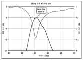
도 3a는 본 발명의 SiP 기반 19GHz 대역 통과 필터의 성능을 보여주는 그래프이다.
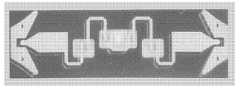
도 3b는 본 발명의 SiP 기반 19GHz 대역 통과 필터의 이미지이다.
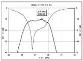
도 4a는 본 발명의 SiP 기반 24GHz 대역 통과 필터의 성능을 보여주는 그래프이다.
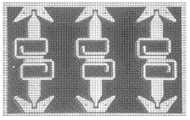
도 4b는 본 발명의 SiP 기반 24GHz 대역 통과 필터의 이미지이다.
도 5a는 본 발명의 SiP 기반 33GHz 저역 통과 필터의 성능을 보여주는 그래프이다.
도 5b는 본 발명의 SiP 기반 33GHz 저역 통과 필터의 이미지를 보여준다.
도 6a는 본 발명의 SiP 기반 28GHz 대역 통과 필터의 성능을 보여주는 그래프이다.
도 6b는 본 발명의 SiP 기반 28GHz 대역 통과 필터의 이미지를 보여준다.
도 7a는 본 발명의 SiP 기반 7GHz 대역 통과 필터의 성능을 보여주는 그래프이다.
도 7b는 본 발명의 여러 개의 SiP 기반 7GHz 대역 통과 필터의 이미지를 보여준다.
도 8은 본 발명의 SiP 기반 필터들의 삽입 손실을 보여주는 그래프이다.
도 9는 본 발명의 집중 소자들을 포함한 도허티 증폭기 설계를 도시한다.
도 10은 전력 분배기/결합기를 도시한다.
도 11은 종단 저항기가 서큘레이터에 연결될 때 집중 소자 서큘레이터를 도시하며, 그것은 아이솔레이터가 된다.
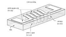
도 12는 본 발명의 통합 집중 소자 디바이스들을 가진 유리 기반 SiP을 도시한다. SiP은 대략 0.5cm×0.5cm이다.
도 13은 본 발명의 통합 집중 소자 디바이스들을 가진 유리 기반 SiP의 샘플링을 도시한다. SiP의 크기에 의존하여, 단일 웨이퍼 상에 다수의 SiP들이 있을 수 있다.
도 14a 내지 도 14f는 본 발명을 사용하여 디바이스들을 만드는 프로세스를 도시한다.
도 15a 내지 도 15f는 본 발명을 사용하여 디바이스를 만들기 위한 추가 프로세싱 단계들을 도시한다.For a more complete understanding of the features and advantages of the invention, reference is now made to the detailed description of the invention together with the accompanying drawings:
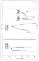
1A is a graph showing the effect of parasitic signals/losses capacitance on the performance of a capacitor in a system-in-package (SiP) versus surface mount technology of the present invention.
1B is a graph showing the effect of parasitic signals/losses on the performance of an inductor in SiP versus SMT of the present invention.
2A is a graph showing the performance of a 30 GHz Ban pass filter and RF distortions in a surface mount package on a PCB of the present invention.
Figure 2b is a graph showing the performance of the 28GHz SiP Ban pass filter of the present invention.
Figure 2c is a graph showing the performance of the SiP-based 2.5GHz all-pass filter of the present invention.
Figure 2d is an image of the SiP-based 2.5 GHz low-pass filter of the present invention.
Figure 3a is a graph showing the performance of the SiP-based 19GHz bandpass filter of the present invention.
Figure 3b is an image of the SiP-based 19GHz bandpass filter of the present invention.
Figure 4a is a graph showing the performance of the SiP-based 24GHz bandpass filter of the present invention.
Figure 4b is an image of the SiP-based 24GHz bandpass filter of the present invention.
Figure 5a is a graph showing the performance of the SiP-based 33GHz low-pass filter of the present invention.
Figure 5b shows an image of the SiP-based 33GHz low-pass filter of the present invention.
Figure 6a is a graph showing the performance of the SiP-based 28GHz bandpass filter of the present invention.
Figure 6b shows an image of the SiP-based 28GHz bandpass filter of the present invention.
7A is a graph showing the performance of the SiP-based 7GHz bandpass filter of the present invention.
7b shows images of several SiP-based 7GHz bandpass filters of the present invention.
8 is a graph showing the insertion loss of SiP-based filters of the present invention.
9 shows a Doherty amplifier design incorporating the lumped elements of the present invention.
10 shows a power divider/combiner.
11 shows a lumped element circulator when the terminating resistor is connected to the circulator, which becomes an isolator.
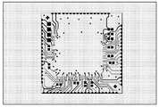
12 shows a glass-based SiP with integrated lumped element devices of the present invention. SiP is approximately 0.5 cm x 0.5 cm.
13 shows a sampling of a glass-based SiP with integrated lumped element devices of the present invention. Depending on the size of the SiP, there may be multiple SiPs on a single wafer.
14A-14F illustrate a process for making devices using the present invention.
15A-15F show additional processing steps for making a device using the present invention.
본 발명의 다양한 실시예들의 제작 및 사용은 이하에서 상세하게 논의되지만, 본 발명은 매우 다양한 특정 맥락들로 구체화될 수 있는 많은 적용 가능한 발명의 개념들을 제공한다는 것이 이해되어야 한다. 여기에서 논의된 특정 실시예들은 발명을 만들고 사용하기 위한 특정 방식들에 대해 단지 예시적이며 발명의 범위를 구분 짓지 않는다.While the making and use of various embodiments of the invention are discussed in detail below, it should be understood that the invention provides many applicable inventive concepts that may be embodied in a wide variety of specific contexts. The specific embodiments discussed herein are merely illustrative of specific ways for making and using the invention and do not delimit the scope of the invention.
본 발명의 이해를 가능하게 하기 위해, 다수의 용어들이 이하에서 정의된다. 여기에서 정의된 용어들은 본 발명에 관련된 분야들에서 통상의 기술자에 의해 일반적으로 이해되는 바와 같은 의미들을 가진다. 단수 표현 및 "상기" 와 같은 용어들은 단지 단수형 엔티티를 나타내도록 의도되지 않으며, 특정 예의 일반적인 클래스는 예시를 위해 사용될 수 있다. 여기에서의 용어는 발명의 특정 실시예들을 설명하기 위해 사용되지만, 그것들의 사용은, 청구항들에서 개괄되는 경우를 제외하고, 발명을 제한하지 않는다.To facilitate an understanding of the present invention, a number of terms are defined below. The terms defined herein have the meanings as commonly understood by one of ordinary skill in the art related to the present invention. The singular expressions and terms such as “the” are not intended to indicate merely a singular entity, and the general class of specific examples may be used for illustration. Although terminology is used herein to describe specific embodiments of the invention, their use does not limit the invention, except as outlined in the claims.
본 발명은 RF 도메인에서 집중 소자 디바이스들과 연관된 기생 손실들 및 신호들을 제거한다. 집중 소자 디바이스들 또는 집중 소자 디바이스들의 어레이는 기생 신호들 또는 손실들을 제거하거나 또는 크게 감소시키는 마이크로파 및 라디오주파수에 대해 광 한정가능 유리 세라믹 시스템 인 패키지(SiP)에 필터들(대역-통과, 대역-정지, 고역-통과, 노치, 저역-통과 필터), 서큘레이터들, 안테나, 전력 조절, 전력 결합기, 전력 스플리터, 매칭 네트워크들, 아이솔레이터들 및/또는 도허티(Doherty) 전력 증폭기를 포함하여 다수의 전자 디바이스들 및 기능들을 구현하기 위해 커패시터들, 인덕터들, 및 저항기들로 이루어진다. 기생 신호들 또는 손실들은 패키징된 집중 소자 디바이스들을 SiP에 부착하는 패키징, 솔더 접합(볼 그리드), 전자 커넥터들(와이어), 전기 접합 패드들 및 장착 소자들로부터의 인덕턴스, 정전용량 및 저항과 조합된 안테나 효과들로부터 발생된다. 왜곡된 신호들 또는 손실들은 인쇄 회로 보드 또는 기판상에서의 다른 RF 디바이스들로 송신된다. 실제 의도된 성능으로부터 큰 성능 변화들을 생성하기 위해 집중 소자들의 종래의 패키징 및 장착에 충분한 변화가 있다. 이들 변화들은 원하는 동작 엔벨로프를 충족시키는 최종 RF 회로를 생성하기 위해 RF 제품들이 다수의 설계 반복들 및/또는 수동 트리밍/정정을 겪게 하는 패키징에서의 미묘한 차이들로 인해 무작위인 것처럼 보인다. RF 패키징 및 장착 소자들과 연관된 왜곡을 제거하는 것은 RF 필터 디바이스가 설계/시뮬레이션된 대로 미리 형성하도록 허용한다. 집중 소자 디바이스들을 광 한정가능 유리 세라믹 SiP으로 통합하는 것은 회로가 전체 RF 스펙트럼을 통해 설계되고 시뮬레이션된 대로 미리 형성할 수 있게 한다. 이들 집중 소자 디바이스 구조들은 디바이스 패리티, 보다 낮은 손실, 낮은 신호 왜곡, 감소된 기생 용량, 감소된 비용, 및 더 작은 물리적 크기에 대한 설계를 갖고 2 또는 3-차원 집중 소자 디바이스들을 형성하기 위해 개별적으로 또는 동시에 수직뿐만 아니라 수평 평면들 양쪽 모두로 이루어진다.The present invention eliminates parasitic losses and signals associated with lumped element devices in the RF domain. The lumped element devices or array of lumped element devices contain filters (band-pass, band-pass) in a light confining glass ceramic system in package (SiP) for microwave and radio frequency that eliminates or greatly reduces parasitic signals or losses. stop, high-pass, notch, low-pass filter), circulators, antennas, power conditioning, power combiners, power splitters, matching networks, isolators and/or Doherty power amplifiers. It consists of capacitors, inductors, and resistors to implement devices and functions. Parasitic signals or losses combine with inductance, capacitance and resistance from packaging, solder joints (ball grids), electronic connectors (wires), electrical bonding pads and mounting elements that attach packaged lumped device devices to SiP. resulting from the antenna effects. Distorted signals or losses are transmitted to the printed circuit board or other RF devices on the substrate. There is sufficient variation in conventional packaging and mounting of lumped elements to produce large performance variations from actual intended performance. These changes appear to be random due to nuances in packaging that cause RF products to undergo multiple design iterations and/or manual trimming/correction to produce a final RF circuit that meets the desired operating envelope. Eliminating distortion associated with RF packaging and mounting elements allows the RF filter device to be preformed as designed/simulated. Incorporating the concentrator devices into a light confining glass ceramic SiP allows the circuit to be preformed as designed and simulated over the entire RF spectrum. These lumped element device structures can be individually designed to form two or three-dimensional lumped element devices with design for device parity, lower loss, lower signal distortion, reduced parasitic capacitance, reduced cost, and smaller physical size. or in both vertical as well as horizontal planes at the same time.
배경에서 설명된 바와 같이, 감광성 유리 구조들은 다른 소자 시스템들 또는 서브시스템들과 함께 통합 전자 소자들과 같은 다수의 미세 기계 가공 및 미세 제작 프로세스들을 위해 제안되어 왔다. 본 발명은 값비싸고 낮은 수율인 종래의 유리의 실리콘 미세 제작에 비해 이점들을 갖지만 사출 성형 또는 엠보싱 프로세스들은 일관되지 않은 형태들을 생성한다. 본 발명은, 값비싼 자본 장비; 일반적으로 각각 백만 달러를 초과하는 비용이 들며 수백만 내지 수십억 이상이 드는 초-청정, 고-생산 실리콘 제작 설비를 요구하는 포토리소그래피 및 반응성 이온 에칭 또는 이온 빔 밀링 툴들에 의존하는 실리콘 미세 제작 프로세스들에 비해 추가 이점들을 가진다. 본 발명은 또한 이송 시 가진 결함들을 생성하거나 또는 스토캐스틱 경화 프로세스로 인한 차이들을 갖는 사출 성형 및 엠보싱이 가진 문제들을 극복한다. 이상적인 인덕터들은 0 저항 및 0 정전용량을 가질 것이다. 그러나, 실제 인덕터들은 "기생" 저항, 인덕터들 및 정전용량을 가진다. 인덕터의 제 1 자기-공진 주파수는 인덕터가 그것의 자기-정전용량을 갖고 공진하는 최저 주파수이다. 제 1 공진은 인덕턴스 및 정전용량의 병렬 조합에 의해 모델링될 수 있다. 저항기("R1")는 인덕터의 자기-공진 주파수(SRF)에서의 공진 주파수에 가깝게 임피던스를 제한하며, 다음의 조건들 중 모두가 충족된다: (1) 입력 임피던스는 그것의 피크에 있다; (2) 입력 임피던스의 위상 각도는 0이어서, 양(유도성)에서 음(용량성)으로 가로지른다; (3) 위상 각이 0이므로, Q는 0이다; (4) 음의 용량성 리액턴스(Xc=1/jωC)가 단지 양의 유도성 리액턴스(XL=jωL)를 소거하므로, 유효 인덕턴스는 0이다; (5) 2-포트 삽입 손실(예컨대, S21 dB)이 최대이며, 이것은 주파수 대 S21 dB의 플롯에서 최소치에 대응한다; 및 (6) 2-포트 위상(예컨대, S21) 각도는 0이어서, 하위 주파수들에서의 음에서 상위 주파수들에서의 양으로 가로지른다.As described in the background, photosensitive glass structures have been proposed for a number of micromachining and microfabrication processes, such as integrated electronic devices along with other device systems or subsystems. The present invention has advantages over expensive and low yield silicon microfabrication of conventional glass, but injection molding or embossing processes produce inconsistent shapes. The present invention relates to expensive capital equipment; Silicon microfabrication processes that rely on photolithography and reactive ion etching or ion beam milling tools that typically cost in excess of a million dollars each and require ultra-clean, high-production silicon fabrication facilities costing millions to billions or more. have additional advantages compared to The present invention also overcomes the problems with injection molding and embossing that create defects in transport or have differences due to the stochastic curing process. Ideal inductors would have zero resistance and zero capacitance. However, real inductors have “parasitic” resistance, inductors and capacitance. The first self-resonant frequency of the inductor is the lowest frequency at which the inductor resonates with its self-capacitance. The first resonance can be modeled by a parallel combination of inductance and capacitance. Resistor “R1” limits the impedance close to the resonant frequency at the self-resonant frequency (SRF) of the inductor, and all of the following conditions are met: (1) the input impedance is at its peak; (2) the phase angle of the input impedance is zero, traversing from positive (inductive) to negative (capacitive); (3) Since the phase angle is zero, Q is zero; (4) since the negative capacitive reactance (Xc=1/jωC) only cancels the positive inductive reactance (XL=jωL), the effective inductance is zero; (5) the two-port insertion loss (eg, S21 dB) is maximum, which corresponds to the minimum in the plot of frequency versus S21 dB; and (6) the two-port phase (eg, S21) angle is zero, traversing from negative at lower frequencies to positive at higher frequencies.
이들 요구들을 다루기 위해, 본 발명자들은 반도체들, RF 전자 장치들, 마이크로파 전자 장치들, 및 광학 이미징을 위한 신규 패키징 및 기판 재료로서 유리 세라믹(APEX® 유리 세라믹)을 개발하였다. APEX® 유리 세라믹은 단순한 3단계 프로세스에서 1세대 반도체 장비를 사용하여 프로세싱되며 최종 재료는 유리, 세라믹으로 만들어지거나, 또는 유리 및 세라믹 양쪽 모두의 영역들을 포함한다. APEX® 유리 세라믹은 다음 중 하나 또는 일부를 포함하는 SiP의 생성을 가능하게 한다: 쉽게 제작된 고 밀도 비아들, 인덕터들, 커패시터들, 저항기들, 송신 라인들, 동축 라인들, 안테나, 마이크로프로세서, 메모리, 증폭기, 트랜지스터들, 매칭 네트워크들, RF 필터들, RF 서큘레이터들, RF 아이솔레이터들, 임피던스 정합 소자들, 50 옴 종단 소자들, 통합 접지 평면들, RF 차폐 소자들, EMI 차폐 소자들, RF 결합기들, RF 스플리터들, 변압기들, 스위치들, 멀티플렉서들, 및/또는 다이플렉서들을 포함한 전자 디바이스들.To address these needs, the inventors have developed glass ceramic (APEX® glass ceramic) as a novel packaging and substrate material for semiconductors, RF electronic devices, microwave electronic devices, and optical imaging. APEX® glass ceramics are processed using first-generation semiconductor equipment in a simple three-step process and the final material is made of glass, ceramic, or includes regions of both glass and ceramic. APEX® glass ceramic enables the creation of a SiP comprising one or some of the following: easily fabricated high density vias, inductors, capacitors, resistors, transmission lines, coaxial lines, antennas, microprocessors , memory, amplifiers, transistors, matching networks, RF filters, RF circulators, RF isolators, impedance matching elements, 50 ohm termination elements, integrated ground planes, RF shielding elements, EMI shielding elements , RF couplers, RF splitters, transformers, switches, multiplexers, and/or electronic devices including diplexers.
도 1a는 동일한 3pF 및 5pF 커패시터들에 대한 테스트 결과들을 도시한다. 일 세트의 커패시터들이 유리 SiP 상에서 통합되고 테스트되었다. 다른 세트의 커패시터들은 표면 장착 기술(SMT)로 패키징되고 테스트되었다. 결과 데이터는 SiP 통합 커패시터가 동일한 커패시터 패키징 SMT에 비교하여 150% 내지 135% 사이에서의 더 높은 SRF를 갖는다는 것을 보여주며, 따라서 종래 기술보다 상당히 낫다. 성능에서의 개선은 SMT 패키징과 연관된 접합 패드들, 볼 접합, 내장 리드들, 기판 및 다른 기생 효과들로부터의 손실들의 제거 때문이다. 도 1b는 SMT 또는 통합 SiP에서 측정된 두 개의 인덕터들 간의 성능(56nH 및 95nH)을 도시한다. SiP 기반 인덕터들은 SMT 패키징의 패드들에 의해 생성된 정전용량과 연관된 기생 손실들 또는 신호들의 제거로 인해 SMT 부분들보다 50% 더 높은 SRF를 갖는다. 평균적으로 통합 SIP 구성요소들은 SMT와 정확히 동일한 부분에 비교하여 50% 더 높은 SRF를 갖는다. SMT 디바이스들에 대한 통합 SIP 디바이스들 간의 성능 차이들이 dB로 측정됨에 따라, 그것은 패키지로 시스템을 만들기 위해 사용된 다른 RF/마이크로파 구성요소들 외에 필터들, 도허티 증폭기들, 서큘레이터들, 아이솔레이터들, 안테나, 전력 스플리터들, 전력 결합기들에서 실현된 조합 인덕터들 및 커패시터들의 사용과 연관된 기생 손실들 또는 신호들을 부가할 수 있다. 손실들의 조합은 도 2a 내지 도 2d에서 보여질 수 있다. 도 2a 및 도 2b는 SiP으로 통합된 집중 소자 필터의 성능과 표면 장착 디바이스(SMD) 패키지로 패키징된 다른 것 사이에서의 차이를 도시한다. 도 1a는 인쇄 회로 보드 기반 SiP 상에 장착된 SMD 패키지에서 집중 소자 대역통과 필터에 대한 신호를 도시한다. 도 1b는 유리 기반 SiP로 직접 통합된 동일한 집중 소자 대역통과 필터에 대한 신호를 도시한다. 도 1a 및 도 1b의 성능 곡선들 하에서 영역들 간의 정규화된 차이는 대략 200%이다. 이것은 SiP 기판으로 직접 통합된 RF 집중 소자 디바이스의 사용이 200%까지 기생 잡음 및 손실들을 감소시키거나 또는 제거한다는 것을 보여준다. 손실들, 왜곡/잡음, 기생 신호들 및 열악한 성능 품질 인자를 제거한다. SiP 기반 집중 소자 디바이스들은 120보다 훨씬 더 큰 품질 인자들을 가진 인덕터들과 함께 80보다 훨씬 더 큰 품질 인자들을 가진 커패시터들을 가질 수 있다. SiP으로 직접 통합되는 집중 소자 디바이스들의 강화된 성능은 이제 작은 피처 크기와 결합될 수 있는 RF/마이크로파 디바이스에서 극적으로 개선된 기능을 입증하여 왔다. SiP으로 또는 그것 상으로 직접 통합된 집중 소자 기반 디바이스들은 이에 제한되지 않지만 RF 필터들, RF 서큘레이터들, RF 아이솔레이터들, 안테나, 임피던스 정합 소자들, 50옴 종단 소자들, 통합 접지 평면들, RF 차폐 소자들, EMI 차폐 소자들, RF 결합기들, RF 스플리터들, 변압기들, 스위치들, 전력 스플리터들, 전력 결합기들, 및/또는 다이플렉서들을 포함한다. SiP 상에서 이들 직접 통합된 집중 소자 디바이스들은 통합 회로 디바이스들과 연결된다. 이들 통합 회로들은, 이에 제한되지 않지만: 마이크로프로세서들, 멀티플렉서들, 스위치들, 증폭기들, 및 메모리들을 포함한다. 도 3a는 본 발명의 SiP 기반 19GHz 대역 통과 필터의 성능을 보여주는 그래프이다. 도 3b는 본 발명의 SiP 기반 19GHz 대역 통과 필터의 이미지이다.1A shows test results for the same 3pF and 5pF capacitors. A set of capacitors were integrated and tested on glass SiP. Another set of capacitors was packaged and tested with surface mount technology (SMT). The resulting data show that the SiP integrated capacitor has a higher SRF between 150% and 135% compared to the same capacitor packaging SMT, and thus significantly better than the prior art. The improvement in performance is due to the elimination of losses from bond pads, ball bonds, embedded leads, substrate and other parasitic effects associated with SMT packaging. Figure 1b shows the performance (56nH and 95nH) between two inductors measured in SMT or integrated SiP. SiP based inductors have a 50% higher SRF than SMT parts due to the elimination of parasitic losses or signals associated with capacitance generated by the pads of the SMT packaging. On average, the integrated SIP components have a 50% higher SRF compared to exactly the same part as the SMT. As the performance differences between the integrated SIP devices for the SMT devices are measured in dB, it includes filters, Doherty amplifiers, circulators, isolators, in addition to other RF/microwave components used to make the system into a package. Add parasitic losses or signals associated with the use of combination inductors and capacitors realized in antennas, power splitters, power combiners. The combination of losses can be seen in FIGS. 2A-2D . 2A and 2B show the performance of a lumped element filter incorporated into SiP and the difference between others packaged in a surface mount device (SMD) package. 1A shows the signal for a lumped element bandpass filter in an SMD package mounted on a printed circuit board based SiP. Figure 1b shows the signal for the same lumped element bandpass filter integrated directly into the glass-based SiP. The normalized difference between regions under the performance curves of FIGS. 1A and 1B is approximately 200%. This shows that the use of an RF concentrator device directly integrated into the SiP substrate reduces or eliminates parasitic noise and losses by up to 200%. Eliminates losses, distortion/noise, parasitics and poor performance quality factors. SiP based lumped element devices may have capacitors with quality factors much greater than 80 along with inductors with quality factors much greater than 120. The enhanced performance of lumped element devices directly integrated into SiP has now demonstrated dramatically improved functionality in RF/microwave devices that can be combined with small feature sizes. Concentrated element based devices integrated directly into or on SiP include, but are not limited to, RF filters, RF circulators, RF isolators, antennas, impedance matching elements, 50 ohm termination elements, integrated ground planes, RF shielding elements, EMI shielding elements, RF couplers, RF splitters, transformers, switches, power splitters, power couplers, and/or diplexers. These directly integrated concentrator devices on SiP are connected with integrated circuit devices. These integrated circuits include, but are not limited to: microprocessors, multiplexers, switches, amplifiers, and memories. Figure 3a is a graph showing the performance of the SiP-based 19GHz bandpass filter of the present invention. Figure 3b is an image of the SiP-based 19GHz bandpass filter of the present invention.
도 4a는 본 발명의 SiP 기반 24GHz 대역 통과 필터의 성능을 보여주는 그래프이다. 본 발명은 정전용량 대 주파수를 측정할 때 본 발명의 SiP 대 SMT에 대해 150% 및 135%만큼 신호를 개선하였다. 도 4b는 SiP 기반 24GHz 대역 통과 필터의 성능을 보여주는 그래프이다. 본 발명은 인덕턴스 대 주파수를 측정할 때 SMT에 비교될 때 본 발명의 SiP을 사용하여 50%만큼 신호를 개선하였다.Figure 4a is a graph showing the performance of the SiP-based 24GHz bandpass filter of the present invention. The present invention improved the signal by 150% and 135% for our SiP versus SMT when measuring capacitance versus frequency. 4B is a graph showing the performance of the SiP-based 24 GHz bandpass filter. The present invention improves the signal by 50% using the inventive SiP when compared to SMT when measuring inductance versus frequency.
도 5a는 본 발명의 SiP 기반 33GHz 저역 통과 필터의 성능을 보여주는 그래프이다. 도 5b는 본 발명의 SiP 기반 33GHz 저역 통과 필터의 이미지를 도시힌다.Figure 5a is a graph showing the performance of the SiP-based 33GHz low-pass filter of the present invention. Figure 5b shows an image of the SiP-based 33 GHz low-pass filter of the present invention.
도 6a는 본 발명의 SiP 기반 28GHz 대역 통과 필터의 성능을 보여주는 그래프이다. 도 6b는 본 발명의 SiP 28GHz 대역 통과 필터의 이미지를 도시한다.Figure 6a is a graph showing the performance of the SiP-based 28GHz bandpass filter of the present invention. Figure 6b shows an image of the
도 7a는 본 발명의 SiP 기반 7GHz 대역 통과 필터의 성능을 보여주는 그래프이다. 도 7b는 본 발명의 여러 개의 SiP 기반 7GHz 대역 통과 필터의 이미지를 도시한다.7A is a graph showing the performance of the SiP-based 7GHz bandpass filter of the present invention. Figure 7b shows an image of several SiP-based 7GHz bandpass filters of the present invention.
도 8은 본 발명의 SiP 기반 필터들의 삽입 손실을 보여주는 그래프이다.8 is a graph showing the insertion loss of SiP-based filters of the present invention.
도 9는 본 발명을 사용하여 만들어질 수 있는 집중 소자들을 포함한 도허티 증폭기 설계를 도시한다. 도 10은 본 발명을 사용하여 만들어질 수 있는 전력 분배기/조합기를 도시한다. 도 11은 종단 저항기가 서큘레이터에 연결될 때 집중 소자 서큘레이터를 도시하며, 그것은 아이솔레이터가 되며 본 발명을 사용하여 만들어질 수 있다. 도 12는 본 발명의 통합 집중 소자 디바이스들을 가진 유리 기반 SiP을 도시한다. SiP은 대략 0.5cm×0.5cm이다. 도 13은 본 발명의 통합 집중 소자 디바이스들을 가진 유리 기반 SiP의 샘플링을 도시한다. SiP의 크기에 의존하여, 단일 웨이퍼 상에 다수의 SiP들이 있을 수 있다.9 shows a Doherty amplifier design including lumped elements that can be made using the present invention. 10 shows a power divider/combiner that can be made using the present invention. 11 shows a lumped element circulator when a terminating resistor is connected to the circulator, which becomes an isolator and can be made using the present invention. 12 shows a glass-based SiP with integrated lumped element devices of the present invention. SiP is approximately 0.5 cm x 0.5 cm. 13 shows a sampling of a glass-based SiP with integrated lumped element devices of the present invention. Depending on the size of the SiP, there may be multiple SiPs on a single wafer.
특히 통합 집중 소자 RF 디바이스를 가진 SiP는 종래의 반도체 프로세싱 장비를 사용하여 APEX® Glass에서 디바이스 패리티에 대한 설계를 갖고 생성되어 왔다. APEX® Glass SiP에서 통합 집중 소자 RF 필터는 도 12에서 보여질 수 있다. 통합 집중 소자 디바이스들을 가진 APEX® Glass SiP. SiP의 중심에서 개방 영역은 SiP을 완성하기 위해 통합 회로들의 배치를 위한 것이다. 도 13은 본 발명의 통합 집중 소자 디바이스들을 가진 유리 기반 SiP의 샘플링을 도시한다. SiP의 크기에 의존하여, 단일 웨이퍼 상에 다수의 SiP들이 있을 수 있다. APEX® Glass 웨이퍼는 통합 집중 소자 디바이스들을 갖고 500 SiP 위에 실장된다.Specifically, SiPs with integrated concentrator RF devices have been created with design for device parity in APEX® Glass using conventional semiconductor processing equipment. An integrated concentrator RF filter in APEX® Glass SiP can be seen in FIG. 12 . APEX® Glass SiP with integrated concentrator devices. An open area in the center of the SiP is for the placement of integrated circuits to complete the SiP. 13 shows a sampling of a glass-based SiP with integrated lumped element devices of the present invention. Depending on the size of the SiP, there may be multiple SiPs on a single wafer. The APEX® Glass wafer is mounted on 500 SiP with integrated lumped device devices.
완전 통합 집중 소자 디바이스를 가진 SiP은 광-한정가능 유리들에서 생성되고, 높은 온도 안정성, 양호한 기계적 및 전기적 속성들을 가지며, 플라스틱들 및 많은 금속들보다 양호한 화학적 저항을 가질 수 있다. 우리가 아는 한, 유일한 상업적 광-한정가능 유리는 Schott Corporation에 의해 만들어진, FOTURAN™이다. FOTURAN™은 은 이온들의 트레이스들을 포함한 리튬-알루미늄-실리케이트 유리를 포함한다. 세륨 산화물의 흡수 대역 내에서 UV-광에 노출될 때, 세륨 산화물은 감광물질들로서 동작하여, 광자를 흡수하고 은 원자들을 형성하기 위해 이웃한 은 산화물을 환원하는 전자를 놓아준다, 예로서,SiP with fully integrated concentrator device is produced in light-definable glasses, has high temperature stability, good mechanical and electrical properties, and can have better chemical resistance than plastics and many metals. To the best of our knowledge, the only commercial light-limitable glass is FOTURAN™, made by Schott Corporation. FOTURAN™ contains lithium-aluminum-silicate glass containing traces of silver ions. When exposed to UV-light within the absorption band of cerium oxide, cerium oxide acts as photosensitive materials, absorbing photons and releasing electrons that reduce neighboring silver oxide to form silver atoms, e.g.,
Ce3+ + Ag+ = Ce4+ + Ag0Ce3+ + Ag+ = Ce4+ + Ag0
은 원자들은 베이킹 프로세스 동안 은 나노클러스터들로 합쳐지며 주변 유리의 결정화를 위해 핵형성 사이트들을 유도한다. 마스크를 통해 UV 광에 노출되면, 단지 유리의 노출 영역들만이 뒤이은 열 처리 동안 결정화할 것이다.Silver atoms coalesce into silver nanoclusters during the baking process and induce nucleation sites for crystallization of the surrounding glass. When exposed to UV light through a mask, only the exposed areas of the glass will crystallize during subsequent heat treatment.
이러한 열 처리는 유리 변형 온도(예컨대, FOTURAN™에 대해 공기 중에서 465℃보다 큰)에 가까운 온도로 수행되어야 한다. 결정질 상은 노출되지 않은 유리같은, 비정질 영역들보다, 불화 수소산(HF)과 같은, 에천트들에서 더 용해 가능하다. 특히, FOTURAN™의 결정질 영역들은 10% HF에서의 비정질 영역들보다 약 20배 더 빠르게 에칭되어, 노출된 영역들이 제거될 때 약 20:1의 벽 기울기 비율들을 가진 미세구조들을 가능하게 한다. 여기에 참조로서 통합되는, 미세전자 엔지니어링 30, 497(1996), T. R. Dietrich 외의, "포토 에칭 가능 유리를 이용한 마이크로시스템들을 위한 제작 기술들"을 참조하자.This heat treatment should be performed at a temperature close to the glass deformation temperature (eg, greater than 465° C. in air for FOTURAN™). The crystalline phase is more soluble in etchants, such as hydrofluoric acid (HF), than unexposed glassy, amorphous regions. In particular, crystalline regions of FOTURAN™ etch about 20 times faster than amorphous regions at 10% HF, enabling microstructures with wall slope ratios of about 20:1 when exposed regions are removed.
바람직하게는, 성형된 유리 구조는 적어도 하나 이상의, 2 또는 3-차원 유도성 디바이스를 포함한다. 유도성 디바이스는 독립된 인덕터를 형성하기 위해 일련의 연결된 루프들을 만듦으로써 형성된다. 루프들은 유도를 생성하는 패턴을 생성하는 직사각형, 원형, 타원형, 프랙털 또는 다른 형태들일 수 있다. APEX® 유리의 패터닝된 영역들은 도금 또는 기체 상 증착을 포함한 다수의 방법들에 의해, 금속, 합금들, 합성물들, 유리 또는 다른 자기 매체로 채워질 수 있다. 디바이스에서 구조들(루프들, 턴들 또는 다른 유도성 소자)의 치수들 및 수와 조합된 매체의 자기 자기 유전율은 디바이스들의 인덕턴스를 제공한다.Preferably, the shaped glass structure comprises at least one, two or three-dimensional inductive device. An inductive device is formed by making a series of connected loops to form an independent inductor. The loops can be rectangular, circular, oval, fractal or other shapes creating a pattern that creates an induction. Patterned regions of APEX® glass can be filled with metal, alloys, composites, glass or other magnetic medium by a number of methods including plating or gas phase deposition. The magneto-permittivity of the medium in combination with the dimensions and number of structures (loops, turns or other inductive element) in the device provides the inductance of the devices.
FOTURAN™은 중량으로 75 내지 85%의 실리콘 산화물(SiO2), 중량으로 7 내지 11%의 리튬 산화물(Li2O), 중량으로 3 내지 6%의 알루미늄 산화물(Al2O3), 중량으로 1 내지 2%의 나트륨 산화물(Na2O), 중량으로 0.2 내지 0.5%의 안티모늄 삼산화물(Sb2O3) 또는 비소 산화물(As2O3), 중량으로 0.05 내지 0.15%의 은 산화물(Ag2O), 및 중량으로 0.01 내지 0.04%의 세륨 산화물(CeO2)로 구성된 Invenios에 의해 공급된 정보(FOTURAN™에 대한 U.S. 공급자)에서 설명된다. 여기에서 사용된 바와 같이, 용어들("APEX® Glass 세라믹", "APEX 유리" 또는 간단히 "APEX")은 본 발명의 유리 세라믹 조성물의 일 실시예를 나타내기 위해 사용된다.FOTURAN™ contains 75 to 85% by weight silicon oxide (SiO2 ), 7 to 11% lithium oxide (Li2 O) by weight, 3 to 6% aluminum oxide (Al2 O3 ) by weight, 1 to 2% sodium oxide (Na2 O), 0.2 to 0.5% by weight antimonium trioxide (Sb2 O3 ) or arsenic oxide (As2 O3 ), 0.05 to 0.15% by weight silver oxide ( Ag2 O), and information supplied by Invenios (US supplier for FOTURAN™) consisting of 0.01-0.04% cerium oxide (CeO2 ) by weight. As used herein, the terms (“APEX® Glass ceramic”, “APEX glass” or simply “APEX”) are used to refer to one embodiment of the glass ceramic composition of the present invention.
본 발명은 렌즈들을 위해 사용되는 성형된 APEX 유리 구조들에 의해 이미징 애플리케이션들에서의 사용을 위한 광-한정가능 APEX 유리를 갖는 광학 미세구조들의 제작을 위한 단일 재료 접근법을 제공하며 스루-층 또는 층-내 설계들을 포함한다.The present invention provides a single material approach for the fabrication of optical microstructures with photo-definable APEX glass for use in imaging applications with shaped APEX glass structures used for lenses and through-layer or layer. -Including my designs.
일반적으로, 유리 세라믹 재료들은 성능, 균일성, 다른 것들에 의한 사용 가능성 및 이용 가능성 이슈들로 괴로워하는 미세구조 형성에서 성공을 제한하여 왔다. 과거 유리-세라믹 재료들은 APEX® 유리가 50:1보다 큰 평균 에칭 종횡비를 갖는 것과 대조적으로 대략 15:1의 에칭 종횡-비를 산출하여 왔다. 이것은 사용자들이 더 작고 더 깊은 특징들을 생성하도록 허용한다. 부가적으로, 우리의 제조 프로세스는 90%보다 큰 제품 수율들을 가능하게 한다(레거시 유리 수율들은 50%에 더 가깝다). 마지막으로, 레거시 유리 세라믹들에서, 유리의 대략 30%만이 세라믹 상태로 변환되는 반면, APEX® Glass 세라믹을 갖고, 이러한 변환은 70%에 더 가깝다.In general, glass ceramic materials have limited success in forming microstructures that suffer from performance, uniformity, usability by others, and usability issues. Past glass-ceramic materials have yielded an etch aspect-ratio of approximately 15:1 as opposed to APEX® glass having an average etch aspect ratio greater than 50:1. This allows users to create smaller and deeper features. Additionally, our manufacturing process enables product yields greater than 90% (legacy glass yields are closer to 50%). Finally, in legacy glass ceramics, only approximately 30% of the glass is converted to a ceramic state, whereas with APEX® Glass ceramic, this conversion is closer to 70%.
APEX® Glass 조성물은 그것의 강화된 성능을 위해 3개의 주요 메커니즘들을 제공한다: (1) 더 높은 양의 은은 결정립계들에서 더 빠르게 에칭되는 더 작은 세라믹 결정들의 형성을 이끈다, (2) 실리카 함량(HF 산에 의해 에칭된 주요 성분)에서의 감소는 노출되지 않은 재료의 바람직하지 않은 에칭을 감소시킨다, 및 (3) 알칼리 금속들 및 붕소 산화물의 더 높은 총 중량 퍼센트는 제조 동안 훨씬 더 동질의 유리를 생성한다.The APEX® Glass composition provides three major mechanisms for its enhanced performance: (1) higher amounts of silver lead to the formation of smaller ceramic crystals that etch faster at grain boundaries, (2) silica content ( The reduction in the main component etched by HF acid) reduces the undesirable etching of the unexposed material, and (3) the higher total weight percentage of alkali metals and boron oxide makes the glass much more homogeneous during manufacture. create
본 발명은 전자기 송신, 변압기들 및 필터링 애플리케이션들에서 사용된 유도성 구조들을 형성할 때 사용을 위한 유리 세라믹 구조를 제작하기 위한 방법을 포함한다. 본 발명은 유리-세라믹 기판의 다수의 평면들에서 생성된 유도성 구조들을 포함하며, 이러한 프로세싱은 (a) 기판의 또는 에너지 소스의 배향을 변경함으로써 다양한 각도들에서 노출이 발생하도록 하는 여기 에너지로의 노출, (b) 베이크 단계 및 (c) 에칭 단계를 이용한다. 각도 크기들은 예각 또는 둔각일 수 있다. 곡선 및 디지털 구조들은, 대부분의 유리, 세라믹 또는 실리콘 기판들에서 생성하는 것이 실행 불가능하지 않다면, 어렵다. 본 발명은 유리-세라믹 기판들에 대해 수직뿐만 아니라 수평 평면 양쪽 모두에 이러한 구조들을 생성하기 위한 능력을 생성하여 왔다. 본 발명은 유리 세라믹 상에 또는 그것에 유도성 구조의 제작을 위한 방법을 포함한다.The present invention includes a method for fabricating a glass ceramic structure for use in forming inductive structures used in electromagnetic transmission, transformers and filtering applications. The present invention includes inductive structures created in multiple planes of a glass-ceramic substrate, such processing with (a) excitation energy such that exposure occurs at various angles by changing the orientation of the substrate or of the energy source. exposure, (b) a bake step, and (c) an etch step. Angular magnitudes may be acute or obtuse. Curves and digital structures are difficult, if not impossible to create on most glass, ceramic or silicon substrates. The present invention has created the ability to create such structures in both vertical as well as horizontal planes for glass-ceramic substrates. The present invention includes a method for the fabrication of an inductive structure on or in a glass ceramic.
유리의 도재화(ceramicization)는 전체 유리 기판을 대략 20J/㎠의 310nm 광에 노출시킴으로써 성취된다. 세라믹 내에서 유리 공간들을 생성하려고 할 때, 사용자들은, 유리가 계속 유리인 경우를 제외하고, 재료의 모두를 노출시킨다. 일 실시예에서, 본 발명은 상이한 직경들을 가진 다양한 동심원들을 포함한 석영/크롬 마스크를 제공한다.Ceramicization of the glass is achieved by exposing the entire glass substrate to approximately 20 J/
본 발명은 전기 마이크로파 및 라디오 주파수 애플리케이션들에서 유리 세라믹 구조에 또는 그것 상에 유도성 디바이스를 제작하기 위한 방법을 포함한다. 유리 세라믹 구조는 이에 제한되지 않지만: 60 내지 76 중량 % 실리카; 6 중량 % 내지 16 중량 %의 K2O 및 Na2O의 조합을 가진 적어도 3 중량 % K2O; Ag20 및 Au2O로 이루어진 그룹으로부터 선택된 0.003 내지 1 중량 %의 적어도 하나의 산화물; 0.003 내지 2 중량 % Cu2O; 0.75 중량 % 내지 7 중량 % B2O3, 및 6 내지 7 중량 % Al2O3로 B2O3와 Al2O3의 조합은 13 중량 %를 넘지 않고; 8 내지 15 중량 % Li2O; 및 0.001 내지 0.1 중량 % CeO2를 포함한 다수의 조성 변화들을 가진 감광성 유리 기판일 수 있다. 이것 및 다른 변경된 조성은 일반적으로 APEX® 유리로서 불리운다.The present invention includes a method for fabricating an inductive device in or on a glass ceramic structure in electrical microwave and radio frequency applications. Glass ceramic structures include, but are not limited to: 60 to 76 weight % silica; at least 3 wt % K2 O with a combination of 6 wt % to 16 wt % K2 O and Na2 O; 0.003 to 1% by weight of at least one oxide selected from the group consisting of
노출된 부분은 유리 변형 온도에 가까운 온도로 유리 기판을 가열함으로써 결정성 재료로 변형될 수 있다. 불화 수소산과 같은 에천트에 유리 기판을 에칭시킬 때, 노출된 부분 대 노출되지 않은 부분의 이방성-에칭 비는, 유리가 적어도 30:1의 종횡 비를 갖는 성형된 유리 구조를 제공하기 위해, 및 유도성 구조를 생성하기 위해 넓은 스펙트럼 중간-자외선(약 308 내지 312nm)에 노출될 때 적어도 30:1이다. 노출을 위한 마스크는 유도성 구조/디바이스를 생성하기 위한 곡선 구조를 형성하기 위해 연속적인 그레이스케일을 노출에 제공하는 하프톤 마스크일 수 있다. 하프톤 마스크 또는 그레이스케일은 노출 강도를 제어함으로써 디바이스 구조의 제어를 가능하게 한다. 디지털 마스크의 언더컷은 또한 유도성 구조/디바이스의 생성을 위해 생성하기 위해 사용될 수 있는 전면 노출(flood exposure)과 함께 사용될 수 있다. 노출된 유리는 그 후 통상적으로 2-단계 프로세스에서 베이킹된다. 온도 범위는 은 이온들의 은 나노입자들로의 합침을 위해, 10분 내지 2시간 사이 동안 420℃ 내지 520℃ 사이에서 가열되며 온도 범위는 10분 내지 2시간 사이 동안 520℃ 내지 620℃ 사이에서 가열되어, 리튬 산화물이 은 나노입자들 주위에 형성하도록 허용한다. 유리 판은 그 후 에칭된다. 유리 기판은 통상적으로 5% 내지 10% 볼륨으로, HF 용액의, 에천트에서 에칭되며, 여기에서 노출된 부분의 에치 비 대 노출되지 않은 부분의 것은, 이방성-에칭을 성형된 유리 구조에 제공하기 위해, 광 스펙트럼 중간-자외선 투광 조명으로 노출될 때 적어도 30:1이며, 레이저로 노출될 때 30:1보다 크다.The exposed portion can be transformed into a crystalline material by heating the glass substrate to a temperature close to the glass deformation temperature. When etching the glass substrate in an etchant such as hydrofluoric acid, the anisotropic-etch ratio of the exposed portion to the unexposed portion is such that the glass provides a shaped glass structure having an aspect ratio of at least 30:1, and at least 30:1 when exposed to broad spectrum mid-ultraviolet (about 308-312 nm) to create an inductive structure. The mask for the exposure may be a halftone mask that provides a continuous grayscale to the exposure to form a curved structure for creating an inductive structure/device. A halftone mask or grayscale allows control of the device structure by controlling the intensity of exposure. The undercut of the digital mask can also be used with a flood exposure which can be used to create for the creation of inductive structures/devices. The exposed glass is then baked, typically in a two-step process. The temperature range is between 420° C. and 520° C. for between 10 minutes and 2 hours and the temperature range is between 520° C. and 620° C. for between 10 minutes and 2 hours, for incorporation of silver ions into silver nanoparticles. This allows lithium oxide to form around the silver nanoparticles. The glass plate is then etched. Glass substrates are typically etched in an etchant, in an HF solution, at 5% to 10% volume, wherein the etch ratio of the exposed portion to that of the unexposed portion provides an anisotropic-etching to the molded glass structure. For this purpose, the light spectrum is at least 30:1 when exposed with mid-ultraviolet flood illumination and greater than 30:1 when exposed with laser.
유리 기판은 그 후 통상적으로 5% 내지 10% 볼륨으로 HF 용액의, 에천트에서 에칭된다. 완전히 통합된 집중 소자 디바이스(들) 구조는 다음에 의한 생성으로 생성된다:The glass substrate is then etched in an etchant, typically in a HF solution, to 5% to 10% volume. A fully integrated centralized element device(s) structure is created by creating:
본 발명 및 그것의 이점들은 상세하게 설명되었지만, 다양한 변화들, 대체들 및 변경들은 첨부된 청구항들에 의해 정의된 바와 같이 발명의 사상 및 범위로부터 벗어나지 않고 이루어질 수 있다는 것이 이해되어야 한다. 원하는 회로 성능 또는 재료 호환 가능성인 몇몇 경우들에서, SiP은 광-한정가능 유리 기반 디바이스들 중 하나 대신에, 저항기, 커패시터, 또는 인덕터의 SMD 버전을 사용하려고 택할 수 있다. 소자들 중 하나 이상의 SMD 버전을 사용하는 것은 조립 및 패키징시 추가 주의를 요구하는 SiP의 기생 생성 잡음에 기여할 것이다. 게다가, 본 출원의 범위는 명세서에 설명된 프로세스, 기계, 제조물, 물질 조성, 수단, 방법들 및 단계들이 특정한 실시예들에 제한되도록 의도되지 않는다. 이 기술분야의 통상의 기술자가 본 발명의 개시로부터 쉽게 이해할 바와 같이, 현재 존재하거나 또는 나중에 개발될, 대체로 동일한 기능을 수행하거나 또는 여기에서 설명된 대응하는 실시예들과 대체로 동일한 결과를 달성하는, 프로세스들, 기계들, 제조물, 물질 조성, 수단들, 방법들, 또는 단계들은 본 발명에 따라 이용될 수 있다. 따라서, 첨부된 청구항들은 그것들의 범위 내에서 이러한 프로세스들, 기계들, 제조물, 물질 조성들, 수단들, 방법들, 또는 단계들을 포함하도록 의도된다.While the present invention and its advantages have been described in detail, it should be understood that various changes, substitutions and alterations may be made without departing from the spirit and scope of the invention as defined by the appended claims. In some cases where desired circuit performance or material compatibility is desired, SiP may choose to use an SMD version of a resistor, capacitor, or inductor instead of one of the light-limitable glass based devices. Using an SMD version of one or more of the devices will contribute to the parasitic generated noise of the SiP, which requires additional attention during assembly and packaging. Furthermore, the scope of the present application is not intended to be limited to the specific embodiments of the process, machine, article of manufacture, composition of matter, means, methods, and steps described in the specification. As one of ordinary skill in the art will readily appreciate from the present disclosure, existing or later developed that perform substantially the same function or achieve substantially the same result as corresponding embodiments described herein; Processes, machines, articles of manufacture, composition of matter, means, methods, or steps may be utilized in accordance with the present invention. Accordingly, the appended claims are intended to include within their scope such processes, machines, articles of manufacture, compositions of matter, means, methods, or steps.
도 14a 내지 도 14f는 본 발명을 사용하여 디바이스를 만드는 프로세스를 도시한다. 도 14a 내지 도 14d는 본 발명의 일 예를 도시한다. 도 14a는 웨이퍼일 수 있으며 바람직하게는, 예컨대 50nm 이하의 표면 거칠기를 가진 1mm 두께 및 RMS 거칠기 < 200Å를 가진 10% 이하의 평행한 표면 대 표면의 APEX® Glass일 수 있는, 광 한정가능 유리(10)인 시 재료를 도시한다. 도 14a 내지 도 14d의 각각에서, 상부 등각도는 점선(A-A')을 따라 도시된 단면 측면도와 함게 도시된다. 이 예에서, SiP의 저항기 섹션 및 그것의 제조가 도시된다. 단계 1로부터의 광 한정가능 유리 웨이퍼의 표면상에서, 포토마스크가 트렌치/직사각형의 패턴이 형성되는 광 한정가능 유리(10) 상에 증착되며, 광 한정가능 유리(10)는 강도 ~ 20J/cm2를 갖고 310nm에서의 방사선에 노출되며 상기 설명된 바와 같이 노출을 생성하기 위해 베이킹된다. 노출의 길이 및 깊이는 저항기 값을 결정하는, 저항기 매체의 저항률과 조합된다. 단면 측면도의 상면도 양쪽 모두는 저항기에 대한 비아 패턴이 도시되는 것을 포함하여 도시된다. 마스크에 의해 커버되지 않은 광 한정가능 유리(10)의 노출은 광 한정가능 유리(10)에서 세라믹(12)을 생성한다.14A-14F illustrate a process for making a device using the present invention. 14A to 14D show an example of the present invention. 14A is a light-limitable glass ( 10) shows the city material. In each of FIGS. 14A-14D , a top isometric view is shown with a cross-sectional side view taken along dotted line A-A′. In this example, a resistor section of SiP and its fabrication are shown. On the surface of the light confining glass wafer from
도 14b에서, 이전 단계에서 형성된 세라믹(12)이 추가로 프로세싱된다. 세라믹(12)으로 변환된 광 한정가능 유리(10) 영역들은 트렌치(14)를 형성하기 위해 상기 설명된 바와 같이 HF 산의 습식 에칭에서 에칭된다.In Fig. 14b, the ceramic 12 formed in the previous step is further processed. The regions of the
도 14c에서, 광 한정가능 유리(10)의 에칭 영역들은 알루미나, AlN, Be 또는 다른 고 주파수 저항기 재료의 RF 저항 페이스트 또는 매체(16)로 채워진다. 트렌치(14)는 파일링된 저항 페이스트이거나 또는 매체(16)는 실크 스크리닝 프로세스를 통해 증착된다. 과도한 페이스트는 경량 DI 물 또는 IPA 헹굼 및 나일론 와이프에 의해 제거된다.In FIG. 14C , the etched regions of the
저항 페이스트(16)를 가진 광 한정가능 유리(10) 웨이퍼는 그 후 아르곤 또는 진공과 같은 비활성 환경을 갖고 어닐링 오븐으로 위치된다. 광 한정가능 유리(10) 웨이퍼는 저항성 재료를 소결시키기 위해 증가된다. 표면상에서의 임의의 과도한 저항기 미디어는 2㎛ 실리카 연마 매체 및 물을 갖고 5분 CMP 프로세스에 의해 제거될 수 있다.The light-
저항기를 연결하기 위해, 광 한정가능 유리(10)는 다시 표준 포토레지스트로 코팅된다. 패턴은 저항기 층이 증착될 수 있는 포토레지스트들을 통해 패턴을 생성하기 위해 표준 프로세스에 이어 노출되고 발생된다. 웨이퍼는 패턴에 임의의 잔여 유리 재료를 제거하기 위해 광 O2 플라즈마에 노출된다. 통상적으로 이것은 1분 동안 200W 순방향 전력을 갖고 0.1mTorr에서 성취된다. 다음으로, 금속화 층(18), 예컨대 탄탈, 티타늄, TiN, TiW, NiCr 또는 다른 유사한 미디어의 박막이 증착된다. 통상적으로, 증착은 진공 증착에 의해 성취된다. 시드 층의 진공 증착은 40Å/분의 레이트로 유리 기판으로 리프트오프 패턴을 통한 탄탈의 DC 스퍼터링에 의해 성취될 수 있다.To connect the resistors, the
또 다른 방법에서, 광 한정가능 유리(10) 웨이퍼는 표준 포토레지스트로 코팅된다. 패턴은 금속 시드 층이 증착될 수 있는 포토레지스트들을 통해 패턴을 생성하기 위해 표준 프로세스에 이어 노출되고 발생된다. 웨이퍼는 패턴에서 임의의 잔여 유기 재료를 제거하기 위해 광 02 플라즈마에 노출된다. 통상적으로 이것은 1분 동안 200W 순방향 전력을 갖고 0.1mTorr에서 성취된다. 400Å의 탄탈의 박막 시드 층이 진공 증착에 의해 증착된다. 시드 층의 진공 증착은 40Å/분의 레이트로 유리 기판으로의 리프트오프 패턴을 통한 탄탈의 DC 스퍼터링에 의해 성취될 수 있다.In another method, a light-
도 14e에 도시된, 또 다른 실시예에서, SiP의 커패시터 섹션은 마스크들을 사용하여 형성된다. 단계 1로부터의 광 한정가능 유리(10) 웨이퍼의 표면상에서, 포토마스크는 상기 설명된 바와 같이 광 한정가능 유리에서 사다리형 노출을 생성하기 위해 ~20 J/cm2의 강도로 310nm 광에서 커패시터를 이미징하기 위해 사용된다. 사다리에서의 런들 간의 간격은 범위가 5% 내지 95% 사이에 있다. 이러한 구조는 지간 전극 기반 커패시터를 형성한다.In another embodiment, shown in FIG. 14E , a capacitor section of SiP is formed using masks. On the surface of the
도 14f에 도시된, 또 다른 실시예에서, SiP의 인덕터 섹션은 마스크들을 사용하여 형성된다. 상기 설명된 바와 같이 광 한정가능 유리(10) 웨이퍼 상에서의 커패시터 또는 저항기에 인접한 표면상에서, 스루-홀 비아들의 패턴을 가진 포토마스크는 비아의 로우들 중 하나가 다른 로우에 대해 30%만큼 오프셋되는 경우 만들어진다. 비아 패턴은 상기 설명된 바와 같이 노출을 생성하기 위해 ~20 J/cm2의 강도로 310nm 방사선에서 노출된다. 이 도면들은 인덕터에 대한 비아 패턴의 상면도를 도시한다.In another embodiment, shown in FIG. 14F, an inductor section of SiP is formed using masks. On a surface adjacent to a capacitor or resistor on a
세라믹으로 변환된 유리 영역들은 상기 설명된 바와 같이 HF 산의 습식 에칭에서 에칭된다. 광 한정가능 유리(10) 웨이퍼는 우선적으로 에칭된 세라믹 구조를 도금하고 상기 설명된 바와 같이 비아 및 지간 라인 구조를 완전히 채우는 구리 도금 조에 위치된다.Glass regions converted to ceramic are etched in a wet etch of HF acid as described above. The
도 15a 내지 도 15f는 본 발명을 사용하여 디바이스를 만들기 위한 추가 프로세싱 단계들을 도시한다.15A-15F show additional processing steps for making a device using the present invention.
도 15a는 본 발명을 사용하여 디바이스를 만들기 위한 추가 프로세싱 단계들을 도시한다. 도 15a는 유리 구조들(비아 및 지간 라인들)을 통해 채워진 구리를 도시하며 APEX 유리 기판은 인덕터들에 대한 비아를 연결하고 커패시터에 대한 지간 패턴을 마감하기 위한 패턴들을 가진 제 2 포토 마스크를 사용하여 노출된다. 도 15b는 인덕터의 단면도를 도시한다. 310nm 광의 강도는 0.1 J/cm2이고, 웨이퍼는 상기 설명된 바와 같이 30분 동안 아르곤에서 600℃로 베이킹된다. 도 15a 및 도 15b는 이것이 제 1의 수 마이크론들의 노출된 유리를 세라믹으로 변환한다는 것을 도시한다. 웨이퍼는 금속 은을 노출시키는 희석된 HF 조로 위치된다. 웨이퍼는 노출된 은/에칭된 영역들을 선택적으로 금속화하는 구리 도금 용액으로 위치된다. 도 15C는 부가적인 포토 노출 및 에칭이 커패시터의 품질 인자 또는 Q를 개선하기 위해 커패시터의 지간 전극들 사이에서 유리/세라믹 재료를 제거하기 위해 성취될 수 있는 다음 단계를 도시한다. 도 15d는 부가적인 포토 노출 및 에칭이 지간 전극들 사이에서 유리/세라믹 재료를 제거하기 위해 성취되고 커패시터의 품질 인자를 개선하기 위해 정전용량을 극적으로 증가시키도록 하이 k 미디어로 채워질 수 있는 다음 단계를 도시한다. 도 15e는 부가적인 포토 노출 및 에칭이 인덕터의 품질 인자 또는 Q를 개선하기 위해 코일들로 하여금 독립적일 수 있게 하기 위해 인덕터의 직사각형 윤곽 내에서 재료로 식별된 유리/세라믹 재료를 제거하기 위해 성취될 수 있는 다음 단계를 도시한다. 도 15f는 부가 포토 노출 및 에칭이 인덕터의 직사각형 윤곽 내에서 또는 직사각형 윤곽의 밖에서 재료로서 식별된 유리/세라믹 재료를 제거하기 위해 성취될 수 있는 다음 단계를 도시한다. 이 영역은 자기 코어 인덕터를 생성하기 위해 비활성 가스 하에 소결될 수 있는 자기 입자들로 채워질 수 있다. 이것은 훨씬 더 높은 레벨들의 인덕턴스를 가진 통합 인덕터를 가능하게 한다.15A shows additional processing steps for making a device using the present invention. Figure 15a shows copper filled through glass structures (vias and span lines) an APEX glass substrate using a second photomask with patterns to connect vias to inductors and finish span patterns to capacitors; to be exposed 15B shows a cross-sectional view of the inductor. The intensity of 310 nm light is 0.1 J/
본 명세서에서 논의된 임의의 실시예는 본 발명의 임의의 방법, 키트, 시약, 또는 조성에 대하여 구현될 수 있으며, 그 역 또한 마찬가지임이 고려된다. 뿐만 아니라, 본 발명의 조성들은 본 발명의 방법들을 달성하기 위해 사용될 수 있다.It is contemplated that any of the embodiments discussed herein may be implemented with respect to any method, kit, reagent, or composition of the invention, and vice versa. In addition, the compositions of the present invention can be used to achieve the methods of the present invention.
여기에서 설명된 특정한 실시예들은 본 발명의 제한들로서가 아닌 예시로서 도시된다는 것이 이해될 것이다. 본 발명의 주요 특징들은 본 발명의 범위로부터 벗어나지 않고 다양한 실시예들에서 이용될 수 있다. 이 기술분야의 숙련자들은 여기에서 설명된 특정 절차들에 대한 단지 일상적인 실험, 다수의 등가물들만을 사용하여 인식하거나, 또는 알아낼 수 있을 것이다. 이러한 등가물들은 본 발명의 범위 내에 있는 것으로 고려되며 청구항들에 의해 커버된다.It will be understood that the specific embodiments described herein are shown by way of illustration and not as limitations of the invention. The key features of the present invention may be utilized in various embodiments without departing from the scope of the present invention. Those skilled in the art will recognize, or be able to ascertain using no more than routine experimentation, many equivalents to the specific procedures described herein. Such equivalents are considered to be within the scope of the invention and covered by the claims.
명세서에서 언급된 모든 공보들 및 특허 출원들은 본 발명이 관련되는 이 기술분야의 숙련자들의 기술 레벨을 나타낸다. 모든 공보들 및 특허 출원들은 각각의 개개의 공보 또는 특허 출원이 구체적으로 및 개별적으로 참조로서 통합되는 것으로 나타내는 것과 동일한 정도로 참조로서 통합된다.All publications and patent applications mentioned in the specification are indicative of the level of skill of those skilled in the art to which the present invention pertains. All publications and patent applications are incorporated by reference to the same extent as if each individual publication or patent application was specifically and individually indicated to be incorporated by reference.
청구항들 및/또는 명세서에서 용어("포함하는")와 함께 사용될 때 단수 표현의 사용은 "하나"를 의미할 수 있지만, 그것은 "하나 이상", "적어도 하나", 및 "하나 또는 하나 이상"의 의미와 일치한다. 청구항들에서 용어("또는")의 사용은 대안들만을 나타내는 것으로 명시적으로 표시되지 않는다면 "및/또는"을 의미하기 위해 사용되거나 또는 대안들은 상호 배타적이지만, 개시는 단지 대안들 및 "및/또는"을 나타내는 정의를 지원한다. 본 출원 전체에 걸쳐, 용어("약")는 값이 디바이스에 대해 오류의 고유 변화, 값을 결정하기 위해 이용되는 방법, 또는 연구 과제들 중에 존재하는 변화를 포함한다는 것을 나타내기 위해 사용된다.The use of the singular when used in conjunction with the term ("comprising") in the claims and/or the specification may mean "a", although it may mean "one or more," "at least one," and "one or one or more." coincides with the meaning of The use of the term ("or") in the claims is used to mean "and/or" unless explicitly indicated as indicating alternatives only or alternatives are mutually exclusive, although the disclosure is only intended to indicate alternatives and "and/or". or ". Throughout this application, the term (“about”) is used to indicate that a value includes an inherent variation in error for a device, a method used to determine the value, or variation that exists during research projects.
본 명세서 및 청구항(들)에서 사용된 바와 같이, 단어들("포함하는"(및 "포함하다"와 같은, 임의의 형태의 포함하는), "갖는"("갖다" 및 "가지다"와 같은, 임의의 형태의 갖는), "포함시키는"(및 "포함시키다"와 같은, 임의의 형태의 포함시키는) 또는 "함유하는(및 "함유하다"와 같은, 임의의 형태의 함유하는))은 포괄적이거나 또는 제한을 두지 않으며 부가적인, 나열되지 않은 요소들 또는 방법 단계들을 제외하지 않는다. 여기에서 제공된 조성들 및 방법들 중 임의의 것의 실시예들에서, "포함하는"은 "본질적으로 ~로 이루어진" 또는 "~로 이루어진"으로 대체될 수 있다. 여기에서 사용된 바와 같이, 구절("본질적으로 ~로 이루어진")은 특정된 정수(들) 또는 단계들뿐만 아니라 실질적으로 청구된 발명의 특성 또는 기능에 영향을 주지 않는 것들을 요구한다. 여기에서 사용된 바와 같이, 용어("이루어진")는 나열된 정수(예컨대, 특징, 소자, 특성, 속성, 방법/프로세스 단계 또는 제한) 또는 정수들(예컨대, 특징(들), 소자(들), 특성(들), 속성(들), 방법/프로세스 단계들 또는 제한(들))의 존재만을 나타내기 위해 사용된다.As used in this specification and claim(s), words (such as "comprising" (and "comprises", including any form), "having" (such as "have" and "have") , having any form), "comprising" (and including, in any form, such as "include") or "containing (and containing in any form, such as "contain")) means It is not exhaustive or limiting and does not exclude additional, non-listed elements or method steps In embodiments of any of the compositions and methods provided herein, "comprising" means "essentially from may be substituted for "consisting of" or "consisting or those that do not affect function.As used herein, the term ("consisting of") refers to an enumerated integer (eg, feature, element, characteristic, attribute, method/process step or limitation) or integer (eg, , feature(s), element(s), property(s), attribute(s), method/process steps or limitation(s)).
여기에서 사용된 바와 같이 용어("또는 그 조합들")는 용어에 앞서 나열된 아이템들의 모든 순열들 및 조합들을 나타낸다. 예를 들어, "A, B, C, 또는 그 조합들"은: A, B, C, AB, AC, BC, 또는 ABC, 및 순서가 특정한 맥락에서 중요하다면, 또한 BA, CA, CB, CBA, BCA, ACB, BAC, 또는 CAB 중 적어도 하나를 포함하도록 의도된다. 이 예를 계속하면, BB, AAA, AB, BBC, AAABCCCC, CBBAAA, CABABB 등과 같은 하나 이상의 아이템 또는 용어의 반복들을 포함하는 조합들이 명확하게 포함된다. 숙련공은 통상적으로 그 외 맥락으로부터 분명하지 않다면, 임의의 조합으로 아이템들 또는 용어들의 수에 대한 제한이 없다는 것을 이해할 것이다.As used herein, the term (“or combinations thereof”) refers to all permutations and combinations of items listed prior to the term. For example, "A, B, C, or combinations thereof" means: A, B, C, AB, AC, BC, or ABC, and also BA, CA, CB, CBA, if the order is important in a particular context. , BCA, ACB, BAC, or CAB. Continuing this example, combinations comprising repetitions of one or more items or terms such as BB, AAA, AB, BBC, AAABCCCC, CBBAAA, CABABB, etc. are expressly included. The skilled artisan will usually understand that there is no limit to the number of items or terms in any combination, unless it is otherwise apparent from the context.
여기에서 사용된 바와 같이, 제한 없이, "약", "상당한" 또는 "대체로"와 같은 근사의 단어들은 그렇게 수정될 때 반드시 절대적이거나 또는 완전한 것이 아닌 것으로 이해되는 조건을 나타내지만 존재하는 것으로서 조건을 지정하는 것을 보장하기 위해 이 기술분야의 통상의 기술자에게 충분히 가까운 것으로 고려될 것이다. 설명이 달라질 수 있는 정도는 얼마나 많은 변화가 도입될 수 있는지에 의존할 것이며 이 기술분야의 통상의 기술자는 수정된 특징을 수정되지 않은 특징의 요구된 특성들 및 능력들을 여전히 갖는 것으로 여전히 인식할 것이다. 일반적으로, 그러나 이전 논의를 조건으로, "약"과 같은 근사의 단어에 의해 수정되는 여기에서의 수치 값은 적어도 ±1, 2, 3, 4, 5, 6, 7, 10, 12 또는 15%만큼 서술된 값으로부터 달라질 수 있다.As used herein, without limitation, words of approximation, such as "about," "substantially," or "substantially," when so modified indicate a condition to be understood as not necessarily absolute or complete, but as being present. It will be considered close enough to one of ordinary skill in the art to ensure specifying. The extent to which the description may vary will depend on how many changes may be introduced and one of ordinary skill in the art will still recognize a modified feature as still having the desired characteristics and capabilities of the unmodified feature. . In general, but subject to the preceding discussion, a numerical value herein, as modified by a word of approximation, such as “about,” shall be at least ±1, 2, 3, 4, 5, 6, 7, 10, 12 or 15%. may vary from the stated value.
여기에서 개시되고 주장된 조성들 및/또는 방법들의 모두는 본 개시를 고려하여 과도한 실험 없이 이루어지고 실행될 수 있다. 본 발명의 조성들 및 방법들은 바람직한 실시예들에 대하여 설명되었지만, 변화들이 본 발명의 개념, 사상 및 범위로부터 벗어나지 않고 여기에서 설명된 방법의 단계들에서 또는 일련의 단계들에서 조성들 및/또는 방법들에 적용될 수 있다는 것이 이 기술분야의 숙련자들에게 명백할 것이다. 이 기술분야의 숙련자들에게 명백한 모든 이러한 유사한 대체물들 및 수정들은 첨부된 청구항들에 의해 정의된 바와 같이 발명의 사상, 범위 및 개념 내에 있는 것으로 간주된다.All of the compositions and/or methods disclosed and claimed herein can be made and practiced without undue experimentation in light of the present disclosure. While the compositions and methods of the present invention have been described with respect to preferred embodiments, changes may be made in the steps or series of steps of the method described herein without departing from the spirit, spirit and scope of the invention. It will be apparent to those skilled in the art that the methods can be applied. All such similar substitutes and modifications apparent to those skilled in the art are deemed to be within the spirit, scope and concept of the invention as defined by the appended claims.
10: 광 한정가능 유리12: 세라믹
14: 트렌치16: 저항 페이스트10: light limitable glass 12: ceramic
14: trench 16: resistance paste
Claims (21)
Translated fromKorean실리카, 리튬 산화물, 알루미늄, 및 세륨 산화물을 포함하는 감광성 유리 기판을 제공하는 단계;
하나 이상의 통합 집중 소자 디바이스를 형성하기 위해 하나 이상의 구조를 포함하는 설계 레이아웃을 마스킹하는 단계로서, 각각의 집중 소자 디바이스는 상기 감광성 유리 기판 위에 또는 그 안에 하나 이상의 저항기, 하나 이상의 커패시터, 및 하나 이상의 인덕터로 구성되는, 상기 설계 레이아웃을 마스킹하는 단계;
상기 감광성 유리 기판의 적어도 일부를 활성화 에너지 소스에 노출시키는 단계;
적어도 10분 동안 상기 감광성 유리 기판을 그것의 유리 전이 온도를 넘어 가열하는 단계;
유리-결정성 기판을 형성하기 위해 상기 노출된 감광성 유리 기판의 적어도 부분을 결정성 재료로 변형시키기 위해 상기 감광성 유리 기판을 냉각시키는 단계;
상기 디바이스에서 하나 이상의 트렌치들 및 하나 이상의 비아들을 형성하기 위해 에천트 용액으로 상기 유리-결정성 기판을 에칭하는 단계;
저항 재료로 상기 하나 이상의 저항기를 형성하기 위해 상기 하나 이상의 트렌치들을 저항 재료로 충전하는 단계;
구리의 전기도금이 상기 하나 이상의 트렌치들을 채우고 상기 감광성 유리 기판의 표면상에 상기 구리를 증착(deposit)할 수 있게 하기 위해 상기 에칭 단계 동안 노출된 상기 유리-결정성 기판의 표면상에 시드 층을 생성하도록 증착, 성장, 또는 선택적으로 에칭하는 단계;
상기 하나 이상의 커패시터 및 상기 하나 이상의 인덕터를 형성하기 위해 상기 하나 이상의 트렌치들 및 상기 하나 이상의 비아들 내에 구리를 전기 도금하는 단계;
상기 하나 이상의 커패시터의 전극 사이에 하나 이상의 커패시터 공간을 형성하고 하이 k 미디어(high-k media)로 상기 하나 이상의 커패시터 공간을 충전하여 상기 하나 이상의 커패시터의 커패시턴스를 증가시켜 상기 하나 이상의 커패시터의 품질 인자를 개선하는 단계; 및
상기 하나 이상의 인덕터 사이 또는 주위에 하나 이상의 인덕터 공간을 형성하고 자기 입자를 포함하는 졸-겔 재료로 상기 하나 이상의 인덕터 공간을 충전하여 상기 하나 이상의 인덕터의 인덕턴스를 증가시키는 단계를 포함하는, 시스템-인-패키지를 생성하기 위한 방법.A method for creating a system-in-package comprising integrated concentrating element devices forming at least part of a system-in-a-package on or in photosensitive glass, the method comprising:
providing a photosensitive glass substrate comprising silica, lithium oxide, aluminum, and cerium oxide;
masking a design layout including one or more structures to form one or more integrated lumped element devices, each lumped element device having one or more resistors, one or more capacitors, and one or more inductors on or in the photosensitive glass substrate Consisting of, masking the design layout;
exposing at least a portion of the photosensitive glass substrate to an activation energy source;
heating the photosensitive glass substrate above its glass transition temperature for at least 10 minutes;
cooling the photosensitive glass substrate to transform at least a portion of the exposed photosensitive glass substrate into a crystalline material to form a glass-crystalline substrate;
etching the glass-crystalline substrate with an etchant solution to form one or more trenches and one or more vias in the device;
filling the one or more trenches with a resistive material to form the one or more resistors with a resistive material;
a seed layer on the surface of the glass-crystalline substrate exposed during the etching step to enable electroplating of copper to fill the one or more trenches and deposit the copper on the surface of the photosensitive glass substrate; depositing, growing, or selectively etching to create;
electroplating copper in the one or more trenches and the one or more vias to form the one or more capacitors and the one or more inductors;
forming one or more capacitor spaces between the electrodes of the one or more capacitors and filling the one or more capacitor spaces with high-k media to increase the capacitance of the one or more capacitors to obtain a quality factor of the one or more capacitors improving; and
forming one or more inductor spaces between or around the one or more inductors and increasing the inductance of the one or more inductors by filling the one or more inductor spaces with a sol-gel material comprising magnetic particles. - A method for creating a package.
상기 감광성 유리 기판은 60 내지 76 중량 % 실리카; 6 중량 % 내지 16 중량 %의 K2O 및 Na2O의 조합을 가진 적어도 3 중량 % K2O; Ag20 및 Au2O로 이루어진 그룹으로부터 선택된 0.003 내지 1 중량 %의 적어도 하나의 산화물; 0.003 내지 2 중량 % Cu2O; 0.75 중량 % 내지 7 중량 % B2O3, 및 6 내지 7 중량 % Al2O3로 B2O3와 Al2O3의 조합은 13 중량 %를 넘지 않고; 8 내지 15 중량 % Li2O; 및 0.001 내지 0.1 중량 % CeO2의 조성을 가진, 시스템-인-패키지를 생성하기 위한 방법.The method of claim 1,
The photosensitive glass substrate may include 60 to 76 wt % silica; at least 3 wt % K2 O with a combination of 6 wt % to 16 wt % K2 O and Na2 O; 0.003 to 1% by weight of at least one oxide selected from the group consisting of Ag2 0 and Au2 O; 0.003 to 2 wt % Cu2 O; 0.75 wt % to 7 wt % B2 O3 , and 6 to 7 wt % Al2 O3 the combination of B2 O3 and Al2 O3 does not exceed 13 wt %; 8 to 15 wt % Li2 O; and a composition of 0.001 to 0.1 wt % CeO2 .
상기 감광성 유리 기판의 노출된 부분과 노출되지 않은 부분의 이방성-에칭 비는 적어도 30:1인, 시스템-인-패키지를 생성하기 위한 방법.The method of claim 1,
and an anisotropic-etch ratio of the exposed and unexposed portions of the photosensitive glass substrate is at least 30:1.
상기 하나 이상의 트렌치 또는 상기 하나 이상의 비아에 인접한 상기 유리-결정성 기판을 세라믹 상(ceramic phase)으로 변환하는 단계를 더 포함하는, 시스템-인-패키지를 생성하기 위한 방법.The method of claim 1,
converting the glass-crystalline substrate adjacent the one or more trenches or the one or more vias to a ceramic phase.
상기 하나 이상의 통합 집중 소자 디바이스들은 감광성 유리 위에 또는 그 안에 있지 않은 등가 표면 장착 디바이스와 비교하여 기생 잡음 및 손실을 적어도 25%, 30%, 35%, 40%, 45%, 또는 50%만큼 감소시키는, 시스템-인-패키지를 생성하기 위한 방법.The method of claim 1,
wherein the one or more integrated lumped element devices reduce parasitic noise and loss by at least 25%, 30%, 35%, 40%, 45%, or 50% as compared to an equivalent surface mount device on or not in photosensitive glass; , a method for creating a system-in-package.
상기 하나 이상의 통합 집중 소자 디바이스들로, 하나 이상의 RF 필터들, 서큘레이터들, 아이솔레이터들, 안테나들, 임피던스 정합 소자들, 50옴 종단 소자들, 통합 접지 평면들, RF 차폐 소자들, EMI 차폐 소자들, RF 결합기들, RF 스플리터들, 전력 결합기들, 전력 변환기들, 스위치들, 또는 다이플렉서들을 형성하는 단계를 더 포함하는, 시스템-인-패키지를 생성하기 위한 방법.The method of claim 1,
one or more integrated concentrator devices, one or more RF filters, circulators, isolators, antennas, impedance matching elements, 50 ohm termination elements, integrated ground planes, RF shielding elements, EMI shielding element A method for creating a system-in-package, further comprising forming fields, RF combiners, RF splitters, power combiners, power converters, switches, or diplexers.
상기 하나 이상의 RF 필터들은, 대역 통과 필터, 저역 통과 필터, 고역 통과 필터, 또는 노치 필터를 포함하는, 시스템-인-패키지를 생성하기 위한 방법.7. The method of claim 6,
wherein the one or more RF filters comprise a band pass filter, a low pass filter, a high pass filter, or a notch filter.
실리카, 리튬 산화물, 알루미늄, 및 세륨 산화물을 포함하는 감광성 유리 기판을 제공하는 단계;
하나 이상의 통합 집중 소자 디바이스를 형성하기 위해 하나 이상의 구조를 포함하는 설계 레이아웃을 마스킹하는 단계로서, 각각의 집중 소자 디바이스는 상기 감광성 유리 기판 위에 또는 그 안에 하나 이상의 저항기, 하나 이상의 커패시터, 및 하나 이상의 인덕터로 구성되는, 상기 설계 레이아웃을 마스킹하는 단계;
유리-결정성 기판을 형성하기 위해 상기 감광성 유리 기판의 적어도 부분을 변형시키는 단계;
상기 디바이스에서 하나 이상의 트렌치들 및 하나 이상의 비아들을 형성하기 위해 에천트 용액으로 상기 유리-결정성 기판을 에칭하는 단계;
상기 하나 이상의 저항기를 형성하기 위해 상기 하나 이상의 트렌치들을 저항 재료로 충전하는 단계;
구리의 전기도금이 상기 하나 이상의 트렌치들을 채우고 상기 감광성 유리 기판의 표면상에 상기 구리를 증착(deposit)할 수 있게 하기 위해 상기 에칭 단계 동안 노출된 상기 유리-결정성 기판의 표면상에 시드 층을 증착, 성장, 또는 선택적으로 에칭하는 단계;
상기 하나 이상의 커패시터 및 상기 하나 이상의 인덕터를 형성하기 위해 상기 하나 이상의 트렌치들 및 상기 하나 이상의 비아들 내에 구리를 전기 도금하는 단계;
상기 하나 이상의 커패시터의 전극 사이에 하나 이상의 커패시터 공간을 형성하고 하이 k 미디어로 상기 하나 이상의 커패시터 공간을 충전하여 상기 하나 이상의 커패시터의 커패시턴스를 증가시켜 상기 하나 이상의 커패시터의 품질 인자를 개선하는 단계; 및
상기 하나 이상의 인덕터 사이 또는 주위에 하나 이상의 인덕터 공간을 형성하고 자기 입자를 포함하는 졸-겔 재료로 상기 하나 이상의 인덕터 공간을 충전하여 상기 하나 이상의 인덕터의 인덕턴스를 증가시키는 단계를 포함하는, 시스템-인-패키지를 생성하기 위한 방법.A method for creating a system-in-package comprising integrated concentrating element devices formed as at least part of a system-in-package on or in photosensitive glass, the method comprising:
providing a photosensitive glass substrate comprising silica, lithium oxide, aluminum, and cerium oxide;
masking a design layout including one or more structures to form one or more integrated lumped element devices, each lumped element device having one or more resistors, one or more capacitors, and one or more inductors on or in the photosensitive glass substrate Consisting of, masking the design layout;
deforming at least a portion of the photosensitive glass substrate to form a glass-crystalline substrate;
etching the glass-crystalline substrate with an etchant solution to form one or more trenches and one or more vias in the device;
filling the one or more trenches with a resistive material to form the one or more resistors;
a seed layer on the surface of the glass-crystalline substrate exposed during the etching step to enable electroplating of copper to fill the one or more trenches and deposit the copper on the surface of the photosensitive glass substrate; depositing, growing, or selectively etching;
electroplating copper in the one or more trenches and the one or more vias to form the one or more capacitors and the one or more inductors;
improving the quality factor of the one or more capacitors by forming one or more capacitor spaces between the electrodes of the one or more capacitors and filling the one or more capacitor spaces with high k media to increase the capacitance of the one or more capacitors; and
forming one or more inductor spaces between or around the one or more inductors and increasing the inductance of the one or more inductors by filling the one or more inductor spaces with a sol-gel material comprising magnetic particles. - A method for creating a package.
상기 감광성 유리 기판은 60 내지 76 중량 % 실리카; 6 중량 % 내지 16 중량 %의 K2O 및 Na2O의 조합을 가진 적어도 3 중량 % K2O; Ag20 및 Au2O로 이루어진 그룹으로부터 선택된 0.003 내지 1 중량 %의 적어도 하나의 산화물; 0.003 내지 2 중량 % Cu2O; 0.75 중량 % 내지 7 중량 % B2O3, 및 6 내지 7 중량 % Al2O3로 B2O3와 Al2O3의 조합은 13 중량 %를 넘지 않고; 8 내지 15 중량 % Li2O; 및 0.001 내지 0.1 중량 % CeO2의 조성을 가진, 시스템-인-패키지를 생성하기 위한 방법.9. The method of claim 8,
The photosensitive glass substrate may include 60 to 76 wt % silica; at least 3 wt % K2 O with a combination of 6 wt % to 16 wt % K2 O and Na2 O; 0.003 to 1% by weight of at least one oxide selected from the group consisting of Ag2 0 and Au2 O; 0.003 to 2 wt % Cu2 O; 0.75 wt % to 7 wt % B2 O3 , and 6 to 7 wt % Al2 O3 the combination of B2 O3 and Al2 O3 does not exceed 13 wt %; 8 to 15 wt % Li2 O; and a composition of 0.001 to 0.1 wt % CeO2 .
상기 하나 이상의 트렌치 또는 상기 하나 이상의 비아에 인접한 상기 유리-결정성 기판을 세라믹 상(ceramic phase)으로 변환하는 단계를 더 포함하는, 시스템-인-패키지를 생성하기 위한 방법.9. The method of claim 8,
converting the glass-crystalline substrate adjacent the one or more trenches or the one or more vias to a ceramic phase.
상기 하나 이상의 통합 집중 소자 디바이스들은 감광성 유리 위에 또는 그 안에 있지 않은 등가 표면 장착 디바이스와 비교하여 기생 잡음 및 손실을 적어도 25%, 30%, 35%, 40%, 45%, 또는 50%만큼 감소시키는, 시스템-인-패키지를 생성하기 위한 방법.9. The method of claim 8,
wherein the one or more integrated lumped element devices reduce parasitic noise and loss by at least 25%, 30%, 35%, 40%, 45%, or 50% as compared to an equivalent surface mount device on or not in photosensitive glass; , a method for creating a system-in-package.
상기 하나 이상의 통합 집중 소자 디바이스들로, 하나 이상의 RF 필터들, 서큘레이터들, 아이솔레이터들, 안테나들, 임피던스 정합 소자들, 50옴 종단 소자들, 통합 접지 평면들, RF 차폐 소자들, EMI 차폐 소자들, RF 결합기들, RF 스플리터들, 전력 결합기들, 전력 변환기들, 스위치들, 또는 다이플렉서들을 형성하는 단계를 더 포함하는, 시스템-인-패키지를 생성하기 위한 방법.9. The method of claim 8,
one or more integrated concentrator devices, one or more RF filters, circulators, isolators, antennas, impedance matching elements, 50 ohm termination elements, integrated ground planes, RF shielding elements, EMI shielding element A method for creating a system-in-package, further comprising forming fields, RF combiners, RF splitters, power combiners, power converters, switches, or diplexers.
상기 하나 이상의 RF 필터들은, 대역 통과 필터, 저역 통과 필터, 고역 통과 필터, 또는 노치 필터를 포함하는, 시스템-인-패키지를 생성하기 위한 방법.13. The method of claim 12,
wherein the one or more RF filters comprise a band pass filter, a low pass filter, a high pass filter, or a notch filter.
실리카, 리튬 산화물, 알루미늄, 및 세륨 산화물을 포함하는 감광성 유리 기판을 제공하는 단계;
하나 이상의 통합 집중 소자 디바이스를 형성하기 위해 하나 이상의 구조를 포함하는 설계 레이아웃을 마스킹하는 단계로서, 각각의 집중 소자 디바이스는 상기 감광성 유리 기판 위에 또는 그 안에 하나 이상의 저항기, 하나 이상의 커패시터, 및 하나 이상의 인덕터로 구성되는, 상기 설계 레이아웃을 마스킹하는 단계;
유리-결정성 기판을 형성하기 위해 상기 감광성 유리 기판의 적어도 부분을 변형시키는 단계;
상기 디바이스에서 하나 이상의 트렌치들 및 하나 이상의 비아들을 형성하기 위해 에천트 용액으로 상기 유리-결정성 기판을 에칭하는 단계;
상기 하나 이상의 저항기를 형성하기 위해 상기 하나 이상의 트렌치들을 저항 재료로 충전하는 단계;
구리의 전기도금이 상기 하나 이상의 트렌치들을 채우고 상기 감광성 유리 기판의 표면상에 상기 구리를 증착(deposit)할 수 있게 하기 위해 상기 에칭 단계 동안 노출된 상기 유리-결정성 기판의 표면상에 시드 층을 증착, 성장, 또는 선택적으로 에칭하는 단계;
상기 하나 이상의 커패시터 및 상기 하나 이상의 인덕터를 형성하기 위해 상기 하나 이상의 트렌치들 및 상기 하나 이상의 비아들 내에 구리를 전기 도금하는 단계;
상기 하나 이상의 커패시터의 전극 사이에 하나 이상의 커패시터 공간을 형성하고 하이 k 미디어로 상기 하나 이상의 커패시터 공간을 충전하여 상기 하나 이상의 커패시터의 커패시턴스를 증가시켜 상기 하나 이상의 커패시터의 품질 인자를 개선하는 단계; 및
상기 하나 이상의 인덕터 사이 또는 주위에 하나 이상의 인덕터 공간을 형성하고 자기 입자를 포함하는 졸-겔 재료로 상기 하나 이상의 인덕터 공간을 충전하여 상기 하나 이상의 인덕터의 인덕턴스를 증가시키는 단계를 포함하는 방법에 의하여 생성된, 시스템-인-패키지.A system-in-package comprising integrated centralized element devices, the system-in-package comprising:
providing a photosensitive glass substrate comprising silica, lithium oxide, aluminum, and cerium oxide;
masking a design layout including one or more structures to form one or more integrated lumped element devices, each lumped element device having one or more resistors, one or more capacitors, and one or more inductors on or in the photosensitive glass substrate Consisting of, masking the design layout;
deforming at least a portion of the photosensitive glass substrate to form a glass-crystalline substrate;
etching the glass-crystalline substrate with an etchant solution to form one or more trenches and one or more vias in the device;
filling the one or more trenches with a resistive material to form the one or more resistors;
a seed layer on the surface of the glass-crystalline substrate exposed during the etching step to enable electroplating of copper to fill the one or more trenches and deposit the copper on the surface of the photosensitive glass substrate; depositing, growing, or selectively etching;
electroplating copper in the one or more trenches and the one or more vias to form the one or more capacitors and the one or more inductors;
improving the quality factor of the one or more capacitors by forming one or more capacitor spaces between the electrodes of the one or more capacitors and filling the one or more capacitor spaces with high k media to increase the capacitance of the one or more capacitors; and
increasing the inductance of the one or more inductors by forming one or more inductor spaces between or around the one or more inductors and filling the one or more inductor spaces with a sol-gel material comprising magnetic particles. , system-in-package.
상기 시스템-인-패키지를 생성하는 상기 방법에 있어서, 상기 변형시키는 단계는:
상기 감광성 유리 기판의 적어도 일부를 활성화 에너지 소스에 노출시키는 단계;
적어도 10분 동안 상기 감광성 유리 기판을 그것의 유리 전이 온도를 넘어 가열하는 단계; 및
유리-결정성 기판을 형성하기 위해 상기 노출된 감광성 유리 기판의 적어도 부분을 결정성 재료로 변형시키기 위해 상기 감광성 유리 기판을 냉각시키는 단계를 포함하는, 시스템-인-패키지.15. The method of claim 14,
In the method of generating the system-in-package, the transforming comprises:
exposing at least a portion of the photosensitive glass substrate to an activation energy source;
heating the photosensitive glass substrate above its glass transition temperature for at least 10 minutes; and
cooling the photosensitive glass substrate to transform at least a portion of the exposed photosensitive glass substrate into a crystalline material to form a glass-crystalline substrate.
상기 감광성 유리 기판은 60 내지 76 중량 % 실리카; 6 중량 % 내지 16 중량 %의 K2O 및 Na2O의 조합을 가진 적어도 3 중량 % K2O; Ag20 및 Au2O로 이루어진 그룹으로부터 선택된 0.003 내지 1 중량 %의 적어도 하나의 산화물; 0.003 내지 2 중량 % Cu2O; 0.75 중량 % 내지 7 중량 % B2O3, 및 6 내지 7 중량 % Al2O3로 B2O3와 Al2O3의 조합은 13 중량 %를 넘지 않고; 8 내지 15 중량 % Li2O; 및 0.001 내지 0.1 중량 % CeO2의 조성을 가진, 시스템-인-패키지.15. The method of claim 14,
The photosensitive glass substrate may include 60 to 76 wt % silica; at least 3 wt % K2 O with a combination of 6 wt % to 16 wt % K2 O and Na2 O; 0.003 to 1% by weight of at least one oxide selected from the group consisting of Ag2 0 and Au2 O; 0.003 to 2 wt % Cu2 O; 0.75 wt % to 7 wt % B2 O3 , and 6 to 7 wt % Al2 O3 the combination of B2 O3 and Al2 O3 does not exceed 13 wt %; 8 to 15 wt % Li2 O; and 0.001 to 0.1 weight % CeO2 .
상기 감광성 유리 기판의 노출된 부분과 노출되지 않은 부분의 이방성-에칭 비는 적어도 30:1인, 시스템-인-패키지.15. The method of claim 14,
and an anisotropic-etch ratio of the exposed portion and the unexposed portion of the photosensitive glass substrate is at least 30:1.
상기 시스템-인-패키지를 생성하는 상기 방법은,
상기 하나 이상의 트렌치 또는 상기 하나 이상의 비아에 인접한 상기 유리-결정성 기판을 세라믹 상(ceramic phase)으로 변환하는 단계를 더 포함하는, 시스템-인-패키지.15. The method of claim 14,
The method of generating the system-in-package comprises:
converting the glass-crystalline substrate adjacent the one or more trenches or the one or more vias to a ceramic phase.
상기 하나 이상의 통합 집중 소자 디바이스들은 감광성 유리 위에 또는 그 안에 있지 않은 등가 표면 장착 디바이스와 비교하여 기생 잡음 및 손실을 적어도 25%, 30%, 35%, 40%, 45%, 또는 50%만큼 감소시키는, 시스템-인-패키지.15. The method of claim 14,
wherein the one or more integrated lumped element devices reduce parasitic noise and loss by at least 25%, 30%, 35%, 40%, 45%, or 50% as compared to an equivalent surface mount device on or not in photosensitive glass; , system-in-package.
상기 하나 이상의 통합 집중 소자 디바이스들로, 하나 이상의 RF 필터들, 서큘레이터들, 아이솔레이터들, 안테나들, 임피던스 정합 소자들, 50옴 종단 소자들, 통합 접지 평면들, RF 차폐 소자들, EMI 차폐 소자들, RF 결합기들, RF 스플리터들, 전력 결합기들, 전력 변환기들, 스위치들, 또는 다이플렉서들을 형성하는 단계를 더 포함하는, 시스템-인-패키지를 생성하기 위한 방법.15. The method of claim 14,
one or more integrated concentrator devices, one or more RF filters, circulators, isolators, antennas, impedance matching elements, 50 ohm termination elements, integrated ground planes, RF shielding elements, EMI shielding element A method for creating a system-in-package, further comprising forming fields, RF combiners, RF splitters, power combiners, power converters, switches, or diplexers.
상기 하나 이상의 RF 필터들은, 대역 통과 필터, 저역 통과 필터, 고역 통과 필터, 또는 노치 필터를 포함하는, 시스템-인-패키지.
21. The method of claim 20,
wherein the one or more RF filters include a band pass filter, a low pass filter, a high pass filter, or a notch filter.
Applications Claiming Priority (4)
| Application Number | Priority Date | Filing Date | Title |
|---|---|---|---|
| US201762529990P | 2017-07-07 | 2017-07-07 | |
| US62/529,990 | 2017-07-07 | ||
| KR1020207003027AKR102386799B1 (en) | 2017-07-07 | 2018-06-27 | 2D and 3D Concentrated Element Devices for RFD Systems in Packaged Photoactive Glass Substrates |
| PCT/US2018/039841WO2019010045A1 (en) | 2017-07-07 | 2018-06-27 | 2d and 3d rf lumped element devices for rf system in a package photoactive glass substrates |
Related Parent Applications (1)
| Application Number | Title | Priority Date | Filing Date |
|---|---|---|---|
| KR1020207003027ADivisionKR102386799B1 (en) | 2017-07-07 | 2018-06-27 | 2D and 3D Concentrated Element Devices for RFD Systems in Packaged Photoactive Glass Substrates |
Publications (2)
| Publication Number | Publication Date |
|---|---|
| KR20220054688A KR20220054688A (en) | 2022-05-03 |
| KR102418671B1true KR102418671B1 (en) | 2022-07-12 |
Family
ID=64951198
Family Applications (2)
| Application Number | Title | Priority Date | Filing Date |
|---|---|---|---|
| KR1020227012035AActiveKR102418671B1 (en) | 2017-07-07 | 2018-06-27 | 2d and 3d rf lumped element devices for rf system in a package photoactive glass substrates |
| KR1020207003027AActiveKR102386799B1 (en) | 2017-07-07 | 2018-06-27 | 2D and 3D Concentrated Element Devices for RFD Systems in Packaged Photoactive Glass Substrates |
Family Applications After (1)
| Application Number | Title | Priority Date | Filing Date |
|---|---|---|---|
| KR1020207003027AActiveKR102386799B1 (en) | 2017-07-07 | 2018-06-27 | 2D and 3D Concentrated Element Devices for RFD Systems in Packaged Photoactive Glass Substrates |
Country Status (7)
| Country | Link |
|---|---|
| US (1) | US11342896B2 (en) |
| EP (1) | EP3649733A4 (en) |
| JP (1) | JP6995891B2 (en) |
| KR (2) | KR102418671B1 (en) |
| AU (2) | AU2018297035B2 (en) |
| CA (1) | CA3067812C (en) |
| WO (1) | WO2019010045A1 (en) |
Families Citing this family (26)
| Publication number | Priority date | Publication date | Assignee | Title |
|---|---|---|---|---|
| EP3140838B1 (en) | 2014-05-05 | 2021-08-25 | 3D Glass Solutions, Inc. | Inductive device in a photo-definable glass structure |
| US20220239270A1 (en)* | 2017-07-07 | 2022-07-28 | 3D Glass Solutions, Inc. | 2D & 3D RF Lumped Element Devices for RF System in a Package Photoactive Glass Substrates |
| KR102418671B1 (en) | 2017-07-07 | 2022-07-12 | 3디 글래스 솔루션즈 인코포레이티드 | 2d and 3d rf lumped element devices for rf system in a package photoactive glass substrates |
| JP7008824B2 (en) | 2017-12-15 | 2022-01-25 | スリーディー グラス ソリューションズ,インク | Connection transmission line resonant RF filter |
| EP3735743A4 (en) | 2018-01-04 | 2021-03-03 | 3D Glass Solutions, Inc. | Impedance matching conductive structure for high efficiency rf circuits |
| US10903545B2 (en) | 2018-05-29 | 2021-01-26 | 3D Glass Solutions, Inc. | Method of making a mechanically stabilized radio frequency transmission line device |
| WO2020014661A1 (en) | 2018-07-13 | 2020-01-16 | Knowles Cazenovia, Inc. | Millimeter wave filter array |
| US11139582B2 (en) | 2018-09-17 | 2021-10-05 | 3D Glass Solutions, Inc. | High efficiency compact slotted antenna with a ground plane |
| AU2019416325A1 (en)* | 2018-12-28 | 2021-02-04 | 3D Glass Solutions, Inc. | Heterogenous integration for RF, microwave and mm wave systems in photoactive glass substrates |
| AU2019416327B2 (en) | 2018-12-28 | 2021-12-09 | 3D Glass Solutions, Inc. | Annular capacitor RF, microwave and MM wave systems |
| IL264679B (en)* | 2019-02-05 | 2022-01-01 | Rafael Advanced Defense Systems Ltd | A transformer-based coordination network with high flexibility in designing integrated circuits |
| JP7287185B2 (en)* | 2019-04-05 | 2023-06-06 | 株式会社村田製作所 | Electronic component, electronic component mounting substrate, and method for manufacturing electronic component |
| CA3156811A1 (en)* | 2019-10-14 | 2021-04-22 | 3D Glass Solutions, Inc. | High temperature printed circuit board substrate |
| US11784610B2 (en)* | 2020-03-03 | 2023-10-10 | Nxp Usa, Inc. | Doherty amplifier module with compact wideband impedance inverter |
| NL2025291B1 (en)* | 2020-04-07 | 2021-10-25 | Univ Delft Tech | Superconducting microwave filters and filter elements for quantum devices |
| KR20220164800A (en)* | 2020-04-17 | 2022-12-13 | 3디 글래스 솔루션즈 인코포레이티드 | broadband inductor |
| CN111814419B (en)* | 2020-07-27 | 2024-01-16 | 中国电子科技集团公司第九研究所 | Design method for selecting lumped capacitance in lumped parameter circulator for communication |
| JP7322838B2 (en) | 2020-09-03 | 2023-08-08 | 株式会社村田製作所 | Electronic components and electronic component modules |
| KR20240019226A (en)* | 2021-06-04 | 2024-02-14 | 3디 글래스 솔루션즈 인코포레이티드 | Ceramic capacitors devices for RF systems on photoactive glass substrates |
| KR20230009131A (en) | 2021-07-08 | 2023-01-17 | 이영준 | Non-disabled Vehicle Recognition Robot |
| KR20240095180A (en)* | 2021-09-03 | 2024-06-25 | 3디 글래스 솔루션즈 인코포레이티드 | Power amplifier system-in-package |
| KR102825268B1 (en)* | 2021-11-09 | 2025-06-26 | 한국전자기술연구원 | Wave guide package and manufacturing method thereof, and package housing |
| WO2023200624A1 (en)* | 2022-04-11 | 2023-10-19 | 3D Glass Solutions, Inc. | 2d and 3d rf lumped element devices for rf system in a package photoactive glass substrates |
| KR102766488B1 (en)* | 2022-08-22 | 2025-02-13 | 한국광기술원 | Inductor Chip Package and Method for Manufacturing thereof |
| WO2024122114A1 (en)* | 2022-12-07 | 2024-06-13 | 株式会社村田製作所 | Electronic component and method for manufacturing same |
| KR102834805B1 (en)* | 2023-11-06 | 2025-07-17 | 알에프코어 주식회사 | True time delay apparatus using glass substrate and thereof package system |
Family Cites Families (243)
| Publication number | Priority date | Publication date | Assignee | Title |
|---|---|---|---|---|
| FR958680A (en) | 1946-09-09 | 1950-03-17 | ||
| US2515941A (en) | 1946-09-09 | 1950-07-18 | Corning Glass Works | Photosensitive opal glass |
| US2628160A (en) | 1951-08-30 | 1953-02-10 | Corning Glass Works | Sculpturing glass |
| BE513836A (en) | 1951-08-30 | |||
| US2971853A (en) | 1953-03-05 | 1961-02-14 | Corning Glass Works | Ceramic body and method of making it |
| US3281264A (en) | 1963-01-31 | 1966-10-25 | Coast Metals Inc | Method of gold-plating aluminum |
| JPS5321827B2 (en) | 1973-02-12 | 1978-07-05 | ||
| US3993401A (en) | 1975-02-10 | 1976-11-23 | Minnesota Mining And Manufacturing Company | Retroreflective material including geometric fresnel zone plates |
| US3985531A (en) | 1975-03-19 | 1976-10-12 | Corning Glass Works | Spontaneously-formed fluormica glass-ceramics |
| US4029605A (en) | 1975-12-08 | 1977-06-14 | Hercules Incorporated | Metallizing compositions |
| US4131516A (en) | 1977-07-21 | 1978-12-26 | International Business Machines Corporation | Method of making metal filled via holes in ceramic circuit boards |
| US4413061A (en) | 1978-02-06 | 1983-11-01 | International Business Machines Corporation | Glass-ceramic structures and sintered multilayer substrates thereof with circuit patterns of gold, silver or copper |
| JPS56155587A (en) | 1980-05-02 | 1981-12-01 | Fujitsu Ltd | Printed circuit board |
| JPS57200042A (en) | 1981-06-02 | 1982-12-08 | Hoya Corp | Exposure method for chemically machinable photosensitive glass |
| US4537612A (en) | 1982-04-01 | 1985-08-27 | Corning Glass Works | Colored photochromic glasses and method |
| US4647940A (en) | 1982-09-27 | 1987-03-03 | Rogers Corporation | Parallel plate waveguide antenna |
| US5078771A (en) | 1989-02-07 | 1992-01-07 | Canyon Materials, Inc. | Method of making high energy beam sensitive glasses |
| US4514053A (en) | 1983-08-04 | 1985-04-30 | Corning Glass Works | Integral photosensitive optical device and method |
| JPS61149905A (en) | 1984-12-25 | 1986-07-08 | Fujitsu Ltd | Optical multiplexer and demultiplexer |
| JPS61231529A (en) | 1985-04-08 | 1986-10-15 | Agency Of Ind Science & Technol | Optical control type optical switch device |
| JPS62202840A (en) | 1986-03-03 | 1987-09-07 | Toshiba Corp | Working of photosensitive glass |
| US4692015A (en) | 1986-03-14 | 1987-09-08 | Xerox Corporation | Short focal lens array with multi-magnification properties |
| JPS63128699A (en) | 1986-11-19 | 1988-06-01 | 株式会社日立製作所 | Light-sensitive glass-ceramic multilayer interconnection board |
| CA1320507C (en) | 1987-10-07 | 1993-07-20 | Elizabeth A. Boylan | Thermal writing on glass or glass-ceramic substrates and copper-exuding glasses |
| US4788165A (en) | 1987-10-07 | 1988-11-29 | Corning Glass Works | Copper-exuding, boroaluminosilicate glasses |
| US4942076A (en) | 1988-11-03 | 1990-07-17 | Micro Substrates, Inc. | Ceramic substrate with metal filled via holes for hybrid microcircuits and method of making the same |
| JP2737292B2 (en) | 1989-09-01 | 1998-04-08 | 富士通株式会社 | Copper paste and metallizing method using the same |
| US5147740A (en) | 1990-08-09 | 1992-09-15 | Rockwell International Corporation | Structure and process for fabricating conductive patterns having sub-half micron dimensions |
| US5215610A (en) | 1991-04-04 | 1993-06-01 | International Business Machines Corporation | Method for fabricating superconductor packages |
| BE1004844A7 (en) | 1991-04-12 | 1993-02-09 | Laude Lucien Diego | Metallisation methods surface using metal powder. |
| US5212120A (en) | 1991-06-10 | 1993-05-18 | Corning Incorporated | Photosensitive glass |
| US5395498A (en) | 1991-11-06 | 1995-03-07 | Gombinsky; Moshe | Method for separating biological macromolecules and means therfor |
| JPH05139787A (en) | 1991-11-19 | 1993-06-08 | Seikosha Co Ltd | Working method for photosensitive glass |
| US5374291A (en) | 1991-12-10 | 1994-12-20 | Director-General Of Agency Of Industrial Science And Technology | Method of processing photosensitive glass |
| JPH05206706A (en) | 1992-01-30 | 1993-08-13 | Reader Denshi Kk | Interdigital type band pass filter |
| US5371466A (en) | 1992-07-29 | 1994-12-06 | The Regents Of The University Of California | MRI RF ground breaker assembly |
| US6258497B1 (en) | 1992-07-29 | 2001-07-10 | International Business Machines Corporation | Precise endpoint detection for etching processes |
| US6017681A (en) | 1992-11-09 | 2000-01-25 | Fujitsu Limited | Method of coupling optical parts and method of forming a mirror |
| GB2290171B (en) | 1994-06-03 | 1998-01-21 | Plessey Semiconductors Ltd | Inductor chip device |
| JPH0826767A (en) | 1994-07-13 | 1996-01-30 | Nippon Glass Kk | Soda lime-silica photosensitive glass and its production |
| JPH08179155A (en) | 1994-12-26 | 1996-07-12 | Ricoh Co Ltd | Method for coupling lens and optical fiber and method for producing lens substrate |
| JP3438383B2 (en) | 1995-03-03 | 2003-08-18 | ソニー株式会社 | Polishing method and polishing apparatus used therefor |
| CA2704228C (en) | 1995-03-10 | 2013-10-22 | Meso Scale Technologies, Llc | Multi-array, multi-specific electrochemiluminescence testing |
| US5919607A (en) | 1995-10-26 | 1999-07-06 | Brown University Research Foundation | Photo-encoded selective etching for glass based microtechnology applications |
| US5733370A (en) | 1996-01-16 | 1998-03-31 | Seagate Technology, Inc. | Method of manufacturing a bicrystal cluster magnetic recording medium |
| JPH107435A (en) | 1996-06-26 | 1998-01-13 | Ngk Spark Plug Co Ltd | Glass ceramic wiring substrate and its production |
| DE69739727D1 (en) | 1996-09-26 | 2010-02-11 | Asahi Glass Co Ltd | Protective plate for a plasma display and method of making the same |
| US6562523B1 (en) | 1996-10-31 | 2003-05-13 | Canyon Materials, Inc. | Direct write all-glass photomask blanks |
| JPH10199728A (en)* | 1997-01-07 | 1998-07-31 | Murata Mfg Co Ltd | Thin-film coil component and method of manufacturing the same |
| US5850623A (en) | 1997-03-14 | 1998-12-15 | Eastman Chemical Company | Method for standardizing raman spectrometers to obtain stable and transferable calibrations |
| JP2000512810A (en) | 1997-04-25 | 2000-09-26 | コーニンクレッカ フィリップス エレクトロニクス エヌ ヴィ | Method of manufacturing encapsulated multilayer capacitor and encapsulated multilayer capacitor |
| US5998224A (en) | 1997-05-16 | 1999-12-07 | Abbott Laboratories | Magnetically assisted binding assays utilizing a magnetically responsive reagent |
| US6287965B1 (en) | 1997-07-28 | 2001-09-11 | Samsung Electronics Co, Ltd. | Method of forming metal layer using atomic layer deposition and semiconductor device having the metal layer as barrier metal layer or upper or lower electrode of capacitor |
| JPH11176815A (en) | 1997-12-15 | 1999-07-02 | Ricoh Co Ltd | Dry etching end point determination method and dry etching apparatus |
| US6598291B2 (en) | 1998-03-20 | 2003-07-29 | Viasystems, Inc. | Via connector and method of making same |
| US6115521A (en) | 1998-05-07 | 2000-09-05 | Trw Inc. | Fiber/waveguide-mirror-lens alignment device |
| WO1999063557A1 (en) | 1998-05-29 | 1999-12-09 | Nissha Printing Co., Ltd. | Printed annular coil and method of manufacture thereof |
| US6171886B1 (en) | 1998-06-30 | 2001-01-09 | Eastman Kodak Company | Method of making integrated hybrid silicon-based micro-actuator devices |
| JP2000199827A (en) | 1998-10-27 | 2000-07-18 | Sony Corp | Optical wave guide device and its manufacture |
| US6136210A (en) | 1998-11-02 | 2000-10-24 | Xerox Corporation | Photoetching of acoustic lenses for acoustic ink printing |
| JP2000228615A (en) | 1999-02-05 | 2000-08-15 | Tokin Corp | Lc bandpass filter |
| US6511793B1 (en) | 1999-03-24 | 2003-01-28 | Lg Electronics Inc. | Method of manufacturing microstructure using photosensitive glass substrate |
| JP3756041B2 (en) | 1999-05-27 | 2006-03-15 | Hoya株式会社 | Manufacturing method of multilayer printed wiring board |
| US6485690B1 (en) | 1999-05-27 | 2002-11-26 | Orchid Biosciences, Inc. | Multiple fluid sample processor and system |
| FR2795745B1 (en) | 1999-06-30 | 2001-08-03 | Saint Gobain Vitrage | PROCESS FOR DEPOSITING A TUNGSTENE AND / OR MOLYBDENE LAYER ON A GLASS, CERAMIC OR VITROCERAMIC SUBSTRATE, AND SUBSTRATE THUS COATED |
| JP2001033664A (en) | 1999-07-21 | 2001-02-09 | Hitachi Cable Ltd | Optical fiber block |
| US6278352B1 (en) | 1999-07-26 | 2001-08-21 | Taiwan Semiconductor Manufacturing Company | High efficiency thin film inductor |
| US7179638B2 (en) | 1999-07-30 | 2007-02-20 | Large Scale Biology Corporation | Microarrays and their manufacture by slicing |
| US6538775B1 (en) | 1999-09-16 | 2003-03-25 | Reveo, Inc. | Holographically-formed polymer dispersed liquid crystals with multiple gratings |
| US6403286B1 (en) | 1999-11-04 | 2002-06-11 | Corning Incorporated | High aspect ratio patterning of glass film |
| JP2001206735A (en) | 2000-01-25 | 2001-07-31 | Central Glass Co Ltd | Plating method |
| US6579817B2 (en) | 2000-04-26 | 2003-06-17 | Matsushita Electric Industrial Co., Ltd. | Dielectric ceramic composition and method for producing the same, and device for communication apparatus using the same |
| US6329702B1 (en) | 2000-07-06 | 2001-12-11 | Tyco Electronics Corporation | High frequency carrier |
| US6495411B1 (en) | 2000-07-13 | 2002-12-17 | Promos Technology Inc. | Technique to improve deep trench capacitance by increasing surface thereof |
| US6510264B2 (en) | 2000-07-31 | 2003-01-21 | Corning Incorporated | Bulk internal bragg gratings and optical devices |
| US7829348B2 (en) | 2000-09-22 | 2010-11-09 | Iowa State University Research Foundation, Inc. | Raman-active reagents and the use thereof |
| CA2425476C (en) | 2000-10-10 | 2011-02-01 | Biotrove, Inc. | Apparatus for assay, synthesis and storage, and methods of manufacture, use, and manipulation thereof |
| US7033821B2 (en) | 2000-11-08 | 2006-04-25 | Surface Logix, Inc. | Device for monitoring cell motility in real-time |
| KR100392956B1 (en) | 2000-12-30 | 2003-07-28 | 엘지전자 주식회사 | Method of Fabricating the Barrier Rib on Plasma Display Panel |
| KR100368930B1 (en)* | 2001-03-29 | 2003-01-24 | 한국과학기술원 | Three-Dimensional Metal Devices Highly Suspended above Semiconductor Substrate, Their Circuit Model, and Method for Manufacturing the Same |
| US6932933B2 (en) | 2001-03-30 | 2005-08-23 | The Aerospace Corporation | Ultraviolet method of embedding structures in photocerams |
| US6824974B2 (en) | 2001-06-11 | 2004-11-30 | Genorx, Inc. | Electronic detection of biological molecules using thin layers |
| US6771860B2 (en) | 2001-06-29 | 2004-08-03 | Xanoptix, Inc. | Module mounted aligning optical connector |
| DK2461156T3 (en) | 2001-06-29 | 2020-08-03 | Meso Scale Technologies Llc | Device for luminescence test measurements |
| CN1630946A (en) | 2001-07-12 | 2005-06-22 | 株式会社日立制作所 | electronic circuit components |
| US6843902B1 (en) | 2001-07-20 | 2005-01-18 | The Regents Of The University Of California | Methods for fabricating metal nanowires |
| US20030025227A1 (en) | 2001-08-02 | 2003-02-06 | Zograph, Llc | Reproduction of relief patterns |
| CA2500453A1 (en) | 2001-09-28 | 2003-04-03 | Biovalve Technologies, Inc. | Microneedle with membrane |
| KR100814806B1 (en) | 2001-10-15 | 2008-03-19 | 삼성에스디아이 주식회사 | Spacer manufacturing method and flat panel display element having this spacer |
| US20040171076A1 (en) | 2001-12-20 | 2004-09-02 | Dejneka Matthew J. | Detectable micro to nano sized structures, methods of manufacture and use |
| US7064103B2 (en) | 2002-01-04 | 2006-06-20 | Becton, Dickinson And Company | Binding protein as biosensors |
| US7470518B2 (en) | 2002-02-12 | 2008-12-30 | Cellectricon Ab | Systems and method for rapidly changing the solution environment around sensors |
| US20030156819A1 (en) | 2002-02-15 | 2003-08-21 | Mark Pruss | Optical waveguide |
| WO2003079082A2 (en) | 2002-03-14 | 2003-09-25 | Corning Incorporated | Fiber array and methods of fabrication |
| WO2003093809A1 (en) | 2002-04-30 | 2003-11-13 | University Of Maryland, Baltimore | Fluorescence sensing |
| JP2003329877A (en) | 2002-05-14 | 2003-11-19 | Nippon Sheet Glass Co Ltd | Optical module |
| US6580054B1 (en) | 2002-06-10 | 2003-06-17 | New Wave Research | Scribing sapphire substrates with a solid state UV laser |
| JP2005538377A (en) | 2002-09-11 | 2005-12-15 | シナメム コーポレイション | Membrane-based assay |
| US6875544B1 (en) | 2002-10-03 | 2005-04-05 | Sandia Corporation | Method for the fabrication of three-dimensional microstructures by deep X-ray lithography |
| US20040184705A1 (en) | 2003-01-08 | 2004-09-23 | Mikihiro Shimada | Optical waveguide component and method of manufacturing the same |
| US6783920B2 (en) | 2003-01-15 | 2004-08-31 | The Aerospace Corporation | Photosensitive glass variable laser exposure patterning method |
| DE10304606B3 (en) | 2003-02-05 | 2004-06-03 | Magnet-Physik Dr. Steingroever Gmbh | Transformer providing high electrical currents e.g. for magnetization of magnets or magnetic field deformation, has secondary provided by electrically-conductive plate divided by slit to providing current terminals |
| US7601491B2 (en) | 2003-02-06 | 2009-10-13 | Becton, Dickinson And Company | Pretreatment method for extraction of nucleic acid from biological samples and kits therefor |
| WO2004073039A2 (en) | 2003-02-11 | 2004-08-26 | Oplink Communications, Inc. | Ultra broadband inductor assembly |
| US7150569B2 (en) | 2003-02-24 | 2006-12-19 | Nor Spark Plug Co., Ltd. | Optical device mounted substrate assembly |
| EP1609206B1 (en) | 2003-03-04 | 2010-07-28 | Rohm and Haas Electronic Materials, L.L.C. | Coaxial waveguide microstructures and methods of formation thereof |
| US20040198582A1 (en) | 2003-04-01 | 2004-10-07 | Borrelli Nicholas F. | Optical elements and methods of making optical elements |
| US6909137B2 (en) | 2003-04-07 | 2005-06-21 | International Business Machines Corporation | Method of creating deep trench capacitor using a P+ metal electrode |
| US7579077B2 (en) | 2003-05-05 | 2009-08-25 | Nanosys, Inc. | Nanofiber surfaces for use in enhanced surface area applications |
| US7335972B2 (en) | 2003-11-13 | 2008-02-26 | Sandia Corporation | Heterogeneously integrated microsystem-on-a-chip |
| US20050170670A1 (en) | 2003-11-17 | 2005-08-04 | King William P. | Patterning of sacrificial materials |
| US7316063B2 (en) | 2004-01-12 | 2008-01-08 | Micron Technology, Inc. | Methods of fabricating substrates including at least one conductive via |
| JP4153442B2 (en) | 2004-02-02 | 2008-09-24 | シャープ株式会社 | Manufacturing method of optical module |
| WO2005094440A2 (en) | 2004-03-18 | 2005-10-13 | Nanosys Inc. | Nanofiber surface based capacitors |
| JP4394999B2 (en) | 2004-04-12 | 2010-01-06 | 大日本印刷株式会社 | Passive element built-in wiring board and manufacturing method thereof |
| CN1262500C (en) | 2004-04-16 | 2006-07-05 | 武汉理工大学 | Method for preparing microcrystalline glass/glass carrier material having nano holes in high density |
| DE102004059252A1 (en) | 2004-06-09 | 2006-01-19 | Schott Ag | Optically active structure application method for Fresnel lens manufacture, involves photographic structuring photosensitive resist layer, coating substrate with optically active layer and lifting-off resist layer |
| US7176152B2 (en) | 2004-06-09 | 2007-02-13 | Ferro Corporation | Lead-free and cadmium-free conductive copper thick film pastes |
| JP4622359B2 (en) | 2004-07-22 | 2011-02-02 | コニカミノルタホールディングス株式会社 | Inkjet head manufacturing method |
| US7132054B1 (en) | 2004-09-08 | 2006-11-07 | Sandia Corporation | Method to fabricate hollow microneedle arrays |
| US20060147344A1 (en) | 2004-09-30 | 2006-07-06 | The University Of Cincinnati | Fully packed capillary electrophoretic separation microchips with self-assembled silica colloidal particles in microchannels and their preparation methods |
| JP4843611B2 (en) | 2004-10-01 | 2011-12-21 | デ,ロシェモント,エル.,ピエール | Ceramic antenna module and manufacturing method thereof |
| JP4795677B2 (en) | 2004-12-02 | 2011-10-19 | ルネサスエレクトロニクス株式会社 | Semiconductor device, semiconductor module using the same, and manufacturing method of semiconductor device |
| JP2006179564A (en) | 2004-12-21 | 2006-07-06 | Nec Corp | Semiconductor connection substrate, method of manufacturing the same semiconductor apparatus, semiconductor device, and semiconductor substrate |
| DE102005003594B4 (en) | 2004-12-31 | 2016-02-18 | Schott Ag | Method for producing an optical component, component produced according to the method, and device comprising such components |
| US7714688B2 (en) | 2005-01-20 | 2010-05-11 | Avx Corporation | High Q planar inductors and IPD applications |
| KR100682919B1 (en) | 2005-01-20 | 2007-02-15 | 삼성전자주식회사 | Formation method of fine metal thin film pattern, biomaterial fixing substrate and biochip |
| US7964380B2 (en) | 2005-01-21 | 2011-06-21 | Argylia Technologies | Nanoparticles for manipulation of biopolymers and methods of thereof |
| JP2006236516A (en) | 2005-02-28 | 2006-09-07 | Hitachi Ltd | Optical head, optical information reproducing apparatus and manufacturing method thereof |
| EP1873923A4 (en) | 2005-04-18 | 2013-12-04 | Murata Manufacturing Co | High frequency module |
| US7355704B2 (en) | 2005-06-13 | 2008-04-08 | Solaris Nanosciences, Inc. | Chemical and biological sensing using metallic particles in amplifying and absorbing media |
| JP2006352750A (en) | 2005-06-20 | 2006-12-28 | Denso Corp | Antenna coil, resonant antenna and card type radio equipment using it |
| US7755291B2 (en) | 2005-06-27 | 2010-07-13 | Osram Sylvania Inc. | Incandescent lamp that emits infrared light and a method of making the lamp |
| DE102005039323B4 (en) | 2005-08-19 | 2009-09-03 | Infineon Technologies Ag | Guideway arrangement and associated production method |
| US7410763B2 (en) | 2005-09-01 | 2008-08-12 | Intel Corporation | Multiplex data collection and analysis in bioanalyte detection |
| TW200721064A (en) | 2005-11-29 | 2007-06-01 | Novatek Microelectronics Corp | Timing controller chip |
| US8003408B2 (en) | 2005-12-29 | 2011-08-23 | Intel Corporation | Modification of metal nanoparticles for improved analyte detection by surface enhanced Raman spectroscopy (SERS) |
| GB2434913A (en) | 2006-02-02 | 2007-08-08 | Xsil Technology Ltd | Support for wafer singulation |
| US7812416B2 (en) | 2006-05-22 | 2010-10-12 | Cardiomems, Inc. | Methods and apparatus having an integrated circuit attached to fused silica |
| JP2007318002A (en) | 2006-05-29 | 2007-12-06 | Matsushita Electric Ind Co Ltd | Solid-state imaging device and manufacturing method thereof |
| US8192795B2 (en) | 2006-06-28 | 2012-06-05 | Northwestern University | Etching and hole arrays |
| US7990679B2 (en) | 2006-07-14 | 2011-08-02 | Dais Analytic Corporation | Nanoparticle ultracapacitor |
| US8061017B2 (en) | 2006-08-28 | 2011-11-22 | Avago Technologies Ecbu Ip (Singapore) Pte. Ltd. | Methods of making coil transducers |
| US7847669B2 (en) | 2006-12-06 | 2010-12-07 | Georgia Tech Research Corporation | Micro-electromechanical switched tunable inductor |
| US7556440B2 (en) | 2006-12-22 | 2009-07-07 | Lightwire Inc. | Dual-lensed unitary optical receiver assembly |
| KR100849791B1 (en) | 2007-03-12 | 2008-07-31 | 삼성전기주식회사 | Capacitor embedded printed circuit board |
| JP2008225339A (en) | 2007-03-15 | 2008-09-25 | Hitachi Cable Ltd | Optical system connection structure, optical member, and optical transmission module |
| CN101641749B (en)* | 2007-03-26 | 2011-05-04 | 株式会社村田制作所 | Photosensitive dielectric paste and electronic part made with the same |
| US8096147B2 (en) | 2007-03-28 | 2012-01-17 | Life Bioscience, Inc. | Methods to fabricate a photoactive substrate suitable for shaped glass structures |
| JP4458296B2 (en) | 2007-03-30 | 2010-04-28 | Tdk株式会社 | Dielectric resonator, dielectric filter, and characteristic adjustment method thereof |
| US8143431B2 (en) | 2007-06-05 | 2012-03-27 | Air Products And Chemicals, Inc. | Low temperature thermal conductive inks |
| WO2008154931A1 (en) | 2007-06-18 | 2008-12-24 | Danmarks Tekniske Universitet (Technical University Of Denmark) | Adsorbent beads suitable for use in separation of biological molecules |
| TW200905703A (en) | 2007-07-27 | 2009-02-01 | Delta Electronics Inc | Magnetic device and manufacturing method thereof |
| WO2009029733A2 (en) | 2007-08-28 | 2009-03-05 | Life Biosciences, Inc. | Method of providing a pattern of biological-binding areas for biological testing |
| US8211625B2 (en) | 2007-11-07 | 2012-07-03 | Massachusetts Institute Of Technology | Method of forming a locally periodic 3D structure with larger-scale variation in periodic properties and applications thereof |
| JP5133047B2 (en) | 2007-12-28 | 2013-01-30 | 太陽誘電株式会社 | Manufacturing method of electronic parts |
| US7792823B2 (en) | 2008-01-15 | 2010-09-07 | International Business Machines Corporation | Maintained symbol table only index |
| US8569678B2 (en) | 2008-03-04 | 2013-10-29 | The Regents Of The University Of California | Micron-scale lens array having diffracting structures |
| US8603626B2 (en) | 2008-03-12 | 2013-12-10 | Dai Nippon Printing Co., Ltd. | Decorative sheet for three-dimensional work |
| US8076162B2 (en) | 2008-04-07 | 2011-12-13 | Life Bioscience, Inc. | Method of providing particles having biological-binding areas for biological applications |
| US7948342B2 (en) | 2008-07-24 | 2011-05-24 | Cutt-A-Watt Enterprises, Llc | Electromotive rectification system |
| WO2010011939A2 (en) | 2008-07-25 | 2010-01-28 | Life Bioscience, Inc. | Assay plates, methods and systems having one or more etched features |
| KR101031134B1 (en) | 2008-09-11 | 2011-04-27 | 주식회사 동부하이텍 | Contact of semiconductor device and manufacturing method thereof |
| US20100237462A1 (en) | 2009-03-18 | 2010-09-23 | Benjamin Beker | Package Level Tuning Techniques for Propagation Channels of High-Speed Signals |
| WO2010114654A1 (en) | 2009-04-03 | 2010-10-07 | Research Triangle Institute | Cantilever-based mems optical scanning apparatus, system, and method |
| KR100941691B1 (en) | 2009-04-10 | 2010-02-12 | (주)제이스 | Photosensitve glass wafer and method for manufacturing potosensitve glass wafer and semiconductor probe chip |
| US7989248B2 (en) | 2009-07-02 | 2011-08-02 | Advanced Microfab, LLC | Method of forming monolithic CMOS-MEMS hybrid integrated, packaged structures |
| SG10201500620PA (en) | 2009-07-24 | 2015-03-30 | Amazentis Sa | Compounds, compositions and methods for protecting brain health in neurodegenerative disorders |
| TWI410380B (en) | 2009-11-11 | 2013-10-01 | Ind Tech Res Inst | Method and system of manufacturing photosensitive glass microstructure |
| US8479375B2 (en) | 2010-01-13 | 2013-07-09 | The Aerospace Corporation | Method of making an embedded electromagnetic device |
| US20110217657A1 (en) | 2010-02-10 | 2011-09-08 | Life Bioscience, Inc. | Methods to fabricate a photoactive substrate suitable for microfabrication |
| DE112011100505T5 (en) | 2010-02-10 | 2013-03-28 | Life Bioscience, Inc. | METHOD FOR PRODUCING A PHOTOACTIVE SUBSTRATE SUITABLE FOR MICRO-PRODUCTION |
| EP2543065A4 (en) | 2010-03-03 | 2018-01-24 | Georgia Tech Research Corporation | Through-package-via (tpv) structures on inorganic interposer and methods for fabricating same |
| US8411459B2 (en) | 2010-06-10 | 2013-04-02 | Taiwan Semiconductor Manufacturing Company, Ltd | Interposer-on-glass package structures |
| US9564320B2 (en) | 2010-06-18 | 2017-02-07 | Soraa, Inc. | Large area nitride crystal and method for making it |
| US8492818B2 (en) | 2010-09-14 | 2013-07-23 | International Business Machines Corporation | High capacitance trench capacitor |
| JP5644340B2 (en) | 2010-10-04 | 2014-12-24 | 株式会社デンソー | Capacitor structure and manufacturing method thereof |
| US20130233202A1 (en) | 2010-12-03 | 2013-09-12 | Ei Du Pont De Nemours And Company | Inks and processes for preparing copper indium gallium sulfide/selenide coatings and films |
| US8502340B2 (en) | 2010-12-09 | 2013-08-06 | Tessera, Inc. | High density three-dimensional integrated capacitors |
| US8835217B2 (en) | 2010-12-22 | 2014-09-16 | Intel Corporation | Device packaging with substrates having embedded lines and metal defined pads |
| JP2012194455A (en) | 2011-03-17 | 2012-10-11 | Enplas Corp | Lens array |
| KR101167691B1 (en) | 2011-08-09 | 2012-07-20 | 주식회사 비티엔아이티솔루션스 | Multilayer capacitor having photosensitive glass, fabrication method thereof, and the use the same |
| US9287614B2 (en) | 2011-08-31 | 2016-03-15 | The Regents Of The University Of Michigan | Micromachined millimeter-wave frequency scanning array |
| JP2013062473A (en) | 2011-09-15 | 2013-04-04 | Toppan Printing Co Ltd | Wiring board and manufacturing method therefor |
| JP5541425B2 (en) | 2012-01-16 | 2014-07-09 | 株式会社村田製作所 | RF signal blocking device |
| US9293269B2 (en) | 2012-02-08 | 2016-03-22 | Dais Analytic Corporation | Ultracapacitor tolerating electric field of sufficient strength |
| US9285554B2 (en) | 2012-02-10 | 2016-03-15 | International Business Machines Corporation | Through-substrate optical coupling to photonics chips |
| JP6011958B2 (en) | 2012-03-28 | 2016-10-25 | 株式会社エンプラス | Optical receptacle and optical module having the same |
| JP2013217989A (en) | 2012-04-04 | 2013-10-24 | Hitachi Chemical Co Ltd | Optical fiber connector |
| US8896521B2 (en) | 2012-04-24 | 2014-11-25 | Qualcomm Mems Technologies, Inc. | Metal-insulator-metal capacitors on glass substrates |
| US20130308906A1 (en) | 2012-05-21 | 2013-11-21 | LaXense, Inc. | System and method for dense coupling between optical devices and an optical fiber array |
| US8815638B2 (en) | 2012-06-19 | 2014-08-26 | E I Du Pont De Nemours And Company | Method of manufacturing thick-film electrode |
| US10115671B2 (en) | 2012-08-03 | 2018-10-30 | Snaptrack, Inc. | Incorporation of passives and fine pitch through via for package on package |
| US20140035935A1 (en) | 2012-08-03 | 2014-02-06 | Qualcomm Mems Technologies, Inc. | Passives via bar |
| US9755305B2 (en) | 2012-08-16 | 2017-09-05 | Ethertronics, Inc. | Active antenna adapted for impedance matching and band switching using a shared component |
| WO2014028022A1 (en) | 2012-08-16 | 2014-02-20 | Hewlett-Packard Development Company, L.P. | Diagonal openings in photodefinable glass |
| US8872349B2 (en) | 2012-09-11 | 2014-10-28 | Intel Corporation | Bridge interconnect with air gap in package assembly |
| US20150277047A1 (en)* | 2012-09-12 | 2015-10-01 | Life Bioscience, Inc. | Methods of fabricating photoactive substrates suitable for electromagnetic transmission and filtering applications |
| US20140104284A1 (en)* | 2012-10-16 | 2014-04-17 | Qualcomm Mems Technologies, Inc. | Through substrate via inductors |
| KR102239142B1 (en) | 2012-10-19 | 2021-04-09 | 럿거스, 더 스테이트 유니버시티 오브 뉴저지 | In situ exfoliation method to fabricate a graphene-reinforced polymer matrix composite |
| US20140144681A1 (en) | 2012-11-27 | 2014-05-29 | Qualcomm Mems Technologies, Inc. | Adhesive metal nitride on glass and related methods |
| US9035457B2 (en) | 2012-11-29 | 2015-05-19 | United Microelectronics Corp. | Substrate with integrated passive devices and method of manufacturing the same |
| TWI565989B (en) | 2012-12-14 | 2017-01-11 | 鴻海精密工業股份有限公司 | Optical fiber connector |
| US20140247269A1 (en) | 2013-03-04 | 2014-09-04 | Qualcomm Mems Technologies, Inc. | High density, low loss 3-d through-glass inductor with magnetic core |
| US20140272688A1 (en) | 2013-03-15 | 2014-09-18 | Photronics, Inc. | Grayscale lithography of photo definable glass |
| JP6015567B2 (en) | 2013-06-12 | 2016-10-26 | 株式会社デンソー | Feedthrough capacitor |
| US9202888B2 (en) | 2013-06-18 | 2015-12-01 | Stephen P. Barlow | Trench high electron mobility transistor device |
| US10014843B2 (en)* | 2013-08-08 | 2018-07-03 | Zhuhai Advanced Chip Carriers & Electronic Substrate Solutions Technologies Co. Ltd. | Multilayer electronic structures with embedded filters |
| US9093975B2 (en) | 2013-08-19 | 2015-07-28 | Harris Corporation | Microelectromechanical systems comprising differential inductors and methods for making the same |
| US9449753B2 (en) | 2013-08-30 | 2016-09-20 | Qualcomm Incorporated | Varying thickness inductor |
| JPWO2015033826A1 (en) | 2013-09-04 | 2017-03-02 | Hoya株式会社 | Silicate ceramics, plate substrate and method for manufacturing plate substrate |
| KR20160036666A (en) | 2013-09-27 | 2016-04-04 | 인텔 코포레이션 | Die package with superposer substrate for passive components |
| EP3055871A1 (en) | 2013-10-07 | 2016-08-17 | Koninklijke Philips N.V. | Precision batch production method for manufacturing ferrite rods |
| JP2017504828A (en) | 2013-12-19 | 2017-02-09 | スリーエム イノベイティブ プロパティズ カンパニー | Multimode optical connector |
| US20150201495A1 (en) | 2014-01-14 | 2015-07-16 | Qualcomm Incorporated | Stacked conductive interconnect inductor |
| JP2017508177A (en) | 2014-01-24 | 2017-03-23 | スリーディー グラス ソリューションズ,インク3D Glass Solutions,Inc | Method for fabricating photoactive substrates for microlenses and arrays |
| US9437921B2 (en)* | 2014-02-04 | 2016-09-06 | Raytheon Company | Optically reconfigurable RF fabric |
| EP3140838B1 (en)* | 2014-05-05 | 2021-08-25 | 3D Glass Solutions, Inc. | Inductive device in a photo-definable glass structure |
| KR102233579B1 (en) | 2014-08-12 | 2021-03-30 | 삼성전자주식회사 | Pellicle for an extreme ultraviolet(euv) lithography |
| US10201901B2 (en) | 2015-01-29 | 2019-02-12 | Canon Kabushiki Kaisha | Robot apparatus, method for controlling robot, program, and recording medium |
| US9647306B2 (en) | 2015-03-04 | 2017-05-09 | Skyworks Solutions, Inc. | RF filter comprising N coaxial resonators arranged in a specified interdigitation pattern |
| US20160265974A1 (en) | 2015-03-09 | 2016-09-15 | Corning Incorporated | Glass waveguide spectrophotometer |
| US9385083B1 (en) | 2015-05-22 | 2016-07-05 | Hrl Laboratories, Llc | Wafer-level die to package and die to die interconnects suspended over integrated heat sinks |
| US9853624B2 (en) | 2015-06-26 | 2017-12-26 | Qorvo Us, Inc. | SAW resonator with resonant cavities |
| US9712131B2 (en) | 2015-09-15 | 2017-07-18 | Karl L. Thorup | High isolation power combiner/splitter and coupler |
| US10070533B2 (en)* | 2015-09-30 | 2018-09-04 | 3D Glass Solutions, Inc. | Photo-definable glass with integrated electronics and ground plane |
| KR20180097179A (en) | 2016-01-21 | 2018-08-30 | 어플라이드 머티어리얼스, 인코포레이티드 | Process and Chemistry of Plating of Silicon Through Vias |
| EP3414210A4 (en) | 2016-01-31 | 2019-11-27 | 3D Glass Solutions, Inc. | MULTI-LAYER PHOTODEFINABLE GLASS COMPRISING INTEGRATED DEVICES |
| KR20180134868A (en) | 2016-02-25 | 2018-12-19 | 3디 글래스 솔루션즈 인코포레이티드 | A photoactive substrate for fabricating 3D capacitors and capacitor arrays |
| US9819991B1 (en) | 2016-02-29 | 2017-11-14 | Amazon Technologies, Inc. | Adaptive impedance matching interface |
| US11161773B2 (en) | 2016-04-08 | 2021-11-02 | 3D Glass Solutions, Inc. | Methods of fabricating photosensitive substrates suitable for optical coupler |
| US9635757B1 (en) | 2016-08-11 | 2017-04-25 | Unimicron Technology Corp. | Circuit board and manufacturing method thereof |
| EP3327806B1 (en) | 2016-11-24 | 2021-07-21 | Murata Integrated Passive Solutions | Integrated electronic component suitable for broadband biasing |
| KR102273624B1 (en) | 2017-04-28 | 2021-07-07 | 3디 글래스 솔루션즈 인코포레이티드 | Rf Circulator |
| US10367243B2 (en) | 2017-05-02 | 2019-07-30 | Bae Systems Information And Electronic Systems Integration Inc. | Miniature LTCC coupled stripline resonator filters for digital receivers |
| JP7083600B2 (en) | 2017-05-25 | 2022-06-13 | 凸版印刷株式会社 | Glass circuit board with built-in capacitor and its manufacturing method |
| KR102418671B1 (en) | 2017-07-07 | 2022-07-12 | 3디 글래스 솔루션즈 인코포레이티드 | 2d and 3d rf lumped element devices for rf system in a package photoactive glass substrates |
| JP2019106429A (en) | 2017-12-11 | 2019-06-27 | 凸版印刷株式会社 | Glass wiring substrate, method for manufacturing the same, and semiconductor device |
| JP7008824B2 (en) | 2017-12-15 | 2022-01-25 | スリーディー グラス ソリューションズ,インク | Connection transmission line resonant RF filter |
| EP3735743A4 (en) | 2018-01-04 | 2021-03-03 | 3D Glass Solutions, Inc. | Impedance matching conductive structure for high efficiency rf circuits |
| EP3643148A4 (en) | 2018-04-10 | 2021-03-31 | 3D Glass Solutions, Inc. | INTEGRATED RF POWER CONDITIONING CAPACITOR |
| US10903545B2 (en) | 2018-05-29 | 2021-01-26 | 3D Glass Solutions, Inc. | Method of making a mechanically stabilized radio frequency transmission line device |
| CN210668058U (en) | 2019-12-09 | 2020-06-02 | 梅州市成就电子科技有限公司 | A Broadband Conical Inductor |
- 2018
- 2018-06-27KRKR1020227012035Apatent/KR102418671B1/enactiveActive
- 2018-06-27JPJP2019570136Apatent/JP6995891B2/enactiveActive
- 2018-06-27KRKR1020207003027Apatent/KR102386799B1/enactiveActive
- 2018-06-27CACA3067812Apatent/CA3067812C/enactiveActive
- 2018-06-27AUAU2018297035Apatent/AU2018297035B2/enactiveActive
- 2018-06-27EPEP18828907.8Apatent/EP3649733A4/enactivePending
- 2018-06-27USUS16/622,421patent/US11342896B2/enactiveActive
- 2018-06-27WOPCT/US2018/039841patent/WO2019010045A1/ennot_activeCeased
- 2021
- 2021-02-26AUAU2021201253Apatent/AU2021201253A1/ennot_activeAbandoned
Also Published As
| Publication number | Publication date |
|---|---|
| AU2021201253A1 (en) | 2021-03-18 |
| KR20220054688A (en) | 2022-05-03 |
| WO2019010045A1 (en) | 2019-01-10 |
| EP3649733A1 (en) | 2020-05-13 |
| KR20200026926A (en) | 2020-03-11 |
| AU2018297035A1 (en) | 2020-01-23 |
| AU2018297035B2 (en) | 2021-02-25 |
| JP6995891B2 (en) | 2022-01-17 |
| US20200212864A1 (en) | 2020-07-02 |
| KR102386799B1 (en) | 2022-04-18 |
| CA3067812A1 (en) | 2019-01-10 |
| JP2020526952A (en) | 2020-08-31 |
| CA3067812C (en) | 2023-03-14 |
| US11342896B2 (en) | 2022-05-24 |
| EP3649733A4 (en) | 2020-05-13 |
Similar Documents
| Publication | Publication Date | Title |
|---|---|---|
| KR102418671B1 (en) | 2d and 3d rf lumped element devices for rf system in a package photoactive glass substrates | |
| JP7249690B2 (en) | Low insertion loss RF transmission line | |
| US11594457B2 (en) | Heterogenous integration for RF, microwave and MM wave systems in photoactive glass substrates | |
| WO2023200624A1 (en) | 2d and 3d rf lumped element devices for rf system in a package photoactive glass substrates | |
| US20220239270A1 (en) | 2D & 3D RF Lumped Element Devices for RF System in a Package Photoactive Glass Substrates | |
| US20240258033A1 (en) | Ceramic Phase Capacitors Devices for RF System in Photoactive Glass Substrates | |
| JP2023516817A (en) | broadband induction |
Legal Events
| Date | Code | Title | Description |
|---|---|---|---|
| A107 | Divisional application of patent | ||
| PA0104 | Divisional application for international application | Comment text:Divisional Application for International Patent Patent event code:PA01041R01D Patent event date:20220411 Application number text:1020207003027 Filing date:20200131 | |
| PA0201 | Request for examination | ||
| PG1501 | Laying open of application | ||
| E701 | Decision to grant or registration of patent right | ||
| PE0701 | Decision of registration | Patent event code:PE07011S01D Comment text:Decision to Grant Registration Patent event date:20220516 | |
| GRNT | Written decision to grant | ||
| PR0701 | Registration of establishment | Comment text:Registration of Establishment Patent event date:20220705 Patent event code:PR07011E01D | |
| PR1002 | Payment of registration fee | Payment date:20220706 End annual number:3 Start annual number:1 | |
| PG1601 | Publication of registration | ||
| PR1001 | Payment of annual fee | Payment date:20250618 Start annual number:4 End annual number:4 |