KR102413035B1 - Pixelated temperature controlled substrate support assembly - Google Patents
Pixelated temperature controlled substrate support assemblyDownload PDFInfo
- Publication number
- KR102413035B1 KR102413035B1KR1020217033031AKR20217033031AKR102413035B1KR 102413035 B1KR102413035 B1KR 102413035B1KR 1020217033031 AKR1020217033031 AKR 1020217033031AKR 20217033031 AKR20217033031 AKR 20217033031AKR 102413035 B1KR102413035 B1KR 102413035B1
- Authority
- KR
- South Korea
- Prior art keywords
- heaters
- substrate support
- pixel
- heater
- support assembly
- Prior art date
- Legal status (The legal status is an assumption and is not a legal conclusion. Google has not performed a legal analysis and makes no representation as to the accuracy of the status listed.)
- Active
Links
Images


Classifications
- H—ELECTRICITY
- H01—ELECTRIC ELEMENTS
- H01L—SEMICONDUCTOR DEVICES NOT COVERED BY CLASS H10
- H01L21/00—Processes or apparatus adapted for the manufacture or treatment of semiconductor or solid state devices or of parts thereof
- H01L21/67—Apparatus specially adapted for handling semiconductor or electric solid state devices during manufacture or treatment thereof; Apparatus specially adapted for handling wafers during manufacture or treatment of semiconductor or electric solid state devices or components ; Apparatus not specifically provided for elsewhere
- H01L21/67005—Apparatus not specifically provided for elsewhere
- H01L21/67011—Apparatus for manufacture or treatment
- H01L21/67098—Apparatus for thermal treatment
- H01L21/67103—Apparatus for thermal treatment mainly by conduction
- H—ELECTRICITY
- H01—ELECTRIC ELEMENTS
- H01L—SEMICONDUCTOR DEVICES NOT COVERED BY CLASS H10
- H01L21/00—Processes or apparatus adapted for the manufacture or treatment of semiconductor or solid state devices or of parts thereof
- H01L21/02—Manufacture or treatment of semiconductor devices or of parts thereof
- H01L21/04—Manufacture or treatment of semiconductor devices or of parts thereof the devices having potential barriers, e.g. a PN junction, depletion layer or carrier concentration layer
- H01L21/18—Manufacture or treatment of semiconductor devices or of parts thereof the devices having potential barriers, e.g. a PN junction, depletion layer or carrier concentration layer the devices having semiconductor bodies comprising elements of Group IV of the Periodic Table or AIIIBV compounds with or without impurities, e.g. doping materials
- H01L21/30—Treatment of semiconductor bodies using processes or apparatus not provided for in groups H01L21/20 - H01L21/26
- H01L21/324—Thermal treatment for modifying the properties of semiconductor bodies, e.g. annealing, sintering
- H—ELECTRICITY
- H01—ELECTRIC ELEMENTS
- H01L—SEMICONDUCTOR DEVICES NOT COVERED BY CLASS H10
- H01L21/00—Processes or apparatus adapted for the manufacture or treatment of semiconductor or solid state devices or of parts thereof
- H01L21/67—Apparatus specially adapted for handling semiconductor or electric solid state devices during manufacture or treatment thereof; Apparatus specially adapted for handling wafers during manufacture or treatment of semiconductor or electric solid state devices or components ; Apparatus not specifically provided for elsewhere
- H01L21/67005—Apparatus not specifically provided for elsewhere
- H01L21/67011—Apparatus for manufacture or treatment
- H01L21/67098—Apparatus for thermal treatment
- H—ELECTRICITY
- H01—ELECTRIC ELEMENTS
- H01L—SEMICONDUCTOR DEVICES NOT COVERED BY CLASS H10
- H01L21/00—Processes or apparatus adapted for the manufacture or treatment of semiconductor or solid state devices or of parts thereof
- H01L21/67—Apparatus specially adapted for handling semiconductor or electric solid state devices during manufacture or treatment thereof; Apparatus specially adapted for handling wafers during manufacture or treatment of semiconductor or electric solid state devices or components ; Apparatus not specifically provided for elsewhere
- H01L21/67005—Apparatus not specifically provided for elsewhere
- H01L21/67242—Apparatus for monitoring, sorting or marking
- H01L21/67248—Temperature monitoring
- H—ELECTRICITY
- H01—ELECTRIC ELEMENTS
- H01L—SEMICONDUCTOR DEVICES NOT COVERED BY CLASS H10
- H01L21/00—Processes or apparatus adapted for the manufacture or treatment of semiconductor or solid state devices or of parts thereof
- H01L21/67—Apparatus specially adapted for handling semiconductor or electric solid state devices during manufacture or treatment thereof; Apparatus specially adapted for handling wafers during manufacture or treatment of semiconductor or electric solid state devices or components ; Apparatus not specifically provided for elsewhere
- H01L21/683—Apparatus specially adapted for handling semiconductor or electric solid state devices during manufacture or treatment thereof; Apparatus specially adapted for handling wafers during manufacture or treatment of semiconductor or electric solid state devices or components ; Apparatus not specifically provided for elsewhere for supporting or gripping
- H01L21/6831—Apparatus specially adapted for handling semiconductor or electric solid state devices during manufacture or treatment thereof; Apparatus specially adapted for handling wafers during manufacture or treatment of semiconductor or electric solid state devices or components ; Apparatus not specifically provided for elsewhere for supporting or gripping using electrostatic chucks
- H—ELECTRICITY
- H01—ELECTRIC ELEMENTS
- H01L—SEMICONDUCTOR DEVICES NOT COVERED BY CLASS H10
- H01L21/00—Processes or apparatus adapted for the manufacture or treatment of semiconductor or solid state devices or of parts thereof
- H01L21/67—Apparatus specially adapted for handling semiconductor or electric solid state devices during manufacture or treatment thereof; Apparatus specially adapted for handling wafers during manufacture or treatment of semiconductor or electric solid state devices or components ; Apparatus not specifically provided for elsewhere
- H01L21/683—Apparatus specially adapted for handling semiconductor or electric solid state devices during manufacture or treatment thereof; Apparatus specially adapted for handling wafers during manufacture or treatment of semiconductor or electric solid state devices or components ; Apparatus not specifically provided for elsewhere for supporting or gripping
- H01L21/6835—Apparatus specially adapted for handling semiconductor or electric solid state devices during manufacture or treatment thereof; Apparatus specially adapted for handling wafers during manufacture or treatment of semiconductor or electric solid state devices or components ; Apparatus not specifically provided for elsewhere for supporting or gripping using temporarily an auxiliary support
Landscapes
- Engineering & Computer Science (AREA)
- Microelectronics & Electronic Packaging (AREA)
- Condensed Matter Physics & Semiconductors (AREA)
- General Physics & Mathematics (AREA)
- Manufacturing & Machinery (AREA)
- Computer Hardware Design (AREA)
- Physics & Mathematics (AREA)
- Power Engineering (AREA)
- Container, Conveyance, Adherence, Positioning, Of Wafer (AREA)
- Drying Of Semiconductors (AREA)
- Resistance Heating (AREA)
- Control Of Resistance Heating (AREA)
- Physical Vapour Deposition (AREA)
- Chemical Vapour Deposition (AREA)
Abstract
Translated fromKoreanDescription
Translated fromKorean[0001] 본원에서 설명되는 구현예들은 일반적으로, 반도체 제조에 관한 것이며, 보다 구체적으로 온도 제어식 기판 지지 조립체 및 온도 제어식 기판 지지 조립체를 사용하는 방법에 관한 것이다.[0001] Embodiments described herein relate generally to semiconductor fabrication, and more particularly to temperature controlled substrate support assemblies and methods of using temperature controlled substrate support assemblies.
[0002] 디바이스 패턴들의 피쳐 크기가 더 작아짐에 따라, 이러한 피쳐들의 임계 치수(CD) 요건들이, 안정적이며 반복가능한 디바이스 성능을 위해 더 중요한 척도가 되었다. 프로세싱 챔버 내에서 프로세싱되는 기판에 걸친 허용가능한 CD 변동(variation)은, 챔버 불균형들(asymmetries), 이를테면 챔버 및 기판 온도, 유동 컨덕턴스(flow conductance), 및 RF 필드들(RF fields)로 인해 달성하기가 어렵다.As the feature size of device patterns becomes smaller, the critical dimension (CD) requirements of these features become a more important metric for stable and repeatable device performance. An acceptable CD variation across the substrate being processed within the processing chamber is not achieved due to chamber asymmetries, such as chamber and substrate temperature, flow conductance, and RF fields. is difficult
[0003] 정전 척을 활용하는 프로세스들에서, 기판의 표면에 걸친 온도 제어의 균일성은, 기판 아래의 척의 비-균질한 구성으로 인해, 훨씬 더 어렵다. 예를 들면, 정전 척의 일부 영역들은 기공들(gas holes)을 갖는 반면, 다른 영역들은 기공들로부터 측면으로(laterally) 오프셋된 리프트 핀 홀들(lift pin holes)을 갖는다. 또 다른 영역들은 척킹 전극들을 갖는 반면, 다른 영역들은 척킹 전극들로부터 측면으로 오프셋된 히터 전극들을 갖는다. 정전 척의 구조는 측면으로와 방위각으로(azimuthally) 모두 변화할 수 있기 때문에, 척과 기판 사이의 열 전달의 균일성은 획득하기가 매우 어렵고 복잡하여서, 척 표면에 걸쳐서 국소적인 열점(hot spot) 및 냉점(cold spot)을 초래하며, 이는 결과적으로 기판의 표면을 따라서 프로세싱 결과들의 불-균일성을 초래한다.[0003] In processes utilizing an electrostatic chuck, uniformity of temperature control across the surface of the substrate is even more difficult due to the non-homogeneous configuration of the chuck under the substrate. For example, some regions of the electrostatic chuck have gas holes, while other regions have lift pin holes laterally offset from the pores. Still other regions have chucking electrodes, while other regions have heater electrodes laterally offset from the chucking electrodes. Because the structure of the electrostatic chuck can vary both laterally and azimuthally, uniformity of heat transfer between the chuck and the substrate is very difficult and complex to obtain, resulting in localized hot spots and cold spots across the chuck surface. cold spots), which in turn leads to non-uniformity of processing results along the surface of the substrate.
[0004] 척과 기판 사이의 열 전달의 측면(lateral) 및 방위각 균일성은, 정전 척이 장착되는 종래의 기판 지지부들에서 일반적으로 활용되는 열 전달 체계들에 의해 더 복잡하다. 예를 들면, 종래의 기판 지지부들은 전형적으로 엣지 대 중심(edge to center)의 온도 제어만을 갖는다. 따라서, 종래의 기판 지지부들의 열 전달 특징들을 활용하는 한, 정전 척 내의 국소적인 열점 및 냉점은 보상될 수 없다.[0004] The lateral and azimuthal uniformity of heat transfer between the chuck and the substrate is further complicated by the heat transfer schemes commonly utilized in conventional substrate supports to which the electrostatic chuck is mounted. For example, conventional substrate supports typically only have edge to center temperature control. Accordingly, local hot and cold spots in the electrostatic chuck cannot be compensated for as long as the heat transfer characteristics of conventional substrate supports are utilized.
[0005] 따라서, 개선된 기판 지지 조립체에 대한 필요성이 있다.[0005] Accordingly, there is a need for an improved substrate support assembly.
[0006] 본원에서 설명되는 구현예들은, 픽셀화된 기판 지지 조립체를 제공하며, 픽셀화된 기판 지지 조립체는 정전 척과 가열 조립체 사이의 열 전달에 대한 측면과 방위각 모두의 조정(tuning)을 가능하게 한다. 픽셀화된 기판 지지 조립체는, 상부 표면 및 하부 표면; 픽셀화된 기판 지지부에 배치되는 하나 또는 그 초과의 주 저항성 히터들; 및 기판 지지부에 배치되며 주 저항성 히터들에 대해 종대로 있는(in column with)의 복수의 픽셀 히터들을 포함한다. 픽셀 히터들의 양은 주 저항성 히터들의 양보다 10배(an order of magnitude) 더 많으며, 픽셀 히터들은 주 저항성 히터뿐만 아니라 서로에 대해 독립적으로 제어가능하다.[0006] Implementations described herein provide a pixelated substrate support assembly, wherein the pixelated substrate support assembly enables both lateral and azimuthal tuning for heat transfer between an electrostatic chuck and a heating assembly. do. A pixelated substrate support assembly comprising: an upper surface and a lower surface; one or more primary resistive heaters disposed in the pixelated substrate support; and a plurality of pixel heaters disposed on the substrate support and in column with the primary resistive heaters. The amount of pixel heaters is an order of magnitude greater than the amount of main resistive heaters, and the pixel heaters are independently controllable with respect to each other as well as the main resistive heaters.
[0007] 일 실시예에서, 기판 지지 조립체는, 기판 지지 표면 및 하부 표면을 갖는 기판 지지부; 기판 지지부에 배치되거나 커플링되는 복수의 저항성 히터들, ― 복수의 저항성 히터들은 서로에 대해 독립적으로 제어가능함 ―; 및 복수의 저항성 히터들에 커플링되는 픽셀 히터 제어기를 포함하며, 픽셀 히터 제어기는 광학기기(optics) 및 히터 제어기를 포함한다.[0007] In one embodiment, a substrate support assembly includes a substrate support having a substrate support surface and a lower surface; a plurality of resistive heaters disposed or coupled to the substrate support, the plurality of resistive heaters being independently controllable with respect to each other; and a pixel heater controller coupled to the plurality of resistive heaters, the pixel heater controller comprising optics and a heater controller.
[0008] 또 다른 실시예에서, 프로세싱 챔버는, 챔버 본체 및 픽셀화된 기판 지지 조립체를 포함한다. 픽셀화된 기판 지지 조립체는, 상부 표면 및 하부 표면; 픽셀화된 기판 지지 조립체에 배치되는 하나 또는 그 초과의 주 저항성 히터들; 및 기판 지지부에 배치되며 주 저항성 히터들에 대해 종대로 있는 복수의 픽셀 히터들을 포함한다. 픽셀 히터들의 양은 주 저항성 히터들의 양보다 10배 더 많으며, 픽셀 히터들은 주 저항성 히터뿐만 아니라 서로에 대해 독립적으로 제어가능하다.[0008] In another embodiment, a processing chamber includes a chamber body and a pixelated substrate support assembly. A pixelated substrate support assembly comprising: an upper surface and a lower surface; one or more primary resistive heaters disposed in the pixelated substrate support assembly; and a plurality of pixel heaters disposed on the substrate support and columnar with respect to the main resistive heaters. The amount of pixel heaters is ten times greater than the amount of main resistive heaters, and the pixel heaters are independently controllable with respect to each other as well as the main resistive heaters.
[0009] 본 발명의 상기 열거된 특징들이 상세히 이해될 수 있는 방식으로, 앞서 간략히 요약된 본 발명의 보다 구체적인 설명이 구현예들을 참조로 하여 이루어질 수 있는데, 이러한 구현예들의 일부는 첨부된 도면들에 예시되어 있다. 그러나, 첨부된 도면들은 본 발명의 단지 전형적인 구현예들을 도시하는 것이므로 본 발명의 범위를 제한하는 것으로 간주되지 않아야 한다는 것이 주목되어야 하는데, 이는 본 발명이 다른 균등하게 유효한 구현예들을 허용할 수 있기 때문이다.
[0010] 도 1은 픽셀화된 기판 지지 조립체의 일 실시예를 갖는 프로세싱 챔버의 개략적 측단면도이다.
[0011] 도 2는 픽셀화된 기판 지지 조립체의 부분들(portions)을 상술하는 부분적인 개략적 측단면도이다.
[0012] 도 3a는 도 2의 3A-3A 단면선을 따라서 취한 단면도이다.
[0013] 도 3b-3d는 도 2의 3A-3A 단면선을 따라서 취한, 픽셀 히터들에 대한 대안적인 레이아웃들(layouts)을 예시하는 단면도들이다.
[0014] 도 4a-4e는 픽셀화된 기판 지지부 내의 주 저항성 히터들 및 픽셀 히터들에 대한 다양한 위치들을 예시하는 부분적인 개략적 측면도들이다.
[0015] 도 5는 픽셀화된 기판 지지 조립체를 활용하는, 기판을 프로세싱하기 위한 방법의 일 실시예의 흐름도이다.
[0016] 도 6은 픽셀 히터들을 동작시키기 위한 간략화된 배선(wiring) 개략도이다.
[0017] 도 7은 하드웨어 키(hardware key)를 갖는 주 저항성 히터들의 배선에 대한 그래프식 도면(graphical depiction)이다.
[0018] 도 8은 하드웨어 키들을 사용하도록 구성된 설비 플레이트(facility plate)의 평면도이다.
[0019] 도 9는 하드웨어 키가 없는 주 저항성 히터들에 대한 대안적인(alternate) 배선 도식(schema)에 대한 그래프식 도면이다.
[0020] 도 10은 도 9에 도시된 배선 도식을 위해 구성된 냉각 베이스(cooling base)의 평면도이다.
[0021] 이해를 용이하게 하기 위해, 가능한 경우, 동일한 참조 번호들을 사용하여, 도면들에 공통적인 동일한 엘리먼트들을 지시하였다. 일 구현예에 개시된 엘리먼트들은 특정 설명 없이도 다른 구현예들에서 유리하게 사용될 수 있는 것으로 고려된다.[0009] In such a way that the above-listed features of the invention may be understood in detail, a more specific description of the invention, briefly summarized above, may be made with reference to embodiments, some of which are shown in the accompanying drawings is exemplified in It should be noted, however, that the appended drawings illustrate only typical implementations of the invention and are not to be regarded as limiting the scope of the invention, as the invention may admit to other equally effective implementations. to be.
1 is a schematic cross-sectional side view of a processing chamber having one embodiment of a pixelated substrate support assembly;
[0011] FIG. 2 is a partial schematic cross-sectional side view detailing portions of a pixelated substrate support assembly;
3A is a cross-sectional view taken along
3B-3D are cross-sectional views illustrating alternative layouts for pixel heaters, taken along
4A-4E are partial schematic side views illustrating various locations for main resistive heaters and pixel heaters within a pixelated substrate support;
5 is a flow diagram of one embodiment of a method for processing a substrate, utilizing a pixelated substrate support assembly;
6 is a simplified wiring schematic for operating pixel heaters.
7 is a graphical depiction of wiring of main resistive heaters with a hardware key.
8 is a top view of a facility plate configured to use hardware keys;
[0019] FIG. 9 is a graphical diagram of an alternate wiring schema for primary resistive heaters without a hardware key.
FIG. 10 is a plan view of a cooling base configured for the wiring diagram shown in FIG. 9 ;
To facilitate understanding, where possible, like reference numbers have been used to indicate like elements common to the drawings. It is contemplated that elements disclosed in one implementation may be advantageously used in other implementations without specific recitation.
[0022] 본원에서 설명되는 구현예들은 픽셀화된 기판 지지 조립체를 제공하며, 픽셀화된 기판 지지 조립체는 기판 지지 조립체를 포함하는 정전 척의 온도에 대한, 측면과 방위각 모두의 조정(tuning)을 가능하게 하며, 이는 결국 기판 지지 조립체 상에서 프로세싱되는 기판의 측면 온도 프로파일에 대한, 측면과 방위각 모두의 조정을 허용한다. 또한, 픽셀화된 기판 지지 조립체는 또한, 기판 상의 국소적인 열점 또는 냉점이 실질적으로 제거될 수 있게 한다. 픽셀화된 기판 지지 조립체 상에서 프로세싱되는 기판의 측면 온도 프로파일을 조정하기 위한 방법이 또한 본원에서 설명된다. 픽셀화된 기판 지지 조립체는 하기에서 에칭(etch) 프로세싱 챔버에 관해 설명되지만, 픽셀화된 기판 지지 조립체는 다른 유형들의 플라즈마 프로세싱 챔버들, 이를테면 특히, 물리 기상 증착 챔버들, 화학 기상 증착 챔버들, 이온 주입 챔버들, 및 측면 온도 프로파일의 방위각 조정이 바람직한 다른 시스템들에서 활용될 수 있다. 또한, 픽셀화된 히터들은, 반도체 프로세싱에 사용되지 않는 것들을 포함하여, 다른 표면들의 온도를 제어하는데 또한 활용될 수 있음이 고려된다.[0022] Implementations described herein provide a pixelated substrate support assembly, wherein the pixelated substrate support assembly allows for both lateral and azimuthal tuning of the temperature of an electrostatic chuck comprising the substrate support assembly. This in turn allows for adjustment of both lateral and azimuth angles to the lateral temperature profile of the substrate being processed on the substrate support assembly. In addition, the pixelated substrate support assembly also allows localized hot or cold spots on the substrate to be substantially eliminated. Also described herein is a method for adjusting the lateral temperature profile of a substrate being processed on a pixelated substrate support assembly. Although a pixelated substrate support assembly is described below with respect to an etch processing chamber, a pixelated substrate support assembly can be used in other types of plasma processing chambers, such as physical vapor deposition chambers, chemical vapor deposition chambers, among others; Ion implantation chambers, and other systems where azimuth adjustment of the lateral temperature profile is desirable may be utilized. It is also contemplated that pixelated heaters may also be utilized to control the temperature of other surfaces, including those not used in semiconductor processing.
[0023] 하나 또는 그 초과의 실시예들에서, 픽셀화된 기판 지지 조립체는, 온도, 유동 컨덕턴스, 전계들, 플라즈마 밀도, 등과 같은 챔버 불-균일성들을 보상하는데 기판 온도가 활용되도록 허용함으로써, 에칭, 증착, 주입, 등과 같은 진공 프로세스 동안 기판의 엣지에서의 임계 치수(CD) 변동의 수정(correction)을 허용한다. 부가적으로, 몇몇 실시예들은 기판에 걸친 온도 균일성을 섭씨 약 ± 0.3도 미만으로 제어할 수 있는 능력을 나타냈다.[0023] In one or more embodiments, the pixelated substrate support assembly allows the substrate temperature to be utilized to compensate for chamber non-uniformities, such as temperature, flow conductance, electric fields, plasma density, etc. Allows for correction of critical dimension (CD) variations at the edge of the substrate during vacuum processes such as etching, deposition, implantation, and the like. Additionally, some embodiments have demonstrated the ability to control temperature uniformity across the substrate to less than about ±0.3 degrees Celsius.
[0024] 도 1은 픽셀화된 기판 지지 조립체(126)를 갖는 예시적인 에칭 프로세싱 챔버(100)의 개략적 단면도이다. 전술된 바와 같이, 픽셀화된 기판 지지 조립체(126)는 다른 프로세싱 챔버, 예를 들면, 특히 플라즈마 처리 챔버들, 어닐링 챔버들, 물리 기상 증착 챔버들, 화학 기상 증착 챔버들, 및 이온 주입 챔버들뿐만 아니라, 기판과 같은 워크피스 또는 표면의 온도 프로파일을 제어할 수 있는 능력이 바람직한 다른 시스템들에서 활용될 수 있다. 표면에 걸친 많은 개별적인(discrete) 영역들에 걸쳐서 온도를 독립적이며 국소적으로 제어하는 것은 유리하게, 온도 프로파일의 방위각 조정, 온도 프로파일의 중심 대 엣지 조정, 및 국소적인 온도의 극심함들(asperities), 이를테면 열점 및 냉점의 감소를 가능하게 한다.1 is a schematic cross-sectional view of an exemplary
[0025] 프로세싱 챔버(100)는 접지되는 챔버 본체(102)를 포함한다. 챔버 본체(102)는, 내부 용적(124)을 둘러싸는, 벽들(104), 바닥(106), 및 리드(108)를 포함한다. 픽셀화된 기판 지지 조립체(126)는 내부 용적(124)에 배치되며, 프로세싱 동안 픽셀화된 기판 지지 조립체 상에서 기판(134)을 지지한다.The
[0026] 프로세싱 챔버(100)의 벽들(104)은 개구(미도시)를 포함하며, 이 개구를 통해 기판(134)이 내부 용적(124) 내로 및 외부로 로봇에 의해(robotically) 이송될 수 있다. 챔버 본체(102)의 바닥(106) 또는 벽들(104) 중 하나에 펌핑 포트(110)가 형성되며, 펌핑 포트(110)는 펌핑 시스템(미도시)에 유체적으로 연결된다. 펌핑 시스템은, 프로세싱 챔버(100)의 내부 용적(124) 내에 진공 환경을 유지하면서 프로세싱 부산물들을 제거하는데 활용된다.The
[0027] 챔버 본체(102)의 벽들(104) 또는 리드(108) 중 적어도 하나를 통해 형성된 하나 또는 그 초과의 유입구 포트들(114)을 통하여, 가스 패널(112)이 프로세싱 챔버(100)의 내부 용적(124)에 프로세스 가스 및/또는 다른 가스를 제공한다. 가스 패널(112)에 의해 제공되는 프로세스 가스는 내부 용적(124) 내에서 에너자이징되어, 픽셀화된 기판 지지 조립체(126) 상에 배치된 기판(134)을 프로세싱하는데 활용되는 플라즈마(122)를 형성한다. 프로세스 가스들은, 챔버 본체(102) 외측(outside)에 위치된 플라즈마 애플리케이터(plasma applicator; 120)로부터의 프로세스 가스들에 유도적으로 커플링되는(inductively coupled) RF 전력에 의해 에너자이징될 수 있다. 도 1에 도시된 실시예에서, 플라즈마 애플리케이터(120)는 매칭 회로(118)를 통해 RF 전력 소스(116)에 커플링되는 동축 코일들의 쌍이다.Through one or
[0028] 기판(134)의 프로세싱 및 프로세싱 챔버(100)의 동작을 제어하기 위해, 제어기(148)가 프로세싱 챔버(100)에 커플링된다. 제어기(148)는, 다양한 하위프로세서들(subprocessors) 및 하위제어기들(subcontrollers)을 제어하기 위해 산업 현장에서 사용될 수 있는, 임의의 형태의 범용 데이터 프로세싱 시스템 중 하나일 수 있다. 일반적으로, 제어기(148)는 다른 공통의 컴포넌트들 중에서, 메모리(174) 및 입력/출력(I/O) 회로망(176)과 통신하는 중앙 처리 장치(CPU; 172)를 포함한다. 제어기(148)의 CPU에 의해 실행되는 소프트웨어 명령들은, 프로세싱 챔버로 하여금, 예를 들면, 내부 용적(124) 내로 에천트(etchant) 가스 혼합물(즉, 프로세싱 가스)을 도입하게 하고, 플라즈마 애플리케이터(120)로부터 RF 전력을 인가함으로써 프로세싱 가스로부터 플라즈마(122)를 형성하게 하며, 그리고 기판(134) 상에 재료의 층을 에칭하게 한다.A
[0029] 일반적으로 픽셀화된 기판 지지 조립체(126)는 적어도 기판 지지부(132)를 포함한다. 기판 지지부(132)는, 진공 척, 정전 척, 서셉터, 또는 다른 워크피스 지지 표면일 수 있다. 도 1의 실시예에서, 기판 지지부(132)는 정전 척이며, 이하에서 정전 척(132)으로 설명될 것이다. 픽셀화된 기판 지지 조립체(126)는 부가적으로 히터 조립체(170)를 포함할 수 있다. 픽셀화된 기판 지지 조립체(126)는 또한 냉각 베이스(130)를 포함할 수 있다. 냉각 베이스는 대안적으로, 픽셀화된 기판 지지 조립체(126)로부터 분리될 수 있다. 픽셀화된 기판 지지 조립체(126)는 지지 페디스털(125)에 제거가능하게 커플링될 수 있다. 페디스털 베이스(128) 및 설비 플레이트(180)를 포함할 수 있는 지지 페디스털(125)은 챔버 본체(102)에 장착된다. 픽셀화된 기판 지지 조립체(126)는 픽셀화된 기판 지지 조립체(126)의 하나 또는 그 초과의 컴포넌트들의 개장(refurbishment)을 허용하도록 지지 페디스털(125)로부터 주기적으로 제거될 수 있다.The pixelated
[0030] 설비 플레이트(180)는, 복수의 리프팅 핀들을 상승 및 하강시키도록 구성된 복수의 구동 메커니즘(driving mechanism)을 수용하도록(accommodate) 구성된다. 부가적으로, 설비 플레이트(180)는 냉각 베이스(130) 및 정전 척(132)으로부터의 복수의 유체 연결부들을 수용하도록 구성된다. 설비 플레이트(180)는 또한, 히터 조립체(170) 및 정전 척(132)으로부터의 복수의 전기적 연결부들을 수용하도록 구성된다. 설비 플레이트(180)가 연결부들에 대한 인터페이스를 각각의 종점들(terminus)에 제공하는 동안, 무수히 많은(myriad of) 연결부들이 픽셀화된 기판 지지 조립체(126)의 내부로 또는 외부로 연장할 수 있다.The
[0031] 정전 척(132)은, 장착 표면(131) 및 장착 표면(131)에 대향하는 워크피스 표면(133)을 갖는다. 정전 척(132)은 일반적으로, 유전체 본체(150)에 매립된 척킹 전극(136)을 포함한다. 척킹 전극(136)은 단극성(mono polar) 또는 양극성(bipolar) 전극, 또는 다른 적합한 배열체(arrangement)로 구성될 수 있다. 척킹 전극(136)은 RF 필터(182)를 통해 척킹 전력 소스(138)에 커플링되며, 척킹 전력 소스(138)는 유전체 본체(150)의 상부 표면에 기판(134)을 정전기적으로 고정시키도록 RF 또는 DC 전력을 제공한다. RF 필터(182)는, 프로세싱 챔버(100) 내에 플라즈마(122)를 형성하는데 활용되는 RF 전력이 전기 장비를 손상시키는 것 또는 챔버 외측에 전기적 위험 요소(electrical hazard)를 제공하는 것을 방지한다. 유전체 본체(150)는, AlN 또는 Al2O3와 같은 세라믹 재료로 제조될 수 있다. 대안적으로, 유전체 본체(150)는, 폴리이미드, 폴리에테르에테르케톤, 폴리아릴에테르케톤, 등과 같은 폴리머로 제조될 수 있다.The
[0032] 정전 척(132)의 워크피스 표면(133)은, 정전 척(132)의 워크피스 표면(133)과 기판(134) 사이에 정의되는 간극(interstitial) 공간에 후면측 열전달 가스(backside heat transfer gas)를 제공하기 위한 가스 통로들(미도시)을 포함할 수 있다. 정전 척(132)은 또한, 정전 척(132)의 워크피스 표면(133) 위로 기판(134)을 상승시키는 리프트 핀들을 수용하기 위한 리프트 핀 홀들(리프트 핀들과 리프트 핀 홀들 양자 모두 도시되지 않음)을 포함하여서, 프로세싱 챔버(100)의 외부 및 내부로의, 로봇을 이용한(robotic) 이송을 용이하게 할 수 있다.The
[0033] 온도 제어식 냉각 베이스(130)는 열 전달 유체 소스(144)에 커플링된다. 열 전달 유체 소스(144)는 액체, 가스, 또는 이들의 조합과 같은 열 전달 유체를 제공하며, 열 전달 유체는 베이스(130)에 배치된 하나 또는 그 초과의 도관들(160)을 통하여 순환된다. 이웃하는 도관들(160)을 통해 유동하는 유체는 격리되어서, 냉각 베이스(130)의 상이한 영역들과 정전 척(132) 사이의 열 전달의 국소적인 제어를 가능하게 할 수 있으며, 이는 기판(134)의 측면 온도 프로파일을 제어하는 것을 돕는다.The temperature controlled
[0034] 온도 제어식 냉각 베이스(130)와 열 전달 유체 소스(144)의 배출구 사이에는 유체 분배기가 유체적으로 커플링될 수 있다. 유체 분배기는 도관들(160)에 제공되는 열 전달 유체의 양을 제어하도록 동작한다. 유체 분배기는, 프로세싱 챔버(100)의 외측에, 픽셀화된 기판 지지 조립체(126) 내부에, 페디스털 베이스(128) 내부에 또는 다른 적한합 위치에 배치될 수 있다.A fluid distributor may be fluidly coupled between the temperature controlled
[0035] 히터 조립체(170)는, 본체(152)에 매립된 복수의 픽셀 히터들(140) 및/또는 하나 또는 그 초과의 주 저항성 히터들(154)을 포함할 수 있다. 주 저항성 히터들(154)은 픽셀화된 기판 지지 조립체(126)의 온도를, 챔버 프로세스들을 실행하기 위한 온도로 상승시키도록 제공될 수 있다. 픽셀 히터들(140)은 주 저항성 히터들(154)에 의해 생성되는 픽셀화된 기판 지지 조립체(126)의 온도 프로파일에 대해 국소화된 조정들(adjustments)을 제공한다. 따라서, 주 저항성 히터들(154)은 전체화된 대규모(globalized macro scale)로 동작하는 반면, 픽셀 히터들은 국소화된 미소 규모(localized micro scale)로 동작한다. 주 저항성 히터들(154)은 RF 필터(184)를 통해 주 히터 전력 소스(156)에 커플링된다. 전력 소스(156)는 주 저항성 히터들(154)에 500 와트 또는 그 초과의 전력을 제공할 수 있다. 제어기(148)는 주 히터 전력 소스(156)의 동작을 제어할 수 있으며, 주 히터 전력 소스(156)는 일반적으로, 대략 미리 정의된 온도로 기판(134)을 가열하도록 설정된다. 일 실시예에서, 주 저항성 히터들(154)은 복수의 측면으로 분리된 가열 구역들을 포함하며, 제어기(148)는 주 저항성 히터들(154)의 한 구역이 다른 구역들 중 하나 또는 그 초과의 구역에 위치된 주 저항성 히터들(154)에 대해 우선적으로 가열될 수 있게 한다. 예를 들면, 주 저항성 히터들(154)은 복수의 분리된 가열 구역들에 동심으로 배열될 수 있다.The
[0036] 픽셀 히터들(140)은 RF 필터(186)를 통해 픽셀 히터 전력 소스(142)에 커플링된다. 픽셀 히터 전력 소스(142)는 픽셀 히터들(140)에 10 와트 또는 그 미만의 전력을 제공할 수 있다. 일 실시예에서, 픽셀 히터 전력 소스(142)에 의해 공급되는 전력은 주 저항성 히터들의 전력 소스(156)에 의해 공급되는 전력보다 10배 더 작다. 픽셀 히터들(140)은 부가적으로 픽셀 제어기(202)에 커플링될 수 있다. 픽셀 제어기(202)는 기판 지지 조립체(126)의 외부에 또는 내부에 위치될 수 있다. 픽셀 제어기(202)는, 픽셀 히터 전력 소스(142)로부터 개별적인 픽셀 히터들(140) 또는 픽셀 히터들(140)의 그룹들로 제공되는 전력을 관리하여, 기판 지지 조립체(126)에 걸쳐서 측면으로 분배된 각각의 픽셀 히터들(140)에서 국소적으로 생성되는 열을 제어할 수 있다. 광학 전력 소스(178)는 프로세싱 챔버(100)에 대한 RF 에너지의 영향으로부터 제어기(148)를 디커플링하도록, 픽셀 제어기(202)를 제어기(148)에 커플링할 수 있다.The
[0037] 대안적으로, 하나 또는 그 초과의 주 저항성 히터들(154), 및/또는 픽셀 히터들(140)은 정전 척(132)에 형성될 수 있다. 주 저항성 히터들(154)과 픽셀 히터들(140) 양자 모두가 정전 척(132)에 형성되는 실시예에서, 픽셀화된 기판 지지 조립체(126)는 히터 조립체(170)가 없이 형성될 수 있으며, 정전 척(132)은 냉각 베이스(130) 상에 직접 배치될 수 있다.Alternatively, one or more primary
[0038] 정전 척(132)은 하나 또는 그 초과의 열전대들(thermocouples)(미도시)을 포함할 수 있으며, 열전대들은, 주 히터 전력 소스(156)에 의해 주 저항성 히터들(154)에 인가되는 전력을 제어하고, 냉각 베이스(130)의 동작들을 제어하고, 그리고 픽셀 히터 전력 소스(142)에 의해 픽셀 히터들(140)에 인가되는 전력을 제어하기 위해, 제어기(148)에 온도 피드백 정보를 제공한다.The
[0039] 프로세싱 챔버(100) 내의 기판(134)에 대한 표면의 온도는, 펌프, 슬릿 밸브 도어, 플라즈마(122) 및 다른 인자들(factors)에 의한 프로세스 가스들의 진공배기(evacuation)에 의해 영향받을 수 있다. 냉각 베이스(130), 하나 또는 그 초과의 주 저항성 히터들(154), 및 픽셀 히터들(140)은 모두 기판(134)의 표면 온도를 제어하는 것을 돕는다.The temperature of the surface relative to the
[0040] 2 구역 구성의 주 저항성 히터들(154)에서, 주 저항성 히터들(154)은, 하나의 구역으로부터 다른 하나의 구역까지 섭씨 약 +/- 10도의 변동을 갖고, 프로세싱에 적합한 온도로 기판(134)을 가열하는데 사용될 수 있다. 주 저항성 히터들(154)에 대한 4 구역 조립체에서, 주 저항성 히터들(154)은 특정 구역 내에서, 섭씨 약 +/-1.5도의 변동을 갖고, 프로세싱에 적합한 온도로 기판(134)을 가열하는데 사용될 수 있다. 각각의 구역은 프로세스 조건들 및 파라미터들에 따라, 인접하는 구역들로부터 섭씨 약 0도 내지 섭씨 약 20도 다를(vary) 수 있다. 그러나, 기판에 걸친 임계 치수들의 변동들을 최소화하기 위한 요건은, 기판 표면의 결정된 표면 프로세스 온도(determined process temperature of surface)의 허용가능한 변동을 감소시켰다. 기판(134)에 대한 표면 온도의 변동의 절반 정도(a half a degree variation)는 기판 내부의 구조들의 형성시 나노미터만큼의 차이를 초래할 수 있다. 픽셀 히터들(140)은 온도 프로파일의 변동들을 섭씨 약 +/-0.3도로 감소시킴으로써, 주 저항성 히터들(154)에 의해 생성된, 기판(134) 표면의 온도 프로파일을 개선한다. 온도 프로파일은, 픽셀 히터들(140)의 사용을 통해 기판(134)의 영역들에 걸쳐서 미리 결정된 방식으로 정밀하게 변화하거나 균일하게 되어서, 희망 결과들의 실현을 가능하게 할 수 있다.[0040] In the primary
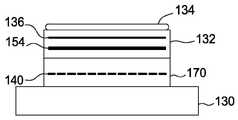
[0041] 도 2는 픽셀화된 기판 지지 조립체(126)의 부분들을 예시하는 부분적인 개략적 단면도이다. 도 2에는 정전 척(132), 히터 조립체(170), 및 설비 플레이트(180)의 부분들이 포함된다.2 is a partial schematic cross-sectional view illustrating portions of a pixelated
[0042] 히터 조립체(170)의 본체(152)는 폴리이미드와 같은 폴리머로 제조될 수 있다. 본체(152)는 일반적으로 평면 형태에서 원통형일 수 있지만, 또한 다른 기하학적 형상들로 형성될 수 있다. 본체(152)는 상부 표면(270) 및 하부 표면(272)을 갖는다. 상부 표면(270)은 정전 척(132)을 향하지만, 하부 표면(272)은 냉각 베이스(130)를 향한다.The
[0043] 히터 조립체(170)의 본체(152)는 둘 또는 그 초과의 유전체 층들(도 2에서 3개의 유전체 층들(260, 262, 264)로 도시됨)로 형성될 수 있으며, 압력하에서 층들(260, 262, 264)을 가열하여 단일 본체(152)를 형성할 수 있다. 예를 들면, 본체(152)는 주 히터(154)와 픽셀 히터(140)를 분리시키는 폴리이미드 층들(260, 262, 264)로 형성될 수 있고, 주 히터(154)와 픽셀 히터(140)는 히터 조립체(170)의 단일 본체(152)를 형성하도록 압력하에서 가열된다. 픽셀 히터들(140)은 본체(152)를 형성하기 전에, 제 1, 제 2, 또는 제 3 층들(260, 262, 264) 내에, 상에, 또는 사이에 배치될 수 있다. 부가적으로, 주 저항성 히터들(154)은 조립 이전에, 제 1, 제 2, 또는 제 3 층들(260, 262, 264) 내에, 상에, 또는 사이에 배치될 수 있으며, 층들(260, 262, 264) 중 적어도 하나는 히터들(154, 140)을 분리시키고 전기적으로 절연시킨다. 이런 방식으로, 픽셀 히터들(140) 및 주 저항성 히터들(154)은 히터 조립체(170)의 일체형 부분이 된다.The
[0044] 주 저항성 히터들(154)과 픽셀 히터들(140)의 위치들에 대한 대안적인 구성들은, 정전 척(132) 내에 또는 정전 척(132) 아래에 하나 또는 양쪽 히터들(154, 140)을 배치할 수 있다. 도 4a-4e는 픽셀 히터들(140) 및 주 저항성 히터들(154)에 대한 다양한 위치들을 열거하는 픽셀화된 기판 지지 조립체(126)의 부분적인 개략도들이지만, 모든 실시예들에 제한되지는 않는다.Alternative configurations for the locations of the main
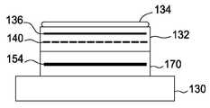
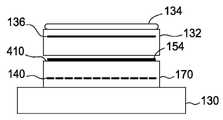
[0045] 도 4a에 도시된 실시예에서, 픽셀화된 기판 지지 조립체(126)는 히터 조립체(170)를 갖지 않으며, 픽셀 히터들(140) 및 주 저항성 히터들(154)이 정전 척(132) 내에, 예를 들면, 척킹 전극(136) 아래에 배치된다. 픽셀 히터들(140)들은 주 저항성 히터들(154) 아래에 도시되어 있지만, 픽셀 히터들(140)은 대안적으로 주 저항성 히터들(154) 위에 위치될 수 있다. 도 4b에 도시된 실시예에서, 픽셀화된 기판 지지 조립체(126)에 대한 히터 조립체(170)는 픽셀 히터들(140)을 포함하지만, 주 저항성 히터들(154)은 정전 척(132) 내에, 예를 들면, 척킹 전극(136) 아래에 배치된다. 대안적으로, 픽셀 히터들(140)은 정전 척(132) 내에 배치될 수 있지만, 주 저항성 히터들(154)은 히터 조립체(170) 내에 배치된다. 도 4c에 도시된 실시예에서, 픽셀화된 기판 지지 조립체(126)에 대한 히터 조립체(170)는 히터 조립체(170) 내에 배치된 주 저항성 히터들(154)을 갖는다. 픽셀 히터들(140)은 정전 척(132) 내에, 예를 들면, 척킹 전극(136) 아래에 배치된다. 도 4d에 도시된 실시예에서, 픽셀화된 기판 지지 조립체(126)에 대한 히터 조립체(170)는 히터 조립체(170) 내에 배치된 픽셀 히터들(140)을 갖지만, 주 저항성 히터들(154)은 정전 척(132) 또는 히터 조립체(170) 중 하나에 배치된다. 히터 조립체(170)는 픽셀 히터들(140)을 냉각 베이스(130)로부터 격리시킨다. 도 4e에 도시된 실시예에서, 픽셀화된 기판 지지 조립체(126)의 히터 조립체(170)는 히터 조립체(170) 내에 배치된 주 저항성 히터들(154)을 갖는다. 픽셀 히터들(140)은 히터 조립체(170) 내에, 또는 히터 조립체(170) 상에, 예를 들면, 정전 척(132) 아래에 배치된다. 픽셀 히터들(140) 및 주 저항성 히터들(154)은 다른 배향들로 배열될 수 있음이 고려된다. 예를 들면, 픽셀화된 기판 지지 조립체(126)는 기판(134)을 가열하기 위해 복수의 픽셀 히터들(140)만을 가질 수 있다. 일 실시예에서, 픽셀 히터들(140) 및 주 저항성 히터들(154)은 픽셀화된 기판 지지 조립체(126) 내에서 서로의 바로 아래에 배치된다. 픽셀 히터들(140)은 픽셀화된 기판 지지 조립체(126)에 의해 지지되는 기판(134)의 온도 프로파일에 대한 미세 조정 제어(fine tune control)를 제공한다.In the embodiment shown in FIG. 4A , the pixelated
[0046] 픽셀 히터들(140)은, 정전 척(132) 또는 히터 조립체(170)의 본체(152) 내에 또는 상에 배치되거나 형성될 수 있다. 픽셀 히터들(140)은, 도금, 잉크젯 프린팅, 스크린 프린팅, 물리 기상 증착, 스탬핑, 와이어 메시(wire mesh) 또는 다른 적합한 방식으로 형성될 수 있다. 이러한 방식으로, 픽셀화된 기판 지지 조립체(126)의 제조가 단순화된다. 일 실시예에서, 픽셀 히터들(140)은 히터 조립체(170) 내에 배치되면서, 히터 조립체(170)를 형성한다. 다른 실시예에서, 픽셀 히터들(140)은 정전 척(132)의 장착 표면(131) 상에 직접 배치된다. 예를 들면, 픽셀 히터들(140)은 정전 척(132)의 장착 표면(131)에 접착될(adhered) 수 있는 시트 형태일 수 있거나, 픽셀 히터들은 다른 수단에 의해 증착될 수 있다. 예를 들면, 픽셀 히터들(140)은, 물리 기상 증착, 화학 기상 증착, 스크린 프린팅, 또는 다른 적합한 방법들에 의해 장착 표면(131) 상에 증착될 수 있다. 주 저항성 히터들(154)은 상기에 나타낸 바와 같이, 히터 조립체(170) 또는 정전 척(132) 내에 있을 수 있다.
[0047] 주 저항성 히터들(154)은 정전 척(132) 또는 히터 조립체(170)의 본체(152) 내에 또는 상에 배치되거나 형성될 수 있다. 주 저항성 히터들(154)은, 도금, 잉크젯 프린팅, 스크린 프린팅, 물리 기상 증착, 스탬핑, 와이어 메시, 또는 다른 적합한 방식으로 형성될 수 있다. 이러한 방식으로, 픽셀화된 기판 지지 조립체(126)의 제조가 단순화된다. 일 실시예에서, 주 저항성 히터들(154)은 히터 조립체(170) 내에 배치되면서 히터 조립체(170)를 형성한다. 다른 실시예에서, 주 저항성 히터들(154)은 정전 척(132)의 장착 표면(131) 상에 직접 배치된다. 예를 들면, 주 저항성 히터들(154)은 정전 척(132)의 장착 표면(131)에 접착될 수 있는 시트 형태일 수 있거나, 주 저항성 히터들(154)은 다른 수단에 의해 증착될 수 있다. 예를 들면, 주 저항성 히터들(154)은 물리 기상 증착, 화학 기상 증착, 스크린 프린팅, 또는 다른 적합한 방법들에 의해 장착 표면(131) 상에 증착될 수 있다. 픽셀 히터들(140)들은 상기에서 나타낸 바와 같이, 히터 조립체(170) 또는 정전 척(132) 내에 있을 수 있다.The primary
[0048] 몇몇 실시예들에서, 주 저항성 히터들(154)은 픽셀 히터들(140)과 유사하게 제조될 수 있으며, 그러한 실시예들에서 선택적으로, 부가적인 픽셀 히터들(140)의 이득 없이 활용될 수 있다. 다시 말해서, 픽셀화된 기판 지지 조립체(126)의 주 저항성 히터들(154)은 픽셀화되며(pixelated), 즉 복수의 개별적인 저항성 가열 엘리먼트들로 분할된다(segmented). 주 저항성 히터들(154)을 소형 저항성 히터들의 형태로 분할하는 것은, 기판(134)의 표면 상의 열점 및 냉점의 국소적인 제어를 허용한다. 픽셀 히터들(140)의 부가적인 층은, 요구되는 온도 제어 레벨에 따라 선택적이다.In some embodiments, the primary
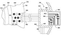
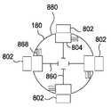
[0049] 도 7은 복수의 단위 히터들(846)로 형성된, 분할된 주 저항성 히터들(154)에 대한 배선 레이아웃(wiring layout)에 대한 그래프식 도면이다. 단위 히터들(846)은 전술된 바와 같이 픽셀 제어기(202)의 사용을 통해, 또는 도 7에 도시된 바와 같이 하드웨어 배선 키(802)의 형태로 픽셀 히터 제어기의 사용을 통해 제어될 수 있다. 하드웨어 배선 키들(802)을 사용하기 위한 한가지 구현예가 도 8에 도시된 설비 플레이트(180)의 평면도에 예시되어 있다.FIG. 7 is a graphical diagram of a wiring layout for divided main
[0050] 도 7 및 8을 공동으로 참조하면, 픽셀화된 기판 지지 조립체(126)는, 4개의 주 저항성 히터들(154)로서 예시적으로 도시된 하나 또는 그 초과의 주 저항성 히터(154)를 가질 수 있으며, 이들은 각각 4개의 구역들(810, 820, 830, 840) 중 하나를 정의한다. 각각의 구역(810, 820, 830, 840)의 온도는 구역과 연관된 주 저항성 히터(154)에 의해 독립적으로 제어될 수 있다. 부가적으로, 각각의 주 저항성 히터들(154)은 복수의 분리된 단위 히터들(846)로 구성된다. 단위 히터들(846)은 활성이거나(활성 단위 히터들(842)) 또는 비활성(비활성 단위 히터들(844))일 수 있다. 활성 단위 히터들(842)은 전력 소스에 커플링되며 주 저항성 히터들(154)에 열을 제공한다(contribute). 비활성 단위 히터들(844)은 전력 소스이며, 따라서 주 저항성 히터들(154)에 열을 제공하지 않는다. 따라서, 어떤 주 저항성 히터들(154)이 활성 단위 히터들(842)인지 또는 비활성 단위 히터들(844)인지를 선택적으로 선택함으로써, 기판 지지 조립체(126)의 온도 프로파일은, 예를 들면, 국소적인 열점 또는 냉점을 제어하고, 온도 프로파일에 대한 중심 대 엣지 조정을 제공하고, 픽셀화된 기판 지지 조립체(126) 및 결과적으로 픽셀화된 기판 지지 조립체(126) 상에서 프로세싱되는 기판(134)의 측면 온도 프로파일의 방위각 조정을 제공하도록 제어될 수 있다.7 and 8 , the pixelated
[0051] 각각의 주 저항성 히터들(154)에 대한 단위 히터들(846)은, 구역들(810, 820, 830, 840) 중 각각의 구역 내에서 활성 히터 밀도의 패턴을 형성하도록 선택될 수 있다. 단위 히터들(846)의 패턴은, 부호가 854인 단위 히터들의 패턴과 유사하게, 빈틈없이 패킹되고 균일할 수 있다. 대안적으로, 단위 히터들(846)에 대한 패턴은 성기게(loosely) 이격될 수 있다. 단위 히터들(846)은, 하드웨어 배선 키(802)와 같은 하드웨어, 픽셀 제어기(202), 제어기(148)에 의해 실행되는 소프트웨어 또는 펌웨어를 사용하여, 또는 다른 방법 또는 디바이스를 통해서, 활성 단위 히터들(842)과 비활성 단위 히터들(844) 사이에서 전환될 수 있다. 따라서, 구역들(810, 820, 830, 840) 중 각각에서 주 저항성 히터들(154)로부터 생성된 온도 프로파일은, 주 저항성 히터들(154)에 의해 공급되는 열을 제어하기 위해 단위 히터들(846)을 선택적으로 작동시킴으로써(activating) 개선될(refined) 수 있다.The
[0052] 각각의 단위 히터(846), 즉 모든 활성 단위 히터들(842) 및 모든 비활성 단위 히터들(844)은 유선 연결부(wired connection)(860)를 갖는다. 유선 연결부들(860)은, 예를 들면, 설비 플레이트(180)에 형성된 리셉터클(804)에 라우팅된다(routed). 일 실시예에서, 유선 연결부들(860)은 픽셀화된 기판 지지 조립체(126)의 외향으로(outward) 연장하고, 픽셀화된 기판 지지 조립체(126)의 외측까지 내려가 설비 플레이트(180) 내의 리셉터클(804)로 연장할 수 있다. 대안적으로, 유선 연결부(860)는 히터 조립체(170)를 통해 내부로, 예를 들면, 냉각 베이스(130) 내의 홀(hole)을 통해 설비 플레이트(180) 내의 리셉터클(804)로 연장할 수 있다.Each
[0053] 설비 플레이트(180) 내의 리셉터클(804)은 내부 표면(805) 및 측면 표면(side surface)(806)을 갖는다. 유선 연결부들(860)은 내부 표면(805)에서 종결되며, 그에 따라 커넥터 또는 소켓을 형성할 수 있다. 제어 보드 연결부(868)가 커넥터 또는 소켓과(with) 측면 표면(806)에서 종결될 수 있다. 제어 보드 연결부(868)는 단일의 전력 리드(lead) 또는 복수의 전력 리드들일 수 있다. 유선 연결부들(860) 및 제어 보드 연결부들(868)은 회로의 부분(part)이다. 대안적으로, 유선 연결부들(860) 및 제어 보드 연결부들(868)은 양자 모두, 설비 플레이트(180)의 동일한 표면 상에 상주할(residing) 수 있다. 예를 들면, 유선 연결부들(860)과 제어 보드 연결부들(868) 양자 모두는 리셉터클(804)의 내부 표면(805) 상에 상주할 수 있다. 회로 내의 갭이 리셉터클(804)에 형성되며, 그에 따라 회로에 걸쳐서, 즉, 제어 보드 연결부들(868)로부터 유선 연결부들(860)로 어떠한 전류도 흐르지 않을 수 있다.The
[0054] 하드웨어 배선 키(802)는 리셉터클(804)에 끼워맞춤되도록(fit) 구성된다. 하드웨어 배선 키(802)는 설비 플레이트(180)의 외측 표면(880)과 같은 높이일 수 있지만, 하드웨어 배선 키(802)의 전방 표면(885)은 리셉터클(804)의 내부 표면(805)과 접촉한다. 부가적으로, 하드웨어 배선 키(802)의 측면 표면(886)은 리셉터클의 측면 표면(806)과 접촉한다. 하드웨어 배선 키(802)는 리셉터클(804)의 회로 내의 갭을 선택적으로 채우도록 구성되어서, 제어 보드 연결부들(868)로부터 선택된 유선 연결부들(860)로 전류가 흐를 수 있다. 이런 방식으로, 유선 연결부들(860)과 제어 보드 연결부들(868) 사이의 전기적 연결부들이 형성될 수 있다. 따라서, 하드웨어 배선 키(802)는 단위 히터들(846)에 전력을 선택적으로 제공하도록 구성된다.The
[0055] 하드웨어 배선 키(802)는 유선 연결부들(860) 중 각각에 대한 공통의 음극 단자(common negative terminal)를 사용할 수 있다. 예를 들면, 모든 음극 단자들은, 하드웨어 배선 키(802)의 재킷에 형성될 수 있는 공통 버스를 활용할 수 있거나, 음극 단자는 공유되는 핀 연결부(shared pin connection)일 수 있다. 대안적으로, 하드웨어 배선 키(802)는 유선 연결부들(860) 중 각각에 대한 개별적인 음극 단자를 사용할 수 있다. 음극 단자는 단자에 걸친 전류의 유동을 선택적으로 중단시키기(interrupting) 위해, 게이트 스위치 또는 다른 수단을 가질 수 있다.The
[0056] 하드웨어 배선 키(802)는, 단위 히터들(846)에 전력을 전달하는데 이용가능하고 활성화시키는데 요구되는 그러한 회로들만을 사전선택하는(preselect) 방식으로 형성될 수 있다. 비활성 회로들은, 주 저항성 히터들(154) 내의 단위 히터들(846)의 유선 연결부들(860)로의 전력의 유동을 중단시키기 위한 다른 적합한 수단 중에서도, 갭 또는 게이트들(864), 하드웨어 배선 키(802) 내의 아직 형성되지 않은(unformed) 회로망, 또는 절연 캡(미도시)을 가질 수 있다. 따라서, 하나의 하드웨어 배선 키(802)는 하나의 프로세스를 수행하면서 기판의 미리정의된 측면 온도 분포를 제공하도록 활용될 수 있으며, 상이한 사전선택의 회로들을 갖는 하드웨어 배선 키(802)로 대체될 수 있으며, 상이한 사전선택의 회로들은 다른 프로세스를 수행하면서 기판의 상이한 미리정의된 측면 온도 분포를 산출할 단위 히터들(846)에 전력을 전달하는데 이용가능하며 활성화시키는데 요구된다. 이러한 방식으로, 상이한 하드웨어 배선 키들(802)은, 상이한 온도 프로파일들을 제공하고 그에 따라 이로운 프로세싱 결과들의 실현을 보장하는데 있어서 더 높은 유연성을 제공하도록, 효율적으로 스왑 아웃될(swapped out) 수 있다.The
[0057] 유선 연결부들(860)은 설비 플레이트(180)의 외측 표면(880) 주위에 동등하게 이격되고, 분할될 수 있다. 일 실시예에서, 설비 플레이트는 4개의 리셉터클들(804)을 가지며, 각각의 리셉터클은 실질적으로 동일한 수의 유선 연결부들(860)을 갖는다. 이러한 배열은 픽셀화된 기판 지지 조립체(126)가 대칭적으로 안정되도록(balanced) 허용하며, 프로세싱 챔버(100) 내에서 발생하는 프로세스들에 대한 배선의 효과들을 최소화한다. 유리하게, 단위 히터들(846) 및 연결부들의 배열은 픽셀화된 기판 지지 조립체(126)에 대해 균질한 구성을 제공하며, 프로세스 대칭을 촉진한다.The
[0058] 주 저항성 히터들(154)의 단위 히터들(846)은, 주 저항성 히터들(154)이 섭씨 약 0.3도의 증분들로 프로파일링된(profiled) 측면 온도를 제어할 수 있는 능력을 갖고, 대략 주위 온도(ambient) 내지 섭씨 약 500도의 온도 범위를 갖도록 허용한다. 단위 히터들(846)로 구성된 주 저항성 히터들(154)을 갖는 픽셀화된 기판 지지 조립체(126)는, 픽셀화된 기판 지지 조립체(126) 상에서 프로세싱되는 기판의 온도 균일성을 섭씨 약 ±1.5도 미만으로 제어할 수 있는 능력을 나타냈다.The
[0059] 도 2에 도시된 실시예로 다시 돌아가면, 히터 조립체(170)는 결합제(bonding agent)(244)를 활용하여 정전 척(132)의 장착 표면(131)에 커플링될 수 있다. 결합제(244)는 아크릴-계 접착제, 에폭시, 실리콘계 접착제, 네오프렌-계 접착제, 또는 다른 적합한 접착제와 같은 접착제일 수 있다. 일 실시예에서, 결합제(244)는 에폭시이다. 결합제(244)는 0.01 내지 200 W/mK의 범위, 예시적인 일 실시예에서 0.1 내지 10 W/mK의 범위에서 선택된 열 전도성 계수(coefficient of thermal conductivity)를 가질 수 있다. 결합제(244)를 포함하는 접착 재료들은 부가적으로, 적어도 하나의 열 전도성 세라믹 필러, 예를 들면, 알루미늄 옥사이드(Al2O3), 알루미늄 나이트라이드(AlN), 및 티타늄 디보라이드(TiB2), 등을 포함할 수 있다.2 , the
[0060] 일 실시예에서, 히터 조립체(170)는 결합제(242)를 활용하여 냉각 베이스(130)에 커플링된다. 결합제(242)는 결합제(244)와 유사할 수 있으며, 아크릴-계 접착제, 에폭시, 네오프렌-계 접착제, 또는 다른 적합한 접착제와 같은 접착제일 수 있다. 일 실시예에서, 결합제(242)는 에폭시이다. 결합제(242)는 0.01 내지 200 W/mK의 범위, 예시적인 일 실시예에서, 0.1 내지 10 W/mK의 범위에서 선택된 열 전도성 계수를 가질 수 있다. 결합제(242)를 포함하는 접착 재료들은 부가적으로, 적어도 하나의 열 전도성 세라믹 필러, 예를 들면, 알루미늄 옥사이드(Al2O3), 알루미늄 나이트라이드(AlN), 및 티타늄 디보라이드(TiB2), 등을 포함할 수 있다.In one embodiment, the
[0061] 결합제들(244, 242)은, 정전 척(132), 냉각 베이스(130), 및 히터 조립체(170) 중 하나 또는 모두(both)를 개장하는 경우 제거될 수 있다. 다른 실시예들에서, 히터 조립체(170)는 파스너들(fasteners) 또는 클램프들(미도시)을 활용하여, 냉각 베이스(130) 및 정전 척(132)에 제거가능하게 커플링된다.The
[0062] 히터 조립체(170)는 픽셀 히터들(140a, 140b, 140c)로서 예시적으로 도시된 복수의 픽셀 히터들(140)을 포함한다. 픽셀 히터들(140)은 일반적으로, 히터 조립체(170) 내의 밀폐된 용적(enclosed volume)이며, 이 밀폐된 용적에서 복수의 저항성 히터들이 히터 조립체(170)와 정전 척(132) 사이의 열 전달을 실행한다. 각각의 픽셀 히터(140)는 히터 조립체(170), 및 그에 따라 히터 조립체(170) 내에 정의된 셀(200)에 걸쳐서 측면으로 배열될 수 있어서, 그러한 셀(200)과 정렬된, 히터 조립체(170)의 영역 (및 주 저항성 히터(154)의 부분(portion))에 부가적인 열을 국소적으로 제공한다. 히터 조립체(170)에 형성되는 픽셀 히터들(140)의 개수는 달라질 수 있으며, 주 저항성 히터들(154)의 개수보다 적어도 10배 더 많은 픽셀 히터들(140)(및 셀들(200))이 존재할 수 있음이 고려된다. 히터 조립체(170)가 4개의 주 저항성 히터들(154)을 갖는 일 실시예에서, 40개 초과의 픽셀 히터들(140)이 존재할 수 있다. 그러나, 300 mm 기판과 사용하도록 구성되는 기판 지지 조립체(126)에 대한 주어진 실시예에서, 약 200, 약 400, 또는 훨씬 더 많은 픽셀 히터들(140)이 존재할 수 있음이 고려된다. 픽셀 히터들(140)의 예시적인 분포는 도 3a-3d를 참조로 하여 하기에서 더 설명된다.The
[0063] 셀들(200)은 히터 조립체(170)의 본체(152)를 구성하는 하나 또는 그 초과의 층들(260, 262, 264)을 통하여 형성될 수 있다. 일 실시예에서, 셀들은 본체(152)의 하부 표면(272) 및 상부 표면(270)에 대해 개방된다. 셀들은 측벽들(214)을 포함할 수 있다. 측벽들(214)은 열 초크(216)로서 작용하는 재료(또는 갭)로 구성될 수 있다. 열 초크들(216)은 본체(152)의 상부 표면(270)에 형성된다. 열 초크들(216)은 인접하는 셀들(200)을 분리시키고 이들 사이의 전도를 감소시킨다. 따라서, 각각의 픽셀 히터들(140)에 제공되는 전력, 및 결과적으로 셀(200)을 통한 열 전달을 개별적으로 그리고 독립적으로 제어함으로써, 온도 제어에 대한 픽셀 단위(pixel by pixel) 접근법이 실현될 수 있으며, 이는 기판(134)의 특정 지점들이 가열되거나 냉각될 수 있게 함으로써, 기판(134)의 표면에 대해 정확하게(truly) 어드레스가능한 측면 온도 프로파일 조정 및 제어를 가능하게 한다.
[0064] 부가적인 열 초크(216)가 본체(152)의 측면으로 최외측 측벽(280)과 방사상 최외측 셀들(200) 사이에 형성될 수 있다. 본체(152)의 측면으로 최외측 측벽(280)과 셀들(200) 사이에 위치된 이러한 최외측 열 초크(216)는, 프로세싱 챔버(100)의 내부 용적(124)과, 측면으로 최외측 측벽(280)에 인접한 셀들(200) 사이의 열 전달을 최소화한다. 그에 따라, 픽셀화된 기판 지지 조립체(126)의 엣지에 더 가까이에서 더 정밀한 온도 제어를 허용하며, 결과적으로 기판(134)의 외측 직경 엣지에 더 우수한 온도 제어를 허용한다.An additional
[0065] 전술된 바와 같이, 각각의 픽셀 히터(140)는 픽셀 제어기(202)에 독립적으로 커플링될 수 있다. 픽셀 제어기(202)는 픽셀화된 기판 지지 조립체(126)에 배치될 수 있다. 픽셀 제어기(202)는, 다른 셀들(200)에 대해, 각각의 셀(200)에서 히터 조립체(170) 내의 픽셀 히터들(140)의 온도를 조절할 수 있거나, 대안적으로 셀들(200)의 다른 그룹에 대해, 셀들(200)의 한 그룹에 걸쳐서 히터 조립체(170) 내의 픽셀 히터들(140)의 그룹의 온도를 조절할 수 있다. 픽셀 제어기(202)는 온/오프 상태를 토글링할(toggle) 수 있거나, 개별적인 픽셀 히터들(140) 또는 픽셀 히터들(140)의 그룹에 대한 듀티 사이클을 제어할 수 있다. 대안적으로, 픽셀 제어기(202)는 개별적인 픽셀 히터들(140) 또는 픽셀 히터들(140)의 그룹들에 전달되는 전력의 양을 제어할 수 있다. 예를 들면, 픽셀 제어기(202)는, 하나 또는 그 초과의 픽셀 히터들(140)에 10 와트의 전력을 제공하고, 다른 픽셀 히터들(140)에 9 와트의 전력을 제공하며, 또 다른 픽셀 히터들에 1 와트의 전력을 제공할 수 있다.As described above, each
[0066] 일 실시예에서, 각각의 셀(200)은, 예를 들면, 더 정밀한 온도 제어를 가능하게 하는 열 초크(216)를 사용하여, 이웃한 셀들(200)로부터 열적으로 격리될 수 있다. 다른 실시예에서, 각각의 셀(200)은 인접 셀에 열적으로 결합되어, 히터 조립체(170)의 상부 표면(270)을 따라 아날로그(즉, 평탄한(smooth) 또는 블렌딩된(blended)) 온도 프로파일을 생성할 수 있다. 예를 들면, 알루미늄 호일과 같은 금속 층이, 픽셀 히터들(140)과 주 저항성 히터들(154) 사이의 열 스프레더(thermal spreader)로서 사용될 수 있다.[0066] In one embodiment, each
[0067] 주 저항성 히터들(154)에 의해 생성된 온도 프로파일을 수정하거나 고르게(smooth out) 하기 위해 독립적으로 제어가능한 픽셀 히터들(140)을 사용하는 것은, 기판에 걸친 국소적인 온도 균일성의 제어를 매우 작은 허용오차들로 가능하게 하며, 그에 따라 기판(134)을 프로세싱 할 때, 정밀한 프로세스 및 CD 제어를 가능하게 한다. 부가적으로, 주 저항성 히터들(154)에 비해 작은 크기 및 높은 밀도의 픽셀 히터들(140)은, 이웃하는 지역들의 온도에 실질적으로 영향을 주지 않으면서 픽셀화된 기판 지지 조립체(126)의 특정 위치들에서의 온도 제어를 가능하게 하며, 그에 따라 스큐잉(skewing) 또는 다른 온도 비대칭들을 도입하지 않으면서 국소적인 열점 및 냉점이 보상되도록 허용한다. 복수의 픽셀 히터들(140)을 갖는 픽셀화된 기판 지지 조립체(126)는 픽셀화된 기판 지지 조립체(126) 상에서 프로세싱되는 기판(134)의 온도 균일성을 섭씨 약 ± 0.3도 미만으로 제어할 수 있는 능력을 나타냈다.[0067] Using the independently
[0068] 픽셀화된 기판 지지 조립체(126)의 몇몇 실시예들의 다른 이득은, RF 전력이 제어 회로망을 통해 이동하는 것을 방지할 수 있는 능력이다. 예를 들면, 픽셀 제어기(202)는 전기 전력 회로(210) 및 광학 제어 회로(220)를 포함할 수 있다. 전기 전력 회로(210)는 픽셀 히터들(140)에 커플링된다. 각각의 픽셀 히터(140)는 전기 전력 회로(210)에 연결되는 전력 리드들의 쌍(커넥터들(250))을 갖는다. 50개의 픽셀 히터들(140)을 갖는 예시적인 히터 조립체(170)에서, 픽셀 히터들(140)을 제어하기 위해 50 쌍들의 전력 리드들(커넥터들(250))이 요구된다. 플라즈마를 형성하기 위해 프로세싱 챔버(100)로 공급되는 RF 에너지는 전력 리드들에 커플링된다. 도 1에 도시된 RF 필터들(182, 184, 186)과 같은 필터들은, 주 히터 전력 소스(156)와 같은 전기적 장비를 RF 에너지로부터 보호하기 위해 사용된다. 전기 전력 회로(210)에서 전력 리드들(커넥터들(250))을 종결하고, 그리고 각각의 픽셀 히터들(140)에 얼마나 많은 전력이 제공되는지를 제어하기 위해 광학 제어 회로(220)를 활용함으로써, 전기 전력 회로(210)와 전력 소스(156) 사이에 단일 RF 필터(184)만이 요구된다. 종래의 애플리케이션들에서, 각각의 히터는 전용 RF 필터를 요구한다. 따라서, 전용 RF 필터들에 대한 공간이 매우 제한됨에 따라, 기판 지지 조립체 내에서 활용되는 히터들의 개수가 또한 제한되며, 그에 따라 사용될 수 있는 주 히터 구역들의 개수를 제한하고 픽셀화된 수정 히터들(pixelated corrective heaters)이 구현되는 것을 불가능하게 한다. 따라서, 광학 제어 회로(220)와 전기 전력 회로(210)의 사용은 더 많은 히터들, 및 결과적으로 보다 우수한 측면 온도 제어를 허용한다.Another benefit of some embodiments of the pixelated
[0069] 도 6을 간략히 참조하면, 픽셀 히터들(140)에 대한 간략화된 배선 개략도는 전기적 챔버 컴포넌트들을 RF 신호로부터 보호하는데 필요한 감소된 개수의 RF 필터들을 예시한다. 복수의 픽셀 히터들(140)을 제어하는 것을 돕기 위해 플렉스(flex) 회로(600)가 사용될 수 있다. 플렉스 회로(600)는 픽셀 히터들(140)에 대한 매트릭스 패턴(matrix pattern)을 형성할 수 있다. 플렉스 회로(600)는 다수의 교차하지-않는 양의(positive) 리드들(640) 및 음의(negative) 리드들(650)로 이루어지며, 각각의 리드는 일 단부에서 픽셀 제어기(202)에 부착된다. 각각의 양의 리드(640)는, 대응하는 음의 리드(650)에 대한 연결부를 브릿징하는(bridging) 복수의 픽셀 히터 조립체들(662)을 가질 수 있다. 따라서, 픽셀 히터 조립체(662)는 양의 리드(640)의 각각의 연결부와 음의 리드(650)의 각각의 연결부 사이에 배치된다. 예시적인 일 실시예에서, 플렉스 회로(600)는 9개의 양의 리드들(640) 및 9개의 음의 리드들(650) 및 그에 따라 81개만큼 많은 픽셀 히터 조립체들(662)을 가질 수 있다.Referring briefly to FIG. 6 , a simplified wiring schematic for
[0070] 픽셀 히터 조립체(662)는 직렬로 연결된 다이오드(664) 및 픽셀 히터(663)를 갖는다. 픽셀 히터(663)는 양의 리드(640)에 부착되며, 다이오드(664)는 음의 리드(650)에 부착될 수 있다. 대안적으로, 픽셀 히터(663)는 음의 리드(650)에 부착되며, 다이오드(630)는 양의 리드(640)에 부착될 수 있다. 다이오드(664)는 한 방향으로만 전류가 유동하는 것을 보장한다. 일 실시예에서, 픽셀 히터 조립체들(662)의 각각에 대한 전류 유동의 방향은 양의 리드(640)로부터 음의 리드(650)로이다.
[0071] 픽셀 제어기(202)는 선택된(a selection of) 양의 리드들(640) 및 음의 리드들(650)에 걸쳐서 미리결정된 전류 유동을 제공하기 위해, 개별적인 회로들을 개방 및/또는 폐쇄할 수 있다. 예를 들면, 픽셀 제어기(202)는 부호가 641인 양의 리드 상에 전류 유동을, 그리고 부호가 653인 음의 리드 상에 전류에 대한 복귀 유동을 제공할 수 있으며, 이때 모든 다른 양의 리드들(640) 및 음의 리드들(650)은 개방된 회로들로서 작용한다. 대안적으로, 픽셀 제어기(202)는 부호가 642 및 643인 양의 리드들 상에 전류 유동을 선택적으로 제공하면서 음의 리드(652) 상에 복귀 유동을 제공할 수 있으며, 이때 모든 다른 양의 리드들(640) 및 음의 리드들(650)은 개방된 회로들로서 작용한다. 픽셀 제어기(202)는 그에 따라, 선택된 조합들의 양의 리드들(640)과 음의 리드(650)들 사이에 배치된 픽셀 히터 조립체들(662)에 전류를 선택적으로 제공할 수 있다. 플렉스 회로(600)는, 각각의 픽셀 히터(663)에 전력을 공급하기 위해 다시 픽셀 제어기(202)로 돌아가는(back to) 연결부들의 수가 가장 적은 개별적인 회로들을 완성한다.
[0072] 일 실시예에서, 픽셀 제어기(202)는 부호가 641인 양의 리드 상에 전류를 제공하고, 모든 음의 리드들(650) 상에 전류에 대한 복귀 경로가 제공된다. 최상부 행(row)(612)을 따르는 픽셀 히터들(140)은 선택적으로 턴온되지만(활성화), 나머지 픽셀 히터들(140)은 비활성 상태이다. 다른 실시예에서, 픽셀 제어기(202)는 부호가 641 및 642인 양의 리드들 상에 전류를 제공하며, 부호가 651 및 652인 음의 리드들 상에 전류에 대한 복귀 경로를 제공한다. 이러한 구성에서, 4개의 픽셀 히터들(691, 692, 693, 694)의 소 그룹이 선택적으로 턴온되지만, 나머지 픽셀 히터들(140)은 비활성으로(즉, 전력공급되지 않음(unpowered)) 남아 있다. 따라서, 픽셀 제어기(202)는 선택된 양의 리드들(640) 및 선택된 음의 리드들(650)을 작동시킴으로써 다양한 픽셀 히터들(140)을 선택적으로 작동시키도록 활용될 수 있다. 픽셀 제어기(202)는 또한, 특정 픽셀 히터에 의해 생성된 열의 양을 제어하기 위해, 주어진 픽셀 히터를 통한 전류 또는 주어진 픽셀 히터에 걸친 전압을 제어할 수 있다. 픽셀 제어기(202)는 대안적으로 또는 부가적으로, 특정 픽셀 히터에 의해 생성된 열의 양을 시간에 대해 제어하기 위해, 주어진 픽셀 히터에 대한 듀티 사이클을 제어할 수 있다. 픽셀 제어기(202)는 대안적으로 또는 부가적으로, 특정 픽셀 히터에 의해 생성된 열의 양을 시간에 대해 제어하기 위해, 픽셀 히터들을 통해 스캐닝할 수 있다.In one embodiment, the
[0073] 플렉스 회로(600)는, 히터 조립체(170)의 본체(152)를 구성하는 층들(260, 262, 264) 중 하나의 내에, 상에, 또는 아래에 형성될 수 있다. 픽셀 히터들(140)은 플렉스 회로(600) 위에 또는 플렉스 회로(600)와 함께 배치될 수 있다. 플렉스 회로(600)는, 증착, 도금, 잉크젯 프린팅, 스크린 프린팅될 수 있거나, 임의의 적합한 방식으로 형성될 수 있다. 양의 리드들(640) 및 음의 리드들(650)은 픽셀 제어기(202)에 플렉스 회로(600)를 연결하기 위해 하나 또는 그 초과의 커넥터들(250)을 형성할 수 있다. 커넥터들(250)은 픽셀화된 기판 지지 조립체(126)를 통해 내부로 연장할 수 있다. 예를 들면, 냉각 베이스(130) 및 설비 플레이트(180)는, 커넥터들(250)의 통로를 수용하기 위해, 냉각 베이스(130) 및 설비 플레이트(180)를 통해 형성된 하나 또는 그 초과의 통로들을 가질 수 있다. 커넥터들(250)은 픽셀화된 기판 지지 조립체(126) 전체에 걸쳐서 분할되거나, 위치되거나, 분배될 수 있으며, 그에 따라 프로세싱 챔버(100)에서 진행중인 플라즈마 프로세스들에 대한 배선의 임의의 영향들을 안정시킨다. 예를 들면, 4개의 커넥터들(250)이, 픽셀화된 기판 지지 조립체(126)의 중심 부근에 형성된, 4개의 동등하게 이격된 통로들을 통과할 수 있다. 일 실시예에서, 플렉스 회로(600)는 50개 또는 그 초과의 히터들(140)을 동작시키기 위해 100개 또는 그 초과의 단자 리드들(terminal leads)을 갖는 히터 조립체(170)의 층들 상에 또는 내에 프린팅될 수 있다. 일 예에서, 200개의 픽셀 히터들(140)에 전력을 제공하기 위해, 400개의 단자 리드들이 활용된다. 단자 리드들은, 냉각 베이스(130)에 형성된 슬롯들을 통해 연장할 수 있는 별도의 가요성 스트립들, 이를테면 리본 케이블 또는 회로로 분할될 수 있다. 냉각 베이스(130)를 통해 설비 플레이트(180)에 형성되는, 동등하게 이격된 슬롯들을 통한 연장(run)에 의해 단자 리드를 포함하는 가요성 스트립들은 대칭적인 온도 제어 및 프로세스 균일성에 기여하는 대칭적인 기하형상을 제공한다.The
[0074] 도 2로 다시 돌아가면, 전기 전력 회로(210)는 플렉스 회로(600)로부터 비롯되는, 복수의 커넥터들(250)에 대한 전력을 스위칭하거나 순환시킬 수 있다. 전기 전력 회로(210)는 커넥터들(250)의 각각에 전력을 제공하여서, 하나 또는 그 초과의 픽셀 히터들(140)을 작동시킨다. 전기 전력 소스는 결국, 복수의 픽셀 히터들(140)에 전력을 공급하지만, 전기 전력 회로(210)는 단일한 전력 소스, 즉 픽셀 히터 전력 소스(142)를 가지며, 그에 따라 단일한 필터(184)만을 요구한다. 유리하게, 많은 히터들 및 히터 구역들의 사용을 가능하게 하면서, 부가적으로 필터들에 대한 비용 및 공간이 경감된다(mitigated).2 , the
[0075] 광학 제어 회로(220)는 광 섬유 케이블과 같은 광학 케이블(226)에 의해 전기 전력 회로(210)에 커플링되어서, 커넥터들(250), 및 그에 따라 픽셀 히터들(140)에 공급되는 전력을 제어할 수 있다. 광학 제어 회로(220)는 광학 도파관(228)을 통해 광학 전력 소스(178)에 커플링될 수 있다. 광학 전력 소스(178)는 픽셀 히터들(140)의 기능을 제어하는 신호들을 제공하기 위해 제어기(148)에 커플링된다. 광학 케이블(226) 및 광학 도파관(228)은 전자기 간섭(electromagnetic interference) 또는 무선 주파수(RF) 에너지를 받지 않는다. 따라서, 픽셀 제어기(202)에서, RF 에너지로부터 광학 전력 소스(178)를 보호하기 위한 RF 필터가 불필요하며, 그에 따라 기판 지지 조립체(126) 내에 다른 유틸리티들(utilities)을 라우팅하기 위한 더 많은 공간을 허용한다.The
[0076] 광학 제어 회로(220)는 각각의 픽셀 히터(140) 또는 픽셀 히터들(140)의 그룹들/영역들을 조절하기 위해 전기 전력 회로(210)에 명령들 또는 지시를 보낼 수 있다. 도 6의 플렉스 회로(600)에서 보이는 바와 같이, 단일한 픽셀 히터(140) 또는 픽셀 히터들(140)의 그룹들/영역들이 전기 전력 회로(210)로 다시 돌아가는 최소 개수의 연결부들을 사용하여 작동될 수 있으며, 광학 제어 회로(220)에 의해 제어될 수 있다.The
[0077] 광학 제어 회로(220)는 각각의 픽셀 히터(140)에서의 온도 상승을 측정함으로써 교정되고(calibrated) 프로그래밍될 수 있다. 온도 상승은 픽셀 히터들(140)에 대해 증대하는(incremental) 전력 증가들과 연관될 수 있다. 예를 들면, 온도 상승은 픽셀 히터(140)에 공급되는 전력의 백분율 증가, 예를 들면, 5% 증가와 연관될 수 있다. 이러한 방법을 사용하여 온도 맵(map)이 획득될 수 있다. 맵은 각각의 픽셀 히터(140)에 대한 전력 분포 곡선에 대해 온도 또는 CD를 상관시킬 수 있다. 따라서, 픽셀 히터(140)는, 개별적인 픽셀 히터들(140)에 대한 프로그램 조절 전력 설정들에 기초하여, 기판에 대한 온도 프로파일을 생성하는데 사용될 수 있다. 로직은 제어기(148)와 같은 외부에 연결된 제어기에 또는 광학 제어 회로(220)에 직접적으로 배치될 수 있다.The
[0078] 픽셀 히터들(140)의 배열은 이제, 도 3a 내지 3b를 참조로 하여 논의될 수 있다. 도 3a는 일 실시예에 따른, 3A--3A 단면선을 따르는 도 2의 단면도이다. 도 3b-3d는 대안적인 실시예들에 따른, 도 2의 동일한 3A--3A 단면선을 따르는 단면도들이다.The arrangement of
[0079] 이제 도 3a를 참조하면, 복수의 픽셀 히터들(140)이 히터 조립체(170)의 본체(152)를 통하는 3A-3A 단면선의 평면을 따라 배치된다. 열 초크(216)는 각각의 이웃하는 셀(200) 사이에 배치되며, 각각의 셀(200)은 픽셀 히터들(140) 중 적어도 하나와 연관된다. 부가적으로, 열 초크(216)는 픽셀화된 기판 지지 조립체(126)의 외측 표면(326)을 따라서 배치된다. 도시된 셀들(200)의 개수는 단지 예시를 위한 것이며, 임의의 개수의 실시예들은 실질적으로 더 많은(또는 더 적은) 셀들(200)을 가질 수 있다. 픽셀 히터들(140)의 개수는 주 저항성 히터들(154)의 개수보다 적어도 10배 더 많을 수 있다. 픽셀화된 기판 지지 조립체(126)에 걸쳐서 위치되는 픽셀 히터들(140)의 개수는 아마(easily) 수백개를 초과할 것이다.Referring now to FIG. 3A , a plurality of
[0080] 각각의 픽셀 히터(140)는 단자들(306, 308)에서 끝나는 레지스터(304)를 갖는다. 전류가, 부호가 306인 단자와 같은 하나의 단자에 들어가고 부호가 308인 단자와 같은 다른 단자를 나가기 때문에, 전류는 레지스터(304)의 와이어(wire)에 걸쳐서 이동하며 열을 발생시킨다. 픽셀 히터(140)는 픽셀화된 기판 지지 조립체(126)의 외측 표면(326)을 따라서 적절한 온도 상승을 제공하기 위한 설계 출력 밀도(design power density)를 가질 수 있다. 레지스터(304)에 의해 방출되는 열의 양은 레지스터를 통과하는 전류의 제곱에 비례한다. 설계 출력 밀도는 약 1 와트/셀 내지 약 100 와트/셀, 이를테면 10 와트/셀일 수 있다.Each
[0081] 레지스터(304)는, 니크롬, 레늄, 텅스텐, 백금, 탄탈(tantalum) 또는 다른 적합한 재료들의 막으로 형성될 수 있다. 레지스터(304)는 전기 저항률(electrical resistivity)(ρ)을 가질 수 있다. 낮은 ρ는 레지스터(304)에 걸쳐서 전기 전하(electric charge)의 이동을 쉽게 허용하는 재료를 나타낸다. 저항(R)은 ρ곱하기(times) 길이(l) 나누기(over) 와이어의 단면적(A)에 좌우되거나(dependent), 간단하게는 R = ρ*l/A이다. 백금은 20℃에서 약 1.06×10⁻⁷(Ω·m)의 ρ를 갖는다. 텅스텐은 20℃에서 약 5.60×10⁻⁸ (Ω·m)의 ρ를 갖는다. 니크롬은 20℃에서 약 1.1 ×10⁻⁸ 내지 약 1.5 ×10⁻⁸ (Ω·m)의 ρ를 갖는다. 3가지 전술된 재료들 중 니크롬으로 구성된 레지스터(304)는, 전기 전하가 보다 쉽게 이동하고 그에 따라 더 많은 열을 생성하도록 허용한다. 그러나, 텅스텐에 대한 전기적 특성들은, 특정 온도 범위들에서 저항성 히터로서 재료를 구별지을(differentiate) 수 있다.
[0082] 레지스터(304)는, 전류가 레지스터(304)를 따라서 통과할 때, 열을 효율적으로 제공하도록 구성된 와이어 두께(372) 및 막 두께(미도시)를 가질 수 있다. 레지스터(304)에 대한 와이어 두께(372)의 증가는 레지스터(304)의 저항(R)의 감소를 초래할 수 있다. 와이어 두께(372)는 텅스텐 와이어에 대해 약 0.05 mm 내지 약 0.5 mm의 범위일 수 있으며, 니크롬 와이어에 대해 약 0.5 mm 내지 약 1 mm의 범위일 수 있다.
[0083] 공식 (R = ρ*l/A)을 상기하면, 와이어의 재료, 길이, 및 와이어 두께는, 각각의 픽셀 히터(140)에 의해 생성된 열, 전력 소모, 및 비용을 제어하도록, 레지스터(304)에 대해 선택될 수 있음을 알 수 있다. 일 실시예에서, 레지스터(304)는 10 와트의 전력에서 약 50 옴의 저항 및 약 0.08 mm의 와이어 두께(372)를 갖는 텅스텐으로 구성된다.[0083] Recalling the formula (R = ρ*l/A), the material, length, and wire thickness of the wire are determined to control the heat, power consumption, and cost generated by each
[0084] 픽셀 히터들(140)은 픽셀화된 기판 지지 조립체(126)의 표면을 따라서 열 프로파일을 효율적으로 생성하는 패턴(390)으로 구성될 수 있다. 패턴(390)은 리프트 핀들 또는 다른 기계적, 유체적, 또는 전기적 연결부들을 위한 홀들(322)에 및 그 둘레에 간극(clearance)을 제공하면서, 중간점(midpoint)(392)을 중심으로 대칭적일 수 있다. 각각의 픽셀 히터(140)는 픽셀 제어기(202)에 의해 제어될 수 있다. 픽셀 제어기(202)는 히터(340)를 정의하는 단일 픽셀 히터(140); 또는 비-접촉식 구성들을 포함하여, 내측 웨지(362), 둘레부 그룹(perimeter group)(364), 파이 형상 지역(360), 또는 다른 희망 기하형상의 구조를 정의하도록 그룹화된(grouped) 복수의 픽셀 히터들(140)을 턴 온(turn on)할 수 있다. 이러한 방식으로, 온도는 픽셀화된 기판 지지 조립체(126)의 표면을 따르는 독립적인 위치들에서 정밀하게 제어될 수 있으며, 그러한 독립적인 위치들은 기술분야에 공지되어 있는 바와 같은 동심 링에 제한되지는 않는다. 도시된 패턴은 더 작은 단위들로 구성되지만, 패턴은 대안적으로 더 크고 그리고/또는 더 작은 단위들을 가질 수 있거나, 엣지로 연장할 수 있거나, 다른 형상들을 가질 수 있다.
[0085] 도 3b는 다른 실시예에 따른, 본체(152)를 통하는 3A-3A 단면선의 평면을 따라 배치된 복수의 픽셀 히터들(140)의 평면도이다. 선택적으로 열 초크들(216)이 존재할 수 있다. 픽셀 히터들(140)은 그리드의 형태로 배열되며, 그에 따라 그리드 패턴으로 또한 배열되는 온도 제어 셀들(200)의 어레이를 정의한다. 픽셀 히터들(140)의 그리드 패턴은 행들 및 열(column)들로 구성된 X/Y 그리드로 도시되어 있지만, 픽셀 히터들(140)의 그리드 패턴은 대안적으로 약간 다른 균일하게 패킹된 형상, 이를테면 육각형에 가까운 팩(pack)을 가질 수 있다. 전술된 바와 같이, 픽셀 히터들(140)은 그룹들로 또는 단수로(singularly) 작동될 수 있음이 이해되어야 한다.3B is a plan view of a plurality of
[0086] 도 3c는 다른 실시예에 따른, 본체(152)를 통하는 3A-3A 단면선의 평면을 따라 배치된 복수의 픽셀 히터들(140)의 평면도이다. 도 3c는 본체(152)에 극성 어레이(polar array)로 배열된 복수의 픽셀 히터들(140)을 예시한다. 선택적으로, 하나 또는 그 초과의 열 초크들(216)이 픽셀 히터들(140) 사이에 배치될 수 있다. 픽셀 히터들(140)의 극성 어레이 패턴은, 그에 따라 극성 어레이로 또한 배열될 수 있는 이웃하는 셀들(200)을 정의한다. 선택적으로, 열 초크들(216)은 인접하는 셀들(200)을 이웃하는 셀들(200)로부터 격리시키는데 활용될 수 있다.3C is a plan view of a plurality of
[0087] 도 3d는 다른 실시예에 따른, 본체(152)를 통하는 3A--3A 단면선의 평면을 따라 배치된 복수의 픽셀 히터들(140)의 평면도이다. 도 3d는 본체(152)에 동심 채널들로 배열된 복수의 픽셀 히터들(140)을 예시한다. 픽셀 히터들(140)의 동심 채널 패턴은 선택적으로, 열 초크들(216)에 의해 분리될 수 있다. 픽셀 히터들(140) 및 셀들(200)은 다른 배향들로 배열될 수 있음이 고려된다.3D is a plan view of a plurality of
[0088] 도 9를 간략히 참조하면, 주 저항성 히터들(154) 및 픽셀 히터들(140)에 대한 대안적인 배선 도식에 대한 그래프식 도면이 제공된다. 배선 도식은 하드웨어 키(도 7에서 802)를 사용하지 않는다. 주 저항성 히터들(154) 및 픽셀 히터들(140)은 제어기(902)에 부착될 수 있다. 제어기(902)는 공통 필터(910)를 통해 전력 소스(978)에 부착된다. 제어기(902)는 도 1 및 2에 도시된 제어기(202)와 유사하며, 전기 제어기(210) 및 광학 제어기(220)의 유사한 버전을 갖는다.Referring briefly to FIG. 9 , a graphical illustration of an alternative wiring schematic for main
[0089] 픽셀 히터들(140(1-n))은 상징적으로(figuratively) 도시되어 있으며, 픽셀 히터(1401)는, 대안적으로, 픽셀화된 기판 지지 조립체(126)에 걸쳐서 배치된 모든 픽셀 히터들(140)에 대해, 또는 공통 구역에 대규모 그룹의 픽셀 히터들을 나타낼 수 있음이 이해되어야 한다. 주 히터들(154)보다 10배 더 많은 픽셀 히터들(140), 및 그에 따라 전기 제어기(210) 및 광학 제어기(220)에 대해 10배 더 많은 연결부들이 존재한다.
[0090] 전기 제어기(210)는 픽셀 히터들(140)과 주 저항성 히터들(154) 양자 모두로부터, 냉각 베이스(130)를 통해 형성된 홀 또는 슬롯(920)을 통해 복수의 전력 리본들(912, 922)을 수용한다(accept). 리본들(912, 922)은 각각의 픽셀 히터(140) 및 주 저항성 히터(154)를 위한 다수의 전력 리드들을 그래프식으로 도시한다. 예를 들면, 전력 리본(912)은 픽셀 히터들(140(1-n))을 위한 별도의 전력 리드들을 포함한다. 일 실시예에서, 각각의 전력 리드는 각각의 제어 리드에 의해 작동될 수 있는 스위치(960)를 갖는다. 단일한 리본, 또는 심지어 3개 또는 그 초과의 리본들이 활용되어, 픽셀 히터들(140) 및 주 저항성 히터(154)를 위한 전력 리드들을 라우팅할 수 있음이 고려된다.
[0091] 광학 제어기(220)는 픽셀 히터들(140)과 주 저항성 히터들(154) 양자 모두로부터, 냉각 베이스(130)를 통해 형성된 슬롯(920)을 통해 복수의 제어 리본들(940, 950)을 수용한다. 리본들(940, 950)은 각각의 픽셀 히터(140) 및 주 저항성 히터(154)를 위한 다수의 제어 리드들을 그래프식으로 도시한다. 예를 들면, 제어 리본(940)은 별도의 제어 리드들을 포함한다. 광학 제어기(220)는, 프로그램, 온도 측정 디바이스, 외부 제어기, 사용자로부터 또는 다른 소스에 의해 입력을 취할 수 있으며, 어느 픽셀 히터들(140) 및 주 저항성 히터들(154)이 에너자이징될지를 결정한다. 광학 제어기(220)가 입력 디바이스, 스위치들 및 전기 제어기 사이에서 투과하는 광학기기를 사용하기 때문에, 광학 제어기는 RF 간섭을 받지 않으며, 프로세싱 챔버의 외측의 영역들로 RF 간섭을 전파하지 않는다. 단일한 리본, 또는 심지어 3개 또는 그 초과의 리본들이 활용되어, 제어 리드들을 라우팅할 수 있음이 고려된다.The
[0092] 제어 리드들(940)은 스위치(960)의 상태를 제어하기 위해, 광학 제어기(220)에 의해 생성된 신호들을 제공한다. 스위치(960)는 전계 효과 트랜지스터(field effect transistor), 또는 다른 적합한 전자 스위치일 수 있다. 대안적으로, 스위치(960)는 전기 제어기(210) 내의 광학적으로 제어되는 회로 보드에 매립될 수 있다. 스위치(960)는 에너자이징된(활성) 상태와 에너자이징되지-않은(비활성) 상태 사이의 히터들(154, 140)에 대한 단순한 순환(cycling)을 제공할 수 있다. 대안적으로, 스위치는 가변 레지스터 또는 다른 적합한 디바이스일 수 있으며, 이는 히터들(154, 140)에 공급되는 전력의 양을 제어할 수 있다.Control leads 940 provide signals generated by
[0093] 일 실시예에서, 제어기(202)는 전력의 50%가 통과하는 것을 허용하도록 스위치(9601)에 명령하기 위해, 제어 리본(9401)을 따라서 신호를 제공한다. 전력 제어기(210)는 전력 리본(9121)을 따라서 약 10 와트의 전력을 제공한다. 스위치(9601)는 공급된 전력의 50%가, 약 5와트의 전력으로 가열하는(heat up) 픽셀 히터(1401)로 통과하도록 허용한다.In one embodiment, the
[0094] 다른 실시예에서, 제어기(202)는 전력의 100%가 통과하는 것을 허용하도록 스위치(9602)에 명령하기 위해, 제어 리본(9502)을 따라서 신호를 제공한다. 전력 제어기(210)는 전력 리본(9222)을 따라서 약 100 와트의 전력을 제공한다. 스위치(9602)는 공급된 전력의 100%가, 약 100와트의 전력으로 가열하는(heat up) 주 저항성 히터(1542)로 통과하도록 허용한다. 유사하게, 주 저항성 히터들(154(1-N))은 모두 제어기(202)로부터 동작될 수 있다.In another embodiment, the
[0095] 또 다른 실시예에서, 픽셀 제어기(202)는 전력이 통과하는 것을 허용하는 활성 상태로 또는 전력이 통과하는 것을 방지하는 비활성 상태로 되도록 스위치들(960)에 명령하기 위해, 제어 리본(940)을 따라서 신호를 제공한다. 전력 제어기(210)는 활성 상태로 스위치(960)에 커플링되는 각각의 픽셀 히터(140)에, 전력 리본(912)을 따라서 약 10 와트의 전력을 제공한다. 픽셀 제어기(202)는 스위치(960)가 활성 상태로 남아 있는 기간 및 다른 스위치들(960)에 대한 스위치(960) 중 각각의 듀티 사이클 중 적어도 하나를 독립적으로 제어하며, 이는 결국 픽셀화된 기판 지지 조립체(126) 및 픽셀화된 기판 지지 조립체(126) 상에 위치된 기판의 온도 균일성에 대한 제어들을 제공한다. 주 저항성 히터들(154)에 대한 전력을 제어하는 스위치들(960)은 유사하게 제어될 수 있다.[0095] In another embodiment, the
[0096] 다른 실시예에서, 별도의 구역을 나타내는 각각의 주 저항성 히터(154(1-N))는 별도의 제어기(202)를 가질 수 있다. 이 실시예에서, 하나의 주 저항성 히터(154(1-N))에 대한 구역에 공통적인 픽셀 히터들(140(1-N))은 공통적인 주 저항성 히터(154(1-N))에 대한 제어기(202)를 공유할 수 있다. 예를 들면, 4개의 구역들이 존재한다면, 4개의 주 저항성 히터들(154(1-4)) 및 4개의 동등하게 이격된 제어기들(202)이 있을 것이다. 도 10은 4개의 구역들 및 4개의 동등하게 이격된 제어기들(202)의 배선 도식에 대해 구성된 홀들(960)을 갖는 냉각 베이스(130)의 평면도이다.In another embodiment, each primary resistive heater 154 (1-N ) representing a separate zone may have a
[0097] 다른 실시예들에서, 별도의 제어기들(202)은 단일한 제어기에 의해 서비싱되는(serviced) 픽셀 히터들(140)의 개수를 분할하는데 활용될 수 있다. 픽셀 히터들(140)의 제어를 분할하는 것은, 도 9에 도시된 바와 같이, 냉각 베이스를 통해 형성된 슬롯들(920)을 통해 리본들을 라우팅하는데 요구되는 더 적은 공간 및 더 작은 제어기들을 허용한다.In other embodiments,
[0098] 도 2로 되돌아가면, 픽셀 히터들(140)의 밀도 및 개수는 기판에 걸친 온도 균일성을 매우 작은 허용 오차들로 제어할 수 있는 능력에 기여하며, 이는 기판(134)을 프로세싱 할 때 정밀한 프로세스 및 CD 제어를 가능하게 한다. 부가적으로, 다른 픽셀 히터들(140)에 대한 하나의 픽셀 히터들(140)의 개별적인 제어는 이웃하는 지역들의 온도에 실질적으로 영향을 주지 않으면서, 픽셀화된 기판 지지 조립체(126)의 특정 위치들에서 온도 제어를 가능하게 하며, 그에 따라 스큐잉 또는 다른 온도 비대칭들을 도입하지 않으면서 국소적인 열점 및 냉점이 보상되도록 허용한다. 픽셀 히터들(140)은, 섭씨 약 0.1도의 증분들의 온도 상승을 제어할 수 있는 능력으로, 섭씨 약 0.0도 내지 섭씨 약 10.0도의 개별적인 온도 범위를 가질 수 있다. 일 실시예에서, 주 저항성 히터들(154)과 함께, 픽셀화된 기판 지지 조립체(126)의 복수의 픽셀 히터들(140)은, 섭씨 약 ± 0.3도 미만으로, 픽셀화된 기판 지지 조립체(126) 상에서 프로세싱되는 기판(134)의 온도 균일성을 제어할 수 있는 능력을 나타냈다. 따라서, 픽셀 히터들(140)은 픽셀화된 기판 지지 조립체(126) 상에서 프로세싱되는 기판(134)의 측면 온도 프로파일의 측면과 방위각 모두의 조정을 허용한다.2 , the density and number of
[0099] 도 5는 특히, 전술된 픽셀화된 기판 지지 조립체와 같은 픽셀화된 기판 지지 조립체를 활용하여 기판을 프로세싱하기 위한 방법(500)의 일 실시예에 대한 흐름도이다. 이 방법(500)은 블록(502)에서, 픽셀화된 기판 지지 조립체에 형성된 주 저항성 히터에 전력을 인가함으로써 시작한다. 주 저항성 히터는 단일한 히터일 수 있거나 또는 구역들로 분할될 수 있다. 주 저항성 히터 구역들은 독립적으로 제어가능할 수 있다.[0099] FIG. 5 is a flow diagram for one embodiment of a
[00100] 블록(504)에서, 픽셀화된 기판 지지 조립체 내에서 측면으로 분배된 복수의 픽셀 히터들에 전력 제공된다. 픽셀 히터들 중 적어도 두개의 픽셀 히터는 미리결정된 상이한 양의 열을 생성한다. 다른 픽셀 히터에 대한 하나의 픽셀 히터에 의해 생성된 열의 차이는, 듀티 사이클, 전압, 전류, 다른 픽셀 히터에 비한 하나의 픽셀 히터에 인가되는 전력의 지속기간 중 적어도 하나 또는 그 초과를 제어함으로써 제어될 수 있다. 전력은 또한 픽셀 히터들에 걸쳐서 순차적으로 스캐닝될 수 있다.At
[00101] 픽셀 히터들에 제공되는 전력의 제어는, 픽셀화된 기판 지지 조립체에 배치되는 제어기와 인터페이싱하는(interfacing) 광학 신호를 통해 제공될 수 있다.[00101] Control of the power provided to the pixel heaters may be provided via an optical signal interfacing with a controller disposed on the pixelated substrate support assembly.
[00102] 블록(506)에서, 픽셀화된 기판 지지 조립체 상에서, 기판과 같은 워크피스가 프로세싱될 수 있다. 예를 들면, 기판은 예를 들면, 플라즈마 프로세스를 사용하여 진공 챔버에서 프로세싱될 수 있다. 프로세싱 챔버 내에서 플라즈마의 존재하에 선택적으로 수행될 수 있는 진공 프로세스는, 에칭, 화학 기상 증착, 물리 기상 증착, 이온 주입, 플라즈마 처리, 어닐링, 옥사이드 제거, 저감(abatement) 또는 다른 플라즈마 프로세스 중 하나일 수 있다. 워크피스는, 다른 애플리케이션들의 경우, 다른 환경들에서, 예를 들면, 대기 조건들에서 온도 제어되는 표면 상에서 프로세싱될 수 있음이 고려된다.At
[00103] 선택적으로, 블록(508)에서, 프로세스 레시피의 변화 또는 프로세스 조건들에 응답하여, 픽셀화된 기판 지지 조립체 내에서 측면으로 분배된 복수의 픽셀 히터들에 제공되는 전력이 변화될 수 있다. 예를 들면, 복수의 픽셀 히터들에 제공되는 전력은, 픽셀 제어기(202)로부터의 명령들을 활용하여서 또는 하나의 하드웨어 배선 키(802)를 상이한 하드웨어 배선 키(802)로 변경하여서, 변화될 수 있다.Optionally, at
[00104] 전술된 예들에 부가하여, 몇몇 부가적인 비-제한적 예들이 하기와 같이 설명될 수 있다.[00104] In addition to the examples described above, some additional non-limiting examples may be described as follows.
예 1. 프로세싱 챔버로서:Example 1. As a processing chamber:
챔버 본체;chamber body;
픽셀화된 기판 지지 조립체를 포함하고, 픽셀화된 기판 지지 조립체는:A pixelated substrate support assembly, comprising: a pixelated substrate support assembly:
상부 표면 및 하부 표면;upper and lower surfaces;
픽셀화된 기판 지지 조립체에 배치되는 하나 또는 그 초과의 주 저항성 히터들; 및one or more primary resistive heaters disposed in the pixelated substrate support assembly; and
픽셀화된 기판 지지부에 배치되며 주 저항성 히터들에 대해 종대로 있는(in column with)의 복수의 픽셀 히터들을 포함하며, 픽셀 히터들의 양은 주 저항성 히터들의 양보다 10배 더 많으며, 픽셀 히터들은 주 저항성 히터뿐만 아니라 서로에 대해 독립적으로 제어가능한 프로세싱 챔버.a plurality of pixel heaters disposed on the pixelated substrate support and in column with respect to the main resistive heaters, wherein the amount of the pixel heaters is ten times greater than the amount of the main resistive heaters, the pixel heaters being the main resistive heaters Independently controllable processing chambers with respect to each other as well as resistive heaters.
예 2. 예 1의 프로세싱 챔버로서, 픽셀화된 기판 지지부는 정전 척인 프로세싱 챔버.Example 2. The processing chamber of example 1, wherein the pixelated substrate support is an electrostatic chuck.
예 3, 예 1의 프로세싱 챔버로서, 정전 척은 세라믹 본체를 갖는 프로세싱 챔버.The processing chamber of Example 3, Example 1, wherein the electrostatic chuck has a ceramic body.
예 4. 예 3의 프로세싱 챔버로서, 주 저항성 히터들 및 복수의 픽셀 히터들 중 적어도 하나는 세라믹 본체의 하부 표면 상에 형성되는 프로세싱 챔버.Example 4. The processing chamber of example 3, wherein at least one of the primary resistive heaters and the plurality of pixel heaters is formed on a lower surface of the ceramic body.
예 5. 예 3의 프로세싱 챔버로서, 주 저항성 히터들 및 복수의 픽셀 히터들 중 적어도 하나는 세라믹 본체의 하부 표면에 커플링되는 폴리머 본체에 배치되는 프로세싱 챔버.Example 5 The processing chamber of example 3, wherein at least one of the primary resistive heaters and the plurality of pixel heaters is disposed in a polymer body coupled to a lower surface of the ceramic body.
예 6. 예 1의 프로세싱 챔버로서, 픽셀화된 기판 지지부에 커플링되는 냉각 플레이트를 더 포함하는 프로세싱 챔버.Example 6. The processing chamber of example 1, further comprising a cooling plate coupled to the pixelated substrate support.
예 7. 예 6의 프로세싱 챔버로서, 각각의 픽셀 히터에 대한 온도 출력을 조절하기 위한 픽셀 히터 제어기가 냉각 플레이트에 커플링되는 프로세싱 챔버.Example 7. The processing chamber of example 6, wherein a pixel heater controller for adjusting a temperature output for each pixel heater is coupled to the cooling plate.
예 8. 예 7의 프로세싱 챔버로서, 픽셀 히터 제어기는 광섬유 제어 회로 및 전기 전력 제어부를 포함하는 프로세싱 챔버.Example 8 The processing chamber of example 7, wherein the pixel heater controller includes a fiber optic control circuit and an electrical power control.
예 9. 기판 지지 조립체로서:Example 9. A substrate support assembly comprising:
기판 지지 표면 및 하부 표면을 갖는 기판 지지부;a substrate support having a substrate support surface and a lower surface;
기판 지지부에 걸쳐서 배치되는 복수의 저항성 히터들 ― 복수의 저항성 히터들은 동심 구역들로 그룹화됨 ―; 및a plurality of resistive heaters disposed across the substrate support, wherein the plurality of resistive heaters are grouped into concentric zones; and
저항성 히터들의 각각의 그룹에 커플링되는 픽셀 히터 제어기를 포함하며, 픽셀 히터 제어기는 주어진 구역 내의 어떠한 저항성 히터가 주어진 구역 내의 다른 저항성 히터들보다 더 많은 열을 생성하는지를 제어하도록 동작가능한 기판 지지 조립체.A substrate support assembly comprising: a pixel heater controller coupled to each group of resistive heaters, wherein the pixel heater controller is operable to control which resistive heater in a given region generates more heat than other resistive heaters in a given region.
예 10. 예 9의 기판 지지 조립체로서, 픽셀 히터 제어기는 광섬유 제어 회로 및 전기 전력 제어부를 포함하는 기판 지지 조립체.Example 10 The substrate support assembly of example 9, wherein the pixel heater controller comprises a fiber optic control circuit and an electrical power control.
예 11. 예 9의 기판 지지 조립체로서, 픽셀 히터 제어기는 하나 또는 그 초과의 하드웨어 배선 키들을 포함하는 기판 지지 조립체.Example 11 The substrate support assembly of example 9, wherein the pixel heater controller includes one or more hardware wire keys.
[00105] 전술한 내용은 본 발명의 구현예들에 관한 것이지만, 본 발명의 기본 범위로부터 벗어나지 않으면서 본 발명의 다른 그리고 추가적인 구현예들이 안출될 수 있으며, 본 발명의 범위는 이하의 청구항들에 의해 결정된다.[00105] While the foregoing relates to embodiments of the present invention, other and additional embodiments of the present invention may be devised without departing from the basic scope thereof, the scope of the present invention being set forth in the following claims. is determined by
Claims (20)
Translated fromKorean상부 표면 및 하부 표면,
상기 유전체 바디에 배치된 척킹(chucking) 전극,
상기 유전체 바디에 배치된 하나 이상의 주 저항성 가열기들, 및
주 저항성 가열기들과 상기 상부 표면 및 상기 하부 표면 중 하나 사이에 있는, 상기 유전체 바디 내의 복수의 2차 가열기들을 포함하고,
상기 2차 가열기들의 양(quantity)은 상기 주 저항성 가열기들의 양보다 많고, 각각의 2차 가열기는 상기 유전체 바디와 함께 고유의(unique) 전력 회로에 커플링되고, 각각의 전력 회로는, 상기 하나 이상의 주 저항성 가열기들 뿐만 아니라 다른 임의의 2차 가열기들의 온(on) 상태 및 오프(off) 상태를 변경하지 않고, 연결된 2차 가열기를 온 상태 및 오프 상태 사이에서 독립적으로 작동하도록 구성되는 것인, 유전체 바디;
복수의 스위치들로서, 각각의 2차 가열기가 각각의 2차 가열기에 대한 개별적인 제어를 제공하는 각 스위치에 커플링되는 것인, 복수의 스위치들; 및
복수의 제어 리드들(leads)로서, 각각의 제어 리드는 상기 복수의 스위치들의 각 개별 스위치에 커플링되고, 각각의 제어 리드는 복수의 2차 가열기들 중 하나의 개별 2차 가열기를 제어하도록 구성되는 것인, 복수의 제어 리드들을 포함하는,
정전 척(ESC).A dielectric body formed of a ceramic material, the dielectric body comprising:
upper surface and lower surface;
a chucking electrode disposed on the dielectric body;
one or more primary resistive heaters disposed in the dielectric body; and
a plurality of secondary heaters in the dielectric body between primary resistive heaters and one of the upper surface and the lower surface;
a quantity of the secondary heaters is greater than the quantity of the primary resistive heaters, each secondary heater coupled with the dielectric body to a unique power circuit, each power circuit comprising: configured to independently operate a connected secondary heater between on and off states without changing the on and off states of the above primary resistive heaters as well as any other secondary heaters , dielectric body;
a plurality of switches, each secondary heater coupled to each switch providing individual control for each secondary heater; and
a plurality of control leads, each control lead coupled to a respective respective switch of the plurality of switches, each control lead configured to control a respective secondary heater of one of the plurality of secondary heaters comprising a plurality of control leads,
Electrostatic chuck (ESC).
상기 복수의 2차 가열기들은 상기 유전체 바디의 중심을 중심으로 공통 반경을 따라 2차 가열기들의 그룹들로 동심으로 배열되는 것인,
정전 척.The method of claim 1,
wherein the plurality of secondary heaters are arranged concentrically into groups of secondary heaters along a common radius about a center of the dielectric body.
pretend electrostatic.
임의의 하나의 전력 회로는, 다른 모든 2차 가열기들이 동시에 온 상태로 스위칭되는 동안 커플링된 2차 가열기가 오프 상태로 유지되는 것을 가능하게 하는 것인,
정전 척.The method of claim 1,
wherein any one power circuit enables a coupled secondary heater to remain off while all other secondary heaters are simultaneously switched on.
pretend electrostatic.
각각의 개별 스위치는 전원에 개별적으로 및 직접적으로 커플링되도록 구성되는 것인,
정전 척.The method of claim 1,
wherein each individual switch is configured to be individually and directly coupled to a power source;
pretend electrostatic.
상기 스위치는 단자를 가로지르는 전류의 흐름을 선택적으로 차단하는 각각의 2차 가열기의 음극(negative) 단자 상에 배치되는 것인,
정전 척.The method of claim 1,
wherein the switch is disposed on the negative terminal of each secondary heater that selectively blocks the flow of current across the terminals;
pretend electrostatic.
상기 스위치는 전력의 50%가 각각의 2차 가열기의 각각으로 통과하도록 작동 가능한 것인,
정전 척.The method of claim 1,
wherein the switch is operable to pass 50% of the power to each of the respective secondary heaters;
pretend electrostatic.
상기 척킹 전극은 상기 복수의 2차 가열기들과 상기 상부 표면 사이에 배치되는 것인,
정전 척.The method of claim 1,
wherein the chucking electrode is disposed between the plurality of secondary heaters and the upper surface.
pretend electrostatic.
기판 지지 표면 및 하부 표면;
상기 유전체 바디에 커플링되거나 배치되는 주 저항성 가열기; 및
상기 유전체 바디에 배치되는 복수의 저항성 2차 가열기들을 포함하는 것인, 기판 지지부를 포함하고,
상기 복수의 저항성 2차 가열기들의 각각은 다른 모든 저항성 2차 가열기들 및 주 저항성 가열기에 대해 독립적으로 제어 가능하고, 상기 복수의 저항성 2차 가열기들은, 개별 상태 스위치들의 각각의 조합이 다른 모든 저항성 2차 가열기들의 양에 대해 저항성 2차 가열기들의 각각의 조합에 독립적으로 전력을 공급하는 것을 가능하게 하기 위해, 각 상태 스위치에 의해 개별적으로 스위칭되도록 구성되고, 상기 양은 2 이상이고,
각각의 개별 상태 스위치는 제어기에 개별적으로 그리고 직접적으로 커플링되도록 구성된 제어 리드를 가지는 것인,
기판 지지 조립체.A substrate support having a dielectric body, the dielectric body comprising:
a substrate support surface and a lower surface;
a primary resistive heater coupled to or disposed on the dielectric body; and
a substrate support comprising a plurality of resistive secondary heaters disposed on the dielectric body;
each of said plurality of resistive secondary heaters is independently controllable with respect to all other resistive secondary heaters and a primary resistive heater, said plurality of resistive secondary heaters including all resistive 2 configured to be individually switched by each state switch, in order to make it possible to independently power each combination of resistive secondary heaters relative to the amount of primary heaters, said quantity being at least two;
each individual state switch having a control lead configured to be individually and directly coupled to the controller;
substrate support assembly.
상기 기판 지지부는 정전 척이고 상기 정전 척의 상기 유전체 바디는 세라믹인 것인,
기판 지지 조립체.9. The method of claim 8,
wherein the substrate support is an electrostatic chuck and the dielectric body of the electrostatic chuck is ceramic.
substrate support assembly.
상기 복수의 저항성 2차 가열기들은 공통 반경을 따라 저항성 2차 가열기들의 그룹들로 동심으로 배열되는 것인,
기판 지지 조립체.9. The method of claim 8,
wherein the plurality of resistive secondary heaters are arranged concentrically into groups of resistive secondary heaters along a common radius.
substrate support assembly.
상기 주 저항성 가열기는 상기 유전체 바디의 하부 표면 상에 형성되는 것인,
기판 지지 조립체.11. The method of claim 10,
wherein the primary resistive heater is formed on a lower surface of the dielectric body;
substrate support assembly.
상기 주 저항성 가열기는 상기 유전체 바디의 하부 표면에 커플링된 폴리머(polymer) 바디에 배치되는 것인,
기판 지지 조립체.11. The method of claim 10,
wherein the primary resistive heater is disposed in a polymer body coupled to a lower surface of the dielectric body;
substrate support assembly.
상기 기판 지지부에 커플링된 냉각 플레이트를 더 포함하는,
기판 지지 조립체.9. The method of claim 8,
a cooling plate coupled to the substrate support;
substrate support assembly.
제어기;
기판 지지 조립체를 포함하고,
상기 기판 지지 조립체는 정전 척을 가지고, 상기 정전 척은 세라믹 재료의 단일 응집 질량(single coherent mass)으로 형성된 유전체 바디를 가지고, 상기 유전체 바디는:
상부 표면 및 하부 표면,
상기 유전체 바디에 배치된 척킹 전극,
상기 유전체 바디에 배치된 하나 이상의 주 저항성 가열기들, 및
주 저항성 가열기들과 상기 상부 표면 및 상기 하부 표면 중 하나 사이에 있는, 상기 유전체 바디 내의 복수의 2차 가열기들을 포함하고,
상기 2차 가열기들의 양은 상기 주 저항성 가열기들의 양보다 많고, 각각의 2차 가열기는 상기 유전체 바디와 함께 고유의 전력 회로에 커플링되고, 각각의 전력 회로는, 상기 하나 이상의 주 저항성 가열기들 뿐만 아니라 다른 임의의 2차 가열기들의 온 상태 및 오프 상태를 변경하지 않고, 연결된 2차 가열기를 온 상태 및 오프 상태 사이에서 독립적으로 작동하도록 구성되고,
상기 전력 회로는:
각 2차 가열기에 커플링된 복수의 개별 상태 스위치들; 및
각각의 개별적인 상태가 제어기로 개별적으로 그리고 직접적으로 스위칭되도록 구성된 제어 리드를 더 포함하고,
상기 상태 스위치는 각 2차 가열기에 대한 전력 상태를 수정하는 것인,
프로세싱 챔버.chamber body;
controller;
a substrate support assembly;
wherein the substrate support assembly has an electrostatic chuck, the electrostatic chuck having a dielectric body formed of a single coherent mass of ceramic material, the dielectric body comprising:
upper surface and lower surface;
a chucking electrode disposed on the dielectric body;
one or more primary resistive heaters disposed in the dielectric body; and
a plurality of secondary heaters in the dielectric body between primary resistive heaters and one of the upper surface and the lower surface;
The amount of secondary heaters is greater than the amount of the primary resistive heaters, each secondary heater coupled with the dielectric body to a unique power circuit, each power circuit comprising: the one or more primary resistive heaters as well as configured to independently operate a connected secondary heater between on and off states without changing the on and off states of any other secondary heaters;
The power circuit is:
a plurality of individual state switches coupled to each secondary heater; and
further comprising a control lead configured such that each respective state is individually and directly switched to the controller;
wherein the state switch modifies the power state for each secondary heater,
processing chamber.
임의의 하나의 2차 가열기는, 다른 모든 2차 가열기들이 동시에 온 상태로 스위칭되는 동안 커플링된 오프 상태로 유지되도록 구성되는 것인,
프로세싱 챔버.15. The method of claim 14,
wherein any one secondary heater is configured to remain coupled in an off state while all other secondary heaters are simultaneously switched on.
processing chamber.
각각의 상태 스위치는 각 2차 가열기의 음극 전력 리드 상에 배치되고, 각 2차 가열기에 전력을 공급하기 위해 상기 음극 전력 리드를 가로지르는 전류의 흐름을 선택적으로 차단하도록 구성되는 것인,
프로세싱 챔버.15. The method of claim 14,
wherein each status switch is disposed on the negative power lead of each secondary heater and is configured to selectively block the flow of current across the negative power lead to power each secondary heater.
processing chamber.
상기 상태 스위치는 전력의 50%가 각각 연결된 2차 가열기로 통과하도록 작동 가능한 것인,
프로세싱 챔버.17. The method of claim 16,
wherein the status switch is operable to pass 50% of the power to each connected secondary heater,
processing chamber.
Applications Claiming Priority (6)
| Application Number | Priority Date | Filing Date | Title |
|---|---|---|---|
| US201461937348P | 2014-02-07 | 2014-02-07 | |
| US61/937,348 | 2014-02-07 | ||
| US14/285,606 | 2014-05-22 | ||
| US14/285,606US11158526B2 (en) | 2014-02-07 | 2014-05-22 | Temperature controlled substrate support assembly |
| KR1020167002581AKR102315349B1 (en) | 2014-02-07 | 2015-01-07 | Pixelated temperature controlled substrate support assembly |
| PCT/US2015/010468WO2015119734A1 (en) | 2014-02-07 | 2015-01-07 | Pixelated temperature controlled substrate support assembly |
Related Parent Applications (1)
| Application Number | Title | Priority Date | Filing Date |
|---|---|---|---|
| KR1020167002581ADivisionKR102315349B1 (en) | 2014-02-07 | 2015-01-07 | Pixelated temperature controlled substrate support assembly |
Publications (2)
| Publication Number | Publication Date |
|---|---|
| KR20210126164A KR20210126164A (en) | 2021-10-19 |
| KR102413035B1true KR102413035B1 (en) | 2022-06-23 |
Family
ID=53775556
Family Applications (2)
| Application Number | Title | Priority Date | Filing Date |
|---|---|---|---|
| KR1020167002581AActiveKR102315349B1 (en) | 2014-02-07 | 2015-01-07 | Pixelated temperature controlled substrate support assembly |
| KR1020217033031AActiveKR102413035B1 (en) | 2014-02-07 | 2015-01-07 | Pixelated temperature controlled substrate support assembly |
Family Applications Before (1)
| Application Number | Title | Priority Date | Filing Date |
|---|---|---|---|
| KR1020167002581AActiveKR102315349B1 (en) | 2014-02-07 | 2015-01-07 | Pixelated temperature controlled substrate support assembly |
Country Status (6)
| Country | Link |
|---|---|
| US (2) | US11158526B2 (en) |
| JP (4) | JP6709736B2 (en) |
| KR (2) | KR102315349B1 (en) |
| CN (3) | CN113539931A (en) |
| TW (2) | TWI695906B (en) |
| WO (1) | WO2015119734A1 (en) |
Families Citing this family (328)
| Publication number | Priority date | Publication date | Assignee | Title |
|---|---|---|---|---|
| US9275887B2 (en) | 2006-07-20 | 2016-03-01 | Applied Materials, Inc. | Substrate processing with rapid temperature gradient control |
| US20130023129A1 (en) | 2011-07-20 | 2013-01-24 | Asm America, Inc. | Pressure transmitter for a semiconductor processing environment |
| JP5973731B2 (en)* | 2012-01-13 | 2016-08-23 | 東京エレクトロン株式会社 | Plasma processing apparatus and heater temperature control method |
| US10714315B2 (en) | 2012-10-12 | 2020-07-14 | Asm Ip Holdings B.V. | Semiconductor reaction chamber showerhead |
| US20160376700A1 (en) | 2013-02-01 | 2016-12-29 | Asm Ip Holding B.V. | System for treatment of deposition reactor |
| WO2014164910A1 (en) | 2013-03-12 | 2014-10-09 | Applied Materials, Inc. | Multi zone heating and cooling esc for plasma process chamber |
| US10332772B2 (en) | 2013-03-13 | 2019-06-25 | Applied Materials, Inc. | Multi-zone heated ESC with independent edge zones |
| TW201518538A (en) | 2013-11-11 | 2015-05-16 | Applied Materials Inc | Pixelated cooling, temperature controlled substrate support assembly |
| US10460968B2 (en) | 2013-12-02 | 2019-10-29 | Applied Materials, Inc. | Electrostatic chuck with variable pixelated magnetic field |
| US9622375B2 (en) | 2013-12-31 | 2017-04-11 | Applied Materials, Inc. | Electrostatic chuck with external flow adjustments for improved temperature distribution |
| US9520315B2 (en) | 2013-12-31 | 2016-12-13 | Applied Materials, Inc. | Electrostatic chuck with internal flow adjustments for improved temperature distribution |
| US11158526B2 (en) | 2014-02-07 | 2021-10-26 | Applied Materials, Inc. | Temperature controlled substrate support assembly |
| US9472410B2 (en) | 2014-03-05 | 2016-10-18 | Applied Materials, Inc. | Pixelated capacitance controlled ESC |
| WO2016003633A1 (en) | 2014-07-02 | 2016-01-07 | Applied Materials, Inc | Apparatus, systems, and methods for temperature control of substrates using embedded fiber optics and epoxy optical diffusers |
| KR101758087B1 (en) | 2014-07-23 | 2017-07-14 | 어플라이드 머티어리얼스, 인코포레이티드 | Tunable temperature controlled substrate support assembly |
| US10941490B2 (en) | 2014-10-07 | 2021-03-09 | Asm Ip Holding B.V. | Multiple temperature range susceptor, assembly, reactor and system including the susceptor, and methods of using the same |
| US10700120B2 (en) | 2015-01-23 | 2020-06-30 | Vuereal Inc. | Micro device integration into system substrate |
| CN107851586B (en) | 2015-01-23 | 2021-07-06 | 维耶尔公司 | Selective microdevice transfer to acceptor substrates |
| US10134803B2 (en) | 2015-01-23 | 2018-11-20 | Vuereal Inc. | Micro device integration into system substrate |
| US12402466B2 (en) | 2015-01-23 | 2025-08-26 | Vuereal Inc. | Micro device integration into system substrate |
| US10847571B2 (en) | 2015-01-23 | 2020-11-24 | Vuereal Inc. | Micro device integration into system substrate |
| US10276355B2 (en) | 2015-03-12 | 2019-04-30 | Asm Ip Holding B.V. | Multi-zone reactor, system including the reactor, and method of using the same |
| US9999947B2 (en)* | 2015-05-01 | 2018-06-19 | Component Re-Engineering Company, Inc. | Method for repairing heaters and chucks used in semiconductor processing |
| US10458018B2 (en) | 2015-06-26 | 2019-10-29 | Asm Ip Holding B.V. | Structures including metal carbide material, devices including the structures, and methods of forming same |
| US10187966B2 (en)* | 2015-07-24 | 2019-01-22 | Applied Materials, Inc. | Method and apparatus for gas abatement |
| JP6129451B1 (en)* | 2015-08-20 | 2017-05-17 | 日本碍子株式会社 | Electrostatic chuck heater |
| US10237916B2 (en)* | 2015-09-30 | 2019-03-19 | Tokyo Electron Limited | Systems and methods for ESC temperature control |
| US10211308B2 (en) | 2015-10-21 | 2019-02-19 | Asm Ip Holding B.V. | NbMC layers |
| JP6530701B2 (en)* | 2015-12-01 | 2019-06-12 | 日本特殊陶業株式会社 | Electrostatic chuck |
| US9812342B2 (en)* | 2015-12-08 | 2017-11-07 | Watlow Electric Manufacturing Company | Reduced wire count heater array block |
| US10690414B2 (en)* | 2015-12-11 | 2020-06-23 | Lam Research Corporation | Multi-plane heater for semiconductor substrate support |
| US10499461B2 (en)* | 2015-12-21 | 2019-12-03 | Intel Corporation | Thermal head with a thermal barrier for integrated circuit die processing |
| US11139308B2 (en) | 2015-12-29 | 2021-10-05 | Asm Ip Holding B.V. | Atomic layer deposition of III-V compounds to form V-NAND devices |
| US20170215280A1 (en) | 2016-01-21 | 2017-07-27 | Vuereal Inc. | Selective transfer of micro devices |
| US10582570B2 (en)* | 2016-01-22 | 2020-03-03 | Applied Materials, Inc. | Sensor system for multi-zone electrostatic chuck |
| US10529554B2 (en) | 2016-02-19 | 2020-01-07 | Asm Ip Holding B.V. | Method for forming silicon nitride film selectively on sidewalls or flat surfaces of trenches |
| KR102513443B1 (en)* | 2016-03-15 | 2023-03-24 | 삼성전자주식회사 | electrostatic chuck and substrate processing apparatus including the same |
| US10343920B2 (en) | 2016-03-18 | 2019-07-09 | Asm Ip Holding B.V. | Aligned carbon nanotubes |
| KR102062751B1 (en)* | 2016-03-29 | 2020-01-06 | 엔지케이 인슐레이터 엘티디 | Electrostatic chuck heater |
| US10973088B2 (en) | 2016-04-18 | 2021-04-06 | Applied Materials, Inc. | Optically heated substrate support assembly with removable optical fibers |
| US10367080B2 (en) | 2016-05-02 | 2019-07-30 | Asm Ip Holding B.V. | Method of forming a germanium oxynitride film |
| US10340171B2 (en) | 2016-05-18 | 2019-07-02 | Lam Research Corporation | Permanent secondary erosion containment for electrostatic chuck bonds |
| US11069553B2 (en)* | 2016-07-07 | 2021-07-20 | Lam Research Corporation | Electrostatic chuck with features for preventing electrical arcing and light-up and improving process uniformity |
| US10612137B2 (en) | 2016-07-08 | 2020-04-07 | Asm Ip Holdings B.V. | Organic reactants for atomic layer deposition |
| US9859151B1 (en) | 2016-07-08 | 2018-01-02 | Asm Ip Holding B.V. | Selective film deposition method to form air gaps |
| US9887082B1 (en) | 2016-07-28 | 2018-02-06 | Asm Ip Holding B.V. | Method and apparatus for filling a gap |
| US9812320B1 (en) | 2016-07-28 | 2017-11-07 | Asm Ip Holding B.V. | Method and apparatus for filling a gap |
| KR102532607B1 (en) | 2016-07-28 | 2023-05-15 | 에이에스엠 아이피 홀딩 비.브이. | Substrate processing apparatus and method of operating the same |
| US20180053666A1 (en)* | 2016-08-19 | 2018-02-22 | Applied Materials, Inc. | Substrate carrier with array of independently controllable heater elements |
| US10366867B2 (en) | 2016-08-19 | 2019-07-30 | Applied Materials, Inc. | Temperature measurement for substrate carrier using a heater element array |
| US10685861B2 (en) | 2016-08-26 | 2020-06-16 | Applied Materials, Inc. | Direct optical heating of substrates through optical guide |
| WO2018051494A1 (en)* | 2016-09-16 | 2018-03-22 | キヤノンアネルバ株式会社 | Heating device, substrate heating device, and method for manufacturing semiconductor device |
| US11532757B2 (en) | 2016-10-27 | 2022-12-20 | Asm Ip Holding B.V. | Deposition of charge trapping layers |
| US10714350B2 (en) | 2016-11-01 | 2020-07-14 | ASM IP Holdings, B.V. | Methods for forming a transition metal niobium nitride film on a substrate by atomic layer deposition and related semiconductor device structures |
| EP3539775A4 (en)* | 2016-11-09 | 2020-05-06 | Tongtai Machine & Tool Co., Ltd. | HEATING AND COOLING DEVICE |
| KR102546317B1 (en) | 2016-11-15 | 2023-06-21 | 에이에스엠 아이피 홀딩 비.브이. | Gas supply unit and substrate processing apparatus including the same |
| KR102762543B1 (en) | 2016-12-14 | 2025-02-05 | 에이에스엠 아이피 홀딩 비.브이. | Substrate processing apparatus |
| US11581186B2 (en) | 2016-12-15 | 2023-02-14 | Asm Ip Holding B.V. | Sequential infiltration synthesis apparatus |
| US11447861B2 (en) | 2016-12-15 | 2022-09-20 | Asm Ip Holding B.V. | Sequential infiltration synthesis apparatus and a method of forming a patterned structure |
| US10269558B2 (en) | 2016-12-22 | 2019-04-23 | Asm Ip Holding B.V. | Method of forming a structure on a substrate |
| US10910195B2 (en) | 2017-01-05 | 2021-02-02 | Lam Research Corporation | Substrate support with improved process uniformity |
| US11390950B2 (en) | 2017-01-10 | 2022-07-19 | Asm Ip Holding B.V. | Reactor system and method to reduce residue buildup during a film deposition process |
| US20180213608A1 (en)* | 2017-01-20 | 2018-07-26 | Applied Materials, Inc. | Electrostatic chuck with radio frequency isolated heaters |
| US10468261B2 (en) | 2017-02-15 | 2019-11-05 | Asm Ip Holding B.V. | Methods for forming a metallic film on a substrate by cyclical deposition and related semiconductor device structures |
| JP6341457B1 (en)* | 2017-03-29 | 2018-06-13 | Toto株式会社 | Electrostatic chuck |
| US10770286B2 (en) | 2017-05-08 | 2020-09-08 | Asm Ip Holdings B.V. | Methods for selectively forming a silicon nitride film on a substrate and related semiconductor device structures |
| JP6688763B2 (en)* | 2017-05-30 | 2020-04-28 | 東京エレクトロン株式会社 | Plasma processing method |
| JP7158131B2 (en) | 2017-05-30 | 2022-10-21 | 東京エレクトロン株式会社 | Stage and plasma processing equipment |
| US12040200B2 (en) | 2017-06-20 | 2024-07-16 | Asm Ip Holding B.V. | Semiconductor processing apparatus and methods for calibrating a semiconductor processing apparatus |
| US11306395B2 (en) | 2017-06-28 | 2022-04-19 | Asm Ip Holding B.V. | Methods for depositing a transition metal nitride film on a substrate by atomic layer deposition and related deposition apparatus |
| KR20190009245A (en) | 2017-07-18 | 2019-01-28 | 에이에스엠 아이피 홀딩 비.브이. | Methods for forming a semiconductor device structure and related semiconductor device structures |
| US11374112B2 (en) | 2017-07-19 | 2022-06-28 | Asm Ip Holding B.V. | Method for depositing a group IV semiconductor and related semiconductor device structures |
| US10590535B2 (en) | 2017-07-26 | 2020-03-17 | Asm Ip Holdings B.V. | Chemical treatment, deposition and/or infiltration apparatus and method for using the same |
| TWI815813B (en) | 2017-08-04 | 2023-09-21 | 荷蘭商Asm智慧財產控股公司 | Showerhead assembly for distributing a gas within a reaction chamber |
| US10770336B2 (en) | 2017-08-08 | 2020-09-08 | Asm Ip Holding B.V. | Substrate lift mechanism and reactor including same |
| US10692741B2 (en) | 2017-08-08 | 2020-06-23 | Asm Ip Holdings B.V. | Radiation shield |
| US11769682B2 (en) | 2017-08-09 | 2023-09-26 | Asm Ip Holding B.V. | Storage apparatus for storing cassettes for substrates and processing apparatus equipped therewith |
| US11830730B2 (en) | 2017-08-29 | 2023-11-28 | Asm Ip Holding B.V. | Layer forming method and apparatus |
| US11295980B2 (en) | 2017-08-30 | 2022-04-05 | Asm Ip Holding B.V. | Methods for depositing a molybdenum metal film over a dielectric surface of a substrate by a cyclical deposition process and related semiconductor device structures |
| US11056344B2 (en) | 2017-08-30 | 2021-07-06 | Asm Ip Holding B.V. | Layer forming method |
| KR102491945B1 (en) | 2017-08-30 | 2023-01-26 | 에이에스엠 아이피 홀딩 비.브이. | Substrate processing apparatus |
| US10128084B1 (en)* | 2017-09-18 | 2018-11-13 | Axcelis Technologies, Inc. | Wafer temperature control with consideration to beam power input |
| US10658205B2 (en) | 2017-09-28 | 2020-05-19 | Asm Ip Holdings B.V. | Chemical dispensing apparatus and methods for dispensing a chemical to a reaction chamber |
| US10403504B2 (en) | 2017-10-05 | 2019-09-03 | Asm Ip Holding B.V. | Method for selectively depositing a metallic film on a substrate |
| US10923344B2 (en) | 2017-10-30 | 2021-02-16 | Asm Ip Holding B.V. | Methods for forming a semiconductor structure and related semiconductor structures |
| US11236422B2 (en)* | 2017-11-17 | 2022-02-01 | Lam Research Corporation | Multi zone substrate support for ALD film property correction and tunability |
| WO2019103613A1 (en) | 2017-11-27 | 2019-05-31 | Asm Ip Holding B.V. | A storage device for storing wafer cassettes for use with a batch furnace |
| CN111344522B (en) | 2017-11-27 | 2022-04-12 | 阿斯莫Ip控股公司 | Including clean mini-environment device |
| US10872771B2 (en) | 2018-01-16 | 2020-12-22 | Asm Ip Holding B. V. | Method for depositing a material film on a substrate within a reaction chamber by a cyclical deposition process and related device structures |
| KR102695659B1 (en) | 2018-01-19 | 2024-08-14 | 에이에스엠 아이피 홀딩 비.브이. | Method for depositing a gap filling layer by plasma assisted deposition |
| TWI799494B (en) | 2018-01-19 | 2023-04-21 | 荷蘭商Asm 智慧財產控股公司 | Deposition method |
| US11081345B2 (en) | 2018-02-06 | 2021-08-03 | Asm Ip Holding B.V. | Method of post-deposition treatment for silicon oxide film |
| US10896820B2 (en) | 2018-02-14 | 2021-01-19 | Asm Ip Holding B.V. | Method for depositing a ruthenium-containing film on a substrate by a cyclical deposition process |
| WO2019158960A1 (en) | 2018-02-14 | 2019-08-22 | Asm Ip Holding B.V. | A method for depositing a ruthenium-containing film on a substrate by a cyclical deposition process |
| US10731249B2 (en) | 2018-02-15 | 2020-08-04 | Asm Ip Holding B.V. | Method of forming a transition metal containing film on a substrate by a cyclical deposition process, a method for supplying a transition metal halide compound to a reaction chamber, and related vapor deposition apparatus |
| KR102636427B1 (en) | 2018-02-20 | 2024-02-13 | 에이에스엠 아이피 홀딩 비.브이. | Substrate processing method and apparatus |
| TWI743446B (en)* | 2018-02-20 | 2021-10-21 | 美商應用材料股份有限公司 | Pbn heaters for ald temperature uniformity |
| US10975470B2 (en) | 2018-02-23 | 2021-04-13 | Asm Ip Holding B.V. | Apparatus for detecting or monitoring for a chemical precursor in a high temperature environment |
| US11473195B2 (en) | 2018-03-01 | 2022-10-18 | Asm Ip Holding B.V. | Semiconductor processing apparatus and a method for processing a substrate |
| US11629406B2 (en) | 2018-03-09 | 2023-04-18 | Asm Ip Holding B.V. | Semiconductor processing apparatus comprising one or more pyrometers for measuring a temperature of a substrate during transfer of the substrate |
| US11114283B2 (en) | 2018-03-16 | 2021-09-07 | Asm Ip Holding B.V. | Reactor, system including the reactor, and methods of manufacturing and using same |
| KR102646467B1 (en) | 2018-03-27 | 2024-03-11 | 에이에스엠 아이피 홀딩 비.브이. | Method of forming an electrode on a substrate and a semiconductor device structure including an electrode |
| US11230766B2 (en) | 2018-03-29 | 2022-01-25 | Asm Ip Holding B.V. | Substrate processing apparatus and method |
| KR102600229B1 (en) | 2018-04-09 | 2023-11-10 | 에이에스엠 아이피 홀딩 비.브이. | Substrate supporting device, substrate processing apparatus including the same and substrate processing method |
| TWI811348B (en) | 2018-05-08 | 2023-08-11 | 荷蘭商Asm 智慧財產控股公司 | Methods for depositing an oxide film on a substrate by a cyclical deposition process and related device structures |
| US12025484B2 (en) | 2018-05-08 | 2024-07-02 | Asm Ip Holding B.V. | Thin film forming method |
| US12272527B2 (en) | 2018-05-09 | 2025-04-08 | Asm Ip Holding B.V. | Apparatus for use with hydrogen radicals and method of using same |
| KR102596988B1 (en) | 2018-05-28 | 2023-10-31 | 에이에스엠 아이피 홀딩 비.브이. | Method of processing a substrate and a device manufactured by the same |
| TWI840362B (en) | 2018-06-04 | 2024-05-01 | 荷蘭商Asm Ip私人控股有限公司 | Wafer handling chamber with moisture reduction |
| US11718913B2 (en) | 2018-06-04 | 2023-08-08 | Asm Ip Holding B.V. | Gas distribution system and reactor system including same |
| US11286562B2 (en) | 2018-06-08 | 2022-03-29 | Asm Ip Holding B.V. | Gas-phase chemical reactor and method of using same |
| KR102568797B1 (en) | 2018-06-21 | 2023-08-21 | 에이에스엠 아이피 홀딩 비.브이. | Substrate processing system |
| US10797133B2 (en) | 2018-06-21 | 2020-10-06 | Asm Ip Holding B.V. | Method for depositing a phosphorus doped silicon arsenide film and related semiconductor device structures |
| KR102854019B1 (en) | 2018-06-27 | 2025-09-02 | 에이에스엠 아이피 홀딩 비.브이. | Periodic deposition method for forming a metal-containing material and films and structures comprising the metal-containing material |
| TWI873894B (en) | 2018-06-27 | 2025-02-21 | 荷蘭商Asm Ip私人控股有限公司 | Cyclic deposition methods for forming metal-containing material and films and structures including the metal-containing material |
| US10612136B2 (en) | 2018-06-29 | 2020-04-07 | ASM IP Holding, B.V. | Temperature-controlled flange and reactor system including same |
| US10755922B2 (en) | 2018-07-03 | 2020-08-25 | Asm Ip Holding B.V. | Method for depositing silicon-free carbon-containing film as gap-fill layer by pulse plasma-assisted deposition |
| US10388513B1 (en) | 2018-07-03 | 2019-08-20 | Asm Ip Holding B.V. | Method for depositing silicon-free carbon-containing film as gap-fill layer by pulse plasma-assisted deposition |
| US11430674B2 (en) | 2018-08-22 | 2022-08-30 | Asm Ip Holding B.V. | Sensor array, apparatus for dispensing a vapor phase reactant to a reaction chamber and related methods |
| US11024523B2 (en) | 2018-09-11 | 2021-06-01 | Asm Ip Holding B.V. | Substrate processing apparatus and method |
| KR102707956B1 (en) | 2018-09-11 | 2024-09-19 | 에이에스엠 아이피 홀딩 비.브이. | Method for deposition of a thin film |
| WO2020068546A2 (en)* | 2018-09-24 | 2020-04-02 | Lam Research Corporation | Multiplexed high tcr based ampoule heaters |
| CN110970344B (en) | 2018-10-01 | 2024-10-25 | Asmip控股有限公司 | Substrate holding apparatus, system comprising the same and method of using the same |
| US11232963B2 (en) | 2018-10-03 | 2022-01-25 | Asm Ip Holding B.V. | Substrate processing apparatus and method |
| KR102592699B1 (en) | 2018-10-08 | 2023-10-23 | 에이에스엠 아이피 홀딩 비.브이. | Substrate support unit and apparatuses for depositing thin film and processing the substrate including the same |
| KR102605121B1 (en) | 2018-10-19 | 2023-11-23 | 에이에스엠 아이피 홀딩 비.브이. | Substrate processing apparatus and substrate processing method |
| KR102546322B1 (en) | 2018-10-19 | 2023-06-21 | 에이에스엠 아이피 홀딩 비.브이. | Substrate processing apparatus and substrate processing method |
| US12378665B2 (en) | 2018-10-26 | 2025-08-05 | Asm Ip Holding B.V. | High temperature coatings for a preclean and etch apparatus and related methods |
| US11087997B2 (en) | 2018-10-31 | 2021-08-10 | Asm Ip Holding B.V. | Substrate processing apparatus for processing substrates |
| KR102748291B1 (en) | 2018-11-02 | 2024-12-31 | 에이에스엠 아이피 홀딩 비.브이. | Substrate support unit and substrate processing apparatus including the same |
| US11572620B2 (en) | 2018-11-06 | 2023-02-07 | Asm Ip Holding B.V. | Methods for selectively depositing an amorphous silicon film on a substrate |
| US10818758B2 (en) | 2018-11-16 | 2020-10-27 | Asm Ip Holding B.V. | Methods for forming a metal silicate film on a substrate in a reaction chamber and related semiconductor device structures |
| US10847366B2 (en) | 2018-11-16 | 2020-11-24 | Asm Ip Holding B.V. | Methods for depositing a transition metal chalcogenide film on a substrate by a cyclical deposition process |
| US12040199B2 (en) | 2018-11-28 | 2024-07-16 | Asm Ip Holding B.V. | Substrate processing apparatus for processing substrates |
| US11217444B2 (en) | 2018-11-30 | 2022-01-04 | Asm Ip Holding B.V. | Method for forming an ultraviolet radiation responsive metal oxide-containing film |
| KR102636428B1 (en) | 2018-12-04 | 2024-02-13 | 에이에스엠 아이피 홀딩 비.브이. | A method for cleaning a substrate processing apparatus |
| US11158513B2 (en) | 2018-12-13 | 2021-10-26 | Asm Ip Holding B.V. | Methods for forming a rhenium-containing film on a substrate by a cyclical deposition process and related semiconductor device structures |
| TWI874340B (en) | 2018-12-14 | 2025-03-01 | 荷蘭商Asm Ip私人控股有限公司 | Method of forming device structure, structure formed by the method and system for performing the method |
| CN111385915B (en)* | 2018-12-27 | 2022-04-26 | 中微半导体设备(上海)股份有限公司 | Plasma reactor and heating device thereof |
| TWI866480B (en) | 2019-01-17 | 2024-12-11 | 荷蘭商Asm Ip 私人控股有限公司 | Methods of forming a transition metal containing film on a substrate by a cyclical deposition process |
| KR102253808B1 (en)* | 2019-01-18 | 2021-05-20 | 주식회사 유진테크 | Apparatus for processing substrate |
| KR102727227B1 (en) | 2019-01-22 | 2024-11-07 | 에이에스엠 아이피 홀딩 비.브이. | Semiconductor processing device |
| CN111524788B (en) | 2019-02-01 | 2023-11-24 | Asm Ip私人控股有限公司 | Method for forming topologically selective films of silicon oxide |
| FR3092436B1 (en)* | 2019-02-04 | 2021-02-12 | Aloxtec | VCSEL side oxidation furnace with local modification of the oxidation rate |
| TWI845607B (en) | 2019-02-20 | 2024-06-21 | 荷蘭商Asm Ip私人控股有限公司 | Cyclical deposition method and apparatus for filling a recess formed within a substrate surface |
| TWI838458B (en) | 2019-02-20 | 2024-04-11 | 荷蘭商Asm Ip私人控股有限公司 | Apparatus and methods for plug fill deposition in 3-d nand applications |
| TWI873122B (en) | 2019-02-20 | 2025-02-21 | 荷蘭商Asm Ip私人控股有限公司 | Method of filling a recess formed within a surface of a substrate, semiconductor structure formed according to the method, and semiconductor processing apparatus |
| KR102626263B1 (en) | 2019-02-20 | 2024-01-16 | 에이에스엠 아이피 홀딩 비.브이. | Cyclical deposition method including treatment step and apparatus for same |
| TWI842826B (en) | 2019-02-22 | 2024-05-21 | 荷蘭商Asm Ip私人控股有限公司 | Substrate processing apparatus and method for processing substrate |
| KR102782593B1 (en) | 2019-03-08 | 2025-03-14 | 에이에스엠 아이피 홀딩 비.브이. | Structure Including SiOC Layer and Method of Forming Same |
| KR102858005B1 (en) | 2019-03-08 | 2025-09-09 | 에이에스엠 아이피 홀딩 비.브이. | Method for Selective Deposition of Silicon Nitride Layer and Structure Including Selectively-Deposited Silicon Nitride Layer |
| US11742198B2 (en) | 2019-03-08 | 2023-08-29 | Asm Ip Holding B.V. | Structure including SiOCN layer and method of forming same |
| JP2020167398A (en) | 2019-03-28 | 2020-10-08 | エーエスエム・アイピー・ホールディング・ベー・フェー | Door openers and substrate processing equipment provided with door openers |
| KR102809999B1 (en) | 2019-04-01 | 2025-05-19 | 에이에스엠 아이피 홀딩 비.브이. | Method of manufacturing semiconductor device |
| KR20200123380A (en) | 2019-04-19 | 2020-10-29 | 에이에스엠 아이피 홀딩 비.브이. | Layer forming method and apparatus |
| KR20200125453A (en) | 2019-04-24 | 2020-11-04 | 에이에스엠 아이피 홀딩 비.브이. | Gas-phase reactor system and method of using same |
| US11562913B2 (en)* | 2019-04-25 | 2023-01-24 | Watlow Electric Manufacturing Company | Multi-zone azimuthal heater |
| KR20200130121A (en) | 2019-05-07 | 2020-11-18 | 에이에스엠 아이피 홀딩 비.브이. | Chemical source vessel with dip tube |
| US11289326B2 (en) | 2019-05-07 | 2022-03-29 | Asm Ip Holding B.V. | Method for reforming amorphous carbon polymer film |
| KR20200130652A (en) | 2019-05-10 | 2020-11-19 | 에이에스엠 아이피 홀딩 비.브이. | Method of depositing material onto a surface and structure formed according to the method |
| JP7612342B2 (en) | 2019-05-16 | 2025-01-14 | エーエスエム・アイピー・ホールディング・ベー・フェー | Wafer boat handling apparatus, vertical batch furnace and method |
| JP7598201B2 (en) | 2019-05-16 | 2024-12-11 | エーエスエム・アイピー・ホールディング・ベー・フェー | Wafer boat handling apparatus, vertical batch furnace and method |
| USD947913S1 (en) | 2019-05-17 | 2022-04-05 | Asm Ip Holding B.V. | Susceptor shaft |
| USD975665S1 (en) | 2019-05-17 | 2023-01-17 | Asm Ip Holding B.V. | Susceptor shaft |
| USD935572S1 (en) | 2019-05-24 | 2021-11-09 | Asm Ip Holding B.V. | Gas channel plate |
| KR20200141002A (en) | 2019-06-06 | 2020-12-17 | 에이에스엠 아이피 홀딩 비.브이. | Method of using a gas-phase reactor system including analyzing exhausted gas |
| KR20200141931A (en) | 2019-06-10 | 2020-12-21 | 에이에스엠 아이피 홀딩 비.브이. | Method for cleaning quartz epitaxial chambers |
| KR20200143254A (en) | 2019-06-11 | 2020-12-23 | 에이에스엠 아이피 홀딩 비.브이. | Method of forming an electronic structure using an reforming gas, system for performing the method, and structure formed using the method |
| USD944946S1 (en) | 2019-06-14 | 2022-03-01 | Asm Ip Holding B.V. | Shower plate |
| USD931978S1 (en) | 2019-06-27 | 2021-09-28 | Asm Ip Holding B.V. | Showerhead vacuum transport |
| KR20210005515A (en) | 2019-07-03 | 2021-01-14 | 에이에스엠 아이피 홀딩 비.브이. | Temperature control assembly for substrate processing apparatus and method of using same |
| JP7499079B2 (en) | 2019-07-09 | 2024-06-13 | エーエスエム・アイピー・ホールディング・ベー・フェー | Plasma device using coaxial waveguide and substrate processing method |
| CN112216646A (en) | 2019-07-10 | 2021-01-12 | Asm Ip私人控股有限公司 | Substrate supporting assembly and substrate processing device comprising same |
| KR20210010307A (en) | 2019-07-16 | 2021-01-27 | 에이에스엠 아이피 홀딩 비.브이. | Substrate processing apparatus |
| KR20210010816A (en) | 2019-07-17 | 2021-01-28 | 에이에스엠 아이피 홀딩 비.브이. | Radical assist ignition plasma system and method |
| KR102860110B1 (en) | 2019-07-17 | 2025-09-16 | 에이에스엠 아이피 홀딩 비.브이. | Methods of forming silicon germanium structures |
| US11643724B2 (en) | 2019-07-18 | 2023-05-09 | Asm Ip Holding B.V. | Method of forming structures using a neutral beam |
| TWI839544B (en) | 2019-07-19 | 2024-04-21 | 荷蘭商Asm Ip私人控股有限公司 | Method of forming topology-controlled amorphous carbon polymer film |
| KR20210010817A (en) | 2019-07-19 | 2021-01-28 | 에이에스엠 아이피 홀딩 비.브이. | Method of Forming Topology-Controlled Amorphous Carbon Polymer Film |
| TWI851767B (en) | 2019-07-29 | 2024-08-11 | 荷蘭商Asm Ip私人控股有限公司 | Methods for selective deposition utilizing n-type dopants and/or alternative dopants to achieve high dopant incorporation |
| CN112309900A (en) | 2019-07-30 | 2021-02-02 | Asm Ip私人控股有限公司 | Substrate processing apparatus |
| US12169361B2 (en) | 2019-07-30 | 2024-12-17 | Asm Ip Holding B.V. | Substrate processing apparatus and method |
| US11894255B2 (en)* | 2019-07-30 | 2024-02-06 | Applied Materials, Inc. | Sheath and temperature control of process kit |
| CN112309899A (en) | 2019-07-30 | 2021-02-02 | Asm Ip私人控股有限公司 | Substrate processing apparatus |
| US11587814B2 (en) | 2019-07-31 | 2023-02-21 | Asm Ip Holding B.V. | Vertical batch furnace assembly |
| US11587815B2 (en) | 2019-07-31 | 2023-02-21 | Asm Ip Holding B.V. | Vertical batch furnace assembly |
| US11227782B2 (en) | 2019-07-31 | 2022-01-18 | Asm Ip Holding B.V. | Vertical batch furnace assembly |
| CN112323048B (en) | 2019-08-05 | 2024-02-09 | Asm Ip私人控股有限公司 | Liquid level sensor for chemical source container |
| CN112342526A (en) | 2019-08-09 | 2021-02-09 | Asm Ip私人控股有限公司 | Heater assembly including cooling device and method of using same |
| USD965044S1 (en) | 2019-08-19 | 2022-09-27 | Asm Ip Holding B.V. | Susceptor shaft |
| USD965524S1 (en) | 2019-08-19 | 2022-10-04 | Asm Ip Holding B.V. | Susceptor support |
| JP2021031769A (en) | 2019-08-21 | 2021-03-01 | エーエスエム アイピー ホールディング ビー.ブイ. | Production apparatus of mixed gas of film deposition raw material and film deposition apparatus |
| USD940837S1 (en) | 2019-08-22 | 2022-01-11 | Asm Ip Holding B.V. | Electrode |
| USD930782S1 (en) | 2019-08-22 | 2021-09-14 | Asm Ip Holding B.V. | Gas distributor |
| KR20210024423A (en) | 2019-08-22 | 2021-03-05 | 에이에스엠 아이피 홀딩 비.브이. | Method for forming a structure with a hole |
| USD949319S1 (en) | 2019-08-22 | 2022-04-19 | Asm Ip Holding B.V. | Exhaust duct |
| USD979506S1 (en) | 2019-08-22 | 2023-02-28 | Asm Ip Holding B.V. | Insulator |
| KR20210024420A (en) | 2019-08-23 | 2021-03-05 | 에이에스엠 아이피 홀딩 비.브이. | Method for depositing silicon oxide film having improved quality by peald using bis(diethylamino)silane |
| US11286558B2 (en) | 2019-08-23 | 2022-03-29 | Asm Ip Holding B.V. | Methods for depositing a molybdenum nitride film on a surface of a substrate by a cyclical deposition process and related semiconductor device structures including a molybdenum nitride film |
| KR102806450B1 (en) | 2019-09-04 | 2025-05-12 | 에이에스엠 아이피 홀딩 비.브이. | Methods for selective deposition using a sacrificial capping layer |
| KR102733104B1 (en) | 2019-09-05 | 2024-11-22 | 에이에스엠 아이피 홀딩 비.브이. | Substrate processing apparatus |
| US11562901B2 (en) | 2019-09-25 | 2023-01-24 | Asm Ip Holding B.V. | Substrate processing method |
| CN112593212B (en) | 2019-10-02 | 2023-12-22 | Asm Ip私人控股有限公司 | Method for forming topologically selective silicon oxide film by cyclic plasma enhanced deposition process |
| TW202128273A (en) | 2019-10-08 | 2021-08-01 | 荷蘭商Asm Ip私人控股有限公司 | Gas injection system, reactor system, and method of depositing material on surface of substratewithin reaction chamber |
| KR20210042810A (en) | 2019-10-08 | 2021-04-20 | 에이에스엠 아이피 홀딩 비.브이. | Reactor system including a gas distribution assembly for use with activated species and method of using same |
| TWI846953B (en) | 2019-10-08 | 2024-07-01 | 荷蘭商Asm Ip私人控股有限公司 | Substrate processing device |
| TWI846966B (en) | 2019-10-10 | 2024-07-01 | 荷蘭商Asm Ip私人控股有限公司 | Method of forming a photoresist underlayer and structure including same |
| US12009241B2 (en) | 2019-10-14 | 2024-06-11 | Asm Ip Holding B.V. | Vertical batch furnace assembly with detector to detect cassette |
| TWI834919B (en) | 2019-10-16 | 2024-03-11 | 荷蘭商Asm Ip私人控股有限公司 | Method of topology-selective film formation of silicon oxide |
| US11637014B2 (en) | 2019-10-17 | 2023-04-25 | Asm Ip Holding B.V. | Methods for selective deposition of doped semiconductor material |
| KR102845724B1 (en) | 2019-10-21 | 2025-08-13 | 에이에스엠 아이피 홀딩 비.브이. | Apparatus and methods for selectively etching films |
| KR20210050453A (en) | 2019-10-25 | 2021-05-07 | 에이에스엠 아이피 홀딩 비.브이. | Methods for filling a gap feature on a substrate surface and related semiconductor structures |
| US11646205B2 (en) | 2019-10-29 | 2023-05-09 | Asm Ip Holding B.V. | Methods of selectively forming n-type doped material on a surface, systems for selectively forming n-type doped material, and structures formed using same |
| KR20210054983A (en) | 2019-11-05 | 2021-05-14 | 에이에스엠 아이피 홀딩 비.브이. | Structures with doped semiconductor layers and methods and systems for forming same |
| US11501968B2 (en) | 2019-11-15 | 2022-11-15 | Asm Ip Holding B.V. | Method for providing a semiconductor device with silicon filled gaps |
| KR102861314B1 (en) | 2019-11-20 | 2025-09-17 | 에이에스엠 아이피 홀딩 비.브이. | Method of depositing carbon-containing material on a surface of a substrate, structure formed using the method, and system for forming the structure |
| US11450529B2 (en) | 2019-11-26 | 2022-09-20 | Asm Ip Holding B.V. | Methods for selectively forming a target film on a substrate comprising a first dielectric surface and a second metallic surface |
| CN112951697B (en) | 2019-11-26 | 2025-07-29 | Asmip私人控股有限公司 | Substrate processing apparatus |
| CN112885692B (en) | 2019-11-29 | 2025-08-15 | Asmip私人控股有限公司 | Substrate processing apparatus |
| CN120432376A (en) | 2019-11-29 | 2025-08-05 | Asm Ip私人控股有限公司 | Substrate processing apparatus |
| JP7527928B2 (en) | 2019-12-02 | 2024-08-05 | エーエスエム・アイピー・ホールディング・ベー・フェー | Substrate processing apparatus and substrate processing method |
| KR20210070898A (en) | 2019-12-04 | 2021-06-15 | 에이에스엠 아이피 홀딩 비.브이. | Substrate processing apparatus |
| KR20210078405A (en) | 2019-12-17 | 2021-06-28 | 에이에스엠 아이피 홀딩 비.브이. | Method of forming vanadium nitride layer and structure including the vanadium nitride layer |
| KR20210080214A (en) | 2019-12-19 | 2021-06-30 | 에이에스엠 아이피 홀딩 비.브이. | Methods for filling a gap feature on a substrate and related semiconductor structures |
| JP7636892B2 (en) | 2020-01-06 | 2025-02-27 | エーエスエム・アイピー・ホールディング・ベー・フェー | Channeled Lift Pins |
| JP7730637B2 (en) | 2020-01-06 | 2025-08-28 | エーエスエム・アイピー・ホールディング・ベー・フェー | Gas delivery assembly, components thereof, and reactor system including same |
| US11993847B2 (en) | 2020-01-08 | 2024-05-28 | Asm Ip Holding B.V. | Injector |
| KR20210093163A (en) | 2020-01-16 | 2021-07-27 | 에이에스엠 아이피 홀딩 비.브이. | Method of forming high aspect ratio features |
| KR102675856B1 (en) | 2020-01-20 | 2024-06-17 | 에이에스엠 아이피 홀딩 비.브이. | Method of forming thin film and method of modifying surface of thin film |
| TWI889744B (en) | 2020-01-29 | 2025-07-11 | 荷蘭商Asm Ip私人控股有限公司 | Contaminant trap system, and baffle plate stack |
| JP7411431B2 (en)* | 2020-01-31 | 2024-01-11 | 新光電気工業株式会社 | Electrostatic chuck, substrate fixing device |
| TW202513845A (en) | 2020-02-03 | 2025-04-01 | 荷蘭商Asm Ip私人控股有限公司 | Semiconductor structures and methods for forming the same |
| KR20210100010A (en) | 2020-02-04 | 2021-08-13 | 에이에스엠 아이피 홀딩 비.브이. | Method and apparatus for transmittance measurements of large articles |
| US11776846B2 (en) | 2020-02-07 | 2023-10-03 | Asm Ip Holding B.V. | Methods for depositing gap filling fluids and related systems and devices |
| TW202146691A (en) | 2020-02-13 | 2021-12-16 | 荷蘭商Asm Ip私人控股有限公司 | Gas distribution assembly, shower plate assembly, and method of adjusting conductance of gas to reaction chamber |
| KR20210103956A (en) | 2020-02-13 | 2021-08-24 | 에이에스엠 아이피 홀딩 비.브이. | Substrate processing apparatus including light receiving device and calibration method of light receiving device |
| TWI855223B (en) | 2020-02-17 | 2024-09-11 | 荷蘭商Asm Ip私人控股有限公司 | Method for growing phosphorous-doped silicon layer |
| JP7539236B2 (en)* | 2020-02-21 | 2024-08-23 | 東京エレクトロン株式会社 | Substrate Processing Equipment |
| CN113410160A (en) | 2020-02-28 | 2021-09-17 | Asm Ip私人控股有限公司 | System specially used for cleaning parts |
| KR20210113043A (en) | 2020-03-04 | 2021-09-15 | 에이에스엠 아이피 홀딩 비.브이. | Alignment fixture for a reactor system |
| KR20210116240A (en) | 2020-03-11 | 2021-09-27 | 에이에스엠 아이피 홀딩 비.브이. | Substrate handling device with adjustable joints |
| US11876356B2 (en) | 2020-03-11 | 2024-01-16 | Asm Ip Holding B.V. | Lockout tagout assembly and system and method of using same |
| KR102775390B1 (en) | 2020-03-12 | 2025-02-28 | 에이에스엠 아이피 홀딩 비.브이. | Method for Fabricating Layer Structure Having Target Topological Profile |
| US12173404B2 (en) | 2020-03-17 | 2024-12-24 | Asm Ip Holding B.V. | Method of depositing epitaxial material, structure formed using the method, and system for performing the method |
| WO2021201989A1 (en)* | 2020-03-31 | 2021-10-07 | Applied Materials, Inc. | High temperature micro-zone electrostatic chuck |
| KR102755229B1 (en) | 2020-04-02 | 2025-01-14 | 에이에스엠 아이피 홀딩 비.브이. | Thin film forming method |
| TWI887376B (en) | 2020-04-03 | 2025-06-21 | 荷蘭商Asm Ip私人控股有限公司 | Method for manufacturing semiconductor device |
| TWI888525B (en) | 2020-04-08 | 2025-07-01 | 荷蘭商Asm Ip私人控股有限公司 | Apparatus and methods for selectively etching silcon oxide films |
| US11821078B2 (en) | 2020-04-15 | 2023-11-21 | Asm Ip Holding B.V. | Method for forming precoat film and method for forming silicon-containing film |
| KR20210128343A (en) | 2020-04-15 | 2021-10-26 | 에이에스엠 아이피 홀딩 비.브이. | Method of forming chromium nitride layer and structure including the chromium nitride layer |
| US11996289B2 (en) | 2020-04-16 | 2024-05-28 | Asm Ip Holding B.V. | Methods of forming structures including silicon germanium and silicon layers, devices formed using the methods, and systems for performing the methods |
| KR20210130646A (en) | 2020-04-21 | 2021-11-01 | 에이에스엠 아이피 홀딩 비.브이. | Method for processing a substrate |
| TW202208671A (en) | 2020-04-24 | 2022-03-01 | 荷蘭商Asm Ip私人控股有限公司 | Methods of forming structures including vanadium boride and vanadium phosphide layers |
| KR20210132600A (en) | 2020-04-24 | 2021-11-04 | 에이에스엠 아이피 홀딩 비.브이. | Methods and systems for depositing a layer comprising vanadium, nitrogen, and a further element |
| CN113555279A (en) | 2020-04-24 | 2021-10-26 | Asm Ip私人控股有限公司 | Methods of forming vanadium nitride-containing layers and structures comprising the same |
| KR20210132612A (en) | 2020-04-24 | 2021-11-04 | 에이에스엠 아이피 홀딩 비.브이. | Methods and apparatus for stabilizing vanadium compounds |
| KR102866804B1 (en) | 2020-04-24 | 2025-09-30 | 에이에스엠 아이피 홀딩 비.브이. | Vertical batch furnace assembly comprising a cooling gas supply |
| KR102783898B1 (en) | 2020-04-29 | 2025-03-18 | 에이에스엠 아이피 홀딩 비.브이. | Solid source precursor vessel |
| KR20210134869A (en) | 2020-05-01 | 2021-11-11 | 에이에스엠 아이피 홀딩 비.브이. | Fast FOUP swapping with a FOUP handler |
| JP7726664B2 (en) | 2020-05-04 | 2025-08-20 | エーエスエム・アイピー・ホールディング・ベー・フェー | Substrate processing system for processing a substrate |
| US11551951B2 (en)* | 2020-05-05 | 2023-01-10 | Applied Materials, Inc. | Methods and systems for temperature control for a substrate |
| KR102788543B1 (en) | 2020-05-13 | 2025-03-27 | 에이에스엠 아이피 홀딩 비.브이. | Laser alignment fixture for a reactor system |
| TW202146699A (en) | 2020-05-15 | 2021-12-16 | 荷蘭商Asm Ip私人控股有限公司 | Method of forming a silicon germanium layer, semiconductor structure, semiconductor device, method of forming a deposition layer, and deposition system |
| KR20210143653A (en) | 2020-05-19 | 2021-11-29 | 에이에스엠 아이피 홀딩 비.브이. | Substrate processing apparatus |
| KR102795476B1 (en) | 2020-05-21 | 2025-04-11 | 에이에스엠 아이피 홀딩 비.브이. | Structures including multiple carbon layers and methods of forming and using same |
| KR20210145079A (en) | 2020-05-21 | 2021-12-01 | 에이에스엠 아이피 홀딩 비.브이. | Flange and apparatus for processing substrates |
| TWI873343B (en) | 2020-05-22 | 2025-02-21 | 荷蘭商Asm Ip私人控股有限公司 | Reaction system for forming thin film on substrate |
| KR20210146802A (en) | 2020-05-26 | 2021-12-06 | 에이에스엠 아이피 홀딩 비.브이. | Method for depositing boron and gallium containing silicon germanium layers |
| TWI876048B (en) | 2020-05-29 | 2025-03-11 | 荷蘭商Asm Ip私人控股有限公司 | Substrate processing device |
| TW202212620A (en) | 2020-06-02 | 2022-04-01 | 荷蘭商Asm Ip私人控股有限公司 | Apparatus for processing substrate, method of forming film, and method of controlling apparatus for processing substrate |
| KR102339176B1 (en)* | 2020-06-09 | 2021-12-14 | 한국고요써모시스템(주) | Heater power supply unit of heat treatment oven |
| TW202208659A (en) | 2020-06-16 | 2022-03-01 | 荷蘭商Asm Ip私人控股有限公司 | Method for depositing boron containing silicon germanium layers |
| TW202218133A (en) | 2020-06-24 | 2022-05-01 | 荷蘭商Asm Ip私人控股有限公司 | Method for forming a layer provided with silicon |
| TWI873359B (en) | 2020-06-30 | 2025-02-21 | 荷蘭商Asm Ip私人控股有限公司 | Substrate processing method |
| US12431354B2 (en) | 2020-07-01 | 2025-09-30 | Asm Ip Holding B.V. | Silicon nitride and silicon oxide deposition methods using fluorine inhibitor |
| TW202202649A (en) | 2020-07-08 | 2022-01-16 | 荷蘭商Asm Ip私人控股有限公司 | Substrate processing method |
| KR20220010438A (en) | 2020-07-17 | 2022-01-25 | 에이에스엠 아이피 홀딩 비.브이. | Structures and methods for use in photolithography |
| TWI878570B (en) | 2020-07-20 | 2025-04-01 | 荷蘭商Asm Ip私人控股有限公司 | Method and system for depositing molybdenum layers |
| KR20220011092A (en) | 2020-07-20 | 2022-01-27 | 에이에스엠 아이피 홀딩 비.브이. | Method and system for forming structures including transition metal layers |
| US12322591B2 (en) | 2020-07-27 | 2025-06-03 | Asm Ip Holding B.V. | Thin film deposition process |
| JP7594867B2 (en)* | 2020-08-03 | 2024-12-05 | 日本特殊陶業株式会社 | Retaining device |
| KR20220021863A (en) | 2020-08-14 | 2022-02-22 | 에이에스엠 아이피 홀딩 비.브이. | Method for processing a substrate |
| US12040177B2 (en) | 2020-08-18 | 2024-07-16 | Asm Ip Holding B.V. | Methods for forming a laminate film by cyclical plasma-enhanced deposition processes |
| US11688615B2 (en)* | 2020-08-19 | 2023-06-27 | Taiwan Semiconductor Manufacturing Co., Ltd. | System and method for heating semiconductor wafers |
| TW202228863A (en) | 2020-08-25 | 2022-08-01 | 荷蘭商Asm Ip私人控股有限公司 | Method for cleaning a substrate, method for selectively depositing, and reaction system |
| US11725280B2 (en) | 2020-08-26 | 2023-08-15 | Asm Ip Holding B.V. | Method for forming metal silicon oxide and metal silicon oxynitride layers |
| TW202229601A (en) | 2020-08-27 | 2022-08-01 | 荷蘭商Asm Ip私人控股有限公司 | Method of forming patterned structures, method of manipulating mechanical property, device structure, and substrate processing system |
| TW202217045A (en) | 2020-09-10 | 2022-05-01 | 荷蘭商Asm Ip私人控股有限公司 | Methods for depositing gap filing fluids and related systems and devices |
| USD990534S1 (en) | 2020-09-11 | 2023-06-27 | Asm Ip Holding B.V. | Weighted lift pin |
| KR20220036866A (en) | 2020-09-16 | 2022-03-23 | 에이에스엠 아이피 홀딩 비.브이. | Silicon oxide deposition method |
| USD1012873S1 (en) | 2020-09-24 | 2024-01-30 | Asm Ip Holding B.V. | Electrode for semiconductor processing apparatus |
| TWI889903B (en) | 2020-09-25 | 2025-07-11 | 荷蘭商Asm Ip私人控股有限公司 | Semiconductor processing method |
| US12009224B2 (en) | 2020-09-29 | 2024-06-11 | Asm Ip Holding B.V. | Apparatus and method for etching metal nitrides |
| KR20220045900A (en) | 2020-10-06 | 2022-04-13 | 에이에스엠 아이피 홀딩 비.브이. | Deposition method and an apparatus for depositing a silicon-containing material |
| CN114293174A (en) | 2020-10-07 | 2022-04-08 | Asm Ip私人控股有限公司 | Gas supply unit and substrate processing apparatus including the same |
| TW202229613A (en) | 2020-10-14 | 2022-08-01 | 荷蘭商Asm Ip私人控股有限公司 | Method of depositing material on stepped structure |
| TW202232565A (en) | 2020-10-15 | 2022-08-16 | 荷蘭商Asm Ip私人控股有限公司 | Method of manufacturing semiconductor device, and substrate treatment apparatus using ether-cat |
| TW202217037A (en) | 2020-10-22 | 2022-05-01 | 荷蘭商Asm Ip私人控股有限公司 | Method of depositing vanadium metal, structure, device and a deposition assembly |
| TW202223136A (en) | 2020-10-28 | 2022-06-16 | 荷蘭商Asm Ip私人控股有限公司 | Method for forming layer on substrate, and semiconductor processing system |
| TW202229620A (en) | 2020-11-12 | 2022-08-01 | 特文特大學 | Deposition system, method for controlling reaction condition, method for depositing |
| TW202229795A (en) | 2020-11-23 | 2022-08-01 | 荷蘭商Asm Ip私人控股有限公司 | A substrate processing apparatus with an injector |
| TW202235649A (en) | 2020-11-24 | 2022-09-16 | 荷蘭商Asm Ip私人控股有限公司 | Methods for filling a gap and related systems and devices |
| TW202235675A (en) | 2020-11-30 | 2022-09-16 | 荷蘭商Asm Ip私人控股有限公司 | Injector, and substrate processing apparatus |
| TWI748774B (en)* | 2020-12-01 | 2021-12-01 | 天虹科技股份有限公司 | Wafer support and thin film deposition apparatus using the same |
| US12255053B2 (en) | 2020-12-10 | 2025-03-18 | Asm Ip Holding B.V. | Methods and systems for depositing a layer |
| TW202233884A (en) | 2020-12-14 | 2022-09-01 | 荷蘭商Asm Ip私人控股有限公司 | Method of forming structures for threshold voltage control |
| US11946137B2 (en) | 2020-12-16 | 2024-04-02 | Asm Ip Holding B.V. | Runout and wobble measurement fixtures |
| TW202232639A (en) | 2020-12-18 | 2022-08-16 | 荷蘭商Asm Ip私人控股有限公司 | Wafer processing apparatus with a rotatable table |
| TW202242184A (en) | 2020-12-22 | 2022-11-01 | 荷蘭商Asm Ip私人控股有限公司 | Precursor capsule, precursor vessel, vapor deposition assembly, and method of loading solid precursor into precursor vessel |
| TW202226899A (en) | 2020-12-22 | 2022-07-01 | 荷蘭商Asm Ip私人控股有限公司 | Plasma treatment device having matching box |
| TW202231903A (en) | 2020-12-22 | 2022-08-16 | 荷蘭商Asm Ip私人控股有限公司 | Transition metal deposition method, transition metal layer, and deposition assembly for depositing transition metal on substrate |
| CN114959654B (en)* | 2021-02-26 | 2024-01-09 | 鑫天虹(厦门)科技有限公司 | Wafer bearing disc and thin film deposition device using same |
| CN112929998B (en)* | 2021-03-10 | 2023-03-31 | 盐城嘉腾机电有限公司 | Heating plate |
| USD981973S1 (en) | 2021-05-11 | 2023-03-28 | Asm Ip Holding B.V. | Reactor wall for substrate processing apparatus |
| USD1023959S1 (en) | 2021-05-11 | 2024-04-23 | Asm Ip Holding B.V. | Electrode for substrate processing apparatus |
| USD980813S1 (en) | 2021-05-11 | 2023-03-14 | Asm Ip Holding B.V. | Gas flow control plate for substrate processing apparatus |
| USD980814S1 (en) | 2021-05-11 | 2023-03-14 | Asm Ip Holding B.V. | Gas distributor for substrate processing apparatus |
| KR102579400B1 (en)* | 2021-05-12 | 2023-09-18 | 주식회사 한국제이텍트써모시스템 | Heat treatment oven heater power connector |
| JP7213592B1 (en) | 2021-08-19 | 2023-01-27 | アダプティブ プラズマ テクノロジー コーポレーション | Electrostatic chuck with multiple heating zone structure |
| USD990441S1 (en) | 2021-09-07 | 2023-06-27 | Asm Ip Holding B.V. | Gas flow control plate |
| USD1060598S1 (en) | 2021-12-03 | 2025-02-04 | Asm Ip Holding B.V. | Split showerhead cover |
| US11831252B2 (en)* | 2021-12-07 | 2023-11-28 | The Boeing Company | Pixelated electrostatic adhesion |
| US12293933B2 (en)* | 2021-12-15 | 2025-05-06 | Vm Inc. | Electrostatic chuck with multiple heater zones |
| CN114496889B (en)* | 2022-01-21 | 2025-09-16 | 北京北方华创微电子装备有限公司 | Electrostatic chuck device and temperature control method |
| KR102716890B1 (en) | 2022-03-29 | 2024-10-16 | 토토 가부시키가이샤 | Electrostatic chuck |
| EP4344364A1 (en)* | 2022-09-23 | 2024-03-27 | Nederlandse Organisatie voor toegepast-natuurwetenschappelijk Onderzoek TNO | Thermal processing device and method |
| WO2024150693A1 (en)* | 2023-01-10 | 2024-07-18 | 東京エレクトロン株式会社 | Support body, substrate support, and plasma processing device |
| WO2025171196A1 (en)* | 2024-02-08 | 2025-08-14 | Lam Research Corporation | Designs for metallic straps connecting diodes and heaters embedded in electrostatic chucks |
Citations (3)
| Publication number | Priority date | Publication date | Assignee | Title |
|---|---|---|---|---|
| WO2013033381A2 (en)* | 2011-08-30 | 2013-03-07 | Watlow Electric Manufacturing Company | High definition heater and method of operation |
| US20130269368A1 (en)* | 2011-09-21 | 2013-10-17 | Lam Research Corporation | Thermal plate with planar thermal zones for semiconductor processing |
| JP2018181992A (en)* | 2017-04-10 | 2018-11-15 | 日本特殊陶業株式会社 | Holding device |
Family Cites Families (49)
| Publication number | Priority date | Publication date | Assignee | Title |
|---|---|---|---|---|
| JPS5986395A (en)* | 1982-11-09 | 1984-05-18 | Toshiba Corp | light control device |
| US6133557A (en)* | 1995-01-31 | 2000-10-17 | Kyocera Corporation | Wafer holding member |
| US5671116A (en)* | 1995-03-10 | 1997-09-23 | Lam Research Corporation | Multilayered electrostatic chuck and method of manufacture thereof |
| US5596169A (en) | 1995-05-12 | 1997-01-21 | Iomega Corporation | Combined SCSI/parallel port cable |
| JPH11111823A (en)* | 1997-10-06 | 1999-04-23 | Dainippon Screen Mfg Co Ltd | Heat treatment device for substrate |
| JPH11354528A (en)* | 1998-06-11 | 1999-12-24 | Toshiba Mach Co Ltd | Heater for heating wafer |
| JP3764278B2 (en)* | 1998-07-13 | 2006-04-05 | 株式会社東芝 | Substrate heating apparatus, substrate heating method, and substrate processing method |
| US6490146B2 (en) | 1999-05-07 | 2002-12-03 | Applied Materials Inc. | Electrostatic chuck bonded to base with a bond layer and method |
| US6190040B1 (en)* | 1999-05-10 | 2001-02-20 | Sensarray Corporation | Apparatus for sensing temperature on a substrate in an integrated circuit fabrication tool |
| JP2001118662A (en)* | 1999-08-09 | 2001-04-27 | Ibiden Co Ltd | Ceramic heater |
| US6740853B1 (en) | 1999-09-29 | 2004-05-25 | Tokyo Electron Limited | Multi-zone resistance heater |
| JP4328009B2 (en) | 2000-11-30 | 2009-09-09 | 日本碍子株式会社 | Heating device |
| US6538872B1 (en) | 2001-11-05 | 2003-03-25 | Applied Materials, Inc. | Electrostatic chuck having heater and method |
| US6921724B2 (en)* | 2002-04-02 | 2005-07-26 | Lam Research Corporation | Variable temperature processes for tunable electrostatic chuck |
| US20050217799A1 (en) | 2004-03-31 | 2005-10-06 | Tokyo Electron Limited | Wafer heater assembly |
| US7126092B2 (en) | 2005-01-13 | 2006-10-24 | Watlow Electric Manufacturing Company | Heater for wafer processing and methods of operating and manufacturing the same |
| US8226769B2 (en) | 2006-04-27 | 2012-07-24 | Applied Materials, Inc. | Substrate support with electrostatic chuck having dual temperature zones |
| US8440049B2 (en) | 2006-05-03 | 2013-05-14 | Applied Materials, Inc. | Apparatus for etching high aspect ratio features |
| US9275887B2 (en) | 2006-07-20 | 2016-03-01 | Applied Materials, Inc. | Substrate processing with rapid temperature gradient control |
| US20080035306A1 (en)* | 2006-08-08 | 2008-02-14 | White John M | Heating and cooling of substrate support |
| JP2008115440A (en)* | 2006-11-06 | 2008-05-22 | Shinko Electric Ind Co Ltd | Substrate heating apparatus |
| JP2009054871A (en) | 2007-08-28 | 2009-03-12 | Tokyo Electron Ltd | Placing stand structure and treatment apparatus |
| US20090274590A1 (en) | 2008-05-05 | 2009-11-05 | Applied Materials, Inc. | Plasma reactor electrostatic chuck having a coaxial rf feed and multizone ac heater power transmission through the coaxial feed |
| US20110068084A1 (en)* | 2008-07-10 | 2011-03-24 | Canon Anelva Corporation | Substrate holder and substrate temperature control method |
| CN201435414Y (en) | 2009-07-10 | 2010-03-31 | 杨学新 | Anti-explosion combined cover cap of cylindrical battery |
| US8755204B2 (en) | 2009-10-21 | 2014-06-17 | Lam Research Corporation | RF isolation for power circuitry |
| US8637794B2 (en) | 2009-10-21 | 2014-01-28 | Lam Research Corporation | Heating plate with planar heating zones for semiconductor processing |
| SG180882A1 (en) | 2009-12-15 | 2012-07-30 | Lam Res Corp | Adjusting substrate temperature to improve cd uniformity |
| US8274017B2 (en) | 2009-12-18 | 2012-09-25 | Applied Materials, Inc. | Multifunctional heater/chiller pedestal for wide range wafer temperature control |
| US8274020B2 (en)* | 2010-05-04 | 2012-09-25 | Whirlpool Corporation | Apparatus and method of controlling a triple heating element of a cooking appliance |
| US8546732B2 (en)* | 2010-11-10 | 2013-10-01 | Lam Research Corporation | Heating plate with planar heater zones for semiconductor processing |
| US20120196242A1 (en)* | 2011-01-27 | 2012-08-02 | Applied Materials, Inc. | Substrate support with heater and rapid temperature change |
| US9307578B2 (en) | 2011-08-17 | 2016-04-05 | Lam Research Corporation | System and method for monitoring temperatures of and controlling multiplexed heater array |
| US8624168B2 (en) | 2011-09-20 | 2014-01-07 | Lam Research Corporation | Heating plate with diode planar heater zones for semiconductor processing |
| US9324589B2 (en) | 2012-02-28 | 2016-04-26 | Lam Research Corporation | Multiplexed heater array using AC drive for semiconductor processing |
| US8809747B2 (en) | 2012-04-13 | 2014-08-19 | Lam Research Corporation | Current peak spreading schemes for multiplexed heated array |
| US8937800B2 (en) | 2012-04-24 | 2015-01-20 | Applied Materials, Inc. | Electrostatic chuck with advanced RF and temperature uniformity |
| US10049948B2 (en) | 2012-11-30 | 2018-08-14 | Lam Research Corporation | Power switching system for ESC with array of thermal control elements |
| WO2014164910A1 (en) | 2013-03-12 | 2014-10-09 | Applied Materials, Inc. | Multi zone heating and cooling esc for plasma process chamber |
| US10332772B2 (en) | 2013-03-13 | 2019-06-25 | Applied Materials, Inc. | Multi-zone heated ESC with independent edge zones |
| US9196514B2 (en) | 2013-09-06 | 2015-11-24 | Applied Materials, Inc. | Electrostatic chuck with variable pixilated heating |
| TW201518538A (en) | 2013-11-11 | 2015-05-16 | Applied Materials Inc | Pixelated cooling, temperature controlled substrate support assembly |
| US10460968B2 (en) | 2013-12-02 | 2019-10-29 | Applied Materials, Inc. | Electrostatic chuck with variable pixelated magnetic field |
| US10217615B2 (en) | 2013-12-16 | 2019-02-26 | Lam Research Corporation | Plasma processing apparatus and component thereof including an optical fiber for determining a temperature thereof |
| US9622375B2 (en) | 2013-12-31 | 2017-04-11 | Applied Materials, Inc. | Electrostatic chuck with external flow adjustments for improved temperature distribution |
| US9520315B2 (en) | 2013-12-31 | 2016-12-13 | Applied Materials, Inc. | Electrostatic chuck with internal flow adjustments for improved temperature distribution |
| US11158526B2 (en) | 2014-02-07 | 2021-10-26 | Applied Materials, Inc. | Temperature controlled substrate support assembly |
| US9472410B2 (en) | 2014-03-05 | 2016-10-18 | Applied Materials, Inc. | Pixelated capacitance controlled ESC |
| KR101758087B1 (en) | 2014-07-23 | 2017-07-14 | 어플라이드 머티어리얼스, 인코포레이티드 | Tunable temperature controlled substrate support assembly |
- 2014
- 2014-05-22USUS14/285,606patent/US11158526B2/enactiveActive
- 2015
- 2015-01-07CNCN202110815314.7Apatent/CN113539931A/enactivePending
- 2015-01-07KRKR1020167002581Apatent/KR102315349B1/enactiveActive
- 2015-01-07CNCN201580001498.6Apatent/CN105474382A/enactivePending
- 2015-01-07WOPCT/US2015/010468patent/WO2015119734A1/enactiveApplication Filing
- 2015-01-07KRKR1020217033031Apatent/KR102413035B1/enactiveActive
- 2015-01-07JPJP2016568792Apatent/JP6709736B2/enactiveActive
- 2015-01-07CNCN202110820802.7Apatent/CN113539932A/enactivePending
- 2015-02-03TWTW107147096Apatent/TWI695906B/enactive
- 2015-02-03TWTW104103592Apatent/TWI650442B/enactive
- 2020
- 2020-02-17JPJP2020024027Apatent/JP6987166B2/enactiveActive
- 2020-05-26JPJP2020091016Apatent/JP7023321B2/enactiveActive
- 2021
- 2021-09-23USUS17/483,509patent/US12243756B2/enactiveActive
- 2021-11-30JPJP2021193875Apatent/JP7444842B2/enactiveActive
Patent Citations (3)
| Publication number | Priority date | Publication date | Assignee | Title |
|---|---|---|---|---|
| WO2013033381A2 (en)* | 2011-08-30 | 2013-03-07 | Watlow Electric Manufacturing Company | High definition heater and method of operation |
| US20130269368A1 (en)* | 2011-09-21 | 2013-10-17 | Lam Research Corporation | Thermal plate with planar thermal zones for semiconductor processing |
| JP2018181992A (en)* | 2017-04-10 | 2018-11-15 | 日本特殊陶業株式会社 | Holding device |
Also Published As
| Publication number | Publication date |
|---|---|
| JP2022043074A (en) | 2022-03-15 |
| KR20210126164A (en) | 2021-10-19 |
| TW201920759A (en) | 2019-06-01 |
| JP6709736B2 (en) | 2020-06-17 |
| JP7444842B2 (en) | 2024-03-06 |
| JP7023321B2 (en) | 2022-02-21 |
| US12243756B2 (en) | 2025-03-04 |
| CN105474382A (en) | 2016-04-06 |
| TWI650442B (en) | 2019-02-11 |
| JP2017512385A (en) | 2017-05-18 |
| TWI695906B (en) | 2020-06-11 |
| KR102315349B1 (en) | 2021-10-19 |
| KR20160117407A (en) | 2016-10-10 |
| JP2020109845A (en) | 2020-07-16 |
| TW201534754A (en) | 2015-09-16 |
| US20220013374A1 (en) | 2022-01-13 |
| CN113539931A (en) | 2021-10-22 |
| US11158526B2 (en) | 2021-10-26 |
| US20150228513A1 (en) | 2015-08-13 |
| JP6987166B2 (en) | 2021-12-22 |
| WO2015119734A1 (en) | 2015-08-13 |
| JP2020145468A (en) | 2020-09-10 |
| CN113539932A (en) | 2021-10-22 |
Similar Documents
| Publication | Publication Date | Title |
|---|---|---|
| US12243756B2 (en) | Temperature controlled substrate support assembly | |
| US12334385B2 (en) | Tunable temperature controlled substrate support assembly | |
| US11265971B2 (en) | Sensor system for multi-zone electrostatic chuck |
Legal Events
| Date | Code | Title | Description |
|---|---|---|---|
| A107 | Divisional application of patent | ||
| PA0104 | Divisional application for international application | St.27 status event code:A-0-1-A10-A18-div-PA0104 St.27 status event code:A-0-1-A10-A16-div-PA0104 | |
| P11-X000 | Amendment of application requested | St.27 status event code:A-2-2-P10-P11-nap-X000 | |
| P13-X000 | Application amended | St.27 status event code:A-2-2-P10-P13-nap-X000 | |
| PG1501 | Laying open of application | St.27 status event code:A-1-1-Q10-Q12-nap-PG1501 | |
| A201 | Request for examination | ||
| PA0201 | Request for examination | St.27 status event code:A-1-2-D10-D11-exm-PA0201 | |
| E902 | Notification of reason for refusal | ||
| PE0902 | Notice of grounds for rejection | St.27 status event code:A-1-2-D10-D21-exm-PE0902 | |
| E13-X000 | Pre-grant limitation requested | St.27 status event code:A-2-3-E10-E13-lim-X000 | |
| P11-X000 | Amendment of application requested | St.27 status event code:A-2-2-P10-P11-nap-X000 | |
| P13-X000 | Application amended | St.27 status event code:A-2-2-P10-P13-nap-X000 | |
| E701 | Decision to grant or registration of patent right | ||
| PE0701 | Decision of registration | St.27 status event code:A-1-2-D10-D22-exm-PE0701 | |
| GRNT | Written decision to grant | ||
| PR0701 | Registration of establishment | St.27 status event code:A-2-4-F10-F11-exm-PR0701 | |
| PR1002 | Payment of registration fee | St.27 status event code:A-2-2-U10-U12-oth-PR1002 Fee payment year number:1 | |
| PG1601 | Publication of registration | St.27 status event code:A-4-4-Q10-Q13-nap-PG1601 | |
| R17-X000 | Change to representative recorded | St.27 status event code:A-5-5-R10-R17-oth-X000 |