KR102412982B1 - Raid-enabled solid state drive and method of processing request via controller thereof - Google Patents
Raid-enabled solid state drive and method of processing request via controller thereofDownload PDFInfo
- Publication number
- KR102412982B1 KR102412982B1KR1020180080225AKR20180080225AKR102412982B1KR 102412982 B1KR102412982 B1KR 102412982B1KR 1020180080225 AKR1020180080225 AKR 1020180080225AKR 20180080225 AKR20180080225 AKR 20180080225AKR 102412982 B1KR102412982 B1KR 102412982B1
- Authority
- KR
- South Korea
- Prior art keywords
- flash
- write
- chips
- flash chip
- parity
- Prior art date
- Legal status (The legal status is an assumption and is not a legal conclusion. Google has not performed a legal analysis and makes no representation as to the accuracy of the status listed.)
- Active
Links
Images


Classifications
- G—PHYSICS
- G06—COMPUTING OR CALCULATING; COUNTING
- G06F—ELECTRIC DIGITAL DATA PROCESSING
- G06F11/00—Error detection; Error correction; Monitoring
- G06F11/07—Responding to the occurrence of a fault, e.g. fault tolerance
- G06F11/08—Error detection or correction by redundancy in data representation, e.g. by using checking codes
- G06F11/10—Adding special bits or symbols to the coded information, e.g. parity check, casting out 9's or 11's
- G06F11/1008—Adding special bits or symbols to the coded information, e.g. parity check, casting out 9's or 11's in individual solid state devices
- G06F11/1072—Adding special bits or symbols to the coded information, e.g. parity check, casting out 9's or 11's in individual solid state devices in multilevel memories
- G—PHYSICS
- G06—COMPUTING OR CALCULATING; COUNTING
- G06F—ELECTRIC DIGITAL DATA PROCESSING
- G06F11/00—Error detection; Error correction; Monitoring
- G06F11/07—Responding to the occurrence of a fault, e.g. fault tolerance
- G06F11/08—Error detection or correction by redundancy in data representation, e.g. by using checking codes
- G06F11/10—Adding special bits or symbols to the coded information, e.g. parity check, casting out 9's or 11's
- G06F11/1076—Parity data used in redundant arrays of independent storages, e.g. in RAID systems
- G—PHYSICS
- G06—COMPUTING OR CALCULATING; COUNTING
- G06F—ELECTRIC DIGITAL DATA PROCESSING
- G06F12/00—Accessing, addressing or allocating within memory systems or architectures
- G06F12/02—Addressing or allocation; Relocation
- G06F12/0223—User address space allocation, e.g. contiguous or non contiguous base addressing
- G06F12/023—Free address space management
- G06F12/0238—Memory management in non-volatile memory, e.g. resistive RAM or ferroelectric memory
- G06F12/0246—Memory management in non-volatile memory, e.g. resistive RAM or ferroelectric memory in block erasable memory, e.g. flash memory
- G—PHYSICS
- G06—COMPUTING OR CALCULATING; COUNTING
- G06F—ELECTRIC DIGITAL DATA PROCESSING
- G06F12/00—Accessing, addressing or allocating within memory systems or architectures
- G06F12/02—Addressing or allocation; Relocation
- G06F12/0223—User address space allocation, e.g. contiguous or non contiguous base addressing
- G06F12/023—Free address space management
- G06F12/0253—Garbage collection, i.e. reclamation of unreferenced memory
- G06F12/0269—Incremental or concurrent garbage collection, e.g. in real-time systems
- G—PHYSICS
- G06—COMPUTING OR CALCULATING; COUNTING
- G06F—ELECTRIC DIGITAL DATA PROCESSING
- G06F3/00—Input arrangements for transferring data to be processed into a form capable of being handled by the computer; Output arrangements for transferring data from processing unit to output unit, e.g. interface arrangements
- G06F3/06—Digital input from, or digital output to, record carriers, e.g. RAID, emulated record carriers or networked record carriers
- G06F3/0601—Interfaces specially adapted for storage systems
- G06F3/0602—Interfaces specially adapted for storage systems specifically adapted to achieve a particular effect
- G06F3/061—Improving I/O performance
- G—PHYSICS
- G06—COMPUTING OR CALCULATING; COUNTING
- G06F—ELECTRIC DIGITAL DATA PROCESSING
- G06F3/00—Input arrangements for transferring data to be processed into a form capable of being handled by the computer; Output arrangements for transferring data from processing unit to output unit, e.g. interface arrangements
- G06F3/06—Digital input from, or digital output to, record carriers, e.g. RAID, emulated record carriers or networked record carriers
- G06F3/0601—Interfaces specially adapted for storage systems
- G06F3/0628—Interfaces specially adapted for storage systems making use of a particular technique
- G06F3/0629—Configuration or reconfiguration of storage systems
- G—PHYSICS
- G06—COMPUTING OR CALCULATING; COUNTING
- G06F—ELECTRIC DIGITAL DATA PROCESSING
- G06F3/00—Input arrangements for transferring data to be processed into a form capable of being handled by the computer; Output arrangements for transferring data from processing unit to output unit, e.g. interface arrangements
- G06F3/06—Digital input from, or digital output to, record carriers, e.g. RAID, emulated record carriers or networked record carriers
- G06F3/0601—Interfaces specially adapted for storage systems
- G06F3/0628—Interfaces specially adapted for storage systems making use of a particular technique
- G06F3/0638—Organizing or formatting or addressing of data
- G06F3/064—Management of blocks
- G—PHYSICS
- G06—COMPUTING OR CALCULATING; COUNTING
- G06F—ELECTRIC DIGITAL DATA PROCESSING
- G06F3/00—Input arrangements for transferring data to be processed into a form capable of being handled by the computer; Output arrangements for transferring data from processing unit to output unit, e.g. interface arrangements
- G06F3/06—Digital input from, or digital output to, record carriers, e.g. RAID, emulated record carriers or networked record carriers
- G06F3/0601—Interfaces specially adapted for storage systems
- G06F3/0628—Interfaces specially adapted for storage systems making use of a particular technique
- G06F3/0655—Vertical data movement, i.e. input-output transfer; data movement between one or more hosts and one or more storage devices
- G06F3/0658—Controller construction arrangements
- G—PHYSICS
- G06—COMPUTING OR CALCULATING; COUNTING
- G06F—ELECTRIC DIGITAL DATA PROCESSING
- G06F3/00—Input arrangements for transferring data to be processed into a form capable of being handled by the computer; Output arrangements for transferring data from processing unit to output unit, e.g. interface arrangements
- G06F3/06—Digital input from, or digital output to, record carriers, e.g. RAID, emulated record carriers or networked record carriers
- G06F3/0601—Interfaces specially adapted for storage systems
- G06F3/0628—Interfaces specially adapted for storage systems making use of a particular technique
- G06F3/0655—Vertical data movement, i.e. input-output transfer; data movement between one or more hosts and one or more storage devices
- G06F3/0659—Command handling arrangements, e.g. command buffers, queues, command scheduling
- G—PHYSICS
- G06—COMPUTING OR CALCULATING; COUNTING
- G06F—ELECTRIC DIGITAL DATA PROCESSING
- G06F3/00—Input arrangements for transferring data to be processed into a form capable of being handled by the computer; Output arrangements for transferring data from processing unit to output unit, e.g. interface arrangements
- G06F3/06—Digital input from, or digital output to, record carriers, e.g. RAID, emulated record carriers or networked record carriers
- G06F3/0601—Interfaces specially adapted for storage systems
- G06F3/0628—Interfaces specially adapted for storage systems making use of a particular technique
- G06F3/0662—Virtualisation aspects
- G06F3/0665—Virtualisation aspects at area level, e.g. provisioning of virtual or logical volumes
- G—PHYSICS
- G06—COMPUTING OR CALCULATING; COUNTING
- G06F—ELECTRIC DIGITAL DATA PROCESSING
- G06F3/00—Input arrangements for transferring data to be processed into a form capable of being handled by the computer; Output arrangements for transferring data from processing unit to output unit, e.g. interface arrangements
- G06F3/06—Digital input from, or digital output to, record carriers, e.g. RAID, emulated record carriers or networked record carriers
- G06F3/0601—Interfaces specially adapted for storage systems
- G06F3/0668—Interfaces specially adapted for storage systems adopting a particular infrastructure
- G06F3/0671—In-line storage system
- G06F3/0673—Single storage device
- G06F3/0679—Non-volatile semiconductor memory device, e.g. flash memory, one time programmable memory [OTP]
- G—PHYSICS
- G06—COMPUTING OR CALCULATING; COUNTING
- G06F—ELECTRIC DIGITAL DATA PROCESSING
- G06F3/00—Input arrangements for transferring data to be processed into a form capable of being handled by the computer; Output arrangements for transferring data from processing unit to output unit, e.g. interface arrangements
- G06F3/06—Digital input from, or digital output to, record carriers, e.g. RAID, emulated record carriers or networked record carriers
- G06F3/0601—Interfaces specially adapted for storage systems
- G06F3/0668—Interfaces specially adapted for storage systems adopting a particular infrastructure
- G06F3/0671—In-line storage system
- G06F3/0683—Plurality of storage devices
- G06F3/0688—Non-volatile semiconductor memory arrays
- G—PHYSICS
- G06—COMPUTING OR CALCULATING; COUNTING
- G06F—ELECTRIC DIGITAL DATA PROCESSING
- G06F3/00—Input arrangements for transferring data to be processed into a form capable of being handled by the computer; Output arrangements for transferring data from processing unit to output unit, e.g. interface arrangements
- G06F3/06—Digital input from, or digital output to, record carriers, e.g. RAID, emulated record carriers or networked record carriers
- G06F3/0601—Interfaces specially adapted for storage systems
- G06F3/0668—Interfaces specially adapted for storage systems adopting a particular infrastructure
- G06F3/0671—In-line storage system
- G06F3/0683—Plurality of storage devices
- G06F3/0689—Disk arrays, e.g. RAID, JBOD
- G—PHYSICS
- G11—INFORMATION STORAGE
- G11C—STATIC STORES
- G11C16/00—Erasable programmable read-only memories
- G11C16/02—Erasable programmable read-only memories electrically programmable
- G11C16/06—Auxiliary circuits, e.g. for writing into memory
- G11C16/10—Programming or data input circuits
- G—PHYSICS
- G11—INFORMATION STORAGE
- G11C—STATIC STORES
- G11C16/00—Erasable programmable read-only memories
- G11C16/02—Erasable programmable read-only memories electrically programmable
- G11C16/06—Auxiliary circuits, e.g. for writing into memory
- G11C16/26—Sensing or reading circuits; Data output circuits
- G—PHYSICS
- G06—COMPUTING OR CALCULATING; COUNTING
- G06F—ELECTRIC DIGITAL DATA PROCESSING
- G06F2212/00—Indexing scheme relating to accessing, addressing or allocation within memory systems or architectures
- G06F2212/10—Providing a specific technical effect
- G06F2212/1016—Performance improvement
- G06F2212/1024—Latency reduction
- G—PHYSICS
- G06—COMPUTING OR CALCULATING; COUNTING
- G06F—ELECTRIC DIGITAL DATA PROCESSING
- G06F2212/00—Indexing scheme relating to accessing, addressing or allocation within memory systems or architectures
- G06F2212/72—Details relating to flash memory management
- G06F2212/7205—Cleaning, compaction, garbage collection, erase control
- G—PHYSICS
- G06—COMPUTING OR CALCULATING; COUNTING
- G06F—ELECTRIC DIGITAL DATA PROCESSING
- G06F2212/00—Indexing scheme relating to accessing, addressing or allocation within memory systems or architectures
- G06F2212/72—Details relating to flash memory management
- G06F2212/7208—Multiple device management, e.g. distributing data over multiple flash devices
Landscapes
- Engineering & Computer Science (AREA)
- Theoretical Computer Science (AREA)
- Physics & Mathematics (AREA)
- General Engineering & Computer Science (AREA)
- General Physics & Mathematics (AREA)
- Human Computer Interaction (AREA)
- Quality & Reliability (AREA)
- Techniques For Improving Reliability Of Storages (AREA)
Abstract
Translated fromKoreanDescription
Translated fromKorean본 발명에 따른 하나 또는 그 이상의 사상들은 낸드 플래시 SSD들(NAND flash SSDs)과 관련되고, 좀 더 상세하게는, 낸드 플래시 SSD들에서, 읽기-쓰기 간섭을 감소시키는 것에 관한 것이다.One or more aspects in accordance with the present invention relate to NAND flash SSDs, and more particularly, to reducing read-write interference in NAND flash SSDs.
솔리드 스테이트 드라이브들(SSD; Solid State Drives)은 일반적으로 복수의 그룹들로 군집된 다수의 플래시 칩들을 사용한다. 각 그룹은 채널들이라 불리는 독립적으로 기능하는 데이터 버스들(independently-functioning data buses)을 통해 SSD 컨트롤러와 연결된다. 각 플래시 칩은 더 높은 수준의 병렬 처리를 제공하는 복수의 플레인들(plane)을 포함한다. 플레인은 수 백/수 천 개의 블록들을 포함하고, 각 블록은 수 백개의 페이지들을 포함한다. 페이지는 SSD의 읽기/쓰기 동작에 대한 가장 작은 최소 단위이다.Solid state drives (SSDs) generally use a plurality of flash chips clustered into a plurality of groups. Each group is connected to the SSD controller through independently-functioning data buses called channels. Each flash chip includes multiple planes that provide a higher degree of parallelism. A plane contains several hundred/thousands of blocks, and each block contains several hundred pages. A page is the smallest and smallest unit for read/write operations of an SSD.
읽기(read), 프로그램(program), 및 소거(erase)와 같은 3 가지 다른 타입의 동작들이 SSD에 존재한다. SSD에 데이터를 저장하거나 또는 기입하기 위하여, 블록-레벨의 단위에서 발생하는 긴-레이턴시(long-latency)의 소거 동작이 사전에 요구되는 프로그램 동작이 수행된다. 소거 동작에 의한 각 프로그램 동작이 중단되는 것을 방지하기 위하여, SSD는 no-write-in-place 속성을 이용한다. no-write-in-place 속성은 (i) 논리 및 물리 어드레스들에 대한 매핑 정보를 FTL 테이블들에 저장하는 것 및 (ii) 공간을 확보하기 위해 주기적으로 호출되는 가비지 콜렉터(garbage collector)를 필요로 한다. 가비지 콜렉션 프로세스는 (i) 희생 블록(victim block)(즉, 가비지 콜렉션에 의해 목표된 블록)에서 유효 데이터(valid data)를 읽는 것 및 (ii) 읽은 유효 데이터를 다른 블록에 다시 기입하는 것의 2 단계에 걸쳐 수행된다.There are three different types of operations on an SSD: read, program, and erase. In order to store or write data to the SSD, a program operation that requires a long-latency erase operation occurring in a block-level unit in advance is performed. In order to prevent each program operation from being interrupted by an erase operation, the SSD uses the no-write-in-place attribute. The no-write-in-place attribute requires (i) to store mapping information for logical and physical addresses in FTL tables and (ii) a garbage collector that is called periodically to free up space. do it with The garbage collection process consists of two steps: (i) reading valid data from a victim block (i.e., the block targeted by garbage collection) and (ii) writing the read valid data back to another block. carried out in stages.
읽기-쓰기-소거 차이 뿐만 아니라, 높은 수준의 SSD 내부 병렬화 를 이용하기 위한 시도는 일부 읽기 요청들의 제공에서 긴 지연들을 유발한다. 따라서, 일부 읽기 요청들의 레이턴시들은 급격하게 증가하고, 이에 따라 SSD로부터의 긴 읽기 테일 레이턴시(long read tail latency)가 유발되고, 이는 차례대로 레이턴시 SLOs(Service Level Objectives)를 위반한다. 반면에, Facebook®및 Amazon®과 같은 데이터 베이스 및 스토리지 서비스 제공자들은 99.99 퍼센트의 레이턴시 SLOs를 만족시키기 위한 SSD들을 필요로 한다. 큰 읽기 테일 레이턴시의 원인들은 3가지이다. (i) 읽기-읽기 간섭, (ii) 읽기-쓰기 간섭, 및 (iii) 읽기-소거 간섭. 그러나 (ii)는 읽기 동작과 비교하여 쓰기/프로그램 동작들의 상대적으로 긴 레이턴시 및 소거 동작과 비교하여 쓰기/프로그램 동작의 빈번한 주기로 인한 읽기 테일 레인턴시의 주요한 원인이다.Attempts to take advantage of the read-write-erase difference, as well as the high degree of SSD internal parallelism, cause long delays in the serving of some read requests. Therefore, the latencies of some read requests increase rapidly, and thus long read tail latency from the SSD is induced, which in turn violates latency Service Level Objectives (SLOs). On the other hand, database and storage service providers such as Facebook® and Amazon® require SSDs to meet latency SLOs of 99.99 percent. There are three causes of large read tail latency. (i) read-read interference, (ii) read-write interference, and (iii) read-erase interference. However, (ii) is the main cause of the read tail latency due to the relatively long latency of the write/program operations compared to the read operation and the frequent cycle of the write/program operation compared to the erase operation.
본 발명은 상술된 기술적 과제를 해결하기 위한 것으로써, 본 발명은 향상된 성능을 갖는 RAID 가능한 SSD 및 그것의 데이터 처리 방법을 제공할 수 있다.The present invention is to solve the above technical problem, the present invention can provide a RAID capable SSD having improved performance and a data processing method thereof.
본 발명에 따른 실시 예들의 양상들은 읽기 테일 레이턴시를 감소시키도록 RAID-장착형 SSD(또는 RAID-가능한 SSD)에서 읽기-쓰기 및 읽기-소거 간섭을 감소시키거나 또는 최소화하는 것에 관한 것이다. 이를 위하여, 본 발명의 실시 예들은 플래시 칩들을 복수의 그룹들로 군집(clustered)시키는 새로운 스케쥴링 및 데이터 배치 메커니즘을 포함할 수 있다. 각 그룹에서, 쓰기들은 주어진 시간에서 하나의 플래시 칩으로만 국한되고, 라운드-로빈 방식으로 그룹에서 다른 플래시 칩들로 순환된다. 프로그램 비지 상태의 플래시 칩을 목표로 하는 읽기들은 각 그룹에서 패리티-유지 플래시 칩에 저장된, 각 그룹의 패리티를 포함하여 재구성될 수 있다.Aspects of embodiments in accordance with the present invention relate to reducing or minimizing read-write and read-erase interference in a RAID-mounted SSD (or RAID-capable SSD) to reduce read tail latency. To this end, embodiments of the present invention may include a new scheduling and data placement mechanism for clustering flash chips into a plurality of groups. In each group, writes are limited to one flash chip at a given time, and are cycled to other flash chips in the group in a round-robin fashion. Reads targeting the flash chip in the program busy state may be reconstructed including parity of each group stored in the parity-maintaining flash chip in each group.
가비지 콜렉션에 의해 유발되는 프로그램/소거 동작들 및 읽기 사이의 간섭을 추가적으로 감소시키기 위하여, 본 발명의 실시 예들은 사용자 쓰기들 및 가비지 콜렉션 쓰기들을 분리하여 유효 데이터 이동들이 다음 GC 사이클들로 전파되는 것을 방지할 수 있다. 그로 인하여, GC 주기 및 이동 비용이 감소되거나 또는 최소화되고, GC 쓰기들 및 소거 동작들에 의해 유발되는 긴 읽기 테일 레이턴시가 감소된다.To further reduce the interference between read and program/erase operations caused by garbage collection, embodiments of the present invention separate user writes and garbage collection writes to prevent valid data movements from propagating to subsequent GC cycles. can be prevented Thereby, GC cycle and move costs are reduced or minimized, and long read tail latency caused by GC writes and erase operations is reduced.
본 발명의 실시 예에 따르면, 복수의 채널들과 연결된 컨트롤러; 및 복수의 플래시 칩 그룹들을 포함하고, 상기 복수의 플래시 칩 그룹들 각각은 상기 복수의 채널들과 연결된 복수의 플래시 칩들을 포함하고, 상기 복수의 플래시 칩들은 복수의 비-패리티 플래시 칩들; 및 i개의 패리티 플래시 칩들을 포함하고, (단, i는 1보다 크거나 같은 정수) 상기 컨트롤러는 상기 복수의 플래시 칩 그룹들 각각에서, 상기 복수의 플래시 칩들 중 상기 i와 같거나 그 보다 적은 개수의 플래시 칩들에 데이터가 기입되도록, 상기 복수의 플래시 칩 그룹들에 데이터를 기입하도록 구성되는 RAID(redundant array of independent disks)-가능한 솔리드 스테이트 드라이브(SSD; solid state drive)가 제공된다.According to an embodiment of the present invention, a controller connected to a plurality of channels; and a plurality of flash chip groups, wherein each of the plurality of flash chip groups includes a plurality of flash chips connected to the plurality of channels, the plurality of flash chips comprising: a plurality of non-parity flash chips; and i parity flash chips, wherein i is an integer greater than or equal to 1, wherein the controller is configured to: in each of the plurality of flash chip groups, a number equal to or less than i among the plurality of flash chips A redundant array of independent disks (RAID)-capable solid state drive (SSD) is provided, configured to write data to the plurality of flash chip groups, such that data is written to the flash chips of
상기 컨트롤러는 현재 기입 중인 상기 비-패리티 플래시 칩들에 대한 읽기 요청이 수신된 경우, 읽기 데이터가 동일한 플래시 칩 그룹내에서 상기 패리티 플래시 칩 및 상기 다른 비-패리티 플래시 칩들에 저장된 데이터로부터 재구성되도록 더 구성될 수 있다. 상기 컨트롤러는 상기 복수의 플래시 칩 그룹들 중 동일한 플래시 칩 그룹 내의 상기 복수의 플래시 칩들로의 쓰기들이 연속하여 발생하고, 상기 패리티 플래시 칩이 마지막에 기입되도록 더 구성될 수 있다.the controller is further configured to, when a read request for the non-parity flash chips currently being written is received, read data is reconstructed from data stored in the parity flash chip and other non-parity flash chips within the same flash chip group can be The controller may be further configured such that writes to the plurality of flash chips in the same flash chip group among the plurality of flash chip groups occur sequentially, and the parity flash chip is written last.
상기 컨트롤러는 가비지 콜렉션 쓰기 포인트가 사용자 쓰기 포인트로부터 구분되도록 더 구성될 수 있다. 상기 컨트롤러는 가비지 콜렉션 사이클 동안 데이터가 이동한 경우, 상기 데이터가 상기 가비지 콜렉션 쓰기 포인트를 기반으로 위치되고, 상기 가비지 콜렉션 쓰기 포인트가 증가되도록 더 구성될 수 있다. 상기 컨트롤러는, 데이터가 사용자 쓰기로 인해 저장된 경우, 상기 데이터가 상기 사용자 쓰기 포인트를 기반으로 위치하고, 상기 사용자 쓰기 포인트가 증가되도록 더 구성될 수 있다.The controller may be further configured to distinguish a garbage collection write point from a user write point. The controller may be further configured such that when data is moved during a garbage collection cycle, the data is located based on the garbage collection write point and the garbage collection write point is incremented. The controller may be further configured such that when data is stored due to user writing, the data is located based on the user writing point and the user writing point is increased.
하나의 플래시 칩 그룹의 상기 복수의 플래시 칩들 중 각 플래시 칩은 상기 채널들 중 다른 하나와 연결될 수 있다. 하나의 플래시 칩 그룹의 상기 복수의 플래시 칩들 중 각 플래시 칩은 상기 채널들 중 동일한 하나와 연결될 수 있다.Each flash chip among the plurality of flash chips of one flash chip group may be connected to another one of the channels. Each flash chip among the plurality of flash chips of one flash chip group may be connected to the same one of the channels.
상기 i개의 패리티 플래시 칩들은 하나의 패리티 플래시 칩만 포함할 수 있다. 동일한 채널과 연결된 다른 플래시 칩 그룹들의 플래시 칩들이 동시에 기입될 수 있다. 다른 채널들과 연결된 다른 플래시 칩 그룹들의 플래시 칩들이 동시에 기입될 수 있다.The i parity flash chips may include only one parity flash chip. Flash chips of different flash chip groups connected to the same channel can be written simultaneously. Flash chips of different flash chip groups connected to different channels can be written simultaneously.
본 발명의 실시 예에 따르면, 복수의 채널들과 연결된 컨트롤러; 및 복수의 플래시 칩 그룹들을 포함하고, 상기 복수의 플래시 칩 그룹들 각각은 상기 복수의 채널들과 연결된 복수의 플래시 칩들을 포함하고, 상기 복수의 플래시 칩들은 복수의 비-패리티 플래시 칩들; 및 i개의 플래시 칩들을 포함하고, 단, i는 1보다 크거나 같은 정수, 상기 컨트롤러는 가비지 콜렉션 쓰기 포인트가 사용자 쓰기 포인트와 분리되도록 상기 복수의 플래시 칩 그룹들 데이터를 기입하도록 구성된 RAID(redundant array of independent disks)-가능한 솔리드 스테이트 드라이브(SSD; solid state drive)가 제공된다.According to an embodiment of the present invention, a controller connected to a plurality of channels; and a plurality of flash chip groups, wherein each of the plurality of flash chip groups includes a plurality of flash chips connected to the plurality of channels, the plurality of flash chips comprising: a plurality of non-parity flash chips; and i flash chips, wherein i is an integer greater than or equal to 1, and the controller is configured to write data of the plurality of flash chip groups such that a garbage collection write point is separated from a user write point. of independent disks-capable solid state drives (SSDs) are provided.
데이터가 가비지 콜렉션 동안 이동되는 경우, 상기 데이터가 상기 가비지 콜렉션 쓰기 포인트를 기반으로 위치되고, 상기 가비지 콜렉션 쓰기 포인트가 증가될 수 있다. 데이터가 사용자 쓰기에 따라 저장된 경우, 상기 데이터가 상기 사용자 쓰기 포인트를 기반으로 위치되고, 상기 사용자 쓰기 포인트가 증가될 수 있다.When data is moved during garbage collection, the data may be located based on the garbage collection write points, and the garbage collection write points may be incremented. When data is stored according to user writing, the data may be located based on the user writing point, and the user writing point may be increased.
상기 컨트롤러는 상기 복수의 플래시 그룹들 각각에서, 상기 복수의 플래시 칩들 중 하나만 동시에 기입되도록 상기 복수의 플래시 칩 그룹들로 데이터를 기입하도록 더 구성될 수 있다. 상기 컨트롤러는 현재 기입 중인 상기 비-패리티 플래시 칩들 중 하나에 대한 읽기 요청이 수신된 경우, 상기 동일한 플래시 칩 그룹 내에서 상기 패리티 플래시 칩 및 상기 다른 비-패리티 플래시 칩들에 저장된 데이터로부터 상기 데이터를 재구성하도록 더 구성될 수 있다.The controller may be further configured to write data to the plurality of flash chip groups such that, in each of the plurality of flash groups, only one of the plurality of flash chips is simultaneously written. The controller reconstructs the data from data stored in the parity flash chip and the other non-parity flash chips within the same flash chip group when a read request for one of the non-parity flash chips currently being written is received. It may be further configured to do so.
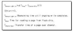
본 발명의 실시 예에 따르면, 요청 큐로부터 요청 플래시 칩으로 지정된 상기 요청을 선택하는 것; 상기 요청이 읽기 요청인지 판별하는 것; 및 상기 요청이 읽기 요청인 경우, α를 리셋하고, 수학식 1이 만족되는지 판별하고, [수학식 1]


상기 요청이 읽기 요청이고, 상기 수학식 1이 만족한 경우, 상기 방법은 상기 요청 플래시 칩과 동일한 플래시 칩 그룹 내에서 다른 플래시 칩들로부터 읽음으로써 상기 요청을 재구성하는 것을 더 포함할 수 있다. 상기 요청이 쓰기 요청인 경우, 상기 방법은 수학식 2를 사용하여 α를 증가시키고, [수학식 2]
상기 요청이 상기 쓰기 요청이고, 상기 수학식 1이 만족되는 경우, 상기 요청이 스케쥴링되지 않을 수 있다. 이는 동시에 쓰기 작업이 발생하지 않는 상황을 방지하기 위하여 현재 쓰기 동작이 완료될 때까지 기다려야 함을 의미한다.When the request is the write request and
본 발명의 실시 예에 따르면, 향상된 성능을 갖는 RAID 가능한 SSD 및 그것의 데이터 처리 방법이 제공된다.According to an embodiment of the present invention, a RAID capable SSD having improved performance and a data processing method thereof are provided.
본 발명의 특징들 및 사상들은 상세한 설명, 특허청구범위, 및 첨부된 도면들을 참조하여 이해되고 인정될 것이다.
도 1은 본 발명의 실시 예에 따른 SSD 채널들 및 플래시 칩들에 대한 대표적인 구조를 보여준다.
도 2는 도 1에 도시된 실시 예에 따른, SSD에서 발생하는 쓰기 동작들의 타임라인을 보여준다.
도 3은 본 발명의 다른 실시 예에 따른 SSD 채널들 및 플래시 칩들에 대한 대표적인 구조를 보여준다.
도 4는 도 3에 도시된 실시 예에 따른, SSD에서 발생하는 쓰기 동작들의 타임 라인을 보여준다.
도 5는 본 발명의 실시 예에 따른 스케쥴링 프로세스를 보여준다.
도 6a는 본 발명의 실시 예에 따른 읽기 및 쓰기 스케쥴링을 결정하는 방법을 보여준다.
도 6b는 본 발명의 실시 예에 따른 읽기 및 쓰기 스케쥴링을 결정하는데 사용되는 수학식을 보여준다.
도 7은 가비지 콜렉션 사이클의 예를 보여준다.
도 8은 플레인에서 쓰기 포인트들을 확장하는 것을 보여준다.
도 9는 본 발명의 실시 예에 따른 스케쥴링 프로세스를 보여준다.The features and spirits of the present invention will be understood and appreciated with reference to the detailed description, claims, and appended drawings.
1 shows a representative structure of SSD channels and flash chips according to an embodiment of the present invention.
FIG. 2 shows a timeline of write operations occurring in the SSD according to the embodiment shown in FIG. 1 .
3 shows a representative structure of SSD channels and flash chips according to another embodiment of the present invention.
FIG. 4 shows a timeline of write operations occurring in the SSD according to the embodiment shown in FIG. 3 .
5 shows a scheduling process according to an embodiment of the present invention.
6A shows a method of determining read and write scheduling according to an embodiment of the present invention.
6B shows an equation used to determine read and write scheduling according to an embodiment of the present invention.
7 shows an example of a garbage collection cycle.
8 shows extending the write points in the plane.
9 shows a scheduling process according to an embodiment of the present invention.
첨부된 도면들과 연관된 이하의 상세한 설명은 본 발명에 따라 제공되는 예시적인 실시 예의 설명으로 의도되며, 본 발명이 구성되고 활용될 수 있는 유일한 형태를 나타내는 것으로 의도되지 않는다. 상세한 설명은 기재된 실시 예들과 연관된 본 발명의 특징들을 설명한다. 그러나 동일하거나 또는 균등한 기능들 및 구조들이 본 발명의 사상 및 범위 내에 포함되는 것으로 의도되는 다른 실시 예들에 의해 구현될 수 있음이 이해될 것이다. 더욱이 당업자는 본 발명에 따른 하나 또는 그 이상의 실시 예들의 특징들이 본 발명의 다른 실시 예들을 구현하는 적절한 방식으로 조합될 수 있음을 이해할 것이다. 상세한 설명에서 다르게 기재되지 않는 한, 동일한 참조 번호들은 동일한 기능 또는 구성 요소들을 지칭하는 것으로 의도된다.DETAILED DESCRIPTION The following detailed description, in conjunction with the appended drawings, is intended as a description of exemplary embodiments provided in accordance with the present invention and is not intended to represent the only forms in which the present invention may be constructed and utilized. The detailed description sets forth features of the invention in connection with the described embodiments. However, it will be understood that the same or equivalent functions and structures may be implemented by other embodiments which are intended to be included within the spirit and scope of the present invention. Moreover, those skilled in the art will understand that features of one or more embodiments of the present invention may be combined in any suitable manner to implement other embodiments of the present invention. Unless stated otherwise in the detailed description, like reference numbers are intended to refer to like functions or components.
복수의 플래시 칩들을 포함하는 낸드 플래시 솔리드 스테이트 드라이브들(SSD; solid state drive)에서, 특정 플래시 칩으로의 읽기 요청들은 목표 플래시 칩에서 수행 중인 긴-레이턴시의 프로그램/소거 동작으로 인해 그것들의 서비스에서 큰 지연을 경험할 수 있다. 프로그램 동작은 일반적으로 읽기 레이턴시보다 더 많은 시간(10X~20X)을 소모하여 완료된다. 쓰기들보다 읽기들에 높은 우선 순위를 할당함에도 불구하고, 읽기 요청이 프로그램 동작을 수행하느라 바쁜 플래시 칩으로 향할 때 동일한 플래시 칩으로의 읽기 자체 및 그에 따른 읽기들이 지연될 것이고, 이로 인하여 읽기, 프로그램, 및 소거 동작들 레이턴시의 차이로 인한 상당히 큰 읽기 테일 레이턴시(read tail latency)가 유발된다.In NAND flash solid state drives (SSDs) including a plurality of flash chips, read requests to a specific flash chip are out of service due to the long-latency program/erase operation being performed in the target flash chip. You may experience large delays. Program operations are typically completed by consuming more time (10X-20X) than read latency. Despite assigning a higher priority to reads than writes, when a read request is directed to a flash chip busy performing a program operation, the read itself and subsequent reads to the same flash chip will be delayed, which results in read, program , and a significantly large read tail latency due to the difference in latencies of erase operations.
수행 중인 프로그램/소거 동작으로 인해 유발되는 큰 읽기 테일 레이턴시를 감소시키거나 또는 최소화하기 위하여, 본 발명의 실시 예는 SSD로의 읽기 및 쓰기에 대한 새로운 스케쥴링 메커니즘을 포함할 수 있다. 새로운 스케쥴링 메커니즘을 통해, 비지 플래시 칩(busy flash chip)으로의 읽기 요청이 재구성되고, 프로그램/소거 동작이 완료될 때까지 기다리는 것보다 빠르게 제공될 수 있다.In order to reduce or minimize a large read tail latency caused by a program/erase operation being performed, an embodiment of the present invention may include a new scheduling mechanism for reading and writing to and from the SSD. Through the new scheduling mechanism, a read request to a busy flash chip can be reconfigured and provided faster than waiting for a program/erase operation to complete.
본 발명에 따른 실시 예들의 양상들은 읽기 테일 레이턴시를 감소시키는 것을 기대하고, RAID-장착 SSD에서 읽기-쓰기 간섭(read-write interference)를 감소시키거나 또는 최소화하는 것과 관련된다. 이를 위하여, 본 발명의 실시 예는 새로운 스케쥴링 및 데이터 배치 메커니즘을 포함할 수 있다. 이를 통해, 플래시 칩들이 복수의 그룹들로 군집된다. 각 그룹에서, 쓰기들은 주어진 시간에서, 오직 하나의 플래시 칩에 국한되고, 라운드-로빈 방식으로 그룹내의 다른 플래시 칩들로 순환된다. 프로그램-비지 상태의 플래시 칩을 목표로 하는 읽기들은 각 그룹에서 패리티-홀딩 플래시 칩에 저장된 각 그룹의 패리티를 갖는 것으로 재구성될 것이다.Aspects of embodiments in accordance with the present invention are directed to reducing or minimizing read-write interference in a RAID-equipped SSD, with the expectation of reducing read tail latency. To this end, an embodiment of the present invention may include a new scheduling and data placement mechanism. Through this, the flash chips are clustered into a plurality of groups. In each group, writes are confined to only one flash chip at any given time, and are cycled to other flash chips in the group in a round-robin fashion. Reads targeting the flash chip in the program-busy state will be reconstructed with the parity of each group stored in the parity-holding flash chip in each group.
가비지 콜렉션에 의해 유발되는 읽기 및 프로그램/소거 동작들 사이의 간섭을 더 감소시키기 위하여, 본 발명의 실시 예들은 사용자 쓰기들 및 가비지 콜렉션 쓰기들을 분리하여 유효 데이터 이동이 다음 가비지 콜렉션(GC) 사이클들로 이동하는 것을 방지한다. 그로 인하여, GC 주기 및 이동 비용이 감소되거나 또는 최소화될 수 있고, GC 쓰기들 및 소거 동작들에 의해 유발되는 긴 읽기 테일 레이턴시가 감소될 수 있다.To further reduce the interference between read and program/erase operations caused by garbage collection, embodiments of the present invention separate user writes and garbage collection writes so that valid data movement is performed in subsequent garbage collection (GC) cycles. to prevent moving to Thereby, the GC cycle and move cost may be reduced or minimized, and long read tail latency caused by GC writes and erase operations may be reduced.
도 1은 본 발명의 실시 예에 따른 SSD 채널들 및 플래시 칩들에 대한 대표 구조를 보여준다.1 shows a representative structure of SSD channels and flash chips according to an embodiment of the present invention.
이러한 실시 예에서, SSD(100)는 4개의 채널들(140)을 포함하고, 각 채널은 4개의 플래시 칩들(120)을 포함한다. 채널들(140) 각각은 컨트롤러(110)와 연결된다. 더욱이, 이러한 실시 예에서, RAID-장착 SSD(100)는 3+1 패리티(또는 6+2 패리티)를 사용할 수 있다. 즉, 각 패리티 플래시 칩(120P)에 대하여 3개의 비-패리티 플래시 칩들이 존재한다. 복수의 플래시 칩들(120)은 플래시 칩 그룹(160)(예를 들어, 플래시 그룹들(160-1 및 160-2))으로 군집화된다.In this embodiment,
도 1에 도시된 바와 같이, 2개의 그룹들(160)이 존재할 수 있고, 각 그룹은 독립적으로 동작한다. 각 그룹(160)에서, 복수의 플래시 칩들(120)이 포함되나, 각 그룹(160)에서 최대 한 개의 활성 기입 플래시 칩(120A)이 존재한다. 즉, 어느 때나, 하나의 쓰기/프로그램 동작이 각 그룹(160)에서 발생한다. 쓰기가 완료된 경우, 동일한 그룹내의 다른 플래시 칩(120)으로 지정된 다음 쓰기가 발생한다. 플래시 칩 그룹에서 하나의 쓰기 포인트만 존재하나, 다른 그룹들은 그것들의 그룹들과 연관된 플래시 칩들로 지정된 쓰기 요청들을 제공할 수 있다. 즉, 본 발명의 실시 예들에 따른 컨트롤러(110)는 각 그룹이 하나씩 쓰기들을 제공받기를 기다리는 쓰기들을 지정함으로써, 그룹 당 하나의 쓰기 포인트 규칙을 시행할 수 있고, 어느 때나 각 그룹에서 하나 이상의 쓰기 포인트를 허용하지 않을 수 있다.As shown in FIG. 1 , there may be two
읽기가 활성 쓰기 플래시 칩(120A)과 다른 그룹의 플래시 칩(120)을 목표로 하는 경우, 읽기가 통상적 절차(regular procedure)를 통해 제공될 수 있다. 그러나 읽기가 쓰기 요청을 제공한 비지 상태인 활성 쓰기 플래시 칩(120A)을 목표로 하는 경우, 동일한 그룹(160)의 다른 플래시 칩(120)으로부터의 대응하는 페이지들을 읽고, 읽은 데이터를 배타적 논리합 연산(XOR) 또는 재구성함으로써, 읽기가 재구성될 수 있다. 추가적인 예로서, 일부 인코딩 방식들의 예에서, 읽기 요청이 현재 활성 쓰기 플래시 칩(120A)인 플래시 칩(2)을 목표로 하는 경우, 플래시 칩(2)으로부터 요청된 데이터는 (i) 플래시 칩(1), 플래시 칩(3), 및 플래시 칩(4)(패리티 플래시 칩(120P))으로부터 각각의 페이지들을 읽고, 그리고 (ii) 앞서 언급된 플래시 칩들(120)로부터 읽은 데이터를 배타적 논리합(XOR) 연산함으로써 재구성될 수 있다.When the read targets the
도 2는 도 1의 실시 예에 따른 SSD(100)에서 발생하는 쓰기 동작들의 타임라인을 보여준다.FIG. 2 shows a timeline of write operations occurring in the
제0 시점(t0)으로부터 제1 시점(t1)까지, 2 각각의 그룹들(160-1, 160-2) 각각에서 플래시 칩들(1, 9)의 각각으로 향하는 2개의 페이지 쓰기들이 제공될 수 있다. 이러한 시간 구간 동안, 쓰기-비지 플래시 칩들로 어떤 읽기가 발생한 경우, 요청된 데이터가 상술된 바와 같이 재구성될 수 있다. 쓰기들이 그룹의 플래시 칩들에 대해 완료된 경우, 패리티 칩들이 갱신된다. 필요에 따라, 그 이후에, 상기 그룹은 그것을 목표로 하는 쓰기들을 제공하는 것을 다시 시작하고, 이러한 스케쥴링이 반복된다. 즉, 제4 시점(t4)에서, 패리티 플래시 칩들(4, 12)이 갱신될 수 있고, 어떤 필요한 프로그램 동작이 이 때 발생할 수 있다.From the 0th time point t0 to the first time point t1, two page writes directed to each of the
각 그룹에서, 플래시 칩 쓰기들 및 패리티 갱신들이 비결합(decoupled)되고, 패리티 갱신들이 지연되지만, 이러한 제약이 모든 그룹들의 모든 플래시 칩들에 대하여 전체적으로 유지될 필요는 없다. 오히려, 이러한 제약은 그룹을 형성하는 플래시 칩들에 대하여 부분적으로 유지된다. 도시된 실시 예에서, 모든 그룹들의 패리티 갱신들은 일부 플래시 칩들에서 쓰기가 발생하기 않은 경우에 동시에 발생된다. 그러나, 그룹의 패리티 플래시 칩이 요구된 패리티 페이지들을 갱신하는 비지 상태인 동안, 다른 그룹들로의 쓰기들이 제공될 수 있다.In each group, flash chip writes and parity updates are decoupled, and parity updates are delayed, but this constraint need not be held globally for all flash chips in all groups. Rather, this constraint holds in part for flash chips forming a group. In the illustrated embodiment, parity updates of all groups are simultaneously generated when no write occurs in some flash chips. However, writes to other groups may be provided while the group's parity flash chip is busy updating the requested parity pages.
쓰기 포인트들은 각 그룹에서 순환하고, 패리티는 쓰기들이 완료된 경우 갱신된다. 플래시 칩(4)이 요구된 패리티 블록들을 갱신하는 비지 상태인 경우, 플래시 칩들(1~3)로의 어떤 읽기들이 이러한 플래시 칩들에서 수행 중인 프로그램 동작을 접하는 것 없이 제공될 수 있다. 더욱이, 플래시 칩들(5~7)로의 읽기들이 동일한 프로세스를 거치므로, 수행 중인 프로그램 동작으로 인해 읽기 동작이 차단되지 않는다.Write points cycle in each group, and parity is updated when writes are complete. When the
도 3은 본 발명의 다른 실시 예에 따른 SSD 채널들 및 플래시 칩들의 대표 구조를 보여준다.3 shows a representative structure of SSD channels and flash chips according to another embodiment of the present invention.
이러한 실시 예에서, SSD(200)는 4개의 채널들(240)을 포함하고, 채널들 각각은 4개의 플래시 칩들(220)을 포함한다. 채널들(240) 각각은 컨트롤러(210)와 연결된다. 더욱이, 이러한 실시 예에서, RAID-장착 SSD(200)(RAID-equipped SSD)는 3+1 패리티를 사용한다. 즉, 각 패리티 플래시 칩(220P)에 대하여 3개의 비-패리티 칩들이 존재한다. 복수의 플래시 칩들(220)은 플래시 칩 그룹(260)(예를 들어, 플래시 그룹들(260-1, 260-2, 260-3, 260-4))으로 군집될 수 있다.In this embodiment,
도 3에 도시된 바와 같이, 각각이 독립적으로 동작하는 4개의 그룹들(260)이 존재한다. 각 그룹(260)에서, 복수의 플래시 칩들(220)이 포함된다. 그러나 최대 1개의 활성 쓰기 플래시 칩(220A)이 각 그룹(260)에 존재한다. 즉, 어느 때나, 하나의 쓰기/프로그램 동작이 각 그룹(260)에서 발생한다. 쓰기가 완료된 경우, 동일한 그룹에서 다음 플래시 칩(220)에 지정된 다음 쓰기가 발생한다. 플래시 칩 그룹에서 하나의 쓰기 포인트만 존재하나, 다른 그룹들은 해당 그룹들과 대응하는 플래시 칩들에 지정된 쓰기 요청들을 제공할 수 있다. 따라서, 본 발명의 실시 예들에 따른 컨트롤러(110)는 각 그룹이 하나씩 제공받기를 기다리는 쓰기들을 지시함으로써 그룹 규칙당 하나의 쓰기 포인트를 시행할 수 있고, 어느 때나 각 그룹에서 하나 이상의 쓰기 포인트를 허용하지 않을 수 있다.As shown in FIG. 3 , there are four
읽기가 활성 쓰기 플래시 칩(220A)과 다른 그룹의 어떤 플래시 칩(220)을 목표로 하는 경우, 읽기가 통상적 절차를 통해 제공될 수 있다. 그러나, 읽기가 쓰기 요청을 제공하는 비지 상태인 활성 쓰기 플래시 칩(220A)을 목표로 하는 경우, 동일한 그룹(260)의 다른 플래시 칩들(220)로부터 대응하는 페이지들을 읽고, 읽은 데이터를 재구성함으로써 읽기가 재구성될 수 있다. 실시 예로서, 인코딩의 일부 형태들에서, 읽기 요청이 현재 활성 플래시 칩(220A)인 플래시 칩(2)을 목표로 하는 경우, 플래시 칩(2)으로부터 요청된 데이터는 (i) 플래시 칩(1), 플래시 칩(3), 및 플래시 칩(4)(패리티 플래시 칩(220P)으로부터의 각각의 페이지들을 읽고, (ii) 앞서 언급된 플래시 칩들(220)로부터 읽은 데이터를 배타적 논리합(XOR) 연산함으로써 재구성될 수 있다.If the read is aimed at any
도 4는 도 3의 실시 예에 따른 SSD(220)에서 발생하는 쓰기 동작들의 타임라인을 보여준다.FIG. 4 shows a timeline of write operations occurring in the
제0 시점(t0)으로부터 제1 시점(t1)까지, 4개의 페이지 쓰기들이 플래시 칩들(1, 5, 9, 13)으로 지정되고, 플래시 칩들 각각은 각각의 플래시 그룹(260)에 포함된다. 이러한 시간 구간에서, 쓰기-비지 상태인 플래시 칩들로 어떤 읽기가 발생한 경우, 요청된 데이터는 상술된 바와 같이 재구성될 수 있다. 쓰기들이 그룹의 플래시 칩들에 대하여 완료된 경우, 패리티 칩들이 갱신된다. 필요에 따라, 이후에, 스케쥴이 반복된다. 즉, 제3 시점(t3)으로부터 제4 시점(t4)까지, 패리티 플래시 칩들(4, 8, 12, 16)이 갱신될 수 있고, 요청된 프로그램 동작이 이 때 수행될 수 있다.From the 0th time point t0 to the first time point t1 , four page writes are designated to the
각 그룹에서, 플래시 칩 쓰기들 및 패리티 갱신들이 비-연결되고, 패리티 갱신들이 지연되지만, 이러한 제약이 모든 그룹들의 모든 플래시 칩들에 대하여 전체적으로 유지될 필요는 없다. 오히려, 이러한 제약은 그룹을 형성하는 플래시 칩들에 대하여 부분적으로 유지된다. 도시된 실시 예에서, 모든 그룹들의 패리티 갱신들은 일반 플래시 칩들에서 쓰기가 발생하지 않은 경우에, 동시에 발생한다. 그러나, 그룹의 패리티 플래시 칩들이 요청된 패리티 페이지들을 갱신하는 비지 상태인 동안, 다른 그룹들로의 쓰기들이 제공될 수 있다.In each group, flash chip writes and parity updates are uncoupled, and parity updates are delayed, but this constraint need not be held globally for all flash chips in all groups. Rather, this constraint holds in part for flash chips forming a group. In the illustrated embodiment, parity updates of all groups occur at the same time when writing does not occur in general flash chips. However, writes to other groups may be provided while the group's parity flash chips are busy updating the requested parity pages.
각 그룹에서 쓰기 포인트들은 순환하고, 쓰기들이 완료된 경우 패리티가 갱신된다. 플래시 칩(4)이 요청된 패리티 블록들을 갱신하는 비지 상태인 경우, 이러한 플래시 칩들에서 수행 중인 프로그램 동작을 접하는 것 없이 플래시 칩들(1~3)로의 어떤 읽기가 제공될 수 있다. 더욱이, 다른 플래시 침들로의 읽기들이 동일한 절차를 거치기 때문에, 수행 중인 프로그램 동작으로 인해 읽기가 차단되지 않는다.The write points in each group cycle, and when writes are completed, the parity is updated. When the
도 1 내지 도 4를 참조하면, 도 1 내지 도 4의 실시 예들이 동시에 동일한 채널들에서 발생하는 모든 쓰기들(각 그룹 당 하나)을 보여주나, 본 발명이 이에 한정되는 것은 아니다. 더욱이, 쓰기들은 다른 그룹들에서 쓰기들이 발생한 때로부터 독립적으로 각 그룹에서 발생할 수 있다. 예를 들어, 쓰기들은 플래시 칩들(1, 14)에서 중복될 수 있거나, 또는 쓰기들은 플래시 칩들(1, 16)에서 중복될 수 있거나 또는 그룹 당 하나의 쓰기만 발생하는 다른 적절한 조합으로 발생할 수 있다.1 to 4 , the embodiments of FIGS. 1 to 4 show all writes (one for each group) simultaneously occurring in the same channels, but the present invention is not limited thereto. Moreover, writes can occur in each group independently from when writes in other groups occur. For example, writes may be duplicated in
더욱이, 도 1 내지 도 4를 참조하면, 도 1 내지 도 4의 실시 예들은 각 그룹 당 하나의 쓰기만을 보여주나, 본 발명이 이에 한정되는 것은 아니다. 예를 들어, 각 플래시 칩 그룹이 2개의 패리티 칩들을 포함하는 경우, 2개의 쓰기들이 동일한 그룹에서 동시에 발생할 수 있다. 일반적으로, 각 플래시 칩 그룹이 i개의 패리티 플래시 칩들을 포함하는 경우, i개의 쓰기들이 각 플래시 그룹에서 동시에 발생할 수 있고, 이 때, i는 1보다 크거나 같은 정수이다. 플래시 칩 그룹 내의 쓰기들의 개수가 플래시 칩 그룹의 패리티 플래시 칩들의 개수보다 적거나 같은 경우, 읽기가 기입 중인 플래시 칩들 중 하나로 보내질때, 읽기 요청들이 재구성될 수 있다.Furthermore, referring to FIGS. 1 to 4 , the embodiments of FIGS. 1 to 4 show only one write per group, but the present invention is not limited thereto. For example, when each flash chip group includes two parity chips, two writes may occur simultaneously in the same group. In general, when each flash chip group includes i parity flash chips, i writes may occur simultaneously in each flash group, where i is an integer greater than or equal to 1 . If the number of writes in the flash chip group is less than or equal to the number of parity flash chips in the flash chip group, read requests can be reconstructed when the read is sent to one of the flash chips being written.
더욱이, 각 비-패리티 플래시 칩에서 처리 중인 각 쓰기의 시간에서 또는 그 이전에, 읽기 요청이 있는 경우, 정확한 데이터가 배타적 논리합을 위해 이용 가능하도록 비-패리티 플래시 칩의 데이터가 임시 메모리(예를 들어, 캐시)에 저장될 수 있다. 이는 쓰기가 발생할 때마다 발생할 수 있거나 또는 쓰기가 칩으로부터 데이터를 교체 중이거나 또는 삭제 중인 경우에만 발생할 수 있다. 더욱이, 이는 비-패리티 칩들 중 마지막이 기입중이거나 및/또는 패리티 칩이 기입 중인 경우 발생하지 않을 수 있다.Moreover, at or before the time of each write being processed by each non-parity flash chip, if there is a read request, the data from the non-parity flash chip is stored in temporary memory (e.g. For example, it may be stored in a cache). This can happen whenever a write occurs, or it can only happen when a write is replacing or erasing data from the chip. Moreover, this may not occur if the last of the non-parity chips is writing and/or the parity chip is writing.
예를 들어, 플래시 칩(1)이 기입되고, 데이터가 변경되는 경우, 쓰기가 플래시 칩(1)에서 발생한 시점 또는 그 이전에, 플래시 칩(1)에 저장된 데이터가 임시 메모리에 저장된다. 이후에, 플래시 칩(2)이 기입되는 동안, 플래시 칩(2)에 대한 읽기가 수신된 경우, 도 1 내지 도 4를 참조하여 설명된 실시 예들을 사용하여 데이터가 부정확하게 읽어질 수 있다. 예를 들어, 플래시 칩(1)의 데이터가 변경되고, 패리티 칩이 아직 갱신되지 않은 경우(플래시 칩(2)이 여전히 기입 중인 경우 일 수 있으므로), 플래시 칩들(1, 3, 4)의 데이터를 배타적 논리합 연산함으로써 정확한 데이터가 수신되지 않을 수 있다.For example, when the
이 경우, 플래시 칩(1)에 대하여 저장된 이전 데이터(old data) 및 플래시 칩들(3, 4)의 현재 데이터를 배타적 논리합 연산함으로써, 데이터가 정확하게 읽어질 수 있다. 플래시 칩(3)이 기입 중인 경우, 플래시 칩들(1, 2)의 이전 기입들에서 변경된 데이터에도 마찬가지이다.In this case, data can be accurately read by performing an exclusive OR operation on old data stored with respect to the
도 1 내지 도 4을 참조하여 설명된 실시 예들이 3+1P 구조를 포함하나, 본 발명이 이에 한정되는 것은 아니며, 다른 패리티 구조들이 사용될 수 있다. 예를 들어, 2+1P, 4+1P, 3+2P, 4+2P 등이 상술된 3+1P 구조 대신에 또는 그에 추가적으로 사용될 수 있다. 마찬가지로, 4X4 세트의 칩은 단순히 예시적인 것이며, 칩들은 적절한 개수의 채널들 또는 채널당 칩들을 포함할 수 있다.Although the embodiments described with reference to FIGS. 1 to 4 include a 3+1P structure, the present invention is not limited thereto, and other parity structures may be used. For example, 2+1P, 4+1P, 3+2P, 4+2P, etc. may be used instead of or in addition to the 3+1P structure described above. Likewise, a 4X4 set of chips is merely exemplary, and the chips may include any number of channels or chips per channel.
더욱이, 도 2 및 도 4를 참조하면, 동일한 채널과 연결된 다른 플래시 칩 그룹들의 플래시 칩들이 동시에 기입되는 것으로 도시되어 있으나, 본 발명이 이에 한정되는 것은 아니며, 동일한 채널에 연결된 다른 플래시 칩 그룹들의 플래시 칩들은 다른 시간에 기입될 수 있거나 및/또는 다른 채널들과 연결된 다른 플래시 칩 그룹들의 플래시 칩들이 동시에 기입될 수 있다.Furthermore, referring to FIGS. 2 and 4 , although flash chips of different flash chip groups connected to the same channel are simultaneously written, the present invention is not limited thereto, and flash of different flash chip groups connected to the same channel is not limited thereto. The chips may be written to at different times and/or flash chips of different flash chip groups connected to different channels may be written to at the same time.
도 5는 본 발명의 실시 예에 따른 스케쥴링 절차를 보여준다. 본 발명의 실시 예에 따르면, 각 플래시 그룹에서 발생하는 일련의 이벤트들이 도 5에 도시된다.5 shows a scheduling procedure according to an embodiment of the present invention. According to an embodiment of the present invention, a series of events occurring in each flash group is illustrated in FIG. 5 .
도 5에 도시된 바와 같이, 이러한 실시 예에서, 플래시 그룹(x)에 대하여, 쓰기들이 그룹(x)의 플래시 칩들(예를 들어, 그룹(x)의 비-패리티 플래시 칩들)에서 발생한다. 연속된 방식(consecutive manner)으로 그룹(x)의 플래시 칩들로 발행된 쓰기들이 완료된 경우, 그룹(x)의 패리티 칩은 RAID 구현에 따라 요청된 패리티 페이지들을 갱신한다. 그룹(x)의 패리티 플래시 칩들에 대한 갱신이 완료된 경우, 절차(process)가 반복될 수 있다.5 , in this embodiment, for flash group x, writes occur to flash chips of group x (eg, non-parity flash chips of group x). When writes issued to the flash chips of the group (x) are completed in a consecutive manner, the parity chip of the group (x) updates the requested parity pages according to the RAID implementation. When the update of the parity flash chips of the group (x) is completed, the process may be repeated.
도 6a는 본 발명의 실시 예에 따른 읽기 및 쓰기 스케쥴링을 결정하는 방법을 보여준다. 도 6b는 본 발명의 실시 예에 따른 읽기 및 쓰기 스케쥴링을 결정하는 방법에서 사용되는 수학식을 보여준다. 더욱이, 도 6a 및 도 6b는 RAID-가능 SSD의 컨트롤러를 통해 플래시 칩(예를 들어, 요청 플래시 칩)으로부터 데이터를 읽거나 또는 그것으로 데이터를 기입하는 요청을 처리하는 방법을 보여준다.6A shows a method of determining read and write scheduling according to an embodiment of the present invention. 6B shows an equation used in a method for determining read and write scheduling according to an embodiment of the present invention. Moreover, FIGS. 6A and 6B show how to process a request to read data from or write data to a flash chip (eg, a request flash chip) via a controller of a RAID-capable SSD.
상보적인 스케쥴링을 수행하고, 패리티 갱신들을 지연시키고, 읽기 재구성 메커니즘들을 수행하는 것은 플래시 칩들에 대한 읽기-쓰기 간섭을 감소시키고, 순차적으로 읽기 테일 레이턴시를 상당히 감소시킬 수 있지만, 상술된 본 발명의 실시 예들은 다음과 같은 적어도 3개의 추가적인 결과들을 포함한다. (i) 플래시 칩들의 부분으로만 쓰기들을 국한시키는 것은 SSD들로 제공된 고-레벨의 병렬화를 활용하는 것을 방해하고, 그로 인하여 쓰기 성능이 저하된다. (ii) 메커니즘은 정적으로 기능하고, 업무량 역동성(workload dynamism)을 수집하지 못한다. (iii) 각 읽기를 제구성하는 것은 추가적인 읽기 동작들을 필요로 한다. 본 발명은 이러한 단점들을 크게 완화시킬 수 있는 적응적인 결정 절차를 제안함으로써, 이러한 문제점들을 해결한다.Performing complementary scheduling, delaying parity updates, and performing read reconfiguration mechanisms can reduce read-write interference to flash chips and significantly reduce sequential read tail latency, but the implementation of the present invention described above Examples include at least three additional results as follows. (i) Confining writes to only a portion of the flash chips prevents exploiting the high-level parallelism provided by SSDs, thereby degrading write performance. (ii) the mechanism functions statically and does not collect workload dynamism; (iii) Reconstructing each read requires additional read operations. The present invention solves these problems by proposing an adaptive decision procedure that can greatly alleviate these shortcomings.
상술된 바와 같이, (i) 쓰기 스케쥴링 결정들, 및 (ii) 읽기 재구성 결정들의 실행을 통한 2가지 주된 결정(main decision)이 존재한다. 어떤 I/O 작업 부하 및 장치 동작을 고려하지 않고, 결정들이 정적으로 이루어진 경우, SSD로의 쓰기가 매우 큰 레이턴시들을 경험할 것이다.As noted above, there are two main decisions through execution of (i) write scheduling decisions, and (ii) read reconfiguration decisions. If the decisions are made statically, without considering any I/O workload and device behavior, the write to the SSD will experience very high latencies.
도 6a 및 도 6b를 참조하면, 의사 결정 프로세스는 도 6b에 도시된 수학식 1을 기반으로 SSD의 장치 고유의 특성 및 작업부하 역동성(workload dynamism)에 적용할 수 있다. 예를 들어, 작업부하가 긴 시간 동안, 쓰기 요청들만 생성하는 경우, 수학식은 입력되는 쓰기 요청들로 더욱 많은 플래시 칩들을 사용할 수 있도록 적용할 수 있다. 반면에, 읽기가 도달한 경우, 읽기-쓰기 간섭을 감소시키기 위하여 수학식 1은 쓰기들을 몇몇 플래시 칩들로 국한시킨다.6A and 6B , the decision-making process may be applied to device-specific characteristics and workload dynamism of the SSD based on
의사 결정 프로세스 및 요청된 파라미터들을 갱신하는 것과 연관된 절차는 도 6a에 도시된다. 도 6a에서 설명되는 바와 같이, 스케쥴러(예를 들어, 컨트롤러)가 요청의 타입 및 그룹의 플래시 칩들의 상태를 기반으로 요청을 수집할때마다, 스케쥴러는 (쓰기에 대한) 요청을 제공할 수 있는지 또는 없는지 결정하고, (읽기에 대한) 데이터를 재구성할 수 있는지 또는 없는지 결정한다. 좀 더 정확하게는, 요청이 쓰기인 경우, 컨트롤러는 프로그램 동작이 수행 중이지 않거나 또는 프로그램 동작의 종료가 임박한 어느 그룹이 존재하는지 검사한다.The decision making process and the procedure associated with updating the requested parameters is shown in FIG. 6A . As illustrated in FIG. 6A , whenever the scheduler (eg, a controller) collects a request based on the type of request and the status of the flash chips in the group, the scheduler can provide the request (for writes). or not, and whether or not the data can be reconstructed (for reading). More precisely, if the request is a write, the controller checks to see if there is a group in which no program operation is being performed or the end of the program operation is imminent.
종료가 임박함은 수학식 1을 검사함으로써 판별될 수 있다. 수학식 1은 각 반복에서 상수 파라미터 β와 곱해짐으로써 갱신되는 파라미터 α를 사용한다. 만약


좀 더 상세하게, 300 동작에서, 스케쥴러는 요청 큐로부터 요청을 선택한다.예를 들어, 하나의 읽기(READ) 요청 큐 및 하나의 쓰기(WRITE) 요청 큐가 유지될 수 있다. 읽기(READ) 요청 큐가 비어있거나 또는 쓰기(WRITE) 요청 큐가 x%(예를 들어, 80%) 이상으로 채워진 경우, 스케쥴러는 쓰기(WRITE) 요청 큐로부터 하나의 쓰기(WRITE) 요청을 처리한다. 그렇지 않은 경우, 스케쥴러는 읽기(READ) 요청을 처리한다.More specifically, in
310 동작에서, 스케쥴러는 요청이 읽기 요청인지 판별한다.In
요청이 읽기 요청인 경우, 320 동작에서, 스케쥴러는 α를 리셋한다. 예를 들어, α는 2로 리셋될 수 있다. 이후에, 330 동작에서, 스케쥴러는 수학식 1이 유지되는지 판별한다. 수학식 1이 유지되지 않은 경우, 340 동작에서, 읽기 요청이 발생된다. 수학식 1이 유지되는 경우, 350 동작에서, 그룹의 다른 플래시 칩으로부터 읽기 및 배타적 논리합 연산에 의해 읽기 요청이 재구성된다.If the request is a read request, in
요청이 읽기 요청이 아닌 경우, 360 동작에서, 스케쥴러는 α를 α×β와 동일하도록 설정한다. 이 때, β는 증가 파라미터이다. 예를 들어, β는 1.001과 같을 수 있다. 이후에, 370 동작에서, 스케쥴러는 수학식 1이 유지되는지 판별한다. 수학식 1이 유지되는 경우, 380 단계에서, 요청은 스케쥴링되지 않는다. 수학식 1이 유지되지 않는 경우, 390 동작에서, 그룹의 다음 플래시 칩으로 쓰기가 발행된다.If the request is not a read request, in
380 동작에서, 요청이 스케쥴링되지 않은 경우, 385 동작에서, 읽기 요청 큐로부터 하나의 요청이 수집되고, 방법은 310 동작에서 다시 시작할 수 있다.In
도 7은 가비지 콜렉션 사이클의 예를 보여준다.7 shows an example of a garbage collection cycle.
가비지 콜렉션에 의해 유발된 읽기 및 프로그램/소거 동작들 사이의 간섭을 추가적으로 감소시키기 위하여, 사용자 쓰기들 및 가비지 콜렉션 쓰기들이 분산되어 유효 데이터 이동들이 다음 GC 사이클로 전달되는 것을 방지할 수 있고, 그로 인하여 GC 주기 및 이동 비용이 감소 또는 최소화되고, GC 쓰기들 및 소거 동작들에 의해 유발되는 긴 읽기 테일 레이턴시가 감소될 수 있다.To further reduce the interference between read and program/erase operations caused by garbage collection, user writes and garbage collection writes can be distributed to prevent valid data movements from being propagated to the next GC cycle, thereby Cycle and move costs can be reduced or minimized, and long read tail latency caused by GC writes and erase operations can be reduced.
도 7은 가비지 콜렉션 사이클의 예를 보여준다. 이러한 프로세스를 통해, 블록(본 실시 예에서, 제i 블록)이 희생 블록(victim block)으로서 선택된다. 유효 페이지들이 다른 블록으로 이동한 이후에, 이 블록은 소거된다. 유효 데이터가 새로운 블록으로 이동한 경우, 이 블록의 나머지는 새로운 쓰기들로 채워질 것이다. 동일한 위치의 새로운 쓰기들 및 이전 유효 데이터(오랜 기간 동안 유효 데이터로 남는 경향이 있는 데이터)는 다음 GC 사이클들에서, 페이지 이동들의 캐스케이드 효과(cascading effect)를 유발할 수 있다. 다시 말해서, 과거 GC 사이클들에서 이동된 유효 데이터는 다음(또는 이후의) GC 사이클들에서 또 이동될 수 있는 경향이 있다. 따라서, 본 발명의 실시 예들은 이러한 효과들을 감소시키거나 또는 제거하기 위하여 GC 쓰기 및 사용자 쓰기들을 구분할 수 있고, 그로 인하여, GC의 주기 뿐만 아니라 각 GC 사이클로서의 GC에 의해 유발된 쓰기들이 감소된다.7 shows an example of a garbage collection cycle. Through this process, a block (in this embodiment, the i-th block) is selected as a victim block. After valid pages are moved to another block, this block is erased. When valid data has been moved to a new block, the remainder of this block will be filled with new writes. New writes to the same location and old valid data (data that tends to remain valid for a long period of time) can cause a cascading effect of page moves in subsequent GC cycles. In other words, valid data moved in past GC cycles tends to be moved again in next (or later) GC cycles. Accordingly, embodiments of the present invention can distinguish GC writes and user writes to reduce or eliminate these effects, thereby reducing not only the cycle of GC but also writes caused by GC as each GC cycle.
도 8은 플레인에서 쓰기 포인트들을 확장하는 것을 보여준다.8 shows extending the write points in the plane.
GC 동작을 관리하기 위하여, 본 발명의 실시 예는 내부-플래시 칩 GC(intra-flash chip GC)를 수행한다. 내부-플래시 칩 GC는 채널들을 통한 데이터 전송이나 유효 페이지의 이동들에 의한 패리티 갱신을 필요로 하지 않기 때문에, GC를 수행하는 성능-효율적인 방식이다.In order to manage the GC operation, the embodiment of the present invention performs intra-flash chip GC (intra-flash chip GC). Inner-flash chip GC is a performance-efficient way to perform GC because it does not require data transmission through channels or parity update due to movement of valid pages.
내부-플래시 칩 GC를 통합시키기 위하여, 수학식 1은
도 9는 본 발명의 실시 예에 따른 스케쥴링 절차를 보여준다.9 shows a scheduling procedure according to an embodiment of the present invention.
GC 기능이 추가된 경우, 도 5는 도 9에 도시된 바와 같이 갱신된다. 도 9에 도시된 바와 같이, 각 시간에서, 쓰기, 배경 동작, 또는 패리티 갱신 중 어느 하나가 각 그룹에서 진행된다. 더욱이, 그룹이 어떤 배경 동작(GC와 같은)을 수행 중인 경우, 상기 그룹의 어떤 플래시 칩들로의 쓰기들이 발행되지 않는다.When the GC function is added, FIG. 5 is updated as shown in FIG. 9 . As shown in Fig. 9, at each time, any one of a write, a background operation, or a parity update proceeds in each group. Moreover, if the group is performing some background operation (such as GC), no writes to any flash chips in the group are issued.
그러나, 상술된 실시 예들과 유사하게, 그룹이 쓰기 또는 배경 동작에 대하여 비지 상태인 경우, 다른 그룹들의 다른 플래시 칩들은 해당 그룹들과 연관된 플래시 칩들로의 서비스를 기다리는 쓰기 또는 배경 동작을 제공할 수 있다. 도 3의 실시 예에서 주어진 바와 같이, 그룹 1이 배경 동작 모드인 경우, 제2 내지 제4 그룹들로부터의 플래시 칩들은 각 그룹에서 시간 제약/규칙에 따라 하나의 쓰기 또는 배경 동작을 수행하는 동안 서비스 받기를 기다리는 쓰기들 또는 배경 동작들을 제공할 수 있다.However, similar to the above-described embodiments, when a group is in a busy state for a write or background operation, other flash chips of different groups may provide a write or background operation waiting for service to the flash chips associated with the corresponding groups. have. As given in the embodiment of FIG. 3 , when
본 발명에 따른 실시 예들의 양상들은 읽기-테일 레이턴시를 감소시키기 위하여, RAID-장착 SSD에서 읽기-쓰기 간섭을 감소시키거나 또는 최소화하는 것과 관련된다. 이를 위하여, 본 발명의 실시 예들은 복수의 그룹들로 군집된 플래시 칩들을 통한 새로운 스케쥴링 및 데이터 배치 기법을 포함할 수 있다. 각 그룹에서, 쓰기들이 주어진 시간에서 오직 하나의 플래시 칩으로만 국한되고, 그룹에서 다른 플래시 칩들로 라운드-로빈 방식으로 순환된다. 프로그램-비지 상태의 플래시 칩들을 목표로 하는 읽기들은 각 그룹의 패리티-유지 플래시 칩들에 저장된 각 그룹의 패리티를 포함하는 것으로 재구성될 수 있다.Aspects of embodiments in accordance with the present invention relate to reducing or minimizing read-write interference in a RAID-equipped SSD to reduce read-tail latency. To this end, embodiments of the present invention may include a new scheduling and data arrangement technique through flash chips clustered into a plurality of groups. In each group, writes are confined to only one flash chip at any given time, and are cycled in a round-robin fashion to other flash chips in the group. Reads targeting the flash chips in the program-busy state may be reconfigured to include parity of each group stored in the parity-maintaining flash chips of each group.
가비지 콜렉션에 의해 유발된 읽기 및 프로그램/소거 동작들 사이의 간섭을 더 감소시키기 위하여, 본 발명의 실시 예들은 사용자 쓰기들 및 가비지 콜렉션 쓰기들을 분산하여 유효 데이터의 이동들이 다음 GC 사이클들로 전달되는 것을 방지할 수 있다. 이로 인하여, GC 주기 및 이동 비용들이 감소되거나 또는 최소화될 수 잇고, GC 쓰기들 및 소거 동작들에 의해 유발되는 긴 읽기 테일 레이턴시가 감소될 수 있다.In order to further reduce the interference between read and program/erase operations caused by garbage collection, embodiments of the present invention distribute user writes and garbage collection writes so that movement of valid data is passed to the next GC cycles. it can be prevented Due to this, GC cycle and move costs may be reduced or minimized, and long read tail latency caused by GC writes and erase operations may be reduced.
상세한 설명에서 설명된 본 발명의 실시 예들에 따른 연관된 장치 또는 구성(또는 연관된 장치들 또는 구성들)은 적절한 하드웨어(예를 들어, ASIC(application-specific integrated circuit)), 펌웨어(예를 들어, DSP 또는 FPGA), 소프트웨어, 또는 소프트웨어, 펌웨어, 및 하드웨어의 적절한 조합을 사용하여 구현될 수 있다. 예를 들어, 연관된 장치(들)의 다양한 구성들은 하나의 집적 회로(IC; integrated circuit) 칩 또는 별도의 IC 칩들로 형성될 수 있다. 더욱이, 연관된 장치들의 다양한 구성들은 연성 인쇄 회로 필름(flexible printed circuit film), TCP(tape carrier package), PCB(printed circuit board)로 구현될 수 있거나, 또는 하나 또는 그 이상의 회로들 및/또는 다른 장치들로서 동일한 기판 상에 형성될 수 있다. 더욱이, 연관된 장치(들)의 다양한 구성들은, 상세한 설명에 기재된 다양한 기능들을 수행하기 위하여 컴퓨터 프로그램 명령어들을 실행하고 다른 시스템 구성들과 상호 작용하는 하나 또는 그 이상의 컴퓨팅 장치들의, 하나 또는 그 이상의 프로세서들에서 구동하는, 프로세스 또는 쓰레드일 수 있다. 컴퓨터 프로그램 명령어들은, 예를 들어, 랜덤 액세스 메모리(RAM; random access memory)와 같은, 표준 메모리를 사용하는 컴퓨팅 장치에서 구현될 수 있는 메모리에 저장된다. 컴퓨터 프로그램 명령어들은, 예를 들어, CD-ROM, 플래시 드라이브 등과 같은 다른 비-일시적인 컴퓨터 판독 가능한 메체에 저장될 수 있다. 또한, 당업자는 본 발명의 예시적인 실시 예들의 사상 및 범위로부터의 벗어남 없이, 다양한 컴퓨팅 장치들의 기능이 단일 컴퓨팅 장치로 직접 또는 결합될 수 있거나 또는 특정 컴퓨팅 장치의 기능이 하나 또는 그 이상의 다른 컴퓨팅 장치들을 통해 분산될 수 있음을 인식하여야 한다.The associated device or configuration (or associated devices or configurations) according to the embodiments of the present invention described in the detailed description may include suitable hardware (eg, an application-specific integrated circuit (ASIC)), firmware (eg, a DSP). or FPGA), software, or any suitable combination of software, firmware, and hardware. For example, the various components of the associated device(s) may be formed of one integrated circuit (IC) chip or separate IC chips. Moreover, various configurations of the associated devices may be implemented in a flexible printed circuit film, a tape carrier package (TCP), a printed circuit board (PCB), or one or more circuits and/or other device. They may be formed on the same substrate. Moreover, the various components of the associated device(s) may include one or more processors of one or more computing devices that execute computer program instructions and interact with other system components to perform the various functions described in the detailed description. It can be a process or a thread running in . The computer program instructions are stored in a memory that may be implemented in a computing device using standard memory, such as, for example, random access memory (RAM). The computer program instructions may be stored in other non-transitory computer readable media, such as, for example, a CD-ROM, flash drive, or the like. In addition, those skilled in the art will know that the functions of various computing devices may be directly or combined into a single computing device, or the functions of a particular computing device may be different from one or more other computing devices, without departing from the spirit and scope of the exemplary embodiments of the present invention. It should be recognized that they can be distributed through
상세한 설명에서 사용된 용어들은 특정 실시 예를 설명하기 위한 것이며, 본 발명이 이에 한정되는 것으로 의도되지 않는다. 본문에서 사용되는 바와 같이, 맥락에서 다르게 명확하게 지칭되지 않는 한, 단수 형태들은 복수 형태들을 포함하는 것으로 의도된다. "포함하다(comprise)"의 용어가 상세한 설명에서 사용되는 경우, 열거된 특징들, 정수들, 단계들, 동작들, 요소들, 및/또는 구성들을 존재를 특정하는 것이나, 하나 또는 그 이상의 다른 특징들, 정수들, 단계들, 동작들, 요소들, 구성들, 및/또는 그것들의 그룹들의, 존재 또는 추가를 배제하는 것은 아니다.Terms used in the detailed description are for the purpose of describing specific embodiments, and the present invention is not intended to be limited thereto. As used herein, singular forms are intended to include plural forms, unless the context clearly dictates otherwise. When the term “comprise” is used in the specification, it specifies the existence of the enumerated features, integers, steps, operations, elements, and/or configurations, or one or more other It does not exclude the presence or addition of features, integers, steps, acts, elements, configurations, and/or groups thereof.
본문에서 사용되는 바와 같이, "및/또는(and/or)"의 용어는 하나 또는 그 이상의 연관되어 열거된 목록의 일부 및 모든 조합을 포함한다. "~ 중 적어도 하나(at least on of ~)", "~ 중 하나(~ of one)", 및 "~으로부터 선택된(selected from ~)"과 같은 표현들은 요소들의 전체 목록을 변형하고, 목록의 개별적인 요소들을 변형하지 않는다. 더욱이 본 발명의 실시 예를 설명하는데 "할 수 있다(may)"의 사용은 본 발명의 하나 또는 그 이상의 실시 예들을 지칭한다. 또는 "예시적인(exemplary)"의 용어는 예시적이거나 또는 개략적인 것을 지칭하는 것으로 의도된다.As used herein, the term “and/or” includes some and all combinations of one or more associated listed listings. Expressions such as "at least on of", "of one", and "selected from" transform the entire list of elements, and Individual elements are not modified. Moreover, the use of “may” in describing an embodiment of the invention refers to one or more embodiments of the invention. Or the term “exemplary” is intended to refer to something exemplary or schematic.
요소 또는 계층이 "다른 요소 또는 계층 상에(on)", " 다른 요소 또는 계층과 연결된(connected to, coupled to, connected with, coupled with)" 또는 " 다른 요소 또는 계층과 인접한(adjacent to)"의 용어들로 지칭되는 경우, 다른 요소 또는 계층에 직접적인 상부에(directly on)", " 다른 요소 또는 계층과 직접적으로 연결된(connected directly to, coupled directly to, connected directly with, coupled directly with)" 또는 " 다른 요소 또는 계층과 직접적으로 인접한(adjacent directly to)"일 수 있거나 또는 하나 또는 그 이상의 중간 요소들 또는 계층들이 존재할 수 있다. 더욱이, 당업자가 이해할 수 있는 바와 같이 용어들이 사용된 맥락에 따라, "연결(connection) 등은 "전기적인 연결(electrical connection)을 지칭할 수 있다. 요소 또는 계층이 "직접적으로 상부에(directly on)", "다른 요소 또는 계층과 직접적으로 연결된(connected directly to, coupled directly to, connected directly with, coupled directly with)" 또는 "다른 요소 또는 계층과 직접적으로 인접한(adjacent immediately to)" 것으로 지칭되는 경우, 중간 요소 또는 계층들이 존재하지 않는다.An element or layer is “on” another element or layer, “connected to, coupled to, connected with, coupled with,” or “adjacent to” another element or layer. When referred to in terms of, "directly on" another element or layer, "connected directly to, coupled directly to, connected directly with, coupled directly with" or It may be “adjacent directly to” another element or layer, or there may be one or more intermediate elements or layers. Moreover, depending on the context in which the terms are used, as will be understood by one of ordinary skill in the art, A “connection or the like may refer to an “electrical connection.” An element or layer is “directly on”, “connected directly to another element or layer, When referring to "coupled directly to, connected directly with, coupled directly with" or "adjacent immediately to another element or layer," there are no intermediate elements or layers.
본문에서 사용되는 바와 같이, "실질적으로(substantially)", "약(about)" 및 유사한 용어들은 근사의 정도로서 사용되는 것이며, 등급의 용어(terms of degree)로서 사용되지 않는다. 이러한 용어들은 당업자에 의해 인식될 수 잇는 측정되거나 또는 연산된 값들의 고유한 편차를 설명하기 위한 것이다.As used herein, "substantially", "about" and similar terms are used as degrees of approximation and not as terms of degree. These terms are intended to describe inherent deviations in measured or computed values that would be recognized by one of ordinary skill in the art.
본문에서 사용되는 바와 같이, "사용(use, using, used)"의 용어들은 "활용(utilize, utilizing, utilized)의 용어들과 동의어로 고려될 수 있다.As used herein, the terms "use, using, used" may be considered synonymous with the terms "utilize, utilizing, utilized."
본 발명의 하나 또는 그 이상의 실시 예들과 연관되어 설명된 특징들은 본 발명의 다른 실시 예들의 특징들과 관련된 사용을 위하여 사용될 수 있다. 예를 들어, 비록 제3 실시 예가 본문에 명확하게 기재되지 않을 수 있으나, 제1 실시 예에서 설명된 특징들은 제2 실시 예에서 설명된 특징들과 결합되어 제3 실시 예를 형성할 수 있다.Features described in connection with one or more embodiments of the invention may be used in connection with features of other embodiments of the invention. For example, although the third embodiment may not be clearly described in the text, the features described in the first embodiment may be combined with the features described in the second embodiment to form the third embodiment.
비록 본 발명이 특정한 실시 예에 대하여 설명되었으나, 당업자는 본 발명의 사상 및 범위로부터의 벗어남 없이, 설명된 실시 예들의 변형들을 어렵지 않게 변형할 수 있음이 이해될 것이다. 더욱이, 다양한 기술 분야의 당업자에게, 본문에 기재된 발명이 다른 애플리케이션들을 위한 다른 작업들 및 개조물에 대한 솔루션들을 제한할 것이다. 본 발명의 사상 및 범위로부터의 벗어남 없이, 본문에 기재된 본 발명의 실시 예들에 대하여 행해질 수 잇는 변형들 및 변화들 및 본 발명의 모든 사용들이 특허청구범위로 포함시키는 것이 본 출원인의 의도이다. 즉, 본 발명의 현재 실시 예들은 제시된 모든 측면에서 고려되어야 하고, 제한되지 않아야 하며, 본 발명의 범위는 첨부된 특허청구범위 및 그것의 균등물에 의해 지칭되는 것으로 고려되어야 한다.Although the present invention has been described with respect to specific embodiments, it will be understood by those skilled in the art that modifications of the described embodiments can be readily made without departing from the spirit and scope of the invention. Moreover, to those skilled in the art, the invention described herein will limit solutions to other tasks and adaptations for other applications. It is the applicant's intention that all uses of the invention and modifications and variations that may be made to the embodiments of the invention described herein without departing from the spirit and scope of the invention are covered by the claims. That is, the present embodiments of the present invention are to be considered in all aspects presented, not to be limited, and the scope of the present invention is to be considered as indicated by the appended claims and their equivalents.
Claims (10)
Translated fromKorean복수의 채널들과 연결된 컨트롤러; 및
복수의 플래시 칩 그룹들을 포함하고,
상기 복수의 플래시 칩 그룹들은 각각은 복수의 채널들과 연결된 복수의 플래시 칩들을 포함하고,
상기 복수의 플래시 칩 그룹들 각각의 상기 복수의 플래시 칩들은:
복수의 비-패리티 플래시 칩들; 및
i개의 플래시 칩들(단 i는 1보다 크거나 같은 정수)을 포함하고,
상기 컨트롤러는, 상기 복수의 플래시 칩 그룹들 각각 내에서, 상기 복수의 플래시 칩들 중 i개 또는 그보다 적은 개수의 플래시 칩들에 데이터가 동시에 기입되도록, 상기 복수의 플래시 칩 그룹들에 데이터를 기입하도록 구성되고,
쓰기 요청을 수신한 것에 응답하여, 상기 컨트롤러는, 현재 쓰기가 완료되기 전의 남은 시간의 크기, 칩으로부터 읽기를 수행하는데 요구되는 시간의 크기, 및 칩으로부터 메모리로 채널을 통해 데이터를 전송하는데 요구되는 시간의 크기를 기반으로 동일한 플래시 칩 그룹의 다음 플래시 칩에 쓰기를 발행하도록 구성되는 SSD.
In a solid state drive (SSD),
a controller connected to a plurality of channels; and
a plurality of flash chip groups;
Each of the plurality of flash chip groups includes a plurality of flash chips connected to a plurality of channels,
The plurality of flash chips of each of the plurality of flash chip groups include:
a plurality of non-parity flash chips; and
including i flash chips, where i is an integer greater than or equal to 1,
the controller is configured to write data to the plurality of flash chip groups such that, in each of the plurality of flash chip groups, data is simultaneously written to i or fewer flash chips among the plurality of flash chips become,
In response to receiving the write request, the controller determines the amount of time remaining before the current write is completed, the amount of time required to perform a read from the chip, and the amount of time required to transfer data over the channel from the chip to the memory. An SSD configured to issue writes to the next flash chip in the same flash chip group based on the amount of time.
상기 컨트롤러는:
상기 복수의 비-패리티 플래시 칩들 중 기입 중인 하나에 대한 읽기 요청을 수신하고;
동일한 플래시 칩 그룹 내의 상기 i개의 패리티 플래시 칩들 및 다른 비-패리티 플래시 칩들에 저장된 데이터로부터 읽기 데이터를 생성하도록 더 구성되는 SSD.
The method of claim 1,
The controller is:
receive a read request for a writing one of the plurality of non-parity flash chips;
The SSD further configured to generate read data from data stored in the i parity flash chips and other non-parity flash chips in the same flash chip group.
상기 컨트롤러는 상기 복수의 플래시 칩 그룹들 중 동일한 플래시 칩 그룹 내의 상기 복수의 플래시 칩들에 연속하여 기입하도록 더 구성되고,
상기 i개의 패리티 플래시 칩들은 마지막에 기입되는 SSD.
The method of claim 1,
the controller is further configured to write successively to the plurality of flash chips in the same flash chip group among the plurality of flash chip groups;
The i parity flash chips are written last.
상기 컨트롤러는 가비지 콜렉션 쓰기 포인트가 사용자 기반 쓰기 포인트와 구분되도록 더 구성되는 SSD.
The method of claim 1,
wherein the controller is further configured such that the garbage collection write point is distinct from the user-based write point.
상기 컨트롤러는:
가비지 콜렉션 사이클 동안 이동된 데이터를 기반으로, 상기 가비지 콜렉션 쓰기 포인트를 기반으로 상기 데이터를 저장하고;
상기 가비지 콜렉션 쓰기 포인트를 증가시키도록 더 구성된 SSD.
5. The method of claim 4,
The controller is:
store the data based on the garbage collection write point, based on the data moved during the garbage collection cycle;
SSD further configured to increase the garbage collection write point.
상기 사용자 기반의 쓰기에 의해 저장된 데이터를 기반으로, 상기 사용자 기반 쓰기 포인트를 기반으로 데이터를 저장하고;
상기 사용자 기반 쓰기 포인트를 증가시키도록 더 구성된 SSD.
5. The method of claim 4,
based on the data stored by the user-based write, and store data based on the user-based write point;
SSD further configured to increase the user-based write point.
하나의 플래시 칩 그룹의 상기 복수의 플래시 칩들은 상기 채널들과 각각 연결되는 SSD.
The method of claim 1,
The plurality of flash chips of one flash chip group are respectively connected to the channels.
하나의 플래시 칩 그룹의 상기 복수의 플래시 칩들 각각은 상기 채널들 중 동일한 채널과 연결되는 SSD.
The method of claim 1,
each of the plurality of flash chips of one flash chip group is connected to the same channel among the channels.
상기 i개의 패리티 플래시 칩들은 하나의 패리티 플래시 칩을 포함하는 SSD.
The method of claim 1,
The i parity flash chips includes one parity flash chip.
상기 컨트롤러는 다른 플래시 칩 그룹들 중 동일한 채널과 연결된 플래시 칩들이 동시에 기입되도록 더 구성되는 SSD.
The method of claim 1,
wherein the controller is further configured to simultaneously write flash chips connected to the same channel among other flash chip groups.
Applications Claiming Priority (4)
| Application Number | Priority Date | Filing Date | Title |
|---|---|---|---|
| US201762551505P | 2017-08-29 | 2017-08-29 | |
| US62/551,505 | 2017-08-29 | ||
| US15/832,681 | 2017-12-05 | ||
| US15/832,681US10970204B2 (en) | 2017-08-29 | 2017-12-05 | Reducing read-write interference by adaptive scheduling in NAND flash SSDs |
Publications (2)
| Publication Number | Publication Date |
|---|---|
| KR20190024653A KR20190024653A (en) | 2019-03-08 |
| KR102412982B1true KR102412982B1 (en) | 2022-06-24 |
Family
ID=65437664
Family Applications (1)
| Application Number | Title | Priority Date | Filing Date |
|---|---|---|---|
| KR1020180080225AActiveKR102412982B1 (en) | 2017-08-29 | 2018-07-10 | Raid-enabled solid state drive and method of processing request via controller thereof |
Country Status (3)
| Country | Link |
|---|---|
| US (1) | US10970204B2 (en) |
| KR (1) | KR102412982B1 (en) |
| CN (1) | CN109426454A (en) |
Families Citing this family (4)
| Publication number | Priority date | Publication date | Assignee | Title |
|---|---|---|---|---|
| CN109979509B (en)* | 2019-03-29 | 2020-05-08 | 长江存储科技有限责任公司 | A three-dimensional memory and its programming operation method |
| CN110347334B (en)* | 2019-05-29 | 2023-03-14 | 深圳市金泰克半导体有限公司 | Solid state disk working method and system, electronic equipment and storage medium |
| CN112799980A (en)* | 2021-02-01 | 2021-05-14 | 北京华捷艾米科技有限公司 | A method and device for adjusting NAND FLASH frequency |
| CN114741037B (en)* | 2022-05-20 | 2024-10-18 | 苏州浪潮智能科技有限公司 | Disk array bitmap structure reconstruction method, system, terminal and storage medium |
Citations (4)
| Publication number | Priority date | Publication date | Assignee | Title |
|---|---|---|---|---|
| US20030165076A1 (en) | 2001-09-28 | 2003-09-04 | Gorobets Sergey Anatolievich | Method of writing data to non-volatile memory |
| US20130254544A1 (en) | 2010-12-07 | 2013-09-26 | Telefonaktiebolaget L M Ericsson (Publ) | Method and Apparatus for Provisioning a Temporary Identity Module Using a Key-Sharing Scheme |
| US20140380092A1 (en) | 2012-02-09 | 2014-12-25 | Tli Inc. | Efficient raid technique for reliable ssd |
| US10198205B1 (en) | 2016-12-19 | 2019-02-05 | Pure Storage, Inc. | Dynamically adjusting a number of storage devices utilized to simultaneously service write operations |
Family Cites Families (26)
| Publication number | Priority date | Publication date | Assignee | Title |
|---|---|---|---|---|
| US5822251A (en)* | 1997-08-25 | 1998-10-13 | Bit Microsystems, Inc. | Expandable flash-memory mass-storage using shared buddy lines and intermediate flash-bus between device-specific buffers and flash-intelligent DMA controllers |
| US8341332B2 (en)* | 2003-12-02 | 2012-12-25 | Super Talent Electronics, Inc. | Multi-level controller with smart storage transfer manager for interleaving multiple single-chip flash memory devices |
| US20090204872A1 (en)* | 2003-12-02 | 2009-08-13 | Super Talent Electronics Inc. | Command Queuing Smart Storage Transfer Manager for Striping Data to Raw-NAND Flash Modules |
| US8060670B2 (en)* | 2004-03-17 | 2011-11-15 | Super Talent Electronics, Inc. | Method and systems for storing and accessing data in USB attached-SCSI (UAS) and bulk-only-transfer (BOT) based flash-memory device |
| US8200887B2 (en)* | 2007-03-29 | 2012-06-12 | Violin Memory, Inc. | Memory management system and method |
| US7945752B1 (en)* | 2008-03-27 | 2011-05-17 | Netapp, Inc. | Method and apparatus for achieving consistent read latency from an array of solid-state storage devices |
| JP5489434B2 (en)* | 2008-08-25 | 2014-05-14 | 株式会社日立製作所 | Storage device with flash memory |
| CN101727976B (en)* | 2008-10-15 | 2012-09-19 | 晶天电子(深圳)有限公司 | Multi-layer flash-memory device, a solid hard disk and a segmented non-volatile memory system |
| US8266501B2 (en) | 2009-09-29 | 2012-09-11 | Micron Technology, Inc. | Stripe based memory operation |
| US9432298B1 (en) | 2011-12-09 | 2016-08-30 | P4tents1, LLC | System, method, and computer program product for improving memory systems |
| US9251059B2 (en) | 2011-09-23 | 2016-02-02 | Avalanche Technology, Inc. | Storage system employing MRAM and redundant array of solid state disk |
| US9274937B2 (en)* | 2011-12-22 | 2016-03-01 | Longitude Enterprise Flash S.A.R.L. | Systems, methods, and interfaces for vector input/output operations |
| US8996782B2 (en)* | 2012-03-23 | 2015-03-31 | Kabushiki Kaisha Toshiba | Memory system and bank interleaving method |
| US8938584B2 (en) | 2012-04-30 | 2015-01-20 | Dell Products, Lp | System and method to keep parity consistent in an array of solid state drives when data blocks are de-allocated |
| WO2014016860A1 (en) | 2012-07-23 | 2014-01-30 | Hitachi, Ltd. | Raid storage system and rebuild process |
| JP5971354B2 (en) | 2013-01-25 | 2016-08-17 | 株式会社日立製作所 | Storage system |
| US9268702B2 (en) | 2013-04-11 | 2016-02-23 | Institute of Computer Science (ICS) of the Foundation for Research and Technology—Hellas (FORTH) | Storage I/O path partitioning to eliminate I/O interference in consolidated servers |
| US9798620B2 (en) | 2014-02-06 | 2017-10-24 | Sandisk Technologies Llc | Systems and methods for non-blocking solid-state memory |
| US9319073B2 (en) | 2014-02-11 | 2016-04-19 | Seagate Technology Llc | Mitigation of write errors in multi-level cell flash memory through adaptive error correction code decoding |
| US20170337212A1 (en) | 2015-01-13 | 2017-11-23 | Hitachi Data Systems Engineering UK Limited | Computer program product, method, apparatus and data storage system for managing defragmentation in file systems |
| US10528272B2 (en) | 2015-02-20 | 2020-01-07 | International Business Machines Corporation | RAID array systems and operations using mapping information |
| WO2016194095A1 (en) | 2015-06-01 | 2016-12-08 | 株式会社日立製作所 | Information processing system, storage unit, and storage device |
| US10133625B2 (en)* | 2015-08-11 | 2018-11-20 | Western Digital Technologies, Inc. | Storing parity data separate from protected data |
| US9778855B2 (en) | 2015-10-30 | 2017-10-03 | Sandisk Technologies Llc | System and method for precision interleaving of data writes in a non-volatile memory |
| JP6696280B2 (en) | 2016-04-13 | 2020-05-20 | 富士通株式会社 | Information processing apparatus, RAID control method, and RAID control program |
| US20180059976A1 (en) | 2016-08-26 | 2018-03-01 | Sandisk Technologies Llc | Storage System with Integrated Components and Method for Use Therewith |
- 2017
- 2017-12-05USUS15/832,681patent/US10970204B2/enactiveActive
- 2018
- 2018-07-10KRKR1020180080225Apatent/KR102412982B1/enactiveActive
- 2018-08-22CNCN201810961176.1Apatent/CN109426454A/enactivePending
Patent Citations (4)
| Publication number | Priority date | Publication date | Assignee | Title |
|---|---|---|---|---|
| US20030165076A1 (en) | 2001-09-28 | 2003-09-04 | Gorobets Sergey Anatolievich | Method of writing data to non-volatile memory |
| US20130254544A1 (en) | 2010-12-07 | 2013-09-26 | Telefonaktiebolaget L M Ericsson (Publ) | Method and Apparatus for Provisioning a Temporary Identity Module Using a Key-Sharing Scheme |
| US20140380092A1 (en) | 2012-02-09 | 2014-12-25 | Tli Inc. | Efficient raid technique for reliable ssd |
| US10198205B1 (en) | 2016-12-19 | 2019-02-05 | Pure Storage, Inc. | Dynamically adjusting a number of storage devices utilized to simultaneously service write operations |
Also Published As
| Publication number | Publication date |
|---|---|
| KR20190024653A (en) | 2019-03-08 |
| US10970204B2 (en) | 2021-04-06 |
| US20190065360A1 (en) | 2019-02-28 |
| CN109426454A (en) | 2019-03-05 |
Similar Documents
| Publication | Publication Date | Title |
|---|---|---|
| US20240362111A1 (en) | Ssd architecture supporting low latency operation | |
| KR102412982B1 (en) | Raid-enabled solid state drive and method of processing request via controller thereof | |
| Dong et al. | Data elevator: Low-contention data movement in hierarchical storage system | |
| CN105573660B (en) | Method and apparatus for improving the performance of sub-clustering disk array | |
| Shahidi et al. | Exploring the potentials of parallel garbage collection in ssds for enterprise storage systems | |
| US20160188227A1 (en) | Method and apparatus for writing data into solid state disk | |
| US10459661B2 (en) | Stream identifier based storage system for managing an array of SSDs | |
| US20170337107A1 (en) | Data storage system and data storage method | |
| US20150127975A1 (en) | Distributed virtual array data storage system and method | |
| US9582433B2 (en) | Disk array flushing method and disk array flushing apparatus | |
| CN103999060A (en) | Solid-state storage management | |
| Kim et al. | {AutoSSD}: an autonomic {SSD} architecture | |
| Koo et al. | An empirical study of I/O separation for burst buffers in HPC systems | |
| KR20180089273A (en) | Method and apparatus for implementing out-of-order resource allocation | |
| An et al. | Avoiding read stalls on flash storage | |
| US20170185338A1 (en) | Efficient method of combining parity groups for uniform load distribution and maximizing parallelization in parity de-clustered and sliced disk raid architecture | |
| CN108733307B (en) | Storage management method, apparatus and computer readable medium | |
| US11256621B2 (en) | Dual controller cache optimization in a deterministic data storage system | |
| Han et al. | Achieving performance isolation in docker environments with ZNS SSDs | |
| Mishra et al. | Host managed contention avoidance storage solutions for Big Data | |
| JP5158576B2 (en) | Input/Output Control System, Input/Output Control Method, and Input/Output Control Program | |
| Kwak et al. | GALRU: A group-aware buffer management scheme for flash storage systems | |
| CN112748848A (en) | Method, apparatus and computer program product for storage management | |
| McEwan et al. | Reliability and performance enhancements for SSD RAID | |
| US12366961B2 (en) | Watermarked IO diverts for virtual disks |
Legal Events
| Date | Code | Title | Description |
|---|---|---|---|
| PA0109 | Patent application | Patent event code:PA01091R01D Comment text:Patent Application Patent event date:20180710 | |
| PG1501 | Laying open of application | ||
| PA0201 | Request for examination | Patent event code:PA02012R01D Patent event date:20210707 Comment text:Request for Examination of Application Patent event code:PA02011R01I Patent event date:20180710 Comment text:Patent Application | |
| PA0302 | Request for accelerated examination | Patent event date:20210707 Patent event code:PA03022R01D Comment text:Request for Accelerated Examination Patent event date:20180710 Patent event code:PA03021R01I Comment text:Patent Application | |
| E902 | Notification of reason for refusal | ||
| PE0902 | Notice of grounds for rejection | Comment text:Notification of reason for refusal Patent event date:20211105 Patent event code:PE09021S01D | |
| E701 | Decision to grant or registration of patent right | ||
| PE0701 | Decision of registration | Patent event code:PE07011S01D Comment text:Decision to Grant Registration Patent event date:20220323 | |
| GRNT | Written decision to grant | ||
| PR0701 | Registration of establishment | Comment text:Registration of Establishment Patent event date:20220621 Patent event code:PR07011E01D | |
| PR1002 | Payment of registration fee | Payment date:20220622 End annual number:3 Start annual number:1 | |
| PG1601 | Publication of registration |