KR102410919B1 - Semiconductor structure having buried gate structure and method for manufacturing the same, memory cell having the same - Google Patents
Semiconductor structure having buried gate structure and method for manufacturing the same, memory cell having the sameDownload PDFInfo
- Publication number
- KR102410919B1 KR102410919B1KR1020150150915AKR20150150915AKR102410919B1KR 102410919 B1KR102410919 B1KR 102410919B1KR 1020150150915 AKR1020150150915 AKR 1020150150915AKR 20150150915 AKR20150150915 AKR 20150150915AKR 102410919 B1KR102410919 B1KR 102410919B1
- Authority
- KR
- South Korea
- Prior art keywords
- work function
- layer
- forming
- gate insulating
- abandoned
- Prior art date
- Legal status (The legal status is an assumption and is not a legal conclusion. Google has not performed a legal analysis and makes no representation as to the accuracy of the status listed.)
- Active
Links
Images


Classifications
- H—ELECTRICITY
- H10—SEMICONDUCTOR DEVICES; ELECTRIC SOLID-STATE DEVICES NOT OTHERWISE PROVIDED FOR
- H10D—INORGANIC ELECTRIC SEMICONDUCTOR DEVICES
- H10D64/00—Electrodes of devices having potential barriers
- H10D64/20—Electrodes characterised by their shapes, relative sizes or dispositions
- H10D64/27—Electrodes not carrying the current to be rectified, amplified, oscillated or switched, e.g. gates
- H10D64/311—Gate electrodes for field-effect devices
- H10D64/411—Gate electrodes for field-effect devices for FETs
- H10D64/511—Gate electrodes for field-effect devices for FETs for IGFETs
- H10D64/512—Disposition of the gate electrodes, e.g. buried gates
- H10D64/513—Disposition of the gate electrodes, e.g. buried gates within recesses in the substrate, e.g. trench gates, groove gates or buried gates
- H01L29/42356—
- H—ELECTRICITY
- H01—ELECTRIC ELEMENTS
- H01L—SEMICONDUCTOR DEVICES NOT COVERED BY CLASS H10
- H01L21/00—Processes or apparatus adapted for the manufacture or treatment of semiconductor or solid state devices or of parts thereof
- H01L21/02—Manufacture or treatment of semiconductor devices or of parts thereof
- H01L21/02104—Forming layers
- H01L21/02107—Forming insulating materials on a substrate
- H01L21/02109—Forming insulating materials on a substrate characterised by the type of layer, e.g. type of material, porous/non-porous, pre-cursors, mixtures or laminates
- H01L21/02112—Forming insulating materials on a substrate characterised by the type of layer, e.g. type of material, porous/non-porous, pre-cursors, mixtures or laminates characterised by the material of the layer
- H01L21/02172—Forming insulating materials on a substrate characterised by the type of layer, e.g. type of material, porous/non-porous, pre-cursors, mixtures or laminates characterised by the material of the layer the material containing at least one metal element, e.g. metal oxides, metal nitrides, metal oxynitrides or metal carbides
- H01L21/02175—Forming insulating materials on a substrate characterised by the type of layer, e.g. type of material, porous/non-porous, pre-cursors, mixtures or laminates characterised by the material of the layer the material containing at least one metal element, e.g. metal oxides, metal nitrides, metal oxynitrides or metal carbides characterised by the metal
- H01L21/02186—Forming insulating materials on a substrate characterised by the type of layer, e.g. type of material, porous/non-porous, pre-cursors, mixtures or laminates characterised by the material of the layer the material containing at least one metal element, e.g. metal oxides, metal nitrides, metal oxynitrides or metal carbides characterised by the metal the material containing titanium, e.g. TiO2
- H—ELECTRICITY
- H01—ELECTRIC ELEMENTS
- H01L—SEMICONDUCTOR DEVICES NOT COVERED BY CLASS H10
- H01L21/00—Processes or apparatus adapted for the manufacture or treatment of semiconductor or solid state devices or of parts thereof
- H01L21/02—Manufacture or treatment of semiconductor devices or of parts thereof
- H01L21/02104—Forming layers
- H01L21/02107—Forming insulating materials on a substrate
- H01L21/02225—Forming insulating materials on a substrate characterised by the process for the formation of the insulating layer
- H01L21/02227—Forming insulating materials on a substrate characterised by the process for the formation of the insulating layer formation by a process other than a deposition process
- H01L21/02255—Forming insulating materials on a substrate characterised by the process for the formation of the insulating layer formation by a process other than a deposition process formation by thermal treatment
- H—ELECTRICITY
- H01—ELECTRIC ELEMENTS
- H01L—SEMICONDUCTOR DEVICES NOT COVERED BY CLASS H10
- H01L21/00—Processes or apparatus adapted for the manufacture or treatment of semiconductor or solid state devices or of parts thereof
- H01L21/02—Manufacture or treatment of semiconductor devices or of parts thereof
- H01L21/04—Manufacture or treatment of semiconductor devices or of parts thereof the devices having potential barriers, e.g. a PN junction, depletion layer or carrier concentration layer
- H01L21/18—Manufacture or treatment of semiconductor devices or of parts thereof the devices having potential barriers, e.g. a PN junction, depletion layer or carrier concentration layer the devices having semiconductor bodies comprising elements of Group IV of the Periodic Table or AIIIBV compounds with or without impurities, e.g. doping materials
- H01L21/28—Manufacture of electrodes on semiconductor bodies using processes or apparatus not provided for in groups H01L21/20 - H01L21/268
- H01L21/28008—Making conductor-insulator-semiconductor electrodes
- H01L21/28017—Making conductor-insulator-semiconductor electrodes the insulator being formed after the semiconductor body, the semiconductor being silicon
- H01L21/28026—Making conductor-insulator-semiconductor electrodes the insulator being formed after the semiconductor body, the semiconductor being silicon characterised by the conductor
- H01L21/28088—Making conductor-insulator-semiconductor electrodes the insulator being formed after the semiconductor body, the semiconductor being silicon characterised by the conductor the final conductor layer next to the insulator being a composite, e.g. TiN
- H—ELECTRICITY
- H01—ELECTRIC ELEMENTS
- H01L—SEMICONDUCTOR DEVICES NOT COVERED BY CLASS H10
- H01L21/00—Processes or apparatus adapted for the manufacture or treatment of semiconductor or solid state devices or of parts thereof
- H01L21/02—Manufacture or treatment of semiconductor devices or of parts thereof
- H01L21/04—Manufacture or treatment of semiconductor devices or of parts thereof the devices having potential barriers, e.g. a PN junction, depletion layer or carrier concentration layer
- H01L21/18—Manufacture or treatment of semiconductor devices or of parts thereof the devices having potential barriers, e.g. a PN junction, depletion layer or carrier concentration layer the devices having semiconductor bodies comprising elements of Group IV of the Periodic Table or AIIIBV compounds with or without impurities, e.g. doping materials
- H01L21/28—Manufacture of electrodes on semiconductor bodies using processes or apparatus not provided for in groups H01L21/20 - H01L21/268
- H01L21/28008—Making conductor-insulator-semiconductor electrodes
- H01L21/28017—Making conductor-insulator-semiconductor electrodes the insulator being formed after the semiconductor body, the semiconductor being silicon
- H01L21/28158—Making the insulator
- H01L21/28167—Making the insulator on single crystalline silicon, e.g. using a liquid, i.e. chemical oxidation
- H01L21/28176—Making the insulator on single crystalline silicon, e.g. using a liquid, i.e. chemical oxidation with a treatment, e.g. annealing, after the formation of the definitive gate conductor
- H—ELECTRICITY
- H01—ELECTRIC ELEMENTS
- H01L—SEMICONDUCTOR DEVICES NOT COVERED BY CLASS H10
- H01L21/00—Processes or apparatus adapted for the manufacture or treatment of semiconductor or solid state devices or of parts thereof
- H01L21/02—Manufacture or treatment of semiconductor devices or of parts thereof
- H01L21/04—Manufacture or treatment of semiconductor devices or of parts thereof the devices having potential barriers, e.g. a PN junction, depletion layer or carrier concentration layer
- H01L21/18—Manufacture or treatment of semiconductor devices or of parts thereof the devices having potential barriers, e.g. a PN junction, depletion layer or carrier concentration layer the devices having semiconductor bodies comprising elements of Group IV of the Periodic Table or AIIIBV compounds with or without impurities, e.g. doping materials
- H01L21/30—Treatment of semiconductor bodies using processes or apparatus not provided for in groups H01L21/20 - H01L21/26
- H01L21/324—Thermal treatment for modifying the properties of semiconductor bodies, e.g. annealing, sintering
- H01L29/42324—
- H01L29/4234—
- H01L29/4236—
- H01L29/66477—
- H01L29/7838—
- H—ELECTRICITY
- H10—SEMICONDUCTOR DEVICES; ELECTRIC SOLID-STATE DEVICES NOT OTHERWISE PROVIDED FOR
- H10B—ELECTRONIC MEMORY DEVICES
- H10B12/00—Dynamic random access memory [DRAM] devices
- H10B12/01—Manufacture or treatment
- H10B12/02—Manufacture or treatment for one transistor one-capacitor [1T-1C] memory cells
- H10B12/05—Making the transistor
- H10B12/053—Making the transistor the transistor being at least partially in a trench in the substrate
- H—ELECTRICITY
- H10—SEMICONDUCTOR DEVICES; ELECTRIC SOLID-STATE DEVICES NOT OTHERWISE PROVIDED FOR
- H10D—INORGANIC ELECTRIC SEMICONDUCTOR DEVICES
- H10D64/00—Electrodes of devices having potential barriers
- H10D64/60—Electrodes characterised by their materials
- H10D64/66—Electrodes having a conductor capacitively coupled to a semiconductor by an insulator, e.g. MIS electrodes
- H10D64/68—Electrodes having a conductor capacitively coupled to a semiconductor by an insulator, e.g. MIS electrodes characterised by the insulator, e.g. by the gate insulator
- H10D64/681—Electrodes having a conductor capacitively coupled to a semiconductor by an insulator, e.g. MIS electrodes characterised by the insulator, e.g. by the gate insulator having a compositional variation, e.g. multilayered
- H10D64/685—Electrodes having a conductor capacitively coupled to a semiconductor by an insulator, e.g. MIS electrodes characterised by the insulator, e.g. by the gate insulator having a compositional variation, e.g. multilayered being perpendicular to the channel plane
- H—ELECTRICITY
- H10—SEMICONDUCTOR DEVICES; ELECTRIC SOLID-STATE DEVICES NOT OTHERWISE PROVIDED FOR
- H10D—INORGANIC ELECTRIC SEMICONDUCTOR DEVICES
- H10D64/00—Electrodes of devices having potential barriers
- H10D64/60—Electrodes characterised by their materials
- H10D64/66—Electrodes having a conductor capacitively coupled to a semiconductor by an insulator, e.g. MIS electrodes
- H10D64/68—Electrodes having a conductor capacitively coupled to a semiconductor by an insulator, e.g. MIS electrodes characterised by the insulator, e.g. by the gate insulator
- H10D64/691—Electrodes having a conductor capacitively coupled to a semiconductor by an insulator, e.g. MIS electrodes characterised by the insulator, e.g. by the gate insulator comprising metallic compounds, e.g. metal oxides or metal silicates
Landscapes
- Engineering & Computer Science (AREA)
- Manufacturing & Machinery (AREA)
- Microelectronics & Electronic Packaging (AREA)
- General Physics & Mathematics (AREA)
- Condensed Matter Physics & Semiconductors (AREA)
- Computer Hardware Design (AREA)
- Physics & Mathematics (AREA)
- Power Engineering (AREA)
- Chemical & Material Sciences (AREA)
- Composite Materials (AREA)
- Chemical Kinetics & Catalysis (AREA)
- Crystallography & Structural Chemistry (AREA)
- General Chemical & Material Sciences (AREA)
- Insulated Gate Type Field-Effect Transistor (AREA)
- Electrodes Of Semiconductors (AREA)
Abstract
Translated fromKoreanDescription
Translated fromKorean본 발명은 반도체장치에 관한 것으로서, 상세하게는 매립게이트구조를 구비한 반도체구조물 및 그 제조 방법, 그를 구비한 메모리셀에 관한 것이다.The present invention relates to a semiconductor device, and more particularly, to a semiconductor structure having a buried gate structure, a method for manufacturing the same, and a memory cell having the same.
트랜지스터의 고성능을 위해 금속게이트전극(Metal gate electrode)을 적용하고 있다. 특히, 매립게이트형 트랜지스터(Buried gate type transistor)에서는 고성능 동작을 위해 문턱전압(Threshhold voltage)의 제어가 요구된다. 또한, 게이트유도드레인누설(Gate Induced Drain Leakage; GIDL) 특성이 매립게이트형 트랜지스터의 성능에 큰 영향을 미치고 있다.For the high performance of the transistor, a metal gate electrode is applied. In particular, in a buried gate type transistor, it is required to control a threshold voltage for high performance operation. In addition, gate induced drain leakage (GIDL) characteristics have a great influence on the performance of the buried gate transistor.
본 실시예들은, 문턱전압을 쉬프트(shift)시킬 수 있는 반도체구조물 및 그 제조 방법을 제공한다.The present embodiments provide a semiconductor structure capable of shifting a threshold voltage and a method of manufacturing the same.
본 실시예들은, 게이트유도드레인누설(GIDL)을 개선할 수 있는 반도체구조물 및 그 제조 방법을 제공한다.The present embodiments provide a semiconductor structure capable of improving gate induced drain leakage (GIDL) and a manufacturing method thereof.
본 실시예들은, 리프레쉬(Refresh) 특성을 개선할 수 있는 메모리셀을 제공한다.The present embodiments provide a memory cell capable of improving a refresh characteristic.
본 실시예들은, 성능이 개선된 전자장치를 제공한다.The present embodiments provide an electronic device with improved performance.
본 발명의 실시예에 따른 반도체구조물 제조 방법은 반도체기판에 트렌치를 형성하는 단계; 상기 트렌치의 저면 및 측벽들 상에 게이트절연층을 형성하는 단계; 상기 게이트절연층 상에 일함수층을 형성하는 단계; 상기 트렌치 내에 위치하는 게이트전극을 형성하기 위해, 상기 일함수층을 리세싱하는 단계; 및 상기 게이트전극과 게이트절연층 사이에 다이폴유도층을 형성하기 위해, 상기 게이트전극을 열공정에 노출시키는 단계를 포함할 수 있다.A method of manufacturing a semiconductor structure according to an embodiment of the present invention includes forming a trench in a semiconductor substrate; forming a gate insulating layer on a bottom surface and sidewalls of the trench; forming a work function layer on the gate insulating layer; recessing the work function layer to form a gate electrode located in the trench; and exposing the gate electrode to a thermal process to form a dipole inducing layer between the gate electrode and the gate insulating layer.
본 발명의 실시예에 따른 반도체구조물 제조 방법은 반도체기판에 트렌치를 형성하는 단계; 상기 트렌치의 저면 및 측벽들 상에 게이트절연층을 형성하는 단계; 상기 게이트절연층 상에 제1일함수층을 형성하는 단계; 상기 제1일함수층과 게이트절연층 사이에 예비 다이폴유도층을 형성하기 위해, 상기 일함수층을 열공정에 노출시키는 단계; 상기 제1일함수층 상에 상기 트렌치를 채우는 제2일함수층을 형성하는 단계; 상기 트렌치 내에 위치하는 제2일함수부 및 제1일함수부를 형성하기 위해, 각각 상기 제2일함수층과 제1일함수층을 리세싱하는 단계; 및 상기 제1일함수부와 게이트절연층 사이에 다이폴유도층을 형성하기 위해, 상기 예비 다이폴유도층을 리세싱하는 단계를 포함할 수 있다.A method of manufacturing a semiconductor structure according to an embodiment of the present invention includes forming a trench in a semiconductor substrate; forming a gate insulating layer on a bottom surface and sidewalls of the trench; forming a first work function layer on the gate insulating layer; exposing the work function layer to a thermal process to form a preliminary dipole inducing layer between the first work function layer and the gate insulating layer; forming a second work function layer filling the trench on the first work function layer; recessing the second work function layer and the first work function layer, respectively, to form a second work function portion and a first work function portion located in the trench; and recessing the preliminary dipole inducing layer to form a dipole inducing layer between the first work function part and the gate insulating layer.
본 발명의 실시예에 따른 반도체구조물 제조 방법은 반도체기판에 트렌치를 형성하는 단계; 상기 트렌치의 저면 및 측벽들 상에 게이트절연층을 형성하는 단계; 상기 게이트절연층 상에 상기 트렌치를 채우는 일함수층을 형성하는 단계; 상기 반도체기판의 상부 표면보다 높은 레벨의 예비 일함수부를 형성하기 위해 상기 일함수층을 평탄화하는 단계; 상기 예비 일함수부와 게이트절연층 사이에 예비 다이폴유도층을 형성하기 위해, 상기 예비 일함수부를 열공정에 노출시키는 단계; 상기 트렌치 내에 위치하는 일함수부를 형성하기 위해, 상기 예비 일함수부를 리세싱하는 단계; 및 상기 일함수부와 게이트절연층 사이에 다이폴유도층을 형성하기 위해, 상기 예비 다이폴유도층을 리세싱하는 단계를 포함할 수 있다.A method of manufacturing a semiconductor structure according to an embodiment of the present invention includes forming a trench in a semiconductor substrate; forming a gate insulating layer on a bottom surface and sidewalls of the trench; forming a work function layer filling the trench on the gate insulating layer; planarizing the work function layer to form a preliminary work function portion having a higher level than an upper surface of the semiconductor substrate; exposing the preliminary work function portion to a thermal process to form a preliminary dipole inducing layer between the preliminary work function portion and the gate insulating layer; recessing the preliminary work function portion to form a work function portion located in the trench; and recessing the preliminary dipole inducing layer to form a dipole inducing layer between the work function part and the gate insulating layer.
본 발명의 실시예에 따른 반도체구조물은 제1도핑영역과 제2도핑영역을 포함하는 반도체기판; 상기 반도체기판에 형성되며 상기 제1도핑영역과 제2도핑영역 사이의 채널영역을 포함하는 트렌치; 상기 채널영역 상의 게이트절연층; 상기 채널영역을 커버링하는 제1일함수층을 포함하는 상기 트렌치 내의 게이트전극; 상기 제1일함수층과 채널영역 사이에 형성되며, 음전하로 대전된 게이트절연층; 및 상기 게이트절연층과 제1일함수층 사이에 형성되며, 양전하로 대전된 다이폴유도층을 포함하고, 상기 다이폴유도층과 상기 제1일함수층은 동일한 금속 요소를 포함할 수 있다.A semiconductor structure according to an embodiment of the present invention includes: a semiconductor substrate including a first doped region and a second doped region; a trench formed in the semiconductor substrate and including a channel region between the first doped region and the second doped region; a gate insulating layer on the channel region; a gate electrode in the trench including a first work function layer covering the channel region; a negatively charged gate insulating layer formed between the first work function layer and the channel region; and a positively charged dipole inducing layer formed between the gate insulating layer and the first work function layer, wherein the dipole inducing layer and the first work function layer may include the same metal element.
본 기술은 게이트전극을 구성하는 물질을 채운 후에 다이폴유도층을 형성하므로써 게이트전극의 채움을 개선할 수 있다.The present technology can improve the filling of the gate electrode by forming the dipole inducing layer after filling the material constituting the gate electrode.
또한, 본 기술은 다이폴유도층에 의해 도핑영역에 오버랩되는 게이트절연층의 손실을 방지할 수 있다.In addition, the present technology can prevent loss of the gate insulating layer overlapping the doped region by the dipole inducing layer.
또한, 본 기술은 채널영역과 게이트전극 사이에 고일함수(High work function)를 유도하는 다이폴유도층을 형성하므로써 채널 도즈(Channel dose)를 감소시켜 접합누설(Junction leakage)을 감소시킬 수 있다.In addition, the present technology can reduce junction leakage by reducing channel dose by forming a dipole inducing layer inducing a high work function between the channel region and the gate electrode.
또한, 본 기술은 게이트전극과 도핑영역 사이에 저일함수물질(Low work function materials)을 형성하므로써, 게이트유도드레인누설(GIDL)을 감소시킬 수 있다.In addition, the present technology can reduce gate induced drain leakage (GIDL) by forming low work function materials between the gate electrode and the doped region.
도 1a는 제1실시예에 따른 반도체구조물을 설명한다.
도 1b는 게이트전극과 채널영역 사이의 다이폴을 설명하기 위한 도면이다.
도 2a 및 도 2b는 제1실시예의 변형예에 따른 반도체구조물을 설명한다.
도 3은 제1실시예에 따른 반도체구조물의 응용예를 설명한다.
도 4a 내지 도 4f는 제1실시예에 따른 반도체구조물을 제조하는 방법의 일예를 설명하기 위한 도면이다.
도 5a는 제2실시예에 따른 반도체구조물을 설명한다.
도 5b는 제2실시예의 변형예에 따른 반도체구조물을 설명한다.
도 5c는 제2실시예에 따른 반도체구조물의 응용예를 설명한다.
도 6a 내지 도 6g는 제2실시예에 따른 반도체구조물 제조하는 방법의 일예를 설명하기 위한 도면이다.
도 7a 내지 도 7g는 제2실시예에 따른 반도체구조물 제조하는 방법의 다른 예를 설명하기 위한 도면이다.1A illustrates a semiconductor structure according to a first embodiment.
1B is a diagram for explaining a dipole between a gate electrode and a channel region.
2A and 2B illustrate a semiconductor structure according to a modification of the first embodiment.
3 illustrates an application example of the semiconductor structure according to the first embodiment.
4A to 4F are diagrams for explaining an example of a method of manufacturing the semiconductor structure according to the first embodiment.
5A illustrates a semiconductor structure according to a second embodiment.
5B illustrates a semiconductor structure according to a modification of the second embodiment.
5C illustrates an application example of the semiconductor structure according to the second embodiment.
6A to 6G are diagrams for explaining an example of a method of manufacturing a semiconductor structure according to the second embodiment.
7A to 7G are diagrams for explaining another example of a method of manufacturing a semiconductor structure according to the second embodiment.
본 명세서에서 기재하는 실시예들은 본 발명의 이상적인 개략도인 단면도, 평면도 및 블록도를 참고하여 설명될 것이다. 따라서, 제조 기술 및/또는 허용 오차 등에 의해 예시도의 형태가 변형될 수 있다. 따라서, 본 발명의 실시예들은 도시된 특정 형태로 제한되는 것이 아니라 제조 공정에 따라 생성되는 형태의 변화도 포함하는 것이다. 따라서, 도면에서 예시된 영역들은 개략적인 속성을 가지며, 도면에서 예시된 영역들의 모양은 소자의 영역의 특정 형태를 예시하기 위한 것이고, 발명의 범주를 제한하기 위한 것은 아니다.The embodiments described herein will be described with reference to cross-sectional views, plan views and block diagrams, which are ideal schematic views of the present invention. Accordingly, the shape of the illustrative drawing may be modified due to manufacturing technology and/or tolerance. Accordingly, the embodiments of the present invention are not limited to the specific form shown, but also include changes in the form generated according to the manufacturing process. Accordingly, the regions illustrated in the drawings have schematic properties, and the shapes of the regions illustrated in the drawings are intended to illustrate specific shapes of regions of the device, and not to limit the scope of the invention.
이하, 실시예들에서, 문턱전압(Threshold voltage; Vt)은 플랫밴드전압(Flat-band voltage)에 의존한다. 플랫밴드전압은 일함수(workfunction)에 의존한다. 일함수는 다양한 방법에 의해 엔지니어링될 수 있다. 예컨대, 일함수는 게이트전극의 물질, 게이트전극과 채널 사이의 물질, 다이폴 등에 의해 조절될 수 있다. 일함수를 증가시키거나 또는 감소시키므로써 플랫밴드전압이 쉬프트될 수 있다. 고일함수는 플랫밴드전압을 파지티브(positive) 방향으로 쉬프트시킬 수 있고, 저일함수는 플랫밴드전압을 네가티브(negative) 방향으로 쉬프트시킬 수 있다. 위와 같이 플랫밴드전압의 쉬프트에 의해, 문턱전압을 조절할 수 있다. 실시예들은, 채널 농도를 감소시키거나 채널 도핑을 생략하더라도, 플랫밴드전압 쉬프트에 의해 문턱전압을 조절할 수 있다. 다이폴유도층에 의해 플랫밴드전압을 쉬프트시킬 수 있다.Hereinafter, in embodiments, a threshold voltage (Vt) depends on a flat-band voltage. The flatband voltage depends on the workfunction. The work function can be engineered by various methods. For example, the work function may be controlled by a material of the gate electrode, a material between the gate electrode and the channel, a dipole, and the like. By increasing or decreasing the work function, the flat band voltage can be shifted. The high work function may shift the flat band voltage in a positive direction, and the low work function may shift the flat band voltage in a negative direction. As described above, the threshold voltage can be adjusted by shifting the flat band voltage. In embodiments, the threshold voltage may be adjusted by shifting the flat band voltage even if the channel concentration is reduced or channel doping is omitted. The flat band voltage can be shifted by the dipole inducing layer.
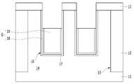
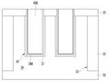
도 1a는 제1실시예에 따른 반도체구조물을 설명하기 위한 도면이다. 도 1a는 반도체구조물(100)의 일부로서 트랜지스터(120)가 도시된다. 도 1b는 게이트전극과 채널영역 사이의 다이폴을 설명하기 위한 도면이다.1A is a view for explaining a semiconductor structure according to a first embodiment. 1A shows a
반도체구조물(100)은 기판(101)을 포함할 수 있다. 기판(101)에 활성영역(104)을 정의하는 소자분리영역(102)이 형성될 수 있다. 매립게이트구조(100G)는 기판(101) 내부로(into) 연장(extend)될 수 있다. 기판(101)에 게이트트렌치(106)가 형성될 수 있다. 게이트트렌치(106)는 활성영역(104)과 소자분리영역(102)을 횡단하는 라인 형상일 수 있다. 게이트트렌치(106) 내에 매립게이트구조(100G)가 형성될 수 있다. 활성영역(104)은 채널영역(104C), 제1도핑영역(112)과 제2도핑영역(113)을 포함할 수 있다.The
트랜지스터(120)는 비-플라나 트랜지스터(Non-planar transistor), 예컨대, 매립게이트형 트랜지스터(Buried gate type transistor)일 수 있다.The
기판(101)은 반도체프로세싱에 적합한 물질일 수 있다. 기판(101)은 반도체기판을 포함할 수 있다. 기판(101)은 실리콘을 함유하는 물질로 이루어질 수 있다. 기판(101)은 실리콘, 단결정 실리콘, 폴리실리콘, 비정질 실리콘, 실리콘저마늄, 단결정 실리콘저마늄, 다결정 실리콘저마늄, 탄소 도핑된 실리콘, 그들의 조합 또는 그들의 다층을 포함할 수 있다. 기판(101)은 저마늄과 같은 다른 반도체물질을 포함할 수도 있다. 기판(101)은 Ⅲ/Ⅴ족 반도체기판, 예컨대 GaAs과 같은 화합물반도체기판을 포함할 수도 있다. 기판(101)은 SOI(Silicon On Insulator) 기판을 포함할 수도 있다.The
기판(101)에 활성영역(104)을 정의하는 소자분리영역(102)이 형성될 수 있다. 소자분리영역(102)은 STI(Shallow Trench Isolation) 영역일 수 있다. 소자분리영역(102)은 분리트렌치(103) 내에 형성될 수 있다.A
활성영역(104)에 채널영역(104C), 제1도핑영역(112) 및 제2도핑영역(113)이 형성될 수 있다. 채널영역(104C)은 게이트트렌치(106)를 포함할 수 있다. 게이트트렌치(106) 양측의 활성영역(104) 내에 제1도핑영역(112)과 제2도핑영역(113)이 형성될 수 있다. 제1도핑영역(112)과 제2도핑영역(113)은 도전형 도펀트가 도핑된 영역이다. 예컨대, 도전형 도펀트는 인(P), 비소(As), 안티몬(Sb) 또는 붕소(B)를 포함할 수 있다. 제1도핑영역(112)과 제2도핑영역(113)은 동일 도전형의 도펀트로 도핑될 수 있다. 제1도핑영역(112)과 제2도핑영역(113)은 각각 소스영역과 드레인영역이라고 지칭될 수 있다. 제1도핑영역(112)과 제2도핑영역(113)의 하부면은 기판(101)의 상부 표면(top surface)으로부터 소정의 깊이에 위치할 수 있다. 제1도핑영역(112)과 제2도핑영역(113)은 게이트트렌치(106)의 측벽에 접촉할 수 있다. 제1도핑영역(112)과 제2도핑영역(113)의 하부면은 게이트트렌치(106)의 바닥면보다 높을 수 있다. 제1도핑영역(112)과 제2도핑영역(113)은 대칭될 수 있다. 예컨대, 제1도핑영역(112)과 제2도핑영역(113)은 동일 깊이의 접합을 형성할 수 있다.A
게이트트렌치(106) 내에 매립게이트구조(100G)가 형성될 수 있다. 이를 임베디드 매립게이트구조(Embedded BG)라고 약칭할 수 있다. 매립게이트구조(100G)는 제1도핑영역(112)과 제2도핑영역(113) 사이의 게이트트렌치(106) 내에 위치할 수 있다.A buried
매립게이트구조(100G)는 다이폴유도층(110) 및 게이트전극(G)을 포함할 수 있다. 게이트전극(G)은 제1일함수부(108)와 제2일함수부(109)를 포함할 수 있다. 매립게이트구조(100G)는 게이트절연층(107) 및 캡핑층(111)을 더 포함할 수 있다. 게이트전극(G)은 기판(101)의 상부면보다 낮은 레벨에 위치할 수 있다. 게이트전극(G)은 게이트트렌치(106)를 부분적으로 채울 수 있다. 따라서, '매립 게이트전극'이라고 지칭될 수 있다. 캡핑층(111)은 게이트전극(G) 상에 위치할 수 있다. 게이트절연층(107)은 게이트트렌치(106)의 바닥 및 측벽들 상에 형성될 수 있다. 다이폴유도층(110)은 게이트전극(G)의 제1일함수부(108)와 게이트절연층(107) 사이에 위치할 수 있다.The buried
게이트절연층(107)은 실리콘산화물(Silicon oxide), 실리콘질화물(Silicon nitride), 실리콘산질화물(Silicon oxynitride), 고유전물질(High-k material) 또는 이들의 조합을 포함할 수 있다. 고유전물질은 실리콘산화물의 유전상수(dielectric constant)보다 더 큰 유전상수를 갖는 물질을 포함할 수 있다. 예컨대, 고유전물질은 3.9보다 큰 유전상수를 갖는 물질을 포함할 수 있다. 다른 예에서, 고유전물질은 10보다 큰 유전상수를 갖는 물질을 포함할 수 있다. 또다른 예에서, 고유전물질은 10 내지 30의 유전상수를 갖는 물질을 포함할 수 있다. 고유전물질은 적어도 하나의 금속성 원소(at least one metallic element)를 포함할 수 있다. 고유전물질은 하프늄함유물질(hafnium-containing material)을 포함할 수 있다. 하프늄함유물질은 하프늄산화물(hafnium oxide), 하프늄실리콘산화물(hafnium silicon oxide), 하프늄실리콘산화질화물(hafnium silicon oxynitride) 또는 그들의 조합을 포함할 수 있다. 다른 실시예에서, 고유전물질은 란탄산화물(lanthanum oxide), 란탄알루미늄산화물(lanthanum aluminum oxide), 지르코늄산화물(zirconium oxide), 지르코늄실리콘산화물(zirconium silicon oxide), 지르코늄실리콘산화질화물(zirconium silicon oxynitride), 알루미늄산화물(aluminum oxide), 및 그들의 조합을 포함할 수 있다. 고유전물질로는 공지된 다른 고유전물질이 선택적으로 사용될 수도 있다. 게이트절연층(107)은 다이폴유도층(110)에 따라 적절한 물질이 선택될 수 있다. 예컨대, 게이트절연층(107)은 다이폴유도층(110)보다 단위부피당 산소함량, 즉 산소농도가 작은 물질이 선택될 수 있다. 본 실시예에서, 게이트절연층(107)은 SiO2일 수 있다.The
채널영역(104C)은 게이트트렌치(106)에 의해 채널길이가 길어질 수 있다. 본 실시예들에 따른 채널영역(104C)은 일반적인 플라나형 트랜지스터(Planar type transistor)에 비해 채널길이가 길다. 이에 따라, 숏채널효과를 방지할 수 있다.The channel length of the
게이트전극(G)은 채널영역(104C)과 오버랩될 수 있고, 제1,2도핑영역(112, 113)과 비-오버랩될 수 있다. 여기서, 오버랩이란 수평적으로 오버랩됨을 의미할 수 있다. 게이트전극(G)의 상부 표면 높이는 기판(101)의 상부 표면보다 낮은 레벨일 수 있다. 게이트전극(G)의 제2일함수부(109)는 저저항 금속-베이스 물질(Low resistivity metal-base materials)일 수 있다. 게이트전극(G)은 저저항을 위해, 저저항금속을 포함할 수 있다. 게이트전극(G)의 제2일함수부(109)는 텅스텐(W), 알루미늄(Al) 또는 이들의 조합을 포함할 수 있다.The gate electrode G may overlap the
게이트전극(G)과 게이트절연층(107) 사이에 다이폴유도층(110)이 위치할 수 있다. 다이폴유도층(110)은 게이트절연층(107)과 제1일함수부(108) 사이에 위치할 수 있다. 다이폴유도층(110) 및 게이트전극(G)의 상부 표면은 동일 레벨일 수 있다. 다이폴유도층(110) 및 제1일함수부(108)는 U자 형상일 수 있다.A
게이트전극(G)의 상부에 캡핑층(111)이 채워질 수 있다. 캡핑층(111)은 게이트전극(109)을 보호하는 역할을 한다. 캡핑층(111)은 절연물질을 포함할 수 있다. 캡핑층(111)는 실리콘질화물, 실리콘산화질화물 또는 이들의 조합을 포함할 수 있다. 다른 실시예에서, 캡핑층(111)은 실리콘질화물과 실리콘산화물의 조합을 포함할 수 있다. 예컨대, 캡핑층(111)을 형성하기 위해 실리콘질화물로 라이닝한 후, 스핀온절연물질(Spin On Dielectric; SOD)로 채울 수 있다. 또다른 실시예에서, 캡핑층(111)은 N(Nitride)-O(Oxide)-N(Nitride)로 이루어진 삼중층(tri-layers)일 수 있다.A
제1도핑영역(112)과 제2도핑영역(113) 상에 하드마스크층(105)이 형성될 수 있다. 하드마스크층(105)은 소자분리영역(102)의 상부를 커버링하도록 연장될 수 있다. 하드마스크층(105)은 TEOS와 같은 실리콘산화물을 포함할 수 있다.A
다이폴유도층(110)에 대해 자세히 살펴보면 다음과 같다.A detailed look at the
다이폴유도층(110)은 절연성 물질(Dielectric material)일 수 있다. 이에 따라, 게이트전극(G)의 저항을 감소시킬 수 있다. 다이폴유도층(110)은 게이트절연층(107)보다 유전상수가 높은 고유전물질(High-k material)일 수 있다. 다이폴유도층(110)은 고일함수(High workfunction)를 유도할 수 있다. 여기서, 고일함수란 실리콘의 미드갭일함수(Mid-gap Work Function)보다 높은 일함수를 지칭한다. 저일함수는 실리콘의 미드갭일함수보다 낮은 일함수를 지칭한다. 부연 설명하면, 고일함수는 4.5eV보다 높은 일함수를 갖고, 저일함수는 4.5eV보다 낮은 일함수를 가질 수 있다. 다이폴유도층(110)과 게이트절연층(107)이 접촉하게 되면, 다이폴(dipole)이 생성될 수 있다. 이러한 다이폴에 의해 제1일함수부(108)의 일함수가 증가될 수 있다. 다이폴을 생성하기 위해, 다이폴유도층(110)와 게이트절연층(107)은 서로 다른 단위부피당 산소함량을 가질 수 있다. 다이폴유도층(110)은 게이트절연층(107)보다 단위부피당 산소함량이 큰 고산소함유-금속산화물(High oxygen contained-metal oxide)로 형성할 수 있다. 게이트절연층(107)이 SiO2인 경우, 다이폴유도층(110)은 SiO2보다 단위부피당 산소함량이 큰 물질을 포함할 수 있다. SiO2보다 단위부피당 산소함량이 큰 물질은 알루미늄산화물(Al2O3), 티타늄산화물(TiO2), 하프늄산화물(HfO2), 지르코늄산화물(ZrO2) 또는 마그네슘산화물(MgO)을 포함할 수 있다. SiO2보다 단위부피당 산소함량이 작은 물질은 이트륨산화물(Y2O3), 란탄늄산화물(La2O3), 저마늄산화물(GeO2), 루테튬산화물(Lu2O3) 또는 스트론튬산화물(SrO)을 포함할 수 있다. 예를 들어, SiO2에 대한 Al2O3의 단위부피당 산소함량비는 1.21일 수 있다. SiO2에 대한 La2O3의 산소함량비는 0.77일 수 있다. SiO2에 대한 HfO2의 단위부피당 산소함량비는 1.05이다. 다이폴유도층(110)은 얇은 두께로 형성될 수 있다. 이로써, 게이트전극(G)의 체적을 크게 하여 게이트전극(G)의 저항을 현저히 낮출 수 있다.The
제1일함수부(108)는 금속베이스물질일 수 있다. 제1일함수부(108)는 제1요소 및 제2요소를 포함할 수 있다. 제1요소는 금속원자일 수 있고, 제2요소는 질소를 포함할 수 있다. 제1요소는 열공정에 의해 확산될 수 있다. 이에 따라, 제1일함수부(108)와 게이트절연층(107) 사이에 제1요소의 산화물이 형성될 수 있다. 제1요소의 산화물은 다이폴유도층(110)이 될 수 있다. 즉, 다이폴유도층(110)은 제1일함수부(108)와 동일하게 제1요소를 포함할 수 있다. 제1일함수부(108)는 티타늄질화물을 포함할 수 있고, 다이폴유도층(110)은 티타늄산화물을 포함할 수 있다. 이와 같이, 제1일함수부(108)와 다이폴유도층(110)은 동일하게 티타늄 원자를 포함할 수 있다.The first
도 1b는 게이트전극과 채널영역 사이의 영역(C)을 상세히 설명한다.FIG. 1B describes the region C between the gate electrode and the channel region in detail.
도 1b를 참조하면, 제1일함수부(108)가 티타늄질화물을 포함하는 경우, 티타늄질화물의 티타늄과 게이트절연층(107)의 산소가 반응하여 티타늄산화물(TiO2)이 형성될 수 있다. 티타늄산화물은 다이폴유도층(110)이 될 수 있다. 다이폴유도층(110) 내의 산소농도는 게이트절연층(107)의 산소농도보다 높을 수 있다. 예컨대, 티타늄산화물(TiO2) 내의 산소 농도는 SiO2의 산소농도보다 높으며, 이로 인해 티타늄산화물(TiO2) 내의 산소가 SiO2 내부로 확산하게 된다. 즉, O2- 이온(ion)이 티타늄산화물로부터 SiO2로 확산됨으로써, 티타늄산화물은 양전하로 대전(positive charged, 110P)되고, SiO2는 음전하로 대전(negative charged, 107N)된다. 이에 따라 다이폴(Dipole, D)이 형성된다. 다이폴(D)은 게이트전극(G), 특히 제1일함수부(108)의 에너지밴드(Energy Band)를 끌어내리게 되며, 이로써 제1일함수부(108)는 증가된 일함수를 갖게 된다. 결국, 게이트전극(G)의 유효일함수가 증가함에 따라 문턱전압을 조절할 수 있다.Referring to FIG. 1B , when the first
위와 같이, 다이폴유도층(110)에 의해 게이트절연층(107)과 다이폴유도층(110) 사이에 다이폴(D)이 생성될 수 있다. 다이폴(D)은 다이폴유도층(110)과 게이트절연층(107)간의 산소함량비 차이에 의해 발생될 수 있다. 이러한 다이폴(D)은 게이트전극(G)의 제1일함수부(108)의 일함수를 증가시켜 고일함수를 유도하고, 이에 따라 문턱전압을 조절할 수 있다. 결국, 다이폴유도층(110)에 의해 채널영역(104C)의 채널도즈(channel dose)를 낮출 수 있다. 다이폴(D)의 극성 방향(polarity direction)을 제어하므로써 일함수를 제어할 수 있다. 이러한 다이폴(D)에 의해, 고일함수 또는 저일함수를 유도할 수 있다. 예컨대, 다이폴유도층(110)이 게이트절연층(107)보다 단위부피당 산소함량비가 큰 물질인 경우, 고일함수를 유도하는 방향의 다이폴이 생성될 수 있다. 다이폴유도층(110)이 게이트절연층(107)보다 단위부피당 산소함량비가 작은 물질인 경우, 저일함수를 유도하는 방향의 다이폴이 생성될 수 있다. 다이폴유도층(110)은 게이트절연층(107)보다 단위부피당 산소함량비가 큰 물질이므로, 고일함수로 변화시키는 방향의 다이폴(D)이 생성될 수 있다.As described above, a dipole D may be generated between the
게이트트렌치(106)가 고종횡비(High aspect ratio)를 갖기 때문에, 일반적인 채널도핑에 의해서는, 게이트트렌치(106)의 바닥부까지 충분히 도핑을 수행하기 어렵다. 따라서, 채널도핑 이후에 추가로 게이트트렌치(106)의 바닥부에 국부적으로 채널도핑을 수행하는데, 이를 '국부적채널도핑'이라 지칭한다. 국부적채널도핑으로서 임플란트(Implantation)를 적용하는 경우, LCI(Locally Channel Implantation)라고 지칭한다.Since the
다이폴유도층(110)에 의해 문턱전압을 조절할 수 있으므로, 국부적채널도핑(LCI)의 도즈를 현저히 낮추거나, 국부적채널도핑(LCI)을 생략할 수 있다. 결국, 본 실시예들은, 채널도즈를 낮추므로, 접합누설(junction leakage) 특성이 개선된다.Since the threshold voltage can be adjusted by the
또한, 다이폴유도층(110)이 제1,2도핑영역(112, 113)과 비-오버랩되므로, 제1도핑영역(112) 및 제2도핑영역(113)에서의 게이트유도드레인누설(GIDL)을 억제할 수 있다. 다이폴유도층(110)이 제1도핑영역(112) 및 제2도핑영역(113)에 오버랩되는 경우, 고일함수 유도로 인해 게이트유도드레인누설(GIDL)이 증가될 수 있다. 따라서, 다이폴유도층(110)은 제1도핑영역(112) 및 제2도핑영역(113)에 비-오버랩(Non-overlap)되도록 높이가 조절될 수 있다.In addition, since the
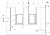
도 2a 및 도 2b는 제1실시예의 변형예에 따른 반도체구조물을 설명한다. 도 2b는 도 2a의 A-A'선에 따른 단면도이다.2A and 2B illustrate a semiconductor structure according to a modification of the first embodiment. FIG. 2B is a cross-sectional view taken along line A-A' of FIG. 2A.
도 2a 및 도 2b를 참조하면, 반도체구조물(100M)의 일부로서 트랜지스터(120M)가 도시된다.2A and 2B , a
트랜지스터(120M)는 도 1a의 트랜지스터(120)와 유사할 수 있다. 트랜지스터(120M)은 매립게이트구조(100MG), 제1도핑영역(112) 및 제2도핑영역(113)를 포함할 수 있다. 매립게이트구조(100MG)는 게이트절연층(107), 다이폴유도층(110), 게이트전극(G) 및 캡핑층(111)을 포함할 수 있다. 게이트전극(G)은 제1일함수부(108) 및 제2일함수부(109)를 포함할 수 있다. 매립게이트구조(100MG)는 핀영역(104F)을 더 포함할 수 있다. 핀영역(104F)은 게이트트렌치(106)의 저면 아래에 위치할 수 있다. 게이트트렌치(106)는 제1트렌치(106A)와 제2트렌치(106B)를 포함할 수 있다. 제1트렌치(106A)는 활성영역(104) 내에 형성될 수 있다. 제2트렌치(106B)는 소자분리층(102) 내에 형성될 수 있다. 제1트렌치(106A)로부터 제2트렌치(106B)로 연속적으로 확장될 수 있다. 제1트렌치(106A)와 제2트렌치(106B)는 서로 다른 레벨에 위치하는 바닥면을 가질 수 있다. 예를 들어, 제1트렌치(106A)의 바닥면은 제2트렌치(106B)의 바닥면보다 높은 레벨에 위치할 수 있다. 제1트렌치(106A)와 제2트렌치(106B)의 높이 차이는 소자분리층(102)이 리세스됨에 따라 형성된다. 따라서, 제2트렌치(106B)는 제1트렌치(106A)의 바닥면보다 낮은 바닥면을 갖는 리세스영역(R)을 포함할 수 있다. 제1트렌치(106A)와 제2트렌치(106B) 사이의 단차로 인하여 활성영역(104)에 핀영역(104F)이 형성된다. 따라서, 활성영역(104)은 핀영역(104F)을 포함한다.
이와 같이, 제1트렌치(106A) 아래에 핀영역(104F)이 형성되고, 핀영역(104F)의 측벽은 리세스된 소자분리층(102F)에 의해 노출된다. 핀영역(104F)은 채널이 형성되는 부분이다. 핀영역(104F)은 새들핀(Saddle Fin)이라고 일컫는다. 핀영역(104F)에 의해 채널 폭을 증가시킬 수 있고, 전기적 특성을 향상시킬 수 있다.In this way, the
도 3은 제1실시예에 따른 반도체구조물의 응용예를 설명한다.3 illustrates an application example of the semiconductor structure according to the first embodiment.
도 3을 참조하면, 반도체구조물(100)의 일부로서 메모리셀(130)이 도시된다. 메모리셀(130)은 트랜지스터(120), 비트라인(140) 및 메모리요소(150)를 포함할 수 있다. 트랜지스터(120)는 도 1a의 트랜지스터(120)일 수 있다. 따라서, 트랜지스터(120)는 매립게이트구조(100G), 제1도핑영역(112) 및 제2도핑영역(113)을 포함할 수 있다. 제1도핑영역(112)은 제1콘택플러그(141)를 통해 비트라인(140)에 전기적으로 연결될 수 있다. 제2도핑영역(113)은 제2콘택플러그(151)를 통해 메모리요소(150)에 전기적으로 연결될 수 있다. 매립게이트구조(100G)는 매립워드라인구조(Buried Wordline Structrue; BWL)라고 지칭될 수 있다. 매립게이트구조(100G)는 게이트트렌치(106) 내에 내장될 수 있다. 매립게이트구조(100G)는 게이트절연층(107), 다이폴유도층(110), 게이트전극(G) 및 캡핑층(111)을 포함할 수 있다. 게이트전극(G)은 제1일함수부(108)와 제2일함수부(109)를 포함할 수 있다.Referring to FIG. 3 , a
트랜지스터(120)는 도 2a의 트랜지스터(120M)로 대체될 수 있다.The
도 4a 내지 도 4f는 제1실시예에 따른 반도체구조물을 제조하는 방법의 일예를 설명하기 위한 도면이다.4A to 4F are diagrams for explaining an example of a method of manufacturing the semiconductor structure according to the first embodiment.
도 4a에 도시된 바와 같이, 기판(11)에 소자분리층(12)이 형성된다. 소자분리층(12)에 의해 활성영역(14)이 정의된다. 소자분리층(12)은 STI 공정에 의해 형성될 수 있다. 예를 들어, 기판(11)을 식각하여, 분리트렌치(13)를 형성한다. 분리트렌치(13)는 절연물질로 채워지고, 이에 따라 소자분리층(12)이 형성된다. 소자분리층(12)은 실리콘산화물, 실리콘질화물 또는 이들의 조합을 포함할 수 있다. 화학기상증착(CVD) 또는 다른 증착공정은 절연물질로 분리트렌치(13)를 채우는데 사용될 수 있다. CMP(chemical-mechanical polishing)와 같은 평탄화 공정(planarization process)이 부가적으로 사용될 수 있다.As shown in FIG. 4A , the
다음으로, 기판(11) 상에 하드마스크층(15)이 형성될 수 있다. 하드마스크층(15)은 기판(11)에 대해 식각선택비를 갖는 물질로 형성될 수 있다. 하드마스크층(15)은 실리콘산화물을 포함할 수 있다. 하드마스크층(15)은 TEOS(Tetra-Ethyl-Ortho-Silicate)와 같은 실리콘산화물을 포함할 수 있다. 하드마스크층(15)은 라인 형상의 오프닝을 갖도록 패터닝되어 있을 수 있다.Next, a
다음으로, 기판(11) 내에 게이트트렌치(16)가 형성된다. 게이트트렌치(16)는 활성영역(14) 및 소자분리층(12)을 횡단하는 라인 형상을 가질 수 있다. 게이트트렌치(16)는 하드마스크층(15)을 식각 마스크로 이용한 식각 공정에 의해 형성될 수 있다. 게이트트렌치(16)는 분리트렌치(13)보다 얕게 형성될 수 있다. 게이트트렌치(16)의 깊이는 후속 게이트전극의 평균 단면적을 크게 할 수 있는 충분한 깊이를 가질 수 있다. 이에 따라, 게이트전극의 저항을 감소시킬 수 있다. 게이트트렌치(16)의 저부는 곡률을 가질 수 있다. 이와 같이 곡률을 갖도록 형성하므로써, 게이트트렌치(16)의 저부에서 요철을 최소화하고, 그에 따라 게이트전극의 채움(filling)을 용이하게 수행할 수 있다. 또한, 곡률을 갖도록 하므로써, 게이트트렌치(16)의 저부 모서리에 각진 모양을 제거하여 전계집중(electric field)을 완화할 수 있다.Next, a
도시하지 않았으나, 핀영역을 형성할 수 있다. 핀영역은 소자분리층(12)을 리세스시켜 형성할 수 있다(도 2a 및 도 2b 참조).Although not shown, a fin region may be formed. The fin region may be formed by recessing the device isolation layer 12 (refer to FIGS. 2A and 2B).
도 4b에 도시된 바와 같이, 게이트트렌치(16)의 표면 상에 게이트절연층(17)이 형성될 수 있다. 게이트절연층(17)을 형성하기 전에, 게이트트렌치(16) 표면의 식각손상을 치유할 수 있다. 예컨대, 열산화 처리에 의해 희생산화물을 형성한 후, 희생산화물을 제거할 수 있다.As shown in FIG. 4B , a
게이트절연층(17)은 열산화 공정(Thermal Oxidation)에 의해 형성될 수 있다. 게이트절연층(17)은 후속 다이폴유도층보다 단위부피당 산소 함량이 작은 물질일 수 있다. 게이트절연층(17)은 SiO2일 수 있다. 다른 실시예에서, 게이트절연층(17)은 라이너폴리실리콘층을 증착한 후, 라이너폴리실리콘층을 라디칼산화시켜 형성할 수 있다. 또다른 실시예에서, 게이트절연층(17)은 라이너실리콘질화물층을 형성한 후, 라이너실리콘질화물층을 라디칼산화시켜 형성할 수도 있다.The
다음으로, 게이트절연층(17) 상에 제1일함수층(18A) 및 제2일함수층(19A)이 형성될 수 있다. 제2일함수층(19A)은 게이트절연층(17) 상에서 게이트트렌치(16)를 채울 수 있다. 제1일함수층(18A)과 제2일함수층(19A)은 저저항 물질일 수 있다. 제2일함수층(19A)은 제1일함수층(18A)보다 저저항을 갖는 물질로 형성될 수 있다. 제1일함수층(18A)과 제2일함수층(19A)은 금속베이스물질(Metal-base material)을 포함할 수 있다. 제2일함수층(19A)과 제1일함수층(18A)은 동일 물질일 수 있다. 제2일함수층(19A)은 미드갭일함수를 가질 수 있다. 제1일함수층(18A)과 제2일함수층(19A)은 동일 일함수를 가질 수 있다. 제1일함수층(18A)은 제2일함수층(19A)보다 일함수가 높을 수 있다. 즉, 제1일함수층(18A)은 고일함수물질일 수 있다. 제2일함수층(22A)은 텅스텐층 또는 티타늄질화물을 포함할 수 있다. 제1일함수층(22A)은 티타늄질화물(TiN)을 포함할 수 있다. 제1일함수층(18A)은 산소와 반응할 수 있는 산소반응성 요소(oxygen-reactable elements)를 포함할 수 있다. 예컨대, 티타늄질화물의 티타늄은 산소와 반응하여 티타늄산화물을 형성할 수 있다.Next, a first
도 4c에 도시된 바와 같이, 게이트 전극(G)이 형성될 수 있다. 게이트 전극(G)은 제2일함수부(Second workfunction portion, 19) 및 제1일함수부(First workfunction portion, 18)를 포함할 수 있다. 제2일함수부(19) 및 제1일함수부(18)를 형성하기 위해, 제2일함수층(19A) 및 제1일함수층(18A)이 선택적으로 식각될 수 있다. 예컨대, CMP 및 에치백공정이 순차적으로 진행될 수 있다. 게이트 전극(G)의 상부 표면은 활성영역(14)의 상부 표면보다 낮은 레벨일 수 있다. 이에 따라, 게이트트렌치(16) 내에 게이트 전극(G)이 위치할 수 있다. 이를, 임베디드 게이트전극 또는 매립게이트전극이라고 지칭할 수 있다. 제1일함수부(18)는 제2일함수부(19)의 확산을 방지하기 위한 배리어층의 역할을 할 수도 있다.As shown in FIG. 4C , a gate electrode G may be formed. The gate electrode G may include a
도 4d에 도시된 바와 같이, 다이폴유도층(dipole induction layer, 20)이 형성될 수 있다. 다이폴유도층(20)을 형성하기 위해 게이트전극(G)이 열공정(20H)에 노출될 수 있다. 열공정(20H)은 급속열처리(RTA)를 포함할 수 있다. 급속열처리는 800℃ 이상의 온도에서 실시할 수 있다. 노출된 게이트전극(G), 특히 제2일함수부(19)의 산화 현상을 방지하기 위해 산소프리(Oxygen-free) 분위기에서 실시한다. 급속열처리는 질소(N2) 또는 아르곤(Ar) 분위기에서 실시할 수 있다.As shown in FIG. 4D , a
위와 같은 열공정(20H)에 의해 게이트절연층(17)과 게이트전극(G) 사이에 다이폴유도층(20)이 형성될 수 있다. 다이폴유도층(20)은 제1일함수부(18)와 게이트절연층(17) 사이에 형성될 수 있다. 예컨대, 제1일함수부(18)가 티타늄질화물을 포함하는 경우, 티타늄질화물의 티타늄과 게이트절연층(17)의 산소가 반응하여 티타늄산화물(TiO2)이 형성될 수 있다. 티타늄산화물은 다이폴유도층(20)이 될 수 있다. 다이폴유도층(20) 내의 산소농도는 게이트절연층(17)의 산소농도보다 높을 수 있다. 예컨대, 티타늄산화물(TiO2) 내의 산소 농도는 SiO2의 산소농도보다 높으며, 이로 인해 티타늄산화물(TiO2) 내의 산소가 SiO2 내부로 확산하게 된다. 즉, O2- 이온(ion)이 티타늄산화물로부터 SiO2로 확산됨으로써, 티타늄산화물은 양전하로 대전(positive charged)되고, SiO2는 음전하로 대전(negative charged)된다. 이에 따라 다이폴(Dipole)이 형성된다. 다이폴은 게이트전극(G), 특히 제1일함수부(18)의 에너지밴드(Energy Band)를 끌어내리게 되며, 이로써 제1일함수부(18)는 증가된 일함수를 갖게 된다. 결국, 게이트전극(G)의 유효일함수가 증가함에 따라 문턱전압을 조절할 수 있다.The
이와 같이, 다이폴(D)을 형성하면, 반도체기판(11), 즉 채널영역의 도펀트의 양을 줄일 수 있게 되고, 그로 인해 전계(E-Field)가 완화됨으로써 트랜지스터의 신뢰성 개선 및 DRAM의 리프레쉬 특성을 개선할 수 있게 된다.In this way, when the dipole D is formed, the amount of dopant in the
열공정(20H)의 온도를 올릴수록 다이폴유도층(20)의 두께를 더욱 증가시킬 수 있게 되고, 그에 따라 게이트전극(G)의 유효일함수를 더욱 증가시킬 수 있다. 한편, 다이폴유도층(20)은 게이트전극(G)이 형성된 이후의 열공정(20H)에 의해 형성되므로, 그 두께가 증가되더라도 게이트전극(G)의 채움 특성에 영향을 미치지 않는다. 비교예로서, 다이폴유도층을 증착한 후, 게이트전극으로 사용되는 일함수층들을 채우는 경우, 다이폴유도층의 두께에 의해 일함수층들의 채움 특성이 열화될 수 있다.As the temperature of the
상술한 바와 같이, 열공정(20H)을 통해 게이트전극(G)의 유효일함수를 증가시킬 수 있으므로, 게이트전극(G)의 채움 특성이 개선될 수 있다. 즉, 게이트전극(G)의 유효일함수를 증가시키 위해 고일함수물질층을 추가로 형성하지 않아도 되므로, 종횡비 증가가 없다. 아울러, 열공정(20H)에 의해, 제2일함수부(19)의 비저항을 줄여, RC 딜레이(dealy)를 개선할 수 있다.As described above, since the effective work function of the gate electrode G can be increased through the
도 4e에 도시된 바와 같이, 게이트전극(G) 상에 캡핑층(21)이 형성된다. 캡핑층(21)은 절연물질을 포함한다. 게이트전극(G) 상에서 게이트트렌치(16)가 캡핑층(21)으로 채워진다. 캡핑층(21)은 실리콘질화물을 포함할 수 있다. 후속하여, 기판(11)의 상부 표면이 노출되도록 캡핑층(21)의 평탄화가 진행될 수 있다. 다른 실시예에서, 캡핑층(21)은 실리콘산화물을 포함할 수 있다. 또다른 실시예에서, 캡핑층(23)은 NON(Nitride-Oxide-Nitride) 구조일 수 있다.As shown in FIG. 4E , a
캡핑층(21)을 형성하므로써, 매립게이트구조(BG)가 형성된다. 매립게이트구조(BG)는 게이트절연층(17), 다이폴유도층(20), 게이트전극(G) 및 캡핑층(21)을 포함한다. 게이트전극(G)은 제1일함수부(18)와 제2일함수부(19)를 포함할 수 있고, 제1일함수부(18)와 게이트절연층(17) 사이에 다이폴유도층(20)이 위치할 수 있다. 게이트전극(G)의 상부 표면은 기판(11)의 상부 표면보다 낮게 위치한다. 이와 같이, 게이트전극(G)의 상부 표면을 낮게 리세스시킴에 따라, 게이트전극(G)과 주변 도전물(예, 콘택플러그) 간의 물리적 거리를 충분히 확보할 수 있다. 결국, 게이트전극(G)과 주변 도전물간의 절연 내압을 향상시킬 수 있다.By forming the
도 4f에 도시된 바와 같이, 활성영역(14) 내에 제1도핑영역(22)과 제2도핑영역(23)이 형성될 수 있다. 제1도핑영역(22)과 제2도핑영역(23)은 매립게이트구조(BG) 양측에 형성될 수 있다. 제1도핑영역(22)과 제2도핑영역(23)은 임플란트 등의 도핑 공정에 의해 형성될 수 있다. 제1도핑영역(22)과 제2도핑영역(23)은 게이트전극(G)과 비-오버랩되는 깊이를 가질 수 있다. 다이폴유도층(20) 및 제1일함수부(18)는 제1 및 제2도핑영역(22, 23)과 비-오버랩될 수 있다. 이에 따라, GIDL을 개선할 수 있다.As shown in FIG. 4F , a first
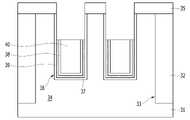
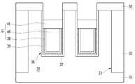
도 5a는 제2실시예에 따른 반도체구조물을 설명한다. 도 5b는 제2실시예의 변형예에 따른 반도체구조물을 설명한다.5A illustrates a semiconductor structure according to a second embodiment. 5B illustrates a semiconductor structure according to a modification of the second embodiment.
도 5a 및 도 5b를 참조하면, 반도체구조물(200)의 일부로서 트랜지스터(220)이 도시된다.5A and 5B , the
트랜지스터(220)는 도 1a의 트랜지스터(120)와 유사할 수 있다. 트랜지스터(220)는 매립게이트구조(200G), 제1도핑영역(112) 및 제2도핑영역(113)를 포함할 수 있다. 매립게이트구조(200G)는 게이트절연층(107), 다이폴유도층(110), 게이트전극(G) 및 캡핑층(111)을 포함할 수 있다. 게이트전극(G)은 제1일함수부(108), 제2일함수부(109) 및 제3일함수부(210)를 포함할 수 있다. 매립게이트구조(200G)는 핀영역(104F)을 더 포함할 수 있다(도 5b 참조).
제3일함수부(210)는 제1일함수부(108)보다 낮은 일함수를 가질 수 있다. 제3일함수부(210)는 N형 일함수를 가질 수 있다. 제3일함수부는 실리콘의 미드갭일함수보다 낮은 일함수를 가질 수 있다. 제3일함수부(210)는 N형 도펀트가 도핑된 폴리실리콘을 포함할 수 있다. 제3일함수부(210)는 제1도핑영역(112) 및 제2도핑영역(113)과 오버랩될 수 있다. 저일함수를 갖는 제3일함수부(210)에 의해 게이트유도드레인누설(GIDL)을 개선할 수 있다. 도시하지 않았으나, 제3일함수부(210)와 제2일함수부(109) 사이에 배리어가 더 형성될 수 있다. 배리어는 제1일함수부(108)와 제3일함수부(210) 사이에 위치하도록 연장될 수 있다. 또한, 배리어는 제3일함수부(210)와 다이폴유도층(110) 사이에 위치하도록 연장될 수 있다. 배리어는 티타늄질화물을 포함할 수 있다.The third
도 5c는 제2실시예에 따른 반도체구조물의 응용예를 설명한다.5C illustrates an application example of the semiconductor structure according to the second embodiment.
도 5c를 참조하면, 반도체구조물(200)의 일부로서 메모리셀(230)이 도시된다. 메모리셀(230)은 트랜지스터(220), 비트라인(140) 및 메모리요소(150)를 포함할 수 있다. 트랜지스터(220)는 도 5a의 트랜지스터(220)일 수 있다. 따라서, 트랜지스터(220)는 매립게이트구조(200G), 제1도핑영역(112) 및 제2도핑영역(113)을 포함할 수 있다. 제1도핑영역(112)은 제1콘택플러그(141)를 통해 비트라인(140)에 전기적으로 연결될 수 있다. 제2도핑영역(113)은 제2콘택플러그(151)를 통해 메모리요소(150)에 전기적으로 연결될 수 있다. 매립게이트구조(200G)는 매립워드라인구조(BWL)라고 지칭될 수 있다. 매립게이트구조(200G)는 게이트트렌치(206) 내에 내장될 수 있다. 매립게이트구조(200G)는 게이트절연층(107), 다이폴유도층(110), 게이트전극(G) 및 캡핑층(111)을 포함할 수 있다. 게이트전극(G)은 제1일함수부(108) 및 제2일함수부(109)를 포함할 수 있다. 게이트전극(G)은 제1도핑영역(112) 및 제2도핑영역(113)에 오버랩되는 제3일함수부(210)를 더 포함할 수 있다.Referring to FIG. 5C , a
도 6a 내지 도 6g는 제2실시예에 따른 반도체구조물을 제조하는 방법의 일예를 설명하기 위한 도면이다. 제2실시예에 따른 제조 방법은 제1실시예에 따른 제조 방법과 유사할 수 있다.6A to 6G are views for explaining an example of a method of manufacturing a semiconductor structure according to the second embodiment. The manufacturing method according to the second embodiment may be similar to the manufacturing method according to the first embodiment.
도 6a에 도시된 바와 같이, 기판(31)에 소자분리층(32)이 형성된다. 소자분리층(32)은 분리트렌치(33) 내에 채워질 수 있다. 소자분리층(32)에 의해 활성영역(34)이 정의된다.As shown in FIG. 6A , the
다음으로, 기판(31) 상에 하드마스크층(35)이 형성될 수 있다. 하드마스크층(35)은 실리콘산화물을 포함할 수 있다. 하드마스크층(35)은 TEOS를 포함할 수 있다. 하드마스크층(35)은 라인 형상의 오프닝을 갖도록 패터닝되어 있을 수 있다.Next, a
다음으로, 기판(31) 내에 게이트트렌치(36)가 형성된다. 게이트트렌치(36)는 활성영역(34) 및 소자분리층(32)을 횡단하는 라인 형상을 가질 수 있다. 다음으로, 도시하지 않았으나, 핀영역을 형성할 수 있다.Next, a
다음으로, 게이트트렌치(36)의 표면 상에 게이트절연층(37)이 형성될 수 있다. 게이트절연층(37)은 열산화 공정에 의해 형성될 수 있다. 게이트절연층(37)은 후속 다이폴유도층보다 단위부피당 산소함량이 작은 물질일 수 있다. 게이트절연층(37)은 SiO2일 수 있다.Next, a
다음으로, 게이트절연층(37) 상에 제1일함수층(38A)이 형성될 수 있다. 제1일함수층(38A)은 티타늄질화물(TiN) 또는 탄탈륨질화물(TaN)을 포함할 수 있다.Next, a first
도 6b에 도시된 바와 같이, 다이폴유도층(39A)이 형성될 수 있다. 다이폴유도층(39A)을 형성하기 위해 제1일함수층(38A)이 열공정(39H)에 노출될 수 있다. 열공정(39H)은 급속열처리(RTA)를 포함할 수 있다. 급속열처리는 800℃ 이상의 온도에서 실시하며, 질소(N2) 또는 아르곤(Ar) 분위기에서 실시한다.As shown in FIG. 6B , a
위와 같은 열공정(39H)에 의해 게이트절연층(37)과 제1일함수층(38A) 사이에 다이폴유도층(39A)이 형성될 수 있다. 예컨대, 제1일함수층(38A)이 티타늄질화물을 포함하는 경우, 티타늄질화물의 일부가 산화되어 티타늄산화물(TiO2)이 형성될 수 있다. 티타늄산화물은 다이폴유도층(39A)이 될 수 있다.The
다이폴유도층(39A)은 하드마스크층(35)의 측벽 및 상부표면을 커버링할 수도 있다.The
도 6c에 도시된 바와 같이, 제2일함수층(40A)이 형성될 수 있다. 제1일함수층(40A)은 제1일함수층(38A) 상에서 게이트트렌치(36)를 채울 수 있다. 제2일함수층(40A)은 미드갭일함수를 가질 수 있다. 제2일함수층(40A)은 저저항 물질로 형성될 수 있다. 제2일함수층(40A)은 저저항 금속을 포함할 수 있다. 제2일함수층(40A)은 텅스텐층을 포함할 수 있다.As shown in FIG. 6C , a second
도 6d에 도시된 바와 같이, 제2일함수부(40) 및 제1일함수부(38)가 형성될 수 있다. 제2일함수부(40) 및 제1일함수부(38)를 형성하기 위해, 제2일함수층(40A) 및 제1일함수층(38A)이 에치백공정에 의해 식각될 수 있다. 제2일함수부(40) 및 제1일함수부(38)의 상부 표면은 활성영역(34)의 상부 표면보다 낮은 레벨일 수 있다.As shown in FIG. 6D , the second
제2일함수층(40A) 및 제1일함수층(38A)을 에치백하는 동안에, 다이폴유도층(39A)에 의해 게이트절연층(37)이 손상되는 것을 방지할 수 있다(도면부호 37T 참조).During etch-back of the second
도 6e에 도시된 바와 같이, 다이폴유도층(39A)의 노출부분을 선택적으로 제거할 수 있다. 이에 따라, 게이트트렌치(36) 내에 다이폴유도층(39)이 잔류할 수 있다. 다이폴유도층(39)의 상부표면은 제2일함수부(40) 및 제1일함수부(38)의 상부 표면과 동일 레벨일 수 있다.As shown in FIG. 6E , the exposed portion of the
도 6f에 도시된 바와 같이, 제3일함수부(41)가 형성될 수 있다. 제3일함수부(41)는 제3일함수층(도면부호 생략)을 채운 후에, 리세싱 공정에 의해 형성될 수 있다. 제3일함수부(41)는 저일함수 물질을 포함한다. 제3일함수부(41)는 도전성을 갖는 비-금속물질로 형성될 수 있다. 제3일함수부(41)는 N형 불순물이 도핑된 폴리실리콘을 포함할 수 있다. 제3일함수부(41)는 활성영역(34)의 상부 표면보다 낮은 레벨일 수 있다.As shown in FIG. 6F , a third
위와 같이, 제3일함수부(41)를 형성하므로써, 게이트트렌치(36) 내에 게이트전극(G)이 형성될 수 있다. 게이트전극(G)은 제1일함수부(38), 제2일함수부(40) 및 제3일함수부(41)를 포함할 수 있다. 제1일함수부(38)와 게이트절연층(37) 사이에 다이폴유도층(39)이 위치할 수 있다.As described above, by forming the third
도 6g에 도시된 바와 같이, 제3일함수부(41) 상에 캡핑층(42)이 형성된다. 캡핑층(42)은 절연물질을 포함한다. 제3일함수부(41) 상에서 게이트트렌치(36)가 캡핑층(42)으로 채워진다. 캡핑층(42)은 실리콘질화물을 포함할 수 있다. 후속하여, 하드마스크층(35)의 상부 표면이 노출되도록 캡핑층(42)의 평탄화가 진행될 수 있다.As shown in FIG. 6G , a
상술한 바와 같은 일련의 공정에 의해, 매립게이트구조(BG)가 형성된다. 매립게이트구조(BG)는 게이트절연층(37), 다이폴유도층(39), 제1일함수부(38), 제2일함수부(40), 제3일함수부(41) 및 캡핑층(42)을 포함한다.A buried gate structure BG is formed by a series of processes as described above. The buried gate structure BG includes a
캡핑층(42) 형성 후에, 임플란트 또는 기타 다른 도핑기술에 의해 불순물의 도핑공정이 수행된다. 이에 따라 기판(31) 내에 제1도핑영역(43)과 제2도핑영역(44)이 형성된다. 불순물의 도핑 공정을 진행할 때, 캡핑층(42)이 배리어로 사용된다. 제1도핑영역(43)과 제2도핑영역(44)은 각각 소스영역과 드레인영역이라고 지칭될 수 있다.After the
제1도핑영역(43)과 제2도핑영역(44)은 제3일함수부(41)와 오버랩되는 깊이를 가질 수 있다.The first
도 7a 내지 도 7g는 제2실시예에 따른 반도체구조물 제조하는 방법의 다른 예를 설명하기 위한 도면이다.7A to 7G are diagrams for explaining another example of a method of manufacturing a semiconductor structure according to the second embodiment.
도 7a에 도시된 바와 같이, 기판(31)에 소자분리층(32)이 형성된다. 소자분리층은 분리트렌치(33) 내에 채워질 수 있다. 소자분리층(32)에 의해 활성영역(34)이 정의된다.As shown in FIG. 7A , the
다음으로, 기판(31) 상에 하드마스크층(35)이 형성될 수 있다. 하드마스크층(35)은 실리콘산화물을 포함할 수 있다. 하드마스크층(35)은 TEOS를 포함할 수 있다. 하드마스크층(35)은 라인 형상의 오프닝을 갖도록 패터닝되어 있을 수 있다.Next, a
다음으로, 기판(31) 내에 게이트트렌치(36)가 형성된다. 게이트트렌치(36)는 활성영역(34) 및 소자분리층(32)을 가로지르는 라인 형상을 가질 수 있다.Next, a
다음으로, 게이트트렌치(36)의 표면 상에 게이트절연층(37)이 형성될 수 있다. 게이트절연층(37)은 열산화 공정에 의해 형성될 수 있다. 게이트절연층(37)은 후속 다이폴유도층보다 단위부피당 산소함량이 작은 물질일 수 있다. 게이트절연층(37)은 SiO2일 수 있다.Next, a
다음으로, 게이트절연층(37) 상에 제1일함수층(38A)이 형성될 수 있다. 제1일함수층(38A)은 티타늄질화물(TiN) 또는 탄탈륨질화물(TaN)을 포함할 수 있다.Next, a first
다음으로, 제2일함수층(40A)이 형성될 수 있다. 제2일함수층(40A)은 제1일함수층(38A) 상에서 게이트트렌치(36)를 채울 수 있다. 제2일함수층(40A)은 텅스텐층을 포함할 수 있다.Next, the second
도 7b에 도시된 바와 같이, 예비 제2일함수부(40B) 및 예비 제1일함수부(38B)가 형성될 수 있다. 예비 제2일함수부(40B) 및 예비 제1일함수부(38B)를 형성하기 위해, 제2일함수층(40A) 및 제1일함수층(38A)의 CMP 공정이 수행될 수 있다. CMP 공정은 하드마스크층(35)의 표면이 노출될때까지 수행될 수 있다.7B , a preliminary second
도 7c에 도시된 바와 같이, 다이폴유도층(39B)이 형성될 수 있다. 다이폴유도층(39B)을 형성하기 위해 예비 제1일함수부(38A)가 열공정(39H)에 노출될 수 있다. 열공정(39H)은 급속열처리(RTA)를 포함할 수 있다. 급속열처리는 800℃ 이상의 온도에서 실시하며, 질소(N2) 또는 아르곤(Ar) 분위기에서 실시한다.As shown in FIG. 7C , a
위와 같은 열공정(39H)에 의해 게이트절연층(37)과 예비 제1일함수부(38B) 사이에 다이폴유도층(39B)이 형성될 수 있다. 예컨대, 예비 제1일함수부(38A)가 티타늄질화물을 포함하는 경우, 티타늄질화물의 일부가 산화되어 티타늄산화물(TiO2)이 형성될 수 있다. 티타늄산화물은 다이폴유도층(39B)이 될 수 있다.A
다이폴유도층(39B)은 하드마스크층(35)의 측벽을 커버링할 수도 있다.The
도 7d에 도시된 바와 같이, 제2일함수부(40) 및 제1일함수부(38)가 형성될 수 있다. 제2일함수부(40) 및 제1일함수부(38)를 형성하기 위해, 예비 제2일함수부(40B) 및 예비 제1일함수부(38B)가 에치백공정에 의해 식각될 수 있다. 제2일함수부(40) 및 제1일함수부(38)의 상부 표면은 활성영역(34)의 상부 표면보다 낮은 레벨일 수 있다.As shown in FIG. 7D , the second
예비 제2일함수부(40B) 및 예비 제1일함수부(38B)을 에치백하는 동안에, 다이폴유도층(39B)에 의해 게이트절연층(37)이 손상되는 것을 방지할 수 있다(도면부호 37T 참조).During the etch-back of the preliminary second
도 7e에 도시된 바와 같이, 다이폴유도층(39B)의 노출부분을 선택적으로 제거할 수 있다. 이에 따라, 게이트트렌치(36) 내에 다이폴유도층(39)이 잔류할 수 있다. 다이폴유도층(39)의 상부표면은 제2일함수부(40) 및 제1일함수부(38)의 상부 표면과 동일 레벨일 수 있다.As shown in FIG. 7E , the exposed portion of the
도 7f에 도시된 바와 같이, 제3일함수부(41)가 형성될 수 있다. 제3일함수부(41)는 제3일함수층(도면부호 생략)을 채운 후에, 리세싱 공정에 의해 형성될 수 있다. 제3일함수부(41)는 저일함수 물질을 포함한다. 제3일함수부(41)는 도전성을 갖는 비-금속물질로 형성될 수 있다. 제3일함수부(41)는 N형 불순물이 도핑된 폴리실리콘을 포함할 수 있다. 제3일함수부(41)는 활성영역(34)의 상부 표면보다 낮은 레벨일 수 있다.As shown in FIG. 7F , a third
위와 같이, 제3일함수부(41)를 형성하므로써, 게이트트렌치(36) 내에 게이트전극(G)이 형성될 수 있다. 게이트전극(G)은 제1일함수부(38), 제2일함수부(40) 및 제3일함수부(41)를 포함할 수 있다. 제1일함수부(38)와 게이트절연층(37) 사이에 다이폴유도층(39)이 위치할 수 있다.As described above, by forming the third
도 7g에 도시된 바와 같이, 제3일함수부(41) 상에 캡핑층(42)이 형성된다. 캡핑층(42)은 절연물질을 포함한다. 제3일함수부(41) 상에서 게이트트렌치(36)가 캡핑층(42)으로 채워진다. 캡핑층(42)은 실리콘질화물을 포함할 수 있다. 후속하여, 하드마스크층(35)의 상부 표면이 노출되도록 캡핑층(42)의 평탄화가 진행될 수 있다.As shown in FIG. 7G , a
상술한 바와 같은 일련의 공정에 의해, 매립게이트구조(BG)가 형성된다. 매립게이트구조(BG)는 게이트절연층(37), 다이폴유도층(39), 제1일함수부(38), 제2일함수부(40), 제3일함수부(41) 및 캡핑층(42)을 포함한다.A buried gate structure BG is formed by a series of processes as described above. The buried gate structure BG includes a
캡핑층(42) 형성 후에, 임플란트 또는 기타 다른 도핑기술에 의해 불순물의 도핑공정이 수행된다. 이에 따라 기판(31) 내에 제1도핑영역(43)과 제2도핑영역(44)이 형성된다. 불순물의 도핑 공정을 진행할 때, 캡핑층(42)이 배리어로 사용된다. 제1도핑영역(43)과 제2도핑영역(44)은 각각 소스영역과 드레인영역이라고 지칭될 수 있다.After the
제1도핑영역(43)과 제2도핑영역(44)은 제3일함수부(41)와 오버랩되는 깊이를 가질 수 있다.The first
상술한 실시예들에 따른 반도체구조물은 DRAM(Dynamic Random Access Memory)에 적용될 수 있으며, 이에 한정되지 않고 SRAM(Static Random Access Memory), 플래시메모리(Flash Memory), FeRAM(Ferroelectric Random Access Memory), MRAM(Magnetic Random Access Memory), PRAM(Phase Change Random Access Memory) 등의 메모리에 적용될 수 있다.The semiconductor structure according to the above-described embodiments may be applied to dynamic random access memory (DRAM), but is not limited thereto, and is not limited thereto, but is not limited thereto, but is not limited thereto; (Magnetic Random Access Memory), PRAM (Phase Change Random Access Memory), etc. may be applied to a memory.
상술한 실시예들에 따른 반도체구조물은 전자장치에 적용될 수 있다. 전자장치는 복수의 반도체장치를 포함할 수 있고, 반도체장치는 트랜지스터를 포함할 수 있다. 전자장치에 포함된 반도체장치들 중 적어도 하나의 반도체장치는, 게이트트렌치 내에 형성된 매립게이트구조를 포함한다. 매립게이트구조는 다이폴유도층 및 게이트전극을 포함할 수 있다. 게이트전극은 제1일함수부와 제2일함수부를 포함할 수 있다. 다이폴유도층은 티타늄산화물을 포함할 수 있고, 제1일함수부는 티타늄질화물을 포함할 수 있다. 제2일함수부는 텅스텐을 포함할 수 있다. 다이폴유도층에 의해 문턱전압을 용이하게 조절할 수 있다. 따라서, 전자장치는 소형화에 대응하여 빠른 동작속도를 구현할 수 있다.The semiconductor structure according to the above-described embodiments may be applied to an electronic device. The electronic device may include a plurality of semiconductor devices, and the semiconductor device may include a transistor. At least one semiconductor device among semiconductor devices included in the electronic device includes a buried gate structure formed in a gate trench. The buried gate structure may include a dipole inducing layer and a gate electrode. The gate electrode may include a first work function portion and a second work function portion. The dipole inducing layer may include titanium oxide, and the first work function part may include titanium nitride. The second work function part may include tungsten. The threshold voltage can be easily adjusted by the dipole inducing layer. Accordingly, the electronic device may realize a high operating speed in response to miniaturization.
전술한 본 발명은 전술한 실시예 및 첨부된 도면에 의해 한정되는 것이 아니고, 본 발명의 기술적 사상을 벗어나지 않는 범위 내에서 여러 가지 치환, 변형 및 변경이 가능하다는 것이 본 발명이 속하는 기술분야에서 통상의 지식을 가진 자에게 있어 명백할 것이다.The present invention described above is not limited by the above-described embodiments and the accompanying drawings, and it is common in the technical field to which the present invention pertains that various substitutions, modifications and changes are possible without departing from the technical spirit of the present invention. It will be clear to those who have the knowledge of
101 : 반도체기판 102 : 소자분리층
104 : 활성영역 105 : 하드마스크층
106 : 게이트트렌치 107 : 게이트절연층
108 : 제1일함수부 109 : 제2일함수부
110 : 다이폴유도층 111 : 캡핑층
112 : 제1도핑영역 113 : 제2도핑영역101: semiconductor substrate 102: device isolation layer
104: active region 105: hard mask layer
106: gate trench 107: gate insulating layer
108: first work function unit 109: second work function unit
110: dipole inducing layer 111: capping layer
112: first doped region 113: second doped region
Claims (34)
Translated fromKorean상기 트렌치의 저면 및 측벽들 상에 게이트절연층을 형성하는 단계;
상기 게이트절연층 상에 일함수층을 형성하는 단계;
상기 트렌치 내에 위치하는 게이트전극을 형성하기 위해, 상기 일함수층을 리세싱하는 단계; 및
상기 게이트전극과 게이트절연층 사이에 다이폴유도층을 형성하기 위해, 상기 게이트전극을 열공정에 노출시키는 단계를 포함하고,
상기 다이폴유도층은 상기 일함수층의 일부와 상기 게이트절연층의 일부가 반응하여 형성되는
반도체구조물 형성 방법.
forming a trench in a semiconductor substrate;
forming a gate insulating layer on a bottom surface and sidewalls of the trench;
forming a work function layer on the gate insulating layer;
recessing the work function layer to form a gate electrode located in the trench; and
exposing the gate electrode to a thermal process to form a dipole inducing layer between the gate electrode and the gate insulating layer;
The dipole inducing layer is formed by reacting a part of the work function layer and a part of the gate insulating layer.
A method of forming a semiconductor structure.
상기 열공정은 산소프리(Oxygen-free) 분위기에서 수행하는 반도체구조물 형성 방법.
According to claim 1,
The method of forming a semiconductor structure wherein the thermal process is performed in an oxygen-free atmosphere.
상기 다이폴유도층을 형성하는 단계는,
급속열처리에 의해 수행되는 반도체구조물 형성 방법.According to claim 1,
The step of forming the dipole inducing layer,
A method of forming a semiconductor structure performed by rapid heat treatment.
상기 급속열처리는 질소 또는 아르곤 분위기에서 수행하는 반도체구조물 형성 방법.
4. The method of claim 3,
The rapid heat treatment is a method of forming a semiconductor structure that is performed in a nitrogen or argon atmosphere.
상기 다이폴유도층은 상기 게이트절연층보다 산소농도가 큰 물질을 포함하는 반도체구조물 형성 방법.
According to claim 1,
The dipole inducing layer includes a material having a higher oxygen concentration than the gate insulating layer.
상기 다이폴유도층은 상기 일함수층을 구성하고 있는 일부 요소의 산화물을 포함하는 반도체구조물 형성 방법.
According to claim 1,
The dipole inducing layer includes an oxide of some elements constituting the work function layer.
상기 일함수층은 금속베이스물질을 포함하고, 상기 다이폴유도층은 상기 금속베이스물질의 금속을 함유하는 산화물을 포함하는 반도체구조물 형성 방법.
According to claim 1,
The work function layer includes a metal base material, and the dipole inducing layer includes an oxide containing a metal of the metal base material.
상기 일함수층은 티타늄질화물을 포함하고, 상기 다이폴유도층은 티타늄산화물을 포함하는 반도체구조물 형성 방법.
According to claim 1,
The work function layer includes titanium nitride, and the dipole inducing layer includes titanium oxide.
상기 일함수층을 형성하는 단계는,
상기 게이트절연층 상에 제1일함수층을 컨포멀하게 형성하는 단계; 및
상기 제1일함수층 상에 제2일함수층을 채우는 단계를 포함하고,
상기 다이폴유도층은 상기 제1일함수층의 일부와 상기 게이트절연층의 일부가 반응하여 형성되는 반도체구조물 형성 방법.
According to claim 1,
The step of forming the work function layer,
conformally forming a first work function layer on the gate insulating layer; and
filling a second work function layer on the first work function layer;
The dipole inducing layer is formed by reacting a portion of the first work function layer and a portion of the gate insulating layer.
상기 제1일함수층은 티타늄질화물을 포함하고, 상기 제2일함수층은 텅스텐을 포함하는 반도체구조물 형성 방법.
10. The method of claim 9,
The first work function layer includes titanium nitride, and the second work function layer includes tungsten.
상기 제1일함수층과 제2일함수층은 각각 티타늄질화물을 포함하는 반도체구조물 형성 방법.
10. The method of claim 9,
Each of the first work function layer and the second work function layer includes titanium nitride.
상기 게이트절연층은 실리콘산화물(SiO2)을 포함하고, 상기 일함수층은 티타늄질화물을 포함하며, 상기 다이폴유도층은 티타늄산화물(TiO2)을 포함하는 반도체구조물 형성 방법.
According to claim 1,
The gate insulating layer includes silicon oxide (SiO2 ), the work function layer includes titanium nitride, and the dipole inducing layer includes titanium oxide (TiO2 ).
상기 트렌치의 저면 및 측벽들 상에 게이트절연층을 형성하는 단계;
상기 게이트절연층 상에 제1일함수층을 형성하는 단계;
상기 제1일함수층과 게이트절연층 사이에 예비 다이폴유도층을 형성하기 위해, 상기 제1일함수층을 열공정에 노출시키는 단계;
상기 제1일함수층 상에 상기 트렌치를 채우는 제2일함수층을 형성하는 단계;
상기 트렌치 내에 위치하는 제2일함수부 및 제1일함수부를 형성하기 위해, 각각 상기 제2일함수층과 제1일함수층을 리세싱하는 단계; 및
상기 제1일함수부와 게이트절연층 사이에 다이폴유도층을 형성하기 위해, 상기 예비 다이폴유도층을 리세싱하는 단계를 포함하고,
상기 다이폴유도층은 상기 제1일함수층의 일부와 상기 게이트절연층의 일부가 반응하여 형성되는
반도체구조물 형성 방법.
forming a trench in a semiconductor substrate;
forming a gate insulating layer on a bottom surface and sidewalls of the trench;
forming a first work function layer on the gate insulating layer;
exposing the first work function layer to a thermal process to form a preliminary dipole inducing layer between the first work function layer and the gate insulating layer;
forming a second work function layer filling the trench on the first work function layer;
recessing the second work function layer and the first work function layer, respectively, to form a second work function portion and a first work function portion located in the trench; and
Recessing the preliminary dipole inducing layer to form a dipole inducing layer between the first work function part and the gate insulating layer;
The dipole inducing layer is formed by reacting a part of the first work function layer and a part of the gate insulating layer.
A method of forming a semiconductor structure.
상기 열공정은 산소프리(Oxygen-free) 분위기에서 수행하는 반도체구조물 형성 방법.
14. The method of claim 13,
The method of forming a semiconductor structure wherein the thermal process is performed in an oxygen-free atmosphere.
상기 다이폴유도층을 형성하는 단계는,
급속열처리에 의해 수행되는 반도체구조물 형성 방법.
14. The method of claim 13,
The step of forming the dipole inducing layer,
A method of forming a semiconductor structure performed by rapid heat treatment.
상기 급속열처리는 질소 또는 아르곤 분위기에서 수행하는 반도체구조물 형성 방법.
16. The method of claim 15,
The rapid heat treatment is a method of forming a semiconductor structure that is performed in a nitrogen or argon atmosphere.
상기 제1일함수층은 티타늄질화물을 포함하고, 상기 다이폴유도층은 티타늄산화물을 포함하는 반도체구조물 형성 방법.
14. The method of claim 13,
The first work function layer includes titanium nitride, and the dipole inducing layer includes titanium oxide.
상기 다이폴유도층을 형성하는 단계 이후에,
상기 제1일함수부 및 제2일함수부 상에 제3일함수층을 채우는 단계;
제3일함수부를 형성하기 위해, 상기 제3일함수층을 리세싱하는 단계;
상기 제3일함수부 상에 캡핑층을 채우는 단계; 및
상기 제3일함수부와 오버랩되는 도핑영역을 형성하기 위해, 상기 캡핑층을 배리어로 하여 상기 반도체기판에 도펀트를 도입하는 단계
를 더 포함하는 반도체구조물 형성 방법.
14. The method of claim 13,
After the step of forming the dipole inducing layer,
filling a third work function layer on the first work function unit and the second work function unit;
recessing the third work function layer to form a third work function portion;
filling a capping layer on the third work function part; and
introducing a dopant into the semiconductor substrate using the capping layer as a barrier to form a doped region overlapping the third work function portion;
A method of forming a semiconductor structure further comprising a.
상기 도핑영역은 상기 다이폴유도층과 비-오버랩되는 깊이를 갖는 반도체구조물 형성 방법.
19. The method of claim 18,
The doped region has a depth that does not overlap with the dipole inducing layer.
상기 제3일함수층은 상기 제1일함수층 및 제2일함수층보다 낮은 일함수를 갖는 물질로 형성하는 반도체구조물 형성 방법.
19. The method of claim 18,
wherein the third work function layer is formed of a material having a lower work function than that of the first work function layer and the second work function layer.
상기 트렌치의 저면 및 측벽들 상에 게이트절연층을 형성하는 단계;
상기 게이트절연층 상에 상기 트렌치를 채우는 일함수층을 형성하는 단계;
상기 반도체기판의 상부 표면보다 높은 레벨의 예비 일함수부를 형성하기 위해 상기 일함수층을 평탄화하는 단계;
상기 예비 일함수부와 게이트절연층 사이에 예비 다이폴유도층을 형성하기 위해, 상기 예비 일함수부를 열공정에 노출시키는 단계;
상기 트렌치 내에 위치하는 일함수부를 형성하기 위해, 상기 예비 일함수부를 리세싱하는 단계; 및
상기 일함수부와 게이트절연층 사이에 다이폴유도층을 형성하기 위해, 상기 예비 다이폴유도층을 리세싱하는 단계를 포함하고,
상기 다이폴유도층은 상기 일함수층의 일부와 상기 게이트절연층의 일부가 반응하여 형성되는
반도체구조물 형성 방법.
forming a trench in a semiconductor substrate;
forming a gate insulating layer on a bottom surface and sidewalls of the trench;
forming a work function layer filling the trench on the gate insulating layer;
planarizing the work function layer to form a preliminary work function portion having a higher level than an upper surface of the semiconductor substrate;
exposing the preliminary work function portion to a thermal process to form a preliminary dipole inducing layer between the preliminary work function portion and the gate insulating layer;
recessing the preliminary work function portion to form a work function portion located in the trench; and
Recessing the preliminary dipole inducing layer to form a dipole inducing layer between the work function portion and the gate insulating layer,
The dipole inducing layer is formed by reacting a part of the work function layer and a part of the gate insulating layer.
A method of forming a semiconductor structure.
상기 열공정은 산소프리(Oxygen-free) 분위기에서 수행하는 반도체구조물 형성 방법.
22. The method of claim 21,
The method of forming a semiconductor structure wherein the thermal process is performed in an oxygen-free atmosphere.
상기 다이폴유도층을 형성하는 단계는,
급속열처리에 의해 수행되는 반도체구조물 형성 방법.
22. The method of claim 21,
The step of forming the dipole inducing layer,
A method of forming a semiconductor structure performed by rapid heat treatment.
상기 급속열처리는 질소 또는 아르곤 분위기에서 수행하는 반도체구조물 형성 방법.
24. The method of claim 23,
The rapid heat treatment is a method of forming a semiconductor structure that is performed in a nitrogen or argon atmosphere.
상기 일함수층은 티타늄질화물을 포함하고, 상기 다이폴유도층은 티타늄산화물을 포함하는 반도체구조물 형성 방법.
22. The method of claim 21,
The work function layer includes titanium nitride, and the dipole inducing layer includes titanium oxide.
상기 일함수층을 형성하는 단계는,
상기 게이트절연층 상에 제1일함수층을 컨포멀하게 형성하는 단계; 및
상기 제1일함수층 상에 제2일함수층을 채우는 단계를 포함하고,
상기 다이폴유도층은 상기 제1일함수층의 일부와 상기 게이트절연층의 일부가 반응하여 형성되는
반도체구조물 형성 방법.
22. The method of claim 21,
The step of forming the work function layer,
conformally forming a first work function layer on the gate insulating layer; and
filling a second work function layer on the first work function layer;
The dipole inducing layer is formed by reacting a part of the first work function layer and a part of the gate insulating layer.
A method of forming a semiconductor structure.
상기 다이폴유도층을 형성하는 단계 이후에,
상기 일함수부 상에 제3일함수층을 채우는 단계;
제3일함수부를 형성하기 위해, 상기 제3일함수층을 리세싱하는 단계;
상기 제3일함수부 상에 캡핑층을 채우는 단계; 및
상기 제3일함수부와 오버랩되는 도핑영역을 형성하기 위해, 상기 캡핑층을 배리어로 하여 상기 반도체기판에 도펀트를 도입하는 단계
를 더 포함하는 반도체구조물 형성 방법.
27. The method of claim 26,
After the step of forming the dipole inducing layer,
filling a third work function layer on the work function part;
recessing the third work function layer to form a third work function portion;
filling a capping layer on the third work function part; and
introducing a dopant into the semiconductor substrate using the capping layer as a barrier to form a doped region overlapping the third work function portion;
A method of forming a semiconductor structure further comprising a.
상기 도핑영역은 상기 다이폴유도층과 비-오버랩되는 깊이를 갖는 반도체구조물 형성 방법.
28. The method of claim 27,
The doped region has a depth that does not overlap with the dipole inducing layer.
상기 제3일함수층은 상기 제1일함수층 및 제2일함수층보다 낮은 일함수를 갖는 물질로 형성하는 반도체구조물 형성 방법.
28. The method of claim 27,
wherein the third work function layer is formed of a material having a lower work function than that of the first work function layer and the second work function layer.
상기 반도체기판에 형성되며 상기 제1도핑영역과 제2도핑영역 사이의 채널영역을 포함하는 트렌치;
상기 채널영역 상의 게이트절연층;
상기 채널영역을 커버링하는 제1일함수층을 포함하는 상기 트렌치 내의 게이트전극; 및
상기 제1일함수층과 채널영역 사이에 형성되며, 음전하로 대전된 게이트절연층;
상기 게이트절연층과 제1일함수층 사이에 형성되며, 양전하로 대전된 다이폴유도층을 포함하고,
상기 다이폴유도층과 상기 제1일함수층은 동일한 금속 요소를 포함하는
반도체구조물.a semiconductor substrate including a first doped region and a second doped region;
a trench formed in the semiconductor substrate and including a channel region between the first doped region and the second doped region;
a gate insulating layer on the channel region;
a gate electrode in the trench including a first work function layer covering the channel region; and
a negatively charged gate insulating layer formed between the first work function layer and the channel region;
It is formed between the gate insulating layer and the first work function layer and includes a positively charged dipole inducing layer,
The dipole inducing layer and the first work function layer include the same metal element
semiconductor structures.
상기 게이트절연층은 실리콘산화물을 포함하고, 상기 다이폴유도층은 상기 실리콘산화물보다 산소농도가 큰 금속산화물을 포함하는 반도체구조물.
31. The method of claim 30,
The gate insulating layer includes silicon oxide, and the dipole inducing layer includes a metal oxide having a higher oxygen concentration than the silicon oxide.
상기 다이폴유도층은 티타늄산화물을 포함하며, 상기 제1일함수층은 티타늄질화물을 포함하는 반도체구조물.
32. The method of claim 31,
The dipole inducing layer includes titanium oxide, and the first work function layer includes titanium nitride.
상기 게이트전극은,
상기 제1일함수층 상의 제2일함수층 및 상기 제2일함수층 상에 위치하며 상기 제1 및 제2도핑영역과 오버랩되는 제3일함수층을 더 포함하는 반도체구조물.
31. The method of claim 30,
The gate electrode is
and a second work function layer on the first work function layer and a third work function layer on the second work function layer and overlapping the first and second doped regions.
상기 제1일함수층은 실리콘의 미드갭일함수보다 높은 고일함수를 갖고, 상기 제3일함수층은 실리콘의 미드갭일함수보다 낮은 저일함수를 갖는 반도체구조물.34. The method of claim 33,
The first work function layer has a high work function higher than a mid-gap work function of silicon, and the third work function layer has a low work function lower than a mid-gap work function of silicon.
Priority Applications (3)
| Application Number | Priority Date | Filing Date | Title |
|---|---|---|---|
| KR1020150150915AKR102410919B1 (en) | 2015-10-29 | 2015-10-29 | Semiconductor structure having buried gate structure and method for manufacturing the same, memory cell having the same |
| US15/090,759US9704961B2 (en) | 2015-10-29 | 2016-04-05 | Semiconductor structure having buried gate structure, method for manufacturing the same, and memory cell having the same |
| US15/613,845US9917167B2 (en) | 2015-10-29 | 2017-06-05 | Semiconductor structure having buried gate structure, method for manufacturing the same, and memory cell having the same |
Applications Claiming Priority (1)
| Application Number | Priority Date | Filing Date | Title |
|---|---|---|---|
| KR1020150150915AKR102410919B1 (en) | 2015-10-29 | 2015-10-29 | Semiconductor structure having buried gate structure and method for manufacturing the same, memory cell having the same |
Publications (2)
| Publication Number | Publication Date |
|---|---|
| KR20170049959A KR20170049959A (en) | 2017-05-11 |
| KR102410919B1true KR102410919B1 (en) | 2022-06-21 |
Family
ID=58635753
Family Applications (1)
| Application Number | Title | Priority Date | Filing Date |
|---|---|---|---|
| KR1020150150915AActiveKR102410919B1 (en) | 2015-10-29 | 2015-10-29 | Semiconductor structure having buried gate structure and method for manufacturing the same, memory cell having the same |
Country Status (2)
| Country | Link |
|---|---|
| US (2) | US9704961B2 (en) |
| KR (1) | KR102410919B1 (en) |
Families Citing this family (32)
| Publication number | Priority date | Publication date | Assignee | Title |
|---|---|---|---|---|
| KR102410919B1 (en)* | 2015-10-29 | 2022-06-21 | 에스케이하이닉스 주식회사 | Semiconductor structure having buried gate structure and method for manufacturing the same, memory cell having the same |
| KR102455869B1 (en)* | 2015-12-23 | 2022-10-20 | 에스케이하이닉스 주식회사 | Semiconductor device having buried gate structure and method for manufacturing the same, memory cell having the same |
| KR102511942B1 (en)* | 2016-12-16 | 2023-03-23 | 에스케이하이닉스 주식회사 | Semiconductor device having buried gate structure and method for manufacturing the same |
| US10128347B2 (en)* | 2017-01-04 | 2018-11-13 | International Business Machines Corporation | Gate-all-around field effect transistor having multiple threshold voltages |
| US11245020B2 (en)* | 2017-01-04 | 2022-02-08 | International Business Machines Corporation | Gate-all-around field effect transistor having multiple threshold voltages |
| CN108346666B (en)* | 2017-01-23 | 2022-10-04 | 联华电子股份有限公司 | Semiconductor element and manufacturing method thereof |
| CN108962891B (en)* | 2017-05-18 | 2019-11-19 | 联华电子股份有限公司 | Semiconductor structure and method of making same to avoid row hammering problem |
| KR102404645B1 (en) | 2017-08-28 | 2022-06-03 | 삼성전자주식회사 | Semiconductor device |
| KR102378471B1 (en) | 2017-09-18 | 2022-03-25 | 삼성전자주식회사 | A semiconductor memory device and a method for manufacturing the same |
| US10600900B2 (en)* | 2017-10-16 | 2020-03-24 | Kabushiki Kaisha Toshiba | Semiconductor device and electric apparatus |
| KR102377358B1 (en) | 2017-10-16 | 2022-03-23 | 삼성전자주식회사 | A semiconductor memory device and a method for manufacturing the same |
| KR102528205B1 (en) | 2018-06-26 | 2023-05-03 | 에스케이하이닉스 주식회사 | Cryogenic Semiconductor Device Having a Buried Channel Array Transistor |
| US10304835B1 (en)* | 2018-08-15 | 2019-05-28 | Taiwan Semiconductor Manufacturing Company, Ltd. | Semiconductor device and method |
| US10573723B1 (en)* | 2018-08-23 | 2020-02-25 | International Business Machines Corporation | Vertical transport FETs with asymmetric channel profiles using dipole layers |
| CN110875391A (en)* | 2018-09-03 | 2020-03-10 | 长鑫存储技术有限公司 | Transistor, forming method thereof and integrated circuit memory |
| US10790287B2 (en) | 2018-11-29 | 2020-09-29 | Applied Materials, Inc. | Reducing gate induced drain leakage in DRAM wordline |
| KR102704119B1 (en)* | 2019-06-17 | 2024-09-10 | 에스케이하이닉스 주식회사 | Semiconductor device having buried gate structure and method for manufacturing the same |
| CN112447718B (en)* | 2019-08-30 | 2024-07-19 | 长鑫存储技术有限公司 | Semiconductor structure, preparation method and dynamic random access memory |
| CN112670269B (en)* | 2019-10-16 | 2025-02-25 | 长鑫存储技术有限公司 | Stepped word line structure and preparation method thereof |
| KR102821829B1 (en)* | 2019-10-25 | 2025-06-18 | 삼성전자주식회사 | Semiconductor device and method for manufacturing the same |
| US20210126103A1 (en)* | 2019-10-29 | 2021-04-29 | Micron Technology, Inc. | Apparatus comprising wordlines comprising multiple metal materials, and related methods and electronic systems |
| CN112309987A (en)* | 2020-10-30 | 2021-02-02 | 福建省晋华集成电路有限公司 | Manufacturing method of semiconductor structure and semiconductor structure |
| DE102021103788A1 (en)* | 2021-02-17 | 2022-08-18 | Infineon Technologies Ag | SIC MOSFET WITH REDUCED ON RESISTANCE |
| CN115172369B (en)* | 2021-04-02 | 2024-10-29 | 华邦电子股份有限公司 | Semiconductor structure and manufacturing method thereof |
| US11711914B2 (en) | 2021-04-07 | 2023-07-25 | Winbond Electronics Corp. | Semiconductor structure having buried gate structure and method of manufacturing the same |
| TWI769797B (en)* | 2021-04-27 | 2022-07-01 | 華邦電子股份有限公司 | Dynamic random access memory and method of fabricating the same |
| US11374011B1 (en)* | 2021-05-11 | 2022-06-28 | Winbond Electronics Corp. | Method of manufacturing dynamic random access memory |
| TWI783534B (en)* | 2021-06-18 | 2022-11-11 | 華邦電子股份有限公司 | Dynamic random access memory and method of manufacturing the same |
| US11690217B2 (en) | 2021-07-06 | 2023-06-27 | Winbond Electronics Corp. | Dynamic random access memory with adhesion layer and method of manufacturing the same |
| US11742402B2 (en)* | 2021-07-21 | 2023-08-29 | Nanya Technology Corporation | Semiconductor structure and manufacturing method thereof |
| KR20230134287A (en)* | 2022-03-14 | 2023-09-21 | 삼성전자주식회사 | Semiconductor device and method of fabricating the same |
| CN119300342B (en)* | 2023-07-03 | 2025-09-19 | 长鑫存储技术有限公司 | Semiconductor structure and preparation method thereof |
Family Cites Families (9)
| Publication number | Priority date | Publication date | Assignee | Title |
|---|---|---|---|---|
| JP2008235399A (en)* | 2007-03-19 | 2008-10-02 | Toshiba Corp | Trench type power semiconductor device and manufacturing method thereof |
| KR101205143B1 (en)* | 2010-11-15 | 2012-11-26 | 에스케이하이닉스 주식회사 | Semiconductor Device and Method for Manufacturing the same |
| KR101853316B1 (en)* | 2012-03-29 | 2018-04-30 | 삼성전자주식회사 | Transistor, semiconductor device and a semiconductor module including the same |
| KR101927992B1 (en)* | 2012-08-31 | 2018-12-12 | 에스케이하이닉스 주식회사 | Semiconductor device and method for fabricating the same |
| KR102008318B1 (en) | 2012-12-06 | 2019-08-08 | 삼성전자주식회사 | Semiconductor device |
| KR20140145434A (en) | 2013-06-13 | 2014-12-23 | 삼성전자주식회사 | Semiconductor device and method for fabricating the same |
| US9196546B2 (en)* | 2013-09-13 | 2015-11-24 | United Microelectronics Corp. | Metal gate transistor |
| KR20150090669A (en)* | 2014-01-29 | 2015-08-06 | 에스케이하이닉스 주식회사 | Dual work function bruied gate type transistor, method for manufacturing the same and electronic device having the same |
| KR102410919B1 (en)* | 2015-10-29 | 2022-06-21 | 에스케이하이닉스 주식회사 | Semiconductor structure having buried gate structure and method for manufacturing the same, memory cell having the same |
- 2015
- 2015-10-29KRKR1020150150915Apatent/KR102410919B1/enactiveActive
- 2016
- 2016-04-05USUS15/090,759patent/US9704961B2/enactiveActive
- 2017
- 2017-06-05USUS15/613,845patent/US9917167B2/enactiveActive
Also Published As
| Publication number | Publication date |
|---|---|
| US9917167B2 (en) | 2018-03-13 |
| US9704961B2 (en) | 2017-07-11 |
| US20170125532A1 (en) | 2017-05-04 |
| KR20170049959A (en) | 2017-05-11 |
| US20170271464A1 (en) | 2017-09-21 |
Similar Documents
| Publication | Publication Date | Title |
|---|---|---|
| KR102410919B1 (en) | Semiconductor structure having buried gate structure and method for manufacturing the same, memory cell having the same | |
| KR102396085B1 (en) | Semiconductor device having buried gate structure and method for manufacturing the same, memory cell having the same and electronic device having the same | |
| US11276761B2 (en) | Semiconductor device having buried gate structure, method for manufacturing the same, and memory cell having the same | |
| KR102671273B1 (en) | Semiconductor device having buried gate structure and method for manufacturing the same | |
| US11935939B2 (en) | Semiconductor device having buried gate structure and method for fabricating the same | |
| US20220293734A1 (en) | Semiconductor device having buried gate structure and method for fabricating the same | |
| US10811260B2 (en) | Semiconductor device having buried gate structure and method for fabricating the same | |
| KR102432719B1 (en) | Semiconductor device having buried gate structure and method for manufacturing the same, memory cell having the same and electronic device having the same | |
| KR102336033B1 (en) | Semiconductor device having buried gate structure and method for manufacturing the same, memory cell having the same and electronic device having the same | |
| CN112447521A (en) | Semiconductor device with buried gate structure and method of making the same | |
| KR20160073143A (en) | Semiconductor device having dual work function gate structure and method for manufacturing the same, memory cell having the same and electronic device having the same | |
| TW201545352A (en) | Double work function buried gate type transistor, method for forming same and electronic device therewith |
Legal Events
| Date | Code | Title | Description |
|---|---|---|---|
| PA0109 | Patent application | Patent event code:PA01091R01D Comment text:Patent Application Patent event date:20151029 | |
| PG1501 | Laying open of application | ||
| PA0201 | Request for examination | Patent event code:PA02012R01D Patent event date:20200911 Comment text:Request for Examination of Application Patent event code:PA02011R01I Patent event date:20151029 Comment text:Patent Application | |
| E902 | Notification of reason for refusal | ||
| PE0902 | Notice of grounds for rejection | Comment text:Notification of reason for refusal Patent event date:20211020 Patent event code:PE09021S01D | |
| E701 | Decision to grant or registration of patent right | ||
| PE0701 | Decision of registration | Patent event code:PE07011S01D Comment text:Decision to Grant Registration Patent event date:20220323 | |
| GRNT | Written decision to grant | ||
| PR0701 | Registration of establishment | Comment text:Registration of Establishment Patent event date:20220615 Patent event code:PR07011E01D | |
| PR1002 | Payment of registration fee | Payment date:20220616 End annual number:3 Start annual number:1 | |
| PG1601 | Publication of registration | ||
| PR1001 | Payment of annual fee | Payment date:20250527 Start annual number:4 End annual number:4 |