KR102409349B1 - Display device - Google Patents
Display deviceDownload PDFInfo
- Publication number
- KR102409349B1 KR102409349B1KR1020170153277AKR20170153277AKR102409349B1KR 102409349 B1KR102409349 B1KR 102409349B1KR 1020170153277 AKR1020170153277 AKR 1020170153277AKR 20170153277 AKR20170153277 AKR 20170153277AKR 102409349 B1KR102409349 B1KR 102409349B1
- Authority
- KR
- South Korea
- Prior art keywords
- data
- mux
- output
- output channel
- data lines
- Prior art date
- Legal status (The legal status is an assumption and is not a legal conclusion. Google has not performed a legal analysis and makes no representation as to the accuracy of the status listed.)
- Active
Links
Images


Classifications
- G—PHYSICS
- G09—EDUCATION; CRYPTOGRAPHY; DISPLAY; ADVERTISING; SEALS
- G09G—ARRANGEMENTS OR CIRCUITS FOR CONTROL OF INDICATING DEVICES USING STATIC MEANS TO PRESENT VARIABLE INFORMATION
- G09G3/00—Control arrangements or circuits, of interest only in connection with visual indicators other than cathode-ray tubes
- G09G3/20—Control arrangements or circuits, of interest only in connection with visual indicators other than cathode-ray tubes for presentation of an assembly of a number of characters, e.g. a page, by composing the assembly by combination of individual elements arranged in a matrix no fixed position being assigned to or needed to be assigned to the individual characters or partial characters
- G09G3/2003—Display of colours
- G—PHYSICS
- G09—EDUCATION; CRYPTOGRAPHY; DISPLAY; ADVERTISING; SEALS
- G09G—ARRANGEMENTS OR CIRCUITS FOR CONTROL OF INDICATING DEVICES USING STATIC MEANS TO PRESENT VARIABLE INFORMATION
- G09G3/00—Control arrangements or circuits, of interest only in connection with visual indicators other than cathode-ray tubes
- G09G3/20—Control arrangements or circuits, of interest only in connection with visual indicators other than cathode-ray tubes for presentation of an assembly of a number of characters, e.g. a page, by composing the assembly by combination of individual elements arranged in a matrix no fixed position being assigned to or needed to be assigned to the individual characters or partial characters
- G09G3/22—Control arrangements or circuits, of interest only in connection with visual indicators other than cathode-ray tubes for presentation of an assembly of a number of characters, e.g. a page, by composing the assembly by combination of individual elements arranged in a matrix no fixed position being assigned to or needed to be assigned to the individual characters or partial characters using controlled light sources
- G09G3/30—Control arrangements or circuits, of interest only in connection with visual indicators other than cathode-ray tubes for presentation of an assembly of a number of characters, e.g. a page, by composing the assembly by combination of individual elements arranged in a matrix no fixed position being assigned to or needed to be assigned to the individual characters or partial characters using controlled light sources using electroluminescent panels
- G09G3/32—Control arrangements or circuits, of interest only in connection with visual indicators other than cathode-ray tubes for presentation of an assembly of a number of characters, e.g. a page, by composing the assembly by combination of individual elements arranged in a matrix no fixed position being assigned to or needed to be assigned to the individual characters or partial characters using controlled light sources using electroluminescent panels semiconductive, e.g. using light-emitting diodes [LED]
- G09G3/3208—Control arrangements or circuits, of interest only in connection with visual indicators other than cathode-ray tubes for presentation of an assembly of a number of characters, e.g. a page, by composing the assembly by combination of individual elements arranged in a matrix no fixed position being assigned to or needed to be assigned to the individual characters or partial characters using controlled light sources using electroluminescent panels semiconductive, e.g. using light-emitting diodes [LED] organic, e.g. using organic light-emitting diodes [OLED]
- G09G3/3225—Control arrangements or circuits, of interest only in connection with visual indicators other than cathode-ray tubes for presentation of an assembly of a number of characters, e.g. a page, by composing the assembly by combination of individual elements arranged in a matrix no fixed position being assigned to or needed to be assigned to the individual characters or partial characters using controlled light sources using electroluminescent panels semiconductive, e.g. using light-emitting diodes [LED] organic, e.g. using organic light-emitting diodes [OLED] using an active matrix
- G—PHYSICS
- G09—EDUCATION; CRYPTOGRAPHY; DISPLAY; ADVERTISING; SEALS
- G09G—ARRANGEMENTS OR CIRCUITS FOR CONTROL OF INDICATING DEVICES USING STATIC MEANS TO PRESENT VARIABLE INFORMATION
- G09G3/00—Control arrangements or circuits, of interest only in connection with visual indicators other than cathode-ray tubes
- G09G3/20—Control arrangements or circuits, of interest only in connection with visual indicators other than cathode-ray tubes for presentation of an assembly of a number of characters, e.g. a page, by composing the assembly by combination of individual elements arranged in a matrix no fixed position being assigned to or needed to be assigned to the individual characters or partial characters
- G09G3/22—Control arrangements or circuits, of interest only in connection with visual indicators other than cathode-ray tubes for presentation of an assembly of a number of characters, e.g. a page, by composing the assembly by combination of individual elements arranged in a matrix no fixed position being assigned to or needed to be assigned to the individual characters or partial characters using controlled light sources
- G09G3/30—Control arrangements or circuits, of interest only in connection with visual indicators other than cathode-ray tubes for presentation of an assembly of a number of characters, e.g. a page, by composing the assembly by combination of individual elements arranged in a matrix no fixed position being assigned to or needed to be assigned to the individual characters or partial characters using controlled light sources using electroluminescent panels
- G09G3/32—Control arrangements or circuits, of interest only in connection with visual indicators other than cathode-ray tubes for presentation of an assembly of a number of characters, e.g. a page, by composing the assembly by combination of individual elements arranged in a matrix no fixed position being assigned to or needed to be assigned to the individual characters or partial characters using controlled light sources using electroluminescent panels semiconductive, e.g. using light-emitting diodes [LED]
- G09G3/3208—Control arrangements or circuits, of interest only in connection with visual indicators other than cathode-ray tubes for presentation of an assembly of a number of characters, e.g. a page, by composing the assembly by combination of individual elements arranged in a matrix no fixed position being assigned to or needed to be assigned to the individual characters or partial characters using controlled light sources using electroluminescent panels semiconductive, e.g. using light-emitting diodes [LED] organic, e.g. using organic light-emitting diodes [OLED]
- G09G3/3275—Details of drivers for data electrodes
- G—PHYSICS
- G09—EDUCATION; CRYPTOGRAPHY; DISPLAY; ADVERTISING; SEALS
- G09G—ARRANGEMENTS OR CIRCUITS FOR CONTROL OF INDICATING DEVICES USING STATIC MEANS TO PRESENT VARIABLE INFORMATION
- G09G3/00—Control arrangements or circuits, of interest only in connection with visual indicators other than cathode-ray tubes
- G09G3/20—Control arrangements or circuits, of interest only in connection with visual indicators other than cathode-ray tubes for presentation of an assembly of a number of characters, e.g. a page, by composing the assembly by combination of individual elements arranged in a matrix no fixed position being assigned to or needed to be assigned to the individual characters or partial characters
- G09G3/34—Control arrangements or circuits, of interest only in connection with visual indicators other than cathode-ray tubes for presentation of an assembly of a number of characters, e.g. a page, by composing the assembly by combination of individual elements arranged in a matrix no fixed position being assigned to or needed to be assigned to the individual characters or partial characters by control of light from an independent source
- G09G3/36—Control arrangements or circuits, of interest only in connection with visual indicators other than cathode-ray tubes for presentation of an assembly of a number of characters, e.g. a page, by composing the assembly by combination of individual elements arranged in a matrix no fixed position being assigned to or needed to be assigned to the individual characters or partial characters by control of light from an independent source using liquid crystals
- G09G3/3611—Control of matrices with row and column drivers
- G09G3/3685—Details of drivers for data electrodes
- G09G3/3688—Details of drivers for data electrodes suitable for active matrices only
- H—ELECTRICITY
- H10—SEMICONDUCTOR DEVICES; ELECTRIC SOLID-STATE DEVICES NOT OTHERWISE PROVIDED FOR
- H10F—INORGANIC SEMICONDUCTOR DEVICES SENSITIVE TO INFRARED RADIATION, LIGHT, ELECTROMAGNETIC RADIATION OF SHORTER WAVELENGTH OR CORPUSCULAR RADIATION
- H10F39/00—Integrated devices, or assemblies of multiple devices, comprising at least one element covered by group H10F30/00, e.g. radiation detectors comprising photodiode arrays
- H10F39/80—Constructional details of image sensors
- H10F39/803—Pixels having integrated switching, control, storage or amplification elements
- H—ELECTRICITY
- H10—SEMICONDUCTOR DEVICES; ELECTRIC SOLID-STATE DEVICES NOT OTHERWISE PROVIDED FOR
- H10K—ORGANIC ELECTRIC SOLID-STATE DEVICES
- H10K59/00—Integrated devices, or assemblies of multiple devices, comprising at least one organic light-emitting element covered by group H10K50/00
- H10K59/30—Devices specially adapted for multicolour light emission
- H10K59/35—Devices specially adapted for multicolour light emission comprising red-green-blue [RGB] subpixels
- G—PHYSICS
- G09—EDUCATION; CRYPTOGRAPHY; DISPLAY; ADVERTISING; SEALS
- G09G—ARRANGEMENTS OR CIRCUITS FOR CONTROL OF INDICATING DEVICES USING STATIC MEANS TO PRESENT VARIABLE INFORMATION
- G09G2310/00—Command of the display device
- G09G2310/02—Addressing, scanning or driving the display screen or processing steps related thereto
- G09G2310/0264—Details of driving circuits
- G09G2310/0297—Special arrangements with multiplexing or demultiplexing of display data in the drivers for data electrodes, in a pre-processing circuitry delivering display data to said drivers or in the matrix panel, e.g. multiplexing plural data signals to one D/A converter or demultiplexing the D/A converter output to multiple columns
- G—PHYSICS
- G09—EDUCATION; CRYPTOGRAPHY; DISPLAY; ADVERTISING; SEALS
- G09G—ARRANGEMENTS OR CIRCUITS FOR CONTROL OF INDICATING DEVICES USING STATIC MEANS TO PRESENT VARIABLE INFORMATION
- G09G2330/00—Aspects of power supply; Aspects of display protection and defect management
- G09G2330/02—Details of power systems and of start or stop of display operation
- G09G2330/021—Power management, e.g. power saving
- G—PHYSICS
- G09—EDUCATION; CRYPTOGRAPHY; DISPLAY; ADVERTISING; SEALS
- G09G—ARRANGEMENTS OR CIRCUITS FOR CONTROL OF INDICATING DEVICES USING STATIC MEANS TO PRESENT VARIABLE INFORMATION
- G09G2340/00—Aspects of display data processing
- G09G2340/04—Changes in size, position or resolution of an image
- G09G2340/0407—Resolution change, inclusive of the use of different resolutions for different screen areas
- G09G2340/0414—Vertical resolution change
Landscapes
- Engineering & Computer Science (AREA)
- Physics & Mathematics (AREA)
- Computer Hardware Design (AREA)
- General Physics & Mathematics (AREA)
- Theoretical Computer Science (AREA)
- Chemical & Material Sciences (AREA)
- Crystallography & Structural Chemistry (AREA)
- Control Of Indicators Other Than Cathode Ray Tubes (AREA)
Abstract
Translated fromKoreanDescription
Translated fromKorean본 발명은 표시장치에 관한 것으로서, 보다 상세하게는 해상도에 따라 데이터 출력을 제어하는 표시장치에 관한 것이다.The present invention relates to a display device, and more particularly, to a display device for controlling data output according to a resolution.
정보화 시대로 접어듦에 따라 전기적 정보신호를 시각적으로 표현하는 디스플레이(display) 분야가 급속도로 발전해 왔고, 이에 부응하여 박형화, 경량화, 저소비 전력화의 우수한 성능을 지닌 여러 가지 다양한 표시 장치(Display Device)가 개발되고 있다. 이와 같은 표시 장치의 예로는 액정 표시 장치(Liquid Crystal Display device: LCD), 유기 발광 표시 장치(Organic Light Emitting Display Device: OLED) 등을 들 수 있다.As we enter the information age, the field of display that visually expresses electrical information signals has developed rapidly, and in response to this, various display devices with excellent performance such as thinness, light weight, and low power consumption have been developed. is being developed Examples of such a display device include a liquid crystal display device (LCD), an organic light emitting display device (OLED), and the like.
이러한 표시장치는 영상을 표시하기 위한 화소 어레이들이 배치된 표시 패널 및 표시패널에 배치된 데이터 배선들에 데이터 신호를 공급하는 데이터 구동회로, 게이트 펄스를 표시 영역에 배치된 게이트 배선들에 순차적으로 공급하는 게이트 구동회로 및 데이터 구동회로와 게이트 구동회로를 제어하는 타이밍 컨트롤러 등과 같은 구동회로를 포함한다.Such a display device sequentially supplies a display panel on which pixel arrays for displaying an image are disposed, a data driving circuit for supplying data signals to data lines disposed on the display panel, and a gate pulse to gate lines disposed on the display area. and a driving circuit such as a gate driving circuit and a data driving circuit and a timing controller for controlling the gate driving circuit.
이와 같은 구동회로 중 데이터 구동회로는 타이밍 컨트롤러에서 출력되는 데이터 제어 신호에 응답하여 디지털 데이터 신호를 아날로그 비디오 신호로 변환하여 표시패널의 데이터 라인들에 공급한다. 이때, 일반적인 데이터 구동회로는 표시패널의 데이터 라인 수만큼의 출력 채널을 필요로 한다.Among the driving circuits, the data driving circuit converts a digital data signal into an analog video signal in response to a data control signal output from the timing controller and supplies it to the data lines of the display panel. In this case, a general data driving circuit requires as many output channels as the number of data lines of the display panel.
그러나, 최근 표시장치가 대형화 및 고해상도화되어 가고 있기 때문에 데이터 구동회로의 출력 채널을 표시패널에 배치된 데이터 라인의 수만큼 설치해야 하는 경우 그에 따른 제조 비용이 상승되는 문제가 있다.However, since display devices have recently become larger and higher in resolution, when the output channels of the data driving circuit need to be installed as many as the number of data lines disposed on the display panel, there is a problem in that the manufacturing cost increases accordingly.
본 명세서가 해결하고자 하는 과제는 해상도에 따라 먹스 구동부를 통한 데이터 출력을 제어할 수 있는 표시장치를 제공하는 것이다.An object of the present specification is to provide a display device capable of controlling data output through a mux driver according to resolution.
본 명세서가 해결하고자 하는 과제는 저해상도에서의 불필요한 전력 소모를 저감시킬 수 있는 표시장치를 제공하는 것이다.An object of the present specification is to provide a display device capable of reducing unnecessary power consumption at a low resolution.
본 명세서의 과제들은 이상에서 언급한 과제들로 제한되지 않으며, 언급되지 않은 또 다른 과제들은 아래의 기재로부터 당업자에게 명확하게 이해될 수 있을 것이다.The tasks of the present specification are not limited to the tasks mentioned above, and other tasks not mentioned will be clearly understood by those skilled in the art from the following description.
전술한 바와 같은 과제를 해결하기 위하여 본 발명의 일 실시예에 따른 표시장치는 서로 다른 색의 복수의 서브 화소를 포함하는 복수 개의 화소 및 상기 서브 화소 각각과 연결되는 복수의 데이터 라인을 포함하는 표시패널, 복수의 데이터 라인에 대응하는 데이터 신호를 공급하는 제1 출력채널 및 제2 출력채널을 포함하는 데이터 구동부 및 표시패널과 상기 데이터 구동부 사이에 배치되고, 외부에서 입력되는 영상신호의 해상도에 따라 상기 제1 출력 채널 및 상기 제2 출력 채널 각각과 연결되는 복수의 데이터 라인의 데이터 출력을 제어하는 먹스 구동부를 포함한다.In order to solve the above problems, a display device according to an embodiment of the present invention provides a display including a plurality of pixels including a plurality of sub-pixels of different colors and a plurality of data lines connected to each of the sub-pixels. A panel, a data driver including a first output channel and a second output channel for supplying data signals corresponding to a plurality of data lines, and the display panel and the data driver are disposed between the display panel and the data driver according to the resolution of an externally input image signal and a mux driver controlling data output of a plurality of data lines connected to each of the first output channel and the second output channel.
본 발명의 일 실시예에 따른 표시장치는 복수의 데이터 라인을 포함하는 표시패널, 복수의 데이터 라인에 대응하는 데이터 신호를 공급하는 제1 출력채널 및 제2 출력채널을 포함하는 데이터 구동부 및 표시패널과 상기 데이터 구동부 사이에 배치되고, 외부에서 입력되는 영상신호가 고해상도이면 서로 다른 극성을 갖는 데이터가 출력되도록 하고, 외부에서 입력되는 영상신호가 저해상도이면 동일한 극성을 갖는 데이터가 출력되도록 하는 먹스 구동부를 포함한다.A display device according to an embodiment of the present invention includes a display panel including a plurality of data lines, a data driver including a first output channel and a second output channel for supplying data signals corresponding to the plurality of data lines, and a display panel and a mux driver disposed between the data driver and configured to output data having different polarities when an externally input image signal has a high resolution, and output data having the same polarity when an externally input image signal has a low resolution include
기타 실시예의 구체적인 사항들은 상세한 설명 및 도면들에 포함되어 있다.Details of other embodiments are included in the detailed description and drawings.
본 발명은 먹스 구동제어신호와 출력 채널 및 그에 대응하는 데이터 라인들을 선택할 수 있는 멀티 인에이블 신호에 의해 먹스 구동부를 해상도에 따라 제어할 수 있다.According to the present invention, the mux driver can be controlled according to the resolution by the mux driving control signal and the multi enable signal for selecting the output channel and data lines corresponding thereto.
본 발명은 입력 영상신호가 저해상도일 때 출력 채널 및 그에 대응하는 데이터 라인들 중 일부에서만 출력되도록 하고, 데이터가 출력되지 않는 데이터 라인에 데이터가 출력되는 데이터와 동일한 극성의 데이터를 복사하여 출력되도록 함으로서 표시장치의 소비 전력을 감소시킬 수 있다.According to the present invention, when an input image signal is of a low resolution, only a portion of the output channel and corresponding data lines are outputted, and data of the same polarity as the data outputted by data is copied and outputted to a data line to which data is not output. Power consumption of the display device can be reduced.
본 발명에 따른 효과는 이상에서 예시된 내용에 의해 제한되지 않으며, 더욱 다양한 효과들이 본 발명 내에 포함되어 있다.The effect according to the present invention is not limited by the contents exemplified above, and more various effects are included in the present invention.
도 1은 본 발명의 일 실시예에 따른 표시장치를 설명하기 위한 블록도이다.
도 2는 본 발명의 일 실시예에 따른 표시장치의 먹스 구동부를 설명하기 위한 블록도이다.
도 3은 도 2의 먹스 구동부의 상세 구조의 일례를 설명하기 위한 도면이다.
도 4는 도 2의 먹스 구동부의 상세 구조의 다른 예를 설명하기 위한 도면이다.
도 5는 본 발명의 다른 실시예에 따른 표시장치의 먹스 구동부를 설명하기 위한 블록도이다.
도 6은 도 5의 먹스 구동부의 상세 구조의 일례를 설명하기 위한 도면이다.
도 7은 도 5의 먹스 구동부의 상세 구조의 다른 예를 설명하기 위한 도면이다.1 is a block diagram illustrating a display device according to an embodiment of the present invention.
2 is a block diagram illustrating a mux driver of a display device according to an embodiment of the present invention.
FIG. 3 is a view for explaining an example of a detailed structure of the mux driving unit of FIG. 2 .
FIG. 4 is a view for explaining another example of the detailed structure of the mux driving unit of FIG. 2 .
5 is a block diagram illustrating a MUX driver of a display device according to another exemplary embodiment of the present invention.
6 is a view for explaining an example of a detailed structure of the mux driving unit of FIG. 5 .
7 is a view for explaining another example of the detailed structure of the mux driving unit of FIG. 5 .
본 발명의 이점 및 특징, 그리고 그것들을 달성하는 방법은 첨부되는 도면과 함께 상세하게 후술되어 있는 실시예들을 참조하면 명확해질 것이다. 그러나, 본 발명은 이하에서 개시되는 실시예들에 제한되는 것이 아니라 서로 다른 다양한 형태로 구현될 것이며, 단지 본 실시예들은 본 발명의 개시가 완전하도록 하며, 본 발명이 속하는 기술 분야에서 통상의 지식을 가진 자에게 발명의 범주를 완전하게 알려주기 위해 제공되는 것이며, 본 발명은 청구항의 범주에 의해 정의될 뿐이다.Advantages and features of the present invention and methods of achieving them will become apparent with reference to the embodiments described below in detail in conjunction with the accompanying drawings. However, the present invention is not limited to the embodiments disclosed below, but will be embodied in various different forms, and only these embodiments allow the disclosure of the present invention to be complete, and common knowledge in the technical field to which the present invention pertains It is provided to fully inform those who have the scope of the invention, and the present invention is only defined by the scope of the claims.
본 발명의 실시예를 설명하기 위한 도면에 개시된 형상, 크기, 비율, 각도, 개수 등은 예시적인 것이므로 본 발명이 도시된 사항에 제한되는 것은 아니다. 명세서 전체에 걸쳐 동일 참조 부호는 동일 구성 요소를 지칭한다. 또한, 본 발명을 설명함에 있어서, 관련된 공지 기술에 대한 구체적인 설명이 본 발명의 요지를 불필요하게 흐릴 수 있다고 판단되는 경우 그 상세한 설명은 생략한다. 본 발명 상에서 언급된 '포함한다', '갖는다', '이루어진다' 등이 사용되는 경우 '~만'이 사용되지 않는 이상 다른 부분이 추가될 수 있다. 구성 요소를 단수로 표현한 경우에 특별히 명시적인 기재 사항이 없는 한 복수를 포함하는 경우를 포함한다.The shapes, sizes, proportions, angles, numbers, etc. disclosed in the drawings for explaining the embodiments of the present invention are illustrative and the present invention is not limited to the illustrated matters. Like reference numerals refer to like elements throughout. In addition, in describing the present invention, if it is determined that a detailed description of a related known technology may unnecessarily obscure the gist of the present invention, the detailed description thereof will be omitted. When 'includes', 'have', 'consists of', etc. mentioned in the present invention are used, other parts may be added unless 'only' is used. When a component is expressed in the singular, cases including the plural are included unless otherwise explicitly stated.
구성 요소를 해석함에 있어서, 별도의 명시적 기재가 없더라도 오차 범위를 포함하는 것으로 해석한다.In interpreting the components, it is construed as including an error range even if there is no separate explicit description.
위치 관계에 대한 설명일 경우, 예를 들어, '~상에', '~상부에', '~하부에', '~옆에' 등으로 두 부분의 위치 관계가 설명되는 경우, '바로' 또는 '직접'이 사용되지 않는 이상 두 부분 사이에 하나 이상의 다른 부분이 위치할 수도 있다.In the case of a description of the positional relationship, for example, when the positional relationship of two parts is described as 'on', 'on', 'on', 'beside', etc., 'right' Alternatively, one or more other parts may be positioned between two parts unless 'directly' is used.
소자 또는 층이 다른 소자 또는 층 "위 (on)"로 지칭되는 것은 다른 소자 바로 위에 또는 중간에 다른 층 또는 다른 소자를 개재한 경우를 모두 포함한다.Reference to a device or layer “on” another device or layer includes any intervening layer or other device directly on or in the middle of the other device or layer.
또한 제 1, 제 2 등이 다양한 구성 요소들을 서술하기 위해서 사용되나, 이들 구성 요소들은 이들 용어에 의해 제한되지 않는다. 이들 용어들은 단지 하나의 구성 요소를 다른 구성 요소와 구별하기 위하여 사용하는 것이다. 따라서, 이하에서 언급되는 제 1 구성 요소는 본 발명의 기술적 사상 내에서 제 2 구성 요소일 수도 있다.Also, although the first, second, etc. are used to describe various components, these components are not limited by these terms. These terms are only used to distinguish one component from another. Accordingly, the first component mentioned below may be the second component within the spirit of the present invention.
명세서 전체에 걸쳐 동일 참조 부호는 동일 구성 요소를 지칭한다.Like reference numerals refer to like elements throughout.
도면에서 나타난 각 구성의 크기 및 두께는 설명의 편의를 위해 도시된 것이며, 본 발명이 도시된 구성의 크기 및 두께에 반드시 한정되는 것은 아니다.The size and thickness of each component shown in the drawings are illustrated for convenience of description, and the present invention is not necessarily limited to the size and thickness of the illustrated component.
본 발명의 여러 실시예들의 각각 특징들이 부분적으로 또는 전체적으로 서로 결합 또는 조합 가능하고, 기술적으로 다양한 연동 및 구동이 가능하며, 각 실시예들이 서로에 대하여 독립적으로 실시 가능할 수도 있고 연관 관계로 함께 실시할 수도 있다.Each feature of the various embodiments of the present invention can be partially or wholly combined or combined with each other, technically various interlocking and driving are possible, and each of the embodiments may be independently implemented with respect to each other or implemented together in a related relationship. may be
본 발명의 실시예들은 액정표시장치를 기초로 설명하였으나, 본 발명은 액정표시장치에 한정되지 않고 유기발광표시장치 등의 데이터 구동회로와 표시패널 사이에 배치된 멀티플렉서(Multiplexer), 즉, 먹스(Mux)가 구비된 모든 표시장치에 적용 가능하다.Although the embodiments of the present invention have been described based on a liquid crystal display device, the present invention is not limited to a liquid crystal display device, and a multiplexer, that is, a multiplexer, disposed between a data driving circuit such as an organic light emitting display device and a display panel is not limited thereto. It is applicable to all display devices equipped with Mux).
이하에서는 도면을 참조하여 본 발명에 대해 설명하기로 한다.Hereinafter, the present invention will be described with reference to the drawings.
도 1은 본 발명의 일 실시예에 따른 표시장치를 설명하기 위한 블록도이다. 도 2는 본 발명의 일 실시예에 따른 표시장치의 먹스구동부를 설명하기 위한 블록도이다.1 is a block diagram illustrating a display device according to an embodiment of the present invention. 2 is a block diagram illustrating a MUX driver of a display device according to an embodiment of the present invention.
도 1을 참조하면, 본 발명의 일 실시예에 따른 표시장치(100)는 표시패널(110), 게이트 구동부(120), 데이터 구동부(130), 먹스 구동부(140) 및 타이밍 컨트롤러(150)를 포함한다.Referring to FIG. 1 , a
표시패널(110)은 복수 개의 화소(P)들이 배열되고, 각각의 화소(P)들이 표시하는 계조를 기반으로 화상을 표시한다. 표시패널(110)은 화상이 표시되는 표시영역(A/A)과 표시영역(A/A)의 외곽 영역인 비표시영역(N/A)를 포함한다,A plurality of pixels P are arranged in the
표시패널(110)의 표시영역(A/A)에는 제1 방향으로 배치된 n개의 게이트 라인(GL1, … GLn)과 제1 방향과 다른 방향으로 배치된 m개의 데이터 라인(DL1, … DLm)이 배열된다. 복수 개의 화소(P)는 n개의 게이트 라인(GL1, … GLn) 및 m개의 데이터 라인(DL1, … DLm)과 전기적으로 연결되고, 게이트 라인(GL1, … GLn)과 데이터 라인(DL1, … DLm)을 통해 인가된 구동 신호 또는 구동 전압에 의해 화상을 표시한다. 복수 개의 화소(P)에는 TFT, 화소전극, 스토리지 커패시터 및 공통전극이 배치될 수 있고, 화소전극과 공통전극 사이의 전계에 의해 액정셀이 구동되어 화상을 표시한다. 각각의 화소(P)는 삼원색(R, G, B)에 대응하는 3개의 서브화소들 또는 삼원색 및 백색(W)을 포함하는 4개의 서브화소들 또는 삼원색 및 백색 외의 다른 색을 포함하는 복수의 서브화소들로 이루어질 수 있다.In the display area A/A of the
표시패널(110)의 비표시영역(N/A)에는 표시영역(A/A)에 배치된 화소(P)의 동작을 제어하는 제어 신호를 전달하기 위한 각종 신호 배선 및 구동 회로 등이 배치될 수 있다.In the non-display area N/A of the
게이트 구동부(120)는 타이밍 컨트롤러(150)로부터 전송된 게이트 구동 제어 신호(GCS)에 따라 순차적으로 게이트 라인(GL1, … GLn)들에 게이트 신호를 공급한다. 게이트 구동부(120)는 시프트 레지스터 및 레벨 시프터 등을 포함할 수 있다. 게이트 구동부(120)는 표시패널(110)과 독립되게 형성되어 다양한 방식으로 표시패널(100)과 전기적으로 연결되는 형태로 구성되거나 표시패널(110)의 기판 제조 시 박막 패턴 형태로 비표시영역(N/A) 상에 게이트 인 패널(Gate In Panel; GIP) 방식으로 내장될 수도 있다.The
데이터 구동부(130)는 타이밍 컨트롤러(150)로부터 전송된 데이터 구동 제어 신호(DCS)에 의해 샘플링 신호를 생성하고, 타이밍 컨트롤러(150)로부터 입력되는 영상 데이터를 샘플링 신호에 따라 래치하여 데이터 신호로 변경한 후, 소스 출력 인에이블(Source Output Enable; SOE) 신호에 응답하여 데이터 신호를 데이터 라인(DL1, … DLm)들에 공급한다. 데이터 구동회로(130)는 칩 온 글래스(Chip On Glass; COG) 방식으로 표시패널(110)의 본딩 패드에 연결되거나, 표시패널(110)에 직접 배치될 수도 있으며, 경우에 따라 표시패널(110)에 집적화되어 배치될 수도 있다. 또한, 데이터 구동부(130)는 칩 온 필름(Chip On Film; COF) 방식으로 배치될 수 있다. 이때, 데이터 구동부(130)는 채널의 수가 데이터 배선(DL1, … DLm)의 1/3개로 구성될 수 있고, 먹스 구동부(140)를 통해 모든 데이터 배선(DL1, … DLm)과 연결된다.The
먹스 구동부(140)는 타이밍 컨트롤러(150)로부터 전송된 먹스 제어 신호(MCS)에 따라 하나의 수평 기간(1H)을 하나의 채널당 연결된 데이터 라인(DL1, … DLm)의 수만큼 시분할하여 각 데이터 라인(DL1, … DLm)과 채널을 선택적으로 연결한다. 이때, 하나의 채널에 연결된 데이터 라인은 서로 다른 색의 서브화소와 각각 연결되는 복수의 데이터 라인일 수 있다. 먹스 구동부(140)는 먹스 구동부가 배치되지 않은 표시장치에 비해 데이터 구동부(130)의 채널 수를 시분할하는 수만큼 저감시킬 수 있다.The
본 발명에 따른 표시장치(100)의 먹스 구동부(140)는, 도 2에 도시된 바와 같이, 먹스 스위치부(141)와 출력 선택부(142)를 포함할 수 있다.As shown in FIG. 2 , the
먹스 스위치부(141)는 데이터 구동부(130)와 출력 선택부(142) 사이에 배치되고, 데이터 구동부(130)에서 출력되는 하나의 채널과 먹스의 설계에 따른 수만큼의 데이터 라인(DL1, … DLm)을 전기적으로 연결할 수 있다. 즉, 먹스 스위치부(141)는 타이밍 컨트롤러(150)로부터 전송되는 복수의 먹스 제어 신호(MCS)에 따라 데이터 라인(DL1, … DLm) 중 이웃하는 복수의 데이터 라인을 묶어서 구동할 수 있다. 이때, 이웃하는 복수의 데이터 라인은 서로 다른 색의 서브화소들과 연결될 수 있다. 복수의 먹스 제어 신호(MCS)는 해상도에 따라 타이밍 컨트롤러(150)로부터 다르게 출력될 수 있다. 이에 대한 자세한 설명은 다음 도 3 및 4를 참조하여 설명하도록 한다.The
출력 선택부(142)는 먹스 스위치부(141)와 표시패널(110) 사이에 배치되고, 타이밍 컨트롤러(150)에서 해상도에 따라 출력되는 먹스 제어 신호(MCS) 및 멀티 인에이블 제어 신호(MRE)에 의해 복수의 채널 중 어느 하나의 채널만을 선택하여 그에 대응하는 데이터 라인으로 데이터를 출력할 수 있다. 출력 선택부(142)에 대한 보다 상세한 설명은 다음 도 3 및 도 4를 참조하여 설명하도록 한다.The
타이밍 컨트롤러(150)는 호스트 시스템으로부터 수신된 입력 영상신호(RGB)를 데이터 구동부(130)로 전송한다. 타이밍 컨트롤러(150)는 입력영상신호(RGB)와 함께 수신되는 클럭신호(DCLK), 수평동기신호(Hsync), 수직동기신호(Vsync) 및 데이터 인에이블 신호(DE) 등의 타이밍 신호를 이용하여 게이트 구동부(120) 및 데이터 구동부(130)의 동작 타이밍을 제어하기 위한 타이밍 제어 신호를 생성한다. 이때, 수평동기신호(Hsync)는 화면의 한 수평선을 표시하는데 걸리는 시간을 나타내는 신호이고, 수직동기신호(Vsync)는 한 프레임의 화면을 표시하는데 걸리는 시간을 나타내는 신호이며, 데이터 인에이블 신호(DE)는 표시패널(110)에 정의된 화소(P)에 데이터 전압을 공급하는 기간을 나타내는 신호이다. 타이밍 컨트롤러(400)는 타이밍 신호에 동기하여 게이트 구동부(120)의 제어신호(GCS) 및 데이터 구동부(130)의 제어신호(DCS)를 생성한다.The
타이밍 컨트롤러(150)는 입력 영상신호(RGB)의 해상도에 따라 먹스 스위치부(141)에 인가될 복수의 먹스 제어 신호(MCS)와 출력 선택부(142)에 인가될 멀티 인에이블 제어 신호(MRE)를 생성할 수 있다. 복수의 먹스 제어 신호(MCS)는 먹스 스위치부(141)에 배치된 먹스 스위치의 개수만큼 생성될 수 있다. 즉, 타이밍 컨트롤러(150)에서 생성되는 먹스 제어 신호(MCS)는 먹스 스위치부(141)에 배치된 먹스 스위치의 수와 대응될 수 있다.The
보다 상세하게, 먹스 제어 신호(MCS)는 입력 영상신호(RGB)의 해상도가 고해상도라고 판단되면 먹스 스위치부(141)에 배치된 복수의 스위치가 모두 턴온(turn-on)되도록 하고, 입력 영상신호(RGB)의 해상도가 저해상도라고 판단되면 먹스 스위치부(141)에 배치된 복수의 스위치 중 일부만 턴온되도록 하는 신호일 수 있다. 먹스 제어 신호(MCS)는 먹스 스위치부(141)의 설계에 따라 해상도에 관계없이 배치된 모든 스위치가 턴온되도록 하는 신호일 수도 있다.In more detail, the mux control signal MCS causes all of the plurality of switches disposed in the
멀티 인에이블 제어 신호(MRE)는 입력 영상신호(RGB)의 해상도가 고해상도라고 판단되면 출력 선택부(142)에 배치된 복수의 스위치가 모두 턴-오프(turn-off)되도록 하고, 입력 영상신호(RGB)의 해상도가 저해상도라고 판단되면 출력 선택부(142)에 배치된 복수의 스위치가 모두 턴-온(turn-on)되도록 하는 신호일 수 있다.The multi-enable control signal MRE causes all of the plurality of switches disposed in the
이와 같은 본 발명의 일 실시예에 따른 표시장치(100)의 먹스 구동부(140)의 상세 구성을 살펴보면 다음 도 3 및 도 4와 같다.A detailed configuration of the
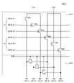
도 3은 도 2의 먹스 구동부의 상세 구조의 일례를 설명하기 위한 도면이다.FIG. 3 is a view for explaining an example of a detailed structure of the mux driving unit of FIG. 2 .
도 3을 참조하면, 본 발명의 일 실시예에 따른 표시장치(100)의 먹스 구동부(140)는 6개의 먹스 스위치(TM1, TM2, TM3, TM4, TM5, TM6)로 구성되는 먹스 스위치부(141)와 타이밍 컨트롤러(150)에서 인가되는 멀티 인에이블 제어 신호(MRE)에 따라 턴온(turn-on) 또는 턴오프(turn-off)되는 3개의 스위치(TS1, TS2, TS3)로 구성되는 출력 선택부(142)를 포함할 수 있다.Referring to FIG. 3 , the
먹스 스위치부(141)는 데이터 구동부(130)의 제1 출력 채널(Ch1)과 전기적으로 연결된 제1 내지 제3 데이터 라인(DL1, DL2, DL3) 및 제2 출력 채널(Ch2)과 전기적으로 연결된 제4 내지 데6 데이터 라인(DL4, DL5, DL6)이 배치되고, 각 데이터 라인에 배치된 제1 내지 제6 먹스 스위치(TM1, TM2, TM3, TM4, TM5, TM6)을 포함할 수 있다. 제1 출력 채널(Ch1)과 제2 출력 채널(Ch2)은 제1 수평기간(1H)동안 적색 데이터, 녹색 데이터 및 청색 데이터를 시분할로 제1 내지 제6 데이터 라인(D1~D6)에 제공할 수 있다. 도 3에서, 제1 내지 제6 먹스 스위치(TM1~TM6)를 엔모스 트랜지스터로 구성되는 것으로 도시하였으나, 이에 한정되지 않고 제1 내지 제6 먹스 스위치(TM1~TM6)를 피모스 트랜지스터로 구성될 수도 있다.The
제1 먹스 스위치(TM1) 및 제4 먹스 스위치(TM4)는 타이밍 컨트롤러(150)로부터 전송된 제1 멀티 제어신호(MCS1)에 따라 턴온 또는 턴오프될 수 있고, 제2 먹스 스위치(TM2) 및 제5 먹스 스위치(TM5)는 제2 멀티 제어신호(MCS2)에 따라 턴온 또는 턴오프될 수 있으며, 제3 먹스 스위치(TM3) 및 제6 먹스 스위치(TM6)는 제3 멀티 제어신호(MCS3)에 따라 턴온 또는 턴오프될 수 있다.The first mux switch TM1 and the fourth mux switch TM4 may be turned on or off according to the first multi-control signal MCS1 transmitted from the
입력 영상신호(RGB)가 고해상도일 때, 제1 수평기간(1H) 중 제1 기간동안 제1 먹스 스위치(TM1) 및 제4 먹스 스위치(TM4)는 고해상도에 대응하는 제1 멀티 제어신호(MCS1)에 응답하여 제1 출력 채널(Ch1) 및 제2 출력 채널(Ch2) 각각을 통해 제공받는 적색 데이터(R1, R2)를 각각 제1 데이터 라인(DL1) 및 제4 데이터 라인(DL4)에 제공한다. 이때, 제1 데이터 라인(DL1)에 제공되는 적색 데이터(R1)와 제4 데이터 라인(DL4)에 제공되는 적색 데이터(R2)는 서로 다른 극성을 가질 수 있다. 한편, 입력 영상신호(RGB)가 저해상도일 때, 제1 수평기간(1H) 중 제1 기간동안 제1 먹스 스위치(TM1) 및 제4 먹스 스위치(TM4)는 저해상도에 대응하는 제1 멀티 제어신호(MCS1)에 응답하여 제1 출력 채널(Ch1) 및 제2 출력 채널(Ch2) 중 어느 하나의 채널을 통해 제공받는 적색 데이터를 제1 데이터 라인(DL1) 또는 제4 데이터 라인(DL4)에 제공한다. 즉, 입력 영상신호(RGB)가 저해상도일 때에는 제1 먹스 스위치(TM1) 및 제4 먹스 스위치(TM4) 중 어느 하나만 턴온될 수 있다.When the input image signal RGB has a high resolution, during a first period of the first horizontal period 1H, the first mux switch TM1 and the fourth mux switch TM4 transmit the first multi-control signal MCS1 corresponding to the high resolution. ), the red data R1 and R2 received through each of the first output channel Ch1 and the second output channel Ch2 are provided to the first data line DL1 and the fourth data line DL4, respectively. do. In this case, the red data R1 provided to the first data line DL1 and the red data R2 provided to the fourth data line DL4 may have different polarities. On the other hand, when the input image signal RGB has a low resolution, during the first period of the first horizontal period 1H, the first mux switch TM1 and the fourth mux switch TM4 receive a first multi-control signal corresponding to the low resolution. Red data received through any one of the first output channel Ch1 and the second output channel Ch2 is provided to the first data line DL1 or the fourth data line DL4 in response to the MCS1 do. That is, when the input image signal RGB has a low resolution, only one of the first mux switch TM1 and the fourth mux switch TM4 may be turned on.
입력 영상신호(RGB)가 고해상도일 때, 제1 수평기간(1H) 중 제1 기간과 다른 타이밍의 제2 기간동안 제2 먹스 스위치(TM2) 및 제5 먹스 스위치(TM5)는 제2 멀티 제어신호(MCS2)에 응답하여 제1 출력 채널(Ch1) 및 제2 출력 채널(Ch2) 각각을 통해 제공받는 녹색 데이터(G1, G2)를 각각 제2 데이터 라인(DL2) 및 제5 데이터 라인(DL5)에 제공한다. 이때, 제2 데이터 라인(DL2)에 제공되는 녹색 데이터(G1)와 제5 데이터 라인(DL5)에 제공되는 녹색 데이터(G2)는 서로 다른 극성을 가질 수 있다. 한편, 입력 영상신호(RGB)가 저해상도일 때, 제1 수평기간(1H) 중 제2 기간동안 제2 먹스 스위치(TM2) 및 제5 먹스 스위치(TM5)는 저해상도에 대응하는 제2 멀티 제어신호(MCS12)에 응답하여 제1 출력 채널(Ch1) 및 제2 출력 채널(Ch2) 중 어느 하나의 채널을 통해 제공받는 녹색 데이터를 제2 데이터 라인(DL2) 또는 제5 데이터 라인(DL5)에 제공한다. 즉, 입력 영상신호(RGB)가 저해상도일 때에는 제2 먹스 스위치(TM2) 및 제5 먹스 스위치(TM5) 중 어느 하나만 턴온될 수 있다.When the input image signal RGB has a high resolution, the second mux switch TM2 and the fifth mux switch TM5 control the second multi-control for a second period different from the first period of the first horizontal period 1H. The green data G1 and G2 provided through each of the first output channel Ch1 and the second output channel Ch2 in response to the signal MCS2 are transferred to the second data line DL2 and the fifth data line DL5, respectively. ) is provided in In this case, the green data G1 provided to the second data line DL2 and the green data G2 provided to the fifth data line DL5 may have different polarities. On the other hand, when the input image signal RGB has a low resolution, the second mux switch TM2 and the fifth mux switch TM5 during the second period of the first horizontal period 1H provide a second multi-control signal corresponding to the low resolution. Green data received through one of the first output channel Ch1 and the second output channel Ch2 is provided to the second data line DL2 or the fifth data line DL5 in response to the MCS12 do. That is, when the input image signal RGB has a low resolution, only one of the second mux switch TM2 and the fifth mux switch TM5 may be turned on.
입력 영상신호(RGB)가 고해상도일 때, 제1 수평기간(1H) 중 제2 기간과 다른 타이밍의 제3 기간동안 제3 먹스 스위치(TM4) 및 제6 먹스 스위치(TM6)는 제3 멀티 제어신호(MCS3)에 응답하여 제1 출력 채널(Ch1) 및 제2 출력 채널(Ch2) 각각을 통해 제공받는 청색 데이터(B1, B2)를 각각 제3 데이터 라인(DL3) 및 제6 데이터 라인(DL6)에 제공한다. 이때, 제3 데이터 라인(DL3)에 제공되는 청색 데이터(B1)와 제6 데이터 라인(DL6)에 제공되는 청색 데이터(B2)는 서로 다른 극성을 가질 수 있다. 한편, 입력 영상신호(RGB)가 저해상도일 때, 제1 수평기간(1H) 중 제3 기간동안 제3 먹스 스위치(TM3) 및 제6 먹스 스위치(TM6)는 저해상도에 대응하는 제3 멀티 제어신호(MCS3)에 응답하여 제1 출력 채널(Ch1) 및 제2 출력 채널(Ch2) 중 어느 하나의 채널을 통해 제공받는 청색 데이터를 제3 데이터 라인(DL3) 또는 제6 데이터 라인(DL6)에 제공한다. 즉, 입력 영상신호(RGB)가 저해상도일 때에는 제3 먹스 스위치(TM3) 및 제6 먹스 스위치(TM6) 중 어느 하나만 턴온될 수 있다. 여기서 제1 수평기간은 게이트 구동부(120)에서 표시패널(110)의 게이트 라인들(GL1, … GLn)에 인가되는 스캔신호의 타이밍과 동일할 수 있다.When the input video signal RGB has a high resolution, the third mux switch TM4 and the sixth mux switch TM6 control the third multi-control for a third period different from the second period of the first horizontal period 1H. Blue data B1 and B2 provided through each of the first output channel Ch1 and the second output channel Ch2 in response to the signal MCS3 are transferred to the third data line DL3 and the sixth data line DL6, respectively. ) is provided in In this case, the blue data B1 provided to the third data line DL3 and the blue data B2 provided to the sixth data line DL6 may have different polarities. Meanwhile, when the input image signal RGB has a low resolution, during the third period of the first horizontal period 1H, the third mux switch TM3 and the sixth mux switch TM6 provide a third multi-control signal corresponding to the low resolution. Blue data received through one of the first output channel Ch1 and the second output channel Ch2 is provided to the third data line DL3 or the sixth data line DL6 in response to the MCS3 do. That is, when the input image signal RGB has a low resolution, only one of the third mux switch TM3 and the sixth mux switch TM6 may be turned on. Here, the first horizontal period may be the same as the timing of the scan signal applied from the
출력 선택부(142)는 멀티 인에이블 제어신호(MRE)에 따라 극성이 서로 다른 적색 데이터(R1, R2)를 출력하는 제1 데이터 라인(DL1)과 제4 데이터 라인(DL4)을 전기적으로 연결할 수 있는 제1 스위치(TS1), 멀티 인에이블 제어신호(MRE)에 따라 극성이 서로 다른 녹색 데이터(G1, G2)를 출력하는 제2 데이터 라인(DL2)과 제5 데이터 라인(DL5)을 전기적으로 연결할 수 있는 제2 스위치(TS2) 및 멀티 인에이블 제어신호(MRE)에 따라 극성이 서로 다른 청색 데이터(B1, B2)를 출력하는 제3 데이터 라인(DL3)과 제6 데이터 라인(DL6)을 전기적으로 연결할 수 있는 제3 스위치(TS1~TS3)를 포함할 수 있다. 제1 데이터 라인(D1) 및 제4 데이터 라인(D4)는 표시패널(110)의 적색 서브화소와 연결될 수 있고, 제2 데이터 라인(D2) 및 제5 데이터 라인(D5)는 표시패널(110)의 녹색 서브화소와 연결될 수 있으며, 제3 데이터 라인(D3) 및 제6 데이터 라인(D6)은 표시패널(110)의 청색 서브화소와 연결될 수 있다. 또한 제1 내지 제3 데이터 라인(DL1~DL3)은 표시패널(110)의 제1 화소에 포함되는 서로 다른 색의 서브 화소, 예를 들어, 적색 서브화소, 녹색 서브화소 및 청색 서브화소에 각각 연결되는 데이터 라인일 수 있고, 제4 내지 제6 데이터 라인(DL4~DL6)은 제1 화소에 이웃하는 제2 화소에 포함되는 서로 다른 색의 서브화소, 예를 들어, 적색 서브화소, 녹색 서브화소 및 청색 서브화소에 각각 연결되는 데이터 라인일 수 있다. 즉, 출력 선택부(140)의 제1 스위치(TS1)에 전기적으로 연결되는 제1 데이터 라인(DL1)과 제4 데이터 라인(DL2), 출력 선택부(140)의 제2 스위치(TS2)에 전기적으로 연결되는 제2 데이터 라인(DL2)과 제5 데이터 라인(DL5) 및 출력 선택부(140)의 제3 스위치(TS3)에 의해 전기적으로 연결될 수 있는 제3 데이터 라인(DL3)과 제6 데이터 라인(DL6)은 이웃하는 서로 다른 화소와 연결되는 데이터 라인일 수 있다.The
제1 스위치(TS1)는 게이트가 멀티 인에이블 제어신호(MRE)가 인가되는 인에이블 라인에 연결되고, 소스 및 드레인은 각각 제1 데이터 라인(DL1) 및 제4 데이터 라인(DL4)이 연결될 수 있다.The first switch TS1 may have a gate connected to an enable line to which the multi-enable control signal MRE is applied, and a source and drain connected to a first data line DL1 and a fourth data line DL4, respectively. have.
제2 스위치(TS2)는 게이트가 멀티 인에이블 제어신호(MRE)가 인가되는 인에이블 라인에 연결되고, 소스 및 드레인은 각각 제2 데이터 라인(DL2) 및 제5 데이터 라인(DL5)이 연결될 수 있다.The second switch TS2 may have a gate connected to an enable line to which the multi-enable control signal MRE is applied, and a source and drain connected to a second data line DL2 and a fifth data line DL5, respectively. have.
제3 스위치(TS3)는 게이트가 멀티 인에이블 제어신호(MRE)가 인가되는 인에이블 라인에 연결되고, 소스 및 드레인은 각각 제3 데이터 라인(DL3) 및 제6 데이터 라인(DL6)이 연결될 수 있다.The third switch TS3 may have a gate connected to an enable line to which the multi-enable control signal MRE is applied, and a source and drain connected to a third data line DL3 and a sixth data line DL6, respectively. have.
이와 같은 도 3에 따른 먹스 구동부의 구동을 보다 상세히 살펴보면, 입력 영상신호(RGB)의 해상도가 고해상도인 경우 멀티 인에이블 제어신호(MRE)는 제1 내지 제3 스위치(T1~T3)가 턴오프되도록 하고, 이에 따라, 제1 채널(Ch1) 및 제2 채널(Ch2)에서 출력되는 모든 데이터가 제1 내지 제6 데이터 라인(DL1~DL6)으로 모두 출력될 수 있다. 즉, 입력 영상신호(RGB)가 고해상도인 경우 일반적인 표시장치의 먹스 구동부와 동일하게 구동될 수 있다.Looking at the driving of the mux driver according to FIG. 3 in more detail, when the resolution of the input image signal RGB is high, the first to third switches T1 to T3 are turned off in the multi enable control signal MRE. Accordingly, all data output from the first channel Ch1 and the second channel Ch2 may be output to the first to sixth data lines DL1 to DL6. That is, when the input image signal RGB has a high resolution, it may be driven in the same manner as the mux driver of a general display device.
한편, 입력 영상신호(RGB)의 해상도가 저해상도인 경우 먹스 스위치부(141) 중 일부 먹스 스위치, 예를 들어, 제4 내지 제6 먹스 스위치(TM4~TM6)는 턴오프되고, 이에 따라, 제1 채널(Ch1)과 제2 채널(Ch2) 중 제2 채널(Ch2)과 연결된 제4 내지 제6 데이터 라인(DL4~DL6)으로 데이터가 출력되지 않을 수 있다. 또한, 출력 선택부(142)는 멀티 인에이블 제어신호(MRE)에 의해 제1 내지 제3 스위치(T1~T3)가 턴-온되고, 제1 내지 제3 스위치(T1~T3)가 턴온되면 제1 데이터 라인(DL1)을 통해 출력되는 적색 데이터(R1)가 제1 데이터 라인(DL1)과 제4 데이터 라인(DL4)을 통해 출력될 수 있고, 제2 데이터 라인(DL2)을 통해 출력되는 녹색 데이터(G1)는 제5 데이터 라인(DL5)에 복사되어 제5 데이터 라인(DL5)을 통해 출력될 수 있으며, 제3 데이터 라인(DL3)을 통해 출력되는 청색 데이터(B1)는 제6 데이터 라인(DL6)에 복사되어 제6 데이터 라인(DL6)을 통해 출력될 수 있다. 이때, 제1 내지 제3 데이터 라인(DL1~DL3)을 통해 출력되는 적색, 녹색 및 청색 데이터들과 제4 내지 제6 데이터 라인(DL4~DL6)을 통해 출력되는 적색, 녹색 및 청색 데이터들 각각은 동일한 극성을 가질 수 있다.On the other hand, when the resolution of the input image signal RGB is a low resolution, some of the mux switches of the
이와 같이, 본 발명의 일 실시예에 따른 표시장치(100)의 먹스 구동부(140)는 입력 영상신호(RGB)가 고해상도일 때에는 제1 채널(Ch1) 및 제2 채널(Ch2) 각각과 연결된 모든 데이터 라인(DL1~DL6)을 통해 데이터들이 출력되도록 하여 고해상도의 영상이 표시되도록 한다.As described above, when the input image signal RGB has a high resolution, the
한편, 입력 영상신호(RGB)가 저해상도일 때에는 제1 채널(Ch1) 및 제2 채널(Ch2) 중 제1 채널(Ch1)과 연결된 제1 내지 제3 데이터 라인(DL1~DL3)을 통해서만 적색 데이터, 녹색 데이터 및 청색 데이터가 출력되도록 하되, 사용하지 않는 제2 채널(Ch2)과 연결된 제4 내지 제6 데이터 라인(DL4~DL6)에 제1 채널(Ch1)에서 출력되는 적색 데이터, 녹색 데이터 및 청색 데이터가 복사되어 출력되도록 하여 전체적인 표시장치(100)의 소비 전력을 저감시킬 수 있다. 입력 영상신호(RGB)가 저해상도일 때에는 제1 화소를 통해 화상이 표시되도록 하되, 제1 화소와 이웃하는 제2 화소에서도 제1 화소와 동일한 화상이 표시되도록 할 수 있다. 이에 따라, 본 발명의 일 실시예에 따른 표시장치(100)는 저해상도의 영상을 표시할 때 먹스 구동부(140)를 통해 하나의 극성을 갖는 데이터가 출력되도록 하여 전압레벨의 변동이 작아지기 때문에 표시장치(100)의 소비 전력을 저감시킬 수 있다.On the other hand, when the input image signal RGB has a low resolution, red data is transmitted only through the first to third data lines DL1 to DL3 connected to the first channel Ch1 among the first channel Ch1 and the second channel Ch2. , green data and blue data are outputted, but the red data, green data, and By allowing the blue data to be copied and output, the overall power consumption of the
다만, 도 3에 도시된 바와 같은 먹스 구동부(140)는, 예를 들어, 제1 먹스 제어신호(MCS1)가 인가되는 신호라인에 두 개의 먹스 스위치(TM1, TM4)가 배치되므로 하나의 신호 라인의 로드(load)가 증가될 수 있다. 이에 따라, 본 발명의 일 실시예에 따른 표시장치(100)는 신호 라인의 로드를 감소시킬 수 있는 다음 도 4와 같은 먹스 구동부의 구성을 제안하였다.However, in the
도 4은 도 2의 먹스 구동부의 상세 구조의 다른 예를 설명하기 위한 도면이다.FIG. 4 is a view for explaining another example of the detailed structure of the mux driving unit of FIG. 2 .
도 4를 참조하면, 먹스 구동부(140-1)는 6개의 먹스 스위치(TM1, TM2, TM3, TM4, TM5, TM6)로 구성되는 먹스 스위치부(1411)와 타이밍 컨트롤러(150)에서 인가되는 멀티 인에이블 제어 신호(MRE)에 따라 턴온(turn-on) 또는 턴오프(turn-off)되는 3개의 스위치(TS1, TS2, TS3)로 구성되는 출력 선택부(1421)를 포함할 수 있다.Referring to FIG. 4 , the mux driving unit 140-1 includes a
먹스 스위치부(1411)는 제1 및 제2 제어신호(S1, S2)에 따라 데이터 구동부(130)의 제1 출력 채널(ch1)과 전기적으로 연결된 제1 내지 제3 데이터 라인(DL1, DL2, DL3) 및 제2 출력 채널(Ch2)과 전기적으로 연결된 제4 내지 데6 데이터 라인(DL4, DL5, DL6)이 배치된다. 여기서, 제1 내지 제3 데이터 라인(DL1~DL3)은 모두 제1 화소에 포함되는 서로 다른 색의 서브화소에 데이터 신호를 인가하기 위한 데이터 라인일 수 있고, 제4 내지 제6 데이터 라인(D4~D6)은 모두 제1 화소와 이웃하는 제2 화소에 포함되는 서로 다른 색의 서브화소에 데이터 신호를 인가하기 위한 데이터 라인일 수 있다. 각 데이터 라인에 배치된 제1 내지 제6 먹스 스위치(TM1, TM2, TM3, TM4, TM5, TM6)을 포함할 수 있다. 제1 출력 채널(Ch1)과 제2 출력 채널(Ch2)은 제1 수평기간(1H)동안 적색 데이터, 녹색 데이터 및 청색 데이터를 시분할로 제공할 수 있다. 도 4에서, 제1 내지 제6 먹스 스위치(TM1~TM6)을 엔모스 트랜지스터로 구성되는 것으로 도시하였으나, 이에 한정되지 않고 제1 내지 제6 먹스 스위치(TM1~TM6)을 피모스 트랜지스터로 구성될 수도 있다.The
제1 수평기간동안 제1 채널(Ch1) 및 제2 채널(Ch2)과 제1 내지 제6 데이터 라인(DL1~DL6)의 연결방식을 설명하면, 제1 및 제2 제어신호(S1, S2)에 대응하여 초기 1/3 수평기간인 제1 기간동안에는 제1 채널(Ch1) 및 제1 데이터 라인(DL1)과 제2 채널(Ch2) 및 제4 데이터 라인(DL4)을 각각 연결하고, 다음 1/3 수평기간인 제2 기간동안에는 제1 채널(Ch1) 및 제2 데이터 라인(DL2)과 제2 채널(Ch2) 및 제5 데이터 라인(DL5)을 각각 연결하며, 마지막 1/3 수평기간인 제3 기간 동안에는 제1 채널(Ch1) 및 제3 데이터 라인(DL3)과 제2 채널(Ch2) 및 제6 데이터 라인(DL6)을 각각 연결할 수 있다. 이때, 이웃한 화소들간에는 인버젼 구동으로 인하여 서로 다른 극성의 데이터 신호가 인가되어야 하며, 이에 따라, 제1 데이터 라인(DL1) 및 제4 데이터 라인(DL4)에는 서로 다른 극성의 적색 데이터(R1, R2)가 인가되고, 제2 데이터 라인(DL2) 및 제5 데이터 라인(DL5)에는 서로 다른 극성의 녹색 데이터(G1, G2)가 인가되며, 제3 데이터 라인(DL3) 및 제6 데이터 라인(DL6)에는 서로 다른 극성의 청색 데이터(B1, B2)가 인가될 수 있다.A method of connecting the first channel Ch1 and the second channel Ch2 and the first to sixth data lines DL1 to DL6 during the first horizontal period will be described, when the first and second control signals S1 and S2 are described. Correspondingly, during the first period, which is the initial 1/3 horizontal period, the first channel Ch1 and the first data line DL1 and the second channel Ch2 and the fourth data line DL4 are respectively connected, and the next 1 During the second period, which is the /3 horizontal period, the first channel Ch1 and the second data line DL2 and the second channel Ch2 and the fifth data line DL5 are respectively connected, and the last 1/3 horizontal period During the third period, the first channel Ch1 and the third data line DL3 and the second channel Ch2 and the sixth data line DL6 may be respectively connected. In this case, data signals having different polarities must be applied between neighboring pixels due to inversion driving. Accordingly, red data R1 having different polarities is applied to the first data line DL1 and the fourth data line DL4. , R2 are applied, green data G1 and G2 having different polarities are applied to the second data line DL2 and the fifth data line DL5, and the third data line DL3 and the sixth data line Blue data B1 and B2 having different polarities may be applied to DL6.
도 4의 먹스 구동부(140-1)의 먹스 스위치부(1411)는, 도 3과 비교하여, 먹스 제어신호가 인가되는 하나의 라인에 하나의 먹스 스위치만이 배치되도록 한다. 또한, 제1 채널(Ch1)과 연결된 제1 내지 제3 데이터 라인(DL1~DL3)에 연결된 제1 내지 제3 먹스 스위치(TM1~TM3)는 제1 제어신호(S1)에 의해 제어되도록 하고, 제2 채널(Ch2)과 연결된 제4 내지 제6 데이터 라인(DL4~DL6)에 연결된 제4 내지 제6 먹스 스위치(TM4~TM6)는 제2 제어신호(S2)에 의해 제어되도록 구성될 수 있다. 즉 입력 영상신호(RGB)가 고해상도이면 제1 제어신호(S1) 및 제2 제어신호(S2)에 의해 제1 내지 제6 먹스 스위치(TM1~TM6)는 모두 턴온될 수 있고, 입력 영상신호(RGB)가 저해상도이면 제1 제어신호(S1) 및 제2 제어신호(S2) 중 어느 하나의 제어신호에 대응되는 일부 먹스 스위치만 턴온될 수 있다. 예를 들어, 제1 제어신호(S1)가 인가되면 제1 내지 제3 먹스 스위치(TM1~TM3)만 턴온될 수 있고, 제2 제어신호(S2)가 인가되면 제4 내지 제6 먹스 스위치(TM4~TM6)만 턴온될 수 있다.Compared to FIG. 3 , the
이에 따라, 먹스 제어신호가 인가되는 하나의 라인에 하나의 먹스 스위치만 배치되기 때문에 신호 라인의 로드를 감소시킬 수 있고, 제1 제어신호(S1) 또는 제2 제어신호(S2)에 따라 제1 채널(Ch1) 또는 제2 채널(Ch2) 각각과 연결된 데이터 라인들을 통해서 데이터가 출력되도록 제어할 수 있다.Accordingly, since only one mux switch is disposed on one line to which the mux control signal is applied, the load on the signal line can be reduced, and according to the first control signal S1 or the second control signal S2, the first It is possible to control data to be output through data lines connected to each of the channel Ch1 or the second channel Ch2.
한편, 도 4의 먹스 구동부(140-1)의 출력 선택부(1421)의 구성은 도 3의 출력 선택부(142)의 구성과 동일하기 때문에 상세한 설명은 생략토록 한다.Meanwhile, since the configuration of the
이와 같은 도 4에 따른 먹스 구동부의 구동을 보다 상세히 살펴보면, 입력 영상신호(RGB)의 해상도가 고해상도인 경우 먹스 스위치부(1411)에 제1 제어신호(S1) 및 제2 제어신호(S2)가 인가되어 그에 대응되는 제1 내지 제6 먹스 스위치(TM1~TM6)는 모두 턴온되고, 출력 선택부(1421)의 제1 내지 제3 스위치(TS1~TS3)는 모두 턴오프되어 모든 데이터가 제1 내지 제6 데이터 라인(DL1~DL6)으로 출력될 수 있다. 즉, 입력 영상신호(RGB)가 고해상도인 경우 일반적인 표시장치의 먹스 구동부와 동일하게 구동될 수 있다.Referring to the driving of the mux driver according to FIG. 4 in more detail, when the resolution of the input image signal RGB is high, the first control signal S1 and the second control signal S2 are transmitted to the
한편, 입력 영상신호(RGB)의 해상도가 저해상도인 경우 먹스 스위치부(1411) 중 제4 내지 제6 먹스 스위치(TM4~TM6)는 턴오프되고, 이에 따라, 제1 채널(Ch1)과 제2 채널(Ch2) 중 제2 채널(Ch2)과 연결된 제4 내지 제6 데이터 라인(DL4~DL6)으로 데이터가 출력되지 않을 수 있다. 또한, 출력 선택부(1421)는 멀티 인에이블 제어신호(MRE)에 의해 제1 내지 제3 스위치(T1~T3)가 턴-온되면 제1 데이터 라인(DL1)을 통해 출력되는 적색 데이터(R1)가 제1 데이터 라인(DL1)과 제4 데이터 라인(DL4)을 통해 출력될 수 있고, 제2 데이터 라인(DL2)을 통해 출력되는 녹색 데이터(G1)는 제5 데이터 라인(DL5)에 복사되어 제5 데이터 라인(DL5)을 통해 출력될 수 있으며, 제3 데이터 라인(DL3)을 통해 출력되는 청색 데이터(B1)는 제6 데이터 라인(DL6)에 복사되어 제6 데이터 라인(DL6)을 통해 출력될 수 있다. 이때, 제1 내지 제3 데이터 라인(DL1~DL3)을 통해 출력되는 적색, 녹색 및 청색 데이터들과 제4 내지 제6 데이터 라인(DL4~DL6)을 통해 출력되는 적색, 녹색 및 청색 데이터들 각각은 동일한 극성을 가질 수 있다.On the other hand, when the resolution of the input image signal RGB is a low resolution, the fourth to sixth mux switches TM4 to TM6 of the
이와 같이, 본 발명의 일 실시예에 따른 표시장치(100)의 먹스 구동부(140)는 입력 영상신호(RGB)가 고해상도일 때에는 제1 채널(Ch1) 및 제2 채널(Ch2) 각각과 연결된 모든 데이터 라인(DL1~DL6)을 통해 데이터들이 출력되도록 하여 고해상도의 영상이 표시되도록 하고, 입력 영상신호(RGB)가 저해상도일 때에는 제1 채널(Ch1) 및 제2 채널(Ch2) 중 제1 채널(Ch1)과 연결된 제1 내지 제3 데이터 라인(DL1~DL3)을 통해서만 적색 데이터, 녹색 데이터 및 청색 데이터가 출력되도록 하되, 사용하지 않는 제2 채널(Ch2)과 연결된 제4 내지 제6 데이터 라인(DL4~DL6)에 제1 채널(Ch1)에서 출력되는 적색 데이터, 녹색 데이터 및 청색 데이터가 복사되어 출력되도록 하여 전체적인 표시장치(100)의 소비 전력을 저감시킬 수 있다.As described above, when the input image signal RGB has a high resolution, the
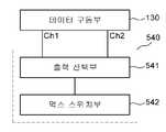
도 5는 본 발명의 다른 실시예에 따른 표시장치의 먹스 구동부를 설명하기 위한 블록도이다.5 is a block diagram illustrating a MUX driver of a display device according to another exemplary embodiment of the present invention.
도 5을 참조하면, 본 발명의 다른 실시예에 따른 표시장치의 먹스 구동부(540)는 출력 선택부(541)와 먹스 스위치부(542)를 포함할 수 있다. 이때, 먹스 구동부(540)는 도 1 내지 도 4의 먹스 구동부(140)와 비교하여 출력 선택부와 먹스 스위치부의 배치 위치가 상이할 수 있다. 본 발명의 다른 실시예에 따른 표시장치의 먹스 구동부(540)의 출력 선택부(541)는 데이터 구동부(130)와 먹스 스위치부(542) 사이에 배치되고, 먹스 스위치부(542)는 출력 선택부(541)와 표시패널(110) 사이에 배치될 수 있다.Referring to FIG. 5 , the
도 6은 도 5의 먹스 구동부의 상세 구조의 일례를 설명하기 위한 도면이다.6 is a view for explaining an example of a detailed structure of the mux driving unit of FIG. 5 .
도 6을 살펴보기 전에, 도 5의 먹스 스위치부(542)는 도 3의 먹스 스위치부(141)와 구성이 동일하기 때문에 도 5의 먹스 스위치부(542)에 대한 상세한 설명은 생략하도록 한다.Before examining FIG. 6 , since the
도 6을 참조하면, 출력 선택부(541)는 하나의 스위치(TS1)를 포함할 수 있고, 하나의 스위치(TS1)는 멀티 인에이블 라인에 게이트가 연결되고, 소스 및 드레인은 제1 출력채널(Ch1)과 제2 출력채널(Ch2)과 각각 연결될 수 있다.Referring to FIG. 6 , the
도 6의 구동을 살펴보면, 입력 영상신호(RGB)가 고해상도인 경우 멀티 인에이블 제어신호(MRE)에 의해 출력 선택부(541)의 스위치(TS1)가 턴오프된다. 출력 선택부(541)의 스위치(TS1)가 턴오프되면 제1 채널(Ch1) 및 제2 채널(Ch2)과 연결된 제1 내지 제6 데이터 라인(DL1~DL6)을 통해 데이터가 출력될 수 있다. 이때, 제1 채널(Ch1)과 제2 채널(Ch2)을 통해 출력되는 각 적색 데이터(R1, R2), 녹색 데이터(G1, G2) 및 청색 데이터(B1, B2)의 극성은 서로 다를 수 있다.Referring to the driving of FIG. 6 , when the input image signal RGB has a high resolution, the switch TS1 of the
한편, 입력 영상신호(RGB)가 저해상도인 경우 멀티 인에이블 제어신호(MRE)에 의해 출력 선택부(541)의 스위치(TS1)가 턴온된다. 출력 선택부(541)의 스위치(TS1)가 턴온되면 제1 채널(Ch1) 및 제2 채널(Ch2) 중 제1 채널(Ch1)과 연결된 제1 내지 제3 데이터 라인(DL1~DL3)을 통해서만 적색 데이터, 녹색 데이터 및 청색 데이터가 출력되도록 하되, 사용하지 않는 제2 채널(Ch2)과 연결된 제4 내지 제6 데이터 라인(DL4~DL6)에 제1 채널(Ch1)에서 출력되는 적색 데이터, 녹색 데이터 및 청색 데이터가 복사되어 출력되도록 하여 전체적인 표시장치의 소비 전력을 저감시킬 수 있다. 즉, 본 발명의 다른 실시예에 따른 표시장치는 저해상도의 영상을 표시할 때 먹스 구동부(540)를 통해 하나의 극성을 갖는 데이터가 출력되도록 하여 전압레벨의 변동이 작아지기 때문에 표시장치의 소비 전력을 저감시킬 수 있다.Meanwhile, when the input image signal RGB has a low resolution, the switch TS1 of the
다만, 도 6에 도시된 바와 같은 먹스 구동부(540)는, 도 3을 참조하여 설명한 바와 같이, 제1 먹스 제어신호(MCS1)가 인가되는 신호라인에 두 개의 먹스 스위치(TM1, TM4)가 배치되므로 하나의 신호 라인의 로드(load)가 증가될 수 있다. 이에 따라, 본 발명의 일 실시예에 따른 표시장치(100)는 신호 라인의 로드를 감소시킬 수 있는 다음 도 7과 같은 먹스 구동부의 구성을 제안하였다.However, in the
도 7은 도 5의 먹스 구동부의 상세 구조의 다른 예를 설명하기 위한 도면이다.7 is a view for explaining another example of the detailed structure of the mux driving unit of FIG. 5 .
도 7을 참조하면, 먹스 구동부(540-1)는 도 6에서 설명한 바와 동일한 구성을 갖는 출력 선택부(5411) 및 도 4에서 설명한 바와 동일한 구성을 갖는 먹스 스위치부(5421)을 포함할 수 있다. 도 7의 먹스 구동부(540-1)는 앞서 설명한 바의 구성을 조합한 것으로, 그 구동도 유사하기 때문에 상세한 설명은 생략하도록 한다.Referring to FIG. 7 , the mux driving unit 540-1 may include an
본 발명의 다양한 실시예들에 따른 표시 장치는 다음과 같이 설명될 수 있다.A display device according to various embodiments of the present disclosure may be described as follows.
본 발명의 일 실시예에 따른 표시 장치는 서로 다른 색의 복수의 서브 화소를 포함하는 복수 개의 화소 및 상기 서브 화소 각각과 연결되는 복수의 데이터 라인을 포함하는 표시패널, 복수의 데이터 라인에 대응하는 데이터 신호를 공급하는 제1 출력채널 및 제2 출력채널을 포함하는 데이터 구동부 및 표시패널과 상기 데이터 구동부 사이에 배치되고, 외부에서 입력되는 영상신호의 해상도에 따라 상기 제1 출력 채널 및 상기 제2 출력 채널 각각과 연결되는 복수의 데이터 라인의 데이터 출력을 제어하는 먹스 구동부를 포함한다.A display device according to an embodiment of the present invention includes a display panel including a plurality of pixels including a plurality of sub-pixels of different colors and a plurality of data lines connected to each of the sub-pixels; A data driver including a first output channel and a second output channel for supplying a data signal and a data driver disposed between the display panel and the data driver, the first output channel and the second output channel according to the resolution of an image signal input from the outside and a mux driver controlling data output of a plurality of data lines connected to each of the output channels.
먹스 구동부는 제1 출력 채널과 연결되는 제1 내지 제3 데이터 라인과 연결되는 제1 내지 제3 먹스 스위치와 상기 제2 출력 채널과 연결되는 제4 내지 제6 데이터 라인과 연결되는 제4 내지 제6 먹스 스위치를 포함하는 먹스 스위치부 및 제1 내지 제6 데이터 라인 중 동일한 색에 대응하는 데이터를 출력하는 데이터 라인들을 전기적으로 연결하는 제1 내지 3 스위치를 포함하는 출력 선택부를 포함할 수 있다.The mux driver includes first to third mux switches connected to first to third data lines connected to a first output channel, and fourth to sixth data lines connected to fourth to sixth data lines connected to the second output channel. and an output selector including a mux switch unit including 6 mux switches and first to third switches electrically connecting data lines outputting data corresponding to the same color among first to sixth data lines.
제1 내지 제3 데이터 라인은 상기 표시패널의 복수의 화소 중 제1 화소에 포함되는 적색 서브화소, 녹색 서브화소 및 청색 서브화소와 각각 연결되고, 상기 제4 내지 제6 데이터 라인은 상기 표시패널의 상기 복수의 화소 중 상기 제1 화소와 이웃하는 제2 화소에 포함되는 적색 서브화소, 녹색 서브화소 및 청색 서브화소와 각각 연결되며, 출력 선택부의 제1 스위치는 해상도에 따라 상기 제1 데이터 라인과 상기 제4 데이터 라인을 전기적으로 연결하고, 상기 출력 선택부의 제2 스위치는 해상도에 따라 상기 제2 데이터 라인과 상기 제5 데이터 라인을 전기적으로 연결하며, 상기 출력 선택부의 제3 스위치는 상기 제3 데이터 라인과 상기 제6 데이터 라인을 전기적으로 연결할 수 있다.The first to third data lines are respectively connected to a red sub-pixel, a green sub-pixel, and a blue sub-pixel included in a first pixel among the plurality of pixels of the display panel, and the fourth to sixth data lines are connected to the display panel of the plurality of pixels, each of the red sub-pixel, the green sub-pixel, and the blue sub-pixel included in the second pixel adjacent to the first pixel of and the fourth data line, the second switch of the output selector electrically connects the second data line and the fifth data line according to a resolution, and the third switch of the output selector electrically connects the second data line with the fifth data line according to the resolution. The third data line and the sixth data line may be electrically connected.
출력 선택부는 멀티 인에이블 신호에 의해 상기 제1 내지 제3 스위치가 턴온 또는 턴오프될 수 있다.The output selector may turn on or off the first to third switches by the multi enable signal.
먹스 구동부는 상기 멀티 인에이블 신호를 상기 제1 내지 제3 스위치에 전달하는 멀티 인에이블 라인을 포함하고, 제1 내지 제3 스위치의 게이트는 상기 멀티 인에이블 라인에 연결될 수 있다.The mux driver may include a multi enable line for transmitting the multi enable signal to the first to third switches, and gates of the first to third switches may be connected to the multi enable line.
멀티 인에이블 신호는 상기 입력 영상신호가 고해상도일 때 제1 내지 제3 스위치가 턴오프되도록 제어하고, 입력 영상신호가 저해상도일 때 상기 제1 내지 제3 스위치가 턴온되도록 제어하는 신호일 수 있다.The multi-enable signal may be a signal for controlling the first to third switches to be turned off when the input image signal has a high resolution, and for controlling the first to third switches to be turned on when the input image signal has a low resolution.
먹스 스위치부는 상기 데이터 구동부와 상기 출력 선택부 사이에 배치되고, 출력 선택부는 상기 먹스 스위치부와 상기 표시패널 사이에 배치될 수 있다.The MUX switch unit may be disposed between the data driver and the output selector, and the output selector may be disposed between the MUX switch unit and the display panel.
먹스 구동부는 제1 출력 채널과 연결되는 제1 내지 제3 데이터 라인과 연결되는 제1 내지 제3 먹스 스위치와 상기 제2 출력 채널과 연결되는 제4 내지 제6 데이터 라인과 연결되는 제4 내지 제6 먹스 스위치를 포함하는 먹스 스위치부 및 제1 출력 채널과 상기 제2 출력 채널 중 해상도에 따라 출력채널을 선택하는 스위치를 포함하는 출력 선택부를 포함할 수 있다.The mux driver includes first to third mux switches connected to first to third data lines connected to a first output channel, and fourth to sixth data lines connected to fourth to sixth data lines connected to the second output channel. and an output selector including a mux switch unit including 6 mux switches and a switch for selecting an output channel according to a resolution among the first output channel and the second output channel.
먹스 스위치부는 상기 출력 선택부와 상기 표시패널 사이에 배치되고, 출력 선택부는 상기 데이터 구동부와 상기 먹스 스위치부 사이에 배치될 수 있다.The MUX switch unit may be disposed between the output selector and the display panel, and the output selector may be disposed between the data driver and the MUX switch unit.
출력 선택부는 멀티 인에이블 신호에 의해 스위치가 턴온 또는 턴오프될 수 있다.The output selector may have a switch turned on or off by the multi-enable signal.
본 발명의 다른 실시예에 따른 표시 장치는 복수의 데이터 라인을 포함하는 표시패널, 복수의 데이터 라인에 대응하는 데이터 신호를 공급하는 제1 출력채널 및 제2 출력채널을 포함하는 데이터 구동부 및 표시패널과 상기 데이터 구동부 사이에 배치되고, 외부에서 입력되는 영상신호가 고해상도이면 서로 다른 극성을 갖는 데이터가 출력되도록 하고, 외부에서 입력되는 영상신호가 저해상도이면 동일한 극성을 갖는 데이터가 출력되도록 하는 먹스 구동부를 포함할 수 있다.A display device according to another exemplary embodiment of the present invention includes a display panel including a plurality of data lines, a data driver including a first output channel and a second output channel for supplying data signals corresponding to the plurality of data lines, and a display panel and a mux driver disposed between the data driver and configured to output data having different polarities when an externally input image signal has a high resolution, and output data having the same polarity when an externally input image signal has a low resolution may include
먹스 구동부는 외부에서 입력되는 영상신호가 저해상도이면 상기 제1 출력채널 및 상기 제2 출력채널 중 하나의 출력채널을 선택하여 선택된 하나의 출력채널과 연결된 복수의 데이터 라인을 통해 데이터가 출력되도록 할 수 있다.The mux driver may select one of the first output channel and the second output channel to output data through a plurality of data lines connected to the selected one output channel when the externally input image signal is of a low resolution. have.
먹스 구동부는 상기 제1 출력채널 및 상기 제2 출력채널 중 선택되지 않은 다른 하나의 출력채널과 연결된 복수의 데이터 라인에 선택된 출력채널과 연결된 복수의 데이터 라인의 데이터를 복사하여 출력되도록 할 수 있다.The mux driver may copy and output data of a plurality of data lines connected to the selected output channel to a plurality of data lines connected to another output channel that is not selected among the first output channel and the second output channel.
먹스 구동부는 외부에서 입력되는 영상신호가 고해상도이면 상기 제1 출력채널 및 상기 제2 출력채널 각각과 연결된 복수의 데이터 라인을 통해 복수의 데이터가 출력되도록 할 수 있다.The mux driver may output a plurality of data through a plurality of data lines connected to each of the first output channel and the second output channel when an externally input image signal has a high resolution.
이상 첨부된 도면을 참조하여 본 발명의 실시예들을 더욱 상세하게 설명하였으나, 본 발명은 반드시 이러한 실시예로 국한되는 것은 아니고, 본 발명의 기술사상을 벗어나지 않는 범위 내에서 다양하게 변형실시될 수 있다. 따라서, 본 발명에 개시된 실시예들은 본 발명의 기술 사상을 한정하기 위한 것이 아니라 설명하기 위한 것이고, 이러한 실시예에 의하여 본 발명의 기술 사상의 범위가 한정되는 것은 아니다. 그러므로, 이상에서 기술한 실시예들은 모든 면에서 예시적인 것이며 한정적이 아닌 것으로 이해해야만 한다. 본 발명의 보호 범위는 아래의 청구범위에 의하여 해석되어야 하며, 그와 동등한 범위 내에 있는 모든 기술 사상은 본 발명의 권리범위에 포함되는 것으로 해석되어야 할 것이다.Although embodiments of the present invention have been described in more detail with reference to the accompanying drawings, the present invention is not necessarily limited to these embodiments, and various modifications may be made within the scope without departing from the technical spirit of the present invention. . Therefore, the embodiments disclosed in the present invention are not intended to limit the technical spirit of the present invention, but to explain, and the scope of the technical spirit of the present invention is not limited by these embodiments. Therefore, it should be understood that the embodiments described above are illustrative in all respects and not restrictive. The protection scope of the present invention should be construed by the following claims, and all technical ideas within the scope equivalent thereto should be construed as being included in the scope of the present invention.
110: 표시패널
120: 게이트 구동부
130: 데이터 구동부
140, 140-1, 540, 540-1: 먹스 구동부
141, 1411, 541, 5411: 먹스 스위치부
142, 1421, 542, 5421: 출력 선택부
150: 타이밍 컨트롤러110: display panel
120: gate driver
130: data driving unit
140, 140-1, 540, 540-1: mux drive unit
141, 1411, 541, 5411: mux switch unit
142, 1421, 542, 5421: output selector
150: timing controller
Claims (14)
Translated fromKorean상기 복수의 데이터 라인에 대응하는 데이터 신호를 공급하는 제1 출력채널 및 제2 출력채널을 포함하는 데이터 구동부; 및
상기 표시패널과 상기 데이터 구동부 사이에 배치되고, 외부에서 입력되는 영상신호의 해상도에 따라 상기 제1 출력 채널 및 상기 제2 출력 채널 각각과 연결되는 복수의 데이터 라인의 데이터 출력을 제어하는 먹스 구동부를 포함하고,
상기 먹스 구동부는,
상기 제1 출력 채널과 연결되는 제1 내지 제3 데이터 라인과 연결되는 제1 내지 제3 먹스 스위치와 상기 제2 출력 채널과 연결되는 제4 내지 제6 데이터 라인과 연결되는 제4 내지 제6 먹스 스위치를 포함하는 먹스 스위치부; 및
상기 제1 내지 제6 데이터 라인 중 동일한 색에 대응하는 데이터를 출력하는 데이터 라인들을 전기적으로 연결하는 제1 내지 3 스위치를 포함하는 출력 선택부를 포함하는, 표시장치.a display panel comprising: a display panel including a plurality of pixels including a plurality of sub-pixels of different colors and a plurality of data lines connected to each of the sub-pixels;
a data driver including a first output channel and a second output channel for supplying data signals corresponding to the plurality of data lines; and
a mux driver disposed between the display panel and the data driver and configured to control data output of a plurality of data lines connected to each of the first output channel and the second output channel according to a resolution of an externally input image signal; including,
The mux driving unit,
first to third mux switches connected to first to third data lines connected to the first output channel, and fourth to sixth mux switches connected to fourth to sixth data lines connected to the second output channel a mux switch unit including a switch; and
and an output selector including first to third switches electrically connecting data lines outputting data corresponding to the same color among the first to sixth data lines.
상기 제1 내지 제3 데이터 라인은 상기 표시패널의 복수의 화소 중 제1 화소에 포함되는 적색 서브화소, 녹색 서브화소 및 청색 서브화소와 각각 연결되고, 상기 제4 내지 제6 데이터 라인은 상기 표시패널의 상기 복수의 화소 중 상기 제1 화소와 이웃하는 제2 화소에 포함되는 적색 서브화소, 녹색 서브화소 및 청색 서브화소와 각각 연결되며,
상기 출력 선택부의 제1 스위치는 해상도에 따라 상기 제1 데이터 라인과 상기 제4 데이터 라인을 전기적으로 연결하고, 상기 출력 선택부의 제2 스위치는 해상도에 따라 상기 제2 데이터 라인과 상기 제5 데이터 라인을 전기적으로 연결하며, 상기 출력 선택부의 제3 스위치는 상기 제3 데이터 라인과 상기 제6 데이터 라인을 전기적으로 연결하는, 표시장치.3. The method of claim 2,
The first to third data lines are respectively connected to a red sub-pixel, a green sub-pixel, and a blue sub-pixel included in a first pixel among the plurality of pixels of the display panel, and the fourth to sixth data lines are connected to the display panel. connected to a red sub-pixel, a green sub-pixel, and a blue sub-pixel included in a second pixel adjacent to the first pixel among the plurality of pixels of the panel, respectively;
A first switch of the output selector electrically connects the first data line and the fourth data line according to a resolution, and a second switch of the output selector electrically connects the second data line and the fifth data line according to a resolution and the third switch of the output selector electrically connects the third data line and the sixth data line.
상기 출력 선택부는 멀티 인에이블 신호에 의해 상기 제1 내지 제3 스위치가 턴온 또는 턴오프되는, 표시장치.4. The method of claim 3,
The display device of claim 1, wherein the output selector turns on or off the first to third switches by a multi-enable signal.
상기 먹스 구동부는 상기 멀티 인에이블 신호를 상기 제1 내지 제3 스위치에 전달하는 멀티 인에이블 라인을 포함하고,
상기 제1 내지 제3 스위치의 게이트는 상기 멀티 인에이블 라인에 연결되는, 표시장치.5. The method of claim 4,
The mux driving unit includes a multi enable line for transmitting the multi enable signal to the first to third switches,
and gates of the first to third switches are connected to the multi-enable line.
상기 멀티 인에이블 신호는 상기 영상신호가 고해상도일 때 상기 제1 내지 제3 스위치가 턴오프되도록 제어하고, 상기 영상신호가 저해상도일 때 상기 제1 내지 제3 스위치가 턴온되도록 제어하는 신호인, 표시장치.6. The method of claim 5,
The multi-enable signal is a signal for controlling the first to third switches to be turned off when the video signal is of a high resolution, and controlling the first to third switches to be turned on when the video signal is of a low resolution. Device.
상기 먹스 스위치부는 상기 데이터 구동부와 상기 출력 선택부 사이에 배치되고,
상기 출력 선택부는 상기 먹스 스위치부와 상기 표시패널 사이에 배치되는, 표시장치.3. The method of claim 2,
The mux switch unit is disposed between the data driving unit and the output selection unit,
and the output selector is disposed between the mux switch and the display panel.
상기 복수의 데이터 라인에 대응하는 데이터 신호를 공급하는 제1 출력채널 및 제2 출력채널을 포함하는 데이터 구동부; 및
상기 표시패널과 상기 데이터 구동부 사이에 배치되고, 외부에서 입력되는 영상신호의 해상도에 따라 상기 제1 출력 채널 및 상기 제2 출력 채널 각각과 연결되는 복수의 데이터 라인의 데이터 출력을 제어하는 먹스 구동부를 포함하고,
상기 먹스 구동부는,
상기 제1 출력 채널과 연결되는 제1 내지 제3 데이터 라인과 연결되는 제1 내지 제3 먹스 스위치와 상기 제2 출력 채널과 연결되는 제4 내지 제6 데이터 라인과 연결되는 제4 내지 제6 먹스 스위치를 포함하는 먹스 스위치부; 및
상기 제1 출력 채널과 상기 제2 출력 채널 중 해상도에 따라 출력채널을 선택하는 스위치를 포함하는 출력 선택부를 포함하는, 표시장치.a display panel comprising: a display panel including a plurality of pixels including a plurality of sub-pixels of different colors and a plurality of data lines connected to each of the sub-pixels;
a data driver including a first output channel and a second output channel for supplying data signals corresponding to the plurality of data lines; and
a mux driver disposed between the display panel and the data driver and configured to control data output of a plurality of data lines connected to each of the first output channel and the second output channel according to a resolution of an externally input image signal; including,
The mux driving unit,
first to third mux switches connected to first to third data lines connected to the first output channel, and fourth to sixth mux switches connected to fourth to sixth data lines connected to the second output channel a mux switch unit including a switch; and
and an output selector including a switch for selecting an output channel according to a resolution among the first output channel and the second output channel.
상기 먹스 스위치부는 상기 출력 선택부와 상기 표시패널 사이에 배치되고,
상기 출력 선택부는 상기 데이터 구동부와 상기 먹스 스위치부 사이에 배치되는, 표시장치.9. The method of claim 8,
the mux switch unit is disposed between the output selection unit and the display panel;
and the output selector is disposed between the data driver and the mux switch.
상기 출력 선택부는 멀티 인에이블 신호에 의해 상기 스위치가 턴온 또는 턴오프되는, 표시장치.10. The method of claim 9,
The display device of claim 1, wherein the output selector is turned on or off by the multi-enable signal.
상기 복수의 데이터 라인에 대응하는 데이터 신호를 공급하는 제1 출력채널 및 제2 출력채널을 포함하는 데이터 구동부; 및
상기 표시패널과 상기 데이터 구동부 사이에 배치되고, 외부에서 입력되는 영상신호가 고해상도이면 서로 다른 극성을 갖는 데이터가 출력되도록 하고, 외부에서 입력되는 영상신호가 저해상도이면 동일한 극성을 갖는 데이터가 출력되도록 하는 먹스 구동부를 포함하는, 표시장치.a display panel including a plurality of data lines;
a data driver including a first output channel and a second output channel for supplying data signals corresponding to the plurality of data lines; and
It is disposed between the display panel and the data driver so that data having different polarities is output when an externally input image signal has a high resolution, and data having the same polarity is output when an externally input image signal has a low resolution A display device comprising a mux driving unit.
상기 먹스 구동부는 외부에서 입력되는 영상신호가 저해상도이면 상기 제1 출력채널 및 상기 제2 출력채널 중 하나의 출력채널을 선택하여 선택된 하나의 출력채널과 연결된 복수의 데이터 라인을 통해 데이터가 출력되도록 하는, 표시장치.12. The method of claim 11,
The mux driver selects one of the first output channel and the second output channel to output data through a plurality of data lines connected to the selected one output channel when an externally input image signal has a low resolution. , display.
상기 먹스 구동부는 상기 제1 출력채널 및 상기 제2 출력채널 중 선택되지 않은 다른 하나의 출력채널과 연결된 복수의 데이터 라인에 선택된 출력채널과 연결된 복수의 데이터 라인의 데이터를 복사하여 출력되도록 하는, 표시장치.13. The method of claim 12,
and the mux driver copies data of a plurality of data lines connected to a selected output channel to a plurality of data lines connected to an unselected output channel among the first output channel and the second output channel to be output. Device.
상기 먹스 구동부는 외부에서 입력되는 영상신호가 고해상도이면 상기 제1 출력채널 및 상기 제2 출력채널 각각과 연결된 복수의 데이터 라인을 통해 복수의 데이터가 출력되도록 하는, 표시장치.12. The method of claim 11,
The mux driver outputs a plurality of data through a plurality of data lines connected to each of the first output channel and the second output channel when an externally input image signal has a high resolution.
Priority Applications (2)
| Application Number | Priority Date | Filing Date | Title |
|---|---|---|---|
| KR1020170153277AKR102409349B1 (en) | 2017-11-16 | 2017-11-16 | Display device |
| US16/190,272US10720093B2 (en) | 2017-11-16 | 2018-11-14 | Display device |
Applications Claiming Priority (1)
| Application Number | Priority Date | Filing Date | Title |
|---|---|---|---|
| KR1020170153277AKR102409349B1 (en) | 2017-11-16 | 2017-11-16 | Display device |
Publications (2)
| Publication Number | Publication Date |
|---|---|
| KR20190056137A KR20190056137A (en) | 2019-05-24 |
| KR102409349B1true KR102409349B1 (en) | 2022-06-14 |
Family
ID=66431410
Family Applications (1)
| Application Number | Title | Priority Date | Filing Date |
|---|---|---|---|
| KR1020170153277AActiveKR102409349B1 (en) | 2017-11-16 | 2017-11-16 | Display device |
Country Status (2)
| Country | Link |
|---|---|
| US (1) | US10720093B2 (en) |
| KR (1) | KR102409349B1 (en) |
Families Citing this family (7)
| Publication number | Priority date | Publication date | Assignee | Title |
|---|---|---|---|---|
| CN110335561B (en)* | 2019-04-03 | 2021-03-16 | 武汉华星光电技术有限公司 | Multiplexing circuit |
| WO2022104750A1 (en)* | 2020-11-20 | 2022-05-27 | 京东方科技集团股份有限公司 | Display apparatus and driving method therefor |
| EP4339934A4 (en)* | 2021-07-02 | 2024-05-22 | BOE Technology Group Co., Ltd. | Display panel, display device, and method for driving display device |
| KR20240158967A (en)* | 2022-03-18 | 2024-11-05 | 소니 세미컨덕터 솔루션즈 가부시키가이샤 | Display devices and electronic devices |
| US11908387B1 (en)* | 2022-11-07 | 2024-02-20 | Syndiant, Inc. | Display backplane with shared drivers for light source devices |
| CN117676060B (en)* | 2024-02-01 | 2024-06-11 | 深圳市灰度科技有限公司 | Video signal transmission circuit and system |
| KR102837592B1 (en)* | 2024-09-26 | 2025-07-24 | 주식회사 라온텍 | A display driving device of a pixel array having a plurality of pixel driving circuits |
Citations (1)
| Publication number | Priority date | Publication date | Assignee | Title |
|---|---|---|---|---|
| US20170092188A1 (en)* | 2015-09-25 | 2017-03-30 | Samsung Display Co., Ltd. | Data driving apparatus and display device using the same |
Family Cites Families (1)
| Publication number | Priority date | Publication date | Assignee | Title |
|---|---|---|---|---|
| KR101519914B1 (en) | 2008-12-17 | 2015-05-14 | 엘지디스플레이 주식회사 | Apparatus and method for driving liquid crystal display device |
- 2017
- 2017-11-16KRKR1020170153277Apatent/KR102409349B1/enactiveActive
- 2018
- 2018-11-14USUS16/190,272patent/US10720093B2/enactiveActive
Patent Citations (1)
| Publication number | Priority date | Publication date | Assignee | Title |
|---|---|---|---|---|
| US20170092188A1 (en)* | 2015-09-25 | 2017-03-30 | Samsung Display Co., Ltd. | Data driving apparatus and display device using the same |
Also Published As
| Publication number | Publication date |
|---|---|
| US10720093B2 (en) | 2020-07-21 |
| US20190147786A1 (en) | 2019-05-16 |
| KR20190056137A (en) | 2019-05-24 |
Similar Documents
| Publication | Publication Date | Title |
|---|---|---|
| KR102409349B1 (en) | Display device | |
| US9647003B2 (en) | Display device | |
| US9865210B2 (en) | Selection circuit for inversion mode and display device having the same | |
| US11114005B2 (en) | Pixel structure and method for driving the same, display panel and display apparatus | |
| USRE46561E1 (en) | Method and system for driving light emitting display | |
| US9934752B2 (en) | Demultiplex type display driving circuit | |
| CN113838433B (en) | Display device, data driving circuit and display panel | |
| US20170076665A1 (en) | Display device | |
| US20170243528A1 (en) | Display device reducing source driver channels and method for driving the same | |
| US9778528B2 (en) | Display apparatus | |
| KR102683915B1 (en) | Light Emitting Display Device and Driving Method of the same | |
| US20180122304A1 (en) | Display apparatus | |
| US20090085858A1 (en) | Driving circuit and related driving method of display panel | |
| US20100060806A1 (en) | Display device and its driving method | |
| KR20210035651A (en) | Gate driving circuit and display device | |
| KR20150073482A (en) | Driving apparatus for image display device and method for driving the same | |
| KR20130037490A (en) | Driving apparatus for image display device and method for driving the same | |
| CN113129826A (en) | Organic light emitting diode display device and driving method thereof | |
| KR102416710B1 (en) | Touch display device and driving method for the same | |
| KR20160042352A (en) | Display Device | |
| KR102383826B1 (en) | Source driver ic and display device | |
| KR102332279B1 (en) | Gate Driver And Display Device Including The Same | |
| KR20160040387A (en) | Display device | |
| KR102452837B1 (en) | Display device | |
| KR20200072300A (en) | Display device and driving method thereof |
Legal Events
| Date | Code | Title | Description |
|---|---|---|---|
| PA0109 | Patent application | Patent event code:PA01091R01D Comment text:Patent Application Patent event date:20171116 | |
| PG1501 | Laying open of application | ||
| A201 | Request for examination | ||
| PA0201 | Request for examination | Patent event code:PA02012R01D Patent event date:20201005 Comment text:Request for Examination of Application Patent event code:PA02011R01I Patent event date:20171116 Comment text:Patent Application | |
| E902 | Notification of reason for refusal | ||
| PE0902 | Notice of grounds for rejection | Comment text:Notification of reason for refusal Patent event date:20211027 Patent event code:PE09021S01D | |
| E701 | Decision to grant or registration of patent right | ||
| PE0701 | Decision of registration | Patent event code:PE07011S01D Comment text:Decision to Grant Registration Patent event date:20220426 | |
| GRNT | Written decision to grant | ||
| PR0701 | Registration of establishment | Comment text:Registration of Establishment Patent event date:20220610 Patent event code:PR07011E01D | |
| PR1002 | Payment of registration fee | Payment date:20220610 End annual number:3 Start annual number:1 | |
| PG1601 | Publication of registration |