KR102408164B1 - Display device and method of manufacturing the same - Google Patents
Display device and method of manufacturing the sameDownload PDFInfo
- Publication number
- KR102408164B1 KR102408164B1KR1020170143995AKR20170143995AKR102408164B1KR 102408164 B1KR102408164 B1KR 102408164B1KR 1020170143995 AKR1020170143995 AKR 1020170143995AKR 20170143995 AKR20170143995 AKR 20170143995AKR 102408164 B1KR102408164 B1KR 102408164B1
- Authority
- KR
- South Korea
- Prior art keywords
- layer
- pad
- electrode
- touch
- disposed
- Prior art date
- Legal status (The legal status is an assumption and is not a legal conclusion. Google has not performed a legal analysis and makes no representation as to the accuracy of the status listed.)
- Active
Links
Images


Classifications
- H—ELECTRICITY
- H10—SEMICONDUCTOR DEVICES; ELECTRIC SOLID-STATE DEVICES NOT OTHERWISE PROVIDED FOR
- H10K—ORGANIC ELECTRIC SOLID-STATE DEVICES
- H10K59/00—Integrated devices, or assemblies of multiple devices, comprising at least one organic light-emitting element covered by group H10K50/00
- H10K59/40—OLEDs integrated with touch screens
- H—ELECTRICITY
- H10—SEMICONDUCTOR DEVICES; ELECTRIC SOLID-STATE DEVICES NOT OTHERWISE PROVIDED FOR
- H10K—ORGANIC ELECTRIC SOLID-STATE DEVICES
- H10K59/00—Integrated devices, or assemblies of multiple devices, comprising at least one organic light-emitting element covered by group H10K50/00
- H10K59/10—OLED displays
- H10K59/12—Active-matrix OLED [AMOLED] displays
- H10K59/124—Insulating layers formed between TFT elements and OLED elements
- H01L51/5237—
- G—PHYSICS
- G06—COMPUTING OR CALCULATING; COUNTING
- G06F—ELECTRIC DIGITAL DATA PROCESSING
- G06F3/00—Input arrangements for transferring data to be processed into a form capable of being handled by the computer; Output arrangements for transferring data from processing unit to output unit, e.g. interface arrangements
- G06F3/01—Input arrangements or combined input and output arrangements for interaction between user and computer
- G06F3/03—Arrangements for converting the position or the displacement of a member into a coded form
- G06F3/041—Digitisers, e.g. for touch screens or touch pads, characterised by the transducing means
- G06F3/0412—Digitisers structurally integrated in a display
- G—PHYSICS
- G06—COMPUTING OR CALCULATING; COUNTING
- G06F—ELECTRIC DIGITAL DATA PROCESSING
- G06F3/00—Input arrangements for transferring data to be processed into a form capable of being handled by the computer; Output arrangements for transferring data from processing unit to output unit, e.g. interface arrangements
- G06F3/01—Input arrangements or combined input and output arrangements for interaction between user and computer
- G06F3/03—Arrangements for converting the position or the displacement of a member into a coded form
- G06F3/041—Digitisers, e.g. for touch screens or touch pads, characterised by the transducing means
- G06F3/0416—Control or interface arrangements specially adapted for digitisers
- G06F3/04164—Connections between sensors and controllers, e.g. routing lines between electrodes and connection pads
- G—PHYSICS
- G06—COMPUTING OR CALCULATING; COUNTING
- G06F—ELECTRIC DIGITAL DATA PROCESSING
- G06F3/00—Input arrangements for transferring data to be processed into a form capable of being handled by the computer; Output arrangements for transferring data from processing unit to output unit, e.g. interface arrangements
- G06F3/01—Input arrangements or combined input and output arrangements for interaction between user and computer
- G06F3/03—Arrangements for converting the position or the displacement of a member into a coded form
- G06F3/041—Digitisers, e.g. for touch screens or touch pads, characterised by the transducing means
- G06F3/044—Digitisers, e.g. for touch screens or touch pads, characterised by the transducing means by capacitive means
- G06F3/0443—Digitisers, e.g. for touch screens or touch pads, characterised by the transducing means by capacitive means using a single layer of sensing electrodes
- G—PHYSICS
- G06—COMPUTING OR CALCULATING; COUNTING
- G06F—ELECTRIC DIGITAL DATA PROCESSING
- G06F3/00—Input arrangements for transferring data to be processed into a form capable of being handled by the computer; Output arrangements for transferring data from processing unit to output unit, e.g. interface arrangements
- G06F3/01—Input arrangements or combined input and output arrangements for interaction between user and computer
- G06F3/03—Arrangements for converting the position or the displacement of a member into a coded form
- G06F3/041—Digitisers, e.g. for touch screens or touch pads, characterised by the transducing means
- G06F3/044—Digitisers, e.g. for touch screens or touch pads, characterised by the transducing means by capacitive means
- G06F3/0446—Digitisers, e.g. for touch screens or touch pads, characterised by the transducing means by capacitive means using a grid-like structure of electrodes in at least two directions, e.g. using row and column electrodes
- H01L27/3211—
- H01L27/323—
- H01L27/3258—
- H01L51/5203—
- H01L51/56—
- H—ELECTRICITY
- H10—SEMICONDUCTOR DEVICES; ELECTRIC SOLID-STATE DEVICES NOT OTHERWISE PROVIDED FOR
- H10K—ORGANIC ELECTRIC SOLID-STATE DEVICES
- H10K50/00—Organic light-emitting devices
- H10K50/80—Constructional details
- H10K50/84—Passivation; Containers; Encapsulations
- H10K50/844—Encapsulations
- H—ELECTRICITY
- H10—SEMICONDUCTOR DEVICES; ELECTRIC SOLID-STATE DEVICES NOT OTHERWISE PROVIDED FOR
- H10K—ORGANIC ELECTRIC SOLID-STATE DEVICES
- H10K50/00—Organic light-emitting devices
- H10K50/80—Constructional details
- H10K50/86—Arrangements for improving contrast, e.g. preventing reflection of ambient light
- H10K50/865—Arrangements for improving contrast, e.g. preventing reflection of ambient light comprising light absorbing layers, e.g. light-blocking layers
- H—ELECTRICITY
- H10—SEMICONDUCTOR DEVICES; ELECTRIC SOLID-STATE DEVICES NOT OTHERWISE PROVIDED FOR
- H10K—ORGANIC ELECTRIC SOLID-STATE DEVICES
- H10K59/00—Integrated devices, or assemblies of multiple devices, comprising at least one organic light-emitting element covered by group H10K50/00
- H10K59/10—OLED displays
- H10K59/12—Active-matrix OLED [AMOLED] displays
- H10K59/122—Pixel-defining structures or layers, e.g. banks
- H—ELECTRICITY
- H10—SEMICONDUCTOR DEVICES; ELECTRIC SOLID-STATE DEVICES NOT OTHERWISE PROVIDED FOR
- H10K—ORGANIC ELECTRIC SOLID-STATE DEVICES
- H10K59/00—Integrated devices, or assemblies of multiple devices, comprising at least one organic light-emitting element covered by group H10K50/00
- H10K59/10—OLED displays
- H10K59/12—Active-matrix OLED [AMOLED] displays
- H10K59/131—Interconnections, e.g. wiring lines or terminals
- H—ELECTRICITY
- H10—SEMICONDUCTOR DEVICES; ELECTRIC SOLID-STATE DEVICES NOT OTHERWISE PROVIDED FOR
- H10K—ORGANIC ELECTRIC SOLID-STATE DEVICES
- H10K59/00—Integrated devices, or assemblies of multiple devices, comprising at least one organic light-emitting element covered by group H10K50/00
- H10K59/80—Constructional details
- H10K59/87—Passivation; Containers; Encapsulations
- H10K59/873—Encapsulations
- H10K59/8731—Encapsulations multilayered coatings having a repetitive structure, e.g. having multiple organic-inorganic bilayers
Landscapes
- Engineering & Computer Science (AREA)
- General Engineering & Computer Science (AREA)
- Theoretical Computer Science (AREA)
- Physics & Mathematics (AREA)
- Microelectronics & Electronic Packaging (AREA)
- Human Computer Interaction (AREA)
- General Physics & Mathematics (AREA)
- Chemical & Material Sciences (AREA)
- Inorganic Chemistry (AREA)
- Optics & Photonics (AREA)
- Computer Networks & Wireless Communication (AREA)
- Electroluminescent Light Sources (AREA)
- Devices For Indicating Variable Information By Combining Individual Elements (AREA)
- Liquid Crystal (AREA)
Abstract
Translated fromKoreanDescription
Translated fromKorean본 발명은 표시 장치 및 그의 제조방법에 관한 것이다.The present invention relates to a display device and a method for manufacturing the same.
정보화 사회가 발전함에 따라 영상을 표시하기 위한 표시 장치에 대한 요구가 다양한 형태로 증가하고 있다. 이에 따라, 최근에는 액정 표시 장치(LCD: Liquid Crystal Display), 플라즈마 표시 장치(PDP: Plasma Display Panel), 유기 발광 표시 장치(OLED: Organic Light Emitting Display)와 같은 여러 가지 표시 장치가 활용되고 있다.As the information society develops, the demand for a display device for displaying an image is increasing in various forms. Accordingly, various display devices such as a liquid crystal display (LCD), a plasma display panel (PDP), and an organic light emitting display (OLED) have recently been used.
표시 장치들 중에서 유기 발광 표시 장치는 자체 발광형으로서, 액정 표시 장치(LCD)에 비해 시야각, 대조비 등이 우수하며, 별도의 백라이트가 필요하지 않아 경량 박형이 가능하며, 소비전력이 유리한 장점이 있다. 또한, 유기 발광 표시 장치는 직류 저전압 구동이 가능하고, 응답속도가 빠르며, 특히 제조비용이 저렴한 장점이 있다.Among display devices, an organic light emitting display device is a self-luminous display device, which has superior viewing angle and contrast ratio compared to a liquid crystal display device (LCD). . In addition, the organic light emitting diode display can be driven with a low direct current voltage, has a fast response speed, and has advantages of low manufacturing cost.
다만, 유기 발광 표시 장치는 화소들 각각에 유기 발광 소자를 포함하는데, 유기 발광 소자가 외부의 수분, 산소와 같은 외적 요인에 의해 쉽게 열화가 일어나는 단점이 있다. 이를 방지하기 위해서, 유기 발광 표시 장치는 외부의 수분, 산소가 유기 발광 소자에 침투되지 않도록 봉지막을 형성한다.However, although the organic light emitting diode display includes an organic light emitting device in each of the pixels, the organic light emitting device has a disadvantage in that the organic light emitting device is easily deteriorated by external factors such as external moisture and oxygen. To prevent this, the organic light emitting diode display forms an encapsulation layer to prevent external moisture and oxygen from penetrating into the organic light emitting diode.
봉지막은 적어도 하나의 무기막 및 적어도 하나의 유기막을 포함함으로써, 유기 발광층과 전극에 산소 또는 수분이 침투되는 것을 방지한다. 이때, 적어도 하나의 유기막은 일반적으로 폴리머(polymer)로 구성되며, 액상 형태로 기판 상에 도포된 후 경화 공정을 거쳐 형성된다. 이러한 유기막은 경화 공정 전까지 유동성을 갖고 있기 때문에 봉지막을 형성하고자 하는 영역 밖으로, 예를 들면 복수의 패드가 마련된 패드 영역으로 흘러 넘치는 경우가 발생할 수 있다. 이를 방지하기 위해서, 최근에는 유기 발광 소자의 외곽을 따라 유기막의 흐름을 차단하는 댐을 형성하고 있다.The encapsulation layer includes at least one inorganic layer and at least one organic layer, thereby preventing oxygen or moisture from penetrating into the organic light emitting layer and the electrode. At this time, the at least one organic layer is generally composed of a polymer, and is formed through a curing process after being applied in a liquid form on a substrate. Since the organic layer has fluidity until the curing process, it may overflow out of the area where the encapsulation layer is to be formed, for example, into the pad area where a plurality of pads are provided. In order to prevent this, recently, a dam blocking the flow of the organic layer is formed along the periphery of the organic light emitting diode.
또한, 적어도 하나의 무기막은 유기 발광 소자를 산소 또는 수분으로부터 보호하기 위해서, 패드 전극이 배치되는 패드 영역을 제외한 유기 발광 소자 상부에 전체적으로 형성된다. 종래의 제조 방법에서는 패드 전극을 노출시키기 위해서, 패드 전극을 가리는 마스크(mask)를 패드 전극 상부에 배치하고, 무기막을 형성하였다. 무기막이 패드 영역에는 형성되지 않도록 마스크(mask)를 패드 전극과 가까이 배치하게 되는데, 이때, 패드 영역을 가리는 마스크(mask)의 경계면과 패드 전극 사이에 아킹(arcing) 현상이 발생할 수 있다. 마스크(mask)와 패드 전극 사이에서 아킹(arcing) 현상이 발생하는 경우, 마스크(mask)로부터 패드 전극으로 유입된 대전류가 패드 전극을 타고 표시 장치 내부로 흘러 불량이 발생할 수 있다.In addition, in order to protect the organic light emitting device from oxygen or moisture, at least one inorganic layer is formed entirely on the organic light emitting device except for the pad region where the pad electrode is disposed. In the conventional manufacturing method, in order to expose the pad electrode, a mask for covering the pad electrode is disposed on the pad electrode, and an inorganic layer is formed. A mask is disposed close to the pad electrode so that the inorganic layer is not formed in the pad region. In this case, an arcing phenomenon may occur between the interface surface of the mask covering the pad region and the pad electrode. When an arcing phenomenon occurs between the mask and the pad electrode, a large current flowing from the mask to the pad electrode may flow through the pad electrode into the inside of the display device, and defects may occur.
본 발명은 전술한 문제점을 해결하고자 안출된 것으로, 아킹(arcing) 현상을 방지할 수 있는 표시 장치 및 그의 제조방법을 제공하는 것을 기술적 과제로 한다.The present invention has been devised to solve the above problems, and an object of the present invention is to provide a display device capable of preventing an arcing phenomenon and a method of manufacturing the same.
상술한 기술적 과제를 달성하기 위한 본 발명은 화소들이 배치된 표시영역, 및 표시영역을 둘러싸는 비 표시영역을 포함하는 제1 기판, 표시영역을 둘러싸며 비 표시영역에 배치되는 댐, 댐 바깥쪽에 배치되는 패드 전극, 및 표시영역을 덮으며, 제1 무기막을 갖는 봉지막을 포함하고, 제1 무기막은 패드 전극을 둘러싸는 표시 장치 및 그의 제조방법을 제공한다.According to an aspect of the present invention, a first substrate including a display area in which pixels are disposed and a non-display area surrounding the display area, a dam surrounding the display area and disposed in the non-display area, and the outside of the dam are provided. Provided are a display device including a pad electrode disposed thereon and an encapsulation film covering a display area and having a first inorganic film, wherein the first inorganic film surrounds the pad electrode, and a method of manufacturing the same.
본 발명의 제1 실시예에 따른 표시 장치는 제1 무기막이 패드영역(PA)까지 연장되어 형성되기 때문에, 패드영역에 제1 무기막을 형성하지 않기 위해서, 패드 전극을 가리는 마스크(mask)를 패드 전극 상부에 배치할 필요가 없다.In the display device according to the first embodiment of the present invention, since the first inorganic layer is formed to extend to the pad area PA, in order not to form the first inorganic layer in the pad area, a mask covering the pad electrode is applied to the pad. There is no need to place it on top of the electrode.
따라서, 본 발명의 제1 실시예에 따른 표시 장치는 패드 전극 상부에 마스크(mask)를 배치하지 않음으로써, 마스크(mask)의 경계면과 패드 전극 사이에 아킹(arcing) 현상이 발생하는 것을 방지할 수 있으며, 마스크(mask)에서 유입되는 대전류가 패드 전극을 타고 표시 장치 내부로 흘러 불량이 발생하는 것을 방지할 수 있다.Therefore, in the display device according to the first embodiment of the present invention, by not disposing a mask on the pad electrode, it is possible to prevent arcing from occurring between the interface of the mask and the pad electrode. Also, it is possible to prevent a defect from flowing into the inside of the display device through a large current flowing through the mask through the pad electrode.
본 발명의 제2 실시예에 따른 표시 장치는 버퍼층이 생략되어 제조 비용을 절약하고 공정을 줄일 수 있다.In the display device according to the second exemplary embodiment of the present invention, the buffer layer is omitted, thereby saving manufacturing costs and reducing processes.
본 발명에서 얻을 수 있는 효과는 이상에서 언급한 효과로 제한되지 않으며, 언급하지 않은 또 다른 효과들은 아래의 기재로부터 본 발명이 속하는 기술분야에서 통상의 지식을 가진 자에게 명확하게 이해될 수 있을 것이다.The effects obtainable in the present invention are not limited to the above-mentioned effects, and other effects not mentioned will be clearly understood by those of ordinary skill in the art to which the present invention belongs from the following description. .
도 1은 본 발명의 일 실시예에 따른 표시 장치를 보여주는 사시도이다.
도 2는 본 발명의 일 실시예에 따른 표시 장치를 보여주는 블록도이다.
도 3은 도 1의 표시패널의 일 측을 개략적으로 보여주는 단면도이다.
도 4는 본 발명의 일 실시예에 따른 제1 기판을 개략적으로 보여주는 평면도이다.
도 5는 제1 기판에 배치되는 터치 센싱층을 보여주는 평면도이다.
도 6은 도 5의 I-I'의 제1 실시예를 보여주는 단면도이다.
도 7은 도 5의 I-I'의 제2 실시예를 보여주는 단면도이다.
도 8은 본 발명의 제1 실시예에 따른 표시 장치의 제조방법을 설명하기 위한 흐름도이다.
도 9a 내지 도 9I는 본 발명의 제1 실시예에 따른 표시 장치의 제조방법을 설명하기 위한 단면도들이다.
도 10은 본 발명의 제2 실시예에 따른 표시 장치의 제조방법을 설명하기 위한 흐름도이다.
도 11a 내지 도 11f는 본 발명의 제2 실시예에 따른 표시 장치의 제조방법을 설명하기 위한 단면도들이다.1 is a perspective view illustrating a display device according to an exemplary embodiment.
2 is a block diagram illustrating a display device according to an exemplary embodiment.
3 is a cross-sectional view schematically illustrating one side of the display panel of FIG. 1 .
4 is a plan view schematically showing a first substrate according to an embodiment of the present invention.
5 is a plan view illustrating a touch sensing layer disposed on a first substrate.
6 is a cross-sectional view illustrating a first embodiment of line I-I' of FIG. 5 .
7 is a cross-sectional view illustrating a second embodiment of line I-I' of FIG. 5 .
8 is a flowchart illustrating a method of manufacturing a display device according to a first exemplary embodiment of the present invention.
9A to 9I are cross-sectional views illustrating a method of manufacturing a display device according to a first exemplary embodiment of the present invention.
10 is a flowchart illustrating a method of manufacturing a display device according to a second exemplary embodiment of the present invention.
11A to 11F are cross-sectional views illustrating a method of manufacturing a display device according to a second exemplary embodiment of the present invention.
본 명세서에서 서술되는 용어의 의미는 다음과 같이 이해되어야 할 것이다.The meaning of the terms described in this specification should be understood as follows.
단수의 표현은 문맥상 명백하게 다르게 정의하지 않는 한 복수의 표현을 포함하는 것으로 이해되어야 하고, "제 1", "제 2" 등의 용어는 하나의 구성요소를 다른 구성요소로부터 구별하기 위한 것으로, 이들 용어들에 의해 권리범위가 한정되어서는 아니 된다. "포함하다" 또는 "가지다" 등의 용어는 하나 또는 그 이상의 다른 특징이나 숫자, 단계, 동작, 구성요소, 부분품 또는 이들을 조합한 것들의 존재 또는 부가 가능성을 미리 배제하지 않는 것으로 이해되어야 한다. "적어도 하나"의 용어는 하나 이상의 관련 항목으로부터 제시 가능한 모든 조합을 포함하는 것으로 이해되어야 한다. 예를 들어, "제 1 항목, 제 2 항목 및 제 3 항목 중에서 적어도 하나"의 의미는 제 1 항목, 제 2 항목 또는 제 3 항목 각각 뿐만 아니라 제 1 항목, 제 2 항목 및 제 3 항목 중에서 2개 이상으로부터 제시될 수 있는 모든 항목의 조합을 의미한다. "상에"라는 용어는 어떤 구성이 다른 구성의 바로 상면에 형성되는 경우뿐만 아니라 이들 구성들 사이에 제3의 구성이 개재되는 경우까지 포함하는 것을 의미한다.The singular expression is to be understood as including the plural expression unless the context clearly defines otherwise, and the terms "first", "second", etc. are used to distinguish one element from another, The scope of rights should not be limited by these terms. It should be understood that terms such as “comprise” or “have” do not preclude the possibility of addition or existence of one or more other features or numbers, steps, operations, components, parts, or combinations thereof. The term “at least one” should be understood to include all possible combinations of one or more related items. For example, the meaning of “at least one of the first, second, and third items” means that each of the first, second, or third items as well as two of the first, second and third items It means a combination of all items that can be presented from more than one. The term “on” is meant to include not only cases in which a certain component is formed directly above another component, but also a case in which a third component is interposed between these components.
이하에서는 본 발명에 따른 표시 장치 및 그의 제조방법의 바람직한 예를 첨부된 도면을 참조하여 상세히 설명한다. 각 도면의 구성요소들에 참조부호를 부가함에 있어서, 동일한 구성요소들에 대해서는 비록 다른 도면상에 표시되더라도 가능한 한 동일한 부호를 가질 수 있다. 또한, 본 발명을 설명함에 있어, 관련된 공지 구성 또는 기능에 대한 구체적인 설명이 본 발명의 요지를 흐릴 수 있다고 판단되는 경우에는 그 상세한 설명은 생략할 수 있다.Hereinafter, a preferred example of a display device and a method for manufacturing the same according to the present invention will be described in detail with reference to the accompanying drawings. In adding reference numerals to components of each drawing, the same components may have the same reference numerals as much as possible even though they are indicated in different drawings. In addition, in describing the present invention, if it is determined that a detailed description of a related known configuration or function may obscure the gist of the present invention, the detailed description may be omitted.
이하, 첨부된 도면을 참조하여 본 발명의 바람직한 실시예를 상세히 설명하기로 한다.Hereinafter, preferred embodiments of the present invention will be described in detail with reference to the accompanying drawings.
도 1은 본 발명의 일 실시예에 따른 표시 장치를 보여주는 사시도이고, 도 2는 본 발명의 일 실시예에 따른 표시 장치를 보여주는 블록도이다.1 is a perspective view illustrating a display device according to an exemplary embodiment, and FIG. 2 is a block diagram illustrating a display device according to an exemplary embodiment.
도 1 및 도 2를 참조하면, 본 발명의 일 실시예에 따른 표시 장치는 표시 패널(110), 스캔 구동부(120), 데이터 구동부(130), 타이밍 콘트롤러(160), 호스트 시스템(170), 터치 구동부(180), 및 터치 좌표 산출부(190)를 포함한다.1 and 2 , a display device according to an embodiment of the present invention includes a
본 발명의 실시 예에 따른 터치 스크린 일체형 표시 장치는 액정 표시 장치(Liquid Crystal Display, LCD), 전계 방출 표시 장치(Field Emission Display: FED), 플라즈마 표시 장치(Plasma Display Panel, PDP), 유기 발광 표시 장치(Organic Light Emitting Display, OLED), 전기 영동 표시 장치(Electrophoresis, EPD) 등의 평판 표시 장치로 구현될 수 있다. 이하의 실시 예에서, 본 발명의 실시 예에 따른 터치 스크린 일체형 표시 장치가 유기 발광 표시 장치로 구현된 것을 중심으로 설명하지만, 이에 한정되지 않음에 주의하여야 한다.A touch screen-integrated display device according to an embodiment of the present invention includes a liquid crystal display (LCD), a field emission display (FED), a plasma display panel (PDP), and an organic light emitting display. It may be implemented as a flat panel display device such as an organic light emitting display (OLED) device or an electrophoresis display device (EPD). In the following embodiments, it should be noted that although the touch screen-integrated display device according to an embodiment of the present invention is mainly implemented as an organic light emitting display device, the present invention is not limited thereto.
상기표시 패널(110)은 화소(P)들이 마련되어 화상을 표시하는 영역인 표시영역을 포함한다. 표시 패널(110)에는 데이터 라인들(D1~Dm, m은 2 이상의 양의 정수)과 스캔 라인들(S1~Sn, n은 2 이상의 양의 정수)이 마련된다. 데이터 라인들(D1~Dm)은 스캔 라인들(S1~Sn)과 교차되도록 배치될 수 있다. 화소(P)들은 게이트 라인들과 데이터 라인들의 교차 구조에 의해 정의되는 영역에 마련될 수 있다.The
표시 패널(110)의 화소(P)들 각각은 데이터 라인들(D1~Dm) 중 어느 하나와 스캔 라인들(S1~Sn) 중 어느 하나에 접속될 수 있다. 표시 패널(110)의 화소(P)들 각각은 게이트 전극에 인가된 데이터 전압에 따라 드레인-소스간 전류를 조정하는 구동 트랜지스터(transistor), 스캔 라인의 스캔신호에 의해 턴-온되어 데이터 라인의 데이터 전압을 구동 트랜지스터의 게이트 전극에 공급하는 스캔 트랜지스터, 구동 트랜지스터의 드레인-소스간 전류에 따라 발광하는 유기발광다이오드(organic light emitting diode), 및 상기 구동 트랜지스터의 게이트 전극의 전압을 저장하기 위한 커패시터(capacitor)를 포함할 수 있다. 이로 인해, 화소(P)들 각각은 유기발광 다이오드에 공급되는 전류에 따라 발광할 수 있다.Each of the pixels P of the
상기 스캔 구동부(120)는 상기 타이밍 콘트롤러(160)로부터 스캔 제어신호(GCS)를 입력 받는다. 스캔 구동부(120)는 스캔 제어신호(GCS)에 따라 스캔 신호들을 스캔 라인들(S1~Sn)에 공급한다.The
스캔 구동부(120)는 표시 패널(110)의 표시영역의 일측 또는 양측 바깥쪽의 비 표시영역에 GIP(gate driver in panel) 방식으로 형성될 수 있다. 또는, 스캔 구동부(120)는 구동 칩으로 제작되어 연성필름에 실장되고 TAB(tape automated bonding) 방식으로 표시 패널(110)의 표시영역의 일측 또는 양측 바깥쪽의 비 표시영역에 부착될 수도 있다.The
상기데이터 구동부(130)는 타이밍 콘트롤러(160)로부터 디지털 비디오 데이터(DATA)와 데이터 제어신호(DCS)를 입력 받는다. 데이터 구동부(130)는 데이터 제어신호(DCS)에 따라 디지털 비디오 데이터(DATA)를 아날로그 정극성/부극성 데이터 전압으로 변환하여 데이터 라인들에 공급한다. 즉, 스캔 구동부(120)의 스캔 신호들에 의해 데이터 전압들이 공급될 화소(P)들이 선택되며, 선택된 화소(P)들에 데이터 전압들이 공급된다.The
데이터 구동부(130)는 복수의 소스 드라이브 IC들을 포함할 수 있다. 복수의 소스 드라이브 IC들 각각은 COF(chip on film) 또는 COP(chip on plastic) 방식으로 연성 필름(140)에 실장될 수 있다. 연성 필름(140)은 이방성 도전 필름(antisotropic conducting film)을 이용하여 표시 패널(110)의 비 표시영역에 마련된 패드들 상에 부착되며, 이로 인해 복수의 소스 드라이브 IC들은 패드들에 연결될 수 있다.The
상기회로 보드(150)는 연성 필름(140)들에 부착될 수 있다. 회로 보드(150)는 구동 칩들로 구현된 다수의 회로들이 실장될 수 있다. 예를 들어, 회로 보드(150)에는 타이밍 제어부(160)가 실장될 수 있다. 회로 보드(150)는 인쇄 회로 보드(printed circuit board) 또는 연성 인쇄 회로 보드(flexible printed circuit board)일 수 있다.The
상기타이밍 콘트롤러(160)는 호스트 시스템(170)으로부터 디지털 비디오 데이터(DATA)와 타이밍 신호들을 입력 받는다. 타이밍 신호들은 수직 동기 신호(vertical synchronization signal), 수평 동기 신호(horizontal synchronization signal), 데이터 인에이블 신호(data enable signal), 도트 클럭(dot clock) 등을 포함할 수 있다. 수직동기신호는 1 프레임 기간을 정의하는 신호이다. 수평동기신호는 표시패널(DIS)의 1 수평 라인의 화소들에 데이터 전압들을 공급하는데 필요한 1 수평기간을 정의하는 신호이다. 데이터 인에이블 신호는 유효한 데이터가 입력되는 기간을 정의하는 신호이다. 도트 클럭은 소정의 짧은 주기로 반복되는 신호이다.The
타이밍 콘트롤러(160)는 스캔 구동부(120)와 데이터 구동부(130)의 동작 타이밍을 제어하기 위해, 타이밍 신호들에 기초하여 데이터 구동부(130)의 동작 타이밍을 제어하기 위한 데이터 제어신호(DCS)와 스캔 구동부(120)의 동작 타이밍을 제어하기 위한 스캔 제어신호(GCS)를 발생한다. 타이밍 콘트롤러(160)는 스캔 구동부(120)에 스캔 제어신호(GCS)를 출력하고, 데이터 구동부(130)에 디지털 비디오 데이터(DATA)와 데이터 제어신호(DCS)를 출력한다.The
상기 호스트 시스템(170)은 네비게이션 시스템, 셋톱 박스, DVD 플레이어, 블루레이 플레이어, 개인용 컴퓨터(PC), 홈 시어터 시스템, 방송 수신기, 폰 시스템(Phone system) 등으로 구현될 수 있다. 호스트 시스템(170)은 스케일러(scaler)를 내장한 SoC(System on chip)을 포함하여 입력 영상의 디지털 비디오 데이터(DATA)를 표시 패널(110)에 표시하기에 적합한 포맷으로 변환한다. 호스트 시스템(170)는 디지털 비디오 데이터(DATA)와 타이밍 신호들을 타이밍 콘트롤러(160)로 전송한다.The
표시 패널(110)에는 데이터 라인들(D1~Dm)과 스캔 라인들(S1~Sn) 이외에 제1 및 제2 터치 전극들이 형성될 수 있다. 제1 터치 전극들은 제2 터치 전극들과 교차되도록 형성될 수 있다. 제1 터치 전극들은 제1 터치 라인들(T1~Tj, j는 2 이상의 양의 정수)을 통해 제1 터치 구동부(181)에 연결될 수 있다. 제2 터치 전극들은 제2 터치 라인들(R1~Ri, i는 2 이상의 양의 정수)을 통해 제2 터치 구동부(182)에 연결될 수 있다. 제1 터치 전극들과 제2 터치 전극들의 교차부들 각각에는 터치 센서가 형성될 수 있다. 본 발명의 실시예에서 터치 센서가 상호 용량(mutual capacitance)으로 구현된 것을 예시하였으나, 이에 한정되지 않음에 주의하여야 한다. 제1 및 제2 터치 전극들에 대한 자세한 설명은 도 4를 결부하여 후술한다.First and second touch electrodes may be formed on the
상기터치 구동부(180)는 제1 터치 라인들(T1~Tj)을 통해 제1 터치 전극들에 구동펄스를 공급하고 제2 터치 라인들(R1~Ri)을 통해 터치 센서들 각각의 차지 변화량을 센싱한다. 즉, 도 2에서는 제1 터치 라인들(T1~Tj)이 구동 펄스를 공급하는 Tx 라인들이고, 제2 터치 라인들(R1~Ri)이 터치 센서들 각각의 차지 변화량을 센싱하는 Rx 라인들인 것을 중심으로 설명하였다.The
터치 구동부(180)는 제1 터치 구동부(181), 제2 터치 구동부(182), 및 터치 콘트롤러(183)를 포함한다. 제1 터치 구동부(181), 제2 터치 구동부(182), 및 터치 콘트롤러(183)는 하나의 ROIC(Read-out IC) 내에 집적될 수 있다.The
상기 제1 터치 구동부(181)는 터치 콘트롤러(183)의 제어 하에 구동펄스를 출력할 제1 터치 라인을 선택하고, 선택된 제1 터치 라인에 구동펄스를 공급한다. 예를 들어, 제1 터치 구동부(181)는 제1 터치 라인들(T1~Tj)에 순차적으로 구동펄스들을 공급할 수 있다.The first
상기제2 터치 구동부(182)는 터치 콘트롤러(183)의 제어 하에 터치 센서들의 차지 변화량들을 수신할 제2 터치 라인들을 선택하고, 선택된 제2 터치 라인들을 통해 터치 센서들의 차지 변화량들을 수신한다. 제2 터치 구동부(182)는 제2 터치 라인들(R1~Ri)을 통해 수신된 터치 센서들의 차지 변화량들을 샘플링하여 디지털 데이터인 터치 로우 데이터(touch raw data, TRD)로 변환한다.The
상기터치 콘트롤러(183)는 제1 터치 구동부(181)에서 구동펄스가 출력될 제1 터치 라인을 설정하기 위한 Tx 셋업 신호와, 제2 터치 구동부(182)에서 터치 센서 전압을 수신할 제2 터치 라인을 설정하기 위한 Rx 셋업 신호를 발생할 수 있다. 또한, 터치 콘트롤러(183)는 제1 터치 구동부(181)와 제2 터치 구동부(182)의 동작 타이밍을 제어하기 위한 타이밍 제어신호들을 발생한다.The
상기터치 좌표 산출부(190)는 터치 구동부(180)로부터 터치 로우 데이터(TRD)를 입력 받는다. 터치 좌표 산출부(190)는 터치 좌표 산출방법에 따라 터치 좌표(들)를 산출하고, 터치 좌표(들)의 정보를 포함하는 터치 좌표 데이터(HIDxy)를 호스트 시스템(170)으로 출력한다.The touch coordinate
터치 좌표 산출부(190)는 MCU(Micro Controller Unit, MCU)로 구현될 수 있다. 호스트 시스템(170)은 터치 좌표 산출부(190)로부터 입력되는 터치 좌표 데이터(HIDxy)를 분석하여 사용자에 의해 터치가 발생한 좌표와 연계된 응용 프로그램(application program)을 실행한다. 호스트 시스템(170)은 실행된 응용 프로그램에 따라 디지털 비디오 데이터(DATA)와 타이밍 신호들을 타이밍 콘트롤러(160)로 전송한다.The touch coordinate
터치 구동부(180)는 소스 드라이브 IC들에 포함되거나 또는 별도의 구동 칩으로 제작되어 회로 보드(150) 상에 실장될 수 있다. 또한, 터치 좌표 산출부(190)는 구동 칩으로 제작되어 회로 보드(150) 상에 실장될 수 있다.The
도 3은 도 1의 표시패널의 일 측을 개략적으로 보여주는 단면도이다.3 is a cross-sectional view schematically illustrating one side of the display panel of FIG. 1 .
도 3을 참조하면, 표시 패널(110)은 제1 기판(111), 제2 기판(112), 제1 및 제2 기판들(111, 112) 사이에 배치된 박막 트랜지스터층(10), 유기발광소자층(20), 봉지층(30), 및 터치 센싱층(40)을 포함할 수 있다.Referring to FIG. 3 , the
상기 제1 기판(111)은 플라스틱 필름 또는 유리 기판일 수 있다.The
제1 기판(111) 상에는 상기 박막 트랜지스터층(10)이 배치된다. 박막 트랜지스터층(10)은 스캔 라인들, 데이터 라인들, 및 박막 트랜지스터들을 포함할 수 있다. 박막 트랜지스터들 각각은 게이트 전극, 반도체층, 소스 및 드레인 전극들을 포함한다. 스캔 구동부가 GIP(gate driver in panel) 방식으로 형성되는 경우, 스캔 구동부는 박막 트랜지스터층(10)와 함께 형성될 수 있다.The thin
박막 트랜지스터층(10) 상에는 상기 유기발광소자층(20)이 배치된다. 유기발광소자층(20)은 제1 전극들, 유기발광층, 제2 전극, 및 뱅크들을 포함한다. 유기발광층들 각각은 정공 수송층(hole transporting layer), 발광층(organic light emitting layer), 및 전자 수송층(electron transporting layer)을 포함할 수 있다. 이 경우, 제1 전극과 제2 전극에 전압이 인가되면 정공과 전자가 각각 정공 수송층과 전자 수송층을 통해 발광층으로 이동되며, 발광층에서 서로 결합하여 발광하게 된다. 유기발광소자층(20)이 배치된 영역에는 화소(P)들이 마련되므로, 유기발광소자층(20)이 배치된 영역은 표시영역으로 정의될 수 있다. 표시영역의 주변 영역은 비 표시영역으로 정의될 수 있다.The organic light emitting
유기발광소자층(20) 상에는 상기 봉지층(30)이 배치된다. 봉지층(30)은 유기발광소자층(20)에 산소 또는 수분이 침투되는 것을 방지하는 역할을 한다. 봉지층(30)은 적어도 하나의 무기막을 포함할 수 있다.The
봉지층(30) 상에는 상기 터치 센싱층(40)이 형성된다. 터치 센싱층(40)은 사용자의 터치를 센싱하기 위한 제1 및 제2 터치 전극들을 포함하고, 제1 터치 전극들을 전기적으로 연결하거나 제2 터치 전극들을 전기적으로 연결하는 브리지 전극들을 포함할 수 있다.The
이하에서는 도 4 내지 도 11을 참조하여 본 발명의 일 실시예에 따른 봉지층(30) 및 터치 센싱층(40)에 대하여 보다 구체적으로 설명하도록 한다.Hereinafter, the
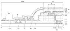
도 4는 본 발명의 일 실시예에 따른 제1 기판을 개략적으로 보여주는 평면도이고, 도 5는 제1 기판에 배치되는 터치 센싱층을 보여주는 평면도이다. 도 6은 본 발명의 제1 실시예에 따른 표시 장치의 단면도로서, 도 5의 I-I'의 제1 실시예를 보여주는 단면도이다.4 is a plan view schematically showing a first substrate according to an embodiment of the present invention, and FIG. 5 is a plan view showing a touch sensing layer disposed on the first substrate. 6 is a cross-sectional view of a display device according to a first embodiment of the present invention, and is a cross-sectional view taken along line I-I′ of FIG. 5 .
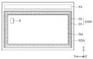
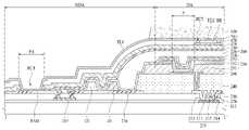
도 4 내지 도 6을 참조하면, 제1 기판(111)은 표시영역(DA)과 비 표시영역(NDA)으로 구분되며, 표시영역(DA)에는 화소(P)들이 배치된다. 비 표시영역(NDA)은 표시영역(DA)을 둘러싸며, 댐(DAM)이 형성되고, 패드 전극(PAD)들이 형성되는 패드영역(PA)이 마련된다.4 to 6 , the
상기 제1 기판(111) 상에는 박막 트랜지스터층(10) 및 유기발광소자층(20)이 형성된다.A thin
상기 박막 트랜지스터층(10)은 박막 트랜지스터(210), 게이트 절연막(220), 층간 절연막(230), 및 평탄화막(240)을 포함한다.The thin
제1 기판(111)의 일면 상에는 버퍼막이 배치될 수 있다. 상기 버퍼막은 투습에 취약한 제1 기판(111)을 통해 침투하는 수분으로부터 박막 트랜지스터(210)들과 유기발광소자(250)들을 보호하기 위해 제1 기판(111)의 일면 상에 배치될 수 있다. 제1 기판(111)의 일면은 제2 기판(112)과 마주보는 면일 수 있다. 버퍼막은 교번하여 적층된 복수의 무기막들로 이루어질 수 있다. 예를 들어, 버퍼막은 실리콘 산화막(SiOx), 실리콘 질화막(SiNx), SiON 중 하나 이상의 무기막이 교번하여 적층된 다중막으로 형성될 수 있다. 이러한 버퍼막은 생략될 수 있다.A buffer layer may be disposed on one surface of the
버퍼막 상에는 상기 박막 트랜지스터(210)가 배치된다. 박막 트랜지스터(210)는 액티브층(211), 게이트 전극(212), 소스 전극(213) 및 드레인 전극(214)을 포함한다. 도 6에서는 박막 트랜지스터(210)가 게이트 전극(212)이 액티브층(211)의 상부에 위치하는 상부 게이트(탑 게이트, top gate) 방식으로 형성된 것을 예시하였으나, 이에 한정되지 않음에 주의하여야 한다. 즉, 박막 트랜지스터(210)들은 게이트 전극(212)이 액티브층(211)의 하부에 위치하는 하부 게이트(보텀 게이트, bottom gate) 방식 또는 게이트 전극(212)이 액티브층(211)의 상부와 하부에 모두 위치하는 더블 게이트(double gate) 방식으로 형성될 수 있다.The
제1 기판(111) 상에는 상기 액티브층(211)이 배치된다. 액티브층(211)은 실리콘계 반도체 물질 또는 산화물계 반도체 물질로 형성될 수 있다. 제1 기판(111)과 액티브층(211) 사이에는 액티브층(211)으로 입사되는 외부광을 차단하기 위한 차광층이 배치될 수 있다.The
액티브층(211) 상에는 상기 게이트 절연막(220)이 배치될 수 있다. 게이트 절연막(220)은 무기막, 예를 들어 실리콘 산화막(SiOx), 실리콘 질화막(SiNx), 또는 이들의 다중막으로 형성될 수 있다.The
게이트 절연막(220) 상에는 상기 게이트 전극(212)과 게이트 라인(215)이 배치될 수 있다. 게이트 전극(212)과 게이트 라인은 몰리브덴(Mo), 알루미늄(Al), 크롬(Cr), 금(Au), 티타늄(Ti), 니켈(Ni), 네오디뮴(Nd) 및 구리(Cu) 중 어느 하나 또는 이들의 합금으로 이루어진 단일층 또는 다중층으로 형성될 수 있다.The
게이트 전극(212)과 게이트 라인(215) 상에는 상기 층간 절연막(230)이 배치될 수 있다. 층간 절연막(230)은 무기막, 예를 들어 실리콘 산화막(SiOx), 실리콘 질화막(SiNx), 또는 이들의 다중막으로 형성될 수 있다.The interlayer insulating
층간 절연막(230) 상에는 상기 소스 전극(213), 드레인 전극(214), 소스 드레인 라인(216), 및 패드 전극(PAD)이 배치될 수 있다. 소스 전극(213)과 드레인 전극(214) 각각은 게이트 절연막(220)과 층간 절연막(230)을 관통하는 컨택홀을 통해 액티브층(211)에 접속될 수 있다. 또한, 소스 드레인 라인(216), 및 패드 전극(PAD)은 층간 절연막(230)을 관통하는 컨택홀을 통해 게이트 라인(215)에 접속될 수 있다. 소스 전극(213), 드레인 전극(214), 소스 드레인 라인(216), 및 패드 전극(PAD)은 몰리브덴(Mo), 알루미늄(Al), 크롬(Cr), 금(Au), 티타늄(Ti), 니켈(Ni), 네오디뮴(Nd) 및 구리(Cu) 중 어느 하나 또는 이들의 합금으로 이루어진 단일층 또는 다중층으로 형성될 수 있다.The
소스 전극(213) 및 드레인 전극(214) 상에는 박막 트랜지스터(210)를 절연하기 위한 보호막이 배치될 수 있다. 보호막은 무기막, 예를 들어 실리콘 산화막(SiOx), 실리콘 질화막(SiNx), 또는 이들의 다중막으로 형성될 수 있다. 이러한 보호막은 생략될 수 있다.A protective layer for insulating the
소스 전극(213) 및 드레인 전극(214) 상에는 박막 트랜지스터(210)로 인한 단차를 평탄하게 하기 위한 상기 평탄화막(240)이 배치될 수 있다. 평탄화막(240)은 아크릴 수지(acryl resin), 에폭시 수지(epoxy resin), 페놀 수지(phenolic resin), 폴리아미드 수지(polyamide resin), 폴리이미드 수지(polyimide resin) 등의 유기막으로 형성될 수 있다.The
박막 트랜지스터층(10) 상에는 상기 유기발광소자층(20)이 배치된다. 유기발광소자층(20)은 유기발광소자(250)와 뱅크(260)를 포함한다.The organic light emitting
상기 유기발광소자(250)와 뱅크(260)는 평탄화막(240) 상에 배치된다. 유기발광소자(250)는 제1 전극(251), 유기발광층(252), 및 제2 전극(253)을 포함한다. 상기 제1 전극(251)은 애노드 전극이고, 제2 전극(253)은 캐소드 전극일 수 있다.The organic
제1 전극(251)은 평탄화막(240) 상에 배치될 수 있다. 제1 전극(251)은 보호막과 평탄화막(240)을 관통하는 컨택홀을 통해 박막 트랜지스터(210)의 소스 전극(213)에 접속된다. 제1 전극(251)은 알루미늄과 티타늄의 적층 구조(Ti/Al/Ti), 알루미늄과 ITO의 적층 구조(ITO/Al/ITO), APC 합금, 및 APC 합금과 ITO의 적층 구조(ITO/APC/ITO)과 같은 반사율이 높은 금속물질로 형성될 수 있다. APC 합금은 은(Ag), 팔라듐(Pd), 및 구리(Cu)의 합금이다.The
뱅크(260)는 화소(P)들을 구획하기 위해 평탄화막(240) 상에서 제1 전극(251)의 가장자리를 덮도록 배치될 수 있다. 즉, 뱅크(260)는 화소(P)들을 정의하는 화소 정의막으로서 역할을 한다. 뱅크(260)는 아크릴 수지(acryl resin), 에폭시 수지(epoxy resin), 페놀 수지(phenolic resin), 폴리아미드 수지(polyamide resin), 폴리이미드 수지(polyimide resin) 등의 유기막으로 형성될 수 있다.The
제1 전극(251)과 뱅크(260) 상에는 상기 유기발광층(252)이 배치된다. 유기발광층(252)은 정공 수송층(hole transporting layer), 적어도 하나의 발광층(light emitting layer), 및 전자 수송층(electron transporting layer)을 포함할 수 있다. 이 경우, 제1 전극(251)과 제2 전극(253)에 전압이 인가되면 정공과 전자가 각각 정공 수송층과 전자 수송층을 통해 발광층으로 이동하게 되며, 발광층에서 서로 결합하여 발광하게 된다.The organic
유기발광층(252)은 백색 광을 발광하는 백색 발광층으로 이루어질 수 있다. 이 경우, 제1 전극(251)과 뱅크(260)를 덮도록 배치될 수 있다. 또한, 제2 기판(112) 상에는 컬러 필터(미도시)가 배치될 수 있다.The organic
또는, 유기발광층(252)은 적색 광을 발광하는 적색 발광층, 녹색 광을 발광하는 녹색 발광층, 또는 청색 광을 발광하는 청색 발광층으로 이루어질 수 있다. 이 경우, 유기발광층(252)는 제1 전극(251)에 대응되는 영역에 배치될 수 있으며, 제2 기판(112) 상에는 컬러 필터가 배치되지 않을 수 있다.Alternatively, the
제2 전극(253)은 유기발광층(252) 상에 배치된다. 유기 발광 표시 장치가 상부 발광(top emission) 구조로 형성되는 경우, 제2 전극(253)은 광을 투과시킬 수 있는 ITO, IZO와 같은 투명한 금속물질(TCO, Transparent Conductive Material), 또는 마그네슘(Mg), 은(Ag), 또는 마그네슘(Mg)과 은(Ag)의 합금과 같은 반투과 금속물질(Semi-transmissive Conductive Material)로 형성될 수 있다. 제2 전극(253) 상에는 캡핑층(capping layer)이 배치될 수 있다.The
유기발광소자층(20) 상에는 봉지층(30)이 제1 기판(111)의 표시영역(DA)은 물론 비 표시영역(NDA)까지 배치된다. 봉지층(30)은 댐(DAM) 및 봉지막(300)을 포함한다.On the organic light emitting
상기댐(DAM)은 비 표시영역(NDA)에 배치되어 봉지막(300)을 구성하는 유기막(320)의 흐름을 차단한다. 보다 구체적으로, 댐(DAM)은 표시영역(DA)의 외곽을 둘러싸도록 배치되어 봉지막(300)을 구성하는 유기막(320)의 흐름을 차단할 수 있다. 또한, 댐(DAM)은 비 표시영역(NDA)에 배치되어 봉지막(300)을 구성하는 유기막(320)이 패드 컨택홀(PCT)에 의해 노출된 패드 전극(PAD)으로 침범하지 못하도록 유기막(320)의 흐름을 차단할 수 있다. 이를 통해, 댐(DAM)은 유기막(320)이 표시장치의 외부로 노출되거나 패드 전극(PAD)으로 침범하는 것을 방지할 수 있다.The dam DAM is disposed in the non-display area NDA to block the flow of the
이러한 댐(DAM)은 제1 댐(D1) 및 제2 댐(D2)을 포함할 수 있다.The dam DAM may include a first dam D1 and a second dam D2.
상기 제1 댐(D1)은 표시영역(DA)의 외곽을 둘러싸도록 배치되어 봉지막(300)을 구성하는 유기막(320)의 흐름을 1차적으로 차단할 수 있다. 또한, 제1 댐(D1)은 표시영역(DA)과 패드영역(PA) 사이에 배치되어 노출된 패드 전극(PAD)에 유기막(320)이 침범하지 못하도록 유기막(320)의 흐름을 1차적으로 차단할 수 있다.The first dam D1 may be disposed to surround the periphery of the display area DA to primarily block the flow of the
상기 제2 댐(D2)은 제1 댐(D1)의 외곽을 둘러싸도록 배치되며, 제1 댐(D1)과 서로 이격되어 나란히 배치된다. 제2 댐(D2)은 제1 댐(D1)의 외곽으로 흘러 넘치는 유기막(320)을 2차적으로 차단할 수 있다. 이를 통해, 제1 댐(D1) 및 제2 댐(D2)은 유기막(320)이 표시장치의 외부로 노출되거나 노출된 패드 전극(PAD)를 침범하는 것을 보다 효과적으로 차단할 수 있다.The second dam D2 is disposed to surround the outer periphery of the first dam D1, and is spaced apart from the first dam D1 and disposed side by side. The second dam D2 may secondarily block the
이러한 댐(DAM)은 평탄화막(240) 또는 뱅크(260)와 동시에 형성될 수 있으며, 평탄화막(240) 또는 뱅크(260)와 같은 물질로 이루어질 수 있다. 이와 같은 경우, 댐(DAM)은 아크릴 수지(acryl resin), 에폭시 수지(epoxy resin), 페놀 수지(phenolic resin), 폴리아미드 수지(polyamide resin), 폴리이미드 수지(polyimide resin) 등의 유기 물질로 형성될 수 있다.The dam DAM may be formed simultaneously with the
상기 봉지막(300)은 표시영역(DA)을 덮도록 배치되어 유기발광층(252)과 제2 전극(253)에 산소 또는 수분이 침투되는 것을 방지하는 역할을 한다. 이를 위해, 봉지막(300)은 적어도 하나의 무기막과 적어도 하나의 유기막을 포함할 수 있다. 예를 들어, 봉지막(300)은 제1 무기막(310), 유기막(320), 및 제2 무기막(330)를 포함할 수 있다.The
상기 제1 무기막(310)은 제2 전극(253) 상에 배치된다. 제1 무기막(310)은 제2 전극(253)을 덮도록 배치된다. 본 발명의 제1 실시예에 따른 제1 무기막(310)은 제2 전극(253)을 덮고, 비 표시영역(NDA)까지 연장되어 댐(DAM)을 덮는다. 또한, 본 발명의 제1 실시예에 따른 제1 무기막(310)은 댐(DAM) 바깥쪽에 배치되는 패드영역(PA)까지 연장되나, 패드 전극(PAD)을 덮지 않고 노출시킨다. 이때, 본 발명의 제1 실시예에 따른 제1 무기막(310)은 패드 전극(PAD)을 둘러싸며, 보다 구체적으로, 패드 전극(PAD)을 노출시키는 패드 컨택홀(PCT) 외곽을 둘러싸도록 배치된다.The first
이러한, 본 발명의 제1 실시예에 따른 표시 장치(100)는 제1 무기막(310)이 패드영역(PA)까지 연장되어 형성되기 때문에, 패드영역(PA)에 제1 무기막(310)을 형성하지 않기 위해서, 패드 전극(PAD)을 가리는 마스크(mask)를 패드 전극(PAD) 상부에 배치할 필요가 없다. 따라서, 본 발명의 제1 실시예에 따른 표시 장치(100)는 패드 전극(PAD) 상부에 마스크(mask)를 배치하지 않음으로써, 마스크(mask)의 경계면과 패드 전극 사이에 아킹(arcing) 현상이 발생하는 것을 방지할 수 있으며, 마스크(mask)에서 유입되는 대전류가 패드 전극(PAD)을 타고 표시 장치 내부로 흘러 불량이 발생하는 것을 방지할 수 있다.In the
이와 같이, 본 발명의 제1 실시예에 따른 표시 장치(100)는 제1 무기막(310)이 패드 전극(PAD)을 덮도록 전체적으로 형성하며, 유기막(320) 및 제2 무기막(330)을 형성한 후에, 포토 레지스트(photo resist)를 이용한 에칭(etching) 공정으로 패드 컨택홀(PCT)을 형성한다.As described above, in the
상기 유기막(320)은 제1 무기막(310) 상에 배치된다. 유기막(320)은 이물들(particles)이 제1 무기막(310)을 뚫고 유기발광층(252)과 제2 전극(253)에 투입되는 것을 방지하기 위해 충분한 두께로 형성될 수 있다. 유기막(320)은 액상 형태로 잉크젯(inkjet) 공정을 통해 도포된 뒤에, 경화 공정을 거쳐 형성될 수 있다.The
상기 제2 무기막(330)은 유기막(320) 상에 배치된다. 제2 무기막(330)은 유기막(320)을 덮도록 배치된다. 본 발명의 제1 실시예에 따른 제2 무기막(330)은 유기막(320)을 덮고, 비 표시영역(NDA)까지 연장되어 댐(DAM)을 덮도록 배치될 수 있다. 이때, 본 발명의 제1 실시예에 따른 제2 무기막(330)은 패드영역(PA)에는 형성되지 않는다. 즉, 본 발명의 제1 실시예에 따른 제1 무기막(310) 및 제2 무기막(330)은 끝단의 위치가 서로 다르게 형성된다.The second
본 발명의 제1 실시예에 따른 제2 무기막(330)은 패드 전극(PAD)을 노출시키기 위해서, 패드 전극(PAD)을 가리는 마스크(mask)를 패드 전극(PAD) 상부에 배치한다. 이때, 본 발명의 제1 실시예에 따른 표시 장치(100)는 패드 전극(PAD) 상면에 제1 무기막(310)이 형성되어 있기 때문에, 패드 전극(PAD) 상부에 마스크(mask)를 배치하여도 마스크(mask)의 경계면과 패드 전극(PAD) 사이에 아킹(arcing) 현상이 발생하지 않는다. 즉, 제1 무기막(310)이 마스크(mask)와 패드 전극(PAD) 사이에서 절연막 역할을 한다. 이와 같이, 본 발명의 제1 실시예에 따른 표시 장치(100)는 패드영역(PA)까지 형성된 제1 무기막(310)이 절연막 역할을 함으로써, 제2 무기막(330)의 제조공정에서 패드 전극(PAD) 상부에 마스크(mask)를 배치하여도 마스크(mask)의 경계면과 패드 전극(PAD) 사이에 아킹(arcing) 현상이 발생하지 않는다.In the second
이러한, 제1 및 제2 무기막들(310, 330) 각각은 실리콘 질화물, 알루미늄 질화물, 지르코늄 질화물, 티타늄 질화물, 하프늄 질화물, 탄탈륨 질화물, 실리콘 산화물, 알루미늄 산화물, 또는 티타늄 산화물로 형성될 수 있다. 유기막(320)은 아크릴 수지(acryl resin), 에폭시 수지(epoxy resin), 페놀 수지(phenolic resin), 폴리아미드 수지(polyamide resin) 또는 폴리이미드 수지(polyimide resin)로 형성될 수 있다.Each of the first and second
상기 봉지층(30) 상에는 터치 센싱층(40)이 형성된다. 상기 터치 센싱층(40)은 버퍼층(410), 브리지 전극(BE)들, 절연막(420), 제1 터치 전극(TE1)들, 제2 터치 전극(TE2)들, 및 패시베이션막(430)을 포함한다.A
봉지층(30) 상에는 상기 버퍼층(410)이 배치된다. 버퍼층(410)은 봉지막(300)을 덮도록 배치된다. 본 발명의 제1 실시예에 따른 버퍼층(410)은 봉지막(300)을 덮고, 비 표시영역(NDA)까지 연장되어 댐(DAM)을 덮는다. 또한, 본 발명의 제1 실시예에 따른 버퍼층(410)은 댐(DAM) 바깥쪽에 배치되는 패드영역(PA)까지 연장되나, 패드 전극(PAD)을 덮지 않고 노출시킨다. 이때, 본 발명의 제1 실시예에 따른 버퍼층(410)은 패드 전극(PAD)을 둘러싸며, 보다 구체적으로, 패드 전극(PAD)을 노출시키는 패드 컨택홀(PCT) 외곽을 둘러싸도록 배치된다.The
이러한, 본 발명의 제1 실시예에 따른 표시 장치(100)는 버퍼층(410)이 패드영역(PA)까지 연장되어 형성되기 때문에, 버퍼층(410) 상면에 형성되는 브리지 전극(BE) 형성 시에 패드 전극(PAD)이 손상되는 것을 방지할 수 있다. 보다 구체적으로, 버퍼층(410) 상면에 브리지 전극(BE)을 형성하는데, 패드 전극(PAD)이 노출되어 있는 경우 패드 전극(PAD)이 손상될 수 있다. 본 발명의 제1 실시예에 따른 표시 장치(100)는 버퍼층(410)을 패드영역(PA)까지 형성하고 브리지 전극(BE)을 형성함으로써, 패드 전극(PAD)이 손상되는 것을 방지할 수 있다.In the
버퍼층(410) 상에는 상기 브리지 전극(BE)이 배치된다. 브리지 전극(BE)은 제1 터치 전극(TE1)들과 제2 터치 전극(TE2)들이 그들의 교차 영역들에서 서로 단락되는 것을 방지하기 위해, 제1 방향으로 서로 인접한 제1 터치 전극(TE1)들을 전기적으로 연결한다. 브리지 전극(BE)은 제1 및 제2 터치 전극들(TE1, TE2)과 서로 다른 층에 배치되며, 브리지 컨택홀(BCT)들을 통해 서로 인접한 제1 터치 전극(TE1)들에 접속될 수 있다. 브리지 전극(BE)은 제2 터치 전극(TE2)과 교차될 수 있다.The bridge electrode BE is disposed on the
브리지 전극(BE) 상에는 절연막(420)이 배치된다. 절연막(420)은 브리지 전극(BE)을 덮도록 배치되어, 브리지 전극(BE)과 제1 및 제2 터치 전극들(TE1, TE2)을 절연시킨다. 본 발명의 제1 실시예에 따른 절연막(420)은 브리지 전극(BE)을 덮고, 비 표시영역(NDA)까지 연장되어 패드영역(PA)까지 형성될 수 있다. 본 발명의 제1 실시예에 따른 절연막(420)은 댐(DAM) 바깥쪽에 배치되는 패드영역(PA)까지 연장되나, 패드 전극(PAD)을 덮지 않고 노출시킨다. 이때, 본 발명의 제1 실시예에 따른 절연막(420)은 패드 전극(PAD)을 둘러싸며, 보다 구체적으로, 패드 전극(PAD)을 노출시키는 패드 컨택홀(PCT) 외곽을 둘러싸도록 배치된다.An insulating
이러한, 본 발명의 제1 실시예에 따른 표시 장치(100)는 절연막(420)이 패드영역(PA)까지 연장되어 형성되기 때문에, 패드영역(PA)에 절연막(420)을 형성하지 않기 위해서, 패드 전극(PAD)을 가리는 마스크(mask)를 패드 전극(PAD) 상부에 배치하는 공정이 필요 없다.In the
패드 전극(PAD) 상면에 형성된 버퍼층(410)과 절연막(420)은 브리지 컨택홀(BCT) 형성 공정에서, 패드 전극(PAD)이 노출되도록 동시에 제거될 수 있다. 즉, 브리지 컨택홀(BCT)과 패드 컨택홀(PCT)은 동시에 형성될 수 있다.The
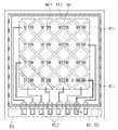
절연막(420) 상에는 상기 제1 터치 전극(TE1)들 및 제2 터치 전극(TE2)들이 배치된다. 제1 터치 전극(TE1)들, 제2 터치 전극(TE2)들, 제1 터치 라인(TL1)들 및 제2 터치 라인(TL)들은 동일한 층에 배치될 수 있다. 제1 터치 전극(TE1)들은 제1 방향(y축 방향)으로 배치되어 서로 연결되며, 제2 터치 전극(TE2)들은 제2 방향(x축 방향)으로 배치되어 서로 연결된다. 제1 방향(y축 방향)은 스캔 라인들(S1~Sn)과 나란한 방향이고, 제2 방향(x축 방향)은 데이터 라인들(D1~Dm)과 나란한 방향일 수 있다. 또는, 제1 방향(y축 방향)은 데이터 라인들(D1~Dm)과 나란한 방향이고, 제2 방향(x축 방향)은 스캔 라인들(S1~Sn)과 나란한 방향일 수 있다.The first touch electrodes TE1 and the second touch electrodes TE2 are disposed on the insulating
제1 방향(y축 방향)으로 연결된 제1 터치 전극(TE1)들 각각은 제2 방향(x축 방향)으로 이웃하는 제1 터치 전극(TE1)들과 전기적으로 절연된다. 제2 방향(x축 방향)으로 연결된 제2 터치 전극(TE2)들 각각은 제1 방향(y축 방향)으로 이웃하는 제2 터치 전극(TE2)들과 전기적으로 절연된다.Each of the first touch electrodes TE1 connected in the first direction (y-axis direction) is electrically insulated from the adjacent first touch electrodes TE1 in the second direction (x-axis direction). Each of the second touch electrodes TE2 connected in the second direction (x-axis direction) is electrically insulated from neighboring second touch electrodes TE2 in the first direction (y-axis direction).
이로 인해, 제1 터치 전극(TE1)과 제2 터치 전극(TE2)의 교차 영역에는 터치 센서에 해당하는 상호 용량(mutual capacitance)이 형성될 수 있다.For this reason, a mutual capacitance corresponding to the touch sensor may be formed in the cross region of the first touch electrode TE1 and the second touch electrode TE2 .
제1 방향(y축 방향)으로 서로 연결된 제1 터치 전극(TE1)들 중 일 측 끝에 배치된 제1 터치 전극(TE1)은 비 표시영역(NDA)에서 제1 터치 라인(TL1)과 연결될 수 있다. 제1 터치 라인(TL1)은 제1 터치 전극(TE1)에서 연장되어 패드영역(PA)까지 패턴 형성될 수 있다. 제1 터치 라인(TL1)은 패드영역(PA)에서 패드 전극(PAD)와 접속하여 패드 전극(PAD)를 통해 제1 터치 구동부(181)에 연결될 수 있다. 따라서, 제1 방향(y축 방향)으로 서로 연결된 제1 터치 전극(TE1)들은 제1 터치 라인(TL1)을 통해 제1 터치 구동부(181)로부터 구동펄스를 입력 받을 수 있다.The first touch electrode TE1 disposed at one end of the first touch electrodes TE1 connected to each other in the first direction (y-axis direction) may be connected to the first touch line TL1 in the non-display area NDA. have. The first touch line TL1 may extend from the first touch electrode TE1 to form a pattern up to the pad area PA. The first touch line TL1 may be connected to the pad electrode PAD in the pad area PA and may be connected to the
제2 방향(x축 방향)으로 서로 연결된 제2 터치 전극(TE2)들 중 일 측 끝에 배치된 제2 터치 전극(TE2)은 비 표시영역(NDA)에서 제2 터치 라인(TL2)과 연결될 수 있다. 제2 터치 라인(TL2)은 제2 터치 전극(TE2)에서 연장되어 패드영역(PA)까지 패턴 형성될 수 있다. 제2 터치 라인(TL2)은 패드영역(PA)에서 패드 전극(PAD)와 접속하여 패드 전극(PAD)를 통해 제2 터치 구동부(182)에 연결될 수 있다. 따라서, 제2 터치 구동부(182)는 제2 방향(x축 방향)으로 서로 연결된 제2 터치 전극(TE2)들의 터치 센서들의 차지 변화량들을 입력 받을 수 있다.The second touch electrode TE2 disposed at one end of the second touch electrodes TE2 connected to each other in the second direction (x-axis direction) may be connected to the second touch line TL2 in the non-display area NDA. have. The second touch line TL2 may extend from the second touch electrode TE2 to form a pattern up to the pad area PA. The second touch line TL2 may be connected to the pad electrode PAD in the pad area PA and may be connected to the
제1 터치 전극(TE1)들 및 제2 터치 전극(TE2)들 상에는 상기 패시베이션막(430)이 배치된다. 패시베이션막(430)은 외부로부터 유해한 환경을 차단하여 표시 장치의 특성의 안정화를 유지한다. 또한, 패시베이션막(430)은 제1 터치 전극(TE1)들 및 제2 터치 전극(TE2)들 상에 배치될 뿐만 아니라 제1 터치 전극(TE1)들 및 제2 터치 전극(TE2)들 사이에 배치될 수도 있다. 제1 터치 전극(TE1)들 각각은 패시베이션막(430)에 의해 제2 터치 전극(TE2)들 각각과 절연될 수 있다.The
본 발명의 실시예는 봉지층(30) 상에 터치 센싱층(40)을 직접 형성함으로써 제1 기판(111)과 제2 기판(112)을 합착시 정렬할 필요가 없다.In the embodiment of the present invention, since the
상술한 바와 같이, 본 발명의 제1 실시예에 따른 표시 장치(100)는 제1 무기막(310)이 패드영역(PA)까지 연장되어 형성되기 때문에, 패드영역(PA)에 제1 무기막(310)을 형성하지 않기 위해서, 패드 전극(PAD)을 가리는 마스크(mask)를 패드 전극(PAD) 상부에 배치할 필요가 없다.As described above, in the
따라서, 본 발명의 제1 실시예에 따른 표시 장치(100)는 패드 전극(PAD) 상부에 마스크(mask)를 배치하지 않음으로써, 마스크(mask)의 경계면과 패드 전극 사이에 아킹(arcing) 현상이 발생하는 것을 방지할 수 있으며, 마스크(mask)에서 유입되는 대전류가 패드 전극(PAD)을 타고 표시 장치(100) 내부로 흘러 불량이 발생하는 것을 방지할 수 있다.Accordingly, in the
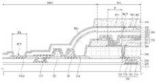
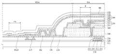
도 7은 본 발명의 제2 실시예에 따른 표시 장치의 단면도로서, 도 5의 I-I'의 제2 실시예를 보여주는 단면도이다. 도 7에 도시된 표시 장치(100)는 버퍼층이 생략됨에 따른 패드 컨택홀(PCT) 제조방법을 제외하고, 전술한 도 6에서 설명한 제1 실시예에 따른 표시 장치(100)와 동일하다. 이에 따라, 이하의 설명에서는 패드 컨택홀(PCT) 제조방법에 대해서만 설명하고, 동일한 구성에 대한 중복 설명은 생략하기로 한다.7 is a cross-sectional view of a display device according to a second exemplary embodiment of the present invention, and is a cross-sectional view taken along line I-I′ of FIG. 5 according to the second exemplary embodiment. The
도 7을 참조하면, 본 발명의 제2 실시예에 따른 표시 장치(100)의 제1 무기막(310)은 제2 전극(253) 상에 배치된다. 제1 무기막(310)은 제2 전극(253)을 덮도록 배치된다. 본 발명의 제2 실시예에 따른 제1 무기막(310)은 제2 전극(253)을 덮고, 비 표시영역(NDA)까지 연장되어 댐(DAM)을 덮는다. 또한, 본 발명의 제2 실시예에 따른 제1 무기막(310)은 댐(DAM) 바깥쪽에 배치되는 패드영역(PA)까지 연장되나, 패드 전극(PAD)을 덮지 않고 노출시킨다. 이때, 본 발명의 제2 실시예에 따른 제1 무기막(310)은 패드 전극(PAD)을 둘러싸며, 보다 구체적으로, 패드 전극(PAD)을 노출시키는 패드 컨택홀(PCT) 외곽을 둘러싸도록 배치된다.Referring to FIG. 7 , the first
이러한, 본 발명의 제2 실시예에 따른 표시 장치(100)는 제1 무기막(310)이 패드영역(PA)까지 연장되어 형성되기 때문에, 패드영역(PA)에 제1 무기막(310)을 형성하지 않기 위해서, 패드 전극(PAD)을 가리는 마스크(mask)를 패드 전극(PAD) 상부에 배치할 필요가 없다. 따라서, 본 발명의 제2 실시예에 따른 표시 장치(100)는 패드 전극(PAD) 상부에 마스크(mask)를 배치하지 않음으로써, 마스크(mask)의 경계면과 패드 전극 사이에 아킹(arcing) 현상이 발생하는 것을 방지할 수 있으며, 마스크(mask)에서 유입되는 대전류가 패드 전극(PAD)을 타고 표시 장치 내부로 흘러 불량이 발생하는 것을 방지할 수 있다.In the
상기 유기막(320)은 제1 무기막(310) 상에 배치되고, 상기 제2 무기막(330)은 유기막(320) 상에 배치된다. 제2 무기막(330)은 유기막(320)을 덮도록 배치된다. 본 발명의 제2 실시예에 따른 제2 무기막(330)은 유기막(320)을 덮고, 비 표시영역(NDA)까지 연장되어 댐(DAM)을 덮도록 배치될 수 있다. 이때, 본 발명의 제2 실시예에 따른 제2 무기막(330)은 패드영역(PA)에는 형성되지 않는다. 즉, 본 발명의 제2 실시예에 따른 제1 무기막(310) 및 제2 무기막(330)은 끝단의 위치가 서로 다르게 형성된다.The
본 발명의 제2 실시예에 따른 제2 무기막(330)은 패드 전극(PAD)을 노출시키기 위해서, 패드 전극(PAD)을 가리는 마스크(mask)를 패드 전극(PAD) 상부에 배치한다. 이때, 본 발명의 제2 실시예에 따른 표시 장치(100)는 패드 전극(PAD) 상면에 제1 무기막(310)이 형성되어 있기 때문에, 패드 전극(PAD) 상부에 마스크(mask)를 배치하여도 마스크(mask)의 경계면과 패드 전극(PAD) 사이에 아킹(arcing) 현상이 발생하지 않는다. 즉, 제1 무기막(310)이 마스크(mask)와 패드 전극(PAD) 사이에서 절연막 역할을 한다. 이와 같이, 본 발명의 제2 실시예에 따른 표시 장치(100)는 패드영역(PA)까지 형성된 제1 무기막(310)이 절연막 역할을 함으로써, 제2 무기막(330)의 제조공정에서 패드 전극(PAD) 상부에 마스크(mask)를 배치하여도 마스크(mask)의 경계면과 패드 전극(PAD) 사이에 아킹(arcing) 현상이 발생하지 않는다.In the second
본 발명의 제2 실시예에 따른 표시 장치(100)는 봉지막(300) 상에 버퍼층이 형성되지 않으며, 봉지막(300) 상면에 브리지 전극(BE)이 형성된다. 본 발명의 제1 실시예에 따른 표시 장치(100)는 브리지 전극(BE) 형성 시에 노출된 패드 전극(PAD)을 보호하기 위해서 봉지막(300) 상에 버퍼층을 형성하였으나, 본 발명의 제2 실시예에 따른 표시 장치(100)는 브리지 전극(BE) 형성 시에 패드 전극(PAD)이 제1 무기막(310)에 의해 노출되지 않기 때문에 버퍼층을 형성할 필요가 없다. 따라서, 본 발명의 제2 실시예에 따른 표시 장치(100)는 버퍼층이 생략되어 제조 비용을 절약하고 공정을 줄일 수 있다.In the
본 발명의 제2 실시예에 따른 표시 장치(100)는 봉지막(300) 상에 브리지 전극(BE)이 배치되고, 브리지 전극(BE) 상에는 절연막(420)이 배치된다. 절연막(420)은 브리지 전극(BE)을 덮도록 배치되어, 브리지 전극(BE)과 제1 및 제2 터치 전극들(TE1, TE2)을 절연시킨다. 본 발명의 제2 실시예에 따른 절연막(420)은 브리지 전극(BE)을 덮고, 비 표시영역(NDA)까지 연장되어 패드영역(PA)까지 형성될 수 있다. 본 발명의 제2 실시예에 따른 절연막(420)은 댐(DAM) 바깥쪽에 배치되는 패드영역(PA)까지 연장되나, 패드 전극(PAD)을 덮지 않고 노출시킨다. 이때, 본 발명의 제2 실시예에 따른 절연막(420)은 패드 전극(PAD)을 둘러싸며, 보다 구체적으로, 패드 전극(PAD)을 노출시키는 패드 컨택홀(PCT) 외곽을 둘러싸도록 배치된다.In the
이러한, 본 발명의 제2 실시예에 따른 표시 장치(100)는 절연막(420)이 패드영역(PA)까지 연장되어 형성되기 때문에, 패드영역(PA)에 절연막(420)을 형성하지 않기 위해서, 패드 전극(PAD)을 가리는 마스크(mask)를 패드 전극(PAD) 상부에 배치하는 공정이 필요 없다.In the
패드 전극(PAD) 상면에 형성된 제1 무기막(310)과 절연막(420)은 브리지 컨택홀(BCT) 형성 공정에서, 패드 전극(PAD)이 노출되도록 동시에 제거될 수 있다. 즉, 브리지 컨택홀(BCT)과 패드 컨택홀(PCT)은 동시에 형성될 수 있다.The first
상술한 바와 같이, 본 발명의 제2 실시예에 따른 표시 장치(100)는 제1 무기막(310)이 패드영역(PA)까지 연장되어 형성되기 때문에, 패드영역(PA)에 제1 무기막(310)을 형성하지 않기 위해서, 패드 전극(PAD)을 가리는 마스크(mask)를 패드 전극(PAD) 상부에 배치할 필요가 없다.As described above, in the
따라서, 본 발명의 제2 실시예에 따른 표시 장치(100)는 패드 전극(PAD) 상부에 마스크(mask)를 배치하지 않음으로써, 마스크(mask)의 경계면과 패드 전극 사이에 아킹(arcing) 현상이 발생하는 것을 방지할 수 있으며, 마스크(mask)에서 유입되는 대전류가 패드 전극(PAD)을 타고 표시 장치(100) 내부로 흘러 불량이 발생하는 것을 방지할 수 있다.Accordingly, in the
또한, 본 발명의 제2 실시예에 따른 표시 장치(100)는 브리지 전극(BE) 형성 시에 패드 전극(PAD)이 제1 무기막(310)에 의해 노출되지 않기 때문에 버퍼층을 형성할 필요가 없다. 따라서, 본 발명의 제2 실시예에 따른 표시 장치(100)는 버퍼층이 생략되어 제조 비용을 절약하고 공정을 줄일 수 있다.In addition, in the
도 8은 본 발명의 제1 실시예에 따른 표시 장치의 제조방법을 설명하기 위한 흐름도이고, 도 9a 내지 도 9I는 본 발명의 제1 실시예에 따른 표시 장치의 제조방법을 설명하기 위한 단면도들이다.8 is a flowchart illustrating a method of manufacturing a display device according to a first exemplary embodiment of the present invention, and FIGS. 9A to 9I are cross-sectional views illustrating a method of manufacturing a display device according to the first exemplary embodiment of the present invention. .
도 9a 내지 도 9I에 도시된 평면도들은 전술한 도 6에 도시된 본 발명의 제1 실시예에 따른 표시 장치의 제조방법에 관한 것으로, 동일한 구성에 대해 동일한 도면부호를 부여하였다. 이하에서는 도 8 및 도 9a 내지 도 9I를 결부하여 본 발명의 제1 실시예에 따른 표시 장치의 제조 방법을 설명한다.The plan views shown in FIGS. 9A to 9I relate to the method of manufacturing the display device according to the first embodiment of the present invention shown in FIG. 6 described above, and the same reference numerals are assigned to the same components. Hereinafter, a method of manufacturing the display device according to the first exemplary embodiment of the present invention will be described with reference to FIGS. 8 and 9A to 9I.
첫 번째로, 도 9a와 같이, 제1 기판(111)의 표시영역(DA)에 화소(P)들을 형성하고, 상기 표시영역(DA)을 둘러싸는 비 표시영역(NDA)에 패드 전극(PAD) 및 댐(DAM)을 형성한다. (S801)First, as shown in FIG. 9A , pixels P are formed in the display area DA of the
구체적으로 설명하면, 우선, 제1 기판(111) 상에 박막 트랜지스터(210)의 액티브층(211)을 형성한다. 보다 구체적으로, 스퍼터링법(Sputtering) 또는 MOCVD법(Metal Organic Chemical Vapor Deposition) 등을 이용하여 제1 기판(111) 상의 전면에 액티브 금속층을 형성한다. 그리고 나서, 포토 레지스트 패턴을 이용한 마스크 공정으로 액티브 금속층을 패터닝하여 액티브층(211)을 형성한다. 액티브층(211)은 실리콘계 반도체 물질 또는 산화물계 반도체 물질로 형성될 수 있다.In detail, first, the
그리고 나서, 액티브층(211) 상에 게이트 절연막(220)을 형성한다. 게이트 절연막(220)은 무기막, 예를 들어 실리콘 산화막(SiOx), 실리콘 질화막(SiNx), 또는 이들의 다중막으로 형성될 수 있다.Then, a
그리고 나서, 게이트 절연막(220) 상에 박막 트랜지스터(210)의 게이트 전극(212) 및 게이트 라인(215)을 형성한다. 구체적으로, 스퍼터링법 또는 MOCVD법 등을 이용하여 게이트 절연막(220) 상의 전면(全面)에 제1 금속층을 형성한다. 그 다음, 포토 레지스트 패턴을 이용한 마스크 공정으로 제1 금속층을 패터닝하여 게이트 전극(212) 및 게이트 라인(215)을 형성한다. 게이트 전극(212) 및 게이트 라인(215)은 몰리브덴(Mo), 알루미늄(Al), 크롬(Cr), 금(Au), 티타늄(Ti), 니켈(Ni), 네오디뮴(Nd) 및 구리(Cu) 중 어느 하나 또는 이들의 합금으로 이루어진 단일층 또는 다중층으로 형성될 수 있다.Then, the
그리고 나서, 게이트 전극(212) 상에 층간 절연막(230)을 형성한다. 층간 절연막(230)은 무기막, 예를 들어 실리콘 산화막(SiOx), 실리콘 질화막(SiNx), 또는 이들의 다중막으로 형성될 수 있다.Then, an
그리고 나서, 게이트 절연막(220)과 층간 절연막(230)을 관통하여 액티브층(211)을 노출시키는 컨택홀들과 층간 절연막(230)을 관통하여 게이트 라인(214)을 노출시키는 컨택홀들을 형성한다.Then, contact holes passing through the
그리고 나서, 층간 절연막(230) 상에 박막 트랜지스터(210)의 소스 및 드레인 전극들(213, 214), 소스 드레인 라인(216), 및 패드 전극(PAD)을 형성한다. 구체적으로, 스퍼터링법 또는 MOCVD법 등을 이용하여 층간 절연막(230) 상의 전면에 제2 금속층을 형성한다. 그 다음, 포토 레지스트 패턴을 이용한 마스크 공정으로 제2 금속층을 패터닝하여 소스 및 드레인 전극들(213, 214), 소스 드레인 라인(216), 및 패드 전극(PAD)을 형성한다. 소스 및 드레인 전극들(213, 214) 각각은 게이트 절연막(220)과 층간 절연막(230)을 관통하는 컨택홀을 통해 액티브층(211)에 접속될 수 있다. 또한, 소스 드레인 라인(216), 및 패드 전극(PAD)은 층간 절연막(230)을 관통하는 컨택홀을 통해 게이트 라인(215)에 접속될 수 있다. 소스 및 드레인 전극들(213, 214), 소스 드레인 라인(216), 및 패드 전극(PAD)은 몰리브덴(Mo), 알루미늄(Al), 크롬(Cr), 금(Au), 티타늄(Ti), 니켈(Ni), 네오디뮴(Nd) 및 구리(Cu) 중 어느 하나 또는 이들의 합금으로 이루어진 단일층 또는 다중층으로 형성될 수 있다.Then, the source and drain
그리고 나서, 박막 트랜지스터(210)의 소스 및 드레인 전극들(213, 214) 상에 박막 트랜지스터(210)로 인한 단차를 평탄화하기 위한 평탄화막(240)을 형성한다. 평탄화막(240) 각각은 아크릴 수지(acryl resin), 에폭시 수지(epoxy resin), 페놀 수지(phenolic resin), 폴리아미드 수지(polyamide resin), 폴리이미드 수지(polyimide resin) 등의 유기막으로 형성될 수 있다.Then, a
그리고 나서, 평탄화막(240) 상에 유기발광소자(250)를 형성한다. 구체적으로, 평탄화막(240) 상에 유기발광소자(250)의 제1 전극(251)을 형성한다. 보다 구체적으로, 스퍼터링법 또는 MOCVD법 등을 이용하여 평탄화막(240) 상의 전면에 제3 금속층을 형성한다. 그리고 나서, 포토 레지스트 패턴을 이용한 마스크 공정으로 제3 금속층을 패터닝하여 제1 전극(251)을 형성한다. 제1 전극(251)은 평탄화막(240)을 관통하는 컨택홀을 통해 박막 트랜지스터(210)의 소스 전극(213)에 접속될 수 있다. 제1 전극(251)은 알루미늄과 티타늄의 적층 구조(Ti/Al/Ti), 알루미늄과 ITO의 적층 구조(ITO/Al/ITO), APC 합금, 및 APC 합금과 ITO의 적층 구조(ITO/APC/ITO)과 같은 반사율이 높은 금속물질로 형성될 수 있다.Then, the organic
그리고 나서, 화소들(P)을 구획하기 위해 평탄화막(240) 상에서 제1 전극(251)의 가장자리를 덮도록 뱅크(260)를 형성하고, 이와 함께 댐(DAM)을 형성한다. 이때, 댐(DAM)은 비 표시영역(NDA)에 형성된다. 댐(DAM) 및 뱅크(260) 각각은 아크릴 수지(acryl resin), 에폭시 수지(epoxy resin), 페놀 수지(phenolic resin), 폴리아미드 수지(polyamide resin), 폴리이미드 수지(polyimide resin) 등의 유기막으로 형성될 수 있다.Then, to partition the pixels P, a
한편, 댐(DAM)이 뱅크(260)와 동시에 형성되는 것으로 설명하고 있으나, 이에 한정되지 않으며, 댐(DAM)은 평탄화막(240)과 동시에 형성될 수도 있다.Meanwhile, although it has been described that the dam DAM is formed simultaneously with the
그리고 나서, 제1 전극(251)과 뱅크(260) 상에 유기발광층(252)을 증착 공정 또는 용액 공정으로 형성한다. 그리고 나서, 유기발광층(252) 상에 제2 전극(253)을 형성한다. 제2 전극(253)은 화소(P)들에 공통적으로 형성되는 공통층일 수 있다. 제2 전극(253)은 광을 투과시킬 수 있는 ITO, IZO와 같은 투명한 금속물질(TCO, Transparent Conductive Material)로 형성될 수 있다. 제2 전극(253)은 스퍼터링법과 같은 물리적 기상 증착법(physics vapor deposition)으로 형성될 수 있다. 제2 전극(253) 상에는 캡핑층(capping layer)이 형성될 수 있다.Then, the organic
두 번째로, 도 9b와 같이, 제1 기판(111) 상에 제1 무기막(310)을 전체적으로 형성한다. (S802)Second, as shown in FIG. 9B , the first
본 발명의 제1 실시예에 따른 제1 무기막(310)은 제2 전극(253)을 덮고, 비 표시영역(NDA)까지 연장되어 댐(DAM) 및 패드 전극(PAD)을 덮도록 형성된다. 이러한, 본 발명의 제1 실시예에 따른 표시 장치(100)는 제1 무기막(310)이 패드영역(PA)까지 연장되어 형성되기 때문에, 패드영역(PA)에 제1 무기막(310)을 형성하지 않기 위해서, 패드 전극(PAD)을 가리는 마스크(mask)를 패드 전극(PAD) 상부에 배치할 필요가 없다. 따라서, 본 발명의 제1 실시예에 따른 표시 장치(100)는 패드 전극(PAD) 상부에 마스크(mask)를 배치하지 않음으로써, 마스크(mask)의 경계면과 패드 전극 사이에 아킹(arcing) 현상이 발생하는 것을 방지할 수 있으며, 마스크(mask)에서 유입되는 대전류가 패드 전극(PAD)을 타고 표시 장치 내부로 흘러 불량이 발생하는 것을 방지할 수 있다.The first
세 번째로, 도 9c와 같이, 제1 무기막(310) 상에 유기막(320) 및 제2 무기막(330)을 형성한다. (S803)Third, as shown in FIG. 9C , the
유기막(320)은 제1 무기막(310)을 덮도록 형성된다. 유기막(320)은 이물들(particles)이 제1 무기막(310)을 뚫고 유기발광층(252)과 제2 전극(253)에 투입되는 것을 방지하기 위해 충분한 두께로 형성되는 것이 바람직하다.The
제2 무기막(330)은 유기막(320)을 덮도록 형성되며, 구체적으로, 패드 전극(PAD)을 가리는 마스크(mask)를 패드 전극(PAD) 상부에 배치하여, 패드 전극(PAD) 상부를 제외하고 형성한다.The second
제1 및 제2 무기막들(310, 330) 각각은 실리콘 산화물, 실리콘 질화물, 실리콘옥시나이트라이드, 알루미늄 산화물, 알루미늄 질화물, 지르코늄 질화물, 티타늄 질화물, 하프늄 질화물, 탄탈륨 질화물, 또는 티타늄 산화물로 형성될 수 있다. 유기막(320)은 아크릴 수지(acryl resin), 에폭시 수지(epoxy resin), 페놀 수지(phenolic resin), 폴리아미드 수지(polyamide resin) 또는 폴리이미드 수지(polyimide resin)로 형성될 수 있다.Each of the first and second
네 번째로, 도 9d와 같이, 패드영역(PA)을 제외하고, 제1 기판(111) 상에 포토 레지스트(photo resist; PR) 패턴을 형성한다. (S804)Fourth, as shown in FIG. 9D , a photo resist (PR) pattern is formed on the
다섯 번째로, 도 9e와 같이, 패드 전극(PAD) 상에 형성된 제1 무기막(310)을 제거한다. (S805)Fifthly, as shown in FIG. 9E , the first
구체적으로, 포토 레지스트(PR) 패턴이 형성된 제1 기판(111) 상에 건식 식각(dry etch) 공정을 한다. 건식 식각(dry etch) 공정에 의해서 포토 레지스트(PR) 패턴이 형성되지 않은 패드영역(PA)의 제1 무기막(310)이 제거되고, 패드 전극(PAD)이 노출된다. 그런 다음, 포토 레지스트(PR) 패턴을 제거한다.Specifically, a dry etching process is performed on the
여섯 번째로, 도 9f와 같이, 제1 기판(111) 상에 버퍼층(410)을 전체적으로 형성한다. (S806)Sixth, as shown in FIG. 9F , the
본 발명의 제1 실시예에 따른 버퍼층(410)은 봉지막(300)을 덮고, 비 표시영역(NDA)까지 연장되어 댐(DAM) 및 패드 전극(PAD)을 덮도록 형성된다. 이러한, 본 발명의 제1 실시예에 따른 표시 장치(100)는 버퍼층(410)이 패드영역(PA)까지 연장되어 형성되기 때문에, 버퍼층(410) 상면에 형성되는 브리지 전극(BE) 형성 시에 패드 전극(PAD)이 손상되는 것을 방지할 수 있다. 보다 구체적으로, 버퍼층(410) 상면에 브리지 전극(BE)을 형성하는데, 패드 전극(PAD)이 노출되어 있는 경우 패드 전극(PAD)이 손상될 수 있다. 본 발명의 제1 실시예에 따른 표시 장치(100)는 버퍼층(410)을 패드영역(PA)까지 형성하고 브리지 전극(BE)을 형성함으로써, 패드 전극(PAD)이 손상되는 것을 방지할 수 있다.The
일곱 번째로, 도 9g와 같이, 버퍼층(410) 상에 브리지 전극(BE)을 형성하고, 제1 기판(111) 상에 절연막(420)을 전체적으로 형성한다. (S807)Seventh, as shown in FIG. 9G , the bridge electrode BE is formed on the
구체적으로, 스퍼터링법 또는 MOCVD법 등을 이용하여 버퍼층(410) 상의 전면에 제4 금속층을 형성한다. 그리고 나서, 포토 레지스트 패턴을 이용한 마스크 공정으로 제4 금속층을 패터닝하여 브리지 전극(BE)을 형성한다.Specifically, a fourth metal layer is formed on the entire surface of the
그리고 나서, 제1 기판(111) 상에 절연막(420)을 전체적으로 형성한다. 본 발명의 제1 실시예에 따른 절연막(420)은 브리지 전극(BE)을 덮고, 비 표시영역(NDA)까지 연장되어 댐(DAM) 및 패드 전극(PAD)을 덮도록 형성된다. 이러한, 본 발명의 제1 실시예에 따른 표시 장치(100)는 절연막(420)이 패드영역(PA)까지 연장되어 형성되기 때문에, 패드영역(PA)에 절연막(420)을 형성하지 않기 위해서, 패드 전극(PAD)을 가리는 마스크(mask)를 패드 전극(PAD) 상부에 배치하는 공정이 필요 없다.Then, the insulating
여덟 번째로, 도 9h와 같이, 브리지 전극(BE)을 노출시키는 브리지 컨택홀(BCT), 및 패드 전극(PAD)을 노출시키는 패드 컨택홀(BCT)을 형성한다. (S808)Eighth, as shown in FIG. 9H , a bridge contact hole BCT exposing the bridge electrode BE and a pad contact hole BCT exposing the pad electrode PAD are formed. (S808)
절연막(420)을 관통하여 브리지 전극(BE)을 노출시키는 브리지 컨택홀(BCT), 및 패드 전극(PAD)을 노출시키는 패드 컨택홀(BCT)은 동시에 형성된다.A bridge contact hole BCT passing through the insulating
패드 전극(PAD) 상면에 형성된 버퍼층(410)과 절연막(420)은 브리지 컨택홀(BCT) 형성 공정에서, 패드 전극(PAD)이 노출되도록 동시에 제거될 수 있다.The
브리지 전극(BE)은 절연막(420)을 관통하는 브리지 컨택홀(BCT)을 통해 제1 터치 전극(TE1)들에 접속되어 전기적으로 연결할 수 있다.The bridge electrode BE may be electrically connected to the first touch electrodes TE1 through the bridge contact hole BCT penetrating the insulating
아홉 번째로, 도 9i와 같이, 브리지 전극(BE) 및 패드 전극(PAD)과 전기적으로 연결되는 제1 터치 전극(TE1), 제2 터치 전극(TE2), 및 터치 라인(TL1, TL2)을 형성하고, 패시베이션막(430)을 형성한다. (S809)Ninth, as shown in FIG. 9I , the first touch electrode TE1 , the second touch electrode TE2 , and the touch lines TL1 and TL2 electrically connected to the bridge electrode BE and the pad electrode PAD are formed. and a
구체적으로, 버퍼층(410) 상에 제1 터치 전극(TE1), 제2 터치 전극(TE2), 및 터치 라인(TL1, TL2)을 형성한다. 제1 터치 전극(TE1)들은 제1 방향으로 배치되어 일정한 간격으로 이격되도록 형성되고, 제2 터치 전극(TE2)들은 제2 방향으로 배치되어 서로 연결되도록 형성된다. 이때, 제1 터치 전극(TE1)들 및 제2 터치 전극(TE2)들 각각은 직사각 형태, 팔각 형태, 원 형태 또는 마름모 형태를 가질 수 있다.Specifically, the first touch electrode TE1 , the second touch electrode TE2 , and the touch lines TL1 and TL2 are formed on the
제1 방향으로 서로 연결된 제1 터치 전극(TE1)들 중 일 측 끝에 배치된 제1 터치 전극(TE1)은 비 표시영역(NDA)에서 제1 터치 라인(TL1)과 연결될 수 있다. 제1 터치 라인(TL1)은 제1 터치 전극(TE1)에서 연장되어 패드영역(PA)까지 패턴 형성될 수 있다. 제1 터치 전극(TE1)과 제1 터치 라인(TL1)은 동일 층에 형성될 수 있으며, 동일 물질로 형성될 수 있다.The first touch electrode TE1 disposed at one end of the first touch electrodes TE1 connected to each other in the first direction may be connected to the first touch line TL1 in the non-display area NDA. The first touch line TL1 may extend from the first touch electrode TE1 to form a pattern up to the pad area PA. The first touch electrode TE1 and the first touch line TL1 may be formed on the same layer and may be formed of the same material.
제2 방향으로 서로 연결된 제2 터치 전극(TE2)들 중 일 측 끝에 배치된 제2 터치 전극(TE2)은 비 표시영역(NDA)에서 제2 터치 라인(TL2)과 연결될 수 있다. 제2 터치 라인(TL2)은 제2 터치 전극(TE2)에서 연장되어 패드영역(PA)까지 패턴 형성될 수 있다. 제2 터치 전극(TE2)과 제2 터치 라인(TL2)은 동일 층에 형성될 수 있으며, 동일 물질로 형성될 수 있다.The second touch electrode TE2 disposed at one end of the second touch electrodes TE2 connected to each other in the second direction may be connected to the second touch line TL2 in the non-display area NDA. The second touch line TL2 may extend from the second touch electrode TE2 to form a pattern up to the pad area PA. The second touch electrode TE2 and the second touch line TL2 may be formed on the same layer and may be formed of the same material.
이러한 제1 터치 전극(TE1)들, 제2 터치 전극(TE2)들, 제1 터치 라인(TL1)들 및 제2 터치 라인(TL2)들은 광을 투과시킬 수 있는 ITO, IZO와 같은 투명한 금속물질(TCO, Transparent Conductive Material)로 형성될 수 있다.The first touch electrodes TE1 , the second touch electrodes TE2 , the first touch lines TL1 , and the second touch lines TL2 are made of a transparent metal material such as ITO or IZO that can transmit light. (TCO, Transparent Conductive Material) can be formed.
스퍼터링법 또는 MOCVD법 등을 이용하여 절연막(420) 상의 전면에 제5 금속층을 형성한다. 그리고 나서, 포토 레지스트 패턴을 이용한 마스크 공정으로 제5 금속층을 패터닝하여 제1 터치 전극(TE1)들, 제2 터치 전극(TE2)들, 제1 터치 라인(TL1)들 및 제2 터치 라인(TL2)들을 형성한다.A fifth metal layer is formed on the entire surface of the insulating
그리고 나서, 제1 터치 전극(TE1) 및 제2 터치 전극(TE2) 상에 패시베이션막(430)을 형성한다.Then, a
도면에 구체적으로 도시하고 있지 않지만, 패시베이션막(430)이 형성된 제1 기판(111)은 제2 기판(112)과 합착한다. 접착층(미도시)을 이용하여 제1 기판(111)의 패시베이션막(430)과 제2 기판(112)을 접착함으로써, 제1 기판(111)과 제2 기판(112)을 합착할 수 있다. 접착층(미도시)은 투명한 접착 레진(optically clear resin, OCR) 또는 투명한 접착 레진 필름(optically clear adhesive film, OCA)일 수 있다.Although not specifically illustrated in the drawings, the
이러한, 본 발명의 제1 실시예에 따른 표시 장치(100)는 제1 무기막(310)이 패드영역(PA)까지 연장되어 형성되기 때문에, 패드영역(PA)에 제1 무기막(310)을 형성하지 않기 위해서, 패드 전극(PAD)을 가리는 마스크(mask)를 패드 전극(PAD) 상부에 배치할 필요가 없다. 따라서, 본 발명의 제1 실시예에 따른 표시 장치(100)는 패드 전극(PAD) 상부에 마스크(mask)를 배치하지 않음으로써, 마스크(mask)의 경계면과 패드 전극 사이에 아킹(arcing) 현상이 발생하는 것을 방지할 수 있으며, 마스크(mask)에서 유입되는 대전류가 패드 전극(PAD)을 타고 표시 장치 내부로 흘러 불량이 발생하는 것을 방지할 수 있다.In the
도 10은 본 발명의 제2 실시예에 따른 표시 장치의 제조방법을 설명하기 위한 흐름도이고, 도 11a 내지 도 11f는 본 발명의 제2 실시예에 따른 표시 장치의 제조방법을 설명하기 위한 단면도들이다.10 is a flowchart illustrating a method of manufacturing a display device according to a second exemplary embodiment of the present invention, and FIGS. 11A to 11F are cross-sectional views illustrating a method of manufacturing a display device according to the second exemplary embodiment of the present invention. .
도 11a 내지 도 11f에 도시된 평면도들은 전술한 도 7에 도시된 본 발명의 제2 실시예에 따른 표시 장치의 제조방법에 관한 것으로, 동일한 구성에 대해 동일한 도면부호를 부여하였다. 이하에서는 도 10 및 도 11a 내지 도 11f를 결부하여 본 발명의 제2 실시예에 따른 표시 장치의 제조 방법을 설명한다.The plan views shown in FIGS. 11A to 11F relate to the method of manufacturing the display device according to the second embodiment of the present invention shown in FIG. 7 described above, and the same reference numerals are assigned to the same components. Hereinafter, a method of manufacturing a display device according to a second exemplary embodiment of the present invention will be described with reference to FIGS. 10 and 11A to 11F .
첫 번째로, 도 11a와 같이, 제1 기판(111)의 표시영역(DA)에 화소(P)들을 형성하고, 상기 표시영역(DA)을 둘러싸는 비 표시영역(NDA)에 패드 전극(PAD) 및 댐(DAM)을 형성한다. (S1001)First, as shown in FIG. 11A , pixels P are formed in the display area DA of the
두 번째로, 도 11b와 같이, 제1 기판(111) 상에 제1 무기막(310)을 전체적으로 형성한다. (S1002)Second, as shown in FIG. 11B , the first
세 번째로, 도 11c와 같이, 제1 무기막(310) 상에 유기막(320) 및 제2 무기막(330)을 형성한다. (S1003)Third, as shown in FIG. 11C , the
도 11a 내지 도 11c에 도시된 표시 장치(100)의 제조방법은 전술한 도 9a 내지 도 9c에서 설명한 제1 실시예에 따른 표시 장치(100)와 동일하다. 이에 따라, 동일한 구성에 대한 중복 설명은 생략하기로 한다.The manufacturing method of the
네 번째로, 도 11d와 같이, 제2 무기막(330) 상에 브리지 전극(BE)을 형성하고, 제1 기판(111) 상에 절연막(420)을 전체적으로 형성한다. (S1004)Fourth, as shown in FIG. 11D , the bridge electrode BE is formed on the second
본 발명의 제2 실시예에 따른 표시 장치(100)는 봉지막(300) 상에 버퍼층이 형성되지 않으며, 봉지막(300) 상면에 브리지 전극(BE)이 형성된다. 본 발명의 제1 실시예에 따른 표시 장치(100)는 브리지 전극(BE) 형성 시에 노출된 패드 전극(PAD)을 보호하기 위해서 봉지막(300) 상에 버퍼층을 형성하였으나, 본 발명의 제2 실시예에 따른 표시 장치(100)는 브리지 전극(BE) 형성 시에 패드 전극(PAD)이 제1 무기막(310)에 의해 노출되지 않기 때문에 버퍼층을 형성할 필요가 없다. 따라서, 본 발명의 제2 실시예에 따른 표시 장치(100)는 버퍼층이 생략되어 제조 비용을 절약하고 공정을 줄일 수 있다.In the
브리지 전극(BE)을 형성하는 공정은 구체적으로, 스퍼터링법 또는 MOCVD법 등을 이용하여 제2 무기막(330) 상의 전면에 제4 금속층을 형성한다. 그리고 나서, 포토 레지스트 패턴을 이용한 마스크 공정으로 제4 금속층을 패터닝하여 브리지 전극(BE)을 형성한다.Specifically, in the process of forming the bridge electrode BE, a fourth metal layer is formed on the entire surface of the second
그리고 나서, 제1 기판(111) 상에 절연막(420)을 전체적으로 형성한다. 본 발명의 제2 실시예에 따른 절연막(420)은 브리지 전극(BE)을 덮고, 비 표시영역(NDA)까지 연장되어 댐(DAM) 및 패드 전극(PAD)을 덮도록 형성된다. 이러한, 본 발명의 제2 실시예에 따른 표시 장치(100)는 절연막(420)이 패드영역(PA)까지 연장되어 형성되기 때문에, 패드영역(PA)에 절연막(420)을 형성하지 않기 위해서, 패드 전극(PAD)을 가리는 마스크(mask)를 패드 전극(PAD) 상부에 배치하는 공정이 필요 없다.Then, the insulating
다섯 번째로, 도 11e와 같이, 브리지 전극(BE)을 노출시키는 브리지 컨택홀(BCT), 및 패드 전극(PAD)을 노출시키는 패드 컨택홀(BCT)을 형성한다. (S1005)Fifthly, as shown in FIG. 11E , a bridge contact hole BCT exposing the bridge electrode BE and a pad contact hole BCT exposing the pad electrode PAD are formed. (S1005)
절연막(420)을 관통하여 브리지 전극(BE)을 노출시키는 브리지 컨택홀(BCT), 및 절연막(420)을 관통하여 패드 전극(PAD)을 노출시키는 패드 컨택홀(BCT)은 동시에 형성된다.A bridge contact hole BCT passing through the insulating
브리지 전극(BE)은 절연막(420)을 관통하는 브리지 컨택홀(BCT)을 통해 제1 터치 전극(TE1)들에 접속되어 전기적으로 연결할 수 있다.The bridge electrode BE may be electrically connected to the first touch electrodes TE1 through the bridge contact hole BCT penetrating the insulating
여섯 번째로, 도 11f와 같이, 브리지 전극(BE) 및 패드 전극(PAD)과 전기적으로 연결되는 제1 터치 전극(TE1), 제2 터치 전극(TE2), 및 터치 라인(TL1, TL2)을 형성하고, 패시베이션막(430)을 형성한다. (S1006)Sixth, as shown in FIG. 11F , the first touch electrode TE1 , the second touch electrode TE2 , and the touch lines TL1 and TL2 electrically connected to the bridge electrode BE and the pad electrode PAD are formed. and a
도 11e에 도시된 표시 장치(100)의 제조방법은 전술한 도 9i에서 설명한 제1 실시예에 따른 표시 장치(100)와 동일하다. 이에 따라, 동일한 구성에 대한 중복 설명은 생략하기로 한다.The manufacturing method of the
상술한 바와 같이, 본 발명의 제2 실시예에 따른 표시 장치(100)는 제1 무기막(310)이 패드영역(PA)까지 연장되어 형성되기 때문에, 패드영역(PA)에 제1 무기막(310)을 형성하지 않기 위해서, 패드 전극(PAD)을 가리는 마스크(mask)를 패드 전극(PAD) 상부에 배치할 필요가 없다.As described above, in the
따라서, 본 발명의 제2 실시예에 따른 표시 장치(100)는 패드 전극(PAD) 상부에 마스크(mask)를 배치하지 않음으로써, 마스크(mask)의 경계면과 패드 전극 사이에 아킹(arcing) 현상이 발생하는 것을 방지할 수 있으며, 마스크(mask)에서 유입되는 대전류가 패드 전극(PAD)을 타고 표시 장치(100) 내부로 흘러 불량이 발생하는 것을 방지할 수 있다.Accordingly, in the
또한, 본 발명의 제2 실시예에 따른 표시 장치(100)는 브리지 전극(BE) 형성 시에 패드 전극(PAD)이 제1 무기막(310)에 의해 노출되지 않기 때문에 버퍼층을 형성할 필요가 없다. 따라서, 본 발명의 제2 실시예에 따른 표시 장치(100)는 버퍼층이 생략되어 제조 비용을 절약하고 공정을 줄일 수 있다.In addition, in the
이상 첨부된 도면을 참조하여 본 발명의 실시예들을 더욱 상세하게 설명하였으나, 본 발명은 반드시 이러한 실시예로 국한되는 것은 아니고, 본 발명의 기술사상을 벗어나지 않는 범위 내에서 다양하게 변형 실시될 수 있다. 따라서, 본 발명에 개시된 실시예들은 본 발명의 기술 사상을 한정하기 위한 것이 아니라 설명하기 위한 것이고, 이러한 실시예에 의하여 본 발명의 기술 사상의 범위가 한정되는 것은 아니다. 그러므로, 이상에서 기술한 실시예들은 모든 면에서 예시적인 것이며 한정적이 아닌 것으로 이해해야만 한다. 본 발명의 보호 범위는 청구 범위에 의하여 해석되어야 하며, 그와 동등한 범위 내에 있는 모든 기술 사상은 본 발명의 권리 범위에 포함되는 것으로 해석되어야 할 것이다.Although the embodiments of the present invention have been described in more detail with reference to the accompanying drawings, the present invention is not necessarily limited to these embodiments, and various modifications may be made within the scope without departing from the technical spirit of the present invention. . Accordingly, the embodiments disclosed in the present invention are not intended to limit the technical spirit of the present invention, but to explain, and the scope of the technical spirit of the present invention is not limited by these embodiments. Therefore, it should be understood that the embodiments described above are illustrative in all respects and not restrictive. The protection scope of the present invention should be construed by the claims, and all technical ideas within the scope equivalent thereto should be construed as being included in the scope of the present invention.
100: 터치 스크린 일체형 표시장치110: 표시패널
111: 하부 기판 112: 상부 기판
120: 게이트 구동부130: 데이터 구동부
131: 소스 드라이브 IC 140: 연성필름
150: 회로보드160: 타이밍 콘트롤러
170: 호스트 시스템180: 터치 구동부
181: 제1 터치 구동부 182: 제2 터치 구동부
183: 터치 콘트롤러190: 터치 좌표 산출부
10: 박막 트랜지스터층 20: 유기발광소자층
30: 봉지층 40: 터치 센싱층
210: 박막 트랜지스터 211: 액티브층
212: 게이트 전극 213: 소스 전극
214: 드레인 전극 220: 게이트 절연막
230: 층간 절연막 240: 평탄화막
250: 유기발광소자 251: 제1 전극
252: 유기발광층 253: 제2 전극
300: 봉지막 310: 제1 무기막
320: 유기막 330: 제2 무기막
410: 버퍼층 420: 절연막
430: 패시베이션막100: touch screen integrated display 110: display panel
111: lower substrate 112: upper substrate
120: gate driver 130: data driver
131: source drive IC 140: flexible film
150: circuit board 160: timing controller
170: host system 180: touch driving unit
181: first touch driving unit 182: second touch driving unit
183: touch controller 190: touch coordinate calculator
10: thin film transistor layer 20: organic light emitting device layer
30: encapsulation layer 40: touch sensing layer
210: thin film transistor 211: active layer
212: gate electrode 213: source electrode
214: drain electrode 220: gate insulating film
230: interlayer insulating film 240: planarization film
250: organic light emitting device 251: first electrode
252: organic light emitting layer 253: second electrode
300: encapsulation film 310: first inorganic film
320: organic layer 330: second inorganic layer
410: buffer layer 420: insulating film
430: passivation film
Claims (12)
Translated fromKorean상기 표시영역을 둘러싸며 상기 비 표시영역에 배치되는 댐;
상기 댐 바깥쪽에 배치되는 패드 전극;
상기 표시영역을 덮으며, 제1 무기막을 갖는 봉지막;
상기 봉지막 상에 배치되는 절연막;
상기 절연막 상에 배치된 제1 터치 전극; 및
상기 제1 터치 전극으로부터 상기 봉지막의 측면을 따라 연장된 터치 라인을 포함하고,
상기 터치 라인은 상기 패드 전극을 노출시키는 패드 컨택홀을 통해 상기 패드 전극과 전기적으로 접속하고,
상기 제1 무기막 및 상기 절연막은 상기 패드 컨택홀 외곽을 둘러싸는 표시 장치.a first substrate including a display area on which pixels are disposed, and a non-display area surrounding the display area;
a dam surrounding the display area and disposed in the non-display area;
a pad electrode disposed outside the dam;
an encapsulation film covering the display area and having a first inorganic film;
an insulating film disposed on the encapsulation film;
a first touch electrode disposed on the insulating layer; and
a touch line extending along a side surface of the encapsulation film from the first touch electrode;
the touch line is electrically connected to the pad electrode through a pad contact hole exposing the pad electrode;
The first inorganic layer and the insulating layer surround the pad contact hole.
상기 봉지막은 상기 제1 무기막 상에 배치되는 유기막, 및 상기 유기막 상에 배치되는 제2 무기막을 더 포함하고,
상기 제1 무기막과 상기 제2 무기막은 끝단의 위치가 서로 다른 표시 장치.The method of claim 1,
The encapsulation layer further includes an organic layer disposed on the first inorganic layer, and a second inorganic layer disposed on the organic layer,
The first inorganic layer and the second inorganic layer have different ends of the display device.
상기 봉지막은 상기 제1 무기막 상에 배치되는 유기막, 및 상기 유기막 상에 배치되는 제2 무기막을 더 포함하고,
상기 제1 무기막 및 상기 제2 무기막은 댐을 덮는 표시 장치.The method of claim 1,
The encapsulation layer further includes an organic layer disposed on the first inorganic layer, and a second inorganic layer disposed on the organic layer,
The first inorganic layer and the second inorganic layer cover the dam.
상기 봉지막과 상기 절연막 사이에 배치되는 버퍼층을 더 포함하고, 상기 버퍼층은 상기 패드 전극을 둘러싸는 표시 장치.The method of claim 1,
The display device further includes a buffer layer disposed between the encapsulation layer and the insulating layer, wherein the buffer layer surrounds the pad electrode.
상기 봉지막 상면에 상기 제1 터치 전극과 동일한 층에 이격되어 배치되는 제2 터치 전극을 연결하는 브리지 전극이 마련되고, 상기 절연막은 상기 브리지 전극 및 상기 봉지막 상면을 덮는 표시 장치.The method of claim 1,
A bridge electrode connecting a second touch electrode spaced apart from the first touch electrode is provided on an upper surface of the encapsulation film, and the insulating film covers the bridge electrode and an upper surface of the encapsulation film.
상기 제1 기판 상에 제1 무기막을 전체적으로 형성하는 단계;
상기 제1 무기막 상에 유기막 및 제2 무기막을 형성하는 단계;
상기 패드 전극 상에 형성된 상기 제1 무기막을 제거하는 단계;
상기 제1 기판 상에 버퍼층을 전체적으로 형성하는 단계;
상기 버퍼층 상에 브리지 전극을 형성하는 단계;
상기 제1 기판 상에 절연막을 전체적으로 형성하는 단계;
상기 브리지 전극을 노출시키는 브리지 컨택홀, 및 상기 패드 전극을 노출시키는 패드 컨택홀을 형성하는 단계; 및
상기 브리지 전극 및 상기 패드 전극과 전기적으로 연결되는 터치 전극을 형성하는 단계를 포함하는 표시 장치의 제조방법.forming pixels in a display area of a first substrate, and forming a pad electrode and a dam in a non-display area surrounding the display area;
forming a first inorganic film as a whole on the first substrate;
forming an organic layer and a second inorganic layer on the first inorganic layer;
removing the first inorganic layer formed on the pad electrode;
forming a buffer layer as a whole on the first substrate;
forming a bridge electrode on the buffer layer;
forming an entire insulating film on the first substrate;
forming a bridge contact hole exposing the bridge electrode and a pad contact hole exposing the pad electrode; and
and forming a touch electrode electrically connected to the bridge electrode and the pad electrode.
상기 패드 전극 상에 형성된 상기 제1 무기막을 제거하는 단계는,
상기 패드 전극 상부를 제외하고 상기 제1 기판 상에 포토 레지스트를 전체적으로 형성하는 단계;
에칭 공정으로 상기 제1 무기막을 제거하여 상기 패드 전극을 노출시키는 단계; 및
상기 포토 레지스트를 제거하는 단계를 포함하는 표시 장치의 제조방법.9. The method of claim 8,
The step of removing the first inorganic film formed on the pad electrode,
forming a photoresist entirely on the first substrate except for the upper portion of the pad electrode;
exposing the pad electrode by removing the first inorganic layer through an etching process; and
and removing the photoresist.
상기 제1 무기막 상에 상기 제2 무기막을 형성하는 단계는,
상기 패드 전극을 가리는 마스크를 상기 패드 전극 상부에 배치하여, 상기 패드 전극 상부를 제외하고 제2 무기막을 형성하는 단계인 표시 장치의 제조방법.9. The method of claim 8,
The step of forming the second inorganic film on the first inorganic film,
and disposing a mask covering the pad electrode on the pad electrode to form a second inorganic layer except for the pad electrode.
상기 제1 기판 상에 제1 무기막을 전체적으로 형성하는 단계;
상기 제1 무기막 상에 유기막 및 제2 무기막을 형성하는 단계;
상기 제2 무기막 상에 브리지 전극을 형성하는 단계;
상기 제1 기판 상에 절연막을 전체적으로 형성하는 단계;
상기 브리지 전극을 노출시키는 브리지 컨택홀, 및 상기 패드 전극을 노출시키는 패드 컨택홀을 형성하는 단계; 및
상기 브리지 전극 및 상기 패드 전극과 전기적으로 연결되는 터치 전극을 형성하는 단계를 포함하는 표시 장치의 제조방법.forming pixels in a display area of a first substrate, and forming a pad electrode and a dam in a non-display area surrounding the display area;
forming a first inorganic film as a whole on the first substrate;
forming an organic layer and a second inorganic layer on the first inorganic layer;
forming a bridge electrode on the second inorganic layer;
forming an entire insulating film on the first substrate;
forming a bridge contact hole exposing the bridge electrode and a pad contact hole exposing the pad electrode; and
and forming a touch electrode electrically connected to the bridge electrode and the pad electrode.
상기 제2 무기막과 상기 브리지 전극 사이에 버퍼층을 형성하지 않는 표시 장치의 제조방법.12. The method of claim 11,
A method of manufacturing a display device in which a buffer layer is not formed between the second inorganic layer and the bridge electrode.
Priority Applications (11)
| Application Number | Priority Date | Filing Date | Title |
|---|---|---|---|
| KR1020170143995AKR102408164B1 (en) | 2017-10-31 | 2017-10-31 | Display device and method of manufacturing the same |
| JP2018204057AJP6925310B2 (en) | 2017-10-31 | 2018-10-30 | Display device |
| US16/176,061US10971571B2 (en) | 2017-10-31 | 2018-10-31 | Display device for preventing arcing and method of manufacturing the same |
| CN202310504663.6ACN116507167A (en) | 2017-10-31 | 2018-10-31 | display device |
| EP18203826.5AEP3477726B1 (en) | 2017-10-31 | 2018-10-31 | Display device |
| EP23178795.3AEP4236653A3 (en) | 2017-10-31 | 2018-10-31 | Display device |
| CN201811286920.9ACN109728040B (en) | 2017-10-31 | 2018-10-31 | display device |
| US17/192,043US11600686B2 (en) | 2017-10-31 | 2021-03-04 | Display device for preventing arcing between boundary surface of mask for covering pad area and pad electrode and method of manufacturing the same |
| JP2021127271AJP7311562B2 (en) | 2017-10-31 | 2021-08-03 | Display device |
| KR1020220069365AKR102514449B1 (en) | 2017-10-31 | 2022-06-08 | Display device |
| US18/100,828US11882740B2 (en) | 2017-10-31 | 2023-01-24 | Display device for preventing arcing between boundary surface of mask for covering pad area and pad electrode |
Applications Claiming Priority (1)
| Application Number | Priority Date | Filing Date | Title |
|---|---|---|---|
| KR1020170143995AKR102408164B1 (en) | 2017-10-31 | 2017-10-31 | Display device and method of manufacturing the same |
Related Child Applications (1)
| Application Number | Title | Priority Date | Filing Date |
|---|---|---|---|
| KR1020220069365ADivisionKR102514449B1 (en) | 2017-10-31 | 2022-06-08 | Display device |
Publications (2)
| Publication Number | Publication Date |
|---|---|
| KR20190048784A KR20190048784A (en) | 2019-05-09 |
| KR102408164B1true KR102408164B1 (en) | 2022-06-10 |
Family
ID=64048987
Family Applications (2)
| Application Number | Title | Priority Date | Filing Date |
|---|---|---|---|
| KR1020170143995AActiveKR102408164B1 (en) | 2017-10-31 | 2017-10-31 | Display device and method of manufacturing the same |
| KR1020220069365AActiveKR102514449B1 (en) | 2017-10-31 | 2022-06-08 | Display device |
Family Applications After (1)
| Application Number | Title | Priority Date | Filing Date |
|---|---|---|---|
| KR1020220069365AActiveKR102514449B1 (en) | 2017-10-31 | 2022-06-08 | Display device |
Country Status (5)
| Country | Link |
|---|---|
| US (3) | US10971571B2 (en) |
| EP (2) | EP3477726B1 (en) |
| JP (2) | JP6925310B2 (en) |
| KR (2) | KR102408164B1 (en) |
| CN (2) | CN109728040B (en) |
Families Citing this family (50)
| Publication number | Priority date | Publication date | Assignee | Title |
|---|---|---|---|---|
| KR101974086B1 (en)* | 2016-09-30 | 2019-05-02 | 삼성디스플레이 주식회사 | Display module |
| KR102325262B1 (en)* | 2017-06-01 | 2021-11-10 | 엘지디스플레이 주식회사 | Touch display device, touch display panel and method for manufacturing thereof |
| KR102408164B1 (en)* | 2017-10-31 | 2022-06-10 | 엘지디스플레이 주식회사 | Display device and method of manufacturing the same |
| WO2019186845A1 (en)* | 2018-03-28 | 2019-10-03 | シャープ株式会社 | Display device and method for manufacturing display device |
| JP7150527B2 (en)* | 2018-08-31 | 2022-10-11 | 株式会社ジャパンディスプレイ | Display device and display device manufacturing method |
| KR20200028567A (en)* | 2018-09-06 | 2020-03-17 | 삼성디스플레이 주식회사 | Display apparatus |
| KR102563782B1 (en)* | 2018-10-19 | 2023-08-04 | 엘지디스플레이 주식회사 | Display device |
| KR102661283B1 (en)* | 2018-11-26 | 2024-05-02 | 삼성디스플레이 주식회사 | Display substrate, method of manufacturing the same, and display device including the same |
| CN110096174A (en)* | 2019-04-18 | 2019-08-06 | 武汉华星光电半导体显示技术有限公司 | Flexible touch-control screen structure and preparation method thereof |
| KR20200123906A (en)* | 2019-04-22 | 2020-11-02 | 삼성디스플레이 주식회사 | Display panel |
| CN110071228A (en)* | 2019-04-30 | 2019-07-30 | 武汉华星光电半导体显示技术有限公司 | A kind of display panel |
| KR102675479B1 (en)* | 2019-06-14 | 2024-06-13 | 삼성디스플레이 주식회사 | Display device and method for manufacturing the same |
| KR102843099B1 (en)* | 2019-07-12 | 2025-08-06 | 삼성디스플레이 주식회사 | Display device and method of manufacturing for display device |
| KR102813429B1 (en)* | 2019-07-19 | 2025-05-27 | 엘지디스플레이 주식회사 | Organic light emitting display device |
| KR102754154B1 (en)* | 2019-08-05 | 2025-01-10 | 엘지디스플레이 주식회사 | Display device |
| KR102840643B1 (en)* | 2019-08-12 | 2025-07-30 | 엘지디스플레이 주식회사 | Electroluminescent Display Device |
| CN110634917A (en)* | 2019-08-19 | 2019-12-31 | 武汉华星光电半导体显示技术有限公司 | Display panel, display device and method for manufacturing display panel |
| KR20210024360A (en)* | 2019-08-22 | 2021-03-05 | 삼성디스플레이 주식회사 | Display apparatus and Method of manufacturing of the same |
| KR20210032614A (en) | 2019-09-16 | 2021-03-25 | 삼성디스플레이 주식회사 | Display device |
| KR20210040203A (en) | 2019-10-02 | 2021-04-13 | 삼성디스플레이 주식회사 | Organic light emitting display device |
| KR20210059833A (en)* | 2019-11-15 | 2021-05-26 | 삼성디스플레이 주식회사 | Display device |
| CN110808275A (en)* | 2019-11-15 | 2020-02-18 | 昆山工研院新型平板显示技术中心有限公司 | Display panel, preparation method thereof and display device |
| KR20210070459A (en) | 2019-12-04 | 2021-06-15 | 삼성디스플레이 주식회사 | Electronic apparatus |
| KR20210069289A (en)* | 2019-12-03 | 2021-06-11 | 엘지디스플레이 주식회사 | Display device |
| KR102851564B1 (en)* | 2019-12-10 | 2025-08-28 | 엘지디스플레이 주식회사 | Display Device |
| KR20210081598A (en)* | 2019-12-24 | 2021-07-02 | 엘지디스플레이 주식회사 | Transparent display device |
| KR102854144B1 (en) | 2019-12-30 | 2025-09-02 | 엘지디스플레이 주식회사 | Transparent display device |
| KR102735417B1 (en)* | 2019-12-31 | 2024-11-27 | 엘지디스플레이 주식회사 | Display device |
| KR20210099709A (en)* | 2020-02-04 | 2021-08-13 | 삼성디스플레이 주식회사 | Display device and fabricating method thereof |
| KR20210116840A (en) | 2020-03-17 | 2021-09-28 | 삼성디스플레이 주식회사 | Display apparatus |
| JP7524224B2 (en)* | 2020-04-09 | 2024-07-29 | 京東方科技集團股▲ふん▼有限公司 | Display panel and display device |
| CN113675356A (en)* | 2020-05-14 | 2021-11-19 | Ncd有限公司 | Method for forming a touch screen panel on a thin film package |
| KR20210157947A (en)* | 2020-06-22 | 2021-12-30 | 삼성디스플레이 주식회사 | Display apparatus |
| KR20220011378A (en)* | 2020-07-21 | 2022-01-28 | 엘지디스플레이 주식회사 | Display device |
| JP7077468B2 (en)* | 2020-11-11 | 2022-05-30 | ヤフー株式会社 | Information processing equipment, information processing methods and information processing programs |
| KR102846652B1 (en)* | 2020-11-18 | 2025-08-14 | 엘지디스플레이 주식회사 | Display apparatus |
| KR20220082315A (en)* | 2020-12-10 | 2022-06-17 | 엘지디스플레이 주식회사 | Light emitting display device with integrated touch screen |
| EP4012778A1 (en) | 2020-12-11 | 2022-06-15 | LG Display Co., Ltd. | Organic light emitting display apparatus |
| WO2022201437A1 (en)* | 2021-03-25 | 2022-09-29 | シャープディスプレイテクノロジー株式会社 | Display device |
| KR20230067762A (en)* | 2021-11-08 | 2023-05-17 | 삼성디스플레이 주식회사 | Display device and method of manufacturing the same |
| KR20230071893A (en)* | 2021-11-16 | 2023-05-24 | 삼성디스플레이 주식회사 | display device and manufacturing method thereof |
| KR20230100496A (en) | 2021-12-28 | 2023-07-05 | 엘지디스플레이 주식회사 | Touch display device |
| KR20230141195A (en)* | 2022-03-31 | 2023-10-10 | 엘지디스플레이 주식회사 | Light emitting display apparatus |
| TWI841951B (en)* | 2022-04-15 | 2024-05-11 | 睿生光電股份有限公司 | Detection device and manufacturing method thereof |
| CN116960109A (en) | 2022-04-15 | 2023-10-27 | 睿生光电股份有限公司 | Detection device and manufacturing method thereof |
| CN114860110A (en)* | 2022-05-19 | 2022-08-05 | 武汉华星光电半导体显示技术有限公司 | Touch display panel and display device |
| KR20240020765A (en)* | 2022-08-08 | 2024-02-16 | 삼성디스플레이 주식회사 | Display panel, and electronic device comprising the display apparatus |
| KR20240106258A (en)* | 2022-12-29 | 2024-07-08 | 엘지디스플레이 주식회사 | Display device |
| KR20240118284A (en)* | 2023-01-27 | 2024-08-05 | 엘지디스플레이 주식회사 | Organic light diode display apparatus and fabricating method thererof |
| KR20240120483A (en)* | 2023-01-31 | 2024-08-07 | 엘지디스플레이 주식회사 | Display device with integrated touch screen |
Citations (1)
| Publication number | Priority date | Publication date | Assignee | Title |
|---|---|---|---|---|
| CN107068720A (en)* | 2017-04-19 | 2017-08-18 | 上海天马微电子有限公司 | Organic light-emitting diode display panel and display device |
Family Cites Families (51)
| Publication number | Priority date | Publication date | Assignee | Title |
|---|---|---|---|---|
| JP4384293B2 (en)* | 1999-07-06 | 2009-12-16 | エーユー オプトロニクス コーポレイション | Liquid crystal display panel, display device, identification mark detection device, detection display system, TFT array repair device, and identification mark detection method |
| JP2003050380A (en)* | 2001-08-07 | 2003-02-21 | Toshiba Corp | Array substrate inspection method |
| US7109653B2 (en) | 2002-01-15 | 2006-09-19 | Seiko Epson Corporation | Sealing structure with barrier membrane for electronic element, display device, electronic apparatus, and fabrication method for electronic element |
| JP2005309230A (en)* | 2004-04-23 | 2005-11-04 | Tohoku Pioneer Corp | Self-luminous display module, electronic equipment equipped with the same, and method of verifying defective state in the module |
| JP2006309028A (en) | 2005-04-28 | 2006-11-09 | Sanyo Epson Imaging Devices Corp | Display device and method for manufacturing display device |
| KR20080067158A (en)* | 2007-01-15 | 2008-07-18 | 삼성전자주식회사 | Display |
| JP4518123B2 (en)* | 2007-09-12 | 2010-08-04 | ソニー株式会社 | Display panel and panel inspection device |
| KR101496844B1 (en)* | 2008-07-28 | 2015-02-27 | 삼성디스플레이 주식회사 | Touch screen display device and driving method of the same |
| CN102171746B (en)* | 2008-10-02 | 2015-05-20 | 夏普株式会社 | Display device substrate, display device substrate manufacturing method, display device, liquid crystal display (LCD) device, LCD manufacturing method, and organic electroluminescence display device |
| CN103019420A (en) | 2011-09-21 | 2013-04-03 | 联胜(中国)科技有限公司 | Touch display panel |
| KR101971164B1 (en)* | 2011-11-08 | 2019-08-14 | 삼성디스플레이 주식회사 | Touch substratre and display device having the same |
| KR101453880B1 (en) | 2012-11-29 | 2014-10-22 | 삼성디스플레이 주식회사 | Organic light emitting display apparatus and the method for manufacturing the same |
| KR101980766B1 (en)* | 2012-12-27 | 2019-05-21 | 엘지디스플레이 주식회사 | Organic light emitting diode display device including touch panel |
| US20150255748A1 (en)* | 2014-03-10 | 2015-09-10 | Samsung Sdi Co., Ltd. | Low permeation gas ultra-barrier with wet passivation layer |
| US10032844B2 (en)* | 2014-12-29 | 2018-07-24 | Lg Display Co., Ltd. | Organic light emitting display device and method of manufacturing the same |
| US9287329B1 (en)* | 2014-12-30 | 2016-03-15 | Lg Display Co., Ltd. | Flexible display device with chamfered polarization layer |
| KR102391361B1 (en)* | 2015-01-14 | 2022-04-27 | 삼성디스플레이 주식회사 | Organic light emitting diode display |
| KR102314470B1 (en)* | 2015-03-09 | 2021-10-20 | 삼성디스플레이 주식회사 | Organic light emitting display device |
| KR102362189B1 (en)* | 2015-04-16 | 2022-02-11 | 삼성디스플레이 주식회사 | Organic light emitting diode display |
| KR20160128513A (en)* | 2015-04-28 | 2016-11-08 | 삼성디스플레이 주식회사 | Display device with touch sensor |
| KR102446857B1 (en)* | 2015-05-26 | 2022-09-23 | 삼성디스플레이 주식회사 | display device |
| KR101763616B1 (en)* | 2015-07-29 | 2017-08-02 | 삼성디스플레이 주식회사 | Organic luminescence emitting display device |
| KR102401080B1 (en) | 2015-09-30 | 2022-05-23 | 삼성디스플레이 주식회사 | Display device |
| KR102512480B1 (en)* | 2015-11-30 | 2023-03-22 | 엘지디스플레이 주식회사 | Display device |
| KR101765103B1 (en)* | 2015-12-18 | 2017-08-04 | 엘지디스플레이 주식회사 | Organic light emitting display device |
| KR102483229B1 (en)* | 2015-12-31 | 2022-12-29 | 엘지디스플레이 주식회사 | Organic light emitting display device |
| KR102531673B1 (en)* | 2016-04-07 | 2023-05-12 | 삼성디스플레이 주식회사 | Display apparatus |
| KR101979444B1 (en)* | 2016-07-29 | 2019-05-17 | 삼성디스플레이 주식회사 | Display apparatus |
| KR101998831B1 (en)* | 2016-07-29 | 2019-07-11 | 삼성디스플레이 주식회사 | Display apparatus |
| KR102601207B1 (en)* | 2016-07-29 | 2023-11-13 | 삼성디스플레이 주식회사 | Display device |
| KR102586113B1 (en)* | 2016-08-31 | 2023-10-06 | 엘지디스플레이 주식회사 | Display panel with a built-in touch screen, display device with a built-in touch screen, integrated driving circuit, and driving method |
| KR102405120B1 (en)* | 2016-09-29 | 2022-06-08 | 삼성디스플레이 주식회사 | Display apparatus and method for manufacturing the same |
| KR102668610B1 (en)* | 2016-10-21 | 2024-05-24 | 삼성디스플레이 주식회사 | Display device |
| CN106816456B (en) | 2016-12-16 | 2019-12-24 | 上海天马微电子有限公司 | An organic light emitting diode display panel and display |
| JP6827332B2 (en)* | 2017-02-01 | 2021-02-10 | 株式会社ジャパンディスプレイ | Display device |
| CN106775173B (en)* | 2017-02-07 | 2019-12-20 | 上海天马微电子有限公司 | Touch display panel and touch display device |
| KR102657718B1 (en)* | 2017-02-09 | 2024-04-16 | 삼성디스플레이 주식회사 | Display device and manufacturing method of the same |
| CN106803514B (en)* | 2017-02-22 | 2020-06-30 | 上海天马微电子有限公司 | Touch-control integrated organic light-emitting diode display device |
| CN106951125B (en) | 2017-03-30 | 2019-09-13 | 上海天马微电子有限公司 | A touch display panel and a touch display device |
| JP2018181799A (en) | 2017-04-21 | 2018-11-15 | 株式会社ジャパンディスプレイ | Display device and method of manufacturing display device |
| KR102438255B1 (en) | 2017-05-31 | 2022-08-30 | 엘지디스플레이 주식회사 | Display device |
| KR102408164B1 (en)* | 2017-10-31 | 2022-06-10 | 엘지디스플레이 주식회사 | Display device and method of manufacturing the same |
| KR102493681B1 (en)* | 2018-03-30 | 2023-01-31 | 엘지디스플레이 주식회사 | Touch display device and touch sensing method |
| KR102463812B1 (en)* | 2018-04-03 | 2022-11-03 | 엘지디스플레이 주식회사 | Touch display device and touch sensing method |
| KR102463801B1 (en)* | 2018-04-03 | 2022-11-03 | 엘지디스플레이 주식회사 | Touch display device and touch sensing method |
| KR102461365B1 (en)* | 2018-04-04 | 2022-10-31 | 엘지디스플레이 주식회사 | Touch display panel and touch display device |
| KR102498978B1 (en)* | 2018-05-02 | 2023-02-10 | 엘지디스플레이 주식회사 | Touch display apparatus |
| KR102553544B1 (en)* | 2018-07-20 | 2023-07-10 | 엘지디스플레이 주식회사 | Touch display device, touch circuit, and driving method |
| KR102553542B1 (en)* | 2018-07-20 | 2023-07-10 | 엘지디스플레이 주식회사 | Touch display panel, touch display device |
| KR102553530B1 (en)* | 2018-07-20 | 2023-07-10 | 엘지디스플레이 주식회사 | Touch display panel, touch display device and method for driving thereof |
| KR102671256B1 (en)* | 2018-11-23 | 2024-06-03 | 엘지디스플레이 주식회사 | Touch panel and touch display device |
- 2017
- 2017-10-31KRKR1020170143995Apatent/KR102408164B1/enactiveActive
- 2018
- 2018-10-30JPJP2018204057Apatent/JP6925310B2/enactiveActive
- 2018-10-31CNCN201811286920.9Apatent/CN109728040B/enactiveActive
- 2018-10-31CNCN202310504663.6Apatent/CN116507167A/enactivePending
- 2018-10-31EPEP18203826.5Apatent/EP3477726B1/enactiveActive
- 2018-10-31EPEP23178795.3Apatent/EP4236653A3/enactivePending
- 2018-10-31USUS16/176,061patent/US10971571B2/enactiveActive
- 2021
- 2021-03-04USUS17/192,043patent/US11600686B2/enactiveActive
- 2021-08-03JPJP2021127271Apatent/JP7311562B2/enactiveActive
- 2022
- 2022-06-08KRKR1020220069365Apatent/KR102514449B1/enactiveActive
- 2023
- 2023-01-24USUS18/100,828patent/US11882740B2/enactiveActive
Patent Citations (1)
| Publication number | Priority date | Publication date | Assignee | Title |
|---|---|---|---|---|
| CN107068720A (en)* | 2017-04-19 | 2017-08-18 | 上海天马微电子有限公司 | Organic light-emitting diode display panel and display device |
Also Published As
| Publication number | Publication date |
|---|---|
| JP7311562B2 (en) | 2023-07-19 |
| JP2021184388A (en) | 2021-12-02 |
| CN109728040B (en) | 2023-05-09 |
| US11600686B2 (en) | 2023-03-07 |
| JP2019083195A (en) | 2019-05-30 |
| JP6925310B2 (en) | 2021-08-25 |
| CN116507167A (en) | 2023-07-28 |
| KR102514449B1 (en) | 2023-03-24 |
| KR20190048784A (en) | 2019-05-09 |
| US20210193787A1 (en) | 2021-06-24 |
| EP4236653A2 (en) | 2023-08-30 |
| US11882740B2 (en) | 2024-01-23 |
| EP3477726B1 (en) | 2023-08-02 |
| US20190131379A1 (en) | 2019-05-02 |
| US10971571B2 (en) | 2021-04-06 |
| EP3477726A1 (en) | 2019-05-01 |
| US20230172019A1 (en) | 2023-06-01 |
| EP4236653A3 (en) | 2023-10-11 |
| KR20220080067A (en) | 2022-06-14 |
| CN109728040A (en) | 2019-05-07 |
Similar Documents
| Publication | Publication Date | Title |
|---|---|---|
| KR102514449B1 (en) | Display device | |
| KR102516938B1 (en) | Display device | |
| KR102577155B1 (en) | Display device | |
| KR102734994B1 (en) | Display device | |
| KR102277705B1 (en) | Display device | |
| KR102758971B1 (en) | Display device | |
| KR20220090190A (en) | Display device |
Legal Events
| Date | Code | Title | Description |
|---|---|---|---|
| PA0109 | Patent application | Patent event code:PA01091R01D Comment text:Patent Application Patent event date:20171031 | |
| PG1501 | Laying open of application | ||
| A201 | Request for examination | ||
| PA0201 | Request for examination | Patent event code:PA02012R01D Patent event date:20200915 Comment text:Request for Examination of Application Patent event code:PA02011R01I Patent event date:20171031 Comment text:Patent Application | |
| E902 | Notification of reason for refusal | ||
| PE0902 | Notice of grounds for rejection | Comment text:Notification of reason for refusal Patent event date:20211025 Patent event code:PE09021S01D | |
| E701 | Decision to grant or registration of patent right | ||
| PE0701 | Decision of registration | Patent event code:PE07011S01D Comment text:Decision to Grant Registration Patent event date:20220425 | |
| A107 | Divisional application of patent | ||
| GRNT | Written decision to grant | ||
| PA0107 | Divisional application | Comment text:Divisional Application of Patent Patent event date:20220608 Patent event code:PA01071R01D | |
| PR0701 | Registration of establishment | Comment text:Registration of Establishment Patent event date:20220608 Patent event code:PR07011E01D | |
| PR1002 | Payment of registration fee | Payment date:20220608 End annual number:3 Start annual number:1 | |
| PG1601 | Publication of registration |