KR102401704B1 - Moveable edge ring designs - Google Patents
Moveable edge ring designsDownload PDFInfo
- Publication number
- KR102401704B1 KR102401704B1KR1020217015653AKR20217015653AKR102401704B1KR 102401704 B1KR102401704 B1KR 102401704B1KR 1020217015653 AKR1020217015653 AKR 1020217015653AKR 20217015653 AKR20217015653 AKR 20217015653AKR 102401704 B1KR102401704 B1KR 102401704B1
- Authority
- KR
- South Korea
- Prior art keywords
- edge ring
- ring
- edge
- substrate
- substrate support
- Prior art date
- Legal status (The legal status is an assumption and is not a legal conclusion. Google has not performed a legal analysis and makes no representation as to the accuracy of the status listed.)
- Active
Links
- 239000000758substrateSubstances0.000claimsabstractdescription125
- 238000012545processingMethods0.000claimsabstractdescription81
- 238000000034methodMethods0.000claimsdescription49
- 239000000919ceramicSubstances0.000claimsdescription34
- 239000007789gasSubstances0.000description21
- 235000012431wafersNutrition0.000description19
- 238000004519manufacturing processMethods0.000description17
- 239000004065semiconductorSubstances0.000description15
- 238000010438heat treatmentMethods0.000description13
- 239000000463materialSubstances0.000description13
- 239000012212insulatorSubstances0.000description12
- 238000012546transferMethods0.000description9
- 239000002826coolantSubstances0.000description8
- 238000005260corrosionMethods0.000description7
- 230000007797corrosionEffects0.000description7
- 238000000231atomic layer depositionMethods0.000description6
- 238000005229chemical vapour depositionMethods0.000description6
- 230000000295complement effectEffects0.000description6
- 238000004140cleaningMethods0.000description5
- VYPSYNLAJGMNEJ-UHFFFAOYSA-Nsilicon dioxideInorganic materialsO=[Si]=OVYPSYNLAJGMNEJ-UHFFFAOYSA-N0.000description5
- 238000005530etchingMethods0.000description4
- 239000002184metalSubstances0.000description4
- 229910052751metalInorganic materials0.000description4
- NJPPVKZQTLUDBO-UHFFFAOYSA-NnovaluronChemical compoundC1=C(Cl)C(OC(F)(F)C(OC(F)(F)F)F)=CC=C1NC(=O)NC(=O)C1=C(F)C=CC=C1FNJPPVKZQTLUDBO-UHFFFAOYSA-N0.000description4
- 238000005240physical vapour depositionMethods0.000description4
- 238000000151depositionMethods0.000description3
- 230000008021depositionEffects0.000description3
- 238000011065in-situ storageMethods0.000description3
- 239000000203mixtureSubstances0.000description3
- 239000002243precursorSubstances0.000description3
- 235000012239silicon dioxideNutrition0.000description3
- 238000004891communicationMethods0.000description2
- 238000001816coolingMethods0.000description2
- 238000009826distributionMethods0.000description2
- 239000012530fluidSubstances0.000description2
- 238000002347injectionMethods0.000description2
- 239000007924injectionSubstances0.000description2
- 238000005468ion implantationMethods0.000description2
- 239000010410layerSubstances0.000description2
- 238000005259measurementMethods0.000description2
- 150000002739metalsChemical class0.000description2
- 238000012986modificationMethods0.000description2
- 230000004048modificationEffects0.000description2
- -1oxidesSubstances0.000description2
- 238000007747platingMethods0.000description2
- 238000010926purgeMethods0.000description2
- 230000004044responseEffects0.000description2
- 229910052710siliconInorganic materials0.000description2
- 239000010703siliconSubstances0.000description2
- 239000000377silicon dioxideSubstances0.000description2
- 238000006243chemical reactionMethods0.000description1
- 239000004020conductorSubstances0.000description1
- 238000010586diagramMethods0.000description1
- 238000002513implantationMethods0.000description1
- 238000009616inductively coupled plasmaMethods0.000description1
- 239000002245particleSubstances0.000description1
- 238000005498polishingMethods0.000description1
- 230000001681protective effectEffects0.000description1
- 239000010453quartzSubstances0.000description1
- 239000000376reactantSubstances0.000description1
- 229910052594sapphireInorganic materials0.000description1
- 239000010980sapphireSubstances0.000description1
- 238000000926separation methodMethods0.000description1
- HBMJWWWQQXIZIP-UHFFFAOYSA-Nsilicon carbideChemical compound[Si+]#[C-]HBMJWWWQQXIZIP-UHFFFAOYSA-N0.000description1
- 229910010271silicon carbideInorganic materials0.000description1
- 238000013022ventingMethods0.000description1
- RUDFQVOCFDJEEF-UHFFFAOYSA-Nyttrium(III) oxideInorganic materials[O-2].[O-2].[O-2].[Y+3].[Y+3]RUDFQVOCFDJEEF-UHFFFAOYSA-N0.000description1
Images


Classifications
- H—ELECTRICITY
- H01—ELECTRIC ELEMENTS
- H01L—SEMICONDUCTOR DEVICES NOT COVERED BY CLASS H10
- H01L21/00—Processes or apparatus adapted for the manufacture or treatment of semiconductor or solid state devices or of parts thereof
- H01L21/67—Apparatus specially adapted for handling semiconductor or electric solid state devices during manufacture or treatment thereof; Apparatus specially adapted for handling wafers during manufacture or treatment of semiconductor or electric solid state devices or components ; Apparatus not specifically provided for elsewhere
- H01L21/683—Apparatus specially adapted for handling semiconductor or electric solid state devices during manufacture or treatment thereof; Apparatus specially adapted for handling wafers during manufacture or treatment of semiconductor or electric solid state devices or components ; Apparatus not specifically provided for elsewhere for supporting or gripping
- H01L21/687—Apparatus specially adapted for handling semiconductor or electric solid state devices during manufacture or treatment thereof; Apparatus specially adapted for handling wafers during manufacture or treatment of semiconductor or electric solid state devices or components ; Apparatus not specifically provided for elsewhere for supporting or gripping using mechanical means, e.g. chucks, clamps or pinches
- H01L21/68714—Apparatus specially adapted for handling semiconductor or electric solid state devices during manufacture or treatment thereof; Apparatus specially adapted for handling wafers during manufacture or treatment of semiconductor or electric solid state devices or components ; Apparatus not specifically provided for elsewhere for supporting or gripping using mechanical means, e.g. chucks, clamps or pinches the wafers being placed on a susceptor, stage or support
- H01L21/68735—Apparatus specially adapted for handling semiconductor or electric solid state devices during manufacture or treatment thereof; Apparatus specially adapted for handling wafers during manufacture or treatment of semiconductor or electric solid state devices or components ; Apparatus not specifically provided for elsewhere for supporting or gripping using mechanical means, e.g. chucks, clamps or pinches the wafers being placed on a susceptor, stage or support characterised by edge profile or support profile
- H—ELECTRICITY
- H01—ELECTRIC ELEMENTS
- H01J—ELECTRIC DISCHARGE TUBES OR DISCHARGE LAMPS
- H01J37/00—Discharge tubes with provision for introducing objects or material to be exposed to the discharge, e.g. for the purpose of examination or processing thereof
- H01J37/32—Gas-filled discharge tubes
- H01J37/32431—Constructional details of the reactor
- H01J37/32623—Mechanical discharge control means
- H01J37/32642—Focus rings
- H—ELECTRICITY
- H01—ELECTRIC ELEMENTS
- H01J—ELECTRIC DISCHARGE TUBES OR DISCHARGE LAMPS
- H01J37/00—Discharge tubes with provision for introducing objects or material to be exposed to the discharge, e.g. for the purpose of examination or processing thereof
- H01J37/32—Gas-filled discharge tubes
- H01J37/32431—Constructional details of the reactor
- H01J37/32715—Workpiece holder
- H—ELECTRICITY
- H01—ELECTRIC ELEMENTS
- H01J—ELECTRIC DISCHARGE TUBES OR DISCHARGE LAMPS
- H01J37/00—Discharge tubes with provision for introducing objects or material to be exposed to the discharge, e.g. for the purpose of examination or processing thereof
- H01J37/32—Gas-filled discharge tubes
- H01J37/32431—Constructional details of the reactor
- H01J37/32798—Further details of plasma apparatus not provided for in groups H01J37/3244 - H01J37/32788; special provisions for cleaning or maintenance of the apparatus
- H01J37/32807—Construction (includes replacing parts of the apparatus)
- H—ELECTRICITY
- H01—ELECTRIC ELEMENTS
- H01L—SEMICONDUCTOR DEVICES NOT COVERED BY CLASS H10
- H01L21/00—Processes or apparatus adapted for the manufacture or treatment of semiconductor or solid state devices or of parts thereof
- H01L21/67—Apparatus specially adapted for handling semiconductor or electric solid state devices during manufacture or treatment thereof; Apparatus specially adapted for handling wafers during manufacture or treatment of semiconductor or electric solid state devices or components ; Apparatus not specifically provided for elsewhere
- H01L21/67005—Apparatus not specifically provided for elsewhere
- H01L21/67011—Apparatus for manufacture or treatment
- H01L21/67017—Apparatus for fluid treatment
- H01L21/67063—Apparatus for fluid treatment for etching
- H01L21/67069—Apparatus for fluid treatment for etching for drying etching
- H—ELECTRICITY
- H01—ELECTRIC ELEMENTS
- H01L—SEMICONDUCTOR DEVICES NOT COVERED BY CLASS H10
- H01L21/00—Processes or apparatus adapted for the manufacture or treatment of semiconductor or solid state devices or of parts thereof
- H01L21/67—Apparatus specially adapted for handling semiconductor or electric solid state devices during manufacture or treatment thereof; Apparatus specially adapted for handling wafers during manufacture or treatment of semiconductor or electric solid state devices or components ; Apparatus not specifically provided for elsewhere
- H01L21/683—Apparatus specially adapted for handling semiconductor or electric solid state devices during manufacture or treatment thereof; Apparatus specially adapted for handling wafers during manufacture or treatment of semiconductor or electric solid state devices or components ; Apparatus not specifically provided for elsewhere for supporting or gripping
- H01L21/6831—Apparatus specially adapted for handling semiconductor or electric solid state devices during manufacture or treatment thereof; Apparatus specially adapted for handling wafers during manufacture or treatment of semiconductor or electric solid state devices or components ; Apparatus not specifically provided for elsewhere for supporting or gripping using electrostatic chucks
- H01L21/6833—Details of electrostatic chucks
- H—ELECTRICITY
- H01—ELECTRIC ELEMENTS
- H01L—SEMICONDUCTOR DEVICES NOT COVERED BY CLASS H10
- H01L21/00—Processes or apparatus adapted for the manufacture or treatment of semiconductor or solid state devices or of parts thereof
- H01L21/67—Apparatus specially adapted for handling semiconductor or electric solid state devices during manufacture or treatment thereof; Apparatus specially adapted for handling wafers during manufacture or treatment of semiconductor or electric solid state devices or components ; Apparatus not specifically provided for elsewhere
- H01L21/683—Apparatus specially adapted for handling semiconductor or electric solid state devices during manufacture or treatment thereof; Apparatus specially adapted for handling wafers during manufacture or treatment of semiconductor or electric solid state devices or components ; Apparatus not specifically provided for elsewhere for supporting or gripping
- H01L21/6835—Apparatus specially adapted for handling semiconductor or electric solid state devices during manufacture or treatment thereof; Apparatus specially adapted for handling wafers during manufacture or treatment of semiconductor or electric solid state devices or components ; Apparatus not specifically provided for elsewhere for supporting or gripping using temporarily an auxiliary support
- H—ELECTRICITY
- H01—ELECTRIC ELEMENTS
- H01L—SEMICONDUCTOR DEVICES NOT COVERED BY CLASS H10
- H01L21/00—Processes or apparatus adapted for the manufacture or treatment of semiconductor or solid state devices or of parts thereof
- H01L21/67—Apparatus specially adapted for handling semiconductor or electric solid state devices during manufacture or treatment thereof; Apparatus specially adapted for handling wafers during manufacture or treatment of semiconductor or electric solid state devices or components ; Apparatus not specifically provided for elsewhere
- H01L21/683—Apparatus specially adapted for handling semiconductor or electric solid state devices during manufacture or treatment thereof; Apparatus specially adapted for handling wafers during manufacture or treatment of semiconductor or electric solid state devices or components ; Apparatus not specifically provided for elsewhere for supporting or gripping
- H01L21/687—Apparatus specially adapted for handling semiconductor or electric solid state devices during manufacture or treatment thereof; Apparatus specially adapted for handling wafers during manufacture or treatment of semiconductor or electric solid state devices or components ; Apparatus not specifically provided for elsewhere for supporting or gripping using mechanical means, e.g. chucks, clamps or pinches
- H01L21/68714—Apparatus specially adapted for handling semiconductor or electric solid state devices during manufacture or treatment thereof; Apparatus specially adapted for handling wafers during manufacture or treatment of semiconductor or electric solid state devices or components ; Apparatus not specifically provided for elsewhere for supporting or gripping using mechanical means, e.g. chucks, clamps or pinches the wafers being placed on a susceptor, stage or support
- H01L21/68721—Apparatus specially adapted for handling semiconductor or electric solid state devices during manufacture or treatment thereof; Apparatus specially adapted for handling wafers during manufacture or treatment of semiconductor or electric solid state devices or components ; Apparatus not specifically provided for elsewhere for supporting or gripping using mechanical means, e.g. chucks, clamps or pinches the wafers being placed on a susceptor, stage or support characterised by edge clamping, e.g. clamping ring
- H—ELECTRICITY
- H01—ELECTRIC ELEMENTS
- H01L—SEMICONDUCTOR DEVICES NOT COVERED BY CLASS H10
- H01L21/00—Processes or apparatus adapted for the manufacture or treatment of semiconductor or solid state devices or of parts thereof
- H01L21/67—Apparatus specially adapted for handling semiconductor or electric solid state devices during manufacture or treatment thereof; Apparatus specially adapted for handling wafers during manufacture or treatment of semiconductor or electric solid state devices or components ; Apparatus not specifically provided for elsewhere
- H01L21/683—Apparatus specially adapted for handling semiconductor or electric solid state devices during manufacture or treatment thereof; Apparatus specially adapted for handling wafers during manufacture or treatment of semiconductor or electric solid state devices or components ; Apparatus not specifically provided for elsewhere for supporting or gripping
- H01L21/687—Apparatus specially adapted for handling semiconductor or electric solid state devices during manufacture or treatment thereof; Apparatus specially adapted for handling wafers during manufacture or treatment of semiconductor or electric solid state devices or components ; Apparatus not specifically provided for elsewhere for supporting or gripping using mechanical means, e.g. chucks, clamps or pinches
- H01L21/68714—Apparatus specially adapted for handling semiconductor or electric solid state devices during manufacture or treatment thereof; Apparatus specially adapted for handling wafers during manufacture or treatment of semiconductor or electric solid state devices or components ; Apparatus not specifically provided for elsewhere for supporting or gripping using mechanical means, e.g. chucks, clamps or pinches the wafers being placed on a susceptor, stage or support
- H01L21/68742—Apparatus specially adapted for handling semiconductor or electric solid state devices during manufacture or treatment thereof; Apparatus specially adapted for handling wafers during manufacture or treatment of semiconductor or electric solid state devices or components ; Apparatus not specifically provided for elsewhere for supporting or gripping using mechanical means, e.g. chucks, clamps or pinches the wafers being placed on a susceptor, stage or support characterised by a lifting arrangement, e.g. lift pins
- H—ELECTRICITY
- H01—ELECTRIC ELEMENTS
- H01L—SEMICONDUCTOR DEVICES NOT COVERED BY CLASS H10
- H01L21/00—Processes or apparatus adapted for the manufacture or treatment of semiconductor or solid state devices or of parts thereof
- H01L21/67—Apparatus specially adapted for handling semiconductor or electric solid state devices during manufacture or treatment thereof; Apparatus specially adapted for handling wafers during manufacture or treatment of semiconductor or electric solid state devices or components ; Apparatus not specifically provided for elsewhere
- H01L21/683—Apparatus specially adapted for handling semiconductor or electric solid state devices during manufacture or treatment thereof; Apparatus specially adapted for handling wafers during manufacture or treatment of semiconductor or electric solid state devices or components ; Apparatus not specifically provided for elsewhere for supporting or gripping
- H01L21/687—Apparatus specially adapted for handling semiconductor or electric solid state devices during manufacture or treatment thereof; Apparatus specially adapted for handling wafers during manufacture or treatment of semiconductor or electric solid state devices or components ; Apparatus not specifically provided for elsewhere for supporting or gripping using mechanical means, e.g. chucks, clamps or pinches
- H01L21/68714—Apparatus specially adapted for handling semiconductor or electric solid state devices during manufacture or treatment thereof; Apparatus specially adapted for handling wafers during manufacture or treatment of semiconductor or electric solid state devices or components ; Apparatus not specifically provided for elsewhere for supporting or gripping using mechanical means, e.g. chucks, clamps or pinches the wafers being placed on a susceptor, stage or support
- H01L21/68764—Apparatus specially adapted for handling semiconductor or electric solid state devices during manufacture or treatment thereof; Apparatus specially adapted for handling wafers during manufacture or treatment of semiconductor or electric solid state devices or components ; Apparatus not specifically provided for elsewhere for supporting or gripping using mechanical means, e.g. chucks, clamps or pinches the wafers being placed on a susceptor, stage or support characterised by a movable susceptor, stage or support, others than those only rotating on their own vertical axis, e.g. susceptors on a rotating caroussel
- H—ELECTRICITY
- H01—ELECTRIC ELEMENTS
- H01L—SEMICONDUCTOR DEVICES NOT COVERED BY CLASS H10
- H01L2221/00—Processes or apparatus adapted for the manufacture or treatment of semiconductor or solid state devices or of parts thereof covered by H01L21/00
- H01L2221/67—Apparatus for handling semiconductor or electric solid state devices during manufacture or treatment thereof; Apparatus for handling wafers during manufacture or treatment of semiconductor or electric solid state devices or components; Apparatus not specifically provided for elsewhere
- H01L2221/683—Apparatus for handling semiconductor or electric solid state devices during manufacture or treatment thereof; Apparatus for handling wafers during manufacture or treatment of semiconductor or electric solid state devices or components; Apparatus not specifically provided for elsewhere for supporting or gripping
- H01L2221/68304—Apparatus for handling semiconductor or electric solid state devices during manufacture or treatment thereof; Apparatus for handling wafers during manufacture or treatment of semiconductor or electric solid state devices or components; Apparatus not specifically provided for elsewhere for supporting or gripping using temporarily an auxiliary support
Landscapes
- Engineering & Computer Science (AREA)
- Physics & Mathematics (AREA)
- Condensed Matter Physics & Semiconductors (AREA)
- General Physics & Mathematics (AREA)
- Manufacturing & Machinery (AREA)
- Computer Hardware Design (AREA)
- Microelectronics & Electronic Packaging (AREA)
- Power Engineering (AREA)
- Plasma & Fusion (AREA)
- Chemical & Material Sciences (AREA)
- Analytical Chemistry (AREA)
- Container, Conveyance, Adherence, Positioning, Of Wafer (AREA)
- Drying Of Semiconductors (AREA)
- Polishing Bodies And Polishing Tools (AREA)
- Professional, Industrial, Or Sporting Protective Garments (AREA)
- Respiratory Apparatuses And Protective Means (AREA)
- External Artificial Organs (AREA)
- Plasma Technology (AREA)
Abstract
Translated fromKorean
Description
Translated fromKorean본 명세는 기판 프로세싱 시스템들의 이동가능한 (moveable) 에지 링들과 관련된다.This disclosure relates to moveable edge rings of substrate processing systems.
본 명세서에 제공된 배경기술 설명은 일반적으로 본 명세의 맥락을 제공하기 위한 것이다. 본 발명자들의 성과로서 본 배경기술 섹션에 기술되는 정도의 성과 및 출원시 종래 기술로서 인정되지 않을 수도 있는 기술의 양태들은 본 명세에 대한 종래 기술로서 명시적으로나 암시적으로 인정되지 않는다.The background description provided herein is generally intended to provide a context for the present specification. The achievements of the inventors to the extent described in this background section and aspects of the art that may not be admitted as prior art at the time of filing are not expressly or implicitly admitted as prior art to this disclosure.
기판 프로세싱 시스템들은 반도체 웨이퍼들과 같은 기판들을 처리하도록 사용될 수도 있다. 기판 상에서 수행될 수도 있는 예시적인 프로세스들은 이로 제한되는 것은 아니지만, CVD (chemical vapor deposition), ALD (atomic layer deposition), 도전체 에칭, 및/또는 다른 에칭, 증착, 또는 세정 프로세스들을 포함한다. 기판은 기판 프로세싱 시스템의 프로세싱 챔버의 페데스탈, ESC (electrostatic chuck), 등과 같은 기판 지지부 상에 배치될 수도 있다. 에칭 동안, 하나 이상의 전구체들을 포함하는 가스 혼합물들은 프로세싱 챔버 내로 도입될 수도 있고 플라즈마가 화학 반응들을 명세하도록 사용될 수도 있다.Substrate processing systems may be used to process substrates, such as semiconductor wafers. Exemplary processes that may be performed on the substrate include, but are not limited to, chemical vapor deposition (CVD), atomic layer deposition (ALD), conductor etching, and/or other etching, deposition, or cleaning processes. The substrate may be placed on a substrate support, such as a pedestal, an electrostatic chuck (ESC), or the like of a processing chamber of a substrate processing system. During etching, gas mixtures including one or more precursors may be introduced into the processing chamber and plasma may be used to specify chemical reactions.
기판 지지부는 웨이퍼를 지지하도록 구성된 세라믹 층을 포함할 수도 있다. 예를 들어, 웨이퍼는 프로세싱 동안 세라믹 층에 클램핑될 수도 있다. 기판 지지부는 기판 지지부의 외측 부분 (예를 들어, 외부 및/또는 주변부에 인접한) 둘레에 배치된 에지 링을 포함할 수도 있다. 에지 링은 기판 위의 볼륨에 플라즈마를 한정하고, 플라즈마에 의해 유발된 부식으로부터 기판 지지부를 보호하는, 등을 하도록 제공될 수도 있다.The substrate support may include a ceramic layer configured to support a wafer. For example, a wafer may be clamped to a ceramic layer during processing. The substrate support may include an edge ring disposed around an outer portion of the substrate support (eg, adjacent to the exterior and/or perimeter). An edge ring may be provided to confine the plasma to a volume above the substrate, protect the substrate support from plasma induced corrosion, and the like.
에지 링은 기판 프로세싱 시스템에서, 하나 이상의 리프트 핀들을 통해, 기판 지지부에 대해 상승 및 하강되도록 구성된다. 에지 링은 에지 링의 튜닝 동안 기판 지지부의 하단 링 및/또는 중간 링으로부터 상향으로 연장하는 가이드 피처와 인터페이싱하도록 더 구성된다. 에지 링은 상부 표면, 환형 내경, 환형 외경, 하부 표면, 및 가이드 피처와 인터페이싱하도록 에지 링의 하부 표면에 배치된 환형 홈부를 포함한다. 환형 홈부의 벽들은 실질적으로 수직이다.The edge ring is configured to be raised and lowered relative to the substrate support via one or more lift pins in the substrate processing system. The edge ring is further configured to interface with a guide feature extending upwardly from the middle ring and/or the bottom ring of the substrate support during tuning of the edge ring. The edge ring includes an upper surface, an annular inner diameter, an annular outer diameter, a lower surface, and an annular groove disposed in a lower surface of the edge ring for interfacing with a guide feature. The walls of the annular groove are substantially vertical.
에지 링은 기판 프로세싱 시스템에서, 하나 이상의 리프트 핀들을 통해, 기판 지지부에 대해 상승 및 하강되도록 구성된다. 에지 링은 상부 표면, 환형 내경, 환형 외경, 및 하부 표면을 포함한다. 상부 표면과 외경 사이의 계면에서 에지 링의 외측, 상부 코너부가 챔퍼링된다.The edge ring is configured to be raised and lowered relative to the substrate support via one or more lift pins in the substrate processing system. The edge ring includes an upper surface, an annular inner diameter, an annular outer diameter, and a lower surface. The outer, upper corner portion of the edge ring is chamfered at the interface between the upper surface and the outer diameter.
본 발명의 일 실시예에 따르면, 기판 프로세싱 시스템에서, 하나 이상의 리프트 핀들을 통해, 기판 지지부에 대해 상승 및 하강되도록 구성된 에지 링에 있어서, 상기 에지 링은 상기 에지 링의 튜닝 동안 상기 기판 지지부의 하단 링 또는 중간 링으로부터 상향으로 연장하는 가이드 피처와 인터페이싱하도록 더 구성되고, 상기 에지 링은, 상부 표면; 환형 내경; 환형 외경; 하부 표면; 및 상기 가이드 피처와 인터페이싱하도록 상기 에지 링의 상기 하부 표면에 배치된 환형 홈부로서, 상기 환형 홈부의 벽들은 실질적으로 수직인, 상기 환형 홈부를 포함하고, 상기 홈부의 깊이는 상기 에지 링의 두께의 50 %보다 크고, 상기 홈부의 깊이는 상기 에지 링의 튜닝가능 범위에 따라 선택되는, 에지 링이 제공된다.According to an embodiment of the present invention, in a substrate processing system, an edge ring configured to be raised and lowered relative to a substrate support via one or more lift pins, wherein the edge ring is located at the bottom of the substrate support during tuning of the edge ring. further configured to interface with a guide feature extending upwardly from the ring or intermediate ring, the edge ring comprising: an upper surface; annular inner diameter; annular outer diameter; lower surface; and an annular groove disposed on the lower surface of the edge ring for interfacing with the guide feature, the walls of the annular groove being substantially vertical, the depth of the groove being equal to a thickness of the edge ring greater than 50%, and the depth of the groove is selected according to the tunable range of the edge ring.
본 발명의 일 특징에 따르면, 상기 에지 링은 "U" 형상일 수 있다.According to one aspect of the present invention, the edge ring may have a “U” shape.
본 발명의 다른 특징에 따르면, 상기 환형 내경에서의 상기 에지 링의 두께는 상기 환형 외경에서의 상기 에지 링의 두께보다 클 수 있다.According to another feature of the present invention, a thickness of the edge ring in the annular inner diameter may be greater than a thickness of the edge ring in the annular outer diameter.
본 발명의 다른 특징에 따르면, 상기 홈부의 깊이는 7.7 ㎜ 내지 8.3 ㎜일 수 있다.According to another feature of the present invention, the depth of the groove portion may be 7.7 mm to 8.3 mm.
본 발명의 다른 특징에 따르면, 상기 에지 링의 상기 하부 표면 상의 제 1 코너부는 챔퍼링될 수 있다.According to another feature of the invention, the first corner portion on the lower surface of the edge ring may be chamfered.
본 발명의 다른 특징에 따르면, 상기 환형 홈부 내 제 1 코너부는 챔퍼링될 수 있다.According to another feature of the present invention, the first corner portion in the annular groove portion may be chamfered.
본 발명의 다른 특징에 따르면, 상기 에지 링의 외경의 상부 코너부는 챔퍼링될 수 있다.According to another feature of the present invention, the upper corner portion of the outer diameter of the edge ring may be chamfered.
본 발명의 다른 특징에 따르면, 상기 에지 링의 상기 하부 표면은 적어도 4번의 방향 변화들을 포함할 수 있다.According to another feature of the invention, the lower surface of the edge ring may comprise at least four directional changes.
본 발명의 다른 특징에 따르면, 상기 에지 링의 상기 하부 표면은 적어도 5 번의 교번하는 수직 경로 및 수평 경로를 포함할 수 있다.According to another feature of the invention, the lower surface of the edge ring may comprise at least five alternating vertical and horizontal paths.
본 발명의 다른 특징에 따르면, 상기 에지 링의 외경은 대략 12.833"보다 작고, 그리고 상기 에지 링의 상기 환형 내경은 대략 11.6"보다 클 수 있다.According to another feature of the invention, the outer diameter of the edge ring may be less than approximately 12.833", and the annular inner diameter of the edge ring may be greater than approximately 11.6".
본 발명의 다른 특징에 따르면, 상기 환형 내경에서 상기 에지 링의 두께는 대략 0.459" 내지 대략 0.592" 일 수 있다.According to another feature of the present invention, the thickness of the edge ring at the annular inner diameter may be from about 0.459" to about 0.592".
본 명세의 추가 적용가능 영역들은 상세한 기술, 청구항들 및 도면들로부터 명백해질 것이다. 상세한 기술 및 구체적인 예들은 단지 예시를 목적으로 의도되고, 본 명세의 범위를 제한하는 것으로 의도되지 않았다.Further applicable areas of the disclosure will become apparent from the detailed description, claims and drawings. The detailed description and specific examples are intended for illustrative purposes only and are not intended to limit the scope of the present disclosure.
본 명세는 상세한 기술 및 첨부된 도면들로부터 보다 완전히 이해될 것이다.
도 1은 본 명세에 따른, 예시적인 프로세싱 챔버의 기능적 블록도이다.
도 2a는 본 명세에 따른, 하강된 위치의 예시적인 이동가능한 에지 링을 도시한다.
도 2b는 본 명세에 따른, 상승된 위치의 예시적인 이동가능한 에지 링을 도시한다.
도 3a는 본 명세에 따른, 이동가능한 에지 링을 포함하는 제 1 예시적인 기판 지지부를 도시한다.
도 3b는 본 명세에 따른, 이동가능한 에지 링을 포함하는 제 2 예시적인 기판 지지부를 도시한다.
도 4a는 본 명세에 따른, 이동가능한 에지 링을 포함하는 제 3 예시적인 기판 지지부를 도시한다.
도 4b는 본 명세에 따른, 이동가능한 에지 링을 포함하는 제 4 예시적인 기판 지지부를 도시한다.
도 4c는 본 명세에 따른, 이동가능한 에지 링을 포함하는 제 5 예시적인 기판 지지부를 도시한다.
도 5a는 본 명세에 따른, 이동가능한 에지 링을 포함하는 제 6 예시적인 기판 지지부를 도시한다.
도 5b는 본 명세에 따른, 이동가능한 에지 링을 포함하는 제 7 예시적인 기판 지지부를 도시한다.
도 6a는 본 명세에 따른, 기판 지지부의 예시적인 하단 링의 하면도를 도시한다.
도 6b는 본 명세에 따른, 기판 지지부의 하단 링의 클로킹 피처를 도시한다.
도면들에서, 참조 번호들은 유사한 그리고/또는 동일한 엘리먼트들을 식별하도록 재사용될 수도 있다.BRIEF DESCRIPTION OF THE DRAWINGS The present specification will be more fully understood from the detailed description and accompanying drawings.
1 is a functional block diagram of an exemplary processing chamber, in accordance with the present disclosure;
2A illustrates an exemplary movable edge ring in a lowered position, in accordance with the present disclosure;
2B illustrates an exemplary movable edge ring in a raised position, in accordance with the present disclosure.
3A illustrates a first exemplary substrate support including a movable edge ring, in accordance with the present disclosure;
3B illustrates a second exemplary substrate support including a movable edge ring, in accordance with the present disclosure.
4A illustrates a third exemplary substrate support including a movable edge ring, in accordance with the present disclosure.
4B illustrates a fourth exemplary substrate support including a movable edge ring, in accordance with the present disclosure.
4C illustrates a fifth exemplary substrate support including a movable edge ring, in accordance with the present disclosure.
5A illustrates a sixth exemplary substrate support including a movable edge ring, in accordance with the present disclosure.
5B illustrates a seventh exemplary substrate support including a movable edge ring, in accordance with the present disclosure.
6A illustrates a bottom view of an exemplary bottom ring of a substrate support, in accordance with the present disclosure.
6B illustrates a clocking feature of a bottom ring of a substrate support, in accordance with the present disclosure.
In the drawings, reference numbers may be reused to identify similar and/or identical elements.
기판 프로세싱 시스템의 기판 지지부는 에지 링을 포함할 수도 있다. 에지 링의 상부 표면은 기판 지지부의 상부 표면 위로 연장할 수도 있고, 기판 지지부의 상부 표면 (그리고, 일부 예들에서, 기판 지지부 상에 배치된 기판의 상부 표면) 으로 하여금 에지 링에 대해 리세스되게 한다. 이 리세스는 포켓으로 지칭될 수도 있다. 에지 링의 상부 표면과 기판의 상부 표면 사이의 거리는 "포켓 깊이"로 지칭될 수도 있다. 일반적으로, 포켓 깊이는 에지 링의 높이에 따라 기판의 상부 표면에 대해 고정된다.A substrate support of a substrate processing system may include an edge ring. A top surface of the edge ring may extend over a top surface of the substrate support, causing the top surface of the substrate support (and, in some examples, the top surface of the substrate disposed on the substrate support) to be recessed relative to the edge ring. . This recess may be referred to as a pocket. The distance between the top surface of the edge ring and the top surface of the substrate may be referred to as the “pocket depth”. In general, the pocket depth is fixed relative to the upper surface of the substrate according to the height of the edge ring.
에칭 프로세싱의 일부 양태들은 기판 프로세싱 시스템, 기판, 가스 혼합물들, 등의 특성들로 인해 가변할 수도 있다. 예를 들어, 플로우 패턴들, 그리고 이에 따라 에칭 레이트 및 에칭 균일도는 에지 링의 포켓 깊이, 에지 링 기하구조 (즉, 형상), 뿐만 아니라 이로 제한되는 것은 아니지만, 가스 플로우 레이트들, 가스 종들, 주입 각도, 주입 위치, 등을 포함하는 다른 변수들에 따라 가변할 수도 있다. 이에 따라, 에지 링의 구성 (예를 들어, 에지 링 높이 및/또는 기하구조를 포함) 을 가변하는 것은 기판의 표면에 걸친 가스 속도 프로파일을 수정할 수도 있다.Some aspects of etch processing may vary due to characteristics of the substrate processing system, substrate, gas mixtures, and the like. For example, flow patterns, and thus etch rate and etch uniformity, may depend on the pocket depth of the edge ring, edge ring geometry (ie shape), as well as, but not limited to, gas flow rates, gas species, implantation It may vary depending on other variables including angle, injection location, and the like. Accordingly, varying the configuration of the edge ring (eg, including edge ring height and/or geometry) may modify the gas velocity profile across the surface of the substrate.
일부 기판 프로세싱 시스템들은 이동가능한 (예를 들어, 튜닝가능) 에지 링들 및/또는 대체가능한 에지 링들을 구현할 수도 있다. 일 예에서, 이동가능한 에지의 높이는 에칭 균일도를 제어하기 위해 프로세싱 동안 조정될 수도 있다. 에지 링은 제어기, 사용자 인터페이스, 등에 응답하여 에지 링을 상승 및 하강시키도록 구성된 액추에이터에 커플링될 수도 있다. 일 예에서, 기판 프로세싱 시스템의 제어기는 수행될 특정한 레시피 및 연관된 가스 주입 파라미터들에 따라 프로세스 동안, 프로세스 단계들 사이, 등에 에지 링의 높이를 제어한다. 또한, 에지 링들 및 다른 컴포넌트들이 시간에 따라 마모/부식되는 소모성 재료들을 포함할 수도 있다. 이에 따라, 에지 링의 높이는 부식을 보상하기 위해 조정될 수도 있다. 다른 예들에서, 에지 링들은 제거가능하고 대체가능할 수도 있다 (예를 들어, 부식되거나 손상된 에지 링들을 대체, 상이한 기하구조를 갖는 에지 링으로 에지 링을 대체하는, 등). 이동가능하고 대체가능한 에지 링들을 구현하는 기판 프로세싱 시스템들의 예들은 전체 콘텐츠가 참조로서 본 명세서에 인용된, 2015년 5월 6일 출원된 미국 특허 출원번호 제 14/705,430 호에서 알 수 있다.Some substrate processing systems may implement movable (eg, tunable) edge rings and/or replaceable edge rings. In one example, the height of the movable edge may be adjusted during processing to control etch uniformity. The edge ring may be coupled to an actuator configured to raise and lower the edge ring in response to a controller, user interface, or the like. In one example, the controller of the substrate processing system controls the height of the edge ring during the process, between process steps, etc. according to the particular recipe to be performed and associated gas injection parameters. Additionally, the edge rings and other components may contain consumable materials that wear/corrode over time. Accordingly, the height of the edge ring may be adjusted to compensate for corrosion. In other examples, the edge rings may be removable and replaceable (eg, replacing corroded or damaged edge rings, replacing the edge ring with an edge ring having a different geometry, etc.). Examples of substrate processing systems implementing movable and replaceable edge rings can be found in US Patent Application Serial No. 14/705,430, filed May 6, 2015, the entire content of which is incorporated herein by reference in its entirety.
본 명세의 원리들에 따른 기판 프로세싱 시스템들 및 방법들은 튜닝 및/또는대체를 용이하게 하는 다양한 피처들을 갖는 이동가능한 에지 링들을 포함한다.Substrate processing systems and methods in accordance with the principles of this disclosure include movable edge rings having various features to facilitate tuning and/or replacement.
이제 도 1을 참조하면, 예시적인 기판 프로세싱 시스템 (100) 이 도시된다. 단지 예를 들면, 기판 프로세싱 시스템 (100) 은 RF 플라즈마 및/또는 다른 적합한 기판 프로세싱을 사용하여 에칭을 수행하도록 사용될 수도 있다. 기판 프로세싱 시스템 (100) 은 기판 프로세싱 시스템 (100) 의 다른 컴포넌트들을 둘러싸고 RF 플라즈마를 담는 프로세싱 챔버 (102) 를 포함한다. 기판 프로세싱 챔버 (102) 는 상부 전극 (104) 및 ESC (electrostatic chuck) 와 같은 기판 지지부 (106) 를 포함한다. 동작 동안, 기판 (108) 이 기판 지지부 (106) 상에 배치된다. 특정한 기판 프로세싱 시스템 (100) 및 챔버 (102) 이 예로서 도시되지만, 본 명세의 원리들은 인시츄로 플라즈마를 생성하는 기판 프로세싱 시스템, 리모트 플라즈마 생성 및 (예를 들어, 플라즈마 튜브, 마이크로웨이브 튜브를 사용한) 전달, 등을 구현하는 기판 프로세싱 시스템과 같은, 다른 타입들의 기판 프로세싱 시스템들 및 챔버들에 적용될 수도 있다.Referring now to FIG. 1 , an exemplary
단지 예를 들면, 상부 전극 (104) 은 프로세스 가스들을 도입하고 분배하는 샤워헤드 (109) 와 같은 가스 분배 디바이스를 포함할 수도 있다. 샤워헤드 (109) 는 프로세싱 챔버의 상단 표면에 연결된 일 단부를 포함하는 스템 부분을 포함할 수도 있다. 베이스 부분은 일반적으로 실린더형이고, 프로세싱 챔버의 상단 표면으로부터 이격되는 위치에 스템 부분의 반대편 단부로부터 외향으로 방사상으로 연장한다. 샤워헤드의 베이스 부분의 기판-대면 표면 또는 대면 플레이트는 프로세스 가스 또는 퍼지 가스가 흐르는 복수의 홀들을 포함한다. 대안적으로, 상부 전극 (104) 은 도전 플레이를 포함할 수도 있고, 프로세스 가스들은 또 다른 방식으로 도입될 수도 있다.By way of example only,
기판 지지부 (106) 는 하부 전극으로 기능하는 도전성 베이스플레이트 (110) 를 포함한다. 베이스플레이트 (110) 는 세라믹층 (112) 을 지지한다. 일부 예들에서, 세라믹층 (112) 은 세라믹 멀티-존 히팅 플레이트와 같은 히팅층을 포함할 수도 있다. 내열 층 (114)(예를 들어, 본딩층) 은 세라믹층 (112) 과 베이스플레이트 (110) 사이에 배치될 수도 있다. 베이스플레이트 (110) 는 베이스플레이트 (110) 를 통해 냉각제를 흘리기 위한 하나 이상의 냉각제 채널들 (116) 을 포함할 수도 있다.The
RF 생성 시스템 (120) 은 RF 전압을 생성하고 상부 전극 (104) 및 하부 전극 (예를 들어, 기판 지지부 (106) 의 베이스플레이트 (110)) 중 하나로 출력한다. 상부 전극 (104) 및 베이스플레이트 (110) 중 다른 하나는 DC 접지될 수도 있거나, AC 접지될 수도 있거나 플로팅할 수도 있다. 단지 예를 들면, RF 생성 시스템 (120) 은 매칭 및 분배 네트워크 (124) 에 의해 상부 전극 (104) 또는 베이스플레이트 (110) 에 의해 피딩되는 RF 전압을 생성하는 RF 전압 생성기 (122) 를 포함할 수도 있다. 다른 예들에서, 플라즈마는 유도성으로 또는 리모트로 생성될 수도 있다. 예를 목적으로 도시되었지만, RF 생성 시스템 (120) 은 CCP (capacitively coupled plasma) 시스템에 대응하고, 본 명세의 원리들은 단지 예를 들면 TCP (transformer coupled plasma) 시스템들, CCP 캐소드 시스템들, 리모트 마이크로웨이브 플라즈마 생성 및 전달 시스템들, 등과 같은, 다른 적합한 시스템들로 구현될 수도 있다.The
가스 전달 시스템 (130) 은 하나 이상의 가스 소스들 (132-1, 132-2, … 및 132-N (집합적으로 가스 소스들 (132)) 을 포함하고, N은 0보다 큰 정수이다. 가스 소스들은 하나 이상의 전구체들 및 이의 혼합물들을 공급한다. 기화된 전구체들이 또한 사용될 수도 있다. 가스 소스들은 또한 퍼지 가스를 공급할 수도 있다. 가스 소스들 (132) 은 밸브들 (134-1, 134-2, … 및 134-N (집합적으로 밸브들 (134)) 및 질량 유량 제어기들 (mass flow controllers) (136-1, 136-2, … 및 136-N (집합적으로 질량 유량 제어기들 (136)) 에 의해 매니폴드 (140) 에 연결된다. 매니폴드 (140) 의 출력은 프로세싱 챔버 (102) 로 피드된다. 단지 예를 들면, 매니폴드 (140) 의 출력은 샤워헤드 (109) 로 피딩된다.
온도 제어기 (142) 는 세라믹 층 (112) 에 배치된 복수의 TCE들 (thermal control elements) (144) 과 같은 복수의 가열 엘리먼트들에 연결될 수도 있다. 예를 들면, 가열 엘리먼트들 (144) 은 이로 제한되는 것은 아니지만, 멀티-존 가열 플레이트의 각각의 존들에 대응하는 매크로 가열 엘리먼트들 및/또는 멀티-존 가열 플레이트의 복수의 존들에 걸쳐 배치된 마이크로 가열 엘리먼트들의 어레이를 포함할 수도 있다. 온도 제어기 (142) 는 기판 지지부 (106) 및 기판 (108) 의 온도를 제어하기 위해 복수의 가열 엘리먼트들 (144) 을 제어하도록 사용될 수도 있다. 본 개시의 원리들에 따른 가열 엘리먼트들 (144) 각각은 이하에 보다 상세히 기술된 바와 같은, 포지티브 TCR을 갖는 제 1 재료 및 네거티브 TCR을 갖는 제 2 재료를 포함한다.The
온도 제어기 (142) 는 채널들 (116) 을 통한 냉각제 플로우를 제어하도록 냉각제 어셈블리 (146) 와 연통할 수도 있다. 예를 들어, 냉각제 어셈블리 (146) 는 냉각제 펌프 및 저장부를 포함할 수도 있다. 온도 제어기 (142) 는 기판 지지부 (106) 를 냉각하기 위해 채널들 (116) 을 통해 냉각제를 선택적으로 흘리도록 냉각제 어셈블리 (146) 를 동작시킨다.The
밸브 (150) 및 펌프 (152) 는 프로세싱 챔버 (102) 로부터 반응물질들을 배기하도록 사용될 수도 있다. 시스템 제어기 (160) 는 기판 프로세싱 시스템 (100) 의 컴포넌트들을 제어하도록 사용될 수도 있다. 로봇 (170) 은 기판 지지부 (106) 상으로 기판들을 전달하고 그리고 기판 지지부 (106) 로부터 기판들을 제거하도록 사용될 수도 있다. 예를 들어, 로봇 (170) 은 기판 지지부 (106) 와 로드록 (172) 사이에서 기판들을 이송할 수도 있다. 별도의 제어기로서 도시되지만, 온도 제어기 (142) 는 시스템 제어기 (160) 내에 구현될 수도 있다. 일부 예들에서, 보호 시일 (176) 이 세라믹층 (112) 과 베이스플레이트 (110) 사이의 본딩층 (114) 의 주변부 둘레에 제공될 수도 있다.A
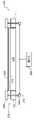
기판 지지부 (106) 는 에지 링 (180) 을 포함한다. 에지 링 (180) 은 하단 링 (184) 에 의해 지지될 수도 있는 상단 링에 대응할 수도 있다. 일부 예들에서, 에지 링 (180) 은 이하에 보다 상세히 기술된 바와 같이, 중간 링 (도 1에는 미도시), 세라믹 층 (112) 의 단차된 부분, 등 중 하나 이상에 의해 더 지지될 수도 있다. 본 명세의 원리들에 따라, 에지 링 (180) 은 기판 (108) 에 대해 이동가능한 (예를 들어, 수직 방향으로 상향 및 하향으로 이동가능) 하다. 예를 들어, 에지 링 (180) 은 제어기 (160) 에 응답하여 액추에이터를 통해 제어될 수도 있다. 일부 예들에서, 에지 링 (180) 은 기판 프로세싱 동안 조정될 수도 있다 (즉, 에지 링 (180) 은 튜닝가능 에지 링일 수도 있다). 다른 예들에서, 에지 링 (180) 은 (예를 들어, 프로세싱 챔버 (102) 가 진공 하에 있는 동안, 에어록을 통해 로봇 (170) 을 사용하여) 이동가능할 수도 있다. 여전히 다른 예들에서, 에지 링 (180) 은 튜닝가능 및 이동가능한 둘다일 수도 있다.The
이제 도 2a 및 도 2b를 참조하면, 본 명세의 원리들에 따른, 상부에 배치된 기판 (204) 을 갖는 예시적인 기판 지지부 (200) 가 도시된다. 기판 지지부 (200) 는 (예를 들어, ESC에 대응하는) 내측 부분 (208) 및 외측 부분 (212) 을 갖는 베이스 또는 페데스탈을 포함할 수도 있다. 예들에서, 외측 부분 (212) 은 내측 부분 (208) 으로부터 독립적일 수도 있고 내측 부분 (208) 에 대해 이동가능할 수도 있다. 예를 들어, 외측 부분 (212) 은 하단 링 (216) 및 상단 에지 링 (220) 을 포함할 수도 있다. 기판 (204) 은 프로세싱을 위해 내측 부분 (208) 상 (예를 들어, 세라믹 층 (224) 상) 에 배치된다. 제어기 (228) 는 에지 링 (220) 을 선택적으로 상승 및 하강시키기 위해 하나 이상의 액추에이터들 (232) 와 통신한다. 예를 들어, 에지 링 (220) 은 프로세싱 동안 지지부 (200) 의 포켓 깊이를 조정하도록 상승되고 그리고/또는 하강될 수도 있다. 또 다른 예에서, 에지 링 (220) 은 에지 링 (220) 의 제거 및 대체를 용이하게 하도록 상승될 수도 있다.Referring now to FIGS. 2A and 2B , an
단지 예를 들면, 에지 링 (220) 은 도 2a에서 완전히 하강된 위치로 도시되고 도 2b에서 예시적인 완전히 상승된 위치로 도시된다. 도시된 바와 같이, 액추에이터들 (232) 은 수직 방향으로 핀들 (236) 을 선택적으로 연장 및 반응시키도록 구성된 핀 액추에이터들에 대응한다. 다른 적합한 타입들의 액추에이터들이 다른 예들에서 사용될 수도 있다. 단지 예를 들면, 에지 링 (220) 은 세라믹 또는 석영 에지 링에 대응하지만, 다른 적합한 재료들이 사용될 수도 있다 (예를 들어, 실리콘 카바이드, 이트리아, 등). 도 2a에서, 제어기 (228) 는 핀들 (236) 을 통해 에지 링 (220) 을 직접적으로 상승 및 하강시키기 위해 액추에이터들 (232) 과 통신한다. 일부 예들에서, 내측 부분 (208) 은 외측 부분 (212) 에 대해 이동가능하다.By way of example only,
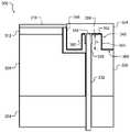
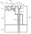
본 명세의 원리들에 따른, 예시적인 기판 지지부 (300) 의 피처들이 도 3a 및 도 3b에 보다 상세히 도시된다. 기판 지지부 (300) 는 절연체 링 또는 플레이트 (304) 및 절연체 플레이트 (304) 상에 배치된 (예를 들어, ESC의) 베이스플레이트 (308) 를 포함한다. 베이스플레이트 (308) 는 세라믹 층 (312) 을 지지하고, 세라믹 층 (312) 은 프로세싱을 위해 상부에 배치된 기판 (316) 을 지지하도록 구성된다. 도 3a에서, 세라믹 층 (312) 은 비단차 (non-stepped) 구성을 갖는다. 도 3b에서, 세라믹 층 (312) 은 단차진 구성을 갖는다. 기판 지지부 (300) 는 상부 ("상단") 에지 링 (324) 을 지지하는 하단 링 (320) 을 포함한다. 하나 이상의 비아들 또는 가이드 채널들 (328) 은 에지 링 (324) 을 선택적으로 상승 및 하강시키도록 구성된 각각의 리프트 핀들 (332) 을 수용하기 위해 절연체 플레이트 (304), 하단 링 (320), 및/또는 베이스플레이트 (308) 를 관통하여 형성될 수도 있다. 예를 들어, 가이드 채널들 (328) 은 리프트 핀들 (332) 각각의 리프트 핀을 위한 핀 정렬 홀들로서 기능한다. 도 3b에 도시된 바와 같이, 기판 지지부 (300) 는 하단 링 (320) 과 에지 링 (324) 사이에 배치된 중간 링 (336) 을 더 포함할 수도 있다. 단차진 구성에서, 중간 링 (336) 은 세라믹 층 (312) 과 오버랩하고 기판 (316) 의 외측 에지를 지지하도록 구성된다.Features of an
리프트 핀들 (332) 은 부식-내성 재료 (예를 들어, 사파이어) 를 포함할 수도 있다. 리프트 핀들 (332) 의 외측 표면은 이동을 용이하게 하기 위해 리프트 핀들 (332) 과 하단 링 (320) 의 구조적 피처들 사이의 마찰을 감소시키도록 평활하게 연마될 수도 있다. 일부 예들에서, 하나 이상의 세라믹 슬리브들 (340) 은 리프트 핀들 (332) 둘레의 채널들 (328) 에 배치될 수도 있다. 리프트 핀들 (332) 각각은 상부 단부 (344) 와 에지 링 (324) 사이의 콘택트 면적을 최소화하도록 라운딩된 상부 단부 (344) 를 포함할 수도 있다. 평활한 외측 표면, 라운딩된 상부 단부 (344), 가이드 채널 (328), 및/또는 세라믹 슬리브들 (340) 은 에지 링 (324) 의 상승 및 하강을 용이하게 하는 한편 이동 동안 리프트 핀들 (332) 의 바인딩을 방지한다.The lift pins 332 may include a corrosion-resistant material (eg, sapphire). The outer surface of the lift pins 332 may be polished smooth to reduce friction between the structural features of the
도 3a에 도시된 바와 같이, 하단 링 (320) 은 가이드 피처 (348) 를 포함한다. 도 3b에서, 중간 링 (336) 은 가이드 피처 (348) 를 포함한다. 예를 들어, 가이드 피처 (348) 는 하단 링 (320)/ 중간 링 (336) 으로부터 상향으로 연장하는 상승된 환형 림 (352) 에 대응한다. 도 3a에서, 가이드 채널들 (328) 및 리프트 핀들 (332) 은 에지 링 (324) 을 인게이지하기 위해 가이드 피처 (348) 를 통해 연장한다. 반대로, 도 3b에서, 가이드 채널들 (328) 및 리프트 핀들 (332) 은 에지 링 (324) 을 인게이지하기 위해 중간 링 (336) 을 통과하지 않고 하단 링 (320) 을 통해 연장한다.As shown in FIG. 3A , the
에지 링 (324) 은 가이드 피처 (348) 를 수용하도록 구성된 환형 하단 홈부 (356) 를 포함한다. 예를 들어, 에지 링 (324) 의 프로파일 (즉, 단면) 형상은 일반적으로 가이드 피처 (348) 를 수용하도록 구성된 "U" 형상에 대응할 수도 있지만, 다른 적합한 형상들이 사용될 수도 있다. 또한, 에지 링의 상부 표면 (324) 이 대체로 수평인 (즉, 기판 지지부 (300) 의 상부 표면에 평행) 것으로 도시되지만, 에지 링의 상부 표면 (324) 은 다른 예들에서 상이한 프로파일을 가질 수도 있다. 예를 들어, 에지 링의 상부 표면 (324) 은 틸팅되거나 기울어지거나 (slant), 라운딩되거나 할 수도 있다. 일부 예들에서, 에지 링의 상부 표면 (324) 은 내경에서 부식을 보상하기 위해 에지 링 (324) 의 내경에서의 두께가 에지 링 (324) 의 외경에서의 두께보다 크도록 틸팅된다.The
이에 따라, 에지 링 (324) 의 하단 표면은 도 3a의 하단 링 (320) 의 상부 표면 또는 도 3b의 하단 링 (320) 및 중간 링 (336) 의 각각의 표면들 에 상보적으로 구성된다. 또한, 에지 링 (324) 과 하단 링 (320)/중간 링 (336) 사이의 계면 (360) 은 미로와 같다 (labyrinthine). 즉, 에지 링 (324) 의 하부 표면 및 대응하여, 계면 (360) 은 에지 링 (324) 과 하단 링 (320)/중간 링 (336) 사이에서 기판 지지부 (300) 의 내부 구조체들로 직접 경로를 제공하는 대신 복수의 방향 변화들 (예를 들어, 방향의 90 도 변화들, 상향 단차 및 하향 단차, 교번하는 수평 직교 경로 및 수직 직교 경로, 등) 을 포함한다. 통상적으로, 다중 인터페이싱 링들 (예를 들어, 상단 에지 링 (324) 및 중간 링 (336) 및 하단 링 (320) 중 하나 이상 모두) 을 포함하는 기판 지지부들에서 플라즈마 및 프로세스 재료 누설 가능성이 상승될 수도 있다. 이 가능성은 프로세싱 동안 이동가능한 에지 링 (324) 이 상승될 때 더 상승될 수도 있다. 이에 따라, 계면 (360) (그리고, 구체적으로, 에지 링 (324) 의 프로파일) 은 프로세스 재료들, 플라즈마, 등이 기판 지지부 (300) 의 내부 구조체들에 도달하는 것을 방지하도록 구성된다.Accordingly, the bottom surface of the
예를 들어, 도 3a에 도시된 바와 같이, 계면 (360) 은 가이드 채널들 (328) 및 핀들 (332), 세라믹 층 (312), 기판 (316) 의 후면 및 에지, 등으로의 액세스를 제한하기 위해 5 번의 방향 변화들을 포함한다. 반대로, 도 3b에 도시된 바와 같이, 계면 (360) 은 가이드 채널들 (328) 및 핀들 (332), 세라믹 층 (312), 기판 (316) 의 후면 및 에지, 본딩층 (372), 시일부 (376), 등으로의 액세스를 제한하기 위해 제 1 경로 (364) 의 7 번의 방향 변화들 및 제 2 경로 (368) 의 5 번의 방향 변화들을 포함한다. 이에 따라, 계면 (360) 은 기판 지지부 (300) 의 내부 구조체들에 영향을 주는 플라즈마 누설 및 발광, 부식, 등의 가능성을 감소시킨다.For example, as shown in FIG. 3A ,
에지 링 (324) 의 프로파일 (즉, 단면) 형상 (뿐만 아니라 하단 링 (320), 중간 링 (336), 등의 인터페이싱 표면들) 은 제작을 용이하게 하고 제작 비용들을 감소시키도록 설계된다. 예를 들어, 홈부 (356) 의 벽들 (380, 384) 및 가이드 피처 (340) 는 플라즈마 및 프로세스 재료 누설을 방지하는 동안 제작을 용이하게 하도록 (예를 들어, 포물선, 사다리꼴, 삼각형, 등이 되는 것과 반대로) 실질적으로 수직일 수도 있다. 단지 예를 들면, 실질적으로 수직은 에지 링 (324) 의 상부 표면 및/또는 하부 표면에 수직하게, 에지 링 (324) 의 상부 표면 및/또는 하부 표면의 법선의 1° 이내, 에지 링 (324) 의 이동 방향에 평행하게, 등으로 규정될 수도 있다. 또한, 수직 벽들 (380, 384) 은 에지 링 (324) 의 이동 동안 가이드 피처 (340) 에 대한 에지 링 (324) 의 정렬을 유지한다. 반대로, 홈부 (356) 및 가이드 피처 (340) 의 각각의 프로파일들이 포물선, 사다리꼴, 삼각형, 등일 때, 에지 링 (324) 의 상향 이동은 벽들 (380) 과 벽들 (384) 사이에 상당한 분리를 유발한다.The profile (ie, cross-sectional) shape of the edge ring 324 (as well as the interfacing surfaces of the
계면 (360) 에서 (그리고, 구체적으로, 홈부 (356) 에서) 에지 링 (324), 하단 링 (320), 및 중간 링 (336) 의 표면들은 에지 링 (324) 의 이동 동안 에지 링 (324) 과 가이드 피처 (340) 사이의 마찰을 최소화하도록 상대적으로 평활하고 연속적이다. 예를 들어, 계면 (360) 에서 에지 링 (324), 하단 링 (320), 및 중간 링 (336) 의 각각의 표면들은 목표된 표면 평활도를 달성하도록 부가적인 연마를 겪을 수도 있다. 다른 예들에서, 계면 (360) 에서 에지 링 (324), 하단 링 (320), 및 중간 링 (336) 의 표면들은 마찰을 더 감소시키는 재료로 코팅될 수도 있다. 여전히 다른 예들에서, 계면 (360) 에서 (그리고, 구체적으로, 에지 링 (324) 에서) 에지 링 (324), 하단 링 (320), 및 중간 링 (336) 의 표면들은 스크류 홀들 및/또는 유사한 어셈블리 피처들이 없을 수도 있다. 이러한 방식에서, 표면들 간 콘택트로 인해 입자들의 생성 (예를 들어, 에지 링 (324) 의 이동 동안) 이 최소화될 수도 있다.At the interface 360 (and specifically in the groove 356 ), the surfaces of the
상기 기술된 바와 같이 프로세싱 동안 에지 링 (324) 이 튜닝을 위해 상승될 때, 도 2a 및 도 2b에 기술된 바와 같은 제어기 (228) 는 가이드 피처 (348) 의 높이 H에 따라 에지 링 (324) 의 튜닝가능 범위를 제한하도록 구성된다. 예를 들어, 튜닝가능 범위는 가이드 피처 (348) 의 높이 H보다 작게 제한될 수도 있다. 예를 들어, 가이드 피처 (348) 가 대략 8 ㎜ (예를 들어, 7.7 ㎜ 내지 8.3 ㎜) 의 높이 H를 갖는다면, 에지 링 (324) 의 튜닝가능 범위는 6 ㎜일 수도 있다. 즉, 에지 링 (324) 은 에지 링 (324) 내의 홈부 (356) 로부터 가이드 피처 (348) 를 전적으로 제거하지 않고 완전히 하강된 위치 (예를 들어, 0 ㎜) 로부터 완전히 상승된 위치 (예를 들어, 6 ㎜) 로 상승될 수도 있다. 이에 따라, 완전히 상승된 위치에서도, 에지 링 (324) 은 여전히 가이드 피처 (348) 의 적어도 일부와 오버랩한다. 이러한 방식으로 에지 링 (324) 의 범위를 제한하는 것은 상기 기술된 바와 같이 미로와 같은 계면 (360) 을 유지하고 에지 링 (324) 의 측방향 오정렬을 방지한다. 홈부 (356) 의 깊이는 가이드 피처 (348) 의 높이 H와 거의 같을 수도 있다 (예를 들어, 5 % 이내). 홈부 (356) 의 깊이는 에지 링의 두께의 적어도 50 %일 수도 있다. 단지 예를 들면, 도 3a의 에지 링 (324) 의 튜닝가능 범위는 6 ㎜이고, 도 3b의 에지 링 (324) 의 튜닝가능 범위는 1 ㎜이다. 예를 들어, 에지 링 (324) 의 전체 두께 (즉, 높이) 는 대략 0.459" (예를 들어, 0.450" 내지 0.469") 내지 대략 0.592" (예를 들어, 0.582" 내지 0.602") 일 수도 있고, 홈부 (356) 의 깊이는 대략 0.308" (예를 들어, 0.298" 내지 0.318") 일 수도 있다.When the
예를 들어, 에지 링 (324) 의 전체 두께는 에지 링 (324) 의 내경에서 에지 링 (324) 의 두께 (예를 들어, 내측 벽 (388) 에서 에지 링 (324) 의 두께/높이) 에 대응할 수도 있다. 일부 예들에서, 에지 링 (324) 의 두께는 에지 링의 상부 표면 (324) 에 걸쳐 균일하지 않을 수도 있다 (예를 들어, 에지 링의 상부 표면 (324) 은 내측 벽 (388) 에서의 두께가 에지 링 (324) 의 외경에서의 두께보다 크도록 상기 기술된 바와 같이 틸팅될 수도 있다). 그러나, 플라즈마로의 노출로 인한 부식이 에지 링 (324) 의 외경에 비해 내측 벽 (388) 에서 상승될 수도 있기 때문에, 에지 링 (324) 은 내측 벽 (388) 이 내측 벽 (388) 에서 상승된 부식을 보상하기 위해 적어도 미리 결정된 두께를 갖도록 형성될 수도 있다. 단지 예를 들면, 내측 벽 (388) 은 에지 링 (324) 의 이동 동안 기판 (316) 과의 콘택트를 회피하도록 실질적으로 수직이다.For example, the overall thickness of the
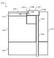
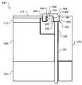
이제 도 4a, 도 4b, 및 도 4c를 참조하면, 본 개시의 원리들에 따른 또 다른 예시적인 기판 지지부 (400) 가 보다 상세히 도시된다. 기판 지지부 (400) 는 절연체 플레이트 (404) 상에 배치된 절연체 링 또는 플레이트 (404) 및 베이스플레이트 (408) 를 포함한다. 베이스플레이트 (408) 는 세라믹 층 (412) 을 지지하고, 세라믹 층은 프로세싱을 위해 상부에 배치된 기판 (416) 을 지지하도록 구성된다. 도 4a에서, 세라믹 층 (412) 은 비단차 구성을 갖는다. 도 4b 및 도 4c에서, 세라믹 층 (412) 은 단차진 구성을 갖는다. 기판 지지부 (400) 는 상부 에지 링 (424) 을 지지하는 하단 링 (420) 을 포함한다. 단차진 구성에서, 에지 링 (424) 은 세라믹 층 (412) 과 오버랩한다. 하나 이상의 비아들 또는 가이드 채널들 (428) 이 에지 링 (424) 을 선택적으로 상승 및 하강시키도록 구성된 각각의 리프트 핀들 (432) 을 수용하기 위해 절연체 플레이트 (404), 하단 링 (420), 및/또는 베이스플레이트 (408) 를 관통하여 형성될 수도 있다. 예를 들어, 가이드 채널들 (428) 은 리프트 핀들 (432) 각각의 핀에 대해 핀 정렬 홀들로서 기능한다.Referring now to FIGS. 4A , 4B, and 4C , another
도 4a, 도 4b 및 도 4c의 예들에서, 에지 링들 (424) 은 세라믹 층 (412) 상에 배치된 기판 (416) 의 외측 에지를 지지하도록 구성된다. 예를 들어, 에지 링들 (424) 의 내경들은 기판 (416) 의 외측 에지를 지지하도록 구성된 단차 (434) 를 포함한다. 이에 따라, 에지 링 (424) 은 에지 링 (424) 의 제거 및 대체를 용이하게 하도록 상승 및 하강될 수도 있지만 프로세싱 동안 상승 및 하강되지 않을 수도 있다 (즉, 에지 링 (424) 은 튜닝가능하지 않다). 예를 들어, 에지 링 (424) 은 제거 및 대체를 위해 리프트 핀들 (432) 을 사용하여 (예를 들어, 로봇 (170) 을 사용하여) 상승될 수도 있다.In the examples of FIGS. 4A , 4B and 4C , the edge rings 424 are configured to support an outer edge of the
일 예에서, 에지 링 (424) 의 하부, 내측 코너부 (436) 는 기판 지지부 (400) 상의 에지 링 (424) 의 정렬 (즉, 센터링 (centering)) 을 용이하게 하도록 챔퍼링될 수도 있다. 반대로, 세라믹 층 (412) 의 상부, 외측 코너부 (444) 및/또는 하부, 내측 코너부 (448) 는 코너부 (436) 에 상보적으로 챔퍼링될 수도 있다. 이에 따라, 에지 링 (424) 이 기판 지지부 (400) 상으로 하강됨에 따라, 챔퍼링된 코너부 (436) 는 에지 링 (424) 으로 하여금 기판 지지부 (400) 상에 셀프-센터링되게 하도록 챔퍼링된 코너부(들) (444/448) 와 상호작용한다.In one example, the lower,
에지 링 (424) 의 상부, 외측 코너부 (456) 는 프로세싱 챔버 (102) 로부터 에지 링 (424) 의 제거를 용이하게 하도록 챔퍼링될 수도 있다. 예를 들어, 기판 지지부 (400) 는 에지 링 (424) 의 인시츄 제거 (즉, 프로세싱 챔버 (102) 를 완전히 개방 및 벤팅하지 않고) 하기 위해 구성되기 때문에, 에지 링 (424) 은 에어록을 통해 제거되도록 구성된다. 통상적으로, 에어록들이 미리 결정된 사이즈 (예를 들어, 300 ㎜) 의 기판들을 수용하도록 사이징된다. 그러나, 에지 링 (424) 은 기판 (416) 보다 상당히 큰 직경을 갖고, 통상적인 에지 링 (424) 은 에어록을 통해 피팅 (fit) 하지 않을 수도 있다. 이에 따라, (예를 들어, 도 3a 및 도 3b에 도시된 바와 같이 에지 링들 (324) 과 비교하여) 에지 링 (424) 의 직경이 감소된다. 예를 들어, 에지 링 (324) 의 외경은 하단 링 (320) 의 외경과 유사하다. 반대로, 에지 링 (424) 의 외경은 하단 링 (420) 의 외경보다 상당히 작다. 단지 예를 들면, 에지 링 (424) 의 외경은 대략 12.833" (예를 들어, 12.823" 내지 12.843") 이하이다. 에지 링 (424) 의 내경은 대략 11.6"보다 크다 (예를 들어, 11.5"보다 크다). 외측 코너부 (456) 를 챔퍼링하는 것은 에어록을 통해 에지 링 (424) 의 이송을 더 용이하게 한다.A top,
단지 예를 들면, 외측 코너부의 챔퍼는 대략 0.060" (예를 들어, 0.050" 내지 0.070") 의 높이, 대략 0.040" (예를 들어, 0.030" 내지 0.050") 의 폭, 그리고 대략 30° (예를 들어, 25 내지 35°) 의 각도를 가질 수도 있다. 일부 예들에서, 에지 링 (424) 의 다른 외측 코너부들은 외측 코너부 (356) 에 부가하여 또는 대신 챔퍼링될 수도 있다. 일부 예들에서, 하부 코너부 (436) 의 챔퍼는 대략 0.025" (예를 들어, 0.015" 내지 0.040") 의 높이, 대략 0.015" (예를 들어, 0.005" 내지 0.030") 의 폭, 그리고 대략 60° (50 내지 70°) 의 각도를 가질 수도 있다. 단지 예를 들면, 에지 링 (424) 의 전체 두께 (즉, 높이) 는 대략, 0.268" (예를 들어, 0.258" 내지 0.268") 이하이다. 예를 들어, 에지 링 (424) 의 두께는 에지 링 (424) 의 제거를 허용하도록 프로세싱 챔버 (102) 의 에어록의 높이를 초과하지 않을 수도 있다. 단지 예를 들면, 에지 링 (424) 의 전체 두께는 도 3a 및 도 3b에 대해 상기 기술된 바와 같이 에지 링 (424) 의 내경에서 에지 링 (424) 의 두께 (예를 들어, 내측 벽 (458) 에서 에지 링 (424) 의 두께/높이) 에 대응할 수도 있다.By way of example only, the chamfer of the outer corner may be approximately 0.060" (eg, 0.050" to 0.070") high, approximately 0.040" (eg, 0.030" to 0.050") wide, and approximately 30° (eg, 0.030" to 0.050") For example, it may have an angle of 25 to 35°). In some examples, other outer corner portions of
도 4c에 도시된 바와 같이, 하단 링 (420) 은 가이드 피처 (460) 를 포함한다. 예를 들어, 가이드 피처 (460) 는 하단 링 (420) 으로부터 상향으로 연장하는 상승된 환형 림 (464) 에 대응한다. 가이드 채널들 (428) 및 리프트 핀들 (432) 은 에지 링 (424) 을 인게이지하도록 하단 링 (420) 을 통해 연장한다. 에지 링 (424) 은 가이드 피처 (460) 를 수용하도록 구성된 환형 하단 홈부 (468) 를 포함한다. 예를 들어, 에지 링 (424) 의 프로파일은 대체로 가이드 피처 (460) 를 수용하도록 구성된 "U" 형상에 대응할 수도 있다.As shown in FIG. 4C , the
이에 따라, 도 3a 및 도 3b의 예들과 유사하게, 에지 링 (424) 의 하단 표면은 미로와 같은 계면 (472) 을 형성하도록 하단 링 (420) 및 세라믹 층 (412) 의 각각의 상부 표면들에 상보적으로 구성된다. 즉, 계면 (472) 은 기판 지지부 (400) 의 내부 구초제들로 에지 링 (424) 과 하단 링 (420) 사이의 직접 경로를 제공하는 대신 복수의 방향 변화들 (예를 들어, 방향의 90 도 변화들) 을 포함한다. 일부 예들에서, 계면 (360) 에서 가이드 피처 (460), 에지 링 (424), 하단 링 (420), 및/또는 세라믹 층 (412) 의 부분들은 기판 지지부 (400) 상의 에지 링 (424) 의 정렬 (즉, 센터링) 을 용이하게 하도록 챔퍼링될 수도 있다. 예를 들어, 에지 링 (424) 의 내경의 하부, 내측 코너부 (476) 및 대응하는 세라믹 층 (412) 의 하부, 내측 코너부 (480) 및/또는 상부, 외측 코너부 (484) 는 챔퍼링된다. 다른 예들에서, 홈부 (468) 내 가이드 피처 (460) 의 기계적 정렬은 에지 링 (324) 을 센터링한다. 일부 예들에서, 하부 코너부 (476) 의 챔퍼는 대략 0.025" (예를 들어, 0.015" 내지 0.040") 의 높이, 대략 0.015" (예를 들어, 0.005" 내지 0.030") 의 폭, 및 대략 60° (예를 들어, 50 내지 60°) 의 각도를 가질 수도 있다.Accordingly, similar to the examples of FIGS. 3A and 3B , the bottom surface of the
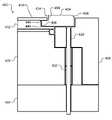
이제 도 5a 및 도 5b를 참조하면, 본 명세의 원리들에 따른 또 다른 예시적인 기판 지지부 (500) 가 보다 상세히 도시된다. 기판 지지부 (500) 는 절연체 플레이트 (504) 상에 배치된 절연체 링 또는 플레이트 (504) 및 베이스플레이트 (508) 를 포함한다. 베이스플레이트 (508) 는 세라믹 층 (512) 을 지지하고, 세라믹 층 (512) 은 프로세싱을 위해 상부에 배치된 기판 (516) 을 지지하도록 구성된다. 도 5a에서, 세라믹 층 (512) 은 비단차 구성을 갖는다. 도 5b에서, 세라믹 층 (512) 은 단차진 구성을 갖는다. 기판 지지부 (500) 는 (도 5a에 도시된 바와 같은) 상부 에지 링 (524) 또는 (도 5b에 도시된 바와 같은) 상부 에지 링 (526) 을 지지하는 하단 링 (520) 을 포함한다. 하나 이상의 비아들 또는 가이드 채널들 (528) 이 에지 링 (524/526) 을 선택적으로 상승 및 하강시키도록 구성된 각각의 리프트 핀들 (532) 을 수용하도록 절연체 플레이트 (504), 하단 링 (520), 및/또는 베이스플레이트 (508) 를 통해 형성될 수도 있다. 예를 들어, 가이드 채널들 (528) 은 리프트 핀들 (532) 각각의 리프트 핀을 위한 핀 정렬 홀들로서 기능한다. 도 5b에 도시된 바와 같이, 기판 지지부 (500) 는 하단 링 (520) 과 에지 링 (524/526) 사이에 배치된 중간 링 (536) 을 더 포함할 수도 있다. 단차진 구성에서, 중간 링 (536) 은 세라믹 층 (512) 과 오버랩하고 기판 (516) 의 외측 에지를 지지하도록 배치된다.Referring now to FIGS. 5A and 5B , another
도 5a 및 도 5b의 예들은 도 3a 및 도 3b의 튜닝가능 에지 링들 (324) 및 도 4a, 도 4b, 및 도 4c의 제거가능/대체가능 에지 링들 모두의 피처들을 결합한다. 예를 들어, 도 5b의 단차진 구성에서도, 에지 링 (526) 은 기판 (516) 밑으로 연장하지 않고 기판 (516) 을 지지하지 않는다. 이에 따라, 에지 링 (524/526) 은 프로세싱 동안 상승 및 하강될 수도 있다. 단지 예를 들면, 도 5a의 에지 링 (524) 튜닝가능 범위는 2.75 ㎜이고 도 5b의 에지 링 (526) 의 튜닝가능 범위는 1 ㎜이다. 또한, 에어록을 통한 에지 링 (524/526) 의 이송을 용이하게 하도록 에지 링 (524/526) 의 외경이 도 4a, 도 4b, 및 도 4c에 대해 기술된 바와 같이 감소된다. 이에 따라, 에지 링 (524/526) 은 상기 기술된 바와 같이 인시츄로 제거되고 대체될 수도 있다.The examples of FIGS. 5A and 5B combine features of both the tunable edge rings 324 of FIGS. 3A and 3B and the removable/replaceable edge rings of FIGS. 4A, 4B, and 4C. For example, even in the stepped configuration of FIG. 5B , the
도 5a에 도시된 바와 같이, 하단 링 (520) 은 가이드 피처 (540) 를 포함한다. 도 5b에서, 중간 링 (536) 은 가이드 피처 (540) 를 포함한다. 예를 들어, 가이드 피처 (540) 는 하단 링 (520)/중간 링 (536) 으로부터 상향으로 연장하는 상승된 환형 림 (544) 에 대응한다. 도 5a 및 도 5b 각각에서, 에지 링 (524/526) 을 인게이지하기 위해 가이드 채널들 (528) 및 리프트 핀들 (532) 하단 링 (520) 을 통해 연장한다. 예를 들어, 에지 링 (524/526) 은 가이드 피처 (540) 를 수용하도록 구성된 환형 하단 홈부 (548) 를 포함한다. 예를 들어, 에지 링 (524/526) 의 프로파일은 대체로 가이드 피처 (540) 를 수용하도록 구성된 "U" 형상에 대응할 수도 있다.As shown in FIG. 5A , the
이에 따라, 도 3a, 도 3b, 및 도 4c의 예들과 유사하게, 에지 링 (524/526) 의 하단 표면은 미로와 같은 계면 (552) 을 형성하도록 하단 링 (520) 및 중간 링 (536) 의 각각의 상부 표면들에 상보적으로 구성된다. 즉, 계면 (552) 은 기판 지지부 (500) 의 내부 구조체들로 에지 링 (524/526) 과 하단 링 (520) 사이의 직접 경로를 제공하는 대신 복수의 방향 변화들 (예를 들어, 방향의 90 도 변화들) 을 포함한다. 일부 예들에서, 계면 (552) 에서 가이드 피처 (540), 에지 링 (524/526), 하단 링 (520), 및/또는 중간 링 (536) 의 부분들은 기판 지지부 (500) 상의 에지 링 (524/526) 의 정렬 (즉, 센터링) 을 용이하게 하도록 챔퍼링될 수도 있다. 예를 들어, 도 5a에서, 에지 링 (524) 의 코너부들 (556 및 558) 및 가이드 피처 (540) 및 하단 링 (520) 의 상보적인 코너부들 (560) 이 챔퍼링된다. 반대로, 도 5b에서, 에지 링 (526) 의 코너부 (556) 및 하단 링 (520) 의 코너부 (560) 만이 챔퍼링된다. 도 4a, 도 4b, 및 도 4c에 대해 상기 기술된 바와 같이, 에지 링 (524) 의 상부, 외측 코너부 (564) 는 프로세싱 챔버 (102) 로부터 에지 링 (524) 의 제거를 용이하게 하도록 챔퍼링될 수도 있다.Accordingly, similar to the examples of FIGS. 3A, 3B, and 4C , the bottom surface of the
단지 예를 들면, 하부 코너부들 (556 및 558) 의 챔퍼들은 대략 0.015" (예를 들어, 0.005" 내지 0.030") 의 높이 및 폭 그리고 대략 30° (예를 들어, 25 내지 35°) 의 각도를 가질 수도 있다. 예를 들어, 에지 링 (524/526) 의 전체 두께 (즉, 높이) 는 대략 0.268" 이하 (예를 들어, 0.258" 이하) 일 수도 있고 홈부 (548) 의 깊이는 0.210" (예를 들어, 0.200" 내지 0.220") 일 수도 있다. 에지 링 (524/526) 의 두께와 홈부 (548) 의 깊이 간의 차는 0.058"보다 작지 않을 수도 있다. 예를 들어, 에지 링 (524/526) 의 에지 링 (524/526) 의 제거를 허용하도록 프로세싱 챔버 (102) 의 에어록의 높이를 초과하지 않을 수도 있다. 그러나, 에지 링 (524/526) 의 두께는 에지 링 (524/526) 의 튜닝가능성을 최적화하기 위해, 에어록의 높이를 초과하지 않고 최대화될 수도 있다. 즉, 에지 링 (524/526) 이 시간에 따라 부식함에 따라, 에지 링 (524/526) 이 대체될 필요 없이 상승될 수도 있는 양은 에지 링 (524/526) 의 두께에 비례하여 증가한다. 단지 예를 들면, 본 명세서에 사용된 바와 같은, 에지 링 (524/526) 의 "두께"는 도 3a, 도 3b, 도 4a, 도 4b, 및 도 4c에 대해 상기 기술된 바와 같이, 에지 링 (524/526) 의 내경에서 에지 링 (524/526) 의 두께 (예를 들어, 내측 벽 (568) 에서 에지 링 (524/526) 의 두께/높이) 를 지칭할 수도 있다.By way of example only, the chamfers of the
이제 도 6a 및 도 6b를 참조하면, 예시적인 하단 링 (600) (예를 들어, 하단 링들 (320, 420, 또는 520) 중 어느 하나에 대응) 은 절연체 링 (604) 과 하단 링 (600) 의 정렬을 용이하게 하도록 클록킹 피처를 구현할 수도 있다. 하단 링 (600) 은 절연체 링 (604) 을 통해 연장하는 각각의 리프트 핀들 (612) 을 수용하도록 구성된 복수의 가이드 채널들 (608) 을 포함한다. 하단 링 (600) 은 노치 (616) 와 같은, 하나 이상의 클록킹 피처들을 더 포함한다. 노치 (616) 는 절연체 링 (604) 으로부터 상향으로 연장하는, 돌출부 (620) 와 같은 상보적인 구조체를 수용하도록 구성된다. 이에 따라, 하단 링 (600) 은 가이드 채널들 (608) 이 리프트 핀들 (612) 각각의 리프트 핀과 정렬한다는 것을 보장하기 위해 노치 (616) 가 돌출부 (620) 와 정렬되고 돌출부 (620) 를 수용하도록 설치될 수도 있다.Referring now to FIGS. 6A and 6B , an exemplary bottom ring 600 (eg, corresponding to either of the bottom rings 320 , 420 , or 520 ) includes an
전술한 기술은 본질적으로 단순히 예시적이고 어떠한 방법으로도 명세, 이들의 애플리케이션 또는 용도들을 제한하도록 의도되지 않는다. 명세의 광범위한 교시가 다양한 형태들로 구현될 수 있다. 따라서, 본 명세는 특정한 예들을 포함하지만, 다른 수정 사항들이 도면들, 명세서, 및 이하의 청구항들을 연구함으로써 명백해질 것이기 때문에, 본 명세의 진정한 범위는 이렇게 제한되지 않아야 한다. 방법 내의 하나 이상의 단계들이 본 명세의 원리들을 변경하지 않고 상이한 순서로 (또는 동시에) 실행될 수도 있다는 것이 이해되어야 한다. 또한, 실시예들 각각이 특정한 피처들을 갖는 것으로 상기에 기술되었지만, 본 명세의 임의의 실시예에 대하여 기술된 임의의 하나 이상의 이들 피처들은, 조합이 명시적으로 기술되지 않아도, 임의의 다른 실시예들의 피처들로 및/또는 임의의 다른 실시예들의 피처들과 조합하여 구현될 수 있다. 즉, 기술된 실시예들은 상호 배타적이지 않고, 하나 이상의 실시예들의 또 다른 실시예들과의 치환들이 본 명세의 범위 내에 있다.The foregoing description is merely exemplary in nature and is not intended to limit the specification, its application, or uses in any way. The broad teachings of the specification may be embodied in various forms. Accordingly, while this disclosure includes specific examples, the true scope of the disclosure should not be so limited, as other modifications will become apparent from a study of the drawings, the specification, and the following claims. It should be understood that one or more steps in a method may be executed in a different order (or concurrently) without changing the principles of this disclosure. Further, although each of the embodiments has been described above as having specific features, any one or more of these features described with respect to any embodiment of the present disclosure may be used in any other embodiment, even if not explicitly described in combination. may be implemented with the features of and/or in combination with the features of any other embodiments. That is, the described embodiments are not mutually exclusive, and permutations of one or more embodiments with other embodiments are within the scope of the present disclosure.
엘리먼트들 간 (예를 들어, 모듈들, 회로 엘리먼트들, 반도체 층들, 등 간) 의 공간적 및 기능적 관계들은, "연결된 (connected)", "인게이지된 (engaged)", "커플링된 (coupled)", "인접한 (adjacent)", "옆에 (next to)", "~의 상단에 (on top of)", "위에 (above)", "아래에 (below)", 및 "배치된 (disposed)"을 포함하는, 다양한 용어들을 사용하여 기술된다. "직접적 (direct)"인 것으로 명시적으로 기술되지 않는 한, 제 1 엘리먼트와 제 2 엘리먼트 간의 관계가 상기 명세에서 기술될 때, 이 관계는 제 1 엘리먼트와 제 2 엘리먼트 사이에 다른 중개하는 엘리먼트가 존재하지 않는 직접적인 관계일 수 있지만, 또한 제 1 엘리먼트와 제 2 엘리먼트 사이에 (공간적으로 또는 기능적으로) 하나 이상의 중개하는 엘리먼트들이 존재하는 간접적인 관계일 수 있다. 본 명세서에서 논의된 바와 같이, 구 A, B, 및 C 중 적어도 하나는 비배타적인 논리 OR를 사용하여, 논리적으로 (A 또는 B 또는 C) 를 의미하는 것으로 해석되어야 하고, "적어도 하나의 A, 적어도 하나의 B, 및 적어도 하나의 C"를 의미하도록 해석되지 않아야 한다.Spatial and functional relationships between elements (eg, between modules, circuit elements, semiconductor layers, etc.) are “connected”, “engaged”, “coupled” )", "adjacent", "next to", "on top of", "above", "below", and "placed are described using various terms, including "disposed." When a relationship between a first element and a second element is described in the above specification, unless explicitly stated to be "direct," the relationship indicates that other intervening elements between the first and second elements It may be a direct relationship that does not exist, but may also be an indirect relationship in which one or more intervening elements (spatially or functionally) exist between the first element and the second element. As discussed herein, at least one of the phrases A, B, and C is to be interpreted to mean logically (A or B or C), using a non-exclusive logical OR, and "at least one A , at least one B, and at least one C".
일부 구현예들에서, 제어기는 상술한 예들의 일부일 수도 있는 시스템의 일부일 수 있다. 이러한 시스템들은, 프로세싱 툴 또는 툴들, 챔버 또는 챔버들, 프로세싱용 플랫폼 또는 플랫폼들, 및/또는 특정 프로세싱 컴포넌트들 (웨이퍼 페데스탈, 가스 플로우 시스템, 등) 을 포함하는, 반도체 프로세싱 장비를 포함할 수 있다. 이들 시스템들은 반도체 웨이퍼 또는 기판의 프로세싱 이전에, 프로세싱 동안에 그리고 프로세싱 이후에 그들의 동작을 제어하기 위한 전자장치에 통합될 수도 있다. 전자장치들은 시스템 또는 시스템들의 다양한 컴포넌트들 또는 하위부분들을 제어할 수도 있는 "제어기"로서 지칭될 수도 있다. 제어기는, 시스템의 프로세싱 요건들 및/또는 타입에 따라서, 프로세싱 가스들의 전달, 온도 설정사항들 (예를 들어, 가열 및/또는 냉각), 압력 설정사항들, 진공 설정사항들, 전력 설정사항들, 무선 주파수 (RF) 생성기 설정사항들, RF 매칭 회로 설정사항들, 주파수 설정사항들, 플로우 레이트 설정사항들, 유체 전달 설정사항들, 위치 및 동작 설정사항들, 툴들 및 다른 이송 툴들 및/또는 특정 시스템과 연결되거나 인터페이싱된 로드록들 내외로의 웨이퍼 이송들을 포함하는, 본 명세서에 명세된 프로세스들 중 임의의 프로세스들을 제어하도록 프로그램될 수도 있다.In some implementations, the controller may be part of a system, which may be part of the examples described above. Such systems may include semiconductor processing equipment, including a processing tool or tools, a chamber or chambers, a platform or platforms for processing, and/or specific processing components (wafer pedestal, gas flow system, etc.). . These systems may be incorporated into electronics for controlling their operation before, during, and after processing of a semiconductor wafer or substrate. Electronics may be referred to as a “controller,” which may control a system or various components or sub-portions of systems. The controller controls delivery of processing gases, temperature settings (eg, heating and/or cooling), pressure settings, vacuum settings, power settings, depending on the processing requirements and/or type of system. , radio frequency (RF) generator settings, RF matching circuit settings, frequency settings, flow rate settings, fluid transfer settings, position and motion settings, tools and other transport tools and/or It may be programmed to control any of the processes specified herein, including wafer transfers into and out of loadlocks coupled or interfaced with a particular system.
일반적으로 말하면, 제어기는 인스트럭션들을 수신하고, 인스트럭션들을 발행하고, 동작을 제어하고, 세정 동작들을 인에이블하고, 엔드포인트 측정들을 인에이블하는 등을 하는 다양한 집적 회로들, 로직, 메모리, 및/또는 소프트웨어를 갖는 전자장치로서 규정될 수도 있다. 집적 회로들은 프로그램 인스트럭션들을 저장하는 펌웨어의 형태의 칩들, 디지털 신호 프로세서들 (DSP), ASIC (application specific integrated circuit) 으로서 규정되는 칩들 및/또는 프로그램 인스트럭션들 (예를 들어, 소프트웨어) 을 실행하는 하나 이상의 마이크로프로세서들, 또는 마이크로제어기들을 포함할 수도 있다. 프로그램 인스트럭션들은 반도체 웨이퍼 상에서 또는 반도체 웨이퍼에 대한 특정 프로세스를 실행하기 위한 동작 파라미터들을 규정하는, 다양한 개별 설정사항들 (또는 프로그램 파일들) 의 형태로 제어기로 또는 시스템으로 전달되는 인스트럭션들일 수도 있다. 일부 실시예들에서, 동작 파라미터들은 하나 이상의 층들, 재료들, 금속들, 산화물들, 실리콘, 이산화 실리콘, 표면들, 회로들, 및/또는 웨이퍼의 다이들의 제조 동안에 하나 이상의 프로세싱 단계들을 달성하도록 프로세스 엔지니어에 의해서 규정된 레시피의 일부일 수도 있다.Generally speaking, the controller receives instructions, issues instructions, controls an operation, enables cleaning operations, enables endpoint measurements, and/or various integrated circuits, logic, memory, and/or the like. It may be defined as an electronic device with software. Integrated circuits are chips in the form of firmware that store program instructions, digital signal processors (DSP), chips defined as application specific integrated circuits (ASICs) and/or one that executes program instructions (eg, software). It may include more than one microprocessor, or microcontrollers. Program instructions may be instructions passed to a controller or system in the form of various individual settings (or program files), which define operating parameters for executing a particular process on or for a semiconductor wafer. In some embodiments, the operating parameters process one or more processing steps to achieve one or more processing steps during fabrication of one or more layers, materials, metals, oxides, silicon, silicon dioxide, surfaces, circuits, and/or dies of a wafer. It may be part of a recipe prescribed by the engineer.
제어기는, 일부 구현예들에서, 시스템에 통합되거나, 시스템에 커플링되거나, 이와 달리 시스템에 네트워킹되거나, 또는 이들의 조합으로 될 수 있는 컴퓨터에 커플링되거나 이의 일부일 수도 있다. 예를 들어, 제어기는 웨이퍼 프로세싱의 원격 액세스를 가능하게 할 수 있는 공장 (fab) 호스트 컴퓨터 시스템의 전부 또는 일부이거나 "클라우드" 내에 있을 수도 있다. 컴퓨터는 제조 동작들의 현 진행을 모니터링하고, 과거 제조 동작들의 이력을 조사하고, 복수의 제조 동작들로부터 경향들 또는 성능 계측치들을 조사하고, 현 프로세싱의 파라미터들을 변경하고, 현 프로세싱을 따르는 프로세싱 단계들을 설정하고, 또는 새로운 프로세스를 시작하기 위해서 시스템으로의 원격 액세스를 인에이블할 수도 있다. 일부 예들에서, 원격 컴퓨터 (예를 들어, 서버) 는 로컬 네트워크 또는 인터넷을 포함할 수도 있는 네트워크를 통해서 프로세스 레시피들을 시스템에 제공할 수 있다. 원격 컴퓨터는 차후에 원격 컴퓨터로부터 시스템으로 전달될 파라미터들 및/또는 설정사항들의 입력 또는 프로그래밍을 인에이블하는 사용자 인터페이스를 포함할 수도 있다. 일부 예들에서, 제어기는 하나 이상의 동작들 동안에 수행될 프로세스 단계들 각각에 대한 파라미터들을 특정한, 데이터의 형태의 인스트럭션들을 수신한다. 이 파라미터들은 제어기가 제어하거나 인터페이싱하도록 구성된 툴의 타입 및 수행될 프로세스의 타입에 특정적일 수도 있다는 것이 이해되어야 한다. 따라서, 상술한 바와 같이, 제어기는 예를 들어 서로 네트워킹되어서 함께 공통 목적을 위해서, 예를 들어 본 명세서에 기술된 프로세스들 및 제어들을 위해서 협력하는 하나 이상의 개별 제어기들을 포함함으로써 분산될 수도 있다. 이러한 목적을 위한 분산형 제어기의 예는 챔버 상의 프로세스를 제어하도록 조합되는, (예를 들어, 플랫폼 레벨에서 또는 원격 컴퓨터의 일부로서) 원격으로 위치한 하나 이상의 집적 회로들과 통신하는 챔버 상의 하나 이상의 집적 회로들일 수 있다.A controller may be coupled to or part of a computer, which, in some implementations, may be integrated into, coupled to, otherwise networked to the system, or a combination thereof. For example, the controller may be in the “cloud” or all or part of a fab host computer system that may enable remote access of wafer processing. The computer monitors the current progress of manufacturing operations, examines the history of past manufacturing operations, examines trends or performance metrics from a plurality of manufacturing operations, changes parameters of the current processing, and performs processing steps following the current processing. You can also enable remote access to the system to set up, or start a new process. In some examples, a remote computer (eg, server) can provide process recipes to the system via a network that may include a local network or the Internet. The remote computer may include a user interface that enables the input or programming of parameters and/or settings to be subsequently passed from the remote computer to the system. In some examples, the controller receives instructions in the form of data specifying parameters for each of the process steps to be performed during one or more operations. It should be understood that these parameters may be specific to the type of process to be performed and the type of tool the controller is configured to control or interface with. Thus, as described above, a controller may be distributed, such as by including one or more separate controllers that are networked together and cooperate for a common purpose, such as, for example, the processes and controls described herein. An example of a distributed controller for this purpose is one or more integrated circuits on the chamber in communication with one or more remotely located integrated circuits (eg, at the platform level or as part of a remote computer) combined to control a process on the chamber. can be circuits.
비한정적으로, 예시적인 시스템들은 플라즈마 에칭 챔버 또는 모듈, 증착 챔버 또는 모듈, 스핀-린스 챔버 또는 모듈, 금속 도금 챔버 또는 모듈, 세정 챔버 또는 모듈, 베벨 에지 에칭 챔버 또는 모듈, PVD (physical vapor deposition) 챔버 또는 모듈, CVD (chemical vapor deposition) 챔버 또는 모듈, ALD (atomic layer deposition) 챔버 또는 모듈, ALE (atomic layer etch) 챔버 또는 모듈, 이온 주입 챔버 또는 모듈, 트랙 (track) 챔버 또는 모듈, 및 반도체 웨이퍼들의 제조 및/또는 제작 시에 사용되거나 연관될 수도 있는 임의의 다른 반도체 프로세싱 시스템들을 포함할 수도 있다.Exemplary systems include, but are not limited to, a plasma etch chamber or module, a deposition chamber or module, a spin-rinse chamber or module, a metal plating chamber or module, a cleaning chamber or module, a bevel edge etch chamber or module, physical vapor deposition (PVD) chamber or module, chemical vapor deposition (CVD) chamber or module, atomic layer deposition (ALD) chamber or module, atomic layer etch (ALE) chamber or module, ion implantation chamber or module, track chamber or module, and semiconductor may include any other semiconductor processing systems that may be used or associated with the fabrication and/or fabrication of wafers.
상술한 바와 같이, 툴에 의해서 수행될 프로세스 단계 또는 단계들에 따라서, 제어기는, 반도체 제작 공장 내의 툴 위치들 및/또는 로드 포트들로부터/로 웨이퍼들의 컨테이너들을 이동시키는 재료 이송 시에 사용되는, 다른 툴 회로들 또는 모듈들, 다른 툴 컴포넌트들, 클러스터 툴들, 다른 툴 인터페이스들, 인접 툴들, 이웃하는 툴들, 공장 도처에 위치한 툴들, 메인 컴퓨터, 또 다른 제어기 또는 툴들 중 하나 이상과 통신할 수도 있다.As described above, depending on the process step or steps to be performed by the tool, the controller is used in material transfer to move containers of wafers from/to tool locations and/or load ports within the semiconductor fabrication plant. may communicate with one or more of other tool circuits or modules, other tool components, cluster tools, other tool interfaces, adjacent tools, neighboring tools, tools located throughout the factory, main computer, another controller or tools .
전술한 기술은 본질적으로 단순히 예시적이고 어떠한 방법으로도 명세, 이들의 애플리케이션 또는 용도들을 제한하도록 의도되지 않는다. 명세의 광범위한 교시가 다양한 형태들로 구현될 수 있다. 따라서, 본 명세는 특정한 예들을 포함하지만, 다른 수정 사항들이 도면들, 명세서, 및 이하의 청구항들을 연구함으로써 명백해질 것이기 때문에, 본 명세의 진정한 범위는 이렇게 제한되지 않아야 한다. 방법 내의 하나 이상의 단계들이 본 명세의 원리들을 변경하지 않고 상이한 순서로 (또는 동시에) 실행될 수도 있다는 것이 이해되어야 한다. 또한, 실시예들 각각이 특정한 피처들을 갖는 것으로 상기에 기술되었지만, 본 명세의 임의의 실시예에 대하여 기술된 임의의 하나 이상의 이들 피처들은, 조합이 명시적으로 기술되지 않아도, 임의의 다른 실시예들의 피처들로 및/또는 임의의 다른 실시예들의 피처들과 조합하여 구현될 수 있다. 즉, 기술된 실시예들은 상호 배타적이지 않고, 하나 이상의 실시예들의 또 다른 실시예들과의 치환들이 본 명세의 범위 내에 있다.The foregoing description is merely exemplary in nature and is not intended to limit the specification, its application, or uses in any way. The broad teachings of the specification may be embodied in various forms. Accordingly, while this disclosure includes specific examples, the true scope of the disclosure should not be so limited, as other modifications will become apparent from a study of the drawings, the specification, and the following claims. It should be understood that one or more steps in a method may be executed in a different order (or concurrently) without changing the principles of this disclosure. Further, although each of the embodiments has been described above as having specific features, any one or more of these features described with respect to any embodiment of the present disclosure may be used in any other embodiment, even if not explicitly described in combination. may be implemented with the features of and/or in combination with the features of any other embodiments. That is, the described embodiments are not mutually exclusive, and permutations of one or more embodiments with other embodiments are within the scope of the present disclosure.
엘리먼트들 간 (예를 들어, 모듈들, 회로 엘리먼트들, 반도체 층들, 등 간) 의 공간적 및 기능적 관계들은, "연결된 (connected)", "인게이지된 (engaged)", "커플링된 (coupled)", "인접한 (adjacent)", "옆에 (next to)", "~의 상단에 (on top of)", "위에 (above)", "아래에 (below)", 및 "배치된 (disposed)"을 포함하는, 다양한 용어들을 사용하여 기술된다. "직접적 (direct)"인 것으로 명시적으로 기술되지 않는 한, 제 1 엘리먼트와 제 2 엘리먼트 간의 관계가 상기 명세에서 기술될 때, 이 관계는 제 1 엘리먼트와 제 2 엘리먼트 사이에 다른 중개하는 엘리먼트가 존재하지 않는 직접적인 관계일 수 있지만, 또한 제 1 엘리먼트와 제 2 엘리먼트 사이에 (공간적으로 또는 기능적으로) 하나 이상의 중개하는 엘리먼트들이 존재하는 간접적인 관계일 수 있다. 본 명세서에서 논의된 바와 같이, 구 A, B, 및 C 중 적어도 하나는 비배타적인 논리 OR를 사용하여, 논리적으로 (A 또는 B 또는 C) 를 의미하는 것으로 해석되어야 하고, "적어도 하나의 A, 적어도 하나의 B, 및 적어도 하나의 C"를 의미하도록 해석되지 않아야 한다.Spatial and functional relationships between elements (eg, between modules, circuit elements, semiconductor layers, etc.) are “connected”, “engaged”, “coupled” )", "adjacent", "next to", "on top of", "above", "below", and "placed are described using various terms, including "disposed." When a relationship between a first element and a second element is described in the above specification, unless explicitly stated to be "direct," the relationship indicates that other intervening elements between the first and second elements It may be a direct relationship that does not exist, but may also be an indirect relationship in which one or more intervening elements (spatially or functionally) exist between the first element and the second element. As discussed herein, at least one of the phrases A, B, and C is to be interpreted to mean logically (A or B or C), using a non-exclusive logical OR, and "at least one A , at least one B, and at least one C".
일부 구현예들에서, 제어기는 상술한 예들의 일부일 수도 있는 시스템의 일부일 수 있다. 이러한 시스템들은, 프로세싱 툴 또는 툴들, 챔버 또는 챔버들, 프로세싱용 플랫폼 또는 플랫폼들, 및/또는 특정 프로세싱 컴포넌트들 (웨이퍼 페데스탈, 가스 플로우 시스템, 등) 을 포함하는, 반도체 프로세싱 장비를 포함할 수 있다. 이들 시스템들은 반도체 웨이퍼 또는 기판의 프로세싱 이전에, 프로세싱 동안에 그리고 프로세싱 이후에 그들의 동작을 제어하기 위한 전자장치에 통합될 수도 있다. 전자장치들은 시스템 또는 시스템들의 다양한 컴포넌트들 또는 하위부분들을 제어할 수도 있는 "제어기"로서 지칭될 수도 있다. 제어기는, 시스템의 프로세싱 요건들 및/또는 타입에 따라서, 프로세싱 가스들의 전달, 온도 설정사항들 (예를 들어, 가열 및/또는 냉각), 압력 설정사항들, 진공 설정사항들, 전력 설정사항들, 무선 주파수 (RF) 생성기 설정사항들, RF 매칭 회로 설정사항들, 주파수 설정사항들, 플로우 레이트 설정사항들, 유체 전달 설정사항들, 위치 및 동작 설정사항들, 툴들 및 다른 이송 툴들 및/또는 특정 시스템과 연결되거나 인터페이싱된 로드록들 내외로의 웨이퍼 이송들을 포함하는, 본 명세서에 명세된 프로세스들 중 임의의 프로세스들을 제어하도록 프로그램될 수도 있다.In some implementations, the controller may be part of a system, which may be part of the examples described above. Such systems may include semiconductor processing equipment, including a processing tool or tools, a chamber or chambers, a platform or platforms for processing, and/or specific processing components (wafer pedestal, gas flow system, etc.). . These systems may be incorporated into electronics for controlling their operation before, during, and after processing of a semiconductor wafer or substrate. Electronics may be referred to as a “controller,” which may control a system or various components or sub-portions of systems. The controller controls delivery of processing gases, temperature settings (eg, heating and/or cooling), pressure settings, vacuum settings, power settings, depending on the processing requirements and/or type of system. , radio frequency (RF) generator settings, RF matching circuit settings, frequency settings, flow rate settings, fluid transfer settings, position and motion settings, tools and other transport tools and/or It may be programmed to control any of the processes specified herein, including wafer transfers into and out of loadlocks coupled or interfaced with a particular system.
일반적으로 말하면, 제어기는 인스트럭션들을 수신하고, 인스트럭션들을 발행하고, 동작을 제어하고, 세정 동작들을 인에이블하고, 엔드포인트 측정들을 인에이블하는 등을 하는 다양한 집적 회로들, 로직, 메모리, 및/또는 소프트웨어를 갖는 전자장치로서 규정될 수도 있다. 집적 회로들은 프로그램 인스트럭션들을 저장하는 펌웨어의 형태의 칩들, 디지털 신호 프로세서들 (DSP), ASIC (application specific integrated circuit) 으로서 규정되는 칩들 및/또는 프로그램 인스트럭션들 (예를 들어, 소프트웨어) 을 실행하는 하나 이상의 마이크로프로세서들, 또는 마이크로제어기들을 포함할 수도 있다. 프로그램 인스트럭션들은 반도체 웨이퍼 상에서 또는 반도체 웨이퍼에 대한 특정 프로세스를 실행하기 위한 동작 파라미터들을 규정하는, 다양한 개별 설정사항들 (또는 프로그램 파일들) 의 형태로 제어기로 또는 시스템으로 전달되는 인스트럭션들일 수도 있다. 일부 실시예들에서, 동작 파라미터들은 하나 이상의 층들, 재료들, 금속들, 산화물들, 실리콘, 이산화 실리콘, 표면들, 회로들, 및/또는 웨이퍼의 다이들의 제조 동안에 하나 이상의 프로세싱 단계들을 달성하도록 프로세스 엔지니어에 의해서 규정된 레시피의 일부일 수도 있다.Generally speaking, the controller receives instructions, issues instructions, controls an operation, enables cleaning operations, enables endpoint measurements, and/or various integrated circuits, logic, memory, and/or the like. It may be defined as an electronic device with software. Integrated circuits are chips in the form of firmware that store program instructions, digital signal processors (DSP), chips defined as application specific integrated circuits (ASICs) and/or one that executes program instructions (eg, software). It may include more than one microprocessor, or microcontrollers. Program instructions may be instructions passed to a controller or system in the form of various individual settings (or program files), which define operating parameters for executing a particular process on or for a semiconductor wafer. In some embodiments, the operating parameters process one or more processing steps to achieve one or more processing steps during fabrication of one or more layers, materials, metals, oxides, silicon, silicon dioxide, surfaces, circuits, and/or dies of a wafer. It may be part of a recipe prescribed by the engineer.
제어기는, 일부 구현예들에서, 시스템에 통합되거나, 시스템에 커플링되거나, 이와 달리 시스템에 네트워킹되거나, 또는 이들의 조합으로 될 수 있는 컴퓨터에 커플링되거나 이의 일부일 수도 있다. 예를 들어, 제어기는 웨이퍼 프로세싱의 원격 액세스를 가능하게 할 수 있는 공장 (fab) 호스트 컴퓨터 시스템의 전부 또는 일부이거나 "클라우드" 내에 있을 수도 있다. 컴퓨터는 제조 동작들의 현 진행을 모니터링하고, 과거 제조 동작들의 이력을 조사하고, 복수의 제조 동작들로부터 경향들 또는 성능 계측치들을 조사하고, 현 프로세싱의 파라미터들을 변경하고, 현 프로세싱을 따르는 프로세싱 단계들을 설정하고, 또는 새로운 프로세스를 시작하기 위해서 시스템으로의 원격 액세스를 인에이블할 수도 있다. 일부 예들에서, 원격 컴퓨터 (예를 들어, 서버) 는 로컬 네트워크 또는 인터넷을 포함할 수도 있는 네트워크를 통해서 프로세스 레시피들을 시스템에 제공할 수 있다. 원격 컴퓨터는 차후에 원격 컴퓨터로부터 시스템으로 전달될 파라미터들 및/또는 설정사항들의 입력 또는 프로그래밍을 인에이블하는 사용자 인터페이스를 포함할 수도 있다. 일부 예들에서, 제어기는 하나 이상의 동작들 동안에 수행될 프로세스 단계들 각각에 대한 파라미터들을 특정한, 데이터의 형태의 인스트럭션들을 수신한다. 이 파라미터들은 제어기가 제어하거나 인터페이싱하도록 구성된 툴의 타입 및 수행될 프로세스의 타입에 특정적일 수도 있다는 것이 이해되어야 한다. 따라서, 상술한 바와 같이, 제어기는 예를 들어 서로 네트워킹되어서 함께 공통 목적을 위해서, 예를 들어 본 명세서에 기술된 프로세스들 및 제어들을 위해서 협력하는 하나 이상의 개별 제어기들을 포함함으로써 분산될 수도 있다. 이러한 목적을 위한 분산형 제어기의 예는 챔버 상의 프로세스를 제어하도록 조합되는, (예를 들어, 플랫폼 레벨에서 또는 원격 컴퓨터의 일부로서) 원격으로 위치한 하나 이상의 집적 회로들과 통신하는 챔버 상의 하나 이상의 집적 회로들일 수 있다.A controller may be coupled to or part of a computer, which, in some implementations, may be integrated into, coupled to, or otherwise networked to the system, or a combination thereof. For example, the controller may be in the “cloud” or all or part of a fab host computer system that may enable remote access of wafer processing. The computer monitors the current progress of manufacturing operations, examines the history of past manufacturing operations, examines trends or performance metrics from a plurality of manufacturing operations, changes parameters of the current processing, and performs processing steps following the current processing. You can also enable remote access to the system to set up, or start a new process. In some examples, a remote computer (eg, a server) can provide process recipes to the system over a network that may include a local network or the Internet. The remote computer may include a user interface that enables input or programming of parameters and/or settings to be subsequently passed from the remote computer to the system. In some examples, the controller receives instructions in the form of data specifying parameters for each of the process steps to be performed during one or more operations. It should be understood that these parameters may be specific to the type of process to be performed and the type of tool the controller is configured to control or interface with. Accordingly, as described above, a controller may be distributed, for example, by including one or more separate controllers that are networked together and cooperate for a common purpose, such as for the processes and controls described herein. An example of a distributed controller for this purpose is one or more integrated circuits on the chamber in communication with one or more remotely located integrated circuits (eg, at the platform level or as part of a remote computer) combined to control a process on the chamber. can be circuits.
비한정적으로, 예시적인 시스템들은 플라즈마 에칭 챔버 또는 모듈, 증착 챔버 또는 모듈, 스핀-린스 챔버 또는 모듈, 금속 도금 챔버 또는 모듈, 세정 챔버 또는 모듈, 베벨 에지 에칭 챔버 또는 모듈, PVD (physical vapor deposition) 챔버 또는 모듈, CVD (chemical vapor deposition) 챔버 또는 모듈, ALD (atomic layer deposition) 챔버 또는 모듈, ALE (atomic layer etch) 챔버 또는 모듈, 이온 주입 챔버 또는 모듈, 트랙 (track) 챔버 또는 모듈, 및 반도체 웨이퍼들의 제조 및/또는 제작 시에 사용되거나 연관될 수도 있는 임의의 다른 반도체 프로세싱 시스템들을 포함할 수도 있다.Exemplary systems include, but are not limited to, a plasma etch chamber or module, a deposition chamber or module, a spin-rinse chamber or module, a metal plating chamber or module, a cleaning chamber or module, a bevel edge etch chamber or module, physical vapor deposition (PVD) chamber or module, chemical vapor deposition (CVD) chamber or module, atomic layer deposition (ALD) chamber or module, atomic layer etch (ALE) chamber or module, ion implantation chamber or module, track chamber or module, and semiconductor may include any other semiconductor processing systems that may be used or associated with the fabrication and/or fabrication of wafers.
상술한 바와 같이, 툴에 의해서 수행될 프로세스 단계 또는 단계들에 따라서, 제어기는, 반도체 제작 공장 내의 툴 위치들 및/또는 로드 포트들로부터/로 웨이퍼들의 컨테이너들을 이동시키는 재료 이송 시에 사용되는, 다른 툴 회로들 또는 모듈들, 다른 툴 컴포넌트들, 클러스터 툴들, 다른 툴 인터페이스들, 인접 툴들, 이웃하는 툴들, 공장 도처에 위치한 툴들, 메인 컴퓨터, 또 다른 제어기 또는 툴들 중 하나 이상과 통신할 수도 있다.As described above, depending on the process step or steps to be performed by the tool, the controller is used in material transfer to move containers of wafers from/to tool locations and/or load ports within the semiconductor fabrication plant. may communicate with one or more of other tool circuits or modules, other tool components, cluster tools, other tool interfaces, adjacent tools, neighboring tools, tools located throughout the factory, main computer, another controller or tools .
Claims (15)
Translated fromKorean상부 표면;
환형 내경;
환형 외경; 및
하부 표면을 포함하고,
상기 에지 링의 상기 상부 표면은 상기 기판 지지부 상에 배치된 기판의 외측 에지를 지지하도록 구성되고,
상기 상부 표면과 상기 외경 사이의 계면에서 상기 에지 링의 외측, 상부 코너는 챔퍼링되고,
상기 챔퍼링된 외측, 상부 코너는 상기 에어록을 통해 상기 에지 링의 제거를 용이하게 하도록 구성되고, 그리고
상기 환형 외경은 상기 에어록을 통한 제거를 허용하도록 사이징되는, 에지 링.An edge ring configured to be raised and lowered via one or more lift pins and removed via an airlock relative to a substrate support in a substrate processing system, the edge ring comprising:
upper surface;
annular inner diameter;
annular outer diameter; and
a lower surface;
the upper surface of the edge ring is configured to support an outer edge of a substrate disposed on the substrate support;
an outer, upper corner of the edge ring at the interface between the upper surface and the outer diameter is chamfered;
the chamfered outer, upper corner is configured to facilitate removal of the edge ring through the airlock; and
and the annular outer diameter is sized to allow removal through the airlock.
상기 에지 링의 환형 외경은 12.883" (326 ㎜) 이하인, 에지 링.The method of claim 1,
wherein the annular outer diameter of the edge ring is 12.883" (326 mm) or less.
상기 에지 링의 상기 환형 내경은 11.6" (295 ㎜) 보다 큰, 에지 링.The method of claim 1,
and the annular inner diameter of the edge ring is greater than 11.6" (295 mm).
상기 챔퍼링된 상부 코너부는 0.060" (1.52 ㎜) 의 높이, 0.040" (1.02 ㎜) 의 폭, 및 30 °의 각도를 갖는, 에지 링.The method of claim 1,
and the chamfered upper corner portion has a height of 0.060" (1.52 mm), a width of 0.040" (1.02 mm), and an angle of 30 degrees.
상기 환형 내경에서 상기 에지 링의 높이는 0.268" (6.8 ㎜) 인, 에지 링.The method of claim 1,
and the height of the edge ring at the annular inner diameter is 0.268" (6.8 mm).
상기 기판의 상기 외측 에지를 지지하기 위해, 상기 에지 링의 상기 환형 내경은 상기 상부 표면에 단차를 포함하는, 에지 링.The method of claim 1,
and the annular inner diameter of the edge ring comprises a step in the upper surface to support the outer edge of the substrate.
상기 에지 링은 상기 기판 지지부의 하단 링 또는 중간 링으로부터 상향으로 연장하는 가이드 피처와 인터페이싱하도록 구성되는, 에지 링.The method of claim 1,
and the edge ring is configured to interface with a guide feature extending upwardly from a bottom ring or middle ring of the substrate support.
상기 에지 링의 상기 하부 표면에 배치된 환형 홈부를 더 포함하고, 상기 환형 홈부의 벽들은 실질적으로 수직인, 에지 링.The method of claim 1,
and an annular groove disposed on the lower surface of the edge ring, wherein walls of the annular groove are substantially vertical.
상기 환형 홈부에 인접한 상기 에지 링의 상기 하부 표면 상의 코너부는 챔퍼링되는, 에지 링.9. The method of claim 8,
and a corner portion on the lower surface of the edge ring adjacent the annular groove portion is chamfered.
상기 에지 링의 상기 하부 표면은 적어도 4 번의 방향 변화들을 포함하는, 에지 링.9. The method of claim 8,
and the lower surface of the edge ring comprises at least four directional changes.
상기 하부 표면과 상기 내경 사이의 계면에서 상기 에지 링의 내측, 하부 코너부는 챔퍼링되는, 에지 링.11. The method according to any one of claims 1 to 10,
and an inner, lower corner portion of the edge ring at the interface between the lower surface and the inner diameter is chamfered.
상기 챔퍼링된 하부 코너부는 0.015" (0.38 ㎜) 의 높이, 0.015" (0.38 ㎜) 의 폭, 및 30 °의 각도를 갖는, 에지 링.12. The method of claim 11,
and the chamfered lower corner portion has a height of 0.015″ (0.38 mm), a width of 0.015″ (0.38 mm), and an angle of 30°.
상기 챔퍼링된 하부 코너부는 0.025" (0.64 ㎜) 의 높이, 0.015" (0.38 ㎜) 의 폭, 및 60 °의 각도를 갖는, 에지 링.12. The method of claim 11,
and the lower chamfered corner portion has a height of 0.025″ (0.64 mm), a width of 0.015″ (0.38 mm), and an angle of 60°.
상기 에지 링은 단차진 구성을 갖고, 그리고 상기 기판 지지부의 세라믹 층과 오버랩하도록 구성되는, 에지 링.The method of claim 1,
wherein the edge ring has a stepped configuration and is configured to overlap the ceramic layer of the substrate support.
Priority Applications (1)
| Application Number | Priority Date | Filing Date | Title |
|---|---|---|---|
| KR1020227017005AKR102591660B1 (en) | 2017-07-24 | 2017-07-24 | Moveable edge ring designs |
Applications Claiming Priority (2)
| Application Number | Priority Date | Filing Date | Title |
|---|---|---|---|
| KR1020187021511AKR102258054B1 (en) | 2017-07-24 | 2017-07-24 | Movable edge ring designs |
| PCT/US2017/043527WO2019022707A1 (en) | 2017-07-24 | 2017-07-24 | MOBILE RIBBON DESIGNS |
Related Parent Applications (1)
| Application Number | Title | Priority Date | Filing Date |
|---|---|---|---|
| KR1020187021511ADivisionKR102258054B1 (en) | 2017-07-24 | 2017-07-24 | Movable edge ring designs |
Related Child Applications (1)
| Application Number | Title | Priority Date | Filing Date |
|---|---|---|---|
| KR1020227017005ADivisionKR102591660B1 (en) | 2017-07-24 | 2017-07-24 | Moveable edge ring designs |
Publications (2)
| Publication Number | Publication Date |
|---|---|
| KR20210063478A KR20210063478A (en) | 2021-06-01 |
| KR102401704B1true KR102401704B1 (en) | 2022-05-24 |
Family
ID=65041253
Family Applications (6)
| Application Number | Title | Priority Date | Filing Date |
|---|---|---|---|
| KR1020227017005AActiveKR102591660B1 (en) | 2017-07-24 | 2017-07-24 | Moveable edge ring designs |
| KR1020187021511AActiveKR102258054B1 (en) | 2017-07-24 | 2017-07-24 | Movable edge ring designs |
| KR1020247009974AActiveKR102725131B1 (en) | 2017-07-24 | 2017-07-24 | Moveable edge ring designs |
| KR1020237035339AActiveKR102720332B1 (en) | 2017-07-24 | 2017-07-24 | Moveable edge ring designs |
| KR1020217015653AActiveKR102401704B1 (en) | 2017-07-24 | 2017-07-24 | Moveable edge ring designs |
| KR1020247036134APendingKR20240158390A (en) | 2017-07-24 | 2017-07-24 | Moveable edge ring designs |
Family Applications Before (4)
| Application Number | Title | Priority Date | Filing Date |
|---|---|---|---|
| KR1020227017005AActiveKR102591660B1 (en) | 2017-07-24 | 2017-07-24 | Moveable edge ring designs |
| KR1020187021511AActiveKR102258054B1 (en) | 2017-07-24 | 2017-07-24 | Movable edge ring designs |
| KR1020247009974AActiveKR102725131B1 (en) | 2017-07-24 | 2017-07-24 | Moveable edge ring designs |
| KR1020237035339AActiveKR102720332B1 (en) | 2017-07-24 | 2017-07-24 | Moveable edge ring designs |
Family Applications After (1)
| Application Number | Title | Priority Date | Filing Date |
|---|---|---|---|
| KR1020247036134APendingKR20240158390A (en) | 2017-07-24 | 2017-07-24 | Moveable edge ring designs |
Country Status (8)
| Country | Link |
|---|---|
| US (1) | US12230482B2 (en) |
| EP (2) | EP3852137A1 (en) |
| JP (4) | JP6916303B2 (en) |
| KR (6) | KR102591660B1 (en) |
| CN (5) | CN118248616A (en) |
| SG (1) | SG11201908264QA (en) |
| TW (6) | TWI773351B (en) |
| WO (1) | WO2019022707A1 (en) |
Families Citing this family (21)
| Publication number | Priority date | Publication date | Assignee | Title |
|---|---|---|---|---|
| US10658222B2 (en) | 2015-01-16 | 2020-05-19 | Lam Research Corporation | Moveable edge coupling ring for edge process control during semiconductor wafer processing |
| CN118380371A (en)* | 2017-11-21 | 2024-07-23 | 朗姆研究公司 | Bottom edge ring and middle edge ring |
| JP7140610B2 (en)* | 2018-09-06 | 2022-09-21 | 株式会社日立ハイテク | Plasma processing equipment |
| JP7105666B2 (en)* | 2018-09-26 | 2022-07-25 | 東京エレクトロン株式会社 | Plasma processing equipment |
| JP7134104B2 (en)* | 2019-01-09 | 2022-09-09 | 東京エレクトロン株式会社 | Plasma processing apparatus and mounting table for plasma processing apparatus |
| KR102702089B1 (en)* | 2019-03-22 | 2024-09-03 | 삼성전자주식회사 | Substrate processing apparatus including edge ring |
| KR102684969B1 (en)* | 2019-04-12 | 2024-07-16 | 삼성전자주식회사 | Substrate processing apparatus including edge ring |
| KR102128595B1 (en)* | 2019-04-12 | 2020-07-01 | 하나머티리얼즈(주) | Focus Ring and plasma device including the same |
| TWM593655U (en)* | 2019-05-10 | 2020-04-11 | 美商蘭姆研究公司 | Semiconductor process module mid ring |
| TWM602283U (en)* | 2019-08-05 | 2020-10-01 | 美商蘭姆研究公司 | Edge ring with lift pin grooves for a substrate processing system |
| JP2022544494A (en)* | 2019-08-14 | 2022-10-19 | ラム リサーチ コーポレーション | Movable edge ring for substrate processing system |
| JP7550603B2 (en)* | 2020-03-03 | 2024-09-13 | 東京エレクトロン株式会社 | Plasma processing system and method for replacing edge ring - Patents.com |
| TWI871435B (en)* | 2020-03-03 | 2025-02-01 | 日商東京威力科創股份有限公司 | Substrate support, and plasma processing system |
| JP7409976B2 (en)* | 2020-06-22 | 2024-01-09 | 東京エレクトロン株式会社 | How to replace plasma processing system, plasma processing equipment and edge ring |
| KR102751528B1 (en)* | 2020-09-01 | 2025-01-07 | 삼성전자주식회사 | Plasma processing equipment |
| US12100579B2 (en)* | 2020-11-18 | 2024-09-24 | Applied Materials, Inc. | Deposition ring for thin substrate handling via edge clamping |
| JP7492928B2 (en)* | 2021-02-10 | 2024-05-30 | 東京エレクトロン株式会社 | SUBSTRATE SUPPORT, PLASMA PROCESSING SYSTEM AND PLASMA ETCHING METHOD - Patent application |
| US12334383B2 (en)* | 2021-12-16 | 2025-06-17 | Applied Materials, Inc. | Substrate support gap pumping to prevent glow discharge and light-up |
| JP2025508673A (en)* | 2022-03-02 | 2025-04-10 | ラム リサーチ コーポレーション | Improving layer uniformity in deposition-interference-deposition processes |
| US20230377855A1 (en)* | 2022-05-20 | 2023-11-23 | Applied Materials, Inc. | Lower deposition chamber ccp electrode cleaning solution |
| WO2025126845A1 (en)* | 2023-12-12 | 2025-06-19 | 東京エレクトロン株式会社 | Plasma processing device |
Citations (2)
| Publication number | Priority date | Publication date | Assignee | Title |
|---|---|---|---|---|
| KR100578129B1 (en) | 2003-09-19 | 2006-05-10 | 삼성전자주식회사 | Plasma etching device |
| JP2011054933A (en)* | 2009-08-07 | 2011-03-17 | Tokyo Electron Ltd | Substrate treatment device, method for positioning, and method for installing focus ring |
Family Cites Families (48)
| Publication number | Priority date | Publication date | Assignee | Title |
|---|---|---|---|---|
| US5837058A (en)* | 1996-07-12 | 1998-11-17 | Applied Materials, Inc. | High temperature susceptor |
| US5848889A (en)* | 1996-07-24 | 1998-12-15 | Applied Materials Inc. | Semiconductor wafer support with graded thermal mass |
| US5879128A (en)* | 1996-07-24 | 1999-03-09 | Applied Materials, Inc. | Lift pin and support pin apparatus for a processing chamber |
| US5942039A (en)* | 1997-05-01 | 1999-08-24 | Applied Materials, Inc. | Self-cleaning focus ring |
| DE19718501A1 (en) | 1997-05-02 | 1998-11-05 | Fhp Motors Gmbh | Holding device for a stator winding of an electric motor |
| JP2000049207A (en)* | 1998-07-28 | 2000-02-18 | Matsushita Electric Ind Co Ltd | Plasma processing method and apparatus |
| US6231716B1 (en) | 1998-11-09 | 2001-05-15 | Applied Materials, Inc. | Processing chamber with rapid wafer exchange |
| US6264467B1 (en)* | 1999-04-14 | 2001-07-24 | Applied Materials, Inc. | Micro grooved support surface for reducing substrate wear and slip formation |
| US6589352B1 (en)* | 1999-12-10 | 2003-07-08 | Applied Materials, Inc. | Self aligning non contact shadow ring process kit |
| JP2001313329A (en) | 2000-04-28 | 2001-11-09 | Applied Materials Inc | Wafer support device in semiconductor manufacturing equipment |
| JP4526683B2 (en)* | 2000-10-31 | 2010-08-18 | 株式会社山形信越石英 | Quartz glass wafer support jig and manufacturing method thereof |
| JP4477784B2 (en) | 2001-02-02 | 2010-06-09 | 東京エレクトロン株式会社 | Placement mechanism of workpiece |
| JP4286025B2 (en)* | 2003-03-03 | 2009-06-24 | 川崎マイクロエレクトロニクス株式会社 | Method of reclaiming quartz jig, method of reusing and using semiconductor device |
| JP2004296553A (en)* | 2003-03-25 | 2004-10-21 | Ngk Insulators Ltd | Structural for semiconductor manufacturing equipment |
| KR20050038898A (en) | 2003-10-23 | 2005-04-29 | 삼성전자주식회사 | Apparatus for dry etching a semiconductor substrate |
| US7431788B2 (en)* | 2005-07-19 | 2008-10-07 | Lam Research Corporation | Method of protecting a bond layer in a substrate support adapted for use in a plasma processing system |
| KR100849179B1 (en) | 2007-01-10 | 2008-07-30 | 삼성전자주식회사 | Structure for protecting gap formation and plasma processing equipment having the same |
| JP5317424B2 (en) | 2007-03-28 | 2013-10-16 | 東京エレクトロン株式会社 | Plasma processing equipment |
| JP2008251681A (en) | 2007-03-29 | 2008-10-16 | Hitachi High-Technologies Corp | Wafer stage |
| KR102025330B1 (en) | 2008-04-16 | 2019-09-25 | 어플라이드 머티어리얼스, 인코포레이티드 | Wafer processing deposition shielding components |
| JP5743895B2 (en)* | 2008-10-31 | 2015-07-01 | ラム リサーチ コーポレーションLam Research Corporation | Lower electrode assembly in plasma processing chamber |
| KR102124441B1 (en)* | 2009-12-31 | 2020-06-18 | 어플라이드 머티어리얼스, 인코포레이티드 | Shadow ring for modifying wafer edge and bevel deposition |
| JP2011151263A (en)* | 2010-01-22 | 2011-08-04 | Tokyo Electron Ltd | Etching method, etching device, and ring member |
| JP5690596B2 (en)* | 2011-01-07 | 2015-03-25 | 東京エレクトロン株式会社 | Focus ring and substrate processing apparatus having the focus ring |
| JP5948026B2 (en)* | 2011-08-17 | 2016-07-06 | 東京エレクトロン株式会社 | Semiconductor manufacturing apparatus and processing method |
| US8988848B2 (en) | 2011-12-15 | 2015-03-24 | Applied Materials, Inc. | Extended and independent RF powered cathode substrate for extreme edge tunability |
| US20140311676A1 (en) | 2012-01-17 | 2014-10-23 | Tokyo Electron Limited | Substrate mounting table and plasma treatment device |
| US9682398B2 (en) | 2012-03-30 | 2017-06-20 | Applied Materials, Inc. | Substrate processing system having susceptorless substrate support with enhanced substrate heating control |
| KR101390422B1 (en) | 2012-05-07 | 2014-04-29 | 주식회사 제우스 | Lift pin unit in oven chamber for lcd glass substrate |
| US9997381B2 (en)* | 2013-02-18 | 2018-06-12 | Lam Research Corporation | Hybrid edge ring for plasma wafer processing |
| CN203174197U (en)* | 2013-04-01 | 2013-09-04 | 中芯国际集成电路制造(北京)有限公司 | A reaction chamber assembly |
| KR102253990B1 (en)* | 2013-06-26 | 2021-05-18 | 어플라이드 머티어리얼스, 인코포레이티드 | Single ring design for high yield, substrate extreme edge defect reduction in icp plasma processing chamber |
| JP2015109249A (en)* | 2013-10-22 | 2015-06-11 | 東京エレクトロン株式会社 | Plasma processing device |
| ITCO20130072A1 (en)* | 2013-12-19 | 2015-06-20 | Lpe Spa | SUSCECTOR WITH CURVED AND CONCENTRIC MACHINING IN THE SUBSTRATE SUPPORTING AREA |
| US10804081B2 (en)* | 2013-12-20 | 2020-10-13 | Lam Research Corporation | Edge ring dimensioned to extend lifetime of elastomer seal in a plasma processing chamber |
| CN104862660B (en)* | 2014-02-24 | 2017-10-13 | 北京北方华创微电子装备有限公司 | Bogey and plasma processing device |
| JP2016046451A (en) | 2014-08-26 | 2016-04-04 | 株式会社アルバック | Substrate processing apparatus and substrate processing method |
| WO2016111747A1 (en)* | 2015-01-09 | 2016-07-14 | Applied Materials, Inc. | Substrate transfer mechanisms |
| US20170263478A1 (en) | 2015-01-16 | 2017-09-14 | Lam Research Corporation | Detection System for Tunable/Replaceable Edge Coupling Ring |
| US10658222B2 (en) | 2015-01-16 | 2020-05-19 | Lam Research Corporation | Moveable edge coupling ring for edge process control during semiconductor wafer processing |
| JP5975128B2 (en)* | 2015-03-02 | 2016-08-23 | 東京エレクトロン株式会社 | Substrate processing apparatus and substrate processing method |
| US10903055B2 (en)* | 2015-04-17 | 2021-01-26 | Applied Materials, Inc. | Edge ring for bevel polymer reduction |
| JP6541565B2 (en) | 2015-09-25 | 2019-07-10 | 東京エレクトロン株式会社 | Mounting table and plasma processing apparatus |
| US20170115657A1 (en)* | 2015-10-22 | 2017-04-27 | Lam Research Corporation | Systems for Removing and Replacing Consumable Parts from a Semiconductor Process Module in Situ |
| US10985078B2 (en)* | 2015-11-06 | 2021-04-20 | Lam Research Corporation | Sensor and adjuster for a consumable |
| CN108369922B (en)* | 2016-01-26 | 2023-03-21 | 应用材料公司 | Wafer edge ring lifting solution |
| JP3210105U (en)* | 2016-03-04 | 2017-04-27 | アプライド マテリアルズ インコーポレイテッドApplied Materials,Incorporated | Universal process kit |
| US9698042B1 (en)* | 2016-07-22 | 2017-07-04 | Lam Research Corporation | Wafer centering in pocket to improve azimuthal thickness uniformity at wafer edge |
- 2017
- 2017-07-24SGSG11201908264Qpatent/SG11201908264QA/enunknown
- 2017-07-24KRKR1020227017005Apatent/KR102591660B1/enactiveActive
- 2017-07-24CNCN202410215591.8Apatent/CN118248616A/enactivePending
- 2017-07-24CNCN202410215756.1Apatent/CN118248617A/enactivePending
- 2017-07-24EPEP21161965.5Apatent/EP3852137A1/enactivePending
- 2017-07-24KRKR1020187021511Apatent/KR102258054B1/enactiveActive
- 2017-07-24KRKR1020247009974Apatent/KR102725131B1/enactiveActive
- 2017-07-24USUS16/497,091patent/US12230482B2/enactiveActive
- 2017-07-24KRKR1020237035339Apatent/KR102720332B1/enactiveActive
- 2017-07-24CNCN201780089345.0Apatent/CN110506326B/enactiveActive
- 2017-07-24EPEP17919402.2Apatent/EP3580777B1/enactiveActive
- 2017-07-24KRKR1020217015653Apatent/KR102401704B1/enactiveActive
- 2017-07-24WOPCT/US2017/043527patent/WO2019022707A1/ennot_activeCeased
- 2017-07-24CNCN202410215522.7Apatent/CN118248615A/enactivePending
- 2017-07-24JPJP2019559033Apatent/JP6916303B2/enactiveActive
- 2017-07-24KRKR1020247036134Apatent/KR20240158390A/enactivePending
- 2017-07-24CNCN202110768609.3Apatent/CN113707530B/enactiveActive
- 2017-12-01TWTW110119796Apatent/TWI773351B/enactive
- 2017-12-01TWTW112105922Apatent/TWI810138B/enactive
- 2017-12-01TWTW106142110Apatent/TWI772340B/enactive
- 2017-12-01TWTW113125238Apatent/TW202501707A/enunknown
- 2017-12-01TWTW111124192Apatent/TWI796249B/enactive
- 2017-12-01TWTW112123427Apatent/TW202343660A/enunknown
- 2021
- 2021-07-15JPJP2021116793Apatent/JP7530874B2/enactiveActive
- 2023
- 2023-08-09JPJP2023129731Apatent/JP2023156415A/enactivePending
- 2024
- 2024-07-30JPJP2024122938Apatent/JP2024153798A/enactivePending
Patent Citations (2)
| Publication number | Priority date | Publication date | Assignee | Title |
|---|---|---|---|---|
| KR100578129B1 (en) | 2003-09-19 | 2006-05-10 | 삼성전자주식회사 | Plasma etching device |
| JP2011054933A (en)* | 2009-08-07 | 2011-03-17 | Tokyo Electron Ltd | Substrate treatment device, method for positioning, and method for installing focus ring |
Also Published As
Similar Documents
| Publication | Publication Date | Title |
|---|---|---|
| KR102401704B1 (en) | Moveable edge ring designs | |
| KR102401722B1 (en) | Bottom and middle edge rings | |
| TWI760111B (en) | Bottom and middle edge rings |
Legal Events
| Date | Code | Title | Description |
|---|---|---|---|
| A107 | Divisional application of patent | ||
| PA0104 | Divisional application for international application | Comment text:Divisional Application for International Patent Patent event code:PA01041R01D Patent event date:20210524 Application number text:1020187021511 Filing date:20180725 | |
| PA0201 | Request for examination | ||
| PG1501 | Laying open of application | ||
| E902 | Notification of reason for refusal | ||
| PE0902 | Notice of grounds for rejection | Comment text:Notification of reason for refusal Patent event date:20210823 Patent event code:PE09021S01D | |
| E701 | Decision to grant or registration of patent right | ||
| PE0701 | Decision of registration | Patent event code:PE07011S01D Comment text:Decision to Grant Registration Patent event date:20220222 | |
| GRNT | Written decision to grant | ||
| PR0701 | Registration of establishment | Comment text:Registration of Establishment Patent event date:20220520 Patent event code:PR07011E01D | |
| PR1002 | Payment of registration fee | Payment date:20220520 End annual number:3 Start annual number:1 | |
| PG1601 | Publication of registration |