KR102397909B1 - Board and light source module having the same - Google Patents
Board and light source module having the sameDownload PDFInfo
- Publication number
- KR102397909B1 KR102397909B1KR1020150120700AKR20150120700AKR102397909B1KR 102397909 B1KR102397909 B1KR 102397909B1KR 1020150120700 AKR1020150120700 AKR 1020150120700AKR 20150120700 AKR20150120700 AKR 20150120700AKR 102397909 B1KR102397909 B1KR 102397909B1
- Authority
- KR
- South Korea
- Prior art keywords
- body parts
- connection part
- substrate
- shape
- light source
- Prior art date
- Legal status (The legal status is an assumption and is not a legal conclusion. Google has not performed a legal analysis and makes no representation as to the accuracy of the status listed.)
- Active
Links
Images


Classifications
- F—MECHANICAL ENGINEERING; LIGHTING; HEATING; WEAPONS; BLASTING
- F21—LIGHTING
- F21V—FUNCTIONAL FEATURES OR DETAILS OF LIGHTING DEVICES OR SYSTEMS THEREOF; STRUCTURAL COMBINATIONS OF LIGHTING DEVICES WITH OTHER ARTICLES, NOT OTHERWISE PROVIDED FOR
- F21V7/00—Reflectors for light sources
- F21V7/0083—Array of reflectors for a cluster of light sources, e.g. arrangement of multiple light sources in one plane
- H—ELECTRICITY
- H05—ELECTRIC TECHNIQUES NOT OTHERWISE PROVIDED FOR
- H05K—PRINTED CIRCUITS; CASINGS OR CONSTRUCTIONAL DETAILS OF ELECTRIC APPARATUS; MANUFACTURE OF ASSEMBLAGES OF ELECTRICAL COMPONENTS
- H05K1/00—Printed circuits
- H05K1/02—Details
- H05K1/11—Printed elements for providing electric connections to or between printed circuits
- H05K1/118—Printed elements for providing electric connections to or between printed circuits specially for flexible printed circuits, e.g. using folded portions
- F—MECHANICAL ENGINEERING; LIGHTING; HEATING; WEAPONS; BLASTING
- F21—LIGHTING
- F21S—NON-PORTABLE LIGHTING DEVICES; SYSTEMS THEREOF; VEHICLE LIGHTING DEVICES SPECIALLY ADAPTED FOR VEHICLE EXTERIORS
- F21S41/00—Illuminating devices specially adapted for vehicle exteriors, e.g. headlamps
- F—MECHANICAL ENGINEERING; LIGHTING; HEATING; WEAPONS; BLASTING
- F21—LIGHTING
- F21S—NON-PORTABLE LIGHTING DEVICES; SYSTEMS THEREOF; VEHICLE LIGHTING DEVICES SPECIALLY ADAPTED FOR VEHICLE EXTERIORS
- F21S43/00—Signalling devices specially adapted for vehicle exteriors, e.g. brake lamps, direction indicator lights or reversing lights
- F21S43/10—Signalling devices specially adapted for vehicle exteriors, e.g. brake lamps, direction indicator lights or reversing lights characterised by the light source
- F21S43/13—Signalling devices specially adapted for vehicle exteriors, e.g. brake lamps, direction indicator lights or reversing lights characterised by the light source characterised by the type of light source
- F21S43/14—Light emitting diodes [LED]
- F—MECHANICAL ENGINEERING; LIGHTING; HEATING; WEAPONS; BLASTING
- F21—LIGHTING
- F21S—NON-PORTABLE LIGHTING DEVICES; SYSTEMS THEREOF; VEHICLE LIGHTING DEVICES SPECIALLY ADAPTED FOR VEHICLE EXTERIORS
- F21S43/00—Signalling devices specially adapted for vehicle exteriors, e.g. brake lamps, direction indicator lights or reversing lights
- F21S43/10—Signalling devices specially adapted for vehicle exteriors, e.g. brake lamps, direction indicator lights or reversing lights characterised by the light source
- F21S43/19—Attachment of light sources or lamp holders
- F21S43/195—Details of lamp holders, terminals or connectors
- F—MECHANICAL ENGINEERING; LIGHTING; HEATING; WEAPONS; BLASTING
- F21—LIGHTING
- F21S—NON-PORTABLE LIGHTING DEVICES; SYSTEMS THEREOF; VEHICLE LIGHTING DEVICES SPECIALLY ADAPTED FOR VEHICLE EXTERIORS
- F21S45/00—Arrangements within vehicle lighting devices specially adapted for vehicle exteriors, for purposes other than emission or distribution of light
- F21S45/40—Cooling of lighting devices
- F21S45/47—Passive cooling, e.g. using fins, thermal conductive elements or openings
- F21S45/48—Passive cooling, e.g. using fins, thermal conductive elements or openings with means for conducting heat from the inside to the outside of the lighting devices, e.g. with fins on the outer surface of the lighting device
- F—MECHANICAL ENGINEERING; LIGHTING; HEATING; WEAPONS; BLASTING
- F21—LIGHTING
- F21V—FUNCTIONAL FEATURES OR DETAILS OF LIGHTING DEVICES OR SYSTEMS THEREOF; STRUCTURAL COMBINATIONS OF LIGHTING DEVICES WITH OTHER ARTICLES, NOT OTHERWISE PROVIDED FOR
- F21V29/00—Protecting lighting devices from thermal damage; Cooling or heating arrangements specially adapted for lighting devices or systems
- F21V29/50—Cooling arrangements
- F21V29/70—Cooling arrangements characterised by passive heat-dissipating elements, e.g. heat-sinks
- H01L33/62—
- H01L33/64—
- H—ELECTRICITY
- H05—ELECTRIC TECHNIQUES NOT OTHERWISE PROVIDED FOR
- H05K—PRINTED CIRCUITS; CASINGS OR CONSTRUCTIONAL DETAILS OF ELECTRIC APPARATUS; MANUFACTURE OF ASSEMBLAGES OF ELECTRICAL COMPONENTS
- H05K1/00—Printed circuits
- H05K1/02—Details
- H05K1/0277—Bendability or stretchability details
- H05K1/028—Bending or folding regions of flexible printed circuits
- F—MECHANICAL ENGINEERING; LIGHTING; HEATING; WEAPONS; BLASTING
- F21—LIGHTING
- F21V—FUNCTIONAL FEATURES OR DETAILS OF LIGHTING DEVICES OR SYSTEMS THEREOF; STRUCTURAL COMBINATIONS OF LIGHTING DEVICES WITH OTHER ARTICLES, NOT OTHERWISE PROVIDED FOR
- F21V15/00—Protecting lighting devices from damage
- F21V15/01—Housings, e.g. material or assembling of housing parts
- F—MECHANICAL ENGINEERING; LIGHTING; HEATING; WEAPONS; BLASTING
- F21—LIGHTING
- F21Y—INDEXING SCHEME ASSOCIATED WITH SUBCLASSES F21K, F21L, F21S and F21V, RELATING TO THE FORM OR THE KIND OF THE LIGHT SOURCES OR OF THE COLOUR OF THE LIGHT EMITTED
- F21Y2107/00—Light sources with three-dimensionally disposed light-generating elements
- F21Y2107/70—Light sources with three-dimensionally disposed light-generating elements on flexible or deformable supports or substrates, e.g. for changing the light source into a desired form
- F—MECHANICAL ENGINEERING; LIGHTING; HEATING; WEAPONS; BLASTING
- F21—LIGHTING
- F21Y—INDEXING SCHEME ASSOCIATED WITH SUBCLASSES F21K, F21L, F21S and F21V, RELATING TO THE FORM OR THE KIND OF THE LIGHT SOURCES OR OF THE COLOUR OF THE LIGHT EMITTED
- F21Y2115/00—Light-generating elements of semiconductor light sources
- F21Y2115/10—Light-emitting diodes [LED]
- H—ELECTRICITY
- H05—ELECTRIC TECHNIQUES NOT OTHERWISE PROVIDED FOR
- H05K—PRINTED CIRCUITS; CASINGS OR CONSTRUCTIONAL DETAILS OF ELECTRIC APPARATUS; MANUFACTURE OF ASSEMBLAGES OF ELECTRICAL COMPONENTS
- H05K2201/00—Indexing scheme relating to printed circuits covered by H05K1/00
- H05K2201/05—Flexible printed circuits [FPCs]
- H05K2201/058—Direct connection between two or more FPCs or between flexible parts of rigid PCBs
- H—ELECTRICITY
- H05—ELECTRIC TECHNIQUES NOT OTHERWISE PROVIDED FOR
- H05K—PRINTED CIRCUITS; CASINGS OR CONSTRUCTIONAL DETAILS OF ELECTRIC APPARATUS; MANUFACTURE OF ASSEMBLAGES OF ELECTRICAL COMPONENTS
- H05K2201/00—Indexing scheme relating to printed circuits covered by H05K1/00
- H05K2201/09—Shape and layout
- H05K2201/09009—Substrate related
- H05K2201/09036—Recesses or grooves in insulating substrate
- H—ELECTRICITY
- H05—ELECTRIC TECHNIQUES NOT OTHERWISE PROVIDED FOR
- H05K—PRINTED CIRCUITS; CASINGS OR CONSTRUCTIONAL DETAILS OF ELECTRIC APPARATUS; MANUFACTURE OF ASSEMBLAGES OF ELECTRICAL COMPONENTS
- H05K2201/00—Indexing scheme relating to printed circuits covered by H05K1/00
- H05K2201/09—Shape and layout
- H05K2201/09009—Substrate related
- H05K2201/09063—Holes or slots in insulating substrate not used for electrical connections
- H—ELECTRICITY
- H05—ELECTRIC TECHNIQUES NOT OTHERWISE PROVIDED FOR
- H05K—PRINTED CIRCUITS; CASINGS OR CONSTRUCTIONAL DETAILS OF ELECTRIC APPARATUS; MANUFACTURE OF ASSEMBLAGES OF ELECTRICAL COMPONENTS
- H05K2201/00—Indexing scheme relating to printed circuits covered by H05K1/00
- H05K2201/10—Details of components or other objects attached to or integrated in a printed circuit board
- H05K2201/10007—Types of components
- H05K2201/10106—Light emitting diode [LED]
Landscapes
- Engineering & Computer Science (AREA)
- General Engineering & Computer Science (AREA)
- Microelectronics & Electronic Packaging (AREA)
- Physics & Mathematics (AREA)
- Optics & Photonics (AREA)
- Non-Portable Lighting Devices Or Systems Thereof (AREA)
Abstract
Translated fromKoreanDescription
Translated fromKorean본 발명은 기판 및 이를 포함하는 광원 모듈에 관한 것이다.
The present invention relates to a substrate and a light source module including the same.
전장용 광원 모듈에 사용되는 연성회로기판(FPCB)은 광원 모듈의 길이가 일정 수준 이상으로 길어지면 FPCB의 길이가 길어지게 되어 SMT 설비의 SMT 작업이 가능한 사이즈(최대 500mm)로 인해 한번에 SMT가 불가능하다. 따라서, FPCB를 두 개의 파트로 나누어서 SMT를 진행해야 하고, 이렇게 나누어진 두 파트를 다시 연결하는 공정을 추가해야 한다.As for the flexible circuit board (FPCB) used in the electric light module, if the length of the light module becomes longer than a certain level, the length of the FPCB becomes longer. Do. Therefore, SMT should be performed by dividing the FPCB into two parts, and a process of reconnecting the two parts divided in this way should be added.
FPCB를 연결하는 공정은 나누어진 두 개의 파트를 각각 수납땜용 지그에 안착한 후 연결부에 별도의 Jumper FPCB를 부착하여 작업자가 수납땜하여 연결하는 방식으로 진행된다.The process of connecting the FPCB is carried out by placing the two divided parts on a receiving soldering jig, attaching a separate Jumper FPCB to the connecting part, and then soldering and connecting by the operator.
이러한 추가적인 수납땜 공정으로 인해 납땜 불량(쇼트, 미납 등)이 발생하고, 제조단가와 공정 시간이 늘어나고, 불량률 발생이 상승하게 되어 제품의 신뢰도가 저하되는 등의 문제가 있었다.
Due to this additional receiving soldering process, solder defects (shorts, non-soldering, etc.) occur, manufacturing cost and process time increase, and the defect rate increases, thereby reducing product reliability.
이에 당 기술분야에서는 기판의 길이가 길더라도 이를 나누지 않고 한번에 SMT를 진행할 수 있는 방안이 요구되고 있다.Accordingly, there is a demand in the art for a method capable of performing SMT at once without dividing the substrate even if the length of the substrate is long.
다만, 본 발명의 목적은 이에만 제한되는 것은 아니며, 명시적으로 언급하지 않더라도 아래에서 설명하는 과제의 해결수단이나 실시 형태로부터 파악될 수 있는 목적이나 효과도 이에 포함된다고 할 것이다.
However, the object of the present invention is not limited thereto, and even if not explicitly mentioned, the object or effect that can be grasped from the solutions or embodiments of the problems described below will be included therein.
본 발명의 일 실시 형태에 따른 기판은, 복수의 몸체부; 및 상기 복수의 몸체부 사이에 배치되어 상기 복수의 몸체부를 일체로 연결하는 연결부;를 포함하며, 상기 복수의 몸체부가 상기 연결부를 중심으로 회전하여 위치가 변화함에 따라서 상기 연결부는 평평한 형상과 돌출된 형상 사이에서 변화하는 형상을 가질 수 있다.A substrate according to an embodiment of the present invention includes a plurality of body parts; and a connection part disposed between the plurality of body parts to integrally connect the plurality of body parts, wherein as the plurality of body parts rotate around the connection part to change a position, the connection part has a flat shape and a protruding shape It can have a shape that changes between shapes.
본 발명의 일 실시 형태에 따른 광원 모듈은, 서로 다른 레벨에 위치하도록 배열된 복수의 실장면을 갖는 프레임 유닛; 상기 복수의 실장면에 각각 조립되는 복수의 방열 유닛; 및 상기 복수의 방열 유닛 상에 놓이는 기판, 및 상기 기판 상에 실장되어 상기 복수의 실장면 상에 각각 배치되는 복수의 발광소자를 포함하는 광원 유닛;을 포함하며, 상기 기판은, 복수의 몸체부; 및 상기 복수의 몸체부 사이에 배치되어 상기 복수의 몸체부를 일체로 연결하는 연결부;를 포함하며, 상기 복수의 몸체부가 상기 연결부를 중심으로 회전하여 위치가 변화함에 따라서 상기 연결부는 평평한 형상과 돌출된 형상 사이에서 변화하는 형상을 가질 수 있다.
A light source module according to an embodiment of the present invention includes: a frame unit having a plurality of mounting surfaces arranged to be positioned at different levels; a plurality of heat dissipation units respectively assembled to the plurality of mounting surfaces; and a light source unit including a substrate placed on the plurality of heat dissipation units, and a plurality of light emitting devices mounted on the substrate and respectively disposed on the plurality of mounting surfaces, wherein the substrate includes a plurality of body parts ; and a connection part disposed between the plurality of body parts to integrally connect the plurality of body parts, wherein as the plurality of body parts rotate around the connection part to change a position, the connection part has a flat shape and a protruding shape It can have a shape that changes between shapes.
본 발명의 일 실시 형태에 따르면, 기판의 길이가 길더라도 이를 나누지 않고 한번에 SMT를 진행할 수 있는 기판 및 이를 포함하는 광원 모듈이 제공될 수 있다.According to an embodiment of the present invention, even if the length of the substrate is long, it is possible to provide a substrate capable of performing SMT at once without dividing the substrate and a light source module including the same.
본 발명의 다양하면서도 유익한 장점과 효과는 상술한 내용에 한정되지 않으며, 본 발명의 구체적인 실시 형태를 설명하는 과정에서 보다 쉽게 이해될 수 있을 것이다.
Various and advantageous advantages and effects of the present invention are not limited to the above, and will be more easily understood in the course of describing specific embodiments of the present invention.
도 1은 본 발명의 일 실시 형태에 따른 기판을 제1 위치에서 개략적으로 나타내는 평면도이다.
도 2a 및 도 2b는 도 1의 기판에서 'A'부분을 확대한 사시도이다.
도 3은 본 발명의 일 실시 형태에 따른 기판을 제2 위치에서 개략적으로 나타내는 평면도이다.
도 4a 및 도 4b는 도 3의 기판에서 'B'부분을 확대한 사시도이다.
도 5는 연결부가 변형되는 상태를 개략적으로 나타내는 사시도이다.
도 6a 및 도 6b는 기판의 변형예를 개략적으로 나타내는 평면도이다.
도 7은 본 발명의 일 실시 형태에 따른 광원 모듈을 개략적으로 나타내는 사시도이다.
도 8은 도 7의 분해사시도이다.
도 9a 및 도 9b는 각각 본 발명의 일 실시 형태에 따른 광원 모듈에 채용될 수 있는 발광소자를 개략적으로 나타내는 단면도이다.
도 10은 본 발명에 채용가능한 파장변환물질을 설명하기 위한 CIE1931 좌표계이다.
도 11 및 도 12는 발광소자에 사용될 수 있는 LED 칩의 다양한 예를 나타내는 단면도이다.
도 13은 본 발명의 일 실시 형태에 따른 조명 장치를 개략적으로 나타내는 사시도이다.
도 14는 도 13의 조명 장치의 다른 실시 형태를 개략적으로 나타내는 사시도이다.1 is a plan view schematically showing a substrate according to an embodiment of the present invention in a first position;
2A and 2B are enlarged perspective views of part 'A' of the substrate of FIG. 1 .
3 is a plan view schematically illustrating a substrate in a second position according to an embodiment of the present invention.
4A and 4B are enlarged perspective views of part 'B' of the substrate of FIG. 3 .
5 is a perspective view schematically illustrating a state in which a connection part is deformed.
6A and 6B are plan views schematically illustrating a modified example of the substrate.
7 is a perspective view schematically illustrating a light source module according to an embodiment of the present invention.
8 is an exploded perspective view of FIG. 7 .
9A and 9B are cross-sectional views schematically illustrating light emitting devices that may be employed in a light source module according to an embodiment of the present invention, respectively.
10 is a CIE1931 coordinate system for describing a wavelength conversion material employable in the present invention.
11 and 12 are cross-sectional views illustrating various examples of an LED chip that can be used in a light emitting device.
13 is a perspective view schematically illustrating a lighting device according to an embodiment of the present invention.
14 is a perspective view schematically illustrating another embodiment of the lighting device of FIG. 13 .
이하, 첨부된 도면을 참조하여 본 발명의 바람직한 실시 형태들을 설명한다. 그러나, 본 발명의 실시형태는 여러 가지 다른 형태로 변형될 수 있으며, 본 발명의 범위가 이하 설명하는 실시 형태로 한정되는 것은 아니다.Hereinafter, preferred embodiments of the present invention will be described with reference to the accompanying drawings. However, the embodiment of the present invention may be modified in various other forms, and the scope of the present invention is not limited to the embodiments described below.
또한, 본 발명의 실시형태는 당해 기술분야에서 평균적인 지식을 가진 자에게 본 발명을 더욱 완전하게 설명하기 위해서 제공되는 것이다. 따라서, 도면에서 요소들의 형상 및 크기 등은 보다 명확한 설명을 위해 과장될 수 있으며, 도면 상의 동일한 부호로 표시되는 요소는 동일한 요소이다. 본 명세서에서, '상', '상부', '상면', '하', '하부', '하면', '측면' 등의 용어는 도면을 기준으로 한 것이며, 실제로는 소자나 구성요소가 배치되는 방향에 따라 달라질 수 있을 것이다.
In addition, the embodiments of the present invention are provided in order to more completely explain the present invention to those of ordinary skill in the art. Accordingly, the shapes and sizes of elements in the drawings may be exaggerated for clearer description, and elements indicated by the same reference numerals in the drawings are the same elements. In this specification, terms such as 'top', 'top', 'top', 'bottom', 'bottom', 'bottom', 'side', etc. are based on the drawings, and in reality, elements or components are arranged It may vary depending on the direction you are going.
도 1 내지 도 4b를 참조하여 본 발명의 일 실시 형태에 따른 기판을 설명한다. 도 1은 본 발명의 일 실시 형태에 따른 기판을 제1 위치에서 개략적으로 나타내는 평면도이고, 도 2a 및 도 2b는 도 1의 기판에서 'A'부분을 확대한 사시도이다. 도 3은 본 발명의 일 실시 형태에 따른 기판을 제2 위치에서 개략적으로 나타내는 평면도이고, 도 4a 및 도 4b는 도 3의 기판에서 'B'부분을 확대한 사시도이다.
A substrate according to an embodiment of the present invention will be described with reference to FIGS. 1 to 4B . 1 is a plan view schematically showing a substrate according to an embodiment of the present invention in a first position, and FIGS. 2A and 2B are enlarged perspective views of part 'A' of the substrate of FIG. 1 . 3 is a plan view schematically showing a substrate according to an embodiment of the present invention in a second position, and FIGS. 4A and 4B are enlarged perspective views of part 'B' of the substrate of FIG. 3 .
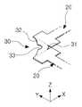
도 1 내지 도 2b를 참조하면, 본 발명의 일 실시 형태에 따른 기판(10)은 평평한 복수의 몸체부(20) 및 상기 복수의 몸체부(20)를 연결하는 연결부(30)를 포함할 수 있다.
1 to 2B , the
상기 복수의 몸체부(20)는 각각 전체적으로 평평한 사각형의 띠 형상을 가지며, 서로 대응되는 구조를 가질 수 있다.Each of the plurality of
상기 각 몸체부(20)는 광원이 실장되는 복수의 실장 영역(21)과, 상기 복수의 실장 영역(21) 사이에 배치되어 각 실장 영역(21)을 연결하는 연장 영역(22)을 포함할 수 있다. 상기 광원은, 예를 들어, 발광소자일 수 있다.Each of the
상기 복수의 몸체부(20)는, 예를 들어, 자유롭게 휘어지며 다양한 모양으로 변형이 용이한 연성회로기판(FPCB)일 수 있다. 그리고, 전기적 연결을 위한 회로 배선을 가질 수 있다.
The plurality of
상기 연결부(30)는 상기 복수의 몸체부(20) 사이에 배치되어 상기 복수의 몸체부(20)를 일체로 연결할 수 있다.The
상기 연결부(30)는 상기 복수의 몸체부(20)가 상기 연결부(30)를 중심으로 회전하여 위치가 변화함에 따라서, 평평한 형상과 돌출된 형상 사이에서 변화하는 형상을 가질 수 있다. 예를 들어, 상기 복수의 몸체부(20)는 각각 제1 위치 및 제2 위치를 가지며, 각 위치에서 상기 연결부(30)는 다른 형상을 가질 수 있다.
The
도 1 내지 도 2b에서는 상기 복수의 몸체부(20)가 제1 위치에 놓인 상태를 개략적으로 나타내고 있다.1 to 2b schematically shows a state in which the plurality of
도 1 내지 도 2b에서 도시하는 바와 같이, 상기 복수의 몸체부(20)는 제1 위치에서 상기 연결부(30)를 중심으로 실질적으로 직각을 이루며 배치될 수 있다. 즉, 상기 복수의 몸체부(20)는 상기 연결부(30)를 통해서 'ㄱ'자 형태의 절곡된 구조를 가질 수 있다.1 to 2B , the plurality of
본 실시 형태에서는 상기 복수의 몸체부(20)가 'ㄱ'자 형상의 직각을 이루며 배치되는 것으로 예시하고 있으나 이에 한정하는 것은 아니다. 예를 들어, 상기 복수의 몸체부(20)는 예각 또는 둔각을 이루는 구조로 배치될 수 있다.
In this embodiment, the plurality of
제1 위치에서 상기 연결부(30)는 전개되어 상기 복수의 몸체부(20)와 나란히 평평한 평면 구조를 유지할 수 있다. 즉, 상기 기판(10)은 상기 복수의 몸체부(20)와 연결부(30)가 전체적으로 평평한 2차원 구조를 가질 수 있다.
In the first position, the
상기 연결부(30)는 서로 마주하는 상기 복수의 몸체부(20)의 양 단면을 연결하는 내측면(31) 및 외측면(32)을 포함할 수 있다.The connecting
상기 내측면(31)과 외측면(32)은 서로 길이가 상이한 비대칭 구조를 가질 수 있다. 예를 들어, 도면에서 도시하는 바와 같이 상기 내측면(31)의 길이는 상기 외측면(32)의 길이보다 더 작을 수 있다.
The
상기 내측면(31)과 상기 외측면(32)은 각각 곡면을 가질 수 있다. 그리고, 상기 내측면(31)과 상기 외측면(32)은 곡면이 향하는 방향이 동일한 방향을 향하도록 배치될 수 있다.The
상기 외측면(32)은 상기 내측면(31)을 향해 오목하게 함몰된 오목홈(33)을 가질 수 있다. 상기 오목홈(33)은 상기 외측면(32)의 중앙에 형성될 수 있다. 상기 오목홈(33)은 필수적인 것이 아니다. 따라서, 실시 형태에 따라 상기 오목홈(33)은 생략될 수 있다.
The
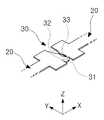
도 3 내지 도 4b에서는 상기 복수의 몸체부(20)가 제2 위치에 놓인 상태를 개략적으로 나타내고 있다.3 to 4b schematically shows a state in which the plurality of
도 3 내지 도 4b에서 도시하는 바와 같이, 상기 복수의 몸체부(20)는 제2 위치에서 대략 일(ㅡ)자 형상, 즉 평각을 이루며 배치될 수 있다. 즉, 상기 연결부(30)를 통해서 일(ㅡ)자 형상으로 펼쳐진 구조를 가질 수 있다.
3 to 4B, the plurality of
제2 위치에서 상기 연결부(30)는 접혀져 상기 복수의 몸체부(20)의 평평한 표면 위로 돌출된 입체 구조를 유지할 수 있다. 즉, 상기 기판(10)은 상기 복수의 몸체부(20)의 평평한 평면 위로 상기 연결부(30)가 부분적으로 돌출된 3차원 구조를 가질 수 있다.
In the second position, the
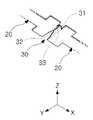
도 5에서는 상기 연결부가 변형되는 상태를 개략적으로 나타내고 있다. 도 5를 참조하면, 상기 복수의 몸체부(20)가 직각 상태에서 평각 상태로 펼쳐짐으로써 상기 연결부(30)는 상기 외측면(32)과 내측면(31)의 중앙을 가로지르는 중심선(L)을 기준으로 상기 외측면(32)의 양측이 서로 가까워지도록 반으로 접힌 구조를 가질 수 있다. 즉, 양측 몸체부(20)와 각각 연결되는 상기 외측면(32)의 양 끝단이 상기 중심선(L) 가까이 모여서 서로 마주하는 구조로 인접하여 배치될 수 있다.
5 schematically shows a state in which the connection part is deformed. Referring to FIG. 5 , as the plurality of
상기 내측면(31)은 상기 복수의 몸체부(20)와 동일한 레벨에 위치할 수 있다. 그리고, 상기 외측면(32)은 상기 복수의 몸체부(20)의 표면 위로 연장되어 상기 내측면(31)과 다른 레벨에 위치할 수 있다. 즉, 상기 외측면(32)은 상기 내측면(31)보다 높은 상부에 위치할 수 있다.The
상기 연결부(30)는 상부의 상기 외측면(32)에서 하부의 상기 내측면(31)과 상기 복수의 몸체부(20)를 향해 비스듬하게 경사진 구조를 가질 수 있다.
The
도 6a 및 도 6b에서는 상기 기판의 변형예를 개략적으로 나타내고 있다. 도 6a 및 도 6b는 각각 상기 기판의 변형예를 개략적으로 나타내는 평면도이다.
6A and 6B schematically show a modified example of the substrate. 6A and 6B are plan views schematically illustrating a modified example of the substrate, respectively.
도 6a에서 도시하는 실시 형태에 따른 기판(10')은 몸체부(20)가 3개로 구성되어 제1 위치에서 전체적으로 'ㄷ'자 형태로 배치되는 점을 제외하고, 앞선 실시 형태와 실질적으로 동일한 것으로 이해될 수 있다.The substrate 10' according to the embodiment shown in FIG. 6A is substantially the same as the previous embodiment, except that the
또한, 도 6b에서 도시하는 실시 형태에 따른 기판(10'')은 몸체부(20)가 5개로 구성되어 제1 위치에서 전체적으로 'ㄹ'자 형태로 배치되는 점을 제외하고, 앞선 실시 형태와 실질적으로 동일한 것으로 이해될 수 있다.
In addition, the substrate 10 '' according to the embodiment shown in FIG. 6B is the same as the previous embodiment, except that the
이와 같이, 본 실시 형태에 따르면, 기판(10)의 길이가 길더라도 종래와 같이 복수개로 나누지 않고 'ㄱ'자, 'ㄷ'자 또는 'ㄹ'자 등과 같이 구부러진 형태를 갖도록 하여 SMT 설비에서 한번에 SMT가 가능하도록 할 수 있다. 그리고, 이렇게 구부러진 형태의 기판을 일(ㅡ)자 형태로 펼침으로써 SMT 설비의 사이즈보다 길이가 긴 기판을 구현할 수 있다.As such, according to this embodiment, even if the length of the
특히, 기판(10)의 구부러진 부분에 해당하는 연결부(30)가 비대칭의 곡면 구조를 가짐으로써 기판(10)을 펼치는 과정에서 기판(10)의 상부로 돌출되며 접혀지도록 하여 기판(10)이 찢어지거나 절단되는 것을 방지할 수 있다.In particular, the
따라서, 종래의 SMT 설비의 SMT 작업이 가능한 사이즈보다 기판의 길이가 더 긴 경우 한번에 SMT가 불가능하기 때문에 기판을 복수개로 나누어서 SMT를 진행하고, 나누어진 기판들을 다시 하나로 연결하는 수납땜 공정을 추가로 실시해야 했던 불편함 및 이에 따른 문제점들을 해소할 수 있다.
Therefore, if the length of the substrate is longer than the size capable of SMT work of the conventional SMT facility, since SMT is impossible at once, the SMT is performed by dividing the substrate into a plurality of substrates, and a receiving soldering process of connecting the divided substrates back into one is additionally performed. Inconvenience that had to be carried out and problems resulting therefrom can be solved.
도 7 및 도 8을 참조하여 본 발명의 일 실시 형태에 따른 광원 모듈을 설명한다. 도 7은 본 발명의 일 실시 형태에 따른 광원 모듈을 개략적으로 나타내는 사시도이고, 도 8은 도 7의 분해사시도이다.
A light source module according to an embodiment of the present invention will be described with reference to FIGS. 7 and 8 . 7 is a perspective view schematically showing a light source module according to an embodiment of the present invention, and FIG. 8 is an exploded perspective view of FIG. 7 .
도 7 및 도 8을 참조하면, 본 발명의 일 실시 형태에 따른 광원 모듈(100)은 프레임 유닛(200), 방열 유닛(300) 및 광원 유닛(400)을 포함할 수 있다.
7 and 8 , the
상기 프레임 유닛(200)은 복수의 실장면(201)을 가지며, 상기 복수의 실장면(201)은 서로 다른 레벨에 위치하도록 배열될 수 있다. 상기 프레임 유닛은 상기 복수의 실장면(201)의 레벨이 일 배열방향에 따라 상승하는 계단식 구조를 가질 수 있다.
The
도 8에서 도시하는 바와 같이, 상기 프레임 유닛(200)은 상면에 해당하는 복수의 실장면(201), 상기 복수의 실장면(201)을 연결하는 연결면(202) 및 측면(203)을 포함할 수 있다.
As shown in FIG. 8 , the
상기 복수의 실장면(201)은 서로 다른 레벨에 위치하도록 배치될 수 있다. 즉, 서로 다른 높이로 배치될 수 있다.The plurality of mounting
상기 실장면(201)에는 상부를 향해 돌출된 복수의 돌기(210)가 구비될 수 있다. 상기 복수의 돌기(210)는 대략 원기둥 형상을 가질 수 있으며, 서로 일정 간격으로 이격되어 배열될 수 있다.
A plurality of
상기 연결면(202)은 상기 복수의 실장면(201) 사이에 위치하며, 서로 다른 레벨에 위치하는 인접한 두 개의 실장면(201)을 상호 연결할 수 있다. 즉, 상대적으로 상부에 위치하는 실장면(201)의 일측에서 하부 방향으로 연장되어 상대적으로 하부에 위치하는 다른 실장면(201)의 타측과 연결될 수 있다.
The
상기 프레임 유닛(200)은, 예를 들어, PC, PMMA와 같은 수지를 금형에 주입하고 고형화하는 방식으로 형성될 수 있다. 예를 들어, 인젝션 몰딩(injection molding), 트랜스퍼 몰딩(transfer molding), 컴프레션 몰딩(compression molding) 등의 방식이 사용될 수 있다.
The
상기 방열 유닛(300)은 상기 복수의 실장면(201)에 각각 장착되어 고정될 수 있다. 그리고, 상기 프레임 유닛(200)에 조립된 상기 각 방열 유닛(300)은 상기 프레임 유닛(200)의 각 실장면(201) 및 상기 각 실장면(201)에 실질적으로 수직한 측면(203)을 덮을 수 있다.The
상기 방열 유닛(300)은 상기 실장면(201)에 탈착이 가능하게 조립되는 히트 싱크(heat sink)의 일종으로, 추후 설명하는 광원 유닛(400)을 지지하는 한편, 상기 광원 유닛(400)에서 발생되는 열을 외부로 방출할 수 있다.
The
상기 방열 유닛(300)은 상기 프레임 유닛(200)의 각 실장면(201)에 놓이는 베이스부(310), 및 상기 베이스부(310)의 가장자리에서 절곡되어 상기 측면(203)을 따라서 하부로 연장되는 연장부(320)를 포함할 수 있다. 상기 방열 유닛(300)은, 예를 들어, 전체적인 형상이 "ㄱ"자 모양을 가질 수 있다.The
상기 베이스부(310)와 연장부(320)는, 예를 들어, 직사각형 형상을 갖는 단일의 금속 플레이트를 프레스 가공하여 일체로 형성될 수 있다. 또한, 단순한 구조를 가져 대량 생산이 가능하다.
The
상기 베이스부(310)는 상기 실장면(201)과 대응되는 형상을 가질 수 있다. 상기 베이스부(310)는 상기 실장면(201)에 돌출된 복수의 돌기(210)가 삽입되는 복수의 연결 홀(330)을 포함할 수 있다.The
상기 복수의 연결 홀(330)은 상기 베이스부(310)를 관통하여 형성될 수 있다. 상기 복수의 연결 홀(330)은 상기 복수의 돌기(210)가 배열된 위치에 대응하여 형성될 수 있다.
The plurality of connection holes 330 may be formed through the
상기 광원 유닛(400)은 상기 복수의 방열 유닛(300) 상에 놓이는 기판(410)과, 상기 기판(410) 상에 실장되는 복수의 발광소자(440)를 포함할 수 있다.
The
상기 기판(410)은 복수의 몸체부(420) 및 상기 복수의 몸체부(420)를 일체로 연결하는 연결부(430)를 포함할 수 있다. 상기 기판(410)은 도 1 내지 도 6에 도시된 실시 형태에 따른 기판(10)과 기본 구성 및 구조가 실질적으로 동일하다. 따라서, 상기 기판(410)에 대한 구체적인 설명은 생략한다.
The
상기 복수의 방열 유닛(300) 상에 놓여 상기 프레임 유닛(200)에 장착되기 위해 상기 기판(410)은 상기 연결부(430)를 통해서 복수의 몸체부(420)가 연속하여 연결되는 계단식 구조를 가질 수 있다.In order to be placed on the plurality of
구체적으로, 도 8에서 도시하는 바와 같이, 상기 복수의 몸체부(420)와 연결부(430)가 제2 위치에 배치된 상태의 구조를 가질 수 있다. 즉, 상기 복수의 몸체부(420)는 평각을 이루며 대략 일(ㅡ)자 형상으로 펼쳐진 구조를 가질 수 있다. 그리고 상기 연결부(430)는 접혀져 상기 복수의 몸체부(420)의 평평한 표면 위로 돌출된 입체 구조를 유지할 수 있다(도 3 및 도 4 참조).
Specifically, as shown in FIG. 8 , the plurality of
한편, 상기 각 몸체부(420)는 상기 복수의 실장면(201) 상에 각각 배치되어 상기 발광소자(440)가 실장되는 복수의 실장 영역(421)과, 상기 복수의 실장 영역(421) 사이에서 각 실장 영역(421)을 연결하는 연장 영역(422)을 포함할 수 있다.
Meanwhile, each of the
상기 복수의 실장 영역(421)은 상기 복수의 실장면(201) 상에 각각 배치되며, 해당 실장면(201)에 장착된 각 방열 유닛(300) 상에 놓여 고정될 수 있다. 상기 복수의 실장 영역(421)은 상기 방열 유닛(300) 위로 돌출된 상기 돌기(210)가 삽입되는 관통 홀(421a)을 가질 수 있다.The plurality of mounting
상기 복수의 연장 영역(422)은 서로 다른 레벨에 위치하는 상기 복수의 실장 영역(421) 사이에 위치하며, 상기 각 실장 영역(421)과 실질적으로 수직하게 연결될 수 있다. 즉, 상대적으로 상부에 위치하는 실장 영역(421)의 일측에서 하부 방향으로 연장되어 상대적으로 하부에 위치하는 다른 실장 영역(421)의 타측과 연결될 수 있다.
The plurality of
상기 복수의 발광소자(440)는 상기 기판(410)에 실장되며, 상기 복수의 실장면(201) 상에 각각 배치될 수 있다.The plurality of light emitting
상기 발광소자(440)는 외부에서 인가되는 구동 전원에 의해 소정 파장의 광을 발생시키는 광전소자(Optoelectronic Device)일 수 있다. 예를 들어, n형 반도체층 및 p형 반도체층과 이들 사이에 개재되는 활성층을 갖는 반도체 발광다이오드(LED) 칩 또는 이를 구비한 LED 패키지를 포함할 수 있다.
The
상기 발광소자(440)는 함유되는 물질 또는 형광체와의 조합에 따라서 청색 광, 녹색 광 또는 적색 광을 발광할 수 있으며, 백색 광, 자외 광 등을 발광할 수도 있다. 상기 발광소자(440)는 동일한 파장의 빛을 발생시키는 동종(同種)이거나 또는 서로 상이한 파장의 빛을 발생시키는 이종(異種)으로 다양하게 구성될 수 있다. 또한, 상기 발광소자(440)는, 예를 들어 0.5W용 및 1W용과 같이 전력에 따라서 다양하게 구성될 수도 있다.
The
상기 발광소자(440)는 다양한 구조의 발광다이오드(LED) 칩 또는 이러한 LED 칩을 내부에 구비하는 다양한 형태의 LED 패키지가 사용될 수 있다. 본 실시 형태에서는 상기 발광소자(440)가 LED 패키지인 경우를 예시하고 있으나 이에 한정하는 것은 아니다.
As the
이하에서는 본 발명의 일 실시 형태에 따른 광원 모듈에 채용될 수 있는 발광소자에 대해 설명한다. 도 9a 및 도 9b에서는 본 발명의 일 실시 형태에 따른 광원 모듈에 채용될 수 있는 발광소자를 각각 개략적으로 나타내고 있다.
Hereinafter, a light emitting device that can be employed in a light source module according to an embodiment of the present invention will be described. 9A and 9B schematically show light emitting devices that may be employed in a light source module according to an embodiment of the present invention.
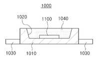
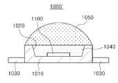
도 9a에서 도시하는 바와 같이, 본 발명의 일 실시 형태에 따른 발광소자(1000)는 반사컵(1020)을 갖는 몸체(1010) 내에 LED 칩(1100)이 실장된 패키지 구조를 가질 수 있다.
As shown in FIG. 9A , the
상기 몸체(1010)는 상기 LED 칩(1100)을 실장하여 지지하며, 광 반사율이 높은 백색 성형 복합재(white molding compound)로 이루어질 수 있다. 이는 LED 칩(1100)에서 방출되는 광을 반사시켜 외부로 방출되는 광량을 증가시키는 효과가 있다. 이러한 백색 성형 복합재는 고 내열성의 열경화성 수지 계열 또는 실리콘 수지 계열을 포함할 수 있다. 또한, 열 가소성 수지 계열에 백색 안료 및 충진제, 경화제, 이형제, 산화방지제, 접착력 향상제 등이 첨가될 수 있다. 또한, FR-4, CEM-3, 에폭시 재질 또는 세라믹 재질 등으로도 이루어질 수 있다. 또한, 알루미늄(Al)과 같은 금속 재질로 이루어지는 것도 가능하다.
The
상기 몸체(1010)에는 상기 기판(410)에 실장되어 외부 전원과의 전기적 연결을 위한 리드 프레임(1030)이 구비될 수 있다. 상기 리드 프레임(1030)은 전기 전도성이 우수한 재질, 예를 들어, 알루미늄, 구리 등의 금속 재질로 이루어질 수 있다. 만일, 상기 몸체(1010)가 금속 재질로 이루어지는 경우에는 상기 몸체(1010)와 상기 리드 프레임(1030) 사이에는 절연 물질이 개재될 수 있다.
The
상기 몸체(1010)에 구비되는 상기 반사컵(1020)은 상기 LED 칩(1100)이 실장되는 바닥면으로 상기 리드 프레임(1030)이 노출될 수 있다. 그리고, 상기 LED 칩(1100)은 상기 노출된 리드 프레임(1030)과 전기적으로 접속될 수 있다.The
상기 반사컵(1020)의 상기 몸체(1010)의 상면으로 노출되는 단면의 크기는 상기 반사컵(1020)의 바닥면의 크기보다 큰 구조를 가질 수 있다. 여기서, 상기 반사컵(1020)의 상기 몸체(1010)의 상면으로 노출되는 단면은 상기 발광소자(1000)의 발광면을 정의할 수 있다.
The size of the cross-section of the
상기 LED 칩(1100)은 상기 몸체(1010)의 반사컵(1020) 내에 형성되는 봉지재(1040)에 의해 밀봉될 수 있다. 상기 봉지재(1040)에는 파장변환물질이 함유될 수 있다.
The
도 9b에서는 상기 발광소자(1000')의 변형예를 개략적으로 나타내고 있다. 도 9b에서 도시하는 바와 같이, 상기 몸체(1010) 상에는 상기 봉지재(1040)를 덮는 렌즈(1050)가 더 부착될 수 있다.9B schematically shows a modified example of the light emitting device 1000'. As shown in FIG. 9B , a
상기 렌즈(1050)는 반구형의 구조를 가지며, 예를 들어, 볼록 렌즈일 수 있다. 상기 렌즈(1050)는 상기 LED 칩(1100)에서 발생된 광을 굴절시켜 보다 넓은 범위로 조사되도록 할 수 있다.
The
한편, 상기 봉지재(1040)에 함유되는 파장변환물질로는, 예컨대 상기 LED 칩(1100)에서 발생된 광에 의해 여기되어 다른 파장의 광을 방출하는 형광체가 적어도 1종 이상 함유될 수 있다. 이를 통해 백색 광을 비롯해 다양한 색상의 광이 방출될 수 있도록 조절할 수 있다.Meanwhile, as the wavelength conversion material contained in the
예를 들어, LED 칩(1100)이 청색 광을 발광하는 경우, 황색, 녹색, 적색 및/또는 오랜지색의 형광체를 조합하여 백색 광을 발광하도록 할 수 있다. 또한, 보라색, 청색, 녹색, 적색 또는 적외선을 발광하는 LED 칩 중 적어도 하나를 포함하게 구성할 수도 있다. 이 경우, 상기 LED 칩(1100)은 연색성(CRI)을 '40'에서 '100' 수준으로 조절할 수 있으며, 또한, 색온도를 대략 2000K에서 20000K 수준으로 다양한 백색 광을 발생시킬 수 있다. 또한, 필요에 따라서는 보라색, 청색, 녹색, 적색, 오랜지색의 가시광 또는 적외선을 발생시켜 주위 분위기 또는 기분에 맞게 색을 조정할 수 있다. 또한, 식물 성장을 촉진할 수 있는 특수 파장의 광을 발생시킬 수도 있다.
For example, when the
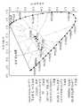
청색 LED 칩에 황색, 녹색, 적색 형광체 및/또는 녹색 LED 칩과 적색 LED 칩의 조합으로 만들어지는 백색 광은 2개 이상의 피크 파장을 가지며, 도 10에서 도시하는 CIE 1931 좌표계의 (x, y) 좌표가 (0.4476, 0.4074), (0.3484, 0.3516), (0.3101, 0.3162), (0.3128, 0.3292), (0.3333, 0.3333)을 잇는 선분 상에 위치할 수 있다. 또는, 상기 선분과 흑체 복사 스펙트럼으로 둘러싸인 영역에 위치할 수 있다. 상기 백색 광의 색 온도는 대략 2000K ~ 20000K사이에 해당한다.White light produced by a combination of yellow, green, and red phosphors on a blue LED chip and/or a green LED chip and a red LED chip has two or more peak wavelengths, and (x, y) in the CIE 1931 coordinate system shown in FIG. The coordinates may be located on the line segment connecting (0.4476, 0.4074), (0.3484, 0.3516), (0.3101, 0.3162), (0.3128, 0.3292), (0.3333, 0.3333). Alternatively, it may be located in a region surrounded by the line segment and the blackbody radiation spectrum. The color temperature of the white light corresponds to approximately 2000K to 20000K.
도 10에서 상기 흑체 복사 스펙트럼 하부에 있는 점 E(0.3333, 0.3333) 부근의 백색 광은 상대적으로 황색계열 성분의 광이 약해진 상태로 사람이 육안으로 느끼기에는 보다 선명한 느낌 또는 신선한 느낌을 가질 수 있는 영역의 조명 광원으로 사용될 수 있다. 따라서, 상기 흑체 복사 스펙트럼 하부에 있는 점 E(0.3333, 0.3333) 부근의 백색 광을 이용한 조명 제품은 식료품, 의류 등을 판매하는 상가용 조명으로 효과가 좋다.
In FIG. 10, the white light near point E (0.3333, 0.3333) in the lower part of the blackbody radiation spectrum is a region in which the light of the yellow-based component is relatively weak, and the human eye can have a clearer feeling or a fresh feeling. It can be used as a lighting source for Accordingly, a lighting product using white light near point E (0.3333, 0.3333) in the lower part of the blackbody radiation spectrum is effective as a lighting for shopping malls selling foodstuffs, clothes, and the like.
형광체는 다음과 같은 조성식 및 컬러(color)를 가질 수 있다.The phosphor may have the following compositional formula and color.
산화물계: 황색 및 녹색 Y3Al5O12:Ce, Tb3Al5O12:Ce, Lu3Al5O12:CeOxide system: yellow and green Y3 Al5 O12 :Ce, Tb3 Al5 O12 :Ce, Lu3 Al5 O12 :Ce
실리케이트계: 황색 및 녹색 (Ba,Sr)2SiO4:Eu, 황색 및 등색 (Ba,Sr)3SiO5:CeSilicates: yellow and green (Ba,Sr)2 SiO4 :Eu, yellow and orange (Ba,Sr)3 SiO5 :Ce
질화물계: 녹색 β-SiAlON:Eu, 황색 La3Si6N11:Ce, 등색 α-SiAlON:Eu, 적색 CaAlSiN3:Eu, Sr2Si5N8:Eu, SrSiAl4N7:Eu, SrLiAl3N4:Eu, Ln4-x(EuzM1-z)xSi12-yAlyO3+x+yN18-x-y (0.5≤x≤3, 0<z<0.3, 0<y≤4) (단, 여기서 Ln은 IIIa 족 원소 및 희토류 원소로 이루어지는 군에서 선택되는 적어도 한 종의 원소이고, M은 Ca, Ba, Sr 및 Mg로 이루어지는 군에서 선택되는 적어도 한 종의 원소일 수 있다.)Nitride type: green β-SiAlON:Eu, yellow La3 Si6 N11 :Ce, orange α-SiAlON:Eu, red CaAlSiN3 :Eu, Sr2 Si5 N8 :Eu, SrSiAl4 N7 :Eu, SrLiAl3 N4 :Eu, Ln4-x (Euz M1-z )x Si12-y Aly O3+x+y N18-xy (0.5≤x≤3, 0<z<0.3, 0<y ≤4) (wherein, Ln is at least one element selected from the group consisting of group IIIa elements and rare earth elements, and M is at least one element selected from the group consisting of Ca, Ba, Sr and Mg. there is.)
플루오라이트(fluoride)계: KSF계 적색 K2SiF6:Mn4+, K2TiF6:Mn4+, NaYF4:Mn4+, NaGdF4:Mn4+ , K3SiF7:Mn4+
Fluoride type: KSF type red K2 SiF6 :Mn4+ , K2 TiF6 :Mn4+ , NaYF4 :Mn4+ , NaGdF4 :Mn4+ , K3 SiF7 :Mn4+
형광체 조성은 기본적으로 화학양론(Stoichiometry)에 부합하여야 하며, 각 원소들은 주기율표상 각 족들 내 다른 원소로 치환이 가능하다. 예를 들어 Sr은 알카리토류(II)족의 Ba, Ca, Mg 등으로, Y는 란탄계열의 Tb, Lu, Sc, Gd 등으로 치환이 가능하다. 또한, 활성제인 Eu 등은 원하는 에너지 준위에 따라 Ce, Tb, Pr, Er, Yb 등으로 치환이 가능하며, 활성제 단독 또는 특성 변형을 위해 부활성제 등이 추가로 적용될 수 있다.The phosphor composition should basically conform to stoichiometry, and each element can be substituted with another element in each group on the periodic table. For example, Sr may be substituted with Ba, Ca, Mg, etc. of alkaline earth (II) group, and Y may be substituted with Tb, Lu, Sc, Gd, etc. of lanthanide series. In addition, the activator Eu, etc. can be substituted with Ce, Tb, Pr, Er, Yb, etc. according to a desired energy level, and a sub-activator or the like may be additionally applied to the activator alone or to modify properties.
특히, 플루오라이트계 적색 형광체는 고온/고습에서의 신뢰성 향상을 위하여 각각 Mn을 함유하지 않는 불화물로 코팅되거나 형광체 표면 또는 Mn을 함유하지 않는 불화물 코팅 표면에 유기물 코팅을 더 포함할 수 있다. 상기와 같은 플루어라이트계 적색 형광체의 경우 기타 형광체와 달리 40nm 이하의 협반치폭을 구현할 수 있기 때문에, UHD TV와 같은 고해상도 TV에 활용될 수 있다.
In particular, the fluorite-based red phosphor may be coated with a fluoride not containing Mn or an organic coating may be further included on the surface of the phosphor or the surface of the fluoride coating not containing Mn to improve reliability at high temperature/high humidity. In the case of the fluorite-based red phosphor as described above, unlike other phosphors, it can implement a narrow half maximum width of 40 nm or less, and thus can be utilized in high-resolution TVs such as UHD TVs.
또한, 파장변환물질은 형광체 대체 물질로 양자점(Quantum Dot, QD) 등의 물질들이 적용될 수 있으며, 형광체와 QD를 혼합 또는 QD 단독으로 사용될 수 있다.In addition, as the wavelength conversion material, materials such as quantum dots (QD) may be applied as a substitute for the phosphor, and a phosphor and QD may be mixed or QD alone may be used.
양자점은 III-V 또는 II-VI화합물 반도체를 이용하여 코어(Core)-쉘(Shell)구조를 가질 수 있다. 예를 들면, CdSe, InP 등과 같은 코어(core)와 ZnS, ZnSe과 같은 쉘(shell)을 가질 수 있다. 또한, 상기 QD는 코어 및 쉘의 안정화를 위한 리간드(ligand)를 포함할 수 있다. 예를 들어, 상기 코어 직경은 대략 1 ~ 30nm, 나아가 대략 3 ~ 10nm일 수 있다. 상기 쉘 두께는 대략 0.1 ~ 20nm, 나아가 0.5 ~ 2nm일 수 있다.The quantum dot may have a core-shell structure using a III-V or II-VI compound semiconductor. For example, it may have a core such as CdSe or InP and a shell such as ZnS or ZnSe. In addition, the QD may include a ligand for stabilizing the core and the shell. For example, the core diameter may be approximately 1 to 30 nm, further approximately 3 to 10 nm. The shell thickness may be approximately 0.1 to 20 nm, further 0.5 to 2 nm.
상기 양자점은 사이즈에 따라 다양한 컬러를 구현할 수 있으며, 특히 형광체 대체 물질로 사용되는 경우에는 적색 또는 녹색 형광체로 사용될 수 있다. 양자점을 이용하는 경우, 협반치폭(예, 약 35nm)을 구현할 수 있다.
The quantum dots may implement various colors according to their size, and in particular, when used as a substitute for a phosphor, may be used as a red or green phosphor. In the case of using quantum dots, a narrow half maximum width (eg, about 35 nm) may be implemented.
이하에서는 본 발명에 따른 LED 칩 다양한 실시예에 대해 설명한다. 도 11 및 도 12는 발광소자에 채용될 수 있는 LED 칩의 다양한 예를 나타내는 단면도이다.
Hereinafter, various embodiments of the LED chip according to the present invention will be described. 11 and 12 are cross-sectional views illustrating various examples of LED chips that may be employed in a light emitting device.
도 11a는 본 발명에 채용될 수 있는 LED 칩의 일 예를 나타내는 평면도이며, 도 11b는 도 11a에 도시된 LED 칩을 III-III'선으로 절취한 측단면도이다.11A is a plan view showing an example of an LED chip that can be employed in the present invention, and FIG. 11B is a side cross-sectional view of the LED chip shown in FIG. 11A taken along line III-III'.
도 11a 및 도 11b에 도시된 LED 칩(1100)은 조명용으로 고출력을 위한 대면적 구조일 수 있다. 상기 LED 칩(1100)은 전류 분산의 효율 및 방열 효율을 높이기 위한 구조이다.The
상기 LED 칩(1100)은 발광적층체(S)와, 제1 전극(1120), 절연층(1130), 제2 전극(1108) 및 도전성 기판(1110)을 포함할 수 있다. 상기 발광적층체(S)는 순차적으로 적층된 제1 도전형 반도체층(1104), 활성층(1105), 제2 도전형 반도체층(1106)을 포함할 수 있다.
The
상기 제1 전극(1120)은 제1 도전형 반도체층(1104)에 전기적으로 접속하기 위하여 제2 도전형 반도체층(1106) 및 활성층(1105)과는 전기적으로 절연되어 상기 제1 도전형 반도체층(1104)의 적어도 일부 영역까지 연장된 하나 이상의 도전성 비아(1180)를 포함할 수 있다. 상기 도전성 비아(1180)는 제1 전극(1120)의 계면에서부터 제2 전극(1108), 제2 도전형 반도체층(1106) 및 활성층(1105)을 통과하여 제1 도전형 반도체층(1104) 내부까지 연장될 수 있다. 이러한 도전성 비아(1180)는 식각 공정, 예를 들어, ICP-RIE 등을 이용하여 형성될 수 있다.The
상기 제1 전극(1120) 상에는 상기 제1 전극(1120)이 상기 제1 도전형 반도체층(1104)을 제외한 다른 영역과 전기적으로 절연시키기 위한 절연층(1130)이 제공된다. 도 11b에 도시된 바와 같이, 상기 절연층(1130)은 상기 제2 전극(1108)과 제1 전극(1120)의 사이뿐만 아니라 상기 도전성 비아(1180)의 측면에도 형성된다. 이로써, 상기 도전성 비아(1180)의 측면에 노출되는 상기 제2 전극(1108), 제2 도전형 반도체층(1106) 및 활성층(1105)과 상기 제1 전극(1120)을 절연시킬 수 있다. 절연층(1130)은 SiO2, SiOxNy, SixNy과 같은 절연 물질을 증착시켜 형성될 수 있다.An insulating
상기 도전성 비아(1180)에 의해 제1 도전형 반도체층(1104)의 컨택영역(C)이 노출되며, 상기 제1 전극(1120)의 일부 영역은 상기 도전성 비아(1180)를 통해 상기 컨택영역(C)에 접하도록 형성될 수 있다. 이로써, 상기 제1 전극(1120)은 상기 제1 도전형 반도체층(1104)에 접속될 수 있다.A contact region C of the first conductivity-
상기 도전성 비아(1180)는 접촉 저항이 낮아지도록 개수, 형상, 피치, 제1 및 제2 도전형 반도체층(1104, 1106)과의 접촉 직경(또는 접촉 면적) 등이 적절히 조절될 수 있으며(도 11a 참조), 행과 열을 따라 다양한 형태로 배열됨으로써 전류 흐름이 개선될 수 있다. 컨택영역(C) 면적은 발광적층체(S)의 평면 면적의 대략 0.1% 내지 20%의 범위가 되도록 도전성 비아(1180)의 개수 및 접촉 면적이 조절될 수 있다. 예를 들어 0.5% 내지 15%이며, 나아가, 1% 내지 10%일 수 있다. 상기 면적이 0.1%보다 작으면 전류 분산이 균일하지 않아 발광 특성이 떨어지며, 또한 20% 이상으로 전극 면적이 증가하면 상대적으로 발광 면적의 감소로 발광 특성 및 휘도가 감소하는 문제가 발생할 수 있다.The number, shape, pitch, and contact diameter (or contact area) of the
상기 제1 도전형 반도체층(1104)과 접촉하는 영역의 도전성 비아(1180)의 반경은 예를 들어, 1㎛ 내지 50㎛의 범위일 수 있으며, 도전성 비아(1180)의 개수는 발광적층체(S) 영역의 넓이에 따라, 발광적층체(S) 영역 당 1개 내지 48000개일 수 있다. 도전성 비아(1180)는 발광적층체(S) 영역의 넓이에 따라 다르지만, 예를 들어 2개 내지 45000개이며, 나아가 5개 내지 40000개이며, 더 나아가 10개 내지 35000개일 수 있다. 각 도전성 비아(1180) 간의 거리는 10㎛ 내지 1000㎛ 범위의 행과 열을 가지는 매트릭스 구조일 수 있으며, 예를 들어 50㎛ 내지 700㎛ 범위일 수 있으며, 나아가 100㎛ 내지 500㎛범위일 수 있고, 더 나아가 150㎛ 내지 400㎛범위 일 수 있다.The radius of the
각 도전성 비아(1180) 간의 거리가 10㎛보다 작으면 비아의 개수가 증가하게 되고 상대적으로 발광면적이 줄어들어 발광 효율이 떨어지며, 거리가 1000㎛보다 커지면 전류 확산이 어려워 발광 효율이 떨어지는 문제점이 있을 수 있다. 도전성 비아의 깊이는 제2 도전형 반도체층(1106) 및 활성층(1105)의 두께에 따라 다르게 형성될 수 있고, 예컨대, 0.1㎛ 내지 5.0㎛의 범위일 수 있다.If the distance between the
상기 제2 전극(1108)은 도 9b에서 도시된 바와 같이 상기 발광적층체(S) 외부로 연장되어 노출된 전극형성영역(D)을 제공한다. 상기 전극형성영역(D)은 외부 전원을 상기 제2 전극(1108)에 연결하기 위한 전극패드부(1119)를 구비할 수 있다. 이러한 전극형성영역(D)을 1개로 예시되어 있으나, 필요에 따라 복수개로 구비할 수 있다. 상기 전극형성영역(D)은 도 11a에 도시된 바와 같이 발광면적을 최대화하기 위해서 상기 LED 칩(1100)의 일측 모서리에 형성할 수 있다.As shown in FIG. 9B , the
본 실시예와 같이, 전극패드부(1119) 주위에는 에칭스톱용 절연층(1140)이 배치될 수 있다. 상기 에칭스톱용 절연층(1140)은 발광적층체(S) 형성 후 그리고 제2 전극(1108)형성 전에 전극형성영역(D)에 형성될 수 있으며, 전극형성영역(D)을 위한 에칭공정시에 에칭스톱으로 작용할 수 있다.As in the present embodiment, an insulating
상기 제2 전극(1108)은 상기 제2 도전형 반도체층(1106)과 오믹컨택을 이루면서도 높은 반사율을 갖는 물질이 사용될 수 있다. 이러한 제2 전극(1108)의 물질로는 앞서 예시된 반사전극물질이 사용될 수 있다.
For the
도 12는 본 발명에 채용될 수 있는 LED 칩의 일 예를 나타내는 측단면도이다.12 is a side cross-sectional view showing an example of an LED chip that can be employed in the present invention.
도 12를 참조하면, 상기 LED 칩(1200)은 기판(1201) 상에 형성된 반도체 적층체(1210)을 포함한다. 상기 반도체 적층체(1210)는 제1 도전형 반도체층(1214), 활성층(1215) 및 제2 도전형 반도체층(1216)을 포함할 수 있다.Referring to FIG. 12 , the
상기 LED 칩(1200)은 상기 제1 및 제2 도전형 반도체층(1214,1216)에 각각 접속된 제1 및 제2 전극(1222, 1224)을 포함한다. 상기 제1 전극(1222)은 제2 도전형 반도체층(1216) 및 활성층(1215)을 관통하여 제1 도전형 반도체층(1214)과 접속된 도전성 비아와 같은 연결전극부(1222a) 및 상기 연결전극부(1222a)에 연결된 제1 전극 패드(1222b)를 포함할 수 있다. 상기 연결전극부(1222a)는 절연부(1221)에 의하여 둘러싸여 활성층(1215) 및 제2 도전형 반도체층(1216)과 전기적으로 분리될 수 있다. 상기 연결전극부(1222a)는 반도체 적층체(1210)가 식각된 영역에 배치될 수 있다. 상기 연결전극부(1222a)는 접촉 저항이 낮아지도록 개수, 형상, 피치 또는 제1 도전형 반도체층(1214)과의 접촉 면적 등을 적절히 설계할 수 있다. 또한, 연결전극부(1222a)는 반도체 적층체(1210) 상에 행과 열을 이루도록 배열됨으로써 전류 흐름을 개선시킬 수 있다. 상기 제2 전극(1224)은 제2 도전형 반도체층(1216) 상의 오믹 콘택층(1224a) 및 제2 전극 패드(1224b)를 포함할 수 있다.The
상기 연결전극부(1222a) 및 오믹 콘택층(1224a)은 각각 제1 및 제2 도전형 반도체층(1214, 1216)과 오믹 특성을 갖는 도전성 물질이 1층 또는 다층 구조를 포함할 수 있다. 예를 들어, Ag, Al, Ni, Cr, 투명 도전성 산화물(TCO) 등의 물질 중 하나 이상을 증착하거나 스퍼터링하는 등의 공정으로 형성될 수 있다.The connection electrode part 1222a and the
상기 제1 및 제2 전극 패드(1222b, 1224b)는 각각 상기 연결전극부(1222a) 및 오믹 콘택층(1224b)에 각각 접속되어 상기 LED 칩(1200)의 외부 단자로 기능할 수 있다. 예를 들어, 제1 및 제2 전극 패드(1222b, 1224b)는 Au, Ag, Al, Ti, W, Cu, Sn, Ni, Pt, Cr, NiSn, TiW, AuSn 또는 이들의 공융 금속일 수 있다.The first and
상기 제1 및 제2 전극(1222, 1224)은 서로 동일한 방향으로 배치될 수 있으며, 리드 프레임 등에 소위, 플립칩 형태로 실장될 수 있다.The first and
한편, 2개의 전극(1222,1224)은 절연부(1221)에 의하여 서로 전기적으로 분리될 수 있다. 절연부(1221)는 전기적으로 절연 특성을 갖는 물질이면 어느 것이나 사용할 수 있으며, 전기 절연성을 갖는 물체라면 어느 것이나 채용 가능하지만, 광흡수율이 낮은 물질을 사용할 수 있다. 예를 들어, SiO2, SiOxNy, SixNy 등의 실리콘 산화물, 실리콘 질화물을 이용할 수 있을 것이다. 필요에 따라, 광투과성 물질 내에 광 반사성 필러를 분산시켜 광반사 구조를 형성할 수 있다. 이와 달리, 상기 절연부(1221)는 서로 다른 굴절률을 갖는 복수의 절연막들이 교대로 적층된 다층 반사구조일 수 있다. 예를 들어 이러한 다층 반사구조는 제1 굴절률을 갖는 제1 절연막과 제2 굴절률을 갖는 제2 절연막이 교대로 적층된 분산 브래그 반사기(DBR: Distributed Bragg Reflector)일 수 있다.Meanwhile, the two
상기 다층 반사구조는 상기 굴절률이 서로 다른 복수의 절연막들이 2회 내지 100회 반복하여 적층될 수 있다. 예를 들어, 3회 내지 70회 반복하여 적층 될 수 있으며, 나아가 4회 내지 50회 반복하여 적층될 수 있다. 상기 다층 반사구조의 복수의 절연막은 각각 SiO2, SiN, SiOxNy, TiO2, Si3N4, Al2O3, TiN, AlN, ZrO2, TiAlN, TiSiN 등의 산화물 또는 질화물 및 그 조합일 수 있다. 예를 들어, 상기 활성층에서 생성되는 빛의 파장을 λ이라고 하고 n을 해당 층의 굴절률이라 할 때에, 상기 제1 절연막과 제2 절연막은, λ/4n의 두께를 갖도록 형성될 수 있으며, 대략 약 300Å 내지 900Å의 두께를 가질 수 있다. 이때, 상기 다층 반사구조는 상기 활성층(1215)에서 생성된 빛의 파장에 대해서 높은 반사율(95% 이상)을 갖도록 각 제1 절연막 및 제2 절연막의 굴절률과 두께가 선택되어 설계될 수 있다.In the multilayer reflective structure, a plurality of insulating layers having different refractive indices may be repeatedly stacked 2 to 100 times. For example, the lamination may be repeated 3 to 70 times, and further may be repeatedly laminated 4 to 50 times. Each of the plurality of insulating layers of the multilayer reflective structure includes an oxide or nitride such as SiO2 , SiN, SiOx Ny , TiO2 , Si3 N4 , Al2 O3 , TiN, AlN, ZrO2 , TiAlN, TiSiN, and the like, and a nitride thereof. It can be a combination. For example, when the wavelength of light generated in the active layer is λ and n is the refractive index of the layer, the first insulating layer and the second insulating layer may be formed to have a thickness of λ/4n, and approximately It may have a thickness of 300 Å to 900 Å. In this case, the multilayer reflective structure may be designed by selecting the refractive index and thickness of each of the first insulating layer and the second insulating layer to have a high reflectance (95% or more) with respect to the wavelength of the light generated by the
상기 제1 절연막 및 제2 절연막의 굴절률은 약 1.4 내지 약 2.5 범위에서 결정될 수 있으며, 상기 제1 도전형 반도체층(1214)의 굴절률 및 기판의 굴절률보다 작은 값일 수 있으나, 상기 제1 도전형 반도체층(1214)의 굴절률보다는 작되 기판의 굴절률보다는 큰 값을 가질 수도 있다.
The refractive indices of the first insulating layer and the second insulating layer may be determined in the range of about 1.4 to about 2.5, and may be smaller than the refractive index of the first conductivity
도 13에서는 본 발명의 다양한 실시 형태에 따른 광원 모듈이 채용된 조명 장치를 개략적으로 나타내고 있다. 본 실시 형태에 따른 조명 장치는, 예를 들어, 자동차의 리어 램프(rear lamp)를 포함할 수 있다.
13 schematically shows a lighting device employing a light source module according to various embodiments of the present disclosure. The lighting device according to the present embodiment may include, for example, a rear lamp of a vehicle.
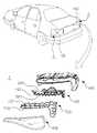
도 13에서 도시하는 바와 같이, 상기 조명 장치(1)는 상기 광원 모듈(100)이 지지되는 하우징(500), 상기 광원 모듈(100)을 보호하도록 상기 하우징(500)을 덮는 커버(600)를 포함하며, 상기 광원 모듈(100) 상에는 리플렉터(700)가 배치될 수 있다. 상기 리플렉터(700)는 복수의 반사면(710) 및 상기 복수의 반사면(710) 각각의 바닥면에 구비되는 복수의 관통홀(720)을 포함하며, 상기 광원 모듈(100)의 광원 유닛(400)은 발광소자(440)가 상기 복수의 관통홀(720)을 통해 상기 복수의 반사면(710)으로 노출될 수 있다.
13 , the
상기 조명 장치(1)는 자동차의 코너 부분의 형상에 대응하여 전체적으로 완만한 곡면 구조를 가질 수 있으며, 따라서 프레임 유닛(200) 및 이에 조립되는 복수의 방열 유닛(300)과 광원 유닛(400)은 조명 장치(1)의 곡면 구조에 대응하는 스텝 구조를 갖는 광원 모듈(100)을 형성할 수 있다. 이러한 광원 모듈(100)의 구조는 조명 장치(1), 즉 리어 램프의 설계 디자인에 대응하여 다양하게 변형될 수 있다.
The
본 발명에 따른 실시 형태에서는 상기 조명 장치(1)가 자동차의 리어 램프인 경우를 예시하고 있으나, 이에 한정하는 것은 아니다. 예를 들어, 도 14에서 도시하는 바와 같이, 상기 조명 장치(1')는 자동차의 헤드 램프를 포함할 수 있으며, 상기 광원 모듈(100)은 상기 헤드 램프의 곡면에 대응하는 다단의 스텝 구조를 갖도록 형성될 수 있다.In the embodiment according to the present invention, the case where the
또한, 상기 조명 장치(1'')는 자동차의 도어 미러에 장착되는 방향 지시등을 포함할 수 있다. 마찬가지로, 상기 광원 모듈(100)은 용이하게 상기 방향 지시등의 곡면에 대응하는 형태를 갖도록 조립될 수 있다.
In addition, the
이상에서 본 발명의 실시 형태에 대하여 상세하게 설명하였지만 본 발명의 권리범위는 이에 한정되는 것은 아니고, 청구범위에 기재된 본 발명의 기술적 사상을 벗어나지 않는 범위 내에서 다양한 수정 및 변형이 가능하다는 것은 당 기술분야의 통상의 지식을 가진 자에게는 자명할 것이다.
Although the embodiment of the present invention has been described in detail above, the scope of the present invention is not limited thereto, and various modifications and variations are possible within the scope without departing from the technical spirit of the present invention described in the claims. It will be apparent to those of ordinary skill in the art.
1... 조명 장치
10... 기판
20... 몸체부
30... 연결부
100... 광원 모듈
200... 프레임 유닛
300... 방열 유닛
400... 광원 유닛1.... lighting devices
10... substrate
20... body
30... connection
100... light module
200... frame unit
300... heat dissipation unit
400... light unit
Claims (10)
Translated fromKorean상기 복수의 몸체부 사이에 배치되어 상기 복수의 몸체부를 연속하여 일체로 연결하는 연결부;
를 포함하며,
상기 복수의 몸체부가 상기 연결부를 중심으로 회전하여 위치가 변화함에 따라서 상기 연결부는 평평한 형상과 돌출된 형상 사이에서 변화하는 형상을 가지며,
상기 연결부는 서로 마주하는 상기 복수의 몸체부의 양 단면을 연결하는 내측면 및 외측면을 포함하며,
상기 내측면과 외측면의 길이가 상이한 비대칭 구조를 가지며,
상기 복수의 몸체부는 상기 연결부가 전개되어 평평한 평면 구조를 유지하는 제1 위치, 및 상기 연결부가 접혀져 상기 복수의 몸체부의 평평한 표면 위로 돌출된 입체 구조를 유지하는 제2 위치를 가지는 것을 특징으로 하는 기판.
a plurality of body parts; and
a connection part disposed between the plurality of body parts to continuously and integrally connect the plurality of body parts;
includes,
As the plurality of body parts rotate around the connection part to change the position, the connection part has a shape that changes between a flat shape and a protruding shape,
The connection part includes an inner surface and an outer surface connecting both end surfaces of the plurality of body parts facing each other,
It has an asymmetric structure in which the length of the inner surface and the outer surface is different,
The plurality of body portions have a first position in which the connecting portions are deployed to maintain a flat planar structure, and a second position in which the connecting portions are folded to maintain a three-dimensional structure protruding above the flat surfaces of the plurality of body portions. .
상기 내측면의 길이는 상기 외측면의 길이보다 더 작은 것을 특징으로 하는 기판.
According to claim 1,
The substrate, characterized in that the length of the inner surface is smaller than the length of the outer surface.
상기 내측면과 상기 외측면은 각각 곡면을 가지며, 각 곡면이 향하는 방향이 동일한 방향을 향하도록 배치되는 것을 특징으로 하는 기판.
The method of claim 1,
Each of the inner surface and the outer surface has a curved surface, and the direction in which each curved surface faces is disposed so as to face the same direction.
상기 외측면은 상기 내측면을 향해 함몰된 오목홈을 가지는 것을 특징으로 하는 기판.
The method of claim 1,
The outer surface of the substrate, characterized in that having a concave groove recessed toward the inner surface.
상기 제1 위치에서 상기 복수의 몸체부는 상기 연결부를 기준으로 각을 이루는 구조로 배치되는 것을 특징으로 하는 기판.
The method of claim 1,
The substrate, characterized in that in the first position, the plurality of body parts are arranged in a structure forming an angle with respect to the connection part.
상기 제2 위치에서 상기 연결부는, 상기 외측면과 내측면의 중앙을 가로지르는 중심선을 기준으로 상기 외측면의 양측이 서로 가까워지도록 반으로 접힌 구조를 가지는 것을 특징으로 하는 기판.
According to claim 1,
In the second position, the connection part has a structure that is folded in half so that both sides of the outer surface are close to each other based on a center line crossing the center of the outer surface and the inner surface.
상기 내측면은 상기 복수의 몸체부와 동일한 레벨에 위치하고,
상기 외측면은 상기 복수의 몸체부의 표면 위로 연장되어 상기 내측면과 다른 레벨에 위치하는 것을 특징으로 하는 기판.
According to claim 1,
The inner surface is located at the same level as the plurality of body parts,
The outer surface extends over the surfaces of the plurality of body parts and is positioned at a different level from the inner surface.
상기 복수의 실장면에 각각 조립되는 복수의 방열 유닛; 및
상기 복수의 방열 유닛 상에 놓이는 기판, 및 상기 기판 상에 실장되어 상기 복수의 실장면 상에 각각 배치되는 복수의 발광소자를 포함하는 광원 유닛;
을 포함하며, 상기 기판은,
복수의 몸체부; 및
상기 복수의 몸체부 사이에 배치되어 상기 복수의 몸체부를 일체로 연결하는 연결부;를 포함하며,
상기 복수의 몸체부가 상기 연결부를 중심으로 회전하여 위치가 변화함에 따라서 상기 연결부는 평평한 형상과 돌출된 형상 사이에서 변화하는 형상을 가지는 것을 특징으로 하는 광원 모듈.
a frame unit having a plurality of mounting surfaces arranged to be positioned at different levels;
a plurality of heat dissipation units respectively assembled to the plurality of mounting surfaces; and
a light source unit including a substrate placed on the plurality of heat dissipation units, and a plurality of light emitting devices mounted on the substrate and respectively disposed on the plurality of mounting surfaces;
Including, the substrate,
a plurality of body parts; and
and a connection part disposed between the plurality of body parts to integrally connect the plurality of body parts;
The light source module, characterized in that as the plurality of body parts rotate around the connection part to change a position, the connection part has a shape that changes between a flat shape and a protruding shape.
Priority Applications (2)
| Application Number | Priority Date | Filing Date | Title |
|---|---|---|---|
| KR1020150120700AKR102397909B1 (en) | 2015-08-27 | 2015-08-27 | Board and light source module having the same |
| US15/097,065US10125947B2 (en) | 2015-08-27 | 2016-04-12 | Board and light source module including the same |
Applications Claiming Priority (1)
| Application Number | Priority Date | Filing Date | Title |
|---|---|---|---|
| KR1020150120700AKR102397909B1 (en) | 2015-08-27 | 2015-08-27 | Board and light source module having the same |
Publications (2)
| Publication Number | Publication Date |
|---|---|
| KR20170026723A KR20170026723A (en) | 2017-03-09 |
| KR102397909B1true KR102397909B1 (en) | 2022-05-16 |
Family
ID=58097781
Family Applications (1)
| Application Number | Title | Priority Date | Filing Date |
|---|---|---|---|
| KR1020150120700AActiveKR102397909B1 (en) | 2015-08-27 | 2015-08-27 | Board and light source module having the same |
Country Status (2)
| Country | Link |
|---|---|
| US (1) | US10125947B2 (en) |
| KR (1) | KR102397909B1 (en) |
Families Citing this family (3)
| Publication number | Priority date | Publication date | Assignee | Title |
|---|---|---|---|---|
| US10811799B2 (en)* | 2018-02-09 | 2020-10-20 | Metrospec Technology, L.L.C. | Interconnectable circuit boards adapted for lateral in-plane bending |
| KR20200117557A (en)* | 2019-04-04 | 2020-10-14 | 에코캡 주식회사 | LED lamp having metal PCB which banding type polyhedric body and Manufacturing Method Thereof |
| US12016121B2 (en) | 2020-10-23 | 2024-06-18 | Metrospec Technology, L.L.C. | Interconnectable circuit boards adapted for three-dimensional constructions as lighting sources |
Citations (2)
| Publication number | Priority date | Publication date | Assignee | Title |
|---|---|---|---|---|
| JP2009059909A (en) | 2007-08-31 | 2009-03-19 | Sanyo Electric Co Ltd | Semiconductor device and electronic apparatus using metal substrate |
| US20120061690A1 (en) | 2010-09-10 | 2012-03-15 | Lee Hao-An | Led module and packing method of the same |
Family Cites Families (48)
| Publication number | Priority date | Publication date | Assignee | Title |
|---|---|---|---|---|
| CN1143394C (en) | 1996-08-27 | 2004-03-24 | 精工爱普生株式会社 | Peeling method, thin film device transfer method and thin film device |
| USRE38466E1 (en) | 1996-11-12 | 2004-03-16 | Seiko Epson Corporation | Manufacturing method of active matrix substrate, active matrix substrate and liquid crystal display device |
| JPH11191662A (en) | 1997-12-25 | 1999-07-13 | Olympus Optical Co Ltd | Flexible printed board |
| US7208725B2 (en) | 1998-11-25 | 2007-04-24 | Rohm And Haas Electronic Materials Llc | Optoelectronic component with encapsulant |
| KR100733877B1 (en) | 2000-07-06 | 2007-07-02 | 엘지.필립스 엘시디 주식회사 | Flexible printed circuit film |
| JP3906654B2 (en)* | 2000-07-18 | 2007-04-18 | ソニー株式会社 | Semiconductor light emitting device and semiconductor light emitting device |
| KR20020033922A (en) | 2000-10-31 | 2002-05-08 | 김춘호 | Method for fabricating a display module for use in a virtual reality display system |
| US6818465B2 (en) | 2001-08-22 | 2004-11-16 | Sony Corporation | Nitride semiconductor element and production method for nitride semiconductor element |
| JP2003218034A (en) | 2002-01-17 | 2003-07-31 | Sony Corp | Selective growth method, semiconductor light emitting device and method of manufacturing the same |
| JP3815335B2 (en) | 2002-01-18 | 2006-08-30 | ソニー株式会社 | Semiconductor light emitting device and manufacturing method thereof |
| KR100499129B1 (en) | 2002-09-02 | 2005-07-04 | 삼성전기주식회사 | Light emitting laser diode and fabricatin method thereof |
| US7002182B2 (en) | 2002-09-06 | 2006-02-21 | Sony Corporation | Semiconductor light emitting device integral type semiconductor light emitting unit image display unit and illuminating unit |
| KR100714639B1 (en) | 2003-10-21 | 2007-05-07 | 삼성전기주식회사 | Light emitting element |
| KR100506740B1 (en) | 2003-12-23 | 2005-08-08 | 삼성전기주식회사 | Nitride semiconductor light emitting device and method of manufacturing the same |
| KR100664985B1 (en) | 2004-10-26 | 2007-01-09 | 삼성전기주식회사 | Nitride-based semiconductor device |
| FR2878401B1 (en)* | 2004-11-22 | 2007-01-19 | Valeo Vision Sa | METHOD FOR MANUFACTURING SUPPORT OF INTERCONNECTED LIGHT EMITTING DIODES IN A THREE DIMENSIONAL ENVIRONMENT |
| KR100665222B1 (en) | 2005-07-26 | 2007-01-09 | 삼성전기주식회사 | LED package using diffusion material and manufacturing method thereof |
| KR100661614B1 (en) | 2005-10-07 | 2006-12-26 | 삼성전기주식회사 | Nitride-based semiconductor light emitting device and its manufacturing method |
| JP2007165707A (en) | 2005-12-15 | 2007-06-28 | Nitto Denko Corp | Flexible printed circuit board |
| KR100723247B1 (en) | 2006-01-10 | 2007-05-29 | 삼성전기주식회사 | Chip coated LED package and manufacturing method thereof |
| KR100735325B1 (en) | 2006-04-17 | 2007-07-04 | 삼성전기주식회사 | Light emitting diode package and its manufacturing method |
| KR100930171B1 (en) | 2006-12-05 | 2009-12-07 | 삼성전기주식회사 | White light emitting device and white light source module using same |
| JP5150130B2 (en)* | 2007-04-23 | 2013-02-20 | スタンレー電気株式会社 | Vehicle lighting |
| KR100855065B1 (en) | 2007-04-24 | 2008-08-29 | 삼성전기주식회사 | Light emitting diode package |
| KR100982980B1 (en) | 2007-05-15 | 2010-09-17 | 삼성엘이디 주식회사 | Surface light source device and LCD backlight unit having same |
| KR101164026B1 (en) | 2007-07-12 | 2012-07-18 | 삼성전자주식회사 | Nitride semiconductor light emitting device and fabrication method thereof |
| KR100891761B1 (en) | 2007-10-19 | 2009-04-07 | 삼성전기주식회사 | Semiconductor light emitting device, manufacturing method thereof and semiconductor light emitting device package using same |
| TW200922428A (en)* | 2007-11-14 | 2009-05-16 | Wintek Corp | Bendable area design for flexible printed circuitboard |
| KR101110865B1 (en)* | 2007-11-27 | 2012-02-15 | 엘이디라이텍(주) | Lamp unit |
| KR101332794B1 (en) | 2008-08-05 | 2013-11-25 | 삼성전자주식회사 | Light emitting device, light emitting system comprising the same, and fabricating method of the light emitting device and the light emitting system |
| US7883251B2 (en)* | 2008-08-20 | 2011-02-08 | Visteon Global Technologies, Inc. | System and method for heat dissipation from an automotive lighting assembly having a liquid cooling circuit |
| KR20100030470A (en) | 2008-09-10 | 2010-03-18 | 삼성전자주식회사 | Light emitting device and system providing white light with various color temperatures |
| KR101530876B1 (en) | 2008-09-16 | 2015-06-23 | 삼성전자 주식회사 | Light emitting device with increased light emitting amount, light emitting device including same, method of manufacturing light emitting device and light emitting device |
| US8008683B2 (en) | 2008-10-22 | 2011-08-30 | Samsung Led Co., Ltd. | Semiconductor light emitting device |
| EP2327929A1 (en)* | 2009-11-25 | 2011-06-01 | Hella KGaA Hueck & Co. | Light unit for vehicles and mounting method |
| KR101786512B1 (en) | 2010-07-26 | 2017-10-18 | 엘지전자 주식회사 | Method for manufacturing multi layered flexible circuit board |
| KR101177226B1 (en) | 2010-12-17 | 2012-08-24 | 허진무 | Curved Power Supply Apparatus |
| JP5665184B2 (en)* | 2011-01-14 | 2015-02-04 | 株式会社小糸製作所 | Lighting device |
| US20120243212A1 (en)* | 2011-03-22 | 2012-09-27 | David Smith | Portable and bendable utility light |
| KR101300577B1 (en) | 2012-07-26 | 2013-08-27 | 주식회사 이노렉스테크놀러지 | Led lamp for vehicle and the method thereof |
| KR20140029679A (en) | 2012-08-29 | 2014-03-11 | (주)인터플렉스 | Flexible printed circuit board |
| KR101322456B1 (en) | 2012-09-28 | 2013-10-28 | 서울반도체 주식회사 | Surface mount type flexible printed circuit board and light emitting device |
| KR101397604B1 (en) | 2012-12-04 | 2014-05-27 | 주식회사 에스엘 서봉 | Automotive lamp assembly and manufacturing method for the same |
| KR20140073282A (en)* | 2012-12-06 | 2014-06-16 | 삼성전자주식회사 | Lighting Source Assembly and Turn Signal lamp for Vehicle using the same |
| JP5727076B2 (en)* | 2013-06-27 | 2015-06-03 | キヤノン・コンポーネンツ株式会社 | Flexible printed wiring board, flexible circuit board, and electronic device using the same |
| TWI590721B (en) | 2013-07-26 | 2017-07-01 | Adv Flexible Circuits Co Ltd | The flexible circuit board with the wings and the shaft assembly structure |
| KR20150017643A (en)* | 2013-08-07 | 2015-02-17 | 서울반도체 주식회사 | Coupling type illumination module having LED and illumination device having the same |
| KR101589017B1 (en)* | 2015-03-20 | 2016-01-28 | 성재덕 | Metal PCB Assembly for lamp of vehicle |
- 2015
- 2015-08-27KRKR1020150120700Apatent/KR102397909B1/enactiveActive
- 2016
- 2016-04-12USUS15/097,065patent/US10125947B2/enactiveActive
Patent Citations (2)
| Publication number | Priority date | Publication date | Assignee | Title |
|---|---|---|---|---|
| JP2009059909A (en) | 2007-08-31 | 2009-03-19 | Sanyo Electric Co Ltd | Semiconductor device and electronic apparatus using metal substrate |
| US20120061690A1 (en) | 2010-09-10 | 2012-03-15 | Lee Hao-An | Led module and packing method of the same |
Also Published As
| Publication number | Publication date |
|---|---|
| US20170059141A1 (en) | 2017-03-02 |
| US10125947B2 (en) | 2018-11-13 |
| KR20170026723A (en) | 2017-03-09 |
Similar Documents
| Publication | Publication Date | Title |
|---|---|---|
| US10113705B2 (en) | Light source module and lighting device having the same | |
| US8569944B2 (en) | Light emitting device | |
| US8901592B2 (en) | Optoelectronic component and method for producing it | |
| US20080203414A1 (en) | White light led device | |
| JP5598323B2 (en) | Light emitting device and method for manufacturing light emitting device | |
| EP2959211B1 (en) | A solid state light emitter package, a light emission device, a flexible led strip and a luminaire | |
| JP2009065137A (en) | Light emitting device | |
| KR20120030432A (en) | Light emitting device | |
| KR20120118692A (en) | Light emitting device package and lighting device using the same | |
| KR102397907B1 (en) | Light source module and lighting device having the same | |
| JP5082427B2 (en) | Light emitting device | |
| JP6095479B2 (en) | LED module | |
| JP5194675B2 (en) | Light emitting device | |
| JP2018107418A (en) | Light emitting device | |
| JP2009111273A (en) | Light emitting device | |
| US20160056143A1 (en) | Light emitting device package | |
| JP2008218998A (en) | Light emitting device | |
| JP2007288138A (en) | Light emitting device | |
| US20160356453A1 (en) | Optical device and light source module including the same | |
| KR102397909B1 (en) | Board and light source module having the same | |
| US9680074B2 (en) | Optical device and light emitting device package including the same | |
| JP2008235552A (en) | LIGHT EMITTING DEVICE MANUFACTURING METHOD AND LIGHT EMITTING DEVICE | |
| JP2008244468A (en) | Light emitting device | |
| KR20140004351A (en) | Light emitting diode package | |
| JP2007324204A (en) | Light emitting device |
Legal Events
| Date | Code | Title | Description |
|---|---|---|---|
| PA0109 | Patent application | Patent event code:PA01091R01D Comment text:Patent Application Patent event date:20150827 | |
| PG1501 | Laying open of application | ||
| A201 | Request for examination | ||
| AMND | Amendment | ||
| PA0201 | Request for examination | Patent event code:PA02012R01D Patent event date:20200630 Comment text:Request for Examination of Application Patent event code:PA02011R01I Patent event date:20150827 Comment text:Patent Application | |
| E902 | Notification of reason for refusal | ||
| PE0902 | Notice of grounds for rejection | Comment text:Notification of reason for refusal Patent event date:20210825 Patent event code:PE09021S01D | |
| AMND | Amendment | ||
| E601 | Decision to refuse application | ||
| PE0601 | Decision on rejection of patent | Patent event date:20220224 Comment text:Decision to Refuse Application Patent event code:PE06012S01D Patent event date:20210825 Comment text:Notification of reason for refusal Patent event code:PE06011S01I | |
| X091 | Application refused [patent] | ||
| AMND | Amendment | ||
| PX0901 | Re-examination | Patent event code:PX09011S01I Patent event date:20220224 Comment text:Decision to Refuse Application Patent event code:PX09012R01I Patent event date:20211022 Comment text:Amendment to Specification, etc. Patent event code:PX09012R01I Patent event date:20200630 Comment text:Amendment to Specification, etc. | |
| PX0701 | Decision of registration after re-examination | Patent event date:20220413 Comment text:Decision to Grant Registration Patent event code:PX07013S01D Patent event date:20220316 Comment text:Amendment to Specification, etc. Patent event code:PX07012R01I Patent event date:20220224 Comment text:Decision to Refuse Application Patent event code:PX07011S01I Patent event date:20211022 Comment text:Amendment to Specification, etc. Patent event code:PX07012R01I Patent event date:20200630 Comment text:Amendment to Specification, etc. Patent event code:PX07012R01I | |
| X701 | Decision to grant (after re-examination) | ||
| GRNT | Written decision to grant | ||
| PR0701 | Registration of establishment | Comment text:Registration of Establishment Patent event date:20220510 Patent event code:PR07011E01D | |
| PR1002 | Payment of registration fee | Payment date:20220511 End annual number:3 Start annual number:1 | |
| PG1601 | Publication of registration |