KR102395205B1 - Slurry plasma spray of plasma resistant ceramic coating - Google Patents
Slurry plasma spray of plasma resistant ceramic coatingDownload PDFInfo
- Publication number
- KR102395205B1 KR102395205B1KR1020167002514AKR20167002514AKR102395205B1KR 102395205 B1KR102395205 B1KR 102395205B1KR 1020167002514 AKR1020167002514 AKR 1020167002514AKR 20167002514 AKR20167002514 AKR 20167002514AKR 102395205 B1KR102395205 B1KR 102395205B1
- Authority
- KR
- South Korea
- Prior art keywords
- ceramic
- coating
- ceramic coating
- plasma
- substrate
- Prior art date
- Legal status (The legal status is an assumption and is not a legal conclusion. Google has not performed a legal analysis and makes no representation as to the accuracy of the status listed.)
- Active
Links
Images


Classifications
- C—CHEMISTRY; METALLURGY
- C04—CEMENTS; CONCRETE; ARTIFICIAL STONE; CERAMICS; REFRACTORIES
- C04B—LIME, MAGNESIA; SLAG; CEMENTS; COMPOSITIONS THEREOF, e.g. MORTARS, CONCRETE OR LIKE BUILDING MATERIALS; ARTIFICIAL STONE; CERAMICS; REFRACTORIES; TREATMENT OF NATURAL STONE
- C04B35/00—Shaped ceramic products characterised by their composition; Ceramics compositions; Processing powders of inorganic compounds preparatory to the manufacturing of ceramic products
- C04B35/01—Shaped ceramic products characterised by their composition; Ceramics compositions; Processing powders of inorganic compounds preparatory to the manufacturing of ceramic products based on oxide ceramics
- C04B35/10—Shaped ceramic products characterised by their composition; Ceramics compositions; Processing powders of inorganic compounds preparatory to the manufacturing of ceramic products based on oxide ceramics based on aluminium oxide
- C—CHEMISTRY; METALLURGY
- C04—CEMENTS; CONCRETE; ARTIFICIAL STONE; CERAMICS; REFRACTORIES
- C04B—LIME, MAGNESIA; SLAG; CEMENTS; COMPOSITIONS THEREOF, e.g. MORTARS, CONCRETE OR LIKE BUILDING MATERIALS; ARTIFICIAL STONE; CERAMICS; REFRACTORIES; TREATMENT OF NATURAL STONE
- C04B35/00—Shaped ceramic products characterised by their composition; Ceramics compositions; Processing powders of inorganic compounds preparatory to the manufacturing of ceramic products
- C04B35/01—Shaped ceramic products characterised by their composition; Ceramics compositions; Processing powders of inorganic compounds preparatory to the manufacturing of ceramic products based on oxide ceramics
- C04B35/16—Shaped ceramic products characterised by their composition; Ceramics compositions; Processing powders of inorganic compounds preparatory to the manufacturing of ceramic products based on oxide ceramics based on silicates other than clay
- C—CHEMISTRY; METALLURGY
- C04—CEMENTS; CONCRETE; ARTIFICIAL STONE; CERAMICS; REFRACTORIES
- C04B—LIME, MAGNESIA; SLAG; CEMENTS; COMPOSITIONS THEREOF, e.g. MORTARS, CONCRETE OR LIKE BUILDING MATERIALS; ARTIFICIAL STONE; CERAMICS; REFRACTORIES; TREATMENT OF NATURAL STONE
- C04B35/00—Shaped ceramic products characterised by their composition; Ceramics compositions; Processing powders of inorganic compounds preparatory to the manufacturing of ceramic products
- C04B35/01—Shaped ceramic products characterised by their composition; Ceramics compositions; Processing powders of inorganic compounds preparatory to the manufacturing of ceramic products based on oxide ceramics
- C04B35/44—Shaped ceramic products characterised by their composition; Ceramics compositions; Processing powders of inorganic compounds preparatory to the manufacturing of ceramic products based on oxide ceramics based on aluminates
- C—CHEMISTRY; METALLURGY
- C04—CEMENTS; CONCRETE; ARTIFICIAL STONE; CERAMICS; REFRACTORIES
- C04B—LIME, MAGNESIA; SLAG; CEMENTS; COMPOSITIONS THEREOF, e.g. MORTARS, CONCRETE OR LIKE BUILDING MATERIALS; ARTIFICIAL STONE; CERAMICS; REFRACTORIES; TREATMENT OF NATURAL STONE
- C04B35/00—Shaped ceramic products characterised by their composition; Ceramics compositions; Processing powders of inorganic compounds preparatory to the manufacturing of ceramic products
- C04B35/01—Shaped ceramic products characterised by their composition; Ceramics compositions; Processing powders of inorganic compounds preparatory to the manufacturing of ceramic products based on oxide ceramics
- C04B35/48—Shaped ceramic products characterised by their composition; Ceramics compositions; Processing powders of inorganic compounds preparatory to the manufacturing of ceramic products based on oxide ceramics based on zirconium or hafnium oxides, zirconates, zircon or hafnates
- C04B35/486—Fine ceramics
- C04B35/488—Composites
- C04B35/4885—Composites with aluminium oxide
- C—CHEMISTRY; METALLURGY
- C04—CEMENTS; CONCRETE; ARTIFICIAL STONE; CERAMICS; REFRACTORIES
- C04B—LIME, MAGNESIA; SLAG; CEMENTS; COMPOSITIONS THEREOF, e.g. MORTARS, CONCRETE OR LIKE BUILDING MATERIALS; ARTIFICIAL STONE; CERAMICS; REFRACTORIES; TREATMENT OF NATURAL STONE
- C04B35/00—Shaped ceramic products characterised by their composition; Ceramics compositions; Processing powders of inorganic compounds preparatory to the manufacturing of ceramic products
- C04B35/50—Shaped ceramic products characterised by their composition; Ceramics compositions; Processing powders of inorganic compounds preparatory to the manufacturing of ceramic products based on rare-earth compounds
- C04B35/505—Shaped ceramic products characterised by their composition; Ceramics compositions; Processing powders of inorganic compounds preparatory to the manufacturing of ceramic products based on rare-earth compounds based on yttrium oxide
- C—CHEMISTRY; METALLURGY
- C04—CEMENTS; CONCRETE; ARTIFICIAL STONE; CERAMICS; REFRACTORIES
- C04B—LIME, MAGNESIA; SLAG; CEMENTS; COMPOSITIONS THEREOF, e.g. MORTARS, CONCRETE OR LIKE BUILDING MATERIALS; ARTIFICIAL STONE; CERAMICS; REFRACTORIES; TREATMENT OF NATURAL STONE
- C04B35/00—Shaped ceramic products characterised by their composition; Ceramics compositions; Processing powders of inorganic compounds preparatory to the manufacturing of ceramic products
- C04B35/515—Shaped ceramic products characterised by their composition; Ceramics compositions; Processing powders of inorganic compounds preparatory to the manufacturing of ceramic products based on non-oxide ceramics
- C04B35/5156—Shaped ceramic products characterised by their composition; Ceramics compositions; Processing powders of inorganic compounds preparatory to the manufacturing of ceramic products based on non-oxide ceramics based on rare earth compounds
- C—CHEMISTRY; METALLURGY
- C04—CEMENTS; CONCRETE; ARTIFICIAL STONE; CERAMICS; REFRACTORIES
- C04B—LIME, MAGNESIA; SLAG; CEMENTS; COMPOSITIONS THEREOF, e.g. MORTARS, CONCRETE OR LIKE BUILDING MATERIALS; ARTIFICIAL STONE; CERAMICS; REFRACTORIES; TREATMENT OF NATURAL STONE
- C04B35/00—Shaped ceramic products characterised by their composition; Ceramics compositions; Processing powders of inorganic compounds preparatory to the manufacturing of ceramic products
- C04B35/622—Forming processes; Processing powders of inorganic compounds preparatory to the manufacturing of ceramic products
- C04B35/62222—Forming processes; Processing powders of inorganic compounds preparatory to the manufacturing of ceramic products obtaining ceramic coatings
- C—CHEMISTRY; METALLURGY
- C04—CEMENTS; CONCRETE; ARTIFICIAL STONE; CERAMICS; REFRACTORIES
- C04B—LIME, MAGNESIA; SLAG; CEMENTS; COMPOSITIONS THEREOF, e.g. MORTARS, CONCRETE OR LIKE BUILDING MATERIALS; ARTIFICIAL STONE; CERAMICS; REFRACTORIES; TREATMENT OF NATURAL STONE
- C04B35/00—Shaped ceramic products characterised by their composition; Ceramics compositions; Processing powders of inorganic compounds preparatory to the manufacturing of ceramic products
- C04B35/622—Forming processes; Processing powders of inorganic compounds preparatory to the manufacturing of ceramic products
- C04B35/626—Preparing or treating the powders individually or as batches ; preparing or treating macroscopic reinforcing agents for ceramic products, e.g. fibres; mechanical aspects section B
- C04B35/62605—Treating the starting powders individually or as mixtures
- C04B35/62625—Wet mixtures
- C—CHEMISTRY; METALLURGY
- C23—COATING METALLIC MATERIAL; COATING MATERIAL WITH METALLIC MATERIAL; CHEMICAL SURFACE TREATMENT; DIFFUSION TREATMENT OF METALLIC MATERIAL; COATING BY VACUUM EVAPORATION, BY SPUTTERING, BY ION IMPLANTATION OR BY CHEMICAL VAPOUR DEPOSITION, IN GENERAL; INHIBITING CORROSION OF METALLIC MATERIAL OR INCRUSTATION IN GENERAL
- C23C—COATING METALLIC MATERIAL; COATING MATERIAL WITH METALLIC MATERIAL; SURFACE TREATMENT OF METALLIC MATERIAL BY DIFFUSION INTO THE SURFACE, BY CHEMICAL CONVERSION OR SUBSTITUTION; COATING BY VACUUM EVAPORATION, BY SPUTTERING, BY ION IMPLANTATION OR BY CHEMICAL VAPOUR DEPOSITION, IN GENERAL
- C23C24/00—Coating starting from inorganic powder
- C23C24/08—Coating starting from inorganic powder by application of heat or pressure and heat
- C23C24/10—Coating starting from inorganic powder by application of heat or pressure and heat with intermediate formation of a liquid phase in the layer
- C23C24/103—Coating with metallic material, i.e. metals or metal alloys, optionally comprising hard particles, e.g. oxides, carbides or nitrides
- C—CHEMISTRY; METALLURGY
- C23—COATING METALLIC MATERIAL; COATING MATERIAL WITH METALLIC MATERIAL; CHEMICAL SURFACE TREATMENT; DIFFUSION TREATMENT OF METALLIC MATERIAL; COATING BY VACUUM EVAPORATION, BY SPUTTERING, BY ION IMPLANTATION OR BY CHEMICAL VAPOUR DEPOSITION, IN GENERAL; INHIBITING CORROSION OF METALLIC MATERIAL OR INCRUSTATION IN GENERAL
- C23C—COATING METALLIC MATERIAL; COATING MATERIAL WITH METALLIC MATERIAL; SURFACE TREATMENT OF METALLIC MATERIAL BY DIFFUSION INTO THE SURFACE, BY CHEMICAL CONVERSION OR SUBSTITUTION; COATING BY VACUUM EVAPORATION, BY SPUTTERING, BY ION IMPLANTATION OR BY CHEMICAL VAPOUR DEPOSITION, IN GENERAL
- C23C28/00—Coating for obtaining at least two superposed coatings either by methods not provided for in a single one of groups C23C2/00 - C23C26/00 or by combinations of methods provided for in subclasses C23C and C25C or C25D
- C23C28/04—Coating for obtaining at least two superposed coatings either by methods not provided for in a single one of groups C23C2/00 - C23C26/00 or by combinations of methods provided for in subclasses C23C and C25C or C25D only coatings of inorganic non-metallic material
- C23C28/042—Coating for obtaining at least two superposed coatings either by methods not provided for in a single one of groups C23C2/00 - C23C26/00 or by combinations of methods provided for in subclasses C23C and C25C or C25D only coatings of inorganic non-metallic material including a refractory ceramic layer, e.g. refractory metal oxides, ZrO2, rare earth oxides
- C—CHEMISTRY; METALLURGY
- C23—COATING METALLIC MATERIAL; COATING MATERIAL WITH METALLIC MATERIAL; CHEMICAL SURFACE TREATMENT; DIFFUSION TREATMENT OF METALLIC MATERIAL; COATING BY VACUUM EVAPORATION, BY SPUTTERING, BY ION IMPLANTATION OR BY CHEMICAL VAPOUR DEPOSITION, IN GENERAL; INHIBITING CORROSION OF METALLIC MATERIAL OR INCRUSTATION IN GENERAL
- C23C—COATING METALLIC MATERIAL; COATING MATERIAL WITH METALLIC MATERIAL; SURFACE TREATMENT OF METALLIC MATERIAL BY DIFFUSION INTO THE SURFACE, BY CHEMICAL CONVERSION OR SUBSTITUTION; COATING BY VACUUM EVAPORATION, BY SPUTTERING, BY ION IMPLANTATION OR BY CHEMICAL VAPOUR DEPOSITION, IN GENERAL
- C23C4/00—Coating by spraying the coating material in the molten state, e.g. by flame, plasma or electric discharge
- C23C4/02—Pretreatment of the material to be coated, e.g. for coating on selected surface areas
- C—CHEMISTRY; METALLURGY
- C23—COATING METALLIC MATERIAL; COATING MATERIAL WITH METALLIC MATERIAL; CHEMICAL SURFACE TREATMENT; DIFFUSION TREATMENT OF METALLIC MATERIAL; COATING BY VACUUM EVAPORATION, BY SPUTTERING, BY ION IMPLANTATION OR BY CHEMICAL VAPOUR DEPOSITION, IN GENERAL; INHIBITING CORROSION OF METALLIC MATERIAL OR INCRUSTATION IN GENERAL
- C23C—COATING METALLIC MATERIAL; COATING MATERIAL WITH METALLIC MATERIAL; SURFACE TREATMENT OF METALLIC MATERIAL BY DIFFUSION INTO THE SURFACE, BY CHEMICAL CONVERSION OR SUBSTITUTION; COATING BY VACUUM EVAPORATION, BY SPUTTERING, BY ION IMPLANTATION OR BY CHEMICAL VAPOUR DEPOSITION, IN GENERAL
- C23C4/00—Coating by spraying the coating material in the molten state, e.g. by flame, plasma or electric discharge
- C23C4/04—Coating by spraying the coating material in the molten state, e.g. by flame, plasma or electric discharge characterised by the coating material
- C23C4/10—Oxides, borides, carbides, nitrides or silicides; Mixtures thereof
- C23C4/11—Oxides
- C—CHEMISTRY; METALLURGY
- C23—COATING METALLIC MATERIAL; COATING MATERIAL WITH METALLIC MATERIAL; CHEMICAL SURFACE TREATMENT; DIFFUSION TREATMENT OF METALLIC MATERIAL; COATING BY VACUUM EVAPORATION, BY SPUTTERING, BY ION IMPLANTATION OR BY CHEMICAL VAPOUR DEPOSITION, IN GENERAL; INHIBITING CORROSION OF METALLIC MATERIAL OR INCRUSTATION IN GENERAL
- C23C—COATING METALLIC MATERIAL; COATING MATERIAL WITH METALLIC MATERIAL; SURFACE TREATMENT OF METALLIC MATERIAL BY DIFFUSION INTO THE SURFACE, BY CHEMICAL CONVERSION OR SUBSTITUTION; COATING BY VACUUM EVAPORATION, BY SPUTTERING, BY ION IMPLANTATION OR BY CHEMICAL VAPOUR DEPOSITION, IN GENERAL
- C23C4/00—Coating by spraying the coating material in the molten state, e.g. by flame, plasma or electric discharge
- C23C4/12—Coating by spraying the coating material in the molten state, e.g. by flame, plasma or electric discharge characterised by the method of spraying
- C23C4/134—Plasma spraying
- C—CHEMISTRY; METALLURGY
- C23—COATING METALLIC MATERIAL; COATING MATERIAL WITH METALLIC MATERIAL; CHEMICAL SURFACE TREATMENT; DIFFUSION TREATMENT OF METALLIC MATERIAL; COATING BY VACUUM EVAPORATION, BY SPUTTERING, BY ION IMPLANTATION OR BY CHEMICAL VAPOUR DEPOSITION, IN GENERAL; INHIBITING CORROSION OF METALLIC MATERIAL OR INCRUSTATION IN GENERAL
- C23C—COATING METALLIC MATERIAL; COATING MATERIAL WITH METALLIC MATERIAL; SURFACE TREATMENT OF METALLIC MATERIAL BY DIFFUSION INTO THE SURFACE, BY CHEMICAL CONVERSION OR SUBSTITUTION; COATING BY VACUUM EVAPORATION, BY SPUTTERING, BY ION IMPLANTATION OR BY CHEMICAL VAPOUR DEPOSITION, IN GENERAL
- C23C4/00—Coating by spraying the coating material in the molten state, e.g. by flame, plasma or electric discharge
- C23C4/18—After-treatment
- C—CHEMISTRY; METALLURGY
- C04—CEMENTS; CONCRETE; ARTIFICIAL STONE; CERAMICS; REFRACTORIES
- C04B—LIME, MAGNESIA; SLAG; CEMENTS; COMPOSITIONS THEREOF, e.g. MORTARS, CONCRETE OR LIKE BUILDING MATERIALS; ARTIFICIAL STONE; CERAMICS; REFRACTORIES; TREATMENT OF NATURAL STONE
- C04B2235/00—Aspects relating to ceramic starting mixtures or sintered ceramic products
- C04B2235/02—Composition of constituents of the starting material or of secondary phases of the final product
- C04B2235/30—Constituents and secondary phases not being of a fibrous nature
- C04B2235/32—Metal oxides, mixed metal oxides, or oxide-forming salts thereof, e.g. carbonates, nitrates, (oxy)hydroxides, chlorides
- C04B2235/3217—Aluminum oxide or oxide forming salts thereof, e.g. bauxite, alpha-alumina
- C—CHEMISTRY; METALLURGY
- C04—CEMENTS; CONCRETE; ARTIFICIAL STONE; CERAMICS; REFRACTORIES
- C04B—LIME, MAGNESIA; SLAG; CEMENTS; COMPOSITIONS THEREOF, e.g. MORTARS, CONCRETE OR LIKE BUILDING MATERIALS; ARTIFICIAL STONE; CERAMICS; REFRACTORIES; TREATMENT OF NATURAL STONE
- C04B2235/00—Aspects relating to ceramic starting mixtures or sintered ceramic products
- C04B2235/02—Composition of constituents of the starting material or of secondary phases of the final product
- C04B2235/30—Constituents and secondary phases not being of a fibrous nature
- C04B2235/32—Metal oxides, mixed metal oxides, or oxide-forming salts thereof, e.g. carbonates, nitrates, (oxy)hydroxides, chlorides
- C04B2235/3224—Rare earth oxide or oxide forming salts thereof, e.g. scandium oxide
- C04B2235/3225—Yttrium oxide or oxide-forming salts thereof
- C—CHEMISTRY; METALLURGY
- C04—CEMENTS; CONCRETE; ARTIFICIAL STONE; CERAMICS; REFRACTORIES
- C04B—LIME, MAGNESIA; SLAG; CEMENTS; COMPOSITIONS THEREOF, e.g. MORTARS, CONCRETE OR LIKE BUILDING MATERIALS; ARTIFICIAL STONE; CERAMICS; REFRACTORIES; TREATMENT OF NATURAL STONE
- C04B2235/00—Aspects relating to ceramic starting mixtures or sintered ceramic products
- C04B2235/02—Composition of constituents of the starting material or of secondary phases of the final product
- C04B2235/30—Constituents and secondary phases not being of a fibrous nature
- C04B2235/32—Metal oxides, mixed metal oxides, or oxide-forming salts thereof, e.g. carbonates, nitrates, (oxy)hydroxides, chlorides
- C04B2235/3231—Refractory metal oxides, their mixed metal oxides, or oxide-forming salts thereof
- C04B2235/3244—Zirconium oxides, zirconates, hafnium oxides, hafnates, or oxide-forming salts thereof
- C—CHEMISTRY; METALLURGY
- C04—CEMENTS; CONCRETE; ARTIFICIAL STONE; CERAMICS; REFRACTORIES
- C04B—LIME, MAGNESIA; SLAG; CEMENTS; COMPOSITIONS THEREOF, e.g. MORTARS, CONCRETE OR LIKE BUILDING MATERIALS; ARTIFICIAL STONE; CERAMICS; REFRACTORIES; TREATMENT OF NATURAL STONE
- C04B2235/00—Aspects relating to ceramic starting mixtures or sintered ceramic products
- C04B2235/02—Composition of constituents of the starting material or of secondary phases of the final product
- C04B2235/30—Constituents and secondary phases not being of a fibrous nature
- C04B2235/34—Non-metal oxides, non-metal mixed oxides, or salts thereof that form the non-metal oxides upon heating, e.g. carbonates, nitrates, (oxy)hydroxides, chlorides
- C04B2235/3418—Silicon oxide, silicic acids or oxide forming salts thereof, e.g. silica sol, fused silica, silica fume, cristobalite, quartz or flint
- Y—GENERAL TAGGING OF NEW TECHNOLOGICAL DEVELOPMENTS; GENERAL TAGGING OF CROSS-SECTIONAL TECHNOLOGIES SPANNING OVER SEVERAL SECTIONS OF THE IPC; TECHNICAL SUBJECTS COVERED BY FORMER USPC CROSS-REFERENCE ART COLLECTIONS [XRACs] AND DIGESTS
- Y10—TECHNICAL SUBJECTS COVERED BY FORMER USPC
- Y10T—TECHNICAL SUBJECTS COVERED BY FORMER US CLASSIFICATION
- Y10T428/00—Stock material or miscellaneous articles
- Y10T428/24—Structurally defined web or sheet [e.g., overall dimension, etc.]
- Y10T428/24355—Continuous and nonuniform or irregular surface on layer or component [e.g., roofing, etc.]
- Y10T428/24372—Particulate matter
Landscapes
- Chemical & Material Sciences (AREA)
- Engineering & Computer Science (AREA)
- Ceramic Engineering (AREA)
- Organic Chemistry (AREA)
- Materials Engineering (AREA)
- Manufacturing & Machinery (AREA)
- Chemical Kinetics & Catalysis (AREA)
- Metallurgy (AREA)
- Mechanical Engineering (AREA)
- Structural Engineering (AREA)
- Physics & Mathematics (AREA)
- Plasma & Fusion (AREA)
- Composite Materials (AREA)
- Inorganic Chemistry (AREA)
- Coating By Spraying Or Casting (AREA)
- Drying Of Semiconductors (AREA)
Abstract
Translated fromKoreanDescription
Translated fromKorean본 발명의 구체예는, 일반적으로, 코팅에 관한 것이다.Embodiments of the present invention relate, generally, to coatings.
반도체 산업에서, 소자는 계속 작아지는 크기의 구조물을 생산하는 많은 제조 프로세스(manufacturing process)에 의해서 제작된다. 일부 제조 프로세스, 예컨대, 플라즈마 에칭 및 플라즈마 세정 프로세스는 기판 지지체(예, 웨이퍼 프로세싱(wafer processing) 동안의 기판 지지체의 가장자리 및 챔버 세정 동안의 전체 기판 지지체)를 고속 플라즈마 스트림(stream)에 노출시켜서 기판을 에칭시키거나 세정한다. 그러한 플라즈마는 매우 부식성일 수 있고, 프로세싱 챔버들 및 플라즈마에 노출되는 그 밖의 표면들을 침식할 수 있다.In the semiconductor industry, devices are fabricated by many manufacturing processes that produce structures of ever-decreasing size. Some manufacturing processes, such as plasma etching and plasma cleaning processes, expose a substrate support (eg, an edge of the substrate support during wafer processing and the entire substrate support during chamber cleaning) to a high velocity plasma stream to expose the substrate is etched or cleaned. Such plasmas can be very corrosive and can erode processing chambers and other surfaces exposed to the plasma.
플라즈마 스프레이 코팅들은, 부품의 수명뿐만 아니라 온-웨이퍼 결함 성능(on-wafer defect performance)을 향상시키기 위해서, 챔버 부품들을 프로세싱 조건으로부터 보호하기 위해서 이용된다. 그러나, 전형적인 챔버 부품 코팅들은 이들의 성능을 손상시키는 고유한 다공성, 균열(crack), 및 거친 표면 피니시(rough surface finish)를 지닐 수 있다.Plasma spray coatings are used to protect chamber components from processing conditions to improve on-wafer defect performance as well as component life. However, typical chamber component coatings can have inherent porosity, cracks, and rough surface finishes that impair their performance.
요약summary
이하 설명은 본 발명 개시내용의 일부 양태의 기본적 이해를 제공하기 위한 본 발명의 개시내용의 간략화한 요약이다. 이러한 요약은 개시내용의 폭넓은 개관이 아니다. 그것은 개시내용의 주요 또는 중요 요소를 확인하기 위한 것으로 의도되지 않을 뿐만 아니라, 개시내용의 어떠한 특정 실행 범위 또는 청구범위의 어떠한 범위를 설명하는 것으로 의도되지 않는다. 그것의 유일한 목적은 뒤에 나타내는 더욱 상세한 설명에 대한 서막으로서 간략화한 형태의 본 발명의 개시내용의 일부 개념을 나타내기 위한 것이다.The following description is a simplified summary of the present disclosure in order to provide a basic understanding of some aspects of the present disclosure. This summary is not an extensive overview of the disclosure. It is not intended to identify key or critical elements of the disclosure, nor is it intended to delineate any specific implementation scope of the disclosure or any scope of the claims. Its sole purpose is to present some concepts of the present disclosure in a simplified form as a prelude to the more detailed description that is presented later.
본 발명의 개시내용의 특정의 구체예는 반도체 프로세싱 챔버들을 위한 향상된 결함 성능을 지니는 극히-조밀하고 극히-평활한 코팅(ultra-dense and ultra-smooth coating)의 생산에 관한 것이다. 한 가지 양태로, 방법은 기판(substrate)을 제공하고, 세라믹 입자들의 슬러리를 플라즈마 플럼(plasma plume)내로 공급하여 기판을 향해 유도된 입자들의 스트림을 생성시킴을 포함한다. 입자들의 스트림은 접촉시에 기판 상에 세라믹 코팅을 형성시킨다.Certain embodiments of the present disclosure relate to the production of ultra-dense and ultra-smooth coatings with improved defect performance for semiconductor processing chambers. In one aspect, a method includes providing a substrate and supplying a slurry of ceramic particles into a plasma plume to produce a stream of particles directed toward the substrate. The stream of particles forms a ceramic coating on the substrate upon contact.
또 다른 양태에서, 방법은 첫 번째 세라믹 코팅을 지니는 기판을 제공하고, 세라믹 입자들의 슬러리를 플라즈마 플럼내로 공급하여 기판을 향해 유도된 입자들의 스트림을 생성시킴을 포함한다. 입자들의 스트림은 접촉시에 첫 번째 세라믹 코팅 상에 두 번째 세라믹 코팅을 형성시킨다.In another aspect, a method includes providing a substrate having a first ceramic coating, and supplying a slurry of ceramic particles into a plasma plume to create a stream of particles directed toward the substrate. The stream of particles, upon contact, forms a second ceramic coating over the first ceramic coating.
유사한 참조번호는 유사한 요소를 나타내는 첨부된 도면의 특징들에서, 본원에서 개시되는 구체예는 예로서 예시되고 있으며 제한으로서 예시되는 것이 아니다. 본 발명의 개시내용에서의 "단수" 또는 "한 가지"의 구체예에 대한 상이한 참조는 반드시 동일한 구체예를 나타내는 것이 아니며 그러한 참조는 하나 이상을 의미함을 주지해야 한다.
도 1은 한 가지 구체예에 따른 프로세싱 챔버의 단면도를 도시하고 있다.
도 2는 한 가지 구체예에 따른 플라즈마 스프레이 장치의 단면도를 도시하고 있다.
도 3a 및 도 3b는 한 가지 구체예에 따른 각각 하나 및 두 개의 코팅을 지니는 예시적인 챔버 부품의 단면도를 도시하고 있다.
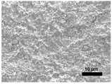
도 4a는 플라즈마 스프레잉된 코팅(plasma sprayed coating)의 현미경 사진이다.
도 4b는 플라즈마 스프레잉된 코팅의 또 다른 현미경 사진이다.
도 5a는 한 가지 구체예에 따른 슬러리 플라즈마 스프레잉된 코팅의 현미경 사진이다.
도 5b는 한 가지 구체예에 따른 슬러리 플라즈마 스프레잉된 코팅의 또 다른 현미경 사진이다.
도 6은 한 가지 구체예에 따른코팅을 생산하는 방법을 예시하는 흐름도이다.
도 7은 한 가지 구체예에 따른 다층 코팅을 생산하는 방법을 예시하는 흐름도이다.In the features of the accompanying drawings in which like reference numbers indicate like elements, the embodiments disclosed herein are illustrated by way of example and not limitation. It should be noted that different references to "a" or "an" in the present disclosure do not necessarily refer to the same embodiment and such references mean more than one.
1 illustrates a cross-sectional view of a processing chamber according to one embodiment.
2 shows a cross-sectional view of a plasma spray apparatus according to one embodiment.
3A and 3B show cross-sectional views of an exemplary chamber component having one and two coatings, respectively, according to one embodiment.
4A is a photomicrograph of a plasma sprayed coating.
4B is another photomicrograph of a plasma sprayed coating.
5A is a photomicrograph of a slurry plasma sprayed coating according to one embodiment.
5B is another photomicrograph of a slurry plasma sprayed coating according to one embodiment.
6 is a flow diagram illustrating a method of producing a coating according to one embodiment.
7 is a flow diagram illustrating a method of producing a multilayer coating according to one embodiment.
구체예에 대한 상세한 설명DETAILED DESCRIPTION OF EMBODIMENTS
본 발명의 구체예는 기판, 예컨대, 반도체 프로세싱 챔버를 위한 챔버 부품을 제공한다. 세라믹 코팅은 슬러리 플라즈마 스프레이 증착을 이용하여 기판 상에 형성될 수 있다. 세라믹 코팅은 보호 코팅으로서 작용할 수 있다. 일부 구체예들에서, 코팅 스택(coating stack)이 기판 상에 증착될 수 있으며, 여기서, 코팅 스택은 둘 이상의 슬러리 플라즈마 스프레잉된 세라믹 코팅으로 구성된다. 그러한 구체예들에서, 각각의 세라믹 코팅은 두께가 약 10 마이크로미터 내지 약 500 마이크로미터일 수 있다. 각각의 세라믹 코팅은 Y3Al5O12(YAG), Y4Al2O9(YAM), Er2O3, Gd2O3, Gd3Al5O12 (GAG), YF3, Nd2O3, Er4Al2O9, Er3Al5O12 (EAG), ErAlO3, Gd4Al2O9, GdAlO3, Nd3Al5O12, Nd4Al2O9, NdAlO3, 또는 Y4Al2O9 및 Y2O3-ZrO2의 고용체로 구성된 세라믹 컴파운드(ceramic compound) 중 하나 이상의 조성을 지닐 수 있다. 개시된 세라믹 코팅 중 하나 이상에 의해서 제공된 개선된 침식 내성은 챔버 부품의 사용 수명을 개선시킬 수 있으면서, 유지 및 제조 비용을 감소시킨다.Embodiments of the present invention provide chamber components for substrates, such as semiconductor processing chambers. The ceramic coating may be formed on the substrate using slurry plasma spray deposition. The ceramic coating may act as a protective coating. In some embodiments, a coating stack may be deposited on a substrate, wherein the coating stack consists of two or more slurry plasma sprayed ceramic coatings. In such embodiments, each ceramic coating may be from about 10 micrometers to about 500 micrometers thick. Each ceramic coating is Y3 Al5 O12 (YAG), Y4 Al2 O9 (YAM), Er2 O3 , Gd2 O3 , Gd3 Al5 O12 (GAG), YF3 , Nd2 O3 , Er4 Al2 O9 , Er3 Al5 O12 (EAG), ErAlO3 , Gd4 Al2 O9 , GdAlO3 , Nd3 Al5 O12 , Nd4 Al2 O9 , NdAlO3 , Alternatively, Y4 Al2 O9 and Y2 O3 -ZrO2 It may have a composition of at least one of a ceramic compound composed of a solid solution. The improved erosion resistance provided by one or more of the disclosed ceramic coatings can improve the service life of the chamber components, while reducing maintenance and manufacturing costs.
도 1은 본 발명의 구체예에 따른 코팅 층으로 코팅되는 하나 이상의 챔버 부품을 지니는 반도체 프로세싱 챔버(semiconductor processing chamber: 100)의 단면도이다. 프로세싱 챔버(100)는 부식성 플라즈마 환경이 제공되는 프로세스를 위해서 사용될 수 있다. 예를 들어, 프로세싱 챔버(100)는 플라즈마 식각장비 또는 플라즈마 식각 반응기, 및 플라즈마 클리너(plasma cleaner) 등을 위한 챔버일 수 있다. 코팅 층을 포함할 수 있는 챔버 부품의 예는 기판 지지 조립체(148), 정전 척(electrostatic chuck(ESC): 150), 링(ring)(예, 프로세스 키트 링 또는 단일 링), 챔버 벽, 베이스, 가스 분배 플레이트, 샤워헤드, 라이너, 라이너 키트, 쉴드(shield), 플라즈마 스크린, 흐름 평형기(flow equalizer), 냉각 베이스(cooling base), 챔버 뷰포트(chamber viewport), 및 챔버 리드(chamber lid) 등을 포함한다. 이하 더욱 상세히 기재되는 코팅 층은 하나 이상의 Y3Al5O12, Y4Al2O9, Er2O3, Gd2O3, Gd3Al5O12, La2O3, YAG, YF3, Nd2O3, Er4Al2O9, Er3Al5O12, ErAlO3, Gd4Al2O9, GdAlO3, Nd3Al5O12, Nd4Al2O9, NdAlO3, 또는 Y4Al2O9 및 Y2O3-ZrO2의 고용체로 구성된 세라믹 컴파운드를 포함할 수 있다. 예시된 바와 같이, 기판 지지 조립체(148)는 한 가지 구체예에 따른 세라믹 코팅 층(136)을 지닌다. 그러나, 다른 챔버 부품들, 예컨대, 상기 열거된 것들 중 어떠한 것이 또한 코팅 층을 포함할 수 있음을 이해해야 한다.1 is a cross-sectional view of a
한 가지 구체예에서, 프로세싱 챔버(100)는 내부 공간(106)을 둘러싸고 있는 챔버 바디(102)와 샤워헤드(130)를 포함한다. 대안적으로, 샤워헤드(130)는 일부 구체예에서 리드(lid) 및 노즐로 대체될 수 있다. 챔버 바디(102)는 알루미늄, 스테인리스 스틸 또는 그 밖의 적합한 재료로 제작될 수 있다. 챔버 바디(102)는 일반적으로 측벽들(108)과 바닥(110)을 포함한다. 샤워헤드(130)(또는 리드 및/또는 노즐), 측벽들(108) 및/또는 바닥(110) 중 하나 이상은 코팅 층을 포함할 수 있다.In one embodiment, the
외부 라이너(116)는 챔버 바디(102)를 보호하도록 측벽들(108)에 인접하여 배치될 수 있다. 외부 라이너(116)는 코팅 층으로 제작되고/거나 코팅될 수 있다. 한 가지 구체예에서, 외부 라이너(116)는 알루미늄 옥사이드로부터 제작된다.An
배기구(126)는 챔버 바디(102)에 형성될 수 있으며, 내부 공간(106)을 펌프 시스템(128)에 연결시킬 수 있다. 펌프 시스템(128)은 프로세싱 챔버(100)의 내부 공간(106)을 배기시키고 그러한 내부 공간의 압력을 조절하기 위해서 사용되는 하나 이상의 펌프들 및 스로틀 밸브(throttle valve)들을 포함할 수 있다.An exhaust port 126 may be formed in the
샤워헤드(130)은 챔버 바디(102)의 측벽(108)상에 지지될 수 있다. 샤워헤드(130)(또는 리드)는 프로세싱 챔버(100)의 내부 공간(106)에 접근을 허용하도록 개방될 수 있고, 폐쇄되는 동안에는 프로세싱 챔버(100)에 대한 밀봉을 제공할 수 있다. 가스 패널(158)은 프로세싱 챔버(100)에 연결되어 프로세스 및/또는 클리닝 가스를 샤워헤드(130) 또는 리드 및 노즐을 통해서 내부 공간(106)에 제공할 수 있다. 샤워헤드(130)는 유전체 에칭(유전 물질의 에칭)을 위해서 사용되는 프로세싱 챔버를 위해서 사용될 수 있다. 샤워헤드(130)는 가스 분배 플레이트(GDP)(133) 전체에 걸친 복수의 가스 전달 구멍들(132)를 지니는 GDP(133)을 포함한다. 샤워헤드(130)는 알루미늄 베이스 또는 양극 산화 알루미늄 베이스(104)에 결합된 GDP(133)을 포함할 수 있다. GDP(133)는 Si 또는 SiC로부터 제조될 수 있거나, 세라믹, 예컨대, Y2O3, Al2O3, 및 YAG 등일 수 있다.The
전도체 에칭(전도성 물질의 에칭)을 위해서 사용되는 프로세싱 챔버의 경우에, 샤워헤드 보다는 리드가 사용될 수 있다. 리드는 리드의 중앙 구멍에 맞는 중앙 노즐을 포함할 수 있다. 리드는 세라믹, 예컨대, Al2O3, Y2O3, YAG, 또는 Y4Al2O9 및 Y2O3-ZrO2의 고용체로 구성된 세라믹 컴파운드일 수 있다. 노즐이 또한 세라믹, 예컨대, Y2O3, YAG, 또는 Y4Al2O9 및 Y2O3-ZrO2의 고용체로 구성된 세라믹 컴파운드일 수 있다. 리드, 샤워헤드 베이스(104), GDP(133) 및/또는 노즐은 세라믹 코팅으로 코팅될 수 있다.In the case of a processing chamber used for conductor etching (etching of conductive material), a lid rather than a showerhead may be used. The lid may include a central nozzle that fits into the central aperture of the lid. The lead may be a ceramic, such as Al2 O3 , Y2 O3 , YAG, or a ceramic compound composed of a solid solution of Y4 Al2 O9 and Y2 O3 -ZrO2 . The nozzle may also be a ceramic, such as Y2 O3 , YAG, or a ceramic compound composed of a solid solution of Y4 Al2 O9 and Y2 O3 -ZrO2 . The lid, showerhead base 104,
프로세싱 챔버(100)내의 기판을 프로세싱하기 위해서 사용될 수 있는 프로세싱 가스의 예는 할로겐-함유 가스, 예컨대, 그 중에서도, C2F6, SF6, SiCl4, HBr, NF3, CF4, CHF3, CH2F3, F, NF3, Cl2, CCl4, BCl3 및 SiF4, 및 다른 가스, 예컨대, O2, 또는 N2O를 포함한다. 캐리어 가스의 예는 N2, He, Ar, 및 프로세스 가스에 불활성인 그 밖의 가스(예, 비-반응성 가스)를 포함한다. 기판 지지 조립체(148)는 샤워헤드(130) 또는 리드 아래의 프로세싱 챔버(100)의 내부 공간(106)에 배치된다. 기판 지지 조립체(148)는 프로세싱 동안에 기판(144)을 보유하고 있다. 링(146)(예, 단일 링)은 정전 척(150)의 일부를 덮을 수 있고, 프로세싱 동안에 플라즈마에 대한 노출로부터 덮은 부분을 보호할 수 있다. 링(146)은 한 가지 구체예에서 실리콘 또는 석영일 수 있다.Examples of processing gases that may be used to process a substrate in
내부 라이너(118)는 기판 지지 조립체(148)의 주변부상에 코팅될 수 있다. 내부 라이너(118)는 외부 라이너(116)를 참조로 논의된 것들과 같은 할로겐-함유 가스 내성 물질일 수 있다. 한 가지 구체예에서, 내부 라이너(118)는 외부 라이너(116)와 동일한 물질로부터 제작될 수 있다. 추가로, 내부 라이너(118)는 세라믹 코팅으로 코팅될 수 있다.An
한 가지 구체예에서, 기판 지지 조립체(148)는 페데스탈(pedestal: 152)을 지지하는 장착 판(mounting plate: 162), 및 정전 척(150)을 포함한다. 정전 척(150)은 추가로 열전도성 베이스(164) 및, 한 가지 구체예로, 실리콘 결합(silicone bond)일 수 있는 결합(138)에 의해서 열전도성 베이스에 결합된 정전 퍽(electrostatic puck: 166)을 포함한다. 정전 퍽(166)의 상부 표면은 예시적인 구체예에서 세라믹 코팅 층(136)에 의해서 피복된다. 한 가지 구체예에서, 세라믹 코팅 층(136)은 정전 퍽(166)의 상부 표면상에 배치된다. 또 다른 구체예에서, 세라믹 코팅 층(136)은 열전도성 베이스(164)와 정전 퍽(166)의 외부 및 측면 주변부를 포함하는 정전 척(150)의 전체 노출된 표면상에 배치된다. 설치판(162)은 챔버 바디(102)의 바닥(110)에 연결되고 열전도성 베이스(164) 및 정전 퍽(166)에 유틸리티(utility)들(예, 유체들, 송전선들, 센서 리드(sensor lead)들, 등)을 지나가게 하기 위한 통로를 포함한다.In one embodiment, the
열전도성 베이스(164) 및/또는 정전 퍽(166)은 하나 이상의 임의의 매립된 발열체들(176), 매립된 단열재들(174) 및/또는 도관들(168, 170)을 포함하여 지지 조립체(148)의 측면 온도 프로파일(temperature profile)을 조절할 수 있다. 도관들(168, 170)은 도관들(168, 170)을 통해서 온도 조절 유체를 순환시키는 유체 공급원(172)에 유체적으로 연결될 수 있다. 매립된 단열재(174)는 한 가지 구체예에서 도관들(168, 170) 사이에 배치될 수 있다. 히터(176)는 히터 전원(178)에 의해서 조절된다. 도관들(168, 170) 및 히터(176)는 열전도성 베이스(164)의 온도를 조절하기 위해서 사용되어서, 정전 퍽(166)과 프로세싱되는 기판(예, 웨이퍼)(144)를 가열하고/거나 냉각시킬 수 있다. 정전 퍽(166)과 열전도성 베이스(164)의 온도는 제어기(195)를 사용하여 모니터링될 수 있는 복수의 온도 센서들(190, 192)을 사용하여 모니터링될 수 있다.The thermally
정전 퍽(166)은 추가로 퍽(166) 및/또는 세라믹 코팅 층(136)의 상부 표면에 형성될 수 있는 복수의 가스 통로들, 예컨대, 그루브(groove)들, 메사(mesa)들 및 그 밖의 표면 피처(feature)들을 포함할 수 있다. 가스 통로들은 퍽(166)에 뚫인 구멍을 통해서 열 전달(또는 백사이드(backside)) 가스, 예컨대, 헬륨의 공급원에 유체적으로 연결될 수 있다. 작동 중에, 백사이드 가스는 정전 퍽(166)과 기판(144) 사이의 열 전달을 향상시키기 위해 가스 통로들 내로 조절된 압력으로 제공될 수 있다. 정전 퍽(166)은 척킹 전원(chucking power source: 182)에 의해서 조절된 하나 이상의 클램핑 전극(180)을 포함한다. 전극(180)(또는 퍽(166) 또는 베이스(164)에 배치된 다른 전극)은 추가로 프로세스로부터 형성된 플라즈마 및/또는 프로세싱 챔버(100) 내의 다른 가스들을 유지시키기 위한 매칭 회로(matching circuit: 188)를 통해서 하나 이상의 RF 전원들(184, 186)에 연결될 수 있다. 전원들(184, 186)은 일반적으로 약 10,000 와트까지의 전력 출력으로 약 50 kHz 내지 약 3 GHz의 주파수를 지니는 RF 신호를 생성시킬 수 있다.The
도 2는 한 가지 구체예에 따른 플라즈마 스프레이 장치(200)의 단면도를 도시하고 있다. 플라즈마 스프레이 장치(200)는 세라믹 물질의 "슬러리 플라즈마 스프레이"("SPS") 증착을 수행하기 위해서 사용되는 열적 스프레이 시스템의 유형이다. 표준 플라즈마 스프레이 기술과는 달리, SPS 증착은 기판 상에 세라믹 코팅을 증착시키기 위해서 입자들의 용액-기반 분배물(슬러리)를 사용한다. SPS는 대기압 플라즈마 스프레이, 고속 옥시-연료(high velocity oxy-fuel: HVOF), 따뜻한 스프레잉(warm spraying), 진공 플라즈마 스프레잉(vacuum plasma spraying: VPS), 및 저압 플라즈마 스프레잉(low pressure plasma spraying: LPPS)을 이용하여 슬러리를 스프레잉함으로써 수행될 수 있다.2 shows a cross-sectional view of a
플라즈마 스프레이 장치(200)는 노즐 애노드(206)과 캐소드(204)를 둘러싸는 캐이싱(casing)(202)을 포함할 수 있다. 캐이싱(202)은 플라즈마 스프레이 장치(200)를 통해서 그리고 노즐 애노드(206)과 캐소드(204) 사이의 가스 흐름(208)을 허용한다. 외부 전원이 노즐 애노드(206)과 캐소드(204) 사이에 전압 전위를 가하기 위해서 사용될 수 있다. 전압 전위는 플라즈마 가스를 생성하도록 가스 흐름(208)을 점화시키는 노즐 애노드(206)과 캐소드(204) 사이에 아크를 생성시킨다. 점화된 플라즈마 가스 흐름(208)은 노즐 애노드(206)를 벗어나서 기판(220)을 향하는 고속 플라즈마 플럼(214)을 생성시킨다. 노즐 애노드(206)의 후단부와 기판(220) 사이의 거리(즉, 건 디스턴스(gun distance))는 약 50 mm 내지 약 500 mm일 수 있다.
플라즈마 스프레이 장치(200)는 챔버 또는 대기 부쓰(atmospheric booth)내에 위치될 수 있다. 일부 구체예들에서, 가스 흐름(208)은, 이로 한정되는 것은 아니지만, 아르곤, 질소, 수소, 헬륨 및 이들의 조합물을 포함한 가스 또는 가스 혼합물일 수 있다. 가스 흐름(208)의 유속은 약 50 L/min 내지 400 L/min일 수 있다. 노즐 애노드(206)과 캐소드(204) 사이에 인가된 전압 전위는 AC 파형, DC 파형, 또는 이들의 조합일 수 있으며, 약 40 V 내지 약 500 V일 수 있다. 인가된 전위는 일반저긍로 1000A 또는 그 초과까지의 건 전류(gun current)와 함께 30 kW 또는 그 초과의 건 전력을 제공할 수 있다.The
플라즈마 스프레이 장치(200)에는, 예를 들어, 5 mL/min 내지 약 100 mL/min의 유속으로, 슬러리를 플라즈마 플럼(214)내로 전달하기 위한 하나 이상의 유체 라인들(212)이 구비될 수 있다. 일부 구체예들에서, 몇 개의 유체 라인들(212)은 플라즈마 플럼(214)의 한 면상에 또는 대칭으로 배열될 수 있다. 일부 구체예들에서, 유체 라인들(212)은 도 2에 도시된 바와 같이 플라즈마 플럼(214)에 대한 수직 양상으로 배열될 수 있다. 다른 구체예들에서, 유체 라인들(212)은 상이한 각도(예, 45°)로 슬러리를 플라즈마 플럼 내로 전달하도록 조절될 수 있거나, 슬러리를 플라즈마 플럼(214)내로 내부적으로 주입시키기 위해서 캐이싱(202)의 적어도 일부 내부에 위치될 수 있다. 일부 구체예들에서, 각각의 유체 라인(212)은 기판(220)을 가로질러 생성되는 코팅의 조성을 다양하게 하기 위해서 사용될 수 있는 상이한 슬러리를 제공할 수 있다.
슬러리 공급장치 시스템이 슬러리를 유체 라인들(212)에 전달하기 위해서 이용될 수 있다. 일부 구체예들에서, 슬러리 공급장치 시스템은 코팅 동안 일정한 유속을 유지시키는 흐름 제어기를 포함한다. 유체 라인들(212)은, 예를 들어, 탈이온수를 사용하여 코팅 프로세스 전후에 세정될 수 있다. 일부 구체예들에서, 플라즈마 스프레이 장치(200)로 공급된 슬러리를 함유하는 슬러리 용기는 코팅 프로세스의 과정 동안에 기계적으로 진탕되어 슬러리를 균일하게 유지시키고 침강을 방지한다.A slurry feeder system may be used to deliver the slurry to the fluid lines 212 . In some embodiments, the slurry feeder system includes a flow controller to maintain a constant flow rate during coating. The
일부 구체예들에서, 슬러리는 용매 내의 세라믹 입자들의 슬러리이다. 용매는, 이로 한정되는 것은 아니지만, 에탄올, 메탄올, 아세토니트릴, 탈이온수 또는 이들의 조합물을 포함하는 저분자량 극성 용매를 포함한다. 일부 구체예들에서, 슬러리의 pH는 슬러리의 안정성을 촉진하도록 약 5 내지 12일 수 있다. 일부 구체예들에서, 약 10 중량% 내지 약 50 중량%의 슬러리 중의 입자 농도가 유동성을 최대화하면서 낮은 점도를 유지시키기 위해서 이용될 수 있다. 일부 구체예들에서, 질량에 의한 평균 입자 직경인 슬러리 중의 입자들의 질량-중간-직경(D50)은 약 10 나노미터 내지 10 마이크로미터일 수 있다. 일부 구체예들에서, 슬러리는 입자들을 균일하게 분배시키는 것을 돕기 위한 분산제를 포함할 수 있다. 예시적인 분산제는 저분자량 폴리머, 예컨대, 폴리아크릴산, 암모늄 폴리메타크릴레이트, 오메가-3 지방산(예, 에이코사펜타에노산 및 도코사헥사에노산), 및 폴리에틸렌 글리콜을 포함할 수 있다. 일부 구체예들에서, 입자들은 Er2O3, Gd2O3, Gd3Al5O12, La2O3, YAG, YF3, Nd2O3, Er4Al2O9, Er3Al5O12, ErAlO3, Gd4Al2O9, GdAlO3, Nd3Al5O12, Nd4Al2O9, 또는 NdAlO3 중 하나 이상을 포함하는 조성들을 지닐 수 있다.In some embodiments, the slurry is a slurry of ceramic particles in a solvent. Solvents include, but are not limited to, low molecular weight polar solvents including, but not limited to, ethanol, methanol, acetonitrile, deionized water, or combinations thereof. In some embodiments, the pH of the slurry may be about 5 to 12 to promote stability of the slurry. In some embodiments, a particle concentration in the slurry of from about 10% to about 50% by weight can be used to maintain low viscosity while maximizing flowability. In some embodiments, the mass-median-diameter (D50) of the particles in the slurry, which is the average particle diameter by mass, may be between about 10 nanometers and 10 micrometers. In some embodiments, the slurry may include a dispersing agent to help distribute the particles evenly. Exemplary dispersants can include low molecular weight polymers such as polyacrylic acid, ammonium polymethacrylate, omega-3 fatty acids (eg, eicosapentaenoic acid and docosahexaenoic acid), and polyethylene glycol. In some embodiments, the particles are Er2 O3 , Gd2 O3 , Gd3 Al5 O12 , La2 O3 , YAG, YF3 , Nd2 O3 , Er4 Al2 O9 , Er3 Al5 O12 , ErAlO3 , Gd4 Al2 O9 , GdAlO3 , Nd3 Al5 O12 , Nd4 Al2 O9 , or NdAlO3 .
플라즈마 플럼(214)은 약 3000℃ 내지 약 10000℃의 온도에 도달할 수 있다. 플라즈마 플럼(214) 내로 주입되는 때에 슬러리(또는 슬러리들)가 겪게 되는 극심한 온도는 슬러리 용매가 신속하게 증발되게 할 수 있고, 세라믹 입자를 용융시켜서, 기판(220)을 향해서 추진되는 입자 스트림(216)을 생성시킬 수 있다. 기판(220)와의 충격시에, 용융된 입자들은 기판 상에 신속하게 편평화되고 고형화되어서, 세라믹 코팅(218)을 형성시킬 수 있다. 용매는 세라믹 입자들이 기판(220)에 도달하기 전에 완전히 증발될 수 있다.
세라믹 코팅의 두께, 밀도, 및 조도에 영향을 줄 수 있는 파라미터들은 슬러리 조건들, 입자 크기 분포, 슬러리 공급 속도, 플라즈마 가스 조성, 가스 유속, 에너지 입력, 스프레이 거리, 및 기판 냉각을 포함한다.Parameters that can affect the thickness, density, and roughness of the ceramic coating include slurry conditions, particle size distribution, slurry feed rate, plasma gas composition, gas flow rate, energy input, spray distance, and substrate cooling.
도 3a 및 도 3b는 구체예에 따른, 각각 하나 또는 두 개의 코팅을 지니는 예시적인 챔버 부품의 단면도를 도시하고 있다. 도 3a를 참조하면, 물품(300)의 베이스 또는 바디(302)의 일부 또는 전부가 세라믹 코팅(304)에 의해서 코팅된다. 물품(300)(또한, 일반적으로는 도 2와 관련하여 기재된 기판(220)과 동일할 수 있는 "기판"으로 일컬어짐)은 챔버 부품, 예컨대, 기판 지지 조립체, 정전 척 (ESC), 링(예, 프로세스 키트 ㄹ링 또는 단일 링), 챔버 라이너, 샤워헤드 베이스, 가스 분배 플레이트, 라이너, 라이너 키트, 쉴드, 플라즈마 스크린, 흐름 평형기, 냉각 베이스, 챔버 뷰포트, 및 챔버 리드 등일 수 있다. 물품(300)의 바디(302)는 금속, 세라믹, 금속-세라믹 복합체, 폴리머, 또는 폴리머-세라믹 복합체일 수 있다.3A and 3B show cross-sectional views of exemplary chamber components having one or two coatings, respectively, according to embodiments. Referring to FIG. 3A , some or all of the base or
다양한 챔버 부품은 상이한 물질로 구성된다. 예를 들어, 정전 척은 양극 산화 알루미늄 베이스에 결합된 세라믹, 예컨대, Al2O3(알루미나), AlN(알루미늄 니트라이드), TiO(티타늄 옥사이드), TiN(티타늄 니트라이드) 또는 SiC(실리콘 카바이드)로 구성될 수 있다. Al2O3, AlN 및 양극 산화 알루미늄은 불량한 플라즈마 부식 내성을 지닌다. 불소 화학 및/또는 환원 화학을 지니는 플라즈마 환경에 노출되는 때에, 정전 척의 정전 퍽은 약 50 시간의 라디오 주파수 시간(RFHr) 프로세싱 후에 저하된 웨이퍼 척킹(wafer chucking), 증가된 헬륨 누출 속도, 웨이퍼 전면 및 배면 입자 생성 및 온-웨이퍼 금속 오염(on-wafer metal contamination)을 나타낼 수 있다. 라디오 주파수 시간은 프로세싱 시간이다.The various chamber parts are made of different materials. For example, an electrostatic chuck may be a ceramic bonded to an anodized aluminum base, such as Al2 O3 (alumina), AlN (aluminum nitride), TiO (titanium oxide), TiN (titanium nitride) or SiC (silicon carbide). ) may consist of Al2 O3 , AlN and anodized aluminum have poor plasma corrosion resistance. When exposed to a plasma environment with fluorine chemistry and/or reducing chemistry, the electrostatic puck of the electrostatic chuck exhibits reduced wafer chucking, increased helium leakage rate, and wafer front side after approximately 50 hours of radio frequency time (RFHr) processing. and backing particle generation and on-wafer metal contamination. Radio frequency time is processing time.
전도체 에칭 프로세스에 사용되는 플라즈마 식각장비를 위한 리드는 소결된 세라믹, 예컨대, Al2O3일 수 있으며, Al2O3는 높은 가요성 강도 및 높은 열전도성을 지닌다. 그러나, 불소 화학에 노출된 Al2O3는 웨이퍼 사에 AlF 입자 뿐만 아니라 알루미늄 금속 오염을 형성시킨다. 일부 챔버 리드는 플라즈마 대향면 상에 두꺼운 필름 보호층을 지녀서 입자 생성 및 금속 오염을 최소화하고 리드의 수명을 연장시킨다. 그러나, 대부분의 두꺼운 필름 코팅 기술은 온-웨이퍼 결함 성능을 저하시킬 수 있는 균열과 기공을 수반한다.The lead for the plasma etching equipment used in the conductor etching process may be a sintered ceramic, such as Al2 O3 , Al2 O3 having high flexible strength and high thermal conductivity. However, Al2 O3 exposed to fluorine chemistry forms aluminum metal contamination as well as AlF particles between wafers. Some chamber lids have a thick film protective layer on the plasma-facing side to minimize particle generation and metal contamination and extend the life of the lid. However, most thick film coating techniques involve cracks and pores that can degrade on-wafer defect performance.
프로세스 키트 링 및 단일 링은 다른 챔버 부품들을 밀봉하고/거나 보호하기 위해서 사용될 수 있으며 전형적으로는 석영 또는 실리콘으로 제조된다. 이들 링들은 지지된 기판(예, 웨이퍼) 둘레에 배치되어 균일한 플라즈마 밀도(및 그에 따른 균일한 에칭)을 확보하게 할 수 있다. 그러나, 석영 및 실리콘은 다양한 에칭 화학(예, 플라즈마 에칭 화학)하에 매우 높은 침식 속도를 지닌다. 추가로, 그러한 링들은 플라즈마 화학에 노출되는 때에 입자 오염을 유발시킬 수 있다. 공정 키트 링 및 단일 링은 또한 소결된 세라믹, 예컨대, YAG 및/또는 Y4Al2O9 및 Y2O3-ZrO2의 고용체로 구성된 세라믹 컴파운드로 이루어질 수 있다.Process kit rings and single rings can be used to seal and/or protect other chamber components and are typically made of quartz or silicon. These rings can be placed around a supported substrate (eg, a wafer) to ensure uniform plasma density (and thus uniform etching). However, quartz and silicon have very high erosion rates under various etch chemistries (eg plasma etch chemistries). Additionally, such rings can cause particle contamination when exposed to plasma chemistry. The process kit ring and single ring may also consist of a sintered ceramic, such as a ceramic compound composed of YAG and/or a solid solution of Y4 Al2 O9 and Y2 O3 -ZrO2 .
유전체 에칭 프로세스를 수행하기 위해서 사용되는 식각장비를 위한 샤워헤드는 전형적으로는 SiC 면판에 결합된 양극 산화 알루미늄으로 제조된다. 그러한 샤워헤드가 불소를 포함하는 플라즈마 화학에 노출되는 때에, 양극 산화 알루미늄 베이스와의 플라즈마 상호작용으로 인해서 AlF가 형성될 수 있다. 추가로, 양극 산화 알루미늄 베이스의 높은 침식 속도는 아크 발생(arcing)을 유도할 수 있고, 궁극적으로는 샤워헤드에 대한 클리닝 사이의 평균 시간을 감소시킬 수 있다.Showerheads for etching equipment used to perform dielectric etching processes are typically made of anodized aluminum oxide bonded to a SiC faceplate. When such a showerhead is exposed to a plasma chemistry comprising fluorine, AlF may form due to plasma interaction with the anodized aluminum base. Additionally, the high erosion rate of the anodized aluminum base can lead to arcing, which can ultimately reduce the average time between cleanings for the showerhead.
챔버 뷰포트(또한, 엔드포인트 윈도우(endpoint window)로 공지됨)는 전형적으로는 석영 또는 사파이어로 제조된 투명한 부품이다. 다양한 광학 센서가 뷰포트에 의해서 보호될 수 있고, 뷰포트를 통한 광학 센서 판독을 수행할 수 있다. 추가로, 뷰포트는 사용자가 프로세싱 동안에 웨이퍼를 시각적으로 검사하거나 볼 수 있게 할 수 있다. 석영과 사파이어 둘 모두는 불량한 플라즈마 침식 내성을 지닌다. 플라즈마 화학이 뷰포트를 침식시키고 거칠게 함에 따라서, 뷰포트의 광학적 성질이 변화된다. 예를 들어, 뷰포트는 탁해질 수 있고/거나 뷰포트를 통해서 통과하는 광학적 신호가 왜곡될 수 있다. 이것은 정확한 판독을 수집하기 위한 광학 센서의 능력을 손상시킬 수 있다. 그러나, 두꺼운 필름 보호층은 뷰포트에 사용하기에 부적절할 수 있는데, 그 이유는 이들 코팅이 뷰포트를 폐색시킬 수 있다.The chamber viewport (also known as the endpoint window) is a transparent part, typically made of quartz or sapphire. Various optical sensors may be protected by the viewport and may perform optical sensor readings through the viewport. Additionally, the viewport may allow a user to visually inspect or view the wafer during processing. Both quartz and sapphire have poor plasma erosion resistance. As the plasma chemistry erodes and roughens the viewport, the optical properties of the viewport change. For example, the viewport may become cloudy and/or the optical signal passing through the viewport may be distorted. This can impair the ability of the optical sensor to collect accurate readings. However, thick film protective layers may be unsuitable for use in the viewport, as these coatings may block the viewport.
상기 제공된 예들은 본원의 구체예에서 기재된 바와 같은 얇은 필름 보호층의 사용에 의해서 성능이 개선될 수 있는 몇 가지 챔버 부품들을 기재하고 있다.The examples provided above describe several chamber components whose performance may be improved by the use of a thin film protective layer as described in the embodiments herein.
도 3a를 다시 참조하면, 물품(300)의 바디(302)는 하나 이상의 표면 피처들을 포함할 수 있다. 정전 척의 경우에, 표면 피처들은 메사들, 밀봉 밴드(sealing band)들, 가스 채널들, 및 헬륨 구멍들 등을 포함할 수 있다. 샤워헤드의 경우에, 표면 피처들은 결합 라인(bond line), 가스 분배를 위한 수백 또는 수천의 구멍들, 및 가스 분배 구멍들 둘레의 디보트(divot)들 또는 범프(bump)들 등을 포함할 수 있다. 다른 챔버 부품들은 다른 표면 피처들을 지닐 수 있다.Referring again to FIG. 3A , the
바디(302) 상에 형성된 세라믹 코팅(304)은 바디(302)의 표면 피처들에 순응할 수 있다. 도시된 바와 같이, 세라믹 코팅(304)은 바디(302)의 상부 표면의 상대적인 모양을 유지한다(예, 메사의 모양들을 텔레그래핑(telegraphing)함). 추가로, 세라믹 코팅은 샤워헤드내의 구멍들 또는 정전 척 내의 헬륨 구멍들을 막지 않도록 충분히 얇을 수 있다. 한 가지 구체예에서, 세라믹 코팅(304)은 약 20 마이크로미터 미만의 두께를 지닌다. 추가의 구체예에서, 세라믹 코팅(304)은 약 10 마이크로미터 내지 약 500 마이크로미터의 두께를 지닌다. 세라믹 코팅(304)은 도 2와 관련하여 기재된 플라즈마 스프레이 장치(200)를 사용하여 바디(302) 상에 증착될 수 있다.The
도 3b를 참조하면, 물품(350)의 베이스 또는 바디(352)의 적어도 일부가 두 코팅, 즉, 첫 번째 코팅(354) 및 첫 번째 코팅(354) 상에 증착된 두 번째 코팅(356)으로 코팅된다. 일부 구체예들에서, 첫 번째 코팅(354)은 표준 증착 기술, 예컨대, 분말의 건식 플라즈마 스프레잉, 열 증착, 스퍼터링 등을 이용하여 수행된 코팅일 수 있다. 첫 번째 코팅(354)은 세라믹 코팅일 수 있지만, 높은 표면 조도뿐만 아니라, 표면 결함, 예컨대, 균열 및 기공을 지닐 수 있다. 따라서, 두 번째 코팅(356)이 첫 번째 코팅(354) 상에 증착될 수 있다. 두 번째 코팅은, 예를 들어, 도 2와 관련하여 기재된 플라즈마 스프레이 장치(200)를 이용한 SPS 증착된 세라믹 코팅일 수 있다. 일부 구체예들에서, 첫 번째 및 두 번째 코팅은 둘 모두가 상이한 조성을 지니는 SPS 증착된 세라믹 코팅일 수 있다.Referring to FIG. 3B , at least a portion of a base or
첫 번째 및 두 번째 코팅들(354, 356)은 단지 예시적인 것이며, 어떠한 적합한 수의 코팅들이 바디(352) 상에 증착되어 코팅 스택을 형성할 수 있다. 코팅 스택 내의 코팅 중 하나 이상은 세라믹 코팅(예, SPS-증착된 세라믹 코팅)일 수 있다. 코팅 스택 내의 코팅은 모두가 동일한 두께를 지닐 수 있거나, 이들은 다양한 두께를 지닐 수 있다. 코팅 스택 내의 코팅의 각각은 일부 구체예들에서 약 20 마이크로미터, 및 약 10 마이크로미터 미만의 두께를 지닐 수 있다. 한 가지 예로, 2-층 적층의 경우에, 도 3b에 도시된 바와 같이, 첫 번째 코팅(354)이 약 10 마이크로미터의 두께를 지니고, 두 번째 코팅(356)은 약 10 마이크로미터의 두께를 지닐 수 있다. 또 다른 예로, 첫 번째 코팅(354)은 약 10 마이크로미터의 두께를 지니는 YAG 층일 수 있고, 두 번째 코팅(356)은 약 500 마이크로미터의 두께를 지니는 SPS-증착된 세라믹 코팅일 수 있다.The first and
매번 물품이 가열되고 냉각되며, 세라믹 코팅과 그것이 코팅되는 기판 사이의 열팽창 계수의 불일치가 세라믹 코팅에 응력을 유발시킨다. 그러한 응력은 수직 균열에서 집중될 수 있다. 이것은 세라믹 코팅이 결국에는 그것이 코팅된 기판으로부터 박리되게 할 수 있다. 대조적으로, 수직 균열이 존재하지 않으면, 응력은 얇은 필름을 가로질러 대체로 고르게 분포된다. 따라서, 한 가지 구체예에서, 첫 번째 코팅(354)은 비정질 세라믹, 예컨대, YAG 또는 EAG이고, 두 번째 코팅(356)은 결정질 또는 나노-결정질 세라믹, 예컨대, 세라믹 컴파운드 또는 Er2O3이며, 여기서, 코팅들 중 하나 이상은 SPS-증착된 코팅이다. 그러한 구체예에서, 두 번째 코팅(356)은 첫 번째 코팅(354)에 비해서 더 큰 플라즈마 내성을 제공할 수 있다. 바디(352) 상에 적접적으로 형성시키는 것이 아니라 첫 번째 코팅(354) 상에 두 번째 코팅(356)을 형성시킴으로써, 첫 번째 코팅(354)은 완충부로서 작용하여 후속 코팅에 대한 격자 불일치(lattice mismatch)를 최소화한다. 따라서, 두 번째 코팅(356)의 수명이 증가될 수 있다.Each time an article is heated and cooled, the mismatch in the coefficient of thermal expansion between the ceramic coating and the substrate on which it is coated causes stress in the ceramic coating. Such stresses can be concentrated in vertical cracks. This can cause the ceramic coating to eventually peel from the substrate on which it is coated. In contrast, if no vertical cracks are present, the stress is distributed generally evenly across the thin film. Thus, in one embodiment, the
또 다른 예로, 바디의 각각, Y3Al5O12, Y4Al2O9, Er2O3, Gd2O3, Er3Al5O12, Gd3Al5O12, 및 Y4Al2O9 및 Y2O3-ZrO2의 고용체로 구성된 세라믹 컴파운드는 상이한 열팽창 계수를 지닐 수 있다. 두 인접 물질 사이의 열팽창 계수에서의 불일치가 크면 클수록, 이들 물질 중 하나가 결국 균열되거나, 박리되거나, 달리 다른 물질에 대한 이의 결합을 상실할 가능성이 더 크다. 첫 번째 및 두 번째 코팅들(354, 356)은 인접 코팅들 사이(또는 첫 번째 코팅(354)과 바디(352) 사이)의 열팽창 계수의 불일치를 최소화하는 방식으로 형성될 수 있다. 예를 들어, 바디(352)가 알루미나이고, EAG가 알루미나의 열팽창 계수와 가장 가까운 열팽창 계수를 지닐 수 있으며, 그 다음으로는, YAG의 열팽창 계수, 그 다음으로는, 추가의 컴파운드 세라믹 코팅의 열팽창 계수일 수 있다. 따라서, 한 가지 구체예로, 첫 번째 코팅(354)은 EAG일 수 있고, 두 번째 코팅(356)은 YAG일 수 있고, 추가의 코팅은 컴파운드 세라믹일 수 있다.As another example, each of the bodies Y3 Al5 O12 , Y4 Al2 O9 , Er2 O3 , Gd2 O3 , Er3 Al5 O12 , Gd3 Al5 O12 , and Y4 Al Ceramic compounds composed of solid solutions of2 O9 and Y2 O3 -ZrO2 may have different coefficients of thermal expansion. The greater the discrepancy in the coefficient of thermal expansion between two adjacent materials, the more likely it is that one of these materials will eventually crack, delaminate, or otherwise lose its bond to the other. The first and
또 다른 예로, 코팅 스택 중의 코팅들은 두 가지 상이한 세라믹의 교대 층일 수 있다. 예를 들어, 첫 번째 및 세 번째 코팅은 YAG일 수 있고, 두 번째 및 네 번째 코팅이 컴파운드 세라믹일 수 있다. 그러한 교대 코팅들은, 교대 코팅들에 사용되는 한 가지 물질이 비정질이고 교대 코팅들에 사용되는 다른 물질이 결정질 또는 나노-결정질인 경우에, 상기 기재된 것들과 유사한 이점을 제공할 수 있다.As another example, the coatings in a coating stack can be alternating layers of two different ceramics. For example, the first and third coatings may be YAG, and the second and fourth coatings may be compound ceramics. Such alternating coatings may provide advantages similar to those described above when one material used for the alternating coatings is amorphous and the other material used for the alternating coatings is crystalline or nano-crystalline.
일부 구체예들에서, 코팅 스택 중의 코팅들 중 하나 이상은 열처리를 이용하여 형성된 전이층이다. 바디(352)가 세라믹 바디이면, 세라믹 코팅(예, 세라믹 코팅(354))과 바디(352) 사이의 상호확산을 촉진시키기 위해서 고온 열처리가 수행될 수 있다. 추가로, 열처리는 인접 코팅들 사이, 또는 두꺼운 코팅과 얇은 코팅 사이의 상호확산을 촉진시키기 위해서 수행될 수 있다. 전이층은 비-다공성 층일 수 있고, 두 세라믹 사이의 확산 결합으로서 작용할 수 있으며, 인접 세라믹 코팅들 사이의 개선된 접착을 제공할 수 있다. 이것은 플라즈마 프로세싱 동안에 세라믹 코팅이 균열되는 것, 박리되는 것, 또는 벗겨지는 것을 방지하는 것을 도울 수 있다.In some embodiments, one or more of the coatings in the coating stack is a transition layer formed using a thermal treatment. If the
열처리는 0.5 내지 5℃/분의 상승 속도로 1 내지 12 시간까지의 기간 동안 이루어지는 약 1200 내지 2000℃까지의 열처리일 수 있다. 냉각은 0.5 내지 5℃/분의 속도로 조절될 수 있거나, 주위 조건하에 자연 냉각될 수 있다. 이것은 첫 번째 세라믹 코팅과 인접 세라믹 바디 중 하나 이상 또는 두 번째 세라믹 코팅 사이의 상호-확산 층을 생성시킬 수 있다. 예를 들어, 세라믹 바디가 Al2O3이고, 세라믹 코팅이 컴파운드 세라믹 Y4Al2O9 및 고용체 Y2-xZrxO3(Y2O3-ZrO2 고용체)로 구성되면, Y3Al5O12 인터페이스 층이 형성될 것이다. 유사하게, 열처리는 EAG의 전이 층이 Er2O3과 Al2O3 사이에 형성되게 할 것이다. 열처리는 또한 YAG의 전이 층이 Y2O3과 Al2O3 사이에 형성되게 할 것이다. 열처리는 또한 GAG가 Gd2O3과 Al2O3 사이에 형성되게 할 수 있다. Al2O3 상의 이트리아 안정화된 지르코리나(YSZ)의 열처리는 Y4Al2O9의 컴파운드 세라믹과 고용체 Y2-xZrxO3의 전이층을 형성시킬 수 있다. 다른 전이 층들이 다른 인접 세라믹 코팅들 사이에서 형성될 수 있다.The heat treatment may be a heat treatment up to about 1200 to 2000° C. for a period of 1 to 12 hours at a rising rate of 0.5 to 5° C./min. Cooling may be controlled at a rate of 0.5 to 5° C./min, or may be naturally cooled under ambient conditions. This may create an inter-diffusion layer between the first ceramic coating and one or more of the adjacent ceramic bodies or a second ceramic coating. For example, if the ceramic body is Al2 O3 , and the ceramic coating is composed of compound ceramic Y4 Al2 O9 and solid solution Y2-x Zrx O3 (Y2 O3 -ZrO2 solid solution), then Y3 An Al5 O12 interface layer will be formed. Similarly, the heat treatment will cause a transition layer of EAG to form between Er2 O3 and Al2 O3 . The heat treatment will also cause a transition layer of YAG to form between Y2 O3 and Al2 O3 . Heat treatment may also cause GAG to form between Gd2 O3 and Al2 O3 . Heat treatment of yttria-stabilized zircorina (YSZ) on Al2 O3 may form a transition layer of Y4 Al2 O9 compound ceramic and solid solution Y2-x Zrx O3 . Other transition layers may be formed between different adjacent ceramic coatings.
본원에 기재된 구체예들에 따라서, 세라믹 입자들의 슬러리를 사용하여 SPS 증착을 수행함으로써, 세라믹 코팅 조성의 예는 Y3Al5O12, Y4Al2O9, Er2O3, Gd2O3, La2O3, YAG, Er3Al5O12, Gd3Al5O12, Y4Al2O9 및 Y2O3-ZrO2의 고용체(Y2O3-ZrO2 고용체)로 구성된 세라믹 컴파운드, 또는 앞서 확인된 다른 세라믹 물질들 중 어떠한 것을 포함할 수 있다. 다른 Er 기반 및/또는 Gd 기반 플라즈마 내성 희토류 옥사이드가 또한 세라믹 코팅들(예, 코팅들(218, 304, 354, 및/또는 356))을 형성시키기 위해서 사용될 수 있다.By performing SPS deposition using a slurry of ceramic particles in accordance with embodiments described herein, an example of a ceramic coating composition is Y3 Al5 O12 , Y4 Al2 O9 , Er2 O3 , Gd2 O3 , La2 O3 , YAG, Er3 Al5 O12 , Gd3 Al5 O12 , Y4 Al2 O9 and Y2 O3 -ZrO2 as a solid solution (Y2 O3 -ZrO2 solid solution) constructed ceramic compounds, or any of the other ceramic materials identified above. Other Er-based and/or Gd-based plasma resistant rare earth oxides may also be used to form ceramic coatings (eg,
SPS-증착된 세라믹 코팅들은 또한 상기 언급된 세라믹 중 어떠한 것에 의해서 형성된 고용체를 기반으로 할 수 있다. Y4Al2O9 및 Y2O3-ZrO2의 고용체로 구성된 세라믹 컴파운드와 관련하여, 한 가지 구체예에서, 세라믹 컴파운드는 62.93 몰 비율(mol%)의 Y2O3, 23.23 mol%의 ZrO2 및 13.94 mol%의 Al2O3를 포함한다. 또 다른 구체예에서, 세라믹 컴파운드는 50-75 mol% 범위의 Y2O3, 10-30 mol% 범위의 ZrO2 및 10-30 mol% 범위의 Al2O3을 포함할 수 있다. 또 다른 구체예에서, 세라믹 컴파운드는 40-100 mol% 범위의 Y2O3, 0-60 mol% 범위의 ZrO2 및 0-10 mol% 범위의 Al2O3을 포함할 수 있다. 또 다른 구체예에서, 세라믹 컴파운드는 40-60 mol% 범위의 Y2O3, 30-50 mol% 범위의 ZrO2 및 10-20 mol% 범위의 Al2O3을 포함할 수 있다. 또 다른 구체예에서, 세라믹 컴파운드는 40-50 mol% 범위의 Y2O3, 20-40 mol% 범위의 ZrO2 및 20-40 mol% 범위의 Al2O3을 포함할 수 있다. 또 다른 구체예에서, 세라믹 컴파운드는 70-90 mol% 범위의 Y2O3, 0-20 mol% 범위의 ZrO2 및 10-20 mol% 범위의 Al2O3을 포함할 수 있다. 또 다른 구체예에서, 세라믹 컴파운드는 60-80 mol% 범위의 Y2O3, 0-10 mol% 범위의 ZrO2 및 20-40 mol% 범위의 Al2O3을 포함할 수 있다. 또 다른 구체예에서, 세라믹 컴파운드는 40-60 mol% 범위의 Y2O3, 0-20 mol% 범위의 ZrO2 및 30-40 mol% 범위의 Al2O3을 포함할 수 있다. 또 다른 구체예에서, 세라믹 컴파운드는 30-60 mol% 범위의 Y2O3, 0-20 mol% 범위의 ZrO2 및 30-60 mol% 범위의 Al2O3을 포함할 수 있다. 또 다른 구체예에서, 세라믹 컴파운드는 20-40 mol% 범위의 Y2O3, 20-80 mol% 범위의 ZrO2 및 0-60 mol% 범위의 Al2O3을 포함할 수 있다. 다른 구체예들에서, 세라믹 컴파운드에 대해서 다른 분포가 또한 이용될 수 있다.SPS-deposited ceramic coatings may also be based on a solid solution formed by any of the aforementioned ceramics. With respect to the ceramic compound composed of a solid solution of Y4 Al2 O9 and Y2 O3 -ZrO2 , in one embodiment, the ceramic compound contains 62.93 mol % Y2 O3 , 23.23 mol % ZrO2 and 13.94 mol % Al2 O3 . In another embodiment, the ceramic compound may comprise Y2 O3 in the range of 50-75 mol%, ZrO2 in the range of 10-30 mol% and Al2 O3 in the range of 10-30 mol%. In another embodiment, the ceramic compound may comprise Y2 O3 in the range of 40-100 mol%, ZrO2 in the range of 0-60 mol% and Al2 O3 in the range of 0-10 mol%. In another embodiment, the ceramic compound may comprise Y2 O3 in the range of 40-60 mol%, ZrO2 in the range of 30-50 mol% and Al2 O3 in the range of 10-20 mol%. In another embodiment, the ceramic compound may comprise Y2 O3 in the range of 40-50 mol%, ZrO2 in the range of 20-40 mol% and Al2 O3 in the range of 20-40 mol%. In another embodiment, the ceramic compound may comprise Y2 O3 in the range of 70-90 mol %, ZrO2 in the range of 0-20 mol % and Al2 O3 in the range of 10-20 mol %. In another embodiment, the ceramic compound may comprise Y2 O3 in the range of 60-80 mol%, ZrO2 in the range of 0-10 mol% and Al2 O3 in the range of 20-40 mol%. In another embodiment, the ceramic compound may comprise Y2 O3 in the range of 40-60 mol%, ZrO2 in the range of 0-20 mol% and Al2 O3 in the range of 30-40 mol%. In another embodiment, the ceramic compound may comprise Y2 O3 in the range of 30-60 mol%, ZrO2 in the range of 0-20 mol% and Al2 O3 in the range of 30-60 mol%. In another embodiment, the ceramic compound may comprise Y2 O3 in the range of 20-40 mol%, ZrO2 in the range of 20-80 mol% and Al2 O3 in the range of 0-60 mol%. In other embodiments, other distributions may also be used for the ceramic compound.
한 가지 구체예에서, Y2O3, ZrO2, Er2O3, Gd2O3 및 SiO2의 조성을 포함하는 대안적인 세라믹 컴파운드가 세라믹 코팅에 사용된다. 한 가지 구체예에서, 대안적인 세라믹 컴파운드는 40-45 mol% 범위의 Y2O3, 0-10 mol% 범위의 ZrO2, 35-40 mol% 범위의 Er2O3, 5-10 mol% 범위의 Gd2O3 및 5-15mol% 범위의 SiO2를 포함할 수 있다. 또 다른 구체예에서, 대안적인 세라믹 컴파운드는 30-60 mol% 범위의 Y2O3, 0-20 mol% 범위의 ZrO2, 20-50 mol% 범위의 Er2O3, 0-10 mol% 범위의 Gd2O3 및 0-30 mol% 범위의 SiO2를 포함할 수 있다. 또 다른 구체예에서, 대안적인 세라믹 컴파운드는 30-45 mol% 범위의 Y2O3, 5-15% mol% 범위의 ZrO2, 25-60 mol% 범위의 Er2O3 및 0-25 mol% 범위의 Gd2O3 을 포함할 수 있다. 첫 번째 예로, 대안적인 세라믹 컴파운드는 40 mol%의 Y2O3, 5 mol%의 ZrO2, 35 mol%의 Er2O3, 5 mol%의 Gd2O3 및 15 mol%의 SiO2을 포함한다. 두 번째 예로, 대안적인 세라믹 컴파운드는 45 mol%의 Y2O3, 5 mol%의 ZrO2, 35 mol%의 Er2O3, 10 mol%의 Gd2O3 및 5 mol%의 SiO2를 포함한다. 세 번째 예로, 대안적인 세라믹 컴파운드는 40 mol%의 Y2O3, 5 mol%의 ZrO2, 40 mol%의 Er2O3, 7 mol%의 Gd2O3 및 8 mol%의 SiO2를 포함한다. 한 가지 구체예에서, 세라믹 코팅은 70-75 mol% 범위의 Y2O3 및 25-30 mol% 범위의 ZrO2를 포함한다. 추가의 구체예에서, 세라믹 코팅은 73.13 mol%의 Y2O3 및 26.87 mol%의 ZrO2를 포함하는 YZ20로 명명되는 물질이다. 추가의 구체예에서, 세라믹 코팅은 37 mol%의 Y2O3, 8 mol%의 ZrO2 및 55 mol%의 Er2O3를 포함하는 YEZ08로 명명되는 물질이다. 추가의 구체예에서, 세라믹 코팅은 40 mol%의 Y2O3, 10 mol%의 ZrO2, 30 mol%의 Er2O3 및 20 mol%의 Gd2O3를 포함하는 YEZG10로 명명되는 물질이다.In one embodiment, an alternative ceramic compound comprising the composition of Y2 O3 , ZrO2 , Er2 O3 , Gd2 O3 and SiO2 is used in the ceramic coating. In one embodiment, the alternative ceramic compound is Y2 O3 in the range of 40-45 mol%, ZrO2 in the range of 0-10 mol%, Er2 O3 in the range of 35-40 mol%, 5-10 mol% Gd2 O3 in the range and SiO2 in the range of 5-15 mol %. In another embodiment, the alternative ceramic compound comprises Y2 O3 in the range of 30-60 mol%, ZrO2 in the range of 0-20 mol%, Er2 O3 in the range of 20-50 mol%, 0-10 mol% Gd2 O3 in the range and SiO2 in the range of 0-30 mol %. In another embodiment, the alternative ceramic compound comprises Y2 O3 in the range of 30-45 mol%, ZrO2 in the range of 5-15% mol%, Er2 O3 in the range of 25-60 mol% and 0-25 mol%. % range of Gd2 O3 . As a first example, an alternative ceramic compound contains 40 mol % Y2 O3 , 5 mol % ZrO2 , 35 mol % Er2 O3 , 5 mol % Gd2 O3 and 15 mol % SiO2 . include As a second example, an alternative ceramic compound contains 45 mol % Y2 O3 , 5 mol % ZrO2 , 35 mol % Er2 O3 , 10 mol % Gd2 O3 and 5 mol % SiO2 . include As a third example, an alternative ceramic compound contains 40 mol % Y2 O3 , 5 mol % ZrO2 , 40 mol % Er2 O3 , 7 mol % Gd2 O3 and 8 mol % SiO2 . include In one embodiment, the ceramic coating comprises Y2 O3 in the range of 70-75 mol % and ZrO2 in the range of 25-30 mol %. In a further embodiment, the ceramic coating is a material designated YZ20 comprising 73.13 mol % Y2 O3 and 26.87 mol % ZrO2 . In a further embodiment, the ceramic coating is a material designated YEZ08 comprising 37 mol % Y2 O3 , 8 mol % ZrO2 and 55 mol % Er2 O3 . In a further embodiment, the ceramic coating is a material designated YEZG10 comprising 40 mol % Y2 O3 , 10 mol % ZrO2 , 30 mol % Er2 O3 and 20 mol % Gd2 O3 . am.
상기 언듭된 세라믹 코팅들 중 어떠한 코팅은 미량의 다른 물질, 예컨대, ZrO2, Al2O3, SiO2, B2O3, Er2O3, Nd2O3, Nb2O5, CeO2, Sm2O3, Yb2O3, 또는 그 밖의 옥사이드를 포함할 수 있다. 한 가지 구체예에서, 두 인접 세라믹 코팅에 대해서 동일한 세라믹 물질이 사용되지 않는다. 그러나, 또 다른 구체예에서, 인접 코팅은 동일한 세라믹으로 구성될 수 있다.Any of the above unlaid ceramic coatings may contain traces of other materials, such as ZrO2 , Al2 O3 , SiO2 , B2 O3 , Er2 O3 , Nd2 O3 , Nb2 O5 , CeO2 , Sm2 O3 , Yb2 O3 , or other oxides. In one embodiment, the same ceramic material is not used for two adjacent ceramic coatings. However, in another embodiment, the adjacent coating may be comprised of the same ceramic.
각각, 건조한 분말에 의한 통상의 플라즈마 스프레이 증착 및 슬러리의 슬러리 플라즈마 스프레이 증착을 이용한 세라믹 코팅을 제조하는데 있어서의 차이를 입증하기 위해서 도 4 및 도 5가 이하 참조된다.Reference is now made to Figures 4 and 5 below to demonstrate the difference in making ceramic coatings using conventional plasma spray deposition with dry powder and slurry plasma spray deposition of slurries, respectively.
도 4a 및 도 4b는 상이한 배율로 동일한 Y2O3 코팅을 나타내고 있는 Y2O3의 건조한 분말을 플라즈마 스프레잉("건식 플라즈마 스프레잉")함으로써 제조된 플라즈마 스프레잉된 코팅의 현미경 사진이다. 도 5a 및 도 5b는 상이한 배율로 동일한 Y2O3 코팅을 나타내고 있는 한 가지 구체예에 따른 Y2O3 슬러리를 플라즈마 스프레잉함으로써 제조된 슬러리 플라즈마 스프레이 코팅의 현미경 사진이다. 표 1은, 표면 조도, 다공성 및 부식 내성(예, HCl 버블 타임(HCl bubble time)) 면에서, 도 4a 및 도 4b의 건식 플라즈마 스프레잉된 코팅에 비한 도 5a 및 도 5b의 SPS-증착된 코팅의 개선된 성질을 예시하고 있다.4A and 4B are photomicrographs of plasma sprayed coatings prepared by plasma spraying (“dry plasma spraying”) dry powder of Y2 O3 showing the same Y2 O3 coating at different magnifications. 5A and 5B are photomicrographs of a slurry plasma spray coating prepared by plasma spraying a Y2 O3 slurry according to one embodiment, showing the same Y2 O3 coating at different magnifications. Table 1 shows the SPS-deposited coatings of FIGS. 5A and 5B compared to the dry plasma sprayed coatings of FIGS. 4A and 4B in terms of surface roughness, porosity, and corrosion resistance (eg, HCl bubble time). The improved properties of the coating are illustrated.
표 1: 건식 플라즈마 스프레잉 대 슬러리 플라즈마 스프레잉의 비교Table 1: Comparison of dry plasma spraying versus slurry plasma spraying

도 4a 및 도 4b의 건식 플라즈마 스프레잉된 코팅은 매우 다공성이며, 밑에 있는 기판을 노출시키는 결함을 함유하지만, 도 5a 및 도 5b의 용액 스프레잉된 코팅은 덜 다공성이고 최소의 결함을 지닌다. 일부 구체예들에서, SPS-증착된 코팅, 예컨대, 도 5a 및 도 5b의 코팅은 결함을 차폐하고 궁극적으로는 더 평활한 세라믹 코팅을 제공하기 위해서 건식 플라즈마 스프레잉된 코팅, 예컨대, 도 4a 및 도 4b의 코팅을 지니는 기판 상에 증착될 수 있다.The dry plasma sprayed coatings of FIGS. 4A and 4B are highly porous and contain defects exposing the underlying substrate, whereas the solution sprayed coatings of FIGS. 5A and 5B are less porous and have minimal defects. In some embodiments, the SPS-deposited coating, such as the coating of FIGS. 5A and 5B, is a dry plasma sprayed coating, such as the coating of FIGS. 4A and 5B, to mask defects and ultimately provide a smoother ceramic coating. It can be deposited on a substrate having the coating of Figure 4b.
도 6은 한 가지 구체예에 따른 코팅을 생성시키기 위한 프로세스(600)를 예시하는 흐름도이다. 블록(602)에서, 기판이 제공된다. 일부 구체예들에서, 기판은 웨이퍼(예, 실리콘 웨이퍼)이다. 일부 구체예들에서, 기판은 도 1과 관련하여 기재된 바와 같은 적합한 챔버 부품일 수 있다. 예를 들어, 기판은, 이로 한정되는 것은 아니지만, 리드, 노즐, 정전 척(예, ESC(150)), 샤워헤드(예, 샤워헤드 (130)), 라이너(예, 외부 라이너(116) 또는 내부 라이너(118)) 또는 라이너 키트, 또는 링(예, 링(146)) 중 어떠한 것일 수 있다.6 is a flow diagram illustrating a
블록(604)에서, 세라믹 입자들의 슬러리가 플라즈마 분무기 내로 공급된다. 그러한 슬러리는 적합한 액체 라인(예, 유체 라인들(212) 중의 하나 이상)을 사용하는 플라즈마 분무기(예, 플라즈마 스프레이 장치(200)) 내로 공급될 수 있다. 슬러리는 Er2O3, Gd2O3, Gd3Al5O12, YF3, Nd2O3, Er4Al2O9, Er3Al5O12, ErAlO3, Gd4Al2O9, GdAlO3, Nd3Al5O12, Nd4Al2O9, 또는 NdAlO3 중의 하나 이상의 조성과 함께 세라믹 입자들을 함유할 수 있다. 입자들의 D50은 약 10 나노미터 내지 10 마이크로미터일 수 있다. 슬러리는 용매, 예컨대, 에탄올, 메탄올, 탈이온수, 아세토니트릴, 또는 이들의 조합물을 함유할 수 있고, 슬러리의 pH는 5 내지 12일 수 있다. 슬러리 내의 입자 농도는 약 10 중량% 내지 약 50 중량%일 수 있다.At block 604, a slurry of ceramic particles is fed into the plasma atomizer. Such slurry may be fed into a plasma atomizer (eg, plasma spray apparatus 200 ) using a suitable liquid line (eg, one or more of fluid lines 212 ). The slurry is Er2 O3 , Gd2 O3 , Gd3 Al5 O12 , YF3 , Nd2 O3 , Er4 Al2 O9 , Er3 Al5 O12 , ErAlO3 , Gd4 Al2 O9 , GdAlO3 , Nd3 Al5 O12 , Nd4 Al2 O9 , or NdAlO3 with a composition of one or more ceramic particles. The D50 of the particles may be between about 10 nanometers and 10 micrometers. The slurry may contain a solvent such as ethanol, methanol, deionized water, acetonitrile, or a combination thereof, and the pH of the slurry may be between 5 and 12. The particle concentration in the slurry may be from about 10% to about 50% by weight.
블록(606)에서, 플라즈마 분무기는 기판 상에 세라믹 코팅을 형성시키기 위해서 기판을 향해서 유도된 세라믹 입자들의 스트림을 생성시킨다. 슬러리가 플라즈마 분무기에 의해서 생성된 플라즈마 플럼(예, 플라즈마 플럼(214)) 내로 유입됨에 따라서, 용매가 증발하고, 입자들의 스트림(예, 입자 스트림(216)이 기판(예, 기판(220))를 향해 추진된다. 기판의 표면 상에 부딪치는 용융된 세라믹 입자들은 기판 상에 세라믹 코팅을 형성시킨다. 생성되는 세라믹 코팅의 조성은 Y3Al5O12, Y4Al2O9, Er2O3, Gd2O3, Gd3Al5O12(GAG), YF3, Nd2O3, Er4Al2O9, Er3Al5O12(EAG), ErAlO3, Gd4Al2O9, GdAlO3, Nd3Al5O12, Nd4Al2O9, NdAlO3, 또는 Y4Al2O9 및 Y2O3-ZrO2의 고용체로 구성된 세라믹 컴파운드 중 하나 이상일 수 있다.At block 606 , the plasma atomizer creates a stream of ceramic particles directed towards the substrate to form a ceramic coating on the substrate. As the slurry is introduced into a plasma plume (e.g., plasma plum 214) created by the plasma atomizer, the solvent evaporates and a stream of particles (e.g., particle stream 216) is transferred to a substrate (e.g., substrate 220). The molten ceramic particles impinging on the surface of the substrate form a ceramic coating on the substrate.The composition of the resulting ceramic coating is Y3 Al5 O12 , Y4 Al2 O9 , Er2 O3 , Gd2 O3 , Gd3 Al5 O12 (GAG), YF3 , Nd2 O3 , Er4 Al2 O9 , Er3 Al5 O12 (EAG), ErAlO3 , Gd4 Al2 O9 , GdAlO3 , Nd3 Al5 O12 , Nd4 Al2 O9 , NdAlO3 , or a ceramic compound composed of a solid solution of Y4 Al2 O9 and Y2 O3 -ZrO2 .
일부 구체예들에서, 마스크(mask)가 SPS 증착을 수행하기 전에 기판 상에 놓일 수 있다. 예를 들어, 마스크는 기판의 특정 영역에 세라믹 입자들이 부딪치는 것을 선택적으로 차단하는 기판으로부터 짧은 거리(예, 1-10 mm)에 놓일 수 있다. 또 다른 예로서, 마스크는 기판 상에 세라믹 물질로 구성된 피처들을 남겨두도록 후에 스트리핑될 수 있는 포토레지스트 층일 수 있다. 차폐(masking)는 거대규모(macroscale) 및 미세규모(microscale) 세라믹 피처들이 기판 상에 증착되게 할 수 있다. 예를 들어, 기판을 차폐하는 것은 ESC 표면 상에 메사들을 형성시키기 위해서 이용될 수 있다.In some embodiments, a mask may be placed on the substrate prior to performing SPS deposition. For example, the mask may be placed at a short distance (eg, 1-10 mm) from the substrate that selectively blocks ceramic particles from striking certain areas of the substrate. As another example, the mask can be a layer of photoresist that can be stripped later to leave features made of a ceramic material on the substrate. Masking may allow macroscale and microscale ceramic features to be deposited on a substrate. For example, shielding the substrate can be used to form mesas on the ESC surface.
블록(608)에서, 기판이 냉각되면서, 세라믹 입자들의 스트림이 세라믹 코팅을 형성시킨다. 예를 들어, 고온의 입자들의 스트림이 기판 상에 부딪침에 따라서 기판과 냉각 유체 사이의 열 교환을 유도하기 위해서, 냉각 유체 라인(예, 물 라인)이 기판 아래로 또는 그에 인접하여 통과할 수 있다. 기판을 냉각시키는 것은, 일부 구체예들에서, 세라믹 코팅의 형성을 촉진시킬 수 있다. 다른 구체예들에서, 블록(608)은 전체적으로 생략될 수 있다.At block 608 , as the substrate cools, the stream of ceramic particles forms a ceramic coating. For example, a cooling fluid line (eg, a water line) may pass under or adjacent to the substrate to induce heat exchange between the substrate and the cooling fluid as a stream of hot particles impinges on the substrate. . Cooling the substrate may, in some embodiments, promote formation of the ceramic coating. In other embodiments, block 608 may be omitted entirely.
블록(610)에서, 세라믹 코팅은 약 1 시간 내지 약 12 시간 동안 약 1200℃ 내지 약 2000℃ 사이의 온도로 가열된다. 일부 구체예들에서, 블록(610)은 플라즈마 스프레잉이 완료된 후에 수행된다. 기판은 플라즈마 분무기 챔버(예, 기판에 인접하여 위치된 열 소자(thermal element)로 가열함으로써)에서 또는 별도의 가열 챔버에서 가열될 수 있다. 세라믹 코팅을 가열하는 것은 세라믹 코팅의 다공성 및 표면 조도를 감소시키는 것을 도울 수 있다. 일부 구체예들에서, 블록(610)은 전체적으로 생략될 수 있다.At block 610, the ceramic coating is heated to a temperature between about 1200° C. and about 2000° C. for about 1 hour to about 12 hours. In some embodiments, block 610 is performed after plasma spraying is complete. The substrate may be heated in a plasma atomizer chamber (eg, by heating with a thermal element positioned adjacent the substrate) or in a separate heating chamber. Heating the ceramic coating can help reduce the porosity and surface roughness of the ceramic coating. In some embodiments, block 610 may be omitted entirely.
도 7은 한 가지 구체예에 따라 다층 코팅을 생산하기 위한 프로세스(700)를 예시하는 흐름도이다. 블록(702)에서, 위에 배치된 첫 번째 세라믹 코팅을 지니는 기판이 제공된다. 첫 번째 세라믹 코팅은 슬러리 플라즈마 스프레잉된 세라믹 코팅일 수 있거나, 다른 증착 기술을 사용하여 증착될 수 있다. 일부 구체예들에서, 기판은 도 1과 관련하여 기재된 적합한 챔버 부품일 수 있다. 예를 들어, 기판은, 이로 한정되는 것은 아니지만, 리드, 노즐, 정전 척(예, ESC(150)), 샤워헤드(예, 샤워헤드 (130)), 라이너(예, 외부 라이너(116) 또는 내부 라이너(118)) 또는 라이너 키트, 또는 링(예, 링(146)) 중 어떠한 것일 수 있다.7 is a flow diagram illustrating a
블록(704)에서, 세라믹 입자들의 슬러리는 플라즈마 분무기 내로 공급된다. 블록(704)은 도 6과 관련하여 기재된 블록(604)과 동일 또는 유사할 수 있다.At block 704 , a slurry of ceramic particles is fed into a plasma atomizer. Block 704 may be the same as or similar to block 604 described with respect to FIG. 6 .
블록(706)에서, 플라즈마 분무기는 첫 번째 세라믹 코팅 상에 두 번째 세라믹 코팅을 형성시키기 위해서 기판을 향해 유도되는 세라믹 입자들의 스트립을 생성시킨다. 블록(706)은 도 6과 관련하여 기재된 블록(606)과 동일 또는 유사할 수 있고, 슬러리는 본원에 기재된 어떠한 적합한 슬러리일 수 있다. 일부 구체예들에서, 첫 번째 세라믹 코팅의 첫 번째 다공도는 0.5% 초과이고, 두 번째 세라믹 코팅의 두 번째 다공도는 0.5% 또는 그 미만이다. 일부 구체예들에서, 첫 번째 세라믹 코팅의 첫 번째 표면 조도는 100 μin 또는 그 초과이고, 두 번째 세라믹 코팅의 두 번째 표면 조도는 100 μin 또는 그 미만이다. 일부 구체예들에서, 차폐(도 6의 블록(606)과 관련하여 기재된 바와 같음)가 첫 번째 세라믹 코팅상에 세라믹 피처를 선택적으로 패턴화시키기 위해서 이용될 수 있다.At block 706, the plasma atomizer creates a strip of ceramic particles directed towards the substrate to form a second ceramic coating on the first ceramic coating. Block 706 may be the same as or similar to block 606 described with respect to FIG. 6 , and the slurry may be any suitable slurry described herein. In some embodiments, the first porosity of the first ceramic coating is greater than 0.5% and the second porosity of the second ceramic coating is 0.5% or less. In some embodiments, the first surface roughness of the first ceramic coating is 100 μin or greater, and the second surface roughness of the second ceramic coating is 100 μin or less. In some embodiments, a shield (as described with respect to block 606 of FIG. 6 ) may be used to selectively pattern a ceramic feature on the first ceramic coating.
일부 구체예들에서, 첫 번째 및 두 번째 세라믹 코팅은 동일한 조성을 지닌다. 일부 구체예들에서, 첫 번째 및 두 번째 세라믹 코팅은 상이한 조성을 지닌다. 블록들(704 및 706)은 다층 코팅 스택을 생성시키기 위해서 요구되는 만큼 여러번 수행될 수 있다.In some embodiments, the first and second ceramic coatings have the same composition. In some embodiments, the first and second ceramic coatings have different compositions. Blocks 704 and 706 may be performed as many times as required to create a multilayer coating stack.
블록(708)에서, 기판이 냉각되면서, 세라믹 입자들의 스트림이 두 번째 세라믹 코팅을 형성시킨다. 블록(708)은, 도 6과 관련하여 기재된 바와 같이, 블록(608)과 실질적으로 유사한 양상으로 수행될 수 있다. 일부 구체예들에서, 블록(708)은 전체적으로 생략될 수 있다.At block 708, as the substrate cools, the stream of ceramic particles forms a second ceramic coating. Block 708 may be performed in a substantially similar manner to block 608 , as described with respect to FIG. 6 . In some embodiments, block 708 may be omitted entirely.
블록(710)에서, 세라믹 코팅은 약 1 시간 내지 약 12 시간 동안 약 1200℃ 내지 약 2000℃ 사이의 온도로 가열된다. 블록(710)은 도 6과 관련하여 기재된 바와 같이, 블록(610)과 실질적으로 유사한 양상으로 수행될 수 있다. 일부 구체예들에서, 블록(710)은 전체적으로 생략될 수 있다.At block 710 , the ceramic coating is heated to a temperature between about 1200° C. and about 2000° C. for about 1 hour to about 12 hours. Block 710 may be performed in substantially similar fashion to block 610 , as described with respect to FIG. 6 . In some embodiments, block 710 may be omitted entirely.
앞선 설명은 본 발명의 몇 가지 구체예들의 양호한 이해를 제공하기 위해서 다양한 특정의 상세사항들, 예컨대, 특정의 시스템들, 부품들, 및 방법들 등의 예들를 기재하고 있다. 그러나, 본 발명의 적어도 일부의 구체예들은 이들 특정의 상세사항 없이도 실행될 수 있음이 당업자에게는 자명할 것이다. 다른 예에서는, 공지된 부품들 또는 방법들이 상세히 기재되지 않거나, 본 발명을 불필요하게 모호하게 하는 것을 피하기 위해서 간단한 블록 다이아그램 형식으로 나타내어져 있다. 따라서, 기재된 특정의 상세사항은 단지 예시적인 것이다. 특정의 구체예들은 이들 예시적인 상세사항과 다를 수 있으며, 여전히 본 발명의 범위 내에 있는 것으로 여겨질 수 있다.The preceding description sets forth various specific details, such as examples of specific systems, components, and methods, etc., in order to provide a good understanding of several embodiments of the invention. It will be apparent, however, to one skilled in the art, that at least some embodiments of the present invention may be practiced without these specific details. In other instances, well-known components or methods have not been described in detail or have been shown in simplified block diagram form in order to avoid unnecessarily obscuring the present invention. Accordingly, the specific details set forth are exemplary only. Certain embodiments may differ from these exemplary details and are still considered to be within the scope of the present invention.
"한 가지 구체예" 또는 "구체예"에 대한 본 명세서 전체에 걸친 언급은 구체예와 연관되어 기재된 특정의 피처, 구조, 또는 특성이 적어도 한 가지 구체예에 포함됨을 의미한다. 따라서, 본 명세서 전체에 걸친 다양한 위치에서의 구 "한 가지 구체예에서" 또는 "구체예에서"의 표현은 동일한 구체예를 반드시 모두 언급하는 것은 아니다. 추가로, 용어 "또는"은 배제하는 "또는"이 아니라 내포적인 "또는"을 의미하는 것으로 의도된다. 용어 "약" 또는 "대략"이 본원에서 사용되는 때에, 이들은 존재하는 수치 값이 ±10% 이내로 정확함을 의미하는 것으로 의도된다.Reference throughout this specification to “one embodiment” or “an embodiment” means that a particular feature, structure, or characteristic described in connection with the embodiment is included in at least one embodiment. Thus, the appearances of the phrases “in one embodiment” or “in an embodiment” in various places throughout this specification are not necessarily all referring to the same embodiment. Additionally, the term “or” is intended to mean an inclusive “or” rather than an exclusive “or.” When the terms “about” or “approximately” are used herein, they are intended to mean that the numerical values present are accurate to within ±10%.
비록, 본원에서의 방법들의 작업들이 특정의 순서로 나타내어져 있지만, 각각의 방법의 작업들의 순서는 변경되어서 특정의 작업들이 역 순서로 수행되거나 특정의 작업들이 다른 작업들과 적어도 일부 동시에 수행될 수 있다. 또 다른 구체예에서, 별개의 작업들의 지시들 또는 서브-작업들은 간헐적 및/또는 교대 방식으로 존재할 수 있다.Although the operations of the methods herein are shown in a specific order, the order of the operations of each method may be altered so that certain operations may be performed in a reverse order or certain operations may be performed at least partially concurrently with other operations. there is. In another embodiment, instructions or sub-tasks of separate tasks may exist in an intermittent and/or alternating manner.
상기 설명은 예시적인 것이며 제한하고자 하는 것이 아닌 것으로 의도됨을 이해해야 한다. 많은 다른 구체예가 상기 설명을 읽어보고 이해한 당업자에게는 자명할 것이다. 따라서, 본 발명의 범위는 첨부된 청구범위에 의해서 정해지는 것의 균등물의 전체 범위와 함께 그러한 청구범위를 참조로 하여 결정되어야 한다.It is to be understood that the above description is intended to be illustrative and not restrictive. Many other embodiments will be apparent to those skilled in the art upon reading and understanding the above description. Accordingly, the scope of the present invention should be determined by reference to the appended claims, along with the full scope of equivalents of those defined by the appended claims.
Claims (15)
Translated fromKorean플라즈마 분무기로, 기판(substrate)을 향해 유도되는 세라믹 입자들의 스트림(stream)을 생성시키는 단계로서, 세라믹 입자들의 스트림이 기판과의 접촉시에 기판 상에 세라믹 코팅을 형성시키는 단계를 포함하는 방법.feeding the slurry into the plasma atomizer, wherein the slurry is Er2 O3 , Gd2 O3 , Gd3 Al5 O12 , La2 O3 , YAG, YF3 , Nd2 O3 , Er4 Al2 O9 ceramic particles comprising one or more of , Er3 Al5 O12 , ErAlO3 , Gd4 Al2 O9 , GdAlO3 , Nd3 Al5 O12 , Nd4 Al2 O9 , or NdAlO3 , and the ceramic including a polymeric dispersant to promote uniform distribution of the particles; and
A method comprising: with a plasma atomizer, generating a stream of ceramic particles directed towards a substrate, wherein the stream of ceramic particles forms a ceramic coating on the substrate upon contact with the substrate.
Applications Claiming Priority (5)
| Application Number | Priority Date | Filing Date | Title |
|---|---|---|---|
| US201461989903P | 2014-05-07 | 2014-05-07 | |
| US61/989,903 | 2014-05-07 | ||
| US14/704,742US10730798B2 (en) | 2014-05-07 | 2015-05-05 | Slurry plasma spray of plasma resistant ceramic coating |
| US14/704,742 | 2015-05-05 | ||
| PCT/US2015/029517WO2015171801A1 (en) | 2014-05-07 | 2015-05-06 | Slurry plasma spray of plasma resistant ceramic coating |
Publications (2)
| Publication Number | Publication Date |
|---|---|
| KR20170003519A KR20170003519A (en) | 2017-01-09 |
| KR102395205B1true KR102395205B1 (en) | 2022-05-04 |
Family
ID=54367214
Family Applications (1)
| Application Number | Title | Priority Date | Filing Date |
|---|---|---|---|
| KR1020167002514AActiveKR102395205B1 (en) | 2014-05-07 | 2015-05-06 | Slurry plasma spray of plasma resistant ceramic coating |
Country Status (6)
| Country | Link |
|---|---|
| US (2) | US10730798B2 (en) |
| JP (1) | JP6820103B2 (en) |
| KR (1) | KR102395205B1 (en) |
| CN (1) | CN105474363B (en) |
| TW (3) | TWI754243B (en) |
| WO (1) | WO2015171801A1 (en) |
Families Citing this family (53)
| Publication number | Priority date | Publication date | Assignee | Title |
|---|---|---|---|---|
| US9212099B2 (en) | 2012-02-22 | 2015-12-15 | Applied Materials, Inc. | Heat treated ceramic substrate having ceramic coating and heat treatment for coated ceramics |
| US9343289B2 (en) | 2012-07-27 | 2016-05-17 | Applied Materials, Inc. | Chemistry compatible coating material for advanced device on-wafer particle performance |
| KR101727848B1 (en)* | 2013-03-13 | 2017-04-17 | 가부시키가이샤 후지미인코퍼레이티드 | Slurry for thermal spraying, thermal sprayed coating, and method for forming thermal sprayed coating |
| US9708713B2 (en) | 2013-05-24 | 2017-07-18 | Applied Materials, Inc. | Aerosol deposition coating for semiconductor chamber components |
| US9850568B2 (en) | 2013-06-20 | 2017-12-26 | Applied Materials, Inc. | Plasma erosion resistant rare-earth oxide based thin film coatings |
| US9711334B2 (en) | 2013-07-19 | 2017-07-18 | Applied Materials, Inc. | Ion assisted deposition for rare-earth oxide based thin film coatings on process rings |
| US9583369B2 (en) | 2013-07-20 | 2017-02-28 | Applied Materials, Inc. | Ion assisted deposition for rare-earth oxide based coatings on lids and nozzles |
| US20150079370A1 (en)* | 2013-09-18 | 2015-03-19 | Applied Materials, Inc. | Coating architecture for plasma sprayed chamber components |
| US9440886B2 (en) | 2013-11-12 | 2016-09-13 | Applied Materials, Inc. | Rare-earth oxide based monolithic chamber material |
| US9725799B2 (en) | 2013-12-06 | 2017-08-08 | Applied Materials, Inc. | Ion beam sputtering with ion assisted deposition for coatings on chamber components |
| US9976211B2 (en) | 2014-04-25 | 2018-05-22 | Applied Materials, Inc. | Plasma erosion resistant thin film coating for high temperature application |
| US9869013B2 (en) | 2014-04-25 | 2018-01-16 | Applied Materials, Inc. | Ion assisted deposition top coat of rare-earth oxide |
| US10730798B2 (en) | 2014-05-07 | 2020-08-04 | Applied Materials, Inc. | Slurry plasma spray of plasma resistant ceramic coating |
| US10196728B2 (en) | 2014-05-16 | 2019-02-05 | Applied Materials, Inc. | Plasma spray coating design using phase and stress control |
| US9460898B2 (en) | 2014-08-08 | 2016-10-04 | Applied Materials, Inc. | Plasma generation chamber with smooth plasma resistant coating |
| JP6291069B2 (en) | 2014-09-03 | 2018-03-14 | 株式会社フジミインコーポレーテッド | Thermal spray slurry, thermal spray coating and method of forming thermal spray coating |
| US20160341832A1 (en)* | 2015-05-21 | 2016-11-24 | DM Lighting Technologies Inc. | Microchip Composite Structure of Ce:Yag and Production Method |
| US12281385B2 (en)* | 2015-06-15 | 2025-04-22 | Taiwan Semiconductor Manufacturing Co., Ltd. | Gas dispenser and deposition apparatus using the same |
| US9850161B2 (en)* | 2016-03-29 | 2017-12-26 | Applied Materials, Inc. | Fluoride glazes from fluorine ion treatment |
| US11326253B2 (en) | 2016-04-27 | 2022-05-10 | Applied Materials, Inc. | Atomic layer deposition of protective coatings for semiconductor process chamber components |
| US11572617B2 (en) | 2016-05-03 | 2023-02-07 | Applied Materials, Inc. | Protective metal oxy-fluoride coatings |
| US9850573B1 (en)* | 2016-06-23 | 2017-12-26 | Applied Materials, Inc. | Non-line of sight deposition of erbium based plasma resistant ceramic coating |
| WO2018012454A1 (en) | 2016-07-14 | 2018-01-18 | 信越化学工業株式会社 | Slurry for suspension plasma spraying, method for forming rare earth acid fluoride sprayed film, and spraying member |
| US20180016678A1 (en) | 2016-07-15 | 2018-01-18 | Applied Materials, Inc. | Multi-layer coating with diffusion barrier layer and erosion resistant layer |
| CN106077663A (en)* | 2016-07-29 | 2016-11-09 | 安庆市德奥特汽车零部件制造有限公司 | A kind of preparation method of nanometer yttrium aluminum garnet fiber composite coating piston ring for combustion engines |
| US10265725B2 (en)* | 2016-12-02 | 2019-04-23 | General Electric Company | Coating system and method |
| US11067002B2 (en) | 2016-12-06 | 2021-07-20 | General Electric Company | Gas turbine engine maintenance tool |
| US20180166311A1 (en)* | 2016-12-12 | 2018-06-14 | Applied Materials, Inc. | New repair method for electrostatic chuck |
| US10186400B2 (en) | 2017-01-20 | 2019-01-22 | Applied Materials, Inc. | Multi-layer plasma resistant coating by atomic layer deposition |
| US20180240649A1 (en)* | 2017-02-17 | 2018-08-23 | Lam Research Corporation | Surface coating for plasma processing chamber components |
| US10755900B2 (en) | 2017-05-10 | 2020-08-25 | Applied Materials, Inc. | Multi-layer plasma erosion protection for chamber components |
| JP7284553B2 (en)* | 2017-09-21 | 2023-05-31 | 日本特殊陶業株式会社 | Substrate with thermal spray coating and method for manufacturing the same |
| US11279656B2 (en) | 2017-10-27 | 2022-03-22 | Applied Materials, Inc. | Nanopowders, nanoceramic materials and methods of making and use thereof |
| US11047035B2 (en) | 2018-02-23 | 2021-06-29 | Applied Materials, Inc. | Protective yttria coating for semiconductor equipment parts |
| US11014853B2 (en)* | 2018-03-07 | 2021-05-25 | Applied Materials, Inc. | Y2O3—ZrO2 erosion resistant material for chamber components in plasma environments |
| US10443126B1 (en) | 2018-04-06 | 2019-10-15 | Applied Materials, Inc. | Zone-controlled rare-earth oxide ALD and CVD coatings |
| US11384430B2 (en)* | 2018-07-03 | 2022-07-12 | Lam Research Corporation | Method for conditioning a ceramic coating |
| US11667575B2 (en)* | 2018-07-18 | 2023-06-06 | Applied Materials, Inc. | Erosion resistant metal oxide coatings |
| US20200024735A1 (en)* | 2018-07-18 | 2020-01-23 | Applied Materials, Inc. | Erosion resistant metal fluoride coatings deposited by atomic layer deposition |
| US11180847B2 (en) | 2018-12-06 | 2021-11-23 | Applied Materials, Inc. | Atomic layer deposition coatings for high temperature ceramic components |
| US10858741B2 (en) | 2019-03-11 | 2020-12-08 | Applied Materials, Inc. | Plasma resistant multi-layer architecture for high aspect ratio parts |
| JP7331762B2 (en)* | 2019-04-12 | 2023-08-23 | 信越化学工業株式会社 | Thermal spray material, method for producing same, and method for forming thermal spray coating |
| CN114287052A (en)* | 2019-08-23 | 2022-04-05 | 朗姆研究公司 | Near net shape additive manufacturing using low temperature plasma jet |
| KR102371936B1 (en)* | 2019-12-04 | 2022-03-08 | 한국세라믹기술원 | Coating method of semiconductor parts with excellent plasma erosion resistance and mechanical properties |
| CN112063956A (en)* | 2020-08-10 | 2020-12-11 | 暨南大学 | Suspension plasma spraying high-purity Y2O3Erosion-resistant coating and preparation method and application thereof |
| JP7668168B2 (en)* | 2021-06-22 | 2025-04-24 | 東京エレクトロン株式会社 | Method for refurbishment of components in a chamber of a plasma processing apparatus - Patents.com |
| KR102356172B1 (en)* | 2021-08-24 | 2022-02-08 | (주)코미코 | Method for Producing Plasma-Resistant Coating Layer |
| CN113862598A (en)* | 2021-09-01 | 2021-12-31 | 暨南大学 | CMAS-resistant protective layer for TBCs or EBCs, preparation method thereof and protective structure obtained by CMAS-resistant protective layer |
| US11932946B2 (en) | 2021-11-10 | 2024-03-19 | Lyten, Inc. | Tuning porous surface coatings using a plasma spray torch |
| US12362150B2 (en)* | 2023-03-09 | 2025-07-15 | Applied Materials, Inc. | Semiconductor chamber components with advanced coating techniques |
| CN119786325A (en)* | 2023-10-07 | 2025-04-08 | 江苏鲁汶仪器股份有限公司 | A film structure and preparation method |
| US20250114819A1 (en)* | 2023-10-10 | 2025-04-10 | Applied Materials, Inc. | Resistant coatings including polymer sealant and resistant particles |
| WO2025183927A1 (en)* | 2024-03-01 | 2025-09-04 | Coorstek, Inc. | High entropy rare earth ceramics |
Citations (3)
| Publication number | Priority date | Publication date | Assignee | Title |
|---|---|---|---|---|
| US20080213496A1 (en)* | 2002-02-14 | 2008-09-04 | Applied Materials, Inc. | Method of coating semiconductor processing apparatus with protective yttrium-containing coatings |
| JP2010150617A (en)* | 2008-12-25 | 2010-07-08 | Fujimi Inc | Slurry for thermal spraying, method of forming sprayed coating, and sprayed coating |
| US20120183790A1 (en)* | 2010-07-14 | 2012-07-19 | Christopher Petorak | Thermal spray composite coatings for semiconductor applications |
Family Cites Families (99)
| Publication number | Priority date | Publication date | Assignee | Title |
|---|---|---|---|---|
| US4695439A (en) | 1986-09-25 | 1987-09-22 | Gte Products Corporation | Yttrium oxide stabilized zirconium oxide |
| US4773928A (en) | 1987-08-03 | 1988-09-27 | Gte Products Corporation | Plasma spray powders and process for producing same |
| US6447848B1 (en) | 1995-11-13 | 2002-09-10 | The United States Of America As Represented By The Secretary Of The Navy | Nanosize particle coatings made by thermally spraying solution precursor feedstocks |
| US6949203B2 (en) | 1999-12-28 | 2005-09-27 | Applied Materials, Inc. | System level in-situ integrated dielectric etch process particularly useful for copper dual damascene |
| JP3672833B2 (en)* | 2000-06-29 | 2005-07-20 | 信越化学工業株式会社 | Thermal spray powder and thermal spray coating |
| JP2003073794A (en)* | 2001-06-18 | 2003-03-12 | Shin Etsu Chem Co Ltd | Heat resistant coating |
| TWI246873B (en) | 2001-07-10 | 2006-01-01 | Tokyo Electron Ltd | Plasma processing device |
| US20030047464A1 (en) | 2001-07-27 | 2003-03-13 | Applied Materials, Inc. | Electrochemically roughened aluminum semiconductor processing apparatus surfaces |
| JP4663927B2 (en)* | 2001-08-29 | 2011-04-06 | 信越化学工業株式会社 | Rare earth-containing oxide member |
| US8067067B2 (en) | 2002-02-14 | 2011-11-29 | Applied Materials, Inc. | Clean, dense yttrium oxide coating protecting semiconductor processing apparatus |
| US20080264564A1 (en) | 2007-04-27 | 2008-10-30 | Applied Materials, Inc. | Method of reducing the erosion rate of semiconductor processing apparatus exposed to halogen-containing plasmas |
| US7311797B2 (en)* | 2002-06-27 | 2007-12-25 | Lam Research Corporation | Productivity enhancing thermal sprayed yttria-containing coating for plasma reactor |
| US7563503B2 (en) | 2003-01-10 | 2009-07-21 | The University Of Connecticut | Coatings, materials, articles, and methods of making thereof |
| US7112758B2 (en) | 2003-01-10 | 2006-09-26 | The University Of Connecticut | Apparatus and method for solution plasma spraying |
| US7220497B2 (en)* | 2003-12-18 | 2007-05-22 | Lam Research Corporation | Yttria-coated ceramic components of semiconductor material processing apparatuses and methods of manufacturing the components |
| US20060222777A1 (en) | 2005-04-05 | 2006-10-05 | General Electric Company | Method for applying a plasma sprayed coating using liquid injection |
| US7672110B2 (en) | 2005-08-29 | 2010-03-02 | Applied Materials, Inc. | Electrostatic chuck having textured contact surface |
| US7968205B2 (en) | 2005-10-21 | 2011-06-28 | Shin-Etsu Chemical Co., Ltd. | Corrosion resistant multilayer member |
| TWI332532B (en) | 2005-11-04 | 2010-11-01 | Applied Materials Inc | Apparatus and process for plasma-enhanced atomic layer deposition |
| US7655328B2 (en) | 2006-04-20 | 2010-02-02 | Shin-Etsu Chemical Co., Ltd. | Conductive, plasma-resistant member |
| FR2900351B1 (en)* | 2006-04-26 | 2008-06-13 | Commissariat Energie Atomique | PROCESS FOR PREPARING A NANOPOROUS LAYER OF NANOPARTICLES AND THE LAYER THUS OBTAINED |
| US20080029032A1 (en) | 2006-08-01 | 2008-02-07 | Sun Jennifer Y | Substrate support with protective layer for plasma resistance |
| US7479464B2 (en) | 2006-10-23 | 2009-01-20 | Applied Materials, Inc. | Low temperature aerosol deposition of a plasma resistive layer |
| KR101304413B1 (en) | 2006-10-25 | 2013-09-10 | 삼성디스플레이 주식회사 | Display device and manufacturing method thereof |
| US8097105B2 (en) | 2007-01-11 | 2012-01-17 | Lam Research Corporation | Extending lifetime of yttrium oxide as a plasma chamber material |
| JP5558807B2 (en)* | 2007-03-22 | 2014-07-23 | 株式会社東芝 | Components for vacuum film forming apparatus and vacuum film forming apparatus |
| JP2008251765A (en)* | 2007-03-30 | 2008-10-16 | Hitachi High-Technologies Corp | Plasma etching equipment |
| US7696117B2 (en) | 2007-04-27 | 2010-04-13 | Applied Materials, Inc. | Method and apparatus which reduce the erosion rate of surfaces exposed to halogen-containing plasmas |
| JP5154141B2 (en)* | 2007-05-21 | 2013-02-27 | 信越化学工業株式会社 | Rare earth oxide-containing thermal spray substrate and laminate |
| US8367227B2 (en) | 2007-08-02 | 2013-02-05 | Applied Materials, Inc. | Plasma-resistant ceramics with controlled electrical resistivity |
| JP5047741B2 (en)* | 2007-09-13 | 2012-10-10 | コバレントマテリアル株式会社 | Plasma resistant ceramic spray coating |
| JP2009068067A (en)* | 2007-09-13 | 2009-04-02 | Covalent Materials Corp | Plasma resistant ceramic sprayed film |
| US8129029B2 (en) | 2007-12-21 | 2012-03-06 | Applied Materials, Inc. | Erosion-resistant plasma chamber components comprising a metal base structure with an overlying thermal oxidation coating |
| JP2009161800A (en)* | 2007-12-28 | 2009-07-23 | Riverstone Kogyo Kk | Gadolinium oxide thermally sprayed film, and method for manufacturing the same |
| US20090214825A1 (en)* | 2008-02-26 | 2009-08-27 | Applied Materials, Inc. | Ceramic coating comprising yttrium which is resistant to a reducing plasma |
| JP5466831B2 (en) | 2008-04-28 | 2014-04-09 | 株式会社フェローテックセラミックス | Yttria sintered body and member for plasma process equipment |
| US8206829B2 (en) | 2008-11-10 | 2012-06-26 | Applied Materials, Inc. | Plasma resistant coatings for plasma chamber components |
| US9017765B2 (en) | 2008-11-12 | 2015-04-28 | Applied Materials, Inc. | Protective coatings resistant to reactive plasma processing |
| JP5407324B2 (en) | 2008-12-24 | 2014-02-05 | 堺化学工業株式会社 | Method for producing zirconium oxide dispersion |
| JP2010242204A (en)* | 2009-04-10 | 2010-10-28 | Riverstone Kogyo Kk | Impact sintering and coating method and apparatus |
| DK2425685T3 (en)* | 2009-05-01 | 2017-01-30 | The Regents Of The Univ Of Michigan Office Of Tech Transfer | In-situ-plasma/laser-hybridsystem |
| EP2292357B1 (en) | 2009-08-10 | 2016-04-06 | BEGO Bremer Goldschlägerei Wilh.-Herbst GmbH & Co KG | Ceramic article and methods for producing such article |
| US20110086178A1 (en)* | 2009-10-14 | 2011-04-14 | General Electric Company | Ceramic coatings and methods of making the same |
| WO2011066314A1 (en) | 2009-11-25 | 2011-06-03 | Green, Tweed Of Delaware, Inc. | Methods of coating substrate with plasma resistant coatings and related coated substrates |
| US20110198034A1 (en) | 2010-02-11 | 2011-08-18 | Jennifer Sun | Gas distribution showerhead with coating material for semiconductor processing |
| FR2957358B1 (en) | 2010-03-12 | 2012-04-13 | Snecma | METHOD FOR MANUFACTURING THERMAL BARRIER PROTECTION AND MULTILAYER COATING FOR FORMING A THERMAL BARRIER |
| TW201209957A (en) | 2010-05-28 | 2012-03-01 | Praxair Technology Inc | Substrate supports for semiconductor applications |
| EP2596068B1 (en) | 2010-07-23 | 2015-09-02 | Rolls-Royce Corporation | Thermal barrier coatings including c mas-resistant thermal barrier coating layers |
| US10720350B2 (en) | 2010-09-28 | 2020-07-21 | Kla-Tencore Corporation | Etch-resistant coating on sensor wafers for in-situ measurement |
| US8916021B2 (en) | 2010-10-27 | 2014-12-23 | Applied Materials, Inc. | Electrostatic chuck and showerhead with enhanced thermal properties and methods of making thereof |
| JP2012128135A (en) | 2010-12-15 | 2012-07-05 | Seiko Epson Corp | Optical article and method for manufacturing the same |
| US20120258266A1 (en)* | 2011-04-06 | 2012-10-11 | Basf Corporation | Coatings For Engine And Powertrain Components To Prevent Buildup Of Deposits |
| US20130048606A1 (en) | 2011-08-31 | 2013-02-28 | Zhigang Mao | Methods for in-situ chamber dry clean in photomask plasma etching processing chamber |
| US20130071685A1 (en) | 2011-09-21 | 2013-03-21 | Iwaki Film Processing Co., Ltd. | Product and method for manufacturing the product |
| AU2012358959B2 (en) | 2011-12-19 | 2018-02-08 | Praxair S.T. Technology, Inc. | Aqueous slurry for the production of thermal and environmental barrier coatings and processes for making and applying the same |
| JP2013136814A (en)* | 2011-12-28 | 2013-07-11 | Fujimi Inc | Ceramic spray deposit and method for manufacturing the same |
| US9034199B2 (en) | 2012-02-21 | 2015-05-19 | Applied Materials, Inc. | Ceramic article with reduced surface defect density and process for producing a ceramic article |
| US9212099B2 (en) | 2012-02-22 | 2015-12-15 | Applied Materials, Inc. | Heat treated ceramic substrate having ceramic coating and heat treatment for coated ceramics |
| US20150064406A1 (en) | 2012-03-22 | 2015-03-05 | Tocalo Co., Ltd. | Method for forming fluoride spray coating, and fluoride spray coating covered member |
| US20130273313A1 (en) | 2012-04-13 | 2013-10-17 | Applied Materials, Inc. | Ceramic coated ring and process for applying ceramic coating |
| US9090046B2 (en) | 2012-04-16 | 2015-07-28 | Applied Materials, Inc. | Ceramic coated article and process for applying ceramic coating |
| WO2013163058A1 (en) | 2012-04-23 | 2013-10-31 | The University Of Connecticut | Method of forming thermal barrier coating, thermal barrier coating formed thereby, and article comprising same |
| US20130288037A1 (en)* | 2012-04-27 | 2013-10-31 | Applied Materials, Inc. | Plasma spray coating process enhancement for critical chamber components |
| US9394615B2 (en) | 2012-04-27 | 2016-07-19 | Applied Materials, Inc. | Plasma resistant ceramic coated conductive article |
| US9988702B2 (en) | 2012-05-22 | 2018-06-05 | Kabushiki Kaisha Toshiba | Component for plasma processing apparatus and method for manufacturing component for plasma processing apparatus |
| US9604249B2 (en) | 2012-07-26 | 2017-03-28 | Applied Materials, Inc. | Innovative top-coat approach for advanced device on-wafer particle performance |
| US9343289B2 (en)* | 2012-07-27 | 2016-05-17 | Applied Materials, Inc. | Chemistry compatible coating material for advanced device on-wafer particle performance |
| US20140037969A1 (en) | 2012-08-03 | 2014-02-06 | General Electric Company | Hybrid Air Plasma Spray and Slurry Method of Environmental Barrier Deposition |
| JP6246567B2 (en) | 2012-11-22 | 2017-12-13 | 群馬県 | Multi-layer coated substrate and method for producing the same |
| US9916998B2 (en) | 2012-12-04 | 2018-03-13 | Applied Materials, Inc. | Substrate support assembly having a plasma resistant protective layer |
| US20140178641A1 (en)* | 2012-12-21 | 2014-06-26 | General Electric Company | Methods of coating a surface and articles with coated surface |
| US8941969B2 (en) | 2012-12-21 | 2015-01-27 | Applied Materials, Inc. | Single-body electrostatic chuck |
| WO2014142019A1 (en) | 2013-03-13 | 2014-09-18 | 株式会社 フジミインコーポレーテッド | Powder for thermal spraying, thermal sprayed coating, and method for forming thermal sprayed coating |
| US9708713B2 (en) | 2013-05-24 | 2017-07-18 | Applied Materials, Inc. | Aerosol deposition coating for semiconductor chamber components |
| US9865434B2 (en) | 2013-06-05 | 2018-01-09 | Applied Materials, Inc. | Rare-earth oxide based erosion resistant coatings for semiconductor application |
| US9850568B2 (en) | 2013-06-20 | 2017-12-26 | Applied Materials, Inc. | Plasma erosion resistant rare-earth oxide based thin film coatings |
| US9711334B2 (en) | 2013-07-19 | 2017-07-18 | Applied Materials, Inc. | Ion assisted deposition for rare-earth oxide based thin film coatings on process rings |
| US9583369B2 (en) | 2013-07-20 | 2017-02-28 | Applied Materials, Inc. | Ion assisted deposition for rare-earth oxide based coatings on lids and nozzles |
| JP5576540B2 (en)* | 2013-08-09 | 2014-08-20 | リバストン工業株式会社 | Fine powder ceramics impact sintering coating method |
| US20150079370A1 (en) | 2013-09-18 | 2015-03-19 | Applied Materials, Inc. | Coating architecture for plasma sprayed chamber components |
| US20150126036A1 (en) | 2013-11-05 | 2015-05-07 | Tokyo Electron Limited | Controlling etch rate drift and particles during plasma processing |
| US9440886B2 (en) | 2013-11-12 | 2016-09-13 | Applied Materials, Inc. | Rare-earth oxide based monolithic chamber material |
| US9725799B2 (en) | 2013-12-06 | 2017-08-08 | Applied Materials, Inc. | Ion beam sputtering with ion assisted deposition for coatings on chamber components |
| JP5894198B2 (en) | 2014-01-06 | 2016-03-23 | 株式会社フジミインコーポレーテッド | Thermal spray slurry and method of forming thermal spray coating |
| US9230780B2 (en) | 2014-03-06 | 2016-01-05 | Applied Materials, Inc. | Hall effect enhanced capacitively coupled plasma source |
| KR20160119187A (en) | 2014-03-31 | 2016-10-12 | 가부시끼가이샤 도시바 | Plasma-resistant component, method for manufacturing plasma-resistant component, and film deposition device used to manufacture plasma-resistant component |
| US9869013B2 (en) | 2014-04-25 | 2018-01-16 | Applied Materials, Inc. | Ion assisted deposition top coat of rare-earth oxide |
| US20150311043A1 (en) | 2014-04-25 | 2015-10-29 | Applied Materials, Inc. | Chamber component with fluorinated thin film coating |
| US9976211B2 (en) | 2014-04-25 | 2018-05-22 | Applied Materials, Inc. | Plasma erosion resistant thin film coating for high temperature application |
| US10730798B2 (en) | 2014-05-07 | 2020-08-04 | Applied Materials, Inc. | Slurry plasma spray of plasma resistant ceramic coating |
| US10385459B2 (en) | 2014-05-16 | 2019-08-20 | Applied Materials, Inc. | Advanced layered bulk ceramics via field assisted sintering technology |
| US10196728B2 (en) | 2014-05-16 | 2019-02-05 | Applied Materials, Inc. | Plasma spray coating design using phase and stress control |
| US9460898B2 (en) | 2014-08-08 | 2016-10-04 | Applied Materials, Inc. | Plasma generation chamber with smooth plasma resistant coating |
| JP5927656B2 (en) | 2014-11-08 | 2016-06-01 | リバストン工業株式会社 | Film-coated substrate, manufacturing method thereof, and semiconductor manufacturing apparatus member including the film-coated substrate |
| JP5987097B2 (en) | 2015-09-07 | 2016-09-06 | 株式会社フジミインコーポレーテッド | Thermal spray coating |
| JP2017061735A (en) | 2015-09-25 | 2017-03-30 | 株式会社フジミインコーポレーテッド | Slurry for spray |
| KR101916872B1 (en) | 2015-10-15 | 2018-11-08 | 아이원스 주식회사 | Method for restoring coating layer of semiconductor process equipment component and semiconductor process equipment component thereof |
| JP6681168B2 (en) | 2015-10-20 | 2020-04-15 | 株式会社フジミインコーポレーテッド | Spraying slurry, sprayed coating and method for forming sprayed coating |
| US20170291856A1 (en) | 2016-04-06 | 2017-10-12 | Applied Materials, Inc. | Solution precursor plasma spray of ceramic coating for semiconductor chamber applications |
- 2015
- 2015-05-05USUS14/704,742patent/US10730798B2/enactiveActive
- 2015-05-06TWTW109108531Apatent/TWI754243B/enactive
- 2015-05-06JPJP2017511544Apatent/JP6820103B2/enactiveActive
- 2015-05-06CNCN201580001485.9Apatent/CN105474363B/ennot_activeExpired - Fee Related
- 2015-05-06KRKR1020167002514Apatent/KR102395205B1/enactiveActive
- 2015-05-06TWTW108118006Apatent/TWI715049B/enactive
- 2015-05-06TWTW104114479Apatent/TWI704119B/ennot_activeIP Right Cessation
- 2015-05-06WOPCT/US2015/029517patent/WO2015171801A1/enactiveApplication Filing
- 2020
- 2020-06-25USUS16/912,428patent/US20200325073A1/ennot_activeAbandoned
Patent Citations (3)
| Publication number | Priority date | Publication date | Assignee | Title |
|---|---|---|---|---|
| US20080213496A1 (en)* | 2002-02-14 | 2008-09-04 | Applied Materials, Inc. | Method of coating semiconductor processing apparatus with protective yttrium-containing coatings |
| JP2010150617A (en)* | 2008-12-25 | 2010-07-08 | Fujimi Inc | Slurry for thermal spraying, method of forming sprayed coating, and sprayed coating |
| US20120183790A1 (en)* | 2010-07-14 | 2012-07-19 | Christopher Petorak | Thermal spray composite coatings for semiconductor applications |
Also Published As
| Publication number | Publication date |
|---|---|
| TWI704119B (en) | 2020-09-11 |
| JP2017515001A (en) | 2017-06-08 |
| TWI715049B (en) | 2021-01-01 |
| CN105474363A (en) | 2016-04-06 |
| TWI754243B (en) | 2022-02-01 |
| CN105474363B (en) | 2021-05-07 |
| TW201940455A (en) | 2019-10-16 |
| TW201544484A (en) | 2015-12-01 |
| US10730798B2 (en) | 2020-08-04 |
| KR20170003519A (en) | 2017-01-09 |
| JP6820103B2 (en) | 2021-01-27 |
| US20150321964A1 (en) | 2015-11-12 |
| WO2015171801A1 (en) | 2015-11-12 |
| US20200325073A1 (en) | 2020-10-15 |
| TW202026269A (en) | 2020-07-16 |
Similar Documents
| Publication | Publication Date | Title |
|---|---|---|
| KR102395205B1 (en) | Slurry plasma spray of plasma resistant ceramic coating | |
| US12195839B2 (en) | Ion beam sputtering with ion assisted deposition for coatings on chamber components | |
| US11053581B2 (en) | Plasma erosion resistant rare-earth oxide based thin film coatings | |
| US20150311043A1 (en) | Chamber component with fluorinated thin film coating | |
| US20170291856A1 (en) | Solution precursor plasma spray of ceramic coating for semiconductor chamber applications | |
| US20230051800A1 (en) | Methods and apparatus for plasma spraying silicon carbide coatings for semiconductor chamber applications |
Legal Events
| Date | Code | Title | Description |
|---|---|---|---|
| PA0105 | International application | St.27 status event code:A-0-1-A10-A15-nap-PA0105 | |
| PG1501 | Laying open of application | St.27 status event code:A-1-1-Q10-Q12-nap-PG1501 | |
| A201 | Request for examination | ||
| PA0201 | Request for examination | St.27 status event code:A-1-2-D10-D11-exm-PA0201 | |
| E902 | Notification of reason for refusal | ||
| PE0902 | Notice of grounds for rejection | St.27 status event code:A-1-2-D10-D21-exm-PE0902 | |
| T11-X000 | Administrative time limit extension requested | St.27 status event code:U-3-3-T10-T11-oth-X000 | |
| E13-X000 | Pre-grant limitation requested | St.27 status event code:A-2-3-E10-E13-lim-X000 | |
| P11-X000 | Amendment of application requested | St.27 status event code:A-2-2-P10-P11-nap-X000 | |
| P13-X000 | Application amended | St.27 status event code:A-2-2-P10-P13-nap-X000 | |
| E701 | Decision to grant or registration of patent right | ||
| PE0701 | Decision of registration | St.27 status event code:A-1-2-D10-D22-exm-PE0701 | |
| GRNT | Written decision to grant | ||
| PR0701 | Registration of establishment | St.27 status event code:A-2-4-F10-F11-exm-PR0701 | |
| PR1002 | Payment of registration fee | St.27 status event code:A-2-2-U10-U12-oth-PR1002 Fee payment year number:1 | |
| PG1601 | Publication of registration | St.27 status event code:A-4-4-Q10-Q13-nap-PG1601 | |
| R17-X000 | Change to representative recorded | St.27 status event code:A-5-5-R10-R17-oth-X000 |