KR102394887B1 - Method for fabricating semiconductor device - Google Patents
Method for fabricating semiconductor deviceDownload PDFInfo
- Publication number
- KR102394887B1 KR102394887B1KR1020140115483AKR20140115483AKR102394887B1KR 102394887 B1KR102394887 B1KR 102394887B1KR 1020140115483 AKR1020140115483 AKR 1020140115483AKR 20140115483 AKR20140115483 AKR 20140115483AKR 102394887 B1KR102394887 B1KR 102394887B1
- Authority
- KR
- South Korea
- Prior art keywords
- gate insulating
- forming
- layer
- film
- insulating layer
- Prior art date
- Legal status (The legal status is an assumption and is not a legal conclusion. Google has not performed a legal analysis and makes no representation as to the accuracy of the status listed.)
- Active
Links
Images


Classifications
- H—ELECTRICITY
- H01—ELECTRIC ELEMENTS
- H01L—SEMICONDUCTOR DEVICES NOT COVERED BY CLASS H10
- H01L21/00—Processes or apparatus adapted for the manufacture or treatment of semiconductor or solid state devices or of parts thereof
- H01L21/02—Manufacture or treatment of semiconductor devices or of parts thereof
- H01L21/04—Manufacture or treatment of semiconductor devices or of parts thereof the devices having potential barriers, e.g. a PN junction, depletion layer or carrier concentration layer
- H01L21/18—Manufacture or treatment of semiconductor devices or of parts thereof the devices having potential barriers, e.g. a PN junction, depletion layer or carrier concentration layer the devices having semiconductor bodies comprising elements of Group IV of the Periodic Table or AIIIBV compounds with or without impurities, e.g. doping materials
- H01L21/28—Manufacture of electrodes on semiconductor bodies using processes or apparatus not provided for in groups H01L21/20 - H01L21/268
- H01L21/28008—Making conductor-insulator-semiconductor electrodes
- H01L21/28017—Making conductor-insulator-semiconductor electrodes the insulator being formed after the semiconductor body, the semiconductor being silicon
- H01L21/28158—Making the insulator
- H—ELECTRICITY
- H01—ELECTRIC ELEMENTS
- H01L—SEMICONDUCTOR DEVICES NOT COVERED BY CLASS H10
- H01L21/00—Processes or apparatus adapted for the manufacture or treatment of semiconductor or solid state devices or of parts thereof
- H01L21/02—Manufacture or treatment of semiconductor devices or of parts thereof
- H01L21/04—Manufacture or treatment of semiconductor devices or of parts thereof the devices having potential barriers, e.g. a PN junction, depletion layer or carrier concentration layer
- H01L21/18—Manufacture or treatment of semiconductor devices or of parts thereof the devices having potential barriers, e.g. a PN junction, depletion layer or carrier concentration layer the devices having semiconductor bodies comprising elements of Group IV of the Periodic Table or AIIIBV compounds with or without impurities, e.g. doping materials
- H01L21/28—Manufacture of electrodes on semiconductor bodies using processes or apparatus not provided for in groups H01L21/20 - H01L21/268
- H01L21/28008—Making conductor-insulator-semiconductor electrodes
- H01L21/28017—Making conductor-insulator-semiconductor electrodes the insulator being formed after the semiconductor body, the semiconductor being silicon
- H01L21/28026—Making conductor-insulator-semiconductor electrodes the insulator being formed after the semiconductor body, the semiconductor being silicon characterised by the conductor
- H01L21/28079—Making conductor-insulator-semiconductor electrodes the insulator being formed after the semiconductor body, the semiconductor being silicon characterised by the conductor the final conductor layer next to the insulator being a single metal, e.g. Ta, W, Mo, Al
- H—ELECTRICITY
- H01—ELECTRIC ELEMENTS
- H01L—SEMICONDUCTOR DEVICES NOT COVERED BY CLASS H10
- H01L21/00—Processes or apparatus adapted for the manufacture or treatment of semiconductor or solid state devices or of parts thereof
- H01L21/02—Manufacture or treatment of semiconductor devices or of parts thereof
- H01L21/04—Manufacture or treatment of semiconductor devices or of parts thereof the devices having potential barriers, e.g. a PN junction, depletion layer or carrier concentration layer
- H01L21/18—Manufacture or treatment of semiconductor devices or of parts thereof the devices having potential barriers, e.g. a PN junction, depletion layer or carrier concentration layer the devices having semiconductor bodies comprising elements of Group IV of the Periodic Table or AIIIBV compounds with or without impurities, e.g. doping materials
- H01L21/28—Manufacture of electrodes on semiconductor bodies using processes or apparatus not provided for in groups H01L21/20 - H01L21/268
- H01L21/28008—Making conductor-insulator-semiconductor electrodes
- H01L21/28017—Making conductor-insulator-semiconductor electrodes the insulator being formed after the semiconductor body, the semiconductor being silicon
- H01L21/28158—Making the insulator
- H01L21/28167—Making the insulator on single crystalline silicon, e.g. using a liquid, i.e. chemical oxidation
- H01L21/28185—Making the insulator on single crystalline silicon, e.g. using a liquid, i.e. chemical oxidation with a treatment, e.g. annealing, after the formation of the gate insulator and before the formation of the definitive gate conductor
- H—ELECTRICITY
- H01—ELECTRIC ELEMENTS
- H01L—SEMICONDUCTOR DEVICES NOT COVERED BY CLASS H10
- H01L21/00—Processes or apparatus adapted for the manufacture or treatment of semiconductor or solid state devices or of parts thereof
- H01L21/02—Manufacture or treatment of semiconductor devices or of parts thereof
- H01L21/04—Manufacture or treatment of semiconductor devices or of parts thereof the devices having potential barriers, e.g. a PN junction, depletion layer or carrier concentration layer
- H01L21/18—Manufacture or treatment of semiconductor devices or of parts thereof the devices having potential barriers, e.g. a PN junction, depletion layer or carrier concentration layer the devices having semiconductor bodies comprising elements of Group IV of the Periodic Table or AIIIBV compounds with or without impurities, e.g. doping materials
- H01L21/28—Manufacture of electrodes on semiconductor bodies using processes or apparatus not provided for in groups H01L21/20 - H01L21/268
- H01L21/28008—Making conductor-insulator-semiconductor electrodes
- H01L21/28017—Making conductor-insulator-semiconductor electrodes the insulator being formed after the semiconductor body, the semiconductor being silicon
- H01L21/28158—Making the insulator
- H01L21/28167—Making the insulator on single crystalline silicon, e.g. using a liquid, i.e. chemical oxidation
- H01L21/28202—Making the insulator on single crystalline silicon, e.g. using a liquid, i.e. chemical oxidation in a nitrogen-containing ambient, e.g. nitride deposition, growth, oxynitridation, NH3 nitridation, N2O oxidation, thermal nitridation, RTN, plasma nitridation, RPN
- H—ELECTRICITY
- H10—SEMICONDUCTOR DEVICES; ELECTRIC SOLID-STATE DEVICES NOT OTHERWISE PROVIDED FOR
- H10D—INORGANIC ELECTRIC SEMICONDUCTOR DEVICES
- H10D30/00—Field-effect transistors [FET]
- H10D30/60—Insulated-gate field-effect transistors [IGFET]
- H10D30/791—Arrangements for exerting mechanical stress on the crystal lattice of the channel regions
- H10D30/797—Arrangements for exerting mechanical stress on the crystal lattice of the channel regions being in source or drain regions, e.g. SiGe source or drain
- H—ELECTRICITY
- H10—SEMICONDUCTOR DEVICES; ELECTRIC SOLID-STATE DEVICES NOT OTHERWISE PROVIDED FOR
- H10D—INORGANIC ELECTRIC SEMICONDUCTOR DEVICES
- H10D64/00—Electrodes of devices having potential barriers
- H10D64/01—Manufacture or treatment
- H10D64/017—Manufacture or treatment using dummy gates in processes wherein at least parts of the final gates are self-aligned to the dummy gates, i.e. replacement gate processes
- H—ELECTRICITY
- H10—SEMICONDUCTOR DEVICES; ELECTRIC SOLID-STATE DEVICES NOT OTHERWISE PROVIDED FOR
- H10D—INORGANIC ELECTRIC SEMICONDUCTOR DEVICES
- H10D64/00—Electrodes of devices having potential barriers
- H10D64/60—Electrodes characterised by their materials
- H10D64/66—Electrodes having a conductor capacitively coupled to a semiconductor by an insulator, e.g. MIS electrodes
- H10D64/667—Electrodes having a conductor capacitively coupled to a semiconductor by an insulator, e.g. MIS electrodes the conductor comprising a layer of alloy material, compound material or organic material contacting the insulator, e.g. TiN workfunction layers
- H—ELECTRICITY
- H10—SEMICONDUCTOR DEVICES; ELECTRIC SOLID-STATE DEVICES NOT OTHERWISE PROVIDED FOR
- H10D—INORGANIC ELECTRIC SEMICONDUCTOR DEVICES
- H10D64/00—Electrodes of devices having potential barriers
- H10D64/60—Electrodes characterised by their materials
- H10D64/66—Electrodes having a conductor capacitively coupled to a semiconductor by an insulator, e.g. MIS electrodes
- H10D64/68—Electrodes having a conductor capacitively coupled to a semiconductor by an insulator, e.g. MIS electrodes characterised by the insulator, e.g. by the gate insulator
- H10D64/681—Electrodes having a conductor capacitively coupled to a semiconductor by an insulator, e.g. MIS electrodes characterised by the insulator, e.g. by the gate insulator having a compositional variation, e.g. multilayered
- H10D64/685—Electrodes having a conductor capacitively coupled to a semiconductor by an insulator, e.g. MIS electrodes characterised by the insulator, e.g. by the gate insulator having a compositional variation, e.g. multilayered being perpendicular to the channel plane
- H—ELECTRICITY
- H10—SEMICONDUCTOR DEVICES; ELECTRIC SOLID-STATE DEVICES NOT OTHERWISE PROVIDED FOR
- H10D—INORGANIC ELECTRIC SEMICONDUCTOR DEVICES
- H10D64/00—Electrodes of devices having potential barriers
- H10D64/60—Electrodes characterised by their materials
- H10D64/66—Electrodes having a conductor capacitively coupled to a semiconductor by an insulator, e.g. MIS electrodes
- H10D64/68—Electrodes having a conductor capacitively coupled to a semiconductor by an insulator, e.g. MIS electrodes characterised by the insulator, e.g. by the gate insulator
- H10D64/693—Electrodes having a conductor capacitively coupled to a semiconductor by an insulator, e.g. MIS electrodes characterised by the insulator, e.g. by the gate insulator the insulator comprising nitrogen, e.g. nitrides, oxynitrides or nitrogen-doped materials
- H—ELECTRICITY
- H10—SEMICONDUCTOR DEVICES; ELECTRIC SOLID-STATE DEVICES NOT OTHERWISE PROVIDED FOR
- H10D—INORGANIC ELECTRIC SEMICONDUCTOR DEVICES
- H10D84/00—Integrated devices formed in or on semiconductor substrates that comprise only semiconducting layers, e.g. on Si wafers or on GaAs-on-Si wafers
- H10D84/01—Manufacture or treatment
- H10D84/0123—Integrating together multiple components covered by H10D12/00 or H10D30/00, e.g. integrating multiple IGBTs
- H10D84/0126—Integrating together multiple components covered by H10D12/00 or H10D30/00, e.g. integrating multiple IGBTs the components including insulated gates, e.g. IGFETs
- H10D84/0165—Integrating together multiple components covered by H10D12/00 or H10D30/00, e.g. integrating multiple IGBTs the components including insulated gates, e.g. IGFETs the components including complementary IGFETs, e.g. CMOS devices
- H10D84/0172—Manufacturing their gate conductors
- H10D84/0177—Manufacturing their gate conductors the gate conductors having different materials or different implants
- H—ELECTRICITY
- H10—SEMICONDUCTOR DEVICES; ELECTRIC SOLID-STATE DEVICES NOT OTHERWISE PROVIDED FOR
- H10D—INORGANIC ELECTRIC SEMICONDUCTOR DEVICES
- H10D84/00—Integrated devices formed in or on semiconductor substrates that comprise only semiconducting layers, e.g. on Si wafers or on GaAs-on-Si wafers
- H10D84/01—Manufacture or treatment
- H10D84/0123—Integrating together multiple components covered by H10D12/00 or H10D30/00, e.g. integrating multiple IGBTs
- H10D84/0126—Integrating together multiple components covered by H10D12/00 or H10D30/00, e.g. integrating multiple IGBTs the components including insulated gates, e.g. IGFETs
- H10D84/0165—Integrating together multiple components covered by H10D12/00 or H10D30/00, e.g. integrating multiple IGBTs the components including insulated gates, e.g. IGFETs the components including complementary IGFETs, e.g. CMOS devices
- H10D84/0193—Integrating together multiple components covered by H10D12/00 or H10D30/00, e.g. integrating multiple IGBTs the components including insulated gates, e.g. IGFETs the components including complementary IGFETs, e.g. CMOS devices the components including FinFETs
- H—ELECTRICITY
- H10—SEMICONDUCTOR DEVICES; ELECTRIC SOLID-STATE DEVICES NOT OTHERWISE PROVIDED FOR
- H10D—INORGANIC ELECTRIC SEMICONDUCTOR DEVICES
- H10D84/00—Integrated devices formed in or on semiconductor substrates that comprise only semiconducting layers, e.g. on Si wafers or on GaAs-on-Si wafers
- H10D84/01—Manufacture or treatment
- H10D84/02—Manufacture or treatment characterised by using material-based technologies
- H10D84/03—Manufacture or treatment characterised by using material-based technologies using Group IV technology, e.g. silicon technology or silicon-carbide [SiC] technology
- H10D84/038—Manufacture or treatment characterised by using material-based technologies using Group IV technology, e.g. silicon technology or silicon-carbide [SiC] technology using silicon technology, e.g. SiGe
- H—ELECTRICITY
- H10—SEMICONDUCTOR DEVICES; ELECTRIC SOLID-STATE DEVICES NOT OTHERWISE PROVIDED FOR
- H10D—INORGANIC ELECTRIC SEMICONDUCTOR DEVICES
- H10D84/00—Integrated devices formed in or on semiconductor substrates that comprise only semiconducting layers, e.g. on Si wafers or on GaAs-on-Si wafers
- H10D84/80—Integrated devices formed in or on semiconductor substrates that comprise only semiconducting layers, e.g. on Si wafers or on GaAs-on-Si wafers characterised by the integration of at least one component covered by groups H10D12/00 or H10D30/00, e.g. integration of IGFETs
- H10D84/82—Integrated devices formed in or on semiconductor substrates that comprise only semiconducting layers, e.g. on Si wafers or on GaAs-on-Si wafers characterised by the integration of at least one component covered by groups H10D12/00 or H10D30/00, e.g. integration of IGFETs of only field-effect components
- H10D84/83—Integrated devices formed in or on semiconductor substrates that comprise only semiconducting layers, e.g. on Si wafers or on GaAs-on-Si wafers characterised by the integration of at least one component covered by groups H10D12/00 or H10D30/00, e.g. integration of IGFETs of only field-effect components of only insulated-gate FETs [IGFET]
- H10D84/85—Complementary IGFETs, e.g. CMOS
- H10D84/853—Complementary IGFETs, e.g. CMOS comprising FinFETs
- H—ELECTRICITY
- H01—ELECTRIC ELEMENTS
- H01L—SEMICONDUCTOR DEVICES NOT COVERED BY CLASS H10
- H01L21/00—Processes or apparatus adapted for the manufacture or treatment of semiconductor or solid state devices or of parts thereof
- H01L21/02—Manufacture or treatment of semiconductor devices or of parts thereof
- H01L21/04—Manufacture or treatment of semiconductor devices or of parts thereof the devices having potential barriers, e.g. a PN junction, depletion layer or carrier concentration layer
- H01L21/18—Manufacture or treatment of semiconductor devices or of parts thereof the devices having potential barriers, e.g. a PN junction, depletion layer or carrier concentration layer the devices having semiconductor bodies comprising elements of Group IV of the Periodic Table or AIIIBV compounds with or without impurities, e.g. doping materials
- H01L21/28—Manufacture of electrodes on semiconductor bodies using processes or apparatus not provided for in groups H01L21/20 - H01L21/268
- H01L21/28008—Making conductor-insulator-semiconductor electrodes
- H01L21/28017—Making conductor-insulator-semiconductor electrodes the insulator being formed after the semiconductor body, the semiconductor being silicon
- H01L21/28026—Making conductor-insulator-semiconductor electrodes the insulator being formed after the semiconductor body, the semiconductor being silicon characterised by the conductor
- H01L21/28088—Making conductor-insulator-semiconductor electrodes the insulator being formed after the semiconductor body, the semiconductor being silicon characterised by the conductor the final conductor layer next to the insulator being a composite, e.g. TiN
Landscapes
- Engineering & Computer Science (AREA)
- Microelectronics & Electronic Packaging (AREA)
- Condensed Matter Physics & Semiconductors (AREA)
- General Physics & Mathematics (AREA)
- Manufacturing & Machinery (AREA)
- Computer Hardware Design (AREA)
- Physics & Mathematics (AREA)
- Power Engineering (AREA)
- Chemical & Material Sciences (AREA)
- Chemical Kinetics & Catalysis (AREA)
- Crystallography & Structural Chemistry (AREA)
- General Chemical & Material Sciences (AREA)
- Insulated Gate Type Field-Effect Transistor (AREA)
- Metal-Oxide And Bipolar Metal-Oxide Semiconductor Integrated Circuits (AREA)
Abstract
Translated fromKoreanDescription
Translated fromKorean본 발명은 반도체 장치의 제조 방법에 관한 것이다.The present invention relates to a method of manufacturing a semiconductor device.
반도체 장치가, 소형화되고 고성능화됨에 따라, 그 내부에 포함된 반도체 소자(예를 들어, 트랜지스터)의 작은 구조적 차이가 반도체 장치의 성능에 큰 영향을 주게 되었다. 이에 따라, 반도체 소자의 성능을 향상시키기 위한 방법에 대한 연구가 활발히 진행되고 있다.As semiconductor devices become smaller and higher in performance, small structural differences between semiconductor devices (eg, transistors) included therein have a significant impact on performance of the semiconductor device. Accordingly, research on a method for improving the performance of a semiconductor device is being actively conducted.
본 발명이 해결하고자 하는 기술적 과제는 성능이 향상되고 동작 신뢰성이 향상된 반도체 장치의 제조 방법을 제공하는 것이다.SUMMARY The technical problem to be solved by the present invention is to provide a method of manufacturing a semiconductor device with improved performance and improved operation reliability.
본 발명의 기술적 과제들은 이상에서 언급한 기술적 과제로 제한되지 않으며, 언급되지 않은 또 다른 기술적 과제들은 아래의 기재로부터 당업자에게 명확하게 이해될 수 있을 것이다.The technical problems of the present invention are not limited to the technical problems mentioned above, and other technical problems not mentioned will be clearly understood by those skilled in the art from the following description.
상기 기술적 과제를 달성하기 위한 본 발명의 일 실시예에 따른 반도체 장치의 제조 방법은, 기판 상에 인터페이스막을 형성하고, 인터페이스막 상에 제1 유전율을 갖는 제1 게이트 절연막을 형성하고, 제1 게이트 절연막 상에 제1 유전율보다 작은 제2 유전율을 갖는 제2 게이트 절연막을 형성하고, 기판을 어닐링하고, 기판을 어닐링한 후, 제1 및 제2 게이트 절연막을 질화(nidridation)시키고, 제1 및 제2 게이트 절연막을 질화시킨 후, 제1 및 제2 게이트 절연막 상에 일함수 조절막을 형성하고, 일함수 조절막 상에 메탈 게이트 전극을 형성하는 것을 포함하되, 일함수 조절막과 메탈 게이트 전극 중 적어도 하나는 알루미늄(Al)을 포함한다.In a method for manufacturing a semiconductor device according to an embodiment of the present invention for achieving the above technical problem, an interface film is formed on a substrate, a first gate insulating film having a first dielectric constant is formed on the interface film, and a first gate A second gate insulating film having a second dielectric constant smaller than the first dielectric constant is formed on the insulating film, the substrate is annealed, and after annealing the substrate, the first and second gate insulating films are nitridated, and the first and second gate insulating films are 2 After nitriding the gate insulating layer, forming a work function control layer on the first and second gate insulating layers, and forming a metal gate electrode on the work function control layer, wherein at least one of the work function control layer and the metal gate electrode One includes aluminum (Al).
본 발명의 몇몇 실시예에서, 상기 인터페이스막과 상기 제2 게이트 절연막을 동일한 산화막을 포함할 수 있다.In some embodiments of the present invention, the interface layer and the second gate insulating layer may include the same oxide layer.
본 발명의 몇몇 실시예에서, 상기 제2 게이트 절연막은 실리콘 산화막(SiO2)을 포함할 수 있다.In some embodiments of the present invention, the second gate insulating layer may include a silicon oxide layer (SiO2).
본 발명의 몇몇 실시예에서, 상기 제1 게이트 절연막은 하프늄 산화막(HfO)을 포함할 수 있다.In some embodiments of the present invention, the first gate insulating layer may include a hafnium oxide layer (HfO).
본 발명의 몇몇 실시예에서, 상기 제1 게이트 절연막을 형성하는 것은, n(n은 자연수) 싸이클(cycle) 동안 ALD(Atomic Layer Depostion)를 통해 상기 제1 게이트 절연막을 형성하는 것을 포함하고, 상기 제2 게이트 절연막을 형성하는 것은, m(m은 m<n인 자연수) 싸이클 동안 ALD를 통해 상기 제2 게이트 절연막을 형성하는 것을 포함할 수 있다.In some embodiments of the present invention, forming the first gate insulating layer includes forming the first gate insulating layer through atomic layer deposition (ALD) for n (n is a natural number) cycle, Forming the second gate insulating layer may include forming the second gate insulating layer through ALD during m (m is a natural number where m<n) cycle.
본 발명의 몇몇 실시예에서, 상기 반도체 장치의 제조 방법은, 상기 제2 게이트 절연막을 형성한 후, 상기 제2 게이트 절연막 상에, 상기 제1 게이트 절연막과 동일한 물질을 포함하는 제3 게이트 절연막을 형성하고, 상기 제3 게이트 절연막 상에, 상기 제2 게이트 절연막과 동일한 물질을 포함하는 제4 게이트 절연막을 형성하는 것을 더 포함할 수 있다.In some embodiments of the present disclosure, in the method of manufacturing the semiconductor device, after forming the second gate insulating layer, a third gate insulating layer including the same material as that of the first gate insulating layer is formed on the second gate insulating layer The method may further include forming a fourth gate insulating layer including the same material as that of the second gate insulating layer on the third gate insulating layer.
본 발명의 몇몇 실시예에서, 상기 제1 게이트 절연막을 형성하는 것은, n(n은 자연수) 싸이클(cycle) 동안 ALD(Atomic Layer Depostion)를 통해 상기 제1 게이트 절연막을 형성하는 것을 포함하고, 상기 제2 게이트 절연막을 형성하는 것은, m(m은 m<n인 자연수) 싸이클 동안 ALD를 통해 상기 제2 게이트 절연막을 형성하는 것을 포함하고, 상기 제3 게이트 절연막을 형성하는 것은, m 싸이클 동안 ALD를 통해 상기 제3 게이트 절연막을 형성하는 것을 포함하고, 상기 제4 게이트 절연막을 형성하는 것은, m 싸이클 동안 ALD를 통해 상기 제4 게이트 절연막을 형성하는 것을 포함할 수 있다.In some embodiments of the present invention, forming the first gate insulating layer includes forming the first gate insulating layer through atomic layer deposition (ALD) for n (n is a natural number) cycle, Forming the second gate insulating film includes forming the second gate insulating film through ALD for m cycles (m is a natural number such that m<n), and forming the third gate insulating film includes ALD for m cycles forming the third gate insulating layer through
본 발명의 몇몇 실시예에서, 상기 기판을 어닐링하는 것은 800 내지 1200℃에서 상기 기판을 플래시(flash), 스파이크(spike), 또는 레이저(laser) 어닐링하는 것을 포함할 수 있다.In some embodiments of the present invention, annealing the substrate may include flash, spike, or laser annealing the substrate at 800 to 1200°C.
본 발명의 몇몇 실시예에서, 상기 제1 및 제2 게이트 절연막을 질화시키는 것은, 질화 가스의 압력을 100mm torr 내지 500mm torr로 유지하여 상기 제1 및 제2 게이트 절연막을 질화시키는 것을 포함할 수 있다.In some embodiments of the present disclosure, nitriding the first and second gate insulating layers may include nitriding the first and second gate insulating layers by maintaining a pressure of the nitriding gas at 100 mm torr to 500 mm torr. .
본 발명의 몇몇 실시예에서, 상기 일함수 조절막을 형성하는 것은, 상기 제1 및 제2 게이트 절연막 상에 캡핑막을 형성하고, 상기 캡핑막 상에, 베리어막을 형성하고, 상기 베리어막 상에, 상기 일함수 조절막을 형성하는 것을 포함할 수 있다.In some embodiments of the present disclosure, forming the work function control layer includes forming a capping layer on the first and second gate insulating layers, forming a barrier layer on the capping layer, and on the barrier layer, the It may include forming a work function control layer.
본 발명의 몇몇 실시예에서, 상기 캡핑막은 TiN을 포함하고, 상기 베리어막은 TaN를 포함하고, 상기 일함수 조절막은 TiN과 TiAl 중 적어도 하나를 포함할 수 있다.In some embodiments of the present disclosure, the capping layer may include TiN, the barrier layer may include TaN, and the work function control layer may include at least one of TiN and TiAl.
본 발명의 몇몇 실시예에서, 상기 기판은 제1 영역과 제2 영역을 포함하고, 상기 일함수 조절막을 형성하는 것은, 상기 제1 및 제2 영역에 p형 일함수 조절막을 형성하고, 상기 제1 영역에 형성된 상기 p형 일함수 조절막을 제거하고, 상기 제1 및 제2 영역에 N형 일함수 조절막을 형성하는 것을 포함할 수 있다.In some embodiments of the present invention, the substrate includes a first region and a second region, and forming the work function regulating film includes forming a p-type work function regulating film in the first and second regions, and the first region and the second region. The method may include removing the p-type work function regulating film formed in the first region and forming an N-type work function regulating film in the first and second regions.
본 발명의 몇몇 실시예에서, 상기 인터페이스막을 형성하는 것은, 상기 기판 상에 층간 절연막과 더미 게이트 전극을 형성하고, 상기 더미 게이트 전극을 제거하여 상기 기판의 상면을 노출시키고, 상기 노출된 기판 상면 상에 상기 인터페이스막을 형성하는 것을 포함할 수 있다.In some embodiments of the present invention, forming the interface layer includes forming an interlayer insulating layer and a dummy gate electrode on the substrate, removing the dummy gate electrode to expose the top surface of the substrate, and on the exposed top surface of the substrate It may include forming the interface layer on the.
상기 기술적 과제를 달성하기 위한 본 발명의 다른 실시예에 따른 반도체 장치의 제조 방법은, 기판 상에 인터페이스막을 형성하고, 상기 인터페이스막 상에 실리콘(Si)이 도핑된 게이트 절연막을 형성하고, 상기 기판을 어닐링 하고, 상기 기판을 어닐링한 후, 질화 가스의 압력을 100mm torr 내지 500mm torr로 유지하여 상기 게이트 절연막을 질화시키고, 상기 게이트 절연막을 질화시킨 후, 상기 게이트 절연막 상에 일함수 조절막을 형성하고, 상기 일함수 조절막 상에 메탈 게이트 전극을 형성하는 것을 포함한다.In a method of manufacturing a semiconductor device according to another embodiment of the present invention for achieving the above technical problem, an interface film is formed on a substrate, a gate insulating film doped with silicon (Si) is formed on the interface film, and the substrate and annealing the substrate, then nitriding the gate insulating film by maintaining the nitriding gas pressure at 100 mm torr to 500 mm torr, nitriding the gate insulating film, and then forming a work function control film on the gate insulating film, , and forming a metal gate electrode on the work function control layer.
본 발명의 몇몇 실시예에서, 상기 게이트 절연막을 형성하는 것은, 상기 인터페이스막 상에 제1 유전율을 갖는 제1 게이트 절연막을 형성하고, 상기 제1 게이트 절연막 상에 상기 제1 유전율보다 작은 제2 유전율을 갖고 실리콘(Si)을 포함하는 제2 게이트 절연막을 형성하는 것을 포함할 수 있다.In some embodiments of the present invention, forming the gate insulating layer includes forming a first gate insulating layer having a first dielectric constant on the interface layer, and forming a second dielectric constant smaller than the first dielectric constant on the first gate insulating layer. and forming a second gate insulating layer including silicon (Si).
본 발명의 몇몇 실시예에서, 상기 게이트 절연막을 형성하는 것은, 상기 제1 및 제2 게이트 절연막을 형성하는 것을 반복하는 것을 포함할 수 있다.In some embodiments of the present disclosure, forming the gate insulating layer may include repeating forming the first and second gate insulating layers.
본 발명의 몇몇 실시예에서, 상기 제1 게이트 절연막은 하프늄 산화막(HfO)을 포함하고, 상기 제2 게이트 절연막은 실리콘 산화막(SiO2)을 포함할 수 있다.In some embodiments of the present invention, the first gate insulating layer may include a hafnium oxide layer (HfO), and the second gate insulating layer may include a silicon oxide layer (SiO2).
본 발명의 몇몇 실시예에서, 상기 일함수 조절막과 상기 메탈 게이트 전극 중 적어도 하나는 알루미늄(Al)을 포함할 수 있다.In some embodiments of the present invention, at least one of the work function control layer and the metal gate electrode may include aluminum (Al).
상기 기술적 과제를 달성하기 위한 본 발명의 또 다른 실시예에 따른 반도체 장치의 제조 방법은, 제1 영역과 제2 영역을 포함하는 기판을 제공하고, 상기 제1 영역에 제1 폭을 갖는 제1 인터페이스막을 형성하고, 상기 제2 영역에 상기 제1 폭과 다른 제2 폭을 갖는 제2 인터페이스막을 형성하고, 상기 제1 인터페이스막 상에 실리콘(Si)이 도핑된 제1 게이트 절연막을 형성하고, 상기 제2 인터페이스막 상에 실리콘(Si)이 도핑된 제2 게이트 절연막을 형성하고, 상기 기판을 어닐링 하고, 상기 기판을 어닐링한 후, 상기 제1 게이트 절연막이 제1 질소 농도를 갖도록 상기 제1 게이트 절연막을 질화시키고, 상기 제2 게이트 절연막이 상기 제1 질소 농도과 다른 제2 질소 농도를 갖도록 상기 제2 게이트 절연막을 질화시키고, 상기 제1 및 제2 게이트 절연막을 질화시킨 후, 상기 제1 및 제2 절연막 상에 일함수 조절막을 형성하고, 상기 일함수 조절막 상에 메탈 게이트 전극을 형성하는 것을 포함한다.A method of manufacturing a semiconductor device according to another embodiment of the present invention for achieving the above technical object is to provide a substrate including a first region and a second region, and to provide a first region having a first width in the first region. forming an interface film, forming a second interface film having a second width different from the first width in the second region, and forming a first gate insulating film doped with silicon (Si) on the first interface film; A second gate insulating layer doped with silicon (Si) is formed on the second interface layer, the substrate is annealed, and after annealing the substrate, the first gate insulating layer has a first nitrogen concentration. After nitriding the gate insulating film, nitriding the second gate insulating film so that the second gate insulating film has a second nitrogen concentration different from the first nitrogen concentration, and nitriding the first and second gate insulating films, the first and and forming a work function control layer on the second insulating layer, and forming a metal gate electrode on the work function control layer.
본 발명의 몇몇 실시예에서, 상기 제1 폭은 상기 제2 폭보다 작고, 상기 제1 질소 농도는 상기 제2 질소 농보보다 클 수 있다.In some embodiments of the present invention, the first width may be smaller than the second width, and the first nitrogen concentration may be greater than the second nitrogen concentration.
본 발명의 몇몇 실시예에서, 상기 실리콘(Si)이 도핑된 제1 게이트 절연막을 형성하는 것은, 상기 제1 인터페이스막 상에 제1 유전율을 갖는 제3 게이트 절연막을 형성하고, 상기 제3 게이트 절연막 상에 상기 제1 유전율보다 작은 제2 유전율을 갖고 실리콘(Si)을 포함하는 제4 게이트 절연막을 형성하는 것을 포함하고, 상기 실리콘(Si)이 도핑된 제2 게이트 절연막을 형성하는 것은, 상기 제2 인터페이스막 상에 제3 유전율을 갖는 제5 게이트 절연막을 형성하고, 상기 제5 게이트 절연막 상에 상기 제3 유전율보다 작은 제4 유전율을 갖고 실리콘(Si)을 포함하는 제6 게이트 절연막을 형성하는 것을 포함할 수 있다.In some embodiments of the present invention, the forming of the first gate insulating layer doped with silicon (Si) includes forming a third gate insulating layer having a first dielectric constant on the first interface layer, and the third gate insulating layer and forming a fourth gate insulating layer including silicon (Si) on the second gate insulating layer having a second dielectric constant smaller than the first dielectric constant, and forming the second gate insulating layer doped with silicon (Si) includes: forming a fifth gate insulating layer having a third dielectric constant on the second interface layer, and forming a sixth gate insulating layer including silicon (Si) and having a fourth dielectric constant smaller than the third dielectric constant on the fifth gate insulating layer may include
본 발명의 몇몇 실시예에서, 상기 제1 게이트 절연막을 형성하는 것은, 상기 제3 및 제4 게이트 절연막을 형성하는 것을 반복하는 것을 포함하고, 상기 제2 게이트 절연막을 형성하는 것은, 상기 제5 및 제6 게이트 절연막을 형성하는 것을 반복하는 것을 포함할 수 있다.In some embodiments of the present invention, forming the first gate insulating layer includes repeating forming the third and fourth gate insulating layers, and forming the second gate insulating layer includes the fifth and It may include repeating forming the sixth gate insulating layer.
본 발명의 몇몇 실시예에서, 상기 제3 및 제5 게이트 절연막은 하프늄 산화막(HfO)을 포함하고, 상기 제4 및 제6 게이트 절연막은 실리콘 산화막(SiO2)을 포함할 수 있다.In some embodiments of the present invention, the third and fifth gate insulating layers may include a hafnium oxide layer (HfO), and the fourth and sixth gate insulating layers may include a silicon oxide layer (SiO2).
상기 기술적 과제를 달성하기 위한 본 발명의 또 다른 실시예에 따른 반도체 장치의 제조 방법은, 기판 상에 인터페이스막을 형성하고, 상기 인터페이스막 상에 제1 하프늄 산화막(HfO)을 형성하고, 상기 제1 하프늄 산화막 상에 제1 실리콘 산화막(SiO2)을 형성하고, 상기 제1 실리콘 산화막 상에 제2 하프늄 산화막을 형성하고, 상기 제2 하프늄 산화막 상에 제2 실리콘 산화막을 형성하고, 상기 기판을 어닐링하여, 상기 제1 및 제2 하프늄 산화막과 상기 제1 및 제2 실리콘 산화막을 실리콘이 도핑된 하프늄 산화막으로 형성하고, 상기 기판을 어닐링한 후, 질화 가스의 압력을 100mm torr 내지 500mm torr로 유지하여 상기 실리콘이 도핑된 하프늄 산화막을 질화시키는 것을 포함한다.In a method for manufacturing a semiconductor device according to another embodiment of the present invention for achieving the above technical problem, an interface film is formed on a substrate, a first hafnium oxide film (HfO) is formed on the interface film, and the first A first silicon oxide film (SiO2) is formed on the hafnium oxide film, a second hafnium oxide film is formed on the first silicon oxide film, a second silicon oxide film is formed on the second hafnium oxide film, and the substrate is annealed. , the first and second hafnium oxide films and the first and second silicon oxide films are formed of silicon-doped hafnium oxide films, and after annealing the substrate, the pressure of the nitriding gas is maintained at 100 mm torr to 500 mm torr. and nitriding the silicon-doped hafnium oxide film.
기타 실시예들의 구체적인 사항들은 상세한 설명 및 도면들에 포함되어 있다.The details of other embodiments are included in the detailed description and drawings.
도 1 내지 도 7은 본 발명의 일 실시예에 따른 반도체 장치의 제조 방법을 설명하기 위한 도면들이다.
도 8 및 도 9는 본 발명의 일 실시예에 따른 반도체 장치의 제조 방법의 효과를 설명하기 위한 도면들이다.
도 10은 본 발명의 다른 실시예에 따른 반도체 장치의 제조 방법을 설명하기 위한 도면이다.
도 11 내지 도 18은 본 발명의 또 다른 실시예에 따른 반도체 장치의 제조 방법을 설명하기 위한 도면들이다.
도 19 및 도 20은 본 발명의 또 다른 실시예에 따른 반도체 장치의 제조 방법을 설명하기 위한 도면들이다.
도 21은 본 발명의 또 다른 실시예에 따른 반도체 장치의 제조 방법을 설명하기 위한 도면이다.
도 22는 본 발명의 실시예들에 따른 반도체 장치의 제조 방법을 이용하여 제조된 메모리 장치를 설명하기 위한 회로도이다.
도 23은 도 22에 도시된 메모리 장치의 레이아웃도이다.
도 24는 본 발명의 실시예들에 따른 반도체 장치의 제조 방법을 이용하여 제조된 반도체 장치의 일 예를 설명하기 위한 도면이다.
도 25는 본 발명의 실시예들에 따른 반도체 장치의 제조 방법을 이용하여 제조된 반도체 장치의 다른 예를 설명하기 위한 도면이다.
도 26은 본 발명의 실시예들에 따른 반도체 장치의 제조 방법을 이용하여 제조된 반도체 장치를 포함하는 SoC 시스템의 블록도이다.
도 27은 본 발명의 실시예들에 따른 반도체 장치의 제조 방법을 이용하여 제조된 반도체 장치를 포함하는 전자 시스템의 블록도이다.
도 28 내지 도 30은 본 발명의 실시예들에 따른 반도체 장치의 제조 방법을 이용하여 제조된 반도체 장치를 적용할 수 있는 예시적인 반도체 시스템들이다.1 to 7 are views for explaining a method of manufacturing a semiconductor device according to an embodiment of the present invention.
8 and 9 are diagrams for explaining effects of a method of manufacturing a semiconductor device according to an embodiment of the present invention.
10 is a view for explaining a method of manufacturing a semiconductor device according to another embodiment of the present invention.
11 to 18 are diagrams for explaining a method of manufacturing a semiconductor device according to still another exemplary embodiment of the present invention.
19 and 20 are diagrams for explaining a method of manufacturing a semiconductor device according to another embodiment of the present invention.
21 is a view for explaining a method of manufacturing a semiconductor device according to another embodiment of the present invention.
22 is a circuit diagram illustrating a memory device manufactured using a method of manufacturing a semiconductor device according to embodiments of the present invention.
23 is a layout diagram of the memory device shown in FIG. 22 .
24 is a diagram for explaining an example of a semiconductor device manufactured by using a method for manufacturing a semiconductor device according to embodiments of the present invention.
25 is a diagram for explaining another example of a semiconductor device manufactured using a method of manufacturing a semiconductor device according to embodiments of the present invention.
26 is a block diagram of a SoC system including a semiconductor device manufactured by using a method for manufacturing a semiconductor device according to embodiments of the present invention.
27 is a block diagram of an electronic system including a semiconductor device manufactured using a method for manufacturing a semiconductor device according to embodiments of the present invention.
28 to 30 are exemplary semiconductor systems to which a semiconductor device manufactured by using the method for manufacturing a semiconductor device according to embodiments of the present invention can be applied.
본 발명의 이점 및 특징, 그리고 그것들을 달성하는 방법은 첨부되는 도면과 함께 상세하게 후술되어 있는 실시예들을 참조하면 명확해질 것이다. 그러나 본 발명은 이하에서 개시되는 실시예들에 한정되는 것이 아니라 서로 다른 다양한 형태로 구현될 것이며, 단지 본 실시예들은 본 발명의 개시가 완전하도록 하며, 본 발명이 속하는 기술분야에서 통상의 지식을 가진 자에게 발명의 범주를 완전하게 알려주기 위해 제공되는 것이며, 본 발명은 청구항의 범주에 의해 정의될 뿐이다. 도면에서 표시된 구성요소의 크기 및 상대적인 크기는 설명의 명료성을 위해 과장된 것일 수 있다. 명세서 전체에 걸쳐 동일 참조 부호는 동일 구성 요소를 지칭하며, "및/또는"은 언급된 아이템들의 각각 및 하나 이상의 모든 조합을 포함한다.Advantages and features of the present invention and methods of achieving them will become apparent with reference to the embodiments described below in detail in conjunction with the accompanying drawings. However, the present invention is not limited to the embodiments disclosed below, but will be implemented in a variety of different forms, and only these embodiments allow the disclosure of the present invention to be complete, and common knowledge in the technical field to which the present invention belongs It is provided to fully inform the possessor of the scope of the invention, and the present invention is only defined by the scope of the claims. Sizes and relative sizes of components indicated in the drawings may be exaggerated for clarity of description. Like reference numerals refer to like elements throughout, and "and/or" includes each and every combination of one or more of the recited items.
소자(elements) 또는 층이 다른 소자 또는 층의 "위(on)" 또는 "상(on)"으로 지칭되는 것은 다른 소자 또는 층의 바로 위뿐만 아니라 중간에 다른 층 또는 다른 소자를 개재한 경우를 모두 포함한다. 반면, 소자가 "직접 위(directly on)" 또는 "바로 위"로 지칭되는 것은 중간에 다른 소자 또는 층을 개재하지 않은 것을 나타낸다.Reference to an element or layer “on” or “on” another element or layer includes not only directly on the other element or layer, but also with other layers or other elements intervening. include all On the other hand, reference to an element "directly on" or "directly on" indicates that no intervening element or layer is interposed.
공간적으로 상대적인 용어인 "아래(below)", "아래(beneath)", "하부(lower)", "위(above)", "상부(upper)" 등은 도면에 도시되어 있는 바와 같이 하나의 소자 또는 구성 요소들과 다른 소자 또는 구성 요소들과의 상관관계를 용이하게 기술하기 위해 사용될 수 있다. 공간적으로 상대적인 용어는 도면에 도시되어 있는 방향에 더하여 사용시 또는 동작시 소자의 서로 다른 방향을 포함하는 용어로 이해되어야 한다. 예를 들면, 도면에 도시되어 있는 소자를 뒤집을 경우, 다른 소자의 "아래(below)" 또는 "아래(beneath)"로 기술된 소자는 다른 소자의 "위(above)"에 놓여질 수 있다. 따라서, 예시적인 용어인 "아래"는 아래와 위의 방향을 모두 포함할 수 있다. 소자는 다른 방향으로도 배향될 수 있고, 이에 따라 공간적으로 상대적인 용어들은 배향에 따라 해석될 수 있다.Spatially relative terms "below", "beneath", "lower", "above", "upper", etc. It can be used to easily describe the correlation between an element or components and other elements or components. The spatially relative terms should be understood as terms including different orientations of the device during use or operation in addition to the orientation shown in the drawings. For example, when an element shown in the figures is turned over, an element described as "beneath" or "beneath" another element may be placed "above" the other element. Accordingly, the exemplary term “below” may include both directions below and above. The device may also be oriented in other orientations, and thus spatially relative terms may be interpreted according to orientation.
본 명세서에서 사용된 용어는 실시예들을 설명하기 위한 것이며 본 발명을 제한하고자 하는 것은 아니다. 본 명세서에서, 단수형은 문구에서 특별히 언급하지 않는 한 복수형도 포함한다. 명세서에서 사용되는 "포함한다(comprises)" 및/또는 "포함하는(comprising)"은 언급된 구성요소 외에 하나 이상의 다른 구성요소의 존재 또는 추가를 배제하지 않는다.The terminology used herein is for the purpose of describing the embodiments and is not intended to limit the present invention. In this specification, the singular also includes the plural unless specifically stated otherwise in the phrase. As used herein, “comprises” and/or “comprising” does not exclude the presence or addition of one or more other components in addition to the stated components.
비록 제1, 제2 등이 다양한 소자나 구성요소들을 서술하기 위해서 사용되나, 이들 소자나 구성요소들은 이들 용어에 의해 제한되지 않음은 물론이다. 이들 용어들은 단지 하나의 소자나 구성요소를 다른 소자나 구성요소와 구별하기 위하여 사용하는 것이다. 따라서, 이하에서 언급되는 제1 소자나 구성요소는 본 발명의 기술적 사상 내에서 제2 소자나 구성요소 일 수도 있음은 물론이다.Although the first, second, etc. are used to describe various elements or elements, these elements or elements are not limited by these terms, of course. These terms are only used to distinguish one element or component from another. Therefore, it goes without saying that the first element or component mentioned below may be the second element or component within the spirit of the present invention.
다른 정의가 없다면, 본 명세서에서 사용되는 모든 용어(기술 및 과학적 용어를 포함)는 본 발명이 속하는 기술분야에서 통상의 지식을 가진 자에게 공통적으로 이해될 수 있는 의미로 사용될 수 있을 것이다. 또 일반적으로 사용되는 사전에 정의되어 있는 용어들은 명백하게 특별히 정의되어 있지 않는 한 이상적으로 또는 과도하게 해석되지 않는다.Unless otherwise defined, all terms (including technical and scientific terms) used herein may be used with the meaning commonly understood by those of ordinary skill in the art to which the present invention belongs. In addition, terms defined in a commonly used dictionary are not to be interpreted ideally or excessively unless clearly defined in particular.
이하, 도 1 내지 도 7을 참조하여, 본 발명의 일 실시예에 따른 반도체 장치의 제조 방법에 대해 설명한다.Hereinafter, a method of manufacturing a semiconductor device according to an exemplary embodiment of the present invention will be described with reference to FIGS. 1 to 7 .
도 1 내지 도 7은 본 발명의 일 실시예에 따른 반도체 장치의 제조 방법을 설명하기 위한 도면들이다.1 to 7 are views for explaining a method of manufacturing a semiconductor device according to an embodiment of the present invention.
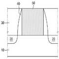
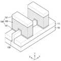
먼저 도 1을 참조하면, 기판(10) 상에 더미 게이트 전극(50)을 형성한다.First, referring to FIG. 1 , a
비록 상세히 도시하지는 않았으나, 기판(10)에는 반도체 소자를 서로 분리하기 위한 예를 들어, STI(Shallow Trench Isolation) 등의 소자 분리막이 형성될 수 있다.Although not shown in detail, a device isolation layer such as shallow trench isolation (STI) for isolating semiconductor devices from each other may be formed on the
기판(10)은 예를 들어, 벌크 실리콘일 수도 있고, 절연체 상에 실리콘이 에피 성장된 SOI(silicon-on-insulator)일 수도 있다.The
기판(10)은 원소 반도체 물질인 실리콘 또는 게르마늄을 포함할 수 있다. 또한, 기판(10)은 화합물 반도체를 포함할 수 있고, 예를 들어, IV-IV족 화합물 반도체 또는 III-V족 화합물 반도체를 포함할 수 있다. 구체적으로, IV-IV족 화합물 반도체를 예로 들면, 기판(10)은 탄소(C), 규소(Si), 게르마늄(Ge), 주석(Sn) 중 적어도 2개 이상을 포함하는 이원계 화합물(binary compound), 삼원계 화합물(ternary compound) 또는 이들에 IV족 원소가 도핑된 화합물일 수 있다.The
III-V족 화합물 반도체를 예로 들면, 에피층은 III족 원소로 알루미늄(Al), 갈륨(Ga) 및 인듐(In) 중 적어도 하나와 V족 원소인 인(P), 비소(As) 및 안티모늄(Sb) 중 하나가 결합되어 형성되는 이원계 화합물, 삼원계 화합물 또는 사원계 화합물 중 하나일 수 있다.Taking a group III-V compound semiconductor as an example, the epitaxial layer includes at least one of aluminum (Al), gallium (Ga), and indium (In) as a group III element, and phosphorus (P), arsenic (As) and anti It may be one of a binary compound, a ternary compound, or a quaternary compound formed by combining one of monium (Sb).
다음, 기판(10) 상에 예를 들어, 폴리 실리콘을 포함하는 더미 게이트 전극(50)를 형성한다. 그리고, 더미 게이트 전극(50)의 양 측에 예를 들어, 질화막, 산질화막 중 적어도 하나를 포함하는 스페이서(40)를 형성한다.Next, a
비록 도면에서는, 기판(10)과 더미 게이트 전극(50)가 직접 접촉하는 것으로 도시되어 있으나, 본 발명이 이에 제한되는 것은 아니다. 본 발명의 몇몇 실시예에서, 기판(10)과 더미 게이트 전극(50) 사이에는 버퍼 산화막이 형성될 수 있다.Although the drawing shows that the
또한, 본 발명의 몇몇 다른 실시예에서, 더미 게이트 전극(50)의 상부에는 예를 들어, 실리콘 질화막(SiN)을 포함하는 하드 마스크가 형성될 수도 있다.In addition, in some other embodiments of the present invention, a hard mask including, for example, a silicon nitride layer (SiN) may be formed on the
다음, 더미 게이트 전극(50)와 스페이서(40)를 마스크로 기판(10)에 불순물을 주입하여 소오스-드레인 영역(20)을 형성한다.Next, impurities are implanted into the
이러한 소오스-드레인 영역(20)은 도시된 것과 달리, 에피택셜 성장(epitaxial growth)을 통해 형성될 수도 있다. 이렇게 소오스-드레인 영역(20)이 에피택셜 성장을 통해 형성될 경우, 기판(10)에 형성된 리세스(recess) 내에 소오스-드레인 영역(20)이 형성될 수 있다.The source-
다음, 더미 게이트 전극(50)와 스페이서(40)를 덮는 층간 절연막(30)을 형성한다. 이러한 층간 절연막(30)은 예를 들어, 산화막, 질화막, 산질화막 등을 포함할 수 있다. 이어서, 더미 게이트 전극(50)의 상면이 노출될 때까지 층간 절연막(30)을 평탄화한다.Next, an
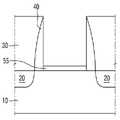
다음 도 2를 참조하면, 기판(10)의 상면이 노출될 때까지 더미 게이트 전극(도 1의 50)을 제거한다. 그리고, 노출된 기판(10)의 상면 상에 인터페이스막(55)을 형성한다.Next, referring to FIG. 2 , the
본 발명의 몇몇 실시예에서, 인터페이스막(55)은 예를 들어, 산화막을 포함할 수 있다. 구체적으로, 인터페이스막(55)은 예를 들어, 유전율(k)이 9 이하인 저유전 물질층, 예를 들면 실리콘 산화막(k는 약 4) 또는 실리콘 산질화막 (산소 원자 및 질소 원자 함량에 따라 k는 약 4~8)을 포함할 수 있다. 또는, 인터페이스막(151b)은 예를 들어, 실리케이트로 이루어질 수도 있으며, 앞서 예시된 막들의 조합으로 이루어질 수도 있다. 본 발명의 몇몇 실시예에서, 인터페이스막(55)은 기판(10)을 열산화하여 형성된 실리콘 산화막(SiO2)을 포함할 수 있다.In some embodiments of the present invention, the
이러한 인터페이스막(55)은 예를 들어, 습식(wet) 공정 또는 열 산화(heat oxidation) 방식을 통해 형성할 수 있다. 이러한 인터페이스막(55)은 후술할 제1 게이트 절연막(도 3의 60a)과 기판(10) 사이에서 제1 게이트 절연막(도 3의 60a)과 기판(10) 사이의 불량 계면을 방지하는 역할을 할 수 있다.The
다음 도 3을 참조하면, 인터페이스막(55) 상에 제1 게이트 절연막(60a)을 형성한다. 이러한 제1 게이트 절연막(60a)은 실리콘 산화막보다 높은 유전 상수를 갖는 고유전체 물질을 포함할 수 있다(예를 들어, 유전율(k)이 9 이상인 고유전 물질).Next, referring to FIG. 3 , a first
제1 게이트 절연막(60a)은 예를 들어, 하프늄 산화물(hafnium oxide), 하프늄 실리콘 산화물(hafnium silicon oxide), 란타늄 산화물(lanthanum oxide), 란타늄 알루미늄 산화물(lanthanum aluminum oxide), 지르코늄 산화물(zirconium oxide), 지르코늄 실리콘 산화물(zirconium silicon oxide), 탄탈륨 산화물(tantalum oxide), 티타늄 산화물(titanium oxide), 바륨 스트론튬 티타늄 산화물(barium strontium titanium oxide), 바륨 티타늄 산화물(barium titanium oxide), 스트론튬 티타늄 산화물(strontium titanium oxide), 이트륨 산화물(yttrium oxide), 알루미늄 산화물(Aluminum oxide), 납 스칸듐 탄탈륨 산화물(lead scandium tantalum oxide), 또는 납 아연 니오브산염(lead zinc niobate) 등을 포함할 수 있다.The first
제1 게이트 절연막(60a) 상에는 제2 게이트 절연막(60b)이 형성될 수 있다. 본 발명의 몇몇 실시예에서, 제2 게이트 절연막(60b)은 제1 게이트 절연막(60a)보다 작은 유전율을 갖는 물질을 포함할 수 있다. 본 발명의 몇몇 실시예에서, 제1 게이트 절연막(60a)은 예를 들어, 하프늄 산화막(HfO)을 포함하고, 제2 게이트 절연막(60b)은 예를 들어, 실리콘 산화막(SiO2)을 포함할 수 있다.A second
제1 및 제2 게이트 절연막(60a, 60b)은 예를 들어, 원자층 증착(ALD, Atomic Layer Depostion)을 통해 형성될 수 있다. 구체적으로, 제1 게이트 절연막(60a)은, 원자층 증착 공정을 n(n은 자연수) 싸이클(cycle) 동안 수행함으로써 형성할 수 있고, 제2 게이트 절연막(60b)은, 원자층 증착 공정을 m(m은 m<n인 자연수) 싸이클 동안 수행함으로써 형성할 수 있다.The first and second
더욱 구체적으로, 제1 게이트 절연막(60a)은, 원자층 증착 공정을 18 싸이클 동안 수행함으로써 형성할 수 있고, 제2 게이트 절연막(60b)은, 원자층 증착 공정을 1 싸이클 동안 수행함으로써 형성할 수 있다. 하지만, 본 발명이 이러한 예시에 제한되는 것은 아니며, 제1 및 제2 게이트 절연막(60a, 60b)을 형성하는 구체적인 공정은 이와 다르게 얼마든지 변형될 수 있다.More specifically, the first
이러한 제1 및 제2 게이트 절연막(60a, 60b)은 도시된 것과 같이 인터페이스막(55)의 상면 및 스페이서(40)의 측벽을 따라 상부로 연장된 형상으로 형성될 수 있다. 또한, 제1 및 제2 게이트 절연막(60a, 60b)은 층간 절연막(30) 상에도 형성될 수 있다.The first and second
다음 도 4를 참조하면, 기판(10)을 어닐링(annealing)한다.Next, referring to FIG. 4 , the
본 발명의 몇몇 실시예에서, 이러한 어닐링은 예를 들어, 플래시(flash) 어닐링, 스파이크(spike) 어닐링, 또는 레이저(laser) 어닐링을 포함할 수 있다. 이 때, 어닐링 온도는 예를 들어, 800 내지 1200℃일 수 있다.In some embodiments of the invention, such annealing may include, for example, flash annealing, spike annealing, or laser annealing. At this time, the annealing temperature may be, for example, 800 to 1200 ℃.
본 발명의 몇몇 실시예에서, 이러한 어닐링 공정에 의해, 제1 및 제2 게이트 절연막(도 3의 60a, 60b)은 제3 게이트 절연막(60)으로 형성될 수 있다. 제3 게이트 절연막(60)은 예를 들어, 실리콘이 도핑된 하프늄 산화막(Si doped HfO)을 포함할 수 있으나, 본 발명이 이에 제한되는 것은 아니다.In some embodiments of the present invention, the first and second
한편, 본 발명의 다른 몇몇 실시예에서, 이러한 어닐링 공정 후에도, 제1 및 제2 게이트 절연막(도 3의 60a, 60b)은 도시된 것과 같이 제3 게이트 절연막(60)으로 형성되지 않을 수도 있다. 즉, 어닐링 공정 후에도, 제1 게이트 절연막(도 3의 60a)과 제2 게이트 절연막(도 3의 60b)이 서로 구분된 상태로 존재할 수도 있다.Meanwhile, in some other embodiments of the present invention, even after the annealing process, the first and second
다음 도 5를 참조하면, 제1 및 제2 게이트 절연막(도 3의 60a, 60b) 또는 제3 게이트 절연막(60)을 질화(nidridation)시킨다.Next, referring to FIG. 5 , the first and second
이러한 질화 공정에 의해 제1 및 제2 게이트 절연막(도 3의 60a, 60b) 또는 제3 게이트 절연막(도 4의 60)은 제4 게이트 절연막(61)으로 형성될 수 있다. 이러한 제4 게이트 절연막(61)은 예를 들어, 실리콘이 도핑된 질화 하프늄 산화막(Si doped HfON)을 포함할 수 있으나, 본 발명이 이에 제한되는 것은 아니다.Through this nitriding process, the first and second
본 발명의 몇몇 실시예에서, 이러한 질화 공정은 예를 들어, 고압 조건에서 수행될 수 있다. 구체적으로, 이러한 질화 공정은 예를 들어, 질화 가스의 압력을 100mm torr 내지 500mm torr로 유지하여 제1 및 제2 게이트 절연막(도 3의 60a, 60b) 또는 제3 게이트 절연막(도 4의 60)을 질화시키는 것을 포함할 수 있다.In some embodiments of the present invention, this nitridation process may be performed under high pressure conditions, for example. Specifically, this nitridation process is performed, for example, by maintaining the pressure of the nitriding gas at 100 mm torr to 500 mm torr to perform the first and second gate insulating films (60a and 60b in FIG. 3) or the third gate insulating film (60 in FIG. 4). It may include nitriding.
이처럼 질화 공정을 고압 조건에서 수행하는 것은, 제4 게이트 절연막(61)에 포함된 질소의 농도 프로 파일의 최고점(peak)을 제4 게이트 절연막(61)의 상면에 인접하게 위치시키기 위함이다. 이렇게 제4 게이트 절연막(61)의 상면에 질소의 농도 프로파일의 최고점(peak)이 위치할 경우, 반도체 소자의 특성이 향상될 수 있다. 이에 관한 보다 구체적인 설명은 후술한다.The nitriding process is performed under a high-pressure condition in order to position the peak of the nitrogen concentration profile included in the fourth
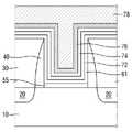
다음, 도 6을 참조하면, 제4 게이트 절연막(61) 상에 캡핑막(capping layer)(72)을 형성한다.Next, referring to FIG. 6 , a
본 발명의 몇몇 실시예에서, 이러한 캡핑막(72)은 예를 들어, 금속 질화막을 포함할 수 있다. 구체적으로, 캡핑막(72)은 예를 들어, TiN을 포함할 수 있으나, 본 발명이 이에 제한되는 것은 아니다.In some embodiments of the present invention, the
이러한 캡핑막(72)은 그 하부에 배치된 제4 게이트 절연막(61)에 포함된 산소 농도를 조절하는 역할을 할 수 있다.The
이어서, 캡핑막(72) 상에 베리어막(barrier layer)(74)을 형성한다.Next, a
본 발명의 몇몇 실시예에서, 이러한 베리어막(74)은 예를 들어, 금속 질화막을 포함할 수 있다. 구체적으로, 베리어막(74)은 예를 들어, TaN을 포함할 수 있으나, 본 발명이 이에 제한되는 것은 아니다.In some embodiments of the present invention, the
이어서, 베리어막(74) 상에 일함수 조절막(76)을 형성한다.Next, a work
이러한 일함수 조절막(76)은 반도체 소자의 일함수를 조절하는 역할을 할 수 있다.The work
예를 들어, 반도체 소자가 n형일 경우, 일함수 조절막(76)은 n형 일함수 물질을 포함할 수 있다. 이러한 n형 일함수 물질의 예로는, TiAl, TiAlN, TaC, TaAlN, TiC, HfSi 등을 들 수 있으나, 본 발명이 이에 제한되는 것은 아니다.For example, when the semiconductor device is n-type, the work
한편, 예를 들어, 반도체 소자가 p형일 경우, 일함수 조절막(76)은 p형 일함수 물질을 포함할 수 있다. 이러한 p형 일함수 물질의 예로는, TiN, TaN 등을 들 수 있다. 구체적으로, p형 일함수 조절막의 예로는, TiN으로 이루어진 단일막, 또는 TiN 하부막과 TaN 상부막으로 이루어진 이중막 등을 들 수 있으나, 본 발명이 이에 제한되는 것은 아니다.Meanwhile, for example, when the semiconductor device is a p-type semiconductor device, the work
본 발명의 몇몇 실시예에서, 반도체 소자가 p형일 경우, 일함수 조절막(76)은, 하부 p형 일함수 조절막과 상부 n형 일함수 조절막의 이중막 구조로 형성될 수도 있다.In some embodiments of the present invention, when the semiconductor device is a p-type semiconductor device, the work
이어서, 일함수 조절막(76) 상에 메탈 게이트 전극(78)을 형성한다. 이러한 메탈 게이트 전극(78)은 일함수 조절막(76)에 의해 형성된 트렌치를 채우는 형상으로 형성될 수 있다.Next, a
본 발명의 몇몇 실시예에서, 메탈 게이트 전극(78)은 전도성이 높은 메탈을 포함할 수 있다. 이러한 메탈의 예로는 Al, W 등을 들 수 있으나, 본 발명이 이에 제한되는 것은 아니다.In some embodiments of the present invention, the
본 발명의 몇몇 실시에에서, 일함수 조절막(76)과 메탈 게이트 전극(78) 중 적어도 하나는 알루미늄(Al)을 포함할 수 있다.In some embodiments of the present invention, at least one of the work
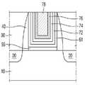
다음, 도 7을 참조하면, 일함수 조절막(76)의 상면이 노출될 때까지, 메탈 게이트 전극(78)을 평탄화한다.Next, referring to FIG. 7 , the
이러한 평탄화 공정에 의해, 베리어막(74), 캡핑막(72) 및 제4 게이트 절연막(61)의 상면이 같이 노출될 수 있다.The top surfaces of the
도 8 및 도 9는 본 발명의 일 실시예에 따른 반도체 장치의 제조 방법의 효과를 설명하기 위한 도면들이다.8 and 9 are diagrams for explaining an effect of a method of manufacturing a semiconductor device according to an embodiment of the present invention.
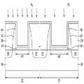
도 8은 본 발명의 일 실시예와 다른 반도체 장치의 제조 방법을 통해 제조한 반도체 장치의 게이트 절연막(도 7의 61)에 포함된 물질들의 깊이에 따른 농도 프로파일을 도시한 그래프이다.8 is a graph illustrating concentration profiles according to depths of materials included in the gate insulating layer (61 of FIG. 7 ) of a semiconductor device manufactured by a method of manufacturing a semiconductor device according to an embodiment of the present invention.
도 8을 참조하면, 게이트 절연막(도 7의 61)의 상면(Surface)에 인접한 위치에 하프늄 산화막(HfO)에 포함된 하프늄(Hf) 및 산소 이온(O)의 농도가 높고, 기판(Si_sub)과 게이트 절연막(도 7의 61)의 계면에 인접한 위치에 실리콘 산화막(SiO2)에 포함된 실리콘(Si) 및 산소 이온(O)의 농도가 높음을 알 수 있다.Referring to FIG. 8 , concentrations of hafnium (Hf) and oxygen ions (O) included in the hafnium oxide film (HfO) at a position adjacent to the surface of the gate insulating film (61 in FIG. 7) are high, and the substrate (Si_sub) It can be seen that the concentrations of silicon (Si) and oxygen ions (O) included in the silicon oxide film (SiO2) are high at a position adjacent to the interface between the gate insulating film and the gate insulating film (61 of FIG. 7 ).
한편, 질화 공정을 통해 게이트 절연막(도 7의 61)에 도핑된 질소 이온(N)의 농도 프로파일의 피크(peak)는 기판(Si_sub)과 게이트 절연막(도 7의 61)의 계면에 인접하여 위치함을 알 수 있다.On the other hand, the peak of the concentration profile of the nitrogen ion (N) doped into the gate insulating film (61 in Fig. 7) through the nitridation process is located adjacent to the interface between the substrate (Si_sub) and the gate insulating film (61 in Fig. 7) it can be seen that
게이트 절연막(도 7의 61)에 도핑된 질소 이온(N)의 농도 프로파일의 피크(peak)가 이와 같이 형성될 경우, 질소 이온(N)이 게이트 절연막(도 7의 61) 하부에 배치된 인터페이스막(도 7의 55)으로 이동하여 N-O 본딩을 형성할 가능성이 높아진다.When the peak of the concentration profile of the nitrogen ions (N) doped in the gate insulating film (61 of FIG. 7) is formed in this way, the nitrogen ions (N) are the interface disposed under the gate insulating film (61 of FIG. 7) It is more likely to migrate to the film (55 in FIG. 7) and form an N-O bond.
그리고, 이러한 N-O 본딩은 결합 에너지가 낮아서, 후속 공정에서 열처리 등이 수행될 시, Hf-N, Si-N 본딩으로 변화될 가능성이 높다.And, since the N-O bonding has a low bonding energy, it is highly likely to be changed to Hf-N or Si-N bonding when heat treatment is performed in a subsequent process.
이처럼, 게이트 절연막(도 7의 61) 내에 포함된 질소 이온(N)이 Hf-N, Si-N 본딩으로 변화되면, 메탈 게이트 전극(78)이나 일함수 조절막(76)에 포함된 알루미늄(Al)이 게이트 절연막(도 7의 61)에 포함된 산소 이온(O)과 결합하는 것을 방지하는 역할을 하지 못한다.As such, when nitrogen ions (N) included in the gate insulating layer (61 in FIG. 7) are changed to Hf-N and Si-N bonding, aluminum ( Al) does not play a role in preventing the combination of oxygen ions (O) included in the gate insulating film (61 in FIG. 7).
한편, 도 9는 본 발명의 일 실시예에 따른 제조 방법을 통해 제조한 반도체 장치의 게이트 절연막(도 7의 61)에 포함된 물질들의 깊이에 따른 농도 프로파일을 도시한 그래프이다.Meanwhile, FIG. 9 is a graph illustrating a concentration profile according to a depth of materials included in a gate insulating layer (61 of FIG. 7 ) of a semiconductor device manufactured by a manufacturing method according to an embodiment of the present invention.
도 9를 참조하면, 하프늄 산화막(HfO)에 포함된 하프늄(Hf) 및 산소(O2)의 농도 프로파일과 실리콘 산화막(SiO2)에 포함된 실리콘(Si) 및 산소(O2)의 농도 프로파일은 도 8에 도시된 것과 유사하나, 질화 공정을 통해 게이트 절연막(도 7의 61)에 도핑된 질소 이온(N)의 농도 프로파일의 피크(peak)가 게이트 절연막(도 7의 61)의 상면(Surface)에 인접하여 위치함을 알 수 있다.Referring to FIG. 9 , the concentration profile of hafnium (Hf) and oxygen (O2) included in the hafnium oxide layer (HfO) and the concentration profile of silicon (Si) and oxygen (O2) included in the silicon oxide layer (SiO2) are shown in FIG. 8 Although similar to that shown in Figure 7, the peak of the concentration profile of nitrogen ions (N) doped into the gate insulating film (61 in Fig. 7) through the nitridation process is on the top surface of the gate insulating film (61 in Fig. 7). It can be seen that they are located adjacent to each other.
본 실시예에 따른 반도체 장치의 제조 방법에서는, 질화 공정 수행 시 압력 조건을 100mm torr 내지 500 mm torr로 유지함으로써, 이러한 질소 이온(N)의 농도 프로파일을 형성할 수 있다.In the method of manufacturing a semiconductor device according to the present embodiment, the concentration profile of nitrogen ions (N) may be formed by maintaining a pressure condition of 100 mm torr to 500 mm torr during the nitriding process.
구체적으로, 본 실시예에 따른 반도체 장치의 제조 방법에서는, 질화 공정 수행 시 압력 조건을 100mm torr 이상으로 설정함으로써, 질화 공정이 수행되는 동안 게이트 절연막(도 7의 61)에 침투되는 질소 이온(N)의 침투 깊이를 작게 할 수 있다.Specifically, in the method of manufacturing a semiconductor device according to the present embodiment, by setting a pressure condition of 100 mm torr or more during the nitridation process, nitrogen ions (N ) can reduce the penetration depth.
또한, 본 실시예에 따른 반도체 장치의 제조 방법에서는, 질화 공정 수행 시 압력 조건을 500mm torr 이하로 설정함으로써, 질화 공정이 수행되는 동안 게이트 절연막(도 7의 61)에 질소 이온(N)이 신뢰성 있게 침투될 수 있도록 할 수 있다.In addition, in the method of manufacturing a semiconductor device according to the present embodiment, by setting a pressure condition of 500 mm torr or less during the nitriding process, nitrogen ions (N) in the gate insulating film (61 in FIG. 7 ) during the nitriding process are reliable. It can be allowed to penetrate.
게이트 절연막(도 7의 61)에 도핑된 질소 이온(N)의 농도 프로파일의 피크(peak)가 이와 같이 형성될 경우, 질소 이온(N)이 게이트 절연막(도 7의 61) 하부에 배치된 인터페이스막(도 7의 55)으로 이동하지 않으므로, N-O 본딩을 형성할 가능성이 거의 없어진다. 이에 따라, 게이트 절연막(도 7의 61) 내에 많은 질소 이온(N)이 포함되므로, 메탈 게이트 전극(78)이나 일함수 조절막(76)에 포함된 알루미늄(Al)이 게이트 절연막(도 7의 61)에 포함된 산소 이온(O)과 결함하는 것을 방지하는 역할을 할 수 있다.When the peak of the concentration profile of the nitrogen ions (N) doped in the gate insulating film (61 of FIG. 7) is formed in this way, the nitrogen ions (N) are the interface disposed under the gate insulating film (61 of FIG. 7) Since it does not migrate to the film (55 in FIG. 7), there is little chance of forming an N-O bond. Accordingly, since many nitrogen ions (N) are included in the gate insulating film (61 in FIG. 7 ), aluminum (Al) included in the
이에 대해 보다 구체적으로, 설명하면 다음과 같다.More specifically, this will be described as follows.
메탈 게이트 전극(78)이나 일함수 조절막(76)에 포함된 알루미늄(Al)은 반도체 소자를 제조하는 과정에서, 게이트 절연막(도 7의 61)으로 확산되어 게이트 절연막(도 7의 61)에 포함된 산소를 뺏어갈 수 있다. 이처럼 게이트 절연막(도 7의 61)에 산소 결핍이 발생할 경우, 게이트 절연막(도 7의 61)의 절연 특성이 저하될 수 있다.Aluminum (Al) included in the
게이트 절연막(도 7의 61)에 도핑되는 질소 이온(N)은 이처럼 게이트 절연막(도 7의 61)에 산소 결핍이 발생할 경우, 산소가 이탈된 빈공간(vacancy)를 채우는 역할을 하여, 게이트 절연막(도 7의 61)의 절연 특성을 유지시킬 수 있다. 즉, 본 실시예에 따른 반도체 장치의 제조 방법에서는, 앞서 설명한 것과 같이 게이트 절연막(도 7의 61) 내에 높은 농도의 질소 이온(N)이 유지되므로, 게이트 절연막(도 7의 61)의 절연 특성이 향상될 수 있다.Nitrogen ions (N) doped into the gate insulating layer (61 of FIG. 7) serves to fill the vacancy from which oxygen is released when oxygen deficiency occurs in the gate insulating layer (61 of FIG. 7) as described above, and the gate insulating layer (61 in FIG. 7) can be maintained. That is, in the method of manufacturing the semiconductor device according to the present embodiment, as described above, a high concentration of nitrogen ions (N) is maintained in the gate insulating film (61 of FIG. 7), so the insulating properties of the gate insulating film (61 of FIG. 7) are This can be improved.
한편, 게이트 절연막(도 7의 61)에 포함된 실리콘 산화막(SiO2)은 그 격자 구조가 안정하므로, 메탈 게이트 전극(78)이나 일함수 조절막(76)에 포함된 알루미늄(Al)에 의해, 게이트 절연막(도 7의 61)이 산소 이온(O)을 빼앗기는 것을 방지하는 역할을 할 수 있다. 즉, 게이트 절연막(도 7의 61)의 절연 특성이 향상될 수 있다.On the other hand, since the lattice structure of the silicon oxide film (SiO2) included in the gate insulating film (61 in FIG. 7) is stable, by aluminum (Al) contained in the
즉, 본 실시예에 따른 반도체 장치의 제조 방법에 따라 반도체 장치를 제조할 경우, 반도체 장치의 성능을 향상시킬 수 있고, 장치의 동작 신뢰성 또한 향상될 수 있다.That is, when a semiconductor device is manufactured according to the method for manufacturing a semiconductor device according to the present exemplary embodiment, the performance of the semiconductor device may be improved, and operation reliability of the device may also be improved.
다음, 도 10을 참조하여, 본 발명의 다른 실시예에 따른 반도체 장치의 제조 방법에 대해 설명한다.Next, a method of manufacturing a semiconductor device according to another exemplary embodiment of the present invention will be described with reference to FIG. 10 .
도 10은 본 발명의 다른 실시예에 따른 반도체 장치의 제조 방법을 설명하기 위한 도면이다. 이하에서는, 앞서 설명한 실시예와 중복된 설명은 생략하고, 차이점을 위주로 설명한다.10 is a view for explaining a method of manufacturing a semiconductor device according to another embodiment of the present invention. Hereinafter, descriptions overlapping those of the above-described embodiment will be omitted, and differences will be mainly described.
도 10을 참조하면, 본 실시예에 따른 반도체 장치의 제조 방법에서는, 앞서 도 3을 참조하여 설명한 공정에서, 게이트 절연막 형성 공정이 추가적으로 반복된다.Referring to FIG. 10 , in the method of manufacturing a semiconductor device according to the present exemplary embodiment, the process of forming a gate insulating layer is additionally repeated in the process described with reference to FIG. 3 .
본 발명의 몇몇 실시예에서, 인터페이스막(55) 상에 제1 및 제2 게이트 절연막(60a, 60b)을 형성한 후, 제2 게이트 절연막(60b) 상에 제5 게이트 절연막(60c)을 형성하고, 제5 게이트 절연막(60c) 상에 제6 게이트 절연막(60d)을 형성할 수 있다.In some embodiments of the present invention, after forming the first and second
여기서, 예를 들어, 제5 게이트 절연막(60c)은 제1 게이트 절연막(60a)과 실질적으로 동일한 물질을 포함할 수 있고, 제6 게이트 절연막(60d)은 제2 게이트 절연막(60b)과 실질적으로 동일한 물질을 포함할 수 있으나, 본 발명이 이에 제한되는 것은 아니다.Here, for example, the fifth
이러한 제1 게이트 절연막(60a), 제2 게이트 절연막(60b), 제5 게이트 절연막(60c), 및 제6 게이트 절연막(60d)은 예를 들어, 원자층 증착(ALD, Atomic Layer Depostion)을 통해 형성될 수 있다.The first
구체적으로, 제1 게이트 절연막(60a)은, 원자층 증착 공정을 n(n은 자연수) 싸이클(cycle) 동안 수행함으로써 형성할 수 있고, 제2 게이트 절연막(60b)은, 원자층 증착 공정을 m(m은 m<n인 자연수) 싸이클 동안 수행함으로써 형성할 수 있다. 제5 게이트 절연막(60c)은, 원자층 증착 공정을 m 싸이클 동안 수행함으로써 형성할 수 있고, 제6 게이트 절연막(60d)은, 원자층 증착 공정을 m 싸이클 동안 수행함으로써 형성할 수 있다.Specifically, the first
더욱 구체적으로, 제1 게이트 절연막(60a)은, 원자층 증착 공정을 18 싸이클 동안 수행함으로써 형성할 수 있고, 제2 게이트 절연막(60b)은, 원자층 증착 공정을 1 싸이클 동안 수행함으로써 형성할 수 있고, 제5 게이트 절연막(60c)은, 원자층 증착 공정을 1 싸이클 동안 수행함으로써 형성할 수 있고, 제6 게이트 절연막(60d)은, 원자층 증착 공정을 1 싸이클 동안 수행함으로써 형성할 수 있다.More specifically, the first
하지만, 본 발명이 이러한 예시에 제한되는 것은 아니며, 제1 게이트 절연막(60a), 제2 게이트 절연막(60b), 제5 게이트 절연막(60c), 및 제6 게이트 절연막(60d)을 형성하는 구체적인 공정은 이와 다르게 얼마든지 변형될 수 있다.However, the present invention is not limited to this example, and a specific process for forming the first
한편, 본 발명의 다른 몇몇 실시예에서, 게이트 절연막 형성 공정은 앞서 설명한 것보다 더 추가적으로 반복될 수 있다.Meanwhile, in some other embodiments of the present invention, the process of forming the gate insulating layer may be additionally repeated than described above.
즉, 예를 들어, 하프늄 산화막(HfO)을 포함하는 게이트 절연막을 형성하는 공정과, 실리콘 산화막(SiO2)을 포함하는 게이트 절연막을 형성하는 공정이 p(p는 3 이상인 자연수)회 반복될 수 있다.That is, for example, a process of forming a gate insulating film including a hafnium oxide film (HfO) and a process of forming a gate insulating film including a silicon oxide film (SiO2) may be repeated p (p is a natural number equal to or greater than 3) times. .
이와 같이 반복적인 공정을 거쳐 게이트 절연막을 형성할 경우, 게이트 절연막 내에 실리콘 산화막(SiO2)의 비중이 증가되어 그 격자구조가 안정해지므로, 메탈 게이트 전극(도 7의 78)이나 일함수 조절막(도 7의 76)에 포함된 알루미늄(Al)에 의한 게이트 절연막의 산소 결핍을 방지할 수 있다.When the gate insulating film is formed through this repetitive process, the specific gravity of the silicon oxide film (SiO2) in the gate insulating film is increased to stabilize the lattice structure, so that the metal gate electrode (78 in FIG. 7) or the work function control film ( Oxygen deficiency in the gate insulating layer due to aluminum (Al) included in 76 of FIG. 7 may be prevented.
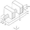
다음, 도 11 내지 도 18을 참조하여, 본 발명의 또 다른 실시예에 따른 반도체 장치의 제조 방법에 대해 설명한다.Next, a method of manufacturing a semiconductor device according to another exemplary embodiment of the present invention will be described with reference to FIGS. 11 to 18 .
도 11 내지 도 18은 본 발명의 또 다른 실시예에 따른 반도체 장치의 제조 방법을 설명하기 위한 도면들이다. 이하에서도, 앞서 설명한 실시예들과 중복된 설명은 생략하고, 차이점을 위주로 설명한다.11 to 18 are views for explaining a method of manufacturing a semiconductor device according to still another exemplary embodiment of the present invention. Hereinafter, descriptions overlapping those of the above-described embodiments will be omitted, and differences will be mainly described.
도 11을 참조하면, 기판(100) 상에 액티브 핀(120)을 형성한다.Referring to FIG. 11 , the
본 발명의 몇몇 실시예에서, 이러한 액티브 핀(120)은, 기판(100) 상에 더미 스페이서를 형성하고 더미 스페이서를 이용하여 기판(100)을 식각함으로써 형성되는 예를 들어, 맨드렐(mandrel) 공정을 통해 형성될 수 있으나, 본 발명이 이에 제한되는 것은 아니다.In some embodiments of the present invention, the
기판(100)은 예를 들어, 벌크 실리콘 또는 SOI(silicon-on-insulator)일 수 있다. 이와 달리, 기판(100)은 실리콘 기판일 수도 있고, 또는 다른 물질, 예를 들어, 실리콘게르마늄, 안티몬화 인듐, 납 텔루르 화합물, 인듐 비소, 인듐 인화물, 갈륨 비소 또는 안티몬화 갈륨을 포함할 수 있다.The
또는, 기판(100)은 베이스 기판 상에 에피층이 형성된 것일 수도 있다. 베이스 기판 상에 형성된 에피층을 이용하여 액티브 핀(120)을 형성할 경우, 에피층은 원소 반도체 물질인 실리콘 또는 게르마늄을 포함할 수 있다. 또한, 에피층은 화합물 반도체를 포함할 수 있고, 예를 들어, IV-IV족 화합물 반도체 또는 III-V족 화합물 반도체를 포함할 수 있다. 구체적으로, IV-IV족 화합물 반도체를 예로 들면, 에피층은 탄소(C), 규소(Si), 게르마늄(Ge), 주석(Sn) 중 적어도 2개 이상을 포함하는 이원계 화합물(binary compound), 삼원계 화합물(ternary compound) 또는 이들에 IV족 원소가 도핑된 화합물일 수 있다. III-V족 화합물 반도체를 예로 들면, 에피층은 III족 원소로 알루미늄(Al), 갈륨(Ga) 및 인듐(In) 중 적어도 하나와 V족 원소인 인(P), 비소(As) 및 안티모늄(Sb) 중 하나가 결합되어 형성되는 이원계 화합물, 삼원계 화합물 또는 사원계 화합물 중 하나일 수 있다.Alternatively, the
본 실시예에 따른 반도체 소자 제조 방법에서, 기판(100)은 실리콘 기판인 것으로 설명한다.In the method of manufacturing a semiconductor device according to the present embodiment, the
액티브 핀(120)은 제2 방향(Y)을 따라 연장될 수 있다. 기판(100)의 일부를 제거한 액티브 핀(120) 주변에는 리세스가 형성될 수 있다.The
도 11에서, 액티브 핀(120)은 수직인 기울기를 갖는 것으로 도시하였지만, 본 발명이 이에 제한되는 것은 아니다. 즉, 액티브 핀(120)의 측면은 기울기를 가질 수 있고, 예를 들어, 액티브 핀(120)은 테이퍼(tapered)진 형상일 수도 있다.In FIG. 11 , the
이어서, 액티브 핀(120) 주변에 리세스를 채우는 필드 절연막(110)을 형성한다. 필드 절연막(110)은 실리콘 산화막, 실리콘 질화막, 실리콘 산질화막 중 적어도 하나를 포함하는 물질로 형성될 수 있다.Next, a
이어서, 필드 절연막(110)을 평탄화한다. 이러한 평탄화 공정을 통해, 액티브 핀(120) 및 필드 절연막(110)은 동일 평면 상에 놓일 수 있다.Next, the
다음 도 12를 참조하면, 필드 절연막(110)의 상부를 리세스하여, 액티브 핀(120)의 상부를 노출시킨다. 즉, 필드 절연막(110) 위로 돌출된 액티브 핀(120)을 형성한다. 리세스 공정은 선택적 식각 공정을 포함할 수 있다.Next, referring to FIG. 12 , an upper portion of the
한편, 필드 절연막(110) 위로 돌출된 액티브 핀(120)의 일부는, 에피 공정에 의하여 형성될 수도 있다. 구체적으로, 필드 절연막(110) 형성 후, 리세스 공정 없이 필드 절연막(110)에 의하여 노출된 액티브 핀(120)의 상면을 씨드로 하는 에피 공정에 의하여 액티브 핀(120)의 일부가 형성될 수 있다.Meanwhile, a portion of the
본 발명의 몇몇 실시예에서, 액티브 핀(120)에 문턱 전압 조절용 도핑이 수행될 수 있다. 액티브 핀(120)을 이용하여 형성되는 트랜지스터가 NMOS 트랜지스터인 경우, 불순물은 예를 들어, 붕소(B)일 수 있다. 액티브 핀(120)을 이용하여 형성되는 트랜지스터가 PMOS 트랜지스터인 경우, 불순물은 예를 들어, 인(P) 또는 비소(As)일 수 있다.In some embodiments of the present invention, doping for adjusting a threshold voltage may be performed on the
다음 13을 참조하면, 액티브 핀(120) 상에 액티브 핀(120)과 교차하는 더미 게이트 구조체(130)를 형성한다. 더미 게이트 구조체(130)는 제1 방향(X)으로 연장되어 형성될 수 있다.Next, referring to 13 , the dummy gate structure 130 crossing the
더미 게이트 구조체(130)는 순차적으로 적층된 더미 실리콘 산화막(131), 폴리 실리콘막(133), 및 하드 마스크(137)를 포함할 수 있다. 즉, 더미 게이트 구조체(130)는 제1 방향(X)으로 연장되는 더미 실리콘 산화막(131), 폴리 실리콘막(133), 및 하드 마스크(137)의 적층체일 수 있다.The dummy gate structure 130 may include a dummy
이러한 더미 게이트 구조체(130)는 하드 마스크(137)를 식각 마스크로 이용하여 형성될 수 있다.The dummy gate structure 130 may be formed using the
더미 실리콘 산화막(131)은 액티브 핀(120)의 둘레뿐만 아니라, 필드 절연막(110) 상에도 형성되는 것으로 도시되었지만, 본 발명이 이에 제한되는 것은 아니다. 즉, 더미 실리콘 산화막(131)은 필드 절연막(110) 위로 돌출된 액티브 핀(120)의 측면 및 상면 상에만 형성될 수도 있다.Although the dummy
또한, 더미 실리콘 산화막(131)은 더미 게이트 구조체(130)와 오버랩되지 않는 액티브 핀(120) 상에는 형성되지 않는 것으로 도시하였지만, 이에 제한되는 것은 아니다. 즉, 더미 실리콘 산화막(131)은 필드 절연막(110) 위로 돌출된 액티브 핀(120)의 측면 및 상면 상에 전체적으로 형성될 수 있음은 물론이다.In addition, although it is illustrated that the dummy
더미 실리콘 산화막(131)은 이후에 진행되는 공정에서 채널 영역으로 사용되는 액티브 핀(120)을 보호하는 역할을 할 수 있다.The dummy
폴리 실리콘막(133)은 더미 실리콘 산화막(131) 상에 형성될 수 있다. 폴리 실리콘막(133)은 더미 게이트 구조체(130)와 오버랩되고, 필드 절연막(110) 위로 돌출된 액티브 핀(120)을 전체적으로 덮을 수 있다. 다시 말하면, 필드 절연막(110)으로부터 액티브 핀(120)의 상면까지의 높이는 필드 절연막(110)으로부터 폴리 실리콘막의 상면까지의 높이보다 작다.The polysilicon layer 133 may be formed on the dummy
폴리 실리콘막(133)과 더미 실리콘 산화막(131)은 높은 식각 선택비를 가질 수 있다. 따라서, 액티브 핀(120)의 상면 상에 폴리 실리콘막(133)이 남아 있으면, 이 후에 리플레이스먼트 금속 게이트를 형성하기 위한 트렌치 형성 공정에서, 폴리 실리콘막(133)은 제거되지만 하부의 더미 실리콘 산화막(131)은 식각 없이 남아있게 된다. 이를 통해, 더미 실리콘 산화막(131) 하부의 액티브 핀(120)은 보호될 수 있다.The polysilicon layer 133 and the dummy
하드 마스크(137)는 폴리 실리콘막(133) 상에 형성될 수 있다. 하드 마스크(137)는 예를 들어, 실리콘 질화물(SiN)을 포함할 수 있지만, 본 발명이 이에 제한되는 것은 아니다. 또한, 하드 마스크(137)는 도 14를 이용하여 설명될 게이트 스페이서막(151p)보다 식각 내성 물질을 포함할 수 있다.The
다음 도 14를 참조하면, 액티브 핀(120) 및 더미 게이트 구조체(130)를 덮는 게이트 스페이서막(151p)을 형성한다.Next, referring to FIG. 14 , a gate spacer layer 151p covering the
게이트 스페이서막(151p)은 더미 게이트 구조체(130)의 측면 및 바닥면과, 액티브 핀(120)의 측면 및 바닥면과, 필드 절연막(110) 상에 컨포말하게 형성될 수 있다.The gate spacer layer 151p may be conformally formed on the side and bottom surfaces of the dummy gate structure 130 , the side and bottom surfaces of the
게이트 스페이서막(151p)은 저유전율 물질을 포함할 수 있고, 예를 들어, SiOCN을 포함할 수 있지만, 본 발명이 이에 제한되는 것은 아니다. 게이트 스페이서막(151p)은 예를 들어, 화학적 기상 증착법(CVD), 원자층 증착법(ALD) 등을 이용하여 형성될 수 있다.The gate spacer layer 151p may include a low-k material, for example, SiOCN, but the present invention is not limited thereto. The gate spacer layer 151p may be formed using, for example, chemical vapor deposition (CVD), atomic layer deposition (ALD), or the like.
본 발명의 실시예들에 따른 반도체 장치 제조 방법에서, 하드 마스크(137)는 실리콘 질화물(SiN)이고, 게이트 스페이서막(151p)은 SiOCN일 수 있다. 이 때, 하드 마스크(137) 및 게이트 스페이서막(151p)을 동시에 식각할 수 있는 식각 공정에서, 하드 마스크(137)는 게이트 스페이서막(151p)보다 식각 내성 물질이다. 따라서, 도 15에 도시된 것과 같이, 하드 마스크(137) 와 게이트 스페이서막(151p)이 동시에 식각되는 과정에서, 더미 게이트 구조체(130)의 측면에 게이트 스페이서(151)가 형성되고, 하드 마스크(137)는 노출될 수 있다.In the method of manufacturing a semiconductor device according to embodiments of the present invention, the
다음, 도 15를 참조하면, 더미 게이트 구조체(130)의 측면에 트렌치(162)가 형성될 수 있다. 구체적으로, 트렌치(162)는 게이트 스페이서(151)의 측면에 형성되고, 액티브 핀(120) 내에 형성될 수 있다.Next, referring to FIG. 15 , a
더미 게이트 구조체(130)의 측면의 게이트 스페이서(151)와 액티브 핀(120) 내의 트렌치(162)는 동시에 형성될 수 있다. 즉, 트렌치(162)를 형성할 때, 게이트 스페이서(151)도 형성될 수 있다.The
게이트 스페이서(151)는 도 14의 게이트 스페이서막(151p)를 식각하여 형성하므로, 게이트 스페이서(151)는 하드 마스크(137)와 다른 물질을 포함할 수 있다. 또한, 본 발명의 몇몇 실시예에 따른 반도체 장치 제조 방법에서, 하드 마스크(137)는 게이트 스페이서(151)보다 식각 내성 물질을 포함할 수 있다.Since the
도 15에서, 필드 절연막(110)의 상면으로부터 게이트 스페이서(151)의 높이는 필드 절연막(110)의 상면으로부터 더미 게이트 구조체(130)의 상면, 즉 하드 마스크(137)의 상면까지의 높이보다 낮을 수 있다.In FIG. 15 , the height of the
더미 게이트 구조체(130)의 측면에 게이트 스페이서(151)을 형성할 때, 더미 게이트 구조체(130)와 오버랩되지 않는 액티브 핀(120)의 측면에도 핀 스페이서가 형성될 수 있다. 하지만, 액티브 핀(120) 내에 트렌치(162)를 형성하기 위해, 액티브 핀(120)의 측면에 형성되는 핀 스페이서는 제거되어야 한다. 액티브 핀(120)의 측면에 형성되는 핀 스페이서가 제거되는 동안, 게이트 스페이서(151)의 높이도 낮아지고, 하드 마스크의 일부도 제거될 수 있다.When the
이 때, 하드 마스크(137)는 게이트 스페이서(151)보다 식각 내성 물질을 포함하고 있으므로, 하드 마스크(137)가 제거되는 두께는 게이트 스페이서(151)가 제거되는 높이보다 작게 된다. 이를 통해, 게이트 스페이서(151)의 높이는 더미 게이트 구조체(130)의 높이보다 낮아지게 된다.In this case, since the
다음 도 16을 참조하면, 에피택셜 성장(epitaxial growth)을 이용하여, 트렌치(162) 내에 반도체 패턴(161)을 형성한다. 트렌치(162) 내에 형성된 반도체 패턴(161)은 더미 게이트 구조체(130)의 측면에 위치할 수 있다. 반도체 패턴(161)은 트렌지스터의 소오스/드레인일 수 있고, 예를 들어, 상승된(elevated) 소오스/드레인일 수 있다.Next, referring to FIG. 16 , a
액티브 핀(120)을 이용하여 형성되는 트랜지스터가 PMOS 트랜지스터인 경우, 반도체 패턴(161)은 압축 스트레스 물질을 포함할 수 있다. 예를 들어, 압축 스트레스 물질은 Si에 비해서 격자상수가 큰 물질일 수 있고, 예를 들어 SiGe일 수 있다. 압축 스트레스 물질은 액티브 핀(120)에 압축 스트레스를 가하여 채널 영역의 캐리어의 이동도(mobility)를 향상시킬 수 있다.When the transistor formed using the
이와는 달리, 액티브 핀(120)을 이용하여 형성되는 트랜지스터가 NMOS 트랜지스터인 경우, 반도체 패턴(161)은 기판(100)과 동일 물질 또는, 인장 스트레스 물질일 수 있다. 예를 들어, 기판(100)이 Si일 때, 반도체 패턴(161)은 Si이거나, Si보다 격자 상수가 작은 물질(예를 들어, SiC)일 수 있다.Alternatively, when the transistor formed using the
반도체 패턴(161)을 형성할 때, 필요에 따라, 에피 공정 시 불순물을 반도체 패턴(161) 내에 인시츄 도핑할 수도 있다.When forming the
반도체 패턴(161)은 다이아몬드 형상, 원 형상 및 직사각형 형상 중 적어도 하나일 수 있다. 도 16에서는 예시적으로 다이아몬드 형상(또는 오각형 형상 또는 육각형 형상)을 도시하였으나, 본 발명이 이에 제한되는 것은 아니다.The
도 17을 참조하면, 반도체 패턴(161) 및 더미 게이트 구조체(130)를 덮는 층간 절연막(171)을 필드 절연막(110) 상에 형성한다.Referring to FIG. 17 , an
층간 절연막(171)은 예를 들어, 저유전율 물질, 산화막, 질화막 및 산질화막 중 적어도 하나를 포함할 수 있다. 저유전율 물질은 예를 들어, FOX(Flowable Oxide), TOSZ(Tonen SilaZen), USG(Undoped Silica Glass), BSG(Borosilica Glass), PSG(PhosphoSilaca Glass), BPSG(BoroPhosphoSilica Glass), PRTEOS(Plasma Enhanced Tetra Ethyl Ortho Silicate), FSG(Fluoride Silicate Glass), HDP(High Density Plasma), PEOX(Plasma Enhanced Oxide), FCVD(Flowable CVD) 또는 이들의 조합으로 이뤄질 수 있으나, 이에 제한되는 것은 아니다.The interlayer insulating
이어서, 하드 마스크(137)의 상면이 노출될 때까지, 층간 절연막(171)을 평탄화한다. 또는, 폴리 실리콘막(133)의 상면이 노출될 때까지, 층간 절연막(171)을 평탄화한다. 이 경우, 하드 마스크(137)가 같이 제거될 수 있다.Next, the
이어서, 폴리 실리콘막(133) 및 더미 실리콘 산화막(131)을 제거하여, 액티브 핀(120)과 교차하는 트렌치(123)를 형성한다. 즉, 더미 게이트 구조체(130)를 제거하여, 액티브 핀(120) 상에 액티브 핀(120)과 교차하는 트렌치(123)를 형성한다.Next, the polysilicon layer 133 and the dummy
다음 도 18을 참조하면, 트렌치(도 17의 123) 내에 게이트 절연막(145) 및 리플레이스먼트(replacement) 게이트 전극(147)을 형성한다. 비록 상세하게 도시하지는 않았으나, 게이트 절연막(145) 하부에는 앞서 설명한 인터페이스막(도 7의 55)이 형성될 수 있다.Next, referring to FIG. 18 , a
이러한 인터페이스막(도 7의 55)과 게이트 절연막(145)은 앞서 설명한 본 발명의 실시예들에 따른 반도체 장치의 제조 방법을 통해 형성할 수 있다. 이에 대한 구체적인 사항은 앞서 충분히 설명한바, 중복된 설명은 생략한다.The interface layer ( 55 in FIG. 7 ) and the
게이트 절연막(145)은 도시된 것과 같이 스페이서(151) 및 게이트 전극(147)의 측면을 따라 제3 방향(Z)으로 연장된 형상으로 형성될 수 있다.The
게이트 전극(147)은 금속층(MG1, MG2)을 포함할 수 있다. 게이트 전극(147)은 도시된 것과 같이, 2층 이상의 금속층(MG1, MG2)이 적층될 수 있다. 제1 금속층(MG1)은 일함수 조절을 하고, 제2 금속층(MG2)은 제1 금속층(MG1)에 의해 형성된 공간을 채우는 역할을 할 수 있다. 예를 들어, 제1 금속층(MG1) TiN, TaN, TiC, 및 TaC 중 적어도 하나를 포함할 수 있다. 또한, 제2 금속층(MG2)은 W 또는 Al을 포함할 수 있다.The
비록 도면에 상세하게 도시하지 않았으나, 게이트 전극(147) 하부에는 앞서 설명한 캡핑막(도 7의 72) 및 베리어막(도 7의 74)이 추가적으로 형성될 수 있다.Although not illustrated in detail in the drawings, the above-described capping layer (72 in FIG. 7 ) and barrier layer ( 74 in FIG. 7 ) may be additionally formed under the
다음, 도 19 및 도 20을 참조하여, 본 발명의 또 다른 실시예에 따른 반도체 장치의 제조 방법에 대해 설명한다.Next, a method of manufacturing a semiconductor device according to another exemplary embodiment of the present invention will be described with reference to FIGS. 19 and 20 .
도 19 및 도 20은 본 발명의 또 다른 실시예에 따른 반도체 장치의 제조 방법을 설명하기 위한 도면들이다. 이하에서도, 앞서 설명한 실시예들과 중복된 설명은 생략하고, 차이점을 위주로 설명한다.19 and 20 are diagrams for explaining a method of manufacturing a semiconductor device according to another embodiment of the present invention. Hereinafter, descriptions overlapping those of the above-described embodiments will be omitted, and differences will be mainly described.
먼저, 도 19를 참조하면, 본 실시예에 따른 반도체 장치의 제조 방법에 사용되는 기판(10)은 제1 영역(I)과 제2 영역(II)을 포함할 수 있다. 제1 영역(I)은 예를 들어, NMOS 영역을 포함하고, 제2 영역(II)은 예를 들어, PMOS 영역을 포함할 수 있으나, 본 발명이 이에 제한되는 것은 아니다.First, referring to FIG. 19 , the
기판(10)의 제1 및 제2 영역(I, II)에 대해 앞서 도 1 내지 도 5를 참조하여 설명한 공정을 수행한다. 이어서, 기판(10)의 제1 및 제2 영역(I, II)에 순차적으로 캡핑막(72)과 베리어막(74)을 형성한다.The processes described above with reference to FIGS. 1 to 5 are performed on the first and second regions I and II of the
이후, 기판(10)의 제1 및 제2 영역(I, II)에 p형 일함수 조절막(82)을 형성한다. p형 일함수 조절막(82)의 예로는 TiN막을 들 수 있으나, 본 발명이 이에 제한되는 것은 아니다.Thereafter, a p-type work
이어서, 기판(10)의 제2 영역(II)을 마스킹한 후, 제1 영역(I)에 형성된 p형 일함수 조절막(82)을 제거한다. 즉, NMOS 영역에 형성된 p형 일함수 조절막(82)을 제거한다.Next, after masking the second region II of the
다음, 도 20을 참조하면, 기판(10)의 제1 영역(I)과 제2 영역(II)에 n형 일함수 조절막(84)을 형성한다. 이러한 n형 일함수 조절막(84)의 예로는 TiAl, TiAlN, TaC, TaAlN, TiC, HfSi 등을 들 수 있으나, 본 발명이 이에 제한되는 것은 아니다.Next, referring to FIG. 20 , an n-type work function control layer 84 is formed in the first region I and the second region II of the
이어서, 기판(10)의 제1 영역(I)과 제2 영역(II)에 메탈 게이트 전극(86)을 형성한다. 이러한 메탈 게이트 전극(86)은 n형 일함수 조절막(84)에 의해 형성된 트렌치를 채우는 형상으로 형성될 수 있다.Next, a metal gate electrode 86 is formed in the first region I and the second region II of the
다음, 도 21을 참조하여, 본 발명의 또 다른 실시예에 따른 반도체 장치의 제조 방법에 대해 설명한다.Next, a method of manufacturing a semiconductor device according to another embodiment of the present invention will be described with reference to FIG. 21 .
도 21은 본 발명의 또 다른 실시예에 따른 반도체 장치의 제조 방법을 설명하기 위한 도면이다. 이하에서도, 앞서 설명한 실시예들과 중복된 설명은 생략하고, 차이점을 위주로 설명한다.21 is a view for explaining a method of manufacturing a semiconductor device according to another embodiment of the present invention. Hereinafter, descriptions overlapping those of the above-described embodiments will be omitted, and differences will be mainly described.
도 21을 참조하면, 본 실시예에 따른 반도체 장치의 제조 방법에 사용되는 기판(10)은 제3 영역(III)과 제4 영역(IV)을 포함할 수 있다.Referring to FIG. 21 , the
기판(10)의 제3 및 제4 영역(III, IV)에 대해 앞서 도 1 내지 도 4를 참조하여 설명한 공정을 수행한다.The processes described above with reference to FIGS. 1 to 4 are performed on the third and fourth regions III and IV of the
이 때, 본 실시예에서, 기판(10)의 제3 영역(III)에 형성된 제1 인터페이스막(54)은 제1 폭(W1)을 가질 수 있고, 기판(10)의 제4 영역(IV)에 형성된 제2 인터페이스막(56)은 제1 폭(W1) 보다 큰 제2 폭(W2)을 가질 수 있다. 즉, 기판(10)의 제3 영역(III)에 형성되는 반도체 소자의 채널 길이가 기판(10)의 제4 영역(IV)에 형성되는 반도체 소자의 채널 길이보다 작을 수 있다.In this case, in the present embodiment, the
이에 따라, 제3 영역(III)의 층간 절연막(30) 내의 제1 인터페이스막(54) 상에 형성된 실리콘(Si)이 도핑된 제7 게이트 절연막(64)의 폭(W1)은, 제4 영역(IV)의 층간 절연막(30) 내의 제2 인터페이스막(56) 상에 형성된 실리콘(Si)이 도핑된 제8 게이트 절연막(66)의 폭보다 작을 수 있다.Accordingly, the width W1 of the seventh
이어서, 기판(10)의 제3 영역(III)에 형성된 실리콘(Si)이 도핑된 제7 게이트 절연막(64)에 대해 제1 질화 공정을 수행하고, 기판(10)의 제4 영역(IV)에 형성된 실리콘(Si)이 도핑된 제8 게이트 절연막(66)에 대해 제2 질화 공정을 수행한다.Subsequently, a first nitridation process is performed on the seventh
구체적으로, 실리콘(Si)이 도핑된 제7 게이트 절연막(64)에 대해서는 실리콘(Si)이 도핑된 제7 게이트 절연막(64)이 제1 질소 농도를 갖도록 제1 질화 공정을 수행하고, 실리콘(Si)이 도핑된 제8 게이트 절연막(66)에 대해서는 실리콘(Si)이 도핑된 제8 게이트 절연막(66)이 제1 질소 농도보다 작은 제2 질소 농도를 갖도록 제2 질화 공정을 수행할 수 있다.Specifically, with respect to the seventh
본 실시예에 따른 반도체 장치의 제조 방법에서는, 이와 같이 반도체 소자의 채널 폭에 따라 서로 다른 질화 공정을 수행함으로써, 서로 다른 반도체 소자를 포함하는 반도체 장치의 동작 신뢰성을 향상시킬 수 있다.In the method of manufacturing a semiconductor device according to the present exemplary embodiment, by performing different nitriding processes according to channel widths of the semiconductor device as described above, operation reliability of a semiconductor device including different semiconductor devices may be improved.
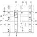
도 22는 본 발명의 실시예들에 따른 메모리 장치의 제조 방법을 이용하여 제조된 메모리 장치를 설명하기 위한 회로도이다. 도 23은 도 22에 도시된 메모리 장치의 레이아웃도이다.22 is a circuit diagram illustrating a memory device manufactured using a method of manufacturing a memory device according to embodiments of the present invention. 23 is a layout diagram of the memory device shown in FIG. 22 .
도 22 및 도 23을 참조하면, 메모리 장치는 전원 노드(VCC)와 접지 노드(VSS) 사이에 병렬 연결된 한 쌍의 인버터(inverter)(INV1, INV2)와, 각각의 인버터(INV1, INV2)의 출력 노드에 연결된 제1 패스 트랜지스터(PS1) 및 제2 패스 트랜지스터(PS2)를 포함할 수 있다.22 and 23 , the memory device includes a pair of inverters INV1 and INV2 connected in parallel between a power node VCC and a ground node VSS, and each of the inverters INV1 and INV2. It may include a first pass transistor PS1 and a second pass transistor PS2 connected to the output node.
제1 패스 트랜지스터(PS1)와 제2 패스 트랜지스터(PS2)는 각각 비트 라인(BL)과 상보 비트 라인(BLb)과 연결될 수 있다. 제1 패스 트랜지스터(PS1)와 제2 패스 트랜지스터(PS2)의 게이트는 워드 라인(WL)과 연결될 수 있다.The first pass transistor PS1 and the second pass transistor PS2 may be respectively connected to the bit line BL and the complementary bit line BLb. Gates of the first pass transistor PS1 and the second pass transistor PS2 may be connected to the word line WL.
제1 인버터(INV1)는 직렬로 연결된 제1 풀업 트랜지스터(PU1)와 제1 풀다운 트랜지스터(PD1)를 포함하고, 제2 인버터(INV2)는 직렬로 연결된 제2 풀업 트랜지스터(PU2)와 제2 풀다운 트랜지스터(PD2)를 포함할 수 있다.The first inverter INV1 includes a first pull-up transistor PU1 and a first pull-down transistor PD1 connected in series, and the second inverter INV2 includes a second pull-up transistor PU2 and a second pull-down transistor PU2 connected in series. A transistor PD2 may be included.
제1 풀업 트랜지스터(PU1)와 제2 풀업 트랜지스터(PU2)은 PFET 트랜지스터이고, 제1 풀다운 트랜지스터(PD1)와 제2 풀다운 트랜지스터(PD2)는 NFET 트랜지스터일 수 있다.The first pull-up transistor PU1 and the second pull-up transistor PU2 may be PFET transistors, and the first pull-down transistor PD1 and the second pull-down transistor PD2 may be NFET transistors.
또한, 제1 인버터(INV1) 및 제2 인버터(INV2)는 하나의 래치회로(latch circuit)를 구성하기 위하여 제1 인버터(INV1)의 입력 노드가 제2 인버터(INV2)의 출력 노드와 연결되고, 제2 인버터(INV2)의 입력 노드는 제1 인버터(INV1)의 출력 노드와 연결될 수 있다.In addition, the first inverter INV1 and the second inverter INV2 have an input node of the first inverter INV1 connected to an output node of the second inverter INV2 to form one latch circuit, and , an input node of the second inverter INV2 may be connected to an output node of the first inverter INV1 .
여기서, 도 22 및 도 23을 참조하면, 서로 이격된 제1 액티브 핀(210), 제2 액티브 핀(220), 제3 액티브 핀(230), 제4 액티브 핀(240)은 일 방향(예를 들어, 도 23의 상하방향)으로 길게 연장되도록 형성될 수 있다. 여기서, 제2 액티브 핀(220), 제3 액티브 핀(230)은 제1 액티브 핀(210), 제4 액티브 핀(240)보다 연장 길이가 짧을 수 있다.Here, referring to FIGS. 22 and 23 , the first
또한, 제1 게이트 전극(251), 제2 게이트 전극(252), 제3 게이트 전극(253), 제4 게이트 전극(254)은 타 방향(예를 들어, 도 23의 좌우 방향)으로 길게 연장되고, 제1 게이트 전극(251) 내지 제4 게이트 전극(254)은 제1 액티브 핀(210) 내지 제4 액티브 핀(240)을 교차하도록 형성될 수 있다.In addition, the
구체적으로, 제1 게이트 전극(251)은 제1 액티브 핀(210)과 제2 액티브 핀(220)을 완전히 교차하고, 제3 액티브 핀(230)의 종단과 일부 오버랩될 수 있다. 제3 게이트 전극(253)은 제4 액티브 핀(240)과 제3 액티브 핀(230)을 완전히 교차하고, 제2 액티브 핀(220)의 종단과 일부 오버랩될 수 있다. 제2 게이트 전극(252), 제4 게이트 전극(254)은 각각 제1 액티브 핀(210), 제4 액티브 핀(240)을 교차하도록 형성될 수 있다.In detail, the
도시된 것과 같이, 제1 풀업 트랜지스터(PU1)는 제1 게이트 전극(251)과 제2 액티브 핀(220)이 교차되는 영역 주변에 정의되고, 제1 풀다운 트랜지스터(PD1)는 제1 게이트 전극(251)과 제1 액티브 핀(210)이 교차되는 영역 주변에 정의되고, 제1 패스 트랜지스터(PS1)는 제2 게이트 전극(252)과 제1 액티브 핀(210)이 교차되는 영역 주변에 정의될 수 있다.As shown, the first pull-up transistor PU1 is defined around a region where the
제2 풀업 트랜지스터(PU2)는 제3 게이트 전극(253)과 제3 액티브 핀(230)이 교차되는 영역 주변에 정의되고, 제2 풀다운 트랜지스터(PD2)는 제3 게이트 전극(253)과 제4 액티브 핀(240)이 교차되는 영역 주변에 정의되고, 제2 패스 트랜지스터(PS2)는 제4 게이트 전극(254)과 제4 액티브 핀(240)이 교차되는 영역 주변에 정의될 수 있다.The second pull-up transistor PU2 is defined around a region where the
명확하게 도시하지 않았으나, 제1 내지 제4 게이트 전극(251~254)과, 제1 내지 제4 액티브 핀(210, 220, 230, 240)이 교차되는 영역의 양측에는 소오스 및 드레인이 형성될 수 있으며, 다수의 컨택(250)이 형성될 수 있다.Although not clearly shown, source and drain may be formed on both sides of a region where the first to
뿐만 아니라, 제1 공유 컨택(shared contact)(261)은 제2 액티브 핀(220), 제3 게이트 라인(253)과, 배선(271)을 동시에 연결할 수 있다. 제2 공유 컨택(262)은 제3 액티브 핀(230), 제1 게이트 라인(251)과, 배선(272)을 동시에 연결할 수 있다.In addition, the first shared contact 261 may simultaneously connect the second
도시된 제1 및 제2 풀업 트랜지스터(PU1, PU2), 제1 및 제2 풀다운 트랜지스터(PD1, PD2), 및 제1 및 제2 패스 트랜지스터(PS1, PS2) 중 적어도 하나는 앞서 설명한 본 발명의 실시예들에 따른 반도체 장치의 제조 방법을 통해 제조될 수 있다.At least one of the illustrated first and second pull-up transistors PU1 and PU2, the first and second pull-down transistors PD1 and PD2, and the first and second pass transistors PS1 and PS2 of the present invention described above It may be manufactured through the method of manufacturing the semiconductor device according to the embodiments.
도 24는 본 발명의 실시예들에 따른 반도체 장치의 제조 방법을 이용하여 제조된 반도체 장치의 일 예를 설명하기 위한 도면이다. 도 25는 본 발명의 실시예들에 따른 반도체 장치의 제조 방법을 이용하여 제조된 반도체 장치의 다른 예를 설명하기 위한 도면이다.24 is a diagram for explaining an example of a semiconductor device manufactured using a method of manufacturing a semiconductor device according to embodiments of the present invention. 25 is a diagram for explaining another example of a semiconductor device manufactured by using a method for manufacturing a semiconductor device according to embodiments of the present invention.
먼저, 도 24를 참조하면, 반도체 장치(13)는 로직 영역(410)과 SRAM 형성 영역(420)을 포함할 수 있다. 로직 영역(410)에는 제11 트랜지스터(411)가 배치되고, SRAM 형성 영역(420)에는 제12 트랜지스터(421)가 배치될 수 있다.First, referring to FIG. 24 , the
본 발명의 몇몇 실시예에서, 제11 트랜지스터(411)와 제12 트랜지스터(421)는 서로 다를 수 있다. 예를 들어, 제11 트랜지스터(411)는 제1 채널 길이를 가질 수 있고, 제12 트랜지스터(421)는 제1 채널 길이보다 짧은 제2 채널 길이를 가질 수 있으나, 본 발명이 이에 제한되는 것은 아니다. 이러한 제11 및 제12 트랜지스터(411, 421)는 앞서 설명한 본 발명의 실시예들에 따른 반도체 장치의 제조 방법을 통해 제조될 수 있다.In some embodiments of the present invention, the
다음, 도 25를 참조하면, 반도체 장치(14)는 로직 영역(410)을 포함하되, 로직 영역(410) 내에는 서로 다른 제13 및 제14 트랜지스터(412, 422)가 배치될 수 있다. 한편, 별도로 도시하지 않았으나, SRAM 영역 내에서도 서로 다른 제13 및 제14 트랜지스터(412, 422)가 배치될 수도 있다.Next, referring to FIG. 25 , the
본 발명의 몇몇 실시예에서, 제13 트랜지스터(412)와 제14 트랜지스터(422)는 서로 다를 수 있다. 예를 들어, 제13 트랜지스터(412)는 NMOS 트랜지스터일 수 있고, 제14 트랜지스터(422)는 PMOS 트랜지스터일 수 있으나, 본 발명이 이에 제한되는 것은 아니다. 이러한 제13 및 제14 트랜지스터(412, 422)는 앞서 설명한 본 발명의 실시예들에 따른 반도체 장치의 제조 방법을 통해 제조될 수 있다.In some embodiments of the present invention, the
도 25에서는, 예시적으로 로직 영역(410)과 SRAM형성 영역(420)을 도시하였으나, 본 발명이 이에 한정되는 것은 아니다. 예를 들어, 로직 영역(410)과, 다른 메모리가 형성되는 영역(예를 들어, DRAM, MRAM, RRAM, PRAM 등)에도 본 발명을 적용할 수 있다.Although FIG. 25 illustrates the
도 26은 본 발명의 실시예들에 따른 반도체 장치의 제조 방법을 이용하여 제조된 반도체 장치를 포함하는 SoC 시스템의 블록도이다.26 is a block diagram of a SoC system including a semiconductor device manufactured using a method of manufacturing a semiconductor device according to embodiments of the present disclosure.
도 26을 참조하면, SoC 시스템(1000)은 어플리케이션 프로세서(1001)와, DRAM(1060)을 포함한다.Referring to FIG. 26 , the
어플리케이션 프로세서(1001)는 중앙처리부(1010), 멀티미디어 시스템(1020), 버스(1030), 메모리 시스템(1040), 주변 회로(1050)을 포함할 수 있다.The
중앙처리부(1010)는 SoC 시스템(1000)의 구동에 필요한 연산을 수행할 수 있다. 본 발명의 몇몇 실시예에서, 중앙처리부(1010)는 복수의 코어를 포함하는 멀티 코어 환경으로 구성될 수 있다.The
멀티미디어 시스템(1020)은, SoC시스템(1000)에서 각종 멀티미디어 기능을 수행하는데 이용될 수 있다. 이러한 멀티미디어 시스템(1020)은 3D 엔진(3D engine) 모듈, 비디오 코덱(video codec), 디스플레이 시스템(display system), 카메라 시스템(camera system), 포스트-프로세서(post -processor) 등을 포함할 수 있다.The
버스(1030)는, 중앙처리부(1010), 멀티미디어 시스템(1020), 메모리 시스템(1040), 및 주변 회로(1050)가 서로 데이터 통신을 하는데 이용될 수 있다. 본 발명의 몇몇 실시예에서, 이러한 버스(1030)는 다층 구조를 가질 수 있다. 구체적으로, 이러한 버스(1030)의 예로는 다층 AHB(multi-layer Advanced High-performance Bus), 또는 다층 AXI(multi-layer Advanced eXtensible Interface)가 이용될 수 있으나, 본 발명이 이에 제한되는 것은 아니다.The
메모리 시스템(1040)은, 어플리케이션 프로세서(1001)가 외부 메모리(예를 들어, DRAM(1060))에 연결되어 고속 동작하는데 필요한 환경을 제공할 수 있다. 본 발명의 몇몇 실시예에서, 메모리 시스템(1040)은 외부 메모리(예를 들어, DRAM(1060))를 컨트롤하기 위한 별도의 컨트롤러(예를 들어, DRAM 컨트롤러)를 포함할 수도 있다.The
주변 회로(1050)는, SoC시스템(1000)이 외부 장치(예를 들어, 메인 보드)와 원활하게 접속되는데 필요한 환경을 제공할 수 있다. 이에 따라, 주변 회로(1050)는 SoC시스템(1000)에 접속되는 외부 장치가 호환 가능하도록 하는 다양한 인터페이스를 구비할 수 있다.The
DRAM(1060)은 어플리케이션 프로세서(1001)가 동작하는데 필요한 동작 메모리로 기능할 수 있다. 본 발명의 몇몇 실시예에서, DRAM(1060)은, 도시된 것과 같이 어플리케이션 프로세서(1001)의 외부에 배치될 수 있다. 구체적으로, DRAM(1060)은 어플리케이션 프로세서(1001)와 PoP(Package on Package) 형태로 패키징될 수 있다.The
이러한 SoC 시스템(1000)의 구성 요소 중 적어도 하나는 앞서 설명한 본 발명의 실시예들에 따른 반도체 장치의 제조 방법을 통해 제조될 수 있다.At least one of the components of the
도 27은 본 발명의 실시예들에 따른 반도체 장치의 제조 방법을 이용하여 제조된 반도체 장치를 포함하는 전자 시스템의 블록도이다.27 is a block diagram of an electronic system including a semiconductor device manufactured using a method for manufacturing a semiconductor device according to embodiments of the present invention.
도 27을 참조하면, 본 발명의 실시예에 따른 전자 시스템(1100)은 컨트롤러(1110), 입출력 장치(1120, I/O), 기억 장치(1130, memory device), 인터페이스(1140) 및 버스(1150, bus)를 포함할 수 있다. 컨트롤러(1110), 입출력 장치(1120), 기억 장치(1130) 및/또는 인터페이스(1140)는 버스(1150)를 통하여 서로 결합될 수 있다. 버스(1150)는 데이터들이 이동되는 통로(path)에 해당한다.Referring to FIG. 27 , an
컨트롤러(1110)는 마이크로프로세서, 디지털 신호 프로세스, 마이크로컨트롤러, 및 이들과 유사한 기능을 수행할 수 있는 논리 소자들 중에서 적어도 하나를 포함할 수 있다. 입출력 장치(1120)는 키패드(keypad), 키보드 및 디스플레이 장치등을 포함할 수 있다. 기억 장치(1130)는 데이터 및/또는 명령어등을 저장할 수 있다. 인터페이스(1140)는 통신 네트워크로 데이터를 전송하거나 통신 네트워크로부터 데이터를 수신하는 기능을 수행할 수 있다. 인터페이스(1140)는 유선 또는 무선 형태일 수 있다. 예컨대, 인터페이스(1140)는 안테나 또는 유무선 트랜시버등을 포함할 수 있다. The
도시하지 않았지만, 전자 시스템(1100)은 컨트롤러(1110)의 동작을 향상시키기 위한 동작 메모리로서, 고속의 디램 및/또는 에스램 등을 더 포함할 수도 있다. 이 때 이러한 동작 메모리로서, 앞서 도 22 및 도 23을 참조하여 설명한 반도체 장치가 채용될 수 있다.Although not shown, the
또한, 앞서 설명한 본 발명의 실시예들에 따른 반도체 장치의 제조 방법을 통해 제조된 반도체 장치는, 기억 장치(1130) 내에 제공되거나, 컨트롤러(1110), 입출력 장치(1120, I/O) 등의 일부로 제공될 수 있다.In addition, the semiconductor device manufactured through the method of manufacturing the semiconductor device according to the above-described embodiments of the present invention is provided in the
전자 시스템(1100)은 개인 휴대용 정보 단말기(PDA, personal digital assistant) 포터블 컴퓨터(portable computer), 웹 타블렛(web tablet), 무선 전화기(wireless phone), 모바일 폰(mobile phone), 디지털 뮤직 플레이어(digital music player), 메모리 카드(memory card), 또는 정보를 무선환경에서 송신 및/또는 수신할 수 있는 모든 전자 제품에 적용될 수 있다. The
도 28 내지 도 30은 본 발명의 실시예들에 따른 반도체 장치의 제조 방법을 이용하여 제조된 반도체 장치를 적용할 수 있는 예시적인 반도체 시스템들이다.28 to 30 are exemplary semiconductor systems to which a semiconductor device manufactured by using a method for manufacturing a semiconductor device according to embodiments of the present invention can be applied.
도 28은 태블릿 PC(1200)을 도시한 도면이고, 도 29는 노트북(1300)을 도시한 도면이며, 도 30은 스마트폰(1400)을 도시한 것이다. 앞서 설명한 본 발명의 실시예들에 따른 반도체 장치의 제조 방법을 통해 제조된 반도체 장치는, 이러한 태블릿 PC(1200), 노트북(1300), 스마트폰(1400) 등에 사용될 수 있다.FIG. 28 is a diagram illustrating a
또한, 앞서 설명한 본 발명의 실시예들에 따른 반도체 장치의 제조 방법을 통해 제조된 반도체 장치는, 예시하지 않는 다른 집적 회로 장치에도 적용될 수 있음은 당업자에게 자명하다.In addition, it is apparent to those skilled in the art that the semiconductor device manufactured by the method of manufacturing the semiconductor device according to the embodiments of the present invention described above may be applied to other integrated circuit devices not illustrated.
즉, 이상에서는 본 실시예에 따른 반도체 시스템의 예로, 태블릿 PC(1200), 노트북(1300), 및 스마트폰(1400)만을 들었으나, 본 실시예에 따른 반도체 시스템의 예가 이에 제한되는 것은 아니다.That is, although only the
본 발명의 몇몇 실시예에서, 반도체 시스템은, 컴퓨터, UMPC (Ultra Mobile PC), 워크스테이션, 넷북(net-book), PDA (Personal Digital Assistants), 포터블(portable) 컴퓨터, 무선 전화기(wireless phone), 모바일 폰(mobile phone), e-북(e-book), PMP(portable multimedia player), 휴대용 게임기, 네비게이션(navigation) 장치, 블랙박스(black box), 디지털 카메라(digital camera), 3차원 수상기(3-dimensional television), 디지털 음성 녹음기(digital audio recorder), 디지털 음성 재생기(digital audio player), 디지털 영상 녹화기(digital picture recorder), 디지털 영상 재생기(digital picture player), 디지털 동영상 녹화기(digital video recorder), 디지털 동영상 재생기(digital video player) 등으로 구현될 수도 있다.In some embodiments of the present invention, the semiconductor system includes a computer, an Ultra Mobile PC (UMPC), a workstation, a net-book, a Personal Digital Assistants (PDA), a portable computer, a wireless phone. , mobile phone, e-book, PMP (portable multimedia player), portable game console, navigation device, black box, digital camera, 3D receiver (3-dimensional television), digital audio recorder, digital audio player, digital picture recorder, digital picture player, digital video recorder ), a digital video player, etc. may be implemented.
이상 첨부된 도면을 참조하여 본 발명의 실시예들을 설명하였으나, 본 발명은 상기 실시예들에 한정되는 것이 아니라 서로 다른 다양한 형태로 제조될 수 있으며, 본 발명이 속하는 기술분야에서 통상의 지식을 가진 자는 본 발명의 기술적 사상이나 필수적인 특징을 변경하지 않고서 다른 구체적인 형태로 실시될 수 있다는 것을 이해할 수 있을 것이다. 그러므로 이상에서 기술한 실시예들은 모든 면에서 예시적인 것이며 한정적이 아닌 것으로 이해해야만 한다.Although the embodiments of the present invention have been described above with reference to the accompanying drawings, the present invention is not limited to the above embodiments, but may be manufactured in various different forms, and those of ordinary skill in the art to which the present invention pertains. It will be understood by those skilled in the art that the present invention may be embodied in other specific forms without changing the technical spirit or essential features of the present invention. Therefore, it should be understood that the embodiments described above are illustrative in all respects and not restrictive.
10: 기판
20: 소오스-드레인 영역
30: 층간 절연막
40: 스페이서
55: 인터페이스막
61: 게이트 절연막10: substrate
20: source-drain region
30: interlayer insulating film
40: spacer
55: interface film
61: gate insulating film
Claims (20)
Translated fromKorean상기 인터페이스막 상에 제1 유전율을 갖는 제1 게이트 절연막을 형성하고,
상기 제1 게이트 절연막 상에 상기 제1 유전율보다 작은 제2 유전율을 갖는 제2 게이트 절연막을 형성하고,
상기 기판을 어닐링하고,
상기 기판을 어닐링한 후, 상기 제1 및 제2 게이트 절연막에 도핑된 질소 이온의 농도 프로파일의 피크가 상기 제1 게이트 절연막과 상기 인터페이스막의 계면과 상기 제2 게이트 절연막의 상면 중 상기 제2 게이트 절연막의 상면에 인접하도록 상기 제1 및 제2 게이트 절연막을 질화(nidridation)시키고,
상기 제1 및 제2 게이트 절연막을 질화시킨 후, 상기 제1 및 제2 게이트 절연막 상에 일함수 조절막을 형성하고,
상기 일함수 조절막 상에 메탈 게이트 전극을 형성하는 것을 포함하되,
상기 일함수 조절막과 상기 메탈 게이트 전극 중 적어도 하나는 알루미늄(Al)을 포함하고,
상기 제2 게이트 절연막은 실리콘 산화막(SiO2)을 포함하는 반도체 장치의 제조 방법.forming an interface film on the substrate;
forming a first gate insulating film having a first dielectric constant on the interface film;
forming a second gate insulating layer having a second dielectric constant smaller than the first dielectric constant on the first gate insulating layer;
annealing the substrate;
After annealing the substrate, the peak of the concentration profile of nitrogen ions doped in the first and second gate insulating layers is the second gate insulating layer among the interface between the first gate insulating layer and the interface layer and the upper surface of the second gate insulating layer. nitridation of the first and second gate insulating films so as to be adjacent to the upper surface of
After nitriding the first and second gate insulating layers, a work function control layer is formed on the first and second gate insulating layers,
Including forming a metal gate electrode on the work function control layer,
At least one of the work function control layer and the metal gate electrode includes aluminum (Al),
The method of manufacturing a semiconductor device, wherein the second gate insulating layer includes a silicon oxide layer (SiO2).
상기 인터페이스막과 상기 제2 게이트 절연막은 동일한 산화막을 포함하는 반도체 장치의 제조 방법.The method of claim 1,
The method of manufacturing a semiconductor device, wherein the interface layer and the second gate insulating layer include the same oxide layer.
상기 제1 게이트 절연막은 하프늄 산화막(HfO)을 포함하는 반도체 장치의 제조 방법.The method of claim 1,
The method of manufacturing a semiconductor device, wherein the first gate insulating layer includes a hafnium oxide layer (HfO).
상기 제1 게이트 절연막을 형성하는 것은, n(n은 자연수) 싸이클(cycle) 동안 ALD(Atomic Layer Depostion)를 통해 상기 제1 게이트 절연막을 형성하는 것을 포함하고,
상기 제2 게이트 절연막을 형성하는 것은, m(m은 m<n인 자연수) 싸이클 동안 ALD를 통해 상기 제2 게이트 절연막을 형성하는 것을 포함하는 반도체 장치의 제조 방법.The method of claim 1,
Forming the first gate insulating film includes forming the first gate insulating film through atomic layer deposition (ALD) during n (n is a natural number) cycle,
The forming of the second gate insulating layer includes forming the second gate insulating layer through ALD during m (m is a natural number such that m<n) cycle.
상기 제2 게이트 절연막을 형성한 후,
상기 제2 게이트 절연막 상에, 상기 제1 게이트 절연막과 동일한 물질을 포함하는 제3 게이트 절연막을 형성하고,
상기 제3 게이트 절연막 상에, 상기 제2 게이트 절연막과 동일한 물질을 포함하는 제4 게이트 절연막을 형성하는 것을 더 포함하는 반도체 장치의 제조 방법.The method of claim 1,
After forming the second gate insulating layer,
forming a third gate insulating layer including the same material as that of the first gate insulating layer on the second gate insulating layer;
and forming a fourth gate insulating layer including the same material as that of the second gate insulating layer on the third gate insulating layer.
상기 제1 게이트 절연막을 형성하는 것은, n(n은 자연수) 싸이클(cycle) 동안 ALD(Atomic Layer Depostion)를 통해 상기 제1 게이트 절연막을 형성하는 것을 포함하고,
상기 제2 게이트 절연막을 형성하는 것은, m(m은 m<n인 자연수) 싸이클 동안 ALD를 통해 상기 제2 게이트 절연막을 형성하는 것을 포함하고,
상기 제3 게이트 절연막을 형성하는 것은, m 싸이클 동안 ALD를 통해 상기 제3 게이트 절연막을 형성하는 것을 포함하고,
상기 제4 게이트 절연막을 형성하는 것은, m 싸이클 동안 ALD를 통해 상기 제4 게이트 절연막을 형성하는 것을 포함하는 반도체 장치의 제조 방법.7. The method of claim 6,
Forming the first gate insulating film includes forming the first gate insulating film through atomic layer deposition (ALD) during n (n is a natural number) cycle,
Forming the second gate insulating film includes forming the second gate insulating film through ALD during m (m is a natural number such that m<n) cycle,
Forming the third gate insulating film includes forming the third gate insulating film through ALD for m cycles,
The forming of the fourth gate insulating layer includes forming the fourth gate insulating layer through ALD for m cycles.
상기 기판을 어닐링하는 것은 800 내지 1200℃에서 상기 기판을 플래시(flash), 스파이크(spike), 또는 레이저(laser) 어닐링하는 것을 포함하는 반도체 장치의 제조 방법.The method of claim 1,
Annealing the substrate includes flash, spike, or laser annealing the substrate at 800 to 1200°C.
상기 제1 및 제2 게이트 절연막을 질화시키는 것은,
질화 가스의 압력을 100mm torr 내지 500mm torr로 유지하여 상기 제1 및 제2 게이트 절연막을 질화시키는 것을 포함하는 반도체 장치의 제조 방법.The method of claim 1,
Nitriding the first and second gate insulating films comprises:
and nitriding the first and second gate insulating layers by maintaining a pressure of a nitriding gas in a range of 100 mm torr to 500 mm torr.
상기 일함수 조절막을 형성하는 것은,
상기 제1 및 제2 게이트 절연막 상에 캡핑막을 형성하고,
상기 캡핑막 상에, 베리어막을 형성하고,
상기 베리어막 상에, 상기 일함수 조절막을 형성하는 것을 포함하는 반도체 장치의 제조 방법.The method of claim 1,
Forming the work function control film,
forming a capping film on the first and second gate insulating films;
forming a barrier film on the capping film;
and forming the work function control layer on the barrier layer.
상기 캡핑막은 TiN을 포함하고,
상기 베리어막은 TaN를 포함하고,
상기 일함수 조절막은 TiN과 TiAl 중 적어도 하나를 포함하는 반도체 장치의 제조 방법.11. The method of claim 10,
The capping film contains TiN,
The barrier layer includes TaN,
The method of manufacturing a semiconductor device, wherein the work function control layer includes at least one of TiN and TiAl.
상기 기판은 제1 영역과 제2 영역을 포함하고,
상기 일함수 조절막을 형성하는 것은,
상기 제1 및 제2 영역에 p형 일함수 조절막을 형성하고,
상기 제1 영역에 형성된 상기 p형 일함수 조절막을 제거하고,
상기 제1 및 제2 영역에 N형 일함수 조절막을 형성하는 것을 포함하는 반도체 장치의 제조 방법.11. The method of claim 10,
The substrate includes a first region and a second region;
Forming the work function control film,
forming a p-type work function control film in the first and second regions;
removing the p-type work function control film formed in the first region;
and forming an N-type work function control layer in the first and second regions.
상기 인터페이스막을 형성하는 것은,
상기 기판 상에 층간 절연막과 더미 게이트 전극을 형성하고,
상기 더미 게이트 전극을 제거하여 상기 기판의 상면을 노출시키고,
상기 노출된 기판 상면 상에 상기 인터페이스막을 형성하는 것을 포함하는 반도체 장치의 제조 방법.The method of claim 1,
Forming the interface film,
forming an interlayer insulating film and a dummy gate electrode on the substrate;
removing the dummy gate electrode to expose a top surface of the substrate;
and forming the interface layer on the exposed upper surface of the substrate.
상기 인터페이스막 상에 실리콘(Si)이 도핑된 게이트 절연막을 형성하고,
상기 기판을 어닐링 하고,
상기 기판을 어닐링한 후, 질화 가스의 압력을 100mm torr 내지 500mm torr로 유지하여 상기 게이트 절연막에 도핑된 질소 이온의 농도 프로파일의 피크가 상기 게이트 절연막과 상기 인터페이스막의 계면과 상기 게이트 절연막의 상면 중 상기 게이트 절연막의 상면에 인접하도록 상기 게이트 절연막을 질화시키고,
상기 게이트 절연막을 질화시킨 후, 상기 게이트 절연막 상에 일함수 조절막을 형성하고,
상기 일함수 조절막 상에 메탈 게이트 전극을 형성하는 것을 포함하되,
상기 게이트 절연막을 형성하는 것은,
상기 인터페이스막 상에 제1 유전율을 갖는 제1 게이트 절연막을 형성하고,
상기 제1 게이트 절연막 상에 상기 제1 유전율보다 작은 제2 유전율을 갖고 실리콘(Si)을 포함하는 제2 게이트 절연막을 형성하고,
상기 제1 및 제2 게이트 절연막을 형성하는 것을 반복하는 것을 포함하는 반도체 장치의 제조 방법.forming an interface film on the substrate;
forming a gate insulating film doped with silicon (Si) on the interface film;
annealing the substrate;
After annealing the substrate, the pressure of the nitriding gas is maintained at 100 mm torr to 500 mm torr so that the peak of the concentration profile of nitrogen ions doped in the gate insulating film is at the interface between the gate insulating film and the interface film and the upper surface of the gate insulating film. nitriding the gate insulating film so as to be adjacent to the upper surface of the gate insulating film;
After nitriding the gate insulating layer, a work function control layer is formed on the gate insulating layer,
Including forming a metal gate electrode on the work function control layer,
Forming the gate insulating film,
forming a first gate insulating film having a first dielectric constant on the interface film;
forming a second gate insulating layer including silicon (Si) having a second dielectric constant smaller than the first dielectric constant on the first gate insulating layer;
and repeating forming the first and second gate insulating films.
상기 제1 게이트 절연막은 하프늄 산화막(HfO)을 포함하고,
상기 제2 게이트 절연막은 실리콘 산화막(SiO2)을 포함하는 반도체 장치의 제조 방법.15. The method of claim 14,
The first gate insulating layer includes a hafnium oxide layer (HfO),
The method of manufacturing a semiconductor device, wherein the second gate insulating layer includes a silicon oxide layer (SiO2).
상기 제1 영역에 제1 폭을 갖는 제1 인터페이스막을 형성하고,
상기 제2 영역에 상기 제1 폭과 다른 제2 폭을 갖는 제2 인터페이스막을 형성하고,
상기 제1 인터페이스막 상에 실리콘(Si)이 도핑된 제1 게이트 절연막을 형성하고,
상기 제2 인터페이스막 상에 실리콘(Si)이 도핑된 제2 게이트 절연막을 형성하고,
상기 기판을 어닐링 하고,
상기 기판을 어닐링한 후, 상기 제1 게이트 절연막이 제1 질소 농도를 갖되, 상기 제1 게이트 절연막에 도핑된 질소 이온의 농도 프로파일의 피크가 상기 제1 게이트 절연막과 상기 제1 인터페이스막의 계면과 상기 제1 게이트 절연막의 상면 중 상기 제1 게이트 절연막의 상면에 인접하도록 상기 제1 게이트 절연막을 질화시키고, 상기 제2 게이트 절연막이 상기 제1 질소 농도과 다른 제2 질소 농도를 갖도록 상기 제2 게이트 절연막을 질화시키고,
상기 제1 및 제2 게이트 절연막을 질화시킨 후, 상기 제1 및 제2 절연막 상에 일함수 조절막을 형성하고,
상기 일함수 조절막 상에 메탈 게이트 전극을 형성하는 것을 포함하는 반도체 장치의 제조 방법.To provide a substrate comprising a first region and a second region,
forming a first interface layer having a first width in the first region;
forming a second interface layer having a second width different from the first width in the second region;
forming a first gate insulating layer doped with silicon (Si) on the first interface layer;
forming a second gate insulating layer doped with silicon (Si) on the second interface layer;
annealing the substrate;
After annealing the substrate, the first gate insulating layer has a first nitrogen concentration, and the peak of the concentration profile of nitrogen ions doped in the first gate insulating layer is at the interface between the first gate insulating layer and the first interface layer and the The first gate insulating layer is nitrided so as to be adjacent to the top surface of the first gate insulating layer among the top surfaces of the first gate insulating layer, and the second gate insulating layer is formed so that the second gate insulating layer has a second nitrogen concentration different from the first nitrogen concentration. nitrate,
After nitriding the first and second gate insulating layers, a work function control layer is formed on the first and second insulating layers,
and forming a metal gate electrode on the work function control layer.
상기 제1 폭은 상기 제2 폭보다 작고,
상기 제1 질소 농도는 상기 제2 질소 농보보다 큰 반도체 장치의 제조 방법.19. The method of claim 18,
The first width is smaller than the second width,
wherein the first nitrogen concentration is greater than the second nitrogen concentration.
상기 인터페이스막 상에 제1 하프늄 산화막(HfO)을 형성하고,
상기 제1 하프늄 산화막 상에 제1 실리콘 산화막(SiO2)을 형성하고,
상기 제1 실리콘 산화막 상에 제2 하프늄 산화막을 형성하고,
상기 제2 하프늄 산화막 상에 제2 실리콘 산화막을 형성하고,
상기 기판을 어닐링하여, 상기 제1 및 제2 하프늄 산화막과 상기 제1 및 제2 실리콘 산화막을 실리콘이 도핑된 하프늄 산화막으로 형성하고,
상기 기판을 어닐링한 후, 질화 가스의 압력을 100mm torr 내지 500mm torr로 유지하여 상기 제1 및 제2 하프늄 산화막과 상기 제1 및 제2 실리콘 산화막에 도핑된 질소 이온의 농도 프로파일의 피크가 상기 제1 하프늄 산화막과 상기 인터페이스막의 계면과 상기 제2 실리콘 산화막의 상면 중 상기 제2 실리콘 산화막의 상면에 인접하도록 상기 실리콘이 도핑된 하프늄 산화막을 질화시키는 것을 포함하는 반도체 장치의 제조 방법.forming an interface film on the substrate;
forming a first hafnium oxide film (HfO) on the interface film;
forming a first silicon oxide film (SiO2) on the first hafnium oxide film;
forming a second hafnium oxide film on the first silicon oxide film;
forming a second silicon oxide film on the second hafnium oxide film;
annealing the substrate to form the first and second hafnium oxide films and the first and second silicon oxide films as hafnium oxide films doped with silicon;
After annealing the substrate, the pressure of the nitriding gas is maintained at 100 mm torr to 500 mm torr so that the peak of the concentration profile of the nitrogen ions doped in the first and second hafnium oxide films and the first and second silicon oxide films is the first 1 A method of manufacturing a semiconductor device, comprising nitriding the silicon-doped hafnium oxide film so as to be adjacent to an upper surface of the second silicon oxide film among an interface between the 1 hafnium oxide film and the interface film and an upper surface of the second silicon oxide film.
Priority Applications (2)
| Application Number | Priority Date | Filing Date | Title |
|---|---|---|---|
| KR1020140115483AKR102394887B1 (en) | 2014-09-01 | 2014-09-01 | Method for fabricating semiconductor device |
| US14/685,618US9318335B2 (en) | 2014-09-01 | 2015-04-14 | Method for fabricating semiconductor device including nitrided gate insulator |
Applications Claiming Priority (1)
| Application Number | Priority Date | Filing Date | Title |
|---|---|---|---|
| KR1020140115483AKR102394887B1 (en) | 2014-09-01 | 2014-09-01 | Method for fabricating semiconductor device |
Publications (2)
| Publication Number | Publication Date |
|---|---|
| KR20160026486A KR20160026486A (en) | 2016-03-09 |
| KR102394887B1true KR102394887B1 (en) | 2022-05-04 |
Family
ID=55403313
Family Applications (1)
| Application Number | Title | Priority Date | Filing Date |
|---|---|---|---|
| KR1020140115483AActiveKR102394887B1 (en) | 2014-09-01 | 2014-09-01 | Method for fabricating semiconductor device |
Country Status (2)
| Country | Link |
|---|---|
| US (1) | US9318335B2 (en) |
| KR (1) | KR102394887B1 (en) |
Families Citing this family (23)
| Publication number | Priority date | Publication date | Assignee | Title |
|---|---|---|---|---|
| US10050147B2 (en)* | 2015-07-24 | 2018-08-14 | Taiwan Semiconductor Manufacturing Co., Ltd. | Semiconductor device and manufacturing method thereof |
| US10153155B2 (en)* | 2015-10-09 | 2018-12-11 | University Of Florida Research Foundation, Incorporated | Doped ferroelectric hafnium oxide film devices |
| US9620610B1 (en)* | 2015-10-28 | 2017-04-11 | Taiwan Semiconductor Manufacturing Co., Ltd. | FinFET gate structure and method for fabricating the same |
| US9824929B2 (en)* | 2015-10-28 | 2017-11-21 | Taiwan Semiconductor Manufacturing Co., Ltd. | FinFET gate structure and method for fabricating the same |
| US9799649B2 (en)* | 2015-12-17 | 2017-10-24 | Taiwan Semiconductor Manufacturing Company Limited | Semiconductor device and manufacturing method thereof |
| US9985031B2 (en)* | 2016-01-21 | 2018-05-29 | Taiwan Semiconductor Manufacturing Co., Ltd. | Integrated circuit and manufacturing method thereof |
| CN107039439B (en)* | 2016-02-04 | 2020-03-10 | 中芯国际集成电路制造(上海)有限公司 | Memory and method of forming the same |
| US10056465B2 (en)* | 2016-06-20 | 2018-08-21 | Semiconductor Manufacturing International (Shanghai) Corporation | Transistor device and fabrication method |
| CN108010884B (en)* | 2016-11-01 | 2020-11-27 | 中芯国际集成电路制造(上海)有限公司 | Semiconductor structure and method of forming the same |
| CN108122914B (en) | 2016-11-30 | 2019-11-01 | 中芯国际集成电路制造(上海)有限公司 | SRAM device and its manufacturing method |
| US10164063B2 (en)* | 2016-12-14 | 2018-12-25 | Taiwan Semiconductor Manufacturing Co., Ltd. | Semiconductor structure with protection layer |
| CN108206211B (en)* | 2016-12-16 | 2020-08-14 | 台湾积体电路制造股份有限公司 | Semiconductor device and method of forming the same |
| US10312160B2 (en)* | 2017-05-26 | 2019-06-04 | International Business Machines Corporation | Gate-last semiconductor fabrication with negative-tone resolution enhancement |
| KR102336784B1 (en)* | 2017-06-09 | 2021-12-07 | 삼성전자주식회사 | Semiconductor device |
| KR102342550B1 (en)* | 2017-06-09 | 2021-12-23 | 삼성전자주식회사 | Semiconductor devices |
| US10170317B1 (en)* | 2017-09-28 | 2019-01-01 | Taiwan Semiconductor Manufacturing Co., Ltd. | Self-protective layer formed on high-k dielectric layer |
| US10629749B2 (en)* | 2017-11-30 | 2020-04-21 | Taiwan Semiconductor Manufacturing Co., Ltd. | Method of treating interfacial layer on silicon germanium |
| US11270994B2 (en)* | 2018-04-20 | 2022-03-08 | Taiwan Semiconductor Manufacturing Company, Ltd. | Gate structure, fin field-effect transistor, and method of manufacturing fin-field effect transistor |
| US11538926B2 (en)* | 2020-04-01 | 2022-12-27 | Taiwan Semiconductor Manufacturing Co., Ltd. | Semiconductor device and method of manufacturing a semiconductor device |
| US12125891B2 (en)* | 2020-07-22 | 2024-10-22 | Taiwan Semiconductor Manufacturing Co., Ltd. | Semiconductor device having gate spacers extending below a fin top surface |
| US11824100B2 (en)* | 2021-01-22 | 2023-11-21 | Taiwan Semiconductor Manufacturing Co., Ltd. | Gate structure of semiconductor device and method of forming same |
| US12336244B2 (en)* | 2021-07-09 | 2025-06-17 | Taiwan Semiconductor Manufacturing Company, Ltd. | Metal caps for gate structures |
| US11948840B2 (en)* | 2021-08-31 | 2024-04-02 | Taiwan Semiconductor Manufacturing Co., Ltd. | Protective layer over FinFET and method of forming same |
Citations (4)
| Publication number | Priority date | Publication date | Assignee | Title |
|---|---|---|---|---|
| KR100551186B1 (en)* | 2000-03-10 | 2006-02-14 | 가부시끼가이샤 도시바 | Semiconductor device having a gate insulating film structure including an insulating film containing metal, silicon and oxygen and manufacturing method thereof |
| US20060257563A1 (en)* | 2004-10-13 | 2006-11-16 | Seok-Joo Doh | Method of fabricating silicon-doped metal oxide layer using atomic layer deposition technique |
| US20110241130A1 (en)* | 2010-04-02 | 2011-10-06 | Taiwan Semiconductor Manufacturing Company, Ltd. | Semiconductor device having a blocking structure and method of manufacturing the same |
| US20130056836A1 (en)* | 2011-09-01 | 2013-03-07 | Taiwan Semiconductor Manufacturing Company, Ltd. | Techniques Providing Metal Gate Devices with Multiple Barrier Layers |
Family Cites Families (13)
| Publication number | Priority date | Publication date | Assignee | Title |
|---|---|---|---|---|
| US7135361B2 (en) | 2003-12-11 | 2006-11-14 | Texas Instruments Incorporated | Method for fabricating transistor gate structures and gate dielectrics thereof |
| US7381608B2 (en) | 2004-12-07 | 2008-06-03 | Intel Corporation | Method for making a semiconductor device with a high-k gate dielectric and a metal gate electrode |
| US8053849B2 (en) | 2005-11-09 | 2011-11-08 | Advanced Micro Devices, Inc. | Replacement metal gate transistors with reduced gate oxide leakage |
| JP2007142266A (en) | 2005-11-21 | 2007-06-07 | Fujitsu Ltd | Semiconductor device and manufacturing method thereof |
| US7645710B2 (en)* | 2006-03-09 | 2010-01-12 | Applied Materials, Inc. | Method and apparatus for fabricating a high dielectric constant transistor gate using a low energy plasma system |
| JP4282691B2 (en) | 2006-06-07 | 2009-06-24 | 株式会社東芝 | Semiconductor device |
| KR100998978B1 (en)* | 2008-11-26 | 2010-12-09 | 동아대학교 산학협력단 | Organic thin film transistor having a dual gate insulating film and manufacturing method thereof |
| DE102009023376B4 (en) | 2009-05-29 | 2012-02-23 | Globalfoundries Dresden Module One Limited Liability Company & Co. Kg | Adjusting the work function in high-k metal gate electrode structures by selectively removing a barrier layer |
| US8304841B2 (en) | 2009-09-14 | 2012-11-06 | Taiwan Semiconductor Manufacturing Company, Ltd. | Metal gate transistor, integrated circuits, systems, and fabrication methods thereof |
| US8643115B2 (en) | 2011-01-14 | 2014-02-04 | International Business Machines Corporation | Structure and method of Tinv scaling for high κ metal gate technology |
| US20120241874A1 (en) | 2011-03-25 | 2012-09-27 | Byung-Dong Kim | Gate oxide film including a nitride layer deposited thereon and method of forming the gate oxide film |
| US20130256802A1 (en) | 2012-03-27 | 2013-10-03 | International Business Machines Corporation | Replacement Gate With Reduced Gate Leakage Current |
| KR101929384B1 (en) | 2012-05-24 | 2018-12-14 | 삼성전자주식회사 | Method for manufacturing semiconductor device having selectively nitrided gate dielectric layer |
- 2014
- 2014-09-01KRKR1020140115483Apatent/KR102394887B1/enactiveActive
- 2015
- 2015-04-14USUS14/685,618patent/US9318335B2/enactiveActive
Patent Citations (4)
| Publication number | Priority date | Publication date | Assignee | Title |
|---|---|---|---|---|
| KR100551186B1 (en)* | 2000-03-10 | 2006-02-14 | 가부시끼가이샤 도시바 | Semiconductor device having a gate insulating film structure including an insulating film containing metal, silicon and oxygen and manufacturing method thereof |
| US20060257563A1 (en)* | 2004-10-13 | 2006-11-16 | Seok-Joo Doh | Method of fabricating silicon-doped metal oxide layer using atomic layer deposition technique |
| US20110241130A1 (en)* | 2010-04-02 | 2011-10-06 | Taiwan Semiconductor Manufacturing Company, Ltd. | Semiconductor device having a blocking structure and method of manufacturing the same |
| US20130056836A1 (en)* | 2011-09-01 | 2013-03-07 | Taiwan Semiconductor Manufacturing Company, Ltd. | Techniques Providing Metal Gate Devices with Multiple Barrier Layers |
Also Published As
| Publication number | Publication date |
|---|---|
| KR20160026486A (en) | 2016-03-09 |
| US9318335B2 (en) | 2016-04-19 |
| US20160064225A1 (en) | 2016-03-03 |
Similar Documents
| Publication | Publication Date | Title |
|---|---|---|
| KR102394887B1 (en) | Method for fabricating semiconductor device | |
| US11581435B2 (en) | Semiconductor device including a first fin active region, a second fin active region and a field region | |
| TWI686849B (en) | Methods of forming semiconductor devices | |
| KR102290685B1 (en) | Semiconductor device | |
| US10256342B2 (en) | Methods of manufacturing fin field effect transistors (FinFETs) comprising reduced gate thicknesses overlying deep trenches | |
| TWI750117B (en) | Semiconductor device | |
| US9923058B2 (en) | Semiconductor device having a fin | |
| US9312188B2 (en) | Method for fabricating semiconductor device | |
| KR20150056307A (en) | Semiconductor device having fin field effect transistor and methods of forming the same | |
| US9443852B2 (en) | Integrated circuit devices with source/drain regions including multiple segments | |
| KR102392991B1 (en) | Semiconductor device and method for fabricating the same | |
| KR20160079598A (en) | Semiconductor device and method for fabricating the same | |
| US9240409B2 (en) | Semiconductor device and method for fabricating the same | |
| US20160049478A1 (en) | Semiconductor device and method for fabricating the same | |
| KR102394881B1 (en) | Semiconductor device and method for fabricating the same | |
| KR102382555B1 (en) | Semiconductor device |
Legal Events
| Date | Code | Title | Description |
|---|---|---|---|
| PA0109 | Patent application | Patent event code:PA01091R01D Comment text:Patent Application Patent event date:20140901 | |
| PG1501 | Laying open of application | ||
| A201 | Request for examination | ||
| PA0201 | Request for examination | Patent event code:PA02012R01D Patent event date:20190807 Comment text:Request for Examination of Application Patent event code:PA02011R01I Patent event date:20140901 Comment text:Patent Application | |
| E902 | Notification of reason for refusal | ||
| PE0902 | Notice of grounds for rejection | Comment text:Notification of reason for refusal Patent event date:20201130 Patent event code:PE09021S01D | |
| AMND | Amendment | ||
| E601 | Decision to refuse application | ||
| PE0601 | Decision on rejection of patent | Patent event date:20210622 Comment text:Decision to Refuse Application Patent event code:PE06012S01D Patent event date:20201130 Comment text:Notification of reason for refusal Patent event code:PE06011S01I | |
| X091 | Application refused [patent] | ||
| AMND | Amendment | ||
| PX0901 | Re-examination | Patent event code:PX09011S01I Patent event date:20210622 Comment text:Decision to Refuse Application Patent event code:PX09012R01I Patent event date:20210111 Comment text:Amendment to Specification, etc. | |
| E902 | Notification of reason for refusal | ||
| PE0902 | Notice of grounds for rejection | Comment text:Notification of reason for refusal Patent event date:20210826 Patent event code:PE09021S01D | |
| AMND | Amendment | ||
| PX0701 | Decision of registration after re-examination | Patent event date:20220223 Comment text:Decision to Grant Registration Patent event code:PX07013S01D Patent event date:20211007 Comment text:Amendment to Specification, etc. Patent event code:PX07012R01I Patent event date:20210706 Comment text:Amendment to Specification, etc. Patent event code:PX07012R01I Patent event date:20210622 Comment text:Decision to Refuse Application Patent event code:PX07011S01I Patent event date:20210111 Comment text:Amendment to Specification, etc. Patent event code:PX07012R01I | |
| X701 | Decision to grant (after re-examination) | ||
| GRNT | Written decision to grant | ||
| PR0701 | Registration of establishment | Comment text:Registration of Establishment Patent event date:20220502 Patent event code:PR07011E01D | |
| PR1002 | Payment of registration fee | Payment date:20220502 End annual number:3 Start annual number:1 | |
| PG1601 | Publication of registration |