KR102393976B1 - Semiconductor memory devices - Google Patents
Semiconductor memory devicesDownload PDFInfo
- Publication number
- KR102393976B1 KR102393976B1KR1020150070648AKR20150070648AKR102393976B1KR 102393976 B1KR102393976 B1KR 102393976B1KR 1020150070648 AKR1020150070648 AKR 1020150070648AKR 20150070648 AKR20150070648 AKR 20150070648AKR 102393976 B1KR102393976 B1KR 102393976B1
- Authority
- KR
- South Korea
- Prior art keywords
- auxiliary
- cell region
- line
- cell
- lines
- Prior art date
- Legal status (The legal status is an assumption and is not a legal conclusion. Google has not performed a legal analysis and makes no representation as to the accuracy of the status listed.)
- Active
Links
- 239000004065semiconductorSubstances0.000titleclaimsabstractdescription86
- 238000000034methodMethods0.000claimsdescription13
- 239000000758substrateSubstances0.000description13
- 238000010586diagramMethods0.000description9
- 101100049574Human herpesvirus 6A (strain Uganda-1102) U5 geneProteins0.000description7
- 230000010365information processingEffects0.000description7
- 101150064834ssl1 geneProteins0.000description7
- 238000004519manufacturing processMethods0.000description5
- 238000005530etchingMethods0.000description4
- 229910052751metalInorganic materials0.000description4
- 239000002184metalSubstances0.000description4
- 230000004048modificationEffects0.000description4
- 238000012986modificationMethods0.000description4
- 230000004044responseEffects0.000description4
- 101100481702Arabidopsis thaliana TMK1 geneProteins0.000description3
- 102100031885General transcription and DNA repair factor IIH helicase subunit XPBHuman genes0.000description3
- 101000920748Homo sapiens General transcription and DNA repair factor IIH helicase subunit XPBProteins0.000description3
- 238000000151depositionMethods0.000description3
- 150000004767nitridesChemical class0.000description3
- 238000000926separation methodMethods0.000description3
- NBIIXXVUZAFLBC-UHFFFAOYSA-NPhosphoric acidChemical compoundOP(O)(O)=ONBIIXXVUZAFLBC-UHFFFAOYSA-N0.000description2
- 229910052581Si3N4Inorganic materials0.000description2
- VYPSYNLAJGMNEJ-UHFFFAOYSA-NSilicium dioxideChemical compoundO=[Si]=OVYPSYNLAJGMNEJ-UHFFFAOYSA-N0.000description2
- XUIMIQQOPSSXEZ-UHFFFAOYSA-NSiliconChemical compound[Si]XUIMIQQOPSSXEZ-UHFFFAOYSA-N0.000description2
- -1chalcogenide compoundChemical class0.000description2
- 229910052710siliconInorganic materials0.000description2
- 239000010703siliconSubstances0.000description2
- HQVNEWCFYHHQES-UHFFFAOYSA-Nsilicon nitrideChemical compoundN12[Si]34N5[Si]62N3[Si]51N64HQVNEWCFYHHQES-UHFFFAOYSA-N0.000description2
- 229910052814silicon oxideInorganic materials0.000description2
- 238000003860storageMethods0.000description2
- 229910000314transition metal oxideInorganic materials0.000description2
- 101150068293SSL5 geneProteins0.000description1
- 229910000147aluminium phosphateInorganic materials0.000description1
- 239000012535impuritySubstances0.000description1
- 230000010354integrationEffects0.000description1
- 238000002955isolationMethods0.000description1
- 230000008569processEffects0.000description1
- 229910021332silicideInorganic materials0.000description1
- FVBUAEGBCNSCDD-UHFFFAOYSA-Nsilicide(4-)Chemical compound[Si-4]FVBUAEGBCNSCDD-UHFFFAOYSA-N0.000description1
- 239000007787solidSubstances0.000description1
- 101150062870ssl3 geneProteins0.000description1
- 101150011582ssl4 geneProteins0.000description1
- WFKWXMTUELFFGS-UHFFFAOYSA-NtungstenChemical compound[W]WFKWXMTUELFFGS-UHFFFAOYSA-N0.000description1
- 229910052721tungstenInorganic materials0.000description1
- 239000010937tungstenSubstances0.000description1
Images


Classifications
- H—ELECTRICITY
- H10—SEMICONDUCTOR DEVICES; ELECTRIC SOLID-STATE DEVICES NOT OTHERWISE PROVIDED FOR
- H10B—ELECTRONIC MEMORY DEVICES
- H10B41/00—Electrically erasable-and-programmable ROM [EEPROM] devices comprising floating gates
- H10B41/40—Electrically erasable-and-programmable ROM [EEPROM] devices comprising floating gates characterised by the peripheral circuit region
- H10B41/41—Electrically erasable-and-programmable ROM [EEPROM] devices comprising floating gates characterised by the peripheral circuit region of a memory region comprising a cell select transistor, e.g. NAND
- H01L27/11556—
- G—PHYSICS
- G11—INFORMATION STORAGE
- G11C—STATIC STORES
- G11C13/00—Digital stores characterised by the use of storage elements not covered by groups G11C11/00, G11C23/00, or G11C25/00
- G11C13/0002—Digital stores characterised by the use of storage elements not covered by groups G11C11/00, G11C23/00, or G11C25/00 using resistive RAM [RRAM] elements
- G11C13/0021—Auxiliary circuits
- G11C13/0023—Address circuits or decoders
- G11C13/0026—Bit-line or column circuits
- H01L27/11521—
- H—ELECTRICITY
- H10—SEMICONDUCTOR DEVICES; ELECTRIC SOLID-STATE DEVICES NOT OTHERWISE PROVIDED FOR
- H10B—ELECTRONIC MEMORY DEVICES
- H10B63/00—Resistance change memory devices, e.g. resistive RAM [ReRAM] devices
- H10B63/30—Resistance change memory devices, e.g. resistive RAM [ReRAM] devices comprising selection components having three or more electrodes, e.g. transistors
- H10B63/34—Resistance change memory devices, e.g. resistive RAM [ReRAM] devices comprising selection components having three or more electrodes, e.g. transistors of the vertical channel field-effect transistor type
- H—ELECTRICITY
- H10—SEMICONDUCTOR DEVICES; ELECTRIC SOLID-STATE DEVICES NOT OTHERWISE PROVIDED FOR
- H10B—ELECTRONIC MEMORY DEVICES
- H10B63/00—Resistance change memory devices, e.g. resistive RAM [ReRAM] devices
- H10B63/80—Arrangements comprising multiple bistable or multi-stable switching components of the same type on a plane parallel to the substrate, e.g. cross-point arrays
- H10B63/84—Arrangements comprising multiple bistable or multi-stable switching components of the same type on a plane parallel to the substrate, e.g. cross-point arrays arranged in a direction perpendicular to the substrate, e.g. 3D cell arrays
- G—PHYSICS
- G11—INFORMATION STORAGE
- G11C—STATIC STORES
- G11C13/00—Digital stores characterised by the use of storage elements not covered by groups G11C11/00, G11C23/00, or G11C25/00
- G11C13/0002—Digital stores characterised by the use of storage elements not covered by groups G11C11/00, G11C23/00, or G11C25/00 using resistive RAM [RRAM] elements
- G11C13/0004—Digital stores characterised by the use of storage elements not covered by groups G11C11/00, G11C23/00, or G11C25/00 using resistive RAM [RRAM] elements comprising amorphous/crystalline phase transition cells
- G—PHYSICS
- G11—INFORMATION STORAGE
- G11C—STATIC STORES
- G11C13/00—Digital stores characterised by the use of storage elements not covered by groups G11C11/00, G11C23/00, or G11C25/00
- G11C13/0002—Digital stores characterised by the use of storage elements not covered by groups G11C11/00, G11C23/00, or G11C25/00 using resistive RAM [RRAM] elements
- G11C13/0007—Digital stores characterised by the use of storage elements not covered by groups G11C11/00, G11C23/00, or G11C25/00 using resistive RAM [RRAM] elements comprising metal oxide memory material, e.g. perovskites
- G—PHYSICS
- G11—INFORMATION STORAGE
- G11C—STATIC STORES
- G11C2213/00—Indexing scheme relating to G11C13/00 for features not covered by this group
- G11C2213/50—Resistive cell structure aspects
- G11C2213/53—Structure wherein the resistive material being in a transistor, e.g. gate
- G—PHYSICS
- G11—INFORMATION STORAGE
- G11C—STATIC STORES
- G11C2213/00—Indexing scheme relating to G11C13/00 for features not covered by this group
- G11C2213/70—Resistive array aspects
- G11C2213/71—Three dimensional array
- G—PHYSICS
- G11—INFORMATION STORAGE
- G11C—STATIC STORES
- G11C2213/00—Indexing scheme relating to G11C13/00 for features not covered by this group
- G11C2213/70—Resistive array aspects
- G11C2213/75—Array having a NAND structure comprising, for example, memory cells in series or memory elements in series, a memory element being a memory cell in parallel with an access transistor
- H—ELECTRICITY
- H01—ELECTRIC ELEMENTS
- H01L—SEMICONDUCTOR DEVICES NOT COVERED BY CLASS H10
- H01L2924/00—Indexing scheme for arrangements or methods for connecting or disconnecting semiconductor or solid-state bodies as covered by H01L24/00
- H01L2924/10—Details of semiconductor or other solid state devices to be connected
- H01L2924/11—Device type
- H01L2924/14—Integrated circuits
- H01L2924/143—Digital devices
- H01L2924/1434—Memory
- H01L2924/1435—Random access memory [RAM]
- H01L2924/1443—Non-volatile random-access memory [NVRAM]
Landscapes
- Semiconductor Memories (AREA)
- Read Only Memory (AREA)
- Non-Volatile Memory (AREA)
Abstract
Translated fromKorean
Description
Translated fromKorean본 발명은 반도체에 관한 것으로, 보다 구체적으로는 반도체 메모리 소자에 관한 것이다.BACKGROUND OF THE
수직 낸드 채널 구성은 비휘발성 메모리의 집적도를 증가시키는데 연구되어 왔다. 이러한 수직 낸드 스트링 구조는 "초고밀도 플래시 메모리에 대한 펀치 및 플러그 프로세스를 사용한 비트 비용 감소 기술(H. Tanka et al. in Symp. On VLSI Tech. Dig. Pp14-15(2007))"에서 논의되었다. 한편, 발명의 제목이 수직형 비휘발성 메모리 장치인 미국 특허공개공보 2009-121271에 메탈게이트를 갖는 VNAND 및 이의 제조방법에 대해 개시하고 있다. 이들 문헌 모두 본원에 전체로 혼입되어 있다.Vertical NAND channel configuration has been studied to increase the density of non-volatile memory. This vertical NAND string structure was discussed in "Technology for Reducing Bit Cost Using Punch and Plug Process for Ultra-High Density Flash Memory (H. Tanka et al. in Symp. On VLSI Tech. Dig. Pp14-15 (2007)"). . Meanwhile, US Patent Publication No. 2009-121271, titled vertical nonvolatile memory device, discloses a VNAND having a metal gate and a method for manufacturing the same. All of these documents are incorporated herein in their entirety.
본 발명의 목적은 보다 고집적화되고 동작속도가 빠른 반도체 메모리 소자를 제공함에 있다.SUMMARY OF THE INVENTION It is an object of the present invention to provide a semiconductor memory device that is highly integrated and has a high operating speed.
본 발명의 다른 목적은 비트라인별 전기적 특성을 균일화한 반도체 메모리 소자를 제공함에 있다.Another object of the present invention is to provide a semiconductor memory device in which electrical characteristics for each bit line are uniform.
상기 목적을 달성하기 위한 본 발명에 따른 반도체 메모리 소자는 지그재그 배열된 수직 채널을 갖는 것을 일 특징으로 한다.A semiconductor memory device according to the present invention for achieving the above object is characterized in that it has vertical channels arranged in a zigzag arrangement.
본 발명은 비트라인들에 길이가 서로 다른 보조배선들을 전기적으로 연결한 것을 다른 특징으로 한다.Another feature of the present invention is that auxiliary wires having different lengths are electrically connected to bit lines.
본 발명은 셀 어레이의 중심에서 패턴의 연속성이 깨진 부분에 더미 셀을 제공한 것을 또 다른 특징으로 한다.Another feature of the present invention is that a dummy cell is provided in a portion where the pattern continuity is broken in the center of the cell array.
상기 특징을 구현할 수 있는 본 발명의 일 실시예에 따른 반도체 메모리 소자는: 제1 방향을 따라 이격되고, 각각 규칙적으로 배열된 복수개의 수직 채널들을 포함하는 복수개의 셀 어레이 영역들; 및 상기 복수개의 셀 어레이 영역들 사이에 제공된 더미 셀 영역을 포함하고, 상기 셀 어레이 영역들은 상기 수직 채널들이 규칙적으로 배열된 패턴을 가지며, 상기 더미 셀 영역은 상기 셀 어레이 영역들 사이에서 상기 규칙적인 패턴을 구현하는 복수개의 더미 채널들을 포함할 수 있다.A semiconductor memory device according to an embodiment of the present invention that can implement the above features includes: a plurality of cell array regions spaced apart in a first direction and each including a plurality of regularly arranged vertical channels; and a dummy cell region provided between the plurality of cell array regions, wherein the cell array regions have a pattern in which the vertical channels are regularly arranged, and wherein the dummy cell region is arranged between the cell array regions. It may include a plurality of dummy channels implementing a pattern.
일 실시예에 있어서, 상기 수직 채널들은 상기 제1 방향과 교차하는 제2 방향을 따라 지그재그 배열되고, 상기 지그재그 배열은 상기 제1 방향을 따라 반복될 수 있다.In an embodiment, the vertical channels may be arranged in a zigzag arrangement along a second direction intersecting the first direction, and the zigzag arrangement may be repeated along the first direction.
일 실시예에 있어서, 상기 더미 채널들은 상기 제2 방향을 따라 지그재그 배열될 수 있다.In an embodiment, the dummy channels may be arranged in a zigzag arrangement along the second direction.
일 실시예에 있어서, 상기 더미 채널들의 지그재그 배열은 상기 제1 방향을 따라 반복될 수 있다.In an embodiment, the zigzag arrangement of the dummy channels may be repeated along the first direction.
일 실시예에 있어서, 상기 더미 채널은 상기 수직 채널과 동일한 구조를 가질 수 있다.In an embodiment, the dummy channel may have the same structure as the vertical channel.
일 실시예에 있어서, 상기 셀 어레이 영역은 상기 수직 채널들과 함께 상기 연속된 패턴을 구현하는 적어도 하나의 더미 채널을 더 포함할 수 있다.In an embodiment, the cell array region may further include at least one dummy channel for implementing the continuous pattern together with the vertical channels.
일 실시예에 있어서, 상기 셀 어레이는 상기 셀 어레이를 상기 제1 방향을 따라 전기적으로 분리하는 그리고 상기 제2 방향을 따라 연장된 제1 분리 영역을 포함하고, 상기 셀 어레이에 포함된 상기 더미 채널은 상기 제1 분리 영역에 제공될 수 있다.In an embodiment, the cell array includes a first isolation region extending along the second direction and electrically isolating the cell array along the first direction, and the dummy channel included in the cell array. may be provided in the first separation region.
일 실시예에 있어서, 상기 셀 어레이 영역과 상기 더미 셀 영역을 상기 제1 방향을 따라 분리하는 그리고 상기 제2 방향을 따라 연장된 제2 분리 영역을 더 포함할 수 있다.In an embodiment, a second separation region separating the cell array region and the dummy cell region along the first direction and extending in the second direction may be further included.
일 실시예에 있어서, 상기 제2 방향을 따라 연장된 그리고 상기 제1 방향으로 이격된 복수개의 비트라인들; 및 상기 수직 채널들과 상기 비트라인들을 사이에 제공되어 상기 수직 채널들과 상기 비트라인들을 전기적으로 연결하는 복수개의 보조배선들을 더 포함하고, 상기 보조배선들은 서로 다른 길이를 가질 수 있다.In an embodiment, the apparatus may further include: a plurality of bit lines extending along the second direction and spaced apart from each other in the first direction; and a plurality of auxiliary wirings provided between the vertical channels and the bit lines to electrically connect the vertical channels and the bit lines, wherein the auxiliary wirings may have different lengths.
일 실시예에 있어서, 상기 수직 채널들은 상기 더미 셀 영역을 중심으로 선대칭을 이루고, 상기 더미 셀 영역을 사이에 두고 상기 제1 방향과 평행한 가상선 상에 배치된 보조배선들은 상기 더미 셀 영역을 중심으로 점대칭을 이룰 수 있다.In an embodiment, the vertical channels are symmetrical with respect to the dummy cell region, and auxiliary wires disposed on an imaginary line parallel to the first direction with the dummy cell region interposed therebetween define the dummy cell region. Point symmetry can be achieved around the center.
일 실시예에 있어서, 상기 비트라인들 각각에 연결된 상기 보조배선들의 길이의 합은 동일할 수 있다.In an embodiment, the sum of the lengths of the auxiliary lines connected to each of the bit lines may be the same.
상기 특징을 구현할 수 있는 본 발명의 다른 실시예에 따른 반도체 메모리 소자는: 규칙적으로 배열된 복수개의 수직 채널들을 포함하는 제1 셀 어레이 영역과 제2 셀 어레이 영역 사이에 제공된 더미 셀 영역을 포함하는 셀 어레이; 상기 셀 어레이를 제1 방향을 따라 가로지르는 복수개의 비트라인들; 그리고 상기 수직 채널들과 상기 비트라인들을 전기적으로 연결하는 복수개의 보조배선들을 포함하고, 상기 비트라인들 중 어느 하나를 상기 제1 셀 어레이의 수직 채널에 연결하는 상기 복수개의 보조배선들 중 어느 하나의 길이는 상기 어느 하나의 비트라인을 상기 제2 셀 어레이의 수직 채널에 연결하는 다른 하나의 길이와 상이할 수 있다.A semiconductor memory device according to another embodiment of the present invention that can implement the above features includes: a dummy cell region provided between a first cell array region including a plurality of regularly arranged vertical channels and a second cell array region cell array; a plurality of bit lines crossing the cell array in a first direction; and a plurality of auxiliary lines electrically connecting the vertical channels and the bit lines, and any one of the plurality of auxiliary lines connecting any one of the bit lines to a vertical channel of the first cell array The length of may be different from the length of the other one connecting the one bit line to the vertical channel of the second cell array.
다른 실시예에 있어서, 상기 어느 하나의 비트라인에 연결된 상기 보조배선들의 길이의 합은 상기 비트라인들 중 다른 하나의 비트라인에 연결된 상기 보조배선들의 길이의 합과 동일할 수 있다.In another embodiment, the sum of the lengths of the auxiliary lines connected to the one bit line may be equal to the sum of the lengths of the auxiliary lines connected to the other bit line among the bit lines.
다른 실시예에 있어서, 상기 제1 및 제2 셀 어레이 영역 각각에 포함된 수직 채널들은, 상기 제1 방향과 교차하는 제2 방향을 따라 지그재그 배열되고, 상기 지그재그 배열은 상기 제1 방향을 따라 반복된 연속 패턴을 가질 수 있다.In another embodiment, the vertical channels included in each of the first and second cell array regions are zigzag arranged along a second direction crossing the first direction, and the zigzag arrangement is repeated along the first direction. It can have a continuous pattern.
다른 실시예에 있어서, 상기 제1 및 제2 셀 어레이 영역들 각각은: 상기 수직 채널들과 함께 상기 연속 패턴을 구현하는 복수개의 더미 채널을 더 포함하고, 상기 더미 채널들은 상기 제1 및 제2 셀 어레이 영역들 중심들을 상기 제2 방향을 따라 배열될 수 있다.In another embodiment, each of the first and second cell array regions further includes: a plurality of dummy channels for implementing the continuous pattern together with the vertical channels, wherein the dummy channels include the first and second channels. Centers of the cell array regions may be arranged in the second direction.
다른 실시예에 있어서, 상기 제1 및 제2 셀 어레이 영역들 각각은: 상기 제2 방향을 따라 해당하는 셀 어레이 영역의 중심을 가로지르는 그리고 상기 해당하는 셀 어레이 영역을 전기적으로 분리하는 적어도 하나의 분리 영역을 더 포함할 수 있다.In another embodiment, each of the first and second cell array regions comprises: at least one traversing a center of a corresponding cell array region along the second direction and electrically isolating the corresponding cell array region It may further include a separation region.
다른 실시예에 있어서, 상기 더미 셀 영역은 상기 수직 채널과 동일한 구조를 갖는 복수개의 더미 채널들을 더 포함하고, 상기 더미 채널들은 상기 제1 방향과 교차하는 제2 방향을 따라 지그재그 배열되고, 상기 지그재그 배열은 상기 제1 방향을 따라 적어도 1회 반복된 연속 패턴을 가질 수 있다.In another embodiment, the dummy cell region further includes a plurality of dummy channels having the same structure as the vertical channel, wherein the dummy channels are arranged in a zigzag along a second direction crossing the first direction, and the zigzag The arrangement may have a continuous pattern repeated at least once in the first direction.
상기 특징을 구현할 수 있는 본 발명의 또 다른 실시예에 따른 반도체 메모리 소자는: 불휘발성 메모리 소자의 선택라인과 전기적으로 연결되고 지그재그 배열된 수직 낸드 채널들을 각각 갖는 제1 셀 영역과 제2 셀 영역, 그리고 상기 제1 및 제2 셀 영역들 사이의 더미 셀 영역이 제1 방향을 따리 배열된 셀 어레이; 및 상기 셀 어레이 상에서 상기 제1 방향을 따라 가로질러 연장되고, 보조배선들을 매개로 상기 수직 채널들과 전기적으로 연결된 비트라인들을 포함하고, 상기 더미 셀 영역은 상기 지그재그 배열된 그리고 상기 비트라인들과 전기적으로 연결되지 아니한 더미 수직 낸드 채널들을 포함하고, 그리고 상기 비트라인들 중 어느 하나에 연결되는 상기 보조배선들 중 상기 제1 셀 영역의 수직 낸드 채널과 연결된 어느 하나의 보조배선이 갖는 길이는 상기 제2 셀 영역의 수직 낸드 채널과 연결된 다른 하나의 보조배선이 갖는 길이와 상이할 수 있다.A semiconductor memory device according to another embodiment of the present invention that can implement the above features includes: a first cell region and a second cell region electrically connected to a selection line of a nonvolatile memory device and each having zigzag vertical NAND channels and a cell array in which dummy cell regions between the first and second cell regions are arranged along a first direction; and bit lines extending transversely along the first direction on the cell array and electrically connected to the vertical channels via auxiliary lines, wherein the dummy cell region is arranged in a zigzag arrangement with the bit lines The length of any one auxiliary line connected to the vertical NAND channel of the first cell region among the auxiliary lines including dummy vertical NAND channels that are not electrically connected, and connected to any one of the bit lines, is It may be different from the length of the other auxiliary wiring connected to the vertical NAND channel of the second cell region.
또 다른 실시예에 있어서, 상기 제1 및 제2 셀 영역 각각에 포함된 상기 선택라인을 상기 제1 방향을 따라 분리하는 적어도 하나의 선택라인 컷 영역을 더 포함하고, 상기 제1 및 제2 셀 영역 각각은, 상기 해당하는 적어도 하나의 선택라인 컷 영역을 따라 배열되며 상기 비트라인들과 전기적으로 연결되지 아니한 제2 더미 수직 낸드 채널들을 더 포함할 수 있다.In another embodiment, the display device further includes at least one selection line cut region separating the selection line included in each of the first and second cell regions in the first direction, and the first and second cells Each of the regions may further include second dummy vertical NAND channels arranged along the corresponding at least one selection line cut region and not electrically connected to the bit lines.
또 다른 실시예에 있어서, 상기 제1 및 제2 셀 영역들 각각과 상기 더미 셀 영역 사이에 제공되어 상기 제1 및 제2 셀 영역들 각각과 상기 더미 셀 영역을 전기적으로 분리하는 워드라인 컷 영역들을 더 포함할 수 있다.In another embodiment, a word line cut region provided between each of the first and second cell regions and the dummy cell region to electrically separate each of the first and second cell regions from the dummy cell region. may include more.
또 다른 실시예에 있어서, 상기 수직 낸드 채널들과 상기 보조배선들 사이에 제공되고, 상기 수직 낸드 채널들과 상기 보조배선들을 전기적으로 연결하는 하부 콘택들; 및 상기 보조배선들과 상기 비트라인들 사이에 제공되고, 상기 보조배선들과 상기 비트라인들을 전기적으로 연결하는 상부 콘택들을 더 포함하고, 상기 하부 콘택들은 상기 수직 낸드 채널들 상에 제공되어 상기 제2 방향을 따라 지그재그 배열되고, 그리고 상기 상부 콘택들은 상기 워드라인 컷 영역과 상기 선택라인 컷 영역 각각 상에서 상기 제2 방향을 따라 일렬 배열될 수 있다.In still another embodiment, the apparatus may further include: lower contacts provided between the vertical NAND channels and the auxiliary wirings and electrically connecting the vertical NAND channels and the auxiliary wirings; and upper contacts provided between the auxiliary wirings and the bit lines and electrically connecting the auxiliary wirings and the bit lines, wherein the lower contacts are provided on the vertical NAND channels to provide the first The upper contacts may be zigzag arranged along two directions, and the upper contacts may be arranged in a line along the second direction on each of the word line cut region and the selection line cut region.
또 다른 실시예에 있어서, 상기 상부 콘택들은 상기 비트라인들의 피치의 2배에 상당하는 거리만큼 상기 제2 방향을 따라 이격될 수 있다.In another embodiment, the upper contacts may be spaced apart from each other in the second direction by a distance corresponding to twice the pitch of the bit lines.
또 다른 실시예에 있어서, 상기 상부 콘택들의 일렬 배열은 상기 워드라인 컷 영역 상의 제1 배열과 상기 워드라인 컷 영역에 바로 인접하는 상기 선택라인 컷 영역 상의 제2 배열을 포함하고, 상기 제1 및 제2 배열들 중 어느 하나는 다른 하나에 대해 상기 비트라인들의 피치에 상당하는 거리만큼 상기 제2 방향을 따라 쉬프트될 수 있다.In another embodiment, the in-line arrangement of the upper contacts includes a first arrangement on the word line cut region and a second arrangement on the selection line cut region immediately adjacent to the word line cut region, wherein the first and One of the second arrangements may be shifted along the second direction by a distance corresponding to the pitch of the bit lines relative to the other.
또 다른 실시예에 있어서, 상기 제1 셀 영역의 상기 상부 콘택들의 배열은 상기 제2 셀 영역의 상기 상부 콘택들의 배열에 대해 상기 비트라인들의 피치에 상당하는 거리만큼 상기 제2 방향을 따라 쉬프트될 수 있다.In another embodiment, the arrangement of the upper contacts in the first cell region is shifted along the second direction by a distance corresponding to the pitch of the bit lines with respect to the arrangement of the upper contacts in the second cell region. can
또 다른 실시예에 있어서, 상기 제1 셀 영역의 상기 상부 콘택들의 배열은 상기 제2 셀 영역의 상기 상부 콘택들의 배열에 대해 상기 더미 셀 영역을 중심으로 미러 이미지를 가질 수 있다.In another embodiment, the arrangement of the upper contacts of the first cell area may have a mirror image with respect to the arrangement of the upper contacts of the second cell area about the dummy cell area.
또 다른 실시예에 있어서, 상기 제1 셀 영역의 상기 수직 낸드 채널들의 배열은 상기 제2 셀 영역의 상기 수직 낸드 채널들의 배열에 대해 상기 더미 셀 영역을 중심으로 미러 이미지를 가질 수 있다.In another embodiment, the arrangement of the vertical NAND channels in the first cell area may have a mirror image with respect to the arrangement of the vertical NAND channels in the second cell area around the dummy cell area.
또 다른 실시예에 있어서, 상기 제1 셀 영역에 포함된 상기 수직 낸드 채널들의 배열은 상기 제2 셀 영역에 포함된 상기 수직 낸드 채널들의 배열에 대해 상기 비트라인의 피치에 상당하는 거리만큼 상기 제2 방향을 따라 쉬프트될 수 있다.In yet another embodiment, the arrangement of the vertical NAND channels included in the first cell region is the distance corresponding to the pitch of the bit line with respect to the arrangement of the vertical NAND channels included in the second cell region. It can be shifted along two directions.
본 발명에 의하면, 비트라인에 상이한 길이를 갖는 보조배선들이 연결되므로써 비트라인별 로드 커패시턴스나 저항과 같은 전기적 특성이 동일해지거나 유사해질 수 있다. 따라서, 반도체 메모리 소자는 향상된 전기적 특성을 가질 수 있다.According to the present invention, since auxiliary wires having different lengths are connected to each bit line, electrical characteristics such as load capacitance or resistance for each bit line can be the same or similar. Accordingly, the semiconductor memory device may have improved electrical characteristics.
도 1a는 본 발명의 개념에 의한 실시예에 따른 반도체 메모리 소자를 나타내는 블록도이다.
도 1b는 도 1a의 셀 어레이의 예를 나타내는 블록도이다.
도 2a는 본 발명의 개념에 의한 일 실시예에 따른 반도체 메모리 소자를 도시한 평면도이다.
도 2b는 도 2a의 IA-IB 선을 절개한 단면도이다.
도 2c는 도 2a의 IIA-IIB 선을 절개한 단면도이다.
도 3a는 도 2a의 반도체 메모리 소자의 더미 셀 영역을 도시한 평면도이다.
도 3b는 도 3a의 번형예를 도시한 평면도이다.
도 4a 내지 9a는 본 발명의 개념에 의한 일 실시예에 따른 반도체 메모리 소자의 제조방법을 도시한 평면도들이다.
도 4b 내지 9b는 도 4a 내지 9a의 IA-IB 선을 절개한 단면도들이다.
도 4c 내지 9c는 도 4a 내지 9a의 IIA-IIB 선을 절개한 단면도들이다.
도 10a는 본 발명의 개념에 의한 다른 실시예에 따른 반도체 메모리 소자를 도시한 평면도이다.
도 10b는 도 10a의 IA-IB 선을 절개한 단면도이다.
도 10c는 도 10a의 IIA-IIB 선을 절개한 단면도이다.
도 11a는 본 발명의 개념에 의한 또 다른 실시예에 따른 반도체 메모리 소자를 도시한 평면도이다.
도 11b는 도 11a의 변형예를 도시한 평면도이다.
도 12a는 본 발명의 개념에 의한 또 다른 실시예에 따른 반도체 메모리 소자를 도시한 평면도이다.
도 12b는 도 12a의 변형예를 도시한 평면도이다.
도 13a는 본 발명의 개념에 의한 또 다른 실시예에 따른 반도체 메모리 소자를 도시한 평면도이다.
도 13b는 도 13a의 변형예를 도시한 평면도이다.
도 14a는 본 발명의 실시예에 따른 반도체 메모리 소자를 구비한 메모리 카드를 도시한 블록도이다.
도 14b는 본 발명의 실시예에 따른 반도체 메모리 소자를 응용한 정보 처리 시스템을 도시한 블록도이다.1A is a block diagram illustrating a semiconductor memory device according to an embodiment according to the concept of the present invention.
1B is a block diagram illustrating an example of the cell array of FIG. 1A.
2A is a plan view illustrating a semiconductor memory device according to an exemplary embodiment according to the concept of the present invention.
FIG. 2B is a cross-sectional view taken along line IA-IB of FIG. 2A.
FIG. 2C is a cross-sectional view taken along line IIA-IIB of FIG. 2A.
3A is a plan view illustrating a dummy cell region of the semiconductor memory device of FIG. 2A .
Fig. 3B is a plan view showing a modified example of Fig. 3A;
4A to 9A are plan views illustrating a method of manufacturing a semiconductor memory device according to an exemplary embodiment according to the concept of the present invention.
4B to 9B are cross-sectional views taken along line IA-IB of FIGS. 4A to 9A .
4C to 9C are cross-sectional views taken along line IIA-IIB of FIGS. 4A to 9A .
10A is a plan view illustrating a semiconductor memory device according to another embodiment according to the concept of the present invention.
10B is a cross-sectional view taken along line IA-IB of FIG. 10A.
10C is a cross-sectional view taken along line IIA-IIB of FIG. 10A.
11A is a plan view illustrating a semiconductor memory device according to another embodiment according to the concept of the present invention.
11B is a plan view illustrating a modified example of FIG. 11A .
12A is a plan view illustrating a semiconductor memory device according to another embodiment according to the concept of the present invention.
12B is a plan view illustrating a modified example of FIG. 12A.
13A is a plan view illustrating a semiconductor memory device according to another embodiment according to the concept of the present invention.
13B is a plan view illustrating a modified example of FIG. 13A.
14A is a block diagram illustrating a memory card including a semiconductor memory device according to an embodiment of the present invention.
14B is a block diagram illustrating an information processing system to which a semiconductor memory device according to an embodiment of the present invention is applied.
이하, 본 발명에 따른 반도체 메모리 소자를 첨부한 도면을 참조하여 상세히 설명한다.Hereinafter, a semiconductor memory device according to the present invention will be described in detail with reference to the accompanying drawings.
본 발명과 종래 기술과 비교한 이점은 첨부된 도면을 참조한 상세한 설명과 특허청구범위를 통하여 명백하게 될 것이다. 특히, 본 발명은 특허청구범위에서 잘 지적되고 명백하게 청구된다. 그러나, 본 발명은 첨부된 도면과 관련해서 다음의 상세한 설명을 참조함으로써 가장 잘 이해될 수 있다. 도면에 있어서 동일한 참조부호는 다양한 도면을 통해서 동일한 구성요소를 나타낸다.Advantages of the present invention and compared with the prior art will become apparent from the detailed description taken with reference to the accompanying drawings and the claims. In particular, the invention is well pointed out and clearly claimed in the claims. However, the present invention may be best understood by reference to the following detailed description in conjunction with the accompanying drawings. In the drawings, the same reference numerals refer to the same components throughout the various drawings.
<블록도><block diagram>
도 1a는 본 발명의 개념에 의한 실시예에 따른 반도체 메모리 소자를 나타내는 블록도이다. 도 1b는 도 1a의 메모리 셀 어레이의 예를 나타내는 블록도이다.1A is a block diagram illustrating a semiconductor memory device according to an embodiment according to the concept of the present invention. 1B is a block diagram illustrating an example of the memory cell array of FIG. 1A.
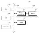
도 1a를 참조하면, 반도체 메모리 소자(1)는 메모리 셀 어레이(10), 어드레스 디코더(20), 읽기/쓰기 회로(30), 데이터 입출력 회로(40), 및 제어 로직(50)을 포함할 수 있다.Referring to FIG. 1A , the
메모리 셀 어레이(10)는 워드라인들(WL)을 통해 어드레스 디코더(20)에 연결되고, 비트라인들(BL)을 통해 읽기/쓰기 회로(30)에 연결될 수 있다. 메모리 셀 어레이(10)는 복수개의 메모리 셀들을 포함할 수 있다. 예를 들어, 메모리 셀 어레이(10)는 셀 당 하나 또는 그 이상의 비트를 저장할 수 있도록 구성될 수 있다.The
어드레스 디코더(20)는 워드라인들(WL)을 통해 메모리 셀 어레이(10)에 연결될 수 있다. 어드레스 디코더(20)는 제어 로직(50)의 제어에 응답하여 동작하도록 구성될 수 있다. 어드레스 디코더(20)는 외부로부터 어드레스(ADDR)를 수신할 수 있다. 어드레스 디코더(20)는 수신된 어드레스(ADDR) 중 행 어드레스를 디코딩하여, 워드라인들(WL) 중 대응하는 워드라인을 선택할 수 있다. 어드레스 디코더(20)는 수신된 어드레스(ADDR) 중 열 어드레스를 디코딩하고, 디코딩된 열 어드레스를 읽기/쓰기 회로(30)에 전달할 수 있다. 예를 들어, 어드레스 디코더(20)는 행 디코더, 열 디코더, 어드레스 버퍼를 포함할 수 있다.The
읽기/쓰기 회로(30)는 비트라인들(BL)을 통해 메모리 셀 어레이(10)에 연결되고, 데이터 라인들(D/L)을 통해 데이터 입출력 회로(40)에 연결될 수 있다. 읽기/쓰기 회로(30)는 제어 로직(50)의 제어에 응답하여 동작할 수 있다. 읽기/쓰기 회로(30)는 어드레스 디코더(20)로부터 디코딩된 열 어드레스를 수신하도록 구성될 수 있다. 디코딩된 열 어드레스를 이용하여, 읽기/쓰기 회로(30)는 비트라인(BL)을 선택할 수 있다. 예를 들어, 읽기/쓰기 회로(30)는 데이터 입출력 회로(40)로부터 데이터를 수신하고, 수신된 데이터를 메모리 셀 어레이(10)에 기입할 수 있다. 읽기/쓰기 회로(30)는 메모리 셀 어레이(10)로부터 데이터를 읽고, 읽어진 데이터를 데이터 입출력 회로(40)에 전달할 수 있다. 읽기/쓰기 회로(30)는 메모리 셀 어레이(10)의 제1 저장 영역으로부터 데이터를 읽고, 읽어진 데이터를 메모리 셀 어레이(10)의 제2 저장 영역에 기입할 수 있다. 예를 들면, 읽기/쓰기 회로(30)는 카피-백(copy-back) 동작을 수행하도록 구성될 수 있다.The read/
읽기/쓰기 회로(30)는 페이지 버퍼(또는 페이지 레지스터) 및 열 선택 회로를 갖는 구성 요소들을 포함할 수 있다. 다른 예로서, 읽기/쓰기 회로(30)는 감지 증폭기, 쓰기 드라이버, 및 열 선택 회로를 포함하는 구성 요소들을 포함할 수 있다.The read/
데이터 입출력 회로(40)는 데이터 라인들(DL)을 통해 읽기/쓰기 회로(30)에 연결될 수 있다. 데이터 입출력 회로(40)는 제어 로직(50)의 제어에 응답하여 동작할 수 있다. 데이터 입출력 회로(40)는 외부와 데이터(DATA)를 교환하도록 구성될 수 있다. 데이터 입출력 회로(40)는 외부로부터 전달되는 데이터(DATA)를 데이터 라인들(DL)을 통해 읽기/쓰기 회로(30)에 전달하도록 구성된다. 데이터 입출력 회로(40)는 읽기/쓰기 회로(30)로부터 데이터 라인들(DL)을 통해 전달되는 데이터(DATA)를 외부로 출력하도록 구성될 수 있다. 예를 들어, 데이터 입출력 회로(40)는 데이터 버퍼 등과 같은 구성 요소를 포함할 수 있다.The data input/
제어 로직(50)은 어드레스 디코더(20), 읽기/쓰기 회로(30), 및 데이터 입출력 회로(40)에 연결될 수 있다. 제어 로직(50)은 반도체 장치의 동작을 제어하도록 구성될 수 있다. 제어 로직(50)은 외부로부터 전달되는 제어 신호(CTRL)에 응답하여 동작할 수 있다.The
도 1b를 참조하면, 메모리 셀 어레이(10)는 메모리 블록들(BLK1~BLKn)을 포함할 수 있다. 메모리 블록들(BLK1~BLKn) 각각은 3차원 또는 수직 구조를 가질 수 있다. 예를 들면, 메모리 블록들(BLK1~BLKn) 각각은 서로 교차하는 방향들을 따라 연장된 가령 복수개의 셀 스트링들을 포함할 수 있다. 이하에서 반도체 메모리 소자(1)의 다양한 예들에 대해 설명한다.Referring to FIG. 1B , the
<제1 실시예><First embodiment>
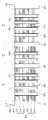
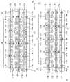
도 2a는 본 발명의 개념에 의한 일 실시예에 따른 반도체 메모리 소자를 도시한 평면도이다. 도 2b는 도 2a의 IA-IB 선을 절개한 단면도이다. 도 2c는 도 2a의 IIA-IIB 선을 절개한 단면도이다. 도 3a는 도 2a의 반도체 메모리 소자의 더미 셀 영역을 도시한 평면도이다. 도 3b는 도 3a의 번형예를 도시한 평면도이다.2A is a plan view illustrating a semiconductor memory device according to an exemplary embodiment according to the concept of the present invention. FIG. 2B is a cross-sectional view taken along line IA-IB of FIG. 2A. FIG. 2C is a cross-sectional view taken along line IIA-IIB of FIG. 2A. 3A is a plan view illustrating a dummy cell region of the semiconductor memory device of FIG. 2A . Fig. 3B is a plan view showing a modified example of Fig. 3A;
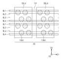
도 2a, 2b 및 2c를 참조하면, 반도체 메모리 소자(1a)는 반도체 기판(110) 상에 게이트 스택(160), 게이트 스택(160)을 관통하는 수직 채널들(150), 그리고 수직 채널들(150)과 전기적으로 연결된 비트라인들(BL1~BL4)을 포함할 수 있다. 반도체 메모리 소자(1a)는 수직 채널(150)을 따라 연장된 메모리막(135)을 더 포함하는 반도체 메모리 소자일 수 있다. 가령 메모리막(135)은 산화막들 사이에 삽입된 질화막을 포함할 수 있다. 다른 예로 메모리막(135)은 칼코켄화합물이나 전이금속산화막과 같은 가변저항막을 포함할 수 있다.Referring to FIGS. 2A, 2B and 2C , the
비트라인들(BL1-BL4)은 반도체 기판(110)에 수평한 제1 방향(D1)을 따라 신장되고, 제1 방향(D1)과 교차하여 반도체 기판(110)에 수평한 제2 방향(D2)을 따라 서로 이격될 수 있다. 수직 채널(150)은 반도체 기판(110)으로부터 수직한 제3 방향(D3)을 따라 신장할 수 있다.The bit lines BL1 - BL4 extend in a first direction D1 horizontal to the
게이트 스택(160)은 수직 채널(150)을 따라 수직 적층되고 절연막들(125)에 의해 이격된 제2 방향(D2)을 따라 연장된 복수개의 게이트들(161-166)을 포함하는 복수개의 셀 스트링들(165)을 포함할 수 있다. 게이트들(161-166)은 반도체 기판(110)에 인접하고 접지 선택라인(GSL)을 구성하는 적어도 하나의 제1 게이트(161), 비트라인(BL1-BL4)에 인접하고 스트링 선택라인(SSL)을 구성하는 적어도 하나의 제6 게이트(166), 그리고 접지 선택라인(GSL)과 스트링 선택라인(SSL) 사이의 워드라인들(WL)을 구성하는 제2 내지 제5 게이트들(162-165)을 포함할 수 있다. 본 실시예에서는 6개의 게이트들(161-166)에 대해 설명하나, 이에 한정되지 않고 그 이상일 수 있다.The
반도체 메모리 소자(1a)는 게이트 스택(160)을 제1 방향(D1)을 따라 분리하는 워드라인 컷 영역(131)을 더 포함할 수 있다. 워드라인 컷 영역(131)은 제2 방향(D2)을 따라 연장된 트렌치 형태를 가질 수 있고, 절연막(141)으로 채워져 있을 수 있다. 절연막(141) 아래의 반도체 기판(110)에는 공통 소오스라인(CSL)을 구성하는 공통 소오스(126)가 제공될 수 있다. 공통 소오스(126)는 반도체 기판(110)의 도전형(예: P형)과 반대되는 도전형(예: N형)을 가질수 있다. 수직 채널(150)의 상단에는 공통 소오스(126)와 동일한 도전형(예: P형)을 갖는 드레인(128)이 제공될 수 있다.The
수직 채널들(150)의 하단들은 반도체 기판(110)과 전기적으로 연결될 수 있고, 수직 채널들(150)의 상단들은 비트라인(BL1-BL4)과 전기적으로 연결될 수 있다. 본 실시예에 따르면, 수직 채널들(150)과 비트라인들(BL1-BL4) 사이에 보조배선들(SBL1-SBL4)이 더 제공될 수 있다. 보조배선들(SBL1-SBL4)은 하부 콘택들(152)을 매개로 수직 채널들(150)과 전기적으로 연결될 수 있고, 상부 콘택들(154)을 매개로 비트라인들(BL1-BL4)과 전기적으로 연결될 수 있다.Lower ends of the
반도체 메모리 소자(1a)는 제1 방향(D1)을 따라 이격된 제1 셀 영역(LC)과 제2 셀 영역(RC)을 포함할 수 있다. 제1 셀 영역(LC)과 제2 셀 영역(RC) 사이에서 정의되는 더미 셀 영역(DC)이 더 제공될 수 있다. 다른 예로, 더미 셀 영역(DC)은 제공되지 않을 수 있고, 제1 셀 영역(LC)과 제2 셀 영역(RC)은 워드라인 컷 영역(131)에 의해 분리될 수 있다. 이하에선 편의상 제1 셀 영역(LC)을 좌측 셀 영역, 제2 셀 영역(RC)을 우측 셀 영역으로 지칭될 수 있다.The
본 실시예에 따르면 반도체 메모리 소자(1a)는 수직 채널(150)과 동일한 구조를 갖는 적어도 하나의 더미 채널(150d)을 더 포함할 수 있다. 가령 좌측 셀 영역(LC)과 우측 셀 영역(RC) 각각은 적어도 하나의 더미 채널(150d)을 포함할 수 있다. 반도체 메모리 소자(1a)는 비트라인들(BL1-BL4)과 전기적으로 연결되는 8개의 수직 채널들(150)과 1개의 더미 채널(150d)로 이루어진 9개 채널을 갖는 셀 어레이(190)가 반복되는 셀 구조를 가질 수 있다.According to the present embodiment, the
좌측 셀 영역(LC) 및 우측 셀 영역(RC) 각각에서 제6 게이트(166)는 적어도 2개로 분리될 수 있다. 가령 제6 게이트(166)는 제2 방향(D2)을 따라 트렌치 형태로 연장되는 선택라인 컷 영역(133)에 의해 제1 방향(D1)으로 이격된 제1 스트링 선택라인(SSL1)과 제2 스트링 선택라인(SSL2)으로 분리될 수 있다. 선택라인 컷 영역(133)은 절연막(143)으로 채워져 있을 수 있다. 복수개의 더미 채널들(150d)은 선택라인 컷 영역(133) 상에서 제2 방향(D2)을 따라 일렬 배열될 수 있다. 일례로, 선택라인 컷 영역(133)은 워드라인 컷 영역(131)에 비해 작은 폭, 즉 제1 방향(D1)으로의 간격이 작을 수 있다.At least two
좌측 셀 영역(LC) 및 우측 셀 영역(RC) 각각에 포함된 수직 채널들(150)과 더미 채널들(150d)은 규칙적으로 배열될 수 있다. 일례로, 수직 채널들(150)과 더미 채널들(150d)은 제2 방향(D2)을 따라 지그재그 형태로 배열될 수 있고, 그 지그재그 배열이 제1 방향(D1)을 따라 반복될 수 있다. 따라서, 가령 수직 채널들이 일렬 배열된 경우에 비해 지그재그 배열된 경우 수직 채널들(150)의 밀도를 더 증가시킬 수 있어 고집적화에 유리할 수 있다. 아울러, 스트링 선택라인들(SSL1,SSL2)이 더 많은 수의 수직 채널들(150)과 연결되므로써 반도체 소자(1a)의 페이지 크기를 확장시킬 수 있고, 이는 더 많은 데이터를 동시에 쓰고 읽어내는 것을 가능하게 하므로써 동작 속도를 증가시킬 수 있다.The
일례로서, 제2 방향(D2)을 따라 최인접하는 2개의 수직 채널들(150)은 비트라인들(BL1-BL4)의 피치(이하, 비트라인 피치)의 약 2배에 상당하는 거리로 이격될 수 있다. 마찬가지로, 제2 방향(D2)을 따라 최인접하는 수직 채널(150)과 더미 채널(150d)은 비트라인 피치의 약 2배에 상당하는 거리로 이격될 수 있다. 제1 방향(D1)을 따라 인접한 수직 채널들(150)과 더미 채널들(150d)은 동일 간격으로 이격되어 일렬 배열될 수 있다. 여기서의 동일 간격은 비트라인 피치의 약 2배에 상당하거나 혹은 이와 다른 거리일 수 있다.As an example, the two
더미 셀 영역(DC)은 더미 채널(150d)을 포함하거나 혹은 포함하지 않을 수 있다. 일례로, 더미 셀 영역(DC)은 도 2a에 도시된 바와 같이 제1 방향(D1)을 따라 등간격으로 일렬 배열되고 제2 방향(D2)을 따라 지그재그 형태로 배열된 더미 채널들(150d)을 포함할 수 있다. 더미 셀 영역(DC)에서의 제6 게이트(166)는 더미 스트링 선택라인(SSLd)을 구성할 수 있다.The dummy cell region DC may or may not include the
다시 말해, 좌측 셀 영역(LC) 및 우측 셀 영역(RC)은 채널들(150,150d)이 규칙적으로 배열된 연속된 패턴을 갖는 셀 어레이를 구성하고, 셀 어레이의 중심에 패턴의 연속성이 깨지는 더미 셀 영역(DC)이 제공될 수 있다. 더미 셀 영역(DC)은 지그재그 배열된 더미 채널들(150d)을 더 포함하므로써 패턴의 연속성을 구현할 수 있고, 구현된 패턴의 연속성에 의해 패턴 연속성의 깨짐에 의해 발생할 수 있는 수직 채널(150)의 전기적 특성(예: 커패시턴스) 차이를 없애거나 최소화할 수 있다.In other words, the left cell region LC and the right cell region RC constitute a cell array having a continuous pattern in which the
더미 셀 영역(DC)의 크기는 임의적일 수 있다. 가령 더미 셀 영역(DC)은 도 3a에 도시된 것처럼 제1 방향(D1)으로 확장될 수 있다. 다른 예로, 도 3b에 도시된 바와 같이, 더미 셀 영역(DC)은 적어도 하나의 제2 방향(D2)을 따라 연장되는 선택적으로 제공된 워드라인 컷 영역(131)에 의해 제1 방향(D1)으로 이격된 적어도 2개의 부분들로 나뉘어질 수 있다. 이외에 더미 셀 영역(DC)은 좌측 셀 영역(LC) 및/혹은 우측 셀 영역(RC)과 동일하거나 유사한 패턴을 가질 수 있다.The size of the dummy cell region DC may be arbitrary. For example, the dummy cell region DC may extend in the first direction D1 as shown in FIG. 3A . As another example, as shown in FIG. 3B , the dummy cell region DC is moved in the first direction D1 by the selectively provided word line cut
본 실시예에 따르면, 도 2a에서 알 수 있듯이, 우측 셀 영역(RC)에서의 채널들(150,150d)의 배열은 좌측 셀 영역(LC)에서의 채널들(150,150d)의 배열에 대해 더미 셀 영역(DC)을 중심으로 선대칭을 이루는 미러 이미지(mirror image)를 가질 수 있다.According to this embodiment, as can be seen from FIG. 2A , the arrangement of
하부 콘택들(152)은 수직 채널들(150) 상에 제공될 수 있다. 하부 콘택들(152)은 드레인들(128)과 접속하여 수직 채널들(150)과 전기적으로 연결될 수 있다. 더미 채널들(150d) 상에는 하부 콘택들(152)이 제공되지 않을 수 있다. 하부 콘택들(152)은 수직 채널들(150)과 수직 정렬될 수 있어 도 2a에 도시된 것처럼 지그재그 형태로 배열될 수 있다. 우측 셀 영역(RC)에서의 하부 콘택들(152)의 배열은 좌측 셀 영역(LC)에서의 하부 콘택들(152)의 배열에 대해 더미 셀 영역(DC)을 중심으로 미러 이미지를 가질 수 있다.The
비트라인들(BL1-BL4) 중 인접한 제1 비트라인(BL1)과 제2 비트라인(BL2)은 제1 방향(D1)을 따라 일렬 배열된 수직 채널들(150) 상에 제공될 수 있다. 마찬가지로, 비트라인들(BL1-BL4) 중 인접한 제3 비트라인(BL3)과 제4 비트라인(BL4)은 제1 방향(D1)을 따라 일렬 배열된 수직 채널들(150) 상에 제공될 수 있다.A first bit line BL1 and a second bit line BL2 adjacent to each other among the bit lines BL1 - BL4 may be provided on the
좌측 셀 영역(LC) 및 우측 셀 영역(RC) 각각에서, 상부 콘택들(154)은 워드라인 컷 영역(131)과 선택라인 컷 영역(133) 상에서 제2 방향(D2)을 따라 일렬 배열될 수 있다. 제2 방향(D2)을 따라 일렬 배열된 상부 콘택들(154)은 등간격, 가령 비트라인 피치의 약 2배에 상당하는 거리로 이격될 수 있다. 워드라인 컷 영역(131) 상에 제공된 상부 콘택들(154)의 배열은 선택라인 컷 영역(133) 상에 제공된 상부 콘택들(154)의 배열에 대해 비트라인 피치에 상당하는 거리만큼 제2 방향(D2)을 따라 쉬프트되어 있을 수 있다.In each of the left cell area LC and the right cell area RC, the
우측 셀 영역(RC)에서의 상부 콘택들(154)의 배열은 좌측 셀 영역(LC)에서의 상부 콘택들(154)의 배열에 대해 비트라인 피치에 상당하는 거리만큼 제2 방향(D2)을 따라 쉬프트되어 있을 수 있다.The arrangement of the
예컨대, 좌측 셀 영역(LC)의 양측에 배치된 워드라인 컷 영역들(131) 상의 상부 콘택들(154)은 제1 비트라인(BL1)과 제3 비트라인(BL3)의 아래에 제공될 수 있다. 좌측 셀 영역(LC)의 선택라인 컷 영역(133) 상의 상부 콘택들(154)은 제2 비트라인(BL2)과 제4 비트라인(BL4)의 아래에 제공될 수 있다.For example, the
이와 다르게, 우측 셀 영역(RC)의 양측에 배치된 워드라인 컷 영역들(131) 상의 상부 콘택들(154)은 제2 비트라인(BL2)과 제4 비트라인(BL4)의 아래에 제공될 수 있다. 우측 셀 영역(RC)의 선택라인 컷 영역(133) 상의 상부 콘택들(154)은 제1 비트라인(BL1)과 제3 비트라인(BL3)의 아래에 제공될 수 있다.Alternatively, the
보조배선들(SBL1-SBL4)은 제2 방향(D2)을 따라 등간격, 가령 비트라인 피치의 약 2배에 상당하는 간격으로 이격 배열될 수 있다. 보조배선들(SBL1-SBL4)은 선택라인 컷 영역(133)에 인접하고 제2 방향(D2)을 따라 교대로 배열된 제1 보조배선(SBL1) 및 제3 보조배선(SBL3), 그리고 워드라인 컷 영역(131)에 인접하고 제2 방향(D2)을 따라 교대로 배열된 제2 보조배선(SBL2) 및 제4 보조배선(SBL4)으로 구분할 수 있다.The auxiliary wirings SBL1 - SBL4 may be arranged to be spaced apart from each other at equal intervals along the second direction D2 , for example, at intervals corresponding to about twice the bit line pitch. The auxiliary wirings SBL1 - SBL4 are adjacent to the selection line cut
좌측 셀 영역(LC) 및 우측 셀 영역(RC) 각각에서, 제1 비트라인(BL1)과 제2 비트라인(BL2)의 아래에선 제2 보조배선들(SBL2)과 제3 보조배선들(SBL3)이 제1 방향(D1)을 따라 배열될 수 있다. 제3 비트라인(BL3)과 제4 비트라인(BL4)의 아래에선 제1 보조배선들(SBL1)과 제4 보조배선들(SBL4)이 제1 방향(D1)을 따라 배열될 수 있다.In each of the left cell area LC and the right cell area RC, the second auxiliary wirings SBL2 and the third auxiliary wirings SBL3 are below the first bit line BL1 and the second bit line BL2. ) may be arranged along the first direction D1. The first auxiliary lines SBL1 and the fourth auxiliary lines SBL4 may be arranged under the third bit line BL3 and the fourth bit line BL4 in the first direction D1 .
보조배선들(SBL1-SBL4)은 도 2a에 도시된 바와 같이 휘어진 비직선형 평면을 가질 수 있다. 좌측 셀 영역(LC)의 보조배선들(SBL1-SBL4)의 평면 형상들은 우측 셀 영역(RC)의 보조배선들(SBL1-SBL4)의 평면 형상들에 대해 제1 방향(D1)의 축을 중심으로 미러 이미지를 가질 수 있다. 예컨대, 우측 셀 영역(RC)의 보조배선들(SBL1-SBL4) 각각의 평면 형상은 좌측 셀 영역(LC)의 보조배선들(SBL1-SBL4) 각각의 평면 형상과 상하 반전된 것일 수 있다. 다시 말해, 더미 셀 영역(DC)을 사이에 두고 제1 방향(D1)에 평행한 가상선(imaginary line) 상에 배치되는 보조배선들(SBL1-SBL4)은 더미 셀 영역(DC)을 중심으로 점대칭을 이룰 수 있다. 점대칭을 이루는 보조배선들(SBL1-SBL4)은 동일한 길이를 가질 수 있다.The auxiliary wirings SBL1 - SBL4 may have a curved non-linear plane as shown in FIG. 2A . The planar shapes of the auxiliary lines SBL1 - SBL4 of the left cell area LC are centered on the axis in the first direction D1 with respect to the planar shapes of the auxiliary lines SBL1 - SBL4 of the right cell area RC. You can have a mirror image. For example, the planar shape of each of the auxiliary wirings SBL1 -SBL4 of the right cell area RC may be vertically inverted from the planar shape of each of the auxiliary wirings SBL1 -SBL4 of the left cell area LC. In other words, the auxiliary lines SBL1 - SBL4 disposed on an imaginary line parallel to the first direction D1 with the dummy cell area DC interposed therebetween are formed with the dummy cell area DC as the center. point symmetry can be achieved. The point-symmetric auxiliary wires SBL1 - SBL4 may have the same length.
보조배선들(SBL1-SBL4)과 이들에 대응하는 상부 콘택들(154) 간의 거리는 서로 다를 수 있고, 이에 따라 보조배선들(SBL1-SBL4)은 서로 다른 길이를 가질 수 있다. 일례로, 제1 보조배선(SBL1)은 가장 작은 제1 길이를 가질 수 있고, 제4 보조배선(SBL4)은 가장 큰 제4 길이를 가질 수 있다. 제2 보조배선(SBL2)은 제1 길이보다 크고 제4 길이보다 작은 제2 길이를 가질 수 있고, 제3 보조배선(SBL3)은 제2 길이보다 크고 제4 길이보다 작은 제3 길이를 가질 수 있다.Distances between the auxiliary wirings SBL1 - SBL4 and the corresponding
본 실시예에 따르면, 비트라인들(BL1-BL4) 각각은 서로 다른 길이를 갖는 보조배선들(SBL1-SBL4)과 전기적으로 연결될 수 있다.According to the present embodiment, each of the bit lines BL1 - BL4 may be electrically connected to the auxiliary lines SBL1 - SBL4 having different lengths.
일례로, 도 2a 및 2b에 도시된 바와 같이, 제1 비트라인(BL1)은 좌측 셀 영역(LC)에선 제2 보조배선(SBL2)과 전기적으로 연결될 수 있고 우측 셀 영역(RC)에선 제3 보조배선(SBL3)과 전기적으로 연결될 수 있다. 제2 비트라인(BL2)은 좌측 셀 영역(LC)에선 제3 보조배선(SBL3)과 전기적으로 연결될 수 있고 우측 셀 영역(RC)에선 제2 보조배선(SBL2)과 전기적으로 연결될 수 있다. 좌측 셀 영역(LC) 및 우측 셀 영역(RC) 각각에 포함된 더미 채널(150d) 상에 제공된 마주보는 두 개의 제3 보조배선들(SBL3)은 합쳐져 싱글 보조배선을 이루어 제2 비트라인(BL2)에 공통 연결될 수 있다.For example, as shown in FIGS. 2A and 2B , the first bit line BL1 may be electrically connected to the second auxiliary line SBL2 in the left cell area LC and the third bit line BL1 in the right cell area RC. It may be electrically connected to the auxiliary line SBL3. The second bit line BL2 may be electrically connected to the third auxiliary line SBL3 in the left cell area LC and may be electrically connected to the second auxiliary line SBL2 in the right cell area RC. Two opposing third auxiliary lines SBL3 provided on the
도 2a 및 2c에 도시된 것처럼, 제3 비트라인(BL3)은 좌측 셀 영역(LC)에선 제4 보조배선(SBL4)과 전기적으로 연결될 수 있고 우측 셀 영역(RC)에선 제1 보조배선(SBL1)과 전기적으로 연결될 수 있다. 제4 비트라인(BL4)은 좌측 셀 영역(LC)에선 제1 보조배선(SBL1)과 전기적으로 연결될 수 있고 우측 셀 영역(RC)에선 제4 보조배선(SBL4)과 전기적으로 연결될 수 있다. 좌측 셀 영역(LC) 및 우측 셀 영역(LC) 각각에 포함된 선택라인 컷 영역(133) 상에 제공된 마주보는 두 개의 제1 보조배선들(SBL1)은 합쳐져 싱글 보조배선을 이루어 제4 비트라인(BL4)에 공통 연결될 수 있다2A and 2C , the third bit line BL3 may be electrically connected to the fourth auxiliary line SBL4 in the left cell area LC and the first auxiliary line SBL1 in the right cell area RC. ) can be electrically connected to. The fourth bit line BL4 may be electrically connected to the first auxiliary line SBL1 in the left cell area LC and may be electrically connected to the fourth auxiliary line SBL4 in the right cell area RC. Two opposing first auxiliary lines SBL1 provided on the selection line cut
제1 비트라인(BL1)과 제2 비트라인(BL2) 각각은 제2 길이를 갖는 제2 보조배선(SBL2)과 제3 길이를 갖는 제3 보조배선(SBL3)과 전기적으로 연결될 수 있다. 이처럼 제1 비트라인(BL1)과 제2 비트라인(BL2)은 보조배선들과의 연결 모습이 동일하므로 실질적으로 동일한 전기적 특성(예: 로딩 커패시턴스, 저항)을 가질 수 있다. 제3 비트라인(BL3)과 제4 비트라인(BL4) 각각은 동일한 연결 모습, 즉 제1 보조배선(SBL1)과 제4 보조배선(SBL4)과 전기적으로 연결될 수 있다. 따라서, 제3 비트라인(BL3)과 제4 비트라인(BL4)은 실질적으로 동일한 전기적 특성을 가질 수 있다.Each of the first bit line BL1 and the second bit line BL2 may be electrically connected to a second auxiliary line SBL2 having a second length and a third auxiliary line SBL3 having a third length. As described above, the first bit line BL1 and the second bit line BL2 have substantially the same electrical characteristics (eg, loading capacitance and resistance) because the connection shape with the auxiliary lines is the same. Each of the third bit line BL3 and the fourth bit line BL4 may be electrically connected to the same connection shape, that is, the first auxiliary line SBL1 and the fourth auxiliary line SBL4 . Accordingly, the third bit line BL3 and the fourth bit line BL4 may have substantially the same electrical characteristics.
제1 비트라인(BL1)에 연결된 제2 및 제3 보조배선들(SBL2,SBL3)의 길이들의 합(예: 2+3=5)은 제4 비트라인(BL4)에 연결된 제1 및 제4 보조배선들(SBL1,SBL4)의 길이들의 합(예: 1+4=5)과 동일하거나 유사할 수 있다. 제2 비트라인(BL2)에 연결된 제2 및 제3 보조배선들(SBL2,SBL3)의 길이들의 합(예: 2+3=5)은 제3 비트라인(BL3)에 연결된 제1 및 제4 보조배선들(SBL1,SBL4)의 길이들의 합(예: 1+4=5)과 동일하거나 유사할 수 있다. 따라서, 제1 비트라인(BL1)과 이에 인접한 제4 비트라인(BL4), 그리고 제2 비트라인(BL1)과 이에 인접한 제3 비트라인(BL3)은 실질적으로 동일한 전기적 특성을 가질 수 있다.The sum (eg, 2+3=5) of the lengths of the second and third auxiliary lines SBL2 and SBL3 connected to the first bit line BL1 is equal to the first and fourth lengths connected to the fourth bit line BL4 It may be the same as or similar to the sum (eg, 1+4=5) of the lengths of the auxiliary wires SBL1 and SBL4 . The sum (eg, 2+3=5) of the lengths of the second and third auxiliary lines SBL2 and SBL3 connected to the second bit line BL2 is equal to the first and fourth lengths connected to the third bit line BL3 It may be the same as or similar to the sum (eg, 1+4=5) of the lengths of the auxiliary wires SBL1 and SBL4 . Accordingly, the first bit line BL1 and the fourth bit line BL4 adjacent thereto, and the second bit line BL1 and the third bit line BL3 adjacent thereto may have substantially the same electrical characteristics.
다른 예로, 제1 보조배선(SBL1)은 제2 보조배선(SBL2)과 실질적으로 동일한 길이(예: 2)를 가질 수 있고, 제3 보조배선(SBL3)은 제4 보조배선(SBL4)과 실질적으로 동일한 길이(예: 3)를 가질 수 있다. 가령, 제1 비트라인(BL1) 및 제2 비트라인(BL2) 각각에 연결된 제2 보조배선(SBL2)과 제3 보조배선(SBL3)의 길이들의 합(예: 2+3=5)은 제3 비트라인(BL3) 및 제4 비트라인(BL4) 각각에 연결된 제1 보조배선(SBL1)과 제4 보조배선(SBL4)의 길이들의 합(예: 3+2=5)의 실질적으로 동일할 수 있다. 그러므로, 제1 내지 제4 비트라인들(BL1-BL4)은 실질적으로 동일한 전기적 특성을 가질 수 있다.As another example, the first auxiliary line SBL1 may have substantially the same length (eg, 2) as the second auxiliary line SBL2 , and the third auxiliary line SBL3 may be substantially the same as the fourth auxiliary line SBL4 . can have the same length (eg 3). For example, the sum (eg, 2+3=5) of the lengths of the second auxiliary line SBL2 and the third auxiliary line SBL3 connected to the first bit line BL1 and the second bit line BL2 is the second The sum (eg, 3+2=5) of the lengths of the first auxiliary line SBL1 and the fourth auxiliary line SBL4 connected to each of the three bit lines BL3 and the fourth bit line BL4 is substantially equal to can Therefore, the first to fourth bit lines BL1 to BL4 may have substantially the same electrical characteristics.
<제조방법의 예><Example of manufacturing method>
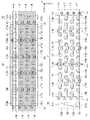
도 4a 내지 9a는 본 발명의 개념에 의한 일 실시예에 따른 반도체 메모리 소자의 제조방법을 도시한 평면도들이다. 도 4b 내지 9b는 도 4a 내지 9a의 IA-IB 선을 절개한 단면도들이다. 도 4c 내지 9c는 도 4a 내지 9a의 IIA-IIB 선을 절개한 단면도들이다.4A to 9A are plan views illustrating a method of manufacturing a semiconductor memory device according to an exemplary embodiment according to the concept of the present invention. 4B to 9B are cross-sectional views taken along line IA-IB of FIGS. 4A to 9A . 4C to 9C are cross-sectional views taken along line IIA-IIB of FIGS. 4A to 9A .
도 4a, 4b 및 4c를 참조하면, 가령 제1 도전형(예: P형)을 갖는 실리콘 웨이퍼와 같은 반도체 기판(110) 상에 몰드 스택(120)을 형성하고, 몰드 스택(120)을 관통하는 복수개의 수직 홀(116)을 형성할 수 있다. 반도체 기판(110)은 좌측 셀 영역(LC), 우측 셀 영역(RC), 그리고 좌측 셀 영역(LC)과 우측 셀 영역(RC) 사이의 더미 셀 영역(DC)으로 구분될 수 있다. 몰드 스택(120)은 가령 절연막들(125)과 희생막들(123)을 교대로 증착하여 형성할 수 있다. 일례로, 절연막들(125)은 실리콘산화막을 포함하고, 희생막들(123)은 실리콘질화막을 포함할 수 있다.Referring to FIGS. 4A, 4B and 4C , the
수직 홀들(116)은 좌측 셀 영역(LC) 및 우측 셀 영역(RC)에 해당하는 몰드 스택(120)을 식각하여 형성할 수 있다. 선택적으로, 더미 셀 영역(DC)에 해당하는 몰드 스택(120)을 식각하여 더미 홀(116d)을 형성할 수 있다. 수직 홀들(116)은 더미 셀 영역(DC)을 중심으로 좌우 대칭적으로 배열될 수 있다.The
도 5a, 5b 및 5c를 참조하면, 수직 홀(116) 내에 메모리막(135)으로 둘러싸이는 수직 채널(150)을 형성할 수 있다. 수직 채널(150)은 가령 제1 도전형(예: P형)의 반도체막일 수 있다. 수직 채널(150)의 상단부를 드레인(128)으로 형성할 수 있다. 드레인(128)은 제2 도전형(예: N형)을 가질 수 있다. 수직 채널(150)의 형성과 동시에 더미 홀(116d)을 채우는 더미 채널(150d)을 더 형성할 수 있다. 더미 채널(150d)은 수직 채널(150)과 동일한 구조를 가질 수 있다.Referring to FIGS. 5A , 5B and 5C , a
수직 채널(150)을 형성하기 이전에, 수직 홀(116)의 내측벽 상에 산화막과 질화막과 산화막을 순차 증착하여 메모리막(135)을 형성할 수 있다. 다른 예로, 메모리막(135)은 칼코켄화합물이나 전이금속산화막과 같은 가변저항막을 증착하여 형성할 수 있다.Before forming the
수직 채널들(150)을 형성한 이후 혹은 그 이전에, 좌측 셀 영역(LC) 및 우측 셀 영역(RC) 각각에 해당하는 몰드 스택(120)을 일부 식각하여 선택라인 컷 영역(133)을 형성할 수 있다. 선택라인 컷 영역(133)은 가령 최상층의 절연막(125)과 최상층의 희생막(123)을 선택적으로 식각하여 트렌치 형태로 형성할 수 있다. 선택라인 컷 영역(133)을 따라 배열된 수직 채널들(150)은 실질적으로 전기적 동작에 참여하지 않는 더미 채널(150d)로 활용할 수 있다.After or before forming the
도 6a, 6b 및 6c를 참조하면, 몰드 스택(120)을 선택적으로 식각하여 반도체 기판(110)을 노출시키는 워드라인 컷 영역(131)을 형성할 수 있다. 워드라인 컷 영역(131)은 좌측 셀 영역(LC) 및 우측 셀 영역(RC) 각각의 양측 가장자리에 형성할 수 있다. 워드라인 컷 영역(131)을 형성하기 이전에 혹은 그 이후에, 선택라인 컷 영역(133)을 가령 실리콘산화막과 같은 절연막(143)으로 채울 수 있다.Referring to FIGS. 6A , 6B and 6C , the word line cut
도 7a, 7b 및 7c를 참조하면, 워드라인 컷 영역(131)을 통해 노출된 희생막들(123)을 제거하여 게이트 영역(132)을 갖는 몰드 윙(122)을 형성할 수 있다. 가령, 희생막들(123)이 실리콘질화막을 포함하는 경우 인산을 포함하는 식각액으로 희생막들(123)을 선택적으로 제거하여 게이트 영역(132)을 형성할 수 있다.Referring to FIGS. 7A , 7B and 7C , the
도 8a, 8b 및 8c를 참조하면, 게이트 영역(132)을 도전막으로 채워 게이트 스택(160)을 형성할 수 있다. 게이트 스택(160)은 수직 채널(150)을 따라 수직 적층되고 절연막들(125)에 의해 복수개의 게이트들(161-166)을 포함할 수 있다. 게이트들(161-166)은 도핑된 실리콘막, 금속막(예: 텅스텐막), 금속질화막 또는 금속실리사이드막을 포함할 수 있다. 워드라인 컷 영역(131)을 통해 노출된 반도체 기판(110)에 불순물을 주입하여 가령 제2 도전형(예: N형)을 갖는 공통 소오스(126)를 형성할 수 있다.Referring to FIGS. 8A , 8B and 8C , the
게이트들(161-166)은 반도체 기판(110)에 인접하고 접지 선택라인(GSL)을 구성하는 적어도 하나의 제1 게이트(161), 비트라인(BL1-BL4)에 인접하고 스트링 선택라인(SSL)을 구성하는 적어도 하나의 제6 게이트(166), 그리고 접지 선택라인(GSL)과 스트링 선택라인(SSL) 사이의 워드라인들(WL)을 구성하는 제2 내지 제5 게이트들(162-165)을 포함할 수 있다. 공통 소오스(126)는 공통 소오스 라인(CSL)을 구성할 수 있다.The gates 161-166 are adjacent to the
제6 게이트(166)는 좌측 셀 영역(LC) 및 우측 셀 영역(RC) 각각에서 선택라인 컷 영역(133)에 의해 분리된 제1 스트링 선택라인(SSL1)과 제2 스트링 선택라인(SSL2)으로 구분될 수 있다. 더미 셀 영역(DC)에서의 제6 게이트(166)는 더미 스트링 선택라인(SSLd)을 구성할 수 있다.The
도 9a, 9b 및 9c를 참조하면, 워드라인 컷 영역(131)을 절연막(141)으로 채울 수 있다. 그리고 수직 채널들(150)과 정렬되는 하부 콘택들(152)을 형성하고, 하부 콘택들(152)과 접속하는 보조배선들(SBL1-SBL2)을 형성할 수 있다. 하부 콘택들(152)과 보조배선들(SBL1-SBL2)은 도 2a 내지 2c에서 설명된 바와 같이 배열될 수 있다.Referring to FIGS. 9A , 9B and 9C , the word line cut
도 2a, 2b 및 2c를 다시 참조하면, 보조배선들(SBL1-SBL4)과 전기적으로 연결되는 상부 콘택들(154)을 형성하고, 상부 콘택들(154)과 전기적으로 연결되는 비트라인들(BL1-BL4)을 형성하여 반도체 메모리 소자(1a)를 제조할 수 있다. 상부 콘택들(154)과 비트라인들(BL1-BL4)은 도 2a 내지 2c에서 설명된 바와 같이 배열될 수 있다.Referring back to FIGS. 2A, 2B and 2C ,
<제1 실시예의 변형><Modification of the first embodiment>
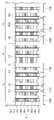
도 10a는 본 발명의 개념에 의한 다른 실시예에 따른 반도체 메모리 소자를 도시한 평면도이다. 도 10b는 도 10a의 IA-IB 선을 절개한 단면도이다. 도 10c는 도 10a의 IIA-IIB 선을 절개한 단면도이다. 이하에선 도 2a 내지 2c를 참조하여 설명된 실시예와 중복된 설명은 생략한다.10A is a plan view illustrating a semiconductor memory device according to another embodiment according to the concept of the present invention. 10B is a cross-sectional view taken along line IA-IB of FIG. 10A. 10C is a cross-sectional view taken along line IIA-IIB of FIG. 10A. Hereinafter, descriptions overlapping those of the embodiment described with reference to FIGS. 2A to 2C will be omitted.
도 10a, 10b 및 10c를 참조하면, 반도체 메모리 소자(1b)는 도 2a의 반도체 메모리 소자(1a)와 동일하거나 유사하게 9개 채널을 갖는 셀 어레이(190)가 반복되는 셀 구조를 가질 수 있다. 반도체 메모리 소자(1a)와 다르게, 좌측 셀 영역(LC)의 채널들(150,150d)의 배열과 우측 셀 영역(RC)의 채널들(150,150d)의 배열은 미러 이미지를 구성하지 않을 수 있다. 가령, 우측 셀 영역(RC)의 채널들(150,150d)의 배열은 좌측 셀 영역(LC)의 채널들(150,150d)의 배열에 대해 비트라인 피치에 상당하는 거리만큼 제2 방향(D2)을 따라 쉬프트되어 있을 수 있다.10A, 10B, and 10C , the
우측 셀 영역(RC)의 보조배선들(SBL1-SBL4)의 평면 형상들은 좌측 셀 영역(LC)의 보조배선들(SBL1-SBL4)의 평면 형상들과 동일할 수 있다. 우측 셀 영역(RC)의 보조배선들(SBL1-SLB4)의 배열은 좌측 셀 영역(LC)의 보조배선들(SBL1-SBL4)이 배열에 대해 비트라인 피치에 상당하는 거리만큼 제2 방향(D2)을 따라 쉬프트되어 있을 수 있다.The planar shapes of the auxiliary lines SBL1 -SBL4 of the right cell area RC may be the same as the planar shapes of the auxiliary lines SBL1 - SBL4 of the left cell area LC. The arrangement of the auxiliary wirings SBL1 -SLB4 in the right cell area RC is arranged in the second direction D2 by a distance corresponding to the bit line pitch with respect to the arrangement of the auxiliary wirings SBL1 - SBL4 in the left cell area LC. ) may be shifted along the
비트라인들(BL1-BL4) 각각은 서로 다른 길이를 갖는 보조배선들(SBL1-SBL4)과 전기적으로 연결될 수 있고, 이에 따라 비트라인들(BL1-BL4)은 실질적으로 동일하거나 유사한 보조배선들과의 연결 모습을 가질 수 있다.Each of the bit lines BL1 - BL4 may be electrically connected to auxiliary wirings SBL1 - SBL4 having different lengths, and accordingly, the bit lines BL1 - BL4 may be connected to substantially the same or similar auxiliary wirings. can have the form of a connection of
예컨대, 제1 비트라인(BL1)은 좌측 셀 영역(LC)에선 제2 보조배선(SBL2)과 우측 셀 영역(RC)에선 제3 보조배선(SBL3)과 연결될 수 있다. 제2 비트라인(BL2)은 좌측 셀 영역(LC)에선 제3 보조배선(SBL3)과 우측 셀 영역(RC)에선 제4 보조배선(SBL4)과 연결될 수 있다. 제3 비트라인(BL3)은 좌측 셀 영역(LC)에선 제4 보조배선(SBL4)과 우측 셀 영역(RC)에선 제1 보조배선(SBL1)과 연결될 수 있다. 제4 비트라인(BL4)은 좌측 셀 영역(LC)에선 제1 보조배선(SBL1)과 우측 셀 영역(RC)에선 제2 보조배선(SBL2)과 연결될 수 있다.For example, the first bit line BL1 may be connected to the second auxiliary line SBL2 in the left cell area LC and the third auxiliary line SBL3 in the right cell area RC. The second bit line BL2 may be connected to the third auxiliary line SBL3 in the left cell area LC and the fourth auxiliary line SBL4 in the right cell area RC. The third bit line BL3 may be connected to the fourth auxiliary line SBL4 in the left cell area LC and the first auxiliary line SBL1 in the right cell area RC. The fourth bit line BL4 may be connected to the first auxiliary line SBL1 in the left cell area LC and the second auxiliary line SBL2 in the right cell area RC.
본 실시예와 다르게, 비트라인들(BL1-BL4) 각각이 동일한 길이를 갖는 보조배선들(SBL1-SLB4)과 연결된 경우 비트라인들(BL1-BL4) 각각의 전기적 특성이 상이해질 수 있다. 가령, 비트라인들(BL1-BL4) 중 어느 하나는 길이가 작은 제1 보조배선들(SBL1)과 연결되고, 다른 하나는 길이가 큰 제4 보조배선들(SBL4)과 연결될 수 있다. 이 경우, 작은 길이를 갖는 제1 보조배선들(SBL1)과 연결된 비트라인이 갖는 전기적 특성은 큰 길이를 갖는 제4 보조배선들(SBL4)과 연결된 비트라인이 갖는 전기적 특성은 서로 다를 수 있다.Unlike the present exemplary embodiment, when each of the bit lines BL1 - BL4 is connected to the auxiliary lines SBL1 -SLB4 having the same length, electrical characteristics of each of the bit lines BL1 - BL4 may be different. For example, one of the bit lines BL1 - BL4 may be connected to the first auxiliary wirings SBL1 having a short length, and the other may be connected to the fourth auxiliary wirings SBL4 having a large length. In this case, electrical characteristics of the bit line connected to the first auxiliary wirings SBL1 having a small length may be different from those of the bit line connected to the fourth auxiliary wirings SBL4 having a large length.
그러나, 본 실시예에 따르면 비트라인들(BL1-BL4)은 상이한 길이들을 갖는 보조배선들(SBL1-SLB4)과 연결되므로써 서로 동일하거나 유사한 보조배선들과의 연결 모습을 가질 수 있고, 이에 따라 유사한 전기적 특성을 가질 수 있다.However, according to the present embodiment, the bit lines BL1 - BL4 are connected to the auxiliary wirings SBL1 -SLB4 having different lengths, so that they may have the same or similar connection shape to each other. It may have electrical properties.
<제2 실시예><Second embodiment>
도 11a는 본 발명의 개념에 의한 또 다른 실시예에 따른 반도체 메모리 소자를 도시한 평면도이다. 도면에서 위는 좌측 셀 영역을 나타내고 아래는 우측 셀 영역을 나타낸다. 이하의 실시예들에 있어서도 이와 마찬가지다.11A is a plan view illustrating a semiconductor memory device according to another embodiment according to the concept of the present invention. In the figure, the upper part represents the left cell area and the lower part represents the right cell area. This is also the case in the following examples.
도 11a를 참조하면, 반도체 메모리 소자(2a)는 도 2a의 반도체 메모리 소자(1a)에 비해 적어도 제1 방향(D1)으로 더 확장된 셀 구조를 가질 수 있다. 일례로, 좌측 셀 영역(LC) 및 우측 셀 영역(RC) 각각은 2개의 선택라인 컷 영역(133)에 의해 분리되는 제1 내지 제3 스트링 선택라인(SSL1-SSL3)을 포함할 수 있다. 반도체 메모리 소자(2a)는 비트라인들(BL1-BL4)과 전기적으로 연결되는 12개의 수직 채널들(150)과 2개의 더미 채널(150d)로 이루어진 14개 채널을 갖는 셀 어레이(190)가 반복되는 셀 구조를 가질 수 있다.Referring to FIG. 11A , the
우측 셀 영역(RC)에서의 채널들(150,150d)의 배열은 좌측 셀 영역(LC)에서의 채널들(150,150d)의 배열에 대해 더미 셀 영역(DC)을 중심으로 미러 이미지(mirror image)를 가질 수 있다. 마찬가지로, 우측 셀 영역(RC)의 수직 채널들(150) 상에 제공된 하부 콘택들(152)의 배열은 좌측 셀 영역(LC)의 수직 채널들(150) 상에 제공된 하부 콘택들(152)의 배열에 대해 더미 셀 영역(DC)을 중심으로 미러 이미지를 가질 수 있다.The arrangement of the
상부 콘택들(154)은 제2 방향(D2)을 따라 비트라인 피치의 약 2배에 상당하는 거리로 이격되어 일렬 배열될 수 있다. 좌측 셀 영역(LC)에서의 상부 콘택들(154)의 배열과 우측 셀 영역(RC)에서의 상부 콘택들(154)의 배열은 동일할 수 있다. 어느 하나의 상부 콘택들(154)의 제2 방향(D2)으로의 배열은 이에 인접한 다른 하나의 상부 콘택들(154)의 제2 방향(D2)으로의 배열에 대해 비트라인 피치에 상당하는 거리만큼 제2 방향(D2)을 따라 쉬프트되어 있을 수 있다.The
예를 들어, 좌측 셀 영역(LC)에서 우측의 워드라인 컷 영역(131) 및 좌측의 선택라인 컷 영역(133) 각각 상에 제공된 상부 콘택들(154)의 배열은 좌측의 워드라인 컷 영역(131) 및 우측의 선택라인 컷 영역(131) 각각 상에 제공된 상부 콘택들(154)의 배열에 대해 비트라인 피치에 상당하는 거리만큼 제2 방향(D2)을 따라 쉬프트되어 있을 수 있다.For example, in the left cell area LC, the arrangement of
더욱 상세하게, 좌측 셀 영역(LC)에서 좌측의 워드라인 컷 영역(131) 및 우측의 선택라인 컷 영역(133) 상의 상부 콘택들(154)은 제1 비트라인(BL1) 및 제3 비트라인(BL3)의 아래에 제공될 수 있다. 우측의 워드라인 컷 영역(131) 및 좌측의 선택라인 컷 영역(133) 상의 상부 콘택들(154)은 제2 비트라인(BL2) 및 제4 비트라인(BL4)의 아래에 제공될 수 있다. 우측 셀 영역(RC)에서의 상부 콘택들(154)의 배열 역시 이와 마찬가지일 수 있다.In more detail, the
우측 셀 영역(RC)의 보조배선들(SBL1-SBL4)의 평면 형상들은 좌측 셀 영역(LC)의 보조배선들(SBL1-SBL4)의 평면 형상들과 동일할 수 있다. 우측 셀 영역(RC)의 보조배선들(SBL1-SLB4)의 배열은 좌측 셀 영역(LC)의 보조배선들(SBL1-SBL4)이 배열에 대해 비트라인 피치의 약 2배에 상당하는 거리만큼 제2 방향(D2)을 따라 쉬프트되어 있을 수 있다.The planar shapes of the auxiliary lines SBL1 -SBL4 of the right cell area RC may be the same as the planar shapes of the auxiliary lines SBL1 - SBL4 of the left cell area LC. The arrangement of the auxiliary wirings SBL1 -SLB4 in the right cell area RC is arranged such that the auxiliary wirings SBL1 - SBL4 in the left cell area LC are arranged by a distance corresponding to about twice the bit line pitch. It may be shifted along two directions D2.
도 2a의 반도체 메모리 소자(1a)와 달리 좌측 셀 영역(LC) 및 우측 셀 영역(RC) 각각에서, 제1 비트라인(BL1)과 제2 비트라인(BL2)의 아래에서 제1 내지 제4 보조배선들(SBL1-SLB4)이 제1 방향(D1)을 따라 배열될 수 있다. 마찬가지로, 제3 비트라인(BL3)과 제4 비트라인(BL4)의 아래에서 제1 내지 제4 보조배선들(SBL1-SLB4)이 제1 방향(D1)을 따라 배열될 수 있다.Unlike the
비트라인들(BL1-BL4) 각각은 서로 다른 길이를 갖는 보조배선들(SBL1-SBL4)과 전기적으로 연결될 수 있다. 예컨대, 제1 비트라인(BL1) 및 제 4 비트라인(BL4) 각각은 좌측 셀 영역(LC)에선 제1 보조배선(SBL1) 및 제2 보조배선(SBL2)과 연결되고 우측 셀 영역(RC)에선 제3 보조배선(SBL3) 및 제4 보조배선(SBL4)과 연결될 수 있다. 제2 비트라인(BL2) 및 제3 비트라인(BL3) 각각은 좌측 셀 영역(LC)에선 제3 보조배선(SBL3) 및 제4 보조배선(SBL4)과 연결되고 우측 셀 영역(RC)에선 제1 보조배선(SBL1) 및 제2 보조배선(SBL4)과 연결될 수 있다.Each of the bit lines BL1 - BL4 may be electrically connected to auxiliary lines SBL1 - SBL4 having different lengths. For example, each of the first bit line BL1 and the fourth bit line BL4 is connected to the first auxiliary line SBL1 and the second auxiliary line SBL2 in the left cell area LC and the right cell area RC. line may be connected to the third auxiliary line SBL3 and the fourth auxiliary line SBL4 . The second bit line BL2 and the third bit line BL3 are respectively connected to the third auxiliary line SBL3 and the fourth auxiliary line SBL4 in the left cell area LC and the second bit line BL3 in the right cell area RC. The first auxiliary line SBL1 and the second auxiliary line SBL4 may be connected.
이처럼 비트라인들(BL1-BL4)은 보조배선들(SBL1-SLB4)과의 연결 모습이 실질적으로 동일하므로 동일한 전기적 특성(예: 로딩 커패시턴스, 저항)을 가질 수 있다.As described above, since the bit lines BL1 - BL4 have substantially the same connection shape with the auxiliary lines SBL1 - SLB4 , they may have the same electrical characteristics (eg, loading capacitance, resistance).
<제2 실시예의 변형><Modification of the second embodiment>
도 11b는 도 11a의 변형예를 도시한 평면도이다.11B is a plan view illustrating a modified example of FIG. 11A .
도 11b를 참조하면, 반도체 메모리 소자(2b)는 도 11a의 반도체 메모리 소자(2a)와 동일하게 14개 채널을 갖는 셀 어레이(190)가 반복되는 셀 구조를 가질 수 있다.Referring to FIG. 11B , the
우측 셀 영역(RC)에서의 채널들(150,150d)의 배열은 좌측 셀 영역(LC)에서의 채널들(150,150d)의 배열과 동일할 수 있다. 마찬가지로, 우측 셀 영역(RC)의 수직 채널들(150) 상에 제공된 하부 콘택들(152)의 배열은 좌측 셀 영역(LC)의 수직 채널들(150) 상에 제공된 하부 콘택들(152)의 배열과 동일할 수 있다.The arrangement of the
좌측 셀 영역(LC)에서의 상부 콘택들(154)의 배열은 도 11a의 좌측 셀 영역(LC)에서의 상부 콘택들(154)의 배열과 동일할 수 있다. 우측 셀 영역(RC)에서의 상부 콘택들(154)의 배열은 좌측 셀 영역(LC)에서의 상부 콘택들(154)의 배열에 대해 비트라인 피치에 상당하는 거리만큼 제2 방향(D2)을 따라 쉬프트되어 있을 수 있다.The arrangement of the
예컨대, 좌측 셀 영역(LC)에서 좌측의 워드라인 컷 영역(131) 및 우측의 선택라인 컷 영역(133) 상의 상부 콘택들(154)은 제1 비트라인(BL1) 및 제3 비트라인(BL3)의 아래에 제공될 수 있다. 우측의 워드라인 컷 영역(131) 및 좌측의 선택라인 컷 영역(133) 상의 상부 콘택들(154)은 제2 비트라인(BL2) 및 제4 비트라인(BL4)의 아래에 제공될 수 있다.For example, the
이와 다르게, 우측 셀 영역(RC)에서 좌측의 워드라인 컷 영역(131) 및 우측의 선택라인 컷 영역(133) 상의 상부 콘택들(154)은 제2 비트라인(BL2) 및 제4 비트라인(BL4)의 아래에 제공될 수 있다. 우측의 워드라인 컷 영역(131) 및 좌측의 선택라인 컷 영역(133) 상의 상부 콘택들(154)은 제1 비트라인(BL1) 및 제3 비트라인(BL3)의 아래에 제공될 수 있다.Unlike this, the
좌측 셀 영역(LC)의 보조배선들(SBL1-SBL4)의 평면 형상들은 우측 셀 영역(RC)의 보조배선들(SBL1-SBL4)의 평면 형상들에 대해 제1 방향(D1)의 축을 중심으로 미러 이미지를 가질 수 있다.The planar shapes of the auxiliary lines SBL1 - SBL4 of the left cell area LC are centered on the axis in the first direction D1 with respect to the planar shapes of the auxiliary lines SBL1 - SBL4 of the right cell area RC. You can have a mirror image.
좌측 셀 영역(LC) 및 우측 셀 영역(RC) 각각에서, 제1 비트라인(BL1)과 제2 비트라인(BL2)의 아래에서 제1 내지 제4 보조배선들(SBL1-SLB4)이 제1 방향(D1)을 따라 배열될 수 있다. 마찬가지로, 제3 비트라인(BL3)과 제4 비트라인(BL4)의 아래에서 제1 내지 제4 보조배선들(SBL1-SLB4)이 제1 방향(D1)을 따라 배열될 수 있다.In each of the left cell area LC and the right cell area RC, first to fourth auxiliary lines SBL1 to SLB4 are formed under the first bit line BL1 and the second bit line BL2. It may be arranged along the direction D1. Similarly, the first to fourth auxiliary lines SBL1 -SLB4 may be arranged in the first direction D1 under the third bit line BL3 and the fourth bit line BL4 .
비트라인들(BL1-BL4) 각각은 서로 다른 길이를 갖는 보조배선들(SBL1-SBL4)과 전기적으로 연결될 수 있다. 예컨대, 제1 비트라인(BL1) 및 제 4 비트라인(BL4) 각각은 좌측 셀 영역(LC)에선 제1 보조배선(SBL1) 및 제2 보조배선(SBL2)과 연결되고 우측 셀 영역(RC)에선 제3 보조배선(SBL3) 및 제4 보조배선(SBL4)과 연결될 수 있다. 제2 비트라인(BL2) 및 제3 비트라인(BL3) 각각은 좌측 셀 영역(LC)에선 제3 보조배선(SBL3) 및 제4 보조배선(SBL4)과 연결되고 우측 셀 영역(RC)에선 제1 보조배선(SBL1) 및 제2 보조배선(SBL4)과 연결될 수 있다.Each of the bit lines BL1 - BL4 may be electrically connected to auxiliary lines SBL1 - SBL4 having different lengths. For example, each of the first bit line BL1 and the fourth bit line BL4 is connected to the first auxiliary line SBL1 and the second auxiliary line SBL2 in the left cell area LC and the right cell area RC. line may be connected to the third auxiliary line SBL3 and the fourth auxiliary line SBL4 . Each of the second bit line BL2 and the third bit line BL3 is connected to the third auxiliary line SBL3 and the fourth auxiliary line SBL4 in the left cell area LC and the second bit line BL3 in the right cell area RC. The first auxiliary line SBL1 and the second auxiliary line SBL4 may be connected.
이처럼 비트라인들(BL1-BL4)은 보조배선들(SBL1-SLB4)과의 연결 모습이 실질적으로 동일하므로 동일한 전기적 특성(예: 로딩 커패시턴스, 저항)을 가질 수 있다.As described above, since the bit lines BL1 - BL4 have substantially the same connection shape with the auxiliary lines SBL1 - SLB4 , they may have the same electrical characteristics (eg, loading capacitance, resistance).
<제3 실시예><Third embodiment>
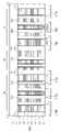
도 12a는 본 발명의 개념에 의한 또 다른 실시예에 따른 반도체 메모리 소자를 도시한 평면도이다.12A is a plan view illustrating a semiconductor memory device according to another embodiment according to the concept of the present invention.
도 12a를 참조하면, 반도체 메모리 소자(3a)는 도 2a의 반도체 메모리 소자(1a)에 비해 적어도 제1 방향(D1)으로 더 확장된 셀 구조를 가질 수 있다. 일례로, 좌측 셀 영역(LC) 및 우측 셀 영역(RC) 각각은 3개의 선택라인 컷 영역(133)에 의해 분리되는 제1 내지 제4 스트링 선택라인(SSL1-SSL4)을 포함할 수 있다. 반도체 메모리 소자(3a)는 비트라인들(BL1-BL4)과 전기적으로 연결되는 16개의 수직 채널들(150)과 3개의 더미 채널(150d)로 이루어진 19개 채널을 갖는 셀 어레이(190)가 반복되는 셀 구조를 가질 수 있다.Referring to FIG. 12A , the
우측 셀 영역(RC)에서의 채널들(150,150d)의 배열은 좌측 셀 영역(LC)에서의 채널들(150,150d)의 배열에 대해 더미 셀 영역(DC)을 중심으로 미러 이미지(mirror image)를 가질 수 있다. 마찬가지로, 우측 셀 영역(RC)의 수직 채널들(150) 상에 제공된 하부 콘택들(152)의 배열은 좌측 셀 영역(LC)의 수직 채널들(150) 상에 제공된 하부 콘택들(152)의 배열에 대해 더미 셀 영역(DC)을 중심으로 미러 이미지를 가질 수 있다.The arrangement of the
우측 셀 영역(RC)에서의 상부 콘택들(154)의 배열은 좌측 셀 영역(LC)에서의 상부 콘택들(154)의 배열에 대해 비트라인 피치에 상당하는 거리만큼 제2 방향(D2)을 따라 쉬프트되어 있을 수 있다.The arrangement of the
예컨대, 좌측 셀 영역(LC)의 양측에 배치된 워드라인 컷 영역들(131) 그리고 좌측 셀 영역(LC)의 중심에 배치된 선택라인 컷 영역(133) 상의 상부 콘택들(154)은 제1 비트라인(BL1)과 제3 비트라인(BL3)의 아래에 제공될 수 있다. 워드라인 컷 영역들(131)에 인접한 좌측 및 우측 선택라인 컷 영역들(133) 상의 상부 콘택들(154)은 제2 비트라인(BL2)과 제4 비트라인(BL4)의 아래에 제공될 수 있다.For example, the
이와 다르게, 우측 셀 영역(RC)의 양측에 배치된 워드라인 컷 영역들(131) 그리고 우측 셀 영역(RC)의 중심에 배치된 선택라인 컷 영역(133) 상의 상부 콘택들(154)은 제2 비트라인(BL2)과 제4 비트라인(BL4)의 아래에 제공될 수 있다. 워드라인 컷 영역들(131)에 인접한 좌측 및 우측 선택라인 컷 영역들(133) 상의 상부 콘택들(154)은 제1 비트라인(BL1)과 제3 비트라인(BL3)의 아래에 제공될 수 있다.Unlike this, the
좌측 셀 영역(LC)의 보조배선들(SBL1-SBL4)의 평면 형상들은 우측 셀 영역(RC)의 보조배선들(SBL1-SBL4)의 평면 형상들에 대해 제1 방향(D1)의 축을 중심으로 미러 이미지를 가질 수 있다.The planar shapes of the auxiliary lines SBL1 - SBL4 of the left cell area LC are centered on the axis in the first direction D1 with respect to the planar shapes of the auxiliary lines SBL1 - SBL4 of the right cell area RC. You can have a mirror image.
비트라인들(BL1-BL4) 각각은 서로 다른 길이를 갖는 보조배선들(SBL1-SBL4)과 전기적으로 연결될 수 있다. 일례로, 제1 비트라인(BL1)은 좌측 셀 영역(LC)에선 제2 보조배선(SBL2) 및 제1 보조배선(SBL1)과 연결되고 우측 셀 영역(RC)에선 제3 보조배선(SBL3)과 연결될 수 있다. 제2 비트라인(BL2)은 좌측 셀 영역(LC)에선 제3 보조배선(SBL3)과 연결되고 우측 셀 영역(RC)에선 제2 보조배선(SBL2) 및 제1 보조배선(SBL1)과 연결될 수 있다. 제3 비트라인(BL3)은 좌측 셀 영역(LC)에선 제4 보조배선(SBL4) 및 제3 보조배선(SBL3)과 연결되고 우측 셀 영역(RC)에선 제1 보조배선(SBL1)과 연결될 수 있다. 제4 비트라인(BL4)은 좌측 셀 영역(LC)에선 제1 보조배선(SBL1)과 연결되고 우측 셀 영역(RC)에선 제4 보조배선(SBL4) 및 제3 보조배선(SBL3)과 연결될 수 있다.Each of the bit lines BL1 - BL4 may be electrically connected to auxiliary lines SBL1 - SBL4 having different lengths. For example, the first bit line BL1 is connected to the second auxiliary line SBL2 and the first auxiliary line SBL1 in the left cell area LC and the third auxiliary line SBL3 in the right cell area RC. can be connected with The second bit line BL2 may be connected to the third auxiliary line SBL3 in the left cell area LC and may be connected to the second auxiliary line SBL2 and the first auxiliary line SBL1 in the right cell area RC. there is. The third bit line BL3 may be connected to the fourth auxiliary line SBL4 and the third auxiliary line SBL3 in the left cell area LC and may be connected to the first auxiliary line SBL1 in the right cell area RC. there is. The fourth bit line BL4 may be connected to the first auxiliary line SBL1 in the left cell area LC and may be connected to the fourth auxiliary line SBL4 and the third auxiliary line SBL3 in the right cell area RC. there is.
제1 비트라인(BL1)과 제2 비트라인(BL2)은 동일한 연결 모습을 가질 수 있고, 제3 비트라인(BL3)은 제4 비트라인(BL4)과 동일한 연결 모습을 가질 수 있다. 아울러, 제1 비트라인(BL1)에 연결된 제1 내지 제3 보조배선들(SBL1-SLB3)의 길이의 합(예: 5+6=11)은 제4 비트라인(BL4)에 연결된 제1, 제3 및 제4 보조배선들(SBL1,SLB3,SLB4)의 길이의 합(예: 2+11=13)과 거의 동일하거나 유사할 수 있다. 제2 비트라인(BL2)에 연결되는 제1 내지 제3 보조배선들(SBL1-SLB3)의 길이의 합(예: 5+6=11)은 제2 비트라인(BL2)에 인접한 제3 비트라인(BL3)에 연결되는 제1, 제3 및 제4 보조배선들(SBL1,SLB3,SLB4)의 길이의 합(예: 2+11=13)과 거의 동일하거나 유사할 수 있다. 이처럼, 비트라인들(BL1-BL4)은 실질적으로 동일한 연결 모습을 가질 수 있고, 보조배선들(SBL1-SBL4)의 길이차가 거의 없으므로 동일한 전기적 특성을 가질 수 있다.The first bit line BL1 and the second bit line BL2 may have the same connection shape, and the third bit line BL3 may have the same connection shape as the fourth bit line BL4 . In addition, the sum (eg, 5+6=11) of the lengths of the first to third auxiliary wires SBL1-SLB3 connected to the first bit line BL1 is the first, It may be substantially equal to or similar to the sum (eg, 2+11=13) of the lengths of the third and fourth auxiliary wires SBL1 , SLB3 , and SLB4 . The sum (eg, 5+6=11) of the lengths of the first to third auxiliary lines SBL1 -SLB3 connected to the second bit line BL2 is a third bit line adjacent to the second bit line BL2 . The sum of lengths (eg, 2+11=13) of the first, third, and fourth auxiliary wires SBL1 , SLB3 and SLB4 connected to BL3 may be substantially equal to or similar to that of the first, third, and fourth auxiliary wires SBL1 , SLB3 , and SLB4 . As such, the bit lines BL1 - BL4 may have substantially the same connection shape, and since there is little difference in length between the auxiliary wirings SBL1 - SBL4 , they may have the same electrical characteristics.
<제3 실시예의 변형><Modification of the third embodiment>
도 12b는 도 12a의 변형예를 도시한 평면도이다.12B is a plan view illustrating a modified example of FIG. 12A.
도 12b를 참조하면, 반도체 메모리 소자(3b)는 도 12a의 반도체 메모리 소자(3a)와 동일하게 16개의 수직 채널들(150)과 3개의 더미 채널(150d)로 이루어진 19개 채널을 갖는 셀 어레이(190)가 반복되는 셀 구조를 가질 수 있다.Referring to FIG. 12B , the
우측 셀 영역(RC)에서의 채널들(150,150d)의 배열은 좌측 셀 영역(LC)에서의 채널들(150,150d)의 배열과 동일할 수 있다. 마찬가지로, 우측 셀 영역(RC)의 수직 채널들(150) 상에 제공된 하부 콘택들(152)의 배열은 좌측 셀 영역(LC)의 수직 채널들(150) 상에 제공된 하부 콘택들(152)의 배열과 동일할 수 있다. 상부 콘택들(154) 역시 이와 마찬가지일 수 있다.The arrangement of the
비트라인들(BL1-BL4) 각각은 서로 다른 길이를 갖는 보조배선들(SBL1-SBL4)과 전기적으로 연결될 수 있다. 일례로, 제1 비트라인(BL1)은 좌측 셀 영역(LC)에선 제2 보조배선(SBL2) 및 제1 보조배선(SBL1)과 연결되고 우측 셀 영역(RC)에선 제3 보조배선(SBL3) 및 제4 보조배선(SBL4)과 연결될 수 있다. 제2 비트라인(BL2)은 좌측 셀 영역(LC)에선 제3 보조배선(SBL3)과 연결되고 우측 셀 영역(RC)에선 제1 보조배선(SBL1)과 연결될 수 있다. 제3 비트라인(BL3)은 좌측 셀 영역(LC)에선 제4 보조배선(SBL4) 및 제3 보조배선(SBL3)과 연결되고 우측 셀 영역(RC)에선 제2 보조배선(SBL2) 및 제1 보조배선(SBL1)과 연결될 수 있다. 제4 비트라인(BL4)은 좌측 셀 영역(LC)에선 제1 보조배선(SBL1)과 연결되고 우측 셀 영역(RC)에선 제3 보조배선(SBL3)과 연결될 수 있다.Each of the bit lines BL1 - BL4 may be electrically connected to auxiliary lines SBL1 - SBL4 having different lengths. For example, the first bit line BL1 is connected to the second auxiliary line SBL2 and the first auxiliary line SBL1 in the left cell area LC and the third auxiliary line SBL3 in the right cell area RC. and a fourth auxiliary line SBL4. The second bit line BL2 may be connected to the third auxiliary line SBL3 in the left cell area LC and may be connected to the first auxiliary line SBL1 in the right cell area RC. The third bit line BL3 is connected to the fourth auxiliary line SBL4 and the third auxiliary line SBL3 in the left cell area LC, and the second auxiliary line SBL2 and the first auxiliary line SBL3 in the right cell area RC. It may be connected to the auxiliary line SBL1. The fourth bit line BL4 may be connected to the first auxiliary line SBL1 in the left cell area LC and may be connected to the third auxiliary line SBL3 in the right cell area RC.
제1 비트라인(BL1)은 제3 비트라인(BL3)과 동일한 연결 모습을 가질 수 있고, 제2 비트라인(BL2)은 제4 비트라인(BL4)과 동일한 연결 모습을 가질 수 있다. 아울러, 제1 비트라인(BL1)에 연결된 제1 내지 제4 보조배선들(SBB1-SBL4)의 길이의 합(예: 5+11=16)은 제1 비트라인(BL1)에 인접한 제4 비트라인(BL4)에 연결되는 제1 및 제3 보조배선들(SBL1,SLB3)의 길이의 합(예: 2+6=8)과 상이할 수 있다. 제2 비트라인(BL2)에 연결된 제1 및 제3 보조배선들(SBL1,SBL3)의 길이의 합(예: 6+2=8)은 제2 비트라인(BL2)에 인접한 제3 비트라인(BL3)에 연결된 제1 내지 제4 보조배선들(SBL1-SBL4)이 길이의 합(예: 11+6=15)과 상이할 수 있다. 그렇지만, 도 10a 내지 10c를 참조하여 전술한 것처럼, 동일한 길이를 갖는 보조배선들과 연결되는 비트라인들에 비해 본 실시예의 비트라인들(BL1-BL4)이 상대적으로 우수한 전기적 특성을 가질 수 있다.The first bit line BL1 may have the same connection shape as the third bit line BL3 , and the second bit line BL2 may have the same connection shape as the fourth bit line BL4 . In addition, the sum (eg, 5+11=16) of the lengths of the first to fourth auxiliary wires SBB1-SBL4 connected to the first bit line BL1 is a fourth bit adjacent to the first bit line BL1. It may be different from the sum (eg, 2+6=8) of the lengths of the first and third auxiliary wires SBL1 and SLB3 connected to the line BL4 . The sum (eg, 6+2=8) of the lengths of the first and third auxiliary lines SBL1 and SBL3 connected to the second bit line BL2 is the third bit line (eg, 6+2=8) adjacent to the second bit line BL2. The first to fourth auxiliary wires SBL1 to SBL4 connected to BL3 may be different from a sum of lengths (eg, 11+6=15). However, as described above with reference to FIGS. 10A to 10C , the bit lines BL1 - BL4 of the present embodiment may have relatively superior electrical characteristics compared to the bit lines connected to the auxiliary lines having the same length.
<제4 실시예><Fourth embodiment>
도 13a는 본 발명의 개념에 의한 또 다른 실시예에 따른 반도체 메모리 소자를 도시한 평면도이다.13A is a plan view illustrating a semiconductor memory device according to another embodiment according to the concept of the present invention.
도 13a를 참조하면, 반도체 메모리 소자(4a)는 도 2a의 반도체 메모리 소자(1a)에 비해 적어도 제1 방향(D1)으로 더 확장된 셀 구조를 가질 수 있다. 일례로, 좌측 셀 영역(LC) 및 우측 셀 영역(RC) 각각은 4개의 선택라인 컷 영역(133)에 의해 분리되는 제1 내지 제5 스트링 선택라인(SSL1-SSL5)을 포함할 수 있다. 반도체 메모리 소자(4a)는 비트라인들(BL1-BL4)과 전기적으로 연결되는 20개의 수직 채널들(150)과 4개의 더미 채널(150d)로 이루어진 24개 채널을 갖는 셀 어레이(190)가 반복되는 셀 구조를 가질 수 있다.Referring to FIG. 13A , the
우측 셀 영역(RC)에서의 채널들(150,150d)의 배열은 좌측 셀 영역(LC)에서의 채널들(150,150d)의 배열에 대해 더미 셀 영역(DC)을 중심으로 미러 이미지(mirror image)를 가질 수 있다. 마찬가지로, 우측 셀 영역(RC)의 수직 채널들(150) 상에 제공된 하부 콘택들(152)의 배열은 좌측 셀 영역(LC)의 수직 채널들(150) 상에 제공된 하부 콘택들(152)의 배열에 대해 더미 셀 영역(DC)을 중심으로 미러 이미지를 가질 수 있다.The arrangement of the
우측 셀 영역(RC)에서의 상부 콘택들(154)의 배열은 좌측 셀 영역(LC)에서의 상부 콘택들(154)의 배열과 동일할 수 있다. 예컨대, 상부 콘택들(154)은 도 11a의 반도체 메모리 소자(2a)에서의 상부 콘택들(154)의 배열 양태와 동일할 수 있다.The arrangement of the
좌측 셀 영역(LC)의 보조배선들(SBL1-SBL4)의 평면 형상들은 우측 셀 영역(RC)의 보조배선들(SBL1-SBL4)의 평면 형상들과 동일할 수 있다.The planar shapes of the auxiliary lines SBL1 -SBL4 of the left cell area LC may be the same as the planar shapes of the auxiliary lines SBL1 -SBL4 of the right cell area RC.
비트라인들(BL1-BL4) 각각은 서로 다른 길이를 갖는 보조배선들(SBL1-SBL4)과 전기적으로 연결될 수 있다. 일례로, 제1 비트라인(BL1) 및 제4 비트라인(BL4) 각각은 좌측 셀 영역(LC)에선 제1 보조배선(SBL1) 및 제2 보조배선(SBL2)과 연결되고 우측 셀 영역(RC)에선 제3 보조배선(SBL3) 및 제4 보조배선(SBL4)과 연결될 수 있다. 제2 비트라인(BL2) 및 제3 비트라인(BL3)은 좌측 셀 영역(LC)에선 제3 보조배선(SBL3) 및 제4 보조배선(SBL4)과 연결되고 우측 셀 영역(RC)에선 제1 보조배선(SBL1) 및 제2 보조배선(SBL2)과 연결될 수 있다. 이처럼 비트라인들(BL1-BL4)은 보조배선들(SBL1-SLB4)과의 연결 모습이 동일하므로 동일한 전기적 특성(예: 로딩 커패시턴스, 저항)을 가질 수 있다.Each of the bit lines BL1 - BL4 may be electrically connected to auxiliary lines SBL1 - SBL4 having different lengths. For example, each of the first bit line BL1 and the fourth bit line BL4 is connected to the first auxiliary line SBL1 and the second auxiliary line SBL2 in the left cell area LC and the right cell area RC ) may be connected to the third auxiliary line SBL3 and the fourth auxiliary line SBL4 . The second bit line BL2 and the third bit line BL3 are connected to the third auxiliary line SBL3 and the fourth auxiliary line SBL4 in the left cell area LC, and the first bit line BL2 and the third bit line BL3 in the right cell area RC. It may be connected to the auxiliary line SBL1 and the second auxiliary line SBL2 . As such, since the bit lines BL1 - BL4 have the same connection shape with the auxiliary lines SBL1 - SLB4 , they may have the same electrical characteristics (eg, loading capacitance and resistance).
<제4 실시예의 변형><Modification of the fourth embodiment>
도 13b는 도 13a의 변형예를 도시한 평면도이다.13B is a plan view illustrating a modified example of FIG. 13A.
도 13b를 참조하면, 반도체 메모리 소자(4b)는 도 13a의 반도체 메모리 소자(4a)와 동일하게 24개 채널을 갖는 셀 어레이(190)가 반복되는 셀 구조를 가질 수 있다.Referring to FIG. 13B , the
우측 셀 영역(RC)에서의 채널들(150,150d)의 배열은 좌측 셀 영역(LC)에서의 채널들(150,150d)의 배열과 동일할 수 있다. 마찬가지로, 우측 셀 영역(RC)의 수직 채널들(150) 상에 제공된 하부 콘택들(152)의 배열은 좌측 셀 영역(LC)의 수직 채널들(150) 상에 제공된 하부 콘택들(152)의 배열과 동일할 수 있다. 우측 셀 영역(RC)에서의 상부 콘택들(154)의 배열은 좌측 셀 영역(RC)의 상부 콘택들(154)에 대해 더미 셀 영역(DC)을 중심으로 미러 이미지를 가질 수 있다.The arrangement of the
좌측 셀 영역(LC)의 보조배선들(SBL1-SBL4)의 평면 형상들은 우측 셀 영역(RC)의 보조배선들(SBL1-SBL4)의 평면 형상들에 대해 제1 방향(D1)의 축을 중심으로 미러 이미지를 가질 수 있다.The planar shapes of the auxiliary lines SBL1 - SBL4 of the left cell area LC are centered on the axis in the first direction D1 with respect to the planar shapes of the auxiliary lines SBL1 - SBL4 of the right cell area RC. You can have a mirror image.
비트라인들(BL1-BL4) 각각은 서로 다른 길이를 갖는 보조배선들(SBL1-SBL4)과 전기적으로 연결될 수 있다. 일례로, 제1 비트라인(BL1) 및 제4 비트라인(BL4) 각각은 좌측 셀 영역(LC)에선 제1 보조배선(SBL1) 및 제2 보조배선(SBL2)과 연결되고 우측 셀 영역(RC)에선 제3 보조배선(SBL3) 및 제4 보조배선(SBL4)과 연결될 수 있다. 제2 비트라인(BL2) 및 제3 비트라인(BL3)은 좌측 셀 영역(LC)에선 제3 보조배선(SBL3) 및 제4 보조배선(SBL4)과 연결되고 우측 셀 영역(RC)에선 제1 보조배선(SBL1) 및 제2 보조배선(SBL2)과 연결될 수 있다. 비트라인들(BL1-BL4)은 보조배선들(SBL1-SLB4)과의 연결 모습이 동일하므로 동일한 전기적 특성(예: 로딩 커패시턴스, 저항)을 가질 수 있다.Each of the bit lines BL1 - BL4 may be electrically connected to auxiliary lines SBL1 - SBL4 having different lengths. For example, each of the first bit line BL1 and the fourth bit line BL4 is connected to the first auxiliary line SBL1 and the second auxiliary line SBL2 in the left cell area LC and the right cell area RC ) may be connected to the third auxiliary line SBL3 and the fourth auxiliary line SBL4 . The second bit line BL2 and the third bit line BL3 are connected to the third auxiliary line SBL3 and the fourth auxiliary line SBL4 in the left cell area LC, and the first bit line BL2 and the third bit line BL3 in the right cell area RC. It may be connected to the auxiliary line SBL1 and the second auxiliary line SBL2 . Since the bit lines BL1 - BL4 have the same connection shape with the auxiliary lines SBL1 - SLB4 , they may have the same electrical characteristics (eg, loading capacitance and resistance).
<응용예><Application example>
도 14a는 본 발명의 실시예에 따른 반도체 메모리 소자를 구비한 메모리 카드를 도시한 블록도이다. 도 14b는 본 발명의 실시예에 따른 반도체 메모리 소자를 응용한 정보 처리 시스템을 도시한 블록도이다.14A is a block diagram illustrating a memory card including a semiconductor memory device according to an embodiment of the present invention. 14B is a block diagram illustrating an information processing system to which a semiconductor memory device according to an embodiment of the present invention is applied.
도 14a를 참조하면, 상술한 본 발명의 실시예에 따른 반도체 메모리 소자들 중 적어도 하나 포함하는 메모리(1210)는 메모리 카드(1200)에 응용될 수 있다. 일례로, 메모리 카드(1200)는 호스트(1230)와 메모리(1210) 간의 제반 데이터 교환을 제어하는 메모리 컨트롤러(1220)를 포함할 수 있다. 에스램(1221)은 중앙처리장치(1222)의 동작 메모리로서 사용될 수 있다. 호스트 인터페이스(1223)는 메모리 카드(1200)와 접속되는 호스트(1230)의 데이터 교환 프로토콜을 구비할 수 있다. 오류 수정 코드(1224)는 메모리(1210)로부터 독출된 데이터에 포함되는 오류를 검출 및 정정할 수 있다. 메모리 인터페이스(1225)는 메모리(1210)와 인터페이싱할 수 있다. 중앙처리장치(1222)는 메모리 컨트롤러(1220)의 데이터 교환을 위한 제반 제어 동작을 수행할 수 있다.Referring to FIG. 14A , the
도 14b를 참조하면, 정보 처리 시스템(1300)은 본 발명의 실시예에 따른 반도체 메모리 소자를 적어도 하나 구비한 메모리 시스템(1310)을 포함할 수 있다. 정보 처리 시스템(1300)은 모바일 기기나 컴퓨터 등을 포함할 수 있다. 일례로, 정보 처리 시스템(1300)은 메모리 시스템(1310)과 각각 시스템 버스(1360)에 전기적으로 연결된 모뎀(1320), 중앙처리장치(1330), 램(1340), 유저인터페이스(1350)를 포함할 수 있다. 메모리 시스템(1310)은 메모리(1311)와 메모리 컨트롤러(1312)를 포함하며, 도 14a의 메모리 카드(1200)와 실질적으로 동일하게 구성될 수 있다.Referring to FIG. 14B , the
이러한 메모리 시스템(1310)에는 중앙처리장치(1330)에 의해서 처리된 데이터 또는 외부에서 입력된 데이터가 저장될 수 있다. 정보 처리 시스템(1300)은 메모리 카드, 반도체 디스크 장치(Solid State Disk), 카메라 이미지 프로세서(Camera Image Sensor) 및 그 밖의 응용 칩셋(Application Chipset)으로 제공될 수 있다. 일례로, 메모리 시스템(1310)은 반도체 디스크 장치(SSD)로 구성될 수 있으며, 이 경우 정보 처리 시스템(1300)은 대용량의 데이터를 메모리 시스템(1310)에 안정적으로 그리고 신뢰성있게 저장할 수 있다.Data processed by the
이상의 발명의 상세한 설명은 개시된 실시 상태로 본 발명을 제한하려는 의도가 아니며, 본 발명의 요지를 벗어나지 않는 범위 내에서 다양한 다른 조합, 변경 및 환경에서 사용할 수 있다. 첨부된 청구범위는 다른 실시 상태도 포함하는 것으로 해석되어야 할 것이다.The detailed description of the present invention is not intended to limit the present invention to the disclosed embodiments, and may be used in various other combinations, changes, and environments without departing from the spirit of the present invention. The appended claims should be construed to include other embodiments as well.
Claims (20)
Translated fromKorean상기 스택 내의 수직 채널;
상기 수직 채널로부터 이격된 더미 셀 영역;
상기 스택과 중첩되는 제1, 제2, 제3 및 제4 보조배선들, 상기 제1 보조배선은 상기 수직 채널과 전기적으로 연결되고;
상기 제2 및 제3 보조배선들과 중첩되면서 이들과 전기적으로 연결되는 제1 비트라인; 및
상기 제1 및 제4 보조배선들과 중첩되면서 이들과 전기적으로 연결되는 제3 비트라인을 포함하되,
상기 제2 보조배선은 제1 길이를 갖고, 상기 제3 보조배선은 제2 길이를 가지며, 상기 제1 길이는 상기 제2 길이보다 길거나 짧고,
상기 제1 보조배선은 제3 길이를 갖고, 상기 제4 보조배선은 제4 길이를 가지며, 상기 제3 길이는 상기 제4 길이보다 길거나 짧고,
상기 제1 및 제3 비트라인들과 상기 제1 내지 제4 보조배선들은 제1 및 제2 셀 영역들 내에 배치되며,
상기 더미 셀 영역은 상기 제1 및 제2 셀 영역들 사이에 개재되고,
상기 제1 길이와 상기 제2 길이의 합은, 상기 제3 길이와 상기 제4 길이의 합과 동일한 반도체 메모리 소자.
a stack comprising alternately stacked gates and insulating layers;
vertical channels in the stack;
a dummy cell region spaced apart from the vertical channel;
first, second, third and fourth auxiliary wirings overlapping the stack, the first auxiliary wiring being electrically connected to the vertical channel;
a first bit line overlapping and electrically connected to the second and third auxiliary lines; and
a third bit line overlapping and electrically connected to the first and fourth auxiliary lines;
the second auxiliary wiring has a first length, the third auxiliary wiring has a second length, the first length being longer or shorter than the second length;
the first auxiliary line has a third length, the fourth auxiliary line has a fourth length, and the third length is longer or shorter than the fourth length;
the first and third bit lines and the first to fourth auxiliary lines are disposed in first and second cell regions;
the dummy cell region is interposed between the first and second cell regions;
A sum of the first length and the second length is equal to a sum of the third length and the fourth length.
상기 제2 및 제3 보조배선들과 중첩되면서 이들과 전기적으로 연결되는 제2 비트라인; 및
상기 제1 및 제4 보조배선들과 중첩되면서 이들과 전기적으로 연결되는 제4 비트라인을 더 포함하는 반도체 메모리 소자.
The method of claim 1,
a second bit line overlapping and electrically connected to the second and third auxiliary lines; and
and a fourth bit line overlapping the first and fourth auxiliary lines and electrically connected thereto.
상기 스택 내의 제1, 제2, 제3 및 제4 워드라인 컷 영역들을 더 포함하되,
상기 제1 셀 영역은 상기 제1 및 제2 워드라인 컷 영역들 사이에 위치하는 복수개의 제1 셀 스트링들을 포함하고,
상기 제2 셀 영역은 상기 제3 및 제4 워드라인 컷 영역들 사이에 위치하는 복수개의 제2 셀 스트링들을 포함하며,
상기 제2 및 제3 워드라인 컷 영역들은 상기 제1 셀 영역을 상기 제2 셀 영역으로부터 이격시키고,
상기 더미 셀 영역은, 상기 제2 및 제3 워드라인 컷 영역들 사이에 개재되어 상기 상기 제1 셀 영역을 상기 제2 셀 영역으로부터 이격시키는 반도체 메모리 소자.
According to claim 1,
first, second, third and fourth wordline cut regions in the stack;
the first cell region includes a plurality of first cell strings positioned between the first and second word line cut regions;
the second cell region includes a plurality of second cell strings positioned between the third and fourth word line cut regions;
the second and third word line cut regions space the first cell region from the second cell region;
The dummy cell region is interposed between the second and third word line cut regions to space the first cell region from the second cell region.
상기 제1 셀 영역에 중첩되는 상기 제1, 제2, 제3 및 제4 보조배선들은, 상기 제2 셀 영역에 중첩되는 상기 제1, 제2, 제3 및 제4 보조배선들과 대칭을 이루는 반도체 메모리 소자.
The method of claim 1,
The first, second, third, and fourth auxiliary wirings overlapping the first cell region are symmetrical with the first, second, third and fourth auxiliary wirings overlapping the second cell region semiconductor memory device.
상기 제1 셀 영역에 중첩되는 상기 제1, 제2, 제3 및 제4 보조배선들의 이미지는, 제2 셀 영역에 중첩되는 상기 제1, 제2, 제3 및 제4 보조배선들의 미러 이미지인 반도체 메모리 소자.
According to claim 1,
The images of the first, second, third, and fourth auxiliary wirings overlapping the first cell region are mirror images of the first, second, third and fourth auxiliary wirings overlapping the second cell region A semiconductor memory device.
각각의 제1 및 제2 셀 영역들 내에서, 상기 게이트들 중 최상부의 게이트는 제1 및 제2 스트링 선택라인들로 분리되는 반도체 메모리 소자.
According to claim 1,
In each of the first and second cell regions, an uppermost one of the gates is separated by first and second string selection lines.
각각의 제1 및 제2 셀 영역들 내에서, 상기 게이트들 중 최상부의 게이트는 세 개 이상의 스트링 선택라인들로 분리되는 반도체 메모리 소자.
8. The method of claim 7,
In each of the first and second cell regions, a topmost gate of the gates is divided into three or more string selection lines.
상기 제2 길이는 상기 제1 길이보다 긴 반도체 메모리 소자.
According to claim 1,
The second length is longer than the first length of the semiconductor memory device.
상기 스택 내의 복수개의 수직 채널들;
상기 복수개의 수직 채널들로부터 이격된 더미 셀 영역;
서로 다른 길이를 갖는 복수개의 제1 보조배선들 및 서로 다른 길이를 갖는 복수개의 제2 보조배선들, 상기 제1 및 제2 보조배선들은 각각 그에 대응하는 상기 수직 채널과 전기적으로 연결되고; 및
상기 복수개의 제1 보조배선들과 전기적으로 연결되는 제1 비트라인 및 상기 복수개의 제2 보조배선들과 전기적으로 연결되는 제2 비트라인을 포함하되,
상기 제1 및 제2 비트라인들과 상기 제1 및 제2 보조배선들은 제1 및 제2 셀 영역들 내에 배치되며,
상기 더미 셀 영역은 상기 제1 및 제2 셀 영역들 사이에 개재되고,
상기 복수개의 제1 보조배선들의 길이의 총 합은, 상기 복수개의 제2 보조배선들의 길이의 총 합과 동일한 반도체 메모리 소자.
a stack comprising alternately stacked gates and insulating layers;
a plurality of vertical channels in the stack;
a dummy cell region spaced apart from the plurality of vertical channels;
a plurality of first auxiliary lines having different lengths and a plurality of second auxiliary lines having different lengths, the first and second auxiliary lines being electrically connected to the corresponding vertical channels, respectively; and
a first bit line electrically connected to the plurality of first auxiliary lines and a second bit line electrically connected to the plurality of second auxiliary lines;
the first and second bit lines and the first and second auxiliary lines are disposed in first and second cell regions;
the dummy cell region is interposed between the first and second cell regions;
A total sum of lengths of the plurality of first auxiliary lines is the same as a total sum of lengths of the plurality of second auxiliary lines.
상기 복수개의 제1 보조배선들은, 제1 길이를 갖는 제1 보조배선, 및 상기 제1 길이보다 긴 제2 길이를 갖는 제2 보조배선을 포함하는 반도체 메모리 소자.
11. The method of claim 10,
The plurality of first auxiliary lines includes a first auxiliary line having a first length and a second auxiliary line having a second length greater than the first length.
상기 복수개의 수직 채널들은 지그재그 형태로 배열되는 반도체 메모리 소자.
11. The method of claim 10,
The plurality of vertical channels are arranged in a zigzag shape.
상기 스택 내의 제1, 제2, 제3, 및 제4 워드라인 컷 영역들, 상기 제1 및 제2 워드라인 컷 영역들은 그들 사이의 제1 셀 영역을 정의하고, 상기 제3 및 제4 워드라인 컷 영역들은 그들 사이의 제2 셀 영역을 정의하며, 상기 제2 및 제3 워드라인 컷 영역들은 상기 제1 셀 영역을 상기 제2 셀 영역으로부터 이격시키고;
상기 제2 및 제3 워드라인 컷 영역들 사이에 개재되어 상기 제1 셀 영역을 상기 제2 셀 영역으로부터 이격시키는 더미 셀 영역;
상기 제1 셀 영역으로부터 상기 제2 셀 영역으로 연장되는 복수개의 비트라인들; 및
상기 복수개의 비트라인들을 상기 제1 및 제2 셀 영역들과 전기적으로 연결하는 복수개의 보조배선들을 포함하되,
상기 복수개의 보조배선들은 서로 다른 길이를 갖고,
상기 복수개의 비트라인들은, 서로 다른 상기 복수개의 보조배선들과 각각 연결되며,
상기 제1 셀 영역은, 상기 스택 내의 수직 채널을 포함하고,
상기 복수개의 보조배선들은 상기 스택과 중첩되는 제1, 제2, 제3 및 제4 보조배선들을 포함하며, 상기 제1 보조배선은 상기 수직 채널과 전기적으로 연결되고,
상기 복수개의 비트라인들은 제1 비트라인 및 제2 비트라인을 포함하며,
상기 제1 비트라인은 상기 제1 및 제2 보조배선들과 중첩되어 이들과 전기적으로 연결되고,
상기 제2 비트라인은 상기 제3 및 제4 보조배선들과 중첩되어 이들과 전기적으로 연결되며,
상기 제1 및 제2 보조배선들의 길이의 합은, 상기 제3 및 제4 보조배선들의 길이의 합과 동일한 반도체 메모리 소자.
a stack comprising alternately stacked gates and insulating layers;
first, second, third, and fourth wordline cut regions in the stack, the first and second wordline cut regions define a first cell region therebetween, and the third and fourth word line cut regions define a second cell region therebetween, the second and third wordline cut regions space the first cell region from the second cell region;
a dummy cell region interposed between the second and third word line cut regions to space the first cell region from the second cell region;
a plurality of bit lines extending from the first cell region to the second cell region; and
a plurality of auxiliary wirings electrically connecting the plurality of bit lines to the first and second cell regions;
The plurality of auxiliary wires have different lengths,
The plurality of bit lines are respectively connected to the plurality of different auxiliary lines,
The first cell region comprises a vertical channel in the stack,
The plurality of auxiliary lines includes first, second, third, and fourth auxiliary lines overlapping the stack, the first auxiliary line being electrically connected to the vertical channel;
The plurality of bit lines includes a first bit line and a second bit line,
the first bit line overlaps the first and second auxiliary lines and is electrically connected to the first and second auxiliary lines;
the second bit line overlaps the third and fourth auxiliary lines and is electrically connected to the third and fourth auxiliary lines;
A semiconductor memory device in which a sum of lengths of the first and second auxiliary lines is equal to a sum of lengths of the third and fourth auxiliary lines.
상기 제1 보조배선의 제1 길이는 상기 제2 보조배선의 제2 길이보다 짧고,
상기 제3 보조배선의 제3 길이는 상기 제4 보조배선의 제4 길이보다 짧은 반도체 메모리 소자.
15. The method of claim 14,
A first length of the first auxiliary line is shorter than a second length of the second auxiliary line,
A third length of the third auxiliary line is shorter than a fourth length of the fourth auxiliary line.
상기 제2 길이는 상기 제1 길이보다 적어도 50% 더 긴 반도체 메모리 소자.
16. The method of claim 15,
wherein the second length is at least 50% greater than the first length.
상기 제1 셀 영역은 상기 제1 및 제2 워드라인 컷 영역들 사이에 위치하는 복수개의 제1 셀 스트링들을 포함하고,
상기 제2 셀 영역은 상기 제3 및 제4 워드라인 컷 영역들 사이에 위치하는 복수개의 제2 셀 스트링들을 포함하며,
상기 복수개의 제1 셀 스트링들은 지그재그 형태로 배열된 채널들을 포함하는 반도체 메모리 소자.
15. The method of claim 14,
the first cell region includes a plurality of first cell strings positioned between the first and second word line cut regions;
the second cell region includes a plurality of second cell strings positioned between the third and fourth word line cut regions;
The plurality of first cell strings may include channels arranged in a zigzag shape.
상기 제1 셀 영역은 상기 제1 및 제2 워드라인 컷 영역들 사이에 위치하는 복수개의 제1 셀 스트링들을 포함하고,
상기 제2 셀 영역은 상기 제3 및 제4 워드라인 컷 영역들 사이에 위치하는 복수개의 제2 셀 스트링들을 포함하며,
상기 복수개의 제1 셀 스트링들은, 적어도 네 개의 셀 스트링 행들을 포함하는 반도체 메모리 소자.
15. The method of claim 14,
the first cell region includes a plurality of first cell strings positioned between the first and second word line cut regions;
the second cell region includes a plurality of second cell strings positioned between the third and fourth word line cut regions;
The plurality of first cell strings may include at least four cell string rows.
상기 제1 셀 영역은 상기 제1 및 제2 워드라인 컷 영역들 사이의 제1 선택라인 컷 영역을 포함하고,
상기 제2 셀 영역은 상기 제3 및 제4 워드라인 컷 영역들 사이의 제2 선택라인 컷 영역을 포함하는 반도체 메모리 소자.
15. The method of claim 14,
the first cell region includes a first selection line cut region between the first and second word line cut regions;
The second cell region includes a second selection line cut region between the third and fourth word line cut regions.
상기 더미 셀 영역은, 상기 제2 및 제3 워드라인 컷 영역들 사이에 개재되어 상기 제1 셀 영역을 상기 제2 셀 영역으로부터 이격시키는 복수개의 더미 셀 영역들을 포함하는 반도체 메모리 소자.15. The method of claim 14,
The dummy cell region may include a plurality of dummy cell regions interposed between the second and third word line cut regions to space the first cell region from the second cell region.
Priority Applications (6)
| Application Number | Priority Date | Filing Date | Title |
|---|---|---|---|
| KR1020150070648AKR102393976B1 (en) | 2015-05-20 | 2015-05-20 | Semiconductor memory devices |
| US14/969,843US9773546B2 (en) | 2015-05-20 | 2015-12-15 | Semiconductor devices including auxiliary bit lines |
| CN201610341096.7ACN106169476B (en) | 2015-05-20 | 2016-05-20 | Semiconductor device including auxiliary bit line |
| JP2016101145AJP6829552B2 (en) | 2015-05-20 | 2016-05-20 | Semiconductor devices including auxiliary bit lines and their manufacturing methods |
| US15/681,910US10276237B2 (en) | 2015-05-20 | 2017-08-21 | Semiconductor devices including auxiliary bit lines |
| US16/368,916US10878901B2 (en) | 2015-05-20 | 2019-03-29 | Semiconductor devices including auxiliary bit lines |
Applications Claiming Priority (1)
| Application Number | Priority Date | Filing Date | Title |
|---|---|---|---|
| KR1020150070648AKR102393976B1 (en) | 2015-05-20 | 2015-05-20 | Semiconductor memory devices |
Publications (2)
| Publication Number | Publication Date |
|---|---|
| KR20160137750A KR20160137750A (en) | 2016-12-01 |
| KR102393976B1true KR102393976B1 (en) | 2022-05-04 |
Family
ID=57324536
Family Applications (1)
| Application Number | Title | Priority Date | Filing Date |
|---|---|---|---|
| KR1020150070648AActiveKR102393976B1 (en) | 2015-05-20 | 2015-05-20 | Semiconductor memory devices |
Country Status (4)
| Country | Link |
|---|---|
| US (3) | US9773546B2 (en) |
| JP (1) | JP6829552B2 (en) |
| KR (1) | KR102393976B1 (en) |
| CN (1) | CN106169476B (en) |
Families Citing this family (34)
| Publication number | Priority date | Publication date | Assignee | Title |
|---|---|---|---|---|
| KR102393976B1 (en)* | 2015-05-20 | 2022-05-04 | 삼성전자주식회사 | Semiconductor memory devices |
| KR102485088B1 (en)* | 2015-11-10 | 2023-01-05 | 삼성전자주식회사 | Vertical memory devices and methods of manufacturing the same |
| US10014316B2 (en)* | 2016-10-18 | 2018-07-03 | Sandisk Technologies Llc | Three-dimensional memory device with leakage reducing support pillar structures and method of making thereof |
| KR102353929B1 (en)* | 2017-03-07 | 2022-01-21 | 삼성전자주식회사 | Semiconductor device |
| CN106910746B (en)* | 2017-03-08 | 2018-06-19 | 长江存储科技有限责任公司 | A kind of 3D nand memories part and its manufacturing method, packaging method |
| KR20180106727A (en)* | 2017-03-21 | 2018-10-01 | 에스케이하이닉스 주식회사 | Semiconductor device and manufacturing method of the same |
| KR102344862B1 (en)* | 2017-05-17 | 2021-12-29 | 삼성전자주식회사 | Vertical semiconductor devices |
| US11114470B2 (en) | 2017-06-02 | 2021-09-07 | Semiconductor Energy Laboratory Co., Ltd. | Semiconductor device, electronic component, and electronic device |
| JP7195068B2 (en) | 2017-06-26 | 2022-12-23 | 株式会社半導体エネルギー研究所 | Semiconductor equipment, electronic equipment |
| KR102389928B1 (en) | 2017-06-27 | 2022-04-25 | 삼성전자주식회사 | Three-dimensional semiconductor memory devices |
| US11133336B2 (en) | 2017-06-27 | 2021-09-28 | Semiconductor Energy Laboratory Co., Ltd. | Semiconductor device and manufacturing method of semiconductor device |
| US11374012B2 (en) | 2017-07-06 | 2022-06-28 | Semiconductor Energy Laboratory Co., Ltd. | Semiconductor device and driving method of semiconductor device |
| US10665604B2 (en) | 2017-07-21 | 2020-05-26 | Semiconductor Energy Laboratory Co., Ltd. | Semiconductor device, semiconductor wafer, memory device, and electronic device |
| KR102307057B1 (en)* | 2017-07-27 | 2021-10-01 | 삼성전자주식회사 | Vertical-type memory device |
| KR102440227B1 (en)* | 2017-10-11 | 2022-09-05 | 삼성전자주식회사 | Vertical memory devices and methods of manufacturing vertical memory devices |
| KR102682342B1 (en)* | 2018-05-23 | 2024-07-09 | 에스케이하이닉스 주식회사 | Semiconductor device and manufacturing method thereof |
| JP2019212691A (en)* | 2018-05-31 | 2019-12-12 | 東芝メモリ株式会社 | Semiconductor memory |
| KR20210041078A (en)* | 2018-10-11 | 2021-04-14 | 양쯔 메모리 테크놀로지스 씨오., 엘티디. | Vertical memory device |
| KR102465965B1 (en) | 2018-11-13 | 2022-11-10 | 삼성전자주식회사 | Vertical memory device with improved electrical characteristics and method of operation thereof |
| US10964397B2 (en) | 2018-11-13 | 2021-03-30 | Samsung Electronics Co., Ltd. | Vertical memory device having improved electrical characteristics and method of operating the same |
| KR102460073B1 (en)* | 2018-12-11 | 2022-10-28 | 삼성전자주식회사 | Semiconductor device including channel hole |
| US11367681B2 (en)* | 2019-01-24 | 2022-06-21 | Micron Technology, Inc. | Slit oxide and via formation techniques |
| EP3891809B1 (en) | 2019-03-01 | 2025-06-25 | Yangtze Memory Technologies Co., Ltd. | Three-dimensional memory devices with architecture of increased number of bit lines |
| CN112689894B (en)* | 2019-03-06 | 2024-03-12 | 铠侠股份有限公司 | Non-volatile semiconductor memory device and manufacturing method thereof |
| JP2020150199A (en)* | 2019-03-15 | 2020-09-17 | キオクシア株式会社 | Semiconductor storage device |
| KR102775519B1 (en)* | 2019-03-26 | 2025-03-06 | 에스케이하이닉스 주식회사 | Semiconductor memory device and manufacturing method thereof |
| KR102633484B1 (en)* | 2019-07-10 | 2024-02-05 | 삼성전자주식회사 | Semiconductor devices including dummy patterns |
| JP2021136279A (en) | 2020-02-25 | 2021-09-13 | キオクシア株式会社 | Semiconductor storage device |
| KR102793911B1 (en)* | 2020-05-21 | 2025-04-08 | 삼성전자주식회사 | Vertical memory device |
| KR20220099212A (en)* | 2021-01-05 | 2022-07-13 | 삼성전자주식회사 | Semiconducotr device and data storage system including the same |
| KR102847561B1 (en)* | 2021-02-09 | 2025-08-19 | 삼성전자주식회사 | Semiconductor device and electronic system including the same |
| KR20230015623A (en) | 2021-07-23 | 2023-01-31 | 삼성전자주식회사 | Semiconductor device and data storage system including the same |
| KR20230091244A (en)* | 2021-12-15 | 2023-06-23 | 삼성전자주식회사 | Semiconductor devices |
| US12396151B2 (en) | 2022-11-01 | 2025-08-19 | Nanya Technology Corporation | Method of manufacturing semiconductor device |
Citations (2)
| Publication number | Priority date | Publication date | Assignee | Title |
|---|---|---|---|---|
| US20120120740A1 (en)* | 2010-11-16 | 2012-05-17 | Samsung Electronics, Co., Ltd. | Nonvolatile Memory Devices, Erasing Methods Thereof and Memory Systems Including the Same |
| JP2012174872A (en)* | 2011-02-21 | 2012-09-10 | Toshiba Corp | Semiconductor storage device |
Family Cites Families (31)
| Publication number | Priority date | Publication date | Assignee | Title |
|---|---|---|---|---|
| JPS469722Y1 (en) | 1967-03-11 | 1971-04-06 | ||
| JPS5118253A (en) | 1974-08-06 | 1976-02-13 | Osaka Tetsuen Kikai Kk | KOKANSEIKEIYO PURESUSOCHI |
| JPH08293588A (en)* | 1995-04-25 | 1996-11-05 | Sony Corp | Semiconductor memory device |
| US5966315A (en) | 1997-09-30 | 1999-10-12 | Siemens Aktiengesellschaft | Semiconductor memory having hierarchical bit line architecture with non-uniform local bit lines |
| US5917744A (en) | 1997-12-18 | 1999-06-29 | Siemens Aktiengesellschaft | Semiconductor memory having hierarchical bit line architecture with interleaved master bitlines |
| AU2000224587A1 (en) | 2000-02-04 | 2001-08-14 | Hitachi Ltd. | Semiconductor device |
| US6479851B1 (en) | 2000-05-16 | 2002-11-12 | Hynix Semiconductor, Inc. | Memory device with divided bit-line architecture |
| KR20030050959A (en) | 2001-12-20 | 2003-06-25 | 주식회사 하이닉스반도체 | Ferroelectric random access memory having uniform cell characteristics |
| CN101189716A (en)* | 2005-05-30 | 2008-05-28 | 斯班逊有限公司 | Semiconductor device and its making method |
| JP4892215B2 (en) | 2005-09-28 | 2012-03-07 | 富士通セミコンダクター株式会社 | Semiconductor memory device |
| JP4609722B2 (en) | 2005-12-09 | 2011-01-12 | セイコーエプソン株式会社 | Ferroelectric memory device and electronic device |
| US7551466B2 (en) | 2006-02-23 | 2009-06-23 | Micron Technology, Inc. | Bit line coupling |
| JP2008004889A (en) | 2006-06-26 | 2008-01-10 | Samsung Electronics Co Ltd | Semiconductor memory device |
| KR100875059B1 (en) | 2006-07-05 | 2008-12-19 | 주식회사 하이닉스반도체 | Bit line of semiconductor device and manufacturing method thereof |
| JP2008227171A (en) | 2007-03-13 | 2008-09-25 | Toshiba Corp | Nonvolatile semiconductor memory |
| KR101226685B1 (en) | 2007-11-08 | 2013-01-25 | 삼성전자주식회사 | Vertical type semiconductor device and Method of manufacturing the same |
| JP5305980B2 (en) | 2009-02-25 | 2013-10-02 | 株式会社東芝 | Nonvolatile semiconductor memory device and manufacturing method thereof |
| JP2011040706A (en)* | 2009-07-15 | 2011-02-24 | Toshiba Corp | Nonvolatile semiconductor memory device |
| KR20110015337A (en) | 2009-08-07 | 2011-02-15 | 주식회사 하이닉스반도체 | Vertical Channel Nonvolatile Memory Device Manufacturing Method |
| KR101624975B1 (en)* | 2009-11-17 | 2016-05-30 | 삼성전자주식회사 | Three dimensional semiconductor memory devices |
| JP2012038865A (en) | 2010-08-05 | 2012-02-23 | Toshiba Corp | Nonvolatile semiconductor memory device and method of manufacturing nonvolatile semiconductor memory device |
| JP5767495B2 (en) | 2011-03-29 | 2015-08-19 | パナソニック株式会社 | Variable inductor and semiconductor device using the same |
| JP5814867B2 (en)* | 2012-06-27 | 2015-11-17 | 株式会社東芝 | Semiconductor memory device |
| US9129861B2 (en)* | 2012-10-05 | 2015-09-08 | Samsung Electronics Co., Ltd. | Memory device |
| KR102031187B1 (en)* | 2012-10-05 | 2019-10-14 | 삼성전자주식회사 | Vertical type memory device |
| KR101997153B1 (en) | 2013-04-01 | 2019-07-05 | 삼성전자주식회사 | Semiconductor device having Balancing Capacitor and method of forming the same |
| US9183940B2 (en) | 2013-05-21 | 2015-11-10 | Aplus Flash Technology, Inc. | Low disturbance, power-consumption, and latency in NAND read and program-verify operations |
| KR102078597B1 (en)* | 2013-06-27 | 2020-04-08 | 삼성전자주식회사 | Semiconductor device |
| CN104659207B (en)* | 2013-11-19 | 2019-04-26 | 三星电子株式会社 | storage device |
| US9023701B1 (en)* | 2013-12-31 | 2015-05-05 | Macronix International Co., Ltd. | Three-dimensional memory and method of forming the same |
| KR102393976B1 (en)* | 2015-05-20 | 2022-05-04 | 삼성전자주식회사 | Semiconductor memory devices |
- 2015
- 2015-05-20KRKR1020150070648Apatent/KR102393976B1/enactiveActive
- 2015-12-15USUS14/969,843patent/US9773546B2/enactiveActive
- 2016
- 2016-05-20JPJP2016101145Apatent/JP6829552B2/enactiveActive
- 2016-05-20CNCN201610341096.7Apatent/CN106169476B/enactiveActive
- 2017
- 2017-08-21USUS15/681,910patent/US10276237B2/enactiveActive
- 2019
- 2019-03-29USUS16/368,916patent/US10878901B2/enactiveActive
Patent Citations (2)
| Publication number | Priority date | Publication date | Assignee | Title |
|---|---|---|---|---|
| US20120120740A1 (en)* | 2010-11-16 | 2012-05-17 | Samsung Electronics, Co., Ltd. | Nonvolatile Memory Devices, Erasing Methods Thereof and Memory Systems Including the Same |
| JP2012174872A (en)* | 2011-02-21 | 2012-09-10 | Toshiba Corp | Semiconductor storage device |
Also Published As
| Publication number | Publication date |
|---|---|
| CN106169476A (en) | 2016-11-30 |
| US10878901B2 (en) | 2020-12-29 |
| JP6829552B2 (en) | 2021-02-10 |
| JP2016219811A (en) | 2016-12-22 |
| US20170345494A1 (en) | 2017-11-30 |
| US20190228824A1 (en) | 2019-07-25 |
| KR20160137750A (en) | 2016-12-01 |
| US20160343434A1 (en) | 2016-11-24 |
| US10276237B2 (en) | 2019-04-30 |
| CN106169476B (en) | 2020-11-10 |
| US9773546B2 (en) | 2017-09-26 |
Similar Documents
| Publication | Publication Date | Title |
|---|---|---|
| KR102393976B1 (en) | Semiconductor memory devices | |
| US11563030B2 (en) | Semiconductor memory device and manufacturing method thereof | |
| CN113410241B (en) | Semiconductor memory device | |
| US10629614B2 (en) | Semiconductor memory device and method for forming the same | |
| US20190115366A1 (en) | Vertical memory device | |
| US20180166462A1 (en) | Semiconductor Memory Devices Including Protrusion Pads | |
| KR20170086746A (en) | Memory device | |
| KR20190091672A (en) | Three dimensional semiconductor memory device | |
| KR20110104317A (en) | Nonvolatile Memory Device with Vertical Channel Structure | |
| CN111564449A (en) | Memory element and method of making the same | |
| CN110277405B (en) | semiconductor memory | |
| US8558283B2 (en) | Semiconductor device including dummy | |
| US10784280B2 (en) | Semiconductor memory device | |
| JP4580787B2 (en) | Semiconductor memory device and method for forming the same | |
| CN112530970B (en) | Semiconductor memory device with a memory cell having a memory cell with a memory cell having a memory cell | |
| CN105448927A (en) | Three-dimensional semiconductor element | |
| KR102866394B1 (en) | Three dimensional semiconductor memory device | |
| CN110910935B (en) | Semiconductor device with a semiconductor device having a plurality of semiconductor chips | |
| KR101642929B1 (en) | Nonvolatile memory device | |
| CN114361176A (en) | storage device | |
| US20250031375A1 (en) | Semiconductor memory device and manufacturing method thereof | |
| US20230126213A1 (en) | Semiconductor memory device and method of manufacturing the semiconductor memory device | |
| KR20240107534A (en) | Semiconductor memory device |
Legal Events
| Date | Code | Title | Description |
|---|---|---|---|
| PA0109 | Patent application | Patent event code:PA01091R01D Comment text:Patent Application Patent event date:20150520 | |
| PG1501 | Laying open of application | ||
| A201 | Request for examination | ||
| PA0201 | Request for examination | Patent event code:PA02012R01D Patent event date:20200323 Comment text:Request for Examination of Application Patent event code:PA02011R01I Patent event date:20150520 Comment text:Patent Application | |
| E902 | Notification of reason for refusal | ||
| PE0902 | Notice of grounds for rejection | Comment text:Notification of reason for refusal Patent event date:20210221 Patent event code:PE09021S01D | |
| E90F | Notification of reason for final refusal | ||
| PE0902 | Notice of grounds for rejection | Comment text:Final Notice of Reason for Refusal Patent event date:20210830 Patent event code:PE09021S02D | |
| E701 | Decision to grant or registration of patent right | ||
| PE0701 | Decision of registration | Patent event code:PE07011S01D Comment text:Decision to Grant Registration Patent event date:20220129 | |
| GRNT | Written decision to grant | ||
| PR0701 | Registration of establishment | Comment text:Registration of Establishment Patent event date:20220428 Patent event code:PR07011E01D | |
| PR1002 | Payment of registration fee | Payment date:20220429 End annual number:3 Start annual number:1 | |
| PG1601 | Publication of registration | ||
| PR1001 | Payment of annual fee | Payment date:20250325 Start annual number:4 End annual number:4 |