KR102391354B1 - Light shielding material and display device comprising of the same - Google Patents
Light shielding material and display device comprising of the sameDownload PDFInfo
- Publication number
- KR102391354B1 KR102391354B1KR1020140181957AKR20140181957AKR102391354B1KR 102391354 B1KR102391354 B1KR 102391354B1KR 1020140181957 AKR1020140181957 AKR 1020140181957AKR 20140181957 AKR20140181957 AKR 20140181957AKR 102391354 B1KR102391354 B1KR 102391354B1
- Authority
- KR
- South Korea
- Prior art keywords
- light
- light blocking
- layer
- shell
- oxide
- Prior art date
- Legal status (The legal status is an assumption and is not a legal conclusion. Google has not performed a legal analysis and makes no representation as to the accuracy of the status listed.)
- Active
Links
Images


Classifications
- C—CHEMISTRY; METALLURGY
- C09—DYES; PAINTS; POLISHES; NATURAL RESINS; ADHESIVES; COMPOSITIONS NOT OTHERWISE PROVIDED FOR; APPLICATIONS OF MATERIALS NOT OTHERWISE PROVIDED FOR
- C09D—COATING COMPOSITIONS, e.g. PAINTS, VARNISHES OR LACQUERS; FILLING PASTES; CHEMICAL PAINT OR INK REMOVERS; INKS; CORRECTING FLUIDS; WOODSTAINS; PASTES OR SOLIDS FOR COLOURING OR PRINTING; USE OF MATERIALS THEREFOR
- C09D201/00—Coating compositions based on unspecified macromolecular compounds
- C—CHEMISTRY; METALLURGY
- C09—DYES; PAINTS; POLISHES; NATURAL RESINS; ADHESIVES; COMPOSITIONS NOT OTHERWISE PROVIDED FOR; APPLICATIONS OF MATERIALS NOT OTHERWISE PROVIDED FOR
- C09D—COATING COMPOSITIONS, e.g. PAINTS, VARNISHES OR LACQUERS; FILLING PASTES; CHEMICAL PAINT OR INK REMOVERS; INKS; CORRECTING FLUIDS; WOODSTAINS; PASTES OR SOLIDS FOR COLOURING OR PRINTING; USE OF MATERIALS THEREFOR
- C09D5/00—Coating compositions, e.g. paints, varnishes or lacquers, characterised by their physical nature or the effects produced; Filling pastes
- C—CHEMISTRY; METALLURGY
- C09—DYES; PAINTS; POLISHES; NATURAL RESINS; ADHESIVES; COMPOSITIONS NOT OTHERWISE PROVIDED FOR; APPLICATIONS OF MATERIALS NOT OTHERWISE PROVIDED FOR
- C09D—COATING COMPOSITIONS, e.g. PAINTS, VARNISHES OR LACQUERS; FILLING PASTES; CHEMICAL PAINT OR INK REMOVERS; INKS; CORRECTING FLUIDS; WOODSTAINS; PASTES OR SOLIDS FOR COLOURING OR PRINTING; USE OF MATERIALS THEREFOR
- C09D7/00—Features of coating compositions, not provided for in group C09D5/00; Processes for incorporating ingredients in coating compositions
- C09D7/40—Additives
- G—PHYSICS
- G09—EDUCATION; CRYPTOGRAPHY; DISPLAY; ADVERTISING; SEALS
- G09F—DISPLAYING; ADVERTISING; SIGNS; LABELS OR NAME-PLATES; SEALS
- G09F9/00—Indicating arrangements for variable information in which the information is built-up on a support by selection or combination of individual elements
Landscapes
- Chemical & Material Sciences (AREA)
- Engineering & Computer Science (AREA)
- Life Sciences & Earth Sciences (AREA)
- Materials Engineering (AREA)
- Wood Science & Technology (AREA)
- Organic Chemistry (AREA)
- Physics & Mathematics (AREA)
- General Physics & Mathematics (AREA)
- Theoretical Computer Science (AREA)
- Optical Filters (AREA)
- Electroluminescent Light Sources (AREA)
Abstract
Translated fromKoreanDescription
Translated fromKorean본 발명은 표시장치에 관한 것으로, 보다 자세하게는 차광 물질 및 이를 포함하는 표시장치에 관한 것이다.
The present invention relates to a display device, and more particularly, to a light blocking material and a display device including the same.
최근, 표시장치(FPD: Flat Panel Display)는 멀티미디어의 발달과 함께 그 중요성이 증대되고 있다. 이에 부응하여 액정표시장치(Liquid Crystal Display : LCD), 플라즈마 디스플레이 패널(Plasma Display Panel: PDP), 전계방출표시장치(Field Emission Display: FED), 유기전계발광표시장치(Organic Light Emitting Device) 등과 같은 여러 가지의 디스플레이가 실용화되고 있다. 이들 중, 유기전계발광표시장치는 응답속도가 1ms 이하로서 고속의 응답속도를 가지며, 소비 전력이 낮고, 자체 발광이므로 시야각에 문제가 없어서, 차세대 표시장치로 주목받고 있다.Recently, the importance of a flat panel display (FPD) is increasing with the development of multimedia. In response, liquid crystal display (LCD), plasma display panel (PDP), field emission display (FED), organic light emitting display device (Organic Light Emitting Device), etc. Various displays are being put to practical use. Among them, the organic light emitting display device has a high response speed with a response speed of 1 ms or less, has low power consumption, and has no problem in a viewing angle because it is self-luminous, and is attracting attention as a next-generation display device.
표시장치를 구동하는 방식에는 수동 매트릭스(passive matrix) 방식과 박막 트랜지스터(thin film transistor)를 이용한 능동 매트릭스(active matrix) 방식이 있다. 수동 매트릭스 방식은 양극과 음극을 직교하도록 형성하고 라인을 선택하여 구동하는데 비해, 능동 매트릭스 방식은 박막트랜지스터를 각 화소 전극에 연결하고 박막트랜지스터의 게이트 전극에 연결된 커패시터 용량에 의해 유지된 전압에 따라 구동하는 방식이다.A method of driving the display device includes a passive matrix method and an active matrix method using a thin film transistor. In the passive matrix method, the anode and the cathode are formed orthogonally and driven by selecting a line, whereas in the active matrix method, a thin film transistor is connected to each pixel electrode and driven according to the voltage maintained by the capacitor connected to the gate electrode of the thin film transistor. way to do it
박막트랜지스터는 이동도, 누설전류 등과 같은 기본적인 박막트랜지스터의 특성뿐만 아니라, 오랜 수명을 유지할 수 있는 내구성 및 전기적 신뢰성이 매우 중요하다. 여기서, 박막트랜지스터의 액티브층은 주로 비정질 실리콘 또는 다결정 실리콘으로 형성되는데, 비정질 실리콘은 성막 공정이 간단하고 생산 비용이 적게 드는 장점이 있지만 전기적 신뢰성이 확보되지 못하는 문제가 있다. 또한 다결정 실리콘은 높은 공정 온도로 인하여 대면적 응용이 매우 곤란하며, 결정화 방식에 따른 균일도가 확보되지 못하는 문제점이 있다.In the thin film transistor, not only basic characteristics of the thin film transistor such as mobility and leakage current, but also durability and electrical reliability to maintain a long lifespan are very important. Here, the active layer of the thin film transistor is mainly formed of amorphous silicon or polycrystalline silicon. Amorphous silicon has the advantage of a simple film formation process and low production cost, but there is a problem in that electrical reliability cannot be secured. In addition, polycrystalline silicon has a problem in that it is very difficult to apply to a large area due to a high process temperature, and uniformity cannot be secured according to a crystallization method.
한편, 산화물로 액티브층을 형성할 경우, 낮은 온도에서 성막하여도 높은 이동도를 얻을 수 있으며 산소의 함량에 따라 저항의 변화가 커서 원하는 물성을 얻기가 매우 용이하기 때문에 최근 박막트랜지스터로의 응용에 있어 큰 관심을 끌고 있다. 특히, 아연 산화물(ZnO), 인듐 아연 산화물(InZnO) 또는 인듐 갈륨 아연 산화물(InGaZnO4) 등을 그 예로 들 수 있다. 산화물 액티브층을 포함하는 박막트랜지스터는 외부 광원에 의해 광전류가 발생하는 불안정한 특성을 가지고 있어, 외부광으로부터 액티브층을 보호하는 차광막이 필요하게 된다.On the other hand, when the active layer is formed of oxide, high mobility can be obtained even when the film is formed at a low temperature, and it is very easy to obtain desired properties due to the large change in resistance depending on the oxygen content. There is a lot of interest there. In particular, zinc oxide (ZnO), indium zinc oxide (InZnO), or indium gallium zinc oxide (InGaZnO4 ) may be mentioned. A thin film transistor including an oxide active layer has an unstable characteristic in that a photocurrent is generated by an external light source, so a light blocking film protecting the active layer from external light is required.
종래 사용되는 차광막은 반사막을 포함하여 이루어질 수 있으며, 예를 들어 금속막과 절연막으로 구성되거나 있거나, 액티브층과 접하는 표면이 산화된 금속막으로 이루어질 수 있다. 또한, 차광막은 광을 흡수하는 절연막으로 이루어질 수 있으며, 예를 들어, 비정질 실리콘 또는 실리콘 카바이드(SiC)로 이루어질 수 있다. 그러나, 상기 언급되거나 공지된 재료들은 내열성, 고저항, 저반사, 저투과 특성을 만족시키지 못한다. 특히, 비정질 실리콘은 반사율이 약 30%이고, SiNx가 포함된 다중막도 반사율이 약 14%이며, 블랙 계열의 실리콘 카바이드도 반사율 약 11 내지 25%로 높은 수준을 나타낸다. 따라서, 액정표시장치의 백라이트 및 유기전계발광표시장치의 외부에서 유입된 광으로 인한 박막트랜지스터의 액티브층의 열화로 소자의 신뢰성이 저하되는 문제점이 있다.
The conventionally used light blocking film may include a reflective film, for example, may be composed of a metal film and an insulating film, or may be formed of an oxidized metal film having a surface in contact with the active layer. In addition, the light blocking film may be formed of an insulating film that absorbs light, for example, may be formed of amorphous silicon or silicon carbide (SiC). However, the above-mentioned or known materials do not satisfy the properties of heat resistance, high resistance, low reflection and low transmission. In particular, amorphous silicon has a reflectance of about 30%, a multilayer including SiNx also has a reflectance of about 14%, and black-based silicon carbide also shows a high level of reflectance of about 11 to 25%. Accordingly, there is a problem in that the reliability of the device is deteriorated due to deterioration of the active layer of the thin film transistor due to the backlight of the liquid crystal display device and the light introduced from the outside of the organic light emitting display device.
본 발명은 차광막의 광 특성을 향상시켜 소자의 광 신뢰성을 향상시킬 수 있는 차광 물질 및 이를 포함하는 표시장치를 제공한다.
The present invention provides a light-shielding material capable of improving optical reliability of a device by improving optical properties of a light-shielding layer, and a display device including the same.
상기한 목적을 달성하기 위해, 본 발명의 일 실시예에 따른 차광 물질은 코어 및 쉘을 포함하는 나노입자, 바인더, 및 용매를 포함한다. 코어는 블랙을 나타내는 금속 산화물로 이루어지고, 쉘은 절연 특성을 나타내는 물질로 이루어진 것을 특징으로 한다.In order to achieve the above object, the light blocking material according to an embodiment of the present invention includes nanoparticles including a core and a shell, a binder, and a solvent. It is characterized in that the core is made of a metal oxide exhibiting black color, and the shell is made of a material exhibiting insulating properties.
블랙을 나타내는 금속 산화물은 구리망간산화물(CuMnOx), 구리(크롬,망간)산화물(Cu(Cr, Mn)xOy), 구리(크롬,철)산화물(Cu(Cr, Fe)xOy) 및 (철,망간)(철,망간)산화물((Fe, Mn)(Fe, Mn)xOy)로 이루어진 군에서 선택된 어느 하나인 것을 특징으로 한다.Metal oxides representing black are copper manganese oxide (CuMnOx), copper (chromium, manganese) oxide (Cu(Cr, Mn)xOy), copper (chromium, iron) oxide (Cu(Cr, Fe)xOy) and (iron, Manganese) (iron, manganese) oxide ((Fe, Mn) (Fe, Mn) x Oy) characterized in that any one selected from the group consisting of.
쉘은 실록산(siloxane), 실리콘 산화물(SiOx), 실리콘 질화물(SiNx), 산화 티타늄(TiO2) 및 실란(silane)으로 이루어진 군에서 선택된 어느 하나인 것을 특징으로 한다.The shell is characterized in that any one selected from the group consisting of siloxane, silicon oxide (SiOx), silicon nitride (SiNx), titanium oxide (TiO2 ) and silane (silane).
바인더는 350℃ 이하의 공정이 가능한 고내열 용액형 재료인 것을 특징으로 한다.The binder is characterized in that it is a high heat-resistant solution-type material that can be processed at 350° C. or less.
바인더는 실세스퀴옥산(silsesquioxane, SSQ)인 것을 특징으로 한다.The binder is characterized in that it is silsesquioxane (SSQ).
또한, 본 발명의 일 실시예에 따른 표시장치는 기판, 기판 상에 위치하는 차광막, 차광막 상에 위치하며, 액티브층, 게이트 전극, 소스 전극 및 드레인 전극을 포함하는 박막트랜지스터, 및 박막트랜지스터 상에 박막트랜지스터와 연결되는 화소 전극을 포함하며, 차광막은 코어 및 쉘을 포함하는 나노입자 및 바인더를 포함하며, 코어는 블랙을 나타내는 금속 산화물로 이루어지고, 쉘은 절연 특성을 나타내는 물질로 이루어진 것을 특징으로 한다.In addition, the display device according to an embodiment of the present invention includes a substrate, a light-shielding film positioned on the substrate, a thin film transistor positioned on the light shielding film, and including an active layer, a gate electrode, a source electrode and a drain electrode, and a thin film transistor on the thin film transistor. It comprises a pixel electrode connected to a thin film transistor, the light blocking film comprises nanoparticles and a binder including a core and a shell, the core is made of a metal oxide representing black, and the shell is made of a material exhibiting insulating properties do.
블랙을 나타내는 금속 산화물은 구리망간산화물(CuMnOx), 구리(크롬,망간)산화물(Cu(Cr, Mn)xOy), 구리(크롬,철)산화물(Cu(Cr, Fe)xOy) 및 (철,망간)(철,망간)산화물((Fe, Mn)(Fe, Mn)xOy)로 이루어진 군에서 선택된 어느 하나인 것을 특징으로 한다.Metal oxides representing black are copper manganese oxide (CuMnOx), copper (chromium, manganese) oxide (Cu(Cr, Mn)xOy), copper (chromium, iron) oxide (Cu(Cr, Fe)xOy) and (iron, Manganese) (iron, manganese) oxide ((Fe, Mn) (Fe, Mn) x Oy) characterized in that any one selected from the group consisting of.
쉘은 실록산(siloxane), 실리콘 산화물(SiOx), 실리콘 질화물(SiNx), 산화 티타늄(TiO2) 및 실란(silane)으로 이루어진 군에서 선택된 어느 하나인 것을 특징으로 한다.The shell is characterized in that any one selected from the group consisting of siloxane, silicon oxide (SiOx), silicon nitride (SiNx), titanium oxide (TiO2 ) and silane (silane).
바인더는 350℃ 이하의 공정이 가능한 고내열 용액형 재료인 것을 특징으로 한다.The binder is characterized in that it is a high heat-resistant solution-type material that can be processed at 350° C. or less.
바인더는 실세스퀴옥산(silsesquioxane, SSQ)인 것을 특징으로 한다.The binder is characterized in that it is silsesquioxane (SSQ).
액티브층은 산화물 반도체로 이루어진 것을 특징으로 한다.The active layer is characterized in that it is made of an oxide semiconductor.
차광막은 면저항이 3.2×10¹² 이상인 것을 특징으로 한다.The light-shielding film is characterized in that the sheet resistance is 3.2×10¹² or more.
차광막은 350 내지 500nm의 광에 대한 투과율이 1.59% 이하이고, 550nm의 광에 대한 투과율이 2.03% 이하인 것을 특징으로 한다.The light-shielding film has a transmittance of 1.59% or less for light of 350 to 500 nm, and a transmittance of 2.03% or less with respect to light of 550 nm.
차광막은 400 내지 700nm의 광에 대한 반사율이 7.56% 이하인 것을 특징으로 한다.The light-shielding film is characterized in that the reflectance with respect to light of 400 to 700 nm is 7.56% or less.
또한, 본 발명의 일 실시예에 따른 표시장치는 기판, 기판 상에 위치하는 박막트랜지스터, 및 박막트랜지스터 상에 위치하는 차광막을 포함하며, 차광막은 코어 및 쉘을 포함하는 나노입자 및 바인더를 포함하며, 코어는 블랙을 나타내는 금속 산화물로 이루어지고, 쉘은 절연 특성을 나타내는 물질로 이루어진 것을 특징으로 한다.In addition, the display device according to an embodiment of the present invention includes a substrate, a thin film transistor positioned on the substrate, and a light shielding film positioned on the thin film transistor, the light shielding film comprising nanoparticles including a core and a shell and a binder, , characterized in that the core is made of a metal oxide exhibiting black, and the shell is made of a material exhibiting insulating properties.
차광막은 블랙 매트릭스 또는 블랙 뱅크층으로 사용되는 것을 특징으로 한다.
The light blocking film is characterized in that it is used as a black matrix or black bank layer.
본 발명의 일 실시예에 따른 차광 물질은 블랙의 금속 산화물 코어와 절연성의 쉘이 형성된 나노입자를 포함함으로써, 내열성이 우수하고 퓸이 발생하지 않아 신뢰성이 우수한 이점이 있다.The light-shielding material according to an embodiment of the present invention includes nanoparticles having a black metal oxide core and an insulating shell, and thus has excellent heat resistance and excellent reliability because no fumes are generated.
또한, 본 발명의 차광 물질로 이루어진 차광막은 면저항과 비저항이 높고 반사율이 낮으며 투과율이 낮아 차광 특성이 우수한 이점이 있다. 또한, 본 발명의 차광막을 구비하는 표시장치는 표시장치의 소자 특성이 저하되는 것을 방지하고 반사 방지를 위한 편광판이 생략될 수 있는 이점이 있다.
In addition, the light-shielding film made of the light-shielding material of the present invention has high sheet resistance and specific resistance, low reflectance, and low transmittance, so that the light-shielding property is excellent. In addition, the display device having the light blocking film of the present invention has the advantage that the element characteristics of the display device are prevented from being deteriorated and the polarizing plate for preventing reflection can be omitted.
도 1은 본 발명의 일 실시예에 따른 표시장치를 나타낸 단면도.
도 2는 본 발명의 다른 실시예에 따른 표시장치를 나타낸 단면도.
도 3은 본 발명의 일 실시예에 따른 나노입자를 나타낸 도면.
도 4a 및 도 4b는 본 발명의 실시예 1에 따라 제조된 나노입자를 나타낸 사진.
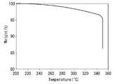
도 5a는 본 발명의 실시예 2에 따라 제조된 차광 물질의 열중량분석 결과를 나타낸 그래프이고, 도 5b는 본 발명의 실시예 1에 따라 제조된 차광 물질의 열중량분석 결과를 나타낸 그래프.
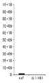
도 6a는 본 발명의 실시예 2에 따라 제조된 차광 물질의 P & T MS 측정 결과를 나타낸 그래프이고, 도 6b는 본 발명의 실시예 1에 따라 제조된 차광 물질의 P & T MS 측정 결과를 나타낸 그래프.
도 7은 본 발명의 2 종류의 실록산과 2 종류의 실세스퀴옥산의 P & T MS 측정 결과를 나타낸 그래프.
도 8은 본 발명의 실시예 3과 실시예 6에 따라 제조된 차광 물질의 열중량분석(TGA) 결과를 나타낸 그래프.
도 9는 본 발명의 실시예 3과 실시예 6에 따라 제조된 차광 물질의 P & T MS측정 결과를 나타낸 그래프.
도 10은 본 발명의 마스크와 차광막 패턴을 4배율 및 10배율의 광학 현미경으로 측정한 이미지.
도 11은 본 발명의 차광막 패턴의 SEM 사진.
도 12는 본 발명의 차광막 패턴의 반사율을 나타낸 그래프.1 is a cross-sectional view illustrating a display device according to an embodiment of the present invention;
2 is a cross-sectional view illustrating a display device according to another embodiment of the present invention.
3 is a view showing nanoparticles according to an embodiment of the present invention.
4a and 4b are photographs showing nanoparticles prepared according to Example 1 of the present invention.
5A is a graph showing the results of thermogravimetric analysis of the light-shielding material prepared according to Example 2 of the present invention, and FIG. 5B is a graph showing the results of thermogravimetric analysis of the light-shielding material prepared according to Example 1 of the present invention.
6A is a graph showing the P & T MS measurement results of the light blocking material prepared according to Example 2 of the present invention, and FIG. 6B is the P & T MS measurement result of the light blocking material prepared according to Example 1 of the present invention. graph shown.
7 is a graph showing the P & T MS measurement results of two types of siloxanes and two types of silsesquioxanes of the present invention.
8 is a graph showing thermogravimetric analysis (TGA) results of light-shielding materials prepared according to Examples 3 and 6 of the present invention.
9 is a graph showing P & T MS measurement results of light-shielding materials prepared according to Examples 3 and 6 of the present invention.
10 is an image of the mask and the light-shielding film pattern of the present invention measured with an optical microscope at 4 magnification and 10 magnification.
11 is a SEM photograph of the light-shielding film pattern of the present invention.
12 is a graph showing the reflectance of the light-shielding film pattern of the present invention.
이하, 첨부한 도면을 참조하여 본 발명의 일 실시 예들을 상세히 설명하면 다음과 같다.Hereinafter, one embodiment of the present invention will be described in detail with reference to the accompanying drawings.
도 1은 본 발명의 일 실시예에 따른 표시장치를 나타낸 단면도이다. 하기에서는 표시장치의 예로 유기발광표시장치를 설명하기로 한다.1 is a cross-sectional view illustrating a display device according to an exemplary embodiment of the present invention. Hereinafter, an organic light emitting display device will be described as an example of the display device.
도 1을 참조하면, 기판(105) 상에 차광막(LS)이 위치한다. 기판(105)은 유리, 플라스틱 또는 금속으로 이루어진다. 차광막(LS)은 광을 차단할 수 있는 차광 물질로 이루어지며, 코어-쉘 구조로 이루어진 나노입자를 포함한다. 차광막(LS)에 대한 자세한 설명은 후술하기로 한다. 상기 차광막(LS)이 형성된 기판(105) 상에 버퍼층(110)이 위치한다. 버퍼층(110)은 기판(105)에서 유출되는 알칼리 이온 등과 같은 불순물로부터 후속 공정에서 형성되는 박막트랜지스터를 보호하기 위해 형성하는 것으로, 실리콘 산화물(SiO2), 실리콘 질화물(SiNx) 등으로 이루어진다.Referring to FIG. 1 , a light blocking layer LS is positioned on a
상기 버퍼층(110) 상에 액티브층(120)이 위치한다. 액티브층(120)은 비정질 아연 산화물계 복합 반도체, 특히 a-IGZO 반도체는 갈륨산화물(Ga2O3), 인듐산화물(In2O3) 및 아연산화물(ZnO)의 복합체 타겟을 이용하여 스퍼터링(sputtering) 방법에 의해 형성될 수 있으며, 이외에도 화학기상증착이나 원자증착(Atomic Layer Deposition; ALD) 등의 화학적 증착방법을 이용할 수도 있다. 여기서, 본 발명의 실시예의 경우에는 갈륨, 인듐, 아연의 원자비가 각각 1:1:1, 2:2:1, 3:2:1 및 4:2:1인 복합 산화물 타겟을 사용하여 비정질 아연 산화물계 복합 반도체를 증착할 수 있으며, 이때 상기 갈륨, 인듐, 아연의 원자비가 2:2:1인 복합 산화물 타겟을 사용하는 경우 상기 갈륨, 인듐, 아연의 당량(equivalent weight)비는 대략 2.8:2.8:1을 가질 수 있다. 액티브층(120)의 양측에는 불순물이 도핑되어 소스 영역(120a)과 드레인 영역(120b)이 구비되고, 소스 영역(120a)과 드레인 영역(120b) 사이에는 채널 영역(120c)이 구비된다.An
상기 액티브층(120) 상에 게이트 절연막(125)이 위치한다. 게이트 절연막(125)은 실리콘 산화막(SiOx), 실리콘 질화막(SiNx) 또는 이들의 다중층으로 이루어진다. 상기 게이트 절연막(125) 상에 게이트 전극(131)이 위치한다. 게이트 전극(131)은 구리(Cu), 몰리브덴(Mo), 알루미늄(Al), 크롬(Cr), 금(Au), 티타늄(Ti), 니켈(Ni), 네오디뮴(Nd), 탄탈륨(Ta) 및 텅스텐(W)로 이루어진 군에서 선택된 어느 하나 또는 이들의 합금의 단층이나 다층으로 이루어진다. 게이트 전극(131)은 상기 액티브층(120)의 채널 영역(120c)에 대응되게 위치한다.A
상기 게이트 전극(131)이 형성된 기판(105) 상에 층간 절연막(135)이 위치한다. 층간 절연막(135)은 실리콘 산화막(SiOx), 실리콘 질화막(SiNx) 또는 이들의 다중층으로 이루어진다. 또한, 층간 절연막(135)은 상기 액티브층(120)의 소스 영역(120a)과 드레인 영역(120b)에 대응되어 액티브층(120)을 노출하는 콘택홀들(136a, 136b)이 구비된다.An interlayer insulating
상기 층간 절연막(135) 상에 소스 전극(141)과 드레인 전극(142)이 위치한다. 소스 전극(141) 및 드레인 전극(142)은 단일층 또는 다중층으로 이루어질 수 있으며, 단일층일 경우에는 몰리브덴(Mo), 알루미늄(Al), 크롬(Cr), 금(Au), 티타늄(Ti), 니켈(Ni), 네오디뮴(Nd) 및 구리(Cu)로 이루어진 군에서 선택된 어느 하나 또는 이들의 합금으로 이루어질 수 있다. 또한, 소스 전극(141) 및 드레인 전극(142)이 다중층일 경우에는 몰리브덴/알루미늄-네오디뮴, 몰리브덴/알루미늄 또는 티타늄/알루미늄의 2중층이거나 몰리브덴/알루미늄-네오디뮴/몰리브덴, 몰리브덴/알루미늄/몰리브덴 또는 티타늄/알루미늄/티타늄의 3중층으로 이루어질 수 있다. 소스 전극(141)과 드레인 전극(142)은 층간 절연막(135)에 형성된 콘택홀들(136a, 136b)을 통해 액티브층(120)의 소스 영역(120a)과 드레인 영역(120b)에 각각 접속된다.A
상기 소스 전극(141) 및 드레인 전극(142)이 형성된 기판(105) 상에 패시베이션막(145)이 위치한다. 패시베이션막(145)은 실리콘 산화막(SiOx), 실리콘 질화막(SiNx) 또는 이들의 다중층으로 이루어진다. 그리고, 패시베이션막(145)은 상기 드레인 전극(142)에 대응되는 영역에 드레인 전극(142)을 노출하는 비어홀(147)이 구비된다. 패시베이션막(145) 상에 컬러필터(CF)가 위치한다. 컬러필터(CF)는 각 화소에 적색(R), 녹색(G) 및 청색(B) 중 어느 하나가 형성되나, 본 실시예에서는 설명의 편의상 R, G, B로 모두 도시하였다. 컬러필터(CF) 상에 보호막(150)이 위치한다. 보호막(150)은 실리콘 산화막(SiOx) 또는 실리콘 질화막(SiNx)의 무기물로 이루어지거나, 폴리이미드(polyimide), 벤조사이클로부틴계 수지(benzocyclobutene series resin), 아크릴레이트(acrylate) 등의 유기물로 이루어질 수 있다.A
상기 보호막(150) 상에 화소 전극(160)이 위치한다. 화소 전극(160)은 ITO(Indium Tin Oxide) 또는 IZO(Indium Zinc Oxide)와 같은 투명한 도전성물질로 이루어진다. 화소 전극(160)은 패시베이션막(145)과 보호막(150)에 구비된 비어홀(147)을 통해 드레인 전극(142)에 연결된다. 화소 전극(160) 상에 화소 전극을 노출하는 뱅크층(165)이 위치한다. 즉, 뱅크층(165)은 화소 전극(160)의 가장자리를 덮고 화소 전극(160)의 중앙을 노출한다. 뱅크층(165)은 화소를 정의하며 화소 전극(160)들을 절연시키는 것으로 폴리이미드(polyimide), 벤조사이클로부틴계 수지(benzocyclobutene series resin), 아크릴레이트(acrylate) 등의 유기물로 이루어진다. 본 발명의 뱅크층(165)은 광을 차광할 수 있는 블랙 뱅크층일 수 있다. 블랙 뱅크층은 광을 차단할 수 있는 차광 물질로 이루어지며, 코어-쉘 구조로 이루어진 나노입자를 포함한다. 차광 물질에 대한 자세한 설명은 후술하기로 한다. 따라서, 뱅크층이 블랙 뱅크층으로 이루어지면 각 화소 사이를 명확하게 정의하여 인접한 화소들 간의 혼색을 방지하고 콘트라스트비를 향상시킬 수 있는 이점이 있다.A
화소 전극(160)과 뱅크층(165) 상에 유기 발광층(170)이 위치한다. 유기 발광층(170)은 적어도 발광층을 포함하며, 정공주입층, 정공수송층, 전자수송층 또는 전자주입층을 더 포함할 수 있다. 유기 발광층(170) 상에 대향 전극(175)이 위치한다. 대향 전극(175)은 일함수가 낮은 금속들로 은(Ag), 마그네슘(Mg), 칼슘(Ca) 등을 사용할 수 있다.The
위와 같이 구성된 본 발명의 일 실시예에 따른 표시장치는 유기 발광층에서 광이 발광되어 하부의 컬러필터를 통해 적색, 녹색 및 청색을 구현한다. 일반적으로 유기발광표시장치는 외부광에 의한 반사광을 저감하기 위해 기판에 편광판이 구비되나, 차광막이 광을 반사하는 배선들 상에 배치되어 외부광이 반사되는 것을 방지할 수 있다. 따라서, 본 발명의 실시예에 따른 유기발광표시장치는 반사광을 방지하기 위해 구비되는 편광판을 생략할 수 있는 이점이 있다.In the display device according to an exemplary embodiment of the present invention configured as described above, light is emitted from the organic light emitting layer to realize red, green, and blue colors through a lower color filter. In general, an organic light emitting display device has a polarizing plate provided on a substrate to reduce reflected light by external light, but a light blocking layer is disposed on the lines that reflect the light to prevent external light from being reflected. Accordingly, the organic light emitting display device according to the embodiment of the present invention has an advantage that a polarizing plate provided to prevent reflected light can be omitted.
도 2는 본 발명의 다른 실시예에 따른 표시장치를 나타낸 단면도이다. 하기에서는 전술한 도 1의 구성과 동일한 구성에 대해서는 그 설명을 생략하기로 한다.2 is a cross-sectional view illustrating a display device according to another exemplary embodiment of the present invention. Hereinafter, a description of the same configuration as that of FIG. 1 will be omitted.
도 2를 참조하면, 본 발명의 표시장치는 액정표시장치(300)일 수 있다. 액정표시장치(300)는 액정층(360)을 사이에 두고 서로 마주보는 TFT 어레이 기판(310)과 컬러필터 기판(370)으로 구성된다. 컬러필터 기판(370)은 각각의 화소를 구획하는 블랙 매트릭스(375), 블랙 매트릭스(375)에 의해 구획된 화소에 형성되는 컬러필터(380), 컬러필터(380) 상에 위치하는 공통 전극(385)을 포함한다. 컬러필터(380)는 블랙 매트릭스(375)에 의해 구획되는 화소 영역에 R,G,B 별로 형성되어 R, G, B 색상을 구현한다. 컬러필터(380)와 공통 전극(385) 사이에 오버코트층이 더 형성될 수 있다.Referring to FIG. 2 , the display device of the present invention may be a liquid
TFT 어레이 기판(310) 상에 게이트 전극(315)이 위치하고, 게이트 전극(315) 상에 게이트 전극(315)을 절연시키는 게이트 절연막(320)이 위치한다. 게이트 절연막(320) 상에 게이트 전극(315)과 대응되는 액티브층(325)이 위치하고, 액티브층(325)의 양 측에 소스 전극(330a)과 드레인 전극(330b)이 위치하여 박막트랜지스터(TFT)를 구성한다. 박막트랜지스터(TFT) 상에 보호막(335)이 위치하고, 보호막(335) 상에 드레인 전극(330b)과 연결되는 화소 전극(340)이 위치한다. 이와 같이 구성된 액정표시장치(300)는 박막트랜지스터(TFT))를 통해 화소 신호가 공급된 화소 전극(340)과 기준 전압이 공급된 공통 전극(385) 사이에 수직 전계가 형성되어 액정을 구동한다. 한편, 도 2에서는 TFT 어레이 기판(310)에 화소 전극(340)이 위치하고 컬러필터 기판(370)에 공통 전극(385)이 위치하는 TN 구조의 액정표시장치를 예로 설명하였지만, TFT 어레이 기판(310)에 화소 전극과 공통 전극이 모두 형성되는 IPS 등의 액정표시장치도 예로 들 수 있다.A
전술한 본 발명의 다른 실시예에 따른 표시장치에서 블랙 매트릭스(375)는 광을 차단할 수 있는 차광 물질로 이루어지며, 코어-쉘 구조로 이루어진 나노입자를 포함한다. 차광 물질에 대한 자세한 설명은 후술하기로 한다. 따라서, 본 발명의 표시장치는 차광 특성이 우수한 블랙 매트릭스를 구비함으로써, 광의 차광 특성을 향상시켜 콘트라스트비 등의 표시품질을 향상시킬 수 있는 이점이 있다.In the display device according to another embodiment of the present invention described above, the
전술한 본 발명의 실시예들에 따른 표시장치는 유기발광표시장치 또는 액정표시장치를 예로 설명하였지만, 이에 한정되지 않고 전기영동 표시장치 등의 평판표시장치에 모두 적용가능하다.Although the display device according to the embodiments of the present invention described above has been described as an example of an organic light emitting display device or a liquid crystal display device, the present invention is not limited thereto, and all flat panel display devices such as an electrophoretic display device are applicable.
이하, 전술한 표시장치에 사용되는 차광 물질에 대해 보다 자세하게 설명하기로 한다. 도 3은 본 발명의 일 실시예에 따른 나노입자를 나타낸 도면이다.Hereinafter, the light blocking material used in the above-described display device will be described in more detail. 3 is a view showing nanoparticles according to an embodiment of the present invention.
본 발명의 일 실시예에 따른 차광막을 제조하는 차광 물질은 코어-쉘의 나노입자, 바인더 및 이들을 분산시키는 용매를 포함한다.The light blocking material for manufacturing the light blocking film according to an embodiment of the present invention includes core-shell nanoparticles, a binder, and a solvent dispersing them.
도 3을 참조하면, 본 발명의 차광 물질을 구성하는 나노입자(200)는 광을 차단하는 차광을 위한 것으로서, 코어-쉘(core-shell) 구조로 이루어진다. 여기서, 코어(210)는 실질적으로 차광의 역할을 하는 것으로, 블랙 금속 산화물(black metal oxide)로 이루어진다. 블랙 금속 산화물은 적어도 크롬(Cr) 또는 망간(Mn)을 포함하는 산화물로 예를 들어, 구리망간산화물(CuMnOx), 구리(크롬,망간)산화물(Cu(Cr, Mn)xOy), 구리(크롬,철)산화물(Cu(Cr, Fe)xOy), (철,망간)(철,망간)산화물((Fe, Mn)(Fe, Mn)xOy) 등일 수 있다. 나노입자(200)의 코어(210)의 크기는 수 나노미터 내지 수 마이크로 미터로 이루어진다. 바람직하게는 10nm 내지 100nm의 크기로 이루어질 수 있다.Referring to FIG. 3 , the
쉘(220)은 상기 코어를 절연시키기 위한 절연막(insulating layer)으로 상기 코어를 완전히 감싸도록 형성된다. 쉘(220)은 절연 특성을 가지는 무기물로 이루어지며, 예를 들어, 실록산(siloxane), 실리콘 산화물(SiOx), 실리콘 질화물(SiNx), 산화 티타늄(TiO2), 실란(silane) 등일 수 있다. 쉘(220)은 1 내지 50nm의 두께로 코어를 감쌀 수 있다. 여기서, 쉘(220)의 두께가 1nm 이상이면 절연성을 증가시키고 저반사 효과를 향상시킬 수 있다. 또한, 쉘(220)의 두께가 50nm 이하이면 표면 거칠기(roughness)가 커지고 차광 효과가 사라지는 것을 방지할 수 있는 이점이 있다. 그러나, 쉘(220)의 두께는 이에 한정되지 않으며 코어(210)의 크기에 따라 다양하게 설계 가능하다. 따라서, 코어(210)와 쉘(220)을 포함하는 나노입자(200)의 크기는 150nm 이하, 바람직하게는 100nm 이하로 이루어질 수 있다.The
전술한 나노입자(200)는 본 발명의 차광 물질 100 중량부에 대해 1 내지 30 중량부로 포함될 수 있다. 여기서, 나노입자(200)의 함량이 1 중량부 이상이면 광학 치수(optical dimension, OD) 특성이 우수하고, 나노입자(200)의 함량이 30 중량부 이하이면 나노입자(200)의 분산안정성이 떨어지는 것을 방지할 수 있는 이점이 있다.The
전술한 코어-쉘 구조의 나노입자는 합성 단계에서 나노입자 사이에서 물리적, 화학적 응집을 형성하고 있으므로 본 발명에 따른 차광 물질 중에 용매에 나노입자를 분산시키기 위해 표면 처리(surface treatment)가 수행될 수 있다.Since the nanoparticles of the above-described core-shell structure form physical and chemical aggregation between the nanoparticles in the synthesis step, a surface treatment may be performed to disperse the nanoparticles in a solvent in the light-shielding material according to the present invention. there is.
예를 들어, 1,2-디클로로벤젠, N-메틸피롤리돈(N-methylpyrrolidone, NMP), N,N-디메틸포름아미드(N,N-dimethylformamide, DMF) 등의 유기용매에 나노입자를 첨가한 뒤 초음파 처리를 수행하는 방법이나, 소듐도데실황산염(sodium dodecyl sulfate, SDS), Trixon X-100, 소듐도데실벤젠술폰산염(sodium dodecyl benzene sulfonate, NaDDBS), 아라비아 검 등의 이온성 저분자 계면활성제 및/또는 폴리비닐피롤리돈(poly vinylpyrrolidone, PVP) 등의 이원 또는 삼원 공중합체와 같은 고분자형 계면활성제를 사용하는 방법이나, 산 처리를 통하여 카르복실기 등을 도입하고 물, 알코올 등에 대한 용해도를 증가시키고, 선택적으로 아닐린 옥타데실아민(ODA), 테트라데실아닐린 등의 탄화수소로 카르복실기 등을 치환하여 방향족 유기용매에 대한 분산을 유도하는 방법이나, 전해질로 사용되는 이온성 액체(ionic liquid), 예를 들면 1-부틸3-메틸이미다졸륨 테트라플루오로보레이트(1-butyl-3-methylimidazolium tetrafluoroborate, BMIMBF4), 1-부틸-3-메틸이미다졸륨 헥사플루오로포르세이트(1-butyl-3-mehtylimidazolium hexafluorophosphate, BMIMPF6) 등과 같은 이온성 액체(ionic liquid) 등을 사용하고, 필요에 따라 유기 용매에 재-분산시키는 방법 등을 이용할 수 있다.For example, adding nanoparticles to an organic solvent such as 1,2-dichlorobenzene, N-methylpyrrolidone (NMP), or N,N-dimethylformamide (DMF) After ultrasonic treatment, sodium dodecyl sulfate (SDS), Trixon X-100, sodium dodecyl benzene sulfonate (NaDDBS), ionic low molecular interface such as gum arabic A method of using an active agent and/or a polymer-type surfactant such as a binary or terpolymer such as polyvinylpyrrolidone (PVP), or introducing a carboxyl group through acid treatment and improving solubility in water, alcohol, etc. A method of inducing dispersion in an aromatic organic solvent by increasing and optionally substituting a carboxyl group with a hydrocarbon such as aniline octadecylamine (ODA) or tetradecylaniline, or an ionic liquid used as an electrolyte, e.g. For example, 1-butyl-3-methylimidazolium tetrafluoroborate (BMIMBF4 ), 1-butyl-3-methylimidazolium hexafluorophosate (1-butyl-3 -Mehtylimidazolium hexafluorophosphate, BMIMPF6 ) Using an ionic liquid, such as, and the like may be used, such as a method of re-dispersion in an organic solvent if necessary.
한편, 본 발명의 실시예에 따른 차광 물질을 구성하는 바인더는 가교결합성 화합물로 실란올기 또는 실록산기를 적어도 하나를 갖는 단량체 화합물이다. 이들 화합물은 후술하는 열처리 등에 의하여 가교결합을 형성하여 폴리실록산을 형성할 수 있다. 이들 화합물은 경화 공정에 의하여 가교결합하여, 코팅막의 매트릭스(matrix)를 형성하는 바인더(binder)로 작용한다.On the other hand, the binder constituting the light blocking material according to an embodiment of the present invention is a crosslinking compound, and is a monomer compound having at least one silanol group or a siloxane group. These compounds may form polysiloxane by forming crosslinks by heat treatment or the like described later. These compounds are cross-linked by the curing process to act as a binder to form a matrix of the coating film.
상기 가교결합성 화합물 중 실란올기를 갖는 단량체 화합물의 예로는 에틸렌계 불포화 알콕시 실란류 및 에틸렌계 불포화 아실옥시 실란류와 같이 실릴기-함유 불포화 단량체를 가수분해시켜 수득된 실란올기-함유 단량체를 들 수 있다. 에틸렌계 불포화 알콕시 실란의 예로는 1) 아크릴레이트계 알콕시 실란류(예: γ-아크릴옥시프로필-트리메톡시실란, γ-아크릴옥시프로필-트리에톡시실란), 2) 메타크릴레이트계 알콕시 실란류(예: γ-메타크릴옥시프로필-트리메톡시실란, γ-메타크릴옥시프로필-트리에톡시실란, γ-메타크릴옥시프로필-트리스(2-메톡시에톡시)실란이 있다. 한편, 에틸렌계 불포화 아실옥시실란의 예로는 아크릴레이트계 아세톡시실란, 메타크릴레이트계 아세톡시실란 및 에틸렌계 불포화 아세톡시실란류 (예를 들면, 아크릴레이토프로필트리아세톡시실란, 메타크릴레이토프로필트리아세톡시실란) 등이 있다.Examples of the monomer compound having a silanol group among the crosslinkable compounds include silanol group-containing monomers obtained by hydrolyzing a silyl group-containing unsaturated monomer such as ethylenically unsaturated alkoxy silanes and ethylenically unsaturated acyloxy silanes. can Examples of the ethylenically unsaturated alkoxy silane include 1) acrylate alkoxy silanes (eg, γ-acryloxypropyl-trimethoxysilane, γ-acryloxypropyl-triethoxysilane), 2) methacrylate alkoxy silane Examples include γ-methacryloxypropyl-trimethoxysilane, γ-methacryloxypropyl-triethoxysilane, and γ-methacryloxypropyl-tris(2-methoxyethoxy)silane. Examples of the ethylenically unsaturated acyloxysilanes include acrylate-based acetoxysilane, methacrylate-based acetoxysilane, and ethylenically-unsaturated acetoxysilanes (e.g., acrylatetopropyltriacetoxysilane, methacrylatetopropyltriacetate). oxysilane) and the like.
그 외에도 가수분해 등을 통하여 실란올기를 갖는 단량체를 얻을 수 있는 실릴기 함유 불포화 화합물의 예로는, 클로로디메틸비닐실란, 5-트리메틸실릴-1,3-사이클로펜타디엔, 3-트리메틸실릴알릴 알코올, 트리메틸실릴 메타크릴레이트, 1-트리메틸실릴옥시-1,3-부타디엔, 1-트리메틸실릴옥시 사이클로펜텐, 2-트리메틸실릴옥시에틸 메타크릴레이트, 2-트리메틸실릴옥시퓨란, 2-트리메틸실릴옥시프로펜, 알릴옥시-t-부틸디메틸실란 및 알릴옥시트리메틸실란, 트리메톡시 비닐실란, 트리에톡시비닐실란, 트리스(메톡시에톡시)비닐실란 같은 트리스알콕시 비닐실란이 있다. 전술한 실란올기를 갖는 단량체는 단독으로 사용할 수도 있고, 2종 이상 혼합하여 사용할 수도 있다.In addition, examples of the silyl group-containing unsaturated compound capable of obtaining a monomer having a silanol group through hydrolysis etc. include chlorodimethylvinylsilane, 5-trimethylsilyl-1,3-cyclopentadiene, 3-trimethylsilylallyl alcohol, Trimethylsilyl methacrylate, 1-trimethylsilyloxy-1,3-butadiene, 1-trimethylsilyloxy cyclopentene, 2-trimethylsilyloxyethyl methacrylate, 2-trimethylsilyloxyfuran, 2-trimethylsilyloxypropene , allyloxy-t-butyldimethylsilane and trisalkoxy vinylsilanes such as allyloxytrimethylsilane, trimethoxyvinylsilane, triethoxyvinylsilane, tris(methoxyethoxy)vinylsilane. The above-mentioned monomers having a silanol group may be used alone or in mixture of two or more.
또한, 상기 가교결합성 화합물로서는 실록산기를 갖는 단량체를 또한 사용할 수 있다. 이러한 실록산기를 갖는 단량체로는 선형 실록산기를 갖는 화합물, 사이클릭 실록산기를 갖는 화합물, 사면체 구조의 실록산기를 갖는 화합물 및 실세스퀴옥산 등을 사용할 수 있다.Further, as the crosslinkable compound, a monomer having a siloxane group can also be used. As the monomer having a siloxane group, a compound having a linear siloxane group, a compound having a cyclic siloxane group, a compound having a tetrahedral siloxane group, silsesquioxane, and the like can be used.
선형 실록산기를 갖는 화합물로는 메틸실록산, 에틸실록산, 프로필실록산, 부틸실록산, 펜틸실록산, 디메틸실록산, 디에틸실록산, 디프로필실록산, 디부틸실록산, 디펜틸실록산, 트리메틸실록산, 트리에틸실록산, 트리프로필실록산, 트리부틸실록산, 헥사메틸디실록산, 헥사에틸디실록산, 옥타메틸트리실록산, 옥타에틸트리실록산, 데카메틸테트라실록산, 테트라메톡시실란(Tetramethoxy silane, TMOS), 테트라에톡시실란(Tetraethoxy silane, TEOS), 메틸트리메톡시실란(Methlytrimethoxy silane, MTMS), 비닐트리메톡시실란, 비닐트리에톡시실란, 비닐트리스(2-메톡시에톡시)-실란, N-(2-아미노에틸)-3-아미노프로필메틸디메톡시실란, N-(2-아미노에틸)-3-아미노프로필메틸트리메톡시실란, 3-아미노프로필트리에톡시실란, 3-글리시독시프로필트리에톡시실란, 3-글리시독시프로필메틸디메톡시실란, 2-(3,4-에톡시 시클로헥실)에틸트리메톡시실란, 3-클로로프로필 메틸디메톡시실란, 3-클로로프로필 트리메톡시 실란, 3-메타아크릴옥시프로필트리메톡시실란, 3-머캅토프로필트리메톡시실란 등을 포함할 수 있으며, 이들 중에서 선택된 1종 또는 2종 이상의 혼합물을 사용할 수 있으나, 본 발명이 이에 한정되지 않는다. 예를 들어, TMOS, TEOS, MTMS, 비닐트리스(2-메톡시에톡시)-실란, N-(2-아미노에틸)-3-아미노프로필메틸디메톡시실란 등과 같이 알콕시기를 함유하는 선형 실록산기를 갖는 단량체를 단독으로 또는 2종 이상 혼합할 수 있다.Compounds having a linear siloxane group include methylsiloxane, ethylsiloxane, propylsiloxane, butylsiloxane, pentylsiloxane, dimethylsiloxane, diethylsiloxane, dipropylsiloxane, dibutylsiloxane, dipentylsiloxane, trimethylsiloxane, triethylsiloxane, tripropyl Siloxane, tributylsiloxane, hexamethyldisiloxane, hexaethyldisiloxane, octamethyltrisiloxane, octaethyltrisiloxane, decamethyltetrasiloxane, tetramethoxy silane (TMOS), tetraethoxy silane, TEOS), methyltrimethoxy silane (MTMS), vinyltrimethoxysilane, vinyltriethoxysilane, vinyltris(2-methoxyethoxy)-silane, N-(2-aminoethyl)-3 -Aminopropylmethyldimethoxysilane, N-(2-aminoethyl)-3-aminopropylmethyltrimethoxysilane, 3-aminopropyltriethoxysilane, 3-glycidoxypropyltriethoxysilane, 3-glyc Cydoxypropylmethyldimethoxysilane, 2-(3,4-ethoxy cyclohexyl)ethyltrimethoxysilane, 3-chloropropyl methyldimethoxysilane, 3-chloropropyl trimethoxysilane, 3-methacryloxypropyl It may include trimethoxysilane, 3-mercaptopropyltrimethoxysilane, and the like, and one or a mixture of two or more selected from these may be used, but the present invention is not limited thereto. For example, having a linear siloxane group containing an alkoxy group, such as TMOS, TEOS, MTMS, vinyltris(2-methoxyethoxy)-silane, N-(2-aminoethyl)-3-aminopropylmethyldimethoxysilane, etc. Monomers can be used individually or in mixture of 2 or more types.
한편, 사이클릭 실록산(cyclic siloxane)의 비제한적인 예로는 메틸하이드로-사이클로실록산, 헥사메틸-사이클로트리실록산, 헥사에틸-사이클로트리실록산과 같은 사이클로트리실록산; 테트라옥틸 -사이클로테트라실록산, 헥사메틸-사이클로테트라실록산, 옥타메틸- 사이클로테트라실록산과 같은 사이클로테트라실록산; 테트라- 및 펜타-메틸사이클로테트라실록산; 테트라-, 펜타-, 헥사- 및 헵타-메틸사이클로펜타실록산; 테트라-, 펜타- 및 헥사메틸-사이클로헥사실록산, 테트라에틸-사이클로테트라실록산, 및 테트라페닐 사이클로테트라실록산; 데카메틸-사이클로펜타실록산, 도데카메틸 사이클로실록산, 1,3,5,7-테트라메틸-사이클로테트라실록산, 1,3,5,7,9-펜타메틸-사이클로펜타실록산, 및 1,3,5,7,9,11-헥사메틸사이클로헥사실록산에서 선택되는 1종 또는 2종 이상의 혼합물을 특히 사용할 수 있지만, 본 발명이 이에 한정되는 것은 아니다.Meanwhile, non-limiting examples of the cyclic siloxane include cyclotrisiloxane such as methylhydro-cyclosiloxane, hexamethyl-cyclotrisiloxane, and hexaethyl-cyclotrisiloxane; cyclotetrasiloxanes such as tetraoctyl-cyclotetrasiloxane, hexamethyl-cyclotetrasiloxane, octamethyl-cyclotetrasiloxane; tetra- and penta-methylcyclotetrasiloxanes; tetra-, penta-, hexa- and hepta-methylcyclopentasiloxanes; tetra-, penta- and hexamethyl-cyclohexasiloxane, tetraethyl-cyclotetrasiloxane, and tetraphenyl cyclotetrasiloxane; Decamethyl-cyclopentasiloxane, dodecamethyl cyclosiloxane, 1,3,5,7-tetramethyl-cyclotetrasiloxane, 1,3,5,7,9-pentamethyl-cyclopentasiloxane, and 1,3, One or a mixture of two or more selected from 5,7,9,11-hexamethylcyclohexasiloxane may be particularly used, but the present invention is not limited thereto.
또한, 사면체 실록산기를 갖는 단량체의 비제한적인 예로는 테트라키스디메틸실록시실란, 테트라키스디페닐실록시실란 및 테트라키스디에틸실록시실란 및 이들의 혼합물을 들 수 있다.Further, non-limiting examples of the monomer having a tetrahedral siloxane group include tetrakisdimethylsiloxysilane, tetrakisdiphenylsiloxysilane and tetrakisdiethylsiloxysilane, and mixtures thereof.
아울러, 선형, 사이클릭 및 사면체 실록산 외에도, 예를 들어 메틸트리클로로실록산과 디메틸클로로실록산의 반응 등에 의하여 합성될 수 있는 실세스퀴옥산(silsesquioxane, SSQ)을 가교결합성 화합물로 사용할 수 있다. 실세스퀴옥산은 가교결합에 의하여 사다리(ladder) 구조 또는 케이지(cage) 구조를 갖는 폴리실세스퀴옥산으로 합성될 수 있다. 예를 들어, 오르가노 트리클로로실란의 가수분해에 의하여 부분적인 케이지 구조의 헵타머 형태의 실록산과, 케이지 구조의 헵타머 형태 및 옥타머 형태의 실록산 등이 얻어지는데, 용해도 차이를 이용하여 헵타머 형태의 실록산을 분리하고, 이를 오르가노트리알콕시실란 또는 오르가노트리클로로실란의 축합 반응에 의하여 실세스퀴옥산 단량체를 얻을 수 있다. 또한, 실세스퀴옥산은 높은 열 안정성, 낮은 유전율을 가진다. 실세스퀴옥산은 산 촉매를 사용한 가수축합 반응으로 생성되는데 여기에 나노포러스(nanophorous)하게 기공을 도입하게 되면 굴절률 뿐만 아니라 유전율까지 낮출 수 있는 장점을 가진다. 또한, 실세스퀴옥산은 차광 물질 포뮬레이션(formulation) 형성 시 바인더의 나노포러스한 입체적인 구조로 인해서 밀베이스(millbase)의 분산성이 높아지게 되며 균일한 분산성으로 인하여 차광막의 저장 안정성까지 높일 수 있는 이점이 있다.In addition, in addition to linear, cyclic and tetrahedral siloxanes, for example, silsesquioxane (SSQ), which can be synthesized by the reaction of methyltrichlorosiloxane and dimethylchlorosiloxane, may be used as a crosslinking compound. Silsesquioxane may be synthesized as polysilsesquioxane having a ladder structure or a cage structure by crosslinking. For example, by hydrolysis of organotrichlorosilane, a heptamer siloxane having a partially caged structure and a heptamer form and an octamer siloxane having a cage structure are obtained. A silsesquioxane monomer can be obtained by isolating the form of siloxane, and then condensing it with organotrialkoxysilane or organotrichlorosilane. In addition, silsesquioxane has high thermal stability and low dielectric constant. Silsesquioxane is produced by a hydrocondensation reaction using an acid catalyst, and when pores are introduced in a nanoporous manner, it has the advantage of lowering not only the refractive index but also the dielectric constant. In addition, silsesquioxane increases the dispersibility of the millbase due to the nanoporous three-dimensional structure of the binder when the light-shielding material formulation is formed, and the storage stability of the light-shielding film can also be increased due to the uniform dispersibility. There is an advantage.
전술한 바인더는 차광 물질 100 중량부에 대해 1 내지 30 중량부로 포함될 수 있다. 여기서, 바인더의 함량이 1 중량부 이상이면, 기판과의 접착력이 저하되는 것을 방지할 수 있고, 바인더의 함량이 30 중량부 이하이면, 차광막의 차광 특성이 저하되는 것을 방지할 수 있는 이점이 있다.The above-described binder may be included in an amount of 1 to 30 parts by weight based on 100 parts by weight of the light blocking material. Here, if the content of the binder is 1 part by weight or more, it is possible to prevent a decrease in adhesion with the substrate, and if the content of the binder is 30 parts by weight or less, there is an advantage in that it is possible to prevent deterioration of the light-shielding property of the light-shielding film .
본 발명의 실시예에 따른 차광 물질을 구성하는 용매는 전술한 나노입자와 바인더와 같은 고형분을 분산시키고, 차광 물질의 점도를 조절하는 역할을 한다. 나노입자 및 바인더를 분산시킬 수 있는 용매로서, 친수성 용매 또는 소수성 용매를 사용할 수 있다. 친수성 용매는 예를 들어, 물; 에탄올, 메탄올, 이소프로필 알코올, 부탄올, 2-에틸헥실알코올, 메톡시펜탄올, 부톡시에탄올, 에톡시에톡시 에탄올, 부톡시에톡시 에탄올, 메톡시 프로폭시 프로판올, 텍산올(texanol), 알파-터피네올(α-terpineol)과 같은 터피네올 등의 알코올류; 테트라하이드로퓨란(THF); 글리세롤과, 알킬렌 글리콜 예를 들어, 에틸렌글리콜, 트리에틸렌글리콜, 폴리에틸렌글리콜, 프로필렌글리콜, 디프로필렌글리콜, 디헥실렌글리콜 또는 이들의 알킬 에테르(일예로 프로필렌글리콜 메틸에테르(PGME), 디에틸렌글리콜 부틸에테르, 디에틸렌글리콜 에틸에테르, 디프로필렌글리콜 메틸에테르, 디헥실렌글리콜 에틸에테르); 글리세린, N-메틸피롤리돈(N-methyl-2-pyrrolidinone, NMP), 2-피롤리돈, 아세틸아세톤, 1,3-디메틸이미다졸리논, 티오디글리콜, 디메틸술폭사이드(dimethyl sulfoxid, DMSO), N,N-디메틸 아세트아미드(N,N-dimethyl acetamide, DMAc)), 디메틸포름아미드(dimethylformamide, DMF)), 술포란, 디에탄올아민, 트리에탄올아민에서 선택되는 유기용매를 단독으로 사용하거나 또는 이들 중에서 2종 이상 혼합하여 사용할 수 있다.The solvent constituting the light-shielding material according to the embodiment of the present invention serves to disperse solids such as the nanoparticles and the binder, and to adjust the viscosity of the light-shielding material. As a solvent in which the nanoparticles and the binder can be dispersed, a hydrophilic solvent or a hydrophobic solvent may be used. Hydrophilic solvents include, for example, water; Ethanol, methanol, isopropyl alcohol, butanol, 2-ethylhexyl alcohol, methoxypentanol, butoxyethanol, ethoxyethoxyethanol, butoxyethoxyethanol, methoxypropoxypropanol, texanol, alpha -Alcohols, such as terpineol, such as terpineol (α-terpineol); tetrahydrofuran (THF); Glycerol and an alkylene glycol, for example, ethylene glycol, triethylene glycol, polyethylene glycol, propylene glycol, dipropylene glycol, dihexylene glycol, or their alkyl ethers (eg, propylene glycol methyl ether (PGME), diethylene glycol butyl ether, diethylene glycol ethyl ether, dipropylene glycol methyl ether, dihexylene glycol ethyl ether); Glycerin, N-methylpyrrolidinone (NMP), 2-pyrrolidone, acetylacetone, 1,3-dimethylimidazolinone, thiodiglycol, dimethyl sulfoxide (dimethyl sulfoxide, An organic solvent selected from DMSO), N,N-dimethyl acetamide (DMAc)), dimethylformamide (DMF)), sulfolane, diethanolamine, and triethanolamine is used alone Or it can be used in mixture of 2 or more types among them.
한편, 소수성 용매로는 예를 들어, 메틸에틸케톤, 사이클로펜탄온 등의 케톤류, 자일렌, 톨루엔이나 벤젠 등의 방향족 화합물, 디프로필렌 메틸에테르와 같은 에테르, 메틸렌클로라이드, 클로로포름 등의 지방족 탄화수소 등을 단독 또는 2종 이상 혼합할 수 있다.On the other hand, as the hydrophobic solvent, for example, ketones such as methyl ethyl ketone and cyclopentanone, aromatic compounds such as xylene, toluene and benzene, ethers such as dipropylene methyl ether, methylene chloride, aliphatic hydrocarbons such as chloroform, etc. It can be used individually or in mixture of 2 or more types.
전술한 용매는 차광 물질 100 중량부에 대해 40 내지 90 중량부로 포함될 수 있다. 여기서, 용매의 함량이 40 중량부 이상이면 1㎛ 이하의 박막 두께를 형성하기 용이한 이점이 있고, 용매의 함량이 90 중량부 이하이면, 200nm 이상의 박막 두께를 형성하기 용이한 이점이 있다.The above-described solvent may be included in an amount of 40 to 90 parts by weight based on 100 parts by weight of the light blocking material. Here, when the content of the solvent is 40 parts by weight or more, there is an advantage in that it is easy to form a thin film thickness of 1 μm or less, and when the content of the solvent is 90 parts by weight or less, there is an advantage in that it is easy to form a thin film thickness of 200 nm or more.
한편, 본 발명의 차광 물질 중에는 전술한 성분 외에도 차광 물질의 분산을 유도하기 위한 계면활성제, 경화를 촉진하기 위한 경화촉진제, 산화를 방지하기 위한 산화방지제와 같은 기능성 첨가제를 더욱 포함할 수 있다.On the other hand, in the light-shielding material of the present invention, in addition to the above-described components, a surfactant for inducing dispersion of the light-shielding material, a curing accelerator for accelerating curing, and an antioxidant for preventing oxidation may further include functional additives.
계면활성제는 나노입자의 표면에 코팅되어 공간적 반발력을 유도하거나, 나노입자의 표면에 흡착하여 안정적인 콜로이드 분산 용액을 형성하는 동시에 커플링제로서의 역할을 수행할 수 있다. 본 발명의 차광 물질에 포함되는 나노입자의 분산을 유도할 수 있는 계면활성제는 음이온성 계면활성제, 양이온성 계면활성제, 양쪽성 계면활성제 및 비이온성 계면활성제를 사용할 수 있다.The surfactant can be coated on the surface of the nanoparticles to induce spatial repulsion, or adsorb to the surface of the nanoparticles to form a stable colloidal dispersion solution and serve as a coupling agent at the same time. Surfactants capable of inducing dispersion of nanoparticles included in the light blocking material of the present invention may include anionic surfactants, cationic surfactants, amphoteric surfactants and nonionic surfactants.
음이온성 계면활성제로는 알킬 술폰산(술포네이트), 알킬 황산(설페이트), 아랄킬 및 알크아릴 음이온성 계면활성제, 알킬 숙신산(숙시네이트), 알킬 술포숙신산염(술포숙시네이트)을 사용할 수 있다. 특히, 알크아릴 술폰산, 알킬 황산 및 알크아릴 황산의 나트륨, 마그네슘, 암모늄 및 모노에탄올아민, 디에탄올아민 및 트리에탄올아민 염이 바람직하다. 양이온성 계면활성제는 암모늄염, 아민 유도체를 사용할 수 있다. 아민염계 양이온성 계면활성제로서 폴리옥시에틸렌알킬아민을 들 수 있고, 제4급 알킬 암모늄계 양이온성 계면활성제로는 테트라알킬암모늄, 피리디늄염을 들 수 있다. 제4급 암모늄계 양이온성 계면활성제의 구체적인 예로는 세틸트리메틸암모늄브로마이드(CTAB), 헥사데실트리메틸암모늄브로마이드, 세틸트리메틸암모늄 클로라이드(CTAC)와 같은 알킬트리메틸암모늄염, 세틸피리디늄클로라이드(CPC), 벤즈알코늄클로라이드(BAC), 벤제토늄클로라이드(BZT), 5-브로모-5-니트로-1,3-디옥산, 디메틸디옥타데실암모늄클로라이드, 디옥타데실메틸암모늄브로마이드(DODAB) 등을 들 수 있다.As anionic surfactants, alkyl sulfonic acids (sulfonates), alkyl sulfuric acids (sulfates), aralkyl and alkaryl anionic surfactants, alkyl succinic acids (succinates), and alkyl sulfosuccinates (sulfosuccinates) can be used. there is. In particular, preference is given to sodium, magnesium, ammonium and monoethanolamine, diethanolamine and triethanolamine salts of alkaryl sulfonic acids, alkyl sulfuric acids and alkaryl sulfuric acids. The cationic surfactant may be an ammonium salt or an amine derivative. Examples of the amine salt-based cationic surfactant include polyoxyethylenealkylamine, and examples of the quaternary alkylammonium-based cationic surfactant include tetraalkylammonium and pyridinium salts. Specific examples of the quaternary ammonium-based cationic surfactant include alkyltrimethylammonium salts such as cetyltrimethylammonium bromide (CTAB), hexadecyltrimethylammonium bromide, cetyltrimethylammonium chloride (CTAC), cetylpyridinium chloride (CPC), benzal Conium chloride (BAC), benzethonium chloride (BZT), 5-bromo-5-nitro-1,3-dioxane, dimethyl dioctadecyl ammonium chloride, dioctadecyl methyl ammonium bromide (DODAB), etc. are mentioned. .
한편, 양쪽성 계면활성제로는 코코암포카복시글리시네이트, 코코암포카복시프로피오네이트, 코코베타인, N-코코아미도프로필디메틸글리신 및 N-라우릴-N-카복시메틸-N-(2-하이드록시에틸)에틸렌디아민을 포함한다. 다른 적합한 양쪽성 계면활성제는 4급 사이클로이미데이트, 베타인, 예를 들면, α-(테트라데실디메틸암모니오)아세테이트, 베타-(헥사데실디에틸암모니오)프로피오네이트 및 감마-(도데실디메틸암모니오)부티레이트. 및 설타인, 예를 들면, 3-(도데실디메틸암모니오)-프로판-1-술포네이트 및 3-(테트라데실디메틸암모니오)에탄-i-술포네이트를 포함한다.On the other hand, as amphoteric surfactants, cocoamphocarboxyglycinate, cocoamphocarboxypropionate, cocobetaine, N-cocoamidopropyldimethylglycine, and N-lauryl-N-carboxymethyl-N-(2-hydro oxyethyl)ethylenediamine. Other suitable amphoteric surfactants include quaternary cycloimidates, betaines such as α-(tetradecyldimethylammonio)acetate, beta-(hexadecyldiethylammonio)propionate and gamma-(dodecyl) dimethylammonio)butyrate. and sultaines such as 3-(dodecyldimethylammonio)-propane-1-sulfonate and 3-(tetradecyldimethylammonio)ethane-i-sulfonate.
또한, 비이온성 계면활성제로는 지방산 알칸올 아미드 및 아민 옥사이드 계면활성제로 이루어진 그룹으로부터 선택될 수 있다. 지방산 알칸올 아미드는 알칸올아민, 예를 들면, 모노에탄올아민, 디에탄올아민, 모노이소프로판올아민 또는 디이소프로판올아민이 지방산 또는 지방산 에스테르와 반응하여 아미드를 형성하여 수득된 비이온성 계면활성제이다. 지방산 알칸올 아미드 계면활성제는, 예를 들면, 지방산 디에탄올아미드, 예를 들면, 이소스테아르산 디에탄올아미드, 라우르산 디에탄올아미드, 카프르산 디에탄올아미드, 코코넛 지방산 디에탄올아미드, 리놀산 디에탄올아미드, 미리스트산 디에탄올아미드, 올레산 디에탄올아미드 및 스테아르산 디에탄올아미드; 지방산 모노에탄올아미드, 예를 들면, 코코넛 지방산 모노에탄올아미드; 및 지방산 모노이소프로판올아미드, 예를 들면, 올레산 모노이소프로판올아미드 및 라우르산 모노이소프로판올아미드를 포함한다.In addition, the nonionic surfactant may be selected from the group consisting of fatty acid alkanol amides and amine oxide surfactants. Fatty acid alkanol amides are nonionic surfactants obtained by reacting an alkanolamine such as monoethanolamine, diethanolamine, monoisopropanolamine or diisopropanolamine with a fatty acid or fatty acid ester to form an amide. Fatty acid alkanol amide surfactants include, for example, fatty acid diethanolamide, such as isostearic acid diethanolamide, lauric acid diethanolamide, capric acid diethanolamide, coconut fatty acid diethanolamide, linoleic acid diethanolamide, ethanolamide, myristic acid diethanolamide, oleic acid diethanolamide and stearic acid diethanolamide; fatty acid monoethanolamides such as coconut fatty acid monoethanolamide; and fatty acid monoisopropanolamides such as oleic acid monoisopropanolamide and lauric acid monoisopropanolamide.
전술한 계면활성제 외에도 특히 폴리실록산으로 구성되는 실리콘계의 계면활성제를 사용할 수 있다. 실리콘계 계면활성제의 예로는 폴리에테르로 개질되어 있는 오르가노실록산으로부터 제조될 수 있다. 이러한 실리콘계 계면활성제로서 폴리에테르로 개질되어 있는 디메틸폴리실록산의 공중합체를 사용할 수 있다. 전술한 계면활성제를 단독 또는 2종 이상 혼합할 수 있다. 계면활성제의 함량은 사용되는 나노입자 및 용매의 종류, 이들의 함량에 따라 달라질 수 있지만, 그 함량은 차광 물질 100 중량부에 대해 0.01 내지 0.5 중량부로 포함될 수 있다.In addition to the above-mentioned surfactant, a silicone-based surfactant particularly composed of polysiloxane may be used. Examples of silicone-based surfactants may be prepared from organosiloxanes modified with polyethers. As such a silicone-based surfactant, a copolymer of dimethylpolysiloxane modified with polyether may be used. The aforementioned surfactants may be used alone or in combination of two or more. The content of the surfactant may vary depending on the type of nanoparticles and solvent used, and their content, but the content may be included in an amount of 0.01 to 0.5 parts by weight based on 100 parts by weight of the light blocking material.
상기 경화 촉진제는 아민, 특히 디메틸아닐린 및 또한 특히 3급 아민(예: 모노에틸아민, 트리메틸아민 및 옥탈디메틸아민)과 삼플루오르화 붕소 또는 삼염화 붕소의 착화합물(예를 들어 디메틸아닐린과 삼플루오르화 붕소의 착화합물)이다. 그 외에도 사용 가능한 경화 촉진제의 예로는 예를 들면 1,1'-메틸렌비스(3-메틸피페리딘)(MBMP), 디메틸벤질아민(DMBA), 트리스(디메틸아미노메틸)페놀(TDMAMP), 헥사메틸렌테트라민 및 1,6-비스-(디메틸아미노)헥산인 3급 아민류; 예를 들면 N-4-클로로페닐-N',N'-디메틸우레아(모누론), N-3-클로로-4-메틸페닐-N',N'-디메틸우레아(클로르톨루론), N-(2-하이드록시페닐)-N',N'-디메틸우레아 및 N-(2-하이드록시-4-니트로페닐)-N',N'-디메틸우레아와 같은 우레아 유도체; 예를 들면 이미다졸, 벤즈이미다졸, 1-메틸이미다졸, 3-메틸이미다졸, 1,2-디메틸이미다졸, 2-에틸-4-메틸이미다졸, 1-비닐이미다졸, 2-비닐이미다졸, 2-페닐이미다졸, 2-페닐-4-메틸이미다졸, 1-(2,6-디클로로벤조일)-2-페닐이미다졸 및 1-(2,4,6-트리메틸벤조일)-2-페닐이미다졸과 같은 치환되거나 치환되지 않은 비치환된 이미다졸류; 트리페닐포스핀과 같은 유기포스핀류 등에서 선택되는 1종 또는 2종 이상의 혼합물을 사용할 수 있다. 경화 촉진제의 함량은 차광 물질 중에 포함되는 사용되는 나노입자 및 용매의 종류 및 함량에 따라 달라질 수 있지만, 그 함량은 차광 물질 100 중량부에 대해 0.01 내지 0.1 중량부로 포함될 수 있다.The curing accelerator may be an amine, in particular dimethylaniline and also in particular a complex of tertiary amines such as monoethylamine, trimethylamine and octaldimethylamine with boron trifluoride or boron trichloride, such as dimethylaniline with boron trifluoride. complex of). Other examples of curing accelerators that can be used include, for example, 1,1'-methylenebis(3-methylpiperidine) (MBMP), dimethylbenzylamine (DMBA), tris(dimethylaminomethyl)phenol (TDMAMP), hexa tertiary amines such as methylenetetramine and 1,6-bis-(dimethylamino)hexane; For example, N-4-chlorophenyl-N',N'-dimethylurea (monuron), N-3-chloro-4-methylphenyl-N',N'-dimethylurea (chlortoluron), N-( urea derivatives such as 2-hydroxyphenyl)-N',N'-dimethylurea and N-(2-hydroxy-4-nitrophenyl)-N',N'-dimethylurea; For example, imidazole, benzimidazole, 1-methylimidazole, 3-methylimidazole, 1,2-dimethylimidazole, 2-ethyl-4-methylimidazole, 1-vinylimidazole , 2-vinylimidazole, 2-phenylimidazole, 2-phenyl-4-methylimidazole, 1-(2,6-dichlorobenzoyl)-2-phenylimidazole and 1-(2,4 substituted or unsubstituted unsubstituted imidazoles such as ,6-trimethylbenzoyl)-2-phenylimidazole; One or a mixture of two or more selected from organic phosphines such as triphenylphosphine may be used. The content of the curing accelerator may vary depending on the type and content of nanoparticles and solvent used in the light-shielding material, but the content may be included in an amount of 0.01 to 0.1 parts by weight based on 100 parts by weight of the light-shielding material.
또한 산화 방지제의 비제한적인 예로서, 열에 의해 유도되는 조성물의 산화반응 방지 및 열-안정성을 부여해 주기 위한 목적으로 사용되는 상기 산화방지제로는, 가지를 갖는 페놀계 혹은 하이드록시 신나메이트계의 물질 등을 첨가할 수 있다. 산화 방지제의 구체적인 예로는 테트라키스-(메틸렌-(3,5-디-t-부틸-4-하이드로 신나메이트)메탄, 3,5-비스(1,1-디메틸에틸)-4-하이드록시 벤젠프로파노익 액시드 티올 디-2,1-에탄다일 에스터, 옥타데실 3,5-디-t-부틸-4-하이드록시 하이드로 신나메이트, 2,6-디-터셔리-p-메틸페놀, 2,2-티오비스(4-메틸-6-t-부틸페놀), 2,6-g,t-부틸페놀 등 중에서 선택된 1종 이상을 포함할 수 있다. 하지만, 본 발명이 반드시 이들 산화 방지제로만 제한되는 것은 아니다. 산화 방지제의 함량 또한 차광 물질 중에 포함되는 나노입자 및 용매의 종류, 이들의 함량에 따라 달라질 수 있지만, 그 함량은 차광 물질에 대해 0.01 내지 0.3 중량부로 포함될 수 있다.In addition, as a non-limiting example of the antioxidant, the antioxidant used for the purpose of preventing the oxidation reaction of the composition induced by heat and providing heat-stability, a phenolic or hydroxycinnamate-based substance having branches etc. can be added. Specific examples of antioxidants include tetrakis-(methylene-(3,5-di-t-butyl-4-hydrocinnamate)methane, 3,5-bis(1,1-dimethylethyl)-4-hydroxybenzene propanoic acid thiol di-2,1-ethanediyl ester,
한편, 본 발명의 실시예에 따른 차광 물질은 금속 알콕시화물(metal alkoxide)(M(OR)x)를 더 포함할 수 있다. 금속 알콕시화물은 차광막의 저반사 특성을 위해 광 산란 효과가 일어나도록 하는 역할을 한다. 금속 알콕시화물에 사용될 수 있는 금속은 예를 들어, 알루미늄(Al), 구리(Cu), 몰리브덴(Mo), 티타늄(Ti), 은(Ag), 금(Au) 등의 반사율이 우수한 금속을 사용할 수 있다.Meanwhile, the light blocking material according to an embodiment of the present invention may further include a metal alkoxide (M(OR)x). The metal alkoxide serves to cause a light scattering effect for the low reflection property of the light blocking film. As the metal that can be used for the metal alkoxide, for example, a metal having excellent reflectance such as aluminum (Al), copper (Cu), molybdenum (Mo), titanium (Ti), silver (Ag), gold (Au), etc. may be used. can
상기와 같이, 본 발명의 일 실시예에 따른 차광막을 제조하는 차광 물질은 코어-쉘의 나노입자, 바인더 및 이들을 분산시키는 용매를 포함하며 기타 첨가제들을 포함할 수 있다.As described above, the light blocking material for manufacturing the light blocking film according to an embodiment of the present invention includes core-shell nanoparticles, a binder, and a solvent dispersing them, and may include other additives.
이하, 본 발명의 차광 물질에 관하여 하기 실시예에서 상술하기로 한다. 다만, 하기의 실시예는 본 발명을 예시하는 것일 뿐 본 발명이 하기 실시예에 한정되는 것은 아니다.Hereinafter, the light blocking material of the present invention will be described in detail in the following Examples. However, the following examples are merely illustrative of the present invention, and the present invention is not limited to the following examples.
나노입자의 제조Preparation of nanoparticles
<실시예 1><Example 1>
상온에서 PVP(Poly(N-vinylpyrrolidone)) 1g을 에탄올 100g에 녹인다. 상기 용액에 CrO2 입자 1g을 넣고 1 시간 교반한 후, 필터링과 건조 과정을 거쳐 PVP로 표면 처리된 코어 입자를 형성한다. 다음, 표면 처리된 코어 입자 1.0g을 100g 의 에탄올(메탄올)에 넣고 pH 11이 되도록 암모니아수 용액을 첨가한다. 이어, 상온과 질소 분위기에서 0.8g의 TEOS(tetraethyl orthosilicate)를 넣고, 12시간 교반 한 후, 필터링 및 건조 과정을 거쳐 코어-쉘의 나노입자를 제조하였다. 도 4a 및 도 4b는 제조된 나노입자의 사진이다. 도 4a 및 도 4b를 통해 나노입자의 제조를 확인하였다.Dissolve 1 g of PVP (Poly(N-vinylpyrrolidone)) in 100 g of ethanol at room temperature. 1 g of CrO2 particles were added to the solution, stirred for 1 hour, and then filtered and dried to form core particles surface-treated with PVP. Next, 1.0 g of the surface-treated core particles are put in 100 g of ethanol (methanol), and an aqueous ammonia solution is added so that the pH is 11. Then, 0.8 g of tetraethyl orthosilicate (TEOS) was added at room temperature and nitrogen atmosphere, stirred for 12 hours, and filtered and dried to prepare core-shell nanoparticles. 4A and 4B are photographs of the prepared nanoparticles. The preparation of nanoparticles was confirmed through FIGS. 4a and 4b.
차광 물질의 코어 재료별 내열성 측정Measurement of heat resistance by core material of light-shielding material
<실시예 2><Example 2>
전술한 실시예 1과 동일한 공정 조건 하에, CrO2 입자 대신에 카본블랙(carbon black) 입자를 사용하여 코어-쉘 나노입자를 제조하였다. 제조된 코어-쉘 나노입자를 실록산(siloxane) 바인더와 용매에 혼합하여 차광 물질을 제조하였다.Under the same process conditions as in Example 1 described above, core-shell nanoparticles were prepared using carbon black particles instead of CrO2 particles. The prepared core-shell nanoparticles were mixed with a siloxane binder and a solvent to prepare a light blocking material.
전술한 실시예 1과 2에 따라 제조된 차광 물질의 내열성을 알아보고자 열중량분석(TGA)을 수행하여, 도 5a(실시예 2)와 도 5b(실시예 1)에 나타내었다. 또한, 실시예 1과 2에 따라 제조된 차광 물질의 퓸 발생을 알아보고자 P & T MS(purge & trap ass spectroscopy)를 측정하여 도 6a(실시예 2)와 도 6b(실시예 1)에 나타내었다.Thermogravimetric analysis (TGA) was performed to determine the heat resistance of the light-shielding material prepared according to Examples 1 and 2 described above, and is shown in FIGS. 5A (Example 2) and 5B (Example 1). In addition, P & T MS (purge & trap ass spectroscopy) was measured to determine the generation of fume of the light-shielding material prepared according to Examples 1 and 2, and is shown in FIGS. 6A (Example 2) and 6B (Example 1). it was
도 5a와 5b를 참조하면, 카본블랙 입자를 사용한 실시예 2의 차광 물질은 150℃에서 350℃까지의 승온 구간에서 총 9.62%의 중량 감소를 보였지만, CrO2 입자를 사용한 실시예 1의 차광 물질은 150℃에서 350℃까지의 승온 구간에서 총 0.38%이하의 중량 감소를 나타내어 내열성이 우수한 것을 확인하였다.5A and 5B, the light-shielding material of Example 2 using carbon black particles showed a total weight reduction of 9.62% in the temperature increase section from 150°C to 350°C, but the light-shielding material of Example 1 using CrO2 particles showed a total weight reduction of 0.38% or less in the temperature increase section from 150°C to 350°C, confirming excellent heat resistance.
또한, 도 6a와 도 6b를 참조하면, 카본블랙 입자를 사용한 실시예 2의 차광 물질은 퓸(fume) 발생량이 1.2E+10 이상 발생하였으나, CrO2 입자를 사용한 실시예 1의 차광 물질은 퓸이 검출되지 않아 신뢰성이 우수한 것을 확인하였다. (참고; ref는 아크릴 수지와 바인더 Benzyl Acrylic Acid(BAA), Methyl Metacylate(MM) 및 Glycidyl Metacrylate(GM)의 총합 15 중량부, 광개시제 (1-hydroxycyclohexyl)phenylmethanone 5 중량부, 용매 PGMEA 80 중량부를 혼합된 물질로 제조된 유기 절연막임, 카본블랙이나 나노입자가 포함되지 않음)In addition, referring to FIGS. 6A and 6B , the light blocking material of Example 2 using carbon black particles generated more than 1.2E+10 fume, but the light blocking material of Example 1 using CrO2 particles was fume. This was not detected and it was confirmed that the reliability was excellent. (Reference; ref is a mixture of 15 parts by weight of acrylic resin and binder Benzyl Acrylic Acid (BAA), Methyl Metacylate (MM) and Glycidyl Metacrylate (GM), 5 parts by weight of photoinitiator (1-hydroxycyclohexyl)phenylmethanone, and 80 parts by weight of solvent PGMEA It is an organic insulating film made of a material with
바인더의 내열성 비교Comparison of heat resistance of binders
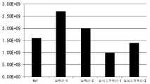
2 종류의 실록산과 2 종류의 실세스퀴옥산 물질에 열중량분석(TGA)을 수행하여 그 결과를 하기 표 1에 나타내었고, P & T MS를 측정하여 도 7에 나타내었다.Thermogravimetric analysis (TGA) was performed on two types of siloxane and two types of silsesquioxane materials, and the results are shown in Table 1 below, and P & T MS was measured and shown in FIG. 7 .
상기 표 1을 참고하면, 2 종류의 실록산의 중량 감소량은 각각 2.79%와 2.32%로 나타났고, 2 종류의 실세스퀴옥산의 중량 감소량은 0.07%와 0.25%로 나타났다.Referring to Table 1, the weight reductions of the two types of siloxanes were 2.79% and 2.32%, respectively, and the weight reductions of the two types of silsesquioxanes were 0.07% and 0.25%, respectively.
또한, 도 7을 참조하면, Ref 대비하여 2 종류의 실록산은 퓸 발생량이 각각 2.50E+09와 2.00E+09 이상으로 나타났으나, 2 종류의 실세스퀴옥산은 퓸 발생량이 각각 1.50E+09와 1.00E+09 이하로 나타났다.Also, referring to FIG. 7 , compared to Ref, the amount of fume generated by the two types of siloxanes was 2.50E+09 and 2.00E+09 or more, respectively, but the amount of fume generated by the two types of silsesquioxanes was 1.50E+, respectively. 09 and 1.00E+09 or less.
이 결과를 통해, 실록산보다 실세스퀴옥산이 내열성과 퓸 발생 특성이 우수한 것을 알 수 있었다.From this result, it was found that silsesquioxane had better heat resistance and fume generation characteristics than siloxane.
차광막의 제조Manufacturing of light-shielding film
<실시예 3><Example 3>
전술한 실시예 1과 동일한 공정 조건으로 제조된 나노입자 1g, TEOS 25.5g, PGMEA 20g, DI 워터 53.5g을 혼합하여 차광 물질을 제조하였다. 유리 기판 상에 차광 물질을 2㎛의 두께로 스핀코팅한 후 경화하여 차광막을 제조하였다.A light blocking material was prepared by mixing 1 g of nanoparticles prepared under the same process conditions as in Example 1, 25.5 g of TEOS, 20 g of PGMEA, and 53.5 g of DI water. A light blocking material was spin-coated to a thickness of 2 μm on a glass substrate and cured to prepare a light blocking film.
<실시예 4><Example 4>
전술한 실시예 3과 동일한 공정 조건 하에, TEOS 대신에 PVP를 사용하여 쉘을 형성한 것만 달리하여 차광막을 제조하였다.Under the same process conditions as in Example 3, a light-shielding film was manufactured except that the shell was formed using PVP instead of TEOS.
<실시예 5><Example 5>
전술한 실시예 3과 동일한 공정 조건 하에, TEOS 대신에 Acryl을 사용하여 쉘을 형성한 것만 달리하여 차광막을 제조하였다.Under the same process conditions as in Example 3, a light-shielding film was manufactured except that the shell was formed using Acryl instead of TEOS.
<실시예 6><Example 6>
전술한 실시예 3과 동일한 공정 조건 하에, TEOS 대신에 실세스퀴옥산을 사용하여 쉘을 형성한 것만 달리하여 차광막을 제조하였다.Under the same process conditions as in Example 3 described above, a light-shielding film was prepared except that the shell was formed using silsesquioxane instead of TEOS.
전술한 실시예 3 내지 6에 따라 제조된 차광막의 면저항, 반사율 및 투과율을 측정하여 하기 표 2에 나타내었다. 하기에서 '기판 면'은 기판 바닥면에서의 반사율을 의미하고, '코팅 면'은 차광막의 표면의 반사율을 의미한다.The sheet resistance, reflectance, and transmittance of the light-shielding films prepared according to Examples 3 to 6 were measured, and are shown in Table 2 below. Hereinafter, the 'substrate surface' refers to the reflectance on the bottom surface of the substrate, and the 'coated surface' refers to the reflectance of the surface of the light-shielding film.
(Ω/□)sheet resistance
(Ω/□)
상기 표 2를 참조하면, SiO2의 무기물의 쉘이 형성된 실시예 3과 6의 나노입자는 acryl이나 PVP의 유기물 계열의 쉘이 형성된 실시예 4 및 5의 나노입자보다 면저항과 비저항이 높고, 반사율이 낮은 것을 확인할 수 있었다. 또한, 실시예 3과 6은 카본블랙 입자가 형성된 실시예 4와 5에 근접하는 투과율을 나타내 차광 특성이 우수하게 나타났다. 특히, 실세스퀴옥산으로 형성된 실시예 6은 실록산으로 형성된 실시예 3보다 반사율과 투과율이 낮아 차광 특성이 더 우수한 것을 알 수 있다.Referring to Table 2, the nanoparticles of Examples 3 and 6 in which an inorganic shell of SiO2 is formed have higher sheet resistance and specific resistance than the nanoparticles of Examples 4 and 5 in which an organic shell of acryl or PVP is formed, and reflectance This low was confirmed. In addition, Examples 3 and 6 exhibited transmittance close to those of Examples 4 and 5 in which carbon black particles were formed, thereby showing excellent light-shielding properties. In particular, it can be seen that Example 6 formed of silsesquioxane had lower reflectance and transmittance than Example 3 formed of siloxane, and thus had better light blocking properties.
차광 물질의 내열성 비교Comparison of heat resistance of light-shielding materials
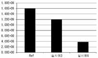
전술한 실시예 3과 실시예 6에 따라 제조된 차광 물질에 열중량분석(TGA)을 수행하여 그 결과를 하기 표 3과 도 8에 나타내었고, P & T MS를 측정하여 도 9에 나타내었다.Thermogravimetric analysis (TGA) was performed on the light-shielding material prepared according to Examples 3 and 6, and the results are shown in Table 3 and FIG. 8, and P & T MS was measured and shown in FIG. .
core
bookbinder
Nanoparticle:Binder:Solvent
MeOx
1:1:2
상기 표 3과 도 8을 참조하면, 실시예 3의 중량 감소량은 0.38%로 나타났고, 실시예 6의 중량 감소량은 0.25%로 나타났다. 또한, 도 9를 참조하면, Ref 대비하여 실시예 3의 퓸 발생량은 1.20E+09로 낮게 나타났고, 실시예 6의 퓸 발생량은 4.00E+08 이하로 낮게 나타났다.Referring to Table 3 and FIG. 8, the weight reduction of Example 3 was 0.38%, and the weight reduction of Example 6 was 0.25%. In addition, referring to FIG. 9 , the amount of fume generated in Example 3 was 1.20E+09 as low as compared to Ref, and the amount of fume generated in Example 6 was low as 4.00E+08 or less.
이 결과를 통해, 바인더로 실록산을 사용한 것보다 실세스퀴옥산을 사용한 차광 물질의 내열성 및 퓸 발생 특성이 우수한 것을 확인할 수 있었다.Through this result, it was confirmed that the light-shielding material using silsesquioxane had superior heat resistance and fume generation characteristics than that using siloxane as a binder.
차광막의 패턴 측정Pattern measurement of light-shielding film
전술한 실시예 6에 따라 제조된 차광막을 600nm로 형성한 후, CD(critical dimesion)이 10㎛인 마스크로 차광막 패턴을 형성하였다. 이 마스크와 차광막 패턴을 4배율 및 10배율의 광학 현미경으로 측정하여 도 10에 나타내었고, 차광막 패턴의 SEM 사진을 도 11에 나타내었다. 또한, 차광막 패턴의 400~700nm 파장대의 광에 대한 반사율을 측정하여 도 12에 나타내었다.After the light blocking film prepared according to Example 6 was formed to a thickness of 600 nm, a light blocking film pattern was formed using a mask having a CD (critical dimesion) of 10 μm. The mask and the light-shielding film pattern were measured with an optical microscope at 4 and 10 magnifications, and are shown in FIG. 10 , and an SEM photograph of the light-shielding film pattern is shown in FIG. 11 . In addition, the reflectance of the light-shielding film pattern with respect to light in a wavelength range of 400 to 700 nm was measured and shown in FIG. 12 .
도 10과 도 11을 참조하면, 마스크의 10㎛ CD에 따라 차광막 패턴의 CD도 10㎛로 정확하게 나타났고, 차광막 패턴의 에지부의 형상도 샤프하게 나타났다. 그리고, 도 12를 참조하면, 400~700nm 파장대의 광에 대한 차광막 패턴의 반사율이 4.95로 나타났다.Referring to FIGS. 10 and 11 , the CD of the light-shielding film pattern was precisely 10 µm according to the 10 µm CD of the mask, and the shape of the edge of the light-shielding film pattern was also sharp. And, referring to FIG. 12 , the reflectance of the light-shielding film pattern for light in a wavelength range of 400 to 700 nm was 4.95.
이 결과를 통해, 본 발명의 차광 물질로 형성한 차광막은 패턴이 정확하게 형성되고 반사율이 매우 낮은 것을 확인할 수 있었다.Through this result, it was confirmed that the light-shielding film formed of the light-shielding material of the present invention had a precisely formed pattern and had a very low reflectance.
상기와 같이, 본 발명의 일 실시예에 따른 차광 물질은 블랙의 금속 산화물 코어와 절연성의 쉘이 형성된 나노입자를 포함함으로써, 내열성이 우수하고 퓸이 발생하지 않아 신뢰성이 우수한 이점이 있다.As described above, the light-shielding material according to an embodiment of the present invention includes nanoparticles having a black metal oxide core and an insulating shell, and thus has excellent heat resistance and excellent reliability because no fumes are generated.
또한, 본 발명의 차광 물질로 이루어진 차광막은 면저항과 비저항이 높고 반사율이 낮으며 투과율이 낮아 차광 특성이 우수한 이점이 있다. 또한, 본 발명의 차광막을 구비하는 표시장치는 표시장치의 소자 특성이 저하되는 것을 방지하고 반사 방지를 위한 편광판이 생략될 수 있는 이점이 있다.In addition, the light-shielding film made of the light-shielding material of the present invention has advantages in that the sheet resistance and specific resistance are high, the reflectance is low, and the transmittance is low, so that the light-shielding property is excellent. In addition, the display device having the light blocking film of the present invention has the advantage that the element characteristics of the display device are prevented from being deteriorated and the polarizing plate for preventing reflection can be omitted.
이상 첨부된 도면을 참조하여 본 발명의 실시예를 설명하였지만, 상술한 본 발명의 기술적 구성은 본 발명이 속하는 기술 분야의 당업자가 본 발명의 그 기술적 사상이나 필수적 특징을 변경하지 않고서 다른 구체적인 형태로 실시될 수 있다는 것을 이해할 수 있을 것이다. 그러므로 이상에서 기술한 실시 예들은 모든 면에서 예시적인 것이며 한정적인 것이 아닌 것으로서 이해되어야 한다. 아울러, 본 발명의 범위는 상기 상세한 설명보다는 후술하는 특허청구범위에 의하여 나타내어진다. 또한, 특허청구범위의 의미 및 범위 그리고 그 등가 개념으로부터 도출되는 모든 변경 또는 변형된 형태가 본 발명의 범위에 포함되는 것으로 해석되어야 한다.
Although the embodiments of the present invention have been described above with reference to the accompanying drawings, the technical configuration of the present invention can be changed to other specific forms by those skilled in the art to which the present invention pertains without changing the technical spirit or essential features of the present invention. It will be appreciated that this may be practiced. Therefore, it should be understood that the embodiments described above are illustrative in all respects and not restrictive. In addition, the scope of the present invention is indicated by the claims to be described later rather than the above detailed description. In addition, all changes or modifications derived from the meaning and scope of the claims and their equivalents should be construed as being included in the scope of the present invention.
100 : 표시장치105 : 기판
110 : 버퍼층120 : 액티브층
125 : 게이트 절연막131: 게이트 전극
135 : 층간 절연막141 : 소스 전극
142 : 드레인 전극145 : 패시베이션막
150 : 보호막160 : 화소 전극
165 : 뱅크층170: 유기 발광층
175 : 대향 전극100: display device 105: substrate
110: buffer layer 120: active layer
125: gate insulating film 131: gate electrode
135: interlayer insulating film 141: source electrode
142: drain electrode 145: passivation film
150: protective film 160: pixel electrode
165: bank layer 170: organic light emitting layer
175: counter electrode
Claims (17)
Translated fromKorean상기 기판 상에 위치하는 차광막;
상기 차광막 상에 위치하며, 액티브층, 게이트 전극, 소스 전극 및 드레인 전극을 포함하는 박막트랜지스터;
상기 박막트랜지스터 상에 상기 박막트랜지스터와 연결되는 화소 전극;
상기 화소 전극의 가장자리를 덮고 상기 화소 전극의 중앙을 노출하는 뱅크층;
상기 화소 전극 상에 위치하는 유기 발광층;
상기 유기 발광층 상에 위치하는 대향 전극;
상기 화소 전극과 상기 기판 사이에 위치하는 컬러필터를 포함하며,
상기 차광막은 코어 및 쉘을 포함하는 나노입자 및 바인더를 포함하며, 상기 코어는 블랙을 나타내는 금속 산화물로 이루어지고, 상기 쉘은 절연 특성을 나타내는 물질로 이루어지며,
상기 블랙을 나타내는 금속 산화물은 구리망간산화물(CuMnOx), 구리크롬산화물(CuCrxOy)로 이루어지는 군에서 선택되고,
상기 컬러필터는 상기 유기 발광층과 중첩하며 상기 차광막과는 중첩하지 않는 것을 특징으로 하는 표시장치.
Board;
a light blocking film positioned on the substrate;
a thin film transistor disposed on the light blocking layer and including an active layer, a gate electrode, a source electrode, and a drain electrode;
a pixel electrode connected to the thin film transistor on the thin film transistor;
a bank layer covering an edge of the pixel electrode and exposing a center of the pixel electrode;
an organic light emitting layer positioned on the pixel electrode;
a counter electrode positioned on the organic light emitting layer;
a color filter positioned between the pixel electrode and the substrate;
The light shielding film includes nanoparticles and a binder including a core and a shell, the core is made of a metal oxide representing black, and the shell is made of a material exhibiting insulating properties,
The metal oxide representing the black is selected from the group consisting of copper manganese oxide (CuMnOx), copper chromium oxide (CuCrxOy),
The color filter overlaps the organic light emitting layer and does not overlap the light blocking layer.
상기 쉘은 실록산(siloxane), 실리콘 산화물(SiOx), 실리콘 질화물(SiNx), 산화 티타늄(TiO2) 및 실란(silane)으로 이루어진 군에서 선택된 어느 하나인 것을 특징으로 하는 표시장치.
7. The method of claim 6,
The shell is any one selected from the group consisting of siloxane, silicon oxide (SiOx), silicon nitride (SiNx), titanium oxide (TiO2 ), and silane.
상기 바인더는 350℃ 이하의 공정이 가능한 고내열 용액형 재료인 것을 특징으로 하는 표시장치.
7. The method of claim 6,
The display device, characterized in that the binder is a high heat-resistant solution-type material that can be processed at a temperature of 350°C or less.
상기 바인더는 실세스퀴옥산(silsesquioxane, SSQ)인 것을 특징으로 하는 표시장치.
10. The method of claim 9,
wherein the binder is silsesquioxane (SSQ).
상기 액티브층은 산화물 반도체로 이루어진 것을 특징으로 하는 표시장치.
7. The method of claim 6,
The active layer is a display device, characterized in that made of an oxide semiconductor.
상기 차광막은 면저항이 3.2×10¹² 이상인 것을 특징으로 하는 표시장치.
7. The method of claim 6,
The light blocking film has a sheet resistance of 3.2×10¹² or more.
상기 차광막은 350 내지 500nm의 광에 대한 투과율이 1.59% 이하이고, 550nm의 광에 대한 투과율이 2.03% 이하인 것을 특징으로 하는 표시장치.
7. The method of claim 6,
The light blocking layer has a transmittance of 1.59% or less for light of 350 to 500 nm and a transmittance of 2.03% or less with respect to light of 550 nm.
상기 차광막은 400 내지 700nm의 광에 대한 반사율이 7.56% 이하인 것을 특징으로 하는 표시장치.
7. The method of claim 6,
The light blocking layer has a reflectance of 7.56% or less with respect to light of 400 to 700 nm.
상기 기판 상에 위치하는 박막트랜지스터; 및
상기 박막트랜지스터 상에 위치하며 각각의 화소를 구획하는 차광막;
상기 화소에 형성된 컬러필터를 포함하며,
상기 차광막은 코어 및 쉘을 포함하는 나노입자 및 바인더를 포함하며, 상기 코어는 블랙을 나타내는 금속 산화물로 이루어지고, 상기 쉘은 절연 특성을 나타내는 물질로 이루어지며,
상기 블랙을 나타내는 금속 산화물은 구리망간산화물(CuMnOx), 구리크롬산화물(CuCrxOy)로 이루어지는 군에서 선택되고,
상기 컬러필터는 상기 차광막과 중첩하지 않는 것을 특징으로 하는 표시장치.
Board;
a thin film transistor positioned on the substrate; and
a light blocking film positioned on the thin film transistor and partitioning each pixel;
It includes a color filter formed in the pixel,
The light shielding film includes nanoparticles and a binder including a core and a shell, the core is made of a metal oxide representing black, and the shell is made of a material exhibiting insulating properties,
The metal oxide representing the black is selected from the group consisting of copper manganese oxide (CuMnOx), copper chromium oxide (CuCrxOy),
The color filter does not overlap the light blocking layer.
상기 차광막은 블랙 매트릭스 또는 블랙 뱅크층으로 사용되는 것을 특징으로 하는 표시장치.16. The method of claim 15,
The light blocking layer is used as a black matrix or black bank layer.
Priority Applications (2)
| Application Number | Priority Date | Filing Date | Title |
|---|---|---|---|
| US14/751,628US10061151B2 (en) | 2014-06-30 | 2015-06-26 | Light shielding material and display device including the same |
| CN201510405784.0ACN105219149B (en) | 2014-06-30 | 2015-06-30 | Light screening material and display device comprising light screening material |
Applications Claiming Priority (2)
| Application Number | Priority Date | Filing Date | Title |
|---|---|---|---|
| KR1020140081278 | 2014-06-30 | ||
| KR20140081278 | 2014-06-30 |
Publications (2)
| Publication Number | Publication Date |
|---|---|
| KR20160002596A KR20160002596A (en) | 2016-01-08 |
| KR102391354B1true KR102391354B1 (en) | 2022-04-28 |
Family
ID=55170485
Family Applications (1)
| Application Number | Title | Priority Date | Filing Date |
|---|---|---|---|
| KR1020140181957AActiveKR102391354B1 (en) | 2014-06-30 | 2014-12-17 | Light shielding material and display device comprising of the same |
Country Status (1)
| Country | Link |
|---|---|
| KR (1) | KR102391354B1 (en) |
Families Citing this family (3)
| Publication number | Priority date | Publication date | Assignee | Title |
|---|---|---|---|---|
| KR102624253B1 (en)* | 2016-08-23 | 2024-01-12 | 엘지디스플레이 주식회사 | High heat resisant planarization film, array substrate for display device and display device having the film |
| KR102745475B1 (en)* | 2018-12-27 | 2024-12-20 | 엘지디스플레이 주식회사 | Display device |
| KR20220053708A (en) | 2020-10-22 | 2022-05-02 | 삼성디스플레이 주식회사 | Display device and method for manufacturing the same |
Citations (3)
| Publication number | Priority date | Publication date | Assignee | Title |
|---|---|---|---|---|
| US20060008942A1 (en)* | 2004-07-07 | 2006-01-12 | Nanosys, Inc. | Systems and methods for harvesting and integrating nanowires |
| US20070164939A1 (en)* | 2006-01-13 | 2007-07-19 | Semiconductor Energy Laboratory Co., Ltd. | Display device and electoric device having the same |
| US20080198109A1 (en)* | 2007-02-16 | 2008-08-21 | Samsung Electronics Co., Ltd. | Color magnetic display pixel panel |
Family Cites Families (2)
| Publication number | Priority date | Publication date | Assignee | Title |
|---|---|---|---|---|
| KR100709866B1 (en)* | 2005-08-01 | 2007-04-23 | 제일모직주식회사 | Low reflectance luminance improving optical film for display device and display device using same |
| KR102010391B1 (en)* | 2012-12-12 | 2019-10-21 | 엘지디스플레이 주식회사 | Composition for Coating Light Blocking Member of Image Display Device and Image Display Device Having the Composition |
- 2014
- 2014-12-17KRKR1020140181957Apatent/KR102391354B1/enactiveActive
Patent Citations (3)
| Publication number | Priority date | Publication date | Assignee | Title |
|---|---|---|---|---|
| US20060008942A1 (en)* | 2004-07-07 | 2006-01-12 | Nanosys, Inc. | Systems and methods for harvesting and integrating nanowires |
| US20070164939A1 (en)* | 2006-01-13 | 2007-07-19 | Semiconductor Energy Laboratory Co., Ltd. | Display device and electoric device having the same |
| US20080198109A1 (en)* | 2007-02-16 | 2008-08-21 | Samsung Electronics Co., Ltd. | Color magnetic display pixel panel |
Also Published As
| Publication number | Publication date |
|---|---|
| KR20160002596A (en) | 2016-01-08 |
Similar Documents
| Publication | Publication Date | Title |
|---|---|---|
| CN105219149B (en) | Light screening material and display device comprising light screening material | |
| Chiba et al. | Anion-exchange red perovskite quantum dots with ammonium iodine salts for highly efficient light-emitting devices | |
| US9412765B2 (en) | Thin film transistor, manufacturing method of same, and display device | |
| Hur et al. | Stretchable polymer gate dielectric by ultraviolet-assisted hafnium oxide doping at low temperature for high-performance indium gallium tin oxide transistors | |
| KR20180054262A (en) | Quantum dot light emitting diode and light emitting display device using the diode | |
| JP6466922B2 (en) | Interfacial layer for electronic devices | |
| KR102391354B1 (en) | Light shielding material and display device comprising of the same | |
| KR102010391B1 (en) | Composition for Coating Light Blocking Member of Image Display Device and Image Display Device Having the Composition | |
| KR102394425B1 (en) | Composition, electronic device, and thin film transistor | |
| US10998389B2 (en) | Pixel defining layer including a temperature-sensitive polymer layer, display substrate, and manufacturing methods thereof | |
| Kim et al. | All‐in‐One Process for Color Tuning and Patterning of Perovskite Quantum Dot Light‐Emitting Diodes | |
| US11018322B2 (en) | Light emitting device using light emitting diode | |
| WO2012086595A1 (en) | Semiconductor device, color filter substrate, display device provided with color filter substrate, and method for manufacturing semiconductor device | |
| US9240565B2 (en) | Composition | |
| Park et al. | Self-defect-passivation by Br-enrichment in FA-doped Cs1− x FA x PbBr3 quantum dots: towards high-performance quantum dot light-emitting diodes | |
| KR101737757B1 (en) | Forming method of hybrid coating layer and Manufacturing method of organic electronic device using the same | |
| CN106104706A (en) | Transparent conductor, its manufacture method and include its optical display devices | |
| KR102332948B1 (en) | Polarizer device and display device comprising the same | |
| TW560074B (en) | Thin film transistor and display apparatus with the same | |
| WO2015108385A1 (en) | Barrier film and method for producing same | |
| Wu et al. | Printable poly (methylsilsesquioxane) dielectric ink and its application in solution processed metal oxide thin-film transistors | |
| KR20180078414A (en) | Transparent Conductive Layer And Liquid Crystal Display Device Comprising The Same | |
| KR20140065660A (en) | Substrate and display device including the same | |
| CN105225727A (en) | Transparency conducting layer, for the manufacture of its method and comprise its display unit | |
| KR102624253B1 (en) | High heat resisant planarization film, array substrate for display device and display device having the film |
Legal Events
| Date | Code | Title | Description |
|---|---|---|---|
| PA0109 | Patent application | Patent event code:PA01091R01D Comment text:Patent Application Patent event date:20141217 | |
| PG1501 | Laying open of application | ||
| A201 | Request for examination | ||
| PA0201 | Request for examination | Patent event code:PA02012R01D Patent event date:20191125 Comment text:Request for Examination of Application Patent event code:PA02011R01I Patent event date:20141217 Comment text:Patent Application | |
| E902 | Notification of reason for refusal | ||
| PE0902 | Notice of grounds for rejection | Comment text:Notification of reason for refusal Patent event date:20210322 Patent event code:PE09021S01D | |
| E90F | Notification of reason for final refusal | ||
| PE0902 | Notice of grounds for rejection | Comment text:Final Notice of Reason for Refusal Patent event date:20210929 Patent event code:PE09021S02D | |
| E701 | Decision to grant or registration of patent right | ||
| PE0701 | Decision of registration | Patent event code:PE07011S01D Comment text:Decision to Grant Registration Patent event date:20220328 | |
| PR0701 | Registration of establishment | Comment text:Registration of Establishment Patent event date:20220422 Patent event code:PR07011E01D | |
| PR1002 | Payment of registration fee | Payment date:20220422 End annual number:3 Start annual number:1 | |
| PG1601 | Publication of registration | ||
| PR1001 | Payment of annual fee | Payment date:20250318 Start annual number:4 End annual number:4 |