KR102390437B1 - Flexible display device and driving mathod of the same - Google Patents
Flexible display device and driving mathod of the sameDownload PDFInfo
- Publication number
- KR102390437B1 KR102390437B1KR1020170170436AKR20170170436AKR102390437B1KR 102390437 B1KR102390437 B1KR 102390437B1KR 1020170170436 AKR1020170170436 AKR 1020170170436AKR 20170170436 AKR20170170436 AKR 20170170436AKR 102390437 B1KR102390437 B1KR 102390437B1
- Authority
- KR
- South Korea
- Prior art keywords
- input
- point
- display panel
- flexible display
- electronic device
- Prior art date
- Legal status (The legal status is an assumption and is not a legal conclusion. Google has not performed a legal analysis and makes no representation as to the accuracy of the status listed.)
- Active
Links
Images


Classifications
- G—PHYSICS
- G06—COMPUTING OR CALCULATING; COUNTING
- G06F—ELECTRIC DIGITAL DATA PROCESSING
- G06F1/00—Details not covered by groups G06F3/00 - G06F13/00 and G06F21/00
- G06F1/16—Constructional details or arrangements
- G06F1/1613—Constructional details or arrangements for portable computers
- G06F1/1633—Constructional details or arrangements of portable computers not specific to the type of enclosures covered by groups G06F1/1615 - G06F1/1626
- G06F1/1637—Details related to the display arrangement, including those related to the mounting of the display in the housing
- G06F1/1652—Details related to the display arrangement, including those related to the mounting of the display in the housing the display being flexible, e.g. mimicking a sheet of paper, or rollable
- G—PHYSICS
- G06—COMPUTING OR CALCULATING; COUNTING
- G06F—ELECTRIC DIGITAL DATA PROCESSING
- G06F1/00—Details not covered by groups G06F3/00 - G06F13/00 and G06F21/00
- G06F1/16—Constructional details or arrangements
- G06F1/1613—Constructional details or arrangements for portable computers
- G06F1/1615—Constructional details or arrangements for portable computers with several enclosures having relative motions, each enclosure supporting at least one I/O or computing function
- G—PHYSICS
- G06—COMPUTING OR CALCULATING; COUNTING
- G06F—ELECTRIC DIGITAL DATA PROCESSING
- G06F1/00—Details not covered by groups G06F3/00 - G06F13/00 and G06F21/00
- G06F1/16—Constructional details or arrangements
- G06F1/1613—Constructional details or arrangements for portable computers
- G06F1/1626—Constructional details or arrangements for portable computers with a single-body enclosure integrating a flat display, e.g. Personal Digital Assistants [PDAs]
- G—PHYSICS
- G06—COMPUTING OR CALCULATING; COUNTING
- G06F—ELECTRIC DIGITAL DATA PROCESSING
- G06F1/00—Details not covered by groups G06F3/00 - G06F13/00 and G06F21/00
- G06F1/16—Constructional details or arrangements
- G06F1/1613—Constructional details or arrangements for portable computers
- G06F1/163—Wearable computers, e.g. on a belt
- G—PHYSICS
- G06—COMPUTING OR CALCULATING; COUNTING
- G06F—ELECTRIC DIGITAL DATA PROCESSING
- G06F1/00—Details not covered by groups G06F3/00 - G06F13/00 and G06F21/00
- G06F1/16—Constructional details or arrangements
- G06F1/1613—Constructional details or arrangements for portable computers
- G06F1/1633—Constructional details or arrangements of portable computers not specific to the type of enclosures covered by groups G06F1/1615 - G06F1/1626
- G06F1/1637—Details related to the display arrangement, including those related to the mounting of the display in the housing
- G06F1/1641—Details related to the display arrangement, including those related to the mounting of the display in the housing the display being formed by a plurality of foldable display components
- G—PHYSICS
- G06—COMPUTING OR CALCULATING; COUNTING
- G06F—ELECTRIC DIGITAL DATA PROCESSING
- G06F1/00—Details not covered by groups G06F3/00 - G06F13/00 and G06F21/00
- G06F1/16—Constructional details or arrangements
- G06F1/1613—Constructional details or arrangements for portable computers
- G06F1/1633—Constructional details or arrangements of portable computers not specific to the type of enclosures covered by groups G06F1/1615 - G06F1/1626
- G06F1/1684—Constructional details or arrangements related to integrated I/O peripherals not covered by groups G06F1/1635 - G06F1/1675
- G—PHYSICS
- G06—COMPUTING OR CALCULATING; COUNTING
- G06F—ELECTRIC DIGITAL DATA PROCESSING
- G06F3/00—Input arrangements for transferring data to be processed into a form capable of being handled by the computer; Output arrangements for transferring data from processing unit to output unit, e.g. interface arrangements
- G06F3/14—Digital output to display device ; Cooperation and interconnection of the display device with other functional units
- G06F3/147—Digital output to display device ; Cooperation and interconnection of the display device with other functional units using display panels
- G—PHYSICS
- G09—EDUCATION; CRYPTOGRAPHY; DISPLAY; ADVERTISING; SEALS
- G09G—ARRANGEMENTS OR CIRCUITS FOR CONTROL OF INDICATING DEVICES USING STATIC MEANS TO PRESENT VARIABLE INFORMATION
- G09G5/00—Control arrangements or circuits for visual indicators common to cathode-ray tube indicators and other visual indicators
- G09G5/36—Control arrangements or circuits for visual indicators common to cathode-ray tube indicators and other visual indicators characterised by the display of a graphic pattern, e.g. using an all-points-addressable [APA] memory
- G09G5/38—Control arrangements or circuits for visual indicators common to cathode-ray tube indicators and other visual indicators characterised by the display of a graphic pattern, e.g. using an all-points-addressable [APA] memory with means for controlling the display position
- G—PHYSICS
- G09—EDUCATION; CRYPTOGRAPHY; DISPLAY; ADVERTISING; SEALS
- G09G—ARRANGEMENTS OR CIRCUITS FOR CONTROL OF INDICATING DEVICES USING STATIC MEANS TO PRESENT VARIABLE INFORMATION
- G09G2340/00—Aspects of display data processing
- G09G2340/04—Changes in size, position or resolution of an image
- G09G2340/0464—Positioning
- G—PHYSICS
- G09—EDUCATION; CRYPTOGRAPHY; DISPLAY; ADVERTISING; SEALS
- G09G—ARRANGEMENTS OR CIRCUITS FOR CONTROL OF INDICATING DEVICES USING STATIC MEANS TO PRESENT VARIABLE INFORMATION
- G09G2354/00—Aspects of interface with display user
- G—PHYSICS
- G09—EDUCATION; CRYPTOGRAPHY; DISPLAY; ADVERTISING; SEALS
- G09G—ARRANGEMENTS OR CIRCUITS FOR CONTROL OF INDICATING DEVICES USING STATIC MEANS TO PRESENT VARIABLE INFORMATION
- G09G2380/00—Specific applications
- G09G2380/02—Flexible displays
Landscapes
- Engineering & Computer Science (AREA)
- Theoretical Computer Science (AREA)
- Computer Hardware Design (AREA)
- Physics & Mathematics (AREA)
- General Physics & Mathematics (AREA)
- Human Computer Interaction (AREA)
- General Engineering & Computer Science (AREA)
- Mathematical Physics (AREA)
- Devices For Indicating Variable Information By Combining Individual Elements (AREA)
- Electroluminescent Light Sources (AREA)
- Control Of Indicators Other Than Cathode Ray Tubes (AREA)
Abstract
Translated fromKoreanDescription
Translated fromKorean본 발명은 전자장치 및 그 구동방법에 관한 것으로, 크로스 뱅글 형상으로 벤딩되는 전자장치 및 그 구동방법에 관한 것이다.The present invention relates to an electronic device and a driving method thereof, and to an electronic device bent in a cross bangle shape and a driving method thereof.
텔레비전, 휴대 전화, 태블릿 컴퓨터, 네비게이션, 게임기 등과 같은 멀티 미디어 장치와 같은 다양한 전자장치들이 개발되고 있다. 전자장치들은 이미지를 제공하는 표시패널과, 입력장치 등을 포함한다. 또한, 최근에 개발되는 전자장치들은 입력장치로써 터치패널을 구비한다.BACKGROUND ART Various electronic devices such as multimedia devices such as televisions, mobile phones, tablet computers, navigation devices, and game machines have been developed. Electronic devices include a display panel that provides an image, an input device, and the like. In addition, recently developed electronic devices include a touch panel as an input device.
종래의 평면 전자장치와 달리 최근에는 다양한 형태의 전자장치가 개발되고 있다. 표시패널의 형태가 커브드인 전자장치, 표시패널이 벤딩되는 벤딩형 전자장치, 표시패널이 폴딩되는 폴더블 전자장치, 표시패널이 감기는 롤러블 전자장치, 및 표시패널이 늘어나는 스트레처블 전자장치들이 개발되고 있다.Unlike conventional planar electronic devices, various types of electronic devices have been developed in recent years. An electronic device in which the display panel has a curved shape, a bendable electronic device in which the display panel is bent, a foldable electronic device in which the display panel is folded, a rollable electronic device in which the display panel is wound, and a stretchable electronic device in which the display panel is stretched Devices are being developed.
본 발명의 목적은 전자장치의 크로스 뱅글 형상을 식별하여 변형된 형상에 부합하는 이미지를 제공할 수 있는 전자장치를 제공하는 것이다.SUMMARY OF THE INVENTION It is an object of the present invention to provide an electronic device capable of providing an image conforming to a deformed shape by identifying a cross bangle shape of the electronic device.
본 발명의 목적은 전자장치의 변형된 형상에 따라 적합한 이미지를 제공할 수 있는 전자장치의 구동방법을 제공하는 것이다.SUMMARY OF THE INVENTION It is an object of the present invention to provide a method of driving an electronic device capable of providing a suitable image according to a deformed shape of the electronic device.
본 발명의 일 실시예에 따른 전자장치는 플렉서블 표시패널, 입력감지패널 및 상기 플렉서블 표시패널 및 상기 입력감지패널을 제어하는 제어모듈을 포함할 수 있다. 상기 플렉서블 표시패널은 제1 방향의 제1 길이 및 상기 제1 방향과 직교하는 제2 방향의 제2 길이를 갖고 이미지를 표시하는 표시면 및 상기 표시면과 두께 방향에서 대향하는 배면을 포함하고, 펼쳐진 상태에서 상기 제2 방향으로 연장된 형상을 갖는다. 상기 입력감지패널은 상기 표시면 상에 배치된 제1 부분, 상기 제1 부분으로부터 연장되며 상기 배면 상에 배치된 제2 부분, 상기 제1 부분으로부터 연장되며 상기 배면 상에 배치되고 상기 배면 상에서 상기 제2 부분과 이격된 제3 부분을 포함하고, 상기 플렉서블 표시패널에 결합되고, 상기 플렉서블 표시패널이 펼쳐진 상태에서 상기 제2 방향으로 연장된 형상을 갖는다.An electronic device according to an embodiment of the present invention may include a flexible display panel, an input sensing panel, and a control module for controlling the flexible display panel and the input sensing panel. The flexible display panel includes a display surface having a first length in a first direction and a second length in a second direction perpendicular to the first direction, the display surface displaying an image, and a rear surface opposite to the display surface in a thickness direction; It has a shape extending in the second direction in an unfolded state. The input sensing panel may include a first portion disposed on the display surface, a second portion extending from the first portion and disposed on the rear surface, and disposed on the rear surface and extending from the first portion, wherein the input sensing panel is disposed on the rear surface. It includes a third portion spaced apart from the second portion, is coupled to the flexible display panel, and has a shape extending in the second direction in an unfolded state of the flexible display panel.
상기 입력감지패널로부터 4개의 입력지점들이 검출되고, 상기 4개의 입력지점들 중 제1 입력지점과 제2 입력지점이 상기 제1 부분에서 검출되고, 상기 제1 입력지점과 상기 제2 입력지점 제1 대각선 방향으로 배열되고, 제3 입력지점과 제4 입력지점이 상기 제2 부분과 상기 제3 부분에서 각각 검출되고, 상기 제3 입력지점의 상기 제1 부분으로 투영된 제1 투영지점과 상기 제4 입력지점의 상기 제1 부분으로 투영된 제2 투영지점이 상기 제1 대각선 방향과 교차하는 제2 대각선 방향으로 배열될 때, 상기 제어모듈은 상기 플렉서블 표시패널이 크로스 뱅글 형상으로 벤딩된 상태로 판단한다.Four input points are detected from the input detection panel, a first input point and a second input point among the four input points are detected in the first part, and the first input point and the second input point are detected in the first part. a first projection point arranged in a diagonal direction, a third input point and a fourth input point respectively detected in the second part and the third part, and projected onto the first part of the third input point, and the When a second projection point projected to the first portion of a fourth input point is arranged in a second diagonal direction intersecting the first diagonal direction, the control module determines that the flexible display panel is bent in a cross-bangle shape to be judged as
상기 플렉서블 표시패널의 상기 크로스 뱅글 형상은 펼쳐진 상태에서 상기 제2 방향에서 마주했던 상기 플렉서블 표시패널의 일단과 상기 플렉서블 표시패널의 타단이 서로 맞닿고, 상기 플렉서블 표시패널의 2개의 부분들이 교차하면서 2개의 링들이 정의되도록 꼬여진 형상으로 정의된다.In the cross-bangle shape of the flexible display panel, in an unfolded state, one end of the flexible display panel facing in the second direction and the other end of the flexible display panel contact each other, and the two portions of the flexible display panel cross It is defined as a twisted shape such that the rings are defined.
상기 제1 입력지점 내지 상기 제4 입력지점 중 상기 제1 입력지점이 상기 플렉서블 표시패널의 상기 일단에 가장 인접하고, 상기 제1 입력지점 내지 상기 제4 입력지점 중 상기 제4 입력지점이 상기 플렉서블 표시패널의 상기 타단에 가장 인접한다.The first input point among the first input point to the fourth input point is closest to the one end of the flexible display panel, and the fourth input point among the first input point to the fourth input point is the flexible display panel. It is closest to the other end of the display panel.
상기 제어모듈은 상기 플렉서블 표시패널이 크로스 뱅글 형상으로 벤딩된 상태 판단될 때, 상기 플렉서블 표시패널의 상기 일단으로부터 상기 제1 입력지점까지 정의되는 제1 표시부분, 상기 플렉서블 표시패널의 상기 타단으로부터 상기 제2 투영지점에 중첩까지 정의되는 제2 표시부분, 및 상기 제2 입력지점으로부터 상기 제1 투영지점까지 정의되는 제3 표시부분에 상기 이미지를 표시할 수 있다.When it is determined that the flexible display panel is bent in a cross-bangle shape, the control module includes a first display portion defined from the one end of the flexible display panel to the first input point, and the other end of the flexible display panel. The image may be displayed on a second display portion defined up to overlap with the second projection point and on a third display portion defined from the second input point to the first projection point.
상기 제1 입력지점과 상기 제2 입력지점의 중간 지점과 상기 제3 입력지점의 상기 투영지점과 상기 제4 입력지점의 상기 투영지점의 중간 지점 사이의 길이는 실질적으로 상기 제2 길이의 절반에 대응 할 수 있다.The length between the midpoint of the first input point and the second input point and the midpoint of the projection point of the third input point and the projection point of the fourth input point is substantially half of the second length can respond
상기 제1 입력지점과 상기 제4 입력지점의 상기 투영지점 사이의 길이와 상기 제2 입력지점과 상기 제3 입력지점의 상기 투영지점 사이의 길이의 평균은 실질적으로 상기 제2 길이의 절반에 대응할 수 있다.The average of the length between the projection point of the first input point and the fourth input point and the length between the second input point and the projection point of the third input point may correspond to substantially half of the second length. can
상기 플렉서블 표시패널이 크로스 뱅글 형상으로 벤딩된 상태로 판단될 때, 상기 제어모듈은 상기 입력감지패널의 상기 제2 부분과 상기 제3 부분을 비활성화시킬 수 있다.When it is determined that the flexible display panel is bent in a cross-bangle shape, the control module may inactivate the second portion and the third portion of the input sensing panel.
상기 플렉서블 표시패널이 크로스 뱅글 형상으로 벤딩된 상태에서 사용자의 손목에 착용될 수 있다.The flexible display panel may be worn on a user's wrist in a state in which it is bent in a cross bangle shape.
상기 제2 부분과 상기 제3 부분에 중첩하는 차광패턴을 더 할 수 있다.A light blocking pattern overlapping the second portion and the third portion may be added.
상기 제2 방향의 길이는 상기 제1 방향의 길이보다 10 배 내지 30 배 클 수 있다.A length in the second direction may be 10 to 30 times greater than a length in the first direction.
상기 제2 방향의 길이는 30cm 내지 50cm일 수 있다.The length in the second direction may be 30 cm to 50 cm.
상기 플렉서블 표시패널의 형상 변화를 감지하는 벤딩감지센서를 더 포함 할 수 있다.The flexible display panel may further include a bending sensor for detecting a change in shape.
상기 벤딩감지센서는 인가된 응력의 세기에 대응하게 저항이 변화되는 물질을 포함할 수 있다.The bending sensor may include a material whose resistance is changed in response to the strength of the applied stress.
본 발명의 일 실시예에 따른 입력감지패널은 상기 표시면 상에 배치된 제1 부분, 상기 제1 부분으로부터 연장되며 상기 측면들 중 제1 측면 상에 배치된 제2 부분, 상기 제1 부분으로부터 연장되며 상기 측면들 중 상기 제1 측면과 상기 제1 방향에서 마주하는 제2 측면 상에 배치된 제3 부분을 포함하고, 상기 플렉서블 표시패널에 결합되고, 상기 플렉서블 표시패널이 펼쳐진 상태에서 상기 제2 방향으로 연장된 형상을 가질 수 있다.An input sensing panel according to an embodiment of the present invention includes a first portion disposed on the display surface, a second portion extending from the first portion and disposed on a first side of the side surfaces, and the first portion a third portion extending from the side surfaces and disposed on a second side surface facing the first side surface in the first direction, coupled to the flexible display panel, and wherein the second portion is in an unfolded state of the flexible display panel It may have a shape extending in two directions.
상기 입력감지패널로부터 4개의 입력지점들이 검출되고, 상기 4개의 입력지점들 중 제1 입력지점과 제2 입력지점이 상기 제2 부분과 상기 제3 부분에 각각 배치되고, 상기 제1 입력지점의 상기 제1 부분으로 투영된 제1 투영지점과 상기 제2 입력지점의 상기 제1 부분으로 투영된 제2 투영지점이 제1 대각선 방향으로 배열되고, 상기 4개의 입력지점들 중 제3 입력지점과 제4 입력지점이 상기 제3 부분과 상기 제2 부분에 각각 배치되고, 상기 제3 입력지점의 상기 제1 부분으로 투영된 제3 투영지점과 상기 제4 입력지점의 상기 제1 부분으로 투영된 제4 투영지점이 상기 제1 대각선 방향과 교차하는 제2 대각선 방향으로 배열될 때, 상기 제어모듈은 상기 플렉서블 표시패널이 크로스 뱅글 형상으로 벤딩된 상태로 판단할 수 있다.Four input points are detected from the input detection panel, and a first input point and a second input point among the four input points are respectively disposed in the second part and the third part, and A first projection point projected to the first portion and a second projection point projected to the first portion of the second input point are arranged in a first diagonal direction, and a third input point of the four input points and A fourth input point is disposed on the third portion and the second portion, respectively, and a third projection point projected onto the first portion of the third input point and a third projection point projected onto the first portion of the fourth input point When a fourth projection point is arranged in a second diagonal direction intersecting the first diagonal direction, the control module may determine that the flexible display panel is bent in a cross-bangle shape.
상기 제1 투영지점과 상기 제2 투영지점의 중간 지점과 상기 제3 투영지점과 상기 제4 투영지점의 중간 지점 사이의 길이는 실질적으로 상기 제2 길이의 절반에 대응할 수 있다.A length between a midpoint between the first projection point and the second projection point and a midpoint between the third projection point and the fourth projection point may substantially correspond to half of the second length.
상기 제1 투영지점과 상기 제4 투영지점 사이의 길이와 상기 제2 투영지점과 상기 제3 투영지점 사이의 길이의 평균은 실질적으로 상기 제2 길이의 절반에 대응할 수 있다.An average of a length between the first projection point and the fourth projection point and a length between the second projection point and the third projection point may correspond to substantially half of the second length.
본 발명의 일 실시예에 따른 전자장치의 구동방법은 플렉서블 표시패널, 입력감지패널, 및 제어모듈을 포함하는 전자장치의 크로스 뱅글 동작을 판단하는 단계 및 상기 전자장치가 크로스 뱅글 형상으로 동작된 것으로 판단될 때, 상기 플렉서블 표시패널의 일부분에 이미지를 표시하는 단계를 포함할 수 있다.A method of driving an electronic device according to an embodiment of the present invention includes determining a cross-bangle operation of an electronic device including a flexible display panel, an input sensing panel, and a control module, and the electronic device is operated in a cross-bangle shape. When it is determined, the method may include displaying an image on a portion of the flexible display panel.
상기 입력감지패널로부터 4개의 입력지점들이 검출되고, 상기 4개의 입력지점들 중 제1 입력지점의 상기 플렉서블 표시패널에 투영한 제1 투영지점과 제2 입력지점의 상기 플렉서블 표시패널에 투영한 제2 투영지점이 제1 대각선 방향으로 배치되고, 제3 입력지점의 상기 플렉서블 표시패널에 투영한 제3 투영지점과 제4 입력지점의 상기 플렉서블 표시패널에 투영한 제4 투영지점이 상기 제1 대각선 방향과 교차하는 제2 대각선 방향으로 배열될 때, 상기 제어모듈은 상기 전자장치가 크로스 뱅글 형상으로 벤딩된 상태로 판단 할 수 있다.Four input points are detected from the input sensing panel, and among the four input points, a first projection point projected on the flexible display panel and a second input point projected on the flexible display panel of a
상기 전자장치의 벤딩 동작을 감지하는 단계를 더 포함 할 수 있다. 상기 전자장치의 벤딩 동작이 감지될 때, 상기 전자장치의 크로스 뱅글 동작을 판단 할 수 있다.The method may further include detecting a bending motion of the electronic device. When the bending motion of the electronic device is detected, the cross-bangle motion of the electronic device may be determined.
상기 제1 투영지점 내지 상기 제4 투영지점 중 상기 제1 투영지점이 상기 플렉서블 표시패널의 상기 일단에 가장 인접하고, 상기 제1 투영지점 내지 상기 제4 투영지점 중 상기 제4 투영지점이 상기 플렉서블 표시패널의 상기 타단에 가장 인접 할 수 있다.The first projection point among the first projection points to the fourth projection points is closest to the one end of the flexible display panel, and the fourth projection point among the first projection points to the fourth projection points is the flexible display panel. It may be closest to the other end of the display panel.
상기 이미지가 표시되는 상기 플렉서블 표시패널의 일부분은 상기 플렉서블 표시패널의 상기 일단으로부터 상기 제1 투영지점까지 정의되는 제1 표시부분, 상기 플렉서블 표시패널의 상기 타단으로부터 상기 제4 투영지점까지 정의되는 제2 표시부분, 및 상기 제2 투영지점으로부터 상기 제3 투영지점까지 정의되는 제3 표시부분을 포함할 수 있다.A portion of the flexible display panel on which the image is displayed includes a first display portion defined from one end of the flexible display panel to the first projection point, and a fourth portion defined from the other end of the flexible display panel to the fourth projection point. and a second display portion, and a third display portion defined from the second projection point to the third projection point.
상기 전자장치의 크로스 뱅글 동작을 판단하는 단계는 반복적으로 수행되고, 상기 입력감지패널로부터 새롭게 검출된 4개의 입력지점들에 근거하여 상기 제1 표시부분, 상기 제2 표시부분, 및 상기 제3 표시부분을 정의할 수 있다.The step of determining the cross bangle operation of the electronic device is repeatedly performed, and the first display part, the second display part, and the third display part are based on four input points newly detected from the input detection panel. part can be defined.
상술한 바에 따르면, 입력감지패널로부터 감지된 복수 개의 입력지점들의 정보를 이용하여 크로스 뱅글 형상으로 벤딩된 전자장치의 형상을 인지할 수 있다. 전자장치의 변형된 형상에 적합한 이미지를 제공할 수 있다.As described above, the shape of the electronic device bent in a cross-bangle shape can be recognized using information on a plurality of input points sensed from the input sensing panel. An image suitable for the deformed shape of the electronic device may be provided.
도 1a는 본 발명의 일 실시예에 따른 전자장치의 제1 동작 상태에 따른 사시도이다.
도 1b는 본 발명의 일 실시예에 따른 전자장치의 제2 동작 상태에 따른 사시도이다.
도 1c는 본 발명의 일 실시예에 따른 전자장치의 사용 형태를 도시한 사시도이다.
도 2a 및 도 2b는 도 1a에 도시된 전자장치의 단면도이다.
도 2c는 본 발명의 일 실시예에 따른 입력감지패널의 펼쳐진 상태의 평면도이다.
도 3은 본 발명의 일 실시예에 따른 전자장치의 블럭도이다.
도 4는 본 발명의 일 실시예에 따른 전자장치의 구동방법을 도시한 흐름도이다.
도 5는 본 발명의 일 실시예에 따른 전자장치의 벤딩동작들을 도시하였다.
도 6은 도 5에 도시된 비교예에 따른 벤딩동작에 대응하는 입력지점들을 도시하였다.
도 7a은 본 발명의 일 실시예에 따른 전자장치의 제2 동작 상태에서 외부 입력이 발생하는 과정을 도시하였다.
도 7b은 도 7a의 외부입력에 따른 입력지점들을 도시하였다.
도 7c은 도 7b의 입력지점들을 표시면에 투영시켜 도시하였다.
도 7d는 본 실시예에 따른 전자장치의 제2 동작 상태에서 표시하는 이미지를 도시하였다.
도 8a은 본 발명의 일 실시예에 따른 전자장치의 제2 동작 상태에서 외부 입력이 발생하는 과정을 도시하였다.
도 8b은 도 8a의 외부입력에 따른 입력지점들을 도시하였다.
도 8c은 도 8b의 입력지점들을 표시면에 투영시켜 도시하였다.
도 8d는 본 실시예에 따른 전자장치의 제2 동작 상태에서 표시하는 이미지를 도시하였다.
도 9a는 본 발명의 일 실시예에 따른 전자장치의 단면도이다.
도 9b은 본 발명의 일 실시예에 따른 전자장치의 제2 동작 상태에서 외부 입력이 발생하는 과정을 도시하였다.
도 9c는 도 9b의 외부입력에 따른 입력지점들을 도시하였다.1A is a perspective view of an electronic device in a first operating state according to an embodiment of the present invention.
1B is a perspective view illustrating a second operating state of an electronic device according to an embodiment of the present invention.
1C is a perspective view illustrating a form of use of an electronic device according to an embodiment of the present invention.
2A and 2B are cross-sectional views of the electronic device shown in FIG. 1A.
2C is a plan view of an unfolded state of an input sensing panel according to an embodiment of the present invention.
3 is a block diagram of an electronic device according to an embodiment of the present invention.
4 is a flowchart illustrating a method of driving an electronic device according to an embodiment of the present invention.
5 illustrates bending operations of an electronic device according to an embodiment of the present invention.
FIG. 6 illustrates input points corresponding to the bending operation according to the comparative example shown in FIG. 5 .
7A illustrates a process in which an external input is generated in a second operating state of the electronic device according to an embodiment of the present invention.
7B shows input points according to the external input of FIG. 7A.
FIG. 7C shows the input points of FIG. 7B by projecting the input points on the display surface.
7D illustrates an image displayed in the second operating state of the electronic device according to the present embodiment.
8A illustrates a process in which an external input is generated in a second operating state of an electronic device according to an embodiment of the present invention.
8B shows input points according to the external input of FIG. 8A.
FIG. 8c shows the input points of FIG. 8b by projecting them on the display surface.
8D illustrates an image displayed in the second operating state of the electronic device according to the present embodiment.
9A is a cross-sectional view of an electronic device according to an embodiment of the present invention.
9B illustrates a process in which an external input is generated in the second operating state of the electronic device according to an embodiment of the present invention.
FIG. 9c shows input points according to the external input of FIG. 9b.
본 발명은 다양한 변경을 가할 수 있고 여러 가지 형태를 가질 수 있는 바, 특정 실시예들을 도면에 예시하고 본문에 상세하게 설명하고자 한다. 그러나, 이는 본 발명을 특정한 개시 형태에 대해 한정하려는 것이 아니며, 본 발명의 사상 및 기술 범위에 포함되는 모든 변경, 균등물 내지 대체물을 포함하는 것으로 이해되어야 한다.Since the present invention can have various changes and can have various forms, specific embodiments are illustrated in the drawings and described in detail in the text. However, this is not intended to limit the present invention to the specific disclosed form, it should be understood to include all modifications, equivalents and substitutes included in the spirit and scope of the present invention.
도면에서는 여러 층 및 영역을 명확하게 표현하기 위하여 일부 구성요소의 스케일을 과장하거나 축소하여 나타내었다. 명세서 전체에 걸쳐 유사한 참조 부호는 유사한 구성 요소를 지칭한다. 그리고, 어떤 층이 다른 층의 '상에' 형성된다(배치된다)는 것은, 두 층이 접해 있는 경우뿐만 아니라 두 층 사이에 다른 층이 존재하는 경우도 포함한다. 또한, 도면에서 어떤 층의 일면이 평평하게 도시되었지만, 반드시 평평할 것을 요구하지 않으며, 적층 공정에서 하부층의 표면 형상에 의해 상부층의 표면에 단차가 발생할 수도 있다.In the drawings, the scales of some components are exaggerated or reduced in order to clearly express various layers and regions. Like reference numerals refer to like elements throughout. And, that a layer is formed (disposed) 'on' another layer includes not only the case where the two layers are in contact with each other, but also the case where the other layer exists between the two layers. In addition, although one surface of a certain layer is shown to be flat in the drawings, it is not necessarily required to be flat, and a step may occur on the surface of the upper layer due to the surface shape of the lower layer in the lamination process.
이하, 도면들을 참조하여 본 발명의 일 실시예에 따른 전자장치를 설명한다.Hereinafter, an electronic device according to an embodiment of the present invention will be described with reference to the drawings.
도 1a는 본 발명의 일 실시예에 따른 전자장치(ED)의 제1 동작 상태에 따른 사시도이다. 도 1b는 본 발명의 일 실시예에 따른 전자장치(ED)의 제2 동작 상태에 따른 사시도이다. 도 1c는 본 발명의 일 실시예에 따른 전자장치(ED)의 사용 형태를 도시한 사시도이다.1A is a perspective view of an electronic device ED in a first operating state according to an embodiment of the present invention. 1B is a perspective view illustrating a second operating state of an electronic device ED according to an embodiment of the present invention. 1C is a perspective view illustrating a use form of an electronic device ED according to an embodiment of the present invention.
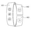
본 발명의 일 실시예에서 전자장치(ED)는 사용자의 사용 형태에 따라 펼쳐진 상태 또는 크로스 뱅글 형상으로 벤딩된 상태(이하, 크로스 뱅글 상태)로 동작할 수 있다. 도 1a는 전자장치(ED)의 펼쳐진 상태를 도시하였다. 도 1b는 전자장치(ED)의 크로스 뱅글 상태를 도시하였다. 도 1c는 사용자의 손목에 착용된 크로스 뱅글 상태의 전자장치(ED)를 도시하였다.According to an embodiment of the present invention, the electronic device ED may operate in an unfolded state or a bent state in a cross-bangle shape (hereinafter, a cross-bangle state) according to a user's usage form. 1A illustrates an unfolded state of the electronic device ED. 1B illustrates a cross-bangle state of the electronic device ED. 1C illustrates an electronic device ED in a cross-bangle state worn on a user's wrist.
전자장치(ED)는 펼쳐진 상태에서 제1 모드로 동작하고, 크로스 뱅글 상태에서 제2 모드로 동작할 수 있다. 전자장치(ED)는 펼쳐진 상태에서 제1 방향축(DR1)과 제2 방향축(DR2)에 의해 정의되는 표시면(ISD) 전체가 활성화된다. 제1 모드의 전자장치(ED)는 표시면(ISD) 전체를 이용하여 이미지(IM)를 표시할 수 있다. 제2 모드의 전자장치(ED)는 표시면(ISD) 중 일부분을 활성화시켜 이미지(IM)를 표시할 수 있다. 펼쳐진 상태에서 표시면(ISD)의 법선 방향은 제3 방향축(DR3)이 지시한다. 제3 방향축(DR3)은 전자장치(ED)의 두께 방향을 지시한다. 각 부재들의 전면과 배면은 제3 방향축(DR3)에 의해 구분된다. 이하, 방향축과 그 방향축이 지시하는 방향은 실질적으로 동일하게 정의된다.The electronic device ED may operate in the first mode in the unfolded state and may operate in the second mode in the cross-bangle state. In the unfolded state of the electronic device ED, the entire display surface ISD defined by the first direction axis DR1 and the second direction axis DR2 is activated. The electronic device ED in the first mode may display the image IM using the entire display surface ISD. The electronic device ED in the second mode may display the image IM by activating a portion of the display surface ISD. In the unfolded state, the normal direction of the display surface ISD is indicated by the third direction axis DR3 . The third direction axis DR3 indicates a thickness direction of the electronic device ED. A front surface and a rear surface of each member are divided by the third direction axis DR3. Hereinafter, the direction axis and the direction indicated by the direction axis are defined to be substantially the same.
표시면(ISD)은 제1 방향(DR1)의 제1 길이(L1) 및 제2 방향(DR2)의 제2 길이(L2)를 갖는다. 이하, 제1 길이(L1)는 너비로, 제2 방향(DR2)의 제2 길이(L2)는 길이로 정의될 수 있다. 전자장치(ED)는 펼쳐진 상태에서 제2 방향(DR2)을 따라 연장된 스틱형상을 가질 수 있다. 표시면(ISD)의 길이는 전자장치(ED)의 길이와 실질적으로 동일할 수 있고, 표시면(ISD)의 너비는 실질적으로 전자장치(ED)의 너비와 실질적으로 동일할 수 있다.The display surface ISD has a first length L1 in the first direction DR1 and a second length L2 in the second direction DR2 . Hereinafter, the first length L1 may be defined as a width, and the second length L2 in the second direction DR2 may be defined as a length. The electronic device ED may have a stick shape extending along the second direction DR2 in an unfolded state. The length of the display surface ISD may be substantially the same as the length of the electronic device ED, and the width of the display surface ISD may be substantially the same as the width of the electronic device ED.
도 1c에 도시된 것과 같이, 사용자의 손목에 크로스 뱅글 상태로 착용되기 위해 전자장치(ED)는 좁은 너비를 갖고 긴 길이를 갖는 것이 바람직하다. 전자장치(ED)의 길이는 30cm 내지 50cm 일 수 있다. 전자장치(ED)의 길이는 전자장치(ED)의 너비의 10 배 내지 30 배 클 수 있다.As shown in FIG. 1C , the electronic device ED preferably has a narrow width and a long length to be worn on a user's wrist in a cross bangle state. The length of the electronic device ED may be 30 cm to 50 cm. The length of the electronic device ED may be 10 to 30 times greater than the width of the electronic device ED.
여기서, "크로스 뱅글 형상"이란은 펼쳐진 상태에서 제2 방향축(DR2)에서 마주했던 전자장치(ED)의 일단(ED-E1)과 전자장치(ED)의 타단(ED-E2)이 서로 맞닿고, 전자장치(ED)의 2개의 부분들이 교차하면서 2개의 링들(R1, R2)이 형성되도록 전자장치(ED)가 꼬여진 형상으로 정의된다.Here, the term “cross bangle shape” means that one end ED-E1 of the electronic device ED and the other end ED-E2 of the electronic device ED facing each other on the second direction axis DR2 in the unfolded state are aligned with each other. The electronic device ED is defined as a twisted shape such that two rings R1 and R2 are formed while touching and two parts of the electronic device ED intersect.
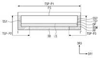
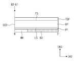
도 2a 및 도 2 b는 도 1a에 도시된 전자장치(ED)의 단면도이다. 도 2c는 도 2a에 도시된 입력감지패널(TSP)의 펼쳐진 상태의 평면도이다. 도 3은 본 발명의 일 실시예에 따른 전자장치(ED)의 블럭도이다.2A and 2B are cross-sectional views of the electronic device ED shown in FIG. 1A . FIG. 2C is a plan view of the input sensing panel TSP shown in FIG. 2A in an unfolded state. 3 is a block diagram of an electronic device ED according to an embodiment of the present invention.
도 2a 및 도 2b에 도시된 것과 같이, 본 실시예에 따른 전자장치(ED)는 플렉서블 표시패널(DP, 이하 표시패널), 입력감지패널(TSP), 벤딩감지센서(BSM), 결합부재(MM), 보호부재(PF), 및 바디부재(BD)를 포함한다. 이러한 부재들은 접착제를 통해 결합되거나, 연속공정을 통해 모듈 형태(일체의 형상)로 제조될 수 있다. 본 발명의 일 실시예에서 결합부재(MM), 벤딩감지센서(BSM) 및 보호부재(PF)는 생략될 수 있다. 또한, 바디부재(BD)는 표시패널(DP)과 입력감지패널(TSP)의 동작을 제어하는 제어모듈을 포함하면 충분하다.As shown in FIGS. 2A and 2B , the electronic device ED according to the present embodiment includes a flexible display panel (DP, hereinafter, a display panel), an input sensing panel (TSP), a bending sensing sensor (BSM), and a coupling member ( MM), a protection member PF, and a body member BD. These members may be bonded through an adhesive, or may be manufactured in the form of a module (one-piece shape) through a continuous process. In an embodiment of the present invention, the coupling member MM, the bending sensing sensor BSM, and the protection member PF may be omitted. In addition, it is sufficient if the body member BD includes a control module for controlling the operation of the display panel DP and the input sensing panel TSP.
표시패널(DP)은 플렉서블한 성질을 갖는 발광형 표시패널일 수 있고, 특별히 제한되지 않는다. 예컨대, 표시패널(DP)은 유기발광 표시패널 또는 퀀텀닷 발광 표시패널일 수 있다. 유기발광 표시패널의 발광층은 유기발광물질을 포함할 수 있다. 퀀텀닷 발광 표시패널의 발광층은 퀀텀닷, 및 퀀텀로드 등을 포함할 수 있다.The display panel DP may be a light emitting display panel having a flexible property, and is not particularly limited. For example, the display panel DP may be an organic light emitting display panel or a quantum dot light emitting display panel. The emission layer of the organic light emitting display panel may include an organic light emitting material. The emission layer of the quantum dot light emitting display panel may include quantum dots, quantum rods, and the like.
표시패널(DP)은 전면(FS) 및 제3 방향(DR3)에서 전면(FS)과 마주하는 배면(LS)을 포함할 수 있다. 전면(FS)은 상술한 표시면(IDS)과 실질적으로 동일할 수 있다. 표시패널(DP)은 복수 개의 절연층들, 도전층들, 및 기타 기능층이 적층되어 형성되는데, 상기 층들의 측면들이 표시패널(DP)의 측면들(SS1, SS2, SS3)을 정의한다. 상기 층들 중 최하층의 하면이 배면(LS)을 정의하고, 상기 층들 중 최상층의 상면이 전면(FS)을 정의할 수 있다.The display panel DP may include a front surface FS and a rear surface LS facing the front surface FS in the third direction DR3 . The front surface FS may be substantially the same as the above-described display surface IDS. The display panel DP is formed by stacking a plurality of insulating layers, conductive layers, and other functional layers, and side surfaces of the layers define side surfaces SS1 , SS2 , and SS3 of the display panel DP. A lower surface of a lowermost layer among the layers may define a rear surface LS, and an upper surface of an uppermost layer among the layers may define a front surface FS.
입력감지패널(TSP)은 표시패널(DP)에 결합되어 외부입력을 감지한다. 입력감지패널(TSP)은 베이스층, 감지전극, 감지전극에 연결된 신호라인, 적어도 하나의 절연층, 및 보호층을 포함할 수 있다. 입력감지패널(TSP)은 예컨대, 정전용량 방식으로 외부입력을 감지할 수 있다. 본 발명에서 입력감지패널(TSP) 동작방식은 특별히 제한되지 않고, 본 발명의 일 실시예에서 입력감지패널(TSP)은 전자기 유도방식 또는 압력 감지방식으로 외부입력을 감지할 수도 있다.The input sensing panel TSP is coupled to the display panel DP to sense an external input. The input sensing panel TSP may include a base layer, a sensing electrode, a signal line connected to the sensing electrode, at least one insulating layer, and a protective layer. The input sensing panel TSP may sense an external input, for example, in a capacitive manner. In the present invention, the operation method of the input sensing panel (TSP) is not particularly limited, and in an embodiment of the present invention, the input sensing panel (TSP) may sense an external input using an electromagnetic induction method or a pressure sensing method.
도 2a 내지 도 2c에 도시된 것과 같이, 입력감지패널(TSP)은 표시패널(DP)을 에워싸는 형상을 가질 수 있다. 입력감지패널(TSP)은 표시패널(DP)의 길이(L2)와 실질적으로 동일한 길이를 가질 수 있다.2A to 2C , the input sensing panel TSP may have a shape surrounding the display panel DP. The input sensing panel TSP may have substantially the same length as the length L2 of the display panel DP.
입력감지패널(TSP)은 표시패널(DP)의 전면(FS) 상에 배치된 제1 부분(TSP-P1), 제1 부분(TSP-P1)으로부터 연장되며 굴곡되어 배면(LS) 상에 배치된 제2 부분(TSP-P2), 제1 부분(TSP-P1)으로부터 연장되며 굴곡되어 배면(LS) 상에 배치된 제3 부분(TSP-P3)을 포함할 수 있다. 제3 부분(TSP-P3)은 배면(LS) 상에서 제2 부분(TSP-P2)과 이격될 수 있다. 제2 부분(TSP-P2)과 제3 부분(TSP-P3)은 배면(LS) 상에서 제2 방향축(DR2)을 기준으로 대칭을 이룰 수 있다.The input sensing panel TSP extends from the first portion TSP-P1 and the first portion TSP-P1 disposed on the front surface FS of the display panel DP and is bent to be disposed on the rear surface LS It may include a second portion TSP-P2 and a third portion TSP-P3 extending from the first portion TSP-P1 and being bent to be disposed on the rear surface LS. The third portion TSP-P3 may be spaced apart from the second portion TSP-P2 on the rear surface LS. The second portion TSP-P2 and the third portion TSP-P3 may be symmetrical with respect to the second direction axis DR2 on the rear surface LS.
입력감지패널(TSP)은 윈도우 패널의 역할을 가질 수 도 있다. 입력감지패널(TSP)의 보호층은 플라스틱 수지를 포함할 수 있고, 입력감지패널(TSP)의 보호층상에 하드코팅층, 반사방지층 및/또는 지문방지층과 같은 기능층들이 배치될 수 있다. 본 발명의 일 실시예에서 전자장치(ED)는 입력감지패널(TSP)과 구별되는 윈도우 패널을 더 포함할 수도 있다.The input detection panel (TSP) may have a role of a window panel. The protective layer of the input sensing panel TSP may include a plastic resin, and functional layers such as a hard coating layer, an anti-reflection layer and/or an anti-fingerprint layer may be disposed on the protective layer of the input sensing panel TSP. In an embodiment of the present invention, the electronic device ED may further include a window panel distinct from the input sensing panel TSP.
전자장치(ED)는 제2 부분(TSP-P2)과 제3 부분(TSP-P3)에 중첩하는 차광패턴(BM)을 더 포함할 수 있다. 도 2c에서 차광패턴(BM)이 배치된 영역은 어둡게 표시되었다. 차광패턴(BM)은 입력감지패널(TSP) 및 표시패널(DP)의 내측부분이 사용자에게 시인되지 않도록 빛을 차단한다.The electronic device ED may further include a light blocking pattern BM overlapping the second portion TSP-P2 and the third portion TSP-P3 . In FIG. 2C , the region where the light blocking pattern BM is disposed is darkly displayed. The light blocking pattern BM blocks light so that inner portions of the input sensing panel TSP and the display panel DP are not viewed by the user.
차광패턴(BM)은 유색의 유기층을 포함할 수 있다. 차광패턴(BM)은 입력감지패널(TSP)의 보호층에 인쇄되거나, 별도의 윈도우 패널에 인쇄될 수 있다.The light blocking pattern BM may include a colored organic layer. The light blocking pattern BM may be printed on the protective layer of the input sensing panel TSP or may be printed on a separate window panel.
벤딩감지센서(BSM)는 응력을 받으면 그 저항값이 변화되는 물질을 포함한다. 벤딩감지센서(BSM)는 벤딩감지센서(BSM)는 스트레인 게이지(strain gauge)로 구현될 수 있다. 벤딩감지센서(BSM)는 실리콘 패턴을 포함할 수 있다. 실리콘 패턴은 피에조 저항효과(piezoresistance effect)에 의해 응력을 받으면 그 저항값이 변화된다. 실리콘 패턴의 저항 변화가 감지되면, 전자장치(ED)이 밴딩된 것으로 판별될 수 있다.The bending sensor (BSM) includes a material whose resistance value changes when subjected to stress. The bending detection sensor BSM may be implemented as a strain gauge. The bending sensor BSM may include a silicon pattern. When the silicon pattern is stressed by the piezoresistance effect, its resistance value is changed. When a change in resistance of the silicon pattern is sensed, it may be determined that the electronic device ED is bent.
벤딩감지센서(BSM)는 표시패널(DP)의 배면(LS) 상에 배치될 수 있다. 벤딩감지센서(BSM)는 표시패널(DP)에 전체적으로 중첩될 필요는 없다. 벤딩감지센서(BSM)는 복수 개 제공될 수 도 있다.The bending sensor BSM may be disposed on the rear surface LS of the display panel DP. The bending detection sensor BSM does not need to entirely overlap the display panel DP. A plurality of bending detection sensors (BSM) may be provided.
보호부재(PF)는 표시패널(DP)을 지지하고, 외부의 충격으로부터 보호한다. 보호부재(PF)는 플라스틱 필름을 포함할 수 있다. 보호부재(PF)는 서로 연결된 관절구조물들을 포함할 수 있다.The protection member PF supports the display panel DP and protects it from external impact. The protective member PF may include a plastic film. The protective member PF may include joint structures connected to each other.
도 2b에 도시된 것과 같이, 결합부재(MM)는 보호부재(PF)의 하면에 결합된다. 결합부재(MM)는 전자장치(ED)의 양쪽 말단들(ED-E1, ED-E2)에 배치될 수 있다. 2개의 결합부재(MM)는 서로 결합되어 전자장치(ED)의 크로스 뱅글 상태를 유지시킬 수 있다. 2개의 결합부재(MM)는 모두 자석이거나, 2개의 결합부재(MM)는 자석과 금속을 각각 포함할 수 있다.As shown in FIG. 2B , the coupling member MM is coupled to the lower surface of the protection member PF. The coupling member MM may be disposed at both ends ED-E1 and ED-E2 of the electronic device ED. The two coupling members MM may be coupled to each other to maintain the cross-bangle state of the electronic device ED. Both of the two coupling members MM are magnets, or the two coupling members MM may include a magnet and a metal, respectively.
바디부재(BD)는 보호부재(PF)의 하면에 결합된다. 바디부재(BD)는 지지 프레임과 지지 프레임에 결합된 복수 개의 전자모듈들을 포함할 수 있다. 지지 프레임은 플렉서블한 부재이거나, 관절구조물들을 포함함 수 있다. 복수 개의 전자모듈들은 전자장치의 동작을 제어한다. 복수 개의 전자모듈들은 전자장치의 용도에 따라 달라질 수 있다.The body member BD is coupled to the lower surface of the protection member PF. The body member BD may include a support frame and a plurality of electronic modules coupled to the support frame. The support frame may be a flexible member or may include joint structures. The plurality of electronic modules controls the operation of the electronic device. The plurality of electronic modules may vary according to the purpose of the electronic device.
도 3은 전자장치가 스마트 와치의 용도를 가질 때, 바디부재(BD)에 포함된 전자모듈들을 예시적으로 도시한 블럭도이다. 바디부재(BD)는 제어 모듈(10), 무선통신 모듈(20), 영상입력 모듈(30), 음향입력 모듈(40), 음향출력 모듈(50), 메모리(60), 외부 인터페이스(70), 및 전원공급 모듈(80) 등을 포함할 수 있다. 이러한 전자모듈들은 회로기판에 실장되거나, 플렉서블 회로기판을 통해 전기적으로 연결될 수 있다.3 is a block diagram exemplarily illustrating electronic modules included in the body member BD when the electronic device has the purpose of a smart watch. The body member BD includes a
제어 모듈(10)은 스마트 와치의 전반적인 동작을 제어한다. 예를 들어 제어 모듈(10)은 표시패널(DP), 입력감지패널(TSP), 벤딩감지센서(BSM)을 활성화시키거나, 비활성화시킨다. 제어 모듈(10)은 바디부재(BD)에 포함된 다른 전자모듈의 동작을 제어할 수도 있다.The
도 1a 내지 도 1c에 도시된 것과 같이, 전자장치(ED)가의 동작모드가 제1 모드에서 제2 모드로 변화됨에 있어서, 제1 모드에서 표시된 이미지(IM)와 동일한 정보를 표시면(ISD)의 일부분에서 표시하기 위해서 제1 모드의 이미지 데이터와 동일한 컨텐츠 데이터를 제2 모드의 이미지 데이터로 변환한다. 제어 모듈(10)은 데이터 변환을 위한 신호처리회로를 포함할 수 있다.1A to 1C , when the operation mode of the electronic device ED is changed from the first mode to the second mode, the same information as the image IM displayed in the first mode is displayed on the display surface ISD In order to be displayed in a portion of , content data identical to the image data of the first mode is converted into image data of the second mode. The
신호처리회로는 컨텐츠 데이터를 렌더링하여 프레임을 구성한다. 도 1c에 도시된 것과 같이, 제2 모드에서 활성화되는 표시면(ISD)의 부분들의 조합을 제2 모드의 표시면으로 취급하여 컨텐츠 데이터를 렌더링한다. 구성된 프레임의 사이즈를 제2 모드의 표시면의 크기에 맞게 스케일링할 수 있다. 신호처리회로는 처리된 프레임 데이터를 표시패널(DP)에 제공한다. 표시패널(DP)은 수신한 신호를 아날로그 신호로 변환하고 이에 기초하여 이미지를 생성한다.The signal processing circuit renders the content data to form a frame. As shown in FIG. 1C , content data is rendered by treating a combination of portions of the display surface ISD activated in the second mode as a display surface of the second mode. The size of the configured frame may be scaled to match the size of the display surface of the second mode. The signal processing circuit provides the processed frame data to the display panel DP. The display panel DP converts the received signal into an analog signal and generates an image based thereon.
무선통신 모듈(20)은 블루투스 또는 와이파이 회선을 이용하여 다른 단말기와 무선 신호를 송/수신할 수 있다. 무선통신 모듈(20)은 송신할 신호를 변조하여 송신하는 송신부(22)와, 수신되는 신호를 복조하는 수신부(24)를 포함한다.The
영상입력 모듈(30)은 영상 신호를 처리하여 표시패널(DP)에 표시 가능한 영상 데이터로 변환한다. 음향입력 모듈(40)은 녹음 모드, 음성인식 모드 등에서 마이크로폰(Microphone)에 의해 외부의 음향 신호를 입력받아 전기적인 음성 데이터로 변환한다. 음향출력 모듈(50)은 무선통신 모듈(20)로부터 수신된 음향 데이터 또는 메모리(60)에 저장된 음향 데이터를 변환하여 외부로 출력한다.The
외부 인터페이스(70)는 외부 충전기, 유/무선 데이터 포트, 카드 소켓(예를 들어, 메모리 카드(Memory card), SIM/UIM card) 등에 연결되는 인터페이스 역할을 한다. 전원공급 모듈(80)은 스마트 와치의 전반적인 동작에 필요한 전원을 공급한다.The
도 4는 본 발명의 일 실시예에 따른 전자장치(ED)의 구동방법을 도시한 흐름도이다. 도 5는 본 발명의 일 실시예에 따른 전자장치(ED)의 벤딩동작들을 도시하였다. 도 6은 도 5에 도시된 비교예에 따른 벤딩동작에 대응하는 입력지점들(P1 내지 P4)을 도시하였다. 도 7a은 본 발명의 일 실시예에 따른 전자장치(ED)의 제2 동작 상태에서 외부 입력이 발생하는 과정을 도시하였다. 도 7b은 도 7a의 외부입력에 따른 입력지점들(P1 내지 P4)을 도시하였다. 도 7c은 도 7b의 입력지점들(P1 내지 P4)을 표시면(ISD)에 투영시켜 도시하였다. 도 7d는 본 실시예에 따른 전자장치(ED)의 제2 동작 상태에서 표시하는 이미지(IM)를 도시하였다.4 is a flowchart illustrating a method of driving an electronic device (ED) according to an embodiment of the present invention. 5 illustrates bending operations of the electronic device ED according to an embodiment of the present invention. FIG. 6 illustrates input points P1 to P4 corresponding to the bending operation according to the comparative example shown in FIG. 5 . 7A illustrates a process in which an external input is generated in a second operating state of the electronic device ED according to an embodiment of the present invention. FIG. 7B illustrates input points P1 to P4 according to the external input of FIG. 7A . FIG. 7C shows the input points P1 to P4 of FIG. 7B by projecting the input points P1 to P4 on the display surface ISD. 7D illustrates an image IM displayed in the second operating state of the electronic device ED according to the present exemplary embodiment.
도 4에 도시된 것과 같이, 전자장치(ED)의 벤딩 동작을 감지한다(S10). 전자장치(ED)가 제1 모드로 동작하는 상태 또는 비활성화 상태에서 전자장치(ED)의 벤딩 동작을 감지할 수 있다.As shown in FIG. 4 , a bending operation of the electronic device ED is sensed ( S10 ). A bending motion of the electronic device ED may be detected in a state in which the electronic device ED operates in the first mode or in an inactive state.
도 5에는 3가지 형태의 벤딩 동작을 예시적으로 도시하였다. 전자장치(ED)가 벤딩되면 벤딩감지센서(BSM)에 응력이 인가되고, 벤딩감지센서(BSM)의 저항이 변화된다. 제어모듈(10, 도 3 참조)은 벤딩감지센서(BSM)에서 기준값 이상의 저항값 변화가 감지되면 전자장치(ED)가 벤딩된 것으로 판단할 수 있다. 기준값 이상의 저항값 변화가 유지되는 동안 벤딩 상태가 유지되는 것으로 판단할 수 있다. 벤딩감지센서(BSM)를 이용하지 않더라도 입력감지패널(TSP)로부터 감지된 입력지점들이, 후술하는 것과 같이, 소정의 조건을 만족할 때, 전자장치(ED)가 벤딩된 것으로 판단할 수 있다.5 exemplarily shows three types of bending operations. When the electronic device ED is bent, stress is applied to the bending sensor BSM, and the resistance of the bending sensor BSM is changed. The control module 10 (refer to FIG. 3 ) may determine that the electronic device ED is bent when a change in resistance greater than or equal to a reference value is detected by the bending detection sensor BSM. It may be determined that the bending state is maintained while the change in the resistance value greater than or equal to the reference value is maintained. Even if the bending detection sensor BSM is not used, when the input points sensed from the input detection panel TSP satisfy a predetermined condition as will be described later, it may be determined that the electronic device ED is bent.
도 4에 도시된 것과 같이, 전자장치(ED)의 벤딩 동작이 크로스 뱅글 동작인지 판단한다(S20). 제어모듈(10)은 입력감지패널(TSP)로부터 감지된 입력지점들이 특정 조건을 만족하는지 판단한다.As shown in FIG. 4 , it is determined whether the bending operation of the electronic device ED is a cross-bangle operation ( S20 ). The
도 5의 제1 동작(SM1)과 같이, 입력지점들이 감지되지 않으면 크로스 뱅글 동작이 아닌 것으로 판단한다. 여기서 사용자의 파지에 의한 외부입력은 제외한다.As in the first operation SM1 of FIG. 5 , if no input points are detected, it is determined that the cross bangle operation is not. Here, external input by the user's grip is excluded.
도 5의 제2 동작(SM2)과 같이, 전자장치(ED)의 2개 부분들이 접촉되도록 벤딩될 수 있다. 2개 부분들이 접촉될 때 2개의 외부입력들(OI1, OI2)이 발생한 것으로 판단할 수 있다. 도 6에 도시된 것과 같이, 2개의 외부입력들(OI1, OI2)에 의해 4개의 입력지점들(P1 내지 P4)이 감지될 수 있다. 제1 지점(P1)과 제3 지점(P3)은 도 5의 제1 외부입력(OI1)에 의해 결정되고, 제2 지점(P2)과 제4 지점(P4)은 도 5의 제2 외부입력(OI2)에 의해 결정될 수 있다. 제1 지점(P1)과 제2 지점(P2)이 서로 인접하게 감지되고, 제3 지점(P3)과 제4 지점(P4)이 서로 인접하게 감지된다. 제1 지점(P1)과 제2 지점(P2)은 제1 부분(TSP-P1)에서 감지되고, 제3 지점(P3)과 제4 지점(P4)은 제2 부분(TSP-P2)에서 감지될 수 있다. 한편, 크로스 벤딩 동작의 형태에 따라 제3 지점(P3)과 제4 지점(P4)은 제3 부분(TSP-P3)에서 감지될 수 있다.As in the second operation SM2 of FIG. 5 , two parts of the electronic device ED may be bent to contact each other. It may be determined that two external inputs OI1 and OI2 are generated when the two parts are in contact. As shown in FIG. 6 , four input points P1 to P4 may be sensed by two external inputs OI1 and OI2 . The first point P1 and the third point P3 are determined by the first external input OI1 of FIG. 5 , and the second point P2 and the fourth point P4 are the second external input points of FIG. 5 . It can be determined by (OI2). The first point P1 and the second point P2 are detected adjacent to each other, and the third point P3 and the fourth point P4 are detected adjacent to each other. The first point P1 and the second point P2 are detected by the first part TSP-P1, and the third point P3 and the fourth point P4 are detected by the second part TSP-P2 can be Meanwhile, depending on the shape of the cross bending operation, the third point P3 and the fourth point P4 may be detected by the third portion TSP-P3 .
제1 부분(TSP-P1)에서 감지된 제1 지점(P1)과 제2 지점(P2) 사이의 거리 및 제2 부분(TSP-P2)에서 감지된 제3 지점(P3)과 제4 지점(P4) 사이의 거리가 기준 범위에 포함될 때 도 5의 제2 동작(SM2)과 같이 크로스 벤딩 동작으로 판단할 수 있다. 여기서 기준 범위는 표시면(ISD)의 너비(L1)에 근거하여 설정되며, 너비(L1)보다 같거나 크고 너비(L1)의 3배보다 같거나 작을수 있다.The distance between the first point P1 and the second point P2 sensed in the first part TSP-P1 and the third point P3 and the fourth point detected in the second part TSP-P2 ( When the distance between P4) is included in the reference range, it may be determined as a cross bending operation as in the second operation SM2 of FIG. 5 . Here, the reference range is set based on the width L1 of the display surface ISD, and may be equal to or greater than the width L1 and equal to or smaller than three times the width L1.
상기 조건을 만족하는 4개의 입력지점들(P1 내지 P4)이 검출된 때, 제어모듈(10)은 벤딩 동작이 실시된 것으로 판단한다. 그러나, 크로스 뱅글 형상으로 벤딩된 것으로 판단하지 않기 때문에 제어모듈(10)은 도 4에 도시된 것과 같이 제1 모드로 동작한다(S30). 여기서 제1 모드의 동작은 제1 모드의 유지 또는 비활성화 상태에서 활성화의 변화를 의미할 수 있다.When the four input points P1 to P4 satisfying the above conditions are detected, the
도 5의 제3 동작(SM3)과 같이, 크로스 뱅글 형상으로 벤딩될 수 있다. 크로스 뱅글 형상으로 벤딩될 때, 전자장치(ED)의 2개 부분들이 접촉되고, 2개 부분들이 접촉될 때 2개의 외부입력들(OI1, OI2)이 발생한다. 크로스 뱅글 형상은 제1 링(R1)을 정의하는 부분과 제2 링(R2)을 정의하는 부분이 서로 가까워지는 방향으로 동작되고 유지되기 때문에, 도 7a에서 표시된 2개의 지점들(IL1, IL2)은 2개의 외부입력들(OI1, OI2)보다 늦게 접촉하거나 비접촉된다.As in the third operation SM3 of FIG. 5 , it may be bent in a cross bangle shape. When bending into a cross bangle shape, two parts of the electronic device ED are in contact, and when the two parts are in contact, two external inputs OI1 and OI2 are generated. Since the cross bangle shape is operated and maintained in a direction in which the portion defining the first ring R1 and the portion defining the second ring R2 approach each other, the two points IL1 and IL2 indicated in FIG. 7A is in contact or non-contact later than the two external inputs OI1 and OI2.
도 7b에 도시된 것과 같이, 2개의 외부입력들(OI1, OI2)에 의해 4개의 입력지점들(P1 내지 P4)이 감지될 수 있다. 제1 지점(P1)과 제3 지점(P3)은 도 7a의 제1 외부입력(OI1)에 의해 결정되고, 제2 지점(P2)과 제4 지점(P4)은 도 7a의 제2 외부입력(OI2)에 의해 결정될 수 있다. 제1 지점(P1)과 제2 지점(P2)이 서로 인접하게 감지되고, 제3 지점(P3)과 제4 지점(P4)이 서로 인접하게 감지된다. 제1 지점(P1)과 제2 지점(P2)은 제1 부분(TSP-P1)에서 검출되고, 제3 지점(P3)과 제4 지점(P4)은 제3 부분(TSP-P3)과 제2 부분(TSP-P2)에서 각각 검출될 수 있다.As shown in FIG. 7B , four input points P1 to P4 may be sensed by two external inputs OI1 and OI2 . The first point P1 and the third point P3 are determined by the first external input OI1 of FIG. 7A , and the second point P2 and the fourth point P4 are the second external input points of FIG. 7A . It can be determined by (OI2). The first point P1 and the second point P2 are detected adjacent to each other, and the third point P3 and the fourth point P4 are detected adjacent to each other. The first point P1 and the second point P2 are detected in the first part TSP-P1, and the third point P3 and the fourth point P4 are the third part TSP-P3 and the second point P4. Each can be detected in two parts (TSP-P2).
도 7c를 참조함에 있어서, 제3 지점(P3)과 제4 지점(P4)은 제3 지점(P3)과 제4 지점(P4)의 표시면(IDS)에 대한 투영 지점들로 정의된다. 제1 지점(P1)과 제2 지점(P2)의 투영 지점들은 투영 전과 동일하다.Referring to FIG. 7C , the third point P3 and the fourth point P4 are defined as projection points of the third point P3 and the fourth point P4 with respect to the display surface IDS. The projection points of the first point P1 and the second point P2 are the same as before the projection.
도 7c에 도시된 것과 같이, 제1 지점(P1)과 제2 지점(P2)은 제1 대각선 방향(DR4)으로 배열된다. 제3 지점(P3)과 제4 지점(P4)은 제1 대각선 방향(DR4)에 교차하는 제2 대각선 방향(DR5)으로 배열될 수 있다. 상기 조건을 만족하는 4개의 입력지점들(P1 내지 P4)이 검출된 때, 제어모듈(10)은 크로스 뱅글 동작이 실시된 것으로 판단한다.As shown in FIG. 7C , the first point P1 and the second point P2 are arranged in a first diagonal direction DR4 . The third point P3 and the fourth point P4 may be arranged in a second diagonal direction DR5 crossing the first diagonal direction DR4 . When the four input points P1 to P4 satisfying the above conditions are detected, the
벤딩 동작이 크로스 뱅글 동작인지 판단하는 단계(S20)의 신뢰성을 높이기 위해 조건을 추가할 수 있다. 제1 지점(P1)과 제2 지점(P2)의 중간 지점(PC12, 이하 제1 중간 지점)와 제3 지점(P3)과 제4 지점(P4)의 중간 지점(PC34, 이하 제2 중간 지점) 사이의 길이를 전자장치(ED)의 길이와 비교할 수 있다. 제1 중간 지점(PC12)과 제2 중간 지점(PC34) 사이의 길이가 실질적으로 전자장치(ED)의 길이(L2, 도 1a 참조)의 절반에 해당하는 길이(L2/2)에 대응하는 조건을 더 만족하는 경우, 제어모듈(10)은 크로스 뱅글 동작이 실시된 것으로 판단할 수 있다. 제1 중간 지점(PC12)과 제2 중간 지점(PC34) 사이의 길이가 상기 길이(L2/2)와 동일한 경우뿐만 아니라, 오차범위 -10% 내지 +10%인 경우를 포함한다.A condition may be added to increase the reliability of the step S20 of determining whether the bending operation is a cross-bangle operation. A midpoint (PC12, hereinafter first midpoint) between the first point P1 and the second point P2 and a midpoint PC34, hereinafter second midpoint between the third point P3 and the fourth point P4 ) may be compared with the length of the electronic device ED. A condition in which the length between the first intermediate point PC12 and the second intermediate point PC34 corresponds to a length L2/2 that is substantially half of the length L2 (refer to FIG. 1A ) of the electronic device ED In the case of further satisfying , the
상술한 추가 조건은 후술하는 조건으로 대체될 수도 있다. 제1 입력지점(P1)과 제4 입력지점(P2) 사이의 길이와 제2 입력지점(P2)과 제3 입력지점(P3)의 사이의 길이의 평균은 실질적으로 전자장치(ED)의 길이(L2, 도 1a 참조)의 절반에 해당하는 길이(L2/2)에 대응할 수 있다. 실질적으로 절반의 길이는 오차범위 -10% 내지 +10%인 경우를 포함한다.The above-described additional conditions may be replaced with the conditions described later. The average of the length between the first input point P1 and the fourth input point P2 and the length between the second input point P2 and the third input point P3 is substantially the length of the electronic device ED. It may correspond to the length (L2/2) corresponding to half of (L2, see FIG. 1A). Substantially, the half length includes cases with an error range of -10% to +10%.
전자장치(ED)가 크로스 뱅글 형상으로 벤딩된 것으로 판단되면, 제어모듈(10)은 표시면(IDS)에서 활성화시킬 제2 모드의 표시영역을 결정한다(S40). 제어모듈(10)은 도 7c에 도시된 4개의 입력지점들(P1 내지 P4)을 이용하여 표시영역을 결정할 수 있다. 전자장치(ED)의 타단(ED-E2)으로부터 제4 지점(P4)까지를 제1 표시영역(AA1, 또는 제1 표시부분)으로 결정하고, 전자장치(ED)의 일단(ED-E1)으로부터 제1 지점(P1)까지를 제2 표시영역(AA2, 또는 제2 표시부분)으로 결정할 수 있다. 제2 지점(P2)부터 제3 지점(P3)까지를 제3 표시영역(AA3, 또는 제3 표시부분)으로 결정할 수 있다. 여기서 제4 지점(P4)은 4개의 입력지점들(P1 내지 P4) 중 전자장치(ED)의 타단(ED-E2)에 가장 인접한 지점이고, 제1 지점(P1)은 4개의 입력지점들(P1 내지 P4) 중 전자장치(ED)의 일단(ED-E1)에 가장 인접한 지점이다.If it is determined that the electronic device ED is bent in a cross-bangle shape, the
제4 지점(P4)에 의한 제1 표시영역(AA1)의 경계와 제1 지점(P1)에 의한 제2 표시영역(AA2)의 경계는 다양한 방법으로 결정될 수 있다. 예컨대, 제4 지점(P4)에 중첩하고 제1 방향(DR1)으로 연장된 경계선으로부터 전자장치(ED)의 타단(ED-E2)까지를 제1 표시영역(AA1)으로 결정하고, 제1 지점(P1)에 중첩하고 제1 방향(DR1)으로 연장된 경계선으로부터 전자장치(ED)의 일단(ED-E1)까지를 제2 표시영역(AA2)으로 결정할 수 있다. 제3 지점(P3)에 중첩하고 제1 방향(DR1)으로 연장된 경계선으로부터 제2 지점(P2)에 중첩하고 제1 방향(DR1)으로 연장된 경계선까지를 제3 표시영역(AA3)으로 결정할 수 있다.The boundary of the first display area AA1 by the fourth point P4 and the boundary of the second display area AA2 by the first point P1 may be determined in various ways. For example, the first display area AA1 is determined from the boundary line overlapping the fourth point P4 and extending in the first direction DR1 to the other end ED-E2 of the electronic device ED, and the first point A second display area AA2 may be determined from a boundary line overlapping P1 and extending in the first direction DR1 to one end ED-E1 of the electronic device ED. A third display area AA3 is determined from a boundary line overlapping the third point P3 and extending in the first direction DR1 to a boundary line overlapping the second point P2 and extending in the first direction DR1 . can
제1 지점(P2)부터 제2 지점(P2)까지의 영역과 제3 지점(P3)부터 제4 지점(P4)까지의 영역은 비활성화되거나, 컨텐츠를 미포함하는 배경 이미지만을 제공하는 영역으로 설정될 수 있다. 제1 지점(P2), 제2 지점(P2), 제3 지점(P3), 제4 지점(P4)에 중첩하는 경계선들에 의해 비활성화영역이 결정될 수 있다.The area from the first point P2 to the second point P2 and the area from the third point P3 to the fourth point P4 may be inactivated or set as an area providing only a background image without content. can The inactive area may be determined by boundary lines overlapping the first point P2 , the second point P2 , the third point P3 , and the fourth point P4 .
제2 모드의 표시영역이 결정되면 제2 모드로 동작한다(S50). 제어모듈(10)은 제1 내지 제3 표시영역들만(AA1, AA2, AA3)을 활성화시킬 수 있다. 제어모듈(10)은 제1 모드의 컨텐츠 데이터를 제1 내지 제3 표시영역들(AA1, AA2, AA3)에 적절하게 렌더링하여 프레임을 구성한다. 또한, 프레임의 사이즈를 제1 내지 제3 표시영역들(AA1, AA2, AA3)이 정의하는 표시면의 크기에 맞게 스케일링할 수 있다. 도 7d의 아이콘 이미지들은 제1 모드의 아이콘 이미지들(IM, 도 1a 참조)이 제2 모드에 부합하게 렌더링되고 스케일링되었다.When the display area of the second mode is determined, it operates in the second mode (S50). The
본 발명의 일 실시예에서 전자장치의 크로스 뱅글 동작을 판단하는 단계는 반복적으로 수행될 수도 있다(S60). 제어모듈(10)은 입력감지패널(TSP)로부터 새롭게 검출된 4개의 입력지점들에 근거하여 제1 표시영역 내지 제3 표시영역을 새롭게 정의할 수도 있다.In an embodiment of the present invention, the step of determining the cross bangle operation of the electronic device may be repeatedly performed (S60). The
본 발명의 일 실시예에서 제어모듈(10)은 제2 부분(TSP-P2, 도 2c 참고)과 제3 부분(TSP-P3, 도 2c 참고)을 비활성화시킬 수도 있다. 도 1c와 같이 사용자 손목에 착용되는 경우, 손목의 피부에 의해 제2 부분(TSP-P2)과 제3 부분(TSP-P3)에 외부 입력이 인가된 것으로 오작동할 수 있기 때문이다.In an embodiment of the present invention, the
도 8a은 본 발명의 일 실시예에 따른 전자장치(ED)의 제2 동작 상태에서 외부 입력이 발생하는 과정을 도시하였다. 도 8b은 도 8a의 외부입력에 따른 입력지점들(P1 내지 P4)을 도시하였다. 도 8c은 도 8b의 입력지점들(P1 내지 P4)을 표시면(IDS)에 투영시켜 도시하였다. 도 8d는 본 실시예에 따른 전자장치(ED)의 제2 동작 상태에서 표시하는 이미지를 도시하였다. 이하, 도 4 내지 도 7d를 참조하여 설명한 구성과 동일한 구성에 대한 상세한 설명은 생략한다.8A illustrates a process in which an external input is generated in the second operating state of the electronic device ED according to an embodiment of the present invention. FIG. 8B illustrates input points P1 to P4 according to the external input of FIG. 8A . FIG. 8c illustrates the projection of the input points P1 to P4 of FIG. 8b on the display surface IDS. 8D illustrates an image displayed in the second operating state of the electronic device ED according to the present exemplary embodiment. Hereinafter, a detailed description of the same configuration as that described with reference to FIGS. 4 to 7D will be omitted.
도 8a에 도시된 전자장치(ED)의 제2 동작 상태는 도 7a에 도시된 전자장치(ED)의 제2 동작 상태와 꼬인 방향을 제외하고 실질적으로 동일하다. 도 8b에는 도 8a의 2개의 외부입력들(OI1, OI2)에 의해 감지된 4개의 입력지점들(P1 내지 P4)을 도시하였다.The second operating state of the electronic device ED shown in FIG. 8A is substantially the same as the second operating state of the electronic device ED shown in FIG. 7A , except for a twisted direction. FIG. 8B shows four input points P1 to P4 sensed by the two external inputs OI1 and OI2 of FIG. 8A .
도 8c에 도시된 4개의 입력지점들(P1 내지 P4)은 도 7c에 도시된 4개의 입력지점들(P1 내지 P4) 대비 그 위치만 일부 상이할 뿐, 4개의 입력지점들(P1 내지 P4)을 이용한 벤딩 동작이 크로스 뱅글 동작인지 판단하는 단계(S20), 제2 모드의 표시영역을 결정하는 단계(S40), 및 제2 모드의 이미지를 표시하는 단계(S50)는 실질적으로 동일할 수 있다.The four input points P1 to P4 shown in FIG. 8C are only partially different from the four input points P1 to P4 shown in FIG. 7C , and the four input points P1 to P4 Determining whether the bending operation using is a cross bangle operation (S20), determining the display area of the second mode (S40), and displaying the image of the second mode (S50) may be substantially the same .
도 8c에 도시된 것과 같이, 제2 지점(P2)부터 제3 지점(P3)까지를 제1 표시영역(AA1)으로 결정하고, 전자장치(ED)의 타단(ED-E2)으로부터 제1 지점(P1)까지를 제2 표시영역(AA2)으로 결정하고, 전자장치(ED)의 일단(ED-E1)으로부터 제4 지점(P4)까지를 제3 표시영역(AA3)으로 결정할 수 있다.As illustrated in FIG. 8C , the second point P2 to the third point P3 are determined as the first display area AA1 , and the first point from the other end ED-E2 of the electronic device ED. Up to P1 may be determined as the second display area AA2 , and from one end ED-E1 to the fourth point P4 of the electronic device ED may be determined as the third display area AA3 .
도 8d에는 제2 모드에서 표시되는 이미지가 도시되었다. 본 실시예에서 제1 내지 제3 표시영역들(AA1, AA2, AA3)이 도 7c와 다르게 결정되었으므로, 도 7d에서 수행된 데이터 처리와 다르게 렌더링 및 스케일링 될 수 있다.8D shows an image displayed in the second mode. In the present embodiment, since the first to third display areas AA1 , AA2 , and AA3 are determined differently from FIG. 7C , they may be rendered and scaled differently from the data processing performed in FIG. 7D .
도 9a는 본 발명의 일 실시예에 따른 전자장치(ED)의 단면도이다. 도 9b은 본 발명의 일 실시예에 따른 전자장치의 제2 동작 상태에서 외부 입력이 발생하는 과정을 도시하였다. 도 9c는 도 9b의 외부입력에 따른 입력지점들(P1 내지 P3)을 도시하였다. 이하, 도 1 내지 도 8d를 참조하여 설명한 구성과 동일한 구성에 대한 상세한 설명은 생략한다.9A is a cross-sectional view of an electronic device ED according to an embodiment of the present invention. 9B illustrates a process in which an external input is generated in the second operating state of the electronic device according to an embodiment of the present invention. FIG. 9C illustrates input points P1 to P3 according to the external input of FIG. 9B . Hereinafter, a detailed description of the same configuration as that described with reference to FIGS. 1 to 8D will be omitted.
본 실시예에 따르면 입력감지패널(TSP)은 도 1 내지 도 8d를 참조하여 설명한 입력감지패널(TSP) 대비 형상이 상이할 수 있다. 도 9a에 도시된 것과 같이, 제2 부분(TSP-P2)은 제1 부분(TSP-P1)으로부터 연장되며 제1 측면(SS1)에 마주하고, 제3 부분(TSP-P3)은 제1 부분(TSP-P1)으로부터 연장되며 제2 측면(SS2)에 마주할 수 있다. 제2 부분(TSP-P2)과 제3 부분(TSP-P3)이 배면(LS)에 마주하지 않는다.According to the present embodiment, the shape of the input sensing panel TSP may be different from that of the input sensing panel TSP described with reference to FIGS. 1 to 8D . 9A , the second part TSP-P2 extends from the first part TSP-P1 and faces the first side surface SS1, and the third part TSP-P3 is the first part It extends from (TSP-P1) and may face the second side surface (SS2). The second portion TSP-P2 and the third portion TSP-P3 do not face the rear surface LS.
제3 부분(TSP-P3)은 배면(LS) 상에서 제2 부분(TSP-P2)과 이격될 수 있다. 제2 부분(TSP-P2)과 제3 부분(TSP-P3)은 배면(LS) 상에서 제2 방향축(DR2)을 기준으로 대칭을 이룰 수 있다.The third portion TSP-P3 may be spaced apart from the second portion TSP-P2 on the rear surface LS. The second portion TSP-P2 and the third portion TSP-P3 may be symmetrical with respect to the second direction axis DR2 on the rear surface LS.
도 9b에 도시된 2개의 외부입력들(OI1, OI2)은 제2 부분(TSP-P2)과 제3 부분(TSP-P3)에서 발생할 수 있다. 입력감지패널(TSP)로부터 검출된 제1 내지 제4 지점들(P1 내지 P4)을 제1 부분(TSP-P1)으로 투영시킬 수 있다. 제1 내지 제4 지점들(P1 내지 P4)를 최단거리로 제1 부분(TSP-P1)으로 이동시켜 투영된 제1 내지 제4 지점들(PP1 내지 PP4)을 산출할 수 있다. 투영된 제1 내지 제4 지점들(PP1 내지 PP4)을 도 7c에 도시된 제1 내지 제4 지점들(P1 내지 P4)로 가정하여 크로스 뱅글 동작인지 판단하는 단계(S20), 제2 모드의 표시영역을 결정하는 단계(S40), 및 제2 모드의 이미지를 표시하는 단계(S50)를 수행할 수 있다.The two external inputs OI1 and OI2 shown in FIG. 9B may be generated in the second part TSP-P2 and the third part TSP-P3. The first to fourth points P1 to P4 detected from the input sensing panel TSP may be projected onto the first portion TSP-P1 . Projected first to fourth points PP1 to PP4 may be calculated by moving the first to fourth points P1 to P4 to the first portion TSP-P1 by the shortest distance. Assuming that the projected first to fourth points PP1 to PP4 are the first to fourth points P1 to P4 shown in FIG. 7C , determining whether a cross bangle operation is (S20), in the second mode The step of determining the display area (S40) and the step of displaying the image of the second mode (S50) may be performed.
별도로 도시하지 않았으나, 도 2a 내지 도 2c에 도시된 입력감지패널(TSP)에 있어서 측면 터치가 발생하는 경우, 본 실시예와 같은 방식으로 상기 단계들(S20, S40, S50)을 수행할 수 있다.Although not shown separately, when a side touch occurs in the input sensing panel TSP shown in FIGS. 2A to 2C, the steps S20, S40, and S50 may be performed in the same manner as in the present embodiment. .
이상에서는 본 발명의 바람직한 실시예를 참조하여 설명하였지만, 해당 기술 분야의 숙련된 당업자 또는 해당 기술 분야에 통상의 지식을 갖는 자라면, 후술될 특허청구범위에 기재된 본 발명의 사상 및 기술 영역으로부터 벗어나지 않는 범위 내에서 본 발명을 다양하게 수정 및 변경시킬 수 있음을 이해할 수 있을 것이다.Although the above has been described with reference to the preferred embodiment of the present invention, those skilled in the art or those having ordinary knowledge in the technical field will not depart from the spirit and technical scope of the present invention described in the claims to be described later. It will be understood that various modifications and variations of the present invention can be made without departing from the scope of the present invention.
따라서, 본 발명의 기술적 범위는 명세서의 상세한 설명에 기재된 내용으로 한정되는 것이 아니라 특허청구범위에 의해 정하여져야만 할 것이다.Accordingly, the technical scope of the present invention should not be limited to the content described in the detailed description of the specification, but should be defined by the claims.
DD: 표시장치DP: 표시패널
BSP: 벤딩 감지 패널 WM: 윈도우 부재
NBA1, NBA2: 비벤딩영역BA: 벤딩영역DD: Display device DP: Display panel
BSP: Bending detection panel WM: No window
NBA1, NBA2: non-bending area BA: bending area
Claims (20)
Translated fromKorean상기 표시면 상에 배치된 제1 부분, 상기 제1 부분으로부터 연장되며 상기 배면 상에 배치된 제2 부분, 상기 제1 부분으로부터 연장되며 상기 배면 상에 배치되고 상기 배면 상에서 상기 제2 부분과 이격된 제3 부분을 포함하고, 상기 플렉서블 표시패널에 결합되고, 상기 플렉서블 표시패널의 상기 제1 동작 상태에서 상기 제2 방향으로 연장된 형상을 갖는 입력감지패널; 및
상기 플렉서블 표시패널 및 상기 입력감지패널을 제어하는 제어모듈을 포함하고,
크로스 뱅글 형상을 갖는 상기 제2 동작 상태에서 상기 플렉서블 표시패널은 상기 일단과 상기 타단이 서로 맞닿고, 상기 플렉서블 표시패널의 2개의 부분들이 교차하며 2개의 링들이 정의되며 꼬여지는 전자장치.It is deformable into a first operating state and a second operating state, and has a first length in a first direction and a second length in a second direction orthogonal to the first direction in the first operating state corresponding to the unfolded state. a flexible display panel including a display surface displaying an image and a rear surface opposite to the display surface in a thickness direction, the flexible display panel having a shape extending from one end to the other end in the second direction;
a first portion disposed on the display surface, a second portion extending from the first portion and disposed on the rear surface, extending from the first portion and disposed on the rear surface and spaced apart from the second portion on the rear surface an input sensing panel including a third part, the input sensing panel coupled to the flexible display panel, the input sensing panel having a shape extending in the second direction in the first operating state of the flexible display panel; and
a control module for controlling the flexible display panel and the input sensing panel;
In the second operation state having a cross bangle shape, the flexible display panel has one end and the other end in contact with each other, two portions of the flexible display panel cross each other, and two rings are defined and twisted.
상기 입력감지패널로부터 4개의 입력지점들이 검출되고, 상기 4개의 입력지점들 중 제1 입력지점과 제2 입력지점이 상기 제1 부분에서 검출되고, 상기 제1 입력지점과 상기 제2 입력지점이 제1 대각선 방향으로 배열되고, 제3 입력지점과 제4 입력지점이 상기 제2 부분과 상기 제3 부분에서 각각 검출되고, 상기 제3 입력지점의 상기 제1 부분으로 투영된 제1 투영지점과 상기 제4 입력지점의 상기 제1 부분으로 투영된 제2 투영지점이 상기 제1 대각선 방향과 교차하는 제2 대각선 방향으로 배열될 때, 상기 제어모듈은 상기 플렉서블 표시패널이 크로스 뱅글 형상으로 벤딩된 상기 제2 동작 상태로 판단하는 전자장치.According to claim 1,
Four input points are detected from the input detection panel, a first input point and a second input point among the four input points are detected in the first part, and the first input point and the second input point are a first projection point arranged in a first diagonal direction, a third input point and a fourth input point respectively detected in the second part and the third part, and projected onto the first part of the third input point; When the second projection point projected onto the first portion of the fourth input point is arranged in a second diagonal direction intersecting the first diagonal direction, the control module is configured such that the flexible display panel is bent in a cross-bangle shape. An electronic device that determines the second operation state.
상기 제1 입력지점 내지 상기 제4 입력지점 중 상기 제1 입력지점이 상기 플렉서블 표시패널의 상기 일단에 가장 인접하고, 상기 제1 입력지점 내지 상기 제4 입력지점 중 상기 제4 입력지점이 상기 플렉서블 표시패널의 상기 타단에 가장 인접하며,
상기 제어모듈은 상기 플렉서블 표시패널이 크로스 뱅글 형상으로 벤딩된 상태 판단될 때, 상기 플렉서블 표시패널의 상기 일단으로부터 상기 제1 입력지점까지 정의되는 제1 표시부분, 상기 플렉서블 표시패널의 상기 타단으로부터 상기 제2 투영지점에 중첩까지 정의되는 제2 표시부분, 및 상기 제2 입력지점으로부터 상기 제1 투영지점까지 정의되는 제3 표시부분에 상기 이미지를 표시하는 전자장치.3. The method of claim 2,
The first input point among the first input point to the fourth input point is closest to the one end of the flexible display panel, and the fourth input point among the first input point to the fourth input point is the flexible display panel. closest to the other end of the display panel,
When it is determined that the flexible display panel is bent in a cross-bangle shape, the control module includes a first display portion defined from the one end of the flexible display panel to the first input point, and the other end of the flexible display panel. An electronic device for displaying the image on a second display portion defined to overlap a second projection point and on a third display portion defined from the second input point to the first projection point.
상기 제1 입력지점과 상기 제2 입력지점의 중간 지점과 상기 제3 입력지점의 상기 투영지점과 상기 제4 입력지점의 상기 투영지점의 중간 지점 사이의 길이는 상기 제2 길이의 절반에 대응하는 전자장치.3. The method of claim 2,
A length between a midpoint between the first input point and the second input point and a midpoint between the projection point of the third input point and the projection point of the fourth input point corresponds to half of the second length electronics.
상기 제1 입력지점과 상기 제4 입력지점의 상기 제2 투영지점 사이의 길이와 상기 제2 입력지점과 상기 제3 입력지점의 상기 제1 투영지점 사이의 길이의 평균은 상기 제2 길이의 절반에 대응하는 전자장치.3. The method of claim 2,
The average of the length between the second projection point of the first input point and the fourth input point and the length between the second input point and the first projection point of the third input point is half of the second length corresponding electronic devices.
상기 플렉서블 표시패널이 크로스 뱅글 형상으로 벤딩된 상태로 판단될 때, 상기 제어모듈은 상기 입력감지패널의 상기 제2 부분과 상기 제3 부분을 비활성화시키는 전자장치.3. The method of claim 2,
When it is determined that the flexible display panel is bent in a cross-bangle shape, the control module deactivates the second portion and the third portion of the input sensing panel.
상기 플렉서블 표시패널이 크로스 뱅글 형상으로 벤딩된 상태에서 사용자의 손목에 착용될 수 있는 전자장치.3. The method of claim 2,
An electronic device that can be worn on a user's wrist in a state in which the flexible display panel is bent in a cross bangle shape.
상기 제2 부분과 상기 제3 부분에 중첩하는 차광패턴을 더 포함하는 전자장치.According to claim 1,
The electronic device further comprising a light blocking pattern overlapping the second portion and the third portion.
상기 제2 방향의 길이는 상기 제1 방향의 길이보다 10 배 내지 30 배 큰 전자장치.According to claim 1,
The length in the second direction is 10 to 30 times greater than the length in the first direction.
상기 제2 방향의 길이는 30cm 내지 50cm인 전자장치.According to claim 1,
The length in the second direction is 30 cm to 50 cm.
상기 플렉서블 표시패널의 형상 변화를 감지하는 벤딩감지센서를 더 포함하는 전자장치.According to claim 1,
The electronic device further comprising a bending sensor for detecting a change in shape of the flexible display panel.
상기 벤딩감지센서는 인가된 응력의 세기에 대응하게 저항이 변화되는 물질을 포함하는 전자장치.
12. The method of claim 11,
The bending sensor is an electronic device including a material whose resistance is changed in response to the strength of the applied stress.
상기 표시면 상에 배치된 제1 부분, 상기 제1 부분으로부터 연장되며 상기 측면들 중 제1 측면 상에 배치된 제2 부분, 상기 제1 부분으로부터 연장되며 상기 측면들 중 상기 제1 측면과 상기 제1 방향에서 마주하는 제2 측면 상에 배치된 제3 부분을 포함하고, 상기 플렉서블 표시패널에 결합되고, 상기 플렉서블 표시패널의 상기 제1 동작 상태에서 상기 제2 방향으로 연장된 형상을 갖는 입력감지패널; 및
상기 플렉서블 표시패널 및 상기 입력감지패널을 제어하는 제어모듈을 포함하고,
크로스 뱅글 형상을 갖는 상기 제2 동작 상태에서 상기 플렉서블 표시패널은 상기 일단과 상기 타단이 서로 맞닿고, 상기 플렉서블 표시패널의 2개의 부분들이 교차하며 2개의 링들이 정의되며 꼬여지는 전자장치.The image is deformable into a first operating state and a second operating state, and has a first length in a first direction and a second length in a second direction orthogonal to the first direction in the first operating state corresponding to the unfolded state. A flexible display panel comprising: a flexible display panel having a shape extending from one end to the other end in the second direction, the flexible display panel comprising:
a first portion disposed on the display surface, a second portion extending from the first portion and disposed on a first side of the side surfaces, the first portion extending from the first portion and the first side of the side surfaces and the An input including a third portion disposed on a second side surface facing in a first direction, coupled to the flexible display panel, and extending in the second direction in the first operating state of the flexible display panel sensing panel; and
a control module for controlling the flexible display panel and the input sensing panel;
In the second operation state having a cross bangle shape, the flexible display panel has one end and the other end in contact with each other, two portions of the flexible display panel cross each other, and two rings are defined and twisted.
상기 입력감지패널로부터 4개의 입력지점들이 검출되고, 상기 4개의 입력지점들 중 제1 입력지점과 제2 입력지점이 상기 제2 부분과 상기 제3 부분에 각각 배치되고, 상기 제1 입력지점의 상기 제1 부분으로 투영된 제1 투영지점과 상기 제2 입력지점의 상기 제1 부분으로 투영된 제2 투영지점이 제1 대각선 방향으로 배열되고, 상기 4개의 입력지점들 중 제3 입력지점과 제4 입력지점이 상기 제3 부분과 상기 제2 부분에 각각 배치되고, 상기 제3 입력지점의 상기 제1 부분으로 투영된 제3 투영지점과 상기 제4 입력지점의 상기 제1 부분으로 투영된 제4 투영지점이 상기 제1 대각선 방향과 교차하는 제2 대각선 방향으로 배열될 때,
상기 제어모듈은 상기 플렉서블 표시패널이 크로스 뱅글 형상으로 벤딩된 상기 제2 동작 상태로 판단하는 전자장치.14. The method of claim 13,
Four input points are detected from the input detection panel, and a first input point and a second input point among the four input points are respectively disposed in the second part and the third part, and A first projection point projected to the first portion and a second projection point projected to the first portion of the second input point are arranged in a first diagonal direction, and a third input point of the four input points and A fourth input point is disposed on the third portion and the second portion, respectively, and a third projection point projected onto the first portion of the third input point and a third projection point projected onto the first portion of the fourth input point When the fourth projection point is arranged in a second diagonal direction intersecting the first diagonal direction,
The control module determines that the flexible display panel is in the second operation state in which the flexible display panel is bent in a cross-bangle shape.
상기 제1 투영지점과 상기 제2 투영지점의 중간 지점과 상기 제3 투영지점과 상기 제4 투영지점의 중간 지점 사이의 길이는 상기 제2 길이의 절반에 대응하는 전자장치.15. The method of claim 14,
A length between a midpoint between the first projection point and the second projection point and a midpoint between the third projection point and the fourth projection point corresponds to half of the second length.
상기 제1 투영지점과 상기 제4 투영지점 사이의 길이와 상기 제2 투영지점과 상기 제3 투영지점 사이의 길이의 평균은 상기 제2 길이의 절반에 대응하는 전자장치.15. The method of claim 14,
An average of a length between the first projection point and the fourth projection point and a length between the second projection point and the third projection point corresponds to half the second length.
상기 전자장치가 크로스 뱅글 형상으로 동작된 것으로 판단될 때, 상기 플렉서블 표시패널의 일부분에 이미지를 표시하는 단계를 포함하고,
상기 입력감지패널로부터 4개의 입력지점들이 검출되고, 상기 4개의 입력지점들 중 제1 입력지점의 상기 플렉서블 표시패널에 투영한 제1 투영지점과 제2 입력지점의 상기 플렉서블 표시패널에 투영한 제2 투영지점이 제1 대각선 방향으로 배치되고, 제3 입력지점의 상기 플렉서블 표시패널에 투영한 제3 투영지점과 제4 입력지점의 상기 플렉서블 표시패널에 투영한 제4 투영지점이 상기 제1 대각선 방향과 교차하는 제2 대각선 방향으로 배열될 때, 상기 제어모듈은 상기 전자장치가 크로스 뱅글 형상으로 벤딩된 상태로 판단하는 것을 특징으로 하는 전자장치의 구동방법.determining a cross bangle operation of an electronic device including the flexible display panel, the input sensing panel, and the control module; and
displaying an image on a portion of the flexible display panel when it is determined that the electronic device operates in a cross bangle shape;
Four input points are detected from the input sensing panel, and among the four input points, a first projection point projected on the flexible display panel and a second input point projected on the flexible display panel of a first input point 2 projection points are arranged in a first diagonal direction, and a third projection point projected on the flexible display panel of a third input point and a fourth projection point projected on the flexible display panel of a fourth input point are the first diagonal lines The method of driving an electronic device, wherein the control module determines that the electronic device is bent in a cross-bangle shape when the electronic device is arranged in a second diagonal direction intersecting the direction.
상기 전자장치의 벤딩 동작을 감지하는 단계를 더 포함하고,
상기 전자장치의 벤딩 동작이 감지될 때, 상기 전자장치의 크로스 뱅글 동작을 판단하는 것을 특징으로 하는 전자장치의 구동방법.18. The method of claim 17,
Further comprising the step of detecting a bending motion of the electronic device,
and determining a cross-bangle operation of the electronic device when a bending motion of the electronic device is detected.
상기 크로스 뱅글 형상으로 벤딩된 상태에서 상기 플렉서블 표시패널의 일단과 타단은 서로 마주하고, 상기 제1 투영지점 내지 상기 제4 투영지점 중 상기 제1 투영지점이 상기 플렉서블 표시패널의 상기 일단에 가장 인접하고, 상기 제1 투영지점 내지 상기 제4 투영지점 중 상기 제4 투영지점이 상기 플렉서블 표시패널의 상기 타단에 가장 인접하며,
상기 이미지가 표시되는 상기 플렉서블 표시패널의 일부분은상기 플렉서블 표시패널의 상기 일단으로부터 상기 제1 투영지점까지 정의되는 제1 표시부분, 상기 플렉서블 표시패널의 상기 타단으로부터 상기 제4 투영지점까지 정의되는 제2 표시부분, 및 상기 제2 투영지점으로부터 상기 제3 투영지점까지 정의되는 제3 표시부분을 포함하는 표시장치의 구동방법.18. The method of claim 17,
In a state in which the flexible display panel is bent in the cross-bangle shape, one end and the other end of the flexible display panel face each other, and the first projection point among the first to fourth projection points is closest to the one end of the flexible display panel. and the fourth projection point among the first to fourth projection points is closest to the other end of the flexible display panel,
A portion of the flexible display panel on which the image is displayed isa first display portion defined from the one end of the flexible display panel to the first projection point, a second display portion defined from the other end of the flexible display panel to the fourth projection point, and from the second projection point A method of driving a display device including a third display portion defined up to a third projection point.
상기 전자장치의 크로스 뱅글 동작을 판단하는 단계는 반복적으로 수행되고, 상기 입력감지패널로부터 새롭게 검출된 4개의 입력지점들에 근거하여 상기 제1 표시부분, 상기 제2 표시부분, 및 상기 제3 표시부분을 정의하는 전자장치의 구동방법.
20. The method of claim 19,
The step of determining the cross bangle operation of the electronic device is repeatedly performed, and the first display part, the second display part, and the third display part are based on four input points newly detected from the input detection panel. A method of driving an electronic device that defines a part.
Priority Applications (2)
| Application Number | Priority Date | Filing Date | Title |
|---|---|---|---|
| KR1020170170436AKR102390437B1 (en) | 2017-12-12 | 2017-12-12 | Flexible display device and driving mathod of the same |
| US16/205,781US10739818B2 (en) | 2017-12-12 | 2018-11-30 | Electronic device and method for driving the same |
Applications Claiming Priority (1)
| Application Number | Priority Date | Filing Date | Title |
|---|---|---|---|
| KR1020170170436AKR102390437B1 (en) | 2017-12-12 | 2017-12-12 | Flexible display device and driving mathod of the same |
Publications (2)
| Publication Number | Publication Date |
|---|---|
| KR20190070376A KR20190070376A (en) | 2019-06-21 |
| KR102390437B1true KR102390437B1 (en) | 2022-04-26 |
Family
ID=66697128
Family Applications (1)
| Application Number | Title | Priority Date | Filing Date |
|---|---|---|---|
| KR1020170170436AActiveKR102390437B1 (en) | 2017-12-12 | 2017-12-12 | Flexible display device and driving mathod of the same |
Country Status (2)
| Country | Link |
|---|---|
| US (1) | US10739818B2 (en) |
| KR (1) | KR102390437B1 (en) |
Families Citing this family (3)
| Publication number | Priority date | Publication date | Assignee | Title |
|---|---|---|---|---|
| CN110164313B (en)* | 2019-05-31 | 2022-07-26 | 武汉天马微电子有限公司 | Display device |
| US20250028355A1 (en)* | 2023-07-18 | 2025-01-23 | Motorola Mobility Llc | Pivoting wearable reconfigurable screen |
| WO2025116623A1 (en)* | 2023-11-30 | 2025-06-05 | 삼성전자 주식회사 | Electronic device comprising flexible display and method for operating divided display areas thereof |
Family Cites Families (10)
| Publication number | Priority date | Publication date | Assignee | Title |
|---|---|---|---|---|
| KR101803502B1 (en) | 2011-03-09 | 2017-12-01 | 삼성디스플레이 주식회사 | Touch Screen Panel |
| KR102103957B1 (en)* | 2012-10-08 | 2020-04-24 | 삼성디스플레이 주식회사 | Apparatus, method and recording medium for controlling display area of a flexible display device including display unit and touch panel |
| KR102083981B1 (en)* | 2012-11-07 | 2020-03-04 | 삼성디스플레이 주식회사 | Apparatus and method for controlling imaging area of a flexible display device |
| KR20140108971A (en)* | 2013-03-04 | 2014-09-15 | 삼성디스플레이 주식회사 | Flexible display and method and apparatus for controlling the same |
| KR20150063677A (en)* | 2013-12-02 | 2015-06-10 | 삼성전자주식회사 | Mobile device and method for controlling the mobile device |
| CN105814523B (en)* | 2013-12-02 | 2019-05-14 | 株式会社半导体能源研究所 | Touch panel and method of manufacturing touch panel |
| KR101600276B1 (en)* | 2014-07-31 | 2016-03-07 | 디케이 유아이엘 주식회사 | Wearable smart band |
| KR102334084B1 (en)* | 2015-06-16 | 2021-12-03 | 삼성전자주식회사 | Electronic apparatus and method for controlling thereof |
| KR20170076471A (en) | 2015-12-24 | 2017-07-04 | 삼성전자주식회사 | Deforming display apparatus and method for displaying image by using the same |
| KR20170077637A (en)* | 2015-12-28 | 2017-07-06 | 삼성전자주식회사 | Flexable electronic device and displaying method thereof |
- 2017
- 2017-12-12KRKR1020170170436Apatent/KR102390437B1/enactiveActive
- 2018
- 2018-11-30USUS16/205,781patent/US10739818B2/enactiveActive
Also Published As
| Publication number | Publication date |
|---|---|
| KR20190070376A (en) | 2019-06-21 |
| US20190180721A1 (en) | 2019-06-13 |
| US10739818B2 (en) | 2020-08-11 |
Similar Documents
| Publication | Publication Date | Title |
|---|---|---|
| KR102424860B1 (en) | Flexible display device and driving mathod of the same | |
| KR102570350B1 (en) | Touch display device, touch system, driving circuit, and driving method | |
| KR102425824B1 (en) | Haptic driving method and apparatus in flexible display | |
| KR102390437B1 (en) | Flexible display device and driving mathod of the same | |
| KR20220013766A (en) | Multi-foldable electronic device | |
| JP6058866B2 (en) | Touch panel controller, stylus pen, touch panel system, and electronic device | |
| KR20190106322A (en) | Flexible display and electronic device having the same | |
| US10074338B2 (en) | Display device with integrated touch screen and driving method thereof | |
| KR102850421B1 (en) | Electronic device inlcuding slide-out display | |
| KR102031803B1 (en) | Apparatus and method for detecting and processing flexion status of flexible display | |
| KR102471819B1 (en) | Electronic device including sensor module for sensing pressure and for transmitting and receiving ultrasound signal, using piezoelectric element | |
| US11216115B2 (en) | Electronic device and method for controlling touch sensing signals and storage medium | |
| US10705655B2 (en) | Electronic device and method including elastic member for preventing/reducing performance degradation of pressure sensor | |
| CN107943339B (en) | Touch display device and touch driving circuit and driving method thereof | |
| KR20200065324A (en) | Electronic device for preventing display burn-in | |
| US20200117308A1 (en) | Electronic device and method for determining touch input conditions based on type of touch input | |
| EP4212985A1 (en) | Electronic device including display side protection member | |
| KR20200101254A (en) | Touch circuit for processing data related to touch, electronic device comprising touch circuit and method for operating thereof | |
| KR20200037953A (en) | Electronic device comprising structure connecting display and conductive supporting member with conductive adhesive member | |
| US11367581B1 (en) | Membrane switches configured to sense pressure applied from compliant and rigid objects | |
| CN106774816B (en) | Portable electronic system | |
| US10488969B2 (en) | Electronic device and method of driving same | |
| JP6449475B2 (en) | Information processing apparatus, electronic device, control method for information processing apparatus, and control program | |
| US11520446B2 (en) | Sensor, input device, and electronic device | |
| US20200357361A1 (en) | Electronic apparatus receiving supplied power through substrate comprising multiple layers |
Legal Events
| Date | Code | Title | Description |
|---|---|---|---|
| PA0109 | Patent application | Patent event code:PA01091R01D Comment text:Patent Application Patent event date:20171212 | |
| PG1501 | Laying open of application | ||
| A201 | Request for examination | ||
| PA0201 | Request for examination | Patent event code:PA02012R01D Patent event date:20201124 Comment text:Request for Examination of Application Patent event code:PA02011R01I Patent event date:20171212 Comment text:Patent Application | |
| E902 | Notification of reason for refusal | ||
| PE0902 | Notice of grounds for rejection | Comment text:Notification of reason for refusal Patent event date:20211026 Patent event code:PE09021S01D | |
| E701 | Decision to grant or registration of patent right | ||
| PE0701 | Decision of registration | Patent event code:PE07011S01D Comment text:Decision to Grant Registration Patent event date:20220125 | |
| GRNT | Written decision to grant | ||
| PR0701 | Registration of establishment | Comment text:Registration of Establishment Patent event date:20220420 Patent event code:PR07011E01D | |
| PR1002 | Payment of registration fee | Payment date:20220421 End annual number:3 Start annual number:1 | |
| PG1601 | Publication of registration |