KR102388662B1 - Electroluminescence display and driving method thereof - Google Patents
Electroluminescence display and driving method thereofDownload PDFInfo
- Publication number
- KR102388662B1 KR102388662B1KR1020170158696AKR20170158696AKR102388662B1KR 102388662 B1KR102388662 B1KR 102388662B1KR 1020170158696 AKR1020170158696 AKR 1020170158696AKR 20170158696 AKR20170158696 AKR 20170158696AKR 102388662 B1KR102388662 B1KR 102388662B1
- Authority
- KR
- South Korea
- Prior art keywords
- voltage
- pixels
- power
- potential voltage
- block
- Prior art date
- Legal status (The legal status is an assumption and is not a legal conclusion. Google has not performed a legal analysis and makes no representation as to the accuracy of the status listed.)
- Active
Links
Images


Classifications
- G—PHYSICS
- G09—EDUCATION; CRYPTOGRAPHY; DISPLAY; ADVERTISING; SEALS
- G09G—ARRANGEMENTS OR CIRCUITS FOR CONTROL OF INDICATING DEVICES USING STATIC MEANS TO PRESENT VARIABLE INFORMATION
- G09G3/00—Control arrangements or circuits, of interest only in connection with visual indicators other than cathode-ray tubes
- G09G3/20—Control arrangements or circuits, of interest only in connection with visual indicators other than cathode-ray tubes for presentation of an assembly of a number of characters, e.g. a page, by composing the assembly by combination of individual elements arranged in a matrix no fixed position being assigned to or needed to be assigned to the individual characters or partial characters
- G09G3/22—Control arrangements or circuits, of interest only in connection with visual indicators other than cathode-ray tubes for presentation of an assembly of a number of characters, e.g. a page, by composing the assembly by combination of individual elements arranged in a matrix no fixed position being assigned to or needed to be assigned to the individual characters or partial characters using controlled light sources
- G09G3/30—Control arrangements or circuits, of interest only in connection with visual indicators other than cathode-ray tubes for presentation of an assembly of a number of characters, e.g. a page, by composing the assembly by combination of individual elements arranged in a matrix no fixed position being assigned to or needed to be assigned to the individual characters or partial characters using controlled light sources using electroluminescent panels
- G09G3/32—Control arrangements or circuits, of interest only in connection with visual indicators other than cathode-ray tubes for presentation of an assembly of a number of characters, e.g. a page, by composing the assembly by combination of individual elements arranged in a matrix no fixed position being assigned to or needed to be assigned to the individual characters or partial characters using controlled light sources using electroluminescent panels semiconductive, e.g. using light-emitting diodes [LED]
- G09G3/3208—Control arrangements or circuits, of interest only in connection with visual indicators other than cathode-ray tubes for presentation of an assembly of a number of characters, e.g. a page, by composing the assembly by combination of individual elements arranged in a matrix no fixed position being assigned to or needed to be assigned to the individual characters or partial characters using controlled light sources using electroluminescent panels semiconductive, e.g. using light-emitting diodes [LED] organic, e.g. using organic light-emitting diodes [OLED]
- G09G3/3225—Control arrangements or circuits, of interest only in connection with visual indicators other than cathode-ray tubes for presentation of an assembly of a number of characters, e.g. a page, by composing the assembly by combination of individual elements arranged in a matrix no fixed position being assigned to or needed to be assigned to the individual characters or partial characters using controlled light sources using electroluminescent panels semiconductive, e.g. using light-emitting diodes [LED] organic, e.g. using organic light-emitting diodes [OLED] using an active matrix
- G09G3/3258—Control arrangements or circuits, of interest only in connection with visual indicators other than cathode-ray tubes for presentation of an assembly of a number of characters, e.g. a page, by composing the assembly by combination of individual elements arranged in a matrix no fixed position being assigned to or needed to be assigned to the individual characters or partial characters using controlled light sources using electroluminescent panels semiconductive, e.g. using light-emitting diodes [LED] organic, e.g. using organic light-emitting diodes [OLED] using an active matrix with pixel circuitry controlling the voltage across the light-emitting element
- G—PHYSICS
- G09—EDUCATION; CRYPTOGRAPHY; DISPLAY; ADVERTISING; SEALS
- G09G—ARRANGEMENTS OR CIRCUITS FOR CONTROL OF INDICATING DEVICES USING STATIC MEANS TO PRESENT VARIABLE INFORMATION
- G09G3/00—Control arrangements or circuits, of interest only in connection with visual indicators other than cathode-ray tubes
- G09G3/20—Control arrangements or circuits, of interest only in connection with visual indicators other than cathode-ray tubes for presentation of an assembly of a number of characters, e.g. a page, by composing the assembly by combination of individual elements arranged in a matrix no fixed position being assigned to or needed to be assigned to the individual characters or partial characters
- G09G3/22—Control arrangements or circuits, of interest only in connection with visual indicators other than cathode-ray tubes for presentation of an assembly of a number of characters, e.g. a page, by composing the assembly by combination of individual elements arranged in a matrix no fixed position being assigned to or needed to be assigned to the individual characters or partial characters using controlled light sources
- G09G3/30—Control arrangements or circuits, of interest only in connection with visual indicators other than cathode-ray tubes for presentation of an assembly of a number of characters, e.g. a page, by composing the assembly by combination of individual elements arranged in a matrix no fixed position being assigned to or needed to be assigned to the individual characters or partial characters using controlled light sources using electroluminescent panels
- G09G3/32—Control arrangements or circuits, of interest only in connection with visual indicators other than cathode-ray tubes for presentation of an assembly of a number of characters, e.g. a page, by composing the assembly by combination of individual elements arranged in a matrix no fixed position being assigned to or needed to be assigned to the individual characters or partial characters using controlled light sources using electroluminescent panels semiconductive, e.g. using light-emitting diodes [LED]
- G09G3/3208—Control arrangements or circuits, of interest only in connection with visual indicators other than cathode-ray tubes for presentation of an assembly of a number of characters, e.g. a page, by composing the assembly by combination of individual elements arranged in a matrix no fixed position being assigned to or needed to be assigned to the individual characters or partial characters using controlled light sources using electroluminescent panels semiconductive, e.g. using light-emitting diodes [LED] organic, e.g. using organic light-emitting diodes [OLED]
- G09G3/3225—Control arrangements or circuits, of interest only in connection with visual indicators other than cathode-ray tubes for presentation of an assembly of a number of characters, e.g. a page, by composing the assembly by combination of individual elements arranged in a matrix no fixed position being assigned to or needed to be assigned to the individual characters or partial characters using controlled light sources using electroluminescent panels semiconductive, e.g. using light-emitting diodes [LED] organic, e.g. using organic light-emitting diodes [OLED] using an active matrix
- G09G3/3233—Control arrangements or circuits, of interest only in connection with visual indicators other than cathode-ray tubes for presentation of an assembly of a number of characters, e.g. a page, by composing the assembly by combination of individual elements arranged in a matrix no fixed position being assigned to or needed to be assigned to the individual characters or partial characters using controlled light sources using electroluminescent panels semiconductive, e.g. using light-emitting diodes [LED] organic, e.g. using organic light-emitting diodes [OLED] using an active matrix with pixel circuitry controlling the current through the light-emitting element
- G—PHYSICS
- G09—EDUCATION; CRYPTOGRAPHY; DISPLAY; ADVERTISING; SEALS
- G09G—ARRANGEMENTS OR CIRCUITS FOR CONTROL OF INDICATING DEVICES USING STATIC MEANS TO PRESENT VARIABLE INFORMATION
- G09G2230/00—Details of flat display driving waveforms
- G—PHYSICS
- G09—EDUCATION; CRYPTOGRAPHY; DISPLAY; ADVERTISING; SEALS
- G09G—ARRANGEMENTS OR CIRCUITS FOR CONTROL OF INDICATING DEVICES USING STATIC MEANS TO PRESENT VARIABLE INFORMATION
- G09G2300/00—Aspects of the constitution of display devices
- G09G2300/08—Active matrix structure, i.e. with use of active elements, inclusive of non-linear two terminal elements, in the pixels together with light emitting or modulating elements
- G09G2300/0809—Several active elements per pixel in active matrix panels
- G09G2300/0819—Several active elements per pixel in active matrix panels used for counteracting undesired variations, e.g. feedback or autozeroing
- G—PHYSICS
- G09—EDUCATION; CRYPTOGRAPHY; DISPLAY; ADVERTISING; SEALS
- G09G—ARRANGEMENTS OR CIRCUITS FOR CONTROL OF INDICATING DEVICES USING STATIC MEANS TO PRESENT VARIABLE INFORMATION
- G09G2300/00—Aspects of the constitution of display devices
- G09G2300/08—Active matrix structure, i.e. with use of active elements, inclusive of non-linear two terminal elements, in the pixels together with light emitting or modulating elements
- G09G2300/0809—Several active elements per pixel in active matrix panels
- G09G2300/0828—Several active elements per pixel in active matrix panels forming a digital to analog [D/A] conversion circuit
- G—PHYSICS
- G09—EDUCATION; CRYPTOGRAPHY; DISPLAY; ADVERTISING; SEALS
- G09G—ARRANGEMENTS OR CIRCUITS FOR CONTROL OF INDICATING DEVICES USING STATIC MEANS TO PRESENT VARIABLE INFORMATION
- G09G2300/00—Aspects of the constitution of display devices
- G09G2300/08—Active matrix structure, i.e. with use of active elements, inclusive of non-linear two terminal elements, in the pixels together with light emitting or modulating elements
- G09G2300/0809—Several active elements per pixel in active matrix panels
- G09G2300/0842—Several active elements per pixel in active matrix panels forming a memory circuit, e.g. a dynamic memory with one capacitor
- G—PHYSICS
- G09—EDUCATION; CRYPTOGRAPHY; DISPLAY; ADVERTISING; SEALS
- G09G—ARRANGEMENTS OR CIRCUITS FOR CONTROL OF INDICATING DEVICES USING STATIC MEANS TO PRESENT VARIABLE INFORMATION
- G09G2310/00—Command of the display device
- G09G2310/06—Details of flat display driving waveforms
- G09G2310/061—Details of flat display driving waveforms for resetting or blanking
- G—PHYSICS
- G09—EDUCATION; CRYPTOGRAPHY; DISPLAY; ADVERTISING; SEALS
- G09G—ARRANGEMENTS OR CIRCUITS FOR CONTROL OF INDICATING DEVICES USING STATIC MEANS TO PRESENT VARIABLE INFORMATION
- G09G2310/00—Command of the display device
- G09G2310/08—Details of timing specific for flat panels, other than clock recovery
- G—PHYSICS
- G09—EDUCATION; CRYPTOGRAPHY; DISPLAY; ADVERTISING; SEALS
- G09G—ARRANGEMENTS OR CIRCUITS FOR CONTROL OF INDICATING DEVICES USING STATIC MEANS TO PRESENT VARIABLE INFORMATION
- G09G2320/00—Control of display operating conditions
- G09G2320/02—Improving the quality of display appearance
- G09G2320/0209—Crosstalk reduction, i.e. to reduce direct or indirect influences of signals directed to a certain pixel of the displayed image on other pixels of said image, inclusive of influences affecting pixels in different frames or fields or sub-images which constitute a same image, e.g. left and right images of a stereoscopic display
- G09G2320/0214—Crosstalk reduction, i.e. to reduce direct or indirect influences of signals directed to a certain pixel of the displayed image on other pixels of said image, inclusive of influences affecting pixels in different frames or fields or sub-images which constitute a same image, e.g. left and right images of a stereoscopic display with crosstalk due to leakage current of pixel switch in active matrix panels
- G—PHYSICS
- G09—EDUCATION; CRYPTOGRAPHY; DISPLAY; ADVERTISING; SEALS
- G09G—ARRANGEMENTS OR CIRCUITS FOR CONTROL OF INDICATING DEVICES USING STATIC MEANS TO PRESENT VARIABLE INFORMATION
- G09G2320/00—Control of display operating conditions
- G09G2320/02—Improving the quality of display appearance
- G09G2320/0233—Improving the luminance or brightness uniformity across the screen
- G—PHYSICS
- G09—EDUCATION; CRYPTOGRAPHY; DISPLAY; ADVERTISING; SEALS
- G09G—ARRANGEMENTS OR CIRCUITS FOR CONTROL OF INDICATING DEVICES USING STATIC MEANS TO PRESENT VARIABLE INFORMATION
- G09G2320/00—Control of display operating conditions
- G09G2320/02—Improving the quality of display appearance
- G09G2320/0247—Flicker reduction other than flicker reduction circuits used for single beam cathode-ray tubes
- G—PHYSICS
- G09—EDUCATION; CRYPTOGRAPHY; DISPLAY; ADVERTISING; SEALS
- G09G—ARRANGEMENTS OR CIRCUITS FOR CONTROL OF INDICATING DEVICES USING STATIC MEANS TO PRESENT VARIABLE INFORMATION
- G09G2320/00—Control of display operating conditions
- G09G2320/02—Improving the quality of display appearance
- G09G2320/0257—Reduction of after-image effects
- G—PHYSICS
- G09—EDUCATION; CRYPTOGRAPHY; DISPLAY; ADVERTISING; SEALS
- G09G—ARRANGEMENTS OR CIRCUITS FOR CONTROL OF INDICATING DEVICES USING STATIC MEANS TO PRESENT VARIABLE INFORMATION
- G09G2330/00—Aspects of power supply; Aspects of display protection and defect management
- G09G2330/02—Details of power systems and of start or stop of display operation
- G09G2330/025—Reduction of instantaneous peaks of current
- G—PHYSICS
- G09—EDUCATION; CRYPTOGRAPHY; DISPLAY; ADVERTISING; SEALS
- G09G—ARRANGEMENTS OR CIRCUITS FOR CONTROL OF INDICATING DEVICES USING STATIC MEANS TO PRESENT VARIABLE INFORMATION
- G09G2330/00—Aspects of power supply; Aspects of display protection and defect management
- G09G2330/06—Handling electromagnetic interferences [EMI], covering emitted as well as received electromagnetic radiation
Landscapes
- Engineering & Computer Science (AREA)
- Physics & Mathematics (AREA)
- Computer Hardware Design (AREA)
- General Physics & Mathematics (AREA)
- Theoretical Computer Science (AREA)
- Control Of Indicators Other Than Cathode Ray Tubes (AREA)
- Control Of El Displays (AREA)
Abstract
Translated fromKoreanDescription
Translated fromKorean본 발명은 화면 내에서 발광 소자의 전극이 다수의 블록들로 분할되는 전계 발광 표시장치와 그 구동 방법에 관한 것이다.The present invention relates to an electroluminescent display device in which an electrode of a light emitting element is divided into a plurality of blocks in a screen and a driving method thereof.
전계 발광 표시장치는 발광층의 재료에 따라 무기 발광 표시장치와 유기 발광 표시장치로 대별된다. 액티브 매트릭스 타입(active matrix type)의 유기 발광 표시장치는 스스로 발광하는 유기 발광 다이오드(Organic Light Emitting Diode: 이하, "OLED"라 함)를 포함하며, 응답속도가 빠르고 발광효율, 휘도 및 시야각이 큰 장점이 있다.The electroluminescent display device is roughly classified into an inorganic light emitting display device and an organic light emitting display device according to the material of the light emitting layer. The active matrix type organic light emitting diode display includes an organic light emitting diode (hereinafter, referred to as "OLED") that emits light by itself, and has a fast response speed and high luminous efficiency, luminance and viewing angle. There are advantages.
유기 발광 표시장치의 픽셀들은 OLED와, 게이트-소스간 전압에 따라 OLED에 전류를 공급하여 OLED를 구동하는 구동소자를 포함한다. 유기 발광 표시장치의 OLED는 애노드 및 캐소드와, 이 전극들 사이에 형성된 유기 화합물층을 포함한다. 유기 화합물층은 정공주입층(Hole Injection layer, HIL), 정공수송층(Hole transport layer, HTL), 발광층(Emission layer, EML), 전자수송층(Electron transport layer, ETL) 및 전자주입층(Electron Injection layer, EIL)으로 이루어진다. OLED에 전류가 흐를 때 정공수송층(HTL)을 통과한 정공과 전자수송층(ETL)을 통과한 전자가 발광층(EML)으로 이동되어 여기자가 형성되고, 그 결과 발광층(EML)이 가시광을 발생하게 된다.Pixels of an organic light emitting diode display include an OLED and a driving element that supplies a current to the OLED according to a gate-source voltage to drive the OLED. An OLED of an organic light emitting display device includes an anode and a cathode, and an organic compound layer formed between the electrodes. The organic compound layer includes a hole injection layer (HIL), a hole transport layer (HTL), an emission layer (EML), an electron transport layer (ETL) and an electron injection layer (Electron Injection layer, EIL). When a current flows in the OLED, holes passing through the hole transport layer (HTL) and electrons passing through the electron transport layer (ETL) move to the light emitting layer (EML) to form excitons, and as a result, the light emitting layer (EML) generates visible light .
유기 발광 표시장치는 픽셀들에 데이터를 기입하는 어드레스 기간(Address period)과 픽셀들이 발광되는 발광 기간(Emission period)이 시간축 상에서 분리된다. 이러한 구동 방법으로 인하여 유기 발광 표시장치에서 모션 블러(motion blur)가 보일 수 있고 피크 전류(peak current)로 인하여 EMI(Electro-magnetic Interference)에 취약하다.In the organic light emitting diode display, an address period in which data is written to pixels and an emission period in which pixels are emitted are separated on a time axis. Due to this driving method, motion blur may be seen in the organic light emitting diode display, and it is vulnerable to Electro-magnetic Interference (EMI) due to a peak current.
전계 발광 표시장치의 픽셀 회로는 신호 배선들에 연결된 다수의 트랜지스터들을 포함할 수 있다. 이러한 트랜지스터의 게이트에 인가되는 게이트 신호의 전압이 변할 이 트랜지스터의 게이트-소스간 기생 용량으로 인하여 발생되는 킥백(kick back)이 발생될 수 있다 킥백으로 인한 트랜지스터의 전압 변동은 구동 소자용 트랜지스터의 게이트-소스간 전압(Vgs)의 감소를 초래할 수 있다. 구동 소자의 게이트-소스간 전압(Vgs)의 감소는 OLED의 전류 감소를 초래하여 픽셀들의 휘도 저하를 초래한다. 트랜지스터의 기생 용량으로 인한 킥백은 표시패널의 화면 상에 게이트 신호의 지연양이 달라지는 경우에, 표시패널의 위치에 따라 휘도 차이가 커지게 하는 하나의 원인으로 작용한다.The pixel circuit of the electroluminescent display may include a plurality of transistors connected to signal lines. When the voltage of the gate signal applied to the gate of such a transistor changes, kickback may occur due to the gate-source parasitic capacitance of this transistor. may result in a decrease in the gate-source voltage (Vgs) of A decrease in the gate-source voltage (Vgs) of the driving element causes a decrease in the current of the OLED, thereby lowering the luminance of the pixels. The kickback due to the parasitic capacitance of the transistor acts as one cause of the increase in the luminance difference according to the position of the display panel when the delay amount of the gate signal on the screen of the display panel varies.
따라서, 본 발명은 픽셀 회로에서 킥백 전압의 영향을 줄이고 화면의 휘도 균일도를 향상할 수 있는 전계 발광 표시장치와 그 구동 방법을 제공한다.Accordingly, the present invention provides an electroluminescent display device capable of reducing the effect of a kickback voltage in a pixel circuit and improving the luminance uniformity of a screen, and a driving method thereof.
본 발명의 전계 발광 표시장치는 다수의 픽셀들을 포함한 제1 블록; 상기 제1 블록의 픽셀들에 연결된 제1 및 제2 전원 배선; 상기 제1 전원 배선에 공급되는 전압을 고전위 전압과 저전위 전압 사이에서 스위칭하는 제1 스위치 회로; 상기 제2 전원 배선에 공급되는 전압을 고전위 전압과 저전위 전압 사이에서 스위칭하는 제2 스위치 회로; 다수의 픽셀들을 포함한 제2 블록; 상기 제2 블록의 픽셀들에 연결된 제3 및 제4 전원 배선; 상기 제3 전원 배선에 공급되는 전압을 상기 고전위 전압과 상기 저전위 전압 사이에서 스위칭하는 제3 스위치 회로; 및 상기 제4 전원 배선에 공급되는 전압을 고전위 전압과 저전위 전압 사이에서 스위칭하는 제4 스위치 회로를 구비한다.An electroluminescent display device of the present invention includes a first block including a plurality of pixels; first and second power lines connected to the pixels of the first block; a first switch circuit for switching the voltage supplied to the first power supply line between a high potential voltage and a low potential voltage; a second switch circuit for switching the voltage supplied to the second power supply line between a high potential voltage and a low potential voltage; a second block including a plurality of pixels; third and fourth power wiring connected to the pixels of the second block; a third switch circuit for switching a voltage supplied to the third power supply line between the high potential voltage and the low potential voltage; and a fourth switch circuit for switching the voltage supplied to the fourth power supply line between a high potential voltage and a low potential voltage.
상기 제1 내지 제4 전원 배선들에 공급되는 전압들 각각이 상기 고전위 전압과 상기 저전위 전압 사이에서 스윙한다.Each of the voltages supplied to the first to fourth power lines swings between the high potential voltage and the low potential voltage.
상기 전계 발광 표시장치의 구동 방법은 화면을 각각 다수의 픽셀들을 포함한 다수의 블록들로 분할하는 단계; 제1 블록의 픽셀들에 연결된 제1 전원 배선에 공급되는 전압을 고전위 전압과 저전위 전압 사이에서 스위칭하고, 상기 제1 블록의 픽셀들에 연결된 제2 전원 배선에 공급되는 전압을 상기 제1 전원 배선에 인가되는 전압과 반대로 상기 고전위 전압과 상기 저전위 전압 사이에서 스위칭하는 단계; 및 제2 블록의 픽셀들에 연결된 제3 전원 배선에 공급되는 전압을 상기 고전위 전압과 상기 저전위 전압 사이에서 스위칭하고, 상기 제2 블록의 픽셀들에 연결된 제4 전원 배선에 공급되는 전압을 상기 제3 전원 배선에 인가되는 전압과 반대로 상기 고전위 전압과 상기 저전위 전압 사이에서 스위칭하는 단계를 포함한다.The driving method of the electroluminescent display device includes: dividing a screen into a plurality of blocks each including a plurality of pixels; The voltage supplied to the first power line connected to the pixels of the first block is switched between the high potential voltage and the low potential voltage, and the voltage supplied to the second power line connected to the pixels of the first block is applied to the first switching between the high potential voltage and the low potential voltage opposite to a voltage applied to a power supply line; and switching a voltage supplied to a third power line connected to the pixels of the second block between the high potential voltage and the low potential voltage, and a voltage supplied to a fourth power line connected to the pixels of the second block. and switching between the high potential voltage and the low potential voltage opposite to the voltage applied to the third power supply line.
본 발명은 화면을 다수의 블록들로 분할하고 블록 각각에서 고전위 전압(VDD)과 저전위 전압(VSS)을 독립적으로 제어함으로써 화면 전체에서 픽셀들이 임펄스 구동하게 함으로써 모션 블러를 개선할 수 있음은 물론, 블록들 간 피크 전류를 분산하여 EMI를 줄일 수 있다.The present invention can improve motion blur by dividing the screen into a plurality of blocks and independently controlling the high potential voltage (VDD) and the low potential voltage (VSS) in each block to cause the pixels to impulse drive the entire screen. Of course, EMI can be reduced by distributing the peak current between blocks.
나아가, 본 발명은 픽셀들에 인가되는 VDD를 스윙함으로써 픽셀들의 누설 전류를 방지하여 픽셀의 휘도 저하를 방지할 수 있다.Furthermore, according to the present invention, by swinging VDD applied to the pixels, it is possible to prevent a leakage current of the pixels, thereby preventing a decrease in luminance of the pixels.
도 1은 본 발명의 실시예에 따른 전계 발광 표시장치를 보여 주는 블록도이다.
도 2는 픽셀 회로와 픽셀 회로에 연결된 센싱 경로를 보여 주는 회로도이다.
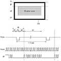
도 3은 파워 온 시퀀스, 디스플레이 구동 기간, 및 파워 오프 시퀀스를 보여 주는 도면이다.
도 4는 액티브 구간과 버티컬 블랭크 구간을 상세히 보여 주는 도면이다.
도 5 및 도 6은 화면 상에서 분할되어 VDD와 VSS가 독립적으로 공급되는 블록들을 보여 주는 도면들이다.
도 7은 VDD와 VSS를 스위칭하기 위한 스위치 회로와 블록 제어부를 보여 주는 회로도이다.
도 8 내지 도 10은 본 발명에서 적용 가능한 다양한 블록 구동 방법을 보여 주는 도면들이다.
도 11a 및 도 11b는 스위치 제어 신호에 따른 블록 구동 방법을 보여 주는 파형도들이다.
도 12는 VDD가 고정되고 VSS가 스윙(swing)될 때 픽셀 회로에서 누설 전류가 흐르는 예를 보여 주는 회로도이다.
도 13은 VSS가 고정되고 VDD가 스윙될 때 픽셀 회로에서 누설 전류가 흐르는 예를 보여 주는 회로도이다.
도 14 내지 도 16은 VSS가 스윙할 때 픽셀 회로의 동작을 상세히 보여 주는 도면들이다.
도 17 내지 도 19는 VDD가 스윙할 때 픽셀 회로의 동작을 상세히 보여 주는 도면들이다.
도 20은 OLED의 VDD와 VSS가 스윙할 때 OLED의 발광 기간 동안 OLED의 전류 변화를 보여 주는 시뮬레이션 결과 도면이다.1 is a block diagram showing an electroluminescent display device according to an embodiment of the present invention.
2 is a circuit diagram illustrating a pixel circuit and a sensing path connected to the pixel circuit.
3 is a diagram illustrating a power-on sequence, a display driving period, and a power-off sequence.
4 is a diagram illustrating in detail an active section and a vertical blank section.
5 and 6 are diagrams illustrating blocks to which VDD and VSS are independently supplied by being divided on a screen.
7 is a circuit diagram showing a switch circuit and a block controller for switching VDD and VSS.
8 to 10 are diagrams illustrating various block driving methods applicable to the present invention.
11A and 11B are waveform diagrams illustrating a block driving method according to a switch control signal.
12 is a circuit diagram illustrating an example in which leakage current flows in a pixel circuit when VDD is fixed and VSS is swinging.
13 is a circuit diagram illustrating an example in which a leakage current flows in a pixel circuit when VSS is fixed and VDD is swinging.
14 to 16 are diagrams detailing the operation of the pixel circuit when VSS swings.
17 to 19 are diagrams detailing the operation of the pixel circuit when VDD swings.
20 is a simulation result diagram showing changes in the current of the OLED during the emission period of the OLED when VDD and VSS of the OLED swing.
본 발명의 이점 및 특징, 그리고 그것들을 달성하는 방법은 첨부되는 도면과 함께 상세하게 후술되어 있는 실시예들을 참조하면 명확해질 것이다. 본 발명은 이하에서 개시되는 실시예들에 한정되는 것이 아니라 서로 다른 다양한 형태로 구현될 것이며, 단지 실시예들은 본 발명의 개시가 완전하도록 하며, 본 발명이 속하는 기술분야에서 통상의 지식을 가진 자에게 발명의 범주를 완전하게 알려주기 위해 제공되는 것이며, 본 발명은 청구항의 범주에 의해 정의될 뿐이다.Advantages and features of the present invention and methods of achieving them will become apparent with reference to the embodiments described below in detail in conjunction with the accompanying drawings. The present invention is not limited to the embodiments disclosed below, but will be implemented in various different forms, only the embodiments allow the disclosure of the present invention to be complete, and those of ordinary skill in the art to which the present invention pertains It is provided to fully understand the scope of the invention, and the present invention is only defined by the scope of the claims.
본 발명의 실시예를 설명하기 위한 도면에 개시된 형상, 크기, 비율, 각도, 개수 등은 예시적인 것이므로 본 발명은 도면에 도시된 사항에 한정되는 것은 아니다. 명세서 전체에 걸쳐 동일 참조 부호는 실질적으로 동일 구성 요소를 지칭한다. 또한, 본 발명을 설명함에 있어서, 관련된 공지 기술에 대한 구체적인 설명이 본 발명의 요지를 불필요하게 흐릴 수 있다고 판단되는 경우 그 상세한 설명을 생략한다.The shape, size, ratio, angle, number, etc. disclosed in the drawings for explaining the embodiment of the present invention are exemplary, and therefore the present invention is not limited to the matters shown in the drawings. Like reference numerals refer to substantially identical elements throughout. In addition, in describing the present invention, if it is determined that a detailed description of a related known technology may unnecessarily obscure the subject matter of the present invention, the detailed description thereof will be omitted.
본 명세서 상에서 언급된 "구비한다", "포함한다", "갖는다", "이루어진다" 등이 사용되는 경우 ' ~ 만'이 사용되지 않는 이상 다른 부분이 추가될 수 있다. 구성 요소를 단수로 표현한 경우에 특별히 명시적인 기재 사항이 없는 한 복수로 해석될 수 있다.When "includes", "includes", "having", "consisting of", etc. mentioned in this specification are used, other parts may be added unless 'only' is used. When a component is expressed in the singular, it may be interpreted as the plural unless otherwise explicitly stated.
구성 요소를 해석함에 있어서, 별도의 명시적 기재가 없더라도 오차 범위를 포함하는 것으로 해석한다.In interpreting the components, it is construed as including an error range even if there is no separate explicit description.
위치 관계에 대한 설명일 경우, 예를 들어, ' ~ 상에', ' ~ 상부에', ' ~ 하부에', ' ~ 옆에' 등으로 두 구성요소들 간에 위치 관계가 설명되는 경우, '바로' 또는 '직접'이 사용되지 않는 그 구성요소들 사이에 하나 이상의 다른 구성 요소가 개재될 수 있다.In the case of a description of the positional relationship, for example, when the positional relationship between two components is described as 'on One or more other elements may be interposed between those elements in which 'directly' or 'directly' are not used.
구성 요소들을 구분하기 위하여 제1, 제2 등이 사용될 수 있으나, 이 구성 요소들은 구성 요소 앞에 붙은 서수나 구성 요소 명칭으로 그 기능이나 구조가 제한되지 않는다. 예컨대, 도 4의 픽셀 회로에서 구성 요소들 앞에 붙여진 제1, 제2, 제3 및 제4와 같은 서수는 스위치 소자들(S1~S4)을 통해 데이터 라인들에 순차적으로 충전되는 순서를 기준으로 붙여진 것이다.1st, 2nd, etc. may be used to distinguish the components, but the functions or structures of these components are not limited to the ordinal number or component name attached to the front of the component. For example, in the pixel circuit of FIG. 4 , ordinal numbers such as first, second, third, and fourth placed in front of the elements are sequentially charged to the data lines through the switch elements S1 to S4 based on the order in which they are sequentially charged. it will be pasted
이하의 실시예들은 부분적으로 또는 전체적으로 서로 결합 또는 조합 가능하며, 기술적으로 다양한 연동 및 구동이 가능하다. 각 실시예들이 서로에 대하여 독립적으로 실시 가능할 수도 있고 연관 관계로 함께 실시 가능할 수도 있다.The following embodiments can be partially or wholly combined or combined with each other, and technically various interlocking and driving are possible. Each of the embodiments may be implemented independently of each other or may be implemented together in a related relationship.
유기 발광 표시장치에서 픽셀들을 구동하기 위한 구동 소자의 특성 변화를 보상하기 위한 보상 회로가 적용될 수 있다. 보상 회로는 내부 보상 회로와 외부 보상 회로로 나뉘어질 수 있다. 내부 보상 회로는 픽셀들 각각에 배치된 내부 보상 회로를 이용하여 구동 소자의 문턱 전압을 샘플링하여 픽셀 데이터의 데이터 전압에 문턱 전압을 더하여 픽셀들을 구동함으로써 구동 소자들 간의 문턱 전압 편차를 픽셀 회로 내부에서 자동으로 보상한다. 외부 보상 회로는 구동 소자들의 전기적 특성을 센싱(sensing)하고, 그 센싱 결과를 바탕으로 입력 영상의 픽셀 데이터를 변조함으로써 픽셀들 각각의 구동 특성 변화를 보상한다. 본 발명은 이하의 실시에에서 외부 보상 회로가 적용된 전계 발광 표시장치를 중심으로 설명되지만 이에 한정되지 않는다.A compensation circuit for compensating for a characteristic change of a driving element for driving pixels in an organic light emitting diode display may be applied. The compensation circuit may be divided into an internal compensation circuit and an external compensation circuit. The internal compensation circuit uses an internal compensation circuit disposed in each of the pixels to sample the threshold voltage of the driving element and add the threshold voltage to the data voltage of the pixel data to drive the pixels, thereby reducing the threshold voltage deviation between the driving elements in the pixel circuit. automatically compensate. The external compensation circuit senses electrical characteristics of the driving elements, and compensates for changes in driving characteristics of each of the pixels by modulating pixel data of an input image based on the sensing result. The present invention is mainly described in the following embodiments, but is not limited to the electroluminescent display device to which the external compensation circuit is applied.
이하, 첨부된 도면을 참조하여 본 발명의 다양한 실시예들을 상세히 설명한다. 이하의 실시예들에서, 전계 발광 표시장치는 유기 발광 물질을 포함한 유기발광 표시장치를 중심으로 설명한다. 본 발명의 기술적 사상은 유기발광 표시장치에 국한되지 않고, 무기발광 물질을 포함한 무기발광 표시장치에 적용될 수 있다.Hereinafter, various embodiments of the present invention will be described in detail with reference to the accompanying drawings. In the following embodiments, the electroluminescent display device will be mainly described with respect to the organic light emitting display device including the organic light emitting material. The technical spirit of the present invention is not limited to an organic light emitting display device, and may be applied to an inorganic light emitting display device including an inorganic light emitting material.
도 1은 본 발명의 실시예에 따른 전계 발광 표시장치를 보여 주는 블록도이다. 도 2는 픽셀 회로에 연결된 센싱 경로를 보여 주는 회로도이다.1 is a block diagram showing an electroluminescent display device according to an embodiment of the present invention. 2 is a circuit diagram illustrating a sensing path connected to a pixel circuit.
도 1 및 도 2를 참조하면, 본 발명의 실시예에 따른 전계 발광 표시장치는 표시패널(100)과, 표시패널 구동회로를 포함한다.1 and 2 , an electroluminescent display device according to an embodiment of the present invention includes a
표시패널(100)의 화면은 입력 영상을 표시하는 액티브 영역(AA)을 포함한다. 액티브 영역(AA)에 픽셀 어레이가 배치된다. 픽셀 어레이는 다수의 데이터 라인들(102), 데이터 라인들(102)과 교차되는 다수의 게이트 라인들(104), 및 매트릭스 형태로 배치되는 픽셀들을 포함한다.The screen of the
픽셀들 각각은 컬러 구현을 위하여 적색 서브 픽셀, 녹색 서브 픽셀, 청색 서브 픽셀로 나뉘어질 수 있다. 픽셀들 각각은 백색 서브 픽셀을 더 포함할 수 있다. 서브 픽셀들(101) 각각은 도 2와 같은 픽셀 회로를 포함한다.Each of the pixels may be divided into a red sub-pixel, a green sub-pixel, and a blue sub-pixel to implement color. Each of the pixels may further include a white sub-pixel. Each of the sub-pixels 101 includes a pixel circuit as shown in FIG. 2 .
표시패널(100) 상에 터치 센서들이 배치될 수 있다. 터치 입력은 별도의 터치 센서들을 이용하여 센싱되거나 픽셀들을 통해 센싱될 수 있다. 터치 센서들은 온-셀(On-cell type) 또는 애드 온 타입(Add on type)으로 표시패널의 화면 상에 배치되거나 픽셀 어레이에 내장되는 인-셀(In-cell type) 터치 센서들로 구현될 수 있다.Touch sensors may be disposed on the
표시패널 구동회로(110, 112, 120)는 데이터 구동부(110)와 게이트 구동부(120)를 구비한다. 데이터 구동부(110)와 데이터 라인들(102) 사이에 배치된 디멀티플렉서(112)가 배치될 수 있다.The display
표시패널 구동회로(110, 112, 120)는 디스플레이 구동 기간 동안 타이밍 콘트롤러(Timing controller, TCON)(130)의 제어 하에 표시패널(100)의 픽셀들에 입력 영상의 픽셀 데이터를 기입하여 화면 상에 입력 영상을 표시한다. 표시패널 구동회로는 터치 센서들을 구동하기 위한 터치 센서 구동부를 더 구비할 수 있다. 터치 센서 구동부는 도 1에서 생략되어 있다. 모바일 기기나 웨어러블 기기에서 데이터 구동부(110), 타이밍 콘트롤러(130) 그리고 전원 회로는 도 5에 도시된 바와 같은 드라이브 IC(Integrated Circuit, DIC)에 집적될 수 있다.The display
데이터 구동부(110)는 도 2에 도시된 바와 같이 디지털-아날로그 변환기(Digital to Analog converter, 이하 DAC라 함)를 이용하여 매 프레임 기간마다 타이밍 콘트롤러(130)로부터 수신되는 입력 영상의 픽셀 데이터(디지털 데이터)를 감마 보상 전압으로 변환하여 데이터 전압을 출력한다. 데이터 전압은 디멀티플렉서(112)와 데이터 라인(102)을 통해 픽셀들에 인가된다. 디멀티플렉서(112)는 다수의 스위치 소자들을 이용하여 데이터 구동부(110)와 데이터 라인들(102) 사이에 배치되어 데이터 구동부(110)로부터 출력되는 데이터 전압을 데이터 라인들(102)로 분배한다. 디멀티플렉서(112)에 의해 데이터 구동부(110)의 한 채널이 다수의 데이터 라인들에 시분할 연결되기 때문에 데이터 라인들(102)의 개수가 감소될 수 있다.As shown in FIG. 2 , the
게이트 구동부(120)는 액티브 영역의 트랜지스터 어레이와 함께 표시패널(100) 상의 베젤(bezel) 영역 상에 직접 형성되는 GIP(Gate in panel) 회로로 구현될 수 있다. 게이트 구동부(120)는 타이밍 콘트롤러(130)의 제어 하에 게이트 신호를 게이트 라인들(104)로 출력한다. 게이트 구동부(120)는 시프트 레지스터(Shift register)를 이용하여 게이트 신호를 시프트시킴으로써 그 신호들을 게이트 라인들(104)에 순차적으로 공급할 수 있다. 게이트 신호는 도 2에 도시된 바왁 같이 제1 및 제2 스캔 신호(SCAN1, SCAN2)로 나뉘어질 수 있다. 제1 스캔 신호(SCAN1)는 데이터 전압에 동기되어 데이터 전압이 인가되는 픽셀들을 선택한다. 제2 스캔 신호(SCAN2)는 제1 스캔 신호(SCAN1)에 동기될 수 있다. 제2 스캔 신호(SCAN2)는 외부 보상 방법에서 픽셀들에 형성된 구동 소자(DT)의 전기적 특성이 센싱되는 픽셀들을 선택한다. 구동 소자의 전기적 특성은 이동도(mobility, μ)와 문턱 전압(Vth)을 포함한다.The
외부 보상 방법은 제2 스캔 신호(SCAN2)를 활성화하여 픽셀 회로를 센싱 라인(103)에 연결하여 구동 소자의 문턱 전압(Vth) 또는 이동도(μ)를 센싱할 수 있다. 센싱 방법은 제품 출하전과 제품 출하 후로 나뉘어진다. 제품 출하전에 픽셀들에 연결된 센싱 경로를 통해 서브 픽셀들 각각에서 구동 소자(DT)의 문턱 전압이 센싱된 후에, 이 센싱 결과를 바탕으로 모든 서브 픽셀들에서 문턱 전압 편차가 보상된다. 그리고 서브 픽셀들 각각에서 구동 소자(DT)의 이동도가 센싱되어 이동도 편차가 보상될 수 있다.In the external compensation method, the threshold voltage Vth or mobility μ of the driving element may be sensed by activating the second scan signal SCAN2 and connecting the pixel circuit to the
제품 출하 후 센싱 방법은 도 3과 같이 파워 온 시퀀스(Power ON sequence, ON), 버티컬 블랭크 구간(Vertical blank, VB), 및 파워 오프 시퀀스(Power OFF sequence)에서 실행된다. 파워 오프 시퀀스(OFF)에서 표시패널 구동회로와 센싱 경로는 파워 오프 신호 수신 후, 미리 설정된 지연 시간 동안 더 구동되어 서브 픽셀들 각각에서 구동 소자의 문턱 전압(Vth)을 센싱한다.After the product is shipped, the sensing method is performed in a power ON sequence (ON), a vertical blank period (VB), and a power OFF sequence as shown in FIG. 3 . In the power-off sequence OFF, the display panel driving circuit and the sensing path are further driven for a preset delay time after receiving the power-off signal to sense the threshold voltage Vth of the driving device in each of the sub-pixels.
타이밍 콘트롤러(130)는 도시하지 않은 호스트 시스템으로부터 입력 영상의 픽셀 데이터와, 그와 동기되는 타이밍 신호를 수신한다. 타이밍 신호는 수직 동기신호(Vsync), 수평 동기신호(Hsync), 클럭 신호(DCLK) 및 데이터 인에이블 신호(DE) 등을 포함한다. 호스트 시스템은 TV(Television) 시스템, 셋톱박스, 네비게이션 시스템, 개인용 컴퓨터(PC), 홈 시어터 시스템, 모바일 기기, 웨어러블 기기 중 어느 하나일 수 있다.The
수직 동기신호(Vsync)는 1 프레임 기간을 정의한다. 수평 동기신호(Hsync)는 1 수평 기간(Horizontal time)을 정의한다. 데이터 인에이블 신호(DE)는 표시패널(100)의 픽셀 어레이에 표시될 픽셀 데이터와 동기되어 유효 픽셀 데이터 구간을 정의한다. 데이터 인에이블 신호(DE)의 1 펄스 주기는 1 수평 기간이고, 데이터 인에이블 신호(DE)의 하이 로직(high logic) 구간은 1 픽셀 라인의 픽셀 데이터 입력 구간을 나타낸다. 1 수평 기간(1H)은 표시패널(100)에서 1 픽셀 라인의 픽셀들에 데이터를 기입하는데 필요한 시간이다. 픽셀 라인은 게이트 라인 방향을 따라 배열되고 동일한 게이트 라인에 연결된 픽셀들을 포함한다. 1 픽셀 라인의 픽셀들은 스캔 신호가 인가되는 게이트 라인을 공유하여 이 게이트 라인으로부터의 스캔 신호에 따라 동시에 어드레싱되어 픽셀 데이터의 데이터 전압을 공급 받는다.The vertical synchronization signal Vsync defines one frame period. The horizontal synchronization signal Hsync defines one horizontal time period. The data enable signal DE is synchronized with pixel data to be displayed in the pixel array of the
타이밍 콘트롤러(130)는 호스트 시스템으로부터 수신된 타이밍 신호(Vsync, Hsync, DE)를 바탕으로 데이터 구동부(110)의 동작 타이밍을 제어하기 위한 데이터 타이밍 제어신호, 디멀티플렉서(112)의 동작 타이밍을 제어하기 위한 스위치 제어신호, 센싱 경로의 스위치 소자 제어신호, 게이트 구동부(120)의 동작 타이밍을 제어하기 위한 게이트 타이밍 제어신호를 발생하여 표시패널 구동회로(110, 112, 120)의 동작 타이밍을 제어한다. 타이밍 콘트롤러(130)로부터 출력된 게이트 타이밍 제어신호의 전압 레벨은 도시하지 않은 레벨 시프터를 통해 게이트 온 전압과 게이트 오프 전압으로 변환되어 게이트 구동부(120)에 공급될 수 있다. 레벨 시프터는 게이트 타이밍 제어신호의 로우 레벨 전압(low level voltage)을 게이트 로우 전압(VGL)으로 변환하고, 게이트 타이밍 제어신호의 하이 레벨 전압(high level voltage)을 게이트 하이 전압(VGH)으로 변환한다.The
센싱 경로는 도 2에 도시된 바와 같이 센싱 라인(103), 아날로그-디지털 변환기(Analog to Digital Convertor, 이하 “ADC”라 함), 및 제1 및 제2 스위치 소자(M1, M2) 등을 포함할 수 있다. 센싱 경로는 구동 소자(DT)의 소스 전압을 센싱하여 구동 소자의 전기적 특성을 센싱할 수 있다. 제1 스위치 소자(M1)는 소정의 기준 전압(Vref)을 센싱 라인(103)에 공급하여 구동 소자(DT)의 소스 전압을 기준 전압(Vref)으로 초기화한다. 제2 스위치 소자(M2)는 제1 스위치 소자(M1)가 턴-오프(turn-off)된 후에 턴-온되어 구동 소자(DT)의 소스 전압을 ADC에 공급한다. ADC는 아날로그 센싱 전압을 디지털 센싱 데이터로 변환하여 보상부(131)로 전송한다. 구동 소자(DT)의 소스 전압은 센싱 방법에 따라 구동 소자(DT)의 문턱 전압 또는 이동도를 나타낼 수 있다. 센싱 경로를 통해 구동 소자(DT)의 문턱 전압을 센싱하는 방법이나 센싱 경로를 통해 구동 소자(DT)의 이동도를 센싱하는 방법은 공지된 센싱 방법을 이용할 수 있다. ADC는 DAC와 함께 데이터 구동부(110)의 IC(integrated circuit)에 집적될 수 있다.The sensing path includes a
보상부(131)에는 서브 픽셀들 각각에서 구동 소자의 문턱 전압(Vth)과 이동도(μ)를 보상하기 위한 보상값들이 저장되어 있다. 보상부(131)는 ADC를 통해 수신된 디지털 센싱 데이터에 따라 미리 설정된 보상값을 선택하고 이 보상값을 입력 영상의 픽셀 데이터(디지털 데이터)에 더하거나 곱하여 픽셀 데이터를 보상한다. 이렇게 보상된 픽셀 데이터는 데이터 구동부(110)로 전송되어 데이터 구동부(110)의 DAC에 의해 데이터 전압(Vdata)으로 변환되어 데이터 라인(102)으로 공급된다. 픽셀 회로의 구동 소자(DT)는 데이터 라인(102)을 통해 공급되는 데이터 전압(Vdata)으로 구동되어 전류를 발생된다. 구동 소자(DT)를 통해 발광 소자인 OLED로 흐르는 전류는 구동 소자(DT)의 게이트-소스간 전압(Vgs)에 따라 결정된다. 보상부(131)는 타이밍 콘트롤러(130) 내의 연산 회로로 구현될 수 있다.The
도 3은 파워 온 시퀀스((Power ON sequence), 디스플레이 구동 기간, 및 파워 오프 시퀀스(Power OFF sequence)를 보여 주는 도면이다. 도 4는 액티브 구간(AT)과 버티컬 블랭크 구간(VB)을 상세히 보여 주는 도면이다.3 is a view showing a power ON sequence, a display driving period, and a power OFF sequence. FIG. 4 shows an active period AT and a vertical blank period VB in detail drawing is given.
도 3 및 도 4를 참조하면, 파워 온 시퀀스(ON)는 디스플레이 전원이 켜진 후에 시작된다. 파워 온 시퀀스(0N)에서 표시패널 구동회로와 표시패널(100)의 구동 전압이 발생되고 표시패널 구동회로가 초기화된다. 파워 온 시퀀스(0N)와 디스플레이 구동 기간의 버티컬 블랭크 구간(VB)에 구동 소자(DT)의 이동도가 센싱되고 이 센싱값에 따라 선택된 이동도 보상값으로 구동 소자(DT)의 이동도 편차가 보상된다. 구동 소자(DT)의 이동도가 센싱 결과를 바탕으로 이동도 보상값이 업데이트(update)될 수 있다. 디스플레이 구동 기간 동안, 매 프레임 기간마다 픽셀들에 기입되는 픽셀 데이터가 업데이트되어 화면 상에 영상이 표시된다.3 and 4 , the power-on sequence ON is started after the display power is turned on. In the power-on sequence 0N, a driving voltage of the display panel driving circuit and the
파워 오프 시퀀스(OFF)는 디스플레이 전원의 오프 신호가 수신된 후에 시작된다. 파워 오프 시퀀스(OFF)에서, 표시패널 구동회로와 센싱 경로가 추가 구동되는 지연 시간 동안 서브 픽셀들 각각의 문턱 전압(Vth)이 센싱된다.The power-off sequence OFF is started after an off signal of the display power is received. In the power-off sequence OFF, the threshold voltage Vth of each of the sub-pixels is sensed during a delay time during which the display panel driving circuit and the sensing path are additionally driven.
타이밍 콘트롤러(130)는 데이터 인에이블 신호(DE)와 입력 영상의 데이터를 버티컬 액티브 구간(AT) 동안 수신한다. 버티컬 블랭크 구간(VB)에 데이터 인에이블 신호(DE)와 입력 영상의 픽셀 데이터가 없다. 액티브 구간(AT) 동안 모든 픽셀들에 기입될 1 프레임 분량의 데이터가 타이밍 콘트롤러(130)에 수신된다. 1 프레임 기간은 액티브 구간간(AT)과 버티컬 블랭크 구간(VB)을 합한 시간이다.The
데이터 인에이블 신호(DE)에서 알 수 있는 바와 같이, 버티컬 블랭크 구간(VB) 동안 표시장치에 입력 데이터가 수신되지 않는다. 버티컬 블랭크 구간(VB)은 수직 싱크 시간(Vertical sync time, VS), 버티컬 프론트 포치(Vertical Front Porch, FP), 및 버티컬 백 포치(Vertical Back Porch, BP)을 포함한다. 수직 싱크 시간(VS)은 Vsync의 폴링 에지(falling edge)부터 라이징 에지(rising edge)까지의 시간으로서, 한 화면의 시작(또는 끝) 타이밍을 나타낸다. 버티컬 프론트 포치(FP)는 1 프레임 데이터의 마지막 라인 데이터 타이밍을 나타내는 마지막 DE의 폴링 에지부터 버티컬 블랭크 기간(VB)의 시작까지의 시간이다. 버티컬 백 포치(BP)는 버티컬 블랭크 기간(VB)의 끝부터 1 프레임 데이터의 제1 라인 데이터 타이밍을 나타내는 제1 DE의 라이징 에지까지의 시간이다.As can be seen from the data enable signal DE, input data is not received by the display device during the vertical blank period VB. The vertical blank section VB includes a vertical sync time (VS), a vertical front porch (FP), and a vertical back porch (BP). The vertical sync time (VS) is a time from a falling edge of Vsync to a rising edge, and represents the start (or end) timing of one screen. The vertical front porch FP is the time from the falling edge of the last DE indicating the last line data timing of one frame data to the start of the vertical blank period VB. The vertical back porch BP is the time from the end of the vertical blank period VB to the rising edge of the first DE indicating the first line data timing of one frame data.
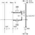
픽셀 회로의 일 예는 도 2와 같다. 픽셀 회로는 도 2에 도시된 바와 같이 발광 소자인 OLED와, OLED에 연결된 구동 소자(DT), 제1 및 제2 스위치 소자(S1, S2), 및 커패시터(Cst)를 포함한다. 픽셀 회로의 구동 소자와 스위치 소자는 MOSFET(metal oxide semiconductor field effect transistor) 구조의 트랜지스터로 구현될 수 있다. 구동 소자(DT)와 스위치 소자들(S1, S2)은 도 2에서 n 타입 트랜지스터로 예시되었으나 이에 한정되지 않는다.An example of a pixel circuit is shown in FIG. 2 . As shown in FIG. 2 , the pixel circuit includes an OLED which is a light emitting device, a driving device DT connected to the OLED, first and second switch devices S1 and S2 , and a capacitor Cst. The driving element and the switch element of the pixel circuit may be implemented as a transistor having a metal oxide semiconductor field effect transistor (MOSFET) structure. The driving element DT and the switch elements S1 and S2 are illustrated as n-type transistors in FIG. 2 , but are not limited thereto.
OLED는 애노드와 캐소드 사이에 형성된 유기 화합물층을 포함한다. 유기 화합물층은 정공주입층(HIL), 정공수송층(HTL), 발광층(EML), 전자수송층(ETL) 및 전자주입층(EIL) 등을 포함할 수 있으나 이에 한정되지 않는다. OLED의 애노드는 제2 노드(n2)를 통해 구동 소자(DT)에 연결되고, OLED의 캐소드는 저전위 전압(VSS)이 인가되는 VSS 전극에 연결된다.The OLED includes an organic compound layer formed between an anode and a cathode. The organic compound layer may include, but is not limited to, a hole injection layer (HIL), a hole transport layer (HTL), a light emitting layer (EML), an electron transport layer (ETL), and an electron injection layer (EIL). The anode of the OLED is connected to the driving element DT through the second node n2, and the cathode of the OLED is connected to the VSS electrode to which the low potential voltage VSS is applied.
구동 소자(DT)는 게이트-소스간 전압(Vgs)에 따라 OLED의 전류를 조절하여 OLED를 구동한다. 구동 소자(DT)는 제1 노드(n1)에 연결된 게이트, 고전위 전압(VDD)이 공급되는 제1 전극(또는 드레인), 및 제2 노드(n2)를 통해 OLED의 애노드에 연결된 제2 전극(또는 소스)을 포함한다. 커패시터(Cst)는 제1 및 제2 노드(n1, n2)를 통해 구동 소자(DT)의 게이트와 소스 사이에 연결된다.The driving device DT drives the OLED by controlling the current of the OLED according to the gate-source voltage Vgs. The driving element DT has a gate connected to the first node n1, a first electrode (or drain) to which the high potential voltage VDD is supplied, and a second electrode connected to the anode of the OLED through the second node n2. (or source). The capacitor Cst is connected between the gate and the source of the driving device DT through the first and second nodes n1 and n2.
제1 스위치 소자(S1)는 제1 스캔 신호(SCAN1)에 따라 턴-온(turn-on)되어 데이터 전압(Vdata)을 제1 노드(n1)에 연결된 구동 소자(DT)의 게이트에 공급한다. 제1 스위치 소자(S1)는 제1 스캔 신호(SCAN1)가 인가되는 제1 게이트 라인(1041)에 연결된 게이트, 데이터 라인(102)에 연결된 제1 전극, 및 제1 노드(n1)에 연결된 제2 전극을 포함한다.The first switch element S1 is turned on according to the first scan signal SCAN1 to supply the data voltage Vdata to the gate of the driving element DT connected to the first node n1. . The first switch element S1 includes a gate connected to the
제2 스위치 소자(S2)는 제2 스캔 신호(SCAN2)에 따라 턴-온되어 기준 전압(Vref)을 제2 노드(n2)에 공급한다. 기준 전압(Vref)과 저전위 전압(VSS)의 전압차는 OLED의 문턱 전압 보다 낮다. 따라서, OLED의 애노드에 기준 전압(Vref)이 인가될 때 OLED에 전류가 흐르지 않기 때문에 OLED가 발광되지 않는다. 제2 스위치 소자(S2)는 제2 스캔 신호(SCAN2)가 인가되는 제2 게이트 라인(1042)에 연결된 게이트, 기준 전압(Vref)이 인가되는 센싱 라인(103)에 연결된 제1 전극, 및 제2 노드(n2)에 연결된 제2 전극을 포함한다.The second switch element S2 is turned on according to the second scan signal SCAN2 to supply the reference voltage Vref to the second node n2 . The voltage difference between the reference voltage Vref and the low potential voltage VSS is lower than the threshold voltage of the OLED. Accordingly, when the reference voltage Vref is applied to the anode of the OLED, the OLED does not emit light because no current flows through the OLED. The second switch element S2 includes a gate connected to the
고전위 전압(VDD)은 구동 소자(DT)를 통해 OLED의 애노드에 인가된다. 저전위 전압(VSS)은 OLED의 캐소드에 인가된다. 따라서, 고전위 전압(VDD)은 구동 소자(DT)를 통해 OLED의 애노드에 공급된다.The high potential voltage VDD is applied to the anode of the OLED through the driving element DT. A low potential voltage (VSS) is applied to the cathode of the OLED. Accordingly, the high potential voltage VDD is supplied to the anode of the OLED through the driving element DT.
도 5 및 도 6은 화면 상에서 분할되어 VDD와 VSS이 독립적으로 공급되는 블록들을 보여 주는 도면들이다. 도 6에서 픽셀 회로의 구동 소자, 스위치 소자 및 커패시터는 생략되어 있다.5 and 6 are diagrams illustrating blocks to which VDD and VSS are independently supplied by being divided on a screen. In FIG. 6 , the driving element, the switch element, and the capacitor of the pixel circuit are omitted.
도 5 및 도 6을 참조하면, 표시패널(100)의 화면(AA)은 적어도 둘 이상의 블록들로 분할 구동될 수 있다. 제1 및 제2 블록들(EB1, EB2) 각각은 다수의 픽셀들을 포함한다. 표시패널은 제1 블록(EB1)의 픽셀들에 연결된 제1 및 제2 전원 배선들, 제1 전원 배선에 공급되는 전압을 VDD와 VSS 사이에서 스위칭하는 제1 스위치 회로, 제2 전원 배선에 공급되는 전압을 VDD와 VSS 사이에서 스위칭하는 제2 스위치 회로, 제2 블록의 픽셀들에 연결된 제3 및 제4 전원 배선, 제3 전원 배선에 공급되는 전압을 VDD와 VSS 사이에서 스위칭하는 제3 스위치 회로, 상기 제4 전원 배선에 공급되는 전압을 VDD와 VSS 사이에서 스위칭하는 제4 스위치 회로를 구비한다.5 and 6 , the screen AA of the
표시패널(100)의 화면(AA)은 다수의 블록들(EB1~EB4)로 분할된다. 블록들(EB1~EB4) 간에 급전 라인들(EL1~EL4, ER1~ER4)이 분리되어 블록들(EB1~EB4)에 VDD와 VSS가 독립적으로 공급된다. 급전 라인들(EL1~EL4, ER1~ER4)은 VDD 급전 라인들(EL1~EL4)과, VSS 급전 라인들(ER1~ER4)으로 나뉘어 진다. VDD 급전 라인들(EL1~EL4)은 블록 단위로 분할되어 블록(EB1~EB4) 내의 픽셀들의 구동 소자(DT)에 연결된다. VSS 급전 라인들(ER1~ER4)은 블록 단위로 분할되어 블록(EB1~EB4) 내의 픽셀들의 OLED 캐소드에 연결된다.The screen AA of the
제1 블록(EB1)의 픽셀들은 제1 VDD 급전 라인(EL1)과 제1 VSS 급전 라인(ER1)에 연결된다. 제2 블록(EB2)의 픽셀들은 제2 VDD 급전 라인(EL2)과 제2 VSS 급전 라인(ER2)에 연결된다. 제3 블록(EB3)의 픽셀들은 제3 VDD 급전 라인(EL3)과 제3 VSS 급전 라인(ER3)에 연결된다. 제4 블록(EB4)의 픽셀들은 제4 VDD 급전 라인(EL4)과 제4 VSS 급전 라인(ER4)에 연결된다.The pixels of the first block EB1 are connected to the first VDD feeding line EL1 and the first VSS feeding line ER1 . The pixels of the second block EB2 are connected to the second VDD feeding line EL2 and the second VSS feeding line ER2 . The pixels of the third block EB3 are connected to the third VDD feeding line EL3 and the third VSS feeding line ER3 . The pixels of the fourth block EB4 are connected to the fourth VDD feeding line EL4 and the fourth VSS feeding line ER4 .
급전 라인들(EL1~EL4, ER1~ER4)은 표시패널(100) 상에서 화면(AA) 밖의 좌측 베젤 영역과 우측 베젤 영역에 분산 배치될 수 있다. 예를 들어, 제1 VDD 급전 라인들(EL1~EL4)은 표시패널(100)의 좌측 베젤 영역에 배치될 수 있다. 제1 VSS 급전 라인들(ER1~ER4)은 표시패널(100)의 우측 베젤 영역에 배치될 수 있다.The power feeding lines EL1 to EL4 and ER1 to ER4 may be distributedly disposed on the
급전 라인들(EL1~EL4, ER1~ER4)에 각각 스위치 회로들(SL1~SL4, SR1~SR4)이 연결된다. 스위치 회로들(SL1~SL4, SR1~SR4)은 블록 제어부(EBC)의 제어 하에 VDD와 VSS를 선택하여 급전 라인들(EL1~EL4, ER1~ER4)에 공급한다. 블록 제어부(EBC)는 스위치 제어 신호들(SW1~SW4, /SW1~/SW4)을 발생하여 스위치 회로들(SL1~SL4, SR1~SR4)의 동작 타이밍을 제어한다.Switch circuits SL1 to SL4 and SR1 to SR4 are respectively connected to the feeding lines EL1 to EL4 and ER1 to ER4. The switch circuits SL1 to SL4 and SR1 to SR4 select VDD and VSS under the control of the block controller EBC, and supply them to the power supply lines EL1 to EL4 and ER1 to ER4. The block controller EBC generates the switch control signals SW1 to SW4 and /SW1 to /SW4 to control operation timings of the switch circuits SL1 to SL4 and SR1 to SR4.
제1-1 스위치 회로(SL1)는 제1 스위치 제어 신호(SW1)에 따라 VDD와 VSS를 선택하여 제1 VDD 급전 라인(EL1)에 공급한다. 제1-2 스위치 회로(SR1)는 제1 반전 스위치 제어 신호(/SW1)에 따라 VDD와 VSS를 선택하여 제1 VSS 급전 라인(ER1)에 공급한다. 제1 스위치 제어 신호(SW1)와 제1 반전 스위치 신호(/SW1)는 역위상으로 발생된다. 따라서, 제1-1 스위치 회로(SL1)는 도 11a 및 도 11b에 도시된 바와 같이 제1 스위치 제어 신호(SW1)가 하이 로직(High logic) 레벨(H)일 때 VDD를 제1 VDD 급전 라인(EL1)에 공급한다. 이와 동시에, 제1-2 스위치 회로(SR1)는 제1 반전 스위치 제어 신호(/SW1)의 로우 로직(Low logic) 레벨(L)에 응답하여 VSS를 제1 VSS 급전 라인(ER1)에 공급한다.The 1-1 switch circuit SL1 selects VDD and VSS according to the first switch control signal SW1 and supplies it to the first VDD power supply line EL1 . The 1-2 switch circuit SR1 selects VDD and VSS according to the first inverted switch control signal /SW1 and supplies it to the first VSS power supply line ER1 . The first switch control signal SW1 and the first inverted switch signal /SW1 are generated out of phase. Accordingly, the 1-1 switch circuit SL1 applies VDD to the first VDD feeding line when the first switch control signal SW1 is a high logic level H as shown in FIGS. 11A and 11B . (EL1) is supplied. At the same time, the 1-2 switch circuit SR1 supplies VSS to the first VSS power supply line ER1 in response to the low logic level L of the first inverted switch control signal /SW1. .
제2-1 스위치 회로(SL2)는 제2 스위치 제어 신호(SW2)에 따라 VDD와 VSS를 선택하여 제2 VDD 급전 라인(EL2)에 공급한다. 제2-2 스위치 회로(SR2)는 제2 반전 스위치 제어 신호(/SW2)에 따라 VDD와 VSS를 선택하여 제2 VSS 급전 라인(ER2)에 공급한다. 제2 스위치 제어 신호(SW2)와 제2 반전 스위치 신호(/SW1)는 역위상으로 발생된다. 따라서, 제2-1 스위치 회로(SL2)는 도 11a 및 도 11b에 도시된 바와 같이 제2 스위치 제어 신호(SW2)가 하이 로직 레벨(H)일 때 VDD를 제1 VDD 급전 라인(EL1)에 공급한다. 이와 동시에, 제2-2 스위치 회로(SR2)는 제2 반전 스위치 제어 신호(/SW2)의 로우 로직 레벨(L)에 응답하여 VSS를 제1 VSS 급전 라인(ER1)에 공급한다.The second-first switch circuit SL2 selects VDD and VSS according to the second switch control signal SW2 and supplies the selected VDD and VSS to the second VDD power supply line EL2 . The 2-2 switch circuit SR2 selects VDD and VSS according to the second inverted switch control signal /SW2 and supplies the selected VDD and VSS to the second VSS power supply line ER2. The second switch control signal SW2 and the second inverted switch signal /SW1 are generated out of phase. Accordingly, the 2-1 switch circuit SL2 transfers VDD to the first VDD feeding line EL1 when the second switch control signal SW2 is at the high logic level H as shown in FIGS. 11A and 11B . supply At the same time, the 2-2 switch circuit SR2 supplies VSS to the first VSS power supply line ER1 in response to the low logic level L of the second inverted switch control signal /SW2.
제3-1 스위치 회로(SL3)는 제3 스위치 제어 신호(SW3)에 따라 VDD와 VSS를 선택하여 제3 VDD 급전 라인(EL3)에 공급한다. 제3-2 스위치 회로(SR3)는 제3 반전 스위치 제어 신호(/SW3)에 따라 VDD와 VSS를 선택하여 제3 VSS 급전 라인(ER3)에 공급한다. 제4-1 스위치 회로(SL4)는 제4 스위치 제어 신호(SW4)에 따라 VDD와 VSS를 선택하여 제4 VDD 급전 라인(EL4)에 공급한다. 제4-2 스위치 회로(SR4)는 제4 반전 스위치 제어 신호(/SW4)에 따라 VDD와 VSS를 선택하여 제4 VSS 급전 라인(ER4)에 공급한다.The 3-1 th switch circuit SL3 selects VDD and VSS according to the third switch control signal SW3 and supplies them to the third VDD power supply line EL3 . The 3 - 2 switch circuit SR3 selects VDD and VSS according to the third inverted switch control signal /SW3 and supplies the selected VDD and VSS to the third VSS power supply line ER3 . The 4-1 th switch circuit SL4 selects VDD and VSS according to the fourth switch control signal SW4 and supplies them to the fourth VDD power supply line EL4 . The 4-2 th switch circuit SR4 selects VDD and VSS according to the fourth inverted switch control signal /SW4 and supplies the selected VDD and VSS to the fourth VSS power supply line ER4.
블록 제어부(EBC)와 스위치 회로들(SL1~SL4, SR1~SR4)은 도 7에 도시된 바와 같이 데이터 구동부(110)와 함께 드라이브 IC(DIC)에 집적될 수 있다.The block controller EBC and the switch circuits SL1 to SL4 and SR1 to SR4 may be integrated in the drive IC DIC together with the
도 7을 참조하면, 스위치 회로들(SL1~SL4)은 각각 스위치 제어 신호(SW1~SW4)에 따라 VDD와 VSS를 선택하는 스위치 소자들(T01, T02)을 구비한다. 스위치 소자(T01)는 n 채널 트랜지스터로 구현되고, 스위치 소자(T02)는 p 채널 트랜지스터로 구현될 수 있다. 스위치 소자(T01)는 스위치 제어 신호(SW1~SW4)의 하이 로직 레벨 전압에 응답하여 턴-온되어 VDD를 VDD 급전 라인(EL1~EL4)에 공급한다. 스위치 소자(T02)는 스위치 제어 신호(SW1~SW4)의 로우 로직 레벨 전압에 응답하여 턴-온되어 VSS를 VDD 급전 라인(EL1~EL4)에 공급한다. 드라이브 IC(DIC)에서 제1 전원 출력 패드들(EBL)은 스위치 회로들(SL1~SL4)의 출력 단자들을 VDD 급전 라인들(EL1~EL4)에 연결한다.Referring to FIG. 7 , the switch circuits SL1 to SL4 include switch elements T01 and T02 for selecting VDD and VSS according to the switch control signals SW1 to SW4, respectively. The switch element T01 may be implemented as an n-channel transistor, and the switch element T02 may be implemented as a p-channel transistor. The switch element T01 is turned on in response to the high logic level voltage of the switch control signals SW1 to SW4 to supply VDD to the VDD power supply lines EL1 to EL4. The switch element T02 is turned on in response to the low logic level voltage of the switch control signals SW1 to SW4 to supply VSS to the VDD power supply lines EL1 to EL4 . In the drive IC DIC, the first power output pads EBL connect output terminals of the switch circuits SL1 to SL4 to the VDD power supply lines EL1 to EL4 .
스위치 회로들(SR1~SR4)은 각각 반전 스위치 제어 신호(/SW1~/SW4)에 따라 VDD와 VSS를 선택하는 스위치 소자들(T03, T04)을 구비한다. 스위치 소자(T03)는 n 채널 트랜지스터로 구현되고, 스위치 소자(T04)는 p 채널 트랜지스터로 구현될 수 있다. 스위치 소자(T03)는 반전 스위치 제어 신호(/SW1~/SW4)의 하이 로직 레벨 전압에 응답하여 턴-온되어 VDD를 VSS 급전 라인(ER1~ER4)에 공급한다. 스위치 소자(T04)는 반전 스위치 제어 신호(/SW1~/SW4)의 로우 로직 레벨 전압에 응답하여 턴-온되어 VSS를 VSS 급전 라인(ER1~ER4)에 공급한다. 드라이브 IC(DIC)에서 제2 전원 출력 패드들(EBR)은 스위치 회로들(SR1~SR4)의 출력 단자들을 VSS 급전 라인들(ER1~ER4)에 연결한다.The switch circuits SR1 to SR4 include switch elements T03 and T04 for selecting VDD and VSS according to the inverted switch control signals /SW1 to /SW4, respectively. The switch element T03 may be implemented as an n-channel transistor, and the switch element T04 may be implemented as a p-channel transistor. The switch element T03 is turned on in response to the high logic level voltage of the inverted switch control signals /SW1 to /SW4 to supply VDD to the VSS power supply lines ER1 to ER4. The switch element T04 is turned on in response to the low logic level voltage of the inverted switch control signals /SW1 to /SW4 to supply VSS to the VSS power supply lines ER1 to ER4. In the drive IC DIC, the second power output pads EBR connect output terminals of the switch circuits SR1 to SR4 to the VSS power supply lines ER1 to ER4 .
드라이브 IC(DIC)가 실장된 COF(Chip on film)은 표시패널(100) 상에 접착된다. 드라이브 IC(DIC)의 소스 출력 패드들(Source output pads)은 표시패널(100)의 데이터 라인들에 전기적으로 연결된다.A chip on film (COF) on which a drive IC (DIC) is mounted is adhered to the
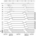
블록 제어부(EBC)는 미리 설정된 블록 구동 방법에 따라 스위치 제어 신호(SW1~SW4, /SW1~/SW4)를 온/오프하여 도 8 내지 도 10에 도시된 바와 같이 다양한 블록 구동 방법으로 픽셀들의 발광 타이밍을 제어할 수 있다.The block controller EBC turns on/off the switch control signals SW1 to SW4 and /SW1 to /SW4 according to a preset block driving method to emit light of pixels in various block driving methods as shown in FIGS. 8 to 10 . You can control the timing.
도 8 내지 도 10은 본 발명에서 적용 가능한 다양한 블록 구동 방법을 보여 주는 도면들이다.8 to 10 are diagrams illustrating various block driving methods applicable to the present invention.
도 8 내지 도 10을 참조하면, 게이트 구동부(120)는 매 프레임 기간마다 액티브 구간(AT) 동안 제1 픽셀 라인부터 제N 픽셀 라인까지 게이트 라인들(104)에 데이터 전압에 동기되는 스캔 신호(SCAN1)를 순차적으로 공급한다. 제N 픽셀 라인은 액티브 구간(AT) 내에서 마지막 스캔 신호에 의해 어드레싱되는 마지막 픽셀 라인이다. 액티브 구간(AT) 동안 1 픽셀 라인씩 픽셀들이 어드레싱된다. 스캔 신호에 의해 어드레싱된 픽셀들에 픽셀 데이터가 기입된다.8 to 10 , the
블록 제어부(EBC)는 도 8에 도시된 바와 같이 픽셀 데이터가 입력되지 않는 버티블 블랭크 기간(VB) 동안 모든 블록들(EB1~EB4)의 픽셀들을 동시에 발광시킬 수 있다. 이 방법은 화면 전체의 픽셀들이 동시에 점등 및 소등되기 때문에 글로벌 셔터(global shutter) 방식으로 알려져 있다. 글로벌 셔터 방식은 프레임 주파수가 높은 가상 현실 기기(VR)에서 픽셀들이 임펄스(Impulse) 방식으로 구동되기 때문에 모션 블러(motion blurr)를 개선할 수 있다.As shown in FIG. 8 , the block controller EBC may simultaneously emit light from the pixels of all blocks EB1 to EB4 during the durable blank period VB in which pixel data is not input. This method is known as a global shutter method because pixels on the entire screen are turned on and off at the same time. The global shutter method can improve motion blur because pixels are driven by an impulse method in a virtual reality device (VR) having a high frame frequency.
블록 제어부(EBC)는 도 9 및 도 10에 도시된 바와 같이 픽셀들을 구동할 수 있다. 도 9 및 도 10에 도시된 바와 같이, 픽셀 데이터가 기입된 픽셀들은 블록 제어부(EBC)의 제어 하에 스위칭되는 VDD와 VSS를 공급 받아 제1 블록(EB1) 부터 제4 블록(EB4) 순으로 발광할 수 있다. 제N 픽셀 라인이 어드레싱되기 전에 어드레싱된 픽셀들을 포함한 블록들이 발광되기 시작할 수 있다. 일 예로, 제1 내지 제3 블록들(EB1~EB3)의 픽셀들은 마지막 픽셀 라인이 어드레싱되기 전에 블록 단위로 순차적으로 발광될 수 있다.. 도 9 및 도 10에서 두꺼운 점선으로 표시된 바와 같이 버티컬 블랭크 기간(VB) 내에서 모든 블록들(EB1~EB4)이 발광되어 픽셀이 임펄스 구동 방법으로 구동된다. 이러한 블록 구동 방법은 픽셀들이 임펄스 구동하기 때문에 모션 블러를 개선할 수 있음은 물론, 블록 단위로 피크 전류(peak current)가 분산되기 때문에 EMI를 개선할 수 있다.The block controller EBC may drive pixels as shown in FIGS. 9 and 10 . As shown in FIGS. 9 and 10 , pixels in which pixel data are written are supplied with VDD and VSS switched under the control of the block controller EBC, and light is emitted from the first block EB1 to the fourth block EB4 in order. can do. Blocks including the addressed pixels may start to emit light before the N-th pixel line is addressed. For example, the pixels of the first to third blocks EB1 to EB3 may be sequentially emitted in block units before the last pixel line is addressed. As indicated by thick dashed lines in FIGS. 9 and 10 , vertical blanks In the period VB, all the blocks EB1 to EB4 emit light so that the pixel is driven by the impulse driving method. In this block driving method, motion blur can be improved because pixels are driven by impulse, and EMI can be improved because a peak current is distributed in units of blocks.
블록 제어부(EBC)는 레지스터(register) 설정값에 따라 도 8 내지 도 10과 같은 블록 구동 방법 중 어느 하나를 선택하여 픽셀들의 발광 타이밍을 조정할 수 있다. 블록 제어부(EBC)는 버티컬 블랭크 기간(VB) 동안 스위치 제어 신호(SW1~SW4)를 동시에 하이 로직 레벨(H)로 반전시켜 도 8과 같은 블록 구동 방법으로 블록들(EB1~EB4)의 발광 타이밍을 제어할 수 있다. 스위치 제어 신호(SW1~SW4)가 하이 로직 레벨(H)로 반전될 때 반전 스위치 제어 신호(/SW1~/SW4)는 로우 로직 레벨(L)로 반전된다. 스위치 제어 신호(SW1~SW4)가 하이 로직 레벨(H)일 때, VDD 급전 라인(EL1~EL4)에 VDD가 인가되고 VSS 급전 라인(ER1~ER4)에 VSS가 인가된다. 이 때, 픽셀 회로의 구동 TFT(DT)에 VDD가 인가되고 OLED의 캐소드에 VSS가 인가되어 OLED가 발광될 수 있다.The block controller EBC may adjust the emission timing of pixels by selecting any one of the block driving methods illustrated in FIGS. 8 to 10 according to a register setting value. The block controller EBC inverts the switch control signals SW1 to SW4 to the high logic level H at the same time during the vertical blank period VB, so that the light emission timing of the blocks EB1 to EB4 is performed by the block driving method as shown in FIG. 8 . can be controlled. When the switch control signals SW1 to SW4 are inverted to the high logic level H, the inverted switch control signals /SW1 to /SW4 are inverted to the low logic level L. When the switch control signals SW1 to SW4 have a high logic level H, VDD is applied to the VDD feed lines EL1 to EL4 and VSS is applied to the VSS feed lines ER1 to ER4. At this time, VDD is applied to the driving TFT (DT) of the pixel circuit and VSS is applied to the cathode of the OLED, so that the OLED can emit light.
블록 제어부(EBC)는 도 11b에 도시된 바와 같이 버티컬 블랭크 기간(VB) 동안 스위치 제어 신호(SW1~SW4, /SW1~/SW4)를 순차적으로 시프트하여 도 9 및 도 10과 같은 블록 구동 방법으로 블록들(EB1~EB4)의 발광 타이밍을 블록 단위로 순차적으로 시프트할 수 있다.The block control unit EBC sequentially shifts the switch control signals SW1 to SW4 and /SW1 to /SW4 during the vertical blank period VB as shown in FIG. The light emission timings of the blocks EB1 to EB4 may be sequentially shifted in units of blocks.
픽셀들이 어드레싱되는 액티브 구간(AT) 동안, 스위치 제어 신호(SW1~SW4)가 로직 로직 레벨(L)을 유지하여, VDD 급전 라인(EL1~EL4)에 VSS가 인가되고 VSS 급전 라인(ER1~ER4)에 VDD가 인가된다. 이 때, 픽셀 회로의 구동 TFT(DT)에 VSS가 인가되고 OLED의 캐소드 전압이 VDD이기 때문에 OLED에 역바이어스 전압이 인가되어 OLED가 발광되지 않는다.During the active period AT in which the pixels are addressed, the switch control signals SW1 to SW4 maintain a logic logic level L, so that VSS is applied to the VDD feed lines EL1 to EL4 and the VSS feed lines ER1 to ER4 ), VDD is applied. At this time, since VSS is applied to the driving TFT (DT) of the pixel circuit and the cathode voltage of the OLED is VDD, a reverse bias voltage is applied to the OLED, so that the OLED does not emit light.
블록들 각각에서 픽셀 회로는 실질적으로 동일하다. 제1 블록(EB1)의 서브 픽셀들 각각은 제1 VSS 급전 라인(ER1)에 캐소드가 연결된 OLED, 제1 VDD 급전 라인(EL1)에 연결되고 OLED 를 구동하는 구동 소자(DT), 데이터 전압에 동기되는 제1 스캔 신호에 따라 턴온되어 구동 소자(DT)의 게이트에 데이터 전압을 공급하는 제1 스위치 소자(S1), 제2 스캔 신호에 따라 턴-온되어 구동 소자(DT)의 소스와 OLED 의 애노드에 기준 전압(Vref)을 공급하는 제2 스위치 소자(S2), 및 구동 소자(DT)의 게이트와 소스 사이에 연결된 커패시터(Cst)를 포함한다.The pixel circuitry in each of the blocks is substantially the same. Each of the sub-pixels of the first block EB1 is an OLED having a cathode connected to the first VSS supply line ER1, a driving element DT connected to the first VDD supply line EL1 and driving the OLED, and a data voltage. The first switch element S1 is turned on according to the synchronized first scan signal to supply a data voltage to the gate of the driving element DT, and is turned on according to the second scan signal to form a source and an OLED of the driving element DT a second switch element S2 for supplying the reference voltage Vref to the anode of the , and a capacitor Cst connected between the gate and the source of the driving element DT.
제2 블록(EB2)의 서브 픽셀들 각각은 제2 VSS 급전 라인(ER2)에 캐소드가 연결된 OLED, 제2 VDD 급전 라인(EL2)에 연결되고 OLED 를 구동하는 구동 소자(DT), 데이터 전압에 동기되는 제1 스캔 신호에 따라 턴온되어 구동 소자(DT)의 게이트에 데이터 전압을 공급하는 제1 스위치 소자(S1), 제2 스캔 신호에 따라 턴-온되어 구동 소자(DT)의 소스와 OLED 의 애노드에 기준 전압(Vref)을 공급하는 제2 스위치 소자(S2), 및 구동 소자(DT)의 게이트와 소스 사이에 연결된 커패시터(Cst)를 포함한다.Each of the sub-pixels of the second block EB2 is an OLED having a cathode connected to the second VSS supply line ER2, a driving element DT connected to the second VDD supply line EL2 and driving the OLED, and a data voltage. The first switch element S1 is turned on according to the synchronized first scan signal to supply a data voltage to the gate of the driving element DT, and is turned on according to the second scan signal to form a source and an OLED of the driving element DT a second switch element S2 for supplying the reference voltage Vref to the anode of the , and a capacitor Cst connected between the gate and the source of the driving element DT.
픽셀들의 발광 타이밍을 조정하기 위하여 픽셀들에서 OLED의 캐소드 전압(VSS)이 교류 전압으로 스윙(swing)할 수 있다. 그러나 이 방법에서 VDD가 고정되면 픽셀들에서 누설 전류(leakage current)가 발생될 수 있다. 본 발명은 OLED의 애노드 전압(VDD)과 캐소드 전압을 픽셀의 발광 기간과 비발광 기간에 따라 동시에 변경하여 픽셀의 누설 전류를 최소화하고 누설 전류로 인한 휘도 저하를 줄일 수 있다. 이를 도 12 및 도 13을 결부하여 설명하기로 한다. 도 12 및 도 13에서 데이터 전압(Vdata)은 Vdata =5V, 기준 전압In order to adjust the emission timing of the pixels, the cathode voltage (VSS) of the OLED in the pixels may swing to an AC voltage. However, in this method, when VDD is fixed, a leakage current may be generated in the pixels. According to the present invention, by simultaneously changing the anode voltage (VDD) and cathode voltage of the OLED according to the light emitting period and the non-emission period of the pixel, it is possible to minimize the leakage current of the pixel and reduce the decrease in luminance due to the leakage current. This will be described in conjunction with FIGS. 12 and 13 . 12 and 13, the data voltage (Vdata) is Vdata = 5V, the reference voltage
도 12를 참조하면, OLED의 캐소드가 연결된 VSS 급전 라인의 전압이 17V와 0V 사이에서 스윙하고 VDD 급전 라인의 전압이 17V로 고정되어 있을 때, 구동 소자(DT)가 턴-온될 때 OLED의 애노드에 17V가 인가된다. OLED의 캐소드 전압이 0V일 때 OLED가 턴-온되어 발광되는 반면, OLED의 캐소드 전압이 17V일 때 OLED는 발광할 수 없다. OLED의 애노드 전압이 17V로 상승하면 커패시터(Cst)를 통한 커플링(Coupling)으로 인하여 제1 노드(n1)의 전압이 22V로 상승한다. 그 결과, 스위치 소자들(S1, S2)의 드레인-소스간 전압(Vds)이 높아 화살표로 나타낸 바와 같이 스위치 소자들(S1, S2)을 통해 누설 전류가 흐른다. 이러한 누설 전류는 구동 소자(DT)의 게이트-소스간 전압(Vgs)의 감소를 초래하여 OLED의 전류를 감소시켜 픽셀의 휘도를 낮춘다.12 , when the voltage of the VSS feed line to which the cathode of the OLED is connected swings between 17V and 0V and the voltage of the VDD feed line is fixed at 17V, the driving element DT is turned on when the anode of the OLED is turned on 17V is applied to When the cathode voltage of the OLED is 0V, the OLED is turned on to emit light, whereas when the cathode voltage of the OLED is 17V, the OLED cannot emit light. When the anode voltage of the OLED rises to 17V, the voltage at the first node n1 rises to 22V due to coupling through the capacitor Cst. As a result, the drain-source voltage Vds of the switch elements S1 and S2 is high, and a leakage current flows through the switch elements S1 and S2 as indicated by the arrow. This leakage current causes a decrease in the gate-source voltage Vgs of the driving element DT to decrease the current of the OLED, thereby lowering the luminance of the pixel.
도 13을 참조하면, OLED의 캐소드가 연결된 VSS 급전 라인의 전압이 VSS=GND=0V로 고정된 반면, VDD 급전 라인의 전압이 17V와 0V 사이에 스윙한다. OLED의 애노드 전압이 17V일 때 OLED가 턴-온되어 발광되는 반면, OLED의 애노드 전압이 0V일 때 OLED는 발광할 수 없다. VDD를 스윙하는 방법으로 OLED의 애노드 전압을 가변하여 OLED의 발광 타이밍을 제어하면, OLED의 비발광 기간 동안 VDD = 0V로 낮기 때문에 스위치 소자들(S1, S2)에 흐르는 누설 전류를 줄일 수 있다. 기준 전압(Vref)을 적절히 조정하면 스위치 소자들(S1, S2)의 누설 전류를 최소화할 수 있다. 예를 들어, 기준 전압(Vref)을 0V 보다 높은 전압(예, 3V)로 높이면 스위치 소자들(S1, S2)의 Vds를 줄여 누설 전류를 최소화할 수 있다.Referring to FIG. 13 , the voltage of the VSS feeding line to which the cathode of the OLED is connected is fixed at VSS=GND=0V, while the voltage of the VDD feeding line swings between 17V and 0V. When the anode voltage of the OLED is 17V, the OLED is turned on and emits light, whereas when the anode voltage of the OLED is 0V, the OLED cannot emit light. If the emission timing of the OLED is controlled by varying the anode voltage of the OLED by swinging VDD, the leakage current flowing through the switch elements S1 and S2 can be reduced because VDD = 0V during the non-emission period of the OLED is low. By properly adjusting the reference voltage Vref, the leakage current of the switch elements S1 and S2 may be minimized. For example, if the reference voltage Vref is increased to a voltage higher than 0V (eg, 3V), the leakage current may be minimized by reducing Vds of the switch elements S1 and S2.
픽셀 회로의 동작은 초기화 및 데이터 기입 단계, 발광 단계로 나뉘어질 수 있다. 이러한 픽셀 회로의 동작에서 VSS가 스윙할 때와 VDD가 스윙할 때 누설 전류의 차이가 있다. 이를 도 14 내지 도 19를 결부하여 설명하기로 한다.The operation of the pixel circuit may be divided into an initialization and data writing phase, and a light emission phase. In the operation of this pixel circuit, there is a difference in leakage current when VSS swings and when VDD swings. This will be described in conjunction with FIGS. 14 to 19 .
도 14 내지 도 16은 VSS가 스윙할 때 픽셀 회로의 동작을 상세히 보여 주는 도면들이다.14 to 16 are diagrams detailing the operation of the pixel circuit when VSS swings.
도 14는 커패시터(Cst)의 초기화 및 데이터 기입 단계에서 픽셀 회로의 동작을 보여 준다.14 shows the operation of the pixel circuit in the initialization and data writing phases of the capacitor Cst.
도 14를 참조하면, 커패시터의 초기화 및 데이터 기입 단계에서 픽셀 회로의 구동 전압은 VDD = 17V, VSS = 17V, Vref = 0V 이다. 이 때 스캔 신호들(SCAN1, SCAN2)의 전압이 VGH로 상승하여 스위치 소자들(S1, S2)이 턴-온(turn-on)된다.Referring to FIG. 14 , driving voltages of the pixel circuit are VDD=17V, VSS=17V, and Vref=0V in the capacitor initialization and data writing steps. At this time, the voltage of the scan signals SCAN1 and SCAN2 rises to VGH so that the switch elements S1 and S2 are turned on.
커패시터의 초기화 및 데이터 기입 단계에서 데이터 전압(Vdata=5V)이 구동 소자(DT)의 게이트에 인가되고 기준 전압(Vref=0V)이 구동 소자(DT)의 소스에 인가된다. 따라서, 커패시터의 초기화 및 데이터 기입 단계에서 구동 소자(DT)의 게이트-소스간 전압(Vgs)은 Vgs = Vdata - Vref이고 이 전압은 커패시터(Cst)의 전압과 같다. 구동 소자(DT)의 게이트 전압(Vg), 소스 전압(Vs), 드레인-소스간 전압(Vds)은 Vg = 5V, Vs = 0V, Vgs = 5V, Vds = 17V 이다.In the capacitor initialization and data writing steps, a data voltage (Vdata=5V) is applied to the gate of the driving device DT and a reference voltage (Vref=0V) is applied to the source of the driving device DT. Accordingly, in the capacitor initialization and data writing steps, the gate-source voltage Vgs of the driving element DT is Vgs = Vdata - Vref, and this voltage is equal to the voltage of the capacitor Cst. The gate voltage Vg, the source voltage Vs, and the drain-source voltage Vds of the driving element DT are Vg = 5V, Vs = 0V, Vgs = 5V, and Vds = 17V.
커패시터의 초기화 및 데이터 기입 단계에서, 구동 소자(DT)의 Vgs 가 문턱 전압(Vth) 보다 크기 때문에 구동 소자(DT)가 턴-온되어 구동 소자(DT)의 드레인-소스 간에 전류(Ids)를 통해 이 전류는 화살표로 나타낸 바와 같이 흐른다. 이 때, OLED의 캐소드에 VSS=17V가 인가되어 OLED가 오프 상태를 유지하여 OLED로 전류가 흐르지 않는다.In the capacitor initialization and data writing step, since Vgs of the driving device DT is greater than the threshold voltage Vth, the driving device DT is turned on to increase the current Ids between the drain and the source of the driving device DT. Through this current flows as indicated by the arrow. At this time, VSS=17V is applied to the cathode of the OLED so that the OLED remains off, so that no current flows to the OLED.
구동 소자(DT)의 전류(Ids)로 인하여, 구동 소자(DT)의 소스 전압은 17V까지 상승하고, 커패시터(Cst)를 통한 커플링(coupling)으로 구동 소자(DT)의 게이트 전압이 5V + 17V = 22V까지 상승한다. 이 때, 구동 소자(DT)의 Vgs는 Vgs = 5V로 유지되기 때문에 커패시터(Cst)에 충전된 전압이 유지되어 데이터 전압의 손실은 없다.Due to the current Ids of the driving element DT, the source voltage of the driving element DT rises to 17V, and the gate voltage of the driving element DT is 5V + due to coupling through the capacitor Cst Rise to 17V = 22V. At this time, since Vgs of the driving element DT is maintained at Vgs = 5V, the voltage charged in the capacitor Cst is maintained, so that there is no loss of data voltage.
도 15는 발광 단계 직전에 픽셀 회로의 전류를 나타낸다.Fig. 15 shows the current in the pixel circuit just before the light-emitting phase.
도 15를 참조하면, 픽셀 회로의 구동 전압은 VDD = 17V, VSS = 17V, Vref = 0V 를 유지한다. 스캔 신호들(SCAN1, SCAN2)의 전압이 VGL로 변하여 스위치 소자들(S1, S2)이 턴-오프(turn-off)된다. 스캔 신호들(SCAN1, SCAN2)이 오프된 상태에서 스위치 소자들(S1, S2)에서 누설 전류가 없어야 하지만 VDD가 도 15에 도시된 바와 같이 높은 전압 17V로 유지되면 스위치 소자들(S1,S2)을 통해 누설 전류가 흐른다.Referring to FIG. 15 , the driving voltages of the pixel circuit maintain VDD = 17V, VSS = 17V, and Vref = 0V. The voltage of the scan signals SCAN1 and SCAN2 is changed to VGL so that the switch elements S1 and S2 are turned off. When the scan signals SCAN1 and SCAN2 are off, there should be no leakage current in the switch elements S1 and S2, but when VDD is maintained at a high voltage of 17V as shown in FIG. 15 , the switch elements S1 and S2 leakage current flows through
스캔 신호들(SCAN1, SCAN2)의 전압이 VGL로 변한 직후에, 구동 소자(DT)의 Vgs가 Vth 보다 낮아져 구동 소자(DT)가 턴-오프되어 구동 소자(DT)에서 전류(Ids)가 흐르지 않는다. 그런데, 제1 스위치 소자(S1)의 Vds는 Vds = 22V - 5V이고, 제2 스위치 소자(S2)의 Vds는 Vds = 17V - 0V이기 때문에 스위치 소자들(S1,S2)의 Vds가 커 화살표 방향으로 누설 전류가 흐른다. 표시 패널(100)이 고해상도, 고 PPI(Pixel Per Inch)이면 스토리지 커패시터(Cst)의 용량이 작기 때문에 누설 전류에 의해서 구동 소자(DT)의 Vgs가 크게 변하여 픽셀의 휘도가 민감하게 변한다.Immediately after the voltage of the scan signals SCAN1 and SCAN2 changes to VGL, Vgs of the driving element DT becomes lower than Vth so that the driving element DT is turned off so that the current Ids does not flow in the driving element DT does not By the way, since Vds of the first switch element S1 is Vds = 22V - 5V, and Vds of the second switch element S2 is Vds = 17V - 0V, Vds of the switch elements S1 and S2 is large in the direction of the arrow leakage current flows. When the
도 16은 발광 단계에서 픽셀 회로의 전류를 나타낸다.Fig. 16 shows the current of the pixel circuit in the light emitting stage.
도 16을 참조하면, 발광 단계에서 VSS는 0V로 변하여 픽셀 회로의 구동 전압은 VDD = 17V, VSS = 0V, Vref = 0V 이다. 발광 단계에서 스위치 소자들(S1, S2)은 오프 상태이다.Referring to FIG. 16 , in the light emission step, VSS is changed to 0V, so that the driving voltage of the pixel circuit is VDD = 17V, VSS = 0V, and Vref = 0V. In the light emitting step, the switch elements S1 and S2 are in an off state.
발광 단계에서 구동 소자(DT)의 전압이 Vg = 22V, Vs = 17V, Vgs = 5V, Vds = 17V 으로 되어 구동 소자(DT)가 턴-온된다. 따라서, 구동 소자(DT)를 통해 구동 소자(DT)의 소스 전압 즉, OLED의 애노드 전압이 상승하여 OLED가 턴-온된다. 이 때 OLED의 구동 전압이 Voled 도달하면 커패시터(Cst)의 커플링으로 인하여 구동 소자(DT)의 전압이 Vg = 22V - Vx, Vs(Voled) =17V-Vx, Vgs = 5V 로 유지되면서 OLED의 양단은 Voled로 발광된다.In the light-emitting step, voltages of the driving element DT become Vg = 22V, Vs = 17V, Vgs = 5V, and Vds = 17V, and the driving element DT is turned on. Accordingly, the source voltage of the driving element DT, ie, the anode voltage of the OLED, is increased through the driving element DT, so that the OLED is turned on. At this time, when the driving voltage of the OLED reaches Voled, the voltage of the driving element DT is maintained at Vg = 22V - Vx, Vs(Voled) = 17V-Vx, Vgs = 5V due to the coupling of the capacitor Cst. Both ends are lit with Voled.
발광 단계에서 스위치 소자들(S1, S2)이 오프 상태이지만 제1 스위치 소자(S1)의 Vds가 Vds = 22V - Vx - 5V이고, 제2 스위치 소자(S2)의 Vds가 Vds = 17V - Vx - 0V으로 크기 때문에 이 스위치 소자들(S1, S2)을 통해 누설 전류가 발생된다.In the light emitting step, although the switch elements S1 and S2 are in an off state, Vds of the first switch element S1 is Vds = 22V - Vx - 5V, and Vds of the second switch element S2 is Vds = 17V - Vx - Since it is large as 0V, a leakage current is generated through these switch elements S1 and S2.
도 17 내지 도 19는 VDD가 스윙할 때 픽셀 회로의 동작을 상세히 보여 주는 도면들이다.17 to 19 are diagrams detailing the operation of the pixel circuit when VDD swings.
도 17은 커패시터(Cst)의 초기화 및 데이터 기입 단계에서 픽셀 회로의 동작을 보여 준다.17 shows the operation of the pixel circuit in the initialization and data writing phases of the capacitor Cst.
도 17을 참조하면, 커패시터의 초기화 및 데이터 기입 단계에서 픽셀 회로의 구동 전압은 VDD = GND, VSS = GND, Vref = 0V 이다. GND는 0V일 수 있다. 이 때 스캔 신호들(SCAN1, SCAN2)의 전압이 VGH로 상승하여 스위치 소자들(S1, S2)이 턴-온된다.Referring to FIG. 17 , in the capacitor initialization and data writing steps, driving voltages of the pixel circuit are VDD = GND, VSS = GND, and Vref = 0V. GND may be 0V. At this time, the voltage of the scan signals SCAN1 and SCAN2 rises to VGH so that the switch elements S1 and S2 are turned on.
커패시터의 초기화 및 데이터 기입 단계에서 데이터 전압(Vdata=5V)이 구동 소자(DT)의 게이트에 인가되고 기준 전압(Vref=0V)이 구동 소자(DT)의 소스에 인가된다. 따라서, 커패시터의 초기화 및 데이터 기입 단계에서 구동 소자(DT)의 게이트-소스간 전압(Vgs)은 Vgs = Vdata - Vref이고 이 전압은 커패시터(Cst)의 전압과 같다. 구동 소자(DT)의 게이트 전압(Vg), 소스 전압(Vs), 드레인-소스간 전압(Vds)은 Vg = 5V, Vs = 0V, Vgs = 5V, Vds = 0V 이다.In the capacitor initialization and data writing steps, a data voltage (Vdata=5V) is applied to the gate of the driving device DT and a reference voltage (Vref=0V) is applied to the source of the driving device DT. Accordingly, in the capacitor initialization and data writing steps, the gate-source voltage Vgs of the driving element DT is Vgs = Vdata - Vref, and this voltage is equal to the voltage of the capacitor Cst. The gate voltage Vg, the source voltage Vs, and the drain-source voltage Vds of the driving element DT are Vg = 5V, Vs = 0V, Vgs = 5V, and Vds = 0V.
커패시터의 초기화 및 데이터 기입 단계에서, 구동 소자(DT)의 Vgs 가 문턱 전압(Vth) 보다 낮기 때문에 구동 소자(DT)가 턴-오프되어 구동 소자(DT)에서 전류가 흐르지 않는다. 이 때 구동 소자(DT)의 소스 전압이 Vs = Vref = 0V이기 때문에 스위치 소자들(S1,S2)의 Vds가 0V로 유지되어 누설 전류가 없고 구동 소자(DT)의 Vgs가 Vgs = 5V를 유지하여 데이터 전압의 손실이 없다.In the capacitor initialization and data writing step, since Vgs of the driving device DT is lower than the threshold voltage Vth, the driving device DT is turned off, so that no current flows in the driving device DT. At this time, since the source voltage of the driving element DT is Vs = Vref = 0V, Vds of the switch elements S1 and S2 is maintained at 0V, there is no leakage current, and Vgs of the driving element DT is maintained at Vgs = 5V Therefore, there is no loss of data voltage.
도 18은 발광 단계 직전에 픽셀 회로의 전류를 나타낸다.18 shows the current in the pixel circuit just before the light-emitting phase.
도 18을 참조하면, 픽셀 회로의 구동 전압은 VDD = GND, VSS = GND, Vref = 0V 를 유지한다. 스캔 신호들(SCAN1, SCAN2)의 전압이 VGL로 변하여 스위치 소자들(S1, S2)이 턴-오프된다. 이 때, 구동 소자(DT)에서 전류(Ids)가 흐르지 않기 때문에 구동 소자(DT)의 소스 전압이 Vs = Vref = 0V으로 유지되어 스위치 소자들(S1,S2)의 Vds가 0V로 유지되어 소비 전류가 없고 구동 소자(DT)의 Vgs가 Vgs = 5V를 유지하여 데이터 전압의 손실이 없다.Referring to FIG. 18 , the driving voltages of the pixel circuit maintain VDD = GND, VSS = GND, and Vref = 0V. The voltages of the scan signals SCAN1 and SCAN2 change to VGL, so that the switch elements S1 and S2 are turned off. At this time, since the current Ids does not flow in the driving element DT, the source voltage of the driving element DT is maintained at Vs = Vref = 0V, and the Vds of the switch elements S1 and S2 are maintained at 0V and consumed. Since there is no current and Vgs of the driving element DT maintains Vgs = 5V, there is no loss of data voltage.
도 19는 발광 단계에서 픽셀 회로의 전류를 나타낸다.Fig. 19 shows the current of the pixel circuit in the light-emitting stage.
도 19를 참조하면, 발광 단계에서 VDD는 17V로 변하여 픽셀 회로의 구동 전압은 VDD = 17V, VSS = GND = 0V, Vref = 0V 이다. 발광 단계에서 스위치 소자들(S1, S2)은 오프 상태이다.Referring to FIG. 19 , in the light emission step, VDD is changed to 17V, so that the driving voltage of the pixel circuit is VDD=17V, VSS=GND=0V, and Vref=0V. In the light emitting step, the switch elements S1 and S2 are in an off state.
발광 단계에서 구동 소자(DT)의 전압이 Vg = 5V, Vs = 0V, Vgs = 5V, Vds = 17V 으로 되어 구동 소자(DT)가 턴-온된다. 따라서, 구동 소자(DT)를 통해 구동 소자(DT)의 소스 전압 즉, OLED의 애노드 전압이 상승하여 OLED가 턴-온된다. 이 때 OLED의 구동 전압이 Voled 도달하면 커패시터(Cst)의 커플링으로 인하여 구동 소자(DT)의 전압이 Vg = 5V + Vx, Vs (Voled) =0V + Vx, Vgs = 5V이고 OLED 는 턴-온되어 발광된다.In the light emitting step, the voltage of the driving element DT becomes Vg = 5V, Vs = 0V, Vgs = 5V, and Vds = 17V, and the driving element DT is turned on. Accordingly, the source voltage of the driving element DT, ie, the anode voltage of the OLED, is increased through the driving element DT, so that the OLED is turned on. At this time, when the driving voltage of the OLED reaches Voled, the voltage of the driving element DT is Vg = 5V + Vx, Vs (Voled) = 0V + Vx, Vgs = 5V due to the coupling of the capacitor Cst, and the OLED turns- turns on and emits light.
이 발광 단계에서 스위치 소자들(S1, S2)이 오프 상태이지만 제1 스위치 소자(S1)의 Vds는 Vds = (5V + Vx) - 5V이고, 제2 스위치 소자(S2)의 Vds는 Vds = (0V + Vx) - 0V 이므로 거의 누설 전류가 흐르지 않는다.In this light emitting step, although the switch elements S1 and S2 are in an off state, Vds of the first switch element S1 is Vds = (5V + Vx) - 5V, and Vds of the second switch element S2 is Vds = ( 0V + Vx) - Since it is 0V, almost no leakage current flows.
도 20은 OLED의 VDD와 VSS가 스윙할 때 OLED의 발광 기간 동안 OLED의 전류 변화를 보여 주는 시뮬레이션 결과 도면이다. 도 20에서 횡축은 시간(ms)이고 종속은 OLED의 전류(nA)이다.20 is a simulation result diagram showing changes in the current of the OLED during the emission period of the OLED when VDD and VSS of the OLED swing. In Fig. 20, the horizontal axis is time (ms) and the dependent is the current (nA) of the OLED.
도 20에서 “Normal driving”은 VDD와 VSS가 스윙하지 않는 종래의 표시장치에서 발광 기간 동안 OLED의 전류 변화를 나타낸다. “Global Shuttering (VSS Swing)”은 OLED의 캐소드에 인가되는 VSS가 스윙하는 표시장치에서 발광 기간 동안 OLED의 전류 변화를 나타낸다. “Global Shuttering (VDD Swing)”는 OLED의 캐소드에 인가되는 VDD가 스윙하는 표시장치에서 발광 기간 동안 OLED의 전류 변화를 나타낸다.In FIG. 20, “Normal driving” indicates a change in the current of the OLED during the light emission period in the conventional display device in which VDD and VSS do not swing. “Global Shuttering (VSS Swing)” refers to the change in the current of the OLED during the emission period in the display device in which the VSS applied to the cathode of the OLED swings. “Global Shuttering (VDD Swing)” refers to the change in the current of the OLED during the light emission period in the display device in which VDD applied to the cathode of the OLED swings.
도 20에서 알 수 있는 바와 같이, VDD가 스윙하는 픽셀 회로에서 OLED의 전류 가 VSS가 스윙하는 비교예에 비하여 더 적게 감소되어 휘도 저하가 덜하다.As can be seen from FIG. 20 , in the pixel circuit in which VDD swings, the current of the OLED is reduced to a lesser extent than in the comparative example in which VSS swings, resulting in less degradation in luminance.
이상 설명한 내용을 통해 당업자라면 본 발명의 기술사상을 일탈하지 아니하는 범위에서 다양한 변경 및 수정이 가능함을 알 수 있을 것이다. 따라서, 본 발명의 기술적 범위는 명세서의 상세한 설명에 기재된 내용으로 한정되는 것이 아니라 특허 청구의 범위에 의해 정하여져야만 할 것이다.Those skilled in the art from the above description will be able to see that various changes and modifications are possible without departing from the technical spirit of the present invention. Accordingly, the technical scope of the present invention should not be limited to the contents described in the detailed description of the specification, but should be defined by the claims.
100 : 표시패널110 : 데이터 구동부
120 : 게이트 구동부130 : 타이밍 콘트롤러
131 : 보상부DT : 픽셀 회로의 구동 소자
S1, S2 : 픽셀 회로의 스위치 소자SCAN, SENSE : 게이트 신호
Cst : 픽셀 회로의 커패시터100: display panel 110: data driver
120: gate driver 130: timing controller
131: compensation unit DT: driving element of the pixel circuit
S1, S2: switch element of pixel circuit SCAN, SENSE: gate signal
Cst: the capacitor in the pixel circuit
Claims (11)
Translated fromKorean상기 제1 블록의 픽셀들에 독립적으로 연결되어 고전위 전압과 저전위 전압 사이에서 스윙하는 제1 전압을 공급하는 제1 전원 배선;
상기 제1 블록의 픽셀들에 독립적으로 연결되어 상기 고전위 전압과 상기 저전위 전압 사이에서 스윙하는 제2 전압을 공급하는 제2 전원 배선;
상기 제1 전원 배선에 공급되는 전압을 상기 고전위 전압과 상기 저전위 전압 사이에서 스위칭하는 제1 스위치 회로;
상기 제2 전원 배선에 공급되는 전압을 상기 고전위 전압과 상기 저전위 전압 사이에서 스위칭하는 제2 스위치 회로;
다수의 픽셀들을 포함한 제2 블록;
상기 제2 블록의 픽셀들에 독립적으로 연결되어 상기 제1 전압을 공급하는 제3 전원배선;
상기 제2 블록의 픽셀들에 독립적으로 연결되어 상기 제2 전압을 공급하는 제4 전원 배선;
상기 제3 전원 배선에 공급되는 전압을 상기 고전위 전압과 상기 저전위 전압 사이에서 스위칭하는 제3 스위치 회로;
상기 제4 전원 배선에 공급되는 전압을 고전위 전압과 저전위 전압 사이에서 스위칭하는 제4 스위치 회로; 및
상기 제1 내지 상기 제4 스위치 회로의 동작 타이밍을 각각 제어하기 위한 제1 내지 제4 스위치 제어신호를 생성하는 블록 제어부를 구비하는 전계 발광 표시장치.a first block including a plurality of pixels;
a first power wiring independently connected to the pixels of the first block to supply a first voltage swinging between a high potential voltage and a low potential voltage;
a second power wiring independently connected to the pixels of the first block to supply a second voltage swinging between the high potential voltage and the low potential voltage;
a first switch circuit for switching a voltage supplied to the first power supply line between the high potential voltage and the low potential voltage;
a second switch circuit for switching a voltage supplied to the second power supply line between the high potential voltage and the low potential voltage;
a second block including a plurality of pixels;
a third power line independently connected to the pixels of the second block to supply the first voltage;
a fourth power line independently connected to the pixels of the second block to supply the second voltage;
a third switch circuit for switching a voltage supplied to the third power supply line between the high potential voltage and the low potential voltage;
a fourth switch circuit for switching the voltage supplied to the fourth power supply line between a high potential voltage and a low potential voltage; and
and a block control unit generating first to fourth switch control signals for controlling operation timings of the first to fourth switch circuits, respectively.
상기 제1 블록의 픽셀들은 상기 제1 전원 배선의 전압이 상기 고전위 전압이고 상기 제2 전원 배선의 전압이 상기 저전위 전압일 때 발광되는 반면, 상기 제1 전원 배선의 전압이 상기 저전위 전압이고 상기 제2 전원 배선의 전압이 상기 고전위 전압일 때 발광되지 않고,
상기 제2 블록의 픽셀들은 상기 제3 전원 배선의 전압이 상기 고전위 전압이고 상기 제4 전원 배선의 전압이 상기 저전위 전압일 때 발광되는 반면, 상기 제3 전원 배선의 전압이 상기 저전위 전압이고 상기 제4 전원 배선의 전압이 상기 고전위 전압일 때 발광되지 않는 전계 발광 표시장치.The method of claim 1,
The pixels of the first block emit light when the voltage of the first power line is the high potential voltage and the voltage of the second power line is the low potential voltage, whereas the voltage of the first power line is the low potential voltage. and does not emit light when the voltage of the second power wiring is the high potential voltage,
The pixels of the second block emit light when the voltage of the third power line is the high potential voltage and the voltage of the fourth power line is the low potential voltage, whereas the voltage of the third power line is the low potential voltage. and does not emit light when the voltage of the fourth power wiring is the high potential voltage.
상기 제1 스위치 회로가 상기 제1 전원 배선에 인가되는 전압을 반전할 때 상기 제2 스위치 회로가 상기 제2 전원 배선에 인가되는 전압을 상기 제1 전원 배선에 인가되는 전압의 반대 전압으로 반전하고,
상기 제3 스위치 회로가 상기 제3 전원 배선에 인가되는 전압을 반전할 때 상기 제4 스위치 회로가 상기 제4 전원 배선에 인가되는 전압을 상기 제3 전원 배선에 인가되는 전압의 반대 전압으로 반전하는 전계 발광 표시장치.The method of claim 1,
When the first switch circuit inverts the voltage applied to the first power line, the second switch circuit inverts the voltage applied to the second power line to a voltage opposite to the voltage applied to the first power line, ,
When the third switch circuit inverts the voltage applied to the third power line, the fourth switch circuit inverts the voltage applied to the fourth power line to a voltage opposite to the voltage applied to the third power line Electroluminescent display.
상기 제1 내지 제4 전원 배선들의 전압이 동시에 반전되는 전계 발광 표시장치.4. The method of claim 3,
An electroluminescent display device in which voltages of the first to fourth power lines are simultaneously inverted.
상기 제1 및 제2 전원 배선들의 전압이 반전된 후에, 상기 제3 및 제4 전원 배선들의 전압이 반전되는 전계 발광 표시장치.4. The method of claim 3,
After the voltages of the first and second power lines are inverted, the voltages of the third and fourth power lines are inverted.
픽셀 데이터가 없는 버티컬 블랭크 기간 동안 상기 제1 및 제3 전원 배선들에 상기 고전위 전압이 공급되고, 상기 제2 및 제4 전원 배선들에 상기 저전위 전압이 공급되는 전계 발광 표시장치.4. The method of claim 3,
An electroluminescent display device in which the high potential voltage is supplied to the first and third power wirings and the low potential voltage is supplied to the second and fourth power wirings during a vertical blank period in which there is no pixel data.
상기 픽셀들 각각은 컬러가 다른 다수의 서브 픽셀들을 포함하고,
상기 제1 블록의 서브 픽셀들 각각은,
제2 전원 배선에 캐소드가 연결된 제1 발광 소자;
상기 제1 전원 배선에 연결되고 상기 제1 발광 소자를 구동하는 제1 구동 소자;
데이터 전압에 동기되는 제1 게이트 신호에 따라 턴온되어 상기 제1 구동 소자의 게이트에 데이터 전압을 공급하는 제1 스위치 소자;
제2 게이트 신호에 따라 턴-온되어 상기 제1 구동 소자의 소스와 상기 제1 발광 소자의 애노드에 소정의 기준 전압을 공급하는 제2 스위치 소자; 및
상기 제1 구동 소자의 게이트와 소스 사이에 연결된 제1 커패시터를 포함하고,
상기 제2 블록의 서브 픽셀들 각각은,
상기 제4 전원 배선에 캐소드가 연결된 제2 발광 소자;
상기 제3 전원 배선에 연결되고 상기 제2 발광 소자를 구동하는 제2 구동 소자;
데이터 전압에 동기되는 제3 게이트 신호에 따라 턴온되어 상기 제2 구동 소자의 게이트에 데이터 전압을 공급하는 제3 스위치 소자;
제3 게이트 신호에 따라 턴-온되어 상기 제2 구동 소자의 소스와 상기 제2 발광 소자의 애노드에 상기 기준 전압을 공급하는 제4 스위치 소자; 및
상기 제2 구동 소자의 게이트와 소스 사이에 연결된 제2 커패시터를 포함하는 전계 발광 표시장치.The method of claim 1,
Each of the pixels includes a plurality of sub-pixels having different colors,
Each of the sub-pixels of the first block,
a first light emitting device having a cathode connected to a second power wiring;
a first driving element connected to the first power wiring and driving the first light emitting element;
a first switch element that is turned on according to a first gate signal synchronized with the data voltage to supply a data voltage to the gate of the first driving element;
a second switch element turned on according to a second gate signal to supply a predetermined reference voltage to the source of the first driving element and the anode of the first light emitting element; and
a first capacitor connected between the gate and the source of the first driving element;
Each of the sub-pixels of the second block,
a second light emitting device having a cathode connected to the fourth power wiring;
a second driving element connected to the third power wiring and driving the second light emitting element;
a third switch device that is turned on according to a third gate signal synchronized with the data voltage to supply a data voltage to the gate of the second driving device;
a fourth switch element turned on according to a third gate signal to supply the reference voltage to the source of the second driving element and the anode of the second light emitting element; and
and a second capacitor connected between a gate and a source of the second driving element.
제1 블록의 픽셀들에 연결된 제1 전원 배선에 공급되는 제1 전압을 고전위 전압과 저전위 전압 사이에서 스위칭하고, 상기 제1 블록의 픽셀들에 연결된 제2 전원 배선에 공급되는 제2 전압을 상기 제1 전원 배선에 인가되는 전압과 반대로 상기 고전위 전압과 상기 저전위 전압 사이에서 스위칭하는 단계; 및
제2 블록의 픽셀들에 연결된 제3 전원 배선에 공급되는 상기 제1 전압을 상기 고전위 전압과 상기 저전위 전압 사이에서 스위칭하고, 상기 제2 블록의 픽셀들에 연결된 제4 전원 배선에 공급되는 상기 제2 전압을 상기 제3 전원 배선에 인가되는 전압과 반대로 상기 고전위 전압과 상기 저전위 전압 사이에서 스위칭하는 단계를 포함하며,
상기 제1 및 제2 전압은 상기 고전위 전압과 상기 저전위 전압 사이에서 스윙하며,
상기 고전위 전압과 상기 저전위 전압 사이의 스위칭은 상기 제1 내지 제4 전원 배선에 각각 연결된 제1 내지 제4 스위치에 공급되는 제1 내지 제2 스위치 제어신호에 의해 수행되는 전계 발광 표시장치의 구동 방법.dividing the screen into a plurality of blocks each including a plurality of pixels;
The first voltage supplied to the first power line connected to the pixels of the first block is switched between the high potential voltage and the low potential voltage, and the second voltage is supplied to the second power line connected to the pixels of the first block. switching between the high potential voltage and the low potential voltage opposite to the voltage applied to the first power wiring; and
The first voltage supplied to a third power line connected to the pixels of the second block is switched between the high potential voltage and the low potential voltage, and is supplied to a fourth power line connected to the pixels of the second block and switching the second voltage between the high potential voltage and the low potential voltage opposite to the voltage applied to the third power wiring,
the first and second voltages swing between the high potential voltage and the low potential voltage;
Switching between the high potential voltage and the low potential voltage is performed by first to second switch control signals supplied to first to fourth switches respectively connected to the first to fourth power lines. How to drive.
상기 제1 내지 제4 전원 배선들의 전압이 동시에 반전되는 전계 발광 표시장치의 구동 방법.9. The method of claim 8,
A method of driving an electroluminescent display in which voltages of the first to fourth power lines are simultaneously inverted.
상기 제1 및 제2 전원 배선들의 전압이 반전된 후에, 상기 제3 및 제4 전원 배선들의 전압이 반전되는 전계 발광 표시장치의 구동 방법.9. The method of claim 8,
After the voltages of the first and second power lines are inverted, the voltages of the third and fourth power lines are inverted.
상기 제1 및 제2 스위치회로는 상기 제1 블록과 상기 고전위 전압과 상기 저전위 전압을 생성하는 전원 사이에 접속되고,
상기 제3 및 제4 스위치회로는 상기 제2 블록과 상기 고전위 전압과 상기 저전위 전압을 생성하는 전원 사이에 접속되는 전계발광 표시장치.
The method of claim 1,
The first and second switch circuits are connected between the first block and a power source for generating the high potential voltage and the low potential voltage,
and the third and fourth switch circuits are connected between the second block and a power source for generating the high potential voltage and the low potential voltage.
Priority Applications (3)
| Application Number | Priority Date | Filing Date | Title |
|---|---|---|---|
| KR1020170158696AKR102388662B1 (en) | 2017-11-24 | 2017-11-24 | Electroluminescence display and driving method thereof |
| CN201811229893.1ACN109841186B (en) | 2017-11-24 | 2018-10-22 | Electroluminescent display device |
| US16/190,289US10679562B2 (en) | 2017-11-24 | 2018-11-14 | Electroluminescence display |
Applications Claiming Priority (1)
| Application Number | Priority Date | Filing Date | Title |
|---|---|---|---|
| KR1020170158696AKR102388662B1 (en) | 2017-11-24 | 2017-11-24 | Electroluminescence display and driving method thereof |
Publications (2)
| Publication Number | Publication Date |
|---|---|
| KR20190060467A KR20190060467A (en) | 2019-06-03 |
| KR102388662B1true KR102388662B1 (en) | 2022-04-20 |
Family
ID=66633435
Family Applications (1)
| Application Number | Title | Priority Date | Filing Date |
|---|---|---|---|
| KR1020170158696AActiveKR102388662B1 (en) | 2017-11-24 | 2017-11-24 | Electroluminescence display and driving method thereof |
Country Status (3)
| Country | Link |
|---|---|
| US (1) | US10679562B2 (en) |
| KR (1) | KR102388662B1 (en) |
| CN (1) | CN109841186B (en) |
Families Citing this family (15)
| Publication number | Priority date | Publication date | Assignee | Title |
|---|---|---|---|---|
| KR102338948B1 (en)* | 2017-05-22 | 2021-12-14 | 엘지디스플레이 주식회사 | Gate shift register and organic light emitting display device including the same |
| WO2019124254A1 (en)* | 2017-12-19 | 2019-06-27 | ソニー株式会社 | Signal processing device, signal processing method, and display device |
| CN108847181B (en)* | 2018-07-13 | 2021-01-26 | 京东方科技集团股份有限公司 | A grayscale adjustment circuit and display device |
| CN109377943A (en)* | 2018-12-26 | 2019-02-22 | 合肥鑫晟光电科技有限公司 | A compensation method for a pixel unit and a display device |
| WO2020186396A1 (en)* | 2019-03-15 | 2020-09-24 | 京东方科技集团股份有限公司 | Pixel array substrate and driving method therefor, display panel, and display apparatus |
| CN110264970A (en)* | 2019-06-14 | 2019-09-20 | 武汉华星光电技术有限公司 | Display panel |
| CN110264957B (en)* | 2019-06-24 | 2021-01-26 | 京东方科技集团股份有限公司 | Pixel circuit compensation method and device and display equipment |
| CN110853575B (en)* | 2019-11-04 | 2021-07-06 | 深圳市华星光电半导体显示技术有限公司 | Voltage regulation method of display panel and storage medium |
| CN111857235B (en)* | 2020-07-20 | 2022-04-19 | 硅谷数模(苏州)半导体有限公司 | Gate timing signal generation method and device |
| JP2022041374A (en)* | 2020-09-01 | 2022-03-11 | ソニーセミコンダクタソリューションズ株式会社 | Display devices, display device drive methods, and electronic devices |
| KR102812880B1 (en)* | 2020-10-30 | 2025-05-27 | 삼성디스플레이 주식회사 | Display device |
| CN112967680B (en)* | 2021-03-18 | 2022-12-16 | 合肥京东方卓印科技有限公司 | Pixel structure and driving method thereof, display substrate |
| KR102732436B1 (en) | 2021-12-08 | 2024-11-25 | 엘지디스플레이 주식회사 | Display device and global dimming control method thereof |
| KR20240048592A (en)* | 2022-10-06 | 2024-04-16 | 삼성디스플레이 주식회사 | Display device |
| CN115547254B (en)* | 2022-12-01 | 2023-03-10 | 惠科股份有限公司 | Pixel driving circuit, pixel driving method and display panel |
Family Cites Families (9)
| Publication number | Priority date | Publication date | Assignee | Title |
|---|---|---|---|---|
| JP4240059B2 (en)* | 2006-05-22 | 2009-03-18 | ソニー株式会社 | Display device and driving method thereof |
| JP2008286953A (en)* | 2007-05-16 | 2008-11-27 | Sony Corp | Display device, its driving method, and electronic equipment |
| KR101860860B1 (en)* | 2011-03-16 | 2018-07-02 | 삼성디스플레이 주식회사 | Organic Light Emitting Display and Driving Method Thereof |
| KR101938880B1 (en)* | 2011-11-18 | 2019-01-16 | 엘지디스플레이 주식회사 | Organic light emitting diode display device |
| KR101893167B1 (en)* | 2012-03-23 | 2018-10-05 | 삼성디스플레이 주식회사 | Pixel circuit, method of driving the same, and method of driving a pixel circuit |
| KR102027169B1 (en)* | 2012-12-21 | 2019-10-01 | 엘지디스플레이 주식회사 | Organic light emitting display device and method for driving the same |
| JP2015090439A (en)* | 2013-11-06 | 2015-05-11 | ソニー株式会社 | Drive circuit, display device, and electronic apparatus |
| KR102174856B1 (en)* | 2014-02-13 | 2020-11-06 | 삼성디스플레이 주식회사 | Burning protection circuit of a display device, display device, and method of protecting a display device from burning |
| KR102576523B1 (en) | 2015-12-28 | 2023-09-08 | 엘지디스플레이 주식회사 | Organic Light Emitting Display and PERSONAL IMMERSION APPARATUS using the same |
- 2017
- 2017-11-24KRKR1020170158696Apatent/KR102388662B1/enactiveActive
- 2018
- 2018-10-22CNCN201811229893.1Apatent/CN109841186B/enactiveActive
- 2018-11-14USUS16/190,289patent/US10679562B2/enactiveActive
Also Published As
| Publication number | Publication date |
|---|---|
| CN109841186B (en) | 2021-11-19 |
| CN109841186A (en) | 2019-06-04 |
| KR20190060467A (en) | 2019-06-03 |
| US10679562B2 (en) | 2020-06-09 |
| US20190164492A1 (en) | 2019-05-30 |
Similar Documents
| Publication | Publication Date | Title |
|---|---|---|
| KR102388662B1 (en) | Electroluminescence display and driving method thereof | |
| KR102369624B1 (en) | Display panel and electroluminescence display using the same | |
| TWI654590B (en) | Display panel and electroluminescent display using the same | |
| KR102435096B1 (en) | Electroluminescence display and managing method of defective pixel of the display | |
| KR102337527B1 (en) | Electroluminescence display | |
| KR102401355B1 (en) | Electroluminescence display and driving method thereof | |
| US11653538B2 (en) | Pixel array substrate and display device including AC EVEDD driver and display device including the same | |
| US11114034B2 (en) | Display device | |
| US11798497B2 (en) | Gate driving circuit and display device using the same | |
| KR102577468B1 (en) | Pixel circuit and display using the same | |
| KR102663402B1 (en) | Display device | |
| KR102603538B1 (en) | Display device and driving method thereof | |
| KR20200055580A (en) | Pixel circuit and display device using the same | |
| KR102711849B1 (en) | Organic Light Emitting Display | |
| KR102729886B1 (en) | Pixel circuit, electroluminescent display using the same, and method for sensing chracteristic of light emission control transistor using the same | |
| KR20140117121A (en) | Organic Light Emitting Display | |
| KR101666589B1 (en) | Organic light emitting diode display device and method for driving the same | |
| KR102390673B1 (en) | Electroluminescence display | |
| KR102361370B1 (en) | Electroluminescence display and driving method thereof | |
| KR102417423B1 (en) | Electroluminescence display and driving method thereof | |
| KR102433958B1 (en) | Electroluminescence display and driving method thereof | |
| GB2638320A (en) | Pixel ciruit and display device including the same |
Legal Events
| Date | Code | Title | Description |
|---|---|---|---|
| PA0109 | Patent application | Patent event code:PA01091R01D Comment text:Patent Application Patent event date:20171124 | |
| PG1501 | Laying open of application | ||
| A201 | Request for examination | ||
| PA0201 | Request for examination | Patent event code:PA02012R01D Patent event date:20200928 Comment text:Request for Examination of Application Patent event code:PA02011R01I Patent event date:20171124 Comment text:Patent Application | |
| E902 | Notification of reason for refusal | ||
| PE0902 | Notice of grounds for rejection | Comment text:Notification of reason for refusal Patent event date:20211031 Patent event code:PE09021S01D | |
| E701 | Decision to grant or registration of patent right | ||
| PE0701 | Decision of registration | Patent event code:PE07011S01D Comment text:Decision to Grant Registration Patent event date:20220130 | |
| PR0701 | Registration of establishment | Comment text:Registration of Establishment Patent event date:20220415 Patent event code:PR07011E01D | |
| PR1002 | Payment of registration fee | Payment date:20220418 End annual number:3 Start annual number:1 | |
| PG1601 | Publication of registration | ||
| PR1001 | Payment of annual fee | Payment date:20250318 Start annual number:4 End annual number:4 |