KR102382440B1 - Semiconductor Light Emitting Device - Google Patents
Semiconductor Light Emitting DeviceDownload PDFInfo
- Publication number
- KR102382440B1 KR102382440B1KR1020150088594AKR20150088594AKR102382440B1KR 102382440 B1KR102382440 B1KR 102382440B1KR 1020150088594 AKR1020150088594 AKR 1020150088594AKR 20150088594 AKR20150088594 AKR 20150088594AKR 102382440 B1KR102382440 B1KR 102382440B1
- Authority
- KR
- South Korea
- Prior art keywords
- layer
- light emitting
- substrate
- emitting device
- height
- Prior art date
- Legal status (The legal status is an assumption and is not a legal conclusion. Google has not performed a legal analysis and makes no representation as to the accuracy of the status listed.)
- Active
Links
Images


Classifications
- H—ELECTRICITY
- H10—SEMICONDUCTOR DEVICES; ELECTRIC SOLID-STATE DEVICES NOT OTHERWISE PROVIDED FOR
- H10H—INORGANIC LIGHT-EMITTING SEMICONDUCTOR DEVICES HAVING POTENTIAL BARRIERS
- H10H20/00—Individual inorganic light-emitting semiconductor devices having potential barriers, e.g. light-emitting diodes [LED]
- H10H20/80—Constructional details
- H10H20/85—Packages
- H10H20/855—Optical field-shaping means, e.g. lenses
- H01L33/22—
- H—ELECTRICITY
- H10—SEMICONDUCTOR DEVICES; ELECTRIC SOLID-STATE DEVICES NOT OTHERWISE PROVIDED FOR
- H10H—INORGANIC LIGHT-EMITTING SEMICONDUCTOR DEVICES HAVING POTENTIAL BARRIERS
- H10H20/00—Individual inorganic light-emitting semiconductor devices having potential barriers, e.g. light-emitting diodes [LED]
- H10H20/80—Constructional details
- H10H20/81—Bodies
- H10H20/819—Bodies characterised by their shape, e.g. curved or truncated substrates
- H10H20/82—Roughened surfaces, e.g. at the interface between epitaxial layers
- H—ELECTRICITY
- H01—ELECTRIC ELEMENTS
- H01L—SEMICONDUCTOR DEVICES NOT COVERED BY CLASS H10
- H01L2224/00—Indexing scheme for arrangements for connecting or disconnecting semiconductor or solid-state bodies and methods related thereto as covered by H01L24/00
- H01L2224/01—Means for bonding being attached to, or being formed on, the surface to be connected, e.g. chip-to-package, die-attach, "first-level" interconnects; Manufacturing methods related thereto
- H01L2224/10—Bump connectors; Manufacturing methods related thereto
- H01L2224/12—Structure, shape, material or disposition of the bump connectors prior to the connecting process
- H01L2224/14—Structure, shape, material or disposition of the bump connectors prior to the connecting process of a plurality of bump connectors
- H—ELECTRICITY
- H01—ELECTRIC ELEMENTS
- H01L—SEMICONDUCTOR DEVICES NOT COVERED BY CLASS H10
- H01L2224/00—Indexing scheme for arrangements for connecting or disconnecting semiconductor or solid-state bodies and methods related thereto as covered by H01L24/00
- H01L2224/01—Means for bonding being attached to, or being formed on, the surface to be connected, e.g. chip-to-package, die-attach, "first-level" interconnects; Manufacturing methods related thereto
- H01L2224/10—Bump connectors; Manufacturing methods related thereto
- H01L2224/15—Structure, shape, material or disposition of the bump connectors after the connecting process
- H01L2224/16—Structure, shape, material or disposition of the bump connectors after the connecting process of an individual bump connector
- H01L2224/161—Disposition
- H01L2224/16151—Disposition the bump connector connecting between a semiconductor or solid-state body and an item not being a semiconductor or solid-state body, e.g. chip-to-substrate, chip-to-passive
- H01L2224/16221—Disposition the bump connector connecting between a semiconductor or solid-state body and an item not being a semiconductor or solid-state body, e.g. chip-to-substrate, chip-to-passive the body and the item being stacked
- H01L2224/16225—Disposition the bump connector connecting between a semiconductor or solid-state body and an item not being a semiconductor or solid-state body, e.g. chip-to-substrate, chip-to-passive the body and the item being stacked the item being non-metallic, e.g. insulating substrate with or without metallisation
- H—ELECTRICITY
- H01—ELECTRIC ELEMENTS
- H01L—SEMICONDUCTOR DEVICES NOT COVERED BY CLASS H10
- H01L2224/00—Indexing scheme for arrangements for connecting or disconnecting semiconductor or solid-state bodies and methods related thereto as covered by H01L24/00
- H01L2224/01—Means for bonding being attached to, or being formed on, the surface to be connected, e.g. chip-to-package, die-attach, "first-level" interconnects; Manufacturing methods related thereto
- H01L2224/42—Wire connectors; Manufacturing methods related thereto
- H01L2224/47—Structure, shape, material or disposition of the wire connectors after the connecting process
- H01L2224/48—Structure, shape, material or disposition of the wire connectors after the connecting process of an individual wire connector
- H01L2224/4805—Shape
- H01L2224/4809—Loop shape
- H01L2224/48091—Arched
- H—ELECTRICITY
- H01—ELECTRIC ELEMENTS
- H01L—SEMICONDUCTOR DEVICES NOT COVERED BY CLASS H10
- H01L2224/00—Indexing scheme for arrangements for connecting or disconnecting semiconductor or solid-state bodies and methods related thereto as covered by H01L24/00
- H01L2224/01—Means for bonding being attached to, or being formed on, the surface to be connected, e.g. chip-to-package, die-attach, "first-level" interconnects; Manufacturing methods related thereto
- H01L2224/42—Wire connectors; Manufacturing methods related thereto
- H01L2224/47—Structure, shape, material or disposition of the wire connectors after the connecting process
- H01L2224/48—Structure, shape, material or disposition of the wire connectors after the connecting process of an individual wire connector
- H01L2224/481—Disposition
- H01L2224/48151—Connecting between a semiconductor or solid-state body and an item not being a semiconductor or solid-state body, e.g. chip-to-substrate, chip-to-passive
- H01L2224/48221—Connecting between a semiconductor or solid-state body and an item not being a semiconductor or solid-state body, e.g. chip-to-substrate, chip-to-passive the body and the item being stacked
- H01L2224/48245—Connecting between a semiconductor or solid-state body and an item not being a semiconductor or solid-state body, e.g. chip-to-substrate, chip-to-passive the body and the item being stacked the item being metallic
- H01L2224/48247—Connecting between a semiconductor or solid-state body and an item not being a semiconductor or solid-state body, e.g. chip-to-substrate, chip-to-passive the body and the item being stacked the item being metallic connecting the wire to a bond pad of the item
- H—ELECTRICITY
- H01—ELECTRIC ELEMENTS
- H01L—SEMICONDUCTOR DEVICES NOT COVERED BY CLASS H10
- H01L2224/00—Indexing scheme for arrangements for connecting or disconnecting semiconductor or solid-state bodies and methods related thereto as covered by H01L24/00
- H01L2224/01—Means for bonding being attached to, or being formed on, the surface to be connected, e.g. chip-to-package, die-attach, "first-level" interconnects; Manufacturing methods related thereto
- H01L2224/42—Wire connectors; Manufacturing methods related thereto
- H01L2224/47—Structure, shape, material or disposition of the wire connectors after the connecting process
- H01L2224/48—Structure, shape, material or disposition of the wire connectors after the connecting process of an individual wire connector
- H01L2224/481—Disposition
- H01L2224/48151—Connecting between a semiconductor or solid-state body and an item not being a semiconductor or solid-state body, e.g. chip-to-substrate, chip-to-passive
- H01L2224/48221—Connecting between a semiconductor or solid-state body and an item not being a semiconductor or solid-state body, e.g. chip-to-substrate, chip-to-passive the body and the item being stacked
- H01L2224/48245—Connecting between a semiconductor or solid-state body and an item not being a semiconductor or solid-state body, e.g. chip-to-substrate, chip-to-passive the body and the item being stacked the item being metallic
- H01L2224/48257—Connecting between a semiconductor or solid-state body and an item not being a semiconductor or solid-state body, e.g. chip-to-substrate, chip-to-passive the body and the item being stacked the item being metallic connecting the wire to a die pad of the item
- H—ELECTRICITY
- H01—ELECTRIC ELEMENTS
- H01L—SEMICONDUCTOR DEVICES NOT COVERED BY CLASS H10
- H01L2224/00—Indexing scheme for arrangements for connecting or disconnecting semiconductor or solid-state bodies and methods related thereto as covered by H01L24/00
- H01L2224/01—Means for bonding being attached to, or being formed on, the surface to be connected, e.g. chip-to-package, die-attach, "first-level" interconnects; Manufacturing methods related thereto
- H01L2224/42—Wire connectors; Manufacturing methods related thereto
- H01L2224/47—Structure, shape, material or disposition of the wire connectors after the connecting process
- H01L2224/49—Structure, shape, material or disposition of the wire connectors after the connecting process of a plurality of wire connectors
- H01L2224/491—Disposition
- H01L2224/49105—Connecting at different heights
- H01L2224/49107—Connecting at different heights on the semiconductor or solid-state body
- H—ELECTRICITY
- H01—ELECTRIC ELEMENTS
- H01L—SEMICONDUCTOR DEVICES NOT COVERED BY CLASS H10
- H01L2924/00—Indexing scheme for arrangements or methods for connecting or disconnecting semiconductor or solid-state bodies as covered by H01L24/00
- H01L2924/10—Details of semiconductor or other solid state devices to be connected
- H01L2924/11—Device type
- H01L2924/12—Passive devices, e.g. 2 terminal devices
- H01L2924/1204—Optical Diode
- H01L2924/12041—LED
- H—ELECTRICITY
- H01—ELECTRIC ELEMENTS
- H01L—SEMICONDUCTOR DEVICES NOT COVERED BY CLASS H10
- H01L2924/00—Indexing scheme for arrangements or methods for connecting or disconnecting semiconductor or solid-state bodies as covered by H01L24/00
- H01L2924/15—Details of package parts other than the semiconductor or other solid state devices to be connected
- H01L2924/181—Encapsulation
- H—ELECTRICITY
- H10—SEMICONDUCTOR DEVICES; ELECTRIC SOLID-STATE DEVICES NOT OTHERWISE PROVIDED FOR
- H10H—INORGANIC LIGHT-EMITTING SEMICONDUCTOR DEVICES HAVING POTENTIAL BARRIERS
- H10H20/00—Individual inorganic light-emitting semiconductor devices having potential barriers, e.g. light-emitting diodes [LED]
- H10H20/01—Manufacture or treatment
- H10H20/011—Manufacture or treatment of bodies, e.g. forming semiconductor layers
- H10H20/013—Manufacture or treatment of bodies, e.g. forming semiconductor layers having light-emitting regions comprising only Group III-V materials
- H10H20/0133—Manufacture or treatment of bodies, e.g. forming semiconductor layers having light-emitting regions comprising only Group III-V materials with a substrate not being Group III-V materials
- H10H20/01335—Manufacture or treatment of bodies, e.g. forming semiconductor layers having light-emitting regions comprising only Group III-V materials with a substrate not being Group III-V materials the light-emitting regions comprising nitride materials
- H—ELECTRICITY
- H10—SEMICONDUCTOR DEVICES; ELECTRIC SOLID-STATE DEVICES NOT OTHERWISE PROVIDED FOR
- H10H—INORGANIC LIGHT-EMITTING SEMICONDUCTOR DEVICES HAVING POTENTIAL BARRIERS
- H10H20/00—Individual inorganic light-emitting semiconductor devices having potential barriers, e.g. light-emitting diodes [LED]
- H10H20/80—Constructional details
- H10H20/81—Bodies
- H10H20/822—Materials of the light-emitting regions
- H10H20/824—Materials of the light-emitting regions comprising only Group III-V materials, e.g. GaP
- H10H20/825—Materials of the light-emitting regions comprising only Group III-V materials, e.g. GaP containing nitrogen, e.g. GaN
- H—ELECTRICITY
- H10—SEMICONDUCTOR DEVICES; ELECTRIC SOLID-STATE DEVICES NOT OTHERWISE PROVIDED FOR
- H10H—INORGANIC LIGHT-EMITTING SEMICONDUCTOR DEVICES HAVING POTENTIAL BARRIERS
- H10H20/00—Individual inorganic light-emitting semiconductor devices having potential barriers, e.g. light-emitting diodes [LED]
- H10H20/80—Constructional details
- H10H20/872—Periodic patterns for optical field-shaping, e.g. photonic bandgap structures
Landscapes
- Led Devices (AREA)
Abstract
Translated fromKoreanDescription
Translated fromKorean본 발명은 반도체 발광소자에 관한 것이다.
The present invention relates to a semiconductor light emitting device.
반도체 발광다이오드(LED)는 전기에너지를 이용하여 소자 내에 포함되어 있는 물질이 빛을 발광하는 소자로서, 접합된 반도체의 전자와 정공이 재결합하며 발생하는 에너지를 광으로 변환하여 방출한다. 이러한 발광다이오드는 조명장치 및 대형 액정디스플레이(Liquid Crystal Display, LCD)용 백라이트(backlight) 장치의 광원으로서 널리 이용되며 그 개발이 가속화되고 있는 추세이다.A semiconductor light emitting diode (LED) is a device in which a material contained in the device emits light by using electrical energy, and converts energy generated by recombination of electrons and holes of a junctioned semiconductor into light and emits light. Such a light emitting diode is widely used as a light source of a backlight device for a lighting device and a large liquid crystal display (LCD), and its development is accelerating.
최근에 LED의 활용범위가 넓어짐에 따라 고전류/고출력 분야의 광원 분야로 그 활용범위가 확대되고 있다. 이에 따라, 당 기술분야에서는 광추출 효율을 개선된 발광소자 구조가 요구되고 있다.
In recent years, as the application range of LED has been expanded, its application range has been expanded to the light source field in the high current/high output field. Accordingly, there is a demand in the art for a light emitting device structure with improved light extraction efficiency.
본 발명의 기술적 사상이 해결하고자 하는 과제 중 하나는 반도체 발광소자의 광추출 효율이 향상된 반도체 발광소자를 제공하는데 있다.
One of the problems to be solved by the technical idea of the present invention is to provide a semiconductor light emitting device having improved light extraction efficiency of the semiconductor light emitting device.
본 발명의 일 실시예에 따른 반도체 발광소자는 기판, 및 상기 기판으로부터 돌출되며, 상기 기판과 동일한 물질로 이루어진 제1층과 상기 제1층 상에 기판과 다른 물질로 이루어진 제2층을 포함하는 볼록부들을 포함하고,, 상기 제2층의 높이는 상기 제1층의 높이보다 높을 수 있다.A semiconductor light emitting device according to an embodiment of the present invention includes a substrate and a first layer protruding from the substrate and made of the same material as the substrate and a second layer formed of a material different from that of the substrate on the first layer It includes convex parts, and a height of the second layer may be higher than a height of the first layer.
일 예로, 상기 볼록부의 전체 높이에 대한 상기 제1층의 높이의 비율은 0.1 내지 0.4일 수 있다.For example, a ratio of the height of the first layer to the total height of the convex portion may be 0.1 to 0.4.
일 예로, 상기 제1층의 높이는 240nm 내지 380nm일 수 있다.For example, the height of the first layer may be 240 nm to 380 nm.
일 예로, 상기 제2층들은 상기 기판보다 굴절률이 작은 물질로 이루어질 수 있다.For example, the second layers may be made of a material having a refractive index lower than that of the substrate.
일 예로, 상기 제2층들은 상기 기판보다 굴절률이 작은 복수의 물질로 이루어질 수 있다.For example, the second layers may be formed of a plurality of materials having a refractive index lower than that of the substrate.
일 예로, 상기 제2층들의 굴절률은 1 내지 1.7일 수 있다.For example, the refractive index of the second layers may be 1 to 1.7.
일 예로, 상기 제2층은 SiOx, SiOxNy, 또는 MgF2로 이루어질 수 있다.For example, the second layer may be made of SiOx , SiOx Ny , or MgF2 .
일 예로, 상기 제2층들은 반구 또는 원뿔 형상일 수 있다.For example, the second layers may have a hemispherical or conical shape.
일 예로, 상기 제2층들은 규칙적인 격자 형태로 배열될 수 있다.For example, the second layers may be arranged in a regular grid shape.
일 예로, 상기 제1층은 상기 제2층의 하부로부터 연장되며, 상기 제2층의 하면에 경사진 측면을 가질 수 있다.For example, the first layer may extend from a lower portion of the second layer and may have an inclined side surface on a lower surface of the second layer.
일 예로, 상기 제1층은 상기 제2층의 하부로부터 연장되며, 상기 제2층의 하면에 수직한 측면을 가질 수 있다.For example, the first layer may extend from a lower portion of the second layer and may have a side surface perpendicular to a lower surface of the second layer.
일 예로, 상기 볼록부 주위의 기판은 평탄한 표면을 가질 수 있다.For example, the substrate around the convex portion may have a flat surface.
일 예로, 상기 볼록부 주위의 기판은 굴곡진 표면을 가질 수 있다.For example, the substrate around the convex portion may have a curved surface.
본 발명의 일 실시예에 따른 반도체 발광소자는, 기판, 상기 기판의 일면에 배치되며, 상기 기판과 다른 물질을 포함하는 복수의 제2층과 상기 복수의 제2층 주위의 제1층을 포함하는 볼록부, 및 상기 볼록부가 배치된 상기 기판의 일면 상에 순차적으로 배치된 제1 도전형 반도체층, 활성층 및 제2 도전형 반도체층을 구비하는 발광 적층체를 포함하고, 상기 제1층의 높이는 240nm 내지 380nm일 수 있다.A semiconductor light emitting device according to an embodiment of the present invention includes a substrate, a plurality of second layers disposed on one surface of the substrate, and a plurality of second layers including a material different from that of the substrate, and a first layer around the plurality of second layers A light emitting laminate including a convex portion, and a first conductivity type semiconductor layer, an active layer, and a second conductivity type semiconductor layer sequentially disposed on one surface of the substrate on which the convex portion is disposed, the first layer comprising: The height may be 240 nm to 380 nm.
일 예로, 상기 제2층의 높이는 상기 제1층의 높이보다 1.5배 내지 9배일 수 있다.For example, the height of the second layer may be 1.5 to 9 times greater than the height of the first layer.
일 예로, 상기 기판은 사파이어 기판이고, 상기 발광 적층체는 III족 질화물 반도체로 이루어질 수 있다.For example, the substrate may be a sapphire substrate, and the light emitting stack may be formed of a group III nitride semiconductor.
본 발명의 일 실시예에 따른 반도체 발광소자는, 제1층과 상기 제1층 상에 배치된 제2층을 포함하는 볼록부들을 구비하는 사파이어 기판, 상기 사파이어 기판의 표면 상에 순차적으로 배치된 제1 도전형 질화물 반도체층, 활성층 및 제2 도전형 질화물 반도체층을 포함하는 발광 적층체, 상기 제1 도전형 질화물 반도체층에 연결되는 제1 전극 및 상기 제2 도전형 질화물 반도체층에 연결되는 제2 전극;을 포함하고, 상기 제2층은 상기 사파이어 기판보다 굴절률이 작은 물질로 이루어질 수 있다.A semiconductor light emitting device according to an embodiment of the present invention includes a sapphire substrate having convex portions including a first layer and a second layer disposed on the first layer, sequentially disposed on a surface of the sapphire substrate A light emitting laminate including a first conductivity type nitride semiconductor layer, an active layer, and a second conductivity type nitride semiconductor layer, a first electrode connected to the first conductivity type nitride semiconductor layer, and a second conductivity type nitride semiconductor layer connected to a second electrode; wherein the second layer may be made of a material having a lower refractive index than that of the sapphire substrate.
일 예로, 상기 볼록부의 전체 높이에 대한 상기 제1층의 높이의 비율은 0.1 내지 0.4일 수 있다.For example, a ratio of the height of the first layer to the total height of the convex portion may be 0.1 to 0.4.
일 예로, 상기 제1층의 높이는 240nm 내지 380nm일 수 있다.For example, the height of the first layer may be 240 nm to 380 nm.
일 예로, 상기 제2 도전형 반도체층 및 상기 활성층을 관통하여 상기 제1 도전형 반도체층에 연결되는 제1 전극 및 상기 제2 도전형 반도체층에 연결되는 제2 전극을 더 포함할 수 있다.For example, it may further include a first electrode connected to the first conductivity-type semiconductor layer through the second conductivity-type semiconductor layer and the active layer and a second electrode connected to the second conductivity-type semiconductor layer.
일 예로, 상기 제2 도전형 반도체층 상에 배치된 투명 전극층을 더 포함하고,For example, further comprising a transparent electrode layer disposed on the second conductivity-type semiconductor layer,
상기 제1 도전형 반도체층 상에 배치된 제1 전극 및 상기 투명 전극층 상에 배치된 제2 전극을 더 포함할 수 있다.
It may further include a first electrode disposed on the first conductivity-type semiconductor layer and a second electrode disposed on the transparent electrode layer.
본 발명의 일 실시예는 기판과 반도체층의 계면에 이종 물질을 포함하는 볼록부를 구비함으로써 광 추출 효율이 향상된 반도체 발광소자를 제공할 수 있다.
An embodiment of the present invention may provide a semiconductor light emitting device having improved light extraction efficiency by providing a convex portion including a heterogeneous material at the interface between the substrate and the semiconductor layer.
도 1은 본 발명의 일 실시예에 따른 반도체 발광소자의 개략적인 단면도이다.
도 2a 및 2b는 본 발명의 일 실시예에 따른 볼록부의 단면도들이다.
도 3a 및 3b는 본 발명의 일 실시예에 따른 볼록부의 배열을 나타내는 평면도이다.
도 4는 본 발명의 일 실시예에 따른 반도체 발광소자의 개략적인 단면도이다.
도 5는 본 발명의 일 실시예에 따른 반도체 발광소자의 개략적인 단면도이다.
도 6a 내지 도 6e는 본 발명의 일 실시예에 따른 반도체 발광소자의 제조방법을 설명하기 위한 도면들이다.
도 7은 기판 상에 구비된 볼록부의 굴절률에 따른 반도체 발광소자의 출력 변화를 나타내는 그래프이다.
도 8은 기판 상에 구비된 볼록부의 높이에 대한 제1층의 높이 비율(h2/h3)에 따른 상대적인 광추출 효율을 나타내는 그래프이다.
도 9는 기판 상에 구비된 볼록부 중 제1층의 높이(h2)에 따른 void 개수를 나타내는 그래프이다.
도 10은 본 발명의 일 실시예에 대한 효과를 설명하기 위한 광학 현미경 이미지이다.
도 11 내지 도 12는 본 발명의 일 실시예에 따른 반도체 발광소자 패키지의 단면도들이다.
도 13은 본 발명의 일 실시예에 따른 반도체 발광소자 패키지를 포함하는 백색 광원 모듈의 개략도이다.
도 14는 본 발명의 일 실시예에 따른 반도체 발광소자 패키지에 채용 가능한 파장 변환 물질을 설명하기 위한 CIE 좌표계이다.
도 15는 본 발명의 일 실시예에 따른 반도체 발광소자 패키지에 채용 가능한 양자점의 단면도이다.
도 16은 본 발명의 일 실시예에 따른 반도체 발광소자 패키지를 포함하는 백라이트 유닛의 사시도이다.
도 17은 본 발명의 일 실시예에 따른 반도체 발광소자 패키지를 포함하는 직하형 백라이트 유닛의 단면도이다.
도 18은 본 발명의 일 실시예에 따른 반도체 발광소자 패키지를 포함하는 직하형 백라이트 유닛의 광원 배치를 나타낸 단면도이다.
도 19는 본 발명의 일 실시예에 따른 반도체 발광소자 패키지를 포함하는 직하형 백라이트 유닛의 단면도이다.
도 20은 본 발명의 일 실시예에 따른 반도체 발광소자 패키지를 포함하는 평판 조명 장치의 사시도이다.
도 21은 본 발명의 일 실시예에 따른 반도체 발광소자를 포함하는 벌브형 램프의 분해 사시도이다.
도 22는 본 발명의 일 실시예에 따른 반도체 발광소자 패키지 및 통신 모듈을 포함하는 램프의 분해 사시도이다.
도 23은 본 발명의 일 실시예에 따른 반도체 발광소자 패키지를 포함하는 바(bar) 타입의 램프의 분해 사시도이다.
도 24는 본 발명의 일 실시예에 따른 반도체 발광소자 패키지를 포함하는 실내용 조명 제어 네트워크 시스템의 개략도이다.1 is a schematic cross-sectional view of a semiconductor light emitting device according to an embodiment of the present invention.
2A and 2B are cross-sectional views of a convex part according to an embodiment of the present invention.
3A and 3B are plan views illustrating an arrangement of convex portions according to an embodiment of the present invention.
4 is a schematic cross-sectional view of a semiconductor light emitting device according to an embodiment of the present invention.
5 is a schematic cross-sectional view of a semiconductor light emitting device according to an embodiment of the present invention.
6A to 6E are views for explaining a method of manufacturing a semiconductor light emitting device according to an embodiment of the present invention.
7 is a graph illustrating an output change of a semiconductor light emitting device according to a refractive index of a convex portion provided on a substrate.
8 is a graph showing the relative light extraction efficiency according to the ratio (h2/h3) of the height of the first layer to the height of the convex portion provided on the substrate.
9 is a graph showing the number of voids according to the height h2 of the first layer among the convex portions provided on the substrate.
10 is an optical microscope image for explaining the effect of an embodiment of the present invention.
11 to 12 are cross-sectional views of a semiconductor light emitting device package according to an embodiment of the present invention.
13 is a schematic diagram of a white light source module including a semiconductor light emitting device package according to an embodiment of the present invention.
14 is a CIE coordinate system for describing a wavelength conversion material employable in a semiconductor light emitting device package according to an embodiment of the present invention.
15 is a cross-sectional view of a quantum dot employable in a semiconductor light emitting device package according to an embodiment of the present invention.
16 is a perspective view of a backlight unit including a semiconductor light emitting device package according to an embodiment of the present invention.
17 is a cross-sectional view of a direct type backlight unit including a semiconductor light emitting device package according to an embodiment of the present invention.
18 is a cross-sectional view illustrating a light source arrangement of a direct type backlight unit including a semiconductor light emitting device package according to an embodiment of the present invention.
19 is a cross-sectional view of a direct type backlight unit including a semiconductor light emitting device package according to an embodiment of the present invention.
20 is a perspective view of a flat panel lighting device including a semiconductor light emitting device package according to an embodiment of the present invention.
21 is an exploded perspective view of a bulb-type lamp including a semiconductor light emitting device according to an embodiment of the present invention.
22 is an exploded perspective view of a lamp including a semiconductor light emitting device package and a communication module according to an embodiment of the present invention.
23 is an exploded perspective view of a bar-type lamp including a semiconductor light emitting device package according to an embodiment of the present invention.
24 is a schematic diagram of an indoor lighting control network system including a semiconductor light emitting device package according to an embodiment of the present invention.
이하, 첨부된 도면을 참조하여 본 발명의 구체적인 실시예를 상세히 설명하기로 한다. 본 발명의 실시예들은 당해 기술 분야에서 통상의 지식을 가진 자에게 본 발명을 더욱 완전하게 설명하기 위하여 제공되는 것이며, 하기 실시예는 여러 가지 다른 형태로 변형될 수 있으며, 본 발명의 범위가 하기 실시예에 한정되는 것은 아니다. 오히려 이들 실시예들은 본 개시를 더욱 충실하고 완전하게 하고, 당업자에게 본 발명의 사상을 완전하게 전달하기 위하여 제공되는 것이다. 또한, 도면에서 각 층의 두께나 크기는 설명의 편의 및 명확성을 위하여 과장된 것이다.Hereinafter, specific embodiments of the present invention will be described in detail with reference to the accompanying drawings. Examples of the present invention are provided to more completely explain the present invention to those of ordinary skill in the art, and the following examples may be modified in various other forms, and the scope of the present invention is as follows It is not limited to an Example. Rather, these embodiments are provided so as to more fully and complete the present disclosure, and to fully convey the spirit of the present invention to those skilled in the art. In addition, in the drawings, the thickness or size of each layer is exaggerated for convenience and clarity of description.
명세서 전체에 걸쳐서, 막, 영역 또는 웨이퍼(기판) 등과 같은 하나의 구성요소가 다른 구성요소 "상에", "연결되어", 또는 "커플링되어" 위치한다고 언급할 때는, 상술한 하나의 구성요소가 직접적으로 다른 구성요소 "상에", "연결되어", 또는 "커플링되어" 접촉하거나, 그 사이에 개재되는 또 다른 구성요소들이 존재할 수 있다고 해석될 수 있다. 반면에, 하나의 구성요소가 다른 구성요소 "직접적으로 상에", "직접 연결되어", 또는 "직접 커플링되어" 위치한다고 언급할 때는, 그 사이에 개재되는 다른 구성요소들이 존재하지 않는다고 해석된다. 동일한 부호는 동일한 요소를 지칭한다. 본 명세서에서 사용된 바와 같이, 용어 "및/또는"은 해당 열거된 항목 중 어느 하나 및 하나 이상의 모든 조합을 포함한다.Throughout this specification, when referring to one component, such as a film, region, or wafer (substrate), being located "on," "connected to," or "coupled to," another component, one of the components described above It may be construed that an element may be directly in contact with, “on,” “connected to,” or “coupled with,” another element, or that there may be other elements interposed therebetween. On the other hand, when it is stated that one element is located "directly on," "directly connected to," or "directly coupled to" another element, it is interpreted that there are no other elements interposed therebetween. do. Like numbers refer to like elements. As used herein, the term “and/or” includes any one and all combinations of one or more of those listed items.
본 명세서에서 제1, 제2등의 용어가 다양한 부재, 부품, 영역, 층들 및/또는 부분들을 설명하기 위하여 사용되지만, 이들 부재, 부품, 영역, 층들 및/또는 부분들은 이들 용어에 의해 한정되어서는 안됨은 자명하다. 이들 용어는 하나의 부재, 부품, 영역, 층 또는 부분을 다른 영역, 층 또는 부분과 구별하기 위하여만 사용된다. 따라서, 이하 상술할 제1부재, 부품, 영역, 층 또는 부분은 본 발명의 가르침으로부터 벗어나지 않고서도 제2부재, 부품, 영역, 층 또는 부분을 지칭할 수 있다.Although the terms first, second, etc. are used herein to describe various members, parts, regions, layers and/or parts, these members, parts, regions, layers, and/or parts are limited by these terms so that they It is self-evident that These terms are used only to distinguish one member, component, region, layer or portion from another region, layer or portion. Accordingly, a first member, component, region, layer, or portion described below may refer to a second member, component, region, layer or portion without departing from the teachings of the present invention.
또한, "상의" 또는 "위의" 및 "하의" 또는 "아래의"와 같은 상대적인 용어들은 도면들에서 도해되는 것처럼 다른 요소들에 대한 어떤 요소들의 관계를 기술하기 위해 여기에서 사용될 수 있다. 상대적 용어들은 도면들에서 묘사되는 방향에 추가하여 소자의 다른 방향들을 포함하는 것을 의도한다고 이해될 수 있다. 예를 들어, 도면들에서 소자가 뒤집어 진다면(turned over), 다른 요소들의 상부의 면 상에 존재하는 것으로 묘사되는 요소들은 상술한 다른 요소들의 하부의 면 상에 방향을 가지게 된다. 그러므로, 예로써 든 "상의"라는 용어는, 도면의 특정한 방향에 의존하여 "하의" 및 "상의" 방향 모두를 포함할 수 있다. 구성 요소가 다른 방향으로 향한다면(다른 방향에 대하여 90도 회전), 본 명세서에 사용되는 상대적인 설명들은 이에 따라 해석될 수 있다.Also, relative terms such as "above" or "above" and "below" or "below" may be used herein to describe the relationship of certain elements to other elements as illustrated in the drawings. It may be understood that relative terms are intended to include other orientations of the element in addition to the orientation depicted in the drawings. For example, if an element is turned over in the figures, elements depicted as being on the face above the other elements will have orientation on the face below the other elements described above. Thus, the term “top” by way of example may include both “bottom” and “top” directions depending on the particular orientation of the drawing. If the component is oriented in a different direction (rotated 90 degrees relative to the other direction), the relative descriptions used herein may be interpreted accordingly.
본 명세서에서 사용된 용어는 특정 실시예를 설명하기 위하여 사용되며, 본 발명을 제한하기 위한 것이 아니다. 본 명세서에서 사용된 바와 같이, 단수 형태는 문맥상 다른 경우를 분명히 지적하는 것이 아니라면, 복수의 형태를 포함할 수 있다. 또한, 본 명세서에서 사용되는 경우 "포함한다(comprise)" 및/또는 "포함하는(comprising)"은 언급한 형상들, 숫자, 단계, 동작, 부재, 요소 및/또는 이들 그룹의 존재를 특정하는 것이며, 하나 이상의 다른 형상, 숫자, 동작, 부재, 요소 및/또는 그룹들의 존재 또는 부가를 배제하는 것이 아니다.The terminology used herein is used to describe specific embodiments, not to limit the present invention. As used herein, the singular form may include the plural form unless the context clearly dictates otherwise. Also, as used herein, “comprise” and/or “comprising” refers to specifying the presence of the recited shapes, numbers, steps, actions, members, elements, and/or groups thereof. and does not exclude the presence or addition of one or more other shapes, numbers, movements, members, elements and/or groups.
이하, 본 발명의 실시예들은 본 발명의 이상적인 실시예들을 개략적으로 도시하는 도면들을 참조하여 설명한다. 도면들에 있어서, 예를 들면, 제조 기술 및/또는 공차(tolerance)에 따라, 도시된 형상의 변형들이 예상될 수 있다. 따라서, 본 발명의 실시예는 본 명세서에 도시된 영역의 특정 형상에 제한된 것으로 해석되어서는 아니 되며, 예를 들면 제조상 초래되는 형상의 변화를 포함하여야 한다. 이하 실시예들은 하나 또는 복수 개를 조합하여 구성할 수도 있다.DETAILED DESCRIPTION OF THE PREFERRED EMBODIMENTS Hereinafter, embodiments of the present invention will be described with reference to the drawings schematically illustrating ideal embodiments of the present invention. In the drawings, variations of the illustrated shape can be envisaged, for example depending on manufacturing technology and/or tolerances. Accordingly, embodiments of the present invention should not be construed as limited to the specific shape of the region shown herein, but should include, for example, changes in shape caused by manufacturing. The following embodiments may be configured by combining one or a plurality of them.
이하에서 설명하는 반도체 발광소자는 다양한 구성을 가질 수 있고 여기서는 필요한 구성만을 예시적으로 제시하며, 본 발명 내용이 이에 한정되는 것은 아님을 밝혀둔다.
The semiconductor light emitting device to be described below may have various configurations, and only the necessary configurations are presented by way of example, and the present invention is not limited thereto.
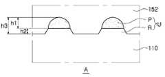
도 1은 본 발명의 일 실시예에 따른 반도체 발광소자의 개략적인 단면도이다. 도 1을 참조하면, 본 실시예에 따른 반도체 발광소자(100A)는 기판(110), 볼록부(U), 발광 적층체(S)를 포함할 수 있다. 반도체 발광소자(100A)는 투명 전극층(160), 제1 전극(171) 및 제2 전극(175)을 포함할 수 있다.1 is a schematic cross-sectional view of a semiconductor light emitting device according to an embodiment of the present invention. Referring to FIG. 1 , a semiconductor
기판(110)은 사파이어, SiC, Si, MgAl2O4, MgO, LiAlO2, LiGaO2, GaN일 수 있다. 기판(110)의 일면에는 기판(110)으로부터 돌출되며, 기판(110)과 동일한 물질로 이루어진 제1층(R)과 제1층(R) 상에 기판(110)과 다른 물질로 이루어진 제2층(P)을 포함하는 볼록부들(U)이 구비될 수 있다.The
상기 제1층(R)은 기판(110)의 일부가 제거되어 형성된 것일 수 있다. 제1층(R)은 제2층(P)를 형성하는 공정 중에 기판(110)에 잔존하는 식각 부산물(byproduct)를 제거하기 위해 형성될 수 있다. 기판(110)의 일면에 형성된 볼록부들(U)은 광추출 효율을 개선하면서 기판(110)으로부터 성장되는 반도체층의 품질을 향상시킬 수 있다.
The first layer R may be formed by removing a portion of the
볼록부들(U)에 대해서 도 2a 내지 도 3b를 참조하여 설명한다.The convex portions U will be described with reference to FIGS. 2A to 3B .
도 2a 및 도 2b는 본 발명의 일 실시예에 따른 볼록부들의 단면도들이다. 도 2a 및 도 2b는 도 1에서의 A 영역에 대응되는 부분을 확대한 도면들이다.2A and 2B are cross-sectional views of convex parts according to an embodiment of the present invention. 2A and 2B are enlarged views of a portion corresponding to area A in FIG. 1 .
도 2a를 참조하면, 볼록부(U)는 제1층(R)과 제1층(R) 상에 배치되는 제2층(P)으로 이루어질 수 있다. 기판(110)의 표면으로부터 볼록부(U)의 높이(h3)는 제1층(R)의 상면으로부터 제2층(P)의 상단까지의 높이(h1)(이하, 제2층(P)의 높이(h1)라 함)와 제1층(R)의 하면으로부터 기판(110)의 표면으로부터 제1층(R)의 상면까지의 높이(h2)(이하, 제1층(R)의 높이(h2)라 함)를 합한 것으로 정의될 수 있다. 제1층(R)의 높이(h2)는 기판(110)이 식각된 깊이로 이해될 수 있다.Referring to FIG. 2A , the convex portion U may include a first layer R and a second layer P disposed on the first layer R. Referring to FIG. The height h3 of the convex portion U from the surface of the
제2층(P)의 높이(h1)는 제1층(R)의 높이(h2)보다 높을 수 있다. 볼록부(U)의 전체 높이(h3)에 대한 제1층(R)의 높이(h2)의 비율(h2/h3)은 0.1 내지 0.4일 수 있다. 바꾸어 말하면, 제2층(P)의 높이(h1)는 제1층(R)의 높이(h2)보다 1.5배 내지 9배일 수 있다. 제1층(R)의 높이(h2)는 240nm 내지 380nm 일 수 있다. 상기 수치 범위들에 대해서는 이후에 도 8 및 도 9를 참조하여 설명한다.The height h1 of the second layer P may be higher than the height h2 of the first layer R. A ratio (h2/h3) of the height h2 of the first layer R to the total height h3 of the convex portion U may be 0.1 to 0.4. In other words, the height h1 of the second layer P may be 1.5 to 9 times greater than the height h2 of the first layer R. The height h2 of the first layer R may be 240 nm to 380 nm. The numerical ranges will be described later with reference to FIGS. 8 and 9 .
본 실시예에서, 제2층(P)은 기판(110)과 다른 굴절률을 가지는 하나의 물질로 이루어진 단일층 구조일 수 있다. 제2층(P)의 굴절률은 기판(110)의 굴절률에 비해 작을 수 있고, 1.0 내지 1.7일 수 있다. 예를 들어, 제2층(P)은 SiOx, SiOxNy, 또는 MgF2 등으로 이루어질 수 있다. 상기 수치 범위에 대해서는 이후 도 7을 참조하여 설명한다.In the present embodiment, the second layer P may have a single-layer structure made of one material having a refractive index different from that of the
제2층(P)은 반구 또는 원뿔 형상을 가질 수 있다. 제1층(R)는 제2층(P)의 하부로부터 연장되며, 기판(110)의 표면에 대해 경사진 측면을 가질 수 있다. 이와 달리, 일 실시예에서, 제1층(R)는 제2층(P)의 하부로부터 연장되며, 기판(110)의 표면에 대해 수직한 측면을 가질 수 있다.The second layer P may have a hemispherical or conical shape. The first layer (R) may extend from the lower portion of the second layer (P) and may have a side inclined with respect to the surface of the
볼록부들(U) 주위의 기판(110)은 평탄한 표면을 가질 수 있다. 이와 달리, 일 실시예에서, 볼록부들(U) 주위의 기판(110)은 굴곡진 표면을 가질 수 있다.The
도 2b를 참조하면, 일 실시예에서, 제2층(P)는 기판(110)과 다른 굴절률을 가지는 복수의 물질이 적층된 다중층 구조일 수 있다. 제2층(P)의 굴절률은 기판(110)의 굴절률에 비해 작을 수 있고, 1.0 내지 1.7일 수 있다. 본 실시예에서는 기판(110)과 다른 굴절률을 가지는 제1 물질부(P1)와 제1 물질부(P1)와 다른 굴절률을 가지는 제2 물질부(P2)로 이루어진 제2층(P')을 예시적으로 도시한 것이다.
Referring to FIG. 2B , in an embodiment, the second layer P may have a multilayer structure in which a plurality of materials having different refractive indices from that of the
도 3a 및 3b는 본 발명의 일 실시예에 따른 볼록부들의 배열을 나타내는 평면도이다.3A and 3B are plan views illustrating an arrangement of convex parts according to an embodiment of the present invention.
도 3a를 참조하면, 볼록부들(U)이 사각형의 꼭지점에 배치되는 사각 격자 형태로 규칙적으로 반복적으로 배열될 수 있다. 이와 달리, 도 3b를 참조하면, 인접한 세 개의 볼록부들(U)이 정삼각형의 꼭지점에 배치되는 육각 격자 형태로 규칙적으로 반복적으로 배열될 수 있다. 도시된 배열에 한정되는 것은 아니며, 볼록부들(U)은 실시예에 따라 다양하게 변형된 형태로 배열될 수 있다.
Referring to FIG. 3A , the convex parts U may be regularly and repeatedly arranged in the form of a quadrangular grid disposed at the vertices of the quadrangle. Alternatively, referring to FIG. 3B , three adjacent convex portions U may be regularly and repeatedly arranged in a hexagonal grid shape disposed at vertices of an equilateral triangle. It is not limited to the illustrated arrangement, and the convex portions U may be arranged in variously modified forms according to embodiments.
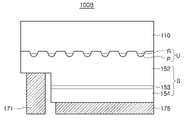
다시 도 1을 참조하면, 발광 적층체(S)는 기판(110) 상에 순차적으로 배치된 제1 도전형 반도체층(152), 활성층(153) 및 제2 도전형 반도체층(154)을 포함할 수 있다. 제2 도전형 반도체층(154) 및 활성층(153)이 식각되어 노출된 제1 도전형 반도체층(152) 상에 투명 전극층(160) 및 제1 전극(171)이 형성될 수 있고, 제2 도전형 반도체층(154) 상에는 제2 전극(173)이 형성될 수 있다.Referring back to FIG. 1 , the light emitting stack S includes a first conductivity
기판(110)과 제1 도전형 반도체층(152) 사이에 버퍼층이 구비될 수 있다. 상기 버퍼층은 InxAlyGa1-x-yN (0≤x≤1, 0≤y≤1)일수 있다. 예를 들어, 상기 버퍼층은 500℃ 내지 600℃의 저온에서 형성되며, 의도적으로 도핑되지 않은 GaN, AlN, AlGaN, InGaN일 수 있다. 필요에 따라, 복수의 층을 조합하거나, 조성을 점진적으로 변화시켜 사용할 수도 있다.A buffer layer may be provided between the
제1 도전형 반도체층(152)은 n형 InxAlyGa1-x-yN (0≤x<1, 0≤y<1, 0≤x+y<1)을 만족하는 질화물 반도체일 수 있으며, n형 불순물은 Si일 수 있다. 제2 도전형 반도체층(154)은 p형 InxAlyGa1-x-yN (0≤x<1, 0≤y<1, 0≤x+y<1)을 만족하는 질화물 반도체층일 수 있으며, p형 불순물은 Mg일 수 있다. 활성층(153)은 양자우물층과 양자장벽층이 서로 교대로 적층된 다중 양자우물(MQW) 구조일 수 있다. 예를 들어, 상기 양자우물층과 양자장벽층은 서로 다른 조성을 가지는 InxAlyGa1-x-yN (0≤x≤1, 0≤y≤1, 0≤x+y≤1)일 수 있다. 특정 예에서, 상기 양자우물층은 InxGa1-xN (0<x≤1)이며, 상기 양자장벽층은 GaN 또는 AlGaN일 수 있다.The first conductivity
도 1에 도시된 반도체 발광소자(100A)은 제1 도전형 반도체층(152) 상에 투명 전극층(160)을 더 포함할 수 있다. 본 실시예에서, 투명 전극층(160)은 선택적으로 채용될 수 있다. 투명 전극층(160)은 제1 도전형 반도체층(152)과 오믹 콘택을 실현하며 발광 적층체(S)로부터 발산되는 빛을 투과하는 것일 수 있다. 제1 도전형 반도체층(152)과 오믹 컨택을 실현할 수 있는 오믹 콘택 물질은, 예를 들어, Ag, Ni, Al, Rh, Pd, Ir, Ru, Mg, Zn, Pt 및 Au 중 적어도 하나를 포함할 수 있으며, 단일층 또는 복수의 층 구조일 수 있다. 또한, 투명 전극층(160)은 투명 전도성 산화물층 또는 질화물층 중 어느 하나일 수 있으며, 예를 들어, ITO(Indium Tin Oxide), ZITO(Zinc-doped Indium Tin Oxide), ZIO(Zinc Indium Oxide), GIO(Gallium Indium Oxide), ZTO(Zinc Tin Oxide), FTO(Fluorine-doped Tin Oxide), AZO(Aluminium-doped Zinc Oxide), GZO(Gallium-doped Zinc Oxide), In4Sn3O12 또는 Zn(1-x)MgxO(Zinc Magnesium Oxide, 0≤x≤1)으로 구성된 그룹으로부터 선택된 적어도 하나일 수 있다. 필요에 따라, 투명 전극층(160)은 그래핀(graphene)을 포함할 수도 있다.The semiconductor
예를 들어, 제1 전극(250)은 Ag, Ni, Al, Cr, Rh, Pd, Ir, Ru, Mg, Zn, Pt, Au 등의 물질을 포함할 수 있으며, 단일층 또는 2층 이상의 구조로 채용될 수 있다. 제2 전극(240)은 Al, Au, Cr, Ni, Ti, Sn 중 적어도 하나를 포함할 수 있다.
For example, the first electrode 250 may include a material such as Ag, Ni, Al, Cr, Rh, Pd, Ir, Ru, Mg, Zn, Pt, Au, etc., and has a single-layer or two-layer or more structure. can be employed as The second electrode 240 may include at least one of Al, Au, Cr, Ni, Ti, and Sn.
도 4는 본 발명의 일 실시예에 따른 반도체 발광소자의 개략적인 단면도이다.4 is a schematic cross-sectional view of a semiconductor light emitting device according to an embodiment of the present invention.
도 4에 도시된 반도체 발광소자(100B)은 플립칩 형태로 적용될 수 있으며, 기판(110), 볼록부(U) 및 발광 적층체(S)을 포함할 수 있다. 반도체 발광소자(110B)은 제1 전극(171) 및 제2 전극(175)을 포함할 수 있다.The semiconductor
본 실시예에서, 기판(110)은 주된 광추출면을 제공할 수 있다. 기판(201)은 광투과성을 가지는 사파이어와 같은 절연성 기판일 수 있다. 하지만, 이에 한정되지 않으며, 광투과성 기판(201)은 절연성 기판 외에도 광투과성을 보장할 수 있는 도전성 또는 반도체 기판일 수 있다. 기판(110)의 일면에는 볼록부(U)가 형성될 수 있다. 볼록부(U)는 광추출효율을 개선하면서 성장되는 단결정의 품질을 향상시킬 수 있다. 볼록부(U)는 도 1 내지 도 3b를 참조하여 상술한 볼록부(U)와 동일한 물질 및 구조로 형성될 수 있다.In this embodiment, the
발광 적층체(S)는 기판(110) 상에 순차적으로 배치된 제1 도전형 반도체층(152), 활성층(153) 및 제2 도전형 반도체층(154)을 포함할 수 있다. 기판(110)과 제1 도전형 반도체층(152) 사이에 버퍼층이 더 구비될 수 있다.The light emitting stack S may include a first conductivity
제1 전극(171)은 Ag, Ni, Al, Cr, Rh, Pd, Ir, Ru, Mg, Zn, Pt, Au 등의 물질을 포함할 수 있으며, 단일층 또는 2층 이상의 구조로 채용될 수 있다.The
제2 전극(175)은 반사성 전극 구조를 가질 수 있다. 제2 전극(175)은 Ag, Ni, Al, Rh, Pd, Ir, Ru, Mg, Zn, Pt, Au, Sn 등의 물질을 포함할 수 있으며, Ni/Ag, Zn/Ag, Ni/Al, Zn/Al, Pd/Ag, Pd/Al, Ir/Ag. Ir/Au, Pt/Ag, Pt/Al, Ni/Ag/Pt 등과 같이 2층 이상의 구조로 채용될 수 있다.
The
도 5는 본 발명의 일 실시예에 따른 반도체 발광소자의 개략적인 단면도이다.5 is a schematic cross-sectional view of a semiconductor light emitting device according to an embodiment of the present invention.
도 5를 참조하면, 본 실시예에 따른 반도체 발광소자(300)는, 광투과성 기판(301), 제1 도전형 반도체층(352), 활성층(353) 및 제2 도전형 반도체층(354)이 순차적으로 적층된 발광 적층체(S)를 포함할 수 있다. 또한, 반도체 발광소자(300)는, 제1 도전형 반도체층(352)에 연결되는 제1 전극(377), 제2 도전형 반도체층(354)에 연결되는 제2 전극(378)을 더 포함할 수 있다.Referring to FIG. 5 , the semiconductor
광투과성 기판(301)은 주된 광추출면을 제공할 수 있다. 광투과성 기판(301)은 사파이어와 같은 절연성 기판일 수 있다. 하지만, 이에 한정되지 않으며, 광투과성 기판(301)은 절연성 기판 외에도 광투과성을 보장할 수 있는 도전성 또는 반도체 기판일 수 있다. 광투과성 기판(301)에는 볼록부(U)가 형성될 수 있다. 볼록부(U)는 광추출효율을 개선함과 동시에 성장되는 발광 적층체(S)의 결정 품질을 향상시킬 수 있다. 볼록부(U)는 도 1 내지 도 3b를 참조하여 상술한 볼록부(U)와 동일한 물질 및 구조로 형성될 수 있다.The light-transmitting substrate 301 may provide a main light extraction surface. The light-transmitting substrate 301 may be an insulating substrate such as sapphire. However, the present invention is not limited thereto, and the light-transmitting substrate 301 may be a conductive or semiconductor substrate capable of ensuring light transmittance in addition to an insulating substrate. A convex portion U may be formed on the light-transmitting substrate 301 . The convex portion U may improve light extraction efficiency and, at the same time, improve the crystal quality of the grown light emitting stack S. The convex portion U may be formed of the same material and structure as the convex portion U described above with reference to FIGS. 1 to 3B .
발광 적층체(S)는 III족 질화물 반도체로 이루어질 수 있다. 제1 도전형 반도체층(352)은 n형 AlxInyGa1-x-yN (0≤x<1, 0≤y<1, 0≤x+y<1)을 만족하는 질화물 반도체일 수 있으며, n형 불순물은 Si일 수 있다. 예를 들어, 제1 도전형 반도체층(352)은 n형 GaN일 수 있다. 활성층(353)은 전자와 정공의 재결합에 의해 소정의 파장을 갖는 광을 방출하며, 양자우물층과 양자장벽층이 서로 교대로 적층된 다중 양자우물(Multi-Quantum Well; MQW) 구조일 수 있다. 예를 들어, 활성층(353)은 GaN/InGaN 구조가 사용될 수 있다. 물론, 활성층(353)은 단일 양자우물(Single-Quantum Well; SQW) 구조일 수도 있다. 제2 도전형 반도체층(354)은 p형 AlxInyGa1-x-yN (0≤x<1, 0≤y<1, 0≤x+y<1)을 만족하는 질화물 반도체층일 수 있으며, p형 불순물은 Mg일 수 있다. 예를 들어, 제2 도전형 반도체층(354)은 p형 GaN일 수 있다.The light emitting stack S may be formed of a group III nitride semiconductor. The first conductivity
제2 도전형 반도체층(354)으로 오버플로우(overflow)되는 전자를 줄이기 위해서 활성층(353)과 제2 도전형 반도체층(304) 사이에 전자차단층이 구비될 수 있다. 상기 전자차단층은 활성층(303)의 마지막 양자장벽층보다 에너지 밴드갭이 클 수 있다. 예를 들어, 상기 전자차단층은 AlrGa1-rN (0<r≤1)으로 이루어질 수 있다.An electron blocking layer may be provided between the
제1 전극(377)는 제2 도전형 반도체층(354) 및 활성층(353)을 관통하여 제1 도전형 반도체층(352)에 연결되고, 제2 도전형 반도체층(354) 및 활성층(353)을 관통하여 제1 도전형 반도체층(352)의 일부를 노출시키는 적어도 하나의 홀을 통해 제공되는 적어도 하나의 제1 컨택 영역을 가질 수 있다. 상기 제1 컨택 영역은 제1 도전형 반도체층(352)와 제1 컨택 전극(371)이 맞닿는 영역을 의미한다. 제1 전극(377)은 상기 제1 컨택 영역에 배치된 제1 컨택 전극(371)과 제1 컨택 전극(371)에 연결되는 제1 패드 전극(375)을 포함할 수 있다. 제1 도전형 반도체층(352)과의 컨택 저항을 낮추고, 발광소자의 전류 분산을 위해 여러 개의 제1 컨택 전극(371)이 배치될 수 있다. 제1 컨택 전극(371)의 개수는 도시된 것에 한정되지 않는다. 제2 전극(378)은 제2 도전형 반도체층(354)의 제2 컨택 영역에 배치된 제2 컨택 전극(373) 및 제2 컨택 전극(373)에 연결되는 제2 패드 전극(376)를 포함할 수 있다. 상기 제2 컨택 영역은 제2 도전형 반도체층(304)와 제2 컨택 전극(373)가 맞닿는 영역을 의미한다. 제2 컨택 전극(373)은 연결된 하나의 도전층으로 형성될 수 있다.The
제1 컨택 전극(371)은 제1 도전형 반도체층(352)과 오믹컨택을 형성하는 물질을 포함할 수 있다. 제1 컨택 전극(371)은 이에 한정되지 않으나, Ag, Ni, Al, Rh, Pd, Ir, Ru, Mg, Zn, Pt, Au 등의 물질을 포함할 수 있으며, 단일층 또는 2층 이상의 구조로 채용될 수 있다. 예를 들어, 제1 컨택 전극(371)은 Cr/Au 또는 Cr/Au/Pt을 포함할 수 있다. 필요에 따라, 제1 컨택 전극(371) 상에 배리어층이 추가로 형성될 수 있다. 제2 컨택 전극(373)은 제2 도전형 반도체층(354)과 오믹컨택을 형성하는 물질을 포함할 수 있다. 예를 들어, 제2 컨택 전극(373)은 Ag 또는 Ag/Ni을 포함할 수 있다. 필요에 따라, 제2 컨택 전극(373) 상에 배리어층이 추가로 형성될 수 있다. 상기 배리어층은 Ni, Al, Cu, Cr, Ti 및 그 조합으로 구성된 그룹으로부터 선택된 적어도 하나일 수 있다. 제1 및 제2 패드 전극(375, 376)는 Ag, Ni, Al, Rh, Pd, Ir, Ru, Mg, Zn, Pt, Au 등의 물질을 포함할 수 있으며, 단일층 또는 다층 구조로 형성될 수 있다.The
제1 전극(377)과 제2 전극(378)은 패시베이션층(306)에 의해 전기적으로 분리될 수 있다. 패시베이션층(346)은 SiOx, SiNx 또는 SiOxNy로 이루어질 수 있다.
The
도 6a 내지 도 6e는 본 발명의 일 실시예에 따른 반도체 발광소자의 제조방법을 나타내기 위한 도면이다.6A to 6E are diagrams illustrating a method of manufacturing a semiconductor light emitting device according to an embodiment of the present invention.
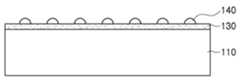
우선, 도 6a에 도시된 바와 같이, 기판(110) 상에 기판(110)과 다른 물질로 이루어진 물질층(130)을 형성할 수 있다. 기판(110)은, 앞서 설명한 바와 같이, 사파이어, SiC, MgAl2O4, MgO, LiAlO2, LiGaO2, GaN 등의 물질로 이루어진 기판을 사용할 수 있다. 기판(110) 상에 형성된 물질층(130)은 기판(110)과 다른 굴절률을 가지는 물질로 이루어질 수 있다. 물질층(130)은 기판(110)보다 작은 굴절률을 가지는 물질로 이루어질 수 있다. 본 실시예에서, 기판(110)은 사파이어 기판일 수 있고, 물질층(130)은 1.0~1.7 범위의 굴절률을 가지는 물질로 이루어질 수 있다. 예를 들어, 물질층(130)은 SiOx, SiOxNy, 또는 MgF2와 같은 물질을 포함할 수 있다. 물질층(130)은 하나의 물질로 이루어질 수 있고, 복수의 물질이 적층된 다중층 구조일 수 있다.
First, as shown in FIG. 6A , a
다음으로, 도 6b에 도시된 바와 같이, 물질층(130) 상에 포토레지스트 패턴(140)을 형성할 수 있다.Next, as shown in FIG. 6B , a
포토레지스트막을 물질층(130) 상에 도포한 후, 노광 및 현상 등의 공정을 수행하여 포토레지스트 패턴(140)을 형성한다. 포토레지스트 패턴(140)을 형성하기 위해, 소정의 온도에서 리플로우(reflow) 공정이 추가적으로 수행될 수 있다.
After the photoresist film is coated on the
다음으로, 도 6c에 도시된 바와 같이, 포토레지스트 패턴(140)을 형성한 후, 포토레지스트 패턴(140)을 식각 마스크로 이용하여 물질층(130)을 건식 식각함으로써, 포토레지스트 패턴(140)과 대응하는 영역에 볼록한 형태의 제2층(P)을 먼저 형성할 수 있다. 제2층(P)은 반구 형상을 가지는 것으로 도시되어 있으나, 이에 한정되지 않는다. 일 실시예에서 제2층(P)은 원뿔 형상을 가지도록 형성될 수 있다. 물질층(130)의 식각 공정은 CF4, SF6 등의 플루오린(Fluorine) 계열, Cl2, BCl3 등의 염소(Chlorine) 계열, 아르곤(Ar), 질소(N2) 등의 식각 가스를 이용할 수 있으나, 이에 제한되는 것은 아니고, 공지된 다양한 식각 가스가 적용될 수 있다.Next, as shown in FIG. 6C , after the
기판(110)과 다른 물질로 이루어진 물질층(130)을 건식 식각하는 동안에 물질층(130)의 식각 부산물(byproduct)이 기판(110)에 침투하거나 기판(110)과 안정한 결합을 할 수 있다. 이와 같은 식각 부산물은 세정 공정을 통해 제거되지 않을 수 있고, 기판(110)으로부터 반도체층을 성장시킬 때, 핵생성을 방해할 수 있다. 따라서 기판(110)으로부터 상기 식각 부산물을 제거하는 것이 필요하다.During the dry etching of the
이어서, 제2층(P) 주위에 기판(110)의 일부를 식각하여 제1층(R)을 형성할 수 있다. 이로써, 기판(110)과 동일한 물질로 이루어진 제1층(R)과 제1층(R) 상에 기판(110)과 다른 물질로 이루어진 제2층(P)을 포함하는 볼록부(U)가 형성될 수 있다. 제1층(R)은 제2층(P)의 하부로부터 연장되며, 제2층(R)의 하면에 대해 경사진 측면을 가지도록 형성될 수 있다. 이와 달리, 일 실시예에서 제1층(R)는 제2층(P)의 하부로부터 연장되며, 제2층(P)의 하면에 수직한 측면을 가지도록 형성될 수 있다. 볼록부(U) 주위의 기판(110)은 평탄한 표면을 가지도록 형성될 수 있다. 이와 달리, 일 실시예에서 볼록부(U) 주위의 기판(110)은 굴곡진 표면을 가지도록 형성될 수 있다. 기판(110)의 일부를 식각하여 제1층(R)를 형성하기 위해, 아르곤(Ar) 등의 식각 가스가 적용될 수 있으며, 이때, 아르곤(Ar) 가스에 Cl2, BCl3 등의 염소(Chlorine) 계열 식각 가스가 혼합될 수 있다.Then, a portion of the
제2층(P) 및 제1층(R)을 형성하는 식각 공정은 연속하여 이루어질 수 있으며, 동일한 식각 가스를 이용한 건식 식각 공정이 적용됨으로써 공정을 단순화 할 수 있다.
The etching process for forming the second layer (P) and the first layer (R) may be performed continuously, and the dry etching process using the same etching gas may be applied, thereby simplifying the process.
다음으로, 도 6d를 참조하면, 볼록부(U)가 형성된 기판(10) 상에 제1 도전형 반도체층(152)을 성장시킬 수 있다. 제1 도전형 반도체층(152)은 기판(110)의 제1층(R)로부터 핵생성 및 성장될 수 있다. 이어서, 에패택셜 측면 과성장(Epitaxial Lateral Overgrowth; ELO) 공정을 통해 분리되어 있는 제1 도전형 반도체층(152)는 측면으로 성장하여 하나의 층으로 형성될 수 있다.Next, referring to FIG. 6D , the first conductivity-
이 때, 제1 도전형 반도체층(152)은 측면으로 성장하게 되므로, 기판(110)과 제1 도전형 반도체층(152) 사이의 격자 상수 차이로 인하여 발생한 전위 결함들(dislocation)이 상부로 전파되지 않고, 상기 전위 결함들은 제1 도전형 반도체층(152)의 측면 성장에 수반하여 측면으로 굴곡된다. 따라서, 성장된 제1 도전형 반도체층(152) 내에서 전위 밀도가 매우 낮아지며, 고품질의 질화물 반도체 발광소자를 제조할 수 있다.
At this time, since the first conductivity-
도 6e을 참조하면, 측면 성장된 제1 도전형 반도체층(152) 상에 순차적으로 형성된 활성층(153) 및 제2 도전형 반도체층(154)을 적층하여 발광 적층체(S)를 형성할 수 있다.
Referring to FIG. 6E , the light emitting stack S may be formed by stacking the
이후, 제1 도전형 반도체층(152)에 연결되는 제1 전극 및 제2 도전형 반도체층(154)에 연결되는 제2 전극을 형성하는 공정이 수행될 수 있다.
Thereafter, a process of forming a first electrode connected to the first conductivity-
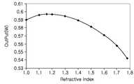
도 7은 볼록부의 굴절률에 따른 반도체 발광소자의 출력 변화를 나타내는 그래프이다. 도 7은 사파이어 기판과 다른 굴절률을 가지는 볼록부를 기판 상에 형성한 경우에 대해 볼록부의 굴절률을 변화시키면서 반도체 발광소자의 출력값을 시뮬레이션한 결과이다.7 is a graph illustrating an output change of a semiconductor light emitting device according to a refractive index of a convex portion. 7 is a result of simulating the output value of the semiconductor light emitting device while changing the refractive index of the convex portion when the convex portion having a refractive index different from that of the sapphire substrate is formed on the substrate.
도 7을 참조하면, 상기 볼록부의 굴절률을 사파이어 기판의 굴절률인 1.78보다 작은 값으로 하는 경우에 출력값이 증가하였고, 상기 볼록부의 굴절률이 1.78인 경우(사파이어 자체가 패턴되어 볼록부가 형성된 경우)에 비해 상기 볼록부의 굴절률이 약 1.16인 경우에 최대 10% 향상됨을 확인할 수 있다. 따라서, 상기 볼록부의 굴절률은 1 내지 1.7인 것이 적절하다.
Referring to FIG. 7 , when the refractive index of the convex portion is set to a value smaller than 1.78, which is the refractive index of the sapphire substrate, the output value increases, and the refractive index of the convex portion is 1.78 (sapphire itself is patterned to form the convex portion). When the refractive index of the convex portion is about 1.16, it can be confirmed that the maximum improvement is 10%. Accordingly, it is appropriate that the refractive index of the convex portion is 1 to 1.7.
도 8은 볼록부의 전체 높이(h3)에 대한 제1층의 높이(h2)의 비율(h2/h3)에 따른 상대적인 광추출 효율을 나타내는 그래프이다. 도 8은 사파이어 기판 상에 SiO2로 이루어진 제2층 및 사파이어 기판과 동일한 물질로 이루어진 제1층을 포함하는 볼록부를 구비하는 반도체 발광소자에 대해 h2/h3 비율에 따라 광추출 효율을 시뮬레이션한 결과이다.8 is a graph showing the relative light extraction efficiency according to the ratio (h2/h3) of the height (h2) of the first layer to the total height (h3) of the convex portion. 8 is a simulation result of light extraction efficiency according to a h2/h3 ratio for a semiconductor light emitting device having a convex portion including a second layer made of SiO2 on a sapphire substrate and a first layer made of the same material as the sapphire substrate. am.
도 8을 참조하면, 볼록부가 사파이어 기판과 다른 SiO2로 이루어진 제2층만으로 형성된 경우, 즉 h2/h3 값이 0인 경우에 상대적인 광추출 효율이 가장 높고, 볼록부가 사파이어 기판과 동일한 물질로 이루어진 제1층만으로 형성된 경우, 즉 h2/h3 값이 1인 경우에 상대적인 광추출 효율이 가장 낮다. 즉, 볼록부에서 기판과 굴절률이 다른 이종 물질이 차지하는 비율이 높을수록 상대적인 광추출 효율이 높아진다. 그러나, 상술한 바와 같이, 사파이어 기판을 식각하지 않으면 이종 물질로 이루어진 제2층을 형성하기 위한 식각 공정을 거치면서 기판에 식각 부산물이 잔존하게 되고, 이러한 식각 부산물들은 기판으로부터 반도체층이 성장하는 것을 방해한다. 그러므로, 제2층을 형성한 후, 기판에 잔존하는 식각 부산물들을 제거하기 위해, h2/h3 값이 약 0.1 되도록 사파이어 기판을 식각하여 제1층을 형성하는 것이 바람직하다. 한편, 그래프 상에서 h2/h3 값이 약 0.4를 넘어가면 상대적인 광추출 효율이 급격히 감소하는 영역에 해당하기 때문에, h2/h3 값은 0.4이하로 유지하는 것이 바람직하다. 따라서, 볼록부의 전체 높이(h3)에 대한 제1층의 높이(h2)의 비율(h2/h3)은 0.1 내지 0.4인 것이 적절하다.
Referring to FIG. 8 , when the convex portion is formed only with a second layer made of SiO2 different from the sapphire substrate, that is, when the h2/h3 value is 0, the relative light extraction efficiency is highest, and the convex portion is made of the same material as the sapphire substrate. When only the first layer is formed, that is, when the h2/h3 value is 1, the relative light extraction efficiency is the lowest. That is, the higher the ratio of the heterogeneous material having a different refractive index to the substrate in the convex portion, the higher the relative light extraction efficiency. However, as described above, if the sapphire substrate is not etched, etching by-products remain on the substrate while going through an etching process for forming a second layer made of a different material, and these etching by-products prevent the semiconductor layer from growing from the substrate. interfere Therefore, after forming the second layer, in order to remove etching by-products remaining on the substrate, it is preferable to etch the sapphire substrate so that the h2/h3 value is about 0.1 to form the first layer. Meanwhile, on the graph, when the h2/h3 value exceeds about 0.4, it corresponds to a region in which the relative light extraction efficiency rapidly decreases, so it is preferable to keep the h2/h3 value below 0.4. Therefore, it is appropriate that the ratio (h2/h3) of the height h2 of the first layer to the total height h3 of the convex portion is 0.1 to 0.4.
도 9는 볼록부 중 제1층의 높이(h2) 즉, 기판의 식각 깊이에 따른 void 개수를 나타내는 그래프이다. 도 9는 SiO2로 이루어진 제2층의 두께는 동일하게 하고, 제1층의 높이(h2)를 서로 다르게 형성한 사파이어 기판 상에 발광 적층체를 성장한 후, void 개수를 확인한 것이다.9 is a graph showing the number of voids according to the height h2 of the first layer among the convex portions, that is, the etching depth of the substrate. 9 shows the number of voids after growing a light emitting laminate on a sapphire substrate in which the thickness of the second layer made of SiO2 is the same and the height (h2) of the first layer is different from each other.
도 9에 도시된 바와 같이, 제1층의 높이(h2)가 각각 190nm, 240nm, 380nm, 580nm인 경우에 대해 각각 void 개수를 확인하였다. 제1층의 높이(h2)가 190nm인 경우는 void 개수가 약 11,000개/mm2이고, 제1층의 높이(h2)가 240nm인 경우는 void 개수가 급격히 감소하여 약 2,000개/mm2이었다. 이 정도 수준의 void는 반도체 발광소자가 제품화될 수 있는 수준으로 충분하다. 제1층의 높이(h2)가 380nm 이상인 경우는 void가 확인되지 않았다. 따라서, 기판의 식각 깊이 즉, 제1층의 높이(h2)는 240nm 내지 380nm 인 것이 적절하다.
As shown in FIG. 9 , the number of voids was checked for the case where the height h2 of the first layer was 190 nm, 240 nm, 380 nm, and 580 nm, respectively. When the height (h2) of the first layer was 190 nm, the number of voids was about 11,000 pieces/mm2 , and when the height (h2) of the first layer was 240 nm, the number of voids decreased sharply to about 2,000 pieces/mm2 . This level of void is sufficient to allow a semiconductor light emitting device to be commercialized. When the height (h2) of the first layer was 380 nm or more, void was not confirmed. Therefore, it is appropriate that the etch depth of the substrate, that is, the height h2 of the first layer, is 240 nm to 380 nm.
도 10은 본 발명의 일 실시예에 따른 효과를 설명하기 위한 광학 현미경 이미지들이다. 도 10의 (a)는 비교예로서, SiO2로 이루어진 단일층 구조의 볼록부를 구비한 사파이어 기판 상에 GaN 반도체층을 성장시킨 것이다. 한편, 도 10의 (b)는 본 발명의 일 실시예로서, SiO2로 이루어진 제2층과 사파이어 기판과 동일한 물질로 이루어진 제1층으로 이루어진 이중층 구조의 볼록부를 구비한 사파이어 기판 상에 GaN 반도체층을 성장시킨 것이다.10 is an optical microscope image for explaining the effect according to an embodiment of the present invention. 10A is a comparative example in which a GaN semiconductor layer is grown on a sapphire substrate having convex portions of a single-layer structure made of SiO2 . Meanwhile, FIG. 10 (b) is an embodiment of the present invention, a GaN semiconductor on a sapphire substrate having a convex portion having a double-layer structure consisting of a second layer made of SiO2 and a first layer made of the same material as the sapphire substrate. layer is grown.
도 10을 참조하면, (a)의 경우는 GaN 반도체층이 기판 전체에서 균일하게 성장하지 못하고 부분적으로 3D 형태로 성장된 것을 확인할 수 있다. 반면, (b)의 경우는 GaN 반도체층이 기판 전체에서 균일하게 성장하여 매끈한 표면을 가지는 2D 형태의 박막으로 성장된 것을 확인할 수 있다.
Referring to FIG. 10 , in the case of (a), it can be confirmed that the GaN semiconductor layer is partially grown in a 3D form without uniformly growing over the entire substrate. On the other hand, in the case of (b), it can be seen that the GaN semiconductor layer is uniformly grown over the entire substrate to form a 2D thin film having a smooth surface.
도 11은 본 발명의 일 실시예에 따른 반도체 발광소자를 적용한 반도체 발광소자 패키지의 단면도이다.11 is a cross-sectional view of a semiconductor light emitting device package to which a semiconductor light emitting device according to an embodiment of the present invention is applied.
도 11에 도시된 반도체 발광소자 패키지는 예시적으로 도 1에 도시된 반도체 발광소자(100A)가 실장된 경우를 나타낸 것이다.The semiconductor light emitting device package shown in FIG. 11 exemplarily shows a case in which the semiconductor
도 11을 참조하면, 반도체 발광소자(100A)는 리드 프레임(270)에 실장되어, 각 전극이 리드 프레임(270)에 와이어(W)에 의해 각각 전기적으로 연결될 수 있다. 필요에 따라, 반도체 발광소자(100A)는 리드 프레임(270)이 아닌 다른 영역, 예를 들어, 패키지 본체(260)에 실장될 수 있다. 또한, 패키지 본체(260)는 빛의 반사 효율이 향상되도록 컵 형상의 홈부를 가질 수 있으며, 이러한 홈부에는 반도체 발광소자(100A) 및 와이어(W)를 봉지하도록 광투과성 물질로 이루어진 봉지체(265)가 형성될 수 있다. 봉지체(265)에는 형광체 및/또는 양자점와 같은 파장변화물질이 함유될 수 있다. 상기 파장변환물질에 대한 상세한 설명은 후술하기로 한다.
Referring to FIG. 11 , the semiconductor
도 12는 본 발명의 일 실시예에 따른 반도체 발광소자를 플립칩 형태로 적용한 반도체 발광소자 패키지를 도시한 단면도이다.12 is a cross-sectional view illustrating a semiconductor light emitting device package to which a semiconductor light emitting device according to an embodiment of the present invention is applied in the form of a flip chip.
도 12에 도시된 반도체 발광소자 패키지는 예시적으로 도 4에 도시된 반도체 발광소자(300)가 실장된 경우를 나타낸 것이다.The semiconductor light emitting device package shown in FIG. 12 exemplarily shows a case in which the semiconductor
도 12를 참조하면, 회로 기판(331)은 제1 및 제2 배선 전극(335a, 335b)을 가진다. 제1 및 제2 배선 전극(335a, 335b)은 각각 회로 기판(331)의 상면에 배치된 제1 및 제2 상부 전극(332a, 332b)과, 회로 기판(331)의 하면에 배치된 제1 및 제2 하부 전극(334a, 334b)과, 제1 상부 전극(332a)과 제1 하부 전극(333a)을 연결하는 제1 관통 전극(333a) 및 제2 상부 전극(332b)과 제2 하부 전극(333b)을 연결하는 제2 관통 전극(333b)을 포함한다. 본 실시예에 채용된 회로 기판(331)은 예시일 뿐이며, 다양한 형태로 응용될 수 있다. 예를 들어, 회로 기판(331)은 MCPCB, MPCB, FPCB과 같은 PCB 기판이나 AlN, Al2O3 등의 세라믹 기판으로 제공될 수 있으며, 리드 프레임이 고정된 형태의 기판으로 제공될 수도 있다.Referring to FIG. 12 , the
반도체 발광소자(300)는 제1 및 제2 패드 전극(375, 376)가 회로기판(331)을 향하도록 회로 기판(331) 상에 실장될 수 있다. 제1 및 제2 패드 전극(375, 376)은 상부에 접합층, 예컨대, 공융 금속층을 포함할 수 있으며, 이를 이용하여 제1 및 제2 상부 전극(332a, 332b)에 접합될 수 있다. 이와 달리, 제1 및 제2 패드 전극 (315, 316)과 제1 및 제2 상부 전극(332a, 332b) 사이에 추가적인 접합층, 예를 들어, 공융 금속층 또는 도전성 에폭시를 이용하여 접합을 구현할 수도 있다.The semiconductor
도 12에 도시된 바와 같이, 반도체 발광소자(300)의 표면에는 활성층(353)으로부터 방출된 빛의 파장을 다른 파장으로 변환하는 파장변환부(365)가 배치할 수 있다. 본 실시예에 채용된 파장변환부(365)는 형광체나 양자점과 같은 파장변환물질을 함유한 수지층일 수 있다. 파장변환물질에 대한 상세한 설명은 후술하기로 한다.
12 , a
도 13은 본 발명의 일 실시예에 따른 반도체 발광소자 패키지를 포함하는 백색 광원 모듈의 개략도이다.13 is a schematic diagram of a white light source module including a semiconductor light emitting device package according to an embodiment of the present invention.
도 13을 참조하면, 광원모듈은 각각 회로 기판 상에 탑재된 복수의 발광소자 패키지를 포함할 수 있다. 하나의 광원 모듈에 탑재된 복수의 발광소자 패키지는 동일한 파장의 빛을 발생시키는 동종(同種)의 패키지로도 구성될 수 있으나, 본 실시예와 같이, 서로 상이한 파장의 빛을 발생시키는 이종(異種)의 패키지로 구성될 수도 있다.Referring to FIG. 13 , each light source module may include a plurality of light emitting device packages mounted on a circuit board. A plurality of light emitting device packages mounted on one light source module may be configured as a package of the same type for generating light of the same wavelength, but as in this embodiment, a plurality of light emitting device packages for generating light of different wavelengths ) may be configured as a package.
도 13의 (a)를 참조하면, 백색 광원 모듈은 색온도 4,000 K 인 백색 발광소자 패키지, 색온도 3,000 K인 백색 발광소자 패키지 및 적색 발광소자 패키지를 조합하여 구성될 수 있다. 상기 백색 광원 모듈은 색온도 3,000 K ~ 4,000 K 범위로 조절 가능하고 연색성 Ra도 105 ~ 100 범위인 백색광을 제공할 수 있다.Referring to FIG. 13A , the white light source module may be configured by combining a white light emitting device package having a color temperature of 4,000 K, a white light emitting device package having a color temperature of 3,000 K, and a red light emitting device package. The white light source module may provide white light having a color temperature of 3,000 K to 4,000 K and a color rendering Ra of 105 to 100.
도 13의 (b)를 참조하면, 백색 광원 모듈은, 백색 발광소자 패키지만으로 구성되되, 일부 패키지는 다른 색온도의 백색광을 가질 수 있다. 예를 들어, 색온도 2,700 K인 백색 발광소자 패키지와 색온도 5,000 K인 백색 발광소자 패키지를 조합하여 색온도 2,700 K ~ 5,000 K 범위로 조절 가능하고 연색성 Ra가 85 ~ 99인 백색광을 제공할 수 있다.Referring to FIG. 13B , the white light source module includes only a white light emitting device package, and some packages may have white light having a different color temperature. For example, by combining a white light emitting device package having a color temperature of 2,700 K and a white light emitting device package having a color temperature of 5,000 K, it is possible to provide white light having a color temperature of 2,700 K to 5,000 K and a color rendering property Ra of 85 to 99.
여기서, 각 색온도의 발광소자 패키지의 개수는 주로 기본 색온도 설정 값에 따라 개수를 달리할 수 있다. 예를 들어, 기본 설정 값이 색온도 4,000 K 부근의 조명장치라면 4,000 K인 발광소자 패키지의 개수가 색온도 3,000 K인 발광소자 패키지의 개수 또는 적색 발광소자 패키지의 개수보다 많도록 할 수 있다.Here, the number of light emitting device packages of each color temperature may vary depending on the basic color temperature setting value. For example, if the basic setting value is a lighting device having a color temperature of around 4,000 K, the number of light emitting device packages having a color temperature of 4,000 K may be greater than the number of light emitting device packages having a color temperature of 3,000 K or the number of red light emitting device packages.
이와 같이, 이종의 발광소자 패키지는 청색 발광소자에 황색, 녹색, 적색 또는 오렌지색의 형광체를 조합하여 백색광을 발하는 발광소자와 보라색, 청색, 녹색, 적색 또는 적외선 발광소자 중 적어도 하나를 포함하도록 구성하여 백색광의 색온도 및 연색성(color rendering index, CRI)을 조절하도록 할 수 있다.As such, the heterogeneous light emitting device package includes at least one of a light emitting device that emits white light by combining a blue light emitting device with a yellow, green, red or orange phosphor and a purple, blue, green, red or infrared light emitting device. The color temperature and color rendering index (CRI) of white light may be adjusted.
상술된 백색 광원 모듈은 벌브형 조명장치(도 21 또는 도 22 참조)의 광원모듈(4240)로 사용될 수 있다.
The above-described white light source module may be used as the
단일 발광소자 패키지에서는, 발광소자인 LED 칩의 파장과 형광체의 종류 및 배합비에 따라, 원하는 색의 광을 결정하고, 백색광일 경우에는 색온도와 연색성을 조절할 수 있다.In a single light emitting device package, the light of a desired color is determined according to the wavelength of the LED chip, which is the light emitting device, and the type and mixing ratio of the phosphor, and in the case of white light, the color temperature and color rendering can be adjusted.
예를 들어, LED 칩이 청색광을 발광하는 경우, 황색, 녹색, 적색 형광체 중 적어도 하나를 포함한 발광소자 패키지는 형광체의 배합비에 따라 다양한 색온도의 백색광을 발광하도록 할 수 있다. 이와 달리, 청색 LED 칩에 녹색 또는 적색 형광체를 적용한 발광소자 패키지는 녹색 또는 적색광을 발광하도록 할 수 있다. 이와 같이, 백색광을 내는 발광소자 패키지와 녹색 또는 적색광을 내는 패키지를 조합하여 백색광의 색온도 및 연색성을 조절하도록 할 수 있다. 또한, 보라색, 청색, 녹색, 적색 또는 적외선을 발광하는 발광소자 중 적어도 하나를 포함하도록 구성할 수도 있다.For example, when the LED chip emits blue light, the light emitting device package including at least one of yellow, green, and red phosphors may emit white light of various color temperatures according to a compounding ratio of the phosphors. In contrast, a light emitting device package in which a green or red phosphor is applied to a blue LED chip may emit green or red light. In this way, the color temperature and color rendering properties of white light may be adjusted by combining the light emitting device package emitting white light and the package emitting green or red light. In addition, it may be configured to include at least one of a light emitting device emitting purple, blue, green, red, or infrared light.
이 경우, 조명 장치는 연색성을 나트륨 등(sodium lamp)에서 태양광 수준으로 조절할 수 있으며, 또한 색온도를 1,500 K에서 20,000 K 수준으로 다양한 백색광을 발생시킬 수 있으며, 필요에 따라서는 보라색, 청색, 녹색, 적색, 오렌지색의 가시광 또는 적외선을 발생시켜 주위 분위기 또는 기분에 맞게 조명 색을 조절할 수 있다. 또한, 식물 성장을 촉진할 수 있는 특수 파장의 광을 발생시킬 수도 있다.
In this case, the lighting device can adjust color rendering to the level of sunlight in a sodium lamp, and can generate various white light with a color temperature of 1,500 K to 20,000 K, and, if necessary, purple, blue, and green. , It is possible to adjust the color of the lighting to suit the surrounding atmosphere or mood by generating visible or infrared light of red or orange color. In addition, it is also possible to generate light of a special wavelength that can promote plant growth.
도 14는 본 발명의 일 실시예에 따른 반도체 발광소자 또는 발광소자 패키지에 채용 가능한 파장 변환 물질을 설명하기 위한 CIE 좌표계이다.14 is a CIE coordinate system for describing a wavelength conversion material employable in a semiconductor light emitting device or a light emitting device package according to an embodiment of the present invention.
도 14에 도시된 CIE 1931 좌표계를 참조하면, 청색 발광소자에 황색, 녹색 및 적색 형광체를 조합하거나 청색 발광소자에 녹색 발광소자 및 적색 발광소자의 조합으로 만들어지는 백색 광은 2개 이상의 피크 파장을 가지며, CIE 1931 좌표계의 (x, y) 좌표가 (0.4476, 0.4074), (0.3484, 0.3516), (0.3101, 0.3162), (0.3128, 0.3292), (0.3333, 0.3333)을 잇는 선분 상에 위치할 수 있다. 또는, 상기 선분과 흑체 복사 스펙트럼으로 둘러싸인 영역에 위치할 수 있다. 상기 백색 광의 색 온도는 1,500 K ~ 20,000 K사이에 해당한다. 도 14에서 상기 흑체 복사 스펙트럼 하부에 있는 점E(0.3333, 0.3333) 부근의 백색광은 상대적으로 황색계열 성분의 광이 약해진 상태로 사람이 육안으로 느끼기에는 보다 선명한 느낌 또는 신선한 느낌을 가질 수 있는 영역의 조명 광원으로 사용 될 수 있다. 따라서 상기 흑체 복사 스펙트럼 하부에 있는 점E(0.3333, 0.3333) 부근의 백색광을 이용한 조명 제품은 식료품, 의류 등을 판매하는 상가용 조명으로 효과가 좋다.
Referring to the CIE 1931 coordinate system shown in FIG. 14, white light produced by combining yellow, green, and red phosphors with a blue light emitting device or a combination of a green light emitting device and a red light emitting device with a blue light emitting device has two or more peak wavelengths. and the (x, y) coordinates of the CIE 1931 coordinate system can be located on the line segment connecting (0.4476, 0.4074), (0.3484, 0.3516), (0.3101, 0.3162), (0.3128, 0.3292), (0.3333, 0.3333). there is. Alternatively, it may be located in a region surrounded by the line segment and the blackbody radiation spectrum. The color temperature of the white light corresponds to between 1,500 K and 20,000 K. In FIG. 14, the white light near point E (0.3333, 0.3333) in the lower part of the blackbody radiation spectrum is a region in which the light of the yellow-based component is relatively weakened and a clearer feeling or fresh feeling can be felt by the human eye. Can be used as lighting source. Therefore, lighting products using white light near point E (0.3333, 0.3333) in the lower part of the blackbody radiation spectrum are effective as lighting for shopping malls selling foodstuffs, clothes, and the like.
반도체 발광소자로부터 방출되는 광의 파장을 변환하기 위한 물질로서, 형광체 및/또는 양자점과 같은 다양한 물질이 사용될 수 있다As a material for converting the wavelength of light emitted from the semiconductor light emitting device, various materials such as phosphors and/or quantum dots may be used.
형광체로는 다음과 같은 조성식 및 컬러(color)를 가질 수 있다.The phosphor may have the following compositional formula and color.
산화물계: 황색 및 녹색 Y3Al5O12:Ce, Tb3Al5O12:Ce, Lu3Al5O12:CeOxide system: yellow and green Y3 Al5 O12 :Ce, Tb3 Al5 O12 :Ce, Lu3 Al5 O12 :Ce
실리케이트계: 황색 및 녹색 (Ba,Sr)2SiO4:Eu, 황색 및 등색 (Ba,Sr)3SiO5:CeSilicates: yellow and green (Ba,Sr)2 SiO4 :Eu, yellow and orange (Ba,Sr)3 SiO5 :Ce
질화물계: 녹색 β-SiAlON:Eu, 황색 La3Si6N11:Ce, 등색 α-SiAlON:Eu, 적색 CaAlSiN3:Eu, Sr2Si5N8:Eu, SrSiAl4N7:Eu, SrLiAl3N4:Eu, Ln4-x(EuzM1-z)xSi12-yAlyO3+x+yN18-x-y (0.5≤x≤3, 0<z<0.3, 0<y≤4) - 식 (1)Nitride type: green β-SiAlON:Eu, yellow La3 Si6 N11 :Ce, orange α-SiAlON:Eu, red CaAlSiN3 :Eu, Sr2 Si5 N8 :Eu, SrSiAl4 N7 :Eu, SrLiAl3 N4 :Eu, Ln4-x (Euz M1-z )x Si12-y Aly O3+x+y N18-xy (0.5≤x≤3, 0<z<0.3, 0<y ≤4) - Equation (1)
단, 식 (1) 중, Ln은 IIIa 족 원소 및 희토류 원소로 이루어지는 군에서 선택되는 적어도 한 종의 원소이고, M은 Ca, Ba, Sr 및 Mg로 이루어지는 군에서 선택되는 적어도 한 종의 원소일 수 있다.However, in formula (1), Ln is at least one element selected from the group consisting of group IIIa elements and rare earth elements, and M is at least one element selected from the group consisting of Ca, Ba, Sr and Mg. can
불화물(fluoride)계: KSF계 적색 K2SiF6:Mn4+, K2TiF6:Mn4+, NaYF4:Mn4+, NaGdF4:Mn4+, K3SiF7:Mn4+Fluoride-based: KSF-based red K2 SiF6 :Mn4+ , K2 TiF6 :Mn4+ , NaYF4 :Mn4+ , NaGdF4 :Mn4+ , K3 SiF7 :Mn4+
형광체 조성은 기본적으로 화학양론(stoichiometry)에 부합하여야 하며, 각 원소들은 주기율표상 각 족들 내 다른 원소로 치환이 가능하다. 예를 들어 Sr은 알카리토류(II)족의 Ba, Ca, Mg 등으로, Y는 란탄계열의 Tb, Lu, Sc, Gd 등으로 치환이 가능하다. 또한, 활성제인 Eu 등은 원하는 에너지 준위에 따라 Ce, Tb, Pr, Er, Yb 등으로 치환이 가능하며, 활성제 단독 또는 특성 변형을 위해 부활성제 등이 추가로 적용될 수 있다.The phosphor composition should basically conform to stoichiometry, and each element can be substituted with another element in each group on the periodic table. For example, Sr may be substituted with Ba, Ca, Mg, etc. of alkaline earth (II) group, and Y may be substituted with Tb, Lu, Sc, Gd, etc. of lanthanide series. In addition, the activator Eu, etc. can be substituted with Ce, Tb, Pr, Er, Yb, etc. according to a desired energy level, and a sub-activator or the like may be additionally applied to the activator alone or to modify properties.
특히, 불화물계 적색 형광체는 고온/고습에서의 신뢰성 향상을 위하여 각각 Mn을 함유하지 않는 불화물로 코팅되거나 형광체 표면 또는 Mn을 함유하지 않는 불화물 코팅 표면에 유기물 코팅을 더 포함할 수 있다. 상기와 같은 불화물계 적색 형광체의 경우 기타 형광체와 달리 40 nm 이하의 협반치폭(narrow FWHM)을 구현할 수 있기 때문에, UHD TV와 같은 고해상도 TV에 활용될 수 있다.In particular, the fluoride-based red phosphor may be coated with a fluoride not containing Mn or an organic coating may be further included on the surface of the phosphor or the surface of the fluoride coating not containing Mn to improve reliability at high temperature/high humidity. In the case of the fluoride-based red phosphor as described above, unlike other phosphors, since a narrow FWHM of 40 nm or less can be implemented, it can be used for high-resolution TVs such as UHD TVs.
아래 표 1은 청색 LED 칩(440 ~ 460nm) 또는 UV LED 칩(380 ~ 440nm)을 사용한 백색 발광소자의 응용분야별 형광체 종류이다.
Table 1 below shows the types of phosphors for each application field of a white light emitting device using a blue LED chip (440 ~ 460 nm) or a UV LED chip (380 ~ 440 nm).
(Mobile, Note PC)Side View
(Mobile, Note PC)
(Head Lamp, etc.)Battlefield
(Head Lamp, etc.)
또한, 파장변환부는 형광체를 대체하거나 형광체와 혼합하여 양자점(quantum dot, QD)과 같은 파장변환물질들이 사용될 수 있다.
In addition, wavelength conversion materials such as quantum dots (QD) may be used in the wavelength conversion unit by replacing the phosphor or mixing with the phosphor.
도 15는 본 발명의 일 실시예에 따른 반도체 발광소자 또는 발광소자 패키지에 채용 가능한 양자점의 단면도이다.15 is a cross-sectional view of quantum dots employable in a semiconductor light emitting device or a light emitting device package according to an embodiment of the present invention.
도 15를 참조하면, 양자점(QD)은 II-VI족 또는 III-V족 화합물반도체로 이루어진 코어(core)-쉘(shell)구조를 가질 수 있다. 예를 들면, CdSe, InP 등과 같은 코어(core)와 ZnS, ZnSe과 같은 쉘(shell)을 가질 수 있다. 또한, 상기 양자점은 코어 및 쉘의 안정화를 위한 리간드(ligand) 를 포함할 수 있다. 예를 들어, 상기 코어 직경은 1 ~ 30 nm, 나아가 3 ~ 10 nm일 수 있다, 상기 쉘 두께는 0.1 ~ 20 nm, 나아가 0.5 ~ 2 nm일 수 있다.Referring to FIG. 15 , a quantum dot (QD) may have a core-shell structure made of a group II-VI or group III-V compound semiconductor. For example, it may have a core such as CdSe or InP and a shell such as ZnS or ZnSe. In addition, the quantum dots may include a ligand for stabilizing the core and the shell. For example, the core diameter may be 1 to 30 nm, further 3 to 10 nm, the shell thickness may be 0.1 to 20 nm, further 0.5 to 2 nm.
상기 양자점은 사이즈에 따라 다양한 컬러를 구현할 수 있으며, 특히 형광체 대체 물질로 사용되는 경우에는 적색 또는 녹색 형광체로 사용될 수 있다. 양자점을 이용하는 경우, 협반치폭(예, 약 35 nm)을 구현할 수 있다.The quantum dots may implement various colors according to their size, and in particular, when used as a substitute for a phosphor, may be used as a red or green phosphor. In the case of using quantum dots, a narrow half maximum width (eg, about 35 nm) may be implemented.
상기 파장 변환 물질은 봉지재에 함유된 형태로 구현될 수 있으나, 이와 달리, 필름 형상으로 미리 제조되어 LED 칩 또는 도광판과 같은 광학 구조의 표면에 부착해서 사용할 수도 있으며, 이 경우에, 상기 파장 변환 물질은 균일한 두께의 구조로 원하는 영역에 용이하게 적용할 수 있다.
The wavelength conversion material may be implemented in a form contained in the encapsulant, but alternatively, it may be prepared in advance in a film shape and used by attaching it to the surface of an optical structure such as an LED chip or a light guide plate. In this case, the wavelength conversion material The material can be easily applied to a desired area with a structure of uniform thickness.
도 16은 본 발명의 일 실시예에 따른 반도체 발광소자 패키지를 포함하는 백라이트 유닛의 사시도이다.16 is a perspective view of a backlight unit including a semiconductor light emitting device package according to an embodiment of the present invention.
도 16을 참조하면, 백라이트 유닛(2000)은 도광판(2040) 및 도광판(2040) 양측면에 제공되는 광원모듈(2010)을 포함할 수 있다. 또한, 백라이트 유닛(2000)은 도광판(2040)의 하부에 배치되는 반사판(2020)을 더 포함할 수 있다. 본 실시예의 백라이트 유닛(2000)은 에지형 백라이트 유닛일 수 있다.Referring to FIG. 16 , the
실시예에 따라, 광원모듈(2010)은 도광판(2040)의 일 측면에만 제공되거나, 다른 측면에 추가적으로 제공될 수도 있다. 광원모듈(2010)은 인쇄회로기판(2001) 및 인쇄회로기판(2001) 상면에 실장된 복수의 광원(2005)을 포함할 수 있다. 여기서, 광원(2005)는 본 발명의 실시예들에 따른 반도체 발광소자를 포함할 수 있다.
According to an embodiment, the
도 17은 본 발명의 일 실시예에 따른 반도체 발광소자 패키지를 포함하는 직하형 백라이트 유닛의 단면도이다.17 is a cross-sectional view of a direct type backlight unit including a semiconductor light emitting device package according to an embodiment of the present invention.
도 17을 참조하면, 백라이트 유닛(2100)은 광확산판(2140) 및 광확산판(2140) 하부에 배열된 광원모듈(2110)을 포함할 수 있다. 또한, 백라이트 유닛(2100)은 광확산판(2140) 하부에 배치되며, 광원모듈(2110)을 수용하는 바텀케이스(2160)를 더 포함할 수 있다. 본 실시예의 백라이트 유닛(2100)은 직하형 백라이트 유닛일 수 있다.Referring to FIG. 17 , the
광원모듈(2110)은 인쇄회로기판(2101) 및 인쇄회로기판(2101) 상면에 실장된 복수의 광원(2105)을 포함할 수 있다. 여기서, 광원(2105)는 본 발명의 실시예들에 따른 반도체 발광소자를 포함할 수 있다.
The
도 18은 본 발명의 일 실시예에 따른 반도체 발광소자 패키지를 포함하는 직하형 백라이트 유닛의 광원 배치를 나타낸 평면도이다.18 is a plan view illustrating a light source arrangement of a direct type backlight unit including a semiconductor light emitting device package according to an embodiment of the present invention.
도 18을 참조하면, 본 실시 형태에 따른 직하형 백라이트 유닛(2200)은 기판(2201)상에 배열된 복수의 광원(2205)을 갖추어 구성된다. 여기서, 광원(2205)는 본 발명의 실시예들에 따른 반도체 발광소자를 포함할 수 있다.Referring to FIG. 18 , a direct
상기 광원(2205)들의 배열 구조는 행과 열로 배열된 매트릭스 구조로서 각각의 행과 열은 지그재그 형태를 가진다. 이는, 복수의 광원(2205)이 일직선상에 행과 열로 배열된 제1 매트릭스의 내부에 동일한 형태의 제2 매트릭스가 배치된 구조로서 상기 제1 매트릭스에 포함된 인접한 4개의 광원(2205)이 이루는 사각형의 내부에 상기 제2 매트릭스의 각 광원(2205)이 위치하는 것으로 이해될 수 있다.The arrangement structure of the
다만, 상기 직하형 백라이트 유닛에 있어서 휘도의 균일성 및 광효율을 보다 향상시키기 위해 필요에 따라서는, 상기 제1 및 제2 매트릭스는 그 배치 구조 및 간격을 서로 다르게 할 수도 있다. 또한, 이러한 복수의 광원 배치 방법 외에, 휘도 균일도를 확보할 수 있도록 인접한 광원간의 거리(S1, S2)를 최적화할 수 있다.However, in order to further improve luminance uniformity and light efficiency in the direct type backlight unit, the arrangement structure and spacing of the first and second matrices may be different from each other if necessary. In addition to the method of disposing the plurality of light sources, the distances S1 and S2 between adjacent light sources may be optimized to ensure luminance uniformity.
이와 같이, 광원(2205)들로 구성된 행과 열을 일직선상에 배치하지 않고, 지그재그로 배치함에 따라, 동일한 발광 면적에 대하여 약 15% ~ 25% 정도 광원(2205)의 수를 줄일 수 있는 장점이 있다.
As described above, the number of
도 19는 본 발명의 기술적 사상의 일 실시예에 따른 반도체 발광소자 패키지를 포함하는 직하형 백라이트 유닛의 단면도이다.19 is a cross-sectional view of a direct-type backlight unit including a semiconductor light emitting device package according to an embodiment of the inventive concept.
도 19를 참조하면, 백라이트 유닛(2400)은 회로기판(2401) 상에 광원(2405)이 실장되며, 그 상부에 배치된 하나 이상의 광학 시트(2406)를 구비한다. 광원(2405)은 본 발명의 실시예들에 따른 반도체 발광소자를 포함할 수 있다.Referring to FIG. 19 , the
본 실시예에 채용된 회로기판(2401)은 메인 영역에 해당되는 제1 평면부(2401a)와 그 주위에 배치되어 적어도 일부가 꺾인 경사부(2401b)와, 상기 경사부(2401b)의 외측인 회로 기판(2401)의 모서리에 배치된 제2 평면부(2401c)를 가질 수 있다. 상기 제1 평면부(2401a) 상에는 제1 간격(d1)에 따라 광원(2405)이 배열되며, 상기 경사부(2401b) 상에도 제2 간격(d2)으로 하나 이상의 광원(2405)이 배열될 수 있다. 상기 제1 간격(d1)은 상기 제2 간격(d2)과 동일할 수 있다. 상기 경사부(2401b)의 폭(또는 단면에서는 길이)는 제1 평면부(2401a)의 폭보다 작으며 제2 평면부(2401c)의 폭에 비해서는 길게 형성될 수 있다. 또한, 제2 평면부(2401c)에도 필요에 따라 적어도 하나의 광원(2405)이 배열될 수 있다.The
상기 경사부(2401b)의 기울기는 제1 평면부(2401a)를 기준으로 0°보다는 크며 90°보다는 작은 범위 안에서 적절하게 조절할 수 있다. 회로기판(2401)은 이러한 구조를 취함으로써 광학 시트(2406)의 가장자리 부근에서도 균일한 밝기를 유지할 수 있다.
The inclination of the
도 20은 본 발명의 일 실시예에 따른 반도체 발광소자 패키지를 포함하는 평판 조명 장치의 사시도이다.20 is a perspective view of a flat panel lighting device including a semiconductor light emitting device package according to an embodiment of the present invention.
도 20을 참조하면, 평판 조명 장치(4100)는 광원모듈(4110), 전원공급장치(4120) 및 하우징(4030)을 포함할 수 있다. 본 발명의 예시적 실시예에 따라, 광원모듈(4110)은 발광소자 어레이를 광원으로 포함할 수 있고, 전원공급장치(4120)는 발광소자 구동부를 포함할 수 있다.Referring to FIG. 20 , the flat
광원모듈(4110)은 발광소자 어레이를 포함할 수 있고, 전체적으로 평면 현상을 이루도록 형성될 수 있다. 발광소자 어레이는 발광소자 및 발광소자의 구동정보를 저장하는 컨트롤러를 포함할 수 있다. 상기 발광소자는 본 발명의 실시예들에 따른 반도체 발광소자일 수 있다.The
전원공급장치(4120)는 광원모듈(4110)에 전원을 공급하도록 구성될 수 있다. 하우징(4130)은 광원모듈(4110) 및 전원공급장치(4120)가 내부에 수용되도록 수용 공간이 형성될 수 있고, 일측면에 개방된 육면체 형상으로 형성되나 이에 한정되는 것은 아니다. 광원모듈(4110)은 하우징(4130)의 개방된 일측면으로 빛을 발광하도록 배치될 수 있다.
The
도 21은 본 발명의 기술적 사상의 일 실시예에 따른 반도체 발광소자 패키지를 포함하는 램프의 분해 사시도이다.21 is an exploded perspective view of a lamp including a semiconductor light emitting device package according to an embodiment of the inventive concept;
도 21을 참조하면, 조명 장치(4200)는 소켓(4210), 전원부(4220), 방열부(4230), 광원모듈(4240) 및 광학부(4250)를 포함할 수 있다. 본 발명의 예시적 실시예에 따라, 광원모듈(4240)은 발광소자 어레이를 포함할 수 있고, 전원부(4220)는 발광소자 구동부를 포함할 수 있다.Referring to FIG. 21 , the
소켓(4210)은 기존의 조명 장치와 대체 가능하도록 구성될 수 있다. 조명 장치(4200)에 공급되는 전력은 소켓(4210)을 통해서 인가될 수 있다. 도시된 바와 같이, 전원부(4220)는 제1 전원부(4221) 및 제2 전원부(4222)로 분리되어 조립될 수 있다. 방열부(4230)는 내부 방열부(4231) 및 외부 방열부(4232)를 포함할 수 있고, 내부 방열부(4231)는 광원모듈(4240) 및/또는 전원부(4220)와 직접 연결될 수 있고, 이를 통해 외부 방열부(4232)로 열이 전달되게 할 수 있다. 광학부(4250)는 내부 광학부(미도시) 및 외부 광학부(미도시)를 포함할 수 있고, 광원모듈(4240)이 방출하는 빛을 고르게 분산시키도록 구성될 수 있다.The
광원모듈(4240)은 전원부(4220)로부터 전력을 공급받아 광학부(4250)로 빛을 방출할 수 있다. 광원모듈(4240)은 하나 이상의 발광소자(4241), 회로기판(4242) 및 컨트롤러(4243)를 포함할 수 있고, 컨트롤러(4243)는 발광소자(4241)들의 구동 정보를 저장할 수 있다. 발광소자(4241)는 본 발명의 실시예들에 따른 반도체 발광소자일 수 있다.
The
도 22는 본 발명의 일 실시예에 따른 반도체 발광소자 패키지 및 통신 모듈을 포함하는 램프의 분해 사시도이다.22 is an exploded perspective view of a lamp including a semiconductor light emitting device package and a communication module according to an embodiment of the present invention.
도 22를 참조하면, 본 실시예에 따른 조명 장치(4300)에서 상기 도 19에서 개시하는 조명 장치(4200)와의 차이점은 광원 모듈(4240)의 상부에 반사판(4310)이 포함되어 있으며, 반사판(4310)은 광원으로부터의 빛을 측면 및 후방으로 고르게 퍼지게 하여 눈부심을 줄일 수 있다.Referring to FIG. 22, the difference from the
반사판(4310)의 상부에는 통신 모듈(4320)이 장착될 수 있으며 상기 통신 모듈(4320)을 통하여 홈-네트워크(home-network) 통신을 구현할 수 있다. 예를 들어, 상기 통신 모듈(4320)은 지그비(Zigbee), 와이파이(WiFi) 또는 라이파이(LiFi)를 이용한 무선 통신 모듈일 수 있으며, 스마트폰 또는 무선 컨트롤러를 통하여 조명 장치의 온(on)/오프(off), 밝기 조절 등과 같은 가정 내외에 설치되어 있는 조명을 컨트롤 할 수 있다. 또한 상기 가정 내외에 설치되어 있는 조명 장치의 가시광 파장을 이용한 라이파이 통신 모듈을 이용하여 TV, 냉장고, 에어컨, 도어락, 자동차 등 가정 내외에 있는 전자 제품 및 자동차 시스템의 컨트롤을 할 수 있다.A
상기 반사판(4310)과 통신 모듈(4320)은 커버부(4330)에 의해 커버될 수 있다.
The
도 23은 본 발명의 일 실시예에 따른 반도체 발광소자 패키지를 포함하는 바(bar) 타입의 램프의 분해 사시도이다.23 is an exploded perspective view of a bar-type lamp including a semiconductor light emitting device package according to an embodiment of the present invention.
도 23을 참조하면, 조명 장치(4400)는 방열 부재(4410), 커버(4441), 광원 모듈(4450), 제1 소켓(4460) 및 제2 소켓(4470)을 포함한다. 방열 부재(4410)의 내부 또는/및 외부 표면에 다수개의 방열 핀(4420, 4431)이 요철 형태로 형성될 수 있으며, 방열 핀(4420, 4431)은 다양한 형상 및 간격을 갖도록 설계될 수 있다. 방열 부재(4410)의 내측에는 돌출 형태의 지지대(4432)가 형성되어 있다. 지지대(4432)에는 광원 모듈(4450)이 고정될 수 있다. 방열 부재(4410)의 양 끝단에는 걸림 턱(4433)이 형성될 수 있다.Referring to FIG. 23 , the
커버(4441)에는 걸림 홈(4442)이 형성되어 있으며, 걸림 홈(4442)에는 방열 부재(4410)의 걸림 턱(4433)이 후크 결합 구조로 결합될 수 있다. 걸림 홈(4442)과 걸림 턱(4433)이 형성되는 위치는 서로 바뀔 수도 있다.A locking
광원 모듈(4450)은 발광소자 어레이를 포함할 수 있다. 광원 모듈(4450)은 인쇄회로기판(4451), 광원(4452) 및 컨트롤러(4453)를 포함할 수 있다. 컨트롤러(4453)는 광원(4452)의 구동 정보를 저장할 수 있다. 인쇄회로기판(4451)에는 광원(4452)을 동작시키기 위한 회로 배선들이 형성되어 있다. 또한, 광원(4452)을 동작시키기 위한 구성 요소들이 포함될 수도 있다. 광원(4452)은 본 발명의 실시예들에 따른 반도체 발광소자를 포함할 수 있다.The
제1 및 2 소켓(4460, 4470)은 한 쌍의 소켓으로서 방열 부재(4410) 및 커버(4441)로 구성된 원통형 커버 유닛의 양단에 결합되는 구조를 가지는이다. 예를 들어, 제1 소켓(4460)은 전극 단자(4461) 및 전원 장치(4462)를 포함할 수 있고, 제2 소켓(4470)에는 더미 단자(4471)가 배치될 수 있다. 또한, 제1 소켓(4460) 또는 제2 소켓(4470) 중의 어느 하나의 소켓에 광센서 및/또는 통신 모듈이 내장될 수 있다. 예를 들어, 더미 단자(4471)가 배치된 제2 소켓(4470)에 광센서 및/또는 통신 모듈이 내장될 수 있다. 다른 예로서, 전극 단자(4461)가 배치된 제1 소켓(4460)에 광센서 및/또는 통신 모듈이 내장될 수도 있다.
The first and
도 24는 본 발명의 일 실시예에 따른 반도체 발광소자 패키지를 포함하는 실내용 조명 제어 네트워크 시스템의 개략도이다.24 is a schematic diagram of an indoor lighting control network system including a semiconductor light emitting device package according to an embodiment of the present invention.
도 24를 참조하면, 본 실시예에 따른 네트워크 시스템(5000)은 LED 등의 발광소자를 이용하는 조명 기술과 사물인터넷(IoT) 기술, 무선 통신 기술 등이 융합된 복합적인 스마트 조명-네트워크 시스템일 수 있다. 네트워크 시스템(5000)은, 다양한 조명 장치 및 유무선 통신 장치를 이용하여 구현될 수 있으며, 센서, 컨트롤러, 통신수단, 네트워크 제어 및 유지 관리 등을 위한 소프트웨어 등에 의해 구현될 수 있다.Referring to FIG. 24 , the
네트워크 시스템(5000)은 가정이나 사무실 같이 건물 내에 정의되는 폐쇄적인 공간은 물론, 공원, 거리 등과 같이 개방된 공간 등에도 적용될 수 있다. 네트워크 시스템(5000)은, 다양한 정보를 수집/가공하여 사용자에게 제공할 수 있도록, 사물인터넷 환경에 기초하여 구현될 수 있다. 이때, 네트워크 시스템(5000)에 포함되는 LED 램프(5200)는, 주변 환경에 대한 정보를 게이트웨이(5100)로부터 수신하여 LED 램프(5200) 자체의 조명을 제어하는 것은 물론, LED 램프(5200)의 가시광 통신 등의 기능에 기초하여 사물인터넷 환경에 포함되는 다른 장치들(5300~5800)의 동작 상태 확인 및 제어 등과 같은 역할을 수행할 수도 있다.The
도 24를 참조하면, 네트워크 시스템(5000)은, 서로 다른 통신 프로토콜에 따라 송수신되는 데이터를 처리하기 위한 게이트웨이(5100), 게이트웨이(5100)와 통신 가능하도록 연결되며 LED 발광소자를 포함하는 LED 램프(5200), 및 다양한 무선 통신 방식에 따라 게이트웨이(5100)와 통신 가능하도록 연결되는 복수의 장치(5300~5800)를 포함할 수 있다. 사물인터넷 환경에 기초하여 네트워크 시스템(5000)을 구현하기 위해, LED 램프(5200)를 비롯한 각 장치(5300~5800)들은 적어도 하나의 통신 모듈을 포함할 수 있다. 일 실시예로, LED 램프(5200)는 WiFi, 지그비(Zigbee), LiFi 등의 무선 통신 프로토콜에 의해 게이트웨이(5100)와 통신 가능하도록 연결될 수 있으며, 이를 위해 적어도 하나의 램프용 통신 모듈(5210)을 가질 수 있다. LED 램프(5200)은 본 발명의 실시예들에 따른 반도체 발광소자를 포함할 수 있다.24, the
앞서 설명한 바와 같이, 네트워크 시스템(5000)은 가정이나 사무실 같이 폐쇄적인 공간은 물론 거리나 공원 같은 개방적인 공간에도 적용될 수 있다. 네트워크 시스템(5000)이 가정에 적용되는 경우, 네트워크 시스템(5000)에 포함되며 사물인터넷 기술에 기초하여 게이트웨이(5100)와 통신 가능하도록 연결되는 복수의 장치(5300~5800)는 텔레비젼(5310)이나 냉장고(5320)과 같은 가전 제품(5300), 디지털 도어록(5400), 차고 도어록(5500), 벽 등에 설치되는 조명용 스위치(5600), 무선 통신망 중계를 위한 라우터(5700) 및 스마트폰, 태블릿, 랩톱 컴퓨터 등의 모바일 기기(5800) 등을 포함할 수 있다.As described above, the
네트워크 시스템(5000)에서, LED 램프(5200)는 가정 내에 설치된 무선 통신 네트워크(Zigbee, WiFi, LiFi 등)를 이용하여 다양한 장치(5300~5800)의 동작 상태를 확인하거나, 주위 환경/상황에 따라 LED 램프(5200) 자체의 조도를 자동으로 조절할 수 있다. 또한 LED 램프(5200)에서 방출되는 가시광선을 이용한 LiFi 통신을 이용하여 네트워크 시스템(5000)에 포함되는 장치들(5300~5800)을 컨트롤 할 수도 있다.In the
우선, LED 램프(5200)는 램프용 통신 모듈(5210)을 통해 게이트웨이(5100)로부터 전달되는 주변 환경, 또는 LED 램프(5200)에 장착된 센서로부터 수집되는 주변 환경 정보에 기초하여 LED 램프(5200)의 조도를 자동으로 조절할 수 있다. 예를 들면, 텔레비젼(5310)에서 방송되고 있는 프로그램의 종류 또는 화면의 밝기에 따라 LED 램프(5200)의 조명 밝기가 자동으로 조절될 수 있다. 이를 위해, LED 램프(5200)는 게이트웨이(5100)와 연결된 램프용 통신 모듈(5210)로부터 텔레비전(5310)의 동작 정보를 수신할 수 있다. 램프용 통신 모듈(5210)은 LED 램프(5200)에 포함되는 센서 및/또는 컨트롤러와 일체형으로 모듈화될 수 있다.First, the
예를 들어, TV프로그램에서 방영되는 프로그램 값이 휴먼드라마일 경우, 미리 셋팅된 설정 값에 따라 조명도 거기에 맞게 12,000 K 이하의 색 온도, 예를 들면 5,000 K로 낮아지고 색감이 조절되어 아늑한 분위기를 연출할 수 있다. 반대로 프로그램 값이 개그프로그램인 경우, 조명도 셋팅 값에 따라 색 온도가 5000K 이상으로 높아지고 푸른색 계열의 백색조명으로 조절되도록 네트워크 시스템(5000)이 구성될 수 있다.For example, if the value of the program aired in the TV program is a human drama, the lighting is also lowered to a color temperature of 12,000 K or less, for example, 5,000 K, according to the preset setting value, and the color is adjusted to create a cozy atmosphere. can be produced. Conversely, when the program value is a gag program, the
또한, 가정 내에 사람이 없는 상태에서 디지털 도어록(5400)이 잠긴 후 일정 시간이 경과하면, 턴-온된 LED 램프(5200)를 모두 턴-오프시켜 전기 낭비를 방지할 수 있다. 또는, 모바일 기기(5800) 등을 통해 보안 모드가 설정된 경우, 가정 내에 사람이 없는 상태에서 디지털 도어록(5400)이 잠기면, LED 램프(5200)를 턴-온 상태로 유지시킬 수도 있다.In addition, when a predetermined time elapses after the
LED 램프(5200)의 동작은, 네트워크 시스템(5000)과 연결되는 다양한 센서를 통해 수집되는 주변 환경에 따라서 제어될 수도 있다. 예를 들어 네트워크 시스템(5000)이 건물 내에 구현되는 경우, 빌딩 내에서 조명과 위치센서와 통신모듈을 결합, 건물 내 사람들의 위치정보를 수집하여 조명을 턴-온 또는 턴-오프하거나 수집한 정보를 실시간으로 제공하여 시설관리나 유휴공간의 효율적 활용을 가능케 한다. 일반적으로 LED 램프(5200)와 같은 조명 장치는, 건물 내 각 층의 거의 모든 공간에 배치되므로, LED 램프(5200)와 일체로 제공되는 센서를 통해 건물 내의 각종 정보를 수집하고 이를 시설관리, 유휴공간의 활용 등에 이용할 수 있다.The operation of the
한편, LED 램프(5200)와 이미지센서, 저장장치, 램프용 통신 모듈(5210) 등을 결합함으로써, 건물 보안을 유지하거나 긴급상황을 감지하고 대응할 수 있는 장치로 활용할 수 있다. 예를 들어 LED 램프(5200)에 연기 또는 온도 감지 센서 등이 부착된 경우, 화재 발생 여부 등을 신속하게 감지함으로써 피해를 최소화할 수 있다. 또한 외부의 날씨나 일조량 등을 고려하여 조명의 밝기를 조절, 에너지를 절약하고 쾌적한 조명환경을 제공할 수도 있다.
On the other hand, by combining the
지금까지의 설명은 본 발명의 기술적 사상을 예시적으로 설명한 것에 불과한 것으로서, 본 발명이 속하는 기술분야에서 통상의 지식을 가진 자라면 본 발명의 본질적인 특성에서 벗어나지 않는 범위에서 다양한 수정 및 변형이 가능할 것이다.The description so far is merely illustrative of the technical idea of the present invention, and various modifications and variations will be possible without departing from the essential characteristics of the present invention by those of ordinary skill in the art to which the present invention pertains. .
따라서, 본 발명에 개시된 실시예들은 본 발명의 기술적 사상을 한정하기 위한 것이 아니라 설명하기 위한 것이고, 이러한 실시예에 의하여 본 발명의 기술 사상의 범위가 한정되는 것은 아니다. 본 발명의 보호 범위는 아래의 청구범위에 의하여 해석되어야 하며, 그와 동등한 범위 내에 있는 모든 기술적 사상은 본 발명의 권리범위에 포함되는 것으로 해석되어야 할 것이다.
Therefore, the embodiments disclosed in the present invention are not intended to limit the technical spirit of the present invention, but to explain, and the scope of the technical spirit of the present invention is not limited by these embodiments. The protection scope of the present invention should be interpreted by the following claims, and all technical ideas within the scope equivalent thereto should be construed as being included in the scope of the present invention.
100A: 반도체 발광소자 110: 기판
U: 볼록부P: 제2층
R: 제1층S: 발광 적층체
152: 제1 도전형 반도체층153: 활성층
154: 제2 도전형 반도체층160: 투명 전극층
171: 제1 전극175: 제2 전극100A: semiconductor light emitting device 110: substrate
U: convex part P: 2nd layer
R: first layer S: light-emitting laminate
152: first conductivity type semiconductor layer 153: active layer
154: second conductivity type semiconductor layer 160: transparent electrode layer
171: first electrode 175: second electrode
Claims (10)
Translated fromKorean상기 기판으로부터 돌출되며, 상기 기판과 동일한 물질로 이루어진 제1층과 상기 제1층 상에 상기 기판과 다른 물질로 이루어진 제2층을 포함하는 볼록부들을 포함하고,
상기 제2층의 높이는 상기 제1층의 높이보다 높으며,
상기 볼록부의 높이에 대한 상기 제1층의 높이 비율은 0.1 내지 0.4이며,
상기 제1층의 높이는 상기 볼록부를 둘러싸는 상기 기판의 상면으로부터 상기 제1층의 상면까지의 거리이고,
상기 제2층의 높이는 상기 제1층의 상면으로부터 상기 제2층의 최상단까지의 거리이고,
상기 제1층의 높이는 240nm 내지 380nm인 것을 특징으로 하는 반도체 발광소자.
Board; and
It protrudes from the substrate and includes convex portions including a first layer made of the same material as the substrate and a second layer made of a material different from the substrate on the first layer,
The height of the second layer is higher than the height of the first layer,
The ratio of the height of the first layer to the height of the convex portion is 0.1 to 0.4,
The height of the first layer is the distance from the upper surface of the substrate surrounding the convex part to the upper surface of the first layer,
The height of the second layer is the distance from the upper surface of the first layer to the uppermost end of the second layer,
The height of the first layer is a semiconductor light emitting device, characterized in that 240nm to 380nm.
상기 제2층은 상기 기판보다 굴절률이 작은 물질로 이루어지는 것을 특징으로 하는 반도체 발광소자.
According to claim 1,
The second layer is a semiconductor light emitting device, characterized in that made of a material having a refractive index smaller than that of the substrate.
상기 제2층은 상기 기판보다 굴절률이 작은 복수의 물질로 이루어진 것을 특징으로 하는 반도체 발광소자.
According to claim 1,
The second layer is a semiconductor light emitting device, characterized in that made of a plurality of materials having a refractive index smaller than that of the substrate.
상기 제2층의 굴절률은 1 내지 1.7인 것을 특징으로 하는 반도체 발광소자.
According to claim 1,
The second layer has a refractive index of 1 to 1.7.
상기 제2층은 SiOx, SiOxNy, 또는 MgF2로 이루어진 것을 특징으로 하는 반도체 발광소자.
The method of claim 1,
The second layer is a semiconductor light emitting device, characterized in that made of SiOx , SiOx Ny , or MgF2 .
상기 제2층은 반구 또는 원뿔 형상인 것을 특징으로 하는 반도체 발광소자.
According to claim 1,
The second layer is a semiconductor light emitting device, characterized in that the hemisphere or cone shape.
상기 볼록부들은 규칙적인 격자 형태로 배열된 것을 특징으로 하는 반도체 발광소자.
According to claim 1,
The convex portion is a semiconductor light emitting device, characterized in that arranged in a regular lattice form.
상기 기판의 일면에 배치되며, 상기 기판과 동일한 물질로 이루어진 제1층과 상기 제1층 상에 상기 기판과 다른 물질로 이루어진 제2층을 포함하는 볼록부들;
상기 볼록부들이 배치된 상기 기판의 일면 상에 순차적으로 배치된 제1 도전형 반도체층, 활성층 및 제2 도전형 반도체층을 구비하는 발광 적층체; 를 포함하고,
상기 제1층의 높이는 240nm 내지 380nm이며,
상기 제2층의 높이는 상기 제1층의 높이보다 1.5배 내지 9배이고,
상기 제1층의 높이는 상기 볼록부를 둘러싸는 상기 기판의 상면으로부터 상기 제1층의 상면까지의 거리이고,
상기 제2층의 높이는 상기 제1층의 상면으로부터 상기 제2층의 최상단까지의 거리인 반도체 발광소자.
Board;
convex portions disposed on one surface of the substrate and including a first layer made of the same material as the substrate and a second layer made of a material different from that of the substrate on the first layer;
a light-emitting laminate including a first conductivity-type semiconductor layer, an active layer, and a second conductivity-type semiconductor layer sequentially disposed on one surface of the substrate on which the convex portions are disposed; including,
The height of the first layer is 240 nm to 380 nm,
The height of the second layer is 1.5 to 9 times the height of the first layer,
The height of the first layer is the distance from the upper surface of the substrate surrounding the convex part to the upper surface of the first layer,
The height of the second layer is a distance from the top surface of the first layer to the uppermost end of the second layer.
Priority Applications (2)
| Application Number | Priority Date | Filing Date | Title |
|---|---|---|---|
| KR1020150088594AKR102382440B1 (en) | 2015-06-22 | 2015-06-22 | Semiconductor Light Emitting Device |
| US15/146,372US9748453B2 (en) | 2015-06-22 | 2016-05-04 | Semiconductor light emitting device having convex portion made with different materials |
Applications Claiming Priority (1)
| Application Number | Priority Date | Filing Date | Title |
|---|---|---|---|
| KR1020150088594AKR102382440B1 (en) | 2015-06-22 | 2015-06-22 | Semiconductor Light Emitting Device |
Publications (2)
| Publication Number | Publication Date |
|---|---|
| KR20170000045A KR20170000045A (en) | 2017-01-02 |
| KR102382440B1true KR102382440B1 (en) | 2022-04-05 |
Family
ID=57588417
Family Applications (1)
| Application Number | Title | Priority Date | Filing Date |
|---|---|---|---|
| KR1020150088594AActiveKR102382440B1 (en) | 2015-06-22 | 2015-06-22 | Semiconductor Light Emitting Device |
Country Status (2)
| Country | Link |
|---|---|
| US (1) | US9748453B2 (en) |
| KR (1) | KR102382440B1 (en) |
Families Citing this family (10)
| Publication number | Priority date | Publication date | Assignee | Title |
|---|---|---|---|---|
| US20180083163A1 (en)* | 2016-09-21 | 2018-03-22 | Tqyqda Gosei Co. , Ltd. | Light-emitting device and method of manufacturing the same |
| CN106784221B (en)* | 2016-12-23 | 2019-06-18 | 华南理工大学 | A broadband high-efficiency GaN-based LED chip based on surface plasmon effect and its preparation method |
| KR102554230B1 (en)* | 2018-07-09 | 2023-07-12 | 서울바이오시스 주식회사 | Light emitting device |
| CN113555478A (en)* | 2018-07-09 | 2021-10-26 | 首尔伟傲世有限公司 | Light-emitting element and method of manufacturing the same |
| KR102724445B1 (en)* | 2018-10-08 | 2024-11-01 | 서울바이오시스 주식회사 | Light emitting device and manufacturing method of the same |
| KR20200018996A (en)* | 2018-08-13 | 2020-02-21 | 서울바이오시스 주식회사 | Light emitting diode having light scattering pattern |
| KR102702883B1 (en)* | 2018-11-30 | 2024-09-05 | 서울바이오시스 주식회사 | Light emitting device |
| DE102019121678B4 (en)* | 2019-08-12 | 2025-02-20 | OSRAM Opto Semiconductors Gesellschaft mit beschränkter Haftung | COMPONENT WITH IMPROVED HEAT DISSIPATION AND METHOD FOR PRODUCING A COMPONENT |
| CN113889557B (en)* | 2020-07-03 | 2025-04-29 | 广东中图半导体科技股份有限公司 | A patterned composite substrate, LED epitaxial wafer and preparation method thereof |
| US11737396B2 (en) | 2020-12-28 | 2023-08-29 | Seoul Viosys Co., Ltd. | Light module for plant cultivation and plant cultivation apparatus including the same |
Family Cites Families (39)
| Publication number | Priority date | Publication date | Assignee | Title |
|---|---|---|---|---|
| CN1143394C (en) | 1996-08-27 | 2004-03-24 | 精工爱普生株式会社 | Peeling method, thin film device transfer method and thin film device |
| USRE38466E1 (en) | 1996-11-12 | 2004-03-16 | Seiko Epson Corporation | Manufacturing method of active matrix substrate, active matrix substrate and liquid crystal display device |
| US7208725B2 (en) | 1998-11-25 | 2007-04-24 | Rohm And Haas Electronic Materials Llc | Optoelectronic component with encapsulant |
| KR100700993B1 (en) | 1999-12-03 | 2007-03-30 | 크리, 인코포레이티드 | Light emitting diode having improved light extraction structure and manufacturing method thereof |
| JP3906654B2 (en) | 2000-07-18 | 2007-04-18 | ソニー株式会社 | Semiconductor light emitting device and semiconductor light emitting device |
| US6818465B2 (en)* | 2001-08-22 | 2004-11-16 | Sony Corporation | Nitride semiconductor element and production method for nitride semiconductor element |
| JP2003218034A (en)* | 2002-01-17 | 2003-07-31 | Sony Corp | Selective growth method, semiconductor light emitting device and method of manufacturing the same |
| JP3815335B2 (en)* | 2002-01-18 | 2006-08-30 | ソニー株式会社 | Semiconductor light emitting device and manufacturing method thereof |
| KR100499129B1 (en) | 2002-09-02 | 2005-07-04 | 삼성전기주식회사 | Light emitting laser diode and fabricatin method thereof |
| US7002182B2 (en)* | 2002-09-06 | 2006-02-21 | Sony Corporation | Semiconductor light emitting device integral type semiconductor light emitting unit image display unit and illuminating unit |
| KR100714639B1 (en) | 2003-10-21 | 2007-05-07 | 삼성전기주식회사 | Light emitting element |
| KR100506740B1 (en) | 2003-12-23 | 2005-08-08 | 삼성전기주식회사 | Nitride semiconductor light emitting device and method of manufacturing the same |
| KR100664985B1 (en) | 2004-10-26 | 2007-01-09 | 삼성전기주식회사 | Nitride-based semiconductor device |
| US20060204865A1 (en)* | 2005-03-08 | 2006-09-14 | Luminus Devices, Inc. | Patterned light-emitting devices |
| KR100669142B1 (en) | 2005-04-20 | 2007-01-15 | (주)더리즈 | Light emitting device and manufacturing method thereof |
| KR100665222B1 (en) | 2005-07-26 | 2007-01-09 | 삼성전기주식회사 | LED package using diffusion material and manufacturing method thereof |
| KR100661614B1 (en) | 2005-10-07 | 2006-12-26 | 삼성전기주식회사 | Nitride-based semiconductor light emitting device and its manufacturing method |
| KR100723247B1 (en) | 2006-01-10 | 2007-05-29 | 삼성전기주식회사 | Chip coated LED package and manufacturing method thereof |
| KR100735325B1 (en) | 2006-04-17 | 2007-07-04 | 삼성전기주식회사 | Light emitting diode package and its manufacturing method |
| KR100930171B1 (en) | 2006-12-05 | 2009-12-07 | 삼성전기주식회사 | White light emitting device and white light source module using same |
| JP5082752B2 (en) | 2006-12-21 | 2012-11-28 | 日亜化学工業株式会社 | Manufacturing method of substrate for semiconductor light emitting device and semiconductor light emitting device using the same |
| KR100855065B1 (en) | 2007-04-24 | 2008-08-29 | 삼성전기주식회사 | Light emitting diode package |
| KR100982980B1 (en) | 2007-05-15 | 2010-09-17 | 삼성엘이디 주식회사 | Surface light source device and LCD backlight unit having same |
| KR101164026B1 (en) | 2007-07-12 | 2012-07-18 | 삼성전자주식회사 | Nitride semiconductor light emitting device and fabrication method thereof |
| KR100891761B1 (en) | 2007-10-19 | 2009-04-07 | 삼성전기주식회사 | Semiconductor light emitting device, manufacturing method thereof and semiconductor light emitting device package using same |
| KR101332794B1 (en) | 2008-08-05 | 2013-11-25 | 삼성전자주식회사 | Light emitting device, light emitting system comprising the same, and fabricating method of the light emitting device and the light emitting system |
| KR20100030470A (en) | 2008-09-10 | 2010-03-18 | 삼성전자주식회사 | Light emitting device and system providing white light with various color temperatures |
| KR101530876B1 (en)* | 2008-09-16 | 2015-06-23 | 삼성전자 주식회사 | Light emitting device with increased light emitting amount, light emitting device including same, method of manufacturing light emitting device and light emitting device |
| US8008683B2 (en) | 2008-10-22 | 2011-08-30 | Samsung Led Co., Ltd. | Semiconductor light emitting device |
| KR101023135B1 (en) | 2009-07-13 | 2011-03-18 | 한국광기술원 | Semiconductor light emitting device having a substrate having a biconcave-convex structure and a manufacturing method thereof |
| KR101673955B1 (en) | 2010-07-02 | 2016-11-08 | 삼성전자주식회사 | Semiconductor Light Emitting Device and Manufacturing Method of The Same |
| JP5573632B2 (en) | 2010-11-25 | 2014-08-20 | 豊田合成株式会社 | Group III nitride semiconductor light emitting device |
| KR20120128961A (en)* | 2011-05-18 | 2012-11-28 | 삼성전자주식회사 | Semiconductor Light Emitting Device and Manufacturing Method of The Same |
| KR20130015770A (en) | 2011-08-05 | 2013-02-14 | 서울옵토디바이스주식회사 | A light emitting diode chip and method for fabricating the same |
| KR101233062B1 (en) | 2012-04-18 | 2013-02-19 | (주)휴넷플러스 | Method for fabricating nano patterned substrate for high efficiency nitride based light emitting diode |
| KR20140071161A (en) | 2012-12-03 | 2014-06-11 | 일진엘이디(주) | Semiconductor Light Emitting Diode comprising Patterned Substrate having Conformity with Crystal Orientation and Manufacturing Method Thereof |
| US20140191243A1 (en)* | 2013-01-08 | 2014-07-10 | University Of Florida Research Foundation, Inc. | Patterned articles and light emitting devices therefrom |
| KR20130046402A (en) | 2013-02-20 | 2013-05-07 | (주)쓰리엘시스템 | Semiconductor light emitting diode and method for manufacturing the same |
| TWI517439B (en) | 2013-08-13 | 2016-01-11 | 隆達電子股份有限公司 | Light-emitting diode structure, light-emitting diode substrate and manufacturing method thereof |
- 2015
- 2015-06-22KRKR1020150088594Apatent/KR102382440B1/enactiveActive
- 2016
- 2016-05-04USUS15/146,372patent/US9748453B2/enactiveActive
Also Published As
| Publication number | Publication date |
|---|---|
| US20160372643A1 (en) | 2016-12-22 |
| US9748453B2 (en) | 2017-08-29 |
| KR20170000045A (en) | 2017-01-02 |
Similar Documents
| Publication | Publication Date | Title |
|---|---|---|
| KR102382440B1 (en) | Semiconductor Light Emitting Device | |
| US9954142B2 (en) | Material layer stack, light emitting element, light emitting package, and method of fabricating light emitting element | |
| US10686103B2 (en) | Semiconductor light emitting apparatus and method of manufacturing same | |
| KR102374268B1 (en) | Light emitting device package | |
| US10217914B2 (en) | Semiconductor light emitting device | |
| KR102476137B1 (en) | Method of manufacturing light emitting device package | |
| US10566502B2 (en) | Semiconductor light-emitting device | |
| KR102374267B1 (en) | Led driving apparatus and lighting apparatus including the same | |
| US10043953B2 (en) | Light emitting diode package | |
| KR102417181B1 (en) | Light emitting package, semiconductor light emitting device, light emitting module, and fabrication method of light emitting package | |
| US9831378B2 (en) | Semiconductor light emitting device and method of manufacturing the same | |
| US9666754B2 (en) | Method of manufacturing semiconductor substrate and substrate for semiconductor growth | |
| US20160329376A1 (en) | Light emitting diode package | |
| US20170005242A1 (en) | Semiconductor light emitting device | |
| KR102357585B1 (en) | Semiconductor ultraviolet light emitting device | |
| US9899565B2 (en) | Method of manufacturing semiconductor substrate including separating two semiconductor layers from a growth substrate | |
| US9735331B2 (en) | Bonding wire for semiconductor package and semiconductor package including same | |
| KR102443030B1 (en) | Method for manufacturing semiconductor substrate and substrate for semiconductor growth |
Legal Events
| Date | Code | Title | Description |
|---|---|---|---|
| PA0109 | Patent application | Patent event code:PA01091R01D Comment text:Patent Application Patent event date:20150622 | |
| PG1501 | Laying open of application | ||
| AMND | Amendment | ||
| PA0201 | Request for examination | Patent event code:PA02012R01D Patent event date:20200601 Comment text:Request for Examination of Application Patent event code:PA02011R01I Patent event date:20150622 Comment text:Patent Application | |
| E902 | Notification of reason for refusal | ||
| PE0902 | Notice of grounds for rejection | Comment text:Notification of reason for refusal Patent event date:20210428 Patent event code:PE09021S01D | |
| AMND | Amendment | ||
| E601 | Decision to refuse application | ||
| PE0601 | Decision on rejection of patent | Patent event date:20211028 Comment text:Decision to Refuse Application Patent event code:PE06012S01D Patent event date:20210428 Comment text:Notification of reason for refusal Patent event code:PE06011S01I | |
| X091 | Application refused [patent] | ||
| AMND | Amendment | ||
| PX0901 | Re-examination | Patent event code:PX09011S01I Patent event date:20211028 Comment text:Decision to Refuse Application Patent event code:PX09012R01I Patent event date:20210622 Comment text:Amendment to Specification, etc. Patent event code:PX09012R01I Patent event date:20200601 Comment text:Amendment to Specification, etc. | |
| PX0701 | Decision of registration after re-examination | Patent event date:20211229 Comment text:Decision to Grant Registration Patent event code:PX07013S01D Patent event date:20211129 Comment text:Amendment to Specification, etc. Patent event code:PX07012R01I Patent event date:20211028 Comment text:Decision to Refuse Application Patent event code:PX07011S01I Patent event date:20210622 Comment text:Amendment to Specification, etc. Patent event code:PX07012R01I Patent event date:20200601 Comment text:Amendment to Specification, etc. Patent event code:PX07012R01I | |
| X701 | Decision to grant (after re-examination) | ||
| GRNT | Written decision to grant | ||
| PR0701 | Registration of establishment | Comment text:Registration of Establishment Patent event date:20220330 Patent event code:PR07011E01D | |
| PR1002 | Payment of registration fee | Payment date:20220331 End annual number:3 Start annual number:1 | |
| PG1601 | Publication of registration | ||
| PR1001 | Payment of annual fee | Payment date:20250225 Start annual number:4 End annual number:4 |