KR102378948B1 - Light-emitting device - Google Patents
Light-emitting deviceDownload PDFInfo
- Publication number
- KR102378948B1 KR102378948B1KR1020217027281AKR20217027281AKR102378948B1KR 102378948 B1KR102378948 B1KR 102378948B1KR 1020217027281 AKR1020217027281 AKR 1020217027281AKR 20217027281 AKR20217027281 AKR 20217027281AKR 102378948 B1KR102378948 B1KR 102378948B1
- Authority
- KR
- South Korea
- Prior art keywords
- transistor
- light emitting
- conductive film
- potential
- gate
- Prior art date
- Legal status (The legal status is an assumption and is not a legal conclusion. Google has not performed a legal analysis and makes no representation as to the accuracy of the status listed.)
- Active
Links
Images


Classifications
- G—PHYSICS
- G09—EDUCATION; CRYPTOGRAPHY; DISPLAY; ADVERTISING; SEALS
- G09G—ARRANGEMENTS OR CIRCUITS FOR CONTROL OF INDICATING DEVICES USING STATIC MEANS TO PRESENT VARIABLE INFORMATION
- G09G3/00—Control arrangements or circuits, of interest only in connection with visual indicators other than cathode-ray tubes
- G09G3/20—Control arrangements or circuits, of interest only in connection with visual indicators other than cathode-ray tubes for presentation of an assembly of a number of characters, e.g. a page, by composing the assembly by combination of individual elements arranged in a matrix no fixed position being assigned to or needed to be assigned to the individual characters or partial characters
- G09G3/22—Control arrangements or circuits, of interest only in connection with visual indicators other than cathode-ray tubes for presentation of an assembly of a number of characters, e.g. a page, by composing the assembly by combination of individual elements arranged in a matrix no fixed position being assigned to or needed to be assigned to the individual characters or partial characters using controlled light sources
- G09G3/30—Control arrangements or circuits, of interest only in connection with visual indicators other than cathode-ray tubes for presentation of an assembly of a number of characters, e.g. a page, by composing the assembly by combination of individual elements arranged in a matrix no fixed position being assigned to or needed to be assigned to the individual characters or partial characters using controlled light sources using electroluminescent panels
- G09G3/32—Control arrangements or circuits, of interest only in connection with visual indicators other than cathode-ray tubes for presentation of an assembly of a number of characters, e.g. a page, by composing the assembly by combination of individual elements arranged in a matrix no fixed position being assigned to or needed to be assigned to the individual characters or partial characters using controlled light sources using electroluminescent panels semiconductive, e.g. using light-emitting diodes [LED]
- G09G3/3208—Control arrangements or circuits, of interest only in connection with visual indicators other than cathode-ray tubes for presentation of an assembly of a number of characters, e.g. a page, by composing the assembly by combination of individual elements arranged in a matrix no fixed position being assigned to or needed to be assigned to the individual characters or partial characters using controlled light sources using electroluminescent panels semiconductive, e.g. using light-emitting diodes [LED] organic, e.g. using organic light-emitting diodes [OLED]
- G09G3/3225—Control arrangements or circuits, of interest only in connection with visual indicators other than cathode-ray tubes for presentation of an assembly of a number of characters, e.g. a page, by composing the assembly by combination of individual elements arranged in a matrix no fixed position being assigned to or needed to be assigned to the individual characters or partial characters using controlled light sources using electroluminescent panels semiconductive, e.g. using light-emitting diodes [LED] organic, e.g. using organic light-emitting diodes [OLED] using an active matrix
- G09G3/3233—Control arrangements or circuits, of interest only in connection with visual indicators other than cathode-ray tubes for presentation of an assembly of a number of characters, e.g. a page, by composing the assembly by combination of individual elements arranged in a matrix no fixed position being assigned to or needed to be assigned to the individual characters or partial characters using controlled light sources using electroluminescent panels semiconductive, e.g. using light-emitting diodes [LED] organic, e.g. using organic light-emitting diodes [OLED] using an active matrix with pixel circuitry controlling the current through the light-emitting element
- H—ELECTRICITY
- H10—SEMICONDUCTOR DEVICES; ELECTRIC SOLID-STATE DEVICES NOT OTHERWISE PROVIDED FOR
- H10D—INORGANIC ELECTRIC SEMICONDUCTOR DEVICES
- H10D86/00—Integrated devices formed in or on insulating or conducting substrates, e.g. formed in silicon-on-insulator [SOI] substrates or on stainless steel or glass substrates
- H10D86/40—Integrated devices formed in or on insulating or conducting substrates, e.g. formed in silicon-on-insulator [SOI] substrates or on stainless steel or glass substrates characterised by multiple TFTs
- H10D86/421—Integrated devices formed in or on insulating or conducting substrates, e.g. formed in silicon-on-insulator [SOI] substrates or on stainless steel or glass substrates characterised by multiple TFTs having a particular composition, shape or crystalline structure of the active layer
- H10D86/423—Integrated devices formed in or on insulating or conducting substrates, e.g. formed in silicon-on-insulator [SOI] substrates or on stainless steel or glass substrates characterised by multiple TFTs having a particular composition, shape or crystalline structure of the active layer comprising semiconductor materials not belonging to the Group IV, e.g. InGaZnO
- H—ELECTRICITY
- H10—SEMICONDUCTOR DEVICES; ELECTRIC SOLID-STATE DEVICES NOT OTHERWISE PROVIDED FOR
- H10D—INORGANIC ELECTRIC SEMICONDUCTOR DEVICES
- H10D86/00—Integrated devices formed in or on insulating or conducting substrates, e.g. formed in silicon-on-insulator [SOI] substrates or on stainless steel or glass substrates
- H10D86/40—Integrated devices formed in or on insulating or conducting substrates, e.g. formed in silicon-on-insulator [SOI] substrates or on stainless steel or glass substrates characterised by multiple TFTs
- H10D86/60—Integrated devices formed in or on insulating or conducting substrates, e.g. formed in silicon-on-insulator [SOI] substrates or on stainless steel or glass substrates characterised by multiple TFTs wherein the TFTs are in active matrices
- G—PHYSICS
- G09—EDUCATION; CRYPTOGRAPHY; DISPLAY; ADVERTISING; SEALS
- G09G—ARRANGEMENTS OR CIRCUITS FOR CONTROL OF INDICATING DEVICES USING STATIC MEANS TO PRESENT VARIABLE INFORMATION
- G09G2300/00—Aspects of the constitution of display devices
- G09G2300/04—Structural and physical details of display devices
- G09G2300/0421—Structural details of the set of electrodes
- G09G2300/043—Compensation electrodes or other additional electrodes in matrix displays related to distortions or compensation signals, e.g. for modifying TFT threshold voltage in column driver
- G—PHYSICS
- G09—EDUCATION; CRYPTOGRAPHY; DISPLAY; ADVERTISING; SEALS
- G09G—ARRANGEMENTS OR CIRCUITS FOR CONTROL OF INDICATING DEVICES USING STATIC MEANS TO PRESENT VARIABLE INFORMATION
- G09G2300/00—Aspects of the constitution of display devices
- G09G2300/08—Active matrix structure, i.e. with use of active elements, inclusive of non-linear two terminal elements, in the pixels together with light emitting or modulating elements
- G09G2300/0809—Several active elements per pixel in active matrix panels
- G09G2300/0819—Several active elements per pixel in active matrix panels used for counteracting undesired variations, e.g. feedback or autozeroing
- G—PHYSICS
- G09—EDUCATION; CRYPTOGRAPHY; DISPLAY; ADVERTISING; SEALS
- G09G—ARRANGEMENTS OR CIRCUITS FOR CONTROL OF INDICATING DEVICES USING STATIC MEANS TO PRESENT VARIABLE INFORMATION
- G09G2300/00—Aspects of the constitution of display devices
- G09G2300/08—Active matrix structure, i.e. with use of active elements, inclusive of non-linear two terminal elements, in the pixels together with light emitting or modulating elements
- G09G2300/0809—Several active elements per pixel in active matrix panels
- G09G2300/0842—Several active elements per pixel in active matrix panels forming a memory circuit, e.g. a dynamic memory with one capacitor
- G09G2300/0861—Several active elements per pixel in active matrix panels forming a memory circuit, e.g. a dynamic memory with one capacitor with additional control of the display period without amending the charge stored in a pixel memory, e.g. by means of additional select electrodes
- G—PHYSICS
- G09—EDUCATION; CRYPTOGRAPHY; DISPLAY; ADVERTISING; SEALS
- G09G—ARRANGEMENTS OR CIRCUITS FOR CONTROL OF INDICATING DEVICES USING STATIC MEANS TO PRESENT VARIABLE INFORMATION
- G09G2310/00—Command of the display device
- G09G2310/02—Addressing, scanning or driving the display screen or processing steps related thereto
- G09G2310/0262—The addressing of the pixel, in a display other than an active matrix LCD, involving the control of two or more scan electrodes or two or more data electrodes, e.g. pixel voltage dependent on signals of two data electrodes
- G—PHYSICS
- G09—EDUCATION; CRYPTOGRAPHY; DISPLAY; ADVERTISING; SEALS
- G09G—ARRANGEMENTS OR CIRCUITS FOR CONTROL OF INDICATING DEVICES USING STATIC MEANS TO PRESENT VARIABLE INFORMATION
- G09G2320/00—Control of display operating conditions
- G09G2320/02—Improving the quality of display appearance
- G09G2320/0233—Improving the luminance or brightness uniformity across the screen
- G—PHYSICS
- G09—EDUCATION; CRYPTOGRAPHY; DISPLAY; ADVERTISING; SEALS
- G09G—ARRANGEMENTS OR CIRCUITS FOR CONTROL OF INDICATING DEVICES USING STATIC MEANS TO PRESENT VARIABLE INFORMATION
- G09G2320/00—Control of display operating conditions
- G09G2320/04—Maintaining the quality of display appearance
- G09G2320/043—Preventing or counteracting the effects of ageing
- G09G2320/045—Compensation of drifts in the characteristics of light emitting or modulating elements
- G—PHYSICS
- G09—EDUCATION; CRYPTOGRAPHY; DISPLAY; ADVERTISING; SEALS
- G09G—ARRANGEMENTS OR CIRCUITS FOR CONTROL OF INDICATING DEVICES USING STATIC MEANS TO PRESENT VARIABLE INFORMATION
- G09G3/00—Control arrangements or circuits, of interest only in connection with visual indicators other than cathode-ray tubes
- G09G3/20—Control arrangements or circuits, of interest only in connection with visual indicators other than cathode-ray tubes for presentation of an assembly of a number of characters, e.g. a page, by composing the assembly by combination of individual elements arranged in a matrix no fixed position being assigned to or needed to be assigned to the individual characters or partial characters
- G09G3/22—Control arrangements or circuits, of interest only in connection with visual indicators other than cathode-ray tubes for presentation of an assembly of a number of characters, e.g. a page, by composing the assembly by combination of individual elements arranged in a matrix no fixed position being assigned to or needed to be assigned to the individual characters or partial characters using controlled light sources
- G09G3/30—Control arrangements or circuits, of interest only in connection with visual indicators other than cathode-ray tubes for presentation of an assembly of a number of characters, e.g. a page, by composing the assembly by combination of individual elements arranged in a matrix no fixed position being assigned to or needed to be assigned to the individual characters or partial characters using controlled light sources using electroluminescent panels
- G09G3/32—Control arrangements or circuits, of interest only in connection with visual indicators other than cathode-ray tubes for presentation of an assembly of a number of characters, e.g. a page, by composing the assembly by combination of individual elements arranged in a matrix no fixed position being assigned to or needed to be assigned to the individual characters or partial characters using controlled light sources using electroluminescent panels semiconductive, e.g. using light-emitting diodes [LED]
- G09G3/3208—Control arrangements or circuits, of interest only in connection with visual indicators other than cathode-ray tubes for presentation of an assembly of a number of characters, e.g. a page, by composing the assembly by combination of individual elements arranged in a matrix no fixed position being assigned to or needed to be assigned to the individual characters or partial characters using controlled light sources using electroluminescent panels semiconductive, e.g. using light-emitting diodes [LED] organic, e.g. using organic light-emitting diodes [OLED]
- G09G3/3275—Details of drivers for data electrodes
- G09G3/3291—Details of drivers for data electrodes in which the data driver supplies a variable data voltage for setting the current through, or the voltage across, the light-emitting elements
Landscapes
- Engineering & Computer Science (AREA)
- Computer Hardware Design (AREA)
- General Physics & Mathematics (AREA)
- Theoretical Computer Science (AREA)
- Physics & Mathematics (AREA)
- Electroluminescent Light Sources (AREA)
- Control Of Indicators Other Than Cathode Ray Tubes (AREA)
- Devices For Indicating Variable Information By Combining Individual Elements (AREA)
- Control Of El Displays (AREA)
- Thin Film Transistor (AREA)
- Led Devices (AREA)
- Led Device Packages (AREA)
- Surgical Instruments (AREA)
Abstract
Translated fromKoreanDescription
Translated fromKorean본 발명은 트랜지스터가 각 화소에 제공된 발광 장치에 관한 것이다.The present invention relates to a light emitting device in which a transistor is provided in each pixel.
발광 소자를 이용한 표시 장치는 시인성이 높고, 박형화에 적합하고, 시야각에도 제한이 없기 때문에, 음극선관(CRTs)과 액정 표시 장치를 대신한 표시 장치로서 주목받고 있다. 구체적으로, 발광 소자를 이용한 액티브 매트릭스형의 표시 장치의 제안된 구성은 제조업체에 따라 다르다. 일반적으로, 화소는 적어도 발광 소자, 화소에 대한 비디오 신호의 입력을 제어하는 트랜지스터(스위칭용 트랜지스터), 이 발광 소자에 공급되는 전류량을 제어하는 트랜지스터(구동용 트랜지스터)를 포함하고 있다.A display device using a light emitting element is attracting attention as a display device replacing cathode ray tubes (CRTs) and liquid crystal display devices because it has high visibility, is suitable for thinning, and has no viewing angle. Specifically, the proposed configuration of an active matrix type display device using a light emitting element differs depending on the manufacturer. In general, a pixel includes at least a light emitting element, a transistor (switching transistor) that controls input of a video signal to the pixel, and a transistor (drive transistor) that controls the amount of current supplied to the light emitting element.
화소에서의 모든 상기 트랜지스터가 같은 극성을 가질 때, 트랜지스터의 제작 공정에서, 예를 들면, 반도체막에 일 도전형을 부여하는 불순물 원소의 첨가 등의 공정을 일부 생략할 수 있다. 특허문헌 1은 화소에 포함되는 트랜지스터들이 모두 n 채널형 트랜지스터에 들어있는 발광 소자형 디스플레이를 개시한다.When all the transistors in the pixel have the same polarity, in the transistor manufacturing process, for example, a process of adding an impurity element that imparts one conductivity type to the semiconductor film may be partially omitted.
발광 장치에서는 구동용 트랜지스터의 드레인 전류가 발광 소자에 공급된다; 따라서 화소 사이에서 구동용 트랜지스터의 문턱 전압이 서로 다를 때, 그에 따라 발광 소자의 휘도도 서로 달라진다. 따라서, 발광 장치의 화질을 향상시키기 위해, 문턱 전압의 편차를 예측하여 구동용 트랜지스터의 전류값이 보상될 수 있는 화소 구성을 제안하는 것이 중요하다.In the light emitting device, the drain current of the driving transistor is supplied to the light emitting element; Accordingly, when the threshold voltages of the driving transistors are different between pixels, the luminance of the light emitting device also varies accordingly. Therefore, in order to improve the image quality of the light emitting device, it is important to propose a pixel configuration in which the current value of the driving transistor can be compensated by predicting the threshold voltage deviation.
일반적으로, 발광 소자의 애노드로서 이용되는 도전막의 표면은 발광 소자의 캐소드로서 이용되는 도전막보다 대기 중에서 산화되기 어렵다. 게다가, 발광 소자의 애노드로서 이용되는 도전막은 통상 스퍼터링법을 이용하여 형성되기 때문에, 발광 재료를 포함하는 EL층 위에 애노드가 형성될 때, EL층은 스퍼터링에 의해 손상을 받는 경향이 있다. 따라서, 애노드, EL층, 캐소드의 순으로 적층된 발광 소자는 간단한 제작 공정으로 제작될 수 있고, 쉽게 높은 발광 효율을 얻을 수 있다. 그러나, n 채널형의 구동용 트랜지스터가 상기 발광 소자와 조합되는 것에 이용될 때, 구동용 트랜지스터의 소스는 발광 소자의 애노드에 접속된다. 이 경우, 발광 재료의 열화로 인하여, 발광 소자의 애노드와 캐소드간의 전압이 증가하면, 구동용 트랜지스터의 소스의 전위가 상승하여, 게이트와 소스간의 전압(게이트 전압)이 감소된다. 따라서, 구동용 트랜지스터의 드레인 전류, 즉, 발광 소자에 공급되는 전류가 감소되어, 발광 소자의 휘도가 저하된다.In general, the surface of the conductive film used as the anode of the light-emitting element is more difficult to be oxidized in the atmosphere than the conductive film used as the cathode of the light-emitting element. In addition, since the conductive film used as the anode of the light emitting element is usually formed using the sputtering method, when the anode is formed over the EL layer containing the light emitting material, the EL layer tends to be damaged by sputtering. Therefore, the light emitting device stacked in the order of the anode, the EL layer, and the cathode can be manufactured by a simple manufacturing process, and high luminous efficiency can be easily obtained. However, when an n-channel type driving transistor is used in combination with the light emitting element, the source of the driving transistor is connected to the anode of the light emitting element. In this case, when the voltage between the anode and the cathode of the light emitting element increases due to deterioration of the light emitting material, the potential of the source of the driving transistor rises and the voltage between the gate and the source (gate voltage) decreases. Accordingly, the drain current of the driving transistor, that is, the current supplied to the light emitting element is reduced, and the luminance of the light emitting element is lowered.
상기와 같은 기술적 배경 하에서, 본 발명의 일 형태는 구동용 트랜지스터의 문턱 전압의 편차에 의한 화소 간의 휘도의 편차가 억제되는 발광 장치를 제공하는 것이다. 본 발명의 다른 일 형태는 EL층의 열화에 의해, 발광 소자의 휘도가 저하되는 것이 억제되는 발광 장치를 제공하는 것이다.Under the above technical background, one aspect of the present invention is to provide a light emitting device in which variations in luminance between pixels due to variations in threshold voltages of driving transistors are suppressed. Another aspect of the present invention is to provide a light emitting device in which a decrease in the luminance of a light emitting element due to deterioration of an EL layer is suppressed.
본 발명의 일 양태에 따른 발광 장치는 적어도 트랜지스터, 제 1 배선, 제 2 배선, 제 1 스위치, 제 2 스위치, 제 3 스위치, 제 4 스위치, 용량 소자, 발광 소자를 포함한다. 제 1 스위치는 제 1 배선과 용량 소자의 한쌍의 전극 중 한쪽 사이에 전기적 연속성이 설정되는지를 결정하는 기능을 가진다. 용량 소자의 한쌍의 전극 중 다른 한쪽은 트랜지스터의 소스 및 드레인의 한쪽에 접속된다. 제 2 스위치는 제 2 배선과 트랜지스터의 게이트와의 사이에 전기적 연속성이 설정되는지를 결정하는 기능을 가진다. 제 3 스위치는 용량 소자의 한쌍의 전극 중 한쪽과 트랜지스터의 게이트와의 사이에 전기적 연속성이 설정되는지를 결정하는 기능을 가진다. 제 4 스위치는 트랜지스터의 소스 및 드레인의 한쪽과 발광 소자의 애노드와의 사이에 전기적 연속성이 설정되는지를 결정하는 기능을 가진다.A light emitting device according to an aspect of the present invention includes at least a transistor, a first wiring, a second wiring, a first switch, a second switch, a third switch, a fourth switch, a capacitor, and a light emitting element. The first switch has a function of determining whether electrical continuity is established between the first wiring and one of the pair of electrodes of the capacitive element. The other of the pair of electrodes of the capacitor is connected to one of the source and the drain of the transistor. The second switch has a function of determining whether electrical continuity is established between the second wiring and the gate of the transistor. The third switch has a function of determining whether electrical continuity is established between one of the pair of electrodes of the capacitor and the gate of the transistor. The fourth switch has a function of determining whether electrical continuity is established between one of the source and the drain of the transistor and the anode of the light emitting element.
본 발명의 다른 일 양태에 따른 발광 장치는 적어도 트랜지스터, 제 1 배선, 제 2 배선, 제 3 배선, 제 1 스위치, 제 2 스위치, 제 3 스위치, 제 4 스위치, 용량 소자, 발광 소자를 포함한다. 제 1 스위치는 제 1 배선과 용량 소자의 한쌍의 전극 중 한쪽과의 사이에 전기적 연속성이 설정되는지를 결정하는 기능을 가진다. 용량 소자의 한쌍의 전극 중 다른 한쪽은 트랜지스터의 소스 및 드레인의 한쪽, 및 발광 소자의 애노드에 접속된다. 제 2 스위치는 제 2 배선과 트랜지스터의 게이트와의 사이에 전기적 연속성이 설정되는지를 결정하는 기능을 가진다. 제 3 스위치는 용량 소자의 한쌍의 전극 중 한쪽과 트랜지스터의 게이트와의 사이에 전기적 연속성이 설정되는지를 결정하는 기능을 가진다. 제 4 스위치는 트랜지스터의 소스 및 드레인의 한쪽과 제 3 배선과의 사이에 전기적 연속성이 설정되는지를 결정하는 기능을 가진다.A light emitting device according to another aspect of the present invention includes at least a transistor, a first wiring, a second wiring, a third wiring, a first switch, a second switch, a third switch, a fourth switch, a capacitor, and a light emitting element. . The first switch has a function of determining whether electrical continuity is established between the first wiring and one of the pair of electrodes of the capacitor. The other of the pair of electrodes of the capacitor is connected to one of the source and the drain of the transistor and the anode of the light emitting element. The second switch has a function of determining whether electrical continuity is established between the second wiring and the gate of the transistor. The third switch has a function of determining whether electrical continuity is established between one of the pair of electrodes of the capacitor and the gate of the transistor. The fourth switch has a function of determining whether electrical continuity is established between one of the source and drain of the transistor and the third wiring.
상기 스위치는 전류 또는 전위의 공급을 제어하는 기능을 가지는 소자이고, 예를 들면, 전기적 스위치 또는 기계적인 스위치일 수 있다. 구체적으로, 스위치는 트랜지스터, 다이오드, 또는 트랜지스터로 이루어진 논리 회로일 수 있다.The switch is an element having a function of controlling the supply of current or potential, and may be, for example, an electrical switch or a mechanical switch. Specifically, the switch may be a transistor, a diode, or a logic circuit made of a transistor.
본 발명의 일 양태에 따른 발광 장치에서는, 상기 구성에 의해, 구동용 트랜지스터의 문턱 전압보다 높고, 상기 문턱 전압과 구동용 트랜지스터의 소스와 드레인간의 전압의 합인 전압보다 낮은 전위가 구동용 트랜지스터의 게이트와 소스 사이에 인가될 수 있다. 상기 전압이 인가되는 동안, 구동용 트랜지스터의 소스가 플로팅 상태로 될 때, 문턱 전압이 구동용 트랜지스터의 게이트와 소스의 사이에서 얻어질 수 있다. 그리고, 소스가 플로팅(부유 상태)된 채로, 화상 신호의 전압이 게이트에 인가될 때, 구동용 트랜지스터의 게이트와 소스 사이에, 화상 신호의 전압과 문턱 전압의 합인 전압이 인가된다. 발광 소자는 구동용 트랜지스터의 게이트 전압에 대응하는 전류가 공급되어, 계조를 나타낸다.In the light emitting device according to an aspect of the present invention, with the above configuration, a potential higher than the threshold voltage of the driving transistor and lower than the voltage that is the sum of the threshold voltage and the voltage between the source and the drain of the driving transistor is the gate of the driving transistor. It can be applied between and the source. When the source of the driving transistor becomes floating while the voltage is applied, a threshold voltage can be obtained between the gate and the source of the driving transistor. Then, with the source floating (floating state), when the voltage of the image signal is applied to the gate, a voltage that is the sum of the voltage of the image signal and the threshold voltage is applied between the gate and the source of the driving transistor. The light emitting element is supplied with a current corresponding to the gate voltage of the driving transistor to display a gray level.
본 발명의 일 양태에 따른 발광 장치에서는, 화상 신호의 전압과 트랜지스터의 문턱 전압의 합인 전위가 트랜지스터의 게이트 전극에 인가될 수 있다; 따라서, 문턱 전압의 보상과 애노드의 전위의 보상이 발광 장치의 화질을 향상시킬 수 있다.In the light emitting device according to an aspect of the present invention, a potential that is the sum of the voltage of the image signal and the threshold voltage of the transistor may be applied to the gate electrode of the transistor; Accordingly, compensation of the threshold voltage and compensation of the potential of the anode may improve the image quality of the light emitting device.
도 1(A) 및 도 1(B)은 화소의 회로도이다.
도 2는 화소의 동작을 나타내는 타이밍 차트이다.
도 3(A) 내지 도 3(C)은 화소의 동작을 나타내는 도면이다.
도 4는 화소의 동작을 나타내는 타이밍 차트이다.
도 5(A) 내지 도 5(C)는 화소의 동작을 나타내는 도면이다.
도 6은 화소의 상면도이다.
도 7은 화소의 단면도이다.
도 8은 화소의 상면도이다.
도 9는 화소의 단면도이다.
도 10은 화소의 단면도이다.
도 11(A) 내지 도 11(C)은 화소의 단면도이다.
도 12는 패널의 사시도이다.
도 13(A) 내지 도 13(E)은 전자기기의 도면이다.
도 14(A) 내지 도 14(E)는 산화물 반도체의 구조를 설명하는 도면이다.
도 15(A) 내지 도 15(C)는 산화물 반도체의 구조를 설명하는 도면이다.
도 16(A) 내지 도 16(C)은 산화물 반도체의 구조를 설명하는 도면이다.
도 17은 시뮬레이션의 결과를 나타내는 도면이다.
도 18은 시뮬레이션의 결과를 나타내는 도면이다.1(A) and 1(B) are circuit diagrams of a pixel.
2 is a timing chart showing the operation of a pixel.
3A to 3C are diagrams illustrating the operation of the pixel.
4 is a timing chart showing the operation of the pixel.
5(A) to 5(C) are diagrams illustrating an operation of a pixel.
6 is a top view of a pixel.
7 is a cross-sectional view of a pixel.
8 is a top view of a pixel.
9 is a cross-sectional view of a pixel.
10 is a cross-sectional view of a pixel.
11A to 11C are cross-sectional views of pixels.
12 is a perspective view of the panel;
13(A) to 13(E) are diagrams of an electronic device.
14(A) to 14(E) are views for explaining the structure of an oxide semiconductor.
15A to 15C are diagrams for explaining the structure of an oxide semiconductor.
16A to 16C are diagrams for explaining the structure of an oxide semiconductor.
17 is a diagram showing a result of a simulation.
18 is a diagram showing a simulation result.
이하에서는 본 발명의 실시형태에 대하여 첨부 도면을 이용하여 상세하게 설명한다. 단, 본 발명은 이하의 설명에 한정되는 것은 아니고, 본 발명의 취지 및 그 범위로부터 벗어나지 않고 그 형태 및 상세한 사항을 다양하게 변경할 수 있다는 것은 당업자라면 용이하게 이해된다. 따라서, 본 발명은 이하에 나타내는 실시형태의 기재 내용으로 한정하여 해석되는 것은 아니다.EMBODIMENT OF THE INVENTION Hereinafter, embodiment of this invention is described in detail using an accompanying drawing. However, the present invention is not limited to the following description, and it is easily understood by those skilled in the art that various changes can be made in the form and details without departing from the spirit and scope of the present invention. Therefore, this invention is limited to the description of embodiment shown below and is not interpreted.
또한, 본 명세서에서 발광 장치란, 발광 소자가 각 화소에 형성된 패널과, 콘트롤러를 포함하는 IC 등이 패널에 탑재된 모듈을 그 범주에 포함한다.In addition, in the present specification, the light emitting device includes a panel in which a light emitting element is formed in each pixel, and a module in which an IC including a controller is mounted on the panel.
(실시형태 1)(Embodiment 1)
도 1(A)은 본 발명의 일 양태에 따른 발광 장치에 포함되는 화소(100)의 구성의 일례를 나타낸다.1A shows an example of the configuration of a
화소(100)는 트랜지스터(11) 내지 트랜지스터(15), 용량 소자(16), 및 발광 소자(17)를 포함한다. 또한, 도 1(A)은 트랜지스터(11) 내지 트랜지스터(15)가 n 채널형인 경우를 나타낸다.The
트랜지스터(12)는 배선 SL과, 용량 소자(16)의 한쌍의 전극 중 한쪽과의 사이에 전기적 연속성이 설정되는지를 결정하는 기능을 가진다. 용량 소자(16)의 한쌍의 전극 중 다른 한쪽은 트랜지스터(11)의 소스 및 드레인의 한쪽에 접속된다. 트랜지스터(13)는 배선 IL과 트랜지스터(11)의 게이트와의 사이에 전기적 연속성이 설정되는지를 결정하는 기능을 가진다. 트랜지스터(14)는 용량 소자(16)의 한쌍의 전극 중 한쪽과 트랜지스터(11)의 게이트와의 사이에 전기적 연속성이 설정되는지를 결정하는 기능을 가진다. 트랜지스터(15)는 트랜지스터(11)의 소스 및 드레인의 한쪽과 발광 소자(17)의 애노드와의 사이에 전기적 연속성이 설정되는지를 결정하는 기능을 가진다.The
또한, 도 1(A)에서는 트랜지스터(11)의 소스 및 드레인의 다른 한쪽은 배선 VL에 접속되어 있다.Further, in Fig. 1A, the other of the source and drain of the
트랜지스터(12)의 온/오프 상태는 트랜지스터(12)의 게이트에 접속된 배선 G1의 전위에 의해 결정된다. 트랜지스터(13)의 온/오프 상태는 트랜지스터(13)의 게이트에 접속된 배선 G1의 전위에 의해 결정된다. 트랜지스터(14)의 온/오프 상태는 트랜지스터(14)의 게이트에 접속된 배선 G2의 전위에 의해 결정된다. 트랜지스터(15)의 온/오프 상태는 트랜지스터(15)의 게이트에 접속된 배선 G3의 전위에 의해 결정된다.The on/off state of the
또한, 본 명세서에서 "접속"이라는 용어는 전기적인 접속을 의미하고, 전류, 전압 또는 전위가 공급 가능, 혹은 전송 가능한 상태에 상당한다. 따라서, 접속 상태란, 직접 접속하고 있는 상태뿐만 아니라, 전류, 전압 또는 전위가, 공급 가능, 혹은 전송 가능한, 배선, 도전막, 저항, 다이오드, 트랜지스터 등의 소자를 통하여 간접적으로 접속하고 있는 상태도 의미한다.In addition, in this specification, the term "connection" means an electrical connection, and corresponds to a state in which current, voltage, or potential can be supplied or transmitted. Therefore, the connection state refers not only to a state in which direct connection is made, but also a state in which current, voltage or potential can be supplied or transmitted and indirectly connected through elements such as wiring, conductive film, resistor, diode, and transistor. it means.
회로도 상에서 다른 구성 요소들이 각각 접속되어 있는 경우에도, 실제로는 배선의 일부가 전극으로서 기능하는 경우 등, 하나의 도전막이, 복수의 구성 요소의 기능을 가지고 있는 경우도 있다. 본 명세서에서 "접속"이란, 이와 같이 하나의 도전막이 복수의 구성 요소의 기능을 가지는 경우도 또한 그 범주에 포함한다.Even when different components are respectively connected on the circuit diagram, in reality, there are cases where one conductive film has the function of a plurality of components, for example, when a part of wiring functions as an electrode. As used herein, the term “connection” also includes a case in which one conductive film has the function of a plurality of components as described above.
발광 소자(17)는 애노드, 캐소드, 그리고 애노드와 캐소드의 사이에 제공된 EL층을 포함한다. EL층은 단층 또는 복수의 층을 이용하여 형성되어 있고, 적어도 이들 층 중 하나는 발광성의 물질을 포함하는 발광층이다. EL층으로부터, 일렉트로루미네슨스는 캐소드의 전위를 기준 전위로 이용하여 캐소드와 애노드 간의 전위차가 발광 소자(17)의 문턱 전압 Vthe 이상이 되었을 때에 공급되는 전류에 의해 얻어진다. 일렉트로루미네슨스로서는 일중항 여기 상태로부터 기저 상태로 복귀할 때의 발광(형광)과 삼중항 여기 상태로부터 기저 상태로 복귀할 때의 발광(인광)이 있다.The
또한, 트랜지스터의 "소스"와 "드레인"이라는 용어는 트랜지스터의 극성 또는 소스와 드레인에 인가되는 전위의 준위에 따라, 서로 교체할 수 있다. 일반적으로, n 채널형 트랜지스터에서는, 낮은 전위가 인가되는 쪽이 소스라고 불리고, 높은 전위가 인가되는 쪽이 드레인이라고 불린다. 또, p 채널형 트랜지스터에서는, 낮은 전위가 인가되는 쪽이 드레인이라고 불리고, 높은 전위가 인가되는 쪽이 소스라고 불린다. 본 명세서에서는, 편의상 소스와 드레인이 고정되어 있는 것이라고 가정하여, 트랜지스터의 접속 관계가 종종 설명되지만, 실제로는 상기 전위의 관계에 따라 소스와 드레인의 호칭이 서로 바뀔 수 있다.Also, the terms “source” and “drain” of a transistor may be interchanged with each other depending on the polarity of the transistor or the level of potential applied to the source and drain. In general, in an n-channel transistor, a side to which a low potential is applied is called a source, and a side to which a high potential is applied is called a drain. Further, in the p-channel transistor, the side to which a low potential is applied is called a drain, and the side to which a high potential is applied is called a source. In this specification, for convenience, it is assumed that the source and the drain are fixed, and the connection relationship of the transistor is often described. In practice, the names of the source and the drain may be interchanged according to the relationship between the potentials.
다음에, 도 1(B)은 본 발명의 일 양태에 따른 발광 장치에 포함되는 화소(100)의 다른 일례를 나타낸다.Next, FIG. 1B shows another example of the
화소(100)는 트랜지스터(11) 내지 트랜지스터(15), 용량 소자(16), 발광 소자(17)를 포함한다. 또한, 도 1(B)은 트랜지스터(11) 내지 트랜지스터(15)가 n 채널형인 경우를 예시하고 있다.The
트랜지스터(12)는 배선 SL과 용량 소자(16)의 한쌍의 전극 중 한쪽과의 사이에 전기적 연속성이 설정되는지를 결정하는 기능을 가진다. 용량 소자(16)의 한쌍의 전극 중 다른 한쪽은 트랜지스터(11)의 소스 및 드레인의 한쪽 및 발광 소자(17)의 애노드에 접속된다. 트랜지스터(13)는 배선 IL과 트랜지스터(11)의 게이트와의 사이에 전기적 연속성이 설정되는지를 결정하는 기능을 가진다. 트랜지스터(14)는 용량 소자(16)의 한쌍의 전극 중 한쪽과 트랜지스터(11)의 게이트와의 사이에 전기적 연속성이 설정되는지를 결정하는 기능을 가진다. 트랜지스터(15)는 트랜지스터(11)의 소스 및 드레인의 한쪽 및 발광 소자(17)의 애노드와 배선 RL과의 사이에 전기적 연속성이 설정되는지를 결정하는 기능을 가진다. 트랜지스터(11)의 소스 및 드레인의 다른 한쪽은 배선 VL에 접속되어 있다.The
트랜지스터(12)의 온/오프 상태는 트랜지스터(12)의 게이트에 접속된 배선 G1의 전위에 의해 정해진다. 트랜지스터(13)의 온/오프 상태는 트랜지스터(13)의 게이트에 접속된 배선 G1의 전위에 의해 정해진다. 트랜지스터(14)의 온/오프 상태는 트랜지스터(14)의 게이트에 접속된 배선 G2의 전위에 의해 정해진다. 트랜지스터(15)의 온/오프 상태는 트랜지스터(15)의 게이트에 접속된 배선 G3의 전위에 의해 정해진다.The on/off state of the
도 1(A) 및 도 1(B)에서, 트랜지스터(11) 내지 트랜지스터(15)는 각각 반도체막의 적어도 한쪽에 위치한 게이트를 가지고 있지만; 그 대신에, 트랜지스터(11) 내지 트랜지스터(15)는 반도체막을 사이에 끼운 한쌍의 게이트를 가지고 있어도 좋다. 각각 한쌍의 게이트의 한쪽을 프런트 게이트, 한 쌍의 게이트의 다른 한쪽을 백 게이트라고 하면, 백 게이트는 플로팅 상태여도 좋고, 전위가 외부로부터 공급되어도 좋다. 후자의 경우, 프런트 게이트 및 백 게이트에 같은 준위의 전위가 인가될 수도 있고, 또는 백 게이트에만 접지 전위 등의 고정의 전위가 인가될 수도 있다. 백 게이트에 인가되는 전위의 높이를 제어함으로써, 트랜지스터의 문턱 전압을 제어할 수 있다. 또, 백 게이트를 제공함으로써, 채널 형성 영역이 증가하여 드레인 전류가 증가될 수 있다. 또한, 백 게이트를 제공하는 것은 반도체막에 공핍층을 형성하여, 이것은 낮은 서브 문턱값 스윙(subthreshold swing)을 초래한다.1(A) and 1(B), the
도 1(A) 및 도 1(B)에서는 트랜지스터(11) 내지 트랜지스터(15)가 n 채널형 트랜지스터인 경우를 예시하고 있다. 트랜지스터(11) 내지 트랜지스터(15)가 같은 극성인 경우, 트랜지스터의 제작 공정에서, 반도체막에 일 도전성을 부여하는 불순물 원소의 첨가 등의 공정을 일부 생략할 수 있다. 단, 본 발명의 일 양태에 따른 발광 장치에서는 트랜지스터(11) 내지 트랜지스터(15)가 반드시 모두 n 채널형일 필요는 없다. 발광 소자(17)의 애노드가 트랜지스터(15)의 소스 및 드레인의 한쪽에 접속되어 있는 경우, 적어도 트랜지스터(11)는 n 채널형인 것이 바람직하고, 반면 발광 소자(17)의 캐소드가 트랜지스터(15)의 소스 및 드레인의 한쪽에 접속되어 있는 경우, 적어도 트랜지스터(11)는 p 채널형인 것이 바람직하다.1(A) and 1(B) exemplify a case in which the
또, 전류를 흘리기 위해 트랜지스터(11)를 포화 영역에서 동작하는 경우, 채널 길이 또는 채널 폭을 트랜지스터(12) 내지 트랜지스터(15)보다 길게 하는 것이 바람직하다. 채널 길이 또는 채널 폭의 증가는, 포화 영역에서 드레인 전류를 일정하게 만들어, 킹크 효과(kink effect)를 저감할 수 있다. 혹은 채널 길이 또는 채널 폭의 증가는 포화 영역에서도 많은 양의 전류가 트랜지스터(11)를 통하여 흐르게 할 수 있다.In addition, when the
도 1(A) 및 도 1(B)은 각각 트랜지스터(11) 내지 트랜지스터(15)가 단수의 게이트와 단수의 채널 형성 영역을 포함하는 싱글 게이트 구조를 가지는 것을 도시하지만; 본 발명의 트랜지스터는 싱글 게이트의 트랜지스터에 한정되는 것은 아니다. 트랜지스터(11) 내지 트랜지스터(15)의 어느 하나 또는 모두가 전기적으로 접속된 복수의 게이트와 복수의 채널 형성 영역을 포함하는 멀티 게이트 구조를 가져도 좋다.1A and 1B respectively show that the
다음에, 도 1(A)에 나타내는 화소(100)의 동작에 대하여 설명한다.Next, the operation of the
도 2는 배선 G1 내지 배선 G3의 전위와 배선 SL에 공급되는 전위 Vdata를 보여주는 타이밍 차트의 예이고; 배선 G1 내지 배선 G3과 배선 SL은 도 1(A)의 화소(100)에 접속된다. 단, 도 2에 나타내는 타이밍 차트는 트랜지스터(11) 내지 트랜지스터(15)가 n 채널형인 경우를 나타내고 있다. 도 2에 나타낸 바와 같이, 도 1(A)에서의 화소(100)의 동작은 주로 제 1 기간에서의 제 1 동작, 제 2 기간에서의 제 2 동작, 제 3 기간에서의 제 3 동작으로 나뉘어질 수 있다.Fig. 2 is an example of a timing chart showing the potentials of the wirings G1 to G3 and the potential Vdata supplied to the wirings SL; The wirings G1 to G3 and the wiring SL are connected to the
먼저, 제 1 기간의 제 1 동작에 대하여 설명한다. 제 1 기간에서는 배선 G1에 로 레벨의 전위가 인가되고, 배선 G2에 로 레벨의 전위가 인가되고, 배선 G3에 하이 레벨의 전위가 인가된다. 결과적으로, 트랜지스터(15)는 온 상태가 되고, 트랜지스터(12) 내지 트랜지스터(14)는 오프 상태가 된다.First, the first operation in the first period will be described. In the first period, a low-level potential is applied to the wiring G1, a low-level potential is applied to the wiring G2, and a high-level potential is applied to the wiring G3. As a result, the
배선 VL에는 전위 Vano가 인가되고, 발광 소자(17)의 캐소드에는 전위 Vcat이 인가된다. 전위 Vano는 발광 소자(17)의 문턱 전압 Vthe와 전위 Vcat의 합인 전위보다 높다. 또한, 이하에서는, 발광 소자(17)의 문턱 전압 Vthe는 0인 것으로 가정한다.A potential Vano is applied to the wiring VL, and a potential Vcat is applied to the cathode of the
도 3(A)은 제 1 기간에서의 화소(100)의 동작을 나타낸다. 또한, 도 3(A)에서는 트랜지스터(12) 내지 트랜지스터(15)를 스위치로서 표기하고 있다. 제 1 기간에서는 상기 동작에 의해, 트랜지스터(11)의 소스 및 드레인의 한쪽(노드 A로서 도시함)의 전위가 전위 Vcat와 발광 소자(17)의 문턱 전압 Vthe의 합인 전위가 된다. 도 3(A)에서는 문턱 전압 Vthe가 0인 것으로 가정하고 있으므로, 노드 A의 전위는 전위 Vcat가 된다.3A shows the operation of the
다음에, 제 2 기간의 제 2 동작에 대하여 설명한다. 제 2 기간에서는 배선 G1에 하이 레벨의 전위가 인가되고, 배선 G2에 로 레벨의 전위가 인가되고, 배선 G3에 로 레벨의 전위가 인가된다. 결과적으로, 트랜지스터(12) 및 트랜지스터(13)는 온 상태가 되고, 트랜지스터(14) 및 트랜지스터(15)는 오프 상태가 된다.Next, the second operation in the second period will be described. In the second period, a high-level potential is applied to the wiring G1, a low-level potential is applied to the wiring G2, and a low-level potential is applied to the wiring G3. As a result, the
제 1 기간에서 제 2 기간으로 이행하는 동안, 배선 G1에 인가되는 전위가 로 레벨에서 하이 레벨로 전환되고 나서, 배선 G3에 인가되는 전위를 하이 레벨로부터 로 레벨로 전환하는 것이 바람직하다. 상기 구성에 의해, 배선 G1에 인가되는 전위의 전환에 의해, 노드 A에서의 전위가 변동하는 것을 막을 수 있다.During the transition from the first period to the second period, it is preferable that the potential applied to the wiring G1 is switched from the low level to the high level, and then the potential applied to the wiring G3 is switched from the high level to the low level. With the above configuration, it is possible to prevent the potential at the node A from fluctuating due to the switching of the potential applied to the wiring G1.
배선 VL에는 전위 Vano가 인가되고, 발광 소자(17)의 캐소드에는 전위 Vcat가 인가된다. 그리고, 배선 IL에는 전위 V0가 인가되고, 배선 SL에는 화상 신호의 전위 Vdata가 인가된다. 또한, 전위 V0는 전위 Vcat와 트랜지스터(11)의 문턱 전압 Vth 및 발광 소자(17)의 문턱 전압 Vthe의 합인 전위보다 높고, 전위 Vano와 트랜지스터(11)의 문턱 전압 Vth의 합인 전위보다 낮은 것이 바람직하다.A potential Vano is applied to the wiring VL, and a potential Vcat is applied to the cathode of the
도 3(B)은 제 2 기간에서의 화소(100)의 동작을 나타낸다. 도 3(B)에서는 트랜지스터(12) 내지 트랜지스터(15)를 스위치로서 표기하고 있다. 제 2 기간에서는 상기 동작에 의해, 전위 V0가 트랜지스터(11)의 게이트(노드 B로서 도시함)에 인가되기 때문에, 트랜지스터(11)가 온 상태가 된다. 따라서, 트랜지스터(11)를 통하여 용량 소자(16)의 전하가 방출되고, 전위 Vcat인 노드 A의 전위가 상승하기 시작한다. 그리고, 최종적으로 노드 A의 전위가 전위 V0-Vth가 되면, 즉 트랜지스터(11)의 게이트 전압이 문턱 전압 Vth까지 작아지면, 트랜지스터(11)가 오프 상태가 된다. 용량 소자(16)의 한쪽의 전극(노드 C로서 도시함)에는 전위 Vdata가 인가된다.3B shows the operation of the
다음에, 제 3 기간의 제 3 동작에 대하여 설명한다. 제 3 기간에서는 배선 G1에 로 레벨의 전위가 인가되고, 배선 G2에 하이 레벨의 전위가 인가되고, 배선 G3에 하이 레벨의 전위가 인가된다. 결과적으로, 트랜지스터(14) 및 트랜지스터(15)는 온 상태가 되고, 트랜지스터(12) 및 트랜지스터(13)는 오프 상태가 된다.Next, the third operation in the third period will be described. In the third period, a low-level potential is applied to the wiring G1, a high-level potential is applied to the wiring G2, and a high-level potential is applied to the wiring G3. As a result, the
제 2 기간에서 제 3 기간으로 이행하는 동안, 배선 G1에 인가되는 전위가 하이 레벨로부터 로 레벨로 전환되고 나서, 배선 G2 및 배선 G3에 인가되는 전위를 로 레벨에서 하이 레벨로 전환하는 것이 바람직하다. 상기 구성에 의해, 배선 G1에 인가되는 전위의 전환에 의해, 노드 A에서의 전위가 변동하는 것을 막을 수 있다.During the transition from the second period to the third period, it is preferable that the potential applied to the wiring G1 is switched from the high level to the low level, and then the potential applied to the wiring G2 and the wiring G3 is switched from the low level to the high level. . With the above configuration, it is possible to prevent the potential at the node A from fluctuating due to the switching of the potential applied to the wiring G1.
또, 배선 VL에는 전위 Vano가 인가되고, 발광 소자(17)의 캐소드에는 전위 Vcat가 인가된다.Further, a potential Vano is applied to the wiring VL, and a potential Vcat is applied to the cathode of the
도 3(C)은 제 3 기간에서의 화소(100)의 동작을 나타낸다. 또한, 도 3(C)에서는 트랜지스터(12) 내지 트랜지스터(15)를 스위치로서 나타낸다. 제 3 기간에서는 상기 동작에 의해, 노드 B에 전위 Vdata가 인가되기 때문에, 트랜지스터(11)의 게이트 전압이 Vdata-V0+Vth가 된다. 즉, 트랜지스터(11)의 게이트 전압을 문턱 전압 Vth가 더해진 값으로 할 수 있다. 결과적으로, 트랜지스터(11)의 문턱 전압 Vth의 편차는 발광 소자(17)에 공급되는 전류값에 부정적으로 영향을 미치는 것을 막을 수 있다. 대신에 트랜지스터(11)가 열화되고, 문턱 전압 Vth가 변화해도, 상기 문턱 전압 Vth의 변화가 발광 소자(17)에 공급되는 전류값에 부정적으로 영향을 미치는 것을 막을 수 있다. 따라서, 표시 편차를 저감할 수 있고, 높은 화질이 표시될 수 있다.3C shows the operation of the
다음에, 도 1(B)에 나타내는 화소(100)의 동작에 대하여 설명한다.Next, the operation of the
도 4는 배선 G1 내지 배선 G3의 전위와 배선 SL에 공급되는 전위 Vdata를 보여주는 타이밍 차트의 예이고; 배선 G1 내지 배선 G3과 배선 SL은 도 1(B)의 화소(100)에 접속된다. 단, 도 4에 나타내는 타이밍 차트는 트랜지스터(11) 내지 트랜지스터(15)가 n 채널형 트랜지스터인 경우를 나타내고 있다. 도 4에 나타낸 바와 같이, 도 1(B)에서의 화소(100)의 동작은 주로 제 1 기간에서의 제 1 동작, 제 2 기간에서의 제 2 동작, 제 3 기간에서의 제 3 동작으로 나뉘어질 수 있다.Fig. 4 is an example of a timing chart showing the potentials of the wirings G1 to G3 and the potential Vdata supplied to the wirings SL; The wirings G1 to G3 and the wiring SL are connected to the
먼저, 제 1 기간의 제 1 동작에 대하여 설명한다. 제 1 기간에서는 배선 G1에 로 레벨의 전위가 인가되고, 배선 G2에 로 레벨의 전위가 인가되고, 배선 G3에 하이 레벨의 전위가 인가된다. 결과적으로, 트랜지스터(15)는 온 상태가 되고, 트랜지스터(12) 내지 트랜지스터(14)는 오프 상태가 된다.First, the first operation in the first period will be described. In the first period, a low-level potential is applied to the wiring G1, a low-level potential is applied to the wiring G2, and a high-level potential is applied to the wiring G3. As a result, the
배선 VL에는 전위 Vano가 인가되고, 발광 소자(17)의 캐소드에는 전위 Vcat가 인가된다. 상술한 바와 같이, 전위 Vano는 발광 소자(17)의 문턱 전압 Vthe와 전위 Vcat의 합인 전위보다 높은 것으로 한다. 배선 RL에는 전위 V1가 인가된다. 전위 V1는 전위 Vcat와 발광 소자(17)의 문턱 전압 Vthe의 합인 전위보다 낮은 것이 바람직하다. 전위 V1을 상기 범위로 설정함으로써, 제 1 기간에서 발광 소자(17)를 통하여 전류가 흐르는 것을 막을 수 있다.A potential Vano is applied to the wiring VL, and a potential Vcat is applied to the cathode of the
도 5(A)는 제 1 기간에서의 화소(100)의 동작을 나타낸다. 또한, 도 5(A)에서는 트랜지스터(12) 내지 트랜지스터(15)를 스위치로서 나타낸다. 제 1 기간에서는 상기 동작에 의해, 트랜지스터(11)의 소스 및 드레인의 한쪽(노드 A로서 도시함)에 전위 V1가 인가된다.5A shows the operation of the
다음에, 제 2 기간의 제 2 동작에 대하여 설명한다. 제 2 기간에서는 배선 G1에 하이 레벨의 전위가 인가되고, 배선 G2에 로 레벨의 전위가 인가되고, 배선 G3에 로 레벨의 전위가 인가된다. 결과적으로, 트랜지스터(12) 및 트랜지스터(13)가 온 상태가 되고, 트랜지스터(14)가 오프 상태로 남게 되고, 트랜지스터(15)가 오프 상태가 된다.Next, the second operation in the second period will be described. In the second period, a high-level potential is applied to the wiring G1, a low-level potential is applied to the wiring G2, and a low-level potential is applied to the wiring G3. As a result, the
제 1 기간에서 제 2 기간으로 이행하는 동안, 배선 G1에 인가되는 전위가 로 레벨로부터 하이 레벨로 전환되고 나서, 배선 G3에 인가되는 전위를 하이 레벨로부터 로 레벨로 전환하는 것이 바람직하다. 상기 구성에 의해, 배선 G1에 인가되는 전위의 전환에 의해, 노드 A에서의 전위가 변동하는 것을 막을 수 있다.During the transition from the first period to the second period, it is preferable that the potential applied to the wiring G1 is switched from the low level to the high level, and then the potential applied to the wiring G3 is switched from the high level to the low level. With the above configuration, it is possible to prevent the potential at the node A from fluctuating due to the switching of the potential applied to the wiring G1.
배선 VL에는 전위 Vano가 인가되고, 발광 소자(17)의 캐소드에는 전위 Vcat가 인가된다. 배선 IL에는 전위 V0가 인가되고, 배선 SL에는 화상 신호의 전위 Vdata가 인가된다. 상술한 바와 같이, 전위 V0는 전위 Vcat와 트랜지스터(11)의 문턱 전압 Vth 및 발광 소자(17)의 문턱 전압 Vthe의 합인 전위보다 높고, 전위 Vano와 트랜지스터(11)의 문턱 전압 Vth의 합인 전위보다 낮은 것이 바람직하다. 단, 도 1(A)에 나타내는 화소(100)와는 달리, 도 1(B)에 나타내는 화소(100)에서 발광 소자(17)의 애노드는 트랜지스터(11)의 소스 및 드레인의 한쪽과 접속되어 있다. 따라서, 제 2 기간에서 발광 소자(17)에 공급되는 전류값을 증가시키지 않기 위해, 도 1(B)에 나타내는 화소(100)의 전위 V0는 도 1(A)에 나타내는 화소(100)의 전위 V0보다 낮은 값으로 설정되는 것이 바람직하다.A potential Vano is applied to the wiring VL, and a potential Vcat is applied to the cathode of the
도 5(B)는 제 2 기간에서의 화소(100)의 동작을 나타낸다. 또한, 도 5(B)에서는 트랜지스터(12) 내지 트랜지스터(15)를 스위치로서 나타낸다. 제 2 기간에서는 상기 동작에 의해, 트랜지스터(11)의 게이트(노드 B로서 도시함)에 전위 V0가 인가되기 때문에, 트랜지스터(11)가 온 상태가 된다. 따라서, 트랜지스터(11)를 통하여 용량 소자(16)의 전하가 방출되고, 전위 V1인 노드 A의 전위가 상승하기 시작한다. 그리고나서, 노드 A의 전위가 마침내 전위 V0-Vth에 도달했을 때, 즉 트랜지스터(11)의 게이트 전압이 문턱 전압 Vth까지 감소하면, 트랜지스터(11)는 오프 상태가 된다. 용량 소자(16)의 한쪽의 전극(노드 C로서 도시함)에는 전위 Vdata가 인가된다.5(B) shows the operation of the
다음에, 제 3 기간의 제 3 동작에 대하여 설명한다. 제 3 기간에서는 배선 G1에 로 레벨의 전위가 인가되고, 배선 G2에 하이 레벨의 전위가 인가되고, 배선 G3에 로 레벨의 전위가 인가된다. 결과적으로, 트랜지스터(14)가 온 상태가 되고, 트랜지스터(12)와 트랜지스터(13)가 오프 상태가 되고, 트랜지스터(15)가 오프 상태로 남게 된다.Next, the third operation in the third period will be described. In the third period, a low-level potential is applied to the wiring G1, a high-level potential is applied to the wiring G2, and a low-level potential is applied to the wiring G3. As a result, the
제 2 기간으로부터 제 3 기간으로 이행하는 동안, 배선 G1에 인가되는 전위가 하이 레벨로부터 로 레벨로 전환되고 나서, 배선 G2에 인가되는 전위를 로 레벨로부터 하이 레벨로 전환하는 것이 바람직하다. 상기 구성에 의해, 배선 G1에 인가되는 전위의 전환에 의해, 노드 A에서의 전위가 변동하는 것을 막을 수 있다.During the transition from the second period to the third period, it is preferable that the potential applied to the wiring G1 is switched from the high level to the low level, and then the potential applied to the wiring G2 is switched from the low level to the high level. With the above configuration, it is possible to prevent the potential at the node A from fluctuating due to the switching of the potential applied to the wiring G1.
배선 VL에는 전위 Vano가 인가되고, 발광 소자(17)의 캐소드에는 전위 Vcat가 인가된다.A potential Vano is applied to the wiring VL, and a potential Vcat is applied to the cathode of the
도 5(C)는 제 3 기간에서의 화소(100)의 동작을 나타낸다. 또한, 도 5(C)에서는 트랜지스터(12) 내지 트랜지스터(15)를 스위치로서 나타낸다. 제 3 기간에서는 상기 동작에 의해, 노드 B에 전위 Vdata가 인가되기 때문에, 트랜지스터(11)의 게이트 전압이 Vdata-V0+Vth가 된다. 즉, 트랜지스터(11)의 게이트 전압을 문턱 전압 Vth가 더해진 값으로 할 수 있다. 결과적으로, 트랜지스터(11)의 문턱 전압 Vth의 편차가 발광 소자(17)에 공급되는 전류값에 부정적으로 영향을 미치는 것을 막을 수 있다. 대신에 트랜지스터(11)가 열화되고, 문턱 전압 Vth가 변화해도, 상기 문턱 전압 Vth의 변화가 발광 소자(17)에 공급되는 전류값에 부정적으로 영향을 미치는 것을 막을 수 있다. 따라서, 표시 편차를 저감할 수 있고, 높은 화질이 표시될 수 있다.5C shows the operation of the
특허문헌 1에 개시된 발광 소자형 디스플레이에서는, 유기 EL 소자에 전류를 공급하기 위한 트랜지스터(Tr12)의 게이트와 드레인이 문턱 전압을 얻기 위해 서로 전기적으로 접속되어 있다. 따라서, 트랜지스터(Tr12)가 노멀리 온(normally-on) 트랜지스터인 경우, 트랜지스터(Tr12)의 소스의 전위가 게이트의 전위보다 높아지는 일은 없다. 따라서, 트랜지스터(Tr12)가 노멀리 온 트랜지스터인 경우, 문턱 전압을 얻기는 어렵다.In the light emitting element type display disclosed in
그에 반하여, 도 1(A) 및 도 1(B)에 나타낸 화소를 포함하는 본 발명의 일 양태에 따른 발광 장치에서는, 트랜지스터(11)의 소스 및 드레인의 다른 한쪽이 트랜지스터(11)의 게이트와 전기적으로 분리되어 있으므로, 그들의 전위를 개별적으로 제어할 수 있다. 따라서, 제 2 동작에서, 트랜지스터(11)의 소스 및 드레인의 다른 한쪽의 전위는 트랜지스터(11)의 게이트의 전위와 문턱 전압 Vth의 합인 값보다 높은 값으로 설정할 수 있다. 따라서, 트랜지스터(11)가 노멀리 온 트랜지스터인 경우에, 즉 문턱 전압 Vth가 네거티브일 때, 트랜지스터(11)의 소스의 전위가 트랜지스터의 게이트의 전위 V0보다 높아질 때까지, 용량 소자(16)에 전하를 축적할 수 있다. 따라서, 본 발명의 일 양태에 따른 발광 장치에서는 트랜지스터(11)가 노멀리 온 트랜지스터이더라도, 상기 제 2 동작에서 문턱 전압을 취득할 수 있고, 제 3 동작에서, 트랜지스터(11)의 게이트 전압은 문턱 전압 Vth가 더해진 값으로 설정될 수 있다.In contrast, in the light emitting device according to an embodiment of the present invention including the pixels shown in FIGS. 1A and 1B , the other of the source and the drain of the
따라서, 본 발명의 일 양태에 따른 발광 장치에서는, 예를 들면, 산화물 반도체를 가지는 반도체막을 포함하는 트랜지스터(11)가 노멀리 온이 되어도, 표시 편차를 저감할 수 있고, 높은 화질이 표시될 수 있다.Accordingly, in the light emitting device according to an aspect of the present invention, for example, even when the
(실시형태 2)(Embodiment 2)
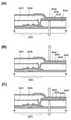
도 6은 도 1(A)에 나타낸 화소의 상면도의 일례를 나타낸다. 또한, 도 6에 나타낸 화소의 상면도에서는, 화소의 레이아웃을 명확하게 나타내기 위해, 절연막을 생략하였다. 또, 도 6에 나타낸 화소의 상면도에서는, 화소에 포함되는 트랜지스터와 용량 소자의 레이아웃을 명확하게 나타내기 위해, 애노드, EL층, 및 캐소드를 생략하였다.Fig. 6 shows an example of a top view of the pixel shown in Fig. 1A. In addition, in the top view of the pixel shown in FIG. 6, in order to show clearly the layout of a pixel, the insulating film is abbreviate|omitted. In the top view of the pixel shown in Fig. 6, the anode, the EL layer, and the cathode are omitted in order to clearly show the layout of the transistors and capacitor elements included in the pixel.
도 7은 도 6의 상면도의 파선 A1-A2 및 파선 A3-A4에 따른 단면도이다.7 is a cross-sectional view taken along broken lines A1-A2 and A3-A4 in the top view of FIG. 6 .
트랜지스터(12)는 절연 표면을 가지는 기판(800) 위에, 게이트로서 기능하는 도전막(801), 도전막(801) 위의 게이트 절연막(802), 도전막(801)과 중첩하는 게이트 절연막(802) 위에 위치하는 반도체막(803), 그리고 반도체막(803) 위에 위치하고, 소스 또는 드레인으로서 기능하는 도전막(804) 및 도전막(805)을 포함한다. 도전막(801)은 배선 G1으로서도 기능한다. 도전막(804)은 배선 SL으로서도 기능한다.The
트랜지스터(13)는 절연 표면을 가지는 기판(800) 위에, 게이트로서 기능하는 도전막(801), 도전막(801) 위의 게이트 절연막(802), 도전막(801)과 중첩하는 게이트 절연막(802) 위에 위치하는 반도체막(806), 그리고 반도체막(806) 위에 위치하고, 소스 또는 드레인으로서 기능하는 도전막(807) 및 도전막(808)을 포함한다. 도전막(807)은 컨택트홀을 통하여, 배선 IL로서 기능하는 도전막(809)에 접속되어 있다.The
트랜지스터(14)는 절연 표면을 가지는 기판(800) 위에, 게이트로서 기능하는 도전막(810), 도전막(810) 위의 게이트 절연막(802), 도전막(810)과 중첩하는 게이트 절연막(802) 위에 위치하는 반도체막(811), 그리고 반도체막(811) 위에 위치하고, 소스 또는 드레인으로서 기능하는 도전막(805) 및 도전막(808)을 포함한다. 도전막(810)은 배선 G2으로서도 기능한다.The
트랜지스터(11)는 절연 표면을 가지는 기판(800) 위에, 게이트로서 기능하는 도전막(812), 도전막(812) 위의 게이트 절연막(802), 도전막(812)과 중첩하는 게이트 절연막(802) 위에 위치하는 반도체막(813), 그리고 반도체막(813) 위에 위치하고, 소스 또는 드레인으로서 기능하는 도전막(814) 및 도전막(815)을 포함한다. 도전막(812)은 도전막(808)에 접속되어 있다. 도전막(814)은 배선 VL로서도 기능한다.The
트랜지스터(15)는 절연 표면을 가지는 기판(800) 위에, 게이트로서 기능하는 도전막(816), 도전막(816) 위의 게이트 절연막(802), 도전막(816)과 중첩하는 게이트 절연막(802) 위에 위치하는 반도체막(817), 반도체막(817) 위에 위치하고, 소스 또는 드레인으로서 기능하는 도전막(815) 및 도전막(818)을 포함한다. 도전막(816)은 배선 G3으로서도 기능한다.The
용량 소자(16)는 절연 표면을 가지는 기판(800) 위에, 도전막(819), 도전막(819) 위의 게이트 절연막(802), 도전막(819)과 중첩하는 게이트 절연막(802) 위에 위치하는 도전막(815)을 포함한다. 도전막(819)은 도전막(805)과 접속되어 있다.The
도전막(804), 도전막(805), 도전막(807), 도전막(808), 도전막(814), 도전막(815), 도전막(818) 위에는 절연막(820)이 형성되어 있다. 그리고, 절연막(821) 위에는 애노드로서 기능하는 도전막(822)이 형성되어 있다. 도전막(822)은 절연막(820) 및 절연막(821)에 형성된 컨택트홀(823)을 통하여, 도전막(818)에 접속되어 있다.An insulating
도전막(822)의 일부가 노출되는 개구부를 가진 절연막(824)이 절연막(821) 위에 제공되어 있다. 도전막(822)의 일부 및 절연막(824) 위에는 EL층(825)과 캐소드로서 기능하는 도전막(826)이 이 순서로 적층되어 있다. 도전막(822)과 EL층(825)과 도전막(826)이 서로 중첩되어 있는 영역이 발광 소자(17)에 상당한다.An insulating
도 8은 도 1(A)에 나타낸 화소의 상면도의 다른 일례를 나타낸다. 또한, 도 8의 화소의 상면도에서는 화소의 레이아웃을 명확하게 나타내기 위해, 절연막을 생략하였다. 또, 도 8의 화소의 상면도에서는 화소가 포함되는 트랜지스터와 용량 소자의 레이아웃을 명확하게 나타내기 위해, 애노드와 EL층과 캐소드를 생략하였다.Fig. 8 shows another example of a top view of the pixel shown in Fig. 1A. In addition, in the top view of the pixel of FIG. 8 , the insulating film is omitted to clearly show the layout of the pixel. In addition, in the top view of the pixel of FIG. 8, the anode, the EL layer, and the cathode are omitted in order to clearly show the layout of the transistor and the capacitor including the pixel.
도 9는 도 8에 나타내는 상면도의, 파선 A1-A2 및 파선 A3-A4에 따른 단면도이다.It is sectional drawing along broken line A1-A2 and broken line A3-A4 of the top view shown in FIG.
트랜지스터(12)는 절연 표면을 가지는 기판(900) 위에, 반도체막(901), 반도체막(901) 위의 게이트 절연막(902), 반도체막(901)과 중첩하는 게이트 절연막(902) 위에 위치하고, 게이트로서 기능하는 도전막(903), 그리고 반도체막(901)에 포함된 소스 및 드레인에 접속된 도전막(904) 및 도전막(905)을 포함한다. 도전막(903)은 배선 G1로서도 기능한다. 도전막(904)은 배선 SL로서도 기능한다.The
트랜지스터(13)는 절연 표면을 가지는 기판(900) 위에, 반도체막(906), 반도체막(906) 위의 게이트 절연막(902), 반도체막(906)과 중첩하는 게이트 절연막(902) 위에 위치하고, 게이트로서 기능하는 도전막(903), 그리고 반도체막(906)에 포함된 소스 및 드레인에 접속된 도전막(907) 및 도전막(908)을 포함한다. 도전막(907)은 컨택트홀을 통하여 배선 IL로서 기능하는 도전막(909)에 접속되어 있다.The
트랜지스터(14)는 절연 표면을 가지는 기판(900) 위에, 반도체막(901), 반도체막(901) 위의 게이트 절연막(902), 반도체막(901)과 중첩하는 게이트 절연막(902) 위에 위치하고, 게이트로서 기능하는 도전막(911), 그리고 반도체막(901)에 포함된 소스 및 드레인에 접속된 도전막(905) 및 도전막(908)을 포함한다. 도전막(911)은 배선 G2로서도 기능한다. 도 8에서는 트랜지스터(12)와 트랜지스터(14)가 하나의 반도체막(901)을 공유하고 있지만; 대신에 트랜지스터(12)와 트랜지스터(14)가 서로 다른 반도체막을 포함해도 좋다.The
트랜지스터(11)는 절연 표면을 가지는 기판(900) 위에, 반도체막(912), 반도체막(912) 위의 게이트 절연막(902), 반도체막(912)과 중첩하는 게이트 절연막(902) 위에 위치하고, 게이트로서 기능하는 도전막(913), 반도체막(912)에 포함된 소스 또는 드레인에 접속된 도전막(914)을 포함한다. 도전막(913)은 도전막(908)에 접속되어 있다. 도전막(914)은 배선 VL로서도 기능한다.The
트랜지스터(15)는 절연 표면을 가지는 기판(900) 위에, 반도체막(912), 반도체막(912) 위의 게이트 절연막(902), 반도체막(912)과 중첩하는 게이트 절연막(902) 위에 위치하고, 게이트로서 기능하는 도전막(915), 반도체막(912)에 포함된 소스 또는 드레인에 접속된 도전막(916)을 포함한다. 도전막(915)은 배선 G3으로서도 기능한다.The
용량 소자(16)는 절연 표면을 가지는 기판(900) 위에, 반도체막(912), 반도체막(912) 위의 게이트 절연막(902), 반도체막(912)과 중첩하는 게이트 절연막(902) 위에 위치하는 도전막(917)을 가진다. 도전막(917)은 도전막(905)에 접속되어 있다.The
도전막(904), 도전막(905), 도전막(907), 도전막(908), 도전막(914), 도전막(916) 위에는 절연막(920)이 형성된다. 절연막(920) 위에는 애노드로서 기능하는 도전막(921)이 제공된다. 도전막(921)은 절연막(920)에 형성된 컨택트홀(922)를 통하여, 도전막(916)에 접속되어 있다.An insulating
도전막(921)의 일부가 노출되는 개구부를 가진 절연막(923)이 절연막(920) 위에 제공되어 있다. 도전막(921)의 일부 및 절연막(923) 위에는 EL층(924)과 캐소드로서 기능하는 도전막(925)이 이 순서로 적층된다. 도전막(921), EL층(924), 도전막(925)이 서로 중첩되어 있는 영역이 발광 소자(17)에 상당한다.An insulating
또한, 본 발명의 일 양태에서, 트랜지스터(11) 내지 트랜지스터(15)는 비정질, 미결정, 다결정 또는 단결정(예를 들면, 실리콘 또는 게르마늄)을 포함하는 반도체막, 또는 와이드 갭 반도체(예를 들면, 산화물 반도체)를 포함하는 반도체막을 포함해도 좋다.Further, in one aspect of the present invention, the
트랜지스터(11) 내지 트랜지스터(15)의 반도체막이 비정질, 미결정, 다결정 또는 단결정(예를 들면, 실리콘 또는 게르마늄)을 이용하여 형성될 때, 상기 반도체막에 일 도전성을 부여하는 불순물 원소를 상기 반도체막에 첨가함으로써 소스 또는 드레인으로서 기능하는 불순물 영역이 형성된다. 예를 들면, 상기 반도체막에 인 또는 비소를 첨가함으로써, n형의 도전성을 가지는 불순물 영역을 형성할 수 있다. 또, 예를 들면, 상기 반도체막에 붕소를 첨가함으로써, p형의 도전성을 가지는 불순물 영역을 형성할 수 있다.When the semiconductor films of the
트랜지스터(11) 내지 트랜지스터(15)의 반도체막에 산화물 반도체가 이용되는 경우, 도펀트를 상기 반도체막에 첨가하여, 소스 또는 드레인으로서 기능하는 불순물 영역을 형성해도 좋다. 도펀트는 이온 주입법을 이용하여 첨가할 수 있다. 도펀트의 예는 헬륨, 아르곤, 크세논 등의 희가스 및, 질소, 인, 비소, 안티몬 등의 15족 원소 등이다. 예를 들면, 질소를 도펀트로서 이용한 경우, 불순물 영역 내의 질소 원자의 농도는 5×10¹⁹/cm3에서 1×10²²/cm3인 것이 바람직하다.When an oxide semiconductor is used for the semiconductor film of the
또한, 실리콘 반도체로서는, 예를 들어, 스퍼터링법 또는 플라즈마 CVD법 등의 기상 성장법에 의해 형성된 비정질 실리콘, 비정질 실리콘이 레이저 어닐 등에 의해 결정화된 방식으로 얻어지는 다결정 실리콘, 단결정 실리콘 웨이퍼에 수소 이온 등을 주입하여 단결정 실리콘 웨이퍼의 표층부가 박리되는 방식으로 얻어지는 단결정 실리콘 등을 이용할 수 있다.In addition, as a silicon semiconductor, for example, amorphous silicon formed by a vapor phase growth method such as sputtering method or plasma CVD method, polycrystalline silicon obtained by a method in which amorphous silicon is crystallized by laser annealing, etc., hydrogen ions etc. to a single crystal silicon wafer Single-crystal silicon obtained by injecting and peeling off the surface layer of a single-crystal silicon wafer, etc. can be used.
산화물 반도체의 예로서는, 산화 인듐; 산화 주석; 산화 아연; 2원계 금속의 산화물인 In-Zn계 산화물, Sn-Zn계 산화물, Al-Zn계 산화물, Zn-Mg계 산화물, Sn-Mg계 산화물, In-Mg계 산화물, In-Ga계 산화물; 3원계 금속의 산화물인 In-Ga-Zn계 산화물(IGZO라고도 표기함), In-Al-Zn계 산화물, In-Sn-Zn계 산화물, Sn-Ga-Zn계 산화물, Al-Ga-Zn계 산화물, Sn-Al-Zn계 산화물, In-Hf-Zn계 산화물, In-La-Zn계 산화물, In-Ce-Zn계 산화물, In-Pr-Zn계 산화물, In-Nd-Zn계 산화물, In-Sm-Zn계 산화물, In-Eu-Zn계 산화물, In-Gd-Zn계 산화물, In-Tb-Zn계 산화물, In-Dy-Zn계 산화물, In-Ho-Zn계 산화물, In-Er-Zn계 산화물, In-Tm-Zn계 산화물, In-Yb-Zn계 산화물, In-Lu-Zn계 산화물; 4원계 금속의 산화물인 In-Sn-Ga-Zn계 산화물, In-Hf-Ga-Zn계 산화물, In-Al-Ga-Zn계 산화물, In-Sn-Al-Zn계 산화물, In-Sn-Hf-Zn계 산화물, In-Hf-Al-Zn계 산화물이 있다.Examples of the oxide semiconductor include indium oxide; tin oxide; zinc oxide; oxides of binary metals such as In-Zn-based oxide, Sn-Zn-based oxide, Al-Zn-based oxide, Zn-Mg-based oxide, Sn-Mg-based oxide, In-Mg-based oxide, In-Ga-based oxide; In-Ga-Zn-based oxide (also referred to as IGZO), In-Al-Zn-based oxide, In-Sn-Zn-based oxide, Sn-Ga-Zn-based oxide, Al-Ga-Zn-based oxide, which are oxides of ternary metals Oxide, Sn-Al-Zn-based oxide, In-Hf-Zn-based oxide, In-La-Zn-based oxide, In-Ce-Zn-based oxide, In-Pr-Zn-based oxide, In-Nd-Zn-based oxide, In-Sm-Zn-based oxide, In-Eu-Zn-based oxide, In-Gd-Zn-based oxide, In-Tb-Zn-based oxide, In-Dy-Zn-based oxide, In-Ho-Zn-based oxide, In- Er-Zn-based oxide, In-Tm-Zn-based oxide, In-Yb-Zn-based oxide, In-Lu-Zn-based oxide; In-Sn-Ga-Zn-based oxide, In-Hf-Ga-Zn-based oxide, In-Al-Ga-Zn-based oxide, In-Sn-Al-Zn-based oxide, In-Sn- There are Hf-Zn-based oxides and In-Hf-Al-Zn-based oxides.
예를 들면, In-Ga-Zn계 산화물이란, In과 Ga와 Zn을 포함하는 산화물을 가리키고, In과 Ga와 Zn의 비율에는 제한이 없다. In-Ga-Zn계 산화물은 In과 Ga와 Zn 이외의 금속 원소를 포함해도 좋다.For example, an In-Ga-Zn-based oxide refers to an oxide containing In, Ga, and Zn, and the ratio of In, Ga, and Zn is not limited. The In-Ga-Zn-based oxide may contain In, Ga, and metal elements other than Zn.
InMO3(ZnO)m(m>0이고, m은 정수가 아님)로 표기되는 재료가 산화물 반도체로서 이용되어도 좋다. 또한, M은 Ga, Fe, Mn 및 Co로부터 선택된 하나의 금속 원소 또는 그 이상의 금속 원소를 나타낸다. 대신에, In2SnO5(ZnO)n(n>0, 또한, n은 자연수)로 나타내어지는 재료가 산화물 반도체로서 이용되어도 좋다.A material expressed by InMO3 (ZnO)m (m>0 and m is not an integer) may be used as the oxide semiconductor. In addition, M represents one or more metal elements selected from Ga, Fe, Mn and Co. Instead, a material represented by In2 SnO5 (ZnO)n (n>0, where n is a natural number) may be used as the oxide semiconductor.
예를 들면, In:Ga:Zn = 1:1:1( = 1/3:1/3:1/3) 혹은 In:Ga:Zn = 2:2:1( = 2/5:2/5:1/5)의 원자비의 In-Ga-Zn계 산화물이나, 상기 원자비에 가까운 원자비의 산화물을 이용할 수 있다. 대신에, In:Sn:Zn = 1:1:1( = 1/3:1/3:1/3), In:Sn:Zn = 2:1:3( = 1/3:1/6:1/2), 또는 In:Sn:Zn = 2:1:5( = 1/4:1/8:5/8)의 원자비의 In-Sn-Zn계 산화물이나, 상기 원자비에 가까운 산화물을 이용하면 좋다.For example, In:Ga:Zn = 1:1:1 (=1/3:1/3:1/3) or In:Ga:Zn = 2:2:1 (=2/5:2/5) An In-Ga-Zn-based oxide having an atomic ratio of 1/5) or an oxide having an atomic ratio close to the above-mentioned atomic ratio can be used. Instead, In:Sn:Zn = 1:1:1 (= 1/3:1/3:1/3), In:Sn:Zn = 2:1:3 (= 1/3:1/6: 1/2) or In:Sn:Zn = 2: 1:5 (= 1/4:1/8:5/8) of an In-Sn-Zn-based oxide or an oxide close to the above atomic ratio It is good to use
이 산화물 반도체를 포함하는 트랜지스터의 전기적 특성의 편차를 줄이기 위한 스태빌라이저(stabilizer)로서, 주석(Sn), 하프늄(Hf), 알루미늄(Al), 지르코늄(Zr), 티탄(Ti)을 포함하는 것이 바람직하다. 다른 스태빌라이저로서, 란타노이드인, 란탄(La), 세륨(Ce), 프라세오디뮴(Pr), 네오디뮴(Nd), 사마륨(Sm), 유로퓸(Eu), 가돌리늄(Gd), 테르븀(Tb), 디스프로슘(Dy), 홀뮴(Ho), 에르븀(Er), 툴륨(Tm), 이테르븀(Yb), 루테튬(Lu)의 일종 혹은 복수종을 포함해도 좋다.It is preferable to include tin (Sn), hafnium (Hf), aluminum (Al), zirconium (Zr), or titanium (Ti) as a stabilizer for reducing variations in electrical characteristics of a transistor including the oxide semiconductor. Do. As other stabilizers, lanthanoids, lanthanum (La), cerium (Ce), praseodymium (Pr), neodymium (Nd), samarium (Sm), europium (Eu), gadolinium (Gd), terbium (Tb), dysprosium ( Dy), holmium (Ho), erbium (Er), thulium (Tm), ytterbium (Yb), and lutetium (Lu) may contain one or more types.
전자 공여체(도너) 역할을 하는 수분 또는 수소 등의 불순물의 감소에 의해, 그리고 산소 결손의 감소에 의해 얻어진 고순도화된 산화물 반도체(purified OS)는 i형(진성) 반도체이거나 실질적으로 i형 반도체이다. 따라서, 고순도화된 산화물 반도체를 포함하는 트랜지스터는 오프 전류가 매우 낮다. 산화물 반도체의 밴드 갭은 2 eV 이상, 바람직하게는 2.5 eV 이상, 더욱 바람직하게는 3 eV 이상이다. 수분 및 수소 등의 불순물 농도가 충분히 저감되고, 산소 결손이 저감됨으로써 고순도화된 산화물 반도체막을 이용함으로써, 트랜지스터의 오프 전류를 낮출 수 있다.A highly purified oxide semiconductor (purified OS) obtained by reduction of impurities such as moisture or hydrogen serving as an electron donor (donor) and reduction of oxygen vacancies is an i-type (intrinsic) semiconductor or substantially an i-type semiconductor . Accordingly, the transistor including the highly purified oxide semiconductor has a very low off-state current. The oxide semiconductor has a band gap of 2 eV or more, preferably 2.5 eV or more, and more preferably 3 eV or more. The off-state current of the transistor can be lowered by using a highly purified oxide semiconductor film in which the concentration of impurities such as moisture and hydrogen is sufficiently reduced and oxygen vacancies are reduced.
구체적으로, 다양한 실험은 고순도화된 산화물 반도체를 반도체막에 이용한 트랜지스터의 낮은 오프 전류를 증명할 수 있다. 예를 들면, 채널 폭이 1×106μm이고, 채널 길이가 10μm인 트랜지스터의 오프 상태 전류는, 소스 전극과 드레인 전극간의 전압(드레인 전압) 사이의 전압이 1 V에서 10 V의 범위일 때, 반도체 파라미터 분석기의 측정 한계 이하, 즉 1×10-13 A 이하인 얻을 수 있다. 이 경우, 오프 전류를 트랜지스터의 채널 폭으로 나눈 수치에 상당하는 오프 전류는 100 zA/m 이하이다. 또, 용량 소자와 트랜지스터를 접속하여, 용량 소자에 유입 또는 용량 소자로부터 유출하는 전하를 이 트랜지스터로 제어하는 회로를 이용하여, 오프 전류를 측정하였다. 이 측정에서는, 채널 형성 영역이 고순도화된 산화물 반도체막에 형성되는 상기 트랜지스터가 사용되었고, 용량 소자의 단위 시간당의 전하량의 추이로부터 이 트랜지스터의 오프 전류를 측정했다. 그 결과, 트랜지스터의 소스 전극과 드레인 전극간의 전압이 3 V의 경우에, 마이크로미터당 수십 약토암페어(yA/m)의 더 낮은 오프 전류가 얻어지는 것을 알 수 있었다. 따라서, 상기 채널 형성 영역이 고순도화된 산화물 반도체막에 형성되는 상기 트랜지스터의 오프 전류는 결정성 실리콘을 이용한 트랜지스터의 오프 전류보다 매우 낮다.Specifically, various experiments can prove the low off-state current of a transistor using a highly purified oxide semiconductor as a semiconductor film. For example, the off-state current of a transistor with a channel width of 1×106 μm and a channel length of 10 μm is in the range of 1 V to 10 V when the voltage between the source electrode and the drain electrode (drain voltage) is in the range of 1 V to 10 V. , which is below the measurement limit of the semiconductor parameter analyzer, that is, 1×10-13 A or less can be obtained. In this case, the off current corresponding to a value obtained by dividing the off current by the channel width of the transistor is 100 zA/m or less. In addition, the off-state current was measured using a circuit in which the capacitor and the transistor were connected, and the electric charge flowing into or flowing out of the capacitor was controlled by the transistor. In this measurement, the transistor in which the channel formation region is formed in a highly purified oxide semiconductor film was used, and the off current of the transistor was measured from the transition of the amount of charge per unit time of the capacitor. As a result, it was found that, when the voltage between the source electrode and the drain electrode of the transistor was 3 V, a lower off-state current of several tens of amps per micrometer (yA/m) was obtained. Accordingly, the off current of the transistor in which the channel formation region is formed in the highly purified oxide semiconductor film is much lower than the off current of the transistor using crystalline silicon.
또한, 특별히 언급하지 않는 한, n 채널형 트랜지스터의 경우, 본 명세서에서 오프 전류란, 드레인의 전위를 소스와 게이트의 전위보다 높게 한 상태에서, 기준 전위로서 소스의 전위를 가지고 게이트의 전위가 0 이하일 때, 소스와 드레인의 사이에 흐르는 전류를 의미한다. 또한, p 채널형 트랜지스터의 경우, 본 명세서에서 오프 전류란, 드레인의 전위를 소스와 게이트의 전위보다 낮게 한 상태에서, 기준 전위로서 소스의 전위를 가지고 게이트의 전위가 0 이상일 때, 소스와 드레인의 사이에 흐르는 전류를 의미한다.In addition, unless otherwise specified, in the case of an n-channel transistor, the off current in this specification means a state in which the potential of the drain is higher than that of the source and the gate, the potential of the source is the reference potential, and the potential of the gate is 0. Below, it means the current flowing between the source and the drain. In addition, in the case of a p-channel transistor, the off-current in this specification refers to a state in which the potential of the drain is lower than the potential of the source and the gate, has the potential of the source as the reference potential, and when the potential of the gate is 0 or more, the source and drain means the current flowing between them.
예를 들면, 산화물 반도체막은 In(인듐), Ga(갈륨), 및 Zn(아연)을 포함하는 타겟을 이용하는 스퍼터링법에 의해 형성할 수 있다. In-Ga-Zn계 산화물 반도체막을 스퍼터링법으로 형성하는 경우, In:Ga:Zn = 1:1:1, 4:2:3, 3:1:2, 1:1:2, 2:1:3, 또는 3:1:4의 원자수비를 가지는 In-Ga-Zn계 산화물의 타겟을 이용하는 것이 바람직하다. 상술한 원자수비를 가지는 In-Ga-Zn계 산화물의 타겟을 이용하여 산화물 반도체막을 형성할 때, 다결정 또는 c축 배향 결정(CAAC)이 형성되기 쉬워진다. 또, In, Ga, 및 Zn을 포함하는 타겟의 충전율은 90% 이상 100% 이하, 바람직하게는 95% 이상 100% 미만이다. 충전율이 높은 타겟을 이용함으로써, 치밀한 산화물 반도체막이 형성된다.For example, the oxide semiconductor film can be formed by a sputtering method using a target containing In (indium), Ga (gallium), and Zn (zinc). In the case of forming an In-Ga-Zn-based oxide semiconductor film by sputtering, In:Ga:Zn = 1:1:1, 4:2:3, 3:1:2, 1:1:2, 2:1: It is preferable to use a target of an In-Ga-Zn-based oxide having an atomic ratio of 3 or 3:1:4. When the oxide semiconductor film is formed using the target of the In-Ga-Zn-based oxide having the above-described atomic ratio, polycrystals or c-axis oriented crystals (CAAC) are easily formed. Moreover, the filling factor of the target containing In, Ga, and Zn is 90% or more and 100% or less, Preferably, it is 95% or more and less than 100%. By using a target with a high filling rate, a dense oxide semiconductor film is formed.
산화물 반도체로서 In-Zn계 산화물 재료를 이용하는 경우, 이용되는 타겟 중의 금속 원소의 원자수비는 In:Zn = 50:1∼1:2(몰수비로 환산하면 In2O3:ZnO = 25:1∼1:4), 바람직하게는 In:Zn = 20:1∼1:1(몰수비로 환산하면 In2O3:ZnO = 10:1∼1:2), 더욱 바람직하게는 In:Zn = 15:1∼1.5:1(몰수비로 환산하면 In2O3:ZnO = 15:2∼3:4)이다. 예를 들면, In:Zn:O = X:Y:Z의 원자수비를 가지는 In-Zn계 산화물을 포함하는 산화물 반도체막의 형성에 이용되는 타겟에서, Z>1.5X+Y의 관계가 만족된다. 상기 범위 내에서 Zn의 비율을 유지함으로써, 이동도를 향상시킬 수 있다.When an In-Zn-based oxide material is used as the oxide semiconductor, the atomic ratio of the metal elements in the target used is In:Zn = 50:1 to 1:2 (In 2O3:ZnO = 25:1 to when converted to a mole ratio) 1:4), preferably In:Zn = 20:1 to 1:1 (in terms of mole ratio, In2 O3 :ZnO = 10:1 to 1:2), more preferably In:Zn = 15: 1 to 1.5:1 (In2 O3 :ZnO = 15:2 to 3:4 in terms of mole ratio). For example, in a target used for formation of an oxide semiconductor film containing an In-Zn-based oxide having an atomic ratio of In:Zn:O = X:Y:Z, the relationship of Z>1.5X+Y is satisfied. By maintaining the ratio of Zn within the above range, it is possible to improve the mobility.
구체적으로, 산화물 반도체막은 다음과 같이 형성될 수 있다: 감압 상태의 처리실 내에 기판을 유지하고, 처리실 내의 잔류 수분을 제거하는 동안 수소 및 수분이 제거된 스퍼터링 가스가 도입되고, 상기 타겟이 이용된다. 성막 동안, 기판 온도는 100℃ 이상 600℃ 이하, 바람직하게는 200℃ 이상 400℃ 이하이면 좋다. 기판이 가열되는 동안, 산화물 반도체막을 형성함으로써, 형성된 산화물 반도체막에 포함되는 불순물 농도를 저감할 수 있다. 또, 스퍼터링에 의한 손상이 경감된다. 처리실 내의 잔류 수분을 제거하기 위해서는 흡착형의 진공 펌프를 이용하는 것이 바람직하다. 예를 들면, 크라이오 펌프, 이온 펌프, 티탄 서블리메이션 펌프를 이용하는 것이 바람직하다. 또, 배기 수단은 콜드 트랩으로 제공된 터보 펌프여도 좋다. 크라이오 펌프를 이용하여 성막실에서는, 예를 들면, 수소 원자, 물(H2O) 등 수소 원자를 포함하는 화합물(보다 바람직하게는 탄소 원자를 포함하는 화합물도) 등이 제거되기 때문에, 이 처리실에서 형성된 산화물 반도체막의 불순물의 농도를 저감할 수 있다.Specifically, the oxide semiconductor film may be formed as follows: a sputtering gas from which hydrogen and moisture are removed is introduced while the substrate is maintained in a process chamber under reduced pressure, and residual moisture in the process chamber is removed, and the target is used. During film formation, the substrate temperature may be 100°C or higher and 600°C or lower, preferably 200°C or higher and 400°C or lower. By forming the oxide semiconductor film while the substrate is heated, the concentration of impurities contained in the formed oxide semiconductor film can be reduced. Moreover, damage by sputtering is reduced. In order to remove residual moisture in the processing chamber, it is preferable to use an adsorption type vacuum pump. For example, it is preferable to use a cryopump, an ion pump, or a titanium sublimation pump. Further, the exhaust means may be a turbo pump provided as a cold trap. In the film-forming chamber using a cryopump, for example, a compound containing a hydrogen atom, such as a hydrogen atom and water (H2 O) (more preferably a compound containing a carbon atom), etc. is removed, so this The concentration of impurities in the oxide semiconductor film formed in the processing chamber can be reduced.
단, 스퍼터링 등으로 성막된 산화물 반도체막은 때때로 불순물로서 다량의 수분 또는 수소(수산기를 포함함)를 포함한다. 수분 및 수소는 도너 준위를 형성하기 쉽기 때문에, 산화물 반도체에서 불순물의 역할을 한다. 본 발명의 일 양태에서는 산화물 반도체막 중의 수분 또는 수소 등의 불순물을 저감(탈수화 또는 탈수소화)하기 위해, 산화물 반도체막은 감압 분위기 하, 질소나 희가스 등의 불활성 가스 분위기 하, 산소 가스 분위기 하, 또는 초건조 에어(캐비티 링 다운 레이저 분광법(CRDS) 방식의 노점 온도계를 이용하여 측정한 경우의 수분량이 20 ppm(노점 환산으로 -55℃) 이하, 바람직하게는 1 ppm 이하, 바람직하게는 10 ppb 이하) 분위기 하에서 가열 처리가 실시된다.However, the oxide semiconductor film formed by sputtering or the like sometimes contains a large amount of moisture or hydrogen (including hydroxyl groups) as impurities. Moisture and hydrogen act as impurities in the oxide semiconductor because they tend to form donor levels. In one aspect of the present invention, in order to reduce (dehydration or dehydrogenation) impurities such as moisture or hydrogen in the oxide semiconductor film, the oxide semiconductor film is formed in a reduced pressure atmosphere, in an inert gas atmosphere such as nitrogen or rare gas, in an oxygen gas atmosphere, or ultra-dry air (cavity ring-down laser spectroscopy (CRDS) method, when measured using a dew point thermometer, the moisture content is 20 ppm (-55 ° C. in dew point conversion) or less), preferably 1 ppm or less, preferably 10 ppb Hereinafter) heat processing is performed in atmosphere.
산화물 반도체막에 가열 처리를 실시함으로써, 산화물 반도체막 중의 수분 또는 수소를 제거할 수 있다. 구체적으로, 가열 처리는 250℃ 이상 750℃이하, 바람직하게는 400℃ 이상 기판의 변형점 미만의 온도에서 실시하면 좋다. 예를 들면, 가열 처리는 500℃에서, 3분 이상 6분 이하 정도 동안 실시하면 좋다. 가열 처리에 RTA법을 이용하면, 단시간에 탈수화 또는 탈수소화를 수행할 수 있다; 따라서, 유리 기판의 변형점보다 높은 온도에서도 처리가 실시될 수 있다.By heat-treating the oxide semiconductor film, moisture or hydrogen in the oxide semiconductor film can be removed. Specifically, the heat treatment may be performed at a temperature of 250°C or higher and 750°C or lower, preferably 400°C or higher and lower than the strain point of the substrate. For example, the heat treatment may be performed at 500°C for about 3 minutes or more and 6 minutes or less. When the RTA method is used for heat treatment, dehydration or dehydrogenation can be performed in a short time; Therefore, the treatment can be carried out even at a temperature higher than the strain point of the glass substrate.
단 어떤 경우에, 상기 가열 처리는 산화물 반도체막으로부터 산소가 이탈하게 하고, 산화물 반도체막 내에 산소 결손이 형성된다. 본 발명의 일 양태에서는, 산소 결손을 방지하기 위해 산화물 반도체막과 접하는 게이트 절연막 등의 절연막으로 산소를 포함하는 절연막을 이용한다. 그리고나서, 산소를 포함하는 절연막을 형성한 후, 가열 처리를 실시함으로써, 상기 절연막으로부터 산화물 반도체막에 산소가 공급된다. 상기 구성에 의해, 반도체막에서 도너 역할을 하는 산소 결손을 저감하고, 산화물 반도체막에 포함되는 산화물 반도체의 화학량론적 조성비를 만족시킬 수 있다. 산화물 반도체막에서 산소의 비율은 화학량론적 조성비에서 산소의 비율보다 높은 것이 바람직하다. 그 결과, 산화물 반도체막을 실질적으로 i형으로 할 수 있고, 산소 결손으로 인한 트랜지스터의 전기적 특성의 편차가 저감된다; 따라서 전기적 특성을 향상시킬 수 있다.However, in some cases, the heat treatment causes oxygen to be released from the oxide semiconductor film, and oxygen vacancies are formed in the oxide semiconductor film. In one aspect of the present invention, an insulating film containing oxygen is used as an insulating film such as a gate insulating film in contact with the oxide semiconductor film to prevent oxygen vacancies. Then, oxygen is supplied from the insulating film to the oxide semiconductor film by performing heat treatment after forming the insulating film containing oxygen. With the above configuration, oxygen vacancies serving as a donor in the semiconductor film can be reduced, and the stoichiometric composition ratio of the oxide semiconductor included in the oxide semiconductor film can be satisfied. It is preferable that the ratio of oxygen in the oxide semiconductor film is higher than that of oxygen in the stoichiometric composition ratio. As a result, the oxide semiconductor film can be made substantially i-type, and variations in the electrical characteristics of the transistor due to oxygen vacancies are reduced; Therefore, electrical characteristics can be improved.
산소를 산화물 반도체막에 공급하기 위한 가열 처리는 질소, 초건조 공기, 또는 희가스(예를 들면, 아르곤, 헬륨 등)의 분위기 하에서, 바람직하게는 200℃ 이상 400℃ 이하, 예를 들면 250℃ 이상 350℃ 이하의 온도에서 행해진다. 상기 가스의 물 함유량은 20 ppm 이하, 바람직하게는 1 ppm 이하, 보다 바람직하게는 10 ppb 이하인 것이 바람직하다.The heat treatment for supplying oxygen to the oxide semiconductor film is performed in an atmosphere of nitrogen, ultra-dry air, or a rare gas (eg, argon, helium, etc.), preferably 200°C or higher and 400°C or lower, for example, 250°C or higher. It is carried out at a temperature of 350° C. or lower. The water content of the gas is preferably 20 ppm or less, preferably 1 ppm or less, more preferably 10 ppb or less.
또, 산화물 반도체는 어모퍼스(비정질)여도 좋고, 결정성을 가지고 있어도 좋다. 후자의 경우, 산화물 반도체는 단결정이어도 좋고, 다결정이어도 좋고, 또는 산화물 반도체의 일부분이 결정성을 가지는 구성이어도 좋고, 결정성 부분을 포함하는 어모퍼스 구조여도 좋고, 비어모퍼스여도 좋다. 일부분이 결정성을 가지는 구성의 일례로서, a-b면, 표면 또는 계면 방향에서 볼 때 삼각 형상 또는 육각 형상의 원자 배열을 가지고, c축 배향(c축 배향된 결정성 산화물 반도체(CAAC-OS)라고도 함)하는 결정을 포함하는 산화물 반도체를 사용하여도 좋다. 결정에서, c축에 수직인 방향에서 볼 때, 금속 원자가 층상 또는 금속 원자와 산소 원자가 층상으로 c축을 따라 배열되고, a축 또는 b축의 방향은 a-b면에서 변동된다(c축을 중심으로 회전함).Moreover, the oxide semiconductor may be amorphous (amorphous), and may have crystallinity. In the latter case, the oxide semiconductor may be a single crystal or a polycrystal, or a structure in which a part of the oxide semiconductor has crystallinity, an amorphous structure including a crystalline part, or a via-morphous structure may be sufficient as it. As an example of a configuration in which a part has crystallinity, it has a triangular or hexagonal atomic arrangement when viewed from the ab-plane, surface, or interface direction, and is c-axis oriented (also called c-axis oriented crystalline oxide semiconductor (CAAC-OS)). Oxide semiconductors containing crystals of In the crystal, when viewed from a direction perpendicular to the c-axis, metal atoms are arranged in layers or metal atoms and oxygen atoms are arranged along the c-axis in layers, and the direction of the a-axis or the b-axis is changed in the ab plane (rotates around the c-axis) .
CAAC-OS란, 넓은 의미로, 그 a-b면에 수직인 방향에서 볼 때, 삼각형, 육각형, 정삼각형 또는 정육각형의 원자 배열을 가지고, c축 방향에서 수직인 방향에서 볼 때, 금속 원자가 층상, 또는 금속 원자와 산소 원자가 층상으로 배열한 상을 포함하는 비단결정 산화물을 말한다.CAAC-OS, in a broad sense, has a triangular, hexagonal, equilateral triangle or regular hexagonal atomic arrangement when viewed in a direction perpendicular to the ab-plane, and when viewed from a direction perpendicular to the c-axis direction, metal atoms are layered, or metal It refers to a non-single-crystal oxide including a phase in which atoms and oxygen atoms are arranged in layers.
CAAC-OS는 단결정은 아니지만, 비정질만으로 구성되어 있는 것을 의미하는 것은 아니다. 비록, CAAC는 결정화된 부분(결정 부분)을 포함하지만, 하나의 결정 부분과 다른 결정 부분의 경계가 명확하지 않은 경우도 있다.CAAC-OS is not a single crystal, but does not mean that it is composed of only amorphous crystals. Although CAAC includes a crystallized part (crystal part), there are cases where the boundary between one crystal part and another crystal part is not clear.
질소는 CAAC-OS를 구성하는 산소의 일부로 치환되어도 좋다. CAAC-OS에 포함되는 결정 부분의 c축은 일정한 방향(예를 들면, CAAC-OS가 형성되는 기판면, 또는 CAAC-OS의 표면 등에 수직인 방향)으로 정렬되어 있어도 좋다. 대신에 CAAC-OS를 포함하는 개개의 결정 부분의 a-b면의 법선은 일정한 방향(예를 들면, CAAC-OS가 형성되는 기판면, 또는 CAAC-OS의 표면 등에 수직인 방향)으로 정렬되어 있어도 좋다.Nitrogen may be substituted with a part of oxygen constituting CAAC-OS. The c-axis of the crystal portion included in the CAAC-OS may be aligned in a fixed direction (for example, a direction perpendicular to the surface of the substrate on which the CAAC-OS is formed, or the surface of the CAAC-OS). Alternatively, the normal to the ab-plane of the individual crystal portions including the CAAC-OS may be aligned in a certain direction (for example, a direction perpendicular to the surface of the substrate on which the CAAC-OS is formed or the surface of the CAAC-OS, etc.). .
CAAC-OS는 그 조성 등에 따라, 도체, 반도체, 또는 절연체이다. 또, 그 조성 등에 따라, CAAC-OS는 가시광을 투과하거나 투과하지 않는다.CAAC-OS is a conductor, semiconductor, or insulator, depending on its composition or the like. In addition, depending on the composition or the like, the CAAC-OS transmits or does not transmit visible light.
이러한 CAAC-OS의 예는 막 상으로 형성되고, 막 표면 또는 막이 형성되는 기판면에 수직인 방향으로부터 관찰했을 때 삼각형 또는 육각형의 원자 배열을 가지고, 그 막 단면을 관찰했을 때 금속 원자가 층상으로 배열되거나, 또는 금속 원자 및 산소 원자(또는 질소 원자)가 층상으로 배열되는 산화물이다.An example of such a CAAC-OS is formed on a film, has a triangular or hexagonal atomic arrangement when viewed from a direction perpendicular to the film surface or a substrate surface on which the film is formed, and metal atoms are arranged in a layered manner when the film cross-section is observed or an oxide in which a metal atom and an oxygen atom (or a nitrogen atom) are arranged in a layered manner.
CAAC-OS의 결정 구조의 일례는 도 14(A) 내지 도 14(E), 도 15(A) 내지 도 15(C), 도 16(A) 내지 도 16(C)을 이용하여 상세하게 설명된다. 특별히 언급하지 않는 한, 도 14(A) 내지 도 14(E), 도 15(A) 내지 도 15(C), 도 16(A) 내지 도 16(C)에서, 수직 방향이 c축 방향에 상당하고, c축 방향에 직교하는 면이 a-b면에 상당한다. 또한, 단순히 "상반분", "하반분"이라는 표현이 사용될 때, a-b면 윗 부분을 상반분이라고 하고, a-b면 아랫 부분을 하반분(a-b면에 대한 상반분, 하반분)이라고 한다. 도 14(A) 내지 도 14(E)에서 동그라미로 둘러싸인 O는 4배위의 O를 나타내고, 이중 동그라미로 둘러싸인 O는 3배위의 O를 나타낸다.An example of the crystal structure of the CAAC-OS will be described in detail with reference to Figs. 14(A) to 14(E), Figs. 15(A) to 15(C), and Figs. 16(A) to 16(C). do. Unless otherwise specified, in Figs. 14(A) to 14(E), Figs. 15(A) to 15(C), and Figs. 16(A) to 16(C), the vertical direction is in the c-axis direction. and the plane orthogonal to the c-axis direction corresponds to the ab plane. Also, when the expressions "upper half" and "lower half" are simply used, the upper half of the a-b plane is called the upper half, and the lower part of the a-b plane is called the lower half (upper half and lower half of the a-b plane). In FIGS. 14(A) to 14(E) , O surrounded by a circle represents O in tetracoordination, and O surrounded by double circles represents O in tricoordination.
도 14(A)는 1개의 6배위의 In 원자, In 원자에 근접한 6개의 4배위의 산소 원자(이하 4배위의 O라고 함)를 포함하는 구조를 나타낸다. 여기에서는 1개의 금속 원자와 그에 근접의 산소 원자를 포함하는 구조를 소그룹이라고 부른다. 도 14(A)의 구조는 실제로는 팔면체 구조이지만, 간단하게 하기 위해, 평면 구조로 나타냈다. 단, 도 14(A)의 상반분 및 하반분 각각에는 3개씩 4배위의 O 원자가 있다. 도 14(A)에 나타내는 소그룹에서, 전하는 0이다.Fig. 14(A) shows a structure including one hexacoordinated In atom and six tetracoordinated oxygen atoms adjacent to the In atom (hereinafter referred to as tetracoordinated O). Here, a structure containing one metal atom and an oxygen atom adjacent thereto is called a small group. The structure of Fig. 14(A) is actually an octahedral structure, but for the sake of simplicity, it is shown as a planar structure. However, in each of the upper and lower halves of FIG. 14(A), there are three O atoms in tetracoordinate. In the small group shown in Fig. 14(A), the charge is zero.
도 14(B)는 1개의 5배위의 Ga 원자와, Ga 원자에 근접한 3개의 3배위의 산소 원자(이하 3배위의 O라고 함)와, Ga 원자에 근접한 2개의 4배위의 O 원자를 포함하는 구조를 나타낸다. 3배위의 O 원자는 모두 a-b면에 존재한다. 도 14(B)의 상반분 및 하반분 각각에는 1개씩 4배위의 O 원자가 있다. In 원자도 5배위를 가지기 때문에, 도 14(B)에 나타내는 구조를 또한 가질 수 있다. 도 14(B)에 나타내는 소그룹에서, 전하는 0이다.14(B) includes one pentacoordinated Ga atom, three tricoordinated oxygen atoms close to the Ga atom (hereinafter referred to as tricoordinated O), and two tetracoordinated O atoms close to the Ga atom. represents the structure. All tri-coordinated O atoms are on the a-b plane. In each of the upper and lower halves of FIG. 14(B), there is one O atom in tetracoordinate. Since the In atom also has a pentacoordination, it can also have the structure shown in Fig. 14(B). In the small group shown in Fig. 14(B), the charge is zero.
도 14(C)는 1개의 4배위의 Zn 원자와, Zn 원자에 근접한 4개의 4배위의 O 원자를 포함하는 구조를 나타낸다. 도 14(C)에서, 상반분에는 1개의 4배위의 O 원자가 있고, 하반분에는 3개의 4배위의 O 원자가 있다. 대신에, 도 14(C)의 상반분에 3개의 4배위의 O 원자가 있고, 하반분에 1개의 4배위의 O 원자가 있어도 좋다. 도 14(C)에 나타내는 소그룹에서, 전하는 0이다.14(C) shows a structure including one tetracoordinated Zn atom and four tetracoordinated O atoms adjacent to the Zn atom. In Fig. 14(C) , there is one tetracoordinated O atom in the upper half, and three tetracoordinated O atoms in the lower half. Alternatively, there may be three tetracoordinated O atoms in the upper half of Fig. 14C and one tetracoordinated O atom in the lower half. In the small group shown in Fig. 14(C), the charge is zero.
도 14(D)는 1개의 6배위의 Sn 원자와, Sn 원자에 근접한 6개의 4배위의 O 원자를 포함하는 구조를 나타낸다. 도 14(D)의 상반분 및 하반분의 각각에는 3개의 4배위의 O 원자가 있다. 도 14(D)에 나타내는 소그룹에서 전하는 +1이다.Fig. 14(D) shows a structure including one hexacoordinated Sn atom and six tetracoordinated O atoms adjacent to the Sn atom. There are three tetracoordinated O atoms in each of the upper and lower halves of Fig. 14(D). In the small group shown in Fig. 14(D), the charge is +1.
도 14(E)는 2개의 Zn 원자를 포함하는 소그룹을 나타낸다. 도 14(E)에서, 상반분 및 하반분의 각각에는 1개의 4배위의 O 원자가 있다. 도 14(E)에 나타내는 소그룹에서, 전하는 -1이다.Fig. 14(E) shows a subgroup containing two Zn atoms. In Fig. 14(E), there is one tetracoordinated O atom in each of the upper and lower halves. In the small group shown in Fig. 14(E), the charge is -1.
여기에서는 복수의 소그룹은 중그룹을 형성하고, 복수의 중그룹은 대그룹을 형성한다(유닛 셀이라고도 함).Here, a plurality of small groups form a medium group, and a plurality of medium groups form a large group (also referred to as a unit cell).
소그룹들 간의 결합 규칙에 대하여 설명한다. 도 14(A)에 나타내는 6배위의 In 원자에 대한 상반분의 3개의 O 원자는 하방향에 각각 3개의 근접 In 원자를 가지고, 하반분의 3개의 O 원자는 상방향에 각각 3개의 근접 In 원자를 가진다. 도 14(B)에 나타내는 5배위의 Ga 원자에 대한 상반분의 1개의 O 원자는 하방향에 1개의 근접 Ga 원자를 가지고, 하반분의 1개의 O 원자는 상방향에 1개의 근접 Ga 원자를 가진다. 도 14(C)에 나타내는 4배위의 Zn 원자에 대한 상반분의 1개의 O 원자는 하방향에 1개의 근접 Zn 원자를 가지고, 하반분의 3개의 O 원자는 상방향에 각각 3개의 근접 Zn 원자를 가진다. 이와 마찬가지로, 금속 원자의 상방향의 4배위의 O 원자의 수와 그 4배위의 O 원자의 하방향에 있는 근접 금속 원자의 수는 동일하다. 마찬가지로, 금속 원자의 하방향의 4배위의 O 원자의 수와 그 4배위의 O 원자의 상방향에 있는 근접 금속 원자의 수는 동일하다. O 원자는 4배위이므로, 하방향에 있는 근접 금속 원자의 수와 상방향에 있는 근접 금속 원자의 수의 합은 4이다. 따라서, 금속 원자의 상방향에 있는 4배위의 O 원자의 수와 다른 금속 원자의 하방향에 있는 4배위의 O 원자의 수와의 합이 4일 때, 금속 원자를 포함하는 2종의 소그룹들은 서로 결합될 수 있다. 예를 들면, 6배위의 금속 원자(In 또는 Sn)가 하반분의 3개의 4배위의 O 원자를 통하여 결합되는 경우, 5배위의 금속 원자(Ga 또는 In) 또는, 4배위의 금속 원자(Zn)에 결합된다.The rules of association between small groups will be described. The three O atoms in the upper half with respect to the 6-coordinated In atom shown in Fig. 14(A) each have three adjacent In atoms in the downward direction, and the three O atoms in the lower half each have three adjacent In atoms in the upward direction. have atoms. One O atom in the upper half has one adjacent Ga atom in the downward direction with respect to the pentacoordinate Ga atoms shown in Fig. 14(B), and one O atom in the lower half has one adjacent Ga atom in the upward direction. have One O atom in the upper half of the tetracoordinated Zn atom shown in Fig. 14(C) has one adjacent Zn atom in the downward direction, and the three O atoms in the lower half have three adjacent Zn atoms in the upward direction. have Likewise, the number of O atoms in the tetracoordinate of a metal atom is equal to the number of adjacent metal atoms in the downward direction of the O atom in the tetracoordinate direction. Similarly, the number of O atoms in the downward tetracoordinate of a metal atom and the number of adjacent metal atoms in the upward direction of the tetracoordinate O atoms are the same. Since the O atom is tetracoordinate, the sum of the number of adjacent metal atoms in the downward direction and the number of adjacent metal atoms in the upward direction is 4. Therefore, when the sum of the number of tetracoordinated O atoms in the upward direction of a metal atom and the number of tetracoordinated O atoms in the downward direction of another metal atom is 4, the two subgroups containing metal atoms are can be combined with each other. For example, when a 6-coordinated metal atom (In or Sn) is bonded through three tetra-coordinated O atoms in the lower half, a 5-coordinated metal atom (Ga or In) or a tetracoordinated metal atom (Zn) ) is bound to
배위수가 4, 5, 또는 6인 금속 원자는 c축 방향에서, 4배위의 O를 통하여 다른 금속 원자에 결합된다. 이 밖에도, 층 구조의 합계의 전하가 0이 되도록 복수의 소그룹을 결합함으로써 중그룹을 형성할 수 있다.A metal atom having a coordination number of 4, 5, or 6 is bonded to another metal atom in the c-axis direction through a tetracoordinated O. In addition, a heavy group can be formed by combining a plurality of small groups so that the total charge of the layer structure becomes zero.
도 15(A)는 In-Sn-Zn계 산화물의 층 구조에 포함되는 중그룹의 모델도를 도시한다. 도 15(B)는 3개의 중그룹을 포함하는 대그룹을 나타낸다. 도 15(C)는 도 15(B)의 층 구조를 c축 방향으로부터 관찰한 경우의 원자 배열을 나타낸다.15(A) shows a model diagram of a medium group included in the layer structure of an In-Sn-Zn-based oxide. Fig. 15(B) shows a large group comprising three medium groups. Fig. 15(C) shows the atomic arrangement when the layer structure of Fig. 15(B) is observed from the c-axis direction.
도 15(A)에서는, 간단하게 하기 위해, 3배위의 O 원자는 생략되고, 4배위의 O 원자는 동그라미로 나타낸다; 동그라미의 개수는 4배위의 O 원자의 수를 나타낸다. 예를 들면, Sn 원자에 대해 상반분 및 하반분 각각에는 3개씩 4배위의 O 원자가 있는 것이 동그라미 3으로 나타나 있다. 마찬가지로, 도 15(A)에서, In 원자에 대해 상반분 및 하반분 각각에는 1개씩 4배위의 O 원자가 있는 것이 동그라미 1로 나타나 있다. 마찬가지로, 도 15(A)는 하반분에서 1개의 4배위의 O 원자 및 상반분에서 3개의 4배위의 O 원자에 근접한 Zn 원자와, 상반분에서 1개의 4배위의 O 원자 및 하반분에서 3개의 4배위의 O 원자에 근접한 Zn 원자를 나타낸다.In Fig. 15(A), for the sake of simplicity, the tri-coordinated O atom is omitted, and the tetra-coordinated O atom is circled; The number of circles represents the number of O atoms in the tetracoordinate. For example, with respect to a Sn atom, three tetracoordinated O atoms are shown in
도 15(A)에서, In-Sn-Zn계 산화물의 층 구조에 포함되는 중그룹에서는 위에서부터 순차로 상반분 및 하반분의 각각에서 3개의 4배위의 O 원자에 근접한 Sn 원자가 상반분 및 하반분의 각각에서 1개의 4배위의 O 원자에 근접한 In 원자와 결합하고, 그 In 원자는 상반분에서 3개의 4배위의 O 원자에 근접한 Zn 원자와 결합하고, 그 Zn 원자는 Zn 원자에 대해 하반분에서 1개의 4배위의 O 원자를 통하여 상반분 및 하반분의 각각에서 3개의 4배위의 O 원자에 근접한 In과 결합하고, 그 In 원자는 2개의 Zn 원자를 포함하고, 상반분에서 1개의 4배위의 O 원자에 근접한 소그룹과 결합하고, 이 소그룹은 이 소그룹에 대해 하반분의 1개의 4배위의 O 원자를 통하여 상반분 및 하반분의 각각에서 3개의 4배위의 O 원자에 근접한 Sn 원자와 결합하고 있는 구성이다. 이 복수의 중그룹이 결합하여 대그룹이 형성된다.In FIG. 15(A), in the middle group included in the layer structure of the In-Sn-Zn-based oxide, Sn atoms close to three tetracoordinated O atoms in each of the upper and lower halves sequentially from the top are in the upper half and the lower half In each of the fractions it bonds with an In atom proximate to one tetracoordinated O atom, and that In atom bonds to a Zn atom proximate to three tetracoordinated O atoms in the upper half, and the Zn atom binds to the lower half of the Zn atom. In the first half, through one tetracoordinated O atom, in each of the upper and lower halves, it bonds with In adjacent to three tetracoordinated O atoms, and the In atom contains two Zn atoms, and one in the upper half Bonded with a subgroup adjacent to a tetracoordinated O atom, this subgroup via one tetracoordinated O atom to the lower half for this subgroup Sn atoms adjacent to three tetracoordinated O atoms in each of the upper and lower halves It is a composition that is combined with A plurality of these heavy groups combine to form a large group.
여기서, 3배위의 O 원자 및 4배위의 O 원자의 결합 1개당의 전하는 각각 -0.667, -0.5라고 생각할 수 있다. 예를 들면, In 원자(6배위 또는 5배위), Zn 원자(4배위), Sn 원자(5배위 또는 6배위)의 전하는 각각 +3, +2, +4이다. 따라서, Sn 원자를 포함하는 소그룹의 전하는 +1이다. 따라서, Sn 원자를 포함하는 층 구조를 형성하기 위해서는 전하 +1을 지우는 전하 -1이 필요하다. 전하 -1을 가지는 구조의 예는 도 14(E)에 나타낸 바와 같이, 2개의 Zn 원자를 포함하는 소그룹을 들 수 있다. 예를 들면, 2개의 Zn 원자를 포함하는 하나의 소그룹으로, Sn 원자를 포함하는 하나의 소그룹의 전하는 지워질 수 있기 때문에, 층 구조의 합계의 전하가 0이 될 수 있다.Here, it can be considered that the charges per bond of the tricoordinated O atom and the tetracoordinated O atom are -0.667 and -0.5, respectively. For example, the charges of an In atom (hexacoordinated or pentacoordinated), a Zn atom (tetracoordinated), and a Sn atom (pentacoordinated or hexacoordinated) are +3, +2, and +4, respectively. Therefore, the charge of the small group containing Sn atoms is +1. Therefore, in order to form a layer structure including Sn atoms, a charge -1 that erases a charge +1 is required. An example of a structure having a charge of -1 is a subgroup including two Zn atoms, as shown in Fig. 14(E). For example, since the charge of one subgroup including Sn atoms can be erased with one subgroup including two Zn atoms, the charge of the sum of the layer structures may be zero.
구체적으로는, 도 15(B)에 나타낸 대그룹을 반복함으로써, In-Sn-Zn계 산화물의 결정(In2SnZn3O8)을 얻을 수 있다. 단, 얻어진 In-Sn-Zn계 산화물의 층 구조는 In2SnZn2O7(ZnO)m(m은 0 또는 자연수)의 조성식으로 나타낼 수 있다.Specifically, by repeating the large group shown in FIG. 15(B), an In-Sn-Zn-based oxide crystal (In2 SnZn3 O8 ) can be obtained. However, the layer structure of the obtained In-Sn-Zn-based oxide can be expressed by a compositional formula of In2 SnZn2 O7 (ZnO)m (m is 0 or a natural number).
상기 규칙은 다음의 산화물, 즉, 4원계 금속의 산화물인 In-Sn-Ga-Zn계 산화물; 3원계 금속의 산화물인 In-Ga-Zn계 산화물(IGZO라고도 표기함), In-Al-Zn계 산화물, Sn-Ga-Zn계 산화물, Al-Ga-Zn계 산화물, Sn-Al-Zn계 산화물이나, In-Hf-Zn계 산화물, In-La-Zn계 산화물, In-Ce-Zn계 산화물, In-Pr-Zn계 산화물, In-Nd-Zn계 산화물, In-Sm-Zn계 산화물, In-Eu-Zn계 산화물, In-Gd-Zn계 산화물, In-Tb-Zn계 산화물, In-Dy-Zn계 산화물, In-Ho-Zn계 산화물, In-Er-Zn계 산화물, In-Tm-Zn계 산화물, In-Yb-Zn계 산화물, In-Lu-Zn계 산화물; 2원계 금속의 산화물인 In-Zn계 산화물, Sn-Zn계 산화물, Al-Zn계 산화물, Zn-Mg계 산화물, Sn-Mg계 산화물, In-Mg계 산화물이나, In-Ga계 산화물에도 적용된다.The above rule is the following oxides, that is, an In-Sn-Ga-Zn-based oxide which is an oxide of a quaternary metal; In-Ga-Zn-based oxide (also referred to as IGZO), In-Al-Zn-based oxide, Sn-Ga-Zn-based oxide, Al-Ga-Zn-based oxide, Sn-Al-Zn-based oxide, which are oxides of ternary metals Oxide, In-Hf-Zn-based oxide, In-La-Zn-based oxide, In-Ce-Zn-based oxide, In-Pr-Zn-based oxide, In-Nd-Zn-based oxide, In-Sm-Zn-based oxide , In-Eu-Zn-based oxide, In-Gd-Zn-based oxide, In-Tb-Zn-based oxide, In-Dy-Zn-based oxide, In-Ho-Zn-based oxide, In-Er-Zn-based oxide, In -Tm-Zn-based oxide, In-Yb-Zn-based oxide, In-Lu-Zn-based oxide; Applicable to In-Zn-based oxides, Sn-Zn-based oxides, Al-Zn-based oxides, Zn-Mg-based oxides, Sn-Mg-based oxides, In-Mg-based oxides, and In-Ga-based oxides, which are oxides of binary metals do.
예를 들면, 도 16(A)은 In-Ga-Zn계 산화물의 층 구조에 포함되는 중그룹의 모델도를 나타낸다.For example, FIG. 16(A) shows a model diagram of a medium group included in the layer structure of an In-Ga-Zn-based oxide.
도 16(A)에서, In-Ga-Zn계 산화물의 층 구조에 포함되는 중그룹에서는 위에서부터 순차로 상반분 및 하반분의 각각에서 3개의 4배위의 O 원자에 근접한 In 원자가, 상반분에서 1개의 4배위의 O 원자에 근접한 Zn 원자과 결합하고, 그 Zn 원자는 Zn 원자에 대해 하반분에서 3개의 4배위의 O 원자를 통하여, 상반분 및 하반분의 각각에서 1개의 4배위의 O 원자에 근접한 Ga 원자와 결합하고, 그 Ga 원자는 Ga 원자의 하반분에 대해 1개의 4배위의 O 원자를 통하여, 상반분 및 하반분의 각각에서 3개의 4배위의 O 원자에 근접한 In 원자와 결합하고 있는 구성이다. 이 복수의 중그룹이 결합하여 대그룹이 형성된다.In Fig. 16(A), in the middle group included in the layer structure of the In-Ga-Zn-based oxide, the In atoms close to the three tetracoordinated O atoms in each of the upper half and the lower half sequentially from the top, in the upper half It binds to a Zn atom adjacent to one tetracoordinated O atom, and the Zn atom is one tetracoordinated O atom in each of the upper and lower halves, through three tetracoordinated O atoms in the lower half to the Zn atom. The Ga atom is bonded to an In atom adjacent to three tetracoordinated O atoms in each of the upper and lower halves through one tetracoordinated O atom to the lower half of the Ga atom. This is the configuration you are doing. A plurality of these heavy groups combine to form a large group.
도 16(B)에 3개의 중그룹으로 구성되는 대그룹을 나타낸다. 도 16(C)은 도 16(B)의 층 구조를 c축 방향에서 관찰한 경우의 원자 배열을 나타내고 있다.16(B) shows a large group composed of three medium groups. Fig. 16(C) shows the atomic arrangement when the layer structure of Fig. 16(B) is observed in the c-axis direction.
여기서, In 원자(6배위 또는 5배위), Zn 원자(4배위), Ga 원자(5배위)의 전하는 각각 +3, +2, +3이기 때문에, In 원자, Zn 원자 및 Ga 원자 중 어느 것을 포함하는 소그룹의 전하는 0이다. 따라서, 이러한 소그룹의 조합을 가지는 중그룹의 합계의 전하는 항상 0이다.Here, since the charges of the In atom (hexacoordinated or pentacoordinated), Zn atom (tetracoordinated), and Ga atom (pentacoordinated) are +3, +2, and +3, respectively, a small group containing any of In atom, Zn atom, and Ga atom The charge of is 0. Thus, the charge of the sum of the heavy groups with these subgroup combinations is always zero.
In-Ga-Zn계 산화물의 층 구조를 형성하기 위해, 대그룹은 도 16(A)에 나타낸 중그룹뿐만 아니라, 도 16(A)에 나타낸 것과 In 원자, Ga 원자, Zn 원자의 배열이 다른 중그룹을 이용하여 형성할 수 있다.In order to form the layer structure of the In-Ga-Zn-based oxide, the large group includes not only the medium group shown in FIG. 16(A), but also the arrangement of In atoms, Ga atoms, and Zn atoms different from those shown in FIG. 16(A). It can be formed using groups.
구체적으로는, 도 16(B)에 나타낸 대그룹을 반복함으로써, In-Ga-Zn계 산화물을 얻을 수 있다. 단, 얻어진 In-Ga-Zn계 산화물의 층 구조는 InGaO3(ZnO)n(n은 자연수)으로 하는 조성식으로 나타낼 수 있다.Specifically, by repeating the large group shown in Fig. 16(B), an In-Ga-Zn-based oxide can be obtained. However, the layer structure of the obtained In-Ga-Zn-based oxide can be expressed by a compositional formula of InGaO3 (ZnO)n (n is a natural number).
본 실시형태는 다른 실시형태와 조합하여 실시하는 것이 가능하다.This embodiment can be implemented in combination with other embodiments.
(실시형태 3)(Embodiment 3)
본 발명의 일 양태에 따른 발광 장치에서는 백색 등의 단색의 광을 발하는 발광 소자와 컬러 필터의 조합을 이용함으로써, 풀 컬러 화상이 표시되는 컬러 필터 방식을 채용할 수 있다. 대신에, 서로 다른 색상의 광을 발하는 복수의 발광 소자를 이용하여, 풀 컬러 화상이 표시되는 방식을 채용할 수도 있다. 이 방식은 발광 소자의 한쌍의 전극 사이에 제공되는 각 EL층을 대응하는 색으로 나누어 채색되기 때문에, 분리 컬러링(coloring) 방식이라고 불린다.In the light emitting device according to an aspect of the present invention, a color filter method in which a full color image is displayed can be adopted by using a combination of a light emitting element that emits light of a single color such as white light and a color filter. Instead, a method in which a full-color image is displayed using a plurality of light emitting elements emitting light of different colors may be employed. Since this method is colored by dividing each EL layer provided between a pair of electrodes of the light emitting element with a corresponding color, it is called a separate coloring method.
분리 컬러링 방식의 경우, EL층은 통상, 메탈 마스크 등의 마스크를 이용하여, 증착법으로 나누어 도포된다; 따라서, 화소의 사이즈는 증착법에 의한 EL층의 분리 컬러링 정밀도에 의존한다. 한편, 분리 컬러링 방식과 달리 컬러 필터 방식에서는, EL층은 나누어 도포될 필요가 없다. 따라서, 분리 컬러링 방식의 경우보다, 화소 사이즈의 축소화가 용이하여; 고정밀의 화소부가 제공될 수 있다.In the case of the separate coloring method, the EL layer is usually applied by a vapor deposition method using a mask such as a metal mask; Therefore, the size of the pixel depends on the separation coloring accuracy of the EL layer by the vapor deposition method. On the other hand, in the color filter method, unlike the separate coloring method, the EL layer does not need to be applied separately. Therefore, it is easier to reduce the pixel size than in the case of the separate coloring method; A high-precision pixel portion can be provided.
발광 장치는 그 카테고리에서 트랜지스터가 형성된 소자 기판측에서 추출된 발광 소자로부터 광이 발해지는 보텀 에미션(bottom-emission) 발광 장치와; 소자 기판과는 반대의 측으로부터 발광 소자에서 발해지는 광이 추출되는 탑 에미션(top-emission) 발광 장치를 포함한다. 탑 에미션 구조의 경우, 발광 소자로부터 발해지는 광을 배선, 트랜지스터, 또는 저장 커패시터 등의 각종 소자에 의해 차단되는 일이 없기 때문에, 보텀 에미션 구조에 비해 화소로부터의 광의 취출 효율을 높일 수 있다. 따라서, 탑 에미션 구조는 발광 소자에 공급되는 전류량을 낮추어도 높은 휘도를 얻을 수 있기 때문에, 발광 소자의 수명을 향상시키는 데 유리하다.The light emitting device includes: a bottom-emission light emitting device in which light is emitted from a light emitting device extracted from a side of an element substrate on which a transistor is formed in the category; and a top-emission light-emitting device in which light emitted from the light-emitting element is extracted from a side opposite to the element substrate. In the case of the top-emission structure, since light emitted from the light-emitting element is not blocked by various elements such as wiring, transistors, or storage capacitors, the efficiency of light extraction from the pixel can be improved compared to that of the bottom-emission structure. . Therefore, the top emission structure is advantageous in improving the lifespan of the light emitting device because high luminance can be obtained even when the amount of current supplied to the light emitting device is reduced.
본 발명의 일 양태에 따른 발광 장치에서는 EL층으로부터 발해지는 광을 발광 소자 내에서 공진시키는 마이크로 캐비티(미소 광 공진기) 구조를 가지고 있어도 좋다. 마이크로 캐비티 구조에 의해, 특정의 파장을 가지는 광이 고효율을 가지고 발광 소자로부터 취출될 수 있기 때문에, 화소부의 휘도와 색순도를 향상시킬 수 있다.The light emitting device according to one aspect of the present invention may have a microcavity (micro light resonator) structure for resonating light emitted from the EL layer in the light emitting element. With the microcavity structure, since light having a specific wavelength can be extracted from the light emitting element with high efficiency, the luminance and color purity of the pixel portion can be improved.
도 10에, 화소의 단면도를 일례로서 나타낸다. 도 10에서는 빨강에 대응하는 화소의 단면의 일부, 초록에 대응하는 화소의 단면의 일부, 파랑에 대응하는 화소의 단면의 일부를 나타내고 있다.Fig. 10 shows a cross-sectional view of a pixel as an example. 10 shows a part of a cross section of a pixel corresponding to red, a part of a cross section of a pixel corresponding to green, and a part of a cross section of a pixel corresponding to blue.
구체적으로, 도 10에서는 빨강에 대응한 화소(140r)와 초록에 대응한 화소(140g)와 파랑에 대응한 화소(140b)가 도시되어 있다. 화소(140r), 화소(140g), 화소(140b)는 각각 애노드(715r), 애노드(715g), 애노드(715b)를 포함한다. 화소(140r), 화소(140g), 화소(140b)에 포함되는 상기 애노드(715r), 애노드(715g), 애노드(715b)는 기판(740)에 형성된 절연막(750)의 위에 제공되어 있다.Specifically, in FIG. 10 , a
애노드(715r), 애노드(715g), 및 애노드(715b) 위에는 절연막을 이용하여 형성되는 격벽(730)이 제공되어 있다. 격벽(730)은 개구부를 가지고, 상기 개구부에서, 애노드(715r), 애노드(715g), 및 애노드(715b)가 각각 일부 노출되어 있다. 또, 상기 노출된 영역을 덮도록, 격벽(730) 위에 EL층(731)과 가시광 투과하는 캐소드(732)가 순차로 적층되어 있다.A
애노드(715r), EL층(731), 및 캐소드(732)가 서로 중첩되는 부분이 빨강에 대응한 발광 소자(741r)에 상당한다. 애노드(715g), EL층(731), 및 캐소드(732)가 서로 중첩되는 부분이 초록에 대응한 발광 소자(741g)에 상당한다. 애노드(715b), EL층(731), 캐소드(732)가 서로 중첩되는 부분이 파랑에 대응한 발광 소자(741b)에 상당한다.A portion where the
기판(742)은 발광 소자(741r), 발광 소자(741g), 및 발광 소자(741b)를 사이에 끼우도록, 기판(740)과 대치하여 제공된다. 기판(742) 위에는 화소(140r)에 대응한 채색층(743r), 화소(140g)에 대응한 채색층(743g), 화소(140b)에 대응한 채색층(743b)이 제공되어 있다. 채색층(743r)은 빨강에 대응한 파장 영역의 광의 투과율이 다른 파장 영역의 광의 투과율보다 높은 층이다. 채색층(743g)은 초록에 대응한 파장 영역의 광의 투과율이 다른 파장 영역의 광의 투과율보다 높은 층이다. 채색층(743b)은 파랑에 대응한 파장 영역의 광의 투과율이 다른 파장 영역의 광의 투과율보다 높은 층이다.The
기판(742) 위에는 채색층(743r), 채색층(743g), 채색층(743b)을 덮도록, 오버코트(744)가 제공되어 있다. 오버코트(744)는 채색층(743r), 채색층(743g), 채색층(743b)을 보호하기 위해 제공되는 가시광을 투과하고, 평탄성이 향상된 수지 재료를 이용하여 형성되는 것이 바람직하다. 채색층(743r), 채색층(743g), 및 채색층(743b)과 오버코트(744)를 통틀어 컬러 필터라고 간주해도 좋고, 또는 채색층(743r), 채색층(743g), 및 채색층(743b)의 각각을 컬러 필터라고 간주해도 좋다.An
도 10에서는 가시광의 반사율이 높은 도전막(745r)과 가시광의 투과율이 상기 도전막(745r)보다 높은 도전막(746r)이 애노드(715r)로서 이용되기 위해 순차로 적층된다. 또, 가시광의 반사율이 높은 도전막(745g)과 가시광의 투과율이 상기 도전막(745g)보다 높은 도전막(746g)이 애노드(715g)로서 이용되기 위해, 순차로 적층된다. 도전막(746g)의 막두께는 도전막(746r)의 막두께보다 작다. 가시광의 반사율이 높은 도전막(745b)이 애노드(715b)로서 이용된다.In Fig. 10, a
따라서, 도 10에 나타내는 발광 장치에서는, 발광 소자(741r)에서, EL층(731)으로부터 발해진 광의 광로 길이는 도전막(745r)과 캐소드(732) 사이의 거리에 의해 조절될 수 있다. 발광 소자(741g)에서, EL층(731)으로부터 발해진 광의 광로 길이는 도전막(745g)과 캐소드(732) 사이의 거리에 의해 조절될 수 있다. 발광 소자(741b)에서, EL층(731)으로부터 발해진 광의 광로 길이는 도전막(745b)과 캐소드(732)의 거리에 의해 조절될 수 있다.Therefore, in the light emitting device shown in FIG. 10, in the
본 발명의 일 양태에서는 발광 소자(741r), 발광 소자(741g), 및 발광 소자(741b)로부터 발해진 광의 파장에 맞추어, 상기 광로 길이를 조정하는 마이크로 캐비티 구조가 이용되어도 좋고, 이에 따라, EL층(731)으로부터 발해진 광을 상기 각 발광 소자 내에서 공진시킨다.In one aspect of the present invention, a microcavity structure in which the optical path length is adjusted according to the wavelength of light emitted from the
본 발명의 일 양태에 따른 발광 장치에 상기 마이크로 캐비티 구조를 적용함으로써, 발광 소자(741r)로부터 발해지는 광에서, 빨강에 대응한 파장을 가지는 광이 그것의 강도를 높이기 위해 마이크로 캐비티 구조에서 공진한다. 결과적으로, 채색층(743r)을 통해 얻어지는 빨강의 광의 색순도 및 휘도가 높아진다. 또, 발광 소자(741g)로부터 발해지는 광에서, 초록에 대응한 파장을 가지는 광이 그것의 강도를 높이기 위해 마이크로 캐비티 구조에서 공진하고, 결과적으로, 채색층(743g)을 통해 얻어지는 초록의 광의 색순도 및 휘도가 높아진다. 발광 소자(741b)로부터 발해지는 광에서, 파랑에 대응한 파장을 가지는 광이 그것의 강도를 높이기 위해 마이크로 캐비티 구조에서 공진하고; 결과적으로, 채색층(743b)을 통해 얻어지는 파랑의 광의 색순도 및 휘도가 높아진다.By applying the microcavity structure to the light emitting device according to an aspect of the present invention, in the light emitted from the
단, 도 10에서는 빨강, 초록, 파랑의 3색에 대응하는 화소를 나타냈지만, 본 발명의 일 양태에서는 이 구성으로 한정되지 않는다. 본 발명의 일 양태에서는, 빨강, 초록, 파랑 및 노랑의 4색의 조합, 또는 청록, 진홍 및 노랑의 3색의 조합이 이용되어도 좋다. 대신에 엷은 색의 빨강, 초록, 및 파랑, 및 짙은 색의 빨강, 초록, 및 파랑의 6색의 조합을 이용할 수 있고, 혹은 빨강, 초록, 파랑, 청록, 진홍, 노랑의 6색의 조합을 이용할 수 있다.However, although pixels corresponding to three colors of red, green, and blue are shown in FIG. 10, the present invention is not limited to this configuration in one embodiment. In one aspect of the present invention, a combination of four colors of red, green, blue and yellow or a combination of three colors of cyan, magenta and yellow may be used. Instead, a combination of the six colors of red, green, and blue for the light colors and red, green, and blue for the dark colors may be used, or a combination of the six colors of red, green, blue, cyan, magenta, and yellow may be used. Available.
단, 예를 들면, 빨강, 초록, 및 파랑의 화소를 이용하여 표현될 수 있는 색은 색도도 상의 각각의 화소의 발광색에 대응하는 3점에 의해 만들어진 삼각형의 내측에 나타나는 색에 한정된다. 따라서, 빨강, 초록, 파랑 및 노랑의 화소를 이용한 경우와 같이, 색도도 상의 이 삼각형의 외측에 존재하는 색의 발광 소자를 추가적으로 제공함으로써, 이 발광 장치에서 표현할 수 있는 색의 범위가 확대될 수 있고, 결과적으로 색 재현성이 향상될 수 있다.However, for example, colors that can be expressed using red, green, and blue pixels are limited to colors appearing inside a triangle formed by three points corresponding to the emission colors of each pixel on the chromaticity diagram. Accordingly, as in the case of using pixels of red, green, blue, and yellow, by additionally providing a light emitting device of a color existing outside this triangle on the chromaticity diagram, the range of colors that can be expressed by this light emitting device can be expanded. and, as a result, color reproducibility may be improved.
도 10에서는 발광 소자(741r), 발광 소자(741g), 발광 소자(741b) 중, 가장 짧은 파장 λ의 빛을 발하는 발광 소자(741b)에서, 가시광의 반사율이 높은 도전막(745b)이 애노드로서 이용되고, 다른 발광 소자(741r), 발광 소자(741g)에서는 막두께가 서로 다른 도전막(746r) 및 도전막(746g)이 이용되고; 따라서 광로 길이가 조정된다. 본 발명의 일 양태에서는 가장 짧은 파장 λ의 빛을 발하는 발광 소자(741b)에서도, 가시광의 반사율이 높은 도전막(745b) 위에, 도전막(746r) 및 도전막(746g)과 같은 가시광의 투과율이 높은 도전막이 제공되어도 좋다. 그러나, 모든 발광 소자(741r, 741g, 741b)의 애노드로서 가시광의 투과율이 높은 도전막을 이용하는 경우보다, 애노드의 제작 공정이 간소화되기 때문에, 도 10에 나타낸 바와 같이, 가장 짧은 파장 λ의 빛을 발하는 발광 소자(741b)의 애노드로서, 가시광의 반사율이 높은 도전막(745b)을 사용하는 것이 바람직하다.In FIG. 10, in the
단, 가시광의 반사율이 높은 도전막(745b)의 일 함수는 가시광의 투과율이 높은 도전막(746r) 및 도전막(746g)에 비해 보통 작다. 따라서, 가장 짧은 파장 λ의 빛을 발하는 발광 소자(741b)에서는 발광 소자(741r), 발광 소자(741g)에 비해, 애노드(715b)로부터 EL층(731)으로 정공을 주입하기 어렵기 때문에, 발광 효율이 낮은 경향이 있다. 이런 관점에서, 본 발명의 일 양태에서는 가장 짧은 파장 λ의 빛을 발하는 발광 소자(741b)에서, 가시광의 반사율이 높은 도전막(745b)과 접하는 EL층(731)의 일부로, 정공 수송성이 높은 물질과, 이 정공 수송성이 높은 물질에 대하여 억셉터성(전자 수용성)을 가지는 물질을 함유시킨 복합 재료를 이용하는 것이 바람직하다. 상기 복합 재료가 애노드(715b)와 접하여 형성될 때, 애노드(715b)로부터 EL층(731)에 정공을 주입하기 쉬워져, 발광 소자(741b)의 발광 효율을 높일 수 있다.However, the work function of the
억셉터성을 가지는 물질로서는, 7,7,8,8-테트라시아노-2,3,5,6-테트라플루오로퀴노디메탄(약칭:F4-TCNQ), 클로라닐, 천이 금속 산화물, 원소 주기표에서 제 4 족 내지 제 8 족에 속하는 금속의 산화물을 들 수 있다. 구체적으로는, 산화 바나듐, 산화 니오브, 산화 탄탈, 산화 크로뮴, 산화 몰리브데넘, 산화 텅스텐, 산화 망간, 산화 레늄은 억셉터성이 높기 때문에 바람직하다. 이 중에서 특히, 산화 몰리브데넘은 대기 중에서도 안정적이고, 흡습성이 낮고, 취급하기 쉽기 때문에 바람직하다.Examples of the substance having an acceptor property include 7,7,8,8-tetracyano-2,3,5,6-tetrafluoroquinodimethane (abbreviation: F4 -TCNQ), chloranyl, transition metal oxide, and oxides of metals belonging to
복합 재료에 이용되는 정공 수송성이 높은 물질로서는, 방향족 아민 화합물, 카바졸 유도체, 방향족 탄화 수소, 고분자 화합물(예를 들면, 올리고머, 덴드리머, 폴리머 등) 등 다양한 화합물을 이용할 수 있다. 또한, 복합 재료에 이용되는 유기 화합물로서는 정공 수송성이 높은 유기 화합물인 것이 바람직하다. 구체적으로는, 10-6 cm2/Vs 이상의 정공 이동도를 가지는 물질이 바람직하게 이용된다. 단, 전자보다 정공의 수송성이 높은 물질이면, 이것들 이외의 것을 이용해도 좋다.Various compounds such as aromatic amine compounds, carbazole derivatives, aromatic hydrocarbons, and high molecular compounds (eg, oligomers, dendrimers, polymers, etc.) can be used as substances with high hole transport properties used in the composite material. Moreover, as an organic compound used for a composite material, it is preferable that it is an organic compound with high hole transport property. Specifically, a material having a hole mobility of 10-6 cm2 /Vs or more is preferably used. However, materials other than these may be used as long as they have a higher hole transport property than electrons.
가시광의 반사율이 높은 도전막(745r), 도전막(745g), 도전막(745b)은, 예를 들면, 알루미늄, 은 또는 이러한 금속 재료를 포함하는 합금 등을 단층, 혹은 적층함으로써, 형성될 수 있다. 대신에, 도전막(745r), 도전막(745g), 도전막(745b)을 가시광의 반사율이 높은 도전막과 막두께가 얇은 도전막(바람직하게는 20 nm 이하, 더욱 바람직하게는 10 nm 이하)을 적층시켜, 형성해도 좋다. 예를 들면, 가시광의 반사율이 높은 도전막 위에, 얇은 티탄막이나 몰리브데넘막을 적층하여 도전막(745b)을 형성함으로써, 가시광의 반사율이 높은 도전막(예를 들면, 알루미늄, 알루미늄을 포함하는 합금, 또는 은 등)의 표면에 산화막이 형성되는 것을 막을 수 있다.The
가시광의 투과율이 높은 도전막(746r) 및 도전막(746g)은 예를 들면, 산화 인듐, 산화 주석, 산화 아연, 인듐 주석 산화물, 인듐 아연 산화물 등을 이용하여 형성될 수 있다.The
캐소드(732)는 예를 들면, 광을 투과할 정도로 충분히 얇은 도전막(바람직하게는 20 nm 이하, 더욱 바람직하게는 10 nm 이하)과 도전성의 금속 산화물을 포함하는 도전막을 적층함으로써, 형성될 수 있다. 광을 투과할 정도로 충분히 얇은 도전막은 은, 마그네슘, 또는 이러한 금속 재료를 포함하는 합금 등을 단층, 혹은 적층하여 형성할 수 있다. 도전성의 금속 산화물로서는 산화 인듐, 산화 주석, 산화 아연, 인듐 주석 산화물, 인듐 아연 산화물, 및 산화 규소를 포함하는 이러한 금속 산화물 재료가 있다.The
본 실시형태는 다른 실시형태와 적절히 조합하여 실시하는 것이 가능하다.This embodiment can be implemented in appropriate combination with other embodiments.
(실시형태 4)(Embodiment 4)
본 실시형태에서는 보텀 에미션 구조, 탑 에미션 구조, 및 듀얼 에미션 구조에 대하여 설명한다. 듀얼 에미션 구조에서는, 발광 소자의 광은 소자 기판측으로부터, 및 소자 기판과는 반대의 측으로부터 꺼내진다.In this embodiment, a bottom emission structure, a top emission structure, and a dual emission structure are demonstrated. In the dual emission structure, the light of the light emitting element is taken out from the element substrate side and from the side opposite to the element substrate.
도 11(A)은 발광 소자(6033)로부터 발해지는 광을 애노드(6034)측에서 꺼내는 경우의, 화소의 단면도를 나타낸다. 트랜지스터(6031)는 절연막(6037)으로 덮여 있고, 절연막(6037) 위에는 개구부를 가지는 격벽(6038)이 형성되어 있다. 격벽(6038)의 개구부에서 애노드(6034)가 일부 노출되어 있고, 이 개구부에서 애노드(6034), EL층(6035), 캐소드(6036)가 순차로 적층되어 있다.11A is a cross-sectional view of a pixel when light emitted from the
애노드(6034)는 광을 투과하기 쉬운 재료를 이용하여 형성되고 또는 애노드(6034)를 쉽게 통과하는 빛의 막두께로 형성된다. 캐소드(6036)는 광을 투과하기 어려운 재료를 이용하여 형성되고 또는 캐소드(6036)를 통과하기 어려운 빛의 막두께로 형성된다. 따라서 상기 구성에 의해, 윤곽 화살표로 나타낸 바와 같이, 애노드(6034)측으로부터 광을 꺼내는 보텀 에미션 구조를 얻을 수 있다.The
도 11(B)은 발광 소자(6043)로부터 발해지는 광을 캐소드(6046)측에서 꺼내는 경우의 화소의 단면도를 나타낸다. 트랜지스터(6041)는 절연막(6047)으로 덮여 있고, 절연막(6047) 위에는 개구부를 가지는 격벽(6048)이 형성되어 있다. 격벽(6048)의 개구부에서 애노드(6044)가 일부 노출되어 있고, 이 개구부에서 애노드(6044), EL층(6045), 캐소드(6046)가 순차로 적층되어 있다.11B is a cross-sectional view of a pixel when light emitted from the
애노드(6044)는 광을 투과하기 어려운 재료를 이용하여 형성되고 또는 애노드(6044)를 통과하기 어려운 빛의 막두께로 형성된다. 캐소드(6046)는 광을 투과하기 쉬운 재료를 이용하여 형성되고 또는 캐소드(6046)를 쉽게 통과하는 빛의 막두께로 형성된다. 따라서 상기 구성에 의해, 윤곽 화살표로 나타낸 바와 같이, 캐소드(6046)측으로부터 광을 꺼내는 탑 에미션 구조를 얻을 수 있다.The
도 11(C)은 광소자(6053)로부터 발해지는 광을 애노드(6054)측 및 캐소드(6056)측에서 꺼내는 경우의 화소의 단면도를 나타낸다. 트랜지스터(6051)는 절연막(6057)으로 덮여 있고, 절연막(6057) 위에는 개구부를 가지는 격벽(6058)이 형성되어 있다. 격벽(6058)의 개구부에서 애노드(6054)이 일부 노출되어 있고, 이 개구부에서 애노드(6054), EL층(6055), 캐소드(6056)가 순차로 적층되어 있다.11C is a cross-sectional view of a pixel when light emitted from the
애노드(6054) 및 캐소드(6056)는 광을 투과하기 쉬운 재료를 이용하여 형성되고 또는 애노드(6054) 및 캐소드(6056)를 쉽게 통과하는 빛의 막두께로 형성된다. 따라서 상기 구성에 의해, 윤곽 화살표로 나타낸 바와 같이, 애노드(6054) 및 캐소드(6056)측으로부터 광을 꺼내는 듀얼 에미션 구조를 얻을 수 있다.The
애노드 및 캐소드 역할을 하는 전극에는, 예를 들면, 금속, 합금, 전기 전도성 화합물, 및 이들의 혼합물 등을 이용할 수 있다. 구체적으로는, 산화 인듐-산화 주석(ITO:Indium Tin Oxide), 규소 혹은 산화 규소를 함유한 산화 인듐-산화 주석, 산화 인듐-산화 아연(Indium Zinc Oxide), 산화 텅스텐 및 산화 아연을 함유한 산화 인듐, 금(Au), 백금(Pt), 니켈(Ni), 텅스텐(W), 크로뮴(Cr), 몰리브데넘(Mo), 철(Fe), 코발트(Co), 구리(Cu), 팔라듐(Pd), 티탄(Ti)을 예로 들 수 있다. 다른 예들로는, 원소 주기표의 제 1 족 또는 제 2 족에 속하는 원소, 즉 리튬(Li)이나 세슘(Cs) 등의 알칼리 금속, 및 칼슘(Ca), 스트론튬(Sr) 등의 알칼리토류 금속, 마그네슘(Mg), 및 이것들을 포함하는 합금(예를 들면, MgAg, AlLi), 유로퓸(Eu), 이테르븀(Yb) 등의 희토류 금속 및 이것들을 포함하는 합금, 및, 그라펜 등이 있다. 상기 전극들은 상기로부터 적절히 선택된 재료를 이용하여 형성되고, 최적의 두께를 갖도록 형성됨으로써, 보텀 에미션 구조, 탑 에미션 구조, 또는 듀얼 에미션 구조를 만드는 것이 가능해진다.For the electrode serving as the anode and the cathode, for example, a metal, an alloy, an electrically conductive compound, and a mixture thereof may be used. Specifically, indium oxide-tin oxide (ITO: Indium Tin Oxide), silicon or silicon oxide-containing indium-tin oxide, indium oxide-zinc oxide (Indium Zinc Oxide), tungsten oxide and zinc oxide-containing oxide Indium, gold (Au), platinum (Pt), nickel (Ni), tungsten (W), chromium (Cr), molybdenum (Mo), iron (Fe), cobalt (Co), copper (Cu), palladium (Pd) and titanium (Ti) are exemplified. As other examples, elements belonging to
본 실시형태는 다른 실시형태와 적절히 조합하여 실시할 수 있다.This embodiment can be implemented in appropriate combination with other embodiments.
(실시형태 5)(Embodiment 5)
도 12는 본 발명의 일 양태에 따른 발광 장치의 사시도의 일례이다.12 is an example of a perspective view of a light emitting device according to an aspect of the present invention.
도 12에 나타내는 발광 장치는 패널(1601), 회로 기판(1602), 접속부(1603)를 포함한다. 패널(1601)은 복수의 화소를 포함하는 화소부(1604), 복수의 화소를 행마다 선택하는 주사선 구동 회로(1605), 선택된 행 내의 화소에의 화상 신호의 입력을 제어하는 신호선 구동 회로(1606)를 포함한다. 구체적으로, 주사선 구동 회로(1605)에서는 배선 G1 내지 배선 G3에 입력되는 신호가 생성된다.The light emitting device shown in FIG. 12 includes a
회로 기판(1602)으로부터 접속부(1603)를 통하여 각종 신호와 전원의 전위가 패널(1601)에 입력된다. 접속부(1603)에는 예를 들면, 가요성 인쇄 기판(FPC:Flexible Printed Circuit) 등을 이용할 수 있다. 접속부(1603)로 COF 테이프가 이용되는 경우, 회로 기판(1602) 내의 일부의 회로, 혹은 패널(1601)에 포함되는 주사선 구동 회로(1605)나 신호선 구동 회로(1606)의 일부 등이 별도 준비된 칩 상에 형성되어도 좋고, COF(Chip On Film)법을 이용하여 이 칩이 COF 테이프에 접속되어도 좋다.Various signals and potentials of power sources are input to the
본 실시형태는 다른 실시형태와 조합하여 실시하는 것이 가능하다.This embodiment can be implemented in combination with other embodiments.
(실시형태 6)(Embodiment 6)
본 발명의 일 양태에 따른 발광 장치는 표시기기, 퍼스널 컴퓨터, 기록 매체가 제공된 화상 재생 장치(대표적으로는, DVD:Digital Versatile Disc 등의 기록 매체의 내용을 재생하여, 그 재생된 화상을 표시하기 위한 디스플레이를 가지는 장치)에 이용될 수 있다. 본 발명의 일 양태에 따른 발광 장치를 포함할 수 있는 전자기기의 다른 예로는 휴대 전화, 휴대형을 포함하는 게임기, 휴대 정보 단말, 전자 서적, 비디오 카메라, 디지털 스틸 카메라와 같은 카메라, 고글형 디스플레이(헤드 마운트 디스플레이), 네비게이션 시스템, 음향 재생 장치(예를 들면, 카 오디오, 디지털 오디오 플레이어 등), 복사기, 팩시밀리, 프린터, 프린터 복합기, 현금 자동 입출금기(ATM), 자동 판매기 등을 들 수 있다. 이러한 전자기기의 구체적인 예를 도 13(A) 내지 도 13(E)에 나타낸다.A light emitting device according to an aspect of the present invention reproduces the contents of a recording medium such as a display device, a personal computer, and an image reproducing device provided with a recording medium (typically, DVD: Digital Versatile Disc, and displays the reproduced image) devices having a display for Other examples of electronic devices that may include the light emitting device according to an aspect of the present invention include a mobile phone, a game machine including a portable type, a portable information terminal, an electronic book, a video camera, a camera such as a digital still camera, a goggle type display ( head mounted display), navigation systems, sound reproduction devices (eg, car audio, digital audio players, etc.), copiers, facsimiles, printers, printer multifunction devices, automatic teller machines (ATMs), vending machines, and the like. A specific example of such an electronic device is shown in FIGS. 13(A) to 13(E).
도 13(A)은 하우징(5001), 하우징(5002), 표시부(5003), 표시부(5004), 마이크로폰(5005), 스피커(5006), 조작 키(5007), 스타일러스(5008) 등을 포함하는 휴대형 게임기를 나타낸다. 본 발명의 일 양태에 따른 발광 장치는 표시부(5003), 또는 표시부(5004)로서 이용될 수 있다. 본 발명의 일 양태에 따른 발광 장치를 표시부(5003) 또는 표시부(5004)로서 이용함으로써, 고화질의 휴대형 게임기를 제공할 수 있다. 단, 도 13(A)에 나타낸 휴대형 게임기는 2개의 표시부(5003)와 표시부(5004)를 포함하지만, 휴대형 게임기에 포함되는 표시부의 수는 두개로 한정되지 않는다.13(A) shows a
도 13(B)은 하우징(5201), 표시부(5202), 지지대(5203) 등을 포함하는 표시기기를 나타낸다. 본 발명의 일 양태에 따른 발광 장치는 표시부(5202)로서 이용될 수 있다. 표시부(5202)로서 본 발명의 일 양태에 따른 발광 장치를 이용함으로써, 고화질의 표시기기를 제공할 수 있다. 단, 표시기기는 그 범주에 퍼스널 컴퓨터용, TV 방송 수신용, 광고 표시용 등의 모든 정보 표시용 표시기기를 포함한다.13(B) shows a display device including a
도 13(C)은 하우징(5401), 표시부(5402), 키보드(5403), 포인팅 디바이스(5404) 등을 포함하는 노트형 퍼스널 컴퓨터를 나타낸다. 본 발명의 일 양태에 따른 발광 장치는 표시부(5402)로서 이용될 수 있다. 표시부(5402)로서 본 발명의 일 양태에 따른 발광 장치를 이용함으로써, 고화질의 노트형 퍼스널 컴퓨터를 제공할 수 있다.Fig. 13(C) shows a notebook-type personal computer including a
도 13(D)은 하우징(5601), 표시부(5602), 조작 키(5603) 등을 포함하는 휴대 정보 단말을 나타낸다. 도 13(D)에 나타내는 휴대 정보 단말에서는 모뎀이 하우징(5601)에 내장되어 있어도 좋다. 본 발명의 일 양태에 따른 발광 장치는 표시부(5602)로서 이용될 수 있다. 표시부(5602)로서 본 발명의 일 양태에 따른 발광 장치를 이용함으로써, 고화질의 휴대 정보 단말을 제공할 수 있다.Fig. 13(D) shows a portable information terminal including a
도 13(E)은 하우징(5801), 표시부(5802), 음성 입력부(5803), 음성 출력부(5804), 조작 키(5805), 수광부(5806) 등을 포함하는 휴대전화를 나타낸다. 수광부(5806)에서 수신된 광을 전기 신호로 변환함으로써, 외부 화상을 로드할 수 있다. 본 발명의 일 양태에 따른 발광 장치는 표시부(5802)로서 이용될 수 있다. 표시부(5802)로서 본 발명의 일 양태에 따른 발광 장치를 이용함으로써, 고화질의 휴대 전화를 제공할 수 있다.Fig. 13E shows a mobile phone including a
본 실시형태는 다른 실시형태와 적절히 조합하여 실시할 수 있다.This embodiment can be implemented in appropriate combination with other embodiments.
(실시형태 7)(Embodiment 7)
본 실시형태에서는 실시형태 1에서 설명한 도 1(A)에 나타내는 화소(100)의 동작의 제 3 기간에서의 트랜지스터(11)의 게이트 전압 Vgs의 값을 계산에 의해 구했다.In the present embodiment, the value of the gate voltage Vgs of the
계산은 배선 IL에서의 전위 V0의 값이 서로 다른 조건 A 또는 조건 B 하에서 행해졌다. 조건 A와 조건 B 하에서 각 배선의 구체적인 전위의 값을 하기 표 1에 나타낸다. 전위 GVDD는 배선 G1, 배선 G2, 및 배선 G3에 각각에 인가되는 하이 레벨의 전위에 상당한다. 전위 GVSS는 배선 G1, 배선 G2, 및 배선 G3에 각각에 인가되는 로 레벨의 전위에 상당한다. 단, 표 1에서는 전위 Vcat를 0 V로 하고, 전위 Vdata, 전위 Vano, 전위 V0, 전위 GVDD, 전위 GVSS의 값을 전위 Vcat에 대한 전위차로 나타내고 있다.Calculation was performed under condition A or condition B in which the values of the potential V0 in the wiring IL were different from each other. Table 1 below shows the specific potential values of each wiring under condition A and condition B. The potential GVDD corresponds to a high-level potential applied to each of the wiring G1, the wiring G2, and the wiring G3. The potential GVSS corresponds to a low-level potential applied to the wiring G1, the wiring G2, and the wiring G3, respectively. However, in Table 1, the potential Vcat is set to 0 V, and the values of the potential Vdata, the potential Vano, the potential V0, the potential GVDD, and the potential GVSS are expressed as potential differences with respect to the potential Vcat.

계산에서 각 트랜지스터의 채널 길이 L과 채널 폭 W의 비에 관해서는, 트랜지스터(11)의 W/L은 3μm/9μm이고, 트랜지스터(12) 내지 트랜지스터(15)의 W/L은 3μm/3μm였다. 그리고, 도 1(A)에 나타낸 화소(100)에 포함되는 모든 트랜지스터에서, 소스 또는 드레인으로서 기능하는 도전막과 반도체막이 접하고 있는 영역을 영역 A라고 하면, 상기 영역 A와 게이트 전극이 형성되어 있는 영역이 중첩되는 영역에서의, 채널 길이 방향의 길이(Lov)는 1.5μm였다.Regarding the ratio of the channel length L to the channel width W of each transistor in the calculation, the W/L of the
제 3 기간에서, 트랜지스터(11)의 게이트 전압 Vgs는 도 3(C)에 나타낸 바와 같이, 전압이 Vdata-V0+Vth였다. 따라서, 도 1(A)에 나타낸 화소(100)에서, 등식 Vgs-Vth = Vdata-V0이 유지되기 때문에, Vgs-Vth는 문턱 전압 Vth의 값에 상관없이 이상적으로 일정하다.In the third period, the gate voltage Vgs of the
도 17은 조건 A 하에서 계산에 의해 얻어진 Vgs-Vth의 값을 나타낸다. 도 17에서는 가로축이 문턱 전압 Vth(V)를 나타내고, 세로축이 Vgs-Vth(V)의 값을 나타낸다. 도 17에서, 문턱 전압 Vth의 값을 변화시켜도, Vgs-Vth의 값이 거의 균일하고, 그 편차는 약 25% 내지 30% 이하로 제한되어 있는 것을 알 수 있다.Fig. 17 shows the values of Vgs-Vth obtained by calculation under condition A. In FIG. 17 , the horizontal axis represents the threshold voltage Vth(V), and the vertical axis represents the value of Vgs-Vth(V). 17 , it can be seen that the value of Vgs-Vth is almost uniform even when the value of the threshold voltage Vth is changed, and the deviation thereof is limited to about 25% to 30% or less.
도 18은 조건 B 하에서 계산에 의해 얻어진 Vgs-Vth의 값을 나타낸다. 도 18에서는 가로축이 문턱 전압 Vth(V)를 나타내고, 세로축이 Vgs-Vth(V)의 값을 나타낸다. 도 18에서는 문턱 전압 Vth의 값이 양의 값을 가지는 경우, Vgs-Vth의 값이 거의 균일하다. 그러나, 문턱 전압 Vth의 값이 음의 값을 가지는 경우, 문턱 전압 Vth의 값이 음의 방향으로 커질수록, Vgs-Vth의 값이 커지고, 이것은 Vgs-Vth의 값이 문턱 전압 Vth의 값에 의존하고 있는 것을 의미한다.Fig. 18 shows the values of Vgs-Vth obtained by calculation under condition B. In FIG. 18 , the horizontal axis indicates the threshold voltage Vth(V), and the vertical axis indicates the value of Vgs-Vth(V). In FIG. 18 , when the value of the threshold voltage Vth has a positive value, the value of Vgs-Vth is almost uniform. However, when the value of the threshold voltage Vth has a negative value, as the value of the threshold voltage Vth increases in the negative direction, the value of Vgs-Vth increases, which means that the value of Vgs-Vth depends on the value of the threshold voltage Vth. means doing
상기 계산의 결과는, 본 발명의 일 양태에 따른 발광 장치에서 트랜지스터(11)가 노멀리 온이어도, 즉 문턱 전압 Vth가 음의 값을 가지고 있어도, 트랜지스터(11)의 문턱 전압 Vth가 더해진 값이 되도록, 트랜지스터(11)의 게이트 전압 Vgs를 설정할 수 있는 것을 증명하였다.The result of the calculation is that even if the
본 실시형태는 다른 실시형태와 조합하여 실시하는 것이 가능하다.This embodiment can be implemented in combination with other embodiments.
11:트랜지스터
12:트랜지스터
13:트랜지스터
14:트랜지스터
15:트랜지스터
16:용량 소자
17:발광 소자
100:화소
140b:화소
140g:화소
140r:화소
715b:애노드
715g:애노드
715r:애노드
730:격벽
731:EL층
732:캐소드
740:기판
741b:발광 소자
741g:발광 소자
741r:발광 소자
742:기판
743b:채색층
743g:채색층
743r:채색층
744:오버코트
745b:도전막
745g:도전막
745r:도전막
746g:도전막
746r:도전막
750:절연막
800:기판
801:도전막
802:게이트 절연막
803:반도체막
804:도전막
805:도전막
806:반도체막
807:도전막
808:도전막
809:도전막
810:도전막
811:반도체막
812:도전막
813:반도체막
814:도전막
815:도전막
816:도전막
817:반도체막
818:도전막
819:도전막
820:절연막
821:절연막
822:도전막
823:컨택트홀
824:절연막
825:EL층
826:도전막
900:기판
901:반도체막
902:게이트 절연막
903:도전막
904:도전막
905:도전막
906:반도체막
907:도전막
908:도전막
909:도전막
911:도전막
912:반도체막
913:도전막
914:도전막
915:도전막
916:도전막
917:도전막
920:절연막
921:도전막
922:컨택트홀
923:절연막
924:EL층
925:도전막
1601:패널
1602:회로 기판
1603:접속부
1604:화소부
1605:주사선 구동 회로
1606:신호선 구동 회로
5001:하우징
5002:하우징
5003:표시부
5004:표시부
5005:마이크로폰
5006:스피커
5007:조작 키
5008:스타일러스
5201:하우징
5202:표시부
5203:지지대
5401:하우징
5402:표시부
5403:키보드
5404:포인팅 디바이스
5601:하우징
5602:표시부
5603:조작 키
5801:하우징
5802:표시부
5803:음성 입력부
5804:음성 출력부
5805:조작 키
5806:수광부
6031:트랜지스터
6033:발광 소자
6034:애노드
6035:EL층
6036:캐소드
6037:절연막
6038:격벽
6041:트랜지스터
6043:발광 소자
6044:애노드
6045:EL층
6046:캐소드
6047:절연막
6048:격벽
6051:트랜지스터
6053:광소자
6054:애노드
6055:EL층
6056:캐소드
6057:절연막
6058:격벽
본 출원은 각각 2011년 7월 22일 및 2011년 11월 29일에 일본 특허청에 출원된 일련 번호가 2011-161103 및 2011-259828인 일본 특허 출원에 기초하고, 본 명세서에 그 전문이 참조로 통합된다.11: transistor
12: transistor
13: transistor
14: transistor
15: transistor
16: Capacitive element
17: light emitting element
100: pixel
140b: pixel
140g: pixel
140r: pixel
715b: Anode
715 g: anode
715r: anode
730: bulkhead
731: EL layer
732: cathode
740: substrate
741b: light emitting element
741g: light emitting element
741r: light emitting element
742: substrate
743b: color layer
743 g: color layer
743r: color layer
744: Overcoat
745b: conductive film
745 g: conductive film
745r: conductive film
746g: conductive film
746r: conductive film
750: insulating film
800: substrate
801: Conductive film
802: gate insulating film
803: semiconductor film
804: Conductive film
805: conductive film
806: semiconductor film
807: Conductive film
808: Conductive Curtain
809: conductive film
810: conductive film
811: semiconductor film
812: Conductive film
813: semiconductor film
814: conductive film
815: Conductive film
816: Conductive film
817: semiconductor film
818: Conductive film
819: Conductive film
820: insulating film
821: insulating film
822: Conductive film
823: Contact Hall
824: insulating film
825: EL layer
826: Conductive film
900: substrate
901: semiconductor film
902: gate insulating film
903: Conductive film
904: conductive film
905: conductive film
906: semiconductor film
907: Conductive Curtain
908: Conductive Curtain
909: Conductive Curtain
911: the challenge
912: semiconductor film
913: Conductive film
914: Conductive film
915: Conductive film
916: Conductive film
917: Conductive film
920: insulating film
921: Conductive film
922: Contact Hall
923: insulating film
924: EL layer
925: conductive film
1601: panel
1602: circuit board
1603: Connection
1604: Pixel part
1605: Scan line driving circuit
1606: Signal line driving circuit
5001: housing
5002: housing
5003: display
5004: display
5005: microphone
5006: speaker
5007: Operation key
5008: Stylus
5201: housing
5202: display
5203: support
5401: housing
5402: display
5403: keyboard
5404: Pointing device
5601: housing
5602: Display
5603: Operation key
5801: housing
5802: display
5803: Audio input unit
5804: Audio output section
5805: Operation key
5806: light receiving unit
6031: transistor
6033: light emitting element
6034: anode
6035: EL layer
6036: cathode
6037: insulating film
6038: bulkhead
6041: transistor
6043: light emitting element
6044: anode
6045: EL layer
6046: cathode
6047: insulating film
6048: bulkhead
6051: transistor
6053: Optical element
6054: anode
6055: EL layer
6056: cathode
6057: insulating film
6058: bulkhead
This application is based on Japanese Patent Applications with serial numbers 2011-161103 and 2011-259828, filed with the Japan Patent Office on July 22, 2011 and November 29, 2011, respectively, which are incorporated herein by reference in their entirety do.
Claims (2)
Translated fromKorean제 1 트랜지스터, 제 2 트랜지스터, 제 3 트랜지스터, 제 4 트랜지스터, 제 5 트랜지스터, 용량 소자, 및 발광 소자를 포함하는 화소를 가지고,
상기 제 1 트랜지스터의 소스 및 드레인 중 한쪽은 상기 발광 소자와, 상기 제 5 트랜지스터의 소스 및 드레인 중 한쪽에 전기적으로 접속되고,
상기 제 1 트랜지스터의 소스 및 드레인 중 다른 한쪽은 제 1 배선에 전기적으로 접속되고,
상기 제 1 트랜지스터의 게이트는 상기 제 3 트랜지스터의 소스 및 드레인 중 한쪽과 상기 제 4 트랜지스터의 소스 또는 드레인에 전기적으로 접속되고,
상기 제 1 트랜지스터의 게이트는 상기 용량 소자의 한쪽 전극에 전기적으로 접속되고,
상기 제 2 트랜지스터의 소스 및 드레인 중 한쪽은 화상 신호가 인가되는 제 2 배선에 전기적으로 접속되고,
상기 제 2 트랜지스터의 게이트와 상기 제 3 트랜지스터의 게이트는 제 1 게이트선에 전기적으로 접속되고,
상기 제 4 트랜지스터의 게이트는 제 2 게이트선에 전기적으로 접속되고,
상기 제 5 트랜지스터의 소스 및 드레인 중 다른 한쪽은 제 3 배선에 전기적으로 접속되고,
상기 제 5 트랜지스터의 게이트는 제 3 게이트선에 전기적으로 접속되고,
반도체막과 상기 제 3 게이트선으로서 기능하는 도전막을 가지고,
상기 반도체막은 상기 제 1 트랜지스터의 채널 형성 영역으로서 기능하는 영역과, 상기 제 5 트랜지스터의 채널 형성 영역을 가지고,
상기 반도체막은 상기 도전막과 중첩되는, 발광 장치.A light emitting device comprising:
a pixel including a first transistor, a second transistor, a third transistor, a fourth transistor, a fifth transistor, a capacitor, and a light emitting element;
One of the source and the drain of the first transistor is electrically connected to one of the light emitting element and the source and the drain of the fifth transistor,
The other of the source and the drain of the first transistor is electrically connected to the first wiring,
a gate of the first transistor is electrically connected to one of a source and a drain of the third transistor and a source or a drain of the fourth transistor;
a gate of the first transistor is electrically connected to one electrode of the capacitor,
one of a source and a drain of the second transistor is electrically connected to a second wiring to which an image signal is applied;
a gate of the second transistor and a gate of the third transistor are electrically connected to a first gate line;
a gate of the fourth transistor is electrically connected to a second gate line;
The other of the source and drain of the fifth transistor is electrically connected to a third wiring,
a gate of the fifth transistor is electrically connected to a third gate line;
having a semiconductor film and a conductive film functioning as the third gate line;
the semiconductor film has a region functioning as a channel formation region of the first transistor and a channel formation region of the fifth transistor;
and the semiconductor film overlaps the conductive film.
제 1 트랜지스터, 제 2 트랜지스터, 제 3 트랜지스터, 제 4 트랜지스터, 제 5 트랜지스터, 용량 소자, 및 발광 소자를 포함하는 화소를 가지고,
상기 제 1 트랜지스터의 소스 및 드레인 중 한쪽은 상기 발광 소자와, 상기 제 5 트랜지스터의 소스 및 드레인 중 한쪽에 전기적으로 접속되고,
상기 제 1 트랜지스터의 소스 및 드레인 중 다른 한쪽은 제 1 배선에 전기적으로 접속되고,
상기 제 1 트랜지스터의 게이트는 상기 제 3 트랜지스터의 소스 및 드레인 중 한쪽과 상기 제 4 트랜지스터의 소스 또는 드레인에 전기적으로 접속되고,
상기 제 1 트랜지스터의 게이트는 상기 용량 소자의 한쪽 전극에 전기적으로 접속되고,
상기 제 2 트랜지스터의 소스 및 드레인 중 한쪽은 화상 신호가 인가되는 제 2 배선에 전기적으로 접속되고,
상기 제 2 트랜지스터의 게이트와 상기 제 3 트랜지스터의 게이트는 제 1 게이트선에 전기적으로 접속되고,
상기 제 4 트랜지스터의 게이트는 제 2 게이트선에 전기적으로 접속되고,
상기 제 5 트랜지스터의 소스 및 드레인 중 다른 한쪽은 제 3 배선에 전기적으로 접속되고,
상기 제 5 트랜지스터의 게이트는 제 3 게이트선에 전기적으로 접속되는, 발광 장치.A light emitting device comprising:
a pixel including a first transistor, a second transistor, a third transistor, a fourth transistor, a fifth transistor, a capacitor, and a light emitting element;
One of the source and the drain of the first transistor is electrically connected to one of the light emitting element and the source and the drain of the fifth transistor,
The other of the source and the drain of the first transistor is electrically connected to the first wiring,
a gate of the first transistor is electrically connected to one of a source and a drain of the third transistor and a source or a drain of the fourth transistor;
a gate of the first transistor is electrically connected to one electrode of the capacitor,
one of a source and a drain of the second transistor is electrically connected to a second wiring to which an image signal is applied;
a gate of the second transistor and a gate of the third transistor are electrically connected to a first gate line;
a gate of the fourth transistor is electrically connected to a second gate line;
The other of the source and drain of the fifth transistor is electrically connected to a third wiring,
and a gate of the fifth transistor is electrically connected to a third gate line.
Priority Applications (1)
| Application Number | Priority Date | Filing Date | Title |
|---|---|---|---|
| KR1020227009269AKR102449610B1 (en) | 2011-07-22 | 2012-06-28 | light emitting device |
Applications Claiming Priority (6)
| Application Number | Priority Date | Filing Date | Title |
|---|---|---|---|
| JPJP-P-2011-161103 | 2011-07-22 | ||
| JP2011161103 | 2011-07-22 | ||
| JP2011259828 | 2011-11-29 | ||
| JPJP-P-2011-259828 | 2011-11-29 | ||
| PCT/JP2012/067244WO2013015091A1 (en) | 2011-07-22 | 2012-06-28 | Light-emitting device |
| KR1020217005826AKR102297329B1 (en) | 2011-07-22 | 2012-06-28 | Light-emitting device |
Related Parent Applications (1)
| Application Number | Title | Priority Date | Filing Date |
|---|---|---|---|
| KR1020217005826ADivisionKR102297329B1 (en) | 2011-07-22 | 2012-06-28 | Light-emitting device |
Related Child Applications (1)
| Application Number | Title | Priority Date | Filing Date |
|---|---|---|---|
| KR1020227009269ADivisionKR102449610B1 (en) | 2011-07-22 | 2012-06-28 | light emitting device |
Publications (2)
| Publication Number | Publication Date |
|---|---|
| KR20210110746A KR20210110746A (en) | 2021-09-08 |
| KR102378948B1true KR102378948B1 (en) | 2022-03-24 |
Family
ID=47555455
Family Applications (11)
| Application Number | Title | Priority Date | Filing Date |
|---|---|---|---|
| KR1020147001696ACeasedKR20140051268A (en) | 2011-07-22 | 2012-06-28 | Light-emitting device |
| KR1020217005826AActiveKR102297329B1 (en) | 2011-07-22 | 2012-06-28 | Light-emitting device |
| KR1020227009269AActiveKR102449610B1 (en) | 2011-07-22 | 2012-06-28 | light emitting device |
| KR1020237020575AActiveKR102663040B1 (en) | 2011-07-22 | 2012-06-28 | Light-emitting device |
| KR1020247014324AActiveKR102807480B1 (en) | 2011-07-22 | 2012-06-28 | Light-emitting device |
| KR1020207013134AActiveKR102168439B1 (en) | 2011-07-22 | 2012-06-28 | Light-emitting device |
| KR1020227033429AAbandonedKR20220135256A (en) | 2011-07-22 | 2012-06-28 | Light-emitting device |
| KR1020257015234APendingKR20250073518A (en) | 2011-07-22 | 2012-06-28 | Light-emitting device |
| KR1020207029451AActiveKR102223582B1 (en) | 2011-07-22 | 2012-06-28 | Light-emitting device |
| KR1020217027281AActiveKR102378948B1 (en) | 2011-07-22 | 2012-06-28 | Light-emitting device |
| KR1020197007208AExpired - Fee RelatedKR102111016B1 (en) | 2011-07-22 | 2012-06-28 | Light-emitting device |
Family Applications Before (9)
| Application Number | Title | Priority Date | Filing Date |
|---|---|---|---|
| KR1020147001696ACeasedKR20140051268A (en) | 2011-07-22 | 2012-06-28 | Light-emitting device |
| KR1020217005826AActiveKR102297329B1 (en) | 2011-07-22 | 2012-06-28 | Light-emitting device |
| KR1020227009269AActiveKR102449610B1 (en) | 2011-07-22 | 2012-06-28 | light emitting device |
| KR1020237020575AActiveKR102663040B1 (en) | 2011-07-22 | 2012-06-28 | Light-emitting device |
| KR1020247014324AActiveKR102807480B1 (en) | 2011-07-22 | 2012-06-28 | Light-emitting device |
| KR1020207013134AActiveKR102168439B1 (en) | 2011-07-22 | 2012-06-28 | Light-emitting device |
| KR1020227033429AAbandonedKR20220135256A (en) | 2011-07-22 | 2012-06-28 | Light-emitting device |
| KR1020257015234APendingKR20250073518A (en) | 2011-07-22 | 2012-06-28 | Light-emitting device |
| KR1020207029451AActiveKR102223582B1 (en) | 2011-07-22 | 2012-06-28 | Light-emitting device |
Family Applications After (1)
| Application Number | Title | Priority Date | Filing Date |
|---|---|---|---|
| KR1020197007208AExpired - Fee RelatedKR102111016B1 (en) | 2011-07-22 | 2012-06-28 | Light-emitting device |
Country Status (7)
| Country | Link |
|---|---|
| US (5) | US10008149B2 (en) |
| JP (12) | JP6181913B2 (en) |
| KR (11) | KR20140051268A (en) |
| CN (1) | CN103688303B (en) |
| DE (1) | DE112012003074T5 (en) |
| TW (2) | TWI642325B (en) |
| WO (1) | WO2013015091A1 (en) |
Families Citing this family (28)
| Publication number | Priority date | Publication date | Assignee | Title |
|---|---|---|---|---|
| KR20140051268A (en) | 2011-07-22 | 2014-04-30 | 가부시키가이샤 한도오따이 에네루기 켄큐쇼 | Light-emitting device |
| US12176356B2 (en) | 2011-10-18 | 2024-12-24 | Semiconductor Energy Laboratory Co., Ltd. | Semiconductor device including transistor and light-emitting element |
| KR101962097B1 (en) | 2011-10-18 | 2019-03-27 | 가부시키가이샤 한도오따이 에네루기 켄큐쇼 | Semiconductor device |
| US10043794B2 (en) | 2012-03-22 | 2018-08-07 | Semiconductor Energy Laboratory Co., Ltd. | Semiconductor device and electronic device |
| JP6410496B2 (en)* | 2013-07-31 | 2018-10-24 | 株式会社半導体エネルギー研究所 | Multi-gate transistor |
| US9552767B2 (en) | 2013-08-30 | 2017-01-24 | Semiconductor Energy Laboratory Co., Ltd. | Light-emitting device |
| JP6426402B2 (en)* | 2013-08-30 | 2018-11-21 | 株式会社半導体エネルギー研究所 | Display device |
| WO2015033496A1 (en)* | 2013-09-04 | 2015-03-12 | パナソニック株式会社 | Display device and driving method |
| US9806098B2 (en)* | 2013-12-10 | 2017-10-31 | Semiconductor Energy Laboratory Co., Ltd. | Light-emitting device |
| KR102841877B1 (en) | 2013-12-27 | 2025-08-05 | 가부시키가이샤 한도오따이 에네루기 켄큐쇼 | Light-emitting device |
| JP6300534B2 (en)* | 2014-01-17 | 2018-03-28 | 株式会社ジャパンディスプレイ | Display device |
| US10483293B2 (en) | 2014-02-27 | 2019-11-19 | Semiconductor Energy Laboratory Co., Ltd. | Active matrix display device, and module and electronic appliance including the same |
| CN106233233B (en)* | 2014-04-23 | 2019-09-10 | 株式会社半导体能源研究所 | The driving method of input/output device and input/output device |
| JP6653997B2 (en)* | 2014-05-09 | 2020-02-26 | 株式会社半導体エネルギー研究所 | Display correction circuit and display device |
| WO2016034984A1 (en)* | 2014-09-05 | 2016-03-10 | Semiconductor Energy Laboratory Co., Ltd. | Semiconductor device, driver ic, display device, and electronic device |
| WO2016108122A1 (en) | 2014-12-29 | 2016-07-07 | Semiconductor Energy Laboratory Co., Ltd. | Semiconductor device and display device having semiconductor device |
| KR102343894B1 (en)* | 2015-04-07 | 2021-12-27 | 삼성디스플레이 주식회사 | Display device |
| JP2017010000A (en) | 2015-04-13 | 2017-01-12 | 株式会社半導体エネルギー研究所 | Display device |
| US9666655B2 (en) | 2015-05-05 | 2017-05-30 | Semiconductor Energy Laboratory Co., Ltd. | Display device |
| US9862101B2 (en)* | 2015-12-22 | 2018-01-09 | Varian Semiconductor Equipment Associats, Inc. | Self-damping end effector |
| JP6914732B2 (en)* | 2017-05-29 | 2021-08-04 | キヤノン株式会社 | Light emitting device and imaging device |
| CN111406280B (en)* | 2017-12-06 | 2022-12-06 | 株式会社半导体能源研究所 | Semiconductor device, display device, electronic apparatus, and operating method |
| RU2020134366A (en) | 2018-03-21 | 2022-04-22 | Пресижн Плэнтинг Ллк | REAGENT CARTRIDGE |
| US12052879B2 (en) | 2020-05-01 | 2024-07-30 | Semiconductor Energy Laboratory Co., Ltd. | Display device including light-emitting and light-receiving element |
| TW202211195A (en) | 2020-08-12 | 2022-03-16 | 日商半導體能源研究所股份有限公司 | Display device, method for operating same, and electronic instrument |
| US12402496B2 (en) | 2020-12-24 | 2025-08-26 | Semiconductor Energy Laboratory Co., Ltd. | Display device |
| KR20220147762A (en)* | 2021-04-27 | 2022-11-04 | 삼성디스플레이 주식회사 | Pixel and display apparatus having the same |
| JPWO2023017362A1 (en) | 2021-08-12 | 2023-02-16 |
Family Cites Families (195)
| Publication number | Priority date | Publication date | Assignee | Title |
|---|---|---|---|---|
| JPS60198861A (en) | 1984-03-23 | 1985-10-08 | Fujitsu Ltd | Thin film transistor |
| JPH0244256B2 (en) | 1987-01-28 | 1990-10-03 | Kagaku Gijutsucho Mukizaishitsu Kenkyushocho | INGAZN2O5DESHIMESARERUROTSUHOSHOKEINOSOJOKOZOOJUSURUKAGOBUTSUOYOBISONOSEIZOHO |
| JPH0244258B2 (en) | 1987-02-24 | 1990-10-03 | Kagaku Gijutsucho Mukizaishitsu Kenkyushocho | INGAZN3O6DESHIMESARERUROTSUHOSHOKEINOSOJOKOZOOJUSURUKAGOBUTSUOYOBISONOSEIZOHO |
| JPS63210023A (en) | 1987-02-24 | 1988-08-31 | Natl Inst For Res In Inorg Mater | Compound having a hexagonal layered structure represented by InGaZn↓4O↓7 and its manufacturing method |
| JPH0244260B2 (en) | 1987-02-24 | 1990-10-03 | Kagaku Gijutsucho Mukizaishitsu Kenkyushocho | INGAZN5O8DESHIMESARERUROTSUHOSHOKEINOSOJOKOZOOJUSURUKAGOBUTSUOYOBISONOSEIZOHO |
| JPH0244262B2 (en) | 1987-02-27 | 1990-10-03 | Kagaku Gijutsucho Mukizaishitsu Kenkyushocho | INGAZN6O9DESHIMESARERUROTSUHOSHOKEINOSOJOKOZOOJUSURUKAGOBUTSUOYOBISONOSEIZOHO |
| JPH0244263B2 (en) | 1987-04-22 | 1990-10-03 | Kagaku Gijutsucho Mukizaishitsu Kenkyushocho | INGAZN7O10DESHIMESARERUROTSUHOSHOKEINOSOJOKOZOOJUSURUKAGOBUTSUOYOBISONOSEIZOHO |
| JPH05251705A (en) | 1992-03-04 | 1993-09-28 | Fuji Xerox Co Ltd | Thin-film transistor |
| US5684365A (en) | 1994-12-14 | 1997-11-04 | Eastman Kodak Company | TFT-el display panel using organic electroluminescent media |
| JP3479375B2 (en) | 1995-03-27 | 2003-12-15 | 科学技術振興事業団 | Metal oxide semiconductor device in which a pn junction is formed with a thin film transistor made of a metal oxide semiconductor such as cuprous oxide, and methods for manufacturing the same |
| KR100394896B1 (en) | 1995-08-03 | 2003-11-28 | 코닌클리케 필립스 일렉트로닉스 엔.브이. | A semiconductor device including a transparent switching element |
| JP3647523B2 (en) | 1995-10-14 | 2005-05-11 | 株式会社半導体エネルギー研究所 | Matrix type liquid crystal display device |
| JP3625598B2 (en) | 1995-12-30 | 2005-03-02 | 三星電子株式会社 | Manufacturing method of liquid crystal display device |
| JP4170454B2 (en) | 1998-07-24 | 2008-10-22 | Hoya株式会社 | Article having transparent conductive oxide thin film and method for producing the same |
| JP2000150861A (en) | 1998-11-16 | 2000-05-30 | Tdk Corp | Oxide thin film |
| JP3276930B2 (en) | 1998-11-17 | 2002-04-22 | 科学技術振興事業団 | Transistor and semiconductor device |
| US7821065B2 (en) | 1999-03-02 | 2010-10-26 | Semiconductor Energy Laboratory Co., Ltd. | Semiconductor device comprising a thin film transistor comprising a semiconductor thin film and method of manufacturing the same |
| US6512504B1 (en) | 1999-04-27 | 2003-01-28 | Semiconductor Energy Laborayory Co., Ltd. | Electronic device and electronic apparatus |
| TW460731B (en) | 1999-09-03 | 2001-10-21 | Ind Tech Res Inst | Electrode structure and production method of wide viewing angle LCD |
| JP2001318627A (en) | 2000-02-29 | 2001-11-16 | Semiconductor Energy Lab Co Ltd | Light emitting device |
| JP4089858B2 (en) | 2000-09-01 | 2008-05-28 | 国立大学法人東北大学 | Semiconductor device |
| SG114502A1 (en)* | 2000-10-24 | 2005-09-28 | Semiconductor Energy Lab | Light emitting device and method of driving the same |
| KR20020038482A (en) | 2000-11-15 | 2002-05-23 | 모리시타 요이찌 | Thin film transistor array, method for producing the same, and display panel using the same |
| KR100675319B1 (en) | 2000-12-23 | 2007-01-26 | 엘지.필립스 엘시디 주식회사 | Electro luminescence panel |
| JP3997731B2 (en) | 2001-03-19 | 2007-10-24 | 富士ゼロックス株式会社 | Method for forming a crystalline semiconductor thin film on a substrate |
| JP2002289859A (en) | 2001-03-23 | 2002-10-04 | Minolta Co Ltd | Thin film transistor |
| JP4785271B2 (en) | 2001-04-27 | 2011-10-05 | 株式会社半導体エネルギー研究所 | Liquid crystal display device, electronic equipment |
| TW582005B (en) | 2001-05-29 | 2004-04-01 | Semiconductor Energy Lab | Pulse output circuit, shift register, and display device |
| US6734636B2 (en)* | 2001-06-22 | 2004-05-11 | International Business Machines Corporation | OLED current drive pixel circuit |
| SG148032A1 (en) | 2001-07-16 | 2008-12-31 | Semiconductor Energy Lab | Light emitting device |
| JP4831895B2 (en) | 2001-08-03 | 2011-12-07 | 株式会社半導体エネルギー研究所 | Semiconductor device |
| JP4650601B2 (en) | 2001-09-05 | 2011-03-16 | 日本電気株式会社 | Current drive element drive circuit, drive method, and image display apparatus |
| JP3925839B2 (en) | 2001-09-10 | 2007-06-06 | シャープ株式会社 | Semiconductor memory device and test method thereof |
| JP4090716B2 (en) | 2001-09-10 | 2008-05-28 | 雅司 川崎 | Thin film transistor and matrix display device |
| SG120889A1 (en)* | 2001-09-28 | 2006-04-26 | Semiconductor Energy Lab | A light emitting device and electronic apparatus using the same |
| US7365713B2 (en) | 2001-10-24 | 2008-04-29 | Semiconductor Energy Laboratory Co., Ltd. | Semiconductor device and driving method thereof |
| US7456810B2 (en) | 2001-10-26 | 2008-11-25 | Semiconductor Energy Laboratory Co., Ltd. | Light-emitting device and driving method thereof |
| JP4498669B2 (en) | 2001-10-30 | 2010-07-07 | 株式会社半導体エネルギー研究所 | Semiconductor device, display device, and electronic device including the same |
| JP4164562B2 (en) | 2002-09-11 | 2008-10-15 | 独立行政法人科学技術振興機構 | Transparent thin film field effect transistor using homologous thin film as active layer |
| WO2003040441A1 (en) | 2001-11-05 | 2003-05-15 | Japan Science And Technology Agency | Natural superlattice homologous single crystal thin film, method for preparation thereof, and device using said single crystal thin film |
| JP4451054B2 (en) | 2001-11-09 | 2010-04-14 | 株式会社半導体エネルギー研究所 | Light emitting device and manufacturing method thereof |
| CN100380673C (en) | 2001-11-09 | 2008-04-09 | 株式会社半导体能源研究所 | Light emitting device and manufacturing method thereof |
| KR100940342B1 (en) | 2001-11-13 | 2010-02-04 | 가부시키가이샤 한도오따이 에네루기 켄큐쇼 | Display device and driving method |
| JP2003173612A (en) | 2001-11-30 | 2003-06-20 | Sharp Corp | Volume control device |
| JP2003195810A (en) | 2001-12-28 | 2003-07-09 | Casio Comput Co Ltd | Driving circuit, driving device, and driving method of optical element |
| CN100511366C (en) | 2002-01-17 | 2009-07-08 | 日本电气株式会社 | Semiconductor device provided with matrix type current load driving circuits, and driving method thereof |
| CN101673508B (en) | 2002-01-18 | 2013-01-09 | 株式会社半导体能源研究所 | Light-emitting device |
| JP3706107B2 (en) | 2002-01-18 | 2005-10-12 | 株式会社半導体エネルギー研究所 | LIGHT EMITTING DEVICE AND ELECTRONIC DEVICE |
| EP2348502B1 (en) | 2002-01-24 | 2013-04-03 | Semiconductor Energy Laboratory Co. Ltd. | Semiconductor device and method of driving the semiconductor device |
| JP4083486B2 (en) | 2002-02-21 | 2008-04-30 | 独立行政法人科学技術振興機構 | Method for producing LnCuO (S, Se, Te) single crystal thin film |
| CN1445821A (en) | 2002-03-15 | 2003-10-01 | 三洋电机株式会社 | Forming method of ZnO film and ZnO semiconductor layer, semiconductor element and manufacturing method thereof |
| JP3933591B2 (en) | 2002-03-26 | 2007-06-20 | 淳二 城戸 | Organic electroluminescent device |
| JP3997109B2 (en) | 2002-05-08 | 2007-10-24 | キヤノン株式会社 | EL element driving circuit and display panel |
| SG119186A1 (en) | 2002-05-17 | 2006-02-28 | Semiconductor Energy Lab | Display apparatus and driving method thereof |
| US7339187B2 (en) | 2002-05-21 | 2008-03-04 | State Of Oregon Acting By And Through The Oregon State Board Of Higher Education On Behalf Of Oregon State University | Transistor structures |
| JP2004022625A (en) | 2002-06-13 | 2004-01-22 | Murata Mfg Co Ltd | Semiconductor device and method of manufacturing the semiconductor device |
| KR100432651B1 (en) | 2002-06-18 | 2004-05-22 | 삼성에스디아이 주식회사 | An image display apparatus |
| US7105868B2 (en) | 2002-06-24 | 2006-09-12 | Cermet, Inc. | High-electron mobility transistor with zinc oxide |
| US7696952B2 (en) | 2002-08-09 | 2010-04-13 | Semiconductor Energy Laboratory Co., Ltd | Display device and method of driving the same |
| US7067843B2 (en) | 2002-10-11 | 2006-06-27 | E. I. Du Pont De Nemours And Company | Transparent oxide semiconductor thin film transistors |
| US7738014B2 (en) | 2002-12-05 | 2010-06-15 | Atlab Inc. | Image sensor and optical pointing system |
| JP4734529B2 (en)* | 2003-02-24 | 2011-07-27 | 奇美電子股▲ふん▼有限公司 | Display device |
| US7612749B2 (en) | 2003-03-04 | 2009-11-03 | Chi Mei Optoelectronics Corporation | Driving circuits for displays |
| JP4166105B2 (en) | 2003-03-06 | 2008-10-15 | シャープ株式会社 | Semiconductor device and manufacturing method thereof |
| JP2004273732A (en) | 2003-03-07 | 2004-09-30 | Sharp Corp | Active matrix substrate and manufacturing method thereof |
| WO2004084168A1 (en) | 2003-03-12 | 2004-09-30 | Koninklijke Philips Electronics N.V. | Light emissive active matrix display devices with optical feedback effective on the timing, to counteract ageing |
| JP4168836B2 (en) | 2003-06-03 | 2008-10-22 | ソニー株式会社 | Display device |
| JP4062179B2 (en) | 2003-06-04 | 2008-03-19 | ソニー株式会社 | Pixel circuit, display device, and driving method of pixel circuit |
| JP4108633B2 (en) | 2003-06-20 | 2008-06-25 | シャープ株式会社 | THIN FILM TRANSISTOR, MANUFACTURING METHOD THEREOF, AND ELECTRONIC DEVICE |
| US8552933B2 (en) | 2003-06-30 | 2013-10-08 | Semiconductor Energy Laboratory Co., Ltd. | Light emitting device and driving method of the same |
| US7262463B2 (en) | 2003-07-25 | 2007-08-28 | Hewlett-Packard Development Company, L.P. | Transistor including a deposited channel region having a doped portion |
| JP2005136017A (en) | 2003-10-29 | 2005-05-26 | Hitachi Displays Ltd | Display device |
| JP4297438B2 (en) | 2003-11-24 | 2009-07-15 | 三星モバイルディスプレイ株式會社 | Light emitting display device, display panel, and driving method of light emitting display device |
| US7405713B2 (en) | 2003-12-25 | 2008-07-29 | Semiconductor Energy Laboratory Co., Ltd. | Light emitting device and electronic equipment using the same |
| JP2005189643A (en) | 2003-12-26 | 2005-07-14 | Sony Corp | Display device and method for driving display device |
| JP4501429B2 (en) | 2004-01-05 | 2010-07-14 | ソニー株式会社 | Pixel circuit and display device |
| CN1998087B (en) | 2004-03-12 | 2014-12-31 | 独立行政法人科学技术振兴机构 | Amorphous oxide and thin film transistor |
| US7145174B2 (en) | 2004-03-12 | 2006-12-05 | Hewlett-Packard Development Company, Lp. | Semiconductor device |
| US7297977B2 (en) | 2004-03-12 | 2007-11-20 | Hewlett-Packard Development Company, L.P. | Semiconductor device |
| US7282782B2 (en) | 2004-03-12 | 2007-10-16 | Hewlett-Packard Development Company, L.P. | Combined binary oxide semiconductor device |
| US7928937B2 (en) | 2004-04-28 | 2011-04-19 | Semiconductor Energy Laboratory Co., Ltd. | Light emitting device |
| KR100560449B1 (en) | 2004-04-29 | 2006-03-13 | 삼성에스디아이 주식회사 | Light emitting display panel and light emitting display device |
| JP3933667B2 (en)* | 2004-04-29 | 2007-06-20 | 三星エスディアイ株式会社 | Light emitting display panel and light emitting display device |
| KR100560452B1 (en)* | 2004-04-29 | 2006-03-13 | 삼성에스디아이 주식회사 | Light emitting display panel and light emitting display device |
| US7173590B2 (en) | 2004-06-02 | 2007-02-06 | Sony Corporation | Pixel circuit, active matrix apparatus and display apparatus |
| US7211825B2 (en) | 2004-06-14 | 2007-05-01 | Yi-Chi Shih | Indium oxide-based thin film transistors and circuits |
| US7046225B2 (en)* | 2004-08-06 | 2006-05-16 | Chen-Jean Chou | Light emitting device display circuit and drive method thereof |
| KR100670140B1 (en)* | 2004-08-26 | 2007-01-16 | 삼성에스디아이 주식회사 | Capacitor |
| JP4160032B2 (en) | 2004-09-01 | 2008-10-01 | シャープ株式会社 | Display device and driving method thereof |
| JP2006100760A (en) | 2004-09-02 | 2006-04-13 | Casio Comput Co Ltd | Thin film transistor and manufacturing method thereof |
| US7285501B2 (en) | 2004-09-17 | 2007-10-23 | Hewlett-Packard Development Company, L.P. | Method of forming a solution processed device |
| CN101527133B (en) | 2004-09-17 | 2012-07-18 | 日本电气株式会社 | Semiconductor device, the circuit and display device using the semiconductor device and the drive method thereof |
| KR100592636B1 (en)* | 2004-10-08 | 2006-06-26 | 삼성에스디아이 주식회사 | LED display device |
| KR100604053B1 (en) | 2004-10-13 | 2006-07-24 | 삼성에스디아이 주식회사 | Light emitting display |
| TWI237913B (en) | 2004-10-13 | 2005-08-11 | Chi Mei Optoelectronics Corp | Circuit and method for OLED with voltage compensation abstract of the invention |
| US7298084B2 (en) | 2004-11-02 | 2007-11-20 | 3M Innovative Properties Company | Methods and displays utilizing integrated zinc oxide row and column drivers in conjunction with organic light emitting diodes |
| EP2453481B1 (en) | 2004-11-10 | 2017-01-11 | Canon Kabushiki Kaisha | Field effect transistor with amorphous oxide |
| AU2005302964B2 (en) | 2004-11-10 | 2010-11-04 | Canon Kabushiki Kaisha | Field effect transistor employing an amorphous oxide |
| US7791072B2 (en) | 2004-11-10 | 2010-09-07 | Canon Kabushiki Kaisha | Display |
| US7863611B2 (en) | 2004-11-10 | 2011-01-04 | Canon Kabushiki Kaisha | Integrated circuits utilizing amorphous oxides |
| KR100953596B1 (en) | 2004-11-10 | 2010-04-21 | 캐논 가부시끼가이샤 | Light emitting device |
| US7829444B2 (en) | 2004-11-10 | 2010-11-09 | Canon Kabushiki Kaisha | Field effect transistor manufacturing method |
| US7453065B2 (en) | 2004-11-10 | 2008-11-18 | Canon Kabushiki Kaisha | Sensor and image pickup device |
| EP1817764A4 (en) | 2004-11-30 | 2009-08-26 | Semiconductor Energy Lab | Display device and driving method thereof, semiconductor device, and electronic apparatus |
| US7579224B2 (en) | 2005-01-21 | 2009-08-25 | Semiconductor Energy Laboratory Co., Ltd. | Method for manufacturing a thin film semiconductor device |
| TWI445178B (en) | 2005-01-28 | 2014-07-11 | Semiconductor Energy Lab | Semiconductor device, electronic device, and method of manufacturing semiconductor device |
| TWI505473B (en) | 2005-01-28 | 2015-10-21 | Semiconductor Energy Lab | Semiconductor device, electronic device, and method of manufacturing semiconductor device |
| US7462897B2 (en) | 2005-01-31 | 2008-12-09 | Semiconductor Energy Laboratory Co., Ltd. | Light emitting device and electronic device |
| JP4923410B2 (en) | 2005-02-02 | 2012-04-25 | ソニー株式会社 | Pixel circuit and display device |
| US7858451B2 (en) | 2005-02-03 | 2010-12-28 | Semiconductor Energy Laboratory Co., Ltd. | Electronic device, semiconductor device and manufacturing method thereof |
| JP2006215275A (en)* | 2005-02-03 | 2006-08-17 | Sony Corp | Display apparatus |
| US7948171B2 (en) | 2005-02-18 | 2011-05-24 | Semiconductor Energy Laboratory Co., Ltd. | Light emitting device |
| US20060197092A1 (en) | 2005-03-03 | 2006-09-07 | Randy Hoffman | System and method for forming conductive material on a substrate |
| US8681077B2 (en) | 2005-03-18 | 2014-03-25 | Semiconductor Energy Laboratory Co., Ltd. | Semiconductor device, and display device, driving method and electronic apparatus thereof |
| US7544967B2 (en) | 2005-03-28 | 2009-06-09 | Massachusetts Institute Of Technology | Low voltage flexible organic/transparent transistor for selective gas sensing, photodetecting and CMOS device applications |
| US7645478B2 (en) | 2005-03-31 | 2010-01-12 | 3M Innovative Properties Company | Methods of making displays |
| US8300031B2 (en) | 2005-04-20 | 2012-10-30 | Semiconductor Energy Laboratory Co., Ltd. | Semiconductor device comprising transistor having gate and drain connected through a current-voltage conversion element |
| JP2006344849A (en) | 2005-06-10 | 2006-12-21 | Casio Comput Co Ltd | Thin film transistor |
| US7402506B2 (en) | 2005-06-16 | 2008-07-22 | Eastman Kodak Company | Methods of making thin film transistors comprising zinc-oxide-based semiconductor materials and transistors made thereby |
| US7691666B2 (en) | 2005-06-16 | 2010-04-06 | Eastman Kodak Company | Methods of making thin film transistors comprising zinc-oxide-based semiconductor materials and transistors made thereby |
| KR100624314B1 (en) | 2005-06-22 | 2006-09-19 | 삼성에스디아이 주식회사 | Light emitting display device and thin film transistor |
| US7507618B2 (en) | 2005-06-27 | 2009-03-24 | 3M Innovative Properties Company | Method for making electronic devices using metal oxide nanoparticles |
| KR101139527B1 (en) | 2005-06-27 | 2012-05-02 | 엘지디스플레이 주식회사 | Oled |
| KR100711890B1 (en) | 2005-07-28 | 2007-04-25 | 삼성에스디아이 주식회사 | OLED display and manufacturing method thereof |
| JP2007059128A (en) | 2005-08-23 | 2007-03-08 | Canon Inc | Organic EL display device and manufacturing method thereof |
| US7986287B2 (en) | 2005-08-26 | 2011-07-26 | Semiconductor Energy Laboratory Co., Ltd. | Display device and method of driving the same |
| JP4850457B2 (en) | 2005-09-06 | 2012-01-11 | キヤノン株式会社 | Thin film transistor and thin film diode |
| JP5116225B2 (en) | 2005-09-06 | 2013-01-09 | キヤノン株式会社 | Manufacturing method of oxide semiconductor device |
| JP2007073705A (en) | 2005-09-06 | 2007-03-22 | Canon Inc | Oxide semiconductor channel thin film transistor and method for manufacturing the same |
| JP4280736B2 (en) | 2005-09-06 | 2009-06-17 | キヤノン株式会社 | Semiconductor element |
| EP1770788A3 (en) | 2005-09-29 | 2011-09-21 | Semiconductor Energy Laboratory Co., Ltd. | Semiconductor device having oxide semiconductor layer and manufacturing method thereof |
| JP5037808B2 (en) | 2005-10-20 | 2012-10-03 | キヤノン株式会社 | Field effect transistor using amorphous oxide, and display device using the transistor |
| CN101577231B (en) | 2005-11-15 | 2013-01-02 | 株式会社半导体能源研究所 | Semiconductor device and method of manufacturing the same |
| US7728810B2 (en) | 2005-11-28 | 2010-06-01 | Lg Display Co., Ltd. | Display device and method for driving the same |
| JP5448257B2 (en)* | 2005-12-02 | 2014-03-19 | 株式会社半導体エネルギー研究所 | Semiconductor device, display device, display module, and electronic apparatus |
| KR101176540B1 (en)* | 2005-12-02 | 2012-08-24 | 삼성전자주식회사 | Poly-Si Thin Film Transistor and organic light emitting display adopting the same |
| EP1793366A3 (en) | 2005-12-02 | 2009-11-04 | Semiconductor Energy Laboratory Co., Ltd. | Semiconductor device, display device, and electronic device |
| WO2007063814A1 (en)* | 2005-12-02 | 2007-06-07 | Semiconductor Energy Laboratory Co., Ltd. | Semiconductor device, display device, and electronic device |
| KR100659155B1 (en)* | 2005-12-05 | 2006-12-19 | 한국과학기술원 | Current feedback type AMOLD drive circuit |
| TWI292281B (en) | 2005-12-29 | 2008-01-01 | Ind Tech Res Inst | Pixel structure of active organic light emitting diode and method of fabricating the same |
| US7867636B2 (en) | 2006-01-11 | 2011-01-11 | Murata Manufacturing Co., Ltd. | Transparent conductive film and method for manufacturing the same |
| JP4977478B2 (en) | 2006-01-21 | 2012-07-18 | 三星電子株式会社 | ZnO film and method of manufacturing TFT using the same |
| US7576394B2 (en) | 2006-02-02 | 2009-08-18 | Kochi Industrial Promotion Center | Thin film transistor including low resistance conductive thin films and manufacturing method thereof |
| JP2007206590A (en)* | 2006-02-06 | 2007-08-16 | Seiko Epson Corp | Pixel circuit, driving method thereof, display device, and electronic apparatus |
| US7977169B2 (en) | 2006-02-15 | 2011-07-12 | Kochi Industrial Promotion Center | Semiconductor device including active layer made of zinc oxide with controlled orientations and manufacturing method thereof |
| TWI430234B (en) | 2006-04-05 | 2014-03-11 | Semiconductor Energy Lab | Semiconductor device, display device, and electronic device |
| KR20070101595A (en) | 2006-04-11 | 2007-10-17 | 삼성전자주식회사 | ZnO TFT |
| US20070252928A1 (en) | 2006-04-28 | 2007-11-01 | Toppan Printing Co., Ltd. | Structure, transmission type liquid crystal display, reflection type display and manufacturing method thereof |
| KR100776481B1 (en)* | 2006-06-08 | 2007-11-16 | 삼성에스디아이 주식회사 | Pixel Structure of Organic Electroluminescent Display |
| JP5028033B2 (en) | 2006-06-13 | 2012-09-19 | キヤノン株式会社 | Oxide semiconductor film dry etching method |
| JP4609797B2 (en) | 2006-08-09 | 2011-01-12 | Nec液晶テクノロジー株式会社 | Thin film device and manufacturing method thereof |
| JP4999400B2 (en) | 2006-08-09 | 2012-08-15 | キヤノン株式会社 | Oxide semiconductor film dry etching method |
| JP4332545B2 (en) | 2006-09-15 | 2009-09-16 | キヤノン株式会社 | Field effect transistor and manufacturing method thereof |
| JP4274219B2 (en) | 2006-09-27 | 2009-06-03 | セイコーエプソン株式会社 | Electronic devices, organic electroluminescence devices, organic thin film semiconductor devices |
| JP5164357B2 (en) | 2006-09-27 | 2013-03-21 | キヤノン株式会社 | Semiconductor device and manufacturing method of semiconductor device |
| US7622371B2 (en) | 2006-10-10 | 2009-11-24 | Hewlett-Packard Development Company, L.P. | Fused nanocrystal thin film semiconductor and method |
| TWI442368B (en) | 2006-10-26 | 2014-06-21 | Semiconductor Energy Lab | Electronic device, display device, and semiconductor device, and driving method thereof |
| US7772021B2 (en) | 2006-11-29 | 2010-08-10 | Samsung Electronics Co., Ltd. | Flat panel displays comprising a thin-film transistor having a semiconductive oxide in its channel and methods of fabricating the same for use in flat panel displays |
| JP2008140684A (en) | 2006-12-04 | 2008-06-19 | Toppan Printing Co Ltd | Color EL display and manufacturing method thereof |
| JP5665256B2 (en) | 2006-12-20 | 2015-02-04 | キヤノン株式会社 | Luminescent display device |
| KR101303578B1 (en) | 2007-01-05 | 2013-09-09 | 삼성전자주식회사 | Etching method of thin film |
| US8207063B2 (en) | 2007-01-26 | 2012-06-26 | Eastman Kodak Company | Process for atomic layer deposition |
| KR100860684B1 (en) | 2007-01-31 | 2008-09-26 | 삼성전자주식회사 | Display device with screen brightness |
| KR100851215B1 (en) | 2007-03-14 | 2008-08-07 | 삼성에스디아이 주식회사 | Thin film transistor and organic light emitting display device using same |
| KR100823199B1 (en) | 2007-04-05 | 2008-04-18 | 삼성에스디아이 주식회사 | Organic light emitting display |
| US7795613B2 (en) | 2007-04-17 | 2010-09-14 | Toppan Printing Co., Ltd. | Structure with transistor |
| KR101325053B1 (en) | 2007-04-18 | 2013-11-05 | 삼성디스플레이 주식회사 | Thin film transistor substrate and manufacturing method thereof |
| KR20080094300A (en) | 2007-04-19 | 2008-10-23 | 삼성전자주식회사 | Thin film transistors and methods of manufacturing the same and flat panel displays comprising thin film transistors |
| KR101334181B1 (en) | 2007-04-20 | 2013-11-28 | 삼성전자주식회사 | Thin Film Transistor having selectively crystallized channel layer and method of manufacturing the same |
| CN101663762B (en) | 2007-04-25 | 2011-09-21 | 佳能株式会社 | Oxynitride semiconductor |
| KR101345376B1 (en) | 2007-05-29 | 2013-12-24 | 삼성전자주식회사 | Fabrication method of ZnO family Thin film transistor |
| KR100840100B1 (en)* | 2007-07-04 | 2008-06-20 | 삼성에스디아이 주식회사 | Organic light emitting display device and manufacturing method |
| US8202365B2 (en) | 2007-12-17 | 2012-06-19 | Fujifilm Corporation | Process for producing oriented inorganic crystalline film, and semiconductor device using the oriented inorganic crystalline film |
| EP2277163B1 (en)* | 2008-04-18 | 2018-11-21 | Ignis Innovation Inc. | System and driving method for light emitting device display |
| KR101458911B1 (en)* | 2008-05-07 | 2014-11-12 | 삼성디스플레이 주식회사 | Display device |
| JP2009271333A (en)* | 2008-05-08 | 2009-11-19 | Toshiba Mobile Display Co Ltd | El display device |
| JP2010039118A (en) | 2008-08-04 | 2010-02-18 | Sony Corp | Display and electronic equipment |
| JP2010049056A (en) | 2008-08-22 | 2010-03-04 | Canon Inc | Organic el display |
| JP4623179B2 (en) | 2008-09-18 | 2011-02-02 | ソニー株式会社 | Thin film transistor and manufacturing method thereof |
| KR101652693B1 (en) | 2008-10-03 | 2016-09-01 | 가부시키가이샤 한도오따이 에네루기 켄큐쇼 | Display device |
| JP5451280B2 (en) | 2008-10-09 | 2014-03-26 | キヤノン株式会社 | Wurtzite crystal growth substrate, manufacturing method thereof, and semiconductor device |
| KR101040893B1 (en)* | 2009-02-27 | 2011-06-16 | 삼성모바일디스플레이주식회사 | Pixel and organic light emitting display device using same |
| JP2010224033A (en)* | 2009-03-19 | 2010-10-07 | Toshiba Corp | Display device and driving method of display device |
| US8784189B2 (en)* | 2009-06-08 | 2014-07-22 | Cfph, Llc | Interprocess communication regarding movement of game devices |
| TWI417840B (en)* | 2009-08-26 | 2013-12-01 | Au Optronics Corp | Pixel circuit, active matrix organic light emitting diode (oled) display and driving method for pixel circuit |
| KR20190045396A (en) | 2009-09-16 | 2019-05-02 | 가부시키가이샤 한도오따이 에네루기 켄큐쇼 | Transistor |
| JP2011112724A (en)* | 2009-11-24 | 2011-06-09 | Sony Corp | Display device, method of driving the same and electronic equipment |
| KR101825345B1 (en) | 2009-11-28 | 2018-02-05 | 가부시키가이샤 한도오따이 에네루기 켄큐쇼 | Stacked oxide material, semiconductor device, and method for manufacturing the semiconductor device |
| WO2011065210A1 (en) | 2009-11-28 | 2011-06-03 | Semiconductor Energy Laboratory Co., Ltd. | Stacked oxide material, semiconductor device, and method for manufacturing the semiconductor device |
| JP5491835B2 (en) | 2009-12-02 | 2014-05-14 | グローバル・オーエルイーディー・テクノロジー・リミテッド・ライアビリティ・カンパニー | Pixel circuit and display device |
| KR101056247B1 (en)* | 2009-12-31 | 2011-08-11 | 삼성모바일디스플레이주식회사 | Pixel and organic light emitting display device using same |
| KR101142660B1 (en)* | 2010-02-09 | 2012-05-03 | 삼성모바일디스플레이주식회사 | Pixel and Organic Light Emitting Display Device Using the same |
| KR101351416B1 (en)* | 2010-05-18 | 2014-01-14 | 엘지디스플레이 주식회사 | Pixel circuit of voltage compensation type of active matrix organic light emitting diode display device |
| CN201904343U (en) | 2010-12-15 | 2011-07-20 | 四川虹视显示技术有限公司 | Thin film transistor structure of organic light-emitting device pixel circuit |
| KR20140051268A (en) | 2011-07-22 | 2014-04-30 | 가부시키가이샤 한도오따이 에네루기 켄큐쇼 | Light-emitting device |
- 2012
- 2012-06-28KRKR1020147001696Apatent/KR20140051268A/ennot_activeCeased
- 2012-06-28KRKR1020217005826Apatent/KR102297329B1/enactiveActive
- 2012-06-28KRKR1020227009269Apatent/KR102449610B1/enactiveActive
- 2012-06-28KRKR1020237020575Apatent/KR102663040B1/enactiveActive
- 2012-06-28KRKR1020247014324Apatent/KR102807480B1/enactiveActive
- 2012-06-28KRKR1020207013134Apatent/KR102168439B1/enactiveActive
- 2012-06-28CNCN201280036250.XApatent/CN103688303B/enactiveActive
- 2012-06-28KRKR1020227033429Apatent/KR20220135256A/ennot_activeAbandoned
- 2012-06-28KRKR1020257015234Apatent/KR20250073518A/enactivePending
- 2012-06-28KRKR1020207029451Apatent/KR102223582B1/enactiveActive
- 2012-06-28WOPCT/JP2012/067244patent/WO2013015091A1/enactiveApplication Filing
- 2012-06-28DEDE112012003074.5Tpatent/DE112012003074T5/enactivePending
- 2012-06-28KRKR1020217027281Apatent/KR102378948B1/enactiveActive
- 2012-06-28KRKR1020197007208Apatent/KR102111016B1/ennot_activeExpired - Fee Related
- 2012-07-12USUS13/547,128patent/US10008149B2/enactiveActive
- 2012-07-12JPJP2012156130Apatent/JP6181913B2/enactiveActive
- 2012-07-19TWTW105140886Apatent/TWI642325B/enactive
- 2012-07-19TWTW101126052Apatent/TWI622317B/enactive
- 2013
- 2013-04-29JPJP2013094856Apatent/JP5389289B2/enactiveActive
- 2013-07-05JPJP2013141617Apatent/JP5442894B2/enactiveActive
- 2016
- 2016-11-25JPJP2016228685Apatent/JP2017085114A/ennot_activeWithdrawn
- 2018
- 2018-06-04USUS15/996,903patent/US10629122B2/enactiveActive
- 2018-07-12JPJP2018132072Apatent/JP6714047B2/enactiveActive
- 2020
- 2020-04-21USUS16/854,029patent/US11081050B2/enactiveActive
- 2020-06-04JPJP2020097611Apatent/JP6942222B2/enactiveActive
- 2021
- 2021-07-29USUS17/388,366patent/US11741895B2/enactiveActive
- 2021-09-07JPJP2021145443Apatent/JP7086260B2/enactiveActive
- 2022
- 2022-06-07JPJP2022092286Apatent/JP7246552B2/enactiveActive
- 2023
- 2023-03-14JPJP2023039264Apatent/JP7406021B2/enactiveActive
- 2023-08-23USUS18/236,966patent/US20230395028A1/enactivePending
- 2023-10-27JPJP2023184913Apatent/JP7542125B2/enactiveActive
- 2024
- 2024-08-19JPJP2024137803Apatent/JP7702027B2/enactiveActive
- 2025
- 2025-06-20JPJP2025104455Apatent/JP2025134879A/enactivePending
Also Published As
Similar Documents
| Publication | Publication Date | Title |
|---|---|---|
| KR102378948B1 (en) | Light-emitting device |
Legal Events
| Date | Code | Title | Description |
|---|---|---|---|
| A107 | Divisional application of patent | ||
| PA0104 | Divisional application for international application | Comment text:Divisional Application for International Patent Patent event code:PA01041R01D Patent event date:20210826 Application number text:1020217005826 Filing date:20210225 | |
| PG1501 | Laying open of application | ||
| A201 | Request for examination | ||
| PA0201 | Request for examination | Patent event code:PA02012R01D Patent event date:20210917 Comment text:Request for Examination of Application | |
| E701 | Decision to grant or registration of patent right | ||
| PE0701 | Decision of registration | Patent event code:PE07011S01D Comment text:Decision to Grant Registration Patent event date:20211222 | |
| A107 | Divisional application of patent | ||
| PA0104 | Divisional application for international application | Comment text:Divisional Application for International Patent Patent event code:PA01041R01D Patent event date:20220321 Application number text:1020217005826 Filing date:20210225 | |
| GRNT | Written decision to grant | ||
| PR0701 | Registration of establishment | Comment text:Registration of Establishment Patent event date:20220322 Patent event code:PR07011E01D | |
| PR1002 | Payment of registration fee | Payment date:20220322 End annual number:3 Start annual number:1 | |
| PG1601 | Publication of registration | ||
| PR1001 | Payment of annual fee | Payment date:20250106 Start annual number:4 End annual number:4 |