KR102376502B1 - Touch sensor, display device having the same, and manufacturing method of touch sensor - Google Patents
Touch sensor, display device having the same, and manufacturing method of touch sensorDownload PDFInfo
- Publication number
- KR102376502B1 KR102376502B1KR1020170050664AKR20170050664AKR102376502B1KR 102376502 B1KR102376502 B1KR 102376502B1KR 1020170050664 AKR1020170050664 AKR 1020170050664AKR 20170050664 AKR20170050664 AKR 20170050664AKR 102376502 B1KR102376502 B1KR 102376502B1
- Authority
- KR
- South Korea
- Prior art keywords
- touch
- insulating film
- touch sensor
- touch area
- layer
- Prior art date
- Legal status (The legal status is an assumption and is not a legal conclusion. Google has not performed a legal analysis and makes no representation as to the accuracy of the status listed.)
- Active
Links
Images


Classifications
- G—PHYSICS
- G06—COMPUTING OR CALCULATING; COUNTING
- G06F—ELECTRIC DIGITAL DATA PROCESSING
- G06F3/00—Input arrangements for transferring data to be processed into a form capable of being handled by the computer; Output arrangements for transferring data from processing unit to output unit, e.g. interface arrangements
- G06F3/01—Input arrangements or combined input and output arrangements for interaction between user and computer
- G06F3/03—Arrangements for converting the position or the displacement of a member into a coded form
- G06F3/041—Digitisers, e.g. for touch screens or touch pads, characterised by the transducing means
- G06F3/0412—Digitisers structurally integrated in a display
- G—PHYSICS
- G06—COMPUTING OR CALCULATING; COUNTING
- G06F—ELECTRIC DIGITAL DATA PROCESSING
- G06F3/00—Input arrangements for transferring data to be processed into a form capable of being handled by the computer; Output arrangements for transferring data from processing unit to output unit, e.g. interface arrangements
- G06F3/01—Input arrangements or combined input and output arrangements for interaction between user and computer
- G06F3/03—Arrangements for converting the position or the displacement of a member into a coded form
- G06F3/041—Digitisers, e.g. for touch screens or touch pads, characterised by the transducing means
- G06F3/044—Digitisers, e.g. for touch screens or touch pads, characterised by the transducing means by capacitive means
- G06F3/0446—Digitisers, e.g. for touch screens or touch pads, characterised by the transducing means by capacitive means using a grid-like structure of electrodes in at least two directions, e.g. using row and column electrodes
- B—PERFORMING OPERATIONS; TRANSPORTING
- B65—CONVEYING; PACKING; STORING; HANDLING THIN OR FILAMENTARY MATERIAL
- B65H—HANDLING THIN OR FILAMENTARY MATERIAL, e.g. SHEETS, WEBS, CABLES
- B65H37/00—Article or web delivery apparatus incorporating devices for performing specified auxiliary operations
- B65H37/04—Article or web delivery apparatus incorporating devices for performing specified auxiliary operations for securing together articles or webs, e.g. by adhesive, stitching or stapling
- G—PHYSICS
- G02—OPTICS
- G02B—OPTICAL ELEMENTS, SYSTEMS OR APPARATUS
- G02B1/00—Optical elements characterised by the material of which they are made; Optical coatings for optical elements
- G02B1/10—Optical coatings produced by application to, or surface treatment of, optical elements
- G02B1/14—Protective coatings, e.g. hard coatings
- G—PHYSICS
- G02—OPTICS
- G02B—OPTICAL ELEMENTS, SYSTEMS OR APPARATUS
- G02B5/00—Optical elements other than lenses
- G02B5/30—Polarising elements
- G—PHYSICS
- G06—COMPUTING OR CALCULATING; COUNTING
- G06F—ELECTRIC DIGITAL DATA PROCESSING
- G06F3/00—Input arrangements for transferring data to be processed into a form capable of being handled by the computer; Output arrangements for transferring data from processing unit to output unit, e.g. interface arrangements
- G06F3/01—Input arrangements or combined input and output arrangements for interaction between user and computer
- G06F3/03—Arrangements for converting the position or the displacement of a member into a coded form
- G06F3/041—Digitisers, e.g. for touch screens or touch pads, characterised by the transducing means
- G06F3/0414—Digitisers, e.g. for touch screens or touch pads, characterised by the transducing means using force sensing means to determine a position
- G—PHYSICS
- G06—COMPUTING OR CALCULATING; COUNTING
- G06F—ELECTRIC DIGITAL DATA PROCESSING
- G06F3/00—Input arrangements for transferring data to be processed into a form capable of being handled by the computer; Output arrangements for transferring data from processing unit to output unit, e.g. interface arrangements
- G06F3/01—Input arrangements or combined input and output arrangements for interaction between user and computer
- G06F3/03—Arrangements for converting the position or the displacement of a member into a coded form
- G06F3/041—Digitisers, e.g. for touch screens or touch pads, characterised by the transducing means
- G06F3/0416—Control or interface arrangements specially adapted for digitisers
- G06F3/04164—Connections between sensors and controllers, e.g. routing lines between electrodes and connection pads
- G—PHYSICS
- G06—COMPUTING OR CALCULATING; COUNTING
- G06F—ELECTRIC DIGITAL DATA PROCESSING
- G06F3/00—Input arrangements for transferring data to be processed into a form capable of being handled by the computer; Output arrangements for transferring data from processing unit to output unit, e.g. interface arrangements
- G06F3/01—Input arrangements or combined input and output arrangements for interaction between user and computer
- G06F3/03—Arrangements for converting the position or the displacement of a member into a coded form
- G06F3/041—Digitisers, e.g. for touch screens or touch pads, characterised by the transducing means
- G06F3/044—Digitisers, e.g. for touch screens or touch pads, characterised by the transducing means by capacitive means
- G06F3/0443—Digitisers, e.g. for touch screens or touch pads, characterised by the transducing means by capacitive means using a single layer of sensing electrodes
- G—PHYSICS
- G06—COMPUTING OR CALCULATING; COUNTING
- G06F—ELECTRIC DIGITAL DATA PROCESSING
- G06F2203/00—Indexing scheme relating to G06F3/00 - G06F3/048
- G06F2203/041—Indexing scheme relating to G06F3/041 - G06F3/045
- G06F2203/04102—Flexible digitiser, i.e. constructional details for allowing the whole digitising part of a device to be flexed or rolled like a sheet of paper
- G—PHYSICS
- G06—COMPUTING OR CALCULATING; COUNTING
- G06F—ELECTRIC DIGITAL DATA PROCESSING
- G06F2203/00—Indexing scheme relating to G06F3/00 - G06F3/048
- G06F2203/041—Indexing scheme relating to G06F3/041 - G06F3/045
- G06F2203/04103—Manufacturing, i.e. details related to manufacturing processes specially suited for touch sensitive devices
- G—PHYSICS
- G06—COMPUTING OR CALCULATING; COUNTING
- G06F—ELECTRIC DIGITAL DATA PROCESSING
- G06F2203/00—Indexing scheme relating to G06F3/00 - G06F3/048
- G06F2203/041—Indexing scheme relating to G06F3/041 - G06F3/045
- G06F2203/04111—Cross over in capacitive digitiser, i.e. details of structures for connecting electrodes of the sensing pattern where the connections cross each other, e.g. bridge structures comprising an insulating layer, or vias through substrate
- G—PHYSICS
- G06—COMPUTING OR CALCULATING; COUNTING
- G06F—ELECTRIC DIGITAL DATA PROCESSING
- G06F2203/00—Indexing scheme relating to G06F3/00 - G06F3/048
- G06F2203/041—Indexing scheme relating to G06F3/041 - G06F3/045
- G06F2203/04112—Electrode mesh in capacitive digitiser: electrode for touch sensing is formed of a mesh of very fine, normally metallic, interconnected lines that are almost invisible to see. This provides a quite large but transparent electrode surface, without need for ITO or similar transparent conductive material
Landscapes
- Engineering & Computer Science (AREA)
- General Engineering & Computer Science (AREA)
- Theoretical Computer Science (AREA)
- Physics & Mathematics (AREA)
- General Physics & Mathematics (AREA)
- Human Computer Interaction (AREA)
- Optics & Photonics (AREA)
- Computer Networks & Wireless Communication (AREA)
- Textile Engineering (AREA)
- Position Input By Displaying (AREA)
Abstract
Translated fromKoreanDescription
Translated fromKorean본 발명은 터치 센서, 이를 포함하는 표시 장치, 및 터치 센서의 제조 방법에 관한 것이다.The present invention relates to a touch sensor, a display device including the same, and a method of manufacturing the touch sensor.
정보 디스플레이에 관한 관심이 고조되고 휴대가 가능한 정보매체를 이용하려는 요구가 높아지면서, 표시 장치에 대한 연구 및 상업화가 중점적으로 이루어지고 있다.As interest in information displays increases and demands for using portable information media increase, research and commercialization of display devices is being focused.
최근의 표시 장치는 영상 표시 기능과 더불어 사용자의 터치를 입력받기 위한 터치 센서를 구비하고 있다. 이에 따라, 사용자는 터치 센서를 통해 보다 편리하게 표시 장치를 이용할 수 있게 되었다.Recent display devices are equipped with a touch sensor to receive a user's touch input in addition to an image display function. Accordingly, users can use the display device more conveniently through the touch sensor.
본 발명은 결함이 감소된 터치 센서, 및 이를 채용한 표시 장치를 제공하는 데 목적이 있다.The purpose of the present invention is to provide a touch sensor with reduced defects and a display device employing the same.
본 발명은 또한 결함이 감소된 터치 센서를 제조하는 방법을 제공하는 데 목적이 있다.The present invention also aims to provide a method for manufacturing a touch sensor with reduced defects.
본 발명의 일 실시예에 따른 터치 센서는 터치 영역과 상기 터치 영역을 둘러싸는 비터치 영역을 포함하는 지지층, 상기 지지층 상의 터치 영역에 제공된 센싱 전극부, 및 상기 터치 영역 및 상기 비터치 영역의 일부를 커버하는 절연막을 포함한다. 상기 절연막은 상기 비터치 영역에서 상기 터치 영역의 둘레를 따라 제공된 트렌치를 갖는다.A touch sensor according to an embodiment of the present invention includes a support layer including a touch area and a non-touch area surrounding the touch area, a sensing electrode portion provided in the touch area on the support layer, and a portion of the touch area and the non-touch area. Includes an insulating film covering. The insulating film has a trench provided along the perimeter of the touch area in the non-touch area.
본 발명의 일 실시예에 있어서, 상기 절연막은 상기 트렌치를 사이에 두고 터치 영역 측에 제공된 제1 절연막과 상기 제1 절연막의 외측에 제공된 제2 절연막을 포함할 수 있다.In one embodiment of the present invention, the insulating film may include a first insulating film provided on a touch area side with the trench therebetween, and a second insulating film provided outside the first insulating film.
본 발명의 일 실시예에 있어서, 상기 절연막은 복층으로 제공될 수 있다.In one embodiment of the present invention, the insulating film may be provided in multiple layers.
본 발명의 일 실시예에 있어서, 상기 절연막은 상기 지지층 상에 제공된 제1 서브 절연막과 상기 제1 서브 절연막을 커버하는 제2 서브 절연막을 포함할 수 있다.In one embodiment of the present invention, the insulating film may include a first sub-insulating film provided on the support layer and a second sub-insulating film covering the first sub-insulating film.
본 발명의 일 실시예에 있어서, 상기 센싱 전극부는 제1 터치 전극들, 상기 제1 터치 전극과 이격되며 상기 제1 터치 전극들과 정전 용량을 형성하는 제2 터치 전극들을 포함할 수 있다. 상기 센싱 전극부는 서로 인접한 상기 제1 터치 전극들을 연결하는 제1 브릿지, 서로 인접한 상기 제2 터치 전극들을 연결하는 제2 브릿지를 포함할 수 있다. 상기 절연막은 상기 제1 및 제2 터치 전극들 상에 순차적으로 제공된 제1 서브 절연막과 제2 서브 절연막을 포함하며, 상기 제1 및 제2 브릿지 중 하나는 상기 제1 서브 절연막 상에 제공될 수 있다.In one embodiment of the present invention, the sensing electrode unit may include first touch electrodes and second touch electrodes that are spaced apart from the first touch electrodes and form capacitance with the first touch electrodes. The sensing electrode unit may include a first bridge connecting the adjacent first touch electrodes and a second bridge connecting the adjacent second touch electrodes. The insulating film includes a first sub-insulating film and a second sub-insulating film sequentially provided on the first and second touch electrodes, and one of the first and second bridges may be provided on the first sub-insulating film. there is.
본 발명의 일 실시예에 있어서, 상기 터치 센서는 상기 지지층의 외측에 제공된 기판을 더 포함할 수 있다. 본 발명의 일 실시예에 있어서, 상기 기판은 표시 패널, 편광층, 및 윈도우 중 하나일 수 있다.In one embodiment of the present invention, the touch sensor may further include a substrate provided outside the support layer. In one embodiment of the present invention, the substrate may be one of a display panel, a polarizing layer, and a window.
본 발명의 일 실시예에 있어서, 상기 트렌치는 복수 개로 제공될 수 있다.In one embodiment of the present invention, a plurality of trenches may be provided.
본 발명의 일 실시예에 있어서, 상기 터치 센서는 상기 절연막 상에 제공된 보호 필름을 더 포함할 수 있다.In one embodiment of the present invention, the touch sensor may further include a protective film provided on the insulating film.
본 발명의 일 실시예에 있어서, 상기 트렌치는 공기 배출구를 포함할 수 있다.In one embodiment of the present invention, the trench may include an air outlet.
본 발명의 일 실시예에 있어서, 상기 터치 센서는 표시 장치에 채용될 수 있다. 본 발명의 일 실시예에 따른 표시 장치는 표시 패널, 및 상기 표시 패널의 상면에 제공된 터치 센서를 포함한다. 상기 터치 센서는 터치 영역과 상기 터치 영역을 둘러싸는 비터치 영역을 포함하는 지지층, 상기 지지층 상의 터치 영역에 제공된 센싱 전극부, 및 상기 터치 영역 및 상기 비터치 영역의 일부를 커버하는 절연막을 포함하며, 상기 절연막은 상기 비터치 영역에서 상기 터치 영역의 둘레를 따라 제공된 트렌치를 갖는다.In one embodiment of the present invention, the touch sensor may be employed in a display device. A display device according to an embodiment of the present invention includes a display panel and a touch sensor provided on an upper surface of the display panel. The touch sensor includes a support layer including a touch area and a non-touch area surrounding the touch area, a sensing electrode portion provided in the touch area on the support layer, and an insulating film covering a portion of the touch area and the non-touch area, , the insulating film has a trench provided along the perimeter of the touch area in the non-touch area.
본 발명의 일 실시예에 있어서, 상기 표시 패널과 상기 지지층은 접착제를 사이에 두고 서로 접착될 수 있다.In one embodiment of the present invention, the display panel and the support layer may be adhered to each other with an adhesive interposed therebetween.
본 발명의 일 실시예에 있어서, 상기 표시 장치는 상기 터치 센서 상에 제공된 윈도우를 더 포함할 수 있으며, 상기 지지층은 상기 윈도우와 상기 표시 패널 중 어느 하나와 접착제를 사이에 두고 서로 접착될 수 있다.In one embodiment of the present invention, the display device may further include a window provided on the touch sensor, and the support layer may be bonded to one of the window and the display panel through an adhesive. .
본 발명의 일 실시예에 있어서, 상기 표시 장치는 상기 표시 패널 상에 제공된 윈도우, 및 상기 표시 패널과 상기 윈도우 사이에 제공된 편광층을 더 포함할 수 있으며, 상기 터치 센서는 상기 윈도우와 편광층 사이 또는 상기 편광층과 상기 표시 패널 사이에 제공될 수 있다. 본 발명의 일 실시예에 있어서, 상기 지지층은 상기 윈도우, 상기 편광층, 및 상기 표시 패널 중 어느 하나와 접착제를 사이에 두고 서로 접착될 수 있다.In one embodiment of the present invention, the display device may further include a window provided on the display panel and a polarizing layer provided between the display panel and the window, and the touch sensor may be located between the window and the polarizing layer. Alternatively, it may be provided between the polarizing layer and the display panel. In one embodiment of the present invention, the support layer may be adhered to any one of the window, the polarizing layer, and the display panel via an adhesive.
상기한 터치 센서는 캐리어 기판 상에 지지층을 형성하고, 상기 지지층 상에 터치 전극 패턴을 형성하고, 상기 터치 전극 패턴 상에 절연막을 형성하여 터치 센서를 형성하고, 상기 캐리어 기판으로부터 터치 센서를 분리하고, 상기 터치 센서를 기판 상에 부착함으로써 제조될 수 있다. 여기서, 상기 절연막은 터치 영역과 상기 터치 영역을 둘러싸는 비터치 영역 상에 형성되며, 상기 절연막은 상기 비터치 영역에서 상기 터치 영역의 둘레를 따라 제공된 트렌치를 갖는다.The touch sensor includes forming a support layer on a carrier substrate, forming a touch electrode pattern on the support layer, forming an insulating film on the touch electrode pattern to form a touch sensor, and separating the touch sensor from the carrier substrate. , can be manufactured by attaching the touch sensor to a substrate. Here, the insulating film is formed on a touch area and a non-touch area surrounding the touch area, and the insulating film has a trench provided along the periphery of the touch area in the non-touch area.
본 발명의 일 실시예에 있어서, 상기 터치 센서를 기판 상에 부착하는 단계는 롤-투-롤 방식으로 수행될 수 있다.In one embodiment of the present invention, attaching the touch sensor to the substrate may be performed using a roll-to-roll method.
본 발명의 일 실시예에 있어서, 상기 터치 센서 제조 시, 상기 캐리어 기판으로부터 상기 터치 센서를 분리하기 전에 터치 센서 상에 보호 필름을 형성하는 단계 및 상기 터치 센서를 상기 기판 상에 부착하기 전에 상기 보호 필름을 상기 터치 센서로부터 박리하는 단계가 더 포함될 수 있으며, 상기 보호 필름을 형성하는 단계 및 상기 보호 필름을 박리하는 단계는 롤-투-롤 방식으로 수행될 수 있다.In one embodiment of the present invention, when manufacturing the touch sensor, forming a protective film on the touch sensor before separating the touch sensor from the carrier substrate and protecting the touch sensor before attaching the touch sensor to the substrate A step of peeling the film from the touch sensor may be further included, and the steps of forming the protective film and peeling the protective film may be performed in a roll-to-roll manner.
본 발명의 일 실시예에 따른 터치 센서 및 상기 터치 센서를 채용한 표시 장치는 기존 발명에 따른 표시 장치에 비해 센싱 전극부와 배선에서의 결함이 감소한다.The touch sensor according to an embodiment of the present invention and the display device employing the touch sensor have fewer defects in the sensing electrode portion and wiring compared to the display device according to the existing invention.
본 발명의 일 실시예에 따르면 롤-투-롤 방식에 의해 결함이 감소된 터치 센서를 용이하게 제조하는 방법을 제공한다.According to an embodiment of the present invention, a method for easily manufacturing a touch sensor with reduced defects using a roll-to-roll method is provided.
도 1은 본 발명의 일 실시예에 따른 표시 장치를 도시한 사시도이다.
도 2는 본 발명의 일 실시예에 따른 터치 센서를 도시한 평면도이다.
도 3a은 도 2의 I-I'선에 따른 단면도이다.
도 3b는 도 2의 II-II'선에 따른 단면도이다.
도 3c는 터치 센서의 평면도로서 절연막만을 도시한 것이다.
도 4a 및 도 4b는 본 발명의 일 실시예들에 따른 터치 센서를 도시한 평면도들이다.
도 5a 내지 도 5d는 본 발명의 일 실시예에 따른 터치 센서를 도시한 단면도이다.
도 6a 내지 도 6g는 본 발명의 일 실시예에 따른 터치 센서를 제조하는 방법을 순차적으로 도시한 단면도이다.
도 7은 본 발명의 일 실시예에 있어서, 복수 개의 터치 센서를 동시에 제조하는 것을 도시한 평면도이다.
도 8은 본 발명의 일 실시예에 따른 터치 센서를 도시한 평면도이다.
도 9는 도 8의 P1 부분을 확대 도시한 단면도이다.
도 10은 도 9의 III-III'선에 따른 단면도이다.
도 11a 내지 도 11d는 본 발명의 일 실시예에 따른 표시 장치를 도시한 단면도들이다.1 is a perspective view showing a display device according to an embodiment of the present invention.
Figure 2 is a plan view showing a touch sensor according to an embodiment of the present invention.
FIG. 3A is a cross-sectional view taken along line II' of FIG. 2.
FIG. 3B is a cross-sectional view taken along line II-II' of FIG. 2.
Figure 3c is a top view of the touch sensor and shows only the insulating film.
Figures 4a and 4b are plan views showing a touch sensor according to one embodiment of the present invention.
5A to 5D are cross-sectional views showing a touch sensor according to an embodiment of the present invention.
6A to 6G are cross-sectional views sequentially showing a method of manufacturing a touch sensor according to an embodiment of the present invention.
Figure 7 is a plan view showing simultaneous manufacturing of a plurality of touch sensors according to an embodiment of the present invention.
Figure 8 is a plan view showing a touch sensor according to an embodiment of the present invention.
FIG. 9 is an enlarged cross-sectional view of portion P1 of FIG. 8.
FIG. 10 is a cross-sectional view taken along line III-III' of FIG. 9.
11A to 11D are cross-sectional views showing a display device according to an embodiment of the present invention.
본 발명은 다양한 변경을 가할 수 있고 여러 가지 형태를 가질 수 있는 바, 특정 실시예들을 도면에 예시하고 본문에 상세하게 설명하고자 한다. 그러나, 이는 본 발명을 특정한 개시 형태에 대해 한정하려는 것이 아니며, 본 발명의 사상 및 기술 범위에 포함되는 모든 변경, 균등물 내지 대체물을 포함하는 것으로 이해되어야 한다.Since the present invention can be subject to various changes and have various forms, specific embodiments will be illustrated in the drawings and described in detail in the text. However, this is not intended to limit the present invention to a specific disclosed form, and should be understood to include all changes, equivalents, and substitutes included in the spirit and technical scope of the present invention.
각 도면을 설명하면서 유사한 참조부호를 유사한 구성요소에 대해 사용하였다. 첨부된 도면에 있어서, 구조물들의 치수는 본 발명의 명확성을 위하여 실제보다 축소하거나 확대하여 도시한 것이다. 제1, 제2 등의 용어는 다양한 구성요소들을 설명하는데 사용될 수 있지만, 상기 구성요소들은 상기 용어들에 의해 한정되어서는 안 된다. 상기 용어들은 하나의 구성요소를 다른 구성요소로부터 구별하는 목적으로만 사용된다. 예를 들어, 본 발명의 권리 범위를 벗어나지 않으면서 제1 구성요소는 제2 구성요소로 명명될 수 있고, 유사하게 제2 구성요소도 제1 구성요소로 명명될 수 있다. 단수의 표현은 문맥상 명백하게 다르게 뜻하지 않는 한, 복수의 표현을 포함한다.While describing each drawing, similar reference numerals are used for similar components. In the attached drawings, the dimensions of the structures are shown reduced or enlarged from the actual size for clarity of the present invention. Terms such as first, second, etc. may be used to describe various components, but the components should not be limited by the terms. The above terms are used only for the purpose of distinguishing one component from another. For example, a first component may be named a second component without departing from the scope of the present invention, and similarly, the second component may also be named a first component. Singular expressions include plural expressions unless the context clearly dictates otherwise.
본 출원에서, "포함하다" 또는 "가지다" 등의 용어는 명세서 상에 기재된 특징, 숫자, 단계, 동작, 구성요소, 부품 또는 이들을 조합한 것이 존재함을 지정하려는 것이지, 하나 또는 그 이상의 다른 특징들이나 숫자, 단계, 동작, 구성요소, 부분품 또는 이들을 조합한 것들의 존재 또는 부가 가능성을 미리 배제하지 않는 것으로 이해되어야 한다. 또한, 층, 막, 영역, 판 등의 부분이 다른 부분 "상에" 있다고 할 경우, 이는 다른 부분 "바로 위에" 있는 경우뿐만 아니라 그 중간에 또 다른 부분이 있는 경우도 포함한다. 또한, 본 명세서에 있어서, 어느 층, 막, 영역, 판 등의 부분이 다른 부분 상(on)에 형성되었다고 할 경우, 상기 형성된 방향은 상부 방향만 한정되지 않으며 측면이나 하부 방향으로 형성된 것을 포함한다. 반대로 층, 막, 영역, 판 등의 부분이 다른 부분 "아래에" 있다고 할 경우, 이는 다른 부분 "바로 아래에" 있는 경우뿐만 아니라 그 중간에 또 다른 부분이 있는 경우도 포함한다.In this application, terms such as “comprise” or “have” are intended to designate the presence of features, numbers, steps, operations, components, parts, or combinations thereof described in the specification, but are not intended to indicate the presence of one or more other features. It should be understood that this does not exclude in advance the possibility of the existence or addition of elements, numbers, steps, operations, components, parts, or combinations thereof. Additionally, when a part of a layer, membrane, region, plate, etc. is said to be “on” another part, this includes not only being “directly above” the other part, but also cases where there is another part in between. In addition, in the present specification, when it is said that a part of a layer, film, region, plate, etc. is formed on another part, the direction of formation is not limited to the upward direction and includes formation in the side or downward direction. . Conversely, when a part of a layer, membrane, region, plate, etc. is said to be “beneath” another part, this includes not only cases where it is “immediately below” another part, but also cases where there is another part in between.
이하, 첨부한 도면들을 참조하여 본 발명의 바람직한 실시예를 보다 상세하게 설명하고자 한다.Hereinafter, preferred embodiments of the present invention will be described in more detail with reference to the attached drawings.
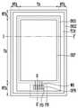
도 1은 본 발명의 일 실시예에 따른 표시 장치를 도시한 사시도이다.1 is a perspective view showing a display device according to an embodiment of the present invention.
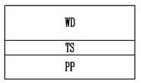
본 발명의 일 실시예에 따른 표시 장치는 영상을 나타내는 표시 패널(PP), 표시 패널(PP)의 전면에 제공된 터치 센서(TS)를 포함한다.A display device according to an embodiment of the present invention includes a display panel (PP) that displays an image, and a touch sensor (TS) provided on the front of the display panel (PP).
표시 패널(PP)은 전면으로 임의의 시각 정보, 예를 들어, 텍스트, 비디오, 사진, 2차원 또는 3차원 영상 등을 표시한다. 표시 패널(PP)의 종류는 영상을 표시하는 것으로서 특별히 한정되는 것은 아니다.The display panel PP displays arbitrary visual information, such as text, video, photos, 2-dimensional or 3-dimensional images, etc. on the front. The type of display panel PP is not particularly limited as it displays images.
표시 패널(PP)은 영상을 표시하는 것으로서 특별히 한정되는 것은 아니다. 본 발명의 일 실시예에서는 표시 패널(PP)이 유기 발광 표시 패널, 액정 표시 패널, 전기 영동 표시 패널, 전기 습윤 표시 패널, MEMS 표시 패널 중 하나일 수 있다. 그러나, 표시 패널(PP)의 종류는 이에 한정되는 것은 아니며, 본 발명의 개념에 부합되는 한도 내에서는 다른 표시 패널이 사용될 수 있다.The display panel PP displays images and is not particularly limited. In one embodiment of the present invention, the display panel PP may be one of an organic light emitting display panel, a liquid crystal display panel, an electrophoresis display panel, an electrowetting display panel, and a MEMS display panel. However, the type of display panel PP is not limited to this, and other display panels may be used within the scope consistent with the concept of the present invention.
표시 패널(PP)은 다양한 형상으로 마련될 수 있으며, 예를 들어, 서로 평행한 두 쌍의 변들을 가지는 직사각형의 판상으로 마련될 수 있다. 표시 패널(PP)이 직사각형의 판상으로 마련되는 경우, 두 쌍의 변들 중 어느 한 쌍의 변이 다른 한 쌍의 변보다 길게 제공될 수 있다. 본 발명의 일 실시예에서는 설명의 편의를 위해 표시 패널(PP)이 한 쌍의 장변과 한 쌍의 단변을 갖는 직사각 형상인 경우를 나타내었다.The display panel PP may be provided in various shapes, for example, in a rectangular plate shape with two pairs of sides parallel to each other. When the display panel PP is provided in a rectangular plate shape, one pair of sides may be longer than the other pair of sides. In one embodiment of the present invention, for convenience of explanation, the display panel PP is shown in a rectangular shape with a pair of long sides and a pair of short sides.
그러나, 표시 패널(PP)의 형상은 이에 한정되는 것은 아니며, 다양한 형상을 가질 수 있다. 예를 들어 표시 패널(PP)은 직선의 변을 포함하는 닫힌 형태의 다각형, 곡선으로 이루어진 변을 포함하는 원, 타원, 등, 직선과 곡선으로 이루어진 변을 포함하는 반원, 반타원, 등 다양한 형상으로 제공될 수 있다. 본 발명의 일 실시예에 있어서, 표시 패널(PP)이 직선으로 이루어진 변을 갖는 경우, 각 형상의 모서리 중 적어도 일부는 곡선으로 이루어질 수 있다. 예를 들어, 표시 패널(PP)이 직사각 형상을 가질 때, 서로 인접한 직선 변들이 만나는 부분이 소정 곡률을 가지는 곡선으로 대체될 수 있다. 즉, 직사각 형상의 꼭지점 부분은 서로 인접한 그 양단이 서로 인접한 두 직선 변들에 연결되고 소정의 곡률을 갖는 곡선 변으로 이루어질 수 있다. 곡률은 위치에 따라 달리 설정될 수 있다. 예를 들어, 곡률은 곡선이 시작되는 위치 및 곡선의 길이 등에 따라 변경될 수 있다.However, the shape of the display panel PP is not limited to this and may have various shapes. For example, the display panel (PP) can be of various shapes, such as a closed polygon with straight sides, a circle, ellipse, etc. with curved sides, a semicircle with straight and curved sides, a semi-ellipse, etc. can be provided. In one embodiment of the present invention, when the display panel PP has straight sides, at least some of the edges of each shape may be curved. For example, when the display panel PP has a rectangular shape, a portion where adjacent straight sides meet may be replaced with a curved line having a predetermined curvature. In other words, the vertices of the rectangular shape may be formed of curved sides where both adjacent ends are connected to two adjacent straight sides and have a predetermined curvature. The curvature may be set differently depending on the location. For example, curvature may change depending on the position where the curve starts and the length of the curve.
표시 패널(PP)는 전체 또는 적어도 일부가 가요성을 가질 수 있다. 예를 들어, 표시 패널(PP)는 전체 영역에서 가요성을 가질 수 있으며, 또는 가요성 영역에 대응하는 영역에서 가요성을 가질 수 있다.The display panel PP may be fully or at least partially flexible. For example, the display panel PP may have flexibility in the entire area, or may have flexibility in an area corresponding to the flexible area.
표시 패널(PP)은 화소(PXL)가 제공됨으로써 영상이 표시되는 표시 영역(DA)과 표시 영역(DA)의 적어도 일측에 위치한 비표시 영역(NDA)을 포함한다. 예를 들어, 비표시 영역(NDA)은 표시 영역(DA)을 둘러싸는 형태로 제공될 수 있다.The display panel PP includes a display area DA in which an image is displayed by providing pixels PXL, and a non-display area NDA located on at least one side of the display area DA. For example, the non-display area NDA may be provided to surround the display area DA.
표시 영역(DA)은 표시 패널(PP)의 형상에 대응하는 형상으로 제공될 수 있다. 예를 들어, 표시 영역(DA)은 표시 패널(PP)의 형상과 마찬가지로 직선의 변을 포함하는 닫힌 형태의 다각형, 곡선으로 이루어진 변을 포함하는 원, 타원, 등, 직선과 곡선으로 이루어진 변을 포함하는 반원, 반타원, 등 다양한 형상으로 제공될 수 있다. 본 발명의 일 실시예에 있어서, 표시 영역(DA)이 직사각 형상으로 제공될 수 있다.The display area DA may be provided in a shape corresponding to the shape of the display panel PP. For example, like the shape of the display panel PP, the display area DA has a closed polygon with straight sides, a circle with curved sides, an ellipse, etc., and the like with straight and curved sides. It can be provided in various shapes including semicircle, semiellipse, etc. In one embodiment of the present invention, the display area DA may be provided in a rectangular shape.
본 발명의 일 실시예에 따른 표시 장치에 있어서, 표시 영역(DA)에는 복수 개의 화소들(PXL)이 제공된다. 화소들(PXL)은 행과 열을 갖는 매트릭스 형상으로 배열될 수 있다. 그러나, 화소들(PXL)의 배열 방식은 이와 달리 설정될 수 있다. 본 발명의 일 실시예에 있어서, 화소들(PXL)은 각각 청색광, 녹색광, 및 적색광을 출사하는 청색 화소, 녹색 화소, 및 적색 화소 중 어느 하나일 수 있다. 그러나, 화소(PXL) 각각에서 출사하는 광의 컬러는 이에 한정되는 것은 아니며, 컬러와 다른 컬러의 광, 예를 들어, 마젠타색 광, 황색광, 시안색 광, 백색광 등이 출사될 수도 있다.In the display device according to an embodiment of the present invention, a plurality of pixels (PXL) are provided in the display area (DA). Pixels PXL may be arranged in a matrix shape with rows and columns. However, the arrangement method of the pixels (PXL) may be set differently. In one embodiment of the present invention, the pixels PXL may be any one of a blue pixel, a green pixel, and a red pixel that emit blue light, green light, and red light, respectively. However, the color of light emitted from each pixel PXL is not limited to this, and light of a different color, for example, magenta light, yellow light, cyan light, or white light, may be emitted.
터치 센서(TS)는 표시 패널(PP) 상에 제공될 수 있다. 상기 터치 센서(TS)는 사용자의 터치 시 터치 위치 및/또는 압력을 감지한다. 본 발명의 일 실시예에 있어서, 상기 터치 센서(TS)는 지문을 감지할 수 있다. 터치 센서는 다양한 방식의 센서일 수 있으며, 예를 들어, 정전 용량 방식, 저항막 방식, 압전 방식 등의 센서일 수 있다.The touch sensor TS may be provided on the display panel PP. The touch sensor TS detects the touch position and/or pressure when the user touches it. In one embodiment of the present invention, the touch sensor TS can detect a fingerprint. The touch sensor may be a sensor of various types, for example, a capacitive type, a resistive type, or a piezoelectric type sensor.
터치 센서(TS)는 표시 패널(PP)의 형상에 대응하는 판상으로 제공될 수 있으며, 표시 패널(PP)의 전면의 적어도 일부를 커버한다. 예를 들어, 표시 패널(PP)이 직사각 형상으로 제공되는 경우, 터치 센서(TS) 또한 이에 대응하는 직사각 형상으로 제공될 수 있다. 또는 표시 패널(PP)이 원형으로 제공되는 경우, 터치 센서(TS) 또한 이에 대응하는 원형으로 제공될 수 있다.The touch sensor TS may be provided in a plate shape corresponding to the shape of the display panel PP and covers at least a portion of the front surface of the display panel PP. For example, when the display panel PP is provided in a rectangular shape, the touch sensor TS may also be provided in a corresponding rectangular shape. Alternatively, when the display panel PP is provided in a circular shape, the touch sensor TS may also be provided in a corresponding circular shape.
터치 센서(TS)는 전체 또는 적어도 일부가 가요성을 가질 수 있다. 예를 들어, 터치 센서(TS)는 전체 영역에서 가요성을 가질 수 있으며, 또는 가요성 영역에 대응하는 영역에서 가요성을 가질 수 있다.The touch sensor TS may be fully or at least partially flexible. For example, the touch sensor TS may be flexible in its entire area, or may be flexible in a region corresponding to the flexible area.
터치 센서(TS)는 사용자의 터치를 감지할 수 있는 터치 영역(TA)과 터치 영역(TA)의 적어도 일측에 제공된 비터치 영역(NTA)을 포함할 수 있다. 본 발명의 일 실시예에 있어서, 상기 비터치 영역(NTA) 영역은 터치 영역(TA)를 둘러싸는 형태로 제공된다.The touch sensor TS may include a touch area (TA) capable of detecting a user's touch and a non-touch area (NTA) provided on at least one side of the touch area (TA). In one embodiment of the present invention, the non-touch area (NTA) area is provided in a form surrounding the touch area (TA).
터치 영역(TA)은 표시 영역(DA)에 대응할 수 있으며, 비터치 영역(NTA)은 비표시 영역(NDA)에 대응할 수 있다. 이에 따라, 평면 상에서 볼 때 터치 영역(TA)과 표시 영역(DA)은 서로 중첩할 수 있으며, 비터치 영역(NTA)과 비표시 영역(NDA) 또한 서로 대응할 수 있다. 그러나, 터치 영역(TA)과 비터치 영역(NTA)의 크기나 형상은 이에 한정되는 것은 아니다. 예를 들어, 터치 영역(TA)은 비표시 영역(NDA) 중 일부까지 연장될 수도 있다.The touch area (TA) may correspond to the display area (DA), and the non-touch area (NTA) may correspond to the non-display area (NDA). Accordingly, when viewed on a plane, the touch area (TA) and the display area (DA) may overlap each other, and the non-touch area (NTA) and the non-display area (NDA) may also correspond to each other. However, the size or shape of the touch area (TA) and the non-touch area (NTA) are not limited to these. For example, the touch area TA may extend to a portion of the non-display area NDA.
본 발명의 일 실시예에 있어서, 터치 센서(TS)는 비터치 영역(NTA)에 제공되며 적어도 1개 이상의 터치 전극에 전기적으로 연결된 인쇄 회로 기판(PB)을 포함할 수 있다.In one embodiment of the present invention, the touch sensor TS may be provided in the non-touch area NTA and may include a printed circuit board PB electrically connected to at least one touch electrode.
상기 인쇄 회로 기판에는 상기 터치 센서(TS)를 제어하는 센서 제어부가 제공될 수 있다. 상기 센서 제어부는 상기 터치 센서의 동작을 제어한다. 본 발명의 일 실시예에 있어서, 센서 제어부는 터치 센서(TS)의 정전 용량이나 저항 등을 감지함으로써 터치 위치 및/또는 사용자의 터치에 따른 터치 압력을 감지할 수 있다.The printed circuit board may be provided with a sensor control unit that controls the touch sensor TS. The sensor control unit controls the operation of the touch sensor. In one embodiment of the present invention, the sensor control unit may detect the touch position and/or the touch pressure according to the user's touch by detecting the capacitance or resistance of the touch sensor TS.
도시하지는 않았으나, 터치 센서(TS)와 표시 패널(PP) 사이에는 접착제가 제공될 수 있다. 접착제는 서로 인접한 두 구성 요소를 부착하기 위한 것으로서, 본 실시예에서는 터치 센서(TS)와 표시 패널(PP)를 부착한다. 본 발명의 일 실시예에 있어서 접착제는 서로 인접한 두 구성 요소를 하나로 붙여주는 역할과 동시에, 두 구성 요소에 인가되는 스트레스를 분산시킬 수 있다. 이를 위해 접착제는 소정 범위의 점착력과 탄성력을 가지는 것 중에서 선택될 수 있다. 본 명세서 내에서 언급되는 접착제는 이러한 기능을 만족하는 한도 내에서 다양한 것이 사용될 수 있으며, 다양한 두께로 제공될 수 있다.Although not shown, an adhesive may be provided between the touch sensor TS and the display panel PP. The adhesive is used to attach two adjacent components, and in this embodiment, the touch sensor (TS) and the display panel (PP) are attached. In one embodiment of the present invention, the adhesive serves to bond two adjacent components together and at the same time distributes stress applied to the two components. For this purpose, the adhesive may be selected from those having a predetermined range of adhesive force and elasticity. Adhesives mentioned in this specification may be used in a variety of ways as long as they satisfy these functions, and may be provided in various thicknesses.
본 발명의 실시예들에 있어서 "접착제"라고 하면 인접한 두 구성 요소 사이에 제공되어 상기 두 구성 요소를 연결하는 것으로써, 인접한 구성 요소를 물리적 화학적으로 결합시켜 분리되지 않는 상태가 되도록 접착하는 접착제 뿐만 아니라, 두 구성 요소를 물리적으로는 결합하되 화학적으로는 결합되지 않아 박리가 가능한 감압형 접착제(pressure-sensitive adhesive)를 포함하는 용어이다. 상기 접착제는 서로 인접한 구성 요소를 영구적으로 부착하느냐 이후 박리를 통해 제거하느냐의 여부에 따라 달리 사용될 수 있으며, 이하에서는 전자와 후자를 모두 접착제로 표시한다.In embodiments of the present invention, "adhesive" refers to an adhesive provided between two adjacent components to connect the two components, and is an adhesive that physically and chemically bonds the adjacent components so that they are not separated. Rather, it is a term that includes pressure-sensitive adhesives that physically bond two components but do not chemically bond them, making them removable. The adhesive may be used differently depending on whether adjacent components are permanently attached or removed through peeling, and hereinafter, both the former and the latter are referred to as adhesives.
상기 터치 센서(TS)와 표시 패널(PP) 사이의 접착제는 박리가 가능한 감압형 접착제일 수 있다.The adhesive between the touch sensor TS and the display panel PP may be a peelable pressure-sensitive adhesive.
접착제는 표시 패널(PP)로부터의 영상이 최대한 투과되는 광학적으로 투명한 접착제를 포함할 수 있다. 상기 접착제는 폴리에스테르, 폴리에테르, 폴리우레탄, 에폭시, 실리콘 및 아크릴로 이루어진 군에서 선택된 하나 이상의 물질을 포함할 수 있다.The adhesive may include an optically transparent adhesive that transmits images from the display panel PP as much as possible. The adhesive may include one or more materials selected from the group consisting of polyester, polyether, polyurethane, epoxy, silicone, and acrylic.
그러나, 터치 센서(TS)는 표시 패널(PP) 상에 접착제 없이 놓이거나, 표시 패널(PP) 상에 직접 놓일 수 있으며, 이 경우, 터치 센서(TS)와 표시 패널(PP) 사이에 접착제가 제공되지 않을 수 있다.However, the touch sensor TS may be placed on the display panel PP without adhesive, or may be placed directly on the display panel PP, in which case there is adhesive between the touch sensor TS and the display panel PP. It may not be provided.
이하, 도 2 및 도 3a 내지 도 3c를 참조하여 본 발명의 일 실시예에 따른 표시 장치에 대해서 설명하되 터치 센서(TS)를 중심으로 설명한다.Hereinafter, a display device according to an embodiment of the present invention will be described with reference to FIGS. 2 and 3A to 3C, focusing on the touch sensor TS.
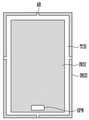
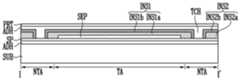
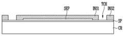
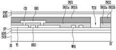
도 2는 본 발명의 일 실시예에 따른 터치 센서를 도시한 평면도이다. 도 3a은 도 2의 I-I'선에 따른 단면도, 도 3b는 도 2의 II-II'선에 따른 단면도이며, 도 3c는 터치 센서의 평면도로서 절연막만을 도시한 것이다.Figure 2 is a plan view showing a touch sensor according to an embodiment of the present invention. FIG. 3A is a cross-sectional view taken along line II-I' of FIG. 2, FIG. 3B is a cross-sectional view taken along line II-II' of FIG. 2, and FIG. 3C is a top view of the touch sensor, showing only the insulating film.
도 2, 도 3a 내지 도 3c을 참조하면, 터치 센서는 터치 영역(TA)과 상기 터치 영역(TA)을 둘러싸는 비터치 영역(NTA)을 포함하는 지지층(SP), 상기 지지층(SP) 상의 터치 영역(TA)에 제공된 센싱 전극부(SEP), 상기 센싱 전극부(SEP)에 연결된 배선(WR), 및 상기 터치 영역(TA) 및 상기 비터치 영역(NTA)의 일부를 커버하는 절연막(INS)을 포함한다.2 and 3A to 3C, the touch sensor includes a support layer (SP) including a touch area (TA) and a non-touch area (NTA) surrounding the touch area (TA), and a support layer (SP) on the support layer (SP). A sensing electrode portion (SEP) provided in the touch area (TA), a wiring (WR) connected to the sensing electrode portion (SEP), and an insulating film ( INS).
본 발명의 일 실시예에 있어서, 상기 지지층(SP)의 외측에는 상기 터치 센서(TS)가 부착되는 기판(SUB)이 제공될 수 있다.In one embodiment of the present invention, a substrate (SUB) to which the touch sensor (TS) is attached may be provided outside the support layer (SP).
상기 지지층(SP)은 사용자의 터치가 이루어지고, 그 터치를 감지하기 위한 센싱 전극부(SEP)가 형성된 터치 영역(TA)과, 상기 터치 영역(TA)의 적어도 일측에 위치한 비터치 영역(NTA)을 포함한다.The support layer (SP) includes a touch area (TA) where a user's touch is made and a sensing electrode portion (SEP) for detecting the touch is formed, and a non-touch area (NTA) located on at least one side of the touch area (TA). ) includes.
본 발명의 일 실시예에 있어서, 상기 터치 센서(TS)는 기판(SUB) 상에 제공되는 바, 이하, 적층된 순서를 따라 각 구성 요소를 설명한다.In one embodiment of the present invention, the touch sensor TS is provided on a substrate SUB. Hereinafter, each component will be described in stacking order.
상기 기판(SUB)은 그 상면에 터치 센서(TS)의 센싱 전극부(SEP)가 배치될 수 있는 것으로서, 특별히 한정되는 것은 아니다. 상기 기판(SUB)은 그 상면에 센싱 전극부(SEP)가 배치될 수 있는 다양한 구성 요소, 예를 들어, 표시 패널(PP)의 최상부에 제공된 봉지층, 편광 필름이나 위상차 필름과 같은 기능성 필름, 표시 패널(PP)의 전면에 배치되는 윈도우 등일 수도 있다. 또한, 상기 기판(SUB)은 절연 기판으로 제공될 수 있으며, 이 경우, 상기 절연 기판은 유리, 수지(resin) 등과 같은 절연성 재료로 이루어질 수 있다. 또한, 기판은 휘거나 접힘이 가능하도록 가요성(flexibility)을 갖는 재료로 이루어질 수 있고, 단층 구조 또는 다층 구조를 가질 수 있다. 상기 기판(SUB)은 폴리에틸렌테레프탈레이트, 폴리에틸렌이소프탈레이트, 폴리에틸렌나프탈레이트, 폴리부틸렌테레프탈레이트 등의 폴리에스테르계 수지; 디아세틸셀룰로오스, 트리아세틸셀룰로오스 등의 셀룰로오스계 수지; 폴리카보네이트계 수지; 폴리메틸(메타)아크릴레이트, 폴리에틸(메타)아크릴레이트 등의 아크릴계 수지; 폴리스티렌, 아크릴로니트릴-스티렌공중합체 등의 스티렌계 수지; 폴리에틸렌, 폴리프로필렌, 시클로계 또는 노보넨 구조를 갖는 폴리올레핀, 에틸렌-프로필렌 공중합체 등의 폴리올레핀계 수지; 염화비닐계 수지; 나일론, 방향족 폴리아미드 등의 아미드계 수지; 이미드계 수지; 폴리에테르술폰계 수지; 술폰계 수지; 폴리에테르에테르케톤계 수지; 황화 폴리페닐렌계 수지; 비닐알코올계 수지; 염화비닐리덴계 수지; 비닐부티랄계 수지; 알릴레이트계 수지; 폴리옥시메틸렌계 수지; 에폭시계 수지 등과 같은 열가소성 수지로 구성된 필름을 들 수 있으며, 상기 열가소성 수지의 블렌드물로 구성된 필름도 사용할 수 있다. 또한, (메타)아크릴계, 우레탄계, 아크릴우레탄계, 에폭시계, 실리콘계 등의 열경화성 수지 또는 자외선 경화형 수지로 된 필름을 이용할 수도 있다. 다만, 기판을 구성하는 재료는 다양하게 변화될 수 있으며, 유리 섬유 강화플라스틱(FRP, Fiber glass reinforced plastic) 등으로도 이루어질 수 있다.The substrate (SUB) can have the sensing electrode portion (SEP) of the touch sensor (TS) disposed on its upper surface, and is not particularly limited. The substrate (SUB) includes various components on which a sensing electrode portion (SEP) can be disposed, for example, an encapsulation layer provided on the top of the display panel (PP), a functional film such as a polarizing film or a retardation film, It may be a window or the like disposed in front of the display panel PP. Additionally, the substrate SUB may be provided as an insulating substrate. In this case, the insulating substrate may be made of an insulating material such as glass, resin, etc. Additionally, the substrate may be made of a material that has flexibility so that it can be bent or folded, and may have a single-layer structure or a multi-layer structure. The substrate (SUB) is a polyester resin such as polyethylene terephthalate, polyethylene isophthalate, polyethylene naphthalate, and polybutylene terephthalate; Cellulose-based resins such as diacetylcellulose and triacetylcellulose; polycarbonate-based resin; Acrylic resins such as polymethyl (meth)acrylate and polyethyl (meth)acrylate; Styrene-based resins such as polystyrene and acrylonitrile-styrene copolymer; Polyolefin resins such as polyethylene, polypropylene, polyolefins with cyclo- or norbornene structures, and ethylene-propylene copolymers; Vinyl chloride-based resin; Amide resins such as nylon and aromatic polyamide; imide-based resin; polyethersulfone-based resin; Sulfone-based resin; polyetheretherketone-based resin; Sulfated polyphenylene-based resin; Vinyl alcohol-based resin; Vinylidene chloride-based resin; Vinyl butyral resin; Allylate resin; polyoxymethylene-based resin; A film composed of a thermoplastic resin such as an epoxy resin may be used, and a film composed of a blend of the thermoplastic resin may also be used. In addition, films made of thermosetting resins such as (meth)acrylic, urethane, acrylic urethane, epoxy, and silicone or ultraviolet curable resins may be used. However, the materials that make up the substrate can vary in various ways, and can also be made of fiber glass reinforced plastic (FRP).
상기 지지층(SP)은 상기 기판(SUB) 상에 제공된다. 상기 지지층(SP)에는 후술할 센싱 전극부(SEP), 배선(WR), 및 패드(PD) 등이 그 상면에 직접적으로 형성된다.The support layer (SP) is provided on the substrate (SUB). A sensing electrode part (SEP), a wire (WR), and a pad (PD), which will be described later, are formed directly on the support layer (SP).
상기 지지층(SP)은 가요성(flexibility)을 갖는 유기 재료로 이루어질 수 있고, 단층 구조 또는 다층 구조를 가질 수 있다. 예를 들어, 지지층(SP)은 상기 기판(SUB)을 구성하는 재료 중에서 선택될 수 있으며, 상기 기판(SUB)과 상기 지지층(SP)은 서로 동일하거나 서로 다른 재료로 이루어질 수 있다. 본 발명의 일 실시예에 있어서, 상기 지지층(SP)은 폴리스티렌(polystyrene), 폴리비닐알코올(polyvinyl alcohol), 폴리메틸메타크릴레이트(Polymethyl methacrylate), 폴리에테르술폰(polyethersulfone), 폴리아크릴레이트(polyacrylate), 폴리에테르이미드(polyetherimide), 폴리에틸렌 나프탈레이트(polyethylene naphthalate), 폴리에틸렌 테레프탈레이트(polyethylene terephthalate), 폴리페닐렌 설파이드(polyphenylene sulfide), 폴리아릴레이트(polyarylate), 폴리이미드(polyimide), 폴리카보네이트(polycarbonate), 트리아세테이트 셀룰로오스(WRiacetate cellulose), 셀룰로오스아세테이트 프로피오네이트(cellulose acetate propionate), 폴리아미드(polyamide), 폴리아믹산(polyamic acid), 폴리에틸렌(polyethylene), 폴리스티렌(polystyrene), 폴리노르보르넨(polynorbornene), 페닐말레이미드 공중합체(polymaleimide copolymer), 폴리아조벤젠(polyazobenzene), 폴리페닐렌프탈아미드(polyphenylenephthalamide), 폴리에스테르(polyester), 신나메이트(cinnamate)계 고분자, 쿠마린(coumarin)계 고분자, 프탈이미딘(phthalimidine)계 고분자, 칼콘(chalcone)계 고분자, 시클로폴리올레핀계 고분자 및 방향족 아세틸렌계 고분자 물질 중 적어도 어느 하나를 포함할 수 있다.The support layer SP may be made of an organic material with flexibility and may have a single-layer structure or a multi-layer structure. For example, the support layer SP may be selected from materials constituting the substrate SUB, and the substrate SUB and the support layer SP may be made of the same or different materials. In one embodiment of the present invention, the support layer (SP) is made of polystyrene, polyvinyl alcohol, polymethyl methacrylate, polyethersulfone, and polyacrylate. ), polyetherimide, polyethylene naphthalate, polyethylene terephthalate, polyphenylene sulfide, polyarylate, polyimide, polycarbonate ( polycarbonate, triacetate cellulose, cellulose acetate propionate, polyamide, polyamic acid, polyethylene, polystyrene, polynorbornene ( polynorbornene, phenylmaleimide copolymer, polyazobenzene, polyphenylenephthalamide, polyester, cinnamate polymer, coumarin polymer, phthalate It may include at least one of phthalimidine-based polymers, chalcone-based polymers, cyclopolyolefin-based polymers, and aromatic acetylene-based polymers.
상기 지지층(SP)은 재료에 따라 다양한 굴절률을 가질 수 있다. 상기 지지층(SP)이 단층 또는 복층으로 형성되는 경우, 상기 지지층(SP)은 굴절률 매칭층(Index Matching Layer)을 더 포함하거나, 그 자체가 굴절률 매칭층으로 이용될 수 있다. 또는 상기 지지층(SP)은 상기 굴절률 매칭층은 고굴절 재료, 예를 들어 나노파티클이 포함될 수 있다.The support layer (SP) may have various refractive indices depending on the material. When the support layer (SP) is formed as a single layer or a double layer, the support layer (SP) may further include a refractive index matching layer (Index Matching Layer) or may itself be used as a refractive index matching layer. Alternatively, the support layer (SP) and the refractive index matching layer may include a high refractive index material, for example, nanoparticles.
상기 지지층(SP)은 터치 센서(TS) 제조시 분리층으로 기능하는 바, 이에 대해서는 터치 센서(TS)의 제조 방법에서 후술한다.The support layer (SP) functions as a separation layer when manufacturing the touch sensor (TS), which will be described later in the manufacturing method of the touch sensor (TS).
상기 지지층(SP)과 상기 기판(SUB) 사이에는 상기 기판(SUB)과 상기 지지층(SP)을 서로 연결하는 접착제(ADH)가 제공될 수 있다. 상기 접착제(ADH)은 표시 패널(PP)로부터의 영상이 최대한 투과되는 광학적으로 투명한 접착제(ADH)일 수 있다. 여기서, 상기 기판(SUB)와 상기 지지층(SP) 사이에 제공된 접착제(ADH)는 자외선과 같은 광에 의해 경화되는 광경화 접착제일 수 있으며, 경화를 통해 상기 기판(SUB)와 상기 지지층(SP)을 영구적으로 접착시킬 수 있다.An adhesive (ADH) may be provided between the support layer (SP) and the substrate (SUB) to connect the substrate (SUB) and the support layer (SP) to each other. The adhesive (ADH) may be an optically transparent adhesive (ADH) through which images from the display panel (PP) can be transmitted as much as possible. Here, the adhesive (ADH) provided between the substrate (SUB) and the support layer (SP) may be a photocurable adhesive that is cured by light such as ultraviolet rays, and the substrate (SUB) and the support layer (SP) are bonded through curing. can be permanently bonded.
상기 센싱 전극부(SEP)는 지지층(SP)의 터치 영역(TA)에 제공되며, 적어도 1개 이상의 터치 전극을 포함한다.The sensing electrode portion (SEP) is provided in the touch area (TA) of the support layer (SP) and includes at least one touch electrode.
상기 배선(WR)은 센싱 전극부(SEP)에 신호를 제공하거나, 센싱 전극부(SEP)로부터의 신호를 터치 제어부에 연결하기 위한 것으로서, 센싱 전극부(SEP)에 연결된다. 상기 배선(WR)은 비터치 영역(NTA)에 제공되며, 일부가 상기 센싱 전극부(SEP)에 연결되도록 터치 영역(TA)에 제공될 수 있다. 상기 배선(WR)에서 센싱 전극부(SEP)에 연결되지 않은 다른 측 단부에는 인쇄 회로 기판 등에 연결되기 위한 패드(PD)가 제공될 수 있다.The wiring WR is used to provide a signal to the sensing electrode unit SEP or to connect a signal from the sensing electrode unit SEP to the touch control unit, and is connected to the sensing electrode unit SEP. The wiring WR may be provided in the non-touch area NTA, and a portion of the wire WR may be provided in the touch area TA so as to be connected to the sensing electrode portion SEP. A pad PD for connection to a printed circuit board, etc. may be provided at the other end of the wiring WR that is not connected to the sensing electrode portion SEP.
상기 센싱 전극부(SEP) 및 배선(WR)은 터치 센서(TS)의 종류에 따라 다양한 형태로 제공될 수 있다. 예를 들어, 상기 센싱 전극부(SEP), 배선(WR), 및 패드(PD)는 상호 정전 용량 방식 또는 자기 정전 용량 방식으로 터치를 감지하도록 구현될 수 있다. 이 경우, 상기 터치 전극들은 다각형으로 구현될 수 있는 바, 예를 들어, 직사각형, 사다리꼴, 마름모 등의 사각 형상을 가질 수 있다. 또는 터치 전극들 각각은 원형으로 구현될 수 있다. 또는 터치 전극들 각각이 일 방향으로 연장되어 전체적으로 스트라이프 형상을 이룰 수도 있다. 터치 전극들이 일 방향으로 연장되는 경우, 연장되는 방향은 기판의 장변 방향, 또는 단변 방향, 또는 경사진 방향 등 다양하게 변형될 수 있다.The sensing electrode portion (SEP) and wiring (WR) may be provided in various forms depending on the type of touch sensor (TS). For example, the sensing electrode portion (SEP), wiring (WR), and pad (PD) may be implemented to sense a touch using a mutual capacitance method or a self-capacitance method. In this case, the touch electrodes may be implemented as polygons, for example, may have a square shape such as a rectangle, trapezoid, or diamond. Alternatively, each of the touch electrodes may be implemented in a circular shape. Alternatively, each of the touch electrodes may extend in one direction to form an overall stripe shape. When the touch electrodes extend in one direction, the direction in which they extend may be changed in various ways, such as a long side direction of the substrate, a short side direction, or an inclined direction.
상기 센싱 전극부(SEP), 배선(WR), 및/또는 패드(PD)는 금속, 금속 산화물, 전도성 고분자, 금속 나노와이어, 탄소나노튜브, 그래핀 등의 도전성 물질 중 적어도 하나로 이루어질 수 있다.The sensing electrode portion (SEP), wiring (WR), and/or pad (PD) may be made of at least one of conductive materials such as metal, metal oxide, conductive polymer, metal nanowire, carbon nanotube, and graphene.
상기 금속은 구리, 은, 금, 백금, 팔라듐, 니켈, 주석, 알루미늄, 코발트, 로듐, 이리듐, 철, 루테늄, 오스뮴, 망간, 몰리브덴, 텅스텐, 니오브, 탄탈, 타이타늄, 비스머스, 안티몬, 납, 아연, 및 이들의 합금 중 적어도 하나를 포함할 수 있다.The metals include copper, silver, gold, platinum, palladium, nickel, tin, aluminum, cobalt, rhodium, iridium, iron, ruthenium, osmium, manganese, molybdenum, tungsten, niobium, tantalum, titanium, bismuth, antimony, lead, It may contain at least one of zinc and alloys thereof.
본 발명의 일 실시예에 있어서, 상기 센싱 전극부(SEP), 배선(WR), 및 패드(PD) 중 적어도 하나를 이루는 재료는 은/팔라듐/구리 합금을 포함할 수 있다. 또는 상기 센싱 전극부(SEP), 배선(WR), 및 패드(PD) 중 적어도 하나를 이루는 재료는 니켈/구리 합금일 수 있다.In one embodiment of the present invention, a material forming at least one of the sensing electrode portion (SEP), wiring (WR), and pad (PD) may include a silver/palladium/copper alloy. Alternatively, the material forming at least one of the sensing electrode portion (SEP), wiring (WR), and pad (PD) may be a nickel/copper alloy.
상기 도전성 금속 산화물은 상술한 금속의 산화물 이외에, ITO(Indium Tin Oxide), IZO(Indium Zinc Oxide), AZO(Antimony Zinc Oxide), ITZO(Indium Tin Zinc Oxide), ZnO(Zinc Oxide), SnO2(Tin Oxide)와 같은 투명 금속 화합물 중 적어도 하나를 포함할 수 있다. 상기 도전성 고분자는 폴리티오펜계, 폴리피롤계, 폴리아닐린계, 폴리아세틸렌계, 폴리페닐렌계 화합물 및 이들의 혼합물 등을 들 수 있으며, 특히 폴리티오펜계 중에서도 PEDOT/PSS 화합물을 포함할 수 있다.In addition to the above-mentioned metal oxides, the conductive metal oxide includes ITO (Indium Tin Oxide), IZO (Indium Zinc Oxide), AZO (Antimony Zinc Oxide), ITZO (Indium Tin Zinc Oxide), ZnO (Zinc Oxide), and SnO2 (Tin Oxide). It may contain at least one of transparent metal compounds such as oxide). The conductive polymer may include polythiophene-based, polypyrrole-based, polyaniline-based, polyacetylene-based, polyphenylene-based compounds, and mixtures thereof. In particular, among polythiophene-based compounds, it may include PEDOT/PSS compounds.
도면에서 센싱 전극부(SEP)가 단층으로 도시되었으나 이는 설명의 편의를 위한 것으로서, 상기 센싱 전극부(SEP), 배선(WR), 및 패드(PD)는 단층 또는 복층으로 제공될 수 있다. 본 발명의 일 실시예에 있어서, 상기 센싱 전극부(SEP), 배선(WR), 및 패드(PD)는 각각이 개수의 층으로 이루어질 수 있으나, 이에 한정되는 것은 아니며, 서로 다른 개수의 층으로 이루어질 수도 있다.In the drawing, the sensing electrode portion (SEP) is shown as a single layer, but this is for convenience of explanation. The sensing electrode portion (SEP), wiring (WR), and pad (PD) may be provided as a single layer or a multiple layer. In one embodiment of the present invention, the sensing electrode portion (SEP), wiring (WR), and pad (PD) may each be made of a number of layers, but are not limited thereto, and may be made of different numbers of layers. It may come true.
예를 들어, 센싱 전극부(SEP)는 단일층으로 이루어질 수 있으며, 배선(WR) 및/또는 패드(PD)는 복층으로 이루어질 수 있다. 또는 센싱 전극부(SEP)의 일부는 단일층으로, 다른 일부는 복층으로 이루어질 수 있으며, 배선(WR) 및/또는 패드(PD)는 복층으로 이루어질 수 있다. 또는, 센싱 전극부(SEP)의 일부는 단일층으로, 다른 일부는 복층으로 이루어질 수 있으며, 배선(WR) 및/또는 패드(PD)는 단일층으로 이루어질 수 있다.For example, the sensing electrode part (SEP) may be made of a single layer, and the wiring (WR) and/or pad (PD) may be made of multiple layers. Alternatively, part of the sensing electrode part (SEP) may be made of a single layer, another part may be made of a multiple layer, and the wiring (WR) and/or the pad (PD) may be made of a multiple layer. Alternatively, part of the sensing electrode part (SEP) may be made of a single layer, another part may be made of a multiple layer, and the wire (WR) and/or pad (PD) may be made of a single layer.
본 발명의 일 실시예에 있어서, 상기 센싱 전극부(SEP), 배선(WR), 및 패드(PD)는 각각이 동일한 재료로 이루어질 수 있으나, 이에 한정되는 것은 아니며, 서로 다른 재료로 이루어질 수도 있다.In one embodiment of the present invention, the sensing electrode portion (SEP), wiring (WR), and pad (PD) may each be made of the same material, but are not limited thereto and may be made of different materials. .
예를 들어, 센싱 전극부(SEP), 배선(WR) 및 패드(PD)는 도전성 금속 산화물로만 이루어질 수 있다. 또는 센싱 전극부(SEP)는 도전성 금속 산화물로, 배선(WR) 및/또는 패드(PD)는 금속으로 이루어질 수 있다. 또는, 센싱 전극부(SEP)는 도전성 금속 산화물로, 배선(WR) 및/또는 패드(PD)는 도전성 금속 산화물과 금속 합금으로 이루어질 수 있다. 또는 센싱 전극부(SEP)는 나노와이어로, 배선(WR) 및/또는 패드(PD)는 금속으로 이루어질 수 있다.For example, the sensing electrode part (SEP), wiring (WR), and pad (PD) may be made only of conductive metal oxide. Alternatively, the sensing electrode portion (SEP) may be made of conductive metal oxide, and the wiring (WR) and/or pad (PD) may be made of metal. Alternatively, the sensing electrode portion (SEP) may be made of a conductive metal oxide, and the wiring (WR) and/or the pad (PD) may be made of a conductive metal oxide and a metal alloy. Alternatively, the sensing electrode part (SEP) may be made of nanowire, and the wiring (WR) and/or pad (PD) may be made of metal.
상기 절연막(INS)은 기판(SUB) 상에 제공된다. 상기 절연막(INS)은 특히 상기 터치 영역(TA)에서 상기 센싱 전극부(SEP)를 커버하며, 상기 비터치 영역(NTA)에서 상기 지지층(SP)의 일부를 커버한다. 상기 절연막(INS)는 다양한 두께로 형성될 수 있다. 예를 들어, 상기 절연막(INS)는 약 1 마이크로미터 내지 약 10 마이크로미터의 두께로 제공될 수 있다. 본 발명의 일 실시예에 있어서, 상기 절연막은 약 3 내지 약 4 마이크로 미터의 두께로 제공될 수 있다.The insulating film (INS) is provided on the substrate (SUB). The insulating film (INS) particularly covers the sensing electrode portion (SEP) in the touch area (TA) and a portion of the support layer (SP) in the non-touch area (NTA). The insulating film (INS) may be formed in various thicknesses. For example, the insulating film (INS) may be provided with a thickness of about 1 micrometer to about 10 micrometers. In one embodiment of the present invention, the insulating film may be provided with a thickness of about 3 to about 4 micrometers.
상기 절연막(INS)은 상기 배선(WR)의 단부에 연결된 패드(PD)를 노출하는 개구(OPN)를 갖는다. 즉, 상기 개구(OPN)는 패드(PD)가 제공된 영역에 제공된다. 본 실시예에서는 개구(OPN)가 사각형 형태로 하나로 제공된 것을 도시하였으나 이에 한정되는 것은 아니며, 패드(PD)를 충분히 노출하는 한도 내에서 다른 형상과 다른 개수로 제공될 수 있다. 상기 패드(PD)는 상기 개구(OPN)를 통해 별도의 배선, 가요성 인쇄 회로 기판, 테이프 캐리어 패키지, 커넥터, 또는 칩 온 필름 등을 통해 센서 제어부와 연결될 수 있다. 예를 들어 상기 패드(PD)는 상기 개구(OPN)에 배치된 이방성 도전 필름 등을 통해 다른 구성 요소와 연결될 수 있다.The insulating film INS has an opening OPN exposing the pad PD connected to the end of the wiring WR. That is, the opening OPN is provided in an area where the pad PD is provided. In this embodiment, it is shown that the opening OPN is provided in a rectangular shape, but the opening OPN is not limited thereto, and may be provided in different shapes and in different numbers within the limit of sufficiently exposing the pad PD. The pad PD may be connected to the sensor control unit through the opening OPN through a separate wire, flexible printed circuit board, tape carrier package, connector, or chip-on-film. For example, the pad PD may be connected to other components through an anisotropic conductive film disposed in the opening OPN.
비터치 영역(NTA)에서 상기 절연막(INS)의 일부가 제거된 트렌치(TCH)를 갖는다. 상기 트렌치(TCH)에 해당하는 영역의 지지층(SP) 상에는 절연막(INS)이 제공되지 않으므로 지지층(SP)의 상면이 노출된다. In the non-touch area (NTA), there is a trench (TCH) in which a portion of the insulating film (INS) is removed. Since the insulating film INS is not provided on the support layer SP in the area corresponding to the trench TCH, the top surface of the support layer SP is exposed.
상기 트렌치(TCH)에 해당하는 영역의 지지층(SP) 상에는 절연막(INS)이 제공되지 않는다. 상기 트렌치(TCH)의 폭은 절연막의 높이에 따라 달라질 수 있으나, 약 30 마이크로미터 내지 약 70마이크로미터일수 있으며, 본 발명의 일 실시예에서는 약 50마이크로미터일 수 있다. 트렌치(TCH)가 상기 범위의 폭을 갖도록 형성함으로써, 후술하는 롤-투-롤 압착 전사 공정에서 절연막이 제공되지 않은 부분의 접착제(ADH) 미도포 또는 불충분 도포를 방지할 수 있다. 아울러, 트렌치(TCH)가 상기 범위의 폭을 가짐에 따라, 트렌치(TCH) 부분에 기포가 발생하는 것을 막을 수 있다.An insulating film (INS) is not provided on the support layer (SP) in the area corresponding to the trench (TCH). The width of the trench (TCH) may vary depending on the height of the insulating film, but may be about 30 micrometers to about 70 micrometers, and in one embodiment of the present invention, may be about 50 micrometers. By forming the trench (TCH) to have a width within the above range, it is possible to prevent non-application or insufficient application of adhesive (ADH) to areas where an insulating film is not provided in the roll-to-roll compression transfer process described later. In addition, as the trench (TCH) has a width within the above range, it is possible to prevent bubbles from occurring in the trench (TCH) portion.
상기 트렌치(TCH)는 평면 상에서 볼 때 상기 터치 영역(TA)의 둘레를 따라 제공된다. 이에 따라, 상기 절연막(INS)은 상기 트렌치(TCH)를 사이에 두고 두 개의 절연막(INS1, INS2)으로 이격될 수 있다. 상기 트렌치(TCH)를 사이에 두고 서로 이격된 절연막(INS1, INS2) 중 터치 영역(TA)을 커버하는 절연막을 제1 절연막(INS1)이라고 하고, 나머지 하나의 절연막을 제2 절연막(INS2)이라고 하면, 상기 제2 절연막(INS2)은 상기 제1 절연막(INS1)의 외측에서 상기 제1 절연막(INS1)의 둘레를 따라 제공된다.The trench (TCH) is provided along the perimeter of the touch area (TA) when viewed in plan. Accordingly, the insulating layer INS may be separated into two insulating layers INS1 and INS2 with the trench TCH in between. Among the insulating films INS1 and INS2 spaced apart from each other with the trench TCH in between, the insulating film covering the touch area TA is called the first insulating film INS1, and the remaining insulating film is called the second insulating film INS2. In this case, the second insulating film INS2 is provided outside the first insulating film INS1 and along the perimeter of the first insulating film INS1.
상기 제1 절연막(INS1)과 상기 제2 절연막(INS2)은 실질적으로 동일한 높이를 갖는다. 상기 제2 절연막(INS2)은 비터치 영역(NTA) 단부에서의 절연막(INS)의 높이를 유지하기 위한 스페이서로 작용하는 바, 터치 센서의 제조 공정 중 롤-투-롤 방식으로 터치 센서(TS)를 압착 전사하는 과정에서 접착제(ADH)의 미도포 또는 불충분 도포를 방지하기 위한 것이다.The first insulating layer INS1 and the second insulating layer INS2 have substantially the same height. The second insulating film (INS2) acts as a spacer to maintain the height of the insulating film (INS) at the end of the non-touch area (NTA), and is used in the touch sensor (TS) in a roll-to-roll manner during the manufacturing process of the touch sensor. ) This is to prevent non-application or insufficient application of adhesive (ADH) during the process of pressing and transferring.
상기 절연막(INS)은 또한 상기 패드(PD)가 형성된 영역에서 상기 패드(PD)의 상면을 노출하는 개구(OPN)를 갖는다. 상기 개구(OPN)는 비터치 영역(NTA)의 상기 제1 절연막(INS1) 내에 제공될 수 있다. 상기 개구(OPN)를 통해 상기 패드(PD)는 다른 별도의 배선(WR), 가요성 인쇄 회로 기판, 테이프 캐리어 패키지, 커넥터, 또는 칩 온 필름 등을 통해 센서 제어부와 연결될 수 있다.The insulating film INS also has an opening OPN exposing the top surface of the pad PD in the area where the pad PD is formed. The opening OPN may be provided in the first insulating layer INS1 in the non-touch area NTA. Through the opening OPN, the pad PD may be connected to the sensor control unit through another separate wiring WR, a flexible printed circuit board, a tape carrier package, a connector, or a chip-on-film.
상기 절연막(INS)은 유기물, 및 무기물 중 적어도 하나를 포함할 수 있으며, 단층 또는 다층 구조를 가질 수 있다. 본 발명의 일 실시예에 있어서, 상기 유기막의 재료로는 상기 지지층을 구성하는 유기 재료가 사용될 수 있다. 본 발명의 일 실시예에 있어서, 상기 절연막의 재료로는 상기 유기 재료 이외에도 테프론과 같은 불소계 탄소 화합물, 폴리에폭시, 벤조시클로부텐 등과 같은 유기 재료를 포함할 수 있으며, 무기막의 재료로는 폴리실록산, 실리콘 질화물, 실리콘 산화물, 알루미늄 산화물을 포함한 금속 산화물 등의 무기 절연 물질이 이용될 수 있다.The insulating film (INS) may include at least one of an organic material and an inorganic material, and may have a single-layer or multi-layer structure. In one embodiment of the present invention, an organic material constituting the support layer may be used as a material for the organic layer. In one embodiment of the present invention, the material of the insulating film may include organic materials such as fluorine-based carbon compounds such as Teflon, polyepoxy, and benzocyclobutene in addition to the organic materials, and the material of the inorganic film may include polysiloxane and silicon. Inorganic insulating materials such as nitride, silicon oxide, and metal oxides including aluminum oxide may be used.
본 발명의 일 실시예에 있어서, 상기 절연막(INS) 상에는 접착제(ADH)를 사이에 두고 보호 필름(PRT)이 제공될 수 있다. 본 실시예에 있어서, 접착제(ADH)의 두께가 보호 필름(PRT)의 두께와 크게 차이나지 않도록 도시되었으나, 이는 설명의 편의를 위한 것으로, 실제 제품에서는 보호 필름(PRT)의 두께가 접착제(ADH)의 두께보다 두꺼울 수 있다.In one embodiment of the present invention, a protective film (PRT) may be provided on the insulating film (INS) with an adhesive (ADH) interposed therebetween. In this embodiment, the thickness of the adhesive (ADH) is shown to be not significantly different from the thickness of the protective film (PRT), but this is for convenience of explanation. In the actual product, the thickness of the protective film (PRT) is less than that of the adhesive (ADH). It may be thicker than the thickness of .
상기 보호 필름(PRT)은 상기 터치 센서(TS)를 제조하는 공정 중, 및/또는 상기 터치 센서(TS)의 제조 후 사용자에게 전달되기 전까지, 상기 터치 센서(TS)를 보호하기 위한 것으로서, 상기 터치 센서(TS)는 완제품 또는 완제품을 제조하기 위한 중간 단계의 제품일 수 있다.The protective film (PRT) is used to protect the touch sensor (TS) during the process of manufacturing the touch sensor (TS) and/or after manufacturing the touch sensor (TS) until it is delivered to the user. A touch sensor (TS) may be a finished product or an intermediate product for manufacturing a finished product.
상기 접착제(ADH)는 상기 터치 센서(TS)의 표면을 보호하는 보호 필름(PRT)에 제공되어 상기 표시 장치의 서로 인접한 다른 구성 요소들과의 사이에서 구성 요소들 사이를 접착시키는 접착제(ADH)로 사용될 수 있다. 상기 접착제(ADH)는 폴리에스테르, 폴리에테르, 폴리우레탄, 에폭시, 실리콘 및 아크릴로 이루어진 군에서 선택된 하나 이상의 물질을 포함할 수 있다.The adhesive (ADH) is provided on the protective film (PRT) that protects the surface of the touch sensor (TS) and adheres the components to other adjacent components of the display device. It can be used as The adhesive (ADH) may include one or more materials selected from the group consisting of polyester, polyether, polyurethane, epoxy, silicone, and acrylic.
상기 절연막(INS)과 상기 보호 필름(PRT) 사이의 접착제(ADH)는 두 구성 요소를 물리적으로는 결합하되 화학적으로는 결합되지 않아 박리가 가능한 감압형 접착제일 수 있다.The adhesive (ADH) between the insulating film (INS) and the protective film (PRT) may be a pressure-sensitive adhesive that physically bonds the two components but does not chemically bond them, allowing for peeling.
상기 보호 필름(PRT)은 피착체의 일면에 점착되어 피착체를 보호한다. 상기 보호 필름(PRT)은 상기 터치 센서(TS)가 다른 구성 요소에 부착될 때 제거될 수 있다. 상기 접착제(ADH)는 상기 보호 필름(PRT)이 제거될 때 상기 보호 필름(PRT)과 함께 동시에 제거될 수 있다. 패드(PD)는 상기 보호 필름(PRT)과 상기 접착제(ADH)가 동시에 제거된 후, 별도의 배선(WR), 가요성 인쇄 회로 기판, 테이프 캐리어 패키지, 커넥터, 또는 칩 온 필름 등과 연결될 수 있다.The protective film (PRT) is adhered to one side of the adherend and protects the adherend. The protective film (PRT) may be removed when the touch sensor (TS) is attached to another component. The adhesive (ADH) may be removed simultaneously with the protective film (PRT) when the protective film (PRT) is removed. After the protective film (PRT) and the adhesive (ADH) are simultaneously removed, the pad (PD) may be connected to a separate wiring (WR), flexible printed circuit board, tape carrier package, connector, or chip-on-film. .
다만, 상기 보호 필름(PRT)만 제거되고 상기 접착제(ADH)는 상기 터치 센서 상에 그대로 남아 있을 수 있으며, 상기 접착제(ADH) 상에 다른 구성 요소가 부착될 수 있다. 즉, 상기 보호 필름(PRT)이 제거됨으로써 상기 접착제(ADH)층의 일면이 노출되며, 상기 노출된 접착제(ADH)층을 다른 구성 요소에 부착시킬 수 있다. 이 경우, 상기 보호 필름(PRT)과 상기 접착제(ADH)는 상기 패드(PD)를 제외한 부분에만 제공될 수 있다.However, only the protective film (PRT) may be removed and the adhesive (ADH) may remain on the touch sensor, and other components may be attached to the adhesive (ADH). That is, when the protective film (PRT) is removed, one side of the adhesive (ADH) layer is exposed, and the exposed adhesive (ADH) layer can be attached to another component. In this case, the protective film (PRT) and the adhesive (ADH) may be provided only in areas excluding the pad (PD).
상기 보호 필름(PRT)은 피착체를 보호하기 위한 것이면 족하며, 특별히 한정되는 것은 아니다. 상기 보호 필름(PRT)은 예를 들어, 금속 시트, 유기 고분자 시트, 고무 시트, 등 다양한 물질로 이루어질 수 있다.The protective film (PRT) is sufficient as long as it protects the adherend, and is not particularly limited. The protective film (PRT) may be made of various materials, such as a metal sheet, an organic polymer sheet, a rubber sheet, etc.
본 발명의 일 실시예에 따른 보호 필름(PRT)은 유기 고분자로 이루어질 수 있다. 상기 유기 고분자는, 예를 들어, 폴리에틸렌, 폴리프로필렌, 에틸렌-프로필렌 공중합체, 에틸렌-아세트산비닐 공중합체, 올레핀계 중합체, 폴리에틸렌테레프탈레이트, 폴리에틸렌나프탈레이트, 폴리부틸렌테레프탈레이트, 폴리카르보네이트, 폴리염화비닐, 아세트산비닐계 중합체, 폴리페닐렌술피드; 폴리아미드(나일론), 폴리아미드, 폴리이미드, 폴리에테르에테르케톤, 폴리에테르 중 적어도 1종을 포함할 수 있으나, 이에 한정되는 것은 아니다. 상기 보호 필름(PRT)은 피착체를 보호하는 한도 내에서 상술한 기판(SUB)의 재료, 지지층(SP)의 재료, 또는 절연막(INS) 재료 등이 사용될 수 있음은 물론이다.The protective film (PRT) according to an embodiment of the present invention may be made of an organic polymer. The organic polymers include, for example, polyethylene, polypropylene, ethylene-propylene copolymer, ethylene-vinyl acetate copolymer, olefin-based polymer, polyethylene terephthalate, polyethylene naphthalate, polybutylene terephthalate, polycarbonate, polyvinyl chloride, vinyl acetate-based polymer, polyphenylene sulfide; It may include at least one of polyamide (nylon), polyamide, polyimide, polyetheretherketone, and polyether, but is not limited thereto. Of course, the protective film (PRT) may be made of the above-described substrate (SUB) material, support layer (SP) material, or insulating film (INS) material, etc., as long as it protects the adherend.
본 발명의 일 실시예에 따른 터치 센서에 있어서, 트렌치(TCH)를 갖는 절연막(INS)은 평면 상에서 볼 때 다양한 형태로 제공될 수 있다. 이하의 실시예에서는 설명의 중복을 피하기 위해 상술한 실시예와 다른 점을 위주로 설명한다. 설명하지 않은 부분은 상술한 실시예에 따른다.In the touch sensor according to an embodiment of the present invention, the insulating film (INS) having a trench (TCH) may be provided in various shapes when viewed from a plan view. In the following embodiments, differences from the above-described embodiments will be mainly described to avoid duplication of explanation. Parts not explained follow the above-described embodiment.
도 4a 및 도 4b는 본 발명의 일 실시예들에 따른 터치 센서를 도시한 평면도들이다.Figures 4a and 4b are plan views showing a touch sensor according to one embodiment of the present invention.
도 4a를 참조하면, 절연막은 비터치 영역(NTA)에서 절연막의 일부가 제거된 트렌치(TCH)를 가지며, 상기 트렌치(TCH)는 복수 개로 제공될 수 있다. 본 실시예에서는 트렌치(TCH)가 두 개로 형성된 것이 일 예로서 도시되었다.Referring to FIG. 4A, the insulating film has a trench (TCH) in which a portion of the insulating film is removed from the non-touch area (NTA), and the trenches (TCH) may be provided in plural numbers. In this embodiment, two trenches (TCH) are shown as an example.
상기 트렌치(TCH)에 해당하는 영역의 지지층(SP) 상에는 절연막이 제공되지 않는다. 상기 트렌치(TCH)의 폭은 롤-투-롤 압착 전사 공정에서 절연막이 제공되지 않은 부분의 접착제(ADH) 미도포 또는 불충분 도포를 방지하기 위한 정도의 폭으로 제공된다. 롤-투-롤 압착 전사 공정은 후술한다.No insulating film is provided on the support layer (SP) in the area corresponding to the trench (TCH). The width of the trench (TCH) is provided to prevent non-application or insufficient application of adhesive (ADH) to areas where an insulating film is not provided during the roll-to-roll compression transfer process. The roll-to-roll compression transfer process is described later.
상기 트렌치(TCH)는 터치 영역(TA)의 둘레를 따라 제공된 내측 트렌치(TCH)와 외측 트렌치(TCH')를 가질 수 있다. 이 경우, 상기 절연막은 상기 내측 트렌치(TCH)와 외측 트렌치(TCH')에 의해 서로 이격된 3개의 절연막(INS1, INS2', INS2")을 갖는다. 가장 내측의 절연막(INS1)은 터치 영역(TA)을 전부 커버하며 터치 영역(TA)의 둘레를 따라 비터치 영역(NTA)의 일부를 커버한다. 중간의 절연막(INS2')은 가장 내측의 절연막(INS1)의 둘레를 따라 닫힌 고리 형상으로 가장 내측의 절연막(INS1)을 둘러싼다. 외측의 절연막(INS2")은 중간의 절연막(INS2')의 둘레를 따라 닫힌 고리 형상으로 중간의 절연막(INS2')을 둘러싼다.The trench (TCH) may have an inner trench (TCH) and an outer trench (TCH') provided along the perimeter of the touch area (TA). In this case, the insulating film has three insulating films (INS1, INS2', INS2") spaced apart from each other by the inner trench (TCH) and the outer trench (TCH'). The innermost insulating film (INS1) has a touch area ( The middle insulating film (INS2') covers the entirety of the touch area (TA) and a portion of the non-touch area (NTA) in a closed ring shape along the innermost insulating film (INS1). The outer insulating film INS2" surrounds the innermost insulating film INS1 in a closed ring shape along the circumference of the middle insulating film INS2'.
도 4b를 참조하면, 절연막은 비터치 영역(NTA)에서 절연막의 일부가 제거된 트렌치(TCH)를 가지며, 상기 트렌치(TCH)에는 공기가 외부로 배출될 수 있는 공기 배출구(air path; AR)가 마련될 수 있다. 상기 공기 배출구(AR)는 하나 또는 2 개 이상의 개수로 제공될 수 있으며, 그 위치 또한 특별히 한정되는 것은 아니다. 상기 트렌치(TCH)에 연결된 공기 배출구(AR)는 롤-투-롤 압착 전사 공정에서 절연막이 제공되지 않은 부분에서의 공기가 외부로 용이하게 배출되게 한다. 트렌치(TCH) 내에 공기층 또는 공기 방울이 불균일하게 존재하는 경우, 롤-투-롤 압착 전사 공정 시 접착제의 불균일 도포를 야기할 수 있는 바, 상기 공기 배출구(AR)는 공기가 외부로 용이하게 배출되게 함으로써 불균일한 접착제 도포를 감소시킨다.Referring to FIG. 4B, the insulating film has a trench (TCH) in which a portion of the insulating film is removed in the non-touch area (NTA), and the trench (TCH) has an air outlet (AR) through which air can be discharged to the outside. can be prepared. The air outlet AR may be provided in one or two or more numbers, and its location is not particularly limited. The air outlet (AR) connected to the trench (TCH) allows air to be easily discharged to the outside in areas where an insulating film is not provided in the roll-to-roll compression transfer process. If an air layer or air bubble exists unevenly in the trench (TCH), it may cause uneven application of adhesive during the roll-to-roll compression transfer process, and the air outlet (AR) allows air to be easily discharged to the outside. This reduces uneven adhesive application.
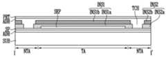
본 발명의 일 실시예에 따른 터치 센서는 다양한 형태로 구현될 수 있다. 도 5a 내지 도 5d는 본 발명의 일 실시예에 따른 터치 센서를 도시한 단면도들로서, 도 2의 I-I'선에 대응하는 단면도들이다.The touch sensor according to an embodiment of the present invention may be implemented in various forms. FIGS. 5A to 5D are cross-sectional views showing a touch sensor according to an embodiment of the present invention, and are cross-sectional views corresponding to line II′ of FIG. 2 .
도 5a를 참조하면, 본 발명의 일 실시예에 따른 터치 센서에 있어서, 절연막(INS)이 복층으로 제공될 수 있다. 복층으로 제공된 절연막(INS)은 2중층, 또는 3중층 이상으로 제공될 수 있다. 본 발명의 일 실시예에서는 트렌치(TCH)를 사이에 두고 서로 이격된 제1 절연막(INS1)과 제2 절연막(INS2)으로 이루어진 경우를 설명한다.Referring to FIG. 5A, in the touch sensor according to an embodiment of the present invention, the insulating film (INS) may be provided in multiple layers. The insulating film (INS) provided as a multiple layer may be provided as a double layer, a triple layer or more. In one embodiment of the present invention, a case consisting of a first insulating layer INS1 and a second insulating layer INS2 spaced apart from each other with a trench TCH in between will be described.
상기 제1 절연막(INS1)은 센싱 전극부(SEP) 상에 제공되며, 순차적으로 적층된 제1 서브 절연막(INS1a)과 제2 서브 절연막(INS1b)을 포함한다. 상기 제2 절연막(INS2) 또한 순차적으로 적층된 제1 서브 절연막(INS2a)과 제2 서브 절연막(INS2b)을 포함한다.The first insulating film INS1 is provided on the sensing electrode part SEP and includes a first sub-insulating film INS1a and a second sub-insulating film INS1b sequentially stacked. The second insulating layer INS2 also includes a first sub-insulating layer INS2a and a second sub-insulating layer INS2b that are sequentially stacked.
상기 제1 절연막(INS1)에 있어서, 상기 제1 서브 절연막(INS1a)은 상기 센싱 전극부(SEP) 상에 제공되며, 상기 센싱 전극부(SEP)를 커버한다. 상기 제2 서브 절연막(INS1b)은 상기 제1 서브 절연막(INS1a) 상에 제공된다. 상기 제1 서브 절연막(INS1a)과 상기 제2 서브 절연막(INS1b)은 터치 영역(TA)에서 중첩한다. 상기 제1 서브 절연막(INS1a)과 상기 제2 서브 절연막(INS1b)은 비터치 영역(NTA)에서 적어도 일부가 중첩한다. 본 실시예에서는 제2 서브 절연막(INS1b)이 제1 서브 절연막(INS1a)의 일부와 중첩한 것을 도시하였다. 이 때, 평면상에서 볼 때 제2 서브 절연막(INS1b)의 크기가 제1 서브 절연막(INS1a)의 크기보다 크게 형성될 수 있다.In the first insulating film INS1, the first sub-insulating film INS1a is provided on the sensing electrode part SEP and covers the sensing electrode part SEP. The second sub-insulating layer INS1b is provided on the first sub-insulating layer INS1a. The first sub-insulating layer INS1a and the second sub-insulating layer INS1b overlap in the touch area TA. The first sub-insulating layer INS1a and the second sub-insulating layer INS1b overlap at least a portion of the non-touch area NTA. In this embodiment, the second sub-insulating layer INS1b is shown overlapping a portion of the first sub-insulating layer INS1a. At this time, when viewed in plan, the size of the second sub-insulating layer INS1b may be formed to be larger than the size of the first sub-insulating layer INS1a.
그러나, 상기 제1 서브 절연막(INS1a)과 상기 제2 서브 절연막(INS1b)의 크기는 이에 한정되는 것은 아니다. 도 5b를 참조하면, 평면상에서 볼 때 제2 서브 절연막(INS1b)의 크기가 제1 서브 절연막(INS1a)의 크기보다 작게 형성될 수 있다. 도 5c를 참조하면, 상기 제1 서브 절연막(INS1a)의 크기가 상기 제2 서브 절연막(INS1b)의 크기보다 작게 형성되되, 제2 서브 절연막(INS1b)이 상기 제1 서브 절연막(INS1a)의 상면 및 측면을 모두 커버할 수 있다. 이에 더해, 도시하지는 않았으나, 본 발명의 일 실시예에 따르면, 상기 제1 서브 절연막(INS1a)과 제2 서브 절연막(INS1b)은 동일한 크기 및 동일한 형태로 제공되어 완전히 중첩할 수 있다. 이 경우, 제1 서브 절연막(INS1a)의 단부와 상기 제2 서브 절연막(INS1b)의 단부는 서로 일치할 수 있다.However, the sizes of the first sub-insulating layer INS1a and the second sub-insulating layer INS1b are not limited thereto. Referring to FIG. 5B , the size of the second sub-insulating layer INS1b may be formed to be smaller than the size of the first sub-insulating layer INS1a when viewed from a plan view. Referring to FIG. 5C, the size of the first sub-insulating film INS1a is smaller than that of the second sub-insulating film INS1b, and the second sub-insulating film INS1b is formed on the top surface of the first sub-insulating film INS1a. and both sides can be covered. In addition, although not shown, according to an embodiment of the present invention, the first sub-insulating layer INS1a and the second sub-insulating layer INS1b are provided in the same size and shape and can completely overlap. In this case, an end of the first sub-insulating layer INS1a and an end of the second sub-insulating layer INS1b may coincide with each other.
도 5a 내지 도 5c를 참조하면, 상기 제2 절연막(INS2)도 제1 절연막(INS1)과 유사한 형태로 제공될 수 있다. 즉, 상기 제1 서브 절연막(INS2a)은 평면 상에서 볼 때 상기 터치 센서의 단부 측에 위치하며, 상기 제2 서브 절연막(INS2b)은 상기 제1 서브 절연막(INS2a) 상에 제공된다. 상기 제2 절연막(INS2)에 있어서도, 상기 제1 서브 절연막(INS2a)은 상기 제1 절연막(INS1)의 적어도 일부와 중첩하며, 본 실시예에 있어서, 제1 절연막(INS1)의 제2 서브 절연막(INSb)과 제2 절연막(INS2)의 제2 서브 절연막(INS2b) 사이의 트렌치(TCH)의 폭은 제1 절연막(INS1)의 제1 서브 절연막(INS1a)과 제2 절연막(INS2)의 제1 서브 절연막(INS2a)의 트렌치(TCH)의 폭과 같거나 다를 수 있다. 도 5a 내지 도 5c의 실시예에서 확인할 수 있는 바와 같이, 제1 절연막(INS1)의 제2 서브 절연막(INSb)과 제2 절연막(INS2)의 제2 서브 절연막(INS2b) 사이의 트렌치(TCH)의 폭은 제1 절연막(INS1)의 제1 서브 절연막(INS1a)과 제2 절연막(INS2)의 제1 서브 절연막(INS2a)의 트렌치(TCH)의 폭보다 좁거나 넓을 수 있다. 본 발명의 일 실시예에 따르면, 상기 제1 서브 절연막(INS1a)과 상기 제2 서브 절연막(INS1b)의 두께는 다양한 형태로 변경될 수 있으며, 상술한 실시예들에 한정되는 것은 아니다. 예를 들어, 상기 제1 서브 절연막(INS1a)의 두께보다 상기 제2 서브 절연막(INS1b)의 두께는 다를 수 있다. 도 5d를 참조하면, 센싱 전극부(SEP)상에 제공되는 제1 절연막(INS1)의 제2 서브 절연막(INS1b)의 두께는 제1 절연막(INS1)의 상기 제1 서브 절연막(INS1a)의 두께보다 크게 제공될 수 있다. 제2 절연막(INS2)의 제1 및 제2 서브 절연막(INS2a, INS2b)의 두께 또한 제1 절연막(INS1)과 동일한 형태로 제공될 수 있다.Referring to FIGS. 5A to 5C , the second insulating layer INS2 may also be provided in a similar form to the first insulating layer INS1. That is, the first sub-insulating layer INS2a is located at an end of the touch sensor when viewed from a plan view, and the second sub-insulating layer INS2b is provided on the first sub-insulating layer INS2a. In the second insulating layer INS2, the first sub-insulating layer INS2a overlaps at least a portion of the first insulating layer INS1, and in this embodiment, the second sub-insulating layer of the first insulating layer INS1 The width of the trench (TCH) between (INSb) and the second sub-insulating layer (INS2b) of the first insulating layer (INS1) is the width of the first sub-insulating layer (INS1a) of the first insulating layer (INS1) and the second insulating layer (INS2). 1 It may be the same as or different from the width of the trench (TCH) of the sub-insulating layer (INS2a). As can be seen in the embodiment of FIGS. 5A to 5C, the trench (TCH) between the second sub-insulating film (INSb) of the first insulating film (INS1) and the second sub-insulating film (INS2b) of the second insulating film (INS2) The width of may be narrower or wider than the width of the trench TCH of the first sub-insulating layer INS1a of the first insulating layer INS1 and the first sub-insulating layer INS2a of the second insulating layer INS2. According to an embodiment of the present invention, the thickness of the first sub-insulating layer INS1a and the second sub-insulating layer INS1b may be changed in various ways, and are not limited to the above-described embodiments. For example, the thickness of the second sub-insulating layer INS1b may be different than the thickness of the first sub-insulating layer INS1a. Referring to FIG. 5D, the thickness of the second sub-insulating film INS1b of the first insulating film INS1 provided on the sensing electrode portion SEP is the thickness of the first sub-insulating film INS1a of the first insulating film INS1. It can be provided in a larger size. The thickness of the first and second sub-insulating layers INS2a and INS2b of the second insulating layer INS2 may also be provided in the same form as that of the first insulating layer INS1.
본 발명의 일 실시예에 있어서, 상술한 실시예들은 본 발명의 개념에 반하지 않는 한도 내에서 일부 변형되거나 실시예들끼리 서로 조합될 수 있다. 예를 들어, 상술한 실시예들에서는 제1 절연막(INS1)과 제2 절연막(INS2)의 높이가 실질적으로 동일하게 도시되었으나, 이에 한정되는 것은 아니며, 서로 다른 높이를 가질 수 있다. 또한, 도 5a에 도시된 실시예에 있어서 제1 절연막(INS1)에 있어서 제1 및 제2 서브 절연막(INS1a, INS1b)의 두께가 도 5d에 도시된 실시예에서와 유사하게 달리 설정될 수 있다.In one embodiment of the present invention, the above-described embodiments may be partially modified or the embodiments may be combined with each other within a limit that does not conflict with the concept of the present invention. For example, in the above-described embodiments, the heights of the first insulating layer INS1 and the second insulating layer INS2 are shown to be substantially the same, but this is not limited and they may have different heights. Additionally, in the embodiment shown in FIG. 5A, the thicknesses of the first and second sub-insulating layers INS1a and INS1b in the first insulating layer INS1 may be set differently, similar to those in the embodiment shown in FIG. 5D. .
상술한 터치 센서는 다음과 같은 방법으로 제조할 수 있다. 이하에서는 상술한 터치 센서 중 도 2에 도시된 터치 센서를 제조하는 방법을 순차적으로 설명한다.The above-described touch sensor can be manufactured by the following method. Hereinafter, a method of manufacturing the touch sensor shown in FIG. 2 among the above-described touch sensors will be sequentially described.
도 6a 내지 도 6g는 본 발명의 일 실시예에 따른 터치 센서를 제조하는 방법을 순차적으로 도시한 단면도이다. 이하의 도면에서는 설명의 편의를 위해 하나의 터치 센서를 형성하는 경우를 일예로서 도시하였으나, 이에 한정되는 것은 아니며, 하나의 모기판 상에 복수 개의 터치 센서를 형성한 후 모기판을 절단함으로써 터치 센서를 형성할 수 있다. 모기판의 절단 공정에 대해서는 도 7을 참조하여 설명한다.6A to 6G are cross-sectional views sequentially showing a method of manufacturing a touch sensor according to an embodiment of the present invention. In the drawings below, the case of forming a single touch sensor is shown as an example for convenience of explanation, but it is not limited to this. The touch sensor is formed by forming a plurality of touch sensors on one mother substrate and then cutting the mother substrate. can be formed. The cutting process of the mother substrate will be described with reference to FIG. 7.
도 6a를 참조하면, 캐리어 기판(CR) 상에 지지층(SP)이 형성된다.Referring to FIG. 6A, a support layer (SP) is formed on the carrier substrate (CR).
상기 캐리어 기판(CR)은 그 상면에 터치 센서를 형성할 수 있는 것이면 특별히 한정되는 것은 아니며, 유리나 플라스틱 등으로 이루어질 수 있다.The carrier substrate CR is not particularly limited as long as it can form a touch sensor on its upper surface, and may be made of glass or plastic.
상기 지지층(SP)은 터치 센서를 이루는 센싱 전극부(SEP), 배선(미도시), 및 패드(미도시) 등을 그 상면에 형성하기 위한 층으로서, 터치 센서를 제조한 후, 상기 캐리어 기판(CR)으로부터 상기 터치 센서를 용이하게 분리하기 위하여 형성된다.The support layer (SP) is a layer for forming the sensing electrode part (SEP), wiring (not shown), and pad (not shown), etc., which make up the touch sensor, on its upper surface. After manufacturing the touch sensor, It is formed to easily separate the touch sensor from (CR).
상기 지지층(SP)은 캐리어 기판(CR) 상에 유기 고분자 재료를 형성하고 경화함으로써 제조될 수 있다.The support layer (SP) can be manufactured by forming an organic polymer material on the carrier substrate (CR) and curing it.
상기 지지층(SP)은 단층 또는 복층으로 형성될 수 있으며, 복층으로 형성될 시에는 복수 회에 걸쳐 반복될 수 있다.The support layer (SP) may be formed as a single layer or a multiple layer, and when formed as a multiple layer, it may be repeated multiple times.
상기 지지층(SP)은 다양한 방식으로 형성될 수 있다. 예를 들어, 상기 지지층(SP)은, 프린팅 방식, 코팅 방식, 디스펜싱 방식 등으로 형성될 수 있다. 예를 들어, 지지층(SP)은 스크린 프린팅, 잉크젯 프린팅 및 노즐 프린팅 등의 프린팅 방식, 슬릿 코팅, 스핀 코팅 및 분사 코팅 등의 코팅 방식, 디스펜서를 이용하는 디스펜싱 방식 중 어느 하나에 의해 형성될 수 있다. 본 발명의 일 실시예에 있어서, 상기 코팅 방식으로 형성할 수 있다.The support layer (SP) can be formed in various ways. For example, the support layer (SP) may be formed by a printing method, a coating method, a dispensing method, etc. For example, the support layer (SP) may be formed by any one of printing methods such as screen printing, inkjet printing and nozzle printing, coating methods such as slit coating, spin coating and spray coating, and dispensing methods using a dispenser. . In one embodiment of the present invention, it can be formed using the above coating method.
상기 지지층(SP)은 상기한 방법을 통해 용이하게 제조될 수 있는 바, 기존 발명에 비해 매우 얇은 두께로 제조될 수 있다.The support layer (SP) can be easily manufactured through the above-described method, and can be manufactured to a very thin thickness compared to the existing invention.
상기 캐리어 기판(CR)과 경화된 지지층(SP)은 서로 접촉된 상태이며 정전기나 반데르발스 힘 등에 의해 서로 부착되어 있다. 여기서, 상기 캐리어 기판(CR)과 상기 지지층(SP)은 접착되었다고 하였으나, 상기 접착의 의미는 서로 표면이 접촉하고 있되, 서로 화학적으로 결합(예를 들어, 공유 결합)되어 분리되지 않은 상태가 되는 것을 제외한다. 또한, 캐리어 기판(CR)과 지지층(SP) 사이에는 공기층 이외에 별도의 접착제(ADH)와 같은 별도의 층이 개재되지 않는다. 상기 캐리어 기판(CR)과 상기 지지층(SP) 외부로부터 힘이 가해지는 경우 손상없이 용이하게 분리될 수 있는 상태이다.The carrier substrate (CR) and the cured support layer (SP) are in contact with each other and are attached to each other by static electricity or van der Waals force. Here, the carrier substrate (CR) and the support layer (SP) are said to be adhered, but the adhesion means that the surfaces are in contact with each other, but are chemically bonded (e.g., covalently bonded) to each other and are not separated. exclude that In addition, there is no separate layer such as an additional adhesive (ADH) other than the air layer between the carrier substrate CR and the support layer SP. When force is applied from the outside of the carrier substrate CR and the support layer SP, they can be easily separated without damage.
도 6b를 참조하면, 지지층(SP) 상에 센싱 전극부(SEP)가 형성된다. 도시하지는 않았으나, 센싱 전극부(SEP)와 함께 배선 및/또는 패드가 함께 또는 별개로 형성될 수 있다. 센싱 전극부(SEP), 배선, 및 패드는 화학 기상 증착, 물리적 기상 증착, 프린팅, 도금 등의 다양한 방식으로 형성될 수 있다. 예를 들어, 센싱 전극부(SEP), 배선, 및 패드는 화학적 기상 증착을 이용하여 도전층을 형성하고 포토리소그래피로 도전층을 패터닝함으로써 제조될 수 있다.Referring to FIG. 6B, a sensing electrode portion (SEP) is formed on the support layer (SP). Although not shown, wiring and/or pads may be formed together or separately with the sensing electrode portion (SEP). The sensing electrode portion (SEP), wiring, and pad may be formed by various methods such as chemical vapor deposition, physical vapor deposition, printing, and plating. For example, the sensing electrode part (SEP), wiring, and pad can be manufactured by forming a conductive layer using chemical vapor deposition and patterning the conductive layer by photolithography.
도 6c를 참조하면, 센싱 전극부(SEP) 등이 형성된 기판 상에 절연막(INS)이 형성된다. 상기 절연막(INS)은 비터치 영역에서 상기 절연막(INS)의 일부가 제거된 트렌치(TCH)를 갖도록 형성된다. 상기 트렌치(TCH)에 해당하는 영역의 지지층(SP) 상에는 절연막(INS)이 제공되지 않으므로 지지층(SP)의 상면이 노출된다.Referring to FIG. 6C, an insulating film (INS) is formed on the substrate on which the sensing electrode part (SEP), etc. is formed. The insulating film INS is formed to have a trench TCH in which a portion of the insulating film INS is removed in a non-touch area. Since the insulating film INS is not provided on the support layer SP in the area corresponding to the trench TCH, the top surface of the support layer SP is exposed.
상기 트렌치(TCH)는 평면 상에서 볼 때 상기 터치 영역의 둘레를 따라 제공된다. 이에 따라, 상기 절연막(INS)은 상기 트렌치(TCH)를 사이에 두고 이격된 제1 및 제2 절연막(INS1, INS2)으로 이루어질 수 있다. 상기 제2 절연막(INS2)은 상기 제1 절연막(INS1)의 외측에서 상기 제1 절연막(INS1)의 둘레를 따라 제공된다.The trench (TCH) is provided along the perimeter of the touch area when viewed in plan. Accordingly, the insulating layer INS may be composed of first and second insulating layers INS1 and INS2 spaced apart with the trench TCH in between. The second insulating layer INS2 is provided outside the first insulating layer INS1 and along the perimeter of the first insulating layer INS1.
또한 상기 절연막(INS)은 비터치 영역 중 패드에 대응하는 영역에 상기 배선의 단부에 연결된 패드를 노출하는 개구를 갖도록 형성된다. 상기 개구를 통해 상기 패드의 상면이 노출된다.Additionally, the insulating film INS is formed to have an opening exposing the pad connected to the end of the wiring in an area corresponding to the pad in the non-touch area. The top surface of the pad is exposed through the opening.
상기 절연막(INS)은 다양한 방식으로 형성될 수 있다. 예를 들어, 상기 절연막(INS)은, 프린팅 방식, 코팅 방식, 디스펜싱 방식 등으로 형성될 수 있다. 예를 들어, 절연막(INS)은 스크린 프린팅, 잉크젯 프린팅 및 노즐 프린팅 등의 프린팅 방식, 슬릿 코팅, 스핀 코팅 및 분사 코팅 등의 코팅 방식, 디스펜서를 이용하는 디스펜싱 방식 중 어느 하나에 의해 형성될 수 있다. 본 발명의 일 실시예에 있어서, 상기 코팅 방식으로 형성할 수 있다.The insulating film (INS) can be formed in various ways. For example, the insulating film (INS) may be formed by a printing method, a coating method, a dispensing method, etc. For example, the insulating film (INS) may be formed by any one of printing methods such as screen printing, inkjet printing and nozzle printing, coating methods such as slit coating, spin coating and spray coating, and dispensing methods using a dispenser. . In one embodiment of the present invention, it can be formed using the above coating method.
상기 절연막(INS)에 있어서, 상기 트렌치(TCH) 및 개구는 캐리어 기판(CR)의 전면상에 절연막(INS)을 형성한 후 포토리소그래피를 이용하여 패터닝함으로써 제공될 수 있다. 또는, 상기 트렌치(TCH) 및 개구는 프린팅, 코팅, 디스펜싱 시 트렌치(TCH)나 개구가 형성될 영역을 제외한 부분에만 절연막(INS)을 형성하는 방식으로 형성될 수 있다.In the insulating film (INS), the trench (TCH) and the opening may be provided by forming the insulating film (INS) on the entire surface of the carrier substrate (CR) and then patterning it using photolithography. Alternatively, the trench (TCH) and the opening may be formed by forming the insulating film (INS) only in a portion excluding the area where the trench (TCH) or opening is to be formed during printing, coating, and dispensing.
여기서, 제1 절연막(INS1)과 상기 제2 절연막(INS2)은 상기한 바와 같이 단일 공정에서 제조될 수 있으며. 이에 따라, 제1 절연막(INS1)과 제2 절연막(INS2)은 동일한 재료로 이루어질 수 있다. 또한 제1 절연막(INS1)과 제2 절연막(INS2)은 실질적으로 서로 동일한 높이로 형성될 수 있다. 그러나, 상기 제1 절연막(INS1)과 상기 제2 절연막(INS2)은 다른 공정에서 별도로 제조될 수 있는 바, 이 경우에도 제1 절연막(INS1)과 제2 절연막(INS2)은 실질적으로 동일한 높이를 갖도록 형성된다.Here, the first insulating layer INS1 and the second insulating layer INS2 may be manufactured in a single process as described above. Accordingly, the first insulating layer INS1 and the second insulating layer INS2 may be made of the same material. Additionally, the first insulating layer INS1 and the second insulating layer INS2 may be formed to have substantially the same height. However, the first insulating film (INS1) and the second insulating film (INS2) may be manufactured separately in different processes, and even in this case, the first insulating film (INS1) and the second insulating film (INS2) have substantially the same height. It is formed to have
도 6d를 참조하면, 절연막(INS) 등이 형성된 캐리어 기판(CR) 상에 접착제(ADH)를 사이에 두고 보호 필름(PRT)이 부착된다. 상기 보호 필름(PRT)과 접착제(ADH)는 제1 롤러(R1)를 이용하여 부착될 수 있다. 즉, 제1 롤러(R1)를 이용하여 접착제(ADH)와 보호 필름(PRT)을 절연막(INS) 등이 형성된 캐리어 기판(CR) 상에 압착함으로써 보호 필름(PRT)을 절연막(INS) 상에 부착할 수 있다. 이때, 상기 접착제(ADH)는 트렌치(TCH)와 개구 내부를 전부 또는 적어도 일부 충진할 수 있다.Referring to FIG. 6D, a protective film (PRT) is attached to a carrier substrate (CR) on which an insulating film (INS), etc. is formed, with an adhesive (ADH) interposed therebetween. The protective film (PRT) and adhesive (ADH) may be attached using the first roller (R1). That is, the adhesive (ADH) and the protective film (PRT) are pressed onto the carrier substrate (CR) on which the insulating film (INS) is formed using the first roller (R1), thereby forming the protective film (PRT) on the insulating film (INS). It can be attached. At this time, the adhesive (ADH) may fill all or at least part of the trench (TCH) and the inside of the opening.
도 6e를 참조하면, 터치 센서 공정을 진행하기 위해 사용된 캐리어 기판(CR)이 제거된다. 상기 캐리어 기판(CR)을 제거하는 방법은 특별히 한정되는 것은 아니며 리프트오프나 필오프 방법이 이용될 수 있다. 본 발명의 일 실시예에서는 상기 캐리어 기판(CR)이 제2 롤러(R2)를 이용하여 지지층(SP)과 캐리어 기판(CR)을 분리하는 방식으로 수행된다.Referring to Figure 6e, the carrier substrate (CR) used to proceed with the touch sensor process is removed. The method of removing the carrier substrate CR is not particularly limited, and a lift-off or peel-off method may be used. In one embodiment of the present invention, the carrier substrate CR is separated from the support layer SP using a second roller R2.
도 6f를 참조하면, 상기한 방식으로 제조된 터치 센서는 기판(SUB) 상에 접합된다. 상기 터치 센서는 접착제(ADH)를 사이에 두고 기판(SUB) 상에 부착될 수 있다. 본 발명의 일 실시예에서는 제3 롤러(R3)와 제4 롤러(R4)를 서로 마주보도록 배치하고, 제3 롤러(R3)와 제4 롤러(R4) 사이로 접착제(ADH)가 형성된 기판(SUB)과 터치 센서를 압착시키면서 통과시킴으로써 기판과 터치 센서를 부착한다. 즉, 상기 터치 센서는 롤-투-롤 방식으로 캐리어 기판(CR)으로부터 분리되어 기판(SUB) 상에 전사된다. 여기서, 상기 기판(SUB)은 상기 터치 센서를 부착하고자 하는 구성 요소일 수 있는 바, 예를 들어, 표시 패널, 기능성 필름, 윈도우 등의 다양한 구성 요소가 사용될 수 있다.Referring to FIG. 6F, the touch sensor manufactured in the above manner is bonded onto a substrate (SUB). The touch sensor may be attached to the substrate (SUB) with an adhesive (ADH) interposed therebetween. In one embodiment of the present invention, the third roller (R3) and the fourth roller (R4) are arranged to face each other, and the substrate (SUB) is formed with an adhesive (ADH) between the third roller (R3) and the fourth roller (R4). ) and the touch sensor are attached to the substrate by passing the touch sensor while pressing it. That is, the touch sensor is separated from the carrier substrate CR and transferred onto the substrate SUB in a roll-to-roll manner. Here, the substrate SUB may be a component to which the touch sensor is attached. For example, various components such as a display panel, functional film, and window may be used.
도 6g를 참조하면, 상기한 공정을 통해 기판 상에 터치 센서가 부착된 최종 결과물이 완성된다.Referring to FIG. 6g, the final result in which a touch sensor is attached to a substrate is completed through the above process.
본 발명의 일 실시예에 따른 제조 방법에 있어서, 터치 센서는 개별적으로 하나씩 형성될 수 있으나, 복수 개의 터치 센서를 동시에 형성할 수도 있다. 도 7은 본 발명의 일 실시예에 있어서, 복수 개의 터치 센서를 동시에 제조하는 것을 도시한 평면도이다.In the manufacturing method according to an embodiment of the present invention, touch sensors may be formed individually, but a plurality of touch sensors may be formed simultaneously. Figure 7 is a plan view showing simultaneous manufacturing of a plurality of touch sensors according to an embodiment of the present invention.
본 실시예에 있어서, 복수 개의 터치 센서를 동시에 형성한다는 것을 설명하기 위해 6개의 터치 센서를 형성하기 위한 모기판(M_SUB)을 도시하였으나 이에 한정되는 것은 아니며, 다양한 개수의 터치 센서를 형성하기 위해 다양한 크기의 모기판(M_SUB)이 사용될 수 있다.In this embodiment, a mother substrate (M_SUB) for forming six touch sensors is shown to explain forming a plurality of touch sensors at the same time, but it is not limited thereto, and various types of substrates are used to form various numbers of touch sensors. A mother substrate of size (M_SUB) may be used.
본 실시예에 있어서, 대형 모기판(M_SUB)에 복수 개의 터치 센서를 동시에 형성한다는 면에서 일부 차이가 있으나, 각 모기판(M_SUB) 상에 형성되는 구성요소는 상술한 개별 터치 센서의 구성요소와 실질적으로 동일하다. 제조 방법 또한 복수 개의 터치 센서를 동시에 형성하기 위해 캐리어 기판(CR), 지지층(SP) 등의 크기가 대형으로 준비된다는 것 이외의 차이는 실질적으로 없다. 상기 모기판(M_SUB)은 개별적인 터치 센서들을 형성하기 위한 단위 영역(UNT)을 가지며, 각 단위 영역(UNT) 내에 터치 센서가 형성된다. 상기 각 단위 영역(UNT)은 이후 절단선(CT)을 따라 절단되며 이에 따라 복수 개의 터치 센서가 동시에 형성될 수 있다.In this embodiment, there is some difference in that a plurality of touch sensors are simultaneously formed on the large mother substrate (M_SUB), but the components formed on each mother substrate (M_SUB) are the components of the individual touch sensors described above. are substantially the same. There is virtually no difference in the manufacturing method other than that the carrier substrate (CR) and support layer (SP) are prepared in large sizes in order to form a plurality of touch sensors simultaneously. The mother substrate (M_SUB) has unit areas (UNT) for forming individual touch sensors, and a touch sensor is formed in each unit area (UNT). Each unit area UNT is then cut along a cutting line CT, and thus a plurality of touch sensors can be formed simultaneously.
이를 도 6a 내지 도 6f 및 도 7을 참조하여 설명하면, 먼저 모기판(M_SUB)과 실질적으로 동일한 크기의 캐리어 기판(CR)이 준비될 수 있다. 상기 캐리어 기판(CR)상에는 지지층(SP)이 형성된다. 상기 지지층(SP)은 제조하고자 하는 터치 센서의 개수에 따른 복수 개의 단위 영역(UNT)을 가질 수 있으며, 상기 지지층(SP)의 단위 영역(UNT)에는 각각 센싱 전극부(SEP), 배선, 및 패드 등이 형성된다. 다음으로 상기 단위 영역(UNT)들 각각에는 트렌치(TCH)를 갖는 절연막(INS)이 형성된다. 각각의 절연막(INS) 상에 모기판(M_SUB)과 실질적으로 동일한 크기의 보호 필름(PRT)이 접착제(ADH)를 사이에 두고 접착되고, 다음으로 캐리어 기판(CR)이 제거된다. 캐리어 기판(CR)이 제거된 터치 센서들은 모기판(M_SUB)에 접착제(ADH)를 사이에 두고 접착된다. 모기판(M_SUB) 상에 형성된 각 터치 센서들은 커터나 레이저 등을 이용하여 개별 터치 센서로 절단됨으로써 최종적인 터치 센서가 완성된다.If this is explained with reference to FIGS. 6A to 6F and FIG. 7 , first, a carrier substrate (CR) of substantially the same size as the mother substrate (M_SUB) may be prepared. A support layer (SP) is formed on the carrier substrate (CR). The support layer (SP) may have a plurality of unit areas (UNT) according to the number of touch sensors to be manufactured, and each unit area (UNT) of the support layer (SP) includes a sensing electrode portion (SEP), a wiring, and A pad, etc. are formed. Next, an insulating film (INS) having a trench (TCH) is formed in each of the unit regions (UNT). A protective film (PRT) of substantially the same size as the mother substrate (M_SUB) is attached to each insulating film (INS) with an adhesive (ADH) interposed therebetween, and then the carrier substrate (CR) is removed. The touch sensors from which the carrier substrate (CR) has been removed are attached to the mother substrate (M_SUB) with an adhesive (ADH) in between. Each touch sensor formed on the mother substrate (M_SUB) is cut into individual touch sensors using a cutter or laser, thereby completing the final touch sensor.
상기한 구조를 가지며 상기한 방식으로 제조된 본 발명의 일 실시예에 따른 터치 센서는 기존 발명에 비해 결함이 감소되는 바, 이를 설명하면 다음과 같다.The touch sensor according to an embodiment of the present invention having the above structure and manufactured in the above manner has reduced defects compared to the existing invention, which is explained as follows.
기존 발명에 따르면, 센싱 전극부를 덮는 절연막은 지지층의 단부까지 연장되었다. 이 경우 모기판의 절단 공정 등에서 절연막의 단부에 크랙 등의 결함이 발생할 수 있으며, 상기 결함을 통해 외부 기체(예를 들어, 산소)나 습기 등이 내부로 침투함으로써 센싱 전극부, 배선, 패드 등의 변성이 일어나는 문제가 발생하였다. 즉, 센싱 전극부, 배선, 패드 등의 ITO가 부식되거나, 금속이 산화되는 등의 문제가 발생하며, 이는 결국 저항 증가, 배선 사이의 쇼트, 터치 감지 저하 등으로 이어진다.According to the existing invention, the insulating film covering the sensing electrode portion extends to the end of the support layer. In this case, defects such as cracks may occur at the end of the insulating film during the cutting process of the mother board, and external gas (e.g. oxygen) or moisture penetrates into the interior through the defect, causing damage to the sensing electrode part, wiring, pad, etc. A problem occurred in which degeneration occurred. In other words, problems such as corrosion of the ITO of the sensing electrode part, wiring, and pad, or oxidation of the metal occur, which ultimately leads to increased resistance, short circuits between wiring, and deterioration of touch detection.
이를 방지하기 위해 절연막을 터치 영역을 커버하되 단부 측에는 형성하지 않는 경우에는, 롤-투-롤 공정에서의 압착 전사시에 절연막이 없는 부분에 단차가 발생하며, 이러한 단차 차이로 인해 접착제가 적게 도포되거나 미도포되는 현상이 발생하였다. 이는 롤-투-롤 방식에서 터치 센서의 전사시 압착에 의해 접착제가 외측으로 밀림으로써 접착제가 불충분 도포 또는 미도포되기 때문으로서, 터치 센서의 단부 영역에서 결국 기판과 터치 센서 사이의 접착제 두께의 감소로 이어진다. 기판과 지지층 사이에 접착제의 두께가 감소하는 경우, 터치 센서의 인장력이 감소한다. 접착제의 경우 소정의 탄성력을 가지고 있으며 굽힘 등의 외부 스트레스를 완화하는 역할을 수행하는 것이 일반적이나, 접착제의 두께가 너무 작은 경우 탄성력이 감소하고 외부 스트레스를 완화하기 어렵게 된다. 그 결과, 센싱 전극부, 배선, 패드 등에는 외부로부터 인가되는 스트레스에 의해 크랙이 형성되는 등의 결함이 발생한다. 예를 들어, 약 500 gF/cm의 스트레스에도 배선에 크랙이 발생할 수 있다.To prevent this, if an insulating film is covered over the touch area but not formed on the end side, a step occurs in the area where the insulating film is not present during compression transfer in the roll-to-roll process, and due to this step difference, less adhesive is applied. A phenomenon of application or non-application occurred. This is because the adhesive is pushed outward by compression during transfer of the touch sensor in the roll-to-roll method, resulting in insufficient or no adhesive application, which ultimately leads to a decrease in the thickness of the adhesive between the substrate and the touch sensor in the end area of the touch sensor. It continues. When the thickness of the adhesive between the substrate and the support layer decreases, the tensile force of the touch sensor decreases. In the case of adhesives, they generally have a certain amount of elasticity and play a role in relieving external stress such as bending. However, if the thickness of the adhesive is too small, the elasticity decreases and it becomes difficult to relieve external stress. As a result, defects such as cracks are formed in the sensing electrode portion, wiring, pad, etc. due to stress applied from the outside. For example, cracks can occur in wiring even under a stress of about 500 gF/cm.
이에 더해, 기판과 지지층 사이가 쉽게 탈리될 뿐만 아니라, 지지층이 기판으로부터 쉽게 들림으로써 지지층 상의 센싱 전극부, 배선, 패드 등에 외부 기체나 습기 등이 내부로 쉽게 침투하게 된다. 그 결과, 터치 센서의 단부 부분의 센싱 전극부, 배선 패드 등의 변성이 일어나는 문제가 발생하며, 이 경우 역시 저항 증가, 배선 사이의 쇼트, 터치 감지 저하 등으로 이어진다.In addition, not only is the gap between the substrate and the support layer easily separated, but the support layer is easily lifted from the substrate, allowing external gases or moisture to easily penetrate into the sensing electrodes, wiring, and pads on the support layer. As a result, a problem occurs in which the sensing electrode portion and wiring pad at the end of the touch sensor are deformed, which also leads to increased resistance, short circuits between wiring, and deterioration of touch detection.
그러나, 본 발명의 일 실시예에 따르면, 트렌치를 사이에 두고 서로 이격된 제1 절연막과 제2 절연막을 형성함으로써, 상술한 결함이 예방된다.However, according to one embodiment of the present invention, the above-described defect is prevented by forming the first insulating film and the second insulating film spaced apart from each other with a trench therebetween.
본 발명의 경우, 센싱 전극부 등을 커버하는 제1 절연막을 형성하되, 상기 제1 절연막이 터치 센서의 외측 단부에는 형성되지 않으며, 센싱 전극부 등을 커버하는 제1 절연막이 외측으로 노출되지 않는다. 이에 따라, 절단 공정 등이 수행될 때 제1 절연막에 크랙과 같은 결함이 발생하지 않는다. 이에 더해, 터치 센서의 외곽을 따라 제2 절연막이 제공되되, 제1 절연막과 제2 절연막의 높이가 실질적으로 동일하기 때문에 롤-투-롤 방식을 이용한 압착 시에 접착제가 적게 도포되는 현상이 현저하게 감소한다. 이는 제2 절연막이 간격재로 작용함으로써 터치 센서의 단부에서의 압착 시 접착제의 눌림 현상을 감소시키기 때문이다.In the case of the present invention, a first insulating film covering the sensing electrode portion, etc. is formed, but the first insulating film is not formed on the outer end of the touch sensor, and the first insulating film covering the sensing electrode portion, etc. is not exposed to the outside. . Accordingly, defects such as cracks do not occur in the first insulating film when a cutting process or the like is performed. In addition, a second insulating film is provided along the outer edge of the touch sensor, and because the heights of the first and second insulating films are substantially the same, the phenomenon of less adhesive being applied when pressing using the roll-to-roll method is noticeable. decreases significantly. This is because the second insulating film acts as a spacer to reduce the pressing phenomenon of the adhesive when pressed at the end of the touch sensor.
하기 표 1은 기존 발명의 터치 센서에 있어서, 고온 및 고습 환경에서의 시간에 따른 터치 센서의 불량 여부 결과를 나타낸 것이며, 하기 표 2는 본 발명의 일 실시예에 따른 터치 센서에 있어서, 고온 및 고습 환경에서의 시간에 따른 터치 센서의 불량 여부 결과를 나타낸 것이다.Table 1 below shows the results of whether the touch sensor is defective over time in a high temperature and high humidity environment in the touch sensor of the existing invention, and Table 2 below shows the results of the touch sensor according to an embodiment of the present invention, high temperature and high humidity. This shows the results of whether the touch sensor is defective over time in a high humidity environment.
표 1 및 표 2에 사용된 터치 센서는 다른 조건은 모두 동일하되, 절연막의 형상만 달리 제조되었다. 표 1 및 표 2에 사용된 터치 센서의 센싱 전극부는 ITO 단일막으로 형성되었으며, 배선은 ITO막과 알루미늄/팔라듐/구리 합금막의 이중막으로 형성되었다.The touch sensors used in Tables 1 and 2 were manufactured with all other conditions being the same, but only the shape of the insulating film was different. The sensing electrode part of the touch sensor used in Tables 1 and 2 was formed of an ITO single film, and the wiring was formed of a double film of an ITO film and an aluminum/palladium/copper alloy film.
표 1의 터치 센서의 경우, 절연막이 터치 센서의 단부까지 연장되지 않도록 제조되었으며, 절연막이 트렌치를 포함하지 않도록 제작되었다. 반면, 표 2의 터치 센서의 경우 제1 절연막의 형태는 표 1의 터치 센서와 동일하되, 터치 센서의 단부에 제1 절연막과 트렌치를 사이에 두고 이격된 제1 절연막을 가지도록 제조되었다. 터치 센서의 불량은 ITO막 및 브릿지의 부식과 및 배선의 단선 및 합선 등에 의한 불량 여부로 평가하였다.In the case of the touch sensor in Table 1, the insulating film was manufactured so that it did not extend to the end of the touch sensor, and the insulating film was manufactured so that it did not include a trench. On the other hand, in the case of the touch sensor in Table 2, the shape of the first insulating film is the same as that of the touch sensor in Table 1, but it was manufactured to have the first insulating film spaced apart from the first insulating film at the end of the touch sensor with a trench in between. Defects in the touch sensor were evaluated based on corrosion of the ITO film and bridge, and disconnection or short circuit of the wiring.
표 1 및 표 2에서 확인할 수 있는 바와 같이, 기존 발명에 따른 터치 센서는 고온 다습한 환경에서 불량이 발생하였으며, 특히, 500시간 이후에는 78개의 표본 중 9개의 터치 센서에서 불량이 발생하였다. 이에 비해, 본 발명에 따른 터치 센서는 모든 시간에서 불량이 발생하지 않았다.As can be seen in Tables 1 and 2, defects occurred in the touch sensor according to the existing invention in a high temperature and high humidity environment, and in particular, defects occurred in 9 touch sensors out of 78 samples after 500 hours. In comparison, the touch sensor according to the present invention did not have any defects at any time.
본 발명의 일 실시예에 따른 터치 센서는 다양한 형태로 구현될 수 있다. 도 8은 본 발명의 일 실시예에 따른 터치 센서를 도시한 평면도로서, 특히, 센싱 전극부(SEP)의 일 예를 도시한 것이다. 도 9는 도 8의 P1 부분을 확대 도시한 단면도이다. 도 10은 도 9의 III-III'선에 따른 단면도이다.The touch sensor according to an embodiment of the present invention may be implemented in various forms. Figure 8 is a plan view showing a touch sensor according to an embodiment of the present invention, and in particular, shows an example of the sensing electrode part (SEP). FIG. 9 is an enlarged cross-sectional view of portion P1 of FIG. 8. FIG. 10 is a cross-sectional view taken along line III-III' of FIG. 9.
본 발명의 일 실시예에 따른 터치 센서는 정전용량 방식으로서 상호 정전 용량 방식 및/또는 자기 정전 용량 방식으로 제공될 수 있다. 이하의 실시예에서는, 설명의 편의를 위해 상호 정전 용량 방식의 터치 센서를 일 예로서 설명하나, 이에 한정되는 것은 아니다.The touch sensor according to an embodiment of the present invention may be provided in a mutual capacitance method and/or a self-capacitance method as a capacitive method. In the following embodiments, for convenience of explanation, a mutual capacitance type touch sensor is described as an example, but is not limited thereto.
먼저 도 9 및 도 10를 참조하면, 본 발명의 일 실시예에 의한 터치 센서는, 제1 터치 전극들(T1), 제2 터치 전극들(T2), 제1 및 제2 배선(WR1, WR2), 패드들(PD)을 포함한다. 제1 터치 전극들(T1) 및 제2 터치 전극들(T2)은 터치 영역(TA)에 제공된다.First, referring to FIGS. 9 and 10, the touch sensor according to an embodiment of the present invention includes first touch electrodes T1, second touch electrodes T2, and first and second wires WR1 and WR2. ), including pads (PD). The first touch electrodes T1 and the second touch electrodes T2 are provided in the touch area TA.
터치 센서의 비터치 영역(NTA)에는 제1 터치 전극들(T1)에 전기적으로 연결되는 제1 배선들(WR1)이 제공될 수 있으며, 또한 제2 터치 전극들(T2)에 전기적으로 연결되는 제2 배선들(WR2)이 제공될 수 있다. 여기서 제1 배선들(WR1)은 서로 연결된 일련의 제1 터치 전극들(T1)의 일 단에 연결되고, 제2 배선들(WR2) 또한 서로 연결된 일련의 제2 터치 전극들(T2)의 일 단에 연결될 수 있다.The non-touch area (NTA) of the touch sensor may be provided with first wires (WR1) electrically connected to the first touch electrodes (T1) and also electrically connected to the second touch electrodes (T2). Second wires WR2 may be provided. Here, the first wires WR1 are connected to one end of a series of first touch electrodes T1 connected to each other, and the second wires WR2 are also connected to one end of a series of second touch electrodes T2 connected to each other. It can be connected to a terminal.
본 발명의 일 실시예에 있어서, 터치 센서에는 센서 제어부(미도시)가 제공될 수 있다. 센서 제어부는 인쇄 회로 기판, 테이프 캐리어 팩키지, 또는 칩 온 필름 등의 형태로 제공될 수 있으며, 별도의 배선들(WR), 커넥터 등을 통해 패드들에 전기적으로 연결될 수 있다. 여기서, 인쇄 회로 기판이나 테이프 캐리어 팩키지 등은 가요성을 가질 수 있다.In one embodiment of the present invention, the touch sensor may be provided with a sensor control unit (not shown). The sensor control unit may be provided in the form of a printed circuit board, tape carrier package, or chip-on-film, and may be electrically connected to the pads through separate wires (WR), connectors, etc. Here, the printed circuit board, tape carrier package, etc. may have flexibility.
제1 터치 전극들(T1)은, 지지층(SP) 상에, 예컨대 X 방향을 따라 형성된다. 일례로, 제1 터치 전극들(T1) 각각은, X 방향을 따라 동일한 행(row)에 배열될 수 있다. 각 행에 배열된 제1 터치 전극들(T1)은 컨택홀(CH)을 통해 X 방향을 따라 서로 인접한 제1 터치 전극들(T1)을 연결하는 다수의 제1 브릿지(BR1)들을 포함할 수 있다.The first touch electrodes T1 are formed on the support layer SP, for example, along the X direction. For example, each of the first touch electrodes T1 may be arranged in the same row along the X direction. The first touch electrodes T1 arranged in each row may include a plurality of first bridges BR1 connecting adjacent first touch electrodes T1 to each other along the X direction through the contact hole CH. there is.
이러한 제1 터치 전극들(T1)은 제1 배선들(WR1)을 통해 각각의 패드(PD)에 연결된다.These first touch electrodes T1 are connected to each pad PD through first wires WR1.
제2 터치 전극들(T2)은 상기 지지층(SP) 상에, 예컨대 Y 방향을 따라 형성된다. 일례로, 제2 터치 전극들(T2) 각각은, Y 방향을 따라 동일한 열(column)에 배열될 수 있다. 각 열에 배열된 제2 터치 전극들(T2)은 Y 방향을 따라 서로 인접한 제2 터치 전극들(T2)을 연결하는 다수의 제2 브릿지(BR2)들을 포함할 수 있다.The second touch electrodes T2 are formed on the support layer SP, for example, along the Y direction. For example, each of the second touch electrodes T2 may be arranged in the same column along the Y direction. The second touch electrodes T2 arranged in each row may include a plurality of second bridges BR2 connecting adjacent second touch electrodes T2 along the Y direction.
이러한 제2 터치 전극들(T2)은 제2 배선들(WR2)을 통해 각각의 패드(PD)에 연결된다.These second touch electrodes T2 are connected to each pad PD through second wires WR2.
본 발명의 일 실시예에 있어서, 제1 브릿지(BR1)들은 해당 행의 제1 터치 전극들(T1)과 분리되지 않는 일체로 구현될 수 있다. 또는 제2 브릿지(BR2)들은 해당 열의 제2 터치 전극들(T2)과 분리되지 않는 일체로 구현될 수 있다. 다만, 본 발명이 이에 한정되는 것은 아니며, 제1 브릿지(BR1)들 및/또는 제2 브릿지(BR2)들은 하나 이상의 브릿지를 포함하는 구조로 변경 실시될 수도 있다.In one embodiment of the present invention, the first bridges BR1 may be implemented integrally with the first touch electrodes T1 of the corresponding row. Alternatively, the second bridges BR2 may be implemented integrally with the second touch electrodes T2 of the corresponding row. However, the present invention is not limited to this, and the first bridges BR1 and/or the second bridges BR2 may be modified to include one or more bridges.
편의상, 본 실시예에서는 인접한 두 개의 제1 터치 전극들(T1) 사이에는 제1 브릿지(BR1)가 1개, 제2 브릿지(BR2)가 1개인 것이 개시되었으나, 상기 제1 브릿지(BR1) 및 제2 브릿지(BR2)의 수는 다양하게 변경 실시될 수 있다.For convenience, in this embodiment, there is one first bridge (BR1) and one second bridge (BR2) between two adjacent first touch electrodes (T1), but the first bridge (BR1) and The number of second bridges BR2 can be changed in various ways.
본 발명의 일 실시예에 있어서, 도 3에서는 제1 및 제2 터치 전극들(T1, T2)을 다이아몬드 형상으로 도시하였으나, 이들의 형상은 다양하게 변경될 수 있다. 예컨대, 제1 및 제2 터치 전극들(T1, T2)은 원형으로 구현될 수도 있다.In one embodiment of the present invention, the first and second touch electrodes T1 and T2 are shown in a diamond shape in FIG. 3, but their shapes may be changed in various ways. For example, the first and second touch electrodes T1 and T2 may be implemented in a circular shape.
본 발명의 일 실시예에 있어서, 제1 터치 전극들(T1)이 구동 전극이고, 제2 터치 전극들(T2)이 수신 전극인 경우, 제1 터치 전극들(T1)은 각각의 패드(PD)를 통해 센서 제어부로부터 구동신호를 입력받고, 제2 터치 전극들(T2)은 각각의 패드(PD)를 통해 사용자의 터치로 인한 감지신호를 센서 제어부로 출력할 수 있다. 이 경우, 도시된 실시예의 터치 센서는 상호 정전 용량 방식으로 구동될 수 있다.In one embodiment of the present invention, when the first touch electrodes T1 are driving electrodes and the second touch electrodes T2 are receiving electrodes, the first touch electrodes T1 are connected to each pad PD. ), and the second touch electrodes T2 can output a detection signal due to the user's touch to the sensor control unit through each pad PD. In this case, the touch sensor of the illustrated embodiment may be driven in a mutual capacitance manner.
한편, 도면에서는 제1 및 제2 터치 전극들(T1, T2)을 각각 X 및 Y 방향을 따라 배치하였으나, 본 발명이 이에 한정되는 것은 아니다. 예컨대, 제1 전극(EL1)들 및/또는 제2 터치 전극들(T2)은 X 및 Y 방향 이외의 방향, 예를 들어, 사선 방향으로 배치될 수도 있다.Meanwhile, in the drawing, the first and second touch electrodes T1 and T2 are arranged along the X and Y directions, respectively, but the present invention is not limited thereto. For example, the first electrodes EL1 and/or the second touch electrodes T2 may be disposed in a direction other than the X and Y directions, for example, in a diagonal direction.
본 발명의 일 실시예에 있어서, 도시하지는 않았으나, 제1 터치 전극들(T1) 및 제2 터치 전극들(T2) 중 적어도 일부는 세선(細線)들로 이루어진 메쉬(mesh) 형태로 제공될 수 있다. 예컨대, 제1 터치 전극들(T1), 제2 터치 전극들(T2) 중 적어도 하나는, 한 층 이상의 메쉬형 도전층을 포함하도록 형성될 수 있다. 예컨대, 제1 터치 전극들(T1), 제2 터치 전극들(T2) 중 적어도 하나는 평면 상에서 볼 때 서로 다른 방향들로 연장되는 세선들이 서로 교차하는 형태로 제공될 수 있으며 교차 지점에서 세선들끼리 서로 연결된다. 달리 설명하면, 상기 제1 및 제2 터치 전극들(T1, T2)은 평면 상에서 볼 때 그 내부에 다수의 개구(OPN)들이 형성된 형태로 제공된다.In one embodiment of the present invention, although not shown, at least some of the first touch electrodes T1 and the second touch electrodes T2 may be provided in a mesh form made of thin lines. there is. For example, at least one of the first touch electrodes T1 and the second touch electrodes T2 may be formed to include one or more mesh-type conductive layers. For example, at least one of the first touch electrodes T1 and the second touch electrodes T2 may be provided in a form in which thin lines extending in different directions intersect each other when viewed on a plane, and the thin lines may be formed at the intersection points. They are connected to each other. In other words, the first and second touch electrodes T1 and T2 are provided with a plurality of openings OPN formed therein when viewed from a plan view.
본 발명의 일 실시예에 있어서, 제1 및/또는 제2 터치 전극들(T1, T2)은 각각 도전성 재료를 포함한다. 도전성 재료로는 금속, 금속 산화물, 전도성 고분자, 금속 나노와이어, 탄소나노튜브, 그래핀 등이 사용될 수 있다. 상기 금속은 구리, 은, 금, 백금, 팔라듐, 니켈, 주석, 알루미늄, 코발트, 로듐, 이리듐, 철, 루테늄, 오스뮴, 망간, 몰리브덴, 텅스텐, 니오브, 탄탈, 타이타늄, 비스머스, 안티몬, 납, 아연, 및 이들의 합금 중 적어도 하나를 포함할 수 있다. 상기 도전성 금속 산화물은 상술한 금속의 산화물 이외에, ITO(Indium Tin Oxide), IZO(Indium Zinc Oxide), AZO(Antimony Zinc Oxide), ITZO(Indium Tin Zinc Oxide), ZnO(Zinc Oxide), SnO2(Tin Oxide)와 같은 투명 금속 화합물 중 적어도 하나를 포함할 수 있다. 상기 도전성 고분자는 폴리티오펜계, 폴리피롤계, 폴리아닐린계, 폴리아세틸렌계, 폴리페닐렌계 화합물 및 이들의 혼합물 등을 들 수 있으며, 특히 폴리티오펜계 중에서도 PEDOT/PSS 화합물을 포함할 수 있다. 본 발명의 일 실시예에 있어서, 제1 및 제2 터치 전극들(T1, T2)은 단일막 또는 다중막으로 이루어질 수 있다.In one embodiment of the present invention, the first and/or second touch electrodes T1 and T2 each include a conductive material. Conductive materials may include metals, metal oxides, conductive polymers, metal nanowires, carbon nanotubes, and graphene. The metals include copper, silver, gold, platinum, palladium, nickel, tin, aluminum, cobalt, rhodium, iridium, iron, ruthenium, osmium, manganese, molybdenum, tungsten, niobium, tantalum, titanium, bismuth, antimony, lead, It may contain at least one of zinc and alloys thereof. In addition to the above-mentioned metal oxides, the conductive metal oxide includes ITO (Indium Tin Oxide), IZO (Indium Zinc Oxide), AZO (Antimony Zinc Oxide), ITZO (Indium Tin Zinc Oxide), ZnO (Zinc Oxide), and SnO2 (Tin Oxide). It may contain at least one of transparent metal compounds such as oxide). The conductive polymer may include polythiophene-based, polypyrrole-based, polyaniline-based, polyacetylene-based, polyphenylene-based compounds, and mixtures thereof. In particular, among polythiophene-based compounds, it may include PEDOT/PSS compounds. In one embodiment of the present invention, the first and second touch electrodes T1 and T2 may be made of a single layer or a multilayer.
제1 브릿지(BR1)는 상술한 제1 및/또는 제2 터치 전극들(T1, T2)의 재료를 포함할 수 있다.The first bridge BR1 may include the material of the first and/or second touch electrodes T1 and T2 described above.
본 발명의 일 실시예에 따르면, 제1 및 제2 터치 전극들(T1, T2) 중 하나는 구동 전극, 나머지 하나는 수신 전극일 수 있다. 제1 및 제2 터치 전극들(T1, T2)에 또는 제1 및 제2 터치 전극들(T1, T2) 근처에 사용자의 터치가 있는 경우 구동 전극과 수신 전극 사이의 상호 정전 용량이 변경될 수 있다. 센서 제어부는 구동 전극과 수신 전극 사이의 상호 정전 용량 변화량을 감지함으로써 사용자의 터치 여부 및 터치 위치를 감지할 수 있다.According to an embodiment of the present invention, one of the first and second touch electrodes T1 and T2 may be a driving electrode and the other may be a receiving electrode. When a user touches the first and second touch electrodes T1 and T2 or near the first and second touch electrodes T1 and T2, the mutual capacitance between the driving electrode and the receiving electrode may change. there is. The sensor control unit can detect whether the user touches the device and the touch location by detecting the change in mutual capacitance between the driving electrode and the receiving electrode.
다음으로, 도 9 내지 도 10를 참조하여 적층 관계에 따라 설명하면 다음과 같다.Next, with reference to FIGS. 9 to 10, the stacking relationship is explained as follows.
제1 터치 전극들(T1), 제2 터치 전극들(T2), 제2 브릿지(BR2), 제1 및 제2 배선(WR1, WR2), 패드들(PD)은 지지층(SP) 상에 제공된다.First touch electrodes T1, second touch electrodes T2, second bridge BR2, first and second wires WR1 and WR2, and pads PD are provided on the support layer SP. do.
지지층(SP)의 하부에는 기판(SUB)이 제공될 수 있으며 지지층(SP)과 기판의 사이에는 접착제(ADH)가 개재될 수 있다.A substrate (SUB) may be provided under the support layer (SP), and an adhesive (ADH) may be interposed between the support layer (SP) and the substrate.
제1 터치 전극들(T1), 제2 터치 전극들(T2), 제2 브릿지(BR2), 제1 및 제2 배선(WR1, WR2), 패드들(PD) 상에는 제1 서브 절연막 (INS1a, INS2a)이 배치된다. 상기 제1 서브 절연막(INS1a, INS2a)은 트렌치(TCH)를 사이에 두고 서로 이격된 제1 절연막(INS1)의 제1 서브 절연막(INS1a)과, 제2 절연막(INS2)의 제1 서브 절연막(INS2a)으로 이루어진다.A first sub-insulating film (INS1a, INS2a) is deployed. The first sub-insulating layers INS1a and INS2a include a first sub-insulating layer INS1a of the first insulating layer INS1 and a first sub-insulating layer INS2 of the second insulating layer INS2 spaced apart from each other with a trench TCH in between. It consists of INS2a).
상기 제1 절연막(INS1)의 제1 서브 절연막(INS1a)에는 제1 터치 전극들(T1)의 상면을 노출하는 컨택홀(CH)이 제공된다.A contact hole CH exposing the top surface of the first touch electrodes T1 is provided in the first sub-insulating layer INS1a of the first insulating layer INS1.
상기 제1 절연막(INS1)의 제1 서브 절연막(INS1a) 상에는 서로 인접한 제1 터치 전극들(T1)을 연결하는 제1 브릿지(BR1)가 제공된다. 상기 제1 브릿지(BR1)는 컨택홀(CH)을 통해 서로 인접한 제1 터치 전극들(T1)에 각각 연결된다.A first bridge BR1 connecting adjacent first touch electrodes T1 is provided on the first sub-insulating layer INS1a of the first insulating layer INS1. The first bridge BR1 is connected to adjacent first touch electrodes T1 through contact holes CH.
상기 제1 서브 절연막(INS1a, INS2a) 상에는 제2 서브 절연막(INS1b, INS2b)이 제공된다. 상기 제2 서브 절연막(INS1b, INS2b)은 트렌치(TCH)를 사이에 두고 서로 이격된 제1 절연막(INS1)의 제2 서브 절연막(INS1b)과, 제2 절연막(INS2)의 제2 서브 절연막(INS2b)으로 이루어진다.Second sub-insulating layers INS1b and INS2b are provided on the first sub-insulating layers INS1a and INS2a. The second sub-insulating films INS1b and INS2b include a second sub-insulating film INS1b of the first insulating film INS1 and a second sub-insulating film INS2 of the second insulating film INS2 spaced apart from each other with the trench TCH in between. It consists of INS2b).
상기 제2 서브 절연막(INS1b, INS2b)은 제1 서브 절연막(INS1a, INS2a)과 적어도 일부가 중첩하며, 제1 서브 절연막(INS1a, INS2a)과 제2 서브 절연막(INS1b, INS2b)의 외측 단부는 평면 상에서 볼 때 서로 일치하거나 서로 다른 위치에 배치될 수 있다.The second sub-insulating films (INS1b, INS2b) overlap at least a portion of the first sub-insulating films (INS1a, INS2a), and outer ends of the first sub-insulating films (INS1a, INS2a) and the second sub-insulating films (INS1b, INS2b) When viewed on a plane, they may coincide with each other or may be placed in different positions.
상기 제2 서브 절연막(INS1b, INS2b) 상에는 접착제(ADH)를 사이에 두고 보호 필름(PRT)이 제공될 수 있다.A protective film (PRT) may be provided on the second sub-insulating layer (INS1b, INS2b) with an adhesive (ADH) interposed therebetween.
상술한 바와 같이, 상호 정전 용량 방식의 터치 센서가 적층된 두 개의 서브 절연막(INS)을 가질 수 있으며, 터치 영역(TA)의 둘레를 따라 형성된 트렌치(TCH)를 사이에 두고 나누어진 제1 절연막(INS1)과 제2 절연막(INS2)을 포함할 수 있다.As described above, a mutual capacitance type touch sensor may have two sub-insulating films (INS) stacked, and a first insulating film divided with a trench (TCH) formed along the circumference of the touch area (TA) in between. It may include (INS1) and a second insulating film (INS2).
본 실시예에 의한 터치 센서는 터치 전극의 상측에 브릿지가 형성된 것을 도시하였으나, 이에 한정된 것은 아니며 터치 전극들의 하측에 브릿지가 형성된 구조로 구현될 수 있다. 또한, 본 실시예에서는 제1 터치 전극들(T1)과 제2 터치 전극들(T2)이 실질적으로 동일한 층 상에 배치되는 구조를 도시하였으나, 본 발명이 이에 한정되는 것은 아니다. 예컨대, 실시예에 따라서는 제1 터치 전극들(T1)과 제2 터치 전극들(T2)은 서로 다른 층 상에 배치될 수도 있다.The touch sensor according to this embodiment is shown with a bridge formed on the upper side of the touch electrodes, but it is not limited to this and may be implemented with a structure in which the bridge is formed on the lower side of the touch electrodes. Additionally, in this embodiment, a structure in which the first touch electrodes T1 and the second touch electrodes T2 are substantially disposed on the same layer is shown, but the present invention is not limited thereto. For example, depending on the embodiment, the first touch electrodes T1 and the second touch electrodes T2 may be disposed on different layers.
본 발명의 일 실시예에 따른 터치 센서는 표시 장치 내에서 다양한 방식으로 채용될 수 있다. 도 11a 내지 도 11d는 본 발명의 일 실시예에 따른 표시 장치를 도시한 단면도들이다.The touch sensor according to an embodiment of the present invention may be employed in various ways within a display device. 11A to 11D are cross-sectional views showing a display device according to an embodiment of the present invention.
도 11a를 참조하면, 본 발명의 일 실시예에 따른 표시 장치는 영상을 표시하는 표시 패널(PP), 상기 표시 패널(PP)의 전면에 제공된 윈도우(WD), 및 상기 표시 패널(PP)과 상기 윈도우(WD) 사이에 제공된 터치 센서(TS)를 포함할 수 있다.Referring to FIG. 11A, a display device according to an embodiment of the present invention includes a display panel (PP) that displays an image, a window (WD) provided on the front of the display panel (PP), and the display panel (PP) It may include a touch sensor (TS) provided between the windows (WD).
윈도우(WD)는 표시 패널(PP)의 형상에 대응하는 판상으로 제공될 수 있으며, 표시 패널(PP)의 전면의 적어도 일부를 커버한다. 예를 들어, 표시 패널(PP)이 직사각 형상으로 제공되는 경우, 윈도우(WD) 또한 이에 대응하는 직사각 형상으로 제공될 수 있다. 또는 표시 패널(PP)이 원형으로 제공되는 경우, 윈도우(WD) 또한 이에 대응하는 원형으로 제공될 수 있다.The window WD may be provided in a plate shape corresponding to the shape of the display panel PP and covers at least a portion of the front surface of the display panel PP. For example, when the display panel PP is provided in a rectangular shape, the window WD may also be provided in a corresponding rectangular shape. Alternatively, when the display panel PP is provided in a circular shape, the window WD may also be provided in a corresponding circular shape.
윈도우(WD)는 표시 패널(PP)로부터의 영상을 투과시킴과 동시에 외부의 충격을 완화시킴으로써, 외부의 충격에 의해 표시 패널(PP)이 파손되거나 오작동하는 것을 방지한다. 외부로부터의 충격이라 함은 압력, 스트레스 등으로 표현할 수 있는 외부로부터의 힘으로써 표시 패널(PP)에 결함을 야기하는 힘을 의미한다.The window WD transmits images from the display panel PP and alleviates external shocks, thereby preventing the display panel PP from being damaged or malfunctioning due to external shocks. Shock from the outside refers to a force from the outside that can be expressed as pressure, stress, etc. that causes a defect in the display panel (PP).
윈도우(WD)는 전체 또는 적어도 일부가 가요성을 가질 수 있다. 예를 들어, 윈도우(WD)는 전체 영역에서 가요성을 가질 수 있으며, 또는 가요성 영역에 대응하는 영역에서 가요성을 가질 수 있다.The window WD may be fully or at least partially flexible. For example, the window WD may be flexible in its entire area, or may be flexible in an area corresponding to the flexible area.
상기 터치 센서(TS)는 상기 표시 패널(PP)과 상기 윈도우(WD) 사이에 배치될 수 있다.The touch sensor TS may be disposed between the display panel PP and the window WD.
본 발명의 일 실시예에 있어서, 상기 터치 센서(TS)는 상기 표시 패널(PP) 상에 접착제를 사이에 두고 접착될 수 있다. 이 경우, 상술한 실시예들에 따른 터치 센서(TS)에서, 기판에 대응하는 구성 요소가 표시 패널(PP)이 된다. 본 발명의 다른 실시예에 있어서, 상기 터치 센서(TS)는 상기 윈도우(WD)에 접착제를 사이에 두고 접착될 수 있다. 이 경우, 상기 실시예들에 따른 터치 센서(TS)에서, 기판에 대응하는 구성 요소가 윈도우(WD)가 된다.In one embodiment of the present invention, the touch sensor TS may be adhered to the display panel PP with an adhesive in between. In this case, in the touch sensor TS according to the above-described embodiments, a component corresponding to the substrate becomes the display panel PP. In another embodiment of the present invention, the touch sensor TS may be attached to the window WD with an adhesive interposed therebetween. In this case, in the touch sensor TS according to the above embodiments, the component corresponding to the substrate becomes the window WD.
또는, 상기 실시예들에 있어서, 보호 필름(PRT)은 일시적으로 터치 센서(TS)를 보호하기 위한 것으로서 제거될 수 있는 바, 터치 센서(TS)의 기판을 유지한 상태에서 상부의 보호 필름(PRT)을 제거한 후, 접착제를 사이에 두고 보호 필름(PRT) 대신 표시 패널(PP)이나 윈도우(WD)가 부착될 수 있다.Alternatively, in the above embodiments, the protective film PRT may be removed to temporarily protect the touch sensor TS, and the upper protective film (PRT) may be removed while maintaining the substrate of the touch sensor TS. After removing the PRT, a display panel (PP) or window (WD) may be attached instead of the protective film (PRT) with an adhesive in between.
실시예들에 따라, 어느 구성 요소에 부착되느냐, 또는 어느 위치에 배치되느냐에 따라 터치 센서(TS)의 상면과 하면이 반전(反轉)될 수 있다. 그러나, 별도의 배선(WR), 가요성 인쇄 회로 기판, 테이프 캐리어 패키지, 커넥터, 또는 칩 온 필름 등이 연결될 수 있도록 패드의 상면을 노출하는 단계를 포함하는 것이 바람직하다.Depending on embodiments, the top and bottom surfaces of the touch sensor TS may be reversed depending on which component it is attached to or where it is placed. However, it is preferable to include exposing the upper surface of the pad so that a separate wiring (WR), flexible printed circuit board, tape carrier package, connector, or chip-on film can be connected.
도 11b를 참조하면, 본 발명의 일 실시예에 따른 표시 장치는 영상을 표시하는 표시 패널(PP), 상기 표시 패널(PP)의 전면에 제공된 윈도우(WD), 상기 표시 패널(PP)과 상기 윈도우(WD) 사이에 제공된 터치 센서(TS), 상기 표시 패널(PP)의 외측에 제공된 완충 부재(BF) 및 추가 센서(AE)를 포함할 수 있다.Referring to FIG. 11B, a display device according to an embodiment of the present invention includes a display panel (PP) that displays an image, a window (WD) provided on a front side of the display panel (PP), the display panel (PP), and the display panel (PP). It may include a touch sensor TS provided between the windows WD, a buffering member BF provided outside the display panel PP, and an additional sensor AE.
상기 추가 센서(AE)는 사용자의 터치가 있을 때 터치의 압력을 감지하기 위한 것이다. 상기 추가 센서(AE)는 다양한 방식의 센서일 수 있으며, 예를 들어, 상기 터치 센서(TS)와의 정전 용량을 감지하는 정전 용량 방식의 센서일 수 있다. 이 경우, 상기 추가 센서(AE)는 도전성 재료, 예를 들어, 상술한 센싱 전극부나 배선의 재료 등으로 형성될 수 있으나 이에 한정되는 것은 아니다.The additional sensor (AE) is for detecting the pressure of the touch when the user touches it. The additional sensor AE may be a sensor of various types. For example, it may be a capacitive sensor that detects capacitance with the touch sensor TS. In this case, the additional sensor AE may be formed of a conductive material, for example, the above-described sensing electrode portion or wiring material, but is not limited thereto.
상기 완충 부재(BF)는 상기 터치 센서(TS)와 추가 센서(AE)에 제공될 수 있는 바, 본 실시예에서는 표시 패널(PP)과 추가 센서(AE) 사이에 제공된 것을 도시하였다. 상기 완충 부재(BF)는 외부의 충격을 완화시키는 역할을 수행할 수 있으며, 이를 위해 탄성력을 가질 수 있다. 예를 들어, 완충 부재(BF)는 외부로부터의 압력에 의해 변형이 일어나며, 외부로부터의 압력이 제거되면 다시 원 상태로 복원 가능한 탄성력을 가질 수 있다.The buffer member BF may be provided to the touch sensor TS and the additional sensor AE, and in this embodiment, it is shown to be provided between the display panel PP and the additional sensor AE. The buffer member (BF) may play a role in alleviating external shocks, and may have elastic force for this purpose. For example, the buffer member BF is deformed by external pressure and may have elasticity that can be restored to its original state when the external pressure is removed.
상기 완충 부재(BF) 및/또는 추가 센서(AE)의 배치 위치는 이에 한정되는 것은 아니며, 다른 실시예에서는 다른 위치에 배치될 수 있다.The placement position of the buffer member (BF) and/or the additional sensor (AE) is not limited to this, and may be placed in different positions in other embodiments.
도 11c를 참조하면, 본 발명의 일 실시예에 따른 표시 장치는 영상을 표시하는 표시 패널(PP), 상기 표시 패널(PP)의 전면에 제공된 윈도우(WD), 상기 표시 패널(PP)과 상기 윈도우(WD) 사이에 제공된 편광층(POL), 상기 표시 패널(PP)과 편광층(POL) 사이에 제공된 터치 센서(TS)를 포함할 수 있다.Referring to FIG. 11C, a display device according to an embodiment of the present invention includes a display panel (PP) that displays an image, a window (WD) provided on a front side of the display panel (PP), the display panel (PP), and the display panel (PP). It may include a polarizing layer (POL) provided between the windows (WD), and a touch sensor (TS) provided between the display panel (PP) and the polarizing layer (POL).
상기 터치 센서(TS)는 상기 표시 패널(PP)과 상기 편광층(POL) 사이에 배치될 수 있다.The touch sensor TS may be disposed between the display panel PP and the polarization layer POL.
본 발명의 일 실시예에 있어서, 상기 터치 센서(TS)는 상기 표시 패널(PP) 상에 접착제를 사이에 두고 접착될 수 있다. 이 경우, 상술한 실시예들에 따른 터치 센서(TS)에서, 기판에 대응하는 구성 요소가 표시 패널(PP)이 된다. 본 발명의 다른 실시예에 있어서, 상기 터치 센서(TS)는 상기 편광층(POL)에 접착제를 사이에 두고 접착될 수 있다. 이 경우, 상기 실시예들에 따른 터치 센서(TS)에서, 기판에 대응하는 구성 요소가 편광층(POL)이 된다.In one embodiment of the present invention, the touch sensor TS may be adhered to the display panel PP with an adhesive in between. In this case, in the touch sensor TS according to the above-described embodiments, a component corresponding to the substrate becomes the display panel PP. In another embodiment of the present invention, the touch sensor TS may be adhered to the polarization layer POL through an adhesive. In this case, in the touch sensor TS according to the above embodiments, the component corresponding to the substrate becomes the polarization layer (POL).
또는, 상기 실시예들에 있어서, 터치 센서(TS)의 기판을 유지한 상태에서 상부의 보호 필름(PRT)을 제거한 후, 접착제를 사이에 두고 보호 필름(PRT) 대신 표시 패널(PP)이나 편광층(POL)이 부착될 수 있다.Alternatively, in the above embodiments, the upper protective film (PRT) is removed while maintaining the substrate of the touch sensor (TS), and then the display panel (PP) or the polarizing light is applied instead of the protective film (PRT) with an adhesive in between. layer (POL) may be attached.
도 11d를 참조하면, 본 발명의 일 실시예에 따른 표시 장치는 영상을 표시하는 표시 패널(PP), 상기 표시 패널(PP)의 전면에 제공된 윈도우(WD), 상기 표시 패널(PP)과 상기 윈도우(WD) 사이에 제공된 편광층(POL), 상기 편광층(POL)과 윈도우(WD) 사이에 제공된 터치 센서(TS)를 포함할 수 있다.Referring to FIG. 11D, a display device according to an embodiment of the present invention includes a display panel (PP) that displays an image, a window (WD) provided on a front side of the display panel (PP), the display panel (PP), and the display panel (PP). It may include a polarizing layer (POL) provided between the windows (WD), and a touch sensor (TS) provided between the polarizing layer (POL) and the window (WD).
상기 터치 센서(TS)는 상기 편광층(POL)과 윈도우(WD) 사이에 배치될 수 있다.The touch sensor TS may be disposed between the polarization layer POL and the window WD.
본 발명의 일 실시예에 있어서, 상기 터치 센서(TS)는 상기 편광층(POL)에 접착제를 사이에 두고 접착될 수 있다. 이 경우, 상술한 실시예들에 따른 터치 센서(TS)에서, 기판에 대응하는 구성 요소가 편광층(POL)이 된다. 본 발명의 다른 실시예에 있어서, 상기 터치 센서(TS)는 상기 윈도우(WD)에 접착제를 사이에 두고 접착될 수 있다. 이 경우, 상기 실시예들에 따른 터치 센서(TS)에서, 기판에 대응하는 구성 요소가 윈도우(WD)가 된다.In one embodiment of the present invention, the touch sensor TS may be adhered to the polarization layer POL through an adhesive. In this case, in the touch sensor TS according to the above-described embodiments, the component corresponding to the substrate becomes the polarization layer (POL). In another embodiment of the present invention, the touch sensor TS may be attached to the window WD with an adhesive interposed therebetween. In this case, in the touch sensor TS according to the above embodiments, the component corresponding to the substrate becomes the window WD.
또는, 상기 실시예들에 있어서, 터치 센서(TS)의 기판을 유지한 상태에서 상부의 보호 필름(PRT)을 제거한 후, 접착제를 사이에 두고 보호 필름(PRT) 대신 편광층(POL)이나 윈도우(WD)가 부착될 수 있다.Alternatively, in the above embodiments, after removing the upper protective film (PRT) while maintaining the substrate of the touch sensor (TS), a polarizing layer (POL) or window is applied instead of the protective film (PRT) with an adhesive in between. (WD) may be attached.
본 발명의 일 실시예에 따른 터치 센서는 다양한 표시 장치에 채용될 수 있다. 상기 표시 장치는 다양한 전자 기기에 채용될 수 있다. 예를 들어, 표시 장치는 텔레비젼, 노트북, 휴대폰, 스마트폰, 스마트패드, 피엠피(PMP), 피디에이(PDA), 내비게이션, 스마트 워치와 같은 각종 웨어러블 기기 등에 적용되는 소자일 수 있다.The touch sensor according to an embodiment of the present invention can be employed in various display devices. The display device can be employed in various electronic devices. For example, a display device may be an element applied to various wearable devices such as televisions, laptops, mobile phones, smartphones, smart pads, PMPs, PDAs, navigation systems, and smart watches.
이상에서는 본 발명의 바람직한 실시예를 참조하여 설명하였지만, 해당 기술 분야의 숙련된 당업자 또는 해당 기술 분야에 통상의 지식을 갖는 자라면, 후술될 특허청구범위에 기재된 본 발명의 사상 및 기술 영역으로부터 벗어나지 않는 범위 내에서 본 발명을 다양하게 수정 및 변경시킬 수 있음을 이해할 수 있을 것이다.Although the present invention has been described above with reference to preferred embodiments, those skilled in the art or have ordinary knowledge in the relevant technical field should not deviate from the spirit and technical scope of the present invention as set forth in the claims to be described later. It will be understood that the present invention can be modified and changed in various ways within the scope of the present invention.
따라서, 본 발명의 기술적 범위는 명세서의 상세한 설명에 기재된 내용으로 한정되는 것이 아니라 특허청구범위에 의해 정하여져야만 할 것이다.Therefore, the technical scope of the present invention should not be limited to what is described in the detailed description of the specification, but should be defined by the scope of the claims.
INS : 절연막 NTA : 비터치 영역
PD : 패드 PP : 표시 패널
SEP : 센싱 전극부 SUB : 기판
TA : 터치 영역 TCH : 트렌치
TS : 터치 센서 WR : 배선INS: Insulating film NTA: Non-touch area
PD: Pad PP: Display panel
SEP: Sensing electrode SUB: Substrate
TA: Touch area TCH: Trench
TS: Touch sensor WR: Wiring
Claims (20)
Translated fromKorean상기 지지층 상의 터치 영역에 제공된 센싱 전극부; 및
상기 터치 영역 및 상기 비터치 영역의 일부를 커버하는 절연막을 포함하며,
상기 절연막은 상기 비터치 영역에서 상기 터치 영역의 둘레를 따라 제공된 트렌치를 갖되,
상기 트렌치는 상기 터치 영역의 둘레를 완전히 둘러싸도록 상기 절연막에 형성되는 터치 센서.A support layer including a touch area and a non-touch area surrounding the touch area;
a sensing electrode provided in a touch area on the support layer; and
An insulating film covering a portion of the touch area and the non-touch area,
The insulating film has a trench provided along the perimeter of the touch area in the non-touch area,
A touch sensor wherein the trench is formed in the insulating film to completely surround the touch area.
상기 절연막은 상기 트렌치를 사이에 두고 터치 영역 측에 제공된 제1 절연막과 상기 제1 절연막의 외측에 제공된 제2 절연막을 포함하는 터치 센서.According to claim 1,
The touch sensor includes a first insulating film provided on a touch area side with the trench therebetween, and a second insulating film provided outside the first insulating film.
상기 제1 및 제2 절연막 중 적어도 하나는 복층으로 제공된 터치 센서.According to clause 2,
A touch sensor wherein at least one of the first and second insulating films is provided as a multiple layer.
상기 절연막은 상기 지지층 상에 제공된 제1 서브 절연막과 상기 제1 서브 절연막을 커버하는 제2 서브 절연막을 포함하는 터치 센서.According to clause 3,
The insulating film includes a first sub-insulating film provided on the support layer and a second sub-insulating film covering the first sub-insulating film.
상기 센싱 전극부는 제1 터치 전극들, 상기 제1 터치 전극과 이격되며 상기 제1 터치 전극들과 정전 용량을 형성하는 제2 터치 전극들을 포함하는 터치 센서.According to claim 1,
The sensing electrode unit includes first touch electrodes and second touch electrodes that are spaced apart from the first touch electrodes and form capacitance with the first touch electrodes.
상기 센싱 전극부는 서로 인접한 상기 제1 터치 전극들을 연결하는 제1 브릿지, 서로 인접한 상기 제2 터치 전극들을 연결하는 제2 브릿지를 포함하는 터치 센서.According to clause 5,
The sensing electrode unit includes a first bridge connecting the first touch electrodes adjacent to each other, and a second bridge connecting the second touch electrodes adjacent to each other.
상기 절연막은 상기 제1 및 제2 터치 전극들 상에 순차적으로 제공된 제1 서브 절연막과 제2 서브 절연막을 포함하며,
상기 제1 및 제2 브릿지 중 하나는 상기 제1 서브 절연막 상에 제공된 터치 센서.According to clause 6,
The insulating film includes a first sub-insulating film and a second sub-insulating film sequentially provided on the first and second touch electrodes,
One of the first and second bridges is a touch sensor provided on the first sub-insulating layer.
상기 지지층의 외측에 제공된 기판을 더 포함하는 터치 센서.According to claim 1,
A touch sensor further comprising a substrate provided outside the support layer.
상기 기판은 표시 패널, 편광층, 및 윈도우 중 하나인 터치 센서.According to clause 8,
The substrate is a touch sensor that is one of a display panel, a polarizing layer, and a window.
상기 트렌치는 복수 개로 제공되는 터치 센서.According to claim 1,
A touch sensor in which a plurality of the trenches are provided.
상기 절연막 상에 제공된 보호 필름을 더 포함하는 터치 센서.According to claim 1,
A touch sensor further comprising a protective film provided on the insulating film.
상기 트렌치는 공기 배출구를 포함하는 것을 특징으로 하는 터치 센서.According to claim 1,
A touch sensor, wherein the trench includes an air outlet.
상기 표시 패널의 상면에 제공된 터치 센서를 포함하며,
상기 터치 센서는
터치 영역과 상기 터치 영역을 둘러싸는 비터치 영역을 포함하는 지지층;
상기 지지층 상의 터치 영역에 제공된 센싱 전극부; 및
상기 터치 영역 및 상기 비터치 영역의 일부를 커버하는 절연막을 포함하며,
상기 절연막은 상기 비터치 영역에서 상기 터치 영역의 둘레를 따라 제공된 트렌치를 갖되,
상기 트렌치는 상기 터치 영역의 둘레를 완전히 둘러싸도록 상기 절연막에 형성되는 표시 장치.display panel; and
It includes a touch sensor provided on the upper surface of the display panel,
The touch sensor is
A support layer including a touch area and a non-touch area surrounding the touch area;
a sensing electrode provided in a touch area on the support layer; and
An insulating film covering a portion of the touch area and the non-touch area,
The insulating film has a trench provided along the perimeter of the touch area in the non-touch area,
The trench is formed in the insulating film to completely surround the touch area.
상기 표시 패널과 상기 지지층은 접착제를 사이에 두고 서로 접착된 표시 장치.According to claim 13,
A display device in which the display panel and the support layer are bonded to each other with an adhesive interposed therebetween.
상기 터치 센서 상에 제공된 윈도우를 더 포함하며,
상기 지지층은 상기 윈도우와 상기 표시 패널 중 어느 하나와 접착제를 사이에 두고 서로 접착된 표시 장치.According to claim 13,
Further comprising a window provided on the touch sensor,
The support layer is bonded to one of the window and the display panel with an adhesive interposed therebetween.
상기 표시 패널 상에 제공된 윈도우, 및 상기 표시 패널과 상기 윈도우 사이에 제공된 편광층을 더 포함하며,
상기 터치 센서는 상기 윈도우와 편광층 사이 또는 상기 편광층과 상기 표시 패널 사이에 제공된 표시 장치.According to claim 13,
It further includes a window provided on the display panel, and a polarizing layer provided between the display panel and the window,
The touch sensor is a display device provided between the window and the polarization layer or between the polarization layer and the display panel.
상기 지지층은 상기 윈도우, 상기 편광층, 및 상기 표시 패널 중 어느 하나와 접착제를 사이에 두고 서로 접착된 표시 장치.According to claim 16,
The support layer is bonded to one of the window, the polarizing layer, and the display panel with an adhesive interposed therebetween.
상기 절연막은 상기 트렌치를 사이에 두고 터치 영역 측에 제공된 제1 절연막과 상기 제1 절연막의 외측에 제공된 제2 절연막을 포함하고, 상기 제1 절연막과 상기 제2 절연막은 각각 단층 또는 복층으로 제공되는 표시 장치.According to claim 13,
The insulating film includes a first insulating film provided on the touch area side with the trench in between and a second insulating film provided outside the first insulating film, and the first insulating film and the second insulating film are each provided as a single layer or a multiple layer. display device.
상기 지지층 상에 터치 전극 패턴을 형성하는 단계;
상기 터치 전극 패턴 상에 절연막을 형성하여 터치 센서를 형성하는 단계;
상기 캐리어 기판으로부터 상기 터치 센서를 분리하는 단계; 및
상기 터치 센서를 기판 상에 부착하는 단계를 포함하며,
상기 절연막은 터치 영역과 상기 터치 영역을 둘러싸는 비터치 영역 상에 형성되며, 상기 절연막은 상기 비터치 영역에서 상기 터치 영역의 둘레를 따라 제공된 트렌치를 갖되,
상기 트렌치는 상기 터치 영역의 둘레를 완전히 둘러싸도록 상기 절연막에 형성되는 것을 특징으로 하는 터치 센서 제조 방법.forming a support layer on a carrier substrate;
forming a touch electrode pattern on the support layer;
forming a touch sensor by forming an insulating film on the touch electrode pattern;
separating the touch sensor from the carrier substrate; and
Attaching the touch sensor to a substrate,
The insulating film is formed on a touch area and a non-touch area surrounding the touch area, and the insulating film has a trench provided along the perimeter of the touch area in the non-touch area,
A touch sensor manufacturing method, wherein the trench is formed in the insulating film to completely surround the touch area.
상기 터치 센서를 상기 기판 상에 부착하는 단계는 롤-투-롤 방식으로 수행되는 터치 센서 제조 방법.According to clause 19,
A touch sensor manufacturing method in which the step of attaching the touch sensor to the substrate is performed in a roll-to-roll manner.
Priority Applications (3)
| Application Number | Priority Date | Filing Date | Title |
|---|---|---|---|
| KR1020170050664AKR102376502B1 (en) | 2017-04-19 | 2017-04-19 | Touch sensor, display device having the same, and manufacturing method of touch sensor |
| US15/863,963US11023084B2 (en) | 2017-04-19 | 2018-01-07 | Touch sensor, display device including the same, and method of manufacturing touch sensor |
| CN201810311585.7ACN108733253B (en) | 2017-04-19 | 2018-04-09 | Touch sensor, display device including same and method of manufacturing touch sensor |
Applications Claiming Priority (1)
| Application Number | Priority Date | Filing Date | Title |
|---|---|---|---|
| KR1020170050664AKR102376502B1 (en) | 2017-04-19 | 2017-04-19 | Touch sensor, display device having the same, and manufacturing method of touch sensor |
Publications (2)
| Publication Number | Publication Date |
|---|---|
| KR20180117768A KR20180117768A (en) | 2018-10-30 |
| KR102376502B1true KR102376502B1 (en) | 2022-03-22 |
Family
ID=63852380
Family Applications (1)
| Application Number | Title | Priority Date | Filing Date |
|---|---|---|---|
| KR1020170050664AActiveKR102376502B1 (en) | 2017-04-19 | 2017-04-19 | Touch sensor, display device having the same, and manufacturing method of touch sensor |
Country Status (3)
| Country | Link |
|---|---|
| US (1) | US11023084B2 (en) |
| KR (1) | KR102376502B1 (en) |
| CN (1) | CN108733253B (en) |
Families Citing this family (14)
| Publication number | Priority date | Publication date | Assignee | Title |
|---|---|---|---|---|
| KR102346393B1 (en)* | 2017-06-19 | 2022-01-03 | 동우 화인켐 주식회사 | Method for Manufacturing Flexible Display Device Comprising Touch Sensor |
| KR20180137748A (en)* | 2017-06-19 | 2018-12-28 | 동우 화인켐 주식회사 | Method for Manufacturing Flexible Display Device Comprising Touch Sensor |
| CN108241456B (en)* | 2018-02-01 | 2021-07-27 | 业成科技(成都)有限公司 | Touch sensing module and its manufacturing method and touch display panel using the same |
| US20190354211A1 (en)* | 2018-05-15 | 2019-11-21 | Wuhan China Star Optoelectronics Semiconductor Display Technology Co., Ltd. | Touch panel and touch display device |
| US20190377442A1 (en)* | 2018-06-12 | 2019-12-12 | Wuhan China Star Optoelectronics Semiconductor Display Technology Co., Ltd. | Touch panel and method for producing the same |
| KR102693244B1 (en)* | 2018-11-21 | 2024-08-12 | 삼성디스플레이 주식회사 | Display device |
| KR102766477B1 (en) | 2019-01-30 | 2025-02-13 | 삼성디스플레이 주식회사 | Display device |
| CN110489017B (en)* | 2019-09-27 | 2022-08-30 | 业成科技(成都)有限公司 | Touch screen, touch display screen and intelligent terminal |
| TWI757035B (en)* | 2020-03-19 | 2022-03-01 | 義隆電子股份有限公司 | Touch pad and sensing unit for the same |
| CN113495642A (en) | 2020-03-19 | 2021-10-12 | 义隆电子股份有限公司 | Touch control panel and induction unit thereof |
| CN114594868B (en)* | 2020-12-04 | 2025-05-30 | 京东方科技集团股份有限公司 | Touch structure and display device |
| US11515271B2 (en)* | 2021-01-27 | 2022-11-29 | Innolux Corporation | Electronic device including wire on side surface of substrate and manufacturing method thereof |
| CN114911376A (en)* | 2022-05-31 | 2022-08-16 | 武汉天马微电子有限公司 | Touch panel and touch display device |
| WO2025150580A1 (en)* | 2024-01-08 | 2025-07-17 | 엘지전자 주식회사 | Pressure sensor, smart pad including same, and display system |
Family Cites Families (20)
| Publication number | Priority date | Publication date | Assignee | Title |
|---|---|---|---|---|
| JP3574308B2 (en)* | 1997-09-02 | 2004-10-06 | アルプス電気株式会社 | Laminated substrate and data input device using the same |
| US7538488B2 (en)* | 2004-02-14 | 2009-05-26 | Samsung Mobile Display Co., Ltd. | Flat panel display |
| US9817526B2 (en)* | 2010-05-18 | 2017-11-14 | Electric Mirror, Llc | Apparatuses and methods for streaming audio and video |
| KR101341030B1 (en)* | 2012-08-29 | 2013-12-13 | 엘지디스플레이 주식회사 | Organic emitting display device and method for manufacturing the same |
| JP2015052985A (en) | 2013-09-09 | 2015-03-19 | 株式会社ブイ・テクノロジー | Method for manufacturing touch panel |
| KR102239840B1 (en)* | 2014-04-28 | 2021-04-14 | 삼성디스플레이 주식회사 | Display apparutus and method of manufacturing the same |
| TWI540475B (en)* | 2014-05-20 | 2016-07-01 | 恆顥科技股份有限公司 | Touch panel and trace wire structure and method for forming trace wire structure |
| US9304645B2 (en)* | 2014-07-02 | 2016-04-05 | Chih-Chung Lin | Manufacturing method of touch module |
| KR101586739B1 (en) | 2014-07-31 | 2016-01-20 | 동우 화인켐 주식회사 | Film Touch Sensor and Method for Fabricating the Same |
| KR101554124B1 (en)* | 2014-10-10 | 2015-09-21 | 엘지디스플레이 주식회사 | Liquid Crystal Display Device |
| KR101586736B1 (en) | 2014-11-20 | 2016-01-20 | 동우 화인켐 주식회사 | Film Touch Sensor and Method for Fabricating the Same |
| KR101586740B1 (en) | 2014-11-20 | 2016-01-20 | 동우 화인켐 주식회사 | Film Touch Sensor and Method for Fabricating the Same |
| KR102312314B1 (en)* | 2015-01-28 | 2021-10-13 | 삼성디스플레이 주식회사 | Touch sensor device and manufacturing method |
| KR20160143899A (en)* | 2015-06-04 | 2016-12-15 | 이수정 | intelligent remote-contrl LED guidence light |
| US20160357291A1 (en)* | 2015-06-05 | 2016-12-08 | Innolux Corporation | Touch display device |
| TWI615952B (en)* | 2015-08-07 | 2018-02-21 | Japan Display Inc | Display device and method of manufacturing same |
| CN105206618B (en)* | 2015-08-26 | 2018-10-30 | 京东方科技集团股份有限公司 | A kind of array substrate, display panel, display device and production method |
| CN105739803B (en)* | 2016-02-26 | 2018-10-12 | 京东方科技集团股份有限公司 | Touch screen and preparation method thereof, touching device |
| US20170336895A1 (en)* | 2016-05-20 | 2017-11-23 | A D Metro | Touch Sensor Regulator Device and Method |
| DE102017125366B4 (en)* | 2016-10-31 | 2021-03-18 | Lg Display Co., Ltd. | ORGANIC LIGHT EMITTING DISPLAY DEVICE |
- 2017
- 2017-04-19KRKR1020170050664Apatent/KR102376502B1/enactiveActive
- 2018
- 2018-01-07USUS15/863,963patent/US11023084B2/enactiveActive
- 2018-04-09CNCN201810311585.7Apatent/CN108733253B/enactiveActive
Also Published As
| Publication number | Publication date |
|---|---|
| KR20180117768A (en) | 2018-10-30 |
| CN108733253A (en) | 2018-11-02 |
| CN108733253B (en) | 2023-10-27 |
| US20180307346A1 (en) | 2018-10-25 |
| US11023084B2 (en) | 2021-06-01 |
Similar Documents
| Publication | Publication Date | Title |
|---|---|---|
| KR102376502B1 (en) | Touch sensor, display device having the same, and manufacturing method of touch sensor | |
| KR102373330B1 (en) | Display device and driving method thereof | |
| KR102457248B1 (en) | Display device and method of manufacturing the same | |
| EP2746907B1 (en) | Touch display device and method of manufacturing the same | |
| KR102648676B1 (en) | Touch sensing device and display device including the same | |
| CN107037922B (en) | Display device and method of manufacturing the same | |
| KR20200115751A (en) | Display device | |
| CN101893958A (en) | Syndeton between electrode and the touch-screen | |
| KR102563741B1 (en) | Display device | |
| KR102542992B1 (en) | Touch sensor and display device having the same | |
| CN212322239U (en) | Touch sensor module, window stack structure including the same, and image display device | |
| CN106959793B (en) | Display device and method of manufacturing the same | |
| CN212515752U (en) | Touch sensor module, window stack structure and image display device | |
| JP2010211823A (en) | Touch sensor | |
| US9791987B2 (en) | Touch screen panel | |
| KR102557962B1 (en) | Flat panel display device having a touch screen and method of fabricating the same | |
| KR20200114765A (en) | Flexible display module and flexible display device including the same | |
| KR102283020B1 (en) | Tocuh sensor stack structure and image display device | |
| US9323094B2 (en) | Touch panel | |
| KR101400741B1 (en) | Touch sensing apparatus and method for manufacturing the same | |
| KR102354108B1 (en) | Touch panel and junction structure of the touch sensor and flexible printed circuit board | |
| KR20160140239A (en) | Touch-integrated display panel | |
| KR20150117081A (en) | Touch panel | |
| KR20150077854A (en) | Touch Screen Bonding Element and Manufacturing Method of Touch Screen Display Panel using the same | |
| KR101111090B1 (en) | Capacitive touch sensor, capacitive touch panel, and capacitive touch sensor manufacturing method |
Legal Events
| Date | Code | Title | Description |
|---|---|---|---|
| PA0109 | Patent application | Patent event code:PA01091R01D Comment text:Patent Application Patent event date:20170419 | |
| PG1501 | Laying open of application | ||
| A201 | Request for examination | ||
| PA0201 | Request for examination | Patent event code:PA02012R01D Patent event date:20200416 Comment text:Request for Examination of Application Patent event code:PA02011R01I Patent event date:20170419 Comment text:Patent Application | |
| E902 | Notification of reason for refusal | ||
| PE0902 | Notice of grounds for rejection | Comment text:Notification of reason for refusal Patent event date:20210608 Patent event code:PE09021S01D | |
| E701 | Decision to grant or registration of patent right | ||
| PE0701 | Decision of registration | Patent event code:PE07011S01D Comment text:Decision to Grant Registration Patent event date:20211229 | |
| GRNT | Written decision to grant | ||
| PR0701 | Registration of establishment | Comment text:Registration of Establishment Patent event date:20220315 Patent event code:PR07011E01D | |
| PR1002 | Payment of registration fee | Payment date:20220316 End annual number:3 Start annual number:1 | |
| PG1601 | Publication of registration | ||
| PR1001 | Payment of annual fee | Payment date:20250224 Start annual number:4 End annual number:4 |