KR102375981B1 - Method for fabricating semiconductor device, and fabricating equipment for semiconductor device - Google Patents
Method for fabricating semiconductor device, and fabricating equipment for semiconductor deviceDownload PDFInfo
- Publication number
- KR102375981B1 KR102375981B1KR1020170027647AKR20170027647AKR102375981B1KR 102375981 B1KR102375981 B1KR 102375981B1KR 1020170027647 AKR1020170027647 AKR 1020170027647AKR 20170027647 AKR20170027647 AKR 20170027647AKR 102375981 B1KR102375981 B1KR 102375981B1
- Authority
- KR
- South Korea
- Prior art keywords
- gas
- supplying
- suppression
- substrate
- semiconductor device
- Prior art date
- Legal status (The legal status is an assumption and is not a legal conclusion. Google has not performed a legal analysis and makes no representation as to the accuracy of the status listed.)
- Active
Links
Images


Classifications
- H—ELECTRICITY
- H01—ELECTRIC ELEMENTS
- H01L—SEMICONDUCTOR DEVICES NOT COVERED BY CLASS H10
- H01L21/00—Processes or apparatus adapted for the manufacture or treatment of semiconductor or solid state devices or of parts thereof
- H01L21/02—Manufacture or treatment of semiconductor devices or of parts thereof
- H01L21/04—Manufacture or treatment of semiconductor devices or of parts thereof the devices having potential barriers, e.g. a PN junction, depletion layer or carrier concentration layer
- H01L21/18—Manufacture or treatment of semiconductor devices or of parts thereof the devices having potential barriers, e.g. a PN junction, depletion layer or carrier concentration layer the devices having semiconductor bodies comprising elements of Group IV of the Periodic Table or AIIIBV compounds with or without impurities, e.g. doping materials
- H01L21/28—Manufacture of electrodes on semiconductor bodies using processes or apparatus not provided for in groups H01L21/20 - H01L21/268
- H01L21/283—Deposition of conductive or insulating materials for electrodes conducting electric current
- H01L21/285—Deposition of conductive or insulating materials for electrodes conducting electric current from a gas or vapour, e.g. condensation
- H01L21/28506—Deposition of conductive or insulating materials for electrodes conducting electric current from a gas or vapour, e.g. condensation of conductive layers
- H01L21/28512—Deposition of conductive or insulating materials for electrodes conducting electric current from a gas or vapour, e.g. condensation of conductive layers on semiconductor bodies comprising elements of Group IV of the Periodic Table
- H01L21/28556—Deposition of conductive or insulating materials for electrodes conducting electric current from a gas or vapour, e.g. condensation of conductive layers on semiconductor bodies comprising elements of Group IV of the Periodic Table by chemical means, e.g. CVD, LPCVD, PECVD, laser CVD
- H—ELECTRICITY
- H01—ELECTRIC ELEMENTS
- H01L—SEMICONDUCTOR DEVICES NOT COVERED BY CLASS H10
- H01L21/00—Processes or apparatus adapted for the manufacture or treatment of semiconductor or solid state devices or of parts thereof
- H01L21/02—Manufacture or treatment of semiconductor devices or of parts thereof
- H01L21/02041—Cleaning
- H01L21/02043—Cleaning before device manufacture, i.e. Begin-Of-Line process
- H01L21/02046—Dry cleaning only
- H—ELECTRICITY
- H01—ELECTRIC ELEMENTS
- H01L—SEMICONDUCTOR DEVICES NOT COVERED BY CLASS H10
- H01L21/00—Processes or apparatus adapted for the manufacture or treatment of semiconductor or solid state devices or of parts thereof
- H01L21/02—Manufacture or treatment of semiconductor devices or of parts thereof
- H01L21/02104—Forming layers
- H01L21/02107—Forming insulating materials on a substrate
- H01L21/02225—Forming insulating materials on a substrate characterised by the process for the formation of the insulating layer
- H01L21/0226—Forming insulating materials on a substrate characterised by the process for the formation of the insulating layer formation by a deposition process
- H01L21/02263—Forming insulating materials on a substrate characterised by the process for the formation of the insulating layer formation by a deposition process deposition from the gas or vapour phase
- H—ELECTRICITY
- H01—ELECTRIC ELEMENTS
- H01L—SEMICONDUCTOR DEVICES NOT COVERED BY CLASS H10
- H01L21/00—Processes or apparatus adapted for the manufacture or treatment of semiconductor or solid state devices or of parts thereof
- H01L21/02—Manufacture or treatment of semiconductor devices or of parts thereof
- H01L21/02104—Forming layers
- H01L21/02365—Forming inorganic semiconducting materials on a substrate
- H01L21/02612—Formation types
- H01L21/02617—Deposition types
- H01L21/0262—Reduction or decomposition of gaseous compounds, e.g. CVD
- H01L21/205—
- H—ELECTRICITY
- H01—ELECTRIC ELEMENTS
- H01L—SEMICONDUCTOR DEVICES NOT COVERED BY CLASS H10
- H01L2924/00—Indexing scheme for arrangements or methods for connecting or disconnecting semiconductor or solid-state bodies as covered by H01L24/00
- H01L2924/011—Groups of the periodic table
- H01L2924/01111—Halogens
Landscapes
- Engineering & Computer Science (AREA)
- Microelectronics & Electronic Packaging (AREA)
- Condensed Matter Physics & Semiconductors (AREA)
- General Physics & Mathematics (AREA)
- Manufacturing & Machinery (AREA)
- Computer Hardware Design (AREA)
- Physics & Mathematics (AREA)
- Power Engineering (AREA)
- Chemical & Material Sciences (AREA)
- Chemical Kinetics & Catalysis (AREA)
- General Chemical & Material Sciences (AREA)
- Semiconductor Memories (AREA)
- Chemical Vapour Deposition (AREA)
Abstract
Translated fromKoreanDescription
Translated fromKorean반도체 장치 제조 방법 및 반도체 장치 제조 설비에 관한 것이다. 더 구체적으로 전극층을 형성하는 것을 포함하는 반도체 장치 제조 방법 및 반도체 장치 제조 설비에 관한 것이다.It relates to a semiconductor device manufacturing method and a semiconductor device manufacturing facility. More particularly, it relates to a semiconductor device manufacturing method and semiconductor device manufacturing equipment comprising forming an electrode layer.
반도체 소자의 고집적화, 미세화에 따라, 최근에는 DRAM 소자의 커패시턴스(Capacitance)를 증가시키는 기술이 요구되고 있다. 제한된 면적 내에서 커패시턴스를 증가시키는 방법으로는, 고유전 물질을 유전체막으로 사용하는 방법, 유전체막의 두께를 감소시키는 방법, 하부 전극의 유효 면적을 증가시키는 방법 등이 있다.With the high integration and miniaturization of semiconductor devices, a technique for increasing the capacitance of a DRAM device is recently required. Methods of increasing the capacitance within a limited area include a method of using a high-k material as a dielectric layer, a method of decreasing the thickness of the dielectric layer, a method of increasing the effective area of the lower electrode, and the like.
하부 전극의 유효 면적을 증가시키는 방법으로서, 하부 전극을 입체화하고, 하부 전극의 높이를 증가시키는 방법이 있다. 즉, 실린더형, 스택(stack)형, 또는 컨케이브(concave)형 등으로 하부 전극을 형성할 수 있다. 이들의 경우, 하부 전극의 면적이 넓어지는 장점이 있다. 그러나, 하부 전극의 종횡비가 높은 입체 구조로 인해, 하부 전극 상에 일정한 두께를 가지는 박막 형성이 어려운 문제가 있다.As a method of increasing the effective area of the lower electrode, there is a method of making the lower electrode three-dimensional and increasing the height of the lower electrode. That is, the lower electrode may be formed in a cylindrical shape, a stack shape, or a concave shape. In these cases, there is an advantage in that the area of the lower electrode is increased. However, due to the three-dimensional structure of the lower electrode having a high aspect ratio, it is difficult to form a thin film having a constant thickness on the lower electrode.
본 발명이 해결하고자 하는 과제는, 신뢰성이 향상된 반도체 장치 제조 방법을 제공하는 것이다.An object of the present invention is to provide a method of manufacturing a semiconductor device with improved reliability.
본 발명이 해결하고자 하는 과제는, 종횡비가 높은 입체 구조 상에, 일정한 두께를 가지는 박막을 형성할 수 있는 반도체 장치 제조 방법을 제공하는 것이다.SUMMARY OF THE INVENTION An object of the present invention is to provide a method of manufacturing a semiconductor device capable of forming a thin film having a constant thickness on a three-dimensional structure having a high aspect ratio.
본 발명이 해결하고자 하는 다른 과제는, 신뢰성이 향상된 반도체 장치 제조 설비를 제공하는 것이다.Another object of the present invention is to provide a semiconductor device manufacturing facility with improved reliability.
본 발명이 해결하려는 과제들은 이상에서 언급한 과제들로 제한되지 않으며, 언급되지 않은 또 다른 과제들은 아래의 기재로부터 당업자에게 명확하게 이해될 수 있을 것이다.The problems to be solved by the present invention are not limited to the problems mentioned above, and other problems not mentioned will be clearly understood by those skilled in the art from the following description.
상술한 기술적 과제를 해결하기 위하여, 본 발명의 기술적 사상의 몇몇 실시예에 따른 반도체 장치 제조 방법은 기판 상에 억제 가스를 공급하고, 소스 가스를 공급하고, 반응 가스를 공급하고, 비활성 가스를 포함하는 퍼지 가스를 공급하여, 상기 기판 상에 전극층을 형성하는 것을 포함하되, 상기 억제 가스는 상기 소스 가스의 상기 기판 상의 물리적 흡착을 억제할 수 있다.In order to solve the above technical problem, a semiconductor device manufacturing method according to some embodiments of the inventive concept supplies a suppression gas on a substrate, supplies a source gas, supplies a reaction gas, and includes an inert gas and supplying a purge gas to form an electrode layer on the substrate, wherein the suppression gas may suppress physical adsorption of the source gas on the substrate.
상술한 기술적 과제를 해결하기 위하여, 본 발명의 기술적 사상의 몇몇 실시예에 따른 반도체 장치 제조 방법은 기판 상에 실린더형 입체 구조를 가지는 하부 전극층을 형성하고, 상기 하부 전극층 상에 컨포말하게 유전층을 형성하고, 상기 유전층 상에 컨포말하게 상기 상부 전극층을 형성하는 것을 포함하되, 상기 상부 전극층을 형성하는 것은, 상기 기판 상에 할로겐화합물을 포함하는 억제 가스를 공급하고, 티타늄계 화합물을 포함하는 소스 가스를 공급하고, 질화물계 화합물을 포함하는 반응 가스를 공급하고, 비활성 가스를 포함하는 퍼지 가스를 공급하여, 상기 상부 전극층을 형성하는 것을 포함할 수 있다.In order to solve the above technical problem, a semiconductor device manufacturing method according to some embodiments of the technical idea of the present invention forms a lower electrode layer having a cylindrical three-dimensional structure on a substrate, and conformally forms a dielectric layer on the lower electrode layer and forming the upper electrode layer conformally on the dielectric layer, wherein forming the upper electrode layer includes supplying a suppressing gas containing a halogen compound on the substrate, and a source containing a titanium compound It may include supplying a gas, supplying a reactive gas including a nitride-based compound, and supplying a purge gas including an inert gas to form the upper electrode layer.
상술한 기술적 과제를 해결하기 위하여, 본 발명의 기술적 사상의 몇몇 실시예에 따른 반도체 장치 제조 방법은 챔버, 상기 챔버 내에 배치되고, 기판이 안치되는 기판 받침대, 상기 챔버 내에 소스 가스를 공급하는 소스 가스 공급부, 상기 챔버 내에 반응 가스를 공급하는 반응 가스 공급부, 상기 챔버 내에, 상기 소스 가스의 상기 기판 상의 물리적 흡착을 억제하는 억제 가스를 공급하는 억제 가스 공급부, 및 상기 챔버 내에 제1 퍼지 가스를 공급하는 제1 퍼지 가스 공급부를 포함할 수 있다.In order to solve the above technical problem, a semiconductor device manufacturing method according to some embodiments of the inventive concept includes a chamber, a substrate support disposed in the chamber and on which a substrate is placed, and a source gas supplying a source gas into the chamber. A supply unit, a reactive gas supply unit supplying a reaction gas into the chamber, a suppression gas supply unit supplying a suppression gas for suppressing physical adsorption of the source gas on the substrate into the chamber, and a first purge gas in the chamber It may include a first purge gas supply unit.
본 발명의 기타 구체적인 사항들은 상세한 설명 및 도면들에 포함되어 있다.Other specific details of the invention are included in the detailed description and drawings.
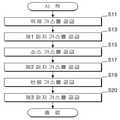
도 1은 본 발명의 기술적 사상의 몇몇 실시예에 따른 반도체 장치 제조 방법을 설명하기 위한 순서도이다.
도 2는 본 발명의 기술적 사상의 몇몇 실시예에 따른 반도체 장치 제조 방법의 원리를 설명하기 위한 그래프이다.
도 3a 및 도 3b는 본 발명의 기술적 사상의 몇몇 실시예에 따른 반도체 장치 제조 방법을 설명하기 위한 단면도이다.
도 4a 및 도 4b는 본 발명의 기술적 사상의 몇몇 실시예에 따른 반도체 장치 제조 방법에 따라 형성된 박막을 설명하기 위한 단면도이다.
도 5는 본 발명의 기술적 사상의 몇몇 실시예에 따른 반도체 장치 제조 방법에 따라 형성된 박막을 설명하기 위한 사진이다.
도 6 내지 도 18은 본 발명의 기술적 사상의 몇몇 실시예에 따른 반도체 장치 제조 방법을 설명하기 위한 단면도들이다.
도 19은 본 발명의 기술적 사상의 몇몇 실시예에 따른 반도체 장치 제조 방법을 설명하기 위한 순서도이다.
도 20은 본 발명의 기술적 사상의 몇몇 실시예에 따른 반도체 장치 제조 방법을 설명하기 위한 순서도이다.
도 21은 본 발명의 기술적 사상의 몇몇 실시예에 따른 반도체 장치 제조 방법을 설명하기 위한 순서도이다.
도 22는 본 발명의 기술적 사상의 몇몇 실시예에 따른 반도체 장치 제조 방법을 설명하기 위한 순서도이다.
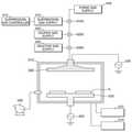
도 23은 본 발명의 기술적 사상의 몇몇 실시예에 따른 반도체 장치 제조 설비를 설명하기 위한 개략도이다.
도 24는 본 발명의 기술적 사상의 몇몇 실시예에 따른 반도체 장치 제조 설비의 동작을 설명하기 위한 타이밍도이다.
도 25은 본 발명의 기술적 사상의 몇몇 실시예에 따른 반도체 장치 제조 설비를 설명하기 위한 개략도이다.
도 26은 본 발명의 기술적 사상의 몇몇 실시예에 따른 반도체 장치 제조 설비를 설명하기 위한 개략도이다.1 is a flowchart illustrating a method of manufacturing a semiconductor device according to some embodiments of the inventive concept.
2 is a graph for explaining a principle of a method of manufacturing a semiconductor device according to some embodiments of the inventive concept.
3A and 3B are cross-sectional views illustrating a method of manufacturing a semiconductor device according to some embodiments of the inventive concept.
4A and 4B are cross-sectional views for explaining a thin film formed according to a method of manufacturing a semiconductor device according to some embodiments of the inventive concept.
5 is a photograph for explaining a thin film formed according to a method of manufacturing a semiconductor device according to some embodiments of the inventive concept.
6 to 18 are cross-sectional views illustrating a method of manufacturing a semiconductor device according to some embodiments of the inventive concept.
19 is a flowchart illustrating a method of manufacturing a semiconductor device according to some embodiments of the inventive concept.
20 is a flowchart illustrating a method of manufacturing a semiconductor device according to some embodiments of the inventive concept.
21 is a flowchart illustrating a method of manufacturing a semiconductor device according to some embodiments of the inventive concept.
22 is a flowchart illustrating a method of manufacturing a semiconductor device according to some embodiments of the inventive concept.
23 is a schematic diagram illustrating a semiconductor device manufacturing facility according to some embodiments of the inventive concept.
24 is a timing diagram illustrating an operation of a semiconductor device manufacturing facility according to some embodiments of the inventive concept.
25 is a schematic diagram illustrating a semiconductor device manufacturing facility according to some embodiments of the inventive concept.
26 is a schematic diagram illustrating a semiconductor device manufacturing facility according to some embodiments of the inventive concept.
이하에서, 본 발명의 실시예들에 따른 반도체 장치 제조 방법에 대하여 도면을 참조하여 설명한다.Hereinafter, a method of manufacturing a semiconductor device according to embodiments of the present invention will be described with reference to the drawings.
도 1은 본 발명의 기술적 사상의 몇몇 실시예에 따른 반도체 장치 제조 방법을 설명하기 위한 순서도이다. 도 2는 본 발명의 기술적 사상의 몇몇 실시예에 따른 반도체 장치 제조 방법의 원리를 설명하기 위한 그래프이다. 도 3a 및 도 3b는 본 발명의 기술적 사상의 몇몇 실시예에 따른 반도체 장치 제조 방법을 설명하기 위한 단면도이다. 도 4a 및 도 4b는 본 발명의 기술적 사상의 몇몇 실시예에 따른 반도체 장치 제조 방법에 따라 형성된 박막을 설명하기 위한 단면도이다.1 is a flowchart illustrating a method of manufacturing a semiconductor device according to some embodiments of the inventive concept. 2 is a graph for explaining a principle of a method of manufacturing a semiconductor device according to some embodiments of the inventive concept. 3A and 3B are cross-sectional views illustrating a method of manufacturing a semiconductor device according to some embodiments of the inventive concept. 4A and 4B are cross-sectional views for explaining a thin film formed according to a method of manufacturing a semiconductor device according to some embodiments of the inventive concept.
도 1을 참조하면, 본 발명의 기술적 사상의 몇몇 실시예에 따른 반도체 장치 제조 방법은 억제 가스를 공급하고(S11), 소스 가스를 공급하고(S15), 반응 가스를 공급하는 것(S19)을 포함한다. 또한, 제1 퍼지 가스를 공급하고(S13), 제2 퍼지 가스를 공급하고(S17), 제3 퍼지 가스를 공급하는 것(S20)을 포함할 수 있다.Referring to FIG. 1 , a method for manufacturing a semiconductor device according to some embodiments of the inventive concept includes supplying a suppression gas (S11), supplying a source gas (S15), and supplying a reaction gas (S19). include In addition, it may include supplying the first purge gas (S13), supplying the second purge gas (S17), and supplying the third purge gas (S20).
구체적으로, 본 발명의 기술적 사상의 몇몇 실시예에 따른 반도체 장치 제조 방법은 챔버 내에 배치된 기판 상에 억제 가스를 공급하고(S11), 상기 기판과 비흡착된 억제 가스를 제1 퍼지 가스를 공급하여 제거하고(S13), 이어서, 상기 챔버 내로 소스 가스를 공급하고(S15), 상기 기판과 비흡착된 소스 가스를 제2 퍼지 가스를 공급하여 제거하고(S17), 이어서, 반응 가스를 공급(S19)하여, 상기 기판 상에 흡착된 소스 가스와 반응시킨 후, 제3 퍼지 가스를 공급하여 미반응 소스 가스와 반응 가스를 제거하여 전극층 등을 포함하는 박막을 기판 상에 형성하는 것을 포함할 수 있고, 이러한 방법은 원자층 증착 방법(ALD)으로 수행될 수 있으나, 이에 제한되는 것은 아니다.Specifically, in the method of manufacturing a semiconductor device according to some embodiments of the inventive concept, a suppression gas is supplied to a substrate disposed in a chamber ( S11 ), and a first purge gas is supplied to the suppression gas that is not adsorbed to the substrate. to remove (S13), then, supplying a source gas into the chamber (S15), supplying a second purge gas to remove the source gas non-adsorbed to the substrate (S17), and then supplying a reaction gas ( S19), after reacting with the source gas adsorbed on the substrate, supplying a third purge gas to remove the unreacted source gas and the reactive gas to form a thin film including an electrode layer on the substrate And, this method may be performed by an atomic layer deposition method (ALD), but is not limited thereto.
즉, 본 발명에 따른 반도체 장치 제조 방법은 박막을 형성하는 것을 포함할 수 있다. 예를 들어, 본 발명에 따른 반도체 장치 제조 방법은 기판 또는 유전층 상에 전극층을 형성하는 것을 포함할 수 있다. 상기 전극층은 Ti와 N을 포함하는 화합물을 포함할 수 있고, 예를 들어, TiN, TiSiN, TiAlN, TiBN, TiON, TiAlON, TiCN, TiAlCN, TiOCN, 또는 TiSiCN 일 수 있다.That is, the method for manufacturing a semiconductor device according to the present invention may include forming a thin film. For example, a method of manufacturing a semiconductor device according to the present invention may include forming an electrode layer on a substrate or a dielectric layer. The electrode layer may include a compound including Ti and N, for example, TiN, TiSiN, TiAlN, TiBN, TiON, TiAlON, TiCN, TiAlCN, TiOCN, or TiSiCN.
본 실시예에 따른 반도체 장치 제조 방법에 있어서는 TiN층을 형성하는 것을 예를 들어 설명할 수 있다. 다만, 이는 설명을 위한 예시적인 것으로 본 발명의 기술적 사상이 이에 제한되는 것은 아니다.In the method of manufacturing a semiconductor device according to the present embodiment, the formation of the TiN layer may be described as an example. However, this is an example for description, and the technical spirit of the present invention is not limited thereto.
따라서, 본 실시예에 있어서, 소스 가스를 공급하는 것(S15)은 티타늄계 화합물을 포함하는 소스 가스를 공급하는 것을 포함할 수 있고, 예를 들어, 상기 티타늄계 화합물은 TiCl4 일 수 있으나, 이에 제한되는 것은 아니다. 반응 가스를 공급하는 것(S19)은 질화물계 화합물을 포함하는 반응 가스를 공급하는 것을 포함할 수 있고, 예를 들어, 상기 질화물계 화합물은 NH3 일 수 있으나, 이에 제한되는 것은 아니다.Therefore, in this embodiment, supplying the source gas ( S15 ) may include supplying the source gas including the titanium-based compound, for example, the titanium-based compound may be TiCl4 , However, the present invention is not limited thereto. Supplying the reaction gas ( S19 ) may include supplying the reaction gas including the nitride compound, for example, the nitride compound may be NH3 , but is not limited thereto.
본 발명에 따른 억제 가스는, 상기 소스 가스가 흡착되고자 하는 기판과의 물리적 흡착을 억제할 수 있다. 따라서, 상기 소스 가스가 TiCl4 인 경우에는, 상기 억제 가스는 산소 원자 및 질소 원자를 미포함하고, 상기 소스 가스와 미반응하는 가스일 수 있다.The suppression gas according to the present invention can suppress the physical adsorption of the source gas to the substrate to be adsorbed. Accordingly, when the source gas is TiCl4 , the suppression gas may be a gas that does not contain oxygen atoms and nitrogen atoms and does not react with the source gas.
따라서, 본 발명에 있어서, 억제 가스를 공급하는 것(S11)은 박막을 형성하고자 하는 기판 상에, 소스 가스가 흡착되는 속도를 늦출 수 있다.Therefore, in the present invention, supplying the suppression gas ( S11 ) may slow the rate at which the source gas is adsorbed on the substrate on which the thin film is to be formed.
구체적으로, 억제 가스는 할로겐(halogen) 원자를 포함하거나, 불포화 결합(unsaturated bond)를 포함하는 화합물을 포함할 수 있다. 예를 들어, 억제 가스는 할로겐화 알킬(alkyl halide), 할로겐화 알케닐(alkenyl halide), 할로겐화 알키닐(alkynyl halide), 알켄(alkene), 알킨(alkyne), 또는 이들의 조합 중 적어도 하나를 포함할 수 있다. 예를 들어, 억제 가스는 tetrachloro propane 또는 dichloro ethylene을 포함할 수 있다.Specifically, the suppressing gas may include a compound including a halogen atom or an unsaturated bond. For example, the suppressing gas may include at least one of an alkyl halide, an alkenyl halide, an alkynyl halide, an alkene, an alkyne, or a combination thereof. can For example, the suppressing gas may include tetrachloro propane or dichloro ethylene.
몇몇 실시예에서, 상기 할로겐화 알킬, 상기 할로겐화 알케닐, 상기 할로겐화 알키닐은 각각 1개 내지 10개의 탄소 원자를 포함하는 선형, 가지형, 또는 고리형 할로겐화 탄화수소기(halogenated hydrocarbon group)를 포함할 수 있다. 또한, 상기 알켄 및 상기 알킨은 각각 1개 내지 10개의 탄소 원자를 포함하는 선형, 가지형, 또는 고리형 탄화수소기(hydrocarbon group)를 포함할 수 있다.In some embodiments, the halogenated alkyl, the halogenated alkenyl, and the halogenated alkynyl may each include a linear, branched, or cyclic halogenated hydrocarbon group containing 1 to 10 carbon atoms. there is. In addition, the alkene and the alkyne may include a linear, branched, or cyclic hydrocarbon group each containing 1 to 10 carbon atoms.
상기 할로겐화 탄화수소기 또는 상기 탄화수소기의 탄소 원자의 개수가 10개를 초과하는 경우에, 억제 가스는 소스 가스의 기판 상의 물리적 흡착을 용이하게 억제하지 못할 수 있다.When the number of the halogenated hydrocarbon group or the number of carbon atoms in the hydrocarbon group exceeds 10, the suppression gas may not readily suppress the physical adsorption of the source gas on the substrate.
몇몇 실시예에서, 상기 할로겐화 알킬, 상기 할로겐화 알케닐, 상기 할로겐화 알키닐은 각각 1개 내지 10개의 할로겐 원자를 포함할 수 있다.In some embodiments, each of the alkyl halide, the alkenyl halide, and the alkynyl halide may include 1 to 10 halogen atoms.
상기 할로겐화 알킬, 상기 할로겐화 알케닐, 상기 할로겐화 알키닐의 할로겐 원자의 개수가 10개를 초과하는 경우에, 억제 가스는 소스 가스의 기판 상의 물리적 흡착을 용이하게 억제하지 못할 수 있다.When the number of halogen atoms of the alkyl halide, the alkenyl halide, or the alkynyl halide is more than 10, the suppression gas may not readily suppress the physical adsorption of the source gas on the substrate.
도 2를 참조하면, 억제 가스 공급 후 퍼지 시간에 따른 증착 속도를 확인할 수 있다. 도 2에 있어서, a선은 억제 가스를 포함하지 않고, TiCl4 소스 가스와 NH3반응 가스를 이용하여 ALD를 수행한 경우의 증착 속도를, b선의 경우, TiCl4 소스 가스와 NH3반응 가스와 더불어, Tetrachloro propane 억제 가스를 이용하여 ALD를 수행한 경우의 증착 속도를, c선의 경우, TiCl4 소스 가스와 NH3반응 가스와 더불어, Dichloro Ethylene 억제 가스를 이용하여 ALD를 수행한 경우의 증착 속도를 나타낸다.Referring to FIG. 2 , the deposition rate according to the purge time after the suppression gas is supplied can be confirmed. In FIG. 2 , a line a does not contain a suppressor gas, and the deposition rate when ALD is performed using a TiCl4 source gas and NH3 reaction gas, and a line b, TiCl4 source gas and NH3 reaction gas In addition, the deposition rate when ALD was performed using tetrachloro propane suppression gas, and in the case of c line, TiCl4 source gas and NH3 reaction gas, and deposition when ALD was performed using dichloro ethylene suppression gas indicates speed.
억제 가스를 사용한 경우가 억제 가스를 사용하지 않은 경우와 비교하여 상대적으로 박막의 성장 속도가 늦음을 확인할 수 있다. 즉, 본 발명에 있어서, 억제 가스는 기판 상에 흡착되어, 소스 가스의 과흡착을 저지하여, 박막의 성장 속도를 늦출 수 있고, 컨포말한 박막층을 형성할 수 있다. 또한, 억제 가스 공급 후 퍼지 시간에 따라 증착 속도의 증가가 없음을 확인할 수 있다. 이 현상은 억제 가스가 쉽게 탈착되지 않음을 나타내며, 공정시간에 따라 억제제의 효과가 감소하지 않는 것을 의미한다.It can be seen that the growth rate of the thin film is relatively slow when the suppression gas is used compared to the case where the suppression gas is not used. That is, in the present invention, the suppression gas is adsorbed on the substrate to prevent overadsorption of the source gas, thereby slowing the growth rate of the thin film, and forming a conformal thin film layer. In addition, it can be seen that there is no increase in the deposition rate according to the purge time after the suppression gas is supplied. This phenomenon indicates that the inhibitory gas is not easily desorbed, which means that the effect of the inhibitor does not decrease with the process time.
도 3a 및 도 3b를 통해, 본 발명에 따른 반도체 장치 제조 방법을 통해 컨포말한 박막층을 형성하는 원리를 설명한다.A principle of forming a conformal thin film layer through the method for manufacturing a semiconductor device according to the present invention will be described with reference to FIGS. 3A and 3B .
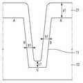
도 3a는 본 발명에 따른 억제 가스를 사용하지 않고, 소스 가스와 반응 가스를 사용하여 박막을 형성하는 경우의 소스 가스의 흡착 정도를, 도 3b는 본 발명에 따른 억제 가스와 소스 가스 및 반응 가스를 사용하여 박막을 형성하는 경우의 소스 가스의 흡착 정도를 설명하기 위한 단면도들이다.Figure 3a shows the degree of adsorption of the source gas in the case of forming a thin film using the source gas and the reaction gas without using the suppression gas according to the present invention, and Figure 3b is the suppression gas, the source gas, and the reaction gas according to the present invention Cross-sectional views for explaining the degree of adsorption of the source gas in the case of forming a thin film using
도 3a 및 도 3b를 참조하면, 기판(10)은 종횡비가 큰 홀(S19)을 가지며, 상부면(A), 하부면(C) 및 측벽(B)을 개시한다. 여기서, 화살표 길이는 해당 영역에서의 소스 가스의 흡착 정도를 의미한다.Referring to FIGS. 3A and 3B , the
즉, 본 발명에 따른 억제 가스를 사용하지 않고 박막을 형성하는 경우(도 3a)에는, 시간이 흐를수록 상부면(A) 상에는 소스 가스의 흡착 정도(a1)가 하부면(C) 상에서의 소스 가스의 흡착 정도(c1)보다 크다.That is, in the case of forming a thin film without using the suppression gas according to the present invention (FIG. 3A), the degree of adsorption (a1) of the source gas on the upper surface (A) increases as time passes by the source on the lower surface (C). It is greater than the degree of gas adsorption (c1).
그러나, 본 발명에 따른 억제 가스를 사용하는 경우(도 3b)에는, 시간이 흐를수록 상부면(A) 상에는 소스 가스의 흡착 정도(a2)와 하부면(C) 상에서의 소스 가스의 흡착 정도(c2)가 유사하다. 이는 상부면(A)에서의 소스 가스의 과흡착이 억제 가스를 통해 억제되기 때문이다. 보다 구체적으로는, 기판(10)의 상부면(A)에서의 소스 가스의 물리적 흡착에 의한 과흡착을 억제 가스가 억제할 수 있다.However, in the case of using the suppression gas according to the present invention (FIG. 3b), the degree of adsorption of the source gas on the upper surface (A) (a2) and the degree of adsorption of the source gas on the lower surface (C) over time ( c2) is similar. This is because over-adsorption of the source gas on the upper surface A is suppressed through the suppression gas. More specifically, the suppression gas can suppress overadsorption due to physical adsorption of the source gas on the upper surface A of the
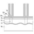
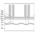
도 4a 및 도 4b는 도 3a 및 도 3b를 통해 형성된 박막(21)의 균일도를 확인할 수 있다. 도 4a 및 도 4b를 참조하면, 억제 가스를 통해 기판(10) 상부면(A)에서의 소스 가스의 과흡착이 억제된 경우(도 4b)의 박막(21)의 두께는 억제 가스를 사용하지 않은 경우(도 4a)와 비교하여, 전 영역에서 상대적으로 균일한 두께를 가지고 형성됨을 알 수 있다.4A and 4B show the uniformity of the
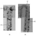
도 5는 도 4a 및 도 4b에 따라 형성된 박막의 영역에 따른 두께를 확인하기 위한 사진이다. 도 5(a)는 억제 가스를 사용하지 않고, 소스 가스와 반응 가스를 사용하여 원자층 증착 공정을 수행한 경우를 도 5(b)는 억제 가스, 소스 가스 및 반응 가스를 사용하여 원자층 증착 공정을 수행한 경우를 각각 나타낸다.5 is a photograph for confirming the thickness according to the region of the thin film formed according to FIGS. 4A and 4B. 5(a) shows a case in which the atomic layer deposition process is performed using a source gas and a reactive gas without using a suppressor gas, and FIG. Each case in which the process was performed is shown.
도 5를 참조하면, 억제 가스를 사용하지 않은 경우의 박막(L1)은 트렌치(H1) 내에서는 상대적으로 얇고, 트렌치(H1) 밖에서는 상대적으로 두꺼움을 확인할 수 있다. 이와 달리, 억제 가스를 사용한 경우의 박막(L2)은 트렌치(H2)의 안과 밖에서 균일한 두께를 가지고 있음을 확인할 수 있다.Referring to FIG. 5 , it can be seen that the thin film L1 in the case where the suppression gas is not used is relatively thin inside the trench H1 and relatively thick outside the trench H1 . On the contrary, it can be seen that the thin film L2 in the case of using the suppression gas has a uniform thickness inside and outside the trench H2.
즉, 본 발명에 따른 반도체 장치 제조 방법은 종횡비가 큰 트렌치 영역 내에, 박막을 형성하는 경우에 균일한 두께를 가지는 박막을 형성하는 방법을 포함할 수 있다. 따라서, 본 발명에 따른 반도체 장치 제조 방법으로 형성하고자 하는 박막은 예를 들어, 소자 분리 영역(Shallow Trench Isolation; STI), 층간 절연막(Inter Layer Dielectric layer; ILD), 메탈간 절연막(Inter Metal Dielectric layer; LMD), 실린더형 커패시터 영역 등과 같이, 종횡비가 큰 영역에 형성하는 박막일 수 있다.That is, the method of manufacturing a semiconductor device according to the present invention may include a method of forming a thin film having a uniform thickness when forming the thin film in a trench region having a large aspect ratio. Accordingly, the thin film to be formed by the method for manufacturing a semiconductor device according to the present invention is, for example, a shallow trench isolation (STI), an inter-layer dielectric layer (ILD), or an inter-metal dielectric layer (Inter Metal Dielectric layer). ; LMD) may be a thin film formed in a region having a large aspect ratio, such as a cylindrical capacitor region.
이어서, 실린더형 커패시터를 포함하는 반도체 장치 제조 방법을 예를 들어 본 발명의 기술적 사상을 설명한다. 앞서 설명한 바와 같이, 실린더형 커패시터를 포함하는 반도체 장치 제조 방법은 예시적인 것일 뿐이며, 본 발명의 기술적 사상은 종횡비가 큰 영역 상에 균일한 두께를 가지는 박막을 형성하는 방법에 적용될 수 있다.Next, the technical idea of the present invention will be described by taking a semiconductor device manufacturing method including a cylindrical capacitor as an example. As described above, the method of manufacturing a semiconductor device including a cylindrical capacitor is only exemplary, and the technical spirit of the present invention may be applied to a method of forming a thin film having a uniform thickness on a region having a large aspect ratio.
이어서, 도 1 및 도 6 내지 도 18을 참조하여, 본 발명의 기술적 사상의 몇몇 실시예에 따른 반도체 장치 제조 방법을 설명한다.Next, a method of manufacturing a semiconductor device according to some embodiments of the inventive concept will be described with reference to FIGS. 1 and 6 to 18 .
도 6 내지 도 18은 본 발명의 기술적 사상의 몇몇 실시예에 따른 반도체 장치 제조 방법을 설명하기 위한 단면도들이다.6 to 18 are cross-sectional views illustrating a method of manufacturing a semiconductor device according to some embodiments of the inventive concept.
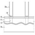
도 6을 참조하면, 본 발명의 기술적 사상의 몇몇 실시예에 따른 반도체 장치 제조 방법으로 제조되는 반도체 장치는 기판(100), 제1 층간 절연막(135), 제2 층간 절연막(137), 식각 정지막(140), 도전 금속층(150), 커패시터(CP1), 캡핑막(220)을 포함할 수 있다.Referring to FIG. 6 , a semiconductor device manufactured by the method of manufacturing a semiconductor device according to some embodiments of the inventive concept includes a
기판(100)은 예를 들어, 메모리 셀 어레이 영역 및 페리 영역을 포함하도록 구성될 수 있다. 또한 기판(100)에는 소자간 분리를 위해 필드 산화막(130)이 형성될 수 있고, 스페이서(125)를 구비한 게이트 전극(120)이 형성될 수 있다.The
또한 기판(100)은 Si, Ge, SiGe, GaP, GaAs, SiC, SiGeC, InAs 및 InP로 이루어지는 군에서 선택되는 하나 이상의 반도체 재료로 이루어질 수 있고, SOI(silicon on insulator) 기판을 사용하여도 무방하다.In addition, the
제1 층간 절연막(135)은 게이트 전극(120)을 포함한 기판(100)의 전면에 형성될 수 있다. 또한 제1 층간 절연막(135)을 관통하여 게이트 전극(120) 사이에 비트라인 콘택(162)이 형성될 수 있다. 비트라인 콘택(162)은 기판(100)과 비트라인(164)을 접속시켜주는 역할을 수행하고, 비트라인 콘택(162)을 통해 기판(100)과 접속된 비트라인(164)은 제1 층간 절연막(135) 상에 형성될 수 있다.The first
제2 층간 절연막(137)은 제1 층간 절연막(135) 상에 형성될 수 있다. 또한 제1 및 제2 층간 절연막(135, 137)을 관통하여 기판(100)과 접속되는 스토리지노드 콘택(172)이 형성될 수 있다. 스토리지노드 콘택(172)은 예를 들어, 폴리실리콘플러그, 티타늄나이트라이드 및 티타늄 배리어의 적층 구조를 포함할 수 있으나, 이에 한정되는 것은 아니다.The second
식각 정지막(140)은 제2 층간 절연막(137) 및 스토리지노드 콘택(172) 상에 형성될 수 있다. 구체적으로, 식각 정지막(140)은 식각 정지막(140) 상에 형성되는 몰드막(도 9의 145)의 식각 공정시, 식각 정지막(140) 아래로 식각이 이루어지지 않게하는 역할을 수행할 수 있다.The
또한 식각 정지막(140)은 예를 들어, 실리콘 질화물을 포함할 수 있으나, 이에 한정되는 것은 아니다. 다만, 몰드막(도 9의 145)에 이루어지는 식각 공정이 식각 정지막(140) 아래로 진행되는 것을 멈춰야 하기에, 몰드막(도 9의 145)과 다른 재질을 포함한다.Also, the
도전 금속층(150)은 스토리지노드 콘택(172) 상에 형성되는 스토리지노드 홀(도 13의 153)의 하면에 배치될 수 있다. 즉, 도전 금속층(150)은 스토리지노드 홀(도 13의 153)과 하부 전극층(200a) 사이에 배치될 수 있다. 다만, 도전 금속층(150)은 커패시터의 구조에 따라 생략될 수도 있다. 도전 금속층(150)은 예를 들어, Ag, Au, Pt, Al, Cu 중 어느 하나를 포함할 수 있으나, 이에 한정되는 것은 아니다.The
본 실시예에서, 커패시터(CP1)는 예를 들어, OCS(One Cylinder Storage)형 커패시터를 포함할 수 있다. 구체적으로, 커패시터(CP1)는 상면과 하면의 폭이 동일한 스토리지노드 홀(도 12의 153)을 중심으로 형성되기에, 커패시터(CP1)의 상면과 하면의 폭 역시 동일하게 형성될 수 있다. 여기서 "동일하다"의 의미는 공정에 의해서 약간의 오차가 발생하는 것을 포함하는 개념이다. 다만, 이는 본 발명의 기술적 사상의 설명을 위한 예시적인 것이므로, 커패시터(CP1)의 상면과 하면의 폭은 서로 다를 수 있다.In this embodiment, the capacitor CP1 may include, for example, a One Cylinder Storage (OCS) type capacitor. Specifically, since the capacitor CP1 is formed around the
커패시터(CP1)는 하부 전극층(200a), 유전막(205a), 상부 전극층(210a)을 포함할 수 있다.The capacitor CP1 may include a
하부 전극층(200a)은 커패시터(CP1)의 하부 전극으로써, 실린더 형상의 하부 전극을 포함할 수 있다.The
하부 전극층(200a)은 예를 들어, 전도성 산화물을 포함할 수 있다. 즉, 하부 전극층(200a)은 Pt, Ru, Ir, PtO, RuO2, IrO2, SrRuO3, BaRuO3, CaRuO3, (Ba, Sr)RuO3를 포함할 수 있으며, 이들은 단일막으로 이루어지거나 또는 둘 이상이 적층된 형상을 가질 수 있다.The
하부 전극층(200a)은 전도성 산화물 외에도 내화성 금속 또는 내화성 금속 질화물을 포함할 수 있다. 즉, Ti, TiN, W, WN, Ta, TaN, HfN, ZrN, TiAlN, TaSiN, TiSiN, TaAlN, TiBN, TiON, TiAlON, TiCN, TiAlCN, 또는 TiSiCN를 포함할 수 있으며, 이들은 단일막으로 이루어지거나 또는 둘 이상이 적층된 형상을 가질 수 있다.The
하부 전극층(200a)은 도전 금속층(150) 상에 형성되는 경우, 도전 금속층(150)과 다른 물질을 포함할 수 있다. 즉, 하부 전극층(200a)과 도전 금속층(150)이 서로 간에 물리, 화학적 영향을 미치지 않고 구분될 수 있도록 서로 다른 물질을 포함하도록 한다.When the
유전막(205a)은 하부 전극층(200a) 상에 형성될 수 있다. 구체적으로, 유전막(205a)은 실린더 형상의 하부 전극층(200a)의 외측벽, 내측벽 및 하부 전극층(200a) 내부의 하면과 식각 정지막(140) 상에 형성될 수 있다.The
또한 유전막(205a)은 예를 들어, 삼성분계 이상의 물질을 포함할 수 있다. 즉, 유전막(205a)은 (Ba, Sr)TiO3(BST), SrTiO3, BaTiO3, PZT, PLZT, (Ba, Sr)(Zr, Ti)O3(BSZTO), Sr(Zr, Ti)O3(SZTO), Ba(Zr, Ti)O3(BZTO), (Ba, Sr)ZrO3(BSZO), SrZrO3, BaZrO3를 포함할 수 있으나, 이에 제한되는 것은 아니며, 유전막(205a)은 전술한 삼성분계 이상의 유전 물질이 아닌 ZrO2, HfO2, Al2O3, Ta2O5, TiO2 등의 이성분계 유전 물질을 포함할 수 있으며, 이들은 단독으로 형성되거나, 둘 이상이 적층될 수 있다.Also, the
상부 전극층(210a)은 커패시터(CP1)의 상부 전극을 포함할 수 있다.The
구체적으로, 상부 전극층(210a)은 유전막(205a)을 덮으면서 유전막(205a)의 표면 프로파일과 동일한 표면 프로파일을 포함할 수 있다.Specifically, the
상부 전극층(210a)은 예를 들어, Pt, Ru, Ir과 같은 높은 일함수를 갖는 물질을 포함할 수 있다. 즉, 상부 전극층(210a)은 이러한 물질을 포함함으로써, 상부 전극층(210a)과 유전막(205a) 사이의 일함수 차이를 크게 만들어, 커패시터(CP1)의 누설 전류를 제어할 수 있다.The
상부 전극층(210a)은 전도성 산화물을 포함할 수 있다. 예를 들어, 상부 전극층(210a)은 Pt, Ru, Ir, PtO, RuO2, IrO2, SrRuO3, BaRuO3, CaRuO3, (Ba, Sr)RuO3를 포함할 수 있으며, 이들은 단일막으로 이루어지거나 또는 둘 이상이 적층된 형상을 가질 수 있다.The
캡핑막(220)은 상부 전극층(210a)의 그레인 성장 및 응집을 억제하기 위해 상부 전극층(210a) 상에 형성될 수 있다. 구체적으로, 캡핑막(220)으로 사용될 수 있는 물질의 예로는, ZrO2, Al2O3, HfO2, LaAlO3, BaZrO3, SrZrO3, BST, SrTiO3, BaTiO3, TiO2, SiO2을 포함할 수 있으며, 이들은 단일막으로 이루어지거나 또는 둘 이상이 적층된 형상을 가질 수 있다.The
도 6을 참조하면, 본 발명의 기술적 사상의 몇몇 실시예에 따른 반도체 장치 제조 방법으로 제조되는 반도체 장치의 기본 구조에 대해 설명하였다. 이어서, 도 6 내지 도 18을 이용하여, 본 발명의 기술적 사상의 몇몇 실시예에 따른 반도체 장치 제조 방법으로 제조되는 하부 전극층, 유전층 및 상부 전극층에 대해 보다 상세히 설명한다.Referring to FIG. 6 , a basic structure of a semiconductor device manufactured by a method of manufacturing a semiconductor device according to some embodiments of the inventive concept has been described. Next, a lower electrode layer, a dielectric layer, and an upper electrode layer manufactured by a method of manufacturing a semiconductor device according to some embodiments of the inventive concept will be described in detail with reference to FIGS. 6 to 18 .
도 7을 참조하면, 기판(100) 상에 형성된 제2 층간 절연막(137)의 일부 영역을 식각하여 콘택홀을 형성한다. 콘택홀을 형성한 후, 콘택홀 내부에 도전 물질을 채워넣고, 제2 층간 절연막(137)의 상부면이 노출되도록 평탄화함으로써, 스토리지노드 콘택(172)을 형성할 수 있다.Referring to FIG. 7 , a portion of the second
도시하지는 않았지만, 도 7은 도 6에 도시된 식각 정지막(140) 아래의 구조를 포함한다. 즉, 도 7은 후술할 식각 정지막(140)의 형성 공정 이전 단계까지를 포함하는 도면이다.Although not shown, FIG. 7 includes a structure under the
도 8을 참조하면, 제2 층간 절연막(137) 상에 식각 정지막(140)을 형성한다.Referring to FIG. 8 , an
식각 정지막(140)은 예를 들어, 실리콘 질화물을 포함할 수 있으나, 이에 한정되는 것은 아니다. 또한 식각 정지막(140)은 실리콘 질화물을 화학기상증착법으로 증착하여 형성할 수 있다.The
도 9을 참조하면, 식각 정지막(140) 상에 몰드막(145)을 형성한다.Referring to FIG. 9 , a
구체적으로, 몰드막(145)은 커패시터의 하부 전극을 성형하기 위하여 제공되는 막이다. 따라서, 몰드막(145)은 형성하고자 하는 하부 전극의 높이와 동일하거나 더 높게 형성될 수 있다.Specifically, the
몰드막(145)은 예를 들어, 폴리실리콘을 포함할 수 있으나, 이에 한정되는 것은 아니다. 구체적으로, 몰드막(145)은 식각 정지막(140)과의 식각 선택비가 높은 물질로 형성되어야 한다. 또한 몰드막(145)은 후술할 습식 식각 공정을 통해 용이하게 제거될 수 있는 물질로 형성되어야 한다.The
도 10을 참조하면, 몰드막(145) 상에 마스크 패턴(147)을 형성한다.Referring to FIG. 10 , a
구체적으로, 마스크 패턴(147)은 후술하는 몰드막(145)의 식각 공정시, 마스크 역할을 하는 것으로, 마스크 패턴(147) 간의 폭은 스토리지노드 홀(도 13의 153)과 동일한 폭으로 형성될 수 있다. 여기서 "동일하다"의 의미는 공정에 의해서 약간의 오차가 발생하는 것을 포함하는 개념이다.Specifically, the
도 11 및 도 12를 참조하면, 마스크 패턴(147)을 식각 마스크로 몰드막(145)을 식각한다.11 and 12 , the
구체적으로, 마스크 패턴(147)을 식각 마스크로 이용하여 몰드막(145)을 습식 식각하여, 스토리지 노드 콘택(172)의 상면을 노출 시킬 수 있다. 이어서, 노출된 스토리지 노드 콘택(172) 상면 상에 도전 금속층(150)을 형성할 수 있으나, 이에 제한되는 것은 아니다, 따라서, 도전 금속층(150)의 형성은 생략될 수 있다.Specifically, the
또한 스토리지노드 홀(153)을 형성한 후, 마스크 패턴(147)을 제거할 수 있다.Also, after the
도 13를 참조하면, 스토리지노드 홀(도 12의 153)의 측벽, 하면 및 몰드막(145)의 상면을 따라 제1 전극층(200)을 형성한다.Referring to FIG. 13 , the
구체적으로, 제1 전극층(200)은 스토리지노드 홀(153) 내부를 채우지 않으면서, 스토리지노드 홀(153)의 측벽, 하면 및 몰드막(145)의 상면의 프로파일과 동일한 프로파일을 갖도록 형성될 수 있다.Specifically, the
제1 전극층(200)은 금속을 포함하고, 제1 전극층(200)으로써 사용할 수 있는 물질은 전도성 산화물을 포함할 수 있으나, 이에 한정되는 것은 아니다. 즉, 제1 전극층(200)으로 사용할 수 있는 물질의 예로는 Pt, Ru, Ir, PtO, RuO2, IrO2, SrRuO3, BaRuO3, CaRuO3, (Ba, Sr)RuO3을 들 수 있으며, 이들은 단일막으로 이루어지거나 또는 둘 이상이 적층된 형상을 가질 수 있다.The
또한, 제1 전극층(200)은 금속 질화물을 포함할 수 있다. 즉, 제1 전극층(200)으로 사용될 수 있는 물질의 구체적인 예로는 Ti, TiN, W, WN, Ta, TaN, HfN, ZrN, TiAlN, TaSiN, TiSiN, TaAlN, TiBN, TiON, TiAlON, TiCN, TiAlCN, 또는 TiSiCN을 들 수 있으며, 이들은 단일막으로 이루어지거나 또는 둘 이상이 적층된 형상을 가질 수 있다.Also, the
제1 전극층(200)은 원자층 적층법, 화학기상증착법 또는 물리기상증착법으로 형성할 수 있다. 그러나, 제1 전극층(200)은 스텝 커버리지(step coverage) 특성이 우수한 원자층 적층법으로 형성하는 것이 가장 바람직하다.The
즉, 제1 전극층(200)은 도 1을 통해 설명한 장치 제조 방법을 통해 형성될 수 있다.That is, the
도 1 및 도 13을 참조하면, 제1 전극층(200)을 스토리지노드 홀(153)의 측벽, 하면 및 몰드막(145)의 상면 상에 형성하는 것은, 기판(100)이 배치된 원자층 증착 장치의 챔버 내로 억제 가스를 공급(S11)하는 것을 포함한다.1 and 13 , the formation of the
억제 가스를 공급하는 것(S11)은 산소 원자 및 질소 원자를 미포함하고, 상기 소스 가스와 미반응하는 가스를 공급하는 것을 포함할 수 있다.Supplying the suppression gas ( S11 ) may include supplying a gas that does not contain oxygen atoms and nitrogen atoms and does not react with the source gas.
구체적으로, 억제 가스는 할로겐(halogen) 원자를 포함하거나, 불포화 결합(unsaturated bond)를 포함하는 화합물을 포함할 수 있다. 예를 들어, 억제 가스는 할로겐화 알킬(alkyl halide), 할로겐화 알케닐(alkenyl halide), 할로겐화 알키닐(alkynyl halide), 알켄(alkene), 알킨(alkyne), 또는 이들의 조합 중 적어도 하나를 포함할 수 있다. 예를 들어, 억제 가스는 tetrachloro propane 또는 dichloro ethylene을 포함할 수 있다.Specifically, the suppressing gas may include a compound including a halogen atom or an unsaturated bond. For example, the suppressing gas may include at least one of an alkyl halide, an alkenyl halide, an alkynyl halide, an alkene, an alkyne, or a combination thereof. can For example, the suppressing gas may include tetrachloro propane or dichloro ethylene.
상기 억제 가스를 소정의 시간 동안 공급하면, 스토리지노드 홀(153)의 측벽, 하면 및 몰드막(145)의 상면의 표면에 억제 가스가 물리적 및/또는 화학적으로 흡착되거나, 챔버 내부에 머물게 된다.When the suppression gas is supplied for a predetermined time, the suppression gas is physically and/or chemically adsorbed onto the sidewall, lower surface of the
이이서, 스토리지노드 홀(153)의 측벽, 하면 및 몰드막(145)의 상면과 비흡착된 가스는 제1 퍼지 가스를 공급하여(S13) 제거한다. 상기 제1 퍼지 가스로는 비활성 가스가 사용될 수 있으며, 비활성 가스는 Ar, He, Kr, Xe 및 N2, 또는 이들의 조합일 수 있다. 또는, 펌핑(pumping)에 의해 상기 억제 가스를 퍼지할 수 있다. 퍼지 가스 공급 및 펌핑을 같이 진행하여 상기 억제 가스를 퍼지할 수도 있음은 물론이다.Accordingly, the gas not adsorbed to the sidewall, the lower surface of the
이어서, 상기 챔버 내에 소스 가스를 공급한다(S15).Then, a source gas is supplied into the chamber (S15).
챔버 내로, 소스 가스를 소정의 시간 동안 공급하면, 스토리지노드 홀(153)의 측벽, 하면 및 몰드막(145)의 상면의 표면에 소스 가스가 반응 또는 화학 흡착되고, 나머지는 반응 또는 화학 흡착된 소스 가스 표면에 물리적으로 흡착되거나, 챔버 내부에 머물게 된다.When the source gas is supplied into the chamber for a predetermined time, the source gas is reacted or chemically adsorbed on the sidewall, the lower surface of the
다만, 본 실시예에 있어서, 스토리지노드 홀(153)의 측벽, 하면 및 몰드막(145)의 상면의 표면 상에는 이미 억제 가스가 흡착되어 있으므로, 소스 가스의 물리적 흡착은 억제될 수 있다.However, in the present embodiment, since the suppression gas is already adsorbed on the sidewall, the lower surface of the
여기서, 소스 가스와 함께 비활성 가스가 공급될 수도 있다. 비활성 가스는 예를 들어, Ar, He, Kr, Xe, N2 또는 이들의 조합일 수 있다. 상기 소스 가스를 공급하는 것은 티타늄계 화합물을 포함하는 소스 가스를 공급하는 것을 포함할 수 있고, 예를 들어, 상기 티타늄계 화합물은 TiCl4 일 수 있으나, 이에 제한되는 것은 아니다.Here, an inert gas may be supplied together with the source gas. The inert gas may be, for example, Ar, He, Kr, Xe, N2 or a combination thereof. The supplying of the source gas may include supplying the source gas including the titanium-based compound, for example, the titanium-based compound may be TiCl4 , but is not limited thereto.
이어서, 기판과 반응하지 않은 소스 가스를 퍼지하기 위해, 제2 퍼지 가스를 공급한다(S17).Next, in order to purge the source gas that has not reacted with the substrate, a second purge gas is supplied ( S17 ).
이 때, 소스 가스를 퍼지하는 것은 제2 퍼지 가스를 공급하여 수행할 수 있다. 제2 퍼지 가스로는 비활성 가스가 사용될 수 있으며, 비활성 가스는 Ar, He, Kr, Xe 및 N2, 또는 이들의 조합일 수 있다. 또는, 펌핑(pumping)에 의해 소스 가스를 퍼지할 수 있다. 제2 퍼지 가스 공급 및 펌핑을 같이 진행하여 소스 가스를 퍼지할 수도 있음은 물론이다.In this case, the purging of the source gas may be performed by supplying the second purge gas. An inert gas may be used as the second purge gas, and the inert gas may be Ar, He, Kr, Xe, and N2 , or a combination thereof. Alternatively, the source gas may be purged by pumping. It goes without saying that the source gas may be purged by simultaneously supplying and pumping the second purge gas.
이어서, 기판(100)에 바이어스를 인가하여 기판에 수직으로 전기장을 형성할 수 있다. 한다. 기판(100)에 바이어스를 인가하는 것은 다양한 방법으로 구현할 수 있다. 예를 들어, 챔버의 상부 및 하부에 각각 장착된 전극 사이에 바이어스를 인가하여 기판(100)에 수직으로 전기장을 형성할 수 있다. 또는, 기판(100)이 안착된 척 상부 및 하부에 바이어스를 인가하여 기판(100)에 수직으로 전기장을 형성할 수 있다. 전기장의 방향은 형성하려는 박막의 종류에 따라, 공급되는 반응 가스에 따라 달라질 수 있다.Then, a bias may be applied to the
이어서, 상기 챔버 내에 반응 가스를 공급한다(S19).Then, a reaction gas is supplied into the chamber (S19).
이 때, 기판(100)에 수직으로 전기장을 형성한 상태에서 반응 가스를 공급하고 플라즈마화 한다.At this time, a reaction gas is supplied and plasma is formed in a state in which an electric field is formed perpendicularly to the
반응 가스를 공급하고 플라즈마화 하면, 플라즈마화된 반응 가스는 불안정한 에너지 상태를 가지나, 반응성이 크다. When a reaction gas is supplied and plasma is formed, the plasma-ized reaction gas has an unstable energy state, but has high reactivity.
플라즈마화된 반응 가스는 기판(100)에 수직으로 형성된 전기장에 반응하여, 스토리지노드 홀(153)의 측벽, 하면 및 몰드막(145)의 상면의 표면 상에 흡착된 소스 가스와 반응하여, 제1 전극층(200)을 형성한다.The plasma-ized reaction gas reacts with an electric field formed perpendicular to the
이어서, 반응하지 않은 반응 가스를 퍼지한다. 이러한 도 1의 과정을 반복하여, 원하는 두께의 박막을 증착할 수 있다.Then, the unreacted reaction gas is purged. By repeating the process of FIG. 1, a thin film having a desired thickness may be deposited.
한편, 상기에서의 설명은 전기장이 기판에 수직인 방향으로 형성되었을 때를 예를 들어 설명한 것이다. 보다 효율적인 증착을 위하여 전기장의 방향을 조절할 수 있음은 물론이다.Meanwhile, in the above description, an example is given when the electric field is formed in a direction perpendicular to the substrate. It goes without saying that the direction of the electric field can be adjusted for more efficient deposition.
도 14 및 도 15를 참조하면, 제1 전극층(200) 상에 스토리지노드 홀(도 12의 153) 내부를 채우는 희생막(203)을 형성한다.14 and 15 , a
희생막(203)은 몰드막(145)과 동일한 특성을 갖는 물질로 형성될 수 있으나, 이에 한정되는 것은 아니다.The
희생막(203)을 형성한 후, 몰드막(145)의 상면이 노출될 때까지 희생막(203) 및 제1 전극층(200)을 평탄화한다. 평탄화 공정은 예를 들어, CMP공정을 포함할 수 있으나, 이에 한정되는 것은 아니다.After the
평탄화 공정을 완료하면, 실린더 형상의 하부 전극층(200a)이 형성될 수 있다. 실린더 형상의 하부 전극층(200a)은 OCS형 커패시터의 하부 전극 역할을 수행할 수 있다.Upon completion of the planarization process, a cylindrical
하부 전극층(200a)을 형성한 후, 하부 전극층(200a)을 열처리하는 공정이 더 포함될 수 있다.After forming the
구체적으로, 열처리 공정을 수행하면, 유전막(도 17의 205a)을 형성하기 전에 하부 전극층(200a)의 그레인을 충분히 성장시킬 수 있다. 즉, 유전막(도 17의 205a)을 형성한 이 후에는 하부 전극층(200a)의 그레인 성장이 일어나지 않게되고, 후속 공정에서, 하부 전극층(200a)의 그레인 성장에 따른 유전막(도 17의 205a)의 특성 변화가 발생되지 않을 수 있다.Specifically, when the heat treatment process is performed, the grains of the
도 16을 참조하면, 몰드막(145) 및 희생막(203)을 제거한다.Referring to FIG. 16 , the
제거 공정 시, 실린더 형상의 하부 전극층(200a)이 손상되지 않아야 하기 때문에, 플라즈마에 의한 어택이 발생되지 않는 습식 식각 공정을 통해 몰드막(145) 및 희생막(203)을 제거하는 것이 바람직하다.During the removal process, since the cylindrical
몰드막(145) 및 희생막(203)을 제거함으로써, 실린더 형상의 하부 전극층(200a)의 외측벽 및 내측벽이 모두 외부에 노출될 수 있다.By removing the
도 17를 참조하면, 하부 전극층(200a) 및 식각 정지막(140) 상에 금속 산화물로 이루어지는 이성분계 이상의 유전물질을 증착시켜 유전막(205a)을 형성한다. 유전막(205a)은 높은 유전율을 가질 수 있다.Referring to FIG. 17 , a
유전막(205a)은 원자층 적층법, 화학기상증착법 또는 물리기상증착법으로 형성할 수 있다. 따라서, 유전층(205a) 역시 도 1을 통해 설명한 반도체 장치 제조 방법을 통해 형성될 수 있다.The
유전막(205a)을 형성한 후, 유전막(205a) 상에 금속을 포함하는 물질을 증착시켜 상부 전극층(210a)을 형성할 수 있다. 상부 전극층(210a) 역시 도 1을 통해 설명한 반도체 장치 제조 방법을 통해 형성될 수 있다.After the
상부 전극층(210a)은 유전막(205a)의 표면 프로파일을 따라 형성될 수 있고, 하부 전극층(200a)들 사이에 생성되는 공간이 상부 전극층(210a)에 의해 완전하게 채워지지 않도록 한다.The
상부 전극층(210a)은 원자층 적층법, 화학기상증착법 또는 물리기상증착법으로 형성할 수 있다. 따라서, 상부 전극층(210a) 역시 도 1을 통해 설명한 반도체 장치 제조 방법을 통해 형성될 수 있다.The
도 18을 참조하면, 상부 전극층(210a)의 상부면 전체를 덮는 캡핑막(220)을 형성한다. 캡핑막(220)은 상부 전극층(210a)의 그레인 성장 및 응집을 억제하기 위하여 형성될 수 있다. 캡핑막(220)을 이용하여, 상부 전극층(210a)의 그레인 성장을 효과적으로 억제하기 위하여, 캡핑막(220)은 실린더 형상의 하부 전극층(200a)들 사이의 공간을 채우도록 형성될 수 있다.Referring to FIG. 18 , a
캡핑막(220)은 예를 들어, 원자층 적층법, 화학기상증착법, 물리기상증착법 또는 SOG법 중 어느 하나의 방법으로 형성할 수 있다.The
결과적으로, 캡핑막(220)을 전술한 공정을 통해 형성함으로써, 도 6에 도시된 반도체 소자(3a)를 제조할 수 있다.As a result, by forming the
본 발명에 있어서, 하부 전극층(200a) 및 상부 전극층(210a)은 도 1에서 설명한 반도체 장치 제조 방법을 통해 제조할 수 있다. 따라서, 일정한 폭을 가지는 하부 전극층(200a) 및 상부 전극층(210a)을 종횡비가 큰 홀(153) 내에 형성할 수 있다.In the present invention, the
상술한 바와 같이, 본 발명의 기술적 사상은 스토리지노드 홀(도 12의 153) 내에 컨포말한 박막을 형성하는 방법으로 제한되는 것은 아니며, 종횡비가 큰 홀 또는 트렌치 내에 컨포말한 박막을 형성하는 방법에 적용될 수 있다.As described above, the technical idea of the present invention is not limited to a method of forming a conformal thin film in a storage node hole (153 in FIG. 12 ), and a method of forming a conformal thin film in a hole or trench having a large aspect ratio can be applied to
이어서, 도 19를 참조하여 본 발명의 기술적 사상의 몇몇 실시예에 따른 반도체 장치 제조 방법을 설명한다.Next, a method of manufacturing a semiconductor device according to some embodiments of the inventive concept will be described with reference to FIG. 19 .
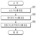
본 실시예에 따른 반도체 장치 제조 방법은 도 1을 통해 설명한 반도체 장치 제조 방법과 비교하여, 소스 가스를 공급한 후에 억제 가스를 공급하는 것을 제외하고는 실질적으로 동일하다. 따라서, 차이점을 위주로 설명한다.The semiconductor device manufacturing method according to the present embodiment is substantially the same as the semiconductor device manufacturing method described with reference to FIG. 1 , except that the suppression gas is supplied after the source gas is supplied. Therefore, the differences will be mainly described.
도 19를 참조하면, 본 실시예에 따른 반도체 장치 제조 방법은 소스 가스를 공급(S21)하고, 제1 퍼지 가스를 공급(S23)하고, 억제 가스를 공급(S25)하고, 제2 퍼지 가스를 공급(S27)하고, 반응 가스를 공급(S29)하는 것을 포함한다.Referring to FIG. 19 , in the semiconductor device manufacturing method according to the present embodiment, a source gas is supplied ( S21 ), a first purge gas is supplied ( S23 ), a suppression gas is supplied ( S25 ), and a second purge gas is supplied. and supplying (S27) and supplying (S29) a reaction gas.
본 실시예에 따른 소스 가스를 공급(S21)하는 것, 제1 퍼지 가스를 공급(S23)하는 것, 억제 가스를 공급(S25)하는 것, 제2 퍼지 가스를 공급(S27)하는 것 및 반응 가스를 공급(S29)하는 것 각각은 도 1의 소스 가스를 공급(S15)하는 것, 제1 퍼지 가스를 공급(S13)하는 것, 억제 가스를 공급(S11)하는 것, 제2 퍼지 가스를 공급하는 것(S17) 및 반응 가스를 공급하는 것(S19)과 실질적으로 동일하다.Supplying the source gas (S21), supplying the first purge gas (S23), supplying the suppression gas (S25), supplying the second purge gas (S27) and the reaction according to the present embodiment The supply of the gas (S29) includes supplying the source gas of FIG. 1 (S15), supplying the first purge gas (S13), supplying the suppression gas (S11), and the second purge gas. It is substantially the same as supplying (S17) and supplying the reaction gas (S19).
다만, 본 실시예에 있어서, 억제 가스를 공급(S25)하는 것은 소스 가스를 공급하는 것(S21) 이후에 수행된다. 즉, 본 발명에 있어서, 억제 가스는 소스 가스가 기판 상에 흡착된 후에 수행되므로, 억제 가스는 상기 기판 상에 흡착된 소스 가스를 밀쳐냄을 통해 상기 기판 상에 흡착될 수 있다. 이에 따라, 상기 기판 상에 흡착된 소스 가스를 밀쳐내고 상기 기판 상에 흡착된 억제 가스는 도 1의 실시예와 마찬가지로 특정 영역에서의 소스 가스의 과흡착을 방지할 수 있다.However, in this embodiment, supplying the suppression gas (S25) is performed after supplying the source gas (S21). That is, in the present invention, since the suppression gas is performed after the source gas is adsorbed onto the substrate, the suppression gas may be adsorbed onto the substrate by pushing the source gas adsorbed onto the substrate. Accordingly, the source gas adsorbed on the substrate is repelled, and the suppression gas adsorbed on the substrate may prevent over-adsorption of the source gas in a specific region as in the embodiment of FIG. 1 .
이를 통해, 본 실시예에 따른 반도체 장치 제조 방법은 기판 상에 컨포말한 박막을 형성할 수 있다. 이를 통해, 기판 상에 컨포말한 박막을 형성할 수 있다.Through this, the semiconductor device manufacturing method according to the present exemplary embodiment may form a conformal thin film on the substrate. Through this, a conformal thin film can be formed on the substrate.
이어서, 도 20를 참조하여 본 발명의 기술적 사상의 몇몇 실시예에 따른 반도체 장치 제조 방법을 설명한다.Next, a method of manufacturing a semiconductor device according to some embodiments of the inventive concept will be described with reference to FIG. 20 .
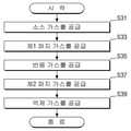
본 실시예에 따른 반도체 장치 제조 방법은 도 1을 통해 설명한 반도체 장치 제조 방법과 비교하여, 반응 가스를 공급한 후에 억제 가스를 공급하는 것을 제외하고는 실질적으로 동일하다. 따라서, 차이점을 위주로 설명한다.The semiconductor device manufacturing method according to the present exemplary embodiment is substantially the same as the semiconductor device manufacturing method described with reference to FIG. 1 , except for supplying the suppression gas after supplying the reaction gas. Therefore, the differences will be mainly described.
도 20를 참조하면, 본 실시예에 따른 반도체 장치 제조 방법은 소스 가스를 공급(S31)하고, 제1 퍼지 가스를 공급(S33)하고, 반응 가스를 공급(S35)하고, 제2 퍼지 가스를 공급(S37)하고, 억제 가스를 공급(S39)하는 것을 포함한다.Referring to FIG. 20 , in the semiconductor device manufacturing method according to the present embodiment, a source gas is supplied ( S31 ), a first purge gas is supplied ( S33 ), a reaction gas is supplied ( S35 ), and a second purge gas is supplied. It includes supplying (S37) and supplying (S39) suppression gas.
본 실시예에 따른 소스 가스를 공급(S31)하는 것, 제1 퍼지 가스를 공급(S33)하는 것, 반응 가스를 공급(S35)하는 것, 제2 퍼지 가스를 공급(S37)하는 것 및 억제 가스를 공급(S39)하는 것 각각은 도 1의 소스 가스를 공급(S15)하는 것, 제1 퍼지 가스를 공급(S13)하는 것, 반응 가스를 공급하는 것(S19), 제2 퍼지 가스를 공급하는 것(S17) 및 억제 가스를 공급(S11)하는 것 과 실질적으로 동일하다.Supplying the source gas (S31), supplying the first purge gas (S33), supplying the reaction gas (S35), supplying the second purge gas (S37) and suppressing the source gas according to the present embodiment Supplying the gas (S39) includes supplying the source gas of FIG. 1 (S15), supplying the first purge gas (S13), supplying the reaction gas (S19), and the second purge gas It is substantially the same as supplying (S17) and supplying the suppression gas (S11).
본 실시예에 있어서, 억제 가스를 공급하는 것(S39)은 반응 가스를 공급(S35)한 후에 수행된다. 따라서, 억제 가스는 과흡착된 소스 가스 및 반응가스를 특정 영역에서 불어내는 역할을 수행할 수 있다. 이를 통해, 본 실시예에 따른 반도체 장치 제조 방법은 기판 상에 컨포말한 박막을 형성할 수 있다.In this embodiment, supplying the suppression gas ( S39 ) is performed after supplying the reaction gas ( S35 ). Accordingly, the suppression gas may serve to blow the over-adsorbed source gas and the reaction gas from a specific region. Through this, the semiconductor device manufacturing method according to the present exemplary embodiment may form a conformal thin film on the substrate.
이어서, 도 21를 참조하여 본 발명의 기술적 사상의 몇몇 실시예에 따른 반도체 장치 제조 방법을 설명한다.Next, a method of manufacturing a semiconductor device according to some embodiments of the inventive concept will be described with reference to FIG. 21 .
본 실시예에 따른 반도체 장치 제조 방법은 도 1을 통해 설명한 반도체 장치 제조 방법과 비교하여, 소스 가스와 억제 가스를 함께 공급하는 것을 제외하고는 실질적으로 동일하다. 따라서, 차이점을 위주로 설명한다.The semiconductor device manufacturing method according to the present exemplary embodiment is substantially the same as the semiconductor device manufacturing method described with reference to FIG. 1 , except that the source gas and the suppression gas are supplied together. Therefore, the differences will be mainly described.
도 21을 참조하면, 본 실시예에 따른 반도체 장치 제조 방법은 소스 가스와 억제 가스를 공급(S41)하고, 제1 퍼지 가스를 공급(S43)하고, 반응 가스를 공급(S45)하는 것을 포함한다.Referring to FIG. 21 , the semiconductor device manufacturing method according to the present embodiment includes supplying a source gas and a suppression gas ( S41 ), supplying a first purge gas ( S43 ), and supplying a reaction gas ( S45 ). .
본 실시예에 따른 소스 가스와 억제 가스를 공급(S41)하는 것, 제1 퍼지 가스를 공급(S43)하는 것, 반응 가스를 공급(S45)하는 것 각각은 도 1의 소스 가스를 공급(S15)하는 것, 억제 가스를 공급(S11)하는 것, 제1 퍼지 가스를 공급(S13)하는 것, 반응 가스를 공급하는 것(S19)과 실질적으로 동일하다.Supplying the source gas and the suppression gas ( S41 ), supplying the first purge gas ( S43 ), and supplying the reaction gas ( S45 ) according to the present embodiment each supply the source gas of FIG. 1 ( S15 ) ), supplying the suppression gas (S11), supplying the first purge gas (S13), and supplying the reaction gas (S19) are substantially the same.
본 실시예에 있어서, 소스 가스와 억제 가스는 함께 공급(S41)될 수 있다. 따라서, 억제 가스는 소스 가스가 기판 상에 흡착되는 것을 억제하면서, 기판 상에 흡착될 수 있다. 이를 통해, 기판 상에 컨포말한 박막을 형성할 수 있다.In this embodiment, the source gas and the suppression gas may be supplied together ( S41 ). Accordingly, the suppression gas can be adsorbed onto the substrate while suppressing the source gas from adsorbing onto the substrate. Through this, a conformal thin film can be formed on the substrate.
이어서, 도 22를 참조하여 본 발명의 기술적 사상의 몇몇 실시예에 따른 반도체 장치 제조 방법을 설명한다.Next, a method of manufacturing a semiconductor device according to some embodiments of the inventive concept will be described with reference to FIG. 22 .
본 실시예에 따른 반도체 장치 제조 방법은 도 1을 통해 설명한 반도체 장치 제조 방법과 비교하여, 반응 가스와 억제 가스를 함께 공급하는 것을 제외하고는 실질적으로 동일하다. 따라서, 차이점을 위주로 설명한다.The semiconductor device manufacturing method according to the present exemplary embodiment is substantially the same as that of the semiconductor device manufacturing method described with reference to FIG. 1 , except that the reactive gas and the suppressing gas are supplied together. Therefore, the differences will be mainly described.
도 22을 참조하면, 본 실시예에 따른 반도체 장치 제조 방법은 소스 가스를 공급(S51)하고, 제1 퍼지 가스를 공급(S53)하고, 반응 가스와 억제 가스를 공급(S55)하는 것을 포함한다.Referring to FIG. 22 , the semiconductor device manufacturing method according to the present exemplary embodiment includes supplying a source gas ( S51 ), supplying a first purge gas ( S53 ), and supplying a reaction gas and a suppression gas ( S55 ). .
본 실시예에 따른 소스 가스를 공급(S51)하는 것, 제1 퍼지 가스를 공급(S53)하는 것, 반응 가스와 억제 가스를 공급(S55)하는 것 각각은 도 1의 소스 가스를 공급(S15)하는 것, 제1 퍼지 가스를 공급(S13)하는 것, 반응 가스를 공급하는 것(S19) 및 억제 가스를 공급(S11)하는 것 실질적으로 동일하다.Supplying the source gas ( S51 ), supplying the first purge gas ( S53 ), and supplying the reaction gas and the suppression gas ( S55 ) according to the present embodiment each supply the source gas of FIG. 1 ( S15 ) ), supplying the first purge gas (S13), supplying the reaction gas (S19), and supplying the suppression gas (S11) are substantially the same.
본 실시예에 있어서, 반응 가스와 억제 가스는 함께 공급(S55)될 수 있다. 따라서, 억제 가스는 기판 상에 기흡착된 소스 가스를 탈착시키면서, 과흡착된 소스 가스를 제거할 수 있다. 이를 통해, 본 실시예에 따른 반도체 장치 제조 방법은 기판 상에 컨포말한 박막을 형성할 수 있다.In this embodiment, the reaction gas and the suppression gas may be supplied together ( S55 ). Accordingly, the suppression gas may remove the over-adsorbed source gas while desorbing the pre-adsorbed source gas on the substrate. Through this, the semiconductor device manufacturing method according to the present exemplary embodiment may form a conformal thin film on the substrate.
이어서, 도 23 및 도 24를 참조하여, 본 발명의 기술적 사상의 몇몇 실시예에 따른 반도체 장치 제조 설비를 설명한다.Next, a semiconductor device manufacturing facility according to some embodiments of the inventive concept will be described with reference to FIGS. 23 and 24 .
이하에서, 플라즈마를 이용하여 박막을 형성하는 반도체 장치 제조 설비를 예를 들어 본 발명의 기술적 사상을 설명한다. 그러나, 이러한 반도체 장치 제조 설비는 예시적인 것일 뿐이며, 본 발명의 기술적 사상은 플라즈마를 이용하지 않고 박막을 형성하는 반도체 장치 제조 설비에 적용될 수도 있다. 예를 들어, 본 발명의 기술적 사상은 열을 이용하여 박막을 형성하는 반도체 장치 제조 설비에 적용될 수도 있다.Hereinafter, the technical idea of the present invention will be described by taking a semiconductor device manufacturing facility for forming a thin film using plasma as an example. However, such a semiconductor device manufacturing facility is merely exemplary, and the technical idea of the present invention may be applied to a semiconductor device manufacturing facility that forms a thin film without using plasma. For example, the technical idea of the present invention may be applied to a semiconductor device manufacturing facility that forms a thin film using heat.
도 23은 본 발명의 기술적 사상의 몇몇 실시예에 따른 반도체 장치 제조 설비를 설명하기 위한 개략도이다.23 is a schematic diagram illustrating a semiconductor device manufacturing facility according to some embodiments of the inventive concept.
도 23을 참조하면, 몇몇 실시예에 따른 반도체 장치 제조 설비는 챔버(310), 기판 받침대(320), 가스 분사부(330), 억제 가스 공급부(410), 소스 가스 공급부(420), 반응 가스 공급부(430), 및 퍼지 가스 공급부(440)를 포함한다.Referring to FIG. 23 , a semiconductor device manufacturing facility according to some exemplary embodiments includes a
챔버(310)는 반응 공간을 갖는 통 형상일 수 있다. 또한, 챔버(310)는 펌프(340), 압력 조절 장치(312), 및 가열 장치(314)를 포함할 수 있다.The
펌프(340)는 챔버(310)와 연결되어, 챔버(310) 내부의 불순물 및 반응 부산물을 배기할 수 있다. 또한, 펌프(340)는 챔버(310) 내부에 진공 상태를 형성하고 이를 유지할 수도 있다.The
압력 조절 장치(312)는 챔버 내부의 압력을 조절할 수 있다. 또한, 가열 장치(314)는 챔버(310) 내부를 가열하여 반응성을 향상시킬 수 있다. 도시하지 않았으나, 챔버(310)는 가열된 챔버(310)를 냉각하기 위한 냉각 장치를 더 포함할 수도 있다.The
기판 받침대(320)는 챔버(310) 내에 배치되어, 기판(S)을 안치할 수 있다. 기판 받침대(320)는 챔버(310)의 하부에 고정될 수 있으나, 필요에 따라 기판 받침대(320)는 챔버(310) 내에서 승강 및/또는 회전할 수도 있다.The
여기서, 기판(S)은 실리콘 웨이퍼일 수 있다. 그러나, 본 발명의 기술적 사상이 이에 제한되는 것은 아니고, 기판(S)은 박막이 형성될 수 있는 다양한 기판을 포함할 수 있다.Here, the substrate S may be a silicon wafer. However, the technical spirit of the present invention is not limited thereto, and the substrate S may include various substrates on which a thin film may be formed.
도시하지 않았으나, 기판 받침대(320)는 그 상면에 기판(S)을 안치하기 위한 장치를 포함할 수도 있다. 예를 들어, 기판 받침대(320)는 기판(S)의 로딩(loading) 및 언로딩(unloading)을 위한 복수의 리프트 핀부를 포함할 수 있다.Although not shown, the
기판 받침대(320)는 하부 전원(325)에 연결될 수 있다. 하부 전원(325)은 기판 받침대(320)에 연결되어, 기판 받침대(320)에 전압을 제공할 수 있다. 본 실시예에서, 하부 전원(325)은 교류(RF) 전원일 수 있으나, 본 발명의 기술적 사상이 이에 제한되는 것은 아니고, 하부 전원(325)은 직류 전원(DC)일 수도 있다.The
가스 분사부(330)는 챔버 내에 배치되어, 챔버(310) 내에 가스를 분사할 수 있다. 구체적으로, 가스 분사부(330)는 소스 가스 공급부(420), 반응 가스 공급부(430), 억제 가스 공급부(410), 또는 퍼지 가스 공급부(440)에 연결되어, 챔버(310) 내에 다양한 가스를 분사할 수 있다. 가스 분사부(330)는 챔버(310)의 상부에 고정될 수 있으나, 필요에 따라 가스 분사부(330)는 챔버(310) 내에서 승강 및/또는 회전할 수도 있다.The
가스 분사부(330)는 상부 전원(335)에 연결될 수 있다. 상부 전원(335)은 가스 분사부(330)에 연결되어, 가스 분사부(330)에 전압을 제공할 수 있다. 본 실시예에서, 상부 전원(335)은 교류(RF) 전원일 수 있으나, 본 발명의 기술적 사상이 이에 제한되는 것은 아니고, 상부 전원(335)은 직류 전원(DC)일 수도 있다.The
몇몇 실시예에서, 하부 전원(325) 및 상부 전원(335)은 챔버(310) 내에 전기장을 형성할 수 있다. 예를 들어, 하부 전원(325) 및 상부 전원(335)은 각각 기판 받침대(320) 및 가스 분사부(330)를 통해 챔버(310) 내에 전기장을 형성할 수 있다.In some embodiments, the
이에 따라, 챔버(310) 내에 주입된 가스는 플라즈마화될 수 있다. 예를 들어, 챔버(310) 내에 공급된 반응 가스는 하부 전원(325) 및 상부 전원(335)에 의해 형성된 전기장에 의해 플라즈마화될 수 있다. 플라즈마화된 가스는 불안정한 에너지 상태를 가지나, 반응성이 크다.Accordingly, the gas injected into the
억제 가스 공급부(410)는 챔버(310)와 연결되어 챔버(310) 내에 억제 가스를 공급할 수 있다. 몇몇 실시예에서, 억제 가스 공급부(410)는 제1 밸브(410V)에 의해 제어되고, 가스 분사부(330)와 연결되어 챔버(310) 내에 억제 가스를 공급할 수 있다.The suppression
소스 가스 공급부(420)는 챔버(310)와 연결되어 챔버(310) 내에 소스 가스를 공급할 수 있다. 몇몇 실시예에서, 소스 가스 공급부(420)는 제2 밸브(420V)에 의해 제어되고, 가스 분사부(330)와 연결되어 챔버(310) 내에 소스 가스를 공급할 수 있다.The source
반응 가스 공급부(430)는 챔버(310)와 연결되어 챔버(310) 내에 반응 가스를 공급할 수 있다. 몇몇 실시예에서, 반응 가스 공급부(430)는 제3 밸브(430V)에 의해 제어되고, 가스 분사부(330)와 연결되어 챔버(310) 내에 반응 가스를 공급할 수 있다.The reaction
퍼지 가스 공급부(440)는 챔버(310)와 연결되어 챔버(310) 내에 퍼지 가스를 공급할 수 있다. 몇몇 실시예에서, 퍼지 가스 공급부(440)는 제1 내지 제3 밸브(410V, 220V, 230V)에 의해 제어되고, 가스 분사부(330)와 연결되어 챔버(310) 내에 억제 가스를 공급할 수 있다.The purge
몇몇 실시예에 따른 반도체 장치 제조 설비는, 억제 가스의 증기압을 조절하는 억제 가스 조절부(412)를 포함할 수 있다. 억제 가스 조절부(412)는 억제 가스 공급부(410)와 연결되어, 억제 가스의 증기압을 조절할 수 있다.A semiconductor device manufacturing facility according to some embodiments may include a suppression
구체적으로, 억제 가스 조절부(412)는 공급되는 억제 가스를 가열시키거나 냉각시키는 장치를 포함할 수 있다. 억제 가스 조절부(412)가 공급되는 억제 가스를 가열시키는 경우에, 억제 가스의 증기압은 증가할 수 있다. 이러한 경우에, 억제 가스는 과흡착되는 소스 가스를 많이 억제할 수 있다. 반대로, 억제 가스 조절부(412)가 공급되는 억제 가스를 냉각시키는 경우에, 억제 가스의 증기압은 감소할 수 있다. 이러한 경우에, 억제 가스는 과흡착되는 소스 가스를 적게 억제할 수 있다. 즉, 억제 가스 조절부(412)는 챔버(310) 내에 공급되는 억제 가스를 조절하여, 컨포말한 박막을 형성하는 방법을 제어할 수 있다.Specifically, the suppression
이어서, 도 24를 참조하여, 본 발명의 기술적 사상의 몇몇 실시예에 따른 반도체 장치 제조 설비의 동작을 설명한다.Next, an operation of a semiconductor device manufacturing facility according to some embodiments of the inventive concept will be described with reference to FIG. 24 .
도 24는 본 발명의 기술적 사상의 몇몇 실시예에 따른 반도체 장치 제조 설비의 동작을 설명하기 위한 타이밍도이다. 예를 들어, 도 24는 원자층 증착 방법(ALD)의 한 주기에서 챔버(310) 내로 공급되는 가스의 타이밍을 도시하는 도면일 수 있다.24 is a timing diagram for explaining an operation of a semiconductor device manufacturing facility according to some embodiments of the inventive concept. For example, FIG. 24 may be a diagram illustrating timing of a gas supplied into the
도 24를 참조하면, 먼저 제1 밸브(410V)는 억제 가스를 위한 배관을 제공할 수 있다. 즉, 억제 가스 공급부(410)로부터 챔버(310) 내의 기판(S) 상으로 억제 가스가 공급될 수 있다.Referring to FIG. 24 , first, the
이어서, 제1 내지 제3 밸브(410V, 220V, 230V)는 억제 가스를 차단하고, 제1 퍼지 가스를 위한 배관을 제공할 수 있다. 즉, 퍼지 가스 공급부(440)로부터 챔버(310) 내의 기판(S) 상으로 제1 퍼지 가스가 공급될 수 있다. 이에 따라, 제1 퍼지 가스는 기판(S)과 비흡착된 억제 가스를 퍼지할 수 있다.Subsequently, the first to
이어서, 제2 밸브(420V)는 제1 퍼지 가스를 차단하고, 소스 가스를 위한 배관을 제공할 수 있다. 즉, 소스 가스 공급부(420)로부터 챔버(310) 내의 기판(S) 상으로 소스 가스가 공급될 수 있다.Subsequently, the
이어서, 제1 내지 제3 밸브(410V, 220V, 230V)는 소스 가스를 차단하고, 제2 퍼지 가스를 위한 배관을 제공할 수 있다. 즉, 퍼지 가스 공급부(440)로부터 챔버(310) 내의 기판(S) 상으로 제2 퍼지 가스가 공급될 수 있다. 이에 따라, 제2 퍼지 가스는 기판(S)과 비흡착된 소스 가스를 퍼지할 수 있다.Subsequently, the first to
이어서, 제3 밸브(430V)는 제2 퍼지 가스를 차단하고, 반응 가스를 위한 배관을 제공할 수 있다. 즉, 반응 가스 공급부(430)로부터 챔버(310) 내의 기판(S) 상으로 반응 가스가 공급될 수 있다. 이에 따라, 반응 가스는 기판(S) 상에 흡착된 소스 가스와 반응할 수 있다. 이 때, 반응 가스는 하부 전원(325) 및 상부 전원(335)에 의해 챔버(310) 내에서 플라즈마화될 수 있다. 플라즈마화된 반응 가스는 소스 가스와 더 잘 반응할 수 있다. 그러나, 상술한 것처럼, 플라즈마를 이용하여 박막을 형성하는 것은 예시적인 것일 뿐이다. 예를 들어, 반응 가스는 챔버(310)에 제공된 열을 이용하여 소스 가스와 반응할 수도 있다.Subsequently, the
이어서, 제1 내지 제3 밸브(410V, 220V, 230V)는 반응 가스를 차단하고, 제3 퍼지 가스를 위한 배관을 제공할 수 있다. 즉, 퍼지 가스 공급부(440)로부터 챔버(310) 내의 기판(S) 상으로 제3 퍼지 가스가 공급될 수 있다. 이에 따라, 제3 퍼지 가스는 미반응 소스 가스와 반응 가스를 퍼지할 수 있다.Subsequently, the first to
이에 따라, 몇몇 실시예에 따른 반도체 장치 제조 설비는 신뢰성이 향상된 반도체 장치를 제공할 수 있다.Accordingly, the semiconductor device manufacturing facility according to some embodiments may provide a semiconductor device with improved reliability.
이어서, 도 25를 참조하여, 본 발명의 기술적 사상의 몇몇 실시예에 따른 반도체 장치 제조 설비를 설명한다.Next, a semiconductor device manufacturing facility according to some embodiments of the inventive concept will be described with reference to FIG. 25 .
도 25은 본 발명의 기술적 사상의 몇몇 실시예에 따른 반도체 장치 제조 설비를 설명하기 위한 개략도이다.25 is a schematic diagram illustrating a semiconductor device manufacturing facility according to some embodiments of the inventive concept.
본 실시예에 따른 반도체 장치 제조 설비는 도 23 및 도 24를 통해 설명한 반도체 장치 제조 설비와 중복된 부분은 생략하고, 차이점을 위주로 설명한다.In the semiconductor device manufacturing facility according to the present embodiment, portions overlapping those of the semiconductor device manufacturing facility described with reference to FIGS. 23 and 24 will be omitted, and differences will be mainly described.
도 25를 참조하면, 몇몇 실시예에 따른 반도체 장치 제조 설비는 제1 내지 제3 퍼지 가스 공급부(440a, 240b, 240c)를 포함한다.Referring to FIG. 25 , a semiconductor device manufacturing facility according to some embodiments includes first to third purge
제1 내지 제3 퍼지 가스 공급부(440a, 240b, 240c)는 각각 억제 가스 공급부(410), 소스 가스 공급부(420), 및 반응 가스 공급부(430)에 연결될 수 있다.The first to third purge
구체적으로, 제1 퍼지 가스 공급부(440a)는 챔버(310) 및 억제 가스 공급부(410)와 연결될 수 있다. 이에 따라, 제1 퍼지 가스 공급부(440a)는 챔버(310) 내의 억제 가스를 퍼지하는 제1 퍼지 가스를 공급할 수 있다.Specifically, the first purge
이 때, 제1 밸브(410V')는 제1 퍼지 가스 공급부(440a) 및 억제 가스 공급부(410)와 연결될 수 있다. 즉, 제1 밸브(410V')는 제1 퍼지 가스 또는 억제 가스를 위한 배관을 제공할 수 있다. 예를 들어, 제1 밸브(410V')는 제1 퍼지 가스를 차단하고 억제 가스를 위한 배관을 제공하거나, 억제 가스를 차단하고 제1 퍼지 가스를 위한 배관을 제공할 수 있다.In this case, the
제2 퍼지 가스 공급부(440b)는 챔버(310) 및 소스 가스 공급부(420)와 연결될 수 있다. 이에 따라, 제2 퍼지 가스 공급부(440b)는 챔버(310) 내의 소스 가스를 퍼지하는 제2 퍼지 가스를 공급할 수 있다.The second purge
이 때, 제2 밸브(420V')는 제2 퍼지 가스 공급부(440b) 및 소스 가스 공급부(420)와 연결될 수 있다. 즉, 제2 밸브(420V')는 제2 퍼지 가스 또는 소스 가스를 위한 배관을 제공할 수 있다. 예를 들어, 제2 밸브(420V')는 제2 퍼지 가스를 차단하고 소스 가스를 위한 배관을 제공하거나, 소스 가스를 차단하고 제2 퍼지 가스를 위한 배관을 제공할 수 있다.In this case, the
제3 퍼지 가스 공급부(440c)는 챔버(310) 및 반응 가스 공급부(430)와 연결될 수 있다. 이에 따라, 제3 퍼지 가스 공급부(440c)는 챔버(310) 내의 반응 가스를 퍼지하는 제1 퍼지 가스를 공급할 수 있다.The third purge
이 때, 제3 밸브(430V')는 제3 퍼지 가스 공급부(440c) 및 반응 가스 공급부(430)와 연결될 수 있다. 즉, 제3 밸브(430V')는 제3 퍼지 가스 또는 반응 가스를 위한 배관을 제공할 수 있다. 예를 들어, 제3 밸브(430V')는 제3 퍼지 가스를 차단하고 반응 가스를 위한 배관을 제공하거나, 반응 가스를 차단하고 제3 퍼지 가스를 위한 배관을 제공할 수 있다.In this case, the
이어서, 도 26을 참조하여, 본 발명의 기술적 사상의 몇몇 실시예에 따른 반도체 장치 제조 설비를 설명한다.Next, a semiconductor device manufacturing facility according to some embodiments of the inventive concept will be described with reference to FIG. 26 .
도 26은 본 발명의 기술적 사상의 몇몇 실시예에 따른 반도체 장치 제조 설비를 설명하기 위한 개략도이다.26 is a schematic diagram illustrating a semiconductor device manufacturing facility according to some embodiments of the inventive concept.
본 실시예에 따른 반도체 장치 제조 설비는 도 23 내지 도 25를 통해 설명한 반도체 장치 제조 설비와 중복된 부분은 생략하고, 차이점을 위주로 설명한다.In the semiconductor device manufacturing facility according to the present embodiment, portions overlapping those of the semiconductor device manufacturing facility described with reference to FIGS. 23 to 25 will be omitted, and differences will be mainly described.
도 26을 참조하면, 몇몇 실시예에 따른 반도체 장치 제조 설비는 가스 박스(500)를 포함한다.Referring to FIG. 26 , a semiconductor device manufacturing facility according to some embodiments includes a
가스 박스(500) 내에는 억제 가스 공급부(410) 및 소스 가스 공급부(420)가 배치될 수 있다. 즉, 가스 박스(500)는 챔버(310) 내에 억제 가스 및 소스 가스 중 적어도 하나를 제공할 수 있다.A suppression
구체적으로, 가스 박스(500)는 제4 밸브(500V)를 포함할 수 있다. 제4 밸브(500V)는 억제 가스 공급부(410) 및 소스 가스 공급부(420)와 연결될 수 있다. 즉, 제4 밸브(500V)는 억제 가스 또는 소스 가스 중 적어도 하나를 위한 배관을 제공할 수 있다. 예를 들어, 제4 밸브(500V)는 소스 가스를 차단하고 억제 가스를 위한 배관을 제공하거나, 억제 가스를 차단하고 소스 가스를 위한 배관을 제공할 수 있다. 또한, 제4 밸브(500V)는 억제 가스 및 소스 가스 모두를 위한 배관을 제공할 수도 있다.Specifically, the
이 때, 제1 퍼지 가스 공급부(440a')는 챔버(310) 및 가스 박스(500)와 연결될 수 있다. 구체적으로, 제1 퍼지 가스 공급부(440a')는 억제 가스 공급부(410) 및 소스 가스 공급부(420)에 각각 연결될 수 있다. 이에 따라, 제1 퍼지 가스 공급부(440a')는 챔버(310) 내에 공급된 억제 가스 및 소스 가스 중 적어도 하나를 퍼지할 수 있다.In this case, the first purge
이상 첨부된 도면을 참조하여 본 발명의 실시예들을 설명하였으나, 본 발명은 상기 실시예들에 한정되는 것이 아니라 서로 다른 다양한 형태로 제조될 수 있으며, 본 발명이 속하는 기술분야에서 통상의 지식을 가진 자는 본 발명의 기술적 사상이나 필수적인 특징을 변경하지 않고서 다른 구체적인 형태로 실시될 수 있다는 것을 이해할 수 있을 것이다. 그러므로 이상에서 기술한 실시예들은 모든 면에서 예시적인 것이며 한정적이 아닌 것으로 이해해야만 한다.Although the embodiments of the present invention have been described above with reference to the accompanying drawings, the present invention is not limited to the above embodiments, but may be manufactured in various different forms, and those of ordinary skill in the art to which the present invention pertains. It will be understood by those skilled in the art that the present invention may be embodied in other specific forms without changing the technical spirit or essential features of the present invention. Therefore, it should be understood that the embodiments described above are illustrative in all respects and not restrictive.
10: 기판11: 홀
21: 박막200a: 하부 전극층
205a: 유전막210a: 상부 전극층10: board 11: hole
21:
205a:
Claims (10)
Translated fromKorean소스 가스를 공급하고,
반응 가스를 공급하고,
비활성 가스를 포함하는 퍼지 가스를 공급하여 상기 기판 상에 박막을 형성하는 것을 포함하되,
상기 억제 가스는 상기 소스 가스의 상기 기판 상의 물리적 흡착을 억제하고,
상기 소스 가스는 티타늄계 화합물을 포함하고,
상기 반응 가스는 질화물계 화합물을 포함하고,
상기 억제 가스는 할로겐화 알킬(alkyl halide), 할로겐화 알케닐(alkenyl halide), 할로겐화 알키닐(alkynyl halide), 알켄(alkene) 및 알킨(alkyne) 중 적어도 하나를 포함하고,
상기 할로겐화 알킬, 상기 할로겐화 알케닐, 상기 할로겐화 알키닐, 상기 알켄 및 상기 알킨은 각각 1개 내지 10개의 탄소 원자를 포함하고,
상기 할로겐화 알킬, 상기 할로겐화 알케닐 및 상기 할로겐화 알키닐은 각각 1개 내지 10개의 할로겐 원자를 더 포함하는 반도체 장치 제조 방법.supplying suppression gas on the substrate;
supplying the source gas;
supplying a reaction gas;
Comprising forming a thin film on the substrate by supplying a purge gas containing an inert gas,
the suppression gas inhibits physical adsorption of the source gas on the substrate;
The source gas includes a titanium-based compound,
The reaction gas includes a nitride-based compound,
The suppressing gas comprises at least one of an alkyl halide, an alkenyl halide, an alkynyl halide, an alkene, and an alkyne,
wherein said alkyl halide, said alkenyl halide, said halide alkynyl, said alkene and said alkyne each contain 1 to 10 carbon atoms;
and each of the alkyl halide, the alkenyl halide, and the alkynyl halide further contains 1 to 10 halogen atoms.
상기 억제 가스를 공급하는 것은,
상기 소스 가스를 공급하기 전 또는 상기 소스 가스를 공급한 후에 상기 억제 가스를 공급하는 것을 포함하는 반도체 장치 제조 방법.The method of claim 1,
Supplying the suppression gas is,
and supplying the suppression gas before or after supplying the source gas.
상기 억제 가스를 공급하는 것은,
상기 반응 가스를 공급한 후에 상기 억제 가스를 공급하는 것을 포함하는 반도체 장치 제조 방법.The method of claim 1,
Supplying the suppression gas is,
and supplying the suppression gas after supplying the reaction gas.
상기 퍼지 가스는 제1 내지 제3 퍼지 가스를 포함하고,
상기 퍼지 가스를 공급하는 것은,
상기 억제 가스를 공급한 후에 상기 제1 퍼지 가스를 공급하고, 상기 소스 가스를 공급한 후에 상기 제2 퍼지 가스를 공급하고, 상기 반응 가스를 공급한 후에 상기 제3 퍼지 가스를 공급하는 것을 포함하는 반도체 장치 제조 방법.The method of claim 1,
The purge gas includes first to third purge gases,
Supplying the purge gas is,
supplying the first purge gas after supplying the suppression gas, supplying the second purge gas after supplying the source gas, and supplying the third purge gas after supplying the reaction gas A method of manufacturing a semiconductor device.
상기 억제 가스를 공급하는 것은, 상기 소스 가스와 함께 상기 억제 가스를 공급하는 것을 포함하는 반도체 장치 제조 방법.The method of claim 1,
The supplying of the suppression gas includes supplying the suppression gas together with the source gas.
상기 억제 가스를 공급하는 것은, 상기 반응 가스와 함께 상기 억제 가스를 공급하는 것을 포함하는 반도체 장치 제조 방법.The method of claim 1,
The supplying of the suppression gas includes supplying the suppression gas together with the reaction gas.
상기 하부 전극층 상에 컨포말하게 유전층을 형성하고,
상기 유전층 상에 컨포말하게 상부 전극층을 형성하는 것을 포함하되,
상기 상부 전극층을 형성하는 것은, 상기 기판 상에 할로겐화합물을 포함하는 억제 가스를 공급하고, 티타늄계 화합물을 포함하는 소스 가스를 공급하고, 질화물계 화합물을 포함하는 반응 가스를 공급하고, 비활성 가스를 포함하는 퍼지 가스를 공급하여, 상기 상부 전극층을 형성하는 것을 포함하는 반도체 장치 제조 방법.Forming a lower electrode layer having a cylindrical three-dimensional structure on a substrate,
Forming a dielectric layer conformally on the lower electrode layer,
Conformally forming an upper electrode layer on the dielectric layer,
The forming of the upper electrode layer includes supplying a suppressing gas containing a halogen compound on the substrate, supplying a source gas containing a titanium compound, supplying a reactive gas containing a nitride compound, and releasing an inert gas and supplying a purge gas comprising: forming the upper electrode layer.
상기 챔버 내에 배치되고, 기판이 안치되는 기판 받침대;
상기 챔버 내에 소스 가스를 공급하는 소스 가스 공급부;
상기 챔버 내에 반응 가스를 공급하는 반응 가스 공급부;
상기 챔버 내에, 상기 소스 가스의 상기 기판 상의 물리적 흡착을 억제하는 억제 가스를 공급하는 억제 가스 공급부; 및
상기 챔버 내에 제1 퍼지 가스를 공급하는 제1 퍼지 가스 공급부를 포함하는 반도체 장치 제조 설비.chamber;
a substrate pedestal disposed in the chamber and on which a substrate is placed;
a source gas supply unit supplying a source gas into the chamber;
a reactive gas supply unit for supplying a reactive gas into the chamber;
a suppression gas supply unit supplying a suppression gas for suppressing physical adsorption of the source gas onto the substrate into the chamber; and
and a first purge gas supply unit supplying a first purge gas into the chamber.
Priority Applications (4)
| Application Number | Priority Date | Filing Date | Title |
|---|---|---|---|
| US15/613,737US10468264B2 (en) | 2016-07-04 | 2017-06-05 | Method of fabricating semiconductor device |
| JP2017128007AJP7076956B2 (en) | 2016-07-04 | 2017-06-29 | Semiconductor device manufacturing method and semiconductor device manufacturing equipment |
| CN201710533807.5ACN107578995B (en) | 2016-07-04 | 2017-07-03 | Method for manufacturing semiconductor device and semiconductor device manufacturing equipment |
| TW106122192ATWI739857B (en) | 2016-07-04 | 2017-07-03 | Method of fabricating semiconductor device and semiconductor device fabricating equipment |
Applications Claiming Priority (2)
| Application Number | Priority Date | Filing Date | Title |
|---|---|---|---|
| KR20160084321 | 2016-07-04 | ||
| KR1020160084321 | 2016-07-04 |
Publications (2)
| Publication Number | Publication Date |
|---|---|
| KR20180004650A KR20180004650A (en) | 2018-01-12 |
| KR102375981B1true KR102375981B1 (en) | 2022-03-18 |
Family
ID=61001149
Family Applications (1)
| Application Number | Title | Priority Date | Filing Date |
|---|---|---|---|
| KR1020170027647AActiveKR102375981B1 (en) | 2016-07-04 | 2017-03-03 | Method for fabricating semiconductor device, and fabricating equipment for semiconductor device |
Country Status (3)
| Country | Link |
|---|---|
| KR (1) | KR102375981B1 (en) |
| CN (1) | CN107578995B (en) |
| TW (1) | TWI739857B (en) |
Families Citing this family (16)
| Publication number | Priority date | Publication date | Assignee | Title |
|---|---|---|---|---|
| US10900120B2 (en) | 2017-07-14 | 2021-01-26 | Asm Ip Holding B.V. | Passivation against vapor deposition |
| WO2019246500A1 (en) | 2018-06-22 | 2019-12-26 | Applied Materials, Inc. | Catalyzed deposition of metal films |
| CN111834247B (en)* | 2019-04-23 | 2023-09-08 | 北京北方华创微电子装备有限公司 | Cooling device and semiconductor processing equipment |
| US10872763B2 (en)* | 2019-05-03 | 2020-12-22 | Applied Materials, Inc. | Treatments to enhance material structures |
| KR102138149B1 (en)* | 2019-08-29 | 2020-07-27 | 솔브레인 주식회사 | Growth inhibitor for forming thin film, method for forming thin film and semiconductor substrate prepared therefrom |
| KR102156663B1 (en)* | 2019-09-25 | 2020-09-21 | 솔브레인 주식회사 | Method for forming thin film |
| KR102776345B1 (en)* | 2019-09-25 | 2025-03-10 | 솔브레인 주식회사 | Method for forming thin film |
| KR102141547B1 (en)* | 2019-09-25 | 2020-09-14 | 솔브레인 주식회사 | Method for forming thin film |
| KR20210050453A (en)* | 2019-10-25 | 2021-05-07 | 에이에스엠 아이피 홀딩 비.브이. | Methods for filling a gap feature on a substrate surface and related semiconductor structures |
| US11967502B2 (en) | 2020-06-30 | 2024-04-23 | Samsung Electronics Co., Ltd. | Methods of forming material layer, semiconductor devices, and methods of manufacturing the same |
| KR102229118B1 (en)* | 2020-07-08 | 2021-03-18 | 솔브레인 주식회사 | Growth inhibitor for forming pellicle protection thin film, method for forming pellicle protection thin film and mask prepared therefrom |
| KR102254394B1 (en)* | 2020-07-16 | 2021-05-24 | 솔브레인 주식회사 | Growth inhibitor for forming thin film, method for forming thin film and semiconductor substrate prepared therefrom |
| KR102254395B1 (en)* | 2020-07-17 | 2021-05-24 | 솔브레인 주식회사 | Growth inhibitor for forming thin film, method for forming thin film and semiconductor substrate prepared therefrom |
| KR102406174B1 (en)* | 2020-09-08 | 2022-06-08 | 주식회사 이지티엠 | Selectivity material and method of selective formation of thin film using selectivity material |
| CN117015630A (en)* | 2021-03-04 | 2023-11-07 | 秀博瑞殷株式公社 | Metal thin film precursor composition, thin film forming method using the same, and semiconductor substrate manufactured by the method |
| CN116080220B (en)* | 2022-09-23 | 2024-07-26 | 春语科技(广东)有限公司 | Three-layer composite polyvinyl butyral sponge cleaning roller and preparation method thereof |
Citations (3)
| Publication number | Priority date | Publication date | Assignee | Title |
|---|---|---|---|---|
| US20030003696A1 (en) | 2001-06-29 | 2003-01-02 | Avgerinos Gelatos | Method and apparatus for tuning a plurality of processing chambers |
| US20090035466A1 (en) | 2006-02-28 | 2009-02-05 | Tokyo Electron Limited | Ruthenium film formation method and computer readable storage medium |
| JP2009105328A (en)* | 2007-10-25 | 2009-05-14 | Nuflare Technology Inc | Semiconductor manufacturing method and semiconductor manufacturing apparatus |
Family Cites Families (5)
| Publication number | Priority date | Publication date | Assignee | Title |
|---|---|---|---|---|
| KR20080089807A (en)* | 2007-04-02 | 2008-10-08 | 삼성전자주식회사 | Method for manufacturing semiconductor device and semiconductor device manufactured accordingly |
| JP5692842B2 (en)* | 2010-06-04 | 2015-04-01 | 株式会社日立国際電気 | Semiconductor device manufacturing method and substrate processing apparatus |
| JP5587716B2 (en)* | 2010-09-27 | 2014-09-10 | マイクロンメモリジャパン株式会社 | Semiconductor device, manufacturing method thereof, and adsorption site blocking atomic layer deposition method |
| KR101895398B1 (en)* | 2011-04-28 | 2018-10-25 | 삼성전자 주식회사 | Method of forming an oxide layer and a method of fabricating a semiconductor device comprising the same |
| JP6249815B2 (en)* | 2014-02-17 | 2017-12-20 | 株式会社Ihi | Manufacturing method and manufacturing apparatus for heat-resistant composite material |
- 2017
- 2017-03-03KRKR1020170027647Apatent/KR102375981B1/enactiveActive
- 2017-07-03CNCN201710533807.5Apatent/CN107578995B/enactiveActive
- 2017-07-03TWTW106122192Apatent/TWI739857B/enactive
Patent Citations (3)
| Publication number | Priority date | Publication date | Assignee | Title |
|---|---|---|---|---|
| US20030003696A1 (en) | 2001-06-29 | 2003-01-02 | Avgerinos Gelatos | Method and apparatus for tuning a plurality of processing chambers |
| US20090035466A1 (en) | 2006-02-28 | 2009-02-05 | Tokyo Electron Limited | Ruthenium film formation method and computer readable storage medium |
| JP2009105328A (en)* | 2007-10-25 | 2009-05-14 | Nuflare Technology Inc | Semiconductor manufacturing method and semiconductor manufacturing apparatus |
Also Published As
| Publication number | Publication date |
|---|---|
| CN107578995B (en) | 2023-07-11 |
| TW201802886A (en) | 2018-01-16 |
| CN107578995A (en) | 2018-01-12 |
| TWI739857B (en) | 2021-09-21 |
| KR20180004650A (en) | 2018-01-12 |
Similar Documents
| Publication | Publication Date | Title |
|---|---|---|
| KR102375981B1 (en) | Method for fabricating semiconductor device, and fabricating equipment for semiconductor device | |
| JP7076956B2 (en) | Semiconductor device manufacturing method and semiconductor device manufacturing equipment | |
| US11062897B2 (en) | Metal doped carbon based hard mask removal in semiconductor fabrication | |
| KR102345587B1 (en) | Sacrificial pre-metal dielectric for self-aligned contact scheme | |
| KR102656062B1 (en) | Semiconductor device and a method for manufacturing the same | |
| KR100881730B1 (en) | Capacitor and manufacturing method thereof | |
| KR20060091908A (en) | Thin Film Formation Method | |
| US9607853B2 (en) | Patterning method using metal mask and method of fabricating semiconductor device including the same patterning method | |
| US11233118B2 (en) | Integrated circuit device having dielectric layer, and method and apparatus for manufacturing the integrated circuit device | |
| US12062536B2 (en) | Amorphous carbon for gap fill | |
| KR101713336B1 (en) | Liner removal process | |
| JP2007306001A (en) | Method for forming semiconductor device | |
| US20230343598A1 (en) | Method For Improving Etch Rate And Critical Dimension Uniformity When Etching High Aspect Ratio Features Within A Hard Mask Layer | |
| US7923343B2 (en) | Capacitor of semiconductor device and method for forming the same | |
| US10522467B2 (en) | Ruthenium wiring and manufacturing method thereof | |
| KR20200050662A (en) | Substrate processing method and substrate processing apparatus | |
| KR100536030B1 (en) | Method for forming a capacitor in a semiconductor device | |
| US20240030277A1 (en) | Semiconductor device and method of manufacturing the same | |
| US20070264770A1 (en) | Capacitor forming method | |
| JP2009299101A (en) | Method of manufacturing semiconductor device and substrate processing apparatus | |
| KR100351247B1 (en) | Method of manufacturing a capacitor in a semiconductor device | |
| TW202316694A (en) | Semiconductor device and method for fabricating the same | |
| KR101008984B1 (en) | Capacitor Formation Method for Semiconductor Devices | |
| JP2014120570A (en) | Semiconductor device manufacturing method | |
| KR20100135097A (en) | Capacitors and Forming Methods for Semiconductor Devices |
Legal Events
| Date | Code | Title | Description |
|---|---|---|---|
| PA0109 | Patent application | Patent event code:PA01091R01D Comment text:Patent Application Patent event date:20170303 | |
| PG1501 | Laying open of application | ||
| A201 | Request for examination | ||
| PA0201 | Request for examination | Patent event code:PA02012R01D Patent event date:20200204 Comment text:Request for Examination of Application Patent event code:PA02011R01I Patent event date:20170303 Comment text:Patent Application | |
| E902 | Notification of reason for refusal | ||
| PE0902 | Notice of grounds for rejection | Comment text:Notification of reason for refusal Patent event date:20210602 Patent event code:PE09021S01D | |
| E701 | Decision to grant or registration of patent right | ||
| PE0701 | Decision of registration | Patent event code:PE07011S01D Comment text:Decision to Grant Registration Patent event date:20211221 | |
| GRNT | Written decision to grant | ||
| PR0701 | Registration of establishment | Comment text:Registration of Establishment Patent event date:20220315 Patent event code:PR07011E01D | |
| PR1002 | Payment of registration fee | Payment date:20220315 End annual number:3 Start annual number:1 | |
| PG1601 | Publication of registration | ||
| PR1001 | Payment of annual fee | Payment date:20250225 Start annual number:4 End annual number:4 |