KR102373816B1 - Semiconductor Device - Google Patents
Semiconductor DeviceDownload PDFInfo
- Publication number
- KR102373816B1 KR102373816B1KR1020150110977AKR20150110977AKR102373816B1KR 102373816 B1KR102373816 B1KR 102373816B1KR 1020150110977 AKR1020150110977 AKR 1020150110977AKR 20150110977 AKR20150110977 AKR 20150110977AKR 102373816 B1KR102373816 B1KR 102373816B1
- Authority
- KR
- South Korea
- Prior art keywords
- region
- air gap
- substrate
- gap structure
- memory cell
- Prior art date
- Legal status (The legal status is an assumption and is not a legal conclusion. Google has not performed a legal analysis and makes no representation as to the accuracy of the status listed.)
- Active
Links
Images


Classifications
- H—ELECTRICITY
- H10—SEMICONDUCTOR DEVICES; ELECTRIC SOLID-STATE DEVICES NOT OTHERWISE PROVIDED FOR
- H10D—INORGANIC ELECTRIC SEMICONDUCTOR DEVICES
- H10D1/00—Resistors, capacitors or inductors
- H01L27/11512—
- H—ELECTRICITY
- H10—SEMICONDUCTOR DEVICES; ELECTRIC SOLID-STATE DEVICES NOT OTHERWISE PROVIDED FOR
- H10B—ELECTRONIC MEMORY DEVICES
- H10B43/00—EEPROM devices comprising charge-trapping gate insulators
- H10B43/50—EEPROM devices comprising charge-trapping gate insulators characterised by the boundary region between the core and peripheral circuit regions
- H—ELECTRICITY
- H10—SEMICONDUCTOR DEVICES; ELECTRIC SOLID-STATE DEVICES NOT OTHERWISE PROVIDED FOR
- H10D—INORGANIC ELECTRIC SEMICONDUCTOR DEVICES
- H10D89/00—Aspects of integrated devices not covered by groups H10D84/00 - H10D88/00
- H10D89/10—Integrated device layouts
- H10D89/105—Integrated device layouts adapted for thermal considerations
- H—ELECTRICITY
- H01—ELECTRIC ELEMENTS
- H01L—SEMICONDUCTOR DEVICES NOT COVERED BY CLASS H10
- H01L21/00—Processes or apparatus adapted for the manufacture or treatment of semiconductor or solid state devices or of parts thereof
- H01L21/70—Manufacture or treatment of devices consisting of a plurality of solid state components formed in or on a common substrate or of parts thereof; Manufacture of integrated circuit devices or of parts thereof
- H01L21/71—Manufacture of specific parts of devices defined in group H01L21/70
- H01L21/76—Making of isolation regions between components
- H01L21/764—Air gaps
- H—ELECTRICITY
- H01—ELECTRIC ELEMENTS
- H01L—SEMICONDUCTOR DEVICES NOT COVERED BY CLASS H10
- H01L21/00—Processes or apparatus adapted for the manufacture or treatment of semiconductor or solid state devices or of parts thereof
- H01L21/70—Manufacture or treatment of devices consisting of a plurality of solid state components formed in or on a common substrate or of parts thereof; Manufacture of integrated circuit devices or of parts thereof
- H01L21/71—Manufacture of specific parts of devices defined in group H01L21/70
- H01L21/768—Applying interconnections to be used for carrying current between separate components within a device comprising conductors and dielectrics
- H01L21/76801—Applying interconnections to be used for carrying current between separate components within a device comprising conductors and dielectrics characterised by the formation and the after-treatment of the dielectrics, e.g. smoothing
- H01L21/7682—Applying interconnections to be used for carrying current between separate components within a device comprising conductors and dielectrics characterised by the formation and the after-treatment of the dielectrics, e.g. smoothing the dielectric comprising air gaps
- H01L27/11514—
- H—ELECTRICITY
- H10—SEMICONDUCTOR DEVICES; ELECTRIC SOLID-STATE DEVICES NOT OTHERWISE PROVIDED FOR
- H10B—ELECTRONIC MEMORY DEVICES
- H10B41/00—Electrically erasable-and-programmable ROM [EEPROM] devices comprising floating gates
- H10B41/20—Electrically erasable-and-programmable ROM [EEPROM] devices comprising floating gates characterised by three-dimensional arrangements, e.g. with cells on different height levels
- H10B41/23—Electrically erasable-and-programmable ROM [EEPROM] devices comprising floating gates characterised by three-dimensional arrangements, e.g. with cells on different height levels with source and drain on different levels, e.g. with sloping channels
- H10B41/27—Electrically erasable-and-programmable ROM [EEPROM] devices comprising floating gates characterised by three-dimensional arrangements, e.g. with cells on different height levels with source and drain on different levels, e.g. with sloping channels the channels comprising vertical portions, e.g. U-shaped channels
- H—ELECTRICITY
- H10—SEMICONDUCTOR DEVICES; ELECTRIC SOLID-STATE DEVICES NOT OTHERWISE PROVIDED FOR
- H10B—ELECTRONIC MEMORY DEVICES
- H10B41/00—Electrically erasable-and-programmable ROM [EEPROM] devices comprising floating gates
- H10B41/50—Electrically erasable-and-programmable ROM [EEPROM] devices comprising floating gates characterised by the boundary region between the core region and the peripheral circuit region
- H—ELECTRICITY
- H10—SEMICONDUCTOR DEVICES; ELECTRIC SOLID-STATE DEVICES NOT OTHERWISE PROVIDED FOR
- H10B—ELECTRONIC MEMORY DEVICES
- H10B43/00—EEPROM devices comprising charge-trapping gate insulators
- H10B43/20—EEPROM devices comprising charge-trapping gate insulators characterised by three-dimensional arrangements, e.g. with cells on different height levels
- H10B43/23—EEPROM devices comprising charge-trapping gate insulators characterised by three-dimensional arrangements, e.g. with cells on different height levels with source and drain on different levels, e.g. with sloping channels
- H10B43/27—EEPROM devices comprising charge-trapping gate insulators characterised by three-dimensional arrangements, e.g. with cells on different height levels with source and drain on different levels, e.g. with sloping channels the channels comprising vertical portions, e.g. U-shaped channels
- H—ELECTRICITY
- H10—SEMICONDUCTOR DEVICES; ELECTRIC SOLID-STATE DEVICES NOT OTHERWISE PROVIDED FOR
- H10B—ELECTRONIC MEMORY DEVICES
- H10B43/00—EEPROM devices comprising charge-trapping gate insulators
- H10B43/30—EEPROM devices comprising charge-trapping gate insulators characterised by the memory core region
- H10B43/35—EEPROM devices comprising charge-trapping gate insulators characterised by the memory core region with cell select transistors, e.g. NAND
- H—ELECTRICITY
- H10—SEMICONDUCTOR DEVICES; ELECTRIC SOLID-STATE DEVICES NOT OTHERWISE PROVIDED FOR
- H10B—ELECTRONIC MEMORY DEVICES
- H10B43/00—EEPROM devices comprising charge-trapping gate insulators
- H10B43/40—EEPROM devices comprising charge-trapping gate insulators characterised by the peripheral circuit region
- H—ELECTRICITY
- H01—ELECTRIC ELEMENTS
- H01L—SEMICONDUCTOR DEVICES NOT COVERED BY CLASS H10
- H01L2924/00—Indexing scheme for arrangements or methods for connecting or disconnecting semiconductor or solid-state bodies as covered by H01L24/00
- H01L2924/10—Details of semiconductor or other solid state devices to be connected
- H01L2924/11—Device type
- H01L2924/14—Integrated circuits
- H01L2924/143—Digital devices
- H01L2924/1434—Memory
- H01L2924/1435—Random access memory [RAM]
- H01L2924/1443—Non-volatile random-access memory [NVRAM]
- H—ELECTRICITY
- H10—SEMICONDUCTOR DEVICES; ELECTRIC SOLID-STATE DEVICES NOT OTHERWISE PROVIDED FOR
- H10D—INORGANIC ELECTRIC SEMICONDUCTOR DEVICES
- H10D84/00—Integrated devices formed in or on semiconductor substrates that comprise only semiconducting layers, e.g. on Si wafers or on GaAs-on-Si wafers
- H10D84/01—Manufacture or treatment
- H10D84/0123—Integrating together multiple components covered by H10D12/00 or H10D30/00, e.g. integrating multiple IGBTs
- H10D84/0126—Integrating together multiple components covered by H10D12/00 or H10D30/00, e.g. integrating multiple IGBTs the components including insulated gates, e.g. IGFETs
- H10D84/0151—Manufacturing their isolation regions
- H—ELECTRICITY
- H10—SEMICONDUCTOR DEVICES; ELECTRIC SOLID-STATE DEVICES NOT OTHERWISE PROVIDED FOR
- H10D—INORGANIC ELECTRIC SEMICONDUCTOR DEVICES
- H10D84/00—Integrated devices formed in or on semiconductor substrates that comprise only semiconducting layers, e.g. on Si wafers or on GaAs-on-Si wafers
- H10D84/01—Manufacture or treatment
- H10D84/0123—Integrating together multiple components covered by H10D12/00 or H10D30/00, e.g. integrating multiple IGBTs
- H10D84/0126—Integrating together multiple components covered by H10D12/00 or H10D30/00, e.g. integrating multiple IGBTs the components including insulated gates, e.g. IGFETs
- H10D84/0165—Integrating together multiple components covered by H10D12/00 or H10D30/00, e.g. integrating multiple IGBTs the components including insulated gates, e.g. IGFETs the components including complementary IGFETs, e.g. CMOS devices
- H10D84/0188—Manufacturing their isolation regions
- H—ELECTRICITY
- H10—SEMICONDUCTOR DEVICES; ELECTRIC SOLID-STATE DEVICES NOT OTHERWISE PROVIDED FOR
- H10D—INORGANIC ELECTRIC SEMICONDUCTOR DEVICES
- H10D84/00—Integrated devices formed in or on semiconductor substrates that comprise only semiconducting layers, e.g. on Si wafers or on GaAs-on-Si wafers
- H10D84/01—Manufacture or treatment
- H10D84/02—Manufacture or treatment characterised by using material-based technologies
- H10D84/03—Manufacture or treatment characterised by using material-based technologies using Group IV technology, e.g. silicon technology or silicon-carbide [SiC] technology
- H10D84/038—Manufacture or treatment characterised by using material-based technologies using Group IV technology, e.g. silicon technology or silicon-carbide [SiC] technology using silicon technology, e.g. SiGe
Landscapes
- Engineering & Computer Science (AREA)
- Semiconductor Memories (AREA)
- Non-Volatile Memory (AREA)
- Physics & Mathematics (AREA)
- Condensed Matter Physics & Semiconductors (AREA)
- General Physics & Mathematics (AREA)
- Manufacturing & Machinery (AREA)
- Computer Hardware Design (AREA)
- Microelectronics & Electronic Packaging (AREA)
- Power Engineering (AREA)
Abstract
Translated fromKoreanDescription
Translated fromKorean본 발명은 반도체 소자에 관한 것이다.
The present invention relates to a semiconductor device.
전자 제품은 그 부피가 점점 작아지면서도 고용량의 데이터 처리를 요하고 있다. 이에 따라, 이러한 전자 제품에 사용되는 반도체 메모리 소자의 집적도를 증가시킬 필요가 있다. 반도체 메모리 소자의 집적도를 향상시키기 위한 방법들 중 하나로서, 기존의 평면 트랜지스터 구조 대신 수직 트랜지스터 구조를 가지는 메모리 장치가 제안되고 있다.
Electronic products require high-capacity data processing while their volume is getting smaller. Accordingly, it is necessary to increase the degree of integration of semiconductor memory devices used in such electronic products. As one of methods for improving the degree of integration of a semiconductor memory device, a memory device having a vertical transistor structure instead of a conventional planar transistor structure has been proposed.
본 발명의 기술적 사상이 해결하고자 하는 과제 중 하나는, 반도체 소자가 동작하는 동안에 주변 회로 영역으로부터 발생되는 열이 메모리 셀 영역으로 전달되는 것을 차단하거나 감소시키는 에어갭 구조물을 갖는 반도체 소자를 제공하는 것이다.
One of the problems to be solved by the inventive concept is to provide a semiconductor device having an air gap structure that blocks or reduces heat generated from a peripheral circuit region from being transferred to a memory cell region during operation of the semiconductor device. .
본 발명의 일 실시예에 따른 반도체 소자는, 복수의 메모리 셀 어레이를 포함하는 셀 영역, 주변 회로 영역 및 상기 셀 영역과 상기 주변 회로 영역 사이에 배치되는 경계 영역을 포함하는 기판, 및 상기 경계 영역에 구비되며, 상기 기판 내에 형성되는 트렌치 및 상기 트렌치 내부의 에어갭을 포함하는 에어갭 구조물을 포함할 수 있다. 상기 에어갭 구조물은 주변 회로 영역으로부터 상기 셀 영역으로 전달되는 열을 차단할 수 있다.A semiconductor device according to an embodiment of the present invention includes a substrate including a cell region including a plurality of memory cell arrays, a peripheral circuit region, and a boundary region disposed between the cell region and the peripheral circuit region, and the boundary region is provided in the substrate, and may include an air gap structure including a trench formed in the substrate and an air gap inside the trench. The air gap structure may block heat transferred from the peripheral circuit region to the cell region.
일 예로, 상기 에어갭 구조물은 각각의 상기 셀 어레이마다 하나씩 구비되고, 상기 에어갭 구조물은 상기 셀 어레이의 일면을 따라 일 방향으로 연장될 수 있다.For example, one air gap structure may be provided for each cell array, and the air gap structure may extend in one direction along one surface of the cell array.
일 예로, 각각의 상기 에어갭 구조물은 각각의 상기 셀 어레이의 일면의 길이에 대응하는 길이를 가질 수 있다.For example, each of the air gap structures may have a length corresponding to the length of one surface of each of the cell arrays.
일 예로, 상기 에어갭 구조물은 상기 복수의 셀 어레이 모두에 대응하여 단절되는 구간 없이 연속적으로 구비되며 상기 복수의 셀 어레이의 일면을 따라 일 방향으로 연장될 수 있다.For example, the air gap structure may be continuously provided without a cut-off section corresponding to all of the plurality of cell arrays, and may extend in one direction along one surface of the plurality of cell arrays.
일 예로, 상기 에어갭 구조물은 하나의 라인 형태의 트렌치를 포함할 수 있다.For example, the air gap structure may include a trench in the form of one line.
일 예로, 상기 에어갭 구조물은 서로 이격된 라인 형태의 복수의 트렌치를 포함하고, 각각의 트렌치의 깊이는 동일할 수 있다.For example, the air gap structure may include a plurality of line-shaped trenches spaced apart from each other, and the depths of each trench may be the same.
일 예로, 상기 에어갭 구조물은 서로 이격된 라인 형태의 복수의 트렌치를 포함하고, 각각의 트렌치의 깊이는 서로 다를 수 있다.For example, the air gap structure may include a plurality of line-shaped trenches spaced apart from each other, and the depths of each trench may be different from each other.
일 예로, 상기 에어갭 구조물은 상기 기판 상부에서 보았을 때 직선 형태일 수 있다.For example, the air gap structure may have a straight shape when viewed from the top of the substrate.
일 예로, 상기 에어갭 구조물은 상기 기판 상부에서 보았을 때 지그재그선 형태일 수 있다.For example, the air gap structure may have a zigzag line shape when viewed from an upper portion of the substrate.
일 예로, 상기 에어갭 구조물은 상기 기판 상부에서 보았을 때, 사다리 형태일 수 있다.For example, the air gap structure may have a ladder shape when viewed from the top of the substrate.
본 발명의 일 실시예에 따른 반도체 소자는, 복수의 메모리 셀 어레이를 포함하는 셀 영역과 주변 회로 영역을 포함하는 비휘발성 메모리 소자 및 로직 소자들을 포함하는 기판, 및 상기 셀 영역과 상기 주변 회로 영역의 사이 및 상기 셀 영역과 상기 로직 소자들의 사이에 배치되고, 상기 기판 내에 형성되는 트렌치 및 상기 트렌치 내부의 에어갭을 포함하는 에어갭 구조물을 포함할 수 있다. 상기 주변 회로 영역 및 상기 로직 소자로부터 상기 셀 영역으로 전달되는 열을 차단할 수 있다.A semiconductor device according to an embodiment of the present invention includes a substrate including a nonvolatile memory device and logic devices including a cell region including a plurality of memory cell arrays and a peripheral circuit region, and the cell region and the peripheral circuit region and an air gap structure disposed between the cell region and the logic elements and including a trench formed in the substrate and an air gap inside the trench. Heat transferred from the peripheral circuit region and the logic element to the cell region may be blocked.
일 예로, 상기 에어갭 구조물은 하나의 사각 링 형태로 상기 복수의 셀 어레이를 모두 둘러쌀 수 있다.For example, the air gap structure may surround all of the plurality of cell arrays in the form of a single square ring.
일 예로, 상기 에어갭 구조물은 각각의 상기 셀 어레이마다 하나씩 구비되며, 각각의 에어갭 구조물은 사각 링 형태로 각각의 셀 어레이를 둘러쌀 수 있다.
For example, one air gap structure may be provided for each cell array, and each air gap structure may surround each cell array in a rectangular ring shape.
본 발명의 일 실시예에 따르면, 반도체 소자의 셀 어레이 영역과 주변 회로 영역 사이에 에어갭 구조물을 구비하여 주변 회로 영역으로부터 셀 어레이 영역으로 전달되는 열을 차단함으로써, 셀 특성이 열화되는 것을 방지할 수 있다.
According to an embodiment of the present invention, an air gap structure is provided between the cell array region and the peripheral circuit region of the semiconductor device to block heat transferred from the peripheral circuit region to the cell array region, thereby preventing cell characteristics from being deteriorated. can
도 1은 본 발명의 일 실시예에 따른 반도체 소자의 개략적인 블록 다이어그램이다.
도 2는 본 발명의 일 실시예에 따른 반도체 소자의 개략적인 배치도이다.
도 3은 본 발명의 일 실시예에 따른 반도체 소자의 셀 어레이를 나타내는 회로도이다.
도 4는 본 발명의 일 실시예에 따른 반도체 소자의 일부 영역에 대한 개략적인 평면도이다.
도 5는 도 4의 본 발명의 일 실시예에 따른 반도체 소자를 A-A'선을 따라 절단한 개략적인 단면도이다.
도 6은 본 발명의 일 실시예에 따른 반도체 소자의 일부 영역에 대한 개략적인 평면도이다.
도 7은 도 6의 본 발명의 일 실시예에 따른 반도체 소자를 A-A'선을 따라 절단한 개략적인 단면도이다.
도 8은 본 발명의 일 실시예에 따른 반도체 소자의 일부 영역에 대한 개략적인 평면도이다.
도 9는 도 8의 본 발명의 일 실시예에 따른 반도체 소자를 A-A'선을 따라 절단한 개략적인 단면도이다.
도 10은 본 발명의 일 실시예에 따른 반도체 소자의 일부 영역에 대한 개략적인 평면도이다.
도 11은 도 10의 본 발명의 일 실시예에 따른 반도체 소자를 A-A'선을 따라 절단한 개략적인 단면도이다.
도 12는 본 발명의 일 실시예에 따른 반도체 소자의 개략적인 단면도이다.
도 13은 본 발명의 일 실시예에 따른 반도체 소자의 메모리 셀 어레이를 나타내는 등가 회로도이다.
도 14는 본 발명의 일 실시예에 따른 반도체 소자의 일부 영역에 대한 개략적인 평면도이다.
도 15는 도 14의 본 발명의 일 실시예에 따른 반도체 소자를 B-B'선을 따라 절단한 개략적인 단면도이다.
도 16 및 도 17은 본 발명의 일 실시예에 따른 반도체 소자에 대한 개략적인 배치도들이다.1 is a schematic block diagram of a semiconductor device according to an embodiment of the present invention.
2 is a schematic layout view of a semiconductor device according to an embodiment of the present invention.
3 is a circuit diagram illustrating a cell array of a semiconductor device according to an embodiment of the present invention.
4 is a schematic plan view of a partial region of a semiconductor device according to an embodiment of the present invention.
5 is a schematic cross-sectional view of the semiconductor device of FIG. 4 taken along line A-A'.
6 is a schematic plan view of a partial region of a semiconductor device according to an embodiment of the present invention.
7 is a schematic cross-sectional view taken along line A-A' of the semiconductor device according to an embodiment of the present invention of FIG. 6 .
8 is a schematic plan view of a partial region of a semiconductor device according to an embodiment of the present invention.
9 is a schematic cross-sectional view of the semiconductor device of FIG. 8 taken along line A-A'.
10 is a schematic plan view of a partial region of a semiconductor device according to an embodiment of the present invention.
11 is a schematic cross-sectional view of the semiconductor device of FIG. 10 taken along line A-A'.
12 is a schematic cross-sectional view of a semiconductor device according to an embodiment of the present invention.
13 is an equivalent circuit diagram illustrating a memory cell array of a semiconductor device according to an embodiment of the present invention.
14 is a schematic plan view of a partial region of a semiconductor device according to an embodiment of the present invention.
15 is a schematic cross-sectional view of the semiconductor device of FIG. 14 taken along line B-B'.
16 and 17 are schematic layout views of a semiconductor device according to an embodiment of the present invention.
이하, 첨부된 도면을 참조하여 본 발명의 실시예들을 다음과 같이 설명한다.Hereinafter, embodiments of the present invention will be described with reference to the accompanying drawings.
본 발명의 실시예는 여러 가지 다른 형태로 변형되거나 여러 가지 실시예가 조합될 수 있으며, 본 발명의 범위가 이하 설명하는 실시예로 한정되는 것은 아니다. 또한, 본 발명의 실시예는 당해 기술분야에서 평균적인 지식을 가진 자에게 본 발명을 더욱 완전하게 설명하기 위해서 제공되는 것이다. 따라서, 도면에서의 요소들의 형상 및 크기 등은 보다 명확한 설명을 위해 과장될 수 있으며, 도면 상의 동일한 부호로 표시되는 요소는 동일한 요소이다.Embodiments of the present invention may be modified in various other forms or various embodiments may be combined, and the scope of the present invention is not limited to the embodiments described below. In addition, the embodiments of the present invention are provided to more completely explain the present invention to those of ordinary skill in the art. Accordingly, the shapes and sizes of elements in the drawings may be exaggerated for clearer description, and elements indicated by the same reference numerals in the drawings are the same elements.
본 명세서에서 사용된 용어는 특정 실시예를 설명하기 위해 사용된 것이며, 본 발명을 한정하기 위한 것이 아니다. 단수의 표현은 문맥상 명백하게 다르게 지적하는 것이 아니라면, 복수의 표현을 포함한다. 본 명세서에서 사용되는 경우 "포함하다", "구비하다", 또는 "가지다" 등과 같은 용어는 명세서에 기재된 특징, 숫자, 단계, 동작, 구성요소, 부품 또는 이들의 조합이 존재함을 특정하려는 것이며, 하나 이상의 다른 특징, 숫자, 단계, 동작, 구성요소, 부품 또는 이들의 조합의 존재 또는 부가 가능성을 미리 배제하지 않는 것으로 해석되어야 한다. 용어 "및/또는"은 해당 열거된 항목 중 어느 하나 및 하나 이상의 모든 조합을 포함한다.The terminology used herein is used to describe specific embodiments, and is not intended to limit the present invention. The singular expression includes the plural expression unless the context clearly dictates otherwise. As used herein, terms such as “comprise,” “comprise,” or “have” are intended to specify that a feature, number, step, action, component, part, or combination thereof described in the specification is present. , the presence or addition of one or more other features, numbers, steps, operations, components, parts, or combinations thereof should not be construed as precluding the possibility of addition. The term “and/or” includes any one and all combinations of one or more of those listed items.
본 명세서에서 제1, 제2 등의 용어가 다양한 부재, 부품, 영역, 층들 및/또는 부분들을 설명하기 위하여 사용되지만, 이들 부재, 부품, 영역, 층들 및/또는 부분들은 이들 용어에 의해 한정되어서는 안됨은 자명하다. 이들 용어는 하나의 부재, 부품, 영역, 층 또는 부분을 다른 영역, 층 또는 부분과 구별하기 위하여만 사용된다. 따라서, 이하 상술할 제1 부재, 부품, 영역, 층 또는 부분은 본 발명의 가르침으로부터 벗어나지 않고서도 제2 부재, 부품, 영역, 층 또는 부분을 지칭할 수 있다.
Although the terms first, second, etc. are used herein to describe various members, parts, regions, layers and/or parts, these members, parts, regions, layers, and/or parts are limited by these terms so that they It is self-evident that These terms are used only to distinguish one member, component, region, layer or portion from another region, layer or portion. Accordingly, a first member, component, region, layer or portion discussed below may refer to a second member, component, region, layer or portion without departing from the teachings of the present invention.
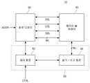
도 1은 본 발명의 일 실시예에 따른 반도체 소자의 개략적인 블록 다이어그램이다.1 is a schematic block diagram of a semiconductor device according to an embodiment of the present invention.
도 1을 참조하면, 본 발명의 실시 형태에 따른 반도체 소자(10)는 메모리 셀 어레이(20), 로우 디코더(30) 및 코어 로직 회로(55)를 포함할 수 있다. 코어 로직 회로(55)는 읽기/쓰기(read/write) 회로(40) 및 제어 회로(50)를 포함할 수 있다.Referring to FIG. 1 , a
메모리 셀 어레이(20)는 복수의 행과 열을 따라 배열된 복수의 메모리 셀들을 포함할 수 있다. 메모리 셀 어레이(20)에 포함되는 복수의 메모리 셀들은, 워드 라인(Word Line, WL), 공통 소스 라인(Common Source Line, CSL), 스트링 선택 라인(String Select Line, SSL), 접지 선택 라인(Ground Select Line, GSL) 등을 통해 로우 디코더(30)와 연결될 수 있으며, 비트 라인(Bit Line, BL)을 통해 읽기/쓰기 회로(40)와 연결될 수 있다. 일 실시예에서, 동일한 행을 따라 배열되는 복수의 메모리 셀은 동일한 워드 라인(WL)에 연결되고, 동일한 열을 따라 배열되는 복수의 메모리 셀은 동일한 비트 라인(BL)에 연결될 수 있다.The
메모리 셀 어레이(20)에 포함되는 복수의 메모리 셀은 복수의 메모리 블록으로 구분될 수 있다. 각 메모리 블록은 복수의 워드 라인(WL), 복수의 스트링 선택 라인(SSL), 복수의 접지 선택 라인(GSL), 복수의 비트 라인(BL)과 적어도 하나의 공통 소스 라인(CSL)을 포함할 수 있다.A plurality of memory cells included in the
로우 디코더(30)는 외부로부터 어드레스 정보(ADDR)를 수신하고, 수신한 어드레스 정보(ADDR)를 디코딩하여 메모리 셀 어레이(20)에 연결된 워드 라인(WL), 공통 소스 라인(CSL), 스트링 선택 라인(SSL) 및 접지 선택 라인(GSL) 중 적어도 일부를 선택할 수 있다.The
읽기/쓰기 회로(40)는 제어 회로(50)로부터 수신하는 명령에 따라 메모리 셀 어레이(20)에 연결되는 비트 라인(BL) 중 적어도 일부를 선택할 수 있다. 읽기/쓰기 회로(40)는 선택한 적어도 일부의 비트 라인(BL)과 연결된 메모리 셀에 저장된 데이터를 읽어오거나, 선택한 적어도 일부의 비트 라인(BL)과 연결된 메모리 셀에 데이터를 기입할 수 있다. 읽기/쓰기 회로(40)는 상기와 같은 동작을 수행하기 위해, 페이지 버퍼, 입/출력 버퍼, 데이터 래치 등과 같은 회로를 포함할 수 있다.The read/
제어 회로(50)는 외부로부터 전달되는 제어 신호(CTRL)에 응답하여 로우 디코더(30) 및 읽기/쓰기 회로(40)의 동작을 제어할 수 있다. 메모리 셀 어레이(20)에 저장된 데이터를 읽어오는 경우, 제어 회로(50)는 읽어오고자 하는 데이터가 저장된 워드 라인(WL)에 읽기 동작을 위한 전압을 공급하도록 로우 디코더(30)의 동작을 제어할 수 있다. 읽기 동작을 위한 전압이 특정 워드 라인(WL)에 공급되면, 제어 회로(50)는 읽기/쓰기 회로(40)가 읽기 동작을 위한 전압이 공급된 워드 라인(WL)과 연결된 메모리 셀에 저장된 데이터를 읽어오도록 제어할 수 있다.The
한편, 메모리 셀 어레이(20)에 데이터를 쓰는 경우, 제어 회로(50)는 데이터를 쓰고자 하는 워드 라인(WL)에 쓰기 동작을 위한 전압을 공급하도록 로우 디코더(30)의 동작을 제어할 수 있다. 쓰기 동작을 위한 전압이 특정 워드 라인(WL)에 공급되면, 제어 회로(50)는 쓰기 동작을 위한 전압이 공급된 워드 라인(WL)에 연결된 메모리 셀에 데이터를 기록하도록 읽기/쓰기 회로(40)를 제어할 수 있다.
Meanwhile, when data is written to the
도 2는 본 발명의 일 실시예에 따른 반도체 소자의 개략적인 배치도이다.2 is a schematic layout view of a semiconductor device according to an embodiment of the present invention.
도 2를 참조하면, 본 발명의 일 실시예에 따른 반도체 소자(10)는, 셀 영역(C), 주변 회로 영역(P) 및 셀 영역(C)와 주변 회로 영역(P) 사이의 경계 영역(B)을 포함할 수 있다. 셀 영역(C)은 복수의 메모리 셀 어레이들(20)을 포함하고, 주변 회로 영역(P)은 로우 디코더(30), 코어 로직 회로(55) 및 기타 주변 회로(60)를 포함할 수 있다.Referring to FIG. 2 , in the
셀 영역(C)에서, 메모리 셀 어레이들(20)은 로우 디코더(30)를 중심으로 양쪽에 배치될 수 있다.In the cell region C, the
주변 회로 영역(P)에서, 코어 로직 회로(55)는 각각의 메모리 셀 어레이(20)에 대응하여 배치될 수 있다. 또한, 기타 주변 회로(60)는 코어 로직 회로(55)의 주변에 배치되며, 고전압 발생회로 등을 포함할 수 있다. 다만, 도 2에 도시된 이러한 메모리 셀 어레이 및 주변 회로의 배치 관계는 예시적인 것이며, 본 발명의 일 실시예에 따른 반도체 소자의 내부 배치 관계는 이에 한정되지 않는다.In the peripheral circuit region P, the
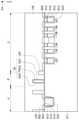
경계 영역(B)은 주변 회로 영역(P)으로부터 셀 영역(C)으로 전달되는 열을 차단하거나 감소시키는 에어갭 구조물(45)를 포함할 수 있다. 구체적으로, 에어갭 구조물(45)은 메모리 셀 어레이들(20)과 코어 로직 회로(55) 사이의 경계 영역(B)에 배치될 수 있다. 각각의 메모리 셀 어레이(20)마다 에어갭 구조물(45)가 구비될 수 있다. 즉, 복수의 메모리 셀 어레이(20)에 일대일 대응하여, 복수의 에어갭 구조물들(45)이 구비될 수 있다. 각각의 에어갭 구조물(45)은 메모리 셀 어레이(20)의 일면을 따라 일 방향(예를 들어, X 방향)으로 연장되고, 메모리 셀 어레이(20)의 일면의 길이에 대응하는 길이를 가질 수 있다. 이와 달리, 각각의 메모리 셀 어레이(20)에 대응하여 분리되어 구비되는 것이 아니라, 메모리 셀 어레이들(20) 전체에 대응하여 일 방향(예를 들어, X 방향)으로 연장되는 하나의 에어갭 구조물(45)이 구비될 수 있다.The boundary region B may include an
반도체 소자(10)가 동작하는 동안에 코어 로직 회로(55) 및/또는 기타 주변 회로(60)에서 열이 발생할 수 있고, 발생한 열이 기판 및/또는 층간 절연층을 통해 메모리 셀 어레이(20)에 전달되어 셀 특성이 열화될 수 있다. 특히, 코어 로직 회로(55)에 가까이 위치한 메모리 셀들은 코어 로직 회로(55)로부터 멀리 위치한 메모리 셀들에 비해 상대적으로 고온에 노출되므로 메모리 셀 특성의 열화가 더 심각할 수 있다. 따라서, 본 발명의 일 실시예에 따르면, 메모리 셀 어레이(20)와 코어 로직 회로(55) 사이에 에어갭 구조물(45)를 형성하여 메모리 셀 어레이(20)에 전달되는 열을 차단하거나 감소시킴으로써, 메모리 셀 특성이 열화되는 것을 막을 수 있다. 에어갭 구조물(45)의 구조에 대해서는 아래에서 도 4 내지 도 11를 참조하여 더욱 상세히 설명한다.
During operation of the
도 3은 본 발명의 일 실시예에 따른 반도체 소자의 메모리 셀 어레이를 나타내는 등가 회로도이다. 본 발명의 일 실시예에 따른 반도체 소자는 수직형(vertical) 낸드(NAND) 플래시 소자일 수 있다.3 is an equivalent circuit diagram illustrating a memory cell array of a semiconductor device according to an embodiment of the present invention. The semiconductor device according to an embodiment of the present invention may be a vertical NAND flash device.
도 3을 참조하면, 메모리 셀 어레이는, 서로 직렬로 연결되는 n 개의 메모리 셀(MC1~MCn), 메모리 셀(MC1~MCn)의 양단에 직렬로 연결되는 접지 선택 트랜지스터(GST) 및 스트링 선택 트랜지스터(SST)를 포함하는 복수의 메모리 셀 스트링(S)을 포함할 수 있다.Referring to FIG. 3 , the memory cell array includes n memory cells MC1 to MCn connected in series to each other, a ground select transistor GST and a string select transistor connected in series to both ends of the memory cells MC1 to MCn. A plurality of memory cell strings S including SST may be included.
서로 직렬로 연결되는 n 개의 메모리 셀(MC1~MCn)는 메모리 셀(MC1~MCn)을 선택하기 위한 n 개의 워드 라인(WL1~WLn)에 각각 연결될 수 있다.The n memory cells MC1 to MCn connected in series may be respectively connected to the n word lines WL1 to WLn for selecting the memory cells MC1 to MCn.
접지 선택 트랜지스터(GST)의 게이트 단자는 접지 선택 라인(GSL)과 연결되고, 소스 단자는 공통 소스 라인(CSL)에 연결될 수 있다. 한편, 스트링 선택 트랜지스터(SST)의 게이트 단자는 스트링 선택 라인(SSL)에 연결되고, 소스 단자는 메모리 셀(MCn)의 드레인 단자에 연결될 수 있다. 도 3에서는 서로 직렬로 연결되는 n 개의 메모리 셀(MC1~MCn)에 접지 선택 트랜지스터(GST)와 스트링 선택 트랜지스터(SST)가 하나씩 연결되는 구조를 도시하였으나, 이와 달리 복수의 접지 선택 트랜지스터(GST) 또는 복수의 스트링 선택 트랜지스터(SST)가 연결될 수도 있다.A gate terminal of the ground select transistor GST may be connected to the ground select line GSL, and a source terminal may be connected to the common source line CSL. Meanwhile, a gate terminal of the string select transistor SST may be connected to the string select line SSL, and a source terminal may be connected to a drain terminal of the memory cell MCn. 3 illustrates a structure in which the ground select transistor GST and the string select transistor SST are connected one by one to the n memory cells MC1 to MCn connected in series. Alternatively, a plurality of string select transistors SST may be connected.
스트링 선택 트랜지스터(SST)의 드레인 단자는 복수의 비트 라인(BL1~BLm)에 연결될 수 있다. 스트링 선택 트랜지스터(SST)의 게이트 단자에 스트링 선택 라인(SSL)을 통해 신호가 인가되면, 비트 라인(BL1~BLm)을 통해 인가되는 신호가 서로 직렬로 연결된 n 개의 메모리 셀(MC1~MCn)에 전달됨으로써 데이터 읽기 또는 쓰기 동작이 실행될 수 있다. 또한, 소스 단자가 공통 소스 라인(CSL)에 연결된 게이트 선택 트랜지스터(GST)의 게이트 단자에 게이트 선택 라인(GSL)을 통해 신호를 인가함으로써, n 개의 메모리 셀(MC1~MCn)에 저장된 전하를 모두 제거하는 소거(erase) 동작이 실행될 수 있다.
A drain terminal of the string select transistor SST may be connected to the plurality of bit lines BL1 to BLm. When a signal is applied to the gate terminal of the string select transistor SST through the string select line SSL, the signal applied through the bit lines BL1 to BLm is applied to the n memory cells MC1 to MCn connected in series with each other. By passing, a data read or write operation can be executed. In addition, by applying a signal through the gate selection line GSL to the gate terminal of the gate selection transistor GST whose source terminal is connected to the common source line CSL, all charges stored in the n memory cells MC1 to MCn are removed. An erase operation that removes may be performed.
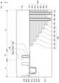
도 4는 본 발명의 일 실시예에 따른 반도체 소자의 일부 영역에 대한 개략적인 평면도이다. 도 5는 도 4의 본 발명의 일 실시예에 따른 반도체 소자를 A-A'선을 따라 절단한 개략적인 단면도이다. 도 4 및 도 5에 도시된 셀 영역(C)에는 도 3을 참조하여 설명한 수직형 낸드 플래시 메모리 소자의 메모리 셀 어레이 일부가 도시되어 있다. 도 4는 기판(101) 상에 형성된 주요 구성을 설명하기 위해 층간 절연층(175), 식각 정지층(220) 등의 일부 구성을 생략하고 도시하였다.
4 is a schematic plan view of a partial region of a semiconductor device according to an embodiment of the present invention. 5 is a schematic cross-sectional view of the semiconductor device of FIG. 4 taken along line A-A'. A part of the memory cell array of the vertical NAND flash memory device described with reference to FIG. 3 is shown in the cell region C shown in FIGS. 4 and 5 . In FIG. 4 , some components such as the
도 4를 참조하면, 본 발명의 일 실시예에 따른 반도체 소자에서 기판(101)은 셀 영역(C), 주변 회로 영역(P), 그리고 그 사이의 경계 영역(B)을 포함할 수 있다. 셀 영역(C)은 복수의 게이트 전극층들(131-136: 130), 채널 패드(170) 및 도전층(180)을 포함할 수 있다. 주변 회로 영역(P)는 활성 영역(208)을 정의하는 소자 분리막(207), 활성 영역(208)과 교차하는 게이트 전극(214)을 포함할 수 있다. 활성 영역(208) 및 게이트 전극(214)은 주변 트랜지스터를 형성할 수 있다. 경계 영역(B)은 주변 회로 영역(P)로부터 셀 영역(C)으로 전달되는 열을 차단하거나 감소시키는 에어갭 구조물(45)을 포함할 수 있다.Referring to FIG. 4 , in the semiconductor device according to an embodiment of the present invention, a
복수의 게이트 전극층들(130) 사이에는 복수의 절연층들(140, 도 5 참조)이 배치될 수 있다. 복수의 게이트 전극층들(130)과 복수의 절연층들(140)은 예를 들어, Y축 방향으로 연장될 수 있다. 복수의 게이트 전극층들(130)과 복수의 절연층들(140)은 기판(101)에 더 가까운 층일수록 Y축 방향으로 더 길게 연장되어 계단 형상을 이루는 복수의 단차를 형성할 수 있다.A plurality of insulating layers 140 (refer to FIG. 5 ) may be disposed between the plurality of gate electrode layers 130 . The plurality of gate electrode layers 130 and the plurality of insulating
기판(101)은 X축 방향과 Y축 방향으로 연장되는 상면을 가질 수 있다. 기판(101)은 반도체 물질, 예컨대 Ⅳ족 반도체, Ⅲ-Ⅴ족 화합물 반도체 또는 Ⅱ-Ⅵ족 화합물 반도체를 포함할 수 있다. 예를 들어, Ⅳ족 반도체는 실리콘, 게르마늄 또는 실리콘-게르마늄을 포함할 수 있다. 기판(101)은 벌크 웨이퍼 또는 에피택셜층, SOI(Silicon On Insulator)층, 또는 SeOI(Semiconductor On Insulator)층 등으로 제공될 수도 있다.The
게이트 전극층들(130)은 다결정 실리콘 또는 금속 실리사이드 물질을 포함할 수 있다. 상기 금속 실리사이드 물질은, 예컨대, Co, Ni, Hf, Pt, W 및 Ti 중에서 선택되는 금속의 실리사이드 물질 또는 이들의 조합일 수 있다. 실시예에 따라, 게이트 전극들(130)은 금속 물질, 예컨대 텅스텐(W)을 포함할 수도 있다. 또한, 별도로 도시되지는 않았지만, 게이트 전극들(130)은 확산 방지막(diffusion barrier)을 더 포함할 수 있으며, 예컨대, 상기 확산 방지막은 텅스텐 질화물(WN), 탄탈륨 질화물(TaN), 티타늄 질화물(TiN) 또는 이들의 조합을 포함할 수 있다. 절연층들(140)은 실리콘 산화물 또는 실리콘 질화물과 같은 절연성 물질을 포함할 수 있다.The gate electrode layers 130 may include polycrystalline silicon or a metal silicide material. The metal silicide material may be, for example, a silicide material of a metal selected from Co, Ni, Hf, Pt, W, and Ti, or a combination thereof. In some embodiments, the
채널 패드(170)은 게이트 전극층들(131-136: 130)을 관통하는 채널 영역(160, 도 5 참조) 상에 배치되며, 채널 패드(170)은 일 방향(예를 들어, Y축 방향)으로 지그재그 형태로 배치될 수 있다. 채널 패드(170)는 예컨대, 도핑된 다결정 실리콘을 포함할 수 있다. 채널 패드(170)는 도 3에 도시한 스트링 선택 트랜지스터(SST)의 드레인 영역으로 작용할 수 있다.The
도전층(180)은 복수의 게이트 전극층들(130) 및 복수의 절연층들(140)을 관통하여 기판(101)과 연결될 수 있다. 도전층(180)은 예를 들어, Y 방향으로 연장되는 라인 형상으로 배치될 수 있다. 도전층(180)은 예를 들어, X 방향에서 소정 간격으로 배열될 수 있으며, 도시된 바에 한정되지 않는다. 도전층(180)은 도 3에 도시한 공통 소스 라인(CSL)을 이룰 수 있다. 도전층(180)은 텅스텐(W), 알루미늄(Al) 또는 구리(Cu) 등과 같은 금속을 포함할 수 있다. 도전층(180)과 게이트 전극층들(130) 사이에 절연층이 더 배치될 수 있다. 상기 절연층에 의해 게이트 전극층들(130)과 전기적으로 절연될 수 있다.The
주변 회로 영역(P)은 활성 영역(208)을 정의하는 소자 분리막(207), 활성 영역(208)과 교차하는 게이트 전극(214)을 포함할 수 있다. 활성 영역(208)과 게이트 전극(214)는 주변 트랜지스터들을 형성할 수 있다. 상기 주변 트랜지스터들은 도 1에 도시한 코어 로직 회로(55) 등을 구성할 수 있다. 도 4에는 두 개의 주변 트랜지스터들이 도시되었으나, 주변 회로 영역(P)에 포함되는 주변 트랜지스터들의 개수 및 상대적인 크기는 이에 한정되지 않는다.The peripheral circuit region P may include a
에어갭 구조물(45)은 예를 들어, 기판(101) 내에서 X축 방향으로 연장되는 라인 형태의 트렌치(205t), 트렌치(205t)를 부분적으로 매립하는 절연층(205) 및 절연층(205)에 의해 둘러싸인 에어갭(205a)을 포함할 수 있다. 에어갭 구조물(45)는 기판(101)의 상부에서 보았을 때 직선 형태일 수 있다. 즉, 트렌치(205t)는 기판(101)의 상부에서 보았을 때 직선 형태일 수 있다. 에어갭(205a)은 트렌치(205t) 내에 끊기지 않고 연속적으로 형성될 수 있다. 일 실시예에서, 에어갭 구조물(45)은 Y축 방향으로 서로 이격된 복수의 라인 형태의 트렌치(205t)를 포함할 수 있다. 절연층(205)은 소자 분리막(207)를 형성하는 제조 단계와 동일한 제조 단계에서 형성될 수 있다. 일 실시예에서, 절연층(205)은 소자 분리막(207)를 형성하는 제조 단계와 별개의 제조 단계에서 의해 형성될 수 있다.
The
도 5를 참조하면, 기판(101)은 셀 영역(C), 주변 회로 영역(P), 그리고 그 사이의 경계 영역(B)을 포함할 수 있다.Referring to FIG. 5 , the
셀 영역(C)에는 Z축 방향을 따라 기판(101)의 상면 위에 적층되는 복수의 게이트 전극층(131-136: 130) 및 복수의 게이트 전극층(130)과 번갈아 배치되는 복수의 절연층(141-147: 140)을 포함할 수 있다. 복수의 게이트 전극층들(130)과 복수의 절연층들(140)은 예를 들어, Y축 방향으로 연장될 수 있다. 셀 영역(C)에는 복수의 게이트 전극층(130)과 복수의 절연층(140)을 관통하며 기판(101)의 상면에 실질적으로 수직한 방향(예를 들어, Z축 방향)으로 연장되는 채널 영역(160)이 더 마련될 수 있다. 채널 영역(160)은 원형의 단면을 갖는 개구부 내에 형성될 수 있으며, 가운데가 비어 있는 환형의 채널 영역(160) 내부에 매립 절연층(165)이 마련될 수도 있다. 채널 영역(160)은 예를 들어, Y축 방향을 따라 지그재그 형태로 배치될 수 있다. 다만, 채널 영역(160)의 배치는 실시예에 따라 다양할 수 있으며, 도시된 형태에 한정되지 않는다. 채널 영역(160) 상에는 채널 패드(170)가 마련될 수 있으며, 채널 패드(170)을 통해 비트 라인이 채널 영역(160)과 서로 연결될 수 있다.In the cell region C, a plurality of gate electrode layers 131 to 136: 130 stacked on the upper surface of the
채널 영역(160)과 게이트 전극층들(130) 사이에는 게이트 절연층(150)이 배치될 수 있다. 게이트 절연층(150)은 블록킹층, 전하 저장층, 터널링층 등을 포함할 수 있다. 상기 터널링층이 채널 영역(160)에 접하도록 배치되고, 상기 블록킹층은 게이트 전극층(130)에 접하도록 배치될 수 있다. 게이트 절연층(150)은 채널 영역(160)을 따라 기판(101) 상으로 연장될 수 있다. 실시예에 따라, 게이트 절연층(150)이 게이트 전극층(130)을 둘러싸는 형태로 배치될 수 있다. 실시예에 따라, 게이트 절연층(130)의 상기 전하 저장층과 상기 터널링층은 채널 영역(160)과 평행하게 연장되도록 채널 영역(160)의 외측에 배치되고, 상기 블록킹층은 게이트 전극층(130)을 둘러싸도록 배치될 수 있다. 상기 블록킹층은 실리콘 산화물(SiO2), 실리콘 질화물(Si3N4), 실리콘 산질화물(SiON) 또는 고유전율 유전 물질을 포함할 수 있다. 상기 고유전율 유전 물질은, 알루미늄 산화물(Al2O3), 탄탈륨 산화물(Ta2O3), 티타늄 산화물(TiO2), 이트륨 산화물(Y2O3), 지르코늄 산화물(ZrO2), 지르코늄 실리콘 산화물(ZrSixOy), 하프늄 산화물(HfO2), 하프늄 실리콘 산화물(HfSixOy), 란탄 산화물(La2O3), 란탄 알루미늄 산화물(LaAlxOy), 란탄 하프늄 산화물(LaHfxOy), 하프늄 알루미늄 산화물(HfAlxOy), 및 프라세오디뮴 산화물(Pr2O3) 중 어느 하나일 수 있다. 한편, 선택적으로 상기 블록킹층은 서로 다른 유전율을 갖는 복수의 층을 포함할 수 있다. 이때, 상대적으로 낮은 유전율을 갖는 층을, 높은 유전율을 갖는 층보다 채널 영역(160)에 가깝게 배치함으로써, 베리어(barrier) 높이와 같은 에너지 밴드를 조절하여 메모리 장치의 특성, 예컨대 소거(erase) 특성을 향상시킬 수 있다. 상기 전하 저장층은 전하 트랩층 또는 도전성 나노 입자를 포함하는 절연층일 수 있다. 상기 전하 트랩층은 예를 들면 실리콘 질화물을 포함할 수 있다. 상기 터널링층은 블록킹 절연층보다 낮은 유전율을 갖는 물질로 이루어 질 수 있다. 상기 터널링층은 실리콘 산화물(SiO2), 실리콘 질화물(Si3N4), 실리콘 산질화물(SiON), 하프늄 산화물(HfO2), 하프늄 실리콘 산화물(HfSixOy), 알루미늄 산화물(Al2O3), 및 지르코늄 산화물(ZrO2) 중 적어도 하나를 포함할 수 있다.A
게이트 전극층들(130)과 절연층들(140)은 기판(101)에 더 가까운 층일수록 Y축 방향으로 더 연장되어 계단 형상을 이루는 복수의 단차를 형성할 수 있다. 복수의 게이트 전극층(130) 및 절연층(140)이 Y축 방향을 따라 서로 다른 길이로 연장되어 마련된 단차로 인해, 복수의 패드 영역이 제공될 수 있다. 도 4에는 각 패드 영역에서 Z축 방향을 따라 절연층(140)이 게이트 전극층(130)보다 상부에 위치하는 것으로 도시하였으나, 이와 달리 게이트 전극층(130)이 절연층(140)보다 상부에 위치할 수도 있다.The gate electrode layers 130 and the insulating
주변 회로 영역(P)은 활성 영역(208)을 정의하는 소자 분리막(207), 활성 영역(208) 상에 배치되는 게이트 전극(214)을 포함할 수 있다. 활성 영역(207)과 게이트 전극(214) 사이에 게이트 절연층(212)이 개재될 수 있다. 게이트 전극(214)의 양 측벽에는 게이트 스페이서(216)가 배치될 수 있다. 게이트 전극(214) 양측의 활성 영역(208)에는 n형 또는 p형 불순물이 주입된 소스/드레인 영역(209)이 형성될 수 있다.The peripheral circuit region P may include a
게이트 전극(214)은 폴리 실리콘(Poly-Silicon), 금속(예를 들어, 텅스텐 또는 몰리브덴 등), 또는 금속 실리사이드 중 적어도 하나를 포함할 수 있다. 게이트 전극(214)은 폴리 실리콘 층과 금속 실리사이드 층이 적층된 구조를 가질 수도 있다. 게이트 절연층(212)은 실리콘 산화물(SiO2), 실리콘 질화물(Si3N4), 실리콘 산질화물(SiON) 또는 고유전율 유전 물질을 포함할 수 있다. 게이트 스페이서(216)은 실리콘 산화물(SiO2), 실리콘 질화물(Si3N4), 실리콘 산질화물(SiON) 또는 이들의 조합으로 이루어질 수 있다.The
게이트 전극(214), 소자 분리막(207) 및 에어갭 구조물(45) 등을 덮는 식각 정지층(220)이 주변 회로 영역(P) 및 경계 영역(B)에 형성될 수 있다. 식각 정지층(220)은 실리콘 질화물(Si3N4), 실리콘 산질화물(SiON) 또는 이들의 조합으로 이루어질 수 있다.An
에어갭 구조물(45)은 예를 들어, 기판(101)을 식각하여 형성한 트렌치(205t), 트렌치(205t)를 부분적으로 매립하는 절연층(205) 및 절연층(205)에 의해 둘러싸인 에어갭(205a)를 포함할 수 있다. 트렌치(205t)의 깊이는 주변 회로 영역(P)에서 소자 분리막(207)을 형성하는 페리 트렌치의 깊이와 동일할 수 있다. 일 실시예에서, 트렌치(205t)의 깊이는 상기 페리 트렌치의 깊이보다 더 깊을 수 있다. 트렌치(205t)의 종횡비(aspect ratio)는 상기 페리 트렌치의 종횡비보다 클 수 있다. 트렌치(205t)는 페리 트렌치를 형성하는 제조 단계와 동일한 제조 단계에 의해 형성될 수 있다. 일 실시예에서, 트렌치(205t)는 페리 트렌치를 형성하는 제조 단계와 별개의 제조 단계에 의해 형성될 수 있다.The
일 실시예에서, 에어갭 구조물(45)은 서로 이격된 복수의 트렌치(205t)를 포함할 수 있다. 복수의 트렌치(205t)는 동일한 깊이를 가지도록 형성될 수 있다. 복수의 트렌치(205t)는 서로 다른 깊이를 가지도록 형성될 수 있다.In one embodiment, the
절연층(205)은 소자 분리막(207)를 형성하는 제조 단계와 동일한 제조 단계에 의해 형성될 수 있다. 일 실시예에서, 절연층(205)은 소자 분리막(207)를 형성하는 제조 단계와 별개의 제조 단계에 의해 형성될 수 있다. 절연층(205)의 상면이 기판(101)의 상면과 동일한 높이를 가지는 것으로 도시되어 있으나, 이에 한정되지 않는다. 절연층(205)의 상면의 높이는 기판(101)의 상면보다 더 높을 수 있다.The insulating
층간 절연층(175)은 셀 영역(C), 경계 영역(B) 및 주변 회로 영역(P)에 걸쳐서 기판(101) 상에 배치될 수 있다. 셀 영역(C)에서 층간 절연층(175)은 복수의 게이트 전극층(130) 및 절연층(140)을 덮도록 배치되고, 경계 영역(B) 및 주변 회로 영역(P)에서 층간 절연층(175)은 식각 정지층(220)을 덮도록 배치될 수 있다. 일 실시예에서 층간 절연층(175)은 경계 영역(B) 및 주변 회로 영역(P)에서 미리 형성된 다른 층간 절연층 상에 배치될 수 있다.
The interlayer insulating
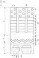
도 6은 본 발명의 일 실시예에 따른 반도체 소자의 일부 영역에 대한 개략적인 평면도이다. 도 7은 도 6의 본 발명의 일 실시예에 따른 반도체 소자를 A-A'선을 따라 절단한 개략적인 단면도이다. 도 6 및 도 7에 도시된 반도체 소자는 경계 영역(B)에 형성된 에어갭 구조물(45a) 이외에 다른 구성들은 도 4 및 도 5를 참조하여 설명한 내용과 동일하므로 생략한다.6 is a schematic plan view of a partial region of a semiconductor device according to an embodiment of the present invention. 7 is a schematic cross-sectional view taken along line A-A' of the semiconductor device according to an embodiment of the present invention of FIG. 6 . In the semiconductor device illustrated in FIGS. 6 and 7 , other components other than the
도 6 및 도 7을 참조하면, 에어갭 구조물(45a)은 예를 들어, 기판(101) 내에서 X축 방향으로 연장되는 라인 형태의 트렌치(205ta), 트렌치(205ta)를 부분적으로 매립하는 절연층(205) 및 절연층(205)에 의해 둘러싸인 에어갭(205aa)를 포함할 수 있다. 에어갭 구조물(45a)는 기판(101)의 상부에서 보았을 때 삼각 톱니 모양으로 꺾이며 연장되는 지그재그선 형태일 수 있다. 즉, 트렌치(205ta)는 기판(101)의 상부에서 보았을 때 삼각 톱니 모양으로 꺾이며 연장되는 지그재그선 형태일 수 있다. 에어갭(205aa)은 트렌치(205ta) 내에 끊기지 않고 연속적으로 형성될 수 있다. 트렌치(205ta)의 깊이는 주변 회로 영역(P)에 소자 분리막(207)을 형성하기 위한 페리 트렌치의 깊이와 동일할 수 있다. 일 실시예에서, 트렌치(205ta)의 깊이는 소자 분리막(207)을 형성하기 위한 페리 트렌치의 깊이보다 더 깊을 수 있다. 트렌치(205ta)의 종횡비(aspect ratio)는 소자 분리막(207)을 형성하기 위한 페리 트렌치의 종횡비보다 클 수 있다.
Referring to FIGS. 6 and 7 , the
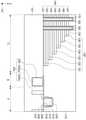
도 8은 본 발명의 일 실시예에 따른 반도체 소자의 일부 영역에 대한 개략적인 평면도이다. 도 9는 도 8의 본 발명의 일 실시예에 따른 반도체 소자를 A-A'선을 따라 절단한 개략적인 단면도이다. 도 8 및 도 9에 도시된 반도체 소자는 경계 영역(B)에 형성된 에어갭 구조물(45b) 이외에 다른 구성들은 도 4 및 도 5를 참조하여 설명한 내용과 동일하므로 생략한다.8 is a schematic plan view of a partial region of a semiconductor device according to an embodiment of the present invention. 9 is a schematic cross-sectional view of the semiconductor device of FIG. 8 taken along line A-A'. In the semiconductor device illustrated in FIGS. 8 and 9 , other configurations other than the
도 8 및 도 9를 참조하면, 에어갭 구조물(45b)은 기판(101) 내에서 X축 방향으로 연장되는 라인 형태의 트렌치(205tb), 트렌치(205tb)를 부분적으로 매립하는 절연층(205) 및 절연층(205)에 의해 둘러싸인 에어갭(205ab)를 포함할 수 있다. 에어갭 구조물(45b)는 기판(101)의 상부에서 보았을 때 사각 톱니 모양으로 꺾이며 연장되는, 다시 말해, X축 방향, Y축 방향, X축 방향 그리고 -Y축 방향으로 교대로 소정의 길이만큼 꺾이며 연장되는 지그재그선 형태일 수 있다. 즉, 트렌치(205tb)는 기판(101)의 상부에서 보았을 때 사각 톱니 모양으로 꺾이며 연장되는 지그재그선 형태일 수 있다. 에어갭(205ab)는 트렌치(205tb) 내에 끊기지 않고 연속적으로 형성될 수 있다. 트렌치(205tb)의 깊이는 주변 회로 영역(P)에 소자 분리막(207)을 형성하기 위한 페리 트렌치의 깊이와 동일할 수 있다. 일 실시예에서, 트렌치(205tb)의 깊이는 소자 분리막(207)을 형성하기 위한 페리 트렌치의 깊이보다 더 깊을 수 있다. 트렌치(205tb)의 종횡비(aspect ratio)는 소자 분리막(207)을 형성하기 위한 페리 트렌치의 종횡비보다 클 수 있다.
8 and 9 , the
도 10은 본 발명의 일 실시예에 따른 반도체 소자의 일부 영역에 대한 개략적인 평면도이다. 도 11은 도 10의 본 발명의 일 실시예에 따른 반도체 소자를 A-A'선을 따라 절단한 개략적인 단면도이다. 도 10 및 도 11에 도시된 반도체 소자는 경계 영역(B)에 형성된 에어갭 구조물(45c) 이외에 다른 구성들은 도 4 및 도 5를 참조하여 설명한 내용과 동일하므로 생략한다.10 is a schematic plan view of a partial region of a semiconductor device according to an embodiment of the present invention. 11 is a schematic cross-sectional view of the semiconductor device of FIG. 10 taken along line A-A'. In the semiconductor device illustrated in FIGS. 10 and 11 , other components other than the
도 10 및 도 11을 참조하면, 에어갭 구조물(45c)은 예를 들어, 기판(101) 내에서 X축 방향으로 연장되는 트렌치(205tc), 트렌치(205tc)를 부분적으로 매립하는 절연층(205) 및 절연층(205)에 의해 둘러싸인 에어갭(205ac)를 포함할 수 있다. 에어갭 구조물(45c)는 기판(101)의 상부에서 보았을 때 사다리 형태일 수 있다. 즉, 트렌치(205tc)는 기판(101)의 상부에서 보았을 때 서로 이격되어 나란히 X축 방향으로 연장되는 세로 트렌치들과 상기 세로 트렌치들을 연결하도록 Y축 방향으로 연장되며 일정한 간격으로 배치되는 가로 트렌치들로 이루어진 사다리 형태일 수 있다. 에어갭(205ac)는 트렌치(205tc) 내에 끊기지 않고 연속적으로 형성될 수 있다. 트렌치(205tc)의 깊이는 주변 회로 영역(P)에 소자 분리막(207)을 형성하기 위한 페리 트렌치의 깊이와 동일할 수 있다. 일 실시예에서, 트렌치(205tc)의 깊이는 소자 분리막(207)을 형성하기 위한 페리 트렌치의 깊이보다 더 깊을 수 있다. 트렌치(205tc)의 종횡비(aspect ratio)는 소자 분리막(207)을 형성하기 위한 페리 트렌치의 종횡비보다 클 수 있다.
10 and 11 , the
도 12는 본 발명의 일 실시예에 따른 반도체 소자의 개략적인 단면도이다. 도 12에 도시된 셀 영역(C)에는 도 3을 참조하여 설명한 수직형 낸드 플래시 메모리 소자의 메모리 셀 어레이 일부가 도시되어 있다. 도 12에 도시된 반도체 소자는 경계 영역(B)에 형성된 상부 에어갭 구조물(45u) 이외에 다른 구성들은 도 4 및 도 5를 참조하여 설명한 내용과 동일하므로 생략한다.12 is a schematic cross-sectional view of a semiconductor device according to an embodiment of the present invention. A part of the memory cell array of the vertical NAND flash memory device described with reference to FIG. 3 is shown in the cell region C shown in FIG. 12 . In the semiconductor device shown in FIG. 12 , other components other than the upper
도 12를 참조하면, 에어갭 구조물(45) 상에 상부 에어갭 구조물(45u)가 형성될 수 있다. 에어갭 구조물(45)와 상부 에어갭 구조물(45u)는 식각 정지층(220)에 의해 분리될 수 있다. 상부 열절단 방지 구조물(45u)는 층간 절연층(175)을 관통하는 개구부(190t), 개구부(190t)를 부분적으로 매립하는 상부 절연층(190) 및 상부 절연층(190)에 의해 둘러싸인 에어갭(190a)를 포함할 수 있다. 도 4에서 트렌치(205t)가 X축 방향으로 연장되는 것과 유사하게, 개구부(190t)는 기판(101)의 상부에서 보았을 때, X축 방향으로 연장될 수 있다. 개구부(190t)의 폭은 트렌치(205t)의 폭과 다를 수 있다. 개구부(190t)는 기판(101)에 가까워질수록 폭이 점점 좁아지는 형상일 수 있다.
12 , an upper
도 13은 본 발명의 일 실시예에 따른 반도체 소자의 메모리 셀 어레이를 나타내는 등가 회로도이다. 본 발명의 일 실시예에 따른 반도체 소자는 평면형(planar) 낸드(NAND) 플래시 소자일 수 있다.13 is an equivalent circuit diagram illustrating a memory cell array of a semiconductor device according to an embodiment of the present invention. The semiconductor device according to an embodiment of the present invention may be a planar NAND flash device.
메모리 셀 어레이는 복수의 셀 블록들로 구성될 수 있고, 도 13은 하나의 셀 블록을 나타낸 것일 수 있다. 도 13을 참조하면, 셀 블록은 복수의 페이지들로 구성될 수 있다. 각각의 페이지는 하나의 워드 라인(WL)에 연결된 복수의 메모리 셀들(MC1~MCn)로 구성될 수 있다. 한편, 셀 블록은 복수의 셀 스트링들로 구성될 수 있다. 각각의 셀 스트링은 스트링 선택 라인(SSL)에 연결되는 스트링 선택 트랜지스터(SST), 복수의 워드 라인들(WL1~WLn)에 연결되는 복수의 메모리 셀 들(MC1~MCn), 그리고 접지 선택 라인(GSL)에 연결되는 접지 선택 트랜지스터(GST)를 포함할 수 있다. 스트링 선택 트랜지스터(SST)는 비트 라인(BL)에 연결되고, 접지 선택 트랜지스터(GST)는 공통 소스 라인(CSL)에 연결될 수 있다. 하나의 비트 라인(BL)과 공통 소스 라인(CSL)사이에서 복수의 메모리 셀들(MC1~MCn)이 직렬로 연결되도록 구성될 수 있다.
The memory cell array may be composed of a plurality of cell blocks, and FIG. 13 may show one cell block. Referring to FIG. 13 , a cell block may include a plurality of pages. Each page may include a plurality of memory cells MC1 to MCn connected to one word line WL. Meanwhile, a cell block may be composed of a plurality of cell strings. Each cell string includes a string select transistor SST connected to the string select line SSL, a plurality of memory cells MC1 to MCn connected to a plurality of word lines WL1 to WLn, and a ground select line A ground select transistor GST connected to the GSL may be included. The string select transistor SST may be connected to the bit line BL, and the ground select transistor GST may be connected to the common source line CSL. The plurality of memory cells MC1 to MCn may be connected in series between one bit line BL and the common source line CSL.
도 14는 본 발명의 일 실시예에 따른 반도체 소자의 일부 영역에 대한 개략적인 평면도이다. 도 15는 도 14의 본 발명의 일 실시예에 따른 반도체 소자를 B-B'선을 따라 절단한 개략적인 단면도이다. 도 14 및 도 15의 셀 영역(C)에는 도 13을 참조하여 설명한 평면형 낸드 플래시 메모리 소자의 메모리 셀 어레이 일부가 도시되어 있다. 도 14는 기판(101) 상에 형성된 주요 구성을 설명하기 위해 층간 절연층(375), 식각 정지층(220) 등의 일부 구성을 생략하고 도시하였다.
14 is a schematic plan view of a partial region of a semiconductor device according to an embodiment of the present invention. 15 is a schematic cross-sectional view of the semiconductor device of FIG. 14 taken along line B-B'. A part of the memory cell array of the planar NAND flash memory device described with reference to FIG. 13 is illustrated in the cell region C of FIGS. 14 and 15 . In FIG. 14 , some components such as the interlayer insulating layer 375 and the
도 14를 참조하면, 본 발명의 일 실시예에 따른 반도체 소자에서 기판(301)은 셀 영역(C), 주변 회로 영역(P), 그리고 그 사이의 경계 영역(B)을 포함할 수 있다. 셀 영역(C)은 예를 들어, X축 방향으로 서로 이격되고, Y축 방향으로 연장되는 복수의 활성 영역들(ACT1~ACTm) 및 활성 영역들(ACT1~ACTm)을 정의하는 소자 분리막(307)을 포함할 수 있다. 셀 영역(C)은 제2 도전층(318)로 이루어진 스트링 선택 라인(SSL), 복수의 워드 라인들(WL1~WLn), 그리고 접지 선택 라인(GSL)을 포함할 수 있다. 스트링 선택 라인(SSL), 복수의 워드 라인들(WL1~WLn), 그리고 접지 선택 라인(GSL)은 활성 영역들(ACT1~ACTm)과 교차하도록 배치될 수 있다.Referring to FIG. 14 , in the semiconductor device according to an embodiment of the present invention, a
주변 회로 영역(P)는 활성 영역(208)을 정의하는 소자 분리막(207), 활성 영역(208)과 교차하는 게이트 전극(214)을 포함할 수 있다. 활성 영역(208)과 게이트 전극(214)는 주변 트랜지스터들을 형성할 수 있다. 본 실시예에서도 주변 회로 영역(P)에 대하여 도 4를 참조하여 설명한 내용들이 그대로 적용될 수 있다.The peripheral circuit region P may include a
경계 영역(B)에 배치되는 에어갭 구조물(45)은 예를 들어, 기판(101) 내에서 X축 방향으로 연장되는 라인 형태의 트렌치(205t), 트렌치(205t)를 부분적으로 매립하는 절연층(205) 및 절연층(205)에 의해 둘러싸인 에어갭(205a)를 포함할 수 있다. 본 실시예에서도 에어갭 구조물(45)에 대하여 도 4를 참조하여 설명한 내용들이 그대로 적용될 수 있다.
The
도 15를 참조하면, 셀 영역(C)에는 복수의 셀 스트링들이 반복적으로 배치될 수 있으며, 그 일부로서 하나의 셀 스트링에 대한 구조가 도시되어 있다. 하나의 셀 스트링은 비트 라인(BL, 도 13 참조)에 연결되는 스트링 선택 트랜지스터(SST), 공통 소스 라인(CSL, 도 13 참조))에 연결되는 접지 선택 트랜지스터(GST) 및 스트링 선택 트랜지스터(SST)와 접지 선택 트랜지스터(GST) 사이에 배치되는 복수의 메모리 셀들(MC1~MCn)을 포함할 수 있다. 각각의 메모리 셀(MC)은 기판 상에 형성된 절연층(312), 제1 도전층(314), 블로킹 절연층(316) 및 제2 도전층(318)를 포함할 수 있다. 제1 도전층(314)은 블로킹 절연층(316)에 의해 제2 도전층(318)과 전기적으로 절연되고, 절연층(31)에 의해 기판(301)과 절연된 부유 게이트(floating gate)일 수 있다. 제2 도전층(318)은 제어 게이트(control gate)일 수 있다. 스트링 선택 트랜지스터(SST)와 접지 선택 트랜지스터(GST)는 기판 상에 형성된 절연층(312), 제1 도전층(314), 블로킹 절연층(316) 및 제2 도전층(318)을 포함할 수 있고, 블로킹 절연층(316)의 일부 영역이 제거되어 제1 도전층(314)와 제2 도전층(318)이 전기적으로 연결될 수 있다. 메모리 셀(MC)들 사이, 스트링 선택 트랜지스터(SST)와 인접한 메모리 셀(MC1) 사이 및 접지 선택 트랜지스터(GST)와 인접한 메모리 셀(MCn) 사이의 기판 내에 n형 불순물로 도핑된 불순물 영역(309)을 포함할 수 있다.Referring to FIG. 15 , a plurality of cell strings may be repeatedly disposed in the cell region C, and a structure of one cell string is illustrated as a part thereof. One cell string includes a string select transistor SST connected to a bit line BL (refer to FIG. 13 ), a ground select transistor GST and a string select transistor SST connected to a common source line CSL (see FIG. 13 )). ) and a plurality of memory cells MC1 to MCn disposed between the ground selection transistor GST. Each memory cell MC may include an insulating
경계 영역(B)에 배치되는 에어갭 구조물(45)은 예를 들어, 기판(101)을 식각하여 형성한 트렌치(205t), 트렌치(205t)를 부분적으로 매립하는 절연층(205) 및 절연층(205)에 의해 둘러싸인 에어갭(205a)를 포함할 수 있다. 본 실시예에서도 에어갭 구조물(45)와 관련하여 도 5를 참조하여 설명한 내용들이 그대로 적용될 수 있다.The
본 실시예에서도 주변 회로 영역(P)와 관련하여 앞서 도 5를 참조하여 설명한 내용들이 그대로 적용될 수 있다.
In this embodiment as well, the contents described above with reference to FIG. 5 in relation to the peripheral circuit region P may be applied as it is.
도 16 및 도 17은 본 발명의 일 실시예에 따른 반도체 소자에 대한 개략적인 배치도들이다. 도 16 및 도 17에 도시된 반도체 소자(100, 100A)는 메모리 소자들 및 다양한 로직 소자들을 하나의 칩에 포함하는 SoC (System-on-Chip) 소자일 수 있다.
16 and 17 are schematic layout views of a semiconductor device according to an embodiment of the present invention. The
도 16을 참조하면, 반도체 소자(100)은 하나의 기판에 형성된 비휘발성 메모리 소자(10'), RAM(Random Access Memory), ROM(Read Only Memory) 등의 메모리 소자들, 및 CPU (Central Processing Unit), GPU(Graphic Processing Uint), ISP(Image Signal Processor), DSP(Digital Signal Processor) 등의 로직 소자들을 포함할 수 있다. 반도체 소자(100)은 이 외에 다양한 콘트롤러나 인터페이스들을 포함할 수 있다. 도 16에 도시된 여러 소자들의 배치관계는 예시적인 것일 뿐이며, 이에 한정되지 않는다. 반도체 소자(100)은 응용 분야에 따라 다양한 소자들을 포함할 수 있다.Referring to FIG. 16 , the
비휘발성 메모리 소자(10')은 도 2에 도시된 반도체 소자(10)과 유사한 구조를 가질 수 있다. 비휘발성 메모리 소자(10')은 셀 영역과 주변 회로 영역을 포함할 수 있다. 상기 셀 영역은 복수의 메모리 셀 어레이들(20)을 포함할 수 있다. 상기 주변 회로 영역은 로우 디코더(30), 코어 로직 회로(55) 및 기타 주변 회로(60)을 포함할 수 있다. 비휘발성 메모리 소자(10')은 로우 디코더(30)를 중심으로 양쪽에 배치된 메모리 셀 어레이들(20), 각각의 메모리 셀 어레이(20)에 대응하여 배치된 코어 로직 회로(55)를 포함할 수 있다. 또한, 비휘발성 메모리 소자(10')는 코어 로직 회로(55)의 주변에서 고전압 발생회로 등을 포함하는 기타 주변 회로(60)를 포함할 수 있다.The
반도체 소자(100)가 동작하는 동안에 비휘발성 메모리 소자(10')의 주변에 배치된 여러 로직 소자들(CPU, GPU 등)에서 열이 발생할 수 있다. 뿐만 아니라, 비휘발성 메모리 소자(10')의 코어 로직 회로(55) 등에서도 열이 발생할 수 있다. 발생된 열은 비휘발성 메모리 소자(10')의 메모리 셀 어레이들(20)에 전달되어 셀 특성을 열화시킬 수 있다.While the
상기 주변 회로 영역 및 상기 로직 소자로부터 상기 셀 영역으로 전달되는 열을 차단하거나 감소시키기 위해, 비휘발성 메모리 소자(10')은 메모리 셀 어레이(20)와 코어 로직 회로(55) 사이에 그리고, 메모리 셀 어레이(20)와 상기 로직 소자들 사이에 에어갭 구조물(45)를 포함할 수 있다. 비휘발성 메모리 소자(10')은 사각 링 형태로 상기 셀 영역을 둘러싸는 하나의 에어갭 구조물(45')을 포함할 수 있다.In order to block or reduce heat transferred from the peripheral circuit region and the logic element to the cell region, a
에어갭 구조물(45')로 인하여 코어 로직 회로(55) 및 로직 소자들메모리 셀 어레이(20)에 전달되는 열을 차단하거나 감소시킴으로써, 메모리 셀 특성이 열화되는 것을 막을 수 있다. 에어갭 구조물(45')의 구조는 앞서 도 4 내지 도 12를 참조하여 상술한 구조들이 그대로 적용될 수 있다.
By blocking or reducing heat transferred to the
도 17을 참조하면, 반도체 소자(100A)은 하나의 기판에 형성된 비휘발성 메모리 소자(10"), RAM(Random Access Memory), ROM(Read Only Memory) 등의 기억 소자들, 및 CPU (Central Processing Unit), GPU(Graphic Processing Uint), ISP(Image Signal Processor), DSP(Digital Signal Processor) 등의 로직 소자들을 포함할 수 있다. 반도체 소자(100)은 이 외에 다양한 콘트롤러나 인터페이스들을 포함할 수 있다. 도 17에 도시된 여러 소자들의 배치관계는 예시적인 것일 뿐이며, 이에 한정되지 않는다. 반도체 소자(100)은 응용 분야에 따라 다양한 소자들을 포함할 수 있다.Referring to FIG. 17 , the
비휘발성 메모리 소자(10")은 도 16에 도시된 비휘발성 메모리 소자(10')와 유사한 구조를 가질 수 있다. 비휘발성 메모리 소자(10")은 도 16에 도시된 에어갭 구조물(45')와 다른 형태로 배치된 에어갭 구조물(45")을 포함할 수 있다. 상기 셀 영역은 복수의 메모리 셀 어레이들(20)을 포함할 수 있다. 본 실시예에서, 비휘발성 메모리 소자(10")은 메모리 셀 어레이(20)와 코어 로직 회로(55) 사이에 그리고, 메모리 셀 어레이(20)와 상기 로직 소자들 사이에 에어갭 구조물(45)를 포함할 수 있다. 비휘발성 메모리 소자(10")은 사각 링 형태로 상기 메모리 셀 어레이(20)를 각각 둘러싸는 복수의 에어갭 구조물(45")을 포함할 수 있다. 에어갭 구조물(45")로 인하여 코어 로직 회로(55) 및 로직 소자들메모리 셀 어레이(20)에 전달되는 열을 차단하거나 감소시킴으로써, 메모리 셀 특성이 열화되는 것을 막을 수 있다. 에어갭 구조물(45")의 구조는 앞서 도 4 내지 도 12를 참조하여 상술한 구조들이 그대로 적용될 수 있다.
The
지금까지의 설명은 본 발명의 기술적 사상을 예시적으로 설명한 것에 불과한 것으로서, 본 발명이 속하는 기술분야에서 통상의 지식을 가진 자라면 본 발명의 본질적인 특성에서 벗어나지 않는 범위에서 다양한 수정 및 변형이 가능할 것이다.The description so far is merely illustrative of the technical idea of the present invention, and various modifications and variations will be possible without departing from the essential characteristics of the present invention by those of ordinary skill in the art to which the present invention pertains. .
따라서, 본 발명에 개시된 실시예들은 본 발명의 기술적 사상을 한정하기 위한 것이 아니라 설명하기 위한 것이고, 이러한 실시예에 의하여 본 발명의 기술 사상의 범위가 한정되는 것은 아니다. 본 발명의 보호 범위는 아래의 청구범위에 의하여 해석되어야 하며, 그와 동등한 범위 내에 있는 모든 기술적 사상은 본 발명의 권리범위에 포함되는 것으로 해석되어야 할 것이다.
Therefore, the embodiments disclosed in the present invention are not intended to limit the technical spirit of the present invention, but to explain, and the scope of the technical spirit of the present invention is not limited by these embodiments. The protection scope of the present invention should be interpreted by the following claims, and all technical ideas within the scope equivalent thereto should be construed as being included in the scope of the present invention.
10: 반도체 소자20: 메모리 셀 어레이
30: 로우 디코더45: 에어갭 구조물
55: 코어 로직 회로60: 기타 주변 회로
C: 셀 영역B: 경계 영역
P: 주변 회로 영역10: semiconductor element 20: memory cell array
30: row decoder 45: air gap structure
55: core logic circuit 60: other peripheral circuits
C: cell area B: border area
P: Peripheral circuit area
Claims (10)
Translated fromKorean상기 경계 영역에 구비되며, 상기 기판 내에 형성되는 트렌치 및 상기 트렌치 내부의 에어갭을 포함하는 에어갭 구조물;을 포함하고,
상기 에어갭 구조물은 상기 복수의 메모리 셀 어레이 모두에 대응하여 단절되는 구간 없이 연속적으로 구비되며 상기 복수의 메모리 셀 어레이의 일면을 따라 일 방향으로 연장되는 것을 특징으로 하는 반도체 소자.
A substrate comprising: a substrate including a cell region including a plurality of memory cell arrays, a peripheral circuit region, and a boundary region disposed between the cell region and the peripheral circuit region; and
an air gap structure provided in the boundary region and including a trench formed in the substrate and an air gap inside the trench;
The air gap structure is provided continuously without a cut-off section corresponding to all of the plurality of memory cell arrays and extends in one direction along one surface of the plurality of memory cell arrays.
상기 에어갭 구조물은 각각의 상기 메모리 셀 어레이마다 하나씩 구비되고, 상기 메모리 셀 어레이의 일면을 따라 일 방향으로 연장되는 것을 특징으로 하는 반도체 소자.
According to claim 1,
wherein the air gap structure is provided one for each of the memory cell arrays, and extends in one direction along one surface of the memory cell array.
각각의 상기 에어갭 구조물은 각각의 상기 메모리 셀 어레이의 일면의 길이에 대응하는 길이를 가지는 것을 특징으로 하는 반도체 소자.
3. The method of claim 2,
Each of the air gap structures has a length corresponding to a length of one surface of each of the memory cell array.
상기 에어갭 구조물은 하나의 라인 형태의 트렌치를 포함하는 것을 특징으로 하는 반도체 소자.
According to claim 1,
The air gap structure is a semiconductor device, characterized in that it includes a trench in the form of a single line.
상기 경계 영역에 구비되며, 상기 기판 내에 형성되는 트렌치 및 상기 트렌치 내부의 에어갭을 포함하는 에어갭 구조물;을 포함하고,
상기 에어갭 구조물은 서로 이격된 라인 형태의 복수의 트렌치를 포함하는 것을 특징으로 하는 반도체 소자.
A substrate comprising: a substrate including a cell region including a plurality of memory cell arrays, a peripheral circuit region, and a boundary region disposed between the cell region and the peripheral circuit region; and
an air gap structure provided in the boundary region and including a trench formed in the substrate and an air gap inside the trench;
The air gap structure comprises a plurality of trenches in the form of lines spaced apart from each other.
상기 경계 영역에 구비되며, 상기 기판 내에 형성되는 트렌치 및 상기 트렌치 내부의 에어갭을 포함하는 에어갭 구조물;을 포함하고,
상기 에어갭 구조물은 상기 기판 상부에서 보았을 때 직선 형태인 것을 특징으로 하는 반도체 소자.
A substrate comprising: a substrate including a cell region including a plurality of memory cell arrays, a peripheral circuit region, and a boundary region disposed between the cell region and the peripheral circuit region; and
an air gap structure provided in the boundary region and including a trench formed in the substrate and an air gap inside the trench;
The air gap structure is a semiconductor device, characterized in that when viewed from the top of the substrate has a straight shape.
상기 셀 영역과 상기 주변 회로 영역 사이 및 상기 셀 영역과 상기 로직 소자들 사이의 경계 영역에 배치되고, 상기 기판 내에 형성되는 트렌치 및 상기 트렌치 내부의 에어갭을 포함하는 에어갭 구조물;
상기 주변 회로 영역에 형성된 트렌치를 매립하고, 상기 주변 회로 영역의 활성 영역을 정의하는 소자 분리막; 및
상기 주변 회로 영역 및 상기 경계 영역에서, 상기 에어갭 구조물, 상기 소자 분리막, 및 상기 활성 영역 상의 게이트 전극을 덮는 식각 정지층;을 포함하고,
상기 복수의 메모리 셀 어레이는 상기 기판에 적층된 복수의 게이트 전극층 및 상기 복수의 게이트 전극층을 관통하여 상기 기판의 상면에 수직으로 연장되는 복수의 채널을 포함하고,
상기 에어갭 구조물은 상기 복수의 메모리 셀 어레이와 상기 소자 분리막 사이에 배치되는, 반도체 소자.
a nonvolatile memory device including a cell region including a plurality of memory cell arrays and a peripheral circuit region, and a substrate including logic devices;
an air gap structure disposed in a boundary region between the cell region and the peripheral circuit region and between the cell region and the logic elements, the air gap structure including a trench formed in the substrate and an air gap inside the trench;
an isolation layer filling the trench formed in the peripheral circuit region and defining an active region of the peripheral circuit region; and
an etch stop layer covering the air gap structure, the device isolation layer, and a gate electrode on the active region in the peripheral circuit region and the boundary region;
The plurality of memory cell arrays include a plurality of gate electrode layers stacked on the substrate and a plurality of channels penetrating through the plurality of gate electrode layers and extending perpendicularly to an upper surface of the substrate;
The air gap structure is disposed between the plurality of memory cell arrays and the device isolation layer.
상기 셀 영역은 복수의 메모리 셀 어레이를 포함하고, 하나의 상기 에어갭 구조물이 사각 링 형태로 상기 복수의 메모리 셀 어레이를 모두 둘러싸는 것을 특징으로 하는 반도체 소자.
9. The method of claim 8,
The cell region includes a plurality of memory cell arrays, and one air gap structure surrounds all of the plurality of memory cell arrays in a square ring shape.
상기 셀 영역은 복수의 셀 어레이를 포함하고, 각각의 상기 셀 어레이마다 상기 에어갭 구조물이 구비되며, 상기 에어갭 구조물은 사각 링 형태로 각각의 셀 어레이를 둘러싸는 것을 특징으로 하는 반도체 소자.
9. The method of claim 8,
The cell region includes a plurality of cell arrays, the air gap structure is provided for each cell array, and the air gap structure surrounds each cell array in a square ring shape.
Priority Applications (3)
| Application Number | Priority Date | Filing Date | Title |
|---|---|---|---|
| KR1020150110977AKR102373816B1 (en) | 2015-08-06 | 2015-08-06 | Semiconductor Device |
| US15/168,349US9698154B2 (en) | 2015-08-06 | 2016-05-31 | Semiconductor device |
| CN201610637818.3ACN106449631B (en) | 2015-08-06 | 2016-08-05 | Semiconductor device with a plurality of semiconductor chips |
Applications Claiming Priority (1)
| Application Number | Priority Date | Filing Date | Title |
|---|---|---|---|
| KR1020150110977AKR102373816B1 (en) | 2015-08-06 | 2015-08-06 | Semiconductor Device |
Publications (2)
| Publication Number | Publication Date |
|---|---|
| KR20170018165A KR20170018165A (en) | 2017-02-16 |
| KR102373816B1true KR102373816B1 (en) | 2022-03-15 |
Family
ID=58053545
Family Applications (1)
| Application Number | Title | Priority Date | Filing Date |
|---|---|---|---|
| KR1020150110977AActiveKR102373816B1 (en) | 2015-08-06 | 2015-08-06 | Semiconductor Device |
Country Status (3)
| Country | Link |
|---|---|
| US (1) | US9698154B2 (en) |
| KR (1) | KR102373816B1 (en) |
| CN (1) | CN106449631B (en) |
Families Citing this family (13)
| Publication number | Priority date | Publication date | Assignee | Title |
|---|---|---|---|---|
| US9991280B2 (en)* | 2016-02-17 | 2018-06-05 | Sandisk Technologies Llc | Multi-tier three-dimensional memory devices containing annular dielectric spacers within memory openings and methods of making the same |
| US11211305B2 (en)* | 2016-04-01 | 2021-12-28 | Texas Instruments Incorporated | Apparatus and method to support thermal management of semiconductor-based components |
| US10861796B2 (en) | 2016-05-10 | 2020-12-08 | Texas Instruments Incorporated | Floating die package |
| US10179730B2 (en) | 2016-12-08 | 2019-01-15 | Texas Instruments Incorporated | Electronic sensors with sensor die in package structure cavity |
| KR102285787B1 (en)* | 2017-03-03 | 2021-08-04 | 삼성전자 주식회사 | three dimensional semiconductor device |
| KR102442933B1 (en) | 2017-08-21 | 2022-09-15 | 삼성전자주식회사 | Three-dimensional semiconductor device |
| CN108364953B (en)* | 2018-03-13 | 2019-08-27 | 长江存储科技有限责任公司 | Three-dimensional memory device and device protection method in its manufacturing process |
| US11631465B2 (en) | 2018-07-03 | 2023-04-18 | Samsung Electronics Co., Ltd. | Non-volatile memory device |
| CN110675907B (en)* | 2018-07-03 | 2024-08-23 | 三星电子株式会社 | Nonvolatile memory device and method of transmitting data therein |
| KR102601213B1 (en)* | 2018-07-03 | 2023-11-10 | 삼성전자주식회사 | Non volatile memory devices and method of fabricating the same |
| JP7350583B2 (en)* | 2019-09-12 | 2023-09-26 | キオクシア株式会社 | semiconductor storage device |
| JP7592464B2 (en) | 2020-11-06 | 2024-12-02 | キオクシア株式会社 | Semiconductor memory device |
| CN112928117B (en)* | 2021-03-15 | 2022-06-10 | 长江存储科技有限责任公司 | Three-dimensional memory device and method of fabricating the same |
Citations (3)
| Publication number | Priority date | Publication date | Assignee | Title |
|---|---|---|---|---|
| US20130277730A1 (en) | 2012-04-20 | 2013-10-24 | Woo Duck Jung | Semiconductor device and method of manufacturing the same |
| US20140151777A1 (en) | 2012-12-04 | 2014-06-05 | Jae-Hwang Sim | Semiconductor Memory Devices and Methods of Fabricating the Same |
| US20140239368A1 (en) | 2013-02-22 | 2014-08-28 | Kabushiki Kaisha Toshiba | Semiconductor storage device and method of manufacturing the same |
Family Cites Families (16)
| Publication number | Priority date | Publication date | Assignee | Title |
|---|---|---|---|---|
| US6413827B2 (en)* | 2000-02-14 | 2002-07-02 | Paul A. Farrar | Low dielectric constant shallow trench isolation |
| JP4171695B2 (en) | 2003-11-06 | 2008-10-22 | 株式会社東芝 | Semiconductor device |
| JP4689244B2 (en) | 2004-11-16 | 2011-05-25 | ルネサスエレクトロニクス株式会社 | Semiconductor device |
| JP4558557B2 (en) | 2005-03-31 | 2010-10-06 | 富士通セミコンダクター株式会社 | Nonvolatile semiconductor memory device |
| US7871902B2 (en)* | 2008-02-13 | 2011-01-18 | Infineon Technologies Ag | Crack stop trenches |
| KR20100102982A (en)* | 2009-03-12 | 2010-09-27 | 삼성전자주식회사 | Semiconductor device |
| KR20110117326A (en) | 2010-04-21 | 2011-10-27 | 매그나칩 반도체 유한회사 | Semiconductor device and manufacturing method thereof |
| KR20110117988A (en) | 2010-04-22 | 2011-10-28 | 주식회사 하이닉스반도체 | Semiconductor device and manufacturing method thereof |
| US8288750B2 (en)* | 2010-04-29 | 2012-10-16 | Taiwan Semiconductor Manufacturing Company, Ltd. | Phase change memory device with air gap |
| KR101139462B1 (en) | 2010-08-30 | 2012-05-02 | 에스케이하이닉스 주식회사 | Method for forming semiconductor device |
| JP2012059830A (en) | 2010-09-07 | 2012-03-22 | Toshiba Corp | Semiconductor memory device |
| KR20120129082A (en) | 2011-05-19 | 2012-11-28 | 에스케이하이닉스 주식회사 | Semiconductor Device and Method for Manufacturing the same |
| KR101841199B1 (en)* | 2011-12-07 | 2018-03-23 | 삼성전자주식회사 | Method of forming semiconductor device and the device formed by the method |
| US8603889B2 (en)* | 2012-03-30 | 2013-12-10 | International Business Machines Corporation | Integrated circuit structure having air-gap trench isolation and related design structure |
| KR20140007608A (en)* | 2012-07-09 | 2014-01-20 | 삼성전자주식회사 | Semiconductor device and method of manufacturing the same |
| US9870943B2 (en)* | 2015-01-16 | 2018-01-16 | Macronix International Co., Ltd. | Contact process and contact structure for semiconductor device |
- 2015
- 2015-08-06KRKR1020150110977Apatent/KR102373816B1/enactiveActive
- 2016
- 2016-05-31USUS15/168,349patent/US9698154B2/enactiveActive
- 2016-08-05CNCN201610637818.3Apatent/CN106449631B/enactiveActive
Patent Citations (3)
| Publication number | Priority date | Publication date | Assignee | Title |
|---|---|---|---|---|
| US20130277730A1 (en) | 2012-04-20 | 2013-10-24 | Woo Duck Jung | Semiconductor device and method of manufacturing the same |
| US20140151777A1 (en) | 2012-12-04 | 2014-06-05 | Jae-Hwang Sim | Semiconductor Memory Devices and Methods of Fabricating the Same |
| US20140239368A1 (en) | 2013-02-22 | 2014-08-28 | Kabushiki Kaisha Toshiba | Semiconductor storage device and method of manufacturing the same |
Also Published As
| Publication number | Publication date |
|---|---|
| CN106449631B (en) | 2020-03-13 |
| CN106449631A (en) | 2017-02-22 |
| US9698154B2 (en) | 2017-07-04 |
| US20170040335A1 (en) | 2017-02-09 |
| KR20170018165A (en) | 2017-02-16 |
Similar Documents
| Publication | Publication Date | Title |
|---|---|---|
| KR102373816B1 (en) | Semiconductor Device | |
| CN108573979B (en) | Semiconductor device | |
| KR102460070B1 (en) | Vertical memory device | |
| CN112071847B (en) | Memory device having a common source line including different material layers | |
| KR102637644B1 (en) | Memory device | |
| US11594544B2 (en) | Semiconductor devices with string select channel for improved upper connection | |
| CN107134458B (en) | Semiconductor device including stacked electrodes | |
| US8441059B2 (en) | Memory devices including vertical pillars and methods of manufacturing and operating the same | |
| KR101660432B1 (en) | Semiconductor memory device having vertical structure | |
| KR101845507B1 (en) | Non-volatile memory device having vertical structure and method for manufacturing the same | |
| US11744078B2 (en) | 3D semiconductor memory device | |
| US20170338238A1 (en) | Semiconductor device | |
| CN110808248A (en) | Semiconductor device including through wiring region | |
| KR102600999B1 (en) | Vertical-type memory device | |
| KR20170036877A (en) | Three dimensional semiconductor device | |
| US20200176464A1 (en) | Nonvolatile memory device and method for fabricating the same | |
| KR20180135642A (en) | Vertical type memory device | |
| CN110504269B (en) | Three-dimensional semiconductor device | |
| US11930641B2 (en) | Semiconductor devices | |
| KR102609517B1 (en) | Memory device | |
| KR20170043977A (en) | Memory device | |
| US20250142829A1 (en) | Three-dimensional memory device |
Legal Events
| Date | Code | Title | Description |
|---|---|---|---|
| PA0109 | Patent application | Patent event code:PA01091R01D Comment text:Patent Application Patent event date:20150806 | |
| PG1501 | Laying open of application | ||
| A201 | Request for examination | ||
| PA0201 | Request for examination | Patent event code:PA02012R01D Patent event date:20200616 Comment text:Request for Examination of Application Patent event code:PA02011R01I Patent event date:20150806 Comment text:Patent Application | |
| E902 | Notification of reason for refusal | ||
| PE0902 | Notice of grounds for rejection | Comment text:Notification of reason for refusal Patent event date:20210707 Patent event code:PE09021S01D | |
| E701 | Decision to grant or registration of patent right | ||
| PE0701 | Decision of registration | Patent event code:PE07011S01D Comment text:Decision to Grant Registration Patent event date:20220126 | |
| GRNT | Written decision to grant | ||
| PR0701 | Registration of establishment | Comment text:Registration of Establishment Patent event date:20220308 Patent event code:PR07011E01D | |
| PR1002 | Payment of registration fee | Payment date:20220310 End annual number:3 Start annual number:1 | |
| PG1601 | Publication of registration | ||
| PR1001 | Payment of annual fee | Payment date:20250225 Start annual number:4 End annual number:4 |