KR102372209B1 - Display device - Google Patents
Display deviceDownload PDFInfo
- Publication number
- KR102372209B1 KR102372209B1KR1020150171534AKR20150171534AKR102372209B1KR 102372209 B1KR102372209 B1KR 102372209B1KR 1020150171534 AKR1020150171534 AKR 1020150171534AKR 20150171534 AKR20150171534 AKR 20150171534AKR 102372209 B1KR102372209 B1KR 102372209B1
- Authority
- KR
- South Korea
- Prior art keywords
- connection
- connection terminals
- terminals
- dummy
- disposed
- Prior art date
- Legal status (The legal status is an assumption and is not a legal conclusion. Google has not performed a legal analysis and makes no representation as to the accuracy of the status listed.)
- Active
Links
- 239000000758substrateSubstances0.000claimsabstractdescription18
- 230000002093peripheral effectEffects0.000claimsabstractdescription14
- 230000003111delayed effectEffects0.000description3
- 238000010586diagramMethods0.000description2
- 239000004973liquid crystal related substanceSubstances0.000description2
- 239000011521glassSubstances0.000description1
- 230000005484gravityEffects0.000description1
- 238000012986modificationMethods0.000description1
- 230000004048modificationEffects0.000description1
- 229910052709silverInorganic materials0.000description1
- 239000004332silverSubstances0.000description1
Images


Classifications
- G—PHYSICS
- G02—OPTICS
- G02F—OPTICAL DEVICES OR ARRANGEMENTS FOR THE CONTROL OF LIGHT BY MODIFICATION OF THE OPTICAL PROPERTIES OF THE MEDIA OF THE ELEMENTS INVOLVED THEREIN; NON-LINEAR OPTICS; FREQUENCY-CHANGING OF LIGHT; OPTICAL LOGIC ELEMENTS; OPTICAL ANALOGUE/DIGITAL CONVERTERS
- G02F1/00—Devices or arrangements for the control of the intensity, colour, phase, polarisation or direction of light arriving from an independent light source, e.g. switching, gating or modulating; Non-linear optics
- G02F1/01—Devices or arrangements for the control of the intensity, colour, phase, polarisation or direction of light arriving from an independent light source, e.g. switching, gating or modulating; Non-linear optics for the control of the intensity, phase, polarisation or colour
- G02F1/13—Devices or arrangements for the control of the intensity, colour, phase, polarisation or direction of light arriving from an independent light source, e.g. switching, gating or modulating; Non-linear optics for the control of the intensity, phase, polarisation or colour based on liquid crystals, e.g. single liquid crystal display cells
- G02F1/133—Constructional arrangements; Operation of liquid crystal cells; Circuit arrangements
- G02F1/1333—Constructional arrangements; Manufacturing methods
- G02F1/1345—Conductors connecting electrodes to cell terminals
- G02F1/13458—Terminal pads
- H01L51/56—
- G—PHYSICS
- G02—OPTICS
- G02F—OPTICAL DEVICES OR ARRANGEMENTS FOR THE CONTROL OF LIGHT BY MODIFICATION OF THE OPTICAL PROPERTIES OF THE MEDIA OF THE ELEMENTS INVOLVED THEREIN; NON-LINEAR OPTICS; FREQUENCY-CHANGING OF LIGHT; OPTICAL LOGIC ELEMENTS; OPTICAL ANALOGUE/DIGITAL CONVERTERS
- G02F1/00—Devices or arrangements for the control of the intensity, colour, phase, polarisation or direction of light arriving from an independent light source, e.g. switching, gating or modulating; Non-linear optics
- G02F1/01—Devices or arrangements for the control of the intensity, colour, phase, polarisation or direction of light arriving from an independent light source, e.g. switching, gating or modulating; Non-linear optics for the control of the intensity, phase, polarisation or colour
- G02F1/13—Devices or arrangements for the control of the intensity, colour, phase, polarisation or direction of light arriving from an independent light source, e.g. switching, gating or modulating; Non-linear optics for the control of the intensity, phase, polarisation or colour based on liquid crystals, e.g. single liquid crystal display cells
- G02F1/133—Constructional arrangements; Operation of liquid crystal cells; Circuit arrangements
- G02F1/1333—Constructional arrangements; Manufacturing methods
- G02F1/1345—Conductors connecting electrodes to cell terminals
- G02F1/13452—Conductors connecting driver circuitry and terminals of panels
- G—PHYSICS
- G02—OPTICS
- G02F—OPTICAL DEVICES OR ARRANGEMENTS FOR THE CONTROL OF LIGHT BY MODIFICATION OF THE OPTICAL PROPERTIES OF THE MEDIA OF THE ELEMENTS INVOLVED THEREIN; NON-LINEAR OPTICS; FREQUENCY-CHANGING OF LIGHT; OPTICAL LOGIC ELEMENTS; OPTICAL ANALOGUE/DIGITAL CONVERTERS
- G02F1/00—Devices or arrangements for the control of the intensity, colour, phase, polarisation or direction of light arriving from an independent light source, e.g. switching, gating or modulating; Non-linear optics
- G02F1/01—Devices or arrangements for the control of the intensity, colour, phase, polarisation or direction of light arriving from an independent light source, e.g. switching, gating or modulating; Non-linear optics for the control of the intensity, phase, polarisation or colour
- G02F1/13—Devices or arrangements for the control of the intensity, colour, phase, polarisation or direction of light arriving from an independent light source, e.g. switching, gating or modulating; Non-linear optics for the control of the intensity, phase, polarisation or colour based on liquid crystals, e.g. single liquid crystal display cells
- G02F1/133—Constructional arrangements; Operation of liquid crystal cells; Circuit arrangements
- G02F1/136—Liquid crystal cells structurally associated with a semi-conducting layer or substrate, e.g. cells forming part of an integrated circuit
- G02F1/1362—Active matrix addressed cells
- G02F1/136286—Wiring, e.g. gate line, drain line
- H01L27/3241—
- H01L27/3276—
- H—ELECTRICITY
- H05—ELECTRIC TECHNIQUES NOT OTHERWISE PROVIDED FOR
- H05K—PRINTED CIRCUITS; CASINGS OR CONSTRUCTIONAL DETAILS OF ELECTRIC APPARATUS; MANUFACTURE OF ASSEMBLAGES OF ELECTRICAL COMPONENTS
- H05K1/00—Printed circuits
- H05K1/02—Details
- H05K1/11—Printed elements for providing electric connections to or between printed circuits
- H05K1/111—Pads for surface mounting, e.g. lay-out
- H—ELECTRICITY
- H05—ELECTRIC TECHNIQUES NOT OTHERWISE PROVIDED FOR
- H05K—PRINTED CIRCUITS; CASINGS OR CONSTRUCTIONAL DETAILS OF ELECTRIC APPARATUS; MANUFACTURE OF ASSEMBLAGES OF ELECTRICAL COMPONENTS
- H05K1/00—Printed circuits
- H05K1/18—Printed circuits structurally associated with non-printed electric components
- H05K1/181—Printed circuits structurally associated with non-printed electric components associated with surface mounted components
- H—ELECTRICITY
- H10—SEMICONDUCTOR DEVICES; ELECTRIC SOLID-STATE DEVICES NOT OTHERWISE PROVIDED FOR
- H10K—ORGANIC ELECTRIC SOLID-STATE DEVICES
- H10K50/00—Organic light-emitting devices
- H10K50/80—Constructional details
- H—ELECTRICITY
- H10—SEMICONDUCTOR DEVICES; ELECTRIC SOLID-STATE DEVICES NOT OTHERWISE PROVIDED FOR
- H10K—ORGANIC ELECTRIC SOLID-STATE DEVICES
- H10K50/00—Organic light-emitting devices
- H10K50/80—Constructional details
- H10K50/88—Terminals, e.g. bond pads
- H—ELECTRICITY
- H10—SEMICONDUCTOR DEVICES; ELECTRIC SOLID-STATE DEVICES NOT OTHERWISE PROVIDED FOR
- H10K—ORGANIC ELECTRIC SOLID-STATE DEVICES
- H10K59/00—Integrated devices, or assemblies of multiple devices, comprising at least one organic light-emitting element covered by group H10K50/00
- H10K59/10—OLED displays
- H10K59/12—Active-matrix OLED [AMOLED] displays
- H10K59/131—Interconnections, e.g. wiring lines or terminals
- H01L2227/32—
- H—ELECTRICITY
- H05—ELECTRIC TECHNIQUES NOT OTHERWISE PROVIDED FOR
- H05K—PRINTED CIRCUITS; CASINGS OR CONSTRUCTIONAL DETAILS OF ELECTRIC APPARATUS; MANUFACTURE OF ASSEMBLAGES OF ELECTRICAL COMPONENTS
- H05K2201/00—Indexing scheme relating to printed circuits covered by H05K1/00
- H05K2201/09—Shape and layout
- H05K2201/09209—Shape and layout details of conductors
- H05K2201/09654—Shape and layout details of conductors covering at least two types of conductors provided for in H05K2201/09218 - H05K2201/095
- H05K2201/09781—Dummy conductors, i.e. not used for normal transport of current; Dummy electrodes of components
- H—ELECTRICITY
- H05—ELECTRIC TECHNIQUES NOT OTHERWISE PROVIDED FOR
- H05K—PRINTED CIRCUITS; CASINGS OR CONSTRUCTIONAL DETAILS OF ELECTRIC APPARATUS; MANUFACTURE OF ASSEMBLAGES OF ELECTRICAL COMPONENTS
- H05K2201/00—Indexing scheme relating to printed circuits covered by H05K1/00
- H05K2201/09—Shape and layout
- H05K2201/09209—Shape and layout details of conductors
- H05K2201/09654—Shape and layout details of conductors covering at least two types of conductors provided for in H05K2201/09218 - H05K2201/095
- H05K2201/0979—Redundant conductors or connections, i.e. more than one current path between two points
- H—ELECTRICITY
- H05—ELECTRIC TECHNIQUES NOT OTHERWISE PROVIDED FOR
- H05K—PRINTED CIRCUITS; CASINGS OR CONSTRUCTIONAL DETAILS OF ELECTRIC APPARATUS; MANUFACTURE OF ASSEMBLAGES OF ELECTRICAL COMPONENTS
- H05K2201/00—Indexing scheme relating to printed circuits covered by H05K1/00
- H05K2201/10—Details of components or other objects attached to or integrated in a printed circuit board
- H05K2201/10007—Types of components
- H05K2201/10128—Display
- Y—GENERAL TAGGING OF NEW TECHNOLOGICAL DEVELOPMENTS; GENERAL TAGGING OF CROSS-SECTIONAL TECHNOLOGIES SPANNING OVER SEVERAL SECTIONS OF THE IPC; TECHNICAL SUBJECTS COVERED BY FORMER USPC CROSS-REFERENCE ART COLLECTIONS [XRACs] AND DIGESTS
- Y02—TECHNOLOGIES OR APPLICATIONS FOR MITIGATION OR ADAPTATION AGAINST CLIMATE CHANGE
- Y02P—CLIMATE CHANGE MITIGATION TECHNOLOGIES IN THE PRODUCTION OR PROCESSING OF GOODS
- Y02P70/00—Climate change mitigation technologies in the production process for final industrial or consumer products
- Y02P70/50—Manufacturing or production processes characterised by the final manufactured product
Landscapes
- Physics & Mathematics (AREA)
- Nonlinear Science (AREA)
- Optics & Photonics (AREA)
- Engineering & Computer Science (AREA)
- Microelectronics & Electronic Packaging (AREA)
- Mathematical Physics (AREA)
- Chemical & Material Sciences (AREA)
- Crystallography & Structural Chemistry (AREA)
- General Physics & Mathematics (AREA)
- Devices For Indicating Variable Information By Combining Individual Elements (AREA)
- Liquid Crystal (AREA)
Abstract
Translated fromKoreanDescription
Translated fromKorean본 기재는 표시 장치에 관한 것이다.The present disclosure relates to a display device.
현재 알려져 있는 표시 장치에는 액정 표시 장치(liquid crystal display: LCD), 플라즈마 표시 장치(plasma display panel: PDP), 유기 발광 표시 장치(organic light emitting diode device: OLED device) 등이 있다.Currently known display devices include a liquid crystal display (LCD), a plasma display panel (PDP), an organic light emitting diode device (OLED device), and the like.
이와 같은 표시 장치를 구동하기 위해서는 기판의 주변 영역에 집적회로 칩이 실장된다. 그러나 이러한 집적회로 칩과 인쇄 회로 기판에 각각 연결되는 패드부 사이에 배치되는 연결 배선의 길이가 서로 달라 상대적으로 긴 연결 배선을 통해 전달되는 신호가 지연되는 문제점이 있다.In order to drive such a display device, an integrated circuit chip is mounted on a peripheral area of a substrate. However, there is a problem in that the length of the connecting wires disposed between the integrated circuit chip and the pad portion respectively connected to the printed circuit board is different from each other, so that a signal transmitted through the relatively long connecting wires is delayed.
또한, 인접한 연결 단자 사이의 간격이 좁아지면서 서로 인접되어 있는 연결 단자들이 서로 단락될 수 있다.In addition, as the distance between the adjacent connection terminals is narrowed, the adjacent connection terminals may be shorted to each other.
상기한 바와 같은 기술적 배경을 바탕으로, 본 발명은 패드부를 서로 연결하는 연결 배선의 길이 차이에 따라 발생하는 신호 지연을 줄이고, 서로 인접되어 있는 연결 단자들이 서로 단락되는 것을 방지할 수 있는 표시 장치를 제공하고자 한다.Based on the technical background as described above, the present invention provides a display device capable of reducing a signal delay caused by a difference in length of connecting wires connecting pad units to each other and preventing adjacent connecting terminals from being shorted to each other. would like to provide
본 발명의 일 실시예에 따른 표시 장치는, 집적회로 칩이 배치되는 주변 영역을 포함하는 기판, 상기 집적회로 칩과 중첩하며, 상기 집적회로 칩과 연결되는 복수의 제1 연결 단자들 및 복수의 제1 더미 단자들을 포함하는 제1 패드부, 상기 주변 영역에 배치되며, 인쇄 회로 기판과 연결되는 복수의 제2 연결 단자들을 포함하는 제2 패드부 및 상기 복수의 제1 연결 단자들과 상기 복수의 제2 연결 단자들을 서로 연결하는 복수의 제1 연결 배선들을 포함하며, 상기 제1 연결 배선들이 연결되지 않는 제1 더미 단자들 사이에 상기 복수의 제1 연결 단자들 중 일부가 배치될 수 있다.A display device according to an exemplary embodiment includes a substrate including a peripheral region on which an integrated circuit chip is disposed, a plurality of first connection terminals overlapping the integrated circuit chip and connected to the integrated circuit chip, and a plurality of the plurality of first connection terminals. A first pad part including first dummy terminals, a second pad part disposed in the peripheral area and including a plurality of second connection terminals connected to a printed circuit board, and the plurality of first connection terminals and the plurality of first connection terminals a plurality of first connection wires connecting the second connection terminals of .
상기 제1 더미 단자들에 인접한 상기 제1 연결 단자들에 연결된 상기 제1 연결 배선들 각각의 길이는, 인접한 상기 제1 연결 단자들과 상기 제2 연결 단자들 사이의 최단 거리의 100% ~ 200 % 일 수 있다.A length of each of the first connection wires connected to the first connection terminals adjacent to the first dummy terminals is 100% to 200% of the shortest distance between the adjacent first connection terminals and the second connection terminals % can be
상기 복수의 제1 연결 단자들 각각에는 적어도 하나 이상의 상기 제1연결 배선이 연결될 수 있다.Each of the plurality of first connection terminals has at least one of the firstA connecting wire may be connected.
상기 복수의 제1 연결 단자들은 일렬로 배열될 수 있다.The plurality of first connection terminals may be arranged in a line.
상기 제2 패드부는, 상기 복수의 제2 연결 단자들 사이에 배치되며, 상기 제1 연결 배선들이 연결되지 않는 제2 더미 단자를 더 포함할 수 있다.The second pad part may further include a second dummy terminal disposed between the plurality of second connection terminals and to which the first connection wires are not connected.
상기 제2 더미 단자의 양측에 인접하여 위치하는 한 쌍의 제2 연결 단자들에 각각 연결된 상기 제1 연결 배선들은, 서로 다른 제1 연결 단자들에 연결될 수 있다.The first connection wires respectively connected to a pair of second connection terminals positioned adjacent to both sides of the second dummy terminal may be connected to different first connection terminals.
본 발명의 일 실시예에 따른 표시 장치는, 기판, 상기 기판의 일측에 결합되는 베이스 필름, 상기 베이스 필름에 배치되는 집적회로 칩, 상기 베이스 필름 위에 상기 집적회로 칩과 중첩하며, 상기 집적회로 칩과 연결되는 복수의 제3 연결 단자들 및 복수의 제3 더미 단자들을 포함하는 제3 패드부, 상기 베이스 필름의 일측 단부에 위치하는 복수의 제4 연결 단자들을 포함하는 제4 패드부 및 상기 복수의 제3 연결 단자들과 상기 복수의 제4 연결 단자들을 서로 연결하는 복수의 제2 연결 배선들을 포함하며, 상기 제2 연결 배선들이 연결되지 않는 제3 더미 단자들 사이에 상기 복수의 제3 연결 단자들 중 일부가 배치될 수 있다.A display device according to an embodiment of the present invention includes a substrate, a base film coupled to one side of the substrate, an integrated circuit chip disposed on the base film, and the integrated circuit chip overlapping the integrated circuit chip on the base film, the integrated circuit chip A third pad part including a plurality of third connection terminals connected to and a plurality of third dummy terminals, a fourth pad part including a plurality of fourth connection terminals positioned at one end of the base film, and the plurality of a plurality of second connection wires connecting the third connection terminals and the plurality of fourth connection terminals to each other, and the plurality of third connections between third dummy terminals to which the second connection wires are not connected Some of the terminals may be disposed.
상기 제3 더미 단자들에 인접한 상기 제3 연결 단자들에 연결된 상기 제2 연결 배선들 각각의 길이는, 인접한 상기 제3 연결 단자들과 상기 제4 연결 단자들 사이의 최단 거리의 100% ~ 200 % 이하일 수 있다.A length of each of the second connection wires connected to the third connection terminals adjacent to the third dummy terminals is 100% to 200% of the shortest distance between the adjacent third connection terminals and the fourth connection terminals % or less.
상기 복수의 제3 연결 단자들 각각에는 적어도 하나 이상의 상기 제2연결 배선이 연결될 수 있다.Each of the plurality of third connection terminals has at least one of the secondA connecting wire may be connected.
상기 복수의 제3 연결 단자들은 일렬로 배열될 수 있다.The plurality of third connection terminals may be arranged in a line.
상기 제4 패드부는, 상기 복수의 제4 연결 단자들 사이에 배치되며, 상기 제2 연결 배선들이 연결되지 않는 제4 더미 단자를 더 포함할 수 있다.The fourth pad part may further include a fourth dummy terminal disposed between the plurality of fourth connection terminals and to which the second connection wires are not connected.
상기 제4 더미 단자의 양측에 인접하여 위치하는 한 쌍의 제4 연결 단자들에 각각 연결된 상기 제2 연결 배선들은, 서로 다른 제3 연결 단자들에 연결될 수 있다.The second connection wires respectively connected to a pair of fourth connection terminals positioned adjacent to both sides of the fourth dummy terminal may be connected to different third connection terminals.
상기 베이스 필름은 가요성일 수 있다.The base film may be flexible.
상기한 바와 같은 표시 장치에 의하면, 패드부를 서로 연결하는 연결 배선의 길이 차이를 줄여, 연결 배선들에 전달되는 신호가 지연되는 것을 방지할 수 있다.According to the display device as described above, it is possible to reduce a difference in lengths of connecting wires connecting the pad parts to each other, thereby preventing delay of signals transmitted to the connecting wires.
또한, 패드부에서 인접한 연결 단자 사이에 더미 단자를 배치하여, 인접한 연결 단자가 서로 단락되는 것을 방지할 수 있다.In addition, by disposing the dummy terminals between adjacent connection terminals in the pad part, it is possible to prevent the adjacent connection terminals from being shorted to each other.
도 1은 본 발명의 제1 실시예에 따른 표시 장치의 부분 평면도이다.
도 2는 도 1의 표시 영역을 개략적으로 나타낸 도면이다.
도 3은 도 2의 Ⅲ-Ⅲ를 따라 자른 단면도이다.
도 4는 도 1 의 A 영역을 확대한 도면이다.
도 5는 도 4의 제1 및 제2 패드부의 변형예이다.
도 6은 본 발명의 제2 실시예에 따른 표시 장치의 부분 평면도이다.
도 7은 도 6의 B 영역을 확대한 도면이다.
도 8은 도 7의 제3 및 제4 패드부의 변형예이다.1 is a partial plan view of a display device according to a first exemplary embodiment of the present invention.
FIG. 2 is a diagram schematically illustrating the display area of FIG. 1 .
FIG. 3 is a cross-sectional view taken along line III-III of FIG. 2 .
FIG. 4 is an enlarged view of area A of FIG. 1 .
FIG. 5 is a modified example of the first and second pad parts of FIG. 4 .
6 is a partial plan view of a display device according to a second exemplary embodiment of the present invention.
FIG. 7 is an enlarged view of area B of FIG. 6 .
FIG. 8 is a modified example of the third and fourth pad parts of FIG. 7 .
이하, 첨부한 도면을 참고로 하여 본 발명의 실시예에 대하여 본 발명이 속하는 기술분야에서 통상의 지식을 가진 자가 용이하게 실시할 수 있도록 상세히 설명한다. 본 발명은 여러 가지 상이한 형태로 구현될 수 있으며 여기에서 설명하는 실시예에 한정되지 않는다. 도면에서 본 발명을 명확하게 설명하기 위해서 설명과 관계없는 부분은 생략하였으며, 명세서 전체를 통하여 동일 또는 유사한 구성요소에 대해서는 동일한 참조부호를 붙였다.Hereinafter, with reference to the accompanying drawings, embodiments of the present invention will be described in detail so that those of ordinary skill in the art to which the present invention pertains can easily implement them. The present invention may be embodied in many different forms and is not limited to the embodiments described herein. In order to clearly explain the present invention in the drawings, parts irrelevant to the description are omitted, and the same reference numerals are assigned to the same or similar components throughout the specification.
또한, 도면에서 나타난 각 구성의 크기 및 두께는 설명의 편의를 위해 임의로 나타내었으므로, 본 발명이 반드시 도시된 바에 한정되지 않는다.In addition, since the size and thickness of each component shown in the drawings are arbitrarily indicated for convenience of description, the present invention is not necessarily limited to the illustrated bar.
도면에서 여러 층 및 영역을 명확하게 표현하기 위하여 두께를 확대하여 나타내었다. 그리고 도면에서, 설명의 편의를 위해, 일부 층 및 영역의 두께를 과장되게 나타내었다. 층, 막, 영역, 판 등의 부분이 다른 부분 "위에" 또는 "상에" 있다고 할 때, 이는 다른 부분 "바로 위에" 있는 경우뿐 아니라 그 중간에 또 다른 부분이 있는 경우도 포함한다.In order to clearly express various layers and regions in the drawings, the thicknesses are enlarged. And in the drawings, for convenience of description, the thickness of some layers and regions is exaggerated. When a part, such as a layer, film, region, plate, etc., is “on” or “on” another part, it includes not only cases where it is “directly on” another part, but also cases where there is another part in between.
또한, 명세서 전체에서, 어떤 부분이 어떤 구성요소를 "포함" 한다고 할 때, 이는 특별히 반대되는 기재가 없는 한 다른 구성요소를 제외하는 것이 아니라 다른 구성요소를 더 포함할 수 있는 것을 의미한다. 또한, 명세서 전체에서, "~상에"라 함은 대상 부분의 위 또는 아래에 위치함을 의미하는 것이며, 반드시 중력 방향을 기준으로 상 측에 위치하는 것을 의미하는 것은 아니다.In addition, throughout the specification, when a part "includes" a certain component, it means that other components may be further included, rather than excluding other components, unless otherwise stated. In addition, throughout the specification, "on" means to be located above or below the target part, and does not necessarily mean to be located above the direction of gravity.
이하, 도 1 내지 도 4를 참조하여 본 발명의 제1 실시예에 따른 표시 장치에 대해 설명한다.Hereinafter, a display device according to a first exemplary embodiment of the present invention will be described with reference to FIGS. 1 to 4 .
도 1은 본 발명의 제1 실시예에 따른 표시 장치의 부분 평면도이며, 도 2는 도 1의 표시 영역을 개략적으로 나타낸 도면이며, 도 3은 도 2의 Ⅲ-Ⅲ를 따라 자른 단면도이며, 도 4는 도 1 의 A 영역을 확대한 도면이다.1 is a partial plan view of a display device according to a first embodiment of the present invention, FIG. 2 is a diagram schematically illustrating the display area of FIG. 1 , and FIG. 3 is a cross-sectional view taken along line III-III of FIG. 2 , FIG. 4 is an enlarged view of area A of FIG. 1 .
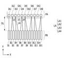
도 1 내지 도 4를 참조하면, 본 발명의 제1 실시예의 표시 장치는, 기판(SUB), 표시 패널(100), 집적회로 칩(510), 제1 패드부(PA), 제2 패드부(PB) 및 복수의 제1 연결 배선들(LA)을 포함한다.1 to 4 , the display device according to the first embodiment of the present invention includes a substrate SUB, a
본 실시예에 따르면, 제1 연결 배선들(LA)에 연결되는 제1 패드부(PA)의 복수의 제1 연결 단자들(IA1∼ IA8) 중 일부인 복수의 제1 연결 단자들 사이에 제1 연결 배선(LA)이 연결되지 않는 제1 더미 단자들(DA1, DA2, DA3)이 배치될 수 있다. 따라서, 제1 연결 배선(LA)이 연결되지 않는 제1 더미 단자들(DA1, DA2, DA3) 사이에 복수의 제1 연결 단자들(IA1∼ IA8) 중 일부가 배치될 수 있다. 이에 의해, 제1 패드부(PA)와 제2 패드부(PB)를 연결하는 제1 연결 배선들(LA) 사이의 길이 차이를 줄일 수 있다.According to the present exemplary embodiment, the first connection terminal is disposed between the plurality of first connection terminals which are some of the plurality of first connection terminals IA1 to IA8 of the first pad part PA connected to the first connection wires LA. First dummy terminals DA1 , DA2 , and DA3 to which the connection line LA is not connected may be disposed. Accordingly, some of the plurality of first connection terminals IA1 to IA8 may be disposed between the first dummy terminals DA1 , DA2 , and DA3 to which the first connection wire LA is not connected. Accordingly, a difference in length between the first connection lines LA connecting the first pad part PA and the second pad part PB may be reduced.
도 1을 참조하면, 기판(SUB)은 화상을 표시하는 표시 영역(DA)과 상기 표시 영역(DA)과 이웃하는 주변 영역(NDA)으로 구분된다. 표시 영역(DA)에는 빛을 발광하는 표시 패널(100)이 위치할 수 있다. 그리고, 주변 영역(NDA)에는 표시 패널(100)을 구동하기 위한 집적회로 칩(510), 제1 패드부(PA), 제2 패드부(PB), 표시 패널(100)과 제1 패드부(PA)를 연결하는 팬-아웃 배선(300) 및 복수의 제1 연결 배선(LA) 등이 위치할 수 있다. 하기에서는, 기판(SUB) 상에 형성되는 상기 주요 구성에 대해 설명하기로 한다.Referring to FIG. 1 , the substrate SUB is divided into a display area DA displaying an image and a peripheral area NDA adjacent to the display area DA. The
우선, 도 2 및 도 3을 참조하여, 기판(SUB)의 표시 영역(DA)에 형성되는 표시 패널(100)에 대해 상세히 설명하기로 한다.First, the
본 실시예에 따르면, 표시 패널(100)은 제1 게이트 배선들(GW1), 제2 게이트 배선들(GW2), 데이터 배선들(DW), 화소들(150)을 포함하고, 화소들(150)은 표시부(140)에 위치한다.According to the present exemplary embodiment, the
게이트 구동부(210)는 도시되지 않은 외부의 제어회로, 예컨대 타이밍 제어부 등으로부터 공급되는 제어신호에 대응하여 제1 게이트 배선들(GW1) 또는 제2 게이트 배선들(GW2)에 포함된 제1 스캔 라인들(SC2~SC2n) 또는 제2 스캔 라인들(SC1~SC2n-1)로 스캔 신호를 순차적으로 공급한다. 그러면, 화소들(150)은 스캔 신호에 의해 선택되어 순차적으로 데이터 신호를 공급받는다. 여기에서, 도 2에 도시된 게이트 구동부(210)는 후술하는 집적회로 칩(510) 내에 형성되는 것으로, 설명의 편의상 도 2에 도시한 것이다.The
제1 게이트 배선들(GW1)은 제1 절연층(GI1)을 사이에 두고 기판(SUB) 상에 위치하며, 제1 방향으로 연장되어 있다. 제1 게이트 배선들(GW1)은 제2 스캔 라인(SC2n-1) 및 발광 제어 라인들(E1~En)을 포함한다.The first gate wirings GW1 are disposed on the substrate SUB with the first insulating layer GI1 interposed therebetween and extend in the first direction. The first gate wirings GW1 include the second scan line SC2n-1 and the emission control lines E1 to En.
제2 스캔 라인(SC2n-1)은 게이트 구동부(210)와 연결되어 있으며, 게이트 구동부(210)로부터 스캔 신호를 공급받는다. 발광 제어 라인(En)은 발광 제어 구동부(220)와 연결되어 있으며, 발광 제어 구동부(220)로부터 발광 제어 신호를 공급받는다.The second scan line SC2n-1 is connected to the
여기에서, 도 2에 도시된 발광 제어 구동부(220)는 게이트 구동부(210)와 마찬가지로 후술하는 집적회로 칩(510) 내에 형성되는 것으로, 설명의 편의상 도 2에 도시한 것이다. 이하 도면에서 좌표를 나타내는 X 축은 제1 방향을, Y 축은 제2 방향을 나타낸다.Here, the light
제2 게이트 배선들(GW2)은 제2 절연층(GI2)을 사이에 두고 제1 게이트 배선들(GW1) 상에 위치하며, 제1 방향으로 연장되어 있다. 제2 게이트 배선들(GW2)은 제1 스캔 라인(SC2n) 및 초기화 전원 라인(Vinit)을 포함한다.The second gate lines GW2 are disposed on the first gate lines GW1 with the second insulating layer GI2 interposed therebetween, and extend in the first direction. The second gate lines GW2 include a first scan line SC2n and an initialization power line Vinit.
제1 게이트 배선들(GW1)과 제2 게이트 배선들(GW2)은 서로 중첩되지 않는다.The first gate lines GW1 and the second gate lines GW2 do not overlap each other.
제1 스캔 라인(SC2n)은 게이트 구동부(210)와 연결되어 있으며, 게이트 구동부(210)로부터 스캔 신호를 공급받는다. 초기화 전원 라인(Vinit)은 게이트 구동부(210)와 연결되어 있으며, 게이트 구동부(210)로부터 초기화 전원을 인가받는다.The first scan line SC2n is connected to the
본 발명의 일 실시예에서는 초기화 전원 라인(Vinit)이 게이트 구동부(210)로부터 초기화 전원을 인가받으나, 초기화 전원 라인(Vinit)이 추가적인 다른 구성과 연결되어 상기 추가적인 다른 구성으로부터 초기화 전원을 인가받을 수도 있다.In an embodiment of the present invention, the initialization power line Vinit receives initialization power from the
발광 제어 구동부(220)는 타이밍 제어부 등의 외부로부터 공급되는 제어신호에 대응하여 발광 제어 라인(En)로 발광 제어 신호를 순차적으로 공급한다. 그러면, 화소들(150)은 발광 제어 신호에 의해 발광이 제어된다.The light
즉, 발광 제어 신호는 화소들(150)의 발광 시간을 제어한다. 단, 발광 제어 구동부(220)는 화소들(150)의 내부 구조에 따라 생략될 수도 있다.That is, the emission control signal controls the emission time of the
데이터 구동부(230)는 타이밍 제어부 등의 외부로부터 공급되는 제어신호에 대응하여 데이터 배선들(DW) 중 데이터 라인(DAm)으로 데이터 신호를 공급한다. 데이터 라인(DAm)으로 공급된 데이터 신호는 제1 스캔 라인(SC2n) 또는 제2 스캔 라인(SC2n-1)으로 스캔 신호가 공급될 때마다 스캔 신호에 의해 선택된 화소(150)로 공급된다. 그러면, 화소(150)는 데이터 신호에 대응하는 전압을 충전하고 이에 대응하는 휘도로 발광한다. 여기에서, 도 2에 도시된 데이터 구동부(230)는 게이트 구동부(210)와 마찬가지로 후술하는 집적회로 칩(510) 내에 형성되는 것으로, 설명의 편의상 도 2에 도시한 것이다.The
데이터 배선들(DW)은 제3 절연층(ILD)을 사이에 두고 제2 게이트 배선들(GW2) 상에 위치하며, 제1 방향과 교차하는 제2 방향으로 연장되어 있다. 데이터 배선들(DW)은 데이터 라인들(DA1~DAm) 및 구동 전원 라인(ELVDDL)을 포함한다. 데이터 라인(DAm)은 데이터 구동부(230)와 연결되어 있으며, 데이터 구동부(230)로부터 데이터 신호를 공급받는다. 구동 전원 라인(ELVDDL)은 후술할 외부의 제1 전원(ELVDD)과 연결되어 있으며, 제1 전원(ELVDD)으로부터 구동 전원을 공급받는다.The data lines DW are disposed on the second gate lines GW2 with the third insulating layer ILD interposed therebetween, and extend in a second direction crossing the first direction. The data lines DW include data lines DA1 to DAm and a driving power line ELVDDL. The data line DAm is connected to the
이때, 구동 전원 라인(ELVDDL)과 데이터 라인(DAm)은 상기 제3 절연층(ILD) 상에 동일 층으로 형성될 수 있다. 그러나, 이에 한정되지 않고, 상기 구동 전원 라인(ELVDDL)과 데이터 라인(DAm)은 서로 다른 층에 형성될 수 있다. 예를 들어, 구동 전원 라인(ELVDDL)은 제1 게이트 배선(GW1)과 동일 층으로, 데이터 라인(DAm)은 제2 게이트 배선(GW2)와 동일 층으로 형성될 수 있다.In this case, the driving power line ELVDDL and the data line DAm may be formed in the same layer on the third insulating layer ILD. However, the present invention is not limited thereto, and the driving power line ELVDDL and the data line DAm may be formed on different layers. For example, the driving power line ELVDDL may be formed on the same layer as the first gate line GW1 , and the data line DAm may be formed on the same layer as the second gate line GW2 .
반대로, 구동 전원 라인(ELVDDL)은 제2 게이트 배선(GW2)과 동일 층으로, 데이터 라인(DAm)은 제1 게이트 배선(GW1)와 동일 층으로 형성될 수 있다. 표시부(140)는 제1 게이트 배선들(GW1), 제2 게이트 배선들(GW2) 및 데이터 배선들(DW)의 교차 영역에 위치하는 복수의 화소들(150)을 포함한다.Conversely, the driving power line ELVDDL may be formed on the same layer as the second gate line GW2 , and the data line DAm may be formed on the same layer as the first gate line GW1 . The
여기서, 각각의 화소들(150)은 데이터 신호에 대응되는 구동 전류에 상응하는 휘도로 발광하는 유기 발광 소자와, 상기 유기 발광 소자에 흐르는 구동전류를 제어하기 위한 화소 회로를 포함한다. 화소 회로는 제1 게이트 배선들(GW1), 제2 게이트 배선들(GW2) 및 데이터 배선들(DW) 각각과 연결되어 있으며, 유기 발광 소자는 상기 화소 회로에 연결되어 있다. 상기 화소들(150)은 유기 발광 소자로 설명되나, 본 실시예의 표시 장치에 적용되는 화소들(150)은 여기에 한정되지 않고, 액정 표시 소자, 전기 영동 표시 소자 등일 수 있다.Here, each of the
이와 같은 표시부(140)의 유기 발광 소자는 화소 회로를 사이에 두고 외부의 제1 전원(ELVDD)과 연결되고, 제2 전원(ELVSS)과 연결된다. 제1 전원(ELVDD) 및 제2 전원(ELVSS) 각각은 구동 전원 및 공통 전원 각각을 표시부(140)의 화소들(150)로 공급하며, 화소들(150)은 화소들(150)로 공급된 구동 전원 및 공통 전원에 따라 데이터 신호에 대응하여 제1 전원(ELVDD)으로부터 유기 발광 소자를 통하는 구동 전류에 대응하는 휘도로 발광한다.The organic light emitting diode of the
이와 같이, 본 발명의 일 실시예에 따른 표시 장치는 화소들(150)을 제1 방향으로 가로지르며 서로 비중첩되어 있는 게이트 배선들인 제2 스캔 라인(SC2n-1) 및 발광 제어 라인(En)을 포함하는 제1 게이트 배선들(GW1) 및 제1 스캔 라인(SC2n) 및 초기화 전원 라인(Vinit)을 포함하는 제2 게이트 배선들(GW2) 각각이 모두 동일한 층에 위치하는 것이 아니라, 게이트 배선들인 제1 게이트 배선들(GW1) 및 제2 게이트 배선들(GW2) 각각이 제2 절연층(GI2)을 사이에 두고 서로 다른 층에 위치함으로써, 서로 다른 층에 위치하는 이웃하는 게이트 배선들 간의 거리(W)를 좁게 형성할 수 있기 때문에, 동일한 면적에 보다 많은 화소들(150)을 형성할 수 있다. 즉, 고해상도의 표시 장치를 형성할 수 있다.As described above, in the display device according to the exemplary embodiment of the present invention, the second scan line SC2n-1 and the emission control line En, which are gate lines that do not overlap each other while crossing the
다시 도 1을 참조하면, 집적회로 칩(510)은 기판(SUB) 상의 주변 영역(NDA)에 위치한다. 집적회로 칩(510)은 구동 신호를 생성할 수 있다. 본 실시예에서는, 집적회로 칩(510)은 기판(SUB)의 주변 영역(NDA)에 칩온글라스(COG, Chip On Glass) 형태로 배치될 수 있다.Referring back to FIG. 1 , the
이때, 집적회로 칩(510)은 외부로부터 제어 신호를 수신하여 스캔 신호를 생성하는 스캔 구동 회로 또는 데이터 신호를 생성하는 데이터 구동 회로를 포함할 수 있다. 즉, 전술한 게이트 구동부(210) 또는 데이터 구동부(230)가 상기 집적회로 칩(510) 내에 형성될 수 있다.In this case, the
집적회로 칩(510)은 기판(SUB)의 주변 영역(NDA)에 위치하는 제1 패드부(PA)와 전기적으로 연결된다. 이때, 제1 패드부(PA)는 집적회로 칩(510)과 중첩된다.The
제1 패드부(PA)는 제1 노드(PA1)와 제2 노드(PA2)를 포함하며, 집적회로 칩(510)은 제1 노드(PA1) 및 제2 노드(PA2)와 전기적으로 연결된다. 제1 노드(PA1)는 외부로부터 제어 신호를 수신하여 집적회로 칩(510)에 전달한다. 그리고, 제2 노드(PA2)는 집적회로 칩(510)로부터 생성된 신호를 표시 패널(100)로 전달한다.The first pad part PA includes a first node PA1 and a second node PA2 , and the
도 1 및 도 4를 참조하면, 제1 패드부(PA)는 복수의 제1 연결 단자들(IA1∼ IA8)과 복수의 제1 더미 단자들(DA1, DA2, DA3)을 포함한다. 여기에서, 복수의 제1 연결 단자들(IA1∼ IA8)과 복수의 제1 더미 단자들(DA1, DA2, DA3)은 전술한 도 1의 제1 노드(PA1)에 위치할 수 있다.1 and 4 , the first pad part PA includes a plurality of first connection terminals IA1 to IA8 and a plurality of first dummy terminals DA1 , DA2 , and DA3 . Here, the plurality of first connection terminals IA1 to IA8 and the plurality of first dummy terminals DA1 , DA2 , and DA3 may be located at the first node PA1 of FIG. 1 .
이때, 복수의 제1 연결 단자들(IA1∼ IA8)은 일렬로 배치되어 집적회로 칩(510) 및 제1 연결 배선들(LA)과 전기적으로 연결될 수 있다. 복수의 제1 연결 단자들(IA1∼ IA8)은 집적회로 칩(510)과 상하 방향으로 중첩 배치되어 전기적으로 연결될 수 있다.In this case, the plurality of first connection terminals IA1 to IA8 may be arranged in a line to be electrically connected to the
그리고, 복수의 제1 연결 배선들(LA)은 제1 패드부(PA)의 복수의 제1 연결 단자들(IA1∼ IA8)과 후술하는 제2 패드부(PB)의 복수의 제2 연결 단자들(IB1∼IB15)을 서로 연결한다.In addition, the plurality of first connection wires LA includes a plurality of first connection terminals IA1 to IA8 of the first pad part PA and a plurality of second connection terminals of the second pad part PB to be described later. The IB1 to IB15 are connected to each other.
예를 들어, 복수의 제1 연결 배선들(LA) 중 제1 연결 배선(LA1)은 복수의 제1 연결 단자들(IA1∼ IA8) 중 제1 연결 단자(IA3)와 복수의 제2 연결 단자들(IB1∼IB15) 중 제2 연결 단자(IB4)를 서로 연결하고, 복수의 제1 연결 배선들(LA) 중 제1 연결 배선(LA2)은 복수의 제1 연결 단자들(IA1∼ IA8) 중 제1 연결 단자(IA3)와 복수의 제2 연결 단자들(IB1∼IB15) 중 제2 연결 단자(IB5)를 서로 연결한다. 그리고, 복수의 제1 연결 배선들(LA) 중 제1 연결 배선(LA3)은 복수의 제1 연결 단자들(IA1∼ IA8) 중 제1 연결 단자(IA4)와 복수의 제2 연결 단자들(IB1∼IB15) 중 제2 연결 단자(IB6)를 서로 연결하고, 복수의 제1 연결 배선들(LA) 중 제1 연결 배선(LA4)은 은 복수의 제1 연결 단자들(IA1∼ IA8) 중 제1 연결 단자(IA4)와 복수의 제2 연결 단자들(IB1∼IB15) 중 제2 연결 단자(IB7)를 서로 연결한다.For example, the first connection wire LA1 of the plurality of first connection wires LA may include a first connection terminal IA3 of the plurality of first connection terminals IA1 to IA8 and a plurality of second connection terminals The second connection terminals IB4 among the ones IB1 to IB15 are connected to each other, and the first connection wiring LA2 of the plurality of first connection wires LA is connected to the plurality of first connection terminals IA1 to IA8. of the first connection terminal IA3 and the second connection terminal IB5 of the plurality of second connection terminals IB1 to IB15 are connected to each other. In addition, the first connection wire LA3 of the plurality of first connection wires LA includes a first connection terminal IA4 and a plurality of second connection terminals IA4 among the plurality of first connection terminals IA1 to IA8. The second connection terminals IB6 of IB1 to IB15 are connected to each other, and the first connection wire LA4 of the plurality of first connection wires LA is formed of a silver among the plurality of first connection terminals IA1 to IA8. The first connection terminal IA4 and the second connection terminal IB7 among the plurality of second connection terminals IB1 to IB15 are connected to each other.
이때, 상기 제1 연결 단자(IA3)에 두 개의 제1 연결 배선들(LA1, LA2)이 연결되고, 상기 제1 연결 단자(IA4)에 두 개의 제1 연결 배선들(LA3, LA4)이 연결된다. 즉, 제1 패드부(PA)의 복수의 제1 연결 단자들(IA1∼ IA8) 각각에는 적어도 하나 이상의 제1 연결 배선(LA)이 연결될 수 있다.In this case, two first connection wires LA1 and LA2 are connected to the first connection terminal IA3 , and two first connection wires LA3 and LA4 are connected to the first connection terminal IA4 . do. That is, at least one first connection wire LA may be connected to each of the plurality of first connection terminals IA1 to IA8 of the first pad part PA.
이와 같이, 제1 패드부(PA)의 복수의 제1 연결 단자들(IA1∼ IA8) 각각에 적어도 하나 이상의 제1 연결 배선(LA)이 연결되면, 외부로부터 전달된 제어 신호가 손실되는 것을 방지할 수 있다. 예를 들어, 연결된 제1 연결 배선들(LA) 중 일부의 배선이 파손되어 신호가 전달되지 않더라도, 다른 배선을 통해 제어 신호를 전달할 수 있게 된다.As such, when at least one first connection wire LA is connected to each of the plurality of first connection terminals IA1 to IA8 of the first pad part PA, loss of a control signal transmitted from the outside is prevented can do. For example, even if some of the connected first connection wires LA are damaged and thus signals are not transmitted, a control signal may be transmitted through other wires.
한편, 제2 패드부(PB)는 제1 연결 배선들(LA)을 통해 제1 패드부(PA)와 연결되고, 복수의 제2 연결 단자들(IB1∼IB15)을 포함할 수 있다. 제2 패드부(PB)는 주변 영역(NDA)의 일측 단부에 배치되어, 외부로부터 제어 신호를 전달하는 인쇄 회로 기판(미도시)과 결합될 수 있다.Meanwhile, the second pad part PB may be connected to the first pad part PA through the first connection wires LA and may include a plurality of second connection terminals IB1 to IB15 . The second pad part PB may be disposed at one end of the peripheral area NDA and may be coupled to a printed circuit board (not shown) that transmits a control signal from the outside.
본 실시예에 따르면, 제1 패드부(PA)에서는 제1 연결 배선들(LA)이 연결되지 않는 제1 더미 단자들(DA1, DA2, DA3) 사이에 복수의 제1 연결 단자들(IA1∼ IA8) 중 일부가 배치될 수 있다. 보다 구체적으로 설명하면, 제1 더미 단자들(DA1, DA2, DA3) 중 제1 더미 단자(DA1)와 제1 더미 단자(DA2) 사이에 제1 연결 단자들(IA4, IA5)이 배치된다. 또한, 제1 더미 단자들(DA1, DA2, DA3) 중 제1 더미 단자(DA2)와 제1 더미 단자(DA3) 사이에 복수의 제1 연결 단자들(IA1∼ IA8) 중 제1 연결 단자들(IA6, IA7)이 배치된다.According to the present embodiment, in the first pad part PA, the plurality of first connection terminals IA1 to IA1 to Some of IA8) may be deployed. More specifically, the first connection terminals IA4 and IA5 are disposed between the first dummy terminal DA1 and the first dummy terminal DA2 among the first dummy terminals DA1 , DA2 , and DA3 . Also, between the first dummy terminal DA2 and the first dummy terminal DA3 among the first dummy terminals DA1 , DA2 , and DA3 , the first connection terminals of the plurality of first connection terminals IA1 to IA8 are connected. (IA6, IA7) is placed.
전술한 바와 같이, 상기 제1 더미 단자(DA1)와 상기 제1 더미 단자(DA2) 사이에 복수의 제1 연결 단자들(IA1∼ IA8) 중 제1 연결 단자들(IA4, IA5)이 배치되면, 제1 연결 단자들(IA1∼ IA8)과 제2 연결 단자들(IB1∼IB15)을 연결하는 제1 연결 배선들(LA) 사이의 길이 차이를 줄일 수 있다.As described above, when the first connection terminals IA4 and IA5 of the plurality of first connection terminals IA1 to IA8 are disposed between the first dummy terminal DA1 and the first dummy terminal DA2, , a difference in length between the first connection wires LA connecting the first connection terminals IA1 to IA8 and the second connection terminals IB1 to IB15 may be reduced.
만약, 도 4에서, 복수의 제1 연결 단자들(IA1∼ IA8) 중 제1 연결 단자(IA3)와 제1 연결 단자(IA4) 사이에 제1 더미 단자들(DA1, DA2, DA3) 중 제1 더미 단자(DA1)가 배치되지 않으면, 복수의 제1 연결 배선들(LA) 중 제1 연결 배선(LA3) 및 제1 연결 배선(LA4)이 연결된 상기 제1 연결 단자(IA4)는 왼쪽으로 이동하게 된다.If, in FIG. 4 , a second of the first dummy terminals DA1 , DA2 , and DA3 is disposed between the first connection terminal IA3 and the first connection terminal IA4 among the plurality of first connection terminals IA1 to IA8 . When the first dummy terminal DA1 is not disposed, the first connection terminal IA4 to which the first connection wire LA3 and the first connection wire LA4 are connected among the plurality of first connection wires LA moves to the left. will move
즉, 복수의 제1 연결 단자들(IA1∼IA8) 중 제1 연결 단자(IA4)는 제1 더미 단자들(DA1, DA2, DA3) 중 제1 더미 단자(DA1)의 위치로 이동하게 된다. 이렇게 되면, 제1 더미 단자(DA1)가 배치되는 경우와 비교할 때, 제1 더미 단자(DA1)가 배치되지 않는 경우의 복수의 제1 연결 배선들(LA) 중 제1 연결 배선(LA3) 및 제1 연결 배선(LA4)의 길이는 길어지게 된다.That is, the first connection terminal IA4 among the plurality of first connection terminals IA1 to IA8 moves to the position of the first dummy terminal DA1 among the first dummy terminals DA1 , DA2 , and DA3 . In this case, compared to the case in which the first dummy terminal DA1 is disposed, the first connection wire LA3 of the plurality of first connection wires LA when the first dummy terminal DA1 is not disposed, and The length of the first connection line LA4 is increased.
따라서, 본 발명의 제1 실시예에 따르면, 복수의 제1 연결 단자들(IA1∼ IA8) 중 제1 연결 단자(IA3)와 제1 연결 단자(IA4) 사이에 제1 더미 단자(DA1)를 배치함으로써, 제1 연결 배선들(LA3, LA4)과 제1 연결 배선들(LA3, LA4)에 인접한 제1 연결 배선들(LA1, LA2) 사이의 길이 차이를 줄일 수 있다.제1 패드부(PA)와 제2 패드부(PB)를 연결하는 제1 연결 배선들(LA) 사이의 길이 차이가 커되면, 상대적으로 길이가 긴 제1 연결 배선들(LA)을 통해 외부로부터 전달되는 상기 제어 신호는 지연될 수 있다.Accordingly, according to the first embodiment of the present invention, the first dummy terminal DA1 is formed between the first connection terminal IA3 and the first connection terminal IA4 among the plurality of first connection terminals IA1 to IA8. By disposing it, a difference in length between the first connection wires LA3 and LA4 and the first connection wires LA1 and LA2 adjacent to the first connection wires LA3 and LA4 can be reduced. When the difference in length between the first connection wires LA connecting the PA and the second pad part PB increases, the control transmitted from the outside through the relatively long first connection wires LA The signal may be delayed.
결국, 본 발명의 제1 실시예에서와 같이, 복수의 제1 연결 단자들(IA1∼ IA8) 중 제1 연결 단자(IA3)와 제1 연결 단자(IA4) 사이에 제1 더미 단자들(DA1, DA2, DA3) 중 제1 더미 단자(DA1)를 배치하면, 외부로부터 표시 패널로 전달되는 제어 신호의 지연을 방지할 수 있다.As a result, as in the first embodiment of the present invention, between the first connection terminal IA3 and the first connection terminal IA4 among the plurality of first connection terminals IA1 to IA8, the first dummy terminals DA1 , DA2 and DA3 , if the first dummy terminal DA1 is disposed, a delay of a control signal transmitted from the outside to the display panel may be prevented.
이때, 제1 더미 단자를 복수의 제1 연결 단자들 사이에 적절히 배치하면, 제1 연결 배선들(LA)의 길이를 인접한 제1 연결 단자들(IA1∼IA8)과 제2 연결 단자들(IB1∼IB15) 사이의 최단 거리(DL)에 가깝게 배치할 수 있다.In this case, when the first dummy terminal is properly disposed between the plurality of first connection terminals, the lengths of the first connection wires LA are adjusted to the adjacent first connection terminals IA1 to IA8 and the second connection terminals IB1 . -IB15) can be placed close to the shortest distance (DL).
본 발명의 제1 실시예에 따르면, 제1 연결 배선들(LA)의 길이가 상기 최단 거리(DL)의 100%∼200%가 되도록, 복수의 제1 연결 단자들(IA1∼ IA8) 중 일부인 복수의 제1 연결 단자들 사이에 제1 연결 배선들(LA)에 연결되지 않는 제1 더미 단자들(DA1, DA2, DA3)을 배치한다. 제1 연결 배선들(LA)의 길이가 상기 최단 거리(DL)에 대한 상기 범위로 배치되면, 제1 연결 배선들(LA)을 통해 외부로부터 표시 패널로 전달되는 제어 신호가 지연되는 것을 방지할 수 있다.According to the first embodiment of the present invention, some of the plurality of first connection terminals IA1 to IA8 are selected so that the length of the first connection wires LA is 100% to 200% of the shortest distance DL. First dummy terminals DA1 , DA2 , and DA3 not connected to the first connection lines LA are disposed between the plurality of first connection terminals. When the lengths of the first connection wires LA are arranged within the range with respect to the shortest distance DL, it is possible to prevent delay of a control signal transmitted from the outside to the display panel through the first connection wires LA. can
하기에서는, 도 5를 참조하여 본 발명의 제1 실시예에 따른 표시 장치의 변형예에 대해 설명하기로 한다. 상기 변형예를 설명함에 있어, 전술한 제1 실시예와 동일한 구성에 대한 상세한 설명은 생략하기로 한다.Hereinafter, a modified example of the display device according to the first embodiment of the present invention will be described with reference to FIG. 5 . In describing the modified example, a detailed description of the same configuration as that of the above-described first embodiment will be omitted.
도 5는 도 4의 제1 및 제2 패드부의 변형예이다.FIG. 5 is a modified example of the first and second pad parts of FIG. 4 .
도 5를 참조하면, 제2 패드부(PB)는 복수의 제2 연결 단자들(IB1∼IB15) 사이에 배치되는 제2 더미 단자들(DB1, DB2)을 더 포함할 수 있다. 제2 더미 단자들(DB1, DB2)은 복수의 제2 연결 단자들(IB1∼IB15)와 달리 상기 제1 연결 배선들(LA)이 연결되지 않는다.Referring to FIG. 5 , the second pad part PB may further include second dummy terminals DB1 and DB2 disposed between the plurality of second connection terminals IB1 to IB15 . Unlike the plurality of second connection terminals IB1 to IB15 , the second dummy terminals DB1 and DB2 are not connected to the first connection wires LA.
본 변형예에 따르면, 제2 더미 단자(DB1)의 양측에 인접하여 위치하는 한 쌍의 제2 연결 단자들(IB5, IB6)에 각각 연결된 제1 연결 배선들(LA2, LA3)은 서로 다른 제1 연결 단자들(IA3, IA4)에 연결된다. 보다 구체적으로 설명하면, 복수의 제2 연결 단자들(IB1∼IB15) 중 제2 연결 단자(IB5)에 연결된 제1 연결 배선(LA2)은 복수의 제1 연결 단자들(IA1∼IA8) 중 제1 연결 단자(IA3)에 연결되고, 복수의 제2 연결 단자들(IB1∼IB15) 중 제2 연결 단자(IB6)에 연결된 제1 연결 배선(LA3)은 복수의 제1 연결 단자들(IA1∼IA8) 중 제1 연결 단자(IA4)에 연결된다.According to this modified example, the first connection wires LA2 and LA3 respectively connected to the pair of second connection terminals IB5 and IB6 positioned adjacent to both sides of the second dummy terminal DB1 are 1 is connected to the connection terminals IA3 and IA4. More specifically, the first connection wire LA2 connected to the second connection terminal IB5 among the plurality of second connection terminals IB1 to IB15 is the first connection wire LA2 of the plurality of first connection terminals IA1 to IA8. The first connection wire LA3 connected to the first connection terminal IA3 and connected to the second connection terminal IB6 among the plurality of second connection terminals IB1 to IB15 is connected to the plurality of first connection terminals IA1 to IB15 . It is connected to the first connection terminal IA4 of IA8).
상기 제2 연결 단자(IB5)와 상기 제2 연결 단자(IB6)는 서로 다른 제어 신호를 외부로부터 수신하고, 수신된 제어 신호를 각각 다른 경로, 즉 다른 제1 연결 배선들(LA2, LA3)을 통해 표시 패널 측으로 전달한다.The second connection terminal IB5 and the second connection terminal IB6 receive different control signals from the outside, and transmit the received control signals through different paths, that is, different first connection wires LA2 and LA3. through the display panel.
그러나, 상기 제2 연결 단자(IB5)와 상기 제2 연결 단자(IB6)가 서로 단락되면, 정확한 제어 신호를 표시 패널 측으로 전달할 수 없게 된다. 본 변형예에서는, 상기 제2 연결 단자(IB5)와 상기 제2 연결 단자(IB6) 사이에 제2 더미 단자(DB1)를 배치하여, 상기 제2 연결 단자(IB5)와 상기 제2 연결 단자(IB6)가 서로 단락되는 것을 방지할 수 있다.However, when the second connection terminal IB5 and the second connection terminal IB6 are shorted together, an accurate control signal cannot be transmitted to the display panel side. In this modified example, a second dummy terminal DB1 is disposed between the second connection terminal IB5 and the second connection terminal IB6, so that the second connection terminal IB5 and the second connection terminal IB5 and the second connection terminal ( IB6) can be prevented from being shorted to each other.
한편, 상기 제2 연결 단자(IB5)와 상기 제2 연결 단자(IB6) 사이에 제2 더미 단자들(DB1, DB2) 중 제2 더미 단자(DB1)가 배치되면, 제1 연결 배선들(LA3, LA4)의 길이가 증가되어 인접한 제1 연결 배선들(LA1, LA2)과 길이 차이가 발생할 수 있다. 이 경우, 제1 연결 배선들(LA3, LA4)의 길이가 증가되어 신호 지연이 발생하는 것을 방지하기 위해, 도 4에서와 달리 상기 제1 연결 단자(IA3)과 상기 제1 연결 단자(IA4) 사이에 두 개의 제1 더미 단자들(DA1, DA2)이 배치될 수 있다.Meanwhile, when the second dummy terminal DB1 of the second dummy terminals DB1 and DB2 is disposed between the second connection terminal IB5 and the second connection terminal IB6, the first connection wires LA3 , LA4 may be increased in length, so that a difference in length may occur with respect to the adjacent first connection lines LA1 and LA2 . In this case, unlike in FIG. 4 , in order to prevent a signal delay due to an increase in the length of the first connection wires LA3 and LA4 , the first connection terminal IA3 and the first connection terminal IA4 are Two first dummy terminals DA1 and DA2 may be disposed therebetween.
하기에서는, 도 6 및 도 7을 참조하여 본 발명의 제2 실시예에 따른 표시 장치에 대해 설명하기로 한다. 상기 제2 실시예를 설명함에 있어, 전술한 제1 실시예와 동일한 구성에 대한 상세한 설명은 생략하기로 한다.Hereinafter, a display device according to a second exemplary embodiment of the present invention will be described with reference to FIGS. 6 and 7 . In describing the second embodiment, a detailed description of the same configuration as that of the above-described first embodiment will be omitted.
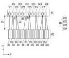
도 6은 본 발명의 제2 실시예에 따른 표시 장치의 부분 평면도이며, 도 7은 도 6의 B 영역을 확대한 도면이다.6 is a partial plan view of a display device according to a second exemplary embodiment, and FIG. 7 is an enlarged view of area B of FIG. 6 .
도 6 및 도 7을 참조하면, 본 발명의 제2 실시예의 표시 장치는, 기판(SUB), 표시 패널(100), 베이스 필름(400), 집적회로 칩(530), 제3 패드부(PC), 제4 패드부(PD), 복수의 제2 연결 배선들(LB), 복수의 제3 연결 배선들(600)을 포함한다.6 and 7 , the display device according to the second embodiment of the present invention includes a substrate SUB, a
제1 실시예와 마찬가지로, 제2 실시예에 따르면, 제2 연결 배선들(LB)에 연결되는 제3 패드부(PC)의 복수의 제3 연결 단자들(IC1∼IC8) 중 일부인 복수의 제3 연결 단자들 사이에 제2 연결 배선들(LB)이 연결되지 않는 제3 더미 단자들(DC1, DC2, DC3)이 배치될 수 있다. 결국, 제2 연결 배선(LB)이 연결되지 않는 제3 더미 단자들(DC1, DC2, DC3) 사이에 복수의 제3 연결 단자들(IC1∼IC8) 중 일부가 배치될 수 있다. 이에 의해, 제3 패드부(PC)와 제4 패드부(PD)를 연결하는 제2 연결 배선들(LB) 사이의 길이 차이를 줄일 수 있다.Like the first embodiment, according to the second embodiment, a plurality of third connection terminals IC1 to IC8 of the third pad unit PC connected to the second connection lines LB are some of the plurality of third connection terminals IC1 to IC8 . Third dummy terminals DC1 , DC2 , and DC3 to which the second connection wires LB are not connected may be disposed between the three connection terminals. As a result, some of the plurality of third connection terminals IC1 to IC8 may be disposed between the third dummy terminals DC1 , DC2 , and DC3 to which the second connection line LB is not connected. Accordingly, a difference in length between the second connection lines LB connecting the third pad unit PC and the fourth pad unit PD may be reduced.
기판(SUB)의 주변 영역(NDA)의 일측 단부에는 가요성인 베이스 필름(400)이 결합된다. 상기 베이스 필름(400)에는 구동 신호를 생성할 수 있는 집적회로 칩(530)이 배치된다. 이때, 상기 베이스 필름(400)에 형성된 제5 패드부(P1)를 통해, 상기 베이스 필름(400)은 상기 기판(SUB)과 연결될 수 있다. 본 실시예에서는, 집적회로 칩(530)은 베이스 필름(400)에 형성되는 칩온필름(COF, Chip On Film) 형태로 배치될 수 있다.A
이때, 집적회로 칩(530)은 외부로부터 제어 신호를 수신하여 스캔 신호를 생성하는 스캔 구동 회로 또는 데이터 신호를 생성하는 데이터 구동 회로를 포함할 수 있다. 즉, 전술한 게이트 구동부(210) 또는 데이터 구동부(230)가 상기 집적회로 칩(530) 내에 형성될 수 있다.In this case, the
집적회로 칩(530)은 베이스 필름(400)에 위치하는 제3 패드부(PC)와 전기적으로 결합한다. 이때, 제3 패드부(PC)는 집적회로 칩(530)과 중첩되도록 배치된다.The
제3 패드부(PC)는 제3 노드(PC1)와 제4 노드(PC2)를 포함하며, 집적회로 칩(530)은 제3 노드(PC1) 및 제4 노드(PC2)와 전기적으로 연결된다. 제3 노드(PC1)는 외부로부터 제어 신호를 수신하여 집적회로 칩(530)에 전달한다. 그리고, 제4 노드(PC2)는 집적회로 칩(530)로부터 생성된 신호를 제3 연결 배선(600) 및 제5 패드부(P1)를 통해 표시 패널(100)로 전달한다.The third pad unit PC includes a third node PC1 and a fourth node PC2 , and the
제3 패드부(PC)는 복수의 제3 연결 단자들(IC1∼IC8)과 복수의 제3 더미 단자들(DC1, DC2, DC3)을 포함한다. 여기에서, 복수의 제3 연결 단자들(IC1∼IC8)과 복수의 제3 더미 단자들(DC1, DC2, DC3)은 전술한 도 6의 제3 노드(PC1)에 위치할 수 있다.The third pad part PC includes a plurality of third connection terminals IC1 to IC8 and a plurality of third dummy terminals DC1 , DC2 , and DC3 . Here, the plurality of third connection terminals IC1 to IC8 and the plurality of third dummy terminals DC1 , DC2 , and DC3 may be located at the third node PC1 of FIG. 6 .
이때, 복수의 제3 연결 단자들(IC1∼IC8)은 일렬로 배치되어 집적회로 칩(530) 및 제2 연결 배선들(LB)과 전기적으로 연결될 수 있다. 복수의 제3 연결 단자들(IC1∼IC8)은 집적회로 칩(530)과 상하 방향으로 중첩 배치되어 전기적으로 연결될 수 있다.In this case, the plurality of third connection terminals IC1 to IC8 may be arranged in a line to be electrically connected to the
그리고, 복수의 제2 연결 배선들(LB)은 제3 패드부(PC)의 복수의 제3 연결 단자들(IC1∼IC8)과 제4 패드부(PD)의 복수의 제4 연결 단자들(ID1∼ID15)을 서로 연결한다.In addition, the plurality of second connection wires LB are connected to the plurality of third connection terminals IC1 to IC8 of the third pad part PC and the plurality of fourth connection terminals IC1 to IC8 of the fourth pad part PD. ID1 to ID15) are connected to each other.
예를 들어, 복수의 제2 연결 배선들(LB) 중 제2 연결 배선(LB1)은 복수의 제3 연결 단자들(IC1∼IC8) 중 제3 연결 단자(IC3)와 복수의 제4 연결 단자들(ID1∼ID15) 중 제4 연결 단자(ID4)를 서로 연결하고, 복수의 제2 연결 배선들(LB) 중 제2 연결 배선(LB2)은 복수의 제3 연결 단자들(IC1∼IC8) 중 제3 연결 단자(IC3)와 복수의 제4 연결 단자들(ID1∼ID15) 중 제4 연결 단자(ID5)를 서로 연결한다. 그리고, 복수의 제2 연결 배선들(LB) 중 제2 연결 배선(LB3)은 복수의 제3 연결 단자들(IC1∼IC8) 중 제3 연결 단자(IC4)와 복수의 제4 연결 단자들(ID1∼ID15) 중 제4 연결 단자(ID6)를 서로 연결하고, 복수의 제2 연결 배선들(LB) 중 제2 연결 배선(LB4)은 복수의 제3 연결 단자들(IC1∼IC8) 중 제3 연결 단자(IC4)와 복수의 제4 연결 단자들(ID1∼ID15) 중 제4 연결 단자(ID7)를 서로 연결한다.For example, the second connection line LB1 of the plurality of second connection lines LB may include a third connection terminal IC3 and a plurality of fourth connection terminals among the plurality of third connection terminals IC1 to IC8 . The fourth connection terminal ID4 among the ones ID1 to ID15 is connected to each other, and the second connection wire LB2 of the plurality of second connection wires LB is connected to the plurality of third connection terminals IC1 to IC8. The third connection terminal IC3 and the fourth connection terminal ID5 among the plurality of fourth connection terminals ID1 to ID15 are connected to each other. In addition, the second connection wiring LB3 of the plurality of second connection wirings LB includes a third connection terminal IC4 and a plurality of fourth connection terminals IC4 among the plurality of third connection terminals IC1 to IC8. A fourth connection terminal ID6 of ID1 to ID15 is connected to each other, and a second connection wire LB4 of the plurality of second connection wires LB is a second connection terminal of the plurality of third connection terminals IC1 to IC8. The third connection terminal IC4 and a fourth connection terminal ID7 among the plurality of fourth connection terminals ID1 to ID15 are connected to each other.
이때, 제3 패드부(PC)의 제3 연결단자들(IC1∼IC8) 각각에는 적어도 하나 이상의 제2 연결 배선(LB)이 연결될 수 있다.At this time, at least one second connection line LB may be connected to each of the third connection terminals IC1 to IC8 of the third pad unit PC.
제1 실시예와 마찬가지로, 제3 패드부(PC)의 제3 연결단자들(IC1∼IC8) 각각에 적어도 하나 이상의 제2 연결 배선(LB)이 연결되면, 외부로부터 전달된 제어 신호가 손실되는 것을 방지할 수 있다.As in the first embodiment, when at least one or more second connection wires LB are connected to each of the third connection terminals IC1 to IC8 of the third pad unit PC, the control signal transmitted from the outside is lost. can prevent
한편, 제4 패드부(PD)는 제2 연결 배선들(LB)을 통해 제3 패드부(PC)와 연결되는 것으로, 복수의 제4 연결 단자들(ID1∼ID15)을 포함할 수 있다. 제4 패드부(PD)는 베이스 필름(400)의 일측 단부에 배치되어, 외부로부터 제어 신호를 전달하는 인쇄 회로 기판(미도시)과 결합될 수 있다.Meanwhile, the fourth pad part PD is connected to the third pad part PC through the second connection lines LB, and may include a plurality of fourth connection terminals ID1 to ID15 . The fourth pad part PD may be disposed at one end of the
본 실시예에 따르면, 제3 패드부(PC)에서는 제2 연결 배선들(LB)이 연결되지 않는 제3 더미 단자들(DC1, DC2, DC3) 사이에 복수의 제3 연결 단자들(IC1∼IC8) 중 일부가 배치될 수 있다. 보다 구체적으로 설명하면, 제3 더미 단자들(DC1, DC2, DC3) 중 제3 더미 단자(DC1)와 제3 더미 단자(DC2) 사이에 제3 연결 단자들(IC4, IC5)이 배치된다. 또한, 제3 더미 단자들(DC1, DC2, DC3) 중 제3 더미 단자(DC2)와 제3 더미 단자(DC3) 사이에 복수의 제3 연결 단자들(IC1∼IC8) 중 제3 연결 단자들(IC6, IC7)이 배치된다.According to the present embodiment, in the third pad unit PC, a plurality of third connection terminals IC1 to Some of IC8) may be disposed. More specifically, the third connection terminals IC4 and IC5 are disposed between the third dummy terminal DC1 and the third dummy terminal DC2 among the third dummy terminals DC1 , DC2 , and DC3 . Also, between the third dummy terminal DC2 and the third dummy terminal DC3 among the third dummy terminals DC1 , DC2 and DC3 , third connection terminals among the plurality of third connection terminals IC1 to IC8 are (IC6, IC7) is placed.
전술한 바와 같이, 상기 제3 더미 단자(DC1)와 상기 제3 더미 단자(DC2) 사이에 복수의 제3 연결 단자들(IC1∼IC8) 중 제3 연결 단자들(IC4, IC5)이 배치되면, 제3 연결 단자들(IC1∼IC8)과 제4 연결 단자들(ID1∼ID15)을 연결하는 제2 연결 배선들(LB) 사이의 길이 차이를 줄일 수 있다.As described above, when the third connection terminals IC4 and IC5 among the plurality of third connection terminals IC1 to IC8 are disposed between the third dummy terminal DC1 and the third dummy terminal DC2, , a difference in length between the second connection wires LB connecting the third connection terminals IC1 to IC8 and the fourth connection terminals ID1 to ID15 may be reduced.
따라서, 본 발명의 제2 실시예에 따르면, 복수의 제3 연결 단자들(IC1∼IC8) 중 제3 연결 단자(IC3)와 제3 연결 단자(IC4) 사이에 제3 더미 단자들(DC1, DC2, DC3) 중 제3 더미 단자(DC1)를 배치함으로써, 제2 연결 배선들(LB3, LB4)과 제2 연결 배선들(LB3, LB4)에 인접한 제2 연결 배선들(LB1, LB2) 사이의 길이 차이를 줄일 수 있다.Therefore, according to the second embodiment of the present invention, the third dummy terminals DC1, DC1, between the third connection terminal IC3 and the third connection terminal IC4 among the plurality of third connection terminals IC1 to IC8. By disposing the third dummy terminal DC1 among DC2 and DC3 , between the second connection wires LB3 and LB4 and the second connection wires LB1 and LB2 adjacent to the second connection wires LB3 and LB4 can reduce the difference in length.
제1 실시예와 마찬가지로, 제3 패드부(PC)와 제4 패드부(PD)를 연결하는 제2 연결 배선들(LB) 사이의 길이 차이가 증가되면, 제2 연결 배선들(LB)을 통해 외부로부터 전달되는 상기 제어 신호는 지연될 수 있다. 결국, 본 발명의 제2 실시예에서와 같이, 제3 연결 단자(IC3)와 제3 연결 단자(IC4) 사이에 제3 더미 단자(DC1)를 배치하면, 외부로부터 표시 패널로 전달되는 제어 신호의 지연을 방지할 수 있다.As in the first embodiment, when the difference in length between the second connection wires LB connecting the third pad part PC and the fourth pad part PD increases, the second connection wires LB are connected to each other. The control signal transmitted from the outside through the may be delayed. As a result, as in the second embodiment of the present invention, when the third dummy terminal DC1 is disposed between the third connection terminal IC3 and the third connection terminal IC4 , a control signal transmitted from the outside to the display panel delay can be avoided.
이때, 제3 더미 단자를 복수의 제3 연결 단자들 사이에 적절히 배치하면, 제2 연결 배선들(LB)의 길이를 인접한 제3 연결 단자들(IC1∼IC8)과 제4 연결 단자들(ID1∼ID15) 사이의 최단 거리(DL)에 가깝게 배치할 수 있다.In this case, when the third dummy terminal is properly disposed between the plurality of third connection terminals, the lengths of the second connection wires LB are adjusted to the adjacent third connection terminals IC1 to IC8 and the fourth connection terminals ID1 . ~ID15) can be placed close to the shortest distance (DL).
본 발명의 제2 실시예에 따르면, 제2 연결 배선들(LB)의 길이가 상기 최단 거리(DL)의 100%∼200%가 되도록, 복수의 제3 연결 단자들(IC1∼IC8) 중 일부인 복수의 제3 연결 단자들 사이에 제2 연결 배선들(LB)이 연결되지 않는 제3 더미 단자들(DC1, DC2, DC3)을 배치한다. 제2 연결 배선들(LB)의 길이가 상기 최단 거리(DL)에 대한 상기 범위로 배치되면, 제2 연결 배선들(LB)을 통해 외부로부터 표시 패널로 전달되는 제어 신호가 지연되는 것을 방지할 수 있다.According to the second embodiment of the present invention, some of the plurality of third connection terminals IC1 to IC8 are formed so that the length of the second connection wires LB becomes 100% to 200% of the shortest distance DL. Third dummy terminals DC1 , DC2 , and DC3 to which the second connection lines LB are not connected are disposed between the plurality of third connection terminals. When the length of the second connection lines LB is arranged within the range for the shortest distance DL, it is possible to prevent delay of a control signal transmitted from the outside to the display panel through the second connection lines LB. can
하기에서는, 도 8을 참조하여 본 발명의 제2 실시예에 따른 표시 장치의 변형예에 대해 설명하기로 한다. 상기 변형예를 설명함에 있어, 전술한 제2 실시예와 동일한 구성에 대한 상세한 설명은 생략하기로 한다.Hereinafter, a modified example of the display device according to the second embodiment of the present invention will be described with reference to FIG. 8 . In describing the modified example, a detailed description of the same configuration as that of the above-described second embodiment will be omitted.
도 8은 도 7의 제3 및 제4 패드부의 변형예이다.FIG. 8 is a modified example of the third and fourth pad parts of FIG. 7 .
도 8을 참조하면, 제4 패드부(PD)는 복수의 제4 연결 단자들(ID1∼ID15) 사이에 배치되는 제4 더미 단자들(DD1, DD2)을 더 포함할 수 있다. 제4 더미 단자들(DD1, DD2)은 복수의 제4 연결 단자들(ID1∼ID15)과 달리 상기 제2 연결 배선들(LB)이 연결되지 않는다.Referring to FIG. 8 , the fourth pad part PD may further include fourth dummy terminals DD1 and DD2 disposed between the plurality of fourth connection terminals ID1 to ID15 . Unlike the plurality of fourth connection terminals ID1 to ID15 , the fourth dummy terminals DD1 and DD2 are not connected to the second connection lines LB.
본 변형예에 따르면, 제4 더미 단자(DD1)의 양측에 인접하여 위치하는 한 쌍의 제4 연결 단자들(ID5, ID6)에 각각 연결된 제2 연결 배선들(LB2, LB3)은 서로 다른 제3 연결 단자들(IC3, IC4)에 연결된다. 보다 구체적으로 설명하면, 복수의 제4 연결 단자들(ID1∼ID15) 중 제4 연결 단자(ID5)에 연결된 제2 연결 배선(LB2)은 복수의 제3 연결 단자들(IC1∼IC8) 중 제3 연결 단자(IC3)에 연결되고, 복수의 제4 연결 단자들(ID1∼ID15) 중 제4 연결 단자(ID6)에 연결된 제2 연결 배선(LB3)은 복수의 제3 연결 단자들(IC1∼IC8) 중 제3 연결 단자(IC4)에 연결된다.According to this modified example, the second connection wires LB2 and LB3 respectively connected to the pair of fourth connection terminals ID5 and ID6 positioned adjacent to both sides of the fourth dummy terminal DD1 are 3 are connected to the connection terminals IC3 and IC4. More specifically, the second connection wire LB2 connected to the fourth connection terminal ID5 among the plurality of fourth connection terminals ID1 to ID15 is a second connection wire LB2 of the plurality of third connection terminals IC1 to IC8. The second connection wire LB3 connected to the third connection terminal IC3 and connected to the fourth connection terminal ID6 among the plurality of fourth connection terminals ID1 to ID15 is connected to the plurality of third connection terminals IC1 to ID15. of IC8) is connected to the third connection terminal IC4.
상기 제4 연결 단자(ID5)와 상기 제4 연결 단자(ID6)는 서로 다른 제어 신호를 외부로부터 수신하고, 수신된 제어 신호를 각각 다른 경로, 즉 다른 제2 연결 배선들(LB2, LB3)을 통해 표시 패널 측으로 전달한다.The fourth connection terminal ID5 and the fourth connection terminal ID6 receive different control signals from the outside, and transmit the received control signals through different paths, that is, different second connection wires LB2 and LB3. through the display panel.
그러나, 상기 제4 연결 단자(ID5)와 상기 제4 연결 단자(ID6)가 서로 단락되면, 정확한 제어 신호를 표시 패널 측으로 전달할 수 없게 된다. 본 변형예에서는, 상기 제4 연결 단자(ID5)와 상기 제4 연결 단자(ID6) 사이에 제4 더미 단자(DD1)를 배치하여, 상기 제4 연결 단자(ID5)와 상기 제4 연결 단자(ID6)가 서로 단락되는 것을 방지할 수 있다.However, when the fourth connection terminal ID5 and the fourth connection terminal ID6 are shorted together, an accurate control signal cannot be transmitted to the display panel side. In this modified example, a fourth dummy terminal DD1 is disposed between the fourth connection terminal ID5 and the fourth connection terminal ID6, and the fourth connection terminal ID5 and the fourth connection terminal ID6 are disposed. ID6) can be prevented from being shorted to each other.
한편, 상기 제4 연결 단자(ID5)와 상기 제4 연결 단자(ID6) 사이에 제4 더미 단자들(DD1, DD2) 중 제4 더미 단자(DD1)가 배치되면, 제2 연결 배선들(LB3, LB4)의 길이가 증가되어 인접한 제2 연결 배선들(LB1, LB2)과 길이 차이가 발생될 수 있다. 이 경우, 제2 연결 배선들(LB3, LB4)의 길이가 증가되어 신호 지연이 발생하는 것을 방지하기 위해, 도 7에서와 달리 상기 제3 연결 단자(IC3)과 상기 제3 연결 단자(IC4) 사이에 두 개의 제3 더미 단자들(DC1, DC2)이 배치될 수 있다.Meanwhile, when the fourth dummy terminal DD1 of the fourth dummy terminals DD1 and DD2 is disposed between the fourth connection terminal ID5 and the fourth connection terminal ID6, the second connection lines LB3 , LB4 may be increased in length so that a difference in length may be generated from the adjacent second connection lines LB1 and LB2 . In this case, unlike in FIG. 7 , in order to prevent signal delay from occurring due to an increase in the length of the second connection lines LB3 and LB4 , the third connection terminal IC3 and the third connection terminal IC4 are Two third dummy terminals DC1 and DC2 may be disposed therebetween.
본 발명의 일 실시예에 따른 표시 장치는, 집적회로 칩과 연결되는 제1 패드부(PA)의 제1 연결 단자들(IA1∼ IA8) 중 일부인 복수의 제1 연결 단자들 사이에 제1 연결 배선들(LA)이 연결되지 않는 제1 더미 단자들(DA1, DA2, DA3)을 배치하여, 제1 연결 배선(LA)들 사이의 길이 차이를 줄여 외부로부터 표시 패널로 전달되는 제어 신호의 지연을 방지할 수 있다. In the display device according to an embodiment of the present invention, a first connection is made between a plurality of first connection terminals which are some of the first connection terminals IA1 to IA8 of the first pad part PA connected to an integrated circuit chip. By disposing the first dummy terminals DA1 , DA2 , and DA3 to which the wires LA are not connected, a difference in length between the first connection wires LA is reduced to delay the control signal transmitted from the outside to the display panel. can prevent
이상과 같이, 본 발명은 한정된 실시예와 도면을 통하여 설명되었으나, 본 발명은 이에 한정되는 것은 아니며, 본 발명이 속하는 기술 분야에서 통상의 지식을 가진 자에 의해 본 발명의 기술 사상과 아래에 기재된 특허청구범위의 균등범위 내에서 다양한 수정 및 변형이 가능하다.As described above, the present invention has been described with reference to limited embodiments and drawings, but the present invention is not limited thereto, and the technical spirit of the present invention and described below by those of ordinary skill in the art to which the present invention pertains. Various modifications and variations are possible within the scope of equivalents of the claims.
SUB 기판
DA 표시 영역
NDA 주변 영역
LA 제1 연결 배선
LB 제2 연결 배선
PA 제1 패드부
PB 제2 패드부
PC 제3 패드부
PC 제4 패드부
IA1∼ IA8 제1 연결 단자
IC1∼IC8 제3 연결 단자
DA1, DA2, DA3 제1 더미 단자
DC1, DC2, DC3 제3 더미 단자
100 표시 패널
510, 530 집적회로 칩SUB board
DA display area
Area around NDA
LA 1st connection wiring
LB 2nd connection wiring
PA first pad part
PB second pad part
PC 3rd pad part
PC 4th pad part
IA1 to IA8 first connection terminal
IC1 to IC8 3rd connection terminal
DA1, DA2, DA3 first dummy terminals
DC1, DC2, DC3 3rd dummy terminal
100 display panel
510 and 530 integrated circuit chips
Claims (13)
Translated fromKorean상기 집적회로 칩과 중첩하며, 상기 집적회로 칩과 연결되는 복수의 제1 연결 단자들 및 복수의 제1 더미 단자들을 포함하는 제1 패드부;
상기 주변 영역에 배치되며, 인쇄 회로 기판과 연결되는 복수의 제2 연결 단자들을 포함하는 제2 패드부; 및
상기 복수의 제1 연결 단자들과 상기 복수의 제2 연결 단자들을 서로 연결하는 복수의 제1 연결 배선들을 포함하며,
상기 제1 연결 배선들이 연결되지 않는 제1 더미 단자들 사이에 상기 복수의 제1 연결 단자들 중 일부가 배치되는, 표시 장치.a substrate including a peripheral region on which an integrated circuit chip is disposed;
a first pad part overlapping the integrated circuit chip and including a plurality of first connection terminals and a plurality of first dummy terminals connected to the integrated circuit chip;
a second pad unit disposed in the peripheral area and including a plurality of second connection terminals connected to the printed circuit board; and
and a plurality of first connection wires connecting the plurality of first connection terminals and the plurality of second connection terminals to each other,
A portion of the plurality of first connection terminals is disposed between first dummy terminals to which the first connection lines are not connected.
상기 제1 더미 단자들에 인접한 상기 제1 연결 단자들에 연결된 상기 제1 연결 배선들 각각의 길이는,
인접한 상기 제1 연결 단자들과 상기 제2 연결 단자들 사이의 최단 거리의 100% ~ 200 % 인, 표시 장치.The method of claim 1,
A length of each of the first connection wires connected to the first connection terminals adjacent to the first dummy terminals is,
100% to 200% of the shortest distance between the adjacent first connection terminals and the second connection terminals.
상기 복수의 제1 연결 단자들 각각에는 적어도 하나 이상의 상기 제1연결 배선이 연결되는, 표시 장치.The method of claim 1,
Each of the plurality of first connection terminals has at least one of the firstA display device to which the connecting wiring is connected.
상기 복수의 제1 연결 단자들은 일렬로 배열되는, 표시 장치.The method of claim 1,
The plurality of first connection terminals are arranged in a line.
상기 제2 패드부는,
상기 복수의 제2 연결 단자들 사이에 배치되며, 상기 제1 연결 배선들이 연결되지 않는 제2 더미 단자를 더 포함하는, 표시 장치.The method of claim 1,
The second pad part,
and a second dummy terminal disposed between the plurality of second connection terminals and to which the first connection lines are not connected.
상기 제2 더미 단자의 양측에 인접하여 위치하는 한 쌍의 제2 연결 단자들에 각각 연결된 상기 제1 연결 배선들은, 서로 다른 제1 연결 단자들에 연결되는, 표시 장치.6. The method of claim 5,
The first connection wires respectively connected to a pair of second connection terminals positioned adjacent to both sides of the second dummy terminal are connected to different first connection terminals.
상기 기판의 일측에 결합되는 베이스 필름;
상기 베이스 필름에 배치되는 집적회로 칩;
상기 베이스 필름 위에 상기 집적회로 칩과 중첩하며, 상기 집적회로 칩과 연결되는 복수의 제3 연결 단자들 및 복수의 제3 더미 단자들을 포함하는 제3 패드부;
상기 베이스 필름의 일측 단부에 위치하는 복수의 제4 연결 단자들을 포함하는 제4 패드부; 및
상기 복수의 제3 연결 단자들과 상기 복수의 제4 연결 단자들을 서로 연결하는 복수의 제2 연결 배선들을 포함하며,
상기 제2 연결 배선들이 연결되지 않는 제3 더미 단자들 사이에 상기 복수의 제3 연결 단자들 중 일부가 배치되는, 표시 장치.Board;
a base film coupled to one side of the substrate;
an integrated circuit chip disposed on the base film;
a third pad unit overlapping the integrated circuit chip on the base film and including a plurality of third connection terminals and a plurality of third dummy terminals connected to the integrated circuit chip;
a fourth pad unit including a plurality of fourth connection terminals positioned at one end of the base film; and
a plurality of second connection wires connecting the plurality of third connection terminals and the plurality of fourth connection terminals to each other;
A portion of the plurality of third connection terminals is disposed between third dummy terminals to which the second connection lines are not connected.
상기 제3 더미 단자들에 인접한 상기 제3 연결 단자들에 연결된 상기 제2 연결 배선들 각각의 길이는,
인접한 상기 제3 연결 단자들과 상기 제4 연결 단자들 사이의 최단 거리의 100% ~ 200 % 이하인, 표시 장치.8. The method of claim 7,
A length of each of the second connection wires connected to the third connection terminals adjacent to the third dummy terminals is,
100% to 200% or less of the shortest distance between the adjacent third connection terminals and the fourth connection terminals.
상기 복수의 제3 연결 단자들 각각에는 적어도 하나 이상의 상기 제2연결 배선이 연결되는, 표시 장치.8. The method of claim 7,
Each of the plurality of third connection terminals has at least one of the secondA display device to which the connecting wiring is connected.
상기 복수의 제3 연결 단자들은 일렬로 배열되는, 표시 장치.8. The method of claim 7,
The plurality of third connection terminals are arranged in a line.
상기 제4 패드부는,
상기 복수의 제4 연결 단자들 사이에 배치되며, 상기 제2 연결 배선들이 연결되지 않는 제4 더미 단자를 더 포함하는, 표시 장치.8. The method of claim 7,
The fourth pad part,
The display device of claim 1 , further comprising: a fourth dummy terminal disposed between the plurality of fourth connection terminals and to which the second connection lines are not connected.
상기 제4 더미 단자의 양측에 인접하여 위치하는 한 쌍의 제4 연결 단자들에 각각 연결된 상기 제2 연결 배선들은, 서로 다른 제3 연결 단자들에 연결되는, 표시 장치.12. The method of claim 11,
The second connection wires respectively connected to a pair of fourth connection terminals positioned adjacent to both sides of the fourth dummy terminal are connected to different third connection terminals.
상기 베이스 필름은 가요성인, 표시 장치.8. The method of claim 7,
The base film is flexible.
Priority Applications (3)
| Application Number | Priority Date | Filing Date | Title |
|---|---|---|---|
| KR1020150171534AKR102372209B1 (en) | 2015-12-03 | 2015-12-03 | Display device |
| US15/208,247US9930784B2 (en) | 2015-12-03 | 2016-07-12 | Display device having dummy terminals |
| CN201610997868.2ACN107015407A (en) | 2015-12-03 | 2016-11-11 | Display device with virtual terminal |
Applications Claiming Priority (1)
| Application Number | Priority Date | Filing Date | Title |
|---|---|---|---|
| KR1020150171534AKR102372209B1 (en) | 2015-12-03 | 2015-12-03 | Display device |
Publications (2)
| Publication Number | Publication Date |
|---|---|
| KR20170065718A KR20170065718A (en) | 2017-06-14 |
| KR102372209B1true KR102372209B1 (en) | 2022-03-08 |
Family
ID=58798681
Family Applications (1)
| Application Number | Title | Priority Date | Filing Date |
|---|---|---|---|
| KR1020150171534AActiveKR102372209B1 (en) | 2015-12-03 | 2015-12-03 | Display device |
Country Status (3)
| Country | Link |
|---|---|
| US (1) | US9930784B2 (en) |
| KR (1) | KR102372209B1 (en) |
| CN (1) | CN107015407A (en) |
Families Citing this family (10)
| Publication number | Priority date | Publication date | Assignee | Title |
|---|---|---|---|---|
| KR102435975B1 (en) | 2017-08-18 | 2022-08-24 | 삼성디스플레이 주식회사 | Display device |
| CN107807479B (en) | 2017-11-15 | 2021-01-22 | 京东方(河北)移动显示技术有限公司 | Array substrates and display panels |
| CN109817164B (en)* | 2017-11-20 | 2020-10-27 | 上海视涯技术有限公司 | AMOLED display panel and image display device |
| KR102147336B1 (en) | 2018-01-23 | 2020-08-24 | 동우 화인켐 주식회사 | Film antenna-circuit connection structure and display device including the same |
| CN108877520A (en)* | 2018-06-27 | 2018-11-23 | 云谷(固安)科技有限公司 | A kind of display device and preparation method thereof |
| CN108803166B (en)* | 2018-07-06 | 2021-05-25 | 京东方科技集团股份有限公司 | Substrate assembly, display panel and display device |
| KR102864588B1 (en) | 2019-03-26 | 2025-09-25 | 삼성디스플레이 주식회사 | Display device |
| CN110346994B (en)* | 2019-07-23 | 2022-07-08 | 昆山国显光电有限公司 | Array substrate and display panel |
| CN116567922A (en)* | 2022-01-29 | 2023-08-08 | 京东方科技集团股份有限公司 | Flexible printed circuit board and display touch device |
| CN117460295B (en)* | 2023-10-12 | 2024-11-15 | 武汉华星光电半导体显示技术有限公司 | Display panel and display device |
Family Cites Families (16)
| Publication number | Priority date | Publication date | Assignee | Title |
|---|---|---|---|---|
| JPH11212117A (en)* | 1998-01-26 | 1999-08-06 | Advanced Display Inc | Tft array substrate and liquid crystal display device provided with the substrate |
| EP1092676B1 (en)* | 1999-03-31 | 2008-01-02 | Seiko Epson Corporation | Narrow-pitch connector, electrostatic actuator, piezoelectric actuator, ink-jet head, ink-jet printer, micromachine, liquid crystal panel, and electronic apparatus |
| JP2002215059A (en)* | 2001-01-18 | 2002-07-31 | Seiko Epson Corp | Electro-optical device |
| JP3708467B2 (en)* | 2001-09-26 | 2005-10-19 | 株式会社日立製作所 | Display device |
| KR100945585B1 (en) | 2003-06-12 | 2010-03-08 | 삼성전자주식회사 | LCD Display |
| JP3835442B2 (en)* | 2003-09-24 | 2006-10-18 | セイコーエプソン株式会社 | Electro-optical device and electronic apparatus |
| KR101034683B1 (en)* | 2004-06-28 | 2011-05-16 | 엘지디스플레이 주식회사 | LCD Display |
| KR20060022086A (en) | 2004-09-06 | 2006-03-09 | 삼성전자주식회사 | Flexible printed circuit boards, tape carrier packages, and display devices comprising the same |
| KR20070002278A (en) | 2005-06-30 | 2007-01-05 | 삼성전자주식회사 | Display substrate and display device having same |
| KR20070063310A (en) | 2005-12-14 | 2007-06-19 | 삼성전자주식회사 | Liquid crystal display panel having a signal line test pad and a liquid crystal display including the same |
| JP2009258655A (en)* | 2008-03-24 | 2009-11-05 | Epson Imaging Devices Corp | Mounting structure, electrooptical device, and electronic equipment |
| KR101783953B1 (en)* | 2010-12-27 | 2017-10-11 | 삼성디스플레이 주식회사 | Display device and method of testing the same |
| KR101826898B1 (en)* | 2011-05-26 | 2018-03-23 | 삼성디스플레이 주식회사 | Display panel |
| KR101854283B1 (en)* | 2011-09-22 | 2018-05-04 | 삼성디스플레이 주식회사 | Liquid crystal display apparatus |
| CN104221072B (en)* | 2012-04-20 | 2016-09-07 | 夏普株式会社 | Display device |
| KR102260060B1 (en)* | 2013-11-22 | 2021-06-04 | 삼성디스플레이 주식회사 | Display substrate and display apparatus having the display substrate |
- 2015
- 2015-12-03KRKR1020150171534Apatent/KR102372209B1/enactiveActive
- 2016
- 2016-07-12USUS15/208,247patent/US9930784B2/enactiveActive
- 2016-11-11CNCN201610997868.2Apatent/CN107015407A/enactivePending
Also Published As
| Publication number | Publication date |
|---|---|
| US20170164478A1 (en) | 2017-06-08 |
| CN107015407A (en) | 2017-08-04 |
| US9930784B2 (en) | 2018-03-27 |
| KR20170065718A (en) | 2017-06-14 |
Similar Documents
| Publication | Publication Date | Title |
|---|---|---|
| KR102372209B1 (en) | Display device | |
| KR102403234B1 (en) | Display device | |
| KR20220105630A (en) | Display device | |
| KR102054851B1 (en) | Organic light emitting display, method of repairing the same and the method of driving the same | |
| KR102732854B1 (en) | Display device | |
| KR102569967B1 (en) | Printed circuit board and display device including the same | |
| CN103578418B (en) | Display device and method of forming display device | |
| CN111367099B (en) | Display substrate, display device and test method of display substrate | |
| CN102903732A (en) | Organic light emitting diode device and corresponding display device | |
| KR20230048267A (en) | Display device | |
| KR102518426B1 (en) | Display device | |
| KR102567483B1 (en) | Display device | |
| KR102768500B1 (en) | Driving apparatus for display, display panel, and display apparatus | |
| KR102535209B1 (en) | Printed circuit board package and display device including the same | |
| KR20160130069A (en) | Organic light emitting diode display | |
| WO2024000788A1 (en) | Display panel and display apparatus | |
| KR20170052719A (en) | Display device | |
| KR102542963B1 (en) | Display device | |
| KR20170036942A (en) | Flexible film, display panel and display device comprising the same | |
| KR102684682B1 (en) | Display device including panel built-in gate driver | |
| KR102487370B1 (en) | Display device | |
| CN114695469A (en) | Light emitting display device | |
| KR100690578B1 (en) | Display device | |
| KR102537387B1 (en) | Organic light emitting display module and organic light emitting display device | |
| US11925080B2 (en) | Display device |
Legal Events
| Date | Code | Title | Description |
|---|---|---|---|
| PA0109 | Patent application | Patent event code:PA01091R01D Comment text:Patent Application Patent event date:20151203 | |
| PG1501 | Laying open of application | ||
| A201 | Request for examination | ||
| PA0201 | Request for examination | Patent event code:PA02012R01D Patent event date:20201125 Comment text:Request for Examination of Application Patent event code:PA02011R01I Patent event date:20151203 Comment text:Patent Application | |
| E701 | Decision to grant or registration of patent right | ||
| PE0701 | Decision of registration | Patent event code:PE07011S01D Comment text:Decision to Grant Registration Patent event date:20211210 | |
| GRNT | Written decision to grant | ||
| PR0701 | Registration of establishment | Comment text:Registration of Establishment Patent event date:20220303 Patent event code:PR07011E01D | |
| PR1002 | Payment of registration fee | Payment date:20220303 End annual number:3 Start annual number:1 | |
| PG1601 | Publication of registration |