KR102370148B1 - Steep-slope field-effect transistor and fabrication method - Google Patents
Steep-slope field-effect transistor and fabrication methodDownload PDFInfo
- Publication number
- KR102370148B1 KR102370148B1KR1020200098003AKR20200098003AKR102370148B1KR 102370148 B1KR102370148 B1KR 102370148B1KR 1020200098003 AKR1020200098003 AKR 1020200098003AKR 20200098003 AKR20200098003 AKR 20200098003AKR 102370148 B1KR102370148 B1KR 102370148B1
- Authority
- KR
- South Korea
- Prior art keywords
- gate
- slop
- effect transistor
- field effect
- floating gate
- Prior art date
- Legal status (The legal status is an assumption and is not a legal conclusion. Google has not performed a legal analysis and makes no representation as to the accuracy of the status listed.)
- Active
Links
- 230000005669field effectEffects0.000titleclaimsabstractdescription55
- 238000004519manufacturing processMethods0.000titleclaimsabstractdescription12
- 238000000034methodMethods0.000titleclaimsdescription28
- 238000007667floatingMethods0.000claimsabstractdescription116
- 230000007704transitionEffects0.000claimsabstractdescription77
- 239000000758substrateSubstances0.000claimsabstractdescription16
- 239000010410layerSubstances0.000claimsdescription92
- 229910052710siliconInorganic materials0.000claimsdescription35
- 239000010703siliconSubstances0.000claimsdescription35
- XUIMIQQOPSSXEZ-UHFFFAOYSA-NSiliconChemical compound[Si]XUIMIQQOPSSXEZ-UHFFFAOYSA-N0.000claimsdescription34
- 239000000463materialSubstances0.000claimsdescription26
- 230000008859changeEffects0.000claimsdescription25
- 239000004065semiconductorSubstances0.000claimsdescription22
- 229910021332silicideInorganic materials0.000claimsdescription15
- FVBUAEGBCNSCDD-UHFFFAOYSA-Nsilicide(4-)Chemical compound[Si-4]FVBUAEGBCNSCDD-UHFFFAOYSA-N0.000claimsdescription15
- 229910052751metalInorganic materials0.000claimsdescription14
- 239000002184metalSubstances0.000claimsdescription14
- 239000002070nanowireSubstances0.000claimsdescription12
- VYPSYNLAJGMNEJ-UHFFFAOYSA-NSilicium dioxideChemical groupO=[Si]=OVYPSYNLAJGMNEJ-UHFFFAOYSA-N0.000claimsdescription10
- 229910052814silicon oxideInorganic materials0.000claimsdescription10
- PXHVJJICTQNCMI-UHFFFAOYSA-NNickelChemical compound[Ni]PXHVJJICTQNCMI-UHFFFAOYSA-N0.000claimsdescription9
- 229910052732germaniumInorganic materials0.000claimsdescription9
- GNPVGFCGXDBREM-UHFFFAOYSA-Ngermanium atomChemical compound[Ge]GNPVGFCGXDBREM-UHFFFAOYSA-N0.000claimsdescription9
- BASFCYQUMIYNBI-UHFFFAOYSA-NplatinumChemical compound[Pt]BASFCYQUMIYNBI-UHFFFAOYSA-N0.000claimsdescription9
- 229910052581Si3N4Inorganic materials0.000claimsdescription8
- 238000009792diffusion processMethods0.000claimsdescription8
- 239000011229interlayerSubstances0.000claimsdescription8
- TWNQGVIAIRXVLR-UHFFFAOYSA-Noxo(oxoalumanyloxy)alumaneChemical compoundO=[Al]O[Al]=OTWNQGVIAIRXVLR-UHFFFAOYSA-N0.000claimsdescription8
- 229910021420polycrystalline siliconInorganic materials0.000claimsdescription8
- HQVNEWCFYHHQES-UHFFFAOYSA-Nsilicon nitrideChemical compoundN12[Si]34N5[Si]62N3[Si]51N64HQVNEWCFYHHQES-UHFFFAOYSA-N0.000claimsdescription8
- OKTJSMMVPCPJKN-UHFFFAOYSA-NCarbonChemical compound[C]OKTJSMMVPCPJKN-UHFFFAOYSA-N0.000claimsdescription6
- 229910000577Silicon-germaniumInorganic materials0.000claimsdescription6
- LEVVHYCKPQWKOP-UHFFFAOYSA-N[Si].[Ge]Chemical compound[Si].[Ge]LEVVHYCKPQWKOP-UHFFFAOYSA-N0.000claimsdescription6
- CJNBYAVZURUTKZ-UHFFFAOYSA-Nhafnium(iv) oxideChemical compoundO=[Hf]=OCJNBYAVZURUTKZ-UHFFFAOYSA-N0.000claimsdescription6
- 239000010936titaniumSubstances0.000claimsdescription6
- 229910017052cobaltInorganic materials0.000claimsdescription5
- 239000010941cobaltSubstances0.000claimsdescription5
- GUTLYIVDDKVIGB-UHFFFAOYSA-Ncobalt atomChemical compound[Co]GUTLYIVDDKVIGB-UHFFFAOYSA-N0.000claimsdescription5
- 238000007599dischargingMethods0.000claimsdescription5
- 239000002135nanosheetSubstances0.000claimsdescription5
- 239000007784solid electrolyteSubstances0.000claimsdescription5
- 229910018072Al 2 O 3Inorganic materials0.000claimsdescription4
- 229910004298SiO 2Inorganic materials0.000claimsdescription4
- 238000005530etchingMethods0.000claimsdescription4
- 238000005468ion implantationMethods0.000claimsdescription4
- 229910001092metal group alloyInorganic materials0.000claimsdescription4
- 150000004767nitridesChemical class0.000claimsdescription4
- 229910052684CeriumInorganic materials0.000claimsdescription3
- 229910052691ErbiumInorganic materials0.000claimsdescription3
- 229910052772SamariumInorganic materials0.000claimsdescription3
- UCKMPCXJQFINFW-UHFFFAOYSA-NSulphideChemical compound[S-2]UCKMPCXJQFINFW-UHFFFAOYSA-N0.000claimsdescription3
- ATJFFYVFTNAWJD-UHFFFAOYSA-NTinChemical compound[Sn]ATJFFYVFTNAWJD-UHFFFAOYSA-N0.000claimsdescription3
- RTAQQCXQSZGOHL-UHFFFAOYSA-NTitaniumChemical compound[Ti]RTAQQCXQSZGOHL-UHFFFAOYSA-N0.000claimsdescription3
- 229910052769YtterbiumInorganic materials0.000claimsdescription3
- 230000004888barrier functionEffects0.000claimsdescription3
- 239000002041carbon nanotubeSubstances0.000claimsdescription3
- 229910021393carbon nanotubeInorganic materials0.000claimsdescription3
- GWXLDORMOJMVQZ-UHFFFAOYSA-NceriumChemical compound[Ce]GWXLDORMOJMVQZ-UHFFFAOYSA-N0.000claimsdescription3
- 150000001875compoundsChemical class0.000claimsdescription3
- 229920001940conductive polymerPolymers0.000claimsdescription3
- 239000002019doping agentSubstances0.000claimsdescription3
- UYAHIZSMUZPPFV-UHFFFAOYSA-NerbiumChemical compound[Er]UYAHIZSMUZPPFV-UHFFFAOYSA-N0.000claimsdescription3
- 229910021389grapheneInorganic materials0.000claimsdescription3
- 229910052735hafniumInorganic materials0.000claimsdescription3
- KQHQLIAOAVMAOW-UHFFFAOYSA-Nhafnium(4+) oxygen(2-) zirconium(4+)Chemical compound[O--].[O--].[O--].[O--].[Zr+4].[Hf+4]KQHQLIAOAVMAOW-UHFFFAOYSA-N0.000claimsdescription3
- 238000010438heat treatmentMethods0.000claimsdescription3
- 150000002500ionsChemical class0.000claimsdescription3
- 229910052741iridiumInorganic materials0.000claimsdescription3
- GKOZUEZYRPOHIO-UHFFFAOYSA-Niridium atomChemical compound[Ir]GKOZUEZYRPOHIO-UHFFFAOYSA-N0.000claimsdescription3
- 229910052759nickelInorganic materials0.000claimsdescription3
- RVTZCBVAJQQJTK-UHFFFAOYSA-Noxygen(2-);zirconium(4+)Chemical compound[O-2].[O-2].[Zr+4]RVTZCBVAJQQJTK-UHFFFAOYSA-N0.000claimsdescription3
- 229910052697platinumInorganic materials0.000claimsdescription3
- KZUNJOHGWZRPMI-UHFFFAOYSA-Nsamarium atomChemical compound[Sm]KZUNJOHGWZRPMI-UHFFFAOYSA-N0.000claimsdescription3
- 238000005204segregationMethods0.000claimsdescription3
- 239000007787solidSubstances0.000claimsdescription3
- 239000007790solid phaseSubstances0.000claimsdescription3
- 229910052718tinInorganic materials0.000claimsdescription3
- 229910052719titaniumInorganic materials0.000claimsdescription3
- WFKWXMTUELFFGS-UHFFFAOYSA-NtungstenChemical compound[W]WFKWXMTUELFFGS-UHFFFAOYSA-N0.000claimsdescription3
- 229910052721tungstenInorganic materials0.000claimsdescription3
- 239000010937tungstenSubstances0.000claimsdescription3
- NAWDYIZEMPQZHO-UHFFFAOYSA-NytterbiumChemical compound[Yb]NAWDYIZEMPQZHO-UHFFFAOYSA-N0.000claimsdescription3
- 229910052727yttriumInorganic materials0.000claimsdescription3
- VWQVUPCCIRVNHF-UHFFFAOYSA-Nyttrium atomChemical compound[Y]VWQVUPCCIRVNHF-UHFFFAOYSA-N0.000claimsdescription3
- 229910001928zirconium oxideInorganic materials0.000claimsdescription3
- 229910002367SrTiOInorganic materials0.000claimsdescription2
- 229910010413TiO 2Inorganic materials0.000claimsdescription2
- 230000015572biosynthetic processEffects0.000claimsdescription2
- VBJZVLUMGGDVMO-UHFFFAOYSA-Nhafnium atomChemical compound[Hf]VBJZVLUMGGDVMO-UHFFFAOYSA-N0.000claimsdescription2
- 239000012212insulatorSubstances0.000claimsdescription2
- 230000006870functionEffects0.000description10
- 238000010586diagramMethods0.000description7
- 238000005259measurementMethods0.000description5
- 230000008569processEffects0.000description5
- 238000011161developmentMethods0.000description4
- -1IGZOChemical compound0.000description3
- 229920001223polyethylene glycolPolymers0.000description3
- 229920003171Poly (ethylene oxide)Polymers0.000description2
- 239000004696Poly ether ether ketoneSubstances0.000description2
- 239000002202Polyethylene glycolSubstances0.000description2
- 229910004166TaNInorganic materials0.000description2
- GWEVSGVZZGPLCZ-UHFFFAOYSA-NTitan oxideChemical compoundO=[Ti]=OGWEVSGVZZGPLCZ-UHFFFAOYSA-N0.000description2
- UGACIEPFGXRWCH-UHFFFAOYSA-N[Si].[Ti]Chemical compound[Si].[Ti]UGACIEPFGXRWCH-UHFFFAOYSA-N0.000description2
- 230000000694effectsEffects0.000description2
- 238000005516engineering processMethods0.000description2
- 230000010354integrationEffects0.000description2
- KWGKDLIKAYFUFQ-UHFFFAOYSA-Mlithium chlorideChemical compound[Li+].[Cl-]KWGKDLIKAYFUFQ-UHFFFAOYSA-M0.000description2
- 230000007246mechanismEffects0.000description2
- PEUPIGGLJVUNEU-UHFFFAOYSA-Nnickel siliconChemical compound[Si].[Ni]PEUPIGGLJVUNEU-UHFFFAOYSA-N0.000description2
- 238000011017operating methodMethods0.000description2
- 229920002530polyetherether ketonePolymers0.000description2
- 229920001343polytetrafluoroethylenePolymers0.000description2
- 239000004810polytetrafluoroethyleneSubstances0.000description2
- WNUPENMBHHEARK-UHFFFAOYSA-Nsilicon tungstenChemical compound[Si].[W]WNUPENMBHHEARK-UHFFFAOYSA-N0.000description2
- 230000003068static effectEffects0.000description2
- 229910017107AlOxInorganic materials0.000description1
- 229910016553CuOxInorganic materials0.000description1
- 229910016411CuxOInorganic materials0.000description1
- 239000002227LISICONSubstances0.000description1
- 229910012305LiPONInorganic materials0.000description1
- 239000002228NASICONSubstances0.000description1
- 229920000557Nafion®Polymers0.000description1
- 229910005855NiOxInorganic materials0.000description1
- 229910004205SiNXInorganic materials0.000description1
- 229910002370SrTiO3Inorganic materials0.000description1
- 238000003917TEM imageMethods0.000description1
- 229910003070TaOxInorganic materials0.000description1
- 229910003087TiOxInorganic materials0.000description1
- QCWXUUIWCKQGHC-UHFFFAOYSA-NZirconiumChemical compound[Zr]QCWXUUIWCKQGHC-UHFFFAOYSA-N0.000description1
- 229910003134ZrOxInorganic materials0.000description1
- ZOJZLMMAVKKSFE-UHFFFAOYSA-N[P]=S.[Li]Chemical compound[P]=S.[Li]ZOJZLMMAVKKSFE-UHFFFAOYSA-N0.000description1
- 238000013473artificial intelligenceMethods0.000description1
- 230000003190augmentative effectEffects0.000description1
- 230000008901benefitEffects0.000description1
- 230000005540biological transmissionEffects0.000description1
- 230000008878couplingEffects0.000description1
- 238000010168coupling processMethods0.000description1
- 238000005859coupling reactionMethods0.000description1
- 230000007423decreaseEffects0.000description1
- 230000003247decreasing effectEffects0.000description1
- 238000009795derivationMethods0.000description1
- STVZJERGLQHEKB-UHFFFAOYSA-Nethylene glycol dimethacrylateChemical compoundCC(=C)C(=O)OCCOC(=O)C(C)=CSTVZJERGLQHEKB-UHFFFAOYSA-N0.000description1
- 230000001747exhibiting effectEffects0.000description1
- 239000002223garnetSubstances0.000description1
- 230000006872improvementEffects0.000description1
- 239000011810insulating materialSubstances0.000description1
- HTXDPTMKBJXEOW-UHFFFAOYSA-Niridium(IV) oxideInorganic materialsO=[Ir]=OHTXDPTMKBJXEOW-UHFFFAOYSA-N0.000description1
- 238000012986modificationMethods0.000description1
- 230000004048modificationEffects0.000description1
- 229910052961molybdeniteInorganic materials0.000description1
- CWQXQMHSOZUFJS-UHFFFAOYSA-Nmolybdenum disulfideChemical compoundS=[Mo]=SCWQXQMHSOZUFJS-UHFFFAOYSA-N0.000description1
- 229910052982molybdenum disulfideInorganic materials0.000description1
- GNRSAWUEBMWBQH-UHFFFAOYSA-Nnickel(II) oxideInorganic materials[Ni]=OGNRSAWUEBMWBQH-UHFFFAOYSA-N0.000description1
- 238000012545processingMethods0.000description1
- 150000003376siliconChemical class0.000description1
- 229910014031strontium zirconium oxideInorganic materials0.000description1
- HLLICFJUWSZHRJ-UHFFFAOYSA-NtioxidazoleChemical compoundCCCOC1=CC=C2N=C(NC(=O)OC)SC2=C1HLLICFJUWSZHRJ-UHFFFAOYSA-N0.000description1
- OGIDPMRJRNCKJF-UHFFFAOYSA-Ntitanium oxideInorganic materials[Ti]=OOGIDPMRJRNCKJF-UHFFFAOYSA-N0.000description1
- XLOMVQKBTHCTTD-UHFFFAOYSA-Nzinc oxideInorganic materials[Zn]=OXLOMVQKBTHCTTD-UHFFFAOYSA-N0.000description1
- 229910052726zirconiumInorganic materials0.000description1
Images


Classifications
- H—ELECTRICITY
- H10—SEMICONDUCTOR DEVICES; ELECTRIC SOLID-STATE DEVICES NOT OTHERWISE PROVIDED FOR
- H10D—INORGANIC ELECTRIC SEMICONDUCTOR DEVICES
- H10D30/00—Field-effect transistors [FET]
- H10D30/60—Insulated-gate field-effect transistors [IGFET]
- H10D30/68—Floating-gate IGFETs
- H01L29/788—
- G—PHYSICS
- G11—INFORMATION STORAGE
- G11C—STATIC STORES
- G11C16/00—Erasable programmable read-only memories
- G11C16/02—Erasable programmable read-only memories electrically programmable
- G11C16/06—Auxiliary circuits, e.g. for writing into memory
- G11C16/10—Programming or data input circuits
- H01L29/0657—
- H01L29/0843—
- H01L29/16—
- H01L29/66825—
- H—ELECTRICITY
- H10—SEMICONDUCTOR DEVICES; ELECTRIC SOLID-STATE DEVICES NOT OTHERWISE PROVIDED FOR
- H10D—INORGANIC ELECTRIC SEMICONDUCTOR DEVICES
- H10D30/00—Field-effect transistors [FET]
- H10D30/01—Manufacture or treatment
- H10D30/021—Manufacture or treatment of FETs having insulated gates [IGFET]
- H10D30/0411—Manufacture or treatment of FETs having insulated gates [IGFET] of FETs having floating gates
- H—ELECTRICITY
- H10—SEMICONDUCTOR DEVICES; ELECTRIC SOLID-STATE DEVICES NOT OTHERWISE PROVIDED FOR
- H10D—INORGANIC ELECTRIC SEMICONDUCTOR DEVICES
- H10D30/00—Field-effect transistors [FET]
- H10D30/60—Insulated-gate field-effect transistors [IGFET]
- H10D30/68—Floating-gate IGFETs
- H10D30/681—Floating-gate IGFETs having only two programming levels
- H—ELECTRICITY
- H10—SEMICONDUCTOR DEVICES; ELECTRIC SOLID-STATE DEVICES NOT OTHERWISE PROVIDED FOR
- H10D—INORGANIC ELECTRIC SEMICONDUCTOR DEVICES
- H10D30/00—Field-effect transistors [FET]
- H10D30/60—Insulated-gate field-effect transistors [IGFET]
- H10D30/68—Floating-gate IGFETs
- H10D30/6891—Floating-gate IGFETs characterised by the shapes, relative sizes or dispositions of the floating gate electrode
- H—ELECTRICITY
- H10—SEMICONDUCTOR DEVICES; ELECTRIC SOLID-STATE DEVICES NOT OTHERWISE PROVIDED FOR
- H10D—INORGANIC ELECTRIC SEMICONDUCTOR DEVICES
- H10D62/00—Semiconductor bodies, or regions thereof, of devices having potential barriers
- H10D62/10—Shapes, relative sizes or dispositions of the regions of the semiconductor bodies; Shapes of the semiconductor bodies
- H10D62/117—Shapes of semiconductor bodies
- H—ELECTRICITY
- H10—SEMICONDUCTOR DEVICES; ELECTRIC SOLID-STATE DEVICES NOT OTHERWISE PROVIDED FOR
- H10D—INORGANIC ELECTRIC SEMICONDUCTOR DEVICES
- H10D62/00—Semiconductor bodies, or regions thereof, of devices having potential barriers
- H10D62/10—Shapes, relative sizes or dispositions of the regions of the semiconductor bodies; Shapes of the semiconductor bodies
- H10D62/13—Semiconductor regions connected to electrodes carrying current to be rectified, amplified or switched, e.g. source or drain regions
- H10D62/149—Source or drain regions of field-effect devices
- H—ELECTRICITY
- H10—SEMICONDUCTOR DEVICES; ELECTRIC SOLID-STATE DEVICES NOT OTHERWISE PROVIDED FOR
- H10D—INORGANIC ELECTRIC SEMICONDUCTOR DEVICES
- H10D62/00—Semiconductor bodies, or regions thereof, of devices having potential barriers
- H10D62/80—Semiconductor bodies, or regions thereof, of devices having potential barriers characterised by the materials
- H10D62/83—Semiconductor bodies, or regions thereof, of devices having potential barriers characterised by the materials being Group IV materials, e.g. B-doped Si or undoped Ge
- H—ELECTRICITY
- H10—SEMICONDUCTOR DEVICES; ELECTRIC SOLID-STATE DEVICES NOT OTHERWISE PROVIDED FOR
- H10D—INORGANIC ELECTRIC SEMICONDUCTOR DEVICES
- H10D64/00—Electrodes of devices having potential barriers
- H10D64/01—Manufacture or treatment
- H10D64/031—Manufacture or treatment of data-storage electrodes
- H10D64/035—Manufacture or treatment of data-storage electrodes comprising conductor-insulator-conductor-insulator-semiconductor structures
- B—PERFORMING OPERATIONS; TRANSPORTING
- B82—NANOTECHNOLOGY
- B82Y—SPECIFIC USES OR APPLICATIONS OF NANOSTRUCTURES; MEASUREMENT OR ANALYSIS OF NANOSTRUCTURES; MANUFACTURE OR TREATMENT OF NANOSTRUCTURES
- B82Y10/00—Nanotechnology for information processing, storage or transmission, e.g. quantum computing or single electron logic
- G—PHYSICS
- G11—INFORMATION STORAGE
- G11C—STATIC STORES
- G11C16/00—Erasable programmable read-only memories
- G11C16/02—Erasable programmable read-only memories electrically programmable
- G11C16/04—Erasable programmable read-only memories electrically programmable using variable threshold transistors, e.g. FAMOS
- G11C16/0408—Erasable programmable read-only memories electrically programmable using variable threshold transistors, e.g. FAMOS comprising cells containing floating gate transistors
- H—ELECTRICITY
- H10—SEMICONDUCTOR DEVICES; ELECTRIC SOLID-STATE DEVICES NOT OTHERWISE PROVIDED FOR
- H10D—INORGANIC ELECTRIC SEMICONDUCTOR DEVICES
- H10D30/00—Field-effect transistors [FET]
- H10D30/40—FETs having zero-dimensional [0D], one-dimensional [1D] or two-dimensional [2D] charge carrier gas channels
- H10D30/43—FETs having zero-dimensional [0D], one-dimensional [1D] or two-dimensional [2D] charge carrier gas channels having 1D charge carrier gas channels, e.g. quantum wire FETs or transistors having 1D quantum-confined channels
- H—ELECTRICITY
- H10—SEMICONDUCTOR DEVICES; ELECTRIC SOLID-STATE DEVICES NOT OTHERWISE PROVIDED FOR
- H10D—INORGANIC ELECTRIC SEMICONDUCTOR DEVICES
- H10D30/00—Field-effect transistors [FET]
- H10D30/60—Insulated-gate field-effect transistors [IGFET]
- H10D30/62—Fin field-effect transistors [FinFET]
Landscapes
- Insulated Gate Type Field-Effect Transistor (AREA)
- Metal-Oxide And Bipolar Metal-Oxide Semiconductor Integrated Circuits (AREA)
- Thin Film Transistor (AREA)
- Semiconductor Memories (AREA)
- Non-Volatile Memory (AREA)
Abstract
Translated fromKoreanDescription
Translated fromKorean본 발명은 스팁-슬롭(steep-slope) 동작이 가능한 전계 효과 트랜지스터(Field-Effect Transistor; FET)의 구조와 그 제조 방법에 관한 것으로, 보다 상세하게는 기존 FET의 게이트(gate) 상부에 전이층(transition layer)과 컨트롤 게이트(control gate)를 가지는 트랜지스터에서, 스팁-슬롭 성능을 구현할 수 있는 스팁-슬롭 전계 효과 트랜지스터와 그 제조 방법에 관한 것이다.The present invention relates to a structure of a field-effect transistor (FET) capable of a steep-slope operation and a method for manufacturing the same, and more particularly, to a transition layer on an upper portion of a gate of a conventional FET. A step-slop field effect transistor capable of realizing a step-slop performance in a transistor having a transition layer and a control gate, and a method for manufacturing the same.
4차 산업 혁명 시대를 맞아, 최근 인공지능(AI), 자율주행차, 빅데이터, 증강/가상 현실(AR/VR), 사물인터넷(IoT) 등의 관련 산업의 급격한 수요증가가 일어나고 있다. 그리고 이 모든 산업의 기반이 되는 반도체 산업의 중요성과 시장이 점점 커지고 있다. 기존에는 처리 불가능한 방대한 양의 데이터를 모바일 기기와 대형 서버 등에서 생산, 저장, 가공하기 위해서는 반도체 소자의 고성능화와 고집적화, 그리고 이로 인해 높아진 소비전력을 줄이기 위한 저전력화가 필수적이다.In the era of the 4th industrial revolution, the demand for related industries such as artificial intelligence (AI), autonomous vehicle, big data, augmented/virtual reality (AR/VR), and Internet of Things (IoT) is rapidly increasing. And the importance and market of the semiconductor industry, which is the basis of all these industries, is growing. In order to produce, store, and process massive amounts of data that cannot be processed in the past, such as mobile devices and large servers, high performance and high integration of semiconductor devices and lower power consumption are essential to reduce the increased power consumption.
반도체 산업은 1960년대 실리콘(Si) 및 실리콘 산화물(SiO2)을 이용한 금속 산화막 반도체 전계 효과 트랜지스터(Metal-Oxide-Semiconductor Field-Effect Transistor; MOSFET)가 개발된 후 급속도로 발전해오고 있다. 이러한 실리콘 기반 MOSFET의 미세화 공정과 기술의 개발은 성공적으로 반도체 산업을 이끌어 왔으나, 실리콘 반도체가 지니는 고유한 물리적, 재료적 특성 탓으로 초미세 공정을 통한 성능향상은 한계에 직면하였다. 또한, 미세화로 인해 파생되는 높은 누설전류와 상대적으로 높은 동작 전압이 초래하는 높은 전력 소비량은 현재 실리콘 기반 반도체 소자의 가장 큰 문제점 가운데 하나로 대두되고 있다.The semiconductor industry has developed rapidly after the development of a metal-oxide-semiconductor field-effect transistor (MOSFET) using silicon (Si) and silicon oxide (SiO2) in the 1960s. This silicon-based MOSFET miniaturization process and technology development have successfully led the semiconductor industry, but due to the unique physical and material characteristics of silicon semiconductors, performance improvement through ultra-fine processing is limited. In addition, high leakage current derived from miniaturization and high power consumption caused by a relatively high operating voltage are currently emerging as one of the biggest problems of silicon-based semiconductor devices.
반도체 소자의 소비전력은 동작 소비전력, 쇼트-서킷(short-circuit) 소비전력, 그리고 누설 소비전력을 합한 값으로 정의되며, 총 소비전력을 줄이기 위해서는 트랜지스터 성능 지표 중에서도 오프(off) 상태에서의 누설전류값, 그리고 온(on) 상태로 만들기 위해 필요한 구동 전압을 모두 줄여야 한다.Power consumption of a semiconductor device is defined as the sum of operating power consumption, short-circuit power consumption, and leakage power consumption. Both the current value and the driving voltage required to turn it on should be reduced.
한편 기존의 MOSFET의 경우 채널 형성이 열적 확산(thermionic diffusion)을 통해 일어나기 때문에, 온도에 따라 온-오프(on-off) 스위칭(switching) 동작 속도의 한계치를 가지고 있다. 이 스위칭 동작은 트랜지스터 전기적 특성의 기울기값, 즉 문턱 전압 이하 기울기(subthreshold swing; SS)로 정해지는데, 이 SS값은 상온에서의 물리적 한계값인 60 mV/decade보다 작아질 수 없다. 이 한계 때문에 기존의 MOSFET에서는 구동전압을 일정 수준 이하로 낮출 수가 없었다. 특히, 동적 상태에서의 소비전력보다 정적 상태에서의 소비전력이 증가하는 현시점에서 정적 상태의 소비전력을 낮출 수 있는 신개념?신구?* 소자 개발이 요구되고 있다.On the other hand, in the case of the conventional MOSFET, since channel formation occurs through thermal diffusion, it has a limit of an on-off switching operation speed according to temperature. This switching operation is determined by the slope value of the electrical characteristics of the transistor, that is, the subthreshold swing (SS), and this SS value cannot be smaller than 60 mV/decade, which is a physical limit value at room temperature. Due to this limitation, it was not possible to lower the driving voltage below a certain level in the conventional MOSFET. In particular, at a time when power consumption in a static state is increasing compared to power consumption in a dynamic state, the development of a new concept, new and old?* device capable of lowering power consumption in a static state is required.
따라서, 이러한 문제점을 해결하고 구동전압과 누설전류를 모두 낮추기 위해서는 기존의 열적 확산에 의존하는 동작 기전과 완전히 다른 새로운 온-오프 스위칭 메커니즘 발굴이 절실히 필요한 실정이다. 실리콘 기반 CMOS의 60 mV/dec의 한계를 극복하는 일명 스팁-슬롭(steep-slope) 신개념 반도체 소자의 개발은 동작전압을 낮춤과 동시에 누설전류도 줄여 기존 반도체 소자의 저전압, 저전력, 집적도의 한계를 해결할 수 있어, 기존의 MOSFET 기반 반도체 소자를 대체할 뿐만 아니라, 앞으로의 4차 산업 혁명을 선도하는 기술이 될 것으로 예상된다.Therefore, in order to solve these problems and reduce both the driving voltage and the leakage current, it is urgently needed to discover a new on-off switching mechanism that is completely different from the existing operating mechanism that depends on thermal diffusion. The development of a new concept semiconductor device called “steep-slope” that overcomes the 60 mV/dec limit of silicon-based CMOS lowers the operating voltage and leakage current at the same time, thereby reducing the low voltage, low power, and integration limits of existing semiconductor devices. It is expected to be a technology that not only replaces the existing MOSFET-based semiconductor device, but also leads the 4th industrial revolution in the future.
MOSFET의 한계를 극복하기 위해 다양한 스팁-슬롭 전계 효과 트랜지스터가 개발되었으나, 기존의 스팁-슬롭 전계 효과 트랜지스터들은 MOSFET과 다른 구조의 동작 원리로 동작하여 온-전류(on-current)가 MOSFET에 비해 작고 소형화에 한계가 존재한다. 여기에 더해 스팁-슬롭을 보이는 드레인 전류 구간이 전체 스위칭 전류 구간 중 30% 수준에 불과하다.To overcome the limitations of MOSFETs, various step-slop field effect transistors have been developed, but the existing step-slop field effect transistors operate on a different structure from that of MOSFETs, so their on-current is smaller than that of MOSFETs. There is a limit to miniaturization. In addition, the drain current section showing the step-slop is only 30% of the total switching current section.
따라서, 기존 스팁-슬롭 전계 효과 트랜지스터들의 한계인 온-전류, 제한된 스팁-슬롭 성능, 소형화 가능성을 모두 해결할 수 있는 구조가 필요하다.Therefore, there is a need for a structure that can solve all of the limitations of the existing step-slop field effect transistors, such as on-current, limited step-slop performance, and miniaturization.
본 발명의 실시예들은, 기존 FET의 게이트(gate) 상부에 전이층(transition layer)과 컨트롤 게이트(control gate)를 가지는 트랜지스터에서, 스팁-슬롭 성능을 구현할 수 있는 스팁-슬롭 전계 효과 트랜지스터와 그 제조 방법을 제공한다.Embodiments of the present invention, in a transistor having a transition layer and a control gate on top of the gate of the conventional FET, a step-slop field effect transistor capable of implementing the step-slop performance and the A manufacturing method is provided.
구체적으로, 본 발명은 기존 MOSFET의 구조 및 동작 원리를 기반으로 하여 높은 온-전류와 소형화 가능성을 충족시키는 동시에 전체 스위칭 전류 구간 중 50% 이상에서 60 mV/dec 이하 SS 성능을 보이는 신구조 스팁-슬롭 전계 효과 트랜지스터의 구조, 동작 원리 및 그 제조 방법을 제공한다.Specifically, the present invention provides a new structure that satisfies high on-current and miniaturization potential based on the structure and operation principle of the existing MOSFET, while at the same time exhibiting SS performance of 60 mV/dec or less in 50% or more of the entire switching current section. A structure of a slop field effect transistor, a principle of operation, and a method of manufacturing the same are provided.
다만, 본 발명이 해결하고자 하는 기술적 과제들은 상기 과제로 한정되는 것은 아니며, 본 발명의 기술적 사상 및 영역으로부터 벗어나지 않는 범상부에서 다양하게 확장될 수 있다.However, the technical problems to be solved by the present invention are not limited to the above problems, and may be variously expanded without departing from the technical spirit and scope of the present invention.
본 발명의 일 실시예에 따른 스팁-슬롭 전계 효과 트랜지스터는 기판 상에 형성되는 소스, 채널 영역과 드레인; 상기 채널 영역 상부에 형성되는 게이트 절연막; 상기 게이트 절연막 상부에 형성되는 플로팅 게이트; 상기 플로팅 게이트 상부에 형성되는 전이층; 및 상기 전이층 상부에 형성되는 컨트롤 게이트를 포함한다.A step-slop field effect transistor according to an embodiment of the present invention includes a source, a channel region and a drain formed on a substrate; a gate insulating layer formed over the channel region; a floating gate formed on the gate insulating layer; a transition layer formed over the floating gate; and a control gate formed on the transition layer.
상기 스팁-슬롭 전계 효과 트랜지스터는 상기 컨트롤 게이트에 기준 전위 이상을 인가하여 상기 플로팅 게이트에 저장된 적어도 하나의 전하를 방출 또는 반입시킬 수 있다.The step-slop field effect transistor may discharge or bring in at least one charge stored in the floating gate by applying a reference potential or more to the control gate.
상기 채널 영역은 평면형(planar) 구조, 핀(fin) 구조, 나노시트(nanosheet) 구조, 나노와이어(nanowire) 구조와 다중 나노와이어(multi-nanowire) 구조를 포함하는 돌출형 구조와 매립형 구조 중 어느 하나의 구조로 형성될 수 있다.The channel region may include any one of a protruding structure including a planar structure, a fin structure, a nanosheet structure, a nanowire structure, and a multi-nanowire structure, and a buried structure. It may be formed in one structure.
상기 돌출형 구조의 채널 영역은 핀펫(finFET), 트라이 게이트(tri-gate) MOSFET, 파이 게이트(Π-gate) MOSFET, 오메가 게이트(Ω-gate) MOSFET, 게이트 올어라운드(gate-all-around) MOSFET, 벌크 핀펫(bulk finFET), 벌크 게이트 올어라운드(bulk gate-all-around) MOSFET에서 사용하는 핀(fin) 구조, 나노시트(nanosheet) 구조, 나노와이어(nanowire) 구조 및 다중 나노와이어(multi-nanowire) 구조 중 어느 하나의 구조로 형성될 수 있다.The channel region of the protruding structure includes a finFET, a tri-gate MOSFET, a pi-gate MOSFET, an omega gate MOSFET, and a gate-all-around structure. MOSFETs, bulk finFETs, bulk gate-all-around fin structures used in MOSFETs, nanosheet structures, nanowire structures, and multi-nanowire structures -nanowire) structure may be formed in any one of the structures.
상기 매립형 구조의 채널 영역은 버리드 게이트(buried gate) MOSFET, 리세스드 게이트(recessed gate) MOSFET, 스페어 쉐입드 리세스드 게이트(sphere-shaped recessed gate) MOSFET, 새들 핀펫 (saddle finFET), 그루브 게이트(groove gate) MOSFET, 브이-그루브 게이트(V-groove gate) MOSFET에서 사용하는 매립형 채널 구조 중 어느 하나의 구조로 형성될 수 있다.The channel region of the buried structure includes a buried gate MOSFET, a recessed gate MOSFET, a sphere-shaped recessed gate MOSFET, a saddle finFET, and a groove gate ( It may be formed in any one of a groove gate MOSFET and a buried channel structure used in a V-groove gate MOSFET.
상기 채널 영역, 상기 소스와 상기 드레인은 실리콘(silicon), 게르마늄(germanium), 실리콘 게르마늄(silicon-germanium), 인장 실리콘(strained silicon), 인장 게르마늄(strained germanium), 인장 실리콘 게르마늄(strained silicon-germanium) 및 절연층 매몰 실리콘(silicon on insulator; SOI), 3-5족 반도체 물질들 중 적어도 하나를 포함할 수 있다.The channel region, the source and the drain are silicon, germanium, silicon-germanium, strained silicon, strained germanium, and strained silicon-germanium. ), an insulating layer buried silicon (SOI), and may include at least one of Group III-V semiconductor materials.
상기 소스 및 상기 드레인은 수평형 트랜지스터의 경우에 상기 채널 영역의 좌우에 형성되고, 수직형 트랜지스터의 경우에는 상기 채널 영역의 상하에 형성되며, n형 실리콘, p형 실리콘 및 금속실리사이드 중 어느 하나로 형성될 수 있다.The source and the drain are formed on the left and right sides of the channel region in the case of a horizontal transistor, and are formed above and below the channel region in the case of a vertical transistor, and are formed of any one of n-type silicon, p-type silicon, and metal silicide. can be
상기 n형 실리콘 또는 상기 p형 실리콘으로 형성된 상기 소스 및 상기 드레인은 확산(diffusion), 고상 확산(solid-phase diffusion), 에피택셜 성장(epitaxial growth), 선택적 에피택셜 성장(epitaxial growth), 이온 주입(ion implantation) 및 후속 열처리 중 적어도 하나 이상에 의해 형성될 수 있다.The source and the drain formed of the n-type silicon or the p-type silicon may be formed by diffusion, solid-phase diffusion, epitaxial growth, selective epitaxial growth, or ion implantation. (ion implantation) and subsequent heat treatment may be formed by at least one or more.
상기 금속실리사이드로 형성된 상기 소스 및 상기 드레인은 텅스텐(W), 티타늄(Ti), 코발트(Co), 니켈(Ni), 어븀(Er), 이터븀(Yb), 사마륨(Sm), 이트륨(Y), 가돌륨(Gd), 터뷸(Tb), 세륨(Ce), 백금(Pt) 및 이리듐(Ir) 중 어느 하나로 형성된 상기 금속실리사이드를 포함하며, 도펀트 편석(dopant segregation)을 이용하여 접합을 개선할 수 있다.The source and the drain formed of the metal silicide include tungsten (W), titanium (Ti), cobalt (Co), nickel (Ni), erbium (Er), ytterbium (Yb), samarium (Sm), and yttrium (Y). ), gadollium (Gd), turbul (Tb), cerium (Ce), platinum (Pt), and iridium (Ir) containing the metal silicide formed of any one of, and improving bonding using dopant segregation can do.
상기 게이트 절연막은 실리콘 산화물(SiO2), 실리콘 질화물(Si3N4), 실리콘 산화질화물(SiON), 하프늄 옥사이드(HfO2), 알루미늄 옥사이드(Al2O3), 지르코늄 옥사이드(ZrO2), 하프늄 지르코늄 옥사이드(HZO), 하프늄 옥시나이트라이드(HfON) 중 적어도 하나를 포함할 수 있다.The gate insulating layer is silicon oxide (SiO2), silicon nitride (Si3N4), silicon oxynitride (SiON), hafnium oxide (HfO2), aluminum oxide (Al2O3), zirconium oxide (ZrO2), hafnium zirconium oxide (HZO), hafnium oxy It may include at least one of nitride (HfON).
상기 플로팅 게이트는 금속, 2종 또는 3종 금속 합금, n+ 다결정 실리콘, p+ 다결정 실리콘, 실리사이드 중 적어도 하나 이상의 물질을 포함할 수 있다.The floating gate may include at least one of a metal, two or three metal alloys, n+ polycrystalline silicon, p+ polycrystalline silicon, and silicide.
상기 플로팅 게이트는 채널 구조에 따라 평면형 게이트(planar-gate), 다중 게이트(multiple-gate)와 전면 게이트(gate-all-around) 구조를 포함하는 돌출형 게이트 구조와 매립형 게이트 구조 중 적어도 하나의 구조로 형성될 수 있다.The floating gate may have at least one of a protruding gate structure including a planar-gate, a multiple-gate, and a gate-all-around structure and a buried gate structure according to a channel structure. can be formed with
상기 돌출형 게이트 구조의 플로팅 게이트는 핀펫(finFET), 트라이 게이트(tri-gate) MOSFET, 파이 게이트(Π-gate) MOSFET, 오메가 게이트(Ω-gate) MOSFET, 게이트 올어라운드(gate-all-around) MOSFET, 벌크 핀펫(bulk finFET), 벌크 게이트 올어라운드(bulk gate-all-around) MOSFET에서 사용하는 돌출형 게이트 구조 중 어느 하나의 구조로 형성될 수 있다.The floating gate of the protruding gate structure includes a finFET, a tri-gate MOSFET, a pi-gate MOSFET, an omega gate MOSFET, and a gate-all-around. ) MOSFET, bulk finFET, and bulk gate-all-around MOSFET may be formed in any one of a protruding gate structure.
상기 매립형 게이트 구조의 플로팅 게이트는 버리드 게이트(buried gate) MOSFET, 리세스드 게이트(recessed gate) MOSFET, 스페어 쉐입드 리세스드 게이트(sphere-shaped recessed gate) MOSFET, 새들 핀펫 (saddle finFET), 그루브 게이트(groove gate) MOSFET, 브이-그루브 게이트(V-groove gate) MOSFET에서 사용하는 매립형 게이트 구조 중 어느 하나의 구조로 형성될 수 있다.The floating gate of the buried gate structure includes a buried gate MOSFET, a recessed gate MOSFET, a sphere-shaped recessed gate MOSFET, a saddle finFET, and a grooved gate. (groove gate) MOSFET and V-groove gate (V-groove gate) may be formed in any one of a buried gate structure used in the MOSFET structure.
상기 전이층은 실리콘(Si), 게르마늄(Ge), Ⅲ-V족 화합물, 및 2-D 물질(carbon nanotube, MoS2, 및 그래핀 중 적어도 하나), 질화규소(Si3N4), 질화막(nitride), 실리콘 옥시나이트라이드(SiON), 실리콘 산화물(SiO2), 고체 산화막(oxide), 알루미늄 옥사이드(Al2O3), IGZO, 및 하프늄 옥사이드(HfO2), 전이 물질, 반도체 물질(SrTiO3, SrZrO3, NiO, TiO2, HfOx, AlOx, NiOx, TiOx, TaOx, TaN, CuxO, CuOx, TiN, TaN, WOx, SiNx, VO2, IrO2, ZrOx, ZnO, NbOx, IGZO, HZO, HfON), 고체 전해질 물질(상기 고체 전해질 물질은 황화물계 소재, 산화물계 소재와 이온 전도성 폴리머를 포함함) 중 적어도 하나를 포함하여 형성될 수 있다.The transition layer includes silicon (Si), germanium (Ge), a group III-V compound, and a 2-D material (at least one of carbon nanotube, MoS2, and graphene), silicon nitride (Si3N4), nitride, silicon Oxynitride (SiON), silicon oxide (SiO2), solid oxide, aluminum oxide (Al2O3), IGZO, and hafnium oxide (HfO2), transition materials, semiconductor materials (SrTiO3, SrZrO3, NiO, TiO2, HfOx, AlOx, NiOx, TiOx, TaOx, TaN, CuxO, CuOx, TiN, TaN, WOx, SiNx, VO2, IrO2, ZrOx, ZnO, NbOx, IGZO, HZO, HfON), solid electrolyte material (the solid electrolyte material is sulfide-based) material, including at least one of an oxide-based material and an ion conductive polymer).
상기 스팁-슬롭 전계 효과 트랜지스터는 기준 전압 이상의 전위를 상기 컨트롤 게이트에 인가하여, 상기 컨트롤 게이트와 상기 플로팅 게이트 사이의 전위차를 만들고, 상기 플로팅 게이트에 저장된 적어도 하나의 전하를 방출 또는 반입시킬 수 있다.The step-slop field effect transistor may apply a potential greater than or equal to a reference voltage to the control gate to create a potential difference between the control gate and the floating gate, and discharge or bring in at least one charge stored in the floating gate.
상기 스팁-슬롭 전계 효과 트랜지스터는 상기 컨트롤 게이트에 기준 전압 이상의 전위가 인가되는 경우에, 상기 플로팅 게이트에 저장된 적어도 하나의 전하가 상기 전이층에 의한 에너지 장벽을 통과하여 상기 컨트롤 게이트로 방출 또는 반입 되는 상황에서, 상기 컨트롤 게이트가 특정 전압 영역에 도달하면, 상기 컨트롤 게이트 전압 변화 대비 상기 플로팅 게이트 전압 변화가 더 커질 수 있다.In the step-slop field effect transistor, when a potential greater than or equal to a reference voltage is applied to the control gate, at least one charge stored in the floating gate passes through an energy barrier by the transition layer and is emitted or brought into the control gate. In this situation, when the control gate reaches a specific voltage region, the change in the voltage of the floating gate may be greater than the change in the voltage of the control gate.
상기 스팁-슬롭 전계 효과 트랜지스터는 상기 컨트롤 게이트를 게이트로 두고 소자를 동작 시킬 때, 상기 플로팅 게이트를 게이트로 두고 소자를 동작 시키는 것에 비해, 문턱 전압 이하 기울기 값이 더 낮아질 수 있다.When the step-slop field effect transistor operates a device with the control gate as a gate, a slope value below a threshold voltage may be lower than that of operating the device with the floating gate as a gate.
본 발명의 일 실시예에 따른 스팁-슬롭 전계 효과 트랜지스터 제조 방법은 기판 상에 소스, 채널 영역과 드레인을 형성하는 단계; 상기 채널 영역 상부에 게이트 절연막을 형성하는 단계; 상기 게이트 절연막 상부에 플로팅 게이트를 형성하는 단계; 상기 플로팅 게이트 상부에 전이층을 형성하는 단계; 및 상기 전이층 상부에 컨트롤 게이트를 형성하는 단계를 포함한다.A step-slop field effect transistor manufacturing method according to an embodiment of the present invention includes forming a source, a channel region, and a drain on a substrate; forming a gate insulating layer over the channel region; forming a floating gate on the gate insulating layer; forming a transition layer over the floating gate; and forming a control gate on the transition layer.
상기 컨트롤 게이트를 형성하는 단계는 상기 전이층 상부에 층간 절연막을 형성하는 단계; 상기 층간 절연막을 식각하여 상기 전이층 상부 일부를 노출시키는 단계; 및 상기 노출된 전이층 상부에 상기 컨트롤 게이트를 형성하는 단계를 포함할 수 있다.The forming of the control gate may include: forming an interlayer insulating layer on the transition layer; exposing a portion of the upper portion of the transition layer by etching the interlayer insulating layer; and forming the control gate on the exposed transition layer.
본 발명의 일 실시예에 따른 스팁-슬롭 전계 효과 트랜지스터 동작 방법은 기판 상에 형성되는 소스, 채널 영역과 드레인, 상기 채널 영역 상부에 형성되는 게이트 절연막, 상기 게이트 절연막 상부에 형성되는 플로팅 게이트, 상기 플로팅 게이트 상부에 형성되는 전이층 및 상기 전이층 상부에 형성되는 컨트롤 게이트를 포함하는 스팁-슬롭 전계 효과 트랜지스터 동작 방법에 있어서, 상기 컨트롤 게이트와 상기 플로팅 게이트 간에 기준 전압 이상의 전위차가 생기도록, 상기 컨트롤 게이트에 일정 전압을 인가하는 단계; 및 상기 컨트롤 게이트와 상기 플로팅 게이트 간에 생성된 기준 전압 이상의 전위차를 통해 상기 플로팅 게이트에 저장된 적어도 하나의 전하를 방출 또는 반입시키는 단계를 포함한다.A step-slop field effect transistor operating method according to an embodiment of the present invention includes a source formed on a substrate, a channel region and a drain, a gate insulating film formed on the channel region, a floating gate formed on the gate insulating film, and the A step-slop field effect transistor operating method comprising a transition layer formed on a floating gate and a control gate formed on the transition layer, wherein the control gate and the floating gate generate a potential difference greater than or equal to a reference voltage between the control gate and the floating gate. applying a constant voltage to the gate; and discharging or bringing in at least one charge stored in the floating gate through a potential difference greater than or equal to a reference voltage generated between the control gate and the floating gate.
본 발명의 실시예에 따르면, 기존 FET의 게이트(gate) 상부에 전이층(transition layer)과 컨트롤 게이트(control gate)를 가지는 트랜지스터에서, 스팁-슬롭 성능을 구현할 수 있다.According to an embodiment of the present invention, in a transistor having a transition layer and a control gate on top of a gate of a conventional FET, a step-slop performance can be implemented.
이러한 본 발명은 기존 MOSFET의 구조 및 동작 원리를 기반으로 하여 높은 온-전류와 소형화 가능성을 충족시키는 동시에 전체 스위칭 전류 구간 중 50% 이상에서 60 mV/dec 이하 SS 성능을 보일 수 있다. 해당 구조 및 방법으로, 기존 MOSFET의 높은 온-전류, 소형화 가능성은 그대로 확보하면서 스팁-슬롭 성능을 가지는 반도체 소자를 구현할 수 있으며, 이에 따라 반도체 소자의 저전력 동작이 가능해진다.Based on the structure and operation principle of the existing MOSFET, the present invention can satisfy high on-current and miniaturization potential, and at the same time exhibit SS performance of 60 mV/dec or less in 50% or more of the entire switching current section. With the structure and method, it is possible to implement a semiconductor device having a step-slop performance while maintaining the high on-current and miniaturization potential of the existing MOSFET, thereby enabling low-power operation of the semiconductor device.
이러한 본 발명의 로직 소자를 포함하는 다양한 장치 및 시스템에 적용될 수 있다. 따라서, 본 발명은 휴대폰, 스마트 폰, PDA, PMP, 디지털 카메라, 캠코더, PC, 서버 컴퓨터, 워크스테이션, 노트북, 디지털 TV, 셋-탑 박스, 음악 재생기, 휴대용 게임 콘솔, 네비게이션 기기, 웨어러블 기기, IoT 기기, VR 기기, AR 기기 등과 같은 다양한 전자 기기에 유용하게 이용될 수 있다.It can be applied to various devices and systems including the logic element of the present invention. Accordingly, the present invention relates to a mobile phone, a smart phone, a PDA, a PMP, a digital camera, a camcorder, a PC, a server computer, a workstation, a notebook computer, a digital TV, a set-top box, a music player, a portable game console, a navigation device, a wearable device, It can be usefully used in various electronic devices such as IoT devices, VR devices, AR devices, and the like.
다만, 본 발명의 효과는 상기 효과들로 한정되는 것이 아니며, 본 발명의 기술적 사상 및 영역으로부터 벗어나지 않는 범상부에서 다양하게 확장될 수 있다.However, the effects of the present invention are not limited to the above effects, and may be expanded in various ways without departing from the spirit and scope of the present invention.
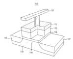
도 1은 본 발명의 실시예들에 따른 스팁-슬롭 전계 효과 트랜지스터, Γ-FET을 나타내는 사시도이다.
도 2는 도 1의 스팁-슬롭 전계 효과 트랜지스터를 나타내는 평면도이다.
도 3은 도 2의 I-I' 라인을 따라 절단한 단면도이다.
도 4는 Γ-FET에서 전이층 밑의 하부 MOSFET으로 사용할 수 있는 다양한 돌출형 게이트 FET 구조를 나타내는 도면이다.
도 5는 Γ-FET에서 전이층 밑의 하부 MOSFET으로 사용할 수 있는 다양한 매립형 게이트 FET 구조를 나타내는 도면이다
도 6은 본 발명의 실시예들에 따른 스팁-슬롭 전계 효과 트랜지스터 제조 과정을 나타내는 도면이다.
도 7은 본 발명의 실시예에 따라 제조된 소자의 투과전자현미경 사진이다.
도 8은 본 발명의 실시예들에 따른 스팁-슬롭 전계 효과 트랜지스터의 측정 환경을 간략히 표현한 도면이다.
도 9는 본 발명의 실시예들에 따라 제조된 스팁-슬롭 전계 효과 트랜지스터의 실제 측정 결과값이다.
도 10은 본 발명의 실시예들에 따른 스팁-슬롭 전계 효과 트랜지스터의 실제 측정 결과값에서 추출해낸 2차 데이터이다.
도 11는 플로팅 게이트 전압 모델링 수식의 유도 과정을 설명하는 도면이다.1 is a perspective view showing a step-slop field effect transistor, Γ-FET according to embodiments of the present invention.
FIG. 2 is a plan view illustrating the step-slop field effect transistor of FIG. 1 .
FIG. 3 is a cross-sectional view taken along line II′ of FIG. 2 .
4 is a diagram showing various structures of a protruding gate FET that can be used as a lower MOSFET under a transition layer in a Γ-FET.
5 is a diagram showing various buried gate FET structures that can be used as a lower MOSFET under the transition layer in the Γ-FET.
6 is a diagram illustrating a manufacturing process of a step-slop field effect transistor according to embodiments of the present invention.
7 is a transmission electron microscope photograph of a device manufactured according to an embodiment of the present invention.
8 is a diagram schematically illustrating a measurement environment of a step-slop field effect transistor according to embodiments of the present invention.
9 is an actual measurement result of a step-slop field effect transistor manufactured according to embodiments of the present invention.
10 is secondary data extracted from actual measurement results of a step-slop field effect transistor according to embodiments of the present invention.
11 is a view for explaining a process of deriving a floating gate voltage modeling equation.
본 발명의 이점 및 특징, 그리고 그것들을 달성하는 방법은 첨부되는 도면과 함께 상세하게 후술되어 있는 실시예들을 참조하면 명확해질 것이다. 그러나, 본 발명은 이하에서 개시되는 실시예들에 한정되는 것이 아니라 서로 다른 다양한 형태로 구현될 것이며, 단지 본 실시예들은 본 발명의 개시가 완전하도록 하며, 본 발명이 속하는 기술분야에서 통상의 지식을 가진 자에게 발명의 범주를 완전하게 알려주기 위해 제공되는 것이며, 본 발명은 청구항의 범주에 의해 정의될 뿐이다.Advantages and features of the present invention and methods of achieving them will become apparent with reference to the embodiments described below in detail in conjunction with the accompanying drawings. However, the present invention is not limited to the embodiments disclosed below, but will be embodied in various different forms, and only these embodiments allow the disclosure of the present invention to be complete, and common knowledge in the art to which the present invention pertains It is provided to fully inform those who have the scope of the invention, and the present invention is only defined by the scope of the claims.
본 명세서에서 사용된 용어는 실시예들을 설명하기 위한 것이며, 본 발명을 제한하고자 하는 것은 아니다. 본 명세서에서, 단수형은 문구에서 특별히 언급하지 않는 한 복수형도 포함한다. 명세서에서 사용되는 "포함한다(comprises)" 및/또는 "포함하는(comprising)"은 언급된 구성요소, 단계, 동작 및/또는 소자는 하나 이상의 다른 구성요소, 단계, 동작 및/또는 소자의 존재 또는 추가를 배제하지 않는다.The terminology used herein is for the purpose of describing the embodiments, and is not intended to limit the present invention. In this specification, the singular also includes the plural unless specifically stated otherwise in the phrase. As used herein, "comprises" and/or "comprising" refers to the presence of one or more other components, steps, operations and/or elements mentioned. or addition is not excluded.
다른 정의가 없다면, 본 명세서에서 사용되는 모든 용어(기술 및 과학적 용어를 포함)는 본 발명이 속하는 기술분야에서 통상의 지식을 가진 자에게 공통적으로 이해될 수 있는 의미로 사용될 수 있을 것이다. 또한, 일반적으로 사용되는 사전에 정의되어 있는 용어들은 명백하게 특별히 정의되어 있지 않는 한 이상적으로 또는 과도하게 해석되지 않는다.Unless otherwise defined, all terms (including technical and scientific terms) used herein may be used with the meaning commonly understood by those of ordinary skill in the art to which the present invention belongs. In addition, terms defined in a commonly used dictionary are not to be interpreted ideally or excessively unless specifically defined explicitly.
이하, 첨부한 도면들을 참조하여, 본 발명의 바람직한 실시예들을 보다 상세하게 설명하고자 한다. 도면 상의 동일한 구성요소에 대해서는 동일한 참조 부호를 사용하고 동일한 구성요소에 대해서 중복된 설명은 생략한다.Hereinafter, preferred embodiments of the present invention will be described in more detail with reference to the accompanying drawings. The same reference numerals are used for the same components in the drawings, and repeated descriptions of the same components are omitted.
본 발명의 실시예들은, 기존 FET의 게이트(gate) 상부에 전이층(transition layer)과 컨트롤 게이트(control gate)를 가지는 트랜지스터에서, 스팁-슬롭 성능을 구현하는 것을 그 요지로 한다.Embodiments of the present invention, in a transistor having a transition layer and a control gate on top of the gate (gate) of the conventional FET, it is a gist of implementing the step-slop performance.
본 발명에서의 반도체 소자는 전류-전압 특성 곡선에서 스팁-슬롭을 구비하여 외관상 그리스 대문자 'Γ'(gamma) 형태로 보이기 때문에, 이후 Γ-FET으로 명명하여 사용한다.Since the semiconductor device in the present invention has a steep-slop in the current-voltage characteristic curve and appears in the form of a Greek capital letter 'Γ' (gamma) in appearance, it is later named and used as a Γ-FET.
Γ-FET은 기존 MOSFET의 장점인 높은 온-전류, 소형화 가능성을 유지한 채로 스팁-슬롭 성능 구현이 가능하고, 이를 통해 소자의 저전력 동작을 가능하게 한다.The Γ-FET can realize the step-slop performance while maintaining the high on-current and miniaturization potential of the existing MOSFET, thereby enabling low-power operation of the device.
도 1은 본 발명의 실시예들에 따른 스팁-슬롭 전계 효과 트랜지스터, Γ-FET(100)을 나타내는 사시도이고, 도 2는 이를 상부에서 본 평면도이며, 도 3은 도 2의 I-I' 라인을 따라 절단한 단면도이다. 그리고, 도 4와 도 5는 Γ-FET에서 전이층 밑의 하부 MOSFET으로 사용할 수 있는 다양한 돌출형 게이트 FET 및 매립형 게이트 FET 구조를 나타내는 도면이다.1 is a perspective view showing a step-slop field effect transistor, Γ-
Γ-FET는 기존 MOSFET의 게이트에 전이층(102)과 컨트롤 게이트(101)를 형성한 구조로, 현업에서 쓰이는 다양한 구조의 MOSFET을 하부 MOSFET으로 사용할 수 있다. 도 1, 도 2와 도 3에서 보이는 평판 MOSFET 외에도 도 4와 도 5에서 일부 도시된 돌출형, 매립형 구조 MOSFET을 하부 MOSFET으로 삼아 Γ-FET을 제조할 수 있다.The Γ-FET has a structure in which a
도 1 내지 도 3 을 참조하면, Γ-FET(100)은 기판(108), 채널 영역(106), 게이트 절연막(104), 플로팅 게이트(103), 전이층(102), 컨트롤 게이트(101), 소스(105)와 드레인(107)을 포함한다.1 to 3 , the Γ-
상기 기판(108)은 실리콘(silicon), 게르마늄(germanium), 실리콘 게르마늄(silicon-germanium), 인장 실리콘(strained silicon), 인장 게르마늄(strained germanium), 인장 실리콘 게르마늄(strained silicon-germanium) 및 절연층 매몰 실리콘(silicon on insulator; SOI), 3-5족 반도체 물질들 중 적어도 하나를 포함할 수 있다.The
상기 소스(105) 및 드레인(107)은 수평형 트랜지스터의 경우에 상기 채널 영역(106)의 좌우에 형성되고, 수직형 트랜지스터의 경우에는 상기 채널 영역(106)의 상하에 형성되며, n형 실리콘, p형 실리콘 및 금속실리사이드 중 어느 하나로 형성될 수 있다.The
상기 n형 실리콘 또는 상기 p형 실리콘으로 형성된 상기 소스(105) 및 드레인(106)은 확산(diffusion), 고상 확산(solid-phase diffusion), 에피택셜 성장(epitaxial growth), 선택적 에피택셜 성장(epitaxial growth), 이온 주입(ion implantation) 및 후속 열처리 중 적어도 하나 이상에 의해 형성될 수 있다.The
상기 금속실리사이드로 형성된 상기 소스 및 드레인은 텅스텐(W), 티타늄(Ti), 코발트(Co), 니켈(Ni), 어븀(Er), 이터븀(Yb), 사마륨(Sm), 이트륨(Y), 가돌륨(Gd), 터뷸(Tb), 세륨(Ce), 백금(Pt), 납(Pb) 및 이리듐(Ir) 중 어느 하나로 형성된 상기 금속실리사이드를 포함하며, 도펀트 편석(dopant segregation)을 이용하여 접합을 개선할 수 있다.The source and drain formed of the metal silicide include tungsten (W), titanium (Ti), cobalt (Co), nickel (Ni), erbium (Er), ytterbium (Yb), samarium (Sm), and yttrium (Y). , including the metal silicide formed of any one of gadollium (Gd), turbul (Tb), cerium (Ce), platinum (Pt), lead (Pb) and iridium (Ir), using dopant segregation This can improve bonding.
상기 채널 영역(106)은 평면형(planar) 구조를 비롯하여 도 4에 일부 도시된 핀(fin) 구조, 채널 영역의 종횡비(높이/너비)가 0.5 이하의 형태인 나노시트(nanosheet) 구조, 채널 영역의 종횡비(높이/너비)가 0.5 이상의 형태인 나노와이어(nanowire) 구조, 다중 나노와이어(multi-nanowire) 구조 등의 돌출형 구조 또는 도 5에 일부 도시된 매립형 구조 중 어느 하나의 구조로 형성될 수 있다.The
여기서, 상기 매립형 구조의 채널 영역은 버리드 게이트(buried gate) MOSFET, 리세스드 게이트(recessed gate) MOSFET, 스페어 쉐입드 리세스드 게이트(sphere-shaped recessed gate) MOSFET, 새들 핀펫 (saddle finFET), 그루브 게이트(groove gate) MOSFET, 브이-그루브 게이트(V-groove gate) MOSFET에서 사용하는 매립형 채널 구조 중 어느 하나의 구조로 형성될 수 있다.Here, the channel region of the buried structure includes a buried gate MOSFET, a recessed gate MOSFET, a sphere-shaped recessed gate MOSFET, a saddle finFET, and a groove. It may be formed in any one of a gate (groove gate) MOSFET and a buried channel structure used in a V-groove gate (V-groove gate) MOSFET.
게이트 절연막(104)은 채널 영역(106) 상부에 형성된다. 게이트 절연막(104)은 플로팅 게이트(103)와 채널 영역(106)을 절연시킬 수 있다. 예를 들어, 게이트 절연막(104)는 실리콘 산화물(SiO2), 실리콘 질화물(Si3N4), 실리콘 산화질화물(SiON), 하프늄 옥사이드(HfO2), 알루미늄 옥사이드(Al2O3), 지르코늄 옥사이드(ZrO2), 하프늄 지르코늄 옥사이드(HZO)와 하프늄 옥시나이트라이드(HfON) 중 적어도 하나를 포함하여 형성될 수 있다. 또한, 게이트 절연막(104)은 메모리 특성을 보이지 않는 임의의 절연 물질들 중 적어도 하나를 포함하여 형성될 수 있다.The
상기 플로팅 게이트(103)는 상기 게이트 절연막(104) 상부에 형성된다. 예를 들어, 플로팅 게이트(103)은 금속, 2종 또는 3종 금속 합금, n+ 다결정 실리콘, p+ 다결정 실리콘, 실리사이드(예를 들어, 텅스텐 실리사이드(WSi), 티타늄 실리사이드(TiSi), 코발트 실리사이드(CoSi), 니클 실리사이드(NiSi) 등) 중 적어도 하나 이상에 의해 형성될 수 있다. 플로팅 게이트(103)은 컨트롤 게이트와 채널 영역(또는 채널)사이에 위치하므로 내부 게이트(internal gate)라고 부를 수 있다.The floating
상기 플로팅 게이트(103)는 채널 구조에 따라 평면형 게이트(planar-gate) 구조를 비롯하여 도 4에 일부 도시된 다중 게이트(multiple-gate) 구조, 전면 게이트(gate-all-around) 구조 등의 돌출형 게이트 구조 혹은 도 5에 일부 도시된 매립형 게이트 구조 중 적어도 하나의 구조로 형성될 수 있다.The floating
이 때, 돌출형 게이트 구조의 플로팅 게이트는 핀펫(finFET), 트라이 게이트(tri-gate) MOSFET, 파이 게이트(Π-gate) MOSFET, 오메가 게이트(Ω-gate) MOSFET, 게이트 올어라운드(gate-all-around) MOSFET, 벌크 핀펫(bulk finFET), 벌크 게이트 올어라운드(bulk gate-all-around) MOSFET에서 쓰이는(또는 사용하는) 돌출형 게이트 구조 중 어느 하나의 구조로 형성될 수 있다.At this time, the floating gate of the protruding gate structure includes a finFET, a tri-gate MOSFET, a pi-gate MOSFET, an omega gate MOSFET, and a gate-all-around gate. -around) MOSFET, bulk finFET, and bulk gate-all-around MOSFET may be formed in any one of a protruding gate structure used (or used).
이 때, 매립형 게이트 구조의 플로팅 게이트는 버리드 게이트(buried gate) MOSFET, 리세스드 게이트(recessed gate) MOSFET, 스페어 쉐입드 리세스드 게이트(sphere-shaped recessed gate) MOSFET, 새들 핀펫 (saddle finFET), 그루브 게이트(groove gate) MOSFET, 브이-그루브 게이트(V-groove gate) MOSFET에서 쓰이는 매립형 게이트 구조 중 어느 하나의 구조로 형성될 수 있다.In this case, the floating gate of the buried gate structure includes a buried gate MOSFET, a recessed gate MOSFET, a sphere-shaped recessed gate MOSFET, a saddle finFET, It may be formed in any one of a groove gate MOSFET and a buried gate structure used in a V-groove gate MOSFET.
전이층(102)은 플로팅 게이트(103) 상부에 형성될 수 있다. 전이층(102)은 플로팅 게이트(103)와 컨트롤 게이트(101)(또는 컨트롤 게이트 구조물)를 절연시킬 수 있다. 예를 들어, 전이층(102)은 실리콘(Si), 게르마늄(Ge), Ⅲ-V족 화합물, 및 2-D 물질(carbon nanotube, MoS2, 및 그래핀 중 적어도 하나), 질화규소(Si3N4), 질화막(nitride), 실리콘 옥시나이트라이드(SiON), 실리콘 산화물(SiO2), 고체 산화막(oxide), 알루미늄 옥사이드(Al2O3), IGZO, 및 하프늄 옥사이드(HfO2), 그리고 그 외 다양한 전이 물질, 반도체 물질(SrTiO3, SrZrO3, NiO, TiO2, HfOx, AlOx, NiOx, TiOx, TaOx, TaN, CuxO, CuOx, TiN, TaN, WOx, SiNx, VO2, IrO2, ZrOx, ZnO, NbOx, IGZO, HZO, HfON), 그리고 고체 전해질 물질(황화물계 소재(예를 들어, Li10GeP2S12, Li9.54Si1.74P1.44S11.7Cl0.3, argyrodite, LPS(lithium phosphorus sulfide), LPS + LiCl), 산화물계 소재(예를 들어, perovskite, NASICON(Na1+xZr2SixP3xO12, 0<x<3), LISICON(Li2+2xZn1xGeO4), LiPON(LixPOyNz), garnet), 이온 전도성 폴리머(예를 들어, PEO(polyethylene oxide), PEG(polyethylene glycol), PEGDMA(polyethylene glycol dimethacrylate), PTFE(polytetrafluoroethylene), PEEK(polyether ether ketone), nafion(C7HF13O5S·C2F4))) 중 적어도 하나를 포함하여 형성될 수도 있다.The
이러한 전이층(102)은 단일 물질 혹은 여러 물질로 구성될 수 잇다.The
일 실시예에서, 전이층(102) 혹은 컨트롤 게이트(101)가 접촉하는 플로팅 게이트(103) 면적은 플로팅 게이트 전체 면적보다 좁을 수 있다. 즉, 전이층(102)과 컨트롤 게이트(101)는 플로팅 게이트(103)의 상부 적어도 일부 영역에 형성될 수 있다.In an embodiment, the area of the floating
컨트롤 게이트(101)는 전이층(102) 상부에 형성되며, 플로팅 게이트(103)와의 전위차를 만든다. 예를 들어, 컨트롤 게이트(101)는 플로팅 게이트(103)에 전류를 흘려보낼 수 있도록 플로팅 게이트(103)와 인접하여 형성될 수 있다.The
일 실시예에서, 컨트롤 게이트(101)는 금속, 2종 또는 3종 금속 합금, n+ 다결정 실리콘, p+ 다결정 실리콘, 실리사이드(예를 들어, 텅스텐 실리사이드(WSi), 티타늄 실리사이드(TiSi), 코발트 실리사이드(CoSi), 니클 실리사이드(NiSi) 등) 중 하나 이상으로 형성될 수 있다.In one embodiment, the
상기 전이층(102)은 컨트롤 게이트(101)에 전압 신호가 인가되면 양 단의 게이트 사이의 전압 차 즉, 플로팅 게이트(103)와 컨트롤 게이트(101) 사이의 전압 차에 따라 플로팅 게이트(103)로 전류를 흘려보낼 수 있다.When a voltage signal is applied to the
본 발명에서 채널 영역(106), 소스(105) 및 드레인(107)은 모두 기판(108) 상에 형성될 수 있다. 예를 들어, 채널 영역(106)은 나노와이어(nanowire) 구조로 형성될 수 있다. 이 경우, 도 3에 도시된 것처럼, 게이트 절연막(104), 플로팅 게이트(103), 전이층(102) 및 컨트롤 게이트(101)는 채널 영역(106)의 일부분을 순차적으로 둘러싸도록 형성될 수 있고, 채널 영역(106)의 나머지 부분(예를 들어, 상기 일부분을 제외한 나머지 부분)과 기판(108) 사이에는 빈 공간이 존재할 수 있다. 다시 말하면, 채널 영역(106)은 구성 요소들(104, 103, 102, 101)에 의해 지지되어 기판(108) 상에 교각(Bridge)처럼 떠 있을 수 있다.In the present invention, the
이러한 구조를 가지는 본 발명의 Γ-FET(100)는 기준 전압 이상의 전위를 컨트롤 게이트(101)에 인가하여 컨트롤 게이트(101)와 플로팅 게이트(103) 사이의 전위차를 만듦으로써, 플로팅 게이트(103)에 저장된 적어도 하나의 전하를 방출 또는 반입시킬 수 있다.The Γ-
이 때, Γ-FET(100)는 컨트롤 게이트(101)에 기준 전압 이상의 전위가 인가되는 경우에, 플로팅 게이트(103)에 저장된 적어도 하나의 전하가 전이층(102)에 의한 에너지 장벽을 통과하여 컨트롤 게이트(101)로 방출/반입 되는 상황에서, 컨트롤 게이트(101)가 특정 전압 영역에 도달하면, 컨트롤 게이트(101) 전압 변화 대비 플로팅 게이트(103) 전압 변화가 더 커질 수 있다.At this time, in the Γ-
이 때, Γ-FET(100)는 컨트롤 게이트 전극을 게이트로 두고 소자를 동작 시킬 때, 플로팅 게이트 전극을 게이트로 두고 소자를 동작 시키는 것에 비해, 문턱 전압 이하 기울기(SS) 값이 더 낮아질 수 있다.At this time, when the Γ-
도 6은 Γ-FET(100)의 제조 과정을 나타내는 도면이다.6 is a diagram illustrating a manufacturing process of the Γ-
도 6을 참조하면, 본 발명의 Γ-FET는 기판 상에 채널 영역, 소스와 드레인이 형성되고, 채널 영역 상부에 게이트 절연막이 형성된 후 게이트 절연막 상부에 플로팅 게이트를 형성하는 과정을 통해 기존 MOSFET 구조(internal MOSFET)를 형성한다.6, the Γ-FET of the present invention has a conventional MOSFET structure through the process of forming a channel region, a source and a drain on a substrate, a gate insulating film is formed on the channel region, and then a floating gate is formed on the gate insulating film. (internal MOSFET) is formed.
그리고, 플로팅 게이트 상부에 전이층(TL)과 층간 절연막(ILD; inter-layer dielectric)을 순차적으로 형성하고, 플로팅 게이트가 일부 노출되도록 전이층과 층간 절연막 일부를 식각한다. 전이층과 층간 절연막 일부를 식각한 후 플로팅 게이트 패턴을 형성하고, 전이층 일부가 노출되도록 층간 절연막 일부를 식각한 후 컨트롤 게이트 패턴을 형성함으로써, 본 발명의 Γ-FET가 제조될 수 있다.Then, a transition layer (TL) and an inter-layer dielectric (ILD) are sequentially formed on the floating gate, and a portion of the transition layer and the inter-layer insulating layer are etched to partially expose the floating gate. The Γ-FET of the present invention can be manufactured by etching a part of the transition layer and the interlayer insulating layer, forming a floating gate pattern, etching a part of the interlayer insulating layer to expose a part of the transition layer, and then forming a control gate pattern.
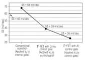
도 7은 본 발명의 실시예에 따라 제조된 소자 즉, Γ-FET(100)의 투과전자현미경 사진이며, 도 8은 Γ-FET(100)의 측정 환경을 간략히 표현한 도면이다. Γ-FET(100)의 전기적 특성은 컨트롤 게이트(101)에 전압을 가하여 확보할 수 있다. 또한, 이와 비교할 하부 MOSFET의 특성을 확인하기 위해서 플로팅 게이트(103)에 의도적으로 전압을 인가할 수 있으며, 실제 소자 동작에서는 플로팅 게이트에 별도로 전압을 인가할 필요가 없다.7 is a transmission electron micrograph of a device manufactured according to an embodiment of the present invention, that is, the Γ-
도 9는 Γ-FET(100) 및 하부 MOSFET의 실제 측정 결과값이고, 도 10은 이로부터 추출된 2차 데이터이다. Γ-FET(100)이 하부 MOSFET에 비하여 스위칭 동작을 위해 더 작은 전압 만을 사용하고, 이는 곧 문턱 전압 이하 기울기(subthreshold slope; SS)의 차이로 나타난다. 하부 MOSFET의 경우 널리 알려진 것처럼 SS 값이 60 mV/dec 이상으로 나타난 반면, 그 상부에 전이층(102)과 컨트롤 게이트(101)를 추가하여 제조된 Γ-FET(100)의 SS는 60 mV/dec의 한계를 넘어 26 mV/dec까지 낮아지는 것을 알 수 있다. 스팁-슬롭이 구현되는 원인은 컨트롤 게이트(101)의 전압 변화량이 매우 큰 플로팅 게이트(103) 전압 변화량으로 나타나기 때문이다.9 is an actual measurement result of the Γ-
구체적인 스팁-슬롭 구현 원리는 후술할 수식을 통해 설명 가능하다. 본 발명의 소자는 형태상 기존 평면형 플로팅 게이트(103) 메모리에서 쓰이는 수식을 만족해야 한다. 플로팅 게이트(103) 메모리에서, 플로팅 게이트(103) 전압은 캐퍼시턴스 커플링(capacitance coupling) 및 플로팅 게이트(103) 내부 전하를 고려하여 일반적으로 아래 <수학식 1>과 같이 주어진다.A specific step-slop implementation principle can be described through an equation to be described later. The device of the present invention must satisfy the equation used in the conventional planar floating
[수학식 1][Equation 1]

도 11은 상기 플로팅 게이트(103) 전압 수식의 유도 과정을 설명하는 도면이다. QC, QF, QS, QB, QD는 각 지점 즉, 컨트롤 게이트(101), 플로팅 게이트(103), 소스(105), 채널(106) 표면, 드레인(107)의 전하를 의미하며, VCG, VFG, VS,
컨트롤 게이트(101) 전압 변화에 따라 값이 바뀌는 변수는 컨트롤 게이트(101) 전압(VCG), 플로팅 게이트(103) 전압(VFG), 플로팅 게이트(103) 내부 전하(QF), 그리고 하부 MOSFET 채널(106)의 표면 전위(
전통적인 플로팅 게이트(103) 메모리의 경우 플로팅 게이트(103) 내부 전하가 일정하여 변수가 아니지만, 본 발명의 Γ-FET(100)에서는 전이층(102)을 통해 컨트롤 게이트(101)로부터 플로팅 게이트(103)로 전하가 공급되기 때문에, 플로팅 게이트(103) 전하 역시 변수가 된다.In the case of the conventional floating
상기 수학식 1을 컨트롤 게이트(101) 전압으로 미분하면 컨트롤 게이트(101) 전압 변화에 따른 플로팅 게이트(103) 전압 변화 값을 알 수 있다. 그리고 변화하지 않는 상수들은 사라지고, 컨트롤 게이트(101) 전압에 따라 변화하는 변수들만 남는다. 이를 표현하면 아래 <수학식 2>와 같이 나타낼 수 있다.By differentiating
[수학식 2][Equation 2]

상기 수학식 2를 정리하면 아래 <수학식 3>과 같이 변환될 수 있다.By rearranging
[수학식 3][Equation 3]

여기서, t는 시간을 의미할 수 있다. 상기 수학식 3의 좌항은 컨트롤 게이트 전압 변화 대비 플로팅 게이트(103) 전압 변화이며, 이 값이 1보다 커지게 되면 스팁-슬롭이 가능해진다.Here, t may mean time. The left term of
시간에 따른 플로팅 게이트(103) 전하 변화량은 전이층(102)을 통해 흐르는 전류일 수 있다. 그리고 전이층(102)을 통해 흐르는 전류(=dQF/dt)는 전이층(102) 양단에 걸리는 전압, 즉 컨트롤 게이트(101) 전압과 플로팅 게이트(103) 전압 간 차이의 함수이다. 따라서, 상기 수학식 3은 아래 <수학식 4>와 같이 변화시킬 수 있다.The amount of charge change in the floating
[수학식 4][Equation 4]

여기서, f는 전이층을 통해 흐르는 전류를 의미하는 것으로, 이후 전이 전류 함수로 명명하여 사용한다.Here, f denotes a current flowing through the transition layer, and will be named and used later as a transition current function.
전이 전류 함수는 양단에 걸리는 전압에 따라 변한다. 전이 전류 함수의 개형 및 크기는 전이층(102)의 특성을 비롯하여 컨트롤 게이트(101), 전이층(102), 플로팅 게이트(103) 구성 및 형태에 따라서 바뀔 수 있다. 이 중 하부 MOSFET의 표면 전위는 플로팅 게이트(103) 전압에 깊게 연관되어 있다. 이에 맞추어 상기 수학식 4를 재배열하면 아래 <수학식 5>와 같이 나타낼 수 있다.The transition current function changes with the voltage across it. The shape and magnitude of the transition current function may be changed depending on the configuration and shape of the
[수학식 5][Equation 5]

상기 수학식 5의 좌항에 컨트롤 게이트(101) 전압 변화 대비 플로팅 게이트(103) 전압 변화만 남도록 정리하면, 아래 <수학식 6>과 같이 나타낼 수 있다.If only the change in the voltage of the floating
[수학식 6][Equation 6]

여기서 주목할 점은 네 가지이다. 첫째, 전통적인 플로팅 게이트(103) 메모리에서는 우항 중 분자의 두 번째 항이 존재하지 않는다. 왜냐하면 컨트롤 게이트(101)에서 플로팅 게이트(103)로 흐르는 전류가 읽기 동작 중에 발생하지 않기 때문이다. 반면, 본 발명의 Γ-FET(100)에서는 전류 항이 존재하여 플로팅 게이트(103) 전압 변화량을 기존보다 훨씬 끌어올릴 수 있다. 둘째, 상술한 전류 항을 통해 우항 분자의 크기가 충분히 크게 조절되는 상황에서 분모가 1보다 작아지면, 플로팅 게이트(103) 전압 변화가 매우 커지게 되어 스팁-슬롭 구현이 가능하다. 셋째, 우항의 분모가 작아지는 상황은 플로팅 게이트(103) 전압 대비 하부 MOSFET의 표면 전위 변화량이 충분히 커지는 상황이다. 넷째, 그 상황은 하부 MOSFET의 ON/OFF가 나뉘는 약한 반전(weak inversion) 영역에서 일어난다.There are four things to note here. First, in the conventional floating
결론적으로, 본 밟명의 Γ-FET(100)는 전이층(102)을 통해 흐르는 전류량을 조절하여 상기 수학식 6의 우항 분자를 크게 한 상황에서 컨트롤 게이트(101) 전압을 스윕(sweep)하면, 하부 MOSFET의 ON/OFF가 나뉘는 영역에서 우항 분모 값이 작아지게 되고, 결과적으로 컨트롤 게이트 전압 변화 대비 플로팅 게이트(103) 전압 변화량이 매우 크게 상승하여 스팁-슬롭이 구현된다.In conclusion, the Γ-
상술한 바와 같이, 스팁-슬롭 동작은 전이 전류 함수 f, 즉 전이층을 통해 흐르는 전류 함수의 영향을 크게 받는다. 전이 전류 함수 값이 전이층 양단에 걸린 전압의 크기에 상관없이, 그리고 주변 항(CCF/CT)에 비해 너무 작으면 전류가 흐르지 않는 플로팅 게이트 메모리처럼 동작하여 오히려 슬롭이 커진다. 반면에, 전이 전류 함수 값이 너무 커서 전이층이 금속처럼 동작하는 경우, 컨트롤 게이트와 플로팅 게이트 간에 전압차가 발생할 수 없어 플로팅 게이트 전압 변화량은 컨트롤 게이트 전압 변화량과 언제나 같아 스팁-슬롭이 구현될 수 없다. 스팁-슬롭 동작을 위해서는 전이 전류 함수가 양단에 걸린 전압이 작을 경우 주변 항(CCF/CT)에 비해 작아야 하며, 양단의 전압이 클 경우 주변 항(CCF/CT)에 비해 클 필요가 있다. 즉 전이 전류 함수 값은 양단에 걸린 전압에 따라 주변 항(CCF/CT)에 비해 크거나 작아지며 변동해야 한다.As described above, the step-slop operation is greatly affected by the transition current function f, that is, the current function flowing through the transition layer. Regardless of the magnitude of the voltage across the transition layer, and if the transition current function value is too small compared to the surrounding term (CCF /CT ), it behaves like a floating gate memory in which no current flows and the slop is rather large. On the other hand, when the transition current function value is too large and the transition layer behaves like a metal, a voltage difference cannot occur between the control gate and the floating gate, so the amount of change in the voltage of the floating gate is always the same as the amount of change in the control gate voltage, so a step-slop cannot be implemented. . For step-slop operation, the transition current function needs to be smaller than the surrounding term (CCF /CT ) when the voltage across both ends is small, and needs to be larger than the surrounding term (CCF /CT ) when the voltage across both ends is large. there is In other words, the value of the transition current function should be changed by increasing or decreasing compared to the surrounding term (CCF /CT ) according to the voltage applied across both ends.
이와 같이, 본 발명의 실시예에 따른 스팁-슬롭 FET는 기존 FET의 게이트(gate) 상부에 전이층(transition layer)과 컨트롤 게이트(control gate)를 가지는 트랜지스터에서, 스팁-슬롭 성능을 구현할 수 있다.As described above, the step-slop FET according to the embodiment of the present invention can implement the step-slop performance in a transistor having a transition layer and a control gate on top of the gate of the conventional FET. .
이러한 본 발명은 기존 MOSFET의 구조 및 동작 원리를 기반으로 하여 높은 온-전류와 소형화 가능성을 충족시키는 동시에 전체 스위칭 전류 구간 중 50% 이상에서 60 mV/dec 이하 SS 성능을 보일 수 있다. 해당 구조 및 방법으로, 기존 MOSFET의 높은 온-전류, 소형화 가능성은 그대로 확보하면서 스팁-슬롭 성능을 가지는 반도체 소자를 구현할 수 있으며, 이에 따라 반도체 소자의 저전력 동작이 가능해진다.Based on the structure and operation principle of the existing MOSFET, the present invention can satisfy high on-current and miniaturization potential, and at the same time exhibit SS performance of 60 mV/dec or less in 50% or more of the entire switching current section. With the structure and method, it is possible to implement a semiconductor device having a step-slop performance while maintaining the high on-current and miniaturization potential of the existing MOSFET, thereby enabling low-power operation of the semiconductor device.
나아가, 본 발명의 스팁-슬롭 FET는 컨트롤 게이트와 플로팅 게이트 간의 기준 전압 이상의 전위차가 생기도록, 컨트롤 게이트에 일정 전압을 인가함으로써, 플로팅 게이트에 저장된 적어도 하나의 전하를 방출 또는 반입시키는 동작을 구현할 수 있다. 즉, 본 발명의 실시예에 따른 스팁-슬롭 FET의 동작 방법은 컨트롤 게이트와 플로팅 게이트 간에 기준 전압 이상의 전위차가 생기도록, 컨트롤 게이트에 일정 전압을 인가하는 단계 및 컨트롤 게이트와 플로팅 게이트 간에 생성된 기준 전압 이상의 전위차를 통해 플로팅 게이트에 저장된 적어도 하나의 전하를 방출 또는 반입시키는 단계를 포함할 수 있다.Furthermore, the step-slop FET of the present invention can implement an operation of discharging or bringing in at least one charge stored in the floating gate by applying a constant voltage to the control gate so that a potential difference greater than or equal to the reference voltage is generated between the control gate and the floating gate. there is. That is, the operation method of the step-slop FET according to the embodiment of the present invention includes the steps of applying a constant voltage to the control gate so that a potential difference greater than or equal to the reference voltage is generated between the control gate and the floating gate, and the reference generated between the control gate and the floating gate The method may include discharging or bringing in at least one charge stored in the floating gate through a potential difference greater than or equal to the voltage.
이상과 같이 실시예들이 비록 한정된 실시예와 도면에 의해 설명되었으나, 해당 기술분야에서 통상의 지식을 가진 자라면 상기의 기재로부터 다양한 수정 및 변형이 가능하다. 예를 들어, 설명된 기술들이 설명된 방법과 다른 순서로 수행되거나, 및/또는 설명된 시스템, 구조, 장치, 회로 등의 구성요소들이 설명된 방법과 다른 형태로 결합 또는 조합되거나, 다른 구성요소 또는 균등물에 의하여 대치되거나 치환되더라도 적절한 결과가 달성될 수 있다.As described above, although the embodiments have been described with reference to the limited embodiments and drawings, various modifications and variations are possible from the above description by those skilled in the art. For example, the described techniques are performed in an order different from the described method, and/or the described components of the system, structure, apparatus, circuit, etc. are combined or combined in a different form than the described method, or other components Or substituted or substituted by equivalents may achieve an appropriate result.
그러므로, 다른 구현들, 다른 실시예들 및 특허청구범위와 균등한 것들도 후술하는 특허청구범위의 범상부에 속한다.Therefore, other implementations, other embodiments, and equivalents to the claims are also within the scope of the following claims.
101 : 컨트롤 게이트
102: 전이층
103: 플로팅 게이트
104: 게이트 절연막
105: 소스
106: 채널 영역
107: 드레인
108: 기판101: control gate
102: transition layer
103: floating gate
104: gate insulating film
105: source
106: channel area
107: drain
108: substrate
Claims (21)
Translated fromKorean기판 상에 형성되는 소스, 채널 영역과 드레인;
상기 채널 영역 상부에 형성되는 게이트 절연막;
상기 게이트 절연막 상부에 형성되는 플로팅 게이트;
상기 플로팅 게이트 상부에 형성되는 전이층; 및
상기 전이층 상부에 형성되는 컨트롤 게이트를 포함하되,
상기 스팁-슬롭 전계 효과 트랜지스터는
상기 컨트롤 게이트에 기준 전위 이상을 인가하여 상기 플로팅 게이트에 저장된 적어도 하나의 전하를 방출 또는 반입시키는 것을 특징으로 하는, 스팁-슬롭 전계 효과 트랜지스터.
In a step-slope field-effect transistor (FET) capable of a step-slope operation,
a source, a channel region and a drain formed on the substrate;
a gate insulating layer formed over the channel region;
a floating gate formed on the gate insulating layer;
a transition layer formed over the floating gate; and
a control gate formed on the transition layer;
The step-slop field effect transistor is
The step-slop field effect transistor, characterized in that by applying a reference potential or more to the control gate to discharge or bring in at least one charge stored in the floating gate.
상기 채널 영역은
평면형(planar) 구조, 핀(fin) 구조, 나노시트(nanosheet) 구조, 나노와이어(nanowire) 구조와 다중 나노와이어(multi-nanowire) 구조를 포함하는 돌출형 구조와 매립형 구조 중 어느 하나의 구조로 형성되는 것을 특징으로 하는, 스팁-슬롭 전계 효과 트랜지스터.
According to claim 1,
The channel area is
Any one of a protruding structure and a buried structure including a planar structure, a fin structure, a nanosheet structure, a nanowire structure, and a multi-nanowire structure A step-slop field effect transistor, characterized in that formed.
상기 돌출형 구조의 채널 영역은
핀펫(finFET), 트라이 게이트(tri-gate) MOSFET, 파이 게이트(Π-gate) MOSFET, 오메가 게이트(Ω-gate) MOSFET, 게이트 올어라운드(gate-all-around) MOSFET, 벌크 핀펫(bulk finFET), 벌크 게이트 올어라운드(bulk gate-all-around) MOSFET에서 사용하는 핀(fin) 구조, 나노시트(nanosheet) 구조, 나노와이어(nanowire) 구조 및 다중 나노와이어(multi-nanowire) 구조 중 어느 하나의 구조로 형성되는 것을 특징으로 하는, 스팁-슬롭 전계 효과 트랜지스터.
4. The method of claim 3,
The channel region of the protruding structure is
FinFET, tri-gate MOSFET, pi-gate MOSFET, omega-gate MOSFET, gate-all-around MOSFET, bulk finFET , any one of a fin structure, a nanosheet structure, a nanowire structure, and a multi-nanowire structure used in a bulk gate-all-around MOSFET A step-slop field effect transistor, characterized in that formed in the structure.
상기 매립형 구조의 채널 영역은
버리드 게이트(buried gate) MOSFET, 리세스드 게이트(recessed gate) MOSFET, 스페어 쉐입드 리세스드 게이트(sphere-shaped recessed gate) MOSFET, 새들 핀펫 (saddle finFET), 그루브 게이트(groove gate) MOSFET, 브이-그루브 게이트(V-groove gate) MOSFET에서 사용하는 매립형 채널 구조 중 어느 하나의 구조로 형성되는 것을 특징으로 하는, 스팁-슬롭 전계 효과 트랜지스터.
4. The method of claim 3,
The channel region of the buried structure is
buried gate MOSFET, recessed gate MOSFET, sphere-shaped recessed gate MOSFET, saddle finFET, groove gate MOSFET, V- A step-slop field effect transistor, characterized in that it is formed in any one of the buried channel structures used in V-groove gate MOSFETs.
상기 채널 영역, 상기 소스와 상기 드레인은
실리콘(silicon), 게르마늄(germanium), 실리콘 게르마늄(silicon-germanium), 인장 실리콘(strained silicon), 인장 게르마늄(strained germanium), 인장 실리콘 게르마늄(strained silicon-germanium) 및 절연층 매몰 실리콘(silicon on insulator; SOI), 3-5족 반도체 물질들 중 적어도 하나를 포함하는 것을 특징으로 하는, 스팁-슬롭 전계 효과 트랜지스터.
According to claim 1,
The channel region, the source and the drain are
Silicon, germanium, silicon-germanium, strained silicon, strained germanium, strained silicon-germanium and insulating layer buried silicon on insulator SOI), a step-slop field effect transistor comprising at least one of group III-V semiconductor materials.
상기 소스 및 상기 드레인은
수평형 트랜지스터의 경우에 상기 채널 영역의 좌우에 형성되고, 수직형 트랜지스터의 경우에는 상기 채널 영역의 상하에 형성되며, n형 실리콘, p형 실리콘 및 금속실리사이드 중 어느 하나로 형성되는 것을 특징으로 하는, 스팁-슬롭 전계 효과 트랜지스터.
According to claim 1,
The source and the drain are
In the case of a horizontal transistor, it is formed on the left and right of the channel region, in the case of a vertical transistor, it is formed above and below the channel region, characterized in that it is formed of any one of n-type silicon, p-type silicon, and metal silicide, Step-Slop Field Effect Transistor.
상기 n형 실리콘 또는 상기 p형 실리콘으로 형성된 상기 소스 및 상기 드레인은
확산(diffusion), 고상 확산(solid-phase diffusion), 에피택셜 성장(epitaxial growth), 선택적 에피택셜 성장(epitaxial growth), 이온 주입(ion implantation) 및 후속 열처리 중 적어도 하나 이상에 의해 형성되는 것을 특징으로 하는, 스팁-슬롭 전계 효과 트랜지스터.
8. The method of claim 7,
The source and the drain formed of the n-type silicon or the p-type silicon are
characterized by being formed by at least one of diffusion, solid-phase diffusion, epitaxial growth, selective epitaxial growth, ion implantation, and subsequent heat treatment. , which is a step-slop field effect transistor.
상기 금속실리사이드로 형성된 상기 소스 및 상기 드레인은
텅스텐(W), 티타늄(Ti), 코발트(Co), 니켈(Ni), 어븀(Er), 이터븀(Yb), 사마륨(Sm), 이트륨(Y), 가돌륨(Gd), 터뷸(Tb), 세륨(Ce), 백금(Pt) 및 이리듐(Ir) 중 어느 하나로 형성된 상기 금속실리사이드를 포함하며, 도펀트 편석(dopant segregation)을 이용하여 접합을 개선하는 것을 특징으로 하는, 스팁-슬롭 전계 효과 트랜지스터.
8. The method of claim 7,
The source and the drain formed of the metal silicide are
Tungsten (W), Titanium (Ti), Cobalt (Co), Nickel (Ni), Erbium (Er), Ytterbium (Yb), Samarium (Sm), Yttrium (Y), Gadolium (Gd), Turbul (Tb) ), including the metal silicide formed of any one of cerium (Ce), platinum (Pt) and iridium (Ir), characterized in that the junction is improved using dopant segregation, the step-slop field effect transistor.
상기 게이트 절연막은
실리콘 산화물(SiO2), 실리콘 질화물(Si3N4), 실리콘 산화질화물(SiON), 하프늄 옥사이드(HfO2), 알루미늄 옥사이드(Al2O3), 지르코늄 옥사이드(ZrO2), 하프늄 지르코늄 옥사이드(HZO), 하프늄 옥시나이트라이드(HfON) 중 적어도 하나를 포함하는 것을 특징으로 하는, 스팁-슬롭 전계 효과 트랜지스터.
According to claim 1,
The gate insulating film is
Silicon oxide (SiO2 ), silicon nitride (Si3 N4 ), silicon oxynitride (SiON), hafnium oxide (HfO2 ), aluminum oxide (Al2 O3 ), zirconium oxide (ZrO2 ), hafnium zirconium oxide ( HZO), comprising at least one of hafnium oxynitride (HfON), a step-slop field effect transistor.
상기 플로팅 게이트는
금속, 2종 또는 3종 금속 합금, n+ 다결정 실리콘, p+ 다결정 실리콘, 실리사이드 중 적어도 하나 이상의 물질을 포함하는 것을 특징으로 하는, 스팁-슬롭 전계 효과 트랜지스터.
According to claim 1,
The floating gate is
A step-slop field effect transistor comprising at least one of a metal, a two- or three-metal alloy, n+ polycrystalline silicon, p+ polycrystalline silicon, and silicide.
상기 플로팅 게이트는
채널 구조에 따라 평면형 게이트(planar-gate), 다중 게이트(multiple-gate)와 전면 게이트(gate-all-around) 구조를 포함하는 돌출형 게이트 구조와 매립형 게이트 구조 중 적어도 하나의 구조로 형성되는 것을 특징으로 하는, 스팁-슬롭 전계 효과 트랜지스터.
According to claim 1,
The floating gate is
Formation of at least one of a protruding gate structure including a planar-gate, multiple-gate, and gate-all-around structures and a buried gate structure according to the channel structure characterized by a step-slop field effect transistor.
상기 돌출형 게이트 구조의 플로팅 게이트는
핀펫(finFET), 트라이 게이트(tri-gate) MOSFET, 파이 게이트(Π-gate) MOSFET, 오메가 게이트(Ω-gate) MOSFET, 게이트 올어라운드(gate-all-around) MOSFET, 벌크 핀펫(bulk finFET), 벌크 게이트 올어라운드(bulk gate-all-around) MOSFET에서 사용하는 돌출형 게이트 구조 중 어느 하나의 구조로 형성되는 것을 특징으로 하는, 스팁-슬롭 전계 효과 트랜지스터.
13. The method of claim 12,
The floating gate of the protruding gate structure is
FinFET, tri-gate MOSFET, pi-gate MOSFET, omega-gate MOSFET, gate-all-around MOSFET, bulk finFET , a step-slop field effect transistor, characterized in that it is formed in any one of the protruding gate structures used in bulk gate-all-around MOSFETs.
상기 매립형 게이트 구조의 플로팅 게이트는
버리드 게이트(buried gate) MOSFET, 리세스드 게이트(recessed gate) MOSFET, 스페어 쉐입드 리세스드 게이트(sphere-shaped recessed gate) MOSFET, 새들 핀펫 (saddle finFET), 그루브 게이트(groove gate) MOSFET, 브이-그루브 게이트(V-groove gate) MOSFET에서 사용하는 매립형 게이트 구조 중 어느 하나의 구조로 형성되는 것을 특징으로 하는, 스팁-슬롭 전계 효과 트랜지스터.
13. The method of claim 12,
The floating gate of the buried gate structure is
buried gate MOSFET, recessed gate MOSFET, sphere-shaped recessed gate MOSFET, saddle finFET, groove gate MOSFET, V- A step-slop field effect transistor, characterized in that it is formed in any one of the buried gate structures used in V-groove gate MOSFETs.
상기 전이층은
실리콘(Si), 게르마늄(Ge), Ⅲ-V족 화합물, 및 2-D 물질(carbon nanotube, MoS2, 및 그래핀 중 적어도 하나), 질화규소(Si3N4), 질화막(nitride), 실리콘 옥시나이트라이드(SiON), 실리콘 산화물(SiO2), 고체 산화막(oxide), 알루미늄 옥사이드(Al2O3), IGZO, 및 하프늄 옥사이드(HfO2), 전이 물질, 반도체 물질(SrTiO3, SrZrO3, NiO, TiO2, HfOx, AlOx, NiOx, TiOx, TaOx, TaN, CuxO, CuOx, TiN, TaN, WOx, SiNx, VO2, IrO2, ZrOx, ZnO, NbOx, IGZO, HZO, HfON), 고체 전해질 물질(상기 고체 전해질 물질은 황화물계 소재, 산화물계 소재와 이온 전도성 폴리머를 포함함) 중 적어도 하나를 포함하여 형성되는 것을 특징으로 하는, 스팁-슬롭 전계 효과 트랜지스터.
According to claim 1,
The transition layer is
Silicon (Si), germanium (Ge), a group III-V compound, and a 2-D material (at least one of carbon nanotube, MoS2 , and graphene), silicon nitride (Si3 N4 ), nitride, silicon Oxynitride (SiON), silicon oxide (SiO2 ), solid oxide, aluminum oxide (Al2 O3 ), IGZO, and hafnium oxide (HfO2 ), transition material, semiconductor material (SrTiO3 , SrZrO3 ) , NiO, TiO2 , HfOx , AlOx , NiOx , TiOx , TaOx , TaN, Cux O, CuOx , TiN, TaN, WOx , SiNx , VO2 , IrO2 , ZrOx , ZnO , NbOx , IGZO, HZO, HfON), a solid electrolyte material (the solid electrolyte material includes a sulfide-based material, an oxide-based material, and an ion conductive polymer). Slop Field Effect Transistor.
상기 스팁-슬롭 전계 효과 트랜지스터는
상기 컨트롤 게이트에 기준 전압 이상의 전위가 인가되는 경우에, 상기 플로팅 게이트에 저장된 적어도 하나의 전하가 상기 전이층에 의한 에너지 장벽을 통과하여 상기 컨트롤 게이트로 방출 또는 반입 되는 상황에서, 상기 컨트롤 게이트가 특정 전압 영역에 도달하면, 상기 컨트롤 게이트의 전압 변화 대비 상기 플로팅 게이트의 전압 변화가 더 커지는 것을 특징으로 하는, 스팁-슬롭 전계 효과 트랜지스터.
According to claim 1,
The step-slop field effect transistor is
When a potential greater than or equal to a reference voltage is applied to the control gate, at least one charge stored in the floating gate passes through an energy barrier by the transition layer and is released or brought into the control gate, Step-slop field effect transistor, characterized in that the voltage change of the floating gate becomes larger compared to the voltage change of the control gate when the voltage region is reached.
상기 채널 영역 상부에 형성되는 게이트 절연막;
상기 게이트 절연막 상부에 형성되는 플로팅 게이트;
상기 플로팅 게이트 상부에 형성되는 전이층; 및
상기 전이층 상부에 형성되는 컨트롤 게이트를 포함하되,
스팁-슬롭 전계 효과 트랜지스터는
기준 전압 이상의 전위를 상기 컨트롤 게이트에 인가하여, 상기 컨트롤 게이트와 상기 플로팅 게이트 사이의 전위차를 만들고, 상기 플로팅 게이트에 저장된 적어도 하나의 전하를 방출 또는 반입시키는 것을 특징으로 하는, 스팁-슬롭 전계 효과 트랜지스터.
a source, a channel region and a drain formed on the substrate;
a gate insulating layer formed over the channel region;
a floating gate formed on the gate insulating layer;
a transition layer formed over the floating gate; and
a control gate formed on the transition layer;
A step-slop field effect transistor is
Step-slop field effect transistor, characterized in that by applying a potential equal to or higher than a reference voltage to the control gate, creating a potential difference between the control gate and the floating gate, and discharging or bringing in at least one charge stored in the floating gate .
상기 채널 영역 상부에 형성되는 게이트 절연막;
상기 게이트 절연막 상부에 형성되는 플로팅 게이트;
상기 플로팅 게이트 상부에 형성되는 전이층; 및
상기 전이층 상부에 형성되는 컨트롤 게이트를 포함하되,
스팁-슬롭 전계 효과 트랜지스터는
상기 컨트롤 게이트를 게이트로 두고 소자를 동작 시킬 때, 상기 플로팅 게이트를 게이트로 두고 소자를 동작 시키는 것에 비해, 문턱 전압 이하 기울기 값이 더 낮아지는 것을 특징으로 하는, 스팁-슬롭 전계 효과 트랜지스터.
a source, a channel region and a drain formed on the substrate;
a gate insulating layer formed over the channel region;
a floating gate formed on the gate insulating layer;
a transition layer formed over the floating gate; and
a control gate formed on the transition layer;
A step-slop field effect transistor is
When the device is operated with the control gate as the gate, compared to operating the device with the floating gate as the gate, a slope value below the threshold voltage is lowered, a step-slop field effect transistor.
기판 상에 소스, 채널 영역과 드레인을 형성하는 단계;
상기 채널 영역 상부에 게이트 절연막을 형성하는 단계;
상기 게이트 절연막 상부에 플로팅 게이트를 형성하는 단계;
상기 플로팅 게이트 상부에 전이층을 형성하는 단계; 및
상기 전이층 상부에 컨트롤 게이트를 형성하는 단계를 포함하되,
상기 스팁-슬롭 전계 효과 트랜지스터는
상기 컨트롤 게이트에 기준 전위 이상을 인가하여 상기 플로팅 게이트에 저장된 적어도 하나의 전하를 방출 또는 반입시키는 것을 특징으로 하는, 스팁-슬롭 전계 효과 트랜지스터 제조 방법.
In a method for manufacturing a step-slope field-effect transistor (FET) capable of a step-slope operation, the method comprising:
forming a source, a channel region and a drain on a substrate;
forming a gate insulating layer over the channel region;
forming a floating gate on the gate insulating layer;
forming a transition layer over the floating gate; and
forming a control gate on the transition layer;
The step-slop field effect transistor is
A method of manufacturing a step-slop field effect transistor, characterized in that by applying a reference potential or higher to the control gate to discharge or bring in at least one charge stored in the floating gate.
상기 컨트롤 게이트를 형성하는 단계는
상기 전이층 상부에 층간 절연막을 형성하는 단계;
상기 층간 절연막을 식각하여 상기 전이층 상부 일부를 노출시키는 단계; 및
상기 노출된 전이층 상부에 상기 컨트롤 게이트를 형성하는 단계
를 포함하는 것을 특징으로 하는 스팁-슬롭 전계 효과 트랜지스터 제조 방법.
20. The method of claim 19,
The step of forming the control gate is
forming an interlayer insulating film on the transition layer;
exposing a portion of the upper portion of the transition layer by etching the interlayer insulating layer; and
forming the control gate over the exposed transition layer;
Steep-slop field effect transistor manufacturing method comprising a.
상기 컨트롤 게이트와 상기 플로팅 게이트 간에 기준 전압 이상의 전위차가 생기도록, 상기 컨트롤 게이트에 일정 전압을 인가하는 단계; 및
상기 컨트롤 게이트와 상기 플로팅 게이트 간에 생성된 기준 전압 이상의 전위차를 통해 상기 플로팅 게이트에 저장된 적어도 하나의 전하를 방출 또는 반입시키는 단계
를 포함하는 스팁-슬롭 전계 효과 트랜지스터 동작 방법.A source, a channel region and a drain formed on a substrate, a gate insulating layer formed over the channel region, a floating gate formed over the gate insulating layer, a transition layer formed over the floating gate, and a control formed over the transition layer A method of operating a step-slop field effect transistor comprising a gate, the method comprising:
applying a constant voltage to the control gate such that a potential difference greater than or equal to a reference voltage is generated between the control gate and the floating gate; and
discharging or bringing in at least one charge stored in the floating gate through a potential difference greater than or equal to a reference voltage generated between the control gate and the floating gate
A method of operating a step-slop field effect transistor comprising:
Priority Applications (4)
| Application Number | Priority Date | Filing Date | Title |
|---|---|---|---|
| KR1020200098003AKR102370148B1 (en) | 2020-08-05 | 2020-08-05 | Steep-slope field-effect transistor and fabrication method |
| US17/437,368US11869950B2 (en) | 2020-08-05 | 2021-07-29 | Steep-slope field-effect transistor and fabrication method thereof |
| JP2021555154AJP7352984B2 (en) | 2020-08-05 | 2021-07-29 | Steep slope field effect transistor and how it works |
| PCT/KR2021/009918WO2022030884A1 (en) | 2020-08-05 | 2021-07-29 | Steep-slope field effect transistor and manufacturing method therefor |
Applications Claiming Priority (1)
| Application Number | Priority Date | Filing Date | Title |
|---|---|---|---|
| KR1020200098003AKR102370148B1 (en) | 2020-08-05 | 2020-08-05 | Steep-slope field-effect transistor and fabrication method |
Publications (2)
| Publication Number | Publication Date |
|---|---|
| KR20220017700A KR20220017700A (en) | 2022-02-14 |
| KR102370148B1true KR102370148B1 (en) | 2022-03-04 |
Family
ID=80118237
Family Applications (1)
| Application Number | Title | Priority Date | Filing Date |
|---|---|---|---|
| KR1020200098003AActiveKR102370148B1 (en) | 2020-08-05 | 2020-08-05 | Steep-slope field-effect transistor and fabrication method |
Country Status (4)
| Country | Link |
|---|---|
| US (1) | US11869950B2 (en) |
| JP (1) | JP7352984B2 (en) |
| KR (1) | KR102370148B1 (en) |
| WO (1) | WO2022030884A1 (en) |
Families Citing this family (1)
| Publication number | Priority date | Publication date | Assignee | Title |
|---|---|---|---|---|
| TWI883759B (en)* | 2024-01-02 | 2025-05-11 | 力晶積成電子製造股份有限公司 | Memory device and method of manufacturing the same |
Family Cites Families (25)
| Publication number | Priority date | Publication date | Assignee | Title |
|---|---|---|---|---|
| US6191463B1 (en)* | 1997-07-15 | 2001-02-20 | Kabushiki Kaisha Toshiba | Apparatus and method of improving an insulating film on a semiconductor device |
| JP2004022575A (en)* | 2002-06-12 | 2004-01-22 | Sanyo Electric Co Ltd | Semiconductor device |
| US6762093B2 (en) | 2002-08-21 | 2004-07-13 | Micron Technology, Inc. | High coupling floating gate transistor |
| US20060145136A1 (en) | 2004-12-30 | 2006-07-06 | Martin Verhoeven | Quantum dot memory |
| US7402850B2 (en)* | 2005-06-21 | 2008-07-22 | Micron Technology, Inc. | Back-side trapped non-volatile memory device |
| JP2007053171A (en)* | 2005-08-16 | 2007-03-01 | Toshiba Corp | Nonvolatile semiconductor memory device |
| KR100861236B1 (en) | 2007-04-10 | 2008-10-02 | 경북대학교 산학협력단 | Low Leakage Current Column Effect Transistor |
| US9331209B2 (en)* | 2008-01-09 | 2016-05-03 | Faquir C Jain | Nonvolatile memory and three-state FETs using cladded quantum dot gate structure |
| US7915664B2 (en)* | 2008-04-17 | 2011-03-29 | Sandisk Corporation | Non-volatile memory with sidewall channels and raised source/drain regions |
| KR101134353B1 (en) | 2008-12-30 | 2012-04-09 | 한국과학기술원 | Unified random access memory and the method for manufacturing thereof |
| EP2738203B1 (en)* | 2012-11-29 | 2018-04-18 | Solvay Specialty Polymers USA, LLC. | Polyester compositions with improved heat and light aging |
| US8902663B1 (en) | 2013-03-11 | 2014-12-02 | Monolithic 3D Inc. | Method of maintaining a memory state |
| US10262747B2 (en)* | 2013-03-12 | 2019-04-16 | Cypress Semiconductor Corporation | Method to reduce program disturbs in non-volatile memory cells |
| KR20240042562A (en)* | 2013-12-26 | 2024-04-02 | 가부시키가이샤 한도오따이 에네루기 켄큐쇼 | Semiconductor device |
| TWI559457B (en)* | 2014-01-15 | 2016-11-21 | 林崇榮 | Non-volatile memory and associated memory cell |
| US9312268B2 (en)* | 2014-09-02 | 2016-04-12 | Globalfoundries Singapore Pte. Ltd. | Integrated circuits with FinFET nonvolatile memory |
| DE102014018382B4 (en)* | 2014-12-15 | 2018-07-26 | Forschungszentrum Jülich GmbH | Tunnel field effect transistor and method for its production |
| JP6506095B2 (en)* | 2015-05-07 | 2019-04-24 | エイブリック株式会社 | Semiconductor memory device |
| JP2017050537A (en) | 2015-08-31 | 2017-03-09 | 株式会社半導体エネルギー研究所 | Semiconductor device |
| US9852801B1 (en)* | 2016-12-01 | 2017-12-26 | Commissariat A L'energie Atomique Et Aux Energies Alternatives | Method for determining a leakage current through an inter-gate dielectric structure of a flash memory cell |
| US10741678B2 (en) | 2017-10-30 | 2020-08-11 | Taiwan Semiconductor Manufacturing Co., Ltd. | Semiconductor device and manufacturing method thereof |
| US10714634B2 (en)* | 2017-12-05 | 2020-07-14 | Silicon Storage Technology, Inc. | Non-volatile split gate memory cells with integrated high K metal control gates and method of making same |
| US10522614B2 (en) | 2018-02-23 | 2019-12-31 | Globalfoundries Singapore Pte. Ltd. | Method to fabricate capacitance-matching FET and related device |
| US10702940B2 (en) | 2018-08-20 | 2020-07-07 | Samsung Electronics Co., Ltd. | Logic switching device and method of manufacturing the same |
| US11922988B2 (en)* | 2021-02-23 | 2024-03-05 | Korea Advanced Institute Of Science And Technology | Dynamic random access memory device with long retention and operating method thereof |
- 2020
- 2020-08-05KRKR1020200098003Apatent/KR102370148B1/enactiveActive
- 2021
- 2021-07-29JPJP2021555154Apatent/JP7352984B2/enactiveActive
- 2021-07-29USUS17/437,368patent/US11869950B2/enactiveActive
- 2021-07-29WOPCT/KR2021/009918patent/WO2022030884A1/ennot_activeCeased
Non-Patent Citations (2)
| Title |
|---|
| M. Wong et al., IEEE ELECTRON DEVICE LETTERS, VOL 13, 1992, pages 566~568.* |
| W. Cao et al., NATURE COMMUNICATIONS, January 2020, pages 1~8.* |
Also Published As
| Publication number | Publication date |
|---|---|
| KR20220017700A (en) | 2022-02-14 |
| US20220223705A1 (en) | 2022-07-14 |
| JP7352984B2 (en) | 2023-09-29 |
| US11869950B2 (en) | 2024-01-09 |
| WO2022030884A1 (en) | 2022-02-10 |
| JP2022546788A (en) | 2022-11-09 |
Similar Documents
| Publication | Publication Date | Title |
|---|---|---|
| CN109525232B (en) | Semiconductor device | |
| US10170520B1 (en) | Negative-capacitance steep-switch field effect transistor with integrated bi-stable resistive system | |
| US20090127592A1 (en) | Fin-jfet | |
| CN103426772B (en) | Utilize and substitute the method that channel material forms fin formula field effect transistor device | |
| US10504895B2 (en) | FinFET isolation structure and method for fabricating the same | |
| US9455350B2 (en) | Transistor device structure that includes polycrystalline semiconductor thin film that has large grain size | |
| CN101777580A (en) | Tunneling field-effect transistor and manufacturing method thereof | |
| CN102569066A (en) | Manufacturing method for gate controlled diode semiconductor device | |
| KR102370148B1 (en) | Steep-slope field-effect transistor and fabrication method | |
| CN101777557A (en) | Semiconductor circuit structure and manufacturing method thereof | |
| KR102336609B1 (en) | Transistor element, method of facbricating the same, and ternary inverter device including the same | |
| US12261174B2 (en) | Transistor element, ternary inverter apparatus comprising same, and method for producing same | |
| US11922988B2 (en) | Dynamic random access memory device with long retention and operating method thereof | |
| US11201244B2 (en) | FinFET resistive switching device having interstitial charged particles for memory and computational applications | |
| US20190198100A1 (en) | Conductive bridge resistive random access memory cell | |
| JP7499523B2 (en) | Neuromorphic synapse element having excellent linearity characteristics and method of operating the same | |
| KR20230110508A (en) | non-volatile memory | |
| KR102709524B1 (en) | Dynamic random access memory device with long retention and operating method thereof | |
| KR20230003968A (en) | Ternary inverter and method of manufacturing the same | |
| Mishra et al. | Simulation of n-FinFET performance reliance on varying combinations of gate material and oxide | |
| KR101639260B1 (en) | Hybrid semiconductor device and method of manufacturing the same | |
| Masahara et al. | Experimental investigation of optimum gate workfunction for CMOS four-terminal multigate MOSFETs (MUGFETs) | |
| CN113257906B (en) | ESD protection device structure and fabrication method based on tunneling transistor | |
| US20250301712A1 (en) | Semiconductor device and manufacturing method thereof | |
| CN100464423C (en) | Memory device and manufacturing method and operating method thereof |
Legal Events
| Date | Code | Title | Description |
|---|---|---|---|
| PA0109 | Patent application | Patent event code:PA01091R01D Comment text:Patent Application Patent event date:20200805 | |
| PA0201 | Request for examination | ||
| PE0902 | Notice of grounds for rejection | Comment text:Notification of reason for refusal Patent event date:20210615 Patent event code:PE09021S01D | |
| PE0701 | Decision of registration | Patent event code:PE07011S01D Comment text:Decision to Grant Registration Patent event date:20211130 | |
| PG1501 | Laying open of application | ||
| GRNT | Written decision to grant | ||
| PR0701 | Registration of establishment | Comment text:Registration of Establishment Patent event date:20220228 Patent event code:PR07011E01D | |
| PR1002 | Payment of registration fee | Payment date:20220228 End annual number:3 Start annual number:1 | |
| PG1601 | Publication of registration |