KR102367787B1 - Semiconductor device and method for operating the semiconductor device - Google Patents
Semiconductor device and method for operating the semiconductor deviceDownload PDFInfo
- Publication number
- KR102367787B1 KR102367787B1KR1020170075583AKR20170075583AKR102367787B1KR 102367787 B1KR102367787 B1KR 102367787B1KR 1020170075583 AKR1020170075583 AKR 1020170075583AKR 20170075583 AKR20170075583 AKR 20170075583AKR 102367787 B1KR102367787 B1KR 102367787B1
- Authority
- KR
- South Korea
- Prior art keywords
- transistor
- drain
- source
- electrode
- electrically connected
- Prior art date
- Legal status (The legal status is an assumption and is not a legal conclusion. Google has not performed a legal analysis and makes no representation as to the accuracy of the status listed.)
- Active
Links
- 239000004065semiconductorSubstances0.000titleclaimsabstractdescription489
- 238000000034methodMethods0.000titleclaimsdescription62
- 239000003990capacitorSubstances0.000claimsabstractdescription82
- XEEYBQQBJWHFJM-UHFFFAOYSA-NIronChemical compound[Fe]XEEYBQQBJWHFJM-UHFFFAOYSA-N0.000claimsdescription34
- 229910052738indiumInorganic materials0.000claimsdescription29
- APFVFJFRJDLVQX-UHFFFAOYSA-Nindium atomChemical compound[In]APFVFJFRJDLVQX-UHFFFAOYSA-N0.000claimsdescription27
- XUIMIQQOPSSXEZ-UHFFFAOYSA-NSiliconChemical compound[Si]XUIMIQQOPSSXEZ-UHFFFAOYSA-N0.000claimsdescription21
- 229910052710siliconInorganic materials0.000claimsdescription21
- 239000010703siliconSubstances0.000claimsdescription21
- 230000015572biosynthetic processEffects0.000claimsdescription19
- PXHVJJICTQNCMI-UHFFFAOYSA-NNickelChemical compound[Ni]PXHVJJICTQNCMI-UHFFFAOYSA-N0.000claimsdescription12
- 229910052733galliumInorganic materials0.000claimsdescription9
- 229910052782aluminiumInorganic materials0.000claimsdescription8
- XAGFODPZIPBFFR-UHFFFAOYSA-NaluminiumChemical compound[Al]XAGFODPZIPBFFR-UHFFFAOYSA-N0.000claimsdescription8
- GYHNNYVSQQEPJS-UHFFFAOYSA-NGalliumChemical compound[Ga]GYHNNYVSQQEPJS-UHFFFAOYSA-N0.000claimsdescription7
- 229910052732germaniumInorganic materials0.000claimsdescription7
- GNPVGFCGXDBREM-UHFFFAOYSA-Ngermanium atomChemical compound[Ge]GNPVGFCGXDBREM-UHFFFAOYSA-N0.000claimsdescription7
- ZOXJGFHDIHLPTG-UHFFFAOYSA-NBoronChemical compound[B]ZOXJGFHDIHLPTG-UHFFFAOYSA-N0.000claimsdescription6
- FYYHWMGAXLPEAU-UHFFFAOYSA-NMagnesiumChemical compound[Mg]FYYHWMGAXLPEAU-UHFFFAOYSA-N0.000claimsdescription6
- RTAQQCXQSZGOHL-UHFFFAOYSA-NTitaniumChemical compound[Ti]RTAQQCXQSZGOHL-UHFFFAOYSA-N0.000claimsdescription6
- QCWXUUIWCKQGHC-UHFFFAOYSA-NZirconiumChemical compound[Zr]QCWXUUIWCKQGHC-UHFFFAOYSA-N0.000claimsdescription6
- 229910052796boronInorganic materials0.000claimsdescription6
- 229910052735hafniumInorganic materials0.000claimsdescription6
- VBJZVLUMGGDVMO-UHFFFAOYSA-Nhafnium atomChemical compound[Hf]VBJZVLUMGGDVMO-UHFFFAOYSA-N0.000claimsdescription6
- 229910052749magnesiumInorganic materials0.000claimsdescription6
- 239000011777magnesiumSubstances0.000claimsdescription6
- 229910052759nickelInorganic materials0.000claimsdescription6
- 229910052715tantalumInorganic materials0.000claimsdescription6
- GUVRBAGPIYLISA-UHFFFAOYSA-Ntantalum atomChemical compound[Ta]GUVRBAGPIYLISA-UHFFFAOYSA-N0.000claimsdescription6
- 229910052719titaniumInorganic materials0.000claimsdescription6
- 239000010936titaniumSubstances0.000claimsdescription6
- WFKWXMTUELFFGS-UHFFFAOYSA-NtungstenChemical compound[W]WFKWXMTUELFFGS-UHFFFAOYSA-N0.000claimsdescription6
- 229910052721tungstenInorganic materials0.000claimsdescription6
- 239000010937tungstenSubstances0.000claimsdescription6
- 229910052726zirconiumInorganic materials0.000claimsdescription6
- ZOKXTWBITQBERF-UHFFFAOYSA-NMolybdenumChemical compound[Mo]ZOKXTWBITQBERF-UHFFFAOYSA-N0.000claimsdescription5
- 229910052779NeodymiumInorganic materials0.000claimsdescription5
- 229910052742ironInorganic materials0.000claimsdescription5
- 229910052746lanthanumInorganic materials0.000claimsdescription5
- FZLIPJUXYLNCLC-UHFFFAOYSA-Nlanthanum atomChemical compound[La]FZLIPJUXYLNCLC-UHFFFAOYSA-N0.000claimsdescription5
- 229910052750molybdenumInorganic materials0.000claimsdescription5
- 239000011733molybdenumSubstances0.000claimsdescription5
- QEFYFXOXNSNQGX-UHFFFAOYSA-Nneodymium atomChemical compound[Nd]QEFYFXOXNSNQGX-UHFFFAOYSA-N0.000claimsdescription5
- 229910052727yttriumInorganic materials0.000claimsdescription5
- VWQVUPCCIRVNHF-UHFFFAOYSA-Nyttrium atomChemical compound[Y]VWQVUPCCIRVNHF-UHFFFAOYSA-N0.000claimsdescription5
- 229910052684CeriumInorganic materials0.000claimsdescription4
- 229910052720vanadiumInorganic materials0.000claimsdescription4
- 229910052790berylliumInorganic materials0.000claimsdescription2
- ATBAMAFKBVZNFJ-UHFFFAOYSA-Nberyllium atomChemical compound[Be]ATBAMAFKBVZNFJ-UHFFFAOYSA-N0.000claimsdescription2
- GWXLDORMOJMVQZ-UHFFFAOYSA-NceriumChemical compound[Ce]GWXLDORMOJMVQZ-UHFFFAOYSA-N0.000claims1
- LEONUFNNVUYDNQ-UHFFFAOYSA-Nvanadium atomChemical compound[V]LEONUFNNVUYDNQ-UHFFFAOYSA-N0.000claims1
- 239000010410layerSubstances0.000description539
- 230000006870functionEffects0.000description75
- 239000011701zincSubstances0.000description60
- 239000000758substrateSubstances0.000description49
- 125000004429atomChemical group0.000description41
- IJGRMHOSHXDMSA-UHFFFAOYSA-NAtomic nitrogenChemical compoundN#NIJGRMHOSHXDMSA-UHFFFAOYSA-N0.000description36
- 239000012535impuritySubstances0.000description32
- 238000010586diagramMethods0.000description31
- 239000000463materialSubstances0.000description29
- QVGXLLKOCUKJST-UHFFFAOYSA-Natomic oxygenChemical compound[O]QVGXLLKOCUKJST-UHFFFAOYSA-N0.000description28
- 229910052760oxygenInorganic materials0.000description28
- 239000001301oxygenSubstances0.000description28
- 239000001257hydrogenSubstances0.000description20
- 229910052739hydrogenInorganic materials0.000description20
- 230000008569processEffects0.000description20
- 238000003860storageMethods0.000description19
- 229910052757nitrogenInorganic materials0.000description18
- 239000013078crystalSubstances0.000description16
- UFHFLCQGNIYNRP-UHFFFAOYSA-NHydrogenChemical compound[H][H]UFHFLCQGNIYNRP-UHFFFAOYSA-N0.000description15
- HCHKCACWOHOZIP-UHFFFAOYSA-NZincChemical compound[Zn]HCHKCACWOHOZIP-UHFFFAOYSA-N0.000description15
- 230000002093peripheral effectEffects0.000description15
- 229910052725zincInorganic materials0.000description15
- 238000000899pressurised-fluid extractionMethods0.000description14
- 229910052751metalInorganic materials0.000description13
- 239000004020conductorSubstances0.000description11
- 230000007423decreaseEffects0.000description11
- 230000007547defectEffects0.000description11
- 230000000694effectsEffects0.000description10
- 239000002184metalSubstances0.000description10
- 238000001004secondary ion mass spectrometryMethods0.000description10
- 238000003384imaging methodMethods0.000description9
- BUGBHKTXTAQXES-UHFFFAOYSA-NSeleniumChemical compound[Se]BUGBHKTXTAQXES-UHFFFAOYSA-N0.000description8
- -1elements MChemical compound0.000description8
- 239000011810insulating materialSubstances0.000description8
- 238000004519manufacturing processMethods0.000description8
- 229910052711seleniumInorganic materials0.000description8
- 239000011669seleniumSubstances0.000description8
- 229910052783alkali metalInorganic materials0.000description7
- 150000001340alkali metalsChemical class0.000description7
- 229910052784alkaline earth metalInorganic materials0.000description7
- 150000001342alkaline earth metalsChemical class0.000description7
- 239000000969carrierSubstances0.000description7
- 238000002955isolationMethods0.000description7
- OKTJSMMVPCPJKN-UHFFFAOYSA-NCarbonChemical compound[C]OKTJSMMVPCPJKN-UHFFFAOYSA-N0.000description6
- 101000835860Homo sapiens SWI/SNF-related matrix-associated actin-dependent regulator of chromatin subfamily B member 1Proteins0.000description6
- 102100025746SWI/SNF-related matrix-associated actin-dependent regulator of chromatin subfamily B member 1Human genes0.000description6
- 229910052799carbonInorganic materials0.000description6
- 230000008859changeEffects0.000description6
- AJNVQOSZGJRYEI-UHFFFAOYSA-Ndigallium;oxygen(2-)Chemical compound[O-2].[O-2].[O-2].[Ga+3].[Ga+3]AJNVQOSZGJRYEI-UHFFFAOYSA-N0.000description6
- 230000005669field effectEffects0.000description6
- 229910001195gallium oxideInorganic materials0.000description6
- 239000011347resinSubstances0.000description6
- 229920005989resinPolymers0.000description6
- 238000007667floatingMethods0.000description5
- 239000011521glassSubstances0.000description5
- 238000004544sputter depositionMethods0.000description5
- XLYOFNOQVPJJNP-UHFFFAOYSA-NwaterSubstancesOXLYOFNOQVPJJNP-UHFFFAOYSA-N0.000description5
- 229910001868waterInorganic materials0.000description5
- 150000001875compoundsChemical class0.000description4
- PMHQVHHXPFUNSP-UHFFFAOYSA-Mcopper(1+);methylsulfanylmethane;bromideChemical compoundBr[Cu].CSCPMHQVHHXPFUNSP-UHFFFAOYSA-M0.000description4
- 229910021419crystalline siliconInorganic materials0.000description4
- 238000001514detection methodMethods0.000description4
- 238000009792diffusion processMethods0.000description4
- AMGQUBHHOARCQH-UHFFFAOYSA-Nindium;oxotinChemical compound[In].[Sn]=OAMGQUBHHOARCQH-UHFFFAOYSA-N0.000description4
- MRELNEQAGSRDBK-UHFFFAOYSA-Nlanthanum(3+);oxygen(2-)Chemical compound[O-2].[O-2].[O-2].[La+3].[La+3]MRELNEQAGSRDBK-UHFFFAOYSA-N0.000description4
- 230000004048modificationEffects0.000description4
- 238000012986modificationMethods0.000description4
- 239000002159nanocrystalSubstances0.000description4
- PLDDOISOJJCEMH-UHFFFAOYSA-Nneodymium(3+);oxygen(2-)Chemical compound[O-2].[O-2].[O-2].[Nd+3].[Nd+3]PLDDOISOJJCEMH-UHFFFAOYSA-N0.000description4
- 150000004767nitridesChemical class0.000description4
- TWNQGVIAIRXVLR-UHFFFAOYSA-Noxo(oxoalumanyloxy)alumaneChemical compoundO=[Al]O[Al]=OTWNQGVIAIRXVLR-UHFFFAOYSA-N0.000description4
- OAICVXFJPJFONN-UHFFFAOYSA-NPhosphorusChemical compound[P]OAICVXFJPJFONN-UHFFFAOYSA-N0.000description3
- 229910052581Si3N4Inorganic materials0.000description3
- 229910000577Silicon-germaniumInorganic materials0.000description3
- GWEVSGVZZGPLCZ-UHFFFAOYSA-NTitan oxideChemical compoundO=[Ti]=OGWEVSGVZZGPLCZ-UHFFFAOYSA-N0.000description3
- LEVVHYCKPQWKOP-UHFFFAOYSA-N[Si].[Ge]Chemical compound[Si].[Ge]LEVVHYCKPQWKOP-UHFFFAOYSA-N0.000description3
- 230000003213activating effectEffects0.000description3
- ZMIGMASIKSOYAM-UHFFFAOYSA-NceriumChemical compound[Ce][Ce][Ce][Ce][Ce][Ce][Ce][Ce][Ce][Ce][Ce][Ce][Ce][Ce][Ce][Ce][Ce][Ce][Ce][Ce][Ce][Ce][Ce][Ce][Ce][Ce][Ce][Ce][Ce][Ce][Ce][Ce][Ce][Ce][Ce][Ce][Ce][Ce]ZMIGMASIKSOYAM-UHFFFAOYSA-N0.000description3
- 238000006243chemical reactionMethods0.000description3
- 238000005229chemical vapour depositionMethods0.000description3
- 230000006854communicationEffects0.000description3
- 238000004891communicationMethods0.000description3
- 238000012937correctionMethods0.000description3
- 230000005684electric fieldEffects0.000description3
- 239000007789gasSubstances0.000description3
- 238000010438heat treatmentMethods0.000description3
- 150000002431hydrogenChemical class0.000description3
- 239000011159matrix materialSubstances0.000description3
- 229910052698phosphorusInorganic materials0.000description3
- 239000011574phosphorusSubstances0.000description3
- 230000000704physical effectEffects0.000description3
- 238000005268plasma chemical vapour depositionMethods0.000description3
- HQVNEWCFYHHQES-UHFFFAOYSA-Nsilicon nitrideChemical compoundN12[Si]34N5[Si]62N3[Si]51N64HQVNEWCFYHHQES-UHFFFAOYSA-N0.000description3
- 238000004088simulationMethods0.000description3
- 239000002356single layerSubstances0.000description3
- OGIDPMRJRNCKJF-UHFFFAOYSA-Ntitanium oxideInorganic materials[Ti]=OOGIDPMRJRNCKJF-UHFFFAOYSA-N0.000description3
- 230000007704transitionEffects0.000description3
- XKRFYHLGVUSROY-UHFFFAOYSA-NArgonChemical compound[Ar]XKRFYHLGVUSROY-UHFFFAOYSA-N0.000description2
- JBRZTFJDHDCESZ-UHFFFAOYSA-NAsGaChemical compound[As]#[Ga]JBRZTFJDHDCESZ-UHFFFAOYSA-N0.000description2
- CURLTUGMZLYLDI-UHFFFAOYSA-NCarbon dioxideChemical compoundO=C=OCURLTUGMZLYLDI-UHFFFAOYSA-N0.000description2
- 229910001218Gallium arsenideInorganic materials0.000description2
- 239000004952PolyamideSubstances0.000description2
- 239000004642PolyimideSubstances0.000description2
- BQCADISMDOOEFD-UHFFFAOYSA-NSilverChemical compound[Ag]BQCADISMDOOEFD-UHFFFAOYSA-N0.000description2
- ATJFFYVFTNAWJD-UHFFFAOYSA-NTinChemical compound[Sn]ATJFFYVFTNAWJD-UHFFFAOYSA-N0.000description2
- NRTOMJZYCJJWKI-UHFFFAOYSA-NTitanium nitrideChemical compound[Ti]#NNRTOMJZYCJJWKI-UHFFFAOYSA-N0.000description2
- XLOMVQKBTHCTTD-UHFFFAOYSA-NZinc monoxideChemical compound[Zn]=OXLOMVQKBTHCTTD-UHFFFAOYSA-N0.000description2
- 230000001133accelerationEffects0.000description2
- 238000004458analytical methodMethods0.000description2
- 239000004760aramidSubstances0.000description2
- 229920003235aromatic polyamidePolymers0.000description2
- 238000001505atmospheric-pressure chemical vapour depositionMethods0.000description2
- 230000004888barrier functionEffects0.000description2
- 230000007175bidirectional communicationEffects0.000description2
- 239000000470constituentSubstances0.000description2
- 238000005520cutting processMethods0.000description2
- 239000003822epoxy resinSubstances0.000description2
- YBMRDBCBODYGJE-UHFFFAOYSA-Ngermanium oxideInorganic materialsO=[Ge]=OYBMRDBCBODYGJE-UHFFFAOYSA-N0.000description2
- PCHJSUWPFVWCPO-UHFFFAOYSA-NgoldChemical compound[Au]PCHJSUWPFVWCPO-UHFFFAOYSA-N0.000description2
- 229910052737goldInorganic materials0.000description2
- 239000010931goldSubstances0.000description2
- 229910000449hafnium oxideInorganic materials0.000description2
- WIHZLLGSGQNAGK-UHFFFAOYSA-Nhafnium(4+);oxygen(2-)Chemical compound[O-2].[O-2].[Hf+4]WIHZLLGSGQNAGK-UHFFFAOYSA-N0.000description2
- 229910003437indium oxideInorganic materials0.000description2
- PJXISJQVUVHSOJ-UHFFFAOYSA-Nindium(iii) oxideChemical compound[O-2].[O-2].[O-2].[In+3].[In+3]PJXISJQVUVHSOJ-UHFFFAOYSA-N0.000description2
- 239000012212insulatorSubstances0.000description2
- 238000003475laminationMethods0.000description2
- 238000004518low pressure chemical vapour depositionMethods0.000description2
- 230000014759maintenance of locationEffects0.000description2
- 238000002488metal-organic chemical vapour depositionMethods0.000description2
- 238000002156mixingMethods0.000description2
- 238000001451molecular beam epitaxyMethods0.000description2
- 238000000465mouldingMethods0.000description2
- 239000011368organic materialSubstances0.000description2
- SIWVEOZUMHYXCS-UHFFFAOYSA-Noxo(oxoyttriooxy)yttriumChemical compoundO=[Y]O[Y]=OSIWVEOZUMHYXCS-UHFFFAOYSA-N0.000description2
- PVADDRMAFCOOPC-UHFFFAOYSA-NoxogermaniumChemical compound[Ge]=OPVADDRMAFCOOPC-UHFFFAOYSA-N0.000description2
- 125000004430oxygen atomChemical groupO*0.000description2
- BPUBBGLMJRNUCC-UHFFFAOYSA-Noxygen(2-);tantalum(5+)Chemical compound[O-2].[O-2].[O-2].[O-2].[O-2].[Ta+5].[Ta+5]BPUBBGLMJRNUCC-UHFFFAOYSA-N0.000description2
- RVTZCBVAJQQJTK-UHFFFAOYSA-Noxygen(2-);zirconium(4+)Chemical compound[O-2].[O-2].[Zr+4]RVTZCBVAJQQJTK-UHFFFAOYSA-N0.000description2
- 230000003071parasitic effectEffects0.000description2
- 238000000623plasma-assisted chemical vapour depositionMethods0.000description2
- BASFCYQUMIYNBI-UHFFFAOYSA-NplatinumChemical compound[Pt]BASFCYQUMIYNBI-UHFFFAOYSA-N0.000description2
- 229910021420polycrystalline siliconInorganic materials0.000description2
- 229920000647polyepoxidePolymers0.000description2
- 229920001721polyimidePolymers0.000description2
- 238000012545processingMethods0.000description2
- 238000004549pulsed laser depositionMethods0.000description2
- 238000005057refrigerationMethods0.000description2
- 238000005001rutherford backscattering spectroscopyMethods0.000description2
- 238000000926separation methodMethods0.000description2
- HBMJWWWQQXIZIP-UHFFFAOYSA-Nsilicon carbideChemical compound[Si+]#[C-]HBMJWWWQQXIZIP-UHFFFAOYSA-N0.000description2
- 229910010271silicon carbideInorganic materials0.000description2
- VYPSYNLAJGMNEJ-UHFFFAOYSA-Nsilicon dioxideInorganic materialsO=[Si]=OVYPSYNLAJGMNEJ-UHFFFAOYSA-N0.000description2
- 229910052709silverInorganic materials0.000description2
- 239000004332silverSubstances0.000description2
- 239000011029spinelSubstances0.000description2
- 229910052596spinelInorganic materials0.000description2
- MZLGASXMSKOWSE-UHFFFAOYSA-Ntantalum nitrideChemical compound[Ta]#NMZLGASXMSKOWSE-UHFFFAOYSA-N0.000description2
- 229910001936tantalum oxideInorganic materials0.000description2
- 238000012360testing methodMethods0.000description2
- 238000002230thermal chemical vapour depositionMethods0.000description2
- 229910052718tinInorganic materials0.000description2
- GPPXJZIENCGNKB-UHFFFAOYSA-NvanadiumChemical compound[V]#[V]GPPXJZIENCGNKB-UHFFFAOYSA-N0.000description2
- YVTHLONGBIQYBO-UHFFFAOYSA-Nzinc indium(3+) oxygen(2-)Chemical compound[O--].[Zn++].[In+3]YVTHLONGBIQYBO-UHFFFAOYSA-N0.000description2
- 229910001928zirconium oxideInorganic materials0.000description2
- 229920000178Acrylic resinPolymers0.000description1
- 239000004925Acrylic resinSubstances0.000description1
- ZAMOUSCENKQFHK-UHFFFAOYSA-NChlorine atomChemical compound[Cl]ZAMOUSCENKQFHK-UHFFFAOYSA-N0.000description1
- VYZAMTAEIAYCRO-UHFFFAOYSA-NChromiumChemical compound[Cr]VYZAMTAEIAYCRO-UHFFFAOYSA-N0.000description1
- RYGMFSIKBFXOCR-UHFFFAOYSA-NCopperChemical compound[Cu]RYGMFSIKBFXOCR-UHFFFAOYSA-N0.000description1
- 229910001111Fine metalInorganic materials0.000description1
- PXGOKWXKJXAPGV-UHFFFAOYSA-NFluorineChemical compoundFFPXGOKWXKJXAPGV-UHFFFAOYSA-N0.000description1
- 229910002601GaNInorganic materials0.000description1
- 229910000530Gallium indium arsenideInorganic materials0.000description1
- JMASRVWKEDWRBT-UHFFFAOYSA-NGallium nitrideChemical compound[Ga]#NJMASRVWKEDWRBT-UHFFFAOYSA-N0.000description1
- GPXJNWSHGFTCBW-UHFFFAOYSA-NIndium phosphideChemical compound[In]#PGPXJNWSHGFTCBW-UHFFFAOYSA-N0.000description1
- 239000004677NylonSubstances0.000description1
- KXNLCSXBJCPWGL-UHFFFAOYSA-N[Ga].[As].[In]Chemical compound[Ga].[As].[In]KXNLCSXBJCPWGL-UHFFFAOYSA-N0.000description1
- YKTSYUJCYHOUJP-UHFFFAOYSA-N[O--].[Al+3].[Al+3].[O-][Si]([O-])([O-])[O-]Chemical compound[O--].[Al+3].[Al+3].[O-][Si]([O-])([O-])[O-]YKTSYUJCYHOUJP-UHFFFAOYSA-N0.000description1
- NIXOWILDQLNWCW-UHFFFAOYSA-Nacrylic acid groupChemical groupC(C=C)(=O)ONIXOWILDQLNWCW-UHFFFAOYSA-N0.000description1
- 230000009471actionEffects0.000description1
- 229910045601alloyInorganic materials0.000description1
- 239000000956alloySubstances0.000description1
- FTWRSWRBSVXQPI-UHFFFAOYSA-Nalumanylidynearsane;gallanylidynearsaneChemical compound[As]#[Al].[As]#[Ga]FTWRSWRBSVXQPI-UHFFFAOYSA-N0.000description1
- 239000005407aluminoborosilicate glassSubstances0.000description1
- 229910021417amorphous siliconInorganic materials0.000description1
- 230000003321amplificationEffects0.000description1
- 229910052786argonInorganic materials0.000description1
- 238000003491arrayMethods0.000description1
- 229910052788bariumInorganic materials0.000description1
- DSAJWYNOEDNPEQ-UHFFFAOYSA-Nbarium atomChemical compound[Ba]DSAJWYNOEDNPEQ-UHFFFAOYSA-N0.000description1
- 238000005452bendingMethods0.000description1
- UMIVXZPTRXBADB-UHFFFAOYSA-NbenzocyclobuteneChemical compoundC1=CC=C2CCC2=C1UMIVXZPTRXBADB-UHFFFAOYSA-N0.000description1
- 230000000903blocking effectEffects0.000description1
- 239000005380borophosphosilicate glassSubstances0.000description1
- 239000005388borosilicate glassSubstances0.000description1
- 239000001569carbon dioxideSubstances0.000description1
- 229910002092carbon dioxideInorganic materials0.000description1
- 229910052800carbon group elementInorganic materials0.000description1
- 230000015556catabolic processEffects0.000description1
- 239000000919ceramicSubstances0.000description1
- 239000000460chlorineSubstances0.000description1
- 229910052801chlorineInorganic materials0.000description1
- 229910052804chromiumInorganic materials0.000description1
- 239000011651chromiumSubstances0.000description1
- 230000000295complement effectEffects0.000description1
- 238000001816coolingMethods0.000description1
- 229910052802copperInorganic materials0.000description1
- 239000010949copperSubstances0.000description1
- 230000008878couplingEffects0.000description1
- 238000010168coupling processMethods0.000description1
- 238000005859coupling reactionMethods0.000description1
- 230000007123defenseEffects0.000description1
- 238000000151depositionMethods0.000description1
- 230000008021depositionEffects0.000description1
- 238000013461designMethods0.000description1
- 230000006866deteriorationEffects0.000description1
- KPUWHANPEXNPJT-UHFFFAOYSA-NdisiloxaneChemical class[SiH3]O[SiH3]KPUWHANPEXNPJT-UHFFFAOYSA-N0.000description1
- 239000000428dustSubstances0.000description1
- 230000005611electricityEffects0.000description1
- 238000000605extractionMethods0.000description1
- 210000000744eyelidAnatomy0.000description1
- 239000000835fiberSubstances0.000description1
- 229910052731fluorineInorganic materials0.000description1
- 239000011737fluorineSubstances0.000description1
- BHEPBYXIRTUNPN-UHFFFAOYSA-Nhydridophosphorus(.) (triplet)Chemical compound[PH]BHEPBYXIRTUNPN-UHFFFAOYSA-N0.000description1
- 238000007689inspectionMethods0.000description1
- 238000009413insulationMethods0.000description1
- 230000010354integrationEffects0.000description1
- 238000010030laminatingMethods0.000description1
- CPLXHLVBOLITMK-UHFFFAOYSA-Nmagnesium oxideInorganic materials[Mg]=OCPLXHLVBOLITMK-UHFFFAOYSA-N0.000description1
- 239000000395magnesium oxideSubstances0.000description1
- AXZKOIWUVFPNLO-UHFFFAOYSA-Nmagnesium;oxygen(2-)Chemical compound[O-2].[Mg+2]AXZKOIWUVFPNLO-UHFFFAOYSA-N0.000description1
- WPBNNNQJVZRUHP-UHFFFAOYSA-Lmanganese(2+);methyl n-[[2-(methoxycarbonylcarbamothioylamino)phenyl]carbamothioyl]carbamate;n-[2-(sulfidocarbothioylamino)ethyl]carbamodithioateChemical compound[Mn+2].[S-]C(=S)NCCNC([S-])=S.COC(=O)NC(=S)NC1=CC=CC=C1NC(=S)NC(=O)OCWPBNNNQJVZRUHP-UHFFFAOYSA-L0.000description1
- 229910021424microcrystalline siliconInorganic materials0.000description1
- 229910021421monocrystalline siliconInorganic materials0.000description1
- RUFLMLWJRZAWLJ-UHFFFAOYSA-Nnickel silicideChemical compound[Ni]=[Si]=[Ni]RUFLMLWJRZAWLJ-UHFFFAOYSA-N0.000description1
- 229910021334nickel silicideInorganic materials0.000description1
- 229910052758niobiumInorganic materials0.000description1
- 239000010955niobiumSubstances0.000description1
- GUCVJGMIXFAOAE-UHFFFAOYSA-Nniobium atomChemical compound[Nb]GUCVJGMIXFAOAE-UHFFFAOYSA-N0.000description1
- QGLKJKCYBOYXKC-UHFFFAOYSA-NnonaoxidotritungstenChemical compoundO=[W]1(=O)O[W](=O)(=O)O[W](=O)(=O)O1QGLKJKCYBOYXKC-UHFFFAOYSA-N0.000description1
- 238000003199nucleic acid amplification methodMethods0.000description1
- 229920001778nylonPolymers0.000description1
- 238000011017operating methodMethods0.000description1
- 230000001151other effectEffects0.000description1
- 230000003647oxidationEffects0.000description1
- 238000007254oxidation reactionMethods0.000description1
- 239000012466permeateSubstances0.000description1
- 238000007747platingMethods0.000description1
- 229910052697platinumInorganic materials0.000description1
- 229920002647polyamidePolymers0.000description1
- 229920006122polyamide resinPolymers0.000description1
- 229920000515polycarbonatePolymers0.000description1
- 239000004417polycarbonateSubstances0.000description1
- 229920000728polyesterPolymers0.000description1
- 229920000098polyolefinPolymers0.000description1
- 229920005591polysiliconPolymers0.000description1
- 230000002265preventionEffects0.000description1
- 238000007639printingMethods0.000description1
- 239000000047productSubstances0.000description1
- 239000010453quartzSubstances0.000description1
- 230000009467reductionEffects0.000description1
- 230000004044responseEffects0.000description1
- 230000000630rising effectEffects0.000description1
- 229910052594sapphireInorganic materials0.000description1
- 239000010980sapphireSubstances0.000description1
- 238000007789sealingMethods0.000description1
- 230000035945sensitivityEffects0.000description1
- 229910021332silicideInorganic materials0.000description1
- FVBUAEGBCNSCDD-UHFFFAOYSA-Nsilicide(4-)Chemical compound[Si-4]FVBUAEGBCNSCDD-UHFFFAOYSA-N0.000description1
- 229910052814silicon oxideInorganic materials0.000description1
- 238000005476solderingMethods0.000description1
- 238000004528spin coatingMethods0.000description1
- 230000003068static effectEffects0.000description1
- 238000006467substitution reactionMethods0.000description1
- 229910001930tungsten oxideInorganic materials0.000description1
- 239000011787zinc oxideSubstances0.000description1
Images


Classifications
- G—PHYSICS
- G11—INFORMATION STORAGE
- G11C—STATIC STORES
- G11C5/00—Details of stores covered by group G11C11/00
- G11C5/14—Power supply arrangements, e.g. power down, chip selection or deselection, layout of wirings or power grids, or multiple supply levels
- G11C5/145—Applications of charge pumps; Boosted voltage circuits; Clamp circuits therefor
- G—PHYSICS
- G11—INFORMATION STORAGE
- G11C—STATIC STORES
- G11C5/00—Details of stores covered by group G11C11/00
- G11C5/02—Disposition of storage elements, e.g. in the form of a matrix array
- G11C5/025—Geometric lay-out considerations of storage- and peripheral-blocks in a semiconductor storage device
- G—PHYSICS
- G11—INFORMATION STORAGE
- G11C—STATIC STORES
- G11C5/00—Details of stores covered by group G11C11/00
- G11C5/06—Arrangements for interconnecting storage elements electrically, e.g. by wiring
- G—PHYSICS
- G11—INFORMATION STORAGE
- G11C—STATIC STORES
- G11C11/00—Digital stores characterised by the use of particular electric or magnetic storage elements; Storage elements therefor
- G11C11/21—Digital stores characterised by the use of particular electric or magnetic storage elements; Storage elements therefor using electric elements
- G11C11/34—Digital stores characterised by the use of particular electric or magnetic storage elements; Storage elements therefor using electric elements using semiconductor devices
- G11C11/40—Digital stores characterised by the use of particular electric or magnetic storage elements; Storage elements therefor using electric elements using semiconductor devices using transistors
- G11C11/401—Digital stores characterised by the use of particular electric or magnetic storage elements; Storage elements therefor using electric elements using semiconductor devices using transistors forming cells needing refreshing or charge regeneration, i.e. dynamic cells
- G11C11/403—Digital stores characterised by the use of particular electric or magnetic storage elements; Storage elements therefor using electric elements using semiconductor devices using transistors forming cells needing refreshing or charge regeneration, i.e. dynamic cells with charge regeneration common to a multiplicity of memory cells, i.e. external refresh
- G11C11/404—Digital stores characterised by the use of particular electric or magnetic storage elements; Storage elements therefor using electric elements using semiconductor devices using transistors forming cells needing refreshing or charge regeneration, i.e. dynamic cells with charge regeneration common to a multiplicity of memory cells, i.e. external refresh with one charge-transfer gate, e.g. MOS transistor, per cell
- G—PHYSICS
- G11—INFORMATION STORAGE
- G11C—STATIC STORES
- G11C11/00—Digital stores characterised by the use of particular electric or magnetic storage elements; Storage elements therefor
- G11C11/21—Digital stores characterised by the use of particular electric or magnetic storage elements; Storage elements therefor using electric elements
- G11C11/34—Digital stores characterised by the use of particular electric or magnetic storage elements; Storage elements therefor using electric elements using semiconductor devices
- G11C11/40—Digital stores characterised by the use of particular electric or magnetic storage elements; Storage elements therefor using electric elements using semiconductor devices using transistors
- G11C11/401—Digital stores characterised by the use of particular electric or magnetic storage elements; Storage elements therefor using electric elements using semiconductor devices using transistors forming cells needing refreshing or charge regeneration, i.e. dynamic cells
- G11C11/403—Digital stores characterised by the use of particular electric or magnetic storage elements; Storage elements therefor using electric elements using semiconductor devices using transistors forming cells needing refreshing or charge regeneration, i.e. dynamic cells with charge regeneration common to a multiplicity of memory cells, i.e. external refresh
- G11C11/405—Digital stores characterised by the use of particular electric or magnetic storage elements; Storage elements therefor using electric elements using semiconductor devices using transistors forming cells needing refreshing or charge regeneration, i.e. dynamic cells with charge regeneration common to a multiplicity of memory cells, i.e. external refresh with three charge-transfer gates, e.g. MOS transistors, per cell
- G—PHYSICS
- G11—INFORMATION STORAGE
- G11C—STATIC STORES
- G11C11/00—Digital stores characterised by the use of particular electric or magnetic storage elements; Storage elements therefor
- G11C11/21—Digital stores characterised by the use of particular electric or magnetic storage elements; Storage elements therefor using electric elements
- G11C11/34—Digital stores characterised by the use of particular electric or magnetic storage elements; Storage elements therefor using electric elements using semiconductor devices
- G11C11/40—Digital stores characterised by the use of particular electric or magnetic storage elements; Storage elements therefor using electric elements using semiconductor devices using transistors
- G11C11/401—Digital stores characterised by the use of particular electric or magnetic storage elements; Storage elements therefor using electric elements using semiconductor devices using transistors forming cells needing refreshing or charge regeneration, i.e. dynamic cells
- G11C11/4063—Auxiliary circuits, e.g. for addressing, decoding, driving, writing, sensing or timing
- G11C11/407—Auxiliary circuits, e.g. for addressing, decoding, driving, writing, sensing or timing for memory cells of the field-effect type
- G11C11/4074—Power supply or voltage generation circuits, e.g. bias voltage generators, substrate voltage generators, back-up power, power control circuits
- G—PHYSICS
- G11—INFORMATION STORAGE
- G11C—STATIC STORES
- G11C11/00—Digital stores characterised by the use of particular electric or magnetic storage elements; Storage elements therefor
- G11C11/21—Digital stores characterised by the use of particular electric or magnetic storage elements; Storage elements therefor using electric elements
- G11C11/34—Digital stores characterised by the use of particular electric or magnetic storage elements; Storage elements therefor using electric elements using semiconductor devices
- G11C11/40—Digital stores characterised by the use of particular electric or magnetic storage elements; Storage elements therefor using electric elements using semiconductor devices using transistors
- G11C11/401—Digital stores characterised by the use of particular electric or magnetic storage elements; Storage elements therefor using electric elements using semiconductor devices using transistors forming cells needing refreshing or charge regeneration, i.e. dynamic cells
- G11C11/4063—Auxiliary circuits, e.g. for addressing, decoding, driving, writing, sensing or timing
- G11C11/407—Auxiliary circuits, e.g. for addressing, decoding, driving, writing, sensing or timing for memory cells of the field-effect type
- G11C11/4076—Timing circuits
- G—PHYSICS
- G11—INFORMATION STORAGE
- G11C—STATIC STORES
- G11C11/00—Digital stores characterised by the use of particular electric or magnetic storage elements; Storage elements therefor
- G11C11/21—Digital stores characterised by the use of particular electric or magnetic storage elements; Storage elements therefor using electric elements
- G11C11/34—Digital stores characterised by the use of particular electric or magnetic storage elements; Storage elements therefor using electric elements using semiconductor devices
- G11C11/40—Digital stores characterised by the use of particular electric or magnetic storage elements; Storage elements therefor using electric elements using semiconductor devices using transistors
- G11C11/401—Digital stores characterised by the use of particular electric or magnetic storage elements; Storage elements therefor using electric elements using semiconductor devices using transistors forming cells needing refreshing or charge regeneration, i.e. dynamic cells
- G11C11/4063—Auxiliary circuits, e.g. for addressing, decoding, driving, writing, sensing or timing
- G11C11/407—Auxiliary circuits, e.g. for addressing, decoding, driving, writing, sensing or timing for memory cells of the field-effect type
- G11C11/409—Read-write [R-W] circuits
- G11C11/4091—Sense or sense/refresh amplifiers, or associated sense circuitry, e.g. for coupled bit-line precharging, equalising or isolating
- G—PHYSICS
- G11—INFORMATION STORAGE
- G11C—STATIC STORES
- G11C11/00—Digital stores characterised by the use of particular electric or magnetic storage elements; Storage elements therefor
- G11C11/21—Digital stores characterised by the use of particular electric or magnetic storage elements; Storage elements therefor using electric elements
- G11C11/34—Digital stores characterised by the use of particular electric or magnetic storage elements; Storage elements therefor using electric elements using semiconductor devices
- G11C11/40—Digital stores characterised by the use of particular electric or magnetic storage elements; Storage elements therefor using electric elements using semiconductor devices using transistors
- G11C11/401—Digital stores characterised by the use of particular electric or magnetic storage elements; Storage elements therefor using electric elements using semiconductor devices using transistors forming cells needing refreshing or charge regeneration, i.e. dynamic cells
- G11C11/4063—Auxiliary circuits, e.g. for addressing, decoding, driving, writing, sensing or timing
- G11C11/407—Auxiliary circuits, e.g. for addressing, decoding, driving, writing, sensing or timing for memory cells of the field-effect type
- G11C11/409—Read-write [R-W] circuits
- G11C11/4097—Bit-line organisation, e.g. bit-line layout, folded bit lines
- G—PHYSICS
- G11—INFORMATION STORAGE
- G11C—STATIC STORES
- G11C5/00—Details of stores covered by group G11C11/00
- G11C5/06—Arrangements for interconnecting storage elements electrically, e.g. by wiring
- G11C5/063—Voltage and signal distribution in integrated semi-conductor memory access lines, e.g. word-line, bit-line, cross-over resistance, propagation delay
- H—ELECTRICITY
- H03—ELECTRONIC CIRCUITRY
- H03K—PULSE TECHNIQUE
- H03K5/00—Manipulating of pulses not covered by one of the other main groups of this subclass
- H03K5/22—Circuits having more than one input and one output for comparing pulses or pulse trains with each other according to input signal characteristics, e.g. slope, integral
- H03K5/24—Circuits having more than one input and one output for comparing pulses or pulse trains with each other according to input signal characteristics, e.g. slope, integral the characteristic being amplitude
- H03K5/2472—Circuits having more than one input and one output for comparing pulses or pulse trains with each other according to input signal characteristics, e.g. slope, integral the characteristic being amplitude using field effect transistors
- H03K5/2481—Circuits having more than one input and one output for comparing pulses or pulse trains with each other according to input signal characteristics, e.g. slope, integral the characteristic being amplitude using field effect transistors with at least one differential stage
- H—ELECTRICITY
- H10—SEMICONDUCTOR DEVICES; ELECTRIC SOLID-STATE DEVICES NOT OTHERWISE PROVIDED FOR
- H10B—ELECTRONIC MEMORY DEVICES
- H10B41/00—Electrically erasable-and-programmable ROM [EEPROM] devices comprising floating gates
- H10B41/20—Electrically erasable-and-programmable ROM [EEPROM] devices comprising floating gates characterised by three-dimensional arrangements, e.g. with cells on different height levels
- H10B41/23—Electrically erasable-and-programmable ROM [EEPROM] devices comprising floating gates characterised by three-dimensional arrangements, e.g. with cells on different height levels with source and drain on different levels, e.g. with sloping channels
- H10B41/27—Electrically erasable-and-programmable ROM [EEPROM] devices comprising floating gates characterised by three-dimensional arrangements, e.g. with cells on different height levels with source and drain on different levels, e.g. with sloping channels the channels comprising vertical portions, e.g. U-shaped channels
- H—ELECTRICITY
- H10—SEMICONDUCTOR DEVICES; ELECTRIC SOLID-STATE DEVICES NOT OTHERWISE PROVIDED FOR
- H10B—ELECTRONIC MEMORY DEVICES
- H10B43/00—EEPROM devices comprising charge-trapping gate insulators
- H10B43/20—EEPROM devices comprising charge-trapping gate insulators characterised by three-dimensional arrangements, e.g. with cells on different height levels
- H10B43/23—EEPROM devices comprising charge-trapping gate insulators characterised by three-dimensional arrangements, e.g. with cells on different height levels with source and drain on different levels, e.g. with sloping channels
- H10B43/27—EEPROM devices comprising charge-trapping gate insulators characterised by three-dimensional arrangements, e.g. with cells on different height levels with source and drain on different levels, e.g. with sloping channels the channels comprising vertical portions, e.g. U-shaped channels
- H—ELECTRICITY
- H10—SEMICONDUCTOR DEVICES; ELECTRIC SOLID-STATE DEVICES NOT OTHERWISE PROVIDED FOR
- H10D—INORGANIC ELECTRIC SEMICONDUCTOR DEVICES
- H10D30/00—Field-effect transistors [FET]
- H10D30/60—Insulated-gate field-effect transistors [IGFET]
- H10D30/67—Thin-film transistors [TFT]
- H10D30/6729—Thin-film transistors [TFT] characterised by the electrodes
- H10D30/673—Thin-film transistors [TFT] characterised by the electrodes characterised by the shapes, relative sizes or dispositions of the gate electrodes
- H10D30/6733—Multi-gate TFTs
- H10D30/6734—Multi-gate TFTs having gate electrodes arranged on both top and bottom sides of the channel, e.g. dual-gate TFTs
- H—ELECTRICITY
- H10—SEMICONDUCTOR DEVICES; ELECTRIC SOLID-STATE DEVICES NOT OTHERWISE PROVIDED FOR
- H10D—INORGANIC ELECTRIC SEMICONDUCTOR DEVICES
- H10D30/00—Field-effect transistors [FET]
- H10D30/60—Insulated-gate field-effect transistors [IGFET]
- H10D30/67—Thin-film transistors [TFT]
- H10D30/6757—Thin-film transistors [TFT] characterised by the structure of the channel, e.g. transverse or longitudinal shape or doping profile
- H—ELECTRICITY
- H10—SEMICONDUCTOR DEVICES; ELECTRIC SOLID-STATE DEVICES NOT OTHERWISE PROVIDED FOR
- H10D—INORGANIC ELECTRIC SEMICONDUCTOR DEVICES
- H10D62/00—Semiconductor bodies, or regions thereof, of devices having potential barriers
- H10D62/80—Semiconductor bodies, or regions thereof, of devices having potential barriers characterised by the materials
- H—ELECTRICITY
- H10—SEMICONDUCTOR DEVICES; ELECTRIC SOLID-STATE DEVICES NOT OTHERWISE PROVIDED FOR
- H10D—INORGANIC ELECTRIC SEMICONDUCTOR DEVICES
- H10D86/00—Integrated devices formed in or on insulating or conducting substrates, e.g. formed in silicon-on-insulator [SOI] substrates or on stainless steel or glass substrates
- H10D86/40—Integrated devices formed in or on insulating or conducting substrates, e.g. formed in silicon-on-insulator [SOI] substrates or on stainless steel or glass substrates characterised by multiple TFTs
- H10D86/421—Integrated devices formed in or on insulating or conducting substrates, e.g. formed in silicon-on-insulator [SOI] substrates or on stainless steel or glass substrates characterised by multiple TFTs having a particular composition, shape or crystalline structure of the active layer
- H10D86/423—Integrated devices formed in or on insulating or conducting substrates, e.g. formed in silicon-on-insulator [SOI] substrates or on stainless steel or glass substrates characterised by multiple TFTs having a particular composition, shape or crystalline structure of the active layer comprising semiconductor materials not belonging to the Group IV, e.g. InGaZnO
- H—ELECTRICITY
- H10—SEMICONDUCTOR DEVICES; ELECTRIC SOLID-STATE DEVICES NOT OTHERWISE PROVIDED FOR
- H10D—INORGANIC ELECTRIC SEMICONDUCTOR DEVICES
- H10D86/00—Integrated devices formed in or on insulating or conducting substrates, e.g. formed in silicon-on-insulator [SOI] substrates or on stainless steel or glass substrates
- H10D86/40—Integrated devices formed in or on insulating or conducting substrates, e.g. formed in silicon-on-insulator [SOI] substrates or on stainless steel or glass substrates characterised by multiple TFTs
- H10D86/481—Integrated devices formed in or on insulating or conducting substrates, e.g. formed in silicon-on-insulator [SOI] substrates or on stainless steel or glass substrates characterised by multiple TFTs integrated with passive devices, e.g. auxiliary capacitors
- H—ELECTRICITY
- H10—SEMICONDUCTOR DEVICES; ELECTRIC SOLID-STATE DEVICES NOT OTHERWISE PROVIDED FOR
- H10D—INORGANIC ELECTRIC SEMICONDUCTOR DEVICES
- H10D86/00—Integrated devices formed in or on insulating or conducting substrates, e.g. formed in silicon-on-insulator [SOI] substrates or on stainless steel or glass substrates
- H10D86/40—Integrated devices formed in or on insulating or conducting substrates, e.g. formed in silicon-on-insulator [SOI] substrates or on stainless steel or glass substrates characterised by multiple TFTs
- H10D86/60—Integrated devices formed in or on insulating or conducting substrates, e.g. formed in silicon-on-insulator [SOI] substrates or on stainless steel or glass substrates characterised by multiple TFTs wherein the TFTs are in active matrices
- H—ELECTRICITY
- H10—SEMICONDUCTOR DEVICES; ELECTRIC SOLID-STATE DEVICES NOT OTHERWISE PROVIDED FOR
- H10D—INORGANIC ELECTRIC SEMICONDUCTOR DEVICES
- H10D87/00—Integrated devices comprising both bulk components and either SOI or SOS components on the same substrate
- H—ELECTRICITY
- H10—SEMICONDUCTOR DEVICES; ELECTRIC SOLID-STATE DEVICES NOT OTHERWISE PROVIDED FOR
- H10D—INORGANIC ELECTRIC SEMICONDUCTOR DEVICES
- H10D88/00—Three-dimensional [3D] integrated devices
- H—ELECTRICITY
- H10—SEMICONDUCTOR DEVICES; ELECTRIC SOLID-STATE DEVICES NOT OTHERWISE PROVIDED FOR
- H10D—INORGANIC ELECTRIC SEMICONDUCTOR DEVICES
- H10D89/00—Aspects of integrated devices not covered by groups H10D84/00 - H10D88/00
- H10D89/211—Design considerations for internal polarisation
- H10D89/213—Design considerations for internal polarisation in field-effect devices
- H10D89/215—Design considerations for internal polarisation in field-effect devices comprising arrangements for charge pumping or biasing substrates
- H—ELECTRICITY
- H10—SEMICONDUCTOR DEVICES; ELECTRIC SOLID-STATE DEVICES NOT OTHERWISE PROVIDED FOR
- H10D—INORGANIC ELECTRIC SEMICONDUCTOR DEVICES
- H10D84/00—Integrated devices formed in or on semiconductor substrates that comprise only semiconducting layers, e.g. on Si wafers or on GaAs-on-Si wafers
- H10D84/01—Manufacture or treatment
- H10D84/02—Manufacture or treatment characterised by using material-based technologies
- H10D84/08—Manufacture or treatment characterised by using material-based technologies using combinations of technologies, e.g. using both Si and SiC technologies or using both Si and Group III-V technologies
Landscapes
- Engineering & Computer Science (AREA)
- Microelectronics & Electronic Packaging (AREA)
- Computer Hardware Design (AREA)
- Physics & Mathematics (AREA)
- Nonlinear Science (AREA)
- Power Engineering (AREA)
- Thin Film Transistor (AREA)
- Semiconductor Memories (AREA)
- Metal-Oxide And Bipolar Metal-Oxide Semiconductor Integrated Circuits (AREA)
- Electroluminescent Light Sources (AREA)
- Manipulation Of Pulses (AREA)
- Electrodes Of Semiconductors (AREA)
- Non-Volatile Memory (AREA)
- Solid State Image Pick-Up Elements (AREA)
- Dram (AREA)
Abstract
Translated fromKoreanDescription
Translated fromKorean본 출원의 명세서, 도면, 및 청구범위(이하, 본 명세서 등이라고 부름)에 개시(開示)되는 본 발명의 일 형태는 반도체 장치, 그 동작 방법, 사용 방법, 및 제작 방법 등에 관한다. 또한 본 발명의 일 형태는 예시한 기술 분야에 한정되지 않는다.One embodiment of the present invention disclosed in the specification, drawings, and claims of the present application (hereinafter referred to as the present specification and the like) relates to a semiconductor device, an operating method thereof, a method of using the same, a manufacturing method, and the like. In addition, one aspect of this invention is not limited to the illustrated technical field.
차지 펌프 회로에 의하여 음전압을 생성할 수 있다. 특허문헌 1 및 2에는 음전압을 높은 정밀도로 생성하기 위한 기술이 개시되어 있다. 특허문헌 1 및 2에서는 차지 펌프 회로로부터 출력되는 음전압을 양전압으로 변환하고, 이 양전압과 양의 기준 전압과의 차이를 비교 회로에 의하여 검출하고, 검출 결과에 따라 차지 펌프 회로의 동작을 제어하고 있다.A negative voltage may be generated by the charge pump circuit.
산화물 반도체를 사용한 트랜지스터는 비도통 상태에서 누설 전류가 매우 작은 것이 알려져 있다. 예를 들어, 산화물 반도체를 사용한 트랜지스터의 누설 전류가 매우 작다는 특성이 응용된 저소비전력의 CPU 등이 개시되어 있다(특허문헌 3 참조).It is known that a transistor using an oxide semiconductor has a very small leakage current in a non-conductive state. For example, a low power consumption CPU to which the characteristic that the leakage current of a transistor using an oxide semiconductor is very small is applied (refer patent document 3).
본 발명의 일 형태는 신규 반도체 장치를 제공하는 것을 과제 중 하나로 한다. 또는 본 발명의 일 형태는 신규 기억 장치를 제공하는 것을 과제 중 하나로 한다. 또는 본 발명의 일 형태는 신규 전자 부품을 제공하는 것을 과제 중 하나로 한다.One aspect of the present invention makes it one of the problems to provide a novel semiconductor device. Another object of one embodiment of the present invention is to provide a novel storage device. Alternatively, one embodiment of the present invention makes it one of the problems to provide a novel electronic component.
또는 본 발명의 일 형태는 신규 반도체 장치의 동작 방법을 제공하는 것을 과제 중 하나로 한다. 또는 본 발명의 일 형태는 신규 반도체 장치의 사용 방법을 제공하는 것을 과제 중 하나로 한다.Another object of one embodiment of the present invention is to provide a method for operating a novel semiconductor device. Another object of one embodiment of the present invention is to provide a method of using a novel semiconductor device.
또는 본 발명의 일 형태는 전위를 안정적으로 유지하는 것을 과제 중 하나로 한다. 또는 본 발명의 일 형태는 음전위를 높은 정밀도로 생성하는 것을 과제 중 하나로 한다. 또는 본 발명의 일 형태는 2개의 음전위를 직접적으로 비교하는 것을 과제 중 하나로 한다. 또는 본 발명의 일 형태는 출력 전압이 큰 반도체 장치를 제공하는 것을 과제 중 하나로 한다. 또는 본 발명의 일 형태는 신뢰성이 양호한 반도체 장치를 제공하는 것을 과제 중 하나로 한다. 또는 본 발명의 일 형태는 반도체 장치를 소형화하는 것을 과제 중 하나로 한다. 또는 본 발명의 일 형태는 반도체 장치의 소비전력을 낮게 하는 것을 과제 중 하나로 한다. 또는 본 발명의 일 형태는 단일 전원으로 동작하는 반도체 장치를 제공하는 것을 과제 중 하나로 한다.Alternatively, one aspect of the present invention makes it one of the subjects to stably maintain an electric potential. Alternatively, in one embodiment of the present invention, one of the problems is to generate negative potentials with high precision. Alternatively, in one embodiment of the present invention, one of the problems is to directly compare two negative potentials. Another object of one embodiment of the present invention is to provide a semiconductor device having a large output voltage. Another object of one embodiment of the present invention is to provide a semiconductor device with good reliability. Alternatively, one embodiment of the present invention makes it one of the subjects to downsize a semiconductor device. Alternatively, one aspect of the present invention is to reduce power consumption of a semiconductor device as one of the problems. Another object of one embodiment of the present invention is to provide a semiconductor device that operates with a single power supply.
또한 본 발명의 일 형태는 이들 모든 과제를 해결할 필요는 없다. 복수의 과제의 기재는 서로의 과제의 존재를 방해하는 것은 아니다. 열거한 외의 과제는 본 명세서 등의 기재로부터 저절로 명확해지고, 이들 과제도 본 발명의 일 형태의 과제가 될 수 있다.In addition, one aspect of this invention does not need to solve all these subjects. The description of a plurality of tasks does not impede the existence of each other's tasks. Subjects other than those listed will become apparent from the description of the present specification and the like, and these subjects can also become subjects of one embodiment of the present invention.
본 발명의 일 형태는 제 1 단자 내지 제 3 단자와, 제 1 트랜지스터 내지 제 7 트랜지스터와, 제 1 용량 소자 내지 제 4 용량 소자를 가지고, 제 1 트랜지스터의 게이트는 제 1 용량 소자를 통하여 제 1 단자에 전기적으로 접속되고, 제 2 트랜지스터의 게이트는 제 2 용량 소자를 통하여 제 2 단자에 전기적으로 접속되고, 제 3 트랜지스터의 소스 및 드레인 중 한쪽은 제 3 용량 소자를 통하여 제 1 트랜지스터의 게이트에 전기적으로 접속되고, 제 4 트랜지스터의 소스 및 드레인 중 한쪽은 제 4 용량 소자를 통하여 제 2 트랜지스터의 게이트에 전기적으로 접속되고, 제 3 트랜지스터의 소스 및 드레인 중 다른 한쪽과 제 4 트랜지스터의 소스 및 드레인 중 다른 한쪽은 고전위 전원에 전기적으로 접속되고, 제 1 트랜지스터의 소스 및 드레인 중 한쪽과 제 2 트랜지스터의 소스 및 드레인 중 한쪽은 제 5 트랜지스터의 소스 및 드레인 중 한쪽과 전기적으로 접속되고, 제 5 트랜지스터의 소스 및 드레인 중 다른 한쪽은 저전위 전원에 전기적으로 접속되고, 제 6 트랜지스터의 소스 및 드레인 중 한쪽과 제 7 트랜지스터의 소스 및 드레인 중 한쪽은 고전위 전원에 전기적으로 접속되고, 제 1 트랜지스터의 소스 및 드레인 중 다른 한쪽은 제 6 트랜지스터의 소스 및 드레인 중 다른 한쪽과 전기적으로 접속되고, 제 2 트랜지스터의 소스 및 드레인 중 다른 한쪽은 제 7 트랜지스터의 소스 및 드레인 중 다른 한쪽과 전기적으로 접속되고, 제 3 단자는 제 2 트랜지스터의 소스 및 드레인 중 다른 한쪽에 전기적으로 접속되고, 제 1 단계에서, 제 1 트랜지스터의 게이트에는 제 1 전위가, 제 2 트랜지스터의 게이트에는 제 2 전위가 각각 인가되고, 제 2 단계에서, 제 1 단자에는 제 3 전위가, 제 1 트랜지스터의 게이트에는 제 4 전위가, 제 2 단자에는 제 5 전위가, 제 2 트랜지스터의 게이트에는 제 6 전위가 각각 인가되고, 제 3 단자에서 제 4 전위와 제 6 전위의 차이에 따른 전위가 출력되고, 제 4 전위 및 제 6 전위는 양전위이고, 제 3 전위 및 제 5 전위는 음전위이고, 제 1 전위는 제 4 전위보다 크고, 제 2 전위는 제 6 전위보다 크고, 제 3 트랜지스터 및 제 4 트랜지스터는 채널 형성 영역에 산화물 반도체를 가지는 반도체 장치의 동작 방법이다.One embodiment of the present invention has first to third terminals, first to seventh transistors, and first to fourth capacitors, wherein the gate of the first transistor is connected to the first through the first capacitor. is electrically connected to the terminal, the gate of the second transistor is electrically connected to the second terminal through the second capacitor, and one of the source and the drain of the third transistor is connected to the gate of the first transistor through the third capacitor. electrically connected, one of the source and drain of the fourth transistor is electrically connected to the gate of the second transistor through a fourth capacitor, the other of the source and drain of the third transistor and the source and drain of the fourth transistor the other is electrically connected to a high potential power supply, and one of the source and drain of the first transistor and one of the source and drain of the second transistor are electrically connected to one of the source and drain of the fifth transistor; The other of the source and drain of the transistor is electrically connected to a low potential power supply, one of the source and drain of the sixth transistor and one of the source and drain of the seventh transistor are electrically connected to the high potential power supply, and the first transistor the other one of the source and the drain is electrically connected to the other one of the source and the drain of the sixth transistor, and the other one of the source and the drain of the second transistor is electrically connected to the other one of the source and the drain of the seventh transistor, , the third terminal is electrically connected to the other of the source and drain of the second transistor, and in the first step, a first potential is applied to the gate of the first transistor and a second potential is applied to the gate of the second transistor, respectively , in a second step, a third potential is applied to the first terminal, a fourth potential is applied to the gate of the first transistor, a fifth potential is applied to the second terminal, and a sixth potential is applied to the gate of the second transistor, respectively, 4th potential and 6th at terminal 3 A potential according to the difference in potential is output, the fourth potential and the sixth potential are positive potentials, the third and fifth potentials are negative potentials, the first potential is greater than the fourth potential, and the second potential is the sixth potential Larger, the third and fourth transistors are a method of operating a semiconductor device having an oxide semiconductor in a channel formation region.
또한 상기 구성에서, 제 8 트랜지스터와 제 9 트랜지스터를 가지고, 제 8 트랜지스터의 소스 및 드레인 중 한쪽은 제 1 트랜지스터의 게이트에, 다른 한쪽은 제 1 트랜지스터의 소스 및 드레인 중 한쪽에 각각 전기적으로 접속되고, 제 9 트랜지스터의 소스 및 드레인 중 한쪽은 제 2 트랜지스터의 게이트에, 다른 한쪽은 제 2 트랜지스터의 소스 및 드레인 중 한쪽에 각각 전기적으로 접속되는 것이 바람직하다.Also in the above configuration, it has an eighth transistor and a ninth transistor, one of the source and the drain of the eighth transistor is electrically connected to the gate of the first transistor, and the other is electrically connected to one of the source and the drain of the first transistor, respectively, , preferably, one of the source and the drain of the ninth transistor is electrically connected to the gate of the second transistor, and the other is electrically connected to one of the source and the drain of the second transistor.
또한 상기 구성에서, 제 8 트랜지스터와 제 9 트랜지스터를 가지고, 제 8 트랜지스터의 소스 및 드레인 중 한쪽은 제 1 트랜지스터의 게이트에, 다른 한쪽은 제 1 트랜지스터의 소스 및 드레인 중 다른 한쪽에 각각 전기적으로 접속되고, 제 9 트랜지스터의 소스 및 드레인 중 한쪽은 제 2 트랜지스터의 게이트에, 다른 한쪽은 제 2 트랜지스터의 소스 및 드레인 중 다른 한쪽에 각각 전기적으로 접속되는 것이 바람직하다.Further, in the above configuration, it has an eighth transistor and a ninth transistor, and one of the source and the drain of the eighth transistor is electrically connected to the gate of the first transistor, and the other is electrically connected to the other of the source and drain of the first transistor, respectively. Preferably, one of the source and drain of the ninth transistor is electrically connected to the gate of the second transistor, and the other is electrically connected to the other of the source and drain of the second transistor.
또는 본 발명의 일 형태는 제 1 단자 내지 제 3 단자와, 제 1 트랜지스터 내지 제 9 트랜지스터와, 제 1 용량 소자 내지 제 5 용량 소자를 가지고, 제 1 트랜지스터의 게이트는 제 1 용량 소자를 통하여 제 1 단자에 전기적으로 접속되고, 제 2 트랜지스터의 게이트는 제 2 용량 소자를 통하여 제 2 단자에 전기적으로 접속되고, 제 3 트랜지스터의 소스 및 드레인 중 한쪽은 제 3 용량 소자를 통하여 제 1 트랜지스터의 게이트에 전기적으로 접속되고, 제 4 트랜지스터의 소스 및 드레인 중 한쪽은 제 4 용량 소자를 통하여 제 2 트랜지스터의 게이트에 전기적으로 접속되고, 제 3 트랜지스터의 소스 및 드레인 중 다른 한쪽과 제 4 트랜지스터의 소스 및 드레인 중 다른 한쪽은 고전위 전원에 전기적으로 접속되고, 제 1 트랜지스터의 소스 및 드레인 중 한쪽과 제 2 트랜지스터의 소스 및 드레인 중 한쪽은 제 5 트랜지스터의 소스 및 드레인 중 한쪽과 전기적으로 접속되고, 제 5 트랜지스터의 소스 및 드레인 중 다른 한쪽은 저전위 전원에 전기적으로 접속되고, 제 6 트랜지스터의 소스 및 드레인 중 한쪽과 제 7 트랜지스터의 소스 및 드레인 중 한쪽은 고전위 전원에 전기적으로 접속되고, 제 1 트랜지스터의 소스 및 드레인 중 다른 한쪽은 제 6 트랜지스터의 소스 및 드레인 중 다른 한쪽과 전기적으로 접속되고, 제 2 트랜지스터의 소스 및 드레인 중 다른 한쪽은 제 7 트랜지스터의 소스 및 드레인 중 다른 한쪽과 전기적으로 접속되고, 제 3 단자는 제 2 트랜지스터의 소스 및 드레인 중 다른 한쪽에 전기적으로 접속되고, 제 8 트랜지스터는 프런트 게이트와 백 게이트를 가지고, 제 9 트랜지스터의 게이트는, 제 9 트랜지스터의 소스 및 드레인 중 한쪽, 제 1 단자, 제 5 용량 소자의 한쪽 전극, 및 제 8 트랜지스터의 백 게이트와 전기적으로 접속되고, 제 3 트랜지스터 내지 제 9 트랜지스터는 채널 형성 영역에 산화물 반도체를 가지고, 제 8 트랜지스터 및 제 9 트랜지스터의 채널 영역은 인듐, 원소 M, 및 아연을 가지고, 원소 M은 갈륨, 알루미늄, 실리콘, 이트륨, 붕소, 타이타늄, 철, 니켈, 저마늄, 지르코늄, 몰리브데넘, 란타넘, 세륨, 네오디뮴, 하프늄, 탄탈럼, 텅스텐, 마그네슘, 바나듐, 및 베릴륨 중에서 하나 이상 선택되고, 제 8 트랜지스터의 채널 형성 영역이 가지는 인듐, 원소 M, 및 아연의 원자수비는 인듐:원소 M:아연=X7:Y7:Z7로 표현되고, 제 9 트랜지스터의 채널 형성 영역이 가지는 인듐, 원소 M, 및 아연의 원자수비는 인듐:원소 M:아연=X8:Y8:Z8로 표현되고, X7/Y7이 X8/Y8보다 큰 부분을 가지는 반도체 장치이다.Alternatively, one embodiment of the present invention has first to third terminals, first to ninth transistors, and first to fifth capacitors, wherein the gate of the first transistor is connected to the first through the first capacitor. electrically connected to the first terminal, the gate of the second transistor is electrically connected to the second terminal through the second capacitor, and one of the source and the drain of the third transistor is the gate of the first transistor through the third capacitor one of the source and the drain of the fourth transistor is electrically connected to the gate of the second transistor through a fourth capacitor, the other of the source and drain of the third transistor and the source of the fourth transistor; The other of the drains is electrically connected to a high potential power supply, and one of the source and drain of the first transistor and one of the source and drain of the second transistor are electrically connected to one of the source and drain of the fifth transistor, The other one of the source and the drain of the fifth transistor is electrically connected to the low potential power supply, one of the source and the drain of the sixth transistor and one of the source and the drain of the seventh transistor are electrically connected to the high potential power supply, and the first The other of the source and the drain of the transistor is electrically connected to the other of the source and the drain of the sixth transistor, and the other of the source and the drain of the second transistor is electrically connected to the other of the source and the drain of the seventh transistor and a third terminal is electrically connected to the other of the source and the drain of the second transistor, the eighth transistor has a front gate and a back gate, and the gate of the ninth transistor is one of a source and a drain of the ninth transistor , the first terminal, one electrode of the fifth capacitor, and the back gate of the eighth transistor, the third to ninth transistors having an oxide semiconductor in the channel formation region, the eighth transistor and the second transistor 9 The channel region of the transistor has indium, elements M, and zinc, and the elements M are gallium, aluminum, silicon, yttrium, boron, titanium, iron, nickel, germanium, zirconium, molybdenum, lanthanum, cerium, neodymium , hafnium, tantalum, tungsten, magnesium, vanadium, and at least one selected from beryllium, and the atomic ratio of indium, element M, and zinc in the channel forming region of the eighth transistor is indium: element M: zinc=X7 : Y7 :Z7 , and the atomic ratio of indium, element M, and zinc in the channel forming region of the ninth transistor is expressed as indium: element M: zinc=X8 :Y8 :Z8 , and X7 A semiconductor device in which /Y7 has a portion greater than X8 /Y8 .
또한 상기 구성에서, 제 10 트랜지스터와 제 11 트랜지스터를 가지고, 제 10 트랜지스터의 소스 및 드레인 중 한쪽은 제 1 트랜지스터의 게이트에, 다른 한쪽은 제 1 트랜지스터의 소스 및 드레인 중 다른 한쪽에 각각 전기적으로 접속되고, 제 11 트랜지스터의 소스 및 드레인 중 한쪽은 제 2 트랜지스터의 게이트에, 다른 한쪽은 제 2 트랜지스터의 소스 및 드레인 중 다른 한쪽에 각각 전기적으로 접속되는 것이 바람직하다.Further, in the above configuration, it has a tenth transistor and an eleventh transistor, and one of the source and the drain of the tenth transistor is electrically connected to the gate of the first transistor, and the other is electrically connected to the other of the source and drain of the first transistor, respectively. Preferably, one of the source and drain of the eleventh transistor is electrically connected to the gate of the second transistor, and the other is electrically connected to the other of the source and drain of the second transistor.
또한 상기 구성에서, 제 10 트랜지스터와 제 11 트랜지스터를 가지고, 제 10 트랜지스터의 소스 및 드레인 중 한쪽은 제 1 트랜지스터의 게이트에, 다른 한쪽은 제 1 트랜지스터의 소스 및 드레인 중 다른 한쪽에 각각 전기적으로 접속되고, 제 11 트랜지스터의 소스 및 드레인 중 한쪽은 제 2 트랜지스터의 게이트에, 다른 한쪽은 제 2 트랜지스터의 소스 및 드레인 중 다른 한쪽에 각각 전기적으로 접속되는 것이 바람직하다.Further, in the above configuration, it has a tenth transistor and an eleventh transistor, and one of the source and the drain of the tenth transistor is electrically connected to the gate of the first transistor, and the other is electrically connected to the other of the source and drain of the first transistor, respectively. Preferably, one of the source and drain of the eleventh transistor is electrically connected to the gate of the second transistor, and the other is electrically connected to the other of the source and drain of the second transistor.
또한 상기 구성에서, 기억 장치를 가지고, 제 5 트랜지스터는 기억 장치를 구성하는 것이 바람직하다.Further, in the above configuration, it is preferable that the memory device is included, and the fifth transistor constitutes the memory device.
본 발명의 일 형태에 의하여 신규 반도체 장치를 제공할 수 있다. 또한 본 발명의 일 형태에 의하여 신규 기억 장치를 제공할 수 있다. 또한, 본 발명의 일 형태에 의하여 신규 전자 부품을 제공할 수 있다.According to one embodiment of the present invention, a novel semiconductor device can be provided. Further, according to one embodiment of the present invention, a novel storage device can be provided. Moreover, according to one aspect of this invention, a novel electronic component can be provided.
또한 본 발명의 일 형태에 의하여 신규 반도체 장치의 동작 방법을 제공할 수 있다. 또한 본 발명의 일 형태에 의하여 신규 반도체 장치의 사용 방법을 제공할 수 있다.Further, according to one embodiment of the present invention, a novel method of operating a semiconductor device can be provided. Further, according to one embodiment of the present invention, a method for using a novel semiconductor device can be provided.
또한 본 발명의 일 형태에 의하여 전위를 안정적으로 유지할 수 있다. 또한 본 발명의 일 형태에 의하여 높은 정밀도로 음전위를 생성할 수 있다. 또한 본 발명의 일 형태에 의하여 2개의 음전위를 직접적으로 비교할 수 있다. 또한 본 발명의 일 형태에 의하여 출력 전압이 큰 반도체 장치를 제공할 수 있다. 또한 본 발명의 일 형태에 의하여 신뢰성이 양호한 반도체 장치를 제공할 수 있다. 또한 본 발명의 일 형태에 의하여 반도체 장치를 소형화할 수 있다. 또한 본 발명의 일 형태에 의하여 반도체 장치의 소비전력을 낮게 할 수 있다. 또한 본 발명의 일 형태에 의하여 단일 전원으로 동작하는 반도체 장치를 제공할 수 있다.Further, according to one embodiment of the present invention, the potential can be stably maintained. In addition, according to one embodiment of the present invention, a negative potential can be generated with high precision. In addition, according to one embodiment of the present invention, two negative potentials can be directly compared. Further, according to one embodiment of the present invention, a semiconductor device having a large output voltage can be provided. Further, according to one embodiment of the present invention, a semiconductor device with good reliability can be provided. Further, according to one embodiment of the present invention, a semiconductor device can be downsized. Further, according to one embodiment of the present invention, the power consumption of the semiconductor device can be reduced. Further, according to one embodiment of the present invention, it is possible to provide a semiconductor device that operates with a single power supply.
본 발명의 일 형태는 예시한 모든 효과를 반드시 가질 필요는 없다. 복수의 효과의 기재는 다른 효과의 존재를 방해하는 것은 아니다. 또한, 본 발명의 일 형태에 대해 위에 열거한 외의 과제, 효과, 및 신규 특징에 대해서는, 본 명세서의 기재 및 도면으로부터 저절로 명확해진다.One embodiment of the present invention does not necessarily have all the illustrated effects. The description of a plurality of effects does not prevent the existence of other effects. In addition, about the subject, effect, and novel characteristic other than those enumerated above about one embodiment of this invention, it will become clear naturally from description and drawing of this specification.
도 1은 콤퍼레이터의 일례를 나타낸 회로도.
도 2는 콤퍼레이터의 동작을 설명한 타이밍 차트.
도 3은 콤퍼레이터의 동작을 설명한 흐름도.
도 4는 콤퍼레이터의 동작을 설명한 타이밍 차트.
도 5는 콤퍼레이터의 동작을 설명한 타이밍 차트.
도 6은 콤퍼레이터의 동작을 설명한 타이밍 차트.
도 7은 콤퍼레이터의 일례를 나타낸 회로도.
도 8은 콤퍼레이터의 일례를 나타낸 회로도.
도 9는 콤퍼레이터의 일례를 나타낸 회로도.
도 10은 반도체 장치의 일례를 나타낸 회로도.
도 11은 전압 생성 회로의 구성예를 나타낸 회로도.
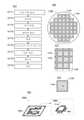
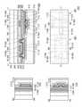
도 12는 기억 장치의 구성예를 나타낸 블록도 및 메모리 셀의 구성예를 나타낸 회로도.
도 13은 기억 장치의 구성예를 나타낸 블록도 및 메모리 셀의 구성예를 나타낸 회로도.
도 14는 메모리 셀의 구성예를 나타낸 회로도.
도 15는 마이크로 컨트롤러 유닛의 구성예를 나타낸 블록도.
도 16은 플립플롭의 구성예를 나타낸 회로도.
도 17은 플립플롭의 동작예를 나타낸 회로도.
도 18은 촬상 장치의 구성예를 나타낸 블록도 및 화소의 구성예를 나타낸 회로도.
도 19는 프로그래머블 회로의 구성예를 나타낸 도면.
도 20은 전자 부품의 제작 방법예를 나타낸 흐름도, 반도체 웨이퍼의 상면도와 그 확대도, 칩의 구성예를 나타낸 모식도, 및 전자 부품의 구성예를 나타낸 사시 모식도.
도 21은 전자 기기의 구성예를 나타낸 도면.
도 22는 전자 기기의 구성예를 나타낸 도면.
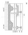
도 23은 트랜지스터의 상면도 및 단면도.
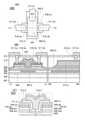
도 24는 트랜지스터의 상면도 및 단면도.
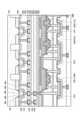
도 25는 반도체 장치의 단면도.
도 26은 반도체 장치의 단면도.
도 27은 반도체 장치의 단면도.
도 28은 반도체 장치의 단면도.
도 29는 트랜지스터의 상면도 및 단면도.
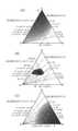
도 30은 본 발명에 관한 산화물의 원자수비의 범위를 설명한 도면.
도 31은 에너지 밴드 구조를 나타낸 도면.
도 32는 에너지 밴드 구조를 나타낸 도면.1 is a circuit diagram showing an example of a comparator;
Fig. 2 is a timing chart for explaining the operation of a comparator;
3 is a flowchart for explaining the operation of the comparator.
Fig. 4 is a timing chart for explaining the operation of the comparator;
Fig. 5 is a timing chart for explaining the operation of the comparator;
Fig. 6 is a timing chart for explaining the operation of the comparator;
Fig. 7 is a circuit diagram showing an example of a comparator;
Fig. 8 is a circuit diagram showing an example of a comparator;
Fig. 9 is a circuit diagram showing an example of a comparator;
Fig. 10 is a circuit diagram showing an example of a semiconductor device;
Fig. 11 is a circuit diagram showing a configuration example of a voltage generating circuit;
Fig. 12 is a block diagram showing a configuration example of a memory device and a circuit diagram showing a configuration example of a memory cell;
Fig. 13 is a block diagram showing a configuration example of a memory device and a circuit diagram showing a configuration example of a memory cell;
Fig. 14 is a circuit diagram showing a configuration example of a memory cell;
Fig. 15 is a block diagram showing a configuration example of a microcontroller unit;
Fig. 16 is a circuit diagram showing a configuration example of a flip-flop;
Fig. 17 is a circuit diagram showing an operation example of a flip-flop;
Fig. 18 is a block diagram showing a configuration example of an imaging device and a circuit diagram showing a configuration example of a pixel;
Fig. 19 is a diagram showing a configuration example of a programmable circuit;
20 is a flowchart showing an example of a manufacturing method of an electronic component, a top view and an enlarged view of a semiconductor wafer, a schematic diagram showing a configuration example of a chip, and a perspective schematic diagram showing a configuration example of an electronic component;
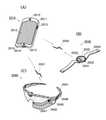
Fig. 21 is a diagram showing a configuration example of an electronic device;
Fig. 22 is a diagram showing a configuration example of an electronic device;
23 is a top view and a cross-sectional view of a transistor;
24 is a top view and a cross-sectional view of a transistor;
25 is a cross-sectional view of a semiconductor device;
26 is a cross-sectional view of a semiconductor device;
27 is a cross-sectional view of a semiconductor device;
28 is a cross-sectional view of a semiconductor device;
29 is a top view and a cross-sectional view of a transistor;
Fig. 30 is a view for explaining the range of the atomic ratio of oxides according to the present invention;
31 is a diagram illustrating an energy band structure;
32 is a diagram illustrating an energy band structure;
이하에 본 발명의 실시형태를 나타낸다. 다만, 본 명세서에 기재된 실시형태를 적절히 조합할 수 있다. 또한 하나의 실시형태 중에 복수의 구성예(동작예, 제조 방법예도 포함됨)가 나타내어지는 경우는, 구성예를 서로 적절히 조합할 수 있다. 또한 본 발명은 많은 상이한 형태로 실시할 수 있고, 취지 및 그 범위에서 벗어남이 없이 그 형태 및 상세한 사항을 다양하게 변경할 수 있다는 것은 통상의 기술자라면 쉽게 이해할 수 있다. 따라서 본 발명은 이하의 실시형태의 기재 내용에 한정하여 해석되는 것은 아니다.EMBODIMENT OF THE INVENTION Embodiment of this invention is shown below. However, the embodiments described in this specification may be appropriately combined. In addition, when a plurality of structural examples (operation examples and manufacturing method examples are also included) are shown in one embodiment, the structural examples can be appropriately combined with each other. In addition, it will be readily understood by those skilled in the art that the present invention may be embodied in many different forms, and that various changes may be made in form and details without departing from the spirit and scope thereof. Therefore, this invention is limited to the description of the following embodiment, and is not interpreted.
도면에서 크기, 층의 두께, 및 영역 등은 명료화를 위해 과장되어 있는 경우가 있다. 따라서 반드시 그 스케일에 한정되는 것은 아니다. 도면은 이상적인 예를 모식적으로 나타낸 것이며, 도면에 나타낸 형상 또는 값 등에 한정되는 것은 아니다. 예를 들어, 노이즈로 인한 신호, 전압, 또는 전류의 편차, 또는 타이밍의 어긋남으로 인한 신호, 전압, 또는 전류의 편차 등을 포함할 수 있다.In the drawings, the size, the thickness of the layer, and the area are exaggerated for clarity in some cases. Therefore, it is not necessarily limited to the scale. The drawings schematically show ideal examples, and are not limited to the shapes or values shown in the drawings. For example, it may include a deviation of a signal, voltage, or current due to noise or a deviation of a signal, voltage, or current due to a deviation of timing.
본 명세서에서, '위에' '아래에' 등의 배치를 나타내는 어구는, 도면을 참조하여 구성끼리의 위치 관계를 설명하기 위해 편의상 사용하는 경우가 있다. 또한 구성끼리의 위치 관계는 각 구성을 묘사하는 방향에 따라 적절히 변화하는 것이다. 따라서, 명세서에서 설명한 어구에 한정되지 않고 상황에 따라 적절히 바꿔 쓸 수 있다.In this specification, phrases indicating arrangement such as 'above' and 'below' may be used for convenience in order to describe the positional relationship between components with reference to the drawings. In addition, the positional relationship between components changes suitably according to the direction in which each structure is described. Therefore, it is not limited to the phraseology described in the specification and can be appropriately used interchangeably depending on the situation.
도면에 기재된 블록도의 각 회로 블록의 배치는, 설명을 위해 위치 관계를 특정하는 것이며, 본 발명의 일 형태의 회로 블록의 배치는 이에 한정되지 않는다. 블록도에서, 상이한 회로 블록으로 다른 기능을 실현하도록 나타내고 있어도, 실제의 회로 블록에서는 같은 회로 블록 내에서 다른 기능을 실현하도록 제공되어 있는 경우도 있다. 또한 각 회로 블록의 기능은 설명을 위해 기능을 특정하는 것이며, 하나의 회로 블록으로 나타내고 있어도, 실제의 회로 블록에서는 하나의 회로 블록으로 행하는 처리를 복수의 회로 블록으로 행하도록 제공되는 경우도 있다.The arrangement of each circuit block in the block diagram described in the drawings specifies the positional relationship for explanation, and the arrangement of the circuit block in one embodiment of the present invention is not limited thereto. Although the block diagram shows that different functions are realized by different circuit blocks, there are cases in which actual circuit blocks are provided so as to realize different functions within the same circuit block. In addition, the function of each circuit block is to specify the function for the purpose of explanation, and although it is shown as one circuit block, in actual circuit block, it may be provided so that the process performed by one circuit block may be performed by a plurality of circuit blocks.
또한 본 명세서 등에서, 채널이 형성되는 반도체층에 산화물 반도체를 사용한 트랜지스터를 'OS 트랜지스터'라고도 한다. 또한 본 명세서 등에서, 채널이 형성되는 반도체층에 실리콘을 사용한 트랜지스터를 'Si 트랜지스터'라고도 한다. 또한 본 명세서 등에서 채널이 형성되는 반도체층에 결정성을 가지는 실리콘을 사용한 트랜지스터를 '결정성 Si 트랜지스터'라고도 한다. 결정성 Si 트랜지스터는 OS 트랜지스터보다도 비교적 높은 이동도가 얻어지는 경향이 있다. 한편으로, 결정성 Si 트랜지스터는 OS 트랜지스터와 같이, 매우 적은 오프 전류의 실현이 어렵다. 따라서, 반도체층에 사용하는 반도체 재료는 목적이나 용도에 따라 적절히 구별하여 사용하는 것이 중요하다. 예를 들어, 목적이나 용도에 따라 OS 트랜지스터와 결정성 Si 트랜지스터 등을 조합하여 사용하여도 좋다.Also, in this specification and the like, a transistor using an oxide semiconductor as a semiconductor layer in which a channel is formed is also referred to as an 'OS transistor'. Also, in this specification and the like, a transistor using silicon as a semiconductor layer in which a channel is formed is also referred to as a 'Si transistor'. Also, in this specification, a transistor using silicon having crystallinity in a semiconductor layer in which a channel is formed is also referred to as a 'crystalline Si transistor'. Crystalline Si transistors tend to have relatively higher mobility than OS transistors. On the other hand, it is difficult to realize a very small off-state current for a crystalline Si transistor, like an OS transistor. Therefore, it is important to properly distinguish and use the semiconductor material used for the semiconductor layer according to the purpose or use. For example, an OS transistor and a crystalline Si transistor may be used in combination depending on the purpose or application.
본 명세서에서 '평행'이란, 2개의 직선이 -10° 이상 10° 이하의 각도로 배치되어 있는 상태를 말한다. 따라서, -5° 이상 5° 이하의 경우도 그 범주에 포함된다. 또한, '실질적으로 평행'이란, 2개의 직선이 -30° 이상 30° 이하의 각도로 배치되어 있는 상태를 말한다. 또한, '수직'이란, 2개의 직선이 80° 이상 100° 이하의 각도로 배치되어 있는 상태를 말한다. 따라서, 85° 이상 95° 이하의 경우도 그 범주에 포함된다. 또한, '실질적으로 수직'이란, 2개의 직선이 60° 이상 120° 이하의 각도로 배치되어 있는 상태를 말한다.As used herein, 'parallel' refers to a state in which two straight lines are arranged at an angle of -10° or more and 10° or less. Accordingly, the case of -5° or more and 5° or less is also included in the category. In addition, "substantially parallel" means a state in which two straight lines are arranged at an angle of -30° or more and 30° or less. In addition, "vertical" means a state in which two straight lines are arranged at an angle of 80° or more and 100° or less. Accordingly, the case of 85° or more and 95° or less is also included in the category. In addition, "substantially perpendicular" means a state in which two straight lines are arranged at an angle of 60° or more and 120° or less.
본 명세서 등에서 반도체 장치란 반도체 특성을 이용한 장치이며, 반도체 소자(트랜지스터, 다이오드 등)를 포함한 회로 및 이 회로를 가지는 장치 등을 말한다. 또한, 반도체 특성을 이용함으로써 기능할 수 있는 장치 전반을 말한다. 예를 들어, 집적 회로, 집적 회로를 가진 칩은 반도체 장치의 일례이다. 또한, 기억 장치, 표시 장치, 발광 장치, 조명 장치, 및 전자 기기 등은 그 자체가 반도체 장치인 경우가 있고, 또는 반도체 장치를 가지는 경우가 있다.In this specification, a semiconductor device is a device using semiconductor characteristics, and refers to a circuit including a semiconductor element (transistor, diode, etc.) and a device having the circuit. In addition, it refers to the overall device that can function by using semiconductor characteristics. For example, an integrated circuit, a chip having an integrated circuit, is an example of a semiconductor device. In addition, a memory device, a display device, a light emitting device, a lighting device, an electronic device, etc. may themselves be a semiconductor device, or may have a semiconductor device.
본 명세서 등에서는, 접지 전위를 0V로 하고, 양전위 및 음전위란 접지 전위를 0V 기준으로 한 전위이다.In this specification and the like, the ground potential is set to 0V, and the positive potential and the negative potential are potentials based on the ground potential of 0V.
본 명세서 등에서 X와 Y가 접속되어 있다고 명시적으로 기재되어 있는 경우는, X와 Y가 전기적으로 접속되어 있는 경우와, X와 Y가 기능적으로 접속되어 있는 경우와, X와 Y가 직접 접속되어 있는 경우가 본 명세서 등에 개시되어 있는 것으로 한다. 따라서 소정의 접속관계, 예를 들어 도면 또는 문장에 기재된 접속 관계에 한정되지 않고, 도면 또는 문장에 기재된 접속 관계 외의 것도 도면 또는 문장에 기재되어 있는 것으로 한다. X, Y는 대상물(예를 들어 장치, 소자, 회로, 배선, 전극, 단자, 도전막, 층 등)인 것으로 한다. 또한 본 명세서 등에서, X와 Y가 사이에 용량 소자를 두고 접속하는 경우, 즉 X가 용량 소자의 한쪽 전극에 전기적으로 접속하고, Y가 용량 소자의 다른 한쪽 전극에 전기적으로 접속하는 경우, X와 Y는 용량 소자를 통하여 전기적으로 접속되어 있다고 기재하는 경우가 있다.When it is explicitly described in this specification that X and Y are connected, when X and Y are electrically connected, when X and Y are functionally connected, and when X and Y are directly connected, It is assumed that the case is disclosed in this specification and the like. Therefore, it is not limited to a predetermined connection relationship, for example, the connection relationship described in the drawing or text, and it is assumed that the connection relationship other than the connection relationship described in the drawing or text is also described in the drawing or text. X and Y shall be objects (for example, devices, elements, circuits, wirings, electrodes, terminals, conductive films, layers, etc.). Further, in this specification and the like, when X and Y are connected with a capacitor between them, that is, when X is electrically connected to one electrode of the capacitor and Y is electrically connected to the other electrode of the capacitor, X and Y is sometimes described as being electrically connected via a capacitive element.
트랜지스터는 게이트, 소스, 및 드레인이라고 불리는 3개의 단자를 가진다. 게이트는 트랜지스터의 도통 상태를 제어하는 제어 노드로서 기능하는 노드이다. 소스 또는 드레인으로서 기능하는 2개의 입출력 노드는, 트랜지스터의 형태 및 각 단자에 인가되는 전위의 고저(高低)에 따라 한쪽이 소스가 되고, 다른 한쪽이 드레인이 된다. 이로써, 본 명세서 등에서는 소스나 드레인의 어구는 바꿔 쓸 수 있는 것으로 한다. 또한 본 명세서 등에서는 게이트 외의 2개의 단자를 제 1 단자, 제 2 단자라고 부르는 경우가 있다.A transistor has three terminals called a gate, a source, and a drain. The gate is a node functioning as a control node that controls the conduction state of the transistor. As for the two input/output nodes functioning as a source or a drain, one becomes a source and the other becomes a drain according to the shape of a transistor and the high and low of the potential applied to each terminal. Accordingly, in this specification and the like, the phrases of source and drain are interchangeable. In addition, in this specification and the like, two terminals other than the gate are sometimes referred to as a first terminal and a second terminal.
노드는 회로 구성이나 디바이스 구조 등에 따라 단자, 배선, 도전층, 도전체, 불순물 영역 등으로 바꿔 말할 수 있다. 또한 단자, 배선 등을 노드로 바꿔 말할 수 있다.A node can be referred to as a terminal, a wiring, a conductive layer, a conductor, an impurity region, etc. depending on the circuit configuration or device structure. Also, terminals, wirings, etc. can be replaced with nodes.
전압은 어떤 전위와 기준의 전위(예를 들어 접지 전위 또는 소스 전위)의 전위차를 가리키는 경우가 많다. 따라서, 전압을 전위라고 바꿔 말할 수 있다.Voltage often refers to the potential difference between a certain potential and a reference potential (eg, a ground potential or a source potential). Therefore, voltage can be said to be potential.
본 명세서 등에서, '막'이라는 어구와 '층'이라는 어구는 경우 또는 상황에 따라 서로 바꿀 수 있다. 예를 들어 '도전층'이라는 어구를 '도전막'이라는 어구로 변경할 수 있는 경우가 있다. 예를 들어 '절연막'이라는 어구를 '절연층'이라는 어구로 변경할 수 있는 경우가 있다.In this specification and the like, the phrase 'film' and the phrase 'layer' may be interchanged with each other depending on the case or situation. For example, the phrase 'conductive layer' can be changed to the phrase 'conductive film' in some cases. For example, the phrase 'insulating film' can be changed to the phrase 'insulating layer' in some cases.
본 명세서 등에서, '제 1', '제 2', '제 3'이라는 서수사는 구성 요소의 혼동을 피하기 위해 붙이는 것이며, 이 경우는 수적으로 한정하는 것은 아니고, 또한 순서를 한정하는 것도 아니다.In this specification and the like, ordinal numbers such as 'first', 'second', and 'third' are added to avoid confusion of components, and in this case, it is not limited in number, nor does it limit the order.
(실시형태 1)(Embodiment 1)
본 실시형태에서는, 본 발명의 일 형태의 반도체 장치에 대해 설명한다.In this embodiment, a semiconductor device of one embodiment of the present invention will be described.
회로의 입력 신호로서 음전위를 사용하는 경우에는, 음전위 전원을 필요로 하는 경우가 있다. 이하에서는 일례로서 음전위의 콤퍼레이터(비교 회로라고 부르는 경우가 있음)에 대해 설명한다.When a negative potential is used as an input signal of a circuit, a negative potential power supply is sometimes required. Hereinafter, a negative potential comparator (sometimes referred to as a comparison circuit) will be described as an example.
예를 들어 도 9에 나타낸 콤퍼레이터(40)가 단자(IN) 및 단자(INB)에 인가되는 전위를 비교하는 기능을 발현하기 위해서는 트랜지스터(3) 및 트랜지스터(4)가 온 상태가 되어 전류가 흐르며 트랜지스터(5)에 전류가 흐를 필요가 있다. 단자(IN) 및 단자(INB)에 인가되는 전위가 음전위인 경우를 생각한다. 트랜지스터(3) 및 트랜지스터(4)에 전류를 흘리기 위해서는 단자(IN) 및 단자(INB)보다 낮은 전위, 즉 음전위를 단자(Low)에 인가할 필요가 있다. 콤퍼레이터(40)가 높은 정밀도의 비교를 행하기 위해서는 전원 등을 사용하여 높은 정밀도로 전위(VA)를 공급하는 것이 요구된다. 즉, 음전위 전원이 필요해진다.For example, in order for the
본 발명의 일 형태의 콤퍼레이터는 전위(VA)에 접지 전위(이하 GND라고 함)를 사용함으로써 전위를 높은 정밀도로 비교할 수 있다. 음전위 전원을 사용하는 경우와 비교하여 접지 전위를 사용하는 경우에는 더 안정적인 전원으로 할 수 있기 때문에 콤퍼레이터의 정밀도를 향상시킬 수 있다. 또한 소비전력을 낮게 할 수 있는 경우가 있다.The comparator of one embodiment of the present invention can compare potentials with high precision by using a ground potential (hereinafter referred to as GND) for the potential VA. Compared to the case of using a negative potential power supply, when a ground potential is used, a more stable power supply can be used, and thus the accuracy of the comparator can be improved. In addition, there are cases in which power consumption can be reduced.
여기서 콤퍼레이터로서 전압 비교 회로와 전류 비교 회로를 들 수 있다. 예를 들어 고전압의 노이즈가 회로에 인가되는 경우에, 전류 비교 회로에서는 전압 비교 회로와 비교하여 고전압 노이즈의 영향이 작기 때문에 바람직하다.Here, as the comparator, a voltage comparison circuit and a current comparison circuit are exemplified. For example, when high voltage noise is applied to the circuit, the current comparison circuit is preferable because the influence of the high voltage noise is small compared to the voltage comparison circuit.
<콤퍼레이터의 예 1><Example 1 of comparator>
본 발명의 일 형태의 콤퍼레이터는 입력되는 2개의 전위의 비교 결과를 출력하는 기능을 가지고, 본 발명의 일 형태의 콤퍼레이터에서, 입력되는 2개의 전위 중 적어도 어느 것이 음전위이다. 본 발명의 일 형태의 콤퍼레이터에서는, 비교하는 음전위를 양전위로 변환함으로써 음전위용의 전원을 사용하지 않고 전위를 비교할 수 있다. 음전위를 양전위로 변환하는 방법으로서, 예를 들어 용량 소자를 통하여 전위를 변환할 수 있다.The comparator of one embodiment of the present invention has a function of outputting a comparison result of two input potentials, and in the comparator of one embodiment of the present invention, at least any one of the two input potentials is a negative potential. In the comparator of one embodiment of the present invention, potentials can be compared without using a power supply for negative potentials by converting negative potentials to be compared into positive potentials. As a method of converting a negative potential into a positive potential, the potential can be converted through, for example, a capacitor.
본 발명의 일 형태의 콤퍼레이터의 일례를 도 1에 나타내었다. 도 1에 나타낸 콤퍼레이터(20)는 입력 단자로서 기능하는 단자(INP) 및 단자(INN), 단자(OUT1), 단자(High), 단자(Low), 단자(BIAS), 입력 단자로서 기능하는 단자(INI1), 노드(ND1) 내지 노드(ND3), 트랜지스터(1) 내지 트랜지스터(5), 트랜지스터(7), 트랜지스터(8), 용량 소자(62) 내지 용량 소자(65)를 가진다. 단자(OUT1)는 출력 단자로서 기능한다.An example of a comparator of one embodiment of the present invention is shown in FIG. 1 . The
노드(ND1)에 인가되는 전위와 노드(ND2)에 인가되는 전위의 비교 결과에 따른 전위가 노드(ND3)로부터 출력된다.A potential according to the result of comparison between the potential applied to the node ND1 and the potential applied to the node ND2 is output from the node ND3 .
노드(ND1)는 용량 소자(62)를 통하여 단자(INP)와 전기적으로 접속되고, 노드(ND2)는 용량 소자(65)를 통하여 단자(INN)와 전기적으로 접속된다. 노드(ND3)는 단자(OUT1)와 전기적으로 접속된다.The node ND1 is electrically connected to the terminal INP through the
여기서 단자(INP) 및 단자(INN)에 인가된 음전위를 용량 소자를 통하여 양전위로 변환한다. 변환된 양전위가 노드(ND1) 및 노드(ND2)에 인가된다. 따라서 음전위 전원은 불필요해진다.Here, the negative potential applied to the terminal INP and the terminal INN is converted into a positive potential through the capacitor. The converted positive potential is applied to the node ND1 and the node ND2. Therefore, the negative potential power supply becomes unnecessary.
트랜지스터(3) 및 트랜지스터(4)는 차동 쌍이다. 트랜지스터(3)와 트랜지스터(4)의 게이트에 인가되는 전위의 비교 결과에 따른 신호가 출력된다. 트랜지스터(1) 및 트랜지스터(2)는 커런트 미러를 구성한다. 트랜지스터(3)는 트랜지스터(1)에, 트랜지스터(4)는 트랜지스터(2)에 각각 직렬로 접속된다. 트랜지스터(3) 및 트랜지스터(4)의 소스는 정전류원에 전기적으로 접속되는 것이 바람직하다. 도 1에서는 정전류원으로서 트랜지스터(5)를 사용하는 예를 나타내었다. 트랜지스터(5)의 드레인에는 트랜지스터(3) 및 트랜지스터(4)의 소스가 전기적으로 접속된다. 트랜지스터(5)의 게이트에는 단자(BIAS)가 전기적으로 접속되고, 소스에는 GND가 전기적으로 접속된다.
트랜지스터(3)와 트랜지스터(4)의 게이트에 인가된 전위에 따라 트랜지스터(4)의 드레인으로부터 전위가 출력된다.A potential is output from the drain of the
노드(ND1)의 전위는 트랜지스터(3)의 게이트에, 노드(ND2)의 전위는 트랜지스터(4)의 게이트에 각각 인가된다. 또한 트랜지스터(4)의 드레인은 노드(ND3)에 전기적으로 접속된다. 노드(ND3)는 단자(OUT1)에 전기적으로 접속된다.The potential of the node ND1 is applied to the gate of the
용량 소자(62)를 통하여 노드(ND1)와 단자(INP)는 전기적으로 접속된다. 용량 소자(65)를 통하여 노드(ND2)와 단자(INN)는 전기적으로 접속된다.The node ND1 and the terminal INP are electrically connected through the
도 1에서는 트랜지스터(1) 및 트랜지스터(2)로서 p채널형의 트랜지스터를 사용하고, 트랜지스터(3) 및 트랜지스터(4)로서 n채널형의 트랜지스터를 사용한다. 트랜지스터(1)의 게이트, 트랜지스터(2)의 게이트, 및 트랜지스터(1)의 드레인은 전기적으로 접속되고, 트랜지스터(1) 및 트랜지스터(2)의 소스에는 Vdd가 인가된다. 트랜지스터(1)의 드레인은 트랜지스터(3)의 드레인에, 트랜지스터(2)의 드레인은 트랜지스터(4)의 드레인에 각각 전기적으로 접속된다.In FIG. 1 , a p-channel transistor is used as the
노드(ND1)는 트랜지스터(7)에 전기적으로 접속된다. 도 1에서 노드(ND1)는, 용량 소자(63)를 통하여 트랜지스터(7)의 소스에 전기적으로 접속된다.Node ND1 is electrically connected to
트랜지스터(7)의 게이트에는 단자(INI1)가 전기적으로 접속된다. 단자(INI1)에는 예를 들어 Vdd가 인가된다. 또한 노드(ND1)는 용량 소자(63)를 통하여 트랜지스터(7)의 소스에 전기적으로 접속된다.A terminal INI1 is electrically connected to the gate of the
트랜지스터(8)의 게이트에는 단자(INI1)가 전기적으로 접속된다. 또한 노드(ND2)는 용량 소자(64)를 통하여 트랜지스터(8)의 소스에 전기적으로 접속된다.A terminal INI1 is electrically connected to the gate of the
<콤퍼레이터의 동작예><Example of comparator operation>
다음에 본 발명의 일 형태에 따른 콤퍼레이터의 동작예에 대해 도 1 내지 도 3을 참조하여 설명한다.Next, an operation example of the comparator according to one embodiment of the present invention will be described with reference to Figs.
도 1에 나타낸 콤퍼레이터(20)의 동작예에 대해 설명한다.An operation example of the
도 2는 도 1에 나타낸 콤퍼레이터(20)의 동작을 나타낸 타이밍 차트이다. 또한 도 3의 (A)는 도 1에 나타낸 콤퍼레이터의 동작을 나타낸 흐름도이다. 도 2에 나타낸 시각(t12)에서 노드(ND1) 및 노드(ND2)의 전위를 양전위인 V1까지 올려둔다(단계 S12). 이때 단자(INP) 및 단자(INN)의 전위에 기준 전위로서, 예를 들어 V0(예를 들어 0V)을 인가한다. 또한 단계 S12의 상세한 사항에 대해서는 후술한다.FIG. 2 is a timing chart showing the operation of the
도 1에 나타낸 트랜지스터(3) 및 트랜지스터(4)의 문턱값 중 더 큰 값을 Vt로 한다. 콤퍼레이터(20)에서는 (V0-V1+Vt)보다 큰 음전위의 입력에 대해서도 동작할 수 있다.The larger of the threshold values of the
다음에 도 2에 나타낸 시각(t21)에서 단자(INP) 및 단자(INN)에 신호, 여기서는 음전위를 입력한다(단계 S21). 단자(INP)의 전위를 Vp, 단자(INN)의 전위를 Vn으로 한다. 도 2에 나타낸 타이밍 차트에서는 Vn 및 Vp는 시각(t21)보다 GND에서 전위가 저하된다. 여기서 도 2의 예에서 GND는 0V이다. 시각(t21)에서 시각(t22)에서는 Vn은 Vp보다 높고, 시각(t22) 이후는 낮아진다. 또한 노드(ND1)의 전위가 Vp의 추이(推移)에, 노드(ND2)의 전위가 Vn의 추이에 각각 대응하는 것이 확인된다.Next, a signal, here a negative potential, is input to the terminal INP and the terminal INN at time t21 shown in Fig. 2 (step S21). The potential of the terminal INP is Vp, and the potential of the terminal INN is Vn. In the timing chart shown in Fig. 2, the potentials of Vn and Vp are lowered at GND than at the time t21. Here, in the example of FIG. 2, GND is 0V. From time t21 to time t22, Vn is higher than Vp, and after time t22, it becomes lower. Also, it is confirmed that the potential of the node ND1 corresponds to the transition of Vp and the potential of the node ND2 corresponds to the transition of Vn, respectively.
단자(INP)에 인가되는 전위가 낮아지면 노드(ND1)의 전위도 낮아진다. 노드(ND1)에는 양의 전위가 미리 인가되기 때문에, 단자(INP)에 음의 전위가 인가되어도 노드(ND1)의 전위가 음의 전위가 되지 않도록 할 수 있다.When the potential applied to the terminal INP decreases, the potential of the node ND1 also decreases. Since a positive potential is previously applied to the node ND1 , it is possible to prevent the potential of the node ND1 from becoming a negative potential even when a negative potential is applied to the terminal INP.
노드(ND1)의 전위의 변화량은, Vp의 변화량과 노드(ND1)에 접속되는 용량 성분의 크기에 따라 결정된다. 즉, 용량 소자(62), 용량 소자(63), 트랜지스터(3)의 게이트 용량, 및 노드(ND1)에 접속되는 그 외의 용량 성분(트랜지스터의 게이트를 포함함)을 합친 용량 결합으로 결정된다.The amount of change in the potential of the node ND1 is determined according to the amount of change in Vp and the magnitude of the capacitance component connected to the node ND1. That is, it is determined by capacitive coupling in which the
노드(ND2)에 대해서도 마찬가지로, 단자(INN)에 인가되는 입력 신호가 낮아지면 노드(ND2)의 전위도 낮아지고, 그 변화량은 예를 들어 도 1에서는 용량 소자(64), 용량 소자(65), 및 트랜지스터(4)의 게이트 용량 각각의 크기에 따라 결정된다.Similarly for the node ND2, when the input signal applied to the terminal INN decreases, the potential of the node ND2 also decreases, and the amount of change is, for example, in the
트랜지스터(3)와 트랜지스터(4)의 게이트에 인가된 전위에 따라 트랜지스터(4)의 드레인으로부터 High(고전위 전원이라고도 함; 전위가 VH) 또는 Low(저전위 전원이라고도 함; 전위가 VL)의 신호가 단자(OUT1)로 출력된다. 단자(OUT1)의 전압을 Vo로 한다. 도 2에 나타낸 타이밍 차트에서 Vo는 시각(t21)에서 서서히 전위가 낮아지고 Vo는 Low, 여기서는 GND에 달한다. 시각(t22)에서 Vn이 Vp보다 낮아지면 Vo는 High, 여기서는 약 Vdd에 달한다.Depending on the potential applied to the
이하에 단계 S12에 대해 더 구체적으로 설명한다.Step S12 will be described in more detail below.
다음에 단계 S12에 대한 상세한 사항을 설명한다.Next, the details of step S12 will be described.
시각(t0)에서 단자(INI1)에는 Low 신호(예를 들어 GND)가 인가된다. 트랜지스터(7)의 드레인에는 Vdd가 인가된다.At time t0, a low signal (eg, GND) is applied to the terminal INI1. Vdd is applied to the drain of the
단계 S12에 의하여, 시각(t12)에서 단자(INI1)에 High 신호, 예를 들어 Vdd가 인가되고, 트랜지스터(7)의 게이트에는 Vdd가 인가되고, 드레인에는 Vdd가 인가된다.By step S12, at time t12, a High signal, for example, Vdd is applied to the terminal INI1, Vdd is applied to the gate of the
트랜지스터(7)의 게이트에 Vdd가 인가됨으로써 트랜지스터(7)가 온 상태가 되어 트랜지스터(7)에 전류가 흐른다. 트랜지스터(7)의 소스 전위는 상승하고, 트랜지스터(7)의 소스는 Vdd에서 트랜지스터(7)의 문턱값만큼 감소된 전위(이하 Vdd-Vt7이라고 함)에 달한다.When Vdd is applied to the gate of the
트랜지스터(7)의 소스가 Vdd-Vt7보다 커지면 트랜지스터(7)의 게이트-소스 간의 전압은 Vt7 미만이 되어 트랜지스터(7)의 전류는 거의 흐르지 않게 된다. 트랜지스터(7)가 OS-FET이며, 게이트-소스 간의 전압이 문턱값 미만인 경우에는 매우 낮은 전류밖에 흐르지 않는다. OS-FET인 경우에는, Si-FET와 비교하여 예를 들어 기판 누설 전류나 pn접합 누설 전류가 거의 없기 때문이다. 따라서 노드(ND1)에서의 전하의 누설을 매우 작게 억제할 수 있어 안정적인 전위를 얻을 수 있다.When the source of the
노드(ND1)의 전위는 트랜지스터(7)의 소스의 전위가 상승됨에 따라 상승한다. 예를 들어 도 1에서는 용량 소자(62), 용량 소자(63), 트랜지스터(3)의 게이트 용량이 주된 용량 성분이 된다. 트랜지스터(7)가 오프 상태인 경우에는 용량 소자(62) 및 용량 소자(63)의 용량을 각각 C2 및 C3으로 하고, 트랜지스터(3)의 게이트 용량을 Ct3으로 하고 Vp의 변화량을 ΔVp로 하면, 노드(ND1)의 전위의 변화량 ΔV는 수학식(1)으로 나타낼 수 있다.The potential of the node ND1 rises as the potential of the source of the
[수학식 1][Equation 1]

여기서 V1+ΔV>0이 되도록 V1을 선택함으로써 노드(ND1)를 양의 전위로 할 수 있다.Here, by selecting V1 so that V1+ΔV>0, the node ND1 can have a positive potential.
또한 트랜지스터(7)를 트랜지스터(8)에, 용량 소자(63)를 용량 소자(64)에 각각 치환함으로써 노드(ND2)에 대해서도 같은 동작으로 전위를 상승시킬 수 있다.Further, by replacing the
도 5에서는 노드(ND1)의 전위 및 노드(ND2)의 전위는 시각(t12)에서 -3V로부터 약 1.2V 상승한다.In Fig. 5, the potential of the node ND1 and the potential of the node ND2 rise from -3V to about 1.2V at time t12.
여기서 트랜지스터(7)와 트랜지스터(8)에 OS-FET를 사용하면 용량 소자(63)와 용량 소자(64)의 누설 전류를 매우 작게 할 수 있다. 즉 트랜지스터(3)와 트랜지스터(4)의 게이트 전위(즉 노드(ND1)와 노드(ND2)의 전위)가 안정적이다. 콤퍼레이터의 정밀도가 향상된다.Here, when OS-FETs are used for the
<콤퍼레이터의 예 2><Example 2 of comparator>
도 7에 나타낸 콤퍼레이터(20)는 도 1에 나타낸 콤퍼레이터(20)에 더하여 트랜지스터(10), 트랜지스터(11), 및 단자(INI2)를 가진다. 노드(ND1)는 트랜지스터(10)의 드레인에, 노드(ND2)는 트랜지스터(11)의 드레인에, 트랜지스터(5)의 드레인은 트랜지스터(10) 및 트랜지스터(11)의 소스에, 단자(INI2)는 트랜지스터(10) 및 트랜지스터(11)의 게이트에 각각 전기적으로 접속된다.The
도 3의 (B)는 도 7에 나타낸 콤퍼레이터(20)의 동작을 나타낸 흐름도이다. 도 7에 나타낸 콤퍼레이터(20)에서는 단계 S12를 행하기 전에 단계 S10을 행한다. 단계 S10에 의하여 시각(t10)에서, 단자(INI2)에 High 신호를 공급하여 트랜지스터(10) 및 트랜지스터(11)를 온 상태로 한다. 또한 단자(BIAS)에 High 신호를 공급하여 트랜지스터(5)를 온 상태로 한다. 트랜지스터(10), 트랜지스터(11), 및 트랜지스터(5)를 온 상태로 함으로써 노드(ND1) 및 노드(ND2)에 GND가 인가된다. 노드(ND1) 및 노드(ND2)에, 기준이 되는 전위를 인가하는 동작을 '리셋'이라고 부르는 경우가 있다.FIG. 3B is a flowchart showing the operation of the
노드(ND1) 및 노드(ND2)의 전위의 리셋을 행하지 않을 때에는 전위가 불확정, 즉 부유 상태이다. 단계 S21에서, 입력되는 전위에 부유 전위가 가산되므로 노드(ND1) 및 노드(ND2)에 인가되는 전위의 정밀도가 저하되는 경우가 있다.When the potentials of the nodes ND1 and ND2 are not reset, the potentials are indeterminate, that is, in a floating state. In step S21, since the floating potential is added to the input potential, the precision of the potential applied to the nodes ND1 and ND2 may decrease.
도 7에 나타낸 콤퍼레이터(20)의 구성으로 함으로써 단계 S12를 행하기 전에 단계 S10에 의하여 노드(ND1) 및 노드(ND2)의 전위의 리셋을 행할 수 있다. 노드(ND1) 및 노드(ND2)에 인가되는 전위의 정밀도가 향상된다.With the configuration of the
<콤퍼레이터의 예 3><Example 3 of comparator>
도 8에 나타낸 콤퍼레이터(20)는 트랜지스터(1)와 트랜지스터(3) 사이에 트랜지스터(14)를 가진다는 점, 트랜지스터(2) 및 트랜지스터(4) 사이에 트랜지스터(15)를 가진다는 점, 단자(INI3) 및 단자(INI4)를 가진다는 점, 노드(ND1)에 전기적으로 접속되는 트랜지스터(12) 및 용량 소자(67)를 가진다는 점, 및 노드(ND2)에 전기적으로 접속되는 트랜지스터(13) 및 용량 소자(68)를 가진다는 점이 도 1에 나타낸 콤퍼레이터(20)와 상이하다.The
트랜지스터(3)는 트랜지스터(14)에, 트랜지스터(14)는 트랜지스터(1)에 각각 직렬로 접속된다. 또한 트랜지스터(4)는 트랜지스터(15)에, 트랜지스터(15)는 트랜지스터(2)에 각각 직렬로 접속된다. 트랜지스터(3) 및 트랜지스터(4)의 소스는 정전류원에 전기적으로 접속되는 것이 바람직하다. 도 1, 도 7, 및 도 8에는 정전류원으로서 트랜지스터(5)를 사용하는 예를 나타내었다. 트랜지스터(5)의 드레인에는 트랜지스터(3) 및 트랜지스터(4)의 소스가 전기적으로 접속된다. 트랜지스터(5)의 게이트에는 단자(BIAS)가 전기적으로 접속되고, 소스에는 GND가 전기적으로 접속된다. 단자(INI3)에는 트랜지스터(14) 및 트랜지스터(15)의 게이트가 전기적으로 접속되고, 단자(INI4)에는 트랜지스터(12) 및 트랜지스터(13)의 게이트가 전기적으로 접속된다.
여기서 트랜지스터(12) 및 트랜지스터(13)는 OS-FET인 것이 바람직하다. 트랜지스터(12) 및 트랜지스터(13)는 각각 트랜지스터(3) 및 트랜지스터(4)의 문턱값 보정을 행하는 트랜지스터이다. 트랜지스터(12) 및 트랜지스터(13)는 각각 트랜지스터(3) 및 트랜지스터(4)의 문턱 전압을 각각 노드(ND1) 및 노드(ND2)에 기억한다. 트랜지스터(12) 및 트랜지스터(13)를 OS-FET로 함으로써 노드(ND1) 및 노드(ND2)에 기억된 전위에 상당하는 전하가 누설되지 않기 때문에 콤퍼레이터의 정밀도를 높일 수 있다.Here, the
도 8에서는 트랜지스터(1)의 드레인은 트랜지스터(14)의 드레인에, 트랜지스터(2)의 드레인은 트랜지스터(15)의 드레인에 각각 전기적으로 접속된다. 트랜지스터(14)의 소스는 트랜지스터(3)의 드레인에, 트랜지스터(15)의 소스는 트랜지스터(4)의 드레인에 각각 전기적으로 접속된다.In FIG. 8 , the drain of the
트랜지스터(5), 트랜지스터(7), 트랜지스터(8), 용량 소자(62), 용량 소자(63), 용량 소자(64), 및 용량 소자(65)에 대해서는 도 1을 참조할 수 있다.1 may be referred to for the
도 3의 (C)는 도 8에 나타낸 콤퍼레이터(20)의 동작을 나타내는 흐름도이다. 도 8에 나타낸 콤퍼레이터(20)에서는 단계 S12를 행하기 전에 단계 S11을 행한다. 단계 S11에 의하여 시각(t12)에서 단자(INI3)에 High 신호를 공급하여 트랜지스터(14) 및 트랜지스터(15)를 온 상태로 한다. 또한 단자(INI4)에 High 신호를 공급하여 트랜지스터(12) 및 트랜지스터(13)를 온 상태로 한다. 또한 단자(BIAS)에 High 신호를 공급하여 트랜지스터(5)를 온 상태로 한다. 트랜지스터(3)는 게이트와 소스 간의 전압이 문턱값이 되었을 때에 오프 상태가 된다. 즉, 트랜지스터(3)의 소스와 드레인 사이의 전압도 문턱 전압이 된다. 트랜지스터(4)에 대해서도 마찬가지로, 게이트-소스 간에 문턱 전압을 인가할 수 있다. 트랜지스터(3)의 게이트에 문턱 전압에 상당하는 전하가 축적된다(문턱값의 기억, 문턱값의 보정). 마찬가지로 하여, 트랜지스터(4)의 게이트에도 문턱 전압에 상당하는 전하가 축적된다(문턱값의 기억, 문턱값의 보정).FIG. 3C is a flowchart showing the operation of the
다음에, 단자(INI3)에 Low 신호를 공급하여 트랜지스터(14) 및 트랜지스터(15)를 오프 상태로 한다. 또한 단자(INI4)에 Low 신호를 공급하여 트랜지스터(12) 및 트랜지스터(13)를 오프 상태로 한다. 또한 단자(BIAS)에 High 신호를 공급하여 트랜지스터(5)를 오프 상태로 한다.Next, a low signal is supplied to the terminal INI3 to turn off the
단계 S11에 의하여 트랜지스터(3) 및 트랜지스터(4)에 문턱 전압을 미리 인가해 둠으로써 본 발명의 일 형태에 따른 콤퍼레이터의 정밀도를 향상시킬 수 있다.By applying the threshold voltage to the
예를 들어 트랜지스터(3) 및 트랜지스터(4)의 문턱값이 상이한 경우, 게이트-소스 간의 전압에 대한 전류값이 상이하다. 예를 들어 문턱값이 큰 경우에는 같은 전류값을 흘리기 위해 더 큰 게이트-소스 간의 전압이 필요해진다. 본 발명의 일 형태에 따른 콤퍼레이터는 트랜지스터(3)와 트랜지스터(4)의 게이트-소스 간의 전압의 비교 결과에 따라 단자(OUT1)로부터 신호를 출력하는 기능을 가지지만, 트랜지스터(3)와 트랜지스터(4)의 문턱값이 상이하면, 비교 결과의 정밀도가 저하되는 경우가 있다.For example, when the threshold values of the
또한 노드(ND1) 및 노드(ND2)에 정해진 전위를 인가하지 않는 경우에는 전위가 불확정, 즉 부유 상태이다. 단계 S21에서 입력되는 전위에 부유 전위가 가산되기 때문에 노드(ND1) 및 노드(ND2)에 인가되는 전위의 정밀도가 저하되는 경우가 있다.In addition, when predetermined potentials are not applied to the nodes ND1 and ND2 , the potential is indeterminate, that is, in a floating state. Since the floating potential is added to the potential input in step S21, the precision of the potentials applied to the nodes ND1 and ND2 may decrease.
트랜지스터(3) 및 트랜지스터(4)의 게이트-소스 간에 각각의 문턱값을 인가함으로써 트랜지스터(3)와 트랜지스터(4)의 문턱값의 편차로 인한 영향을 작게 할 수 있기 때문에 본 발명의 일 형태에 따른 콤퍼레이터의 정밀도를 향상시킬 수 있다.By applying the respective threshold values between the gate and source of the
<시뮬레이션예><Example of simulation>
도 4 내지 도 6의 타이밍 차트에는 도 1에 나타낸 회로도를 참조하여 시뮬레이션에 의하여 산출한 각 단자의 전위를 나타내었다. 도 4 내지 도 6에 나타낸 전압은 GND를 기준으로 한 전압이다. 도 4에는 단자(INP) 및 단자(INN)의 전위를, 도 5에는 노드(ND1), 노드(ND2), 트랜지스터(7)의 소스 및 트랜지스터(8)의 소스의 전위를, 도 6에는 단자(OUT1) 및 트랜지스터(1)의 소스 전위를 각각 나타내었다. 트랜지스터(1) 내지 트랜지스터(4)는 채널 길이를 0.5μm, 채널 폭을 2.61μm로 하고, 트랜지스터(5)는 채널 길이를 0.5μm, 채널 폭을 0.87μm로 하고, 트랜지스터(7) 및 트랜지스터(8)는 채널 길이를 0.5μm, 채널 폭을 60.9μm로 하고, 용량 소자(62) 및 용량 소자(65)의 용량은 50fF, 용량 소자(63) 및 용량 소자(64)의 용량은 500fF로 하였다. 시뮬레이션은 실바코(Silvaco)사 제조, 회로 시뮬레이터 SmartSpice MultiCore Version 4.18.16.R을 사용하였다. Level을 54로 하고, Vth0을 0.531V로 하였다.In the timing charts of FIGS. 4 to 6 , potentials of respective terminals calculated by simulation with reference to the circuit diagram shown in FIG. 1 are shown. The voltages shown in FIGS. 4 to 6 are voltages with respect to GND. Fig. 4 shows the potentials of the terminal INP and the terminal INN, Fig. 5 shows the potentials of the node ND1, the node ND2, the source of the
도 4 내지 도 6에서 본 발명의 일 형태에 따른 콤퍼레이터의 상정한 동작이 확인되었다.4 to 6 , the assumed operation of the comparator according to one embodiment of the present invention was confirmed.
(실시형태 2)(Embodiment 2)
본 실시형태에서는 음전위가 인가되는 반도체 소자를 가지는 반도체 장치(300)의 일례를 나타낸다.In the present embodiment, an example of a
<반도체 장치의 일례><Example of semiconductor device>
반도체 장치(300)는 상기 반도체 소자에 인가되는 음전위를 제 1 기준 전위와 비교하는 콤퍼레이터를 가지는 것이 바람직하다. 이 콤퍼레이터로서 상술한 실시형태에 나타낸 콤퍼레이터를 사용할 수 있다. 또한 반도체 장치(300)는 전압 유지부, 전압 생성부, 제어부 등을 가짐으로써 상기 반도체 소자에 인가되는 음전위를 유지할 수 있다.The
이하에는 음전위가 인가되는 반도체 소자의 일례로서 트랜지스터를 나타낸다.Hereinafter, a transistor is shown as an example of a semiconductor device to which a negative potential is applied.
트랜지스터의 백 게이트에 전위를 인가함으로써 문턱값을 제어할 수 있다. 예를 들어 n채널형 트랜지스터의 백 게이트에 음전위를 인가함으로써 문턱값을 플러스 시프트시킬 수 있다. 트랜지스터로서 OS-FET를 사용한 경우에, 문턱값을 플러스 시프트시킴으로써 매우 낮은 컷 오프 전류를 구현할 수 있다. 여기서 컷 오프 전류란, 게이트-소스 간의 전압이 0V일 때에 흐르는 전류이다.The threshold can be controlled by applying a potential to the back gate of the transistor. For example, the threshold value can be positively shifted by applying a negative potential to the back gate of the n-channel transistor. In the case of using an OS-FET as a transistor, a very low cut-off current can be realized by positively shifting the threshold. Here, the cut-off current is a current flowing when the gate-source voltage is 0V.
컷 오프 전류가 낮은 트랜지스터를 사용함으로써 예를 들어, 전하 유지 성능이 향상되어 반도체 장치가 가지는 회로의 리프레시 동작의 빈도를 줄일 수 있다. 따라서 소비전력이 매우 낮은 반도체 장치를 구현할 수 있다.By using a transistor having a low cut-off current, for example, charge retention performance may be improved, and the frequency of a circuit refresh operation of a semiconductor device may be reduced. Accordingly, a semiconductor device having very low power consumption can be implemented.
도 10의 (A)에 일례로서 나타낸 반도체 장치(300)는 콤퍼레이터(51)를 가진다. 콤퍼레이터(51)는 입력 단자로서 기능하는 단자(CI)와 단자(REF)와 출력 단자로서 기능하는 단자(CO)를 가진다. 콤퍼레이터(51)로서 실시형태 1에 나타낸 콤퍼레이터를 사용하는 것이 바람직하다. 또한 단자(CI), 단자(REF), 및 단자(CO)로서 실시형태 1에 나타낸 단자(INP), 단자(INN), 및 단자(OUT1)를 사용할 수 있다.The
여기서 반도체 장치(300)는, 반도체 소자에 인가되는 음전위를 유지하기 위해 전압 유지부(43)를 가지는 것이 바람직하다. 전압 유지부(43)는 예를 들어 용량 소자(CA2)와 트랜지스터(FE2)와 입력 단자로서 기능하는 단자(IN)와 출력 단자로서 기능하는 단자(BG)를 가진다. 트랜지스터(FE2)의 소스 및 드레인 중 한쪽은 단자(IN)에 전기적으로 접속되고, 다른 한쪽은 용량 소자(CA2)의 한쪽 전극과 콤퍼레이터(51)의 단자(CI)와 단자(BG)에 전기적으로 접속된다. 용량 소자(CA2)의 다른 한쪽 전극에는 예를 들어 GND가 인가된다. 트랜지스터(FE2)의 게이트는 단자(BG)에 전기적으로 접속된다.Here, the
용량 소자(CA2)의 전하의 유지 능력을 높이기 위해 트랜지스터(FE2)로서 OS-FET를 사용한다. 또한 트랜지스터(FE2)에서는 백 게이트에 음 전위를 인가하지 않아도 낮은 컷 오프 전류가 얻어지는 것이 바람직하다. 따라서 트랜지스터(FE2)의 문턱값은 0.5V 이상 6V 이하, 또는 1V 이상 4V 이하가 바람직하다. 또한 트랜지스터(MW)의 문턱값보다 큰 것이 바람직하다.An OS-FET is used as the transistor FE2 in order to increase the charge holding capacity of the capacitor CA2. In addition, in the transistor FE2, it is preferable that a low cut-off current is obtained even if a negative potential is not applied to the back gate. Therefore, the threshold value of the transistor FE2 is preferably 0.5V or more and 6V or less, or 1V or more and 4V or less. It is also desirable to be larger than the threshold of the transistor MW.
여기서 트랜지스터(FE2)로서 후술하는 트랜지스터(200)를 사용하는 것이 바람직하다. 또한 트랜지스터(MW)로서 후술하는 트랜지스터(100)를 사용하는 것이 바람직하다. 또한 트랜지스터(7) 및 트랜지스터(8)로서 후술하는 트랜지스터(100) 또는 트랜지스터(200) 중 어느 것을 사용할 수 있다.Here, it is preferable to use a
단자(BG)로부터는 예를 들어 음전위(이하, Vbg이라고 함)가 출력된다.From the terminal BG, for example, a negative potential (hereinafter referred to as Vbg) is output.
도 10의 (B)는 Vbg가 인가되는 반도체 소자를 가지는 회로의 일례로서 셀 어레이(44)를 나타내었다. 셀 어레이(44)는 복수의 트랜지스터(MW)를 가지고, 트랜지스터(MW)는 프런트 게이트 및 백 게이트를 가지고, 복수의 트랜지스터(MW) 각각의 프런트 게이트는 배선(WL)과 전기적으로 접속되고, 복수의 트랜지스터(MW) 각각의 백 게이트에는 전압 유지부(43)로부터 Vnb가 인가된다. 각각의 트랜지스터(MW)의 소스 및 드레인 중 한쪽에는 용량 소자(CS)의 한쪽 전극이 전기적으로 접속되고, 용량 소자(CS)의 다른 한쪽 전극에는 GND가 인가된다.10B shows the
또한 도 10의 (B)에서 반도체 장치(300)는 전압 생성부(42)를 가지고, 전압 생성부(42)는 차지 펌프(80a), 차지 펌프(80b), 및 제어 회로(42a)를 가진다. 단자(IN)에는 차지 펌프(80a)로부터 전위가 인가되고, 단자(REF)에는 차지 펌프(80b)로부터 전위가 인가된다. 콤퍼레이터(51)의 단자(CO)로부터 출력되는 신호는 버퍼에 의하여 증폭된 후에 제어 회로(42a)에 입력된다. 제어 회로(42a)는 단자(CO)로부터 출력되는 신호에 따라 차지 펌프(80a)를 제어한다.Also, in FIG. 10B , the
또한 도 10의 (B)에 나타낸 바와 같이 트랜지스터(FE2)는 백 게이트를 가져도 좋다. 도 10의 (B)에서는 트랜지스터(FE2)의 백 게이트는 톱 게이트와 전기적으로 접속된다.Further, as shown in FIG. 10B , the transistor FE2 may have a back gate. In FIG. 10B , the back gate of the transistor FE2 is electrically connected to the top gate.
전압 생성부(42)는 차지 펌프 회로 등을 가진다. 이하에 전압 생성부(42)의 구성예를 나타낸다.The
도 11의 (A)에 나타낸 음전위 생성 회로(150)는 차지 펌프(160), 클록 버퍼 회로(170)를 가진다. 음전위 생성 회로(150)는 전압 생성부(42)에, 차지 펌프(160)는 차지 펌프(80a)에 각각 적용할 수 있다.The negative
(클록 버퍼 회로)(clock buffer circuit)
클록 버퍼 회로(170)는 인버터(70) 내지 인버터(75), 단자(a1) 내지 단자(a3)를 가진다. 클록 버퍼 회로(170)는 신호(CLK_cp)로부터 신호(CK1_cp), 신호(CKB1_cp)를 생성하는 기능을 가진다. 단자(a1)는 신호(CLK_cp)의 입력 단자이고, 단자(a2), 단자(a3)는 신호(CK1_cp), 신호(CKB1_cp)의 출력 단자이다. 신호(CLK_cp)는 제어부로부터 출력되는 클록 신호이다. 예를 들어 제어부는 기준 클록 신호를 분주하여 신호(CLK_cp)를 생성한다. 신호(CK1_cp)와 신호(CKB1_cp)는 상보 관계인 클록 신호이다.The
레벨 시프터(LS)를 클록 버퍼 회로에 제공하여도 좋다. 그런 구성예를 도 11의 (B)에 나타내었다. 도 11의 (B)에 나타낸 클록 버퍼 회로(171)는 LS(172), 인버터(76) 내지 인버터(79)를 가진다. LS(172)는 신호(CLK_cp)를 레벨 시프터하여 신호(CK1_LS), 신호(CKB1_LS)를 생성한다. 인버터(77)로부터 신호(CK1_cp)가 출력되고 인버터(79)로부터 신호(CKB1_cp)가 출력된다.The level shifter LS may be provided in the clock buffer circuit. An example of such a configuration is shown in Fig. 11B. The
여기서는 클록 버퍼 회로(170)에 6개의 인버터를 제공하지만 인버터의 개수는 6개에 한정되지 않는다. 클록 버퍼 회로(170)는 적어도 인버터(70), 인버터(71)를 가지면 좋다. 클록 버퍼 회로(170)에는 신호(CLK_cp)의 지연 회로로서의 기능을 가지게 할 수 있다. 그러므로 지연 시간에 따라 인버터의 개수를 정하면 좋다. 예를 들어 클록 버퍼 회로(171)에 대해서도 마찬가지이다.Here, six inverters are provided in the
(차지 펌프)(charge pump)
차지 펌프(160)는 강압형 차지 펌프이며, 전위(GND)를 강압하여 전위(Vcp1)를 생성하는 기능을 가진다. 또한 입력 전위는 전위(GND)에 한정되지 않는다. 차지 펌프(160)는 트랜지스터(MN61) 내지 트랜지스터(MN65), 용량 소자(C61) 내지 용량 소자(C65)를 가진다. 차지 펌프(160)의 단수는 5단이지만 이에 한정되지 않는다.The
트랜지스터(MN61) 내지 트랜지스터(MN65)는 다이오드 접속된 n채널형 트랜지스터 Si 트랜지스터이다. 트랜지스터(MN61) 내지 트랜지스터(MN65) 대신에 다이오드 접속된 p채널형 Si 트랜지스터를 제공하여도 좋고, 다이오드 접속된 OS 트랜지스터를 제공하여도 좋다. OS 트랜지스터를 제공하는 경우, 백 게이트를 가지는 OS 트랜지스터를 제공하여도 좋다.Transistors MN61 to MN65 are diode-connected n-channel transistors Si transistors. A diode-connected p-channel Si transistor may be provided instead of the transistors MN61 to MN65, or a diode-connected OS transistor may be provided. When an OS transistor is provided, an OS transistor having a back gate may be provided.
(실시형태 3)(Embodiment 3)
본 실시형태에서는 실시형태 2에 나타낸 반도체 장치(300)의 더 구체적인 적용예를 나타낸다.In this embodiment, a more specific application example of the
<기억 장치 1><
반도체 장치(300)가 가지는 셀 어레이(44)가 도 12의 (A)에 나타낸 기억 장치(210)가 가지는 셀 어레이(203)에 대응하는 예를 이하에 나타낸다.An example in which the
도 12의 (A)에 나타낸 기억 장치(210)는 셀 어레이(203)를 가진다. 셀 어레이(203)는 메모리 셀(209)을 가진다. 반도체 장치(300)가 가지는 셀 어레이(44)를 도 12의 (A)에 나타낸 셀 어레이(203)에 적용할 수 있다.The
셀 어레이(203)는 복수의 메모리 셀(209)을 가진다. 도 12의 (B)는 메모리 셀(209)의 일례를 나타낸 회로도이다.The
도 12의 (A)에 나타낸 기억 장치(210)는 전위 생성부(201), 제어부(202), 셀 어레이(203), 주변 회로(208)를 가진다. 주변 회로(208)는 감지 증폭 회로(204), 드라이버(205), 메인 증폭기(206), 입출력 회로(207)를 가진다.The
셀 어레이(203)는 복수의 메모리 셀(209)을 가진다. 메모리 셀(209)은 배선(WL), 배선(LBL)(또는 배선(LBLB)), 배선(BGL)에 전기적으로 접속된다. 배선(WL)은 워드선이고, 배선(LBL), 배선(LBLB)은 로컬 비트선이다.The
도 12의 (B)에는 메모리 셀(209)의 구성예를 나타내었다. 메모리 셀(209)은 트랜지스터(MW1), 용량 소자(CS1)를 가진다. 메모리 셀(209)은 DRAM의 메모리 셀과 같은 회로 구성을 가진다. 여기서는 트랜지스터(MW1)는 백 게이트를 가지는 OS 트랜지스터이다. 트랜지스터(MW1)의 백 게이트는 배선(BGL)에 전기적으로 접속된다. 트랜지스터(MW1)가 OS 트랜지스터이므로 메모리 셀(209)은 데이터를 유지하는 동안 전력을 소비하지 않으며, 장기간에 걸쳐 데이터를 유지할 수 있는 저소비전력의 메모리 셀이다. 후술하는 트랜지스터(100) 또는 트랜지스터(200)를 트랜지스터(MW1)로서 사용할 수 있고, 특히 트랜지스터(100)를 사용하는 것이 바람직하다. 또한 후술하는 트랜지스터(MW2), 트랜지스터(MW3), 트랜지스터(MW5), 트랜지스터(MW6) 등에 대해서도 마찬가지이다.12B shows a configuration example of the
드라이버(205)에는 복수의 배선(WL, CSEL)이 전기적으로 접속된다. 드라이버(205)는 복수의 배선(WL, CSEL)에 출력하는 신호를 생성한다.A plurality of wirings WL and CSEL are electrically connected to the
셀 어레이(203)는 감지 증폭 회로(204)에 적층하여 제공된다. 감지 증폭 회로(204)는 복수의 감지 증폭기(SA)를 가진다. 감지 증폭기(SA)는 인접하는 배선(LBL), 배선(LBLB)(한 쌍의 로컬 비트선대), 배선(GBL), 배선(GBLB)(한 쌍의 글러벌 비트선대), 복수의 배선(CSEL)에 전기적으로 접속된다. 감지 증폭기(SA)는 배선(LBL)과 배선(LBLB)의 전위차를 증폭하는 기능을 가진다.The
감지 증폭 회로(204)에는 4개의 배선(LBL)에 대해 하나의 배선(GBL)이 제공되고, 4개의 배선(LBLB)에 대해 하나의 배선(GBLB)이 제공되지만, 감지 증폭 회로(204)의 구성은 도 12의 (A)에 나타낸 구성예에 한정되지 않는다.In the
메인 증폭기(206)는 감지 증폭 회로(204) 및 입출력 회로(207)에 접속된다. 메인 증폭기(206)는 배선(GBL)의 전압을 증폭하는 기능을 가진다. 메인 증폭기(206)는 생략할 수 있다.The
입출력 회로(207)는 기록 데이터에 대응하는 전위를 배선(GBL)에 입력하는 기능, 배선(GBL)의 전위 또는 메인 증폭기(206)의 출력 전위를 판독 데이터로서 외부로 출력하는 기능을 가진다.The input/
배선(CSEL)의 신호를 사용하여 데이터를 판독하는 감지 증폭기(SA) 및 데이터를 기록하는 감지 증폭기(SA)를 선택할 수 있다. 그러므로 입출력 회로(207)는 멀티플렉서 등의 선택 회로가 불필요하기 때문에 회로 구성을 간략화할 수 있어 점유 면적을 축소할 수 있다.A sense amplifier SA for reading data and a sense amplifier SA for writing data can be selected using the signal of the wiring CSEL. Therefore, since the input/
제어부(202)는 기억 장치(210)를 제어하는 기능을 가진다. 예를 들어 제어부(202)는 드라이버(205), 메인 증폭기(206), 및 입출력 회로(207)를 제어한다.The
기억 장치(210)에는 전원 전위로서 전위(Vdd), 전위(GND)가 입력된다. 전위(Vdd), 전위(GND) 외의 전위는 전위 생성부(201)에서 생성된다. 전위 생성부(201)에서 생성된 전위는 기억 장치(210)의 각 내부 회로에 입력된다. 전위(Vdd)는 OS 트랜지스터(트랜지스터(MW1))의 구동 전위에 사용된다. OS 트랜지스터의 구동 전위를 전위 생성부(201)에서 생성하여도 좋다.A potential Vdd and a potential GND are input to the
전위 생성부(201)는 전위(Vbg_w1)를 생성하는 기능을 가진다. 전위(Vbg_w1)는 배선(BGL)에 입력된다. 예를 들어 전위(Vbg_w1)를 음전위로 하여 트랜지스터(MW1)의 Vt를 양전위 측에 시프트시킴으로써 메모리 셀(209)의 전하 유지 시간을 길게 할 수 있다.The
전위 생성부(201)로서 반도체 장치(300)가 가지는 전압 유지부(43)를 적용할 수 있다. 전압 유지부(43)는 음전위 또는/및 양전위를 인가할 수 있다. 예를 들어 전압 유지부(43)로부터 전위(Vbg_w2)가 인가되고, 셀 어레이(223)가 가지는 트랜지스터(MW2)의 백 게이트에 공급된다. 또한 반도체 장치(300)가 가지는 전압 생성부(42)는 전위 생성부(201)에 포함되어도 좋고 다른 회로 영역, 예를 들어 제어부(202) 등에 포함되어도 좋다.As the
전위 생성부(201)를 제공함으로써 기억 장치(210)의 단일 전원화를 구현할 수 있다. 또한 기억 장치(210)의 각 회로는 하나의 IC 칩에 집적할 수 있다.By providing the
<기억 장치 2><
반도체 장치(300)가 가지는 셀 어레이(44)가 도 13의 (A)에 나타낸 기억 장치(220)의 셀 어레이(223)에 대응하는 예를 이하에 나타낸다.An example in which the
도 13의 (A)에 나타낸 기억 장치(220)는 셀 어레이(223)를 가진다. 셀 어레이(223)는 메모리 셀(227)을 가진다.The
셀 어레이(223)는 복수의 메모리 셀(227)을 가진다. 도 13의 (B)는 메모리 셀(227)의 일례를 나타낸 회로도이다.The
도 13의 (A)에 나타낸 기억 장치(220)는 전위 생성부(221), 제어부(222), 셀 어레이(223), 주변 회로(224)를 가진다. 주변 회로(224)는 입력 회로(225), 출력 회로(226), 프리디코더(predecoder)(230), 행 디코더(231), 열 디코더(232), 행 드라이버(234), 열 드라이버(235)를 가진다.The
기억 장치(220)에서 각 회로, 각 신호, 및 각 전압은 필요에 따라 적절히 제공할지 여부를 선택할 수 있다. 또는 다른 회로 또는 다른 신호를 추가하여도 좋다. 또한 기억 장치(220)의 입력 신호 및 출력 신호의 구조(예를 들어 비트 길이)는 기억 장치(220)에 접속되는 호스트 장치의 아키텍처(architecture), 기억 장치(220)의 동작 모드, 및 셀 어레이(223)의 구성 등에 기초하여 설정된다.In the
신호(CLK), 신호(CE), 신호(GW), 신호(BW), 신호(ADDR), 신호(WDA)는 외부로부터의 입력 신호이고, 신호(RDA)는 외부로의 출력 신호이다. 신호(CLK)는 클록 신호이다. 신호(CE), 신호(GW), 및 신호(BW)는 제어 신호이다. 신호(CE)는 칩 인에이블 신호이고, 신호(GW)는 글러벌 기록 인에이블 신호이고, 신호(BW)는 바이트 기록 인에이블 신호이다. 신호(ADDR)는 어드레스 신호이다. 신호(WDA)는 기록 데이터 신호이고, 신호(RDA)는 판독 데이터 신호이다.Signal CLK, signal CE, signal GW, signal BW, signal ADDR, and signal WDA are input signals from the outside, and signal RDA is an output signal to the outside. The signal CLK is a clock signal. Signal CE, signal GW, and signal BW are control signals. Signal CE is a chip enable signal, signal GW is a global write enable signal, and signal BW is a byte write enable signal. The signal ADDR is an address signal. The signal WDA is a write data signal, and the signal RDA is a read data signal.
제어부(222)는 기억 장치(220)의 동작 전반을 제어하는 기능을 가지는 로직 회로이다. 예를 들어 제어부(222)는 신호(CE), 신호(GW), 및 신호(BW)를 논리 연산하여 동작 모드를 결정한다. 제어부(222)는 이 동작 모드가 실행되도록 주변 회로(224)의 제어 신호를 생성한다. 제어부(222)는 신호(CLK)로부터 내부 클록 신호를 생성하는 기능 등의 기능을 가져도 좋다.The
셀 어레이(223)는 복수의 메모리 셀(227) 및 복수의 배선(WWL), 배선(RWL), 배선(WBL), 배선(RBL), 배선(SL), 및 배선(BGL)을 가진다. 복수의 메모리 셀(227)은 행렬 형태로 배치된다. 같은 행의 메모리 셀(227)은 그 행의 배선(WWL), 배선(RWL), 배선(BGL)에 전기적으로 접속된다. 같은 열의 메모리 셀은 그 열의 배선(WBL), 배선(RBL), 및 배선(SL)에 전기적으로 접속된다. 배선(WWL)은 기록 워드선이고, 배선(RWL)은 판독 워드선이고, 배선(WBL)은 기록 비트선이고, 배선(RBL)은 판독 비트선이고, 배선(SL)은 소스선이다.The
도 13의 (B)에 셀 어레이(223)의 구성예를 나타내었다. 여기서는 메모리 셀(227)은 2 트랜지스터형의 게인 셀이다. 메모리 셀(227)은 트랜지스터(MW2), 트랜지스터(MR2), 용량 소자(CS2)를 가진다. 트랜지스터(MW2)는 백 게이트를 가지는 OS 트랜지스터이고, 백 게이트는 배선(BGL)에 전기적으로 접속된다. 배선(BGL)에는 전위(Vbg_w2)가 입력된다. 전위(Vbg_w2)는 전위 생성부(221)에서 생성되는 전위다.13B shows a configuration example of the
전위 생성부(221)로서 반도체 장치(300)가 가지는 전압 유지부(43)를 적용할 수 있다. 전압 유지부(43)는 음전위 또는/및 양전위를 인가할 수 있다. 예를 들어 전압 유지부(43)로부터 전위(Vbg_w2)가 인가되고, 셀 어레이(223)가 가지는 트랜지스터(MW2)의 백 게이트에 공급된다. 또한 반도체 장치(300)가 가지는 전압 생성부(42)는 전위 생성부(221)에 포함되어도 좋고 다른 회로 영역, 예를 들어 제어부(222) 등에 포함되어도 좋다.As the
트랜지스터(MW2)가 OS 트랜지스터이므로 메모리 셀(227)은 데이터를 유지하는 동안 전력을 소비하지 않으며 장기간에 걸쳐 데이터를 유지할 수 있는 저소비전력의 메모리 셀이다. 따라서 기억 장치(220)를 비휘발성 기억 장치로서 사용할 수 있다. 트랜지스터(MW2), 용량 소자(CS2)는 트랜지스터(MR2)에 적층하여 제공할 수 있기 때문에 셀 어레이(223)의 집적도를 향상시킬 수 있다.Since the transistor MW2 is an OS transistor, the
주변 회로(224)는 셀 어레이(223)에 대한 데이터를 기록 및 판독하기 위한 회로이다. 예를 들어 주변 회로(224)는 배선(WWL), 배선(RWL), 배선(WBL), 배선(RBL), 및 배선(SL)을 구동하는 기능을 가진다.The
프리디코더(230), 행 디코더(231), 및 열 디코더(232)는 신호(ADDR)를 디코더하는 기능을 가진다. 프리디코더(230)는 셀 어레이(223)를 복수의 블록으로 분할한 경우 등에 제공하면 좋다. 이 경우, 프리디코더(230)는 접속하는 블록을 지정하는 기능을 가진다. 행 디코더(231)는 접속하는 행을 지정하는 기능을 가지고, 열 디코더(232)는 접속하는 열을 지정하는 기능을 가진다.The pre-decoder 230 , the
열 드라이버(235)는 데이터를 셀 어레이(223)에 기록하는 기능, 셀 어레이(223)로부터 데이터를 판독하는 기능, 판독한 데이터를 증폭하는 기능, 판독한 데이터를 유지하는 기능 등을 가진다. 열 드라이버(235)의 더 구체적인 기능에는 예를 들어, 배선(WBL), 배선(RBL), 및 배선(SL)의 전압을 제어하는 기능이 있다.The
행 드라이버(234)는 행 디코더(231)가 지정하는 행의 배선(WWL) 및 배선(RWL)을 액티브로 하는 기능을 가진다. 배선(WWL)을 액티브로 함으로써 해당하는 행의 메모리 셀(227)이 선택되고, 선택 상태의 메모리 셀(227)에는 열 드라이버(235)에 의하여 데이터가 기록된다. 배선(RWL)을 액티브로 함으로써 해당하는 행의 메모리 셀(227)이 선택된다. 선택 상태의 메모리 셀(227)은 열 드라이버(235)에 의하여 데이터가 판독된다.The
입력 회로(225)는 배선(WDA)을 유지하는 기능을 가진다. 입력 회로(225)가 유지하는 데이터는 배선(GWBL)(글러벌 기록 비트선)을 통하여 열 드라이버(235)에 출력된다. Din은 입력 회로(225)의 출력 데이터이고, 셀 어레이(223)에 기록하는 데이터이다.The
열 드라이버(235)가 메모리 셀로부터 판독된 데이터 신호(Dout)는 배선(GRBL)(글러벌 판독 비트선)을 통하여 출력 회로(226)에 출력된다. 출력 회로(226)는 데이터 신호(Dout)를 유지하는 기능을 가진다. 출력 회로(226)는 유지하는 데이터를 기억 장치(220)의 외부로 출력한다. 출력 회로(226)로부터 출력되는 데이터 신호가 신호(RDA)이다.The data signal Dout read from the memory cell by the
기억 장치(220)에는 전원 전위로서 전위(Vdd), 전위(GND)가 입력된다. 전위(Vdd), 전위(GND) 외의 전위는 전위 생성부(221)에서 생성되고, 이들은 기억 장치(220)의 각 내부 회로에 입력된다. 전위(Vdd)는 OS 트랜지스터(트랜지스터(MW2))의 구동 전위에 사용된다. 물론, 전위 생성부(221)에서 OS 트랜지스터의 구동 전위를 생성하여도 좋다.A potential Vdd and a potential GND are input to the
예를 들어 전위 생성부(221)는 전위(Vbg_w2)를 생성하는 기능을 가진다. 예를 들어 전위(Vbg_w2)를 음전위로 하여 트랜지스터(MW2)의 Vt를 양전위 측으로 시프트시킴으로써 메모리 셀(227)의 전하 유지 시간을 길게 할 수 있다.For example, the
전위 생성부(221)를 전원 회로에 사용함으로써 기억 장치(220)의 단일 전원화를 구현할 수 있다. 기억 장치(220)의 각 회로는 하나의 IC 칩에 집적할 수 있다.By using the
또한 셀 어레이(223)는 도 13의 (B)에 나타낸 메모리 셀(227) 대신에 도 14의 (A)에 나타낸 메모리 셀(241), 도 14의 (B)에 나타낸 메모리 셀(227), 도 14의 (C)에 나타낸 메모리 셀(241), 도 14의 (D)에 나타낸 메모리 셀(242) 또는 도 14의 (E)에 나타낸 메모리 셀(243)을 사용하여도 좋다.In addition, the
도 14의 (A) 내지 (E)에 셀 어레이의 다른 구성예를 나타내었다. 각 도면에는 1행 1열분의 구성예를 나타내었다.14 (A) to (E) show another configuration example of the cell array. In each figure, a configuration example for one row and one column is shown.
도 14의 (A)에는 3 트랜지스터형의 게인 셀을 가지는 셀 어레이의 구성예를 나타내었다. 도 14의 (A)에 나타낸 셀 어레이에는 행마다 배선(RCL)이 제공된다. 메모리 셀(241)은 배선(WWL), 배선(RWL), 배선(WBL), 배선(RBL), 배선(SL), 배선(RCL), 배선(BGL)에 전기적으로 접속된다. 메모리 셀(241)은 트랜지스터(MW3), 트랜지스터(MR3), 트랜지스터(MR4), 용량 소자(CS3)를 가진다. 트랜지스터(MW3)는 백 게이트를 가지는 OS 트랜지스터이고, 백 게이트는 배선(BGL)에 전기적으로 접속된다. 트랜지스터(MR4), 트랜지스터(MR3)는 p채널형 Si 트랜지스터이다.Fig. 14A shows a configuration example of a cell array having a 3-transistor type gain cell. In the cell array shown in FIG. 14A, wirings RCL are provided for each row. The
도 14의 (B)에 나타낸 셀 어레이는 도 13의 (B)에 나타낸 셀 어레이의 변형예이고, 도 14의 (C)에 나타낸 메모리 셀 어레이는 도 14의 (A)에 나타낸 셀 어레이의 변형예이다. 이들의 셀 어레이에는 배선(WBL), 배선(RBL) 대신에 기록 및 판독용의 비트선(배선(BL))이 제공된다.The cell array shown in FIG. 14B is a modification of the cell array shown in FIG. 13B, and the memory cell array shown in FIG. 14C is a modification of the cell array shown in FIG. 14A. Yes. These cell arrays are provided with bit lines (wirings BL) for writing and reading in place of the wirings WBL and RBL.
도 14의 (D)에 나타낸 셀 어레이는 도 13의 (B)에 나타낸 셀 어레이의 변형예이고, 트랜지스터(MR2)를 n채널형 Si 트랜지스터로 한 예이다. 도 14의 (D)에 나타낸 메모리 셀(242)은 배선(WWL), 배선(RWL), 배선(WBL), 배선(RBL), 배선(SL), 배선(BGL)에 전기적으로 접속된다. 메모리 셀(242)은 트랜지스터(MW5), 트랜지스터(MR5), 용량 소자(CS5)를 가진다. 트랜지스터(MW5)는 백 게이트를 가지는 OS 트랜지스터이다. 트랜지스터(MR5)는 n채널형 Si 트랜지스터이다. 도 14의 (D)에 나타낸 셀 어레이에도 도 14의 (B)에 나타낸 셀 어레이와 같이 배선(WBL), 배선(RBL) 대신에 배선(BL)을 제공하여도 좋다.The cell array shown in FIG. 14D is a modification of the cell array shown in FIG. 13B, and is an example in which the transistor MR2 is an n-channel Si transistor. The
또한 도 14의 (D)에 나타낸 셀 어레이를 기억 장치(220)에 적용하는 경우, 비선택행의 배선(RWL)에는 음전위를 입력하고, 선택행의 배선(RWL)에는 양전위를 입력하는 것이 바람직하다. 배선(RWL)에 입력하는 음전위는 전위 생성부(221)에서 생성하면 좋다.In addition, when the cell array shown in FIG. 14D is applied to the
도 14의 (E)에 나타낸 셀 어레이는 도 14의 (A)에 나타낸 셀 어레이의 변형예이고, 트랜지스터(MR3), 트랜지스터(MR4)를 n채널형 Si 트랜지스터로 한 예이다. 도 14의 (E)에 나타낸 메모리 셀(243)은 배선(WWL), 배선(RWL), 배선(WBL), 배선(RBL), 배선(BGL), 및 전위(GND)가 입력되는 배선에 전기적으로 접속된다. 메모리 셀(243)은 트랜지스터(MW6), 트랜지스터(MR6), 트랜지스터(MR7), 용량 소자(CS6)를 가진다. 트랜지스터(MW6)는 백 게이트를 가지는 OS 트랜지스터이다. 트랜지스터(MR6), 트랜지스터(MR7)는 n채널형 Si 트랜지스터이다. 도 14의 (E)에 나타낸 셀 어레이에도 도 14의 (C)에 나타낸 셀 어레이와 같이 배선(WBL), 배선(RBL) 대신에 배선(BL)을 제공하여도 좋다.The cell array shown in Fig. 14E is a modification of the cell array shown in Fig. 14A, and is an example in which the transistors MR3 and MR4 are n-channel Si transistors. The
여기서 셀 어레이(203)가 가지는 메모리 셀(209), 셀 어레이(223)가 가지는 메모리 셀(227), 메모리 셀(241), 메모리 셀(242), 및 메모리 셀(243)은 백 게이트를 가지는 트랜지스터(트랜지스터(MW2), 트랜지스터(MW3), 트랜지스터(MW5), 또는 트랜지스터(MW6))를 하나 가진다.Here, the
<<MCU(250)>><<MCU(250)>>
도 15에 마이크로 컨트롤러 유닛(MCU)의 구성예를 나타내었다. 도 15에 나타낸 MCU(250)는 클록 게이팅 및 파워 게이팅이 가능한 반도체 장치이다.Fig. 15 shows a configuration example of a microcontroller unit (MCU). The
MCU(250)는 전원 관리 유닛(PMU)(260), 전위 생성 유닛(261), 버스(262), 파워 스위치(264), 파워 스위치(265), 레벨 시프터(LS) 및 버퍼 회로(267), 프로세서 코어인 코어(270), 메모리(280)를 가진다. PMU(260), 코어(270), 및 메모리(280) 간의 데이터 등의 주고받기는 버스(262)를 통하여 행해진다.
반도체 장치의 소비전력 삭감을 위해, 동작시킬 필요가 없는 회로를 파워 게이팅 또는 클록 게이팅에 의하여 정지시킨다. 플립플롭은 반도체 장치에 흔이 포함되는 순서 회로(상태를 유지하는 기억 회로)의 하나이다. 따라서 플립플롭의 소비전력의 삭감은, 플립플롭을 가진 반도체 장치의 소비전력을 저감하는 데 효과적이다. 일반적인 플립플롭은 전원을 차단하면 유지하는 상태(데이터)가 소실되기 때문에 반도체 장치를 파워 게이팅하기 위해서는, 플립플롭의 상태를 백업할 필요가 있다.In order to reduce power consumption of the semiconductor device, circuits that do not need to be operated are stopped by power gating or clock gating. A flip-flop is one of the sequence circuits (memory circuits that maintain a state) commonly included in semiconductor devices. Therefore, the reduction in power consumption of the flip-flop is effective in reducing the power consumption of the semiconductor device having the flip-flop. Since the state (data) maintained in the general flip-flop is lost when the power is turned off, it is necessary to back up the state of the flip-flop in order to power gating the semiconductor device.
코어(270)는 복수의 플립플롭(271)을 가진다. 플립플롭(271)은 코어(270)의 각종 레지스터에 제공된다. 플립플롭(271)은 백업 회로(272) 및 스캔 플립플롭(273)을 가진다. 즉 플립플롭(271)은 백업 회로를 탑재한 스캔 플립플롭이다.The
클록 게이팅 및 파워 게이팅 시에 플립플롭(271)의 데이터를 백업하기 위해 플립플롭(271)에는 백업 회로(272)가 제공된다. 백업 회로(272)에는 백 게이트를 가지는 복수의 OS 트랜지스터가 제공된다. 백업 회로(272)는 Si 트랜지스터를 가지지 않는 회로 구성으로 함으로써 Si 트랜지스터로 이루어지는 논리 셀 위에 적층할 수 있다.A
메모리(280)는 제어부(281), 주변 회로(282), 및 셀 어레이(283)를 가진다. 셀 어레이(283)에는 OS 트랜지스터를 가지는 복수의 메모리 셀을 가진다. 메모리(280)에는 상술한 기억 장치를 적용할 수 있다.The
MCU(250)에는 전원 전위로서 전위(Vdd), 전위(GND)가 입력된다. 전위(Vdd), 전위(GND) 외의 양전위 및 음전위는 전위 생성 유닛(261)에서 생성된다. 전위 생성 유닛(261)은 예를 들어 음전위로서 전위(Vbg_ff), 전위(Vbg_mc)를 생성한다. 전위(Vbg_ff)는 백업 회로(272)의 OS 트랜지스터의 백 게이트에 입력된다. 전위(Vbg_mc)는 셀 어레이(283)의 OS 트랜지스터의 백 게이트에 입력된다. 여기서는 전위(Vdd)는 OS 트랜지스터용의 구동 전위이다. 전위(Vdd)는 LS 및 버퍼 회로(267), 셀 어레이(283)에 공급된다. 전위 생성 유닛(261)은 양전위로서 참조 전압, Si 트랜지스터를 구동하기 위한 고전원 전위 등을 생성한다. 물론, 전위 생성 유닛(261)에서 OS 트랜지스터용의 구동 전압을 생성하여도 좋다.A potential Vdd and a potential GND are input to the
MCU(250)에 반도체 장치(300)가 가지는 전압 유지부(43) 및 전압 생성부(42)를 적용할 수 있다.The
전위 생성 유닛(261)은 반도체 장치(300)가 가지는 전압 유지부(43)를 가지는 것이 바람직하다. 전압 유지부(43)는 음전위 또는/및 양전위를 인가할 수 있다. 예를 들어 전압 유지부(43)로부터 전위(Vbg_ff)가 인가되고, 셀 어레이(283)가 가지는 OS 트랜지스터의 백 게이트에 공급된다. 또한 반도체 장치(300)가 가지는 전압 생성부(42)는 전위 생성 유닛(261)에 포함되어도 좋고, 다른 회로 영역에 포함되어도 좋다.The
MCU(250)에는 클록 신호, 인터럽트 요구 신호 등이 외부로부터 입력된다. 외부 클록 신호는 PMU(260)에 입력되고, 인터럽트 요구 신호는 PMU(260), 코어(270)에 입력된다.A clock signal, an interrupt request signal, and the like are externally input to the
PMU(260)는 클록 게이팅 및 파워 게이팅을 제어하는 기능을 가진다. PMU(260)는 외부 클록 신호로부터 게이티드 클록 신호(이하 신호(GCLK)라고 부름)를 생성한다. 신호(GCLK)는 코어(270), 메모리(280)에 입력된다. PMU(260)는 각종 제어 신호를 생성한다. 제어 신호는 파워 스위치(264), 파워 스위치(265)의 제어 신호, 백업 회로(272)의 제어 신호, 스캔 플립플롭(273)의 제어 신호(예를 들어 리셋 신호)를 포함한다.The
백업 회로(272)의 제어 신호는 LS 및 버퍼 회로(267)에 입력된다. LS 및 버퍼 회로(267)는 제어 신호를 레벨 시프트하는 기능, 레벨 시프트한 제어 신호를 유지하는 기능을 가진다. LS 및 버퍼 회로(267)가 유지하는 제어 신호는 백업 회로(272)에 입력된다.The control signal of the
파워 스위치(264)에 의하여 코어(270)로의 양전위의 공급이 제어된다. 파워 스위치(265)에 의하여 메모리(280)로의 양전위의 공급이 제어된다. 코어(270)가 복수의 전원 도메인을 가지는 경우, 각 전원 도메인에 대응한 파워 스위치를 파워 스위치(264)에 제공하면 좋다. 파워 스위치(265)도 마찬가지이다. 전위(Vdd) 외에 회로 구성에 대응한 복수의 양전위가 파워 스위치(265)를 통하여 메모리(280)에 입력된다. 메모리(280)에 입력되는 양전위에는 제어부(281)의 전원 전위, 주변 회로(282)의 전원 전위, 비트선의 프리차지용의 전위, 데이터 판독용의 참조 전위 등이 있다.The supply of a positive potential to the
코어(270)로부터 PMU(260)로 신호(SLEEP)가 출력된다. 신호(SLEEP)는 코어(270)를 슬리프 모드(대기 모드)로 이행하기 위한 트리거가 되는 신호이다. PMU(260)는 신호(SLEEP)가 입력되면 액티브 모드로부터 슬리프 모드로 이행하기 위한 제어 신호를 제어 대상의 기능 회로로 출력한다. 인터럽트 요구 신호에 의하여 코어(270)를 액티브 모드로부터 슬리프 모드로 이행할 수 있다.A signal SLEEP is output from the
액티브 모드로부터 슬리프 모드로 이행하기 위해, 먼저 PMU(260)는 코어(270)로의 클록 신호의 공급을 정지한다. 다음에 스캔 플립플롭(273)의 데이터를 백업 회로(272)에 기록한다. 필요에 따라 파워 스위치(264)를 제어하여 코어(270)로의 양전위의 공급을 정지한다.In order to transition from the active mode to the sleep mode, the
코어(270)를 슬리프 모드로부터 액티브 모드로 복귀하기 위한 처리는 예를 들어 인터럽트 요구 신호의 입력에 의하여 실행된다. PMU(260)는 인터럽트 요구 신호에 따라 슬리프 모드로부터 액티브 모드로 이행하기 위한 제어 신호를 제어 대상의 기능 회로에 출력한다. PMU(260)는 파워 스위치(264), 파워 스위치(265)를 제어하여 코어(270), 메모리(280)로의 전위의 공급을 다시 시작한다. 다음에 백업 회로(272)에서 유지하는 데이터를 스캔 플립플롭(273)으로 다시 기록한다. 마지막으로 코어(270), 메모리(280)로의 클록 신호의 공급을 다시 시작한다.The process for returning the core 270 from the sleep mode to the active mode is executed by, for example, input of an interrupt request signal. The
PMU(260)는 메모리(280)의 클록 게이팅 및 파워 게이팅을 코어(270)와 마찬가지로 행한다.The
PMU(260)에 시간을 계측하기 위한 타이머 회로를 제공하고, 타이머 회로의 계측 시간을 기초하여 코어(270) 및 메모리(280)의 파워 게이팅을 행하여도 좋다.A timer circuit for measuring time may be provided in the
<플립플롭(271)><Flip-flop (271)>
도 16에는 플립플롭(271)(백업 회로(272) 및 스캔 플립플롭(273))의 구성예를 나타내었다.Fig. 16 shows a configuration example of the flip-flop 271 (the
스캔 플립플롭(273)의 회로 구성에 특별한 제약은 없다. 회로 라이브러리에 준비되어 있는 스캔 플립플롭을 사용할 수 있다. 스캔 플립플롭(273)은 노드(D), 노드(Q), 노드(CK), 노드(SD), 노드(SE), 셀렉터(275), 플립플롭(276)을 가진다. 노드(SE)에는 신호(SI)가 입력된다. 셀렉터(275)는 신호(SI)의 논리에 따라 노드(D) 또는 노드(SD) 중 어느 하나를 선택하고, 선택한 노드에 입력되는 데이터를 플립플롭(276)에 출력한다. 신호(SI)는 PMU(260)로부터 출력된다.There is no particular restriction on the circuit configuration of the scan flip-
스캔 플립플롭(273)에는 전위(Vdd_core), 전위(GND)가 전원 전위로서 입력된다. 전위(Vdd_core)는 전위 생성 유닛(261)에서 생성된 양전위이다. 전위(Vdd_core)는 파워 스위치(264)를 통하여 코어(270)에 공급된다.A potential Vdd_core and a potential GND are input to the scan flip-
백업 회로(272)는 노드(RE), 노드(BK), 노드(SDIN), 노드(FN), 노드(b1), 노드(b2), 트랜지스터(M71) 내지 트랜지스터(M73), 용량 소자(C71)를 가진다. 노드(FN)는 데이터 유지 노드이다. 노드(FN)에는 용량 소자(C71)가 전기적으로 접속된다. 노드(b1)는 노드(Q)에 전기적으로 접속되고, 노드(b2)는 노드(SD)에 전기적으로 접속된다. 노드(BK)에는 백업 신호(BKUP_LS)가 입력되고, 노드(RE)에는 리스토어 신호(RES_LS)가 입력된다. 신호(BKUP_LS), 신호(RES_LS)는 신호(LS) 및 버퍼 회로(267)로부터 출력된다. 노드(SDIN)는 스캔 테스트 데이터의 입력 노드이다.The
트랜지스터(M71) 내지 트랜지스터(M73)는 백 게이트를 가지는 OS 트랜지스터이다. 이들 백 게이트에는 전위(Vbg_ff)가 입력된다. 트랜지스터(M71), 트랜지스터(M73)의 게이트는 노드(BK)에 전기적으로 접속되고, 트랜지스터(M72)의 게이트는 노드(RE)에 전기적으로 접속된다.Transistors M71 to M73 are OS transistors having a back gate. A potential Vbg_ff is input to these back gates. The gates of the transistors M71 and M73 are electrically connected to the node BK, and the gates of the transistor M72 are electrically connected to the node RE.
여기서 전위(Vbg_ff)의 생성에는 반도체 장치(300)가 가지는 전압 유지부(43) 및 전압 생성부(42)를 사용할 수 있다.Here, the
도 17의 (A) 내지 (C)에 나타낸 회로도를 참조하여 플립플롭(271)의 동작예를 설명한다. 도 17의 (A) 내지 (C)에는 트랜지스터(M71) 내지 트랜지스터(M73)를 스위치로 나타내었다.An operation example of the flip-
(통상 동작)(normal operation)
도 17의 (A)는 액티브 모드에서의 플립플롭(271)의 동작예를 나타낸 것이고, 플립플롭(271)은 통상 동작을 행한다. 플립플롭(271)은 신호(GCLK)의 상승(또는 하강)에 동기하여 노드(D)로부터 입력되는 데이터를 취득하고, 유지하는 데이터를 노드(Q)로부터 출력한다. 노드(D)로부터 데이터를 취득하기 위해 예를 들어 'L'(저레벨)의 신호(SI)가 노드(SE)에 입력된다. 신호(BKUP_LS), 신호(RES_LS)는 'L'이기 때문에 트랜지스터(M71) 내지 트랜지스터(M73)는 오프 상태이다.17A shows an operation example of the flip-
(백업 동작)(backup action)
스캔 플립플롭(273)의 데이터를 백업하기 위해, 먼저 신호(GCLK)의 입력을 정지한다. 이 클록 게이팅에 의하여 노드(Q)의 논리가 확정된다. 다음에, 'H'(고레벨)의 신호(BKUP_LS)를 노드(BK)에 입력하여 트랜지스터(M71), 트랜지스터(M73)를 온 상태로 한다(도 17의 (B) 참조). 노드(FN)와 노드(Q) 간이 도통 상태가 되어 노드(FN)의 논리는 노드(Q)와 같게 된다. 노드(Q)의 논리가 '1'이면 노드(FN)의 논리도 '1'이 되고, 노드(Q)의 논리가 '0'이면 노드(FN)의 논리도 '0'이 된다.In order to back up the data of the scan flip-
다음에 'L'의 신호(BKUP_LS)를 노드(BK)에 입력하여 트랜지스터(M71)를 오프 상태로 한다. 이에 의하여 노드(FN)가 전기적으로 부유 상태가 되어 백업 동작이 종료된다. 백업이 완료된 후, 필요에 따라 스캔 플립플롭(273)으로의 전위(Vdd_core)의 공급을 정지한다. 트랜지스터(M71), 트랜지스터(M72)는 매우 작은 오프 전류를 가지는 OS 트랜지스터이기 때문에 백업 회로(272)에서 데이터를 장시간에 걸쳐 유지할 수 있다.Next, the 'L' signal BKUP_LS is input to the node BK to turn off the transistor M71. As a result, the node FN becomes electrically floating and the backup operation is terminated. After the backup is completed, the supply of the potential (Vdd_core) to the scan flip-
(리스토어 동작)(restore operation)
스캔 플립플롭(273)의 데이터의 리스토어를 시작하기 위해, 먼저 스캔 플립플롭(273)으로의 전위(Vdd_core)의 공급을 다시 시작한다. 다음에 'H'의 신호(SI)를 노드(SE)에 입력하고, 스캔 플립플롭(273)을 노드(SD)의 데이터가 입력되는 상태로 한다. 'H'의 신호(RES_LS)를 노드(RE)에 입력하여 트랜지스터(M72)를 온 상태로 한다. 노드(FN)와 노드(SD) 간이 도통 상태가 되어 노드(FN)의 데이터가 노드(SD)에 기록된다(도 17의 (C) 참조). 다음에 1클록 사이클 기간에, 신호(GCLK)를 입력하여 노드(SD)의 데이터를 노드(Q)에 기록한다. 이에 의하여 스캔 플립플롭(273)은 신호(GCLK)가 정지된 직후의 상태로 복귀한다. 즉 스캔 플립플롭(273)의 노드(Q)의 논리는 신호(GCLK)가 정지된 직후의 노드(Q)와 같은 논리가 된다.In order to start restoring the data of the scan flip-
'L'의 신호(RES_LS)를 노드(RE)에 입력하여 트랜지스터(M72)를 오프 상태로 함으로써 리스토어 동작이 종료된다. 신호(GCLK)의 입력을 다시 시작함으로써 스캔 플립플롭(273)은 통상 동작을 시작한다.The restore operation is completed by inputting the 'L' signal RES_LS to the node RE to turn off the transistor M72. By restarting the input of the signal GCLK, the scan flip-
트랜지스터(M71), 트랜지스터(M72)는 매우 작은 오프 전류를 가지는 OS 트랜지스터이기 때문에 백업 회로(272)에서 데이터를 장시간에 걸쳐 유지할 수 있다. 트랜지스터(M71), 트랜지스터(M72)의 백 게이트에 음전위를 입력함으로써 트랜지스터(M71), 트랜지스터(M72)의 컷 오프 전류를 저감할 수 있어 데이터 유지 시간을 길게 하는 데 유효적이다.Since the transistors M71 and M72 are OS transistors having very small off-state currents, the
트랜지스터(M71) 내지 트랜지스터(M73)를 OS 트랜지스터로 함으로써 스캔 플립플롭(273)에 적층할 수 있다. 그러므로 스캔 플립플롭(273)의 설계 변경 및 레이아웃을 변경하지 않고 백업 회로(272)를 제공할 수 있다. 그러므로 백업 회로(272)에 의한 면적 오버헤드를 실질적으로 없앨 수 있다.By using the transistors M71 to M73 as OS transistors, they can be stacked on the scan flip-
플립플롭(271)은 데이터의 백업 및 리스토어를 고속으로 할 수 있다. 예를 들어 백업 동작, 리스토어 동작을 몇 클록 이내로 완료할 수 있다. 또한 백업 동작, 리스토어 동작은 트랜지스터(M71), 트랜지스터(M72)의 스위칭 동작에 의하여 노드(FN)를 충방전하는 것이기 때문에 이들의 동작에 필요한 에너지는 DRAM 셀과 마찬가지로 작다. 또한 백업 회로(272)는 데이터를 유지할 때에 전력을 소비하지 않기 때문에 플립플롭(271)의 스탠바이 전력을 작게 할 수 있다. 통상 동작 시에는 백업 회로(272)로의 전원 공급은 필요 없기 때문에 백업 회로(272)를 제공하여도 플립플롭(271)의 다이내믹 전력은 실질적으로 증가하지 않는다.The flip-
또한 백업 회로(272)를 제공하면 트랜지스터(M71)로 인한 기생 용량이 노드(Q)에 부가되지만, 노드(Q)에 접속되는 논리 회로로 인한 기생 용량과 비교하여 작으므로 플립플롭(271)의 통상 동작으로의 영향은 무시할 수 있다. 즉 백업 회로(272)를 제공하여도 액티브 모드에서의 플립플롭(271)의 성능을 실질적으로 저하시킬 일은 없다.Also, if the
본 실시형태에 따른 반도체 장치는 음전위를 사용하여 동작하는 회로 블록을 가지지만 실시형태 2에 따른 전위 생성 시스템을 가짐으로써 높은 정밀도로 생성된 음전위를 회로 블록에 입력할 수 있기 때문에 반도체 장치를 안정적으로 동작시킬 수 있다. 또한 전위 생성 시스템을 가짐으로써 음전위가 필요한 반도체 장치라도 단일 전원화를 쉽게 실현할 수 있다.Although the semiconductor device according to the present embodiment has a circuit block that operates using negative potentials, by having the potential generating system according to the second embodiment, the negative potential generated with high precision can be input to the circuit block, so that the semiconductor device can be stably used. can make it work In addition, by having the potential generating system, it is possible to easily realize a single power supply even for a semiconductor device requiring a negative potential.
<<촬상 장치>><<imaging device>>
도 18의 (A)에 나타낸 촬상 장치(400)는 전위 생성 유닛(401), 제어부(402), 화소 어레이(403), 주변 회로(404)를 가진다. 주변 회로(404)는 행 드라이버(405), 열 드라이버(406)를 가진다. 화소 어레이(403)는 행렬 형태로 배치된 복수의 화소(410)를 가진다. 화소(410)는 촬상 소자이고, 광을 전하로 변환하는 기능, 전하를 축적하는 기능 등을 가진다. 도 18의 (B)에 화소(410)의 일례를 나타내었다.The
도 18의 (B)에 나타낸 화소(410)는 포토다이오드(PD1), 트랜지스터(MI1) 내지 트랜지스터(MI4), 용량 소자(C40), 노드(FN40)를 가진다. 노드(FN40)가 데이터 유지 노드이다. 용량 소자(C40)는 노드(FN40)의 전압을 유지하기 위한 유지 용량이다. 트랜지스터(MI1)는 리셋 트랜지스터라고 불린다. 트랜지스터(MI1)는 노드(FN40)의 전압을 리셋하는 기능을 가진다. 트랜지스터(MI2)는 노광 동작을 제어하는 노광 트랜지스터라고 불린다. 트랜지스터(MI2)는 노드(FN40)와 포토다이오드(PD1)와의 도통 상태를 제어하는 패스 트랜지스터이다. 트랜지스터(MI2)에 의하여 노광 동작의 타이밍을 제어할 수 있기 때문에 글러벌 셔터 방식으로의 촬상이 가능하다. 트랜지스터(MI3)는 증폭 트랜지스터라고 불린다. 트랜지스터(MI3)는 노드(FN40)의 전압에 따른 온 전류를 생성하는 기능을 가진다. 트랜지스터(MI4)는 선택 트랜지스터라고 불린다. 트랜지스터(MI4)는 트랜지스터(MI3)와 화소(410)의 출력 단자 간의 도통 상태를 제어하는 패스 트랜지스터이다.The
여기서는 트랜지스터(MI1), 트랜지스터(MI2)는 백 게이트를 가지는 OS 트랜지스터이고, 트랜지스터(MI3)는 n채널형 Si 트랜지스터이고, 트랜지스터(MI4)는 p채널형 Si 트랜지스터이다. 트랜지스터(MI1), 트랜지스터(MI2)의 백 게이트에는 전위(Vbg_im)가 입력된다.Here, the transistors MI1 and MI2 are OS transistors having a back gate, the transistor MI3 is an n-channel Si transistor, and the transistor MI4 is a p-channel Si transistor. A potential Vbg_im is input to the back gates of the transistors MI1 and MI2.
포토다이오드(PD1)에는 실리콘 기판에 형성된 pn 접합 또는 pin 접합 다이오드 소자 및 비단결정 실리콘막(비정질 실리콘막, 미결정 실리콘막)을 사용한 pin형 다이오드 소자 등을 사용할 수 있다. 또한 화소(410)는 광전 변환 소자에 포토다이오드를 사용하지만 다른 광전 변환 소자를 사용하여도 좋다. 예를 들어 다이오드 접속의 트랜지스터를 사용하여도 좋다. 또한 광전 효과를 이용한 가변 저항 등을 실리콘, 저마늄, 셀레늄 등을 사용하여 형성하여도 좋다. 또한 애벌란시 증배라는 현상을 이용한 셀레늄을 사용한 광전 변환 소자를 사용하여도 좋다. 이 광전 소자에서는 입사되는 광량에 대한 전자의 증폭이 크며 고감도의 센서로 할 수 있다. 셀레늄계 재료로서는 비정질 셀레늄 또는 결정 셀레늄을 사용할 수 있다. 결정 셀레늄은 일례로서, 비정질 셀레늄을 성막 후에 열 처리함으로써 얻으면 좋다. 또한 결정 셀레늄의 결정 입경을 화소 피치보다 작게 함으로써 화소마다 특성의 편차를 저감시킬 수 있다.For the photodiode PD1, a pn junction or pin junction diode device formed on a silicon substrate, a pin type diode device using a non-single crystal silicon film (amorphous silicon film, microcrystalline silicon film), etc. can be used. In addition, the
촬상 장치(400)에는 전원 전위로서 전위(Vdd), 전위(GND)가 입력된다. 전위(Vdd)는 OS 트랜지스터(트랜지스터(MI1), 트랜지스터(MI2))의 구동 전압에 사용된다. 물론, OS 트랜지스터의 구동 전위를 전위 생성 유닛(401)에서 생성하여도 좋다.A potential Vdd and a potential GND are input to the
전위(Vdd), 전위(GND) 외의 전위는 전위 생성 유닛(401)에서 생성되고, 이들은 촬상 장치(400)의 각 내부 회로에 입력된다. 전위 생성 유닛(401)은 전위(Vbg_im)를 생성하는 기능을 가진다. 전위(Vbg_im)를 음전위로 함으로써 트랜지스터(MI1), 트랜지스터(MI2)의 컷 오프 전류를 저감시킬 수 있기 때문에 노드(FN40)의 전위가 변동되는 것을 더 억제할 수 있어 촬상 장치(400)는 높은 정밀도로 촬상을 행할 수 있다.Potentials other than the potential Vdd and the potential GND are generated in the
여기서 전위 생성 유닛(401)은 반도체 장치(300)가 가지는 전압 유지부(43)를 가지는 것이 바람직하다. 전압 유지부(43)는 음전위 또는/및 양전위를 인가할 수 있다. 예를 들어 전압 유지부(43)에서 전위(Vbg_im)가 생성되고, 트랜지스터(MI1), 트랜지스터(MI2)의 백 게이트에 공급된다.Here, it is preferable that the
또한 반도체 장치(300)가 가지는 전압 생성부(42) 등은 전위 생성 유닛(401)에 포함되어도 좋고, 다른 회로 영역, 예를 들어 제어부(402) 등에 포함되어도 좋다.In addition, the
<프로그래머블 회로><Programmable Circuit>
본 발명의 일 형태에 따른 반도체 장치의 일례로서 프로그래머블 회로에 대해 이하에 설명한다. 프로그래머블 회로(700)는 어레이 형태의 복수의 PLE(701)를 가진다. 여기서 어레이 형태란, 행렬 형태로 PLE가 주기적으로 배열되는 것을 가리키고, 배열은 도 19의 배열에 한정되지 않는다.A programmable circuit is described below as an example of a semiconductor device according to one embodiment of the present invention. The
또한 복수의 배선이 PLE(701)를 둘러싸도록 형성된다. 도 19에서는 이들의 배선은 복수의 수평의 배선군(703)과 복수의 수직의 배선군(704)을 가진다. 배선군이란, 복수의 배선으로 이루어지는 배선의 다발이다. 수평의 배선군(703)과 수직의 배선군(704)이 교차되는 부분에는 PSE(702)가 제공된다. 또한 수평의 배선군(703) 및 수직의 배선군(704)은 입출력 단자(705)에 접속되어 프로그래머블 회로(700)의 외부 회로와 신호의 수수를 행한다.Also, a plurality of wirings are formed to surround the
입출력 단자(705)는 각각 주위에 제공된 수평의 배선군(703)이나 수직의 배선군(704)에 접속된다. 예를 들어 입출력 단자(705)는 도 19에서 각각 상하좌우의 측에서 수평의 배선군(703)이나 수직의 배선군(704)과 접속된다. 이 수평의 배선군(703)이나 수직의 배선군(704)을 사용함으로써 PLE(701)는 다른 PLE(701)에 접속할 수 있다. 임의의 PLE(701)와 이와 다른 PLE(701)의 접속 경로는 PSE(702)가 가지는 스위치에 따라 결정된다.The input/
PSE(702) 내에서의 배선 간의 접속을 전환하는 스위치의 온 또는 오프는 컨피규레이션 데이터를 유지하는 컨피규레이션 메모리에 따라 결정된다. PSE(702)에 제공되는 컨피규레이션 메모리를 재기록할 수 있는 구성으로 하는 경우, 기억하는 컨피규레이션 데이터가 전원 전압의 공급 정지로 인해 소실되지 않도록 비휘발성 기억 소자를 가지는 구성으로 하는 것이 바람직하다.The on or off of the switch for switching the connection between wirings in the
PLE(701)는 일례로서 룩업 테이블(LUT: Look Up Table), 플립플롭, 및 컨피규레이션 메모리를 가진다.The
LUT는 컨피규레이션 메모리에 기억된 컨피규레이션 데이터의 내용에 따라 정해지는 로직의 기능을 전환할 수 있는 회로이다.The LUT is a circuit that can switch the function of the logic determined according to the content of the configuration data stored in the configuration memory.
플립플롭은 LUT로부터 출력되는 신호를 유지하고, 클록 신호(CLK)에 따라 상기 신호에 대응하는 출력 신호를 출력한다.The flip-flop holds a signal output from the LUT and outputs an output signal corresponding to the signal according to the clock signal CLK.
PLE(701) 및 PSE(702)가 가지는 컨피규레이션 메모리로서 예를 들어 상술한 기억 장치를 적용할 수 있다. 또한 상기 기억 장치에는 상술한 실시형태에 나타낸 전압 유지부에 의하여 전압이 공급되는 것이 바람직하다.As the configuration memory of the
(실시형태 4)(Embodiment 4)
본 실시형태에서는 반도체 장치의 일례로서 IC칩, 전자 부품, 전자 기기 등에 대해 설명한다.In this embodiment, an IC chip, an electronic component, an electronic device, etc. are demonstrated as an example of a semiconductor device.
<전자 부품의 제작 방법예><Example of manufacturing method of electronic component>
도 20의 (A)는 전자 부품의 제작 방법예를 나타낸 흐름도이다. 전자 부품은 반도체 패키지 또는 IC용 패키지라고도 한다. 이 전자 부품은 단자 추출 방향이나 단자의 형상에 따라 복수의 규격이나 명칭이 존재한다. 거기서 본 실시형태에서는 그 일례에 대해 설명하기로 한다.Fig. 20A is a flowchart showing an example of a method for manufacturing an electronic component. Electronic components are also referred to as semiconductor packages or IC packages. This electronic component has a plurality of standards or names depending on the terminal extraction direction or the shape of the terminal. Here, in the present embodiment, an example thereof will be described.
트랜지스터로 구성되는 반도체 장치는 조립 공정(후(後)공정)을 거쳐 인쇄 기판에 탈착 가능한 부품이 복수 조합됨으로써 완성된다. 후공정에 대해서는 도 20의 (A)에 나타낸 각 공정을 거침으로써 완성될 수 있다. 구체적으로는 전(前)공정에서 얻어지는 소자 기판이 완성(단계 ST71)된 후, 기판의 이면을 연삭한다. 이 단계에서 기판을 박막화함으로써 전공정에서의 기판의 구부림 등을 저감시켜 부품의 소형화를 도모한다. 다음에 기판을 복수의 칩으로 분리하는 다이싱 공정을 행한다(단계 ST72).A semiconductor device composed of transistors is completed by assembling a plurality of detachable parts on a printed board through an assembly process (post-process). The post-process can be completed by going through each process shown in FIG. 20A. Specifically, after the element substrate obtained in the pre-process is completed (step ST71), the back surface of the substrate is ground. By thinning the substrate at this stage, bending of the substrate in the previous process is reduced, thereby reducing the size of the parts. Next, a dicing step of separating the substrate into a plurality of chips is performed (step ST72).
도 20의 (B)는 다이싱 공정이 행해지기 전의 반도체 웨이퍼(7100)의 상면도이다. 도 20의 (C)는 도 20의 (B)의 부분 확대도이다. 반도체 웨이퍼(7100)에는 복수의 회로 영역(7102)이 제공된다. 회로 영역(7102)에는 본 발명의 형태에 따른 반도체 장치(예를 들어 유지 회로, 기억 장치, 촬상 장치, MCU 등)가 제공된다.20B is a top view of the
복수의 회로 영역(7102)은 각각이 분리 영역(7104)으로 둘러싸인다. 분리 영역(7104)과 중첩되는 위치에 분리선('다이싱 라인'이라고도 함)(7106)이 설정된다. 다이싱 공정(단계 ST72)에서는 분리선(7106)을 따라 반도체 웨이퍼(7100)를 절단함으로써 회로 영역(7102)을 포함하는 칩(7110)을 반도체 웨이퍼(7100)로부터 잘라낸다. 도 20의 (D)에 칩(7110)의 확대도를 나타내었다.A plurality of
분리 영역(7104)에 도전층이나 반도체층을 제공하여도 좋다. 분리 영역(7104)에 도전층이나 반도체층을 제공함으로써 다이싱 공정 시에 생길 수 있는 ESD를 완화하여 다이싱 공정에 기인하는 수율의 저하를 방지할 수 있다. 또한 다이싱 공정은 일반적으로 기판의 냉각, 절삭 지스러기의 제거, 대전 방지 등을 목적으로, 탄산 가스 등을 용해시켜 비저항을 낮춘 순수를 잘라내는 부분에 공급하면서 행한다. 분리 영역(7104)에 도전층이나 반도체층을 제공함으로써 이 순수의 사용량을 삭감할 수 있다. 따라서 반도체 장치의 생산 비용을 저감시킬 수 있다. 또한 반도체 장치의 생산성을 높일 수 있다.A conductive layer or a semiconductor layer may be provided in the
단계 ST72를 행한 후, 분리한 칩을 개별적으로 픽업하여 리드 프레임 위에 탑재하고 접합하는 다이 본딩 공정을 행한다(단계 ST73). 다이 본딩 공정에서의 칩과 리드 프레임의 접착 방법은 제품에 걸맞은 방법을 선택하면 좋다. 예를 들어 접착은 수지나 테이프를 사용하여 행하면 좋다. 다이 본딩 공정은 인터포저(interposer) 위에 칩을 탑재하여 접합시켜도 좋다. 와이어 본딩 공정에서 리드 프레임의 리드와 칩 위의 전극을 금속 세선(와이어)으로 전기적으로 접속한다(단계 ST74). 금속 세선에는 은선(silver line)이나 금선(gold line)을 사용할 수 있다. 와이어 본딩으로서는 볼 본딩(ball bonding) 및 웨지 본딩(wedge bonding) 중 어느 쪽을 사용하여도 좋다.After step ST72, the separated chips are individually picked up, mounted on a lead frame, and subjected to a die bonding process for bonding (step ST73). As for the bonding method of the chip and the lead frame in the die bonding process, a method suitable for the product may be selected. For example, bonding may be performed using a resin or a tape. In the die bonding process, the chip may be mounted on an interposer and joined. In the wire bonding process, the lead of the lead frame and the electrode on the chip are electrically connected with a thin metal wire (wire) (step ST74). A silver line or a gold line may be used for the fine metal wire. As wire bonding, either of ball bonding and wedge bonding may be used.
와이어 본딩된 칩을 에폭시 수지 등으로 밀봉하는 몰딩 공정을 행한다(단계 ST75). 몰딩 공정을 행함으로써 전자 부품 내부가 수지로 충전되어, 내장된 회로부나 와이어에 기계적인 외력으로 인해 생기는 대미지를 저감시킬 수 있고, 또한 수분이나 먼지로 인한 특성의 열화를 저감시킬 수 있다. 리드 프레임의 리드를 도금 처리한다. 그리고 리드를 절단 및 성형 가공한다(단계 ST76). 도금 처리에 의하여 리드의 녹을 방지하고, 나중에 인쇄 기판에 실장할 때의 납땜을 더 확실하게 행할 수 있다. 패키지 표면에 인자 처리(마킹)를 행한다(단계 ST77). 검사 공정(단계 ST78)을 거쳐 전자 부품이 완성된다(단계 ST79). 상술한 실시형태에 따른 반도체 장치를 조합함으로써, 저소비전력의 소형 전자 부품을 제공할 수 있다.A molding process of sealing the wire-bonded chip with an epoxy resin or the like is performed (step ST75). By performing the molding process, the inside of the electronic component is filled with resin, and damage caused by external mechanical force to the built-in circuit part or wire can be reduced, and deterioration of properties due to moisture or dust can be reduced. The lead of the lead frame is plated. Then, the lead is cut and molded (step ST76). The plating process prevents rusting of the leads, so that soldering can be performed more reliably when mounted on a printed circuit board later. A printing process (marking) is performed on the package surface (step ST77). Through the inspection process (step ST78), the electronic component is completed (step ST79). By combining the semiconductor device according to the above-described embodiments, it is possible to provide a small electronic component with low power consumption.
완성된 전자 부품의 사시 모식도를 도 20의 (E)에 나타내었다. 도 20의 (E)에는 전자 부품의 일례로서 QFP(Quad Flat Package)의 사시 모식도를 나타내었다. 도 20의 (E)에 나타낸 바와 같이, 전자 부품(7000)은 리드(7001) 및 칩(7110)을 가진다.A perspective schematic diagram of the completed electronic component is shown in FIG. 20(E). 20(E) is a perspective schematic diagram of a QFP (Quad Flat Package) as an example of an electronic component. As shown in FIG. 20E , the
전자 부품(7000)은 예를 들어 인쇄 기판(7002)에 실장된다. 이러한 전자 부품(7000)이 복수로 조합되고, 각각이 인쇄 기판(7002) 위에서 전기적으로 접속됨으로써, 전자 기기에 탑재할 수 있다. 완성된 회로 기판(7004)은 전자 기기 등의 내부에 제공된다. 전자 부품(7000)을 탑재함으로써, 전자 기기의 소비전력을 삭감할 수 있다. 또는 전자 기기를 소형화하기가 쉬워진다.The
전자 부품(7000)은 디지털 신호 처리, 소프트웨어 무선, 항공 전자 기기(통신 기기, 항법 시스템, 자동 조종 장치, 비행 관리 시스템 등 항공에 관한 전자 기기), ASIC 프로토타이핑, 의료용 화상 처리, 음성 인식, 암호, 생물 정보 과학(bioinformatics), 기계 장치의 에뮬레이터, 및 전파 천문학에서의 전파 망원경 등, 폭넓은 분야의 전자 기기의 전자 부품(IC 칩)에 적용될 수 있다. 이와 같은 전자 기기로서는 카메라(비디오 카메라, 디지털 스틸 카메라 등), 표시 장치, 퍼스널 컴퓨터(PC), 휴대 전화, 휴대형을 포함하는 게임기, 휴대형 정보 단말(스마트폰, 태블릿형 정보 단말 등), 전자 서적 단말, 웨어러블형 정보 단말(시계형, 헤드 마운트형, 고글형, 안경형, 완장형, 팔찌형, 목걸이형 등), 내비게이션 시스템, 음향 재생 장치(카 오디오, 디지털 오디오 플레이어 등), 복사기, 팩시밀리, 프린터, 프린터 복합기, 현금 자동 입출금기(ATM), 자동 판매기, 가정용 전기 제품 등을 들 수 있다.
이하에 도 21의 (A) 내지 도 22의 (E)를 참조하여 전자 기기의 구성예를 나타낸다. 도 21의 (A) 등의 전자 기기의 표시부에는 터치 센서를 가지는 터치 패널 장치를 사용하는 것이 바람직하다. 터치 패널 장치를 사용함으로써 표시부를 전자 기기의 입력부로서 기능시킬 수도 있다.A configuration example of an electronic device is shown below with reference to FIGS. 21A to 22E . It is preferable to use the touch panel device which has a touch sensor for the display part of an electronic device, such as FIG.21(A). By using the touch panel device, the display unit can also function as an input unit of the electronic device.
도 21의 (A)에 나타낸 정보 단말(2010)은 하우징(2011)에 조합된 표시부(2012) 외에, 조작 버튼(2013), 외부 접속 포트(2014), 스피커(2015), 마이크로폰(2016)을 가진다. 여기에서는 표시부(2012)의 표시 영역은 만곡되어 있다. 정보 단말(2010)은 배터리로 구동하는 휴대형 정보 단말이며 태블릿형 정보 단말 또는 스마트폰으로서 사용할 수 있다. 정보 단말(2010)은 전화, 전자 메일, 수첩, 인터넷 접속, 음악 재생 등의 기능을 가진다. 손가락 등으로 표시부(2012)를 터치함으로써 정보를 입력할 수 있다. 또한, 전화를 걸거나, 문자를 입력하거나, 표시부(2012)의 화면을 전환하는 동작 등의 각종 조작은 손가락 등으로 표시부(2012)를 터치함으로써 행해진다. 또한, 마이크로폰(2016)에서 음성을 입력함으로써 정보 단말(2010)을 조작할 수도 있다. 조작 버튼(2013)의 조작에 의하여, 전원의 온/오프 동작이나 표시부(2012)의 화면 전환 동작 등의 각종 조작을 할 수도 있다.The
도 21의 (B)에 손목시계형 정보 단말의 일례를 나타내었다. 정보 단말(2030)은 하우징(2031), 표시부(2032), 용두(2033), 벨트(2034), 검지부(2035)를 가진다. 용두(2033)를 회전시킴으로써 정보 단말(2030)을 조작할 수 있다. 표시부(2032)를 손가락으로 터치 함으로써 정보 단말(2030)을 조작할 수 있다.An example of a wristwatch type information terminal is shown in FIG.21(B). The
검지부(2035)는 예를 들어 사용 환경의 정보, 생체 정보를 취득하는 기능을 가진다. 마이크로폰, 촬상 소자, 가속도 센서, 방위 센서, 압력 센서, 온도 센서, 습도 센서, 조도 센서, 측위 센서(예를 들어 GPS(글로벌 측위 시스템(Global Positioning System))) 등을 검지부(2035)에 제공하여도 좋다.The
정보 단말(2010) 및 정보 단말(2030)에 규격이 같은 무선 통신 장치를 제공하고, 무선 신호(2020)에 의하여 쌍방향의 통신을 행하도록 하여도 좋다. 예를 들어 정보 단말(2010)이 전자 메일, 전화 등을 착신하면 정보 단말(2030)의 표시부(2032)에 착신을 알리는 정보가 표시된다.The
도 21의 (C)에 안경형 정보 단말의 예를 나타내었다. 정보 단말(2040)은 장착부(2041), 하우징(2042), 케이블(2045), 배터리(2046), 표시부(2047)를 가진다. 배터리(2046)는 장착부(2041)에 수납된다. 표시부(2047)는 하우징(2042)에 제공된다. 하우징(2042)은 프로세서, 무선 통신 장치, 기억 장치, 각종 전자 부품을 내장한다. 케이블(2045)을 통하여 배터리(2046)로부터 하우징(2042) 내의 표시부(2047) 및 전자 부품에 전력이 공급된다. 표시부(2047)에는 무선에 의하여 송신된 영상 등의 각종 정보가 표시된다.An example of a spectacle-type information terminal is shown in FIG. 21C. The
하우징(2042)에 카메라를 제공하여도 좋다. 카메라에 의하여 사용자의 안구나 눈꺼풀의 움직임을 검지함으로써 정보 단말(2040)을 조작할 수 있다.A camera may be provided in the
장착부(2041)에 온도 센서, 압력 센서, 가속도 센서, 생체 센서 등 각종 센서를 제공하여도 좋다. 예를 들어, 생체 센서에 의하여 사용자의 생체 정보를 취득하고 하우징(2042) 내의 기억 장치에 기억시킨다. 예를 들어, 무선 신호(2021)에 의하여 정보 단말(2010)과 정보 단말(2040) 간에서 쌍방향의 통신을 가능하게 한다. 정보 단말(2040)은 기억하는 생체 정보를 정보 단말(2010)로 송신한다. 정보 단말(2010)은 수신한 생체 정보로부터 사용자의 피로도, 활동량 등을 산출한다.Various sensors such as a temperature sensor, a pressure sensor, an acceleration sensor, and a biometric sensor may be provided in the mounting
도 22의 (A)에 나타낸 노트북형 PC(퍼스널 컴퓨터)(2050)는 하우징(2051), 표시부(2052), 키보드(2053), 포인팅 디바이스(2054)를 가진다. 표시부(2052)의 터치 조작으로 노트북형 PC(2050)를 조작할 수 있다.A notebook type PC (personal computer) 2050 shown in FIG. 22A has a
도 22의 (B)에 나타낸 비디오 카메라(2070)는 하우징(2071), 표시부(2072), 하우징(2073), 조작 키(2074), 렌즈(2075), 접속부(2076)를 가진다. 표시부(2072)는 하우징(2071)에 제공되고, 조작 키(2074) 및 렌즈(2075)는 하우징(2073)에 제공된다. 하우징(2071)과 하우징(2073)은 접속부(2076)에 의하여 접속되어 있으며, 하우징(2071)과 하우징(2073) 간의 각도는 접속부(2076)에 의하여 변경할 수 있다. 접속부(2076)에서의 하우징(2071)과 하우징(2073) 간의 각도에 따라 표시부(2072)의 영상을 전환하는 구성으로 하여도 좋다. 표시부(2072)의 터치 조작에 의하여 녹화의 개시 및 정지의 조작, 배율 줌(zoom) 조정, 촬영 범위의 변경 등 각종 조작을 실행할 수 있다.The
도 22의 (C)에 나타낸 휴대 게임기(2110)는 하우징(2111), 표시부(2112), 스피커(2113), LED 램프(2114), 조작 버튼(2115), 접속 단자(2116), 카메라(2117), 마이크로폰(2118), 기록 매체 판독부(2119)를 가진다.The
도 22의 (D)에 나타낸 전기 냉동 냉장고(2150)는 하우징(2151), 냉장실용 도어(2152), 및 냉동실용 도어(2153) 등을 가진다.The
도 22의 (E)에 나타낸 자동차(2170)는 차체(2171), 차륜(2172), 대시보드(2173), 및 라이트(2174) 등을 가진다. 실시형태 2의 프로세서는 자동차(2170) 내의 각종 프로세서에 사용된다.The
(실시형태 5)(Embodiment 5)
본 실시형태에서는 본 발명의 일 형태에 따른 반도체 장치와 이 반도체 장치가 가지는 트랜지스터에 대해 설명한다.In this embodiment, a semiconductor device according to one embodiment of the present invention and a transistor included in the semiconductor device will be described.
<트랜지스터(100)><Transistor (100)>
트랜지스터(100)는 전극(505_1), 절연층(506), 절연층(507), 절연층(508), 반도체층(509_1a), 반도체층(509_1b), 반도체층(509_1c), 전극(510_1a), 전극(510_1b), 층(529_1a), 층(529_1b), 절연층(511_1), 전극(512_1), 및 절연층(513_1)을 가진다(도 23의 (A) 내지 (C) 참조).The
도 23의 (A) 내지 (C)에 나타낸 트랜지스터(100)는 기판(501) 위에 절연층(502) 및 절연층(503)을 개재(介在)하여 제공된다. 구체적으로는 절연층(503) 위에 절연층(504)을 가지고, 절연층(504)의 일부를 제거하여 전극(505_1)이 매립되어 있다. 또한 전극(505_1) 및 절연층(504) 위에 절연층(506)을 가지고, 절연층(506) 위에 절연층(507)을 가지고, 절연층(507) 위에 절연층(508)을 가진다. 또한 절연층(508)은 볼록부를 가지고, 상기 볼록부 위에 반도체층(509_1a)을 가지고, 반도체층(509_1a) 위에 반도체층(509_1b)을 가진다.The
반도체층(509_1b)은 제 1 영역, 제 2 영역, 및 제 3 영역을 가진다. 평면도에서 제 3 영역은, 제 1 영역과 제 2 영역에 끼워진다.The semiconductor layer 509_1b has a first region, a second region, and a third region. In the plan view, the third region is sandwiched between the first region and the second region.
또한 트랜지스터(100)는 반도체층(509_1b)의 제 1 영역 위에 전극(510_1a)을 가지고, 반도체층(509_1b)의 제 2 영역 위에 전극(510_1b)을 가진다. 전극(510_1a) 또는 전극(510_1b) 중 한쪽은 소스 전극 또는 드레인 전극의 한쪽으로서 기능할 수 있고, 다른 한쪽은 소스 전극 또는 드레인 전극의 다른 한쪽으로서 기능할 수 있다. 따라서 반도체층(509_1b)의 제 1 영역 또는 제 2 영역 중 한쪽은 소스 영역으로서 기능할 수 있고, 다른 한쪽은 드레인 영역으로서 기능할 수 있다. 또한 반도체층(509_1b)의 제 3 영역은 채널 형성 영역으로서 기능할 수 있다.In addition, the
또한 트랜지스터(100)는 전극(510_1a) 위에 층(529_1a)을 가지고, 전극(510_1b) 위에 층(529_1b)을 가진다. 또한 층(529_1a), 층(529_1b), 전극(510_1a), 전극(510_1b), 반도체층(509_1b), 및 반도체층(509_1a)을 덮는 반도체층(509_1c)을 가진다. 반도체층(509_1c)은 전극(510_1a) 측면과 접하는 영역, 전극(510_1b) 측면과 접하는 영역, 반도체층(509_1b)의 제 3 영역과 접하는 영역, 반도체층(509_1b) 측면과 접하는 영역, 및 반도체층(509_1a) 측면과 접하는 영역을 가진다.In addition, the
또한 반도체층(509_1c) 위에 절연층(511_1)을 가지고, 절연층(511_1) 위에 전극(512_1)을 가진다. 절연층(511_1) 및 전극(512_1)은 제 3 영역과 중첩하는 영역을 가진다.In addition, the insulating layer 511_1 is provided on the semiconductor layer 509_1c, and the electrode 512_1 is provided on the insulating layer 511_1. The insulating layer 511_1 and the electrode 512_1 have a region overlapping the third region.
또한 트랜지스터(100)는 전극(512_1) 위에 절연층(513_1)을 가진다. 절연층(511_1) 및 절연층(513_1)은 전극(512_1)의 단부를 넘어 연장되며 이 연장 부분에서 접하는 영역을 가진다.Also, the
또한 본 실시형태에서는 반도체층(509_1c) 및 절연층(513_1) 위에 절연층(514)이 제공되고, 절연층(514) 위에 절연층(515)이 제공된다.Also, in this embodiment, the insulating
또한 절연층(515), 절연층(514), 반도체층(509_1c), 및 층(529_1a)에 제공된, 전극(510_1a)과 중첩되는 개구에 전극(516_1a)이 제공된다. 또한 절연층(515), 절연층(514), 반도체층(509_1c), 및 층(529_1b)에 제공된, 전극(510_1b)과 중첩되는 개구에 전극(516_1b)이 제공된다. 또한 절연층(515), 절연층(514), 및 절연층(513_1)에 제공된 전극(512_1)과 중첩되는 개구에 전극(516_1c)이 제공된다.Also provided in the insulating
또한 본 실시형태에서는 절연층(515) 위에 전극(517_1a), 전극(517_1b), 및 전극(517_1c)이 제공된다. 전극(517_1a)은 전극(516_1a)을 통하여 전극(510_1a)과 전기적으로 접속한다. 전극(517_1b)은 전극(516_1b)을 통하여 전극(510_1b)과 전기적으로 접속한다. 전극(517_1c)은 전극(516_1c)을 통하여 전극(512_1)과 전기적으로 접속한다.Also, in this embodiment, an electrode 517_1a, an electrode 517_1b, and an electrode 517_1c are provided on the insulating
도 23의 (B)에 나타낸 바와 같이, 트랜지스터(100)는 채널 폭 방향에서 반도체층(509_1b)이 전극(505_1) 및 전극(512_1)에 끼워진다. 상술한 바와 같이 절연층(508)은 볼록부를 가진다. 또한 반도체층(509_1a)과 반도체층(509_1b)은 상기 볼록부 위에 제공된다. 상기 볼록부를 제공함으로써 상기 볼록부와 중첩되지 않는 영역(반도체층(509_1b)과 중첩되지 않는 영역)에서의 전극(512_1)의 저면을 반도체층(509_1b)의 저면보다 기판에 가깝게 할 수 있다. 상기 볼록부의 높이는 절연층(511_1)의 두께 이상인 것이 바람직하다. 또는 상기 볼록부의 높이는 절연층(511_1)의 두께와 반도체층(509_1c)의 두께를 합친 두께 이상인 것이 바람직하다. 따라서 반도체층(509_1b)의 측면을 전극(512_1)으로 덮을 수 있다.As shown in FIG. 23B , in the
즉 트랜지스터(100)를 전극(505_1) 및 전극(512_1)의 전계에 의하여 반도체층(509_1b)을 전기적으로 둘러쌀 수 있는 구조로 할 수 있다. 이와 같이, 도전층(트랜지스터(100)에서는 전극(505_1) 및 전극(512_1))의 전계에 의하여 채널이 형성되는 반도체층을 전기적으로 둘러싸는 트랜지스터의 구조를 surrounded channel(이하 s-ch라고 함) 구조라고 부른다. s-ch 구조의 트랜지스터(100)는 반도체층(509_1b) 전체(벌크)에 채널을 형성할 수도 있다. s-ch 구조에서는 트랜지스터의 드레인 전류를 크게 할 수 있어 더 큰 온 전류(트랜지스터가 온 상태일 때에 소스 드레인 간을 흐르는 전류)를 얻을 수 있다. 또한 반도체층(509_1b)에 형성되는 채널 형성 영역의 모든 영역을 전극(505_1) 및 전극(512_1)의 전계에 의하여 공핍화(空乏化)할 수 있다. 따라서 s-ch 구조에서는 트랜지스터의 오프 전류를 더 작게 할 수 있다. 또한 채널 폭을 작게 함으로써 s-ch 구조에 의한 온 전류의 증대 효과, 오프 전류의 저감 효과 등을 높일 수 있다.That is, the
전극(505_1) 또는 전극(512_1) 중 한쪽은 게이트 전극으로서 기능할 수 있고, 다른 한쪽은 백 게이트 전극으로서 기능할 수 있다. 일반적으로, 게이트 전극과 백 게이트 전극은 도전층으로 형성된다. 또한 게이트 전극과 백 게이트 전극으로 반도체층의 채널 형성 영역을 끼우도록 배치된다. 따라서 백 게이트 전극은 게이트 전극과 마찬가지로 기능시킬 수 있다. 백 게이트 전극의 전위는 게이트 전극과 같은 전위로 하여도 좋고, 접지 전위나 임의의 전위로 하여도 좋다. 또한, 백 게이트 전극의 전위를 게이트 전극과 연동시키지 않고 독립적으로 변화시킴으로써, 트랜지스터의 문턱 전압을 변화시킬 수 있다.One of the electrode 505_1 or the electrode 512_1 may function as a gate electrode, and the other may function as a back gate electrode. In general, the gate electrode and the back gate electrode are formed of a conductive layer. Also, the gate electrode and the back gate electrode are disposed to sandwich the channel forming region of the semiconductor layer. Therefore, the back gate electrode can function like the gate electrode. The potential of the back gate electrode may be the same as that of the gate electrode, or may be a ground potential or an arbitrary potential. In addition, the threshold voltage of the transistor may be changed by independently changing the potential of the back gate electrode without interlocking with the gate electrode.
전극(505_1) 및 전극(512_1)은 둘 다 게이트 전극으로서 기능할 수 있다. 따라서 절연층(506), 절연층(507), 절연층(508), 및 절연층(511_1)은 각각이 게이트 절연층으로서 기능할 수 있다.Both electrode 505_1 and electrode 512_1 may function as a gate electrode. Accordingly, the insulating
또한 전극(505_1) 또는 전극(512_1) 중 한쪽을 '게이트 전극' 또는 '게이트'라고 하는 경우, 다른 한쪽을 '백 게이트 전극' 또는 '백 게이트'라고 한다. 예를 들어, 트랜지스터(100)에서 전극(505_1)을 '게이트 전극'이라고 하는 경우, 전극(512_1)을 '백 게이트 전극'이라고 한다. 전극(512_1)을 '게이트 전극'으로서 사용하는 경우는 트랜지스터(100)를 톱 게이트형 트랜지스터의 일종이라고 생각할 수 있다.Also, when one of the electrodes 505_1 or 512_1 is referred to as a 'gate electrode' or a 'gate', the other one is referred to as a 'back gate electrode' or a 'back gate'. For example, when the electrode 505_1 in the
백 게이트 전극을 가지는 트랜지스터는 게이트에 양의 전하를 인가하는 +GBT 스트레스 시험 전후에서의 문턱 전압의 변동도 백 게이트 전극을 가지지 않는 트랜지스터보다 작다.A transistor having a back gate electrode also has a smaller threshold voltage variation before and after a +GBT stress test in which a positive charge is applied to the gate than a transistor without a back gate electrode.
<트랜지스터(200)><Transistor (200)>
트랜지스터(100) 및 트랜지스터(200)는 n채널형 트랜지스터인 것이 바람직하다. 또한 트랜지스터(200)는 트랜지스터(100)보다 문턱값이 큰 것이 바람직하다.The
트랜지스터(200)는 톱 게이트형 트랜지스터의 일종이다. 트랜지스터(200)는 전극(505_2), 절연층(506), 절연층(507), 절연층(508), 반도체층(509_2a1), 반도체층(509_2a2), 반도체층(509_2b1), 반도체층(509_2b2), 반도체층(509_2c), 전극(510_2a), 전극(510_2b), 층(529_2a), 층(529_2b), 절연층(511_2), 전극(512_2), 및 절연층(513_2)을 가진다(도 24의 (A) 내지 (C) 참조).The
도 24의 (A) 내지 (C)에 나타낸 트랜지스터(200)는 기판(501) 위에 절연층(502) 및 절연층(503)을 개재하여 제공된다. 구체적으로는 절연층(503) 위에 절연층(504)을 가지고, 절연층(504)의 일부를 제거하여 전극(505_2)이 매립되어 있다. 또한 전극(505_2) 및 절연층(504) 위에 절연층(506)을 가지고, 절연층(506) 위에 절연층(507)을 가지고, 절연층(507) 위에 절연층(508)을 가진다.The
절연층(508)은 제 1 볼록부 및 제 2 볼록부를 가진다. 트랜지스터(200)는 제 1 볼록부 위에 반도체층(509_2a1)을 가지고, 반도체층(509_2a1) 위에 반도체층(509_2b1)을 가진다. 또한 트랜지스터(200)는 반도체층(509_2b1) 위에 전극(510_2a)을 가지고, 전극(510_2a) 위에 층(529_2a)을 가진다. 트랜지스터(200)는 제 2 볼록부 위에 반도체층(509_2a2)을 가지고, 반도체층(509_2a2) 위에 반도체층(509_2b2)을 가진다. 또한 트랜지스터(200)는 반도체층(509_2b2) 위에 전극(510_2b)을 가지고, 전극(510_2b) 위에 층(529_2b)을 가진다. 전극(510_2a) 또는 전극(510_2b) 중 한쪽은 소스 전극 또는 드레인 전극의 한쪽으로서 기능할 수 있고, 다른 한쪽은 소스 전극 또는 드레인 전극 중 다른 한쪽으로서 기능할 수 있다.The insulating
반도체층(509_2c)은 층(529_2a), 층(529_2b), 전극(510_2a), 전극(510_2b), 반도체층(509_2b1), 반도체층(509_2b2), 반도체층(509_2a1), 및 반도체층(509_2a2)을 덮고 있다. 반도체층(509_2c)은 전극(510_2a) 측면과 접하는 영역, 반도체층(509_2b1) 측면과 접하는 영역, 및 반도체층(509_2a1) 측면과 접하는 영역을 가진다. 또한 반도체층(509_2c)은 전극(510_2b) 측면과 접하는 영역, 반도체층(509_2b2) 측면과 접하는 영역, 및 반도체층(509_2a2) 측면과 접하는 영역을 가진다.The semiconductor layer 509_2c includes a layer 529_2a, a layer 529_2b, an electrode 510_2a, an electrode 510_2b, a semiconductor layer 509_2b1, a semiconductor layer 509_2b2, a semiconductor layer 509_2a1, and a semiconductor layer 509_2a2. is covering The semiconductor layer 509_2c has a region in contact with the side surface of the electrode 510_2a , a region in contact with the side surface of the semiconductor layer 509_2b1 , and a region in contact with the side surface of the semiconductor layer 509_2a1 . In addition, the semiconductor layer 509_2c has a region in contact with the side surface of the electrode 510_2b , a region in contact with the side surface of the semiconductor layer 509_2b2 , and a region in contact with the side surface of the semiconductor layer 509_2a2 .
또한 반도체층(509_2c)은 제 1 영역, 제 2 영역, 및 제 3 영역을 가진다. 평면도에서 제 3 영역은, 제 1 영역과 제 2 영역 사이에 끼워진다.Also, the semiconductor layer 509_2c has a first region, a second region, and a third region. The third region in the plan view is sandwiched between the first region and the second region.
반도체층(509_2c)의 제 1 영역은 층(529_2a), 전극(510_2a), 반도체층(509_2b1), 및 반도체층(509_2a1)과 중첩한다. 또한 반도체층(509_2c)의 제 2 영역은 층(529_2b), 전극(510_2b), 반도체층(509_2b2), 및 반도체층(509_2a2)과 중첩한다. 또한 반도체층(509_2c)의 제 3 영역은 채널 형성 영역으로서 기능할 수 있다.A first region of the semiconductor layer 509_2c overlaps the layer 529_2a , the electrode 510_2a , the semiconductor layer 509_2b1 , and the semiconductor layer 509_2a1 . Also, the second region of the semiconductor layer 509_2c overlaps the layer 529_2b, the electrode 510_2b, the semiconductor layer 509_2b2, and the semiconductor layer 509_2a2. Also, the third region of the semiconductor layer 509_2c may function as a channel formation region.
또한 트랜지스터(200)는 반도체층(509_2c) 위에 절연층(511_2)을 가지고, 절연층(511_2) 위에 전극(512_2)을 가진다. 절연층(511_2) 및 전극(512_2)은 반도체층(509_2c)의 제 3 영역과 중첩하는 영역을 가진다.Also, the
또한 트랜지스터(200)는 전극(512_2) 위에 절연층(513_2)을 가진다. 절연층(511_2) 및 절연층(513_2)은 전극(512_2)의 단부를 넘어 연장되며 이 연장 부분에서 서로 접하는 영역을 가진다.Also, the
또한 본 실시형태에서는 반도체층(509_2c) 및 절연층(513_2) 위에 절연층(514)이 제공되고, 절연층(514) 위에 절연층(515)이 제공된다.Also, in this embodiment, the insulating
또한 절연층(515), 절연층(514), 반도체층(509_2c), 및 층(529_2a)에 제공된, 전극(510_2a)과 중첩되는 개구에 전극(516_2a)이 제공된다. 또한 절연층(515), 절연층(514), 반도체층(509_2c), 및 층(529_2b)에 제공된, 전극(510_2b)과 중첩되는 개구에 전극(516_2b)이 제공된다. 또한 절연층(515), 절연층(514), 및 절연층(513_2)에 제공된, 전극(512_2)과 중첩되는 개구에 전극(516_2c)이 제공된다.An electrode 516_2a is also provided in the opening overlapping the electrode 510_2a provided in the insulating
또한 본 실시형태에서는 절연층(515) 위에 전극(517_2a), 전극(517_2b), 및 전극(517_2c)이 제공된다. 전극(517_2a)은 전극(516_2a)을 통하여 전극(510_2a)과 전기적으로 접속한다. 전극(517_2b)은 전극(516_2b)을 통하여 전극(510_2b)과 전기적으로 접속한다. 전극(517_2c)은 전극(516_2c)을 통하여 전극(512_2)과 전기적으로 접속한다.Also, in this embodiment, an electrode 517_2a, an electrode 517_2b, and an electrode 517_2c are provided on the insulating
트랜지스터(100)와 마찬가지로 트랜지스터(200)에서도 전극(505_2) 또는 전극(512_2) 중 한쪽은 게이트 전극으로서 기능할 수 있고, 다른 한쪽은 백 게이트 전극으로서 기능할 수 있다. 따라서 절연층(506), 절연층(507), 절연층(508), 및 절연층(511_2)은 각각이 게이트 절연층으로서 기능할 수 있다.Similarly to the
전극(505_2) 또는 전극(512_2) 중 한쪽을 '게이트 전극' 또는 '게이트'라고 하는 경우, 다른 한쪽을 '백 게이트 전극' 또는 '백 게이트'라고 한다. 예를 들어, 트랜지스터(200)에서 전극(505_2)을 '게이트 전극'이라고 하는 경우, 전극(512_2)을 '백 게이트 전극'이라고 한다. 전극(512_2)을 '게이트 전극'으로서 사용하는 경우는 트랜지스터(200)를 톱 게이트형 트랜지스터의 일종이라고 생각할 수 있다.When one of the electrodes 505_2 or 512_2 is referred to as a 'gate electrode' or a 'gate', the other one is referred to as a 'back gate electrode' or a 'back gate'. For example, when the electrode 505_2 is referred to as a 'gate electrode' in the
트랜지스터(100)에서는 반도체층(509b)에 채널이 형성된다. 또한 트랜지스터(200)에서는 반도체층(509c)에 채널이 형성된다. 반도체층(509b)과 반도체층(509c)은 물리적 성질이 상이한 반도체 재료를 사용하는 것이 바람직하다. 반도체층(509b)과 반도체층(509c)에 물리적 성질이 상이한 반도체 재료를 사용함으로써 트랜지스터(100)와 트랜지스터(200)의 전기 특성을 상이하게 할 수 있다. 예를 들어 반도체층(509b)과 반도체층(509c)의 각각에 에너지 밴드 갭이 상이한 반도체를 사용함으로써 트랜지스터(100)와 트랜지스터(200)의 전계 효과 이동도를 서로 상이하게 할 수도 있다.In the
또한 예를 들어 반도체층(509c)에 반도체층(509b)보다 전자 친화력이 작은 반도체를 사용함으로써 트랜지스터(200)의 Vth를 트랜지스터(100)보다 크게 할 수 있다. 구체적으로는 반도체층(509c)이 In-M-Zn 산화물(In과 원소 M 및 Zn을 포함하는 산화물)이고, 반도체층(509b)도 In-M-Zn 산화물인 경우, 반도체층(509c)을 In:M:Zn=X1:Y1:Z1[원자수비], 반도체층(509b)을 In:M:Zn=X2:Y2:Z2[원자수비]로 하면 Y1/X1이 Y2/X2보다 커지는 반도체층(509c) 및 반도체층(509b)을 사용하면 좋다. 이와 같은 In-M-Zn 산화물을 사용함으로써 트랜지스터(200)의 Vth를 트랜지스터(100)보다 크게 할 수 있다.Also, for example, by using a semiconductor having an electron affinity smaller than that of the semiconductor layer 509b for the semiconductor layer 509c , the Vth of the
도 24에서 트랜지스터(200)는 제 1 게이트로서 기능하는 전극(512_2)과 제 2 게이트 전극으로서 기능하는 전극(505_2)을 가지지만, 트랜지스터(200)는 전극(512_2)과 전극(505_2) 중 어느 한쪽만 가져도 좋다. 예를 들어 전극(505_2)만을 가져도 좋다. 제 1 게이트 측의 절연막과 비교하여 제 2 게이트 측의 게이트 절연막이 더 두꺼운 경우에는 제 2 게이트 측의 절연막의 내압이 더 높은 경우가 있다. 실시형태 2 등에 나타낸 전압 유지부(43)가 가지는 트랜지스터(FE1) 및 트랜지스터(FE2)로서 높은 게이트 전압에 대한 내압이 필요한 경우에는 전극(505_2)에만 높은 전압을 인가하거나, 또는 전극(512_2)을 제공하지 않고 전극(505_2)만을 제공함으로써 트랜지스터의 신뢰성이 향상되는 경우가 있다.In FIG. 24 , the
<반도체 장치의 구조예><Structural example of semiconductor device>
다음에, 본 발명의 일 형태의 반도체 장치의 구조예에 대해 이하에 설명한다. 도 25는 반도체 장치의 셀 어레이(44)가 가지는 메모리 셀로서 메모리 셀(209)을 사용하고, 메모리 셀(209)이 가지는 트랜지스터(MW1)로서 트랜지스터(100)를 사용하고, 전압 유지부(43)의 트랜지스터(FE1) 및 트랜지스터(FE2)로서 트랜지스터(200)를 사용한 경우의 반도체 장치(300)의 단면 구조의 일부를 나타낸 단면도이다. 트랜지스터(FE1), 트랜지스터(FE2), 및 트랜지스터(MW1)는 n채널형 OS 트랜지스터인 것이 바람직하고, 트랜지스터(FE2)의 문턱값은 트랜지스터(MW1)의 문턱값보다 큰 것이 바람직하다. 또한 트랜지스터(FE1)의 문턱값은 트랜지스터(MW1)의 문턱값보다 큰 것이 바람직하다. 트랜지스터(FE1) 및 트랜지스터(FE2)의 문턱값을 크게 함으로써 컷 오프 전류를 매우 작게 할 수 있어 전압 유지부(43)의 유지 특성을 높일 수 있다(양호하게 할 수 있다). 또한 트랜지스터(MW1)는 전압 유지부(43)로부터 공급되는 음전위를 트랜지스터(MW1)의 백 게이트에 공급함으로써 컷 오프 전류를 매우 작게 할 수 있다.Next, a structural example of a semiconductor device of one embodiment of the present invention will be described below. 25 shows that the
도 25에서 반도체 장치(300)는 기판(501) 위에 절연층(502) 및 절연층(503)을 개재하여 트랜지스터(FE1), 트랜지스터(FE2), 및 트랜지스터(MW1)를 가진다. 또한 트랜지스터(FE1), 트랜지스터(FE2), 및 트랜지스터(MW1) 위에 절연층(515) 및 절연층(439)을 가지고, 절연층(439) 위에 전극(441) 및 전극(427) 등의 전극을 가진다. 또한 전극(441) 및 전극(427) 등의 전극을 덮는 절연층(442)을 가진다. 또한 절연층(442) 위에 전극(441)을 덮는 전극(443) 등의 전극을 가진다.In FIG. 25 , the
전극(441), 절연층(442), 및 전극(443)이 중첩되는 영역이 용량 소자(CA1)로서 기능한다. 전극(441)을 덮어 전극(443)을 제공함으로써 전극(441) 상면뿐만 아니라 측면도 용량 소자로서 기능할 수 있다. 마찬가지로, 절연층(442)을 끼워 전극을 배치함으로써 용량 소자(CA2) 및 용량 소자(CS1)를 제공한다.A region where the
또한 전극(443) 및 절연층(442) 위에 절연층(437)을 가지고, 절연층(437) 위에 전극(429)을 가지고, 전극(429) 위에 절연층(438)을 가진다. 전극(429)은 절연층(437)의 일부에 제공된 전극(428)을 통하여 전극(427)과 전기적으로 접속된다.In addition, an insulating
본 실시형태에 나타낸 반도체 장치(300)가 가지는 트랜지스터(100), 트랜지스터(200)는 상술한 실시형태에 나타낸 트랜지스터에 적용할 수 있다.The
예를 들어 도 25에 나타낸 트랜지스터(MW1) 및 용량 소자(CS1)의 구조는 메모리 셀(227)이 가지는 트랜지스터(MW2) 및 용량 소자(CS2), 메모리 셀(241)이 가지는 트랜지스터(MW3) 및 용량 소자(CS3), 메모리 셀(242)이 가지는 트랜지스터(MW5) 및 용량 소자(CS5), 또는 메모리 셀(243)이 가지는 트랜지스터(MW6) 및 용량 소자(CS6)에 적용할 수 있다.For example, the structures of the transistor MW1 and the capacitor CS1 shown in FIG. 25 include the transistor MW2 and the capacitor CS2 of the
도 25에서 용량 소자(CA1)가 가지는 전극(441)은 다른 전극을 통하여 트랜지스터(FE1)의 소스 및 드레인 중 한쪽 및 트랜지스터(FE1)의 게이트와 접속된다. 또한 용량 소자(CA2)의 한쪽 전극은 다른 전극을 통하여 트랜지스터(FE2)의 소스 및 드레인 중 한쪽, 트랜지스터(FE2)의 게이트, 및 트랜지스터(MW1)의 백 게이트와 접속된다.In FIG. 25 , the
여기서 트랜지스터(FE2)의 백 게이트는 도 26에 나타낸 바와 같이 채널 폭 방향으로 연장하여 프런트 게이트와 전기적으로 접속하여도 좋다. 도 26에는 반도체 장치(300)에서 도 24의 W3-W4 방향에 상당하는 트랜지스터(FE2)의 단면을 나타내었다.Here, the back gate of the transistor FE2 may extend in the channel width direction as shown in FIG. 26 and be electrically connected to the front gate. 26 shows a cross section of the transistor FE2 corresponding to the direction W3-W4 of FIG. 24 in the
도 27에 반도체 장치(300)의 단면 구조의 일례를 나타내었다. 도 27에서 트랜지스터(581) 등의 Si 트랜지스터 위에 절연층이 제공되고, 이 절연층 위에 트랜지스터(FE1), 트랜지스터(FE2), 트랜지스터(MW1) 등의 OS 트랜지스터가 제공된다.27 shows an example of a cross-sectional structure of the
트랜지스터(581)는 예를 들어 셀 어레이(223)가 가지는 트랜지스터(MR2) 등의 트랜지스터, 반도체 장치(300)가 가지는 회로의 Si 트랜지스터 등에 적용할 수 있다.The
또한 트랜지스터(100)는 실시형태 1에 나타낸 콤퍼레이터가 가지는 OS 트랜지스터에 적용할 수 있다.In addition, the
반도체 장치(300)는 기판(501)으로서 n형 반도체를 사용한다. 트랜지스터(581)는 채널 형성 영역(583), 고농도 p형 불순물 영역(585), 절연층(586), 전극(587), 측벽(588)을 가진다. 또한 절연층(586)을 개재하여 측벽(588)과 중첩되는 영역에 저농도 p형 불순물 영역(584)을 가진다. 절연층(586)은 게이트 절연층으로서 기능할 수 있다. 전극(587)은 게이트 전극으로서 기능할 수 있다. 트랜지스터(581)는 채널 형성 영역(583)이 기판(501)의 일부에 형성된다.The
저농도 p형 불순물 영역(584)은 전극(587) 형성 후, 측벽(588)을 형성하기 전에 전극(587)을 마스크로서 사용하여 불순물 원소를 도입함으로써 형성할 수 있다. 저농도 p형 불순물 영역(584)은 상황에 따라 제공하지 않아도 된다.The low-concentration p-
트랜지스터(581)는 소자 분리층에 의하여 다른 트랜지스터와 전기적으로 분리된다. 소자 분리층의 형성은 LOCOS(Local Oxidation of Silicon)법이나 STI(Shallow Trench Isolation)법 등을 사용할 수 있다.The
트랜지스터(581)는 p채널형 트랜지스터로서 기능할 수 있다. 또한 트랜지스터(581) 위에 절연층(593)이 형성되고, 절연층(593) 위에 절연층(594)이 형성된다. 또한 절연층(593) 및 절연층(594)은 산소, 수소, 물, 알칼리 금속, 알칼리 토금속 등의 불순물의 확산을 방지하는 기능을 가지는 절연 재료를 사용하여 형성하는 것이 바람직하다. 또한 절연층(593)과 절연층(594) 중 어느 한쪽을 생략하여도 좋고, 절연층을 더 적층하여도 좋다.The
여기서는 p채널형 트랜지스터의 예를 나타내지만 기판(501) 위에는 n채널형 트랜지스터도 제공할 수 있다.Although an example of a p-channel transistor is shown here, an n-channel transistor may also be provided on the
또한 반도체 장치(300)는 절연층(594) 위에 평탄한 표면을 가지는 절연층(595)을 가진다.In addition, the
또한 절연층(595) 위에 전극(522) 등이 형성된다. 또한 전극(522) 등은 콘택트 플러그(521) 등을 통하여 고농도 p형 불순물 영역(585)의 한쪽과 전기적으로 접속된다. 절연층(595) 위에 절연층(531), 절연층(532), 절연층(533), 절연층(534), 절연층(535), 및 절연층(536)을 가진다. 또한 반도체 장치(300)는 절연층(595) 위에 전극(522) 및 전극(524)을 가진다. 전극(522)은 절연층(531) 및 절연층(532)에 매립되도록 제공된다. 또한 전극(522)은 절연층(593), 절연층(594), 및 절연층(595)에 제공된 콘택트 플러그(521)를 통하여 트랜지스터(581)와 전기적으로 접속된다. 전극(524)은 절연층(535)에 매립되도록 제공된다. 또한 전극(524)은 절연층(533) 및 절연층(534)에 제공된 전극(523)을 통하여 전극(522)과 전기적으로 접속된다.Also, an
또한 도 27에 나타낸 예에서는 트랜지스터(581)의 게이트 전극으로서 기능하는 전극(587)을 플러그 및 전극을 통하여 용량 소자(CS1)의 한쪽 전극에 접속된다.In the example shown in Fig. 27, an
<변형예><Modified example>
도 28에는 도 25와는 상이한 구조의 트랜지스터(100) 및 트랜지스터(200)를 사용한 경우의 반도체 장치(300)의 단면 구조의 예를 나타내었다. 도 28에 나타낸 트랜지스터(100) 및 트랜지스터(200)의 상세한 사항에 대해서는 도 29에 나타내었다.28 shows an example of a cross-sectional structure of the
도 29에 나타낸 트랜지스터(200)는 제 1 게이트로서 기능하는 전극(512_2)과 제 2 게이트로서 기능하는 전극(505_2)을 가진다. 전극(505_2)과 같은 층에 형성되는 전극(505_3a) 및 전극(505_3b)은 트랜지스터(200)의 소스 및 드레인으로서 기능한다. 반도체층(509_2c)은 하면에서 전극(505_3a) 및 전극(505_3b)과 접한다.The
전극(512_1) 및 전극(512_2)은 절연층(513_1) 및 절연층(513_2)으로 덮이고 절연층(513_1), 절연층(513_2), 층(529_1a), 및 층(529_1b)은 절연층(519)으로 덮인다. 절연층(519)에 대해서는 예를 들어 절연층(515)을 참조할 수 있다.The electrode 512_1 and the electrode 512_2 are covered with an insulating layer 513_1 and an insulating layer 513_2 , and the insulating layer 513_1 , the insulating layer 513_2 , the layers 529_1a , and the layer 529_1b are covered with an insulating layer 519 . ) is covered with For the insulating layer 519 , for example, reference may be made to the insulating
여기서 절연층(503), 절연층(519), 및 절연층(515)은 2층 이상의 상이한 재료의 적층막으로 하여도 좋다. 또는 상이한 성막 방법으로 형성되어도 좋다. 예를 들어 스퍼터링법을 사용한 산화 알루미늄과 ALD법을 사용한 산화 알루미늄과의 적층으로 하여도 좋다.Here, the insulating
도 28에서 트랜지스터(FE2)의 소스 및 드레인 중 한쪽으로서 기능하는 전극은 트랜지스터(FE2)의 게이트 및 용량 소자(CA2)의 한쪽 전극과 콘택트 플러그를 통하여 접속된다. 또한 트랜지스터(FE2)의 소스 및 드레인 중 한쪽으로서 기능하는 전극은 트랜지스터(MW1)의 제 2 게이트로서 기능한다.In Fig. 28, an electrode serving as one of the source and the drain of the transistor FE2 is connected to the gate of the transistor FE2 and one electrode of the capacitor CA2 via a contact plug. Also, the electrode serving as one of the source and the drain of the transistor FE2 functions as the second gate of the transistor MW1.
<구성 재료에 대한 설명><Description of constituent materials>
이하에 본 발명의 일 형태에 따른 반도체 장치의 구성 재료에 대해 설명한다.Hereinafter, a constituent material of a semiconductor device according to one embodiment of the present invention will be described.
(반도체층)(Semiconductor layer)
반도체층(509)으로서 단결정 반도체, 다결정 반도체, 미결정 반도체, 또는 비정질 반도체 등을 단체(單體)로 또는 조합하여 사용할 수 있다. 반도체 재료로서는 예를 들어 실리콘이나 저마늄 등을 사용할 수 있다. 또한 실리콘 저마늄, 탄소화 실리콘, 갈륨 비소, 산화물 반도체, 질화물 반도체 등의 화합물 반도체나 유기 반도체 등을 사용할 수 있다.As the
반도체층(509a), 반도체층(509b), 및 반도체층(509c)에 각각 상이한 결정 상태를 가지는 반도체를 사용하여도 좋고 각각 상이한 반도체 재료를 사용하여도 좋다. 이하, 반도체층(509a)에 관한 기재는 반도체층(509_1a), 반도체층(509_2a1), 및 반도체층(509_2a2)에, 반도체층(509b)에 관한 기재는 반도체층(509_1b), 반도체층(509_2b1), 및 반도체층(509_2b2)에, 반도체층(509c)에 관한 기재는 반도체층(509_1c) 및 반도체층(509_2c)에 각각 적용할 수 있다.For the semiconductor layer 509a, the semiconductor layer 509b, and the semiconductor layer 509c, semiconductors having different crystal states may be used, or semiconductor materials different from each other may be used. Hereinafter, the description of the semiconductor layer 509a refers to the semiconductor layer 509_1a, the semiconductor layer 509_2a1, and the semiconductor layer 509_2a2, and the description of the semiconductor layer 509b refers to the semiconductor layer 509_1b and the semiconductor layer 509_2b1. ), and the semiconductor layer 509_2b2, the description regarding the semiconductor layer 509c is applicable to the semiconductor layer 509_1c and the semiconductor layer 509_2c, respectively.
또한 산화물 반도체의 에너지 밴드 갭은 2eV 이상 있으므로 반도체층(509)에 산화물 반도체를 사용하면 오프 전류가 매우 작은 트랜지스터를 구현할 수 있다. 구체적으로는, 소스와 드레인 간의 전압이 3.5V이고 실온(대표적으로는, 25℃)하에서, 채널 폭 1μm당 오프 전류를 1×10-20A 미만, 1×10-22A 미만, 또는 1×10-24A 미만으로 할 수 있다. 즉, 온/오프비를 20자릿수 이상 150자릿수 이하로 할 수 있다. 또한, 반도체층(509)에 산화물 반도체를 사용한 트랜지스터는 소스와 드레인 간의 절연 내압이 높다. 따라서 신뢰성이 양호한 트랜지스터를 제공할 수 있다. 또한 출력 전압이 크며, 내압이 높은 트랜지스터를 제공할 수 있다. 또한 신뢰성이 양호한 반도체 장치 등을 제공할 수 있다. 또한, 출력 전압이 크며, 고내압의 반도체 장치를 제공할 수 있다.In addition, since the energy band gap of the oxide semiconductor is 2 eV or more, when the oxide semiconductor is used for the
본 실시형태에서는 반도체층(509)으로서 산화물 반도체를 사용하는 경우에 대해 설명한다.In this embodiment, a case in which an oxide semiconductor is used as the
(산화물 반도체)(Oxide semiconductor)
본 발명에 따른 산화물 반도체에 대해 설명한다. 산화물 반도체는 적어도 인듐 또는 아연을 포함하는 것이 바람직하다. 특히 인듐 및 아연을 포함하는 것이 바람직하다. 또한 이들에 더하여 알루미늄, 갈륨, 이트륨, 또는 주석 등이 포함되는 것이 바람직하다. 또한 붕소, 실리콘, 타이타늄, 철, 니켈, 저마늄, 지르코늄, 몰리브데넘, 란타넘, 세륨, 네오디뮴, 하프늄, 탄탈럼, 텅스텐, 또는 마그네슘 등으로부터 선택된 1종 또는 복수종이 포함되어도 좋다.An oxide semiconductor according to the present invention will be described. The oxide semiconductor preferably contains at least indium or zinc. It is particularly preferred to include indium and zinc. In addition, aluminum, gallium, yttrium, or tin is preferably included in addition to these. In addition, one or more types selected from boron, silicon, titanium, iron, nickel, germanium, zirconium, molybdenum, lanthanum, cerium, neodymium, hafnium, tantalum, tungsten, or magnesium may be included.
여기서 산화물 반도체가 인듐, 원소 M, 및 아연을 가지는 경우를 생각한다. 또한 원소 M은 알루미늄, 갈륨, 이트륨, 또는 주석 등으로 한다. 원소 M에 적용할 수 있는 이들 외의 원소로서는 붕소, 실리콘, 타이타늄, 철, 니켈, 저마늄, 지르코늄, 몰리브데넘, 란타넘, 세륨, 네오디뮴, 하프늄, 탄탈럼, 텅스텐, 마그네슘 등이 있다. 다만 원소 M으로서 상술한 원소를 복수 조합하여도 좋은 경우가 있다.Here, consider the case where the oxide semiconductor has indium, element M, and zinc. In addition, the element M is made into aluminum, gallium, yttrium, or tin. Other elements applicable to element M include boron, silicon, titanium, iron, nickel, germanium, zirconium, molybdenum, lanthanum, cerium, neodymium, hafnium, tantalum, tungsten, and magnesium. However, as the element M, there may be cases in which a plurality of the elements described above may be combined.
<구조><Structure>
산화물 반도체는 단결정 산화물 반도체와 이 외의 비단결정 산화물 반도체로 나눠진다. 비단결정 산화물 반도체로서는 예를 들어 CAAC-OS(c-axis aligned crystalline oxide semiconductor), 다결정 산화물 반도체, nc-OS(nanocrystalline oxide semiconductor), a-like OS(amorphous-like oxide semiconductor), 및 비정질 산화물 반도체 등이 있다.Oxide semiconductors are divided into single-crystal oxide semiconductors and other non-single-crystal oxide semiconductors. Examples of the non-single crystal oxide semiconductor include a c-axis aligned crystalline oxide semiconductor (CAAC-OS), a polycrystalline oxide semiconductor, a nanocrystalline oxide semiconductor (nc-OS), an amorphous-like oxide semiconductor (a-like OS), and an amorphous oxide semiconductor. etc.
CAAC-OS는 c축 배향성을 가지며, a-b면 방향에서 복수의 나노 결정이 연결됨으로써 왜곡을 가진 결정 구조를 가진다. 또한 왜곡이란 복수의 나노 결정이 연결되는 영역에서, 격자 배열이 정렬된 영역과 다른 격자 배열이 정렬된 영역 사이에서 격자 배열의 방향이 변화되는 부분을 가리킨다.CAAC-OS has c-axis orientation and has a crystal structure with distortion by connecting a plurality of nanocrystals in the a-b plane direction. Also, the distortion refers to a portion in which the direction of the lattice arrangement is changed between a region in which a lattice arrangement is arranged and a region in which another lattice arrangement is arranged in a region where a plurality of nanocrystals are connected.
나노 결정은 육각형을 기본으로 하지만 정육각형에 한정되지 않고, 비정육각형인 경우가 있다. 또한 왜곡은 오각형 및 칠각형 등의 격자 배열을 가지는 경우가 있다. 또한 CAAC-OS의 왜곡 근방에서도 명확한 결정립계(grain boundary라고도 함)를 확인할 수는 없다. 즉 격자 배열의 왜곡에 의하여 결정립계의 형성이 억제되는 것을 알 수 있다. 이것은 CAAC-OS가 a-b면 방향에서 산소 원자의 배열이 조밀하지 않은 것이나 금속 원소가 치환됨으로써 원자 간의 결합 거리가 변화되는 것 등에 의하여 왜곡을 허용할 수 있기 때문이라고 생각된다.Nanocrystals are based on hexagons, but are not limited to regular hexagons, and may be non-regular hexagons. Also, the distortion may have a lattice arrangement such as a pentagon and a heptagon. In addition, clear grain boundaries (also called grain boundaries) cannot be confirmed even near the distortion of CAAC-OS. That is, it can be seen that the formation of grain boundaries is suppressed by distortion of the lattice arrangement. This is thought to be because the CAAC-OS can tolerate distortion due to the fact that the arrangement of oxygen atoms in the a-b plane direction is not dense or the bonding distance between atoms is changed due to the substitution of metal elements.
또한 CAAC-OS는 인듐 및 산소를 가지는 층(이하, In층)과 원소 M, 아연, 및 산소를 가지는 층(이하, (M, Zn)층)이 적층된 층상의 결정 구조(층상 구조라고도 함)를 가지는 경향이 있다. 또한 인듐과 원소 M은 서로 치환할 수 있고 (M, Zn)층의 원소 M이 인듐과 치환된 경우, (In, M, Zn)층이라고 나타낼 수도 있다. 또한 In층의 인듐이 원소 M과 치환된 경우, (In, M)층이라고 나타낼 수도 있다.In addition, CAAC-OS has a layered crystal structure (also called a layered structure) in which a layer having indium and oxygen (hereinafter, In layer) and a layer having elements M, zinc, and oxygen (hereinafter, (M, Zn) layer) are stacked. ) tends to have Also, indium and element M can be substituted for each other, and when the element M of the (M, Zn) layer is substituted with indium, it may be expressed as a (In, M, Zn) layer. In addition, when the indium of the In layer is substituted with the element M, it can also be expressed as an (In, M) layer.
nc-OS는 미소한 영역(예를 들어 1nm 이상 10nm 이하의 영역, 특히 1nm 이상 3nm 이하의 영역)에서 원자 배열에 주기성을 가진다. 또한 nc-OS는 상이한 나노 결정 간에서 결정 방위에 규칙성을 확인할 수 없다. 그러므로 막 전체에서 배향성을 확인할 수 없다. 따라서 nc-OS는, 분석 방법에 따라서는 a-like OS나 비정질 산화물 반도체와 구별할 수 없는 경우가 있다.The nc-OS has periodicity in the arrangement of atoms in a microscopic region (eg, 1 nm or more and 10 nm or less, particularly, 1 nm or more and 3 nm or less). Also, nc-OS cannot confirm the regularity in crystal orientation between different nanocrystals. Therefore, the orientation cannot be confirmed throughout the film. Therefore, depending on the analysis method, nc-OS cannot be distinguished from a-like OS or amorphous oxide semiconductor in some cases.
a-like OS는 nc-OS와 비정질 산화물 반도체의 중간의 구조를 가지는 산화물 반도체이다. a-like OS는 공동(void) 또는 저밀도 영역을 가진다. 즉 a-like OS는 nc-OS 및 CAAC-OS와 비교하여 결정성이 낮다.The a-like OS is an oxide semiconductor having an intermediate structure between an nc-OS and an amorphous oxide semiconductor. The a-like OS has voids or low-density regions. That is, the a-like OS has lower crystallinity compared to the nc-OS and CAAC-OS.
산화물 반도체는 다양한 구조를 가지고, 각각이 상이한 특성을 가진다. 본 발명의 일 형태에 따른 산화물 반도체는 비정질 산화물 반도체, 다결정 산화물 반도체, a-like OS, nc-OS, CAAC-OS 중 2종 이상을 가져도 좋다.Oxide semiconductors have various structures, each having different characteristics. The oxide semiconductor according to one embodiment of the present invention may include two or more of an amorphous oxide semiconductor, a polycrystalline oxide semiconductor, a-like OS, nc-OS, and CAAC-OS.
<원자수비><Atomic Defense>
다음에 도 30의 (A) 내지 (C)를 참조하여 본 발명에 따른 산화물 반도체가 가지는 인듐, 원소 M, 및 아연의 원자수비의 바람직한 범위의 일례에 대해 설명한다. 또한 도 30의 (A) 내지 (C)에는 산소의 원자수비에 대해서는 기재하지 않는다. 또한 산화물 반도체가 가지는 인듐, 원소 M, 및 아연의 원자수비 각각의 항을 [In], [M], 및 [Zn]으로 한다.Next, an example of the preferable range of the atomic ratio of indium, element M, and zinc which the oxide semiconductor according to the present invention has will be described with reference to FIGS. 30A to 30C. In addition, in (A)-(C) of FIG. 30, the atomic ratio of oxygen is not described. In addition, each term of the atomic ratio of indium, element M, and zinc of the oxide semiconductor is [In], [M], and [Zn].
도 30의 (A) 내지 (C)에서 파선은 [In]:[M]:[Zn]=(1+α):(1-α):1의 원자수비(-1≤α≤1)가 되는 라인, [In]:[M]:[Zn]=(1+α):(1-α):2의 원자수비가 되는 라인, [In]:[M]:[Zn]=(1+α):(1-α):3의 원자수비가 되는 라인, [In]:[M]:[Zn]=(1+α):(1-α):4의 원자수비가 되는 라인, 및 [In]:[M]:[Zn]=(1+α):(1-α):5의 원자수비가 되는 라인을 나타낸다.In (A) to (C) of FIG. 30, the broken line indicates that the atomic ratio (-1≤α≤1) of [In]:[M]:[Zn]=(1+α):(1-α):1 is A line with an atomic ratio of [In]:[M]:[Zn]=(1+α):(1-α):2, [In]:[M]:[Zn]=(1+ a line with an atomic ratio of α):(1-α):3, a line with an atomic ratio of [In]:[M]:[Zn]=(1+α):(1-α):4, and A line with an atomic ratio of [In]:[M]:[Zn]=(1+α):(1-α):5 is shown.
또한 일점쇄선은 [In]:[M]:[Zn]=5:1:β의 원자수비(β≥0)가 되는 라인, [In]:[M]:[Zn]=2:1:β의 원자수비가 되는 라인, [In]:[M]:[Zn]=1:1:β의 원자수비가 되는 라인, [In]:[M]:[Zn]=1:2:β의 원자수비가 되는 라인, [In]:[M]:[Zn]=1:3:β의 원자수비가 되는 라인, 및 [In]:[M]:[Zn]=1:4:β의 원자수비가 되는 라인을 나타낸다.Also, the dashed-dotted line is a line with an atomic ratio (β≥0) of [In]:[M]:[Zn]=5:1:β, [In]:[M]:[Zn]=2:1:β A line with an atomic ratio of [In]:[M]:[Zn]=1:1:β A line with an atomic ratio of [In]:[M]:[Zn]=1:2:β Atoms A line with a fielding ratio, a line with an atomic ratio of [In]:[M]:[Zn]=1:3:β, and an atomic ratio of [In]:[M]:[Zn]=1:4:β indicates a line that becomes
또한 도 30의 (A) 내지 (C)에 나타낸 [In]:[M]:[Zn]=0:2:1의 원자수비 및 그 근방값의 산화물 반도체는 스피넬형의 결정 구조를 가지기 쉽다.Further, the oxide semiconductor having an atomic ratio of [In]:[M]:[Zn]=0:2:1 and a value in the vicinity thereof shown in FIGS. 30A to 30C tends to have a spinel crystal structure.
또한 산화물 반도체 중에 복수의 상이 공존하는 경우가 있다(2상 공존, 3상 공존 등). 예를 들어 원자수비가 [In]:[M]:[Zn]=0:2:1의 근방값인 경우, 스피넬형의 결정 구조와 층상의 결정 구조와의 2상이 공존되기 쉽다. 또한 원자수비가 [In]:[M]:[Zn]=1:0:0의 근방값인 경우, 빅스비아이트(bixbyite)형 결정 구조와 층상 결정 구조의 2상이 공존되기 쉽다. 산화물 반도체 중에 복수의 상이 공존하는 경우, 상이한 결정 구조 간에서 결정립계가 형성되는 경우가 있다.Moreover, a plurality of phases may coexist in an oxide semiconductor (two-phase coexistence, three-phase coexistence, etc.). For example, when the atomic ratio is in the vicinity of [In]:[M]:[Zn]=0:2:1, two phases of a spinel crystal structure and a layered crystal structure coexist easily. In addition, when the atomic ratio is in the vicinity of [In]:[M]:[Zn]=1:0:0, two phases of a bixbyite-type crystal structure and a layered crystal structure are likely to coexist. When a plurality of phases coexist in an oxide semiconductor, a grain boundary may be formed between different crystal structures.
도 30의 (A)에 나타낸 영역 A는 산화물 반도체가 가지는 인듐, 원소 M, 및 아연의 원자수비의 바람직한 범위의 일례에 대해 나타낸 것이다.Region A shown in FIG. 30A shows an example of a preferable range of the atomic ratios of indium, element M, and zinc in the oxide semiconductor.
산화물 반도체는 인듐의 함유율을 높임으로써 산화물 반도체의 캐리어 이동도(전자 이동도)를 높게 할 수 있다. 따라서 인듐의 함유율이 높은 산화물 반도체는 인듐의 함유율이 낮은 산화물 반도체와 비교하여 캐리어 이동도가 높아진다.In an oxide semiconductor, the carrier mobility (electron mobility) of an oxide semiconductor can be made high by raising the content rate of indium. Accordingly, an oxide semiconductor having a high indium content has a higher carrier mobility than an oxide semiconductor having a low indium content.
한편, 산화물 반도체의 인듐 및 아연의 함유율이 낮아지면 캐리어 이동도가 낮아진다. 따라서 원자수비가 [In]:[M]:[Zn]=0:1:0 및 그 근방값인 경우(예를 들어 도 30의 (C)에 나타낸 영역 C)에서는 절연성이 높아진다.On the other hand, when the content of indium and zinc in the oxide semiconductor is lowered, carrier mobility is lowered. Accordingly, in the case where the atomic ratio is [In]:[M]:[Zn]=0:1:0 and its vicinity (eg, region C shown in FIG. 30C ), the insulating property is increased.
따라서 본 발명의 일 형태에 따른 산화물 반도체는 캐리어 이동도가 높으며 결정립계가 적은 층상 구조를 가지기 쉬운, 도 30의 (A)에 나타낸 영역 A에 나타내어지는 원자수비를 가지는 것이 바람직하다.Therefore, the oxide semiconductor according to one embodiment of the present invention preferably has a high carrier mobility and a layered structure with few grain boundaries, and preferably has an atomic ratio shown in region A shown in FIG. 30A.
특히 도 30의 (B)에 나타낸 영역 B에서는, 영역 A 중에서도 CAAC-OS를 가지기 쉽고, 캐리어 이동도도 높은 우수한 산화물 반도체가 얻어진다.In particular, in the region B shown in FIG. 30B, an excellent oxide semiconductor having a CAAC-OS among the regions A and having a high carrier mobility is obtained.
CAAC-OS는 결정성이 높은 산화물 반도체이다. 한편, CAAC-OS는 명확한 결정립계를 확인할 수 없으므로 결정립계에 기인하는 전자 이동도의 저하가 일어나기 어렵다고 할 수 있다. 또한 산화물 반도체의 결정성은 불순물의 혼입이나 결함의 생성 등으로 인해 저하되는 경우가 있기 때문에 CAAC-OS는 불순물이나 결함(산소 결손 등)이 적은 산화물 반도체라고도 할 수 있다. 따라서 CAAC-OS를 가지는 산화물 반도체는 물리적 성질이 안정된다. 그러므로 CAAC-OS를 가지는 산화물 반도체는 열에 대한 내성이 높고 신뢰성이 높다.CAAC-OS is an oxide semiconductor with high crystallinity. On the other hand, since CAAC-OS cannot confirm a clear grain boundary, it can be said that the decrease in electron mobility due to the grain boundary is difficult to occur. In addition, since the crystallinity of an oxide semiconductor is sometimes deteriorated due to the mixing of impurities or the generation of defects, CAAC-OS can also be called an oxide semiconductor with few impurities or defects (oxygen vacancies, etc.). Accordingly, the oxide semiconductor having CAAC-OS has stable physical properties. Therefore, the oxide semiconductor having CAAC-OS has high resistance to heat and high reliability.
또한 영역 B는 [In]:[M]:[Zn]=4:2:3 내지 4.1, 및 그 근방값을 포함한다. 근방값에는 예를 들어 [In]:[M]:[Zn]=5:3:4가 포함된다. 또한 영역 B는 [In]:[M]:[Zn]=5:1:6 및 그 근방값, 및 [In]:[M]:[Zn]=5:1:7 및 그 근방값을 포함한다.In addition, region B includes [In]:[M]:[Zn]=4:2:3 to 4.1, and values around them. Nearby values include, for example, [In]:[M]:[Zn]=5:3:4. Region B also includes [In]:[M]:[Zn]=5:1:6 and its vicinity, and [In]:[M]:[Zn]=5:1:7 and its vicinity do.
또한 산화물 반도체가 가지는 성질은 원자수비에 따라 일의적으로 정해지지 않는다. 원자수비가 같더라도 형성 조건에 따라 산화물 반도체의 성질이 상이한 경우가 있다. 예를 들어 산화물 반도체를 스퍼터링 장치를 사용하여 성막하는 경우, 표적의 원자수비에서 벗어난 원자수비의 막이 형성된다. 또한 성막 시의 기판 온도에 따라서는 표적의 [Zn]보다 막의 [Zn]이 작게 되는 경우가 있다. 따라서 도시한 영역은 산화물 반도체가 특성을 가지는 경향이 있는 원자수비를 나타낸 영역이고, 영역 A 내지 C의 경계는 엄밀하지 않다.In addition, the properties of oxide semiconductors are not uniquely determined according to the atomic ratio. Even if the atomic ratio is the same, the properties of the oxide semiconductor may differ depending on the formation conditions. For example, when an oxide semiconductor is formed using a sputtering apparatus, a film having an atomic ratio deviating from the target atomic ratio is formed. In addition, depending on the substrate temperature at the time of film formation, [Zn] of the film may be smaller than [Zn] of the target. Accordingly, the illustrated region is a region showing the atomic ratio in which oxide semiconductor tends to have characteristics, and the boundary between regions A to C is not strict.
[산화물 반도체를 가지는 트랜지스터][Transistor having oxide semiconductor]
이어서 상기 산화물 반도체를 트랜지스터에 사용하는 경우에 대해 설명한다.Next, a case in which the oxide semiconductor is used for a transistor will be described.
또한 상기 산화물 반도체를 트랜지스터에 사용함으로써 결정립계에서의 캐리어 산란 등을 감소시킬 수 있어 전계 효과 이동도가 높은 트랜지스터를 구현할 수 있다. 또한 신뢰성이 높은 트랜지스터를 구현할 수 있다.In addition, by using the oxide semiconductor in the transistor, carrier scattering at grain boundaries can be reduced, and thus a transistor having high field effect mobility can be realized. In addition, it is possible to implement a transistor with high reliability.
또한 트랜지스터에는 캐리어 밀도가 낮은 산화물 반도체를 사용하는 것이 바람직하다. 산화물 반도체막의 캐리어 밀도를 낮추기 위해서는 산화물 반도체막 중의 불순물 농도를 낮게 하여 결함 준위 밀도를 낮게 하면 좋다. 본 명세서 등에서, 불순물 농도가 낮고 결함 준위 밀도가 낮은 것을 고순도 진성 또는 실질적으로 고순도 진성이라고 한다. 예를 들어 산화물 반도체의 캐리어 밀도를 8×10¹¹/cm3 미만, 바람직하게는 1×10¹¹/cm3 미만, 더 바람직하게는 1×10¹⁰/cm3 미만이며, 1×10⁻⁹/cm3 이상으로 하면 좋다.In addition, it is preferable to use an oxide semiconductor with a low carrier density for the transistor. In order to lower the carrier density of the oxide semiconductor film, the impurity concentration in the oxide semiconductor film may be lowered to lower the density of defect states. In this specification and the like, a thing having a low impurity concentration and a low density of defect states is called high-purity intrinsic or substantially high-purity intrinsic. For example, the carrier density of the oxide semiconductor is less than 8×10¹¹ /cm3 , preferably less than 1×10¹¹ /cm3 , more preferably less than 1×10¹⁰ /cm3 , and 1×10⁻⁹ / It is good if it is more than cm3 .
또한 고순도 진성 또는 실질적으로 고순도 진성인 산화물 반도체는 결함 준위 밀도가 낮기 때문에 트랩 준위 밀도도 낮아지는 경우가 있다.In addition, since the high-purity intrinsic or substantially high-purity intrinsic oxide semiconductor has a low density of defect states, the density of trap states may also decrease in some cases.
또한 산화물 반도체의 트랩 준위에 포획된 전하는 소실하는 데 걸리는 시간이 길어, 마치 고정 전하처럼 작용하는 경우가 있다. 그러므로 트랩 준위 밀도가 높은 산화물 반도체에 채널 영역이 형성되는 트랜지스터는 전기 특성이 불안정하게 되는 경우가 있다.In addition, the charge trapped in the trap level of the oxide semiconductor takes a long time to dissipate, so it may act as if it were a fixed charge. Therefore, a transistor in which a channel region is formed in an oxide semiconductor having a high density of trap states may have unstable electrical characteristics.
따라서 트랜지스터의 전기 특성을 안정시키기 위해서는, 산화물 반도체 내의 불순물 농도를 저감시키는 것이 유효하다. 또한, 산화물 반도체 내의 불순물 농도를 저감시키기 위해서는, 근접한 막 내의 불순물 농도도 저감시키는 것이 바람직하다. 불순물로서는, 수소, 질소, 알칼리 금속, 알칼리 토금속, 철, 니켈, 실리콘 등이 있다.Therefore, in order to stabilize the electrical characteristics of the transistor, it is effective to reduce the impurity concentration in the oxide semiconductor. In addition, in order to reduce the impurity concentration in the oxide semiconductor, it is preferable to also reduce the impurity concentration in the adjacent film. Examples of impurities include hydrogen, nitrogen, alkali metals, alkaline earth metals, iron, nickel, silicon and the like.
<불순물><Impurities>
여기서 산화물 반도체에서 각 불순물이 미치는 영향에 대해 설명한다.Here, the effect of each impurity in the oxide semiconductor will be described.
산화물 반도체에 제 14족 원소 중 하나인 실리콘이나 탄소가 포함되면, 산화물 반도체에서 결함 준위가 형성된다. 그래서, 산화물 반도체에서의 실리콘이나 탄소의 농도와, 산화물 반도체와의 계면 근방에서의 실리콘이나 탄소의 농도(이차 이온 질량 분석법(SIMS: Secondary Ion Mass Spectrometry)에 의하여 측정되는 농도)를 2×10¹⁸atoms/cm3 이하, 바람직하게는 2×10¹⁷atoms/cm3 이하로 한다.When silicon or carbon, which is one of
또한, 산화물 반도체에 알칼리 금속 또는 알칼리 토금속이 포함되면, 결함 준위를 형성하고, 캐리어를 생성하는 경우가 있다. 따라서, 알칼리 금속 또는 알칼리 토금속이 포함되는 산화물 반도체를 사용한 트랜지스터는 노멀리 온(normally-on) 특성을 가지기 쉽다. 따라서, 산화물 반도체 내의 알칼리 금속 또는 알칼리 토금속의 농도를 저감시키는 것이 바람직하다. 구체적으로는, SIMS에 의하여 측정되는 산화물 반도체 내의 알칼리 금속 또는 알칼리 토금속의 농도를 1×10¹⁸atoms/cm3 이하, 바람직하게는 2×10¹⁶atoms/cm3 이하로 한다.Moreover, when an alkali metal or alkaline-earth metal is contained in an oxide semiconductor, a defect level may be formed and a carrier may be produced|generated. Accordingly, a transistor using an oxide semiconductor containing an alkali metal or alkaline earth metal tends to have normally-on characteristics. Therefore, it is preferable to reduce the concentration of the alkali metal or alkaline earth metal in the oxide semiconductor. Specifically, the concentration of the alkali metal or alkaline earth metal in the oxide semiconductor measured by SIMS is 1×10¹⁸ atoms/cm3 or less, preferably 2×10¹⁶ atoms/cm3 or less.
또한 산화물 반도체에 질소가 포함되면, 캐리어인 전자가 생겨 캐리어 밀도가 증가됨으로써 n형화되기 쉽다. 결과적으로, 질소가 포함되는 산화물 반도체를 반도체에 사용한 트랜지스터는 노멀리 온 특성을 가지기 쉽다. 따라서 상기 산화물 반도체에서 질소는 가능한 한 저감되어 있는 것이 바람직하다. 예를 들어, SIMS에 의하여 측정되는 산화물 반도체 내의 질소 농도를 5×10¹⁹atoms/cm3 미만, 바람직하게는 5×10¹⁸atoms/cm3 이하, 더 바람직하게는 1×10¹⁸atoms/cm3 이하, 더욱 바람직하게는 5×10¹⁷atoms/cm3 이하로 한다.In addition, when nitrogen is contained in the oxide semiconductor, electrons as carriers are generated and the carrier density is increased, so that the oxide semiconductor tends to be n-type. As a result, a transistor in which an oxide semiconductor containing nitrogen is used as a semiconductor tends to have a normally-on characteristic. Therefore, it is preferable that nitrogen is reduced as much as possible in the oxide semiconductor. For example, the nitrogen concentration in the oxide semiconductor measured by SIMS is less than 5×10¹⁹ atoms/cm3 , preferably 5×10¹⁸ atoms/cm3 or less, more preferably 1×10¹⁸ atoms/cm3 Hereinafter, more preferably, it is 5×10¹⁷ atoms/cm3 or less.
또한, 산화물 반도체에 포함되는 수소는 금속 원자와 결합하는 산소와 반응하여 물이 되기 때문에, 산소 결손이 형성되는 경우가 있다. 상기 산소 결손에 수소가 들어감으로써 캐리어인 전자가 생성되는 경우가 있다. 또한 수소의 일부가 금속 원자와 결합하는 산소와 결합하여, 캐리어인 전자가 생성되는 경우가 있다. 따라서, 수소가 포함되는 산화물 반도체를 사용한 트랜지스터는 노멀리 온 특성을 가지기 쉽다. 그러므로 산화물 반도체 내의 수소는 가능한 한 저감되어 있는 것이 바람직하다. 구체적으로는, SIMS에 의하여 측정되는 산화물 반도체 내의 수소 농도를 1×10²⁰atoms/cm3 미만, 바람직하게는 1×10¹⁹atoms/cm3 미만, 더 바람직하게는 5×10¹⁸atoms/cm3 미만, 더욱 바람직하게는 1×10¹⁸atoms/cm3 미만으로 한다.Moreover, since hydrogen contained in an oxide semiconductor reacts with oxygen couple|bonded with a metal atom to become water, oxygen vacancies may be formed. When hydrogen enters the oxygen vacancies, electrons serving as carriers are sometimes generated. In addition, a part of hydrogen bonds with oxygen bonded to a metal atom to generate electrons as carriers. Accordingly, a transistor using an oxide semiconductor containing hydrogen tends to have normally-on characteristics. Therefore, it is preferable that hydrogen in the oxide semiconductor be reduced as much as possible. Specifically, the hydrogen concentration in the oxide semiconductor measured by SIMS is less than 1×10²⁰ atoms/cm3 , preferably less than 1×10¹⁹ atoms/cm3 , more preferably 5×10¹⁸ atoms/cm3 less than, more preferably less than 1×10¹⁸ atoms/cm3 .
불순물이 충분히 저감된 산화물 반도체를 트랜지스터의 채널 영역에 사용함으로써 안정된 전기 특성을 부여할 수 있다.By using an oxide semiconductor in which impurities have been sufficiently reduced for the channel region of the transistor, stable electrical characteristics can be imparted.
이어서 상기 산화물 반도체를 트랜지스터에 사용하는 경우에 대해 설명한다.Next, a case in which the oxide semiconductor is used for a transistor will be described.
또한 상기 산화물 반도체를 트랜지스터에 사용함으로써 입계에서의 캐리어 산란 등을 감소시킬 수 있어 전계 효과 이동도가 높은 트랜지스터를 구현할 수 있다. 또한 신뢰성이 높은 트랜지스터를 구현할 수 있다.In addition, by using the oxide semiconductor in the transistor, carrier scattering at grain boundaries can be reduced, and thus a transistor having high field effect mobility can be realized. In addition, it is possible to implement a transistor with high reliability.
또한 트랜지스터에는 캐리어 밀도가 낮은 산화물 반도체를 사용하는 것이 바람직하다. 예를 들어 산화물 반도체는 캐리어 밀도를 8×10¹¹/cm3 미만, 바람직하게는 1×10¹¹/cm3 미만, 더 바람직하게는 1×10¹⁰/cm3 미만이며, 1×10⁻⁹/cm3 이상으로 하면 좋다.In addition, it is preferable to use an oxide semiconductor with a low carrier density for the transistor. For example, the oxide semiconductor has a carrier density of less than 8×10¹¹ /cm3 , preferably less than 1×10¹¹ /cm3 , more preferably less than 1×10¹⁰ /cm3 , and 1×10⁻⁹ /
OS 트랜지스터의 문턱 전압이 음으로 변동되는 것을 억제하거나 또는 트랜지스터의 오프 전류를 저감시키는 것을 목적으로 하는 경우에는, 산화물 반도체의 캐리어 밀도를 낮게 하는 것이 바람직하다. 산화물 반도체의 캐리어 밀도를 낮게 하는 경우에는, 산화물 반도체 내의 불순물 농도를 낮게 하여 결함 준위 밀도를 낮게 하면 좋다. 본 명세서 등에서, 불순물 농도가 낮고 결함 준위 밀도가 낮은 것을 고순도 진성 또는 실질적으로 고순도 진성이라고 한다. 고순도 진성의 산화물 반도체의 캐리어 밀도로서는 8×1015cm-3 미만, 바람직하게는 1×1011cm-3 미만, 더 바람직하게는 1×1010cm-3 미만이며 1×10⁻⁹cm-3 이상으로 하면 좋다.When the purpose of suppressing negative fluctuations in the threshold voltage of the OS transistor or reducing the off-state current of the transistor is to reduce the carrier density of the oxide semiconductor, it is preferable. When making the carrier density of an oxide semiconductor low, what is necessary is just to make the impurity concentration in an oxide semiconductor low, and to make low the density of defect states. In this specification and the like, a thing having a low impurity concentration and a low density of defect states is called high-purity intrinsic or substantially high-purity intrinsic. The carrier density of the high-purity intrinsic oxide semiconductor is less than 8×1015 cm-3 , preferably less than 1×1011 cm-3 , more preferably less than 1×1010 cm-3 and less than 1×10⁻⁹ cm -3. 3 or more is good.
또한 고순도 진성 또는 실질적으로 고순도 진성인 산화물 반도체는 캐리어 발생원이 적어 캐리어 밀도를 낮출 수 있다. 또한 고순도 진성 또는 실질적으로 고순도 진성인 산화물 반도체는 결함 준위 밀도가 낮기 때문에 트랩 준위 밀도도 낮아지는 경우가 있다.In addition, the high-purity intrinsic or substantially high-purity intrinsic oxide semiconductor has a small number of carrier generating sources, so that the carrier density can be lowered. In addition, since the high-purity intrinsic or substantially high-purity intrinsic oxide semiconductor has a low density of defect states, the density of trap states may also decrease in some cases.
트랜지스터의 전기 특성을 안정시키기 위해서는 산화물 반도체 내의 불순물 농도를 저감시키는 것이 유효적이다.In order to stabilize the electrical characteristics of the transistor, it is effective to reduce the impurity concentration in the oxide semiconductor.
산화물 반도체 내의 실리콘이나 탄소의 농도와 산화물 반도체의 계면 근방의 실리콘이나 탄소의 농도(이차 이온 질량 분석법(SIMS:Secondary Ion Mass Spectrometry)에 의하여 측정되는 농도)는 2×10¹⁸atoms/cm3 이하, 바람직하게는 2×10¹⁷atoms/cm3 이하이다.The concentration of silicon or carbon in the oxide semiconductor and the concentration of silicon or carbon near the interface of the oxide semiconductor (concentration measured by Secondary Ion Mass Spectrometry (SIMS)) are 2×10¹⁸ atoms/cm3 or less, Preferably, it is 2×10¹⁷ atoms/cm3 or less.
또한 SIMS에 의하여 측정되는 산화물 반도체 내의 알칼리 금속 또는 알칼리 토금속의 농도는 1×10¹⁸atoms/cm3 이하, 바람직하게는 2×10¹⁶atoms/cm3 이하이다.Further, the concentration of alkali metal or alkaline earth metal in the oxide semiconductor as measured by SIMS is 1×10¹⁸ atoms/cm3 or less, preferably 2×10¹⁶ atoms/cm3 or less.
또한 산화물 반도체에 질소가 포함되면, 캐리어인 전자가 생겨 캐리어 밀도가 증가됨으로써 n형화되기 쉽다. 결과적으로, 질소가 포함되는 산화물 반도체를 반도체에 사용한 트랜지스터는 노멀리 온 특성을 가지기 쉽다. 따라서 상기 산화물 반도체에서 질소는 가능한 한 저감되어 있는 것이 바람직하고, 예를 들어 SIMS에 의하여 측정되는 산화물 반도체 내의 질소 농도를 5×10¹⁹atoms/cm3 미만, 바람직하게는 5×10¹⁸atoms/cm3 이하, 더 바람직하게는 1×10¹⁸atoms/cm3 이하, 더욱 바람직하게는 5×10¹⁷atoms/cm3 이하로 한다.In addition, when nitrogen is contained in the oxide semiconductor, electrons as carriers are generated and the carrier density is increased, so that the oxide semiconductor tends to be n-type. As a result, a transistor in which an oxide semiconductor containing nitrogen is used as a semiconductor tends to have a normally-on characteristic. Therefore, nitrogen in the oxide semiconductor is preferably reduced as much as possible, for example, the nitrogen concentration in the oxide semiconductor measured by SIMS is less than 5×10¹⁹ atoms/cm3 , preferably 5×10¹⁸ atoms/cm3 or less, more preferably 1×10¹⁸ atoms/cm3 or less, still more preferably 5×10¹⁷ atoms/cm3 or less.
또한, 산화물 반도체에 포함되는 수소는 금속 원자와 결합하는 산소와 반응하여 물이 되기 때문에, 산소 결손이 형성되는 경우가 있다. 상기 산소 결손에 수소가 들어감으로써 캐리어인 전자가 생성되는 경우가 있다. 또한, 수소의 일부가 금속 원자와 결합하는 산소와 결합하여, 캐리어인 전자가 생성되는 경우가 있다. 따라서, 수소가 포함되는 산화물 반도체를 사용한 트랜지스터는 노멀리 온 특성을 가지기 쉽다. 그러므로 산화물 반도체 내의 수소는 가능한 한 저감되어 있는 것이 바람직하다. 구체적으로는 SIMS에 의하여 측정되는 산화물 반도체 내의 수소 농도를 1×10²⁰atoms/cm3 미만, 바람직하게는 1×10¹⁹atoms/cm3 미만, 더 바람직하게는 5×10¹⁸atoms/cm3 미만, 더욱 바람직하게는 1×10¹⁸atoms/cm3 미만으로 한다.Moreover, since hydrogen contained in an oxide semiconductor reacts with oxygen couple|bonded with a metal atom to become water, oxygen vacancies may be formed. When hydrogen enters the oxygen vacancies, electrons serving as carriers are sometimes generated. Also, there are cases where a part of hydrogen bonds with oxygen bonded to a metal atom to generate electrons as carriers. Accordingly, a transistor using an oxide semiconductor containing hydrogen tends to have normally-on characteristics. Therefore, it is preferable that hydrogen in the oxide semiconductor be reduced as much as possible. Specifically, the hydrogen concentration in the oxide semiconductor measured by SIMS is less than 1×10²⁰ atoms/cm3 , preferably less than 1×10¹⁹ atoms/cm3 , more preferably less than 5×10¹⁸ atoms/cm3 , more preferably less than 1×10¹⁸ atoms/cm3 .
반도체층(509b)에는 예를 들어, 에너지 밴드 갭이 큰 산화물 반도체를 사용한다. 반도체층(509b)의 에너지 밴드 갭은 예를 들어, 2.5eV 이상 4.2eV 이하, 바람직하게는 2.8eV 이상 3.8eV 이하, 더 바람직하게는 3eV 이상 3.5eV 이하로 한다.For the semiconductor layer 509b, for example, an oxide semiconductor having a large energy band gap is used. The energy band gap of the semiconductor layer 509b is, for example, 2.5 eV or more and 4.2 eV or less, preferably 2.8 eV or more and 3.8 eV or less, and more preferably 3 eV or more and 3.5 eV or less.
반도체층(509)을 스퍼터링법으로 성막하는 경우, 표적의 원자수비를 In:M:Zn=3:1:1, 3:1:2, 3:1:4, 1:1:0.5, 1:1:1, 1:1:2, 1:4:4, 4:2:4.1, 1:3:2, 1:3:4 등으로 하면 좋다.When the
반도체층(509)을 스퍼터링법으로 성막하는 경우에는, 표적의 원자수비로부터 어긋난 원자수비를 가지는 막이 형성되는 경우가 있다. 특히 아연은 표적의 원자수비보다 막의 원자수비가 작아지는 경우가 있다. 구체적으로는 표적에 포함되는 아연의 원자수비의 40atomic% 이상 90atomic% 정도 이하가 되는 경우가 있다.When the
반도체층(509a) 및 반도체층(509c)은 반도체층(509b)을 구성하는 산소 외의 원소 중 1종류 이상의 동일한 금속 원소를 포함하는 재료로 형성되는 것이 바람직하다. 이러한 재료를 사용하면, 반도체층(509a)과 반도체층(509b)의 계면, 및 반도체층(509c)과 반도체층(509b)의 계면에 계면 준위가 생기기 어렵게 할 수 있다. 따라서, 계면에서 캐리어가 산란되거나 포획되기 어려워, 트랜지스터의 전계 효과 이동도를 향상시킬 수 있다. 또한, 트랜지스터의 문턱 전압(이하, 'Vth'라고도 함)의 편차를 저감시킬 수 있다. 따라서, 양호한 전기 특성을 가지는 반도체 장치를 구현할 수 있다.The semiconductor layer 509a and the semiconductor layer 509c are preferably formed of a material containing one or more kinds of the same metal element among elements other than oxygen constituting the semiconductor layer 509b. If such a material is used, it is possible to make it difficult to generate an interface state at the interface between the semiconductor layer 509a and the semiconductor layer 509b and at the interface between the semiconductor layer 509c and the semiconductor layer 509b. Therefore, it is difficult for carriers to be scattered or captured at the interface, thereby improving the field effect mobility of the transistor. In addition, it is possible to reduce the deviation of the threshold voltage (hereinafter, also referred to as 'Vth') of the transistor. Accordingly, a semiconductor device having good electrical characteristics can be realized.
또한, 반도체층(509b)이 In-M-Zn 산화물(In, 원소 M, Zn을 포함하는 산화물)이고, 반도체층(509a) 및 반도체층(509c)도 In-M-Zn 산화물일 때, 반도체층(509a) 및 반도체층(509c)을 In:M:Zn=X1:Y1:Z1[원자수비]로 하고, 반도체층(509b)을 In:M:Zn=X2:Y2:Z2[원자수비]로 하면, 바람직하게는 Y1/X1이 Y2/X2보다 커지는 반도체층(509a), 반도체층(509c), 및 반도체층(509b)을 선택한다. 더 바람직하게는, Y1/X1이 Y2/X2보다 1.5배 이상 커지는 반도체층(509a), 반도체층(509c), 및 반도체층(509b)을 선택한다. 더 바람직하게는, Y1/X1이 Y2/X2보다 2배 이상 커지는 반도체층(509a), 반도체층(509c), 및 반도체층(509b)을 선택한다. 더 바람직하게는, Y1/X1이 Y2/X2보다 3배 이상 커지는 반도체층(509a), 반도체층(509c), 및 반도체층(509b)을 선택한다. 이때 반도체층(509b)에서 Y2가 X2 이상이면 트랜지스터에 안정된 전기 특성을 부여할 수 있어 바람직하다. 다만 Y2가 X2의 5배 이상이 되면 트랜지스터의 전계 효과 이동도가 저하되기 때문에, Y2는 X2의 5배 미만이 바람직하다. 반도체층(509a) 및 반도체층(509c)을 상술한 구성으로 함으로써, 반도체층(509a) 및 반도체층(509c)을 반도체층(509b)보다 산소 결손이 발생되기 어려운 층으로 할 수 있다.In addition, when the semiconductor layer 509b is an In-M-Zn oxide (an oxide containing In, element M, and Zn), and the semiconductor layer 509a and the semiconductor layer 509c are also In-M-Zn oxide, the semiconductor The layer 509a and the semiconductor layer 509c are In:M:Zn=X1 :Y1 :Z1 [atomic ratio], and the semiconductor layer 509b is In:M:Zn=X2 :Y2 : When Z2 [atomic ratio] is set, preferably, the semiconductor layer 509a, the semiconductor layer 509c, and the semiconductor layer 509b in which Y1 /X1 is larger than Y2 /X2 are selected. More preferably, the semiconductor layer 509a, the semiconductor layer 509c, and the semiconductor layer 509b in which Y1 /X1 is 1.5 times or more larger than Y2 /X2 are selected. More preferably, the semiconductor layer 509a, the semiconductor layer 509c, and the semiconductor layer 509b in which Y1 /X1 is twice or more larger than Y2 /X2 are selected. More preferably, the semiconductor layer 509a, the semiconductor layer 509c, and the semiconductor layer 509b in which Y1 /X1 is three times or more larger than Y2 /X2 are selected. At this time, when Y2 is X2 or more in the semiconductor layer 509b, stable electrical characteristics can be imparted to the transistor, which is preferable. However, when Y2 is 5 times or more of X2 , since the field effect mobility of the transistor is lowered, Y2 is preferably less than 5 times of X2 . By setting the semiconductor layer 509a and the semiconductor layer 509c to the above-described configuration, the semiconductor layer 509a and the semiconductor layer 509c can be made a layer in which oxygen vacancies are less likely to occur than the semiconductor layer 509b.
또한 반도체층(509a)이 In-M-Zn 산화물일 때, In 및 M의 합을 100atomic%로 하면 바람직하게는 In이 50atomic% 미만, M이 50atomic%보다 높고, 더 바람직하게는 In이 25atomic% 미만, M이 75atomic%보다 높게 한다. 또한 반도체층(509b)이 In-M-Zn 산화물일 때, In 및 M의 합을 100atomic%로 하면 바람직하게는 In이 25atomic%보다 높고, M이 75atomic% 미만, 더 바람직하게는 In이 34atomic%보다 높고, M이 66atomic% 미만으로 한다. 또한 반도체층(509c)이 In-M-Zn 산화물일 때, In 및 M의 합을 100atomic%로 하면 바람직하게는 In이 50atomic% 미만, M이 50atomic%보다 높고, 더 바람직하게는 In이 25atomic% 미만, M이 75atomic%보다 높게 한다. 또한 반도체층(509c)에는 반도체층(509a)과 같은 종류의 산화물을 사용하여도 좋다.In addition, when the semiconductor layer 509a is an In-M-Zn oxide, if the sum of In and M is 100 atomic%, preferably In is less than 50 atomic%, M is higher than 50 atomic%, more preferably In is 25 atomic% Less than, M is higher than 75atomic%. In addition, when the semiconductor layer 509b is an In-M-Zn oxide, if the sum of In and M is 100 atomic%, preferably In is higher than 25 atomic%, M is less than 75 atomic%, more preferably In is 34 atomic% higher, and M shall be less than 66 atomic%. In addition, when the semiconductor layer 509c is an In-M-Zn oxide, if the sum of In and M is 100 atomic%, preferably In is less than 50 atomic%, M is higher than 50 atomic%, more preferably In is 25 atomic% Less than, M is higher than 75atomic%. In addition, the same type of oxide as that of the semiconductor layer 509a may be used for the semiconductor layer 509c.
예를 들어, In 또는 Ga를 포함하는 반도체층(509a) 및 In 또는 Ga를 포함하는 반도체층(509c)으로서, 원자수비가 In:Ga:Zn=1:3:2, 1:3:4, 1:3:6, 1:4:5, 1:6:4, 또는 1:9:6 등인 표적을 사용하여 형성한 In-Ga-Zn 산화물이나, 원자수비가 In:Ga=1:9 또는 7:93 등인 표적을 사용하여 형성한 In-Ga 산화물을 사용할 수 있다. 또한, 반도체층(509b)으로서 예를 들어, 원자수비가 In:Ga:Zn=1:1:1 또는 In:Ga:Zn=3:1:2 등인 표적을 사용하여 형성한 In-Ga-Zn 산화물을 사용할 수 있다. 또한, 반도체층(509a), 반도체층(509b), 및 반도체층(509c)의 원자수비는 각각 상기 원자수비의 ±20%의 오차 변동을 포함한다.For example, as the semiconductor layer 509a containing In or Ga and the semiconductor layer 509c containing In or Ga, the atomic ratio is In:Ga:Zn=1:3:2, 1:3:4, In-Ga-Zn oxide formed using a target such as 1:3:6, 1:4:5, 1:6:4, or 1:9:6, or an atomic ratio of In:Ga=1:9 or In-Ga oxide formed using a target such as 7:93 can be used. In addition, as the semiconductor layer 509b, In-Ga-Zn formed using, for example, a target having an atomic ratio of In:Ga:Zn=1:1:1 or In:Ga:Zn=3:1:2. Oxides may be used. In addition, the atomic ratios of the semiconductor layer 509a, the semiconductor layer 509b, and the semiconductor layer 509c each include an error variation of ±20% of the atomic ratio.
반도체층(509b)으로서는 반도체층(509a) 및 반도체층(509c)보다 전자 친화력이 큰 산화물을 사용한다. 예를 들어, 반도체층(509b)에는 반도체층(509a) 및 반도체층(509c)보다 전자 친화력이 0.07eV 이상 1.3eV 이하, 바람직하게는 0.1eV 이상 0.7eV 이하, 더 바람직하게는 0.15eV 이상 0.4eV 이하 큰 산화물을 사용한다. 또한 전자 친화력이란 진공 준위와 전도대 하단의 에너지의 차이이다.As the semiconductor layer 509b, an oxide having a higher electron affinity than that of the semiconductor layer 509a and the semiconductor layer 509c is used. For example, the semiconductor layer 509b has an electron affinity of 0.07 eV or more and 1.3 eV or less, preferably 0.1 eV or more and 0.7 eV or less, more preferably 0.15 eV or more and 0.4 than that of the semiconductor layer 509a and the semiconductor layer 509c. Use large oxides below eV. Also, electron affinity is the difference between the vacuum level and the energy at the lower end of the conduction band.
또한, 인듐 갈륨 산화물은 전자 친화력이 작고 산소 차단성이 높다. 그러므로, 반도체층(509c)이 인듐 갈륨 산화물을 포함하는 것이 바람직하다. 갈륨 원자 비율[Ga/(In+Ga)]은 예를 들어 70% 이상, 바람직하게는 80% 이상, 더 바람직하게는 90% 이상으로 한다.In addition, indium gallium oxide has a small electron affinity and high oxygen barrier properties. Therefore, it is preferable that the semiconductor layer 509c contains indium gallium oxide. The gallium atomic ratio [Ga/(In+Ga)] is, for example, 70% or more, preferably 80% or more, and more preferably 90% or more.
반도체층(509a) 또는/및 반도체층(509c)이 산화 갈륨이라도 좋다. 산화 갈륨을 사용함으로써 트랜지스터의 오프 전류를 작게 할 수 있는 경우가 있다.The semiconductor layer 509a and/or the semiconductor layer 509c may be gallium oxide. By using gallium oxide, the off-state current of a transistor can be made small in some cases.
이때 게이트 전압을 인가하면 트랜지스터(100)에서는 반도체층(509a), 반도체층(509b), 반도체층(509c) 중 전자 친화력이 큰 반도체층(509b)에 채널이 형성된다.At this time, when a gate voltage is applied, in the
또한 층(529)(층(529_1a), 층(529_1b), 층(529_2a), 층(529_2b))을 반도체층(509)과 같은 재료 및 방법으로 형성하여도 좋다. 층(529)에 산화물 반도체층을 사용하는 경우에는 산소가 방출되기 어려운 및/또는 흡수되기 어려운 산화물 반도체층을 사용하는 것이 바람직하다.Alternatively, the layer 529 (layers 529_1a, 529_1b, 529_2a, and 529_2b) may be formed with the same material and method as that of the
반도체층(509_1a), 반도체층(509_1b), 및 반도체층(509_1c)의 적층에 의하여 구성되는 반도체층(509)의 기능 및 그 효과에 대해, 에너지 밴드 구조를 나타낸 도 31을 참조하여 설명한다. 도 31의 (A)에는, 도 23의 (B) 및 (C)에 A1-A2로서 나타낸 일점쇄선 부분의 에너지 밴드 구조를 나타내었다. 즉 도 31의 (A)는 트랜지스터(100)의 채널 형성 영역의 에너지 밴드 구조를 나타낸 것이다.The function and effect of the
도 31의 (A) 중 Ec382, Ec383a, Ec383b, Ec383c, Ec386은 각각 절연층(508), 반도체층(509_1a), 반도체층(509_1b), 반도체층(509_1c), 절연층(511_1)의 전도대 하단의 에너지를 나타낸 것이다.In FIG. 31A, Ec382, Ec383a, Ec383b, Ec383c, and Ec386 are the lower conduction bands of the insulating
절연층(508)과 절연층(511_1)은 절연물이기 때문에 Ec382와 Ec386은 Ec383a, Ec383b, 및 Ec383c 보다 진공 준위에 가깝다(전자 친화력이 작다).Since the insulating
또한 Ec383a는 Ec383b보다 진공 준위에 가깝다. 구체적으로는 Ec383a는 Ec383b보다 0.07eV 이상 1.3eV 이하, 바람직하게는 0.1eV 이상 0.7eV 이하, 더 바람직하게는 0.15eV 이상 0.4eV 이하 진공 준위에 가까운 것이 바람직하다.Also, Ec383a is closer to the vacuum level than Ec383b. Specifically, Ec383a is 0.07 eV or more and 1.3 eV or less, preferably 0.1 eV or more and 0.7 eV or less, and more preferably 0.15 eV or more and 0.4 eV or less than Ec383b.
또한 Ec383c는 Ec383b보다 진공 준위에 가깝다. 구체적으로는 Ec383c는, Ec383b보다 0.07eV 이상 1.3eV 이하, 바람직하게는 0.1eV 이상 0.7eV 이하, 더 바람직하게는 0.15eV 이상 0.4eV 이하 진공 준위에 가까운 것이 바람직하다.Also, Ec383c is closer to the vacuum level than Ec383b. Specifically, Ec383c is 0.07 eV or more and 1.3 eV or less, preferably 0.1 eV or more and 0.7 eV or less, more preferably 0.15 eV or more and 0.4 eV or less, more preferably closer to the vacuum level than Ec383b.
또한 트랜지스터(100)는 s-channel 구조를 가지기 때문에, 반도체층(509_1b) 전체에 채널이 형성된다. 따라서 반도체층(509_1b)이 두꺼울수록 채널 형성 영역은 커진다. 즉 반도체층(509_1b)이 두꺼울수록 트랜지스터(100)의 온 전류를 높게 할 수 있다. 반도체층(509_1b)의 두께는 5nm 이상, 바람직하게는 10nm 이상, 더 바람직하게는 20nm 이상, 더욱 바람직하게는 50nm 이상으로 하면 좋다.Also, since the
또한 트랜지스터(100)의 온 전류를 높게 하기 위해서는, 반도체층(509_1c)의 두께는 얇을수록 바람직하다. 반도체층(509_1c)의 두께는 20nm 미만, 바람직하게는 10nm 이하, 더 바람직하게는 5nm 이하로 하면 좋다. 한편, 반도체층(509_1c)은 인접한 절연체에 포함되는 산소 외의 원소(수소, 실리콘 등)가 채널이 형성되는 반도체층(509_1b)으로 들어가지 않도록 차단하는 기능을 가진다. 따라서 반도체층(509_1c)은 어느 정도 두께를 가지는 것이 바람직하다. 반도체층(509_1c)의 두께는 0.3nm 이상, 바람직하게는 1nm 이상, 더 바람직하게는 2nm 이상으로 하면 좋다.In addition, in order to increase the on-state current of the
또한 신뢰성을 향상시키기 위해서는, 반도체층(509_1a)은 두꺼운 것이 바람직하다. 반도체층(509_1a)의 두께는 10nm 이상, 바람직하게는 20nm 이상, 더 바람직하게는 40nm 이상, 더욱 바람직하게는 60nm 이상으로 하면 좋다. 반도체층(509_1a)의 두께를 두껍게 함으로써, 인접한 절연체(절연층(508))와 반도체층(509_1a)의 계면에서 채널이 형성되는 반도체층(509_1b)까지의 거리를 멀리할 수 있다. 다만 트랜지스터(100) 또는 트랜지스터(100)를 가지는 반도체 장치의 생산성이 저하될 수 있기 때문에, 반도체층(509_1a)의 두께는 예를 들어 50nm 이하, 바람직하게는 20nm 이하, 더 바람직하게는 10nm 이하로 하면 좋다.Also, in order to improve reliability, the semiconductor layer 509_1a is preferably thick. The thickness of the semiconductor layer 509_1a may be 10 nm or more, preferably 20 nm or more, more preferably 40 nm or more, still more preferably 60 nm or more. By increasing the thickness of the semiconductor layer 509_1a, the distance from the interface between the adjacent insulator (insulating layer 508) and the semiconductor layer 509_1a to the semiconductor layer 509_1b in which the channel is formed can be increased. However, since productivity of the
도 31의 (B)는 도 23의 (D)에 B1-B2로서 나타낸 일점쇄선 부분의 에너지 밴드 구조를 나타낸 것이다. 즉 도 31의 (B)는 반도체층(509_1b) 측의 에너지 밴드 구조를 나타낸 것이다.Figure 31 (B) shows the energy band structure of the dashed-dotted line portion shown as B1-B2 in Figure 23 (D). That is, FIG. 31B shows the energy band structure on the semiconductor layer 509_1b side.
도 31의 (B) 중 Ec387, Ec383c, Ec383b는 각각 절연층(514), 반도체층(509_1c), 반도체층(509_1b)의 전도대 하단의 에너지를 나타낸 것이다. 반도체층(509_1b)의 측면과 절연층(514)의 계면 근방에는 불순물이나 결함에 기인한 트랩 준위(390)가 형성될 수 있지만 반도체층(509_1c)이 있음으로써 반도체층(509_1b)의 측면과 상기 트랩 준위를 멀리 할 수 있다.In FIG. 31B , Ec387, Ec383c, and Ec383b indicate energy at the lower end of the conduction band of the insulating
도 32는 도 24의 (C)에 C1-C2로서 나타낸 일점쇄선 부분의 에너지 밴드 구조를 나타낸 것이다. 즉 도 32는 트랜지스터(200)의 채널 형성 영역의 에너지 밴드 구조를 나타낸 것이다.FIG. 32 shows the energy band structure of the dashed-dotted line shown as C1-C2 in FIG. 24C. That is, FIG. 32 shows the energy band structure of the channel formation region of the
도 32 중 Ec382, Ec383c, Ec386은 각각 절연층(508), 반도체층(509_2c), 절연층(511_2)의 전도대 하단의 에너지를 나타낸 것이다. 트랜지스터(200)에서는 반도체층(509_2c)의 채널이 형성되는 영역이 절연층(508)과 절연층(511_2)에 직접 접하기 때문에 계면 산란이나 트랩 준위(390)의 영향을 미치기 쉽다. 따라서 트랜지스터(200)는 트랜지스터(100)보다 온 전류나 전계 효과 이동도가 작아진다. 또한 트랜지스터(200)는 트랜지스터(100)보다 Vth가 크다.In FIG. 32 , Ec382 , Ec383c , and Ec386 indicate energy at the lower end of the conduction band of the insulating
본 실시형태에서는 트랜지스터(100)의 반도체층을 상술한 3층 구조로 하였지만 본 발명의 일 형태는 이에 한정되지 않는다. 예를 들어 반도체층을 반도체층(509_1a) 또는 반도체층(509_1c) 중 한쪽이 없는 2층 구조로 하여도 좋다. 또는 반도체층(509_1a), 반도체층(509_1b), 및 반도체층(509_1c) 중 어느 하나를 사용한 단층 구조로 하여도 좋다. 또는 반도체층(509_1a) 위 또는 아래, 또는 반도체층(509_1c) 위 또는 아래에 상술한 반도체층 중 어느 한쪽을 가지는 4층 구조로 하여도 좋다. 또는 반도체층(509a) 위, 반도체층(509a) 아래, 반도체층(509c) 위, 및 반도체층(509c) 아래 중 어느 2군데 이상에 반도체층(509a), 반도체층(509b), 및 반도체층(509c)으로서 예시한 반도체층 중 어느 한쪽을 가지는 n층 구조(n은 5 이상의 정수(整數))로 하여도 좋다.In the present embodiment, the semiconductor layer of the
(기판)(Board)
기판(501)으로서 사용하는 재료에 큰 제한은 없지만 적어도 나중에 행하는 가열 처리에 견딜 수 있을 정도의 내열성을 가질 필요가 있다. 예를 들어 기판(501)으로서 실리콘이나 탄소화 실리콘 등을 재료로 한 단결정 반도체 기판, 다결정 반도체 기판, 및 실리콘 저마늄 등을 재료로 한 화합물 반도체 기판을 사용할 수 있다. 또한 SOI 기판이나 반도체 기판 위에 스트레인드 트랜지스터(strained transistor)나 FIN형 트랜지스터 등의 반도체 소자가 제공된 것 등을 사용할 수도 있다. 또는 고전자 이동도 트랜지스터(HEMT: high-electron-mobility Transistor)에 적용할 수 있는 비소화 갈륨, 비소화 알루미늄 갈륨, 비소화 인듐 갈륨, 질화 갈륨, 인화 인듐, 실리콘 저마늄 등을 사용하여도 좋다. 즉 기판(501)은 단순한 지지 기판에 한정되지 않고, 다른 트랜지스터 등의 디바이스가 형성된 기판이라도 좋다. 이 경우, 트랜지스터(100) 및/또는 트랜지스터(200)의 게이트, 소스, 또는 드레인 중 적어도 하나는 상기 다른 디바이스와 전기적으로 접속되어도 좋다.Although there is no great restriction on the material used as the
또한 기판(501)으로서 바륨보로실리케이트 유리나 알루미노보로실리케이트 유리 등의 유리 기판, 세라믹 기판, 석영 기판, 사파이어 기판 등을 사용할 수도 있다. 또한 기판(501)으로서 가요성 기판(플렉시블 기판)을 사용하여도 좋다. 가요성 기판을 사용하는 경우, 가요성 기판 위에 트랜지스터나 용량 소자 등을 직접 제작하여도 좋고, 다른 제작 기판 위에 트랜지스터나 용량 소자 등을 제작하고, 그 후 가요성 기판에 박리, 전치(轉置)하여도 좋다. 또한 제작 기판에서 가요성 기판에 박리, 전치하기 위해 제작 기판과 트랜지스터나 용량 소자 등 사이에 박리층을 제공하면 좋다.As the
가요성 기판으로서는 예를 들어 금속, 합금, 수지, 또는 유리, 또는 이들의 섬유 등을 사용할 수 있다. 기판(501)에 사용하는 가요성 기판은 선팽창률이 낮을수록 환경으로 인한 변형이 억제되어 바람직하다. 기판(501)에 사용하는 가요성 기판은 예를 들어 선팽창률이 1×10⁻³/K 이하, 5×10⁻⁵/K 이하, 또는 1×10⁻⁵/K 이하인 재질을 사용하면 좋다. 수지로서는, 예를 들어 폴리에스터, 폴리올레핀, 폴리아마이드(나일론, 아라미드 등), 폴리이미드, 폴리카보네이트, 아크릴 등이 있다. 특히 아라미드는 선팽창률이 낮기 때문에 가요성 기판으로서 적합하다.As a flexible board|substrate, a metal, an alloy, resin, or glass, or these fibers, etc. can be used, for example. As for the flexible substrate used for the
(절연층)(insulation layer)
절연층(502) 내지 절연층(504), 절연층(506) 내지 절연층(508), 절연층(511_1) 및 절연층(511_2)(이하, 절연층(511)이라고 기재함), 절연층(513_1), 절연층(513_2), 절연층(514), 및 절연층(515)은 질화 알루미늄, 산화 알루미늄, 질화산화 알루미늄, 산화질화 알루미늄, 산화 마그네슘, 질화 실리콘, 산화 실리콘, 질화산화 실리콘, 산화질화 실리콘, 산화 갈륨, 산화 저마늄, 산화 이트륨, 산화 지르코늄, 산화 란타넘, 산화 네오디뮴, 산화 하프늄, 산화 탄탈럼, 알루미늄 실리케이트 등에서 선택된 재료를, 단층 또는 적층하여 사용한다. 또한 산화물 재료, 질화물 재료, 산화질화물 재료, 질화산화물 재료 중 복수의 재료를 혼합한 재료를 사용하여도 좋다.Insulating
또한 본 명세서 중에서 질화 산화물이란, 산소보다 질소의 함유량이 많은 화합물을 가리킨다. 또한 산화 질화물이란, 질소보다 산소의 함유량이 많은 화합물을 가리킨다. 또한 각 원소의 함유량은 예를 들어 러더퍼드 후방 산란법(RBS:Rutherford Backscattering Spectrometry) 등을 이용하여 측정할 수 있다.In addition, in this specification, a nitride oxide refers to the compound with much content of nitrogen rather than oxygen. In addition, an oxynitride refers to a compound with more oxygen content than nitrogen. In addition, the content of each element can be measured using, for example, Rutherford Backscattering Spectrometry (RBS).
특히 절연층(502), 및/또는 절연층(503), 및 절연층(515)은 불순물이 투과되기 어려운 절연성 재료를 사용하여 형성하는 것이 바람직하다. 예를 들어 붕소, 탄소, 질소, 산소, 불소, 마그네슘, 알루미늄, 실리콘, 인, 아르곤, 갈륨, 저마늄, 이트륨, 지르코늄, 란타넘, 네오디뮴, 하프늄, 또는 탄탈럼을 포함하는 절연 재료를 단층 또는 적층하여 사용하면 좋다. 예를 들어 불순물이 투과되기 어려운 절연성 재료로서 산화 알루미늄, 질화 알루미늄, 산화질화 알루미늄, 질화산화 알루미늄, 산화 갈륨, 산화 저마늄, 산화 이트륨, 산화 지르코늄, 산화 란타넘, 산화 네오디뮴, 산화 하프늄, 산화 탄탈럼, 질화 실리콘 등이 있다.In particular, the insulating
절연층(502) 및/또는 절연층(503)에 불순물이 투과되기 어려운 절연성 재료를 사용함으로써 기판(501) 측으로부터의 불순물의 확산이 억제되어 트랜지스터의 신뢰성을 높일 수 있다. 절연층(515)에 불순물이 투과되기 어려운 절연성 재료를 사용함으로써 절연층(515)보다 위에 있는 층으로부터 불순물이 확산되는 것이 억제되어 트랜지스터의 신뢰성을 높일 수 있다.By using an insulating material through which impurities are hardly permeable for the insulating
또한 절연층(502), 및/또는 절연층(503), 및 절연층(515)으로서 이들의 재료로 형성되는 절연층을 복수 적층하여 사용하여도 좋다. 또한 절연층(502) 또는 절연층(503) 중 어느 한쪽을 생략하여도 좋다.Further, as the insulating
또한 반도체층(509)으로서 산화물 반도체를 사용하는 경우는, 반도체층(509) 내의 수소 농도가 증가되는 것을 방지하기 위해 절연층 내의 수소 농도를 저감시키는 것이 바람직하다. 구체적으로는, SIMS에서 절연층 내의 수소 농도를 2×10²⁰atoms/cm3 이하, 바람직하게는 5×10¹⁹atoms/cm3 이하, 더 바람직하게는 1×10¹⁹atoms/cm3 이하, 더욱 바람직하게는 5×10¹⁸atoms/cm3 이하로 한다. 특히 절연층(504), 절연층(506) 내지 절연층(508), 절연층(511), 및 절연층(514)의 수소 농도를 저감시키는 것이 바람직하다. 적어도 반도체층(509)과 접하는 절연층(508), 절연층(511), 및 절연층(514)의 수소 농도를 저감시키는 것이 바람직하다.Further, when an oxide semiconductor is used as the
또한 반도체층(509) 내의 질소 농도의 증가를 방지하기 위해 절연층 내의 질소 농도를 저감시키는 것이 바람직하다. 구체적으로는, SIMS에서 절연층 내의 질소 농도를 5×10¹⁹atoms/cm3 이하, 바람직하게는 5×10¹⁸atoms/cm3 이하, 더 바람직하게는 1×10¹⁸atoms/cm3 이하, 더욱 바람직하게는 5×10¹⁷atoms/cm3 이하로 한다.It is also preferable to reduce the nitrogen concentration in the insulating layer in order to prevent an increase in the nitrogen concentration in the
또한 절연층(508), 절연층(511), 및 절연층(514) 중 적어도 하나는 가열에 의하여 산소가 방출되는 절연층을 사용하여 형성하는 것이 바람직하다. 구체적으로는, TDS 분석에서 산소 원자로 환산한 산소의 이탈량이 1.0×10¹⁸atoms/cm3 이상, 바람직하게는 3.0×10²⁰atoms/cm3 이상인 절연층을 사용하는 것이 바람직하다. 또한 가열에 의하여 방출되는 산소를 '과잉 산소'라고도 한다.In addition, at least one of the insulating
또한 절연층(514)으로서 폴리이미드, 아크릴계 수지, 벤조사이클로뷰텐계 수지, 폴리아마이드, 에폭시계 수지 등 내열성을 가지는 유기 재료를 사용할 수 있다. 또한 상기 유기 재료 외에 저유전율 재료(low-k 재료), 실록산계 수지, PSG(인 유리), BPSG(인 붕소 유리) 등을 사용할 수 있다. 또한 이들 재료로 형성되는 절연층을 복수 적층시킴으로써 절연층(514)을 형성하여도 좋다.In addition, as the insulating
또한 층(529)으로서 상기 절연층을 사용하여도 좋다. 층(529)에 절연층을 사용하는 경우에는 산소가 방출되기 어려운 및/또는 흡수되기 어려운 절연층을 사용하는 것이 바람직하다.As the
(전극)(electrode)
전극(505_1), 전극(505_2), 전극(510_1a), 전극(510_1b), 전극(510_2a), 전극(510_2b), 전극(512_1), 전극(512_2), 전극(516_1a), 전극(516_1b), 전극(516_1c), 전극(516_2a), 전극(516_2b), 전극(516_2c), 전극(517_1a), 전극(517_1b), 전극(517_1c), 전극(517_2a), 전극(517_2b), 및 전극(517_2c)을 형성하기 위한 도전성 재료로서는 알루미늄, 크로뮴, 구리, 은, 금, 백금, 탄랄럼, 니켈, 타이타늄, 몰리브데넘, 텅스텐, 하프늄, 바나듐, 나이오븀, 망가니즈, 마그네슘, 지르코늄, 벨리륨, 인듐 등에서 선택된 금속 원소를 1종 이상 포함하는 재료를 사용할 수 있다. 또한 인 등의 불순물 원소를 함유시킨 다결정 실리콘으로 대표되는 전기 전도도가 높은 반도체, 니켈 실리사이드 등의 실리사이드를 사용하여도 좋다.electrode 505_1, electrode 505_2, electrode 510_1a, electrode 510_1b, electrode 510_2a, electrode 510_2b, electrode 512_1, electrode 512_2, electrode 516_1a, electrode 516_1b, electrode 516_1c , electrode 516_2a , electrode 516_2b , electrode 516_2c , electrode 517_1a , electrode 517_1b , electrode 517_1c , electrode 517_2a , electrode 517_2b , and electrode 517_2c Examples of the conductive material for forming the metal include aluminum, chromium, copper, silver, gold, platinum, tantalum, nickel, titanium, molybdenum, tungsten, hafnium, vanadium, niobium, manganese, magnesium, zirconium, belyrium, and indium. A material containing at least one selected metal element may be used. Further, a semiconductor having high electrical conductivity typified by polycrystalline silicon containing an impurity element such as phosphorus, or a silicide such as nickel silicide may be used.
또한 상술한 금속 원소 및 산소를 포함하는 도전성 재료를 사용하여도 좋다. 또한 상술한 금속 원소 및 질소를 포함하는 도전성 재료를 사용하여도 좋다. 예를 들어 질화 타이타늄, 질화 탄탈럼 등의 질소를 포함하는 도전성 재료를 사용하여도 좋다. 또한 인듐 주석 산화물(ITO: Indium Tin Oxide), 산화 텅스텐을 포함하는 인듐 산화물, 산화 타이타늄을 포함하는 인듐 아연 산화물, 산화 타이타늄을 포함하는 인듐 산화물, 산화 타이타늄을 포함하는 인듐 주석 산화물, 인듐 아연 산화물, 실리콘을 첨가한 인듐 주석 산화물을 사용하여도 좋다. 또한 질소를 포함하는 인듐 갈륨 아연 산화물을 사용하여도 좋다.Moreover, you may use the electrically conductive material containing the above-mentioned metallic element and oxygen. Moreover, you may use the electrically conductive material containing the above-mentioned metallic element and nitrogen. For example, a conductive material containing nitrogen such as titanium nitride or tantalum nitride may be used. In addition, indium tin oxide (ITO: Indium Tin Oxide), indium oxide containing tungsten oxide, indium zinc oxide containing titanium oxide, indium oxide containing titanium oxide, indium tin oxide containing titanium oxide, indium zinc oxide, Indium tin oxide to which silicon is added may be used. In addition, indium gallium zinc oxide containing nitrogen may be used.
또한 상기 재료로 형성되는 도전층을 복수 적층하여 사용하여도 좋다.In addition, a plurality of conductive layers formed of the above material may be laminated and used.
또한 전극(516)으로서는 예를 들어 텅스텐, 폴리실리콘 등의 매립성이 높은 도전성 재료를 사용하여도 좋다. 또한, 매립성이 높은 도전성 재료를 타이타늄층, 질화 타이타늄층, 질화 탄탈럼층 등의 배리어층(확산 방지층)과 조합하여 사용하여도 좋다. 또한 전극(516_1a), 전극(516_1b), 전극(516_1c), 전극(516_2a), 전극(516_2b), 및 전극(516_2c)을 '콘택트 플러그'라고 하는 경우가 있다.In addition, as the
또한 층(529)으로서 상기 도전성 재료를 사용하여도 좋다. 층(529)에 도전성 재료를 사용하는 경우는 산소가 방출되기 어려운 및/또는 흡수되기 어려운 도전성 재료를 사용하는 것이 바람직하다.Further, as the
<성막 방법에 대한 설명><Description of the film-forming method>
절연층을 형성하기 위한 절연성 재료, 전극을 형성하기 위한 도전성 재료, 또는 반도체층을 형성하기 위한 반도체 재료는 스퍼터링법, 스핀코트법, CVD(Chemical Vapor Deposition)법(열 CVD법, MOCVD(Metal Organic Chemical Vapor Deposition)법, PECVD(Plasma Enhanced CVD)법, 고밀도 플라스마 CVD(High Density Plasma CVD)법, LPCVD(Low Pressure CVD)법, APCVD(Atmospheric Pressure CVD)법 등을 포함함), ALD(Atomic Layer Deposition)법, MBE(Molecular Beam Epitaxy)법, 또는 PLD(Pulsed Laser Deposition)법을 사용하여 형성할 수 있다.The insulating material for forming the insulating layer, the conductive material for forming the electrode, or the semiconductor material for forming the semiconductor layer may be prepared by sputtering, spin coating, or CVD (Chemical Vapor Deposition) (thermal CVD, MOCVD (Metal Organic) Chemical Vapor Deposition) method, PECVD (Plasma Enhanced CVD) method, High Density Plasma CVD (High Density Plasma CVD) method, LPCVD (Low Pressure CVD) method, APCVD (Atmospheric Pressure CVD) method, etc.), ALD (Atomic Layer) Deposition) method, MBE (Molecular Beam Epitaxy) method, or PLD (Pulsed Laser Deposition) method can be used to form.
플라스마 CVD법은 비교적 낮은 온도에서 고품질의 막이 얻어진다. MOCVD법, ALD법, 또는 열 CVD법 등 성막 시에 플라스마를 사용하지 않는 성막 방법을 사용하면 피형성면에 대미지가 생기기 어렵고 또한 걸함이 적은 막이 얻어진다.In the plasma CVD method, a high-quality film is obtained at a relatively low temperature. When a film formation method that does not use plasma during film formation, such as the MOCVD method, the ALD method, or the thermal CVD method, is used, a film which is less likely to cause damage to the surface to be formed and is less sticky can be obtained.
또한 ALD법에 의하여 성막하는 경우는 재료 가스로서 염소를 포함하지 않는 가스를 사용하는 것이 바람직하다.Moreover, when forming into a film by the ALD method, it is preferable to use the gas which does not contain chlorine as a material gas.
1: 트랜지스터
2: 트랜지스터
3: 트랜지스터
4: 트랜지스터
5: 트랜지스터
7: 트랜지스터
8: 트랜지스터
10: 트랜지스터
11: 트랜지스터
12: 트랜지스터
13: 트랜지스터
14: 트랜지스터
15: 트랜지스터
20: 콤퍼레이터
40: 콤퍼레이터
42: 전압 생성부
43: 전압 유지부
44: 셀 어레이
51: 콤퍼레이터
52: 논리 회로
58: 셀렉터
62: 용량 소자
63: 용량 소자
64: 용량 소자
65: 용량 소자
67: 용량 소자
68: 용량 소자
70: 인버터
71: 인버터
72: 인버터
73: 인버터
74: 인버터
75: 인버터
76: 인버터
77: 인버터
78: 인버터
79: 인버터
80a: 차지 펌프
80b: 차지 펌프
100: 트랜지스터
150: 음전위 생성 회로
160: 차지 펌프
170: 클록 버퍼 회로
171: 클록 버퍼 회로
172: LS
200: 트랜지스터
201: 전위생성부
202: 제어부
203: 셀 어레이
204: 감지 증폭 회로
205: 드라이버
206: 메인 증폭기
207: 입출력 회로
208: 주변 회로
209: 메모리 셀
210: 기억 장치
220: 기억 장치
221: 전위 생성부
222: 제어부
223: 셀 어레이
224: 주변 회로
225: 입력 회로
226: 출력 회로
227: 메모리 셀
230: 프리디코더
231: 행 디코더
232: 열 디코더
234: 행 드라이버
235: 열 드라이버
241: 메모리 셀
242: 메모리 셀
243: 메모리 셀
250: MCU
260: PMU
261: 전위 생성 유닛
262: 버스
264: 파워 스위치
265: 파워 스위치
267: 레벨 시프터 및 버퍼 회로
270: 코어
271: 플립플롭
272: 백업 회로
273: 스캔 플립플롭
275: 셀렉터
276: 플립플롭
280: 메모리
281: 제어부
282: 주변 회로
283: 셀 어레이
300: 반도체 장치
382: Ec
383a: Ec
383b: Ec
383c: Ec
386: Ec
387: Ec
390: 트랩 준위
400: 촬상 장치
401: 전위 생성 유닛
402: 제어부
403: 화소 어레이
404: 주변 회로
405: 행 드라이버
406: 열 드라이버
410: 화소
427: 전극
428: 전극
429: 전극
437: 절연층
438: 절연층
439: 절연층
441: 전극
442: 절연층
443: 전극
501: 기판
502: 절연층
503: 절연층
504: 절연층
505_1: 전극
505_2: 전극
505_3a: 전극
505_3b: 전극
506: 절연층
507: 절연층
508: 절연층
509: 반도체층
509_1a: 반도체층
509_1b: 반도체층
509_1c: 반도체층
509_2a1: 반도체층
509_2a2: 반도체층
509_2b1: 반도체층
509_2b2: 반도체층
509_2c: 반도체층
509a: 반도체층
509b: 반도체층
509c: 반도체층
510_1a: 전극
510_1b: 전극
510_2a: 전극
510_2b: 전극
511: 절연층
511_1: 절연층
511_2: 절연층
512_1: 전극
512_2: 전극
513_1: 절연층
513_2: 절연층
514: 절연층
515: 절연층
516: 전극
516_1a: 전극
516_1b: 전극
516_1c: 전극
516_2a: 전극
516_2b: 전극
516_2c: 전극
517_1a: 전극
517_1b: 전극
517_1c: 전극
517_2a: 전극
517_2b: 전극
517_2c: 전극
519: 절연층
521: 콘택트 플러그
522: 전극
523: 전극
524: 전극
529_1a: 층
529_1b: 층
529_2a: 층
529_2b: 층
531: 절연층
532: 절연층
533: 절연층
534: 절연층
535: 절연층
536: 절연층
552_1: 전극
581: 트랜지스터
583: 채널 형성 영역
584: 저농도 p형 불순물 영역
585: 고농도 p형 불순물 영역
586: 절연층
587: 전극
588: 측벽
592: 절연층
593: 절연층
594: 절연층
595: 절연층
2010: 정보 단말
2011: 하우징
2012: 표시부
2013: 조작 버튼
2014: 외부 접속 포트
2015: 스피커
2016: 마이크로폰
2020: 무선 신호
2021: 무선 신호
2030: 정보 단말
2031: 하우징
2032: 표시부
2033: 용두
2034: 벨트
2035: 검지부
2040: 정보 단말
2041: 장착부
2042: 하우징
2045: 케이블
2046: 배터리
2047: 표시부
2051: 하우징
2052: 표시부
2053: 키보드
2054: 포인팅 디바이스
2070: 비디오 카메라
2071: 하우징
2072: 표시부
2073: 하우징
2074: 조작 키
2075: 렌즈
2076: 접속부
2110: 휴대 게임기
2111: 하우징
2112: 표시부
2113: 스피커
2114: LED 램프
2115: 조작 버튼
2116: 접속 단자
2117: 카메라
2118: 마이크로폰
2119: 기록 매체 판독부
2150: 전기 냉동 냉장고
2151: 하우징
2152: 냉장실용 도어
2153: 냉동실용 도어
2170: 자동차
2171: 차체
2172: 차륜
2173: 대시보드
2174: 라이트
7000: 전자부품
7001: 리드
7002: 프린트 기판
7004: 회로 기판
7100: 반도체 웨이퍼
7102: 회로 영역
7104: 분리 영역
7106: 분리선
7110: 칩1: Transistor
2: Transistor
3: Transistor
4: transistor
5: Transistor
7: Transistor
8: transistor
10: transistor
11: Transistor
12: transistor
13: transistor
14: transistor
15: transistor
20: comparator
40: comparator
42: voltage generator
43: voltage maintaining unit
44: cell array
51: comparator
52: logic circuit
58: selector
62: capacitive element
63: capacitive element
64: capacitive element
65: capacitive element
67: capacitive element
68: capacitive element
70: inverter
71: inverter
72: inverter
73: inverter
74: inverter
75: inverter
76: inverter
77: inverter
78: inverter
79: inverter
80a: charge pump
80b: charge pump
100: transistor
150: negative potential generating circuit
160: charge pump
170: clock buffer circuit
171: clock buffer circuit
172: LS
200: transistor
201: potential generator
202: control unit
203: cell array
204: sense amplifier circuit
205: driver
206: main amplifier
207: input/output circuit
208: peripheral circuit
209: memory cell
210: memory device
220: memory device
221: potential generating unit
222: control unit
223: cell array
224: peripheral circuit
225: input circuit
226: output circuit
227: memory cell
230: pre-decoder
231: row decoder
232: column decoder
234: row driver
235: thermal driver
241: memory cell
242: memory cell
243: memory cell
250: MCU
260: PMU
261: potential generating unit
262: bus
264: power switch
265: power switch
267: level shifter and buffer circuit
270: core
271: flip-flop
272: backup circuit
273: scan flip-flop
275: selector
276: flip-flop
280: memory
281: control unit
282: peripheral circuit
283: cell array
300: semiconductor device
382: Ec
383a: Ec
383b: Ec
383c: Ec
386: Ec
387: Ec
390: trap level
400: imaging device
401: potential generating unit
402: control unit
403: pixel array
404: peripheral circuit
405: row driver
406: thermal driver
410: pixel
427: electrode
428: electrode
429: electrode
437: insulating layer
438: insulating layer
439: insulating layer
441: electrode
442: insulating layer
443: electrode
501: substrate
502: insulating layer
503: insulating layer
504: insulating layer
505_1: electrode
505_2: electrode
505_3a: electrode
505_3b: electrode
506: insulating layer
507: insulating layer
508: insulating layer
509: semiconductor layer
509_1a: semiconductor layer
509_1b: semiconductor layer
509_1c: semiconductor layer
509_2a1: semiconductor layer
509_2a2: semiconductor layer
509_2b1: semiconductor layer
509_2b2: semiconductor layer
509_2c: semiconductor layer
509a: semiconductor layer
509b: semiconductor layer
509c: semiconductor layer
510_1a: electrode
510_1b: electrode
510_2a: electrode
510_2b: electrode
511: insulating layer
511_1: insulating layer
511_2: insulating layer
512_1: electrode
512_2: electrode
513_1: insulating layer
513_2: insulating layer
514: insulating layer
515: insulating layer
516: electrode
516_1a: electrode
516_1b: electrode
516_1c: electrode
516_2a: electrode
516_2b: electrode
516_2c: electrode
517_1a: electrode
517_1b: electrode
517_1c: electrode
517_2a: electrode
517_2b: electrode
517_2c: electrode
519: insulating layer
521: contact plug
522: electrode
523: electrode
524: electrode
529_1a: layer
529_1b: layer
529_2a: layer
529_2b: layer
531: insulating layer
532: insulating layer
533: insulating layer
534: insulating layer
535: insulating layer
536: insulating layer
552_1: electrode
581: transistor
583: channel forming region
584: low-concentration p-type impurity region
585: high concentration p-type impurity region
586: insulating layer
587: electrode
588: side wall
592: insulating layer
593: insulating layer
594: insulating layer
595: insulating layer
2010: Information terminal
2011: housing
2012: display
2013: Control button
2014: External access port
2015: speaker
2016: Microphone
2020: Wireless Signals
2021: radio signal
2030: information terminal
2031: housing
2032: display unit
2033: Crown
2034: Belt
2035: index finger
2040: information terminal
2041: mounting part
2042: housing
2045: cable
2046: battery
2047: display unit
2051: housing
2052: display unit
2053: keyboard
2054: pointing device
2070: video camera
2071: housing
2072: display
2073: housing
2074: operation key
2075: lens
2076: connection
2110: mobile game console
2111: housing
2112: display unit
2113: speaker
2114: LED lamp
2115: operation button
2116: connection terminal
2117: camera
2118: microphone
2119: recording medium reading unit
2150: electric refrigeration refrigerator
2151: housing
2152: door for the refrigerator compartment
2153: door for freezer
2170: car
2171: body
2172: wheel
2173: Dashboard
2174: light
7000: electronic components
7001: lead
7002: printed board
7004: circuit board
7100: semiconductor wafer
7102: circuit area
7104: separation area
7106: dividing line
7110: chip
Claims (14)
Translated fromKorean제 1 트랜지스터 내지 제 7 트랜지스터, 제 1 용량 소자 내지 제 4 용량 소자, 제 1 입력 단자, 제 2 입력 단자, 및 출력 단자를 포함하는 콤퍼레이터;
프런트 게이트 및 백 게이트를 각각 포함하는 제 8 트랜지스터 및 제 9 트랜지스터; 및
제 5 용량 소자를 포함하고,
상기 제 1 트랜지스터의 게이트는 상기 제 1 용량 소자를 통하여 상기 제 1 입력 단자에 전기적으로 접속되고,
상기 제 2 트랜지스터의 게이트는 상기 제 2 용량 소자를 통하여 상기 제 2 입력 단자에 전기적으로 접속되고,
상기 제 3 트랜지스터의 소스 및 드레인 중 한쪽은 상기 제 3 용량 소자를 통하여 상기 제 1 트랜지스터의 상기 게이트에 전기적으로 접속되고,
상기 제 4 트랜지스터의 소스 및 드레인 중 한쪽은 상기 제 4 용량 소자를 통하여 상기 제 2 트랜지스터의 상기 게이트에 전기적으로 접속되고,
상기 제 3 트랜지스터의 상기 소스 및 드레인 중 다른 한쪽, 상기 제 4 트랜지스터의 상기 소스 및 드레인 중 다른 한쪽, 상기 제 6 트랜지스터의 소스 및 드레인 중 한쪽, 및 상기 제 7 트랜지스터의 소스 및 드레인 중 한쪽은 고전위 전원에 전기적으로 접속되고,
상기 제 1 트랜지스터의 소스 및 드레인 중 한쪽 및 상기 제 2 트랜지스터의 소스 및 드레인 중 한쪽은 상기 제 5 트랜지스터의 소스 및 드레인 중 한쪽에 전기적으로 접속되고,
상기 제 5 트랜지스터의 상기 소스 및 드레인 중 다른 한쪽은 저전위 전원에 전기적으로 접속되고,
상기 제 1 트랜지스터의 상기 소스 및 드레인 중 다른 한쪽은 상기 제 6 트랜지스터의 상기 소스 및 드레인 중 다른 한쪽에 전기적으로 접속되고,
상기 제 2 트랜지스터의 상기 소스 및 드레인 중 다른 한쪽 및 상기 제 7 트랜지스터의 상기 소스 및 드레인 중 다른 한쪽은 상기 출력 단자에 전기적으로 접속되고,
상기 제 1 입력 단자는 상기 제 8 트랜지스터의 상기 백 게이트, 상기 제 9 트랜지스터의 상기 프런트 게이트 및 상기 백 게이트, 상기 제 9 트랜지스터의 소스 및 드레인 중 한쪽, 및 상기 제 5 용량 소자의 한쪽 전극에 전기적으로 접속되는, 반도체 장치.A semiconductor device comprising:
a comparator including first to seventh transistors, first to fourth capacitive elements, a first input terminal, a second input terminal, and an output terminal;
an eighth transistor and a ninth transistor each including a front gate and a back gate; and
a fifth capacitive element;
a gate of the first transistor is electrically connected to the first input terminal through the first capacitive element;
a gate of the second transistor is electrically connected to the second input terminal through the second capacitive element;
one of a source and a drain of the third transistor is electrically connected to the gate of the first transistor through the third capacitor,
one of a source and a drain of the fourth transistor is electrically connected to the gate of the second transistor through the fourth capacitor;
The other of the source and drain of the third transistor, the other of the source and drain of the fourth transistor, one of the source and drain of the sixth transistor, and one of the source and drain of the seventh transistor are high electrically connected to the power source above,
one of the source and drain of the first transistor and one of the source and drain of the second transistor are electrically connected to one of the source and drain of the fifth transistor;
The other of the source and the drain of the fifth transistor is electrically connected to a low potential power supply,
the other of the source and the drain of the first transistor is electrically connected to the other of the source and the drain of the sixth transistor,
the other of the source and drain of the second transistor and the other of the source and drain of the seventh transistor are electrically connected to the output terminal;
The first input terminal is electrically connected to one of the back gate of the eighth transistor, the front gate and the back gate of the ninth transistor, a source and a drain of the ninth transistor, and one electrode of the fifth capacitor connected to a semiconductor device.
상기 제 3 트랜지스터, 상기 제 4 트랜지스터, 상기 제 8 트랜지스터, 및 상기 제 9 트랜지스터 각각의 채널 형성 영역은 산화물 반도체를 포함하는, 반도체 장치.The method of claim 1,
and a channel formation region of each of the third transistor, the fourth transistor, the eighth transistor, and the ninth transistor includes an oxide semiconductor.
상기 제 3 트랜지스터, 상기 제 4 트랜지스터, 상기 제 8 트랜지스터, 및 상기 제 9 트랜지스터 각각의 채널 형성 영역은 산화물 반도체를 포함하고,
상기 산화물 반도체는 인듐을 포함하는, 반도체 장치.The method of claim 1,
A channel formation region of each of the third transistor, the fourth transistor, the eighth transistor, and the ninth transistor includes an oxide semiconductor;
The oxide semiconductor comprises indium.
상기 제 8 트랜지스터 및 상기 제 9 트랜지스터 각각의 채널 형성 영역은 산화물 반도체를 포함하고,
상기 산화물 반도체는 인듐 및 원소 M을 포함하고,
상기 원소 M은 갈륨, 알루미늄, 실리콘, 이트륨, 붕소, 타이타늄, 철, 니켈, 저마늄, 지르코늄, 몰리브데넘, 란타넘, 세륨, 네오디뮴, 하프늄, 탄탈럼, 텅스텐, 마그네슘, 바나듐, 및 베릴륨 중 하나 이상이고,
상기 제 8 트랜지스터의 상기 채널 형성 영역은 인듐:상기 원소 M=X7:Y7인 원자수비를 가지고,
상기 제 9 트랜지스터의 상기 채널 형성 영역은 인듐:상기 원소 M=X8:Y8인 원자수비를 가지고,
X7/Y7은 X8/Y8보다 큰, 반도체 장치.The method of claim 1,
A channel formation region of each of the eighth transistor and the ninth transistor includes an oxide semiconductor,
The oxide semiconductor comprises indium and element M;
The element M is one of gallium, aluminum, silicon, yttrium, boron, titanium, iron, nickel, germanium, zirconium, molybdenum, lanthanum, cerium, neodymium, hafnium, tantalum, tungsten, magnesium, vanadium, and beryllium. more than one,
The channel forming region of the eighth transistor has an atomic ratio of indium:the element M=X7 :Y7 ,
The channel forming region of the ninth transistor has an atomic ratio of indium:the element M=X8 :Y8 ;
X7 /Y7 is greater than X8 /Y8 .
상기 콤퍼레이터는 제 10 트랜지스터 및 제 11 트랜지스터를 더 포함하고,
상기 제 10 트랜지스터의 소스 및 드레인 중 한쪽은 상기 제 1 트랜지스터의 상기 게이트에 전기적으로 접속되고,
상기 제 10 트랜지스터의 상기 소스 및 드레인 중 다른 한쪽은 상기 제 1 트랜지스터의 상기 소스 및 드레인 중 상기 한쪽에 전기적으로 접속되고,
상기 제 11 트랜지스터의 소스 및 드레인 중 한쪽은 상기 제 2 트랜지스터의 상기 게이트에 전기적으로 접속되고,
상기 제 11 트랜지스터의 상기 소스 및 드레인 중 다른 한쪽은 상기 제 2 트랜지스터의 상기 소스 및 드레인 중 상기 한쪽에 전기적으로 접속되는, 반도체 장치.The method of claim 1,
The comparator further includes a tenth transistor and an eleventh transistor,
one of the source and the drain of the tenth transistor is electrically connected to the gate of the first transistor,
the other of the source and the drain of the tenth transistor is electrically connected to the one of the source and the drain of the first transistor,
one of the source and the drain of the eleventh transistor is electrically connected to the gate of the second transistor,
The other of the source and the drain of the eleventh transistor is electrically connected to the one of the source and the drain of the second transistor.
상기 콤퍼레이터는 제 10 트랜지스터 및 제 11 트랜지스터를 더 포함하고,
상기 제 10 트랜지스터의 소스 및 드레인 중 한쪽은 상기 제 1 트랜지스터의 상기 게이트에 전기적으로 접속되고,
상기 제 10 트랜지스터의 상기 소스 및 드레인 중 다른 한쪽은 상기 제 1 트랜지스터의 상기 소스 및 드레인 중 상기 다른 한쪽에 전기적으로 접속되고,
상기 제 11 트랜지스터의 소스 및 드레인 중 한쪽은 상기 제 2 트랜지스터의 상기 게이트에 전기적으로 접속되고,
상기 제 11 트랜지스터의 상기 소스 및 드레인 중 다른 한쪽은 상기 제 2 트랜지스터의 상기 소스 및 드레인 중 상기 다른 한쪽에 전기적으로 접속되는, 반도체 장치.The method of claim 1,
The comparator further includes a tenth transistor and an eleventh transistor,
one of the source and the drain of the tenth transistor is electrically connected to the gate of the first transistor,
the other of the source and the drain of the tenth transistor is electrically connected to the other of the source and the drain of the first transistor,
one of the source and the drain of the eleventh transistor is electrically connected to the gate of the second transistor,
The other of the source and the drain of the eleventh transistor is electrically connected to the other of the source and the drain of the second transistor.
상기 제 6 트랜지스터의 게이트는 상기 제 6 트랜지스터의 상기 소스 및 드레인 중 상기 다른 한쪽 및 상기 제 7 트랜지스터의 게이트에 전기적으로 접속되는, 반도체 장치.The method of claim 1,
and a gate of the sixth transistor is electrically connected to the other one of the source and drain of the sixth transistor and a gate of the seventh transistor.
상기 제 8 트랜지스터는 메모리 셀 어레이에 포함되는, 반도체 장치.The method of claim 1,
and the eighth transistor is included in a memory cell array.
상기 제 9 트랜지스터 및 상기 제 5 용량 소자는 전압 유지부에 포함되는, 반도체 장치.The method of claim 1,
and the ninth transistor and the fifth capacitor are included in a voltage holding part.
Applications Claiming Priority (2)
| Application Number | Priority Date | Filing Date | Title |
|---|---|---|---|
| JP2016130650 | 2016-06-30 | ||
| JPJP-P-2016-130650 | 2016-06-30 |
Publications (2)
| Publication Number | Publication Date |
|---|---|
| KR20180003432A KR20180003432A (en) | 2018-01-09 |
| KR102367787B1true KR102367787B1 (en) | 2022-02-24 |
Family
ID=60807119
Family Applications (1)
| Application Number | Title | Priority Date | Filing Date |
|---|---|---|---|
| KR1020170075583AActiveKR102367787B1 (en) | 2016-06-30 | 2017-06-15 | Semiconductor device and method for operating the semiconductor device |
Country Status (4)
| Country | Link |
|---|---|
| US (1) | US10090022B2 (en) |
| JP (2) | JP2018011294A (en) |
| KR (1) | KR102367787B1 (en) |
| TW (1) | TWI723187B (en) |
Families Citing this family (13)
| Publication number | Priority date | Publication date | Assignee | Title |
|---|---|---|---|---|
| US10186311B2 (en)* | 2015-05-07 | 2019-01-22 | Semiconductor Energy Laboratory Co., Ltd. | Semiconductor device or electronic component including the same |
| WO2018167601A1 (en)* | 2017-03-13 | 2018-09-20 | 株式会社半導体エネルギー研究所 | Semiconductor device and manufacturing method for semiconductor device |
| JP7246376B2 (en)* | 2018-03-29 | 2023-03-27 | 株式会社半導体エネルギー研究所 | storage devices and electronics |
| US11138360B2 (en) | 2018-10-31 | 2021-10-05 | Taiwan Semiconductor Manufacturing Company, Ltd. | Semiconductor device with filler cell region, method of generating layout diagram and system for same |
| US11714138B2 (en) | 2018-11-22 | 2023-08-01 | Semiconductor Energy Laboratory Co., Ltd. | Semiconductor device, power storage device, and electronic device |
| CN113196659A (en) | 2018-12-19 | 2021-07-30 | 株式会社半导体能源研究所 | Hysteresis comparator, semiconductor device, and power storage device |
| WO2021001719A1 (en)* | 2019-07-04 | 2021-01-07 | 株式会社半導体エネルギー研究所 | Imaging device and electronic equipment |
| CN114303315A (en)* | 2019-08-23 | 2022-04-08 | 株式会社半导体能源研究所 | Semiconductor device and operating method of semiconductor device |
| KR20220158241A (en)* | 2020-03-27 | 2022-11-30 | 가부시키가이샤 한도오따이 에네루기 켄큐쇼 | storage and electronics |
| JP7689126B2 (en)* | 2020-07-17 | 2025-06-05 | 株式会社半導体エネルギー研究所 | Semiconductor device and electronic device |
| WO2022018560A1 (en)* | 2020-07-24 | 2022-01-27 | 株式会社半導体エネルギー研究所 | Semiconductor device |
| US11659709B2 (en)* | 2020-08-21 | 2023-05-23 | Globalfoundries Singapore Pte. Ltd. | Single well one transistor and one capacitor nonvolatile memory device and integration schemes |
| JP7717080B2 (en)* | 2020-09-18 | 2025-08-01 | 株式会社半導体エネルギー研究所 | Semiconductor device and electronic device |
Family Cites Families (19)
| Publication number | Priority date | Publication date | Assignee | Title |
|---|---|---|---|---|
| JPH0247916A (en)* | 1988-08-08 | 1990-02-16 | Nec Corp | Analog comparator |
| JPH06245489A (en)* | 1993-02-15 | 1994-09-02 | Mitsubishi Electric Corp | Constant-potential generating circuit |
| JP3292417B2 (en)* | 1994-02-15 | 2002-06-17 | 三菱電機株式会社 | Semiconductor device |
| US5514972A (en)* | 1994-10-20 | 1996-05-07 | International Business Machines Corporation | Voltage comparison circuit |
| JP3278765B2 (en)* | 1997-11-17 | 2002-04-30 | 日本電気株式会社 | Negative voltage generation circuit |
| US6433712B1 (en)* | 2001-07-25 | 2002-08-13 | Texas Instruments Incorporated | Offset error compensation of input signals in analog-to-digital converter |
| US7113017B2 (en)* | 2004-07-01 | 2006-09-26 | Intersil Americas Inc. | Floating gate analog voltage level shift circuit and method for producing a voltage reference that operates on a low supply voltage |
| JP4068040B2 (en)* | 2003-10-10 | 2008-03-26 | 富士通株式会社 | Operational amplifier, line driver, and liquid crystal display device |
| JP2005237164A (en)* | 2004-02-23 | 2005-09-02 | Mitsubishi Electric Corp | Power circuit |
| CN107947763B (en)* | 2010-08-06 | 2021-12-28 | 株式会社半导体能源研究所 | Semiconductor integrated circuit having a plurality of transistors |
| KR101850086B1 (en)* | 2011-07-08 | 2018-04-19 | 삼성전자주식회사 | Dual mode comparator and analog to digital converter having the same |
| US8947158B2 (en)* | 2012-09-03 | 2015-02-03 | Semiconductor Energy Laboratory Co., Ltd. | Semiconductor device and electronic device |
| TWI663820B (en) | 2013-08-21 | 2019-06-21 | 日商半導體能源研究所股份有限公司 | Charge pump circuit and semiconductor device including the same |
| JP2016111677A (en)* | 2014-09-26 | 2016-06-20 | 株式会社半導体エネルギー研究所 | Semiconductor device, wireless sensor and electronic device |
| JP6563313B2 (en) | 2014-11-21 | 2019-08-21 | 株式会社半導体エネルギー研究所 | Semiconductor device and electronic device |
| KR102613318B1 (en) | 2015-12-28 | 2023-12-14 | 가부시키가이샤 한도오따이 에네루기 켄큐쇼 | Semiconductor device |
| US9953695B2 (en) | 2015-12-29 | 2018-04-24 | Semiconductor Energy Laboratory Co., Ltd. | Semiconductor device, electronic device, and semiconductor wafer |
| US10250247B2 (en) | 2016-02-10 | 2019-04-02 | Semiconductor Energy Laboratory Co., Ltd. | Semiconductor device, electronic component, and electronic device |
| US10236875B2 (en) | 2016-04-15 | 2019-03-19 | Semiconductor Energy Laboratory Co., Ltd. | Semiconductor device and method for operating the semiconductor device |
- 2017
- 2017-06-15KRKR1020170075583Apatent/KR102367787B1/enactiveActive
- 2017-06-19USUS15/626,595patent/US10090022B2/enactiveActive
- 2017-06-23TWTW106121147Apatent/TWI723187B/ennot_activeIP Right Cessation
- 2017-06-23JPJP2017122858Apatent/JP2018011294A/ennot_activeWithdrawn
- 2021
- 2021-09-13JPJP2021148384Apatent/JP7242792B2/enactiveActive
Also Published As
| Publication number | Publication date |
|---|---|
| JP2022002397A (en) | 2022-01-06 |
| JP2018011294A (en) | 2018-01-18 |
| US20180005668A1 (en) | 2018-01-04 |
| KR20180003432A (en) | 2018-01-09 |
| TWI723187B (en) | 2021-04-01 |
| TW201812748A (en) | 2018-04-01 |
| US10090022B2 (en) | 2018-10-02 |
| JP7242792B2 (en) | 2023-03-20 |
Similar Documents
| Publication | Publication Date | Title |
|---|---|---|
| KR102367787B1 (en) | Semiconductor device and method for operating the semiconductor device | |
| JP6885773B2 (en) | Semiconductor device | |
| US10693448B2 (en) | Semiconductor device, electronic component, and electronic device | |
| US10998447B2 (en) | Semiconductor device, semiconductor wafer, and electronic device | |
| US9443564B2 (en) | Semiconductor device, electronic component, and electronic device | |
| US10002648B2 (en) | Memory device, semiconductor device, and electronic device | |
| US10950297B2 (en) | Semiconductor device, electronic component, and electronic device | |
| KR20180124032A (en) | Semiconductor device and manufacturing method thereof | |
| US20160173096A1 (en) | Semiconductor device and electronic device | |
| JP2017153077A (en) | Semiconductor device | |
| US10032492B2 (en) | Semiconductor device, driver IC, computer and electronic device | |
| JP2017121051A (en) | Circuit, semiconductor device, processor, electronic component, and electronic equipment | |
| KR20230003301A (en) | Memory system and information processing system | |
| JPWO2018220471A1 (en) | Storage device and operating method thereof | |
| JP2017201661A (en) | Semiconductor device, memory device, display device, and electronic device |
Legal Events
| Date | Code | Title | Description |
|---|---|---|---|
| PA0109 | Patent application | Patent event code:PA01091R01D Comment text:Patent Application Patent event date:20170615 | |
| PG1501 | Laying open of application | ||
| PA0201 | Request for examination | Patent event code:PA02012R01D Patent event date:20200508 Comment text:Request for Examination of Application Patent event code:PA02011R01I Patent event date:20170615 Comment text:Patent Application | |
| E902 | Notification of reason for refusal | ||
| PE0902 | Notice of grounds for rejection | Comment text:Notification of reason for refusal Patent event date:20210616 Patent event code:PE09021S01D | |
| E701 | Decision to grant or registration of patent right | ||
| PE0701 | Decision of registration | Patent event code:PE07011S01D Comment text:Decision to Grant Registration Patent event date:20211201 | |
| GRNT | Written decision to grant | ||
| PR0701 | Registration of establishment | Comment text:Registration of Establishment Patent event date:20220222 Patent event code:PR07011E01D | |
| PR1002 | Payment of registration fee | Payment date:20220222 End annual number:3 Start annual number:1 | |
| PG1601 | Publication of registration |