KR102364808B1 - Electronic device comprising antenna - Google Patents
Electronic device comprising antennaDownload PDFInfo
- Publication number
- KR102364808B1 KR102364808B1KR1020170037775AKR20170037775AKR102364808B1KR 102364808 B1KR102364808 B1KR 102364808B1KR 1020170037775 AKR1020170037775 AKR 1020170037775AKR 20170037775 AKR20170037775 AKR 20170037775AKR 102364808 B1KR102364808 B1KR 102364808B1
- Authority
- KR
- South Korea
- Prior art keywords
- antenna radiator
- point
- communication circuit
- electronic device
- signal
- Prior art date
- Legal status (The legal status is an assumption and is not a legal conclusion. Google has not performed a legal analysis and makes no representation as to the accuracy of the status listed.)
- Active
Links
Images


Classifications
- H—ELECTRICITY
- H04—ELECTRIC COMMUNICATION TECHNIQUE
- H04M—TELEPHONIC COMMUNICATION
- H04M1/00—Substation equipment, e.g. for use by subscribers
- H04M1/02—Constructional features of telephone sets
- H04M1/0202—Portable telephone sets, e.g. cordless phones, mobile phones or bar type handsets
- H—ELECTRICITY
- H01—ELECTRIC ELEMENTS
- H01Q—ANTENNAS, i.e. RADIO AERIALS
- H01Q1/00—Details of, or arrangements associated with, antennas
- H01Q1/12—Supports; Mounting means
- H01Q1/22—Supports; Mounting means by structural association with other equipment or articles
- H01Q1/24—Supports; Mounting means by structural association with other equipment or articles with receiving set
- H01Q1/241—Supports; Mounting means by structural association with other equipment or articles with receiving set used in mobile communications, e.g. GSM
- H—ELECTRICITY
- H01—ELECTRIC ELEMENTS
- H01Q—ANTENNAS, i.e. RADIO AERIALS
- H01Q1/00—Details of, or arrangements associated with, antennas
- H01Q1/52—Means for reducing coupling between antennas; Means for reducing coupling between an antenna and another structure
- H01Q1/521—Means for reducing coupling between antennas; Means for reducing coupling between an antenna and another structure reducing the coupling between adjacent antennas
- H—ELECTRICITY
- H01—ELECTRIC ELEMENTS
- H01Q—ANTENNAS, i.e. RADIO AERIALS
- H01Q1/00—Details of, or arrangements associated with, antennas
- H01Q1/12—Supports; Mounting means
- H01Q1/22—Supports; Mounting means by structural association with other equipment or articles
- H01Q1/24—Supports; Mounting means by structural association with other equipment or articles with receiving set
- H01Q1/241—Supports; Mounting means by structural association with other equipment or articles with receiving set used in mobile communications, e.g. GSM
- H01Q1/242—Supports; Mounting means by structural association with other equipment or articles with receiving set used in mobile communications, e.g. GSM specially adapted for hand-held use
- H01Q1/243—Supports; Mounting means by structural association with other equipment or articles with receiving set used in mobile communications, e.g. GSM specially adapted for hand-held use with built-in antennas
- H—ELECTRICITY
- H01—ELECTRIC ELEMENTS
- H01Q—ANTENNAS, i.e. RADIO AERIALS
- H01Q1/00—Details of, or arrangements associated with, antennas
- H01Q1/12—Supports; Mounting means
- H01Q1/22—Supports; Mounting means by structural association with other equipment or articles
- H—ELECTRICITY
- H01—ELECTRIC ELEMENTS
- H01Q—ANTENNAS, i.e. RADIO AERIALS
- H01Q1/00—Details of, or arrangements associated with, antennas
- H01Q1/36—Structural form of radiating elements, e.g. cone, spiral, umbrella; Particular materials used therewith
- H01Q1/38—Structural form of radiating elements, e.g. cone, spiral, umbrella; Particular materials used therewith formed by a conductive layer on an insulating support
- H—ELECTRICITY
- H01—ELECTRIC ELEMENTS
- H01Q—ANTENNAS, i.e. RADIO AERIALS
- H01Q1/00—Details of, or arrangements associated with, antennas
- H01Q1/50—Structural association of antennas with earthing switches, lead-in devices or lightning protectors
- H—ELECTRICITY
- H01—ELECTRIC ELEMENTS
- H01Q—ANTENNAS, i.e. RADIO AERIALS
- H01Q1/00—Details of, or arrangements associated with, antennas
- H01Q1/52—Means for reducing coupling between antennas; Means for reducing coupling between an antenna and another structure
- H01Q1/521—Means for reducing coupling between antennas; Means for reducing coupling between an antenna and another structure reducing the coupling between adjacent antennas
- H01Q1/525—Means for reducing coupling between antennas; Means for reducing coupling between an antenna and another structure reducing the coupling between adjacent antennas between emitting and receiving antennas
- H—ELECTRICITY
- H01—ELECTRIC ELEMENTS
- H01Q—ANTENNAS, i.e. RADIO AERIALS
- H01Q21/00—Antenna arrays or systems
- H01Q21/0006—Particular feeding systems
- H—ELECTRICITY
- H01—ELECTRIC ELEMENTS
- H01Q—ANTENNAS, i.e. RADIO AERIALS
- H01Q21/00—Antenna arrays or systems
- H01Q21/28—Combinations of substantially independent non-interacting antenna units or systems
- H—ELECTRICITY
- H01—ELECTRIC ELEMENTS
- H01Q—ANTENNAS, i.e. RADIO AERIALS
- H01Q21/00—Antenna arrays or systems
- H01Q21/30—Combinations of separate antenna units operating in different wavebands and connected to a common feeder system
- H—ELECTRICITY
- H01—ELECTRIC ELEMENTS
- H01Q—ANTENNAS, i.e. RADIO AERIALS
- H01Q5/00—Arrangements for simultaneous operation of antennas on two or more different wavebands, e.g. dual-band or multi-band arrangements
- H01Q5/10—Resonant antennas
- H—ELECTRICITY
- H01—ELECTRIC ELEMENTS
- H01Q—ANTENNAS, i.e. RADIO AERIALS
- H01Q5/00—Arrangements for simultaneous operation of antennas on two or more different wavebands, e.g. dual-band or multi-band arrangements
- H01Q5/20—Arrangements for simultaneous operation of antennas on two or more different wavebands, e.g. dual-band or multi-band arrangements characterised by the operating wavebands
- H—ELECTRICITY
- H01—ELECTRIC ELEMENTS
- H01Q—ANTENNAS, i.e. RADIO AERIALS
- H01Q5/00—Arrangements for simultaneous operation of antennas on two or more different wavebands, e.g. dual-band or multi-band arrangements
- H01Q5/30—Arrangements for providing operation on different wavebands
- H01Q5/307—Individual or coupled radiating elements, each element being fed in an unspecified way
- H01Q5/314—Individual or coupled radiating elements, each element being fed in an unspecified way using frequency dependent circuits or components, e.g. trap circuits or capacitors
- H01Q5/328—Individual or coupled radiating elements, each element being fed in an unspecified way using frequency dependent circuits or components, e.g. trap circuits or capacitors between a radiating element and ground
- H—ELECTRICITY
- H01—ELECTRIC ELEMENTS
- H01Q—ANTENNAS, i.e. RADIO AERIALS
- H01Q5/00—Arrangements for simultaneous operation of antennas on two or more different wavebands, e.g. dual-band or multi-band arrangements
- H01Q5/30—Arrangements for providing operation on different wavebands
- H01Q5/307—Individual or coupled radiating elements, each element being fed in an unspecified way
- H01Q5/314—Individual or coupled radiating elements, each element being fed in an unspecified way using frequency dependent circuits or components, e.g. trap circuits or capacitors
- H01Q5/335—Individual or coupled radiating elements, each element being fed in an unspecified way using frequency dependent circuits or components, e.g. trap circuits or capacitors at the feed, e.g. for impedance matching
- H—ELECTRICITY
- H01—ELECTRIC ELEMENTS
- H01Q—ANTENNAS, i.e. RADIO AERIALS
- H01Q5/00—Arrangements for simultaneous operation of antennas on two or more different wavebands, e.g. dual-band or multi-band arrangements
- H01Q5/40—Imbricated or interleaved structures; Combined or electromagnetically coupled arrangements, e.g. comprising two or more non-connected fed radiating elements
- H—ELECTRICITY
- H01—ELECTRIC ELEMENTS
- H01Q—ANTENNAS, i.e. RADIO AERIALS
- H01Q9/00—Electrically-short antennas having dimensions not more than twice the operating wavelength and consisting of conductive active radiating elements
- H01Q9/04—Resonant antennas
- H01Q9/30—Resonant antennas with feed to end of elongated active element, e.g. unipole
- H01Q9/42—Resonant antennas with feed to end of elongated active element, e.g. unipole with folded element, the folded parts being spaced apart a small fraction of the operating wavelength
- H—ELECTRICITY
- H04—ELECTRIC COMMUNICATION TECHNIQUE
- H04B—TRANSMISSION
- H04B1/00—Details of transmission systems, not covered by a single one of groups H04B3/00 - H04B13/00; Details of transmission systems not characterised by the medium used for transmission
- H04B1/38—Transceivers, i.e. devices in which transmitter and receiver form a structural unit and in which at least one part is used for functions of transmitting and receiving
- H04B1/40—Circuits
- H—ELECTRICITY
- H04—ELECTRIC COMMUNICATION TECHNIQUE
- H04M—TELEPHONIC COMMUNICATION
- H04M2250/00—Details of telephonic subscriber devices
- H04M2250/06—Details of telephonic subscriber devices including a wireless LAN interface
- H—ELECTRICITY
- H04—ELECTRIC COMMUNICATION TECHNIQUE
- H04M—TELEPHONIC COMMUNICATION
- H04M2250/00—Details of telephonic subscriber devices
- H04M2250/22—Details of telephonic subscriber devices including a touch pad, a touch sensor or a touch detector
Landscapes
- Engineering & Computer Science (AREA)
- Computer Networks & Wireless Communication (AREA)
- Signal Processing (AREA)
- Physics & Mathematics (AREA)
- Electromagnetism (AREA)
- Support Of Aerials (AREA)
- Transceivers (AREA)
Abstract
Translated fromKoreanDescription
Translated fromKorean본 문서의 다양한 실시 예들은 전자 장치에 포함된 복수의 안테나를 활용하기 위한 기술과 관련된다.Various embodiments of the present document relate to a technique for using a plurality of antennas included in an electronic device.
무선 통신 기술은 텍스트, 이미지, 비디오, 또는 음성 등과 같은 다양한 형태의 정보를 송수신할 수 있게 한다. 이러한 무선 통신 기술은 더 많은 정보를 더 빠르게 송수신할 수 있도록 발전하고 있다. 무선 통신 기술이 발전하면서, 무선 통신이 가능한 스마트폰 또는 태블릿 등과 같은 전자 장치는 GPS(global positioning system), Wi-Fi, LTE(long-term evolution), NFC(near field communication) 또는 MST(magnetic stripe transmission) 등의 통신 기능을 이용한 서비스를 제공할 수 있다. 이와 같은 통신을 수행하기 위해 전자 장치는 안테나를 구비할 수 있고, CA(carrier aggregation) 또는 MIMO(multi input-multi output) 등을 지원하는 전자 장치는 복수의 안테나를 구비할 수 있다.Wireless communication technology enables transmission and reception of various types of information such as text, image, video, or voice. These wireless communication technologies are being developed so that more information can be transmitted and received more quickly. BACKGROUND With the development of wireless communication technology, an electronic device such as a smart phone or tablet capable of wireless communication is a global positioning system (GPS), Wi-Fi, long-term evolution (LTE), near field communication (NFC), or magnetic stripe (MST). It is possible to provide a service using a communication function such as transmission). To perform such communication, an electronic device may include an antenna, and an electronic device supporting carrier aggregation (CA) or multi input-multi output (MIMO) may include a plurality of antennas.
전자 장치에 포함된 복수의 안테나의 효율을 향상시키기 위해서는 복수의 안테나가 서로 전기적으로 격리(isolation)되어야 한다. 복수의 안테나를 이용하여 신호를 송신(transmit)하는 경우, 복수의 안테나는 서로 더 전기적으로 격리될 필요가 있다. 한편, 종래의 전자 장치에 포함된 복수의 안테나는 다중 대역(multiband)을 커버하는데 한계가 있고, 종래의 전자 장치에 포함된 3개 이상의 안테나를 이용하여 인터-밴드(inter-band) 캐리어 어그리게이션을 수행하는 것은 어려울 수 있다.In order to improve the efficiency of the plurality of antennas included in the electronic device, the plurality of antennas must be electrically isolated from each other. When a signal is transmitted using a plurality of antennas, the plurality of antennas need to be further electrically isolated from each other. On the other hand, the plurality of antennas included in the conventional electronic device has a limitation in covering a multiband, and inter-band carrier aggregation is performed using three or more antennas included in the conventional electronic device. Performing gating can be difficult.
본 발명의 다양한 실시 예들은, 전술한 문제 및 본 문서에서 제기되는 과제들을 해결하기 위해, 서로 인접하게 배치된 3개 이상의 안테나를 효율적으로 이용할 수 있는 전자 장치를 제공하기 위한 것이다.Various embodiments of the present disclosure are directed to providing an electronic device capable of efficiently using three or more antennas disposed adjacent to each other in order to solve the above-mentioned problems and the problems posed by this document.
본 문서에 개시되는 일 실시 예에 따른 전자 장치는 제1 플레이트, 제1 플레이트의 반대 방향으로 향하는(facing away) 제2 플레이트, 및 제1 플레이트 및 제2 플레이트 사이의 공간을 둘러싸는 측면 부재를 포함하는 하우징으로서, 측면 부재는 제1 플레이트 위에서 바라볼 때 실질적으로 직사각형 형태를 함께 형성하는 제1 도전성 부분, 제2 도전성 부분, 제3 도전성 부분 및 제4 도전성 부분을 포함하고 제1 도전성 부분과 제2 도전성 부분 사이에 개재된(interposed) 제1 비도전성 부분, 제2 도전성 부분과 제3 도전성 부분 사이에 개재된 제2 비도전성 부분, 제3 도전성 부분과 제4 도전성 부분 사이에 개재된 제3 비도전성 부분, 및 제4 도전성 부분과 제1 도전성 부분 사이에 개재된 제4 비도전성 부분을 포함한다.하우징, 제1 플레이트의 일부를 통해 노출된 터치스크린 디스플레이, 하우징 내부에 위치되고, 제1 비도전성 부분에 근접한 제1 도전성 부분 내의 제1 지점, 제1 비도전성 부분에 근접한 제2 도전성 부분 내의 제2 지점, 제4 비도전성 부분에 근접한 제4 도전성 부분 내의 제3 지점, 제3 도전성 부분 내의 제4 지점, 제3 비도전성 부분에 근접한 제4 도전성 부분 내의 제5 지점, 및 제2 비도전성 부분에 근접한 제2 도전성 부분 내의 제6 지점과 전기적으로 연결된 적어도 하나의 무선 통신 회로 및 하우징 내부에 위치되고, 터치스크린 디스플레이 및 적어도 하나의 무선 통신 회로와 전기적으로 연결된 프로세서를 포함하고, 적어도 하나의 무선 통신 회로는 고대역 신호, 고대역 신호의 주파수보다 낮은 주파수를 갖는 중대역 신호 및 중대역 신호의 주파수보다 낮은 주파수를 갖는 저대역 신호를 포함하는 셀룰러 신호를 송신(transmit) 및 수신하도록 설정되고, 적어도 하나의 무선 통신 회로는 제2 지점, 제3 지점, 제4 지점 및 제5 지점을 통해 중대역 신호를 수신하도록 설정될 수 있다.An electronic device according to an embodiment disclosed herein includes a first plate, a second plate facing away from the first plate, and a side member surrounding a space between the first plate and the second plate. A housing comprising: a side member comprising a first conductive portion, a second conductive portion, a third conductive portion and a fourth conductive portion that together form a substantially rectangular shape when viewed from above the first plate, the first conductive portion and a first non-conductive portion interposed between the second conductive portions, a second non-conductive portion interposed between the second conductive portion and the third conductive portion, and a first non-conductive portion interposed between the third conductive portion and the fourth conductive portion. a third non-conductive portion, and a fourth non-conductive portion interposed between the fourth conductive portion and the first conductive portion. A housing, a touch screen display exposed through a portion of the first plate, positioned within the housing, the second a first point in the first conductive portion proximate the first non-conductive portion, a second point in the second conductive portion proximate the first non-conductive portion, a third point in the fourth conductive portion proximate the fourth non-conductive portion, a third conductivity at least one wireless communication circuit and housing in electrical communication with a fourth point in the portion, a fifth point in the fourth conductive portion proximate the third non-conductive portion, and a sixth point in the second conductive portion proximate the second non-conductive portion a processor positioned therein and electrically coupled to the touchscreen display and at least one wireless communication circuit, wherein the at least one wireless communication circuit comprises a high-band signal, a mid-band signal having a frequency lower than a frequency of the high-band signal, and the critical configured to transmit and receive a cellular signal comprising a low-band signal having a frequency lower than a frequency of the inverse signal, wherein the at least one wireless communication circuit comprises a second point, a third point, a fourth point, and a fifth point It may be set to receive a mid-band signal through
또한, 본 문서에 개시되는 일 실시 예에 따른 전자 장치는 제1 대역에서 공진하도록 구성되고, 전자 장치의 일단의 중앙에 배치된 제1 안테나 방사체, 제1 대역보다 높은 제2 대역 및 제3 대역에서 공진하도록 구성되고, 제1 안테나 방사체와 이격되되, 제1 안테나 방사체의 일단에 인접하도록 배치된 제2 안테나 방사체, 제2 대역 및 제3 대역에서 공진하도록 구성되고, 제1 안테나 방사체 및 제2 안테나 방사체와 이격되도록 배치된 제3 안테나 방사체, 통신 회로, 통신 회로와 제1 안테나 방사체를 전기적으로 연결하는 제1 급전부, 통신 회로와 제2 안테나 방사체를 전기적으로 연결하는 제2 급전부 및 통신 회로와 제3 안테나 방사체를 전기적으로 연결하는 제3 급전부를 포함하고, 통신 회로는 제2 안테나 방사체를 이용하여 제2 대역의 신호를 송신 및 수신하는 동안, 제3 안테나 방사체를 이용하여 제2 대역의 신호를 수신하도록 설정되고, 통신 회로는 제3 안테나 방사체를 이용하여 제3 대역의 신호를 송신 및 수신하는 동안, 제2 안테나 방사체를 이용하여 제3 대역의 신호를 수신하도록 설정될 수 있다.In addition, the electronic device according to an embodiment disclosed in this document is configured to resonate in a first band, a first antenna radiator disposed in the center of one end of the electronic device, a second band higher than the first band, and a third band A second antenna radiator configured to resonate in the , spaced apart from the first antenna radiator, disposed adjacent to one end of the first antenna radiator, and configured to resonate in a second band and a third band, the first antenna radiator and the second A third antenna radiator disposed to be spaced apart from the antenna radiator, a communication circuit, a first feeding unit electrically connecting the communication circuit and the first antenna radiator, a second feeding unit electrically connecting the communication circuit and the second antenna radiator, and communication and a third feeding unit electrically connecting the circuit and the third antenna radiator, wherein the communication circuit transmits and receives a signal of the second band using the second antenna radiator while transmitting and receiving a signal of the second band using the third antenna radiator. set to receive a signal of a band, and the communication circuit may be set to receive a signal of a third band using the second antenna radiator while transmitting and receiving a signal of the third band using the third antenna radiator .
본 발명의 다양한 실시 예들에 따르면, 복수의 메인 안테나 중 서로 인접한 안테나가 서로 다른 주파수 대역의 신호를 지원하도록 구성함으로써, 복수의 메인 안테나 사이의 아이솔레이션을 향상시킬 수 있다.According to various embodiments of the present disclosure, by configuring adjacent antennas among the plurality of main antennas to support signals of different frequency bands, isolation between the plurality of main antennas may be improved.
본 발명의 다양한 실시 예들에 따르면, 복수의 메인 안테나 중 서로 인접한 안테나에 직접(direct) 급전 방식 또는 커플링 급전 방식 중 서로 다른 급전 방식을 적용함으로써, 복수의 메인 안테나 사이의 아이솔레이션을 향상시킬 수 있다.According to various embodiments of the present disclosure, isolation between the plurality of main antennas may be improved by applying different feeding methods among a direct feeding method or a coupling feeding method to an antenna adjacent to each other among the plurality of main antennas. .
본 발명의 다양한 실시 예들에 따르면, 복수의 메인 안테나와 연결된 스위치 및 튜너를 채용함으로써, 복수의 메인 안테나의 효율을 향상시킬 수 있다.According to various embodiments of the present disclosure, the efficiency of the plurality of main antennas may be improved by employing a switch and a tuner connected to the plurality of main antennas.
본 발명의 다양한 실시 예들에 따르면, 전기적으로 격리된(isolated) 3개 이상의 복수의 메인 안테나를 채용함으로써, 복수의 메인 안테나와 연결되는 프런트 엔드 모듈(front end module)의 구성을 다양화할 수 있다.According to various embodiments of the present disclosure, by employing a plurality of electrically isolated three or more main antennas, the configuration of a front end module connected to the plurality of main antennas may be diversified.
본 발명의 다양한 실시 예들에 따르면, 전기적으로 격리된 3개 이상의 복수의 메인 안테나를 채용함으로써, MIMO 환경에서 4Rx를 지원할 수 있고, 3개 이상의 안테나를 이용하여 인터-밴드 캐리어 어그리게이션을 수행할 수 있는 전자 장치가 제공될 수 있다.According to various embodiments of the present disclosure, by employing a plurality of electrically isolated three or more main antennas, 4Rx can be supported in a MIMO environment, and inter-band carrier aggregation can be performed using three or more antennas. An electronic device capable of this may be provided.
이 외에, 본 문서를 통해 직접적 또는 간접적으로 파악되는 다양한 효과들이 제공될 수 있다.In addition, various effects directly or indirectly identified through this document may be provided.
도 1은 다양한 실시 예에 따른 네트워크 환경 내의 전자 장치의 블록도를 나타낸다.
도 2는 일 실시 예에 따른 전자 장치에 포함된 도전성 부분들을 나타낸다.
도 3은 일 실시 예에 따른 전자 장치에 포함된 안테나의 구조를 개략적으로 나타낸다.
도 4는 일 실시 예에 따른 전자 장치의 하단의 내부 구조를 나타낸다.
도 5는 일 실시 예에 따른 전자 장치의 하단의 내부 구조를 나타낸다.
도 6은 일 실시 예에 따른 전자 장치의 구조를 개략적으로 나타낸다.
도 7은 일 실시 예에 따른 전자 장치에 포함된 인쇄 회로 기판을 나타낸다.
도 8은 일 실시 예에 따른 전자 장치에 채용된 커플링 급전 구조를 개략적으로 나타낸다.
도 9는 일 실시 예에 따른 전자 장치에 포함된 스위칭 회로를 개략적으로 나타낸다.
도 10은 일 실시 예에 따른 전자 장치에 포함된 스위칭 회로를 개략적으로 나타낸다.
도 11은 일 실시 예에 따른 전자 장치에 포함된 인쇄 회로 기판의 일부를 나타낸다.
도 12는 일 실시 예에 따른 전자 장치에 포함된 안테나들의 주파수에 따른 반사 계수를 나타낸다.
도 13은 일 실시 예에 따른 전자 장치에 포함된 안테나의 주파수에 따른 총 방사 효율을 나타낸다.
도 14는 일 실시 예에 따른 전자 장치에 포함된 안테나의 주파수에 따른 총 방사 효율을 나타낸다.
도 15는 일 실시 예에 따른 전자 장치에 포함된 안테나의 주파수에 따른 총 방사 효율을 나타낸다.
도 16은 일 실시 예에 따른 전자 장치의 구성을 나타내는 블록도이다.
도 17은 일 실시 예에 따른 전자 장치의 구성을 나타내는 블록도이다.
도 18은 일 실시 예에 따른 전자 장치의 구성을 나타내는 블록도이다.
도 19는 일 실시 예에 따른 전자 장치의 구성을 나타내는 블록도이다.
도 20은 일 실시 예에 따른 전자 장치의 분해 사시도를 나타낸다.
도면의 설명과 관련하여, 동일 또는 유사한 구성요소에 대해서는 동일 또는 유사한 참조 부호가 사용될 수 있다.1 is a block diagram of an electronic device in a network environment according to various embodiments of the present disclosure.
2 illustrates conductive parts included in an electronic device according to an exemplary embodiment.
3 schematically illustrates a structure of an antenna included in an electronic device according to an exemplary embodiment.
4 illustrates an internal structure of a lower end of an electronic device according to an exemplary embodiment.
5 illustrates an internal structure of a lower end of an electronic device according to an exemplary embodiment.
6 schematically illustrates a structure of an electronic device according to an exemplary embodiment.
7 illustrates a printed circuit board included in an electronic device according to an exemplary embodiment.
8 schematically illustrates a coupling power supply structure employed in an electronic device according to an exemplary embodiment.
9 schematically illustrates a switching circuit included in an electronic device according to an exemplary embodiment.
10 schematically illustrates a switching circuit included in an electronic device according to an exemplary embodiment.
11 illustrates a portion of a printed circuit board included in an electronic device according to an exemplary embodiment.
12 illustrates reflection coefficients according to frequencies of antennas included in an electronic device according to an embodiment.
13 illustrates total radiation efficiency according to a frequency of an antenna included in an electronic device according to an embodiment.
14 illustrates total radiation efficiency according to a frequency of an antenna included in an electronic device according to an embodiment.
15 illustrates total radiation efficiency according to a frequency of an antenna included in an electronic device according to an embodiment.
16 is a block diagram illustrating a configuration of an electronic device according to an exemplary embodiment.
17 is a block diagram illustrating a configuration of an electronic device according to an embodiment.
18 is a block diagram illustrating a configuration of an electronic device according to an exemplary embodiment.
19 is a block diagram illustrating a configuration of an electronic device according to an embodiment.
20 is an exploded perspective view of an electronic device according to an embodiment.
In connection with the description of the drawings, the same or similar reference numerals may be used for the same or similar components.
이하, 본 발명의 다양한 실시 예가 첨부된 도면을 참조하여 기재된다. 그러나, 이는 본 발명을 특정한 실시 형태에 대해 한정하려는 것이 아니며, 본 발명의 실시 예의 다양한 변경(modification), 균등물(equivalent), 및/또는 대체물(alternative)을 포함하는 것으로 이해되어야 한다.Hereinafter, various embodiments of the present invention will be described with reference to the accompanying drawings. However, this is not intended to limit the present invention to specific embodiments, and it should be understood that various modifications, equivalents, and/or alternatives of the embodiments of the present invention are included.
도 1은 다양한 실시 예들에 따른 네트워크 환경(100) 내의 전자 장치(101)의 블록도 이다. 본 문서에 개시된 다양한 실시 예들에 따른 전자 장치는 다양한 형태의 장치가 될 수 있다. 전자 장치는, 예를 들면, 휴대용 통신 장치(예: 스마트폰), 컴퓨터 장치(예: PDA(personal digital assistant), 태블릿 PC(tablet PC), 랩탑 PC(, 데스크톱 PC, 워크스테이션, 또는 서버), 휴대용 멀티미디어 장치(예: 전자 책 리더기 또는 MP3 플레이어), 휴대용 의료 기기(예: 심박, 혈당, 혈압, 또는 체온 측정기), 카메라, 또는 웨어러블 장치 중 적어도 하나를 포함할 수 있다. 웨어러블 장치는 액세서리 형(예: 시계, 반지, 팔찌, 발찌, 목걸이, 안경, 콘택트 렌즈, 또는 머리 착용 형 장치(head-mounted-device(HMD)), 직물 또는 의류 일체형(예: 전자 의복), 신체 부착 형(예: 스킨 패드 또는 문신), 또는 생체 이식 형 회로 중 적어도 하나를 포함할 수 있다. 어떤 실시 예들에서, 전자 장치는, 예를 들면, 텔레비전, DVD(digital video disk) 플레이어, 오디오 장치, 오디오 액세서리 장치(예: 스피커, 헤드폰, 또는 헤드 셋), 냉장고, 에어컨, 청소기, 오븐, 전자레인지, 세탁기, 공기 청정기, 셋톱 박스, 홈 오토메이션 컨트롤 패널, 보안 컨트롤 패널, 게임 콘솔, 전자 사전, 전자 키, 캠코더, 또는 전자 액자 중 적어도 하나를 포함할 수 있다.1 is a block diagram of an electronic device 101 in a
다른 실시 예에서, 전자 장치는 네비게이션 장치, 위성 항법 시스템(GNSS(global navigation satellite system)), EDR(event data recorder)(예: 차량/선박/비행기 용 블랙박스(black box)), 자동차 인포테인먼트 장치(예: 차량용 헤드-업 디스플레이), 산업용 또는 가정용 로봇, 드론(drone), ATM(automated teller machine), POS(point of sales) 기기, 계측 기기(예: 수도, 전기, 또는 가스 계측 기기), 또는 사물 인터넷 장치(예: 전구, 스프링클러 장치, 화재 경보기, 온도 조절기, 또는 가로등) 중 적어도 하나를 포함할 수 있다. 본 문서의 실시 예에 따른 전자 장치는 전술한 기기들에 한정되지 않으며, 또한, 예를 들면, 개인의 생체 정보(예: 심박 또는 혈당)의 측정 기능이 구비된 스마트폰의 경우처럼, 복수의 장치들의 기능들을 복합적으로 제공할 수 있다. 본 문서에서, 사용자라는 용어는 전자 장치를 사용하는 사람 또는 전자 장치를 사용하는 장치(예: 인공지능 전자 장치)를 지칭할 수 있다.In another embodiment, the electronic device may include a navigation device, a global navigation satellite system (GNSS), an event data recorder (EDR) (eg, a black box for a vehicle/vessel/airplane), and an automotive infotainment device. (e.g. head-up displays for vehicles), industrial or home robots, drones, automated teller machines (ATMs), point of sales (POS) instruments, metering instruments (e.g. water, electricity, or gas metering instruments); Alternatively, it may include at least one of an IoT device (eg, a light bulb, a sprinkler device, a fire alarm, a thermostat, or a street lamp). The electronic device according to the embodiment of this document is not limited to the above-described devices, and, for example, as in the case of a smartphone equipped with a function of measuring personal biometric information (eg, heart rate or blood sugar), a plurality of The functions of the devices may be provided in a complex manner. In this document, the term user may refer to a person who uses an electronic device or a device (eg, an artificial intelligence electronic device) using the electronic device.
도 1을 참조하여, 네트워크 환경(100)에서 전자 장치(101)는 근거리 무선 통신(198)을 통하여 전자 장치(102)와 통신하거나, 또는 네트워크(199)를 통하여 전자 장치(104) 또는 서버(108)와 통신할 수 있다. 일 실시 예에 따르면, 전자 장치(101)는 서버(108)을 통하여 전자 장치(104)와 통신할 수 있다.Referring to FIG. 1 , in a
일 실시 예에 따르면, 전자 장치(101)는 버스(110), 프로세서(120), 메모리(130), 입력 장치(150)(예: 마이크 또는 마우스), 표시 장치(160), 오디오 모듈(170), 센서 모듈(176), 인터페이스(177), 햅틱 모듈(179), 카메라 모듈(180), 전력 관리 모듈(188), 및 배터리(189), 통신 모듈(190), 및 가입자 식별 모듈(196)을 포함할 수 있다. 어떤 실시 예에서는, 전자 장치(101)는 구성요소들 중 적어도 하나(예: 표시 장치(160) 또는 카메라 모듈(180))를 생략하거나 다른 구성요소를 추가적으로 구비할 수 있다.According to an embodiment, the electronic device 101 includes a bus 110 , a processor 120 , a memory 130 , an input device 150 (eg, a microphone or a mouse), a
버스(110)는, 구성요소들(120-190)을 서로 연결하고, 구성요소들 간의 신호(예: 제어 메시지 또는 데이터)를 전달하는 회로를 포함할 수 있다.The bus 110 may include a circuit that connects the components 120 - 190 to each other and transmits a signal (eg, a control message or data) between the components.
프로세서(120)는, 중앙처리장치(central processing unit, CPU), 어플리케이션 프로세서(application processor, AP), GPU(graphics processing unit), 카메라의 ISP(image signal processor), 또는 CP(communication processor) 중 하나 또는 그 이상을 포함할 수 있다. 일 실시 예에 따르면, 프로세서(120)는 SoC(system on chip) 또는 SiP(system in package)로 구현될 수 있다. 프로세서(120)는, 예를 들면, 운영 체제 또는 응용 프로그램을 구동하여 프로세서(120)에 연결된 전자 장치(101)의 적어도 하나의 다른 구성요소(예: 하드웨어 또는 소프트웨어 구성요소)을 제어할 수 있고, 각종 데이터 처리 및 연산을 수행할 수 있다. 프로세서(120)는 다른 구성요소들(예: 통신 모듈(190)) 중 적어도 하나로부터 수신된 명령 또는 데이터를 휘발성 메모리(132)에 로드 하여 처리하고, 결과 데이터를 비 휘발성 메모리(134)에 저장할 수 있다.The processor 120 is one of a central processing unit (CPU), an application processor (AP), a graphics processing unit (GPU), an image signal processor (ISP) of a camera, or a communication processor (CP). or more. According to an embodiment, the processor 120 may be implemented as a system on chip (SoC) or a system in package (SiP). The processor 120 may control at least one other component (eg, a hardware or software component) of the electronic device 101 connected to the processor 120 by, for example, driving an operating system or an application program, , various data processing and operations can be performed. The processor 120 loads and processes a command or data received from at least one of the other components (eg, the communication module 190 ) into the volatile memory 132 , and stores the result data in the non-volatile memory 134 . can
메모리(130)는, 휘발성 메모리(132) 또는 비 휘발성 메모리(134)를 포함할 수 있다. 휘발성 메모리(132)는, 예를 들면, RAM(random access memory)(예: DRAM, SRAM, 또는 SDRAM)로 구성될 수 있다. 비 휘발성 메모리(134)는, 예를 들면, PROM(programmable read-only memory), OTPROM(one time PROM), EPROM(erasable PROM), EEPROM(electrically EPROM), mask ROM, flash ROM, 플래시 메모리, HDD(hard disk drive), 또는 SSD(solid state drive)로 구성될 수 있다. 또한, 비 휘발성 메모리(134)는, 전자 장치(101)와의 연결 형태에 따라, 그 안에 배치된 내장 메모리(136), 또는 필요 시에만 연결하여 사용 가능한 스탠드-얼론(stand-alone) 형태의 외장 메모리(138)로 구성될 수 있다. 외장 메모리(138)는 플래시 드라이브(flash drive), 예를 들면, CF(compact flash), SD(secure digital), Micro-SD, Mini-SD, xD(extreme digital), MMC(multi-media card), 또는 메모리 스틱을 포함할 수 있다. 외장 메모리(138)는 유선(예: 케이블 또는 USB(universal serial bus)) 또는 무선(예: Bluetooth)을 통하여 전자 장치(101)와 기능적으로 또는 물리적으로 연결될 수 있다.The memory 130 may include a volatile memory 132 or a non-volatile memory 134 . The volatile memory 132 may include, for example, random access memory (RAM) (eg, DRAM, SRAM, or SDRAM). The non-volatile memory 134 is, for example, programmable read-only memory (PROM), one time PROM (OTPROM), erasable PROM (EPROM), electrically EPROM (EEPROM), mask ROM, flash ROM, flash memory, HDD. (hard disk drive), or may be configured as a solid state drive (SSD). In addition, the non-volatile memory 134 may include an internal memory 136 disposed therein, or an external stand-alone type that can be connected and used only when necessary, depending on the connection type with the electronic device 101 . It may consist of a memory 138 . External memory 138 is a flash drive, for example, CF (compact flash), SD (secure digital), Micro-SD, Mini-SD, xD (extreme digital), MMC (multi-media card) , or a memory stick. The external memory 138 may be functionally or physically connected to the electronic device 101 through a wired (eg, cable or universal serial bus (USB)) or wireless (eg, Bluetooth).
메모리(130)는, 예를 들면, 전자 장치(101)의 적어도 하나의 다른 소프트웨어 구성요소, 예를 들어, 프로그램(140)에 관계된 명령 또는 데이터를 저장할 수 있다. 프로그램(140)은, 예를 들면, 커널(141), 라이브러리(143), 어플리케이션 프레임워크(145), 또는 어플리케이션 프로그램(interchangeably "어플리케이션")(147)을 포함할 수 있다. The memory 130 may store, for example, at least one other software component of the electronic device 101 , for example, a command or data related to the program 140 . The program 140 may include, for example, a
입력 장치(150)는, 마이크, 마우스, 또는 키보드를 포함할 수 있다. 일 실시 예에 따르면, 키보드는 물리적인 키보드로 연결되거나, 표시 장치(160)를 통해 가상 키보드로 표시될 수 있다.The
표시 장치(160)는, 디스플레이, 홀로그램 장치, 또는 프로젝터 및 해당 장치를 제어하기 위한 제어 회로를 포함할 수 있다. 디스플레이는, 예를 들면, 액정 디스플레이(LCD), 발광 다이오드(LED) 디스플레이, 유기 발광 다이오드(OLED) 디스플레이, 마이크로 전자기계 시스템(MEMS) 디스플레이, 또는 전자 종이(electronic paper) 디스플레이를 포함할 수 있다. 디스플레이는, 일 실시 예에 따르면, 유연하게, 투명하게, 또는 착용할 수 있게 구현될 수 있다. 디스플레이는 사용자의 터치, 제스처, 근접, 또는 호버링(hovering) 입력을 감지할 수 터치 회로(touch circuitry) 또는 터치에 대한 압력의 세기를 측정할 수 있는 압력 센서(interchangeably "force sensor")를 포함할 수 있다. 상기 터치 회로 또는 압력 센서는 디스플레이와 일체형으로 구현되거나, 또는 디스플레이와는 별도의 하나 이상의 센서들로 구현될 수 있다. 홀로그램 장치는 빛의 간섭을 이용하여 입체 영상을 허공에 보여줄 수 있다. 프로젝터는 스크린에 빛을 투사하여 영상을 표시할 수 있다. 스크린은, 예를 들면, 전자 장치(101)의 내부 또는 외부에 위치할 수 있다.The
오디오 모듈(170)은, 예를 들면, 소리와 전기 신호를 쌍방향으로 변환시킬 수 있다. 일 실시 예에 따르면, 오디오 모듈(170)은, 입력 장치(150)(예: 마이크)를 통해 소리를 획득하거나, 또는 전자 장치(101)에 포함된 출력 장치(미 도시)(예: 스피커 또는 리시버), 또는 전자 장치(101)와 연결된 외부 전자 장치(예: 전자 장치(102)(예: 무선 스피커 또는 무선 헤드폰) 또는 전자 장치(106)(예: 유선 스피커 또는 유선 헤드폰))를 통해 소리를 출력할 수 있다.The audio module 170 may interactively convert a sound and an electrical signal, for example. According to an embodiment, the audio module 170 acquires sound through the input device 150 (eg, a microphone) or an output device (not shown) included in the electronic device 101 (eg, a speaker or receiver), or through an external electronic device (eg, electronic device 102 (eg, wireless speakers or wireless headphones) or electronic device 106 (eg, wired speakers or wired headphones)) connected to electronic device 101 ). can be printed out.
센서 모듈(176)은, 예를 들면, 전자 장치(101)의 내부의 작동 상태(예: 전력 또는 온도), 또는 외부의 환경 상태(예: 고도, 습도, 또는 밝기)를 계측 또는 감지하여, 그 계측 또는 감지된 상태 정보에 대응하는 전기 신호 또는 데이터 값을 생성할 수 있다. 센서 모듈(176)은, 예를 들면, 제스처 센서, 자이로 센서, 기압 센서, 마그네틱 센서, 가속도 센서, 그립 센서, 근접 센서, 컬러(color) 센서(예: RGB(red, green, blue) 센서), IR(infrared) 센서, 생체 센서(예: 홍채 센서, 지문 센서, 또는 HRM(heartbeat rate monitoring) 센서, 후각(electronic nose) 센서, EMG(electromyography) 센서, EEG(Electroencephalogram) 센서, ECG(Electrocardiogram) 센서), 온도 센서, 습도 센서, 조도 센서, 또는 UV(ultra violet) 센서를 포함할 수 있다. 센서 모듈(176)은 그 안에 속한 적어도 하나 이상의 센서들을 제어하기 위한 제어 회로를 더 포함할 수 있다. 어떤 실시 예에서는, 전자 장치(101)는 프로세서(120) 또는 프로세서(120)와는 별도의 프로세서(예: 센서 허브)를 이용하여, 센서 모듈(176)을 제어할 수 있다. 별도의 프로세서(예: 센서 허브)를 이용하는 경우에, 전자 장치(101)는 프로세서(120)가 슬립(sleep) 상태에 있는 동안, 프로세서(120)를 깨우지 않고 별도의 프로세서의 작동에 의하여 센서 모듈(176)의 동작 또는 상태의 적어도 일부를 제어할 수 있다.The
인터페이스(177)는, 일 실시 예에 따르면, HDMI(high definition multimedia interface), USB, 광 인터페이스(optical interface), RS-232(recommended standard 232), D-sub(D-subminiature), MHL(mobile high-definition link) 인터페이스, SD카드/MMC(multi-media card) 인터페이스, 또는 오디오 인터페이스를 포함할 수 있다. 연결 단자(178)는 전자 장치(101)와 전자 장치(106)를 물리적으로 연결시킬 수 있다. 일 실시 예에 따르면, 연결 단자(178)는, 예를 들면, USB 커넥터, SD 카드/MMC 커넥터, 또는 오디오 커넥터(예: 헤드폰 커넥터)를 포함할 수 있다.The
햅틱 모듈(179)은 전기적 신호를 기계적인 자극(예: 진동 또는 움직임) 또는 전기적인 자극으로 변환할 수 있다. 예를 들면, 햅틱 모듈(179)은 사용자에게 촉각 또는 운동 감각과 관련된 자극을 제공할 수 있다. 햅틱 모듈(179)은 예를 들면, 모터, 압전 소자, 또는 전기 자극 장치를 포함할 수 있다.The
카메라 모듈(180)은, 예를 들면, 정지 영상 및 동영상을 촬영할 수 있다. 카메라 모듈(180)는, 일 실시 예에 따르면, 하나 이상의 렌즈(예: 광각 렌즈 및 망원 렌즈, 또는 전면 렌즈 및 후면 렌즈), 이미지 센서, 이미지 시그널 프로세서, 또는 플래시(예: 발광 다이오드 또는 제논 램프(xenon lamp) 등)를 포함할 수 있다.The
전력 관리 모듈(188)은 전자 장치(101)의 전력을 관리하기 위한 모듈로서, 예를 들면, PMIC(power management integrated circuit)의 적어도 일부로서 구성될 수 있다.The
배터리(189)는, 예를 들면, 1차 전지, 2차 전지, 또는 연료 전지를 포함하여 외부 전원에 의해 재충전되어, 상기 전자 장치(101)의 적어도 하나의 구성 요소에 전력을 공급할 수 있다.The
통신 모듈(190)은, 예를 들면, 전자 장치(101)와 외부 장치(예: 제1 외부 전자 장치(102), 제2 외부 전자 장치(104), 또는 서버(108)) 간의 통신 채널 수립 및 수립된 통신 채널을 통한 유선 또는 무선 통신의 수행을 지원할 수 있다. 일 실시 예에 따르면, 통신 모듈(190)은 무선 통신 모듈(192) 또는 유선 통신 모듈(194)을포함하고, 그 중 해당하는 통신 모듈을 이용하여 제1 네트워크(198)(예: Bluetooth 또는 IrDA(infrared data association)와 같은 근거리 통신 네트워크) 또는 제2 네트워크(199)(예: 셀룰러 네트워크와 같은 원거리 통신 네트워크)를 통하여 외부 장치와 통신할 수 있다.The communication module 190 establishes, for example, a communication channel between the electronic device 101 and an external device (eg, the first external
무선 통신 모듈(192)은, 예를 들면, 셀룰러 통신, 근거리 무선 통신, 또는 GNSS 통신을 지원할 수 있다. 셀룰러 통신은, 예를 들면, LTE(long-term evolution), LTE-A(LTE Advance), CDMA(code division multiple access), WCDMA(wideband CDMA), UMTS(universal mobile telecommunications system), WiBro(Wireless Broadband), 또는 GSM(Global System for Mobile Communications)을 포함할 수 있다. 근거리 무선 통신은, 예를 들면, Wi-Fi(wireless fidelity), Wi-Fi Direct, Li-Fi(light fidelity), Bluetooth, BLE(Bluetooth low energy), Zigbee, NFC(near field communication), MST(magnetic secure transmission), RF(radio frequency), 또는 BAN(body area network)을 포함할 수 있다. GNSS는, 예를 들면, GPS(Global Positioning System), Glonass(Global Navigation Satellite System), Beidou Navigation Satellite System(이하 "Beidou") 또는 Galileo(the European global satellite-based navigation system)을 포함할 수 있다. 본 문서에서 "GPS"는 "GNSS"와 상호 호환적으로 사용될 수 있다.The wireless communication module 192 may support, for example, cellular communication, short-range wireless communication, or GNSS communication. Cellular communication is, for example, long-term evolution (LTE), LTE Advance (LTE-A), code division multiple access (CDMA), wideband CDMA (WCDMA), universal mobile telecommunications system (UMTS), Wireless Broadband (WiBro) ), or GSM (Global System for Mobile Communications). Short-range wireless communication is, for example, Wi-Fi (wireless fidelity), Wi-Fi Direct, Li-Fi (light fidelity), Bluetooth, BLE (Bluetooth low energy), Zigbee, NFC (near field communication), MST ( magnetic secure transmission), radio frequency (RF), or body area network (BAN). The GNSS may include, for example, Global Positioning System (GPS), Global Navigation Satellite System (Glonass), Beidou Navigation Satellite System (hereinafter, “Beidou”) or Galileo (the European global satellite-based navigation system). In this document, "GPS" may be used interchangeably with "GNSS".
일 실시 예에 따르면, 상기 무선 통신 모듈(192)은, 셀룰러 통신을 지원하는 경우, 예를 들면, 가입자 식별 모듈(196)을 이용하여 통신 네트워크 내에서 전자 장치(101)의 구별 및 인증을 수행할 수 있다. 일 실시 예에 따르면, 무선 통신 모듈(192)은 프로세서(120)(예: AP)와 별개인 CP를 포함할 수 있다. 이런 경우, CP는, 예를 들면, 프로세서(120)가 인액티브(예: 슬립) 상태에 있는 동안 프로세서(120)를 대신하여, 또는 프로세서(120)가 액티브 상태에 있는 동안 프로세서(120)과 함께, 전자 장치(101)의 구성요소들(110-196) 중 적어도 하나의 구성 요소와 관련된 기능들의 적어도 일부 기능을 수행할 수 있다. 일 실시 예에 따르면, 무선 통신 모듈(192)은 셀룰러 통신 모듈, 근거리 무선 통신 모듈, 또는 GNSS 통신 모듈 중 해당하는 통신 방식만을 지원하는 복수의 통신 모듈들로 구성될 수 있다.According to an embodiment, when supporting cellular communication, the wireless communication module 192 identifies and authenticates the electronic device 101 in a communication network using, for example, the
유선 통신 모듈(194)은, 예를 들면, LAN(local area network), 전력선 통신 또는 POTS(plain old telephone service)를 포함할 수 있다.The wired communication module 194 may include, for example, a local area network (LAN), power line communication, or plain old telephone service (POTS).
제1 네트워크(198)는, 예를 들어, 전자 장치(101)와 제1 외부 전자 장치(102)간의 무선으로 직접 연결을 통해 명령 또는 데이터를 송신 또는 수신 할 수 있는 Wi-Fi 다이렉트 또는 Bluetooth를 포함할 수 있다. 제2 네트워크(199)는, 예를 들어, 전자 장치(101)와 제2 외부 전자 장치(104)간의 명령 또는 데이터를 송신 또는 수신할 수 있는 텔레커뮤니케이션 네트워크(예: LAN(local area network)나 WAN(wide area network)와 같은 컴퓨터 네트워크, 인터넷(internet), 또는 텔레폰(telephone) 네트워크)를 포함할 수 있다.The
다양한 실시 예들에 따르면, 상기 명령 또는 상기 데이터는 제2 네트워크에 연결된 서버(108)를 통해서 전자 장치(101)와 제2 외부 전자 장치(104)간에 송신 또는 수신될 수 있다. 제1 및 제2 외부 전자 장치(102, 104) 각각은 전자 장치(101)와 동일한 또는 다른 종류의 장치일 수 있다. 다양한 실시 예들에 따르면, 전자 장치(101)에서 실행되는 동작들의 전부 또는 일부는 다른 하나 또는 복수의 전자 장치(예: 전자 장치(102, 104), 또는 서버(108)에서 실행될 수 있다. 일 실시 예에 따르면, 전자 장치(101)가 어떤 기능이나 서비스를 자동으로 또는 요청에 의하여 수행해야 할 경우에, 전자 장치(101)는 기능 또는 서비스를 자체적으로 실행시키는 대신에 또는 추가적으로, 그와 연관된 적어도 일부 기능을 다른 장치(예: 전자 장치(102, 104), 또는 서버(108))에게 요청할 수 있다. 다른 전자 장치(예: 전자 장치(102, 104), 또는 서버(108))는 요청된 기능 또는 추가 기능을 실행하고, 그 결과를 전자 장치(101)로 전달할 수 있다. 전자 장치(101)는 수신된 결과를 그대로 또는 추가적으로 처리하여 요청된 기능이나 서비스를 제공할 수 있다. 이를 위하여, 예를 들면, 클라우드 컴퓨팅, 분산 컴퓨팅, 또는 클라이언트-서버 컴퓨팅 기술이 이용될 수 있다.According to various embodiments, the command or the data may be transmitted or received between the electronic device 101 and the second external
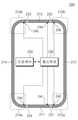
일 실시 예에 따르면, 전자 장치는 제1 플레이트, 제1 플레이트와 다른 방향을 향하는(facing away) 제2 플레이트, 및 제1 플레이트 및 제2 플레이트 사이의 공간을 둘러싸는 측면 부재를 포함하는 하우징을 포함할 수 있다. 제1 플레이트는, 예를 들어, 커버 글래스일 수 있다. 제2 플레이트는, 예를 들어, 백 커버(back cover)일 수 있다. 측면 부재는, 예를 들어, 금속 프레임일 수 있다. 일 실시 예에 따르면, 측면 부재는 제1 플레이트 위에서 바라볼 때 실질적으로 직사각형 형태를 함께 형성하는 복수의 도전성 부분 및 복수의 비도전성 부분을 포함할 수 있다. 전자 장치는 제1 플레이트의 일부를 통해 노출된 터치스크린 디스플레이를 더 포함할 수도 있다.According to an embodiment, an electronic device includes a housing including a first plate, a second plate facing away from the first plate, and a side member surrounding a space between the first plate and the second plate. may include The first plate may be, for example, a cover glass. The second plate may be, for example, a back cover. The side member may be, for example, a metal frame. According to an embodiment, the side member may include a plurality of conductive portions and a plurality of non-conductive portions that together form a substantially rectangular shape when viewed from above the first plate. The electronic device may further include a touch screen display exposed through a portion of the first plate.
도 2는 일 실시 예에 따른 전자 장치에 포함된 도전성 부분들을 나타낸다.2 illustrates conductive parts included in an electronic device according to an exemplary embodiment.
도 2를 참조하면, 일 실시 예에 따른 전자 장치(200)(예: 도 1의 전자 장치(101))는 복수의 도전성 부분들(211, 212, 213 및 214), 복수의 비도전성 부분들(221, 222, 223 및 224), 통신 회로 및 프로세서를 포함할 수 있다.Referring to FIG. 2 , an electronic device 200 (eg, the electronic device 101 of FIG. 1 ) according to an embodiment includes a plurality of
일 실시 예에 따르면, 제1 도전성 부분(211)은 전자 장치(200)의 제1 사이드에 위치될 수 있다. 제1 도전성 부분(211)은, 예를 들어, 전자 장치(200)의 제1 메인 안테나의 방사체로서 이용될 수 있다.According to an embodiment, the first
일 실시 예에 따르면, 제2 도전성 부분(212)은 전자 장치(200)의 제1 사이드와 인접한 제2 사이드에 위치될 수 있다. 제2 도전성 부분(212)의 일단은 제1 도전성 부분(211)의 일단에 인접하도록 배치될 수 있다. 제2 도전성 부분(212)의 제1 부분(212a)은, 예를 들어, 전자 장치(200)의 제2 메인 안테나의 방사체로서 이용될 수 있다. 제2 도전성 부분(212)의 제2 부분(212b)은, 예를 들어, 전자 장치(200)의 제3 서브 안테나의 방사체로서 이용될 수 있다.According to an embodiment, the second
일 실시 예에 따르면, 제3 도전성 부분(213)은 전자 장치(200)의 제1 사이드와 평행하고 제2 사이드와 인접한 제3 사이드에 위치될 수 있다. 제3 도전성 부분(213)의 일단은 제2 도전성 부분(212)의 타단에 인접하도록 배치될 수 있다. 제3 도전성 부분(213)은, 예를 들어, 전자 장치(200)의 제1 서브 안테나의 방사체로서 이용될 수 있다.According to an embodiment, the third
일 실시 예에 따르면, 제4 도전성 부분(214)은 전자 장치(200)의 제1 사이드 및 제3 사이드와 인접하고 제2 사이드와 평행한 제4 사이드에 위치될 수 있다. 제4 도전성 부분(214)의 일단은 제3 도전성 부분(213)의 타단에 인접하도록 배치될 수 있다. 제4 도전성 부분(214)의 타단은 제1 도전성 부분(211)의 타단에 인접하도록 배치될 수 있다. 제4 도전성 부분(214)의 제1 부분(214a)은, 예를 들어, 전자 장치(200)의 제3 메인 안테나의 방사체로서 이용될 수 있다. 제4 도전성 부분(214)의 제2 부분(214b)은, 예를 들어, 전자 장치(200)의 제2 서브 안테나의 방사체로서 이용될 수 있다.According to an embodiment, the fourth
본 문서에서 메인 안테나는 신호의 수신 및 송신(transmit)을 수행하는 안테나일 수 있고, 서브 안테나는 신호의 수신만을 수행하는 안테나일 수 있다.In this document, the main antenna may be an antenna that receives and transmits a signal, and the sub antenna may be an antenna that only receives a signal.
일 실시 예에 따르면, 제1 비도전성 부분(221)은 제1 도전성 부분(211)과 제2 도전성 부분(212) 사이에 개재될(interposed) 수 있다. 제2 비도전성 부분(222)은 제2 도전성 부분(212)과 제3 도전성 부분(213) 사이에 개재될 수 있다. 제3 비도전성 부분(223)은 제3 도전성 부분(213)과 제4 도전성 부분(214) 사이에 개재될 수 있다. 제4 비도전성 부분(224)은 제4 도전성 부분(214)과 제1 도전성 부분(211) 사이에 개재될 수 있다.According to an embodiment, the first
이하에서, 설명의 편의를 위해 제1 도전성 부분(211)을 제1 메인 안테나 방사체라 하고, 제2 도전성 부분(212)의 제1 부분(212a)을 제2 메인 안테나 방사체라 하고, 제4 도전성 부분(214)의 제1 부분(214a)을 제3 메인 안테나 방사체라 하고, 제3 도전성 부분(213)을 제1 서브 안테나 방사체라 하고, 제4 도전성 부분(214)의 제2 부분(214b)을 제2 서브 안테나 방사체라 하고, 제2 도전성 부분(212)의 제2 부분(212b)을 제3 서브 안테나 방사체라 한다.Hereinafter, for convenience of description, the first
일 실시 예에 따르면, 통신 회로(230)는 전자 장치(200)의 하우징 내부에 위치될 수 있다. 통신 회로(230)는 무선 통신을 수행하도록 구성된 회로일 수 있다. 도 2에서는 통신 회로(230)가 하나의 블록으로 도시되었으나, 이에 제한되지 않고, 통신 회로(230)는 하나 이상의 모듈을 포함할 수 있다.According to an embodiment, the
일 실시 예에 따르면, 통신 회로(230)는 제1 비도전성 부분에 근접한 제1 메인 안테나 방사체(211) 내의 제1 지점(241)과 전기적으로 연결될 수 있다. 통신 회로(230)는 제1 지점(241)을 통해 제1 메인 안테나 방사체(211)로 급전할 수 있다.According to an embodiment, the
일 실시 예에 따르면, 통신 회로(230)는 제1 비도전성 부분에 근접한 제2 메인 안테나 방사체(212a) 내의 제2 지점(242)과 전기적으로 연결될 수 있다. 통신 회로(230)는 제2 지점(242)을 통해 제2 메인 안테나 방사체(212a)로 급전할 수 있다.According to an embodiment, the
일 실시 예에 따르면, 통신 회로(230)는 제4 비도전성 부분에 근접한 제3 메인 안테나 방사체(214a) 내의 제3 지점(243)과 전기적으로 연결될 수 있다. 통신 회로(230)는 제3 지점(243)을 통해 제3 메인 안테나 방사체(214a)로 급전할 수 있다.According to an embodiment, the
일 실시 예에 따르면, 통신 회로(230)는 제1 서브 안테나 방사체(213) 내의 제4 지점(244)과 전기적으로 연결될 수 있다. 통신 회로(230)는 제4 지점(244)을 통해 제1 서브 안테나 방사체(213)로 급전할 수 있다.According to an embodiment, the
일 실시 예에 따르면, 통신 회로(230)는 제3 비도전성 부분에 근접한 제2 서브 안테나 방사체(214b) 내의 제5 지점(245)과 전기적으로 연결될 수 있다. 통신 회로(230)는 제5 지점(245)을 통해 제2 서브 안테나 방사체(214b)로 급전할 수 있다.According to an embodiment, the
일 실시 예에 따르면, 통신 회로(230)는 제2 비도전성 부분에 근접한 제3 서브 안테나 방사체(212b) 내의 제6 지점(246)과 전기적으로 연결될 수 있다. 통신 회로(230)는 제6 지점(246)을 통해 제3 서브 안테나 방사체(212b)로 급전할 수 있다.According to an embodiment, the
일 실시 예에 따르면, 통신 회로(230)는 고대역(HB) 신호, HB 신호의 주파수보다 낮은 주파수를 갖는 중대역(MB) 신호 및 MB 신호의 주파수보다 낮은 주파수를 갖는 저대역(LB) 신호를 포함하는 셀룰러 신호를 송신 및 수신할 수 있다. 통신 회로(230)는, 예를 들어, 제1 메인 안테나 방사체(211), 제2 메인 안테나 방사체(212a), 제3 메인 안테나 방사체(214a), 제1 서브 안테나 방사체(213), 제2 서브 안테나 방사체(214b) 및 제3 서브 안테나 방사체(212b) 중 적어도 일부를 이용하여 셀룰러 신호를 송신 및 수신할 수 있다.According to an embodiment, the
표 1은 다양한 실시 예에 따른 전자 장치(200)에 포함된 6개의 안테나에서 송신 또는 수신되는 신호의 대역을 나타낸다. 전자 장치(200)는 제1 메인 안테나 방사체(211), 제2 메인 안테나 방사체(212a) 및 제3 메인 안테나 방사체(214a)를 이용하여 신호를 송신 및 수신할 수 있다. 전자 장치(200)는 제1 서브 안테나 방사체(213), 제2 서브 안테나 방사체(214b) 및 제3 서브 안테나 방사체(212b)를 이용하여 신호를 수신할 수 있다.Table 1 shows bands of signals transmitted or received by six antennas included in the
본 문서에서, HB 신호는 약 2200MHz 내지 약 3500MHz 의 주파수 범위 내에 있을 수 있다. MB 신호는 약 1700MHZ 내지 약 2200MHz 의 주파수 범위 내에 있을 수 있다. LB 신호는 약 700MHz 내지 약 1000MHz 의 주파수 범위 내에 있을 수 있다. 본 문서에서, MB1-1 Tx 신호는 약 1710MHz 내지 약 1780MHz 의 주파수 범위 내에 있을 수 있다. MB1-1 Rx 신호는 약 2110MHz 내지 약 2200MHz 의 주파수 범위 내에 있을 수 있다. 본 문서에서, MB1-2 Tx 신호는 약 1850MHz 내지 약 1910MHz 의 주파수 범위 내에 있을 수 있다. MB1-2 Rx 신호는 약 1930MHz 내지 약 1990MHz 의 주파수 범위 내에 있을 수 있다. 본 문서에서, HB1-1 Tx 신호는 약 2305MHz 내지 약 2315MHz 의 주파수 범위 내에 있을 수 있다. HB1-1 Rx 신호는 약 2350MHz 내지 약 2360MHz 의 주파수 범위 내에 있을 수 있다. 본 문서에서, HB1-2 Tx 신호는 약 2500MHz 내지 약 2570MHz 의 주파수 범위 내에 있을 수 있다. HB1-2 Rx 신호는 약 2620MHz 내지 약 2690MHz 의 주파수 범위 내에 있을 수 있다.In this document, the HB signal may be in a frequency range of about 2200 MHz to about 3500 MHz. The MB signal may be in a frequency range of about 1700 MHz to about 2200 MHz. The LB signal may be in a frequency range of about 700 MHz to about 1000 MHz. In this document, the MB1-1 Tx signal may be in a frequency range of about 1710 MHz to about 1780 MHz. The MB1-1 Rx signal may be in a frequency range of about 2110 MHz to about 2200 MHz. In this document, the MB1-2 Tx signal may be in a frequency range of about 1850 MHz to about 1910 MHz. The MB1-2 Rx signal may be in a frequency range of about 1930 MHz to about 1990 MHz. In this document, the HB1-1 Tx signal may be in a frequency range of about 2305 MHz to about 2315 MHz. The HB1-1 Rx signal may be in a frequency range of about 2350 MHz to about 2360 MHz. In this document, the HB1-2 Tx signal may be in a frequency range of about 2500 MHz to about 2570 MHz. The HB1-2 Rx signal may be in a frequency range of about 2620 MHz to about 2690 MHz.
일 실시 예에 따르면, 통신 회로(230)는 제2 지점(242), 제3 지점(243), 제4 지점(244) 및 제5 지점(245)을 통해 MB 신호를 수신할 수 있다. 통신 회로(230)는 제1 지점(241) 및 제4 지점(244)을 통해 LB 신호를 수신하고, 제1 지점(241)을 통해 LB 신호를 송신할 수 있다. 예를 들어, 통신 회로(230)는 제2 메인 안테나 방사체(212a), 제3 메인 안테나 방사체(214a), 제1 서브 안테나 방사체(213), 제2 서브 안테나 방사체(214b)를 이용하여 MB 신호(MB 신호, MB1-1 신호 또는 MB1-2 신호)를 수신할 수 있다. 예를 들어, 통신 회로(230)는 제1 메인 안테나 방사체(211) 및 제1 서브 안테나 방사체(213)를 이용하여 LB 신호를 수신할 수 있고, 제1 메인 안테나 방사체(211)를 이용하여 LB 신호를 송신할 수 있다(#1-#6).According to an embodiment, the
일 실시 예에 따르면, 통신 회로(230)는 제2 지점(242)을 통해 MB 신호를 송신할 수 있다. 통신 회로(230)는 제2 지점(242), 제3 지점(243), 제5 지점(245) 및 제6 지점(246)을 통해 HB 신호를 수신하고, 제3 지점(243)을 통해 HB 신호를 송신할 수 있다. 예를 들어, 통신 회로(230)는 제2 메인 안테나 방사체(212a)를 이용하여 MB 신호를 송신할 수 있다. 통신 회로(230)는 제2 메인 안테나 방사체(212a), 제3 메인 안테나 방사체(214a), 제2 서브 안테나 방사체(214b) 및 제3 서브 안테나 방사체(212b)를 이용하여 HB 신호를 수신할 수 있다. 통신 회로(230)는 제3 메인 안테나 방사체(214a)를 통히 HB 신호를 송신할 수 있다(#1).According to an embodiment, the
일 실시 예에 따르면, 통신 회로(230)는 제3 지점(243)을 통해 MB 신호를 송신할 수 있다. 통신 회로(230)는 제2 지점(242), 제3 지점(243), 제5 지점(245) 및 제6 지점(246)을 통해 HB 신호를 수신하고, 제2 지점(242)을 통해 HB 신호를 송신할 수 있다. 예를 들어, 통신 회로(230)는 제3 메인 안테나 방사체(214a)를 통해 MB 신호를 송신할 수 있다. 통신 회로(230)는 제2 메인 안테나 방사체(212a), 제3 메인 안테나 방사체(214a), 제2 서브 안테나 방사체(214b) 및 제3 서브 안테나 방사체(212b)를 이용하여 HB 신호를 수신할 수 있다. 통신 회로(230)는 제2 메인 안테나 방사체(212a)를 이용하여 HB 신호를 송신할 수 있다(#2).According to an embodiment, the
일 실시 예에 따르면, 통신 회로(230)는 제1 지점(241)을 통해 MB 신호를 수신하고, 제1 지점(241) 및 제2 지점(242)을 통해 MB 신호를 송신할 수 있다. 통신 회로(230)는 제2 지점(242), 제3 지점(243), 제5 지점(245) 및 제6 지점(246)을 통해 HB 신호를 수신하고, 제3 지점(243)을 통해 HB 신호를 송신할 수 있다. 예를 들어, 통신 회로(230)는 제1 메인 안테나 방사체(211)를 이용하여 MB1-1 신호를 송신 및 수신할 수 있다. 통신 회로(230)는 제2 메인 안테나 방사체(212a)를 이용하여 MB1-2 신호를 송신 및 수신할 수 있다. 통신 회로(230)는 제2 메인 안테나 방사체(212a), 제3 메인 안테나 방사체(214a), 제2 서브 안테나 방사체(214b) 및 제3 서브 안테나 방사체(212b)를 이용하여 HB 신호를 수신할 수 있다. 통신 회로(230)는 제3 메인 안테나 방사체(214a)를 이용하여 HB 신호를 송신할 수 있다(#3).According to an embodiment, the
일 실시 예에 따르면, 통신 회로(230)는 제2 지점(242) 및 제3 지점(243)을 통해 MB 신호를 송신할 수 있다. 통신 회로(230)는 제2 지점(242), 제3 지점(243), 제5 지점(245) 및 제6 지점(246)을 통해 HB 신호를 수신하고, 제3 지점(243)을 통해 HB 신호를 송신할 수 있다. 예를 들어, 통신 회로(230)는 제2 메인 안테나 방사체(212a)를 이용하여 MB1-1 신호를 송신 및 수신할 수 있다. 통신 회로(230)는 제3 메인 안테나 방사체(214a)를 이용하여 MB1-2 신호를 송신하고 MB 신호를 수신할 수 있다. 통신 회로(230)는 제2 메인 안테나 방사체(212a), 제3 메인 안테나 방사체(214a), 제2 서브 안테나 방사체(214b) 및 제3 서브 안테나 방사체(212b)를 이용하여 HB 신호를 수신할 수 있다. 통신 회로(230)는 제3 메인 안테나 방사체(214a)를 이용하여 HB 신호를 송신할 수 있다(#4).According to an embodiment, the
일 실시 예에 따르면, 통신 회로(230)는 제1 지점(241), 제2 지점(242), 제3 지점(243), 제5 지점(245) 및 제6 지점(246)을 통해 HB 신호를 수신하고, 제1 지점(241) 및 제3 지점(243)을 통해 HB 신호를 송신할 수 있다. 예를 들어, 통신 회로(230)는 제1 메인 안테나 방사체(211)를 이용하여 HB1-1 신호를 송신 및 수신할 수 있다. 통신 회로(230)는 제3 메인 안테나 방사체(214a)를 이용하여 HB1-2 신호를 송신 및 수신할 수 있다. 통신 회로(230)는 제2 메인 안테나 방사체(212a), 제2 서브 안테나 방사체(214b) 및 제3 서브 안테나 방사체(212b)를 이용하여 HB 신호를 수신할 수 있다(#5).According to an embodiment, the
일 실시 예에 따르면, 통신 회로(230)는 제2 지점(242), 제3 지점(243), 제5 지점(245) 및 제6 지점(246)을 통해 HB 신호를 수신하고, 제2 지점(242) 및 제3 지점(243)을 통해 HB 신호를 송신할 수 있다. 예를 들어, 통신 회로(230)는 제2 메인 안테나 방사체(212a)를 이용하여 HB1-1 신호를 송신하고, HB 신호를 수신할 수 있다. 통신 회로(230)는 제3 메인 안테나 방사체(214a)를 이용하여 HB1-2 신호를 송신 및 수신할 수 있다. 통신 회로(230)는 제2 서브 안테나 방사체(214b) 및 제3 서브 안테나 방사체(212b)를 이용하여 HB 신호를 수신할 수 있다(#6).According to an embodiment, the
안테나 방사체 각각에 대해 표 1에 기재되지 않은 다양한 형태로 주파수 대역이 할당될 수 있다. 다만, 상술한 바와 같이, 제1 메인 안테나 방사체(211)에 의해 커버되는 주파수 대역과 제2 메인 안테나 방사체(212a)에 의해 커버되는 주파수 대역은 상이할 수 있다. 또 다른 예로, 제1 메인 안테나 방사체(211)에 커버되는 주파수 대역과 제3 메인 안테나 방사체(214a)에 커버되는 주파수 대역은 상이할 수 있다. 또 다른 예로, 제2 메인 안테나 방사체(212a)에 의해 송신되는 신호의 주파수 대역과 제3 메인 안테나 방사체(214a)에 의해 송신되는 신호의 주파수 대역은 상이할 수 있다. 이로써, MB 신호 및 HB 신호에 대한 4Rx가 구현될 수 있다.A frequency band may be allocated in various forms not described in Table 1 for each of the antenna radiators. However, as described above, the frequency band covered by the first
일 실시 예에 따르면, 전자 장치(200)에 포함된 복수의 안테나 방사체는 아래와 같은 LTE band를 커버하도록 구성될 수 있다. 제1 메인 안테나 방사체(211)는, 예를 들어, LTE B12, B17, B13, B5, B26, B2, B4, B66, B25, CDMA BC0, BC10 및 BC1를 커버하도록 구성될 수 있다. 제2 메인 안테나 방사체(212a)는, 예를 들어, LTE B30 및 B41을 커버하도록 구성될 수 있다. 제3 메인 안테나 방사체(214a)는, 예를 들어, LTE B2, B4, B66 및 B30을 커버하도록 구성될 수 있다. 제1 서브 안테나 방사체(213)는, 예를 들어, LTE B12, B17, B13, B5, B26, B2, B4, B66, B25, CDMA BC0 및 BC10을 커버하도록 구성될 수 있다. 제2 서브 안테나 방사체(214b)는, 예를 들어, LTE B2, B4, B66, B25, B30, B41을 커버하도록 구성될 수 있다. 제3 서브 안테나 방사체(212b)는, 예를 들어, B30을 커버하도록 구성될 수 있다.According to an embodiment, the plurality of antenna radiators included in the
일 실시 예에 따르면, 프로세서(250)는 전자 장치(200)의 하우징 내부에 위치될 수 있다. 프로세서(250)는 통신 회로(230)와 전기적으로 연결될 수 있다. 프로세서(250)는 통신 회로(230) 및 전자 장치(200)의 다른 구성들을 제어할 수 있다.According to an embodiment, the
상술한 바와 같이, 4Rx를 위해 전자 장치(200)는 2개의 메인 안테나 방사체 및 2개의 서브 안테나 방사체를 이용할 수 있다. 서브 안테나의 경우 이득(gain)이 낮더라도 별도의 LNA(low noise amplifier)를 채용함으로써 낮은 이득으로 인한 문제가 해결될 수 있다. 신호의 송신을 수행하는 메인 안테나 방사체의 경우 별도의 LNA를 채용할 수 없으므로, 이득을 향상시키기 위해 2개의 메인 안테나 방사체가 충분히 전기적으로 격리될 필요가 있다.As described above, for 4Rx, the
도 3은 일 실시 예에 따른 전자 장치에 포함된 안테나의 구조를 개략적으로 나타낸다.3 schematically illustrates a structure of an antenna included in an electronic device according to an exemplary embodiment.
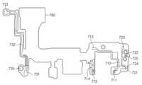
도 3을 참조하면, 일 실시 예에 따른 전자 장치(예: 도 2의 전자 장치(200))는 제1 안테나 방사체(311), 제2 안테나 방사체(312), 제3 안테나 방사체(313), 제1 급전부(321), 제2 급전부(322), 제3 급전부(323), 제1 접지부(331a), 제2 접지부(331b), 제3 접지부(332), 제4 접지부(334), 제1 스위칭 회로(341), 제2 스위칭 회로(342), 제3 스위칭 회로(343), 가변 회로(tunable circuit)(350), USB 포트(360) 및 이어 잭(ear jack)(370)을 포함할 수 있다. 제1 안테나 방사체(311), 제2 안테나 방사체(312) 및 제3 안테나 방사체(313)는 각각 도 2의 제1 메인 안테나 방사체(211), 제2 메인 안테나 방사체(212a) 및 제3 메인 안테나 방사체(214a)와 대응할 수 있다.Referring to FIG. 3 , an electronic device (eg, the
일 실시 예에 따르면, 제1 안테나 방사체(311)는 제1 대역에서 공진하도록 구성될 수 있다. 제1 안테나 방사체(311)는 전자 장치의 일단의 중앙에 배치될 수 있다. 제1 안테나 방사체(311)는 좌우로 길게 연장된(elongated) 형상으로 이루어질 수 있다.According to an embodiment, the
일 실시 예에 따르면, 제2 안테나 방사체(312)는 제1 대역보다 높은 제2 대역 및 제3 대역에서 공진하도록 구성될 수 있다. 제2 안테나 방사체(312)는 제1 안테나 방사체(311)와의 격리를 위해 제1 안테나 방사체(311)와 상이한 주파수 대역을 지원할 수 있다. 제2 안테나 방사체(312)는 제1 안테나 방사체(311)와 이격되도록 배치될 수 있다. 제2 안테나 방사체(312)의 일단은 제1 안테나 방사체(311)의 일단에 인접하도록 배치될 수 있다.According to an embodiment, the
일 실시 예에 따르면, 제3 안테나 방사체(313)는 제2 대역 및 제3 대역에서 공진하도록 구성될 수 있다. 제3 안테나 방사체(313)는 제1 안테나 방사체(311)와의 격리를 위해 제1 안테나 방사체(311)와 상이한 주파수 대역을 지원할 수 있다. 제3 안테나 방사체(313)는 제1 안테나 방사체(311) 및 제2 안테나 방사체(312)와 이격되도록 배치될 수 있다. 예를 들어, 제3 안테나 방사체(313)의 일단은 제1 안테나 방사체(311)의 타단과 인접하도록 배치될 수 있다.According to an embodiment, the
일 실시 예에 따르면, 제1 급전부(321)는 통신 회로(예: 도 2의 통신 회로(230))와 제1 안테나 방사체(311)를 전기적으로 연결할 수 있다. 예를 들어, 제1 급전부(321)는 제1 안테나 방사체(311)의 일단과 인접한 제1 안테나 방사체(311)의 플랜지와 전기적으로 연결될 수 있다.According to an embodiment, the first
일 실시 예에 따르면, 제1 급전부(321)는 가변 회로(350)를 통해 제1 안테나 방사체(311)와 전기적으로 연결될 수 있다. 가변 회로(350)는, 예를 들어, 커패시터 및/또는 인덕터 등과 같은 소자를 포함할 수 있다. 가변 회로(350)의 임피던스 값은 튜닝될 수 있다. 가변 회로(350)를 튜닝함으로써 제1 안테나 방사체(311)의 공진 주파수가 조절될 수 있다. 가변 회로(350)의 튜닝은 제2 안테나 방사체(312) 및/또는 제3 안테나 방사체(313)에 영향을 미칠 수도 있다.According to an embodiment, the first
일 실시 예에 따르면, 제2 급전부(322)는 통신 회로와 제2 안테나 방사체(312)를 전기적으로 연결할 수 있다. 예를 들어, 제2 급전부(322)는 제2 안테나의 일단과 인접한 제2 안테나 방사체(312)의 플랜지와 전기적으로 연결될 수 있다.According to an embodiment, the second
일 실시 예에 따르면, 제2 급전부(322)는 제2 스위칭 회로(342)를 통해 제2 안테나 방사체(312)와 전기적으로 연결될 수 있다. 제2 스위칭 회로(342)의 동작에 의해 제2 안테나 방사체(312)의 공진 주파수가 조절될 수 있다. 제2 스위칭 회로(342)의 동작은 제1 안테나 방사체(311) 및/또는 제3 안테나 방사체(313)에 영향을 미칠 수도 있다. 제2 스위칭 회로(342)에 대해서는 아래에서 도 9 및 도 10을 참조하여 상세히 설명한다.According to an embodiment, the second
일 실시 예에 따르면, 제3 급전부(323)는 통신 회로와 제3 안테나 방사체(313)를 전기적으로 연결할 수 있다. 예를 들어, 제3 급전부(323)는 제3 안테나의 일단과 인접한 제3 안테나 방사체(313)의 플랜지와 전기적으로 연결될 수 있다.According to an embodiment, the third
일 실시 예에 따르면, 제3 급전부(323)는 제3 스위칭 회로(343)를 통해 제3 안테나 방사체(313)와 전기적으로 연결될 수 있다. 제3 스위칭 회로(343)의 동작에 의해 제3 안테나 방사체(313)의 공진 주파수가 조절될 수 있다. 제3 스위칭 회로(343)의 동작은 제1 안테나 방사체(311) 및/또는 제2 안테나 방사체(312)에 영향을 미칠 수도 있다. 제3 스위칭 회로(343)에 대해서는 아래에서 도 9 및 도 10을 참조하여 상세히 설명한다.According to an embodiment, the third
일 실시 예에 따르면, 제1 접지부(331a) 또는 제2 접지부(331b)는 제1 안테나 방사체(311)와 전기적으로 연결될 수 있다. 제1 접지부(331a) 또는 제2 접지부(331b)는 제1 안테나 방사체(311)의 일 지점으로부터 연장된 제1 안테나 방사체(311)의 플랜지와 전기적으로 연결될 수 있다. 제1 접지부(331a) 또는 제2 접지부(331b)는 제1 스위칭 회로(341)를 통해 제1 안테나 방사체(311)와 전기적으로 연결될 수 있다. 제1 스위칭 회로(341)는 제1 접지부(331a) 또는 제2 접지부(331b)를 제1 안테나 방사체(311)와 선택적으로 연결할 수 있다. 제1 스위칭 회로(341)는, 예를 들어, 하나 이상의 집중 소자(lumped element)를 포함할 수 있다. 제1 스위칭 회로(341)의 동작에 의해 제1 안테나 방사체(311)의 공진 주파수가 조절될 수 있다. 제1 스위칭 회로(341)의 동작은 제2 안테나 방사체(312) 및/또는 제3 안테나 방사체(313)에 영향을 미칠 수도 있다.According to an embodiment, the
일 실시 예에 따르면, 제3 접지부(332)는 제2 안테나 방사체(312)와 전기적으로 연결될 수 있다. 예를 들어, 제3 접지부(332)는 제2 안테나 방사체(312)의 타단과 전기적으로 연결될 수 있다.According to an embodiment, the
일 실시 예에 따르면, 제4 접지부(333)는 제3 안테나 방사체(313)와 전기적으로 연결될 수 있다. 예를 들어, 제4 접지부(333)는 제3 안테나 방사체(313)의 타단과 전기적으로 연결될 수 있다.According to an embodiment, the
일 실시 예에 따르면, USB 포트(360)는 제1 안테나 방사체(311)의 중앙 부분에 인접하게 배치될 수 있다. USB 포트(360)는, 예를 들어, 제1 안테나 방사체(311)의 중앙 부분에 형성된 개구(opening)를 통해 노출될 수 있다.According to an embodiment, the
일 실시 예에 따르면, 이어 잭(370)은 제1 접지부(331a) 또는 제2 접지부(331b)와 제1 급전부(321) 사이에 배치될 수 있다. 이어 잭(370)은, 예를 들어, 제1 안테나 방사체(311)에 형성된 개구를 통해 노출될 수 있다.According to an embodiment, the
일 실시 예에 따르면, 제1 안테나 방사체(311), 제1 급전부(321) 및 제1 접지부(331a), 또는 제1 안테나 방사체(311), 제1 급전부(321) 및 제2 접지부(331b)는 IFA(inverted F antenna)를 구성할 수 있다. 일 실시 예에 따르면, 제2 안테나 방사체(312), 제2 급전부(322) 및 제3 접지부(332)는 루프 안테나 또는 IFA를 구성할 수 있다. 일 실시 예에 따르면, 제3 안테나 방사체(313), 제3 급전부(323) 및 제4 접지부(334)는 루프 안테나, IFA 또는 모노폴(monopole) 안테나를 구성할 수 있다.According to an embodiment, the
일 실시 예에 따르면, 통신 회로는 제2 안테나 방사체(312)를 이용하여 제2 대역의 신호를 송신 및 수신하는 동안, 제3 안테나 방사체(313)를 이용하여 제2 대역의 신호를 수신할 수 있다. 예를 들어, 통신 회로는 제2 안테나 방사체(312)를 이용하여 MB 신호를 송신 및 수신하는 동안, 제3 안테나 방사체(313)를 이용하여 MB 신호를 수신할 수 있다. 이 경우, 통신 회로는 제1 안테나 방사체(311)를 이용하여 LB 신호를 송신 및 수신할 수 있다. 제1 안테나 방사체(311)가 제1 안테나 방사체(311)와 인접한 제2 안테나 방사체(312) 및 제3 안테나 방사체(313)와 상이한 주파수 대역을 커버하므로, 제1 안테나 방사체(311)와 제2 안테나 방사체(312) 또는 제1 안테나 방사체(311)와 제3 안테나 방사체(313)는 전기적으로 격리될 수 있다. 또 다른 예로, 제2 안테나 방사체(312)와 제3 안테나 방사체(313) 사이의 거리로 인해 제2 안테나 방사체(312)와 제3 안테나 방사체(313)는 전기적으로 충분히 격리될 수 있다.According to an embodiment, the communication circuit may receive a signal of the second band using the
일 실시 예에 따르면, 통신 회로는 제3 안테나 방사체(313)를 이용하여 제3 대역의 신호를 송신 및 수신하는 동안, 제2 안테나 방사체(312)를 이용하여 제3 대역의 신호를 수신할 수 있다. 예를 들어, 통신 회로는 제3 안테나 방사체(313)를 이용하여 HB 신호를 송신 및 수신하는 동안, 제2 안테나 방사체(312)를 이용하여 HB 신호를 수신할 수 있다. 이 경우, 통신 회로는 제1 안테나 방사체(311)를 이용하여 LB 신호를 송신 및 수신할 수 있다.According to an embodiment, the communication circuit may receive a signal of the third band using the
도 4는 일 실시 예에 따른 전자 장치의 하단의 내부 구조를 나타낸다.4 illustrates an internal structure of a lower end of an electronic device according to an exemplary embodiment.
도 4를 참조하면, 일 실시 예에 따른 전자 장치(예: 도 2의 전자 장치(200))는 제1 프레임(411), 제2 프레임(412), 제3 프레임(413b), 도전성 패턴(413a) 및 기판(420)을 포함할 수 있다. 제1 프레임(411)의 도전성 부분은 도 3의 제1 안테나 방사체(311)에 대응할 수 있다. 제2 프레임(412)의 도전성 부분은 도 3의 제2 안테나 방사체(312)에 대응할 수 있다. 제3 프레임(413b)의 도전성 부분 및/또는 도전성 패턴(413a)은 도 3의 제3 안테나 방사체(313)에 대응할 수 있다.Referring to FIG. 4 , an electronic device (eg, the
일 실시 예에 따르면, 제1 프레임(411)은 전자 장치의 하단 중앙에 위치될 수 있다. 제1 프레임(411)은, 예를 들어, 전자 장치의 측면 프레임의 일부일 수 있다. 제1 프레임(411)의 적어도 일부는 도전성 물질을 포함할 수 있다.According to an embodiment, the
일 실시 예에 따르면, 제2 프레임(412)은 제1 프레임(411)의 일단에 인접하도록 배치될 수 있다. 제2 프레임(412)은, 예를 들어, 전자 장치의 측면 프레임의 일부일 수 있다. 제2 프레임(412)의 적어도 일부는 도전성 물질을 포함할 수 있다.According to an embodiment, the
일 실시 예에 따르면, 제3 프레임(413b)은 제1 프레임(411)의 타단에 인접하도록 배치될 수 있다. 제3 프레임(413b)은, 예를 들어, 전자 장치의 측면 프레임의 일부일 수 있다. 제3 프레임(413b)의 적어도 일부는 도전성 물질을 포함할 수 있다.According to an embodiment, the
일 실시 예에 따르면, 도전성 패턴(413a)은 기판(420) 상에 형성될 수 있다. 예를 들어, 도전성 패턴(413a)은 제3 프레임(413b)과 인접한 기판(420)의 영역 상에 인쇄될 수 있다. 도전성 패턴(413a)은, 예를 들어, 선택적 구성요소로서 본 발명의 구현 형태에 따라 생략될 수도 있다.According to an embodiment, the
일 실시 예에 따르면, 제3 프레임(413b) 및/또는 도전성 패턴(413a)은 안테나 방사체로서 이용될 수 있다. 예를 들어, 제3 프레임(413b)이 안테나 방사체로서 이용되고, 도전성 패턴(413a)은 생략될 수 있다. 다른 예를 들면, 도전성 패턴(413a)이 안테나 방사체로서 이용될 수 있다. 또 다른 예를 들면, 도전성 패턴(413a)이 제3 프레임(413b)과 전기적으로 연결되고, 도전성 패턴(413a) 및 제3 프레임(413b)이 안테나 방사체로서 이용될 수 있다.According to an embodiment, the
도 5는 일 실시 예에 따른 전자 장치의 하단의 내부 구조를 나타낸다.5 illustrates an internal structure of a lower end of an electronic device according to an exemplary embodiment.
도 5를 참조하면, 일 실시 예에 따른 전자 장치는 제1 프레임(511), 제1 도전성 패턴(512), 제2 프레임(520), 제2 도전성 패턴(530), 제1 비도전성 부재(541), 제2 비도전성 부재(542) 및 인쇄 회로 기판(550)을 포함할 수 있다. 제1 프레임(511)의 도전성 부분 및 제1 도전성 패턴(512)은 도 3의 제1 안테나 방사체(311)에 대응할 수 있다. 제2 프레임(520)의 도전성 부분은 도 3의 제2 안테나 방사체(312)에 대응할 수 있다. 제2 도전성 패턴(530)은 도 3의 제3 안테나 방사체(313)에 대응할 수 있다.Referring to FIG. 5 , an electronic device according to an embodiment includes a
일 실시 예에 따르면, 제1 프레임(511)은 전자 장치의 하단 중앙에 위치될 수 있다. 제1 프레임(511)은, 예를 들어, 전자 장치의 측면 프레임의 일부일 수 있다. 제1 도전성 패턴(512)은 제1 프레임(511)과 인접한 인쇄 회로 기판(550)의 영역 상에 인쇄될 수 있다. 제1 프레임(511)은 제1 도전성 패턴(512)과 전기적으로 연결될 수 있다. 제1 프레임(511) 및 제1 도전성 패턴(512)은 전자 장치의 안테나 방사체로서 이용될 수 있다. 제1 프레임(511) 및 제1 도전성 패턴(512)은, 예를 들어, LB 및 MB를 커버할 수 있다.According to an embodiment, the
일 실시 예에 따르면, 제2 프레임(520)은 제1 프레임(511)의 일단에 인접하도록 배치될 수 있다. 제2 프레임(520)은, 예를 들어, 전자 장치의 측면 프레임의 일부일 수 있다. 제2 프레임(520)은 전자 장치의 안테나 방사체로서 이용될 수 있다. 제2 프레임(520)은, 예를 들어, MB 및 HB를 커버할 수 있다.According to an embodiment, the
일 실시 예에 따르면, 제1 비도전성 부재(541)는 제1 프레임(511)의 일단에 접촉되도록 배치될 수 있다. 제1 비도전성 부재(541)는 제1 프레임(511)과 제2 프레임(520) 사이에 개재될 수 있다.According to an embodiment, the first
일 실시 예에 따르면, 제2 비도전성 부재(542)는 제1 프레임(511)의 타단에 접촉되도록 배치될 수 있다. 제2 비도전성 부재(542)는 제1 프레임(511)과 측면 프레임의 다른 부분 사이에 개재될 수 있다.According to an embodiment, the second
일 실시 예에 따르면, 제2 도전성 패턴(530)은 인쇄 회로 기판(550) 상에 형성될 수 있다. 예를 들어, 제2 도전성 패턴(530)은 제1 프레임(511) 및 제2 프레임(520)과 일정 거리가 떨어진 영역에 인쇄될 수 있다. 제2 도전성 패턴(530)은 전자 장치의 안테나 방사체로서 이용될 수 있다. 제2 도전성 패턴(530)은, 예를 들어, HB를 커버할 수 있다.According to an embodiment, the second
일 실시 예에 따르면, 제1 프레임(511) 및 제1 도전성 패턴(512)은, 예를 들어, 제1 지점(560)을 통해 급전될 수 있다. 제1 프레임(511) 및 제1 도전성 패턴(512)은 제1 지점(560)을 통해 통신 회로(예: 도 2의 통신 회로(230))와 전기적으로 연결될 수 있다. 제2 프레임(520)은, 예를 들어, 제2 지점(570)을 통해 급전될 수 있다. 제2 프레임(520)은 제2 지점(570)을 통해 통신 회로와 전기적으로 연결될 수 있다. 제2 도전성 패턴(530)는, 예를 들어, 제3 지점(580)을 통해 급전될 수 있다. 제2 도전성 패턴(530)는 제3 지점(580)을 통해 통신 회로와 전기적으로 연결될 수 있다.According to an embodiment, the
도 6은 일 실시 예에 따른 전자 장치의 구조를 개략적으로 나타낸다.6 schematically illustrates a structure of an electronic device according to an exemplary embodiment.
도 6을 참조하면, 일 실시 예에 따른 전자 장치(예: 도 2의 전자 장치(200))는 제1 프레임(611), 제2 프레임(612), 제3 프레임(613), 도전성 패턴(620), 제1 급전점(631), 제2 급전점(632), 제3 급전점(633), 제1 접지점(641), 제2 접지점(642), 제1 PCB(650), 제1 리셉터클(651), 제2 리셉터클(652), 제2 PCB(660), 제3 리셉터클(661), 제4 리셉터클(662), 제5 리셉터클(663), 제3 PCB(670), 제1 전송 선로(681), 제2 전송 선로(682), 제1 FPCB(691), 제2 FPCB(692) 및 통신 회로(695)를 포함할 수 있다.Referring to FIG. 6 , an electronic device (eg, the
일 실시 예에 따르면, 제1 프레임(611), 제2 프레임(612), 제3 프레임(613) 및 도전성 패턴(620)은 각각 도 4의 제1 프레임(411), 제2 프레임(412), 제3 프레임(413b) 및 도전성 패턴(413a)에 대응할 수 있다.According to an embodiment, the
일 실시 예에 따르면, 제1 PCB(650)는 제1 리셉터클(651) 및 제2 리셉터클(652)을 포함할 수 있다. 제1 리셉터클(651)은 제1 전송 선로(681)를 수용하도록 구성될 수 있다. 제2 리셉터클(652)은 제2 전송 선로(682)를 수용하도록 구성될 수 있다. 제1 리셉터클(651)은 제1 급전점(631)과 전기적으로 연결될 수 있다. 제2 리셉터클(652)은 제2 급전점(632)과 전기적으로 연결될 수 있다.According to an embodiment, the
일 실시 예에 따르면, 제2 PCB(660)는 제3 리셉터클(661), 제4 리셉터클(662) 및 제5 리셉터클(663)을 포함할 수 있다. 제3 리셉터클(661)은 제2 전송 선로(682)를 수용하도록 구성될 수 있다. 제4 리셉터클(662)은 제1 전송 선로(681)를 수용하도록 구성될 수 있다. 제5 리셉터클(663)은 제2 FPCB(692) 및 제3 PCB(670)를 통해 제3 급전점(633)과 전기적으로 연결될 수 있다. 제3 리셉터클(661), 제4 리셉터클(662) 및 제5 리셉터클(663)은 통신 회로(695)와 전기적으로 연결될 수 있다. 도 6에서는 제2 PCB(660)가 3개의 리셉터클(661, 662 및 663)을 포함하는 것으로 도시되었으나, 이에 제한되지 않고, 제3 리셉터클(661), 제4 리셉터클(662) 및 제5 리셉터클(663) 중 적어도 일부는 하나의 리셉터클로 통합될 수도 있다.According to an embodiment, the
일 실시 예에 따르면, 제3 PCB(670)는 제1 FPCB(691)를 통해 제1 PCB(650)와 연결될 수 있고, 제2 FPCB(692)를 통해 제2 PCB(660)와 연결될 수 있다.According to an embodiment, the
도 6에서는 전자 장치가 2개의 FPCB(691 및 692)로 서로 연결된 3개의 PCB(650, 660 및 670)를 포함하는 것으로 도시되었으나, 이에 제한되지 않고, 제1 PCB(650), 제2 PCB(660) 및 제3 PCB(670) 중 적어도 일부는 하나의 기판으로 통합될 수도 있다.In FIG. 6 , the electronic device is illustrated as including three
일 실시 예에 따르면, 제1 프레임(611)은 제1 급전점(631)을 통해 급전될 수 있다. 제1 프레임(611)은 제1 급전점(631)을 통해 통신 회로(695)와 전기적으로 연결될 수 있다. 예를 들어, 제1 프레임(611)은 제1 급전점(631), 제1 리셉터클(651), 제1 전송 선로(681) 및 제4 리셉터클(662)을 통해 통신 회로(695)와 전기적으로 연결될 수 있다. 제1 프레임(611)은 제1 접지점(641)을 통해 접지될 수 있다. 제1 프레임(611)은 IFA의 방사체로 이용될 수 있다.According to an embodiment, the
일 실시 예에 따르면, 제2 프레임(612)은 제2 급전점(632)을 통해 급전될 수 있다. 제2 프레임(612)은 제2 급전점(632)을 통해 통신 회로(695)와 전기적으로 연결될 수 있다. 예를 들어, 제2 프레임(612)은 제2 급전점(632), 제2 리셉터클(652), 제2 전송 선로(682) 및 제3 리셉터클(661)을 통해 통신 회로(695)와 전기적으로 연결될 수 있다. 제2 프레임(612)은 제2 접지점(642)을 통해 접지될 수 있다. 제2 프레임(612)은 IFA 또는 루프 안테나의 방사체로 이용될 수 있다.According to an embodiment, the
일 실시 예에 따르면, 도전성 패턴(620)은 제3 급전점(633)을 통해 급전될 수 있다. 제3 프레임(613)은 제3 급전점(633)을 통해 통신 회로(695)와 전기적으로 연결될 수 있다. 예를 들어, 제3 프레임(613)은 제3 급전점(633) 및 제5 리셉터클(663)을 통해 통신 회로(695)와 전기적으로 연결될 수 있다. 제3 프레임(613)은 모노폴 안테나의 방사체로 이용될 수 있다.According to an embodiment, the
도 7은 일 실시 예에 따른 전자 장치에 포함된 인쇄 회로 기판을 나타낸다.7 illustrates a printed circuit board included in an electronic device according to an exemplary embodiment.
도 7을 참조하면, 일 실시 예에 따른 전자 장치의 인쇄 회로 기판(700)은 제1 급전점(711), 제1 급전 라인(712), 제1 연결부(713), 제1 스위칭 회로(714), 제1 접지점(715), 제2 급전점(721), 제2 급전 라인(722), 제2 연결부(723), 제2 스위칭 회로(724), 제2 접지점(725), 제3 급전점(731), 제3 급전 라인(732), 제3 연결부(733) 및 제3 접지점(735)을 포함할 수 있다.Referring to FIG. 7 , a printed
일 실시 예에 따르면, 제1 급전점(711)은 제1 안테나 방사체(예: 도 3의 제1 안테나 방사체(311))의 일 지점과 전기적으로 연결될 수 있다. 제1 급전점(711)은 제1 급전 라인(712)을 통해 제1 연결부(713)와 전기적으로 연결될 수 있다. 제1 연결부(713)는 케이블(예: 도 6의 제1 전송 선로(681))을 통해 통신 회로(예: 도 6의 통신 회로(695))와 전기적으로 연결될 수 있다. 제1 접지점(715)은 제1 안테나 방사체의 다른 지점과 전기적으로 연결될 수 있다. 제1 접지점(715)은, 예를 들어, 제1 스위칭 회로(714)(예: 도 3의 제1 스위칭 회로(341))를 통해 제1 안테나 방사체의 다른 지점과 전기적으로 연결될 수 있다.According to an embodiment, the
일 실시 예에 따르면, 제2 급전점(721)은 제2 안테나 방사체(예: 도 3의 제2 안테나 방사체(312))의 일 지점과 전기적으로 연결될 수 있다. 제2 급전점(721)은, 예를 들어, 제2 스위칭 회로(724)(예: 도 3의 제2 스위칭 회로(342))를 통해 제2 안테나 방사체의 일 지점과 전기적으로 연결될 수 있다. 제2 급전점(721)은 제2 급전 라인(722)을 통해 제2 연결부(723)와 전기적으로 연결될 수 있다. 제2 연결부(723)는 케이블(예: 도 6의 제2 전송 선로(682))을 통해 통신 회로와 전기적으로 연결될 수 있다. 제2 접지점(725)은 제2 안테나 방사체의 다른 지점과 전기적으로 연결될 수 있다.According to an embodiment, the
일 실시 예에 따르면, 제1 급전점(711)은 제2 급전점(721)과 인접할 수 있다. 제1 급전점(711)은 제2 안테나 방사체와 인접한 제1 안테나 방사체의 일 지점과 전기적으로 연결될 수 있다. 제2 급전점(721)은 제1 안테나 방사체와 인접한 제2 안테나 방사체의 일 지점과 전기적으로 연결될 수 있다.According to an embodiment, the
일 실시 예에 따르면, 제3 급전점(731)은 제3 안테나 방사체(예: 도 3의 제3 안테나 방사체(313))의 일 지점과 전기적으로 연결될 수 있다. 제3 급전점(731)은 제3 급전 라인(732)을 통해 제3 연결부(733)와 전기적으로 연결될 수 있다. 제3 연결부(733)는 케이블을 통해 통신 회로와 전기적으로 연결될 수 있다. 제3 접지부는 제3 안테나 방사체의 다른 지점과 전기적으로 연결될 수 있다.According to an embodiment, the
도 8은 일 실시 예에 따른 전자 장치에 채용된 커플링 급전 구조를 개략적으로 나타낸다.8 schematically illustrates a coupling power supply structure employed in an electronic device according to an exemplary embodiment.
도 8을 참조하면, 일 실시 예에 따른 전자 장치(예: 도 2의 전자 장치(200))는 안테나 방사체(810), 인쇄 회로 기판(820), 제1 도전성 패드(830), 제2 도전성 패드(840), 연결 부재(850) 및 급전부(860)를 포함할 수 있다.Referring to FIG. 8 , an electronic device (eg, the
안테나 방사체(810)는, 예를 들어, 도 3의 제1 안테나 방사체(311), 제2 안테나 방사체(312) 또는 제3 안테나 방사체(313) 중 하나일 수 있다.The
인쇄 회로 기판(820)은 안테나 방사체(810)를 포함하는 전자 장치의 측면 프레임에 의해 형성되는 공간 내에 배치될 수 있다.The printed
일 실시 예에 따르면, 제1 도전성 패드(830)는 인쇄 회로 기판(820)의 일면에 배치될 수 있다. 제2 도전성 패드(840)는 제1 도전성 패드(830)와 이격되되, 제1 도전성 패드(830)와 전기적으로 커플링될 수 있다. 제1 도전성 패드(830) 및 제2 도전성 패드(840)는 커패시터와 같이 기능할 수 있다.According to an embodiment, the first
일 실시 예에 따르면, 연결 부재(850)는 제1 도전성 패드(830)를 안테나 방사체(810)와 연결할 수 있다. 연결 부재(850)는, 예를 들어, C-클립, 스프링, 스크류 또는 도전성 폼(foam) 등과 같은 도전성 탄성 부재일 수 있다.According to an embodiment, the
일 실시 예에 따르면, 급전부(860)는 제2 도전성 패드(840)와 전기적으로 연결될 수 있다. 급전부(860)는 제2 도전성 패드(840)를 통신 회로(예: 도 6의 통신 회로(695))와 전기적으로 연결시킬 수 있다.According to an embodiment, the
일 실시 예에 따르면, 안테나 방사체(810)는 연결 부재(850), 제1 도전성 패드(830), 제2 도전성 패드(840) 및 급전부(860)를 통해 통신 회로와 전기적으로 연결될 수 있다. 안테나 방사체(810)는 제1 도전성 패드(830) 및 제2 도전성 패드(840)를 통해 커플링 급전될 수 있다. 제1 도전성 패드(830) 및 제2 도전성 패드(840)에 의해 형성되는 커패시턴스로 인해, 안테나 방사체(810)에 의해 지원되는 주파수 대역이 낮아질 수 있다.According to an embodiment, the
일 실시 예에 따르면, 서로 인접한 안테나 방사체에 대한 급전 방식을 상이하게 함으로써, 서로 인접한 안테나 방사체가 전기적으로 더 격리될 수 있다. 예를 들어, 도 6의 제1 프레임(611)이 직접 급전되고 제2 프레임(612)이 커플링 급전되면, 서로 인접한 급전점을 갖는 제1 프레임(611)과 제2 프레임(612)은 전기적으로 더 격리될 수 있다.According to an embodiment, by making different feeding methods for the antenna radiators adjacent to each other, the antenna radiators adjacent to each other may be further electrically isolated. For example, when the
도 9는 일 실시 예에 따른 전자 장치에 포함된 스위칭 회로를 개략적으로 나타낸다.9 schematically illustrates a switching circuit included in an electronic device according to an exemplary embodiment.
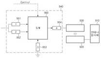
도 9를 참조하면, 일 실시 예에 따른 전자 장치(예: 도 2의 전자 장치(200))는 안테나 방사체(910), 제1 도전성 패드(920), 제2 도전성 패드(930) 및 스위칭 회로(940)를 포함할 수 있다. 도 9에 도시되지는 않았으나, 스위칭 회로(940)는 통신 회로(예: 도 2의 통신 회로(230))와 전기적으로 연결될 수 있다.Referring to FIG. 9 , an electronic device (eg, the
일 실시 예에 따르면, 안테나 방사체(910)는 제1 도전성 패드(920)와 전기적으로 연결될 수 있다. 안테나 방사체(910)는, 예를 들어, C-클립 등과 같은 연결 부재(예: 도 8의 연결 부재(850))를 통해 제1 도전성 패드(920)와 연결될 수 있다. 제1 도전성 패드(920)는 제2 도전성 패드(930)와 전기적으로 커플링될 수 있다.According to an embodiment, the
일 실시 예에 따르면, 스위칭 회로(940)는, 예를 들어, 도 3의 제1 스위칭 회로(341), 제2 스위칭 회로(342) 또는 제3 스위칭 회로(343) 중 적어도 일부와 대응할 수 있다. 스위칭 회로(940)는 제1 소자(951), 제2 소자(952), 제3 소자(953), 제4 소자(954) 및 스위치(960)를 포함할 수 있다. 제1 소자(951), 제2 소자(952), 제3 소자(953) 및 제4 소자(954)는 각각 하나 이상의 집중 소자를 포함할 수도 있다. 제1 소자(951), 제2 소자(952), 제3 소자(953) 및 제4 소자(954) 중 적어도 일부는 0에 가까운 임피던스를 갖는 라인일 수도 있다. 제1 소자(951) 및 제2 소자(952)는 통신 회로와 전기적으로 연결될 수 있다. 제3 소자(953)는 접지될 수 있다. 제4 소자(954)는 제2 도전성 패드(930)와 전기적으로 연결될 수 있다. 제1 소자(951), 제2 소자(952), 제3 소자(953) 및 제4 소자(954)는 스위치(960)와 전기적으로 연결될 수 있다.According to an embodiment, the
일 실시 예에 따르면, 스위치(960)는 통신 회로 또는 프로세서에 의해 제어될 수 있다. 예를 들어, 스위치(960)는 제1 소자(951)와 제4 소자(954)를 연결할 수 있다. 다른 예를 들면, 스위치(960)는 제2 소자(952)와 제4 소자(954)를 연결할 수 있다. 또 다른 예를 들면, 스위치(960)는 제1 소자(951), 제2 소자(952) 및 제4 소자(954)를 서로 연결할 수 있다. 또 다른 예를 들면, 스위치(960)는 제1 소자(951), 제3 소자(953) 및 제4 소자(954)를 서로 연결할 수 있다. 또 다른 예를 들면, 스위치(960)는 제2 소자(952), 제3 소자(953) 및 제4 소자(954)를 서로 연결할 수 있다. 또 다른 예를 들면, 스위치(960)는 제1 소자(951), 제2 소자(952), 제3 소자(953) 및 제4 소자(954)를 서로 연결할 수 있다.According to an embodiment, the
스위치(960)는, 예를 들어, 제3 소자(953)와 제4 소자(954)를 연결할 수 있다. 이 경우, 안테나 방사체(920)는 접지될 수 있다. 스위치(960)는 어느 소자와도 연결되지 않을 수도 있다. 상술한 스위치(960)의 동작에 의해 다양한 매칭 구조가 구성될 수 있다.The
도 10은 일 실시 예에 따른 전자 장치에 포함된 스위칭 회로를 개략적으로 나타낸다.10 schematically illustrates a switching circuit included in an electronic device according to an exemplary embodiment.
도 10을 참조하면, 일 실시 예에 따른 전자 장치(예: 도 2의 전자 장치(200))는 안테나 방사체(1010), 제1 도전성 패드(1020), 제2 도전성 패드(1030) 및 스위칭 회로(1040)를 포함할 수 있다. 도 10에 도시되지는 않았으나, 스위칭 회로(1040)는 통신 회로(예: 도 2의 통신 회로(230))와 전기적으로 연결될 수 있다.Referring to FIG. 10 , an electronic device (eg, the
일 실시 예에 따르면, 안테나 방사체(1010), 제1 도전성 패드(1020) 및 제2 도전성 패드(1030)는 각각 도 9의 안테나 방사체(910), 제1 도전성 패드(920) 및 제2 도전성 패드(930)와 대응할 수 있다.According to an embodiment, the
일 실시 예에 따르면, 스위칭 회로(1040)는, 예를 들어, 도 3의 제1 스위칭 회로(341), 제2 스위칭 회로(342) 또는 제3 스위칭 회로(343) 중 적어도 일부와 대응할 수 있다. 스위칭 회로(1040)는 제1 소자(1051), 제2 소자(1052), 제3 소자(1053), 제4 소자(1054), 제5 소자(1055) 및 스위치(1060)를 포함할 수 있다. 제1 소자(1051), 제2 소자(1052), 제3 소자(1053) 및 제4 소자(1054)는 각각 도 9의 제1 소자(951), 제2 소자(952), 제3 소자(953) 및 제4 소자(954)와 대응할 수 있다. 제5 소자(1055)는 하나 이상의 집중 소자를 포함할 수도 있고, 0에 가까운 임피던스를 갖는 라인일 수도 있다. 제5 소자(1055)는 제1 도전성 패드(1020)와 전기적으로 연결될 수 있다. 예를 들어, 제5 소자(1055)는 인쇄 회로 기판(예: 도 8의 인쇄 회로 기판(820))에 형성된 비아(via)를 통해 제1 도전성 패드(1020)와 전기적으로 연결될 수 있다. 제1 소자(1051), 제2 소자(1052), 제3 소자(1053), 제4 소자(1054) 및 제5 소자(1055)는 스위치(1060)와 전기적으로 연결될 수 있다.According to an embodiment, the
일 실시 예에 따르면, 스위치(1060)는 통신 회로에 의해 제어될 수 있다. 일 실시 예에 따르면, 스위치(1060)는 제1 도전성 패드(1020) 또는 제2 도전성 패드(1030)를 선택적으로 통신 회로와 전기적으로 연결할 수 있다.According to an embodiment, the
일 실시 예에 따르면, 스위치(1060)는 제1 도전성 패드(1020)를 통신 회로와 전기적으로 연결할 수 있다. 이 경우, 안테나 방사체(1010)는 직접 급전될 수 있다. 예를 들어, 스위치(1060)는 제1 소자(1051)와 제4 소자(1054)를 연결할 수 있다. 다른 예를 들면, 스위치(1060)는 제2 소자(1052)와 제4 소자(1054)를 연결할 수 있다. 또 다른 예를 들면, 스위치(1060)는 제1 소자(1051), 제2 소자(1052) 및 제4 소자(1054)를 서로 연결할 수 있다. 또 다른 예를 들면, 스위치(1060)는 제1 소자(1051), 제3 소자(1053) 및 제4 소자(1054)를 서로 연결할 수 있다. 또 다른 예를 들면, 스위치(1060)는 제2 소자(1052), 제3 소자(1053) 및 제4 소자(1054)를 서로 연결할 수 있다. 또 다른 예를 들면, 스위치(1060)는 제1 소자(1051), 제2 소자(1052), 제3 소자(1053) 및 제4 소자(1054)를 서로 연결할 수 있다.According to an embodiment, the
일 실시 예에 따르면, 스위치(1060)는 제2 도전성 패드(1030)를 통신 회로와 전기적으로 연결할 수 있다. 이 경우, 안테나 방사체(1010)는 커플링 급전될 수 있다. 예를 들어, 스위치(1060)는 제1 소자(1051)와 제5 소자(1055)를 연결할 수 있다. 다른 예를 들면, 스위치(1060)는 제2 소자(1052)와 제5 소자(1055)를 연결할 수 있다. 또 다른 예를 들면, 스위치(1060)는 제1 소자(1051), 제2 소자(1052) 및 제5 소자(1055)를 서로 연결할 수 있다. 또 다른 예를 들면, 스위치(1060)는 제1 소자(1051), 제3 소자(1053) 및 제5 소자(1055)를 서로 연결할 수 있다. 또 다른 예를 들면, 스위치(1060)는 제2 소자(1052), 제3 소자(1053) 및 제5 소자(1055)를 서로 연결할 수 있다. 또 다른 예를 들면, 스위치(1060)는 제1 소자(1051), 제2 소자(1052), 제3 소자(1053) 및 제5 소자(1055)를 서로 연결할 수 있다.According to an embodiment, the
스위치(1060)는, 예를 들어, 제3 소자(1053)와 제4 소자(1054)를 연결할 수도 있고, 제3 소자(1053)와 제5 소자(1055)를 연결할 수도 있다. 이 경우, 안테나 방사체(1010)는 접지될 수 있다. 스위치(1060)는 어느 소자와도 연결되지 않을 수도 있다.The
상술한 스위치(1060)의 동작에 의해 다양한 매칭 구조가 구성될 수 있다. 또한, 안테나 방사체(1010)에 대한 급전 방식이 선택될 수도 있다.Various matching structures may be configured by the operation of the above-described
도 11은 일 실시 예에 따른 전자 장치에 포함된 인쇄 회로 기판의 일부를 나타낸다. 도 11의 좌측 이미지는 인쇄 회로 기판의 일면을 도시하고, 도 11의 우측 이미지는 인쇄 회로 기판의 타면을 도시한다.11 illustrates a portion of a printed circuit board included in an electronic device according to an exemplary embodiment. The left image of FIG. 11 shows one side of the printed circuit board, and the right image of FIG. 11 shows the other side of the printed circuit board.
도 11을 참조하면, 일 실시 예에 따른 전자 장치(예: 도 2의 전자 장치(200))에 포함된 인쇄 회로 기판(1110)의 일면에는 제2 도전성 패드(1130), 제1 소자(1141), 제2 소자(1142), 제3 소자(1143), 제4 소자(1144), 제5 소자(1145) 및 스위치(1150)가 배치될 수 있다. 제1 소자(1141), 제2 소자(1142), 제3 소자(1143), 제4 소자(1144) 및 제5 소자(1145)는 스위치(1150)와 전기적으로 연결될 수 있다. 제4 소자(1144)는 제2 도전성 패드(1130)와 전기적으로 연결될 수 있다.Referring to FIG. 11 , on one surface of a printed
일 실시 예에 따르면, 인쇄 회로 기판(1110)의 타면에는 제1 도전성 패드(1120) 및 연결 부재(1160)가 배치될 수 있다. 제1 도전성 패드(1120)는 연결 부재(1160)와 전기적으로 연결될 수 있다. 연결 부재(1160)는 안테나 방사체(예: 도 3의 제1 안테나 방사체(311), 제2 안테나 방사체(312) 또는 제3 안테나 방사체(313))와 전기적으로 연결될 수 있다. 제1 도전성 패드(1120)는 제2 도전성 패드(1130)와 전기적으로 커플링될 수 있다. 제1 도전성 패드(1120)는 제5 소자(1145)와 인쇄 회로 기판(1110)에 형성된 비아를 통해 전기적으로 연결될 수 있다.According to an embodiment, the first
일 실시 예에 따르면, 도 11의 제1 도전성 패드(1120), 제2 도전성 패드(1130), 제1 소자(1141), 제2 소자(1142), 제3 소자(1143), 제4 소자(1144), 제5 소자(1145) 및 스위치(1150)는 각각 도 10의 제1 도전성 패드(1020), 제2 도전성 패드(1030), 제1 소자(1051), 제2 소자(1052), 제3 소자(1053), 제4 소자(1054), 제5 소자(1055) 및 스위치(1160)와 대응할 수 있다.According to an embodiment, the first
도 12는 일 실시 예에 따른 전자 장치에 포함된 안테나들의 주파수에 따른 반사 계수를 나타낸다.12 illustrates reflection coefficients according to frequencies of antennas included in an electronic device according to an embodiment.
도 12를 참조하면, 제1 곡선(1210) 및 제2 곡선(1220)은 제1 안테나 방사체(예: 도 3의 제1 안테나 방사체(311))의 주파수에 따른 반사 계수를 나타낸다. 제3 곡선(1230)은 제3 안테나 방사체(예: 도 3의 제3 안테나 방사체(313))의 주파수에 따른 반사 계수를 나타낸다. 이 경우, 제2 안테나 방사체(예: 도 3의 제2 안테나 방사체(312))는 개방될 수 있다.Referring to FIG. 12 , a
일 실시 예에 따르면, 전자 장치(예: 도 2의 전자 장치(200))는 PCC(primary component carrier)로서 LTE B13을 이용하고, SCC(secondary component carrier)로서 LTE B4를 이용할 수 있다. 제1 곡선(1210)이 나타내는 바와 같이, 제1 안테나 방사체는 B13 Rx를 지원할 수 있다. 또한, 제2 곡선(1220)이 나타내는 바와 같이, 제1 안테나 방사체는 B13 Tx를 지원할 수 있다. 제3 곡선(1230)이 나타내는 바와 같이, 제3 안테나 방사체는 B4 Rx를 지원할 수 있다. 전자 장치는 PCC인 B13 및 SCC인 B4를 집성할 수 있다.According to an embodiment, the electronic device (eg, the
일 실시 예에 따르면, 제4 곡선(1240)은 제1 안테나 방사체의 주파수에 따른 반사 계수를 나타낸다. 제5 곡선(1250) 및 제6 곡선(1260)은 제2 안테나 방사체의 주파수에 따른 반사 계수를 나타낸다. 이 경우, 제3 안테나 방사체는 개방될 수 있다.According to an embodiment, the
일 실시 예에 따르면, 전자 장치는 PCC로서 LTE B4를 이용하고, SCC로서 LTE B13을 이용할 수 있다. 제4 곡선(1240)이 나타내는 바와 같이, 제1 안테나 방사체는 B13 Rx를 지원할 수 있다. 한편, 제5 곡선(1250)이 나타내는 바와 같이, 제2 안테나 방사체는 B4 Tx를 지원할 수 있다. 또한, 제6 곡선(1260)이 나타내는 바와 같이, 제2 안테나 방사체는 B4 Rx를 지원할 수 있다. 전자 장치는 PCC인 B4 및 SCC인 B13을 집성할 수 있다.According to an embodiment, the electronic device may use LTE B4 as the PCC and LTE B13 as the SCC. As the
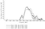
도 13은 일 실시 예에 따른 전자 장치에 포함된 안테나의 주파수에 따른 총 방사 효율을 나타낸다.13 illustrates total radiation efficiency according to a frequency of an antenna included in an electronic device according to an embodiment.
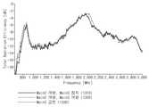
도 13을 참조하면, 도 13에 도시된 곡선들(1310, 1320 및 1330)은 제1 안테나 방사체(예: 도 3의 제1 안테나 방사체(311))의 주파수에 따른 총 방사 효율을 나타낸다. 제1 곡선(1310)은 제2 안테나 방사체(예: 도 3의 제2 안테나 방사체(312))의 급전점이 개방되고, 제3 안테나 방사체(예: 도 3의 제3 안테나 방사체(313))의 급전점이 접지된 경우, 제1 안테나 방사체의 총 방사 효율을 나타낸다. 제2 곡선(1320)은 제2 안테나 방사체의 급전점이 개방되고, 제3 안테나 방사체의 급전점이 개방된 경우, 제1 안테나 방사체의 총 방사 효율을 나타낸다. 제3 곡선(1330)은 제3 안테나 방사체가 급전점을 통해 급전되는 경우, 제1 안테나 방사체의 총 방사 효율을 나타낸다. 제2 안테나 방사체의 상태는, 예를 들어, 도 3의 제2 스위칭 회로(342)의 동작에 의해 변경될 수 있다. 제3 안테나 방사체의 상태는, 예를 들어, 도 3의 제3 스위칭 회로(343)의 동작에 의해 변경될 수 있다.Referring to FIG. 13 ,
도 13에 도시된 바와 같이, 제1 안테나 방사체와 인접한 제2 안테나 방사체 및 제3 안테나 방사체의 상태의 변경에 따라, 제1 안테나 방사체의 총 방사 효율은 변경될 수 있다. 예컨대, 제1 안테나 방사체와 인접한 안테나 방사체의 상태를 변경함으로써, 제1 안테나 방사체의 총 방사 효율이 향상될 수 있다.As shown in FIG. 13 , the total radiation efficiency of the first antenna radiator may be changed according to a change in the states of the second antenna radiator and the third antenna radiator adjacent to the first antenna radiator. For example, by changing the state of the first antenna radiator and the adjacent antenna radiator, the total radiation efficiency of the first antenna radiator may be improved.
도 14는 일 실시 예에 따른 전자 장치에 포함된 안테나의 주파수에 따른 총 방사 효율을 나타낸다.14 illustrates total radiation efficiency according to a frequency of an antenna included in an electronic device according to an embodiment.
도 14를 참조하면, 도 14에 도시된 곡선들(1410, 1420, 1430, 1440 및 1450)은 제2 안테나 방사체(예: 도 3의 제2 안테나 방사체(312))의 주파수에 따른 총 방사 효율을 나타낸다. 제1 곡선(1410)은 제1 안테나 방사체(예: 도 3의 제1 안테나 방사체(311))의 접지점이 개방되고, 제3 안테나 방사체(예: 도 3의 제3 안테나 방사체(313))의 급전점이 접지된 경우, 제2 안테나 방사체의 총 방사 효율을 나타낸다. 제2 곡선(1420)은 제1 안테나 방사체의 접지점이 개방되고, 제3 안테나 방사체의 급전점이 개방된 경우, 제2 안테나 방사체의 총 방사 효율을 나타낸다. 제3 곡선(1430)은 제1 안테나 방사체가 제1 경로를 통해 접지되고, 제3 안테나 방사체가 개방된 경우, 제2 안테나 방사체의 총 방사 효율을 나타낸다. 제4 곡선(1440)은 제1 안테나 방사체가 제2 경로를 통해 접지되고, 제3 안테나 방사체가 개방된 경우, 제2 안테나 방사체의 총 방사 효율을 나타낸다. 제5 곡선(1450)은 제1 안테나 방사체가 제3 경로를 통해 접지되고, 제3 안테나 방사체가 개방된 경우, 제2 안테나 방사체의 총 방사 효율을 나타낸다. 제1 경로, 제2 경로 및 제3 경로의 전기적 길이는 상이할 수 있다. 제1 안테나 방사체의 상태는, 예를 들어, 도 3의 제1 스위칭 회로(341)의 동작에 의해 변경될 수 있다. 제3 안테나 방사체의 상태는, 예를 들어, 도 3의 제3 스위칭 회로(343)의 동작에 의해 변경될 수 있다.Referring to FIG. 14 , the curves 1410 , 1420 , 1430 , 1440 , and 1450 shown in FIG. 14 indicate the total radiation efficiency according to the frequency of the second antenna radiator (eg, the
도 14에 도시된 바와 같이, 제2 안테나 방사체와 인접한 제1 안테나 방사체 및 제3 안테나 방사체의 상태의 변경에 따라, 제2 안테나 방사체의 총 방사 효율은 변경될 수 있다. 예컨대, 제2 안테나 방사체와 인접한 안테나 방사체의 상태를 변경함으로써, 제2 안테나 방사체의 총 방사 효율이 향상될 수 있다.As shown in FIG. 14 , the total radiation efficiency of the second antenna radiator may be changed according to a change in the states of the first antenna radiator and the third antenna radiator adjacent to the second antenna radiator. For example, by changing the state of the second antenna radiator and the adjacent antenna radiator, the total radiation efficiency of the second antenna radiator may be improved.
도 15는 일 실시 예에 따른 전자 장치에 포함된 안테나의 주파수에 따른 총 방사 효율을 나타낸다.15 illustrates total radiation efficiency according to a frequency of an antenna included in an electronic device according to an embodiment.
도 15를 참조하면, 도 15에 도시된 곡선들(1510, 1520 및 1530)은 제3 안테나 방사체(예: 도 3의 제3 안테나 방사체(313))의 주파수에 따른 총 방사 효율을 나타낸다. 제1 곡선(1510)은 제1 안테나 방사체(예: 도 3의 제1 안테나 방사체(311))의 접지점이 개방되고, 제2 안테나 방사체(예: 도 3의 제2 안테나 방사체(312))의 급전점이 접지된 경우, 제3 안테나 방사체의 총 방사 효율을 나타낸다. 제2 곡선(1520)은 제1 안테나 방사체의 접지점이 개방되고, 제2 안테나 방사체의 급전점이 개방된 경우, 제3 안테나 방사체의 총 방사 효율을 나타낸다. 제3 곡선(1530)은 제1 안테나 방사체의 접지점이 접지되고, 제2 안테나 방사체가 개방된 경우, 제3 안테나 방사체의 총 방사 효율을 나타낸다. 제1 안테나 방사체의 상태는, 예를 들어, 도 3의 제1 스위칭 회로(341)의 동작에 의해 변경될 수 있다. 제2 안테나 방사체의 상태는, 예를 들어, 도 3의 제2 스위칭 회로(342)의 동작에 의해 변경될 수 있다.Referring to FIG. 15 , curves 1510 , 1520 , and 1530 shown in FIG. 15 represent total radiation efficiency according to a frequency of a third antenna radiator (eg, the
도 15에 도시된 바와 같이, 제3 안테나 방사체와 인접한 제1 안테나 방사체 및 제2 안테나 방사체의 상태의 변경에 따라, 제3 안테나 방사체의 총 방사 효율은 변경될 수 있다. 예컨대, 제3 안테나 방사체와 인접한 안테나 방사체의 상태를 변경함으로써, 제3 안테나 방사체의 총 방사 효율이 향상될 수 있다.As shown in FIG. 15 , the total radiation efficiency of the third antenna radiator may be changed according to a change in the states of the first antenna radiator and the second antenna radiator adjacent to the third antenna radiator. For example, by changing the state of the third antenna radiator and the adjacent antenna radiator, the total radiation efficiency of the third antenna radiator may be improved.
도 16은 일 실시 예에 따른 전자 장치의 구성을 나타내는 블록도이다.16 is a block diagram illustrating a configuration of an electronic device according to an exemplary embodiment.
도 16을 참조하면, 일 실시 예에 따른 전자 장치(예: 도 2의 전자 장치(200))는 제1 안테나 방사체(1611), 제2 안테나 방사체(1612), 제3 안테나 방사체(1613), 제1 스위치(1651), 제2 스위치(1653), 제3 스위치(1654), LB 블록(1620), MB 블록(1630), HB 블록(1640) 및 통신 회로(1660)를 포함할 수 있다.Referring to FIG. 16 , an electronic device (eg, the
일 실시 예에 따르면, 제1 안테나 방사체(1611)는 LB 신호를 송신 및 수신하도록 구성될 수 있다. 제1 안테나 방사체(1611)는 LB 블록(1620)과 전기적으로 연결될 수 있다. 제1 안테나 방사체(1611)는 LB 블록(1620)으로부터 출력된 신호를 방사할 수 있다. 제1 안테나 방사체(1611)는 외부로부터 수신된 LB 신호를 LB 블록(1620)으로 전달할 수 있다.According to an embodiment, the
일 실시 예에 따르면, LB 블록(1620)은 통신 회로(1660)와 전기적으로 연결될 수 있다. LB 블록(1620)은, 예를 들어, LB 신호를 위한 LPAMID(LNA+PAM+FEMID(FRONT-END MODULE WITH INTEGRATED DUPLEXERS))일 수 있다. LB 블록(1620)은 제1 안테나 방사체(1611)로부터 전달된 LB 신호를 처리하고, 처리된 LB 신호를 통신 회로(1660)로 전달할 수 있다. LB 블록(1620)은 통신 회로(1660)로부터 전달된 신호를 처리하고, 처리된 LB 신호를 제1 안테나 방사체(1611)로 전달할 수 있다.According to an embodiment, the
일 실시 예에 따르면, 제2 안테나 방사체(1612)는 MB 신호 및 HB 신호를 송신 및 수신하도록 구성될 수 있다. 제2 안테나 방사체(1612)는 제1 스위치(1651), 제2 스위치(1653) 및 제3 스위치(1654)의 동작에 따라 MB 블록(1630) 또는 HB 블록(1640)과 전기적으로 연결될 수 있다. 제2 안테나 방사체(1612)는 제1 스위치(1651), 제2 스위치(1653) 및 제3 스위치(1654)의 동작에 따라 MB 블록(1630) 또는 HB 블록(1640)과 연결되지 않고, 개방될 수도 있다. 제2 안테나 방사체(1612)는 MB 블록(1630) 또는 HB 블록(1640)으로부터 출력된 신호를 방사할 수 있다. 제2 안테나 방사체(1612)는 외부로부터 수신된 MB 신호 또는 HB 신호를 각각 MB 블록(1630) 또는 HB 블록(1640)으로 전달할 수 있다.According to an embodiment, the
일 실시 예에 따르면, 제3 안테나 방사체(1613)는 MB 신호 및 HB 신호를 송신 및 수신하도록 구성될 수 있다. 제3 안테나 방사체(1613)는 제1 스위치(1651), 제2 스위치(1653) 및 제3 스위치(1654)의 동작에 따라 MB 블록(1630) 또는 HB 블록(1640)과 전기적으로 연결될 수 있다. 예를 들어, 제3 안테나 방사체(1613)는 MB 블록(1630) 또는 HB 블록(1640) 중 제2 안테나와 연결되지 않은 블록과 전기적으로 연결될 수 있다. 제3 안테나 방사체(1613)는 제1 스위치(1651), 제2 스위치(1653) 및 제3 스위치(1654)의 동작에 따라 MB 블록(1630) 또는 HB 블록(1640)과 연결되지 않고, 개방될 수도 있다. 제3 안테나 방사체(1613)는 MB 블록(1630) 또는 HB 블록(1640)으로부터 출력된 신호를 방사할 수 있다. 제3 안테나 방사체(1613)는 외부로부터 수신된 MB 신호 또는 HB 신호를 각각 MB 블록(1630) 또는 HB 블록(1640)으로 전달할 수 있다.According to an embodiment, the
일 실시 예에 따르면, 제1 스위치(1651)는 제2 안테나 방사체(1612)를 제2 스위치(1653)와 연결하고, 제3 안테나 방사체(1613)를 제3 스위치(1654)와 연결할 수 있다(실선 경로). 또 다른 예로, 제1 스위치(1651)는 제2 안테나 방사체(1612)를 제3 스위치(1654)와 연결하고, 제3 안테나 방사체(1613)를 제2 스위치(1653)와 연결할 수 있다(점선 경로). 제1 스위치(1651)는, 예를 들어, DPDT(double pole double throw)일 수 있다.According to an embodiment, the
일 실시 예에 따르면, 제2 스위치(1653)는 제2 안테나 방사체(1612) 또는 제3 안테나 방사체(1613) 중 제1 스위치(1651)를 통해 제2 스위치(1653)와 연결된 안테나 방사체를 MB 블록(1630)과 연결할 수도 있고, 연결하지 않을 수도 있다. 제2 스위치(1653)와 안테나 방사체가 연결된 경우, 제2 스위치(1653)는 연결된 안테나 방사체로부터 전달된 신호를 MB 블록(1630)으로 전달할 수도 있고, MB 블록(1630)으로부터 전달된 신호를 연결된 안테나 방사체로 전달할 수도 있다. 제2 스위치(1653)는, 예를 들어, SPDT(single pole double throw)일 수 있다.According to an embodiment, the
일 실시 예에 따르면, 제3 스위치(1654)는 제2 안테나 방사체(1612) 또는 제3 안테나 방사체(1613) 중 제1 스위치(1651)를 통해 제3 스위치(1654)와 연결된 안테나 방사체를 HB 블록(1640)과 연결할 수도 있고, 연결하지 않을 수도 있다. 제3 스위치(1654)와 안테나 방사체가 연결된 경우, 제3 스위치(1654)는 연결된 안테나 방사체로부터 전달된 신호를 HB 블록(1640)으로 전달할 수도 있고, HB 블록(1640)으로부터 전달된 신호를 연결된 안테나 방사체로 전달할 수도 있다. 제3 스위치(1654)는, 예를 들어, SPDT일 수 있다.According to an embodiment, the
일 실시 예에 따르면, MB 블록(1630)은 통신 회로(1660)와 전기적으로 연결될 수 있다. MB 블록(1630)은, 예를 들어, MB 신호를 위한 LPAMID일 수 있다. MB 블록(1630)은 제2 안테나 방사체(1612) 또는 제3 안테나 방사체(1613)로부터 전달된 신호를 처리하고, 처리된 MB 신호를 통신 회로(1660)로 전달할 수 있다. MB 블록(1630)은 통신 회로(1660)로부터 전달된 신호를 처리하고, 처리된 MB 신호를 제2 안테나 방사체(1612) 또는 제3 안테나 방사체(1613)로 전달할 수 있다.According to an embodiment, the
일 실시 예에 따르면, HB 블록(1640)은 통신 회로(1660)와 전기적으로 연결될 수 있다. HB 블록(1640)은, 예를 들어, HB 신호를 위한 LPAMID일 수 있다. HB 블록(1640)은 제2 안테나 방사체(1612) 또는 제3 안테나 방사체(1613)로부터 전달된 신호를 처리하고, 처리된 HB 신호를 통신 회로(1660)로 전달할 수 있다. HB 블록(1640)은 통신 회로(1660)로부터 전달된 신호를 처리하고, 처리된 HB 신호를 제2 안테나 방사체(1612) 또는 제3 안테나 방사체(1613)로 전달할 수 있다.According to an embodiment, the
일 실시 예에 따르면, 통신 회로(1660)는 LB 블록(1620), MB 블록(1630) 및 HB 블록(1640)과 전기적으로 연결될 수 있다. 통신 회로(1660)는 LB 블록(1620), MB 블록(1630) 및/또는 HB 블록(1640)으로부터 수신된 신호를 처리할 수 있고, LB 블록(1620), MB 블록(1630) 및/또는 HB 블록(1640)으로 신호를 전달할 수도 있다. 통신 회로(1660)는 LB 블록(1620), MB 블록(1630), HB 블록(1640), 제1 스위치(1651), 제2 스위치(1653) 및 제3 스위치(1654)를 제어할 수 있다.According to an embodiment, the
도 17은 일 실시 예에 따른 전자 장치의 구성을 나타내는 블록도이다.17 is a block diagram illustrating a configuration of an electronic device according to an embodiment.
도 17을 참조하면, 일 실시 예에 따른 전자 장치(예: 도 2의 전자 장치(200))는 제1 안테나 방사체(1711), 제2 안테나 방사체(1712), 제3 안테나 방사체(1713), 다이플렉서(1751), 스위치(1752), LB 블록(1720), MB 블록(1730), HB 블록(1740) 및 통신 회로(1760)를 포함할 수 있다.Referring to FIG. 17 , an electronic device (eg, the
일 실시 예에 따르면, 제1 안테나 방사체(1711)는 LB 신호 및 MB 신호를 송신 및 수신하도록 구성될 수 있다. 제1 안테나 방사체(1711)는 다이플렉서(1751)와 전기적으로 연결될 수 있다. 제1 안테나 방사체(1711)는 다이플렉서(1751)로부터 전달된 LB 신호 또는 MB 신호를 방사할 수 있다. 제1 안테나 방사체(1711)는 외부로부터 수신된 LB 신호 또는 MB 신호를 다이플렉서(1751)로 전달할 수 있다.According to an embodiment, the
일 실시 예에 따르면, 다이플렉서(1751)는 LB 블록(1720) 또는 MB 블록(1730)과 전기적으로 연결될 수 있다. 다이플렉서(1751)는 제1 안테나 방사체(1711)로부터 수신된 신호 중 LB 신호를 필터링하여 LB 블록(1720)으로 전달하고, MB 신호를 필터링하여 MB 블록(1730)으로 전달할 수 있다.According to an embodiment, the
일 실시 예에 따르면, LB 블록(1720)은 다이플렉서(1751)로부터 전달된 LB 신호를 처리하고, 처리된 LB 신호를 통신 회로(1760)로 전달할 수 있다. LB 블록(1720)은 통신 회로(1760)로부터 전달된 신호를 처리하고, 처리된 LB 신호를 다이플렉서(1751)로 전달할 수 있다.According to an embodiment, the
일 실시 예에 따르면, MB 블록(1730)은 다이플렉서(1751)로부터 전달된 MB 신호를 처리하고, 처리된 MB 신호를 통신 회로(1760)로 전달할 수 있다. MB 블록(1730)은 통신 회로(1760)로부터 전달된 신호를 처리하고, 처리된 MB 신호를 다이플렉서(1751)로 전달할 수 있다.According to an embodiment, the
일 실시 예에 따르면, 제2 안테나 방사체(1712)는 HB 신호를 송신 및 수신하도록 구성될 수 있다. 제2 안테나 방사체(1712)는 스위치(1752)와 전기적으로 연결될 수 있다. 제2 안테나 방사체(1712)는 스위치(1752)의 동작에 따라 HB 블록(1740)과 전기적으로 연결될 수 도 있고, 연결되지 않을 수도 있다. 제2 안테나 방사체(1712)는 스위치(1752)로부터 전달된 HB 신호를 방사할 수 있다. 제2 안테나 방사체(1712)는 외부로부터 수신된 HB 신호를 스위치(1752)로 전달할 수 있다.According to an embodiment, the
일 실시 예에 따르면, 제3 안테나 방사체(1713)는 HB 신호를 송신 및 수신하도록 구성될 수 있다. 제3 안테나 방사체(1713)는 스위치(1752)와 전기적으로 연결될 수 있다. 제3 안테나 방사체(1713)는 스위치(1752)의 동작에 따라 HB 블록(1740)과 전기적으로 연결될 수 도 있고, 연결되지 않을 수도 있다. 제3 안테나 방사체(1713)는 스위치(1752)로부터 전달된 HB 신호를 방사할 수 있다. 제3 안테나 방사체(1713)는 외부로부터 수신된 HB 신호를 스위치(1752)로 전달할 수 있다.According to an embodiment, the
일 실시 예에 따르면, 스위치(1752)는 제2 안테나 방사체(1712) 또는 제3 안테나 방사체(1713) 중 하나를 HB 블록(1740)과 전기적으로 연결할 수 있다. 스위치(1752)는 제2 안테나 방사체(1712) 또는 제3 안테나 방사체(1713)로부터 전달된 신호를 HB 블록(1740)을 전달할 수도 있고, HB 블록(1740)으로부터 전달된 신호를 제2 안테나 방사체(1712) 또는 제3 안테나 방사체(1713)로 전달할 수도 있다. 스위치(1752)는, 예를 들어, SPDT일 수 있다.According to an embodiment, the
일 실시 예에 따르면, HB 블록(1740)은 스위치(1752)로부터 전달된 HB 신호를 처리하고, 처리된 HB 신호를 통신 회로(1760)로 전달할 수 있다. HB 블록(1740)은 통신 회로(1760)로부터 전달된 신호를 처리하고, 처리된 HB 신호를 스위치(1752)로 전달할 수 있다.According to an embodiment, the
일 실시 예에 따르면, 통신 회로(1760)는 LB 블록(1720), MB 블록(1730) 및 HB 블록(1740)과 전기적으로 연결될 수 있다. 통신 회로(1760)는 LB 블록(1720), MB 블록(1730) 및/또는 HB 블록(1740)으로부터 수신된 신호를 처리할 수 있고, LB 블록(1720), MB 블록(1730) 및/또는 HB 블록(1740)으로 신호를 전달할 수도 있다. 통신 회로(1760)는 LB 블록(1720), MB 블록(1730), HB 블록(1740) 및 스위치(1752)를 제어할 수 있다.According to an embodiment, the
도 18은 일 실시 예에 따른 전자 장치의 구성을 나타내는 블록도이다.18 is a block diagram illustrating a configuration of an electronic device according to an exemplary embodiment.
도 18을 참조하면, 일 실시 예에 따른 전자 장치(예: 도 2의 전자 장치(200))는 제1 안테나 방사체(1811), 제2 안테나 방사체(1812), 제3 안테나 방사체(1813), 다이플렉서(1851), 스위치(1852), LB 블록(1820), MB 블록(1830), HB 블록(1840) 및 통신 회로(1860)를 포함할 수 있다.Referring to FIG. 18 , an electronic device (eg, the
일 실시 예에 따르면, 제1 안테나 방사체(1811)는 LB 신호 및 HB 신호를 송신 및 수신하도록 구성될 수 있다. 제1 안테나 방사체(1811)는 다이플렉서(1851)와 전기적으로 연결될 수 있다. 제1 안테나 방사체(1811)는 다이플렉서(1851)로부터 전달된 LB 신호 또는 HB 신호를 방사할 수 있다. 제1 안테나 방사체(1811)는 외부로부터 수신된 LB 신호 또는 HB 신호를 다이플렉서(1851)로 전달할 수 있다.According to an embodiment, the
일 실시 예에 따르면, 다이플렉서(1851)는 LB 블록(1820) 또는 HB 블록(1840)과 전기적으로 연결될 수 있다. 다이플렉서(1851)는 제1 안테나 방사체(1811)로부터 수신된 신호 중 LB 신호를 필터링하여 LB 블록(1820)으로 전달하고, HB 신호를 필터링하여 HB 블록(1840)으로 전달할 수 있다.According to an embodiment, the
일 실시 예에 따르면, LB 블록(1820)은 다이플렉서(1851)로부터 전달된 LB 신호를 처리하고, 처리된 LB 신호를 통신 회로(1860)로 전달할 수 있다. LB 블록(1820)은 통신 회로(1860)로부터 전달된 신호를 처리하고, 처리된 LB 신호를 다이플렉서(1851)로 전달할 수 있다.According to an embodiment, the
일 실시 예에 따르면, HB 블록(1840)은 다이플렉서(1851)로부터 전달된 HB 신호를 처리하고, 처리된 HB 신호를 통신 회로(1860)로 전달할 수 있다. HB 블록(1840)은 통신 회로(1860)로부터 전달된 신호를 처리하고, 처리된 HB 신호를 다이플렉서(1851)로 전달할 수 있다.According to an embodiment, the
일 실시 예에 따르면, 제2 안테나 방사체(1812)는 MB 신호를 송신 및 수신하도록 구성될 수 있다. 제2 안테나 방사체(1812)는 스위치(1852)와 전기적으로 연결될 수 있다. 제2 안테나 방사체(1812)는 스위치(1852)의 동작에 따라 MB 블록(1830)과 전기적으로 연결될 수 도 있고, 연결되지 않을 수도 있다. 제2 안테나 방사체(1812)는 스위치(1852)로부터 전달된 MB 신호를 방사할 수 있다. 제2 안테나 방사체(1812)는 외부로부터 수신된 MB 신호를 스위치(1852)로 전달할 수 있다.According to an embodiment, the
일 실시 예에 따르면, 제3 안테나 방사체(1813)는 MB 신호를 송신 및 수신하도록 구성될 수 있다. 제3 안테나 방사체(1813)는 스위치(1852)와 전기적으로 연결될 수 있다. 제3 안테나 방사체(1813)는 스위치(1852)의 동작에 따라 MB 블록(1830)과 전기적으로 연결될 수 도 있고, 연결되지 않을 수도 있다. 제3 안테나 방사체(1813)는 스위치(1852)로부터 전달된 MB 신호를 방사할 수 있다. 제3 안테나 방사체(1813)는 외부로부터 수신된 MB 신호를 스위치(1852)로 전달할 수 있다.According to an embodiment, the
일 실시 예에 따르면, 스위치(1852)는 제2 안테나 방사체(1812) 또는 제3 안테나 방사체(1813) 중 하나를 MB 블록(1830)과 전기적으로 연결할 수 있다. 스위치(1852)는 제2 안테나 방사체(1812) 또는 제3 안테나 방사체(1813)로부터 전달된 신호를 MB 블록(1830)을 전달할 수도 있고, MB 블록(1830)으로부터 전달된 신호를 제2 안테나 방사체(1812) 또는 제3 안테나 방사체(1813)로 전달할 수도 있다. 스위치(1852)는, 예를 들어, SPDT일 수 있다.According to an embodiment, the
일 실시 예에 따르면, MB 블록(1830)은 스위치(1852)로부터 전달된 MB 신호를 처리하고, 처리된 MB 신호를 통신 회로(1860)로 전달할 수 있다. MB 블록(1830)은 통신 회로(1860)로부터 전달된 신호를 처리하고, 처리된 MB 신호를 스위치(1852)로 전달할 수 있다.According to an embodiment, the
일 실시 예에 따르면, 통신 회로(1860)는 LB 블록(1820), MB 블록(1830) 및 HB 블록(1840)과 전기적으로 연결될 수 있다. 통신 회로(1860)는 LB 블록(1820), MB 블록(1830) 및/또는 HB 블록(1840)으로부터 수신된 신호를 처리할 수 있고, LB 블록(1820), MB 블록(1830) 및/또는 HB 블록(1840)으로 신호를 전달할 수도 있다. 통신 회로(1860)는 LB 블록(1820), MB 블록(1830), HB 블록(1840) 및 스위치(1852)를 제어할 수 있다.According to an embodiment, the
도 19는 일 실시 예에 따른 전자 장치의 구성을 나타내는 블록도이다.19 is a block diagram illustrating a configuration of an electronic device according to an embodiment.
도 19를 참조하면, 일 실시 예에 따른 전자 장치(예: 도 2의 전자 장치(200))는 제1 안테나 방사체(1911), 제2 안테나 방사체(1912), 제3 안테나 방사체(1913), LB 블록(1920), MB 블록(1930), HB 블록(1940) 및 통신 회로(1960)를 포함할 수 있다.Referring to FIG. 19 , an electronic device (eg, the
일 실시 예에 따르면, 제1 안테나 방사체(1911)는 LB 신호를 송신 및 수신하도록 구성될 수 있다. 제1 안테나 방사체(1911)는 LB 블록(1920)과 전기적으로 연결될 수 있다. 제1 안테나 방사체(1911)는 LB 블록(1920)으로부터 전달된 LB 신호를 방사할 수 있다. 제1 안테나 방사체(1911)는 외부로부터 수신된 LB 신호를 LB 블록(1920)으로 전달할 수 있다.According to an embodiment, the
일 실시 예에 따르면, LB 블록(1920)은 제1 안테나 방사체(1911)로부터 전달된 LB 신호를 처리하고, 처리된 LB 신호를 통신 회로(1960)로 전달할 수 있다. LB 블록(1920)은 통신 회로(1960)로부터 전달된 신호를 처리하고, 처리된 LB 신호를 제1 안테나 방사체(1911)로 전달할 수 있다.According to an embodiment, the
일 실시 예에 따르면, 제2 안테나 방사체(1912)는 MB 신호를 송신 및 수신하도록 구성될 수 있다. 제2 안테나 방사체(1912)는 MB 블록(1930)과 전기적으로 연결될 수 있다. 제2 안테나 방사체(1912)는 MB 블록(1930)으로부터 전달된 MB 신호를 방사할 수 있다. 제2 안테나 방사체(1912)는 외부로부터 수신된 MB 신호를 MB 블록(1930)으로 전달할 수 있다.According to an embodiment, the
일 실시 예에 따르면, MB 블록(1930)은 제2 안테나 방사체(1912)로부터 전달된 MB 신호를 처리하고, 처리된 MB 신호를 통신 회로(1960)로 전달할 수 있다. MB 블록(1930)은 통신 회로(1960)로부터 전달된 신호를 처리하고, 처리된 MB 신호를 제2 안테나 방사체(1912)로 전달할 수 있다.According to an embodiment, the
일 실시 예에 따르면, 제3 안테나 방사체(1913)는 HB 신호를 송신 및 수신하도록 구성될 수 있다. 제3 안테나 방사체(1913)는 HB 블록(1940)과 전기적으로 연결될 수 있다. 제3 안테나 방사체(1913)는 HB 블록(1940)으로부터 전달된 HB 신호를 방사할 수 있다. 제3 안테나 방사체(1913)는 외부로부터 수신된 HB 신호를 HB 블록(1940)으로 전달할 수 있다.According to an embodiment, the
일 실시 예에 따르면, HB 블록(1940)은 제3 안테나 방사체(1913)로부터 전달된 HB 신호를 처리하고, 처리된 HB 신호를 통신 회로(1960)로 전달할 수 있다. HB 블록(1940)은 통신 회로(1960)로부터 전달된 신호를 처리하고, 처리된 HB 신호를 제3 안테나 방사체(1913)로 전달할 수 있다.According to an embodiment, the
일 실시 예에 따르면, 통신 회로(1960)는 LB 블록(1920), MB 블록(1930) 및 HB 블록(1940)과 전기적으로 연결될 수 있다. 통신 회로(1960)는 LB 블록(1920), MB 블록(1930) 및/또는 HB 블록(1940)으로부터 수신된 신호를 처리할 수 있고, LB 블록(1920), MB 블록(1930) 및/또는 HB 블록(1940)으로 신호를 전달할 수도 있다. 통신 회로(1960)는 LB 블록(1920), MB 블록(1930) 및 HB 블록(1940)을 제어할 수 있다.According to an embodiment, the
일 실시 예에 따르면, 제1 안테나 방사체(1911), 제2 안테나 방사체(1912) 및 제3 안테나 방사체(1913) 각각이 서로 상이한 주파수 대역을 커버하도록 설계함으로써, 안테나 방사체(1911, 1912 및 1913)와 RF 블록(1920, 1930 및 1940) 사이에 다이플렉서 또는 스위치 등과 같은 소자가 생략될 수 있다. 이로써, 안테나의 효율이 향상될 수 있다.According to an embodiment, by designing each of the
도 20은 일 실시 예에 따른 전자 장치의 분해 사시도를 나타낸다.20 is an exploded perspective view of an electronic device according to an embodiment.
도 20를 참조하면, 일 실시 예에 따른 전자 장치(2000)는 커버 글래스(2012), 디스플레이(2020), 차폐층(2030), 하우징(2014), PCB(2040), 배터리(2050), 통신 회로(2060) 및 후면 커버(2016)를 포함할 수 있다. 일 실시 예에 따르면, 전자 장치(2000)는 도 20에 도시된 구성들 중 일부를 생략하거나, 도시되지 않은 다른 구성을 추가로 포함할 수 있다. 또한 전자 장치(2000)에 포함되는 구성들의 적층 순서는 도 20에 도시된 적층 순서와 다를 수 있다.Referring to FIG. 20 , an
커버 글래스(2012)는 디스플레이(2020)에 의해 생성된 빛을 투과시킬 수 있다. 또한, 커버 글래스(2012) 상에서 사용자는 신체의 일부(예: 손가락)를 접촉하여 터치(전자 펜을 이용한 접촉을 포함함)를 수행할 수 있다. 커버 글래스(2012)는, 예컨대, 강화 유리, 강화 플라스틱, 플렉서블(flexible) 고분자 소재 등으로 형성될 수 있다. 커버 글래스(2012)는 글래스 윈도우(glass window)로도 참조될 수 있다.The
일 실시 예에 따르면, 하우징(2014)은 전자 장치(2000)에 포함되는 구성들을 보호할 수 있다. 예를 들어, 하우징(2014) 내부에는 디스플레이(2020), PCB(2040) 및 배터리(2050) 등이 수납될 수 있고, 하우징(2014)은 상기 구성들을 외부 충격으로부터 보호할 수 있다.According to an embodiment, the
일 실시 예에 따르면, 하우징(2014)은 전자 장치(2000)의 외부에 노출되지 않는 지지 부재(예: 브래킷(bracket)(2014a)) 및 전자 장치(2000)의 외부에 노출되는 측면 부재(2014b)을 포함할 수 있다. 예를 들어, 지지 부재(2014a)는 전자 장치(2000)에 포함되는 부품들(예: 디스플레이(2020), PCB(2040) 등)을 지지할 수 있다. 측면 부재(2014b)는 전도성 물질(예: 금속)을 적어도 일부 포함할 수 있다. 예컨대, 금속 소재로 이루어진 측면 부재(2014a)는 금속 베젤(metal bezel)로도 참조될 수도 있다. 일 실시 예에 따르면, 상기 금속 베젤 중 적어도 일부는, 지정된 주파수 대역의 신호를 송수신하기 위한 안테나 엘리먼트로 활용될 수 있다.According to an embodiment, the
일 실시 예에 따르면, 후면 커버(2016)는 하우징(2014)에 결합될 수 있다. 후면 커버(2016)는, 강화 유리, 플라스틱, 및/또는 금속 등을 포함할 수 있다. 일 실시 예에 따르면, 후면 커버(2016)는 하우징(2014)과 일체로 구현되거나, 또는 사용자에 의해 착탈 가능하도록 구현될 수 있다.According to an embodiment, the
일 실시 예에 따르면, 디스플레이(2020)는 커버 글래스(2012)와 차폐층(2030) 사이에 배치될 수 있다. 디스플레이(2020)는 PCB(2040)와 전기적으로 연결되어, 콘텐트(예: 텍스트, 이미지, 비디오, 아이콘, 위젯, 또는 심볼 등)를 출력할 수 있다. 디스플레이(2020)는 사용자로부터 터치 입력(예: 터치, 제스처, 호버링(hovering) 등)을 수신할 수 있다.According to an embodiment, the
일 실시 예에 따르면, 차폐층(2030)은 디스플레이(2020)와 지지 부재(2014a) 사이에 배치될 수 있다. 차폐층(2030)은 디스플레이(2020)와 PCB(2040) 사이에서 발생하는 전자파를 차폐하여 디스플레이(2020)와 PCB(2040) 사이의 전자파 간섭(electro-magnetic interference)을 방지할 수 있다.According to an embodiment, the
일 실시 예에 따르면, 차폐층(2030)은 구리(Cu) 또는 그래파이트(graphite)로 이루어진 박막 시트(sheet) 혹은 플레이트(plate)를 포함할 수 있다. 예를 들어, 차폐층(2030)이 구리 또는 그래파이트로 이루어질 경우, 전자 장치(2000)에 포함되는 구성들의 적어도 일부는 차폐층(2030)에 접지될 수 있다.According to an embodiment, the
일 실시 예에 따르면, PCB(2040)는 전자 장치(2000)의 각종 전자 부품, 소자, 또는 인쇄회로 등을 실장(mount)할 수 있다. 예를 들어, PCB(2040)는 AP(application processor), CP(communication processor), 또는 통신 회로(2060) 등을 실장할 수 있다. 본 문서에서 PCB(2040)는 메인보드, 또는 PBA(printed board assembly)로 참조될 수 있다.According to an embodiment, the
일 실시 예에 따르면, PCB(2040)는 제1 PCB(2042), 제2 PCB(2044), 및 제3 PCB(2046)를 포함할 수 있다. 예를 들어, 제1 PCB(2042) 또는 제2 PCB(2044)는 전자 장치(2000)의 하단에 배치되는 서브 PCB에 해당할 수 있다. 또한 제3 PCB(2046)는 서브 PCB와 전기적으로 연결되는 메인 PCB에 해당할 수 있다. 예를 들어, 메인 PCB라 함은, 프로세서가 탑재되는 PCB로 이해될 수 있다. 도 20에서는 PCB(2040)가 3개의 PCB(2042, 2044 및 2046)를 포함하는 것으로 도시되었으나, 이에 제한되지 않고, PCB(2040)는 1개 또는 2개의 PCB로 이루어질 수도 있다.According to an embodiment, the
일 실시 예에 따르면, 제1 PCB(2042), 제2 PCB(2044), 및/또는 제3 PCB(2046)는 서로 전기적으로 연결될 수 있다. 예를 들어, 제1 PCB(2042) 및 제2 PCB(2044)는 지정된 커넥터 혹은 지정된 배선(예: FPCB(flexible printed circuit board))을 통해 서로 전기적으로 연결될 수 있다.According to an embodiment, the
일 실시 예에 따르면, 배터리(2050)는 화학 에너지와 전기 에너지를 양 방향으로 변환할 수 있다. 예를 들어, 배터리(2050)는 화학 에너지를 전기 에너지로 변환하고, 변환된 전기 에너지를 디스플레이(2020) 및 PCB(2040)에 탑재된 다양한 구성 혹은 모듈에 공급할 수 있다. 배터리(2050)는 외부로부터 공급받은 전기 에너지를 화학 에너지로 변환하여 저장할 수도 있다. 일 실시 예에 따르면, PCB(2040)에는 배터리(2050)의 충방전을 관리하기 위한 전력 관리 모듈이 포함될 수 있다.According to an embodiment, the
일 실시 예에 따르면, 통신 회로(2060)는 PCB(2040) 상에 배치될 수 있다. 도 20에서는 통신 회로(2060)가 제3 PCB(2046) 상에 배치되는 것으로 도시되었으나 통신 회로(2060)는 제1 PCB(2042) 또는 제2 PCB(2044) 상에 배치될 수도 있다. 통신 회로(2060)는 안테나 엘리먼트에 급전하여 신호를 송/수신할 수 있다.According to an embodiment, the
본 문서의 다양한 실시 예들 및 이에 사용된 용어들은 본 문서에 기재된 기술을 특정한 실시 형태에 대해 한정하려는 것이 아니며, 해당 실시 예의 다양한 변경, 균등물, 및/또는 대체물을 포함하는 것으로 이해되어야 한다. 도면의 설명과 관련하여, 유사한 구성요소에 대해서는 유사한 참조 부호가 사용될 수 있다. 단수의 표현은 문맥상 명백하게 다르게 뜻하지 않는 한, 복수의 표현을 포함할 수 있다. 본 문서에서, "A 또는 B", "A 및/또는 B 중 적어도 하나", "A, B 또는 C" 또는 "A, B 및/또는 C 중 적어도 하나" 등의 표현은 함께 나열된 항목들의 모든 가능한 조합을 포함할 수 있다. "제1," "제2," "첫째," 또는 "둘째,"등의 표현들은 해당 구성요소들을, 순서 또는 중요도에 상관없이 수식할 수 있고, 한 구성요소를 다른 구성요소와 구분하기 위해 사용될 뿐 해당 구성요소들을 한정하지 않는다. 어떤(예: 제1) 구성요소가 다른(예: 제2) 구성요소에 "(기능적으로 또는 통신적으로) 연결되어" 있다거나 "접속되어" 있다고 언급된 때에는, 상기 어떤 구성요소가 상기 다른 구성요소에 직접적으로 연결되거나, 다른 구성요소(예: 제 3 구성요소)를 통하여 연결될 수 있다.The various embodiments of this document and the terms used therein are not intended to limit the technology described in this document to a specific embodiment, but it should be understood to include various modifications, equivalents, and/or substitutions of the embodiments. In connection with the description of the drawings, like reference numerals may be used for like components. The singular expression may include the plural expression unless the context clearly dictates otherwise. In this document, expressions such as “A or B”, “at least one of A and/or B”, “A, B or C” or “at least one of A, B and/or C” refer to all of the items listed together. Possible combinations may be included. Expressions such as "first," "second," "first," or "second," can modify the corresponding elements regardless of order or importance, and to distinguish one element from another element. It is used only and does not limit the corresponding components. When an (eg, first) component is referred to as being “connected (functionally or communicatively)” or “connected” to another (eg, second) component, that component is It may be directly connected to the component, or may be connected through another component (eg, a third component).
본 문서에서, "~하도록 설정된(adapted to or configured to)"은 상황에 따라, 예를 들면, 하드웨어적 또는 소프트웨어적으로 "~에 적합한," "~하는 능력을 가지는," "~하도록 변경된," "~하도록 만들어진," "~를 할 수 있는," 또는 "~하도록 설계된"과 상호 호환적으로(interchangeably) 사용될 수 있다. 어떤 상황에서는, "~하도록 구성된 장치"라는 표현은, 그 장치가 다른 장치 또는 부품들과 함께 "~할 수 있는" 것을 의미할 수 있다. 예를 들면, 문구 "A, B, 및 C를 수행하도록 설정된 (또는 구성된) 프로세서"는 해당 동작들을 수행하기 위한 전용 프로세서(예: 임베디드 프로세서), 또는 메모리 장치(예: 메모리 130)에 저장된 하나 이상의 프로그램들을 실행함으로써, 해당 동작들을 수행할 수 있는 범용 프로세서(예: CPU 또는 AP)를 의미할 수 있다.In this document, "adapted to or configured to" is, depending on the context, for example, hardware or software "suitable for," "having the ability to," "modified to, " "made to," "capable of," or "designed to" may be used interchangeably. In some circumstances, the expression “a device configured to” may mean that the device is “capable of” with other devices or parts. For example, the phrase “a processor configured (or configured to perform) A, B, and C” may refer to a dedicated processor (eg, an embedded processor), or one stored in a memory device (eg, memory 130), for performing the corresponding operations. By executing the above programs, it may mean a general-purpose processor (eg, CPU or AP) capable of performing corresponding operations.
본 문서에서 사용된 용어 "모듈"은 하드웨어, 소프트웨어 또는 펌웨어(firmware)로 구성된 유닛(unit)을 포함하며, 예를 들면, 로직, 논리 블록, 부품, 또는 회로 등의 용어와 상호 호환적으로 사용될 수 있다. "모듈"은, 일체로 구성된 부품 또는 하나 또는 그 이상의 기능을 수행하는 최소 단위 또는 그 일부가 될 수 있다. "모듈"은 기계적으로 또는 전자적으로 구현될 수 있으며, 예를 들면, 어떤 동작들을 수행하는, 알려졌거나 앞으로 개발될, ASIC(application-specific integrated circuit) 칩, FPGAs(field-programmable gate arrays), 또는 프로그램 가능 논리 장치를 포함할 수 있다.As used herein, the term “module” includes a unit composed of hardware, software, or firmware, and may be used interchangeably with terms such as, for example, logic, logic block, component, or circuit. can A “module” may be an integrally formed component or a minimum unit or a part that performs one or more functions. A “module” may be implemented mechanically or electronically, for example, known or to be developed, application-specific integrated circuit (ASIC) chips, field-programmable gate arrays (FPGAs), or It may include a programmable logic device.
다양한 실시 예들에 따른 장치(예: 모듈들 또는 그 기능들) 또는 방법(예: 동작들)의 적어도 일부는 프로그램 모듈의 형태로 컴퓨터로 판독 가능한 저장 매체(예: 메모리(130))에 저장된 명령어로 구현될 수 있다. 상기 명령어가 프로세서(예: 프로세서(120))에 의해 실행될 경우, 프로세서가 상기 명령어에 해당하는 기능을 수행할 수 있다. 컴퓨터로 판독 가능한 기록 매체는, 하드디스크, 플로피디스크, 마그네틱 매체(예: 자기테이프), 광기록 매체(예: CD-ROM, DVD, 자기-광 매체(예: 플롭티컬 디스크), 내장 메모리 등을 포함할 수 있다. 명령어는 컴파일러에 의해 만들어지는 코드 또는 인터프리터에 의해 실행될 수 있는 코드를 포함할 수 있다.At least a portion of an apparatus (eg, modules or functions thereof) or a method (eg, operations) according to various embodiments of the present disclosure includes instructions stored in a computer-readable storage medium (eg, memory 130) in the form of a program module. can be implemented as When the instruction is executed by a processor (eg, the processor 120), the processor may perform a function corresponding to the instruction. Computer-readable recording media include hard disks, floppy disks, magnetic media (eg, magnetic tape), optical recording media (eg, CD-ROM, DVD, magneto-optical media (eg, floppy disks), built-in memory, etc.) An instruction may include code generated by a compiler or code that can be executed by an interpreter.
다양한 실시 예들에 따른 구성 요소(예: 모듈 또는 프로그램 모듈) 각각은 단수 또는 복수의 개체로 구성될 수 있으며, 전술한 해당 서브 구성 요소들 중 일부 서브 구성 요소가 생략되거나, 또는 다른 서브 구성 요소를 더 포함할 수 있다. 대체적으로 또는 추가적으로, 일부 구성 요소들(예: 모듈 또는 프로그램 모듈)은 하나의 개체로 통합되어, 통합되기 이전의 각각의 해당 구성 요소에 의해 수행되는 기능을 동일 또는 유사하게 수행할 수 있다. 다양한 실시 예들에 따른 모듈, 프로그램 모듈 또는 다른 구성 요소에 의해 수행되는 동작들은 순차적, 병렬적, 반복적 또는 휴리스틱(heuristic)하게 실행되거나, 적어도 일부 동작이 다른 순서로 실행되거나, 생략되거나, 또는 다른 동작이 추가될 수 있다.Each of the components (eg, a module or a program module) according to various embodiments may be composed of a singular or a plurality of entities, and some sub-components of the aforementioned sub-components may be omitted or other sub-components may be added. may include more. Alternatively or additionally, some components (eg, a module or a program module) may be integrated into a single entity to perform the same or similar functions performed by each corresponding component before being integrated. Operations performed by modules, program modules, or other components according to various embodiments are sequentially, parallelly, repetitively or heuristically executed, or at least some operations are executed in a different order, omitted, or other operations This can be added.
Claims (20)
Translated fromKorean제1 플레이트, 상기 제1 플레이트의 반대 방향으로 향하는(facing away) 제2 플레이트, 및 상기 제1 플레이트 및 상기 제2 플레이트 사이의 공간을 둘러싸는 측면 부재를 포함하는 하우징으로서, 상기 측면 부재는 상기 제1 플레이트 위에서 바라볼 때 실질적으로 직사각형 형태를 함께 형성하는 제1 도전성 부분, 제2 도전성 부분, 제3 도전성 부분 및 제4 도전성 부분을 포함하고 상기 제1 도전성 부분과 상기 제2 도전성 부분 사이에 개재된(interposed) 제1 비도전성 부분, 상기 제2 도전성 부분과 상기 제3 도전성 부분 사이에 개재된 제2 비도전성 부분, 상기 제3 도전성 부분과 상기 제4 도전성 부분 사이에 개재된 제3 비도전성 부분, 및 상기 제4 도전성 부분과 상기 제1 도전성 부분 사이에 개재된 제4 비도전성 부분을 포함하는, 상기 하우징;
상기 제1 플레이트의 일부를 통해 노출된 터치스크린 디스플레이;
상기 하우징 내부에 위치되고, 상기 제1 비도전성 부분에 근접한 상기 제1 도전성 부분 내의 제1 지점, 상기 제1 비도전성 부분에 근접한 상기 제2 도전성 부분 내의 제2 지점, 상기 제4 비도전성 부분에 근접한 상기 제4 도전성 부분 내의 제3 지점, 상기 제3 도전성 부분 내의 제4 지점, 상기 제3 비도전성 부분에 근접한 상기 제4 도전성 부분 내의 제5 지점, 및 상기 제2 비도전성 부분에 근접한 상기 제2 도전성 부분 내의 제6 지점과 전기적으로 연결된 적어도 하나의 무선 통신 회로;
상기 하우징 내부에 위치되고, 상기 터치스크린 디스플레이 및 상기 적어도 하나의 무선 통신 회로와 전기적으로 연결된 프로세서;
상기 하우징 내부에 위치되는 제1 도전성 패드; 및
상기 하우징 내부에 위치되고, 상기 제1 도전성 패드와 이격되되, 상기 제1 도전성 패드와 전기적으로 커플링되는 제2 도전성 패드를 포함하고,
상기 적어도 하나의 무선 통신 회로는 고대역 신호, 상기 고대역 신호의 주파수보다 낮은 주파수를 갖는 중대역 신호 및 상기 중대역 신호의 주파수보다 낮은 주파수를 갖는 저대역 신호를 포함하는 셀룰러 신호를 송신(transmit) 및 수신하도록 설정되고,
상기 적어도 하나의 무선 통신 회로는 상기 제2 지점, 상기 제3 지점, 상기 제4 지점 및 상기 제5 지점을 통해 상기 중대역 신호를 수신하도록 설정되고,
상기 제1 지점 또는 상기 제2 지점 중 하나는 상기 제1 도전성 패드 및 상기 제2 도전성 패드를 통해 상기 무선 통신 회로와 전기적으로 연결되는, 전자 장치.In an electronic device,
A housing comprising a first plate, a second plate facing away from the first plate, and a side member surrounding a space between the first plate and the second plate, wherein the side member comprises the a first conductive portion, a second conductive portion, a third conductive portion and a fourth conductive portion that together form a substantially rectangular shape when viewed from above the first plate, wherein the portion is disposed between the first conductive portion and the second conductive portion. A first non-conductive portion interposed, a second non-conductive portion interposed between the second conductive portion and the third conductive portion, and a third non-conductive portion interposed between the third conductive portion and the fourth conductive portion. the housing comprising a conductive portion and a fourth non-conductive portion interposed between the fourth conductive portion and the first conductive portion;
a touch screen display exposed through a portion of the first plate;
located within the housing, a first point in the first conductive portion proximate the first non-conductive portion, a second point in the second conductive portion proximate the first non-conductive portion, and at the fourth non-conductive portion a third point within the fourth conductive portion proximate, a fourth point within the third conductive portion, a fifth point within the fourth conductive portion proximate the third non-conductive portion, and the second point proximate the second non-conductive portion at least one wireless communication circuit electrically connected to a sixth point in the second conductive portion;
a processor located within the housing and electrically coupled to the touch screen display and the at least one wireless communication circuit;
a first conductive pad positioned inside the housing; and
a second conductive pad positioned inside the housing, spaced apart from the first conductive pad, and electrically coupled to the first conductive pad;
The at least one wireless communication circuit transmits a cellular signal comprising a high-band signal, a mid-band signal having a frequency lower than a frequency of the high-band signal, and a low-band signal having a frequency lower than the frequency of the mid-band signal. ) and is set to receive,
the at least one wireless communication circuit is configured to receive the mid-band signal via the second point, the third point, the fourth point, and the fifth point;
and one of the first point or the second point is electrically connected to the wireless communication circuitry through the first conductive pad and the second conductive pad.
상기 중대역 신호는 1.7GHZ 내지 2.2GHz 의 주파수 범위 내에 있는, 전자 장치.The method of claim 1,
wherein the mid-band signal is within a frequency range of 1.7 GHz to 2.2 GHz.
상기 적어도 하나의 무선 통신 회로는 상기 제1 지점 및 상기 제4 지점을 통해 상기 저대역 신호를 수신하고, 상기 제1 지점을 통해 상기 저대역 신호를 송신하도록 설정된, 전자 장치.The method of claim 1,
and the at least one wireless communication circuit is configured to receive the low-band signal via the first point and the fourth point, and to transmit the low-band signal via the first point.
상기 적어도 하나의 무선 통신 회로는 상기 제2 지점을 통해 상기 중대역 신호를 송신하도록 설정된, 전자 장치.4. The method of claim 3,
and the at least one wireless communication circuit is configured to transmit the mid-band signal via the second point.
상기 적어도 하나의 무선 통신 회로는 상기 제2 지점, 상기 제3 지점, 상기 제5 지점 및 상기 제6 지점을 통해 상기 고대역 신호를 수신하고, 상기 제3 지점을 통해 상기 고대역 신호를 송신하도록 설정된, 전자 장치.5. The method of claim 4,
the at least one wireless communication circuit is configured to receive the high-band signal through the second point, the third point, the fifth point, and the sixth point, and transmit the high-band signal through the third point; Set, electronic device.
상기 적어도 하나의 무선 통신 회로는 상기 제3 지점을 통해 상기 중대역 신호를 송신하도록 설정된, 전자 장치.4. The method of claim 3,
and the at least one wireless communication circuit is configured to transmit the mid-band signal via the third point.
상기 적어도 하나의 무선 통신 회로는 상기 제2 지점, 상기 제3 지점, 상기 제5 지점 및 상기 제6 지점을 통해 상기 고대역 신호를 수신하고, 상기 제2 지점을 통해 상기 고대역 신호를 송신하도록 설정된, 전자 장치.7. The method of claim 6,
the at least one wireless communication circuit is configured to receive the high-band signal via the second point, the third point, the fifth point, and the sixth point, and transmit the high-band signal via the second point; Set, electronic device.
상기 적어도 하나의 무선 통신 회로는 상기 제1 지점을 통해 상기 중대역 신호를 수신하고, 상기 제1 지점 및 상기 제2 지점을 통해 상기 중대역 신호를 송신하도록 설정된, 전자 장치.4. The method of claim 3,
and the at least one wireless communication circuit is configured to receive the mid-band signal via the first point and transmit the mid-band signal via the first point and the second point.
상기 적어도 하나의 무선 통신 회로는 상기 제2 지점, 상기 제3 지점, 상기 제5 지점 및 상기 제6 지점을 통해 상기 고대역 신호를 수신하고, 상기 제3 지점을 통해 상기 고대역 신호를 송신하도록 설정된, 전자 장치.9. The method of claim 8,
the at least one wireless communication circuit is configured to receive the high-band signal through the second point, the third point, the fifth point, and the sixth point, and transmit the high-band signal through the third point; Set, electronic device.
상기 적어도 하나의 무선 통신 회로는 상기 제2 지점 및 상기 제3 지점을 통해 상기 중대역 신호를 송신하도록 설정된, 전자 장치.4. The method of claim 3,
and the at least one wireless communication circuit is configured to transmit the mid-band signal via the second point and the third point.
상기 적어도 하나의 무선 통신 회로는 상기 제2 지점, 상기 제3 지점, 상기 제5 지점 및 상기 제6 지점을 통해 상기 고대역 신호를 수신하고, 상기 제3 지점을 통해 상기 고대역 신호를 송신하도록 설정된, 전자 장치.11. The method of claim 10,
the at least one wireless communication circuit is configured to receive the high-band signal through the second point, the third point, the fifth point, and the sixth point, and transmit the high-band signal through the third point; Set, electronic device.
상기 적어도 하나의 무선 통신 회로는 상기 제1 지점, 상기 제2 지점, 상기 제3 지점, 상기 제5 지점 및 상기 제6 지점을 통해 상기 고대역 신호를 수신하고, 상기 제1 지점 및 상기 제3 지점을 통해 상기 고대역 신호를 송신하도록 설정된, 전자 장치.5. The method of claim 4,
wherein the at least one wireless communication circuit receives the high-band signal through the first point, the second point, the third point, the fifth point, and the sixth point, the first point and the third point An electronic device configured to transmit the high-band signal through a point.
상기 적어도 하나의 무선 통신 회로는 상기 제2 지점, 상기 제3 지점, 상기 제5 지점 및 상기 제6 지점을 통해 상기 고대역 신호를 수신하고, 상기 제2 지점 및 상기 제3 지점을 통해 상기 고대역 신호를 송신하도록 설정된, 전자 장치.5. The method of claim 4,
The at least one wireless communication circuit is configured to receive the high-band signal through the second point, the third point, the fifth point, and the sixth point, and the high-band signal through the second point and the third point. An electronic device configured to transmit a band signal.
제1 대역에서 공진하도록 구성되고, 상기 전자 장치의 일단의 중앙에 배치된 제1 안테나 방사체;
상기 제1 대역보다 높은 제2 대역 및 제3 대역에서 공진하도록 구성되고, 상기 제1 안테나 방사체와 이격되되, 상기 제1 안테나 방사체의 일단에 인접하도록 배치된 제2 안테나 방사체;
상기 제2 대역 및 상기 제3 대역에서 공진하도록 구성되고, 상기 제1 안테나 방사체 및 상기 제2 안테나 방사체와 이격되도록 배치된 제3 안테나 방사체;
통신 회로;
상기 통신 회로와 상기 제1 안테나 방사체를 전기적으로 연결하는 제1 급전부;
상기 통신 회로와 상기 제2 안테나 방사체를 전기적으로 연결하는 제2 급전부;
상기 통신 회로와 상기 제3 안테나 방사체를 전기적으로 연결하는 제3 급전부;
제1 도전성 패드; 및
상기 제1 도전성 패드와 이격되되, 상기 제1 도전성 패드와 전기적으로 커플링되는 제2 도전성 패드를 포함하고,
상기 통신 회로는 상기 제2 안테나 방사체를 이용하여 상기 제2 대역의 신호를 송신 및 수신하는 동안, 상기 제3 안테나 방사체를 이용하여 상기 제2 대역의 신호를 수신하도록 설정되고,
상기 통신 회로는 상기 제3 안테나 방사체를 이용하여 상기 제3 대역의 신호를 송신 및 수신하는 동안, 상기 제2 안테나 방사체를 이용하여 상기 제3 대역의 신호를 수신하도록 설정되고,
상기 제1 안테나 방사체 또는 상기 제2 안테나 방사체 중 하나는 상기 제1 도전성 패드 및 상기 제2 도전성 패드를 통해 상기 통신 회로와 전기적으로 연결되는, 전자 장치.In an electronic device,
a first antenna radiator configured to resonate in a first band and disposed at the center of one end of the electronic device;
a second antenna radiator configured to resonate in a second band and a third band higher than the first band, spaced apart from the first antenna radiator, and disposed adjacent to one end of the first antenna radiator;
a third antenna radiator configured to resonate in the second band and the third band and spaced apart from the first antenna radiator and the second antenna radiator;
communication circuit;
a first feeding unit electrically connecting the communication circuit and the first antenna radiator;
a second feeding unit electrically connecting the communication circuit and the second antenna radiator;
a third power feeding unit electrically connecting the communication circuit and the third antenna radiator;
a first conductive pad; and
a second conductive pad spaced apart from the first conductive pad and electrically coupled to the first conductive pad;
the communication circuit is configured to receive the signal of the second band using the third antenna radiator while transmitting and receiving the signal of the second band using the second antenna radiator;
the communication circuit is configured to receive the signal of the third band using the second antenna radiator while transmitting and receiving the signal of the third band using the third antenna radiator;
and one of the first antenna radiator and the second antenna radiator is electrically connected to the communication circuit through the first conductive pad and the second conductive pad.
상기 제3 안테나 방사체는 상기 제1 안테나 방사체의 타단에 인접하도록 배치되고,
상기 제1 안테나 방사체, 상기 제2 안테나 방사체 및 상기 제3 안테나 방사체 각각은 상기 전자 장치의 메탈 프레임의 일부를 포함하는, 전자 장치.15. The method of claim 14,
The third antenna radiator is disposed adjacent to the other end of the first antenna radiator,
Each of the first antenna radiator, the second antenna radiator, and the third antenna radiator includes a part of a metal frame of the electronic device.
기판을 더 포함하고,
상기 제1 안테나 방사체 및 상기 제2 안테나 방사체 각각은 상기 전자 장치의 메탈 프레임의 일부를 포함하고,
상기 제3 안테나 방사체는 상기 기판 상에 인쇄된 도전성 패턴을 포함하는, 전자 장치.15. The method of claim 14,
further comprising a substrate;
Each of the first antenna radiator and the second antenna radiator includes a part of a metal frame of the electronic device,
The third antenna radiator includes a conductive pattern printed on the substrate.
상기 제1 급전부는 상기 제1 안테나 방사체의 일단과 인접한 제1 지점을 통해 상기 제1 안테나 방사체와 전기적으로 연결되고,
상기 제2 급전부는 상기 제2 안테나 방사체의 일단과 인접한 제2 지점을 통해 상기 제2 안테나 방사체와 전기적으로 연결되고,
상기 제2 안테나 방사체의 일단은 상기 제1 안테나 방사체의 일단과 인접하도록 배치되는, 전자 장치.15. The method of claim 14,
The first feeding unit is electrically connected to the first antenna radiator through a first point adjacent to one end of the first antenna radiator,
The second feeding unit is electrically connected to the second antenna radiator through a second point adjacent to one end of the second antenna radiator,
One end of the second antenna radiator is disposed adjacent to one end of the first antenna radiator.
상기 제1 도전성 패드 또는 상기 제2 도전성 패드를 선택적으로 상기 통신 회로와 전기적으로 연결하는 스위치를 포함하고,
상기 통신 회로는 상기 스위치를 제어하도록 설정된, 전자 장치.15. The method of claim 14,
a switch selectively electrically connecting the first conductive pad or the second conductive pad to the communication circuit;
and the communication circuitry is configured to control the switch.
상기 제1 급전부를 통해 상기 제1 안테나 방사체와 전기적으로 연결된 상기 제1 대역의 신호를 위한 제1 RF 블록;
상기 제2 급전부를 통해 상기 제2 안테나 방사체와 전기적으로 연결된 상기 제2 대역의 신호를 위한 제2 RF 블록; 및
상기 제3 급전부를 통해 상기 제3 안테나 방사체와 전기적으로 연결된 상기 제3 대역의 신호를 위한 제3 RF 블록을 더 포함하는, 전자 장치.15. The method of claim 14,
a first RF block for a signal of the first band electrically connected to the first antenna radiator through the first feeding unit;
a second RF block for the signal of the second band electrically connected to the second antenna radiator through the second feeding unit; and
The electronic device of claim 1, further comprising: a third RF block for a signal of the third band electrically connected to the third antenna radiator through the third power supply unit.
Priority Applications (5)
| Application Number | Priority Date | Filing Date | Title |
|---|---|---|---|
| KR1020170037775AKR102364808B1 (en) | 2017-03-24 | 2017-03-24 | Electronic device comprising antenna |
| PCT/KR2018/003369WO2018174601A1 (en) | 2017-03-24 | 2018-03-22 | Electronic device including antenna |
| US15/928,567US10439267B2 (en) | 2017-03-24 | 2018-03-22 | Electronic device including antenna |
| CN201810246893.6ACN108631039B (en) | 2017-03-24 | 2018-03-23 | Electronic equipment including antenna |
| EP18163666.3AEP3379647B1 (en) | 2017-03-24 | 2018-03-23 | Electronic device including antenna |
Applications Claiming Priority (1)
| Application Number | Priority Date | Filing Date | Title |
|---|---|---|---|
| KR1020170037775AKR102364808B1 (en) | 2017-03-24 | 2017-03-24 | Electronic device comprising antenna |
Publications (2)
| Publication Number | Publication Date |
|---|---|
| KR20180108256A KR20180108256A (en) | 2018-10-04 |
| KR102364808B1true KR102364808B1 (en) | 2022-02-18 |
Family
ID=61763903
Family Applications (1)
| Application Number | Title | Priority Date | Filing Date |
|---|---|---|---|
| KR1020170037775AActiveKR102364808B1 (en) | 2017-03-24 | 2017-03-24 | Electronic device comprising antenna |
Country Status (5)
| Country | Link |
|---|---|
| US (1) | US10439267B2 (en) |
| EP (1) | EP3379647B1 (en) |
| KR (1) | KR102364808B1 (en) |
| CN (1) | CN108631039B (en) |
| WO (1) | WO2018174601A1 (en) |
Cited By (1)
| Publication number | Priority date | Publication date | Assignee | Title |
|---|---|---|---|---|
| WO2025095660A1 (en)* | 2023-11-02 | 2025-05-08 | 삼성전자 주식회사 | Electronic device including antenna |
Families Citing this family (41)
| Publication number | Priority date | Publication date | Assignee | Title |
|---|---|---|---|---|
| KR102364559B1 (en) | 2017-03-24 | 2022-02-21 | 삼성전자주식회사 | Electronic device comprising antenna |
| KR102482071B1 (en)* | 2018-02-14 | 2022-12-28 | 삼성전자주식회사 | Antenna using multi-feeding and electronic device including the same |
| CN208835266U (en)* | 2018-08-03 | 2019-05-07 | 瑞声精密制造科技(常州)有限公司 | Antenna system and mobile terminal |
| CN109193129B (en)* | 2018-08-31 | 2021-04-27 | 北京小米移动软件有限公司 | Antenna system and terminal |
| CN109546338A (en)* | 2018-10-16 | 2019-03-29 | 浙江沃科电子科技有限公司 | A kind of system and method for remote collection mobile satellite antenna working condition and control mobile satellite antenna |
| KR102556813B1 (en) | 2018-10-16 | 2023-07-18 | 삼성전자 주식회사 | Antenna having single non-conductive portion and electronic device including the same |
| KR102624049B1 (en)* | 2018-11-05 | 2024-01-12 | 삼성전자주식회사 | Electronic device comprising antenna |
| KR102568765B1 (en) | 2018-11-19 | 2023-08-22 | 삼성전자주식회사 | An electronic device comprising a antenna module |
| KR102561241B1 (en)* | 2018-11-23 | 2023-07-28 | 삼성전자 주식회사 | Electronic deivce having signal radiation structure to side surface |
| CN109830815B (en)* | 2018-12-24 | 2021-04-02 | 瑞声科技(南京)有限公司 | Antenna system and mobile terminal applying same |
| KR102621852B1 (en)* | 2018-12-26 | 2024-01-08 | 삼성전자주식회사 | Antenna structure including conductive patch feeded using muitiple electrical path and electronic device including the antenna structure |
| KR102606484B1 (en)* | 2019-01-25 | 2023-11-27 | 삼성전자주식회사 | Electronic device including antenna device |
| KR102597392B1 (en)* | 2019-02-28 | 2023-11-03 | 삼성전자주식회사 | Antenna module supporting dual bands and electronic device including the same |
| KR102649428B1 (en)* | 2019-05-03 | 2024-03-20 | 삼성전자주식회사 | Wide-band antenna and electronic device including the same |
| KR102695025B1 (en)* | 2019-05-14 | 2024-08-14 | 삼성전자 주식회사 | Antenna and electronic device incluidng the same |
| WO2020231055A1 (en) | 2019-05-14 | 2020-11-19 | Samsung Electronics Co., Ltd. | Antenna and electronic device including the same |
| KR102699068B1 (en)* | 2019-08-06 | 2024-08-27 | 삼성전자주식회사 | Antenna and electronic device including the same |
| KR102707114B1 (en)* | 2019-10-11 | 2024-09-20 | 삼성전자주식회사 | A structure for fixing an antenna module and including the same |
| CN112993568B (en)* | 2019-12-02 | 2022-08-26 | 北京小米移动软件有限公司 | Electronic device |
| CN111180864A (en)* | 2020-01-21 | 2020-05-19 | 深圳市鑫王牌科技发展有限公司 | An antenna assembly for wearable device and wearable device |
| KR102781529B1 (en)* | 2020-02-10 | 2025-03-12 | 삼성전자주식회사 | An electronic device comprising a plurality of antennas |
| CN113381167B (en)* | 2020-02-25 | 2022-11-01 | 荣耀终端有限公司 | Antenna connecting device, antenna assembly and electronic equipment |
| CN113517556B (en)* | 2020-04-10 | 2024-09-17 | 深圳富泰宏精密工业有限公司 | Antenna structure and electronic equipment with same |
| KR102806168B1 (en)* | 2020-04-17 | 2025-05-13 | 삼성전자주식회사 | Method for controlling aperture switch in e-utra new radio dual connectivity and electronic device for supporting the same |
| KR102864053B1 (en)* | 2020-04-22 | 2025-09-24 | 삼성전자주식회사 | An electronic device including antennas |
| CN113675592B (en)* | 2020-05-13 | 2023-08-04 | 北京小米移动软件有限公司 | Antenna module and terminal equipment |
| CN111613878B (en)* | 2020-05-29 | 2023-02-21 | 北京小米移动软件有限公司 | Antenna of terminal equipment, terminal equipment and manufacturing method of antenna |
| CN113764866B (en) | 2020-06-03 | 2022-11-18 | 华为技术有限公司 | A kind of antenna device, electronic equipment |
| CN111987432B (en)* | 2020-09-04 | 2023-05-23 | 维沃移动通信有限公司 | Antenna structure and electronic equipment |
| CN112216965B (en)* | 2020-09-30 | 2022-02-01 | Oppo广东移动通信有限公司 | Antenna assembly and electronic equipment |
| CN112467347B (en)* | 2020-11-03 | 2023-06-13 | Oppo广东移动通信有限公司 | A kind of antenna device and electronic equipment |
| CN114447574B (en)* | 2020-11-04 | 2025-02-25 | 富泰京精密电子(烟台)有限公司 | Antenna structure and wireless communication device having the same |
| CN112531342B (en)* | 2020-12-07 | 2023-06-09 | Oppo广东移动通信有限公司 | Antenna modules and electronic equipment |
| US12323775B2 (en)* | 2021-04-08 | 2025-06-03 | Samsung Electronics Co., Ltd. | Electronic device including flexible printed circuit board |
| US11901966B2 (en)* | 2021-06-18 | 2024-02-13 | Samsung Electronics Co., Ltd. | Electronic device comprising antenna module with connector for coaxial cable |
| CN115706309A (en)* | 2021-08-05 | 2023-02-17 | 北京小米移动软件有限公司 | Electronic equipment |
| EP4358298A4 (en)* | 2021-08-10 | 2024-10-30 | Samsung Electronics Co., Ltd. | ANTENNA AND ELECTRONIC DEVICE THEREFOR |
| CN113644438B (en)* | 2021-08-31 | 2024-11-19 | 维沃移动通信有限公司 | Antenna device and electronic equipment |
| US20240097331A1 (en)* | 2022-05-20 | 2024-03-21 | Meta Platforms Technologies, Llc | Antenna architecture for mobile devices |
| WO2024205119A1 (en)* | 2023-03-24 | 2024-10-03 | 삼성전자주식회사 | Electronic device including antenna |
| WO2025095401A1 (en)* | 2023-10-31 | 2025-05-08 | 삼성전자주식회사 | Electronic device including antenna |
Family Cites Families (17)
| Publication number | Priority date | Publication date | Assignee | Title |
|---|---|---|---|---|
| MXPA02004221A (en) | 1999-10-26 | 2003-08-20 | Fractus Sa | Interlaced multiband antenna arrays. |
| US8947302B2 (en)* | 2010-11-05 | 2015-02-03 | Apple Inc. | Antenna system with antenna swapping and antenna tuning |
| US8772650B2 (en) | 2011-01-10 | 2014-07-08 | Apple Inc. | Systems and methods for coupling sections of an electronic device |
| US20140274231A1 (en)* | 2013-03-15 | 2014-09-18 | Javier Rodriguez De Luis | Multiband antenna using device metal features as part of the radiator |
| KR102094754B1 (en) | 2013-12-03 | 2020-03-30 | 엘지전자 주식회사 | Mobile terminal |
| US9203463B2 (en) | 2013-12-13 | 2015-12-01 | Google Technology Holdings LLC | Mobile device with antenna and capacitance sensing system with slotted metal bezel |
| KR20160060352A (en)* | 2014-11-20 | 2016-05-30 | 대산전자(주) | Antenna apparatus |
| KR101640787B1 (en) | 2015-05-12 | 2016-07-19 | 국방과학연구소 | The system for finding direction of a wireless signal |
| KR102364415B1 (en)* | 2015-05-19 | 2022-02-17 | 삼성전자주식회사 | Electronic device with antenna device |
| KR102352490B1 (en) | 2015-06-11 | 2022-01-18 | 삼성전자주식회사 | Antenna and electronic device comprising the same |
| CN106340725A (en)* | 2015-07-08 | 2017-01-18 | 三星电机株式会社 | Electronic device with multi-band antenna using outer conductor |
| US10224606B2 (en)* | 2015-07-30 | 2019-03-05 | Samsung Electro-Mechanics Co., Ltd. | Electronic device with multi-band antenna for supporting carrier aggregation using non-segmented conductive border member |
| CN106450658A (en)* | 2015-08-07 | 2017-02-22 | 微软技术许可有限责任公司 | Antenna device for electronic equipment |
| CN105609969A (en)* | 2016-02-22 | 2016-05-25 | 深圳市金立通信设备有限公司 | Communication terminal |
| CN205693664U (en) | 2016-06-08 | 2016-11-16 | 华硕电脑股份有限公司 | communication device |
| KR102534531B1 (en) | 2016-07-29 | 2023-05-19 | 삼성전자주식회사 | Electronic device including multiple antennas |
| CN106207491A (en)* | 2016-08-24 | 2016-12-07 | 北京小米移动软件有限公司 | device for WIFI MIMO |
- 2017
- 2017-03-24KRKR1020170037775Apatent/KR102364808B1/enactiveActive
- 2018
- 2018-03-22WOPCT/KR2018/003369patent/WO2018174601A1/ennot_activeCeased
- 2018-03-22USUS15/928,567patent/US10439267B2/enactiveActive
- 2018-03-23EPEP18163666.3Apatent/EP3379647B1/enactiveActive
- 2018-03-23CNCN201810246893.6Apatent/CN108631039B/enactiveActive
Cited By (1)
| Publication number | Priority date | Publication date | Assignee | Title |
|---|---|---|---|---|
| WO2025095660A1 (en)* | 2023-11-02 | 2025-05-08 | 삼성전자 주식회사 | Electronic device including antenna |
Also Published As
| Publication number | Publication date |
|---|---|
| CN108631039B (en) | 2021-01-01 |
| US10439267B2 (en) | 2019-10-08 |
| US20180277929A1 (en) | 2018-09-27 |
| KR20180108256A (en) | 2018-10-04 |
| CN108631039A (en) | 2018-10-09 |
| WO2018174601A1 (en) | 2018-09-27 |
| EP3379647B1 (en) | 2022-12-07 |
| EP3379647A1 (en) | 2018-09-26 |
Similar Documents
| Publication | Publication Date | Title |
|---|---|---|
| KR102364808B1 (en) | Electronic device comprising antenna | |
| KR102364559B1 (en) | Electronic device comprising antenna | |
| US11728563B2 (en) | Antenna for wireless communication and electronic device including the same | |
| US10418689B2 (en) | Electronic device comprising antenna | |
| CN110800156B (en) | Antenna equipment and electronic equipment including antennas | |
| KR102296158B1 (en) | Multi feeding antenna and electronic device having the same | |
| KR102321393B1 (en) | An electronic device comprising an antenna | |
| KR102390488B1 (en) | An electronic device comprising an antenna | |
| KR102439091B1 (en) | Electronic device comprising an antenna | |
| EP3391462B1 (en) | Electronic device including antenna | |
| US10374286B2 (en) | Antenna and electronic device including the same | |
| US9960489B2 (en) | Electronic device and method of operating the same | |
| KR102151056B1 (en) | Antenna and Electronic Devices comprising the Same | |
| KR20180105356A (en) | Antenna device having slit structure and electronic device including the same | |
| KR20180029326A (en) | Antenna and electronic device including the same | |
| KR102361149B1 (en) | An apparatus comprising an antenna using a conductive member included in housing | |
| KR102267709B1 (en) | Electronic device comprising antenna | |
| US10886600B2 (en) | Antenna and electronic device including the same | |
| KR102786949B1 (en) | Antenna and electronic device having the same |
Legal Events
| Date | Code | Title | Description |
|---|---|---|---|
| PA0109 | Patent application | Patent event code:PA01091R01D Comment text:Patent Application Patent event date:20170324 | |
| PG1501 | Laying open of application | ||
| A201 | Request for examination | ||
| PA0201 | Request for examination | Patent event code:PA02012R01D Patent event date:20200323 Comment text:Request for Examination of Application Patent event code:PA02011R01I Patent event date:20170324 Comment text:Patent Application | |
| E902 | Notification of reason for refusal | ||
| PE0902 | Notice of grounds for rejection | Comment text:Notification of reason for refusal Patent event date:20201122 Patent event code:PE09021S01D | |
| E902 | Notification of reason for refusal | ||
| PE0902 | Notice of grounds for rejection | Comment text:Notification of reason for refusal Patent event date:20210527 Patent event code:PE09021S01D | |
| E701 | Decision to grant or registration of patent right | ||
| PE0701 | Decision of registration | Patent event code:PE07011S01D Comment text:Decision to Grant Registration Patent event date:20211129 | |
| GRNT | Written decision to grant | ||
| PR0701 | Registration of establishment | Comment text:Registration of Establishment Patent event date:20220215 Patent event code:PR07011E01D | |
| PR1002 | Payment of registration fee | Payment date:20220216 End annual number:3 Start annual number:1 | |
| PG1601 | Publication of registration | ||
| PR1001 | Payment of annual fee | Payment date:20250124 Start annual number:4 End annual number:4 |