KR102360845B1 - Gate driving circuit and a display apparatus having the gate driving circuit - Google Patents
Gate driving circuit and a display apparatus having the gate driving circuitDownload PDFInfo
- Publication number
- KR102360845B1 KR102360845B1KR1020150084516AKR20150084516AKR102360845B1KR 102360845 B1KR102360845 B1KR 102360845B1KR 1020150084516 AKR1020150084516 AKR 1020150084516AKR 20150084516 AKR20150084516 AKR 20150084516AKR 102360845 B1KR102360845 B1KR 102360845B1
- Authority
- KR
- South Korea
- Prior art keywords
- node
- signal
- pull
- transistor
- output
- Prior art date
- Legal status (The legal status is an assumption and is not a legal conclusion. Google has not performed a legal analysis and makes no representation as to the accuracy of the status listed.)
- Active
Links
Images


Classifications
- G—PHYSICS
- G09—EDUCATION; CRYPTOGRAPHY; DISPLAY; ADVERTISING; SEALS
- G09G—ARRANGEMENTS OR CIRCUITS FOR CONTROL OF INDICATING DEVICES USING STATIC MEANS TO PRESENT VARIABLE INFORMATION
- G09G3/00—Control arrangements or circuits, of interest only in connection with visual indicators other than cathode-ray tubes
- G09G3/20—Control arrangements or circuits, of interest only in connection with visual indicators other than cathode-ray tubes for presentation of an assembly of a number of characters, e.g. a page, by composing the assembly by combination of individual elements arranged in a matrix no fixed position being assigned to or needed to be assigned to the individual characters or partial characters
- G09G3/34—Control arrangements or circuits, of interest only in connection with visual indicators other than cathode-ray tubes for presentation of an assembly of a number of characters, e.g. a page, by composing the assembly by combination of individual elements arranged in a matrix no fixed position being assigned to or needed to be assigned to the individual characters or partial characters by control of light from an independent source
- G09G3/36—Control arrangements or circuits, of interest only in connection with visual indicators other than cathode-ray tubes for presentation of an assembly of a number of characters, e.g. a page, by composing the assembly by combination of individual elements arranged in a matrix no fixed position being assigned to or needed to be assigned to the individual characters or partial characters by control of light from an independent source using liquid crystals
- G09G3/3611—Control of matrices with row and column drivers
- G09G3/3674—Details of drivers for scan electrodes
- G09G3/3677—Details of drivers for scan electrodes suitable for active matrices only
- G—PHYSICS
- G09—EDUCATION; CRYPTOGRAPHY; DISPLAY; ADVERTISING; SEALS
- G09G—ARRANGEMENTS OR CIRCUITS FOR CONTROL OF INDICATING DEVICES USING STATIC MEANS TO PRESENT VARIABLE INFORMATION
- G09G2300/00—Aspects of the constitution of display devices
- G09G2300/08—Active matrix structure, i.e. with use of active elements, inclusive of non-linear two terminal elements, in the pixels together with light emitting or modulating elements
- G09G2300/0809—Several active elements per pixel in active matrix panels
- G09G2300/0842—Several active elements per pixel in active matrix panels forming a memory circuit, e.g. a dynamic memory with one capacitor
- G—PHYSICS
- G09—EDUCATION; CRYPTOGRAPHY; DISPLAY; ADVERTISING; SEALS
- G09G—ARRANGEMENTS OR CIRCUITS FOR CONTROL OF INDICATING DEVICES USING STATIC MEANS TO PRESENT VARIABLE INFORMATION
- G09G2310/00—Command of the display device
- G09G2310/02—Addressing, scanning or driving the display screen or processing steps related thereto
- G09G2310/0264—Details of driving circuits
- G09G2310/0286—Details of a shift registers arranged for use in a driving circuit
- G—PHYSICS
- G09—EDUCATION; CRYPTOGRAPHY; DISPLAY; ADVERTISING; SEALS
- G09G—ARRANGEMENTS OR CIRCUITS FOR CONTROL OF INDICATING DEVICES USING STATIC MEANS TO PRESENT VARIABLE INFORMATION
- G09G2330/00—Aspects of power supply; Aspects of display protection and defect management
- G09G2330/02—Details of power systems and of start or stop of display operation
- G09G2330/021—Power management, e.g. power saving
Landscapes
- Engineering & Computer Science (AREA)
- Physics & Mathematics (AREA)
- Computer Hardware Design (AREA)
- General Physics & Mathematics (AREA)
- Theoretical Computer Science (AREA)
- Chemical & Material Sciences (AREA)
- Crystallography & Structural Chemistry (AREA)
- Control Of Indicators Other Than Cathode Ray Tubes (AREA)
Abstract
Translated fromKoreanDescription
Translated fromKorean본 발명은 액정 표시 장치에 관한 것이다. 구체적으로 본 발명은, 액정 표시장치의 게이트 구동회로에 관한 것이다.The present invention relates to a liquid crystal display device. Specifically, the present invention relates to a gate driving circuit of a liquid crystal display device.
액정 표시 장치(liquid crystal display, LCD), 유기 발광 표시 장치(organic light emitting diode display, OLED display) 및 전기 영동 표시 장치(electrophoretic display), 플라즈마 표시 장치(plasma display) 등의 평판 표시 장치는 복수 쌍의 전기장 생성 전극과 그 사이에 들어 있는 전기 광학(electro-optical) 활성층을 포함한다. 액정 표시 장치는 전기 광학 활성층으로 액정층을 포함하고, 유기 발광 표시 장치는 전기 광학 활성층으로 유기 발광층을 포함한다. 한 쌍을 이루는 전기장 생성 전극 중 하나는 통상 스위칭 소자에 연결되어 전기 신호를 인가 받고, 전기 광학 활성층은 이러한 전기 신호를 광학 신호로 변환함으로써 영상을 표시한다.A plurality of pairs of flat panel displays such as a liquid crystal display (LCD), an organic light emitting diode display (OLED display), an electrophoretic display, and a plasma display are provided. and an electro-optical active layer interposed therebetween. A liquid crystal display device includes a liquid crystal layer as an electro-optical active layer, and an organic light-emitting display device includes an organic light emitting layer as an electro-optical active layer. One of the pair of electric field generating electrodes is usually connected to a switching element to receive an electric signal, and the electro-optical active layer displays an image by converting the electric signal into an optical signal.
평판 표시 장치에는 박막 트랜지스터가 형성되는 표시 패널이 포함될 수 있다. 박막 트랜지스터 표시 패널에는 여러 층의 전극, 반도체 등이 패터닝되며, 일반적으로 패터닝 공정에 마스크(mask)를 이용한다.A flat panel display device may include a display panel in which a thin film transistor is formed. In a thin film transistor display panel, electrodes, semiconductors, etc. of several layers are patterned, and a mask is generally used in the patterning process.
한편, 반도체는 박막 트랜지스터의 특성을 결정하는 중요한 요소이다. 이러한 반도체는 비정질 실리콘(amorphous silicon)이 많이 사용되고 있지만, 전하 이동도가 낮기 때문에, 고성능 박막 트랜지스터를 제조하는데 한계가 있다. 또한, 다결정 실리콘(polysilicon)을 사용하는 경우, 전하 이동도가 높아 고성능 박막 트랜지스터의 제조가 용이하지만, 원가가 비싸고 균일도가 낮아 대형의 박막 트랜지스터 표시판을 제조하는데 한계가 있다.Meanwhile, a semiconductor is an important factor determining the characteristics of a thin film transistor. Although amorphous silicon is widely used as such a semiconductor, since charge mobility is low, there is a limitation in manufacturing a high-performance thin film transistor. In addition, when polysilicon is used, high-performance thin film transistors can be easily manufactured due to high charge mobility, but there is a limitation in manufacturing a large thin film transistor array panel due to high cost and low uniformity.
이에 따라, 비정질 실리콘보다 전자 이동도가 높고 전류의 ON/OFF 비율이 높으면서, 다결정 실리콘보다 원가가 저렴하고 균일도가 높은 산화물 반도체(oxide semiconductor)를 이용하는 박막 트랜지스터에 대한 연구가 진행 되고 있다.Accordingly, research on thin film transistors using an oxide semiconductor having higher electron mobility and higher current ON/OFF ratio than amorphous silicon, lower cost than polycrystalline silicon, and higher uniformity is being conducted.
한편, 표시 패널의 사이즈를 감소시키면서 생산성을 증대시키기 위하여 표시 패널에 형성된 게이트 라인에 공급되는 게이트 신호를 출력하는 게이트 구동회로를 표시 패널 상에 집적하는 방식이 사용되고 있다. 표시 패널 상에 집적되는 게이트 구동회로는 화소의 박막 트랜지스터와 동일한 제조 공정에 의해 제조된 박막 트랜지스터를 포함하고, 따라서, 게이트 구동회로의 박막 트랜지스터 역시 산화물 반도체로 액티브 층이 형성된다.Meanwhile, in order to increase productivity while reducing the size of the display panel, a method of integrating a gate driving circuit for outputting a gate signal supplied to a gate line formed in the display panel is used on the display panel. The gate driving circuit integrated on the display panel includes a thin film transistor manufactured by the same manufacturing process as the thin film transistor of the pixel, and thus, the thin film transistor of the gate driving circuit is also formed with an oxide semiconductor as an active layer.
본 발명은 상기와 같은 문제를 해결하기 위해 안출된 것으로, 베젤 사이즈의 감소를 위해 출력 풀다운 트랜지스터를 제거한 게이트 구동회로를 제공하기 위함이다.The present invention has been devised to solve the above problems, and to provide a gate driving circuit in which an output pull-down transistor is removed in order to reduce a bezel size.
본 발명의 일 실시 예에 따른 게이트 구동 회로는 복수의 스테이지들이 종속적으로 연결되어 복수의 게이트 신호들을 출력하는 게이트 구동회로에서 제 N(N은 자연수)번째 스테이지 회로를 포함하고, 상기 스테이지 회로는, 상기 제 N번째 스테이지의 이전 스테이지의 제어신호에 응답하여 전위가 상승되는 제1 노드에 연결된 제어전극을 포함하고, 클럭 신호를 수신하여 상기 N번째 스테이지의 게이트 신호를 출력하는 출력 풀업부, 제N-1번째 제어신호를 이용하여 상기 제1 노드를 충전하는 제어노드 풀업부 및 제N+1 번째 제어신호에 따라 상기 제1 노드의 전압을 제2 로우 전압으로 방전시키는 제어노드 풀다운부를 포함하되, 상기 출력 풀업부는, 제N+2 번째 스테이지에서 상기 출력 신호를 방전시키는 것을 특징으로 한다.The gate driving circuit according to an embodiment of the present invention includes an Nth (N is a natural number)-th stage circuit in a gate driving circuit in which a plurality of stages are connected to each other to output a plurality of gate signals, the stage circuit comprising: an output pull-up unit including a control electrode connected to a first node whose potential is increased in response to a control signal of a previous stage of the N-th stage, and receiving a clock signal and outputting a gate signal of the N-th stage; - Comprising a control node pull-up unit for charging the first node using a -1 th control signal and a control node pull-down unit for discharging the voltage of the first node to a second low voltage according to an N+1 th control signal, The output pull-up unit may discharge the output signal in an N+2 th stage.
또한 상기 제N 번째 스테이지 회로는, 상기 제1 노드에 하이 전압이 인가되면 상기 클럭 신호의 하이 전압을 상기 제N 번째 제어 신호로 출력하는 캐리부를 더 포함한다.The N-th stage circuit further includes a carry unit configured to output the high voltage of the clock signal as the N-th control signal when a high voltage is applied to the first node.
또한 상기 제N 번째 스테이지 회로는, 제N 번째 제어 신호의 하이 전압이 출력되는 구간을 제외한 나머지 구간 동안 인버팅 노드에 클럭 신호를 출력하는 인버터부를 더 포함한다.In addition, the N-th stage circuit further includes an inverter unit for outputting a clock signal to the inverting node during a period other than a period in which the high voltage of the N-th control signal is output.
또한 상기 제N 번째 스테이지 회로는, 상기 인버팅 노드의 신호에 응답하여 상기 제N 번째 제어 신호를 출력하는 상기 캐리부의 캐리 출력 단자의 전압을 제2 로우 전압으로 방전하는 캐리 유지부를 더 포함한다.The Nth stage circuit further includes a carry holding unit configured to discharge a voltage of a carry output terminal of the carry unit outputting the Nth control signal to a second low voltage in response to the signal of the inverting node.
또한 상기 제N 번째 스테이지 회로는, 제N+1 번째 제어신호에 따라 상기 캐리 출력 단자의 전압을 제2 로우전압(VSS2)으로 방전하는 캐리 풀다운부를 더 포함한다.In addition, the N-th stage circuit further includes a carry pull-down unit for discharging a voltage of the carry output terminal to a second low voltage VSS2 according to an (N+1)-th control signal.
또한 상기 제N 번째 스테이지 회로는, 상기 인버팅 노드의 신호에 응답하여 상기 제1 노드의 전압을 제2 로우 전압으로 방전하는 제어노드 유지부를 더 포함한다.The Nth stage circuit further includes a control node holding unit configured to discharge the voltage of the first node to a second low voltage in response to the signal of the inverting node.
또한 상기 제N 번째 스테이지 회로는, 상기 인버팅 노드의 신호에 응답하여 상기 N번째 스테이지의 게이트 신호를 출력하는 출력 노드 전압을 제1 로우 전압(VSS1) 방전하는 출력 유지부를 더 포함한다.In addition, the N-th stage circuit further includes an output sustaining unit configured to discharge an output node voltage outputting a gate signal of the N-th stage to a first low voltage VSS1 in response to the signal of the inverting node.
또한 상기 출력 신호의 풀다운 시간이 상기 캐리 출력의 풀다운 보다 더 긴 것을 특징으로 한다.In addition, it is characterized in that the pull-down time of the output signal is longer than the pull-down of the carry output.
또한 상기 제어노드 풀업부는, 제N-1번째 제어신호를 각각 게이트 전극으로 입력 받는 제1 트랜지스터 및 제2 트랜지스터를 포함하고, 상기 제1 트랜지스터의 입력 전극은 상기 N-1번째 제어신호를 입력 받고, 상기 제2 트랜지스터의 입력전극은 상기 제1 트랜지스터의 출력을 입력 받는 것을 특징으로 한다.In addition, the control node pull-up unit includes a first transistor and a second transistor that respectively receive an N-1 th control signal to a gate electrode, and an input electrode of the first transistor receives the N-1 th control signal. , the input electrode of the second transistor receives the output of the first transistor as an input.
또한, 본 발명의 일 실시 예에 따른 표시 장치는, 복수의 게이트 라인들, 복수의 데이터 라인들 및 복수의 화소 트랜지스터들을 포함하는 표시 영역과 상기 표시영역을 둘러싸는 주변 영역을 포함하는 표시 패널, 상기 데이터 라인들에 데이터 신호들을 출력하는 데이터 구동회로 및 상기 주변 영역에 집적되고, 상기 게이트 라인들에 게이트 신호들을 출력하는 복수의 스테이지들을 포함하고, 각 스테이지는 복수의 트랜지스터들을 포함하는 게이트 구동회로를 포함하고, 상기 제 N번째 스테이지의 이전 스테이지의 제어신호에 응답하여 전위가 상승되는 제1 노드에 연결된 제어전극을 포함하고, 클럭 신호를 수신하여 상기 N번째 스테이지의 게이트 신호를 출력하는 출력 풀업부, 제N-1번째 제어신호를 이용하여 상기 제1 노드를 충전하는 제어노드 풀업부 및 제N+1 번째 제어신호에 따라 상기 제1 노드의 전압을 제2 로우 전압으로 방전시키는 제어노드 풀다운부를 포함하되, 상기 출력 풀업부는, 제N+2 번째 스테이지에서 상기 출력 신호를 방전시키는 것을 특징으로 한다.In addition, a display device according to an exemplary embodiment includes a display panel including a display area including a plurality of gate lines, a plurality of data lines, and a plurality of pixel transistors, and a peripheral area surrounding the display area; a data driving circuit for outputting data signals to the data lines and a plurality of stages integrated in the peripheral region and outputting gate signals to the gate lines, each stage including a plurality of transistors and a control electrode connected to a first node whose potential is increased in response to a control signal of a previous stage of the Nth stage, and an output pull-up for receiving a clock signal and outputting a gate signal of the Nth stage A control node pull-up unit that charges the first node using the negative and N-1th control signals, and a control node pull-down that discharges the voltage of the first node to a second low voltage according to the N+1th control signal. unit, wherein the output pull-up unit discharges the output signal in an N+2 th stage.
또한 상기 표시 영역의 상기 화소 트랜지스터 및 상기 주변 영역의 상기 트랜지스터 각각은 산화물 반도체를 포함하는 것을 특징으로 한다.In addition, each of the pixel transistor of the display area and the transistor of the peripheral area may include an oxide semiconductor.
또한 상기 제어노드와 연결된 복수의 트랜지스터 중 방전역할을 하는 트랜지스터의 소스 전원이 다른 방전 트랜지스터의 소스 전원과 상이한 것을 특징으로 한다.In addition, it is characterized in that the source power of the discharge transistor among the plurality of transistors connected to the control node is different from the source power of the other discharge transistors.
또한 상기 제어노드 풀다운부의 트랜지스터의 게이트 전극인 상기 제어노드와 연결된 복수의 트랜지스터 중 방전 속도가 가장 느린 트랜지스터의 출력에 연결되는 것을 특징으로 한다.In addition, it is characterized in that it is connected to the output of the transistor having the slowest discharge rate among the plurality of transistors connected to the control node, which is the gate electrode of the transistor of the pull-down unit of the control node.
또한 상기 게이트 구동회로의 출력 신호의 방전 시간이 상기 제어 신호의 풀다운 보다 더 긴 것을 특징으로 한다.In addition, the discharge time of the output signal of the gate driving circuit is characterized in that longer than the pull-down of the control signal.
본 발명의 다양한 실시 예에 따르면, 게이트 구동회로에 포함된 트랜지스터의 수가 감소하므로, 베젤크기를 줄이고 소비전력을 줄일 수 있다.According to various embodiments of the present disclosure, since the number of transistors included in the gate driving circuit is reduced, it is possible to reduce the size of the bezel and reduce power consumption.
도 1은 본 발명의 일 실시 예에 따른 표시 장치의 평면도이다.
도 2는 종래 기술에 따른 게이트 구동회로의 구조를 나타낸 회로도이다.
도 3은 본 발명의 일 실시 예에 따른 게이트 구동회로의 회로도이다.
도 4는 본 발명에 따른 게이트 구동회로의 시뮬레이션 결과를 나타낸 그래프이다.1 is a plan view of a display device according to an exemplary embodiment.
2 is a circuit diagram showing the structure of a gate driving circuit according to the related art.
3 is a circuit diagram of a gate driving circuit according to an embodiment of the present invention.
4 is a graph showing a simulation result of a gate driving circuit according to the present invention.
이하, 본 발명의 실시 예를 첨부된 도면을 참조하여 상세하게 설명한다.Hereinafter, embodiments of the present invention will be described in detail with reference to the accompanying drawings.
실시 예를 설명함에 있어서 본 발명이 속하는 기술 분야에 익히 알려져 있고 본 발명과 직접적으로 관련이 없는 기술 내용에 대해서는 설명을 생략한다. 이는 불필요한 설명을 생략함으로써 본 발명의 요지를 흐리지 않고 더욱 명확히 전달하기 위함이다.In describing the embodiments, descriptions of technical contents that are well known in the technical field to which the present invention pertains and are not directly related to the present invention will be omitted. This is to more clearly convey the gist of the present invention without obscuring the gist of the present invention by omitting unnecessary description.
본 발명의 이점 및 특징, 그리고 그것들을 달성하는 방법은 첨부되는 도면과 함께 상세하게 후술되어 있는 실시 예들을 참조하면 명확해질 것이다. 그러나 본 발명은 이하에서 개시되는 실시 예들에 한정되는 것이 아니라 서로 다른 다양한 형태로 구현될 수 있으며, 단지 본 실시 예들은 본 발명의 개시가 완전하도록 하고, 본 발명이 속하는 기술분야에서 통상의 지식을 가진 자에게 발명의 범주를 완전하게 알려주기 위해 제공되는 것이다.Advantages and features of the present invention, and a method for achieving them will become apparent with reference to the embodiments described below in detail in conjunction with the accompanying drawings. However, the present invention is not limited to the embodiments disclosed below, but may be implemented in various different forms, and only these embodiments allow the disclosure of the present invention to be complete, and common knowledge in the technical field to which the present invention belongs It is provided to fully inform the possessor of the scope of the invention.
본 명세서에서 구동회로에 사용되는 트랜지스터 소자는 3개의 전극을 포함할 수 있고, 제어전극, 입력전극 및 출력전극으로 각각 명명될 수 있다. 다양한 실시 예에서, 제어전극은 트랜지스터 소자의 게이트 전극일 수 있고, 입력전극은 소스 전극 그리고 출력전극은 드레인 전극일 수 있다.The transistor device used in the driving circuit in the present specification may include three electrodes, and may be referred to as a control electrode, an input electrode, and an output electrode, respectively. In various embodiments, the control electrode may be a gate electrode of the transistor device, the input electrode may be a source electrode, and the output electrode may be a drain electrode.
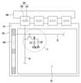
도 1은 본 발명의 일 실시 예에 따른 표시 장치의 평면도이다.1 is a plan view of a display device according to an exemplary embodiment.
도 1에 따르면, 상기 표시 장치는 표시 패널(100), 게이트 구동회로(200), 데이터 구동회로(400) 및 인쇄회로 기판(500)을 포함한다.Referring to FIG. 1 , the display device includes a
상기 표시 패널(100)은 표시 영역(DA) 및 상기 표시 영역(DA)을 둘러싸는 주변 영역(PA)을 포함한다. 상기 표시 영역(DA)에는 서로 교차하는 게이트 라인들, 데이터 라인들 및 복수의 화소부를 포함한다. 각 화소부(P)는 게이트 라인(GL)과 데이터 라인(DL)에 전기적으로 연결된 화소 트랜지스터(TR)와, 상기 화소 트랜지스터(TR)와 전기적으로 연결된 액정 커패시터(CLC) 및 상기 액정 커패시터(CLC)와 병렬 연결된 스토리지 커패시터(CST)를 포함한다. 상기 화소 트랜지스터(TR)는 산화물 반도체를 액티브 층으로 사용하는 산화물 트랜지스터일 수 있다. 상기 산화물 반도체는 인듐(indium: In), 아연(zinc: Zn), 갈륨(gallium: Ga), 주석(tin: Sn) 또는 하프늄(hafnium: Hf) 중 적어도 하나를 포함하는 비정질 산화물로 이루어질 수 있다. 보다 구체적으로는, 인듐(In), 아연(Zn) 및 갈륨(Ga)을 포함하는 비정질 산화물, 또는 인듐(In), 아연(Zn) 및 하프늄(Hf)을 포함하는 비정질 산화물로 이루어질 수 있다. 상기 산화물 반도체에 산화인듐아연(InZnO), 산화인듐갈륨(InGaO), 산화인듐주석(InSnO), 산화아연주석(ZnSnO), 산화갈륨주석(GaSnO) 및 산화갈륨아연(GaZnO) 등의 산화물이 포함될 수 있다. 예를 들면, 상기 액티브 패턴(ACT)은 인듐 갈륨 아연 산화물(indium gallium zinc oxide: IGZO)을 포함할 수 있다.The
상기 게이트 구동회로(200)는 상기 게이트 라인들에 하이 전압의 게이트 신호들을 순차적으로 출력하는 쉬프트 레지스터를 포함한다. 상기 쉬프트 레지스터는 복수의 스테이지들을 포함할 수 있다. 상기 게이트 구동회로(200)는 상기 게이트 라인들의 일단부에 대응하는 상기 주변 영역(PA)에 집적된다. 상기 게이트 구동회로(200)는 복수의 회로 트랜지스터들을 포함하고, 상기 회로 트랜지스터는 상기 화소 트랜지스터(TR)와 동일한 제조 공정으로 상기 주변 영역(PA)에 형성된다. 상기 회로 트랜지스터는 상기 산화물 반도체를 액티브 층으로 사용하는 산화물 트랜지스터일 수 있다. 상기 게이트 구동회로(200)는 상기 게이트 라인들의 양단부에 대응하여 듀얼 구조로 형성될 수 있다.The
상기 데이터 구동회로(400)는 상기 데이터 라인들에 데이터 신호들을 출력하는 데이터 구동칩(410)과, 상기 데이터 구동칩(410)이 실장 되어 상기 인쇄회로기판(500)과 상기 표시 패널(100)을 전기적으로 연결하는 연성회로 기판(430)을 포함한다.The
도 2는 종래 기술에 따른 게이트 구동회로의 구조를 나타낸 회로도이다.2 is a circuit diagram showing the structure of a gate driving circuit according to the related art.
도 2의 게이트 회로 구조는 산화물 반도체(Oxide TFT)를 적용한 게이트 집적회로(Gate IC)에서 요구되는 로버스트(Robust)동작 특성 및 소비전력 감소를 달성하기 위한 회로구조이다. 구체적으로, 기존 아몰퍼스 실리콘 게이트(ASG) 회로 구조에서 High level stress를 받는 TFT를 회로의 구조를 변경하여, Low level stress를 받도록 한고 회로 집적 효율성 증대시킬 수 있다.The gate circuit structure of FIG. 2 is a circuit structure for achieving robust operation characteristics and power consumption reduction required in a gate integrated circuit (Gate IC) to which an oxide semiconductor (Oxide TFT) is applied. Specifically, by changing the circuit structure of a TFT that is subjected to high level stress in an existing amorphous silicon gate (ASG) circuit structure, it is possible to receive low level stress and increase circuit integration efficiency.
또한 도 2의 게이트 구동 회로 구조를 통해 소비전력 감소를 달성할 수 있다 즉, Oxide의 Depletion 특성으로 인해, 홀드-트랜지스터(Hold TFT)로 누설 전류(leakage current)가 발생하여 소비전력 증가되는 문제점을 시리얼(Serial) TFT 배치 구조로 해결할 수 있다.In addition, it is possible to achieve a reduction in power consumption through the gate driving circuit structure of FIG. This can be solved with a serial TFT arrangement structure.
도 2의 게이트 구동회로의 동작을 설명한다. 게이트 구동회로(200)는 서로 종속적으로 연결된 복수의 스테이지를 포함하는 시프트 레지스터를 포함한다.The operation of the gate driving circuit of FIG. 2 will be described. The
도 2에 따르면, 본 발명의 일 실시 예에 따른 게이트 구동회로의 N번째 스테이지는 Q노드 풀업부(210), 출력 풀업부(220), 캐리부(230), 캐리 풀다운부(231), Q노드 풀다운부(251), Q노드 유지부 (252), 출력 풀다운부(261), 출력 유지부(262), 인버터(270) 및 캐리 유지부(280)를 포함한다.Referring to FIG. 2 , the Nth stage of the gate driving circuit according to an embodiment of the present invention includes a Q node pull-up
Q노드 풀업부(210)는 제 N-1 캐리신호를 출력 풀업부(220)에 전달한다. Q노드 풀업부(210)는 제 N-1캐리 신호의 하이 전압이 수신되면, 이에 대응되는 제1 전압(V1)을 Q노드에 인가한다. Q노드 풀업부(210)는 제4 트랜지스터(Tr4)를 포함할 수 있다. 상기 제4 트랜지스터(Tr4)는 상기 제N-1 캐리 입력 단자(CR(N-1))에 연결된 상단 트랜지스터 및 상단 트렌지스터에 직렬로 연결한 하단 트랜지스터를 포함하고, 상기 하단 트랜지스터의 출력전극은 Q노드와 연결된다. 다양한 실시 예에서 상기 제4 트랜지스터(Tr4)는 두 개의 트랜지스터를 다이오드 방식으로 연결하여 구현될 수 있다(Tr4-1, Tr4-2).The Q-node pull-up
출력 풀업부(220)는 제N 게이트 신호를 출력한다. 상기 출력 풀업부(220)는 제1 트랜지스터(Tr1)를 포함한다. 상기 제1 트랜지스터(Tr1)는 상기 제어 노드(Q-node)에 연결된 제어 전극, 상기 클럭 단자(CLK)와 연결된 입력 전극 및 출력 노드(G(N))에 연결된 출력 전극을 포함한다.The output pull-up
상기 출력 풀업부(220)의 제어 전극에 상기 제어 노드(Q node)의 상기 제1 전압(V1)이 인가된 상태에서 상기 클럭 단자(CLK)에 상기 클럭 신호의 하이 전압이 수신되면 상기 제어 노드(Q-node)는 상기 제1 전압(V1)에서 부스팅 전압으로 부스트 업 된다. 즉, 상기 제어 노드(Q-node)는 제 N-1 구간에서는 상기 제1 전압(V1)을 갖고, 제 N 구간에서는 상기 부스팅 전압을 갖는다.When the high voltage of the clock signal is received at the clock terminal CLK while the first voltage V1 of the control node Q node is applied to the control electrode of the output pull-up
상기 출력 풀업부(220)의 제어 전극에 상기 부스팅 전압이 인가되는 구간 동안, 상기 출력 풀업부(220)는 클럭 신호의 하이 전압을 상기 제 N 게이트 신호의 하이 전압으로 출력한다. 상기 제N 게이트 신호는 상기 출력 노드(G(N))에 연결된 단자를 통하여 출력된다.During a period in which the boosting voltage is applied to the control electrode of the output pull-up
상기 캐리부(230)는 제N 캐리 신호를 출력한다. 상기 캐리부(230)는 제15 트랜지스터(Tr15)를 포함한다. 상기 제15 트랜지스터(Tr15)는 상기 제어 노드(Q node)에 연결된 제어 전극, 상기 클럭 단자(CLK)에 연결된 입력 전극 및 캐리 출력 노드(CR(N))에 연결된 출력 전극을 포함한다.The
캐리부(230)는 상기 제어 노드(Q node)에 하이 전압이 인가되면 상기 클럭 단자(CLK) 에 수신된 상기 클럭 신호의 하이 전압을 상기 제N 캐리 신호로 출력한다. 상기 제N 캐리 신호는 상기 캐리 출력 노드(CR(N))에 연결된 단자를 통하여 출력된다.When a high voltage is applied to the control node Q node, the
캐리 풀다운부(231)은 캐리 출력 노드(CR(N))의 전압을 제2 로우전압(VSS2)으로 방전할 수 있다. 구체적으로 캐리 풀다운부(231)은 제17 트랜지스터(Tr17)를 포함한다. 상기 제17 트랜지스터(Tr17)의 제어전극은 Q노드 풀다운부(251)와 연결되고, 입력전극은 제2 로우 전압 단자(VSS2)에 그리고 출력전극은 CR(N)단자에 연결될 수 있다.The carry pull-down
Q노드 풀다운부(251), Q노드 유지부 (252)는 제N+1 캐리 신호(CR(N+1)) 및 인버팅 노드의 출력에 응답하여 제어 노드(Q node)의 전압을 제1 및 제2 로우 전압들(VSS1, VSS2)로 순차적으로 방전한다.The Q node pull-down
Q노드 풀다운부(251) 제9-1 트랜지스터(Tr9-1)를 포함한다. 다양한 실시 예에서 Q노드 풀다운부(251)는 두 개의 트랜지스터를 직렬로 연결한 FRT구조를 가질 수 있다(Tr9-1, Tr9-2). 상기 제9-1 트랜지스터(Tr9) 및 제9-2 트랜지스터(Tr9-2)의 제어전극은 제N+1 캐리 신호와 연결되고, 제9-1 트랜지스터(Tr9-1)의 입력단자는 Q노드에, 제9-2 트랜지스터(Tr9-2)의 출력단자는 제2 로우전압(VSS2)로 연결된다.The Q-node pull-down
제9-1 트랜지스터(Tr9-1) 및 제9-2 트랜지스터(Tr9-2)는 제N+1 구간 동안 제N+1 캐리입력단자(CR(N+1)) 에 제N+1 캐리 신호의 하이 전압이 인가되면, 제어 노드(Q node)의 전압을 제1 로우 전압(VSS1)으로 방전한다. 제9-1 트랜지스터(Tr9-1) 및 제9-2 트랜지스터(Tr9-1)는 제N+1 구간을 제외한 나머지 구간 동안은 제2 로우 전압이 인가된다.The 9-1 th transistor Tr9-1 and the 9-2 th transistor Tr9-2 transmit the N+1 th carry signal to the N+1 th carry input terminal CR(N+1) during the N+1 th period. When the high voltage of is applied, the voltage of the control node Q node is discharged to the first low voltage VSS1. The second low voltage is applied to the 9-1 th transistor Tr9-1 and the 9-2 th transistor Tr9-1 for the remainder of the period except for the N+1th period.
Q노드 유지부(252)는 제어 노드(Q)의 전압을 유지한다. Q노드 유지부(252)는 제10-1 트랜지스터(Tr10-1)를 포함한다. 다양한 실시 예에서 Q노드 유지부(252)는 두 개의 트랜지스터를 직렬로 연결한 FRT구조를 가질 수 있다(Tr10-1, Tr10-2). 제10-1 트랜지스터(Tr10-1) 및 제10-2 트랜지스터(Tr10-2)는 인버팅 노드(N(도면미도시))에 연결된 제어 전극을 포함하고 제10-1 트랜지스터(Tr10-1)의 일측단자는 Q노드에, 제10-2 트랜지스터(Tr10-2)는 제2 로우 전압단자(VSS2)에 연결된다. Q노드 유지부(252)는 프레임의 나머지 구간 동안 인버팅 노드의 신호에 응답하여 상기 제어 노드(Q node)의 전압을 제2 로우 전압(VSS2)으로 유지한다.The Q
출력 풀다운부(261)는 상기 제N 게이트 신호(G(N))를 풀-다운(pull-down)한다. 출력 풀다운부(261)는 제2 트랜지스터(Tr2)를 포함한다. 제2 트랜지스터(Tr2)는 제N+1 캐리 신호가 입력되는 제어전극, 출력 노드(G(N))에 연결된 입력 전극 및 제1 로우 전압(VSS1) 에 연결된 출력 전극을 포함한다. 출력 풀다운부(261)는 제N+1 캐리 신호가 입력되면, 출력 노드(G(N))의 전압을 제1 로우 전압(VSS1)으로 풀-다운(pull-down)한다.The output pull-down
출력 유지부(262)는 출력 노드(G(N))의 전압을 유지한다. 출력 유지부(262)는 제3 트랜지스터(Tr3)를 포함한다. 제3 트랜지스터(T3)는 인버팅 노드에 연결된 제어 전극, 출력 노드(G(N))에 연결된 입력 전극 및 제1 전압 단자(VT1)에 연결된 출력 전극을 포함한다. 출력 유지부(262)는 인버팅 노드의 신호에 응답하여 출력 노드(G(N)) 전압을 제1 로우 전압(VSS1)으로 유지한다.The
인버터(270)는 제N 캐리 신호의 하이 전압이 출력되는 구간을 제외한 프레임의 나머지 구간 동안 인버팅노드에 클럭 단자(CLK)에 수신된 클럭 신호와 위상이 동일한 신호를 출력할 수 있다. 인버터(270)는 제12 트랜지스터(Tr12), 제7 트랜지스터(Tr7), 제13 트랜지스터(Tr13) 및 제8 트랜지스터(Tr8)를 포함한다.The
제12 트랜지스터(Tr12)는 클럭 단자(CLK)에 연결된 제어 전극 및 입력 전극과, 제13 트랜지스터(Tr13)의 입력 전극 및 제7 트랜지스터(Tr7)와 연결된 출력 전극을 포함한다. 제7 트랜지스터(Tr7)는 제13 트랜지스터(T13)에 연결된 제어 전극, 상기 클럭 단자(CLK)에 연결된 입력 전극 및 제8 트랜지스터(Tr8)의 입력 전극과 연결된 출력 전극을 포함한다. 제7 트랜지스터(Tr7)의 출력 전극은 인버팅 노드에 연결된다. 상기 제13 트랜지스터(Tr13)는 캐리 출력 노드(CR(N))에 연결된 제어 전극, 제12 트랜지스터(Tr12)와 연결된 입력 전극 및 제1 로우 전압(VSS1) 단자에 연결된 출력 전극을 포함한다. 제8 트랜지스터(Tr8)는 캐리 출력 노드(CR(N))에 연결된 제어 전극, 인버팅 노드에 연결된 입력 전극 및 제1 로우 전압(VSS1) 단자에 연결된 출력 전극을 포함한다.The twelfth transistor Tr12 includes a control electrode and an input electrode connected to the clock terminal CLK, an input electrode of the thirteenth transistor Tr13, and an output electrode connected to the seventh transistor Tr7. The seventh transistor Tr7 includes a control electrode connected to the thirteenth transistor T13 , an input electrode connected to the clock terminal CLK, and an output electrode connected to the input electrode of the eighth transistor Tr8 . The output electrode of the seventh transistor Tr7 is connected to the inverting node. The thirteenth transistor Tr13 includes a control electrode connected to the carry output node CR(N), an input electrode connected to the twelfth transistor Tr12 , and an output electrode connected to the first low voltage terminal VSS1 . The eighth transistor Tr8 includes a control electrode connected to the carry output node CR(N), an input electrode connected to the inverting node, and an output electrode connected to the first low voltage terminal VSS1 .
상기 인버터(270)는 캐리 출력 노드(CR(N))에 하이 전압이 인가되는 구간 동안에, 클럭 단자(CLK)에 입력된 클럭 신호를 제1 로우 전압(VSS1)으로 방전한다. 즉, 캐리 출력 노드(CR(N))의 하이 전압에 응답하여 제8 및 제13 트랜지스터들(Tr8, Tr13)은 턴-온 되고 이에 따라 클럭 신호는 제1 로우 전압(VSS1)으로 방전된다.The
캐리 유지부(280)는 캐리 출력 노드(CR(N))의 전압을 유지한다. 캐리 유지부(280)는 제11 트랜지스터(Tr11)를 포함한다. 제11 트랜지스터(Tr11)는 인버팅 노드에 연결된 제어 전극, 캐리 출력 노드(CR(N))에 연결된 입력 전극 및 제2 로우 전압(VSS2) 단자에 연결된 출력 전극을 포함한다. 캐리 유지부(280)는 프레임의 나머지 구간 동안 인버팅 노드의 신호에 응답하여 캐리 출력 노드(CR(N))의 전압을 제2 로우 전압(VSS2)으로 유지한다.The
도 2의 게이트 구동회로에 따르면, 출력의 방전 경로는 제1 트랜지스터(Tr1)가 풀업되고, 제2 트랜지스터(Tr2)가 풀다운되는 경로일 수 있다. Q노드가 고전압이므로 제1 트랜지스터(Tr1)을 통한 방전 경로가 형성된다. 이 경우, 제1 트랜지스터(Tr1)의 성능저하 또는 VT의 쉬프트에 의해 출력 풀다운 시간이 늘어날 수 있으므로, 픽셀 데이터가 변동될 수 있다.According to the gate driving circuit of FIG. 2 , the discharge path of the output may be a path in which the first transistor Tr1 is pulled up and the second transistor Tr2 is pulled down. Since the Q node has a high voltage, a discharge path through the first transistor Tr1 is formed. In this case, since the output pull-down time may be increased due to the degradation of the performance of the first transistor Tr1 or the shift of the VT, the pixel data may be changed.
따라서, 본 발명에서는 Q노드의 방전 개선을 통해 출력 풀다운 트랜지스터(Tr2)를 제거하여 네로우 베젤을 달성하는 회로 구조를 제안한다.Accordingly, the present invention proposes a circuit structure in which a narrow bezel is achieved by removing the output pull-down transistor Tr2 by improving the discharge of the Q node.
도 3은 본 발명의 일 실시 예에 따른 게이트 구동회로의 회로도이다.3 is a circuit diagram of a gate driving circuit according to an embodiment of the present invention.
도 3에 따르면, Q노드 방전부(300)를 구성하는 제9-1 트랜지스터(Tr9-1) 및 제9-2 트랜지스터(Tr9-2)의 소스전압을 제1 로우 전압(VSS1)로 변경한다. 또한 Q노드 풀업부를 구성하는 제1 트랜지스터(Tr1)의 방전시 클럭 단자(CLK)의 입력을 제2 로우 전압(VSS2)로 인가하여 Q노드의 전압이 35V에서 -11V로 방전될 수 있도록 한다. 이를 통해 출력 풀다운 트랜지스터(Tr9-1, Tr9-2)의 구동전압이 감소할 수 있다.According to FIG. 3 , the source voltages of the 9-1 th transistor Tr9 - 1 and the 9 - 2 th transistor Tr9 - 2 constituting the Q
또한 Q노드 방전부(300)를 구성하는 제9-1 트랜지스터(Tr9-1) 및 제9-2 트랜지스터(Tr9-2)의 게이트 전압은 도 2에서 입력한 제N+1 캐리 신호가 아닌 제N+1 출력신호(G(N+1))로 입력한다. 따라서 출력의 풀다운 시간이 캐리의 풀다운 시간보다 길도록 할 수 있다. 이는 고전압의 Q노드에서의 풀다운 시간의 증가를 야기한다.In addition, the gate voltages of the 9-1 th transistor Tr9-1 and the 9-2 th transistor Tr9-2 constituting the Q-
Q노드는 제N+2 구간에서 홀드 트랜지스터에 의해 제2 로우 전압으로 더 방전될 수 있다.The Q node may be further discharged to the second low voltage by the hold transistor in the N+2th period.
따라서 도 3에 따르면, 출력이 제1 트랜지스터(Tr1)를 통해 방전될 수 있으므로, 출력 방전부로 동작하는 도 2의 제2 트랜지스터(Tr2) 없이 출력을 방전시킬 수 있다.Accordingly, according to FIG. 3 , since the output may be discharged through the first transistor Tr1 , the output may be discharged without the second transistor Tr2 of FIG. 2 serving as an output discharge unit.
도 4는 본 발명에 따른 게이트 구동회로의 시뮬레이션 결과를 나타낸 그래프이다.4 is a graph showing a simulation result of a gate driving circuit according to the present invention.
도 4에 따르면, 고온, 고전류가 인가되는 경우(401, 402)와 저온, 저전류가 인가되는 경우(403, 404) 모두 제2 로우 전압에서 제1 로우전압으로 Q노드의 풀다운이 더 느리게 진행됨을 알 수 있다.According to FIG. 4 , when high temperature and high current are applied (401, 402) and when low temperature and low current are applied (403, 404), the pull-down of the Q node proceeds more slowly from the second low voltage to the first low voltage. can be known
따라서, 출력의 풀다운 시간이 캐리의 풀다운 시간보다 더 오래 걸리므로 출력이 제1 트랜지스터(Tr1)를 통해 방전되고, Q노드는 제N+2 구간에서 홀드 트랜지스터에 의해 제2 로우 전압으로 더 방전될 수 있다.Therefore, since the pull-down time of the output takes longer than the pull-down time of the carry, the output is discharged through the first transistor Tr1, and the Q node is further discharged to the second low voltage by the hold transistor in the N+2 th section. can
따라서, 제2 트랜지스터(Tr2)가 없음에도 Q노드의 방전 개선을 통해 더 좁은 배젤 사이즈의 구현이 가능함을 알 수 있다.Accordingly, it can be seen that even in the absence of the second transistor Tr2 , a narrower bezel size can be realized by improving the discharge of the Q node.
이상과 같이 본 발명은 비록 한정된 실시예와 도면에 의해 설명되었으나, 본 발명은 상기의 실시예에 한정되는 것은 아니며, 본 발명이 속하는 분야에서 통상의 지식을 가진 자라면 이러한 기재로부터 다양한 수정 및 변형이 가능하다.As described above, although the present invention has been described with reference to limited embodiments and drawings, the present invention is not limited to the above embodiments, and various modifications and variations from these descriptions are provided by those skilled in the art to which the present invention pertains. This is possible.
그러므로, 본 발명의 범위는 설명된 실시예에 국한되어 정해져서는 아니 되며, 후술하는 특허청구범위뿐 아니라 이 특허청구범위와 균등한 것들에 의해 정해져야 한다.Therefore, the scope of the present invention should not be limited to the described embodiments, but should be defined by the following claims as well as the claims and equivalents.
상술한 실시 예들에서, 모든 단계는 선택적으로 수행의 대상이 되거나 생략의 대상이 될 수 있다. 또한 각 실시 예에서 단계들은 반드시 순서대로 일어날 필요는 없으며, 뒤바뀔 수 있다. 한편, 본 명세서와 도면에 개시된 본 명세서의 실시 예들은 본 명세서의 기술 내용을 쉽게 설명하고 본 명세서의 이해를 돕기 위해 특정 예를 제시한 것일 뿐이며, 본 명세서의 범위를 한정하고자 하는 것은 아니다. 즉 본 명세서의 기술적 사상에 바탕을 둔 다른 변형 예들이 실시 가능하다는 것은 본 명세서가 속하는 기술 분야에서 통상의 지식을 가진 자에게 자명한 것이다.In the above-described embodiments, all steps may be selectively performed or omitted. In addition, the steps in each embodiment do not necessarily occur in order, and may be reversed. On the other hand, the embodiments of the present specification disclosed in the present specification and drawings are merely provided as specific examples to easily explain the technical content of the present specification and help the understanding of the present specification, and are not intended to limit the scope of the present specification. That is, it is apparent to those of ordinary skill in the art to which this specification belongs that other modifications may be made based on the technical spirit of the present specification.
한편, 본 명세서와 도면에는 본 발명의 바람직한 실시 예에 대하여 개시하였으며, 비록 특정 용어들이 사용되었으나, 이는 단지 본 발명의 기술 내용을 쉽게 설명하고 발명의 이해를 돕기 위한 일반적인 의미에서 사용된 것이지, 본 발명의 범위를 한정하고자 하는 것은 아니다. 여기에 개시된 실시 예 외에도 본 발명의 기술적 사상에 바탕을 둔 다른 변형 예들이 실시 가능하다는 것은 본 발명이 속하는 기술 분야에서 통상의 지식을 가진 자에게 자명한 것이다.
On the other hand, in the present specification and drawings, preferred embodiments of the present invention have been disclosed, and although specific terms are used, these are only used in a general sense to easily explain the technical contents of the present invention and help the understanding of the present invention, It is not intended to limit the scope of the invention. It will be apparent to those of ordinary skill in the art to which the present invention pertains that other modifications based on the technical spirit of the present invention can be implemented in addition to the embodiments disclosed herein.
210: Q노드 풀업부
220: 출력 풀업부
230: 캐리부
231: 캐리 풀다운부
251: Q노드 풀다운부
252: Q노드 유지부
261: 출력 풀다운부
262: 출력 유지부
270: 인버터
280: 캐리 유지부210: Q node pull-up unit
220: output pull-up unit
230: carry
231: carry pull-down unit
251: Q node pull-down unit
252: Q node holding unit
261: output pull-down unit
262: output holding unit
270: inverter
280: carry holding unit
Claims (14)
Translated fromKorean상기 제 N번째 스테이지의 이전 스테이지의 제어신호에 응답하여 전위가 상승되는 제1 노드에 연결된 제어전극을 포함하고, 클럭 신호를 수신하여 상기 N번째 스테이지의 게이트 신호를 출력하는 출력 풀업부;
제N-1번째 제어신호를 이용하여 상기 제1 노드를 충전하는 제어노드 풀업부; 및
제N+1 번째 게이트 신호에 따라 상기 제1 노드의 전압을 제1 로우 전압으로 방전시키는 제어노드 풀다운부;를 포함하되,
상기 클럭 신호는, 제N+1 번째 스테이지에 대응하여 상기 제1 로우 전압보다 전위가 낮은 제2 로우 전압을 갖고,
상기 출력 풀업부는, 제N+1 번째 게이트 신호에 따라 상기 게이트 신호를 방전시키는 것을 특징으로 하는 게이트 구동 회로.In the gate driving circuit in which a plurality of stages are dependently connected to output a plurality of gate signals, the Nth stage circuit (N is a natural number)
an output pull-up unit including a control electrode connected to a first node whose potential is increased in response to a control signal of a previous stage of the N-th stage, and receiving a clock signal and outputting a gate signal of the N-th stage;
a control node pull-up unit for charging the first node using an N-1th control signal; and
Including; a control node pull-down unit for discharging the voltage of the first node to a first low voltage according to the N+1th gate signal;
The clock signal has a second low voltage having a lower potential than the first low voltage corresponding to the N+1th stage;
The output pull-up unit discharges the gate signal according to an N+1th gate signal.
상기 제1 노드에 하이 전압이 인가되면 상기 클럭 신호의 하이 전압을 상기 제N 번째 제어 신호로 출력하는 캐리부;를 더 포함하는 게이트 구동 회로.The method of claim 1, wherein the Nth stage circuit comprises:
and a carry unit outputting the high voltage of the clock signal as the N-th control signal when a high voltage is applied to the first node.
제N 번째 제어 신호의 하이 전압이 출력되는 구간을 제외한 나머지 구간 동안 인버팅 노드에 클럭 신호를 출력하는 인버터부;를 더 포함하는 게이트 구동 회로.The method of claim 2, wherein the Nth stage circuit comprises:
The gate driving circuit further comprising: an inverter unit for outputting a clock signal to the inverting node during the remainder of the section except for the section in which the high voltage of the N-th control signal is output.
상기 인버팅 노드의 신호에 응답하여, 상기 캐리부의 캐리 출력 단자의 전압을 제2 로우 전압으로 방전하는 캐리 유지부;를 더 포함하는 게이트 구동 회로.4. The method of claim 3, wherein the N-th stage circuit comprises:
and a carry holding unit configured to discharge a voltage of a carry output terminal of the carry unit to a second low voltage in response to the signal of the inverting node.
제N+1 번째 제어신호에 따라 상기 캐리 출력 단자의 전압을 제2 로우전압(VSS2)으로 방전하는 캐리 풀다운부;를 더 포함하는 게이트 구동 회로.5. The method of claim 4, wherein the Nth stage circuit comprises:
The gate driving circuit further comprising a; carry pull-down unit for discharging the voltage of the carry output terminal to a second low voltage (VSS2) according to the N+1th control signal.
상기 인버팅 노드의 신호에 응답하여 상기 제1 노드의 전압을 제2 로우 전압으로 방전하는 제어노드 유지부;를 더 포함하는 게이트 구동 회로.4. The method of claim 3, wherein the N-th stage circuit comprises:
and a control node holding unit configured to discharge the voltage of the first node to a second low voltage in response to the signal of the inverting node.
상기 인버팅 노드의 신호에 응답하여 상기 N번째 스테이지의 게이트 신호를 출력하는 출력 노드 전압을 제1 로우 전압(VSS1) 방전하는 출력 유지부;를 더 포함하는 게이트 구동 회로.4. The method of claim 3, wherein the N-th stage circuit comprises:
and an output sustaining unit configured to discharge an output node voltage outputting the gate signal of the N-th stage to a first low voltage (VSS1) in response to the signal of the inverting node.
상기 게이트 신호의 풀다운 시간이 상기 제어 신호의 풀다운 시간 보다 더 긴 것을 특징으로 하는 게이트 구동 회로.3. The method of claim 2,
and a pull-down time of the gate signal is longer than a pull-down time of the control signal.
제N-1번째 제어신호를 각각 게이트 전극으로 입력 받는 제1 트랜지스터 및 제2 트랜지스터를 포함하고,
상기 제1 트랜지스터의 입력 전극은 상기 N-1번째 제어신호를 입력 받고, 상기 제2 트랜지스터의 입력전극은 상기 제1 트랜지스터의 출력을 입력 받는 것을 특징으로 하는 게이트 구동회로.The method of claim 1, wherein the control node pull-up unit,
A first transistor and a second transistor each receiving an N-1 th control signal to a gate electrode,
The input electrode of the first transistor receives the N-1 th control signal, and the input electrode of the second transistor receives the output of the first transistor.
상기 데이터 라인들에 데이터 신호들을 출력하는 데이터 구동회로; 및
상기 주변 영역에 집적되고, 상기 게이트 라인들에 게이트 신호들을 출력하는 복수의 스테이지들을 포함하고,
각 스테이지는 복수의 트랜지스터들을 포함하는 게이트 구동회로를 포함하고,
상기 제 N번째 스테이지의 이전 스테이지의 제어신호에 응답하여 전위가 상승되는 제1 노드에 연결된 제어전극을 포함하고, 클럭 신호를 수신하여 상기 N번째 스테이지의 게이트 신호를 출력하는 출력 풀업부;
제N-1번째 제어신호를 이용하여 상기 제1 노드를 충전하는 제어노드 풀업부; 및
제N+1 번째 게이트 신호에 따라 상기 제1 노드의 전압을 제1 로우 전압으로 방전시키는 제어노드 풀다운부;를 포함하되,
상기 클럭 신호는, 제N+1 번째 스테이지에 대응하여 상기 제1 로우 전압보다 전위가 낮은 제2 로우 전압을 갖고,
상기 출력 풀업부는, 제N+1 번째 게이트 신호에 따라 상기 게이트 신호를 방전시키는 것을 특징으로 하는 표시 장치.a display panel comprising: a display area including a plurality of gate lines, a plurality of data lines, and a plurality of pixel transistors; and a peripheral area surrounding the display area;
a data driving circuit outputting data signals to the data lines; and
a plurality of stages integrated in the peripheral region and outputting gate signals to the gate lines;
Each stage includes a gate driving circuit including a plurality of transistors,
an output pull-up unit including a control electrode connected to a first node whose potential is increased in response to a control signal of a previous stage of the N-th stage, and receiving a clock signal and outputting a gate signal of the N-th stage;
a control node pull-up unit for charging the first node using an N-1th control signal; and
Including; a control node pull-down unit for discharging the voltage of the first node to a first low voltage according to the N+1th gate signal;
The clock signal has a second low voltage having a lower potential than the first low voltage corresponding to the N+1th stage;
The output pull-up unit discharges the gate signal according to an N+1th gate signal.
상기 표시 영역의 상기 화소 트랜지스터 및 상기 주변 영역의 상기 트랜지스터 각각은 산화물 반도체를 포함하는 것을 특징으로 하는 표시 장치.11. The method of claim 10,
and each of the pixel transistor of the display area and the transistor of the peripheral area includes an oxide semiconductor.
상기 제1 노드와 연결된 복수의 트랜지스터 중 방전역할을 하는 트랜지스터의 소스 전원이 다른 방전 트랜지스터의 소스 전원과 상이한 것을 특징으로 하는 표시장치.11. The method of claim 10,
The display device of claim 1, wherein a source power of a transistor serving as a discharge among the plurality of transistors connected to the first node is different from a source power of another discharging transistor.
상기 제어노드 풀다운부의 트랜지스터는 상기 제1 노드와 연결된 복수의 트랜지스터들 중 방전 속도가 가장 느린 신호에 연결되는 것을 특징으로 하는 표시장치.11. The method of claim 10,
A transistor of the control node pull-down unit is connected to a signal having the slowest discharge rate among the plurality of transistors connected to the first node.
상기 신호는 상기 제어 신호의 풀다운 시간 보다 더 긴 풀다운 시간을 갖는 상기 게이트 신호인 것을 특징으로 하는 표시장치.14. The method of claim 13,
The display device of claim 1, wherein the signal is the gate signal having a pull-down time longer than a pull-down time of the control signal.
Priority Applications (2)
| Application Number | Priority Date | Filing Date | Title |
|---|---|---|---|
| KR1020150084516AKR102360845B1 (en) | 2015-06-15 | 2015-06-15 | Gate driving circuit and a display apparatus having the gate driving circuit |
| US15/172,060US9940889B2 (en) | 2015-06-15 | 2016-06-02 | Gate driving circuit and display device including the same |
Applications Claiming Priority (1)
| Application Number | Priority Date | Filing Date | Title |
|---|---|---|---|
| KR1020150084516AKR102360845B1 (en) | 2015-06-15 | 2015-06-15 | Gate driving circuit and a display apparatus having the gate driving circuit |
Publications (2)
| Publication Number | Publication Date |
|---|---|
| KR20160148131A KR20160148131A (en) | 2016-12-26 |
| KR102360845B1true KR102360845B1 (en) | 2022-02-10 |
Family
ID=57516002
Family Applications (1)
| Application Number | Title | Priority Date | Filing Date |
|---|---|---|---|
| KR1020150084516AActiveKR102360845B1 (en) | 2015-06-15 | 2015-06-15 | Gate driving circuit and a display apparatus having the gate driving circuit |
Country Status (2)
| Country | Link |
|---|---|
| US (1) | US9940889B2 (en) |
| KR (1) | KR102360845B1 (en) |
Cited By (1)
| Publication number | Priority date | Publication date | Assignee | Title |
|---|---|---|---|---|
| US12033583B2 (en) | 2022-06-14 | 2024-07-09 | Samsung Display Co., Ltd. | Gate driver and display device having the same |
Families Citing this family (12)
| Publication number | Priority date | Publication date | Assignee | Title |
|---|---|---|---|---|
| CN105609135B (en)* | 2015-12-31 | 2019-06-11 | 京东方科技集团股份有限公司 | Shift register unit and driving method thereof, gate driving circuit and display device |
| CN106611582A (en)* | 2017-03-08 | 2017-05-03 | 京东方科技集团股份有限公司 | Shift register, grid driving circuit, display panel and driving method |
| CN107507591B (en)* | 2017-09-04 | 2019-03-15 | 深圳市华星光电半导体显示技术有限公司 | A kind of scan drive circuit and liquid crystal display |
| TWI637371B (en)* | 2017-12-28 | 2018-10-01 | 友達光電股份有限公司 | Shift register circuit |
| KR102471321B1 (en)* | 2018-01-04 | 2022-11-29 | 삼성디스플레이 주식회사 | Gate driving circuit and display device having the same |
| CN108281124B (en)* | 2018-03-30 | 2020-11-24 | 京东方科技集团股份有限公司 | Shift register unit and driving method thereof, gate driving circuit and display device |
| CN109119011A (en)* | 2018-07-25 | 2019-01-01 | 深圳市华星光电技术有限公司 | GOA circuit and display panel and display device including it |
| CN111627404B (en)* | 2020-06-09 | 2021-11-23 | 武汉华星光电技术有限公司 | GOA circuit, display panel and display device |
| CN112509511B (en)* | 2020-12-08 | 2022-07-12 | 深圳市华星光电半导体显示技术有限公司 | Display device |
| KR102816751B1 (en) | 2020-12-30 | 2025-06-05 | 엘지디스플레이 주식회사 | Gate driving circuit, display device, and gate driving emthod |
| WO2024092400A1 (en)* | 2022-10-31 | 2024-05-10 | 京东方科技集团股份有限公司 | Drive circuit, display panel, and display apparatus |
| WO2025025010A1 (en)* | 2023-07-28 | 2025-02-06 | 京东方科技集团股份有限公司 | Shift register unit, driving control circuit, display device, and driving method |
Citations (1)
| Publication number | Priority date | Publication date | Assignee | Title |
|---|---|---|---|---|
| JP2014071452A (en) | 2012-09-28 | 2014-04-21 | Samsung Display Co Ltd | Display panel |
Family Cites Families (11)
| Publication number | Priority date | Publication date | Assignee | Title |
|---|---|---|---|---|
| KR101183293B1 (en)* | 2006-04-24 | 2012-09-21 | 엘지디스플레이 주식회사 | Shift register and liquid crystal display device using the same |
| KR101493221B1 (en)* | 2008-04-28 | 2015-02-16 | 엘지디스플레이 주식회사 | Shift register |
| KR101476817B1 (en) | 2009-07-03 | 2014-12-26 | 가부시키가이샤 한도오따이 에네루기 켄큐쇼 | Display device including transistor and manufacturing method thereof |
| KR101758783B1 (en)* | 2010-12-27 | 2017-07-18 | 삼성디스플레이 주식회사 | Gate driving part, display substrate having the same and method of manufacturing the display substrate |
| JP5977569B2 (en) | 2011-04-22 | 2016-08-24 | 株式会社神戸製鋼所 | THIN FILM TRANSISTOR STRUCTURE, AND THIN FILM TRANSISTOR AND DISPLAY DEVICE HAVING THE STRUCTURE |
| KR101863332B1 (en)* | 2011-08-08 | 2018-06-01 | 삼성디스플레이 주식회사 | Scan driver, display device including the same and driving method thereof |
| KR102005938B1 (en)* | 2012-06-19 | 2019-10-02 | 삼성디스플레이 주식회사 | Gate driving circuit and display device having the gate driving circuit |
| KR102009318B1 (en) | 2012-08-20 | 2019-08-13 | 엘지디스플레이 주식회사 | Gate driving circuit for organic light emitting display |
| CN103258495B (en)* | 2013-05-07 | 2015-08-05 | 京东方科技集团股份有限公司 | Shifting deposit unit, shift register and display device |
| KR102085152B1 (en)* | 2013-07-24 | 2020-03-06 | 삼성디스플레이 주식회사 | Gate driving circuit and a display apparatus having the gate driving circuit |
| KR102128579B1 (en)* | 2014-01-21 | 2020-07-01 | 삼성디스플레이 주식회사 | Gate driver and display apparatus having the same |
- 2015
- 2015-06-15KRKR1020150084516Apatent/KR102360845B1/enactiveActive
- 2016
- 2016-06-02USUS15/172,060patent/US9940889B2/enactiveActive
Patent Citations (1)
| Publication number | Priority date | Publication date | Assignee | Title |
|---|---|---|---|---|
| JP2014071452A (en) | 2012-09-28 | 2014-04-21 | Samsung Display Co Ltd | Display panel |
Cited By (1)
| Publication number | Priority date | Publication date | Assignee | Title |
|---|---|---|---|---|
| US12033583B2 (en) | 2022-06-14 | 2024-07-09 | Samsung Display Co., Ltd. | Gate driver and display device having the same |
Also Published As
| Publication number | Publication date |
|---|---|
| US9940889B2 (en) | 2018-04-10 |
| KR20160148131A (en) | 2016-12-26 |
| US20160365052A1 (en) | 2016-12-15 |
Similar Documents
| Publication | Publication Date | Title |
|---|---|---|
| KR102360845B1 (en) | Gate driving circuit and a display apparatus having the gate driving circuit | |
| KR102287194B1 (en) | Gate driving circuit and a display apparatus having the gate driving circuit | |
| JP5590868B2 (en) | Semiconductor device | |
| US9640276B2 (en) | Shift register unit and gate driving circuit | |
| KR101944640B1 (en) | Gate electrode drive circuit based on igzo process | |
| KR101944641B1 (en) | Gate electrode drive circuit based on igzo process | |
| TWI556222B (en) | Shift register | |
| US11705048B2 (en) | Shift register unit, circuit structure, gate drive circuit, drive circuit and display device | |
| KR20150031899A (en) | Gate driving circuit and a display apparatus having the gate driving circuit | |
| KR20150124925A (en) | Shift register using oxide transistor and display device using the same | |
| CN108320708A (en) | A kind of shift register and its driving method, gate driving circuit, display device | |
| CN110738967B (en) | Display device | |
| US20250078943A1 (en) | Shift register, drive circuit, drive method, display panel, and display apparatus | |
| US11626077B2 (en) | Scan driver and display device including the same | |
| US11132955B2 (en) | Display apparatus | |
| KR102771472B1 (en) | Display Device having Gate Drivier | |
| Wu et al. | A highly stable biside gate driver integrated by IZO TFTs | |
| CN101807436B (en) | shift register | |
| CN115101023A (en) | Array substrate, display panel and display device | |
| KR102159684B1 (en) | Thin film transistor | |
| US10276120B2 (en) | Driving circuit and a pull down maintaining circuit and a display apparatus thereof are provided | |
| CN209401289U (en) | Driving unit, gate driving circuit, array substrate and display device | |
| KR20160114781A (en) | Thin film trannsistor array panel and manufacturing method thereof | |
| CN104538456A (en) | Low-temperature polycrystalline silicon thin film transistor and thin film transistor substrate |
Legal Events
| Date | Code | Title | Description |
|---|---|---|---|
| PA0109 | Patent application | Patent event code:PA01091R01D Comment text:Patent Application Patent event date:20150615 | |
| PG1501 | Laying open of application | ||
| A201 | Request for examination | ||
| PA0201 | Request for examination | Patent event code:PA02012R01D Patent event date:20200608 Comment text:Request for Examination of Application Patent event code:PA02011R01I Patent event date:20150615 Comment text:Patent Application | |
| E902 | Notification of reason for refusal | ||
| PE0902 | Notice of grounds for rejection | Comment text:Notification of reason for refusal Patent event date:20210721 Patent event code:PE09021S01D | |
| E701 | Decision to grant or registration of patent right | ||
| PE0701 | Decision of registration | Patent event code:PE07011S01D Comment text:Decision to Grant Registration Patent event date:20211116 | |
| PR0701 | Registration of establishment | Comment text:Registration of Establishment Patent event date:20220204 Patent event code:PR07011E01D | |
| PR1002 | Payment of registration fee | Payment date:20220207 End annual number:3 Start annual number:1 | |
| PG1601 | Publication of registration |