KR102358304B1 - Electronic device having unibody housing and method for manufacturing the same - Google Patents
Electronic device having unibody housing and method for manufacturing the sameDownload PDFInfo
- Publication number
- KR102358304B1 KR102358304B1KR1020150159534AKR20150159534AKR102358304B1KR 102358304 B1KR102358304 B1KR 102358304B1KR 1020150159534 AKR1020150159534 AKR 1020150159534AKR 20150159534 AKR20150159534 AKR 20150159534AKR 102358304 B1KR102358304 B1KR 102358304B1
- Authority
- KR
- South Korea
- Prior art keywords
- housing
- electronic device
- various embodiments
- module
- plate
- Prior art date
- Legal status (The legal status is an assumption and is not a legal conclusion. Google has not performed a legal analysis and makes no representation as to the accuracy of the status listed.)
- Active
Links
Images


Classifications
- H—ELECTRICITY
- H04—ELECTRIC COMMUNICATION TECHNIQUE
- H04M—TELEPHONIC COMMUNICATION
- H04M1/00—Substation equipment, e.g. for use by subscribers
- H04M1/02—Constructional features of telephone sets
- H04M1/0202—Portable telephone sets, e.g. cordless phones, mobile phones or bar type handsets
- G—PHYSICS
- G06—COMPUTING OR CALCULATING; COUNTING
- G06F—ELECTRIC DIGITAL DATA PROCESSING
- G06F1/00—Details not covered by groups G06F3/00 - G06F13/00 and G06F21/00
- G06F1/16—Constructional details or arrangements
- G06F1/1613—Constructional details or arrangements for portable computers
- G06F1/1626—Constructional details or arrangements for portable computers with a single-body enclosure integrating a flat display, e.g. Personal Digital Assistants [PDAs]
- G—PHYSICS
- G06—COMPUTING OR CALCULATING; COUNTING
- G06F—ELECTRIC DIGITAL DATA PROCESSING
- G06F1/00—Details not covered by groups G06F3/00 - G06F13/00 and G06F21/00
- G06F1/16—Constructional details or arrangements
- G06F1/1613—Constructional details or arrangements for portable computers
- G06F1/1633—Constructional details or arrangements of portable computers not specific to the type of enclosures covered by groups G06F1/1615 - G06F1/1626
- G06F1/1635—Details related to the integration of battery packs and other power supplies such as fuel cells or integrated AC adapter
- G—PHYSICS
- G06—COMPUTING OR CALCULATING; COUNTING
- G06F—ELECTRIC DIGITAL DATA PROCESSING
- G06F1/00—Details not covered by groups G06F3/00 - G06F13/00 and G06F21/00
- G06F1/16—Constructional details or arrangements
- G06F1/1613—Constructional details or arrangements for portable computers
- G06F1/1633—Constructional details or arrangements of portable computers not specific to the type of enclosures covered by groups G06F1/1615 - G06F1/1626
- G06F1/1656—Details related to functional adaptations of the enclosure, e.g. to provide protection against EMI, shock, water, or to host detachable peripherals like a mouse or removable expansions units like PCMCIA cards, or to provide access to internal components for maintenance or to removable storage supports like CDs or DVDs, or to mechanically mount accessories
- G06F1/1658—Details related to functional adaptations of the enclosure, e.g. to provide protection against EMI, shock, water, or to host detachable peripherals like a mouse or removable expansions units like PCMCIA cards, or to provide access to internal components for maintenance or to removable storage supports like CDs or DVDs, or to mechanically mount accessories related to the mounting of internal components, e.g. disc drive or any other functional module
- G—PHYSICS
- G06—COMPUTING OR CALCULATING; COUNTING
- G06F—ELECTRIC DIGITAL DATA PROCESSING
- G06F1/00—Details not covered by groups G06F3/00 - G06F13/00 and G06F21/00
- G06F1/16—Constructional details or arrangements
- G06F1/1613—Constructional details or arrangements for portable computers
- G06F1/1633—Constructional details or arrangements of portable computers not specific to the type of enclosures covered by groups G06F1/1615 - G06F1/1626
- G06F1/1684—Constructional details or arrangements related to integrated I/O peripherals not covered by groups G06F1/1635 - G06F1/1675
- G06F1/1698—Constructional details or arrangements related to integrated I/O peripherals not covered by groups G06F1/1635 - G06F1/1675 the I/O peripheral being a sending/receiving arrangement to establish a cordless communication link, e.g. radio or infrared link, integrated cellular phone
- H—ELECTRICITY
- H04—ELECTRIC COMMUNICATION TECHNIQUE
- H04M—TELEPHONIC COMMUNICATION
- H04M1/00—Substation equipment, e.g. for use by subscribers
- H04M1/02—Constructional features of telephone sets
- H04M1/0202—Portable telephone sets, e.g. cordless phones, mobile phones or bar type handsets
- H04M1/0249—Details of the mechanical connection between the housing parts or relating to the method of assembly
- H—ELECTRICITY
- H05—ELECTRIC TECHNIQUES NOT OTHERWISE PROVIDED FOR
- H05K—PRINTED CIRCUITS; CASINGS OR CONSTRUCTIONAL DETAILS OF ELECTRIC APPARATUS; MANUFACTURE OF ASSEMBLAGES OF ELECTRICAL COMPONENTS
- H05K5/00—Casings, cabinets or drawers for electric apparatus
- H05K5/0086—Casings, cabinets or drawers for electric apparatus portable, e.g. battery operated apparatus
- H—ELECTRICITY
- H05—ELECTRIC TECHNIQUES NOT OTHERWISE PROVIDED FOR
- H05K—PRINTED CIRCUITS; CASINGS OR CONSTRUCTIONAL DETAILS OF ELECTRIC APPARATUS; MANUFACTURE OF ASSEMBLAGES OF ELECTRICAL COMPONENTS
- H05K5/00—Casings, cabinets or drawers for electric apparatus
- H05K5/04—Metal casings
Landscapes
- Engineering & Computer Science (AREA)
- Computer Hardware Design (AREA)
- Theoretical Computer Science (AREA)
- General Engineering & Computer Science (AREA)
- Human Computer Interaction (AREA)
- Physics & Mathematics (AREA)
- General Physics & Mathematics (AREA)
- Signal Processing (AREA)
- Power Engineering (AREA)
- Casings For Electric Apparatus (AREA)
- Microelectronics & Electronic Packaging (AREA)
- Telephone Set Structure (AREA)
Abstract
Translated fromKoreanDescription
Translated fromKorean본 문서에 개시되는 다양한 실시예는 유니 바디(unibody) 하우징을 갖는 전자 장치 및 그 제조방법에 관한 것이다.Various embodiments disclosed in this document relate to an electronic device having a unibody housing and a manufacturing method thereof.
근래, 스마트폰 및 태블릿 PC와 같은 휴대용 전자 장치가 널리 보급되고 있다.BACKGROUND ART In recent years, portable electronic devices such as smart phones and tablet PCs have been widely used.
휴대용 전자 장치는 무선 통신을 통해 다른 전자 장치들과 전화, 문자 메시지 및 모바일 메신저 등의 데이터를 송수신할 수 있다.A portable electronic device may transmit and receive data such as a phone call, a text message, and a mobile messenger with other electronic devices through wireless communication.
휴대용 전자 장치는 다른 전자 장치들과 데이터를 송수신하기 위해, 외부의 금속 하우징을 안테나로 이용할 수 있다.The portable electronic device may use an external metal housing as an antenna in order to transmit/receive data to/from other electronic devices.
휴대용 전자 장치의 하우징은 금속 및 합성수지와 같은 서로 다른 2가지 이상의 재질을 사용하여 구성되기도 한다.The housing of the portable electronic device may be constructed using two or more different materials such as metal and synthetic resin.
디자인 개선을 위해서 종래기술에 따른 전자 장치의 경우, 하우징을 구성하는 금속 및 합성수지의 접합부(경계면)에 후가공을 진행하고 있다. 예를 들어, 전자 장치의 하우징에 금속 및 합성수지와 같이 서로 다른 2가지 이상의 재질이 적용되고, 하우징이 외부로 드러나는 면일 경우, 금속 및 합성수지 재질의 접합부 삭제를 위한 퍼티 도장 및 버핑 공정과 같은 후가공 공정을 진행하게 된다. 이러한 공정의 추가는 전자 장치의 하우징 제조에 있어서 비용 상승 및 수율 저하를 발생시킬 수 있다. 또한, 접합부 부분에서는 실제 금속과 같은 느낌이 저하될 수 있다.For design improvement, in the case of an electronic device according to the prior art, post-processing is being performed on the joint (interface) of the metal and synthetic resin constituting the housing. For example, when two or more different materials such as metal and synthetic resin are applied to the housing of an electronic device, and the housing is exposed to the outside, post-processing processes such as putty painting and buffing process to delete the joint between metal and synthetic resin materials will proceed with The addition of such a process may cause an increase in cost and a decrease in yield in manufacturing a housing of an electronic device. In addition, the sense of real metal may be reduced in the joint portion.
또한, 종래 전자 장치의 경우, 하우징의 일부 영역에 금속이 사용되기 때문에, 전자 장치에 내장되는, 예를 들어 MST(Magnetic Secure Transmission; 마그네틱 보안 전송), NFC(Near Field Communication; 근거리 통신), 무선충전 및 GPS안테나 등의 실장 자유도가 감소되며, 안테나의 성능을 저하시킬 수 있다.In addition, in the case of a conventional electronic device, since a metal is used in a portion of the housing, for example, MST (Magnetic Secure Transmission), NFC (Near Field Communication), wireless The degree of freedom of charging and mounting of the GPS antenna is reduced, and the performance of the antenna may be deteriorated.
본 문서에 개시되는 다양한 실시예에 따르면 상술한 종래기술의 문제점들을 해결할 수 있다.According to various embodiments disclosed in this document, it is possible to solve the above-described problems of the prior art.
본 개시의 다양한 실시예에 따른 전자 장치는, 제 1 방향을 향하는 제 1 플레이트, 상기 제 1 방향과 맞은편의 제 2 방향을 향하는 평면을 구비하는 평면을 구비하며 실질적으로 고분자 재료로 구성되는 제 2 플레이트, 및 상기 제 2 플레이트를 상부에서 바라볼 때 상기 평면을 둘러싸는 주변부, 및 상기 제 1 플레이트 및 제 2 플레이트 사이의 공간을 둘러싸되, 금속 재료로 구성되어 상기 제 2 플레이트와 일체로 형성되는 측면 부재를 구비하는, 하우징; 상기 제 1 플레이트의 적어도 일부를 통해 노출된 디스플레이; 상기 하우징의 내부에 배치된 통신 회로; 상기 하우징의 내부에 배치된 메모리; 상기 하우징의 내부에 배치되고, 상기 디스플레이, 통신 회로 및 메모리에 전기적으로 접속되어 있는 프로세서;를 포함하되, 상기 측면 부재는 상기 제 2 플레이트의 상기 주변부에 인접한 제 1 부분을 구비하고, 상기 제 1 부분은 실질적으로 상기 제 2 방향을 향하는 제 1 면과, 상기 제 2 플레이트의 주변부와 접촉하고 상기 제 1 방향 및 제 2 방향과는 다른 제 3 방향을 향하는 제 2 면을 구비할 수 있다.An electronic device according to various embodiments of the present disclosure includes a second plate having a first plate oriented in a first direction, a plane having a plane oriented in a second direction opposite to the first direction, and substantially made of a polymer material. a plate and a periphery surrounding the plane when the second plate is viewed from above, and a space between the first plate and the second plate, which is formed of a metal material and is integrally formed with the second plate a housing having side members; a display exposed through at least a portion of the first plate; a communication circuit disposed inside the housing; a memory disposed inside the housing; a processor disposed within the housing and electrically connected to the display, communication circuitry and memory, wherein the side member has a first portion adjacent the periphery of the second plate, and wherein the first The portion may have a first face facing substantially the second direction and a second face in contact with a periphery of the second plate and facing a third direction different from the first and second directions.
또한, 본 개시의 다양한 실시예에 따른 전자 장치는, 내부에 수용공간이 형성된 하우징을 갖는 전자 장치로서, 상기 하우징은, 후면; 및 상기 후면의 외주면과 결합되는 측면을 포함하되, 상기 측면은, 상기 후면의 말단면과 결합되어 수평방향으로 직선 구간을 갖는 제 1 면과, 상기 제 1 면의 내측에 수직방향으로 형성되어 후면의 말단면과 접합되는 제 2 면을 포함할 수 있다.In addition, an electronic device according to various embodiments of the present disclosure includes an electronic device having a housing having an accommodating space therein, the housing comprising: a rear surface; and a side surface coupled to the outer circumferential surface of the rear surface, wherein the side surface is vertically formed inside the first surface and includes a first surface coupled to the distal end surface of the rear surface and having a straight section in the horizontal direction, the rear surface It may include a second surface joined to the end surface of the.
또한, 본 개시의 다양한 실시예에 따른 전자 장치의 하우징을 제조하는 방법은, 하우징의 측면을 구성하는 금속 모재를 준비하는 단계; 상기 금속 모재를 가공하여 측면 하우징을 형성하는 단계; 인서트 사출 공정을 수행하여 상기 측면 하우징과 일체로 후면 하우징을 형성하는 단계; 및 상기 측면 하우징의 일부에 경사를 갖는 경사면을 형성하는 단계를 포함할 수 있다.In addition, a method of manufacturing a housing of an electronic device according to various embodiments of the present disclosure may include preparing a metal base material constituting a side surface of the housing; forming a side housing by processing the metal base material; performing an insert injection process to form a rear housing integrally with the side housing; and forming an inclined surface having an inclination on a part of the side housing.
본 문서에 개시되는 다양한 실시예에 따르면, 전자 장치의 후면 하우징의 말단면을, 측면 하우징의 최외곽으로 최대한 이동시켜 접합부(경계면)를 형성하고, 상기 접합부에 대한 측면 하우징의 일부에 형성되는 여분 영역을 외부 가공을 통해 커팅하여 전자 장치의 하우징을 제조할 수 있다.According to various embodiments disclosed in this document, the end surface of the rear housing of the electronic device is moved as far as possible to the outermost side of the side housing to form a junction (boundary surface), and an extra formed in a part of the side housing with respect to the junction part The housing of the electronic device may be manufactured by cutting the region through external processing.
즉, 종래기술에 따른 금속과 합성수지의2종 재질의 접합부에 대한 퍼티 도장 및 버핑 공정을 없앰으로써, 전자 장치의 하우징 제조에 대한 비용을 절감하고, 수율을 상승시킬 수 있으며, 접합부를 깔끔하게 처리할 수 있고, 실제 금속과 같은 느낌을 구현할 수 있다.That is, by eliminating the putty coating and buffing process for the joint of the two materials of metal and synthetic resin according to the prior art, it is possible to reduce the cost of manufacturing the housing of the electronic device, increase the yield, and clean the joint. and real metal-like feel.
또한, 측면 하우징을 알루미늄(Aluminium; Al) 또는 알루미늄 합금과 같은 금속재로 구성하고, 후면 하우징 전체를 폴리카보네이트(Polycarbonate; PC)와 같은 고분자 재료로 구성함으로써, 하우징의 후면에 금속재가 존재하지 않게 되어, 내장 안테나의 실장 자유도가 상승되며, 내장 안테나가 전자 장치 내부의 어느 곳에 위치하더라도 성능이 저하되는 것을 방지할 수 있다.In addition, since the side housing is made of a metal material such as aluminum (Al) or an aluminum alloy, and the entire rear housing is made of a polymer material such as polycarbonate (PC), there is no metal material on the rear surface of the housing. , the mounting freedom of the built-in antenna is increased, and performance degradation can be prevented no matter where the built-in antenna is located inside the electronic device.
도 1은 본 개시의 다양한 실시예에 따른 전자 장치의 내부 구성을 나타내는 블록도이다.
도 2는 본 개시의 다양한 실시예에 따른 전자 장치의 세부 구성을 나타내는 블록도이다.
도 3은 본 개시의 다양한 실시예에 따른 전자 장치의 외부 구성을 나타내는 도면이다.
도 4는 본 개시의 다양한 실시예에 따른 전자 장치 하우징의 측면과 후면의 접합구조를 개략적으로 나타내는 도면이다.
도 5 및 도 6은 본 개시의 다양한 실시예에 따른 전자 장치(300)의 내부구성을 개략적으로 나타내는 분해사시도이다.
도 7은 도 5 및 도 6에 도시된 안테나 모듈의 세부구성을 나타내는 도면이다.
도 8은 본 개시의 다양한 실시예에 따른 전자 장치의 측면과 후면이 결합된 상태를 나타내는 도면이다.
도 9는 도 8의 A-A 부분의 단면도 및 일부 확대도이다.
도 10은 본 개시의 다양한 실시예에 따른 전자 장치 하우징의 접지부와 PBA의 단자를 설명하기 위한 도면이다.
도 11은 본 개시의 다양한 실시예에 따른 전자 장치의 측면과 후면이 결합된 상태를 나타내는 도면이다.
도 12는 도 11의 B-B 부분의 단면도 및 일부 확대도이다.
도 13은 본 개시의 다양한 실시예에 따른 전자 장치 하우징 내에 장착되는 다양한 안테나를 나타내는 도면이다.
도 14는 본 개시의 다양한 실시예에 따른 전자 장치 하우징 내에 스크류 인서트가 형성된 상태를 나타내는 도면이다.
도 15는 본 개시의 다양한 실시예에 따른 전자 장치 하우징의 제조방법을 나타내는 흐름도이다.
도 16은 본 개시의 다양한 실시예에 따른 전자 장치의 측면 하우징을 나타내는 도면이다.
도 17은 도 16의 C-C 부분의 단면도이다.
도 18은 본 개시의 다양한 실시예에 따른 측면 하우징에 수지를 이용한 인서트 사출이 필요한 이유를 설명하기 위한 도면이다.
도 19는 본 개시의 다양한 실시예에 따른 전자 장치의 측면 하우징과 후면 하우징이 일체로 결합된 상태를 나타내는 도면이다.
도 20은 도 19의 D-D 부분의 단면도 및 일부 확대도이다.
도 21은 본 개시의 다양한 실시예에 따른 전자 장치의 측면 하우징과 후면 하우징 사이에 형성된 경사면을 설명하기 위한 도면이다.
도 22는 도 21의 E-E 부분의 단면 및 일부 확대도이다.1 is a block diagram illustrating an internal configuration of an electronic device according to various embodiments of the present disclosure;
2 is a block diagram illustrating a detailed configuration of an electronic device according to various embodiments of the present disclosure;
3 is a diagram illustrating an external configuration of an electronic device according to various embodiments of the present disclosure;
4 is a diagram schematically illustrating a bonding structure of a side surface and a rear surface of an electronic device housing according to various embodiments of the present disclosure;
5 and 6 are exploded perspective views schematically illustrating an internal configuration of an
7 is a view showing a detailed configuration of the antenna module shown in FIGS. 5 and 6 .
8 is a diagram illustrating a state in which a side surface and a rear surface of an electronic device are coupled according to various embodiments of the present disclosure;
9 is a cross-sectional view and a partially enlarged view of a portion AA of FIG. 8 .
10 is a view for explaining a ground portion of an electronic device housing and a terminal of a PBA according to various embodiments of the present disclosure;
11 is a diagram illustrating a state in which a side surface and a rear surface of an electronic device are coupled to each other according to various embodiments of the present disclosure;
12 is a cross-sectional view and a partially enlarged view of a portion BB of FIG. 11 .
13 is a view illustrating various antennas mounted in an electronic device housing according to various embodiments of the present disclosure;
14 is a view illustrating a state in which a screw insert is formed in an electronic device housing according to various embodiments of the present disclosure;
15 is a flowchart illustrating a method of manufacturing an electronic device housing according to various embodiments of the present disclosure;
16 is a view illustrating a side housing of an electronic device according to various embodiments of the present disclosure;
17 is a cross-sectional view taken along line CC of FIG. 16 .
18 is a view for explaining the reason why insert injection using a resin is necessary for the side housing according to various embodiments of the present disclosure.
19 is a view illustrating a state in which a side housing and a rear housing of an electronic device are integrally coupled to each other according to various embodiments of the present disclosure;
20 is a cross-sectional view and a partially enlarged view of a portion DD of FIG. 19 .
21 is a view for explaining an inclined surface formed between a side housing and a rear housing of an electronic device according to various embodiments of the present disclosure;
22 is a cross-sectional view and a partially enlarged view of a portion EE of FIG. 21 .
이하, 본 개시의 다양한 실시예들이 첨부된 도면을 참조하여 기재된다. 실시예 및 이에 사용된 용어들은 본 문서에 기재된 기술을 특정한 실시 형태에 대해 한정하려는 것이 아니며, 해당 실시예의 다양한 변경, 균등물, 및/또는 대체물을 포함하는 것으로 이해되어야 한다.Hereinafter, various embodiments of the present disclosure are described with reference to the accompanying drawings. The examples and terms used therein are not intended to limit the technology described in this document to a specific embodiment, but should be understood to include various modifications, equivalents, and/or substitutions of the embodiments.
도면의 설명과 관련하여, 유사한 구성요소에 대해서는 유사한 참조 부호가 사용될 수 있다. 단수의 표현은 문맥상 명백하게 다르게 뜻하지 않는 한, 복수의 표현을 포함할 수 있다.In connection with the description of the drawings, like reference numerals may be used for like components. The singular expression may include the plural expression unless the context clearly dictates otherwise.
본 명세서에서, "가진다", "가질 수 있다", "포함한다" 또는 "포함할 수 있다" 등의 표현은 예를 들어 수치, 기능, 동작 및 부품 등의 구성요소와 같은 특징에 대한 존재를 가리키며, 추가적인 특징의 존재를 배제하지 않는다.In this specification, expressions such as “have”, “may have”, “include” or “may include” refer to the existence of features such as, for example, numerical values, functions, operations, and components such as parts. and does not exclude the presence of additional features.
본 문서에서, "A 또는 B" 또는 "A 및/또는 B 중 적어도 하나" 등의 표현은 함께 나열된 항목들의 모든 가능한 조합을 포함할 수 있다. 예를 들면, "A 또는 B" "A 및 B 중 적어도 하나" 또는 "A 또는 B 중 적어도 하나"는, (1) 적어도 하나의 A를 포함, (2) 적어도 하나의 B를 포함, 또는 (3) 적어도 하나의 A 및 적어도 하나의 B 모두를 포함하는 경우를 모두 지칭할 수 있다.In this document, expressions such as “A or B” or “at least one of A and/or B” may include all possible combinations of items listed together. For example, “A or B” “at least one of A and B” or “at least one of A or B” means (1) includes at least one A, (2) includes at least one B, or ( 3) It may refer to all cases including both at least one A and at least one B.
"제 1," "제 2," "첫째," 또는 "둘째,"등의 표현들은 해당 구성요소들을, 순서 또는 중요도에 상관없이 수식할 수 있고, 한 구성요소를 다른 구성요소와 구분하기 위해 사용될 뿐 해당 구성요소들을 한정하지 않는다. 예를 들면, 제 1 전자 장치와 제 2 전자 장치는, 순서 또는 중요도와 무관하게, 서로 다른 전자 장치를 나타낼 수 있다. 예를 들면, 본 발명의 다양한 실시예들에 기재된 권리 범위를 벗어나지 않으면서 제 1 구성요소는 제 2 구성요소로 명명될 수 있고, 유사하게 제 2 구성요소도 제 1 구성요소로 바꾸어 명명될 수 있다.Expressions such as "first," "second," "first," or "second," can modify the corresponding elements, regardless of order or importance, and to distinguish one element from another element. It is used only and does not limit the corresponding components. For example, the first electronic device and the second electronic device may represent different electronic devices regardless of order or importance. For example, without departing from the scope of the rights described in various embodiments of the present invention, a first component may be named as a second component, and similarly, the second component may also be renamed as a first component. have.
어떤(예: 제 1) 구성요소가 다른(예: 제 2) 구성요소에 "(기능적으로 또는 통신적으로) 연결되어" 있다거나 "접속되어" 있다고 언급된 때에는, 상기 어떤 구성요소가 상기 다른 구성요소에 직접적으로 연결되거나, 다른 구성요소(예: 제 3 구성요소)를 통하여 연결될 수 있다. 반면에, 어떤 구성요소(예: 제 1 구성요소)가 다른 구성요소(예: 제 2 구성요소)에 "직접 연결되어" 있다거나 "직접 접속되어" 있다고 언급된 때에는, 상기 어떤 구성요소와 상기 다른 구성요소 사이에 다른 구성요소(예: 제 3 구성요소)가 존재하지 않는 것으로 이해될 수 있다.When an (eg, first) component is referred to as being “(functionally or communicatively) connected” or “connected” to another (eg, second) component, that component is It may be directly connected to the component or may be connected through another component (eg, a third component). On the other hand, when it is said that a component (eg, a first component) is "directly connected" or "directly connected" to another component (eg, a second component), the component and the It may be understood that other components (eg, a third component) do not exist between other components.
본 문서에서, "~하도록 구성된(또는 설정된)(configured to)"은 상황에 따라, 예를 들면, 하드웨어적 또는 소프트웨어적으로 "~에 적합한," "~하는 능력을 가지는," "~하도록 변경된," "~하도록 만들어진," "~를 할 수 있는," 또는 "~하도록 설계된"과 상호 호환적으로(interchangeably) 사용될 수 있다. 어떤 상황에서는, "~하도록 구성된 장치"라는 표현은, 그 장치가 다른 장치 또는 부품들과 함께 "~할 수 있는" 것을 의미할 수 있다. 예를 들면, 문구 "A, B, 및 C를 수행하도록 구성된(또는 설정된) 프로세서"는 해당 동작을 수행하기 위한 전용 프로세서(예: 임베디드 프로세서), 또는 메모리 장치에 저장된 하나 이상의 소프트웨어 프로그램들을 실행함으로써, 해당 동작들을 수행할 수 있는 범용 프로세서(예: CPU 또는 application processor)를 의미할 수 있다.In this document, "configured (or configured to)" means "suitable for," "having the ability to," "modified to," depending on the context, for example, hardware or software. ," "made to," "capable of," or "designed to" may be used interchangeably. In some circumstances, the expression “a device configured to” may mean that the device is “capable of” with other devices or parts. For example, the phrase "a processor configured (or configured to perform) A, B, and C" refers to a dedicated processor (eg, an embedded processor) for performing the corresponding operations, or by executing one or more software programs stored in a memory device. , may refer to a general-purpose processor (eg, a CPU or an application processor) capable of performing corresponding operations.
본 명세서에서 사용된 용어들은 단지 특정한 실시예를 설명하기 위해 사용된 것으로, 다른 실시예의 범위를 한정하려는 의도가 아닐 수 있다. 단수의 표현은 문맥상 명백하게 다르게 뜻하지 않는 한, 복수의 표현을 포함할 수 있다. 기술적이거나 과학적인 용어를 포함해서 여기서 사용되는 용어들은 본 명세서에 기재된 기술 분야에서 통상의 지식을 가진 자에 의해 일반적으로 이해되는 것과 동일한 의미를 가질 수 있다. 본 명세서에 사용된 용어들 중 일반적인 사전에 정의된 용어들은, 관련 기술의 문맥상 가지는 의미와 동일 또는 유사한 의미로 해석될 수 있으며, 본 명세서에서 명백하게 정의되지 않는 한, 이상적이거나 과도하게 형식적인 의미로 해석되지 않는다. 경우에 따라서, 본 명세서에서 정의된 용어일지라도 본 명세서의 실시예들을 배제하도록 해석될 수 없다.The terms used herein are used only to describe specific embodiments, and may not be intended to limit the scope of other embodiments. The singular expression may include the plural expression unless the context clearly dictates otherwise. Terms used herein, including technical or scientific terms, may have the same meanings as commonly understood by one of ordinary skill in the art described herein. Among the terms used in this specification, terms defined in a general dictionary may be interpreted with the same or similar meaning as the meaning in the context of the related art, and unless explicitly defined in the present specification, have ideal or excessively formal meanings. is not interpreted as In some cases, even terms defined in this specification cannot be construed to exclude embodiments of the present specification.
본 문서의 다양한 실시예들에 따른 전자 장치는, 예를 들면, 스마트폰, 태블릿 PC, 이동 전화기, 영상 전화기, 전자책 리더기, 데스크탑 PC, 랩탑 PC, 넷북 컴퓨터, 워크스테이션, 서버, PDA, PMP(portable multimedia player), MP3 플레이어, 의료기기, 카메라, 또는 웨어러블 장치 중 적어도 하나를 포함할 수 있다. 웨어러블 장치는 액세서리형(예: 시계, 반지, 팔찌, 발찌, 목걸이, 안경, 콘택트 렌즈, 또는 머리 착용형 장치(head-mounted-device(HMD)), 직물 또는 의류 일체형(예: 전자 의복), 신체 부착형(예: 스킨 패드 또는 문신), 또는 생체 이식형 회로 중 적어도 하나를 포함할 수 있다.The electronic device according to various embodiments of the present disclosure may include, for example, a smartphone, a tablet PC, a mobile phone, a video phone, an e-book reader, a desktop PC, a laptop PC, a netbook computer, a workstation, a server, a PDA, and a PMP. It may include at least one of a portable multimedia player, an MP3 player, a medical device, a camera, and a wearable device. A wearable device may be an accessory (e.g., watch, ring, bracelet, anklet, necklace, eyewear, contact lens, or head-mounted-device (HMD)), a textile or clothing integral (e.g. electronic garment); It may include at least one of body-attached (eg, skin pad or tattoo), or bioimplantable circuitry.
어떤 실시예들에서, 전자 장치는, 예를 들면, 텔레비전, DVD(digital video disk) 플레이어, 오디오, 냉장고, 에어컨, 청소기, 오븐, 전자레인지, 세탁기, 공기 청정기, 셋톱 박스, 홈 오토매이션 컨트롤 패널, 보안 컨트롤 패널, 미디어 박스(예: 삼성 HomeSyncTM, 애플TVTM, 또는 구글 TVTM), 게임 콘솔(예: XboxTM, PlayStationTM), 전자 사전, 전자 키, 캠코더, 또는 전자 액자 중 적어도 하나를 포함할 수 있다.In some embodiments, the electronic device is, for example, a television, digital video disk (DVD) player, audio, refrigerator, air conditioner, vacuum cleaner, oven, microwave oven, washing machine, air purifier, set-top box, home automation control. panel, security control panel, media box (eg Samsung HomeSyncTM , Apple TVTM , or Google TVTM ), game console (eg XboxTM , PlayStationTM ), electronic dictionary, electronic key, camcorder, or electronic picture frame. may contain one.
다른 실시예에서, 전자 장치는, 각종 의료기기(예: 각종 휴대용 의료측정기기(혈당 측정기, 심박 측정기, 혈압 측정기, 또는 체온 측정기 등), MRA(magnetic resonance angiography), MRI(magnetic resonance imaging), CT(computed tomography), 촬영기, 또는 초음파기 등), 네비게이션 장치, 위성 항법 시스템(GNSS(global navigation satellite system)), EDR(event data recorder), FDR(flight data recorder), 자동차 인포테인먼트 장치, 선박용 전자 장비(예: 선박용 항법 장치, 자이로 콤파스 등), 항공 전자기기(avionics), 보안 기기, 차량용 헤드 유닛(head unit), 산업용 또는 가정용 로봇, 드론(drone), 금융 기관의 ATM, 상점의 POS(point of sales), 또는 사물 인터넷 장치 (예: 전구, 각종 센서, 스프링클러 장치, 화재 경보기, 온도조절기, 가로등, 토스터, 운동기구, 온수탱크, 히터, 보일러 등) 중 적어도 하나를 포함할 수 있다.In another embodiment, the electronic device may include various medical devices (eg, various portable medical measuring devices (eg, a blood glucose monitor, a heart rate monitor, a blood pressure monitor, or a body temperature monitor), magnetic resonance angiography (MRA), magnetic resonance imaging (MRI), CT (computed tomography), imager, or ultrasound machine, etc.), navigation device, global navigation satellite system (GNSS), event data recorder (EDR), flight data recorder (FDR), automotive infotainment device, marine electronic equipment (e.g. navigation devices for ships, gyro compasses, etc.), avionics, security devices, head units for vehicles, industrial or household robots, drones, ATMs in financial institutions, point of sale (POS) in stores of sales) or IoT devices (eg, light bulbs, various sensors, sprinkler devices, fire alarms, thermostats, street lights, toasters, exercise equipment, hot water tanks, heaters, boilers, etc.).
어떤 실시예에 따르면, 전자 장치는 가구(furniture) 또는 건물/구조물의 일부, 전자 보드(electronic board), 전자 사인 수신 장치(electronic signature receiving device), 프로젝터(projector), 또는 각종 계측 기기(예: 수도, 전기, 가스, 또는 전파 계측 기기 등) 중 적어도 하나를 포함할 수 있다. 다양한 실시예에서, 전자 장치는 전술한 다양한 장치들 중 하나 또는 그 이상의 조합일 수 있다. 어떤 실시예에 따른 전자 장치는 플렉서블 전자 장치일 수 있다. 또한, 본 문서의 실시예에 따른 전자 장치는 전술한 기기들에 한정되지 않으며, 기술 발전에 따른 새로운 전자 장치를 포함할 수 있다.According to some embodiments, the electronic device is a piece of furniture or a building/structure, an electronic board, an electronic signature receiving device, a projector, or various measuring instruments (eg, water, electricity, gas, or a radio wave measuring device). In various embodiments, the electronic device may be a combination of one or more of the various devices described above. The electronic device according to an embodiment may be a flexible electronic device. In addition, the electronic device according to the embodiment of this document is not limited to the above-described devices, and may include a new electronic device according to technological development.
이하, 첨부 도면을 참조하여, 다양한 실시예에 따른 전자 장치가 설명된다. 본 명세서에서, 사용자라는 용어는 전자 장치를 사용하는 사람 또는 전자 장치를 사용하는 장치(예: 인공지능 전자 장치)를 지칭할 수 있다.Hereinafter, an electronic device according to various embodiments will be described with reference to the accompanying drawings. In this specification, the term user may refer to a person who uses an electronic device or a device (eg, an artificial intelligence electronic device) using the electronic device.
도 1은 본 개시의 다양한 실시예에 따른 전자 장치(101)의 내부 구성을 나타내는 블록도이다.1 is a block diagram illustrating an internal configuration of an electronic device 101 according to various embodiments of the present disclosure.
도 1을 참조하면, 전자 장치(101)는 버스(110), 프로세서(120), 메모리(130), 입출력 인터페이스(150), 디스플레이(160) 및 통신 인터페이스(170)를 포함할 수 있다. 어떤 실시예에서, 전자 장치(101)는, 구성요소들 중 적어도 하나를 생략하거나 다른 구성요소를 추가적으로 구비할 수 있다.Referring to FIG. 1 , an electronic device 101 may include a
버스(110)는, 예를 들면, 구성요소들(120-170)을 서로 연결하고, 구성요소들 간의 통신(예: 제어 메시지 및/또는 데이터)을 전달하는 회로를 포함할 수 있다.The
프로세서(120)는, 중앙처리장치(central processing unit(CPU)), 어플리케이션 프로세서(application processor(AP)), 또는 커뮤니케이션 프로세서(communication processor(CP)) 중 하나 또는 그 이상을 포함할 수 있다. 프로세서(120)는, 예를 들면, 전자 장치(101)의 적어도 하나의 다른 구성요소들의 제어 및/또는 통신에 관한 연산이나 데이터 처리를 실행할 수 있다.The
메모리(130)는, 휘발성 및/또는 비휘발성 메모리를 포함할 수 있다. 메모리(130)는, 예를 들면, 전자 장치(101)의 적어도 하나의 다른 구성요소에 관계된 명령 또는 데이터를 저장할 수 있다. 한 실시예에 따르면, 메모리(130)는 소프트웨어 및/또는 프로그램(140)을 저장할 수 있다.The
프로그램(140)은, 예를 들면, 커널(141), 미들웨어(143), 어플리케이션 프로그래밍 인터페이스(application programming interface(API))(145), 및/또는 어플리케이션 프로그램(또는 "어플리케이션")(147) 등을 포함할 수 있다. 커널(141), 미들웨어(143), 또는 API(145)의 적어도 일부는, 운영 시스템(operating system(OS))으로 지칭될 수 있다.
커널(141)은, 예를 들면, 다른 프로그램들(예: 미들웨어(143), API(145), 또는 어플리케이션 프로그램(147))에 구현된 동작 또는 기능을 실행하는 데 사용되는 시스템 리소스들(예: 버스(110), 프로세서(120), 또는 메모리(130) 등)을 제어 또는 관리할 수 있다. 또한, 커널(141)은 미들웨어(143), API(145), 또는 어플리케이션 프로그램(147)에서 전자 장치(101)의 개별 구성요소에 접근함으로써, 시스템 리소스들을 제어 또는 관리할 수 있는 인터페이스를 제공할 수 있다.The
미들웨어(143)는, 예를 들면, API(145) 또는 어플리케이션 프로그램(147)이 커널(141)과 통신하여 데이터를 주고받을 수 있도록 중개 역할을 수행할 수 있다. 또한, 미들웨어(143)는 어플리케이션 프로그램(147)으로부터 수신된 하나 이상의 작업 요청들을 우선 순위에 따라 처리할 수 있다. 예를 들면, 미들웨어(143)는 어플리케이션 프로그램(147) 중 적어도 하나에 전자 장치(101)의 시스템 리소스(예: 버스(110), 프로세서(120), 또는 메모리(130) 등)를 사용할 수 있는 우선 순위를 부여하고, 상기 하나 이상의 작업 요청들을 처리할 수 있다.The
API(145)는, 예를 들면, 어플리케이션(147)이 커널(141) 또는 미들웨어(143)에서 제공되는 기능을 제어하기 위한 인터페이스로, 예를 들면, 파일 제어, 창 제어, 영상 처리, 또는 문자 제어 등을 위한 적어도 하나의 인터페이스 또는 함수(예: 명령어)를 포함할 수 있다.The
입출력 인터페이스(150)는, 예를 들면, 사용자 또는 다른 외부 기기로부터 입력된 명령 또는 데이터를 전자 장치(101)의 다른 구성요소(들)에 전달하거나, 또는 전자 장치(101)의 다른 구성요소(들)로부터 수신된 명령 또는 데이터를 사용자 또는 다른 외부 기기로 출력할 수 있다.The input/
디스플레이(160)는, 예를 들면, 액정 디스플레이(liquid crystal display(LCD)), 발광 다이오드(light-emitting diode(LED)) 디스플레이, 유기 발광 다이오드(organic light-emitting diode(OLED)) 디스플레이, 또는 마이크로 전자기계 시스템(microelectromechanical systems(MEMS)) 디스플레이, 또는 전자종이(electronic paper) 디스플레이를 포함할 수 있다. 디스플레이(160)는, 예를 들면, 사용자에게 각종 콘텐츠(예: 텍스트, 이미지, 비디오, 아이콘, 또는 심볼 등)를 표시할 수 있다. 디스플레이(160)는, 터치 스크린을 포함할 수 있으며, 예를 들면, 전자 펜 또는 사용자의 신체의 일부를 이용한 터치, 제스쳐, 근접, 또는 호버링 입력을 수신할 수 있다.
통신 인터페이스(170)는, 예를 들면, 전자 장치(101)와 외부 장치 간의 통신을 설정할 수 있다. 예를 들면, 통신 인터페이스(170)는 무선 통신 또는 유선 통신을 통해서 네트워크에 연결되어 외부 장치 또는 서버와 통신할 수 있는 통신 회로일 수 있다.The
무선 통신은, 예를 들면, LTE, LTE-A(LTE Advance), CDMA(code division multiple access), WCDMA(wideband CDMA), UMTS(universal mobile telecommunications system), WiBro(Wireless Broadband), 또는 GSM(Global System for Mobile Communications) 등 중 적어도 하나를 사용하는 셀룰러 통신을 포함할 수 있다. 한 실시예에 따르면, 무선 통신은, 예를 들면, WiFi(wireless fidelity), 블루투스, 블루투스 저전력(BLE), 지그비(Zigbee), NFC(near field communication), 자력 시큐어 트랜스미션(Magnetic Secure Transmission), 라디오 프리퀀시(RF), 또는 보디 에어리어 네트워크(BAN) 중 적어도 하나를 포함할 수 있다. 한실시예에 따르면, 무선 통신은 GNSS를 포함할 수 있다. GNSS는, 예를 들면, GPS(Global Positioning System), Glonass(Global Navigation Satellite System), Beidou Navigation Satellite System(이하 "Beidou") 또는 Galileo, the European global satellite-based navigation system일 수 있다. 이하, 본 문서에서는, "GPS"는 "GNSS"와 상호 호환적으로 사용될 수 있다. 유선 통신은, 예를 들면, USB(universal serial bus), HDMI(high definition multimedia interface), RS-232(recommended standard232), 전력선 통신, 또는 POTS(plain old telephone service) 등 중 적어도 하나를 포함할 수 있다. 네트워크(162)는 텔레커뮤니케이션 네트워크, 예를 들면, 컴퓨터 네트워크(예: LAN 또는 WAN), 인터넷, 또는 텔레폰 네트워크 중 적어도 하나를 포함할 수 있다.Wireless communication is, for example, LTE, LTE Advance (LTE-A), CDMA (code division multiple access), WCDMA (wideband CDMA), UMTS (universal mobile telecommunications system), WiBro (Wireless Broadband), or GSM (Global System for Mobile Communications) and the like may include cellular communication using at least one. According to one embodiment, wireless communication is, for example, wireless fidelity (WiFi), Bluetooth, Bluetooth low energy (BLE), Zigbee (Zigbee), near field communication (NFC), magnetic secure transmission (Magnetic Secure Transmission), radio It may include at least one of a frequency (RF) or a body area network (BAN). According to one embodiment, the wireless communication may include GNSS. The GNSS may be, for example, a Global Positioning System (GPS), a Global Navigation Satellite System (Glonass), a Beidou Navigation Satellite System (hereinafter, “Beidou”) or Galileo, the European global satellite-based navigation system. Hereinafter, in this document, "GPS" may be used interchangeably with "GNSS". Wired communication may include, for example, at least one of universal serial bus (USB), high definition multimedia interface (HDMI), recommended standard232 (RS-232), power line communication, or plain old telephone service (POTS). have. The network 162 may include at least one of a telecommunication network, for example, a computer network (eg, LAN or WAN), the Internet, or a telephone network.
도 2는 본 개시의 다양한 실시예에 따른 전자 장치(201)의 세부 구성을 나타내는 블록도이다.2 is a block diagram illustrating a detailed configuration of an electronic device 201 according to various embodiments of the present disclosure.
전자 장치(201)는, 예를 들면, 도 1에 도시된 전자 장치(101)의 전체 또는 일부를 포함할 수 있다. 전자 장치(201)는 하나 이상의 프로세서(예: AP)(210), 통신 모듈(220), 가입자 식별 모듈(229), 메모리(230), 보안 모듈(236), 센서 모듈(240), 입력 장치(250), 디스플레이(260), 인터페이스(270), 오디오 모듈(280), 카메라 모듈(291), 전력 관리 모듈(295), 배터리(296), 인디케이터(297) 및 모터(298)를 포함할 수 있다.The electronic device 201 may include, for example, all or a part of the electronic device 101 illustrated in FIG. 1 . The electronic device 201 includes one or more processors (eg, AP) 210 , a communication module 220 , a
프로세서(210)는, 예를 들면, 운영 체제 또는 응용 프로그램을 구동하여 프로세서(210)에 연결된 다수의 하드웨어 또는 소프트웨어 구성요소들을 제어할 수 있고, 각종 데이터 처리 및 연산을 수행할 수 있다. 프로세서(210)는, 예를 들면, SoC(system on chip)로 구현될 수 있다. 한 실시예에 따르면, 프로세서(210)는 GPU(graphic processing unit) 및/또는 이미지 신호 프로세서를 더 포함할 수 있다. 프로세서(210)는 도 1에 도시된 구성요소들 중 적어도 일부(예: 셀룰러 모듈(221))를 포함할 수도 있다. 프로세서(210) 는 다른 구성요소들(예: 비휘발성 메모리) 중 적어도 하나로부터 수신된 명령 또는 데이터를 휘발성 메모리에 로드하여 처리하고, 결과 데이터를 비휘발성 메모리에 저장할 수 있다.The processor 210 may control a plurality of hardware or software components connected to the processor 210 by, for example, driving an operating system or an application program, and may perform various data processing and operations. The processor 210 may be implemented as, for example, a system on chip (SoC). According to an embodiment, the processor 210 may further include a graphic processing unit (GPU) and/or an image signal processor. The processor 210 may include at least some of the components shown in FIG. 1 (eg, the cellular module 221 ). The processor 210 may load a command or data received from at least one of other components (eg, a non-volatile memory) into a volatile memory for processing, and store the result data in the non-volatile memory.
통신 모듈(220)은, 도 1의 통신 인터페이스(170)와 동일 또는 유사한 구성을 가질 수 있다. 통신 모듈(220)은, 예를 들면, 셀룰러 모듈(221), WiFi 모듈(222), 블루투스(BT) 모듈(223), GNSS 모듈(224)(예: GPS 모듈, Glonass 모듈, Beidou 모듈, 또는 Galileo 모듈), NFC 모듈(225), MST 모듈(226) 및 RF(radio frequency) 모듈(227)를 포함할 수 있다.The communication module 220 may have the same or similar configuration to the
셀룰러 모듈(221)은, 예를 들면, 통신망을 통해서 음성 통화, 영상 통화, 문자 서비스, 또는 인터넷 서비스 등을 제공할 수 있다. 한 실시예에 따르면, 셀룰러 모듈(221)은 가입자 식별 모듈(예: SIM 카드)(229)을 이용하여 통신 네트워크 내에서 전자 장치(201)의 구별 및 인증을 수행할 수 있다. 한 실시예에 따르면, 셀룰러 모듈(221)은 프로세서(210)가 제공할 수 있는 기능 중 적어도 일부 기능을 수행할 수 있다. 한 실시예에 따르면, 셀룰러 모듈(221)은 커뮤니케이션 프로세서(CP)를 포함할 수 있다.The
어떤 실시예에 따르면, 셀룰러 모듈(221), WiFi 모듈(222), 블루투스 모듈(223), GNSS 모듈(224) 또는 NFC 모듈(225) 중 적어도 일부(예: 두 개 이상)는 하나의 integrated chip(IC) 또는 IC 패키지 내에 포함될 수 있다. RF 모듈(227)은, 예를 들면, 통신 신호(예: RF 신호)를 송수신할 수 있다.According to some embodiments, at least some (eg, two or more) of the
RF 모듈(227)은, 예를 들면, 트랜시버, PAM(power amp module), 주파수 필터, LNA(low noise amplifier), 또는 안테나 등을 포함할 수 있다. 다른 실시예에 따르면, 셀룰러 모듈(221), WiFi 모듈(222), 블루투스 모듈(223), GNSS 모듈(224) 또는 NFC 모듈(225) 중 적어도 하나는 별개의 RF 모듈을 통하여 RF 신호를 송수신할 수 있다.The
가입자 식별 모듈(229)은, 예를 들면, 가입자 식별 모듈을 포함하는 카드 또는 임베디드 SIM을 포함할 수 있으며, 고유한 식별 정보(예: ICCID(integrated circuit card identifier)) 또는 가입자 정보(예: IMSI(international mobile subscriber identity))를 포함할 수 있다.The
메모리(230)(예: 도 1의 메모리(130))는, 예를 들면, 내장 메모리(232) 또는 외장 메모리(234)를 포함할 수 있다. 내장 메모리(232)는, 예를 들면, 휘발성 메모리(예: DRAM, SRAM, 또는 SDRAM 등), 비휘발성 메모리(예: OTPROM(one time programmable ROM), PROM, EPROM, EEPROM, mask ROM, flash ROM, 플래시 메모리, 하드 드라이브, 또는 솔리드 스테이트 드라이브 (SSD) 중 적어도 하나를 포함할 수 있다.The memory 230 (eg, the
외장 메모리(234)는 플래시 드라이브(flash drive), 예를 들면, CF(compact flash), SD(secure digital), Micro-SD, Mini-SD, xD(extreme digital), MMC(multi-media card) 또는 메모리 스틱 등을 포함할 수 있다. 외장 메모리(234)는 다양한 인터페이스를 통하여 전자 장치(201)와 기능적으로 또는 물리적으로 연결될 수 있다.External memory 234 is a flash drive, for example, CF (compact flash), SD (secure digital), Micro-SD, Mini-SD, xD (extreme digital), MMC (multi-media card) Alternatively, it may include a memory stick or the like. The external memory 234 may be functionally or physically connected to the electronic device 201 through various interfaces.
보안 모듈(236)은 메모리(230)보다 상대적으로 보안 레벨이 높은 저장 공간을 포함하는 모듈로써, 안전한 데이터 저장 및 보호된 실행 환경을 보장해주는 회로일 수 있다. 보안 모듈(236)은 별도의 회로로 구현될 수 있으며, 별도의 프로세서를 포함할 수 있다. 보안 모듈(236)은, 예를 들면, 탈착 가능한 스마트 칩, 시큐어 디지털(secure digital(SD)) 카드 내에 존재하거나, 또는 전자 장치(201)의 고정 칩 내에 내장된 내장형 보안 요소(embedded secure element(ESE))를 포함할 수 있다. 또한, 보안 모듈(236)은 전자 장치(201)의 운영 체제(operating system(OS))와 다른 운영 체제로 구동될 수 있다. 예를 들면, JCOP(java card open platform) 운영 체제를 기반으로 동작할 수 있다.The security module 236 is a module including a storage space having a relatively higher security level than the memory 230 , and may be a circuit that ensures safe data storage and a protected execution environment. The security module 236 may be implemented as a separate circuit and may include a separate processor. The secure module 236 may include, for example, an embedded secure element residing within a removable smart chip, a secure digital (SD) card, or embedded within a fixed chip of the electronic device 201 . ESE)) may be included. Also, the security module 236 may be driven by an operating system different from the operating system (OS) of the electronic device 201 . For example, it may operate based on a Java card open platform (JCOP) operating system.
센서 모듈(240)은, 예를 들면, 물리량을 계측하거나 전자 장치(201)의 작동 상태를 감지하여, 계측 또는 감지된 정보를 전기 신호로 변환할 수 있다. 센서 모듈(240)은, 예를 들면, 제스처 센서(240A), 자이로 센서(240B), 기압 센서(240C), 마그네틱 센서(240D), 가속도 센서(240E), 그립 센서(240F), 근접 센서(240G), 컬러(color) 센서(240H)(예: RGB(red, green, blue) 센서), 생체 센서(240I), 온/습도 센서(240J), 조도 센서(240K), 또는 UV(ultra violet) 센서(240M) 중의 적어도 하나를 포함할 수 있다. 추가적으로 또는 대체적으로, 센서 모듈(240)은, 예를 들면, 후각(e-nose) 센서, 일렉트로마이오그라피(EMG) 센서, 일렉트로엔씨팔로그램(EEG) 센서, 일렉트로카디오그램(ECG) 센서, IR(infrared) 센서, 홍채 센서 및/또는 지문 센서를 포함할 수 있다. 센서 모듈(240)은 그 안에 속한 적어도 하나 이상의 센서들을 제어하기 위한 제어 회로를 더 포함할 수 있다. 어떤 실시예에서는, 전자 장치(201)는 프로세서(210)의 일부로서 또는 별도로, 센서 모듈(240)을 제어하도록 구성된 프로세서를 더 포함하여, 프로세서(210)가 슬립(sleep) 상태에 있는 동안, 센서 모듈(240)을 제어할 수 있다.The sensor module 240 may, for example, measure a physical quantity or sense an operating state of the electronic device 201 , and convert the measured or sensed information into an electrical signal. The sensor module 240 is, for example, a
입력 장치(250)는, 예를 들면, 터치 패널(252), (디지털) 펜 센서(254), 키(256), 또는 초음파 입력 장치(258)를 포함할 수 있다. 터치 패널(252)은, 예를 들면, 정전식, 감압식, 적외선 방식, 또는 초음파 방식 중 적어도 하나의 방식을 사용할 수 있다. 또한, 터치 패널(252)은 제어 회로를 더 포함할 수도 있다. 터치 패널(252)은 택타일 레이어(tactile layer)를 더 포함하여, 사용자에게 촉각 반응을 제공할 수 있다. (디지털) 펜 센서(254)는, 예를 들면, 터치 패널의 일부이거나, 별도의 인식용 쉬트를 포함할 수 있다. 키(256)는, 예를 들면, 물리적인 버튼, 광학식 키, 또는 키패드를 포함할 수 있다. 초음파 입력 장치(258)는 마이크(예: 마이크로폰(264))를 통해, 입력 도구에서 발생된 초음파를 감지하여, 상기 감지된 초음파에 대응하는 데이터를 확인할 수 있다.The input device 250 may include, for example, a
디스플레이(260)(예: 디스플레이(160))는 패널(262), 홀로그램 장치(264), 프로젝터(266), 및/또는 이들을 제어하기 위한 제어 회로를 포함할 수 있다. 패널(262)은, 예를 들면, 유연하게, 투명하게, 또는 착용할 수 있게 구현될 수 있다. 패널(262)은 터치 패널(252)과 하나 이상의 모듈로 구성될 수 있다. 홀로그램 장치(264)는 빛의 간섭을 이용하여 입체 영상을 허공에 보여줄 수 있다. 프로젝터(266)는 스크린에 빛을 투사하여 영상을 표시할 수 있다. 스크린은, 예를 들면, 전자 장치(201)의 내부 또는 외부에 위치할 수 있다. 인터페이스(270)는, 예를 들면, HDMI(272), USB(274), 광 인터페이스(optical interface)(276), 또는 D-sub(D-subminiature)(278)를 포함할 수 있다.Display 260 (eg, display 160 ) may include panel 262 ,
인터페이스(270)는, 예를 들면, 도 1에 도시된 통신 인터페이스(170)에 포함될 수 있다. 추가적으로 또는 대체적으로, 인터페이스(270)는, 예를 들면, MHL(mobile high-definition link) 인터페이스, SD카드/MMC(multi-media card) 인터페이스, 또는 IrDA(infrared data association) 규격 인터페이스를 포함할 수 있다.The interface 270 may be included in, for example, the
오디오 모듈(280)은, 예를 들면, 소리와 전기 신호를 쌍방향으로 변환시킬 수 있다. 오디오 모듈(280)의 적어도 일부 구성요소는, 예를 들면, 도 1 에 도시된 입출력 인터페이스(150)에 포함될 수 있다. 오디오 모듈(280)은, 예를 들면, 스피커(282), 리시버(284), 이어폰(286), 또는 마이크(288) 등을 통해 입력 또는 출력되는 소리 정보를 처리할 수 있다.The
카메라 모듈(291)은, 예를 들면, 정지 영상 및 동영상을 촬영할 수 있는 장치로서, 한 실시예에 따르면, 하나 이상의 이미지 센서(예: 전면 센서 또는 후면 센서), 렌즈, 이미지 시그널 프로세서(ISP), 또는 플래시(예: LED 또는 xenon lamp 등)를 포함할 수 있다.The
전력 관리 모듈(295)은, 예를 들면, 전자 장치(201)의 전력을 관리할 수 있다. 한 실시예에 따르면, 전력 관리 모듈(295)은 PMIC(power management integrated circuit), 충전 IC, 또는 배터리 또는 연료 게이지를 포함할 수 있다. PMIC는, 유선 및/또는 무선 충전 방식을 가질 수 있다. 무선 충전 방식은, 예를 들면, 자기공명 방식, 자기유도 방식 또는 전자기파 방식 등을 포함하며, 무선 충전을 위한 부가적인 회로, 예를 들면, 코일 루프, 공진 회로, 또는 정류기 등을 더 포함할 수 있다. 배터리 게이지는, 예를 들면, 배터리(296)의 잔량, 충전 중 전압, 전류, 또는 온도를 측정할 수 있다.The
배터리(296)는, 예를 들면, 충전식 전지 및/또는 태양 전지를 포함할 수 있다.Battery 296 may include, for example, rechargeable cells and/or solar cells.
인디케이터(297)는 전자 장치(201) 또는 그 일부(예: 프로세서(210))의 특정 상태, 예를 들면, 부팅 상태, 메시지 상태 또는 충전 상태 등을 표시할 수 있다.The
모터(298)는 전기적 신호를 기계적 진동으로 변환할 수 있고, 진동, 또는 햅틱 효과 등을 발생시킬 수 있다. 전자 장치(201)는, 예를 들면, DMB(digital multimedia broadcasting), DVB(digital video broadcasting), 또는 미디어플로(mediaFloTM) 등의 규격에 따른 미디어 데이터를 처리할 수 있는 모바일 TV 지원 장치(예: GPU)를 포함할 수 있다.The
본 문서에서 기술된 구성요소들 각각은 하나 또는 그 이상의 부품(component)으로 구성될 수 있으며, 해당 구성요소의 명칭은 전자 장치의 종류에 따라서 달라질 수 있다. 다양한 실시예에서, 전자 장치(예: 전자 장치(201))는 일부 구성요소가 생략되거나, 추가적인 구성요소를 더 포함하거나, 또는, 구성요소들 중 일부가 결합되어 하나의 개체로 구성되되, 결합 이전의 해당 구성요소들의 기능을 동일하게 수행할 수 있다.Each of the components described in this document may be composed of one or more components, and the name of the component may vary depending on the type of the electronic device. In various embodiments, the electronic device (eg, the electronic device 201 ) is configured as a single entity by omitting some components, further including additional components, or combining some of the components. The functions of the previous corresponding components may be performed identically.
본 문서에 개시된 실시예는 개시된, 기술 내용의 설명 및 이해를 위해 제시된 것이며, 본 문서에서 기재된 기술의 범위를 한정하는 것은 아니다. 따라서, 본 문서의 범위는, 본 문서의 기술적 사상에 근거한 모든 변경 또는 다양한 다른 실시예를 포함하는 것으로 해석되어야 한다.The embodiments disclosed in this document are presented for explanation and understanding of the disclosed and technical content, and do not limit the scope of the disclosed technology. Accordingly, the scope of this document should be construed to include all modifications or various other embodiments based on the technical spirit of this document.
도 3은 본 개시의 다양한 실시예에 따른 전자 장치의 외부 구성을 나타내는 도면이다. 구체적으로, 도 3의 (a)는 본 개시의 다양한 실시예에 따른 전자 장치의 전면 및 측면의 구성을 나타내는 도면이고, 도 3의 (b)는 본 개시의 다양한 실시예에 따른 전자 장치의 후면의 구성을 나타내는 도면이다. 도 3에 개시된 전자 장치(300)는 도 1 및 도 2에 개시된 전자 장치(101, 201)를 포함할 수 있다.3 is a diagram illustrating an external configuration of an electronic device according to various embodiments of the present disclosure; Specifically, FIG. 3A is a diagram illustrating the configuration of the front and side surfaces of an electronic device according to various embodiments of the present disclosure, and FIG. 3B is a rear view of the electronic device according to various embodiments of the present disclosure. A diagram showing the configuration of The
도 3의 (a) 및 (b)에 도시된 바와 같이, 본 개시의 일 실시예에 따른 전자 장치(300)는, 전면(310), 측면(320) 및 후면(330)을 포함할 수 있다.As shown in FIGS. 3A and 3B , the
다양한 실시예에 따르면, 전자 장치(300)의 전면(310)에는 윈도우(311), 리시버 홀(313), 센서 홀(315), 전면 카메라 홀(317) 및 복수개의 키 버튼(319)이 배치될 수 있다.According to various embodiments, a
윈도우(311)는 영상을 표시하는 기능과, 사용자의 터치에 의한 입력 기능을 수행할 수 있다. 이를 위해, 윈도우(311)는 디스플레이(예: 도 1의 160 및 도 2의 260)와 터치 패널을 포함하는 터치 가능한 윈도우 일 수 있다.The
리시버 홀(313)은 전자 장치의 내부에 장착된 음향장치로부터 출력되는 전기 신호를 소리로 변환하여 출력할 수 있다. 리시버 홀(313)은 전자 장치(300)의 측면(320) 및 후면(330)에 배치될 수 있으며, 예를 들면 리시버 및 스피커와 대응되게 배치될 수 있다.The
센서 홀(315)은 전자 장치(300) 내부의 소정 위치에 적어도 하나 이상 구비되어, 물리량을 계측하거나 전자 장치(300)의 작동 상태를 감지하며, 계측 또는 감지된 정보를 전기 신호로 변환하는 센서와 대응되게 배치될 수 있다. 센서는 제스처 센서, 근접 센서, 그립 센서, 자이로 센서, 가속도 센서, 지자기 센서, 기압 센서, 온/습도 센서, 홀 센서, RGB(Red, Green, Blue) 센서, 조도 센서, 생체 센서, UV(ultra Violet) 센서 중의 적어도 하나를 포함할 수 있다.At least one
전면 카메라 홀(317)은 전자 장치(300) 전방의 화상 및 동영상을 촬영하는 카메라와 대응되게 배치될 수 있다.The
복수개의 키 버튼(319)은 누름 키 버튼 또는 터치 키로 형성될 수 있으며, 메뉴 키, 홈 키 및 취소 키를 포함할 수 있다.The plurality of
다양한 실시예에 따르면, 전자 장치(300)의 측면(320)에는 전원 온/오프 버튼(321), 볼륨 조절버튼(323), 포트(325), 마이크로폰(327) 및 잭(329)이 배치될 수 있다.According to various embodiments, a power on/off
전원 온/오프 버튼(321)은 전자 장치(300)의 전원을 온(on) 또는 오프(off)할 수 있다.The power on/off
볼륨 조절버튼(323)은 전자 장치(300)로부터 출력되는 소리의 강약을 조절할 수 있다.The
포트(325)는 다른 전자 장치와의 전기적인 연결을 위한 인터페이스 장치일 수 있다. 포트(325)는 이어 잭, 충전 잭 및 통신 잭 중 적어도 하나와 연결될 수 있다. 포트(325)는 HDMI(High-Definition Multimedia Interface), USB(Universal Serial Bus), 프로젝터, D-sub(D-subminiature) 케이블 등의 플러그를 접속시킬 수 있다.The port 325 may be an interface device for electrical connection with another electronic device. The port 325 may be connected to at least one of an ear jack, a charging jack, and a communication jack. The port 325 may connect a plug such as a High-Definition Multimedia Interface (HDMI), a Universal Serial Bus (USB), a projector, and a D-sub (D-subminiature) cable.
마이크로폰(327)은 외부의 소리를 전기 신호로 변환하여 전자 장치(300)에 입력할 수 있다.The
잭(329)은 이어폰, 이어셋 및 헤드셋 등의 플러그를 전기적으로 접속시킬 수 있다.The
다양한 실시예에 따르면, 전자 장치(300)의 후면(330)에는 후면 카메라(331), 스피커 방사 홀(333) 및 플래시 윈도우(334)가 배치될 수 있다.According to various embodiments, a
후면 카메라(331)는 전자 장치(300) 후방의 화상 및 동영상을 촬영할 수 있으며, 하나 이상의 이미지 센서 및 ISP(image signal processor)를 포함할 수 있다.The
스피커 방사 홀(333)은 전자 장치의 내부에 장착된 스피커로부터 출력되는 소리를 출력하는 스피커와 대응되게 배치될 수 있다.The
플래시 윈도우(334)는 후면 카메라(331)의 일측에 배치되어, 화상 및 동영상 촬영시 설정에 따라 빛을 방출하여 추가의 광량을 얻을 수 있다.The
다양한 실시예에 따르면, 전자 장치(300)의 전면(310)과 후면(330)은 대향하고, 측면(320)은 전면(310)과 후면(330) 사이의 공간을 둘러쌀 수 있다. 측면(320) 및 후면(330)은 일체로 형성되고, 전방부가 개방된 하우징을 형성할 수 있다. 측면(320)은 금속재(예: 알루미늄(AL) 또는 알루미늄 합금)로 구성될 수 있고, 후면(330)은 고분자 재료(예: 폴리카보네이트(PC))로 구성될 수 있다. 후면(330)은 제 1 방향을 향하는 제 1 플레이트와, 상기 제 1 방향과 맞은편의 제 2 방향을 향하는 평면을 갖는 제 2 플레이트를 구비할 수 있다. 상기 평면을 갖는 제 2 플레이트는 단부에 주변부를 포함할 수 있다. 측면(320)은 상기 제 1 플레이트 및 제 2 플레이트 사이의 공간을 둘러쌀 수 있다.According to various embodiments, the front 310 and the rear 330 of the
다양한 실시예에 따르면, 측면(320) 및 후면(330)을 통해 구성된 전자 장치(300)의 하우징 내부의 수용공간에는 도 1에 개시된 프로세서(120), 메모리(130), 디스플레이(160) 및 통신 인터페이스(170)가 배치될 수 있다. 또한, 측면(320) 및 후면(330)을 통해 구성된 전자 장치(300)의 하우징 내부의 수용공간에는 도 2에 개시된 프로세서(210), 통신 모듈(220), 메모리(230), 센서 모듈(240), 디스플레이(260) 및 인터페이스(270)가 배치될 수 있다. 다양한 실시예에 따르면, 도 2에 개시되어 참조 번호가 부여된 일부 또는 모든 구성 요소들이 하우징 내부의 수용공간에 배치될 수 있다.According to various embodiments, the accommodating space inside the housing of the
다양한 실시예에 따르면, 프로세서(120)는 전자 장치(300)의 전반적인 동작 및 내부 장치들 간 신호의 흐름을 제어하고, 데이터를 처리하는 데이터 처리 기능을 수행할 수 있다. 예를 들어, 프로세서(120)는 중앙 처리 장치(Central Processing Unit : CPU), 어플리케이션 프로세서(Application Processor), 통신 프로세서(Communication Processor) 등으로 형성될 수 있다. 프로세서(120)는 싱글 코어 프로세서(single core processor) 또는 멀티 코어 프로세서(multi-core processor)로 형성될 수 있다.According to various embodiments, the
메모리(130)는 전자 장치(300)의 운영체제(OS, Operating System)를 비롯하여, 기타 옵션(options) 기능 예컨대, 오디오 재생 기능, 이미지 또는 동영상 재생 기능, 방송 재생 기능, 인터넷 접속 기능, 문자 메시지 기능, 게임 기능, 길 안내 서비스 기능 등에 필요한 응용 프로그램들을 저장할 수 있다.The
디스플레이(160)는 전자 장치(300)의 각종 메뉴를 비롯하여 사용자가 입력한 정보 또는 사용자에게 제공하기 위한 정보를 표시할 수 있다. 디스플레이(160)는 액정 표시 장치(Liquid Crystal Display), OLED(Organic Light Emitted Diode), AMOLED(Active Matrix Organic Light Emitted Diode), 플렉서블 디스플레이(Flexible Display), 투명 디스플레이 등으로 형성될 수 있다.The
통신 인터페이스(170)는 전자 장치(300)의 유선 및/또는 무선 통신 기능을 지원하는 통신 회로를 포함할 수 있다. 예를 들어, 통신 인터페이스(170)는 이동통신(예컨대 2G(Generation), 3G, 4G 및/또는 5G 규격의 이동 통신) 기능을 지원하는 이동통신 모듈, 근거리 무선 통신 기능을 지원하는 무선랜(wireless LAN) 통신 모듈, 와이파이(Wi-Fi) 통신 모듈, 블루투스(Bluetooth) 통신 모듈, 적외선 통신 모듈 및 지그비(Zigbee) 통신 모듈 등의 무선 통신 기능을 지원하는 통신 회로를 포함할 수 있다. 통신 인터페이스(170)는 유선 통신 기능을 지원하는 HDMI(High Definition Multimedia Interface) 통신 모듈, USB(Universal Serial Bus) 통신 모듈 등을 포함할 수 있다.The
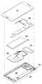
도 4는 본 개시의 다양한 실시예에 따른 전자 장치 하우징의 측면(320)과 후면(330)의 접합구조를 개략적으로 나타내는 도면이다.4 is a diagram schematically illustrating a bonding structure of a
도 4를 참조하면, 후면(330)은 중앙 부근이 평면으로 구성되며, 외곽이 하방으로 라운드되는 가장자리부(335)를 포함할 수 있다. 본 개시의 한 실시예에 따르면, 후면(330)의 중앙 부근이 평면으로 구성되어 있는 것으로 설명하고 있지만, 곡면을 포함하는 비평면으로 구성될 수도 있다. 후면(330)의 가장자리부(335)의 말단면은 최대한 측면(320) 측에 인접하게 이동 배치될 수 있다. 측면(320)은 후면 가장자리부(335)의 말단면과 일단면이 접합되는 제 1 면(320a), 상기 제 1 면(320a)과 일체로 연장되어 외부 가공에 의해 커팅되는 경사면(320b) 및 상기 경사면(320b)과 일체로 연결되어 하우징의 측면을 형성하는 외관면(320c)을 포함할 수 있다. 제 1 면(320a)은 실질적으로 수평방향으로 대략 직선에 가까우며, 대략 0.1mm ~ 0.4mm의 폭을 가질 수 있다. 제 1 면(320a)은 윈도우(311)와 대략 0°~ 10°의 각도를 형성할 수 있다. 상기 각도는 인서트 사출 시, 폴리카보네이트(PC)가 금속 부분으로 넘치지 않게 방지하는 인서트 사출 금형과 인서트 대상물(예: 금속 모재)의 직선 부분이 금형이 닫힐 시 붙어 있어야 하는데, 상기 각도가 크면 클수록 밀착력이 약해질 수 있다. 따라서, 상기 각도는 0°인 것이 가장 바람직하며, 인서트 대상물이 금형에 눌리거나, 사출시 사출압으로 인해 변형될 수 있는 각도를 고려하여 대략 10°이하인 것이 바람직하다. 제 1 면(320a)은 외부 가공에 의해 경사면(320b)을 형성할 때, 폴리카보네이트(PC)로 구성된 후면(330)의 손상을 방지하기 위하여, 다이아몬드 커팅과 같은 외부 가공을 위한 여분 영역으로 구성될 수 있으며, 외부 가공에 의한 커팅 후, 대략 0mm ~ 0.1mm의 폭을 가질 수 있다.Referring to FIG. 4 , the
도 5 및 도 6은 본 개시의 다양한 실시예에 따른 전자 장치(300)의 내부구성을 개략적으로 나타내는 분해사시도이다. 도 7은 도 5 및 도 6에 도시된 안테나 모듈의 세부구성을 나타내는 도면이다.5 and 6 are exploded perspective views schematically illustrating an internal configuration of an
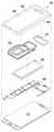
도 5 및 도 6을 참조하면, 다양한 실시예에 따른 전자 장치(300)는 하우징(501), GPS 안테나(510), 안테나 모듈(520), 배터리(530), PBA(540) 및 윈도우(311)를 포함할 수 있다.5 and 6 , the
하우징(501)은 측면(320)과 후면(330)이 일체로 형성되며, 내부에 각종 부품을 배치할 수 있는 수용 공간을 가질 수 있다. 하우징(501) 후면(330)의 평면의 적어도 일부는 하나 이상의 개구부를 포함할 수 있다.The
GPS 안테나(510)는 후면(330)의 상부에 배치될 수 있고, 안테나 모듈(520)은 후면(330)의 중앙 부근에 배치될 수 있다. 다양한 실시예에 따르면, GPS 안테나(510) 및 안테나 모듈(520)은 하우징(501) 내의 특정 위치에 한정되지 않고, 필요에 따라 다양한 위치에 배치될 수 있다.The
다양한 실시예에 따르면, 안테나 모듈(520)은, 도 7에 도시된 바와 같이, MST 안테나(522), NFC 안테나(524) 및 무선충전 안테나(526)를 포함할 수 있다.According to various embodiments, the
MST(Magnetic Secure Transmission; 마그네틱 보안 전송) 안테나(522)는 코일이 대략 8~10회 권선되어 구성될 수 있다. MST 안테나(522)의 인덕턴스 값은, 예를 들어 10~20uH 일 수 있다. NFC(Near Field Communication; 근거리 무선통신) 안테나(524)는 MST 안테나(522)의 외측에 구성되며, 인덕턴스 값은 예를 들어 1uH 미만일 수 있다. 무선충전 안테나(526)는 MST 안테나(522)의 내측 일부에 구성되며, 인덕턴스 값은 예를 들어 5`10uH 일 수 있다. MST 안테나(522) 및 무선충전 안테나(526)는 NFC 안테나(524)의 코일 권선수에 비해 권선수가 많을 수 있다.The MST (Magnetic Secure Transmission)
배터리(530)는 안테나 모듈(520)의 상부에 배치되어 전자 장치(300)의 구동에 필요한 전원을 공급할 수 있다.The
PBA(Printed Board Assembly; 인쇄회로기판 어셈블리)(540)는 도 1에 개시된 프로세서(120), 메모리(130), 및 통신 인터페이스(170)가 실장된 PCB를 포함할 수 있다.A Printed Board Assembly (PBA) 540 may include a PCB on which the
윈도우(311)는 도 1 및 도 2에 개시된 디스플레이(160 및 260)를 포함하며, 하우징(501)의 일면에 배치될 수 있다. 다양한 실시예에 따르면, 윈도우(311)는 전자 장치의 측면에 터치 가능하게 배치될 수도 있다.The
도 8은 본 개시의 다양한 실시예에 따른 전자 장치의 측면과 후면이 결합된 상태를 나타내는 도면이고, 도 9는 도 8의 A-A 부분의 단면도 및 일부 확대도이다.8 is a view illustrating a state in which a side surface and a rear surface of an electronic device are coupled according to various embodiments of the present disclosure, and FIG. 9 is a cross-sectional view and a partially enlarged view of a portion A-A of FIG. 8 .
도 8 및 도 9를 참조하면, 측면(320)은 후면(330)의 가장자리부(335) 말단면에 인접한 제 1 부분을 포함할 수 있다. 후면(330)의 가장자리부(335)의 말단면은 최대한 측면(320) 측에 인접하게 배치될 수 있다. 측면(320)은 후면(330)의 가장자리부(335)의 말단면과 일단이 접합되어 수평방향으로 직선 구간을 갖는 제 1 면(320a)과, 상기 제 1 면(320a)과 일체로 연장되어 외부 가공에 의해 커팅되는 경사면(320b)을 포함할 수 있다. 제 1 면(320a)은 실질적으로 수평방향으로 대략 직선에 가까우며 대략 0.1mm ~ 0.4mm의 폭을 가질 수 있다. 제 1 면(320a)은 윈도우(311)와 대략 0°~ 10°의 각도를 형성할 수 있다. 제 1 면(320a)은 외부 가공에 의해 경사면(320b)을 형성할 때, 폴리카보네이트(PC)로 구성된 후면(330)의 손상을 방지하기 위하여, 다이아몬드 커팅과 같은 외부 가공을 위한 여분 영역으로 구성될 수 있으며, 외부 가공에 의한 커팅 후, 대략 0mm ~ 0.1mm의 폭을 가질 수 있다. 측면(320)은 상기 제 1 면(320a)과 실질적으로 직각으로 형성되고 후면(330)의 가장자리부(335) 말단면과 접합되는 제 2 면(320d)을 포함할 수 있다.8 and 9 , the
다양한 실시예에 따르면, 상기 후면(330)의 가장자리부(335)의 말단면 부근에는 볼록부(931)가 형성되고, 상기 후면(330)의 가장자리부(335) 말단면과 접합되는 부근의 측면(320)에는 오목부(921)가 형성될 수 있다. 후면(330)의 가장자리부(335)의 말단면 부근에 형성된 볼록부(931)의 내측에는 홈부(933)가 형성되고, 측면(320)에 형성된 오목부(921)의 내측에는 상기 홈부(933)와 대응되게 돌기부(923)가 형성될 수 있다. 측면(320)에 형성된 오목부(921)에는 가장자리부(335)의 말단면 부근에 형성된 볼록부(931)가 결합되고, 가장자리부(335)에 형성된 홈부(933)에는 측면(320)에 형성된 돌기부(923)가 결합될 수 있다. 즉, 후면(330)의 가장자리부(335)의 말단면과 측면(320)의 내측이 만나는 접합부를 오목부(921)와 볼록부(931) 및 돌기부(923)와 홈부(933)를 통해 서로 엇갈리게 결합함으로써, 측면(320)과 후면(330)이 서로 쉽게 분리되지 않게 할 뿐만 아니라, 금속재로 구성된 측면(320)이 고분자 재료로 구성된 후면(330)을 받쳐주는 안정적인 구조를 형성할 수 있다.According to various embodiments, a
상술한 실시예에 따르면, 측면(320) 내측에 오목부(921)와 돌기부(923)가 형성되어 있고, 후면(330)의 가장자리부(335) 부근에 볼록부(931)와 홈부(933)가 형성되어 있는 것으로 설명하고 있지만, 측면(320)의 내측에 볼록부와 홈부가 형성되고 후면(330)의 가장자리부(335)에 오목부와 돌기부가 형성될 수도 있다.According to the above-described embodiment, a
도 10은 본 개시의 다양한 실시예에 따른 전자 장치 하우징의 접지부와 PBA의 접지단자를 설명하기 위한 도면이다.10 is a view for explaining a ground portion of an electronic device housing and a ground terminal of a PBA according to various embodiments of the present disclosure;
도 10을 참조하면, 하우징(501)의 후면(330) 내측에는 상술한 GPS 안테나(510), 안테나 모듈(520), 배터리(530) 및 PBA(540) 등과 같은 각종 부품을 안착시키기 위한 패턴이 형성될 수 있다.Referring to FIG. 10 , a pattern for seating various parts such as the
다양한 실시예에 따르면, 하우징(501) 후면(330)의 내측 상부 및 하부 각각에는 적어도 하나의 안테나 접지부(1010)가 형성될 수 있다. PBA(540)의 배면의 상부 및 하부 각각에는 상기 안테나 접지부(1010)와 서로 전기적으로 연결되는 적어도 하나의 접지단자(1020)가 형성될 수 있다.According to various embodiments, at least one
도 11은 본 개시의 다양한 실시예에 따른 전자 장치의 측면과 후면이 결합된 상태를 나타내는 도면이고, 도 12는 도 11의 B-B 부분의 단면도 및 확대도이다.11 is a view illustrating a state in which a side surface and a rear surface of an electronic device are coupled to each other according to various embodiments of the present disclosure, and FIG. 12 is a cross-sectional view and an enlarged view of a portion B-B of FIG. 11 .
도 11 및 도 12를 참조하면, 후면(330)의 가장자리부(335)의 말단면은, 예를 들어 알루미늄(Al) 또는 알루미늄 합금과 같은 금속재로 구성되어 전자 장치의 안테나로서의 기능을 수행하는 측면(320) 측에 인접하게 배치될 수 있다. 측면(320)은 후면(330)의 가장자리부(335)의 말단면과 일단면이 접합되어 수평방향으로 직선 구간을 갖는 제 1 면(320a)과, 상기 제 1 면(320a)과 일체로 연장되어 외부 가공에 의해 커팅되는 경사면(320b)을 포함할 수 있다. 제 1 면(320a)은 외부 가공에 의해 경사면(320b)을 형성할 때, 예를 들어 폴리카보네이트(PC)로 구성된 후면(330)의 손상을 방지하기 위하여, 다이아몬드 커팅과 같은 외부 가공을 위한 여분 영역으로 구성될 수 있으며, 외부 가공에 의한 커팅 후, 대략 0mm ~ 0.1mm의 폭을 가질 수 있다. 측면(320)은 상기 제 1 면(320a)과 실질적으로 수직하게 형성되고 후면(330)의 가장자리부(335)의 말단면과 접합되는 제 2 면(320d)을 포함할 수 있다.11 and 12 , the end surface of the
다양한 실시예에 따르면, 후면(330)의 가장자리부(335)의 말단면 부근에는 볼록부(931)가 형성되고, 상기 후면(330)의 가장자리부(335) 말단면과 접합되는 부근의 측면(320)에는 오목부(921)가 형성될 수 있다. 후면(330)의 가장자리부(335) 말단면 부근에 형성된 볼록부(931)의 내측에는 홈부(933)가 형성되고, 측면(320)에 형성된 오목부(921)의 내측에는 상기 홈부(933)와 대응되게 돌기부(923)가 형성될 수 있다. 측면(320)에 형성된 오목부(921)에는 가장자리부(335)의 말단면 부근에 형성된 볼록부(931)가 결합되고, 가장자리부(335)에 형성된 홈부(933)에는 측면(320)에 형성된 돌기부(923)가 결합될 수 있다. 즉, 후면(330)의 가장자리부(335)의 말단과 측면(320)의 내측이 만나는 접합부를 오목부(921)와 볼록부(931) 및 돌기부(923)와 홈부(933)를 통해 서로 엇갈리게 결합함으로써, 측면(320)과 후면(330)이 서로 쉽게 분리되지 않게 할 뿐만 아니라, 금속재로 구성된 측면(320)이 고분자 재료로 구성된 후면(330)을 받쳐주는 구조를 형성할 수 있다.According to various embodiments, a
다양한 실시예에 따르면, 하우징(501) 내의 안테나 접지부(1010) 및/또는 PBA(540)의 접지단자(1020)는 고분자 재료로 구성된 후면(330)의 외곽으로 노출되지 않는 것이 바람직하다. 예를 들어, 상기 하우징(501) 내의 안테나 접지부(1010) 및/또는 PBA(540)의 접지단자(1020)가 후면(330)의 외곽으로 노출되면, 이 노출 부분에 대하여 퍼티 도장 및 버핑 공정이 필요하게 되므로, 전자 장치 하우징(501)의 제조 비용이 상승될 수 있다.According to various embodiments, it is preferable that the
도 13은 본 개시의 다양한 실시예에 따른 전자 장치 하우징 내에 장착되는 다양한 안테나를 나타내는 도면이다.13 is a view illustrating various antennas mounted in an electronic device housing according to various embodiments of the present disclosure;
도 13을 참조하면, 하우징(501)의 후면(330) 상부에 장착되는 GPS 안테나(510)는 소정 위치에 접지부(515)를 구비할 수 있다. 하우징(501)의 후면(330)의 중앙 부근에 장착되는 안테나 모듈(520)은 소정 위치에 접지부(525)를 구비할 수 있다. 예를 들어, 안테나 모듈(520)이 PBA(540)에 부품으로 적용되면, 안테나 모듈(520)은 PBA(540)와 접지가 되어 있는 상태이기 때문에 별도의 접지부를 구비하지 않을 수 있다. GPS 안테나(510)의 접지부(515) 및 안테나 모듈(520)의 접지부(525)는 도 12에 도시된 PBA(540)의 접지 단자(1020)와 접촉될 수 있다. 하우징(501)의 후면(330)에 금속재가 배제되고, 사출 성형에 의해 예를 들어 폴리카보네이트(PC)와 같은 고분자 재료로만 구성되기 때문에, GPS 안테나(510) 및 안테나 모듈(520)과 같은 내장 안테나들의 실장 영역이 자유스럽게 되며, 안테나의 성능을 저하시키지 않을 수 있다.Referring to FIG. 13 , the
도 14는 본 개시의 다양한 실시예에 따른 전자 장치의 하우징 내에 스크류 인서트가 형성된 상태를 나타내는 도면이다.14 is a view illustrating a state in which a screw insert is formed in a housing of an electronic device according to various embodiments of the present disclosure;
도 14를 참조하면, 하우징(501)의 내부에는 인서트 사출 방식을 통해 적어도 하나의 스크류 인서트(1410)가 구비될 수 있다. 스크류 인서트(1410)는 황동 재질로 구성될 수 있다. 전자 장치의 하우징 제작 후 별도의 스크류 태핑(Screw tapping, 1420) 공정을 통해 스크류 나사선을 형성하는 방식에 비해 하우징의 제조 비용을 절감할 수 있다. 즉, 하우징(501)의 내부에 구비되는 스크류 인서트(1410)는 사출 금형이 열릴 시, 황동 재질의 스크류 인서트(1410)를 삽입한 후 고분자 수지 주입의 사출 공정으로 인해 스크류 인서트(1410)가 함께 형성되어 취출될 수 있다. 즉, 하우징(501)과 스크류 인서트(1410)가 하나의 공정을 통해 동시에 형성될 수 있다. 그러나, 종래기술에 적용되는 스크류 태핑(1420) 공정은 하우징(501)을 먼저 형성하고, 이후에 추가로 나사선을 형성하는 공정을 수행하기 때문에 제조시간 및 재료비가 상승될 수 있다.Referring to FIG. 14 , at least one
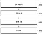
도 15는 본 개시의 다양한 실시예에 따른 전자 장치 하우징의 제조방법을 나타내는 흐름도이다.15 is a flowchart illustrating a method of manufacturing an electronic device housing according to various embodiments of the present disclosure;
도 15를 참조하면, 1510 단계에서, 예를 들어 알루미늄(AL) 또는 알루미늄 합금과 같은 금속 모재를 준비한다. 1520 단계에서, 다이캐스팅(Die casting), CNC(Computerized Numerical Control), 단조, 압연, 용접 및 인발 공정 중 적어도 하나를 수행하여, 도 16에 도시된 바와 같은 전자 장치의 측면 하우징(1620)을 구성할 수 있다.Referring to FIG. 15 , in
도 16은 본 개시의 다양한 실시예에 따른 전자 장치의 측면 하우징을 나타내는 도면이다. 도 17은 도 16의 C-C 부분의 단면도이다.16 is a view illustrating a side housing of an electronic device according to various embodiments of the present disclosure; 17 is a cross-sectional view taken along line C-C of FIG. 16 .
다양한 실시예에 따르면, 다이캐스팅 공정은 측면 하우징(1620)을 제조하기 위한 프레스, 압출, 압연 및 NC(Numerical Control) 가공 등을 포함할 수 있다. 다이캐스팅 공정을 통해 측면 하우징(1620)을 제조시에는, 도 17에 도시된 바와 같이, 측면 하우징(1620)에 대한 금형이 상부 방향으로 빠질 수 있는 구배를 가질 수 있다.According to various embodiments, the die casting process may include pressing, extrusion, rolling, and Numerical Control (NC) processing for manufacturing the
다양한 실시예에 따르면, 1530 단계에서, 인서트 사출(Insert injection) 공정을 수행하여, 도 19에 도시된 바와 같이. 측면 하우징(1620)과 일체로 후면 하우징(1630)을 구성할 수 있다. 측면 하우징(1620)은 측면(320)일 수 있고, 후면 하우징(1630)은 후면(330)일 수 있다. 인서트 사출 공정은 1520 단계의 다이캐스팅 공정을 통해 제조된 측면 하우징(1620)을 사출 금형 내에 장착하고, 사출 금형에 고분자 재료를 주입함으로써 수행될 수 있다.According to various embodiments, in
참고로, 금속재로 구성된 측면 하우징(1620)에 수지를 이용한 인서트 사출이 필요한 이유는 도 18을 참조하여 설명할 수 있다. 스마트폰 및 타블렛 PC 등과 같이 무선 통신이 가능한 전자 장치에 금속 하우징을 적용할 경우, 측면 하우징(1620)의 일부 케이스(1622)는 안테나의 일부로 활용될 수 있다. 이 때문에, 안테나로 사용되는 측면 하우징(1620)의 일부 케이스(1622)는 비전도성 물질을 통해 측면 하우징(1620)과 전기적으로 분리되어 있어야 한다. 또한, 측면 하우징(1620)과 일부 케이스(1622)가 하나의 하우징을 이루기 위해서는 상기 비전도성 물질인 고분자 수지(1624)로 상호 연결될 수 있다. 고분자 수지(1624)를 통해 측면 하우징(1620)과 일부 케이스(1622)를 접합시, 접합력이 약하면 외부의 충격에 의해 쉽게 분리될 수 있다. 따라서, 고분자 수지(1624)는 측면 하우징(1620)과 일부 케이스(1622)의 접합 강도를 위해 너비가 넓은 사각형상이 될 수 있고, 다른 여러 가지 형상으로 형성될 수 있다.For reference, the reason why insert injection using resin is required for the
도 19는 본 개시의 다양한 실시예에 따른 전자 장치의 측면 하우징과 후면 하우징이 일체로 결합된 상태를 나타내는 도면이다. 도 20은 도 19의 D-D 부분의 단면도 및 일부 확대도이다.19 is a diagram illustrating a state in which a side housing and a rear housing of an electronic device are integrally coupled to each other according to various embodiments of the present disclosure; 20 is a cross-sectional view and a partially enlarged view of a portion D-D of FIG. 19 .
다양한 실시예에 따르면, 1530 단계에서 인서트 사출 공정 수행시, 후면 하우징(1630)을 구성하는, 예를 들어 폴리카보네이트(PC)와 같은 고분자 재료가 측면 하우징(1620)으로 넘치는 것을 방지하기 위해, 상기 측면 하우징(1620)의 말단부는 소정의 직선 구간(1625)을 가질 수 있다. 알루미늄(AL) 또는 알루미늄 합금과 같은 금속재로 구성된 측면 하우징(1620)의 외면은 금형이 상부 방향으로 빠질 수 있는 구배를 가질 수 있다.According to various embodiments, when performing the insert injection process in
다양한 실시예에 따르면, 1540 단계에서, 측면 하우징(1620)의 일부에 외부 가공을 수행하여, 상술한 도 9 및 도 12와 후술하는 도 21 및 도 22에 도시된 바와 같이, 대략 20°~ 70°의 경사를 갖는 경사면(320b)을 형성할 수 있다. 외부 가공을 수행하는 목적은 측면 하우징(1620)의 디자인에 대한 심미감을 높이기 위한 공정으로서, 측면 하우징(1620)의 경우, 금형 취출을 위해 구배를 제공하며, 디자인에 대한 심미감 뿐만 아니라 디스플레이 영역과 전자 장치의 외곽까지의 거리를 줄이기 위해 수행할 수 있다. 상기 외부 가공과 함께 다이아몬드 커팅을 수행하여, 측면 하우징(1620)의 외부 노출면에 미려한 질감이 표시되게 할 수도 있다.According to various embodiments, in
도 21은 본 개시의 다양한 실시예에 따른 전자 장치의 측면 하우징과 후면 하우징 사이에 형성된 경사면을 나타내는 도면이다. 도 22는 도 21의 E-E 부분의 단면 및 일부 확대도이다.21 is a view illustrating an inclined surface formed between a side housing and a rear housing of an electronic device according to various embodiments of the present disclosure; 22 is a cross-sectional view and partially enlarged views of portions E-E of FIG. 21 .
다양한 실시예에 따르면, 측면 하우징(1620)과 후면 하우징(1630)이 접합되는 영역의 측면 하우징(1620a)의 일부에 형성된 경사면(320b)의 내측에는 실질적으로 직선에 가까운 제 1 면(320a)이 형성될 수 있다. 제 1 면(320a)은 대략 0.1mm ~ 0.4mm의 폭을 갖도록 구성되어, 외부 가공에 의해 경사면(320b)을 형성할 때, 후면 하우징(1630)이 손상되는 것을 방지할 수 있다. 제 1 면(320a)은 다이아몬드 커팅과 같은 외부 가공을 위한 여분 영역으로 구성될 수 있으며, 외부 가공에 의한 커팅 후, 대략 0mm ~ 0.1mm의 폭을 가질 수 있다.According to various embodiments, on the inside of the
따라서, 본 개시의 다양한 실시예에 따르면, 측면 하우징(1620)과 후면 하우징(1630)의 접합부에 대하여, 종래의 일반적인 퍼티 도장 및 버핑 공정을 수행하지 않고, 측면 하우징(1620)에 대하여 다이아몬드 커팅과 같은 외부 가공만을 수행함으로써, 전자 장치 하우징의 제조에 따른 비용을 절감하고, 수율을 상승시킬 수 있으며, 실제 금속과 같은 느낌의 유니 바디 디자인 및 2가지 컬러를 갖는 하우징을 용이하게 구현할 수 있다.Therefore, according to various embodiments of the present disclosure, for the joint portion of the
본 명세서 및 도면에 개시된 다양한 실시 예들은 이해를 돕기 위해 특정 예를 제시한 것일 뿐이며, 본 발명의 다양한 실시 예들의 범위를 한정하고자 하는 것은 아니다. 따라서 본 발명의 다양한 실시 예들의 범위는 여기에서 설명된 실시 예들 이외에도 본 발명의 다양한 실시 예들의 기술적 사상을 바탕으로 도출되는 모든 변경 또는 변형된 형태가 본 발명의 다양한 실시 예들의 범위에 포함되는 것으로 해석되어야 한다.The various embodiments disclosed in the present specification and drawings are merely presented as specific examples to aid understanding, and are not intended to limit the scope of various embodiments of the present invention. Therefore, in the scope of various embodiments of the present invention, in addition to the embodiments described herein, all changes or modifications derived based on the technical ideas of various embodiments of the present invention are included in the scope of various embodiments of the present invention. should be interpreted
120 : 프로세서130 : 메모리
160 : 디스플레이170 : 통신 인터페이스
320 : 측면320a : 제 1 면
320b : 경사면320c : 외관면
320d : 제 2 면330 : 후면
335 : 가장자리부501 : 하우징
510 : GPS 안테나520 : 안테나 모듈
530 : 배터리 540 : PBA120: processor 130: memory
160: display 170: communication interface
320:
320b:
320d: second side 330: rear
335: edge 501: housing
510: GPS antenna 520: antenna module
530: battery 540: PBA
Claims (20)
Translated fromKorean제 1 방향을 향하는 제 1 플레이트,
상기 제 1 방향과 맞은편의 제 2 방향을 향하는 평면을 구비하며 실질적으로 고분자 재료로 구성되는 제 2 플레이트, 및 상기 제 2 플레이트를 상부에서 바라볼 때 상기 평면을 둘러싸는 주변부, 및
상기 제 1 플레이트 및 제 2 플레이트 사이의 공간을 둘러싸되, 금속 재료로 구성되어 상기 제 2 플레이트와 일체로 형성되는 측면 부재를 구비하는, 하우징;
상기 제 1 플레이트의 적어도 일부를 통해 노출된 디스플레이;
상기 하우징의 내부에 배치된 통신 회로;
상기 하우징의 내부에 배치된 메모리;
상기 하우징의 내부에 배치되고, 상기 디스플레이, 통신 회로 및 메모리에 전기적으로 접속되어 있는 프로세서;를 포함하되,
상기 측면 부재는 상기 제 2 플레이트의 상기 주변부에 인접한 제 1 부분을 구비하고,
상기 제 1 부분은 실질적으로 상기 제 2 방향을 향하는 제 1 면과, 상기 제 2 플레이트의 주변부와 접촉하고 상기 제 1 방향 및 제 2 방향과는 다른 제 3 방향을 향하는 제 2 면을 구비하고,
상기 하우징의 후면의 말단면의 내측에는 볼록부가 형성되어 있고, 상기 볼록부는 상기 후면의 말단면에 접합된 측면 부재의 내측에 형성되어 있는 오목부와 결합되고, 상기 볼록부의 내측에는 홈부가 형성되어 있고, 상기 오목부의 내측에는 돌기부가 형성되어 있되, 상기 홈부에 상기 돌기부가 결합되도록 구성된 전자 장치.An electronic device comprising:
a first plate facing in a first direction;
a second plate having a plane facing in a second direction opposite to the first direction and substantially composed of a polymer material, and a periphery surrounding the plane when viewed from above the second plate; and
a housing that surrounds the space between the first plate and the second plate and includes a side member made of a metal material and integrally formed with the second plate;
a display exposed through at least a portion of the first plate;
a communication circuit disposed inside the housing;
a memory disposed inside the housing;
a processor disposed inside the housing and electrically connected to the display, communication circuitry, and memory;
wherein said side member has a first portion adjacent said periphery of said second plate;
the first portion has a first face facing substantially in the second direction, and a second face in contact with a periphery of the second plate and facing a third direction different from the first and second directions;
A convex portion is formed on the inner side of the end face of the rear surface of the housing, the convex portion is engaged with a concave portion formed on the inner side of the side member joined to the end face of the rear surface, and a groove portion is formed on the inner side of the convex portion, and a protrusion is formed inside the concave portion, and the protrusion is configured to be coupled to the groove portion.
상기 제 1 면은 상기 제 2 플레이트의 평면과 0°내지 10°의 각도를 형성하는 전자 장치.The method of claim 1,
The first surface forms an angle of 0° to 10° with the plane of the second plate.
상기 제 1 면은 0.1mm 내지 0.4mm의 폭을 갖는 전자 장치.The method of claim 1,
The first surface may have a width of 0.1 mm to 0.4 mm.
상기 제 1 면은 커팅 가공을 위한 여분 영역을 포함하도록 구성되며, 커팅 가공 후, 0mm ~ 0.1mm의 폭을 갖는 전자 장치.4. The method of claim 3,
The first surface is configured to include an extra area for cutting, and has a width of 0 mm to 0.1 mm after cutting.
상기 제 3 방향은 상기 제 1 방향의 내측과 평행한 방향인 전자 장치.The method of claim 1,
The third direction is a direction parallel to an inner side of the first direction.
상기 고분자 재료는 폴리카보네이트(PC)인 전자 장치.The method of claim 1,
wherein the polymer material is polycarbonate (PC).
상기 금속 재료는 알루미늄 또는 알루미늄(Al) 합금 중 적어도 하나를 포함하는 전자 장치.The method of claim 1,
The electronic device includes at least one of aluminum and an aluminum (Al) alloy.
상기 하우징은,
후면; 및
상기 후면의 외주면과 결합되는 측면을 포함하되,
상기 측면은,
상기 후면의 말단면과 결합되어 수평방향으로 직선 구간을 갖는 제 1 면과,
상기 제 1 면의 내측에 수직방향으로 형성되어 후면의 말단면과 접합되는 제 2 면을 포함하고,
상기 하우징의 후면의 말단면의 내측에는 볼록부가 형성되어 있고, 상기 볼록부는 상기 후면의 말단면에 접합된 측면의 내측에 형성되어 있는 오목부와 결합되고, 상기 볼록부의 내측에는 홈부가 형성되어 있고, 상기 오목부의 내측에는 돌기부가 형성되어 있되, 상기 홈부에 상기 돌기부가 결합되도록 구성된 전자 장치.An electronic device having a housing having an accommodating space therein, comprising:
The housing is
back side; and
Including a side surface coupled to the outer peripheral surface of the rear surface,
The side is
a first surface coupled to the distal end surface of the rear surface and having a straight section in the horizontal direction;
and a second surface formed in a vertical direction on the inside of the first surface and joined to the end surface of the rear surface,
A convex portion is formed inside the distal end face of the rear surface of the housing, and the convex portion is engaged with a concave portion formed inside a side surface joined to the rear distal face, and a groove is formed inside the convex portion, , An electronic device configured to have a protrusion formed inside the concave portion, and the protrusion to be coupled to the groove portion.
상기 제 1 면의 외측에는 커팅 가공에 의해 경사를 갖는 경사면이 형성되는 전자 장치.9. The method of claim 8,
An electronic device in which an inclined surface having an inclination is formed on an outer side of the first surface by cutting.
상기 제 1 면은 경사면 형성 후, 0mm ~ 0.1mm의 폭을 갖는 전자 장치.10. The method of claim 9,
The first surface has a width of 0 mm to 0.1 mm after forming the inclined surface.
상기 경사면은 상기 제 1 면과 20°~ 70°의 경사를 갖는 전자 장치.10. The method of claim 9,
The inclined surface has an inclination of 20° to 70° with respect to the first surface.
상기 후면은 고분자 재료로 구성되고, 상기 측면은 금속 재료로 구성되는 전자 장치.9. The method of claim 8,
The rear surface is made of a polymer material, and the side surface is made of a metal material.
상기 측면에는 인서트 사출 성형에 의해 적어도 하나의 스크류 인서트가 형성되는 전자 장치.9. The method of claim 8,
An electronic device in which at least one screw insert is formed on the side surface by insert injection molding.
하우징의 측면을 구성하는 금속 모재를 준비하는 단계;
상기 금속 모재를 가공하여 측면 하우징을 형성하는 단계;
인서트 사출 공정을 수행하여 상기 측면 하우징과 일체로 후면 하우징을 형성하는 단계; 및
상기 측면 하우징의 일부에 경사를 갖는 경사면을 형성하는 단계를 포함하되,
상기 후면 하우징의 말단면의 내측에는 볼록부가 형성되어 있고, 상기 볼록부는 상기 후면 하우징의 말단면에 접합된 측면 하우징의 내측에 형성되어 있는 오목부와 결합되고, 상기 볼록부의 내측에는 홈부가 형성되어 있고, 상기 오목부의 내측에는 돌기부가 형성되어 있되, 상기 홈부에 상기 돌기부가 결합되도록 구성된 전자 장치의 하우징 제조방법.A method of manufacturing a housing for an electronic device, comprising:
Preparing a metal base material constituting the side of the housing;
forming a side housing by processing the metal base material;
performing an insert injection process to form a rear housing integrally with the side housing; and
Comprising the step of forming an inclined surface having an inclination on a part of the side housing,
A convex portion is formed on the inner side of the distal face of the rear housing, the convex portion is engaged with a concave portion formed on the inner side of the side housing joined to the distal face of the rear housing, and a groove is formed inside the convex portion, and a protrusion is formed inside the concave portion, and the protrusion is coupled to the groove portion.
상기 금속 모재를 가공하여 측면 하우징을 형성하는 단계는, 다이캐스팅, CNC(computerized Numerical Control), 단조, 압연, 용접 및 인발 가공중 적어도 하나를 포함하는 전자 장치의 하우징 제조방법.16. The method of claim 15,
The forming of the side housing by processing the metal base material includes at least one of die casting, computerized numerical control (CNC), forging, rolling, welding, and drawing.
상기 측면 하우징에 다이캐스팅 공정 수행시, 측면 하우징은 금형이 상부 방향으로 빠질 수 있는 구배를 갖는 전자 장치의 하우징 제조방법.16. The method of claim 15,
When the die-casting process is performed on the side housing, the side housing has a gradient through which a mold can be pulled out in an upward direction.
상기 인서트 사출 공정 수행시, 후면 하우징을 구성하는 고분자 재료가 측면 하우징으로 넘치는 것을 방지하기 위해, 상기 측면 하우징의 말단부에는 소정의 직선 구간이 형성되는 전자 장치의 하우징 제조방법.16. The method of claim 15,
In order to prevent the polymer material constituting the rear housing from overflowing into the side housing when the insert injection process is performed, a predetermined straight section is formed at the distal end of the side housing.
상기 금속 모재의 가공은 다이아몬드 커팅을 포함하는 전자 장치의 하우징 제조방법.16. The method of claim 15,
The method of manufacturing a housing of an electronic device, wherein the processing of the metal base material includes diamond cutting.
상기 경사면을 형성한 후 측면 하우징의 일부에는 0mm ~ 0.1mm의 폭을 갖는 구간이 존재하는 전자 장치의 하우징 제조방법.16. The method of claim 15,
A method of manufacturing a housing for an electronic device in which a section having a width of 0 mm to 0.1 mm exists in a part of the side housing after the inclined surface is formed.
Priority Applications (5)
| Application Number | Priority Date | Filing Date | Title |
|---|---|---|---|
| KR1020150159534AKR102358304B1 (en) | 2015-11-13 | 2015-11-13 | Electronic device having unibody housing and method for manufacturing the same |
| PCT/KR2016/012698WO2017082596A1 (en) | 2015-11-13 | 2016-11-04 | Electronic device having unibody housing and method of manufacturing the same |
| EP16864522.4AEP3375174B1 (en) | 2015-11-13 | 2016-11-04 | Electronic device having unibody housing and method of manufacturing the same |
| CN201680066128.5ACN108353098B (en) | 2015-11-13 | 2016-11-04 | Electronic device with one-piece housing and method of making the same |
| US15/351,055US10205807B2 (en) | 2015-11-13 | 2016-11-14 | Electronic device having unibody housing and method of manufacturing the same |
Applications Claiming Priority (1)
| Application Number | Priority Date | Filing Date | Title |
|---|---|---|---|
| KR1020150159534AKR102358304B1 (en) | 2015-11-13 | 2015-11-13 | Electronic device having unibody housing and method for manufacturing the same |
Publications (2)
| Publication Number | Publication Date |
|---|---|
| KR20170056198A KR20170056198A (en) | 2017-05-23 |
| KR102358304B1true KR102358304B1 (en) | 2022-02-04 |
Family
ID=58692145
Family Applications (1)
| Application Number | Title | Priority Date | Filing Date |
|---|---|---|---|
| KR1020150159534AActiveKR102358304B1 (en) | 2015-11-13 | 2015-11-13 | Electronic device having unibody housing and method for manufacturing the same |
Country Status (5)
| Country | Link |
|---|---|
| US (1) | US10205807B2 (en) |
| EP (1) | EP3375174B1 (en) |
| KR (1) | KR102358304B1 (en) |
| CN (1) | CN108353098B (en) |
| WO (1) | WO2017082596A1 (en) |
Families Citing this family (16)
| Publication number | Priority date | Publication date | Assignee | Title |
|---|---|---|---|---|
| EP2992776B1 (en)* | 2014-09-04 | 2019-11-06 | WITS Co., Ltd. | Case and apparatus including the same |
| US10320960B2 (en)* | 2015-06-19 | 2019-06-11 | Tianjin M&C Electronics Co., Ltd. | Metal frame and method of manufacturing the metal frame for the mobile communication terminal |
| USD795213S1 (en)* | 2015-11-10 | 2017-08-22 | Samsung Electronics Co., Ltd. | Portable electronic device |
| KR102484740B1 (en)* | 2016-01-21 | 2023-01-05 | 삼성전자 주식회사 | Antenna apparatus and electronic device including the same |
| JP6786245B2 (en)* | 2016-04-07 | 2020-11-18 | ソニーモバイルコミュニケーションズ株式会社 | Information processing device |
| USD839231S1 (en)* | 2016-09-26 | 2019-01-29 | Samsung Electronics Co., Ltd. | Electronic device |
| USD816055S1 (en) | 2016-11-11 | 2018-04-24 | Samsung Electronics Co., Ltd. | Mobile phone |
| USD837177S1 (en)* | 2016-11-24 | 2019-01-01 | Samsung Electronics Co., Ltd. | Electronic device |
| KR101949745B1 (en)* | 2017-08-10 | 2019-02-19 | 엘지전자 주식회사 | Mobile terminal |
| CN111542868B (en)* | 2017-12-26 | 2023-09-12 | 索尼公司 | Display apparatus |
| EP3609167A1 (en)* | 2018-08-07 | 2020-02-12 | SABIC Global Technologies B.V. | Portable electronic device with injection molded back and method of manufacture |
| KR102474016B1 (en) | 2018-04-13 | 2022-12-06 | 삼성전자주식회사 | Electronic device having housing and manufacturing method thereof |
| KR102744902B1 (en)* | 2019-01-31 | 2024-12-20 | 삼성전자주식회사 | An electronic device comprising a housing comprising a metallic materials |
| KR102656398B1 (en)* | 2019-02-01 | 2024-04-12 | 삼성전자주식회사 | Housing and electronic device including the same |
| CN110366079B (en)* | 2019-07-30 | 2022-11-18 | 歌尔股份有限公司 | Sound producing device |
| WO2023234598A1 (en)* | 2022-05-30 | 2023-12-07 | 삼성전자 주식회사 | Electronic device comprising key assembly |
Citations (2)
| Publication number | Priority date | Publication date | Assignee | Title |
|---|---|---|---|---|
| US20130318766A1 (en)* | 2012-05-29 | 2013-12-05 | Bryan P. KIPLE | Components of an electronic device and methods for their assembly |
| US20150212626A1 (en)* | 2012-02-23 | 2015-07-30 | Samsung Electronics Co., Ltd. | Touch panel having improved visibility and method of manufacturing the same |
Family Cites Families (13)
| Publication number | Priority date | Publication date | Assignee | Title |
|---|---|---|---|---|
| KR100898575B1 (en) | 2007-06-29 | 2009-05-20 | 김지웅 | Cover of mobile phone and manufacturing method thereof |
| KR100824012B1 (en) | 2008-01-03 | 2008-04-21 | 주식회사금강코엔 | Injection molding method of frame for wireless communication device with synthetic resin container |
| CN101578019A (en)* | 2008-05-09 | 2009-11-11 | 富准精密工业(深圳)有限公司 | Electronic device shell and manufacture method thereof |
| US8797721B2 (en)* | 2010-02-02 | 2014-08-05 | Apple Inc. | Portable electronic device housing with outer glass surfaces |
| CN102202475A (en)* | 2010-03-25 | 2011-09-28 | 深圳富泰宏精密工业有限公司 | Electronic device shell and manufacturing method thereof |
| US9235240B2 (en)* | 2010-11-11 | 2016-01-12 | Apple Inc. | Insert molding around glass members for portable electronic devices |
| US8791864B2 (en)* | 2011-01-11 | 2014-07-29 | Apple Inc. | Antenna structures with electrical connections to device housing members |
| CN105843331B (en) | 2011-06-13 | 2019-06-14 | 树蛙开发公司 | Case to protect tablet |
| US9001002B2 (en)* | 2011-09-30 | 2015-04-07 | Apple Inc. | Portable electronic device housing having insert molding around antenna |
| US9949397B2 (en)* | 2012-02-23 | 2018-04-17 | Samsung Electronics Co., Ltd. | Touch panel having improved visibility and method of manufacturing the same |
| KR101425589B1 (en) | 2012-10-26 | 2014-08-01 | (주)파트론 | Case of electronic devices with antenna pattern and method thereof |
| KR102044505B1 (en)* | 2013-02-08 | 2019-11-13 | 삼성전자주식회사 | Housing, manufacturing method thereof and electronic device using same |
| KR102055330B1 (en)* | 2013-03-13 | 2020-01-22 | 삼성전자주식회사 | Case and manufacturing method thereof |
- 2015
- 2015-11-13KRKR1020150159534Apatent/KR102358304B1/enactiveActive
- 2016
- 2016-11-04EPEP16864522.4Apatent/EP3375174B1/enactiveActive
- 2016-11-04WOPCT/KR2016/012698patent/WO2017082596A1/ennot_activeCeased
- 2016-11-04CNCN201680066128.5Apatent/CN108353098B/enactiveActive
- 2016-11-14USUS15/351,055patent/US10205807B2/enactiveActive
Patent Citations (2)
| Publication number | Priority date | Publication date | Assignee | Title |
|---|---|---|---|---|
| US20150212626A1 (en)* | 2012-02-23 | 2015-07-30 | Samsung Electronics Co., Ltd. | Touch panel having improved visibility and method of manufacturing the same |
| US20130318766A1 (en)* | 2012-05-29 | 2013-12-05 | Bryan P. KIPLE | Components of an electronic device and methods for their assembly |
Also Published As
| Publication number | Publication date |
|---|---|
| EP3375174B1 (en) | 2021-07-21 |
| WO2017082596A1 (en) | 2017-05-18 |
| US20170142239A1 (en) | 2017-05-18 |
| EP3375174A1 (en) | 2018-09-19 |
| EP3375174A4 (en) | 2018-11-07 |
| US10205807B2 (en) | 2019-02-12 |
| CN108353098B (en) | 2021-03-30 |
| CN108353098A (en) | 2018-07-31 |
| KR20170056198A (en) | 2017-05-23 |
Similar Documents
| Publication | Publication Date | Title |
|---|---|---|
| KR102358304B1 (en) | Electronic device having unibody housing and method for manufacturing the same | |
| KR102495207B1 (en) | Electronic device having display with bended area | |
| KR102377279B1 (en) | Electronic device including cooling function and controlling method thereof | |
| KR102335846B1 (en) | Electronic device comprising a plurality of coils | |
| CN108508969B (en) | Electronic device including curved display and method of displaying image of electronic device | |
| CN108696608B (en) | Support structure including conductive paths and electronic device having the same | |
| KR102588423B1 (en) | Electronic device including component mounting structure through bended display | |
| KR102424424B1 (en) | Electronic device | |
| KR102447909B1 (en) | electronic device | |
| US10424964B2 (en) | Electronic device and method for controlling transmission/reception of wireless power | |
| KR102405446B1 (en) | Antenna device and electronic device | |
| KR102507947B1 (en) | Case and Electronic device including the same | |
| KR102464157B1 (en) | Antenna and electronic device having it | |
| US9684335B2 (en) | Rotary device and electronic device having the same | |
| US10305313B2 (en) | Antenna, manufacturing process thereof and electronic device using the antenna | |
| KR102262853B1 (en) | Operating Method For plural Microphones and Electronic Device supporting the same | |
| KR102359786B1 (en) | Antenna and electronic device comprising thereof | |
| EP3504867B1 (en) | Electronic device including antenna | |
| US20160011738A1 (en) | Electronic device, method of providing interface of the same, and accessory for the same | |
| KR102132442B1 (en) | Sensor device and apparatus having the same | |
| KR102431962B1 (en) | Electronic device and method for improving performance of antenna of the same | |
| EP3522296A1 (en) | Electronic device comprising antenna | |
| US11159034B2 (en) | Wireless charging stand, and method for operating electronic device linked thereto | |
| KR102438680B1 (en) | Housing including antenna, manufacturing method thereof, and electronic device having it | |
| EP3503416B1 (en) | Electronic device and method for receiving radio signal in electronic device |
Legal Events
| Date | Code | Title | Description |
|---|---|---|---|
| PA0109 | Patent application | Patent event code:PA01091R01D Comment text:Patent Application Patent event date:20151113 | |
| PG1501 | Laying open of application | ||
| A201 | Request for examination | ||
| PA0201 | Request for examination | Patent event code:PA02012R01D Patent event date:20201028 Comment text:Request for Examination of Application Patent event code:PA02011R01I Patent event date:20151113 Comment text:Patent Application | |
| E902 | Notification of reason for refusal | ||
| PE0902 | Notice of grounds for rejection | Comment text:Notification of reason for refusal Patent event date:20210719 Patent event code:PE09021S01D | |
| E701 | Decision to grant or registration of patent right | ||
| PE0701 | Decision of registration | Patent event code:PE07011S01D Comment text:Decision to Grant Registration Patent event date:20220125 | |
| GRNT | Written decision to grant | ||
| PR0701 | Registration of establishment | Comment text:Registration of Establishment Patent event date:20220127 Patent event code:PR07011E01D | |
| PR1002 | Payment of registration fee | Payment date:20220128 End annual number:3 Start annual number:1 | |
| PG1601 | Publication of registration |