KR102357660B1 - Shingled solar cell module with HIT and manufacturing method there of - Google Patents
Shingled solar cell module with HIT and manufacturing method there ofDownload PDFInfo
- Publication number
- KR102357660B1 KR102357660B1KR1020190092209AKR20190092209AKR102357660B1KR 102357660 B1KR102357660 B1KR 102357660B1KR 1020190092209 AKR1020190092209 AKR 1020190092209AKR 20190092209 AKR20190092209 AKR 20190092209AKR 102357660 B1KR102357660 B1KR 102357660B1
- Authority
- KR
- South Korea
- Prior art keywords
- solar cell
- strips
- wafer
- adhesive layer
- cell module
- Prior art date
- Legal status (The legal status is an assumption and is not a legal conclusion. Google has not performed a legal analysis and makes no representation as to the accuracy of the status listed.)
- Active
Links
- 238000004519manufacturing processMethods0.000titleclaimsabstractdescription28
- 239000012790adhesive layerSubstances0.000claimsabstractdescription40
- 238000000034methodMethods0.000claimsabstractdescription37
- 239000010410layerSubstances0.000claimsabstractdescription32
- 230000015572biosynthetic processEffects0.000claimsabstractdescription6
- 239000000853adhesiveSubstances0.000claimsdescription23
- 230000001070adhesive effectEffects0.000claimsdescription23
- 238000007650screen-printingMethods0.000claimsdescription4
- 235000012431wafersNutrition0.000description32
- 239000000758substrateSubstances0.000description13
- 239000000463materialSubstances0.000description11
- 239000002803fossil fuelSubstances0.000description7
- 229910052751metalInorganic materials0.000description7
- 239000002184metalSubstances0.000description7
- 238000010586diagramMethods0.000description5
- 238000010248power generationMethods0.000description4
- 239000004065semiconductorSubstances0.000description4
- OKTJSMMVPCPJKN-UHFFFAOYSA-NCarbonChemical compound[C]OKTJSMMVPCPJKN-UHFFFAOYSA-N0.000description3
- PXHVJJICTQNCMI-UHFFFAOYSA-NNickelChemical compound[Ni]PXHVJJICTQNCMI-UHFFFAOYSA-N0.000description3
- 229910021417amorphous siliconInorganic materials0.000description3
- 238000005516engineering processMethods0.000description3
- 238000001465metallisationMethods0.000description3
- VNWKTOKETHGBQD-UHFFFAOYSA-NmethaneChemical compoundCVNWKTOKETHGBQD-UHFFFAOYSA-N0.000description3
- BASFCYQUMIYNBI-UHFFFAOYSA-NplatinumChemical compound[Pt]BASFCYQUMIYNBI-UHFFFAOYSA-N0.000description3
- 229910052709silverInorganic materials0.000description3
- XUIMIQQOPSSXEZ-UHFFFAOYSA-NSiliconChemical compound[Si]XUIMIQQOPSSXEZ-UHFFFAOYSA-N0.000description2
- BQCADISMDOOEFD-UHFFFAOYSA-NSilverChemical compound[Ag]BQCADISMDOOEFD-UHFFFAOYSA-N0.000description2
- 229910052799carbonInorganic materials0.000description2
- 239000011231conductive fillerSubstances0.000description2
- 229910052802copperInorganic materials0.000description2
- 239000010949copperSubstances0.000description2
- 229910021419crystalline siliconInorganic materials0.000description2
- 230000000694effectsEffects0.000description2
- 230000005611electricityEffects0.000description2
- 239000011521glassSubstances0.000description2
- 229910052737goldInorganic materials0.000description2
- 239000010931goldSubstances0.000description2
- 229910052759nickelInorganic materials0.000description2
- 238000002161passivationMethods0.000description2
- 229910052697platinumInorganic materials0.000description2
- 239000000843powderSubstances0.000description2
- 229910052710siliconInorganic materials0.000description2
- 239000010703siliconSubstances0.000description2
- 239000004332silverSubstances0.000description2
- 229920000049Carbon (fiber)Polymers0.000description1
- RYGMFSIKBFXOCR-UHFFFAOYSA-NCopperChemical compound[Cu]RYGMFSIKBFXOCR-UHFFFAOYSA-N0.000description1
- 239000002998adhesive polymerSubstances0.000description1
- 239000004917carbon fiberSubstances0.000description1
- 238000006243chemical reactionMethods0.000description1
- 239000003034coal gasSubstances0.000description1
- 239000002131composite materialSubstances0.000description1
- 150000001875compoundsChemical class0.000description1
- 238000005520cutting processMethods0.000description1
- 230000007547defectEffects0.000description1
- 238000000151depositionMethods0.000description1
- 230000001627detrimental effectEffects0.000description1
- 238000011161developmentMethods0.000description1
- 230000018109developmental processEffects0.000description1
- 238000001312dry etchingMethods0.000description1
- 239000003344environmental pollutantSubstances0.000description1
- 239000003822epoxy resinSubstances0.000description1
- 239000000945fillerSubstances0.000description1
- 239000007789gasSubstances0.000description1
- PCHJSUWPFVWCPO-UHFFFAOYSA-NgoldChemical compound[Au]PCHJSUWPFVWCPO-UHFFFAOYSA-N0.000description1
- 229910002804graphiteInorganic materials0.000description1
- 239000010439graphiteSubstances0.000description1
- 239000007769metal materialSubstances0.000description1
- 238000012986modificationMethods0.000description1
- 230000004048modificationEffects0.000description1
- 229910021421monocrystalline siliconInorganic materials0.000description1
- 239000003345natural gasSubstances0.000description1
- 239000003921oilSubstances0.000description1
- 229910052763palladiumInorganic materials0.000description1
- KDLHZDBZIXYQEI-UHFFFAOYSA-NpalladiumSubstances[Pd]KDLHZDBZIXYQEI-UHFFFAOYSA-N0.000description1
- 239000002245particleSubstances0.000description1
- 239000003208petroleumSubstances0.000description1
- 239000004033plasticSubstances0.000description1
- 231100000719pollutantToxicity0.000description1
- 229910021420polycrystalline siliconInorganic materials0.000description1
- 229920000647polyepoxidePolymers0.000description1
- 230000000630rising effectEffects0.000description1
- 239000010944silver (metal)Substances0.000description1
- 238000003860storageMethods0.000description1
- 239000010409thin filmSubstances0.000description1
- 238000001039wet etchingMethods0.000description1
- 239000002023woodSubstances0.000description1
Images


Classifications
- H01L31/188—
- H—ELECTRICITY
- H10—SEMICONDUCTOR DEVICES; ELECTRIC SOLID-STATE DEVICES NOT OTHERWISE PROVIDED FOR
- H10F—INORGANIC SEMICONDUCTOR DEVICES SENSITIVE TO INFRARED RADIATION, LIGHT, ELECTROMAGNETIC RADIATION OF SHORTER WAVELENGTH OR CORPUSCULAR RADIATION
- H10F71/00—Manufacture or treatment of devices covered by this subclass
- H10F71/137—Batch treatment of the devices
- H10F71/1375—Apparatus for automatic interconnection of photovoltaic cells in a module
- H01L31/02002—
- H01L31/02167—
- H01L31/0504—
- H—ELECTRICITY
- H10—SEMICONDUCTOR DEVICES; ELECTRIC SOLID-STATE DEVICES NOT OTHERWISE PROVIDED FOR
- H10F—INORGANIC SEMICONDUCTOR DEVICES SENSITIVE TO INFRARED RADIATION, LIGHT, ELECTROMAGNETIC RADIATION OF SHORTER WAVELENGTH OR CORPUSCULAR RADIATION
- H10F19/00—Integrated devices, or assemblies of multiple devices, comprising at least one photovoltaic cell covered by group H10F10/00, e.g. photovoltaic modules
- H10F19/90—Structures for connecting between photovoltaic cells, e.g. interconnections or insulating spacers
- H10F19/902—Structures for connecting between photovoltaic cells, e.g. interconnections or insulating spacers for series or parallel connection of photovoltaic cells
- H—ELECTRICITY
- H10—SEMICONDUCTOR DEVICES; ELECTRIC SOLID-STATE DEVICES NOT OTHERWISE PROVIDED FOR
- H10F—INORGANIC SEMICONDUCTOR DEVICES SENSITIVE TO INFRARED RADIATION, LIGHT, ELECTROMAGNETIC RADIATION OF SHORTER WAVELENGTH OR CORPUSCULAR RADIATION
- H10F77/00—Constructional details of devices covered by this subclass
- H10F77/30—Coatings
- H10F77/306—Coatings for devices having potential barriers
- H10F77/311—Coatings for devices having potential barriers for photovoltaic cells
- H—ELECTRICITY
- H10—SEMICONDUCTOR DEVICES; ELECTRIC SOLID-STATE DEVICES NOT OTHERWISE PROVIDED FOR
- H10F—INORGANIC SEMICONDUCTOR DEVICES SENSITIVE TO INFRARED RADIATION, LIGHT, ELECTROMAGNETIC RADIATION OF SHORTER WAVELENGTH OR CORPUSCULAR RADIATION
- H10F77/00—Constructional details of devices covered by this subclass
- H10F77/93—Interconnections
- Y—GENERAL TAGGING OF NEW TECHNOLOGICAL DEVELOPMENTS; GENERAL TAGGING OF CROSS-SECTIONAL TECHNOLOGIES SPANNING OVER SEVERAL SECTIONS OF THE IPC; TECHNICAL SUBJECTS COVERED BY FORMER USPC CROSS-REFERENCE ART COLLECTIONS [XRACs] AND DIGESTS
- Y02—TECHNOLOGIES OR APPLICATIONS FOR MITIGATION OR ADAPTATION AGAINST CLIMATE CHANGE
- Y02E—REDUCTION OF GREENHOUSE GAS [GHG] EMISSIONS, RELATED TO ENERGY GENERATION, TRANSMISSION OR DISTRIBUTION
- Y02E10/00—Energy generation through renewable energy sources
- Y02E10/50—Photovoltaic [PV] energy
- Y—GENERAL TAGGING OF NEW TECHNOLOGICAL DEVELOPMENTS; GENERAL TAGGING OF CROSS-SECTIONAL TECHNOLOGIES SPANNING OVER SEVERAL SECTIONS OF THE IPC; TECHNICAL SUBJECTS COVERED BY FORMER USPC CROSS-REFERENCE ART COLLECTIONS [XRACs] AND DIGESTS
- Y02—TECHNOLOGIES OR APPLICATIONS FOR MITIGATION OR ADAPTATION AGAINST CLIMATE CHANGE
- Y02P—CLIMATE CHANGE MITIGATION TECHNOLOGIES IN THE PRODUCTION OR PROCESSING OF GOODS
- Y02P70/00—Climate change mitigation technologies in the production process for final industrial or consumer products
- Y02P70/50—Manufacturing or production processes characterised by the final manufactured product
Landscapes
- Life Sciences & Earth Sciences (AREA)
- Engineering & Computer Science (AREA)
- Sustainable Development (AREA)
- Sustainable Energy (AREA)
- Photovoltaic Devices (AREA)
Abstract
Translated fromKoreanDescription
Translated fromKorean본 발명은 HIT(Hetrojunction with Intrinsic Thin lyaer) 셀을 포함하는 슁글드 태양전지 모듈 및 그 제조방법에 관한 것으로, 특히 버스바 형성 구조를 생략하고 슁글드 태양 전지를 제작할 수 있어 전극 형성 공정을 생략할 수 있는 HIT 셀을 포함하는 슁글드 태양전지 모듈 및 그 제조방법에 관한 것이다.The present invention relates to a shingled solar cell module including a Hetrojunction with Intrinsic Thin lyaer (HIT) cell and a method for manufacturing the same. It relates to a shingled solar cell module including a capable HIT cell and a method for manufacturing the same.
최근 에너지원으로서의 화석 연료의 사용이 감소하고 있는 추세에 있다. 예를 들어, 석유(oil), 석탄 및 천연가스와 같은 화석 연료 기반의 에너지 옵션을 사용하면 가스가 생성되고, 오염은 대기로부터 쉽게 제거될 수 없다는 점이 오랫동안 인식되었다. 그뿐만 아니라, 더욱 많은 화석 연료 기반의 에너지가 소비됨에 따라, 인접한 생활에 해로운 영향을 미치는 더욱 많은 오염원이 대기 중으로 배출된다. 이러한 결과에도 불구하고, 화석 연료 기반의 에너지 옵션은 여전히 빠른 속도로 고갈되고 있으며, 그 결과 석유와 같은 이들 화석 연료 자원의 일부 비용이 상승하고 있다. 또한, 많은 화석 연료 저장부가 정치적으로 불안정한 지역에 위치하고 있기 때문에, 화석 연료의 공급 및 비용이 예측할 수 없게 되었다.In recent years, the use of fossil fuels as an energy source tends to decrease. For example, it has long been recognized that the use of fossil fuel-based energy options such as oil, coal and natural gas creates gas and that pollution cannot be easily removed from the atmosphere. Not only that, as more fossil fuel-based energy is consumed, more pollutants are released into the atmosphere with detrimental effects on nearby life. Despite these results, fossil fuel-based energy options are still being depleted at a rapid rate, resulting in rising costs of some of these fossil fuel resources, such as petroleum. Also, because many fossil fuel storage sites are located in politically unstable regions, the supply and cost of fossil fuels have become unpredictable.
이를 해결하기 위한 청정에너지의 한 형태인 태양 에너지의 인기가 상승하고 있다. 또 반도체 기술의 진보로 인하여, 보다 효율적이고 보다 큰 효율을 얻을 수 있는 태양광 모듈 및 태양광 패널의 설계가 가능하게 되었다. 또한, 태양광 모듈 및 태양광 패널을 제조하기 위해 사용되는 물질이 상대적으로 저렴하게 되면서, 태양광 발전의 생산 비용 감소에 기여하고 있다. 2019년 우드 맥켄지(Wood Mackenzie)에 의하면, 세계 태양광 모듈 시장이 마침내 100GW를 돌파할 것으로 예측하고 있으며, 세계 20위권 태양광 시장 규모는 2023년까지 전 세계 신규 수요의 83%를 차지할 것으로 전망되고, 중동과 지중해(사우디아라비아, 이란, 이집트, 이탈리아)에서 가장 빠르게 성장하고 있다.To solve this problem, the popularity of solar energy, a form of clean energy, is increasing. In addition, due to advances in semiconductor technology, it has become possible to design a solar module and a solar panel that are more efficient and can achieve greater efficiency. In addition, as materials used to manufacture solar modules and solar panels become relatively inexpensive, they contribute to a reduction in the production cost of solar power generation. According to Wood Mackenzie in 2019, the global solar module market is expected to finally exceed 100GW, and the world's top 20 solar PV market size is expected to account for 83% of global new demand by 2023. , the Middle East and the Mediterranean (Saudi Arabia, Iran, Egypt and Italy).
이러한 태양광 발전은 무한정, 무공해의 태양 에너지를 직접 전기에너지로 변환시키는 기술이다. 태양광 발전의 기본 원리는 반도체 PN 접합으로 구성된 태양전지(solar cell)에 태양광이 조사되면 광에너지에 의한 전자, 정공 쌍이 생겨나고, 전자와 정공이 이동하여 n 층과 p 층을 가로질러 전류가 흐르게 되는 광기전력 효과에 의해 기전력이 발생하여 외부에 접속된 부하에 전류가 흐르게 된다.Such solar power generation is a technology that directly converts unlimited, pollution-free solar energy into electrical energy. The basic principle of photovoltaic power generation is that when sunlight is irradiated to a solar cell composed of a semiconductor PN junction, electron and hole pairs are generated by light energy, and electrons and holes move to cross the n-layer and the p-layer to generate a current. An electromotive force is generated by the photovoltaic effect that causes the current to flow through an externally connected load.
또 태양전지 모듈은 태양전지를 외부환경으로부터 보호하기 위하여 다층 구조로 이루어진다. 태양전지 모듈 프레임은 태양전지 모듈의 기계적인 강도를 유지하고, 태양전지와 태양전지의 전면 및 후면에 적층되는 재료들을 강하게 접합시키는 역할을 수행한다.In addition, the solar cell module has a multi-layer structure to protect the solar cell from the external environment. The solar cell module frame maintains the mechanical strength of the solar cell module, and serves to strongly bond the solar cell and materials stacked on the front and rear surfaces of the solar cell.
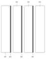
한편, 태양광 모듈은 다수의 스트링(string)이 직렬 연결되어 구성된다. 예를 들어, 4개의 스트링이 하나의 태양광 모듈을 구성하며, 이들 각각은 독립적으로 태양광 발전 기능을 갖는다. 상술한 스트링은 도 1에 도시된 바와 같이, 분할된 스트립(10)의 하부 및 상부 상에 각각 버스바(20)를 제작하고, 이 버스바(20)를 ECA(30)로 연결하여 접합한다. 따라서, 별도의 전극을 형성하는 공정을 마련하고 이에 따라 전극 형성에 필요한 재료도 마련해야 한다.On the other hand, the solar module is configured by connecting a plurality of strings in series. For example, four strings constitute one photovoltaic module, and each of them independently has a photovoltaic power generation function. As shown in FIG. 1, for the above-described string, a
이러한 기술의 일 예가 하기 문헌 1 내지 3 등에 개시되어 있다.An example of such a technique is disclosed in
예를 들어, 하기 특허문헌 1에는 전면 및 후면을 가지는 기판, 상기 기판의 상기 전면 상에 배치되는 금속화 패턴으로서, 상기 금속화 패턴은 다수의 전면 버스바를 포함하고, 각각의 전면 버스바는 각각의 전면 버스바에서 연장되는 핑거를 포함하는 금속화패턴 및 상기 기판의 상기 후면 상에 배치되는 다수의 후면 버스바를 포함하고, 상기 기판의 상기 전면 상에, 상기 다수의 전면 버스바 중에서 하나의 전면 버스바가 상기 기판의 전면 에지를 따라 형성되어 있으며, 상기 다수의 전면 버스바 중에서 나머지 전면 버스바는 상기 기판을 가로질러 균일하지 않게 이격되어 있으며, 상기 기판의 후면 상에 상기 다수의 후면 버스바 중에서 단지 하나의 후면 버스바가 상기 기판의 상기 후면의 에지를 따라 형성되어 있으며, 상기 다수의 후면 버스바 중에서 나머지 후면 버스바는 상기 기판을 가로질러 균일하지 않게 이격되어 있는 태양 전지에 대해 개시되어 있다.For example, in
또 하기 특허문헌 2에는 접착성 고분자 화합물이 그리드리스 PV 구조에 부착하는데 사용될 수 있고, 고출력 레이저빔을 사용하여 원하는 위치에서 광전지의 표면을 소정의 깊이로 스크라이브 한 후, 스크라이브된 광전지를 다수의 작은 셀로 절단하기 위해 적절한 힘을 인가하며, 더 작은 셀들의 형성 후에, 다수의 더 작은 셀들이 직렬연결은 인접한 더 작은 셀들과 부분적으로 중첩하여 광전지 셀 스트링을 형성하는 그리드 없는 태양전지 셀 및 이를 이용한 스트링 제조방법에 대해 개시되어 있다.In addition, in Patent Document 2, an adhesive polymer compound can be used to attach to a gridless PV structure, and after scribing the surface of a photovoltaic cell to a predetermined depth at a desired position using a high-power laser beam, the scribed photovoltaic cell is formed into a plurality of small cells. Applying an appropriate force to cut into cells, and after formation of smaller cells, a series of multiple smaller cells partially overlaps adjacent smaller cells to form a photovoltaic cell string and gridless solar cell and string using same A manufacturing method is disclosed.
한편, 하기 특허문헌 3에는 금속 유연 기판의 상부에 복수의 단위 셀을 포함하는 태양 전지를 형성하는 태양 전지 형성 단계, 상기 복수의 단위 셀 각각에 전도성 접착층을 형성하는 전도성 접착층 형성단계, 상기 복수의 단위 셀을 서로 분리하여 복수의 태양 전지 셀을 형성하는 싱귤레이션 단계 및 상기 복수의 태양 전지 셀을 서로 직렬로 접속하여 태양 전지 모듈을 형성하는 직렬접속 단계를 포함하고, 상기 전도성 접착층 형성 단계에서는 상기 투명 전극의 상면에서 단위 셀의 일단에 제1 전도성 접착층을 형성하고, 상기 금속 유연 기판의 하면에서 단위 셀의 타단에 제2 전도성 접착층을 형성하는 태양 전지 모듈의 제조 방법에 대해 개시되어 있다.On the other hand, in Patent Document 3 below, a solar cell forming step of forming a solar cell including a plurality of unit cells on an upper portion of a metal flexible substrate, a conductive adhesive layer forming step of forming a conductive adhesive layer on each of the plurality of unit cells, the plurality of A singulation step of separating unit cells from each other to form a plurality of solar cells, and a serial connection step of forming a solar cell module by connecting the plurality of solar cells in series with each other, wherein in the conductive adhesive layer forming step, the Disclosed is a method for manufacturing a solar cell module in which a first conductive adhesive layer is formed on one end of a unit cell on an upper surface of a transparent electrode, and a second conductive adhesive layer is formed on the other end of the unit cell on a lower surface of the metal flexible substrate.
상술한 바와 같은 특허문헌 1 및 3에 개시된 기술에서는 도전성 접착제(ECA)를 이용하여 분할된 각 셀의 전면 전극과 후면 전극을 서로 직렬로 연결하여 슁글드 모듈 방식의 태양전지 스트링을 제작하는 것에 대해 기재되어 있지만, 버스바를 마련하므로 고가의 재료를 사용하여 제조비용이 증가하고, 또한 이에 따라 제조 공정이 번잡하게 된다는 문제가 있었다.In the technology disclosed in
한편, 특허문헌 2에 개시된 기술에서는 고출력 레이저빔을 사용하여 표면에서만 스크라이브를 실행하므로, 스트립의 형성과정에서 절단 부분에서 스트립의 불량이나 버가 발생한다는 문제가 있었다.On the other hand, in the technique disclosed in Patent Document 2, since scribing is performed only on the surface using a high-power laser beam, there is a problem that defects or burrs of the strip are generated in the cut portion in the process of forming the strip.
본 발명의 목적은 상술한 바와 같은 문제점을 해결하기 위해 이루어진 것으로서, 다수의 태양 전지 스트립이 서로 부분적으로 중첩(슁글드 구조)되어 스트링을 형성할 때, 별도의 버스바 형성을 하지 않고, 스트립에 전도성 접착제만을 도포하여 전기적으로 연결할 수 있는 HIT 셀을 포함하는 슁글드 태양전지 모듈 및 그 제조방법을 제공하는 것이다.An object of the present invention was made to solve the above-described problems, and when a plurality of solar cell strips are partially overlapped with each other (shingled structure) to form a string, without forming a separate bus bar, To provide a shingled solar cell module including a HIT cell that can be electrically connected by applying only a conductive adhesive, and a method for manufacturing the same.
본 발명의 다른 목적은 버스바의 형성 과정을 생략하여 저렴하게 슁글드 태양전지 모듈을 마련할 수 있는 HIT 셀을 포함하는 슁글드 태양전지 모듈 및 그 제조방법을 제공하는 것이다.Another object of the present invention is to provide a shingled solar cell module including a HIT cell capable of providing a shingled solar cell module inexpensively by omitting a process of forming a bus bar, and a method for manufacturing the same.
본 발명의 또 다른 목적은 필요에 따라 정해진 오버랩 간격 이외에도 유사시 스트립의 오버랩 구간을 제어하여 슁글드 태양전지 모듈을 형성할 수 있는 HIT 셀을 포함하는 슁글드 태양전지 모듈 및 그 제조방법을 제공하는 것이다.Another object of the present invention is to provide a shingled solar cell module including a HIT cell capable of forming a shingled solar cell module by controlling the overlapping section of the strip in case of emergency in addition to a predetermined overlapping interval, and a method for manufacturing the same. .
상기 목적을 달성하기 위해 본 발명에 따른 슁글드 태양전지 모듈 및 그 제조방법은 (a) 상부 및 하부에 각각 다수의 전도층이 형성된 HIT(Hetrojunction with Intrinsic Thin lyaer)로 이루어진 웨이퍼를 마련하는 단계, (b) 상부 전도층 상에 전도성 접착제를 도포하여 접착층을 형성하는 단계, (c) 상기 접착층이 형성된 웨이퍼를 다수의 스트립으로 분할하는 단계, (d) 상기 분할된 스트립 중 접착층이 마련된 영역에 다른 스트립의 하부 전도층을 중첩하여 스트링을 형성하는 단계를 포함하고, 상기 다수의 스트립의 각각의 상부 전도층 및 하부 전도층은 상기 접착층만을 경유하여 전기적으로 접합되는 것을 특징으로 한다.In order to achieve the above object, a shingled solar cell module and a method for manufacturing the same according to the present invention include (a) providing a wafer made of a Hetrojunction with Intrinsic Thin Lyaer (HIT) having a plurality of conductive layers formed on the upper and lower portions, respectively; (b) applying a conductive adhesive on the upper conductive layer to form an adhesive layer, (c) dividing the wafer on which the adhesive layer is formed into a plurality of strips, (d) in the region where the adhesive layer is provided among the divided strips and overlapping the lower conductive layers of the strip to form a string, wherein each of the upper conductive layer and the lower conductive layer of the plurality of strips is electrically bonded via only the adhesive layer.
또 본 발명에 따른 슁글드 태양전지 모듈의 제조방법에서, 상기 단계 (b)에서 전도성 접착제의 도포는 스크린 프린팅 방법에 의해 실행되는 것을 특징으로 한다.In addition, in the method for manufacturing a shingled solar cell module according to the present invention, the application of the conductive adhesive in step (b) is characterized in that it is performed by a screen printing method.
또 본 발명에 따른 슁글드 태양전지 모듈의 제조방법에서, 상기 접착층은 N-1개(여기서, N은 스트립의 갯수)로 마련되는 것을 특징으로 한다.In addition, in the method for manufacturing a shingled solar cell module according to the present invention, the adhesive layer is characterized in that it is provided in N-1 pieces (where N is the number of strips).
또 본 발명에 따른 슁글드 태양전지 모듈의 제조방법에서, 상기 단계 (c)에서 다수의 스트립은 상기 접착층의 일측을 따라 상기 웨이퍼의 상부 및 하부에서 낮은 에너지 수준의 레이저로 스크라이빙하는 것에 의해 분할되어 마련되는 것을 특징으로 한다.In addition, in the method for manufacturing a shingled solar cell module according to the present invention, in step (c), a plurality of strips are scribed along one side of the adhesive layer with a low energy level laser at the upper and lower portions of the wafer. It is characterized in that it is divided and provided.
또 본 발명에 따른 슁글드 태양전지 모듈의 제조방법에서, 상기 레이저의 스크라이빙에 의해 상기 웨이퍼의 상부는 웨이퍼 두께의 60% 미만으로 홈이 형성되고, 상기 웨이퍼의 하부는 웨이퍼 두께의 40% 미만으로 홈이 형성되며, 상기 다수의 스트립은 상부에서 하부를 향한 기계적 분할에 의해 마련되는 것을 특징으로 한다.Also, in the method for manufacturing a shingled solar cell module according to the present invention, a groove is formed on the upper portion of the wafer by less than 60% of the wafer thickness by scribing of the laser, and the lower portion of the wafer is 40% of the wafer thickness It is characterized in that the groove is formed less than, and the plurality of strips are provided by mechanical division from the top to the bottom.
또 본 발명에 따른 슁글드 태양전지 모듈의 제조방법에서, 상기 단계 (c)에서 분할된 스트립의 에지 부분에 전도성 접착제를 도포하는 단계를 더 포함하는 것을 특징으로 한다.In addition, in the method for manufacturing a shingled solar cell module according to the present invention, it is characterized in that it further comprises the step of applying a conductive adhesive to the edge portion of the strip divided in step (c).
또한, 상기 목적을 달성하기 위해 본 발명에 따른 슁글드 태양전지 모듈은 상술한 슁글드 태양전지 모듈의 제조방법에 의해 제조된 것을 특징으로 한다.In addition, in order to achieve the above object, the shingled solar cell module according to the present invention is characterized in that it is manufactured by the above-described method for manufacturing a shingled solar cell module.
상술한 바와 같이, 본 발명에 따른 HIT 셀을 포함하는 슁글드 태양전지 모듈 및 그 제조방법에 의하면, 버스바가 형성되지 않고 접착층만 마련되므로, 필요에 따라 정해진 오버랩 간격 이외에도 유사시에 스트립의 오버랩 구간을 제어하여 슁글드 태양 전지를 용이하게 형성할 수 있다는 효과가 얻어진다.As described above, according to the shingled solar cell module including the HIT cell and the method for manufacturing the same according to the present invention, since only the adhesive layer is provided without the bus bar being formed, the overlapping section of the strip in case of necessity in addition to the overlapping interval determined as necessary The effect of being able to easily form a shingled solar cell by controlling is obtained.
또 본 발명에 따른 HIT 셀을 포함하는 슁글드 태양전지 모듈 및 그 제조방법에 의하면, 고가의 재료를 사용하는 버스바의 형성 과정을 생략하므로, 저렴하게 슁글드 태양전지 모듈을 마련할 수 있다는 효과도 얻어진다.In addition, according to the shingled solar cell module including the HIT cell and the method for manufacturing the same according to the present invention, since the process of forming the bus bar using an expensive material is omitted, the shingled solar cell module can be inexpensively prepared. is also obtained.
도 1은 종래의 슁글드 태양전지 모듈의 모식도,
도 2는 본 발명에 따른 슁글드 태양전지 모듈에 적용되는 접착제가 도포된 웨이퍼의 평면도,
도 3 및 도 4는 본 발명에 따라 스트립을 형성하는 과정을 설명하기 위한 웨이퍼의 단면도,
도 5는 본 발명에 따라 마련된 스트립의 사시도,
도 6은 본 발명에 따라 스트링을 형성하는 과정을 설명하기 위한 공정도,
도 7은 본 발명에 적용되는 일반적인 HIT 태양전지의 모식도.1 is a schematic diagram of a conventional shingled solar cell module;
2 is a plan view of a wafer coated with an adhesive applied to a shingled solar cell module according to the present invention;
3 and 4 are cross-sectional views of a wafer for explaining the process of forming a strip according to the present invention;
5 is a perspective view of a strip prepared in accordance with the present invention;
6 is a process diagram for explaining the process of forming a string according to the present invention;
7 is a schematic diagram of a general HIT solar cell applied to the present invention.
본 발명의 상기 및 그 밖의 목적과 새로운 특징은 본 명세서의 기술 및 첨부 도면에 의해 더욱 명확하게 될 것이다.The above and other objects and novel features of the present invention will become more apparent from the description of the present specification and accompanying drawings.
본원에서 사용하는 용어 "웨이퍼"는 태양전지용 웨이퍼로서 단결정 또는 다결정 실리콘으로 이루어지고, "태양전지 셀"은 P-형의 실리콘 기판에 전극이 스크린 프린트(screen print)된 형태로 마련되며, p-PERC(Passivated Emitter and Rearside Contact), n-HIT(Hetrojunction with Intrinsic Thin lyaer), n-PERT (Passivated Emitter and Rear Totally diffused), CSC(Charge Selective Contact)로 형성될 수 있다.As used herein, the term "wafer" is a wafer for solar cells made of single crystal or polycrystalline silicon, and "solar cell" is provided in a form in which electrodes are screen printed on a P-type silicon substrate, and p- PERC (Passivated Emitter and Rearside Contact), n-HIT (Hetrojunction with Intrinsic Thin lyaer), n-PERT (Passivated Emitter and Rear Totally diffused), CSC (Charge Selective Contact) may be formed.
또 본원에서 사용하는 용어로서, "태양전지 구조(photovoltaic structure)"는 빛을 전기로 변환할 수 있는 장치로서, 다수의 반도체 또는 다른 유형의 물질을 포함할 수 있는 것을 의미하며, "태양전지(solar cell)" 또는 "셀"은 빛을 전기로 변환할 수 있는 광전지(PV) 구조로서, 다양한 크기 및 형태를 가질 수 있으며, 다양한 재료로 제조될 수 있으며, 반도체(예를 들어, 실리콘) 웨이퍼 또는 기판상에 제조된 PV 구조 또는 기판(예를 들어, 유리, 플라스틱, 금속 또는 광전지 구조를 지지할 수 있는 임의의 다른 물질) 상에 제조된 하나 이상의 박막일 수 있다.Also, as used herein, "photovoltaic structure" means a device capable of converting light into electricity, which may include a number of semiconductors or other types of materials, and "solar cell ( A "solar cell" or "cell" is a photovoltaic (PV) structure capable of converting light into electricity, may have various sizes and shapes, may be made of various materials, and may include semiconductor (eg, silicon) wafers. or PV structures fabricated on a substrate or one or more thin films fabricated on a substrate (eg, glass, plastic, metal, or any other material capable of supporting a photovoltaic structure).
또한, "핑거 라인(finger line)", "핑거 전극(finger electrode)", "핑거 스트립(finger strip)" 또는 "핑거"는 캐리어를 수집하기 위한 광전지 구조물의 연장된 전기 전도성(예를 들어, 금속) 전극을 의미하며, "버스바(busbar)", "버스 라인(bus line)" 또는 "버스 전극(bus electrode)"은 2개 이상의 핑거 라인에 의해 수집된 전류를 모으기 위한 PV 구조의 연장된 전기 전도성(예를 들어 : 금속) 전극으로, 일반적으로 핑거 라인보다 넓으며 광전지 구조물 위나 내부에 배치될 수 있으며, 단일 광전지 구조물에는 하나 이상의 버스바가 마련될 수 있다.In addition, a “finger line,” “finger electrode,” “finger strip,” or “finger” may refer to the extended electrical conductivity (e.g., metal) electrode, "busbar", "bus line" or "bus electrode" is an extension of a PV structure for collecting the current collected by two or more finger lines An electrically conductive (eg: metal) electrode, generally wider than a finger line, and may be disposed on or within a photovoltaic structure, a single photovoltaic structure may be provided with one or more busbars.
한편, "금속 그리드(grid)" 또는 "그리드"는 대표적으로 핑거 라인 또는 버스바의 모음으로서, 광전지 구조물 상에 금속 재료 층을 증착하여 형성된 것을 의미하며, "태양전지 스트립(strip)", "광전지 스트립" 또는 "스트립"은 태양전지와 같은 PV 구조의 일부 또는 세그먼트로서, PV 구조는 다수의 스트립으로 분리할 수 있으며, 이 스트립의 폭 및 길이는 서로 동일하거나 상이하게 마련될 수 있다.On the other hand, "metal grid" or "grid" is typically a collection of finger lines or busbars, which means formed by depositing a metal material layer on a photovoltaic structure, "solar cell strip", " A photovoltaic strip" or "strip" is a part or segment of a PV structure, such as a solar cell, wherein the PV structure can be divided into multiple strips, the widths and lengths of which can be the same or different from each other.
또 용어 "슁글드(shingled) 어레이 구조"는 태양전지 모듈의 단위당 변환 효율과 출력을 높이기 위해 전면 전극과 후면 전극이 마련된 태양전지 셀을 절단하여 복수의 스트립을 형성하고 이 전면 전극과 후면 전극을 전도성 접착제로 접착하여 연결된 스트링 구조를 의미한다.In addition, the term "shingled array structure" refers to a plurality of strips by cutting a solar cell provided with a front electrode and a rear electrode in order to increase the conversion efficiency and output per unit of the solar cell module, and the front electrode and the rear electrode are separated. It refers to a string structure connected by bonding with a conductive adhesive.
또 "태양전지 모듈"은 프레임 상에서 다수개의 슁글드 어레이 구조의 태양전지 스트링이 전기적으로 연결되고, 전면에 유리가 위치하고, 후면에는 EVA 시트가 형성되고, 중간에 충진재 등이 배치되어 태양전지 패널을 형성하는 것을 의미한다.In addition, in the "solar cell module", a plurality of solar cell strings of a shingled array structure are electrically connected on a frame, glass is located on the front side, EVA sheet is formed on the back side, and fillers are placed in the middle to form a solar cell panel. means to form
본원에서 사용하는 용어 "전도성 접착제(Electroconductive Adhesive; ECA)"는 전기 전자 제품이나 회로의 배선 접합에 사용하는 전기 전도성을 가진 접착제로, 에폭시 수지에 은 입자를 배합한 것을 사용한다. 또 전도성 접착제는 스크린 프린팅 방식 또는 마이크로 디스펜서를 이용하여 도포할 수 있으며, 니들로부터의 토출량이 일정해야 하고 흘러내리지 않게 한다. 전도성 충진제로는 금, 백금, 은, 구리, 니켈 등의 금속분말, 카본 또는 카본 섬유, 흑연 및 복합 분말 등이 사용할 수 있다.As used herein, the term "electroconductive adhesive (ECA)" is an adhesive having electrical conductivity used for bonding wiring of electrical and electronic products or circuits, and silver particles are mixed with an epoxy resin. In addition, the conductive adhesive can be applied using a screen printing method or a micro dispenser, and the discharge amount from the needle must be constant and do not flow down. As the conductive filler, metal powders such as gold, platinum, silver, copper, and nickel, carbon or carbon fiber, graphite, and composite powder may be used.
먼저, 본 발명에 적용되는 HIT(Hetrojunction with Intrinsic Thin lyaer) 태양전지에 대해 도 7에 따라 설명한다. 도 7은 본 발명에 적용되는 일반적인 HIT 태양전지의 모식도이다.First, a Hetrojunction with Intrinsic Thin Lyaer (HIT) solar cell applied to the present invention will be described with reference to FIG. 7 . 7 is a schematic diagram of a general HIT solar cell applied to the present invention.
본 발명에 적용되는 HIT 태양전지는 일반적인 결정질 실리콘 태양전지와 같이, N형 결정질 실리콘 기판(1)의 양쪽 표면을 습식 또는 건식 식각하여 표면 텍스처를 형성한 뒤에, 양면에 진성의 a-Si:H 패시베이션층(21, 22)을 형성하고, 두 개의 패시베이션층(21, 22)에 P형 a-Si:H층(31)과 N형 a-Si:H층(32)을 형성하며, 표면에 ITO 재질의 투명전도층(TCO)(41, 42)을 형성한 뒤에 상부 전극(50)과 하부 전극(60)을 형성하여 제조된 것을 사용할 수 있다. 그러나 도 7에 도시된 바와 같은 구조에 한정되는 것은 아니고, 다양한 기술 발전에 따라 박형화, 고출력화된 HIT 태양전지를 사용할 수도 있다.The HIT solar cell applied to the present invention forms a surface texture by wet or dry etching both surfaces of the N-type
이하, 본 발명에 따른 실시 예를 도면에 따라서 설명한다.Hereinafter, an embodiment according to the present invention will be described with reference to the drawings.
도 2는 본 발명에 따른 슁글드 태양전지 모듈에 적용되는 접착제가 도포된 웨이퍼의 평면도 이고, 도 3 및 도 4는 본 발명에 따라 스트립을 형성하는 과정을 설명하기 위한 웨이퍼의 단면도 이며, 도 5는 본 발명에 따라 마련된 스트립의 사시도 이다.2 is a plan view of a wafer coated with an adhesive applied to a shingled solar cell module according to the present invention, and FIGS. 3 and 4 are cross-sectional views of the wafer for explaining the process of forming a strip according to the present invention, and FIG. 5 is a perspective view of a strip prepared according to the present invention.
먼저, 본 발명에 따른 슁글드 태양전지 모듈을 제조하기 위해 4 모서리 부분이 테이퍼진 사각 형상(pseudo-squared) 또는 사각 형상(full-squared)으로 이루어진 태양전지용 웨이퍼를 마련한다.First, in order to manufacture a shingled solar cell module according to the present invention, a wafer for solar cells having a tapered quadrangular shape (pseudo-squared) or a square shape (full-squared) is prepared.
본 발명에서는 도 2에 도시된 바와 같이, 사각 형상으로 이루어진 태양전지용 웨이퍼(100)를 적용하지만, 이에 한정되는 것은 아니고 4 모서리 부분이 테이퍼진 사각 형상을 적용할 수도 있다. 또 상기 웨이퍼(100)는 도 7에 도시된 바와 같이, 상부 및 하부에 각각 다수의 전도층으로서 상부 전극(50)과 하부 전극(60)이 형성된 HIT(Hetrojunction with Intrinsic Thin lyaer) 구조를 적용할 수 있다. 즉 웨이퍼 상에는 다수의 스트립(200)의 각각 대응하여 다수의 전도층이 마련된다.In the present invention, as shown in FIG. 2 , a
다음에 도 2에 도시된 바와 같이, 웨이퍼(100)의 상부 전도층 상에 전도성 접착제(ECA)를 도포하여 접착층(300)을 형성한다. 상기 접착층(300)은 웨이퍼(100)가 N 개의 스트립 예를 들어, 4개, 5개, 6개 등으로 분할될 스트립(200)에 따라 (N-1) 개로 마련된다. 즉, 도 2에 도시된 바와 같이, 웨이퍼(100)가 4개의 스트립(200)으로 분할될 경우, 3개의 접착층(300)이 마련되고, 또는 5개의 스트립(200)으로 분할될 경우, 4개의 접착층(300)이 마련되고, 6개의 스트립(200)으로 분할될 경우, 5개의 접착층(300)이 웨이퍼(100)의 내부에만 마련된다.Next, as shown in FIG. 2 , an
상술한 전도성 접착제의 도포는 스크린 프린팅에 의해 일괄적으로 마련된다. 그러나 이에 한정되는 것은 아니고, 마이크로 디스펜서를 이용하여 도포하는 것에 의해 이루어질 수도 있다.Application of the above-described conductive adhesive is provided in a batch by screen printing. However, the present invention is not limited thereto, and may be applied by using a micro dispenser.
이러한 전도성 접착제로서는 시장에 나와 있는 전도성 접착제 중에 본 발명에 적합한 높은 전도성과 알맞은 점도를 가진 제품으로서, 예를 들어 SKC Panacol의 EL-3012, EL-3556, EL-3653, EL-3655과 Henkel의 CE3103WLV, CA3556HF을 적용할 수 있으며, 예를 들어, 25℃에서의 점도 28,000~35,000 mPa·s(cP), 전기적 특성으로서, 체적 저항률 0.0025 Ω·cm, 경화 온도 130~150℃, 경화 시간 25~35초의 특성이 있는 접착제를 적용한다. 또 전도성 접착제에서 전도성 충진제는 Au, Pt, Pd, Ag, Cu, Ni 및 카본 중에서 선택된 적어도 하나의 물질을 포함할 수 있다. 그러나 전도성 접착제의 경화 시간 및 온도는 사용되는 접착제의 종류, 접착제 도포 범위 및 두께 등에 따라 변경 가능하다.Among the conductive adhesives on the market, these conductive adhesives are products with high conductivity and suitable viscosity suitable for the present invention. For example, SKC Panacol's EL-3012, EL-3556, EL-3653, EL-3655 and Henkel's CE3103WLV , CA3556HF can be applied, for example, a viscosity at 25°C of 28,000-35,000 mPa·s (cP), as an electrical property, a volume resistivity of 0.0025 Ω·cm, a curing temperature of 130-150°C, a curing time of 25-35 Apply an adhesive with the properties of a candle. In addition, in the conductive adhesive, the conductive filler may include at least one material selected from Au, Pt, Pd, Ag, Cu, Ni, and carbon. However, the curing time and temperature of the conductive adhesive may be changed depending on the type of adhesive used, the range and thickness of the adhesive, and the like.
다음에 상기 접착층(300)이 형성된 웨이퍼(100)를 다수의 스트립(200)으로 분할한다. 이하의 설명에서는 도 2를 참조하여 4개의 스트립(200)으로 분할되는 과정을 설명한다.Next, the
먼저, 도 3에 도시된 바와 같이, 스크라이빙 과정에서 웨이퍼의 표면 버닝 및 버의 생성을 최소화되도록, 상기 접착층(300)의 일측(도 3에서는 접착층(300)의 우측)을 따라 상기 웨이퍼의 상부에서 낮은 에너지 수준의 UV&그린 레이저로 스크라이빙한다. 상기 낮은 에너지 수준의 레이저로서는 파장 335nm, 442nm 또는 532nm인 UV&그린 레이저를 적용할 수 있다. 따라서, 웨이퍼(100) 상에 마련된 접착층(300)은 스크라이빙 과정에서 레이저의 이동 방향을 안내하는 기준으로 사용될 수도 있다.First, as shown in FIG. 3 , in the scribing process, the surface of the wafer is burned along one side of the adhesive layer 300 (the right side of the
즉, 도 3에 도시된 바와 같이, 상기 웨이퍼(100)의 상부(110)에 웨이퍼 두께의 60% 미만, 바람직하게는 약 50%의 깊이를 갖는 홈(101)을 형성하고, 도 4에 도시된 바와 같이 상기 웨이퍼(100)의 하부(120)에는 웨이퍼 두께의 40% 미만의 홈(102)을 형성한다. 또 상기 웨이퍼(100)에서 홈(101)과 홈(102)의 형성은 동시에 실행할 수도 있다.That is, as shown in FIG. 3 , a
다음에 홈(101)과 홈(102)의 형성된 웨이퍼에 대해 상부에서 하부를 향한 기계적 분할에 의해 도 5에 도시된 바와 같이 4개의 스트립이 마련된다. 이와 같은 기계적 분할은 통상의 태양전지 셀을 사용되는 기기를 적용하여 용이하게 실현할 수 있으므로, 이에 대한 구체적인 설명은 생략한다.Next, four strips are prepared as shown in FIG. 5 by mechanical division from top to bottom for the wafer formed of the
상술한 바와 같이, 본 발명에 따른 스트립(200)에는 버스바가 마련되지 않으므로, 버스바 형성 프로세스를 생략하여 제조 공정을 단순화 화며, 또 버스바를 형성하기 위한 고가의 재료를 절감할 수 있다.As described above, since the bus bar is not provided in the
다음에 상술한 바와 같이 마련된 스트립을 사용하여 스트링을 형성하는 과정에 대해 도 6에 따라 설명한다.Next, a process of forming a string using the strip prepared as described above will be described with reference to FIG. 6 .
도 6은 본 발명에 따라 스트링을 형성하는 과정을 설명하기 위한 공정도 이다. 또 도 6에서의 설명은 도 5에 도시된 바와 같은 4개의 스트립(200)으로 설명하지만, 이에 한정되는 것은 아니고 5개의 스트립 또는 6개의 스트립에도 적용 가능하다.6 is a process diagram for explaining a process of forming a string according to the present invention. In addition, the description in FIG. 6 is described with four
본 발명에서는 버스바를 사용하지 않고, 분할된 스트립(200) 중 접착층(300)이 마련된 영역에 다른 스트립의 하부 전도층을 중첩하여 도 6에 도시된 바와 같은 스트링을 형성한다.In the present invention, without using a bus bar, a string as shown in FIG. 6 is formed by overlapping the lower conductive layer of another strip on the region where the
즉 도 6의 (a)에 도시된 바와 같이, 도 5에 도시된 4개의 스트립(200)을 나열하고, 도 6의 (b)에 도시된 바와 같이, 4개의 스트립 중 최우측의 4번째 스트립을 3번째 스트립 상에 중첩한다. 이와 같은 중첩은 4번째 스트립의 하부에 마련된 전도층이 3번째 스트립에 마련된 접착층(300) 상에 위치 맞춤하여 실행된다.That is, as shown in FIG. 6(a), the four
이후, 3번째 스트립을 2번째 스트립 상에 중첩한다. 이와 같은 중첩은 3번째 스트립의 하부에 마련된 전도층이 2번째 스트립에 마련된 접착층(300) 상에 위치 맞춤하여 실행된다.The third strip is then overlaid on the second strip. Such overlapping is performed by positioning the conductive layer provided under the third strip on the
계속해서 2번째 스트립을 1번째 스트립 상에 중첩한다. 이와 같은 중첩은 2번째 스트립의 하부에 마련된 전도층이 1번째 스트립에 마련된 접착층(300) 상에 위치 맞춤하여 실행하는 것에 의해 도 6의 (c)에 도시된 바와 같은 스트링이 완성된다. 따라서 상기 다수의 스트립의 상부 전도층 및 하부 전도층은 상기 접착층(300)만을 경유하여 전기적으로 접합된다.The second strip is then overlaid on the first strip. Such overlapping is performed by aligning the conductive layer provided on the lower portion of the second strip on the
이어서, 상술한 바와 같이 마련된 각각의 스트링을 직렬, 병렬 또는 직병렬 연결하여 태양전지 모듈을 형성한다.Then, each string prepared as described above is connected in series, parallel, or series-parallel to form a solar cell module.
상술한 바와 같이, 본 발명에서는 종래의 기술과 같은 버스바로 한정되지 않으므로, 스트립 중첩 폭을 용이하게 제어할 수 있다. 즉, 본 발명에서는 도 5에 도시된 바와 같이 버스바가 형성되지 않고 접착층(300)만 마련되므로, 필요에 따라 정해진 오버랩 간격 이외에도 유사시에 스트립(200)의 오버랩 구간을 제어하여 슁글드 태양 전지를 형성할 수 있다.As described above, since the present invention is not limited to a bus bar as in the prior art, the overlapping width of the strips can be easily controlled. That is, in the present invention, as shown in FIG. 5 , since only the
또한, 본 발명에서는 상술한 바와 같은 스트링의 형성 전에 도 5에 도시된 바와 같이, 분할된 스트립의 에지 부분, 예를 들어 접착층(300)이 마련된 부분에 전도성 접착제를 추가로 도포할 수도 있다.In addition, in the present invention, as shown in FIG. 5 , before the formation of the string as described above, a conductive adhesive may be additionally applied to the edge portion of the divided strip, for example, the portion where the
이상 본 발명자에 의해서 이루어진 발명을 상기 실시 예에 따라 구체적으로 설명하였지만, 본 발명은 상기 실시 예에 한정되는 것은 아니고 그 요지를 이탈하지 않는 범위에서 여러 가지로 변경 가능한 것은 물론이다.Although the invention made by the present inventors has been described in detail according to the above embodiments, the present invention is not limited to the above embodiments and various modifications can be made without departing from the gist of the present invention.
본 발명에 따른 HIT 셀을 포함하는 슁글드 태양전지 모듈 및 그 제조방법을 사용하는 것에 의해 저렴하게 슁글드 태양전지 모듈을 마련할 수 있다.A shingled solar cell module can be inexpensively prepared by using the shingled solar cell module including the HIT cell and the manufacturing method thereof according to the present invention.
100 : 웨이퍼
200 : 스트립
300 : 접착층100: wafer
200: strip
300: adhesive layer
Claims (7)
Translated fromKorean(b) 상기 웨이퍼의 상부 전도층 상에만 전도성 접착제를 도포하여 다수의 접착층을 형성하는 단계,
(c) 상기 다수의 접착층이 형성된 웨이퍼를 다수의 스트립으로 분할하는 단계,
(d) 상기 분할된 스트립 중 접착층이 마련된 영역에 다른 스트립의 하부 전도층을 중첩하여 스트링을 형성하는 단계를 포함하고,
상기 다수의 접착층은 스크린 프린팅에 의해 일괄적으로 마련되고,
상기 다수의 스트립의 각각의 상부 전도층 및 하부 전도층은 상기 접착층만을 경유하여 전기적으로 접합되고,
상기 접착층은 N-1개(여기서, N은 스트립의 개수)로 마련되고, N 번째 스트립 상에는 상기 접착층이 마련되지 않고,
상기 접착층은 상기 단계 (c)에서의 분할 과정에서 레이저의 이동 방향을 안내하는 기준으로 사용되고,
상기 단계 (c)에서 상기 웨이퍼의 상부는 웨이퍼 두께의 60% 미만의 깊이로 제1 홈이 형성되고, 상기 웨이퍼의 하부는 웨이퍼 두께의 40% 미만의 깊이로 제2 홈이 형성되며, 상기 제1 홈 및 제2 홈의 형성은 동시에 실행되어 다수의 스트립으로 분할되는 것을 특징으로 하는 슁글드 태양전지 모듈의 제조방법.(a) providing a wafer made of a Hetrojunction with Intrinsic Thin Lyaer (HIT) in which a plurality of conductive layers are formed on the upper and lower portions, respectively;
(b) forming a plurality of adhesive layers by applying a conductive adhesive only on the upper conductive layer of the wafer;
(c) dividing the wafer on which the plurality of adhesive layers are formed into a plurality of strips;
(d) forming a string by superposing a lower conductive layer of another strip on an area where an adhesive layer is provided among the divided strips,
The plurality of adhesive layers are collectively provided by screen printing,
Each of the upper conductive layer and the lower conductive layer of the plurality of strips is electrically bonded via only the adhesive layer,
The adhesive layer is provided in N-1 pieces (where N is the number of strips), and the adhesive layer is not provided on the N-th strip,
The adhesive layer is used as a reference to guide the movement direction of the laser in the division process in step (c),
In step (c), a first groove is formed in the upper portion of the wafer to a depth of less than 60% of the wafer thickness, and a second groove is formed in the lower portion of the wafer to a depth less than 40% of the wafer thickness, A method of manufacturing a shingled solar cell module, characterized in that the formation of the first groove and the second groove is performed simultaneously and divided into a plurality of strips.
상기 단계 (c)에서 다수의 스트립은 상기 접착층의 일측을 따라 상기 웨이퍼의 상부 및 하부에서 낮은 에너지 수준의 레이저로 스크라이빙하는 것에 의해 분할되어 마련되는 것을 특징으로 하는 슁글드 태양전지 모듈의 제조방법.In claim 1,
In the step (c), a plurality of strips are divided and prepared by scribing with a laser of a low energy level at the upper and lower portions of the wafer along one side of the adhesive layer. Way.
상기 단계 (c)에서 분할된 스트립의 에지 부분에 전도성 접착제를 도포하는 단계를 더 포함하는 것을 특징으로 하는 슁글드 태양전지 모듈의 제조방법.In claim 1,
Method of manufacturing a shingled solar cell module, characterized in that it further comprises the step of applying a conductive adhesive to the edge portion of the strip divided in step (c).
Priority Applications (4)
| Application Number | Priority Date | Filing Date | Title |
|---|---|---|---|
| KR1020190092209AKR102357660B1 (en) | 2019-07-30 | 2019-07-30 | Shingled solar cell module with HIT and manufacturing method there of |
| CN201980098859.1ACN114175279B (en) | 2019-07-29 | 2019-11-18 | Tile-like solar cell panel and manufacturing method thereof |
| PCT/KR2019/015749WO2021020657A1 (en) | 2019-07-29 | 2019-11-18 | Shingled solar cell panel and method for manufacturing same |
| US17/631,166US20220271190A1 (en) | 2019-07-29 | 2019-11-18 | Shingled solar cell panel and method of manufacturing the same |
Applications Claiming Priority (1)
| Application Number | Priority Date | Filing Date | Title |
|---|---|---|---|
| KR1020190092209AKR102357660B1 (en) | 2019-07-30 | 2019-07-30 | Shingled solar cell module with HIT and manufacturing method there of |
Publications (3)
| Publication Number | Publication Date |
|---|---|
| KR20210014317A KR20210014317A (en) | 2021-02-09 |
| KR102357660B1true KR102357660B1 (en) | 2022-02-03 |
| KR102357660B9 KR102357660B9 (en) | 2023-04-12 |
Family
ID=74559423
Family Applications (1)
| Application Number | Title | Priority Date | Filing Date |
|---|---|---|---|
| KR1020190092209AActiveKR102357660B1 (en) | 2019-07-29 | 2019-07-30 | Shingled solar cell module with HIT and manufacturing method there of |
Country Status (1)
| Country | Link |
|---|---|
| KR (1) | KR102357660B1 (en) |
Citations (2)
| Publication number | Priority date | Publication date | Assignee | Title |
|---|---|---|---|---|
| US20170077343A1 (en)* | 2014-05-27 | 2017-03-16 | Sunpower Corporation | Shingled solar cell module |
| KR101816178B1 (en)* | 2016-11-09 | 2018-01-08 | 엘지전자 주식회사 | Methods for making a solar cell |
Family Cites Families (4)
| Publication number | Priority date | Publication date | Assignee | Title |
|---|---|---|---|---|
| US20180019349A1 (en) | 2016-07-13 | 2018-01-18 | Solarcity Corporation | Gridless photovoltaic cells and methods of producing a string using the same |
| KR101895025B1 (en)* | 2016-11-14 | 2018-09-04 | 한국생산기술연구원 | Solar cell module and manufacturing method thereof |
| CN110335902A (en) | 2017-03-09 | 2019-10-15 | 伟创力有限公司 | Shingled array solar cells and methods of making solar modules including shingled array solar cells |
| KR20180106442A (en)* | 2017-03-20 | 2018-10-01 | 한국교통대학교산학협력단 | Cigs thin film solar cell module using the direct cell bonding |
- 2019
- 2019-07-30KRKR1020190092209Apatent/KR102357660B1/enactiveActive
Patent Citations (2)
| Publication number | Priority date | Publication date | Assignee | Title |
|---|---|---|---|---|
| US20170077343A1 (en)* | 2014-05-27 | 2017-03-16 | Sunpower Corporation | Shingled solar cell module |
| KR101816178B1 (en)* | 2016-11-09 | 2018-01-08 | 엘지전자 주식회사 | Methods for making a solar cell |
Also Published As
| Publication number | Publication date |
|---|---|
| KR20210014317A (en) | 2021-02-09 |
| KR102357660B9 (en) | 2023-04-12 |
Similar Documents
| Publication | Publication Date | Title |
|---|---|---|
| CN114175279B (en) | Tile-like solar cell panel and manufacturing method thereof | |
| CN106159020B (en) | Use the two-sided photovoltaic module of heterojunction solar battery | |
| US10741703B2 (en) | Shingled solar cells overlapping along non-linear edges | |
| US9960302B1 (en) | Cascaded photovoltaic structures with interdigitated back contacts | |
| US10074755B2 (en) | High efficiency solar panel | |
| US7759158B2 (en) | Scalable photovoltaic cell and solar panel manufacturing with improved wiring | |
| US9219174B2 (en) | Module fabrication of solar cells with low resistivity electrodes | |
| CN204538036U (en) | Solar panel, solar cell, solar cell panel assembly and solar battery apparatus | |
| US20170256661A1 (en) | Method of manufacturing photovoltaic panels with various geometrical shapes | |
| US20230144536A1 (en) | Designable shingled photovoltaic module and manufacturing method therefor | |
| US20140373911A1 (en) | Solar cell | |
| KR102231314B1 (en) | Method manufacturing for solar cell string of shingled module structure and solar cell module | |
| US20210126153A1 (en) | Busbar-less shingled array solar cells and methods of manufacturing solar modules | |
| KR102357660B1 (en) | Shingled solar cell module with HIT and manufacturing method there of | |
| KR102427904B1 (en) | Method for dividing a solar cell for a shingled solar panel and a solar panel using the same | |
| KR102419880B1 (en) | Solar Cell And Manufacturing Method Of Solar Cell Module With Designable Shingled String Structure | |
| US10147831B2 (en) | Solar module and manufacturing method therefor | |
| KR102410785B1 (en) | Shingled high power module and manufacturing method thereof | |
| JP6971749B2 (en) | Manufacturing method of solar cell module and solar cell module | |
| KR20250113357A (en) | Shingled solar cell module with HJT and manufacturing method there of | |
| KR102371947B1 (en) | CELL DIVISION/INTERCONNECTION STRUCTURE SOLAR MODULE USING ELECTRODE PATTERN WITH LESS Ag | |
| KR102186560B1 (en) | Solar cell module for road block amd manufacturing method thereof | |
| KR20240160085A (en) | High-output shingled solar cell module using string array and manufacturing method thereof | |
| KR20080092583A (en) | Front electrode pattern of single crystal silicon solar cell and single crystal silicon solar cell |
Legal Events
| Date | Code | Title | Description |
|---|---|---|---|
| PA0109 | Patent application | Patent event code:PA01091R01D Comment text:Patent Application Patent event date:20190730 | |
| PA0201 | Request for examination | ||
| PG1501 | Laying open of application | ||
| E902 | Notification of reason for refusal | ||
| PE0902 | Notice of grounds for rejection | Comment text:Notification of reason for refusal Patent event date:20210216 Patent event code:PE09021S01D | |
| E902 | Notification of reason for refusal | ||
| PE0902 | Notice of grounds for rejection | Comment text:Notification of reason for refusal Patent event date:20210825 Patent event code:PE09021S01D | |
| E701 | Decision to grant or registration of patent right | ||
| PE0701 | Decision of registration | Patent event code:PE07011S01D Comment text:Decision to Grant Registration Patent event date:20220125 | |
| GRNT | Written decision to grant | ||
| PR0701 | Registration of establishment | Comment text:Registration of Establishment Patent event date:20220126 Patent event code:PR07011E01D | |
| PR1002 | Payment of registration fee | Payment date:20220126 End annual number:3 Start annual number:1 | |
| PG1601 | Publication of registration | ||
| G170 | Re-publication after modification of scope of protection [patent] | ||
| PG1701 | Publication of correction | Patent event code:PG17011E01I Patent event date:20230405 Comment text:Request for Publication of Correction Publication date:20230412 | |
| PR1001 | Payment of annual fee | Payment date:20241223 Start annual number:4 End annual number:4 |