KR102355828B1 - Display Device having Multiple Display Panel - Google Patents
Display Device having Multiple Display PanelDownload PDFInfo
- Publication number
- KR102355828B1 KR102355828B1KR1020150073204AKR20150073204AKR102355828B1KR 102355828 B1KR102355828 B1KR 102355828B1KR 1020150073204 AKR1020150073204 AKR 1020150073204AKR 20150073204 AKR20150073204 AKR 20150073204AKR 102355828 B1KR102355828 B1KR 102355828B1
- Authority
- KR
- South Korea
- Prior art keywords
- optical member
- display device
- panel
- light
- diffusion
- Prior art date
- Legal status (The legal status is an assumption and is not a legal conclusion. Google has not performed a legal analysis and makes no representation as to the accuracy of the status listed.)
- Active
Links
Images


Classifications
- G—PHYSICS
- G09—EDUCATION; CRYPTOGRAPHY; DISPLAY; ADVERTISING; SEALS
- G09F—DISPLAYING; ADVERTISING; SIGNS; LABELS OR NAME-PLATES; SEALS
- G09F9/00—Indicating arrangements for variable information in which the information is built-up on a support by selection or combination of individual elements
- G—PHYSICS
- G02—OPTICS
- G02B—OPTICAL ELEMENTS, SYSTEMS OR APPARATUS
- G02B5/00—Optical elements other than lenses
- G02B5/02—Diffusing elements; Afocal elements
- G02B5/0205—Diffusing elements; Afocal elements characterised by the diffusing properties
- G02B5/021—Diffusing elements; Afocal elements characterised by the diffusing properties the diffusion taking place at the element's surface, e.g. by means of surface roughening or microprismatic structures
- G02B5/0221—Diffusing elements; Afocal elements characterised by the diffusing properties the diffusion taking place at the element's surface, e.g. by means of surface roughening or microprismatic structures the surface having an irregular structure
Landscapes
- Physics & Mathematics (AREA)
- General Physics & Mathematics (AREA)
- Engineering & Computer Science (AREA)
- Theoretical Computer Science (AREA)
- Optics & Photonics (AREA)
- Devices For Indicating Variable Information By Combining Individual Elements (AREA)
- Optical Elements Other Than Lenses (AREA)
Abstract
Translated fromKoreanDescription
Translated fromKorean본 발명의 실시예들은 다수의 개별 표시장치가 연결되어 하나의 대형 영상 출력 장치로 사용되는 다중 패널 표시장치에서, 개별 표시장치들의 연결부분에서 이미지의 연속성을 확보할 수 있는 다중 패널 표시장치에 관한 것이다.Embodiments of the present invention relate to a multi-panel display device in which a plurality of individual display devices are connected and used as one large-size image output device, which can secure image continuity in the connection portion of the individual display devices. will be.
정보화 사회가 발전함에 따라 화상을 표시하기 위한 표시장치에 대한 요구가 다양한 형태로 증가하고 있으며, 근래에는 액정표시장치(Liquid Crystal Display), 플라즈마표시장치(Plasma Display Device), 유기발광표시장치(Organic Light Emitting Display Device)와 같은 여러 가지 표시장치가 활용되고 있다.As the information society develops, the demand for display devices for displaying images is increasing in various forms, and in recent years, liquid crystal displays, plasma display devices, organic light emitting displays Various display devices such as Light Emitting Display Device) are being used.
한편, 상업적인 목적 등에 의하여 대형 사이즈의 표시장치가 필요하다.On the other hand, a large-sized display device is required for commercial purposes or the like.
그러나, 현재 기술에 의하면 표시장치를 구성하는 표시 패널의 크기에 한계가 있기 때문에, 대형 표시장치를 구형하기 위하여, 표시패널 또는 개별 표시장치들을 다수 연결하여 하나의 영상을 표현하는 다중 패널 표시장치가 사용되고 있다. 이러한 다중 패널 표시장치는 비디오월(Video Wall) 등으로 표현되기도 한다.However, according to the present technology, since there is a limit to the size of the display panel constituting the display device, a multi-panel display device that displays a single image by connecting a plurality of display panels or individual display devices to a large-sized display device has been developed. is being used Such a multi-panel display device is also expressed as a video wall or the like.
한편, 이러한 다중 패널 표시장치를 구성하는 각각의 표시패널 또는 개별 표시장치는 이미지가 표시되는 중앙의 표시영역과, 표시영역 주위에 배치되되 이미지가 표시되지 않는 비표시 영역을 포함한다.On the other hand, each display panel or individual display device constituting such a multi-panel display device includes a central display area in which an image is displayed and a non-display area disposed around the display area in which an image is not displayed.
이러한 비표시 영역은 표시패널의 가장자리를 둘러싸면서 일정한 폭을 가지도록 형성되는 일종의 프레임 형상을 가지고, 이러한 비표시 영역은 베젤(Bezel)로 표현될 수도 있다. 이러한 비표시 영역 또는 베젤 영역은 표시패널을 구동하기 위한 게이트 구동회로, 데이터 구동회로 또는 각종 신호선이 형성되는 필수불가결한 부분이다.The non-display area has a frame shape that is formed to have a constant width while surrounding the edge of the display panel, and this non-display area may be expressed as a bezel. The non-display area or the bezel area is an essential part in which a gate driving circuit, a data driving circuit, or various signal lines for driving a display panel are formed.
최근 표시장치에서 이러한 베젤 영역을 최소화하여 내로우 베젤(Narrow Bezel)을 구현하기 위한 연구가 진행되고 있으나 베젤 영역의 폭을 일정 크기 이하로 구현하는 데에는 한계가 있다.Recently, research has been conducted to realize a narrow bezel by minimizing the bezel area in a display device, but there is a limit to realizing the width of the bezel area to a certain size or less.
한편, 다중 패널 표시장치의 경우 다수의 개별 표시장치가 연결되어 형성되므로, 개별 표시장치들의 연결부위에서는 개별 표시장치의 베젤 영역이 이중으로 배치되며, 따라서 개별 표시장치들의 연결부위에서 비표시 영역이 커지게 된다. 이로 인하여 하나의 이미지를 다중 패널 표시장치에 표시하는 경우, 그러한 연결부분에서 이미지가 끊어져 보이는 문제가 발생된다.On the other hand, in the case of a multi-panel display device, since a plurality of individual display devices are connected to each other, the bezel area of the individual display device is double arranged at the connection part of the individual display devices, and thus the non-display area is large at the connection part of the individual display devices. will lose For this reason, when one image is displayed on a multi-panel display device, a problem occurs in that the image is cut off at such a connection part.
즉, 이상적으로 제로 베젤(Zero Bezel)인 경우를 제외하고는, 다수의 개별 표시장치를 연결하여 구현되는 다중 패널 표시장치의 경우, 패널 연결부위에서 이미지의 불연속 현상이 나타나는 문제가 있으며, 이를 위한 해결이 요구된다.That is, in the case of a multi-panel display device implemented by connecting a plurality of individual display devices, except for the ideal case of a zero bezel, there is a problem in that the image discontinuity appears at the panel connection part, and a solution for this this is required
한편, 이러한 다중 패널 표시장치의 패널 연결부분에서의 이미지 불연속 문제를 해결하기 위하여, 패널 연결부분에 일정한 광학 수단을 배치하는 연구가 진행되고는 있으나, 이러한 기술에서도 정면 또는 정면 부근의 시야각에서는 이미지 불연속 현상이 일부 개선되지만, 시야각이 커지는 경우 이미지 불연속 현상은 여전히 존재하는 문제가 있다.On the other hand, in order to solve the problem of image discontinuity in the panel connection part of the multi-panel display device, research is being conducted to arrange a certain optical means in the panel connection part. Although the phenomenon is partially improved, there is a problem that image discontinuity still exists when the viewing angle is increased.
이에 본 발명의 실시예들의 목적은, 개별 표시장치의 연결부분에서의 이미지 불연속 문제가 개선된 다중패널 표시장치를 제공하는 것이다.Accordingly, it is an object of the embodiments of the present invention to provide a multi-panel display device in which the image discontinuity problem in the connection portion of the individual display device is improved.
본 발명의 실시예들의 다른 목적은 수평 시야각이 큰 경우에도 개별 표시장치의 연결부분에서의 이미지 불연속 문제가 개선된 다중 패널 표시장치를 제공하는 것이다.Another object of the embodiments of the present invention is to provide a multi-panel display device in which the image discontinuity problem in the connection portion of the individual display devices is improved even when the horizontal viewing angle is large.
본 발명의 실시예들의 또다른 목적은 다중 패널 표시장치의 상부에 2개의 다른 성질을 가지는 광학부재를 배치함으로써 큰 수평 시야각에서도 패널 연결부분에서의 이미지 연속성을 확보할 수 있는 다중 패널 표시장치를 제공하는 것이다.Another object of the embodiments of the present invention is to provide a multi-panel display device capable of securing image continuity at a panel connection portion even at a large horizontal viewing angle by arranging optical members having two different properties on top of the multi-panel display device. will do
본 발명의 실시예들의 또다른 목적은 다중 패널 표시장치의 상부에 배치되어 개별 표시장치들의 연결부분으로 입사되는 패널 픽셀로부터 광을 굴절하기 위한 굴절 광학부재와, 굴절 광학부재 상부에 배치되어 상기 굴절 광학부재로부터 전달된 광을 확산하는 확산 광학부재를 구비함으로써, 정면 및 고시야각 모두에서 심리스(Seamless)한 영상을 제공할 수 있는 다중 패널 표시장치를 제공하는 것이다.Another object of the embodiments of the present invention is to provide a refractive optical member disposed on a multi-panel display device to refract light from a panel pixel incident to a connection portion of the individual display devices, and a refractive optical member disposed on the refractive optical member to refract the refractive optical member. An object of the present invention is to provide a multi-panel display device capable of providing a seamless image in both front and high viewing angles by providing a diffusing optical member for diffusing light transmitted from the optical member.
본 발명의 실시예들의 또다른 목적은 다중 패널 표시장치의 연결부분에서의 이미지 불연속 문제를 해결하면서도, 다중 패널 표시장치의 전체 영역에서 균일한 휘도의 이미지를 제공할 수 있도록 하는 것이다.Another object of the embodiments of the present invention is to provide an image of uniform luminance in the entire area of the multi-panel display while solving the problem of image discontinuity in the connection portion of the multi-panel display.
이러한 목적을 달성하기 위하여 본 발명의 일 실시예에 의하면, 다수의 개별 표시장치가 연결되되, 상기 개별 표시장치의 비표시 영역이 연결 배치되는 연결부분을 포함하는 표시패널부와, 상기 표시패널부 상부에 배치되고, 적어도 상기 연결부분의 상부를 포함하는 영역에 광굴절 렌즈부가 형성된 굴절 광학부재와, 상기 굴절 광학부재 상부에 배치되어 상기 굴절 광학부재로부터의 광을 확산하는 확산 광학부재를 포함하는 다중 패널 표시장치를 제공한다.
In order to achieve this object, according to an embodiment of the present invention, a plurality of individual display devices are connected to each other, and the display panel part includes a connection part to which non-display areas of the individual display devices are connected, and the display panel part. A refractive optical member disposed on the upper portion and having a light refraction lens unit formed in an area including at least an upper portion of the connection portion, and a diffusing optical member disposed on the refractive optical member to diffuse light from the refractive optical member A multi-panel display is provided.
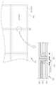
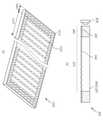
도 1은 본 실시예가 적용될 수 있는 다중 패널 표시장치를 도시하는 것으로서,(a)는 평면도이고, (b)는 다중 패널 표지상치의 각 패널 연결부분의 확대 단면도이다.
도 2는 다중 패널 표시장치의 연결부분을 확대 표시하는 굴절 광학부재의 일 예와, 그를 이용하는 경우 정면 시야에서의 이미지를 도시한다.
도 3은 도 2와 같은 굴절 광학부재가 사용되는 경우 시야각이 일정 이상인 사선 시선 방향에서의 광경로와 그에 따라 사용자에게 인식되는 이미지의 일 예를 도시한다.
도 4는 본 발명의 일실시예에 의한 다중 패널 표시장치의 단면도 및 사시도를 도시한다.
도 5는 본 발명의 일 실시예에 의한 다중 패널 표시장치가 사용되는 경우 패널 연결 부분 근처에서의 광경로를 도시한다.
도 6은 다른 실시예에 의한 굴절 광학부재의 일 예로서 컨벡스(Convex) 렌즈 플레이트가 사용되는 경우를 도시한다.
도 7은 본 발명의 실시예에 의한 다중 패널 표시장치에 사용되는 확산 광학부재의 여러 실시예를 도시한다.
도 8은 다른 실시예에 의한 확산 광학부재를 도시하는 것으로서, 각 패널 중앙 부분에 대응되는 제1확산부와, 패널간 연결부분과 인접한 제2확산부가 구분된 형태를 도시한다.
도 9는 본 발명의 일 실시예에 의한 개별표시장치의 백라이트 유닛의 일 예를 도시하면, 가장자리의 고휘도 영역과 중앙의 저휘도 영역을 포함한다.
도 10은 도 9에 의한 백라이트 유닛의 구체적인 실시예로서, (a)는 엣지 타입의 백라이트 유닛에서 고휘도 및 저휘도 영역에서 도광판의 패턴을 다르게 형성하는 구조이고, (b)는 직하형 백라이트 유닛에서 광원의 분포를 다르게 하는 구조이다.
도 11은 본 발명의 실시예에 의하여 패널 연결부분의 광휘도 저하를 보상할 수 있는 구조에서의 최종적인 광경로를 도시한다.
1 shows a multi-panel display device to which this embodiment can be applied, (a) is a plan view, and (b) is an enlarged cross-sectional view of each panel connection portion of the multi-panel display unit.
FIG. 2 shows an example of a refractive optical member that enlarges and displays a connection part of a multi-panel display device, and an image in a front view when using the refractive optical member.
FIG. 3 shows an example of an image recognized by a user and an optical path in a diagonal gaze direction having a viewing angle greater than or equal to a certain level when the refractive optical member shown in FIG. 2 is used.
4 is a cross-sectional view and a perspective view of a multi-panel display device according to an embodiment of the present invention.
5 illustrates an optical path near a panel connection part when a multi-panel display device according to an embodiment of the present invention is used.
6 illustrates a case in which a convex lens plate is used as an example of a refractive optical member according to another embodiment.
7 illustrates various embodiments of a diffusion optical member used in a multi-panel display device according to an embodiment of the present invention.
8 illustrates a diffusion optical member according to another embodiment, in which a first diffusion unit corresponding to a central portion of each panel and a second diffusion portion adjacent to the inter-panel connection portion are divided.
9 illustrates an example of a backlight unit of an individual display device according to an embodiment of the present invention, it includes an edge high luminance region and a central low luminance region.
10 is a detailed embodiment of the backlight unit shown in FIG. 9, wherein (a) is a structure in which a pattern of a light guide plate is formed differently in high luminance and low luminance regions in an edge-type backlight unit, and (b) is a direct-type backlight unit It is a structure that makes the distribution of the light source different.
11 shows a final optical path in a structure capable of compensating for a decrease in luminance of a panel connection portion according to an embodiment of the present invention.
이하, 본 발명의 일부 실시예들을 예시적인 도면을 참조하여 상세하게 설명한다. 각 도면의 구성요소들에 참조부호를 부가함에 있어서, 동일한 구성요소들에 대해서는 비록 다른 도면상에 표시되더라도 가능한 한 동일한 부호를 가질 수 있다. 또한, 본 발명을 설명함에 있어, 관련된 공지 구성 또는 기능에 대한 구체적인 설명이 본 발명의 요지를 흐릴 수 있다고 판단되는 경우에는 그 상세한 설명은 생략할 수 있다.Hereinafter, some embodiments of the present invention will be described in detail with reference to exemplary drawings. In adding reference numerals to components of each drawing, the same components may have the same reference numerals as much as possible even though they are indicated in different drawings. In addition, in describing the present invention, if it is determined that a detailed description of a related known configuration or function may obscure the gist of the present invention, the detailed description may be omitted.
또한, 본 발명의 구성 요소를 설명하는 데 있어서, 제 1, 제 2, A, B, (a), (b) 등의 용어를 사용할 수 있다. 이러한 용어는 그 구성 요소를 다른 구성 요소와 구별하기 위한 것일 뿐, 그 용어에 의해 해당 구성 요소의 본질, 차례, 순서 또는 개수 등이 한정되지 않는다. 어떤 구성 요소가 다른 구성요소에 "연결", "결합" 또는 "접속"된다고 기재된 경우, 그 구성 요소는 그 다른 구성요소에 직접적으로 연결되거나 또는 접속될 수 있지만, 각 구성 요소 사이에 다른 구성 요소가 "개재"되거나, 각 구성 요소가 다른 구성 요소를 통해 "연결", "결합" 또는 "접속"될 수도 있다고 이해되어야 할 것이다.In addition, in describing the components of the present invention, terms such as first, second, A, B, (a), (b), etc. may be used. These terms are only for distinguishing the elements from other elements, and the essence, order, order, or number of the elements are not limited by the terms. When it is described that a component is “connected”, “coupled” or “connected” to another component, the component may be directly connected or connected to the other component, but other components may be interposed between each component. It should be understood that each component may be “interposed” or “connected”, “coupled” or “connected” through another component.
도 1은 본 실시예가 적용될 수 있는 다중 패널 표시장치를 도시하는 것으로서,(a)는 평면도이고, (b)는 다중 패널 표지장치의 각 패널 연결부분의 확대 단면도이다.1 shows a multi-panel display device to which this embodiment can be applied, (a) is a plan view, and (b) is an enlarged cross-sectional view of each panel connection portion of the multi-panel display device.
도 1을 참조하면, 일반적인 다중 패널 표시장치(100)는 다수의 개별 표시장치(200)가 연결되어 형성되며, 개별 표시장치(200) 들이 연결되는 연결부분(300)이 형성된다.Referring to FIG. 1 , a typical
각각의 개별 표시장치(200)는 단독으로 하나의 완전한 표시장치를 이루는 것으로서, 액정표시장치(LCD), 유기전계발광 표시장치(OLED) 등으로 구현될 수 있으나 그에 한정되는 것은 아니다.Each
본 명세서에서 개별 표시장치는 다중 패널 표시장치를 구성하는 하나의 표시장치를 의미하며, 이러한 개별표시장치는 경우에 따라서 개별 패널, 패널 등의 다른 표현으로 정의될 수 있다.In the present specification, an individual display device means a single display device constituting a multi-panel display device, and the individual display device may be defined as an individual panel or other expression such as a panel in some cases.
도 1의 (b)과 같이, 각 개별 표시장치(200)는 패널 중앙에서 이미지가 표시되는 표시영역(Active Area; A/A; 212)과, 표시영역 가장자리를 둘라싸는 영역으로서 이미지가 표시되지 않는 비표시 영역(N/A; 210)을 포함한다. 각 개별 표시장치(200)의 비표시 영역(210)은 베젤 영역 등으로 달리 표현될 수 있다.As shown in (b) of FIG. 1 , each
한편, 각각의 개별 표시장치(200)는 다시 표시패널(222)과, 표시패널 하부에 배치되어 표시패널로 광을 제공하는 백라이트 유닛(224)과, 표시장치 전체를 둘러싸는 지지구조(226)를 포함하여 구성될 수 있다.Meanwhile, each
표시패널(222)은 통상 박막 트랜지스터 등이 형성되어 화소영역이 정의되는 어레이기판인 제1기판과, 블랙매트릭스 및/또는 칼라필터층 등이 형성된 상부 기판으로서의 제2기판이 합착되어 제조된다. 물론, OLED 표시장치에 의한 패널인 경우에는 상기 제2기판은 보호기판으로서의 기능만 할 수도 있다.The
또한, 백라이트 유닛(224)은 LED 등의 광원과 광원을 고정하기 위한 홀더 및 광원 구동 회로 등을 포함하는 광원 모듈과, 광을 패널 영역 전체로 확산시키기 위한 도광판(LGP) 또는 확산판과, 빛을 표시패널 방향으로 반사하기 위한 반사판과, 광원의 On/Off 등을 제어하기 회로인 LED 연성회로와, 도광판 상부에 배치되어 휘도 향상, 광의 확산 및 보호 등의 용도로 배치되는 1 이상의 광학필름 또는 시트(Sheet) 등과 같은 서브 유닛들을 포함할 수 있다.In addition, the
또한, 표시장치를 커버하는 외부 지지부재(226)는 표시장치 단위에서 백라이트 유닛(224) 및 표시패널(222)을 둘러싸서 보호하는 커버 버텀(Cover Bottom) 및/또는 가이드 패널(guide Panel) 등은 물론, 표시장치를 포함하는 최종 전자제품인 세트 전자장치 단위에서의 백 커버 등이 될 수 있다.In addition, the
한편, 도 1에 도시된 바와 같이, 각 개별 표시장치(200)은 가장자리의 일정 영역에서 이미지가 표시되지 않는 비표시 영역(N/A; 210)을 포함하며, 다중 패널 표시장치는 이러한 개별 표시장치(200)가 다수 연결되어 형성되므로, 다중 표시패널에서 각 개별표시장치가 연결되는 연결부분(300)에는 이미지가 표시되지 않는 현상이 발생한다.On the other hand, as shown in FIG. 1 , each
한편, 각 개별표시장치(200)의 비표시 영역(N/A; 210)은 표시패널(222) 자체의 비표시 영역과, 기타 백라이트 유닛(224)에 의하여 가려지는 부분, 또는 표시장치 전면을 커버하는 케이스 탑(Case Top) 또는 프론트 커버 등에 의하여 형성될 수 있다.Meanwhile, the non-display area N/
따라서, 도 1과 같은 다중 패널 표시장치 또는 비디오월(Video Wall)에 단일의 이미지를 표시하는 경우, 연결부분(300)에서는 이미지가 표시되지 않는 이미지 단절 현상이 발생하며, 이를 해결할 방안이 필요하게 되었다.Therefore, when a single image is displayed on a multi-panel display device or a video wall as shown in FIG. 1 , an image disconnection phenomenon occurs in which the image is not displayed in the
도 2는 다중 패널 표시장치의 연결부분을 확대 표시하는 굴절 광학부재의 일 예와, 그를 이용하는 경우 정면 시야에서의 이미지를 도시한다.FIG. 2 shows an example of a refractive optical member that enlarges and displays a connection part of a multi-panel display, and an image in a front view when using the same.
도 2에 도시된 바와 같이, 다중 패널 표시장치의 연결부분에서의 이미지 단절 현상을 극복하기 위한 하나의 방안으로서, 다중 패널 표시장치 상부에 배치되어 연결부분 근처에서의 광경로를 굴절 또는 확대하는 굴절 광학부재를 사용하는 기술이 고려될 수 있다.As shown in FIG. 2 , as a method for overcoming the image disconnection phenomenon in the connection part of the multi-panel display device, refraction is disposed on the multi-panel display device to refract or enlarge the optical path near the connection part. A technique using an optical member can be considered.
도 2는 그러한 굴절 광학수단으로서 다중 패널 표시장치 상부에 배치되는 렌즈 플레이트를 이용한 구성을 도시한다.FIG. 2 shows a configuration using a lens plate disposed on the multi-panel display device as such refractive optical means.
도 2에 사용되는 굴절 광학부재인 렌즈 플레이트(240)는 일종의 광투과성 스크린으로서, 일정한 두께를 가지는 일반적인 광투과성 판상 재료인 베이스 플레이트(242)와 다중 패널 표시장치의 연결부분(300) 부근에 형성된 렌즈부(244)를 포함한다.The
렌즈 플레이트(240)에 형성된 렌즈부(244)는 연결부분(300) 인근에서의 광경로를 굴절시킬 용도로 사용되는 것으로서, 프레넬 렌즈(Fresnel Lens) 등이 사용될 수 있으나 그에 한정된 것은 아니다.The
도 2에 도시된 바와 같이, 연결부분(300) 정면에 사용자(250)가 있는 경우에는 다중 패널 표시장치의 연결부분 상에 형성되는 렌즈 플레이트(240)의 렌즈부(244)에 의하여 인접한 표시영역의 화소(P1~P4)로부터 광이 렌즈부(240)에 굴절되어 사용자 시야로 입사된다.As shown in FIG. 2 , when the
따라서, 다중 패널 표시장치의 정면에서 바라보게 되면, 도 2의 하부 도면과 같이, 연결부분(300)에서도 인접한 화소의 이미지가 굴절 투사됨으로써 일정한 이미지가 표시되게 되고, 따라서 패널 연결부분에서의 이미지 단절 현상이 어느 정도 보상되는 효과가 있다.Therefore, when viewed from the front of the multi-panel display device, as shown in the lower view of FIG. 2 , images of adjacent pixels are refracted and projected in the
이와 같이, 다중 패널 표시장치 상부에 광경로 굴절이 가능한 프레넬 렌즈 플레이트 등을 배치함으로써 패널 연결부분에서의 이미지 단절 문제를 일부 극복하기 위한 여러 다양한 시도가 이루어지고 있지만, 이러한 기존의 굴절 광학부재를 이용하는 경우에는 정면 시야에서만 그러한 효과를 가진다는 한계가 있다.As described above, various attempts have been made to overcome the image disconnection problem in the panel connection part by disposing a Fresnel lens plate capable of optical path refraction on the upper part of the multi-panel display device. When used, there is a limit to having such an effect only in the front view.
도 3에 도시한 바와 같이, 프레넬 렌즈 플레이트를 다중 패널 표시장치 상부에 배치하더라도 사용자의 시야각이 정면(시야각=0)에서 벗어나서 약45도 이상(α)이 되면 도 2에 도시한 바와 같은 광경로가 형성되지 않고, 패널 연결부분(300)이 그대로 보이게 된다.As shown in FIG. 3 , even if the Fresnel lens plate is disposed on the upper part of the multi-panel display device, if the user's viewing angle deviates from the front (viewing angle = 0) and becomes about 45 degrees or more (α), the view shown in FIG. The furnace is not formed, and the
즉, 도 3에 도시한 바와 같이, 시야각이 α(α>약45도)인 경우 연결부분 근처의 화소로부터 광 중 일부는 비스듬히 보고 있는 사용자에게 입사되지 않고, 결과적으로 각 개별 표시장치의 베젤이 그대로 보이게 된다는 것이다.That is, as shown in FIG. 3, when the viewing angle is α (α > about 45 degrees), some of the light from the pixels near the connection part is not incident on the user who is looking at an angle, and as a result, the bezel of each individual display device is it will be visible as it is.
따라서, 도 3의 하부에 도시한 바와 같은 패널 연결부분에서의 이미지 단절 현상이 그대로 발생하게 된다.Accordingly, the image disconnection phenomenon at the panel connection portion as shown in the lower part of FIG. 3 occurs as it is.
본 발명의 실시예는 이와 같이 일정 각도 이상의 시야각에서도 다중 패널 표시장치의 연결부분에서 발생하는 이미지 단절 현상을 보상하기 위하여 제안된 것이다.The embodiment of the present invention is proposed to compensate for the image disconnection occurring in the connection portion of the multi-panel display device even at a viewing angle greater than or equal to a predetermined angle as described above.
본 실시예에 의한 다중 패널 표시장치는 여러 개별 표시장치가 연결되는 표시패널부 상부에 굴절 광학부재와 확산 광학부재를 순차적으로 배치한다. 이 때 굴절 광학부재는 표시장치의 연결부분 근처에서 인근 화소로부터의 광이 전달되도록 하고, 확산 광학부재는 굴절되어 전달된 광을 다시 한 번 확산함으로써 시야각이 일정 이상인 비스듬한 시야에서도 다중 패널 표시장치 연결부분의 이미지 단절 현상을 최소화할 수 있다.In the multi-panel display device according to the present exemplary embodiment, a refractive optical member and a diffusing optical member are sequentially disposed on a display panel unit to which several individual display devices are connected. At this time, the refractive optical member transmits light from nearby pixels near the connection portion of the display device, and the diffusing optical member diffuses the refracted and transmitted light once again, thereby connecting the multi-panel display device even in an oblique view with a viewing angle greater than a certain level. It is possible to minimize the image disconnection phenomenon of the part.
이하에서는 도 4 내지 도 11을 참고로 본 발명의 실시예에 의한 다중 패널 표시장치의 구성에 대하여 상세하게 설명한다.Hereinafter, a configuration of a multi-panel display device according to an embodiment of the present invention will be described in detail with reference to FIGS. 4 to 11 .
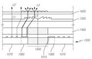
도 4는 본 발명의 일실시예에 의한 다중 패널 표시장치의 단면도 및 사시도를 도시한다.4 is a cross-sectional view and a perspective view of a multi-panel display device according to an embodiment of the present invention.
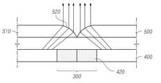
본 발명의 일 실시예에 의한 다중 패널 표시장치는 다수의 개별표시장치가 연결되는 것으로서, 다수의 개별 표시장치(410)의 패널 부분이 연결되어 형성되되 개별 표시장치들이 연결되는 연결부분을 포함하는 표시 패널부(400)와, 표시 패널부 상부에 배치되는 굴절 광학부재(500) 및 굴절 광학부재(500) 상부에 배치되어 굴절 광학부재(500)로부터의 광을 확산하는 확산 광학부재(600)를 포함하여 구성될 수 있다.A multi-panel display device according to an exemplary embodiment of the present invention is a device to which a plurality of individual display devices are connected, the panel parts of the plurality of
표시패널부(400)는 다수의 개별 표시장치(410)가 연결되어 단일의 이미지를 표시하게 되는 다중 패널 표시장치의 디스플레이 부분에 대응되는 것으로서, 개별 표시장치들이 연결되는 부분에는 각 개별 표시장치의 베젤 또는 비표시영역(420)이 연결 형성되어 이미지가 표시되지 않는 부분이 존재하게 된다. 본 명세서에서는 이러한 개별 표시장치가 연결되는 경계영역을 연결부분(300)으로 정의한다.The
즉, 다중 패널 표시장치의 표시패널부(400)에는 이미지가 표시되지 않는 연결부분(300)이 일정한 폭을 가지는 격자 형상의 선형 구조로 형성되며, 이러한 연결부분(300)에서의 이미지 단절 문제를 해결하기 위하여 굴절 광학부재(500) 및 확산 광학부재(600)를 이용하는 것이다.That is, in the
본 발명의 실시예에 사용될 수 있는 개별 표시장치(410)는 액정 표시장치일 수 있으나 그에 한정되는 것은 아니며, 플라즈마 디스플레이, 유기전계발광소자(OLED) 표시장치 등 모든 형태의 표시장치를 포함하는 것으로 이해되어야 한다.The
한편, 본 발명의 실시예에 적용되는 개별 표시장치(410)는 다시 화소가 형성되는 표시패널과, 커버버텀 등과 같이 표시패널을 지지하는 패널 지지구조를 포함할 수 있다.Meanwhile, the
또한, 개별 표시장치(410)가 액정 표시 장치인 경우에는 상기 표시패널은 액정 패널이며, 액정 패널 하부에 배치되어 액정 패널로 광을 제공하는 백라이트 유닛을 추가로 포함할 수 있다.In addition, when the
한편, 개별 표시장치(410)가 액정 표시패널을 포함하는 액정표시장치인 경우, 액정표시패널에는 다시 다수의 게이트 라인과 데이터 라인 및 그 교차 영역에 정의되는 픽셀(Pixel)과, 각 픽셀에서의 광투과도를 조절하기 위한 스위칭 소자인 박막 트랜지스터(TFT)를 포함하는 어레이 기판과, 컬러필터 및/또는 블랙매트릭스 등을 구비한 상부기판과, 그 사이에 형성되는 액정물질층을 포함하여 구성될 수 있으며, 터치 윈도우가 표시패널의 상부 전면에 추가로 배치될 수 있다.On the other hand, when the
물론, 본 발명의 실시예에 적용되는 개별 표시장치가 유기전계 발광 표시장치(OLED)인 경우의 표시패널은 다수의 게이트 라인과 데이터 라인 및 그 교차 영역에 정의되는 픽셀(Pixel)과, 각 픽셀에 제공된 유기전계 발광 재료층에 선택적으로 전기적 신호를 인가하기 위한 스위칭 소자인 박막 트랜지스터(TFT)를 포함하는 어레이 기판과, 상부 보호 기판 등으로 구성될 수 있다.Of course, when the individual display device applied to the embodiment of the present invention is an organic light emitting diode display (OLED), the display panel includes a plurality of gate lines and data lines, and pixels defined in a cross region thereof, and each pixel. It may be composed of an array substrate including a thin film transistor (TFT) as a switching element for selectively applying an electrical signal to the organic electroluminescent material layer provided in the EL material layer, an upper protective substrate, and the like.
도 5에 도시한 바와 같이, 본 실시예에 의한 굴절 광학부재(500)는 다중 패널 표시장치의 표시패널부(400) 상부에 일정 거리 이격되어 배치되는 판상 플레이트일 수 있으며, 이러한 굴절 광학 부재(500)는 다중 패널 표시장치의 표시패널부(400) 전면 전체에 배치되는 광투과성 재질의 판형상의 베이스 플레이트(510)와, 표시패널부의 연결부분(300) 상부를 포함하는 영역에 배치되는 광굴절 렌즈부(520)를 포함할 수 있다.As shown in FIG. 5 , the refractive
이 때, 광굴절 렌즈부(520)는 프레넬 렌즈 또는 컨벡스 렌즈일 수 있으나 그에 한정되는 것은 아니다.In this case, the optical
굴절 광학부재(500)의 광굴절 렌즈부(520)를 형성하는 프레넬 렌즈(Fresnel Lens)는 일반적인 선형 프레넬 렌즈 구조로 형성될 수 있으며, 연결부분의 길이방향으로 길게 연장되는 다수의 리지(Ridge; 522)와 각 리지로부터 렌즈 플레이트 상면까지 연장되는 사선면(524)이 반복적으로 형성된 구조일 수 있다.The Fresnel lens forming the optical
한편, 프레넬 렌즈의 리지(522)는 연결부분의 중간(도 5의 I)에서 가장 높으며 각 개별 표시장치의 중앙 영역으로 이동할수록 리지가 점점 더 작아지는 것이 바람직하다. 이로써, 연결부분의 중앙에서의 굴절각도가 가장 커져서 멀리있는 최외곽 화소(P1)으로부터의 광을 굴절시켜 연결부분(300)의 수직 상부로 향하도록 하는 것이다.On the other hand, the
도 6은 다른 실시예에 의한 굴절 광학부재로서 컨벡스(Convex) 렌즈 플레이트가 사용되는 경우를 도시한다.6 illustrates a case in which a convex lens plate is used as a refractive optical member according to another embodiment.
도 6과 같이, 본 실시예에 의한 굴절 광학부재(500)로서 사용될 수 있는 컨벡스 렌즈 플레이트는, 다중 패널 표시장치의 표시패널부(400) 전면 전체에 배치되는 광투과성 재질의 판형상의 베이스 플레이트(510)와, 표시패널부의 연결부분(300) 상부를 포함하는 영역에 배치되는 광굴절 렌즈부(520)로 구성된다. 이 때, 광굴절 렌즈부(520)는 컨벡스 렌즈 구조로서, 각 개별 표시장치의 표시영역에서는 큰 두께를 가지면서, 개별 표시장치의 비표시영역(420)에서 두께가 감소하기 시작하여 표시패널(400)의 연결부분(300)의 중앙 영역에서 가장 작은 두께를 가지도록 연속적인 곡면을 형성할 수 있다.As shown in FIG. 6 , the convex lens plate that can be used as the refractive
즉, 이러한 컨벡스 렌즈 플레이트는 각 개별 표시장치의 표시영역에 대응되는 부분에서는 화소로부터의 광을 그대로 수직 투과시켜야 하므로 일정한 두께를 가지는 평편한 형태의 베이스 플레이트(510)로 구성하고, 각 개별 표시장치의 베젤부분(비표시영역)에서는 인접한 화소로부터의 광을 굴절시켜 수직 투과시켜야 하므로 일정 곡률을 가지는 곡면 또는 컨벡스 표면을 형성하는 렌즈 구조를 가진다.That is, since the convex lens plate has to vertically transmit the light from the pixel in the portion corresponding to the display area of each individual display device, it is composed of a
본 실시예에 사용되는 프레넬 렌즈 플레이트와 컨벡스 렌즈 플레이트를 비교하면, 프레넬 렌즈 플레이트는 컨벡스 렌즈 플레이트에 비하여 얇은 두께가 가능하다는 장점은 있으나, 불연속 적인 렌즈 구조의 특성상 광굴절 역시 불연속 적이어서 연결부분(300)에서의 이미지가 다소 불연속적이라는 단점이 있을 수 있다.Comparing the Fresnel lens plate and the convex lens plate used in this embodiment, the Fresnel lens plate has the advantage that it can be thinner than the convex lens plate, but the optical refraction is also discontinuous due to the discontinuous lens structure. The disadvantage may be that the image in
이러한 구조의 선형 프레넬 렌즈 플레이트 또는 컨벡스 렌즈 플레이트 등은 광의 확대 및/또는 굴절을 위하여 다른 분야에서도 사용되는 기술이므로 본 명세서에서는 그 상세한 설명은 생략한다.Since the linear Fresnel lens plate or the convex lens plate having such a structure is a technology used in other fields for magnification and/or refraction of light, a detailed description thereof will be omitted herein.
또한, 본 실시예에 의한 굴절 광학부재(500)는 전술한 프레넬 렌즈 플레이트나 컨벡스 렌즈 플레이트에 한정되는 것은 아니며, 다중 패널 표시장치의 연결부분(300)에서 광굴절에 의하여 인접 화소로부터의 광을 외부로 투과시킬 수 있는 모든 광학부재가 사용될 수 있을 것이다.In addition, the refractive
한편, 앞서도 설명한 바와 같이, 프레넬 렌즈 플레이트 및 컨벡스 렌즈 플레이트와 같은 굴절 광학부재(500)를 사용하는 경우, 다중 패널 표시장치의 정면 시야각에서는 연결부분(300)에 인접한 화소(도 5의 P1~P4)로부터의 광이 연결부분 상부로 굴절되어 연결부분에서의 이미지 불연속 현상이 어느 정도 보상될 수 있다.Meanwhile, as described above, when the refractive
그러나, 굴절 광학부재만을 사용하는 경우, 시야각이 정면에서 벗어날수록 이러한 인접 화소의 광굴절 현상이 감소하게 되어, 결과적으로 측면 시야에서는 개별 표시장치의 베젤 또는 연결부분(300)이 그대로 보이게 되는 이미지 불연속 문제가 그대로 발생될 수 있다는 것이다.However, in the case of using only the refractive optical member, the optical refraction phenomenon of the adjacent pixels decreases as the viewing angle deviates from the front. The problem is that it could just happen.
이를 해결하기 위하여 본 실시예에서는 굴절 광학부재(500) 상부에 별도의 광학 부재인 확산 광학부재(600)를 사용하게 되는 것이다.In order to solve this problem, in the present embodiment, the diffusing
본 실시예에 사용되는 확산 광학부재(600)는 굴절 광학부재(500) 상부에 배치되어 굴절 광학부재(500)로부터의 광을 확산하는 기능을 하는 판상 광학 부재로서, 굴절율 1.4 내지 1.55인 광투과성 재질로 형성되는 확산 플레이트일 수 있다.The diffusing
도 7은 본 발명의 실시예에 의한 다중 패널 표시장치에 사용되는 확산 광학부재의 여러 실시예를 도시한다.7 illustrates various embodiments of a diffusion optical member used in a multi-panel display device according to an embodiment of the present invention.
이러한 확산 광학부재(600)의 일 예인 확산 플레이트는 굴절 광학부재(600)로부터 입사된 광을 여러 방향으로 확산 또는 분산시킬 수 있는 판상 부재로서, 확산 플레이트의 광투과성 재질은 폴리메타크릴산 메틸(poly-methyl metha crylate; PMMA), 폴리카보네이트(Poly Carbonate; PC), 폴리에테르 술폰(Poly Ether Sulfone; PES), 메타크릴레이트스티렌(Methacrylate Styrene; MS) 중 선택되는 1 이상의 고분자 레진일 수 있으나 그에 한정되는 것은 아니다.The diffusion plate, which is an example of the diffusion
도 7의 (a)에 도시한 바와 같이 확산 광학부재(600)가 단순한 판 형태의 확산 플레이트 일 수도 있으며, 이 때의 확산 플레이트는 백라이트 유닛의 도광판 상부 등에 배치되어 사용되는 여러 종류의 확산시트 중 하나와 유사한 광학 부재가 사용될 수 있다.As shown in (a) of FIG. 7 , the diffusion
한편, 도 7의 (b)에 도시한 실시예에서는, 확산 광학부재(600)가 광투과성 재질의 베이스 플레이트(610)와, 연결부분의 상부를 포함하는 상기 베이스 플레이트 영역에 배치되는 확산 패턴부(620)를 포함하여 구성될 수 있다.On the other hand, in the embodiment shown in Figure 7 (b), the diffusion
이 때, 확산 광학부재를 구성하는 확산 패턴부(620)는 1 이상의 엠보싱 돌출구조일 수 있다.In this case, the
즉, 도 7의 (b)의 실시예와 같이, 확산 광학부재(600)는 굴절 광학부재 상부에 배치되는 베이스 플레이트(610)와, 베이스 플레이트의 일면에 배치되는 확산 패턴부를 포함하며, 확산 패턴부(620)는 다수의 볼록부 또는 엠보싱 돌출구조와 다수의 오목부를 포함하는 구조일 수 있다.That is, as in the embodiment of Figure 7 (b), the diffusion
이러한 확산 패턴부를 구성하는 엠보싱 및 오목부의 크기는 1~300um일 수 있고, 그 형상은 반구형, 타원형, 다각형, 부정형일 수 도 있다. 또한, 엠보싱 돌출구조가 반원 또는 다각형 단면을 가지면서 길게 형성된 스트라이프 형태일 수도 있다.The size of the embossing and concave portions constituting the diffusion pattern portion may be 1 to 300 μm, and the shape may be a hemispherical shape, an oval shape, a polygonal shape, or an irregular shape. In addition, the embossed protrusion structure may be in the form of a long stripe having a semicircular or polygonal cross-section.
이러한 확산 패턴부는 다중 패널 표시장치에 형성된 연결부분(300) 근처에서 굴절 광학부재(500)로부터 입사된 광을 확산시키는 기능을 한다.The diffusion pattern part functions to diffuse the light incident from the refractive
이 때, 확산 광학부재의 베이스 플레이트 및 확산패턴부는 모두 굴절율이 1.4 내지 1.55인 폴리메타크릴산 메틸(poly-methyl metha crylate; PMMA), 폴리카보네이트(Poly Carbonate; PC), 폴리에테르 술폰(Poly Ether Sulfone; PES), 메타크릴레이트스티렌(Methacrylate Styrene; MS) 등과 같은 고분자 레진으로 형성될 수 있다.At this time, both the base plate and the diffusion pattern portion of the diffusion optical member have a refractive index of 1.4 to 1.55 poly-methyl methacrylate (PMMA), polycarbonate (PC), and polyether sulfone (Poly Ether). It may be formed of a polymer resin such as Sulfone (PES) or methacrylate styrene (MS).
또한, 도 7의 (b)에서는 확산 패턴부가 확산 플레이트를 구성하는 베이스 플레이트의 일면에만 형성된 것으로 도시하였으나, 그에 한정되지 않으며 베이스 플레이트의 타면 또는 양면 모두에 형성될 수 있다.In addition, although it is illustrated that the diffusion pattern portion is formed only on one surface of the base plate constituting the diffusion plate in FIG. 7B , the present invention is not limited thereto and may be formed on the other surface or both surfaces of the base plate.
또한, 확산 패턴부는 다중 표시패널의 표시패널부(400) 전체에 걸쳐 형성될 수도 있으나, 연결부분(300)을 포함하는 표시패널부의 일정 영역에만 형성될 수 있을 것이다.In addition, the diffusion pattern portion may be formed over the entire
도 7의(c)에 도시된 실시예에서는, 확산 광학부재(600)가 광투과성 재질의 베이스 플레이트(610)와, 베이스 플레이트 내부에 분산 배치되되 상기 베이스 플레이트의 굴절율과 상이한 굴절율을 가지는 재료로 구성되는 비드 또는 확산입자(630)를 포함하여 구성될 수 있다.In the embodiment shown in FIG. 7( c ), the diffusion
이때, 확산 광학부재에 포함되는 비드 또는 확산입자(630)는 PMMA, 실리카, PC 중 적어도 하나의 물질로 이루어지며, 비드의 형상은 원형, 사각뿔(피라미드) 형상 등일 수 있다.At this time, the bead or
또한, 경우에 따라서 확산 성능을 향상시키기 위하여 비드 또는 확산입자는 각각 다른 굴절율 및/또는 크기를 가지는 2종류 이상의 비드가 사용될 수도 있을 것이다. 예를 들면, 1㎛ 내지 10㎛의 직경과 제1굴절율을 가지는 제1비드와, 20㎛ 내지 80㎛의 직경을 가지되 제1굴절율보다 0.02~0.2만큼 작은 제2굴절율을 가지는 제2비드를 포함할 수 있다. 이 때, 제1비드와 제2비드의 단위 체적당 분포 밀도를 조절함으로써 원하는 확산 성능을 확보할 수 있을 것이다.In addition, in order to improve diffusion performance in some cases, two or more types of beads or particles having different refractive indexes and/or sizes may be used. For example, a first bead having a diameter of 1 μm to 10 μm and a first refractive index, and a second bead having a diameter of 20 μm to 80 μm but a second refractive index smaller than the first refractive index by 0.02 to 0.2 may include In this case, desired diffusion performance may be secured by controlling the distribution densities per unit volume of the first bead and the second bead.
한편, 확산 광학부재의 확산입자가 반드시 레진 재료일 필요는 없으며, 베이스 플레이트의 내부에 형성되고 베이스 플레이트의 광 굴절률과 다른 광 굴절률을 갖는 1 이상의 공기 캐비티(Air Cavity)일 수도 있다.Meanwhile, the diffusing particles of the diffusing optical member are not necessarily made of a resin material, and may be one or more air cavities formed inside the base plate and having a light refractive index different from the light refractive index of the base plate.
본 실시예에 의한 확산 광학부재(600)은 도 7에 도시한 예에 한정되는 것은 아니며, 광확산 정도를 조절할 수 있는 어떠한 부재가 사용되어도 무방하다.The diffusion
예를 들면, 확산 광학부재의 다른 예로서, 플라스틱 또는 유리의 베이스 플레이트에 구형상의 폴리카보네이트(PC) 확산 패턴을 형성하되, 광경화제에 의하여 PC 확산 패턴을 베이스 플레이트에 부착할 수도 있을 것이다. 이 경우 베이스 플레이트에 접착되는 PC 확산 패턴의 크기와 밀도를 조절함으로써 필요한 광확산도를 형성할 수 있다.For example, as another example of the diffusion optical member, a spherical polycarbonate (PC) diffusion pattern is formed on a base plate of plastic or glass, but the PC diffusion pattern may be attached to the base plate using a photocuring agent. In this case, the required light diffusivity can be formed by adjusting the size and density of the PC diffusion pattern adhered to the base plate.
또한, 베이스 플레이트에 스크래치 또는 광중합체 패턴을 형성함으로써 필요한 확산부를 구성할 수도 있을 것이다.It may also be possible to construct the necessary diffuser by forming scratches or photopolymer patterns on the base plate.
도 8은 또다른 실시예에 의한 확산 광학부재를 도시하는 것으로서, 각 패널 중앙 부분에 대응되는 제1확산부와, 패널간 연결부분과 인접한 제2확산부가 구분된 형태를 도시한다.8 illustrates a diffusion optical member according to another embodiment, in which a first diffusion portion corresponding to a central portion of each panel and a second diffusion portion adjacent to an inter-panel connection portion are divided.
즉, 도 8에 도시된 실시예에서는 확산 광학부재가 2종류의 다른 확산 특성을 가지는 영역을 포함할 수 있다.That is, in the embodiment shown in FIG. 8 , the diffusion optical member may include regions having two different diffusion characteristics.
예를 들면, 도 8에 도시된 바와 같이, 확산 광학부재(700)의 전체 영역 중에서 각 개별 표시장치의 중앙 표시영역에 대응되는 제1영역에는 제1굴절율을 가지는 제1 확산부(720)가 형성되고, 다중 패널 표시장치의 연결부분(300) 상부의 일정한 영역인 제2영역에는 제2굴절율을 가지는 제2확산부(710)가 형성될 수 있다.For example, as shown in FIG. 8 , a
이 때, 제2굴절율을 제1굴절율보다 큰 것이 바람직하다.In this case, it is preferable that the second refractive index is greater than the first refractive index.
제1 확산부(720)는 제1굴절율을 가지는 단순 평판 플레이트 또는 내부에 비드 등을 포함하는 평판 플레이트로 형성될 수 있으며, 제2확산부(710)는 전술한 엠보싱 돌출구조를 가지거나 상기 제1 확산부에 포함된 비드와 상이한 물성을 가지는 비드 또는 확산입자를 포함하도록 구성할 수 있다.The
도 8의 실시예와 같이, 확산 광학부재(700)를 연결부분(300)을 포함한 영역과 그 외의 영역에서 상이한 물성을 가지도록 형성함으로써, 다중 패널 표시장치의 표시영역에서의 광경로 특성과 다중 패널 표시장치의 비표시 영역인 연결부분 상에서의 광경로 특성을 상이하게 할 수 있다.As in the embodiment of FIG. 8 , by forming the diffusion
또한, 도 8에 도시한 바와 같이, 굴절 광학부재(500) 역시 상기 제1확산부(720) 및 제2확산부(710)에 대응되는 상기 제1영역과 제2영역에 각각 다른 굴절 특성을 가지도록 형성할 수 있다.In addition, as shown in FIG. 8 , the refractive
도 8과 같은 실시예를 이용하면, 다중 패널 표시장치의 표시영역에서는 아래에 위치하는 화소로부터의 광이 일반적인 경로를 통하여 외부로 방출되도록 광굴절 및 확산을 최소화하고, 다중 패널 표시장치의 비표시 영역인 연결부분(300)에서는 광굴절 및 확산이 많이 이루어지도록 함으로써, 연결부분에서의 이미지 불연속 문제를 해결하면서도 다중 패널 표시장치 전체의 이미지 열화를 방지할 수 있도록 한다.8, in the display area of a multi-panel display device, light refraction and diffusion are minimized so that light from a pixel located below is emitted to the outside through a general path, and non-display of the multi-panel display device In the
한편, 도 5에 도시한 바와 같이, 확산 광학부재(600)와 굴절 광학부재(500) 사이의 이격 거리(d)는 1.0 ~ 3.0mm 일 수 있다. 이러한 확산 광학부재(600)와 굴절 광학부재(500) 사이의 이격 거리(d)가 1.0mm보다 작은 경우에는 광경로가 짧아져 연결부분에서의 확산 정도가 낮아지고, 따라서 연결부분에서의 확산에 의한 이미지 불연속 해결이 제한적일 수 있다.Meanwhile, as shown in FIG. 5 , the separation distance d between the diffusing
또한, 확산 광학부재(600)와 굴절 광학부재(500) 사이의 이격 거리(d)가 일정 이상(예를 들면, 3.0mm)인 경우에는, 확산 광학부재에서의 확산 정도가 커져서 전체적인 이미지의 선명도가 열화될 가능성이 있다.In addition, when the separation distance d between the diffusing
도 5는 이상 설명한 실시예에 의한 다중 패널 표시장치에서, 패널 연결부분(300) 근처에서의 광경로를 도시한다.5 shows an optical path near the
도 5에 도시된 바와 같이, 다중 패널 표시장치에서 각 개별 표시장치 들이 연결되는 연결부분(300) 부근에서는 굴절 광학부재(500)에 의하여 연결부분에 인접한 최외곽 화소들인 P1 내지 P4로부터의 광이 굴절되어 연결부분(300)의 상부로 수직 방출된다.(L1) 이와 같이 굴절 광학부재(500)에 의하여 굴절 또는 확대되어 출사된 광 L1은 확산 광학부재(600)에서 여러 방향으로 확산된다.(L2)As shown in FIG. 5 , in the multi-panel display device, in the vicinity of the
이와 같이, 확산 광학부재(600)에서 확산된 광 L2는 여러 방향으로 향하기 때문에, 시야각이 일정 크기 이상인 측방으로도 진행하게 되며, 따라서 정면이 아닌 측면 시야각의 위치에서도 연결부분(300)에서 연속적인 심리스(Seamless)한 영상 구현이 가능해진다.In this way, since the light L2 diffused from the diffusion
도 9는 본 발명의 일 실시예에 의한 개별표시장치의 백라이트 유닛의 일 예를 도시하면, 가장자리의 고휘도 영역과 중앙의 저휘도 영역을 포함한다.9 illustrates an example of a backlight unit of an individual display device according to an embodiment of the present invention, it includes an edge high luminance region and a central low luminance region.
본 실시예에 의한 다중 패널 표시장치의 경우, 이상 설명한 바와 같이, 개별 표시장치들이 연결되는 연결부분(300)에서 인접 화소로부터의 광을 확대/굴절시키고, 그를 다시 확산시키는 방식을 이용하고 있다.In the case of the multi-panel display device according to the present embodiment, as described above, a method of expanding/refracting light from adjacent pixels in the
이 때, 다중 패널 표시장치의 연결부분(300) 이외의 영역, 예를 들면, 각 개별표시장치의 표시영역 등에서의 이미지에 비하여, 연결부분(300) 부근에서의 이미지는 휘도나 선명도 등이 떨어질 가능성이 있다.In this case, compared to an image in a region other than the
따라서, 도 9 이하의 실시예에서는 이를 극복하기 위하여, 개별 표시장치에 포함되는 백라이트 유닛을 구성함에 있어서, 백라이트 유닛이 상기 연결부분(300) 부근에서의 고휘도 영역(960)과 각 개별표시장치의 중앙 영역에서의 저휘도 영역(970)을 포함하도록 구성한다.Therefore, in the embodiment shown in FIG. 9 and below, in order to overcome this problem, in configuring the backlight unit included in the individual display device, the backlight unit is formed between the
본 실시예에 의한 다중 패널 표시장치를 구성하는 개별 표시장치 각각은 백라이트 유닛(900)을 포함할 수 있다.Each individual display device constituting the multi-panel display device according to the present embodiment may include a
백라이트 유닛(900)은 LED 등의 광원(LED)을 포함하는 광원 모듈(930)과, 빛을 패널 영역 전체로 확산시키기 위한 도광판(LGP; 940) 또는 확산판과, 빛을 표시패널 방향으로 반사하기 위한 반사판(930)과, 광원의 On/Off 등을 제어하기 회로인 LED 연성회로(LED FPC; 미도시)와, 도광판 상부에 배치되어 휘도 향상, 광의 확산 및 보호 등의 용도로 배치되는 1 이상의 광학필름 또는 시트(950) 등과 같은 서브 유닛들을 포함할 수 있다.The
본 발명의 실시예에서의 백라이트 유닛의 광원 모듈(920)은 광원 소자와, 그 광원 소자를 지지하고 광원 구동을 위한 LED 구동 회로가 포함된 긴 판상 구조의 광원 홀더를 포함할수 있으며, 광원 모듈의 광원소자는 발광 다이오드(LED) 또는 발광 다이오드 스트립 등이 사용될 수 있으나 그에 한정되는 것은 아니며, 표시패널에 필요한 광을 제공할 수 있는 한 모든 형태의 광원이 사용될 수 있을 것이다.The
도광판(LGP; 940)은 일반적으로 플라스틱 시트로부터 다이 커팅되거나, 압출되거나, 사출 성형된 직사각형의 투명한 플라스틱(clear plastic) 시트로 형성될 수 있으며, 발광 다이오드 어레이 등과 같은 광원으로부터의 광은 도광판의 가장자리로 출사되어 도광판 내부에서 전반사되면서 표시패널의 배면을 가로질러 확산되며, 도광판의 평탄한 상면을 통해 출사되는 광이 표시패널의 백라이트로서 기능한다.The light guide plate (LGP) 940 is generally die cut from a plastic sheet, extruded, or injection molded into a rectangular sheet of clear plastic, wherein light from a light source, such as an array of light emitting diodes, passes through the edge of the light guide plate. The light emitted from the light guide plate is totally reflected inside the light guide plate and diffused across the rear surface of the display panel, and the light emitted through the flat top surface of the light guide plate functions as a backlight of the display panel.
반사판(930)은 도광판(940)의 배면에 위치하여, 도광판(940)의 배면을 통과한 광을 표시패널 쪽으로 반사시킴으로써 광의 휘도를 향상시키는 기능을 한다.The
도광판(940) 상부의 광학시트(950)는 확산시트와 적어도 하나의 집광시트 등을 포함하며, 도광판(940)을 통과한 빛을 확산 또는 집광하여 표시패널로 보다 균일한 면광원이 입사 되도록 한다.The
본 발명의 실시예에 의한 각 개별 표시장치의 백라이트 유닛은 가장자리 일정 영역에 형성된 고휘도 영역(960)과 개별 표시장치의 중앙부분에 형성되는 저휘도 영역(970)을 포함하며, 고휘도 영역은 각 개별표시장치의 베젤 또는 비표시 영역을 커버하되, 베젤 영역보다 넓은 범위로 형성될 수 있다The backlight unit of each individual display device according to an embodiment of the present invention includes a
한편, 백라이트 유닛의 고휘도 영역(960) 및 저휘도 영역(970)은 백라이트 유닛의 도광판(940)에 배치되는 도광 패턴에 의하여 구분될 수도 있고, 직하형 백라이트 유닛의 LED 분포 밀도에 의하여 구분될 수도 있다.Meanwhile, the
도 10은 도 9에 의한 백라이트 유닛의 구체적인 실시예로서, (a)는 엣지 타입의 백라이트 유닛에서 고휘도 및 저휘도 영역에서 도광판의 패턴을 다르게 형성하는 구조이고, (b)는 직하형 백라이트 유닛에서 광원의 분포를 다르게 하는 구조이다.10 is a detailed embodiment of the backlight unit of FIG. 9, (a) is a structure in which the pattern of the light guide plate is differently formed in high luminance and low luminance regions in an edge-type backlight unit, (b) is a direct backlight unit It is a structure that makes the distribution of the light source different.
도 10의 (a)는 광원이 표시장치의 일측에만 제공되고 도광판을 통해서 표시패널 전체로 확산되는 엣지(Edge) 타입의 백라이트 유닛(900)으로서, 백라이트 유닛(900)의 도광판(940)은 고휘도 영역(960)에 형성되는 고휘도 도광 패턴(942)과 저휘도 영역(970)에 형성되는 저휘도 도광 패턴(944)이 형성되어 있다.10A is an edge-
도광 패턴은 도광판의 하부 또는 내부에 형성되어 광원으로부터 전달된 광을 표시패널 방향으로 향하도록 확산/집광하기 위한 것으로서, 그 형태는 도트 패턴, 일정 형상의 돌출 패턴 등을 포함할 수 있다. The light guide pattern is formed under or inside the light guide plate to diffuse/condense the light transmitted from the light source toward the display panel, and the shape may include a dot pattern, a protrusion pattern of a certain shape, and the like.
이러한 도광 패턴은 일반적인 백라이트 유닛의 도광판에 적용되는 기술이므로 그에 대한 세부 구성의 설명은 생략한다.Since such a light guide pattern is a technology applied to a light guide plate of a general backlight unit, a detailed configuration thereof will be omitted.
도 10의 (a)에 의한 도광판(940)에서는, 고휘도 영역(960)에 형성되는 고휘도 도광패턴(942)과, 저휘도 영역(970)에 형성되는 저휘도 도광 패턴(944)이 상이한 구조를 가지는 것으로서, 예를 들면, 고휘도 도광패턴(942)이 저휘도 도광 패턴(944)에 비하여 패턴의 형상이 다르거나, 동일한 형태의 도광패턴의 형성 밀도를 달리 하여 구성할 수 있다.In the
예를 들어, 도광 패턴이 도광판의 하면에 원형으로 형성되는 도트 도광 패턴인 경우, 고휘도 도광패턴(942)가 저휘도 도광패턴(944)에 비하여 더 큰 패턴으로 형성되거나, 고휘도 도광패턴이 저휘도 도광패턴보다 더 조밀하게 형성될 수 있을 것이다.For example, when the light guide pattern is a dot light guide pattern formed in a circular shape on the lower surface of the light guide plate, the high-brightness
또한, 도광패턴이 도광판의 하부에 형성되는 프리즘 형태의 돌출구조 또는 요홈 형태인 경우에는, 고휘도 도광패턴(942)가 저휘도 도광패턴(944)에 비하여 프리즘의 첨두부 높이가 더 높거나 요홈의 깊이가 더 깊도록 형성할 수 있다.In addition, when the light guide pattern has a prism-shaped protrusion structure or groove shape formed under the light guide plate, the high-brightness
도 10의 (b)의 실시예는, 표시장치 후면에 배치되는 다수의 LED 칩 으로부터 광이 직접 상부의 표시패널로 전달되는 직하타입의 백라이트 유닛(1000)에 본 발명이 적용된 경우로서, 백라이트 유닛(1000)의 하부에 다수의 광원을 배치함에 있어서, 개별 표시장치의 베젤 또는 비표시 영역에는 광원을 조밀하게 배치하고, 표시영역에는 그보다 덜 조밀하게 광원을 배치할 수 있다. (도 10의 (b) 참고)The embodiment of FIG. 10 (b) is a case in which the present invention is applied to a direct-
또한, 동일한 밀도로 광원이 배치되되, 개별 표시장치의 베젤 또는 비표시 영역에서 광원을 제어하기 위한 광제어신호(구동전압 또는 구동전류 등)가 표시영역에서의 광제어 신호보다 더 크도록 제어할 수도 있다. 물론, 광원의 분포 밀도와 광제어신호(구동전압 또는 구동전류 등)를 함께 이용하여 고휘도 영역과 저휘도 영역을 구분 설계할 수도 있을 것이다.In addition, the light sources are arranged with the same density, and the light control signal (driving voltage or driving current, etc.) for controlling the light source in the bezel or non-display area of the individual display device is greater than the light control signal in the display area. may be Of course, the high luminance region and the low luminance region may be separately designed by using the distribution density of the light source and the light control signal (eg, driving voltage or driving current).
이상과 같이, 다중 패널 표시장치를 구성하는 각 개별 표시장치의 백라이트 유닛의 가장자리에 고휘도 영역을 배치함으로써, 다중 패널 표시장치의 연결부분(300)에서의 굴절/확산에 따른 광휘도 저하 현상을 해결할 수 있다.As described above, by arranging the high luminance region at the edge of the backlight unit of each individual display device constituting the multi-panel display device, the phenomenon of luminance degradation due to refraction/diffusion in the
도 11은 본 발명의 실시예 의하여 패널 연결부분의 광휘도 저하를 보상할 수 있는 구조에서의 최종적인 광경로를 도시한다.11 shows a final optical path in a structure capable of compensating for a decrease in luminance of a panel connection portion according to an embodiment of the present invention.
도 11에 도시된 바와 같이, 백라이트 유닛(1000)의 가장자리에 배치된 고휘도 영역(1060)으로부터는 강한 광이 출사되어 표시패널부(1400)로 향하게 된다. 그러면, 다중 패널 표시장치의 연결부분(1300)을 커버하는 고휘도 영역(1060)에서 굴절 광학부재(1500)를 통과한 굴절광 L1은 저휘도 영역(1070)에서 굴절된 굴절광 L1'보다 더 강하게 된다.(L1>L1') 그러나, 확산 광학부재(1600)는 연결부분(1300)에서 더 많은 확산이 일어나게 되므로, 확산 광학부재(1600)를 통과한 이후에는 고휘도 영역(1060) 상부의 확산광 L2와 저휘도 영역(1070) 상부의 확산광 L2'의 휘도 또는 강도가 거의 균등해 지게 된다.11 , strong light is emitted from the
이와 같이, 굴절 및 확산이 크게 발생하는 다중 패널 표시장치의 연결부분에서 백라이트 유닛의 휘도를 더 크게 함으로써, 다중 패널 표시장치의 연결부분에서의 이미지 불연속 문제를 해결하면서도, 다중 패널 표시장치의 전체 영역에서 균일한 휘도의 이미지를 제공할 수 있게 되는 것이다.As described above, by increasing the brightness of the backlight unit at the connection portion of the multi-panel display where refraction and diffusion occur greatly, the image discontinuity problem in the connection portion of the multi-panel display is solved, and the entire area of the multi-panel display It is possible to provide an image of uniform luminance in
이상과 같은 본 발명의 실시예들에 의하면, 다중 패널 표시장치의 상부에 배치되어 개별 표시장치들의 연결부분으로 입사되는 패널 픽셀로부터 광을 굴절하기 위한 굴절 광학부재와, 굴절 광학부재 상부에 배치되어 상기 굴절 광학부재로부터 전달된 광을 확산하는 확산 광학부재를 구비함으로써, 정면 및 고시야각 모두에서 심리스(Seamless)한 영상을 제공할 수 있는 효과가 있다.According to the embodiments of the present invention as described above, a refractive optical member disposed on the multi-panel display device to refract light from a panel pixel incident to a connection portion of the individual display devices, and a refractive optical member disposed on the refractive optical member By providing a diffusing optical member for diffusing the light transmitted from the refractive optical member, there is an effect of providing a seamless image in both the front and high viewing angles.
또한, 다중 패널 표시장치의 연결부분에서 백라이트 유닛의 휘도를 더 크게 함으로써, 다중 패널 표시장치의 연결부분에서의 이미지 불연속 문제를 해결하면서도, 다중 패널 표시장치의 전체 영역에서 균일한 휘도의 이미지를 제공할 수 있는 효과가 있다.In addition, by increasing the brightness of the backlight unit in the connection part of the multi-panel display device, the image discontinuity problem in the connection part of the multi-panel display device is solved, and an image of uniform luminance is provided in the entire area of the multi-panel display device There is an effect that can be done.
이상에서의 설명 및 첨부된 도면은 본 발명의 기술 사상을 예시적으로 나타낸 것에 불과한 것으로서, 본 발명이 속하는 기술 분야에서 통상의 지식을 가진 자라면 본 발명의 본질적인 특성에서 벗어나지 않는 범위에서 구성의 결합, 분리, 치환 및 변경 등의 다양한 수정 및 변형이 가능할 것이다. 따라서, 본 발명에 개시된 실시예들은 본 발명의 기술 사상을 한정하기 위한 것이 아니라 설명하기 위한 것이고, 이러한 실시예에 의하여 본 발명의 기술 사상의 범위가 한정되는 것은 아니다. 본 발명의 보호 범위는 아래의 청구범위에 의하여 해석되어야 하며, 그와 동등한 범위 내에 있는 모든 기술 사상은 본 발명의 권리범위에 포함되는 것으로 해석되어야 할 것이다.The above description and the accompanying drawings are merely illustrative of the technical idea of the present invention, and those of ordinary skill in the art to which the present invention pertains can combine configurations within a range that does not depart from the essential characteristics of the present invention. , various modifications and variations such as separation, substitution and alteration will be possible. Accordingly, the embodiments disclosed in the present invention are not intended to limit the technical spirit of the present invention, but to explain, and the scope of the technical spirit of the present invention is not limited by these embodiments. The protection scope of the present invention should be construed by the following claims, and all technical ideas within the scope equivalent thereto should be construed as being included in the scope of the present invention.
400 : 표시패널부410 : 개별 표시장치
300 : 연결부분500 : 굴절 광학부재
600 : 확산 광학부재510, 610 : 베이스 플레이트
520 : 광굴절 렌즈부620 : 확산패턴부
630 : 확산입자710 : 제2확산부
720 : 제1확산부 960 : 고휘도 영역
970 : 저휘도 영역400: display panel unit 410: individual display device
300: connection part 500: refractive optical member
600: diffusion
520: light refractive lens unit 620: diffusion pattern unit
630: diffusion particle 710: second diffusion unit
720: first diffusion unit 960: high luminance region
970: low luminance area
Claims (13)
Translated fromKorean상기 표시패널부 상부에 배치되고, 적어도 상기 연결부분의 상부를 포함하는 영역에 광굴절 렌즈부가 형성된 굴절 광학부재;
상기 굴절 광학부재 상부에 배치되어 상기 굴절 광학부재로부터의 광을 확산하는 확산 광학부재를 포함하고,
상기 확산 광학부재는 상기 연결부분의 상부를 포함하는 영역에 배치되는 확산패턴부를 포함하며 상기 굴절 광학부재로부터 이격되어 배치된 다중 패널 표시장치.a display panel unit to which a plurality of individual display devices are connected, the display panel unit including a connection part to which non-display areas of the individual display devices are connected;
a refractive optical member disposed on the display panel part and having a refractive optical lens part formed in at least an area including an upper part of the connection part;
and a diffusing optical member disposed on the refractive optical member to diffuse the light from the refractive optical member,
The diffusion optical member includes a diffusion pattern portion disposed in an area including an upper portion of the connection portion, and is spaced apart from the refractive optical member.
상기 굴절 광학부재는 상기 다중 패널 표시장치 전면 전체에 형성되는 광투과성 재질의 베이스 플레이트와, 상기 표시패널부의 연결부분 상부를 포함하는 영역에 배치되는 광굴절 렌즈부를 포함하는 굴절 렌즈 플레이트인 것을 특징으로 하는 다중 패널 표시장치.2. The method of claim 1
The refractive optical member is a refractive lens plate including a base plate of a light-transmitting material formed on the entire front surface of the multi-panel display and a light-refractive lens unit disposed in an area including an upper portion of the connection part of the display panel part. multi-panel display.
상기 광굴절 렌즈부는 프레넬 렌즈 또는 컨벡스 렌즈인 것을 특징으로 하는 다중 패널 표시장치.3. The method of claim 2
The multi-panel display device, characterized in that the optical refractive lens unit is a Fresnel lens or a convex lens.
상기 확산 광학부재는 굴절율 1.4 내지 1.55 이하인 광투과성 재질로 형성되는 확산 플레이트인 것을 특징으로 하는 다중 패널 표시장치.3. The method of claim 2,
The diffusion optical member is a diffusion plate formed of a light-transmitting material having a refractive index of 1.4 to 1.55 or less.
상기 굴절 광학부재인 굴절 렌즈 플레이트와 상기 확산 광학부재인 확산 플레이트 사이의 간격은 1.0~3.0mm인 것을 특징으로 하는 다중 패널 표시장치.5. The method of claim 4,
The multi-panel display device, characterized in that the interval between the refractive lens plate as the refractive optical member and the diffusion plate as the diffusing optical member is 1.0 to 3.0 mm.
상기 확산 플레이트의 광투과성 재질은 폴리메타크릴산 메틸(poly-methyl metha crylate; PMMA), 폴리카보네이트(Poly Carbonate; PC), 폴리에테르 술폰(Poly Ether Sulfone; PES), 메타크릴레이트스티렌(Methacrylate Styrene; MS) 중 선택되는 1 이상의 고분자 레진인 것을 특징으로 하는 다중 패널 표시장치.6. The method of claim 5,
The light-transmitting material of the diffusion plate is polymethyl methacrylate (PMMA), polycarbonate (PC), poly ether sulfone (PES), methacrylate styrene (Methacrylate Styrene) ; MS), a multi-panel display device, characterized in that at least one polymer resin selected from the group consisting of.
상기 확산 광학부재는 광투과성 재질의 베이스 플레이트를 포함하고,
상기 확산패턴부는 상기 연결부분의 상부를 포함하는 상기 베이스 플레이트 영역에 배치되는 다중 패널 표시장치.7. The method of claim 6,
The diffusion optical member includes a base plate made of a light-transmitting material,
The diffusion pattern portion is disposed in the base plate area including an upper portion of the connection portion.
상기 확산 패턴부는 1 이상의 엠보싱 돌출구조를 포함하는 것을 특징으로 하는 다중 패널 표시장치.8. The method of claim 7,
and the diffusion pattern portion includes one or more embossed protrusion structures.
상기 확산 광학부재는 광투과성 재질의 베이스 플레이트와, 상기 베이스 플레이트 내부에 분산 배치되되 상기 베이스 플레이트의 굴절율보다 큰 굴절율을 가지는 재료로 구성되는 확산입자를 포함하는 것을 특징으로 하는 다중 패널 표시장치.7. The method of claim 6,
and the diffusing optical member includes a base plate made of a light-transmitting material, and diffusing particles dispersedly disposed inside the base plate and made of a material having a refractive index greater than that of the base plate.
상기 굴절 광학부재의 상기 렌즈부와 상기 확산 광학부재의 확산패턴부는 상기 각 개별표시장치의 중앙부분에는 배치되지 않고, 상기 연결부분을 포함하는 일부 영역에만 배치되는 것을 특징으로 하는 다중 패널 표시장치.8. The method of claim 7,
The multi-panel display device of claim 1, wherein the lens portion of the refractive optical member and the diffusion pattern portion of the diffusing optical member are not disposed in a central portion of each individual display device, but are disposed only in a partial area including the connection portion.
상기 개별 표시장치는 백라이트 유닛을 추가로 포함하며,
상기 백라이트 유닛은 상기 연결부분 부근에서의 고휘도 영역과 각 개별표시장치의 중앙 영역에서의 저휘도 영역을 포함하는 것을 특징으로 하는 다중 패널 표시장치.According to claim 1,
The individual display device further includes a backlight unit,
wherein the backlight unit includes a high luminance region near the connection portion and a low luminance region in a central region of each individual display device.
상기 백라이트 유닛의 고휘도 영역 및 저휘도 영역은 백라이트 유닛의 도광판에 배치되는 패턴에 의하여 구분되는 것을 특징으로 하는 다중 패널 표시장치.12. The method of claim 11,
The multi-panel display device, characterized in that the high luminance region and the low luminance region of the backlight unit are distinguished by a pattern disposed on the light guide plate of the backlight unit.
상기 백라이트 유닛의 고휘도 영역 및 저휘도 영역은 직하형 백라이트 유닛의 광원 분포 밀도 및 각 광원에 대한 구동전압 또는 구동 전류 제어 중 하나 이상에 의하여 구분되는 것을 특징으로 하는 다중 패널 표시장치.12. The method of claim 11,
The multi-panel display device, characterized in that the high luminance region and the low luminance region of the backlight unit are divided by at least one of a light source distribution density of the direct backlight unit and a driving voltage or driving current control for each light source.
Priority Applications (1)
| Application Number | Priority Date | Filing Date | Title |
|---|---|---|---|
| KR1020150073204AKR102355828B1 (en) | 2015-05-26 | 2015-05-26 | Display Device having Multiple Display Panel |
Applications Claiming Priority (1)
| Application Number | Priority Date | Filing Date | Title |
|---|---|---|---|
| KR1020150073204AKR102355828B1 (en) | 2015-05-26 | 2015-05-26 | Display Device having Multiple Display Panel |
Publications (2)
| Publication Number | Publication Date |
|---|---|
| KR20160139127A KR20160139127A (en) | 2016-12-07 |
| KR102355828B1true KR102355828B1 (en) | 2022-01-27 |
Family
ID=57572667
Family Applications (1)
| Application Number | Title | Priority Date | Filing Date |
|---|---|---|---|
| KR1020150073204AActiveKR102355828B1 (en) | 2015-05-26 | 2015-05-26 | Display Device having Multiple Display Panel |
Country Status (1)
| Country | Link |
|---|---|
| KR (1) | KR102355828B1 (en) |
Families Citing this family (4)
| Publication number | Priority date | Publication date | Assignee | Title |
|---|---|---|---|---|
| KR102100830B1 (en)* | 2018-06-01 | 2020-05-20 | 주식회사 라온아이엔씨 | System for model structure having image equipment |
| KR102766572B1 (en)* | 2018-09-12 | 2025-02-10 | 엘지디스플레이 주식회사 | Tiled display system |
| US11880235B2 (en)* | 2019-05-10 | 2024-01-23 | Apple Inc. | Electronic devices with enhanced display areas |
| KR102728821B1 (en)* | 2019-10-21 | 2024-11-08 | 엘지디스플레이 주식회사 | Liquid crystal display device and multi-panel display device |
Citations (1)
| Publication number | Priority date | Publication date | Assignee | Title |
|---|---|---|---|---|
| JP2013195458A (en)* | 2012-03-15 | 2013-09-30 | Dainippon Printing Co Ltd | Array-type display device |
Family Cites Families (3)
| Publication number | Priority date | Publication date | Assignee | Title |
|---|---|---|---|---|
| KR101094772B1 (en)* | 2004-06-30 | 2011-12-16 | 엘지디스플레이 주식회사 | Tiled display |
| KR20120061556A (en)* | 2010-12-03 | 2012-06-13 | 삼성전자주식회사 | Display panel module and multi-panel display device including the same |
| KR20150019841A (en)* | 2013-08-16 | 2015-02-25 | 엘지전자 주식회사 | multi display |
- 2015
- 2015-05-26KRKR1020150073204Apatent/KR102355828B1/enactiveActive
Patent Citations (1)
| Publication number | Priority date | Publication date | Assignee | Title |
|---|---|---|---|---|
| JP2013195458A (en)* | 2012-03-15 | 2013-09-30 | Dainippon Printing Co Ltd | Array-type display device |
Also Published As
| Publication number | Publication date |
|---|---|
| KR20160139127A (en) | 2016-12-07 |
Similar Documents
| Publication | Publication Date | Title |
|---|---|---|
| KR102347244B1 (en) | Plate-Type Optical Member with Optical Fiber and Multi-Panel Display Device with the same | |
| US10324299B2 (en) | Video wall display device | |
| CN104409020B (en) | A kind of display panel and display device | |
| US9618682B2 (en) | Optical sheet and backlight unit and display device comprising the same | |
| KR20170013696A (en) | Light-Diffusing Lens and Backlight Unit and Display Device having the same | |
| KR20110009070A (en) | Lighting devices and indicators | |
| KR20120061556A (en) | Display panel module and multi-panel display device including the same | |
| JP2014235896A (en) | Surface light source device, display unit, and luminaire | |
| KR102355828B1 (en) | Display Device having Multiple Display Panel | |
| JP6929725B2 (en) | Backlight device and liquid crystal display device equipped with this | |
| KR20150013979A (en) | Back light unit and display apparatus including the same | |
| US20210215965A1 (en) | Display device | |
| US20170059764A1 (en) | Light guide plate, backlight unit and display device | |
| KR20140097877A (en) | Liquid crystal display device | |
| KR20160098617A (en) | Display device and fabrication method of the same | |
| KR102355821B1 (en) | Display Device having Multiple Display Panel | |
| KR102451409B1 (en) | Frame-Type Optical Member with Optical Fiber and Multi-Panel Display Device with the same | |
| KR20120052627A (en) | Liquid crystal display | |
| KR20120068498A (en) | Light guide plate, backlight unit having the same and liquid crystal display device and method thereof | |
| KR102344296B1 (en) | Display Device having Multiple Display Panel and Plate-type Optical Member therefor | |
| CN204257138U (en) | A kind of display panel and display device | |
| US20090303697A1 (en) | Optical sheet, backlight unit, and liquid crystal display | |
| KR102444400B1 (en) | Double-sided display device and backlight unit therefor | |
| KR102355832B1 (en) | Display Device having Multiple Display Panel | |
| KR101589443B1 (en) | Complex optical film and, light source assembly including the same |
Legal Events
| Date | Code | Title | Description |
|---|---|---|---|
| PA0109 | Patent application | Patent event code:PA01091R01D Comment text:Patent Application Patent event date:20150526 | |
| PG1501 | Laying open of application | ||
| A201 | Request for examination | ||
| PA0201 | Request for examination | Patent event code:PA02012R01D Patent event date:20200408 Comment text:Request for Examination of Application Patent event code:PA02011R01I Patent event date:20150526 Comment text:Patent Application | |
| E902 | Notification of reason for refusal | ||
| PE0902 | Notice of grounds for rejection | Comment text:Notification of reason for refusal Patent event date:20210518 Patent event code:PE09021S01D | |
| E701 | Decision to grant or registration of patent right | ||
| PE0701 | Decision of registration | Patent event code:PE07011S01D Comment text:Decision to Grant Registration Patent event date:20211124 | |
| PR0701 | Registration of establishment | Comment text:Registration of Establishment Patent event date:20220121 Patent event code:PR07011E01D | |
| PR1002 | Payment of registration fee | Payment date:20220124 End annual number:3 Start annual number:1 | |
| PG1601 | Publication of registration | ||
| PR1001 | Payment of annual fee | Payment date:20241216 Start annual number:4 End annual number:4 |