KR102353663B1 - Light-emitting element, light-emitting device, electronic device, and lighting device - Google Patents
Light-emitting element, light-emitting device, electronic device, and lighting deviceDownload PDFInfo
- Publication number
- KR102353663B1 KR102353663B1KR1020170060072AKR20170060072AKR102353663B1KR 102353663 B1KR102353663 B1KR 102353663B1KR 1020170060072 AKR1020170060072 AKR 1020170060072AKR 20170060072 AKR20170060072 AKR 20170060072AKR 102353663 B1KR102353663 B1KR 102353663B1
- Authority
- KR
- South Korea
- Prior art keywords
- light emitting
- light
- layer
- emitting element
- electrode
- Prior art date
- Legal status (The legal status is an assumption and is not a legal conclusion. Google has not performed a legal analysis and makes no representation as to the accuracy of the status listed.)
- Active
Links
Images


Classifications
- H01L51/5012—
- H—ELECTRICITY
- H10—SEMICONDUCTOR DEVICES; ELECTRIC SOLID-STATE DEVICES NOT OTHERWISE PROVIDED FOR
- H10K—ORGANIC ELECTRIC SOLID-STATE DEVICES
- H10K85/00—Organic materials used in the body or electrodes of devices covered by this subclass
- H10K85/60—Organic compounds having low molecular weight
- H10K85/649—Aromatic compounds comprising a hetero atom
- H10K85/657—Polycyclic condensed heteroaromatic hydrocarbons
- H10K85/6572—Polycyclic condensed heteroaromatic hydrocarbons comprising only nitrogen in the heteroaromatic polycondensed ring system, e.g. phenanthroline or carbazole
- C—CHEMISTRY; METALLURGY
- C07—ORGANIC CHEMISTRY
- C07D—HETEROCYCLIC COMPOUNDS
- C07D209/00—Heterocyclic compounds containing five-membered rings, condensed with other rings, with one nitrogen atom as the only ring hetero atom
- C07D209/56—Ring systems containing three or more rings
- C07D209/80—[b, c]- or [b, d]-condensed
- C07D209/82—Carbazoles; Hydrogenated carbazoles
- C—CHEMISTRY; METALLURGY
- C09—DYES; PAINTS; POLISHES; NATURAL RESINS; ADHESIVES; COMPOSITIONS NOT OTHERWISE PROVIDED FOR; APPLICATIONS OF MATERIALS NOT OTHERWISE PROVIDED FOR
- C09K—MATERIALS FOR MISCELLANEOUS APPLICATIONS, NOT PROVIDED FOR ELSEWHERE
- C09K11/00—Luminescent, e.g. electroluminescent, chemiluminescent materials
- C09K11/06—Luminescent, e.g. electroluminescent, chemiluminescent materials containing organic luminescent materials
- H01L27/32—
- H01L51/001—
- H01L51/5016—
- H—ELECTRICITY
- H10—SEMICONDUCTOR DEVICES; ELECTRIC SOLID-STATE DEVICES NOT OTHERWISE PROVIDED FOR
- H10K—ORGANIC ELECTRIC SOLID-STATE DEVICES
- H10K50/00—Organic light-emitting devices
- H10K50/10—OLEDs or polymer light-emitting diodes [PLED]
- H10K50/11—OLEDs or polymer light-emitting diodes [PLED] characterised by the electroluminescent [EL] layers
- H10K50/125—OLEDs or polymer light-emitting diodes [PLED] characterised by the electroluminescent [EL] layers specially adapted for multicolour light emission, e.g. for emitting white light
- H10K50/13—OLEDs or polymer light-emitting diodes [PLED] characterised by the electroluminescent [EL] layers specially adapted for multicolour light emission, e.g. for emitting white light comprising stacked EL layers within one EL unit
- H—ELECTRICITY
- H10—SEMICONDUCTOR DEVICES; ELECTRIC SOLID-STATE DEVICES NOT OTHERWISE PROVIDED FOR
- H10K—ORGANIC ELECTRIC SOLID-STATE DEVICES
- H10K50/00—Organic light-emitting devices
- H10K50/10—OLEDs or polymer light-emitting diodes [PLED]
- H10K50/14—Carrier transporting layers
- H10K50/15—Hole transporting layers
- H10K50/157—Hole transporting layers between the light-emitting layer and the cathode
- H—ELECTRICITY
- H10—SEMICONDUCTOR DEVICES; ELECTRIC SOLID-STATE DEVICES NOT OTHERWISE PROVIDED FOR
- H10K—ORGANIC ELECTRIC SOLID-STATE DEVICES
- H10K50/00—Organic light-emitting devices
- H10K50/10—OLEDs or polymer light-emitting diodes [PLED]
- H10K50/14—Carrier transporting layers
- H10K50/16—Electron transporting layers
- H10K50/167—Electron transporting layers between the light-emitting layer and the anode
- H—ELECTRICITY
- H10—SEMICONDUCTOR DEVICES; ELECTRIC SOLID-STATE DEVICES NOT OTHERWISE PROVIDED FOR
- H10K—ORGANIC ELECTRIC SOLID-STATE DEVICES
- H10K50/00—Organic light-emitting devices
- H10K50/10—OLEDs or polymer light-emitting diodes [PLED]
- H10K50/17—Carrier injection layers
- H10K50/171—Electron injection layers
- H—ELECTRICITY
- H10—SEMICONDUCTOR DEVICES; ELECTRIC SOLID-STATE DEVICES NOT OTHERWISE PROVIDED FOR
- H10K—ORGANIC ELECTRIC SOLID-STATE DEVICES
- H10K50/00—Organic light-emitting devices
- H10K50/80—Constructional details
- H—ELECTRICITY
- H10—SEMICONDUCTOR DEVICES; ELECTRIC SOLID-STATE DEVICES NOT OTHERWISE PROVIDED FOR
- H10K—ORGANIC ELECTRIC SOLID-STATE DEVICES
- H10K50/00—Organic light-emitting devices
- H10K50/80—Constructional details
- H10K50/805—Electrodes
- H10K50/81—Anodes
- H10K50/816—Multilayers, e.g. transparent multilayers
- H—ELECTRICITY
- H10—SEMICONDUCTOR DEVICES; ELECTRIC SOLID-STATE DEVICES NOT OTHERWISE PROVIDED FOR
- H10K—ORGANIC ELECTRIC SOLID-STATE DEVICES
- H10K50/00—Organic light-emitting devices
- H10K50/80—Constructional details
- H10K50/805—Electrodes
- H10K50/82—Cathodes
- H10K50/828—Transparent cathodes, e.g. comprising thin metal layers
- H—ELECTRICITY
- H10—SEMICONDUCTOR DEVICES; ELECTRIC SOLID-STATE DEVICES NOT OTHERWISE PROVIDED FOR
- H10K—ORGANIC ELECTRIC SOLID-STATE DEVICES
- H10K50/00—Organic light-emitting devices
- H10K50/80—Constructional details
- H10K50/84—Passivation; Containers; Encapsulations
- H10K50/842—Containers
- H10K50/8426—Peripheral sealing arrangements, e.g. adhesives, sealants
- H—ELECTRICITY
- H10—SEMICONDUCTOR DEVICES; ELECTRIC SOLID-STATE DEVICES NOT OTHERWISE PROVIDED FOR
- H10K—ORGANIC ELECTRIC SOLID-STATE DEVICES
- H10K50/00—Organic light-emitting devices
- H10K50/80—Constructional details
- H10K50/85—Arrangements for extracting light from the devices
- H—ELECTRICITY
- H10—SEMICONDUCTOR DEVICES; ELECTRIC SOLID-STATE DEVICES NOT OTHERWISE PROVIDED FOR
- H10K—ORGANIC ELECTRIC SOLID-STATE DEVICES
- H10K50/00—Organic light-emitting devices
- H10K50/80—Constructional details
- H10K50/85—Arrangements for extracting light from the devices
- H10K50/852—Arrangements for extracting light from the devices comprising a resonant cavity structure, e.g. Bragg reflector pair
- H—ELECTRICITY
- H10—SEMICONDUCTOR DEVICES; ELECTRIC SOLID-STATE DEVICES NOT OTHERWISE PROVIDED FOR
- H10K—ORGANIC ELECTRIC SOLID-STATE DEVICES
- H10K59/00—Integrated devices, or assemblies of multiple devices, comprising at least one organic light-emitting element covered by group H10K50/00
- H10K59/10—OLED displays
- H10K59/12—Active-matrix OLED [AMOLED] displays
- H10K59/124—Insulating layers formed between TFT elements and OLED elements
- H—ELECTRICITY
- H10—SEMICONDUCTOR DEVICES; ELECTRIC SOLID-STATE DEVICES NOT OTHERWISE PROVIDED FOR
- H10K—ORGANIC ELECTRIC SOLID-STATE DEVICES
- H10K59/00—Integrated devices, or assemblies of multiple devices, comprising at least one organic light-emitting element covered by group H10K50/00
- H10K59/30—Devices specially adapted for multicolour light emission
- H10K59/32—Stacked devices having two or more layers, each emitting at different wavelengths
- H—ELECTRICITY
- H10—SEMICONDUCTOR DEVICES; ELECTRIC SOLID-STATE DEVICES NOT OTHERWISE PROVIDED FOR
- H10K—ORGANIC ELECTRIC SOLID-STATE DEVICES
- H10K71/00—Manufacture or treatment specially adapted for the organic devices covered by this subclass
- H—ELECTRICITY
- H10—SEMICONDUCTOR DEVICES; ELECTRIC SOLID-STATE DEVICES NOT OTHERWISE PROVIDED FOR
- H10K—ORGANIC ELECTRIC SOLID-STATE DEVICES
- H10K85/00—Organic materials used in the body or electrodes of devices covered by this subclass
- H10K85/10—Organic polymers or oligomers
- H—ELECTRICITY
- H10—SEMICONDUCTOR DEVICES; ELECTRIC SOLID-STATE DEVICES NOT OTHERWISE PROVIDED FOR
- H10K—ORGANIC ELECTRIC SOLID-STATE DEVICES
- H10K85/00—Organic materials used in the body or electrodes of devices covered by this subclass
- H10K85/30—Coordination compounds
- H10K85/341—Transition metal complexes, e.g. Ru(II)polypyridine complexes
- H10K85/342—Transition metal complexes, e.g. Ru(II)polypyridine complexes comprising iridium
- H—ELECTRICITY
- H10—SEMICONDUCTOR DEVICES; ELECTRIC SOLID-STATE DEVICES NOT OTHERWISE PROVIDED FOR
- H10K—ORGANIC ELECTRIC SOLID-STATE DEVICES
- H10K85/00—Organic materials used in the body or electrodes of devices covered by this subclass
- H10K85/60—Organic compounds having low molecular weight
- H10K85/615—Polycyclic condensed aromatic hydrocarbons, e.g. anthracene
- H—ELECTRICITY
- H10—SEMICONDUCTOR DEVICES; ELECTRIC SOLID-STATE DEVICES NOT OTHERWISE PROVIDED FOR
- H10K—ORGANIC ELECTRIC SOLID-STATE DEVICES
- H10K85/00—Organic materials used in the body or electrodes of devices covered by this subclass
- H10K85/60—Organic compounds having low molecular weight
- H10K85/631—Amine compounds having at least two aryl rest on at least one amine-nitrogen atom, e.g. triphenylamine
- H10K85/633—Amine compounds having at least two aryl rest on at least one amine-nitrogen atom, e.g. triphenylamine comprising polycyclic condensed aromatic hydrocarbons as substituents on the nitrogen atom
- H—ELECTRICITY
- H10—SEMICONDUCTOR DEVICES; ELECTRIC SOLID-STATE DEVICES NOT OTHERWISE PROVIDED FOR
- H10K—ORGANIC ELECTRIC SOLID-STATE DEVICES
- H10K85/00—Organic materials used in the body or electrodes of devices covered by this subclass
- H10K85/60—Organic compounds having low molecular weight
- H10K85/649—Aromatic compounds comprising a hetero atom
- H10K85/654—Aromatic compounds comprising a hetero atom comprising only nitrogen as heteroatom
- H—ELECTRICITY
- H10—SEMICONDUCTOR DEVICES; ELECTRIC SOLID-STATE DEVICES NOT OTHERWISE PROVIDED FOR
- H10K—ORGANIC ELECTRIC SOLID-STATE DEVICES
- H10K85/00—Organic materials used in the body or electrodes of devices covered by this subclass
- H10K85/60—Organic compounds having low molecular weight
- H10K85/649—Aromatic compounds comprising a hetero atom
- H10K85/657—Polycyclic condensed heteroaromatic hydrocarbons
- H10K85/6576—Polycyclic condensed heteroaromatic hydrocarbons comprising only sulfur in the heteroaromatic polycondensed ring system, e.g. benzothiophene
- H—ELECTRICITY
- H10—SEMICONDUCTOR DEVICES; ELECTRIC SOLID-STATE DEVICES NOT OTHERWISE PROVIDED FOR
- H10K—ORGANIC ELECTRIC SOLID-STATE DEVICES
- H10K2101/00—Properties of the organic materials covered by group H10K85/00
- H—ELECTRICITY
- H10—SEMICONDUCTOR DEVICES; ELECTRIC SOLID-STATE DEVICES NOT OTHERWISE PROVIDED FOR
- H10K—ORGANIC ELECTRIC SOLID-STATE DEVICES
- H10K2101/00—Properties of the organic materials covered by group H10K85/00
- H10K2101/10—Triplet emission
- H—ELECTRICITY
- H10—SEMICONDUCTOR DEVICES; ELECTRIC SOLID-STATE DEVICES NOT OTHERWISE PROVIDED FOR
- H10K—ORGANIC ELECTRIC SOLID-STATE DEVICES
- H10K2101/00—Properties of the organic materials covered by group H10K85/00
- H10K2101/20—Delayed fluorescence emission
- H10K2101/25—Delayed fluorescence emission using exciplex
- H—ELECTRICITY
- H10—SEMICONDUCTOR DEVICES; ELECTRIC SOLID-STATE DEVICES NOT OTHERWISE PROVIDED FOR
- H10K—ORGANIC ELECTRIC SOLID-STATE DEVICES
- H10K2101/00—Properties of the organic materials covered by group H10K85/00
- H10K2101/60—Up-conversion, e.g. by triplet-triplet annihilation
- H—ELECTRICITY
- H10—SEMICONDUCTOR DEVICES; ELECTRIC SOLID-STATE DEVICES NOT OTHERWISE PROVIDED FOR
- H10K—ORGANIC ELECTRIC SOLID-STATE DEVICES
- H10K2101/00—Properties of the organic materials covered by group H10K85/00
- H10K2101/90—Multiple hosts in the emissive layer
- H—ELECTRICITY
- H10—SEMICONDUCTOR DEVICES; ELECTRIC SOLID-STATE DEVICES NOT OTHERWISE PROVIDED FOR
- H10K—ORGANIC ELECTRIC SOLID-STATE DEVICES
- H10K59/00—Integrated devices, or assemblies of multiple devices, comprising at least one organic light-emitting element covered by group H10K50/00
- H10K59/10—OLED displays
- H10K59/12—Active-matrix OLED [AMOLED] displays
- H10K59/131—Interconnections, e.g. wiring lines or terminals
- H—ELECTRICITY
- H10—SEMICONDUCTOR DEVICES; ELECTRIC SOLID-STATE DEVICES NOT OTHERWISE PROVIDED FOR
- H10K—ORGANIC ELECTRIC SOLID-STATE DEVICES
- H10K59/00—Integrated devices, or assemblies of multiple devices, comprising at least one organic light-emitting element covered by group H10K50/00
- H10K59/80—Constructional details
- H10K59/87—Passivation; Containers; Encapsulations
- H10K59/871—Self-supporting sealing arrangements
- H10K59/8722—Peripheral sealing arrangements, e.g. adhesives, sealants
- H—ELECTRICITY
- H10—SEMICONDUCTOR DEVICES; ELECTRIC SOLID-STATE DEVICES NOT OTHERWISE PROVIDED FOR
- H10K—ORGANIC ELECTRIC SOLID-STATE DEVICES
- H10K59/00—Integrated devices, or assemblies of multiple devices, comprising at least one organic light-emitting element covered by group H10K50/00
- H10K59/80—Constructional details
- H10K59/875—Arrangements for extracting light from the devices
- H10K59/876—Arrangements for extracting light from the devices comprising a resonant cavity structure, e.g. Bragg reflector pair
- H—ELECTRICITY
- H10—SEMICONDUCTOR DEVICES; ELECTRIC SOLID-STATE DEVICES NOT OTHERWISE PROVIDED FOR
- H10K—ORGANIC ELECTRIC SOLID-STATE DEVICES
- H10K85/00—Organic materials used in the body or electrodes of devices covered by this subclass
- H10K85/60—Organic compounds having low molecular weight
- H10K85/615—Polycyclic condensed aromatic hydrocarbons, e.g. anthracene
- H10K85/624—Polycyclic condensed aromatic hydrocarbons, e.g. anthracene containing six or more rings
- Y—GENERAL TAGGING OF NEW TECHNOLOGICAL DEVELOPMENTS; GENERAL TAGGING OF CROSS-SECTIONAL TECHNOLOGIES SPANNING OVER SEVERAL SECTIONS OF THE IPC; TECHNICAL SUBJECTS COVERED BY FORMER USPC CROSS-REFERENCE ART COLLECTIONS [XRACs] AND DIGESTS
- Y02—TECHNOLOGIES OR APPLICATIONS FOR MITIGATION OR ADAPTATION AGAINST CLIMATE CHANGE
- Y02P—CLIMATE CHANGE MITIGATION TECHNOLOGIES IN THE PRODUCTION OR PROCESSING OF GOODS
- Y02P20/00—Technologies relating to chemical industry
- Y02P20/50—Improvements relating to the production of bulk chemicals
- Y02P20/582—Recycling of unreacted starting or intermediate materials
Landscapes
- Chemical & Material Sciences (AREA)
- Physics & Mathematics (AREA)
- Engineering & Computer Science (AREA)
- Materials Engineering (AREA)
- Optics & Photonics (AREA)
- Organic Chemistry (AREA)
- Spectroscopy & Molecular Physics (AREA)
- Crystallography & Structural Chemistry (AREA)
- Inorganic Chemistry (AREA)
- Microelectronics & Electronic Packaging (AREA)
- Manufacturing & Machinery (AREA)
- Electroluminescent Light Sources (AREA)
Abstract
Translated fromKorean
Description
Translated fromKorean본 발명의 일 형태는, 발광 소자, 디스플레이 모듈, 조명 모듈, 표시 장치, 발광 장치, 전자 기기, 및 조명 장치에 관한 것이다. 다만, 본 발명의 일 형태는 상기 기술 분야에 한정되지 않는다. 본 명세서 등에서 개시(開示)하는 발명의 일 형태가 속하는 기술 분야는, 물건, 방법, 또는 제조 방법에 관한 것이다. 또는, 본 발명의 일 형태는 공정(process), 기계(machine), 제품(manufacture), 또는 조성물(composition of matter)에 관한 것이다. 그러므로, 본 명세서에서 개시하는 더 구체적인 본 발명의 일 형태의 기술분야로서는 반도체 장치, 표시 장치, 액정 표시 장치, 발광 장치, 조명 장치, 축전 장치, 기억 장치, 이들의 구동 방법 또는 이들의 제조 방법을 일례로서 들 수 있다.One embodiment of the present invention relates to a light emitting element, a display module, a lighting module, a display device, a light emitting device, an electronic device, and a lighting device. However, one embodiment of the present invention is not limited to the above technical field. The technical field to which one embodiment of the invention disclosed in this specification and the like belongs relates to an article, a method, or a manufacturing method. Alternatively, one aspect of the present invention relates to a process, a machine, a product, or a composition of matter. Therefore, as a technical field of one embodiment of the present invention disclosed in this specification, a semiconductor device, a display device, a liquid crystal display device, a light emitting device, a lighting device, a power storage device, a memory device, a driving method thereof, or a manufacturing method thereof It can be mentioned as an example.
박형 및 경량, 입력 신호에 대한 고속 응답성, 저소비전력 등의 퍼텐셜을 갖기 때문에, 조명 장치나 표시 장치로서 유기 화합물 또는 유기 금속 착체를 발광 물질로 하는 발광 소자(유기 EL 소자)를 사용한 표시 장치가 개발되고 있다.Since it has potentials such as thinness and light weight, high-speed response to input signals, and low power consumption, a display device using a light-emitting element (organic EL element) using an organic compound or an organometallic complex as a light-emitting material as a lighting device or display device is being developed
유기 EL 소자는 전극 사이에 발광층을 두고 전압을 인가함으로써, 전극으로부터 주입된 전자 및 홀이 재결합하여 발광 물질이 여기 상태가 되고, 그 여기 상태가 기저 상태로 돌아올 때에 발광한다. 발광 물질이 발하는 광의 스펙트럼은 그 발광 물질 특유의 것이며, 상이한 종류의 발광 물질을 사용함으로써, 다양한 색의 발광을 나타내는 발광 소자를 얻을 수 있다.In the organic EL device, when a voltage is applied with a light emitting layer between electrodes, electrons and holes injected from the electrodes recombine, the light emitting material becomes an excited state, and light is emitted when the excited state returns to the ground state. The spectrum of light emitted by a light-emitting material is unique to the light-emitting material, and by using different types of light-emitting materials, light-emitting devices that emit light of various colors can be obtained.
상술한 바와 같이, 발광 소자를 포함하는 디스플레이나 조명 장치는 다양한 전자 기기에 적합하게 사용할 수 있지만, 그들의 성능은 개선할 여지가 많다. 예를 들어, 소자의 전류 효율은 높을수록 좋지만, 그 내부 양자 효율은 형광, 인광 둘 다 이론 한계값에 도달되어가고 있다. 특히, 형광 발광을 이용하는 소자에 대해서는 삼중항 여기 상태의 이용에 의하여, 그 내부 양자 효율의 이론 한계값인 25% 이상의 내부 양자 효율을 나타내는 소자도 실현되어 있다.As described above, although the display or lighting device including the light emitting element can be suitably used for various electronic devices, their performance has much room for improvement. For example, the higher the current efficiency of a device, the better, but its internal quantum efficiency is approaching theoretical limits for both fluorescence and phosphorescence. In particular, for a device using fluorescence emission, an device exhibiting an internal quantum efficiency of 25% or more, which is the theoretical limit of the internal quantum efficiency, is also realized by using a triplet excited state.
내부 양자 효율이 개선된 발광 소자의 전류 효율을 더 향상시키기 위해서는 추출 효율의 개선이 필수적이다.In order to further improve the current efficiency of the light emitting device with improved internal quantum efficiency, it is essential to improve the extraction efficiency.
특허문헌 1은 발광 물질을 배향시켜 성막함으로써 발광 방향을 제어하고, 추출 효율을 개선한 발광 소자에 대하여 개시한 것이다.
본 발명의 일 형태에서는 신규 발광 소자를 제공하는 것을 목적으로 한다. 또는, 발광 효율이 양호한 신규 발광 소자를 제공하는 것을 목적으로 한다.In one embodiment of the present invention, an object of the present invention is to provide a novel light emitting element. Another object of the present invention is to provide a novel light emitting device having good luminous efficiency.
또는, 본 발명의 다른 일 형태는 소비전력이 적은 디스플레이 모듈, 조명 모듈, 발광 장치, 표시 장치, 전자 기기, 및 조명 장치를 각각 제공하는 것을 목적으로 한다.Another object of the present invention is to provide a display module, a lighting module, a light emitting device, a display device, an electronic device, and a lighting device with low power consumption, respectively.
본 발명의 일 형태는 상술한 과제 중 어느 하나를 해결하면 되는 것으로 한다. 또한, 상술한 과제의 기재는 다른 과제의 존재를 방해하는 것은 아니다. 또한, 본 발명의 일 형태는, 반드시 이들 과제를 모두 해결할 필요는 없다. 또한, 상술한 것 외의 과제는 명세서, 도면, 청구항 등의 기재로부터 저절로 명백해지는 것이며 명세서, 도면, 청구항 등의 기재로부터 상술한 것 외의 과제가 추출될 수 있다.One aspect of the present invention assumes that any one of the above-described problems may be solved. In addition, the description of the above-mentioned subject does not prevent the existence of another subject. In addition, one aspect of this invention does not necessarily need to solve all these subjects. In addition, subjects other than those described above will become apparent from the description of the specification, drawings, claims, etc., and problems other than those described above may be extracted from the description of the specification, drawings, claims, and the like.
본 발명의 일 형태는 제 1 전극과, 제 2 전극과, 상기 제 1 전극과 상기 제 2 전극 사이에 위치하는 EL층을 갖는 발광 소자이고, 상기 EL층은 발광층을 갖고, 상기 발광층은 제 1 물질과 제 2 물질을 갖고, 상기 발광층에 있어서 상기 제 1 물질은 상기 제 2 물질보다 많이 포함되고, 상기 제 2 물질이 발광을 나타내고, 상기 발광 소자의 a의 값(상기 발광층 중의 상기 제 2 물질의 평균적인 전이 쌍극자로부터의 발광을 서로 직교하는 x,y,z 3성분의 전이 쌍극자로부터의 발광으로 분할하고, 상기 제 1 전극 또는 상기 제 2 전극에 대하여 수평인 성분을 x방향, y방향으로 가정하고, 수직인 성분을 z방향으로 가정한 경우의 z방향의 성분의 비율)이 0.2 이하인 발광 소자이다.One embodiment of the present invention is a light emitting element having a first electrode, a second electrode, and an EL layer positioned between the first electrode and the second electrode, wherein the EL layer has a light emitting layer, and the light emitting layer includes a first a material and a second material, wherein in the light-emitting layer, the first material is contained more than the second material, the second material exhibits light emission, and the value of a of the light-emitting element (the second material in the light-emitting layer) The average light emission from the transition dipole is divided into light emission from the transition dipole of three orthogonal x, y, and z components, and the component horizontal to the first electrode or the second electrode is divided into the x-direction and the y-direction. It is assumed that the ratio of the components in the z direction when the vertical component is assumed in the z direction) is 0.2 or less.
본 발명의 다른 일 형태는 상기 구성에 있어서, 상기 제 2 물질이 인광 발광 물질인 발광 소자이다.Another aspect of the present invention is a light emitting device in the above configuration, wherein the second material is a phosphorescent light emitting material.
본 발명의 다른 구성은 상기 구성에 있어서 상기 제 2 물질이 이리듐 착체인 발광 소자이다.Another configuration of the present invention is a light emitting device in which the second material is an iridium complex in the above configuration.
본 발명의 다른 구성은 상기 구성에 있어서 발광 소자의 외부 양자 효율이 25% 이상인 발광 소자이다.Another configuration of the present invention is a light emitting device in which the external quantum efficiency of the light emitting device is 25% or more in the above configuration.
본 발명의 다른 구성은 상기 구성에 있어서 상기 발광층이 제 3 물질을 더 갖고, 상기 제 1 물질과 상기 제 3 물질이 들뜬 복합체를 형성하는 발광 소자이다.Another configuration of the present invention is a light emitting device in the above configuration, wherein the light emitting layer further includes a third material, and the first material and the third material form an exciplex.
본 발명의 다른 구성은 상기 구성에 있어서 상기 제 2 물질이 형광 발광 물질인 발광 소자이다.Another configuration of the present invention is a light emitting device in which the second material is a fluorescent light emitting material in the above configuration.
본 발명의 다른 구성은 상기 구성에 있어서 상기 제 2 물질이 축합 방향족 탄화수소 골격을 포함하는 물질의 발광 소자이다.Another configuration of the present invention is a light-emitting device made of a material in which the second material includes a condensed aromatic hydrocarbon skeleton in the above configuration.
본 발명의 다른 구성은 상기 구성에 있어서 상기 발광 소자의 외부 양자 효율이 7.5% 이상인 발광 소자이다.Another configuration of the present invention is a light emitting device in which the external quantum efficiency of the light emitting device is 7.5% or more in the above configuration.
본 발명의 다른 구성은 상기 구성에 있어서 상기 발광 소자의 외부 양자 효율이 10% 이상인 발광 소자이다.Another configuration of the present invention is a light emitting device in which the external quantum efficiency of the light emitting device is 10% or more in the above configuration.
본 발명의 다른 구성은 상기 구성에 있어서 상기 발광 소자의 발광에 지연 형광 성분이 포함되는 발광 소자이다.Another configuration of the present invention is a light emitting device in which a delayed fluorescence component is included in the light emission of the light emitting device in the above configuration.
본 발명의 다른 구성은 상기 구성에 있어서 상기 a의 값이 0 이상 0.2 이하인 발광 소자이다.Another configuration of the present invention is a light emitting device in which the value of a is 0 or more and 0.2 or less in the above configuration.
본 발명의 다른 구성은 상술한 발광 소자와, 트랜지스터 또는 기판을 갖는 발광 장치이다.Another configuration of the present invention is a light-emitting device including the above-described light-emitting element and a transistor or a substrate.
본 발명의 다른 구성은 상술한 발광 장치와, 센서, 조작 버튼, 스피커, 또는 마이크로폰을 갖는 전자 기기이다.Another configuration of the present invention is an electronic device having the above-described light emitting device and a sensor, an operation button, a speaker, or a microphone.
본 발명의 다른 구성은 상술한 발광 장치와, 하우징을 갖는 조명 장치이다.Another configuration of the present invention is a lighting device having the above-described light emitting device and a housing.
또한, 본 명세서에서 발광 장치란, 발광 소자를 사용한 화상 표시 디바이스를 포함한다. 또한, 발광 소자에 커넥터, 예를 들어 이방 도전성 필름 또는 TCP(Tape Carrier Package)가 제공된 모듈, TCP 끝에 프린트 배선판이 제공된 모듈, 또는 발광 소자에 COG(Chip On Glass) 방식으로 IC(집적 회로)가 직접 실장된 모듈은 발광 장치를 갖는 경우가 있다. 또한, 조명 기구는 발광 장치를 갖는 경우가 있다.In addition, in this specification, the light emitting device includes the image display device which used the light emitting element. In addition, a module provided with a connector, for example, an anisotropic conductive film or TCP (Tape Carrier Package) to the light emitting element, a module provided with a printed wiring board at the end of TCP, or an IC (Integrated Circuit) in a COG (Chip On Glass) method to the light emitting element A module directly mounted may have a light emitting device. Moreover, a lighting fixture may have a light emitting device.
본 발명의 일 형태는 신규 발광 소자를 제공할 수 있다. 또는, 발광 효율이 양호한 신규 발광 소자를 제공할 수 있다.One embodiment of the present invention can provide a novel light emitting device. Alternatively, a novel light emitting device having good luminous efficiency can be provided.
또는, 본 발명의 다른 일 형태는 소비전력이 적은 디스플레이 모듈, 조명 모듈, 발광 장치, 표시 장치, 전자 기기, 및 조명 장치를 각각 제공할 수 있다.Alternatively, another embodiment of the present invention may provide a display module, a lighting module, a light emitting device, a display device, an electronic device, and a lighting device with low power consumption, respectively.
본 발명의 일 형태는 상술한 효과 중 어느 하나를 가지면 된다. 또한, 상술한 효과의 기재는 다른 효과의 존재를 방해하는 것은 아니다. 또한, 본 발명의 일 형태는 반드시 상술한 모든 효과를 가질 필요는 없다. 또한, 상술한 것 외의 효과는 명세서, 도면, 청구항 등의 기재로부터 저절로 명백해지는 것이며 명세서, 도면, 청구항 등의 기재로부터 상술한 것 외의 효과가 추출될 수 있다.One embodiment of the present invention may have any one of the effects described above. In addition, the description of the above-mentioned effect does not prevent the existence of other effects. In addition, one aspect of this invention does not necessarily have to have all the effects mentioned above. In addition, effects other than those described above are naturally apparent from the description of the specification, drawings, claims, etc., and effects other than those described above can be extracted from the description of the specification, drawings, claims, and the like.
도 1은 형광 발광 소자의 외부 양자 효율 산출의 흐름을 나타낸 도면.
도 2는 전이 쌍극자의 방향과 관측 각도에 따른 발광 강도 변화를 나타낸 도면.
도 3은 발광 소자의 개념도.
도 4는 발광 소자의 제작 방법의 일례를 나타낸 도면.
도 5는 발광 소자의 제작 장치의 일례를 나타낸 도면.
도 6은 액티브 매트릭스형 발광 장치의 개념도.
도 7은 액티브 매트릭스형 발광 장치의 개념도.
도 8은 액티브 매트릭스형 발광 장치의 개념도.
도 9는 패시브 매트릭스형 발광 장치의 개념도.
도 10은 조명 장치를 나타낸 도면.
도 11은 전자 기기를 나타낸 도면.
도 12는 광원 장치를 나타낸 도면.
도 13은 조명 장치를 나타낸 도면.
도 14는 조명 장치를 나타낸 도면.
도 15는 차량 탑재 표시 장치 및 조명 장치를 나타낸 도면.
도 16은 전자 기기를 나타낸 도면.
도 17은 전자 기기를 나타낸 도면.
도 18은 측정용 발광 소자의 개념도.
도 19는 발광 소자 1의 외부 양자 효율-휘도 특성을 나타낸 도면.
도 20은 발광 스펙트럼의 각도 의존성 측정 방법을 설명하기 위한 도면.
도 21은 발광 소자 1-1의 검출기의 각도(θ)에 대한 EL 발광 스펙트럼 면적 강도(실측 및 계산)를 나타낸 도면.
도 22는 발광 소자 1-1의 EL 발광 스펙트럼의 각도 의존성을 측정한 2D 등고선도.
도 23은 발광 소자 1-1의 계산에 의하여 얻어진 2D 등고선도.
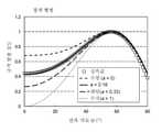
도 24는 발광 소자 2의 외부 양자 효율-휘도 특성을 나타낸 도면.
도 25는 발광 소자 2-1의 검출기의 각도(θ)에 대한 EL 발광 스펙트럼 면적 강도(실측 및 계산)를 나타낸 도면.
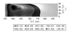
도 26은 발광 소자 2-1의 EL 발광 스펙트럼의 각도 의존성을 측정한 2D 등고선도.
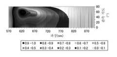
도 27은 발광 소자 2-1의 계산에 의하여 얻어진 2D 등고선도.
도 28은 발광 소자 3의 외부 양자 효율-휘도 특성을 나타낸 도면.
도 29는 발광 소자 3-1의 검출기의 각도(θ)에 대한 EL 발광 스펙트럼 면적 강도(실측 및 계산)를 나타낸 도면.
도 30은 발광 소자 3-1의 EL 발광 스펙트럼의 각도 의존성을 측정한 2D 등고선도.
도 31은 발광 소자 3-1의 계산에 의하여 얻어진 2D 등고선도.
도 32는 발광 소자 4의 외부 양자 효율-휘도 특성을 나타낸 도면.
도 33은 발광 소자 4-1의 검출기의 각도(θ)에 대한 EL 발광 스펙트럼 면적 강도(실측 및 계산)를 나타낸 도면.
도 34는 발광 소자 4-1의 EL 발광 스펙트럼의 각도 의존성을 측정한 2D 등고선도.
도 35는 발광 소자 4-1의 계산에 의하여 얻어진 2D 등고선도.
도 36은 발광 소자 5의 외부 양자 효율-휘도 특성을 나타낸 도면.
도 37은 발광 소자 5-1의 검출기의 각도(θ)에 대한 EL 발광 스펙트럼 면적 강도(실측 및 계산)를 나타낸 도면.
도 38은 발광 소자 6의 외부 양자 효율-휘도 특성을 나타낸 도면.
도 39는 발광 소자 6-1의 검출기의 각도(θ)에 대한 EL 발광 스펙트럼 면적 강도(실측 및 계산)를 나타낸 도면.
도 40은 발광 소자 6-1의 EL 발광 스펙트럼의 각도 의존성을 측정한 2D 등고선도.
도 41은 발광 소자 6-1의 계산에 의하여 얻어진 2D 등고선도.
도 42는 발광 소자 7의 외부 양자 효율-휘도 특성을 나타낸 도면.
도 43은 발광 소자 7-1의 검출기의 각도(θ)에 대한 EL 발광 스펙트럼 면적 강도(실측 및 계산)를 나타낸 도면.
도 44는 발광 소자 7-1의 EL 발광 스펙트럼의 각도 의존성을 측정한 2D 등고선도.
도 45는 발광 소자 7-1의 계산에 의하여 얻어진 2D 등고선도.
도 46은 발광 소자 8의 외부 양자 효율-휘도 특성을 나타낸 도면.
도 47은 발광 소자 8-1의 검출기의 각도(θ)에 대한 EL 발광 스펙트럼 면적 강도(실측 및 계산)를 나타낸 도면.
도 48은 발광 소자 8-1의 EL 발광 스펙트럼의 각도 의존성을 측정한 2D 등고선도.
도 49는 발광 소자 8-1의 계산에 의하여 얻어진 2D 등고선도.1 is a diagram showing a flow of calculating external quantum efficiency of a fluorescent light emitting device;
Fig. 2 is a view showing the change in luminescence intensity according to the direction and observation angle of the transition dipole.
3 is a conceptual diagram of a light emitting device.
4 is a view showing an example of a method of manufacturing a light emitting element.
Fig. 5 is a view showing an example of an apparatus for manufacturing a light emitting element;
Fig. 6 is a conceptual diagram of an active matrix type light emitting device;
Fig. 7 is a conceptual diagram of an active matrix type light emitting device;
Fig. 8 is a conceptual diagram of an active matrix type light emitting device;
Fig. 9 is a conceptual diagram of a passive matrix type light emitting device;
10 is a view showing a lighting device.
11 is a diagram illustrating an electronic device.
12 is a view showing a light source device;
13 is a view showing a lighting device.
14 is a view showing a lighting device;
15 is a view illustrating a vehicle-mounted display device and a lighting device;
16 is a diagram illustrating an electronic device.
17 is a diagram illustrating an electronic device.
18 is a conceptual diagram of a light emitting device for measurement.
19 is a diagram illustrating external quantum efficiency-luminance characteristics of light emitting
Fig. 20 is a diagram for explaining a method for measuring angle dependence of an emission spectrum;
Fig. 21 is a diagram showing the EL emission spectral area intensity (measured and calculated) with respect to the angle θ of the detector of the light emitting element 1-1;
22 is a 2D contour diagram in which the angular dependence of the EL emission spectrum of the light emitting element 1-1 is measured;
23 is a 2D contour diagram obtained by calculation of the light emitting element 1-1;
24 is a diagram illustrating external quantum efficiency-luminance characteristics of light emitting
Fig. 25 is a diagram showing the EL emission spectral area intensity (measured and calculated) with respect to the angle θ of the detector of the light emitting element 2-1;
Fig. 26 is a 2D contour diagram in which the angular dependence of the EL emission spectrum of the light emitting element 2-1 is measured;
27 is a 2D contour diagram obtained by calculation of the light emitting element 2-1;
28 is a diagram illustrating external quantum efficiency-luminance characteristics of light emitting
Fig. 29 is a diagram showing the EL emission spectral area intensity (measured and calculated) with respect to the angle θ of the detector of the light emitting element 3-1;
Fig. 30 is a 2D contour diagram in which the angular dependence of the EL emission spectrum of the light emitting element 3-1 is measured;
31 is a 2D contour diagram obtained by calculation of a light emitting device 3-1;
32 is a diagram illustrating external quantum efficiency-luminance characteristics of light emitting
Fig. 33 is a diagram showing the EL emission spectral area intensity (measured and calculated) with respect to the angle θ of the detector of the light emitting element 4-1;
Fig. 34 is a 2D contour diagram in which the angular dependence of the EL emission spectrum of the light emitting element 4-1 is measured;
Fig. 35 is a 2D contour diagram obtained by calculation of the light emitting element 4-1;
36 is a diagram illustrating external quantum efficiency-luminance characteristics of light emitting
Fig. 37 is a diagram showing the EL emission spectral area intensity (measured and calculated) with respect to the angle θ of the detector of the light emitting element 5-1;
38 is a diagram illustrating external quantum efficiency-luminance characteristics of the
Fig. 39 is a diagram showing the EL emission spectral area intensity (measured and calculated) with respect to the angle θ of the detector of the light emitting element 6-1;
Fig. 40 is a 2D contour diagram in which the angular dependence of the EL emission spectrum of the light emitting element 6-1 is measured;
Fig. 41 is a 2D contour diagram obtained by calculation of the light emitting element 6-1;
42 is a diagram illustrating external quantum efficiency-luminance characteristics of the
Fig. 43 is a diagram showing the EL emission spectral area intensity (measured and calculated) with respect to the angle θ of the detector of the light emitting element 7-1;
Fig. 44 is a 2D contour diagram in which the angle dependence of the EL emission spectrum of the light emitting element 7-1 is measured;
45 is a 2D contour diagram obtained by calculation of a light emitting device 7-1;
46 is a diagram illustrating external quantum efficiency-luminance characteristics of the
Fig. 47 is a diagram showing the EL emission spectral area intensity (measured and calculated) with respect to the angle θ of the detector of the light emitting element 8-1;
Fig. 48 is a 2D contour diagram in which the angular dependence of the EL emission spectrum of the light emitting element 8-1 is measured;
49 is a 2D contour diagram obtained by calculation of the light emitting element 8-1;
아래에서, 본 발명의 실시형태에 대하여 도면을 사용하여 자세히 설명한다. 다만, 본 발명은 아래의 설명에 한정되지 않고, 본 발명의 취지 및 그 범위에서 벗어남이 없이 다양하게 변경될 수 있는 것은 통상의 기술자라면 용이하게 이해할 수 있다. 따라서, 본 발명은 아래에 나타내는 실시형태의 기재 내용에 한정하여 해석되는 것이 아니다.EMBODIMENT OF THE INVENTION Below, embodiment of this invention is described in detail using drawing. However, the present invention is not limited to the description below, and it can be easily understood by those skilled in the art that various changes can be made without departing from the spirit and scope of the present invention. Therefore, this invention is limited to the description of embodiment shown below and is not interpreted.
형광 발광을 나타내는 유기 EL 소자의, 캐리어 재결합으로부터 발광까지의 과정을 도 1을 참조하여 설명한다. 우선, 유기 EL 소자에 전압을 인가하면, 양극으로부터는 홀이, 음극으로부터는 전자가 각각 EL층으로 주입된다. 주입된 캐리어(홀 및 전자)는 EL층 내를 발광층을 향하여 수송되고, 어떤 위치에서 서로 상대함으로써 재결합이 일어난다. 이 재결합이 일어나는 비율을 캐리어 밸런스(γ)라고 한다. 캐리어가 재결합한 에너지에 의하여 유기 재료는 여기되지만 그 여기자의 생성 비율은 단일항 여기자 1에 대하여 삼중항 여기자 3이 된다. 이 비율을 단일항 여기자 생성 비율(α)이라고 부른다. 발광 재료로 생성한 단일항 여기자는 유기 화합물의 형광 양자 수율(Φf)에 따라 발광하고, 그 외의 유기 화합물로 생성한 단일항 여기자는 발광 재료로의 에너지 이동을 거쳐 Φf에 따라 발광한다. 이와 같이 발광한 광이 발광 소자의 외부에서 관측되는 비율이 이 유기 EL 소자의 광 추출 효율(χ)이 되고, 형광 발광 소자의 외부 양자 효율(μext)은 캐리어 밸런스(γ), 단일항 여기자 생성 비율(α), 형광 양자 수율(Φf), 광 추출 효율(χ)의 곱이 되고, 하기 식 (1)으로 나타내어진다.A process from carrier recombination to light emission of an organic EL device exhibiting fluorescence emission will be described with reference to FIG. 1 . First, when a voltage is applied to the organic EL element, holes are injected from the anode and electrons are injected into the EL layer from the cathode, respectively. The injected carriers (holes and electrons) are transported within the EL layer toward the light emitting layer, and recombination occurs by opposing each other at a certain position. The rate at which this recombination occurs is called carrier balance (γ). Although the organic material is excited by the energy of the recombination of carriers, the generation ratio of the excitons becomes 3 triplet excitons to 1 singlet excitons. This ratio is called the singlet exciton generation ratio (α). Singlet excitons generated from the light emitting material emit light according to the fluorescence quantum yield (Φf ) of the organic compound, and singlet excitons generated from other organic compounds emit light according to Φf through energy transfer to the light emitting material. The ratio of the emitted light to the outside of the light emitting element is the light extraction efficiency (χ) of the organic EL element, and the external quantum efficiency (μext ) of the fluorescent light emitting element is the carrier balance (γ) and singlet exciton It becomes the product of the generation ratio (α), the fluorescence quantum yield (Φf ), and the light extraction efficiency (χ), and is expressed by the following formula (1).
[식 1][Equation 1]
외부 양자 효율(μext)=χ·Φf·α·γ(1)External quantum efficiency (μext )=χ Φf α γ (1)
이 중에서, Φf는 발광 재료 특유의 값이고 발광 재료마다 정해진 값이 있다. 또한, γ는 적층 구조의 EL 소자에서는 거의 1이라고 가정할 수 있다. 그러므로, 동일 재료를 사용한 경우, 소자 구조에 의하여 발광 효율의 향상이 기대되는 항은 광추출 효율(χ)과 단일항 여기자 생성 비율(α)의 2개가 된다.Among them, Φf is a value specific to the light emitting material, and there is a value determined for each light emitting material. Also, it can be assumed that γ is approximately 1 in the EL element of the stacked structure. Therefore, when the same material is used, the terms in which the luminous efficiency is expected to be improved by the device structure are two of the light extraction efficiency (χ) and the singlet exciton generation ratio (α).
단일항 여기자 생성 비율(α)은 삼중항 여기자를 단일항 여기자로 업컨버젼하는 삼중항-삼중항 소멸(triplet-triplet annihilation:TTA) 등의 기구가 존재하면 향상시킬 수 있다.The singlet exciton generation ratio (α) can be improved if a mechanism such as triplet-triplet annihilation (TTA) that upconverts triplet excitons into singlet excitons exists.
광추출 효율(χ)은 발광 장치의 구조나 적층 등에도 관여되지만, 유리 기판 위의 유기 EL 소자에 있어서는 일반적으로 20% 내지 30%라고 알려져 있다. 그러나, 이것은 발광이 등방적인 것을 가정하기 때문에, 발광에 이방성이 생긴 경우는 이 값이 변화된다.Although the light extraction efficiency (χ) is also involved in the structure and lamination of a light emitting device, it is generally known that it is 20% to 30% in an organic EL device on a glass substrate. However, since this assumes that light emission is isotropic, this value changes when anisotropy occurs in light emission.
발광 재료의 발광은 분자의 전이 쌍극자 모멘트에 대하여 수직 방향에 생기는 것이 알려져 있으므로 분자의 배향 상태를 제어하면 추출 효율(χ)을 향상시킬 수 있다.Since it is known that light emission of a light emitting material occurs in a direction perpendicular to the transition dipole moment of a molecule, the extraction efficiency (χ) can be improved by controlling the orientation state of the molecule.
비정성의 유기 박막에서의 분자의 배향 상태의 평가 방법으로서는, 분광 엘립소미트리(ellipsometry)를 사용하는 방법이 있다. 이것은 유기 재료의 굴절률(n), 소쇠계수(k)를 측정함으로써 개략적인 값을 해석할 수 있다. 실제로 발광 소자에 사용되는 재료 중, 긴 선상 분자나, 면상으로 넓은 분자에 있어서는 박막면에 평행한 분자 배향이 존재하는 것이 보고되어 있다(비특허문헌 1 참조).As a method for evaluating the orientation state of molecules in an amorphous organic thin film, there is a method using spectroscopic ellipsomtry. This can be roughly interpreted by measuring the refractive index (n) and extinction coefficient (k) of the organic material. It has been reported that, among materials actually used for light emitting devices, molecular orientation parallel to the thin film surface exists in long linear molecules and planar broad molecules (see Non-Patent Document 1).
그러나, 실제의 발광 소자는 유기 박막을 다층 적층하여 구성되어 있으며, 또한, 발광 재료는 호스트 재료 중에 소량 분산되어 있는 상태이다. 그러므로, 실제의 발광 소자에서는 발광 재료의 소쇠계수(k)를 높은 정밀도로 산출할 수 없어, 발광 재료가 발광층 내에서 10wt% 이하의 농도인 경우에는 상기 방법에 의하여 분자 배향을 알아내는 것은 어렵다.However, an actual light emitting element is constituted by laminating an organic thin film in multiple layers, and the light emitting material is in a state in which a small amount is dispersed in the host material. Therefore, in an actual light emitting device, the extinction coefficient k of the light emitting material cannot be calculated with high precision, and when the light emitting material has a concentration of 10 wt% or less in the light emitting layer, it is difficult to find out the molecular orientation by the above method.
여기서, 본 발명자들은 소자의 발광 상태로부터 분자 배향을 어림잡을 방법을 채용하였다. 상기 발광 소자의 발광 강도의 방사 각도 의존성(공간 발광 패턴)은 발광 재료의 평균적인 전이 쌍극자의 방향을 반영한다. 이 공간 분포를 해석할 수 있으면 발광 소자의 배향 상태를 알아낼 수 있다. 이 방법은, 발광 소자의 발광 자체를 관측하고 해석하므로, 발광 재료가 발광되어 있으면 그 농도가 옅은 상태라도 발광층 내에서 발광 재료가 어떤 배향 상태에 있는지를 알아낼 수 있다.Here, the present inventors have adopted a method of estimating molecular orientation from the light emission state of the device. The emission angle dependence (spatial emission pattern) of the emission intensity of the light-emitting element reflects the direction of the average transition dipole of the light-emitting material. If this spatial distribution can be analyzed, the orientation state of a light emitting element can be found out. Since this method observes and analyzes the light emission itself of the light emitting element, if the light emitting material emits light, it is possible to find out what orientation state the light emitting material is in in the light emitting layer even when the concentration is light.
실제로는 측정한 발광 강도의 각도 의존성과, 디바이스 시뮬레이터로 발광 분자의 배향을 나타내는 파라미터 a(하기 식 (2) 참조)를 가정하여 산출되는 발광 강도의 각도 의존성의 계산값을 비교함으로써, 타당한 분자 배향 파라미터 a의 수치를 어림잡아 발광 소자에서의 발광 물질의 배향 상태를 알아낼 수 있다(비특허문헌 2 참조). 또한, 본 발명자들은 디바이스 시뮬레이터로부터 얻어지는 발광 스펙트럼의 형상에도 착안하고, 발광 스펙트럼 형상, 및 각도에 따른 발광 스펙트럼의 형상 변화에 대해서도 실측과 계산값을 비교하여, 조합한다. 또한, 실측 및 시뮬레이션에서의 발광 강도로서는, 어느 특정의 파장의 발광 강도가 아니라, 발광 스펙트럼의 면적 강도를 사용한다. 본 발명자들이 새로 적용한 이들 방법에 의하여, 비특허문헌 2와 달리 파라미터 a를 높은 정밀도로 어림잡을 수 있다.By comparing the actually measured angular dependence of the luminescence intensity with the calculated value of the angular dependence of the luminescence intensity calculated assuming a parameter a indicating the orientation of the luminescent molecules using a device simulator (refer to Equation (2) below), a reasonable molecular orientation By estimating the numerical value of parameter a, the orientation state of the light emitting material in a light emitting element can be found out (refer nonpatent literature 2). In addition, the present inventors also pay attention to the shape of the emission spectrum obtained from the device simulator, and also compare and combine measured values and calculated values for the shape of the emission spectrum and the shape change of the emission spectrum depending on the angle. In addition, as the light emission intensity in actual measurement and simulation, not the light emission intensity of a specific wavelength, but the area intensity of the light emission spectrum is used. By these methods newly applied by the present inventors, the parameter a can be estimated with high precision, unlike
다음에, 분자 배향 파라미터 a에 대하여 설명한다. 도 2는 발광 강도의 공간분포의 측정에 따른 측정기의 관측 방향과, 기판 위의 서로 직교하는 각 전이 쌍극자의 성분과의 관계를 나타낸 것이다. 도면에 나타낸 바와 같이, 발광층 내의 발광 재료에서의 평균적인 전이 쌍극자로부터의 발광(즉, 발광 소자로부터 실제로 관측되는 발광)을, 서로 직교하는 x축 방향의 성분(TEh 성분), y축 방향의 성분(TMh 성분), z축 방향의 성분(TMv 성분)의 각 전이 쌍극자로부터의 발광의 기여로 분해하였다. 바꿔 말하면, x축, y축, 및 z축 방향의 3가지의 전이 쌍극자의 배향이 어떤 비율로 존재하는 것을 가정하고 있으며, 이 경우, 각 전이 쌍극자로부터의 발광을 서로 더함으로써 발광 소자의 발광 패턴이 결정된다. 아래에 기재된 바와 같이, 그 비율에 관하는 파라미터가 a이다.Next, the molecular orientation parameter a will be described. FIG. 2 shows the relationship between the observation direction of the measuring device according to the measurement of the spatial distribution of luminescence intensity and the components of each transition dipole orthogonal to each other on the substrate. As shown in the figure, light emission from the average transition dipole in the light emitting material in the light emitting layer (that is, light actually observed from the light emitting element) is a component in the x-axis direction (TEh component) and a component in the y-axis direction orthogonal to each other. (TMh component) and the z-axis direction component (TMv component) were decomposed into the contribution of light emission from each transition dipole. In other words, it is assumed that the orientations of the three transition dipoles in the x-axis, y-axis, and z-axis directions exist in a certain ratio. this is decided As described below, the parameter relating to the ratio is a.
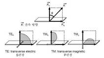
여기서, 상술한 바와 같이 분자로부터의 발광은 전이 쌍극자 모멘트에 대하여 수직의 방향(수직의 면 중 어느 방향)으로 방출되는 것이 이미 알려져 있다. 상기 3방향으로 분할한 성분 중, TEh 성분과, TMh 성분(x축 방향 및 y축 방향)은 기판면 내에 수평인 전이 쌍극자이므로 그 발광 방향은 기판에 대하여 수직이고, 추출하기 쉬운 발광을 나타내는 성분이라고 할 수 있다. 한편, TMv 성분(z축 방향)은 기판면 내에 수직의 전이 쌍극자이므로 그 발광 방향은 기판에 대하여 수평이고, 추출하기 어려운 발광을 나타내는 성분이다.Here, as described above, it is already known that light emission from a molecule is emitted in a direction perpendicular to the transition dipole moment (either in the vertical plane). Among the components divided into the three directions, the TEh component and the TMh component (x-axis direction and y-axis direction) are transition dipoles that are horizontal in the substrate plane, so their emission direction is perpendicular to the substrate, and a component showing light emission that is easy to extract It can be said that On the other hand, since the TMv component (z-axis direction) is a vertical transition dipole in the substrate plane, its emission direction is horizontal with respect to the substrate, and it is a component that exhibits light emission that is difficult to extract.
도 2 중, 각 성분의 전이 쌍극자의 배향을 나타내는 화살표의 중앙으로부터 나온 도형은 검출기의 방향을 기판 정면(θ=0°)으로부터 기판과 거의 수평(θ=90°)까지 바꿀 때 그 방향에 있는 검출기에 들어갈 발광 강도를 나타낸 모식도이고, 중심으로부터의 직선 거리가 강도에 비례한다.In Fig. 2, the diagram from the center of the arrow indicating the orientation of the transition dipole of each component is in that direction when the direction of the detector is changed from the front of the substrate (θ = 0°) to almost horizontal with the substrate (θ = 90°). It is a schematic diagram showing the light emission intensity entering the detector, and the linear distance from the center is proportional to the intensity.
TEh 성분은 광이 방출되는 방향에 검출기가 존재하므로 기판의 각도를 바꿔도 검출되는 광의 강도(즉, 도면 중 화살표의 중심으로부터 나온 도형의 화살표 중심으로부터의 직선 거리)는 일정하고, 도면 중 화살표의 중심으로부터 나온 도형은 부채 형상을 나타낸다. 한편, TMh 성분과 TMv 성분에서의 도면 중 화살표의 중심으로부터 나온 도형은 일그러진 부채 형상이며, 기판에 대한 검출기의 각도 θ에 따라 검출되는 광의 강도가 크게 변화되는 것을 나타낸 것이다. 도면으로 본 바와 같이, TMh 성분은 θ가 작은 영역(기판의 정면 방향에 가까운 방향)에서 관측되면 강도가 강하고, TMv 성분은 θ가 큰 영역(기판에 대하여 평행인 방향에 가까운 방향)에서 관측되면 강도가 강하다. 이때, 측정기로 측정하는 발광 강도(어떤 각도 θ에서의 파장 λ에 관한 발광 강도:Iλ(θ,λ))는 식(2)으로 나타낼 수 있다.Since the TEh component has a detector in the direction in which the light is emitted, the intensity of the detected light (that is, the straight line distance from the center of the arrow in the figure from the center of the arrow in the figure) is constant even if the angle of the substrate is changed, and the center of the arrow in the figure is constant. The figure from is represents a fan shape. On the other hand, in the TMh component and the TMv component, the figure from the center of the arrow in the drawing is a distorted fan shape, indicating that the intensity of the detected light changes greatly according to the angle θ of the detector with respect to the substrate. As shown in the figure, when the TMh component is observed in a region with a small θ (direction close to the front direction of the substrate), the intensity is strong, and when the TMv component is observed in a region with large θ (the direction close to the direction parallel to the substrate), strength is strong At this time, the luminescence intensity (luminescence intensity with respect to wavelength λ at a certain angle θ: Iλ (θ, λ)) measured with a measuring device can be expressed by Equation (2).
[식 2][Equation 2]

식 중,ITMv,ITMh,ITEh는, 도 2에 나타낸 배치의 전이 쌍극자로부터 발한 광의 공간 강도 분포를 나타내고, 식 중 a는 막면에 수직 배치된 전이 쌍극자(TMv 성분)가 존재하는 비율을 나타낸다. 한편, 1-a는 수평으로 배치된 전이 쌍극자(TMh 성분, TEh 성분)가 존재하는 비율을 나타낸다. 즉, a는 발광 분자의 전이 쌍극자의 배향을 나타내는 파라미터로 볼 수도 있다.In the formula,ITMv ,ITMh ,ITEh represent the spatial intensity distribution of light emitted from the transition dipole of the arrangement shown in FIG. indicates. On the other hand, 1-a represents a ratio in which horizontally arranged transition dipoles (TMh component, TEh component) exist. That is, a may be viewed as a parameter indicating the orientation of the transition dipole of the light emitting molecule.
또한, 식 중 a는 전이 쌍극자가 기판에 대하여 완전히 수평 방향으로만 배치되어 있으면 TMv 성분은 없어지므로 a=0이 된다. 한편, 전이 쌍극자가 기판에 대하여 수직 방향으로만 배치되어 있으면 a=1이 된다. 또한, 전이 쌍극자의 방향이 램덤인 경우는 전이 쌍극자의 각 성분의 비율은 x축, y축, z축에 대하여 1:1:1로 등방적으로 된다고 생각되어 있기 때문에 기판에 수직인 성분(TMv 성분)에 대한 기판에 수평인 성분(TMh 성분 및 TEh 성분)은 1:2가 되므로, a=1/3(약 0.33)이 된다.In the formula, a is a = 0 because the TMv component disappears when the transition dipole is arranged only in a completely horizontal direction with respect to the substrate. On the other hand, if the transition dipole is arranged only in the direction perpendicular to the substrate, a=1. In addition, when the direction of the transition dipole is random, the ratio of each component of the transition dipole is 1:1:1 with respect to the x-axis, y-axis, and z-axis. The component (TMh component and TEh component) horizontal to the substrate with respect to the component) becomes 1:2, so a=1/3 (about 0.33).
여기서, 상술한 바와 같이ITEh는 각도에 영향을 받지 않고 그 강도는 일정적이지만,ITMv,ITMh는 상술한 바와 같이 계측기에 대한 기판의 각도(θ)에 따라 그 크기가 변화되기 때문에 θ를 바꾸고 발광 강도를 측정함으로써 그 강도의 θ에 대한 변화로부터 a의 값을 산출할 수 있다.Here, as described above,ITEh is not affected by the angle and its strength is constant, butITMv ,ITMh are θ because the size changes according to the angle (θ) of the substrate with respect to the measuring instrument as described above. By changing , and measuring the emission intensity, the value of a can be calculated from the change in intensity with respect to θ.
또한, 그때, 각도에 따라 그 강도가 변화되지 않는ITEh는 측정의 방해가 된다. 그러나, 방출되는 광의 전기장의 진폭 방향은 전이 쌍극자 모멘트의 방향과 같게 되므로,ITEh는 S파,ITMv,ITMh는 P파인 것으로부터 기판면에 수직의 방향으로 직선 편광자를 삽입함으로써 TEh 성분을 제외하고 측정할 수 있다.In addition, at that time, ITEh whose intensity does not change with the angle interferes with the measurement. However, since the amplitude direction of the electric field of the emitted light becomes the same as the direction of the transition dipole moment,ITEh is an S wave,ITMv , andITMh are P waves. can be measured except
또한, TMv 성분과 TMh 성분을 비교하면, TMh 성분의 발광 방향이 주로 기판에 대하여 수직 방향, TMv 성분의 발광 방향이 주로 기판에 대하여 수평 방향이지만, 고체로부터의 발광을 얻는 발광 소자에 있어서는 TMv 성분의 발광 중 많은 발광은 전반사(全反射)되어 외부에 추출할 수 없다. 한편, TMh 성분의 발광은 TMv 성분에 비하여 더 외부에 추출되기 쉽다. 또한, 광학적으로 막 두께가 최적화된 발광 소자에 있어서는 발광 방향이 주로 기판에 대하여 수직 방향인 TMh 성분의 발광이 간섭에 의하여 강하게 되기 때문에, TMh 성분의 발광 강도가 높아진다(따라서, 발광 효율이 최대화된다). 즉, 배향 파라미터 a가 지나치게 1에 가까운 값이 아닌 한, 광학적으로 막 두께가 최적화된 소자에 있어서는, TMv 성분과 TMh 성분의 발광 강도에 매우 큰 차가 발생된다. 즉, 발광 효율이 최대화된 발광 소자에 있어서는 관측되는 발광의 대부분이 TMh 성분이다. 이와 같이, TMv 성분과 TMh 성분의 발광 강도가 크게 다른 경우, 그 강도가 작은 쪽(이 경우는 TMv 성분)의 기여를 발광 강도의 각도 분포로부터 실험적으로 추출하는 것은 어렵다.Further, comparing the TMv component and the TMh component, the light emission direction of the TMh component is mainly perpendicular to the substrate, and the light emission direction of the TMv component is mainly horizontal to the substrate. A lot of the light emission of light is totally reflected and cannot be extracted to the outside. On the other hand, the light emission of the TMh component is more easily extracted to the outside than the TMv component. In addition, in a light emitting device with an optically optimized film thickness, since the light emission of the TMh component whose light emission direction is mainly perpendicular to the substrate is strengthened by interference, the light emission intensity of the TMh component is increased (thus, the luminous efficiency is maximized) ). That is, unless the orientation parameter a is too close to 1, in an element with an optically optimized film thickness, a very large difference occurs in the emission intensity of the TMv component and the TMh component. That is, in the light emitting element with maximized luminous efficiency, most of the observed light emission is a TMh component. As described above, when the emission intensity of the TMv component and the TMh component is significantly different, it is difficult to experimentally extract the contribution of the smaller one (the TMv component in this case) from the angular distribution of the emission intensity.
그러므로, 본 실시형태에서는, 간섭 효과를 이용하여 기판 정면 방향의 발광 강도를 가능한 한 억제함(즉, TMh 성분의 발광을 광학 간섭을 이용하여 가능한 한 저하시킴)으로써 TMh 성분의 TMv 성분의 비, 즉, 파라미터 a의 값을 쉽게 산출할 수 있도록 막 두께를 조정한 소자를 준비하여 측정을 행한다. 구체적으로는 발광 영역과 음극의 거리를 2분의 nλ(nλ/2)로 함으로써, 기판 정면 방향의 휘도를 약하게 한 소자를 제작하고, 그것을 사용하여 측정을 행한다. 막 두께의 조정은 일반적으로 알칼리 금속을 첨가한 전자 수송층의 막을 두껍게 하는 것 등에 의하여 행하지만 막의 도전성에 한계가 있으므로 구동 전압의 상승이나, 캐리어 밸런스의 무너짐 등을 초래하기 쉽다. 그러므로, 이 막 두께의 조정에는, 정공 수송성 재료와, 상기 정공 수송성 재료에 억셉터성을 나타내는 재료를 함유시킨 복합 재료를 사용하는 것이 바람직하다. 복합 재료는 EL층에서의 정공 주입층에 사용하는 것이 바람직하다. 또는, 전자 주입층과 음극 사이에 사용하여도 좋다.Therefore, in this embodiment, the ratio of the TMv component of the TMh component by using the interference effect to suppress the light emission intensity in the front direction of the substrate as much as possible (that is, by reducing the light emission of the TMh component as much as possible using optical interference); That is, an element whose film thickness is adjusted so that the value of the parameter a can be easily calculated is prepared and measured. Specifically, by setting the distance between the light emitting region and the cathode to be n? The film thickness is generally adjusted by, for example, thickening the film of the electron transport layer to which alkali metal is added. However, since the film has a limit in conductivity, it is easy to cause an increase in the driving voltage or collapse of the carrier balance. Therefore, it is preferable to use a hole-transporting material and a composite material in which the hole-transporting material contains a material exhibiting acceptor properties for adjustment of the film thickness. The composite material is preferably used for the hole injection layer in the EL layer. Alternatively, it may be used between the electron injection layer and the cathode.
복합 재료에 사용하는 정공 수송성 재료로서는, 방향족 아민 화합물, 카바졸 유도체, 방향족 탄화수소, 고분자 화합물(올리고머, 덴드리머, 폴리머 등) 등, 다양한 유기 화합물을 사용할 수 있다. 또한, 복합 재료에 사용하는 정공 수송성의 물질로서는, 10-6cm2/Vs 이상의 정공 이동도를 갖는 물질인 것이 바람직하다. 이하에서는, 복합 재료에서의 정공 수송성 재료로서 사용할 수 있는 유기 화합물의 예를 구체적으로 열거한다.As the hole transporting material used for the composite material, various organic compounds such as aromatic amine compounds, carbazole derivatives, aromatic hydrocarbons, and high molecular compounds (oligomers, dendrimers, polymers, etc.) can be used. In addition, as the hole-transporting substance used for the composite material, it is preferable that the substance has a hole mobility of10 -6 cm2 /Vs or more. Below, examples of organic compounds that can be used as the hole-transporting material in the composite material are specifically listed.
복합 재료에 사용할 수 있는 정공 수송성 재료로서는, N,N'-다이(p-트릴)-N,N'-다이페닐-p-페닐렌다이아민(약칭: DTDPPA), 4,4'-비스[N-(4-다이페닐아미노페닐)-N-페닐아미노]바이페닐(약칭: DPAB), N,N'-비스{4-[비스(3-메틸페닐)아미노]페닐}-N,N'-다이페닐-(1,1'-바이페닐)-4,4'-다이아민(약칭: DNTPD), 1,3,5-트리스[N-(4-다이페닐아미노페닐)-N-페닐아미노]벤젠(약칭: DPA3B) 등의 방향족 아민 화합물, 3-[N-(9-페닐카바졸-3-일)-N-페닐아미노]-9-페닐카바졸(약칭: PCzPCA1), 3,6-비스[N-(9-페닐카바졸-3-일)-N-페닐아미노]-9-페닐카바졸(약칭: PCzPCA2), 3-[N-(1-나프틸)-N-(9-페닐카바졸-3-일)아미노]-9-페닐카바졸(약칭: PCzPCN1), 4,4'-다이(N-카바졸일)바이페닐(약칭: CBP), 1,3,5-트리스[4-(N-카바졸일)페닐]벤젠(약칭: TCPB), 9-[4-(10-페닐-9-안트릴)페닐]-9H-카바졸(약칭: CzPA), 1,4-비스[4-(N-카바졸일)페닐]-2,3,5,6-테트라페닐벤젠 등의 카바졸 유도체, 2-tert-뷰틸-9,10-다이(2-나프틸)안트라센(약칭: t-BuDNA), 2-tert-뷰틸-9,10-다이(1-나프틸)안트라센, 9,10-비스(3,5-다이페닐페닐)안트라센(약칭: DPPA), 2-tert-뷰틸-9,10-비스(4-페닐페닐)안트라센(약칭: t-BuDBA), 9,10-다이(2-나프틸)안트라센(약칭: DNA), 9,10-다이페닐안트라센(약칭: DPAnth), 2-tert-뷰틸안트라센(약칭: t-BuAnth), 9,10-비스(4-메틸-1-나프틸)안트라센(약칭: DMNA), 2-tert-뷰틸-9,10-비스[2-(1-나프틸)페닐]안트라센, 9,10-비스[2-(1-나프틸)페닐]안트라센, 2,3,6,7-테트라메틸-9,10-다이(1-나프틸)안트라센, 2,3,6,7-테트라메틸-9,10-다이(2-나프틸)안트라센, 9,9'-바이안트릴, 10,10'-다이페닐-9,9'-바이안트릴, 10,10'-비스(2-페닐페닐)-9,9'-바이안트릴, 10,10'-비스[(2,3,4,5,6-펜타페닐)페닐]-9,9'-바이안트릴, 안트라센, 테트라센, 루브렌, 페릴렌, 2,5,8,11-테트라(tert-뷰틸)페릴렌 등의 방향족 탄화수소를 들 수 있다. 또한, 이 외에, 펜타센, 코로넨 등도 사용할 수 있다. 바이닐 골격을 갖는 방향족 탄화수소라도 좋고, 바이닐 골격을 갖는 방향족 탄화수소로서는, 예를 들어, 4,4'-비스(2,2-다이페닐바이닐)바이페닐(약칭: DPVBi), 9,10-비스[4-(2,2-다이페닐바이닐)페닐]안트라센(약칭: DPVPA) 등을 들 수 있다.Examples of the hole transporting material usable for the composite material include N,N'-di(p-triyl)-N,N'-diphenyl-p-phenylenediamine (abbreviation: DTDPPA), 4,4'-bis[ N-(4-diphenylaminophenyl)-N-phenylamino]biphenyl (abbreviation: DPAB), N,N'-bis{4-[bis(3-methylphenyl)amino]phenyl}-N,N'- Diphenyl-(1,1'-biphenyl)-4,4'-diamine (abbreviation: DNTPD), 1,3,5-tris[N-(4-diphenylaminophenyl)-N-phenylamino] Aromatic amine compounds such as benzene (abbreviation: DPA3B), 3-[N-(9-phenylcarbazol-3-yl)-N-phenylamino]-9-phenylcarbazole (abbreviation: PCzPCA1), 3,6- Bis[N-(9-phenylcarbazol-3-yl)-N-phenylamino]-9-phenylcarbazole (abbreviation: PCzPCA2), 3-[N-(1-naphthyl)-N-(9- Phenylcarbazol-3-yl)amino]-9-phenylcarbazole (abbreviation: PCzPCN1), 4,4'-di(N-carbazolyl)biphenyl (abbreviation: CBP), 1,3,5-tris[ 4-(N-carbazolyl)phenyl]benzene (abbreviation: TCPB), 9-[4-(10-phenyl-9-anthryl)phenyl]-9H-carbazole (abbreviation: CzPA), 1,4-bis Carbazole derivatives such as [4-(N-carbazolyl)phenyl]-2,3,5,6-tetraphenylbenzene, 2-tert-butyl-9,10-di(2-naphthyl)anthracene (abbreviation: t-BuDNA), 2-tert-butyl-9,10-di(1-naphthyl)anthracene, 9,10-bis(3,5-diphenylphenyl)anthracene (abbreviation: DPPA), 2-tert-butyl -9,10-bis(4-phenylphenyl)anthracene (abbreviation: t-BuDBA), 9,10-di(2-naphthyl)anthracene (abbreviation: DNA), 9,10-diphenylanthracene (abbreviation: DPAnth ), 2-tert-butylanthracene (abbreviation: t-BuAnth), 9,10-bis(4-methyl-1-naphthyl)anthracene (abbreviation: DMNA), 2-tert-butyl-9,10-bis[ 2-(1-naphthyl)phenyl]anthracene, 9,10-bis[2-(1-naphthyl)phenyl]anthracene, 2,3,6,7-tetramethyl-9,10-di(1-naph Tyl) anthracene, 2,3,6,7-tetramethyl-9,10-di(2-naphthyl)anthracene, 9,9'-bianthryl, 10,10'-dipe nyl-9,9'-bianthryl, 10,10'-bis(2-phenylphenyl)-9,9'-bianthryl, 10,10'-bis[(2,3,4,5,6 Aromatic hydrocarbons, such as -pentaphenyl)phenyl]-9,9'- bianthryl, anthracene, tetracene, rubrene, perylene, 2,5,8,11-tetra(tert-butyl)perylene, are mentioned. have. In addition to this, pentacene, coronene, and the like can also be used. An aromatic hydrocarbon having a vinyl skeleton may be used, and examples of the aromatic hydrocarbon having a vinyl skeleton include 4,4'-bis(2,2-diphenylvinyl)biphenyl (abbreviation: DPVBi), 9,10-bis[ 4-(2,2-diphenylvinyl)phenyl]anthracene (abbreviation: DPVPA) etc. are mentioned.
또한, 특히, 정공 수송성 재료로서, 4-[4-(9-페닐-9H-플루오렌-9-일)페닐]-6-페닐다이벤조싸이오펜(약칭: DBTFLP-IV), 1,3,5-트라이(다이벤조싸이오펜-4-일)-벤젠(약칭: DBT3P-II), 4,4'-(바이페닐-2,2'-다이일)-비스-다이벤조싸이오펜(약칭: oDBTBP-II), 2,8-다이페닐-4-[4-(9-페닐-9H-플루오렌-9-일)페닐]다이벤조싸이오펜(약칭: DBTFLP-III), 4-[3-(트라이페닐렌-2-일)페닐]다이벤조싸이오펜(약칭: mDBTPTp-II), 3,6-다이-(다이벤조싸이오펜-4-일)-9-페닐-9H-카바졸(약칭: DBT2PC-II), 4-[3-(9,10-다이페닐-2-안트릴)페닐]다이벤조싸이오펜(약칭: 2mDBTPPA-II), 4-[3-(9,10-다이페닐-2-안트릴)페닐]다이벤조퓨란(약칭: 2mDBFPPA-II), 4-[4-(9-페닐안트라센-10-일)페닐]다이벤조싸이오펜(약칭: mDBTPA-II) 등의 다이벤조싸이오펜 유도체 또는 다이벤조퓨란 유도체, 및 1-[3,5-다이(나프탈렌-1-일)페닐]나프탈렌(약칭: N3P), 9-[3,5-다이(페난트렌-9-일)페닐]페난트렌(약칭: Pn3P), 1,2,3,4-테트라페닐나프탈렌(약칭: P4N), 2-[3,5-다이-(나프탈렌-2-일)-페닐]-나프탈렌(약칭: βN3P), 9,9'-(바이페닐-3,3'-다이일)-다이-페난트렌(약칭: mPnBP) 등의 나프탈렌 골격, 페난트렌 골격, 또는 트라이페닐렌 골격에 치환기가 결합된, 분자량이 350 이상 2000 이하인 탄화수소 화합물을 사용한 복합 재료는 가시광 영역으로부터 근적외 영역에 걸쳐 흡수가 없기 때문에 상기 복합 재료를 사용하여 제작한 발광 소자를 측정한 결과는 계산 결과와 잘 일치하고, 높은 정밀도로 a의 값을 산출할 수 있다.In addition, in particular, as a hole transport material, 4-[4-(9-phenyl-9H-fluoren-9-yl)phenyl]-6-phenyldibenzothiophene (abbreviation: DBTFLP-IV), 1,3, 5-Tri(dibenzothiophen-4-yl)-benzene (abbreviation: DBT3P-II), 4,4'-(biphenyl-2,2'-diyl)-bis-dibenzothiophene (abbreviation: oDBTBP-II), 2,8-diphenyl-4-[4-(9-phenyl-9H-fluoren-9-yl)phenyl]dibenzothiophene (abbreviation: DBTFLP-III), 4-[3- (triphenylen-2-yl)phenyl]dibenzothiophene (abbreviation: mDBTPTp-II), 3,6-di-(dibenzothiophen-4-yl)-9-phenyl-9H-carbazole (abbreviation : DBT2PC-II), 4-[3-(9,10-diphenyl-2-anthryl)phenyl]dibenzothiophene (abbreviation: 2mDBTPPA-II), 4-[3-(9,10-diphenyl) Di such as -2-anthryl)phenyl]dibenzofuran (abbreviation: 2mDBFPPA-II) and 4-[4-(9-phenylanthracen-10-yl)phenyl]dibenzothiophene (abbreviation: mDBTPA-II) Benzothiophene derivatives or dibenzofuran derivatives, and 1-[3,5-di(naphthalen-1-yl)phenyl]naphthalene (abbreviation: N3P), 9-[3,5-di(phenanthren-9-yl) )phenyl]phenanthrene (abbreviation: Pn3P), 1,2,3,4-tetraphenylnaphthalene (abbreviation: P4N), 2-[3,5-di-(naphthalen-2-yl)-phenyl]-naphthalene ( A substituent is bonded to a naphthalene skeleton such as βN3P), 9,9'-(biphenyl-3,3'-diyl)-di-phenanthrene (abbreviation: mPnBP), a phenanthrene skeleton, or a triphenylene skeleton Since the composite material using a hydrocarbon compound having a molecular weight of 350 or more and 2000 or less does not absorb from the visible region to the near-infrared region, the measurement result of the light emitting device manufactured using the composite material is in good agreement with the calculation results, The value of a can be calculated with precision.
또한, 폴리(N-바이닐카바졸)(약칭: PVK)이나 폴리(4-바이닐트라이페닐아민)(약칭: PVTPA), 폴리[N-(4-{N'-[4-(4-다이페닐아미노)페닐]페닐-N'-페닐아미노}페닐)메타크릴아마이드](약칭: PTPDMA), 폴리[N,N'-비스(4-뷰틸페닐)-N,N'-비스(페닐)벤지딘](약칭: Poly-TPD) 등의 고분자 화합물을 사용할 수도 있다.In addition, poly(N-vinylcarbazole) (abbreviation: PVK) or poly(4-vinyltriphenylamine) (abbreviation: PVTPA), poly[N-(4-{N'-[4-(4-diphenyl) Amino)phenyl]phenyl-N'-phenylamino}phenyl)methacrylamide] (abbreviation: PTPDMA), poly[N,N'-bis(4-butylphenyl)-N,N'-bis(phenyl)benzidine] A high molecular compound, such as (abbreviation: Poly-TPD), can also be used.
억셉터성 물질로서는, 7,7,8,8-테트라사이아노-2,3,5,6-테트라플루오로퀴노다이메테인(약칭: F4-TCNQ), 클로라닐 등을 들 수 있다. 또한, 전이 금속 산화물을 들 수 있다. 또한, 원소 주기율표에서의 4족 내지 8족에 속하는 금속의 산화물을 들 수 있다. 구체적으로는, 산화 바나듐, 산화 나이오븀, 산화 탄탈럼, 산화 크로뮴, 산화 몰리브데넘, 산화 텅스텐, 산화 망가니즈, 산화 레늄은 전자 수용성이 높으므로 바람직하다. 이 중에서도 특히, 산화 몰리브데넘은 대기 중에서도 안정적이며, 흡습성이 낮아 취급하기 쉽기 때문에 바람직하다.Examples of the acceptor substance include 7,7,8,8-tetracyano-2,3,5,6-tetrafluoroquinodimethane (abbreviation: F4 -TCNQ) and chloranil. Moreover, a transition metal oxide is mentioned. In addition, oxides of metals belonging to
상기 복합 재료는 도전성이 높으므로, 막을 두껍게 하여도 구동 전압의 상승이 일어나기 어렵고, 캐리어 밸런스도 유지할 수 있다는 이점이 있다.Since the composite material has high conductivity, there is an advantage that the driving voltage is hardly increased even when the film is thickened, and carrier balance can also be maintained.
또한, 이와 같이, 측정에는 일부 특별한 구조를 갖는 발광 소자를 사용하지만, 발광층의 구성은 일반적인 발광 소자와 마찬가지로 형성함으로써 배향의 평가 결과는 마찬가지의 발광층의 구성을 갖는 발광 소자의 배향 상태에도 적용할 수 있다.In this way, although a light emitting element having a certain special structure is used for measurement, the light emitting layer is formed in the same way as a general light emitting element, so that the evaluation result of orientation can be applied to the orientation state of a light emitting element having the same structure of the light emitting layer. have.
이와 같은 발광 소자를 실제로 EL 발광시켜, 직선 편광자를 기판에 수직 방향으로 삽입하여 발광 강도의 각도 의존성을 측정한다. 발광 강도는 어느 하나의 파장에서의 강도로서 나타내어도 좋지만 본 발명의 일 형태에 있어서는 발광 스펙트럼 강도를 적분한 값으로 나타내는 것이 더 정확히 검증할 수 있어 바람직하다.Such a light emitting element is actually made to emit EL light, and a linear polarizer is inserted into the substrate in the vertical direction to measure the angular dependence of the light emission intensity. Although the emission intensity may be expressed as the intensity at any one wavelength, in one embodiment of the present invention, it is preferable to express the emission spectral intensity as an integrated value because it can be verified more accurately.
이 실험값을 유기 디바이스 시뮬레이터(semiconducting emissive thin film optics simulator:setfos; 사이버넷 시스템 주식회사 제조)에 의한 계산 결과와 비교함으로써, 상기 발광 소자에서의 a의 값을 산출할 수 있다. 상기 계산에 있어서는, 발광 재료의 스펙트럼 형상, 적층 구조의 막 두께, 굴절률, 소쇠계수, 및 발광 영역의 위치·폭을 입력함으로써 입력한 임의의 a의 값에 있어서, 각도 θ에 대한 발광 강도(스펙트럼)를 산출할 수 있다.By comparing this experimental value with the calculation result by an organic device simulator (semiconducting emissive thin film optics simulator: setfos; manufactured by Cybernet Systems Co., Ltd.), the value of a in the light emitting element can be calculated. In the above calculation, at any value of a input by inputting the spectral shape of the light emitting material, the film thickness of the laminated structure, the refractive index, the extinction coefficient, and the position and width of the light emitting region, the light emission intensity (spectrum) with respect to the angle θ ) can be calculated.
또한, 발광 영역의 위치는 측정할 수 없기 때문에 상정으로 수행한다. 발광 영역의 지정은 발광층의 캐리어 수송성 등으로부터 경험적으로 상정할 수 있으나 막 두께 방향의 한 곳에 고정하는 것보다 재결합 확률이 가장 높다고 생각되는 발광 위치(예를 들어 발광층의 전자 수송성이 정공 수송성보다 높으면, 정공 수송층 \발광층 계면 근방)를 먼저 고정하고, 그 위치에서 지수 함수적으로 재결합 확률이 감소되도록 발광 영역이 확장된다고 가정하여 계산하면 실측에 가까운 스펙트럼 형상의 양호한 계산 결과를 얻을 수 있다.In addition, since the position of the light emitting region cannot be measured, it is assumed. The designation of the light emitting region can be empirically assumed from the carrier transport property of the light emitting layer, but the light emitting position at which the recombination probability is considered to be the highest (for example, if the electron transport property of the light emitting layer is higher than the hole transport property, By fixing the hole transport layer (near the light emitting layer interface) first, and calculating assuming that the light emitting region expands so that the recombination probability is reduced exponentially at that position, good calculation results with a spectral shape close to the actual measurement can be obtained.
본 발명자들은 발광 소자에 있어서, 상기 방법에 의하여 산출한 a의 값을 0.2 이하, 바람직하게는 0 이상 0.2 이하로 함으로써 발광 효율이 매우 양호한 발광 소자를 얻을 수 있다는 것을 발견하였다.The present inventors have found that, in the light emitting device, a light emitting device with very good luminous efficiency can be obtained by setting the value of a calculated by the above method to 0.2 or less, preferably 0 or more and 0.2 or less.
여기서, 각 배향 상태에서의 광 추출 효율을 생각한다. 전이 쌍극자 모멘트가 램덤 배향(a=1/3≒0.33)할 때에 비하여, 기판에 대하여 완전히 수평으로 배향(a=0)할 때는 램덤 배향 시에 기판에 수직인 3분의 1의 분자의 전이 쌍극자가 수평 상태가 된다. 그러므로, 기판면에 수평인 전이 쌍극자의 비율은 램덤 배향 시의 1.5배가 된다.Here, the light extraction efficiency in each orientation state is considered. When the transition dipole moment is oriented completely horizontally to the substrate (a = 0) compared to when the transition dipole moment is randomly aligned (a = 1/3 ≈ 0.33), the transition dipole of one third of the molecules perpendicular to the substrate in the random alignment is becomes horizontal. Therefore, the ratio of transition dipoles horizontal to the substrate plane is 1.5 times that of the random orientation.
여기서, 상술한 바와 같이, 최적화된 발광 소자에 있어서 관측되는 발광은 그 대부분이 수평 배향된 분자로부터 방출되는 발광 성분에서 유래하고, 수직 배향되는 분자로부터 방출되는 발광(즉, TMv 성분)은 상대적으로 무시할 수 있을 만큼 미약하다. 따라서, 램덤 배향인 경우, 3분의 1의 분자로부터의 발광은 실질적으로 추출되지 않았다고 생각할 수 있다. 한편, a가 0인 경우는 상술한 바와 같이 기판에 수평인 전이 쌍극자의 비율이 램덤 배향인 경우의 1.5배가 되므로, 관측되는 발광에 기여하는 분자의 비율도 실질적으로 1.5배가 되고, 발광의 추출 효율도 실질적으로 1.5배가 된다.Here, as described above, most of the light emission observed in the optimized light emitting device is derived from the light emission component emitted from the horizontally oriented molecule, and the light emission (ie, the TMv component) emitted from the vertically aligned molecule is relatively weak enough to be ignored. Thus, in the case of random orientation, it is conceivable that light emission from one third of the molecules is substantially unextracted. On the other hand, when a is 0, the ratio of transition dipoles horizontal to the substrate is 1.5 times that of the random orientation as described above, so the ratio of molecules contributing to the observed light emission is also substantially 1.5 times, and the extraction efficiency of light emission is also substantially multiplied by 1.5.
이와 같이, 본 발명의 일 형태에 따른 발광 소자는, a의 값이 0.2 이하인 것에 의하여, 램덤 배향인 경우에 비하여 외부에 추출할 수 있는 발광이 더 증가되어, 외부 양자 효율의 양호한 발광 소자를 제공할 수 있다. 또한, a의 값이 0.2인 경우, 수평 배향의 전이 쌍극자의 비율은 램덤 배향의 1.2배가 되고, 1.2배의 추출 효율을 실현한다.As described above, in the light emitting device according to one embodiment of the present invention, when the value of a is 0.2 or less, the light emission that can be extracted to the outside is further increased compared to the case of the random orientation, and a light emitting device with good external quantum efficiency is provided can do. In addition, when the value of a is 0.2, the ratio of transition dipoles in the horizontal orientation becomes 1.2 times that of the random orientation, realizing the extraction efficiency of 1.2 times.
또한, 발광 소자의 전극은 기판에 수평으로 제공되므로 기판에 수평인 전이 쌍극자는 발광 소자의 제 1 전극 또는 제 2 전극에도 수평이라고 할 수 있다.In addition, since the electrode of the light emitting device is provided horizontally to the substrate, a transition dipole that is horizontal to the substrate can be said to be horizontal also to the first electrode or the second electrode of the light emitting device.
또한, 여기까지 발광 재료가 형광 발광 물질인 형광 발광 소자를 예를 들어 설명하였지만, 물론, 발광 재료가 인광 발광 물질인 경우에도 적용할 수 있다. 발광 재료가 인광 발광 물질인 것에 의하여, 매우 양호한 발광 효율을 나타내는 발광 소자를 얻을 수 있다. 또한, 인광 발광 물질은 이리듐 착체인 것이 바람직하다. a의 값이 0.2 이하인 발광층을 갖는 발광 소자인 것에 의하여, 인광 발광 소자에 있어서는 외부 양자 효율 25% 이상의 양호한 효율을 나타내는 발광 소자를 제공하는 것이 용이해진다. 또한, 발광 재료의 인광 양자 수율이 매우 높으면(예를 들어 0.84 이상 바람직하게는 0.9 이상이면), 외부 양자 효율 30% 이상의, 이론 한계를 넘은 외부 양자 효율을 나타내는 매우 양호한 효율을 나타내는 발광 소자를 제공하는 것도 가능하다. 또한, 인광 발광 소자에서는 발광층에 호스트 재료, 발광 재료 외에 제 3 물질을 함유시켜 호스트 재료와 제 3 물질이 들뜬 복합체를 형성하는 바와 같은 구성이 에너지 이동의 효율화나, 구동 전압의 저감 등의 효과가 있으므로 바람직한 구성이다.In addition, although a fluorescent light emitting device in which the light emitting material is a fluorescent light emitting material has been described as an example, of course, it is also applicable to a case where the light emitting material is a phosphorescent light emitting material. When the light-emitting material is a phosphorescent material, a light-emitting element exhibiting very good light-emitting efficiency can be obtained. In addition, the phosphorescent material is preferably an iridium complex. When the value of a is a light emitting element having a light emitting layer of 0.2 or less, in a phosphorescent light emitting element, it becomes easy to provide a light emitting element exhibiting good efficiency of 25% or more of external quantum efficiency. In addition, when the phosphorescence quantum yield of the light emitting material is very high (for example, 0.84 or more and preferably 0.9 or more), an external quantum efficiency of 30% or more, an external quantum efficiency exceeding the theoretical limit, a light emitting device exhibiting very good efficiency. It is also possible to In addition, in a phosphorescent light emitting device, a configuration such that the light emitting layer contains a third material in addition to the host material and the light emitting material to form an exciplex between the host material and the third material has the effect of improving energy transfer efficiency and reducing driving voltage. Therefore, it is a desirable configuration.
발광 재료가 형광 발광 재료인 경우에, 상기 발광 재료는 축합 방향족 탄화수소 골격을 포함하는 물질인 것이 분자 배향에 있어서 바람직하다. a의 값이 0.2 이하인 발광층을 갖는 발광 소자인 것에 의하여 추출 효율이 1.2배가 되기 때문에, 형광 발광 소자에 있어서는 발광 재료의 형광 양자 수율이 매우 높으면(예를 들어 0.84 이상 바람직하게는 0.9 이상이면), 외부 양자 효율 7.5% 이상의, 이론 한계를 넘은 외부 양자 효율을 갖는 양호한 효율을 나타내는 발광 소자를 제공하는 것도 가능하다. 이에 더하여, TTA 등의 기구를 동시에 가짐으로써 외부 양자 효율 10% 이상의 매우 양호한 효율을 나타내는 발광 소자를 제공하는 것도 가능하다. TTA를 동시에 갖는 발광 소자에 있어서는 지연 형광 성분이 관측된다.When the light-emitting material is a fluorescent material, it is preferable in terms of molecular orientation that the light-emitting material is a substance containing a condensed aromatic hydrocarbon skeleton. When the value of a is a light emitting device having a light emitting layer of 0.2 or less, the extraction efficiency is 1.2 times, so in a fluorescent light emitting device, when the fluorescence quantum yield of the light emitting material is very high (for example, 0.84 or more, preferably 0.9 or more), It is also possible to provide a light emitting device exhibiting good efficiency having an external quantum efficiency of 7.5% or more, which exceeds the theoretical limit. In addition to this, it is also possible to provide a light emitting device exhibiting very good efficiency of 10% or more of external quantum efficiency by simultaneously having a mechanism such as TTA. A delayed fluorescence component is observed in the light emitting element simultaneously having TTA.
<<발광 소자>><<Light emitting element>>
이어서, 본 발명의 일 형태인 발광 소자의 예에 대하여 도 3의 (A)를 참조하여 아래에서 자세히 설명한다.Next, an example of a light emitting device of one embodiment of the present invention will be described in detail below with reference to FIG. 3A .
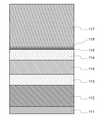
본 실시형태에 따른 발광 소자는 제 1 전극(101)과 제 2 전극(102)으로 이루어지는 한 쌍의 전극과, 제 1 전극(101)과 제 2 전극(102) 사이의 EL층(103)으로 구성되어 있다. 또한, 제 1 전극(101)은 양극으로서 기능하고, 제 2 전극(102)은 음극으로서 기능하는 것으로 하여 아래에 설명한다.The light emitting device according to the present embodiment includes a pair of electrodes comprising a
제 1 전극(101)을 양극으로서 기능시키기 위해서는 일함수가 큰(구체적으로는 4.0eV 이상) 금속, 합금, 도전성 화합물, 및 이들의 혼합물 등을 사용하여 형성하는 것이 바람직하다. 구체적으로는 예를 들어, 산화 인듐-산화 주석(ITO: Indium Tin Oxide), 실리콘 또는 산화 실리콘을 함유한 산화 인듐-산화 주석, 산화 인듐-산화 아연, 산화 텅스텐 및 산화 아연을 함유한 산화 인듐(IWZO) 등을 들 수 있다. 이들 도전성 금속 산화물막은 일반적으로 스퍼터링법에 의하여 형성되지만, 졸-겔법 등을 응용하여 제작하여도 좋다. 제작 방법의 예로서는 산화 인듐에 대하여 1wt% 내지 20wt%의 산화 아연이 첨가된 타깃을 사용하여 스퍼터링법에 의하여, 산화 인듐-산화 아연을 형성하는 방법 등이 있다. 또한, 산화 인듐에 대하여 산화 텅스텐이 0.5wt% 내지 5wt%, 산화 아연이 0.1wt% 내지 1wt% 함유된 타깃을 사용하여 스퍼터링법에 의하여, 산화 텅스텐 및 산화 아연이 함유된 산화 인듐(IWZO)을 형성할 수도 있다. 이 외에, 금(Au), 백금(Pt), 니켈(Ni), 텅스텐(W), 크로뮴(Cr), 몰리브데넘(Mo), 철(Fe), 코발트(Co), 구리(Cu), 팔라듐(Pd), 또는 금속 재료의 질화물(예를 들어, 질화 타이타늄) 등을 들 수 있다. 또한, 그래핀을 사용할 수도 있다. 또한, 후술하는 복합 재료를 EL층(103)에서 제 1 전극(101)과 접촉하는 층에 사용함으로써 일함수에 상관없이 전극 재료를 선택할 수 있게 된다.In order to function as an anode, the
EL층(103)은 적층 구조를 갖고, 적어도 발광층을 갖는다. 그 외의 층으로서는 정공 주입층, 정공 수송층, 전자 수송층, 전자 주입층, 캐리어 블로킹층, 중간층 등이 있고, 발광 소자는 이들을 적절히 조합하여 구성할 수 있다. 본 실시형태에서는 제 1 전극(101) 위에 정공 주입층(111), 정공 수송층(112), 발광층(113), 전자 수송층(114), 및 전자 주입층(115)이 이 순서대로 적층된 EL층(103)의 구성에 대하여 설명한다. 각 층을 구성하는 재료의 예에 대하여 아래에 구체적으로 기재한다.The
정공 주입층(111)은 정공 주입성이 높은 물질을 포함하는 층이다. 몰리브데넘 산화물, 바나듐 산화물, 루테늄 산화물, 텅스텐 산화물, 망가니즈 산화물 등을 사용할 수 있다. 이들 외에, 프탈로사이아닌(약칭: H2Pc)이나 구리 프탈로사이아닌(약칭: CuPC) 등의 프탈로사이아닌계 화합물, 4,4'-비스[N-(4-다이페닐아미노페닐)-N-페닐아미노]바이페닐(약칭: DPAB), N,N'-비스{4-[비스(3-메틸페닐)아미노]페닐}-N,N'-다이페닐-(1,1'-바이페닐)-4,4'-다이아민(약칭: DNTPD) 등의 방향족 아민 화합물, 또는 폴리(3,4-에틸렌다이옥시싸이오펜)/폴리(스타이렌설폰산)(약칭: PEDOT/PSS) 등의 고분자 등, 7,7,8,8,-테트라사이아노-2,3,5,6-테트라플루오로퀴노다이메테인(약칭: F4-TCNQ), 클로라닐 등에 의해서도 정공 주입층(111)을 형성할 수 있다.The
또한, 정공 주입층(111)에, 정공 수송성의 물질에 억셉터성 물질을 포함시킨 복합 재료를 사용할 수 있다. 복합 재료는 발광 소자의 막 두께를 조정할 때에 사용하는 것이 적합하다고 기술한 복합 재료와 동일하므로 반복된 설명은 생략한다. 또한, 복합 재료를 정공 주입층에 사용함으로써 제 1 전극 재료를 일함수에 상관없이 선택할 수 있게 된다.Also, for the
정공 주입층(111)을 형성함으로써, 정공의 주입성이 양호하게 되어, 구동 전압이 작은 발광 소자를 얻을 수 있게 된다.By forming the
정공 수송층(112)은 정공 수송성의 물질을 포함하는 층이다. 정공 수송성의 물질로서는, 예를 들어, 4,4'-비스[N-(1-나프틸)-N-페닐아미노]바이페닐(약칭: NPB)이나 N,N'-비스(3-메틸페닐)-N,N'-다이페닐-[1,1'-바이페닐]-4,4'-다이아민(약칭: TPD), 4,4',4''-트리스(N,N-다이페닐아미노)트라이페닐아민(약칭: TDATA), 4,4',4''-트리스[N-(3-메틸페닐)-N-페닐아미노]트라이페닐아민(약칭: MTDATA), 4,4'-비스[N-(스파이로-9,9'-바이플루오렌-2-일)-N-페닐아미노]바이페닐(약칭: BSPB), 4-페닐-4'-(9-페닐플루오렌-9-일)트라이페닐아민(약칭: BPAFLP) 등의 방향족 아민 화합물 등을 사용할 수 있다. 여기에 열거한 물질은 정공 수송성이 높고, 주로 10-6cm2/Vs 이상의 정공 이동도를 갖는 물질이다. 또한, 상술한 복합 재료에서의 정공 수송성의 물질로서 열거한 유기 화합물도 정공 수송층(112)에 사용할 수 있다. 또한, 정공 수송성의 물질을 포함하는 층은 단층의 것뿐만 아니라, 상기 물질로 이루어지는 층이 2층 이상 적층된 것으로 하여도 좋다.The
발광층(113)은 형광 발광을 나타내는 층이어도 좋고, 인광 발광을 나타내는 층이나 열활성화 지연 형광(TADF)을 나타내는 층이어도 좋다. 또한, 단층이어도 좋고, 상이한 발광 물질이 포함되는 복수의 층으로 이루어져도 좋다. 복수의 층으로 이루어지는 발광층을 형성하는 경우, 인광 발광 물질이 포함되는 층과 형광 발광 물질이 포함되는 층이 적층되어도 좋다. 이때, 인광 발광 물질이 포함되는 층에는, 후술하는 들뜬 복합체를 이용하는 것이 바람직하다.The
형광 발광 물질로서는, 예를 들어 이하와 같은 물질을 사용할 수 있다. 또한, 이 외의 형광 발광 물질도 사용할 수 있다. N,N'-다이페닐-N,N'-비스[4-(9-페닐-9H-플루오렌-9-일)페닐]필렌-1,6-다이아민(약칭: 1,6FLPAPrn), N,N'-비스(3-메틸페닐)-N,N'-비스[3-(9-페닐-9H-플루오렌-9-일)페닐]필렌-1,6-다이아민(약칭: 1,6mMemFLPAPrn), N,N'-다이페닐-N,N'-비스[3-(9-페닐-9H-플루오렌-9-일)페닐]필렌-1,6-다이아민(약칭: 1,6mFLPAPrn), N,N'-비스(2,6-다이메틸페닐)-N,N'-비스[3-(9-페닐-9H-플루오렌-9-일)페닐]필렌-1,6-다이아민(약칭: 1,6oDMemFLPAPrn), N,N'-비스[4-(다이벤조퓨란-4-일)페닐]-N,N'-다이페닐-필렌-1,6-다이아민(약칭: 1,6FrBAPrn-II), N,N'-비스[3-(다이벤조퓨란-4-일)페닐]-N,N'-다이페닐-필렌-1,6-다이아민(약칭: 1,6mFrBAPrn-II), N,N'-(필렌-1,6-다이일)비스[(N-페닐벤조[b]나프토[1,2-d]퓨란)-8-아민](약칭: 1,6BnfAPrn-02), N,N'-(필렌-1,6-다이일)비스[(6,N-다이페닐벤조[b]나프토[1,2-d]퓨란)-8-아민](약칭: 1,6BnfAPrn-03), 9,10-비스[N-페닐-N-(9-페닐카바졸-3-일)아미노]안트라센(약칭: PCA2A), 쿠마린 545T, 등을 들 수 있다. 특히, 1,6FLPAPrn이나 1,6mMemFLPAPrn과 같은 필렌다이아민 화합물로 대표되는 축합 방향족 다이아민 화합물은 홀 트랩성이 높고, 발광 효율이나 신뢰성이 우수하고, 또한 분자 배향하기 쉬우므로 바람직하다.As the fluorescent substance, for example, the following substances can be used. In addition, other fluorescent light-emitting materials can also be used. N,N'-diphenyl-N,N'-bis[4-(9-phenyl-9H-fluoren-9-yl)phenyl]pyrene-1,6-diamine (abbreviation: 1,6FLPAPrn), N ,N'-bis(3-methylphenyl)-N,N'-bis[3-(9-phenyl-9H-fluoren-9-yl)phenyl]pyrene-1,6-diamine (abbreviation: 1,6mMemFLPAPrn ), N,N'-diphenyl-N,N'-bis[3-(9-phenyl-9H-fluoren-9-yl)phenyl]pyrene-1,6-diamine (abbreviation: 1,6mFLPAPrn) , N,N'-bis(2,6-dimethylphenyl)-N,N'-bis[3-(9-phenyl-9H-fluoren-9-yl)phenyl]pyrene-1,6-diamine ( Abbreviation: 1,6oDMemFLPAPrn), N,N'-bis[4-(dibenzofuran-4-yl)phenyl]-N,N'-diphenyl-phyllene-1,6-diamine (abbreviation: 1,6FrBAPrn) -II), N,N'-bis[3-(dibenzofuran-4-yl)phenyl]-N,N'-diphenyl-pyrene-1,6-diamine (abbreviation: 1,6mFrBAPrn-II) , N,N'-(Pyllene-1,6-diyl)bis[(N-phenylbenzo[b]naphtho[1,2-d]furan)-8-amine] (abbreviation: 1,6BnfAPrn-02 ), N,N'-(pyrene-1,6-diyl)bis[(6,N-diphenylbenzo[b]naphtho[1,2-d]furan)-8-amine](abbreviation: 1 ,6BnfAPrn-03), 9,10-bis[N-phenyl-N-(9-phenylcarbazol-3-yl)amino]anthracene (abbreviation: PCA2A), and coumarin 545T. In particular, condensed aromatic diamine compounds typified by pilenediamine compounds such as 1,6FLPAPrn and 1,6mMemFLPAPrn are preferable because of high hole trapping properties, excellent luminous efficiency and reliability, and easy molecular orientation.
발광층(113)에서 인광 발광 물질로서 사용할 수 있는 재료의 예로서는 이하와 같은 재료를 들 수 있다. 트리스{2-[4-(2-아다만틸)-3-메틸-4H-1,2,4-트라이아졸-5-일-κN]페닐-κC}이리듐(III)(약칭: [Ir(Mptz-Adm2)3]), 트리스{2-[4-(4-사이아노-2,6-다이아이소뷰틸페닐)-5-(2-메틸페닐)-4H-1,2,4-트라이아졸-3-일-κN2]페닐-κC}이리듐(III)(약칭: Ir(mpptz-diBuCNp)3), 트리스{2-[4-(4-사이아노-2,6-다이메틸페닐)-5-(2-메틸페닐)-4H-1,2,4-트라이아졸-3-일-κN2]페닐-κC}이리듐(III)(약칭: Ir(mpptz-dmCNp)3), 트리스{2-[1-(4-사이아노-2,6-다이아이소뷰틸페닐)-1H-이미다졸-2-일-κN3]페닐-κC}이리듐(III)(약칭: Ir(pim-diBuCNp)3)와 같은 아졸(특히 트라이아졸이나 이미다졸) 골격을 갖는 유기 금속 이리듐 착체나, (아세틸아세토네이토)비스(6-tert-뷰틸-4-페닐피리미디네이토)이리듐(III)(약칭: [Ir(tBuppm)2(acac)]), (아세틸아세토네이토)비스[6-(2-노보닐)-4-페닐피리미디네이토]이리듐(III)(약칭: [Ir(nbppm)2(acac)]), (아세틸아세토네이토)비스[5-메틸-6-(2-메틸페닐)-4-페닐피리미디네이토]이리듐(III)(약칭: [Ir(mpmppm)2(acac)]), (아세틸아세토네이토)비스(4,6-다이페닐피리미디네이토)이리듐(III)(약칭: [Ir(dppm)2(acac)]), (아세틸아세토네이토)비스(4,5,6-트라이페닐피리미디네이토)이리듐(III)(약칭: [Ir(tppm)2(acac)]), 비스{2-[6-(3,5-다이메틸페닐)-4-피리미딘일-κN3]-4,6-다이메틸페닐-κC}(2,6-다이메틸-3,5-헵테인다이오네이토-κ2O,O')이리듐(III)(약칭: [Ir(dmdppm)2(dibm)], 비스{2-[6-(3,5-다이메틸페닐)-4-피리미딘일-κN3]-4,6-다이메틸페닐-κC}(2,2',6,6'-테트라메틸-3,5-헵테인다이오네이토-κ2O,O')이리듐(III)(약칭: [Ir(dmdppm)2(dpm)]와 같은 피리미딘 골격을 갖는 유기 금속 이리듐 착체나, 비스(2,3,5-트라이페닐피라지네이토)(다이피발로일메타네이토)이리듐(III)(약칭: [Ir(tppr)2(dpm])]), 비스{4,6-다이메틸-2-[5-(2,6-다이메틸페닐)-3-(3,5-다이메틸페닐)-2-피라진일-κN]페닐-κC}(2,4-펜탄다이오네이토-κ2O,O')이리듐(III)(약칭: [Ir(dmdppr-dmp)2(acac)]), 비스{4,6-다이메틸-2-[5-(2,6-다이메틸페닐)-3-(3,5-다이메틸페닐)-2-피라진일-κN]페닐-κC}(2,8-다이메틸-4,6-노난다이오네이토-κ2O,O')이리듐(III)(약칭: [Ir(dmdppr-dmp)2(divm)]), 비스{4,6-다이메틸-2-[5-(2,6-다이메틸페닐)-3-(3,5-다이메틸페닐)-2-피라진일-κN]페닐-κC}(2,2',6,6'-테트라메틸-3,5-헵테인다이오네이토-κ2O,O')이리듐(III)(약칭: [Ir(dmdppr-dmp)2(dpm)]), 비스{4,6-다이메틸-2-[5-(2,5-다이메틸페닐)-3-(3,5-다이메틸페닐)-2-피라진일-κN]페닐-κC}(2,2,6,6-테트라메틸-3,5-헵테인다이오네이토-κ2O,O')이리듐(III)(약칭: [Ir(dmdppr-25dmp)2(dpm)])과 같은 피라진 골격을 갖는 유기 금속 이리듐 착체를 들 수 있다. 이들 유기 금속 이리듐 착체는 발광 효율이나 신뢰성이 우수하고, 또한 분자 배향하기 쉬우므로 바람직하다.Examples of the material that can be used as the phosphorescent light emitting material in the
또한, 상술한 인광성 화합물 외에, 다양한 인광성 발광 재료를 선택하여 사용하여도 좋다.In addition to the above-mentioned phosphorescent compounds, various phosphorescent light-emitting materials may be selected and used.
또한, TADF 재료로서는 2-(바이페닐-4-일)-4,6-비스(12-페닐인돌로[2,3-a]카바졸-11-일)-1,3,5-트라이아진(약칭: PIC-TRZ)이나, 9-(4,6-다이페닐-1,3,5-트라이아진-2-일)-9'-페닐-9H,9'H-3,3'-바이카바졸(약칭: PCCzTzn), 2-{4-[3-(N-페닐-9H-카바졸-3-일)-9H-카바졸-9-일]페닐}-4,6-다이페닐-1,3,5-트라이아진(약칭: PCCzPTzn), 2-[4-(10H-페녹사진-10-일)페닐]-4,6-다이페닐-1,3,5-트라이아진(약칭: PXZ-TRZ), 3-[4-(5-페닐-5,10-다이하이드로페나진-10-일)페닐]-4,5-다이페닐-1,2,4-트라이아졸(약칭: PPZ-3TPT), 3-(9,9-다이메틸-9H-아크리딘-10-일)-9H-크산텐-9-온(약칭: ACRXTN), 비스[4-(9,9-다이메틸-9,10-다이하이드로아크리딘)페닐]설폰(약칭: DMAC-DPS), 10-페닐-10H,10'H-스파이로[아크리딘-9,9'-안트라센]-10'-온(약칭: ACRSA) 등의 π전자 과잉형 헤테로 방향 고리와 π전자 부족형 헤테로 방향 고리 양쪽을 갖는 헤테로 고리 화합물을 사용할 수 있다. 상기 헤테로 고리 화합물은 π전자 과잉형 헤테로 방향 고리 및 π전자 부족형 헤테로 방향 고리를 갖기 때문에, 전자 수송성 및 정공 수송성이 둘 다 높아 바람직하다. 또한, π전자 과잉형 헤테로 방향 고리와 π전자 부족형 헤테로 방향 고리가 직접 결합된 물질은, π전자 과잉형 헤테로 방향 고리의 도너성(donor property) 및 π전자 부족형 헤테로 방향 고리의 억셉터성이 둘 다 증가되어 S1 준위와 T1 준위의 에너지 차이가 작아지기 때문에 열활성화 지연 형광을 효율적으로 얻을 수 있어 특히 바람직하다. 또한, π전자 부족형 헤테로 방향 고리 대신에 사이아노기와 같은 전자 흡인기가 결합된 방향 고리를 사용하여도 좋다.In addition, as a TADF material, 2-(biphenyl-4-yl)-4,6-bis(12-phenylindolo[2,3-a]carbazol-11-yl)-1,3,5-triazine (abbreviation: PIC-TRZ) or 9-(4,6-diphenyl-1,3,5-triazin-2-yl)-9'-phenyl-9H,9'H-3,3'-bi Carbazole (abbreviation: PCCzTzn), 2-{4-[3-(N-phenyl-9H-carbazol-3-yl)-9H-carbazol-9-yl]phenyl}-4,6-diphenyl- 1,3,5-triazine (abbreviation: PCCzPTzn), 2-[4-(10H-phenoxazin-10-yl)phenyl]-4,6-diphenyl-1,3,5-triazine (abbreviation: PXZ-TRZ), 3- [4- (5-phenyl-5,10-dihydrophenazin-10-yl) phenyl] -4,5-diphenyl-1,2,4-triazole (abbreviation: PPZ -3TPT), 3-(9,9-dimethyl-9H-acridin-10-yl)-9H-xanthene-9-one (abbreviation: ACRXTN), bis[4-(9,9-dimethyl) -9,10-dihydroacridine)phenyl]sulfone (abbreviation: DMAC-DPS), 10-phenyl-10H,10'H-spiro[acridine-9,9'-anthracene]-10'- A heterocyclic compound having both a π-electron-rich heteroaromatic ring and a π-electron deficient heteroaromatic ring such as on (abbreviation: ACRSA) can be used. Since the heterocyclic compound has a π-electron-rich heteroaromatic ring and a π-electron deficient heteroaromatic ring, both electron transport properties and hole transport properties are high, which is preferable. In addition, the material in which the π-electron-rich heteroaromatic ring and the π-electron-deficient heteroaromatic ring are directly bonded, the donor property of the π-electron-rich heteroaromatic ring and the acceptor property of the π-electron deficient heteroaromatic ring Since both of these are increased andthe energy difference between the S 1 level and the T1 level is reduced, thermally activated delayed fluorescence can be efficiently obtained, which is particularly preferable. Alternatively, an aromatic ring to which an electron withdrawing group such as a cyano group is bonded may be used instead of the π-electron deficient heteroaromatic ring.
발광층의 호스트 재료로서는, 전자 수송성을 갖는 재료나 정공 수송성을 갖는 재료 등, 다양한 캐리어 수송 재료를 사용할 수 있다.As the host material of the light emitting layer, various carrier transport materials such as a material having an electron transport property and a material having a hole transport property can be used.
전자 수송성을 갖는 재료로서는 예를 들어, 비스(10-하이드록시벤조[h]퀴놀리네이토)베릴륨(II)(약칭: BeBq2), 비스(2-메틸-8-퀴놀리놀레이토)(4-페닐페놀레이토)알루미늄(III)(약칭: BAlq), 비스(8-퀴놀리놀레이토)아연(II)(약칭: Znq), 비스[2-(2-벤즈옥사졸일)페놀레이토]아연(II)(약칭: ZnPBO), 비스[2-(2-벤조싸이아졸일)페놀레이토]아연(II)(약칭: ZnBTZ) 등의 금속 착체나, 2-(4-바이페닐일)-5-(4-tert-뷰틸페닐)-1,3,4-옥사다이아졸(약칭: PBD), 3-(4-바이페닐일)-4-페닐-5-(4-tert-뷰틸페닐)-1,2,4-트라이아졸(약칭: TAZ), 1,3-비스[5-(p-tert-뷰틸페닐)-1,3,4-옥사다이아졸-2-일]벤젠(약칭: OXD-7), 9-[4-(5-페닐-1,3,4-옥사다이아졸-2-일)페닐]-9H-카바졸(약칭: CO11), 2,2',2''-(1,3,5-벤젠트라이일)트리스(1-페닐-1H-벤즈이미다졸)(약칭: TPBI), 2-[3-(다이벤조싸이오펜-4-일)페닐]-1-페닐-1H-벤즈이미다졸(약칭: mDBTBIm-II) 등의 폴리아졸 골격을 갖는 헤테로 고리 화합물이나 2-[3-(다이벤조싸이오펜-4-일)페닐]다이벤조[f,h]퀴녹살린(약칭: 2mDBTPDBq-II), 2-[3'-(다이벤조싸이오펜-4-일)바이페닐-3-일]다이벤조[f,h]퀴녹살린(약칭: 2mDBTBPDBq-II), 2-[3'-(9H-카바졸-9-일)바이페닐-3-일]다이벤조[f, h]퀴녹살린(약칭: 2mCzBPDBq), 4,6-비스[3-(페난트렌-9-일)페닐]피리미딘(약칭: 4,6mPnP2Pm), 4,6-비스[3-(4-다이벤조싸이엔일)페닐]피리미딘(약칭: 4,6mDBTP2Pm-II) 등의 다이아진 골격을 갖는 헤테로 고리 화합물이나, 3,5-비스[3-(9H-카바졸-9-일)페닐]피리딘(약칭: 35DCzPPy), 1,3,5-트라이[3-(3-피리딜)페닐]벤젠(약칭: TmPyPB) 등의 피리딘 골격을 갖는 헤테로 고리 화합물을 들 수 있다. 상술한 것 중에서도 다이아진 골격을 갖는 헤테로 고리 화합물이나 피리딘 골격을 갖는 헤테로 고리 화합물은 신뢰성이 양호하기 때문에 바람직하다. 특히, 다이아진(피리미딘이나 피라진) 골격을 갖는 헤테로 고리 화합물은 전자 수송성이 높고, 구동 전압 저감에도 기여한다.Examples of the material having electron transport properties include bis(10-hydroxybenzo [h] quinolinato) beryllium (II) (abbreviation: BeBq2 ), bis(2-methyl-8-quinolinolato) ( 4-phenylphenolato)aluminum(III)(abbreviation: BAlq), bis(8-quinolinolato)zinc(II)(abbreviation: Znq), bis[2-(2-benzoxazolyl)phenolato]zinc metal complexes such as (II) (abbreviation: ZnPBO), bis[2-(2-benzothiazolyl)phenolato]zinc(II) (abbreviation: ZnBTZ), and 2-(4-biphenylyl)-5 -(4-tert-butylphenyl)-1,3,4-oxadiazole (abbreviation: PBD), 3-(4-biphenylyl)-4-phenyl-5-(4-tert-butylphenyl)- 1,2,4-triazole (abbreviation: TAZ), 1,3-bis[5-(p-tert-butylphenyl)-1,3,4-oxadiazol-2-yl]benzene (abbreviation: OXD -7), 9-[4-(5-phenyl-1,3,4-oxadiazol-2-yl)phenyl]-9H-carbazole (abbreviation: CO11), 2,2',2''- (1,3,5-Benzenetriyl)tris(1-phenyl-1H-benzimidazole) (abbreviation: TPBI), 2-[3-(dibenzothiophen-4-yl)phenyl]-1-phenyl Heterocyclic compounds having a polyazole skeleton such as -1H-benzimidazole (abbreviation: mDBTBIm-II) or 2-[3-(dibenzothiophen-4-yl)phenyl]dibenzo[f,h]quinoxaline (abbreviation: 2mDBTPDBq-II), 2-[3'-(dibenzothiophen-4-yl)biphenyl-3-yl]dibenzo[f,h]quinoxaline (abbreviation: 2mDBTBPDBq-II), 2- [3'-(9H-carbazol-9-yl)biphenyl-3-yl]dibenzo[f,h]quinoxaline (abbreviation: 2mCzBPDBq), 4,6-bis[3-(phenanthrene-9-) diazine skeletons such as yl)phenyl]pyrimidine (abbreviation: 4,6mPnP2Pm) and 4,6-bis[3-(4-dibenzothienyl)phenyl]pyrimidine (abbreviation: 4,6mDBTP2Pm-II) Heterocyclic compound having, 3,5-bis[3-(9H-carbazol-9-yl)phenyl]pyridine (abbreviation: 35DCzPPy), 1,3,5-tri[3-(3-pyridyl)phenyl ] and heterocyclic compounds having a pyridine skeleton such as benzene (abbreviation: TmPyPB). Among those described above, a heterocyclic compound having a diazine skeleton and a heterocyclic compound having a pyridine skeleton are preferable because of their good reliability. In particular, a heterocyclic compound having a diazine (pyrimidine or pyrazine) skeleton has high electron transport properties and also contributes to a reduction in driving voltage.
정공 수송성을 갖는 재료로서는, 4,4'-비스[N-(1-나프틸)-N-페닐아미노]바이페닐(약칭: NPB), N,N'-비스(3-메틸페닐)-N,N'-다이페닐-[1,1'-바이페닐]-4,4'-다이아민(약칭: TPD), 4,4'-비스[N-(스파이로-9,9'-바이플루오렌-2-일)-N-페닐아미노]바이페닐(약칭: BSPB), 4-페닐-4'-(9-페닐플루오렌-9-일)트라이페닐아민(약칭: BPAFLP), 4-페닐-3'-(9-페닐플루오렌-9-일)트라이페닐아민(약칭: mBPAFLP), 4-페닐-4'-(9-페닐-9H-카바졸-3-일)트라이페닐아민(약칭: PCBA1BP), 4,4'-다이페닐-4''-(9-페닐-9H-카바졸-3-일)트라이페닐아민(약칭: PCBBi1BP), 4-(1-나프틸)-4'-(9-페닐-9H-카바졸-3-일)트라이페닐아민(약칭: PCBANB), 4,4'-다이(1-나프틸)-4''-(9-페닐-9H-카바졸-3-일)트라이페닐아민(약칭: PCBNBB), 9,9-다이메틸-N-페닐-N-[4-(9-페닐-9H-카바졸-3-일)페닐]플루오렌-2-아민(약칭: PCBAF), N-페닐-N-[4-(9-페닐-9H-카바졸-3-일)페닐]스파이로-9,9'-바이플루오렌-2-아민(약칭: PCBASF) 등의 방향족 아민 골격을 갖는 화합물이나, 1,3-비스(N-카바졸일)벤젠(약칭: mCP), 4,4'-다이(N-카바졸일)바이페닐(약칭: CBP), 3,6-비스(3,5-다이페닐페닐)-9-페닐카바졸(약칭: CzTP), 3,3'-비스(9-페닐-9H-카바졸)(약칭: PCCP) 등의 카바졸 골격을 갖는 화합물이나, 4,4',4''-(벤젠-1,3,5-트라이일)트라이(다이벤조싸이오펜)(약칭: DBT3P-II), 2,8-다이페닐-4-[4-(9-페닐-9H-플루오렌-9-일)페닐]다이벤조싸이오펜(약칭: DBTFLP-III), 4-[4-(9-페닐-9H-플루오렌-9-일)페닐]-6-페닐다이벤조싸이오펜(약칭: DBTFLP-IV) 등의 싸이오펜 골격을 갖는 화합물이나, 4,4',4''-(벤젠-1,3,5-트라이일)트라이(다이벤조퓨란)(약칭: DBF3P-II), 4-{3-[3-(9-페닐-9H-플루오렌-9-일)페닐]페닐}다이벤조퓨란(약칭: mmDBFFLBi-II) 등의 퓨란 골격을 갖는 화합물을 들 수 있다. 상술한 것 중에서도 방향족 아민 골격을 갖는 화합물이나 카바졸 골격을 갖는 화합물은 신뢰성이 양호하고, 또한 정공 수송성이 높고, 구동 전압 저감에도 기여하기 때문에 바람직하다. 또한, 상술한 정공 수송 재료 외에, 다양한 물질 중에서 정공 수송 재료를 사용하여도 좋다.Examples of the material having hole transport properties include 4,4'-bis[N-(1-naphthyl)-N-phenylamino]biphenyl (abbreviation: NPB), N,N'-bis(3-methylphenyl)-N, N'-diphenyl-[1,1'-biphenyl]-4,4'-diamine (abbreviation: TPD), 4,4'-bis[N-(spiro-9,9'-bifluorene) -2-yl)-N-phenylamino]biphenyl (abbreviation: BSPB), 4-phenyl-4'-(9-phenylfluoren-9-yl)triphenylamine (abbreviation: BPAFLP), 4-phenyl- 3'-(9-phenylfluoren-9-yl)triphenylamine (abbreviation: mBPAFLP), 4-phenyl-4'-(9-phenyl-9H-carbazol-3-yl)triphenylamine (abbreviation: PCBA1BP), 4,4'-diphenyl-4''-(9-phenyl-9H-carbazol-3-yl)triphenylamine (abbreviation: PCBBi1BP), 4-(1-naphthyl)-4'- (9-phenyl-9H-carbazol-3-yl)triphenylamine (abbreviation: PCBANB), 4,4'-di(1-naphthyl)-4''-(9-phenyl-9H-carbazole- 3-yl)triphenylamine (abbreviation: PCBNBB), 9,9-dimethyl-N-phenyl-N-[4-(9-phenyl-9H-carbazol-3-yl)phenyl]fluorene-2- Amine (abbreviation: PCBAF), N-phenyl-N-[4-(9-phenyl-9H-carbazol-3-yl)phenyl]spiro-9,9'-bifluoren-2-amine (abbreviation: PCBASF) compounds having an aromatic amine skeleton, 1,3-bis(N-carbazolyl)benzene (abbreviation: mCP), 4,4'-di(N-carbazolyl)biphenyl (abbreviation: CBP), Carbas such as 3,6-bis(3,5-diphenylphenyl)-9-phenylcarbazole (abbreviation: CzTP) and 3,3'-bis(9-phenyl-9H-carbazole) (abbreviation: PCCP) A compound having a sol skeleton, or 4,4',4''-(benzene-1,3,5-triyl)tri(dibenzothiophene) (abbreviation: DBT3P-II), 2,8-diphenyl- 4-[4-(9-phenyl-9H-fluoren-9-yl)phenyl]dibenzothiophene (abbreviation: DBTFLP-III), 4-[4-(9-phenyl-9H-fluoren-9-) A compound having a thiophene skeleton, such as yl)phenyl]-6-phenyldibenzothiophene (abbreviation: DBTFLP-IV), or 4,4',4''-(benzene-1,3,5-triyl) Tri(dibenzofuran) (abbreviation: DBF) 3P-II), 4-{3-[3-(9-phenyl-9H-fluoren-9-yl)phenyl]phenyl}dibenzofuran (abbreviation: mmDBFFLBi-II), and other compounds having a furan skeleton; can Among the above-mentioned compounds, a compound having an aromatic amine skeleton or a compound having a carbazole skeleton is preferable because it has good reliability, has high hole transport properties, and also contributes to a reduction in driving voltage. In addition to the hole transporting material described above, a hole transporting material from among various substances may be used.
발광 물질로서 형광 발광 물질을 사용하는 경우에는, 9-페닐-3-[4-(10-페닐-9-안트릴)페닐]-9H-카바졸(약칭: PCzPA), 3-[4-(1-나프틸)-페닐]-9-페닐-9H-카바졸(약칭: PCPN), 9-[4-(10-페닐-9-안트라센일)페닐]-9H-카바졸(약칭: CzPA), 7-[4-(10-페닐-9-안트릴)페닐]-7H-다이벤조[c, g]카바졸(약칭: cgDBCzPA), 6-[3-(9,10-다이페닐-2-안트릴)페닐]-벤조[b]나프토[1,2-d]퓨란(약칭: 2mBnfPPA), 9-페닐-10-{4-(9-페닐-9H-플루오렌-9-일)-바이페닐-4'-일}-안트라센(약칭: FLPPA) 등의 안트라센 골격을 갖는 재료가 적합하다. 안트라센 골격을 갖는 물질을 형광 발광 물질의 호스트 재료로서 사용하면, 발광 효율 및 내구성 둘 다 양호한 발광층을 구현할 수 있다. 특히, CzPA, cgDBCzPA, 2mBnfPPA, 및 PCzPA는 특성이 우수하기 때문에 바람직하다.In the case of using a fluorescent material as the light-emitting material, 9-phenyl-3-[4-(10-phenyl-9-anthryl)phenyl]-9H-carbazole (abbreviation: PCzPA), 3-[4-( 1-naphthyl)-phenyl]-9-phenyl-9H-carbazole (abbreviation: PCPN), 9-[4-(10-phenyl-9-anthracenyl)phenyl]-9H-carbazole (abbreviation: CzPA) , 7-[4-(10-phenyl-9-anthryl)phenyl]-7H-dibenzo[c, g]carbazole (abbreviation: cgDBCzPA), 6-[3-(9,10-diphenyl-2) -anthryl)phenyl]-benzo[b]naphtho[1,2-d]furan (abbreviation: 2mBnfPPA), 9-phenyl-10-{4-(9-phenyl-9H-fluoren-9-yl) A material having an anthracene skeleton such as -biphenyl-4'-yl}-anthracene (abbreviation: FLPPA) is suitable. When a material having an anthracene skeleton is used as a host material of the fluorescent material, a light emitting layer having good both luminous efficiency and durability can be realized. In particular, CzPA, cgDBCzPA, 2mBnfPPA, and PCzPA are preferable because of their excellent properties.
또한, 호스트 재료는 복수 종류의 물질을 혼합한 재료라도 좋고, 혼합된 호스트 재료를 사용하는 경우에는 전자 수송성을 갖는 재료와 정공 수송성을 갖는 재료를 혼합하는 것이 바람직하다. 전자 수송성을 갖는 재료와 정공 수송성을 갖는 재료를 혼합함으로써, 발광층(113)의 수송성을 쉽게 조정할 수 있어 재결합 영역의 제어도 쉽게 수행할 수 있다. 정공 수송성을 갖는 재료와 전자 수송성을 갖는 재료의 함유량의 비율은 정공 수송성을 갖는 재료:전자 수송성을 갖는 재료= 1:9 내지 9:1로 하면 좋다.In addition, the host material may be a material in which a plurality of types of substances are mixed, and when a mixed host material is used, it is preferable to mix a material having an electron transport property and a material having a hole transport property. By mixing the material having the electron transporting property and the material having the hole transporting property, the transportability of the
또한, 이들 혼합된 호스트 재료끼리로 들뜬 복합체를 형성하여도 좋다. 상기 들뜬 복합체는 형광 발광 물질, 인광 발광 물질, 및 TADF 재료의 가장 낮은 에너지 측의 흡수대의 파장과 겹치는 발광을 나타내는 들뜬 복합체를 형성하는 조합을 선택함으로써, 에너지 이동이 더 원활하게 수행되어 발광을 효율적으로 얻을 수 있게 된다. 또한, 상기 구성은 구동 전압도 저하되기 때문에 바람직하다.Alternatively, an exciplex may be formed from these mixed host materials. The exciplex is a fluorescent light emitting material, a phosphorescent light emitting material, and by selecting a combination that forms an exciplex exhibiting light emission overlapping the wavelength of the absorption band on the lowest energy side of the TADF material, energy transfer is performed more smoothly and light emission is efficiently performed can be obtained with In addition, the above configuration is preferable because the driving voltage also decreases.
또한, 발광 재료의 배향 상태를 나타내는 a의 수치는 호스트 재료의 종류나 수에는 영향을 많이 받지 않는다는 것이 알려져 있으므로 호스트 재료로서 어떤 재료를 선택하여도 상관없다.In addition, since it is known that the numerical value of a indicating the orientation state of the light emitting material is not greatly affected by the type or number of the host material, any material may be selected as the host material.
상술한 바와 같은 구성을 갖는 발광층(113)은 진공 증착법에 의한 공증착을 사용하여 제작할 수 있다. 이때, 증착실에 설치한 4중극형 질량 분석기(Q-MASS)로 측정한 체임버 분위기로서 체임버 내의 전압(全壓)에 대한 이산화탄소의 분압(分壓)의 비율이 대기 중보다 큰 것이 유효한 조건이다. 대기 중에 있어서, 전압에 대한 이산화탄소의 분압의 비율(즉, 체적비율)은, 약 0.03%이다. 한편, 감압하의 진공 체임버에 있어서, 전압에 대한 이산화탄소의 분압의 비율이 0.03%보다 큰 상태, 바람직하게는 0.1% 이상인 상태로 발광층을 성막함으로써 발광 재료의 a가 0.2 이하의 배향 상태가 되는 발광 소자를 제작할 수 있다. 또한, 이산화탄소는 캐리어 수송성을 저해하므로 상기 비율은 10% 이하가 바람직하다.The
전자 수송층(114)은 전자 수송성을 갖는 물질을 포함하는 층이다. 전자 수송성을 갖는 물질로서는, 상기 호스트 재료에 사용할 수 있는 전자 수송성을 갖는 재료로서 예로 든 재료나, 안트라센 골격을 갖는 재료를 사용할 수 있다.The
또한, 전자 수송층과 발광층 사이에 전자 캐리어의 이동을 제어하는 층을 제공하여도 좋다. 이것은 상술한 전자 수송성이 높은 재료에 전자 트랩성이 높은 물질을 소량 첨가한 층이고, 전자 캐리어의 이동을 억제함으로써, 캐리어 밸런스를 조절할 수 있다. 이와 같은 구성은, 전자가 발광층을 통과하는 것으로 인하여 발생되는 문제(예를 들어 소자 수명의 저하)의 억제에 큰 효과를 발휘한다.Further, a layer for controlling the movement of electron carriers may be provided between the electron transport layer and the light emitting layer. This is a layer in which a small amount of a substance having high electron trapping property is added to the material having high electron transport property described above, and carrier balance can be adjusted by suppressing the movement of electron carriers. Such a configuration exerts a great effect on suppression of problems (for example, reduction in device lifetime) caused by electrons passing through the light emitting layer.
또한, 전자 수송층(114)과 제 2 전극(102) 사이에, 제 2 전극(102)과 접촉되도록 전자 주입층(115)을 제공하여도 좋다. 전자 주입층(115)으로서는, 플루오르화 리튬(LiF), 플루오르화 세슘(CsF), 플루오르화 칼슘(CaF2) 등의 알칼리 금속 또는 알칼리 토금속 또는 이들의 화합물을 사용할 수 있다. 예를 들어, 전자 수송성을 갖는 물질로 이루어지는 층 내에 알칼리 금속 또는 알칼리 토금속 또는 이들의 화합물을 함유시킨 것을 사용할 수 있다. 또한, 전자 주입층(115)에 전자화물(electride)을 사용하여도 좋다. 전자화물로서는, 예를 들어, 칼슘과 알루미늄의 혼합 산화물에 전자를 고농도로 첨가한 물질 등을 들 수 있다. 또한, 전자 주입층(115)으로서, 전자 수송성을 갖는 물질로 이루어지는 층 내에 알칼리 금속 또는 알칼리 토금속을 함유시킨 것을 사용함으로써, 제 2 전극(102)으로부터의 전자 주입이 효율적으로 수행되므로 더 바람직하다.Further, an
또한, 전자 주입층(115) 대신에 전하 발생층(116)을 제공하여도 좋다(도 3의 (B) 참조). 전하 발생층(116)은 전위의 인가에 의하여 상기 층의 음극 측에 접촉되는 층에 정공을, 양극 측에 접촉되는 층에 전자를 주입할 수 있는 층을 말한다. 전하 발생층(116)에는 적어도 P형층(117)이 포함된다. P형층(117)은 상술한 정공 주입층(111)을 구성할 수 있는 재료로서 열거한 복합 재료를 사용하여 형성하는 것이 바람직하다. 또한, P형층(117)은 복합 재료를 구성하는 재료로서 상술한 억셉터 재료를 포함하는 막과 정공 수송 재료를 포함하는 막을 적층하여 구성하여도 좋다. P형층(117)에 전위를 인가함으로써, 전자 수송층(114)에 전자가, 음극인 제 2 전극(102)에 정공이 주입되어, 발광 소자가 동작한다.In addition, the
또한, 전하 발생층(116)에는 P형층(117) 외에, 전자 릴레이층(118) 및 전자 주입 버퍼층(119) 중 어느 한쪽 또는 양쪽 모두가 제공되는 것이 바람직하다.In addition, it is preferable that either or both of the
전자 릴레이층(118)은 적어도 전자 수송성을 갖는 물질을 포함하고, 전자 주입 버퍼층(119)과 P형층(117)의 상호 작용을 방지하여 전자가 원활하게 이동하게 하는 기능을 갖는다. 전자 릴레이층(118)에 포함되는 전자 수송성을 갖는 물질의 LUMO 준위는 P형층(117)에서의 억셉터성 물질의 LUMO 준위와 전자 수송층(114)에서의 전하 발생층(116)에 접촉되는 층에 포함되는 물질의 LUMO 준위 사이인 것이 바람직하다. 전자 릴레이층(118)에 사용되는 전자 수송성을 갖는 물질에서의 LUMO 준위의 구체적인 에너지 준위는 -5.0eV 이상, 바람직하게는 -5.0eV 이상 -3.0eV 이하인 것이 좋다. 또한, 전자 릴레이층(118)에 사용되는 전자 수송성을 갖는 물질로서는 프탈로사이아닌계의 재료 또는 금속-산소 결합과 방향족 배위자를 갖는 금속 착체를 사용하는 것이 바람직하다.The
전자 주입 버퍼층(119)에는, 알칼리 금속, 알칼리 토금속, 희토류 금속, 및 이들의 화합물(알칼리 금속 화합물(산화 리튬 등의 산화물, 할로젠화물, 탄산 리튬이나 탄산 세슘 등의 탄산염을 포함함), 알칼리 토금속 화합물(산화물, 할로젠화물, 탄산염을 포함함), 또는 희토류 금속의 화합물(산화물, 할로젠화물, 탄산염을 포함함)) 등의 전자 주입성이 높은 물질을 사용할 수 있다.In the electron
또한, 전자 주입 버퍼층(119)이 전자 수송성을 갖는 물질과 도너성 물질을 포함하여 형성되는 경우에는, 도너성 물질로서 알칼리 금속, 알칼리 토금속, 희토류 금속, 및 이들의 화합물(알칼리 금속 화합물(산화 리튬 등의 산화물, 할로젠화물, 탄산 리튬이나 탄산 세슘 등의 탄산염을 포함함), 알칼리 토금속 화합물(산화물, 할로젠화물, 탄산염을 포함함), 또는 희토류 금속의 화합물(산화물, 할로젠화물, 탄산염을 포함함))을 사용할 수 있고, 이 외에도 테트라싸이아나프타센(약칭: TTN), 니켈로센, 데카메틸니켈로센 등의 유기 화합물을 사용할 수도 있다.In addition, when the electron
제 2 전극(102)을 형성하는 물질로서는, 일함수가 작은(구체적으로는 3.8eV 이하) 금속, 합금, 전기 전도성 화합물, 및 이들의 혼합물 등을 사용할 수 있다. 이와 같은 음극 재료의 구체적인 예로서는, 리튬(Li)이나 세슘(Cs) 등의 알칼리 금속, 및 마그네슘(Mg), 칼슘(Ca), 스트론튬(Sr) 등의 원소 주기율표에서의 1족 또는 2족에 속하는 원소, 및 이들을 포함하는 합금(MgAg, AlLi), 유로퓸(Eu), 이터븀(Yb) 등의 희토류 금속, 및 이들을 포함하는 합금 등을 들 수 있다. 다만, 제 2 전극(102)과 전자 수송층 사이에 전자 주입층을 제공함으로써, 일함수의 대소에 상관없이 Al, Ag, ITO, 실리콘 또는 산화 실리콘을 함유하는 산화 인듐-산화 주석 등 다양한 도전성 재료를 제 2 전극(102)에 사용할 수 있다. 이들 도전성 재료는, 진공 증착법이나 스퍼터링법 등의 건식법, 잉크젯법, 스핀 코팅법 등을 사용하여 성막하는 것이 가능하다. 또한, 졸-겔법을 사용하여 습식법으로 형성하여도 좋고, 금속 재료의 페이스트를 사용하여 습식법으로 형성하여도 좋다.As the material for forming the
또한, 발광층 이외의 EL층(103)의 형성 방법으로서는, 건식법, 습식법을 불문하고 다양한 방법을 사용할 수 있다. 예를 들어, 진공 증착법, 그라비어 인쇄법, 오프셋 인쇄법, 스크린 인쇄법, 잉크젯법, 또는 스핀 코팅법 등을 사용하여도 좋다.In addition, as a method of forming the
여기서, 액적 토출법을 사용하여 EL층(786)을 형성하는 방법에 대하여 도 4를 참조하여 설명한다. 도 4의 (A) 내지 (D)는 EL층(786)의 제작 방법을 설명하는 단면도이다.Here, a method of forming the
우선, 평탄화 절연막(770) 위에 도전막(772)이 형성되고, 도전막(772)의 일부를 덮도록 절연막(730)이 형성된다(도 4의 (A) 참조).First, a
다음에, 절연막(730)의 개구인 도전막(772)의 노출부에 액적 토출 장치(783)에서 액적(784)을 토출하여, 조성물을 포함하는 층(785)을 형성한다. 액적(784)은 용매를 포함하는 조성물이며 도전막(772) 위에 부착된다(도 4의 (B) 참조).Next, a
또한 액적(784)을 토출하는 공정을 감압하에서 수행하여도 좋다.Also, the step of discharging the
다음에, 조성물을 포함하는 층(785)으로부터 용매를 제거하여 고체화함으로써 EL층(786)을 형성한다(도 4의 (C) 참조).Next, the
또한 용매의 제거 방법으로서는 건조 공정 또는 가열 공정을 수행하면 좋다.In addition, as a method of removing the solvent, a drying step or a heating step may be performed.
다음에, EL층(786) 위에 도전막(788)을 형성하여 발광 소자(782)를 형성한다(도 4의 (D) 참조).Next, a
이와 같이 EL층(786)의 형성을 액적 토출법으로 수행하면 선택적으로 조성물을 토출할 수 있기 때문에, 재료의 낭비를 삭감할 수 있다. 또한, 형상을 가공하기 위한 리소그래피 공정 등도 필요 없어 공정도 간략화할 수 있으므로, 저비용화를 달성할 수 있다.In this way, when the
또한 상술한 액적 토출법이란, 조성물의 토출구를 갖는 노즐, 또는 하나 또는 복수의 노즐을 갖는 헤드 등 액적을 토출하는 수단을 갖는 것의 총칭으로 한다.In addition, let the above-mentioned droplet discharging method be a generic name for the thing which has means for discharging droplets, such as a nozzle which has a discharge port of a composition, or a head which has one or more nozzles.
다음에, 액적 토출법에 사용하는 액적 토출 장치에 대하여 도 5를 참조하여 설명한다. 도 5는 액적 토출 장치(1400)를 설명하는 개념도이다.Next, a droplet discharging device used in the droplet discharging method will be described with reference to FIG. 5 . 5 is a conceptual diagram illustrating the
액적 토출 장치(1400)는 액적 토출 수단(1403)을 갖는다. 또한 액적 토출 수단(1403)은 헤드(1405), 헤드(1412), 및 헤드(1416)를 갖는다.The
헤드(1405) 및 헤드(1412)는 제어 수단(1407)에 접속되고, 이 제어 수단이 컴퓨터(1410)에 의하여 제어됨으로써, 미리 프로그래밍된 패턴으로 묘화할 수 있다.The
또한 묘화하는 타이밍으로서는, 예를 들어 기판(1402) 위에 형성된 마커(1411)를 기준으로 수행하면 좋다. 또는, 기판(1402)의 가장자리를 기준으로 하여 기준점을 확정시켜도 좋다. 여기서는, 마커(1411)를 촬상 수단(1404)으로 검출하여, 화상 처리 수단(1409)으로 디지털 신호로 변환한 것을 컴퓨터(1410)로 인식하여 제어 신호를 발생시켜 제어 수단(1407)에 보낸다.Further, as the timing for drawing, for example, the
촬상 수단(1404)으로서, 전하 결합 소자(CCD)나 상보형 금속-산화물-반도체(CMOS)를 이용한 이미지 센서 등을 사용할 수 있다. 또한, 기판(1402) 위에 형성되어야 할 패턴의 정보는 기억 매체(1408)에 저장되어 있고, 이 정보에 의거하여 제어 수단(1407)에 제어 신호를 보내고, 액적 토출 수단(1403)의 개개의 헤드(1405), 헤드(1412), 및 헤드(1416)를 개별로 제어할 수 있다. 토출되는 재료는 재료 공급원(1413), 재료 공급원(1414), 및 재료 공급원(1415)으로부터 배관을 통하여 헤드(1405), 헤드(1412), 및 헤드(1416)에 각각 공급된다.As the imaging means 1404, a charge-coupled device (CCD), an image sensor using a complementary metal-oxide-semiconductor (CMOS), or the like can be used. In addition, information of a pattern to be formed on the
헤드(1405), 헤드(1412), 및 헤드(1416) 내부는 점선(1406)이 나타내는 바와 같이 액상의 재료를 충전하는 공간과, 토출구인 노즐을 갖는 구조가 되어 있다. 도시되지는 않았지만, 헤드(1412)도 헤드(1405)와 같은 내부 구조를 갖는다. 헤드(1405) 및 헤드(1412)의 노즐을 상이한 사이즈로 제공하면, 상이한 재료를 상이한 폭으로 동시에 묘화할 수 있다. 하나의 헤드로 복수종의 발광 재료 등을 각각 토출하여 묘화할 수 있고, 넓은 범위에 묘화하는 경우에는, 스루풋을 향상시키기 위하여 복수의 노즐로부터 같은 재료를 동시에 토출하여 묘화할 수 있다. 대형 기판을 사용하는 경우, 헤드(1405), 헤드(1412), 및 헤드(1416)는 기판 위를, 도 5의 X, Y, Z의 화살표 방향으로 자유롭게 주사하여, 묘화하는 영역을 자유롭게 설정할 수 있으므로, 같은 패턴을 하나의 기판에 복수 묘화할 수 있다.The inside of the
또한, 조성물을 토출하는 공정을 감압하에서 수행하여도 좋다. 토출 시에 기판을 가열해 두어도 좋다. 조성물을 토출한 후, 건조 및 소성 중 한쪽 또는 양쪽 공정을 수행한다. 건조와 소성의 공정은 양쪽 모두 가열 처리 공정이지만, 그 목적, 온도, 시간이 상이하다. 건조 공정 및 소성 공정은 상압하 또는 감압하에서 레이저 광 조사나 순간 열 어닐, 가열로 등에 의하여 수행한다. 또한, 이 가열 처리를 수행하는 타이밍, 가열 처리 횟수는 특별히 한정되지 않는다. 건조와 소성의 공정을 양호하게 수행하기 위한 온도는, 기판의 재질 및 조성물의 성질에 의존한다.Further, the step of discharging the composition may be performed under reduced pressure. You may heat a board|substrate at the time of discharge. After discharging the composition, one or both processes of drying and firing are performed. Although the drying and calcining processes are both heat treatment processes, their purpose, temperature, and time are different. The drying process and the firing process are performed by laser light irradiation, instantaneous thermal annealing, or a heating furnace under normal or reduced pressure. In addition, the timing for performing this heat treatment and the number of times of heat treatment are not particularly limited. The temperature for properly performing the drying and firing processes depends on the material of the substrate and the nature of the composition.
상술한 바와 같이 하여, 액적 토출 장치를 사용하여 EL층(786)을 제작할 수 있다.As described above, the
액적 토출 장치를 사용하여 EL층(786)을 제작하는 경우, 다양한 유기 용제를 사용하여 도포용 조성물을 제작할 수 있다. 상기 조성물에 사용할 수 있는 유기 용제로서는 벤젠, 톨루엔, 자일렌, 메시틸렌, 테트라하이드로퓨란, 다이옥세인, 에탄올, 메탄올, n-프로판올, 아이소프로판올, n-뷰탄올, t-뷰탄올, 아세토나이트릴, 다이메틸설폭사이드, 다이메틸폼아마이드, 클로로폼, 메틸렌클로라이드, 사염화 탄소, 아세트산 에틸, 헥세인, 사이클로헥세인 등 다양한 유기 용제를 사용할 수 있다. 특히, 벤젠, 톨루엔, 자일렌, 메시틸렌 등의 저극성 벤젠 유도체를 사용하면 바람직한 농도의 용액을 만들 수 있고, 또한 잉크 내에 포함되는 본 발명의 정공 수송층이 산화 등으로 인하여 열화되는 것을 방지할 수 있어 바람직하다. 또한 제작 후의 막의 균일성이나 막 두께의 균일성 등을 고려하면 비점이 100℃ 이상인 것이 바람직하고, 톨루엔, 자일렌, 메시틸렌이 더 바람직하다.When the
또한, 상기 구성은 본 실시형태 중의 다른 구성과 적절히 조합할 수 있다.In addition, the said structure can be combined suitably with the other structure in this embodiment.
전극에 대해서도, 졸-겔법을 사용하여 습식법으로 형성하여도 좋고 금속 재료의 페이스트를 사용하여 습식법으로 형성하여도 좋다. 또한, 스퍼터링법이나 진공 증착법 등의 건식법을 사용하여 형성하여도 좋다.The electrode may also be formed by a wet method using a sol-gel method, or may be formed by a wet method using a metal material paste. Moreover, you may form using dry methods, such as a sputtering method and a vacuum vapor deposition method.
상기 발광 소자의 발광은, 제 1 전극(101) 및 제 2 전극(102) 중 어느 한쪽 또는 양쪽 모두를 통과하여 외부로 추출된다. 따라서, 제 1 전극(101) 및 제 2 전극(102) 중 어느 한쪽 또는 양쪽 모두를 투광성을 갖는 전극으로 형성한다.Light emitted from the light emitting element passes through either or both of the
또한, 제 1 전극(101)과 제 2 전극(102) 사이에 제공되는 층의 구성은 상술한 것에 한정되지 않는다. 다만, 발광 영역과 전극이나 캐리어 주입층에 사용되는 금속이 근접하여 일어나는 소광이 억제되도록, 제 1 전극(101) 및 제 2 전극(102)으로부터 떨어진 부위에 정공과 전자가 재결합하는 발광 영역을 제공하는 구성이 바람직하다.In addition, the configuration of the layer provided between the
또한, 발광층(113)에 접촉하는 정공 수송층이나 전자 수송층, 특히 발광층(113)에서의 재결합 영역에 가까운 쪽과 접촉하는 캐리어 수송층은, 발광층에서 생성된 여기자로부터의 에너지 이동을 억제하기 위하여, 발광층을 구성하는 발광 물질 또는 발광층에 포함되는 발광 중심 물질이 갖는 밴드갭보다 큰 밴드갭을 갖는 물질로 구성되는 것이 바람직하다.In addition, the hole transporting layer or electron transporting layer in contact with the
이어서, 복수의 발광 유닛을 적층한 구성의 발광 소자(적층형 소자, 탠덤형 발광 소자라고도 함)의 형태에 대하여, 도 3의 (C)를 참조하여 설명한다. 이 발광 소자는 양극과 음극 사이에 복수의 발광 유닛을 갖는 발광 소자이다. 하나의 발광 유닛은 도 3의 (A) 또는 (B)에 도시된 EL층(103)과 같은 구성을 갖는다. 즉, 도 3의 (A) 또는 (B)에 도시된 발광 소자는 하나의 발광 유닛을 갖는 발광 소자이고, 도 3의 (C)에 도시된 발광 소자는 복수의 발광 유닛을 갖는 발광 소자라고 할 수 있다.Next, the form of a light emitting element (also referred to as a stacked element or a tandem light emitting element) having a structure in which a plurality of light emitting units are stacked will be described with reference to FIG. 3C . This light emitting element is a light emitting element having a plurality of light emitting units between an anode and a cathode. One light emitting unit has the same configuration as the
도 3의 (C)에서, 제 1 전극(501)과 제 2 전극(502) 사이에는, 제 1 발광 유닛(511)과 제 2 발광 유닛(512)이 적층되어 있고, 제 1 발광 유닛(511)과 제 2 발광 유닛(512) 사이에는 전하 발생층(513)이 제공되어 있다. 제 1 전극(501)과 제 2 전극(502)은 각각 도 3의 (A)에서의 제 1 전극(101)과 제 2 전극(102)에 상당하고, 도 3의 (A)의 설명에서 기재한 것과 같은 것을 적용할 수 있다. 또한, 제 1 발광 유닛(511)과 제 2 발광 유닛(512)은 같은 구성이어도 좋고 상이한 구성이어도 좋다.In FIG. 3C , a first
전하 발생층(513)은, 제 1 전극(501)과 제 2 전극(502)에 전압이 인가되었을 때에 한쪽 발광 유닛에 전자를 주입하고 다른 쪽 발광 유닛에 정공을 주입하는 기능을 갖는다. 즉, 도 3의 (C)에서, 제 1 전극의 전위가 제 2 전극의 전위보다 높게 되도록 전압을 인가한 경우, 전하 발생층(513)은 제 1 발광 유닛(511)에 전자를 주입하고 제 2 발광 유닛(512)에 정공을 주입하는 것이면 좋다.The
전하 발생층(513)은, 도 3의 (B)에서 설명한 전하 발생층(116)과 비슷한 구성으로 형성되는 것이 바람직하다. 유기 화합물과 금속 산화물의 복합 재료는 캐리어 주입성, 캐리어 수송성이 우수하므로, 저전압 구동, 저전류 구동을 구현할 수 있다. 또한, 발광 유닛의 양극 측의 면이 전하 발생층(513)과 접촉되는 경우에는, 전하 발생층(513)이 발광 유닛의 정공 주입층의 역할도 할 수 있기 때문에, 이 발광 유닛에는 정공 주입층을 제공하지 않아도 된다.The
또한, 전자 주입 버퍼층(119)을 제공하는 경우에는 이 층이 양극 측의 발광 유닛에서의 전자 주입층의 역할을 하기 때문에, 상기 발광 유닛에 중복하여 전자 주입층을 반드시 형성할 필요는 없다.In addition, when the electron
도 3의 (C)에서는 2개의 발광 유닛을 갖는 발광 소자에 대하여 설명하였지만, 3개 이상의 발광 유닛을 적층한 발광 소자에 대해서도, 마찬가지로 적용하는 것이 가능하다. 본 실시형태에 따른 발광 소자와 같이, 한 쌍의 전극 사이에 복수의 발광 유닛을 전하 발생층(513)으로 칸막이하여 배치함으로써, 전류 밀도를 낮게 유지하면서 고휘도 발광을 가능하게 하고 수명이 더 긴 소자를 구현할 수 있다. 또한, 저전압 구동이 가능하고 소비전력이 낮은 발광 장치를 구현할 수 있다.Although the light emitting device having two light emitting units has been described in FIG. 3C , the same can be applied to a light emitting device in which three or more light emitting units are stacked. As in the light emitting device according to the present embodiment, a plurality of light emitting units are partitioned between a pair of electrodes by a
또한, 각각의 발광 유닛의 발광색을 다르게 함으로써, 발광 소자 전체로서 원하는 색의 발광을 얻을 수 있다. 예를 들어, 2개의 발광 유닛을 갖는 발광 소자에서, 제 1 발광 유닛으로 적색과 녹색의 발광색, 제 2 발광 유닛으로 청색의 발광색을 얻음으로써, 발광 소자 전체로서 백색 발광하는 발광 소자를 얻는 것도 용이하다.In addition, by making the light emission color of each light emitting unit different, light emission of a desired color can be obtained as a whole of the light emitting element. For example, in a light emitting device having two light emitting units, it is easy to obtain a light emitting device that emits white light as a whole by obtaining red and green light emitting colors as the first light emitting unit and blue light emitting colors as the second light emitting unit. do.
≪미소광 공진기(마이크로캐비티) 구조≫≪Micro-light resonator (microcavity) structure≫
마이크로캐비티 구조를 갖는 발광 소자는 상기 한 쌍의 전극을, 반사 전극과 반투과·반반사 전극으로 구성하는 것에 의하여 얻어진다. 반사 전극과 반투과·반반사 전극은 상술한 제 1 전극과 제 2 전극에 상당한다. 반사 전극과 반투과·반반사 전극 사이에는 적어도 EL층을 갖고, EL층은 적어도 발광 영역이 되는 발광층을 갖는다.A light emitting element having a microcavity structure is obtained by configuring the pair of electrodes with a reflective electrode and a semi-transmissive/reflective electrode. The reflective electrode and the semi-transmissive/semi-reflective electrode correspond to the above-described first and second electrodes. At least an EL layer is provided between the reflective electrode and the transflective/reflective electrode, and the EL layer has at least a light emitting layer serving as a light emitting region.
EL층에 포함되는 발광층으로부터 사출되는 발광은, 반사 전극과 반투과·반반사 전극에 의하여 반사되어 공진한다. 또한, 반사 전극은 가시광의 반사율이 40% 내지 100%, 바람직하게는 70% 내지 100%이고, 또한 그 저항률이 1×10⁻²Ωcm 이하인 것으로 한다. 또한, 반투과·반반사 전극은 가시광의 반사율이 20% 내지 80%, 바람직하게는 40% 내지 70%이고, 또한 그 저항률이 1×10⁻²Ωcm 이하인 것으로 한다.Light emitted from the light emitting layer included in the EL layer is reflected by the reflective electrode and the semi-transmissive/semi-reflective electrode and resonates. Further, the reflecting electrode is the reflectance of visible light of 40% to 100%, preferably 70% to 100%, and the resistivity is 1 × 10- is less than or equal to2 Ωcm. In addition, semi-permeable, semi-reflective electrode is the reflectance of visible light of 20% to 80%, preferably from 40% to 70%, and also the resistivity of 1 × 10- is less than or equal to2 Ωcm.
또한, 상기 발광 소자는 투명 도전막이나 상술한 복합 재료, 캐리어 수송 재료 등의 두께를 변경함으로써 반사 전극과 반투과·반반사 전극 사이의 광학적 거리를 변경할 수 있다. 이에 의하여, 반사 전극과 반투과·반반사 전극 사이에서, 공진하는 파장의 광을 강하게 하고, 공진하지 않는 파장의 광을 감쇠시킬 수 있다.In addition, the light emitting device can change the optical distance between the reflective electrode and the semi-transmissive/semi-reflective electrode by changing the thickness of the transparent conductive film, the above-described composite material, carrier transport material, or the like. Thereby, light of a wavelength that resonates between the reflective electrode and the semi-transmissive/semi-reflective electrode can be strengthened, and light of a wavelength that does not resonate can be attenuated.
또한, 발광층이 발하는 광 중, 반사 전극에 의하여 반사되어 되돌아온 광(제 1 반사광)은, 발광층으로부터 반투과·반반사 전극에 직접 입사하는 광(제 1 입사광)과 큰 간섭을 일으키기 때문에, 반사 전극과 발광층의 광학적 거리를 (2n-1)λ/4(다만, n은 1 이상의 자연수, λ는 증폭하고자 하는 색의 파장)로 조절하는 것이 바람직하다. 이로써, 제 1 반사광과 제 1 입사광의 위상을 맞춰 발광층으로부터의 발광을 더 증폭시킬 수 있다.In addition, among the light emitted by the light emitting layer, the light reflected back by the reflective electrode (first reflected light) causes large interference with the light (first incident light) that is directly incident on the semi-transmissive/semi-reflective electrode from the light emitting layer, so the reflective electrode It is preferable to adjust the optical distance of the light emitting layer to (2n-1)λ/4 (however, n is a natural number greater than or equal to 1, and λ is the wavelength of the color to be amplified). Accordingly, it is possible to further amplify light emission from the light emitting layer by matching the phases of the first reflected light and the first incident light.
또한, 상기 구성에서는, EL층에 복수의 발광층을 갖는 구조이어도 좋고, 단일의 발광층을 갖는 구조이어도 좋고, 예를 들어, 상술한 탠덤형 발광 소자의 구성과 조합하여, 하나의 발광 소자에 전하 발생층을 끼우는 복수의 EL층을 제공하고, 각각의 EL층에 하나 또는 복수의 발광층으로 형성하는 구성에 적용하여도 좋다.Further, in the above configuration, the EL layer may have a structure having a plurality of light emitting layers or a structure having a single light emitting layer. It may be applied to a configuration in which a plurality of EL layers sandwiching the layers are provided, and one or a plurality of light emitting layers are formed in each EL layer.
≪발광 장치≫≪Light-emitting device≫
본 발명의 일 형태에 따른 발광 장치에 대하여 도 6을 참조하여 설명한다. 또한, 도 6의 (A)는 발광 장치를 도시한 상면도, 도 6의 (B)는 도 6의 (A)를 A-B 및 C-D를 따라 절단한 단면도이다. 이 발광 장치는, 점선으로 나타내어진 구동 회로부(소스선 구동 회로)(601), 화소부(602), 구동 회로부(게이트선 구동 회로)(603)를 발광 소자의 발광을 제어하는 것으로서 포함한다. 또한, 도면에서 기호(604)는 밀봉 기판, 기호(605)는 실재를 나타내고, 실재(605)로 둘러싸인 내측은 공간(607)이 되어 있다.A light emitting device according to one embodiment of the present invention will be described with reference to FIG. 6 . 6A is a top view illustrating a light emitting device, and FIG. 6B is a cross-sectional view taken along lines A-B and C-D of FIG. 6A. This light emitting device includes a driving circuit section (source line driving circuit) 601, a
또한, 리드 배선(608)은 소스선 구동 회로(601) 및 게이트선 구동 회로(603)에 입력되는 신호를 전송하기 위한 배선이며, 외부 입력 단자가 되는 FPC(Flexible Printed Circuit)(609)로부터 비디오 신호, 클럭 신호, 스타트 신호, 리셋 신호 등을 받는다. 또한, 여기서는 FPC만을 도시하였지만, 이 FPC에 프린트 배선 기판(PWB)이 부착되어 있어도 좋다. 본 명세서에서는, 발광 장치 본체뿐만 아니라, 이에 FPC 또는 PWB가 부착된 상태도 발광 장치에 포함되는 것으로 한다.In addition, the
다음에, 단면 구조에 대하여 도 6의 (B)를 참조하여 설명한다. 소자 기판(610) 위에는 구동 회로부 및 화소부가 형성되지만, 여기서는 구동 회로부인 소스선 구동 회로(601)와, 화소부(602)에서의 하나의 화소를 도시하였다.Next, the cross-sectional structure will be described with reference to FIG. 6B. A driver circuit portion and a pixel portion are formed on the
또한, 소스선 구동 회로(601)는 n채널형 FET(623)와 p채널형 FET(624)를 조합한 CMOS 회로로 형성된다. 또한, 구동 회로를 다양한 CMOS 회로, PMOS 회로, 또는 NMOS 회로로 형성하여도 좋다. 또한, 본 실시형태에서는, 기판 위에 구동 회로를 형성한 드라이버 일체형에 대하여 설명하지만, 반드시 그렇게 할 필요는 없고 구동 회로를 기판 위가 아니라 외부에 형성할 수도 있다.Further, the source
또한, 화소부(602)는 스위칭용 FET(611)와, 전류 제어용 FET(612)와 그 드레인에 전기적으로 접속된 제 1 전극(613)을 포함하는 복수의 화소로 형성되어 있지만, 이에 한정되지 않고 3개 이상의 FET와, 용량 소자를 조합한 화소부로 하여도 좋다.In addition, the
FET에 사용하는 반도체의 종류 및 결정성은 특별히 한정되지 않고, 비정질 반도체를 사용하여도 좋고, 결정성 반도체를 사용하여도 좋다. FET에 사용하는 반도체의 예로서는, 13족 반도체, 14족 반도체, 화합물 반도체, 산화물 반도체, 유기 반도체 재료를 사용할 수 있지만, 산화물 반도체를 사용하는 것이 특히 바람직하다. 상기 산화물 반도체로서는 예를 들어, In-Ga 산화물, In-M-Zn 산화물(M은 Al, Ga, Y, Zr, La, Ce, 또는 Nd) 등을 들 수 있다. 또한, 에너지 갭이 2eV 이상, 바람직하게는 2.5eV 이상, 더 바람직하게는 3eV 이상인 산화물 반도체 재료를 사용하면, 트랜지스터의 오프 전류를 저감할 수 있으므로 바람직한 구성이 된다.The kind and crystallinity of the semiconductor used for the FET are not particularly limited, and an amorphous semiconductor may be used or a crystalline semiconductor may be used. As examples of the semiconductor used for the FET, a group 13 semiconductor, a
또한, 제 1 전극(613)의 단부를 덮어 절연물(614)이 형성되어 있다. 여기서는, 포지티브형 감광성 아크릴 수지막을 사용하여 형성할 수 있다.In addition, an insulating
또한, 피복성을 양호하게 하기 위하여, 절연물(614)의 상단부 또는 하단부에 곡률을 갖는 곡면이 형성되도록 한다. 예를 들어, 절연물(614)의 재료로서 포지티브형 감광성 아크릴을 사용하는 경우, 절연물(614)의 상단부만이 곡률 반경(0.2μm 내지 3μm)의 곡면을 갖도록 하는 것이 바람직하다. 또한, 절연물(614)로서, 네거티브형 감광성 수지 및 포지티브형 감광성 수지 중 어느 쪽이든 사용할 수 있다.In addition, in order to improve the coverage, a curved surface having a curvature is formed at the upper end or lower end of the insulating
제 1 전극(613) 위에는 EL층(616) 및 제 2 전극(617)이 각각 형성되어 있다. 이들은 각각 도 3의 (A) 또는 (B)에서 설명한 제 1 전극(101), EL층(103), 및 제 2 전극(102), 또는 도 3의 (C)에서 설명한 제 1 전극(501), EL층(511 내지 513), 및 제 2 전극(502)에 상당한다.An
EL층(616)에는 유기 금속 착체가 포함되는 것이 바람직하다. 상기 유기 금속 착체는 발광층에서의 발광 중심 물질로서 사용되는 것이 바람직하다.The
또한, 실재(605)로 밀봉 기판(604)을 소자 기판(610)과 접합함으로써, 소자 기판(610), 밀봉 기판(604), 및 실재(605)로 둘러싸인 공간(607)에 발광 소자(618)가 구비된 구조가 되어 있다. 또한, 공간(607)에는 충전재가 충전되어 있고, 불활성 기체(질소나 아르곤 등)가 충전되는 경우뿐만 아니라 실재(605)로 충전되는 경우도 있다. 밀봉 기판에는 오목부를 형성하고, 거기에 건조제를 제공하면 수분의 영향으로 인한 열화를 억제할 수 있으므로 바람직한 구성이 된다.Further, by bonding the sealing
실재(605)에는 에폭시계 수지나 유리 프릿을 사용하는 것이 바람직하다. 또한, 이들 재료는 가능한 한 수분이나 산소를 투과시키지 않는 재료인 것이 바람직하다. 또한, 소자 기판(610) 및 밀봉 기판(604)에 사용하는 재료로서는 유리 기판이나 석영 기판 외에, FRP(Fiber Reinforced Plastics), PVF(polyvinyl fluoride), 폴리에스터, 또는 아크릴 등으로 이루어지는 플라스틱 기판을 사용할 수 있다.It is preferable to use an epoxy-based resin or glass frit for the
예를 들어, 본 명세서 등에서, 다양한 기판을 사용하여 트랜지스터나 발광 소자를 형성할 수 있다. 기판의 종류는, 특정한 것에 한정되지 않는다. 그 기판의 일례로서는, 반도체 기판(예를 들어 단결정 기판 또는 실리콘 기판), SOI 기판, 유리 기판, 석영 기판, 플라스틱 기판, 금속 기판, 스테인리스 스틸 기판, 스테인리스 스틸 포일을 갖는 기판, 텅스텐 기판, 텅스텐 포일을 갖는 기판, 가요성 기판, 접합 필름, 섬유상의 재료를 포함하는 종이, 또는 기재(base) 필름 등이 있다. 유리 기판의 일례로서는, 바륨보로실리케이트 유리, 알루미노보로실리케이트 유리, 또는 소다 석회 유리 등이 있다. 가요성 기판, 접합 필름, 기재 필름 등의 예로서는 이하와 같은 것을 들 수 있다. 예를 들어, 폴리에틸렌테레프탈레이트(PET), 폴리에틸렌나프탈레이트(PEN), 폴리에터설폰(PES)으로 대표되는 플라스틱이 있다. 또는, 일례로서는, 아크릴 등의 합성 수지 등이 있다. 또는, 일례로서는, 폴리테트라플루오로에틸렌(PTFE), 폴리프로필렌, 폴리에스터, 폴리플루오르화바이닐, 또는 폴리염화바이닐 등이 있다. 또는, 일례로서는, 폴리아마이드, 폴리이미드, 아라미드, 에폭시, 무기 증착 필름, 또는 종이류 등이 있다. 특히, 반도체 기판, 단결정 기판, 또는 SOI 기판 등을 사용하여 트랜지스터를 제조함으로써, 특성, 크기, 또는 형상 등의 편차가 적고 전류 능력이 높고, 크기가 작은 트랜지스터를 제조할 수 있다. 이러한 트랜지스터로 회로를 구성하면, 회로의 저소비전력화 또는 회로의 고집적화를 도모할 수 있다.For example, in this specification and the like, a transistor or a light emitting device may be formed using various substrates. The kind of the substrate is not limited to a specific one. Examples of the substrate include a semiconductor substrate (eg, a single crystal substrate or a silicon substrate), an SOI substrate, a glass substrate, a quartz substrate, a plastic substrate, a metal substrate, a stainless steel substrate, a substrate having a stainless steel foil, a tungsten substrate, a tungsten foil a substrate having a , a flexible substrate, a bonding film, a paper including a fibrous material, or a base film. Examples of the glass substrate include barium borosilicate glass, aluminoborosilicate glass, or soda lime glass. The following are mentioned as an example of a flexible board|substrate, a bonding film, a base film, etc. For example, there is a plastic represented by polyethylene terephthalate (PET), polyethylene naphthalate (PEN), and polyether sulfone (PES). Alternatively, examples include synthetic resins such as acrylic. Alternatively, examples include polytetrafluoroethylene (PTFE), polypropylene, polyester, polyvinyl fluoride, or polyvinyl chloride. Alternatively, examples include polyamide, polyimide, aramid, epoxy, inorganic vapor deposition film, or paper. In particular, by manufacturing the transistor using a semiconductor substrate, a single crystal substrate, or an SOI substrate, it is possible to manufacture a transistor having a small variation in characteristics, size, shape, etc., high current capability, and small size. When a circuit is constituted by such a transistor, it is possible to achieve low power consumption of the circuit or high integration of the circuit.
또한, 기판으로서 가요성 기판을 사용하고, 가요성 기판 위에 트랜지스터나 발광 소자를 직접 형성하여도 좋다. 또는, 기판과 트랜지스터 사이나, 기판과 발광 소자 사이에 박리층을 제공하여도 좋다. 박리층은 그 위에 반도체 장치의 일부 또는 전부를 완성시킨 후, 기판으로부터 분리하여, 다른 기판으로 전재(轉載)하기 위하여 사용할 수 있다. 이때, 트랜지스터는 내열성이 낮은 기판이나 가요성 기판에도 전재될 수 있다. 또한, 상술한 박리층에는 예를 들어, 텅스텐막과 산화 실리콘막의 무기막의 적층 구조의 구성이나, 기판 위에 폴리이미드 등의 유기 수지막이 형성된 구성 등을 사용할 수 있다.Moreover, you may use a flexible board|substrate as a board|substrate, and you may form a transistor and a light emitting element directly on a flexible board|substrate. Alternatively, a peeling layer may be provided between the substrate and the transistor or between the substrate and the light emitting element. The release layer can be used in order to separate from the substrate and transfer to another substrate after a part or all of the semiconductor device is completed thereon. In this case, the transistor may be transferred to a substrate having low heat resistance or a flexible substrate. In addition, for the above-mentioned peeling layer, for example, a structure in which an inorganic film of a tungsten film and a silicon oxide film are laminated, a structure in which an organic resin film such as polyimide is formed on a substrate, or the like can be used.
즉, 어떤 기판을 사용하여 트랜지스터나 발광 소자를 형성한 후, 트랜지스터나 발광 소자를 전재함으로써, 다른 기판 위에 트랜지스터나 발광 소자를 배치하여도 좋다. 트랜지스터나 발광 소자가 전재되는 기판의 일례로서는, 상술한 트랜지스터를 형성할 수 있는 기판에 더하여, 종이 기판, 셀로판 기판, 아라미드 필름 기판, 폴리이미드 필름 기판, 석재 기판, 목재 기판, 천 기판(천연 섬유(견(絹), 면(綿), 마(麻)), 합성 섬유(나일론, 폴리우레탄, 폴리에스터) 또는 재생 섬유(아세테이트, 큐프라, 레이온, 재생 폴리에스터) 등을 포함함), 피혁 기판, 또는 고무 기판 등이 있다. 이들 기판을 사용함으로써, 특성이 좋은 트랜지스터의 형성, 소비전력이 낮은 트랜지스터의 형성, 파괴되기 어려운 장치의 제조, 내열성의 부여, 경량화, 또는 박형화를 도모할 수 있다.That is, the transistor or the light emitting element may be disposed on another substrate by transferring the transistor or the light emitting element after forming the transistor or the light emitting element using a certain substrate. As an example of the substrate on which the transistor or light emitting element is transferred, in addition to the substrate on which the above-described transistor can be formed, a paper substrate, a cellophane substrate, an aramid film substrate, a polyimide film substrate, a stone substrate, a wood substrate, a cloth substrate (natural fiber) (including silk, cotton, hemp), synthetic fibers (nylon, polyurethane, polyester) or recycled fibers (acetate, cupra, rayon, recycled polyester), etc.), leather a substrate, or a rubber substrate, or the like. By using these substrates, it is possible to form transistors with good characteristics, form transistors with low power consumption, manufacture devices that are difficult to break, impart heat resistance, reduce weight, or reduce thickness.
도 7에는, 백색 발광을 나타내는 발광 소자를 형성하고, 착색층(컬러 필터) 등을 제공함으로써 풀 컬러화한 발광 장치의 예를 도시하였다. 도 7의 (A)에는 기판(1001), 하지 절연막(1002), 게이트 절연막(1003), 게이트 전극(1006), 게이트 전극(1007), 게이트 전극(1008), 제 1 층간 절연막(1020), 제 2 층간 절연막(1021), 주변부(1042), 화소부(1040), 구동 회로부(1041), 발광 소자의 제 1 전극(1024W, 1024R, 1024G, 1024B), 격벽(1025), EL층(1028), 발광 소자의 제 2 전극(1029), 밀봉 기판(1031), 실재(1032) 등이 도시되었다.Fig. 7 shows an example of a light-emitting device in which a light-emitting element exhibiting white light emission is formed, and a color layer (color filter) or the like is provided to achieve full color. 7A shows a
또한, 도 7의 (A)에서는 착색층(적색의 착색층(1034R), 녹색의 착색층(1034G), 청색의 착색층(1034B))이 투명한 기재(1033)에 제공되어 있다. 또한, 흑색층(블랙 매트릭스)(1035)을 더 제공하여도 좋다. 착색층 및 흑색층이 제공된 투명한 기재(1033)는, 위치를 맞추고 기판(1001)에 고정한다. 또한, 착색층 및 흑색층은 오버코트층으로 덮여 있다.Further, in FIG. 7A , a colored layer (a red
또한, 도 7의 (A)에서는, 광이 착색층을 투과하지 않고 외부로 나가는 발광층과, 광이 각 색의 착색층을 투과하여 외부로 나가는 발광층이 있고, 착색층을 투과하지 않는 광이 백색, 착색층을 투과하는 광이 적색, 청색, 녹색이 되기 때문에, 4색의 화소로 영상을 표현할 수 있다.In addition, in FIG. 7A , there is a light emitting layer in which light exits without passing through the colored layer, and a light emitting layer in which light passes through the colored layer of each color and exits to the outside, and the light that does not pass through the colored layer is white. , since the light passing through the colored layer becomes red, blue, and green, an image can be expressed with pixels of four colors.
도 7의 (B)에는 착색층(적색의 착색층(1034R), 녹색의 착색층(1034G), 청색의 착색층(1034B))을 게이트 절연막(1003)과 제 1 층간 절연막(1020) 사이에 형성하는 경우의 예를 도시하였다. 이와 같이, 착색층은 기판(1001)과 밀봉 기판(1031) 사이에 제공되어도 좋다.In FIG. 7B , a colored layer (a red
또한, 상술한 발광 장치는, FET가 형성되어 있는 기판(1001) 측으로 광이 추출되는 구조(보텀 이미션형)의 발광 장치로 하였지만, 밀봉 기판(1031) 측으로 광이 추출되는 구조(톱 이미션형)의 발광 장치로 하여도 좋다. 톱 이미션형 발광 장치의 단면도를 도 8에 도시하였다. 이 경우, 기판(1001)에는 광을 투과시키지 않는 기판을 사용할 수 있다. FET와 발광 소자의 양극을 접속하는 접속 전극을 제작하는 단계까지는 보텀 이미션형 발광 장치와 마찬가지로 형성한다. 그 후, 제 3 층간 절연막(1037)을 전극(1022)을 덮도록 형성한다. 이 절연막이 평탄화의 역할을 하여도 좋다. 제 3 층간 절연막(1037)은 제 2 층간 절연막과 같은 재료 외에도, 다른 다양한 재료를 사용하여 형성할 수 있다.The above-described light emitting device is a light emitting device having a structure in which light is extracted toward the
여기서는 발광 소자의 제 1 전극(1024W, 1024R, 1024G, 1024B)이 양극인 것으로 하지만, 음극이어도 상관없다. 또한, 도 8과 같은 톱 이미션형 발광 장치의 경우, 제 1 전극을 반사 전극으로 하는 것이 바람직하다. EL층(1028)의 구성은, 도 3의 (A) 또는 (B)의 EL층(103) 또는 도 3의 (C)의 EL층(511 내지 513)과 같은 구성으로 하며, 백색의 발광이 얻어질 수 있는 소자 구조로 한다.Here, the
도 8과 같은 톱 이미션 구조의 경우, 착색층(적색의 착색층(1034R), 녹색의 착색층(1034G), 청색의 착색층(1034B))을 제공한 밀봉 기판(1031)에 의하여 밀봉할 수 있다. 밀봉 기판(1031)에는 화소와 화소 사이에 위치하도록 흑색층(1035)을 제공하여도 좋다. 착색층(적색의 착색층(1034R), 녹색의 착색층(1034G), 청색의 착색층(1034B))이나 흑색층은 오버코트층에 의하여 덮여 있어도 좋다. 또한, 밀봉 기판(1031)에는 투광성을 갖는 기판을 사용한다.In the case of the top emission structure as shown in Fig. 8, the sealing
또한, 여기서는 적색, 녹색, 청색, 백색의 4색으로 풀 컬러 표시를 하는 경우를 예시하였지만 이에 한정되지 않고, 적색, 녹색, 청색의 3색이나 적색, 녹색, 청색, 황색의 4색으로 풀 컬러 표시를 하여도 좋다.In addition, although the case where full-color display is exemplified by the four colors of red, green, blue, and white is exemplified here, the present invention is not limited thereto. may be marked.
도 9에는 본 발명의 일 형태에 따른 패시브 매트릭스형 발광 장치를 도시하였다. 또한, 도 9의 (A)는 발광 장치를 도시한 사시도이고, 도 9의 (B)는 도 9의 (A)를 X-Y를 따라 절단한 단면도이다. 도 9에서, 기판(951) 위에는, 전극(952)과 전극(956) 사이에 EL층(955)이 제공되어 있다. 전극(952)의 단부는 절연층(953)으로 덮여 있다. 그리고, 절연층(953) 위에는 격벽층(954)이 제공되어 있다. 격벽층(954)의 측벽은, 기판면에 가까워짐에 따라 한쪽 측벽과 다른 쪽 측벽의 간격이 좁아지는 경사를 갖는다. 즉, 격벽층(954)의 단변 방향의 단면은 사다리꼴 형상이고, 밑변(절연층(953)의 면 방향과 같은 방향을 향하고, 절연층(953)과 접촉되는 변)이 윗변(절연층(953)의 면 방향과 같은 방향을 향하고, 절연층(953)과 접촉되지 않는 변)보다 짧다. 이와 같이 격벽층(954)을 제공함으로써 정전기 등에 기인한 발광 소자의 불량을 방지할 수 있다.9 shows a passive matrix type light emitting device according to one embodiment of the present invention. 9A is a perspective view illustrating a light emitting device, and FIG. 9B is a cross-sectional view taken along X-Y of FIG. 9A. In FIG. 9 , on the
이상, 설명한 발광 장치는, 매트릭스 형태로 배치된 많은 미소한 발광 소자를, 화소부에 형성된 FET로 각각 제어할 수 있기 때문에, 화상을 표현하는 표시 장치로서 바람직하게 이용할 수 있는 발광 장치이다.The light emitting device described above is a light emitting device that can be suitably used as a display device for displaying an image, since many minute light emitting elements arranged in a matrix can be individually controlled by FETs formed in the pixel portion.
≪조명 장치≫≪Lighting equipment≫
본 발명의 일 형태에 따른 조명 장치에 대하여 도 10을 참조하여 설명한다. 도 10의 (B)는 조명 장치의 상면도이고, 도 10의 (A)는 도 10의 (B)의 e-f를 자른 단면도이다.A lighting device according to one embodiment of the present invention will be described with reference to FIG. 10 . FIG. 10B is a top view of the lighting device, and FIG. 10A is a cross-sectional view taken along line e-f of FIG. 10B.
상기 조명 장치는, 지지체인 투광성을 갖는 기판(400) 위에, 제 1 전극(401)이 형성되어 있다. 제 1 전극(401)은 도 3의 (A) 및 (B)에서의 제 1 전극(101)에 상당한다. 제 1 전극(401) 측으로부터 발광을 추출하는 경우, 투광성을 갖는 재료로 제 1 전극(401)을 형성한다.In the lighting device, a
제 2 전극(404)에 전압을 공급하기 위한 패드(412)가 기판(400) 위에 형성된다.A
제 1 전극(401) 위에는 EL층(403)이 형성되어 있다. EL층(403)은 도 3의 (A), (B), 및 (C)에서의 EL층(103) 또는 EL층(511 내지 513)에 상당한다. 또한, 이들의 구성에 대해서는 상술한 기재를 참조하기 바란다.An
EL층(403)을 덮도록 제 2 전극(404)을 형성한다. 제 2 전극(404)은 도 3의 (A) 및 (B)에서의 제 2 전극(102)에 상당한다. 발광을 제 1 전극(401) 측으로부터 추출하는 경우, 반사율이 높은 재료를 포함하도록 제 2 전극(404)이 형성된다. 제 2 전극(404)은 패드(412)와 접속됨으로써 전압이 공급된다.A
제 1 전극(401), EL층(403), 및 제 2 전극(404)으로 발광 소자가 형성된다. 실재(405) 및 실재(406)를 사용하여 상기 발광 소자를 밀봉 기판(407)에 고착하여 밀봉함으로써 조명 장치가 완성된다. 실재(405) 및 실재(406) 중 어느 한쪽만을 사용하여도 좋다. 또한, 내측의 실재(406)(도 10의 (B)에 도시하지 않았음)에 건조제를 혼합할 수도 있고, 이에 의하여 수분을 흡착할 수 있으므로 신뢰성의 향상으로 이어진다.A light emitting element is formed with the
또한, 패드(412)와 제 1 전극(401)의 일부를 실재(405), 실재(406) 밖으로 연장시켜 제공함으로써, 외부 입력 단자로 할 수 있다. 또한, 그 위에 컨버터 등을 탑재한 IC 칩(420) 등을 제공하여도 좋다.In addition, by providing the
≪전자 기기≫≪Electronic Equipment≫
본 발명의 일 형태에 따른 전자 기기의 예에 대하여 설명한다. 전자 기기로서는 예를 들어, 텔레비전 장치(텔레비전 또는 텔레비전 수신기라고도 함), 컴퓨터용 등의 모니터, 디지털 카메라, 디지털 비디오 카메라 등의 카메라, 디지털 포토 프레임, 휴대 전화기(휴대 전화, 휴대 전화 장치라고도 함), 휴대용 게임기, 휴대 정보 단말, 음향 재생 장치, 파친코기 등의 대형 게임기 등을 들 수 있다. 이들 전자 기기의 구체적인 예를 이하에서 설명한다.An example of an electronic device according to one embodiment of the present invention will be described. The electronic device includes, for example, a television device (also referred to as a television or television receiver), a monitor for a computer, etc., a digital camera, a camera such as a digital video camera, a digital photo frame, and a mobile phone (also referred to as a mobile phone or a mobile phone device) , a portable game machine, a portable information terminal, a sound reproducing device, and a large game machine such as a pachincorgi. Specific examples of these electronic devices will be described below.
도 11의 (A)는 텔레비전 장치의 일례를 도시한 것이다. 텔레비전 장치는 하우징(7101)에 표시부(7103)가 제공되어 있다. 또한, 여기서는 스탠드(7105)에 의하여 하우징(7101)을 지지한 구성을 도시한 것이다. 표시부(7103)에 의하여 영상을 표시할 수 있고, 표시부(7103)는 매트릭스 형태로 배열된 발광 소자로 구성되어 있다.Fig. 11A shows an example of a television device. In the television apparatus, a
텔레비전 장치는 하우징(7101)이 구비하는 조작 스위치나, 별체의 리모트 컨트롤러(7110)로 조작할 수 있다. 리모트 컨트롤러(7110)가 구비하는 조작 키(7109)에 의하여, 채널이나 음량을 조작할 수 있고, 표시부(7103)에 표시되는 영상을 조작할 수 있다. 또한, 리모트 컨트롤러(7110)에, 상기 리모트 컨트롤러(7110)로부터 출력되는 정보를 표시하는 표시부(7107)를 제공하는 구성으로 하여도 좋다.The television apparatus can be operated with an operation switch provided in the
또한, 텔레비전 장치는 수신기나 모뎀 등을 구비하는 구성으로 한다. 수신기에 의하여 일반 텔레비전 방송을 수신할 수 있고, 모뎀을 통하여 유선 또는 무선 통신 네트워크에 접속함으로써, 단방향(송신자로부터 수신자로) 또는 쌍방향(송신자와 수신자 간, 또는 수신자들끼리 등)의 정보 통신을 하는 것도 가능하다.In addition, the television apparatus is configured to include a receiver, a modem, and the like. General television broadcasting can be received by the receiver, and by connecting to a wired or wireless communication network through a modem, one-way (sender to receiver) or two-way (between sender and receiver, receivers, etc.) information communication is performed. It is also possible
도 11의 (B1)는 컴퓨터이고, 본체(7201), 하우징(7202), 표시부(7203), 키보드(7204), 외부 접속 포트(7205), 포인팅 디바이스(7206) 등을 포함한다. 또한, 이 컴퓨터는, 발광 소자를 매트릭스 형태로 배열하여 표시부(7203)에 사용함으로써 제작된다. 도 11의 (B1)의 컴퓨터는 도 11의 (B2)에 도시된 바와 같은 형태이어도 좋다. 도 11의 (B2)의 컴퓨터에는, 키보드(7204) 및 포인팅 디바이스(7206) 대신에 제 2 표시부(7210)가 제공되어 있다. 제 2 표시부(7210)는 터치 패널식이기 때문에, 제 2 표시부(7210)에 표시된 입력용 표시를 손가락이나 전용 펜으로 조작함으로써 입력을 할 수 있다. 또한, 제 2 표시부(7210)는 입력용 표시뿐만 아니라, 기타 화상을 표시할 수도 있다. 또한, 표시부(7203)도 터치 패널이어도 좋다. 2개의 화면이 힌지로 연결되어 있음으로써, 수납하거나 운반할 때에 화면을 손상시키거나 파손시키는 등의 문제의 발생도 방지할 수 있다.11( B1 ) is a computer, and includes a
도 11의 (C) 및 (D)는 휴대 정보 단말의 일례를 도시한 것이다. 휴대 정보 단말은, 하우징(7401)에 제공된 표시부(7402)에 더하여, 조작 버튼(7403), 외부 접속 포트(7404), 스피커(7405), 마이크로폰(7406) 등을 구비한다. 또한, 휴대 정보 단말은 발광 소자를 매트릭스 형태로 배열하여 제작된 표시부(7402)를 갖는다.11C and 11D show an example of a portable information terminal. The portable information terminal is provided with, in addition to the
도 11의 (C) 및 (D)에 도시된 휴대 정보 단말은 표시부(7402)를 손가락 등으로 터치함으로써 정보를 입력할 수 있는 구성으로 할 수도 있다. 이 경우, 전화를 걸거나 또는 메일을 작성하는 등의 조작은, 표시부(7402)를 손가락 등으로 터치하여 행할 수 있다.The portable information terminal shown in FIGS. 11C and 11D may have a configuration in which information can be input by touching the
표시부(7402)의 화면에는 주로 3가지 모드가 있다. 첫 번째 모드는 화상의 표시를 주로 하는 표시 모드이고, 두 번째 모드는 문자 등의 정보의 입력을 주로 하는 입력 모드이다. 세 번째 모드는 표시 모드와 입력 모드의 2가지 모드가 혼합한 표시+입력 모드이다.There are mainly three modes on the screen of the
예를 들어, 전화를 걸거나 또는 메일을 작성하는 경우에는, 표시부(7402)를 문자의 입력을 주로 하는 문자 입력 모드로 하고, 화면에 표시된 문자의 입력 조작을 행하면 좋다. 이 경우, 표시부(7402)의 화면의 대부분에 키보드 또는 번호 버튼을 표시시키는 것이 바람직하다.For example, when making a phone call or creating an e-mail, the
또한, 자이로스코프, 가속도 센서 등 기울기를 검출하는 센서를 갖는 검출 장치를 휴대 정보 단말 내부에 제공함으로써, 휴대 전화기의 방향(세로인지 가로인지)을 판단하여, 표시부(7402)의 화면 표시가 자동적으로 전환되도록 할 수 있다.In addition, by providing a detection device having a sensor for detecting inclination, such as a gyroscope and an acceleration sensor, inside the portable information terminal, the orientation of the mobile phone (vertical or horizontal) is determined, and the screen display of the
또한, 화면 모드는 표시부(7402)를 터치하거나 또는 하우징(7401)의 조작 버튼(7403)을 조작함으로써 전환된다. 또한, 표시부(7402)에 표시되는 화상의 종류에 따라 전환되도록 할 수도 있다. 예를 들어, 표시부에 표시되는 화상 신호가 동영상의 데이터이면 표시 모드, 텍스트 데이터이면 입력 모드로 전환한다.In addition, the screen mode is switched by touching the
또한, 입력 모드에서 표시부(7402)의 광 센서로 검출되는 신호를 검지하여, 표시부(7402)의 터치 조작에 의한 입력이 일정 기간 없는 경우에는, 화면의 모드를 입력 모드에서 표시 모드로 전환하도록 제어하여도 좋다.In addition, in the input mode, a signal detected by the optical sensor of the
표시부(7402)는 이미지 센서로서 기능시킬 수도 있다. 예를 들어, 표시부(7402)를 손바닥이나 손가락으로 터치하여 장문, 지문 등을 촬상함으로써, 본인 인증을 할 수 있다. 또한, 표시부에 근적외광을 발하는 백 라이트 또는 근적외광을 발하는 센싱용 광원을 사용하면, 손가락 정맥, 손바닥 정맥 등을 촬상할 수도 있다.The
또한, 상기 전자 기기는, 본 명세서에 기재된 구성을 적절히 조합하여 사용할 수 있다.In addition, the said electronic device can be used combining the structures described in this specification suitably.
또한, 표시부에 본 발명의 일 형태의 발광 소자를 사용하는 것이 바람직하다. 상기 발광 소자는 발광 효율이 양호한 발광 소자로 할 수 있다. 또한, 구동 전압이 작은 발광 소자로 할 수 있다. 그러므로, 본 발명의 일 형태의 발광 소자를 포함하는 전자 기기는 소비전력이 낮은 전자 기기로 할 수 있다.Moreover, it is preferable to use the light emitting element of one embodiment of this invention for a display part. The light emitting device can be a light emitting device having good luminous efficiency. Moreover, it can be set as the light emitting element with a small drive voltage. Therefore, the electronic device including the light emitting element of one embodiment of the present invention can be an electronic device with low power consumption.
도 12는 발광 소자를 백 라이트에 적용한 액정 표시 장치의 일례이다. 도 12에 도시된 액정 표시 장치는 하우징(901), 액정층(902), 백 라이트 유닛(903), 하우징(904)을 갖고, 액정층(902)은 드라이버 IC(905)와 접속되어 있다. 백 라이트 유닛(903)에는 발광 소자가 제공되어 있고, 단자(906)에 의하여 전류가 공급된다.12 is an example of a liquid crystal display in which a light emitting element is applied to a backlight. The liquid crystal display device shown in FIG. 12 has a
발광 소자에는 본 발명의 일 형태의 발광 소자를 사용하는 것이 바람직하고, 상기 발광 소자를 액정 표시 장치의 백 라이트에 적용함으로써, 소비전력이 저감된 백 라이트를 얻을 수 있다.It is preferable to use the light-emitting element of one embodiment of the present invention for the light-emitting element, and by applying the light-emitting element to the backlight of a liquid crystal display device, a backlight with reduced power consumption can be obtained.
도 13은 본 발명의 일 형태에 따른 전기 스탠드의 예이다. 도 13에 도시된 전기 스탠드는 하우징(2001) 및 광원(2002)을 갖고, 광원(2002)으로서 발광 소자를 사용한 조명 장치가 사용되고 있다.13 is an example of an electric stand according to one embodiment of the present invention. The electric stand shown in Fig. 13 has a
도 14는 실내의 조명 장치(3001)의 예이다. 상기 조명 장치(3001)에는 본 발명의 일 형태의 발광 소자를 사용하는 것이 바람직하다.14 is an example of an
본 발명의 일 형태에 따른 자동차를 도 15에 도시하였다. 상기 자동차는 앞유리나 대시보드에 발광 소자가 탑재되어 있다. 표시 영역(5000) 내지 표시 영역(5005)은 발광 소자를 사용하여 제공된 표시 영역이다. 본 발명의 일 형태의 발광 소자를 사용하는 것이 바람직하고, 이에 의하여 표시 영역(5000) 내지 표시 영역(5005)의 소비전력을 억제할 수 있으므로 차량용으로서 바람직하다.An automobile according to one embodiment of the present invention is shown in FIG. 15 . The vehicle is equipped with a light emitting device on a windshield or dashboard. The
표시 영역(5000)과 표시 영역(5001)은 자동차의 앞유리에 제공된, 발광 소자를 사용한 표시 장치이다. 이 발광 소자의 제 1 전극과 제 2 전극을 투광성을 갖는 전극으로 제작함으로써, 반대편이 비쳐 보이는 소위 시스루 상태의 표시 장치로 할 수 있다. 시스루 상태의 표시이면, 자동차의 앞유리에도 시야를 방해하지 않고 설치할 수 있다. 또한, 구동을 위한 트랜지스터 등을 제공하는 경우에는 유기 반도체 재료를 사용한 유기 트랜지스터나, 산화물 반도체를 사용한 트랜지스터 등, 투광성을 갖는 트랜지스터를 사용하면 좋다.The
표시 영역(5002)은 필러 부분에 제공된 발광 소자를 사용한 표시 장치이다. 차체에 제공된 촬상 수단으로부터의 영상을 표시 영역(5002)에 표시함으로써, 필러로 차단되는 시야를 보완할 수 있다. 또한, 마찬가지로, 대시보드 부분에 제공된 표시 영역(5003)은 차체로 차단되는 시야를 자동차의 외측에 제공된 촬상 수단으로부터의 영상을 표시함으로써 사각을 보완하고 안전성을 높일 수 있다. 보이지 않는 부분을 보완하도록 영상을 표시함으로써, 더 자연스럽게 위화감 없이 안전을 확인할 수 있다.The
표시 영역(5004)이나 표시 영역(5005)은 내비게이션 정보, 속도계나 회전수, 주행 거리, 급유량, 기어 상태, 에어컨디셔너의 설정 등, 기타 다양한 정보를 제공할 수 있다. 표시 항목이나 레이아웃은 사용자의 취향에 맞춰 적절히 변경할 수 있다. 또한, 이들 정보는 표시 영역(5000) 내지 표시 영역(5003)에도 표시될 수 있다. 또한, 표시 영역(5000) 내지 표시 영역(5005)을 조명 장치로서 사용할 수도 있다.The
도 16의 (A) 및 (B)는 반으로 접을 수 있는 태블릿형 단말의 일례이다. 도 16의 (A)는 펼친 상태를 도시한 것이고, 태블릿형 단말은 하우징(9630), 표시부(9631a), 표시부(9631b), 표시 모드 전환 스위치(9034), 전원 스위치(9035), 절전 모드 전환 스위치(9036), 및 잠금부(9033), 조작 스위치(9038)를 갖는다. 또한, 상기 태블릿형 단말은 본 발명의 일 형태의 발광 소자를 구비한 발광 장치를 표시부(9631a) 및 표시부(9631b) 중 한쪽 또는 양쪽 모두에 사용하여 제작된다.16 (A) and (B) are an example of a tablet-type terminal that can be folded in half. FIG. 16A shows an unfolded state, and the tablet-type terminal has a
표시부(9631a)는 일부를 터치 패널 영역(9632a)으로 할 수 있고, 표시된 조작 키(9637)를 터치함으로써 데이터를 입력할 수 있다. 또한, 표시부(9631a)의 일례로서, 절반 영역이 표시 기능만을 갖는 구성, 나머지 절반 영역이 터치 패널의 기능을 갖는 구성을 도시하였지만 이 구성에 한정되지 않는다. 표시부(9631a)의 전체 영역이 터치 패널의 기능을 갖는 구성으로 하여도 좋다. 예를 들어, 표시부(9631a)의 전체 면에 키보드 버튼을 표시시켜 터치 패널로 하고, 표시부(9631b)를 표시 화면으로서 사용할 수 있다.The display unit 9631a may be a part of the
또한, 표시부(9631b)도 표시부(9631a)와 마찬가지로, 표시부(9631b)의 일부를 터치 패널 영역(9632b)으로 할 수 있다. 또한, 터치 패널에서 키보드 표시 전환 버튼(9639)이 표시되어 있는 위치를 손가락이나 스타일러스 등으로 터치함으로써 표시부(9631b)에 키보드 버튼을 표시시킬 수 있다.In addition, similarly to the display part 9631a, the
또한, 터치 패널 영역(9632a)과 터치 패널 영역(9632b)에 동시에 터치 입력을 할 수도 있다.Also, a touch input may be simultaneously performed on the
또한, 세로 표시 또는 가로 표시 등의 표시 방향의 전환, 흑백 표시나 컬러 표시의 전환 등을 표시 모드 전환 스위치(9034)로 선택할 수 있다. 절전 모드 전환 스위치(9036)에 의하여 태블릿형 단말에 내장된 광 센서로 검출되는 사용 시의 외광의 광량에 따라 표시의 휘도를 최적화할 수 있다. 태블릿형 단말에는 광 센서뿐만 아니라 자이로스코프, 가속도 센서 등 기울기를 검출하는 센서 등 다른 검출 장치가 내장되어도 좋다.In addition, the display
또한, 도 16의 (A)에는 표시부(9631b)와 표시부(9631a)의 표시 면적이 같은 경우의 예를 도시하였지만 이에 특별히 한정되지 않고, 한쪽의 크기와 다른 한쪽의 크기가 달라도 좋고, 표시의 품질도 달라도 좋다. 예를 들어, 한쪽이 다른 쪽보다 고정세(高精細)의 표시를 할 수 있는 표시 패널이어도 좋다.16A shows an example in which the display area of the
도 16의 (B)는 닫은 상태를 도시한 것이고, 본 실시형태에 따른 태블릿형 단말에서는 하우징(9630), 태양 전지(9633), 충방전 제어 회로(9634), 배터리(9635), DCDC 컨버터(9636)를 구비하는 경우의 예를 도시하였다. 또한, 도 16의 (B)에는 충방전 제어 회로(9634)의 일례로서 배터리(9635), DCDC 컨버터(9636)를 갖는 구성을 도시하였다.FIG. 16B shows a closed state, and in the tablet-type terminal according to the present embodiment, a
또한, 태블릿형 단말은 반으로 접을 수 있기 때문에, 사용하지 않을 때에 하우징(9630)을 닫은 상태로 할 수 있다. 따라서, 표시부(9631a) 및 표시부(9631b)를 보호할 수 있어, 내구성이 우수하고 장기 사용의 관점에서도 신뢰성이 우수한 태블릿형 단말을 제공할 수 있다.In addition, since the tablet-type terminal can be folded in half, the
또한, 이 외에도 도 16의 (A) 및 (B)에 도시된 태블릿형 단말은 다양한 정보(정지 화상, 동영상, 텍스트 화상 등)를 표시하는 기능, 달력, 날짜, 또는 시각 등을 표시부에 표시하는 기능, 표시부에 표시된 정보를 터치 입력 조작하거나 또는 편집하는 터치 입력 기능, 다양한 소프트웨어(프로그램)에 의하여 처리를 제어하는 기능 등을 가질 수 있다.In addition, in addition to this, the tablet-type terminal shown in FIGS. 16A and 16B has a function of displaying various information (still image, video, text image, etc.), a calendar, date, or time, etc. It may have a function, a touch input function of manipulating or editing information displayed on the display unit, a function of controlling processing by various software (programs), and the like.
태블릿형 단말의 표면에 장착된 태양 전지(9633)에 의하여, 전력을 터치 패널, 표시부, 또는 영상 신호 처리부 등에 공급할 수 있다. 또한, 태양 전지(9633)가 하우징(9630)의 하나의 면 또는 2개의 면에 제공되어 있으면 배터리(9635)의 충전을 효율적으로 수행하는 구성으로 할 수 있으므로 적합하다.By the
또한, 도 16의 (B)에 도시된 충방전 제어 회로(9634)의 구성, 및 동작에 대하여 도 16의 (C)의 블록도를 참조하여 설명한다. 도 16의 (C)에는 태양 전지(9633), 배터리(9635), DCDC 컨버터(9636), 컨버터(9638), 스위치(SW1) 내지 스위치(SW3), 표시부(9631)를 도시하였고, 배터리(9635), DCDC 컨버터(9636), 컨버터(9638), 스위치(SW1) 내지 스위치(SW3)가, 도 16의 (B)에 도시된 충방전 제어 회로(9634)에 대응하는 개소이다.Further, the configuration and operation of the charge/
먼저, 외광에 의하여 태양 전지(9633)로 발전하는 경우의 동작의 예에 대하여 설명한다. 태양 전지로 발전한 전력은 배터리(9635)를 충전하기 위한 전압이 되도록 DCDC 컨버터(9636)에 의하여 승압 또는 강압된다. 그리고, 표시부(9631)의 동작에 태양 전지(9633)로 충전된 전력이 사용될 때에는 스위치(SW1)를 온으로 하여, 컨버터(9638)에 의하여 표시부(9631)에 필요한 전압으로 승압 또는 강압하게 된다. 또한, 표시부(9631)에서 표시를 하지 않을 때에는, 스위치(SW1)를 오프로 하고 스위치(SW2)를 온으로 하여 배터리(9635)를 충전하는 구성으로 하면 좋다.First, an example of an operation in the case of generating electricity to the
또한, 태양 전지(9633)에 대해서는, 발전 수단의 일례로서 설명하였지만, 발전 수단은 특별히 한정되지 않고 압전 소자(피에조 소자)나 열전 변환 소자(펠티어 소자) 등 다른 발전 수단으로 배터리(9635)를 충전하는 구성이어도 좋다. 무선(비접촉)으로 전력을 송수신하여 충전하는 무접점 전력 전송 모듈이나, 또 다른 충전 수단을 조합하여 충전을 하는 구성으로 하여도 좋고, 발전 수단을 갖지 않아도 된다.In addition, although the
또한, 상술한 표시부(9631)를 구비하기만 하면, 도 16에 도시된 형상의 태블릿형 단말에 한정되지 않는다.In addition, as long as the above-described display unit 9631 is provided, it is not limited to the tablet-type terminal having the shape shown in FIG. 16 .
또한, 도 17의 (A) 내지 (C)에 접을 수 있는 휴대 정보 단말(9310)을 도시하였다. 도 17의 (A)는 펼친 상태의 휴대 정보 단말(9310)을 도시한 것이다. 도 17의 (B)는 펼친 상태 또는 접은 상태의 한쪽으로부터 다른 쪽으로 변화하는 도중의 상태의 휴대 정보 단말(9310)을 도시한 것이다. 도 17의 (C)는 접은 상태의 휴대 정보 단말(9310)을 도시한 것이다. 휴대 정보 단말(9310)은 접은 상태에서는 가반성(可搬性)이 우수하고, 펼친 상태에서는 이음매가 없는 넓은 표시 영역을 가지므로 표시의 일람성(一覽性)이 우수하다.Also, a foldable
표시 패널(9311)은 힌지(9313)로 연결된 3개의 하우징(9315)에 의하여 지지되어 있다. 또한, 표시 패널(9311)은 터치 센서(입력 장치)가 탑재된 터치 패널(입출력 장치)이어도 좋다. 또한, 표시 패널(9311)은, 힌지(9313)를 이용하여 2개의 하우징(9315) 사이를 굴곡시켜, 휴대 정보 단말(9310)을 펼친 상태로부터 접은 상태로 가역적으로 변형시킬 수 있다. 본 발명의 일 형태에 따른 발광 장치를 표시 패널(9311)에 사용할 수 있다. 표시 패널(9311)의 표시 영역(9312)은, 휴대 정보 단말(9310)을 접은 상태로 하였을 때에 측면에 위치하는 표시 영역이다. 표시 영역(9312)에는 정보 아이콘이나 사용 빈도가 높은 애플리케이션 및 프로그램의 바로가기 등을 표시할 수 있고, 정보의 확인이나 애플리케이션 등의 기동을 원활하게 할 수 있다.The
(실시예 1)(Example 1)
본 실시예에서는 효율이 양호한 본 발명의 일 형태의 발광 소자(발광 소자 1)에 대하여 마찬가지의 구성의 발광층을 가지며 정면 휘도를 가능한 한 작게 한 측정용 발광 소자(발광 소자 1-1)를 제작하여 a를 산출한 결과에 대하여 자세히 설명한다. 발광 소자의 소자 구조를 도 18에 도시하였다.In this embodiment, a light-emitting element for measurement (light-emitting element 1-1) having a light-emitting layer having the same configuration as that of the light-emitting element (light-emitting element 1) of one embodiment of the present invention with good efficiency and having the front luminance as small as possible is manufactured, The result of calculating a will be described in detail. The device structure of the light emitting device is shown in FIG. 18 .
먼저, 본 발명의 일 형태의 발광 소자의 제작 방법 및 그 구조에 대하여 설명한다. 본 발명의 일 형태의 발광 소자에 사용한 유기 화합물에 대하여 아래에 기재한다.First, the manufacturing method of the light emitting element of one embodiment of this invention and its structure are demonstrated. The organic compound used for the light emitting element of one embodiment of the present invention is described below.
[화학식 1][Formula 1]

(발광 소자 1의 제작 방법)(Method for manufacturing light emitting element 1)
먼저, 유리 기판 위에 산화 실리콘을 포함하는 인듐 주석 산화물(ITSO)을 스퍼터링법에 의하여 성막하고, 제 1 전극(101)을 형성하였다. 또한, 그 막 두께는 70nm로 하고, 전극 면적은 2mm×2mm로 하였다.First, on a glass substrate, indium tin oxide (ITSO) containing silicon oxide was formed by sputtering to form a
이어서, 기판 위에 발광 소자를 형성하기 위한 전(前)처리로서 기판 표면을 물로 세정하고 200℃로 1시간 동안 소성한 후, UV 오존 처리를 370초 동안 수행하였다.Then, as a pretreatment for forming a light emitting device on the substrate, the surface of the substrate was washed with water and calcined at 200° C. for 1 hour, followed by UV ozone treatment for 370 seconds.
이 후, 내부 압력이 약 10-4Pa까지 감압된 진공 증착 장치에 기판을 도입하고, 진공 증착 장치 내의 가열실에서 170℃로 30분 동안 진공 소성한 후, 기판을 약 30분 동안 방랭(放冷)하였다.Thereafter, thesubstrate was introduced into a vacuum deposition apparatus in which the internal pressure was reduced to about 10 -4 Pa, and after vacuum firing at 170° C. for 30 minutes in a heating chamber in the vacuum deposition apparatus, the substrate was left to cool for about 30 minutes.冷) was done.
다음에, 제 1 전극(101)이 형성된 면이 아래쪽이 되도록 제 1 전극(101)이 형성된 기판을 진공 증착 장치 내에 제공된 기판 홀더에 고정하고, 제 1 전극(101) 위에, 상기 구조식(i)으로 나타내어지는 4,4',4''-(벤젠-1,3,5-트라이일)트라이(다이벤조싸이오펜)(약칭: DBT3P-II)와 산화 몰리브데넘(VI)을 중량비 4:2(=DBT3P-II:산화 몰리브데넘)가 되도록 저항 가열을 사용한 증착법에 의하여 10nm 공증착하여 정공 주입층(111)을 형성하였다.Next, the substrate on which the
다음에, 정공 주입층(111) 위에, 상기 구조식(ii)으로 나타내어지는 4-페닐-4'-(9-페닐플루오렌-9-일)트라이페닐아민(약칭: BPAFLP)을 막 두께 30nm가 되도록 증착하여 정공 수송층(112)을 형성하였다.Next, on the
이어서, 상기 구조식(iii)으로 나타내어지는 7-[4-(10-페닐-9-안트릴)페닐]-7H-다이벤조[c,g]카바졸(약칭: cgDBCzPA)과 상기 구조식(iv)으로 나타내어지는 N,N'-비스(3-메틸페닐)-N,N'-비스[3-(9-페닐-9H-플루오렌-9-일)페닐]-피렌-1,6-다이아민(약칭: 1,6mMemFLPAPrn)을 중량비 1:0.03(=cgDBCzPA:1,6mMemFLPAPrn)이 되도록 15nm 공증착하여 발광층(113)을 형성하였다. 또한, 발광층(113)을 형성할 때(증착 중), 증착실 내에 제공된 Q-MASS의 측정에서, 전압은 1×10⁻⁴Pa 부근을 추이(推移)하고, 분자량 44로 검출되는 이산화탄소의 분압은 6×10⁻⁷Pa 부근을 추이하였다. 즉, 증착 시의 전압에 대한 이산화탄소의 분압의 비율은 약 0.6%였다. 이와 같이, 증착 시의 전압에 대한 이산화탄소의 분압의 비율이 0.03%보다 큰 것, 구체적으로는 0.1% 이상인 것이 중요하다. 또한, Q-MASS는 분자량 1 내지 200의 가스만 검출하므로, Q-MASS의 전압은 체임버 내의 실제의 전압과는 엄밀하게는 다르다. 그러나, 분자량이 200을 넘는 가스 성분의 분압은 무시할 수 있을 만큼 작으므로 어느 전압을 사용하여도 마찬가지의 결과가 얻어진다.Then, 7-[4-(10-phenyl-9-anthryl)phenyl]-7H-dibenzo[c,g]carbazole (abbreviation: cgDBCzPA) represented by the structural formula (iii) and the structural formula (iv) N,N'-bis(3-methylphenyl)-N,N'-bis[3-(9-phenyl-9H-fluoren-9-yl)phenyl]-pyrene-1,6-diamine represented by Abbreviation: 1,6mMemFLPAPrn) was co-deposited at a weight ratio of 1:0.03 (=cgDBCzPA:1,6mMemFLPAPrn) at 15 nm to form the
이 후, 발광층(113) 위에 cgDBCzPA를 막 두께가 20nm가 되도록 증착한 후, 상기 구조식(v)으로 나타내어지는 바소페난트롤린(약칭: BPhen)을 막 두께가 15nm가 되도록 증착하여 전자 수송층(114)을 형성하였다.After that, cgDBCzPA is deposited on the
전자 수송층(114)을 형성한 후, 산화 리튬(Li2O)을 막 두께가 0.1nm가 되도록 증착하여 전자 주입층(115)을 형성하고, 이어서 알루미늄을 200nm의 막 두께가 되도록 증착함으로써 제 2 전극(102)을 형성하여 본 실시예의 발광 소자 1을 제작하였다.After forming the
(발광 소자 1-1의 제작 방법)(Method for manufacturing light emitting element 1-1)
발광 소자 1-1은 상기 발광 소자 1의 전자 주입층(115)을 형성한 후, 상기 구조식(vi)으로 나타내어지는 구리프탈로사이아닌(약칭: CuPc)을 2nm가 되도록 증착하여 전자 릴레이층(118)을 형성하고, DBT3P-II와 산화 몰리브데넘(VI)을 중량비 2:1(=DBT3P-II: 산화 몰리브데넘)이 되도록 60nm 공증착하여 P형층(117)을 형성하여 막 두께 조절층을 형성하였다.Light emitting device 1-1 is an electron relay layer ( 118), and 60 nm co-deposition of DBT3P-II and molybdenum oxide (VI) in a weight ratio of 2:1 (= DBT3P-II: molybdenum oxide) to form a P-
발광 소자 1 및 발광 소자 1-1의 소자 구조를 아래의 표에 나타내었다.The device structures of the light-emitting
[표 1][Table 1]

발광 소자 1 및 발광 소자 1-1을 질소 분위기의 글로브 박스 내에서, 발광 소자가 대기에 노출되지 않도록 유리 기판에 의하여 밀봉하는 작업(실재를 소자의 주위에 도포하고, 밀봉 시에 UV 처리, 80℃에서 1시간 열 처리)을 행한 후, 발광 소자 1 및 발광 소자 1-1의 초기 특성에 대하여 측정을 행하였다. 또한, 측정은 25℃로 유지된 분위기에서 행하였다.The operation of sealing the light-emitting
발광 소자 1의 외부 양자 효율-휘도 특성을 도 19에 나타내었다. 또한, 발광 소자 1 및 발광 소자 1-1의 휘도 1000cd/m2 부근에서의 주요한 특성을 표 2에 나타내었다.The external quantum efficiency-luminance characteristics of the
[표 2][Table 2]

이와 같이, 발광 소자 1은 외부 양자 효율 11%라는, 매우 양호한 효율을 나타낸 발광 소자인 것을 알 수 있다.As described above, it can be seen that the light-emitting
발광 소자 1-1은 발광 소자 1에 막 두께 조절층을 더 형성한 소자이다. 발광 소자의 광로 길이를 조정하여 정면 방향으로 향하는 광을 감쇠시킴으로써 배향 상태를 나타내는 a의 값을 산출하기 쉽게 하였다. 또한, 발광 소자 1과 발광 소자 1-1은 그 구성 및 제작 방법에 있어서 막 두께 조절층의 유무만이 다른 것이기 때문에 발광층에서의 발광 물질의 배향 상태는 같은 것으로 추찰할 수 있다.The light emitting element 1-1 is an element in which a film thickness control layer is further formed on the
발광 소자 1-1을 사용하여 발광층에서의 발광 재료의 배향 상태에 대하여 조사하였다. 먼저, 도 20에 도시된 바와 같이 발광 소자 1-1이 제공된 기판을 검출기(Hamamatsu Photonics Corporation 제조, 멀티 채널 분광기 PMA-12)에 대하여 θ=0°부터 80°까지 기울이면서 1°마다 EL 발광 스펙트럼을 측정하여 EL 발광의 스펙트럼 형상의 각도 의존성을 측정하였다. 이 측정에서는 발광 소자 1-1과 검출기 사이에는 기판면에 수직으로 직선 편광자(글렌테일러 편광 프리즘)를 삽입하여, 발광 소자 1-1이 발하는 광으로부터 S편광을 제거하여 P편광만의 스펙트럼을 측정하였다.The orientation state of the light emitting material in the light emitting layer was investigated using the light emitting element 1-1. First, as shown in FIG. 20, the substrate provided with the light emitting element 1-1 was tilted from θ = 0° to 80° with respect to the detector (manufactured by Hamamatsu Photonics Corporation, multi-channel spectrometer PMA-12), and the EL emission spectrum at every 1° was measured to measure the angular dependence of the spectral shape of EL emission. In this measurement, a linear polarizer (Glen Taylor polarization prism) is inserted perpendicularly to the substrate surface between the light emitting element 1-1 and the detector, the S-polarized light is removed from the light emitted by the light-emitting element 1-1, and only the P-polarized spectrum is measured. did
도 21에, 세로축에 각도(θ)에서의 EL 발광 스펙트럼의 440nm 내지 956nm의 면적 강도, 가로축에 검출기의 각도(θ)를 나타낸 그래프를 나타내었다. 도면 중, □의 플롯으로 나타낸 그래프가 실측값, 실선이나 파선으로 나타낸 그래프가 유기 디바이스 시뮬레이터인 setfos에 의한 계산 결과이다. 상기 계산은 소자에서 사용하는 각 층의 막 두께, 굴절률 및 소쇠계수의 실측값, 도펀트의 발광 스펙트럼의 실측값, 발광 영역의 위치 및 폭, 및 배향 파라미터 a를 입력하여 행하였다. 이들 중, 각 층의 막 두께, 굴절률, 소쇠계수는 분광 엘립소미터(J.A. Woollam JAPAN사 제조 M-2000U)를 사용하여 측정하였다. 측정에는, 석영 기판 위에 상기 재료를 진공 증착법에 의하여 150nm 성막한 막을 사용하였다. 도펀트의 발광 스펙트럼은 형광 광도계(Hamamatsu Photonics Corporation 제조 FS920)를 사용하여 측정하였다. 측정에는, 석영 기판 위에 cgDBCzPA와 1,6mMemFLPAPrn을 중량비 1:0.03, 막 두께는 cgDBCzPA가 50nm가 되도록 진공 증착법에 의하여 공증착 성막한 막을 사용하였다. setfos에 의한 계산에서는, 이에 더하여 발광 영역의 설정을 행한다. 여기서는, 홀 수송층과 발광층 사이의 계면을 정점으로 하여, 재결합 확률이 음극 방향에 대하여 지수 함수적인 감쇠 곡선을 나타내는 발광 영역의 상태(exponential)를 가정하고, 재결합 확률이 1/e로 감쇠하는 막 두께가 10nm가 되도록 발광 영역이 넓혀져 있다고 설정하였다. 이에 의하여, 파라미터 a마다, 그 발광 스펙트럼의 면적 강도의 각도 의존성을 산출할 수 있다. 발광 소자 1-1은 a=0.16일 때의 계산값과 잘 일치하였다.Fig. 21 is a graph showing the area intensity of 440 nm to 956 nm of the EL emission spectrum at the angle θ on the vertical axis and the angle θ of the detector on the horizontal axis. In the figure, the graph indicated by the □ plot is the measured value, and the graph indicated by the solid line or the broken line is the calculation result by setfos, an organic device simulator. The calculation was performed by inputting the measured values of the film thickness, refractive index, and extinction coefficient of each layer used in the device, the measured values of the emission spectrum of the dopant, the position and width of the emission region, and the orientation parameter a. Among them, the film thickness, refractive index, and extinction coefficient of each layer were measured using a spectroscopic ellipsometer (M-2000U manufactured by J.A. Woollam JAPAN). For the measurement, a film in which the material was deposited to a thickness of 150 nm on a quartz substrate by vacuum deposition was used. The emission spectrum of the dopant was measured using a fluorescence photometer (FS920 manufactured by Hamamatsu Photonics Corporation). For the measurement, a film in which cgDBCzPA and 1,6mMemFLPAPrn were co-deposited by vacuum deposition on a quartz substrate so that the weight ratio was 1:0.03 and the film thickness was 50 nm of cgDBCzPA was used. In calculation by setfos, in addition to this, the light emitting area is set. Here, the film thickness at which the recombination probability decays to 1/e is assumed, assuming an exponential state of the light emitting region in which the recombination probability shows an exponential decay curve with respect to the cathode direction with the interface between the hole transport layer and the light emitting layer as the vertex. It was set that the light emitting region was widened so that α was 10 nm. Thereby, for each parameter a, the angular dependence of the area intensity of the emission spectrum can be calculated. Light emitting element 1-1 agrees well with the calculated value when a = 0.16.
또한, 도 22에, 발광 소자 1-1의 EL 발광 스펙트럼의 각도 의존성을 측정한 2D 등고선도(실측)를 나타내었다. 또한, 도 23에는 계산에 의하여 얻어진 2D 등고선도를 나타내었다. 도면으로부터, 이들은 잘 일치하는 것을 알 수 있으며, 이것은, 본 실험과 계산으로 발광 소자 1 및 발광 소자 1-1에서의 발광 재료의 배향이 정확하게 산출된 것을 시사한다.Also, Fig. 22 shows a 2D contour diagram (measured by measurement) in which the angle dependence of the EL emission spectrum of the light-emitting element 1-1 is measured. In addition, FIG. 23 shows a 2D contour diagram obtained by calculation. From the figure, it can be seen that they agree well, which suggests that the orientation of the light-emitting material in the light-emitting
여기서, 전이 쌍극자의 방향이 램덤인 경우의 a의 값이 1/3≒0.33, 기판에 대하여 완전히 수평인 경우의 a의 값이 0이고, a=0인 경우의 추출 효율이 a=1/3≒0.33인 경우의 광 추출 효율의 1.5배가 되는 것을 감안하면, 이번의 a=0.16이라는 값을 갖는 발광 소자는, 램덤 배향인 발광 소자의 1.26배의 광 추출 효율이 되는 것을 알 수 있다. 즉, 본 발명의 발광 소자는, 램덤 배향인 소자의 1.26배의 발광 효율을 나타낸다.Here, when the direction of the transition dipole is random, the value of a is 1/3≈0.33, when the value of a is completely horizontal to the substrate, the value of a is 0, and when a=0, the extraction efficiency is a=1/3 Considering that it is 1.5 times the light extraction efficiency in the case of ≈ 0.33, it can be seen that the light-emitting device having a value of a=0.16 this time has a light extraction efficiency 1.26 times that of the light-emitting device having a random orientation. That is, the light emitting device of the present invention exhibits a luminous efficiency of 1.26 times that of a device in a random orientation.
또한, 발광 소자 1과 발광 소자 1-1은 그 발광층의 재료도, 성막 방법도 같기 때문에 발광 소자 1은 발광 소자 1-1과 마찬가지로, a=0.16의 배향을 갖는다고 할 수 있다. 발광 소자 1은 외부 양자 효율 11%라는, 매우 양호한 값을 나타내는 발광 소자이고, a의 값이 0.2 이하인 것에 의하여 양호한 발광 효율을 갖는 발광 소자를 얻을 수 있는 것을 알았다. 또한 이 소자는, 과도 EL 측정의 결과로부터, TTA가 발생되는 것도 알았다. 또한, cgDBCzPA와 1,6mMemFLPAPrn을 중량비 1:0.03, 막 두께는 cgDBCzPA가 50nm가 되도록 진공 증착법에 의하여 공증착 성막한 막의 양자 수율은 360nm 여기광에 있어서, 평균으로 0.85였다. 즉, 본 실시예의 발광층은 a가 0.2 이하, 또한 형광 양자 수율이 0.84 이상이며, TTA가 발생하지 않았다고 하여도, 외부 양자 효율이 7.5% 이상이 될 수 있는 이론적 조건을 만족시킨다. 또한 본 실시예에서는, 이에 더하여, TTA가 발생하는 덕분에 외부 양자 효율이 10%를 넘는, 매우 양호한 특성을 갖는 발광 소자를 얻을 수 있었다.In addition, since the
(실시예 2)(Example 2)
본 발명예에서는 효율이 양호한 본 발명의 일 형태의 발광 소자(발광 소자 2)에 대하여 마찬가지의 구성의 발광층을 가지며 정면 휘도를 가능한 한 작게 한 측정용 발광 소자(발광 소자 2-1)를 제작하여 a를 산출한 결과에 대하여 자세히 설명한다.In the example of the present invention, a light-emitting element for measurement (light-emitting element 2-1) having a light-emitting layer having the same configuration as that of the light-emitting element (light-emitting element 2) of one embodiment of the present invention with good efficiency and having the frontal luminance as small as possible was produced, The result of calculating a will be described in detail.
먼저, 본 발명의 일 형태의 발광 소자의 제작 방법 및 그 구조에 대하여 설명한다. 본 발명의 일 형태의 발광 소자에 사용한 유기 화합물에 대하여 아래에 기재한다.First, the manufacturing method of the light emitting element of one embodiment of this invention and its structure are demonstrated. The organic compound used for the light emitting element of one embodiment of the present invention is described below.
[화학식 2][Formula 2]

(발광 소자 2의 제작 방법)(Method for manufacturing light emitting element 2)
먼저, 유리 기판 위에 산화 실리콘을 포함하는 인듐 주석 산화물(ITSO)을 스퍼터링법에 의하여 성막하고, 제 1 전극(101)을 형성하였다. 또한, 그 막 두께는, 70nm로 하고, 전극 면적은 2mm×2mm로 하였다.First, on a glass substrate, indium tin oxide (ITSO) containing silicon oxide was formed by sputtering to form a
이어서, 기판 위에 발광 소자를 형성하기 위한 전처리로서 기판 표면을 물로 세정하고 200℃로 1시간 동안 소성한 후, UV 오존 처리를 370초 동안 수행하였다.Then, as a pretreatment for forming a light emitting device on the substrate, the surface of the substrate was washed with water and calcined at 200° C. for 1 hour, followed by UV ozone treatment for 370 seconds.
이 후, 내부 압력이 약 10-4Pa까지 감압된 진공 증착 장치에 기판을 도입하고, 진공 증착 장치 내의 가열실에서 170℃로 30분 동안 진공 소성한 후, 기판을 약 30분 동안 방랭하였다.Thereafter, thesubstrate was introduced into a vacuum deposition apparatus in which the internal pressure was reduced to about 10 −4 Pa, and after vacuum firing at 170° C. for 30 minutes in a heating chamber in the vacuum deposition apparatus, the substrate was allowed to cool for about 30 minutes.
다음에, 제 1 전극(101)이 형성된 면이 아래쪽이 되도록, 제 1 전극(101)이 형성된 기판을 진공 증착 장치 내에 제공된 기판 홀더에 고정하고, 제 1 전극(101) 위에, 저항 가열을 사용한 증착법에 의하여 상기 구조식(i)으로 나타내어지는 4,4',4''-(벤젠-1,3,5-트라이일)트라이(다이벤조싸이오펜)(약칭: DBT3P-II)와 산화 몰리브데넘(VI)을 중량비 4:2(=DBT3P-II:산화 몰리브데넘)가 되도록 50nm 공증착하여 정공 주입층(111)을 형성하였다.Next, the substrate on which the
다음에, 정공 주입층(111) 위에, 상기 구조식(ii)으로 나타내어지는 4-페닐-4'-(9-페닐플루오렌-9-일)트라이페닐아민(약칭: BPAFLP)을 막 두께가 20nm가 되도록 증착하여 정공 수송층(112)을 형성하였다.Next, on the
이어서, 상기 구조식(vii)으로 나타내어지는 2-[3'-(다이벤조싸이오펜-4-일)바이페닐-3-일]다이벤조[f,h]퀴녹살린(약칭: 2mDBTBPDBq-II)과 상기 구조식(viii)으로 나타내어지는 N-(1,1'-바이페닐-4-일)-9,9-다이메틸-N-[4-(9-페닐-9H-카바졸-3-일)페닐]-9H-플루오렌-2-아민(약칭: PCBBiF)과 상기 구조식(ix)으로 나타내어지는 비스{2-[5-메틸-6-(2-메틸페닐)-4-피리미딘일-κN3]페닐-κC}(2,4-펜탄다이오네이토-κ2O,O')이리듐(III)(약칭: [Ir(mpmppm)2(acac)])을, 중량비 0.8:0.2:0.05(=2mDBTBPDBq-II:PCBBiF:[Ir(mpmppm)2(acac)])가 되도록 40nm 공증착하여 발광층(113)을 형성하였다. 또한, 발광층(113)을 형성할 때(증착중), 증착실 내에 제공된 Q-MASS의 측정에 있어서, 전압은 2×10⁻⁴Pa 부근을 추이하고, 분자량 44로 검출되는 이산화탄소의 분압은 1×10⁻⁶Pa 부근을 추이하였다. 즉, 증착 시의 전압에 대한 이산화탄소의 분압의 비율은 약 0.5%였다. 이와 같이, 증착 시의 전압에 대한 이산화탄소의 분압의 비율이 0.03%보다 큰 것, 구체적으로는 0.1% 이상인 것이 중요하다. 또한, Q-MASS는 분자량 1 내지 200의 가스만 검출하므로, Q-MASS의 전압은 체임버 내의 실제의 전압과는 엄밀하게는 다르다. 그러나, 분자량이 200을 넘는 가스 성분의 분압은 무시할 수 있을 만큼 작으므로 어느 전압을 사용하여도 마찬가지의 결과가 얻어진다.Then, 2-[3'-(dibenzothiophen-4-yl)biphenyl-3-yl]dibenzo[f,h]quinoxaline (abbreviation: 2mDBTBPDBq-II) represented by the structural formula (vii) and N-(1,1'-biphenyl-4-yl)-9,9-dimethyl-N-[4-(9-phenyl-9H-carbazol-3-yl) represented by the structural formula (viii) Phenyl]-9H-fluoren-2-amine (abbreviation: PCBBiF) and bis{2-[5-methyl-6-(2-methylphenyl)-4-pyrimidinyl-κN3] represented by the structural formula (ix) Phenyl-κC}(2,4-pentanedionato-κ2 O,O′)iridium (III) (abbreviation: [Ir(mpmppm)2 (acac)]) in a weight ratio of 0.8:0.2:0.05 (=2mDBTBPDBq) -II:PCBBiF:[Ir(mpmppm)2 (acac)]) was co-deposited at 40 nm to form the
그 후, 발광층(113) 위에, 2mDBTBPDBq-II를 막 두께가 25nm가 되도록 증착한 후, 상기 구조식(v)으로 나타내어지는 바소페난트롤린(약칭: BPhen)을 막 두께10nm가 되도록 증착하여 전자 수송층(114)을 형성하였다.Thereafter, 2mDBTBPDBq-II was deposited on the
전자 수송층(114)을 형성한 후, 산화 리튬(Li2O)을 막 두께가 0.1nm가 되도록 증착하여 전자 주입층(115)을 형성하고, 이어서 알루미늄을 200nm의 막 두께가 되도록 증착함으로써 제 2 전극(102)을 형성하여 본 실시예의 발광 소자 2를 제작하였다.After forming the
(발광 소자 2-1의 제작 방법)(Method of manufacturing light emitting element 2-1)
발광 소자 2-1은 상기 발광 소자 2의 전자 주입층(115)을 형성한 후, 상기 구조식(vi)으로 나타내어지는 구리프탈로사이아닌(약칭: CuPc)을 2nm 형성하고, DBT3P-II와 산화 몰리브데넘(VI)을 중량비 2:1(=DBT3P-II: 산화 몰리브데넘)이 되도록 85nm 공증착하여 막 두께 조절층을 형성하였다.Light emitting device 2-1
발광 소자 2 및 발광 소자 2-1의 소자 구조를 아래의 표에 나타내었다.The device structures of the light-emitting
[표 3][Table 3]

발광 소자 2 및 발광 소자 2-1을 질소 분위기의 글로브 박스 내에 있어서, 발광 소자가 대기에 노출되지 않도록 유리 기판에 의하여 밀봉하는 작업(실재를 소자의 주위에 도포하고, 밀봉 시에 UV 처리, 80℃에서 1시간 열 처리)을 행한 후, 발광 소자 2 및 발광 소자 2-1의 초기 특성에 대하여 측정을 행하였다. 또한, 측정은 25℃로 유지된 분위기에서 행하였다.The operation of sealing the light-emitting
발광 소자 2의 외부 양자 효율-휘도 특성을 도 24에 나타내었다. 또한, 발광 소자 2 및 발광 소자 2-1의 휘도 1000cd/m2 부근에서의 주요한 특성을 표 4에 나타내었다.The external quantum efficiency-luminance characteristics of the
[표 4][Table 4]

이와 같이, 발광 소자 2는 외부 양자 효율 30%라는, 매우 양호한 효율을 나타내는 발광 소자인 것을 알 수 있다. 여기서, 이번에 사용한 발광 재료인[Ir(mpmppm)2(acac)]의 발광 양자 수율(Φ)은 0.84인 것이 알려져 있다. 캐리어 밸런스(γ)가 1, 여기자 생성 비율(α)이 1인 것으로 하면, 광 추출 효율(χ)은 35.7%로 산출된다. 이것은 일반적으로 알려져 있는 광 추출 효율의 이론값인 20% 내지 30%보다, 매우 큰 값이다.As described above, it can be seen that the light-emitting
발광 소자 2-1은 발광 소자 2에 막 두께 조절층을 더 형성한 소자이다. 발광 소자의 광로 길이를 조정하여 정면 방향으로 향하는 광을 감쇠시킴으로써 배향 상태를 나타내는 a의 값을 산출하기 쉽게 하였다. 또한, 발광 소자 2와 발광 소자 2-1은 그 구성 및 제작 방법에 있어서 막 두께 조절층의 유무만이 다른 것이기 때문에 발광층에서의 발광 물질의 배향 상태는 같은 것으로 추찰할 수 있다.The light emitting element 2-1 is an element in which a film thickness control layer is further formed on the
발광 소자 2-1을 사용하여 발광층에서의 발광 재료의 배향 상태에 대하여 조사하였다. 먼저, 도 20에 도시된 바와 같이 발광 소자 2-1이 제공된 기판을 검출기(Hamamatsu Photonics Corporation 제조, 멀티 채널 분광기 PMA-12)에 대하여 θ=0°부터 80°까지 기울이면서 1°마다 EL 발광 스펙트럼을 측정하여 EL 발광의 스펙트럼 형상의 각도 의존성을 측정하였다. 이 측정에서는 발광 소자 2-1과 검출기 사이에는 기판면에 수직으로 직선 편광자(글렌테일러 편광 프리즘)를 삽입하여, 발광 소자 2-1이 발하는 광으로부터 S편광을 제거하여 P편광만의 스펙트럼을 측정하였다.The orientation state of the light emitting material in the light emitting layer was investigated using the light emitting element 2-1. First, as shown in FIG. 20, the substrate provided with the light emitting element 2-1 was tilted from θ = 0° to 80° with respect to the detector (manufactured by Hamamatsu Photonics Corporation, multi-channel spectrometer PMA-12), and the EL emission spectrum at every 1° was measured to measure the angular dependence of the spectral shape of EL emission. In this measurement, a linear polarizer (Glen Taylor polarization prism) is inserted perpendicularly to the substrate surface between the light emitting element 2-1 and the detector, the S-polarized light is removed from the light emitted from the light-emitting element 2-1, and only the P-polarized spectrum is measured. did
도 25에, 세로축에 각도(θ)에서의 EL 발광 스펙트럼의 440nm 내지 956nm의 면적 강도, 가로축에 검출기의 각도(θ)를 나타낸 그래프를 나타내었다. 도면 중, □의 플롯으로 나타낸 그래프가 실측값, 실선이나 파선으로 나타낸 그래프가 유기 디바이스 시뮬레이터인 setfos에 의한 계산 결과이다. 상기 계산은 소자에서 사용하는 각 층의 막 두께, 굴절률 및 소쇠계수의 실측값, 도펀트의 발광 스펙트럼의 실측값, 발광 영역의 위치 및 폭, 및 배향 파라미터 a를 입력하여 행하였다. 이들 중, 각 층의 막 두께, 굴절률, 소쇠계수는 분광 엘립소미터(J.A. Woollam JAPAN사 제조 M-2000U)를 사용하여 측정하였다. 측정에는, 석영 기판 위에 상기 재료를 진공 증착법에 의하여 150nm 성막한 막을 사용하였다. 도펀트의 발광 스펙트럼은 형광 광도계(Hamamatsu Photonics Corporation 제조 FS920)를 사용하여 측정하였다. 측정에는, 석영 기판 위에 2mDBTBPDBq-II와 PCBBiF와 Ir(mpmppm)2(acac)를 중량비 0.8:0.2:0.05, 막 두께는 50nm가 되도록 진공 증착법에 의하여 공증착 성막한 막을 사용하였다. setfos에 의한 계산에서는, 이에 더하여 발광 영역의 설정을 행한다. 여기서는, 홀 수송층과 발광층 사이의 계면을 정점으로 하여, 재결합 확률이 음극 방향에 대하여 지수 함수적인 감쇠 곡선을 나타내는 발광 영역의 상태(exponential)를 가정하고, 재결합 확률이 1/e로 감쇠하는 막 두께가 25nm가 되도록 발광 영역이 넓혀져 있다고 설정하였다. 이에 의하여, 파라미터 a마다, 그 발광 스펙트럼의 면적 강도의 각도 의존성을 산출할 수 있다. 발광 소자 2-1에서는 a=0.18일 때에 그래프와 잘 일치하였다.Fig. 25 is a graph showing the area intensity of 440 nm to 956 nm of the EL emission spectrum at the angle θ on the vertical axis and the angle θ of the detector on the horizontal axis. In the figure, the graph indicated by the □ plot is the actual value, and the graph indicated by the solid or broken line is the calculation result by setfos, an organic device simulator. The calculation was performed by inputting the measured values of the film thickness, refractive index, and extinction coefficient of each layer used in the device, the measured values of the emission spectrum of the dopant, the position and width of the emission region, and the orientation parameter a. Among these, the film thickness, refractive index, and extinction coefficient of each layer were measured using a spectroscopic ellipsometer (M-2000U manufactured by J.A. Woollam JAPAN). For the measurement, a film formed by vacuum deposition of the above material to a thickness of 150 nm on a quartz substrate was used. The emission spectrum of the dopant was measured using a fluorescence photometer (FS920 manufactured by Hamamatsu Photonics Corporation). For the measurement, a film in which 2mDBTBPDBq-II, PCBBiF, and Ir(mpmppm)2(acac) were co-deposited by vacuum deposition on a quartz substrate so that the weight ratio was 0.8:0.2:0.05 and the film thickness was 50 nm was used. In calculation by setfos, in addition to this, the light emitting area is set. Here, with the interface between the hole transport layer and the light emitting layer as a vertex, the state (exponential) of the light emitting region in which the recombination probability exhibits an exponential decay curve with respect to the cathode direction is assumed, and the film thickness at which the recombination probability decays to 1/e It was set that the light emitting region was widened so that α was 25 nm. Thereby, for each parameter a, the angular dependence of the area intensity of the emission spectrum can be calculated. In the case of light emitting device 2-1, when a = 0.18, it was in good agreement with the graph.
또한, 도 26에, 발광 소자 2-1의 EL 발광 스펙트럼의 각도 의존성을 측정한 2D 등고선도(실측)를 나타내었다. 또한, 도 27에는 계산에 의하여 얻어진 2D 등고선도를 나타내었다. 도면으로부터, 이들은 잘 일치하는 것을 알 수 있으며, 이것은, 본 실험과 계산으로 발광 소자 2 및 발광 소자 2-1에서의 발광 재료의 배향이 정확하게 산출된 것을 시사한다.Also, Fig. 26 shows a 2D contour diagram (measured by measurement) in which the angle dependence of the EL emission spectrum of the light-emitting element 2-1 is measured. In addition, FIG. 27 shows a 2D contour diagram obtained by calculation. From the figure, it can be seen that they agree well, which suggests that the orientation of the light-emitting material in the light-emitting
여기서, 전이 쌍극자의 방향이 램덤인 경우의 a의 값이 1/3≒0.33, 기판에 대하여 완전히 수평인 경우의 a의 값이 0이고, a=0인 경우의 추출 효율이 a=1/3≒0.33인 경우의 광 추출 효율의 1.5배가 되는 것을 감안하면, 이번의 a=0.18이라는 값을 갖는 발광 소자는, 램덤 배향인 발광 소자의 1.23배의 광 추출 효율이 되는 것을 알 수 있다.Here, when the direction of the transition dipole is random, the value of a is 1/3≈0.33, when the value of a is completely horizontal to the substrate, the value of a is 0, and when a=0, the extraction efficiency is a=1/3 Considering that it is 1.5 times the light extraction efficiency in the case of ≈ 0.33, it can be seen that the light-emitting device having a value of a=0.18 this time has a light extraction efficiency 1.23 times that of the light-emitting device having a random orientation.
또한, 발광 소자 2와 발광 소자 2-1은 그 발광층의 재료도, 성막 방법도 같기 때문에 발광 소자 2는 발광 소자 2-1과 마찬가지로, a=0.18의 배향을 갖는다고 할 수 있다. 발광 소자 2는 외부 양자 효율 30%라는, 매우 양호한 값을 나타내는 발광 소자이고, a의 값이 0.2 이하인 것에 의하여 양호한 발광 효율을 갖는 발광 소자를 얻을 수 있는 것을 알았다. 또한, 2mDBTBPDBq-II와 PCBBiF와 Ir(mpmppm)2(acac)를 중량비 0.8:0.2:0.05, 막 두께는 50nm가 되도록 진공 증착법에 의하여 공증착 성막한 막의 양자 수율은 370nm 여기광에 있어서, 평균으로 0.84였다. 즉, 본 실시예의 발광층은 a가 0.2 이하, 또한 인광 양자 수율이 0.84 이상이며, 외부 양자 효율이 30% 이상이 될 수 있는 이론적 조건을 만족시킨다.In addition, since the
(실시예 3)(Example 3)
본 발명예에서는 효율이 양호한 본 발명의 일 형태의 발광 소자(발광 소자 3)에 대하여 마찬가지의 구성의 발광층을 가지며 정면 휘도를 가능한 한 작게 한 측정용 발광 소자(발광 소자 3-1)를 제작하여 a를 산출한 결과에 대하여 자세히 설명한다.In the example of the present invention, a light emitting element for measurement (light emitting element 3-1) having a light emitting layer having a structure similar to that of the light emitting element (light emitting element 3) of one embodiment of the present invention with good efficiency and having the frontal luminance as small as possible was manufactured. The result of calculating a will be described in detail.
먼저, 본 발명의 일 형태의 발광 소자의 제작 방법 및 그 구조에 대하여 설명한다. 본 발명의 일 형태의 발광 소자에 사용한 유기 화합물에 대하여 아래에 기재한다.First, the manufacturing method of the light emitting element of one embodiment of this invention and its structure are demonstrated. The organic compound used for the light emitting element of one embodiment of the present invention is described below.
[화학식 3][Formula 3]

(발광 소자 3의 제작 방법)(Method of manufacturing light emitting element 3)
먼저, 유리 기판 위에 산화 실리콘을 포함하는 인듐 주석 산화물(ITSO)을 스퍼터링법에 의하여 성막하고, 제 1 전극(101)을 형성하였다. 또한, 그 막 두께는, 70nm로 하고, 전극 면적은 2mm×2mm로 하였다.First, on a glass substrate, indium tin oxide (ITSO) containing silicon oxide was formed by sputtering to form a
이어서, 기판 위에 발광 소자를 형성하기 위한 전처리로서 기판 표면을 물로 세정하고 200℃로 1시간 동안 소성한 후, UV 오존 처리를 370초 동안 수행하였다.Then, as a pretreatment for forming a light emitting device on the substrate, the surface of the substrate was washed with water and calcined at 200° C. for 1 hour, followed by UV ozone treatment for 370 seconds.
이 후, 내부 압력이 약 10-4Pa까지 감압된 진공 증착 장치에 기판을 도입하고, 진공 증착 장치 내의 가열실에서 170℃로 30분 동안 진공 소성한 후, 기판을 약 30분 동안 방랭하였다.Thereafter, thesubstrate was introduced into a vacuum deposition apparatus in which the internal pressure was reduced to about 10 −4 Pa, and after vacuum firing at 170° C. for 30 minutes in a heating chamber in the vacuum deposition apparatus, the substrate was allowed to cool for about 30 minutes.
다음에, 제 1 전극(101)이 형성된 면이 아래쪽이 되도록, 제 1 전극(101)이 형성된 기판을 진공 증착 장치 내에 제공된 기판 홀더에 고정하고, 제 1 전극(101) 위에, 저항 가열을 사용한 증착법에 의하여 상기 구조식(i)으로 나타내어지는 4,4',4''-(벤젠-1,3,5-트라이일)트라이(다이벤조싸이오펜)(약칭: DBT3P-II)와 산화 몰리브데넘(VI)을 중량비 2:1(=DBT3P-II:산화 몰리브데넘)이 되도록 75nm 공증착하여 정공 주입층(111)을 형성하였다.Next, the substrate on which the
다음에, 정공 주입층(111) 위에, 상기 구조식(ii)으로 나타내어지는 4-페닐-4'-(9-페닐플루오렌-9-일)트라이페닐아민(약칭: BPAFLP)을 막 두께가 20nm가 되도록 증착하여 정공 수송층(112)을 형성하였다.Next, on the
이어서, 상기 구조식(vii)으로 나타내어지는 2-[3'-(다이벤조싸이오펜-4-일)바이페닐-3-일]다이벤조[f,h]퀴녹살린(약칭: 2mDBTBPDBq-II)과 상기 구조식(viii)으로 나타내어지는 N-(1,1'-바이페닐-4-일)-9,9-다이메틸-N-[4-(9-페닐-9H-카바졸-3-일)페닐]-9H-플루오렌-2-아민(약칭: PCBBiF)과 상기 구조식(x)으로 나타내어지는 비스{2-[5-(2,6-다이메틸페닐)-3-(3,5-다이메틸페닐)-2-피라진일-κN]-4,6-다이메틸페닐-κC}(2,2,6,6-테트라메틸-3,5-헵테인다이오네이토-κ2O,O')이리듐(III)(약칭: [Ir(dmdppr-dmp)2(dpm)]을, 중량비0.8:0.2:0.05(=2mDBTBPDBq-II:PCBBiF:[Ir(dmdppr-dmp)2(dpm)])가 되도록 40nm 공증착하여 발광층(113)을 형성하였다.Then, 2-[3'-(dibenzothiophen-4-yl)biphenyl-3-yl]dibenzo[f,h]quinoxaline (abbreviation: 2mDBTBPDBq-II) represented by the structural formula (vii) and N-(1,1'-biphenyl-4-yl)-9,9-dimethyl-N-[4-(9-phenyl-9H-carbazol-3-yl) represented by the structural formula (viii) Phenyl]-9H-fluoren-2-amine (abbreviation: PCBBiF) and bis{2-[5-(2,6-dimethylphenyl)-3-(3,5-dimethylphenyl) represented by the structural formula (x) )-2-pyrazinyl-κN]-4,6-dimethylphenyl-κC} (2,2,6,6-tetramethyl-3,5-heptanedionato-κ2 O,O′) iridium ( III) (abbreviation: [Ir(dmdppr-dmp)2 (dpm)], weight ratio 0.8:0.2:0.05 (=2mDBTBPDBq-II:PCBBiF:[Ir(dmdppr-dmp)2 (dpm)]) A
이 후, 발광층(113) 위에 2mDBTBPDBq-II를 막 두께가 30nm가 되도록 증착한 후, 상기 구조식(v)으로 나타내어지는 바소페난트롤린(약칭: BPhen)을 막 두께가 15nm가 되도록 증착하여 전자 수송층(114)을 형성하였다.Thereafter, 2mDBTBPDBq-II was deposited on the
전자 수송층(114)을 형성한 후, 산화 리튬(Li2O)을 막 두께가 0.1nm가 되도록 증착하여 전자 주입층(115)을 형성하고, 이어서 알루미늄을 200nm의 막 두께가 되도록 증착함으로써 제 2 전극(102)을 형성하여 본 실시예의 발광 소자 3을 제작하였다.After forming the
(발광 소자 3-1의 제작 방법)(Method for manufacturing light emitting element 3-1)
발광 소자 3-1은 상기 발광 소자 3의 전자 주입층(115)을 형성한 후, 상기 구조식(vi)으로 나타내어지는 구리프탈로사이아닌(약칭: CuPc)을 2nm 형성하고, DBT3P-II와 산화 몰리브데넘(VI)을 중량비 2:1(=DBT3P-II: 산화 몰리브데넘)이 되도록 100nm 공증착하여 막 두께 조절층을 형성하였다.In the light emitting device 3-1, after forming the
발광 소자 3 및 발광 소자 3-1의 소자 구조를 아래의 표에 나타내었다.The device structures of the light-emitting
[표 5][Table 5]

발광 소자 3 및 발광 소자 3-1을 질소 분위기의 글로브 박스 내에 있어서, 발광 소자가 대기에 노출되지 않도록 유리 기판에 의하여 밀봉하는 작업(실재를 소자의 주위에 도포하고, 밀봉 시에 UV 처리, 80℃에서 1시간 열 처리)을 행한 후, 발광 소자 3 및 발광 소자 3-1의 초기 특성에 대하여 측정을 행하였다. 또한, 측정은 25℃로 유지된 분위기에서 행하였다.The operation of sealing the light-emitting
발광 소자 3의 외부 양자 효율-휘도 특성을 도 28에 나타내었다. 또한, 발광 소자 3 및 발광 소자 3-1의 휘도 1000cd/m2 부근에서의 주요한 특성을 표 6에 나타내었다.The external quantum efficiency-luminance characteristics of the
[표 6][Table 6]

이와 같이, 발광 소자 3은 외부 양자 효율 27%라는, 매우 양호한 효율을 나타내는 발광 소자인 것을 알 수 있다. 여기서, 이번에 사용한 발광 재료인 [Ir(dmdppr-dmp)2(dpm)]의 발광 양자 수율(Φ)은 0.79인 것이 알려져 있다. 캐리어 밸런스(γ)가 1, 여기자 생성 비율(α)이 1인 것으로 하면, 광 추출 효율(χ)은 34.1%로 산출된다. 이것은 일반적으로 알려져 있는 광 추출 효율의 이론값인 20% 내지 30%보다, 매우 큰 값이다.As described above, it can be seen that the light-emitting
발광 소자 3-1은 발광 소자 3의 구성에 막 두께 조절층을 더한 구성을 갖는 소자이다. 발광 소자의 광로 길이를 조정하여 정면 방향으로 향하는 광을 감쇠시킴으로써 배향 상태를 나타내는 a의 값을 산출하기 쉽게 하였다. 또한, 발광 소자 3과 발광 소자 3-1은 그 구성 및 제작 방법에 있어서 막 두께 조절층의 유무만이 다른 것이기 때문에 발광층에서의 발광 물질의 배향 상태는 같은 것으로 추찰할 수 있다.The light-emitting element 3-1 is an element having a structure in which a film thickness adjustment layer is added to the structure of the light-emitting
발광 소자 3-1을 사용하여 발광층에서의 발광 재료의 배향 상태에 대하여 조사하였다. 방법에 대해서는 실시예 1 또는 실시예 2와 마찬가지이므로 할애한다.The orientation state of the light emitting material in the light emitting layer was investigated using the light emitting element 3-1. About the method, since it is the same as Example 1 or Example 2, it spares.
도 29에, 세로축에 각도(θ)에서의 EL 발광 스펙트럼의 570nm 내지 900nm의 면적 강도, 가로축에 검출기의 각도(θ)를 나타낸 그래프를 나타내었다. 도면 중, □의 플롯으로 나타낸 그래프가 실측값, 실선이나 파선으로 나타낸 그래프가 유기 디바이스 시뮬레이터인 setfos에 의한 계산 결과이다. 상기 계산은 소자에서 사용하는 각 층의 막 두께, 굴절률 및 소쇠계수의 실측값, 도펀트의 발광 스펙트럼의 실측값, 발광 영역의 위치 및 폭, 및 배향 파라미터 a를 입력하여 행하였다. 이들 중, 각 층의 막 두께, 굴절률, 소쇠계수는 분광 엘립소미터(J.A. Woollam JAPAN사 제조 M-2000U)를 사용하여 측정하였다. 측정에는, 석영 기판 위에 상기 재료를 진공 증착법에 의하여 150nm 성막한 막을 사용하였다. 도펀트의 발광 스펙트럼은 형광 광도계(Hamamatsu Photonics Corporation 제조 FS920)를 사용하여 측정하였다. 측정에는, 석영 기판 위에 2mDBTBPDBq-II와 PCBBiF와 [Ir(dmdppr-dmp)2(dpm)]를 중량비 0.8:0.2:0.05, 막 두께는 50nm가 되도록 진공 증착법에 의하여 공증착 성막한 막을 사용하였다. setfos에 의한 계산에서는, 이에 더하여 발광 영역의 설정을 행한다. 여기서는, 홀 수송층과 발광층 사이의 계면으로부터 38nm 부근을 정점으로 하여, 재결합 확률이 가우스(Gauss) 함수 분포에 따른 감쇠곡선을 나타내는 발광 영역의 상태(gaussian)를 가정하고, 가정된 가우스 함수의 변곡점간 거리가 28nm가 되도록 발광 영역이 넓혀져 있다고 설정하였다. 이에 의하여, 파라미터 a마다, 그 발광 스펙트럼의 면적 강도의 각도 의존성을 산출할 수 있다. 발광 소자 3-1은 a=0.16의 그래프와 잘 일치한다.29 is a graph showing the area intensity of 570 nm to 900 nm of the EL emission spectrum at the angle θ on the vertical axis and the angle θ of the detector on the horizontal axis. In the figure, the graph indicated by the □ plot is the measured value, and the graph indicated by the solid line or the broken line is the calculation result by setfos, an organic device simulator. The calculation was performed by inputting the measured values of the film thickness, refractive index, and extinction coefficient of each layer used in the device, the measured values of the emission spectrum of the dopant, the position and width of the emission region, and the orientation parameter a. Among these, the film thickness, refractive index, and extinction coefficient of each layer were measured using a spectroscopic ellipsometer (M-2000U manufactured by JA Woollam JAPAN). For the measurement, a film in which the material was deposited to a thickness of 150 nm on a quartz substrate by vacuum deposition was used. The emission spectrum of the dopant was measured using a fluorescence photometer (FS920 manufactured by Hamamatsu Photonics Corporation). For the measurement, a film in which 2mDBTBPDBq-II, PCBBiF, and [Ir(dmdppr-dmp)2 (dpm)] were co-deposited by vacuum deposition on a quartz substrate in a weight ratio of 0.8:0.2:0.05 and a film thickness of 50 nm was used. In calculation by setfos, in addition to this, the light emitting area is set. Here, it is assumed that the state (gaussian) of the light emitting region in which the recombination probability shows an attenuation curve according to the Gauss function distribution with the vertex around 38 nm from the interface between the hole transport layer and the light emitting layer is assumed, and between the inflection points of the assumed Gaussian function. It was set that the light emitting region was widened so that the distance was 28 nm. Thereby, for each parameter a, the angular dependence of the area intensity of the emission spectrum can be calculated. The light emitting device 3-1 agrees well with the graph of a=0.16.
또한, 도 30에, 발광 소자 3-1의 EL 발광 스펙트럼의 각도 의존성을 측정한 2D 등고선도(실측)를 나타내었다. 또한, 도 31에는 계산에 의하여 얻어진 2D 등고선도를 나타내었다. 도면으로부터, 이들은 잘 일치한다는 것을 알 수 있으며, 이것은, 본 실험과 계산으로 발광 소자 3 및 발광 소자 3-1에서의 발광 재료의 배향이 정확하게 산출된 것을 시사한다.Also, Fig. 30 shows a 2D contour diagram (measured by measurement) in which the angle dependence of the EL emission spectrum of the light emitting element 3-1 is measured. In addition, FIG. 31 shows a 2D contour diagram obtained by calculation. From the figure, it can be seen that they agree well, which suggests that the orientation of the light-emitting material in the light-emitting
여기서, 전이 쌍극자의 방향이 램덤인 경우의 a의 값이 1/3≒0.33, 기판에 대하여 완전히 수평인 경우의 a의 값이 0이고, a=0인 경우의 추출 효율이 a=1/3≒0.33인 경우의 광 추출 효율의 1.5배가 되는 것을 감안하면, 이번의 a=0.16이라는 값을 갖는 발광 소자는, 램덤 배향인 발광 소자의 1.26배의 광 추출 효율이 되는 것을 알 수 있다.Here, when the direction of the transition dipole is random, the value of a is 1/3≈0.33, when the value of a is completely horizontal to the substrate, the value of a is 0, and when a=0, the extraction efficiency is a=1/3 Considering that it is 1.5 times the light extraction efficiency in the case of ≈ 0.33, it can be seen that the light-emitting device having a value of a=0.16 this time has a light extraction efficiency 1.26 times that of the light-emitting device having a random orientation.
또한, 발광 소자 3과 발광 소자 3-1은 그 발광층의 재료도 성막 방법도 같기 때문에 발광 소자 3에서의 발광층 중의 [Ir(dmdppr-dmp)2(dpm)]은 발광 소자 3-1과 마찬가지로 a=0.16의 배향을 갖는다고 할 수 있다. 발광 소자 3은 외부 양자 효율 27%라는, 매우 양호한 값을 나타내는 발광 소자이고, a의 값이 0.2 이하인 것으로부터 양호한 발광 효율을 얻을 수 있다는 것을 알았다.In addition, since the
(실시예 4)(Example 4)
본 실시예에서는 효율이 양호한 본 발명의 일 형태의 발광 소자(발광 소자 4)에 대하여 마찬가지의 구성의 발광층을 가지며 정면 휘도를 가능한 한 작게 한 측정용 발광 소자(발광 소자 4-1)를 제작하여 a를 산출한 결과에 대하여 자세히 설명한다.In this embodiment, a light emitting element for measurement (light emitting element 4-1) having a light emitting layer having a structure similar to that of a light emitting element (light emitting element 4) of one embodiment of the present invention with good efficiency and having the front luminance as small as possible is manufactured, The result of calculating a will be described in detail.
먼저, 본 발명의 일 형태의 발광 소자의 제작 방법 및 그 구조에 대하여 설명한다. 본 발명의 일 형태의 발광 소자에 사용한 유기 화합물에 대하여 아래에 기재한다.First, the manufacturing method of the light emitting element of one embodiment of this invention and its structure are demonstrated. The organic compound used for the light emitting element of one embodiment of the present invention is described below.
[화학식 4][Formula 4]

(발광 소자 4의 제작 방법)(Method for manufacturing light emitting element 4)
먼저, 유리 기판 위에 산화 실리콘을 포함하는 인듐 주석 산화물(ITSO)을 스퍼터링법에 의하여 성막하고, 제 1 전극(101)을 형성하였다. 또한, 그 막 두께는, 70nm로 하고, 전극 면적은 2mm×2mm로 하였다.First, on a glass substrate, indium tin oxide (ITSO) containing silicon oxide was formed by sputtering to form a
이어서, 기판 위에 발광 소자를 형성하기 위한 전처리로서 기판 표면을 물로 세정하고 200℃로 1시간 동안 소성한 후, UV 오존 처리를 370초 동안 수행하였다.Then, as a pretreatment for forming a light emitting device on the substrate, the surface of the substrate was washed with water and calcined at 200° C. for 1 hour, followed by UV ozone treatment for 370 seconds.
이 후, 내부 압력이 약 10-4Pa까지 감압된 진공 증착 장치에 기판을 도입하고, 진공 증착 장치 내의 가열실에서 170℃로 30분 동안 진공 소성한 후, 기판을 약 30분 동안 방랭하였다.Thereafter, thesubstrate was introduced into a vacuum deposition apparatus in which the internal pressure was reduced to about 10 −4 Pa, and after vacuum firing at 170° C. for 30 minutes in a heating chamber in the vacuum deposition apparatus, the substrate was allowed to cool for about 30 minutes.
다음에, 제 1 전극(101)이 형성된 면이 아래쪽이 되도록, 제 1 전극(101)이 형성된 기판을 진공 증착 장치 내에 제공된 기판 홀더에 고정하고, 제 1 전극(101) 위에, 저항 가열을 사용한 증착법에 의하여 상기 구조식(i)으로 나타내어지는 4,4',4''-(벤젠-1,3,5-트라이일)트라이(다이벤조싸이오펜)(약칭: DBT3P-II)와 산화 몰리브데넘(VI)을 중량비 2:1(=DBT3P-II:산화 몰리브데넘)이 되도록 20nm 공증착하여 정공 주입층(111)을 형성하였다.Next, the substrate on which the
다음에, 정공 주입층(111) 위에, 상기 구조식(xi)으로 나타내어지는 3,3'-비스(9-페닐-9H-카바졸)(약칭: PCCP)를 막 두께가 20nm가 되도록 증착하여 정공 수송층(112)을 형성하였다.Next, on the
이어서, PCCP와 상기 구조식(xii)으로 나타내어지는 4,6-비스[3-(9H-카바졸-9-일)페닐]피리미딘(약칭: 4,6mCzP2Pm)과 상기 구조식(xiii)으로 나타내어지는 트리스{2-[4-(4-사이아노-2,6-다이아이소뷰틸페닐)-5-(2-메틸페닐)-4H-1,2,4-트라이아졸-3-일-κN2]페닐-κC}이리듐(III)(약칭: [Ir(mpptz-diBuCNp)3])을, 중량비 0.6:0.4:0.125(=PCCP:4,6mCzP2Pm:[Ir(mpptz-diBuCNp)3])가 되도록 30nm 공증착한 후, 중량비 0.2:0.8:0.125(=PCCP:4,6mCzP2Pm:[Ir(mpptz-diBuCNp)3])가 되도록 10nm 공증착하여 발광층(113)을 형성하였다.Then, PCCP and 4,6-bis[3-(9H-carbazol-9-yl)phenyl]pyrimidine (abbreviation: 4,6mCzP2Pm) represented by the structural formula (xii) and the structural formula (xiii) tris {2-[4-(4-cyano-2,6-diisobutylphenyl)-5-(2-methylphenyl)-4H-1,2,4-triazol-3-yl-κN2 ]phenyl -κC} iridium (III) (abbreviation: [Ir (mpptz-diBuCNp) 3]) the weight ratio 0.6: 0.4: 0.125 (= PCCP : 4,6mCzP2Pm: [Ir (mpptz-diBuCNp) 3]) such that the 30nm notary After deposition, the light-emitting
이 후, 발광층(113) 위에 4,6mCzP2Pm을 막 두께가 10nm가 되도록 증착한 후, 상기 구조식(v)으로 나타내어지는 바소페난트롤린(약칭: BPhen)을 막 두께가 15nm가 되도록 증착하여 전자 수송층(114)을 형성하였다.Thereafter, 4,6mCzP2Pm was deposited on the
전자 수송층(114)을 형성한 후, 산화 리튬(Li2O)을 막 두께가 0.1nm가 되도록 증착하여 전자 주입층(115)을 형성하고, 이어서 알루미늄을 200nm의 막 두께가 되도록 증착함으로써 제 2 전극(102)을 형성하여 본 실시예의 발광 소자 4를 제작하였다.After forming the
(발광 소자 4-1의 제작 방법)(Method for manufacturing light emitting element 4-1)
발광 소자 4-1은 상기 발광 소자 4의 전자 주입층(115)을 형성한 후, 상기 구조식(vi)으로 나타내어지는 구리프탈로사이아닌(약칭: CuPc)을 2nm 형성하고, DBT3P-II와 산화 몰리브데넘(VI)을 중량비 2:1(=DBT3P-II:산화 몰리브데넘)이 되도록 55nm 공증착하여 막 두께 조절층을 형성하였다.In the light emitting device 4-1, after the
발광 소자 4 및 발광 소자 4-1의 소자 구조를 아래의 표에 나타내었다.The device structures of the light-emitting
[표 7][Table 7]

발광 소자 4 및 발광 소자 4-1을 질소 분위기의 글로브 박스 내에 있어서, 발광 소자가 대기에 노출되지 않도록 유리 기판에 의하여 밀봉하는 작업(실재를 소자의 주위에 도포하고, 밀봉 시에 UV 처리, 80℃에서 1시간 열 처리)을 행한 후, 발광 소자 4 및 발광 소자 4-1의 초기 특성에 대하여 측정을 행하였다. 또한, 측정은 25℃로 유지된 분위기에서 행하였다.The operation of sealing the light-emitting
발광 소자 4 및 발광 소자의 외부 양자 효율-휘도 특성을 도 32에 나타내었다. 또한, 발광 소자 4 및 발광 소자 4-1의 휘도 1000cd/m2 부근에서의 주요한 특성을 표 8에 나타내었다.The external quantum efficiency-luminance characteristics of the
[표 8][Table 8]

이와 같이, 발광 소자 4는 외부 양자 효율 30%라는, 매우 양호한 효율을 나타내는 발광 소자인 것을 알 수 있다. 여기서, 이번에 사용한 발광 재료인[Ir(mpptz-diBuCNp)3]의 발광 양자 수율(Φ)은 0.93인 것이 알려져 있다. 캐리어 밸런스(γ)가 1, 여기자 생성 비율(α)이 1인 것으로 하면, 광 추출 효율(χ)은 32.3%로 산출된다. 이것은 일반적으로 알려져 있는 광 추출 효율의 이론값인 20% 내지 30%보다, 매우 큰 값이다.In this way, it can be seen that the light-emitting
발광 소자 4-1은 발광 소자 4의 구성에 막 두께 조절층을 더한 구성을 갖는 소자이다. 발광 소자의 광로 길이를 조정하여 정면 방향으로 향하는 광을 감쇠시킴으로써 배향 상태를 나타내는 a의 값을 산출하기 쉽게 하였다. 또한, 발광 소자 4와 발광 소자 4-1은 그 구성 및 제작 방법에 있어서 막 두께 조절층의 유무만이 다른 것이기 때문에 발광층에서의 발광 물질의 배향 상태는 같은 것으로 추찰할 수 있다.The light emitting element 4-1 is an element having a structure in which a film thickness control layer is added to the structure of the
발광 소자 4-1을 사용하여 발광층에서의 발광 재료의 배향 상태에 대하여 조사하였다. 방법에 대해서는 실시예 1 또는 실시예 2와 마찬가지이므로 할애한다.The alignment state of the light emitting material in the light emitting layer was investigated using the light emitting element 4-1. About the method, since it is the same as Example 1 or Example 2, it spares.
도 33에, 세로축에 각도(θ)에서의 EL 발광 스펙트럼의 350nm 내지 810nm의 면적 강도, 가로축에 검출기의 각도(θ)를 나타낸 그래프를 나타내었다. 도면 중, □의 플롯으로 나타낸 그래프가 실측값, 실선이나 파선으로 나타낸 그래프가 유기 디바이스 시뮬레이터인 setfos에 의한 계산 결과이다. 상기 계산은 소자에서 사용하는 각 층의 막 두께, 굴절률 및 소쇠계수의 실측값, 도펀트의 발광 스펙트럼의 실측값, 발광 영역의 위치 및 폭, 및 배향 파라미터 a를 입력하여 행하였다. 이들 중, 각 층의 막 두께, 굴절률, 소쇠계수는 분광 엘립소미터(J.A. Woollam JAPAN사 제조 M-2000U)를 사용하여 측정하였다. 측정에는, 석영 기판 위에 상기 재료를 진공 증착법에 의하여 150nm 성막한 막을 사용하였다. 도펀트의 발광 스펙트럼은 형광 광도계(Hamamatsu Photonics Corporation 제조 FS920)를 사용하여 측정하였다. 측정에는, 석영 기판 위에 PCCP와 4,6mCzP2Pm과 [Ir(mpptz-diBuCNp)3]을 중량비 0.6:0.4:0.125가 되도록 15nm 공증착한 막을 사용하였다. setfos에 의한 계산에서는, 이에 더하여 발광 영역의 설정을 행한다. 홀 수송층과 발광층 사이의 계면으로부터 20nm 부근을 정점으로 하여, 재결합 확률이 재결합 확률이 가우스 함수 분포에 따른 감쇠곡선을 나타내는 발광 영역의 상태(gaussian)를 가정하고, 가정된 가우스 함수의 변곡점간 거리가 30nm가 되도록 발광 영역이 넓혀져 있다고 설정하였다. 이에 의하여, 파라미터 a마다, 그 발광 스펙트럼의 면적 강도의 각도 의존성을 산출할 수 있다. 발광 소자 4-1은 a=0.15의 그래프와 잘 일치한다.33 is a graph showing the area intensity from 350 nm to 810 nm of the EL emission spectrum at the angle θ on the vertical axis and the angle θ of the detector on the horizontal axis. In the figure, the graph indicated by the □ plot is the measured value, and the graph indicated by the solid line or the broken line is the calculation result by setfos, an organic device simulator. The calculation was performed by inputting the measured values of the film thickness, refractive index, and extinction coefficient of each layer used in the device, the measured values of the emission spectrum of the dopant, the position and width of the emission region, and the orientation parameter a. Among these, the film thickness, refractive index, and extinction coefficient of each layer were measured using a spectroscopic ellipsometer (M-2000U manufactured by JA Woollam JAPAN). For the measurement, a film in which the material was deposited to a thickness of 150 nm on a quartz substrate by vacuum deposition was used. The emission spectrum of the dopant was measured using a fluorescence photometer (FS920 manufactured by Hamamatsu Photonics Corporation). For the measurement, a film in which PCCP, 4,6mCzP2Pm, and [Ir(mpptz-diBuCNp)3 ] were co-deposited at a weight ratio of 0.6:0.4:0.125 on a quartz substrate at 15 nm was used. In calculation by setfos, in addition to this, the light emitting area is set. Assuming that the recombination probability shows an attenuation curve according to the Gaussian function distribution, the recombination probability is a gaussian state, and the distance between the inflection points of the assumed Gaussian function is It was set that the light emission area was widened so that it might become 30 nm. Thereby, for each parameter a, the angular dependence of the area intensity of the emission spectrum can be calculated. The light emitting device 4-1 agrees well with the graph of a=0.15.
또한, 도 34에, 발광 소자 4-1의 EL 발광 스펙트럼의 각도 의존성을 측정한 2D 등고선도(실측)를 나타내었다. 또한, 도 35에는 계산에 의하여 얻어진 2D 등고선도를 나타내었다. 도면으로부터, 이들은 잘 일치하는 것을 알 수 있으며, 이것은, 본 실험과 계산으로 발광 소자 4 및 발광 소자 4-1에서의 발광 재료의 배향이 정확하게 산출된 것을 시사한다.Also, Fig. 34 shows a 2D contour diagram (measured) in which the angular dependence of the EL emission spectrum of the light emitting element 4-1 is measured. In addition, FIG. 35 shows a 2D contour diagram obtained by calculation. From the figure, it can be seen that they agree well, which suggests that the orientation of the light-emitting material in the light-emitting
여기서, 전이 쌍극자의 방향이 램덤인 경우의 a의 값이 1/3≒0.33, 기판에 대하여 완전히 수평인 경우의 a의 값이 0이고, a=0인 경우의 추출 효율이 a=1/3≒0.33인 경우의 광 추출 효율의 1.5배가 되는 것을 감안하면, 이번의 a=0.15이라는 값을 갖는 발광 소자는, 램덤 배향인 발광 소자의 1.28배의 광 추출 효율이 되는 것을 알 수 있다.Here, when the direction of the transition dipole is random, the value of a is 1/3≈0.33, when the value of a is completely horizontal to the substrate, the value of a is 0, and when a=0, the extraction efficiency is a=1/3 Considering that it is 1.5 times the light extraction efficiency in the case of ≈ 0.33, it can be seen that the light-emitting device having a value of a=0.15 this time has a light extraction efficiency 1.28 times that of the light-emitting device having a random orientation.
또한, 발광 소자 4와 발광 소자 4-1은 그 발광층의 재료도 성막 방법도 같기 때문에 발광 소자 4에서의 발광층 중의 [Ir(mpptz-diBuCNp)3]은 발광 소자 4-1과 마찬가지로 a=0.15의 배향을 갖는다고 할 수 있다. 발광 소자 4는 외부 양자 효율 30%라는, 매우 양호한 값을 나타내는 발광 소자이고, a의 값이 0.2 이하인 것에 의하여 양호한 발광 효율을 갖는 발광 소자를 얻을 수 있는 것을 알았다.In addition, since the
또한, PCCP와 4,6mCzP2Pm과 [Ir(mpptz-diBuCNp)3]을 중량비 0.6:0.4:0.125가 되도록 50nm 공증착한 막의 양자 수율은 350nm의 여기광에서, 평균 80%였다. 즉, 본 실시예의 발광층은 a가 0.2 이하, 또한 형광 양자 수율이 80% 이상이며, 외부 양자 효율이 30% 이상이 될 수 있는 이론적 조건을 만족시킨다.In addition, the quantum yield of the film co-deposited with PCCP, 4,6mCzP2Pm, and [Ir(mpptz-diBuCNp)3 ] at a weight ratio of 0.6:0.4:0.125 to 50 nm was 80% on average at 350 nm of excitation light. That is, the light emitting layer of this embodiment satisfies the theoretical conditions that a is 0.2 or less, the fluorescence quantum yield is 80% or more, and the external quantum efficiency can be 30% or more.
(실시예 5)(Example 5)
본 발명예에서는 효율이 양호한 본 발명의 일 형태의 발광 소자(발광 소자 5)에 대하여 마찬가지의 구성의 발광층을 가지며 정면 휘도를 가능한 한 작게 한 측정용 발광 소자(발광 소자 5-1)를 제작하여 a를 산출한 결과에 대하여 자세히 설명한다.In the example of the present invention, a light emitting element for measurement (light emitting element 5-1) having a light emitting layer having a structure similar to that of the light emitting element (light emitting element 5) of one embodiment of the present invention having good efficiency and having the frontal luminance as small as possible was manufactured. The result of calculating a will be described in detail.
먼저, 본 발명의 일 형태에 따른 발광 소자의 제작 방법 및 그 구조에 대하여 설명한다. 본 발명의 일 형태의 발광 소자에 사용한 유기 화합물에 대하여 아래에 기재한다.First, a method for manufacturing a light emitting device according to one embodiment of the present invention and a structure thereof will be described. The organic compound used for the light emitting element of one embodiment of the present invention is described below.
[화학식 5][Formula 5]

(발광 소자 5의 제작 방법)(Method for manufacturing light emitting element 5)
먼저, 유리 기판 위에 산화 실리콘을 포함하는 인듐 주석 산화물(ITSO)을 스퍼터링법에 의하여 성막하고, 제 1 전극(101)을 형성하였다. 또한, 그 막 두께는, 70nm로 하고, 전극 면적은 2mm×2mm로 하였다.First, on a glass substrate, indium tin oxide (ITSO) containing silicon oxide was formed by sputtering to form a
이어서, 기판 위에 발광 소자를 형성하기 위한 전처리로서 기판 표면을 물로 세정하고 200℃로 1시간 동안 소성한 후, UV 오존 처리를 370초 동안 수행하였다.Then, as a pretreatment for forming a light emitting device on the substrate, the surface of the substrate was washed with water and calcined at 200° C. for 1 hour, followed by UV ozone treatment for 370 seconds.
이 후, 내부 압력이 약 10-4Pa까지 감압된 진공 증착 장치에 기판을 도입하고, 진공 증착 장치 내의 가열실에서 170℃로 30분 동안 진공 소성한 후, 기판을 약 30분 동안 방랭하였다.Thereafter, thesubstrate was introduced into a vacuum deposition apparatus in which the internal pressure was reduced to about 10 −4 Pa, and after vacuum firing at 170° C. for 30 minutes in a heating chamber in the vacuum deposition apparatus, the substrate was allowed to cool for about 30 minutes.
다음에, 제 1 전극(101)이 형성된 면이 아래쪽이 되도록, 제 1 전극(101)이 형성된 기판을 진공 증착 장치 내에 제공된 기판 홀더에 고정하고, 제 1 전극(101) 위에, 저항 가열을 사용한 증착법에 의하여 상기 구조식(i)으로 나타내어지는 4,4',4''-(벤젠-1,3,5-트라이일)트라이(다이벤조싸이오펜)(약칭: DBT3P-II)과 산화 몰리브데넘(VI)을 중량비 2:1(=DBT3P-II:산화 몰리브데넘)이 되도록 20nm 공증착하여 정공 주입층(111)을 형성하였다.Next, the substrate on which the
다음에, 정공 주입층(111) 위에 상기 구조식(xiv)으로 나타내어지는, 4,4'-비스(9-카바졸)-2,2'-다이메틸-바이페닐(약칭: dmCBP)을 막 두께가 20nm가 되도록 증착하여 정공 수송층(112)을 형성하였다.Next, 4,4'-bis(9-carbazole)-2,2'-dimethyl-biphenyl (abbreviation: dmCBP) represented by the above structural formula (xiv) is deposited on the
이어서, 상기 구조식(xv)으로 나타내어지는 3,5-비스[3-(9H-카바졸-9-일)페닐]피리딘(약칭: 35DCzPPy)과, 상기 구조식(xvi)으로 나타내어지는 트리스{2-[4-(2-아다만틸)-3-메틸-4H-1,2,4-트라이아졸-5-일-κN]페닐-κC}이리듐(III)(약칭: [Ir(Mptz-Adm2)3])을, 중량비 1:0.06(=35DCzPPy:[Ir(Mptz-Adm2)3])가 되도록 30nm 공증착하여 발광층(113)을 형성하였다.Next, 3,5-bis[3-(9H-carbazol-9-yl)phenyl]pyridine (abbreviation: 35DCzPPy) represented by the structural formula (xv) and tris{2- represented by the structural formula (xvi) [4-(2-Adamantyl)-3-methyl-4H-1,2,4-triazol-5-yl-κN]phenyl-κC}iridium(III) (abbreviation: [Ir(Mptz-Adm2)3 ]) was co-deposited at a weight ratio of 1:0.06 (=35DCzPPy:[Ir(Mptz-Adm2)3 ]) at 30 nm to form the
그 후, 발광층(113) 위에 상기 구조식(xvii)으로 나타내어지는 1,3,5-트리스[3-(3-피리딜)페닐]벤젠(약칭: TmPyPB)을 25nm 증착하여 전자 수송층(114)을 형성하였다.After that, 25 nm of 1,3,5-tris[3-(3-pyridyl)phenyl]benzene (abbreviation: TmPyPB) represented by the structural formula (xvii) is deposited on the
전자 수송층(114)을 형성한 후, 산화 리튬(Li2O)을 막 두께가 0.1nm가 되도록 증착하여 전자 주입층(115)을 형성하고, 이어서 알루미늄을 200nm의 막 두께가 되도록 증착함으로써 제 2 전극(102)을 형성하여 본 실시예의 발광 소자 5를 제작하였다.After forming the
(발광 소자 5-1의 제작 방법)(Method for manufacturing light emitting element 5-1)
발광 소자 5-1은 상기 발광 소자 5의 전자 주입층(115)을 형성한 후, 상기 구조식(vi)으로 나타내어지는 구리프탈로사이아닌(약칭: CuPc)을 2nm 형성하고, DBT3P-II와 산화 몰리브데넘(VI)을 중량비 2:1(=DBT3P-II: 산화 몰리브데넘)이 되도록 60nm 공증착하여 막 두께 조절층을 형성하였다.In the light emitting device 5-1, after forming the
발광 소자 5 및 발광 소자 5-1의 소자 구조를 아래의 표에 나타내었다.The device structures of the light-emitting
[표 9][Table 9]

발광 소자 5 및 발광 소자 5-1을 질소 분위기의 글로브 박스 내에 있어서, 발광 소자가 대기에 노출되지 않도록 유리 기판에 의하여 밀봉하는 작업(실재를 소자의 주위에 도포하고, 밀봉 시에 UV 처리, 80℃에서 1시간 열 처리)을 행한 후, 발광 소자 5 및 발광 소자 5-1의 초기 특성에 대하여 측정을 행하였다. 또한, 측정은 25℃로 유지된 분위기에서 행하였다.The operation of sealing the light-emitting
발광 소자 5의 외부 양자 효율-휘도 특성을 도 36에 나타내었다. 또한, 발광 소자 5 및 발광 소자 5-1의 휘도 1000cd/m2 부근에서의 주요한 특성을 표 10에 나타내었다.The external quantum efficiency-luminance characteristics of the
[표 10][Table 10]

이와 같이, 발광 소자 5는 외부 양자 효율 25%라는, 양호한 효율을 나타내는 발광 소자인 것을 알 수 있다. 여기서, 이번에 사용한 발광 재료인[Ir(Mptz-Adm2)3]의 발광 양자 수율(Φ)은 0.94인 것이 알려져 있다. 캐리어 밸런스(γ)가 1, 여기자 생성 비율(α)이 1인 것으로 하면, 광 추출 효율(χ)은 26.6%로 산출된다.As described above, it can be seen that the light-emitting
발광 소자 5-1은 발광 소자 5의 구성에 막 두께 조절층을 더한 구성을 갖는 소자이다. 발광 소자의 광로 길이를 조정하여 정면 방향으로 향하는 광을 감쇠시킴으로써 배향 상태를 나타내는 a의 값을 산출하기 쉽게 하였다. 또한, 발광 소자 5와 발광 소자 5-1은 그 구성 및 제작 방법에 있어서 막 두께 조절층의 유무만이 다른 것이기 때문에 발광층에서의 발광 물질의 배향 상태는 같은 것으로 추찰할 수 있다.The light-emitting element 5-1 is an element having a structure in which a film thickness control layer is added to the structure of the light-emitting
발광 소자 5-1을 사용하여 발광층에서의 발광 재료의 배향 상태에 대하여 조사하였다. 먼저, 도 20에 도시된 바와 같이 발광 소자 5-1이 제공된 기판을 검출기(Hamamatsu Photonics Corporation 제조, 멀티 채널 분광기 PMA-12)에 대하여 θ=0°부터 80°까지 기울이면서 10°마다 EL 발광 스펙트럼을 측정하여 EL 발광의 스펙트럼 형상의 각도 의존성을 측정하였다. 이 측정에서는 발광 소자 5-1과 검출기 사이에는 기판면에 수직으로 직선 편광자(글렌테일러 편광 프리즘)를 삽입하여, 발광 소자 5-1이 발하는 광으로부터 S편광을 제거하여 P편광만의 스펙트럼을 측정하였다.The orientation state of the light emitting material in the light emitting layer was investigated using the light emitting element 5-1. First, as shown in FIG. 20, the EL emission spectrum at every 10° while tilting the substrate provided with the light emitting element 5-1 from θ = 0° to 80° with respect to the detector (manufactured by Hamamatsu Photonics Corporation, multi-channel spectrometer PMA-12) was measured to measure the angular dependence of the spectral shape of EL emission. In this measurement, a linear polarizer (Glen-Taylor polarization prism) is inserted perpendicularly to the substrate surface between the light emitting element 5-1 and the detector, the S-polarized light is removed from the light emitted from the light-emitting element 5-1, and the spectrum of only the P-polarized light is measured. did
도 37에, 세로축에 각도(θ)에서의 EL 발광 스펙트럼의 400nm 내지 800nm의 면적 강도, 가로축에 검출기의 각도(θ)를 나타낸 그래프를 나타내었다. 도면 중, □의 플롯으로 나타낸 그래프가 실측값, 실선이나 파선으로 나타낸 그래프가 유기 디바이스 시뮬레이터인 setfos에 의한 계산 결과이다. 상기 계산은 소자에서 사용하는 각 층의 막 두께, 굴절률 및 소쇠계수의 실측값, 도펀트의 발광 스펙트럼의 실측값, 발광 영역의 위치 및 폭, 및 배향 파라미터 a를 입력하여 행하였다. 이들 중, 각 층의 막 두께, 굴절률, 소쇠계수는 분광 엘립소미터(J.A. Woollam JAPAN사 제조 M-2000U)를 사용하여 측정하였다. 측정에는, 석영 기판 위에 상기 재료를 진공 증착법에 의하여 150nm 성막한 막을 사용하였다. 도펀트의 발광 스펙트럼은 형광 광도계(Hamamatsu Photonics Corporation 제조 FS920)를 사용하여 측정하였다. 측정에는, 석영 기판 위에 35DCzPPy와 [Ir(Mptz-Adm2)3]을 중량비 1:0.06, 막 두께는 50nm가 되도록 진공 증착법에 의하여 공증착 성막한 막을 사용하였다. setfos에 의한 계산에서는, 이에 더하여 발광 영역의 설정을 행한다. 여기서는, 홀 수송층과 발광층 사이의 계면을 정점으로 하여, 재결합 확률이 음극 방향에 대하여 지수 함수적인 감쇠 곡선을 나타내는 발광 영역의 상태(exponential)를 가정하고, 재결합 확률이 1/e로 감쇠하는 막 두께가 5nm가 되도록 발광 영역이 넓혀져 있다고 설정하였다. 이에 의하여, 파라미터 a마다, 그 발광 스펙트럼의 면적 강도의 각도 의존성을 산출할 수 있다. 발광 소자 5-1은 a=0.16일 때에 그래프와 잘 일치하였다.37 is a graph showing the area intensity of the EL emission spectrum from 400 nm to 800 nm at the angle θ on the vertical axis and the angle θ of the detector on the horizontal axis. In the figure, the graph indicated by the □ plot is the measured value, and the graph indicated by the solid line or the broken line is the calculation result by setfos, an organic device simulator. The calculation was performed by inputting the measured values of the film thickness, refractive index, and extinction coefficient of each layer used in the device, the measured values of the emission spectrum of the dopant, the position and width of the emission region, and the orientation parameter a. Among these, the film thickness, refractive index, and extinction coefficient of each layer were measured using a spectroscopic ellipsometer (M-2000U manufactured by JA Woollam JAPAN). For the measurement, a film in which the material was deposited to a thickness of 150 nm on a quartz substrate by vacuum deposition was used. The emission spectrum of the dopant was measured using a fluorescence photometer (FS920 manufactured by Hamamatsu Photonics Corporation). For the measurement, a film in which 35DCzPPy and [Ir(Mptz-Adm2)3 ] were co-deposited on a quartz substrate by a vacuum deposition method so as to have a weight ratio of 1:0.06 and a film thickness of 50 nm was used. In calculation by setfos, in addition to this, the light emitting area is set. Here, with the interface between the hole transport layer and the light emitting layer as a vertex, the state (exponential) of the light emitting region in which the recombination probability exhibits an exponential decay curve with respect to the cathode direction is assumed, and the film thickness at which the recombination probability decays to 1/e It was set that the light emitting region was widened so that α was 5 nm. Thereby, for each parameter a, the angular dependence of the area intensity of the emission spectrum can be calculated. The light emitting device 5-1 was in good agreement with the graph when a=0.16.
여기서, 전이 쌍극자의 방향이 램덤인 경우의 a의 값이 1/3≒0.33, 기판에 대하여 완전히 수평인 경우의 a의 값이 0이고, a=0인 경우의 추출 효율이 a=1/3≒0.33인 경우의 광 추출 효율의 1.5배가 되는 것을 감안하면, 이번의 a=0.16이라는 값을 갖는 발광 소자는, 램덤 배향인 발광 소자의 1.26배의 광 추출 효율이 되는 것을 알 수 있다.Here, when the direction of the transition dipole is random, the value of a is 1/3≈0.33, when the value of a is completely horizontal to the substrate, the value of a is 0, and when a=0, the extraction efficiency is a=1/3 Considering that it is 1.5 times the light extraction efficiency in the case of ≈ 0.33, it can be seen that the light-emitting device having a value of a=0.16 this time has a light extraction efficiency 1.26 times that of the light-emitting device having a random orientation.
또한, 발광 소자 5와 발광 소자 5-1은 그 발광층의 재료도 성막 방법도 같기 때문에 발광 소자 5에서의 발광층 중의 [Ir(Mptz-Adm2)3]은 발광 소자 5-1과 마찬가지로 a=0.16의 배향을 갖는다고 할 수 있다. 발광 소자 5는 외부 양자 효율 25%라는, 양호한 값을 나타내는 발광 소자이고, a의 값이 0.2 이하인 것에 의하여 양호한 발광 효율을 갖는 발광 소자를 얻을 수 있는 것을 알았다.In addition, since the
(실시예 6)(Example 6)
본 실시예에서는 효율이 양호한 본 발명의 일 형태의 발광 소자(발광 소자 6)에 대하여 마찬가지의 구성의 발광층을 가지며 정면 휘도를 가능한 한 작게 한 측정용 발광 소자(발광 소자 6-1)를 제작하여 a를 산출한 결과에 대하여 자세히 설명한다. 발광 소자의 소자 구조를 도 18에 도시하였다.In this embodiment, a light emitting element for measurement (light emitting element 6-1) having a light emitting layer having the same configuration as that of the light emitting element (light emitting element 6) of one embodiment of the present invention with good efficiency and having the front luminance as small as possible is manufactured, The result of calculating a will be described in detail. The device structure of the light emitting device is shown in FIG. 18 .
먼저, 본 발명의 일 형태의 발광 소자의 제작 방법 및 그 구조에 대하여 설명한다. 본 발명의 일 형태의 발광 소자에 사용한 유기 화합물에 대하여 아래에 기재한다.First, the manufacturing method of the light emitting element of one embodiment of this invention and its structure are demonstrated. The organic compound used for the light emitting element of one embodiment of the present invention is described below.
[화학식 6][Formula 6]

(발광 소자 6의 제작 방법)(Method for manufacturing light emitting element 6)
먼저, 유리 기판 위에 산화 실리콘을 포함하는 인듐 주석 산화물(ITSO)을 스퍼터링법에 의하여 성막하고, 제 1 전극(101)을 형성하였다. 또한, 그 막 두께는, 70nm로 하고, 전극 면적은 2mm×2mm로 하였다.First, on a glass substrate, indium tin oxide (ITSO) containing silicon oxide was formed by sputtering to form a
이어서, 기판 위에 발광 소자를 형성하기 위한 전처리로서 기판 표면을 물로 세정하고 200℃로 1시간 동안 소성한 후, UV 오존 처리를 370초 동안 수행하였다.Then, as a pretreatment for forming a light emitting device on the substrate, the surface of the substrate was washed with water and calcined at 200° C. for 1 hour, followed by UV ozone treatment for 370 seconds.
이 후, 내부 압력이 약 10-4Pa까지 감압된 진공 증착 장치에 기판을 도입하고, 진공 증착 장치 내의 가열실에서 170℃로 30분 동안 진공 소성한 후, 기판을 약 30분 동안 방랭하였다.Thereafter, thesubstrate was introduced into a vacuum deposition apparatus in which the internal pressure was reduced to about 10 −4 Pa, and after vacuum firing at 170° C. for 30 minutes in a heating chamber in the vacuum deposition apparatus, the substrate was allowed to cool for about 30 minutes.
다음에, 제 1 전극(101)이 형성된 면이 아래쪽이 되도록, 제 1 전극(101)이 형성된 기판을 진공 증착 장치 내에 제공된 기판 홀더에 고정하고, 제 1 전극(101) 위에, 저항 가열을 사용한 증착법에 의하여 상기 구조식(i)으로 나타내어지는 4,4',4''-(벤젠-1,3,5-트라이일)트라이(다이벤조싸이오펜)(약칭: DBT3P-II)와 산화 몰리브데넘(VI)을 중량비 4:2(=DBT3P-II:산화 몰리브데넘)이 되도록 40nm 공증착하여 정공 주입층(111)을 형성하였다.Next, the substrate on which the
다음에, 정공 주입층(111) 위에, 상기 구조식(ii)으로 나타내어지는 4-페닐-4'-(9-페닐플루오렌-9-일)트라이페닐아민(약칭: BPAFLP)을 막 두께 30nm가 되도록 증착하여 정공 수송층(112)을 형성하였다.Next, on the
이어서, 상기 구조식(iii)으로 나타내어지는 7-[4-(10-페닐-9-안트릴)페닐]-7H-다이벤조[c,g]카바졸(약칭: cgDBCzPA)과 상기 구조식(xviii)으로 나타내어지는 N,N'-비스(3-메틸페닐)-N,N'-비스[3-(9-페닐-9H-플루오렌-9-일)페닐]-안트라센-9,10-다이아민(약칭: 9,10mMemFLPA2A)을 중량비 1:0.1(=cgDBCzPA:9,10mMemFLPA2A)이 되도록 35nm 공증착하여 발광층(113)을 형성하였다.Then, 7-[4-(10-phenyl-9-anthryl)phenyl]-7H-dibenzo[c,g]carbazole (abbreviation: cgDBCzPA) represented by the structural formula (iii) and the structural formula (xviii) N,N'-bis(3-methylphenyl)-N,N'-bis[3-(9-phenyl-9H-fluoren-9-yl)phenyl]-anthracene-9,10-diamine represented by Abbreviation: 9,10mMemFLPA2A) was co-deposited to 35 nm in a weight ratio of 1:0.1 (=cgDBCzPA:9,10mMemFLPA2A) to form the
이 후, 발광층(113) 위에 상기 구조식(v)으로 나타내어지는 바소페난트롤린(약칭: BPhen)을 막 두께가 15nm가 되도록 증착하여 전자 수송층(114)을 형성하였다.Thereafter, vasophenanthroline (abbreviation: BPhen) represented by the structural formula (v) was deposited on the
전자 수송층(114)을 형성한 후, 산화 리튬(Li2O)을 막 두께 0.1nm가 되도록 증착하여 전자 주입층(115)을 형성하고, 이어서 알루미늄을 200nm의 막 두께가 되도록 증착함으로써 제 2 전극(102)을 형성하여 본 실시예의 발광 소자 6을 제작하였다.After forming the
(발광 소자 6-1의 제작 방법)(Method for manufacturing light emitting element 6-1)
발광 소자 6-1은 상기 발광 소자 6의 전자 주입층(115)을 형성한 후, 상기 구조식(vi)으로 나타내어지는 구리프탈로사이아닌(약칭: CuPc)을 2nm이 되도록 증착하여 전자 릴레이층(118)을 형성하고, DBT3P-II와 산화 몰리브데넘(VI)을 중량비 2:1(=DBT3P-II: 산화 몰리브데넘)이 되도록 80nm 공증착하여 P형층(117)을 형성하여 막 두께 조절층을 형성하였다.In the light emitting device 6-1, after forming the
발광 소자 6 및 발광 소자 6-1의 소자 구조를 아래에 표에 나타내었다.The device structures of the light-emitting
[표 11][Table 11]

발광 소자 6 및 발광 소자 6-1을 질소 분위기의 글로브 박스 내에 있어서, 발광 소자가 대기에 노출되지 않도록 유리 기판에 의하여 밀봉하는 작업(실재를 소자의 주위에 도포하고, 밀봉 시에 UV 처리, 80℃에서 1시간 열 처리)을 행한 후, 발광 소자 6 및 발광 소자 6-1의 초기 특성에 대하여 측정을 행하였다. 또한, 측정은 25℃로 유지된 분위기에서 행하였다.The operation of sealing the light-emitting
발광 소자 6의 외부 양자 효율-휘도 특성을 도 38에 나타내었다. 또한, 발광 소자 6 및 발광 소자 6-1의 휘도 1000cd/m2 부근에서의 주요한 특성을 표 12에 나타내었다.The external quantum efficiency-luminance characteristics of the
[표 12][Table 12]

이와 같이, 발광 소자 6은 외부 양자 효율 8.3%라는, 양호한 효율을 나타내는 발광 소자인 것을 알 수 있다. 여기서, 이번에 사용한 발광 재료인 9,10mMemFLPA2A의 발광 양자 수율(Φ)은 0.90인 것이 알려져 있다. 캐리어 밸런스(γ)가 1, 여기자 생성 비율(α)이 0.25인 것으로 하면, 광 추출 효율(χ)은 36.9%로 산출된다. 이것은 일반적으로 알려져 있는 광 추출 효율의 이론값인 20% 내지 30%보다, 매우 큰 값이다.As described above, it can be seen that the light-emitting
발광 소자 6-1은 발광 소자 6에 막 두께 조절층을 더 형성한 소자이다. 발광 소자의 광로 길이를 조정하여 정면 방향으로 향하는 광을 감쇠시킴으로써 배향 상태를 나타내는 a의 값을 산출하기 쉽게 하였다. 또한, 발광 소자 6과 발광 소자 6-1은 그 구성 및 제작 방법에 있어서 막 두께 조절층의 유무만이 다른 것이기 때문에 발광층에서의 발광 물질의 배향 상태는 같은 것으로 추찰할 수 있다.The light emitting element 6-1 is an element in which a film thickness control layer is further formed on the
발광 소자 6-1을 사용하여 발광층에서의 발광 재료의 배향 상태에 대하여 조사하였다. 먼저, 도 20에 도시된 바와 같이 발광 소자 6-1이 제공된 기판을 검출기(Hamamatsu Photonics Corporation 제조, 멀티 채널 분광기 PMA-12)에 대하여 θ=0°부터 80°까지 기울이면서 1°마다 EL 발광 스펙트럼을 측정하여 EL 발광의 스펙트럼 형상의 각도 의존성을 측정하였다. 이 측정에서는 발광 소자 6-1과 검출기 사이에는 기판면에 수직으로 직선 편광자(글렌테일러 편광 프리즘)를 삽입하여, 발광 소자 6-1이 발하는 광으로부터 S편광을 제거하여 P편광만의 스펙트럼을 측정하였다.The orientation state of the light emitting material in the light emitting layer was investigated using the light emitting element 6-1. First, as shown in FIG. 20, the substrate provided with the light emitting element 6-1 was tilted from θ = 0° to 80° with respect to the detector (manufactured by Hamamatsu Photonics Corporation, multi-channel spectrometer PMA-12), and the EL emission spectrum at every 1° was measured to measure the angular dependence of the spectral shape of EL emission. In this measurement, a linear polarizer (Glen Taylor polarization prism) is inserted perpendicularly to the substrate surface between the light emitting element 6-1 and the detector, the S-polarized light is removed from the light emitted from the light-emitting element 6-1, and only the P-polarized spectrum is measured. did
도 39에, 세로축에 각도(θ)에서의 EL 발광 스펙트럼의 470nm 내지 750nm의 면적 강도, 가로축에 검출기의 각도(θ)를 나타낸 그래프를 나타내었다. 도면 중, □의 플롯으로 나타낸 그래프가 실측값, 실선이나 파선으로 나타낸 그래프가 유기 디바이스 시뮬레이터인 setfos에 의한 계산 결과이다. 상기 계산은 소자에서 사용하는 각 층의 막 두께, 굴절률 및 소쇠계수의 실측값, 도펀트의 발광 스펙트럼의 실측값, 발광 영역의 위치 및 폭, 및 배향 파라미터 a를 입력하여 행하였다. 이들 중, 각 층의 막 두께, 굴절률, 소쇠계수는 분광 엘립소미터(J.A. Woollam JAPAN사 제조 M-2000U)를 사용하여 측정하였다. 측정에는, 석영 기판 위에 상기 재료를 진공 증착법에 의하여 150nm 성막한 막을 사용하였다. 도펀트의 발광 스펙트럼은 형광 광도계(Hamamatsu Photonics Corporation 제조 FS920)를 사용하여 측정하였다. 측정에는, 석영 기판 위에 cgDBCzPA와 9,10mMemFLPA2A를 중량비 1:0.1, 막 두께는 50nm가 되도록 진공 증착법에 의하여 공증착 성막한 막을 사용하였다. setfos에 의한 계산에서는, 이에 더하여 발광 영역의 설정을 행한다. 여기서는, 홀 수송층과 발광층 사이의 계면으로부터 33nm 부근을 정점으로 하여, 재결합 확률이 가우스 함수 분포에 따른 감쇠곡선을 나타내는 발광 영역의 상태(gaussian)를 가정하고, 가정된 가우스 함수의 변곡점간 거리가 12.5nm가 되도록 발광 영역이 넓혀져 있다고 설정하였다. 이에 의하여, 파라미터 a마다, 그 발광 스펙트럼의 면적 강도의 각도 의존성을 산출할 수 있다. 발광 소자 6-1에서는 a=0.19일 때에 그래프와 잘 일치하였다.39 is a graph showing the area intensity of 470 nm to 750 nm of the EL emission spectrum at the angle θ on the vertical axis and the angle θ of the detector on the horizontal axis. In the figure, the graph indicated by the □ plot is the measured value, and the graph indicated by the solid line or the broken line is the calculation result by setfos, an organic device simulator. The calculation was performed by inputting the measured values of the film thickness, refractive index, and extinction coefficient of each layer used in the device, the measured values of the emission spectrum of the dopant, the position and width of the emission region, and the orientation parameter a. Among them, the film thickness, refractive index, and extinction coefficient of each layer were measured using a spectroscopic ellipsometer (M-2000U manufactured by J.A. Woollam JAPAN). For the measurement, a film in which the material was deposited to a thickness of 150 nm on a quartz substrate by vacuum deposition was used. The emission spectrum of the dopant was measured using a fluorescence photometer (FS920 manufactured by Hamamatsu Photonics Corporation). For the measurement, a film in which cgDBCzPA and 9,10mMemFLPA2A were co-deposited by vacuum deposition on a quartz substrate so that the weight ratio was 1:0.1 and the film thickness was 50 nm was used. In calculation by setfos, in addition to this, the light emitting area is set. Here, it is assumed that the state (gaussian) of the light emitting region in which the recombination probability shows an attenuation curve according to the Gaussian function distribution with a peak near 33 nm from the interface between the hole transport layer and the light emitting layer is assumed, and the distance between the inflection points of the assumed Gaussian function is 12.5 It was set that the emission area was widened so that it became nm. Thereby, for each parameter a, the angular dependence of the area intensity of the emission spectrum can be calculated. In light emitting device 6-1, when a = 0.19, it was in good agreement with the graph.
또한, 도 40에, 발광 소자 6-1의 EL 발광 스펙트럼의 각도 의존성을 측정한 2D 등고선도(실측)를 나타내었다. 또한, 도 41에는 계산에 의하여 얻어진 2D 등고선도를 나타내었다. 도면으로부터, 이들은 잘 일치하는 것을 알 수 있으며, 이것은, 본 실험과 계산으로 발광 소자 6 및 발광 소자 6-1에서의 발광 재료의 배향이 정확하게 산출된 것을 시사한다.Also, Fig. 40 shows a 2D contour diagram (measured by measurement) in which the angle dependence of the EL emission spectrum of the light emitting element 6-1 is measured. In addition, FIG. 41 shows a 2D contour diagram obtained by calculation. From the figure, it can be seen that they agree well, which suggests that the orientation of the light-emitting material in the light-emitting
여기서, 전이 쌍극자의 방향이 램덤인 경우의 a의 값이 1/3≒0.33, 기판에 대하여 완전히 수평인 경우의 a의 값이 0이고, a=0인 경우의 추출 효율이 a=1/3≒0.33인 경우의 광 추출 효율의 1.5배가 되는 것을 감안하면, 이번의 a=0.19이라는 값을 갖는 발광 소자는, 램덤 배향인 발광 소자의 1.22배의 광 추출 효율이 되는 것을 알 수 있다. 즉, 본 발명의 발광 소자는, 램덤 배향인 소자의 1.22배의 발광 효율을 나타내는 것으로 된다.Here, when the direction of the transition dipole is random, the value of a is 1/3≈0.33, when the value of a is completely horizontal to the substrate, the value of a is 0, and when a=0, the extraction efficiency is a=1/3 Considering that it is 1.5 times the light extraction efficiency in the case of ≈ 0.33, it can be seen that the light-emitting device having a value of a=0.19 this time has a light extraction efficiency 1.22 times that of the light-emitting device having a random orientation. That is, the light emitting device of the present invention exhibits a light emitting efficiency of 1.22 times that of a device having a random orientation.
또한, 발광 소자 6과 발광 소자 6-1은 그 발광층의 재료도, 성막 방법도 같기 때문에 발광 소자 6은 발광 소자 6-1과 마찬가지로, a=0.19의 배향을 갖는다고 할 수 있다. 발광 소자 6은 외부 양자 효율 8.3%라는, 매우 양호한 값을 나타내는 발광 소자이고, a의 값이 0.2 이하인 것에 의하여 양호한 발광 효율을 갖는 발광 소자를 얻을 수 있는 것을 알았다.In addition, since the
(실시예 7)(Example 7)
본 실시예에서는 효율이 양호한 본 발명의 일 형태의 발광 소자(발광 소자 7)에 대하여 마찬가지의 구성의 발광층을 가지며 정면 휘도를 가능한 한 작게 한 측정용 발광 소자(발광 소자 7-1)를 제작하여 a를 산출한 결과에 대하여 자세히 설명한다. 발광 소자의 소자 구조를 도 18에 도시하였다.In this embodiment, a light-emitting element for measurement (light-emitting element 7-1) having a light-emitting layer having the same configuration as the light-emitting element (light-emitting element 7) of one embodiment of the present invention with good efficiency and having the front luminance as small as possible is manufactured, The result of calculating a will be described in detail. The device structure of the light emitting device is shown in FIG. 18 .
먼저, 본 발명의 일 형태의 발광 소자의 제작 방법 및 그 구조에 대하여 설명한다. 본 발명의 일 형태의 발광 소자에 사용한 유기 화합물에 대하여 아래에 기재한다.First, the manufacturing method of the light emitting element of one embodiment of this invention and its structure are demonstrated. The organic compound used for the light emitting element of one embodiment of the present invention is described below.
[화학식 7][Formula 7]

(발광 소자 7의 제작 방법)(Method of manufacturing light emitting element 7)
먼저, 유리 기판 위에 산화 실리콘을 포함하는 인듐 주석 산화물(ITSO)을 스퍼터링법에 의하여 성막하고, 제 1 전극(101)을 형성하였다. 또한, 그 막 두께는, 70nm로 하고, 전극 면적은 2mm×2mm로 하였다.First, on a glass substrate, indium tin oxide (ITSO) containing silicon oxide was formed by sputtering to form a
이어서, 기판 위에 발광 소자를 형성하기 위한 전처리로서 기판 표면을 물로 세정하고 200℃로 1시간 동안 소성한 후, UV 오존 처리를 370초 동안 수행하였다.Then, as a pretreatment for forming a light emitting device on the substrate, the surface of the substrate was washed with water and calcined at 200° C. for 1 hour, followed by UV ozone treatment for 370 seconds.
이 후, 내부 압력이 약 10-4Pa까지 감압된 진공 증착 장치에 기판을 도입하고, 진공 증착 장치 내의 가열실에서 170℃로 30분 동안 진공 소성한 후, 기판을 약 30분 동안 방랭하였다.Thereafter, thesubstrate was introduced into a vacuum deposition apparatus in which the internal pressure was reduced to about 10 −4 Pa, and after vacuum firing at 170° C. for 30 minutes in a heating chamber in the vacuum deposition apparatus, the substrate was allowed to cool for about 30 minutes.
다음에, 제 1 전극(101)이 형성된 면이 아래쪽이 되도록, 제 1 전극(101)이 형성된 기판을 진공 증착 장치 내에 제공된 기판 홀더에 고정하고 제 1 전극(101) 위에, 저항 가열을 사용한 증착법에 의하여 상기 구조식(xix)으로 나타내어지는 2,3,6,7,10,11-헥사사이아노-1,4,5,8,9,12-헥사아자트라이페닐렌(약칭: HAT-CN)을 10nm 증착하여 정공 주입층(111)을 형성하였다.Next, the substrate on which the
다음에, 정공 주입층(111) 위에 상기 구조식(xx)으로 나타내어지는 4,4'-비스[N-(1-나프틸)-N-페닐아미노]바이페닐(약칭: NPB)을 막 두께가 80nm가 되도록 증착하여 정공 수송층(112)을 형성하였다.Next, 4,4'-bis[N-(1-naphthyl)-N-phenylamino]biphenyl (abbreviation: NPB) represented by the structural formula (xx) is deposited on the
이어서, 상기 구조식(xxi)으로 나타내어지는 루브렌과, 상기 구조식(xxii)으로 나타내어지는 9-(1-나프틸)-10-(2-나프틸)안트라센(약칭: α,β-ADN)과, 상기 구조식(xxiii)으로 나타내어지는 5,10,15,20-테트라페닐비스벤조[5,6]인데노[1,2,3-cd:1',2',3'-lm]페릴렌(약칭: DBP)을, 중량비 0.8:0.2:0.005(=루브렌:α,β-ADN:DBP)이 되도록 30nm 공증착하여 발광층(113)을 형성하였다.Next, rubrene represented by the structural formula (xxi) and 9-(1-naphthyl)-10-(2-naphthyl)anthracene (abbreviation: α,β-ADN) represented by the structural formula (xxii) , 5,10,15,20-tetraphenylbisbenzo[5,6]indeno[1,2,3-cd:1',2',3'-lm]perylene represented by the structural formula (xxiii) (abbreviation: DBP) was co-deposited at a weight ratio of 0.8:0.2:0.005 (= rubrene:α,β-ADN:DBP) at 30 nm to form the
그 후, 발광층(113) 위에 상기 구조식(v)으로 나타내어지는 바소페난트롤린(약칭: BPhen)을 막 두께가 20nm가 되도록 증착하여 전자 수송층(114)을 형성하였다.Thereafter, vasophenanthroline (abbreviation: BPhen) represented by the structural formula (v) was deposited on the
전자 수송층(114)을 형성한 후, 산화 리튬(Li2O)을 막 두께가 0.1nm가 되도록 증착하여 전자 주입층(115)을 형성하고, 이어서 알루미늄을 200nm의 막 두께가 되도록 증착함으로써 제 2 전극(102)을 형성하여 본 실시예의 발광 소자 7을 제작하였다.After forming the
(발광 소자 7-1의 제작 방법)(Manufacturing method of light emitting element 7-1)
발광 소자 7-1은 상기 발광 소자 7의 전자 주입층(115)을 형성한 후, 상기 구조식(vi)으로 나타내어지는 구리프탈로사이아닌(약칭: CuPc)을 2nm가 되도록 증착하여 전자 릴레이층(118)을 형성하고, DBT3P-II와 산화 몰리브데넘(VI)을 중량비 2:1(=DBT3P-II: 산화 몰리브데넘)이 되도록 85nm 공증착함으로써 P형층(117)을 형성하여 막 두께 조절층을 형성하였다.In the light emitting device 7-1, after the
발광 소자 7 및 발광 소자 7-1의 소자 구조를 아래의 표에 나타내었다.The device structures of the light-emitting
[표 13][Table 13]

발광 소자 7 및 발광 소자 7-1을 질소 분위기의 글로브 박스 내에 있어서, 발광 소자가 대기에 노출되지 않도록 유리 기판에 의하여 밀봉하는 작업(실재를 소자의 주위에 도포하고, 밀봉 시에 UV 처리, 80℃에서 1시간 열 처리)을 행한 후, 발광 소자 7 및 발광 소자 7-1의 초기 특성에 대하여 측정을 행하였다. 또한, 측정은 25℃로 유지된 분위기에서 행하였다.The operation of sealing the
발광 소자 7의 외부 양자 효율-휘도 특성을 도 42에 나타내었다. 또한, 발광 소자 7 및 발광 소자 7-1의 휘도 1000cd/m2 부근에서의 주요한 특성을 표 14에 나타내었다.The external quantum efficiency-luminance characteristics of the
[표 14][Table 14]

이와 같이, 발광 소자 7은 외부 양자 효율 11%라는, 매우 양호한 효율을 나타내는 발광 소자인 것을 알 수 있다. 여기서, 이번에 사용한 발광 재료인 DBP의 발광 양자 수율(Φ)은 0.72인 것이 알려져 있다. 캐리어 밸런스(γ)가 1, 여기자 생성 비율(α)이 0.25인 것으로 하면, 광 추출 효율(χ)은 61.1%로 산출된다. 이것은 일반적으로 알려져 있는 광 추출 효율의 이론값인 20% 내지 30%보다, 매우 큰 값이다. 또한, 이 소자는 과도 EL의 측정으로부터 TTA도 일어난 것을 알 수 있으며, 실제로는 TTA에 의하여 여기자 생성 비율은 0.25보다 크게 되어 있다.As described above, it can be seen that the light-emitting
발광 소자 7-1은 발광 소자 7에 막 두께 조절층을 더 형성한 소자이다. 발광 소자의 광로 길이를 조정하여 정면 방향으로 향하는 광을 감쇠시킴으로써 배향 상태를 나타내는 a의 값을 산출하기 쉽게 하였다. 또한, 발광 소자 7과 발광 소자 7-1은 그 구성 및 제작 방법에 있어서 막 두께 조절층의 유무만이 다른 것이기 때문에 발광층에서의 발광 물질의 배향 상태는 같은 것으로 추찰할 수 있다.The light emitting element 7-1 is an element in which a film thickness control layer is further formed on the
발광 소자 7-1을 사용하여 발광층에서의 발광 재료의 배향 상태에 대하여 조사하였다. 먼저, 도 20에 도시된 바와 같이 발광 소자 7-1이 제공된 기판을 검출기(Hamamatsu Photonics Corporation 제조, 멀티 채널 분광기 PMA-12)에 대하여 θ=0°부터 80°까지 기울이면서 1°마다 EL 발광 스펙트럼을 측정하여 EL 발광의 스펙트럼 형상의 각도 의존성을 측정하였다. 이 측정에서는 발광 소자 7-1과 검출기 사이에는 기판면에 수직으로 직선 편광자(글렌테일러 편광 프리즘)를 삽입하여, 발광 소자 7-1이 발하는 광으로부터 S편광을 제거하여 P편광만의 스펙트럼을 측정하였다.The orientation state of the light emitting material in the light emitting layer was investigated using the light emitting element 7-1. First, as shown in FIG. 20, the substrate provided with the light emitting element 7-1 was tilted from θ = 0° to 80° with respect to the detector (manufactured by Hamamatsu Photonics Corporation, multi-channel spectrometer PMA-12), and the EL emission spectrum at every 1° was measured to measure the angular dependence of the spectral shape of EL emission. In this measurement, a linear polarizer (Glen Taylor polarization prism) is inserted perpendicularly to the substrate surface between the light emitting element 7-1 and the detector, the S-polarized light is removed from the light emitted from the light-emitting element 7-1, and the spectrum of only the P-polarized light is measured. did
도 43에, 세로축에 각도(θ)에서의 EL 발광 스펙트럼의 570nm 내지 900nm의 면적 강도, 가로축에 검출기의 각도(θ)를 나타낸 그래프를 나타내었다. 도면 중, □의 플롯으로 나타낸 그래프가 실측값, 실선이나 파선으로 나타낸 그래프가 유기 디바이스 시뮬레이터인 setfos에 의한 계산 결과이다. 상기 계산은 소자에서 사용하는 각 층의 막 두께, 굴절률 및 소쇠계수의 실측값, 도펀트의 발광 스펙트럼의 실측값, 발광 영역의 위치 및 폭, 및 배향 파라미터 a를 입력하여 행하였다. 이들 중, 각 층의 막 두께, 굴절률, 소쇠계수는 분광 엘립소미터(J.A. Woollam JAPAN사 제조 M-2000U)를 사용하여 측정하였다. 측정에는, 석영 기판 위에 상기 재료를 진공 증착법에 의하여 150nm 성막한 막을 사용하였다. 도펀트의 발광 스펙트럼은 형광 광도계(Hamamatsu Photonics Corporation 제조 FS920)를 사용하여 측정하였다. 측정에는, 석영 기판 위에 루부렌과 α,β-ADN과 DBP를 중량비 0.8:0.2:0.005, 막 두께는 50nm가 되도록 진공 증착법에 의하여 공증착 성막한 막을 사용하였다. setfos에 의한 계산에서는, 이에 더하여 발광 영역의 설정을 행한다. 여기서는, 홀 수송층과 발광층 사이의 계면으로부터 6nm 부근을 정점으로 하여, 재결합 확률이 가우스 함수 분포에 따른 감쇠곡선을 나타내는 발광 영역의 상태(gaussian)를 가정하고, 가정된 가우스 함수의 변곡점간 거리가 25nm가 되도록 발광 영역이 넓혀져 있다고 설정하였다. 이에 의하여, 파라미터 a마다, 그 발광 스펙트럼의 면적 강도의 각도 의존성을 산출할 수 있다. 발광 소자 7-1에서는 a=0.12일 때에 그래프와 잘 일치하였다.43 is a graph showing the area intensity of 570 nm to 900 nm of the EL emission spectrum at the angle θ on the vertical axis and the angle θ of the detector on the horizontal axis. In the figure, the graph indicated by the □ plot is the measured value, and the graph indicated by the solid line or the broken line is the calculation result by setfos, an organic device simulator. The calculation was performed by inputting the measured values of the film thickness, refractive index, and extinction coefficient of each layer used in the device, the measured values of the emission spectrum of the dopant, the position and width of the emission region, and the orientation parameter a. Among them, the film thickness, refractive index, and extinction coefficient of each layer were measured using a spectroscopic ellipsometer (M-2000U manufactured by J.A. Woollam JAPAN). For the measurement, a film in which the material was deposited to a thickness of 150 nm on a quartz substrate by vacuum deposition was used. The emission spectrum of the dopant was measured using a fluorescence photometer (FS920 manufactured by Hamamatsu Photonics Corporation). For the measurement, a film in which ruburene, α,β-ADN, and DBP were co-deposited on a quartz substrate by a vacuum deposition method so that the weight ratio was 0.8:0.2:0.005 and the film thickness was 50 nm was used. In calculation by setfos, in addition to this, the light emitting area is set. Here, it is assumed that the state (gaussian) of the light emitting region in which the recombination probability shows an attenuation curve according to the Gaussian function distribution with a peak near 6 nm from the interface between the hole transport layer and the light emitting layer is assumed, and the distance between the inflection points of the assumed Gaussian function is 25 nm It was set that the light emitting area was widened so that Thereby, for each parameter a, the angular dependence of the area intensity of the emission spectrum can be calculated. In the case of the light emitting device 7-1, when a = 0.12, it was in good agreement with the graph.
또한, 도 44에, 발광 소자 7-1의 EL 발광 스펙트럼의 각도 의존성을 측정한 2D 등고선도(실측)를 나타내었다. 또한, 도 45에는 계산에 의하여 얻어진 2D 등고선도를 나타내었다. 도면으로부터, 이들은 잘 일치한다는 것을 알 수 있으며, 이것은, 본 실험과 계산으로 발광 소자 7 및 발광 소자 7-1에서의 발광 재료의 배향이 정확하게 산출된 것을 시사한다.Also, Fig. 44 shows a 2D contour diagram (measured) in which the angular dependence of the EL emission spectrum of the light emitting element 7-1 is measured. Also, FIG. 45 shows a 2D contour diagram obtained by calculation. From the figure, it can be seen that they agree well, which suggests that the orientation of the light-emitting material in the light-emitting
여기서, 전이 쌍극자의 방향이 램덤인 경우의 a의 값이 1/3≒0.33, 기판에 대하여 완전히 수평인 경우의 a의 값이 0이고, a=0인 경우의 추출 효율이 a=1/3≒0.33인 경우의 광 추출 효율의 1.5배가 되는 것을 감안하면, 이번의 a=0.12이라는 값을 갖는 발광 소자는, 램덤 배향인 발광 소자의 1.32배의 광 추출 효율이 되는 것을 알 수 있다. 즉, 본 발명의 발광 소자는, 램덤 배향인 소자의 1.32배의 발광 효율을 나타내는 것으로 된다.Here, when the direction of the transition dipole is random, the value of a is 1/3≈0.33, when the value of a is completely horizontal to the substrate, the value of a is 0, and when a=0, the extraction efficiency is a=1/3 Considering that it is 1.5 times the light extraction efficiency in the case of ≈ 0.33, it can be seen that the light-emitting device having a value of a=0.12 this time has a light extraction efficiency 1.32 times that of the light-emitting device having a random orientation. That is, the light emitting device of the present invention exhibits a luminous efficiency of 1.32 times that of a device in a random orientation.
또한, 발광 소자 7과 발광 소자 7-1은 그 발광층의 재료도 성막 방법도 같기 때문에 발광 소자 7은 발광 소자 7-1과 마찬가지로 a=0.12의 배향을 갖는다고 할 수 있다. 발광 소자 7은 외부 양자 효율 11%라는, 매우 양호한 값을 나타내는 발광 소자이고, a의 값이 0.2 이하인 것으로부터 양호한 발광 효율을 얻을 수 있다는 것을 알았다. 또한 이 소자는, 과도 EL 측정의 결과로부터, TTA가 발생되는 것도 알았다.In addition, since the light-emitting
(실시예 8)(Example 8)
본 실시예에서는 효율이 양호한 본 발명의 일 형태의 발광 소자(발광 소자 8)에 대하여 마찬가지의 구성의 발광층을 가지며 정면 휘도를 가능한 한 작게 한 측정용 발광 소자(발광 소자 8-1)를 제작하여 a를 산출한 결과에 대하여 자세히 설명한다.In this embodiment, a light-emitting element for measurement (light-emitting element 8-1) having a light-emitting layer having the same configuration as that of the light-emitting element (light-emitting element 8) of one embodiment of the present invention with good efficiency and having the frontal luminance as small as possible is manufactured. The result of calculating a will be described in detail.
먼저, 본 발명의 일 형태의 발광 소자의 제작 방법 및 그 구조에 대하여 설명한다. 본 발명의 일 형태의 발광 소자에 사용한 유기 화합물에 대하여 아래에 기재한다.First, the manufacturing method of the light emitting element of one embodiment of this invention and its structure are demonstrated. The organic compound used for the light emitting element of one embodiment of the present invention is described below.
[화학식 8][Formula 8]

(발광 소자 8의 제작 방법)(Method for manufacturing light emitting element 8)
먼저, 유리 기판 위에 산화 실리콘을 포함하는 인듐 주석 산화물(ITSO)을 스퍼터링법에 의하여 성막하고, 제 1 전극(101)을 형성하였다. 또한, 그 막 두께는, 70nm로 하고, 전극 면적은 2mm×2mm로 하였다.First, on a glass substrate, indium tin oxide (ITSO) containing silicon oxide was formed by sputtering to form a
이어서, 기판 위에 발광 소자를 형성하기 위한 전처리로서 기판 표면을 물로 세정하고 200℃로 1시간 동안 소성한 후, UV 오존 처리를 370초 동안 수행하였다.Then, as a pretreatment for forming a light emitting device on the substrate, the surface of the substrate was washed with water and calcined at 200° C. for 1 hour, followed by UV ozone treatment for 370 seconds.
이 후, 내부 압력이 약 10-4Pa까지 감압된 진공 증착 장치에 기판을 도입하고, 진공 증착 장치 내의 가열실에서 170℃로 30분 동안 진공 소성한 후, 기판을 약 30분 동안 방랭하였다.Thereafter, thesubstrate was introduced into a vacuum deposition apparatus in which the internal pressure was reduced to about 10 −4 Pa, and after vacuum firing at 170° C. for 30 minutes in a heating chamber in the vacuum deposition apparatus, the substrate was allowed to cool for about 30 minutes.
다음에, 제 1 전극(101)이 형성된 면이 아래쪽이 되도록, 제 1 전극(101)이 형성된 기판을 진공 증착 장치 내에 제공된 기판 홀더에 고정하고, 제 1 전극(101) 위에 저항 가열을 사용한 증착법에 의하여 상기 구조식(i)으로 나타내어지는 4,4',4''-(벤젠-1,3,5-트라이일)트라이(다이벤조싸이오펜)(약칭: DBT3P-II)과 산화 몰리브데넘(VI)을 중량비 4:2(=DBT3P-II:산화 몰리브데넘)가 되도록 50nm 공증착하여 정공 주입층(111)을 형성하였다.Next, the substrate on which the
다음에, 정공 주입층(111) 위에 상기 구조식(xxiv)으로 나타내어지는 9-[3-(9-페닐-9H-플루오렌-9-일)페닐]-9H-카바졸(약칭: mCzFLP)을 막 두께가 20nm가 되도록 증착하여 정공 수송층(112)을 형성하였다.Next, 9-[3-(9-phenyl-9H-fluoren-9-yl)phenyl]-9H-carbazole (abbreviation: mCzFLP) represented by the structural formula (xxiv) is deposited on the
이어서, 상기 구조식(xii)으로 나타내어지는 4,6-비스[3-(9H-카바졸-9-일)페닐]피리미딘(약칭: 4,6mCzP2Pm)과, 상기 구조식(xxv)으로 나타내어지는 비스[2-(6-tert-뷰틸-4-피리미딘일-κN3)페닐-κC](2,4-펜탄다이오네이토-κ2O,O')이리듐(III)(약칭: [Ir(tBuppm)2(acac)])을, 중량비 1:0.05(=4,6mCzP2Pm:[Ir(tBuppm)2(acac)])가 되도록 40nm 공증착하여 발광층(113)을 형성하였다.Next, 4,6-bis[3-(9H-carbazol-9-yl)phenyl]pyrimidine (abbreviation: 4,6mCzP2Pm) represented by the structural formula (xii) and the bis represented by the structural formula (xxv) [2-(6-tert-butyl-4-pyrimidinyl-κN3 )phenyl-κC](2,4-pentanedionato-κ2 O,O′)iridium (III) (abbreviation: [Ir( tBuppm)2 (acac)]) was co-deposited at a weight ratio of 1:0.05 (=4,6mCzP2Pm:[Ir(tBuppm)2 (acac)]) at 40 nm to form a
그 후, 발광층(113) 위에 4,6mCzP2Pm을 막 두께가 15nm가 되도록 증착한 후, 상기 구조식(v)으로 나타내어지는 바소페난트롤린(약칭: BPhen)을 막 두께가 10nm가 되도록 증착하여 전자 수송층(114)을 형성하였다.After that, 4,6mCzP2Pm is deposited on the
전자 수송층(114)을 형성한 후, 산화 리튬(Li2O)을 막 두께가 0.1nm가 되도록 증착하여 전자 주입층(115)을 형성하고, 이어서 알루미늄을 200nm의 막 두께가 되도록 증착함으로써 제 2 전극(102)을 형성하여 본 실시예의 발광 소자 8을 제작하였다.After forming the
(발광 소자 8-1의 제작 방법)(Manufacturing method of light emitting element 8-1)
발광 소자 8-1은 상기 발광 소자 8의 전자 주입층(115)을 형성한 후, 상기 구조식(vi)으로 나타내어지는 구리프탈로사이아닌(약칭: CuPc)을 2nm 형성하고, DBT3P-II와 산화 몰리브데넘(VI)을 중량비 2:1(=DBT3P-II: 산화 몰리브데넘)이 되도록 80nm 공증착하고, 막 두께 조절층을 형성하였다.In the light emitting device 8-1, after forming the
발광 소자 8 및 발광 소자 8-1의 소자 구조를 아래의 표에 나타내었다.The device structures of the light-emitting
[표 15][Table 15]

발광 소자 8 및 발광 소자 8-1을 질소 분위기의 글로브 박스 내에 있어서, 발광 소자가 대기에 노출되지 않도록 유리 기판에 의하여 밀봉하는 작업(실재를 소자의 주위에 도포하고, 밀봉 시에 UV 처리, 80℃에서 1시간 열 처리)을 행한 후, 발광 소자 8 및 발광 소자 8-1의 초기 특성에 대하여 측정을 행하였다. 또한, 측정은 25℃로 유지된 분위기에서 행하였다.The operation of sealing the light-emitting
발광 소자 8의 외부 양자 효율-휘도 특성을 도 46에 나타내었다. 또한, 발광 소자 8 발광 소자 8-1의 휘도 1000cd/m2 부근에서의 주요한 특성을 표 16에 나타내었다.The external quantum efficiency-luminance characteristics of the
[표 16][Table 16]

이와 같이, 발광 소자 8은 외부 양자 효율 31%라는, 매우 양호한 효율을 나타내는 발광 소자인 것을 알 수 있다. 여기서, 이번에 사용한 발광 재료인 [Ir(tBuppm)2(acac)]의 발광 양자 수율(Φ)은 0.91인 것이 알려져 있다. 캐리어 밸런스(γ)가 1, 여기자 생성 비율(α)이 1인 것으로 하면, 광 추출 효율(χ)은 34.1%로 산출된다. 이것은 일반적으로 알려져 있는 광 추출 효율의 이론값인 20% 내지 30%보다, 매우 큰 값이다.As described above, it can be seen that the light-emitting
발광 소자 8-1은 발광 소자 8에 막 두께 조절층을 더 형성한 소자이다. 발광 소자의 광로 길이를 조정하여 정면 방향으로 향하는 광을 감쇠시킴으로써 배향 상태를 나타내는 a의 값을 산출하기 쉽게 하였다. 또한, 발광 소자 8과 발광 소자 8-1은 그 구성 및 제작 방법에 있어서 막 두께 조절층의 유무만이 다른 것이기 때문에 발광층에서의 발광 물질의 배향 상태는 같은 것으로 추찰할 수 있다.The light-emitting element 8-1 is an element in which a film thickness control layer is further formed on the light-emitting
발광 소자 8-1을 사용하여 발광층에서의 발광 재료의 배향 상태에 대하여 조사하였다. 먼저, 도 20에 도시된 바와 같이 발광 소자 8-1이 제공된 기판을 검출기(Hamamatsu Photonics Corporation 제조, 멀티 채널 분광기 PMA-12)에 대하여 θ=0°부터 80°까지 기울이면서 1°마다 EL 발광 스펙트럼을 측정하여 EL 발광의 스펙트럼 형상의 각도 의존성을 측정하였다. 이 측정에서는 발광 소자 8-1과 검출기 사이에는 기판면에 수직으로 직선 편광자(글렌테일러 편광 프리즘)를 삽입하여, 발광 소자 8-1이 발하는 광으로부터 S편광을 제거하여 P편광만의 스펙트럼을 측정하였다.The orientation state of the light emitting material in the light emitting layer was investigated using the light emitting element 8-1. First, as shown in FIG. 20, the substrate provided with the light emitting element 8-1 was tilted from θ = 0° to 80° with respect to the detector (manufactured by Hamamatsu Photonics Corporation, multi-channel spectrometer PMA-12), and the EL emission spectrum at every 1° was measured to measure the angular dependence of the spectral shape of EL emission. In this measurement, a linear polarizer (Glen Taylor polarization prism) is inserted perpendicularly to the substrate surface between the light emitting element 8-1 and the detector, and the S-polarized light is removed from the light emitted by the light-emitting element 8-1, and only the P-polarized light spectrum is measured. did.
도 47에, 세로축에 각도(θ)에서의 EL 발광 스펙트럼의 480nm 내지 800nm의 면적 강도, 가로축에 검출기의 각도(θ)를 나타낸 그래프를 나타내었다. 도면 중, □의 플롯으로 나타낸 그래프가 실측값, 실선이나 파선으로 나타낸 그래프가 유기 디바이스 시뮬레이터인 setfos에 의한 계산 결과이다. 상기 계산은 소자에서 사용하는 각 층의 막 두께, 굴절률 및 소쇠계수의 실측값, 도펀트의 발광 스펙트럼의 실측값, 발광 영역의 위치 및 폭, 및 배향 파라미터 a를 입력하여 행하였다. 이들 중, 각 층의 막 두께, 굴절률, 소쇠계수는 분광 엘립소미터(J.A. Woollam JAPAN사 제조 M-2000U)를 사용하여 측정하였다. 측정에는, 석영 기판 위에 상기 재료를 진공 증착법에 의하여 150nm 성막한 막을 사용하였다. 도펀트의 발광 스펙트럼은 형광 광도계(Hamamatsu Photonics Corporation 제조 FS920)를 사용하여 측정하였다. 측정에는, 석영 기판 위에 4,6mCzP2Pm과 [Ir(tBuppm)2(acac)]를 중량비 1:0.05, 막 두께는 40nm가 되도록 진공 증착법에 의하여 공증착 성막한 막을 사용하였다. setfos에 의한 계산에서는, 이에 더하여 발광 영역의 설정을 행한다. 여기서는, 홀 수송층과 발광층 사이의 계면을 정점으로 하여, 재결합 확률이 가우스 함수 분포에 따른 감쇠곡선을 나타내는 발광 영역의 상태(gaussian)를 가정하고, 가정된 가우스 함수의 변곡점간 거리가 11.5nm가 되도록 발광 영역이 넓혀져 있다고 설정하였다. 이에 의하여, 파라미터 a마다, 그 발광 스펙트럼의 면적 강도의 각도 의존성을 산출할 수 있다. 발광 소자 8-1은 a=0.19일 때에 그래프와 잘 일치하였다.47 is a graph showing the area intensity of 480 nm to 800 nm of the EL emission spectrum at the angle θ on the vertical axis and the angle θ of the detector on the horizontal axis. In the figure, the graph indicated by the □ plot is the measured value, and the graph indicated by the solid line or the broken line is the calculation result by setfos, an organic device simulator. The calculation was performed by inputting the measured values of the film thickness, refractive index, and extinction coefficient of each layer used in the device, the measured values of the emission spectrum of the dopant, the position and width of the emission region, and the orientation parameter a. Among these, the film thickness, refractive index, and extinction coefficient of each layer were measured using a spectroscopic ellipsometer (M-2000U manufactured by JA Woollam JAPAN). For the measurement, a film in which the material was deposited to a thickness of 150 nm on a quartz substrate by vacuum deposition was used. The emission spectrum of the dopant was measured using a fluorescence photometer (FS920 manufactured by Hamamatsu Photonics Corporation). For the measurement, a film in which 4,6mCzP2Pm and [Ir(tBuppm)2 (acac)] were co-deposited by vacuum deposition on a quartz substrate so that the weight ratio was 1:0.05 and the film thickness was 40 nm was used. In calculation by setfos, in addition to this, the light emitting area is set. Here, with the interface between the hole transport layer and the light emitting layer as the vertex, the recombination probability assumes a state (gaussian) of the light emitting region showing an attenuation curve according to the Gaussian function distribution, so that the distance between the inflection points of the assumed Gaussian function is 11.5 nm. It was set that the light emission area was widened. Thereby, for each parameter a, the angular dependence of the area intensity of the emission spectrum can be calculated. The light emitting device 8-1 was in good agreement with the graph when a=0.19.
또한, 도 48에, 발광 소자 8-1의 EL 발광 스펙트럼의 각도 의존성을 측정한 2D 등고선도(실측)를 나타내었다. 또한, 도 49에는 계산에 의하여 얻어진 2D 등고선도를 나타내었다. 도면으로부터, 이들은 잘 일치한다는 것을 알 수 있으며, 이것은, 본 실험과 계산으로 발광 소자 8 및 발광 소자 8-1에서의 발광 재료의 배향이 정확하게 산출된 것을 시사한다.Also, Fig. 48 shows a 2D contour diagram (measured) in which the angular dependence of the EL emission spectrum of the light emitting element 8-1 is measured. Also, FIG. 49 shows a 2D contour diagram obtained by calculation. From the figure, it can be seen that they agree well, which suggests that the orientation of the light-emitting material in the light-emitting
여기서, 전이 쌍극자의 방향이 램덤인 경우의 a의 값이 1/3≒0.33, 기판에 대하여 완전히 수평인 경우의 a의 값이 0이고, a=0인 경우의 추출 효율이 a=1/3≒0.33인 경우의 광 추출 효율의 1.5배가 되는 것을 감안하면, 이번의 a=0.19라는 값을 갖는 발광 소자는, 램덤 배향인 발광 소자의 1.22배의 광 추출 효율이 되는 것을 알 수 있다.Here, when the direction of the transition dipole is random, the value of a is 1/3≈0.33, when the value of a is completely horizontal to the substrate, the value of a is 0, and when a=0, the extraction efficiency is a=1/3 Considering that it is 1.5 times the light extraction efficiency in the case of ≈ 0.33, it can be seen that the light-emitting device having a value of a=0.19 this time has a light extraction efficiency 1.22 times that of the light-emitting device having a random orientation.
또한, 발광 소자 8과 발광 소자 8-1은 그 발광층의 재료도 성막 방법도 같기 때문에 발광 소자 8은 발광 소자 8-1과 마찬가지로 a=0.19의 배향을 갖는다고 할 수 있다. 발광 소자 8은 외부 양자 효율 31%라는, 매우 양호한 값을 나타내는 발광 소자이고, a의 값이 0.2 이하인 것으로부터 양호한 발광 효율을 얻을 수 있다는 것을 알았다.In addition, since the
101: 제 1 전극
102: 제 2 전극
103: EL층
111: 정공 주입층
112: 정공 수송층
113: 발광층
114: 전자 수송층
115: 전자 주입층
116: 전하 발생층
117: P형층
118: 전자 릴레이층
119: 전자 주입 버퍼층
400: 기판
401: 제 1 전극
403: EL층
404: 제 2 전극
405: 실재
406: 실재
407: 밀봉 기판
412: 패드
420: IC 칩
501: 제 1 전극
502: 제 2 전극
503: EL층
511: 제 1 발광 유닛
512: 제 2 발광 유닛
513: 전하 발생층
601: 구동 회로부(소스선 구동 회로)
602: 화소부
603: 구동 회로부(게이트선 구동 회로)
604: 밀봉 기판
605: 실재
607: 공간
608: 배선
609: FPC(Flexible Printed Circuit)
610: 소자 기판
611: 스위칭용 FET
612: 전류 제어용 FET
613: 제 1 전극
614: 절연물
616: EL층
617: 제 2 전극
618: 발광 소자
623: n채널형 FET
624: p채널형 FET
730: 절연막
770: 평탄화 절연막
772: 도전막
782: 발광 소자
783: 액적 토출 장치
784: 액적
785: 층
786: EL층
788: 도전막
901: 하우징
902: 액정층
903: 백 라이트 유닛
904: 하우징
905: 드라이버 IC
906: 단자
951: 기판
952: 전극
953: 절연층
954: 격벽층
955: EL층
956: 전극
1001: 기판
1002: 하지 절연막
1003: 게이트 절연막
1006: 게이트 전극
1007: 게이트 전극
1008: 게이트 전극
1020: 제 1 층간 절연막
1021: 제 2 층간 절연막
1022: 전극
1024W: 발광 소자의 제 1 전극
1024R: 발광 소자의 제 1 전극
1024G: 발광 소자의 제 1 전극
1024B: 발광 소자의 제 1 전극
1025: 격벽
1028: EL층
1029: 발광 소자의 제 2 전극
1031: 밀봉 기판
1032: 실재
1033: 투명한 기재
1034R: 적색의 착색층
1034G: 녹색의 착색층
1034B: 청색의 착색층
1035: 흑색층(블랙 매트릭스)
1037: 제 3 층간 절연막
1040: 화소부
1041: 구동 회로부
1042: 주변부
1400: 액적 토출 장치
1402: 기판
1403: 액적 토출 수단
1404: 촬상 수단
1405: 헤드
1406: 점선
1407: 제어 수단
1408: 기억 매체
1409: 화상 처리 수단
1410: 컴퓨터
1411: 마커
1412: 헤드
1413: 재료 공급원
1414: 재료 공급원
1415: 재료 공급원
1416: 헤드
2001: 하우징
2002: 광원
3001: 조명 장치
5000: 표시 영역
5001: 표시 영역
5002: 표시 영역
5003: 표시 영역
5004: 표시 영역
5005: 표시 영역
7101: 하우징
7103: 표시부
7105: 스탠드
7107: 표시부
7109: 조작 키
7110: 리모트 컨트롤러
7201: 본체
7202: 하우징
7203: 표시부
7204: 키보드
7205: 외부 접속 포트
7206: 포인팅 디바이스
7210: 제 2 표시부
7401: 하우징
7402: 표시부
7403: 조작 버튼
7404: 외부 접속 포트
7405: 스피커
7406: 마이크로폰
9033: 잠금부
9034: 스위치
9035: 전원 스위치
9036: 스위치
9038: 조작 스위치
9310: 휴대 정보 단말
9311: 표시 패널
9312: 표시 영역
9313: 힌지
9315: 하우징
9630: 하우징
9631: 표시부
9631a: 표시부
9631b: 표시부
9632a: 터치 패널 영역
9632b: 터치 패널 영역
9633: 태양 전지
9634: 충방전 제어 회로
9635: 배터리
9636: DCDC 컨버터
9637: 조작 키
9638: 컨버터
9639: 버튼101: first electrode
102: second electrode
103: EL layer
111: hole injection layer
112: hole transport layer
113: light emitting layer
114: electron transport layer
115: electron injection layer
116: charge generation layer
117: P-type layer
118: electronic relay layer
119: electron injection buffer layer
400: substrate
401: first electrode
403: EL layer
404: second electrode
405: Real
406: Real
407: sealing substrate
412: pad
420: IC chip
501: first electrode
502: second electrode
503: EL layer
511: first light emitting unit
512: second light emitting unit
513: charge generation layer
601: driving circuit portion (source line driving circuit)
602: pixel part
603: driving circuit portion (gate line driving circuit)
604: sealing substrate
605: reality
607: space
608: wiring
609: Flexible Printed Circuit (FPC)
610: device substrate
611: FET for switching
612: FET for current control
613: first electrode
614: insulator
616: EL layer
617: second electrode
618: light emitting element
623: n-channel FET
624: p-channel type FET
730: insulating film
770: planarization insulating film
772: conductive film
782: light emitting element
783: droplet ejection device
784: droplet
785: floor
786: EL layer
788: conductive film
901: housing
902: liquid crystal layer
903: backlight unit
904: housing
905: driver IC
906: terminal
951: substrate
952: electrode
953: insulating layer
954: barrier layer
955: EL layer
956: electrode
1001: substrate
1002: underlying insulating film
1003: gate insulating film
1006: gate electrode
1007: gate electrode
1008: gate electrode
1020: first interlayer insulating film
1021: second interlayer insulating film
1022: electrode
1024W: the first electrode of the light emitting element
1024R: the first electrode of the light emitting element
1024G: the first electrode of the light emitting element
1024B: the first electrode of the light emitting element
1025: bulkhead
1028: EL layer
1029: second electrode of the light emitting element
1031: sealing substrate
1032: Real
1033: transparent substrate
1034R: red colored layer
1034G: green colored layer
1034B: blue colored layer
1035: black layer (black matrix)
1037: third interlayer insulating film
1040: pixel unit
1041: driving circuit unit
1042: peripheral
1400: droplet ejection device
1402: substrate
1403: droplet discharging means
1404: imaging means
1405: head
1406: dashed line
1407: control means
1408: storage medium
1409: image processing means
1410: computer
1411: marker
1412: head
1413: material source
1414: material source
1415: material source
1416: head
2001: housing
2002: light source
3001: lighting device
5000: display area
5001: display area
5002: display area
5003: display area
5004: display area
5005: display area
7101: housing
7103: display unit
7105: stand
7107: display unit
7109: operation key
7110: remote controller
7201: body
7202: housing
7203: display unit
7204: keyboard
7205: external access port
7206: pointing device
7210: second display unit
7401: housing
7402: display unit
7403: operation button
7404: External access port
7405: speaker
7406: microphone
9033: lock
9034: switch
9035: power switch
9036: switch
9038: operation switch
9310: portable information terminal
9311: display panel
9312: display area
9313: hinge
9315: housing
9630: housing
9631: display unit
9631a: display
9631b: display
9632a: Touch panel area
9632b: Touch panel area
9633: solar cell
9634: charge and discharge control circuit
9635: battery
9636: DCDC Converter
9637: operation key
9638: converter
9639: button
Claims (20)
Translated fromKorean제 1 전극;
상기 제 1 전극 위의 EL층으로서, 제 1 물질 및 제 2 물질을 포함하는 발광층을 포함하는 상기 EL층; 및
상기 EL층 위의 제 2 전극
을 포함하고,
상기 발광층에 있어서 상기 제 1 물질의 양은 상기 제 2 물질의 양보다 많고,
상기 제 2 물질은 형광성 물질이고,
상기 발광층은 전압(全壓)에 대한 이산화탄소의 분압(分壓)의 체적비가 대기 중보다 큰 분위기하에서 진공 증착법으로 증착되고,
상기 발광층에 있어서 상기 제 2 물질의 각각의 분자는 평균적인 전이 쌍극자 모멘트를 가지고,
상기 발광층에 있어서 상기 제 2 물질은 분자 배향 파라미터 a를 가지고,
상기 분자 배향 파라미터 a는 평균적인 전이 쌍극자 모멘트들에서 TMv 성분의 비율이고,
상기 TMv 성분은 평균적인 전이 쌍극자 모멘트들 중 상기 제 1 전극에 대해 수직인 방향에서 벡터 성분이고,
상기 분자 배향 파라미터 a는 0보다 크고 0.2 이하인, 발광 장치.A light emitting device comprising:
a first electrode;
an EL layer over the first electrode, the EL layer comprising a light emitting layer comprising a first material and a second material; and
a second electrode on the EL layer
including,
In the light emitting layer, the amount of the first material is greater than the amount of the second material,
The second material is a fluorescent material,
The light emitting layer is deposited by vacuum deposition in an atmosphere where the volume ratio of the partial pressure of carbon dioxide to the voltage is greater than that in the atmosphere,
Each molecule of the second material in the light emitting layer has an average transition dipole moment,
In the light emitting layer, the second material has a molecular orientation parameter a,
wherein the molecular orientation parameter a is the ratio of the TMv component in the average transition dipole moments,
the TMv component is a vector component in a direction perpendicular to the first electrode among average transition dipole moments,
wherein the molecular orientation parameter a is greater than 0 and less than or equal to 0.2.
제 1 전극;
상기 제 1 전극 위의 EL층으로서, 제 1 물질 및 제 2 물질을 포함하는 발광층을 포함하는 상기 EL층; 및
상기 EL층 위의 제 2 전극
을 포함하고,
상기 발광층에 있어서 상기 제 1 물질의 양은 상기 제 2 물질의 양보다 많고,
상기 제 2 물질은 이리듐 착체이고,
상기 발광층은 전압에 대한 이산화탄소의 분압의 체적비가 대기 중보다 큰 분위기하에서 진공 증착법으로 증착되고,
상기 발광층에 있어서 상기 제 2 물질의 각각의 분자는 평균적인 전이 쌍극자 모멘트를 가지고,
상기 발광층에 있어서 상기 제 2 물질은 분자 배향 파라미터 a를 가지고,
상기 분자 배향 파라미터 a는 평균적인 전이 쌍극자 모멘트들에서 TMv 성분의 비율이고,
상기 TMv 성분은 평균적인 전이 쌍극자 모멘트들 중 상기 제 1 전극에 대해 수직인 방향에서 벡터 성분이고,
상기 분자 배향 파라미터 a는 0보다 크고 0.2 이하인, 발광 장치.A light emitting device comprising:
a first electrode;
an EL layer over the first electrode, the EL layer comprising a light emitting layer comprising a first material and a second material; and
a second electrode on the EL layer
including,
In the light emitting layer, the amount of the first material is greater than the amount of the second material,
The second material is an iridium complex,
The light emitting layer is deposited by vacuum deposition in an atmosphere where the volume ratio of the partial pressure of carbon dioxide to the voltage is greater than that of the atmosphere,
Each molecule of the second material in the light emitting layer has an average transition dipole moment,
In the light emitting layer, the second material has a molecular orientation parameter a,
wherein the molecular orientation parameter a is the ratio of the TMv component in the average transition dipole moments,
the TMv component is a vector component in a direction perpendicular to the first electrode among average transition dipole moments,
wherein the molecular orientation parameter a is greater than 0 and less than or equal to 0.2.
상기 발광층에서 상기 제 2 물질의 분자들은 배향되는, 발광 장치.3. The method according to claim 1 or 2,
and molecules of the second material are oriented in the light emitting layer.
상기 발광층은 제 3 물질을 더 포함하고,
상기 제 1 물질 및 상기 제 3 물질은 들뜬 복합체를 형성하는, 발광 장치.3. The method according to claim 1 or 2,
The light emitting layer further comprises a third material,
wherein the first material and the third material form an exciplex.
상기 발광 장치의 외부 양자 효율은 10% 이상인, 발광 장치.The method of claim 1,
An external quantum efficiency of the light emitting device is 10% or more.
상기 발광 장치로부터의 발광은 지연 형광 성분을 포함하는, 발광 장치.The method of claim 1,
and the light emission from the light emitting device includes a delayed fluorescence component.
상기 제 2 물질은 축합 방향족 탄화수소 골격을 갖는, 발광 장치.3. The method according to claim 1 or 2,
and the second material has a condensed aromatic hydrocarbon backbone.
상기 분자 배향 파라미터 a는 0보다 크고 0.15 이하인, 발광 장치.3. The method according to claim 1 or 2,
wherein the molecular orientation parameter a is greater than 0 and less than or equal to 0.15.
상기 이리듐 착체는 아졸 골격을 포함하는, 발광 장치.3. The method of claim 2,
The iridium complex includes an azole skeleton.
상기 아졸 골격은 트라이아졸 골격인, 발광 장치.13. The method of claim 12,
The azole skeleton is a triazole skeleton, the light emitting device.
제 1 항 또는 제 2 항에 따른 발광 장치; 및
센서, 조작 버튼, 스피커, 및 마이크로폰 중 적어도 하나를 포함하는, 전자 기기.As an electronic device,
A light emitting device according to claim 1 or 2; and
An electronic device comprising at least one of a sensor, an operation button, a speaker, and a microphone.
제 11 항에 따른 발광 장치; 및
하우징을 포함하는, 조명 장치.A lighting device comprising:
The light emitting device according to claim 11; and
A lighting device comprising a housing.
Priority Applications (1)
| Application Number | Priority Date | Filing Date | Title |
|---|---|---|---|
| KR1020220003282AKR102422079B1 (en) | 2016-05-20 | 2022-01-10 | Light-emitting element, light-emitting device, electronic device, and lighting device |
Applications Claiming Priority (4)
| Application Number | Priority Date | Filing Date | Title |
|---|---|---|---|
| JPJP-P-2016-101789 | 2016-05-20 | ||
| JP2016101789 | 2016-05-20 | ||
| JP2016122964 | 2016-06-21 | ||
| JPJP-P-2016-122964 | 2016-06-21 |
Related Child Applications (1)
| Application Number | Title | Priority Date | Filing Date |
|---|---|---|---|
| KR1020220003282ADivisionKR102422079B1 (en) | 2016-05-20 | 2022-01-10 | Light-emitting element, light-emitting device, electronic device, and lighting device |
Publications (2)
| Publication Number | Publication Date |
|---|---|
| KR20170131234A KR20170131234A (en) | 2017-11-29 |
| KR102353663B1true KR102353663B1 (en) | 2022-01-19 |
Family
ID=60329610
Family Applications (2)
| Application Number | Title | Priority Date | Filing Date |
|---|---|---|---|
| KR1020170060072AActiveKR102353663B1 (en) | 2016-05-20 | 2017-05-15 | Light-emitting element, light-emitting device, electronic device, and lighting device |
| KR1020220003282AActiveKR102422079B1 (en) | 2016-05-20 | 2022-01-10 | Light-emitting element, light-emitting device, electronic device, and lighting device |
Family Applications After (1)
| Application Number | Title | Priority Date | Filing Date |
|---|---|---|---|
| KR1020220003282AActiveKR102422079B1 (en) | 2016-05-20 | 2022-01-10 | Light-emitting element, light-emitting device, electronic device, and lighting device |
Country Status (3)
| Country | Link |
|---|---|
| US (2) | US9985234B2 (en) |
| JP (4) | JP2017228769A (en) |
| KR (2) | KR102353663B1 (en) |
Families Citing this family (11)
| Publication number | Priority date | Publication date | Assignee | Title |
|---|---|---|---|---|
| KR102623039B1 (en)* | 2015-05-15 | 2024-01-08 | 가부시키가이샤 한도오따이 에네루기 켄큐쇼 | Light-emitting element, light-emitting device, electronic device, and lighting device |
| KR20180002505A (en) | 2016-06-29 | 2018-01-08 | 가부시키가이샤 한도오따이 에네루기 켄큐쇼 | Manufacturing method of light-emitting element |
| CN107799658B (en) | 2016-08-29 | 2021-05-28 | 株式会社半导体能源研究所 | Light-emitting element, light-emitting device, electronic equipment, lighting device and organometallic complex |
| US10748497B2 (en)* | 2016-12-27 | 2020-08-18 | Semiconductor Energy Laboratory Co., Ltd. | Light-emitting element, light-emitting device, electronic device, and lighting device |
| JP6765121B2 (en)* | 2017-05-01 | 2020-10-07 | 国立大学法人九州大学 | Orientation index derivation method, computer programs and equipment |
| TWI654628B (en)* | 2017-12-01 | 2019-03-21 | 鼎展電子股份有限公司 | Black layer and transparent conductive structure having the black layer |
| JP6582038B2 (en)* | 2017-12-26 | 2019-09-25 | 株式会社Kyulux | Alignment control agent, film and organic light emitting device |
| KR20210018105A (en)* | 2019-08-09 | 2021-02-17 | 가부시키가이샤 한도오따이 에네루기 켄큐쇼 | Organic compound, light-emitting device, light-emitting apparatus, electronic device, and lighting device |
| US11930701B2 (en)* | 2019-08-29 | 2024-03-12 | Semiconductor Energy Laboratory Co., Ltd. | Compound, light-emitting device, light-emitting apparatus, electronic device, and lighting device |
| KR102776384B1 (en)* | 2020-05-06 | 2025-03-10 | 삼성디스플레이 주식회사 | Llight emitting device and electronic apparatus comprising same |
| CN116940142A (en)* | 2022-03-31 | 2023-10-24 | 北京夏禾科技有限公司 | Organic electroluminescent device |
Citations (1)
| Publication number | Priority date | Publication date | Assignee | Title |
|---|---|---|---|---|
| JP2012231134A (en)* | 2011-04-12 | 2012-11-22 | Fujifilm Corp | Organic electroluminescent element, material for organic electroluminescent element, film, luminescent layer, and manufacturing method of organic electroluminescent element |
Family Cites Families (45)
| Publication number | Priority date | Publication date | Assignee | Title |
|---|---|---|---|---|
| JP4984343B2 (en) | 2000-09-29 | 2012-07-25 | 株式会社日立製作所 | Organic electroluminescent device and optoelectronic device using the same |
| KR101176654B1 (en) | 2003-03-06 | 2012-08-23 | 메르크 파텐트 게엠베하 | Organic light emitting materials as well as light emitting devices containing these materials |
| JP2004342336A (en) | 2003-05-13 | 2004-12-02 | Semiconductor Energy Lab Co Ltd | Light emitting device and manufacturing method thereof |
| US7192326B2 (en) | 2003-08-29 | 2007-03-20 | Semiconductor Energy Laboratory Co., Ltd. | Method of manufacturing a light-emitting element using a rubbing treatment |
| WO2009131019A1 (en)* | 2008-04-22 | 2009-10-29 | 日本ゼオン株式会社 | Organic electroluminescent light source |
| US20100247747A1 (en) | 2009-03-27 | 2010-09-30 | Semiconductor Energy Laboratory Co., Ltd. | Film Deposition Apparatus, Method for Depositing Film, and Method for Manufacturing Lighting Device |
| JP5852855B2 (en) | 2010-11-24 | 2016-02-03 | 株式会社半導体エネルギー研究所 | LIGHT EMITTING ELEMENT, LIGHT EMITTING DEVICE, LIGHTING DEVICE, AND ELECTRONIC DEVICE |
| DE112012000831C5 (en)* | 2011-02-16 | 2022-06-15 | Semiconductor Energy Laboratory Co., Ltd. | light emitting element |
| JP5981736B2 (en)* | 2011-04-12 | 2016-08-31 | ユー・ディー・シー アイルランド リミテッド | ORGANIC ELECTROLUMINESCENT ELEMENT, AND LIGHT EMITTING DEVICE, DISPLAY DEVICE AND LIGHTING DEVICE USING THE ORGANIC ELECTROLUMINESCENT ELEMENT |
| JP5794813B2 (en) | 2011-04-12 | 2015-10-14 | ユー・ディー・シー アイルランド リミテッド | Organic electroluminescent element, organic electroluminescent element material, film, and method for producing organic electroluminescent element |
| TWI532822B (en)* | 2011-04-29 | 2016-05-11 | 半導體能源研究所股份有限公司 | Phosphorescent light emitting device, electronic device and lighting device |
| DE112012005831B3 (en)* | 2011-07-22 | 2015-06-03 | Semiconductor Energy Laboratory Co., Ltd. | Dibenzo [c, g] carbazole compound, light emitting element, light emitting device, display device, lighting device and electronic device |
| US9153788B2 (en) | 2011-12-02 | 2015-10-06 | Kyushu University National University Corporation | Organic light-emitting device, and delayed fluorescent material and compound used therefor |
| US9309458B2 (en)* | 2012-02-24 | 2016-04-12 | Semiconductor Energy Laboratory Co., Ltd. | Phosphorescent organometallic iridium complex, light-emitting element, light-emitting device, electronic device, and lighting device |
| DE102012203583B4 (en)* | 2012-03-07 | 2021-03-18 | Pictiva Displays International Limited | Organic light-emitting component |
| KR102738287B1 (en)* | 2012-03-14 | 2024-12-06 | 가부시키가이샤 한도오따이 에네루기 켄큐쇼 | Light-emitting element |
| JPWO2013161437A1 (en) | 2012-04-25 | 2015-12-24 | 国立大学法人九州大学 | Luminescent material and organic light emitting device |
| US8916897B2 (en)* | 2012-05-31 | 2014-12-23 | Semiconductor Energy Laboratory Co., Ltd. | Light-emitting element, light-emitting device, display device, electronic device, and lighting device |
| TWI602901B (en)* | 2012-12-11 | 2017-10-21 | 半導體能源研究所股份有限公司 | Light-emitting element, light-emitting device, electronic device, and lighting device |
| KR101617877B1 (en)* | 2013-01-16 | 2016-05-03 | 서울대학교산학협력단 | Organic light emitting diode |
| JP6341772B2 (en) | 2013-06-28 | 2018-06-13 | 株式会社半導体エネルギー研究所 | Organometallic complex, light-emitting element, light-emitting device, electronic device, and lighting device |
| US9365921B2 (en) | 2013-06-28 | 2016-06-14 | Semiconductor Energy Laboratory Co., Ltd. | Method for fabricating light-emitting element using chamber with mass spectrometer |
| DE112014003900T5 (en)* | 2013-08-26 | 2016-06-09 | Semiconductor Energy Laboratory Co., Ltd. | Light emitting element, display module, lighting module, light emitting device, display device, electronic device and lighting device |
| WO2015037548A1 (en) | 2013-09-12 | 2015-03-19 | Semiconductor Energy Laboratory Co., Ltd. | Organometallic iridium complex, light-emitting element, light-emitting device, electronic device, and lighting device |
| KR20250013302A (en) | 2013-12-02 | 2025-01-31 | 가부시키가이샤 한도오따이 에네루기 켄큐쇼 | Light-emitting element, light-emitting device, electronic appliance, and lighting device |
| CN108598272B (en) | 2013-12-02 | 2020-10-16 | 株式会社半导体能源研究所 | Light-emitting element, display module, lighting module, light-emitting device, display device, electronic device, and lighting device |
| KR20150130224A (en) | 2014-05-13 | 2015-11-23 | 가부시키가이샤 한도오따이 에네루기 켄큐쇼 | Light-emitting element, light-emitting device, display device, electronic device, and lighting device |
| TWI777568B (en) | 2014-05-30 | 2022-09-11 | 日商半導體能源研究所股份有限公司 | Light-emitting element, light-emitting device, electronic device, and lighting device |
| KR102424714B1 (en) | 2014-08-08 | 2022-07-22 | 가부시키가이샤 한도오따이 에네루기 켄큐쇼 | Light-emitting device, electronic device, and lighting device |
| US9343691B2 (en) | 2014-08-08 | 2016-05-17 | Semiconductor Energy Laboratory Co., Ltd. | Light-emitting element, light-emitting device, electronic device, and lighting device |
| KR102377360B1 (en) | 2014-08-08 | 2022-03-21 | 가부시키가이샤 한도오따이 에네루기 켄큐쇼 | Light-emitting element, light-emitting device, lighting device, display device, display panel, and electronic appliance |
| JP2016110075A (en) | 2014-10-03 | 2016-06-20 | 株式会社半導体エネルギー研究所 | Light-emitting device, module, and electronic device |
| WO2016063169A1 (en) | 2014-10-23 | 2016-04-28 | Semiconductor Energy Laboratory Co., Ltd. | Light-emitting element |
| JP2016085969A (en) | 2014-10-24 | 2016-05-19 | 株式会社半導体エネルギー研究所 | LIGHT EMITTING ELEMENT, LIGHT EMITTING DEVICE, ELECTRONIC DEVICE, AND LIGHTING DEVICE |
| KR20160049974A (en) | 2014-10-28 | 2016-05-10 | 가부시키가이샤 한도오따이 에네루기 켄큐쇼 | Light-emitting element, light-emitting device, electronic device, and lighting device |
| US10074822B2 (en) | 2014-10-28 | 2018-09-11 | Semiconductor Energy Laboratory Co., Ltd. | Light-emitting element, light-emitting device, electronic device, and lighting device |
| US10236448B2 (en)* | 2014-10-31 | 2019-03-19 | Semiconductor Energy Laboratory Co., Ltd. | Benzo[a] anthracene compound, light-emitting element, display device, electronic device, and lighting device |
| US9991471B2 (en) | 2014-12-26 | 2018-06-05 | Semiconductor Energy Laboratory Co., Ltd. | Light-emitting element, light-emitting device, display device, and electronic device |
| US10903440B2 (en) | 2015-02-24 | 2021-01-26 | Semiconductor Energy Laboratory Co., Ltd. | Light-emitting element, light-emitting device, electronic device, and lighting device |
| KR102543330B1 (en) | 2015-02-25 | 2023-06-14 | 가부시키가이샤 한도오따이 에네루기 켄큐쇼 | Light-emitting element, display element, display device, electronic device, and lighting device |
| KR102623039B1 (en) | 2015-05-15 | 2024-01-08 | 가부시키가이샤 한도오따이 에네루기 켄큐쇼 | Light-emitting element, light-emitting device, electronic device, and lighting device |
| US10818853B2 (en)* | 2015-06-04 | 2020-10-27 | University Of Southern California | Organic electroluminescent materials and devices |
| US10270041B2 (en) | 2015-08-28 | 2019-04-23 | Semiconductor Energy Laboratory Co., Ltd. | Light-emitting element, light-emitting device, electronic device, and lighting device |
| CN109196679B (en) | 2015-12-01 | 2021-06-08 | 株式会社半导体能源研究所 | Light-emitting element, light-emitting device, electronic equipment and lighting device |
| KR102270584B1 (en) | 2016-01-29 | 2021-06-28 | 가부시키가이샤 한도오따이 에네루기 켄큐쇼 | Light emitting element, light emitting device, electronic device, and lighting device |
- 2017
- 2017-05-15KRKR1020170060072Apatent/KR102353663B1/enactiveActive
- 2017-05-17USUS15/597,339patent/US9985234B2/enactiveActive
- 2017-05-19JPJP2017099672Apatent/JP2017228769A/ennot_activeWithdrawn
- 2018
- 2018-05-25USUS15/989,611patent/US10270051B2/enactiveActive
- 2021
- 2021-12-16JPJP2021204019Apatent/JP7266664B2/enactiveActive
- 2022
- 2022-01-10KRKR1020220003282Apatent/KR102422079B1/enactiveActive
- 2023
- 2023-04-18JPJP2023067753Apatent/JP7483090B2/enactiveActive
- 2024
- 2024-04-30JPJP2024073607Apatent/JP2024091987A/enactivePending
Patent Citations (1)
| Publication number | Priority date | Publication date | Assignee | Title |
|---|---|---|---|---|
| JP2012231134A (en)* | 2011-04-12 | 2012-11-22 | Fujifilm Corp | Organic electroluminescent element, material for organic electroluminescent element, film, luminescent layer, and manufacturing method of organic electroluminescent element |
Also Published As
| Publication number | Publication date |
|---|---|
| JP2023089208A (en) | 2023-06-27 |
| US10270051B2 (en) | 2019-04-23 |
| JP7266664B2 (en) | 2023-04-28 |
| JP2017228769A (en) | 2017-12-28 |
| KR20170131234A (en) | 2017-11-29 |
| US9985234B2 (en) | 2018-05-29 |
| US20180277784A1 (en) | 2018-09-27 |
| US20170338435A1 (en) | 2017-11-23 |
| KR20220008935A (en) | 2022-01-21 |
| KR102422079B1 (en) | 2022-07-15 |
| JP7483090B2 (en) | 2024-05-14 |
| JP2022027942A (en) | 2022-02-14 |
| JP2024091987A (en) | 2024-07-05 |
Similar Documents
| Publication | Publication Date | Title |
|---|---|---|
| KR102422079B1 (en) | Light-emitting element, light-emitting device, electronic device, and lighting device | |
| JP7154357B2 (en) | Light-emitting elements, light-emitting devices, electronic devices and lighting devices | |
| KR102452189B1 (en) | Light-emitting element, light-emitting device, electronic device, display device, and lighting device | |
| JP7066325B2 (en) | Light emitting elements, display devices, electronic devices, and lighting devices | |
| CN108604641B (en) | Light-emitting element, light-emitting device, electronic apparatus, and lighting device | |
| JP2016219807A (en) | LIGHT EMITTING ELEMENT, DISPLAY DEVICE, ELECTRONIC DEVICE, AND LIGHTING DEVICE | |
| CN109121439B (en) | Light-emitting element, light-emitting device, electronic equipment and lighting device | |
| KR20180074577A (en) | Light-emitting element, light-emitting device, electronic device, display device, and lighting device | |
| JP2017114853A (en) | Organometallic complex, light-emitting element, light-emitting device, electronic device, and lighting device | |
| CN111244141A (en) | Light-emitting device, display device and electronic equipment | |
| KR102679425B1 (en) | Light-emitting element | |
| JP7063554B2 (en) | Method of manufacturing a light emitting element | |
| JP2017130643A (en) | LIGHT EMITTING ELEMENT, LIGHT EMITTING DEVICE, ELECTRONIC DEVICE, LIGHTING DEVICE, AND LIGHTING SYSTEM | |
| KR20210008832A (en) | Organic compounds, light-emitting devices, light-emitting devices, electronic devices, display devices, and lighting devices | |
| CN113330596A (en) | Light-emitting device, light-emitting apparatus, electronic apparatus, and lighting apparatus | |
| JP2017171656A (en) | Organometallic complex, light emitting element, light emitting device, electronic device and lighting device | |
| CN118872407A (en) | Display device, electronic equipment |
Legal Events
| Date | Code | Title | Description |
|---|---|---|---|
| PA0109 | Patent application | Patent event code:PA01091R01D Comment text:Patent Application Patent event date:20170515 | |
| PG1501 | Laying open of application | ||
| A201 | Request for examination | ||
| AMND | Amendment | ||
| PA0201 | Request for examination | Patent event code:PA02012R01D Patent event date:20200514 Comment text:Request for Examination of Application Patent event code:PA02011R01I Patent event date:20170515 Comment text:Patent Application | |
| E902 | Notification of reason for refusal | ||
| PE0902 | Notice of grounds for rejection | Comment text:Notification of reason for refusal Patent event date:20210315 Patent event code:PE09021S01D | |
| AMND | Amendment | ||
| E601 | Decision to refuse application | ||
| PE0601 | Decision on rejection of patent | Patent event date:20210917 Comment text:Decision to Refuse Application Patent event code:PE06012S01D Patent event date:20210315 Comment text:Notification of reason for refusal Patent event code:PE06011S01I | |
| AMND | Amendment | ||
| PX0901 | Re-examination | Patent event code:PX09011S01I Patent event date:20210917 Comment text:Decision to Refuse Application Patent event code:PX09012R01I Patent event date:20210517 Comment text:Amendment to Specification, etc. Patent event code:PX09012R01I Patent event date:20200514 Comment text:Amendment to Specification, etc. | |
| PX0701 | Decision of registration after re-examination | Patent event date:20211019 Comment text:Decision to Grant Registration Patent event code:PX07013S01D Patent event date:20211015 Comment text:Amendment to Specification, etc. Patent event code:PX07012R01I Patent event date:20210917 Comment text:Decision to Refuse Application Patent event code:PX07011S01I Patent event date:20210517 Comment text:Amendment to Specification, etc. Patent event code:PX07012R01I Patent event date:20200514 Comment text:Amendment to Specification, etc. Patent event code:PX07012R01I | |
| X701 | Decision to grant (after re-examination) | ||
| A107 | Divisional application of patent | ||
| PA0107 | Divisional application | Comment text:Divisional Application of Patent Patent event date:20220110 Patent event code:PA01071R01D | |
| GRNT | Written decision to grant | ||
| PR0701 | Registration of establishment | Comment text:Registration of Establishment Patent event date:20220117 Patent event code:PR07011E01D | |
| PR1002 | Payment of registration fee | Payment date:20220117 End annual number:3 Start annual number:1 | |
| PG1601 | Publication of registration | ||
| PR1001 | Payment of annual fee | Payment date:20241216 Start annual number:4 End annual number:4 |