KR102352661B1 - Light-emitting device with patterned substrate - Google Patents
Light-emitting device with patterned substrateDownload PDFInfo
- Publication number
- KR102352661B1 KR102352661B1KR1020167036862AKR20167036862AKR102352661B1KR 102352661 B1KR102352661 B1KR 102352661B1KR 1020167036862 AKR1020167036862 AKR 1020167036862AKR 20167036862 AKR20167036862 AKR 20167036862AKR 102352661 B1KR102352661 B1KR 102352661B1
- Authority
- KR
- South Korea
- Prior art keywords
- substrate
- holes
- lighting device
- iii
- layers
- Prior art date
- Legal status (The legal status is an assumption and is not a legal conclusion. Google has not performed a legal analysis and makes no representation as to the accuracy of the status listed.)
- Active
Links
- 239000000758substrateSubstances0.000titleclaimsabstractdescription96
- 239000000463materialSubstances0.000claimsabstractdescription35
- 239000004065semiconductorSubstances0.000claimsabstractdescription28
- 238000000034methodMethods0.000claimsdescription9
- 229910052594sapphireInorganic materials0.000claimsdescription8
- 239000010980sapphireSubstances0.000claimsdescription8
- 239000003989dielectric materialSubstances0.000claimsdescription4
- 230000003287optical effectEffects0.000claimsdescription4
- 230000007704transitionEffects0.000claimsdescription2
- 239000010410layerSubstances0.000description31
- 239000011247coating layerSubstances0.000description30
- 238000000605extractionMethods0.000description9
- 229910052751metalInorganic materials0.000description5
- 239000002184metalSubstances0.000description5
- 239000013078crystalSubstances0.000description4
- 230000006911nucleationEffects0.000description4
- 238000010899nucleationMethods0.000description4
- 229910004298SiO 2Inorganic materials0.000description3
- 239000002019doping agentSubstances0.000description3
- 239000000203mixtureSubstances0.000description3
- IJGRMHOSHXDMSA-UHFFFAOYSA-NAtomic nitrogenChemical compoundN#NIJGRMHOSHXDMSA-UHFFFAOYSA-N0.000description2
- -1III-nitrideSubstances0.000description2
- NBIIXXVUZAFLBC-UHFFFAOYSA-NPhosphoric acidChemical compoundOP(O)(O)=ONBIIXXVUZAFLBC-UHFFFAOYSA-N0.000description2
- 229910004541SiNInorganic materials0.000description2
- QAOWNCQODCNURD-UHFFFAOYSA-NSulfuric acidChemical compoundOS(O)(=O)=OQAOWNCQODCNURD-UHFFFAOYSA-N0.000description2
- 229910010413TiO 2Inorganic materials0.000description2
- 230000005540biological transmissionEffects0.000description2
- 238000005530etchingMethods0.000description2
- 238000011049fillingMethods0.000description2
- 229910052710siliconInorganic materials0.000description2
- 239000010703siliconSubstances0.000description2
- HBMJWWWQQXIZIP-UHFFFAOYSA-Nsilicon carbideChemical compound[Si+]#[C-]HBMJWWWQQXIZIP-UHFFFAOYSA-N0.000description2
- 229910010271silicon carbideInorganic materials0.000description2
- PIGFYZPCRLYGLF-UHFFFAOYSA-NAluminum nitrideChemical compound[Al]#NPIGFYZPCRLYGLF-UHFFFAOYSA-N0.000description1
- 229910002601GaNInorganic materials0.000description1
- GYHNNYVSQQEPJS-UHFFFAOYSA-NGalliumChemical compound[Ga]GYHNNYVSQQEPJS-UHFFFAOYSA-N0.000description1
- 229910052782aluminiumInorganic materials0.000description1
- XAGFODPZIPBFFR-UHFFFAOYSA-NaluminiumChemical compound[Al]XAGFODPZIPBFFR-UHFFFAOYSA-N0.000description1
- 229910000147aluminium phosphateInorganic materials0.000description1
- 239000012080ambient airSubstances0.000description1
- 230000003667anti-reflective effectEffects0.000description1
- 230000004888barrier functionEffects0.000description1
- 229910002056binary alloyInorganic materials0.000description1
- 238000005229chemical vapour depositionMethods0.000description1
- 239000011248coating agentSubstances0.000description1
- 238000000576coating methodMethods0.000description1
- 239000002131composite materialSubstances0.000description1
- 150000001875compoundsChemical class0.000description1
- 238000002425crystallisationMethods0.000description1
- 230000008025crystallizationEffects0.000description1
- 238000000151depositionMethods0.000description1
- 230000008021depositionEffects0.000description1
- 238000005553drillingMethods0.000description1
- 238000001312dry etchingMethods0.000description1
- 230000000694effectsEffects0.000description1
- 229910052733galliumInorganic materials0.000description1
- 229910052738indiumInorganic materials0.000description1
- APFVFJFRJDLVQX-UHFFFAOYSA-Nindium atomChemical compound[In]APFVFJFRJDLVQX-UHFFFAOYSA-N0.000description1
- 238000009616inductively coupled plasmaMethods0.000description1
- 238000004519manufacturing processMethods0.000description1
- 230000000873masking effectEffects0.000description1
- 238000012986modificationMethods0.000description1
- 230000004048modificationEffects0.000description1
- 229910003465moissaniteInorganic materials0.000description1
- 238000001451molecular beam epitaxyMethods0.000description1
- 150000004767nitridesChemical class0.000description1
- 229910052757nitrogenInorganic materials0.000description1
- 238000002360preparation methodMethods0.000description1
- 229910002059quaternary alloyInorganic materials0.000description1
- 239000002210silicon-based materialSubstances0.000description1
- 229910052709silverInorganic materials0.000description1
- 239000004332silverSubstances0.000description1
- 239000002356single layerSubstances0.000description1
- 229910000679solderInorganic materials0.000description1
- 239000000126substanceSubstances0.000description1
- 229910002058ternary alloyInorganic materials0.000description1
- 238000001429visible spectrumMethods0.000description1
- 238000003631wet chemical etchingMethods0.000description1
- 239000011787zinc oxideSubstances0.000description1
Images


Classifications
- H01L33/22—
- H—ELECTRICITY
- H10—SEMICONDUCTOR DEVICES; ELECTRIC SOLID-STATE DEVICES NOT OTHERWISE PROVIDED FOR
- H10H—INORGANIC LIGHT-EMITTING SEMICONDUCTOR DEVICES HAVING POTENTIAL BARRIERS
- H10H20/00—Individual inorganic light-emitting semiconductor devices having potential barriers, e.g. light-emitting diodes [LED]
- H10H20/80—Constructional details
- H10H20/81—Bodies
- H10H20/819—Bodies characterised by their shape, e.g. curved or truncated substrates
- H10H20/82—Roughened surfaces, e.g. at the interface between epitaxial layers
- H—ELECTRICITY
- H10—SEMICONDUCTOR DEVICES; ELECTRIC SOLID-STATE DEVICES NOT OTHERWISE PROVIDED FOR
- H10H—INORGANIC LIGHT-EMITTING SEMICONDUCTOR DEVICES HAVING POTENTIAL BARRIERS
- H10H20/00—Individual inorganic light-emitting semiconductor devices having potential barriers, e.g. light-emitting diodes [LED]
- H10H20/80—Constructional details
- H10H20/81—Bodies
- H10H20/819—Bodies characterised by their shape, e.g. curved or truncated substrates
- H01L33/007—
- H01L33/32—
- H01L33/58—
- H—ELECTRICITY
- H10—SEMICONDUCTOR DEVICES; ELECTRIC SOLID-STATE DEVICES NOT OTHERWISE PROVIDED FOR
- H10H—INORGANIC LIGHT-EMITTING SEMICONDUCTOR DEVICES HAVING POTENTIAL BARRIERS
- H10H20/00—Individual inorganic light-emitting semiconductor devices having potential barriers, e.g. light-emitting diodes [LED]
- H10H20/01—Manufacture or treatment
- H10H20/011—Manufacture or treatment of bodies, e.g. forming semiconductor layers
- H10H20/013—Manufacture or treatment of bodies, e.g. forming semiconductor layers having light-emitting regions comprising only Group III-V materials
- H10H20/0133—Manufacture or treatment of bodies, e.g. forming semiconductor layers having light-emitting regions comprising only Group III-V materials with a substrate not being Group III-V materials
- H10H20/01335—Manufacture or treatment of bodies, e.g. forming semiconductor layers having light-emitting regions comprising only Group III-V materials with a substrate not being Group III-V materials the light-emitting regions comprising nitride materials
- H—ELECTRICITY
- H10—SEMICONDUCTOR DEVICES; ELECTRIC SOLID-STATE DEVICES NOT OTHERWISE PROVIDED FOR
- H10H—INORGANIC LIGHT-EMITTING SEMICONDUCTOR DEVICES HAVING POTENTIAL BARRIERS
- H10H20/00—Individual inorganic light-emitting semiconductor devices having potential barriers, e.g. light-emitting diodes [LED]
- H10H20/80—Constructional details
- H10H20/81—Bodies
- H10H20/814—Bodies having reflecting means, e.g. semiconductor Bragg reflectors
- H—ELECTRICITY
- H10—SEMICONDUCTOR DEVICES; ELECTRIC SOLID-STATE DEVICES NOT OTHERWISE PROVIDED FOR
- H10H—INORGANIC LIGHT-EMITTING SEMICONDUCTOR DEVICES HAVING POTENTIAL BARRIERS
- H10H20/00—Individual inorganic light-emitting semiconductor devices having potential barriers, e.g. light-emitting diodes [LED]
- H10H20/80—Constructional details
- H10H20/81—Bodies
- H10H20/819—Bodies characterised by their shape, e.g. curved or truncated substrates
- H10H20/821—Bodies characterised by their shape, e.g. curved or truncated substrates of the light-emitting regions, e.g. non-planar junctions
- H—ELECTRICITY
- H10—SEMICONDUCTOR DEVICES; ELECTRIC SOLID-STATE DEVICES NOT OTHERWISE PROVIDED FOR
- H10H—INORGANIC LIGHT-EMITTING SEMICONDUCTOR DEVICES HAVING POTENTIAL BARRIERS
- H10H20/00—Individual inorganic light-emitting semiconductor devices having potential barriers, e.g. light-emitting diodes [LED]
- H10H20/80—Constructional details
- H10H20/81—Bodies
- H10H20/822—Materials of the light-emitting regions
- H10H20/824—Materials of the light-emitting regions comprising only Group III-V materials, e.g. GaP
- H10H20/825—Materials of the light-emitting regions comprising only Group III-V materials, e.g. GaP containing nitrogen, e.g. GaN
- H—ELECTRICITY
- H10—SEMICONDUCTOR DEVICES; ELECTRIC SOLID-STATE DEVICES NOT OTHERWISE PROVIDED FOR
- H10H—INORGANIC LIGHT-EMITTING SEMICONDUCTOR DEVICES HAVING POTENTIAL BARRIERS
- H10H20/00—Individual inorganic light-emitting semiconductor devices having potential barriers, e.g. light-emitting diodes [LED]
- H10H20/80—Constructional details
- H10H20/84—Coatings, e.g. passivation layers or antireflective coatings
- H—ELECTRICITY
- H10—SEMICONDUCTOR DEVICES; ELECTRIC SOLID-STATE DEVICES NOT OTHERWISE PROVIDED FOR
- H10H—INORGANIC LIGHT-EMITTING SEMICONDUCTOR DEVICES HAVING POTENTIAL BARRIERS
- H10H20/00—Individual inorganic light-emitting semiconductor devices having potential barriers, e.g. light-emitting diodes [LED]
- H10H20/80—Constructional details
- H10H20/85—Packages
- H10H20/855—Optical field-shaping means, e.g. lenses
- H—ELECTRICITY
- H10—SEMICONDUCTOR DEVICES; ELECTRIC SOLID-STATE DEVICES NOT OTHERWISE PROVIDED FOR
- H10H—INORGANIC LIGHT-EMITTING SEMICONDUCTOR DEVICES HAVING POTENTIAL BARRIERS
- H10H20/00—Individual inorganic light-emitting semiconductor devices having potential barriers, e.g. light-emitting diodes [LED]
- H10H20/80—Constructional details
- H10H20/872—Periodic patterns for optical field-shaping, e.g. photonic bandgap structures
- H—ELECTRICITY
- H01—ELECTRIC ELEMENTS
- H01L—SEMICONDUCTOR DEVICES NOT COVERED BY CLASS H10
- H01L2924/00—Indexing scheme for arrangements or methods for connecting or disconnecting semiconductor or solid-state bodies as covered by H01L24/00
- H01L2924/10—Details of semiconductor or other solid state devices to be connected
- H01L2924/11—Device type
- H01L2924/12—Passive devices, e.g. 2 terminal devices
- H01L2924/1204—Optical Diode
- H01L2924/12041—LED
- H01L2933/0083—
Landscapes
- Led Devices (AREA)
- Led Device Packages (AREA)
Abstract
Translated fromKoreanDescription
Translated fromKorean본 발명은 광 추출을 개선시킬 수 있는 피처(feature)들을 가지는 기판 상에서 성장하는 발광 디바이스에 관한 것이다.The present invention relates to a light emitting device growing on a substrate having features that can improve light extraction.
발광 다이오드(LED)들, 공진 공동 발광 다이오드(RCLED)들, 수직 공동 레이저 다이오드(VCSEL)들, 및 에지 방출 레이저들을 포함하는 반도체 발광 디바이스들이 현재 이용가능한 가장 효율적인 광원들 중에 있다. 가시 스펙트럼에 걸쳐 동작할 수 있는 높은 밝기의 발광 디바이스들의 제조에 있어서 현재 관심 있는 재료 시스템들은, 또한 III-질화물 재료들이라 지칭되는, III-V족 반도체들, 특히, 갈륨, 알루미늄, 인듐 및 질소의 이원, 삼원 및 사원 합금들을 포함한다. 통상적으로, III-질화물 발광 디바이스들은 금속-유기 화학적 기상 증착(MOCVD), 분자 빔 에피텍시(MBE), 또는 다른 에피텍셜 기법들에 의해, 사파이어, 실리콘 탄화물, III-질화물, 또는 다른 적절한 기판 상에 상이한 조성들 및 도펀트 농도들의 반도체 층들의 스택을 에피텍셜방식으로(epitaxially) 성장시킴으로써 제작된다. 스택은, 기판 상에 형성되는 예를 들어, Si로 도핑되는 하나 이상의 n-타입 층들, n-타입 층 또는 층들 위에 형성되는 활성 영역 내의 하나 이상의 발광층들, 및 활성 영역 위에 형성되는, 예를 들어, Mg로 도핑되는 하나 이상의 p-타입 층들을 종종 포함한다. 전기적 콘택트(contact)들이 n- 및 p-타입 영역들 상에 형성된다.Semiconductor light emitting devices, including light emitting diodes (LEDs), resonant cavity light emitting diodes (RCLEDs), vertical cavity laser diodes (VCSELs), and edge emitting lasers, are among the most efficient light sources currently available. Material systems of current interest in the manufacture of high-brightness light-emitting devices capable of operating over the visible spectrum are those of group III-V semiconductors, in particular gallium, aluminum, indium and nitrogen, also referred to as III-nitride materials. Binary, ternary and quaternary alloys are included. Typically, III-nitride light emitting devices are deposited on sapphire, silicon carbide, III-nitride, or other suitable substrate by metal-organic chemical vapor deposition (MOCVD), molecular beam epitaxy (MBE), or other epitaxial techniques. It is fabricated by epitaxially growing a stack of semiconductor layers of different compositions and dopant concentrations on the phase. The stack may include one or more n-type layers, for example doped with Si, formed on a substrate, one or more light emitting layers in an active region formed over the n-type layer or layers, and one or more light emitting layers in an active region formed over the active region, for example , often containing one or more p-type layers doped with Mg. Electrical contacts are formed on the n- and p-type regions.
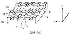
도 1은 US 2013/0015487에 더 상세하게 기술되는, 반도체 발광 디바이스로부터의 광 추출 효율성을 개선시키도록 설계된 기판을 예시한다. 사파이어 기판(10) 상에서, 제1 방향으로(x-축을 따라) 연장되는 복수의 홈들(11)이 병렬 스트라이프 패턴으로 형성된다. 나머지 홈이 없는(ungrooved) 표면은 기판의 최상부 표면(10a)이다. 각각의 홈(11)의 폭은 y-축 방향으로 1.5㎛이고, y-축 방향으로 홈이 없는 부분(10a)의 각각의 스트라이프의 폭은 y-축 방향으로 1.5㎛이다. 각각의 홈(11)의 깊이는 0.1㎛이다. 각각의 홈(11)의 깊이는 100Å 내지 3㎛의 범위 내에 있을 수 있다.1 illustrates a substrate designed to improve the efficiency of light extraction from a semiconductor light emitting device, described in more detail in US 2013/0015487. On the
복수의 SiO2 유전성 스트라이프들(15)이 홈들(11)의 바닥 표면들 및 측면들 상에, 그리고 사파이어 기판(10)의 표면(10a) 상에 병렬로 형성된다. 각각의 유전성 스트라이프(15)는 제2 방향(y-축 방향)으로 연장된다. 각각의 유전성 스트라이프(15)의 폭은 x-축 방향으로 1.5㎛이다. 각각의 유전성 스트라이프(15)의 두께는 100Å 내지 1㎛의 범위 내에 있을 수 있다. 도 1에 도시된 구성을 가지는 사파이어 기판(10) 상에, 10 nm의 필름 두께를 가지는 알루미늄 질화물(AlN) 버퍼층이 퇴적된다. 버퍼층(도 1에 미도시됨)은 홈들(11)의 바닥면들(11a) 및 측면들(11b), 표면(10a), 및 유전성 스트라이프들(15)의 최상부 표면들(15a) 및 측면들(15b) 위에 형성된다.A plurality of SiO2
개선된 추출을 가지는 발광 디바이스를 제공하는 것이 발명의 목적이다.It is an object of the invention to provide a light emitting device with improved extraction.
발명의 실시예들에 따른 조명 디바이스는 기판의 표면으로부터 연장되는 복수의 홀들을 가지는 기판을 포함한다. 비-III-질화물 재료가 복수의 홀들 내에 배치된다. 기판의 표면에는 비-III-질화물 재료가 없다. 반도체 구조체가 기판의 표면 상에 성장된다. 반도체 구조체는 n-타입 영역과 p-타입 영역 사이에 배치되는 발광층을 포함한다.A lighting device according to embodiments of the invention includes a substrate having a plurality of holes extending from a surface of the substrate. A non-III-nitride material is disposed within the plurality of holes. The surface of the substrate is free of non-III-nitride material. A semiconductor structure is grown on the surface of the substrate. The semiconductor structure includes a light emitting layer disposed between an n-type region and a p-type region.
하기의 논의에서, 기판은 사파이어이지만, 사파이어, SiC, 실리콘, GaN, III-질화물, 또는 복합 기판들과 같은 임의의 적절한 기판 재료가 사용될 수 있다. 일부 실시예들에서, 기판은 기판 상에 성장된 III-질화물 재료의 굴절률보다 더 작은 굴절률을 가진다. 예를 들어, 사파이어는 1.7의 굴절률을 가지는 반면, GaN은 2.4의 굴절률을 가진다.In the discussion below, the substrate is sapphire, although any suitable substrate material may be used, such as sapphire, SiC, silicon, GaN, III-nitride, or composite substrates. In some embodiments, the substrate has a refractive index that is less than the refractive index of the III-nitride material grown on the substrate. For example, sapphire has a refractive index of 1.7, whereas GaN has a refractive index of 2.4.
도 1은 반도체 발광 디바이스로부터의 광 추출 효율성을 개선하기 위한 종래 기술의 기판을 예시한다.
도 2는 발명의 실시예들에 따른, 피처들을 가지는 기판의 일부분의 평면도이다.
도 3은 발명의 실시예들에 따른, 피처들을 가지는 기판의 일부분의 단면도이다.
도 4는 피처들의 표면들 상에 하나 이상의 코팅층들을 형성한 이후 도 3의 구조체의 단면도이다.
도 5는 도 4의 기판 상에 형성되는 반도체 디바이스 구조체를 예시한다.
도 6은 플립 칩 디바이스를 예시한다.1 illustrates a prior art substrate for improving light extraction efficiency from a semiconductor light emitting device.
2 is a top view of a portion of a substrate having features, in accordance with embodiments of the invention.
3 is a cross-sectional view of a portion of a substrate having features, in accordance with embodiments of the invention.
4 is a cross-sectional view of the structure of FIG. 3 after forming one or more coating layers on surfaces of the features.
5 illustrates a semiconductor device structure formed on the substrate of FIG. 4 .
6 illustrates a flip chip device.
반도체 발광 디바이스 구조체가 도 1에 예시된 기판 상에 형성될 수 있다. 매끄러운 기판을 가지는 디바이스에서, 기판과 반도체 재료 사이에 도파관이 형성된다. 기판과 반도체 재료의 상이한 굴절률들로 인해, 도파관은 디바이스 내에 광을 가둔다. 도 1의 기판을 가지는 디바이스에서, 기판 상의 홈들(11) 및 유전성 스트라이프들(15)은 도파관을 차단하고(interrupt), 이에 의해 디바이스로부터의 광 추출을 개선시킬 수 있다. 기판의 방향에서 방출되는 광은 홈들(11) 및/또는 유전성 스트라이프들(15)에 의해 산란될 수 있고, 따라서 광이 디바이스로부터 추출될 가능성이 더 크다.A semiconductor light emitting device structure may be formed on the substrate illustrated in FIG. 1 . In devices having a smooth substrate, a waveguide is formed between the substrate and the semiconductor material. Due to the different refractive indices of the substrate and semiconductor material, the waveguide traps light within the device. In the device having the substrate of FIG. 1 , the
도 1에 예시된 구조체에서, 유전성 스트라이프들(15)은 평탄한 표면들(홈들(11)과 홈들(11)의 바닥면들(11a) 사이의 표면들(10a)) 및 평탄하지 않은 표면들(홈들(11)의 수직 측벽들(11b)) 모두 상에 형성된다. 평탄한 표면들 상의 유전성 재료는 광 추출에 대해 최소의 영향을 가지는데, 이는 기판 상에 성장되는 반도체 디바이스 구조체의 결정 성장 품질을 손상시킬 수 있다.In the structure illustrated in FIG. 1 , the
발명의 일부 실시예들에서, 피처들은 기판 상에 형성되고, 기판 상의 반도체 디바이스 구조체의 에피텍셜 성장 이전에, 하나 이상의 반사-방지, 산란 및/또는 구배 지수 코팅층들로 코팅된다. 하나 이상의 코팅층들은 기판 표면에 형성되는 피처들을 완전히 또는 부분적으로 채울 수 있다. 피처들 및 코팅층(들)의 주요 기능은 두 가지일 수 있다: (i) III-질화물 재료로부터 기판까지의 광의 투과를 증가시키고, (ii) 디바이스로부터의 파-필드 방출(far-field emission)을 조정하도록 광의 방향을 제어한다.In some embodiments of the invention, features are formed on a substrate and coated with one or more anti-reflective, scattering and/or gradient index coating layers prior to epitaxial growth of the semiconductor device structure on the substrate. The one or more coating layers may completely or partially fill the features formed on the substrate surface. The main function of the features and coating layer(s) can be two: (i) increase the transmission of light from the III-nitride material to the substrate, and (ii) far-field emission from the device. control the direction of the light to adjust the
코팅층(들)은 성장 동안 III-질화물 재료의 핵생성에 크게 기여하지 않는 기판의 표면 영역들로 제한된다. 이러한 영역들은 일반적으로 기판의 평면에 대해(x 및 y 축으로 기술되며 z축에 직교하는 평면에 대해) 형성되는 피처들의 기울어진 그리고/또는 수직 영역들이다. 기판의 평탄하지 않은 표면들 상에 유전체 층들과 같은 비-III-질화물 코팅층들을 형성하는 것은 기판 상의 결정 성장에 크게 영향을 주지는 않지만, 디바이스로부터의 광 추출을 향상시킬 수 있다.The coating layer(s) is limited to surface regions of the substrate that do not significantly contribute to the nucleation of the III-nitride material during growth. These regions are generally inclined and/or perpendicular regions of features formed with respect to the plane of the substrate (relative to a plane orthogonal to the z-axis and described in the x and y axes). Forming non-III-nitride coating layers, such as dielectric layers, on non-planar surfaces of a substrate does not significantly affect crystal growth on the substrate, but can enhance light extraction from the device.
하기의 예들에서 반도체 발광 디바이스들이 블루 또는 UV 광을 방출하는 III-질화물 LED들이지만, 레이저 다이오드들과 같은 LED들 이외의 반도체 발광 디바이스들 및 다른 III-V 재료들, III-인화물, III-비화물, II-VI 재료들, ZnO, 또는 Si-기반 재료들과 같은 다른 재료 시스템들로 만들어진 반도체 발광 디바이스들이 사용될 수 있다.In the examples below the semiconductor light emitting devices are III-nitride LEDs emitting blue or UV light, but semiconductor light emitting devices other than LEDs such as laser diodes and other III-V materials, III-phosphide, III-ratio Semiconductor light emitting devices made of other material systems such as cargo, II-VI materials, ZnO, or Si-based materials may be used.
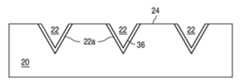
도 2는 발명의 실시예들에 따른 피처들(22)을 포함하는 기판(20)의 일부분의 평면도이다.2 is a top view of a portion of a
도 2에 예시된 피처들(22)은 기판의 최상부 표면으로부터 하향으로 연장되는 기판(20) 내에 형성되는 홀들이다. 홀들은 기판의 전체 두께를 통해 연장되지는 않는다. 홀들은 예를 들어, 수직 측면들 및 평탄한 바닥들을 가지는 홀들, 기울어진 측면들 및 평탄한 바닥들을 가지는 홀들, 절단된 역피라미드들, 절단된 역원뿔들, 역피라미드들, 역원뿔들을 포함하는 임의의 적절한 형상, 또는 임의의 다른 적절한 형상일 수 있다. 홀들은 일부 실시예들에서, 기판의 최상부 표면에 대해 직교하는 축 또는 다른 축을 따라 회전 대칭(rotationally symmetric)일 수 있지만, 이것이 요구되지는 않는다. 홀들은 예를 들어, 삼각, 정사각, 육각과 같은 어레이, 또는 임의의 다른 적절한 어레이, 랜덤 배열, 또는 아르키메데스 격자(Archimedean lattice)와 같은 준-랜덤 배열을 포함하는, 임의의 적절한 패턴으로 배열될 수 있다.The
홀들은 에칭, 드릴링과 같은 기계적 기법들, 또는 임의의 다른 적절한 기법에 의해 형성될 수 있다. 예를 들어, 인산 또는 황산의 화학적 배스 내에서, 홀들은 습식 화학적 에칭에 의해, 또는 유도적으로 커플링된 플라즈마(ICP) 에처 내에서 건식 에칭 기법들에 의해 형성될 수 있다.The holes may be formed by etching, mechanical techniques such as drilling, or any other suitable technique. For example, in a chemical bath of phosphoric acid or sulfuric acid, the holes may be formed by wet chemical etching, or by dry etching techniques in an inductively coupled plasma (ICP) etcher.
도 3은 통상적인 피처들(22)을 포함하는 기판(20)의 일부분의 단면도이다. 도 1의 x 및 y축에 의해 형성되는, 기판의 평면은, 예를 들어, 도 3에 예시된 구조체의 최상부 또는 바닥이다. 도 3에 예시된 피처들(22)의 실시예는 각각의 홀의 축이 기판의 평면에 대해 직교로 배향되는 역삼각 단면을 가진다. 피처들은 임의의 적절한 단면을 가질 수 있다. 예를 들어, 피처들은 평탄한 바닥들 또는 둥근 바닥들을 가질 수 있다. 피처들은 수직 측면들, 기울어진 측면들, 구부러진 측면들, 또는 상이한 세그먼트들이 상이한 기울기들 및/또는 형상들을 가지는 분절된 측면들을 가질 수 있다. 일부 실시예들에서, 피처들의 기울어진 측면들은 발광층들의 최대 각 방출의 방향에 대해 직교하거나 또는 거의 직교한다. 예를 들어, 발광층들에 의해 방출되는 광이 디바이스의 주요 평면에 대한 법선으로부터 60도에서 로브(lobe) 최댓값들을 가지는 패턴으로 방출되는 경우, 피처들의 기울어진 측벽들은 디바이스의 주요 평면에 대한 법선으로부터 30도 각도로 배향될 수 있다.3 is a cross-sectional view of a portion of a
도 3에 예시된 바와 같이, 기판(20)의 최상부 표면(24)이 피처들(22) 사이에서 평탄할 수 있지만, 이것이 요구되지는 않는다. 예를 들어, 최상부 표면(24)은 패터닝되거나, 거칠어지거나, 텍스처링(textured)될 수 있거나, 또는 홀들의 배향에 대해 기울어질 수 있다.As illustrated in FIG. 3 , the
홀들은, 홀들의 전부의 또는 대부분의 축들이 기판의 평면에 대해 직교하도록 배향될 수 있다. 대안적으로, 홀들의 전부의 또는 대부분의 축들이 기판의 평면에 대해 각을 이룰 수 있거나, 또는 홀들의 축들이 랜덤으로 배향될 수 있다.The holes may be oriented such that all or most axes of the holes are orthogonal to the plane of the substrate. Alternatively, all or most axes of the holes may be angled relative to the plane of the substrate, or the axes of the holes may be oriented randomly.
기판(20)은 일부 실시예들에서 적어도 100㎛, 일부 실시예들에서 500㎛ 이하, 일부 실시예들에서 적어도 200㎛, 및 일부 실시예들에서 400㎛ 이하의 두께(34)를 가질 수 있다.The
피처(22)의 개구에서, 기판의 최상부 에지에서, 피처들(22)은 일부 실시예들에서 적어도 1㎛, 일부 실시예들에서 20㎛ 이하, 일부 실시예들에서 적어도 5㎛, 및 일부 실시예들에서 15㎛ 이하의 폭(26)을 가질 수 있다. 피처들(22)은 일부 실시예들에서 적어도 1㎛, 일부 실시예들에서 20㎛ 이하, 일부 실시예들에서 적어도 5㎛, 및 일부 실시예들에서 15㎛ 이하의 깊이를 가질 수 있다. 가장 가까운 이웃 피처들 사이의 간격(32)은 일부 실시예들에서 적어도 2㎛, 일부 실시예들에서 50㎛ 이하, 일부 실시예들에서 적어도 20㎛, 및 일부 실시예들에서 40㎛ 이하일 수 있다. 이웃 피처들(22) 사이의 기판(20)의 최상부 표면(24)의 폭(28)은 일부 실시예들에서 적어도 100 nm, 일부 실시예들에서 50㎛ 이하, 일부 실시예들에서 적어도 5㎛, 및 일부 실시예들에서 25㎛ 이하일 수 있다. 도 3에 예시된 바와 같이, 홀들은 기판의 전체 두께를 투과하지 않는다. 대안적으로, 홀들의 일부 또는 전부는 기판의 전체 두께를 투과할 수 있다.At the opening of
도 4는 피처들(22) 및 하나 이상의 코팅층을 가지는 기판을 예시한다. 코팅층(36)은 피처들(22)의 기울어진 측벽들(22a) 상에만 형성된다. 본 기술분야에 공지된 바와 같이, 코팅층(36)은 종래의 포토마스킹 프로세스들에 의해서만 형성될 수 있다. 예를 들어, 기판이 마스킹되고, 이후 코팅층이 형성되고, 이후 마스크가 제거될 수 있고; 코팅층이 형성되고, 이후 마스킹 및 에칭에 의해 패터닝될 수 있고; 또는 코팅층이 피처들의 측벽들 상에만 선택적으로 형성될 수 있다. 피처들(22) 사이의 기판(20)의 최상부의, 종종 평탄한 표면들(24)은 변형되지 않은(즉, 코팅층(36)에 의해 커버되지 않은) 채 남아서 하기에 기술되는 III-질화물 디바이스 구조체의 에피텍셜 성장 동안 결정화 프로세스의 정확한 핵생성을 보장할 수 있다. III-질화물 결정은 코팅층(36) 위의 기판 표면(24) 상에 우선적으로 핵생성할 것이기 때문에, 피처들(22)의 측벽들(22a)은 에피텍셜 성장 동안 III-질화물 결정의 핵생성에 크게 기여하지 않는다.4 illustrates a
코팅층(들)(36)은 에피텍셜 프로세스와 호환가능한 임의의 적절한 재료들을 포함할 수 있다. 적절한 재료들의 예들은 비-III-질화물 재료들, 유전성 재료들, 증착과 같은 에피텍셜 성장이 아닌 기법들에 의해 형성되는 재료들, SiN, SiO2, TiO2, 산화물들 및 질화물들을 포함한다. 코팅층(들)(36)의 굴절률은 일부 실시예들에서 기판의 굴절률과 GaN의 굴절률 사이에 있을 수 있다(예를 들어, 1.5 내지 2.5의 범위의 굴절률을 가지는 층들을 형성하기 위해, SiN 및 SiO2와 TiO2의 합성물들 등등).The coating layer(s) 36 may include any suitable materials compatible with the epitaxial process. Examples of suitable materials include non-III-nitride materials, dielectric materials, materials formed by techniques other than epitaxial growth such as deposition, SiN, SiO2 , TiO2 , oxides and nitrides. The refractive index of the coating layer(s) 36 may in some embodiments be between the refractive index of the substrate and the refractive index of GaN (eg, to form layers having a refractive index in the range of 1.5 to 2.5, SiN and SiO2 and TiO2 compounds, etc.).
다수의 코팅층들(36)이 사용될 수 있다. 층들의 적절한 조합들은 III-질화물 재료로부터 기판으로의 광 투과의 증가, 또는 특정 각 방향으로의 방출된 광의 지향, 또는 둘 모두의 의도된 효과들을 증폭시키도록 선택될 수 있다. 다수의 코팅층들은 반사방지 코팅(antireflector coating)의 원리에 기초하여, 또는 높은 지수로부터 낮은 지수로 광을 매끄럽게 트랜지션하도록 구배 지수 재료를 에뮬레이팅(emulating)함으로써 선택될 수 있다. 일부 실시예들에서, 기판에 가장 가까우며 통상적으로 기판과 접촉하는 코팅층(첫번째로 퇴적된 코팅층)의 굴절률은 가장 낮은 굴절률, 즉, 기판의 굴절률에 가장 가까운 굴절률을 가진다. 기판으로부터 가장 먼 코팅층(마지막으로 퇴적된 코팅층)은 가장 높은 굴절률, 즉, III-질화물 층들의 굴절률에 가장 가까운 굴절률을 가진다. 따라서, 일부 실시예들에서의 코팅층들의 스택은 III-질화물 재료와 기판 사이에 구배 지수(GRIN) 광학 인터페이스를 형성할 수 있다.Multiple coating layers 36 may be used. Appropriate combinations of layers may be selected to amplify the intended effects of increasing light transmission from the III-nitride material to the substrate, or directing the emitted light in a particular angular direction, or both. The multiple coating layers may be selected based on the principle of an antireflector coating, or by emulating a gradient index material to smoothly transition light from a high index to a low index. In some embodiments, the refractive index of the coating layer closest to the substrate and normally in contact with the substrate (the first deposited coating layer) has the lowest refractive index, ie, the refractive index closest to that of the substrate. The coating layer furthest from the substrate (the coating layer deposited last) has the highest refractive index, ie, the refractive index closest to that of the III-nitride layers. Accordingly, the stack of coating layers in some embodiments may form a gradient index (GRIN) optical interface between the III-nitride material and the substrate.
일 실시예에서, 코팅층(36)은 홀들의 깊이의 적어도 20%, 홀들의 깊이의 50%까지를 채우는 SiN의 단일층이다. 예를 들어, 2㎛ 깊이인 홀들의 경우, 코팅층(36)은 1㎛까지의 두께를 가질 수 있다.In one embodiment, the
코팅층(들)(36)은 피처들(22)을 부분적으로 또는 완전히 채울 수 있다. 특히, 일부 실시예들에서, 코팅층들(36)은 코팅층들(36)의 최상부 표면이 피처들 사이의 기판의 최상부 표면(24)과 같은 높이를 이루도록 피처들(22)을 채울 수 있다. 피처들(22)을 채우는 것은 비-핵발생 표면들을 최소화시킨다.The coating layer(s) 36 may partially or completely fill the
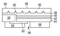
도 5에 예시된 바와 같이, 코팅층(들)(36)을 형성한 이후, 반도체 디바이스 구조체가 성장한다. 반도체 구조체는 n- 및 p-타입 영역들 사이에 끼인 발광 또는 활성 영역을 포함한다.As illustrated in FIG. 5 , after forming the coating layer(s) 36 , the semiconductor device structure is grown. The semiconductor structure includes a light emitting or active region sandwiched between n- and p-type regions.
n-타입 영역(38)이 먼저 성장될 수 있고, 예를 들어, 버퍼층들 또는 핵생성 층들과 같은 준비층들, 콘택트 층들, 및 구속층들을 포함하는, 상이한 조성들 및 도펀트 농도의 다수의 층들을 포함할 수 있으며, 이는 발광 영역이 광을 효율적으로 방출하기에 바람직한 특정의 광학, 재료, 또는 전기적 특성들에 대해 설계된, n-타입 또는 의도적으로 도핑되지 않은, 그리고 n- 또는 심지어 p-타입 디바이스 층들일 수 있다.An n-
n-타입 영역의 제1 부분은 피처들을 채우고 합쳐서 디바이스 층들을 성장시키기에 충분히 높은 품질의 표면을 형성할 수 있다. n-타입 영역의 이러한 부분은 일부 실시예들에서 적어도 2㎛ 두께이고, 일부 실시예들에서 5㎛ 이하의 두께일 수 있다. 초기에 성장된 III-질화물 재료는, 피처들(22)의 코팅층들(36) 상이 아닌, 피처들 사이의 기판의 최상부 표면(24) 상에 우선적으로 핵생성한다.The first portion of the n-type region can fill and coalesce features to form a surface of high enough quality to grow device layers. This portion of the n-type region may be at least 2 μm thick in some embodiments, and less than or equal to 5 μm thick in some embodiments. The initially grown III-nitride material preferentially nucleates on the
발광 또는 활성 영역(40)은 n-타입 영역 위에 성장된다. 적절한 발광 영역들의 예들은 단일의 두꺼운 또는 얇은 발광층, 또는 장벽층들에 의해 분리된 다수의 얇은 또는 두꺼운 발광층들을 포함하는 다중 양자 우물 발광 영역을 포함한다.A light emitting or
p-타입 영역(42)은 이후 발광 영역 위에 성장될 수 있다. n-타입 영역과 마찬가지로, p-타입 영역은 의도적으로 도핑되지 않은 층들, 또는 n-타입 층들을 포함하는, 상이한 조성, 두께 및 도펀트 농도의 다수의 층들을 포함할 수 있다.A p-
성장 이후, p-콘택트(44)는 p-타입 영역의 표면 상에 형성된다. p-콘택트(44)는 반사성 금속 및 반사성 금속의 일렉트로마이그레이션(electromigration)을 방지하거나 감소시킬 수 있는 가드 금속과 같은 다수의 전도성 층들을 종종 포함한다. 반사성 금속은 종종 은이지만, 임의의 적절한 재료 또는 재료들이 사용될 수 있다.After growth, a p-
도 5는 디바이스 내에서의 광의 행동을 예시한다. 광선(46a)과 같이, 조각(glancing angle)들에서 기판(20)의 표면(24)을 때리는 광은 기판과 III-질화물 재료 사이의 도파관에 의해 완전히 내부적으로 반사되어, 광선(46b)에 의해 예시된 바와 같이, 디바이스 내에 광을 가둘 수 있다. 광선들(22)은 도파관을 차단하고, 따라서, 광선(48)과 같이, 조각들에서 피처들(22) 내로 방출되는 광은 반도체 재료로부터 추출된다. 표면(24)에 의해 반사되는 일부 광선들은 콘택트(44)에 의해 다시 반사되고 나서, 피처(22) 상에 입사되는데, 여기서, 광선은 궁극적으로 반도체 재료로부터 추출된다. 피처들(22)의 부재시, 광은 동일한 각들에서 다수의 표면들에 의해 계속 반사되고, 광 에너지가 열로 전환될 때까지, 반도체 구조체 내에 가둬진 채 유지될 수 있다.5 illustrates the behavior of light within a device. Light striking the
도 5에 예시된 구조체는 임의의 적절한 디바이스 구조체로 형성될 수 있다. 일반적으로, 전술된 바와 같은 광 추출 피처들을 가지는 기판을 가지는 디바이스에서, 광은 주로 기판을 통해 디바이스로부터 추출되며, 이는 디바이스의 일부에 남아 있지만, 이것이 요구되지는 않는다. 플립 칩이 도 6에 예시되지만, 도 5의 구조체는 임의의 적절한 디바이스로 형성될 수 있다.The structure illustrated in FIG. 5 may be formed of any suitable device structure. Generally, in a device having a substrate having light extraction features as described above, light is mainly extracted from the device through the substrate, which remains in a portion of the device, although this is not required. Although a flip chip is illustrated in FIG. 6 , the structure of FIG. 5 may be formed into any suitable device.
도 6에 예시된 바와 같이, p-콘택트(44)를 형성한 이후, p-콘택트(44)의 일부분, p-타입 영역(42) 및 활성 영역(40)을 제거하여, n-콘택트(50)가 형성되는 n-타입 영역(38)의 일부분을 노출시킨다. n- 및 p-콘택트들(50 및 44)은 실리콘의 산화물과 같은 유전체(52) 또는 임의의 다른 적절한 재료로 채워질 수 있는 갭에 의해 서로 전기적으로 격리된다. 다수의 n-콘택트 비아들이 형성될 수 있고; n- 및 p-콘택트들(50 및 44)은 도 6에 예시된 배열에 제한되지 않는다. 본 기술분야에 공지된 바와 같이, n- 및 p-콘택트들은 재분배되어 유전체/금속 스택을 가지는 결합 패드들(도 6에 도시되지 않음)을 형성할 수 있다.As illustrated in FIG. 6 , after forming the p-
디바이스에 대한 전기적 접속들을 형성하기 위해, 하나 이상의 상호접속들(54 및 56)은 n- 및 p-콘택트들(50 및 44) 상에 형성되거나 이들에 전기적으로 접속된다. 상호접속(54)은 도 6에서의 n-콘택트(50)에 전기적으로 접속된다. 상호접속(56)은 p-콘택트(44)에 전기적으로 접속된다. 상호접속들(54 및 56)은 n- 및 p-콘택트들(50 및 44)로부터 그리고 유전체 층(52) 및 갭(58)에 의해 서로 전기적으로 격리된다. 상호접속들(54 및 56)은, 예를 들어, 땜납, 스터드 범프들, 또는 임의의 다른 적절한 구조체일 수 있다.One or
많은 개별 LED들은 이후 디바이스들의 웨이퍼로부터 다이싱되는 단일 기판층 상에 형성된다. 다이싱 이전, 다이싱 동안, 또는 다이싱 이후, 기판(20)은 얇아질 수 있다. 일부 실시예들에서, 씨닝(thinning)에 추가로 또는 씨닝 대신에, 기판(20)의 후방측 표면(60)이 패터닝되거나, 텍스처링되거나, 거칠어져서, 기판으로부터 주변 공기로의 광 추출을 개선한다.Many individual LEDs are formed on a single substrate layer that is then diced from the wafer of devices. Before, during, or after dicing, the
도 6에 예시된 디바이스는, 예를 들어, 측 상에 약 1 mm 길이일 수 있다. 따라서, 단일 디바이스의 기판은 일부 실시예들에서 수십 또는 수백 개의 피처들을 포함할 수 있다. 일 예에서, 기판 영역의 3㎛×3㎛ 부분마다 평균 1개 내지 2개의 피처가 존재할 수 있다.The device illustrated in FIG. 6 may be, for example, about 1 mm long on the side. Thus, the substrate of a single device may include tens or hundreds of features in some embodiments. In one example, there may be an average of 1-2 features for every 3 μm×3 μm portion of the substrate area.
발명을 상세히 기술하였지만, 본 기술분야의 통상의 기술자는, 본 개시내용이 주어지면, 본원에 기술된 발명 개념의 사상으로부터 벗어나지 않고 발명에 대해 수정들이 이루어질 수 있음을 인지할 것이다. 따라서, 발명의 범위가 예시되고 기술된 특정 실시예들에 제한되도록 의도되지 않는다.Although the invention has been described in detail, those skilled in the art will recognize that, given this disclosure, modifications may be made to the invention without departing from the spirit of the inventive concept described herein. Accordingly, it is not intended that the scope of the invention be limited to the specific embodiments illustrated and described.
Claims (15)
Translated fromKorean복수의 홀(hole)들을 포함하는 기판 ― 상기 홀들은 상기 기판의 표면으로부터 연장됨 ― ;
상기 복수의 홀들 내에 배치되는 비-III-질화물(non-III-nitride) 재료 ― 상기 기판의 표면에는 상기 비-III-질화물 재료가 없음 ― ; 및
상기 기판의 표면 상에서 성장하는 반도체 구조체 ― 상기 반도체 구조체는 n-타입 층과 p-타입 층 사이에 배치되는 발광층을 포함함 ―
를 포함하며,
상기 홀들은 상기 비-III-질화물 재료에 의해 부분적으로 채워지고,
상기 반도체 구조체의 n-타입 층의 제1 부분이 상기 홀들을 채우고,
상기 비-III-질화물 재료는 상기 반도체 구조체와 상기 기판 사이에 구배 지수 광학 인터페이스(gradient index optical interface)를 형성하는 층들의 스택(a stack of layers)이고,
상기 구배 지수 광학 인터페이스는 높은 굴절률로부터 낮은 굴절률로 트랜지션하고,
상기 층들의 스택 중 상기 기판에 가장 가까운 층이 가장 낮은 굴절률을 갖는, 조명 디바이스.A lighting device comprising:
a substrate comprising a plurality of holes, the holes extending from a surface of the substrate;
a non-III-nitride material disposed within the plurality of holes, the surface of the substrate free of the non-III-nitride material; and
a semiconductor structure growing on a surface of the substrate, wherein the semiconductor structure comprises a light emitting layer disposed between an n-type layer and a p-type layer;
includes,
the holes are partially filled by the non-III-nitride material,
a first portion of the n-type layer of the semiconductor structure fills the holes;
wherein the non-III-nitride material is a stack of layers forming a gradient index optical interface between the semiconductor structure and the substrate;
the gradient index optical interface transitions from a high index of refraction to a low index of refraction;
wherein the layer of the stack of layers closest to the substrate has the lowest index of refraction.
상기 기판은 사파이어 기판이고,
상기 기판의 표면은 평탄하고,
상기 홀들은 상기 기판의 평탄한 표면에 대해 기울어진 측벽들을 포함하고,
상기 비-III-질화물 재료는 상기 기판의 평탄한 표면 상이 아닌 상기 기울어진 측벽들 상에 배치되는 유전성 재료인, 조명 디바이스.The method of claim 1,
The substrate is a sapphire substrate,
The surface of the substrate is flat,
the holes include sidewalls that are inclined with respect to the flat surface of the substrate;
wherein the non-III-nitride material is a dielectric material disposed on the inclined sidewalls rather than on a planar surface of the substrate.
Applications Claiming Priority (3)
| Application Number | Priority Date | Filing Date | Title |
|---|---|---|---|
| US201462005003P | 2014-05-30 | 2014-05-30 | |
| US62/005,003 | 2014-05-30 | ||
| PCT/IB2015/053639WO2015181671A1 (en) | 2014-05-30 | 2015-05-18 | Light-emitting device with patterned substrate |
Publications (2)
| Publication Number | Publication Date |
|---|---|
| KR20170012469A KR20170012469A (en) | 2017-02-02 |
| KR102352661B1true KR102352661B1 (en) | 2022-01-18 |
Family
ID=53476936
Family Applications (1)
| Application Number | Title | Priority Date | Filing Date |
|---|---|---|---|
| KR1020167036862AActiveKR102352661B1 (en) | 2014-05-30 | 2015-05-18 | Light-emitting device with patterned substrate |
Country Status (7)
| Country | Link |
|---|---|
| US (1) | US10355168B2 (en) |
| EP (1) | EP3149781B1 (en) |
| JP (1) | JP6764791B2 (en) |
| KR (1) | KR102352661B1 (en) |
| CN (1) | CN106463574B (en) |
| TW (1) | TWI661576B (en) |
| WO (1) | WO2015181671A1 (en) |
Families Citing this family (14)
| Publication number | Priority date | Publication date | Assignee | Title |
|---|---|---|---|---|
| US20190229230A1 (en) | 2016-05-02 | 2019-07-25 | Sang Jeong An | Template for growing group iii-nitride semiconductor layer, group iii-nitride semiconductor light emitting device, and manufacturing method therefor |
| US10270032B2 (en) | 2017-09-13 | 2019-04-23 | Int Tech Co., Ltd. | Light source and a manufacturing method therewith |
| US20190198709A1 (en) | 2017-12-22 | 2019-06-27 | Lumileds Llc | Iii-nitride multi-color on wafer micro-led enabled by tunnel junctions |
| US12132151B2 (en)* | 2019-06-27 | 2024-10-29 | Lumileds Llc | Nanocone arrays for enhancing light outcoupling and package efficiency |
| US12408481B2 (en) | 2019-12-19 | 2025-09-02 | Lumileds Llc | Light emitting diode (LED) devices with nucleation layer |
| US11211527B2 (en) | 2019-12-19 | 2021-12-28 | Lumileds Llc | Light emitting diode (LED) devices with high density textures |
| US11264530B2 (en) | 2019-12-19 | 2022-03-01 | Lumileds Llc | Light emitting diode (LED) devices with nucleation layer |
| US11289630B2 (en) | 2019-12-20 | 2022-03-29 | Lumileds Llc | Tunable lighting system with preferred color rendering |
| CN111244239B (en)* | 2020-01-19 | 2021-03-23 | 湘能华磊光电股份有限公司 | LED patterned substrate and preparation method thereof |
| CN112652687A (en)* | 2020-12-22 | 2021-04-13 | 至芯半导体(杭州)有限公司 | Composite substrate and manufacturing method thereof |
| US12419140B2 (en)* | 2021-05-17 | 2025-09-16 | Seoul Viosys Co., Ltd. | UV light emitting diode |
| CN114784161B (en)* | 2022-02-24 | 2024-12-03 | 京东方华灿光电(浙江)有限公司 | Sapphire substrate, light-emitting diode chip and method for preparing substrate |
| CN114843379B (en)* | 2022-05-25 | 2025-07-22 | 江苏第三代半导体研究院有限公司 | Light-emitting diode structure based on patterned nitride single crystal substrate and preparation method thereof |
| CN114759126B (en)* | 2022-06-13 | 2022-09-20 | 江苏第三代半导体研究院有限公司 | Semiconductor device structure based on nitride single crystal substrate and preparation method thereof |
Citations (1)
| Publication number | Priority date | Publication date | Assignee | Title |
|---|---|---|---|---|
| CN103022291A (en)* | 2011-09-24 | 2013-04-03 | 山东浪潮华光光电子有限公司 | Patterned substrate equipped with omnibearing reflector and preparation method thereof |
Family Cites Families (30)
| Publication number | Priority date | Publication date | Assignee | Title |
|---|---|---|---|---|
| EP2234142A1 (en)* | 1997-04-11 | 2010-09-29 | Nichia Corporation | Nitride semiconductor substrate |
| US6015979A (en)* | 1997-08-29 | 2000-01-18 | Kabushiki Kaisha Toshiba | Nitride-based semiconductor element and method for manufacturing the same |
| KR100700993B1 (en)* | 1999-12-03 | 2007-03-30 | 크리, 인코포레이티드 | Light emitting diode having improved light extraction structure and manufacturing method thereof |
| JP2001168028A (en)* | 1999-12-03 | 2001-06-22 | Sony Corp | Method for producing nitride-based III-V compound crystal, method for producing nitride-based III-V compound crystal substrate, method for producing nitride-based III-V compound crystal film, and device |
| JP2001176805A (en)* | 1999-12-16 | 2001-06-29 | Sony Corp | Method for manufacturing crystal of nitride-based iii-v- group compound. nitride-based iii-v-group crystal substrate, nitride-based iii-v-group compound crystal film, and method for manufacturing device |
| US6841808B2 (en)* | 2000-06-23 | 2005-01-11 | Toyoda Gosei Co., Ltd. | Group III nitride compound semiconductor device and method for producing the same |
| CN1284250C (en)* | 2001-03-21 | 2006-11-08 | 三菱电线工业株式会社 | Semiconductor light emitting element |
| JP2004153090A (en)* | 2002-10-31 | 2004-05-27 | Toyoda Gosei Co Ltd | Group III nitride compound semiconductor light emitting device and method of manufacturing the same |
| US7071494B2 (en) | 2002-12-11 | 2006-07-04 | Lumileds Lighting U.S. Llc | Light emitting device with enhanced optical scattering |
| WO2004086579A1 (en)* | 2003-03-25 | 2004-10-07 | Matsushita Electric Industrial Co., Ltd. | Nitride semiconductor device and its manufacturing method |
| WO2005018008A1 (en)* | 2003-08-19 | 2005-02-24 | Nichia Corporation | Semiconductor device |
| US7560294B2 (en)* | 2004-06-07 | 2009-07-14 | Toyoda Gosei Co., Ltd. | Light emitting element and method of making same |
| KR100649494B1 (en)* | 2004-08-17 | 2006-11-24 | 삼성전기주식회사 | LED manufacturing method for surface-treating light emitting diode substrate using laser and light emitting diode manufactured by this method |
| US20060204865A1 (en)* | 2005-03-08 | 2006-09-14 | Luminus Devices, Inc. | Patterned light-emitting devices |
| JP2006324331A (en)* | 2005-05-17 | 2006-11-30 | Sony Corp | Light emitting diode and its manufacturing method, integrated light emitting diode and its manufacturing method, growing method of nitride- based group iii-v compound semiconductor, nitride-based group iii-v compound semiconductor growing substrate, light emitting diode backlight, light emitting diode lighting apparatus, light emitting diode display, and electronic equipment |
| TWI288491B (en)* | 2006-03-02 | 2007-10-11 | Nat Univ Chung Hsing | High extraction efficiency of solid-state light emitting device |
| JP4613947B2 (en)* | 2007-12-07 | 2011-01-19 | ソニー株式会社 | Illumination device, color conversion element, and display device |
| US8030666B2 (en)* | 2008-04-16 | 2011-10-04 | Taiwan Semiconductor Manufacturing Company, Ltd. | Group-III nitride epitaxial layer on silicon substrate |
| KR101020961B1 (en)* | 2008-05-02 | 2011-03-09 | 엘지이노텍 주식회사 | Semiconductor light emitting device and fabrication method thereof |
| KR101631599B1 (en)* | 2009-12-02 | 2016-06-27 | 삼성전자주식회사 | Light Emitting Device and method for manufacturing the same |
| KR101034085B1 (en)* | 2009-12-10 | 2011-05-13 | 엘지이노텍 주식회사 | Light emitting device and manufacturing method |
| JP5273081B2 (en)* | 2010-03-30 | 2013-08-28 | 豊田合成株式会社 | Semiconductor light emitting device |
| US8618564B2 (en) | 2010-10-05 | 2013-12-31 | Tsmc Solid State Lighting Ltd. | High efficiency light emitting diodes |
| CN102117869B (en)* | 2011-01-21 | 2013-12-11 | 厦门市三安光电科技有限公司 | Method for stripping substrate of LED |
| KR20130094483A (en) | 2012-02-16 | 2013-08-26 | 서울옵토디바이스주식회사 | Light emitting diode chip and metho for fabricatng the same |
| EP3361517B1 (en)* | 2011-09-16 | 2021-06-23 | Seoul Viosys Co., Ltd. | Light emitting diode |
| US20130087763A1 (en)* | 2011-10-06 | 2013-04-11 | Electronics And Telecommunications Research Institute | Light emitting diode and method of manufacturing the same |
| KR20130099574A (en)* | 2012-02-29 | 2013-09-06 | 서울옵토디바이스주식회사 | Light emitting diode having gallium nitride substrate |
| CN104221170B (en)* | 2012-03-19 | 2017-02-22 | 首尔伟傲世有限公司 | Method for separating epitaxial layer and growth substrate and semiconductor device using same |
| KR20130117474A (en)* | 2012-04-18 | 2013-10-28 | 서울바이오시스 주식회사 | Light emitting diode including substrate having patterns on the back side and fabrication method for the same |
- 2015
- 2015-05-18KRKR1020167036862Apatent/KR102352661B1/enactiveActive
- 2015-05-18USUS15/314,400patent/US10355168B2/enactiveActive
- 2015-05-18JPJP2016569667Apatent/JP6764791B2/enactiveActive
- 2015-05-18CNCN201580028825.7Apatent/CN106463574B/enactiveActive
- 2015-05-18WOPCT/IB2015/053639patent/WO2015181671A1/enactiveApplication Filing
- 2015-05-18EPEP15730850.3Apatent/EP3149781B1/enactiveActive
- 2015-05-27TWTW104117033Apatent/TWI661576B/enactive
Patent Citations (1)
| Publication number | Priority date | Publication date | Assignee | Title |
|---|---|---|---|---|
| CN103022291A (en)* | 2011-09-24 | 2013-04-03 | 山东浪潮华光光电子有限公司 | Patterned substrate equipped with omnibearing reflector and preparation method thereof |
Also Published As
| Publication number | Publication date |
|---|---|
| TW201611335A (en) | 2016-03-16 |
| KR20170012469A (en) | 2017-02-02 |
| US20170104130A1 (en) | 2017-04-13 |
| WO2015181671A1 (en) | 2015-12-03 |
| JP6764791B2 (en) | 2020-10-07 |
| CN106463574B (en) | 2019-10-25 |
| CN106463574A (en) | 2017-02-22 |
| EP3149781A1 (en) | 2017-04-05 |
| US10355168B2 (en) | 2019-07-16 |
| EP3149781B1 (en) | 2020-09-30 |
| TWI661576B (en) | 2019-06-01 |
| JP2017517152A (en) | 2017-06-22 |
Similar Documents
| Publication | Publication Date | Title |
|---|---|---|
| KR102352661B1 (en) | Light-emitting device with patterned substrate | |
| US11038082B2 (en) | Method of separating light emitting devices formed on a substrate wafer | |
| KR102245056B1 (en) | Top emitting semiconductor light emitting device | |
| US8390010B2 (en) | Solid state lighting devices with cellular arrays and associated methods of manufacturing | |
| CN102097561B (en) | Semi-conductor light emitting device and method for manufacturing thereof | |
| US20150129915A1 (en) | Light-emitting diode provided with substrate having pattern on rear side thereof, and method for manufacturing same | |
| US20130045556A1 (en) | Light-Emitting Devices with Textured Active Layer | |
| CN110416377B (en) | Light emitting element | |
| CN102903814A (en) | Method for manufacturing semiconductor light emitting device | |
| KR20090076163A (en) | Nitride semiconductor light emitting device manufacturing method and nitride semiconductor light emitting device manufactured thereby | |
| US9306120B2 (en) | High efficiency light emitting diode | |
| KR102289345B1 (en) | Light emitting diode with structured substrate | |
| KR102307081B1 (en) | Semiconductor light emitting device with shaped substrate and method of manufacturing the same | |
| JP7428564B2 (en) | semiconductor light emitting device | |
| US9130114B2 (en) | Vertical light emitting diode (VLED) dice having confinement layers with roughened surfaces and methods of fabrication | |
| KR20240024292A (en) | Method for manufacturing a radiation-emitting semiconductor chip, and a radiation-emitting semiconductor chip |
Legal Events
| Date | Code | Title | Description |
|---|---|---|---|
| PA0105 | International application | Patent event date:20161229 Patent event code:PA01051R01D Comment text:International Patent Application | |
| PG1501 | Laying open of application | ||
| PN2301 | Change of applicant | Patent event date:20180214 Comment text:Notification of Change of Applicant Patent event code:PN23011R01D | |
| A201 | Request for examination | ||
| PA0201 | Request for examination | Patent event code:PA02012R01D Patent event date:20200518 Comment text:Request for Examination of Application | |
| E902 | Notification of reason for refusal | ||
| PE0902 | Notice of grounds for rejection | Comment text:Notification of reason for refusal Patent event date:20210330 Patent event code:PE09021S01D | |
| E701 | Decision to grant or registration of patent right | ||
| PE0701 | Decision of registration | Patent event code:PE07011S01D Comment text:Decision to Grant Registration Patent event date:20211028 | |
| GRNT | Written decision to grant | ||
| PR0701 | Registration of establishment | Comment text:Registration of Establishment Patent event date:20220113 Patent event code:PR07011E01D | |
| PR1002 | Payment of registration fee | Payment date:20220114 End annual number:3 Start annual number:1 | |
| PG1601 | Publication of registration | ||
| PR1001 | Payment of annual fee | Payment date:20241231 Start annual number:4 End annual number:4 |