KR102350503B1 - Photodefinable alignment layer for chemical assisted patterning - Google Patents
Photodefinable alignment layer for chemical assisted patterningDownload PDFInfo
- Publication number
- KR102350503B1 KR102350503B1KR1020177014242AKR20177014242AKR102350503B1KR 102350503 B1KR102350503 B1KR 102350503B1KR 1020177014242 AKR1020177014242 AKR 1020177014242AKR 20177014242 AKR20177014242 AKR 20177014242AKR 102350503 B1KR102350503 B1KR 102350503B1
- Authority
- KR
- South Korea
- Prior art keywords
- hardmask
- layer
- polymer
- regions
- resist
- Prior art date
- Legal status (The legal status is an assumption and is not a legal conclusion. Google has not performed a legal analysis and makes no representation as to the accuracy of the status listed.)
- Active
Links
- 238000000059patterningMethods0.000titleabstractdescription64
- 239000000126substanceSubstances0.000titledescription11
- 239000000463materialSubstances0.000claimsabstractdescription147
- 239000002253acidSubstances0.000claimsabstractdescription25
- 238000000034methodMethods0.000claimsdescription136
- 229920000642polymerPolymers0.000claimsdescription128
- 229920001400block copolymerPolymers0.000claimsdescription81
- WGTYBPLFGIVFAS-UHFFFAOYSA-Mtetramethylammonium hydroxideChemical group[OH-].C[N+](C)(C)CWGTYBPLFGIVFAS-UHFFFAOYSA-M0.000claimsdescription34
- 229920003229poly(methyl methacrylate)Polymers0.000claimsdescription27
- 239000004926polymethyl methacrylateSubstances0.000claimsdescription27
- 229920002120photoresistant polymerPolymers0.000claimsdescription24
- ZMXDDKWLCZADIW-UHFFFAOYSA-NN,N-DimethylformamideChemical compoundCN(C)C=OZMXDDKWLCZADIW-UHFFFAOYSA-N0.000claimsdescription19
- 238000000137annealingMethods0.000claimsdescription17
- 239000002904solventSubstances0.000claimsdescription15
- IAZDPXIOMUYVGZ-UHFFFAOYSA-NDimethylsulphoxideChemical compoundCS(C)=OIAZDPXIOMUYVGZ-UHFFFAOYSA-N0.000claimsdescription13
- CSCPPACGZOOCGX-UHFFFAOYSA-NAcetoneChemical groupCC(C)=OCSCPPACGZOOCGX-UHFFFAOYSA-N0.000claimsdescription12
- 238000004381surface treatmentMethods0.000claimsdescription10
- 238000005530etchingMethods0.000claimsdescription8
- 239000003795chemical substances by applicationSubstances0.000claimsdescription7
- 239000003960organic solventSubstances0.000claimsdescription5
- 239000003880polar aprotic solventSubstances0.000claimsdescription4
- 150000007522mineralic acidsChemical class0.000claimsdescription3
- 150000007524organic acidsChemical class0.000claimsdescription3
- 238000013459approachMethods0.000abstractdescription41
- 239000010410layerSubstances0.000description278
- 229910052751metalInorganic materials0.000description94
- 239000002184metalSubstances0.000description94
- 230000008569processEffects0.000description71
- 239000000758substrateSubstances0.000description49
- 239000004065semiconductorSubstances0.000description37
- 238000001900extreme ultraviolet lithographyMethods0.000description25
- 238000004519manufacturing processMethods0.000description22
- XUIMIQQOPSSXEZ-UHFFFAOYSA-NSiliconChemical compound[Si]XUIMIQQOPSSXEZ-UHFFFAOYSA-N0.000description20
- 239000010408filmSubstances0.000description20
- 239000011295pitchSubstances0.000description20
- 229910052710siliconInorganic materials0.000description20
- 239000010703siliconSubstances0.000description20
- 238000002408directed self-assemblyMethods0.000description19
- 238000012545processingMethods0.000description18
- 239000011229interlayerSubstances0.000description17
- -1but not limited toSubstances0.000description15
- 238000004891communicationMethods0.000description15
- 230000015572biosynthetic processEffects0.000description14
- 238000001459lithographyMethods0.000description14
- 239000000178monomerSubstances0.000description13
- 239000004793PolystyreneSubstances0.000description12
- 238000000151depositionMethods0.000description12
- 238000011161developmentMethods0.000description10
- 238000001338self-assemblyMethods0.000description10
- 238000000926separation methodMethods0.000description10
- 239000010953base metalSubstances0.000description9
- 238000000576coating methodMethods0.000description9
- 230000008021depositionEffects0.000description9
- 239000003989dielectric materialSubstances0.000description9
- VYPSYNLAJGMNEJ-UHFFFAOYSA-NSilicium dioxideChemical compoundO=[Si]=OVYPSYNLAJGMNEJ-UHFFFAOYSA-N0.000description8
- 239000004205dimethyl polysiloxaneSubstances0.000description8
- 238000002955isolationMethods0.000description8
- 229920000435poly(dimethylsiloxane)Polymers0.000description8
- 229920000747poly(lactic acid)Polymers0.000description8
- 229910052581Si3N4Inorganic materials0.000description7
- 238000005229chemical vapour depositionMethods0.000description7
- 230000004048modificationEffects0.000description7
- 238000012986modificationMethods0.000description7
- HQVNEWCFYHHQES-UHFFFAOYSA-Nsilicon nitrideChemical compoundN12[Si]34N5[Si]62N3[Si]51N64HQVNEWCFYHHQES-UHFFFAOYSA-N0.000description7
- 239000011248coating agentSubstances0.000description6
- 238000005516engineering processMethods0.000description6
- 238000001465metallisationMethods0.000description6
- 150000002739metalsChemical class0.000description6
- 230000008707rearrangementEffects0.000description6
- 230000002829reductive effectEffects0.000description6
- XLYOFNOQVPJJNP-UHFFFAOYSA-NwaterSubstancesOXLYOFNOQVPJJNP-UHFFFAOYSA-N0.000description6
- 238000006243chemical reactionMethods0.000description5
- 238000007306functionalization reactionMethods0.000description5
- 230000002209hydrophobic effectEffects0.000description5
- 229920002125Sokalan®Polymers0.000description4
- 229910052732germaniumInorganic materials0.000description4
- GNPVGFCGXDBREM-UHFFFAOYSA-Ngermanium atomChemical compound[Ge]GNPVGFCGXDBREM-UHFFFAOYSA-N0.000description4
- 238000004377microelectronicMethods0.000description4
- 238000005191phase separationMethods0.000description4
- 238000004987plasma desorption mass spectroscopyMethods0.000description4
- 229910021420polycrystalline siliconInorganic materials0.000description4
- 230000005855radiationEffects0.000description4
- 239000000377silicon dioxideSubstances0.000description4
- 235000012239silicon dioxideNutrition0.000description4
- 238000004528spin coatingMethods0.000description4
- OKTJSMMVPCPJKN-UHFFFAOYSA-NCarbonChemical compound[C]OKTJSMMVPCPJKN-UHFFFAOYSA-N0.000description3
- RYGMFSIKBFXOCR-UHFFFAOYSA-NCopperChemical compound[Cu]RYGMFSIKBFXOCR-UHFFFAOYSA-N0.000description3
- 229910045601alloyInorganic materials0.000description3
- 239000000956alloySubstances0.000description3
- QVGXLLKOCUKJST-UHFFFAOYSA-Natomic oxygenChemical compound[O]QVGXLLKOCUKJST-UHFFFAOYSA-N0.000description3
- 230000004888barrier functionEffects0.000description3
- 229910052799carbonInorganic materials0.000description3
- 229920001577copolymerPolymers0.000description3
- 229910052802copperInorganic materials0.000description3
- 239000010949copperSubstances0.000description3
- 238000004132cross linkingMethods0.000description3
- 238000010511deprotection reactionMethods0.000description3
- 238000013461designMethods0.000description3
- 229920000359diblock copolymerPolymers0.000description3
- 238000010438heat treatmentMethods0.000description3
- 239000003446ligandSubstances0.000description3
- 239000002086nanomaterialSubstances0.000description3
- 229910052760oxygenInorganic materials0.000description3
- 239000001301oxygenSubstances0.000description3
- 230000000737periodic effectEffects0.000description3
- 238000005240physical vapour depositionMethods0.000description3
- 229920002223polystyrenePolymers0.000description3
- 230000000717retained effectEffects0.000description3
- 230000002441reversible effectEffects0.000description3
- 125000006850spacer groupChemical group0.000description3
- 238000012546transferMethods0.000description3
- RBMHUYBJIYNRLY-UHFFFAOYSA-N2-[(1-carboxy-1-hydroxyethyl)-hydroxyphosphoryl]-2-hydroxypropanoic acidChemical compoundOC(=O)C(O)(C)P(O)(=O)C(C)(O)C(O)=ORBMHUYBJIYNRLY-UHFFFAOYSA-N0.000description2
- 229910005540GaPInorganic materials0.000description2
- PXHVJJICTQNCMI-UHFFFAOYSA-NNickelChemical compound[Ni]PXHVJJICTQNCMI-UHFFFAOYSA-N0.000description2
- NBIIXXVUZAFLBC-UHFFFAOYSA-NPhosphoric acidChemical compoundOP(O)(O)=ONBIIXXVUZAFLBC-UHFFFAOYSA-N0.000description2
- 229920003171Poly (ethylene oxide)Polymers0.000description2
- XWCMFHPRATWWFO-UHFFFAOYSA-N[O-2].[Ta+5].[Sc+3].[O-2].[O-2].[O-2]Chemical compound[O-2].[Ta+5].[Sc+3].[O-2].[O-2].[O-2]XWCMFHPRATWWFO-UHFFFAOYSA-N0.000description2
- 230000002378acidificating effectEffects0.000description2
- 229910021417amorphous siliconInorganic materials0.000description2
- 230000008901benefitEffects0.000description2
- 239000003990capacitorSubstances0.000description2
- 230000003197catalytic effectEffects0.000description2
- 230000008859changeEffects0.000description2
- 239000002800charge carrierSubstances0.000description2
- 239000004020conductorSubstances0.000description2
- 238000000280densificationMethods0.000description2
- 238000009792diffusion processMethods0.000description2
- 239000002019doping agentSubstances0.000description2
- 230000000694effectsEffects0.000description2
- 239000003822epoxy resinSubstances0.000description2
- HZXMRANICFIONG-UHFFFAOYSA-Ngallium phosphideChemical compound[Ga]#PHZXMRANICFIONG-UHFFFAOYSA-N0.000description2
- 229910052735hafniumInorganic materials0.000description2
- VBJZVLUMGGDVMO-UHFFFAOYSA-Nhafnium atomChemical compound[Hf]VBJZVLUMGGDVMO-UHFFFAOYSA-N0.000description2
- 229910000449hafnium oxideInorganic materials0.000description2
- WIHZLLGSGQNAGK-UHFFFAOYSA-Nhafnium(4+);oxygen(2-)Chemical compound[O-2].[O-2].[Hf+4]WIHZLLGSGQNAGK-UHFFFAOYSA-N0.000description2
- 229920001519homopolymerPolymers0.000description2
- XLYOFNOQVPJJNP-UHFFFAOYSA-MhydroxideChemical compound[OH-]XLYOFNOQVPJJNP-UHFFFAOYSA-M0.000description2
- 238000007654immersionMethods0.000description2
- 230000006872improvementEffects0.000description2
- WPYVAWXEWQSOGY-UHFFFAOYSA-Nindium antimonideChemical compound[Sb]#[In]WPYVAWXEWQSOGY-UHFFFAOYSA-N0.000description2
- 239000012212insulatorSubstances0.000description2
- MRELNEQAGSRDBK-UHFFFAOYSA-Nlanthanum(3+);oxygen(2-)Chemical compound[O-2].[O-2].[O-2].[La+3].[La+3]MRELNEQAGSRDBK-UHFFFAOYSA-N0.000description2
- JQJCSZOEVBFDKO-UHFFFAOYSA-Nlead zincChemical compound[Zn].[Pb]JQJCSZOEVBFDKO-UHFFFAOYSA-N0.000description2
- 230000007246mechanismEffects0.000description2
- 229910001092metal group alloyInorganic materials0.000description2
- 239000002105nanoparticleSubstances0.000description2
- 150000004767nitridesChemical class0.000description2
- 239000003921oilSubstances0.000description2
- TWNQGVIAIRXVLR-UHFFFAOYSA-Noxo(oxoalumanyloxy)alumaneChemical compoundO=[Al]O[Al]=OTWNQGVIAIRXVLR-UHFFFAOYSA-N0.000description2
- 229920003228poly(4-vinyl pyridine)Polymers0.000description2
- 229920001434poly(D-lactide)Polymers0.000description2
- 229920000647polyepoxidePolymers0.000description2
- 238000002360preparation methodMethods0.000description2
- 238000011112process operationMethods0.000description2
- 230000009467reductionEffects0.000description2
- 238000005204segregationMethods0.000description2
- 238000000935solvent evaporationMethods0.000description2
- 239000010409thin filmSubstances0.000description2
- 229920000428triblock copolymerPolymers0.000description2
- 235000001674Agaricus brunnescensNutrition0.000description1
- JBRZTFJDHDCESZ-UHFFFAOYSA-NAsGaChemical compound[As]#[Ga]JBRZTFJDHDCESZ-UHFFFAOYSA-N0.000description1
- 229910000952Be alloyInorganic materials0.000description1
- ZOXJGFHDIHLPTG-UHFFFAOYSA-NBoronChemical compound[B]ZOXJGFHDIHLPTG-UHFFFAOYSA-N0.000description1
- LFQSCWFLJHTTHZ-UHFFFAOYSA-NEthanolChemical compoundCCOLFQSCWFLJHTTHZ-UHFFFAOYSA-N0.000description1
- 229910002601GaNInorganic materials0.000description1
- 229910001218Gallium arsenideInorganic materials0.000description1
- 229910000530Gallium indium arsenideInorganic materials0.000description1
- JMASRVWKEDWRBT-UHFFFAOYSA-NGallium nitrideChemical compound[Ga]#NJMASRVWKEDWRBT-UHFFFAOYSA-N0.000description1
- GPXJNWSHGFTCBW-UHFFFAOYSA-NIndium phosphideChemical compound[In]#PGPXJNWSHGFTCBW-UHFFFAOYSA-N0.000description1
- BPQQTUXANYXVAA-UHFFFAOYSA-NOrthosilicateChemical compound[O-][Si]([O-])([O-])[O-]BPQQTUXANYXVAA-UHFFFAOYSA-N0.000description1
- CBENFWSGALASAD-UHFFFAOYSA-NOzoneChemical compound[O-][O+]=OCBENFWSGALASAD-UHFFFAOYSA-N0.000description1
- ABLZXFCXXLZCGV-UHFFFAOYSA-NPhosphorous acidChemical compoundOP(O)=OABLZXFCXXLZCGV-UHFFFAOYSA-N0.000description1
- OAICVXFJPJFONN-UHFFFAOYSA-NPhosphorusChemical compound[P]OAICVXFJPJFONN-UHFFFAOYSA-N0.000description1
- 239000004642PolyimideSubstances0.000description1
- BUGBHKTXTAQXES-UHFFFAOYSA-NSeleniumChemical compound[Se]BUGBHKTXTAQXES-UHFFFAOYSA-N0.000description1
- 229910004298SiO 2Inorganic materials0.000description1
- NINIDFKCEFEMDL-UHFFFAOYSA-NSulfurChemical compound[S]NINIDFKCEFEMDL-UHFFFAOYSA-N0.000description1
- RTAQQCXQSZGOHL-UHFFFAOYSA-NTitaniumChemical compound[Ti]RTAQQCXQSZGOHL-UHFFFAOYSA-N0.000description1
- NRTOMJZYCJJWKI-UHFFFAOYSA-NTitanium nitrideChemical compound[Ti]#NNRTOMJZYCJJWKI-UHFFFAOYSA-N0.000description1
- KXNLCSXBJCPWGL-UHFFFAOYSA-N[Ga].[As].[In]Chemical compound[Ga].[As].[In]KXNLCSXBJCPWGL-UHFFFAOYSA-N0.000description1
- 238000002835absorbanceMethods0.000description1
- 239000002250absorbentSubstances0.000description1
- 230000002745absorbentEffects0.000description1
- 239000000654additiveSubstances0.000description1
- 230000004075alterationEffects0.000description1
- FTWRSWRBSVXQPI-UHFFFAOYSA-Nalumanylidynearsane;gallanylidynearsaneChemical compound[As]#[Al].[As]#[Ga]FTWRSWRBSVXQPI-UHFFFAOYSA-N0.000description1
- 229910000147aluminium phosphateInorganic materials0.000description1
- 238000003491arrayMethods0.000description1
- 229910052785arsenicInorganic materials0.000description1
- RQNWIZPPADIBDY-UHFFFAOYSA-Narsenic atomChemical compound[As]RQNWIZPPADIBDY-UHFFFAOYSA-N0.000description1
- 238000004380ashingMethods0.000description1
- 229910052454barium strontium titanateInorganic materials0.000description1
- 229910002113barium titanateInorganic materials0.000description1
- JRPBQTZRNDNNOP-UHFFFAOYSA-Nbarium titanateChemical compound[Ba+2].[Ba+2].[O-][Ti]([O-])([O-])[O-]JRPBQTZRNDNNOP-UHFFFAOYSA-N0.000description1
- 230000009286beneficial effectEffects0.000description1
- 229910052796boronInorganic materials0.000description1
- 239000003575carbonaceous materialSubstances0.000description1
- 150000001732carboxylic acid derivativesChemical class0.000description1
- 150000001735carboxylic acidsChemical class0.000description1
- 238000005266castingMethods0.000description1
- 230000015556catabolic processEffects0.000description1
- 230000001413cellular effectEffects0.000description1
- 229910010293ceramic materialInorganic materials0.000description1
- 238000003776cleavage reactionMethods0.000description1
- 229910017052cobaltInorganic materials0.000description1
- 239000010941cobaltSubstances0.000description1
- GUTLYIVDDKVIGB-UHFFFAOYSA-Ncobalt atomChemical compound[Co]GUTLYIVDDKVIGB-UHFFFAOYSA-N0.000description1
- 238000007796conventional methodMethods0.000description1
- 238000012937correctionMethods0.000description1
- 239000013078crystalSubstances0.000description1
- 229910021419crystalline siliconInorganic materials0.000description1
- 230000007547defectEffects0.000description1
- 238000006731degradation reactionMethods0.000description1
- 238000004090dissolutionMethods0.000description1
- 238000001312dry etchingMethods0.000description1
- 238000001035dryingMethods0.000description1
- 230000009977dual effectEffects0.000description1
- 239000007772electrode materialSubstances0.000description1
- 230000005670electromagnetic radiationEffects0.000description1
- 238000010894electron beam technologyMethods0.000description1
- 238000010931ester hydrolysisMethods0.000description1
- 239000011152fibreglassSubstances0.000description1
- 238000011049fillingMethods0.000description1
- 230000009969flowable effectEffects0.000description1
- 239000012634fragmentSubstances0.000description1
- 230000006870functionEffects0.000description1
- 239000007789gasSubstances0.000description1
- 238000000671immersion lithographyMethods0.000description1
- 239000012535impuritySubstances0.000description1
- 238000010348incorporationMethods0.000description1
- 229910052738indiumInorganic materials0.000description1
- APFVFJFRJDLVQX-UHFFFAOYSA-Nindium atomChemical compound[In]APFVFJFRJDLVQX-UHFFFAOYSA-N0.000description1
- 239000002198insoluble materialSubstances0.000description1
- 239000011810insulating materialSubstances0.000description1
- 230000010354integrationEffects0.000description1
- 230000000670limiting effectEffects0.000description1
- 230000007774longtermEffects0.000description1
- 230000000873masking effectEffects0.000description1
- 239000011159matrix materialSubstances0.000description1
- 229910044991metal oxideInorganic materials0.000description1
- 150000004706metal oxidesChemical class0.000description1
- 239000000203mixtureSubstances0.000description1
- 229910021421monocrystalline siliconInorganic materials0.000description1
- 230000007935neutral effectEffects0.000description1
- 229910052759nickelInorganic materials0.000description1
- 230000003287optical effectEffects0.000description1
- 239000013110organic ligandSubstances0.000description1
- 230000003647oxidationEffects0.000description1
- 238000007254oxidation reactionMethods0.000description1
- SIWVEOZUMHYXCS-UHFFFAOYSA-Noxo(oxoyttriooxy)yttriumChemical compoundO=[Y]O[Y]=OSIWVEOZUMHYXCS-UHFFFAOYSA-N0.000description1
- BPUBBGLMJRNUCC-UHFFFAOYSA-Noxygen(2-);tantalum(5+)Chemical compound[O-2].[O-2].[O-2].[O-2].[O-2].[Ta+5].[Ta+5]BPUBBGLMJRNUCC-UHFFFAOYSA-N0.000description1
- RVTZCBVAJQQJTK-UHFFFAOYSA-Noxygen(2-);zirconium(4+)Chemical compound[O-2].[O-2].[Zr+4]RVTZCBVAJQQJTK-UHFFFAOYSA-N0.000description1
- 150000003009phosphonic acidsChemical class0.000description1
- 229910052698phosphorusInorganic materials0.000description1
- 239000011574phosphorusSubstances0.000description1
- 238000001020plasma etchingMethods0.000description1
- 238000005498polishingMethods0.000description1
- 229920001721polyimidePolymers0.000description1
- 229920005591polysiliconPolymers0.000description1
- 230000001681protective effectEffects0.000description1
- 239000011241protective layerSubstances0.000description1
- 230000005588protonationEffects0.000description1
- 239000000376reactantSubstances0.000description1
- 238000011946reduction processMethods0.000description1
- 239000011347resinSubstances0.000description1
- 229920005989resinPolymers0.000description1
- 230000007017scissionEffects0.000description1
- 229910052711seleniumInorganic materials0.000description1
- 239000011669seleniumSubstances0.000description1
- 239000013545self-assembled monolayerSubstances0.000description1
- 150000004819silanolsChemical class0.000description1
- 229910021332silicideInorganic materials0.000description1
- FVBUAEGBCNSCDD-UHFFFAOYSA-Nsilicide(4-)Chemical compound[Si-4]FVBUAEGBCNSCDD-UHFFFAOYSA-N0.000description1
- 239000007787solidSubstances0.000description1
- 230000007928solubilizationEffects0.000description1
- 238000005063solubilizationMethods0.000description1
- 239000002195soluble materialSubstances0.000description1
- 239000007921spraySubstances0.000description1
- 238000003860storageMethods0.000description1
- VEALVRVVWBQVSL-UHFFFAOYSA-Nstrontium titanateChemical compound[Sr+2].[O-][Ti]([O-])=OVEALVRVVWBQVSL-UHFFFAOYSA-N0.000description1
- 229910052717sulfurInorganic materials0.000description1
- 239000011593sulfurSubstances0.000description1
- 229910001936tantalum oxideInorganic materials0.000description1
- 229910052714telluriumInorganic materials0.000description1
- PORWMNRCUJJQNO-UHFFFAOYSA-Ntellurium atomChemical compound[Te]PORWMNRCUJJQNO-UHFFFAOYSA-N0.000description1
- 150000003573thiolsChemical class0.000description1
- 239000010936titaniumSubstances0.000description1
- 229910052719titaniumInorganic materials0.000description1
- 229910021524transition metal nanoparticleInorganic materials0.000description1
- WFKWXMTUELFFGS-UHFFFAOYSA-NtungstenChemical compound[W]WFKWXMTUELFFGS-UHFFFAOYSA-N0.000description1
- 229910052721tungstenInorganic materials0.000description1
- 239000010937tungstenSubstances0.000description1
- 238000001039wet etchingMethods0.000description1
- 229910001928zirconium oxideInorganic materials0.000description1
- GFQYVLUOOAAOGM-UHFFFAOYSA-Nzirconium(iv) silicateChemical compound[Zr+4].[O-][Si]([O-])([O-])[O-]GFQYVLUOOAAOGM-UHFFFAOYSA-N0.000description1
Images


Classifications
- H—ELECTRICITY
- H01—ELECTRIC ELEMENTS
- H01L—SEMICONDUCTOR DEVICES NOT COVERED BY CLASS H10
- H01L21/00—Processes or apparatus adapted for the manufacture or treatment of semiconductor or solid state devices or of parts thereof
- H01L21/02—Manufacture or treatment of semiconductor devices or of parts thereof
- H01L21/027—Making masks on semiconductor bodies for further photolithographic processing not provided for in group H01L21/18 or H01L21/34
- H01L21/0271—Making masks on semiconductor bodies for further photolithographic processing not provided for in group H01L21/18 or H01L21/34 comprising organic layers
- G—PHYSICS
- G03—PHOTOGRAPHY; CINEMATOGRAPHY; ANALOGOUS TECHNIQUES USING WAVES OTHER THAN OPTICAL WAVES; ELECTROGRAPHY; HOLOGRAPHY
- G03F—PHOTOMECHANICAL PRODUCTION OF TEXTURED OR PATTERNED SURFACES, e.g. FOR PRINTING, FOR PROCESSING OF SEMICONDUCTOR DEVICES; MATERIALS THEREFOR; ORIGINALS THEREFOR; APPARATUS SPECIALLY ADAPTED THEREFOR
- G03F7/00—Photomechanical, e.g. photolithographic, production of textured or patterned surfaces, e.g. printing surfaces; Materials therefor, e.g. comprising photoresists; Apparatus specially adapted therefor
- G03F7/0035—Multiple processes, e.g. applying a further resist layer on an already in a previously step, processed pattern or textured surface
- G—PHYSICS
- G03—PHOTOGRAPHY; CINEMATOGRAPHY; ANALOGOUS TECHNIQUES USING WAVES OTHER THAN OPTICAL WAVES; ELECTROGRAPHY; HOLOGRAPHY
- G03F—PHOTOMECHANICAL PRODUCTION OF TEXTURED OR PATTERNED SURFACES, e.g. FOR PRINTING, FOR PROCESSING OF SEMICONDUCTOR DEVICES; MATERIALS THEREFOR; ORIGINALS THEREFOR; APPARATUS SPECIALLY ADAPTED THEREFOR
- G03F7/00—Photomechanical, e.g. photolithographic, production of textured or patterned surfaces, e.g. printing surfaces; Materials therefor, e.g. comprising photoresists; Apparatus specially adapted therefor
- G03F7/004—Photosensitive materials
- G03F7/09—Photosensitive materials characterised by structural details, e.g. supports, auxiliary layers
- G03F7/094—Multilayer resist systems, e.g. planarising layers
- G—PHYSICS
- G03—PHOTOGRAPHY; CINEMATOGRAPHY; ANALOGOUS TECHNIQUES USING WAVES OTHER THAN OPTICAL WAVES; ELECTROGRAPHY; HOLOGRAPHY
- G03F—PHOTOMECHANICAL PRODUCTION OF TEXTURED OR PATTERNED SURFACES, e.g. FOR PRINTING, FOR PROCESSING OF SEMICONDUCTOR DEVICES; MATERIALS THEREFOR; ORIGINALS THEREFOR; APPARATUS SPECIALLY ADAPTED THEREFOR
- G03F7/00—Photomechanical, e.g. photolithographic, production of textured or patterned surfaces, e.g. printing surfaces; Materials therefor, e.g. comprising photoresists; Apparatus specially adapted therefor
- G03F7/004—Photosensitive materials
- G03F7/09—Photosensitive materials characterised by structural details, e.g. supports, auxiliary layers
- G03F7/095—Photosensitive materials characterised by structural details, e.g. supports, auxiliary layers having more than one photosensitive layer
- G—PHYSICS
- G03—PHOTOGRAPHY; CINEMATOGRAPHY; ANALOGOUS TECHNIQUES USING WAVES OTHER THAN OPTICAL WAVES; ELECTROGRAPHY; HOLOGRAPHY
- G03F—PHOTOMECHANICAL PRODUCTION OF TEXTURED OR PATTERNED SURFACES, e.g. FOR PRINTING, FOR PROCESSING OF SEMICONDUCTOR DEVICES; MATERIALS THEREFOR; ORIGINALS THEREFOR; APPARATUS SPECIALLY ADAPTED THEREFOR
- G03F7/00—Photomechanical, e.g. photolithographic, production of textured or patterned surfaces, e.g. printing surfaces; Materials therefor, e.g. comprising photoresists; Apparatus specially adapted therefor
- G03F7/004—Photosensitive materials
- G03F7/09—Photosensitive materials characterised by structural details, e.g. supports, auxiliary layers
- G03F7/115—Photosensitive materials characterised by structural details, e.g. supports, auxiliary layers having supports or layers with means for obtaining a screen effect or for obtaining better contact in vacuum printing
- H—ELECTRICITY
- H01—ELECTRIC ELEMENTS
- H01L—SEMICONDUCTOR DEVICES NOT COVERED BY CLASS H10
- H01L21/00—Processes or apparatus adapted for the manufacture or treatment of semiconductor or solid state devices or of parts thereof
- H01L21/70—Manufacture or treatment of devices consisting of a plurality of solid state components formed in or on a common substrate or of parts thereof; Manufacture of integrated circuit devices or of parts thereof
- H01L21/71—Manufacture of specific parts of devices defined in group H01L21/70
- H01L21/768—Applying interconnections to be used for carrying current between separate components within a device comprising conductors and dielectrics
- H01L21/76801—Applying interconnections to be used for carrying current between separate components within a device comprising conductors and dielectrics characterised by the formation and the after-treatment of the dielectrics, e.g. smoothing
- H01L21/76802—Applying interconnections to be used for carrying current between separate components within a device comprising conductors and dielectrics characterised by the formation and the after-treatment of the dielectrics, e.g. smoothing by forming openings in dielectrics
- H01L21/76816—Aspects relating to the layout of the pattern or to the size of vias or trenches
- H—ELECTRICITY
- H01—ELECTRIC ELEMENTS
- H01L—SEMICONDUCTOR DEVICES NOT COVERED BY CLASS H10
- H01L21/00—Processes or apparatus adapted for the manufacture or treatment of semiconductor or solid state devices or of parts thereof
- H01L21/70—Manufacture or treatment of devices consisting of a plurality of solid state components formed in or on a common substrate or of parts thereof; Manufacture of integrated circuit devices or of parts thereof
- H01L21/71—Manufacture of specific parts of devices defined in group H01L21/70
- H01L21/768—Applying interconnections to be used for carrying current between separate components within a device comprising conductors and dielectrics
- H01L21/76897—Formation of self-aligned vias or contact plugs, i.e. involving a lithographically uncritical step
- H—ELECTRICITY
- H01—ELECTRIC ELEMENTS
- H01L—SEMICONDUCTOR DEVICES NOT COVERED BY CLASS H10
- H01L23/00—Details of semiconductor or other solid state devices
- H01L23/52—Arrangements for conducting electric current within the device in operation from one component to another, i.e. interconnections, e.g. wires, lead frames
- H01L23/522—Arrangements for conducting electric current within the device in operation from one component to another, i.e. interconnections, e.g. wires, lead frames including external interconnections consisting of a multilayer structure of conductive and insulating layers inseparably formed on the semiconductor body
- H01L23/528—Layout of the interconnection structure
- H—ELECTRICITY
- H01—ELECTRIC ELEMENTS
- H01L—SEMICONDUCTOR DEVICES NOT COVERED BY CLASS H10
- H01L2224/00—Indexing scheme for arrangements for connecting or disconnecting semiconductor or solid-state bodies and methods related thereto as covered by H01L24/00
- H01L2224/01—Means for bonding being attached to, or being formed on, the surface to be connected, e.g. chip-to-package, die-attach, "first-level" interconnects; Manufacturing methods related thereto
- H01L2224/10—Bump connectors; Manufacturing methods related thereto
- H01L2224/15—Structure, shape, material or disposition of the bump connectors after the connecting process
- H01L2224/16—Structure, shape, material or disposition of the bump connectors after the connecting process of an individual bump connector
- H01L2224/161—Disposition
- H01L2224/16151—Disposition the bump connector connecting between a semiconductor or solid-state body and an item not being a semiconductor or solid-state body, e.g. chip-to-substrate, chip-to-passive
- H01L2224/16221—Disposition the bump connector connecting between a semiconductor or solid-state body and an item not being a semiconductor or solid-state body, e.g. chip-to-substrate, chip-to-passive the body and the item being stacked
- H01L2224/16225—Disposition the bump connector connecting between a semiconductor or solid-state body and an item not being a semiconductor or solid-state body, e.g. chip-to-substrate, chip-to-passive the body and the item being stacked the item being non-metallic, e.g. insulating substrate with or without metallisation
Landscapes
- Engineering & Computer Science (AREA)
- Physics & Mathematics (AREA)
- General Physics & Mathematics (AREA)
- Microelectronics & Electronic Packaging (AREA)
- Computer Hardware Design (AREA)
- Condensed Matter Physics & Semiconductors (AREA)
- Power Engineering (AREA)
- Manufacturing & Machinery (AREA)
- Architecture (AREA)
- Structural Engineering (AREA)
- Geometry (AREA)
- Exposure And Positioning Against Photoresist Photosensitive Materials (AREA)
- Photosensitive Polymer And Photoresist Processing (AREA)
Abstract
Translated fromKoreanDescription
Translated fromKorean본 발명의 실시예들은 반도체 구조체들 및 처리, 특히, 화학적 보조 패터닝을 위한 감광성 정렬 층의 분야에 관한 것이다.Embodiments of the present invention relate to the field of semiconductor structures and processing, particularly photosensitive alignment layers for chemically assisted patterning.
지난 수십 년 동안, 집적 회로들에서의 피처들의 스케일링은 계속 성장하는 반도체 산업의 원동력이 되어 왔다. 점점 더 작은 피처들로의 스케일링은 반도체 칩들의 제한된 면적(real estate) 상에서의 기능 유닛들의 증가된 밀도를 가능하게 한다.Over the past few decades, the scaling of features in integrated circuits has been the driving force behind the ever-growing semiconductor industry. Scaling to increasingly smaller features enables increased density of functional units on the limited real estate of semiconductor chips.
제1 양상에서, 집적 회로들은 비아들 위의 금속 라인들 또는 다른 인터커넥트들을 비아들 아래의 금속 라인들 또는 다른 인터커넥트들에 전기적으로 접속하기 위한, 관련분야에서 비아들로 알려진, 전기적 도전성 마이크로전자 구조체들을 통상적으로 포함한다. 비아들은 통상적으로 리소그래피 프로세스에 의해 형성된다. 대표적으로, 포토레지스트 층이 유전체 층 위에 스핀 코팅될 수 있고, 이러한 포토레지스트 층은 패터닝된 마스크를 통해 패터닝된 화학 방사선에 노광될 수 있고, 그리고 나서 이러한 노광된 층은 포토레지스트 층에 개구를 형성하기 위해 현상될 수 있다. 다음으로, 에칭 마스크로서 포토레지스트 층에서의 개구를 사용함으로써 비아를 위한 개구가 유전체 층에 에칭될 수 있다. 이러한 개구는 비아 개구로 지칭된다. 최종적으로, 비아 개구는 하나 이상의 금속들 또는 다른 전도성 재료들로 채워져 비아를 형성할 수 있다.In a first aspect, integrated circuits are electrically conductive microelectronic structures, known in the art as vias, for electrically connecting metal lines or other interconnects above vias to metal lines or other interconnects below vias. are usually included. Vias are typically formed by a lithographic process. Representatively, a layer of photoresist may be spin coated over a dielectric layer, the layer of photoresist may be exposed to patterned actinic radiation through a patterned mask, and then the exposed layer may form an opening in the layer of photoresist. can be developed to Next, the openings for the vias can be etched into the dielectric layer by using the openings in the photoresist layer as an etch mask. These openings are referred to as via openings. Finally, the via opening may be filled with one or more metals or other conductive materials to form the via.
과거에는, 비아들의 크기들 및 간격이 점진적으로 감소되었으며, 적어도 일부 타입의 집적 회로들(예를 들어, 진보된 마이크로프로세서들, 칩셋 컴포넌트들, 그래픽 칩들 등)에 대하여, 미래에도 비아들의 크기들 및 간격이 계속해서 점진적으로 감소될 것으로 예상된다. 비아들의 크기의 하나의 척도는 비아 개구의 임계 치수(critical dimension)이다. 비아들의 간격의 하나의 척도는 비아 피치(via pitch)이다. 비아 피치는 가장 가까운 인접 비아들 사이의 중심간 거리(center-to-center distance)를 표현한다. 이러한 리소그래피 프로세스들에 의해 매우 작은 피치들을 갖는 매우 작은 비아들을 패터닝할 때, 특히, 피치들이 약 70나노미터(nm) 이하일 때 및/또는 비아 개구들의 임계 치수들이 약 35nm 이하일 때, 몇 가지 도전과제들이 발생한다.In the past, the sizes and spacing of vias have been progressively reduced, and for at least some types of integrated circuits (eg, advanced microprocessors, chipset components, graphics chips, etc.), the sizes of vias will continue to be and the interval is expected to continue to progressively decrease. One measure of the size of vias is the critical dimension of the via opening. One measure of the spacing of vias is via pitch. The via pitch represents the center-to-center distance between nearest adjacent vias. Several challenges when patterning very small vias with very small pitches by these lithography processes, particularly when pitches are about 70 nanometers (nm) or less and/or when critical dimensions of via openings are about 35 nm or less are occurring
하나의 이러한 도전과제는 비아들과 위에 놓이는 인터커넥트들 사이의 오버레이(overlay) 및 비아들과 기저 랜딩(landing) 인터커넥트들 사이의 오버레이가 일반적으로 비아 피치의 1/4 정도의 높은 허용오차들(tolerances)로 제어될 필요가 있다는 점이다. 비아 피치들이 시간이 지남에 따라 훨씬 더 작게 스케일링됨에 따라, 이러한 오버레이 허용오차들은 리소그래피 장비가 따라갈 수 있는 것보다 훨씬 더 큰 비율로 이들과 함께 스케일링되는 경향이 있다. 다른 이러한 도전과제는 비아 개구들의 임계 치수들이 일반적으로 리소그래피 스캐너들의 해상도(resolution) 성능들보다 더 빠르게 스케일링되는 경향이 있다는 점이다. 축소 기술들은 비아 개구들의 임계 치수를 축소시키기 위해 존재한다. 그러나, 축소량은, LWR(line width roughness) 및/또는 CDU(critical dimension uniformity)를 상당히 손상시키지는 않으며, 충분히 OPC(optical proximity correction) 중립적인 축소 프로세스의 성능뿐만 아니라 최소 비아 피치에 의해 제한되는 경향이 있다. 또 다른 이러한 도전과제는, 임계 치수 버짓의 동일한 전체 비율(overall fraction)을 유지하기 위해서, 비아 개구들의 임계 치수들이 감소하는 만큼 포토레지스트들의 LWR 및/또는 CDU 특성들이 일반적으로 향상될 필요가 있다는 점이다. 그러나, 현재 대부분의 포토레지스트들의 LWR 및/또는 CDU 특성들은 비아 개구들의 임계 치수들이 감소함에 따라 급속하게 향상되고 있지는 않다. 추가의 이러한 과제는, 극도로 작은 비아 피치들이 일반적으로 EUV(extreme ultraviolet) 리소그래피 스캐너들의 해상도 성능보다 작은 경향이 있다는 점이다. 결과적으로, 통상 2개, 3개 또는 더 많은 상이한 리소그래피 마스크들이 사용될 수 있고, 이는 비용들을 증가시키는 경향이 있다. 어느 시점에, 피치들이 계속 감소하면, 다수의 마스크들에도 불구하고, EUV 스캐너들을 사용하여 이러한 매우 작은 피치들을 위한 비아 개구들을 인쇄하는 것이 가능하지 않을 수 있다.One such challenge is that overlays between vias and overlying interconnects and overlays between vias and underlying landing interconnects have high tolerances, typically on the order of a quarter of the via pitch. ) needs to be controlled. As via pitches scale much smaller over time, these overlay tolerances tend to scale with them at a much larger rate than the lithographic equipment can keep up with. Another such challenge is that the critical dimensions of via openings generally tend to scale faster than the resolution capabilities of lithographic scanners. Reduction techniques exist to reduce the critical dimension of via openings. However, the reduction does not significantly compromise line width roughness (LWR) and/or critical dimension uniformity (CDU), and tends to be limited by the minimum via pitch as well as the performance of the sufficiently optical proximity correction (OPC) neutral reduction process. There is this. Another such challenge is that the LWR and/or CDU properties of photoresists generally need to be improved as the critical dimensions of via openings decrease, in order to maintain the same overall fraction of the critical dimension budget. to be. However, the LWR and/or CDU properties of most current photoresists are not improving rapidly as the critical dimensions of via openings decrease. A further such challenge is that extremely small via pitches generally tend to be less than the resolution performance of extreme ultraviolet (EUV) lithography scanners. As a result, typically two, three or more different lithography masks can be used, which tends to increase costs. At some point, if the pitches continue to decrease, it may not be possible to print via openings for these very small pitches using EUV scanners, despite multiple masks.
따라서, 비아 및 관련 상호 접속 제조 기술들의 영역에서 향상들이 요구된다.Accordingly, improvements are desired in the area of vias and related interconnect fabrication techniques.
제2 양상에서, 디바이스 치수들이 계속해서 축소됨에 따라 트라이-게이트 트랜지스터들(tri-gate transistors)와 같은 멀티-게이트 트랜지스터들이 더 보편적이 되고 있다. 종래의 프로세스들에서, 트라이-게이트 또는 다른 비-평면 트랜지스터들은 벌크 실리콘 기판들 또는 절연체 상의 실리콘(silicon-on-insulator) 기판들 상에서 일반적으로 제조된다. 일부 경우들에서는, 벌크 실리콘 기판들이 그들의 낮은 비용과 기존의 고수율 벌크 실리콘 기판 기반구조와의 호환성으로 인해 바람직하다. 그러나, 멀티-게이트 트랜지스터들을 스케일링하는 것은 부작용이 있었다. 이들 마이크로전자 회로의 기본 빌딩 블록들의 치수들이 감소되고 또한 주어진 영역 내에 제조되는 기본 빌딩 블록들의 순수 개수가 증가함에 따라, 이들 빌딩 블록들을 제조하는데 사용되는 반도체 프로세스들에 대한 제약들이 상황을 압도하게 되었다.In a second aspect, multi-gate transistors, such as tri-gate transistors, are becoming more common as device dimensions continue to shrink. In conventional processes, tri-gate or other non-planar transistors are typically fabricated on bulk silicon substrates or silicon-on-insulator substrates. In some cases, bulk silicon substrates are desirable because of their low cost and compatibility with existing high yield bulk silicon substrate infrastructures. However, scaling multi-gate transistors has a side effect. As the dimensions of the basic building blocks of these microelectronic circuits are reduced and also the net number of basic building blocks fabricated within a given area increases, the constraints on the semiconductor processes used to fabricate these building blocks have become overwhelming. .
따라서, 비-평면 트랜지스터 제조 기술들의 영역에 향상들이 요구된다.Accordingly, improvements are desired in the area of non-planar transistor fabrication techniques.
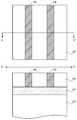
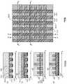
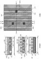
도 1a 내지 도 1f는, 본 발명의 실시예에 따라, EUVL 및 BCP 리소그래피 양자 모두를 수반하는 방법에서의 다양한 작업들의 평면도들 및 대응하는 단면도들을 도시하며,
도 1a는 기저 층 또는 기판 상에 코팅되거나 다른 방식으로 배치되는 하드마스크 층을 도시하는 평면도 및 이러한 평면도의 a-a' 축을 따라 취해진 대응하는 단면도이고;
도 1b는 도 1a의 구조체 상에 형성되는 EUVL 노광된 CAR(chemically amplified photoresist) 재료 층을 도시하는 평면도 및 이러한 평면도의 b-b' 축을 따라 취해진 대응하는 단면도이고;
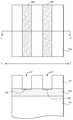
도 1c는 어닐링 프로세스 이후의 도 1b의 구조체를 도시하는 평면도 및 이러한 평면도의 c-c' 축을 따라 취해진 대응하는 단면도이고;
도 1d는 어닐링된 CAR 층의 제거 이후의 도 1c의 구조체를 도시하는 평면도 및 이러한 평면도의 d-d' 축을 따라 취해진 대응하는 단면도이고;
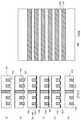
도 1e는 BCP(block co-polymer) 재료의 코팅 및 어닐링 이후의 도 1d의 구조체를 도시하는 평면도 및 이러한 평면도의 e-e' 축을 따라 취해진 대응하는 단면도이며; 그리고
도 1f는 BCP 재료의 일부의 제거 및 패터닝된 하드마스크 층을 제공하기 위한 하드마스크 층의 패터닝 이후의 도 1e의 구조체를 도시하는 평면도 및 이러한 평면도의 f-f 축을 따라 취해진 단면도이다.
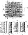
도 2a 내지 2e는, 본 발명의 실시예에 따라, EUVL 및 BCP 리소그래피 양자 모두를 수반하는 방법에서의 다양한 작업들의 평면도들 및 대응하는 단면도들을 도시하며,
도 2a는 기저 층 또는 기판 상에 코팅되거나 다른 방식으로 배치되는 하드마스크 층을 도시하는 평면도 및 이러한 평면도의 a-a' 축을 따라 취해진 대응하는 단면도이고;
도 2b는 도 2a의 구조체 상에 형성되는 EUVL CAR(chemically amplified photoresist) 재료 층을 도시하는 평면도 및 이러한 평면도의 b-b' 축을 따라 취해진 대응하는 단면도이고;
도 2c는 CAR 층의 노광된 부분들의 제거 및 하드마스크 층의 노광된 부분들의 표면 처리 이후의 도 2c의 구조체를 도시하는 평면도 및 이러한 평면도의 c-c' 축을 따라 취해진 대응하는 단면도이고;
도 2d는 BCP(block co-polymer) 재료의 코팅 및 어닐링 이후의 도 2c의 구조체를 도시하는 평면도 및 이러한 평면도의 d-d' 축을 따라 취해진 대응하는 단면도이며; 그리고
도 2e는 BCP 재료의 일부의 제거 및 패터닝된 하드마스크 층을 제공하기 위한 하드마스크 층의 패터닝 이후의 도 2d의 구조체를 도시하는 평면도 및 이러한 평면도의 e-e' 축을 따라 취해진 단면도이다.
도 3, 도 4 및 도 5는, 본 발명의 실시예에 따라, PAG(photoacid generator)를 갖는 폴리-스티렌 또는 PMMA 브러시를 포함하는 광활성 필름의 사용을 수반하는 방법에서의 다양한 작업들을 도시한다.
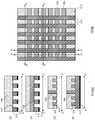
도 6a 내지 도 6l은, 본 발명의 실시예에 따라, 자체-정렬형 비아 및 금속 패터닝의 방법에서의 다양한 작업들을 나타내는 집적 회로 층들의 부분들을 도시하며,
도 6a는 이전 층 금속화 구조체에 대한 선택사항들의 평면도 및 대응하는 단면도들을 도시하고;
도 6b는 도 6a의 구조체 위의 ILD(interlayer dielectric) 라인들의 형성 이후의 도 6a의 구조체의 평면도 및 대응하는 단면도들을 도시하고;
도 6c는 모든 플러그 위치들로부터의 모든 잠재적 비아 위치들의 선택적 구별 이후의 도 6b의 구조체의 평면도 및 대응하는 단면도들을 도시하고;
도 6da은 도 6c의 기저 금속 및 ILD 라인들의 노광된 부분들에 대한 구별 중합체 추가 이후의 도 6c의 구조체의 평면도 및 대응하는 단면도들을 도시하고;
도 6db는, 본 발명의 다른 실시예에 따라, 기저 금속 및 ILD 라인들의 노광된 부분들 상의 선택적 재료 퇴적 이후의 도 6b의 구조체의 단면도를 도시하고;
도 6e는 중합체의 하나의 종의 제거 이후의 도 6da의 구조체의 평면도 및 대응하는 단면도들을 도시하고;
도 6f는 중합체의 하나의 종의 제거시 개방되는 위치들에서의 ILD 재료의 형성 이후의 도 6e의 구조체의 평면도 및 대응하는 단면도들을 도시하고;
도 6g는 비아 패터닝 이후의 도 6f의 구조체의 평면도 및 대응하는 단면도들을 도시하고;
도 6h는 비아 형성 이후의 도 6g의 구조체의 평면도 및 대응하는 단면도들을 도시하고;
도 6i는 중합체의 제2 종의 제거 및 ILD 재료로의 대체 이후의 도 6h의 구조체의 평면도 및 대응하는 단면도들을 도시하고;
도 6j는 선택된 플러그 위치들에서의 레지스트 또는 마스크의 패터닝 이후의 도 6i의 구조체의 평면도 및 대응하는 단면도들을 도시하고;
도 6k는 하드마스크 제거 및 ILD 층 리세싱 이후의 도 6j의 구조체의 평면도 및 대응하는 단면도들을 도시하고;
도 6l은 금속 라인 형성 이후의 도 6k의 구조체의 평면도 및 대응하는 단면도들을 도시한다.
도 7a는, 본 발명의 실시예에 따라, 감광성 정렬을 통해 형성되는 패터닝된 하드마스크 층을 수반하는 처리 방식을 사용하여 하나 이상의 피처들이 패터닝되는 비-평면 반도체 디바이스의 단면도를 도시한다.
도 7b는, 본 발명의 실시예에 따라, 도 7a의 반도체 디바이스의 a-a' 축을 따라 취해진 평면도를 도시한다.
도 8은 본 발명의 일 구현에 따른 컴퓨팅 디바이스를 도시한다.
도 9는 본 발명의 일 구현에 따라 형성될 수 있는 인터포저를 도시한다.1A-1F show top views and corresponding cross-sectional views of various operations in a method involving both EUVL and BCP lithography, in accordance with an embodiment of the present invention;
1A is a plan view showing a hardmask layer coated or otherwise disposed on a base layer or substrate and a corresponding cross-sectional view taken along the aa' axis of this plan view;
FIG. 1B is a plan view showing an EUVL exposed chemically amplified photoresist (CAR) material layer formed on the structure of FIG. 1A and a corresponding cross-sectional view taken along the bb′ axis of the plan view;
1C is a top view showing the structure of FIG. 1B after an annealing process and a corresponding cross-sectional view taken along the cc' axis of this top view;
1D is a top view showing the structure of FIG. 1C after removal of the annealed CAR layer and a corresponding cross-sectional view taken along the dd' axis of this top view;
1E is a plan view showing the structure of FIG. 1D after coating and annealing of a block co-polymer (BCP) material and a corresponding cross-sectional view taken along the ee' axis of this plan view; and
1F is a top view and a cross-sectional view taken along the ff axis of the structure of FIG. 1E after removal of a portion of the BCP material and patterning of the hardmask layer to provide a patterned hardmask layer.
2A-2E show top views and corresponding cross-sectional views of various operations in a method involving both EUVL and BCP lithography, in accordance with an embodiment of the present invention;
2A is a plan view showing a hardmask layer coated or otherwise disposed on a base layer or substrate and a corresponding cross-sectional view taken along the aa' axis of this plan view;
FIG. 2B is a plan view showing a layer of EUVL chemically amplified photoresist (CAR) material formed on the structure of FIG. 2A and a corresponding cross-sectional view taken along the bb′ axis of this plan view;
FIG. 2C is a plan view showing the structure of FIG. 2C after removal of exposed portions of the CAR layer and surface treatment of exposed portions of the hardmask layer and a corresponding cross-sectional view taken along the cc′ axis of this plan view;
FIG. 2D is a plan view showing the structure of FIG. 2C after coating and annealing of a block co-polymer (BCP) material and a corresponding cross-sectional view taken along the dd' axis of this plan view; and
FIG. 2E is a plan view showing the structure of FIG. 2D after removal of a portion of the BCP material and patterning of the hardmask layer to provide a patterned hardmask layer and a cross-sectional view taken along the ee′ axis of this plan view.
3, 4 and 5 illustrate various operations in a method involving the use of a photoactive film comprising a poly-styrene or PMMA brush with a photoacid generator (PAG), in accordance with an embodiment of the present invention.
6A-6L show portions of integrated circuit layers representing various operations in a method of self-aligning via and metal patterning, in accordance with an embodiment of the present invention;
6a shows a top view and corresponding cross-sectional views of options for a previous layer metallization structure;
6B shows a top view and corresponding cross-sectional views of the structure of FIG. 6A after formation of interlayer dielectric (ILD) lines over the structure of FIG. 6A ;
6C shows a top view and corresponding cross-sectional views of the structure of FIG. 6B after selective discrimination of all potential via locations from all plug locations;
6da shows a top view and corresponding cross-sectional views of the structure of FIG. 6c after distinct polymer addition to the exposed portions of the base metal and ILD lines of FIG. 6c;
6DB shows a cross-sectional view of the structure of FIG. 6B after selective material deposition on exposed portions of the base metal and ILD lines, in accordance with another embodiment of the present invention;
6E shows a top view and corresponding cross-sectional views of the structure of FIG. 6Da after removal of one species of polymer;
6F shows a top view and corresponding cross-sectional views of the structure of FIG. 6E after formation of the ILD material in positions that open upon removal of one species of polymer;
6G shows a top view and corresponding cross-sectional views of the structure of FIG. 6F after via patterning;
6H shows a top view and corresponding cross-sectional views of the structure of FIG. 6G after via formation;
6I shows a top view and corresponding cross-sectional views of the structure of FIG. 6H after removal of the second species of polymer and replacement with an ILD material;
6J shows a top view and corresponding cross-sectional views of the structure of FIG. 6I after patterning of the resist or mask at selected plug locations;
6K shows a top view and corresponding cross-sectional views of the structure of FIG. 6J after hardmask removal and ILD layer recessing;
FIG. 6L shows a top view and corresponding cross-sectional views of the structure of FIG. 6K after metal line formation;
7A illustrates a cross-sectional view of a non-planar semiconductor device in which one or more features are patterned using a processing scheme involving a patterned hardmask layer formed through photosensitive alignment, in accordance with an embodiment of the present invention.
7B illustrates a top view taken along the aa′ axis of the semiconductor device of FIG. 7A , in accordance with an embodiment of the present invention.
8 illustrates a computing device in accordance with one implementation of the present invention.
9 illustrates an interposer that may be formed in accordance with one implementation of the present invention.
화학적 보조 패터닝을 위한 감광성 정렬 층들 및 화학적 보조 패터닝을 위한 감광성 정렬 층들을 형성하는 접근방식들이 설명된다. 이하의 설명에서는 본 발명의 실시예들의 철저한 이해를 제공하기 위해 구체적인 집적 및 재료 체제들과 같은 수많은 구체적인 상세사항들이 제시된다. 본 발명의 실시예들은 이러한 구체적인 상세사항들 없이 실시될 수 있다는 점이 관련분야에서의 기술자에게 명백할 것이다. 다른 경우들에서, 집적 회로 설계 레이아웃들과 같은 공지된 피처들은 본 발명의 실시예들을 불필요하게 불명료하게 하지 않기 위해 상세하게 설명되지는 않는다. 또한, 도면들에 도시된 다양한 실시예들은 예시적인 표현이며, 반드시 정확한 비율로 그려질 필요는 없다는 점이 이해되어야 한다.Approaches for forming photosensitive alignment layers for chemically assisted patterning and photosensitive alignment layers for chemically assisted patterning are described. In the following description, numerous specific details are set forth, such as specific integrations and material regimes, in order to provide a thorough understanding of embodiments of the present invention. It will be apparent to one skilled in the art that embodiments of the present invention may be practiced without these specific details. In other instances, well-known features, such as integrated circuit design layouts, have not been described in detail in order not to unnecessarily obscure embodiments of the invention. Also, it should be understood that the various embodiments shown in the drawings are exemplary representations and are not necessarily drawn to scale.
본 명세서에 설명되는 하나 이상의 실시예들은 화학적 보조 패터닝을 위한 감광성 정렬 층의 제조 및 적용에 관한 것이다. 일부 실시예들은, 예를 들어, 임계 치수 층들에 대해 10-50 나노미터 피치 패턴들을 생성하는데 특히 적합하다. 본 명세서에 설명되는 감광성 정렬 층들은 진보된 포토레지스트 분야에서의 이점들을 제공할 수 있다. 본 명세서에 설명되는 실시예들은 현재 기술과 비교하여 감소된 비용으로 지속적인 치수적 스케일링을 가능하게 할 수 있다.One or more embodiments described herein relate to the preparation and application of a photosensitive alignment layer for chemically assisted patterning. Some embodiments are particularly suitable for creating 10-50 nanometer pitch patterns for, for example, critical dimension layers. The photosensitive alignment layers described herein may provide advantages in the advanced photoresist field. Embodiments described herein may enable continuous dimensional scaling at reduced cost compared to current technology.
정황을 제공하기 위해, 고 해상도 EUV 또는 EUVL(extreme ultraviolet lithography) 툴들은 16나노미터 이하의 치수들로 패터닝하는 성능을 보여 왔다. 이러한 치수들에서 패터닝을 위한 주요 경로는 CAR들(chemically amplified resists)의 계속적인 사용을 통한 것이다. 그러나, 현재 상용 등급 CAR들은 패턴 붕괴 및 해상도 양자 모두에 의해 제한된다(예를 들어, 종횡비, 재료 계수, 용해 특성들 및 약 8나노미터보다 큰 확산 길이로 인함). 한편, DSA(directed self-assembly)는 성공을 보여 주었지만, 제조가 어렵고 비용이 많이 드는 프리-패턴들에서만(예를 들어, Ebeam 작성자 프리-패턴들 또는 다수의 처리 작업들에 의해 생성되는 패턴들을 수반하는 에플리케이션들에 대해) 그러하였다.To provide context, high resolution EUV or extreme ultraviolet lithography (EUVL) tools have demonstrated the ability to pattern to dimensions of 16 nanometers or less. A major route for patterning in these dimensions is through the continued use of chemically amplified resists (CARs). However, current commercial grade CARs are limited by both pattern collapse and resolution (eg, due to aspect ratio, material modulus, dissolution properties, and diffusion length greater than about 8 nanometers). On the other hand, directed self-assembly (DSA) has shown success, but only in pre-patterns that are difficult and expensive to manufacture (eg, Ebeam author pre-patterns or patterns created by multiple processing operations). for applications involving them).
본 명세서에 설명되는 하나 이상의 실시예들에 따르면, EUVL의 성능들은 지향성이고 치밀한 프리-패턴들을 형성하는데 이용된다. EUVL 노광은 이러한 프리-패턴들의 제거시 선택적 상단 표면 개질을 제공하는데 추가로 이용된다. BCP들(block copolymers)의 마이크로-상 분리에 대한 자연적인 경향과 연결될 때, 패터닝 피처들이 유리하게는 어느 한 기술로 독립적으로 가능한 것을 넘어서는 정도로 소형화된다. EUVL 접근방식과 BCP들을 상 분리하는 것을 수반하는 접근방식의 조합은 개별적으로 적용되는 어느 한 기술의 관련된 단점들을 극복하도록 구현될 수 있다. 즉, EUVL 자체는 감소된 광자 흡수도 및 박막 효과들에 기인할 수 있는 패턴 붕괴/패턴 거칠기/감소된 막 두께에 시달릴 수 있다. 반면에, BCP 정렬은 화학적 또는 위상기하학적 프리-패턴이 없으면 랜덤하다.In accordance with one or more embodiments described herein, the capabilities of EUVL are used to form directional and dense pre-patterns. EUVL exposure is further used to provide selective top surface modification upon removal of these pre-patterns. When coupled with the natural tendency for micro-phase separation of block copolymers (BCPs), patterning features are advantageously miniaturized to a degree beyond what is possible independently with either technique. A combination of the EUVL approach and an approach involving phase separation of BCPs can be implemented to overcome the associated disadvantages of either technique applied individually. That is, EUVL itself may suffer from pattern collapse/pattern roughness/reduced film thickness which may be due to reduced photon absorbance and thin film effects. On the other hand, BCP alignment is random in the absence of chemical or topological pre-patterns.
추가의 정황을 제공하기 위해, 관련기술 치밀한 로직 패터닝의 현재 상태는 193nm 액침 기술에 크게 의존한다. 이러한 기술은 회절 제한들로 인해 약 80나노미터 피치의 단일 패스 최소 해상도로 제한된다. 따라서, 미래의 로직 기술들을 위한 치밀한 패터닝은 가장 까다로운 프로세스 층들을 실현하기 위해 최대 6개의 193nm 개별 마스킹 작업들을 요구할 것으로 예측된다. 이러한 멀티-패스 패터닝 방식의 구현과 관련된 도전과제들(예를 들어, 비용 및 기술)로 인해, 현재 여러 가지 대안들이 개발되고 있다. EUVL은 그러한 기술 중 하나이지만, 낮은 소스 전력 및 포토레지스트 패터닝 제한들에 의해 HVM(high volume manufacturing) 준비가 방해되고 있다. 예를 들어, 패턴 붕괴 및 높은 LWR(line width roughness)에 대한 경향이 있다. BCP의 사용은 어셈블리를 지향하기 위해 프리-패터닝을 요구하고, 따라서, 단독으로 구현될 수 없다.To provide further context, the current state of the art dense logic patterning relies heavily on 193nm immersion technology. This technique is limited to a single pass minimum resolution of about 80 nanometer pitch due to diffraction limitations. Therefore, dense patterning for future logic technologies is predicted to require up to six 193nm discrete masking operations to realize the most demanding process layers. Due to the challenges (eg, cost and technology) associated with the implementation of such a multi-pass patterning scheme, several alternatives are currently being developed. EUVL is one such technology, but high volume manufacturing (HVM) preparation is hampered by low source power and photoresist patterning limitations. For example, it tends to pattern collapse and high line width roughness (LWR). The use of BCP requires pre-patterning to direct assembly, and thus cannot be implemented alone.
본 발명의 하나 이상의 실시예들에 따르면, EUVL과 보통 관련되는 패턴 붕괴를 극복하도록 구현될 수 있는 처리 접근방식들이 설명된다. 포토레지스트가 현상되지 않고 기저 기판을 화학적으로 개질하는데만 사용되기 때문에 패턴 붕괴가 회피될 수 있다. 또한, 본 명세서에 구현되는 EUVL은 최종 패턴 전사보다는 제거 이전에 표면 특성들을 개질하는 역할만 하기 때문에 LWR 쟁점들이 대처된다. 실시예에서, 투여량이 매우 낮은 높은 LWR EUVL 레지스트 프리-패터닝이 가능해지고, 이는 웨이퍼 처리량을 향상시키고 프리-패턴의 품질을 향상시킴으로써 본 명세서에 설명되는 접근방식들을 더욱 강화시킨다. EUVL은 화학적으로 다른 프리-패턴들을 형성하도록 구현될 수 있기 때문에, BCP의 용이한 지향성 어셈블리가 용이해진다. 일 실시예에서, 치밀한 패턴들은 위에 설명된 바와 같이 이전의 6배 요건에 비해 2회의 리소그래피 작업들(그 중 단지 하나만이 노광 작업들임)만으로 달성된다.In accordance with one or more embodiments of the present invention, processing approaches that may be implemented to overcome the pattern collapse normally associated with EUVL are described. Pattern collapse can be avoided because the photoresist is not developed and is only used to chemically modify the underlying substrate. In addition, LWR issues are addressed because the EUVL embodied herein only serves to modify surface properties prior to removal rather than final pattern transfer. In an embodiment, very low dose high LWR EUVL resist pre-patterning is possible, which further enhances the approaches described herein by improving wafer throughput and improving the quality of the pre-pattern. Because EUVL can be implemented to form chemically different pre-patterns, easy directional assembly of the BCP is facilitated. In one embodiment, dense patterns are achieved in only two lithography operations (only one of which is exposure operations) compared to the previous 6x requirement as described above.
접근방식들 중 제1 예시적인 카테고리에서, 산 민감성 하드마스크 및 기저 층 페어링은 레지스트의 현상없이 화학적으로 증폭된 레지스트를 사용하여 패터닝된다. 예를 들어, 도 1a 내지 도 1f는, 본 발명의 실시예에 따라, EUVL 및 BCP 리소그래피 양자 모두를 수반하는 방법에서의 다양한 작업들의 평면도들 및 대응하는 단면도들을 도시한다.In a first exemplary category of approaches, an acid sensitive hardmask and base layer pairing is patterned using a chemically amplified resist without developing the resist. For example, FIGS. 1A-1F show top views and corresponding cross-sectional views of various operations in a method involving both EUVL and BCP lithography, in accordance with an embodiment of the present invention.
도 1a를 참조하면, 평면도 및 이러한 평면도의 a-a' 축을 따라 취해진 대응하는 단면도는 기저 층 또는 기판(102) 상에 코팅되거나 다른 방식으로 배치되는 하드마스크 층(100)을 도시한다. 적합한 하드마스크 재료들은, 적용 가능한 기저 층들 또는 기판들(102)에 대한 선택사항들로서, 패터닝의 구체적인 적용에 따라, 아래에서 설명된다. 실시예에서, 하드마스크 층(100)은 기저 층 또는 기판(102) 상에 스핀 캐스팅에 의해 형성되는 중합체 에칭 내성 하드마스크 재료이다. 스핀 캐스팅 이후, 하드마스크 재료는 어닐링되어 용매 증발 및 막 치밀화를 촉진시킨다. 또한, 하드마스크 재료의 열 가교가 발생할 수도 있다. 실시예에서, 하드마스크 재료는 시판중인 화학적으로 증폭된 레지스트에서 실현되는 것과 유사한 "스위치"의 일부 형태를 포함한다. 이러한 화학적 스위치는 후속 처리 작업들에서 하드마스크 재료 또는 하드마스크 재료의 일부를, 예를 들어, 염기-불용성에서 염기-가용성 상태(예를 들어, RCO-OR에서 RCO-OH)로 차별적으로 화학적으로 변환시키기 위해 포함된다. 이러한 스위치는 중합체 결합되거나 혼합될 수 있다. 스위치는 하드마스크 재료의 매트릭스 전체에 균일하게 분산될 수 있거나, 스펀 캐스팅 재료의 표면에서 자유 에너지에서의 변경으로 인해 표면 자체 분리될 수 있다. 하드마스크 재료의 스위치 재료 또는 성분은 후속 코팅 작업을 통해 하드마스크 층에 추가로 고정될 수 있거나 하드마스크 재료 상에 형성된 후속 형성된 레지스트 중합체에 포함될 수 있다. 화학적 스위치는 화학적으로 증폭될 필요가 없고 첨가제(예를 들어, 양성자 첨가 또는 산화) 또는 제거제(예를 들어, 에스테르 가수 분해)일 수 있다.Referring to FIG. 1A , a plan view and a corresponding cross-sectional view taken along the a-a′ axis of this plan view shows the
도 1b를 참조하면, 평면도 및 이러한 평면도의 b-b' 축을 따라 취해진 대응하는 단면도는 도 1a의 구조체 상에 형성되는 CAR(chemically amplified photoresist) 재료 층(104)을 도시한다. 실시예에서, 화학적으로 증폭된 포토레지스트 재료 층(104)은 어닐링된 하드마스크 층(100) 상에 스핀 캐스트된다. 다음으로 CAR 층(104)에서 노광 라인들(106)을 제공하도록 EUVL 노광이 수행된다. 그러나, CAR 층(104)은 현상되지 않는다. 입사되는 화학선 광자에 대한 CAR 층(104)의 노광은 탈보호 반응을 용이하게 하기 위해 CAR(104)의 중합체와 반응하는 풍부한 양의 촉매 산을 생성한다는 점이 이해되어야 한다. 하나의 이러한 실시예에서, 노광되지 않은 영역에 비해 노광된 영역에서 현저히 많은 양의 산이 생성된다.Referring to FIG. 1B , a top view and a corresponding cross-sectional view taken along the b-b′ axis of the top view shows a chemically amplified photoresist (CAR)
도 1c를 참조하면, 평면도 및 이러한 평면도의 c-c' 축을 따라 취해진 대응하는 단면도는 어닐링 프로세스 이후의 도 1b의 구조체를 도시한다. 실시예에서, 도 1b의 노광된 CAR 층(104)을 어닐링하는 것은 노광 라인들(106) 내에 생성되는 산으로 하여금 하드마스크 층(100)의 상단 표면과 상호작용하여 하드마스크 층(100)의 표면 특성들을 국부적으로 개질하게 하고, 그 내에 개질된 영역들(108)을 형성한다. 개질된 영역들(108)은 노광 이미지(106)에 대응한다. 어닐링 이후에, 이미지(106)는 실제로, 이러한 어닐 및 CAR 층(104)(이제 어닐링된 CAR 층을 나타내는 층(104')으로서 표기됨)에서 생성되는 산의 대응하는 이동의 결과로서 약간 확장된 잠상(106')일 수 있다.Referring to FIG. 1C , a top view and a corresponding cross-sectional view taken along the c-c′ axis of this top view shows the structure of FIG. 1B after an annealing process. In an embodiment, annealing the exposed
도 1d를 참조하면, 평면도 및 이러한 평면도의 d-d' 축을 따라 취해진 대응하는 단면도는 어닐링된 노광 라인들(106')을 포함하는, 어닐링된 CAR 층(104')의 제거 이후의 도 1c의 구조체를 도시한다. 노광되지 않은 환형 CAR 층(104') 및 어닐링된 노광 라인들(106')의 스트리핑은 본래의 EUVL 패터닝에 대응하는 개질된 영역들(108)을 그 안에 갖는 하드마스크 층(100)을 남긴다.Referring to FIG. 1D , a top view and a corresponding cross-sectional view taken along the dd' axis of this plan view shows the structure of FIG. 1C after removal of the annealed CAR layer 104', including the annealed
실시예에서, 이미징되고 어닐링된 CAR 층(104')은 하드마스크 층(100)의 개질된 영역들(108)과 개질되지 않은 영역 사이의 산성 표면 화학성에서의 차이를 눈에 띄게 변경시키지 않는 용매 프로세스에 의해 제거된다. 산성 표면 화학성에서의 차이를 유지하는 것은 후속하여 형성되는 BCP 층이 적절하게 분리될 수 있게 하는 것을 보장한다. 이러한 일 실시예에서, 용매는, 이에 제한되는 것은 아니지만, 아세톤, DMF(dimethylformamide), 또는 DMSO(dimethyl sulfoxide)와 같은 극성 비양성자성 용매이다. 다른 실시예에 따르면, 어닐링된 CAR 층(104')을 제거하는데 둘 이상의 용매들이 사용될 수 있다. 이러한 실시예들에서, 제1 용매는 성질이 산성이거나 염기성이고 수성계 또는 용매계 중 하나일 수 있는 "스트리핑 용액(stripping solution)"일 수 있다. 예를 들어, 수성계 스트리핑 용액은 물에서의 TMAH일 수 있고, 용매계 스트리핑 용액은 아세톤, DMF, 또는 DMSO와 같은 극성 비양성자성 매질에서의 TMAH일 수 있다.In an embodiment, the imaged and annealed
도 1e를 참조하면, 평면도 및 이러한 평면도의 e-e' 축을 따라 취해진 대응하는 단면도는 BCP(block co-polymer) 재료(110)의 코팅 및 어닐링 이후의 도 1d의 구조체를 도시한다. 실시예에서, BCP 재료는 (개질된 영역들(108)을 포함하는) 화학적으로 프리-패터닝된 하드마스크 층(100) 상에 스핀 캐스팅된다. 프리-패턴(108)의 극성은 화학적 유사성에 따라 BCP를 지향시켜, 개질된 영역들(108)의 패턴에 대응하는 교호 패턴을 갖는 제1 중합체 영역들(112) 및 제2 중합체 영역들(114)을 제공한다. 예시적인 실시예에서, PS-b-PMMA(polystyrene-b-polymethylmethacrylate)의 경우, PMMA 부분은 극성 영역들을 향해 유도되는 반면 PS 부분에 대해서는 그 반대가 사실이다. 일 실시예에서, PMMA가 프리-패턴화된 하드마스크와 1:1 미만의 관계로 직접 정렬될 수 있지만 chi*N의 제품에 따라 마이크로-상 분리되는 자연적인 경향으로 인해 주기적인 지오메트리를 여전히 유지할 수 있도록 프리-패턴의 현명한 사용에 기초하여 패턴 다중화가 또한 가능하다. 예를 들어, 패턴 다중화의 정도는 BCP에서의 중합체들의 길이를 수정함으로써 수정될 수 있다.Referring to FIG. 1E , a top view and a corresponding cross-sectional view taken along the e-e′ axis of this plan view shows the structure of FIG. 1D after coating and annealing of block co-polymer (BCP)
PS-b-PMMA가 예시적인 실시예로서 설명되지만, 2블록 공중합체들, 3블록 공중합체들(예를 들어, ABA, 또는 ABC) 또는 단독중합체들의 자체-분리 조합들과 같은 많은 상이한 재료들이 사용될 수 있다는 점이 이해되어야 한다. 예를 들어, 제한이 아니라, 실시예에 따라 사용될 수 있는 다른 적합한 재료들은, PS-b-PEO(polystyrene-b-polyethylene oxide), (PS-b-PI, Pt)(polystyrene-b-isoprene), PtBS-b-PMMA(4-tert-butylstyrene-block-methyl methacrylate), PS-b-PFS(polystyrene-b-poly(pentafluorostyrene)), PS-b-PAA(polystyrene-b-poly(acrylic acid)), PS-b-P2VP(polystyrene-b-poly-2-vinylpyridine), PE-PDMS(polyethylene-polydimethylsiloxane), PS-b-PLA(polystyrene-b-polylactide)(PDLA), PS-b-PDMS(polystyrene-b-polydimethylsiloxane), PEP-PLA(poly(ethylene phthalate)-polylactide), PS-b-P4VP(polystyrene-b-poly-4-vinylpyridine), PS-b-PHOST(poly(styrene)-b-poly(hydroxystyrene)) 등을 포함한다.Although PS-b-PMMA is described as an illustrative embodiment, many different materials are available, such as diblock copolymers, triblock copolymers (eg, ABA, or ABC) or self-isolating combinations of homopolymers. It should be understood that they may be used. For example, and not by way of limitation, other suitable materials that may be used according to the embodiment are PS-b-PEO (polystyrene-b-polyethylene oxide), (PS-b-PI, Pt) (polystyrene-b-isoprene) , PtBS-b-PMMA(4-tert-butylstyrene-block-methyl methacrylate), PS-b-PFS(polystyrene-b-poly(pentafluorostyrene)), PS-b-PAA(polystyrene-b-poly(acrylic acid) ), PS-b-P2VP (polystyrene-b-poly-2-vinylpyridine), PE-PDMS (polyethylene-polydimethylsiloxane), PS-b-PLA (polystyrene-b-polylactide) (PDLA), PS-b-PDMS ( polystyrene-b-polydimethylsiloxane), PEP-PLA(poly(ethylene phthalate)-polylactide), PS-b-P4VP(polystyrene-b-poly-4-vinylpyridine), PS-b-PHOST(poly(styrene)-b- poly(hydroxystyrene)) and the like.
도 1f를 참조하면, 평면도 및 이러한 평면도의 f-f' 축을 따라 취해진 대응하는 단면도는 BCP 재료의 일부의 제거 및 패터닝된 하드마스크 층(116)을 제공하기 위한 하드마스크 층(100)의 패터닝 이후의 도 1e의 구조체를 도시한다. 실시예에서, PMMA는 PS에 비해 에칭 내성이 훨씬 적기 때문에, 도 1e의 패터닝된 BCP 층(110)은 PMMA의 선택적 제거에 적합한 습식 또는 건식 에칭 화학성에 노광된다. 그 결과, (하드마스크 층(100)에서의 개질된 영역들(108)과 같은) 기저 가이드 패턴의 특성과 결합될 때, 지향성이고 선택적인 패턴 전사가 달성되어 하드마스크 층(100)의 개질된 부분들(108)을 노광시킨다. 나머지 트렌치들(118)의 패턴은 패터닝된 하드마스크 층(116)을 제공하기 위한 하드마스크 층(100)의 에칭에 의해 기저 하드마스크 층(100)으로 전사될 수 있다. 다음으로, 패터닝된 하드마스크 층(116)의 패턴은 후속하는 기저 층 또는 구조체로 전달될 수 있으며, 그 예들은 아래에서 더 상세히 설명된다. 패터닝된 하드마스크 층(116) 상에 남아있는 상부 층(112)은 후속 처리 작업들을 위해 제거되거나 유지될 수 있다. 어느 경우에나, 전체적으로, 패터닝된 하드마스크를 제조하는데 화학적 보조 패터닝을 위한 감광성 정렬 프로세스 방식이 사용되며, 이는 자체가 후속 패터닝 작업들에 사용될 수 있다.Referring to FIG. 1F , a top view and a corresponding cross-sectional view taken along the ff′ axis of this plan view is a view after removal of a portion of the BCP material and patterning of the
접근방식들 중 제2 예시적인 카테고리에서, 산 민감성 하드마스크 및 기저 층 페어링은 레지스트의 현상없이 화학적으로 증폭된 레지스트를 사용하여 패터닝된다. 예를 들어, 도 2a 내지 도 2f는, 본 발명의 실시예에 따라, EUVL 및 BCP 리소그래피 양자 모두를 수반하는 방법에서의 다양한 작업들의 평면도들 및 대응하는 단면도들을 도시한다.In a second exemplary category of approaches, an acid sensitive hardmask and base layer pairing is patterned using a chemically amplified resist without developing the resist. For example, FIGS. 2A-2F show top views and corresponding cross-sectional views of various operations in a method involving both EUVL and BCP lithography, in accordance with an embodiment of the present invention.
도 2a를 참조하면, 평면도 및 이러한 평면도의 a-a' 축을 따라 취해진 대응하는 단면도는 기저 층 또는 기판(202) 상에 코팅되거나 다른 방식으로 배치되는 하드마스크 층(200)을 도시한다. 적합한 하드마스크 재료들은, 적용 가능한 기저 층들 또는 기판들(202)에 대한 선택사항들로서, 패터닝의 구체적인 적용에 따라, 아래에서 설명된다. 실시예에서, 하드마스크 층(200)은 기저 층 또는 기판(202) 상에 스핀 캐스팅에 의해 형성되는 중합체 에칭 내성 하드마스크 재료이다. 스핀 캐스팅 이후, 하드마스크 재료는 어닐링되어 용매 증발 및 막 치밀화를 촉진시킨다. 또한, 하드마스크 재료의 열 가교가 발생할 수도 있다. 실시예에 따르면, 하드마스크 층(200)은 위에 설명된 제1 예시적인 접근방식과 유사한 "스위치"를 요구하지 않는다. 필요한 프리-패터닝을 생성하기 위해 하드마스크 층(200) 내의 "스위치"에 의존하는 대신에, 하드마스크 층(200) 위에 형성되는 CAR 층(204)의 개발 동안 또는 그 후에 접근방식들 중 제2 예시적인 카테고리에 따른 프리-패터닝이 제공된다.Referring to FIG. 2A , a top view and a corresponding cross-sectional view taken along the a-a′ axis of this plan view shows a
도 2b를 참조하면, 평면도 및 이러한 평면도의 b-b' 축을 따라 취해진 대응하는 단면도는 도 2a의 구조체상에 형성되는 CAR(chemically amplified photoresist) 재료 층(204)을 도시한다. 실시예에서, 화학적으로 증폭된 포토레지스트 재료 층(204)은 어닐링된 하드마스크 층(200) 상에 스핀 캐스팅된다. 다음으로 CAR 층(204)에서 노광 라인들(206)을 제공하도록 EUVL 노광이 PEB(post exposure bake)에 뒤이어 수행된다. 노광 후 베이킹(post exposure bake)이 뒤따르는 입사되는 화학선 광자에 대한 CAR 층(204)의 노광은 탈보호 반응을 용이하게 하기 위해 CAR(204)의 중합체와 반응하는 풍부한 양의 촉매 산을 생성할 수 있다는 점이 이해되어야 한다. 하나의 이러한 실시예에서, 노광되지 않은 영역에 비해 노광된 영역에서 현저히 많은 양의 산이 생성되고, 이는 후속하는 현상 작업에서 현상될 수 있게 한다.Referring to FIG. 2B , a top view and a corresponding cross-sectional view taken along the b-b′ axis of this plan view shows a chemically amplified photoresist (CAR)
도 2c를 참조하면, 평면도 및 이러한 평면도의 c-c' 축을 따라 취해진 대응하는 단면도는 CAR 층(204)에 개구부들(217)을 형성하기 위한 패터닝 프로세스로 노광 라인들(206)을 제거한 이후의 도 2b의 구조체를 도시한다. 이러한 패터닝 프로세스는 TMAH(tetramethyl ammonium hydroxide) 현상을 사용할 수 있다. 실시예에서, TMAH는 현상 프로세스 동안 하드마스크 층(200)에서 개질된 부분들(208)을 생성하기 위해서만 노광된 영역들에서 표면 화학성을 변경시킬 수 있다. 개질된 영역들(208)은 노광 라인들(206)에 대응한다. 개질된 영역들(208)은 표면 처리의 결과이기 때문에, 개질된 영역들(208)은 제1 예시적인 프로세스가 구현될 때 관찰되는 정도까지 하드마스크 층(200) 내로 연장되지 않을 수 있다. 실시예에서, 개질된 영역들(208)은 하드마스크 층(200) 내로 전혀 연장되지 않을 수 있다. 예를 들어, 개질된 영역들(208)은 하드마스크 층(200)의 상단 표면을 따라서만 존재하는 리간드들 또는 브러시에 의해 형성될 수 있다. 이러한 일 실시예에서, 보호되는 실라놀들의 분할은 소수성에서 친수성으로의 전환을 초래한다(예를 들어, [Si]-O-SiMe3 -> [Si]-OH). 일 실시예에서, TMAH에 의한 노광된 레지스트의 통상적인 현상은 노광 이후에 수행되지만, 물로 세정하여 모든 TMAH를 제거하는 것이 뒤따른다. 따라서, 특정 실시예들에서, 노광의 스트리핑은 본래의 EUVL 패터닝에 대응하는 개질된 영역들(208)을 내부에 갖는 하드마스크 층(200)을 남긴다.Referring to FIG. 2C , a top view and a corresponding cross-sectional view taken along the cc′ axis of this plan view is shown in FIG. 2B after removing the
추가적인 실시예에 따르면, PS 또는 PMMA 중합체 브러시(도시하지 않음)는 레지스트 코팅, 노광 및 현상 이전에 염기 민감성 결합을 통해 하드마스크(200)의 상단 표면에 그래프팅될 수 있다. 이러한 실시예들에서, 노광 라인들(206)의 현상 동안 TMAH에 대한 노광은 노광된 영역들에서만 중합체 브러시를 제거한다. 이와 같이, 중합체 부시의 제거는 노광된 영역에서만 표면 화학성에서의 변화를 초래하고, 따라서 본래의 EUVL 패터닝에 대응하는 하드마스크 층(200)에 개질된 부분들(208)을 생성한다.According to a further embodiment, a PS or PMMA polymer brush (not shown) may be grafted onto the top surface of the
추가적인 실시예에 따르면, TMAH에 의존하여 하드마스크 층(200)의 소수성을 변경하는 대신에, 개질된 영역들(208)을 형성하기 위한 노광된 영역으로의 화학적 변경들은 TMAH에 표면 그래프팅제를 포함시키는 것에 의해, 또는 TMAH 현상 직후(즉, 건조 이전)에 제2 수성 또는 알코올 처리를 이용하는 것에 의해 영향을 받는다. 예로서, 제한으로서는 아니지만, 관능화는 하드마스크의 무기산(예를 들어, 포스폰 산) 또는 유기산(예를 들어, 카르복실 산)과 반응을 통한 관능화를 포함할 수 있다. 추가의 실시예들은 TMAH 현상 이후의 가스 처리의 사용을 포함할 수 있다. 예를 들어, 노광된 표면들은 오존 처리 또는 산소 애싱 프로세스로 산화될 수 있다. CAR 층(204)의 노광되지 않은 부분들의 바람직하지 않은 가용화를 회피하기 위해, 관능화는 비교적 신속한 프로세스이어야 한다. 예를 들어, 관능화 프로세스는 5분 이하일 수 있다. 구체적인 실시예에서, 관능화 프로세스는 1분 미만일 수 있다.According to a further embodiment, instead of relying on TMAH to alter the hydrophobicity of the
다른 추가적인 실시예에 따르면, CAR 층(204)은 네거티브 톤 레지스트이다. 이러한 실시예에서, 네거티브 톤 현상 프로세스는, 이전 단락에서 설명된 실시예와 유사하게, 개질된 영역들(208)을 형성하기 위해 노광된 하드마스크의 표면 처리가 바로 뒤따른다. 대안적으로, 표면 그래프팅제가 유기 용매 현상제에 포함되는 경우 네거티브 톤 포토레지스트가 사용된다. 이러한 실시예에서, 노광되지 않은 하드마스크 층(200)은 개질된 영역들(208)을 형성하기 위해 현상제에 의해 관능화되고, 후속 표면 처리는 생략 될 수 있다.According to another further embodiment, the
실시예에서, CAR 층(204)의 나머지 부분들은 하드마스크 층(200)의 개질된 영역들(208)과 개질되지 않은 영역들 사이의 소수성에서의 차이를 눈에 띄게 변경시키지 않는 용매 프로세스에 의해 제거된다. 표면 화학성에서의 차이를 유지하는 것은 후속하여 형성되는 BCP 층이 적절하게 분리될 수 있게 하는 것을 보장한다. 이러한 일 실시예에서, 용매는, 이에 제한되는 것은 아니지만, 아세톤, DMF, 또는 DMSO와 같은 극성 비양성자성 용매이다. 다른 실시예에 따르면, CAR 층(204)의 나머지 부분들을 제거하는데 둘 이상의 용매들이 사용될 수 있다.In an embodiment, the remaining portions of the
도 2d를 참조하면, 평면도 및 이러한 평면도의 d-d' 축을 따라 취해진 대응하는 단면도는 CAR 층(204)의 나머지 부분들의 제거 및 BCP(block co-polymer) 재료(210)의 코팅 및 어닐링 이후의 도 2c의 구조체를 도시한다. 실시예에서, BCP 재료는 (개질된 영역들(208)을 포함하는) 화학적으로 프리-패터닝된 하드마스크 층(200) 상에 스핀 캐스팅된다. 개질된 영역들(208)의 소수성에서의 차이들은 화학적 유사성에 따라 BCP를 지향시켜, 개질된 영역들(208)의 패턴에 대응하는 교호 패턴을 갖는 제1 중합체 영역들(212) 및 제2 중합체 영역들(214)을 제공한다. 예시적인 실시예에서, PS-b-PMMA의 경우, PMMA 부분은 개질된 영역들을 향해 유도되는 반면 PS 부분은 개질되지 않은 영역들에 유도된다. 일 실시예에서, PMMA가 프리-패턴화된 하드마스크와 1:1 미만으로 직접 정렬될 수 있지만 chi*N의 제품에 따라 마이크로-상 분리되는 자연적인 경향으로 인해 주기적인 지오메트리를 여전히 유지할 수 있도록 프리-패턴의 현명한 사용에 기초하여 패턴 다중화가 또한 가능하다. 예를 들어, 패턴 다중화의 정도는 BCP에서의 중합체들의 길이를 수정함으로써 수정될 수 있다.Referring to FIG. 2D , a top view and a corresponding cross-sectional view taken along the dd′ axis of this plan view is shown in FIG. 2C after removal of the remaining portions of the
PS-b-PMMA가 예시적인 실시예로서 설명되지만, 2블록 공중합체들, 3블록 공중합체들(예를 들어, ABA, 또는 ABC) 또는 단독중합체들의 자체-분리 조합들과 같은 많은 상이한 재료들이 사용될 수 있다는 점이 이해되어야 한다. 예를 들어, 제한이 아니라, 실시예에 따라 사용될 수 있는 다른 적합한 재료들은, PS-b-PEO(polystyrene-b-polyethylene oxide), (PS-b-PI, Pt)(polystyrene-b-isoprene), PtBS-b-PMMA(4-tert-butylstyrene-block-methyl methacrylate), PS-b-PFS(polystyrene-b-poly(pentafluorostyrene)), PS-b-PAA(polystyrene-b-poly(acrylic acid)), PS-b-P2VP(polystyrene-b-poly-2-vinylpyridine), PE-PDMS(polyethylene-polydimethylsiloxane), PS-b-PLA(polystyrene-b-polylactide)(PDLA), PS-b-PDMS(polystyrene-b-polydimethylsiloxane), PEP-PLA(poly(ethylene phthalate)-polylactide), PS-b-P4VP(polystyrene-b-poly-4-vinylpyridine), PS-b-PHOST(poly(styrene)-b-poly(hydroxystyrene)) 등을 포함한다.Although PS-b-PMMA is described as an illustrative embodiment, many different materials are available, such as diblock copolymers, triblock copolymers (eg, ABA, or ABC) or self-isolating combinations of homopolymers. It should be understood that they may be used. For example, and not by way of limitation, other suitable materials that may be used according to the embodiment are PS-b-PEO (polystyrene-b-polyethylene oxide), (PS-b-PI, Pt) (polystyrene-b-isoprene) , PtBS-b-PMMA(4-tert-butylstyrene-block-methyl methacrylate), PS-b-PFS(polystyrene-b-poly(pentafluorostyrene)), PS-b-PAA(polystyrene-b-poly(acrylic acid) ), PS-b-P2VP (polystyrene-b-poly-2-vinylpyridine), PE-PDMS (polyethylene-polydimethylsiloxane), PS-b-PLA (polystyrene-b-polylactide) (PDLA), PS-b-PDMS ( polystyrene-b-polydimethylsiloxane), PEP-PLA(poly(ethylene phthalate)-polylactide), PS-b-P4VP(polystyrene-b-poly-4-vinylpyridine), PS-b-PHOST(poly(styrene)-b- poly(hydroxystyrene)) and the like.
도 2e를 참조하면, 평면도 및 이러한 평면도의 e-e' 축을 따라 취해진 대응하는 단면도는 BCP 재료의 일부의 제거 및 패터닝된 하드마스크 층(216)을 제공하기 위한 하드마스크 층(200)의 패터닝 이후의 도 2d의 구조체를 도시한다. 실시예에서, PMMA는 PS에 비해 에칭 내성이 훨씬 적기 때문에, 도 2d의 패터닝된 BCP 층(210)은 PMMA의 선택적 제거에 적합한 습식 또는 건식 에칭 화학성에 노광된다. 그 결과, (하드마스크 층(200)에서의 개질된 영역들(208)과 같은) 기저 가이드 패턴의 특성과 결합될 때, 지향성이고 선택적인 패턴 전사가 달성되어 하드마스크 층(200)의 개질된 부분들(208)을 노광시킨다. 나머지 트렌치들(218)의 패턴은 패터닝된 하드마스크 층(216)을 제공하기 위한 하드마스크 층(200)의 에칭에 의해 기저 하드마스크 층(200)으로 전사될 수 있다. 다음으로, 패터닝된 하드마스크 층(216)의 패턴은 후속하는 기저 층 또는 구조체로 전달될 수 있으며, 그 예들은 아래에서 더 상세히 설명된다. 패터닝된 하드마스크 층(116) 상에 남아있는 상부 층(212)은 후속 처리 작업들을 위해 제거되거나 유지될 수 있다. 어느 경우에나, 전체적으로, 패터닝된 하드마스크를 제조하는데 화학적 보조 패터닝을 위한 감광성 정렬 프로세스 방식이 사용되며, 이는 자체가 후속 패터닝 작업들에 사용될 수 있다.Referring to FIG. 2E , a top view and a corresponding cross-sectional view taken along the ee′ axis of this plan view is a view after removal of a portion of the BCP material and patterning of the
접근방식들 중 제3 예시적인 카테고리에서, 하드마스크에 중합체 재료의 산 촉매화된 부착이 수행된다. 예를 들어, 블록 공중합체 어셈블리를 위해 프리-패터닝된 표면을 준비하는 것에 대한 대안적인 방법은 PAG(photoacid generator)를 갖는 폴리-스티렌 또는 PMMA 브러시를 포함하는 광활성 필름의 사용을 수반한다. 노광시, PAG는 산이 부재시 요구되는 것보다 낮은 온도에서 중합체 브러시를 하드마스크 표면에 부착시키는 촉매 작용을 하는 산을 생성한다. 따라서, 예를 들어, EUVL로, 중합체 재료를 선택적으로 노광하는 것은, 프리-패턴이 하드마스크 표면 상에 형성되게 한다.In a third exemplary category of approaches, an acid catalyzed attachment of a polymeric material to a hardmask is performed. For example, an alternative method to preparing a pre-patterned surface for block copolymer assembly involves the use of a photoactive film comprising a poly-styrene or PMMA brush with a photoacid generator (PAG). Upon exposure, the PAG produces an acid that catalyzes adhesion of the polymer brush to the hardmask surface at a lower temperature than would be required in the absence of the acid. Thus, selectively exposing the polymeric material, for example with EUVL, causes a pre-pattern to be formed on the hardmask surface.
접근방식들 중 제3 예시적인 카테고리의 예시적인 실시예에서, 도 3, 도 4 및 도 5는 PAG(photoacid generator)를 갖는 폴리-스티렌 또는 PMMA 브러시를 포함하는 광활성 필름의 사용을 수반하는 방법에서의 다양한 작업들을 도시한다. 도 3을 참조하면, OH(hydroxide) 리간드들을 갖는 표면(300)은 그 위에 배치되는 중합체 브러시(302) 및 관련 PAG(304)를 갖는다. 예를 들어, 중합체 브러시(302) 및 PAG(304)는 표면(300) 위에 배치되는 수지(도시되지 않음)에 혼입될 수 있다. 도 3의 구조체는 EUV 조사(306)에 노광되어 PAG(304)를 도 4에 도시되는 바와 같이 산(404)로 변환한다. 다음으로 도 4의 구조체는 가열되고 용매 린스(408)로 처리되어 도 5의 구조체를 제공한다.In an exemplary embodiment of a third exemplary category of approaches, FIGS. 3 , 4 and 5 are a method involving the use of a photoactive film comprising a poly-styrene or PMMA brush with a photoacid generator (PAG). shows the various works of Referring to FIG. 3 , a
도 5를 참조하면, 예에서, 폴리스티렌 브러시(502)가 따라서 표면(500)에 부착된다(504). 따라서, 도 3 내지 도 5를 집합적으로 참조하면, 표면에 대한 브러시의 산 촉매 부착이 수행될 수 있다. 부착은 EUV 조사(306)에 노광된 도 3의 구조체의 영역으로 제한된다. 일 실시예에서, 부착의 선택도를 강화하기 위해, 브러시 중합체 또는 표면(또는 양자 모두)은 산에 의해 또한 활성화되도록 설계될 수 있다. 따라서, 산은 반응물들을 생성하고 부착 반응들을 촉매화하는데 필요하다. 또한, 표면(500)에 대한 브러시(502)의 부착은 산(404)의 부재시 요구되는 것보다 낮은 온도에서 수행될 수 있다. 여기서 고려되는 전략이 반드시 브러시 중합체들에 제한되는 것은 아니며, 이에 제한되는 것은 아니지만, 포스폰 산들, 카복실 산들 등과 같은 다른 표면 그래프팅제들의 사용에 적응될 수 있다.Referring to FIG. 5 , in the example, a
접근방식들 중 제4 예시적인 카테고리에서, 무기 필름들 및 단분자층의 직접 패터닝이 수행된다. 예를 들어, BCP 어셈블리를 지향시키는데 필요한 화학적 정보는 CAR 층을 요구하지 않고 표면으로 직접 패터닝될 수 있다. 이러한 시나리오에서, 수용 가능한 한도로 노광 투여량을 유지하기 위해서는 고도 EUV 흡수성 필름이 요구된다. 일 실시예에서는, 노광이 금속 코어로부터 리간드를 방출하여 노광 영역들에서 소수성에서 친수성으로 극성에서의 전환에 이르는 경우, 소수성 티올들과 같은 유기 리간드들을 함유하는 고도 흡수성 천이 금속 나노입자들이 이용된다. 고도 흡수성 금속 박막 상에 자체-조립형 단분자층들을 사용하여 유사한 접근방식이 취해질 수 있다.In a fourth exemplary category of approaches, direct patterning of inorganic films and monolayers is performed. For example, the chemical information needed to direct the BCP assembly can be patterned directly into the surface without requiring a CAR layer. In these scenarios, highly EUV absorbing films are required to keep exposure doses within acceptable limits. In one embodiment, highly absorptive transition metal nanoparticles containing organic ligands such as hydrophobic thiols are used when exposure results in a conversion in polarity from hydrophobic to hydrophilic in the exposed regions by releasing ligand from the metal core. A similar approach can be taken using self-assembled monolayers on highly absorbent metal thin films.
감광성 정렬 층의 예시적인 적용에서, 본 명세서에서 설명되는 하나 이상의 실시예들은 자체-정렬형 비아 및 플러그 패터닝에 관련된다. 본 명세서에서 설명되는 프로세스들의 자체-정렬형 양상들은 이하에서 더 상세히 설명되는 바와 같이 DSA(directed self-assembly) 메커니즘에 기초할 수 있다. 그러나, DSA-기반의 접근방식들 대신에, 또는 이와 조합하여, 선택적 성장 메커니즘들이 이용될 수 있다는 점이 이해되어야 한다. 실시예에서, 본 명세서에 설명되는 프로세스들은 라인 피처 제조의 백-엔드에 대해 감광성 정렬을 통해 형성되는 패터닝된 하드 마스크 층들을 수반하는 자체-정렬형 금속화 처리 방식들의 실현을 가능하게 한다.In an exemplary application of a photosensitive alignment layer, one or more embodiments described herein relate to self-aligning via and plug patterning. The self-aligning aspects of the processes described herein may be based on a directed self-assembly (DSA) mechanism as described in more detail below. However, it should be understood that selective growth mechanisms may be used instead of, or in combination with, DSA-based approaches. In an embodiment, the processes described herein enable the realization of self-aligning metallization processing schemes involving patterned hard mask layers formed via photosensitive alignment to the back-end of line feature fabrication.
정황을 제공하기 위해, 피치가 약 80나노미터보다 적은 피처들의 패터닝 및 정렬은 반도체 제조 프로세스에 대해 매우 비용이 많이 드는 많은 레티클들 및 임계 정렬 전략들을 요구한다. 일반적으로, 본 명세서에 설명되는 실시예들은 기저 층의 위치들에 기초하는 금속 및 비아 패턴들의 제조를 수반한다. 즉, 종래의 하향식 패터닝 접근방식들과 대조적으로, 금속 인터커넥트 프로세스가 효과적으로 반전되어 이전 층으로부터 위로 구축된다. 이것은, ILD(interlayer dielectric)가 먼저 퇴적되고, 금속 및 비아 층들에 대한 패턴이 그 안에 후속하여 패터닝되는 종래의 접근방식과 대조적이다. 종래의 접근방식에서는, 이전 층에 대한 정렬이 리소그래피 스캐너 정렬 시스템을 사용하여 수행된다. 다음으로 ILD가 에칭된다.To provide context, the patterning and alignment of features with pitch less than about 80 nanometers requires many reticles and critical alignment strategies that are very expensive for the semiconductor manufacturing process. In general, the embodiments described herein involve the fabrication of metal and via patterns based on the locations of the underlying layer. That is, in contrast to conventional top-down patterning approaches, the metal interconnect process is effectively reversed to build up from the previous layer. This is in contrast to conventional approaches in which an interlayer dielectric (ILD) is deposited first, and the pattern for the metal and via layers is subsequently patterned therein. In a conventional approach, alignment to the previous layer is performed using a lithographic scanner alignment system. Next, the ILD is etched.
보다 구체적으로, 하나 이상의 실시예들은, 금속들("플러그들(plugs)"이라 함) 사이에 도전성 비아들 및 비-도전성 스페이스들 또는 차단들(interruptions)을 구축하기 위한 템플릿으로서 기저 금속을 이용하는 접근방식에 관한 것이다. 비아들은, 정의에 의해, 이전 층 금속 패턴 상에 랜딩하는데 사용된다. 이와 관련하여, 본 명세서에서 설명되는 실시예들은 더 강건한 인터커넥트 제조 방식을 가능하게 하는데, 이는 리소그래피 장비에 의한 정렬에 더 이상 의존하지 않기 때문이다. 이러한 인터커넥트 제조 방식은 다수의 정렬/노광을 줄이는데 사용될 수 있고, (예를 들어, 비아 저항을 줄임으로써) 전기적 접촉을 향상시키는데 사용될 수 있으며, 통상적인 접근방식들을 이용하여 이러한 피처들을 패터닝하는데 필요한 전체 프로세스 작업들 및 처리 시간을 줄이는데 사용될 수 있다.More specifically, one or more embodiments use a base metal as a template for building conductive vias and non-conductive spaces or interruptions between metals (referred to as “plugs”). It's about approach. Vias, by definition, are used to land on the previous layer metal pattern. In this regard, the embodiments described herein enable a more robust interconnect fabrication scheme, as it no longer relies on alignment by the lithographic equipment. This interconnect fabrication approach can be used to reduce multiple alignments/exposures, and can be used to improve electrical contact (eg, by reducing via resistance), and can be used to improve electrical contact (e.g., by reducing via resistance), all of which are needed to pattern these features using conventional approaches. It can be used to reduce process tasks and processing time.
아래 설명되는 바와 같이, 본 명세서에서 설명되는 자체-정렬형 비아 및 금속 패터닝 접근방식들 다음과 같은 양상들 또는 속성들 중 하나 이상을 포함할 수 있다: (a) 상향식 초-자체-정렬형 비아/금속 패터닝 프로세스가 가능하게 된다; (b) 이전 층 금속이 위에 형성된 층 상의 비아들의 위치들을 지향하는데 사용된다; (c) 모든 가능한 비아 및 금속 라인 엔드 위치를 생성하지만 요구되거나 또는 원하는 비아 및 금속 라인 엔드 위치들만 유지하는 프로세스; (d) 비아들 및 금속 라인 엔드들의 위치 및 형상은 이전 층 패턴으로부터 미리 형성된다; (e) 아래의 및 위의 금속의 교차는 완전한 자체-정렬형 비아 위치들을 자연스럽게 형성한다; (f) 비아 및 플러그들 위치, 크기 및 형상은 기저 금속 층들로부터의 기존의 격자 리소그래피(grating lithography)에 의해 정의된다; (g) 비아 및 플러그 리소그래피는 하나 또는 다른 것을 선택하기 위해서만 요구되고 피처들의 위치, 형상 또는 사이즈에 영향을 주지 않는다(예를 들어, LWR이 무관함); (h) 본 명세서에 설명되는 프로세스들은 업사이드 다운(upside down) 듀얼-다마신 또는 비아/플러그 우선 접근방식을 특징으로 할 수 있다; (i) 층 내의 비아 및 플러그 위치들의 선택에서 더 큰 허용오차가 달성되기 때문에 대응 리소그래피 포토레지스트 설계가 단순화될 수 있다(이는 "버킷(bucket)" 접근방식이라 할 수 있으며, 여기서 포토레지스트는 단지 복수의 생성된 홀을 채우는데 사용되고, 여기서 특정 홀들만이 유지되거나 또는 삭제될 것으로 후속하여 선택된다); (j) LWR은 결정적이지 않고 더 빠른 레지스트들이 사용될 수 있다; (k) 피처들의 사이즈는 단일 형상 및 사이즈로서 제조될 수 있고, EBDW(electron beam direct write) 프로세스들에 적용될 수 있다; 및 (k) 비아 설계 규칙들이 단순화되고 모든 가능한 비아들이 임의의 기하학적 구성으로 허용되며, 여기서 비아들의 사이즈는 위의 및 아래의 금속의 교차에 의해 완전히 정의된다.As described below, the self-aligning via and metal patterning approaches described herein may include one or more of the following aspects or properties: (a) bottom-up super-self-aligning via /Metal patterning process becomes possible; (b) the previous layer metal is used to direct the locations of the vias on the layer formed thereon; (c) a process of creating all possible via and metal line end positions but maintaining only required or desired via and metal line end positions; (d) the location and shape of the vias and metal line ends are preformed from the previous layer pattern; (e) the intersection of the metal below and above naturally forms fully self-aligning via locations; (f) via and plugs location, size and shape are defined by conventional grating lithography from the underlying metal layers; (g) via and plug lithography is only required to select one or the other and does not affect the location, shape or size of features (eg, LWR is irrelevant); (h) the processes described herein may feature an upside down dual-damascene or via/plug first approach; (i) the corresponding lithographic photoresist design can be simplified because greater tolerance is achieved in the choice of via and plug locations within the layer (this can be referred to as a “bucket” approach, where the photoresist is only used to fill a plurality of created holes, where only certain holes are subsequently selected to be retained or deleted); (j) LWR is not critical and faster resists may be used; (k) the size of features can be manufactured as a single shape and size, and can be applied to electron beam direct write (EBDW) processes; and (k) via design rules are simplified and all possible vias are allowed in any geometry, where the size of the vias is fully defined by the intersection of the metal above and below.
도 6a 내지 도 6l은, 본 발명의 실시예에 따라, 자체-정렬형 비아 및 금속 패터닝의 방법에서의 다양한 작업들을 나타내는 집적 회로 층들의 부분들을 도시한다. 각각의 설명된 작업에서의 각각의 도면에서, 좌측에는 평면도들이 도시되고, 우측에는 대응하는 단면도들이 도시된다. 이러한 도면들은 본 명세서에서 대응하는 단면도들 및 평면도들로서 지칭될 것이다.6A-6L show portions of integrated circuit layers representing various operations in a method of self-aligning via and metal patterning, in accordance with an embodiment of the present invention. In each figure in each described operation, top views are shown on the left and corresponding cross-sectional views are shown on the right. These drawings will be referred to herein as corresponding cross-sectional views and plan views.
도 6a는, 본 발명의 실시예에 따라, 이전 층 금속화 구조체에 대한 선택사항들의 평면도 및 대응하는 단면도들을 도시한다. 이러한 평면도 및 대응하는 단면도 선택사항 (a)를 참조하면, 시작 구조체(600)는 금속 라인들(602) 및 ILD(interlayer dielectric) 라인들(604)의 패턴을 포함한다. 도 6a에 도시되는 바와 같이, 시작 구조체(600)는 일정한 피치로 이격되고 일정한 폭을 갖는 금속 라인들을 갖는 격자형 패턴으로 패터닝될 수 있다(예를 들어, DSA 실시예에 대해, 그러나 지향성 선택적 성장 실시예에 대해 반드시 필요한 것은 아님). 예를 들어, 이러한 패턴은 피치 2분할 또는 피치 4분할 접근방식에 의해 제조될 수 있다. 다른 실시예들에서, 패턴은 위에 설명된 바와 같이 감광성 정렬을 통해 형성되는 패터닝된 하드마스크 층의 제조를 수반하는 처리 방식을 사용하여 형성된다. 이러한 라인들 중 일부는, 단면도들에서 예로서 도시되는 라인(602')과 같이 기저 비아들과 관련될 수 있다.6A shows a top view and corresponding cross-sectional views of options for a previous layer metallization structure, in accordance with an embodiment of the present invention. Referring to this top view and corresponding cross-sectional view option (a), the starting
다시 도 6a를 참조하면, 대안적인 선택사항들 (b)-(f)는 추가 필름이 금속 라인들(602) 및 층간 유전체 라인들(604) 중 하나, 또는 양자 모두의 표면상에 형성되는(예를 들어, 이전 패터닝 프로세스로부터 남아있는 아티펙트로서 퇴적되거나, 성장되거나, 또는 남는) 상황들에 대처한다. 예 (b)에서, 추가 필름(606)은 층간 유전체 라인들(604) 상에 배치된다. 예 (c)에서, 추가 필름(608)은 금속 라인들(602) 상에 배치된다. 예 (d)에서, 추가 필름(606)은 층간 유전체 라인들(604) 상에 배치되고, 추가 필름(608)은 금속 라인들(602) 상에 배치된다. 더욱이, 금속 라인들(602) 및 층간 유전체 라인들(604)이 (a)에서 동일 평면 상에 있는 것으로 도시되지만, 다른 실시예들에서 그들은 동일 평면 상에 있지 않다. 예를 들어, (e)에서, 금속 라인들(602)은 층간 유전체 라인들(604) 위로 돌출한다. 예 (f)에서, 금속 라인들(602)은 층간 유전체 라인들(604) 아래로 리세싱된다.Referring again to FIG. 6A , alternative options (b)-(f) are that an additional film is formed on the surface of one or both of the
다시 예들 (b)-(d)를 참조하면, 추가 층(예를 들어, 층(606 또는 608))은, HM(hardmask) 또는 보호 층으로서 사용될 수 있거나, 후속 프로세스 단계들과 관련하여 이하 설명되는 선택적 성장 및/또는 자기-조립을 가능하게 하는데 사용될 수 있다. 이러한 추가 층들은 또한 ILD 라인들을 추가적 처리로부터 보호하는데 사용될 수 있다. 또한, 금속 라인들 위에 걸쳐서 다른 재료를 선택적으로 퇴적하는 것이 유사한 이유들로 유익할 수 있다. 다시 예들 (e) 및 (f)를 참조하면, ILD 라인들 또는 금속 라인들 중 어느 하나를 이들 중 어느 하나 또는 양자 모두의 표면들상의 보호성/HM 재료들의 임의의 조합으로 리세싱하는 것 또한 가능할 수 있다. 대체로, 선택적 또는 지향성 자기-조립 프로세스에 대해 궁극적으로 기저 표면들을 준비하는 이러한 단계에 많은 선택사항들이 존재한다.Referring again to examples (b)-(d), an additional layer (eg,
실시예에서, 본 명세서 전반적으로 사용되는 바와 같이, 층간 유전체 라인들(604)의 재료와 같은, ILD(interlayer dielectric) 재료는, 유전체 또는 절연 재료의 층으로 조성되거나 또는 이를 포함한다. 적합한 유전체 재료들의 예들은 실리콘의 산화물들(예를 들어, 실리콘 이산화물(SiO2)), 실리콘의 도핑된 산화물들, 실리콘의 플루오린화된 산화물들, 실리콘의 탄소 도핑된 산화물들, 관련분야에 알려진 다양한 로우-k 유전체 재료들, 및 이들의 조합을 포함하지만, 이에 제한되는 것은 아니다. 층간 유전체 재료는, 예를 들어, CVD(chemical vapor deposition), PVD(physical vapor deposition)와 같은 통상의 기술들에 의해 또는 다른 퇴적 방법들에 의해 형성될 수 있다.In an embodiment, as used throughout this specification, an interlayer dielectric (ILD) material, such as the material of the interlayer
실시예에서, 또한 본 명세서 전반적으로 사용되는 바와 같이, 금속 라인들(602)의 재료와 같은, 인터커넥트 재료가, 하나 이상의 금속 또는 다른 도전성 구조체들로 구성된다. 흔한 예는, 구리와 주변 ILD 재료 사이에 장벽 층들을 포함할 수도 있고 포함하지 않을 수도 있는 구조체들과 구리 라인들의 사용이다. 본 명세서에 사용되는 바와 같이, 금속이라는 용어는 다수의 금속의 합금들, 스택들 및 다른 조합들을 포함한다. 예를 들어, 금속 인터커넥트 라인들은 장벽 층들, 상이한 금속들이나 합금들의 스택들 등을 포함할 수 있다. 인터커넥트 라인들은 때때로 관련분야에서 트레이스들, 와이어들, 라인들, 금속 또는 단순히 인터커넥트로 또한 지칭된다. 이하 더 설명되는 바와 같이, 더 낮은 인터커넥트 라인들의 위에 놓이는 표면들이 자기 정렬형 비아 및 플러그 형성을 위해 사용될 수 있다.In an embodiment, and as used throughout this specification, an interconnect material, such as the material of
실시예에서, 본 명세서 전반적으로 또한 사용되는 바와 같이, 하드마스크로서 포함된다면 층들(606 또는 608)과 같은, 하드마스크 재료들은, 층간 유전체 재료와 상이한 유전체 재료들로 구성된다. 일 실시예에서, 상이한 하드마스크 재료들은, 서로 그리고 기저 유전체와 금속 층들에게 상이한 성장 또는 에치 선택성을 제공하기 위해 상이한 영역들에서 사용될 수 있다. 일부 실시예들에서, 하드마스크 층은 실리콘의 질화물(예를 들어, 실리콘 질화물)의 층 또는 실리콘의 산화물의 층 또는 이들 양자 모두, 또는 이들의 조합을 포함한다. 다른 적합한 재료들은 탄소계 재료들을 포함할 수 있다. 다른 실시예에서, 하드마스크 재료는 금속 종(metal species)을 포함한다. 예를 들어, 하드마스크 또는 다른 상부 재료는 티타늄이나 다른 금속의 질화물(예를 들어, 티타늄 질화물)의 층을 포함할 수 있다. 잠재적으로 더 적은 양의 다른 재료들, 예컨대 산소가 이러한 층들 중 하나 이상에 포함될 수 있다. 대안적으로, 관련분야에 알려진 다른 하드마스크 층들이 특정 구현에 종속하여 이용될 수 있다. 이러한 하드마스크 층들은 CVD, PVD에 의해 또는 다른 퇴적 방법들에 의해 형성될 수 있다.In an embodiment, as also used throughout this specification, hardmask materials, such as
도 6a와 연관하여 설명된 층들 및 재료들은 전형적으로 집적 회로의 기저 디바이스 층(들)과 같은 기저 반도체 기판 또는 구조체 상에 또는 위에 형성된다는 점이 인식되어야 한다. 실시예에서, 기저 반도체 기판은 집적 회로들을 제조하기 위해 이용되는 일반적인 워크피스 오브젝트(workpiece object)를 표현한다. 반도체 기판은 실리콘이나 다른 반도체 재료의 웨이퍼 또는 다른 부분을 종종 포함한다. 적합한 반도체 기판들은 단결정 실리콘, 다결정질 실리콘 및 SOI(silicon on insulator) 뿐만 아니라, 다른 반도체 재료들로 형성된 유사한 기판을 포함하지만, 이에 제한되는 것은 아니다. 반도체 기판은 제조 스테이지에 종속하여 트랜지스터, 집적 회로 등을 종종 포함한다. 기판은 반도체 재료들, 금속들, 유전체들, 도펀트들, 및 반도체 기판들에서 일반적으로 발견되는 다른 재료들을 또한 포함할 수 있다. 또한, 도 6a에 도시되는 구조체는 하부의 하위 레벨 인터커넥트 층들 상에 제조될 수 있다.It should be appreciated that the layers and materials described in connection with FIG. 6A are typically formed on or over an underlying semiconductor substrate or structure, such as the underlying device layer(s) of an integrated circuit. In an embodiment, the underlying semiconductor substrate represents a generic workpiece object used to fabricate integrated circuits. A semiconductor substrate often includes a wafer or other portion of silicon or other semiconductor material. Suitable semiconductor substrates include, but are not limited to, monocrystalline silicon, polycrystalline silicon, and silicon on insulator (SOI), as well as similar substrates formed from other semiconductor materials. Semiconductor substrates often include transistors, integrated circuits, and the like, depending on the stage of manufacture. The substrate may also include semiconductor materials, metals, dielectrics, dopants, and other materials commonly found in semiconductor substrates. Further, the structure shown in FIG. 6A may be fabricated on the underlying lower level interconnect layers.
도 6b는, 본 발명의 일 실시예에 따라, 도 6a의 구조체 위의 ILD(interlayer dielectric) 라인들(610)의 형성 이후의 도 6a의 구조체의 평면도 및 대응하는 단면도들을 도시한다. 이러한 평면도 및, 각각, 축들 a-a'과 c-c'을 따라 취해진 대응하는 단면도들 (a) 및 (c)를 참조하면, ILD 라인들(610)은 기저 라인들(604)의 방향에 수직인 격자 구조체로 형성된다. 실시예에서, 라인들(610)의 재료의 블랭킷 필름은 화학 기상 퇴적 등의 기술들에 의해 퇴적된다. 일 실시예에서, 이어서, 블랭킷 필름은 예를 들어, SBQP(spacer-based-quadruple-patterning) 또는 피치 4분할(pitch quartering)을 포함할 수 있는 리소그래피 및 에치 프로세스를 사용하여 패터닝된다. 라인들(610)의 격자 패턴은 EUV 및/또는 EBDW 리소그래피, 지향성 자기 조립 등을 포함하는 다수의 방법에 의해 제조될 수 있다는 점이 이해되어야 한다. 다른 실시예들에서, 라인들(106)의 격자 패턴은, 위에 설명된 바와 같이, 감광성 정렬을 통해 형성되는 패터닝된 하드마스크 층의 제조를 수반하는 처리 방식을 사용하여 형성된다.6B shows a top view and corresponding cross-sectional views of the structure of FIG. 6A after formation of interlayer dielectric (ILD)
아래에서 더 상세히 설명되는 바와 같이, 후속 금속 층은 그에 따라 이전의 금속 층에 대해 수직 방향으로 패터닝될 것인데, 이는 라인들(610)의 격자가 기저 구조체의 방향에 수직이기 때문이다. 일 실시예에서, 단일의 193nm 리소그래피 마스크가 이전 금속 층(602)에 대한 정렬/정합에 의해 사용된다(예를 들어, 라인들(610)의 격자는 이전 층 '플러그' 패턴에 대해 X축으로 그리고 이전 금속 격자에 대해 Y축으로 정렬됨). 단면 구조체들 (b) 및 (d)를 참조하면, 하드마스크(612)는 유전체 라인들(610) 상에 형성될 수 있거나, 또는 이들을 패터닝한 다음에 유지될 수 있다. 하드마스크(612)는 후속 패터닝 작업들 동안 라인들(610)을 보호하는데 사용될 수 있다. 이하 보다 상세히 설명되는 바와 같이, 격자 패턴에서의 라인들(610)의 형성은 이전 금속 라인들(602) 및 이전 ILD 라인들(604)(또는 602/604 상의 대응 하드마스크 층들)의 영역들을 노광시킨다. 노광된 영역들은 금속이 노광되는 모든 가능한 미래의 비아 위치들에 대응한다. 일 실시예에서, 이전 층 금속 층(예를 들어, 라인들(602))는 프로세스 흐름에서의 이러한 시점에서 보호되고, 라벨링되고, 브러싱되고, 기타 등등이다.As described in more detail below, the subsequent metal layer will accordingly be patterned in a direction perpendicular to the previous metal layer, since the grating of
도 6c는, 본 발명의 일 실시예에 따라, 모든 플러그 위치들로부터의 모든 잠재적 비아 위치들의 선택적 구별 이후의 도 6b의 구조체의 평면도 및 대응하는 단면도들을 도시한다. 평면도 및 a-a', b-b', c-c' 및 d-d' 축을 따라 각각 취해진 대응하는 단면도들 (a)-(d)를 참조하면, ILD 라인들(610)의 형성에 이어서, 표면 개질 층(614)이 기저 ILD 라인들(604)의 노광된 영역들 상에 형성된다. 실시예에서, 표면 개질 층(614)은 유전체 층이다. 실시예에서, 표면 개질 층(614)은 선택적 상향식 성장 접근방식에 의해 형성된다. 이러한 일 실시예에서, 상향식 성장 접근방식은, 기저 ILD 라인들(604) 상에, 또는, 대안적으로 금속 라인들(602) 상에 (또는 기저 금속 또는 ILD 재료 상에 퇴적되거나 또는 성장되는 희생 층 상에) 우선적으로 조립되는 하나의 중합체 성분을 갖는 DSA(directed self-assembly) 브러시 피복을 포함한다.6C shows a top view and corresponding cross-sectional views of the structure of FIG. 6B after selective discrimination of all potential via locations from all plug locations, in accordance with an embodiment of the present invention. Referring to the top view and corresponding cross-sectional views (a)-(d) taken along the axes a-a', b-b', cc' and dd', respectively, following formation of
도 6da는, 본 발명의 일 실시예에 따라, 도 6c의 기저 금속 및 ILD 라인들의 노출된 부분들에 대한 구별 중합체 추가 이후의 도 6c의 구조체의 평면도 및 대응하는 단면도들을 도시한다. 평면도 및 a-a', b-b', c-c' 및 d-d' 축을 따라 각각 취해진 대응하는 단면도 (a)-(d)를 참조하면, 기저 금속/ILD(602/604) 격자의 노광된 부분들 상의 DSA(directed self-assembly) 또는 선택적 성장은 ILD 라인들(610) 사이에 교호 중합체들 또는 교호 중합체 성분들을 갖는 개재 라인들(616)을 형성하는데 사용된다. 예를 들어, 도시된 바와 같이, 중합체(616A)(또는 중합체 성분(616A))이 도 6c의 ILD(interlayer dielectric) 라인들(604)의 노광된 부분들 상에 또는 그 위에 형성되고, 한편 중합체(616B)(또는 중합체 성분(616B))가 도 6c의 금속 라인들(602)의 노광된 부분들 상에 또는 그 위에 형성된다. 중합체(616A)가 도 6c와 관련하여 설명되는 표면 개질 층(614) 상에 또는 그 위에 형성되더라도(도 6da의 단면도들 (b) 및 (d) 참조), 다른 실시예들에서, 표면 개질 층(614)은 생략될 수 있고 교호 중합체들 또는 교호 중합체 성분들이 도 6b와 관련하여 설명되는 구조체에 직접 그 대신 형성될 수 있다는 점이 이해되어야 한다.6D shows a top view and corresponding cross-sectional views of the structure of FIG. 6C after distinct polymer addition to the exposed portions of the base metal and ILD lines of FIG. 6C, in accordance with one embodiment of the present invention. With reference to the top view and corresponding cross-sections (a)-(d) taken along the axes a-a', b-b', cc' and dd', respectively, the exposed portions of the base metal/
도 6da를 다시 참조하면, 일 실시예에서, 기저 구조체(예를 들어, 도 6a의 구조체(600))의 표면이 (예를 들어, 도 6b의 구조체 또는 도 6c의 구조체와 같이) 준비되었거나, 직접 사용되는 경우, 폴리스티렌-폴리메틸 메타크릴레이트(PS-PMMA)와 같은 50-50 2블록 공중합체가 기판 상에 피복되고, 자기 조립을 구동하도록 어닐링되어, 도 6da의 중합체(616A)/중합체(616B) 층(616)에 이르게 된다. 하나의 그러한 실시예에서, 적절한 표면 에너지 조건들을 이용하여, 블록 공중합체들은 ILD 라인들(610) 사이에 노광된 기저 재료에 기초하여 분리된다. 예를 들어, 구체적인 실시예에서, 폴리스티렌은 기저 금속 라인들(602)(또는 대응하는 금속 라인 캡 또는 하드마스크 재료)의 노광된 부분들에 선택적으로 정렬된다. 한편, 폴리메틸 메타크릴레이트는 ILD 라인들(604)(또는 대응 금속 라인 캡 또는 하드마스크 재료)의 노광된 부분들에 선택적으로 정렬된다.Referring back to FIG. 6DA , in one embodiment, the surface of the base structure (eg,
따라서, 실시예에서, ILD 라인들(610) 사이에 노광된 바와 같은 기저 금속 및 ILD 그리드는 블록 공중합체(BCP, 즉 중합체(616A)/중합체(616B)) 내에 재생성된다. 이것은 BCP 피치가 기저 격자 피치와 대응하면 특히 그러할 수 있다. 중합체 그리드(중합체(616A)/중합체(616B))는, 일 실시예에서, 완전한 그리드로부터의 소정의 작은 편차들에 대하여 강건하다. 예를 들어, 완전한 그리드가 금속을 갖는 산화물 등의 재료를 작은 플러그들이 효과적으로 배치하면, 완전한 중합체(616A)/중합체(616B) 그리드가 여전히 달성될 수 있다. 그러나, ILD 라인들 격자는, 일 실시예에서, ILD 백본의 금속 분열들이 없는, 이상적인 격자 구조체이므로, 중합체의 양쪽 타입들(616A 및 616B)이, 이러한 경우에, ILD 유사 재료에 노광될 것인 반면 하나의 타입만이 금속에 노광되기 때문에, ILD 표면을 중성이 되게 하는 것이 필요할 수 있다.Thus, in an embodiment, the base metal as exposed between the
실시예에서, 피복된 중합체(중합체(616A)/중합체(616B))의 두께는 그의 위치에 궁극적으로 형성되는 ILD의 궁극적인 두께와 약 동일하거나 약간 더 두껍다. 일 실시예에서, 이하 보다 상세히 설명되는 바와 같이, 중합체 그리드는 에치 레지스트로서가 아니라, 오히려 궁극적으로 그 주변에 영구 ILD 층을 성장시키기 위한 비계(scaffolding)로서 형성된다. 이와 같이, 중합체(616)(중합체(616A)/중합체(616B))의 두께는 후속하여 형성되는 영구 ILD 층의 궁극적인 두께를 정의하는데 사용될 수 있기 때문에 중요할 수 있다. 즉, 일 실시예에서, 도 6db에 도시되는 중합체 격자는 약 동일한 두께의 ILD 격자로 결국 대체된다.In an embodiment, the thickness of the coated polymer (
실시예에서, 위에 언급된 바와 같이, 도 6da의 중합체(616A)/중합체(616B)의 그리드는 블록 공중합체이다. 이러한 일 실시예에서, 블록 공중합체 분자는 공유결합으로 결합되는 단량체들(covalently bonded monomers)의 체인(chain)으로 형성되는 중합체 분자이다. 블록 공중합체에는, 적어도 2가지 상이한 타입들의 단량체들이 존재하고, 이러한 상이한 타입들의 단량체들은 단량체들의 상이한 블록들 또는 연이은 시퀀스들(sequences) 내에 주로 포함된다. 도시된 블록 공중합체 분자는 중합체(616A)의 블록 및 중합체(616B)의 블록을 포함한다. 실시예에서, 중합체(616A)의 블록은 공유결합으로 링크되는 단량체 A의 체인(예를 들어, A-A-A-A-A...)을 주로 포함하고, 한편 중합체 61B의 블록은 공유결합으로 링크되는 단량체 B의 체인(예를 들어, B-B-B-B-B...)을 주로 포함한다. 단량체들 A 및 B는 관련분야에 알려진 블록 공중합체들에 사용되는 상이한 타입들의 단량체들 중 임의의 것을 나타낼 수 있다. 예를 들면, 단량체 A는 폴리스티렌을 형성하는 단량체들을 나타낼 수 있고, 단량체 B는 폴리(메틸 메타크릴레이트)(PMMA)를 형성하는 단량체들을 나타낼 수 있지만, 본 발명의 범위가 이에 제한되는 것은 아니다. 다른 실시예에서, 3개 이상의 블록이 존재할 수 있다. 또한, 다른 실시예들에서, 블록들 각각은 상이한 타입들의 단량체들을 포함할 수 있다(예를 들어, 각각의 블록은 자체가 공중합체일 수 있다). 일 실시예에서, 중합체(616A)의 블록 및 중합체(616B)의 블록은 함께 공유결합으로 결합된다. 중합체(616A)의 블록 및 중합체(616B)의 블록은 약 동일한 길이의 것일 수 있거나, 하나의 블록이 다른 블록보다 상당히 더 길 수 있다.In an embodiment, as noted above, the grid of
통상적으로, 블록 공중합체들의 블록들(예를 들어, 중합체(616A)의 블록 및 중합체(616B)의 블록)은 각각 상이한 화학적 성질들을 가질 수 있다. 일 예로서, 블록들 중 하나는 비교적 더 소수성(hydrophobic)이고(예를 들어, 물과 비친화적이고) 다른 블록은 비교적 더 친수성(hydrophilic)이다(예를 들어, 물과 친화적이다). 적어도 개념적으로, 블록들 중의 하나는 오일과 비교적 더 유사할 수 있고 다른 블록은 물과 비교적 더 유사할 수 있다. 중합체들의 상이한 블록들 사이의 화학적 성질들에 있어서의 이러한 차이들은, 친수성-소수성 차이든 아니든 간에, 블록 공중합체 분자들이 자기-조립되게 할 수 있다. 예를 들어, 이러한 자기-조립은 중합체 블록들의 미세 상 분리(microphase separation)에 기초할 수 있다. 개념적으로, 이것은 일반적으로 혼합되지 않는 오일 및 물의 상 분리와 유사할 수 있다. 마찬가지로, 중합체 블록들 간의 친수성의 차(예를 들어, 하나의 블록은 비교적 소수성이고 다른 블록은 비교적 친수성이다)는 다른 것에 대한 화학적 비친화성으로 인하여 상이한 중합체 블록들이 서로 "분리"하려고 시도하는 약 유사한 마이크로상 분리를 유발할 수 있다.Typically, blocks of block copolymers (eg, a block of
그러나, 실시예에서, 중합체 블록들은 서로 공유결합으로 결합되기 때문에, 이들은 거시적으로는 완전히 분리될 수 없다. 오히려, 주어진 타입의 중합체 블록들은 매우 작은(예를 들어, 나노-크기의) 영역들 또는 상들에서 동일한 타입의 다른 분자들의 중합체 블록들과 분리되거나 또는 집성되는 경향이 있을 수 있다. 이러한 영역들 또는 미세 상들의 특정 크기 및 형상은 일반적으로 중합체 블록들의 상대적 길이들에 적어도 일부 의존한다. 실시예에서, 예를 들어(도 6da에 도시되는 바와 같이), 2개의 블록 공중합체들에서, 블록들이 약 동일한 길이이면, 교호 중합체(616A) 라인들 및 중합체(616B) 라인들의 그리드형 패턴이 생성된다. 다른 실시예에서(도시되지 않음), 2개의 블록 공중합체들에서, 블록들 중 하나가 다른 블록보다 더 길지만 다른 블록보다 너무 더 길지 않으면, 원주형의(columnar) 구조체들이 형성될 수 있다. 이러한 원주형 구조체들에서, 블록 공중합체 분자들은 원주들(columns)의 내부로 미세 상 분리되는 자신들의 더 짧은 중합체 블록들, 및 원주들로부터 멀리 연장되고 원주들을 둘러싸는 자신들의 더 긴 중합체 블록들과 정렬될 수 있다. 예를 들어, 중합체(616A)의 블록이 중합체(616B)의 블록보다 더 길지만, 너무 더 길지 않으면, 다수의 블록 공중합체 분자들이 중합체(616A)의 더 긴 블록들을 갖는 상에 의해 둘러싸이는 원주형 구조체들을 형성하는 중합체(616B)의 자신의 더 짧은 블록들과 정렬하는 원주형 구조체들이 형성될 수 있다. 이것이 충분한 사이즈의 영역에서 발생하는 경우, 일반적으로 6각형으로 팩킹되는(hexagonally-packed) 원주형 구조체들의 2차원 어레이가 형성될 수 있다.However, in an embodiment, because the polymer blocks are covalently bonded to each other, they cannot be completely separated macroscopically. Rather, polymer blocks of a given type may tend to separate or aggregate with polymer blocks of other molecules of the same type in very small (eg, nano-sized) regions or phases. The specific size and shape of these regions or microphases generally depend, at least in part, on the relative lengths of the polymer blocks. In an embodiment, for example (as shown in FIG. 6da ), in two block copolymers, if the blocks are about the same length, then a grid-like pattern of alternating
실시예에서, 중합체(616A)/중합체(616B) 격자는, 예를 들어, 브러시 또는 다른 피복 프로세스에 의해, 도포되는 블록 공중합체 재료를 포함하는 비조립형 블록 공중합체 층 부분으로서 먼저 도포된다. 비조립형 양상은, 퇴적시에, 블록 공중합체가 아직 나노구조들을 형성하기 위해 실질적으로 상 분리되지 않고/않거나 자기-조립되지 않은 시나리오들을 말한다. 이러한 비조립형 형태에서는, 블록 중합체 분자들은 비교적 매우 랜덤화되어, 상이한 중합체 블록들이 비교적 매우 랜덤하게 배향되고 위치되며, 이는 도 6da의 결과 구조체와 관련하여 논의되는 조립형 블록 공중합체 층 부분과는 대조적이다. 비조립형 블록 공중합체 층 부분은 다양한 상이한 방식들로 도포될 수 있다. 예를 들면, 블록 공중합체는 용제에 용해되고 나서 표면 위에 스핀 피복될 수 있다. 대안적으로, 비조립형 블록 공중합체는 표면 위에 스프레이 피복되거나, 딥 피복되거나, 액침 피복되거나, 또는 다른 방식으로 피복되거나 도포될 수 있다. 블록 공중합체들을 도포하는 다른 방식들뿐만 아니라 유사한 유기 피복들을 도포하는 관련분야에 알려진 다른 방식들이 잠재적으로 사용될 수 있다. 그리고 나서, 비조립형 층은, 예를 들어, 비조립형 블록 공중합체 층 부분의 미세 상 분리 및/또는 자기-조립에 의해, 조립형 블록 공중합체 층 부분을 형성할 수 있다. 미세 상 분리 및/또는 자기-조립은, 블록 공중합체 분자들의 재배열 및/또는 재배치를 통해, 특히 블록 공중합체 분자들의 상이한 중합체 블록들의 재배열 및/또는 재배치를 통해 발생한다.In an embodiment, the
이러한 일 실시예에서, 어닐링 처리는, 미세 상 분리 및/또는 자기-조립을 착수하거나, 가속화하거나, 그 품질을 향상시키거나, 또는 다른 방식으로 이를 촉진하기 위해서, 비조립형 블록 공중합체에 적용될 수 있다. 일부 실시예들에서, 이러한 어닐링 처리는 블록 공중합체의 온도를 증가시키도록 조작가능한 처리를 포함할 수 있다. 이러한 처리의 일 예는, 층을 베이킹(baking)하는 것, 오븐에서 또는 열 램프 아래에서 층을 가열시키는 것, 층에 적외선 방사를 가하는 것, 또는 다른 방식으로 층에 열을 가하거나 층의 온도를 증가시키는 것이다. 원하는 온도 증가는 일반적으로, 블록 공중합체 또는 집적 회로 기판의 임의의 다른 중요한 재료들 또는 구조체들을 손상시키지 않고 블록 중합체의 미세 상 분리 및/또는 자기-조립의 비율을 현저하게 가속화하기에 충분할 것이다. 흔히, 이러한 가열은, 약 50℃ 내지 약 400℃ 사이의, 또는 약 125℃ 내지 약 300℃ 사이의 범위일 수 있지만, 블록 공중합체 또는 집적 회로 기판의 열 저하 제한들을 초과하지 않는다. 이러한 가열 또는 어닐링은, 미세 상 분리의 비율을 증가시키고/증가시키거나 미세 상 분리의 품질을 향상시키기 위해, 블록 공중합체 분자들을 더 이동성/유동성 있게 하도록 블록 공중합체 분자들에게 에너지를 제공하는 것을 도울 수 있다. 이러한 블록 공중합체 분자들의 미세 상 분리 또는 재배열/재배치는, 매우 작은 (예를 들어, 나노-스케일) 구조체들을 형성하기 위해 자기-조립에 이를 수 있다. 이러한 자기-조립은, 표면 에너지, 분자 친화도들 및 다른 표면-관련의 및 화학-관련의 힘들의 영향 아래에서 발생할 수 있다.In one such embodiment, an annealing treatment may be applied to the unassembled block copolymer to initiate, accelerate, improve its quality, or otherwise facilitate microphase separation and/or self-assembly. can In some embodiments, such annealing treatment may include a treatment operable to increase the temperature of the block copolymer. One example of such a treatment is baking the layer, heating the layer in an oven or under a heat lamp, applying infrared radiation to the layer, or otherwise applying heat to the layer or the temperature of the layer. is to increase The desired temperature increase will generally be sufficient to significantly accelerate the rate of microphase separation and/or self-assembly of the block polymer without damaging the block copolymer or any other important materials or structures of the integrated circuit board. Often, such heating may range between about 50° C. and about 400° C., or between about 125° C. and about 300° C., but without exceeding the thermal degradation limits of the block copolymer or integrated circuit board. This heating or annealing provides energy to the block copolymer molecules to make them more mobile/flowable, in order to increase the rate of microphase separation and/or to improve the quality of the microphase separation. can help Microphase separation or rearrangement/rearrangement of these block copolymer molecules can lead to self-assembly to form very small (eg, nano-scale) structures. Such self-assembly can occur under the influence of surface energy, molecular affinities, and other surface-related and chemical-related forces.
여하튼, 일부 실시예들에서, 소수성-친수성 차이들에 기초하든 아니든, 블록 공중합체들의 자체-조립은, 매우 작은 주기적 구조체들(예를 들어, 정밀하게 이격된 나노 스케일 구조체들 또는 라인들)을 형성하는데 사용될 수 있다. 일부 실시예들에서, 이들은 비아 및 개구들을 형성하는데 궁극적으로 사용될 수 있는 나노-스케일 라인들 또는 다른 나노-스케일 구조체들을 형성하는데 사용될 수 있다. 일부 실시예들에서, 블록 공중합체들의 지향성 자체 조립(directed self assembly)은, 이하 보다 상세히 설명되는 바와 같이, 인터커넥트들과 자기 정렬되는 비아들을 형성하는데 사용될 수 있다.Anyway, in some embodiments, self-assembly of block copolymers, whether based on hydrophobic-hydrophilic differences or not, results in very small periodic structures (eg, precisely spaced nanoscale structures or lines). can be used to form In some embodiments, they may be used to form nano-scale lines or other nano-scale structures that may ultimately be used to form vias and openings. In some embodiments, directed self assembly of block copolymers may be used to form vias that are self aligned with interconnects, as described in more detail below.
다시 도 6da을 참조하면, 실시예에서, DSA 프로세스에 대해, 기저 ILD/금속(604/602) 표면들로부터의 방향 이외에도, 성장 프로세스가 ILD 라인들(610)의 재료의 측벽들에 의해 영향을 받을 수 있다. 이와 같이, 일 실시예에서, DSA는 (라인들(610)의 측벽들로부터의) 그래포에피택시(graphoepitaxy) 및 (기저 노광된 표면 특성들로부터의) 케모에피택시(chemoepitaxy)를 통해 제어된다. DSA 프로세스를 물리적으로 및 화학적으로 양쪽으로 제한하는 것은 이러한 프로세스를 결함률 관점으로부터 현저하게 도울 수 있다. 그 결과인 중합체들(616A/616B)은, 더 적은 자유도들을 갖고, 화학적(예를 들어, 기저 ILD 또는 금속 라인들, 또는, 예를 들어, 브러시 접근방식에 의해 그곳에 이루어지는 표면 수정들) 및 물리적(예를 들어, ILD 라인들(610) 사이에 형성되는 트렌치들로부터의)을 통하는 모든 방향들에서 완전히 제한된다.Referring again to FIG. 6D , in an embodiment, for a DSA process, in addition to the direction from the underlying ILD/
대안적인 실시예에서는, 선택적 성장 프로세스가 DSA 접근방식 대신에 사용된다. 도 6db는, 본 발명의 다른 실시예에 따라, 기저 금속 및 ILD 라인들의 노광된 부분들 상의 선택적 재료 퇴적 이후의 도 6b의 구조체의 단면도를 도시한다. 도 6db를 참조하면, 제1 재료 타입(800)은 기저 ILD 라인들(604)의 노광된 부분들 위에 성장된다. 제2의 상이한 재료 타입(802)은 기저 금속 라인들(602)의 노광된 부분들 위에 성장된다. 실시예에서, 이러한 선택적 성장은 제1 및 제2 재료들 각각에 대한 퇴적(dep)-에치-퇴적(dep)-에치 접근방식에 의해 달성되어, 도 6db에 도시된 바와 같이, 재료들 각각의 복수의 층을 초래한다. 이러한 접근방식은 "버섯-머리(mushroom-top)" 형상의 필름들을 형성할 수 있는 종래의 선택적 성장 기술들에 비해 유리할 수 있다. 이러한 버섯 머리형 막 성장 경향은 교호 퇴적/에치/퇴적(퇴적(dep)-에치-퇴적(dep)-에치) 접근방식을 통하여 감소될 수 있다. 다른 실시예에서, 필름은, ILD 위에 선택적으로 상이한 막이 뒤따르는 금속 위에 선택적으로 퇴적되고(또는 그 반대), 다수 횟수 반복되어 샌드위치형 스택을 생성한다. 다른 실시예에서, 양자 모두의 재료들은 기저 기판의 각각의 노광된 영역 상에 선택적으로 성장하는 (예를 들어, CVD 스타일 프로세스에 의한) 반응 챔버에 동시에 성장된다.In an alternative embodiment, a selective growth process is used instead of the DSA approach. 6DB shows a cross-sectional view of the structure of FIG. 6B after selective material deposition on exposed portions of the base metal and ILD lines, in accordance with another embodiment of the present invention. Referring to FIG. 6DB , a
도 6e는, 본 발명의 실시예에 따라, 중합체의 하나의 종의 제거 이후의 도 6da의 구조체의 평면도 및 대응하는 단면도들을 도시한다. 이러한 평면도, 및 각각 축 a-a', b-b', c-c' 및 d-d'를 따라 취해지는 단면도들 (a)-(d)를 참조하면, 중합체 또는 중합체 부분(616A)은 ILD 라인들(604)(또는 ILD 라인들(604) 상에 형성된 하드마스크 또는 캡 층들)을 다시 노광시키도록 제거되고, 반면에 중합체 또는 중합체 부분(616B)은 금속 라인들(602) 위에 유지된다. 실시예에서는, 습식 에치 또는 선택적 건식 에치가 뒤따르는 DUV(deep ultra-violet) 플러드(flood) 노광이, 중합체(616A)를 선택적으로 제거하는데 사용된다. (도시된 바와 같은) ILD 라인들(604)로부터 중합체를 먼저 제거하는 대신에, 금속 라인들(602)로부터의 제거가 그 대신 먼저 수행될 수 있다는 점이 이해되어야 한다. 대안적으로, 유전체 막이 이러한 영역 위에 선택적으로 성장되고, 혼합형 비계(mixed scaffolding)는 사용되지 않는다.6E shows a top view and corresponding cross-sectional views of the structure of FIG. 6D after removal of one species of polymer, in accordance with an embodiment of the present invention. Referring to this top view, and cross-sectional views (a)-(d) taken along the axes a-a', b-b', cc' and d-d', respectively, the polymer or
도 6f는, 본 발명의 실시예에 따라, 중합체의 하나의 종의 제거시 개방되는 위치들에서의 ILD 재료의 형성 이후의 도 6e의 구조체의 평면도 및 대응하는 단면도들을 도시한다. 이러한 평면도, 및, 각각, 축들, a-a', b-b', c-c' 및 d-d'를 따라 취해지는 단면도들 (a)-(d)를 참조하면, 기저 ILD 라인들(604)의 노광된 영역들은 영구 ILD(interlayer dielectric) 층(618)으로 채워진다. 이와 같이, 모든 가능한 비아 위치들 사이의 개구 스페이스들은, 도 6f의 평면도 및 단면도들 (b) 및 (d)에 도시되는 바와 같이, 그 상에 배치되는 하드마스크 층(620)을 포함하여 ILD 층(618)으로 채워진다. ILD 층(618)의 재료가 ILD 라인들(610)과 동일한 재료일 필요는 없다는 점이 이해되어야 한다. 실시예에서, ILD 층(618)은 퇴적 및 폴리쉬 프로세스에 의해 형성된다. ILD 층(618)이 동반 하드마스크 층(620)과 함께 형성되는 경우에, 특정 ILD 충전 재료가 사용될 수 있다(예를 들어, 홀들/트렌치들을 채우는 ILD의 중합체 캡슐화된 나노 입자들). 이러한 경우에, 폴리쉬 작업은 필요하지 않을 수 있다.6F shows a top view and corresponding cross-sectional views of the structure of FIG. 6E after formation of the ILD material in positions that are open upon removal of one species of polymer, in accordance with an embodiment of the present invention. Referring to this top view, and cross-sectional views (a)-(d) taken along the axes a-a', b-b', cc' and d-d', respectively, the underlying
다시 도 6f를 참조하면, 일 실시예에서, 그 결과인 구조체는 균일한 ILD 구조체 (ILD 라인들(610) + ILD 층(618))를 포함하고, 모든 가능한 플러그들의 위치들은 하드마스크(620)에서 커버되며, 모든 가능한 비아들은 중합체(616B)의 영역들에 있다. 이러한 일 실시예에서, ILD 라인들(610) 및 ILD 층(618)은 동일한 재료로 구성된다. 다른 이러한 실시예에서, ILD 라인들(610) 및 ILD 층(618)은 상이한 ILD 재료들로 구성된다. 어느 경우에나, 특정 실시예에서, ILD 라인들(610) 및 ILD 층(618)의 재료들 사이의 이음매와 같은 차이가 최종 구조체에서 관측될 수 있다. 예시적인 이음매들(699)이 설명의 목적들로 도 6f에 도시된다.Referring again to FIG. 6F , in one embodiment, the resulting structure comprises a uniform ILD structure (
도 6g는, 본 발명의 일 실시예에 따라, 비아 패터닝 이후의 도 6f의 구조체의 평면도 및 대응하는 단면도들을 도시한다. 이러한 평면도, 및 각각 축 a-a', b-b', c-c' 및 d-d'를 따라 취해지는 단면도들 (a)-(d)를 참조하면, 선택된 위치들에서의 중합체(616B)의 제거에 의해 비아 위치들(622A, 622B, 622C)이 열린다. 실시예에서, 선택적 비아 위치 형성은 리소그래피 기술을 이용하여 달성된다. 이러한 일 실시예에서, 중합체(616B)는 애쉬(ash)에 의해 글로벌하게 제거되고 포토레지스트로 다시 채워진다. 이러한 포토레지스트는, 매우 민감하고, 잠상이 ILD에 의해(예를 들어, ILD 라인들(610) 및 ILD 층(618)에 의해)에 의해 양자 모두의 방향들에서 제한되기 때문에 (레지스트 톤에 따라서) 큰 산 확산 및 공격적 탈보호(aggressive deprotection) 또는 교차결합(crosslinking)을 가질 수 있다. 이러한 레지스트는, 특정 위치에서 비아가 요구되는지 여부에 따라 턴 "온(on)" 또는 "오프(off)"하는 디지털 스위치로서 역할을 한다. 이상적으로, 이러한 포토레지스트는, 넘치지 않고, 홀들만을 채우는데 사용될 수 있다. 실시예에서, 비아 위치들(622A, 622B 및 622C)은, 라인 에지 또는 LWR(line width roughness) 및 라인 파손 및/또는 반사가 제거되지 않으면 완화되도록 프로세스에 의해 완전히 제한된다. 실시예에서는, 낮은 투여량들(low doses)이 EUV/EBDW와 함께 사용되어 실행속도(runrate)를 현저히 향상시킨다. 일 실시예에서, EBDW의 사용에 의한 추가의 이점은, 필요한 개구들의 수를 현저하게 감소시키는 것뿐만 아니라 전달될 필요가 있는 투여량 낮추는 것에 의해 실행속도를 향상시킬 수 있는 유일한 단일 샷 타입/크기라는 것이다. 193nm 액침 리소그래피(immersion lithography)가 사용되는 경우에, 일 실시예에서, 이러한 프로세스 흐름은, 실제로 패터닝되는 비아의 사이즈가 웨이퍼 상의 실제 비아의 사이즈의 2배가되는 양쪽 방향들로 비아 위치들을 제한한다(예를 들어, 1:1 라인/스페이스 패턴들을 가정함). 대안적으로, 비아 위치들은, 유지될 필요가 있는 비아들이 포토레지스트에 의해 보호되고 나머지 사이트들은 제거되어 ILD로 나중에 채워지는 역 톤(reverse tone)에서 선택될 수 있다. 이러한 접근방식은 패터닝 흐름의 종료시 2개의 분리된 금속 퇴적 작업들 보다는 오히려 단일 금속 충전/폴리쉬 프로세스를 허용할 수 있다.6G shows a top view and corresponding cross-sectional views of the structure of FIG. 6F after via patterning, in accordance with an embodiment of the present invention. Referring to this top view, and cross-sectional views (a)-(d) taken along axes a-a', b-b', cc', and d-d', respectively, of the
도 6h는, 본 발명의 실시예에 따라, 광 지원형, 선택적 금속 퇴적 프로세스를 사용한 비아 형성 이후의 도 6g의 구조체의 평면도 및 대응하는 단면도들을 도시한다. 이러한 평면도, 및 각각 축 a-a', b-b', c-c' 및 d-d'를 따라 취해지는 단면도들 (a)-(d)를 참조하면, 비아 위치들(622A, 622B, 622C)을 금속으로 채워 비아들(624A, 624B, 624C)을 각각 형성한다.6H shows a top view and corresponding cross-sectional views of the structure of FIG. 6G after via formation using a light assisted, selective metal deposition process, in accordance with an embodiment of the present invention. Referring to this top view, and cross-sectional views (a)-(d) taken along axes a-a', b-b', cc' and d-d', respectively, via
도 6i는, 본 발명의 일 실시예에 따라, 중합체의 제2 종의 제거 및 ILD 재료로의 대체 이후의 도 6h의 구조체의 평면도 및 대응하는 단면도들을 도시한다. 이러한 평면도, 및, 각각 축 a-a', b-b', c-c' 및 d-d'를 따라 취해지는 단면도들 (a)-(d)를 참조하면, 남아있는 중합체 또는 중합체 부분(616B)(예를 들어, 비아 위치들이 선택되지 않은 곳)은 금속 라인들(602)을 다시 노광시키도록 제거된다. 후속하여, 도 6i에 도시되는 바와 같이, 남아있는 중합체 또는 중합체 부분(616B)이 제거된 위치들에 ILD 층(626)이 형성된다.6I shows a top view and corresponding cross-sectional views of the structure of FIG. 6H after removal of the second species of polymer and replacement with an ILD material, in accordance with one embodiment of the present invention. Referring to this top view, and cross-sectional views (a)-(d) taken along the axes a-a', b-b', cc' and d-d', respectively, the remaining polymer or
다시 도 6i를 참조하면, 일 실시예에서, 결과적 구조체는 균일한 ILD 구조체(ILD 라인들(610) + ILD 층(618) + ILD 층(626))를 포함하고, 모든 가능한 플러그들의 위치들은 하드마스크(620)로 커버된다. 이러한 일 실시예에서, ILD 라인들(610), ILD 층(618) 및 ILD 층(626)은 동일한 재료로 구성된다. 다른 이러한 실시예에서, ILD 라인들(610), ILD 층(618) 및 ILD 층(626) 중 2개는 동일한 재료로 구성되고, 세번째 것은 상이한 ILD 재료로 구성된다. 또 다른 이러한 실시예에서, ILD 라인들(610), ILD 층(618) 및 ILD 층(626) 모두가 서로에 대해 상이한 ILD 재료로 구성된다. 여하튼, 특정 실시예에서, ILD 라인들(610)과 ILD 층(626)의 재료들 사이의 이음매와 같은 구분이 최종 구조체에서 관찰될 수 있다. 예시적인 이음매들(697)이 설명의 목적들로 도 6i에 도시된다. 마찬가지로, ILD 층(618)과 ILD 층(626)의 재료들 사이의 이음매와 같은 구분이 최종 구조체에서 관찰될 수 있다. 예시적인 이음매들(698)이 설명의 목적들로 도 6i에 도시된다.Referring again to FIG. 6I , in one embodiment, the resulting structure comprises a uniform ILD structure (
도 6j는, 본 발명의 일 실시예에 따른, 선택된 플러그 위치들에서의 레지스트 또는 마스크의 패터닝 이후의 도 6i의 구조체의 평면도 및 대응하는 단면도들을 도시한다. 이러한 평면도, 및, 각각 축, a-a' 및 b-b'를 따라 취해지는 단면도들 (a) 및 (b)를 참조하면, 플러그 위치들(628A, 628B 및 628C)은 그 위치들 위에 마스크 또는 레지스트 층을 형성하는 것에 의해 보존된다. 이러한 보존 패터닝은 금속 엔드-투-엔드(end-to-end) 리소그래피 패터닝이라 할 수 있고, 후속하여 형성되는 금속 라인들에서의 브레이크들(breaks)이 요구되는 플러그 위치들이 결정된다. 플러그 위치들은 ILD 층(618)/하드마스크(620)가 배치되는 위치들에만 있을 수 있기 때문에, 플러그들은 이전 층 ILD 라인들(604) 위에서 발생할 수 있다는 점이 이해되어야 한다. 실시예에서, 이러한 패터닝은 리소그래피 단계를 사용하는 것에 의해 달성된다(예를 들어, EUV, EBDW 또는 액침 193nm). 실시예에서, 도 6j에 도시되는 프로세스는, 금속 사이의 스페이스들이 발생할 필요가 있는 영역들이 보존되는 포지티브 톤 패터닝 프로세스의 사용을 보여준다. 다른 실시예에서는, 그 대신 홀들을 개방하여 이러한 프로세스의 톤을 역전시키는 것이 또한 가능하다는 점이 이해되어야 한다.6J shows a top view and corresponding cross-sectional views of the structure of FIG. 6I after patterning of a resist or mask at selected plug locations, in accordance with an embodiment of the present invention. Referring to this top view, and cross-sectional views (a) and (b) taken along axes, aa' and b-b', respectively, plug
도 6k는, 본 발명의 일 실시예에 따라, 하드마스크 제거 및 ILD 층 리세싱 이후의 도 6j의 구조체의 평면도 및 대응하는 단면도들을 도시한다. 이러한 평면도, 및, 각각 축, a-a' 및 b-b'를 따라 취해지는 단면도들 (a) 및 (b)를 참조하면, 리세싱된 ILD 층(618') 및 리세싱된 ILD 층(626')을 각각 형성하도록, 그들의 본래 최상단 표면들 아래의 이러한 층들을 에칭하는 것에 의해, 하드마스크(620)는 제거되고 ILD 층(618) 및 ILD 층(626)은 리세싱된다. ILD 층(618) 및 ILD 층(626)의 리세싱은 ILD 라인들(610)을 에칭하거나 또는 리세싱하지 않고 수행된다는 점이 이해되어야 한다. 이러한 선택성은 (단면도들 (a) 및 (b)에 도시되는 바와 같이) ILD 라인들 상의 하드마스크 층(612)의 사용에 의해 달성될 수 있다. 대안적으로, ILD 라인들(610)이 ILD 층(618) 및 ILD 층(626)과 상이한 ILD 재료로 구성되는 경우에, 선택적 에치는 하드마스크(612) 없이도 사용될 수 있다. 이하 설명되는 바와 같이, ILD 라인들(610)에 의해 격리되는 것으로서, ILD 층(618) 및 ILD 층(626)의 리세싱은 금속 라인들의 제2 레벨에 대한 위치들을 제공하는 것이다. 이러한 리세스의 정도 또는 깊이는, 일 실시예에서, 그 상에 형성되는 금속 라인들의 원하는 궁극적인 두께에 기초하여 선택된다. 플러그 위치들(628A, 628B 및 628C)에서의 ILD 층(618)은 리세싱되지 않는다는 점이 이해되어야 한다.6K shows a top view and corresponding cross-sectional views of the structure of FIG. 6J after hardmask removal and ILD layer recessing, in accordance with an embodiment of the present invention. Referring to this top view, and cross-sectional views (a) and (b) taken along axes, aa' and b-b', respectively, recessed ILD layer 618' and recessed ILD layer 626' ), the
도 6l은, 본 발명의 일 실시예에 따라, 금속 라인 형성 이후의 도 6k의 구조체의 평면도 및 대응하는 단면도들을 도시한다. 이러한 평면도, 및, 각각, 축들, a-a', b-b' 및 c-c'를 따라 취해지는 단면도들 (a), (b) 및 (c)를 참조하면, 금속 인터커넥트 라인들을 형성하는 금속은 도 6k의 구조체 위에 등각으로 형성된다. 이어서, 금속은 예로서 CMP에 의해 평탄화되어, 금속 라인들(630)을 제공하며, 이들은 리세싱된 ILD 층(618') 및 리세싱된 ILD 층(626') 위의 위치들로 제한된다. 금속 라인들(630)은 사전 결정된 비아 위치들(624A, 624B, 624C)을 통해 기저 금속 라인들(602)과 결합된다(624B는 단면도 (c)에 도시되며; 설명의 목적으로 다른 비아(632)가 단면도 (b)에서 플러그(628B)에 바로 인접하게 도시되지만, 이것은 이전의 도면들과 일치하지 않는다는 점에 유의한다). 금속 라인들(630)은, ILD 라인들(610)에 의해 서로로부터 격리되고, 보존된 플러그들(628A, 628B 및 628C)에 의해 차단되거나 끊긴다. 도 6l에 도시된 바와 같이, 플러그 위치들 상에 및/또는 ILD 라인들(610) 상에 남아있는 임의의 하드마스크는 프로세스 흐름의 이러한 부분에서 제거될 수 있다. 금속 라인들(630)을 형성하기 위한 금속(예를 들어, 구리 및 관련된 장벽과 시드 층들) 퇴적 및 평탄화 프로세스는, 표준 BEOL(back end of line) 단일 또는 듀얼 다마신 처리에 통상적으로 사용되는 것일 수 있다. 실시예에서는, 후속 제조 단계들에서, ILD 라인들(610)이 결과적 금속 라인들(630) 사이의 에어 갭들을 제공하도록 제거될 수 있다.6L shows a top view and corresponding cross-sectional views of the structure of FIG. 6K after metal line formation, in accordance with an embodiment of the present invention. Referring to this top view, and cross-sectional views (a), (b) and (c) taken along axes a-a', bb' and c-c', respectively, the metal forming the metal interconnect lines is Formed conformally over the structure of Figure 6k. The metal is then planarized, for example by CMP, to provide
도 6l의 구조체는 후속 금속 라인/비아 및 ILD 층들을 형성하기 위한 토대로서 후속적으로 사용될 수 있다. 대안적으로, 도 6l의 구조체는 집적 회로에서의 최종 금속 인터커넥트 층을 나타낼 수 있다. 위의 프로세스 작업들이 대안적인 순서들로 실시될 수 있고, 모든 동작이 수행될 필요는 없고/없거나 부가적 프로세스 작업들이 실시될 수 있다는 점을 이해해야 한다. 더욱이, 위 프로세스 흐름은 DSA(directed self-assembly)의 적용들에 초점을 맞추었더라도, 선택적 성장 프로세스들이 이러한 프로세스 흐름의 하나 이상의 위치들에서 그 대신 사용될 수 있다. 여하튼, 결과적인 구조체들은 기저 금속 라인들 상에 직접 중심 배치되는 비아들의 선택적 금속 퇴적(예를 들어, 광 지원형 ALD/CVD 선택적 퇴적)에 의한 제조를 가능하게 한다. 즉, 비아들은 예로서 불완전한 선택적 에치 처리로 인해 기저 금속 라인들보다 넓거나, 좁거나 같은 두께를 가질 수 있다. 그러나, 실시예에서, 비아들의 중심들은 금속 라인들의 중심들과 직접 정렬(매치 업)된다. 따라서, 일 실시예에서, 달리 허용되어야 하는 통상적인 리소그래프/이중 상감법 패터닝으로 인한 오프셋은 본 명세서에서 설명되는 결과적인 구조체들에 대한 팩터가 아니다.The structure of FIG. 6L may subsequently be used as a basis for forming subsequent metal line/via and ILD layers. Alternatively, the structure of FIG. 6L may represent a final metal interconnect layer in an integrated circuit. It should be understood that the above process operations may be performed in alternative orders, not all operations may need to be performed, and/or additional process operations may be performed. Moreover, although the above process flow has focused on applications of directed self-assembly (DSA), selective growth processes may be used instead in one or more locations of this process flow. In any event, the resulting structures enable fabrication by selective metal deposition (eg, light assisted ALD/CVD selective deposition) of vias centered directly on the underlying metal lines. That is, the vias may have a thickness equal to or wider than, narrower, or equal to the underlying metal lines due to, for example, an incomplete selective etch process. However, in an embodiment, the centers of the vias are directly aligned (matched up) with the centers of the metal lines. Thus, in one embodiment, the offset due to conventional lithographic/double damascene patterning, which should otherwise be tolerated, is not a factor for the resulting structures described herein.
다른 양상에서, 본 명세서에서 설명되는 하나 이상의 실시예들은 PMOS 및 NMOS 장치 제조와 같은 반도체 디바이스들의 제조에 관한 것이다. 예를 들어, 반도체 디바이스의 하나 이상의 피처들은, 위에 설명된 바와 같이, 감광성 정렬을 통해 형성되는 패터닝된 하드마스크 층의 제조를 수반하는 처리 방식을 사용하여 형성된다. 완성된 디바이스의 예로서, 도 7a 및 도 7b는, 본 발명의 실시예에 따라, 비-평면 반도체 디바이스의 단면도 및 평면도(단면도의 a-a' 축을 따라 취해짐)를 각각 도시한다.In another aspect, one or more embodiments described herein relate to the fabrication of semiconductor devices, such as PMOS and NMOS device fabrication. For example, one or more features of a semiconductor device are formed using a processing scheme that involves fabrication of a patterned hardmask layer formed via photosensitive alignment, as described above. As an example of a finished device, FIGS. 7A and 7B show a cross-sectional view and a top view (taken along the a-a′ axis of the cross-sectional view), respectively, of a non-planar semiconductor device, in accordance with an embodiment of the present invention.
도 7a를 참조하면, 반도체 구조체 또는 디바이스(700)는 기판(702)으로부터 그리고 분리 영역(706) 내에 형성된 비-평면 활성 영역들(예를 들어, 돌출 핀 부분(704) 및 서브-핀 영역(705)을 포함하는 핀 구조체)을 포함한다. 게이트 라인(708)은 비-평면 활성 영역의 돌출 부분들(704)은 물론 분리 영역(706)의 일부 위에 배치된다. 도시된 바와 같이, 게이트 라인(708)은 게이트 전극(750)과 게이트 유전체 층(752)을 포함한다. 일 실시예에서, 게이트 라인(708)은 또한 유전체 캡 층(754)을 포함할 수 있다. 게이트 콘택(714)과 상부 게이트 콘택 비아(716)는 또한 상부 금속 인터커넥트(760)와 함께, 이 관점에서 볼 수 있으며, 이들 모두는 층간 유전체 스택들 또는 층들(770) 내에 배치된다. 도 7a의 관점에서 또한 보이는 바와 같이, 게이트 콘택(714)는 일 실시예에서 격리 영역(706) 위에 배치되지만, 비-평면 활성 영역들 위에는 배치되지 않는다. 실시예에서, 핀들의 패턴은, 위에 설명된 바와 같이, 감광성 정렬을 통해 형성되는 패터닝된 하드마스크 층의 제조를 수반하는 처리 방식을 사용하여 형성된 격자 패턴이다.Referring to FIG. 7A , a semiconductor structure or
도 7b를 참조하면, 게이트 라인(708)은 돌출 핀 부분들(704) 위에 배치되는 것으로서 도시된다. 돌출 핀 부분들(704)의 소스와 드레인 영역들(704A 및 704B)이 이 관점에서 보일 수 있다. 일 실시예에서, 소스 및 드레인 영역들(704A, 704B)은 돌출 핀 부분들(704)의 원래 재료의 도핑된 부분들이다. 또 다른 실시예에서, 돌출 핀 부분들(704)의 재료는 제거되고 예를 들어 에피택셜 퇴적에 의해 또 다른 반도체 재료로 대체된다. 어느 경우에나, 소스 및 드레인 영역들(704A, 704B)은 유전체 층(706)의 높이 아래로, 즉 서브핀 영역(705) 내로 연장할 수 있다.Referring to FIG. 7B , the
실시예에서, 반도체 구조체 또는 디바이스(700)는 핀-FET 또는 트라이-게이트 디바이스와 같은, 그러나 이에 국한되지 않는 비-평면 디바이스이다. 이러한 실시예에서, 대응하는 반도체 채널 영역은 3차원 바디로 구성되거나 이러한 바디에 형성된다. 그러한 일 실시예에서, 게이트 라인(708)의 게이트 전극 스택들은 3차원 보디의 적어도 상단 표면 및 한 쌍의 측벽을 둘러싼다.In an embodiment, the semiconductor structure or
기판(702)은 제조 프로세스를 견딜 수 있고 전하가 이동할 수 있는 반도체 재료로 구성될 수 있다. 실시예에서, 기판(702)은, 활성 영역(704)을 형성하기 위해, 인(phosphorus), 비소(arsenic), 붕소(boron) 또는 이것들의 조합(이것들에만 제한되지는 않음)과 같은 전하 캐리어로 도핑되는 결정질 실리콘, 실리콘/게르마늄 또는 게르마늄 층으로 그 성분이 구성되는 벌크 기판이다. 일 실시예에서, 벌크 기판(702)에서의 실리콘 원자들의 농도는 97% 초과이다. 다른 실시예에서, 벌크 기판(702)은 별개의 결정 기판 위에 성장된 에피텍시 층, 예를 들어 붕소-도핑된 벌크 실리콘 단결정 기판 위에 성장된 실리콘 에피텍시 층으로 구성된다. 벌크 기판(702)은 대안적으로 III-V족 재료로 구성될 수 있다. 실시예에서, 기판(702)은, 이것들에만 제한되지는 않지만, 갈륨 질화물(gallium nitride), 갈륨 인화물(gallium phosphide), 갈륨 비화물(gallium arsenide), 인듐 인화물(indium phosphide), 인듐 안티몬화물(indium antimonide), 인듐 갈륨 비화물(indium gallium arsenide), 알루미늄 갈륨 비화물(aluminum gallium arsenide), 인듐 갈륨 인화물(indium gallium phosphide), 또는 이것들의 조합과 같은 III-V족 재료로 구성된다. 일 실시예에서, 벌크 기판(702)은 III-V족 재료로 구성되며, 전하 캐리어 도펀트 불순물 원자들은 탄소, 실리콘, 게르마늄, 산소, 황, 셀레늄 또는 텔루륨과 같은 것들인데, 그러나 이것들에만 국한되지는 않는다.
격리 영역(706)은 아래에 놓인 벌크 기판으로부터 영구적 게이트 구조체의 부분들을 궁극적으로 전기적으로 격리하거나 이들의 격리에 기여하거나, 또는 핀 활성 영역들을 격리하는 것과 같이 아래에 놓인 벌크 기판 내에 형성되는 활성 영역들을 격리하기에 적합한 재료로 그 성분이 구성될 수 있다. 예를 들어, 일 실시예에서, 분리 영역(706)은 실리콘 이산화물, 실리콘 산질화물, 실리콘 질화물 또는 탄소-도핑된 실리콘 질화물과 같은, 그러나 이에 제한되지 않는 유전성 재료로 구성된다.
게이트 라인(708)은 게이트 유전체 층(752)과 게이트 전극 층(750)을 포함하는 게이트 전극 스택으로 구성될 수 있다. 실시예에서, 게이트 전극 스택의 게이트 전극은 금속 게이트로 구성되고, 게이트 유전체 층은 하이-K 재료로 구성된다. 예를 들어, 일 실시예에서, 게이트 유전체 층은 하프늄 산화물(hafnium oxide), 하프늄 산질화물(hafnium oxy-nitride), 하프늄 규산염(hafnium silicate), 란타늄 산화물(lanthanum oxide), 지르코늄 산화물(zirconium oxide), 지르코늄 규산염(zirconium silicate), 탄탈륨 산화물(tantalum oxide), 바륨 스트론튬 티탄산염(barium strontium titanate), 바륨 티탄산염(barium titanate), 스트론튬 티탄산염(strontium titanate), 이트륨 산화물(yttrium oxide), 알루미늄 산화물(aluminum oxide), 납 스칸듐 탄탈륨 산화물(lead scandium tantalum oxide), 납 아연 니오브산염(lead zinc niobate), 또는 이들의 조합과 같은 것이지만 이것들에만 국한되지는 않는 재료로 구성된다. 또한, 게이트 유전체 층의 일부는 기판(702)의 상부 몇 개 층들로부터 형성된 자연 산화물 층을 포함할 수 있다. 실시예에서, 게이트 유전체 층은 상부 하이-k 부분 및 반도체 재료의 산화물로 구성되는 기저 부분으로 구성된다. 일 실시예에서, 게이트 유전체 층은 하프늄 산화물의 상부 부분과 실리콘 이산화물 또는 실리콘 산질화물의 바닥 부분으로 구성된다. 실시예에서, 금속 층은 순수한 금속 층 또는 금속 합금이고, 하나 이상의 일 함수를 포함할 수 있고/있거나 도전 층들을 충전할 수 있다.The
게이트 전극 스택들과 연관되는 스페이서들은 자기 정렬 콘택들과 같은 인접한 도전성 콘택들로부터 영구 게이트 구조체를 궁극적으로 전기적으로 분리하거나 그의 분리에 기여하기에 적합한 재료로 구성될 수 있다. 예를 들어, 일 실시예에서, 스페이서들은 실리콘 이산화물, 실리콘 산질화물, 실리콘 질화물 또는 탄소 도핑된 실리콘 질화물과 같은 것이지만 이것들에만 한정되지는 않는 유전체 재료로 구성된다.The spacers associated with the gate electrode stacks may be constructed of a material suitable to ultimately electrically isolate or contribute to the isolation of the permanent gate structure from adjacent conductive contacts, such as self-aligned contacts. For example, in one embodiment, the spacers are constructed of a dielectric material such as, but not limited to, silicon dioxide, silicon oxynitride, silicon nitride, or carbon doped silicon nitride.
게이트 콘택(714) 및 그 위에 놓인 게이트 콘택 비아(716)는 도전성 재료로 구성될 수 있다. 실시예에서, 콘택들 또는 비아들 중 하나 이상은 금속 종들로 구성된다. 이러한 금속 종들은 텅스텐, 니켈 또는 코발트와 같은 순수 금속일 수 있거나, 금속-금속 합금 또는 금속-반도체 합금(예를 들어, 실리사이드 재료)과 같은 합금일 수 있다. 본 발명의 다른 실시예에 따르면, 게이트 콘택 또는 게이트 콘택 비아의 적어도 일부는 광-지원형 ALD/CVD에 의해 형성된다.
실시예에서(도시되지는 않음), 구조체(700)를 제공하는 것은 굉장히 엄격한 레지스트레이션 허용 한계(registration budget)를 가진 리소그래피 단계를 사용할 필요성을 없애면서 본질적으로 완벽하게 기존의 게이트 패턴과 정렬되는 콘택트 패턴의 형성을 수반한다. 하나의 그러한 실시예에서, 이러한 접근방식은 (예를 들어, 통상적으로 구현되는 건식 또는 플라즈마 에칭에 비해) 본질적으로 고도로 선택적인 습식 에칭을 이용하여 콘택 개구들을 발생시키는 것을 가능하게 한다. 실시예에서, 콘택 플러그 리소그래피 작업과 조합되어 기존의 게이트 패턴을 활용함으로써 콘택 패턴이 형성된다. 그러한 하나의 실시예에서, 이 접근방식은, 통상의 접근방식들에서 사용되는 것처럼 콘택 패턴을 발생하기 위해 그렇지 않은 경우에 어려웠을 리소그래피 작업에 대한 필요성을 없애는 것을 가능하게 한다. 실시예에서, 트렌치 콘택 그리드가 별도로 패터닝되지 않고, 오히려 폴리(게이트) 라인들 사이에 형성된다. 예를 들어, 그러한 일 실시예에서, 트렌치 콘택 그리드는 게이트 격자 세공 패터닝(gate grating patterning)에 후속하여 그렇지만 게이트 격자 세공 절단들 이전에 형성된다.In an embodiment (not shown), providing
더욱이, 게이트 스택 구조체(708)는 대체 게이트 프로세스(replacement gate process)에 의해 제조될 수 있다. 그러한 방식에서, 폴리실리콘 또는 실리콘 질화물 필라 재료와 같은 더미 게이트 재료가 제거되고, 영구적 게이트 전극 재료로 대체될 수 있다. 그러한 일 실시예에서, 초기의 프로세스에서 수행된 것과는 대조적으로, 영구적 게이트 유전체 층이 또한 이 프로세스에서 형성된다. 실시예에서, 더미 게이트들은 건식 에칭 또는 습식 에칭 프로세스에 의해 제거된다. 일 실시예에서, 더미 게이트들은 다결정질 실리콘 또는 비정질 실리콘으로 구성되며, SF6의 사용을 포함하는 건식 에칭 프로세스에 의해 제거된다. 또 다른 실시예에서, 더미 게이트들은 다결정질 실리콘 또는 비정질 실리콘으로 구성되며, 수성(NH4OH) 또는 테트라메틸암모늄 수산화물(tetramethylammonium hydroxide)의 사용을 포함하는 습식 에칭 프로세스에 의해 제거된다. 일 실시예에서, 더미 게이트들은 실리콘 질화물로 구성되며, 수성 인산을 포함하는 습식 에칭에 의해 제거된다.Moreover, the
실시예에서, 본 명세서에 설명되는 하나 이상의 접근방식은 구조체(700)에 도달하기 위해 본질적으로 더미 및 대체 콘택 프로세스와 관련하여 더미 및 대체 게이트 프로세스를 고려한다. 그러한 일 실시예에서, 교체 콘택 프로세스가, 영구적 게이트 스택의 적어도 일부분의 고온 어닐링을 허용하기 위해 교체 게이트 프로세스 이후에 수행된다. 예를 들어, 그러한 구체적인 실시예에서, 예를 들어, 게이트 유전체 층이 형성된 이후의 영구적 게이트 구조체들의 적어도 일부분의 어닐링은, 약 600℃보다 높은 온도에서 수행된다. 어닐링은 영구적 콘택들의 형성 이전에 수행된다.In embodiments, one or more approaches described herein contemplate dummy and replacement gate processes with respect to essentially dummy and replacement contact processes to arrive at
다시 도 7a를 참조하면, 반도체 구조체 또는 디바이스(700)의 배열은 격리 영역들 위에 게이트 콘택을 배치한다. 그러한 배열은 레이아웃 공간의 비효율적 사용으로 볼 수 있다. 그러나, 또 다른 실시예에서, 반도체 디바이스는 능동 영역 위에 걸쳐서 형성되는 게이트 전극의 부분들과 콘택하는 콘택 구조체들을 갖는다. 일반적으로, 게이트의 능동 부분 위에 걸쳐서 및 트렌치 콘택 비아와 동일한 층에 게이트 콘택 구조체(예를 들어, 비아)를 형성하기 이전에 (예를 들어, 그에 더하여), 본 발명의 하나 이상의 실시예들은 먼저 게이트 정렬된 트렌치 콘택 프로세스를 이용하는 것을 포함한다. 그러한 프로세스는 반도체 구조체 제조를 위해, 예를 들어 집적 회로 제조를 위해 트렌치 콘택 구조체들을 형성하도록 구현될 수 있다. 실시예에서, 트렌치 콘택 패턴은 기존의 게이트 패턴과 정렬되어 형성된다. 이와 달리, 통상의 접근방식들은 선택적 콘택 에칭들과 조합되는, 기존의 게이트 패턴에 대한 리소그래피 콘택 패턴의 엄격한 레지스트레이션을 가진 추가의 리소그래피 프로세스를 전형적으로 수반한다. 예를 들어, 통상의 프로세스는 콘택 피처들의 개별 패터닝에 의한 폴리(게이트) 그리드 패터닝을 포함할 수 있다.Referring again to FIG. 7A , the arrangement of the semiconductor structure or
전술한 프로세스들의 모든 양상들이 본 발명의 실시예들의 사상 및 범위 내에 들도록 실시될 필요가 있는 것은 아님을 이해할 것이다. 예를 들어, 일 실시예에서, 더미 게이트들이, 게이트 스택들의 능동 부분들 위에 걸쳐서 게이트 콘택들을 제조하기 이전에 형성될 필요가 반드시 있는 것은 아니다. 전술한 게이트 스택들은 실제로 초기에 형성되는 대로의 영구적 게이트 스택들일 수 있다. 또한, 본 명세서에서 기술되는 프로세스들은 하나 또는 복수의 반도체 디바이스를 제조하는데 사용될 수 있다. 반도체 디바이스들은 트랜지스터들 또는 그와 유사한 디바이스들일 수 있다. 예를 들어, 실시예에서, 반도체 디바이스들은 논리 또는 메모리를 위한 MOS(metal-oxide semiconductor) 트랜지스터들이거나, 또는 바이폴라 트랜지스터들이다. 또한, 실시예에서, 반도체 디바이스들은 FIN-FET 디바이스, 트라이게이트 디바이스, 또는 독립적으로 액세스되는 더블 게이트 디바이스와 같은 3차원적 아키텍처를 갖는다. 하나 이상의 실시예들은, 10 나노미터(10㎚) 이하의 기술 노드에서 반도체 디바이스들을 제조하는데 특히 유용할 수 있다.It will be understood that not all aspects of the foregoing processes need be practiced to fall within the spirit and scope of the embodiments of the present invention. For example, in one embodiment, dummy gates do not necessarily need to be formed prior to making gate contacts over the active portions of the gate stacks. The gate stacks described above may actually be permanent gate stacks as initially formed. In addition, the processes described herein may be used to fabricate one or more semiconductor devices. The semiconductor devices may be transistors or similar devices. For example, in an embodiment, the semiconductor devices are metal-oxide semiconductor (MOS) transistors for logic or memory, or bipolar transistors. Further, in an embodiment, the semiconductor devices have a three-dimensional architecture, such as a FIN-FET device, a tri-gate device, or an independently accessed double gate device. One or more embodiments may be particularly useful for fabricating semiconductor devices at sub-10 nanometers (10 nm) technology nodes.
본 명세서에 개시된 실시예들은 매우 다양한 상이한 타입의 집적 회로들 및/또는 마이크로전자 디바이스들을 제조하기 위해 이용될 수 있다. 이러한 집적 회로들의 예들은 프로세서, 칩셋 컴포넌트, 그래픽 프로세서, 디지털 신호 프로세서, 마이크로컨트롤러 등을 포함하지만, 이에 제한되는 것은 아니다. 다른 실시예들에서, 반도체 메모리가 제조될 수 있다. 또한, 집적 회로들 또는 다른 마이크로전자 디바이스들은 관련분야에 알려진 매우 다양한 전자 디바이스들에서 이용될 수 있다. 예를 들어, 컴퓨터 시스템들(예를 들어, 데스크톱, 랩톱, 서버), 셀룰러 폰들, 퍼스널 전자기기들 등에서, 집적 회로들은 이러한 시스템들에서의 다른 컴포넌트들 및 버스와 연결될 수 있다. 예를 들어, 프로세서는 하나 이상의 버스에 의해 메모리, 칩셋 등에 연결될 수 있다. 프로세서, 메모리 및 칩셋 각각은 본 명세서에 개시된 접근방식들을 이용하여 잠재적으로 제조될 수 있다.Embodiments disclosed herein may be used to fabricate a wide variety of different types of integrated circuits and/or microelectronic devices. Examples of such integrated circuits include, but are not limited to, processors, chipset components, graphics processors, digital signal processors, microcontrollers, and the like. In other embodiments, a semiconductor memory may be fabricated. Additionally, integrated circuits or other microelectronic devices may be used in a wide variety of electronic devices known in the art. For example, in computer systems (eg, desktops, laptops, servers), cellular phones, personal electronics, etc., integrated circuits may be coupled with other components and buses in such systems. For example, a processor may be coupled to a memory, a chipset, etc. by one or more buses. Each of a processor, memory and chipset can potentially be manufactured using the approaches disclosed herein.
도 8은 본 발명의 일 구현에 따른 컴퓨팅 디바이스(800)를 예시한다. 컴퓨팅 디바이스(800)는 보드(802)를 수용한다. 보드(802)는 이에 제한되지는 않지만 프로세서(804) 및 적어도 하나의 통신 칩(806)을 포함하는 다수의 컴포넌트들을 포함할 수 있다. 프로세서(804)는 보드(802)에 물리적 및 전기적으로 연결된다. 일부 구현들에서, 적어도 하나의 통신 칩(806)은 또한 보드(802)에 물리적 및 전기적으로 연결된다. 추가 구현들에서, 통신 칩(806)은 프로세서(804)의 일부이다.8 illustrates a
응용에 따라, 컴퓨팅 디바이스(800)는 보드(802)에 물리적 및 전기적으로 연결될 수 있거나 연결되지 않을 수 있는 다른 컴포넌트들을 포함할 수 있다. 이러한 다른 컴포넌트들은 휘발성 메모리(예를 들어, DRAM), 비휘발성 메모리(예를 들어, ROM), 플래시 메모리, 그래픽 프로세서, 디지털 신호 프로세서, 암호 프로세서(crypto processor), 칩셋, 안테나, 디스플레이, 터치스크린 디스플레이, 터치스크린 제어기, 배터리, 오디오 코덱, 비디오 코덱, 전력 증폭기, GPS(global positioning system) 디바이스, 나침반, 가속도계, 자이로스코프, 스피커, 카메라 및 대용량 저장 디바이스(예컨대, 하드 디스크 드라이브, CD(compact disk), DVD(digital versatile disk) 등)를 포함하지만, 이에 제한되는 것은 아니다.Depending on the application,
통신 칩(806)은 컴퓨팅 디바이스(800)에 및 이로부터 데이터를 전송하기 위한 무선 통신을 가능하게 한다. "무선"이라는 용어 및 그 파생어는, 비고체 매체를 통한 변조된 전자기 방사의 이용을 통하여 데이터를 통신할 수 있는 회로들, 디바이스들, 시스템들, 방법들, 기법들, 통신 채널들 등을 설명하는데 이용될 수 있다. 이러한 용어는, 일부 실시예들에서는 그렇지 않을 수도 있지만, 관련 디바이스들이 와이어를 포함하지 않는다는 것을 의미하지는 않는다. 통신 칩(806)은, Wi-Fi(IEEE 802.11 계열), WiMAX(IEEE 802.16 계열), IEEE 802.20, LTE(long term evolution), Ev-DO, HSPA+, HSDPA+, HSUPA+, EDGE, GSM, GPRS, CDMA, TDMA, DECT, 블루투스, 이들의 파생어들, 뿐만 아니라 3G, 4G, 5G 및 그 이상으로 지정되는 임의의 다른 무선 프로토콜들을 포함하는, 다수의 무선 표준들 또는 프로토콜들 중 임의의 것을 구현할 수 있다. 컴퓨팅 디바이스(800)는 복수의 통신 칩(806)을 포함할 수 있다. 예를 들어, 제1 통신 칩(806)은 Wi-Fi 및 블루투스와 같은 단거리 무선 통신에 전용일 수 있으며, 제2 통신 칩(806)은 GPS, EDGE, GPRS, CDMA, WiMAX, LTE, Ev-DO 등과 같은 장거리 무선 통신에 전용일 수 있다.The communication chip 806 enables wireless communication for transferring data to and from the
컴퓨팅 디바이스(800)의 프로세서(804)는 프로세서(804) 내에 패키징되는 집적 회로 다이를 포함한다. 본 발명의 일부 구현들에서, 프로세서의 집적 회로 다이는, 본 발명의 구현들에 따라 구축되는, 화학적 보조 패터닝을 위한 감광성 정렬을 수반하는 처리 방식을 사용하여 형성된 패턴을 갖는 하나 이상의 구조체들을 포함한다. "프로세서"라는 용어는, 레지스터들 및/또는 메모리로부터의 전자 데이터를 처리하여 그 전자 데이터를 레지스터들 및/또는 메모리에 저장될 수 있는 다른 전자 데이터로 변환하는 임의의 디바이스 또는 디바이스의 일부를 지칭할 수 있다.The
통신 칩(806)은 또한 통신 칩(806) 내에 패키징된 집적 회로 다이를 포함한다. 본 발명의 실시예에 따르면, 통신 칩의 집적 회로 다이는, 본 발명의 구현들에 따라 구축되는, 화학적 보조 패터닝을 위한 감광성 정렬을 수반하는 처리 방식을 사용하여 형성된 패턴을 갖는 하나 이상의 구조체들을 포함한다.The communication chip 806 also includes an integrated circuit die packaged within the communication chip 806 . In accordance with an embodiment of the present invention, an integrated circuit die of a communication chip includes one or more structures having a pattern formed using a processing scheme involving photosensitive alignment for chemically assisted patterning, constructed in accordance with implementations of the present invention. do.
추가의 구현들에서, 컴퓨팅 디바이스(800) 내에 수용되는 다른 컴포넌트는, 본 발명의 구현들에 따라 구축되는, 화학적 보조 패터닝을 위한 감광성 정렬을 수반하는 처리 방식을 사용하여 형성된 패턴을 갖는 하나 이상의 구조체들을 포함할 수 있다.In further implementations, another component received within
다양한 구현들에서, 컴퓨팅 디바이스(800)는 랩톱, 넷북, 노트북, 울트라북, 스마트폰, 태블릿, 개인 휴대 단말기(personal digital assistant, PDA), 울트라 이동 PC, 이동 전화, 데스크탑 컴퓨터, 서버, 프린터, 스캐너, 모니터, 셋톱 박스, 엔터테인먼트 제어 유닛, 디지털 카메라, 휴대용 음악 플레이어, 또는 디지털 비디오 레코더일 수 있다. 추가의 구현들에서, 컴퓨팅 디바이스(800)는데이터를 처리하는 임의의 다른 전자 장치일 수 있다.In various implementations,
도 9는 본 발명의 하나 이상의 실시예들을 포함하는 인터포저(900)를 도시한다. 인터포저(900)는 제2 기판(904)에 제1 기판(902)를 브리징하는데 사용되는 개재 기판이다. 제1 기판(902), 예를 들어, 집적 회로 다이일 수 있다. 제2 기판(904)은, 예를 들어, 메모리 모듈, 컴퓨터 마더보드, 또는 다른 집적 회로 다이일 수 있다. 일반적으로, 인터포저(900)의 목적은 더 넓은 피치로의 접속의 확장 또는 상이한 접속으로의 접속의 재라우팅이다. 예를 들어, 인터포저(900)는 집적 회로 다이를 BGA(ball grid array)(906)에 연결할 수 있으며, 이는 후속하여 제2 기판(904)에 연결될 수 있다. 일부 실시예들에서, 제1 및 제2 기판(902/904)은 인터포저(900)의 대향 측부들에 부착된다. 다른 실시예들에서, 제1 및 제2 기판(902/904)은 인터포저(900)의 동일한 측부에 부착된다. 또한, 추가 실시예들에서, 인터포저(900)로 3개 이상의 기판들이 인터커넥트된다.9 illustrates an
인터포저(900)는 에폭시 수지, 섬유유리 강화 에폭시 수지, 세라믹 재료 또는 중합체 재료, 예컨대 폴리이미드로 형성될 수 있다. 추가 구현들에서, 인터포저는, 실리콘, 게르마늄, 및 다른 III-Ⅴ족 및 IV족 재료와 같이, 반도체 기판에서 이용하기 위해 위에서 설명된 것과 동일한 재료들을 포함할 수 있는 대안적인 강성 또는 연성 재료들로 형성될 수 있다.
인터포저는 TSV들(through- silicon vias)(912)를 포함하지만 이에 제한되지 않는 금속 인터커넥트들(908) 및 비아들(910)을 포함할 수 있다. 인터포저(900)는 수동 디바이스와 능동 디바이스 양자 모두를 포함하는 임베디드 디바이스들(914)을 더 포함할 수 있다. 그러한 디바이스들은 커패시터, 디커플링 커패시터, 저항기, 인덕터, 퓨즈, 다이오드, 변압기, 센서, 및 ESD(electrostatic discharge) 디바이스를 포함하지만, 이들에 한정되지 않는다. RF(radio-frequency) 디바이스, 전력 증폭기, 전력 관리 디바이스, 안테나, 어레이, 센서 및 MEMS 디바이스와 같은 더 복잡한 디바이스들이 인터포저(900) 상에 또한 형성될 수 있다.The interposer may include
본 발명의 실시예에 따르면, 화학적 보조 패터닝을 위한 감광성 정렬 층들 및 화학적 보조 패터닝을 위한 감광성 정렬 층들을 형성하는 접근방식들에 관한 본 명세서에 개시되는 장치들 또는 프로세스들은 인터포저(900)의 제조에 또는 디바이스(914)에 사용될 수 있다.In accordance with an embodiment of the present invention, the apparatuses or processes disclosed herein relating to approaches to forming photosensitive alignment layers for chemically assisted patterning and photosensitive alignment layers for chemically assisted patterning are used in the fabrication of
따라서, 본 발명의 실시예들은 화학적 보조 패터닝을 위한 감광성 정렬 층들 및 화학적 보조 패터닝을 위한 감광성 정렬 층을 형성하는 접근방식들을 포함한다.Accordingly, embodiments of the present invention include approaches for forming photosensitive alignment layers for chemically assisted patterning and photosensitive alignment layers for chemically assisted patterning.
본 발명의 실시예들은 감광성 정렬 층을 형성하는 방법을 포함하며, 이는, 스위치 성분을 포함하는 하드마스크 위에 CAR(chemically amplified resist) 재료를 배치하는 단계; 및 CAR 재료의 부분들을 노출시켜 노출된 레지스트 부분들을 형성하는 단계- 노출은 스위치 성분과 상호작용하는 산을 노출된 레지스트 부분들에서의 생성하여 노출된 레지스트 부분들 아래에 하드마스크의 개질된 영역들을 형성함 -를 포함한다. 추가적인 실시예들은 감광성 정렬 층을 형성하는 방법을 포함하며, 이는, 노출 후 하드마스크의 상단 표면으로부터 CAR 재료를 제거하는 단계; 하드마스크의 상단 표면 위에 블록 공중합체를 배치하는 단계- 블록 공중합체는 하드마스크의 개질되지 않은 영역들 위의 제1 중합체 영역들 및 하드마스크의 개질된 영역들 위의 제2 중합체 영역들로 분리됨 -; 제2 중합체 영역들을 제거하여 하드마스크의 개질된 영역들을 노출시키는 단계; 및 하드마스크의 개질된 영역들을 통해 에칭하는 단계- 제1 중합체 영역들은 하드마스크의 개질되지 않은 영역들의 제거를 방지하는 마스크로서 기능함 -를 더 포함한다. 추가적인 실시예들은 감광성 정렬 층을 형성하는 방법을 포함하며, 블록 공중합체는 PS-b-PMMA(polystyrene-b-polymethylmethacrylate)이다. 추가적인 실시예들은 감광성 정렬 층을 형성하는 방법을 포함하며, 제1 중합체 영역은 PS이고, 제2 중합체 영역은 PMMA이다. 추가적인 실시예들은 감광성 정렬 층을 형성하는 방법을 포함하며, CAR 재료는 극성 비양성자성 용매로 제거된다. 추가적인 실시예들은 감광성 정렬 층을 형성하는 방법을 포함하며, 용매는 아세톤, DMF(dimethylformamide) 또는 DMSO(dimethyl sulfoxide)이다. 추가적인 실시예들은 감광성 정렬 층을 형성하는 방법을 포함하며, CAR 재료를 제거하는데 둘 이상의 상이한 용매들이 사용된다. 추가적인 실시예들은 감광성 정렬 층을 형성하는 방법을 포함하며, 하드마스크의 개질된 영역들은 염기 가용성이고 하드마스크의 나머지는 염기 불용성이다. 추가적인 실시예들은 감광성 정렬 층을 형성하는 방법을 포함하며, 하드마스크의 개질된 영역들은 RCO-OH 성분을 포함하고, 하드마스크의 나머지는 RCO-OR 성분을 포함한다. 추가적인 실시예들은 감광성 정렬 층을 형성하는 방법을 포함하며, 스위치 성분은 하드마스크 내에 중합체 결합된다. 추가적인 실시예들은 감광성 정렬 층을 형성하는 방법을 포함하며, 스위치 성분은 재료 내에 혼합된다. 추가적인 실시예들은 감광성 정렬 층을 형성하는 방법을 포함하며, 스위치 성분은 하드마스크의 상단 표면으로 분리된다.Embodiments of the present invention include a method of forming a photosensitive alignment layer, comprising: disposing a chemically amplified resist (CAR) material over a hardmask comprising a switch component; and exposing portions of the CAR material to form exposed portions of resist—exposing creates an acid in the exposed portions of the resist that interacts with the switch component to form modified areas of the hardmask beneath the exposed portions of resist. to form - includes. Additional embodiments include a method of forming a photosensitive alignment layer, comprising: removing a CAR material from a top surface of a hardmask after exposure; disposing the block copolymer over the top surface of the hardmask—the block copolymer is separated into first polymer regions over unmodified regions of the hardmask and second polymer regions over the modified regions of the hardmask -; removing the second polymer regions to expose modified regions of the hardmask; and etching through the modified regions of the hardmask, wherein the first polymer regions serve as a mask to prevent removal of the unmodified regions of the hardmask. Additional embodiments include a method of forming a photosensitive alignment layer, wherein the block copolymer is polystyrene-b-polymethylmethacrylate (PS-b-PMMA). Additional embodiments include a method of forming a photosensitive alignment layer, wherein the first polymer region is PS and the second polymer region is PMMA. Additional embodiments include a method of forming a photosensitive alignment layer, wherein the CAR material is removed with a polar aprotic solvent. Additional embodiments include a method of forming a photosensitive alignment layer, wherein the solvent is acetone, dimethylformamide (DMF) or dimethyl sulfoxide (DMSO). Additional embodiments include a method of forming a photosensitive alignment layer, wherein two or more different solvents are used to remove the CAR material. Additional embodiments include a method of forming a photosensitive alignment layer, wherein the modified regions of the hardmask are base soluble and the remainder of the hardmask is base insoluble. Additional embodiments include a method of forming a photosensitive alignment layer, wherein the modified regions of the hardmask include an RCO-OH component and the remainder of the hardmask includes an RCO-OR component. Additional embodiments include a method of forming a photosensitive alignment layer, wherein the switch component is polymer bonded within the hardmask. Additional embodiments include a method of forming a photosensitive alignment layer, wherein a switch component is incorporated into a material. Additional embodiments include a method of forming a photosensitive alignment layer, wherein the switch component is separated by a top surface of the hardmask.
본 발명의 실시예들은 감광성 정렬 층을 형성하는 방법을 포함하며, 이는, 하드마스크 위에 CAR(chemically amplified resist) 재료를 배치하는 단계; CAR 재료의 부분들을 노출시켜 노출된 레지스트 부분들을 형성하는 단계; CAR 재료를 현상하여 노출된 레지스트 부분들 아래의 하드마스크의 부분들을 노출시키는 단계; 및 하드마스크의 노출된 부분들에 표면 처리를 적용하여 하드마스크의 개질된 영역들을 형성하는 단계를 포함한다. 추가적인 실시예들은 감광성 정렬 층을 형성하는 방법을 포함하며, 노출된 레지스트 부분들을 현상하는데 사용되는 현상제는 하드마스크의 노출된 부분들에 표면 처리를 적용하는데 또한 사용된다. 추가적인 실시예들은 감광성 정렬 층을 형성하는 방법을 포함하며, 현상제는 TMAH(tetramethyl ammonium hydroxide)이다. 추가적인 실시예들은 감광성 정렬 층을 형성하는 방법을 포함하며, 현상제는 하드마스크의 개질된 영역들을 형성하는 반응성 표면 그래프팅제를 더 포함한다. 추가적인 실시예들은 감광성 정렬 층을 형성하는 방법을 포함하며, 표면 처리는 무기산 또는 유기산이다. 추가적인 실시예들은 감광성 정렬 층을 형성하는 방법을 포함하며, 레지스트는 네거티브 톤 포토레지스트이고, 현상제는 유기 용매이며, 유기 용매는 하드마스크의 개질된 영역들을 형성하는 반응성 표면 그래프팅제를 포함한다. 추가적인 실시예들은 감광성 정렬 층을 형성하는 방법을 포함하며, CAR 재료는 중합체 브러시 및 PAG(photoacid generator)를 더 포함한다. 추가적인 실시예들은 감광성 정렬 층을 형성하는 방법을 포함하며, CAR 재료를 노출시키는 단계는 레지스트의 노출된 부분들 아래 하드마스크의 표면으로의 중합체 브러시의 부착을 촉진하는 노출된 레지스트 부분들에서의 산을 생성한다.Embodiments of the present invention include a method of forming a photosensitive alignment layer, comprising: disposing a chemically amplified resist (CAR) material over a hardmask; exposing portions of the CAR material to form exposed portions of resist; developing the CAR material to expose portions of the hardmask below the exposed portions of resist; and applying a surface treatment to the exposed portions of the hardmask to form modified regions of the hardmask. Additional embodiments include a method of forming a photosensitive alignment layer, wherein the developer used to develop the exposed portions of the resist is also used to apply a surface treatment to the exposed portions of the hardmask. Additional embodiments include a method of forming a photosensitive alignment layer, wherein the developer is tetramethyl ammonium hydroxide (TMAH). Additional embodiments include a method of forming a photosensitive alignment layer, wherein the developer further includes a reactive surface grafting agent that forms modified regions of the hardmask. Additional embodiments include a method of forming a photosensitive alignment layer, wherein the surface treatment is an inorganic acid or an organic acid. Additional embodiments include a method of forming a photosensitive alignment layer, wherein the resist is a negative tone photoresist, the developer is an organic solvent, and the organic solvent includes a reactive surface grafting agent that forms modified regions of the hardmask. . Additional embodiments include a method of forming a photosensitive alignment layer, wherein the CAR material further includes a polymer brush and a photoacid generator (PAG). Additional embodiments include a method of forming a photosensitive alignment layer, wherein exposing the CAR material to an acid in the exposed portions of the resist promotes adhesion of the polymer brush to the surface of the hardmask beneath the exposed portions of the resist. create
본 발명의 실시예들은 재료 스택을 포함하며, 이는, 기판 층; 및 기판 층 위에 형성되는 하드마스크 층- 하드마스크 층은 복수의 패터닝된 스루 홀을 포함하고, 하드마스크 층은 스위치 성분을 더 포함함 -을 포함한다. 본 발명의 실시예들은 재료 스택을 포함하며, 스위치 성분은 산과 상호작용할 때 하드마스크를 염기 불용성 재료에서 염기 가용성 재료로 전환시킨다. 본 발명의 실시예들은 재료 스택을 포함하며, 스위치 성분은 하드마스크 재료의 상단 표면으로 분리된다.Embodiments of the present invention include a stack of materials comprising: a substrate layer; and a hardmask layer formed over the substrate layer, the hardmask layer comprising a plurality of patterned through holes, and the hardmask layer further comprising a switch component. Embodiments of the present invention include a stack of materials, wherein the switch component converts the hardmask from a base insoluble material to a base soluble material when interacting with an acid. Embodiments of the present invention include a stack of materials, wherein the switch component is separated by a top surface of hardmask material.
본 발명의 실시예들은 감광성 정렬 층을 형성하는 방법을 포함하며, 이는, 위치 성분을 포함하는 하드마스크 위에 CAR(chemically amplified resist) 재료를 배치하는 단계; CAR 재료의 부분들을 노출시켜 노출된 레지스트 부분들을 형성하는 단계; CAR 재료를 어닐링하는 단계- 노출 및 어닐링은 스위치 성분과 상호작용하는 산을 노출된 레지스트 부분들에서 생성하여 노출된 레지스트 부분들 아래에 하드마스크의 개질된 영역들을 형성함 -; 노출 후 하드마스크의 상단 표면으로부터 CAR 재료를 제거하는 단계; 하드마스크의 상단 표면 위에 블록 공중합체를 배치하는 단계- 블록 공중합체는 하드마스크의 개질되지 않은 영역들 위의 제1 중합체 영역들 및 하드마스크의 개질된 영역들 위의 제2 중합체 영역들로 분리됨 -; 제2 중합체 영역들을 제거하여 하드마스크의 개질된 영역들을 노출시키는 단계; 및 하드마스크의 개질된 영역들을 통해 에칭하는 단계- 제1 중합체 영역들은 하드마스크의 개질되지 않은 영역들의 제거를 방지하는 마스크로서 기능함 -를 포함한다. 추가적인 실시예들은 본 발명의 실시예들은 감광성 정렬 층을 형성하는 방법을 포함하며, 블록 공중합체는 PS-b-PMMA(polystyrene-b-polymethylmethacrylate)이다.Embodiments of the present invention include a method of forming a photosensitive alignment layer, comprising: disposing a chemically amplified resist (CAR) material over a hardmask comprising a location component; exposing portions of the CAR material to form exposed portions of resist; annealing the CAR material, exposing and annealing creating an acid in the exposed portions of the resist that interacts with the switch component to form modified regions of the hardmask beneath the exposed portions of resist; removing the CAR material from the top surface of the hardmask after exposure; disposing the block copolymer over the top surface of the hardmask—the block copolymer is separated into first polymer regions over unmodified regions of the hardmask and second polymer regions over the modified regions of the hardmask -; removing the second polymer regions to expose modified regions of the hardmask; and etching through the modified regions of the hardmask, wherein the first polymer regions serve as a mask to prevent removal of the unmodified regions of the hardmask. Additional embodiments of the present invention include a method for forming a photosensitive alignment layer, wherein the block copolymer is polystyrene-b-polymethylmethacrylate (PS-b-PMMA).
Claims (25)
Translated fromKorean스위치 성분을 포함하는 하드마스크 위에 CAR(chemically amplified resist) 재료를 배치하는 단계;
상기 CAR 재료의 부분들을 노광시켜 노광된 레지스트 부분들을 형성하는 단계- 상기 노광은 상기 스위치 성분과 상호작용하는 산(acid)을 상기 노광된 레지스트 부분들에서 생성하여 상기 노광된 레지스트 부분들 아래에 상기 하드마스크의 개질된 영역들을 형성함 -;
노광 후 상기 하드마스크의 상단 표면으로부터 상기 CAR 재료를 제거하는 단계;
상기 하드마스크의 상단 표면 위에 블록 공중합체를 배치하는 단계- 상기 블록 공중합체는 상기 하드마스크의 개질되지 않은 영역들 위의 제1 중합체 영역들 및 상기 하드마스크의 개질된 영역들 위의 제2 중합체 영역들로 분리(segregate)됨 -;
상기 제2 중합체 영역들을 제거하여 상기 하드마스크의 개질된 영역들을 노광시키는 단계; 및
상기 하드마스크의 개질된 영역들을 통해 에칭하는 단계- 상기 제1 중합체 영역들은 상기 하드마스크의 개질되지 않은 영역들의 제거를 방지하는 마스크로서 기능함 -
를 포함하는 방법.A method of forming a photodefinable alignment layer, comprising:
disposing a chemically amplified resist (CAR) material over a hardmask comprising a switch component;
exposing portions of the CAR material to form exposed portions of resist, wherein the exposure creates an acid in the portions of the exposed resist that interacts with the switch component to form the portions of the resist underneath the exposed portions of resist forming modified regions of the hardmask;
removing the CAR material from the top surface of the hardmask after exposure;
disposing a block copolymer over the top surface of the hardmask, the block copolymer comprising first polymer regions over unmodified regions of the hardmask and a second polymer over modified regions of the hardmask segregated into regions -;
removing the second polymer regions to expose modified regions of the hardmask; and
etching through the modified regions of the hardmask, the first polymer regions functioning as a mask preventing removal of the unmodified regions of the hardmask;
How to include.
상기 블록 공중합체는 PS-b-PMMA(polystyrene-b-polymethylmethacrylate)인 방법.According to claim 1,
The block copolymer is PS-b-PMMA (polystyrene-b-polymethylmethacrylate) method.
상기 제1 중합체 영역은 PS이고, 상기 제2 중합체 영역은 PMMA인 방법.4. The method of claim 3,
wherein the first polymer region is PS and the second polymer region is PMMA.
상기 CAR 재료는 극성 비양성자성 용매(polar aprotic solvent)로 제거되는 방법.According to claim 1,
wherein the CAR material is removed with a polar aprotic solvent.
상기 용매는 아세톤, DMF(dimethylformamide) 또는 DMSO(dimethyl sulfoxide)인 방법.6. The method of claim 5,
The solvent is acetone, DMF (dimethylformamide) or DMSO (dimethyl sulfoxide) method.
상기 CAR 재료를 제거하는데 둘 이상의 상이한 용매들이 사용되는 방법.6. The method of claim 5,
wherein two or more different solvents are used to remove the CAR material.
상기 하드마스크의 개질된 영역들은 염기 가용성이고 상기 하드마스크의 나머지는 염기 불용성인 방법.According to claim 1,
wherein the modified regions of the hardmask are base soluble and the remainder of the hardmask is base insoluble.
상기 하드마스크의 개질된 영역들은 RCO-OH 성분을 포함하고, 상기 하드마스크의 나머지는 RCO-OR 성분을 포함하는 방법.9. The method of claim 8,
wherein the modified regions of the hardmask comprise an RCO-OH component and the remainder of the hardmask comprises an RCO-OR component.
상기 스위치 성분은 상기 하드마스크 내에 중합체 결합되는 방법.The method of claim 1,
wherein the switch component is polymer-bonded within the hardmask.
상기 스위치 성분은 상기 재료 내에 혼합되는 방법.According to claim 1,
wherein the switch component is incorporated into the material.
상기 스위치 성분은 상기 하드마스크의 상단 표면으로 분리되는 방법.According to claim 1,
wherein the switch component is separated by a top surface of the hardmask.
하드마스크 위에 CAR(chemically amplified resist) 재료를 배치하는 단계;
상기 CAR 재료의 부분들을 노광시켜 노광된 레지스트 부분들을 형성하는 단계;
상기 CAR 재료를 현상하여 상기 노광된 레지스트 부분들 아래의 상기 하드마스크의 부분들을 노광시키는 단계; 및
상기 하드마스크의 노광된 부분들에 표면 처리를 적용하여 상기 하드마스크의 개질된 영역들을 형성하는 단계
를 포함하고, 상기 노광된 레지스트 부분들을 현상하는데 사용되는 현상제는 상기 하드마스크의 노광된 부분들에 상기 표면 처리를 적용하는데 또한 사용되며, 상기 현상제는 상기 하드마스크의 개질된 영역들을 형성하는 반응성 표면 그래프팅제(reactive surface grafting agent)를 더 포함하는 방법.A method of forming a photosensitive alignment layer comprising:
disposing a chemically amplified resist (CAR) material over the hardmask;
exposing portions of the CAR material to form exposed portions of resist;
developing the CAR material to expose portions of the hardmask below the exposed portions of resist; and
applying a surface treatment to exposed portions of the hardmask to form modified regions of the hardmask;
wherein the developer used to develop the exposed portions of the resist is also used to apply the surface treatment to the exposed portions of the hardmask, wherein the developer forms modified regions of the hardmask. A method further comprising a reactive surface grafting agent.
상기 현상제는 TMAH(tetramethyl ammonium hydroxide)인 방법.14. The method of claim 13,
wherein the developer is tetramethyl ammonium hydroxide (TMAH).
상기 표면 처리는 무기산 또는 유기산을 사용하는 방법.14. The method of claim 13,
The surface treatment is a method using an inorganic acid or an organic acid.
상기 레지스트는 네거티브 톤 포토레지스트이고, 상기 현상제는 유기 용매이며, 상기 유기 용매는 상기 하드마스크의 개질된 영역들을 형성하는 반응성 표면 그래프팅제를 포함하는 방법.14. The method of claim 13,
wherein the resist is a negative tone photoresist, the developer is an organic solvent, and the organic solvent comprises a reactive surface grafting agent that forms modified regions of the hardmask.
상기 CAR 재료는 중합체 브러시 및 PAG(photoacid generator)를 더 포함하는 방법.14. The method of claim 13,
wherein the CAR material further comprises a polymer brush and a photoacid generator (PAG).
상기 CAR 재료를 노광시키는 단계는 상기 레지스트의 노광된 부분들 아래 상기 하드마스크의 표면으로의 상기 중합체 브러시의 부착을 촉진(catalyze)하는 상기 노광된 레지스트 부분들에서의 산을 생성하는 방법.20. The method of claim 19,
and exposing the CAR material creates an acid in the exposed portions of the resist that catalyzes adhesion of the polymer brush to the surface of the hardmask below the exposed portions of the resist.
스위치 성분을 포함하는 하드마스크 위에 CAR(chemically amplified resist) 재료를 배치하는 단계;
상기 CAR 재료의 부분들을 노광시켜 노광된 레지스트 부분들을 형성하는 단계;
상기 CAR 재료를 어닐링하는 단계- 상기 노광 및 어닐링은 상기 스위치 성분과 상호작용하는 산을 상기 노광된 레지스트 부분들에서 생성하여 상기 노광된 레지스트 부분들 아래에 상기 하드마스크의 개질된 영역들을 형성함 -;
노광 후 상기 하드마스크의 상단 표면으로부터 상기 CAR 재료를 제거하는 단계;
상기 하드마스크의 상단 표면 위에 블록 공중합체를 배치하는 단계- 상기 블록 공중합체는 상기 하드마스크의 개질되지 않은 영역들 위의 제1 중합체 영역들 및 상기 하드마스크의 개질된 영역들 위의 제2 중합체 영역들로 분리됨 -;
상기 제2 중합체 영역들을 제거하여 상기 하드마스크의 개질된 영역들을 노광시키는 단계; 및
상기 하드마스크의 개질된 영역들을 통해 에칭하는 단계- 상기 제1 중합체 영역들은 상기 하드마스크의 개질되지 않은 영역들의 제거를 방지하는 마스크로서 기능함 -
를 포함하는 방법.A method of forming a photosensitive alignment layer comprising:
disposing a chemically amplified resist (CAR) material over a hardmask comprising a switch component;
exposing portions of the CAR material to form exposed portions of resist;
annealing the CAR material, wherein the exposure and annealing creates an acid in the exposed portions of the resist that interacts with the switch component to form modified regions of the hardmask beneath the exposed portions of resist; ;
removing the CAR material from the top surface of the hardmask after exposure;
disposing a block copolymer over the top surface of the hardmask, the block copolymer comprising first polymer regions over unmodified regions of the hardmask and a second polymer over modified regions of the hardmask separated into areas -;
removing the second polymer regions to expose modified regions of the hardmask; and
etching through the modified regions of the hardmask, the first polymer regions functioning as a mask preventing removal of the unmodified regions of the hardmask;
How to include.
상기 블록 공중합체는 PS-b-PMMA(polystyrene-b-polymethylmethacrylate)인 방법.25. The method of claim 24,
The block copolymer is PS-b-PMMA (polystyrene-b-polymethylmethacrylate) method.
Applications Claiming Priority (1)
| Application Number | Priority Date | Filing Date | Title |
|---|---|---|---|
| PCT/US2014/072384WO2016105420A1 (en) | 2014-12-24 | 2014-12-24 | Photodefinable alignment layer for chemical assisted patterning |
Publications (2)
| Publication Number | Publication Date |
|---|---|
| KR20170099868A KR20170099868A (en) | 2017-09-01 |
| KR102350503B1true KR102350503B1 (en) | 2022-01-14 |
Family
ID=56151216
Family Applications (1)
| Application Number | Title | Priority Date | Filing Date |
|---|---|---|---|
| KR1020177014242AActiveKR102350503B1 (en) | 2014-12-24 | 2014-12-24 | Photodefinable alignment layer for chemical assisted patterning |
Country Status (6)
| Country | Link |
|---|---|
| US (1) | US20170345643A1 (en) |
| EP (1) | EP3238234A4 (en) |
| KR (1) | KR102350503B1 (en) |
| CN (1) | CN107004595B (en) |
| TW (1) | TW201701057A (en) |
| WO (1) | WO2016105420A1 (en) |
Families Citing this family (14)
| Publication number | Priority date | Publication date | Assignee | Title |
|---|---|---|---|---|
| US10062674B1 (en)* | 2017-04-28 | 2018-08-28 | Corning Incorporated | Systems and methods for display formation using photo-machinable material substrate layers |
| US10345702B2 (en)* | 2017-08-24 | 2019-07-09 | International Business Machines Corporation | Polymer brushes for extreme ultraviolet photolithography |
| CN108649043A (en)* | 2018-04-25 | 2018-10-12 | 武汉新芯集成电路制造有限公司 | A method of improving the dangling bonds bonding of silicon atom |
| US10304744B1 (en) | 2018-05-15 | 2019-05-28 | International Business Machines Corporation | Inverse tone direct print EUV lithography enabled by selective material deposition |
| US10734278B2 (en)* | 2018-06-15 | 2020-08-04 | Tokyo Electron Limited | Method of protecting low-K layers |
| CN110941119B (en)* | 2019-11-14 | 2022-04-05 | Tcl华星光电技术有限公司 | Amphiphilic microsphere material, preparation method thereof and display |
| WO2021094064A1 (en)* | 2019-11-15 | 2021-05-20 | Asml Netherlands B.V. | Method for device fabrication |
| CN112951766B (en)* | 2019-12-11 | 2025-03-21 | 中芯国际集成电路制造(上海)有限公司 | Semiconductor structure and method of forming the same |
| KR102328949B1 (en)* | 2019-12-26 | 2021-11-19 | 광주과학기술원 | Composite Thin Film Structure with Improved Thermal Performance and Its Manufacturing Methods |
| CN111261586B (en)* | 2020-01-22 | 2023-03-14 | 成都工业学院 | Method for manufacturing mesoporous semiconductor nano structure |
| US20230228910A1 (en)* | 2020-06-18 | 2023-07-20 | Nil Technology Aps | Optical devices including metastructures and methods for fabricating the optical devices |
| US12237223B2 (en)* | 2020-09-25 | 2025-02-25 | Intel Corporation | Contact over active gate structures using directed self-assembly for advanced integrated circuit structure fabrication |
| US11854960B2 (en)* | 2021-01-27 | 2023-12-26 | Taiwan Semiconductor Manufacturing Company, Ltd. | Semiconductor devices including decoupling capacitors and methods of manufacturing thereof |
| US20240337940A1 (en)* | 2023-04-05 | 2024-10-10 | Entegris, Inc. | Solvent systems for selective removal of polymeric materials |
Citations (3)
| Publication number | Priority date | Publication date | Assignee | Title |
|---|---|---|---|---|
| US20090220896A1 (en)* | 2008-02-26 | 2009-09-03 | Katsutoshi Kobayashi | Pattern forming method |
| US20100021849A1 (en)* | 2008-07-28 | 2010-01-28 | Hynix Semiconductor Inc. | Method of Forming Patterns of Semiconductor Device |
| US20110020755A1 (en)* | 2007-06-12 | 2011-01-27 | Fujifilm Corporation | Method of forming patterns |
Family Cites Families (11)
| Publication number | Priority date | Publication date | Assignee | Title |
|---|---|---|---|---|
| JP2006507518A (en)* | 2002-09-19 | 2006-03-02 | フジフィルム・エレクトロニック・マテリアルズ・ユーエスエイ・インコーポレイテッド | Method for removing image-forming layer from semiconductor substrate stack |
| KR100512171B1 (en)* | 2003-01-24 | 2005-09-02 | 삼성전자주식회사 | Compositon for a bottom layer resist |
| US8178287B2 (en)* | 2006-09-08 | 2012-05-15 | Taiwan Semiconductor Manufacturing Company, Ltd. | Photoresist composition and method of forming a resist pattern |
| US20080102648A1 (en)* | 2006-11-01 | 2008-05-01 | Taiwan Semiconductor Manufacturing Company, Ltd. | Method and System For Making Photo-Resist Patterns |
| US7964107B2 (en)* | 2007-02-08 | 2011-06-21 | Micron Technology, Inc. | Methods using block copolymer self-assembly for sub-lithographic patterning |
| JP5357186B2 (en)* | 2008-01-29 | 2013-12-04 | ブルーワー サイエンス アイ エヌ シー. | On-track process for hard mask pattern formation by multiple dark field exposure |
| JP2011017902A (en)* | 2009-07-09 | 2011-01-27 | Panasonic Corp | Chemically amplified resist material and pattern formation method using the same |
| US8828493B2 (en)* | 2009-12-18 | 2014-09-09 | International Business Machines Corporation | Methods of directed self-assembly and layered structures formed therefrom |
| JP5300799B2 (en)* | 2010-07-28 | 2013-09-25 | 株式会社東芝 | Pattern forming method and polymer alloy base material |
| KR20130039124A (en)* | 2011-10-11 | 2013-04-19 | 삼성전자주식회사 | Method for forming patterns of semiconductor device |
| US9171720B2 (en)* | 2013-01-19 | 2015-10-27 | Rohm And Haas Electronic Materials Llc | Hardmask surface treatment |
- 2014
- 2014-12-24KRKR1020177014242Apatent/KR102350503B1/enactiveActive
- 2014-12-24WOPCT/US2014/072384patent/WO2016105420A1/enactiveApplication Filing
- 2014-12-24CNCN201480083740.4Apatent/CN107004595B/enactiveActive
- 2014-12-24EPEP14909260.3Apatent/EP3238234A4/ennot_activeWithdrawn
- 2014-12-24USUS15/529,482patent/US20170345643A1/ennot_activeAbandoned
- 2015
- 2015-11-23TWTW104138803Apatent/TW201701057A/enunknown
Patent Citations (3)
| Publication number | Priority date | Publication date | Assignee | Title |
|---|---|---|---|---|
| US20110020755A1 (en)* | 2007-06-12 | 2011-01-27 | Fujifilm Corporation | Method of forming patterns |
| US20090220896A1 (en)* | 2008-02-26 | 2009-09-03 | Katsutoshi Kobayashi | Pattern forming method |
| US20100021849A1 (en)* | 2008-07-28 | 2010-01-28 | Hynix Semiconductor Inc. | Method of Forming Patterns of Semiconductor Device |
Also Published As
| Publication number | Publication date |
|---|---|
| CN107004595A (en) | 2017-08-01 |
| EP3238234A1 (en) | 2017-11-01 |
| EP3238234A4 (en) | 2018-08-22 |
| KR20170099868A (en) | 2017-09-01 |
| US20170345643A1 (en) | 2017-11-30 |
| TW201701057A (en) | 2017-01-01 |
| WO2016105420A1 (en) | 2016-06-30 |
| CN107004595B (en) | 2021-04-16 |
Similar Documents
| Publication | Publication Date | Title |
|---|---|---|
| KR102350503B1 (en) | Photodefinable alignment layer for chemical assisted patterning | |
| US12218052B2 (en) | Advanced lithography and self-assembled devices | |
| US10991599B2 (en) | Self-aligned via and plug patterning for back end of line (BEOL) interconnects | |
| KR102167317B1 (en) | Previous layer self-aligned via and plug patterning for back end of line(beol) interconnects | |
| KR102287787B1 (en) | Precursor and process design for photo-assisted metal atomic layer deposition (ald) and chemical vapor deposition (cvd) | |
| US10600678B2 (en) | Self-aligned isotropic etch of pre-formed vias and plugs for back end of line (BEOL) interconnects | |
| KR102475024B1 (en) | Inherently Selective Precursors for Deposition of Second or Third Row Transition Metal Thin Films | |
| US20230307298A1 (en) | Aligned pitch-quartered patterning for lithography edge placement error advanced rectification | |
| TWI730099B (en) | Dielectric helmet-based approaches for back end of line (beol) interconnect fabrication and structures resulting therefrom | |
| EP3559983B1 (en) | Conductive cap-based approaches for conductive via fabrication and structures resulting therefrom | |
| JP7222584B2 (en) | An etch-stop layer-based approach for conductive via fabrication and resulting structures |
Legal Events
| Date | Code | Title | Description |
|---|---|---|---|
| PA0105 | International application | Patent event date:20170525 Patent event code:PA01051R01D Comment text:International Patent Application | |
| PG1501 | Laying open of application | ||
| PA0201 | Request for examination | Patent event code:PA02012R01D Patent event date:20191224 Comment text:Request for Examination of Application | |
| E902 | Notification of reason for refusal | ||
| PE0902 | Notice of grounds for rejection | Comment text:Notification of reason for refusal Patent event date:20210330 Patent event code:PE09021S01D | |
| E701 | Decision to grant or registration of patent right | ||
| PE0701 | Decision of registration | Patent event code:PE07011S01D Comment text:Decision to Grant Registration Patent event date:20211021 | |
| PR0701 | Registration of establishment | Comment text:Registration of Establishment Patent event date:20220107 Patent event code:PR07011E01D | |
| PR1002 | Payment of registration fee | Payment date:20220112 End annual number:3 Start annual number:1 | |
| PG1601 | Publication of registration | ||
| PR1001 | Payment of annual fee | Payment date:20241230 Start annual number:4 End annual number:4 |