KR102350385B1 - Exit pupil expanding diffractive optical waveguiding device - Google Patents
Exit pupil expanding diffractive optical waveguiding deviceDownload PDFInfo
- Publication number
- KR102350385B1 KR102350385B1KR1020177002023AKR20177002023AKR102350385B1KR 102350385 B1KR102350385 B1KR 102350385B1KR 1020177002023 AKR1020177002023 AKR 1020177002023AKR 20177002023 AKR20177002023 AKR 20177002023AKR 102350385 B1KR102350385 B1KR 102350385B1
- Authority
- KR
- South Korea
- Prior art keywords
- diffractive optical
- light
- waveguide
- grating
- input
- Prior art date
- Legal status (The legal status is an assumption and is not a legal conclusion. Google has not performed a legal analysis and makes no representation as to the accuracy of the status listed.)
- Active
Links
Images


Classifications
- G—PHYSICS
- G02—OPTICS
- G02B—OPTICAL ELEMENTS, SYSTEMS OR APPARATUS
- G02B27/00—Optical systems or apparatus not provided for by any of the groups G02B1/00 - G02B26/00, G02B30/00
- G02B27/01—Head-up displays
- G02B27/017—Head mounted
- G02B27/0172—Head mounted characterised by optical features
- G—PHYSICS
- G02—OPTICS
- G02B—OPTICAL ELEMENTS, SYSTEMS OR APPARATUS
- G02B27/00—Optical systems or apparatus not provided for by any of the groups G02B1/00 - G02B26/00, G02B30/00
- G02B27/0081—Optical systems or apparatus not provided for by any of the groups G02B1/00 - G02B26/00, G02B30/00 with means for altering, e.g. enlarging, the entrance or exit pupil
- G—PHYSICS
- G02—OPTICS
- G02B—OPTICAL ELEMENTS, SYSTEMS OR APPARATUS
- G02B27/00—Optical systems or apparatus not provided for by any of the groups G02B1/00 - G02B26/00, G02B30/00
- G02B27/42—Diffraction optics, i.e. systems including a diffractive element being designed for providing a diffractive effect
- G02B27/4272—Diffraction optics, i.e. systems including a diffractive element being designed for providing a diffractive effect having plural diffractive elements positioned sequentially along the optical path
- G—PHYSICS
- G02—OPTICS
- G02B—OPTICAL ELEMENTS, SYSTEMS OR APPARATUS
- G02B5/00—Optical elements other than lenses
- G02B5/18—Diffraction gratings
- G02B5/1814—Diffraction gratings structurally combined with one or more further optical elements, e.g. lenses, mirrors, prisms or other diffraction gratings
- G—PHYSICS
- G02—OPTICS
- G02B—OPTICAL ELEMENTS, SYSTEMS OR APPARATUS
- G02B6/00—Light guides; Structural details of arrangements comprising light guides and other optical elements, e.g. couplings
- G02B6/0001—Light guides; Structural details of arrangements comprising light guides and other optical elements, e.g. couplings specially adapted for lighting devices or systems
- G02B6/0011—Light guides; Structural details of arrangements comprising light guides and other optical elements, e.g. couplings specially adapted for lighting devices or systems the light guides being planar or of plate-like form
- G02B6/0013—Means for improving the coupling-in of light from the light source into the light guide
- G02B6/0015—Means for improving the coupling-in of light from the light source into the light guide provided on the surface of the light guide or in the bulk of it
- G02B6/0016—Grooves, prisms, gratings, scattering particles or rough surfaces
- G—PHYSICS
- G02—OPTICS
- G02B—OPTICAL ELEMENTS, SYSTEMS OR APPARATUS
- G02B6/00—Light guides; Structural details of arrangements comprising light guides and other optical elements, e.g. couplings
- G02B6/0001—Light guides; Structural details of arrangements comprising light guides and other optical elements, e.g. couplings specially adapted for lighting devices or systems
- G02B6/0011—Light guides; Structural details of arrangements comprising light guides and other optical elements, e.g. couplings specially adapted for lighting devices or systems the light guides being planar or of plate-like form
- G02B6/0033—Means for improving the coupling-out of light from the light guide
- G02B6/0035—Means for improving the coupling-out of light from the light guide provided on the surface of the light guide or in the bulk of it
- G02B6/0038—Linear indentations or grooves, e.g. arc-shaped grooves or meandering grooves, extending over the full length or width of the light guide
- G—PHYSICS
- G06—COMPUTING OR CALCULATING; COUNTING
- G06T—IMAGE DATA PROCESSING OR GENERATION, IN GENERAL
- G06T19/00—Manipulating 3D models or images for computer graphics
- G06T19/006—Mixed reality
- G—PHYSICS
- G02—OPTICS
- G02B—OPTICAL ELEMENTS, SYSTEMS OR APPARATUS
- G02B27/00—Optical systems or apparatus not provided for by any of the groups G02B1/00 - G02B26/00, G02B30/00
- G02B27/01—Head-up displays
- G02B27/0101—Head-up displays characterised by optical features
- G02B2027/0123—Head-up displays characterised by optical features comprising devices increasing the field of view
- G02B2027/0125—Field-of-view increase by wavefront division
- G—PHYSICS
- G02—OPTICS
- G02B—OPTICAL ELEMENTS, SYSTEMS OR APPARATUS
- G02B27/00—Optical systems or apparatus not provided for by any of the groups G02B1/00 - G02B26/00, G02B30/00
- G02B27/01—Head-up displays
- G02B27/017—Head mounted
- G02B27/0172—Head mounted characterised by optical features
- G02B2027/0174—Head mounted characterised by optical features holographic
Landscapes
- Physics & Mathematics (AREA)
- General Physics & Mathematics (AREA)
- Optics & Photonics (AREA)
- Engineering & Computer Science (AREA)
- General Engineering & Computer Science (AREA)
- Software Systems (AREA)
- Computer Hardware Design (AREA)
- Theoretical Computer Science (AREA)
- Computer Graphics (AREA)
- Optical Couplings Of Light Guides (AREA)
- Diffracting Gratings Or Hologram Optical Elements (AREA)
- Optical Integrated Circuits (AREA)
- Holo Graphy (AREA)
Abstract
Translated fromKoreanDescription
Translated fromKorean본 발명은 증강 현실 디스플레이 또는 헤드-업 디스플레이(head-up display)에 관한 것이다. 구체적으로, 본 발명은 입력 광(input light)이 두 개의 직교하는 방향으로 확장되거나, 웨이브가이드의 밖으로 뷰어(viewer)를 향해 커플링(coupling)되는 디스플레이에 관한 것이다. 이것은 증강 현실 디스플레이에서 이미지의 물리적 확장을 가능하게 할 수 있다.The present invention relates to an augmented reality display or head-up display. Specifically, the present invention relates to a display in which input light is extended in two orthogonal directions or coupled out of a waveguide toward a viewer. This may enable physical extension of images in augmented reality displays.
증강 현실 디스플레이는 사용자가 투영된 이미지뿐만 아니라 그들의 주위 환경도 볼 수 있게 한다. 군사용 혹은 운송용 적용에 있어서, 투영된 이미지들은 사용자에 의해 인식되는 실제 세계에 겹쳐질 수 있다. 이러한 디스플레이들의 다른 응용들은 안경과 같은 웨어러블 디바이스들 및 비디오게임들을 포함한다.
일반적인 구성에서 투명한 디스플레이 스크린은 사용자가 현실 세계를 계속 볼 수 있도록 사용자의 앞에 제공된다. 디스플레이 스크린은 전형적으로 유리 웨이브가이드고, 프로젝터는 한쪽 면에 제공된다. 프로젝터로부터의 광은 회절 격자(diffraction grating)에 의해 웨이브가이드로 커플링된다. 투영된 광은 웨이브가이드에서 완전히 내부적으로 반사된다. 사용자가 볼 수 있도록 광은 그 후에 다른 회절 격자에 의해 웨이브가이드 밖으로 커플링된다. 프로젝터는 사용자의 현실 세계에 대한 시야를 증강시키는 이미지들 및/또는 정보를 제공한다.
넓은 화면의 증강 현실 디스플레이들의 생산에는 도전이 존재한다. 왜냐하면 입력 프로젝터로부터의 광이 (만약 증강된 현실이 전체 넓이에 걸쳐 보여지길 원한다면) 디스플레이의 전체 넓이에 걸쳐 제공될 필요가 있기 때문이다.
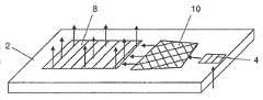
그러한 하나의 장치는 도 1에 도시된 바와 유사한 방식을 설명하는 US 6,580,529에 개시되어 있다. 도 1은 표면들 중 하나 위에 입력 격자 4를 포함하는 웨이브가이드 2의 투시도이다. 입력 프로젝터는 웨이브가이드 2의 평면에 직교하는 방향으로 입력 광을 제공할 수 있다. 입력 격자 4는 제1 회절 오더(diffraction order)가 웨이브가이드 2로 커플링되도록 입력 광을 회절시킬 수 있다. 캡쳐된 광(captured light)은 웨이브가이드 2 내에서 내부 전반사에 의하여 그루브들(grooves)이 입사광에 대해 45도 방향을 향하는 제2 격자 6을 향해 나아간다. 제2 격자 6과의 상호 작용의 각 지점에서, 광은 전송되거나 혹은 회절된다. 제2 격자 6에 의해 회절되는 광은 90도 방향을 바꾸고, 제1 회절 오더는 웨이브가이드 2 내에서 제3 격자 8을 향하여 확장된다. 제2 격자 6에서 처음에 전송된 광은 제3 격자 8을 향하여 회절되기 전에 격자 6내에서 더 확장된다. 이것은 제2 격자 6의 길이(length)를 따라 입사광의 1차원 확장을 제공한다. 제3 격자 8의 그루브들은 입사광에 대해 직교하는 방향을 향한다. 제3 격자 8과의 상호작용의 각 지점에서, 광은 전송되거나 회절될 수 있다. 전송된 광은 내부 전반사에 의하여 웨이브가이드 8 내에서 나아간다. 제3 격자 8에 의하여 회절된 광은 웨이브가이드 2의 밖으로 커플링되고 뷰어(viewer)를 향한다. 그러므로 제3 격자는 제3 격자의 그루브들에 직교하는 방향으로 광의 1차원 확장을 제공한다. 이러한 방식으로, 도1의 광학 장치는 입력 광의 2차원 확장을 달성할 수 있고, 여기에서, 1차원 확장은 제2 격자 6에 의해, 2차원 확장은 제3 격자 8에 의해 제공된다.
도 2에 도시된 바와 유사한 장치가 설명된 WO 2008/081070에서 대안적인 시스템이 개시된다. 도 2는 도 1의 것들과 유사한 제1 격자 4 및 제 3 격자 8을 포함하는 웨이브가이드 2의 투시도이다. 교차된 격자 10은 또한 제1 격자 4 및 제3 격자 8 사이에 제공된다. 교차된 격자 10은 서로 90도 각도를 이루는 그루브들을 가지는 겹쳐진 격자들을 포함한다. 입력 격자 4로부터의 광이 교차된 격자 10을 마주칠 때에, 광은 입력 광빔(input light beam)과 서로 직교하고 웨이브가이드 2 상의 반대의 방향으로 동시에 회절 된다. 광은 그 후 제3 격자 8로 확장할 수 있도록 교차된 격자에서 다시 회절된다. 이러한 방식으로 교차된 격자 10은 두 개의 반대되는 방향으로 입력 광의 확장을 제공한다.
교차된 격자 10에 의한 광 출력은 제3 격자 8을 향하여 나아간다. 입력 광이 제3 격자 8과 마주칠 때에, 광은 전송되거나 또는 회절된다. 전송된 일부의 빔은 제3 웨이브가이드 8에서 확장되고, 회절된 일부의 빔(beam)은 웨이브가이드 2의 밖으로, 뷰어(viewer)를 향해 커플링된다. 임의의 전송된 일부의 빔은 격자 8의 나중(later)의 그루브들에 의해 웨이브가이드 2의 밖으로 회절될 수 있다. 따라서, 1차원의 확장(a first dimension of expansion)은 교차된 격자 10에 의해 제공되고, 2차원의 확장(a second dimension of expansion)은 제3 격자 8에 의하여 제공된다. 이것이 효과적이기 위해, 격자 주기는 교차된 격자 10에 의한 광의 임의의 아웃 커플링(out-coupling)을 막기 위하여 분명하게 결정된다. 따라서, 유일한 광의 아웃 커플링은 제3 격자 8에 의한다.
도 1 및 도 2의 방식(arrangement)에서의 문제점은 웨이브가이드에서 세 개의 분리된 영역들에 회절 격자들을 제공하기 위한 공간과 관련된다. 이러한 큰 광학 시스템들은 모든 장치들에 적합하지는 않을 수 있다. 더 큰 문제는 매우 많은 회절 상호작용이 요구된다는 점이다. 각각의 회절 상호작용은 산란을 일으키고, 따라서, 결과 이미지의 컨트라스트(contrast)를 감소시킨다. 그러나, 또 다른 문제는 이러한 장치들이 반드시 컬러 디스플레이들에 적합한 것은 아니라는 점이다. 이러한 단점들의 일부를 해결하는 것이 본 발명의 목적이다.Augmented reality displays allow users to view projected images as well as their surroundings. In military or transportation applications, projected images can be superimposed on the real world perceived by the user. Other applications of these displays include wearable devices such as glasses and video games.
In a typical configuration, a transparent display screen is provided in front of the user so that he can continue to see the real world. The display screen is typically a glass waveguide, and the projector is provided on one side. Light from the projector is coupled to the waveguide by a diffraction grating. The projected light is fully internally reflected from the waveguide. The light is then coupled out of the waveguide by another diffraction grating so that the user can see it. The projector provides images and/or information that enhance the user's view of the real world.
A challenge exists in the production of wide screen augmented reality displays. This is because the light from the input projector needs to be provided over the entire area of the display (if the augmented reality is to be viewed over the full area).
One such device is disclosed in US 6,580,529 which describes a scheme similar to that shown in FIG. 1 . 1 is a perspective view of a
An alternative system is disclosed in WO 2008/081070 in which a device similar to that shown in FIG. 2 is described. FIG. 2 is a perspective view of
The light output by the
A problem with the arrangement of FIGS. 1 and 2 relates to space for providing diffraction gratings in three separate regions in the waveguide. These large optical systems may not be suitable for all devices. A bigger problem is that very many diffractive interactions are required. Each diffraction interaction causes scattering, thus reducing the contrast of the resulting image. However, another problem is that these devices are not necessarily suitable for color displays. It is an object of the present invention to solve some of these disadvantages.
본 발명의 일 측면에 따르면, 웨이브가이드((waveguide)); 입력 광(input light)을 웨이브가이드로 커플링하도록 구성된 입력 회절 광학 소자(input diffractive optical element); 및 웨이브가이드 내부 혹은 위에서 적어도 부분적으로 겹쳐 있는 두 개의 회절 광학 소자들(two diffractive optical elements)을 포함하는 증강 현실 디스플레이에서, 이차원에서 입력 광을 확장하는 제공된 광학 장치가 있다. 상기 두 개의 회절 광학 소자들 중 적어도 하나는 광이 웨이브가이드 외부에서 뷰어(viewer)를 향하도록 커플링하는 출력 회절 광학 소자로써 동작한다.
이러한 방식을 통하여, 사용자가 볼 수 있도록 웨이브가이드 밖으로 동시에 커플링하면서, 광학 장치는 입력 광 소스의 이차원 확장을 달성할 수 있다. 이차원 확장은 웨이브가이드의 동일한 영역 내에서 출력 커플링(output coupling)으로써 제공될 수 있기 때문에, 이것은 광학 장치 내 공간의 더욱 효율적인 사용을 가능하게 한다. 이것은 제조 비용을 유리하게 감소시킬 수 있다. 장치는 또한 향상된 광학적 특성을 제공할 수 있다. 예를 들면 이차원 확장은 감소된 회절 상호작용을 통해 달성되기 때문에 본 장치는 또한 향상된 배경 컨트라스트(improved background contrast)를 제공할 수 있다. 두 개의 회절 광학 소자들은 부분적으로 혹은 전체로 웨이브가이드 내부 혹은 위에서 서로 겹쳐질 수 있다.
본 광학 장치의 하나의 장점은 동시의 이차원 빔 확장 및 아웃커플링이 회절 광학 소자들에 제공된(devoted) 웨이브가이드의 오직 두 영역들에서 제공될 수 있다는 점이다(한 영역은 입력 회절 광학 소자를 위함이고, 한 영역은 겹쳐진 회절 광학 소자들을 위함이다). 이것은 장치의 전체적인 크기를 줄여줄 수 있다. 추가적으로, 유사한 광학 성능이 장치가 더 싼 가격에 생산될 수 있음을 의미하는, 기판의 편평도 및 웨지(wedge)에 대한 감소된 공차(tolerances)를 통해 달성될 수 있다. 대안적으로, 더 나은 광학적 성능이 생산에 있어서 공차(tolerances)를 증가시키지 않고 달성될 수 있다.
겹쳐진 광학 소자들에서, 소자들 중 하나는 바람직하게는 입력 회절 광학 소자로부터 획득한 광을 겹쳐진 짝의 다른 소자를 향해 보낸다. 다른 회절 광학 소자는 그 후 광을 웨이브가이드 밖으로, 뷰어를 향하도록 커플링한다. 바람직하게는, 이것은 대칭적인 방식이므로, 각각의 겹쳐진 회절 광학 소자는 밖으로의 커플링(outward coupling)을 위하여 획득된 광을 다른 소자를 향해 커플링할 수 있다.
각각의 회절 광학 소자는 바람직하게는 그루브들(grooves) 및 그루브들의 평면상의 격자 벡터(grating vector)를 포함한다. 격자 벡터는 그루브들에 수직한 방향 및 그루브들의 피치(pitch)에 반비례하는 크기(magnitude)를 가지도록 정의될 수 있다. 입력 및 출력 회절 광학 소자들은 각각 실질적으로 동일한 크기의 격자 벡터들을 가질 수 있다.
동일한 크기의 입력 및 출력 격자 벡터들을 제공함에 의하여, 입력빔과 동일한 각 특성들(angular properties)을 가지는 출력빔(exit beam)을 획득할 수 있다. 따라서, 출력빔은 입력빔과 동일한 각으로 제공될 수 있다. 이것은 모든 작동 파장들에서 이루어 질 수 있고, 이는 장치가 효과적으로 컬러(즉, 다양한 파장에 걸쳐)에서 동작할 수 있음을 의미한다.
입력 회절 광학 소자 및 두 개의 회절 광학 소자들 각각의 격자 벡터들의 결합(combination)은 실질적으로 0의 크기를 가지는 결과 벡터(resultant vector)일 수 있다. 이 격자들의 결합된 특성은 출력광이 실질적으로 각도 및 색채의 변화 없이 제공될 수 있음을 의미하고, 이것은 컬러 증강 현실 디스플레이에서 장치의 사용을 가능하게 한다.
몇몇 방식에서 결과 벡터는 작은 크기를 가질 수 있다. 일반적으로 이러한 실시예들은 단색의 광에 더 적절하다. 왜냐하면 이 방식은 일반적으로 컬러 디스플레이에 적합하지 않은 색 분산을 야기하기 때문이다.
회절 광학 소자의 그루브들은 선형적일 수 있고, 웨이브가이드의 표면에 애칭(etching)에 의해 형성될 수 있다. 대안적으로, 그루브들은 볼륨형의 광중합체(volume type photopolymer)에서 발견될 수 있는 것과 같이, 굴절률의 변화에 의해 형성될 수 있다. 이러한 것들은 굴절률의 부드러운 변화 혹은 큰 변화일 수 있다.
두 개의 회절 광학 소자들의 격자 벡터들은 입력 회절 광학 소자의 격자 벡터와 동일하거나 대각(opposite angle)의 각을 이룰 수 있다. 이러한 방식으로 겹쳐진 회절 광학 소자들은 서로 교차될 수 있고, 입력 회절 광학 소자에 대하여 대칭적으로 배치될 수 있다. 그러므로 입력 회절 광학 소자로부터의 광은 두 개의 회절 광학 소자들에 의하여 동시에 방사상의 방향으로 회절될 수 있다. 회절 광학 소자들에 동일한 혹은 반대의 격자 벡터들을 제공함에 의하여, 이차원 확장은 대칭적으로 될 수 있고, 두 개의 격자에 의한 각도의 변화는 모두 동일할 수 있다.
입력 회절 광학 소자 및 두 개의 회절 광학 소자들의 격자 벡터들은 실질적으로 동일한 크기를 가질 수 있다. 이 세 개의 벡터들의 결합은 실질적으로 0의 크기를 가지기 때문에, 벡터들은 서로에 대해 대략적으로 60도를 이루는 등변 삼각형을 생성하도록 조합될 수 있다. 이러한 방식은 심지어 교차된 회절 광학 소자들에 의한 방사상의 방향들로의 회절도 허용할 수 있다. 광을 웨이브가이드 밖으로 커플링하기 위하여 동일한 차후의 회절들은 그 후에 교차된 회절 광학 소자들에 기인하여 발생한다. 이러한 방식으로, 각각의 두 개의 회절 광학 소자들은 출력 격자로써 동작하고, 다른 겹쳐진 회절 광학 소자에 의한 광의 회절을 뒤따른다. 이것은 광이 입력된 방향과 동일한 방향으로 웨이브가이드 밖으로 커플링되는 것을 허용할 수 있다. 모든 파장들은 유익하게(advantageously) 컬러 디스플레이를 가능하게 하는 동일한 결과를 경험할 수 있다.
바람직하게는 입력 격자는 두 개의 회절 광학 소자들과 멀리 떨어져 위치한다. 입력 격자는 광을 웨이브가이드 내부로 커플링하고, 광은 내부 전반사로 웨이브가이드를 통해 다른 회절 광학 소자들로 나아간다.
바람직하게는 프로젝터는 입력 회절 광학 소자를 향해 광을 투영하기 위해 제공된다. 프로젝터는 다색광을 낼 수 있으며, 웨이브가이드의 평면을 가로지르는 방향으로 제공될 수 있다.
투영된 광은 입력 회절 광학 소자에 대해 제1 각도로 제공될 수 있고, 출력 회절 광학 소자에 의해 웨이브가이드의 밖으로 커플링된 광은 또한 제1 각도로 제공될 수 있다. 따라서 출력광은 어떠한 각도의 변화도 없이 제공될 수 있다.
두 개의 겹쳐진 회절 광학 소자들은 서로 다른 평면 상에서 웨이브가이드의 위 혹은 내부에 제공될 수 있다. 이러한 방식으로, 겹쳐진 회절 광학 소자들은 물리적으로 서로 분리될 수 있다. 그러한 방식은 쉽게 제조될 수 있고, 바람직한 결과들을 만들어낼 수 있다.
회절 광학 소자들은 웨이브가이드의 서로 반대의 표면들(opposing surfaces)에 제공될 수 있다. 그들은 필요에 따라 웨이브가이드의 내부 표면 혹은 외부 표면에 제공될 수 있다. 대안적으로 두 개의 회절 광학 소자들은 실질적으로 웨이브가이드의 동일한 평면 상에 제공될 수 있다. 이것은 광 결정(photonic crystal)을 사용함에 의하여 달성될 수 있다. 회절 광학 소자들은 결정의 물질에서 굴절률 및/또는 표면 높이의 변화에 의하여 제공될 수 있다.
본 발명의 다른 측면에 따르면, 광 전송 기판(light transmissive substrate); 상기 기판이 지니는 제1 회절 광학 소자; 상기 기판이 지니는 제2 회절 광학 소자를 포함하는 회절 광학 장치가 제공된다. 상기 광 전송 기판은 이차원에서 두 개의 실질적으로 평행한 표면들을 포함한다. 상기 제1 회절 광학 소자는 광원으로부터 광선들을 커플링하고 내부 전반사에 의하여 상기 기판 내부에 광들을 가둔다. 상기 제2 회절 광학 기판은 상기 광선을 삼차원에서 많은 오더들로 회절시키고, 다수의 이러한 상기 오더들은 여전히 내부 전반사를 통하여, 적어도 하나의 상기 오더들은 웨이브가이드 밖으로 커플링하면서, 서로 다른 방향들(2차원에서는 상기 기판의 주된 표면들을 포함함)로 회절된다.
본 발명의 또 다른 측면에 따르면, 광 전송 기판(light transmissive substrate), 상기 기판이 지니는 회절 광학 소자를 포함하는 회절 광학 장치가 제공된다. 상기 광 전송 기판은 이차원에서 두 개의 실질적으로 평행한 표면들을 포함한다. 상기 단일 회절 기판은 광원으로부터의 광선들을 커플링하고 내부 전반사에 의하여 상기 기판의 내부에 광들을 가두고, 상기 단일 회절 광학 소자는 또한 상기 광선들을 3차원에 있는 많은 오더들로 회절시킨다. 상기 오더들 중 일부는 여전히 내부 전반사를 통하여 서로 다른 방향(이차원에서 상기 기판의 주된 표면들을 포함함)으로 회절되고, 상기 오더들 중 적어도 하나가 웨이브가이드 밖으로 커플링되는 동안에 상기 광선들의 이차원적 레플리케이션(replication)를 야기한다.According to one aspect of the present invention, a waveguide (waveguide); an input diffractive optical element configured to couple input light into a waveguide; and provided optics for expanding input light in two dimensions in an augmented reality display comprising two diffractive optical elements at least partially superimposed within or over the waveguide. At least one of the two diffractive optical elements operates as an output diffractive optical element that couples light from outside the waveguide toward a viewer.
In this way, the optical device can achieve a two-dimensional expansion of the input light source while simultaneously coupling out of the waveguide for viewing by the user. Since the two-dimensional expansion can be provided as an output coupling within the same area of the waveguide, this enables a more efficient use of space within the optics. This can advantageously reduce manufacturing costs. The device may also provide improved optical properties. For example, the device can also provide improved background contrast because two-dimensional expansion is achieved through reduced diffractive interactions. The two diffractive optical elements can be partially or wholly superimposed on each other in or on the waveguide.
One advantage of the present optics is that simultaneous two-dimensional beam expansion and outcoupling can be provided in only two regions of the waveguide devoted to the diffractive optics (one region with the input diffractive optics). and one area is for the overlapping diffractive optical elements). This can reduce the overall size of the device. Additionally, similar optical performance can be achieved through reduced tolerances to the wedge and flatness of the substrate, meaning that the device can be produced at a lower cost. Alternatively, better optical performance can be achieved without increasing tolerances in production.
In superimposed optical elements, one of the elements preferably directs light obtained from the input diffractive optical element towards the other element of the superimposed pair. Another diffractive optical element then couples the light out of the waveguide and towards the viewer. Preferably, this is a symmetrical manner, so that each superimposed diffractive optical element can couple the acquired light towards the other for outward coupling.
Each diffractive optical element preferably comprises grooves and a grating vector in the plane of the grooves. The grating vector may be defined to have a direction perpendicular to the grooves and a magnitude inversely proportional to a pitch of the grooves. The input and output diffractive optical elements may each have grating vectors of substantially the same magnitude.
By providing the input and output grating vectors of the same magnitude, an exit beam having the same angular properties as the input beam can be obtained. Accordingly, the output beam can be provided at the same angle as the input beam. This can be done at all operating wavelengths, which means that the device can effectively operate in color (ie, across a variety of wavelengths).
A combination of the input diffractive optical element and the grating vectors of each of the two diffractive optical elements may be a resultant vector having a substantially zero magnitude. The combined nature of these gratings means that the output light can be provided substantially without changes in angle and color, which enables the use of the device in color augmented reality displays.
In some ways the resulting vector may have a small size. In general, these embodiments are more suitable for monochromatic light. This is because this method usually causes color dispersion that is not suitable for color displays.
The grooves of the diffractive optical element may be linear, and may be formed by etching on the surface of the waveguide. Alternatively, the grooves can be formed by changing the refractive index, such as can be found in a volume type photopolymer. These can be smooth or large changes in the refractive index.
The grating vectors of the two diffractive optical elements may be the same as the grating vectors of the input diffractive optical element or may form an opposite angle. The diffractive optical elements superimposed in this way can intersect each other and can be arranged symmetrically with respect to the input diffractive optical element. Therefore, the light from the input diffractive optical element can be diffracted in the radial direction by the two diffractive optical elements at the same time. By providing the diffractive optical elements with equal or opposite grating vectors, the two-dimensional expansion can be made symmetrical and the change in angle by both gratings can be the same.
The grating vectors of the input diffractive optical element and the two diffractive optical elements may have substantially the same magnitude. Since the combination of these three vectors has a magnitude of substantially zero, the vectors can be combined to create an equilateral triangle that is approximately 60 degrees to each other. This approach can even allow diffraction in radial directions by crossed diffractive optical elements. The same subsequent diffractions then occur due to the crossed diffractive optics to couple the light out of the waveguide. In this way, each of the two diffractive optics acts as an output grating and follows the diffraction of light by the other superimposed diffractive optics. This may allow light to be coupled out of the waveguide in the same direction as the input direction. All wavelengths can advantageously experience the same result enabling color display.
Preferably the input grating is located far away from the two diffractive optical elements. An input grating couples the light into the waveguide, and the light travels through the waveguide to other diffractive optics through total internal reflection.
Preferably a projector is provided for projecting light towards the input diffractive optical element. The projector may emit polychromatic light, and may be provided in a direction transverse to the plane of the waveguide.
The projected light may be provided at a first angle with respect to the input diffractive optical element and light coupled out of the waveguide by the output diffractive optical element may also be provided at a first angle. Accordingly, the output light can be provided without any angle change.
Two superimposed diffractive optical elements may be provided on or inside the waveguide on different planes. In this way, the overlapping diffractive optical elements can be physically separated from each other. Such a method can be easily manufactured and can produce desirable results.
The diffractive optical elements may be provided on opposing surfaces of the waveguide. They may be provided on the inner or outer surface of the waveguide as required. Alternatively the two diffractive optical elements may be provided on substantially the same plane of the waveguide. This can be achieved by using a photonic crystal. Diffractive optical elements may be provided by varying the refractive index and/or surface height in the material of the crystal.
According to another aspect of the present invention, a light transmissive substrate (light transmissive substrate); a first diffractive optical element carried by the substrate; A diffractive optical device including a second diffractive optical element carried by the substrate is provided. The light transmitting substrate includes two substantially parallel surfaces in two dimensions. The first diffractive optical element couples light rays from a light source and confines the light rays within the substrate by total internal reflection. The second diffractive optical substrate diffracts the ray in three dimensions into many orders, a plurality of such orders still coupling through total internal reflection, at least one of the orders out of the waveguide, in
According to another aspect of the present invention, there is provided a diffractive optical device comprising a light transmissive substrate and a diffractive optical element carried by the substrate. The light transmitting substrate includes two substantially parallel surfaces in two dimensions. The single diffractive substrate couples light rays from the light source and confines the light rays to the interior of the substrate by total internal reflection, and the single diffractive optical element also diffracts the rays into many orders in three dimensions. Some of the orders are still diffracted in different directions (including the major surfaces of the substrate in two dimensions) through total internal reflection, and the two-dimensional refraction of the rays while at least one of the orders is coupled out of the waveguide. cause replication.
본 발명의 실시예들은 오직 예로써(by way of example only), 첨부된 도면들을 참조하여 지금부터 설명될 것이다. 첨부된 도면은 다음과 같다.
도 1은 입력빔을 두 개의 직교하는 방향으로 확장하는 광학 장치의 투시도이다.
도 2는 입력빔을 두 개의 직교하는 방향으로 확장하는 또 다른 광학 장치의 투시도이다.
도 3은 본 발명의 실시예에서의 광학 장치의 투시도이다.
도 4는 도 3의 광학 장치에 있는 회절 격자들의 하나의 그루브들의 상면도이다.
도 5는 도 3의 광학 장치에 있는 다른 회절 격자의 그루브들의 상면도이다.
도 6은 도 3의 광학 장치에서 또 다른 회절 격자의 그루브들의 상면도이다.
도 7은 격자 벡터들을 도시하는 도 3에 있는 광학 장치의 도식도(schematic view)이다.
도 8은 도 3에 도시되는 광학 장치를 통하여 얻을 수 있는 일부 광로의 예시이다.
도 9는 도 3에 도시되는 광학 장치를 위한 격자 벡터들의 조합을 도시한다.
도 10은 도 3에 도시되는 광학 장치를 통해 얻을 수 있는 광로의 다른 예시를 도시하는 웨이브가이드의 상면도이다.
도 11은 도 3에 도시된 광학 장치를 통하여 얻을 수 있는 일부 광로들의 다른 예시이다.
도 12는 도 3에 도시되는 광학 장치를 통해 얻을 수 있는 광로들의 또 다른 예시를 도시하는 웨이브가이드의 상면도이다.
도 13은 입력 격자에 의해 획득되거나 회절되는 광을 도시하는 다이어그램이다.
도 14는 출력 격자에 의해 획득되거나 회절되는 광을 도시하는 다이어그램이다.
도 15a 및 15b는 내부 및 외부 격자들을 각각 도시하는 대안적인 방식들에서의 웨이브가이드의 측면도들이다.
도 16은 본 발명의 실시예에서 사용을 위한 삼각형 격자 구조를 가지는 광 결정의 도식도이다.
도 17은 도 16에 도시된 광 결정의 삼각형 격자의 구조를 도시하는 도식도이다.
도 18은 도 16에 도시된 광 결정을 통해 얻을 수 있는 광로들을 도시하는 다이어그램이다.
도 19는 본 발명의 실시예의 한 쌍의 안경의 투시도이다.
도 20은 본 발명의 실시예의 전방 시현 디스플레이의 투시도이다.Embodiments of the present invention will now be described with reference to the accompanying drawings, by way of example only. The attached drawings are as follows.
1 is a perspective view of an optical device that expands an input beam in two orthogonal directions.
2 is a perspective view of another optical device that expands an input beam in two orthogonal directions;
3 is a perspective view of an optical device in an embodiment of the present invention;
FIG. 4 is a top view of one groove of the diffraction gratings in the optical device of FIG. 3 ;
Fig. 5 is a top view of the grooves of another diffraction grating in the optical device of Fig. 3;
FIG. 6 is a top view of grooves of another diffraction grating in the optical device of FIG. 3 ;
Fig. 7 is a schematic view of the optical arrangement in Fig. 3 showing grating vectors;
FIG. 8 is an example of some optical paths obtainable through the optical device shown in FIG. 3 .
FIG. 9 shows a combination of grating vectors for the optical device shown in FIG. 3 .
FIG. 10 is a top view of a waveguide showing another example of an optical path obtainable through the optical device shown in FIG. 3 .
FIG. 11 is another example of some optical paths obtainable through the optical device shown in FIG. 3 .
FIG. 12 is a top view of a waveguide showing another example of optical paths obtainable through the optical device shown in FIG. 3 .
Fig. 13 is a diagram showing light obtained or diffracted by an input grating.
14 is a diagram illustrating light obtained or diffracted by an output grating.
15a and 15b are side views of a waveguide in alternative manners showing inner and outer gratings respectively;
16 is a schematic diagram of a photonic crystal having a triangular lattice structure for use in an embodiment of the present invention.
FIG. 17 is a schematic diagram showing the structure of a triangular lattice of the photonic crystal shown in FIG. 16; FIG.
18 is a diagram illustrating optical paths obtainable through the photonic crystal shown in FIG. 16 .
19 is a perspective view of a pair of glasses according to an embodiment of the present invention;
20 is a perspective view of a forward vision display of an embodiment of the present invention;
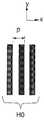
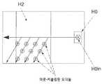
도 3은 3개의 선형 격자들 H0, H1, H2를 포함하는 웨이브가이드 12의 투시도이다. 도 4에 도시된 바와 같이 입력 격자 H0의 그루브들은 y 축과 평행하고, 격자 피치 p를 가지며 웨이브가이드 12의 제1 표면 상에 있는 x-y 평면에 놓여 있다. 선형 격자 H1은 x-y 평면 상에서 입력 격자 H0로부터 좌우로(laterally) 분리되어 있고, 웨이브가이드 12의 제2 표면에 놓여있다. 도 5에 도시된 바와 같이 격자 H1의 그루브들은 x 축에 대해 30도 방향을 향하고, 격자 피치 p를 가지며 x-y 평면에 놓여 있다. 선형 격자 H2는 x-y 평면 상에서 H1과 겹쳐져 있고, 격자 H2와는 반대로 웨이브가이드 12의 제1 표면에 놓여있다. 그러므로 교차된 격자 H1, H2는 z축에 대한 웨이브가이드 12의 두께에 의하여 분리된다. 도 6에 도시된 바와 같이, 격자 H2의 그루브들은 x축에 대해 -30도 방향을 향하고, 격차 피치p를 가지며 x-y 평면상에 놓여있다.
격자 벡터는 격자들 H0, H1, H2의 각각에 대해 정의될 수 있다. 격자 벡터들은 격자의 그루브들의 평면 상에 놓여있고, 그루브들의 방향에 대해 오른쪽 각도의 방향으로 확장될 수 있다.(extends in a direction which is at right angles to the direction of grooves). 벡터의 크기는 G=
도 8은 웨이브가이드 12를 통해 얻을 수 있는 광로를 도시하는 음선도(ray diagram)이다. 이 방식에서, 프로젝터로부터의 입사빔은 입력 격자 H0를 다색광으로 비춘다. 입사빔은 웨이브가이드 12의 아래로부터 제공되고, 웨이브가이드 12의 평면에 대해 직교하는 방향으로 확장한다. 입력 격자 H0는 입사빔을 회절시키고, 제1 회절 오더는 웨이브가이드 12로 커플링된다. 회절된 광은 내부 전반사에 의해 웨이브가이드 12의 내부에서 나아간다. 상기 광은 그 후에 교차된 격자 10과 마주치고, 교차된 격자 H1, H2와 동시에 상호작용한다.
격자 H1(벡터 G2와 함께)은 광을 제로 오더 0R 및 제1 회절 오더 1R로 회절시킨다. 제1 회절 오더 1R은 x축에 대하여 -120도를 향하고, 여전히 웨이브가이드 12에서 내부 전반사하고 있다. 제1 회절 오더 1R은 그 후에 교차된 격자 10의 다른 부분인 H2(벡터 G3과 함께)와 마주친다. 이 지점에서 H2는 또한 광을 제로 오더 및 제1 회절 오더로 회절시킨다. 제로 오더는 웨이브가이드 12 내에서 계속 나아가고, 1차 회절 오더는 웨이브가이드웨이브가이드 12의 밖으로 z축을 따라 뷰어를 향해 커플링된다. 본 예시에서 광이 웨이브가이드 12로부터 출력이 되는 각도는 광이 프로젝터로부터 웨이브가이드 12에 입사하는 각도와 동일하다.
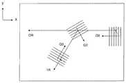
도 10은 도 8에 도시된 또 다른 음선도의 관점(view)이다. 교차된 격자에 대한 입사광이 격자 H1에 의하여 웨이브가이드 내의 복수의 다른 지점들에서 회절될 수 있다는 사실은 도 10으로부터 분명하다. 이것은 각각의 상호작용의 지점에서 광이 제로 오더 혹은 제1 회절 오더로 회절될 수 있기 때문이다. 이러한 방식으로, 입사빔은 제1 방향으로 확장될 수 있다. 격자 H1에 의해 제1 오더로 회절될 수 있는 광은 그 후에 광이 제로 오더 혹은 제1 오더로 회절될 수 있는 격자 H2와 마주친다. 이것은 입사광이 H2의 그루브들과 직교하는 제2 방향으로 확장될 수 있게 할 수 있다. 이러한 방식으로, 아웃커플링된 오더들(outcoupled orders)은 격자 H2에 의해 2차원 영역에 걸쳐 제공될 수 있다. 이것은 이차원 확장 및 광의 아웃커플링이 작은 물리적 영역에 함께 제공될 수 있도록 할 수 있다.
도 11은 웨이브가이드 12를 통해 얻을 수 있는 광로를 도시하는 음선도의 다른 예시이다. 본 방식에서, 입력 격자 H0로부터의 광은 교차된 격자 10과 마주치고, 이것은 격자 H2(G3 벡터와 함께)와 함께 상호작용한다. 격자 H2는 광을 제로 오더 0R 및 제1 회절 오더 1R로 회절시킨다. 제1 회절 오더 1R는 x축에 대하여 +120도를 향하고, 여전히 웨이브가이드 12에서 내부 전반사하고 있다. 제1 회절 오더 1R은 그 후 교차된 격자 10의 다른 부분인 H1과 마주친다. 이 지점에서, H1은 광을 웨이브가이드 12의 밖으로, 윗 방향으로 뷰어를 향하여 커플링한다. 이 예시에서 광이 웨이브가이드 12로부터 출력이 되는 각도는 웨이브가이드 12에 광이 입사하는 각도와 동일하다.
도 12는 도 11에 도시된 음선도의 또 다른 관점(view)이다. 이 격자들의 방식은 2차원 디스플레이를 채우기 위하여 입사빔을 확장할 수 있음이 이해될 수 있다. 당연히, 광은 심지어 2차원 영역을 넘어서는 입사빔의 확장을 제공하는 도 12에 도시된 경로와 동시에 함께 도 10에 도시된 경로를 따른다.
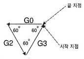
이 예시에서, 광은 벡터 G0, G2, G3를 가지는 세 개의 회절 격자들과 마주친다. 회절의 시퀀스는 G0/G2/G3 또는 G0/G3/G2일 수 있다. 이 벡터들의 각각은 동일한 크기를 가진다. 도 9에 도시된 바와 같이, 만약 벡터들이 서로에게 더해진다면, 벡터 다이어그램은 동일한 시작과 끝점을 가지는 등변 삼각형의 모양으로 얻어진다. 회절 격자들의 물리학은 이러한 방식이 출력빔(exit beam)에게 입사빔과 동일한 각도 및 색채 특성을 제공한다는 것을 지시한다.
도 13은 입력 격자 H0에서 광이 회절되는 것을 도시하는 다이어그램이다. 이 상황에서 입사빔은 z 축에 대해 입사각

도 14는 출력 격자에서 회절되는 광을 도시하는 다이어그램이다. 이 예시에서, 출력 격자는 웨이브가이드 12를 통하는 광에 의해 선택되는 경로에 따라서, H1 또는 H2가 될 수 있다. 여기에서 볼 수 있는 바와 같이, 광은 웨이브가이드 12 내에서 내부 전반사로 출력 격자에서 획득되고, 이는 z축에 대해서


도 15a는 두 개의 유리 판들 14, 16에 중간에 끼인 웨이브가이드 12의 측면도이다. 이 방식에서, 격자 17은 유리판들 14, 16의 표면들에 제공되고, 웨이브가이드 12는 광학 시멘트의 얇은 층을 가지는 이 판들 14, 16에 결합된다. 따라서, 격자 17은 유리 판 14, 16의 내부 표면 상에 제공된다. 도 15b는 격자 17이 그 표면들에 직접 제공되는 대안적인 구성에서의 웨이브가이드 12의 측면도이다. 이 방식에 의하여, 격자 17은 웨이브가이드 12의 외부 표면 상에 제공될 수 있다.
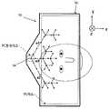
다른 실시예에서 교차된 격자 10은 광 결정에 의해 대체될 수 있다. 광 결정은 가변적인 굴절률이 규칙적인 패턴을 생성하는 물질이다. 이 예시에서, 광 결정은 삼각형 격자의 형태이다(in forms of triangular lattice). 이차원 광 결정은 직교 방향들에서 주기적인 나노 구조들이다. 본 예시에서 광 결정은 등변 삼각형 격자의 형태이다. 도 16은 웨이브가이드 12에 대해 증가된 굴절률을 가지는 원형 필라들 20(circular pillars)을 포함하는 광 결정 19의 상면도이다. 필라들 20은 규칙적인 패턴으로 배열되고, 모두 동일한 x-y 평면 상에 제공된다. 도 17은 필라들 20의 세 개를 도시한다. 필라들은 x축 혹은 y축에 따르는 거리 p에 상응하는 거리 e에 의하여 분리된다.
필라들의 규칙적인 배열은 많은 효과적인 회절 격자들 또는 회절 광학 소자들을 생성한다. 특히
거리 p로 분리된 필라들 20의 인접한 열들과 함께 y축을 따라 정렬된 필라들을 포함하는 격자 H1을 정의할 수 있다. 격자 H2는 거리 p에 의해 분리된 인접한 열들과 함께, x축에 대해 +30도의 각도를 이루는 필라들 20의 열들로 배열되어 있다. 결국, 격자 H3은 거리 p에 의해 분리된 인접한 열들과 함께, x축에 대해 -30도의 각도를 이루는 필라들 20의 열들로 배열되어 있다. 격자들 H1 및 H2는 도 3에 도시된 교차된 격자 실시예에서 상응하는 격자들과 동일한 특성을 가진다는 것이 언급된다.
입력 격자 H0로부터의 광이 광 결정 19 상에 입사될 때에, 광은 다양한 회절 광학 소자들에 의해 다중적 동시 회절들(multiple simultaneous diffractions)을 겪는다. 도 18은 광 결정을 통해 얻을 수 있는 광로를 도시하는 다이어그램이다. 광은 동시에 네 개의 오더들로의 회절을 겪을 수 있는 광 결정에서의 A 지점에서 획득된다. 첫 번째로, 광은 제로 오더 a0로 회절되는데, 이는 입사광의 전파(propagation)의 연속이다. 상기 제로 오더는 지점 B 및 C에서 광 결정과 더 많은 상호작용들을 하는 것을 계속할 수 있다. 둘째로, 광은 격자 H1에 의하여 제1 회절 오더 ae로 회절된다. 이 광(light beam) ae는 뷰어를 향하여 z축의 양의 방향을 따라서 웨이브가이드 12의 밖으로 커플링 된다. 격자 H1의 그루브의 방향과 피치는 격자 H0와 동일하다. 따라서, 회절의 각 및 색 분산 효과들은 격자 H0 및 H1의 결합 효과들(conjugate effects)에 기인하여 상쇄된다. 따라서, 광(light beam) ae는 프로젝터로부터 H0로 입사한 광과 동일한 각도 및 색채 특성들로 제공된다. 셋째로, 광은 H2 격자 컴포넌트에 의해 1차 회절 오더 a1으로 회절된다. a1 광은 x축에 대하여 +60도로 회절되고, 이 광은 지점 D에서 광 결정과 더 많은 상호작용들을 야기하기 위하여 진행한다. a1 회절된 광은 도 12를 참조하여 설명된 바에 따라, 교차된 격자 H2에 의해 회절된 광과 효과적으로(effectively the same as) 동일하다. 넷째로, 광은 H1 격자 컴포넌트에 의해 제1 회절 오더 a2로 회절된다. 이 광은 격자 지점 F에서 H2와 상호작용할 수 있다. 광 결정의 각각의 지점들에서 광은 이러한 네 개의 분리된 회절 상호작용들을 야기할 수 있다. 따라서, 광은 각각의 지점에서 웨이브가이드 밖으로 커플링될 수 있더라도, 광은 2차원에서 웨이브가이드 12 내에서 확장을 계속할 수 있다. 광 결정의 대칭은 모든 출력광이 입사광과 동일한 각도 및 색채 특성들을 가지는 것을 의미하는데, 이는 다색(뿐만 아니라 단색) 광원이 본 광 결정 방식(photonic crystal arrangement)의 입사광으로써 사용될 수 있음을 의미한다.
여기에 설명된 광로들의 수는 간결을 위하여 제한되어 있다. 하지만, 매우 많은 수의 광로들이 가능하고, 이 모든 것들이 증강 현실 이미지의 생성을 가능하게 하는 아웃커플링된 오더들을 생성한다는 점은 당업자(skilled reader)에게 명백할 것이다. 또한, 광 결정 구현(photonic crystal implementation)의 본 예시에서 사용된 원형 구조 모양(circular structure shape)은 설명을 위한 목적일 뿐이다. 통상의 지식을 가진 실시자들(practitioners skilled in the art)은 많은 수의 적절한 구조 모양이 존재함을 이해할 것이다.
광 결정(photonic crystal)은 입력 광이 이차원 디스플레이 스크린을 채우기 위하여 이차원에서 광의 동시적이고 빠른 확장을 가능하게 할 수 있다. 웨이브가이드 사이즈가 이차원 빔 확장(two dimensional beam expansion)에 기인하여 최소화 될 수 있기 때문에 이것은 초소형 디스플레이(ultra compact diplay)를 가능하게 할 수 있다.
도 19는 한 쌍의 안경 40을 도시한다. 아이 피스들(eye pieces) 44은 사용자의 눈 앞에 교차된 격자들 또는 광 결정들을 포함하는 웨이브가이드들이다. 본 예시에서, 입력 격자 42는 안경 40의 브릿지(bridge)에 제공된다. 따라서, 광은 입력 격자 위에 투영될 수 있고, 아이 피스들(eye pieces)44를 향할 수 있다. 안경알들에 있는 교차된 격자들 또는 광 결정들은 그리고 광을 이차원에서 확장 시키고, 사용자의 눈을 향하여 웨이브가이드 밖으로 커플링할 수 있다.
도 20은 사용자의 앞에 전방 시현 디스플레이 50이 제공되는 다른 예시를 도시한다. 교차된 격자들 또는 광 결정은 전방 시현 디스플레이에 있는 웨이브가이드 52에 제공된다. 입력 격자 54는 디스플레이의 상단부에 제공되고, 웨이브가이드 52에 있는 교차된 격자들 또는 광 결정은 이미지의 빠른 이차원 확장 및 뷰어를 향한 광의 외부로 향하는 커플링(outward coupling)을 허용한다.3 is a perspective view of a
A grating vector may be defined for each of gratings H0, H1, H2. The grating vectors lie in the plane of the grooves of the grating and extend in a direction which is at right angles to the direction of grooves. The magnitude of the vector is G=
8 is a ray diagram illustrating an optical path obtained through the
Grating H1 (with vector G2) diffracts light to zero order 0R and
FIG. 10 is a view of another sound diagram shown in FIG. 8 . It is clear from FIG. 10 that the incident light on the crossed grating can be diffracted by the grating H1 at a plurality of different points in the waveguide. This is because, at each point of interaction, light can be diffracted to either the zero order or the first diffraction order. In this way, the incident beam can be expanded in a first direction. Light that can be diffracted in a first order by grating H1 then encounters grating H2 in which light can be diffracted to zero or first order. This may allow the incident light to expand in a second direction orthogonal to the grooves of H2. In this way, outcoupled orders can be provided over a two-dimensional domain by the grating H2. This may allow two-dimensional expansion and outcoupling of light to be provided together in a small physical area.
11 is another example of a sound line diagram showing an optical path obtained through the
FIG. 12 is another view of the sound diagram shown in FIG. 11 . It can be appreciated that the manner of these gratings can expand the incident beam to fill a two-dimensional display. Naturally, the light follows the path shown in Fig. 10 concurrently with the path shown in Fig. 12, which provides an extension of the incident beam even beyond the two-dimensional region.
In this example, light encounters three diffraction gratings with vectors G0, G2, G3. The sequence of diffraction may be G0/G2/G3 or G0/G3/G2. Each of these vectors has the same magnitude. As shown in Fig. 9, if vectors are added to each other, a vector diagram is obtained in the shape of an equilateral triangle with the same starting and ending points. The physics of diffraction gratings dictate that this approach gives the exit beam the same angular and chromatic characteristics as the incident beam.
13 is a diagram illustrating light diffracting in the input grating H0. In this situation, the incident beam is at an angle of incidence relative to the z-axis.
14 is a diagram illustrating light diffracted in an output grating. In this example, the output grating can be H1 or H2, depending on the path chosen by the light through
15A is a side view of a
In another embodiment the crossed grating 10 may be replaced by a photonic crystal. A photonic crystal is a material in which a variable refractive index produces a regular pattern. In this example, the photonic crystal is in forms of triangular lattice. Two-dimensional photonic crystals are nanostructures that are periodic in orthogonal directions. In this example, the photonic crystal is in the form of an equilateral triangular lattice. 16 is a top view of a
The regular arrangement of pillars creates many effective diffraction gratings or diffractive optical elements. Especially
We can define a grid H1 comprising pillars aligned along the y-axis with adjacent columns of
When light from the input grating H0 is incident on the
The number of light paths described herein is limited for the sake of brevity. However, it will be clear to the skilled reader that a very large number of light paths are possible, all of which create outcoupled orders that allow the creation of augmented reality images. Also, the circular structure shape used in this example of a photonic crystal implementation is for illustrative purposes only. Practitioners skilled in the art will appreciate that a large number of suitable structural shapes exist.
Photonic crystals can enable simultaneous and rapid expansion of light in two dimensions so that input light fills a two-dimensional display screen. This can enable ultra compact display because the waveguide size can be minimized due to two dimensional beam expansion.
19 shows a pair of
FIG. 20 shows another example in which the
Claims (14)
Translated fromKorean웨이브가이드;
입력 광을 상기 웨이브가이드에 커플링하도록 구성된 입력 회절 광학 소자; 및
상기 웨이브가이드 위 또는 내부에서 전체적으로 겹쳐 있는 두 개의 회절 광학 소자들
을 포함하고,
상기 두 개의 회절 광학 소자들의 각각은,
상기 입력 회절 광학 소자로부터 나온 광을 수신하고,
상기 두 개의 회절 광학 소자들 중 다른 회절 광학 소자를 향해 상기 수신한 광을 커플링하여, 상기 다른 회절 광학 소자가 뷰어를 향하여 아웃커플링된 오더들(outcoupled orders)을 제공하는 출력 회절 광학 소자로서 동작할 수 있도록 하고,
상기 입력 광은,
상기 웨이브가이드 위 또는 내부에서 전체적으로 겹쳐 있는 상기 두 개의 회절 광학 소자들에 의하여 이차원으로 확장되는
광학 장치.An optical device for expanding input light in two dimensions in an augmented reality display, comprising:
wave guide;
an input diffractive optical element configured to couple input light to the waveguide; and
two diffractive optical elements entirely superimposed on or within the waveguide
including,
Each of the two diffractive optical elements,
receiving light from the input diffractive optical element;
an output diffractive optical element for coupling the received light towards a different one of the two diffractive optical elements, the other diffractive optical element providing outcoupled orders toward a viewer; make it work,
The input light is
The waveguide is expanded in two dimensions by the two diffractive optical elements superimposed entirely on or inside the waveguide.
optical device.
각각의 회절 광학 소자는,
그루브들과 상기 그루브들의 피치에 반비례하는 크기 및 상기 그루브들과 수직한 방향을 가지고, 상기 그루브들의 평면에 있는 격자 벡터를 포함하고,
상기 입력 회절 광학 소자 및 출력 회절 광학 소자는,
각각 실질적으로 동일한 크기의 격자 벡터를 가지는
광학 장치.According to claim 1,
Each diffractive optical element,
a grating vector in the plane of the grooves, having a size inversely proportional to the grooves and a pitch of the grooves and a direction perpendicular to the grooves,
The input diffractive optical element and the output diffractive optical element,
each having a grid vector of substantially the same size
optical device.
상기 입력 회절 광학 소자와 상기 두 개의 회절 광학 소자들 각각의 격자 벡터들의 조합은,
실질적으로 0의 크기를 가지는 결과 벡터(resultant vector)인
광학 장치.3. The method of claim 2,
The combination of the input diffractive optical element and the grating vectors of each of the two diffractive optical elements is,
It is a result vector with a size of practically zero.
optical device.
상기 두 개의 회절 광학 소자들의 격자 벡터들은,
상기 입력 회절 광학 소자의 상기 격자 벡터에 동일하거나 대각(opposite angle)의 각을 이루는
광학 장치.4. The method of claim 3,
The grating vectors of the two diffractive optical elements are,
at an angle equal to or at an opposite angle to the grating vector of the input diffractive optical element
optical device.
상기 두 개의 회절 광학 소자들 및 상기 입력 회절 광학 소자의 상기 격자 벡터들은, 실질적으로 동일한 크기를 가지는
광학 장치.5. The method according to any one of claims 2 to 4,
The grating vectors of the two diffractive optical elements and the input diffractive optical element have substantially the same magnitude.
optical device.
상기 두 개의 회절 광학 소자들 및 상기 입력 회절 광학 소자의 상기 격자 벡터들은, 실질적으로 등변인 삼각형으로 결합될 수 있는
광학 장치.6. The method of claim 5,
wherein the grating vectors of the two diffractive optical elements and the input diffractive optical element can be combined into a substantially equilateral triangle.
optical device.
입력 격자(input grating)는, 상기 두 개의 회절 광학 소자들로부터 떨어져 위치하는
광학 장치5. The method according to any one of claims 2 to 4,
An input grating is positioned away from the two diffractive optical elements.
optical device
상기 입력 회절 광학 소자를 향해 광을 투영하도록 구성된 프로젝터(projector)를 포함하는
광학 장치.5. The method according to any one of claims 2 to 4,
a projector configured to project light toward the input diffractive optical element;
optical device.
상기 투영된 광은,
상기 입력 회절 광학 소자에 대해 제1 각도로 제공되고,
상기 출력 회절 광학 소자에 의해 상기 웨이브가이드 밖으로 커플링된(coupled) 광은,
상기 제1 각도로 제공되는
광학 장치.9. The method of claim 8,
The projected light is
provided at a first angle with respect to the input diffractive optical element;
Light coupled out of the waveguide by the output diffractive optical element is
provided at the first angle
optical device.
상기 두 개의 겹쳐 있는 회절 광학 소자들은,
서로 다른 평면들에 있는 상기 웨이브가이드 내부 또는 위에 제공되는
광학 장치.5. The method according to any one of claims 2 to 4,
The two overlapping diffractive optical elements are
provided inside or above the waveguide in different planes
optical device.
상기 두 개의 회절 광학 소자들은,
상기 웨이브가이드의 서로 반대의 표면들(opposing surfaces) 상에 제공되는
광학 장치.11. The method of claim 10,
The two diffractive optical elements are
provided on opposing surfaces of the waveguide
optical device.
적어도 두 개의 회절 광학 소자들은, 실질적으로 상기 웨이브가이드 상의 동일 평면 상에 제공되는
광학 장치.5. The method according to any one of claims 2 to 4,
At least two diffractive optical elements are provided substantially on the same plane on the waveguide.
optical device.
적어도 두 개의 회절 광학 소자들은, 광 결정(photonic crystal)으로 제공되는
광학 장치.13. The method of claim 12,
At least two diffractive optical elements are provided with a photonic crystal.
optical device.
Applications Claiming Priority (5)
| Application Number | Priority Date | Filing Date | Title |
|---|---|---|---|
| US201462032577P | 2014-08-03 | 2014-08-03 | |
| US62/032,577 | 2014-08-03 | ||
| GB1502098.5 | 2015-02-09 | ||
| GB1502098.5AGB2529003B (en) | 2014-08-03 | 2015-02-09 | Optical device |
| PCT/GB2015/052181WO2016020643A1 (en) | 2014-08-03 | 2015-07-28 | Exit pupil expanding diffractive optical waveguiding device |
Publications (2)
| Publication Number | Publication Date |
|---|---|
| KR20170039655A KR20170039655A (en) | 2017-04-11 |
| KR102350385B1true KR102350385B1 (en) | 2022-01-13 |
Family
ID=52746333
Family Applications (1)
| Application Number | Title | Priority Date | Filing Date |
|---|---|---|---|
| KR1020177002023AActiveKR102350385B1 (en) | 2014-08-03 | 2015-07-28 | Exit pupil expanding diffractive optical waveguiding device |
Country Status (22)
| Country | Link |
|---|---|
| US (2) | US10114220B2 (en) |
| EP (1) | EP3175280B1 (en) |
| JP (1) | JP6714797B2 (en) |
| KR (1) | KR102350385B1 (en) |
| CN (1) | CN106575034B (en) |
| AU (1) | AU2015298504B2 (en) |
| BR (1) | BR112017002290B1 (en) |
| CA (1) | CA2956872C (en) |
| CY (1) | CY1120524T1 (en) |
| DK (1) | DK3175280T3 (en) |
| ES (1) | ES2670022T3 (en) |
| GB (1) | GB2529003B (en) |
| HR (1) | HRP20180778T1 (en) |
| HU (1) | HUE037328T2 (en) |
| LT (1) | LT3175280T (en) |
| PL (1) | PL3175280T3 (en) |
| PT (1) | PT3175280T (en) |
| RS (1) | RS57263B1 (en) |
| SI (1) | SI3175280T1 (en) |
| SM (1) | SMT201800238T1 (en) |
| TR (1) | TR201806707T4 (en) |
| WO (1) | WO2016020643A1 (en) |
Families Citing this family (224)
| Publication number | Priority date | Publication date | Assignee | Title |
|---|---|---|---|---|
| GB0522968D0 (en) | 2005-11-11 | 2005-12-21 | Popovich Milan M | Holographic illumination device |
| GB0718706D0 (en) | 2007-09-25 | 2007-11-07 | Creative Physics Ltd | Method and apparatus for reducing laser speckle |
| US11726332B2 (en) | 2009-04-27 | 2023-08-15 | Digilens Inc. | Diffractive projection apparatus |
| US9335604B2 (en) | 2013-12-11 | 2016-05-10 | Milan Momcilo Popovich | Holographic waveguide display |
| US11204540B2 (en) | 2009-10-09 | 2021-12-21 | Digilens Inc. | Diffractive waveguide providing a retinal image |
| US20200057353A1 (en) | 2009-10-09 | 2020-02-20 | Digilens Inc. | Compact Edge Illuminated Diffractive Display |
| WO2012136970A1 (en) | 2011-04-07 | 2012-10-11 | Milan Momcilo Popovich | Laser despeckler based on angular diversity |
| WO2016020630A2 (en) | 2014-08-08 | 2016-02-11 | Milan Momcilo Popovich | Waveguide laser illuminator incorporating a despeckler |
| US10670876B2 (en) | 2011-08-24 | 2020-06-02 | Digilens Inc. | Waveguide laser illuminator incorporating a despeckler |
| EP2995986B1 (en) | 2011-08-24 | 2017-04-12 | Rockwell Collins, Inc. | Data display |
| US20150010265A1 (en) | 2012-01-06 | 2015-01-08 | Milan, Momcilo POPOVICH | Contact image sensor using switchable bragg gratings |
| CN106125308B (en) | 2012-04-25 | 2019-10-25 | 罗克韦尔柯林斯公司 | Device and method for displaying images |
| WO2013167864A1 (en) | 2012-05-11 | 2013-11-14 | Milan Momcilo Popovich | Apparatus for eye tracking |
| US9933684B2 (en) | 2012-11-16 | 2018-04-03 | Rockwell Collins, Inc. | Transparent waveguide display providing upper and lower fields of view having a specific light output aperture configuration |
| US10209517B2 (en) | 2013-05-20 | 2019-02-19 | Digilens, Inc. | Holographic waveguide eye tracker |
| WO2015015138A1 (en) | 2013-07-31 | 2015-02-05 | Milan Momcilo Popovich | Method and apparatus for contact image sensing |
| GB2529003B (en)* | 2014-08-03 | 2020-08-26 | Wave Optics Ltd | Optical device |
| US10359736B2 (en) | 2014-08-08 | 2019-07-23 | Digilens Inc. | Method for holographic mastering and replication |
| WO2016042283A1 (en) | 2014-09-19 | 2016-03-24 | Milan Momcilo Popovich | Method and apparatus for generating input images for holographic waveguide displays |
| EP3198192A1 (en) | 2014-09-26 | 2017-08-02 | Milan Momcilo Popovich | Holographic waveguide opticaltracker |
| US20180275402A1 (en) | 2015-01-12 | 2018-09-27 | Digilens, Inc. | Holographic waveguide light field displays |
| WO2016113534A1 (en) | 2015-01-12 | 2016-07-21 | Milan Momcilo Popovich | Environmentally isolated waveguide display |
| EP3248026B1 (en) | 2015-01-20 | 2019-09-04 | DigiLens Inc. | Holographic waveguide lidar |
| US9632226B2 (en) | 2015-02-12 | 2017-04-25 | Digilens Inc. | Waveguide grating device |
| WO2016146963A1 (en) | 2015-03-16 | 2016-09-22 | Popovich, Milan, Momcilo | Waveguide device incorporating a light pipe |
| WO2016156776A1 (en) | 2015-03-31 | 2016-10-06 | Milan Momcilo Popovich | Method and apparatus for contact image sensing |
| CN113759555B (en) | 2015-10-05 | 2024-09-20 | 迪吉伦斯公司 | Waveguide Display |
| CN109073889B (en) | 2016-02-04 | 2021-04-27 | 迪吉伦斯公司 | Holographic waveguide optical tracker |
| US10056020B2 (en) | 2016-02-11 | 2018-08-21 | Oculus Vr, Llc | Waveguide display with two-dimensional scanner |
| CN108780224B (en) | 2016-03-24 | 2021-08-03 | 迪吉伦斯公司 | Method and apparatus for providing a polarization selective holographic waveguide device |
| US10890707B2 (en) | 2016-04-11 | 2021-01-12 | Digilens Inc. | Holographic waveguide apparatus for structured light projection |
| US10067347B2 (en) | 2016-04-13 | 2018-09-04 | Microsoft Technology Licensing, Llc | Waveguides with improved intensity distributions |
| US10061124B2 (en)* | 2016-04-29 | 2018-08-28 | Microsoft Technology Licensing, Llc | Robust architecture for large field of view components |
| US10241346B2 (en)* | 2016-05-07 | 2019-03-26 | Microsoft Technology Licensing, Llc | Degrees of freedom for diffraction elements in wave expander |
| GB2550958B (en)* | 2016-06-03 | 2022-02-23 | Bae Systems Plc | Waveguide structure |
| JP7166927B2 (en)* | 2016-06-20 | 2022-11-08 | アコニア ホログラフィックス、エルエルシー | pupil dilation |
| US10649143B2 (en) | 2016-06-20 | 2020-05-12 | Akonia Holographics Llc | Polarization management |
| EP3504567B1 (en)* | 2016-08-26 | 2023-08-09 | Molecular Imprints, Inc. | Edge sealant confinement and halo reduction for optical devices |
| US10095045B2 (en) | 2016-09-12 | 2018-10-09 | Microsoft Technology Licensing, Llc | Waveguide comprising a bragg polarization grating |
| US10444510B1 (en)* | 2016-10-11 | 2019-10-15 | Facebook Technologies, Llc | Opposed gratings in a waveguide display |
| EP3542213B1 (en) | 2016-11-18 | 2025-10-08 | Magic Leap, Inc. | Waveguide light multiplexer using crossed gratings |
| GB2556094A (en)* | 2016-11-18 | 2018-05-23 | Wave Optics Ltd | Optical device |
| WO2018102834A2 (en) | 2016-12-02 | 2018-06-07 | Digilens, Inc. | Waveguide device with uniform output illumination |
| US10429652B2 (en) | 2016-12-12 | 2019-10-01 | Facebook Technologies, Llc | Tiled waveguide display with a wide field-of-view |
| US10185151B2 (en) | 2016-12-20 | 2019-01-22 | Facebook Technologies, Llc | Waveguide display with a small form factor, a large field of view, and a large eyebox |
| EP3339936A1 (en)* | 2016-12-20 | 2018-06-27 | Oculus VR, LLC | Waveguide display with a small form factor, a large field of view and a large eyebox |
| WO2018125574A1 (en) | 2016-12-31 | 2018-07-05 | Vuzix Corporation | Imaging light guide with expanded light distribution |
| US10545346B2 (en) | 2017-01-05 | 2020-01-28 | Digilens Inc. | Wearable heads up displays |
| EP4250242A3 (en) | 2017-01-23 | 2023-11-29 | Magic Leap, Inc. | Eyepiece for virtual, augmented, or mixed reality systems |
| US10690919B1 (en) | 2017-02-17 | 2020-06-23 | Facebook Technologies, Llc | Superluminous LED array for waveguide display |
| GB201705160D0 (en)* | 2017-03-30 | 2017-05-17 | Wave Optics Ltd | Waveguide for an augmented reality or virtual reality display |
| US10969585B2 (en)* | 2017-04-06 | 2021-04-06 | Microsoft Technology Licensing, Llc | Waveguide display with increased uniformity and reduced cross-coupling between colors |
| JP7063328B2 (en)* | 2017-04-28 | 2022-05-17 | ソニーグループ株式会社 | Optical device, image display device and display device |
| FI128831B (en)* | 2017-05-03 | 2021-01-15 | Dispelix Oy | Display element, personal display device, method of producing an image on a personal display and use |
| US10412378B2 (en) | 2017-05-08 | 2019-09-10 | Microsoft Technology Licensing, Llc | Resonating optical waveguide using multiple diffractive optical elements |
| US10222615B2 (en) | 2017-05-26 | 2019-03-05 | Microsoft Technology Licensing, Llc | Optical waveguide with coherent light source |
| US11131807B2 (en) | 2017-05-31 | 2021-09-28 | Microsoft Technology Licensing, Llc | Pupil expander with improved color uniformity |
| US10175423B2 (en) | 2017-05-31 | 2019-01-08 | Microsoft Technology Licensing, Llc | Optical waveguide using overlapping optical elements |
| FI128413B (en)* | 2017-06-02 | 2020-04-30 | Dispelix Oy | Diffractive element with doubly periodic gratings |
| EP3635456A4 (en)* | 2017-06-13 | 2021-01-13 | Vuzix Corporation | IMAGE LIGHT GUIDE WITH OVERLAPPING GRIDS WITH EXTENDED LIGHT DISTRIBUTION |
| CN107092093A (en)* | 2017-06-16 | 2017-08-25 | 北京灵犀微光科技有限公司 | Waveguide display device |
| US10393930B2 (en)* | 2017-06-30 | 2019-08-27 | Microsoft Technology Licensing, Llc | Large-field-of-view waveguide supporting red, green, and blue in one plate |
| CN109212665B (en)* | 2017-07-07 | 2019-09-17 | 京东方科技集团股份有限公司 | Transparent display |
| CN109239920A (en)* | 2017-07-11 | 2019-01-18 | 苏州苏大维格光电科技股份有限公司 | A kind of holographical wave guide eyeglass and augmented reality display device |
| US11789265B2 (en) | 2017-08-18 | 2023-10-17 | A9.Com, Inc. | Waveguide image combiners for augmented reality displays |
| US11698492B2 (en) | 2017-08-18 | 2023-07-11 | A9.Com, Inc. | Waveguide image combiners for augmented reality displays |
| US11668935B2 (en) | 2017-08-18 | 2023-06-06 | A9.Com, Inc. | Waveguide image combiners for augmented reality displays |
| US10859833B2 (en) | 2017-08-18 | 2020-12-08 | Tipd, Llc | Waveguide image combiner for augmented reality displays |
| GB2566274A (en)* | 2017-09-06 | 2019-03-13 | Wave Optics Ltd | Display for use in an augmented reality or virtual reality device |
| US11467407B2 (en) | 2017-09-26 | 2022-10-11 | Apple Inc. | Displays with volume phase gratings |
| WO2019079350A2 (en) | 2017-10-16 | 2019-04-25 | Digilens, Inc. | Systems and methods for multiplying the image resolution of a pixelated display |
| WO2019079014A1 (en)* | 2017-10-16 | 2019-04-25 | Akonia Holographics Llc | Two-dimensional light homogenization |
| CN107797287A (en)* | 2017-11-28 | 2018-03-13 | 苏州苏大维格光电科技股份有限公司 | Fiber waveguide eyeglass and display device |
| US10852547B2 (en)* | 2017-12-15 | 2020-12-01 | Magic Leap, Inc. | Eyepieces for augmented reality display system |
| FI129586B (en)* | 2017-12-22 | 2022-05-13 | Dispelix Oy | Multipupil waveguide display element and display device |
| EP3710876A4 (en) | 2018-01-08 | 2022-02-09 | DigiLens Inc. | SYSTEMS AND METHODS OF FABRICATING WAVEGUIDE CELLS |
| EP3710894B1 (en) | 2018-01-08 | 2025-07-30 | Digilens Inc. | Methods for fabricating optical waveguides |
| US10732569B2 (en) | 2018-01-08 | 2020-08-04 | Digilens Inc. | Systems and methods for high-throughput recording of holographic gratings in waveguide cells |
| WO2019136476A1 (en) | 2018-01-08 | 2019-07-11 | Digilens, Inc. | Waveguide architectures and related methods of manufacturing |
| US10598832B2 (en)* | 2018-01-09 | 2020-03-24 | Varian Semiconductor Equipment Associates, Inc. | System and method for forming diffracted optical element having varied gratings |
| KR102157554B1 (en)* | 2018-01-12 | 2020-09-18 | 주식회사 엘지화학 | Diffractive light guide plate and display device including the same |
| CN111512215B (en) | 2018-01-12 | 2022-05-10 | 株式会社Lg化学 | Diffractive light guide plate and display device including the same |
| US10942355B2 (en)* | 2018-01-22 | 2021-03-09 | Facebook Technologies, Llc | Systems, devices, and methods for tiled multi-monochromatic displays |
| US10877275B2 (en) | 2018-02-15 | 2020-12-29 | Hitachi, Ltd. | Imageguide for head mounted display |
| EP3540499A1 (en) | 2018-03-13 | 2019-09-18 | Thomson Licensing | Image sensor comprising a color splitter with two different refractive indexes |
| EP3540479A1 (en) | 2018-03-13 | 2019-09-18 | Thomson Licensing | Diffraction grating comprising double-materials structures |
| KR102486664B1 (en)* | 2018-03-14 | 2023-01-10 | 주식회사 엘지화학 | Module of diffractive light guide plate |
| US10690851B2 (en) | 2018-03-16 | 2020-06-23 | Digilens Inc. | Holographic waveguides incorporating birefringence control and methods for their fabrication |
| FI129387B (en)* | 2018-03-28 | 2022-01-31 | Dispelix Oy | Waveguide element |
| US10761256B2 (en) | 2018-04-16 | 2020-09-01 | Samsung Electronics Co., Ltd. | Backlight unit providing uniform light and display apparatus including the same |
| FI129306B (en)* | 2018-04-19 | 2021-11-30 | Dispelix Oy | Diffractive exit pupil expander arrangement for display applications |
| JP2019191313A (en) | 2018-04-23 | 2019-10-31 | 株式会社デンソー | Head-up display device |
| US10295723B1 (en)* | 2018-05-01 | 2019-05-21 | Facebook Technologies, Llc | 2D pupil expander using holographic Bragg grating |
| CN108681067A (en)* | 2018-05-16 | 2018-10-19 | 上海鲲游光电科技有限公司 | A kind of waveguide display device at extended field of view angle |
| GB2573793A (en) | 2018-05-17 | 2019-11-20 | Wave Optics Ltd | Optical structure for augmented reality display |
| WO2019241398A1 (en) | 2018-06-12 | 2019-12-19 | Wendong Xing | Edge sealant application for optical devices |
| EP3588150A1 (en) | 2018-06-29 | 2020-01-01 | Thomson Licensing | An optical device comprising multi-layer waveguides |
| EP3803502B1 (en)* | 2018-07-02 | 2025-09-10 | Vuzix Corporation | Waveguide turning grating designs for optimal efficiency |
| EP3591700A1 (en) | 2018-07-02 | 2020-01-08 | Thomson Licensing | Image sensor comprising a color splitter with two different refractive indexes, and different height |
| US10916448B2 (en) | 2018-07-05 | 2021-02-09 | Texas Instruments Incorporated | Method for creating a wettable surface for improved reliability in QFN packages |
| JP7361095B2 (en) | 2018-07-23 | 2023-10-13 | マジック リープ, インコーポレイテッド | Optical device ventilation gaps for edge sealants and laminated dams |
| WO2020023779A1 (en) | 2018-07-25 | 2020-01-30 | Digilens Inc. | Systems and methods for fabricating a multilayer optical structure |
| US11109004B2 (en) | 2018-07-31 | 2021-08-31 | Texas Instruments Incorporated | Display with increased pixel count |
| KR102255150B1 (en)* | 2018-08-22 | 2021-05-24 | 주식회사 엘지화학 | Diffractive light guide plate and display device including the same |
| CN108983425A (en)* | 2018-08-29 | 2018-12-11 | 深圳珑璟光电技术有限公司 | A kind of nearly optics of the eye display device of two-dimensional exit pupil extension waveguide |
| US11131796B2 (en)* | 2018-09-10 | 2021-09-28 | Texas Instruments Incorporated | Optical display with spatial light modulator |
| GB2577327A (en) | 2018-09-24 | 2020-03-25 | Wave Optics Ltd | Device for augmented reality or virtual reality display |
| US12147038B2 (en)* | 2018-09-24 | 2024-11-19 | Apple Inc. | Optical systems with interleaved light redirectors |
| GB2578328A (en) | 2018-10-24 | 2020-05-06 | Wave Optics Ltd | Device for augmented reality or virtual reality display |
| CN112997058B (en)* | 2018-11-07 | 2024-07-30 | 应用材料公司 | Method and apparatus for waveguide metrology |
| JP7100567B2 (en) | 2018-11-14 | 2022-07-13 | 株式会社日立エルジーデータストレージ | Light guide plate and image display device |
| EP3884337A4 (en) | 2018-11-20 | 2022-08-17 | Magic Leap, Inc. | Eyepieces for augmented reality display system |
| EP3671310A1 (en) | 2018-12-18 | 2020-06-24 | Thomson Licensing | Optical manipulation apparatus for trapping or moving micro or nanoparticles |
| EP3671322A1 (en) | 2018-12-18 | 2020-06-24 | Thomson Licensing | Device for forming an outgoing electromagnetic wave from an incident electromagnetic wave |
| EP3671293A1 (en) | 2018-12-21 | 2020-06-24 | Thomson Licensing | An optical device comprising at least one diffraction grating having a grating pitch above the wavelength |
| KR102681845B1 (en)* | 2018-12-26 | 2024-07-04 | 삼성전자주식회사 | Optical device and method for outputting light using the same |
| CN113325507A (en)* | 2018-12-26 | 2021-08-31 | 上海鲲游光电科技有限公司 | Planar optical waveguide based on two-dimensional grating |
| US11067811B2 (en) | 2019-01-11 | 2021-07-20 | Facebook Technologies, Llc | Volume bragg gratings for near-eye waveguide display |
| US11630318B2 (en) | 2019-01-11 | 2023-04-18 | Google Llc | Optical elements for displays |
| JP7416807B2 (en)* | 2019-01-14 | 2024-01-17 | ビュージックス コーポレーション | Digital writing of large grating patterns |
| US20200225471A1 (en) | 2019-01-14 | 2020-07-16 | Digilens Inc. | Holographic Waveguide Display with Light Control Layer |
| US11656458B2 (en) | 2019-01-23 | 2023-05-23 | Fusao Ishii | Optics of a display using an optical light guide |
| DE102019102608A1 (en)* | 2019-02-01 | 2020-08-06 | Carl Zeiss Jena Gmbh | Functionalized waveguide for a detector system |
| US20200247017A1 (en) | 2019-02-05 | 2020-08-06 | Digilens Inc. | Methods for Compensating for Optical Surface Nonuniformity |
| KR102866596B1 (en)* | 2019-02-15 | 2025-09-29 | 디지렌즈 인코포레이티드. | Method and device for providing a holographic waveguide display using an integral grating |
| US20220283377A1 (en) | 2019-02-15 | 2022-09-08 | Digilens Inc. | Wide Angle Waveguide Display |
| WO2020171666A1 (en)* | 2019-02-22 | 2020-08-27 | 주식회사 엘지화학 | Diffractive light guide plate and display device comprising same |
| KR102330600B1 (en)* | 2019-02-22 | 2021-11-26 | 주식회사 엘지화학 | Diffractive light guide plate and display device including the same |
| CN109656026B (en)* | 2019-02-25 | 2021-08-17 | 京东方科技集团股份有限公司 | A holographic optical waveguide display device and method with a large field of view |
| KR102227050B1 (en)* | 2019-02-28 | 2021-03-12 | 고려대학교 세종산학협력단 | Diffractive optical structue based on frustrated total internal reflection, and augmented reality display and waveguide apparatus and having the same |
| KR102102888B1 (en) | 2019-02-28 | 2020-04-21 | 고려대학교 세종산학협력단 | Augmented reality display for enhanced field-of-view, and waveguide apparatus and diffractive optical structue of the same |
| GB201903037D0 (en) | 2019-03-07 | 2019-04-24 | Wave Optics Ltd | Display for augmented realityor virtual reality |
| WO2020186113A1 (en) | 2019-03-12 | 2020-09-17 | Digilens Inc. | Holographic waveguide backlight and related methods of manufacturing |
| WO2020184885A1 (en)* | 2019-03-13 | 2020-09-17 | 주식회사 엘지화학 | Diffractive light guide plate |
| GB201903708D0 (en) | 2019-03-19 | 2019-05-01 | Wave Optics Ltd | Improved angular uniformity waveguide for augmented or virtual reality |
| KR102353768B1 (en)* | 2019-04-01 | 2022-01-20 | 주식회사 엘지화학 | Diffractive light guide plate and display device including the same |
| WO2020204590A1 (en)* | 2019-04-01 | 2020-10-08 | 주식회사 엘지화학 | Diffractive light guide plate and display device comprising same |
| KR102857528B1 (en)* | 2019-04-16 | 2025-09-09 | 디스페릭스 오와이 | New grid array |
| GB201905773D0 (en) | 2019-04-25 | 2019-06-05 | Wave Optics Ltd | Display for augmented reality |
| EP3980825A4 (en)* | 2019-06-07 | 2023-05-03 | Digilens Inc. | WAVEGUIDES WITH TRANSMITTING AND REFLECTING GRIDS AND RELATED MANUFACTURING PROCESSES |
| US11650423B2 (en) | 2019-06-20 | 2023-05-16 | Magic Leap, Inc. | Eyepieces for augmented reality display system |
| JP7297548B2 (en) | 2019-06-21 | 2023-06-26 | 株式会社日立エルジーデータストレージ | Method for manufacturing light guide plate, method for manufacturing light guide plate module, and method for manufacturing image display device |
| GB201909179D0 (en) | 2019-06-26 | 2019-08-07 | Wave Optics Ltd | Pupil relay system |
| CN114051593B (en)* | 2019-07-12 | 2024-05-03 | 三星电子株式会社 | Near-eye display device, augmented reality glasses including the same, and method of operating the same |
| EP4004646A4 (en) | 2019-07-29 | 2023-09-06 | Digilens Inc. | METHODS AND APPARATUS FOR MULTIPLYING THE IMAGE RESOLUTION AND FIELD OF VIEW OF A PIXELATED DISPLAY SCREEN |
| KR20220045988A (en)* | 2019-08-21 | 2022-04-13 | 배 시스템즈 피엘시 | optical waveguide |
| EP3828618A1 (en)* | 2019-11-28 | 2021-06-02 | BAE SYSTEMS plc | Optical waveguide |
| US20210055551A1 (en)* | 2019-08-23 | 2021-02-25 | Facebook Technologies, Llc | Dispersion compensation in volume bragg grating-based waveguide display |
| KR102775783B1 (en) | 2019-08-29 | 2025-02-28 | 디지렌즈 인코포레이티드. | Vacuum grid and method for manufacturing the same |
| WO2021053182A1 (en)* | 2019-09-19 | 2021-03-25 | Interdigital Ce Patent Holdings | Optical device for coupling a high field of view of incident light |
| KR102601442B1 (en) | 2019-10-07 | 2023-11-13 | 주식회사 엘지화학 | Holographic Waveguide |
| US11703689B2 (en)* | 2019-11-15 | 2023-07-18 | Samsung Electronics Co., Ltd. | Device for enlarging exit pupil area and display including the same |
| CN112817151B (en)* | 2019-11-18 | 2025-04-22 | 苏州苏大维格科技集团股份有限公司 | A waveguide lens and AR display device |
| WO2021119381A1 (en)* | 2019-12-11 | 2021-06-17 | Google Llc | Optical elements for displays |
| CN112987294B (en) | 2019-12-16 | 2024-09-20 | 杭州光粒科技有限公司 | A two-dimensional optical waveguide, a virtual-real optical wave combiner, and an AR device |
| CN111025657A (en)* | 2019-12-31 | 2020-04-17 | 瑞声通讯科技(常州)有限公司 | Near-to-eye display device |
| CN111240015B (en)* | 2020-01-17 | 2020-12-18 | 北京理工大学 | Diffractive waveguide with uniform output light on both sides |
| CN111175976B (en)* | 2020-01-17 | 2022-02-22 | 歌尔股份有限公司 | Optical waveguide component, display system, augmented reality device and display method |
| CN111221126B (en)* | 2020-01-17 | 2022-01-14 | 歌尔股份有限公司 | Imaging system, imaging method and virtual reality equipment |
| CN113325506A (en)* | 2020-02-28 | 2021-08-31 | 苏州苏大维格科技集团股份有限公司 | Holographic optical waveguide lens and augmented reality display device |
| CN113325580A (en)* | 2020-02-28 | 2021-08-31 | 苏州苏大维格科技集团股份有限公司 | Head-up display system and automobile |
| CN111323920B (en)* | 2020-03-12 | 2021-07-30 | 深圳市光舟半导体技术有限公司 | Diffraction light waveguide for AR display |
| CN111443486A (en)* | 2020-03-25 | 2020-07-24 | 北京枭龙科技有限公司 | Grating waveguide element and near-to-eye display device |
| CN115349105A (en)* | 2020-03-31 | 2022-11-15 | 索尼集团公司 | Optical device, method for manufacturing optical device, and image display device |
| US11372248B2 (en)* | 2020-03-31 | 2022-06-28 | Facebook Technologies, Llc | Thin waveguide wavelength-selective projector |
| CN119986891A (en)* | 2020-04-03 | 2025-05-13 | 斯纳普公司 | Waveguide, display and method of manufacturing a waveguide |
| US20230161163A1 (en) | 2020-04-07 | 2023-05-25 | Snap Inc. | Optical device |
| CN113568167B (en)* | 2020-04-29 | 2022-09-02 | 宁波舜宇光电信息有限公司 | Lens unit and AR apparatus including the same |
| CN115668033A (en) | 2020-05-22 | 2023-01-31 | 奇跃公司 | Method and system for dual-projector waveguide display with wide field of view |
| CN111552030B (en)* | 2020-06-19 | 2025-09-05 | 北京至格科技有限公司 | Waveguide optical device and display equipment |
| WO2022006730A1 (en)* | 2020-07-07 | 2022-01-13 | 杭州光粒科技有限公司 | Optical waveguide component, display system, and augmented reality display device |
| CN113970805B (en)* | 2020-07-24 | 2023-06-09 | 宁波舜宇光电信息有限公司 | Waveguide assembly and near-eye display device including waveguide assembly |
| WO2022045707A1 (en) | 2020-08-25 | 2022-03-03 | Samsung Electronics Co., Ltd. | Augmented reality device based on waveguide with holographic diffractive grating structure and apparatus for recording the holographic diffractive grating structure |
| RU2745540C1 (en)* | 2020-08-25 | 2021-03-26 | Самсунг Электроникс Ко., Лтд. | Augmented reality device based on waveguides with the structure of holographic diffraction grids, device for recording the structure of holographic diffraction grids |
| US20240019698A1 (en) | 2020-09-01 | 2024-01-18 | Wave Optics Ltd | Methods for designing diffraction grating for augmented reality or virtual reality display and diffraction grating for augmented reality or virtual reality display |
| CN114137655B (en)* | 2020-09-04 | 2022-12-23 | 宁波舜宇光电信息有限公司 | Optical waveguide device for AR apparatus, method of manufacturing the same, and AR apparatus |
| WO2022066461A1 (en)* | 2020-09-25 | 2022-03-31 | Perdix Systems Llc | Displays with dispersion-compensating interleaved gratings |
| EP4191321A4 (en) | 2020-10-08 | 2024-05-29 | Samsung Electronics Co., Ltd. | DIFFRACTIVE OPTICAL ELEMENT ARCHITECTURE OF A WAVEGUIDE FOR AUGMENTED REALITY DEVICE |
| WO2022086002A1 (en) | 2020-10-20 | 2022-04-28 | Samsung Electronics Co., Ltd. | Waveguide structure with segmented diffractive optical elements and near-eye display apparatus employing the same |
| RU2752556C1 (en)* | 2020-10-20 | 2021-07-29 | Самсунг Электроникс Ко., Лтд. | Waveguide with segmented diffraction optical elements and near-eye display |
| WO2022122766A1 (en) | 2020-12-10 | 2022-06-16 | Wave Optics Ltd. | Optical device |
| US11947314B2 (en) | 2020-12-15 | 2024-04-02 | A9.Com, Inc. | Volume holographic optical elements with expanded angular acceptance |
| JP2024502255A (en) | 2020-12-21 | 2024-01-18 | ディジレンズ インコーポレイテッド | Eye glow suppression in waveguide-based displays |
| EP4267998B1 (en)* | 2020-12-23 | 2025-10-15 | Snap Inc. | Waveguide for augmented reality or virtual reality display |
| KR102833684B1 (en) | 2020-12-27 | 2025-07-15 | 스냅 인코포레이티드 | Display device having optical waveguide and projector |
| CN112817153B (en) | 2021-01-05 | 2022-12-02 | 深圳市光舟半导体技术有限公司 | Optical pupil expanding device with large field angle, display device and method |
| WO2022150841A1 (en) | 2021-01-07 | 2022-07-14 | Digilens Inc. | Grating structures for color waveguides |
| JP7465826B2 (en)* | 2021-02-02 | 2024-04-11 | 株式会社日立エルジーデータストレージ | Light guide plate, light guide plate module and image display device |
| EP4288827B1 (en) | 2021-02-03 | 2025-04-16 | Snap Inc. | Projector alignment system |
| EP4288695A1 (en) | 2021-02-05 | 2023-12-13 | Snap Inc. | Device and method for compensating effects of pantoscopic tilt or wrap/sweep tilt on an image presented on an augmented reality or virtual reality display |
| US20240231004A9 (en)* | 2021-03-04 | 2024-07-11 | Vuzix Corporation | Image light guide with multi-wavelength in-coupling diffractive optic |
| CN113031268B (en)* | 2021-03-05 | 2023-01-20 | 深圳市芯视佳半导体科技有限公司 | Optical waveguide structure, AR device, and method for manufacturing optical waveguide structure |
| US12158612B2 (en) | 2021-03-05 | 2024-12-03 | Digilens Inc. | Evacuated periodic structures and methods of manufacturing |
| CN115079334A (en)* | 2021-03-12 | 2022-09-20 | 上海鲲游科技有限公司 | Diffractive optical waveguide device and method therefor |
| CN113093384A (en)* | 2021-03-15 | 2021-07-09 | 深圳珑璟光电技术有限公司 | AR glasses |
| CN112987180B (en)* | 2021-03-30 | 2022-08-23 | 维沃移动通信有限公司 | Diffraction waveguide and electronic device |
| WO2022209106A1 (en)* | 2021-03-31 | 2022-10-06 | パナソニックIpマネジメント株式会社 | Light guide plate, light guide plate unit, and display device |
| CN113031261B (en)* | 2021-04-29 | 2023-03-24 | 深圳市光舟半导体技术有限公司 | Optical pupil expander for displaying color images |
| US12259686B2 (en) | 2021-05-21 | 2025-03-25 | Amazon Technologies, Inc. | Waveguide geometry for improved display performance |
| CN117425850A (en)* | 2021-06-09 | 2024-01-19 | 松下知识产权经营株式会社 | Optical systems and image display devices |
| EP4354205A4 (en)* | 2021-06-09 | 2024-09-11 | Panasonic Intellectual Property Management Co., Ltd. | OPTICAL SYSTEM AND IMAGE DISPLAY DEVICE |
| KR20250130708A (en) | 2021-06-09 | 2025-09-02 | 스냅 인코포레이티드 | Waveguide and diffraction grating for augmented reality or virtual reality display |
| CN113433622A (en)* | 2021-06-24 | 2021-09-24 | 北京枭龙科技有限公司 | High light efficiency grating waveguide element |
| CN114020178B (en)* | 2021-09-08 | 2023-10-17 | 上海交通大学 | An optical touch module based on two vector direction lattice grating structures |
| CN117813542A (en) | 2021-09-13 | 2024-04-02 | 三星电子株式会社 | Diffractive optical element-based waveguide architecture for augmented reality glasses with wide field of view |
| US12282164B2 (en) | 2021-10-08 | 2025-04-22 | Samsung Electronics Co., Ltd. | Augmented reality device |
| US11863730B2 (en) | 2021-12-07 | 2024-01-02 | Snap Inc. | Optical waveguide combiner systems and methods |
| CN118382824A (en) | 2021-12-10 | 2024-07-23 | 斯纳普公司 | Diffraction gratings, diffractive waveguide combiners, and headsets for augmented reality or virtual reality displays |
| EP4445190A1 (en) | 2021-12-10 | 2024-10-16 | Snap Inc. | Waveguide and diffraction grating for augmented reality or virtual reality display for reducing the visible appearance of grating structures |
| US20250035929A1 (en) | 2021-12-10 | 2025-01-30 | Snap Inc. | Optical assembly for augmented reality or virtual reality display |
| US12140754B2 (en)* | 2021-12-30 | 2024-11-12 | Goertek Inc. | Optical display system and augmented reality electronic device |
| CN115166897B (en)* | 2022-01-13 | 2023-04-07 | 北京驭光科技发展有限公司 | Diffractive optical waveguide and display device |
| CN115166895B (en)* | 2022-01-13 | 2023-04-07 | 北京驭光科技发展有限公司 | Display device, diffraction light waveguide for display, and method for designing the same |
| WO2023138922A1 (en) | 2022-01-21 | 2023-07-27 | Snap Inc | Waveguide combiner assemblies for augmented reality or virtual reality displays |
| JP2023124625A (en) | 2022-02-25 | 2023-09-06 | ソニーグループ株式会社 | Light guide plate and image display device |
| JPWO2023188656A1 (en)* | 2022-03-31 | 2023-10-05 | ||
| CN114647082A (en)* | 2022-04-02 | 2022-06-21 | 深圳市光舟半导体技术有限公司 | Pupil expanding device, binocular display method and image display method |
| CN114966947B (en)* | 2022-06-24 | 2024-01-16 | 深圳七泽技术合伙企业(有限合伙) | Large-area display device, vehicle head-up display equipment and virtual image display method |
| CN115113338B (en)* | 2022-07-29 | 2024-12-24 | 中国科学院长春光学精密机械与物理研究所 | Coupler and grating layout method for holographic waveguide display |
| CN115016126B (en)* | 2022-08-04 | 2023-05-23 | 南京平行视界技术有限公司 | Two-dimensional pupil-expanding holographic waveguide color display device |
| KR20250065682A (en) | 2022-09-14 | 2025-05-13 | 스냅 인코포레이티드 | Multipath optical devices |
| EP4474695A1 (en) | 2023-06-08 | 2024-12-11 | Snap, Inc. | Optical device for augmented reality or virtual reality display |
| DE102023207295A1 (en)* | 2023-07-31 | 2025-02-06 | Carl Zeiss Jena Gmbh | waveguide-based imaging system |
| WO2025074868A1 (en)* | 2023-10-06 | 2025-04-10 | ソニーグループ株式会社 | Optical device, light guide plate, and image generation device |
Citations (4)
| Publication number | Priority date | Publication date | Assignee | Title |
|---|---|---|---|---|
| WO1999052002A1 (en)* | 1998-04-02 | 1999-10-14 | Elop Electro-Optics Industries Ltd. | Holographic optical devices |
| US20130051730A1 (en)* | 2011-08-23 | 2013-02-28 | Vuzix Corporation | Dynamic apertured waveguide for near-eye display |
| WO2013033274A1 (en) | 2011-08-29 | 2013-03-07 | Vuzix Corporation | Controllable waveguide for near-eye display applications |
| US20130314789A1 (en) | 2010-03-04 | 2013-11-28 | Nokia Corporation | Optical Apparatus and Method for Expanding an Exit Pupil |
Family Cites Families (19)
| Publication number | Priority date | Publication date | Assignee | Title |
|---|---|---|---|---|
| US6805490B2 (en)* | 2002-09-30 | 2004-10-19 | Nokia Corporation | Method and system for beam expansion in a display device |
| FI114946B (en)* | 2002-12-16 | 2005-01-31 | Nokia Corp | Diffractive grating element for balancing diffraction efficiency |
| JP4475501B2 (en)* | 2003-10-09 | 2010-06-09 | インターナショナル・ビジネス・マシーンズ・コーポレーション | Spectroscopic element, diffraction grating, composite diffraction grating, color display device, and duplexer |
| US7418170B2 (en)* | 2004-03-29 | 2008-08-26 | Sony Corporation | Optical device and virtual image display device |
| US20090303599A1 (en)* | 2005-06-03 | 2009-12-10 | Nokia Corporation | General diffractive optics method for expanding an exit pupil |
| JP2007219106A (en)* | 2006-02-16 | 2007-08-30 | Konica Minolta Holdings Inc | Optical device for expanding diameter of luminous flux, video display device and head mount display |
| WO2008038058A1 (en)* | 2006-09-28 | 2008-04-03 | Nokia Corporation | Beam expansion with three-dimensional diffractive elements |
| US8160411B2 (en)* | 2006-12-28 | 2012-04-17 | Nokia Corporation | Device for expanding an exit pupil in two dimensions |
| EP3667399A1 (en)* | 2007-06-04 | 2020-06-17 | Magic Leap, Inc. | A diffractive beam expander |
| US8494229B2 (en)* | 2008-02-14 | 2013-07-23 | Nokia Corporation | Device and method for determining gaze direction |
| EP2196729A1 (en)* | 2008-12-12 | 2010-06-16 | BAE Systems PLC | Improvements in or relating to waveguides |
| CA2758525A1 (en)* | 2009-04-16 | 2010-10-21 | Koninklijke Philips Electronics N.V. | A light guide apparatus |
| US8885112B2 (en)* | 2009-10-27 | 2014-11-11 | Sbg Labs, Inc. | Compact holographic edge illuminated eyeglass display |
| ES2862398T3 (en)* | 2011-04-18 | 2021-10-07 | Bae Systems Plc | Projection screen |
| US10502876B2 (en)* | 2012-05-22 | 2019-12-10 | Microsoft Technology Licensing, Llc | Waveguide optics focus elements |
| CN115494654B (en)* | 2012-06-11 | 2025-08-01 | 奇跃公司 | Multi-depth planar three-dimensional display using waveguide reflector array projector |
| WO2014091200A1 (en)* | 2012-12-10 | 2014-06-19 | Bae Systems Plc | Display comprising an optical waveguide and switchable diffraction gratings and method of producing the same |
| EP2929378A1 (en)* | 2012-12-10 | 2015-10-14 | BAE Systems PLC | Display comprising an optical waveguide and switchable diffraction gratings and method of producing the same |
| GB2529003B (en) | 2014-08-03 | 2020-08-26 | Wave Optics Ltd | Optical device |
- 2015
- 2015-02-09GBGB1502098.5Apatent/GB2529003B/ennot_activeExpired - Fee Related
- 2015-07-28PTPT157443276Tpatent/PT3175280T/enunknown
- 2015-07-28SMSM20180238Tpatent/SMT201800238T1/enunknown
- 2015-07-28CNCN201580041359.6Apatent/CN106575034B/enactiveActive
- 2015-07-28CACA2956872Apatent/CA2956872C/enactiveActive
- 2015-07-28SISI201530246Tpatent/SI3175280T1/enunknown
- 2015-07-28LTLTEP15744327.6Tpatent/LT3175280T/enunknown
- 2015-07-28ESES15744327.6Tpatent/ES2670022T3/enactiveActive
- 2015-07-28PLPL15744327Tpatent/PL3175280T3/enunknown
- 2015-07-28HRHRP20180778TTpatent/HRP20180778T1/enunknown
- 2015-07-28BRBR112017002290-7Apatent/BR112017002290B1/enactiveIP Right Grant
- 2015-07-28TRTR2018/06707Tpatent/TR201806707T4/enunknown
- 2015-07-28HUHUE15744327Apatent/HUE037328T2/enunknown
- 2015-07-28EPEP15744327.6Apatent/EP3175280B1/enactiveActive
- 2015-07-28RSRS20180522Apatent/RS57263B1/enunknown
- 2015-07-28DKDK15744327.6Tpatent/DK3175280T3/enactive
- 2015-07-28KRKR1020177002023Apatent/KR102350385B1/enactiveActive
- 2015-07-28WOPCT/GB2015/052181patent/WO2016020643A1/enactiveApplication Filing
- 2015-07-28AUAU2015298504Apatent/AU2015298504B2/enactiveActive
- 2015-07-28JPJP2016575366Apatent/JP6714797B2/enactiveActive
- 2015-07-28USUS15/329,557patent/US10114220B2/enactiveActive
- 2018
- 2018-05-15CYCY20181100497Tpatent/CY1120524T1/enunknown
- 2018-08-14USUS16/103,113patent/US10359635B2/enactiveActive
Patent Citations (4)
| Publication number | Priority date | Publication date | Assignee | Title |
|---|---|---|---|---|
| WO1999052002A1 (en)* | 1998-04-02 | 1999-10-14 | Elop Electro-Optics Industries Ltd. | Holographic optical devices |
| US20130314789A1 (en) | 2010-03-04 | 2013-11-28 | Nokia Corporation | Optical Apparatus and Method for Expanding an Exit Pupil |
| US20130051730A1 (en)* | 2011-08-23 | 2013-02-28 | Vuzix Corporation | Dynamic apertured waveguide for near-eye display |
| WO2013033274A1 (en) | 2011-08-29 | 2013-03-07 | Vuzix Corporation | Controllable waveguide for near-eye display applications |
Also Published As
| Publication number | Publication date |
|---|---|
| SMT201800238T1 (en) | 2018-07-17 |
| CA2956872C (en) | 2022-11-15 |
| BR112017002290A2 (en) | 2018-01-16 |
| CA2956872A1 (en) | 2016-02-11 |
| HK1217044A1 (en) | 2016-12-16 |
| AU2015298504B2 (en) | 2020-07-16 |
| US20190004321A1 (en) | 2019-01-03 |
| US10114220B2 (en) | 2018-10-30 |
| CN106575034B (en) | 2018-11-23 |
| LT3175280T (en) | 2018-07-25 |
| GB2529003B (en) | 2020-08-26 |
| CY1120524T1 (en) | 2019-07-10 |
| EP3175280A1 (en) | 2017-06-07 |
| PT3175280T (en) | 2018-05-18 |
| RS57263B1 (en) | 2018-08-31 |
| BR112017002290B1 (en) | 2022-04-26 |
| GB2529003A (en) | 2016-02-10 |
| AU2015298504A1 (en) | 2017-02-09 |
| CN106575034A (en) | 2017-04-19 |
| GB201502098D0 (en) | 2015-03-25 |
| EP3175280B1 (en) | 2018-04-18 |
| SI3175280T1 (en) | 2018-09-28 |
| US10359635B2 (en) | 2019-07-23 |
| HUE037328T2 (en) | 2018-08-28 |
| JP2017528739A (en) | 2017-09-28 |
| PL3175280T3 (en) | 2018-09-28 |
| KR20170039655A (en) | 2017-04-11 |
| ES2670022T3 (en) | 2018-05-29 |
| DK3175280T3 (en) | 2018-05-28 |
| HRP20180778T1 (en) | 2018-08-10 |
| TR201806707T4 (en) | 2018-06-21 |
| WO2016020643A1 (en) | 2016-02-11 |
| JP6714797B2 (en) | 2020-07-01 |
| US20180210205A1 (en) | 2018-07-26 |
Similar Documents
| Publication | Publication Date | Title |
|---|---|---|
| KR102350385B1 (en) | Exit pupil expanding diffractive optical waveguiding device | |
| KR102470733B1 (en) | Waveguides for Augmented Reality or Virtual Reality Displays | |
| JP7731374B2 (en) | Method and system for dual projector waveguide display with wide field of view | |
| EP3871032B1 (en) | Device for augmented reality or virtual reality display | |
| JP2017528739A5 (en) | ||
| CN109073909A (en) | The imaging light guide of array is turned to reflection | |
| WO2018091862A1 (en) | Optical device | |
| HK40048223A (en) | Device for augmented reality or virtual reality display | |
| HK40048223B (en) | Device for augmented reality or virtual reality display |
Legal Events
| Date | Code | Title | Description |
|---|---|---|---|
| PA0105 | International application | Patent event date:20170123 Patent event code:PA01051R01D Comment text:International Patent Application | |
| PG1501 | Laying open of application | ||
| A201 | Request for examination | ||
| PA0201 | Request for examination | Patent event code:PA02012R01D Patent event date:20200407 Comment text:Request for Examination of Application | |
| E902 | Notification of reason for refusal | ||
| PE0902 | Notice of grounds for rejection | Comment text:Notification of reason for refusal Patent event date:20211020 Patent event code:PE09021S01D | |
| E701 | Decision to grant or registration of patent right | ||
| PE0701 | Decision of registration | Patent event code:PE07011S01D Comment text:Decision to Grant Registration Patent event date:20211222 | |
| PR0701 | Registration of establishment | Comment text:Registration of Establishment Patent event date:20220107 Patent event code:PR07011E01D | |
| PR1002 | Payment of registration fee | Payment date:20220110 End annual number:3 Start annual number:1 | |
| PG1601 | Publication of registration |