KR102349663B1 - Wafer processing method - Google Patents
Wafer processing methodDownload PDFInfo
- Publication number
- KR102349663B1 KR102349663B1KR1020170167305AKR20170167305AKR102349663B1KR 102349663 B1KR102349663 B1KR 102349663B1KR 1020170167305 AKR1020170167305 AKR 1020170167305AKR 20170167305 AKR20170167305 AKR 20170167305AKR 102349663 B1KR102349663 B1KR 102349663B1
- Authority
- KR
- South Korea
- Prior art keywords
- wafer
- dividing
- line
- teg
- modified layer
- Prior art date
- Legal status (The legal status is an assumption and is not a legal conclusion. Google has not performed a legal analysis and makes no representation as to the accuracy of the status listed.)
- Active
Links
- 238000003672processing methodMethods0.000titledescription17
- 238000012545processingMethods0.000claimsabstractdescription75
- 239000010410layerSubstances0.000claimsabstractdescription72
- 239000002346layers by functionSubstances0.000claimsabstractdescription50
- 239000002184metalSubstances0.000claimsabstractdescription29
- 238000000034methodMethods0.000claimsabstractdescription17
- 230000001678irradiating effectEffects0.000claimsabstractdescription10
- 238000012360testing methodMethods0.000claimsdescription3
- 238000002834transmittanceMethods0.000claims1
- 238000003754machiningMethods0.000description24
- 238000002679ablationMethods0.000description13
- 239000000463materialSubstances0.000description13
- 238000012546transferMethods0.000description7
- 230000003071parasitic effectEffects0.000description6
- 239000004065semiconductorSubstances0.000description6
- 239000011229interlayerSubstances0.000description5
- 230000015572biosynthetic processEffects0.000description4
- 238000010521absorption reactionMethods0.000description3
- 238000003384imaging methodMethods0.000description3
- 238000013461designMethods0.000description2
- HBMJWWWQQXIZIP-UHFFFAOYSA-Nsilicon carbideChemical compound[Si+]#[C-]HBMJWWWQQXIZIP-UHFFFAOYSA-N0.000description2
- 229910010271silicon carbideInorganic materials0.000description2
- 230000005540biological transmissionEffects0.000description1
- 230000007423decreaseEffects0.000description1
- 230000003247decreasing effectEffects0.000description1
- 239000011521glassSubstances0.000description1
- 238000003475laminationMethods0.000description1
- 238000012986modificationMethods0.000description1
- 230000004048modificationEffects0.000description1
- 230000010355oscillationEffects0.000description1
- 239000002245particleSubstances0.000description1
- 239000010453quartzSubstances0.000description1
- 239000000523sampleSubstances0.000description1
- 229910052594sapphireInorganic materials0.000description1
- 239000010980sapphireSubstances0.000description1
- 229910052710siliconInorganic materials0.000description1
- 239000010703siliconSubstances0.000description1
- VYPSYNLAJGMNEJ-UHFFFAOYSA-Nsilicon dioxideInorganic materialsO=[Si]=OVYPSYNLAJGMNEJ-UHFFFAOYSA-N0.000description1
- 238000000638solvent extractionMethods0.000description1
- 239000000758substrateSubstances0.000description1
Images


Classifications
- H—ELECTRICITY
- H01—ELECTRIC ELEMENTS
- H01L—SEMICONDUCTOR DEVICES NOT COVERED BY CLASS H10
- H01L21/00—Processes or apparatus adapted for the manufacture or treatment of semiconductor or solid state devices or of parts thereof
- H01L21/70—Manufacture or treatment of devices consisting of a plurality of solid state components formed in or on a common substrate or of parts thereof; Manufacture of integrated circuit devices or of parts thereof
- H01L21/77—Manufacture or treatment of devices consisting of a plurality of solid state components or integrated circuits formed in, or on, a common substrate
- H01L21/78—Manufacture or treatment of devices consisting of a plurality of solid state components or integrated circuits formed in, or on, a common substrate with subsequent division of the substrate into plural individual devices
- B—PERFORMING OPERATIONS; TRANSPORTING
- B23—MACHINE TOOLS; METAL-WORKING NOT OTHERWISE PROVIDED FOR
- B23K—SOLDERING OR UNSOLDERING; WELDING; CLADDING OR PLATING BY SOLDERING OR WELDING; CUTTING BY APPLYING HEAT LOCALLY, e.g. FLAME CUTTING; WORKING BY LASER BEAM
- B23K26/00—Working by laser beam, e.g. welding, cutting or boring
- B23K26/36—Removing material
- B23K26/38—Removing material by boring or cutting
- H—ELECTRICITY
- H01—ELECTRIC ELEMENTS
- H01L—SEMICONDUCTOR DEVICES NOT COVERED BY CLASS H10
- H01L21/00—Processes or apparatus adapted for the manufacture or treatment of semiconductor or solid state devices or of parts thereof
- H01L21/02—Manufacture or treatment of semiconductor devices or of parts thereof
- H01L21/02002—Preparing wafers
- H01L21/02005—Preparing bulk and homogeneous wafers
- H01L21/02008—Multistep processes
- H01L21/0201—Specific process step
- H01L21/02013—Grinding, lapping
- H—ELECTRICITY
- H01—ELECTRIC ELEMENTS
- H01L—SEMICONDUCTOR DEVICES NOT COVERED BY CLASS H10
- H01L21/00—Processes or apparatus adapted for the manufacture or treatment of semiconductor or solid state devices or of parts thereof
- H01L21/02—Manufacture or treatment of semiconductor devices or of parts thereof
- H01L21/02002—Preparing wafers
- H01L21/02005—Preparing bulk and homogeneous wafers
- H01L21/02008—Multistep processes
- H01L21/0201—Specific process step
- H01L21/02016—Backside treatment
- H—ELECTRICITY
- H01—ELECTRIC ELEMENTS
- H01L—SEMICONDUCTOR DEVICES NOT COVERED BY CLASS H10
- H01L21/00—Processes or apparatus adapted for the manufacture or treatment of semiconductor or solid state devices or of parts thereof
- H01L21/70—Manufacture or treatment of devices consisting of a plurality of solid state components formed in or on a common substrate or of parts thereof; Manufacture of integrated circuit devices or of parts thereof
- H01L21/71—Manufacture of specific parts of devices defined in group H01L21/70
- H01L21/76—Making of isolation regions between components
Landscapes
- Engineering & Computer Science (AREA)
- Physics & Mathematics (AREA)
- Condensed Matter Physics & Semiconductors (AREA)
- General Physics & Mathematics (AREA)
- Manufacturing & Machinery (AREA)
- Computer Hardware Design (AREA)
- Microelectronics & Electronic Packaging (AREA)
- Power Engineering (AREA)
- Optics & Photonics (AREA)
- Plasma & Fusion (AREA)
- Mechanical Engineering (AREA)
- Dicing (AREA)
- Laser Beam Processing (AREA)
- Mechanical Treatment Of Semiconductor (AREA)
- Grinding Of Cylindrical And Plane Surfaces (AREA)
- Processing Of Stones Or Stones Resemblance Materials (AREA)
Abstract
Translated fromKoreanDescription
Translated fromKorean본 발명은 기능층과, 상기 기능층을 포함하는 복수의 디바이스와, 상기 디바이스를 구획하는 분할 예정 라인과, 상기 분할 예정 라인과 겹쳐지는 금속을 포함하는 TEG를 표면에 갖는 웨이퍼를 상기 분할 예정 라인을 따라 분할하는 웨이퍼의 가공 방법에 관한 것이다.According to the present invention, a wafer having a functional layer, a plurality of devices including the functional layer, a dividing line dividing the devices, and a TEG including a metal overlapping the planned dividing line, is provided on the surface of the divided line. It relates to a processing method of a wafer divided along the
IC칩 등의 디바이스 칩을 구성하는 디바이스에는, 전기 신호나 전력 등을 전송하기 위해서 여러 겹으로 배선층이 형성되어 있다. 최근, 상기 디바이스 칩의 소형화에 대한 요구가 높고, 디바이스의 미세화가 진행됨에 따라, 상기 배선층끼리의 거리도 작아지고 있으며, 배선 사이에 형성되는 기생 용량이 무시할 수 없을 정도의 크기가 되고 있다.In devices constituting a device chip such as an IC chip, multiple wiring layers are formed in order to transmit electric signals, power, and the like. In recent years, there is a high demand for miniaturization of the device chip, and as the device miniaturization progresses, the distance between the wiring layers is also decreasing, and the parasitic capacitance formed between the wirings is of a size that cannot be ignored.
그래서, 기생 용량의 용량값을 저감하기 위해서, 층간 절연막에 유전율이 낮은 이른바 Low-k 재료를 갖는 기능층이 이용되고 있다. Low-k 재료는, 저유전율을 실현하기 위해서 포러스(다공질) 구조로 되는 경향이 있다. 그러나, 재료를 포러스 구조로 하면 기계적인 강도도 저하된다.Therefore, in order to reduce the capacitance value of the parasitic capacitance, a functional layer having a so-called Low-k material having a low dielectric constant is used for the interlayer insulating film. Low-k materials tend to have a porous (porous) structure in order to realize a low dielectric constant. However, when the material has a porous structure, the mechanical strength also decreases.
복수의 디바이스가 형성된 웨이퍼를 분할하여 디바이스 칩을 형성할 때, 종래에서는, 회전하는 원판형의 절삭 블레이드를 상기 웨이퍼의 분할 예정 라인을 따라 절입시켜 상기 웨이퍼를 분할한다. 그러나, Low-k 재료를 갖는 기능층을 포함하는 웨이퍼를 절삭하면, 상기 기능층의 기계적인 강도가 낮기 때문에, 상기 기능층이 박리되기 쉽다.When a device chip is formed by dividing a wafer on which a plurality of devices are formed, in the related art, a rotating disk-shaped cutting blade is cut along a dividing line of the wafer to divide the wafer. However, when a wafer including a functional layer having a low-k material is cut, the functional layer is liable to peel off because the mechanical strength of the functional layer is low.
그래서, 레이저 빔을 이용한 어블레이션 가공에 의해 상기 기능층을 분단한다. 어블레이션 가공에서는, 피가공물의 상면에 펄스 레이저 빔이 조사되어, 피가공물이 분해되어 제거된다. 어블레이션 가공이 실시되면, 피가공물에는 소정의 깊이의 가공홈이 형성된다.Therefore, the functional layer is divided by ablation processing using a laser beam. In ablation processing, a pulsed laser beam is irradiated to the upper surface of the workpiece, and the workpiece is decomposed and removed. When the ablation processing is performed, a processing groove of a predetermined depth is formed in the workpiece.
한편, 웨이퍼를 분할하는 방법으로서, 상기 웨이퍼에 대해 투과성을 갖는 파장의 레이저 빔을 조사하여, 다광자 흡수에 의해 웨이퍼의 내부에 개질층을 형성하고, 상기 개질층을 분할의 기점으로 하여 웨이퍼를 분할하는 기술이 개발되어 있다. 그리고, 이 기술을 어블레이션 가공에 의한 Low-k 재료를 갖는 기능층을 분할하는 기술과 조합하는 것이 검토되고 있다. 즉, 어블레이션 가공에 의해 Low-k 재료를 갖는 기능층을 분단하고, 웨이퍼에 개질층을 형성하여 웨이퍼를 분할하는 가공 방법이 검토되고 있다.On the other hand, as a method of dividing a wafer, a laser beam having a wavelength having transparency is irradiated to the wafer, a modified layer is formed inside the wafer by multiphoton absorption, and the modified layer is used as a starting point for dividing the wafer. Partitioning techniques have been developed. And combining this technique with the technique of dividing the functional layer which has a low-k material by ablation processing is considered. That is, a processing method in which a functional layer having a low-k material is divided by ablation processing and a modified layer is formed on the wafer to divide the wafer is being studied.
웨이퍼의 표면측에는, 반도체 소자나 배선층을 포함하는 디바이스와 함께, TEG(Test Element Group)라고 불리는 회로 패턴이 형성된다. 상기 TEG는, 반도체 소자의 형성 프로세스상의 문제나, 설계상의 문제의 유무를 검지하기 위해서 이용되는 회로 패턴이며, 상기 분할 예정 라인 상에 형성되는 경우가 있다. TEG는, 디바이스에 포함되는 각 층을 포함하고, 금속을 포함하는 층도 형성되어 있다. 또한, TEG에는 프로브 전극을 대기 위한 금속을 포함하는 전극 패드가 형성되어 있다.On the surface side of the wafer, a circuit pattern called TEG (Test Element Group) is formed together with a device including a semiconductor element and a wiring layer. The TEG is a circuit pattern used for detecting the presence or absence of a problem in a process of forming a semiconductor element or a problem in a design, and may be formed on the planned division line. TEG includes each layer included in the device, and a layer containing a metal is also formed. In addition, an electrode pad including a metal for holding the probe electrode is formed in the TEG.
그 때문에, 분할 예정 라인을 따라 웨이퍼의 표면측으로부터 레이저 빔을 조사해서 어블레이션 가공을 행하여, 웨이퍼의 표면측에 Low-k 재료를 갖는 층을 분단하는 홈을 형성할 때, TEG에 포함되는 금속을 포함하는 층에도 동일한 가공을 행하게 된다. 상기 금속을 포함하는 층에 대해 어블레이션 가공을 실시하면, 분단된 부분으로부터 웨이퍼에 수직인 방향으로 신장하는 버어(burr)라고 불리는 금속의 돌기가 형성되어 버린다.Therefore, when ablation processing is performed by irradiating a laser beam from the surface side of the wafer along the division scheduled line to form a groove for dividing a layer having a low-k material on the surface side of the wafer, the metal contained in the TEG The same processing is performed on a layer containing When an ablation process is performed on the layer containing the metal, a metal projection called a burr is formed from the divided portion in a direction perpendicular to the wafer.
디바이스 칩은 소정의 실장 대상에 실장되어 사용되는데, 디바이스 칩의 실장에 필요로 하는 면적을 작게 하기 위해서, 복수의 디바이스 칩을 적층(스택)시켜 적층 칩을 형성하는 기술이 개발되어 있다. 그러나, 표면에 금속의 버어를 갖는 복수의 디바이스 칩을 적층시키면, 버어가 간섭하여 적절한 적층을 방해하는 경우가 있다.A device chip is mounted on a predetermined mounting target and used. In order to reduce the area required for mounting the device chip, a technique for forming a stacked chip by stacking (stacking) a plurality of device chips has been developed. However, when a plurality of device chips having metal burrs on the surface are laminated, the burrs may interfere to prevent proper lamination.
본 발명은 이러한 문제를 감안하여 이루어진 것으로, 그 목적으로 하는 바는, 기능층과, 상기 기능층을 포함하는 복수의 디바이스와, 상기 디바이스를 구획하는 분할 예정 라인과, 상기 분할 예정 라인과 겹쳐지는 금속을 포함하는 TEG를 표면에 갖는 웨이퍼를, 상기 분할 예정 라인을 따라, 상기 기능층을 박리시키지 않고, 또한, 상기 금속의 버어를 발생시키지 않고 분할할 수 있는 웨이퍼의 가공 방법을 제공하는 것이다.The present invention has been made in view of such a problem, and an object thereof is to provide a functional layer, a plurality of devices including the functional layer, a division scheduled line dividing the device, and a line overlapping the division scheduled line. To provide a wafer processing method in which a wafer having a TEG containing metal on its surface can be divided along the division scheduled line without peeling off the functional layer and without generating the metal burr.
본 발명의 일 양태에 의하면, 기능층과, 상기 기능층을 포함하는 복수의 디바이스와, 상기 디바이스를 구획하는 분할 예정 라인과, 상기 분할 예정 라인과 겹쳐지는 금속을 포함하는 TEG를 표면에 갖는 웨이퍼를 상기 분할 예정 라인을 따라 분할하는 웨이퍼의 가공 방법으로서, 상기 기능층에 흡수되는 파장의 레이저 빔을, 웨이퍼의 상기 표면측으로부터 상기 분할 예정 라인을 따라 조사하여, 상기 기능층을 분단하는 가공홈을 형성하는 가공홈 형성 단계와, 상기 웨이퍼에 대해 투과성을 갖는 파장의 레이저 빔을, 상기 웨이퍼의 이면측으로부터 상기 분할 예정 라인을 따라 조사하여, 상기 웨이퍼의 내부에 상기 분할 예정 라인을 따르는 개질층을 형성하는 개질층 형성 단계와, 상기 가공홈 및 상기 개질층이 형성된 웨이퍼에 외력을 부여하여, 상기 개질층을 기점으로 웨이퍼를 상기 분할 예정 라인을 따라 분할하는 분할 단계를 포함하고, 상기 가공홈 형성 단계에서는, 상기 분할 예정 라인의 상기 TEG가 형성되어 있지 않은 영역에만 상기 레이저 빔을 조사하고, 상기 TEG의 전후로 나누어진 상기 가공홈을 형성하는 것을 특징으로 하는 웨이퍼의 가공 방법이 제공된다.According to one aspect of the present invention, a wafer having a functional layer, a plurality of devices including the functional layer, a predetermined division line dividing the device, and a TEG including a metal overlapping the predetermined division line on the surface of the wafer a processing method of dividing a wafer along the division scheduled line, wherein a laser beam having a wavelength absorbed by the functional layer is irradiated along the division line from the surface side of the wafer to divide the functional layer a processing groove forming step of forming A modified layer forming step of forming In the forming step, the laser beam is irradiated only to an area where the TEG is not formed in the line to be divided, and the processing groove divided in front and rear of the TEG is provided.
한편, 본 발명의 일 양태에 있어서, 상기 분할 단계는, 웨이퍼를 이면측으로부터 연삭하여 마무리 두께까지 박화(薄化)하는 연삭 단계를 포함하고, 상기 연삭 단계는, 상기 TEG의 형성 부분에서 상기 개질층으로부터 상기 웨이퍼의 상기 표면에 크랙을 신장시켜 상기 TEG를 분단한다.On the other hand, in one aspect of the present invention, the dividing step includes a grinding step of grinding the wafer from the back side to thin it to a finished thickness, wherein the grinding step includes the modification of the TEG in the forming portion Splitting the TEG by stretching a crack from the layer to the surface of the wafer.
본 발명의 일 양태에 따른 웨이퍼의 가공 방법에 의하면, 기능층에 흡수되는 파장의 레이저 빔을, 웨이퍼의 상기 표면측으로부터 분할 예정 라인을 따라 조사하여, 상기 기능층을 분단하는 가공홈을 형성하는 가공홈 형성 단계를 실시한다. 상기 기능층을 기계적으로 분단하지 않기 때문에, 상기 기능층은 박리되지 않는다.According to a wafer processing method according to an aspect of the present invention, a laser beam having a wavelength absorbed by the functional layer is irradiated from the surface side of the wafer along a dividing line to form a processing groove dividing the functional layer. A machining groove forming step is performed. Since the functional layer is not mechanically divided, the functional layer is not peeled off.
또한, 상기 가공홈 형성 단계에서는, 상기 분할 예정 라인의 상기 TEG가 형성되어 있지 않은 영역에만 상기 레이저 빔을 조사한다. 즉, TEG에는 어블레이션 가공을 실시하지 않기 때문에, 어블레이션 가공에 기인하는 금속의 버어는 발생하지 않는다. 분할 예정 라인의 이면측으로부터 레이저 빔을 조사하여 웨이퍼 중에 개질층을 형성하고, 상기 개질층으로부터 웨이퍼의 표면에 이르는 크랙을 신장시키면, 상기 TEG도 분단할 수 있다.In addition, in the forming of the processing groove, the laser beam is irradiated only to an area of the line to be divided in which the TEG is not formed. That is, since ablation processing is not given to TEG, the burr|burr of the metal resulting from ablation processing does not generate|occur|produce. The TEG can also be divided by irradiating a laser beam from the back side of the line to be divided to form a modified layer in the wafer and extending the crack from the modified layer to the surface of the wafer.
따라서, 본 발명의 일 양태에 의해, 기능층과, 상기 기능층을 포함하는 복수의 디바이스와, 상기 디바이스를 구획하는 분할 예정 라인과, 상기 분할 예정 라인과 겹쳐지는 금속을 포함하는 TEG를 표면에 갖는 웨이퍼를, 상기 분할 예정 라인을 따라, 상기 기능층을 박리시키지 않고, 또한, 상기 금속의 버어를 발생시키지 않고 분할할 수 있는 웨이퍼의 가공 방법이 제공된다.Therefore, according to one aspect of the present invention, a TEG including a functional layer, a plurality of devices including the functional layer, a dividing line dividing the device, and a metal overlapping the divided dividing line is applied to the surface. There is provided a wafer processing method in which a wafer having a wafer can be divided along the division schedule line without peeling off the functional layer and without generating the metal burrs.
도 1의 (A)는 웨이퍼를 도시한 사시도이고, 도 1의 (B)는 웨이퍼의 일부를 도시한 상면도이다.
도 2의 (A)는 가공홈 형성 단계를 설명하는 사시도이고, 도 2의 (B)는 가공홈 형성 단계 후의 웨이퍼의 일부를 도시한 상면도이다.
도 3의 (A)는 가공홈 형성 단계를 설명하는 부분 단면도이고, 도 3의 (B)는 레이저 빔이 조사되는 개소를 확대하여 도시한 단면 모식도이다.
도 4는 표면 보호 테이프 접착 단계를 설명하는 사시도이다.
도 5의 (A)는 개질층 형성 단계를 설명하는 사시도이고, 도 5의 (B)는 개질층 형성 단계를 설명하는 부분 단면도이다.
도 6은 연삭 단계를 설명하는 부분 단면도이다.
도 7의 (A)는 확장 단계의 실시 전을 설명하는 부분 단면도이고, 도 7의 (B)는 확장 단계의 실시 후를 설명하는 부분 단면도이다.
도 8의 (A)는 형성된 디바이스 칩의 일부를 도시한 상면도이고, 도 8의 (B)는 형성된 디바이스 칩의 일부를 도시한 단면도이다.FIG. 1A is a perspective view showing a wafer, and FIG. 1B is a top view showing a part of the wafer.
FIG. 2A is a perspective view illustrating the step of forming a machining groove, and FIG. 2B is a top view showing a part of the wafer after the step of forming the machining groove.
FIG. 3A is a partial cross-sectional view for explaining the step of forming a processing groove, and FIG. 3B is an enlarged cross-sectional schematic view showing a laser beam irradiated portion.
Fig. 4 is a perspective view for explaining the step of attaching the surface protection tape.
FIG. 5A is a perspective view illustrating the modified layer forming step, and FIG. 5B is a partial cross-sectional view illustrating the modified layer forming step.
6 is a partial cross-sectional view illustrating a grinding step.
Fig. 7(A) is a partial cross-sectional view for explaining before implementation of the expanding step, and Fig. 7(B) is a partial cross-sectional view for explaining after implementation of the expanding step.
FIG. 8A is a top view showing a part of the formed device chip, and FIG. 8B is a cross-sectional view showing a part of the formed device chip.
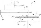
본 발명에 따른 실시형태에 대해 설명한다. 본 실시형태에 따른 가공 방법의 피가공물인 웨이퍼에 대해, 도 1의 (A) 및 도 1의 (B)를 이용하여 설명한다. 도 1의 (A)는 상기 웨이퍼를 도시한 사시도이다. 상기 웨이퍼(1)는, 예컨대, 실리콘, SiC(실리콘 카바이드), 혹은, 그 외의 반도체 등의 재료, 또는, 사파이어, 유리, 석영 등의 재료로 이루어지는 기판이다.An embodiment according to the present invention will be described. A wafer which is a workpiece of the processing method according to the present embodiment will be described with reference to FIGS. 1A and 1B . 1A is a perspective view showing the wafer. The
웨이퍼(1)의 표면(1a)은, 격자형으로 배열된 복수의 분할 예정 라인(스트리트)(3)에 의해 복수의 영역으로 구획되어 있다. 그리고, 분할 예정 라인(3)에 의해 구획된 각 영역에는, IC 등의 디바이스(5)가 형성되어 있다. 최종적으로, 웨이퍼(1)가 분할 예정 라인(3)을 따라 분할됨으로써, 개개의 디바이스 칩이 형성된다.A surface 1a of the
디바이스(5)에는 트랜지스터 등의 복수의 반도체 소자가 포함되어 있다. 상기 반도체 소자에 전기 신호 등을 전송하기 위해서, 상기 디바이스(5)에는 복수의 배선층이 형성되어 있고, 상기 복수의 배선층 사이에는, 각 배선을 전기적으로 절연하기 위한 층간 절연막이 형성되어 있다.The
그 때문에, 디바이스(5)에는, 2개의 배선층과, 상기 2개의 배선층에 끼워진 층간 절연막을 포함하는 기생 용량이 형성된다. 상기 기생 용량이 큰 경우, 디바이스(5) 내의 전기 신호의 전달에 지연을 발생시키거나, 또는, 디바이스(5)의 소비 전력이 증대하는 등 하여 문제가 된다. 디바이스(5)의 소형화가 진행되면, 상기 층간 절연막이 얇아지고 배선의 밀도도 올라가기 때문에, 기생 용량이 커진다.Therefore, in the
그래서, 상기 기생 용량을 저감하기 위해서, 층간 절연막에는, 유전율이 낮은 이른바 Low-k 재료를 갖는 기능층이 이용된다. 상기 Low-k 재료는, 유전율을 저감시키기 위해서 포러스(다공질) 구조가 되도록 형성된다. 그러나, 포러스(다공질) 구조는 기계적 강도가 낮기 때문에, 상기 Low-k 재료를 갖는 기능층의 기계적 강도는 낮다.Therefore, in order to reduce the parasitic capacitance, a functional layer having a so-called Low-k material having a low dielectric constant is used for the interlayer insulating film. The said Low-k material is formed so that it may become a porous (porous) structure in order to reduce dielectric constant. However, since the porous (porous) structure has low mechanical strength, the mechanical strength of the functional layer having the Low-k material is low.
도 1의 (B)는 상기 웨이퍼(1)의 일부의 표면(1a)을 도시한 상면도이다. 도 1의 (B)에 도시된 바와 같이, 분할 예정 라인(3)에는 부분적으로 TEG(Test Element Group)(7)가 형성되어 있다. TEG는, 상기 반도체 소자의 형성 프로세스상의 문제나 설계상의 문제의 유무를 검지하기 위해서 이용되는 회로 패턴이다. 도 1의 (B)에 도시된 바와 같이, 웨이퍼(1)의 분할 예정 라인(3)에 겹쳐지도록 TEG(7)가 형성되면, TEG(7)를 형성하기 위해서만, 웨이퍼(1)의 표면(1a)에 장소를 확보할 필요가 없다.FIG. 1B is a top view showing a surface 1a of a part of the
다음으로, 본 실시형태에 따른 웨이퍼의 가공 방법에 대해 설명한다. 상기 가공 방법에서는, 상기 기능층에 흡수되는 파장의 레이저 빔을, 웨이퍼(1)의 상기 표면(1a)측으로부터 상기 분할 예정 라인(3)을 따라 조사하여, 상기 기능층을 분단하는 가공홈을 형성하는 가공홈 형성 단계를 실시한다. 또한, 웨이퍼(1)에 대해 투과성을 갖는 파장의 레이저 빔을, 상기 웨이퍼(1)의 이면(1b)측으로부터 상기 분할 예정 라인(3)을 따라 조사하여, 상기 웨이퍼(1)의 내부에 상기 분할 예정 라인(3)을 따르는 개질층을 형성하는 개질층 형성 단계를 실시한다.Next, the processing method of the wafer which concerns on this embodiment is demonstrated. In the above processing method, a laser beam having a wavelength absorbed by the functional layer is irradiated from the surface 1a side of the
그 후, 상기 가공홈 및 상기 개질층이 형성된 웨이퍼(1)에 외력을 부여하여, 상기 개질층을 기점으로 웨이퍼(1)를 상기 분할 예정 라인을 따라 분할하는 분할 단계를 실시한다. 이하, 상기 가공 방법의 각 단계에 대해 설명한다.Thereafter, an external force is applied to the
먼저, 가공홈 형성 단계에 대해 설명한다. 도 2의 (A)는 상기 가공홈 형성 단계를 설명하는 사시도이다. 가공홈 형성 단계에서는, 분할 예정 라인(3)을 따라, 웨이퍼(1)의 표면(1a) 상에 형성된 상기 기능층을 분단하는 가공홈(13)을 형성한다. 도 2의 (A)에 도시된 바와 같이, 웨이퍼(1)의 이면(1b)측에는 미리 환형의 프레임(9)에 부착된 테이프(11)를 접착한다. 그러면, 상기 프레임(9)을 통해 웨이퍼(1)를 취급할 수 있기 때문에, 웨이퍼(1)를 반송이나 가공에 의한 예기하지 못한 충격 등으로부터 보호할 수 있다.First, the process groove forming step will be described. 2A is a perspective view for explaining the step of forming the machining groove. In the machining groove forming step, along the
가공홈 형성 단계에서 이용하는 레이저 가공 장치(2)에 대해 설명한다. 상기 레이저 가공 장치(2)는, 웨이퍼(1)를 흡인 유지하는 척 테이블(4)과, 레이저 빔을 발진하는 가공 헤드(6)를 구비한다.The laser processing apparatus 2 used in the processing groove formation step is demonstrated. The laser processing apparatus 2 includes a chuck table 4 for holding the
척 테이블(4)은 상면측에 다공질 부재를 갖는다. 상기 다공질 부재의 상면은 척 테이블(4)의 웨이퍼(1)를 유지하는 유지면(4a)이 된다. 척 테이블(4)은, 흡인원(도시하지 않음)에 접속된 흡인로(도시하지 않음)를 내부에 가지며, 상기 흡인로의 타단이 상기 다공질 부재에 접속되어 있다. 상기 유지면(4a) 상에 프레임(9)에 부착된 테이프(11) 상에 접착된 웨이퍼(1)가 배치되고, 상기 다공질 부재의 구멍을 통해 상기 웨이퍼(1)에 대해 상기 흡인원에 의해 발생한 부압이 작용되면, 웨이퍼(1)는 척 테이블(4)에 흡인 유지된다.The chuck table 4 has a porous member on the upper surface side. The upper surface of the porous member serves as a holding
가공 헤드(6)는, 웨이퍼(1) 상에 적층된 상기 기능층에 흡수되는 파장의 레이저 빔을 발진해서 웨이퍼(1)의 표면(1a)에 조사하여, 상기 기능층에 어블레이션 가공을 실시하여 가공홈을 형성하는 기능을 갖는다. 한편, 상기 레이저 빔에는, 예컨대, Nd:YVO4나 Nd:YAG를 매체로 하여 발진되는 레이저 빔이 이용된다.The processing head 6 oscillates a laser beam having a wavelength absorbed by the functional layer stacked on the
레이저 가공 장치(2)는 펄스 모터 등을 동력으로 하는 가공 이송 수단(가공 이송 기구, 도시하지 않음)에 의해, 척 테이블(4)을 레이저 가공 장치(2)의 가공 이송 방향[예컨대, 도 2의 (A)의 화살표의 방향]으로 이동시킬 수 있다. 웨이퍼(1)의 가공 시 등에는, 척 테이블(4)을 가공 이송 방향으로 보내어 웨이퍼(1)를 가공 이송시킨다. 또한, 척 테이블(4)은 유지면(4a)에 대략 수직인 축의 주위로 회전 가능하고, 척 테이블(4)을 회전시키면 웨이퍼(1)를 가공 이송시키는 방향을 변경할 수 있다.The laser processing apparatus 2 moves the chuck table 4 in the processing transfer direction of the laser processing apparatus 2 (for example, FIG. in the direction of the arrow in (A)]. When processing the
또한, 레이저 가공 장치(2)는 펄스 모터 등을 동력으로 하는 인덱싱 이송 수단(인덱싱 이송 기구, 도시하지 않음)에 의해, 척 테이블(4)을 레이저 가공 장치(2)의 인덱싱 이송 방향(도시하지 않음)으로 이동시킬 수 있다.In addition, the laser processing apparatus 2 moves the chuck table 4 in the indexing transfer direction of the laser processing apparatus 2 (not shown) by indexing transfer means (indexing transfer mechanism, not shown) powered by a pulse motor or the like. not) can be moved to
가공홈 형성 단계에서는, 먼저, 프레임(9)에 부착된 테이프(11)에 접착된 웨이퍼(1)의 표면(1a)을 상측으로 향하게 하여, 레이저 가공 장치(2)의 척 테이블(4) 상에 웨이퍼(1)를 배치한다. 그리고, 상기 척 테이블(4)로부터 부압을 작용시켜, 웨이퍼(1)를 척 테이블(4)의 유지면(4a) 상에 흡인 유지시킨다.In the machining groove forming step, first, the surface 1a of the
웨이퍼(1)를 흡인 유지시킨 후, 분할 예정 라인(3)의 하나를 따라 가공홈(13)을 형성할 수 있도록, 척 테이블(4)을 이동시켜 상기 분할 예정 라인(3)의 단부 바로 위에 가공 헤드(6)를 위치시킨다. 다음으로, 레이저 가공 장치(2)의 가공 헤드(6)로부터 웨이퍼(1)의 표면(1a)에 레이저 빔을 조사한다. 그리고, 분할 예정 라인(3)을 따라 상기 기능층을 분단하는 가공홈(13)이 형성되도록, 레이저 빔을 조사시키면서 척 테이블(4)을 이동시켜 웨이퍼(1)를 가공 이송한다.After the
하나의 분할 예정 라인(3)을 따라 가공홈(13)을 형성한 후, 웨이퍼(1)를 인덱싱 이송하여, 인접하는 분할 예정 라인(3)을 따라 차례로 가공홈(13)을 형성한다. 또한, 하나의 방향을 따라 각 분할 예정 라인(3)을 따라 가공홈(13)을 형성한 후, 웨이퍼(1)를 흡인 유지하는 척 테이블(4)을 4분의 1 회전시켜, 웨이퍼(1)의 가공 이송 방향을 변경한다. 그 후, 레이저 빔을 마찬가지로 분할 예정 라인(3)을 따라 조사함으로써, 모든 분할 예정 라인(3)을 따라 가공홈(13)을 형성한다.After forming the
단, 가공홈 형성 단계에서는, 분할 예정 라인(3)에 형성된 TEG(7)에는 상기 레이저 빔을 조사하지 않는다. 도 2의 (B)를 이용하여 설명한다. 도 2의 (B)는 가공홈 형성 단계에 의해 가공홈(13)이 형성된 웨이퍼(1)의 일부를 도시한 평면도이다. 분할 예정 라인(3)과 겹쳐지는 TEG(7)가 형성되어 있고, 상기 TEG(7)는 금속을 갖는 층을 포함한다.However, in the step of forming the processing groove, the laser beam is not irradiated to the
그 때문에, 상기 TEG(7)에 상기 레이저 빔을 조사하여 어블레이션 가공을 행하면, 상기 TEG(7)로부터 금속의 버어가 발생해 버린다. 상기 금속의 버어는, 웨이퍼(1)의 표면(1a)으로부터 수직인 방향으로 돌출된다. 표면(1a)으로부터 돌출된 금속의 버어는, 웨이퍼(1)가 분할되어 개개의 디바이스 칩이 형성된 후에도 상기 디바이스 칩에 남는다. 그러면, 예컨대, 상기 디바이스 칩을 형성한 후에, 복수의 상기 디바이스 칩을 적층(스택)시켜 적층 칩을 형성할 때, 상기 금속의 버어가 간섭하여 적절히 적층할 수 없다.Therefore, when ablation is performed by irradiating the laser beam to the
디바이스 칩을 적층시키지 않는 경우에도, 디바이스 칩의 반송이나 실장 시에, 상기 금속의 버어가 탈락 등 해서 티끌이 되어, 디바이스 칩의 실장 대상이나 다른 디바이스 칩의 실장 대상에 부착되어, 실장 불량을 일으키는 원인이 되는 경우가 있다. 또한, 상기 금속의 버어가 다른 디바이스 칩이나 지그 등에 닿아, 이들을 손상시키는 경우가 있어, 문제가 된다. 또한, 금속의 버어가 회로의 쇼트를 일으키는 원인이 되는 경우도 있다.Even when the device chips are not stacked, the metal burrs fall off and become particles during transport or mounting of the device chips, and they adhere to the mounting target of the device chip or the mounting target of other device chips, causing mounting failure. It may be the cause. In addition, the metal burrs may come in contact with other device chips or jigs and damage them, which is a problem. Also, there are cases where a metal burr causes a short circuit in the circuit.
한편, 본 실시형태에 따른 웨이퍼의 가공 방법의 가공홈 형성 단계에서는, 분할 예정 라인(3)에 형성된 TEG(7)에는 레이저 빔을 조사하지 않는다. 그 때문에, 상기 금속의 버어가 발생하지 않아, 이러한 문제를 발생시키지 않는다. 도 3의 (A)는 가공홈 형성 단계를 설명하는 부분 단면도이고, 도 3의 (B)는 레이저 빔이 조사되는 개소를 확대하여 도시한 단면 모식도이다. 도 3의 (A) 및 도 3의 (B)에 도시된 바와 같이, 가공홈(13)은, TEG(7)가 형성되어 있지 않은 부분의 기능층(5a)을 제거하여 형성된다.On the other hand, in the processing groove forming step of the wafer processing method according to the present embodiment, the laser beam is not irradiated to the
TEG(7)가 형성되어 있지 않은 부분의 기능층(5a)을 제거하여 가공홈(13)을 형성하기 위해서는, 예컨대, 레이저 가공 장치(2)의 가공 헤드(6)에 인접하여 설치된 촬상 카메라(도시하지 않음)에 의해, 웨이퍼(1)의 표면(1a)을 촬상하면서 가공홈(13)을 형성하면 된다. 상기 촬상 카메라로 TEG(7)를 파악하여, 상기 TEG(7)에 레이저 빔을 조사하지 않도록 레이저 빔의 발진과 정지를 제어하면 된다.In order to remove the
본 실시형태에 따른 웨이퍼의 가공 방법에서는, 다음으로, 표면 보호 테이프 접착 단계를 실시한다. 표면 보호 테이프 접착 단계에 대해, 도 4를 이용하여 설명한다. 도 4는 표면 보호 테이프 접착 단계를 모식적으로 설명하는 사시도이다.In the processing method of the wafer which concerns on this embodiment, next, the surface protection tape adhesion|attaching step is implemented. The surface protection tape adhesion step will be described with reference to FIG. 4 . Fig. 4 is a perspective view schematically illustrating a step of attaching a surface protection tape.
가공홈 형성 단계 실시 후의 웨이퍼(1)의 이면(1b)측에는, 프레임(9)에 부착된 테이프(11)가 접착되어 있다. 본 실시형태에 따른 가공 방법에서는, 그 후에 웨이퍼(1)의 이면(1b)측으로부터 레이저 빔을 조사하는 개질층 형성 단계를 실시한다. 그 때문에, 웨이퍼(1)의 이면(1b)측의 테이프(11)를 박리한다.The
테이프(11)를 웨이퍼(1)의 이면(1b)으로부터 박리한 후, 도 4에 도시된 바와 같이, 웨이퍼(1)의 표면(1a)에 표면 보호 테이프(15)를 접착한다. 표면 보호 테이프(15)는, 디바이스(5)와, 상기 디바이스(5) 주위를 둘러싸는 가공홈(13)이 형성된 웨이퍼(1)의 표면(1a)을 보호하여, 그 후의 각 단계나 웨이퍼(1)의 반송 시에 예기하지 못한 충격 등이 가해져 상기 표면(1a)에 손상이 발생하는 것을 방지한다.After the
한편, 표면 보호 테이프 접착 단계에서는, 웨이퍼(1)의 이면(1b)에 접착된 테이프(11)를 박리하기 전에 표면 보호 테이프(15)를 접착하고, 그 후에 테이프(11)를 박리해도 좋다.On the other hand, in the surface protection tape adhesion step, before peeling the
다음으로, 본 실시형태에 따른 웨이퍼의 가공 방법의 개질층 형성 단계에 대해, 도 5의 (A) 및 도 5의 (B)를 이용하여 설명한다. 상기 개질층 형성 단계는, 가공홈 형성 단계보다 후에 실시한다. 도 5의 (A)는 개질층 형성 단계를 설명하는 사시도이고, 도 5의 (B)는 개질층 형성 단계를 설명하는 부분 단면도이다.Next, the modified layer forming step of the wafer processing method according to the present embodiment will be described with reference to FIGS. 5A and 5B . The modified layer forming step is performed after the machining groove forming step. FIG. 5A is a perspective view illustrating a modified layer forming step, and FIG. 5B is a partial cross-sectional view illustrating a modified layer forming step.
개질층 형성 단계에서는, 웨이퍼(1)의 이면(1b)측으로부터 레이저 빔을 조사하여, 웨이퍼(1)의 내부의 소정의 깊이에 집광시키고, 분할 예정 라인(3)을 따라 개질층(17)을 형성한다. 제1 개질층 형성 단계에서 사용되는 레이저 가공 장치(8)는, 웨이퍼(1)를 흡인 유지하는 척 테이블(10)과, 레이저 빔을 발진하는 가공 헤드(12)를 구비한다. 상기 척 테이블(10)은, 레이저 가공 장치(2)의 척 테이블(4)과 동일한 구성이고, 웨이퍼(1)를 가공 이송 및 인덱싱 이송할 수 있다.In the modified layer forming step, a laser beam is irradiated from the
가공 헤드(12)는, 웨이퍼(1)에 대해 투과성을 갖는 파장의 레이저 빔을 발진하여 웨이퍼(1)의 내부의 소정의 깊이에 집광하는 기능을 갖고, 다광자 흡수에 의해 상기 소정의 깊이에 개질층(17)을 형성한다. 한편, 상기 레이저 빔에는, 예컨대, Nd:YVO4나 Nd:YAG를 매체로 하여 발진되는 레이저 빔이 이용된다.The
개질층 형성 단계에서는, 먼저, 웨이퍼(1)의 표면(1a)을 하측으로 향하게 하여, 레이저 가공 장치(8)의 척 테이블(10) 상에 표면 보호 테이프(15)를 통해 웨이퍼(1)를 배치한다. 그리고, 상기 척 테이블(10)로부터 부압을 작용시켜, 웨이퍼(1)를 척 테이블(10)의 유지면(10a) 상에 흡인 유지시킨다. 웨이퍼(1)의 표면(1a)에 표면 보호 테이프(15)가 접착되어 있는 경우, 웨이퍼(1)는 상기 표면 보호 테이프(15)를 통해 척 테이블(10)에 유지된다.In the modified layer forming step, first, with the surface 1a of the
웨이퍼(1)를 흡인 유지시킨 후, 분할 예정 라인(3)을 따라 개질층(17)을 형성할 수 있도록, 척 테이블(10)과 가공 헤드(12)의 상대 위치를 조정한다. 다음으로, 레이저 가공 장치(8)의 가공 헤드(12)로부터 웨이퍼(1)의 이면(1b)측에 레이저 빔을 조사한다. 레이저 빔을 웨이퍼(1)의 소정의 깊이에 집광시켜, 다광자 흡수에 의해 개질층(17)을 형성한다. 분할 예정 라인(3)을 따라 개질층(17)이 형성되도록, 상기 레이저 빔을 조사시키면서 척 테이블(10)을 이동시켜 웨이퍼(1)를 가공 이송한다.After holding the
하나의 분할 예정 라인(3)을 따라 개질층(17)이 형성된 후, 웨이퍼(1)를 인덱싱 이송하여, 인접하는 분할 예정 라인(3)을 따라 차례로 개질층(17)을 형성한다.After the modified
한편, 레이저 빔의 조사 조건에 따라서는, 개질층(17)을 형성한 후, 상기 개질층(17)으로부터 웨이퍼(1)의 표면(1a)에 이르는 크랙을 형성할 수 있다. 이와 같이, 개질층 형성 단계에서 크랙을 형성할 수 있으면, 크랙을 형성하기 위한 단계를 별도로 실시할 필요가 없어 공정을 간략화할 수 있다.On the other hand, depending on the irradiation conditions of the laser beam, after forming the modified
다음으로, 분할 단계에 대해 설명한다. 상기 분할 단계에서는, 상기 가공홈(13) 및 상기 개질층(17)이 형성된 웨이퍼에 외력을 부여하여, 상기 개질층(17)을 기점으로 웨이퍼를 분할 예정 라인(3)을 따라 분할한다.Next, the division step will be described. In the dividing step, an external force is applied to the wafer on which the
분할 단계에서는, 먼저, 웨이퍼(1)를 이면(1b)측으로부터 연삭하여 웨이퍼(1)를 박화하는 연삭 단계를 실시한다. 연삭 단계에서는, 상기 연삭에 의해 발생한 힘이 개질층(17)에 부여되어 상기 개질층(17)으로부터 웨이퍼(1)의 표면(1a)에 이르는 크랙을 신장시킨다. 그 후, 분할 단계에서는, 웨이퍼(1)에 외주 방향을 향한 힘을 부여하는 확장 단계를 실시한다.In the dividing step, first, a grinding step of thinning the
먼저, 도 6을 이용하여 분할 단계의 연삭 단계에 대해 설명한다. 개질층 형성 단계에 있어서, 개질층(17)으로부터 웨이퍼(1)의 표면(1a)에 이르는 크랙을 형성하고 있지 않은 경우에는, 상기 연삭 단계에 있어서 상기 크랙을 형성한다. 그 경우, 연삭에 의해 발생하는 외력을 상기 개질층(17)에 작용시켜 크랙을 형성한다. 모든 개질층(17)으로부터 웨이퍼(1)의 표면(1a)에 이르는 크랙(19)이 형성되고, 웨이퍼(1)가 이면(1b)으로부터 연삭되어 상기 개질층(17)이 제거되면, 개개의 디바이스 칩이 형성된다.First, the grinding step of the dividing step will be described with reference to FIG. 6 . In the case where the crack from the modified
도 6은 연삭 단계를 모식적으로 설명하는 부분 단면도이다. 본 단계에서는 연삭 장치(14)가 이용된다. 연삭 장치(14)는, 연삭 휠(20)에 수직인 회전축을 구성하는 스핀들(16)과, 상기 스핀들(16)의 일단측에 장착되고 하측에 연삭 지석(18)을 구비하는 원반형의 연삭 휠(20)을 구비한다. 상기 스핀들(16)의 타단측에는 모터 등의 회전 구동원(도시하지 않음)이 연결되어 있고, 상기 모터가 상기 스핀들(16)을 회전시키면, 상기 스핀들(16)에 장착된 연삭 휠(20)도 회전한다.6 is a partial cross-sectional view schematically illustrating a grinding step. In this step, the grinding
또한, 연삭 장치(14)는, 연삭 휠(20)과 대면하여 웨이퍼(1) 등의 피가공물을 유지하는 척 테이블(22)을 갖는다. 척 테이블(22) 상의 유지면(22a)은, 흡인원(도시하지 않음)에 접속된 다공질 부재로 구성된다. 한편, 척 테이블(22)은, 유지면(22a)에 대략 수직인 축의 주위로 회전 가능하다. 또한, 연삭 장치(14)는, 승강 기구(도시하지 않음)를 갖고 있고, 연삭 휠(20)은 상기 승강 기구에 의해 가공 이송(하강)된다.Further, the grinding
연삭 단계에서는, 먼저, 웨이퍼(1)의 표면(1a)을 하측으로 향하게 하여, 척 테이블(22)의 유지면(22a) 상에 표면 보호 테이프(15)를 통해 웨이퍼(1)를 배치한다. 그리고, 상기 다공질 부재를 통해 상기 흡인원에 의한 부압을 작용시켜, 웨이퍼(1)를 척 테이블(22) 상에 흡인 유지시킨다.In the grinding step, first, with the surface 1a of the
연삭 시에는, 척 테이블(22)을 회전시키고, 스핀들(16)을 회전시켜 연삭 휠(20)을 회전시킨다. 척 테이블(22) 및 연삭 휠(20)이 회전하고 있는 상태에서, 연삭 휠(20)이 가공 이송(하강)되어 연삭 지석(18)이 웨이퍼(1)의 이면(1b)에 닿으면, 상기 이면(1b)의 연삭이 개시된다. 그리고, 웨이퍼(1)가 소정의 두께가 되도록 연삭 휠(20)을 더욱 가공 이송한다.In grinding, the chuck table 22 is rotated and the
개질층(17)을 형성할 때에 개질층(17)으로부터 웨이퍼(1)의 표면(1a)에 이르는 크랙을 형성하고 있지 않은 경우, 또는, 상기 크랙의 형성이 불충분한 경우, 상기 연삭 단계에서 상기 크랙(19)을 형성한다. 즉, 상기 연삭에 의해 발생한 힘을 웨이퍼(1)의 내부에 작용시켜, 개질층(17)으로부터 웨이퍼(1)의 두께 방향으로 크랙(19)을 신장시킨다. 웨이퍼(1)의 이면(1b)을 연삭하여 분할 예정 라인(3)을 따라 크랙(19)을 형성하고, 개질층(17)이 연삭에 의해 제거되어 웨이퍼(1)가 박화되면, 개개의 디바이스 칩이 형성된다.In the case where cracks extending from the modified
그런데, 상기 크랙(19)이 형성되기 전에, 웨이퍼(1)의 표면(1a)측에는 분할 예정 라인(3)을 따라, 기능층을 분단하는 가공홈(13)이 형성되어 있다. 한편, 개질층(17)도 분할 예정 라인(3)을 따라 형성되기 때문에, 개질층(17)과, 가공홈(13)은 서로 겹쳐진다. 가공홈(13)이 형성되어 있는 부분은 기계적 강도가 약하기 때문에, 개질층(17)으로부터 표면(1a)측을 향해 크랙(19)이 신장할 때, 상기 크랙(19)은 가공홈(13)으로 유도되어, 상기 가공홈(13)에 이른다. 그 때문에, 크랙(19)은 예기하지 못한 방향으로 신장하기 어렵다.However, before the
또한, 웨이퍼(1)의 표면(1a)측에는, 분할 예정 라인(3) 상에 TEG(7)가 형성되어 있고, 상기 TEG(7)가 있는 부분에서는, 가공홈(13)이 형성되어 있지 않다. 그러나, 가공홈(13)이 형성되지 않는 장소는, 분할 예정 라인(3)의 전체 길이 중 매우 작은 영역뿐이다. 그 때문에, 가공홈(13)이 형성되어 있지 않은 TEG(7)의 형성 개소에 있어서도, 그 전후의 가공홈(13)이 형성되어 있는 장소에 발생하는 크랙(19)으로 유도되어, 마찬가지로 크랙(19)이 웨이퍼(1)의 표면(1a)으로 신장한다. 그리고, 상기 크랙(19)이 기능층을 분단한다.In addition, on the surface 1a side of the
즉, 실시형태에 따른 웨이퍼의 가공 방법에 있어서는, 웨이퍼(1)의 표면(1a)측에 형성된 Low-k 재료를 갖는 기능층은, 분할 예정 라인(3)을 따라 가공홈(13)과 크랙(19)에 의해 분단된다. 이때, 기능층에 가해지는 부하는 다른 방법으로 기능층을 분단할 때에 가해지는 부하보다 작아지기 때문에, 기능층의 박리가 발생하기 어렵다.That is, in the wafer processing method according to the embodiment, the functional layer having a low-k material formed on the surface 1a side of the
본 실시형태에 따른 분할 단계에서는, 상기 연삭 단계 후에, 확장 단계를 실시한다. 확장 단계에서는, 웨이퍼(1)에 외주 방향을 향한 힘을 가하여, 개개의 디바이스 칩 사이의 간극을 확대시킨다. 도 7의 (A) 및 도 7의 (B)를 이용하여 확장 단계에 대해 설명한다.In the dividing step according to the present embodiment, the expanding step is performed after the grinding step. In the expansion step, a force in the circumferential direction is applied to the
상기 확장 단계에서는, 웨이퍼(1)의 이면(1b)측에 다이싱 테이프를 접착하고, 상기 다이싱 테이프를 외주 방향으로 확장함으로써, 웨이퍼(1)에 외주 방향을 향한 힘을 작용시켜, 형성된 개개의 디바이스 칩 사이의 간극을 확대시킨다. 디바이스 칩 사이의 상기 간극이 확대되면, 개개의 디바이스 칩이 픽업 가능해진다. 도 7의 (A)는 확장 전을 설명하는 부분 단면도이고, 도 7의 (B)는 확장 후를 설명하는 부분 단면도이다.In the expansion step, the dicing tape is adhered to the
분할 단계의 연삭 단계의 실시 후에, 웨이퍼(1)(디바이스 칩)의 이면(1b)측에, 환형의 프레임(23)에 부착된 다이싱 테이프(21)를 접착한다. 그 후, 웨이퍼(1)의 표면(1a)측에 접착되어 있던 표면 보호 테이프(15)를 박리한다. 그리고, 프레임(23)째 웨이퍼(1)를 확장 장치(24) 상에 배치한다.After implementation of the grinding step of the dividing step, the dicing
확장 단계에서 이용하는 확장 장치(24)는, 도 7의 (A)에 도시된 바와 같이, 확장 드럼(26)과, 지지 부재(28)를 갖는다. 지지 부재(28)의 상방에는, 확장 드럼(26) 상에 배치된 프레임(23)을 유지하는 기구를 갖는다. 확장 드럼(26)은, 대략 원통형의 부재이며, 상하 방향으로 지지 부재(28)에 대해 상대적으로 이동할 수 있다.The
확장 장치(24)의 확장 드럼(26) 상에, 상기 프레임(23)째 웨이퍼(1)를 배치한 후, 지지 부재(28)에 상기 프레임(23)을 유지시켜 고정한다. 다음으로, 확장 드럼(26)을 상기 지지 부재(28)에 대해 상대적으로 상방으로 이동시킨다. 그러면, 다이싱 테이프(21)가 외주 방향을 향해 확장된다.After the
도 7의 (B)는 다이싱 테이프(21)가 확장되었을 때의 상태를 설명하는 부분 단면도이다. 도 7의 (B)에 도시된 바와 같이, 다이싱 테이프(21)가 확장되면, 상기 다이싱 테이프(21) 상의 웨이퍼(1)에 외주 방향을 향한 힘이 작용하여, 개개의 디바이스 칩(25) 사이의 간극이 확장된다.Fig. 7B is a partial cross-sectional view for explaining a state when the dicing
도 8의 (A)는 다이싱 테이프(21)의 확장 후의 웨이퍼(1)[디바이스 칩(25)]의 일부를 도시한 상면도이다. 도 8의 (A)에 도시된 바와 같이, 웨이퍼(1)는 분할 예정 라인(3)을 따라 분할되어 개개의 디바이스 칩(25)이 형성된다. 상기 분할 예정 라인(3)에 있어서, Low-k막으로 이루어지는 기능층(5a)은 레이저 빔에 의한 어블레이션 가공에 의해 분단되기 때문에, 상기 기능층(5a)에 박리 등의 문제는 발생하지 않는다.FIG. 8A is a top view showing a part of the wafer 1 (device chip 25) after the dicing
도 8의 (B)는 다이싱 테이프(21)의 확장 후의 웨이퍼(1)[디바이스 칩(25)]의 일부를 도시한 단면도이다. 도 8의 (B)에 도시된 바와 같이, 금속을 포함하는 TEG(7)도 분단되어 있다. 금속을 포함하는 TEG(7)는, 레이저 빔에 의한 어블레이션 가공 등으로 분단되는 것이 아니기 때문에, 분단 개소에 상하 방향으로 연장된 금속의 버어가 형성되지 않는다. 그 때문에, 형성된 디바이스 칩(25)의 표면에는 상기 버어 등의 돌기는 형성되지 않고, 표면이 평탄해진다.8B is a cross-sectional view showing a part of the wafer 1 (device chip 25) after the dicing
이상 설명한 바와 같이, 본 실시형태에 따른 웨이퍼 가공 방법에 의하면, 상기 웨이퍼의 상기 기능층을 박리시키지 않고 상기 금속의 버어를 발생시키지 않고 상기 웨이퍼를 분할할 수 있다.As explained above, according to the wafer processing method which concerns on this embodiment, the said wafer can be divided|segmented without peeling off the said functional layer of the said wafer, and without generating the said metal burr.
한편, 본 발명은 상기 실시형태의 기재에 한정되지 않고, 여러 가지로 변경하여 실시 가능하다. 예컨대, 상기 실시형태에서는, 연삭 단계에 있어서 발생한 힘을 개질층에 가함으로써, 개질층으로부터 웨이퍼의 표면으로 신장하는 크랙을 형성하여 웨이퍼를 분단하였다. 그러나, 본 발명은 이것에 한정되지 않고, 예컨대, 연삭 단계에서는 크랙을 발생시키지 않고, 확장 단계에 있어서 웨이퍼에 외주 방향을 향해 힘을 가함으로써 상기 크랙을 신장시켜도 좋다.In addition, this invention is not limited to the description of the said embodiment, It can be changed and implemented in various ways. For example, in the above embodiment, by applying the force generated in the grinding step to the modified layer, cracks extending from the modified layer to the surface of the wafer were formed and the wafer was divided. However, the present invention is not limited to this, and for example, cracks may be extended by applying a force to the wafer in the circumferential direction in the expansion step without generating cracks in the grinding step.
그 외에, 상기 실시형태에 따른 구조, 방법 등은, 본 발명의 목적의 범위를 일탈하지 않는 한에 있어서 적절히 변경하여 실시할 수 있다.In addition, the structure, method, etc. which concern on the said embodiment can be implemented by changing suitably, unless it deviates from the scope of the objective of this invention.
1: 웨이퍼1a: 표면
1b: 이면3: 분할 예정 라인
5: 디바이스5a: 기능층
7: TEG9, 23: 프레임
11: 테이프13: 가공홈
15: 표면 보호 테이프17: 개질층
19: 크랙21: 다이싱 테이프
25: 디바이스 칩2, 8: 레이저 가공 장치
4, 10, 22: 척 테이블4a, 10a, 22a: 유지면
6, 12: 가공 헤드14: 연삭 장치
16: 스핀들18: 연삭 지석
20: 연삭 휠24: 확장 장치
26: 확장 드럼28: 지지 부재1: wafer 1a: surface
1b: back side 3: line to be split
5:
7:
11: Tape 13: Machining groove
15: surface protection tape 17: modified layer
19: crack 21: dicing tape
25: device chip 2, 8: laser processing apparatus
4, 10, 22: chuck table 4a, 10a, 22a: holding surface
6, 12: machining head 14: grinding device
16: spindle 18: grinding wheel
20: grinding wheel 24: extension unit
26: expansion drum 28: support member
Claims (2)
Translated fromKorean상기 기능층에 흡수되는 파장의 레이저 빔을, 웨이퍼의 상기 표면측으로부터 상기 분할 예정 라인을 따라 조사하여, 상기 기능층을 분단하는 가공홈을 형성하는 가공홈 형성 단계와,
상기 웨이퍼에 대해 투과성을 갖는 파장의 레이저 빔을, 상기 웨이퍼의 이면측으로부터 상기 분할 예정 라인을 따라 조사하여, 상기 웨이퍼의 내부에 상기 분할 예정 라인을 따르는 개질층을 형성하는 개질층 형성 단계와,
상기 가공홈 및 상기 개질층이 형성된 웨이퍼에 외력을 부여하여, 상기 개질층을 기점으로 웨이퍼를 상기 분할 예정 라인을 따라 분할하는 분할 단계를 포함하고,
상기 가공홈 형성 단계에서는, 상기 분할 예정 라인의 상기 TEG가 형성되어 있지 않은 영역에만 상기 레이저 빔을 조사하고, 상기 TEG의 전후로 나누어진 상기 가공홈을 형성하는 것을 특징으로 하는 웨이퍼의 가공 방법.A wafer having a functional layer, a plurality of devices including the functional layer, a division scheduled line dividing the device, and a Test Element Group (TEG) including a metal overlapping the division scheduled line, on the surface, is divided into the division A method of processing a wafer divided along a predetermined line, comprising:
A processing groove forming step of forming a processing groove for dividing the functional layer by irradiating a laser beam having a wavelength absorbed by the functional layer along the dividing line from the surface side of the wafer;
A modified layer forming step of irradiating a laser beam having a wavelength having a transmittance to the wafer along the predetermined division line from the back side of the wafer to form a modified layer along the predetermined division line inside the wafer;
A division step of dividing the wafer along the division line with the modified layer as a starting point by applying an external force to the wafer on which the processing groove and the modified layer are formed,
In the forming of the processing groove, the laser beam is irradiated only to an area where the TEG is not formed on the line to be divided, and the processing groove divided before and after the TEG is formed.
상기 연삭 단계는, 상기 TEG의 형성 부분에서 상기 개질층으로부터 상기 웨이퍼의 상기 표면으로 크랙을 신장시켜 상기 TEG를 분단하는 것을 특징으로 하는 웨이퍼의 가공 방법.
The method of claim 1, wherein the dividing step comprises a grinding step of grinding the wafer from the back side to thin it to a finished thickness,
The grinding step comprises dividing the TEG by extending a crack from the modified layer to the surface of the wafer in the portion where the TEG is formed.
Applications Claiming Priority (2)
| Application Number | Priority Date | Filing Date | Title |
|---|---|---|---|
| JPJP-P-2016-239559 | 2016-12-09 | ||
| JP2016239559AJP6815692B2 (en) | 2016-12-09 | 2016-12-09 | Wafer processing method |
Publications (2)
| Publication Number | Publication Date |
|---|---|
| KR20180066864A KR20180066864A (en) | 2018-06-19 |
| KR102349663B1true KR102349663B1 (en) | 2022-01-11 |
Family
ID=62633748
Family Applications (1)
| Application Number | Title | Priority Date | Filing Date |
|---|---|---|---|
| KR1020170167305AActiveKR102349663B1 (en) | 2016-12-09 | 2017-12-07 | Wafer processing method |
Country Status (2)
| Country | Link |
|---|---|
| JP (1) | JP6815692B2 (en) |
| KR (1) | KR102349663B1 (en) |
Families Citing this family (8)
| Publication number | Priority date | Publication date | Assignee | Title |
|---|---|---|---|---|
| JP7154860B2 (en)* | 2018-07-31 | 2022-10-18 | 株式会社ディスコ | Wafer processing method |
| JP7307533B2 (en)* | 2018-10-04 | 2023-07-12 | 浜松ホトニクス株式会社 | Laser processing method, semiconductor device manufacturing method and inspection device |
| JP7171353B2 (en)* | 2018-10-04 | 2022-11-15 | 浜松ホトニクス株式会社 | Laser processing method, semiconductor device manufacturing method and inspection device |
| JP7307534B2 (en) | 2018-10-04 | 2023-07-12 | 浜松ホトニクス株式会社 | Laser processing method, semiconductor device manufacturing method and inspection apparatus |
| JP2020077782A (en)* | 2018-11-08 | 2020-05-21 | 株式会社ディスコ | Wafer processing method |
| KR102653165B1 (en)* | 2018-11-22 | 2024-04-01 | 삼성전자주식회사 | Semiconductor device, semiconductor chip and method of sawing a semiconductor substrate |
| JP7313253B2 (en)* | 2019-10-10 | 2023-07-24 | 株式会社ディスコ | Wafer processing method |
| JP2023032838A (en)* | 2021-08-27 | 2023-03-09 | 株式会社ディスコ | Manufacturing method of semiconductor device |
Citations (9)
| Publication number | Priority date | Publication date | Assignee | Title |
|---|---|---|---|---|
| JP2006041449A (en) | 2004-06-22 | 2006-02-09 | Nec Electronics Corp | Semiconductor wafer, and manufacturing method of semiconductor device |
| JP2006318966A (en) | 2005-05-10 | 2006-11-24 | Disco Abrasive Syst Ltd | Semiconductor wafer |
| JP2006344795A (en)* | 2005-06-09 | 2006-12-21 | Disco Abrasive Syst Ltd | Wafer division method |
| JP2007012878A (en) | 2005-06-30 | 2007-01-18 | Disco Abrasive Syst Ltd | Wafer division method |
| JP2009032726A (en) | 2007-07-24 | 2009-02-12 | Disco Abrasive Syst Ltd | Wafer division method |
| JP2012114322A (en)* | 2010-11-26 | 2012-06-14 | Shinko Electric Ind Co Ltd | Dicing method of semiconductor wafer |
| JP2014146810A (en)* | 2014-03-03 | 2014-08-14 | Disco Abrasive Syst Ltd | Wafer dividing method |
| JP2015106693A (en) | 2013-12-02 | 2015-06-08 | 旭化成エレクトロニクス株式会社 | Semiconductor wafer and semiconductor device manufacturing method |
| US20150235973A1 (en) | 2005-11-10 | 2015-08-20 | Renesas Electronics Corporation | Semiconductor device manufacturing method and semiconductor device |
Family Cites Families (3)
| Publication number | Priority date | Publication date | Assignee | Title |
|---|---|---|---|---|
| JP2007173475A (en) | 2005-12-21 | 2007-07-05 | Disco Abrasive Syst Ltd | Wafer division method |
| JP2011187479A (en)* | 2010-03-04 | 2011-09-22 | Disco Corp | Wafer processing method |
| US8952497B2 (en)* | 2012-09-14 | 2015-02-10 | Taiwan Semiconductor Manufacturing Company, Ltd. | Scribe lines in wafers |
- 2016
- 2016-12-09JPJP2016239559Apatent/JP6815692B2/enactiveActive
- 2017
- 2017-12-07KRKR1020170167305Apatent/KR102349663B1/enactiveActive
Patent Citations (9)
| Publication number | Priority date | Publication date | Assignee | Title |
|---|---|---|---|---|
| JP2006041449A (en) | 2004-06-22 | 2006-02-09 | Nec Electronics Corp | Semiconductor wafer, and manufacturing method of semiconductor device |
| JP2006318966A (en) | 2005-05-10 | 2006-11-24 | Disco Abrasive Syst Ltd | Semiconductor wafer |
| JP2006344795A (en)* | 2005-06-09 | 2006-12-21 | Disco Abrasive Syst Ltd | Wafer division method |
| JP2007012878A (en) | 2005-06-30 | 2007-01-18 | Disco Abrasive Syst Ltd | Wafer division method |
| US20150235973A1 (en) | 2005-11-10 | 2015-08-20 | Renesas Electronics Corporation | Semiconductor device manufacturing method and semiconductor device |
| JP2009032726A (en) | 2007-07-24 | 2009-02-12 | Disco Abrasive Syst Ltd | Wafer division method |
| JP2012114322A (en)* | 2010-11-26 | 2012-06-14 | Shinko Electric Ind Co Ltd | Dicing method of semiconductor wafer |
| JP2015106693A (en) | 2013-12-02 | 2015-06-08 | 旭化成エレクトロニクス株式会社 | Semiconductor wafer and semiconductor device manufacturing method |
| JP2014146810A (en)* | 2014-03-03 | 2014-08-14 | Disco Abrasive Syst Ltd | Wafer dividing method |
Also Published As
| Publication number | Publication date |
|---|---|
| JP2018098296A (en) | 2018-06-21 |
| KR20180066864A (en) | 2018-06-19 |
| JP6815692B2 (en) | 2021-01-20 |
Similar Documents
| Publication | Publication Date | Title |
|---|---|---|
| KR102349663B1 (en) | Wafer processing method | |
| JP4959422B2 (en) | Wafer division method | |
| JP6078376B2 (en) | Wafer processing method | |
| JP4422463B2 (en) | Semiconductor wafer dividing method | |
| JP4694845B2 (en) | Wafer division method | |
| JP6178077B2 (en) | Wafer processing method | |
| KR20160006109A (en) | Wafer processing method | |
| JP2007173475A (en) | Wafer division method | |
| JP6189208B2 (en) | Wafer processing method | |
| JP2009021476A (en) | Wafer division method | |
| JP5992731B2 (en) | Wafer processing method | |
| JP2008283025A (en) | Wafer division method | |
| US20150303113A1 (en) | Wafer processing method | |
| KR20180050225A (en) | Method for processing wafer | |
| JP2011187479A (en) | Wafer processing method | |
| JP2009182178A (en) | Device manufacturing method | |
| KR20160088808A (en) | Wafer processing method | |
| JP2015056489A (en) | Wafer processing method | |
| CN108015650A (en) | The processing method of chip | |
| US9455149B2 (en) | Plate-like object processing method | |
| JP6257365B2 (en) | Wafer processing method | |
| JP5453123B2 (en) | Cutting method | |
| JP2015023135A (en) | Wafer processing method | |
| JP6270520B2 (en) | Wafer processing method | |
| JP7693336B2 (en) | Wafer manufacturing method, chip manufacturing method, and wafer and laser beam alignment method |
Legal Events
| Date | Code | Title | Description |
|---|---|---|---|
| PA0109 | Patent application | Patent event code:PA01091R01D Comment text:Patent Application Patent event date:20171207 | |
| PG1501 | Laying open of application | ||
| A201 | Request for examination | ||
| PA0201 | Request for examination | Patent event code:PA02012R01D Patent event date:20191209 Comment text:Request for Examination of Application Patent event code:PA02011R01I Patent event date:20171207 Comment text:Patent Application | |
| E902 | Notification of reason for refusal | ||
| PE0902 | Notice of grounds for rejection | Comment text:Notification of reason for refusal Patent event date:20210329 Patent event code:PE09021S01D | |
| E701 | Decision to grant or registration of patent right | ||
| PE0701 | Decision of registration | Patent event code:PE07011S01D Comment text:Decision to Grant Registration Patent event date:20211006 | |
| GRNT | Written decision to grant | ||
| PR0701 | Registration of establishment | Comment text:Registration of Establishment Patent event date:20220106 Patent event code:PR07011E01D | |
| PR1002 | Payment of registration fee | Payment date:20220107 End annual number:3 Start annual number:1 | |
| PG1601 | Publication of registration | ||
| PR1001 | Payment of annual fee | Payment date:20241218 Start annual number:4 End annual number:4 |